Design Compiler User Guide
792
Design Compiler ® User Guide Version P-2019.03, March 2019
-
Upload
khangminh22 -
Category
Documents
-
view
2 -
download
0
Transcript of Design Compiler User Guide

Design Compiler®
User Guide
Version P-2019.03, March 2019

Design Compiler® User Guide, Version P-2019.03 ii
Copyright Notice and Proprietary Information©2019 Synopsys, Inc. All rights reserved. This Synopsys software and all associated documentation are proprietary to Synopsys, Inc. and may only be used pursuant to the terms and conditions of a written license agreement with Synopsys, Inc. All other use, reproduction, modification, or distribution of the Synopsys software or the associated documentation is strictly prohibited.
Destination Control StatementAll technical data contained in this publication is subject to the export control laws of the United States of America. Disclosure to nationals of other countries contrary to United States law is prohibited. It is the reader's responsibility to determine the applicable regulations and to comply with them.
DisclaimerSYNOPSYS, INC., AND ITS LICENSORS MAKE NO WARRANTY OF ANY KIND, EXPRESS OR IMPLIED, WITH REGARD TO THIS MATERIAL, INCLUDING, BUT NOT LIMITED TO, THE IMPLIED WARRANTIES OF MERCHANTABILITY AND FITNESS FOR A PARTICULAR PURPOSE.
TrademarksSynopsys and certain Synopsys product names are trademarks of Synopsys, as set forth athttp://www.synopsys.com/company/legal/trademarks-brands.html.All other product or company names may be trademarks of their respective owners.
Free and Open-Source Software Licensing NoticesIf applicable, Free and Open-Source Software (FOSS) licensing notices are available in the product installation.
Third-Party LinksAny links to third-party websites included in this document are for your convenience only. Synopsys does not endorse and is not responsible for such websites and their practices, including privacy practices, availability, and content.
www.synopsys.com

Contents
About This Manual . . . . . . . . . . . . . . . . . . . . . . . . . . . . . . . . . . . . . . . . . . . . . . . . . . xxx
Customer Support. . . . . . . . . . . . . . . . . . . . . . . . . . . . . . . . . . . . . . . . . . . . . . . . . . . xxxiii
1. Design Compiler Introduction
About Design Compiler . . . . . . . . . . . . . . . . . . . . . . . . . . . . . . . . . . . . . . . . . . . . . . . 1-2
Design Compiler NXT . . . . . . . . . . . . . . . . . . . . . . . . . . . . . . . . . . . . . . . . . . . . 1-2
Design Compiler Graphical . . . . . . . . . . . . . . . . . . . . . . . . . . . . . . . . . . . . . . . . 1-3
DC Ultra . . . . . . . . . . . . . . . . . . . . . . . . . . . . . . . . . . . . . . . . . . . . . . . . . . . . . . . 1-4
DC Expert . . . . . . . . . . . . . . . . . . . . . . . . . . . . . . . . . . . . . . . . . . . . . . . . . . . . . 1-5
The Design Compiler Family . . . . . . . . . . . . . . . . . . . . . . . . . . . . . . . . . . . . . . . . . . 1-5
About DC Explorer. . . . . . . . . . . . . . . . . . . . . . . . . . . . . . . . . . . . . . . . . . . . . . . 1-6
About HDL Compiler . . . . . . . . . . . . . . . . . . . . . . . . . . . . . . . . . . . . . . . . . . . . . 1-7
About Library Compiler . . . . . . . . . . . . . . . . . . . . . . . . . . . . . . . . . . . . . . . . . . . 1-7
About Power Compiler. . . . . . . . . . . . . . . . . . . . . . . . . . . . . . . . . . . . . . . . . . . . 1-8
About DFT Compiler and DFTMAX . . . . . . . . . . . . . . . . . . . . . . . . . . . . . . . . . 1-8
About Design Vision . . . . . . . . . . . . . . . . . . . . . . . . . . . . . . . . . . . . . . . . . . . . . 1-8
Design Compiler in the Design Flow. . . . . . . . . . . . . . . . . . . . . . . . . . . . . . . . . . . . . 1-9
High-Level Design Flow Tasks . . . . . . . . . . . . . . . . . . . . . . . . . . . . . . . . . . . . . . . . . 1-10
Design Terminology . . . . . . . . . . . . . . . . . . . . . . . . . . . . . . . . . . . . . . . . . . . . . . . . . 1-13
Designs . . . . . . . . . . . . . . . . . . . . . . . . . . . . . . . . . . . . . . . . . . . . . . . . . . . . . . . 1-13
Design Objects . . . . . . . . . . . . . . . . . . . . . . . . . . . . . . . . . . . . . . . . . . . . . . . . . 1-14Design. . . . . . . . . . . . . . . . . . . . . . . . . . . . . . . . . . . . . . . . . . . . . . . . . . . . . 1-14Reference . . . . . . . . . . . . . . . . . . . . . . . . . . . . . . . . . . . . . . . . . . . . . . . . . . 1-14Instance or Cell. . . . . . . . . . . . . . . . . . . . . . . . . . . . . . . . . . . . . . . . . . . . . . 1-15
iii

Design Compiler® User Guide P-2019.03Design Compiler® User Guide Version P-2019.03
Ports . . . . . . . . . . . . . . . . . . . . . . . . . . . . . . . . . . . . . . . . . . . . . . . . . . . . . . 1-15Pins. . . . . . . . . . . . . . . . . . . . . . . . . . . . . . . . . . . . . . . . . . . . . . . . . . . . . . . 1-15Nets . . . . . . . . . . . . . . . . . . . . . . . . . . . . . . . . . . . . . . . . . . . . . . . . . . . . . . 1-15
Relationship Between Designs, Instances, and References . . . . . . . . . . . . . . . 1-16
Selecting and Using a Compile Strategy . . . . . . . . . . . . . . . . . . . . . . . . . . . . . . . . . 1-16
Optimization Basics . . . . . . . . . . . . . . . . . . . . . . . . . . . . . . . . . . . . . . . . . . . . . . . . . 1-18
2. Working With Design Compiler
Running Design Compiler . . . . . . . . . . . . . . . . . . . . . . . . . . . . . . . . . . . . . . . . . . . . . 2-2
Design Compiler Modes . . . . . . . . . . . . . . . . . . . . . . . . . . . . . . . . . . . . . . . . . . 2-2Wire Load Mode (Default). . . . . . . . . . . . . . . . . . . . . . . . . . . . . . . . . . . . . . 2-3Topographical Mode . . . . . . . . . . . . . . . . . . . . . . . . . . . . . . . . . . . . . . . . . . 2-3Multimode . . . . . . . . . . . . . . . . . . . . . . . . . . . . . . . . . . . . . . . . . . . . . . . . . 2-5UPF Mode. . . . . . . . . . . . . . . . . . . . . . . . . . . . . . . . . . . . . . . . . . . . . . . . . . 2-5
Working With Licenses . . . . . . . . . . . . . . . . . . . . . . . . . . . . . . . . . . . . . . . . . . . 2-5License Requirements . . . . . . . . . . . . . . . . . . . . . . . . . . . . . . . . . . . . . . . . 2-6Enabling License Queuing . . . . . . . . . . . . . . . . . . . . . . . . . . . . . . . . . . . . . 2-6Listing the Licenses in Use. . . . . . . . . . . . . . . . . . . . . . . . . . . . . . . . . . . . . 2-7Checking Out Licenses. . . . . . . . . . . . . . . . . . . . . . . . . . . . . . . . . . . . . . . . 2-7Checking DesignWare Licenses. . . . . . . . . . . . . . . . . . . . . . . . . . . . . . . . . 2-8Releasing Licenses. . . . . . . . . . . . . . . . . . . . . . . . . . . . . . . . . . . . . . . . . . . 2-8
The Setup Files . . . . . . . . . . . . . . . . . . . . . . . . . . . . . . . . . . . . . . . . . . . . . . . . . 2-9Naming Rules Section of the .synopsys_dc.setup File. . . . . . . . . . . . . . . . 2-10
Starting the Tool in Wire Load Mode . . . . . . . . . . . . . . . . . . . . . . . . . . . . . . . . . 2-11
Starting the Tool in Topographical Mode . . . . . . . . . . . . . . . . . . . . . . . . . . . . . . 2-12
Design Compiler Startup Tasks . . . . . . . . . . . . . . . . . . . . . . . . . . . . . . . . . . . . . 2-12
Entering dcnxt_shell or dc_shell Commands. . . . . . . . . . . . . . . . . . . . . . . . . . . 2-13
Redirecting the Output of Commands . . . . . . . . . . . . . . . . . . . . . . . . . . . . . . . . 2-14
Interrupting or Terminating Command Processing . . . . . . . . . . . . . . . . . . . . . . 2-14
Finding Session Information in the Log Files. . . . . . . . . . . . . . . . . . . . . . . . . . . 2-15Command Log Files . . . . . . . . . . . . . . . . . . . . . . . . . . . . . . . . . . . . . . . . . . 2-15Compile Log Files . . . . . . . . . . . . . . . . . . . . . . . . . . . . . . . . . . . . . . . . . . . . 2-15File Name Log Files . . . . . . . . . . . . . . . . . . . . . . . . . . . . . . . . . . . . . . . . . . 2-17
Using Script Files. . . . . . . . . . . . . . . . . . . . . . . . . . . . . . . . . . . . . . . . . . . . . . . . 2-17
Getting Help on the Command Line . . . . . . . . . . . . . . . . . . . . . . . . . . . . . . . . . 2-18
Saving Designs and Exiting Design Compiler . . . . . . . . . . . . . . . . . . . . . . . . . . 2-18
The Synthesis Flow . . . . . . . . . . . . . . . . . . . . . . . . . . . . . . . . . . . . . . . . . . . . . . . . . 2-19
Contents iv

Design Compiler® User Guide Version P-2019.03
A Design Compiler Session Example . . . . . . . . . . . . . . . . . . . . . . . . . . . . . . . . . . . . 2-23
Using Multicore Technology . . . . . . . . . . . . . . . . . . . . . . . . . . . . . . . . . . . . . . . . . . . 2-25
Enabling Multicore Functionality . . . . . . . . . . . . . . . . . . . . . . . . . . . . . . . . . . . . 2-25
Measuring Runtime . . . . . . . . . . . . . . . . . . . . . . . . . . . . . . . . . . . . . . . . . . . . . . 2-26
Runtime Improvement Techniques Outside of Synthesis . . . . . . . . . . . . . . . . . . . . . 2-27
Running Commands in the Background . . . . . . . . . . . . . . . . . . . . . . . . . . . . . . 2-27Verification Guidance Support . . . . . . . . . . . . . . . . . . . . . . . . . . . . . . . . . . 2-28Reporting Jobs Submitted To Run in the Background . . . . . . . . . . . . . . . . 2-28
Enabling Parallel Command Execution . . . . . . . . . . . . . . . . . . . . . . . . . . . . . . . 2-29Running Commands in Parallel in the Foreground. . . . . . . . . . . . . . . . . . . 2-29Supported Commands for Parallel Execution. . . . . . . . . . . . . . . . . . . . . . . 2-30
Parallel Command Execution Design Flow . . . . . . . . . . . . . . . . . . . . . . . . . . . . 2-31
3. Preparing for Synthesis
Managing the Design Data . . . . . . . . . . . . . . . . . . . . . . . . . . . . . . . . . . . . . . . . . . . . 3-2
Controlling the Design Data. . . . . . . . . . . . . . . . . . . . . . . . . . . . . . . . . . . . . . . . 3-2
Organizing the Design Data. . . . . . . . . . . . . . . . . . . . . . . . . . . . . . . . . . . . . . . . 3-3
Partitioning for Synthesis . . . . . . . . . . . . . . . . . . . . . . . . . . . . . . . . . . . . . . . . . . . . . 3-4
Partitioning for Design Reuse . . . . . . . . . . . . . . . . . . . . . . . . . . . . . . . . . . . . . . 3-5
Keeping Related Combinational Logic Together . . . . . . . . . . . . . . . . . . . . . . . . 3-5
Registering Block Outputs . . . . . . . . . . . . . . . . . . . . . . . . . . . . . . . . . . . . . . . . . 3-7
Partitioning by Design Goal . . . . . . . . . . . . . . . . . . . . . . . . . . . . . . . . . . . . . . . . 3-7
Partitioning by Compile Technique . . . . . . . . . . . . . . . . . . . . . . . . . . . . . . . . . . 3-8
Keeping Sharable Resources Together . . . . . . . . . . . . . . . . . . . . . . . . . . . . . . . 3-8
Keeping User-Defined Resources With the Logic They Drive . . . . . . . . . . . . . . 3-9
Isolating Special Functions . . . . . . . . . . . . . . . . . . . . . . . . . . . . . . . . . . . . . . . . 3-10
HDL Coding for Synthesis. . . . . . . . . . . . . . . . . . . . . . . . . . . . . . . . . . . . . . . . . . . . . 3-11
Writing Technology-Independent HDL . . . . . . . . . . . . . . . . . . . . . . . . . . . . . . . . 3-11Inferring Components . . . . . . . . . . . . . . . . . . . . . . . . . . . . . . . . . . . . . . . . . 3-12
Using HDL Constructs . . . . . . . . . . . . . . . . . . . . . . . . . . . . . . . . . . . . . . . . . . . . 3-14General HDL Constructs. . . . . . . . . . . . . . . . . . . . . . . . . . . . . . . . . . . . . . . 3-14Using Verilog Macro Definitions . . . . . . . . . . . . . . . . . . . . . . . . . . . . . . . . . 3-18Using VHDL Port Definitions. . . . . . . . . . . . . . . . . . . . . . . . . . . . . . . . . . . . 3-18
Writing Effective Code . . . . . . . . . . . . . . . . . . . . . . . . . . . . . . . . . . . . . . . . . . . . 3-19Guidelines for Identifiers . . . . . . . . . . . . . . . . . . . . . . . . . . . . . . . . . . . . . . . 3-19Guidelines for Expressions . . . . . . . . . . . . . . . . . . . . . . . . . . . . . . . . . . . . . 3-20
Chapter 1: Contents1-vContents v

Design Compiler® User Guide P-2019.03Design Compiler® User Guide Version P-2019.03
Guidelines for Functions . . . . . . . . . . . . . . . . . . . . . . . . . . . . . . . . . . . . . . . 3-21Guidelines for Modules . . . . . . . . . . . . . . . . . . . . . . . . . . . . . . . . . . . . . . . . 3-22
Instantiating RTL PG Pins . . . . . . . . . . . . . . . . . . . . . . . . . . . . . . . . . . . . . . . . . 3-22
Performing Design Exploration . . . . . . . . . . . . . . . . . . . . . . . . . . . . . . . . . . . . . . . . . 3-23
Creating Constraints . . . . . . . . . . . . . . . . . . . . . . . . . . . . . . . . . . . . . . . . . . . . . . . . . 3-24
4. Setting Up and Working With Libraries
Selecting a Semiconductor Vendor. . . . . . . . . . . . . . . . . . . . . . . . . . . . . . . . . . . . . . 4-3
Library Requirements . . . . . . . . . . . . . . . . . . . . . . . . . . . . . . . . . . . . . . . . . . . . . . . . 4-3
Logic Libraries . . . . . . . . . . . . . . . . . . . . . . . . . . . . . . . . . . . . . . . . . . . . . . . . . . 4-4Target Libraries . . . . . . . . . . . . . . . . . . . . . . . . . . . . . . . . . . . . . . . . . . . . . . 4-5Link Libraries . . . . . . . . . . . . . . . . . . . . . . . . . . . . . . . . . . . . . . . . . . . . . . . 4-6
Symbol Libraries . . . . . . . . . . . . . . . . . . . . . . . . . . . . . . . . . . . . . . . . . . . . . . . . 4-6
DesignWare Libraries . . . . . . . . . . . . . . . . . . . . . . . . . . . . . . . . . . . . . . . . . . . . 4-7
Physical Libraries. . . . . . . . . . . . . . . . . . . . . . . . . . . . . . . . . . . . . . . . . . . . . . . . 4-7
Specifying Logic Libraries. . . . . . . . . . . . . . . . . . . . . . . . . . . . . . . . . . . . . . . . . . . . . 4-9
Specifying DesignWare Libraries. . . . . . . . . . . . . . . . . . . . . . . . . . . . . . . . . . . . 4-10
Specifying a Library Search Path . . . . . . . . . . . . . . . . . . . . . . . . . . . . . . . . . . . 4-10
Setting Minimum Timing Libraries . . . . . . . . . . . . . . . . . . . . . . . . . . . . . . . . . . . 4-11
Specifying Physical Libraries . . . . . . . . . . . . . . . . . . . . . . . . . . . . . . . . . . . . . . . . . . 4-11
Using TLUPlus Files for RC Estimation . . . . . . . . . . . . . . . . . . . . . . . . . . . . . . . . . . 4-12
Working With Libraries . . . . . . . . . . . . . . . . . . . . . . . . . . . . . . . . . . . . . . . . . . . . . . . 4-13
Loading Libraries . . . . . . . . . . . . . . . . . . . . . . . . . . . . . . . . . . . . . . . . . . . . . . . . 4-14
Listing Libraries . . . . . . . . . . . . . . . . . . . . . . . . . . . . . . . . . . . . . . . . . . . . . . . . . 4-14
Reporting Library Contents . . . . . . . . . . . . . . . . . . . . . . . . . . . . . . . . . . . . . . . . 4-14
Specifying Library Objects . . . . . . . . . . . . . . . . . . . . . . . . . . . . . . . . . . . . . . . . . 4-15
Excluding Cells From the Target Libraries . . . . . . . . . . . . . . . . . . . . . . . . . . . . . 4-15
Verifying Library Consistency . . . . . . . . . . . . . . . . . . . . . . . . . . . . . . . . . . . . . . 4-16
Removing Libraries From Memory . . . . . . . . . . . . . . . . . . . . . . . . . . . . . . . . . . 4-16
Saving Libraries . . . . . . . . . . . . . . . . . . . . . . . . . . . . . . . . . . . . . . . . . . . . . . . . . 4-17
Target Library Subsets . . . . . . . . . . . . . . . . . . . . . . . . . . . . . . . . . . . . . . . . . . . . . . . 4-17
Specifying Target Library Subsets . . . . . . . . . . . . . . . . . . . . . . . . . . . . . . . . . . . 4-17Setting Target Library Subset Examples. . . . . . . . . . . . . . . . . . . . . . . . . . . 4-19
Checking Target Library Subsets. . . . . . . . . . . . . . . . . . . . . . . . . . . . . . . . . . . . 4-20
Contents vi

Design Compiler® User Guide Version P-2019.03
Reporting Target Library Subsets . . . . . . . . . . . . . . . . . . . . . . . . . . . . . . . . . . . 4-20
Removing Target Library Subsets . . . . . . . . . . . . . . . . . . . . . . . . . . . . . . . . . . . 4-20
Library Subsets for Sequential Cells and Instantiated Combinational Cells . . . . . . . 4-20
Specifying the Library Cell Subsets . . . . . . . . . . . . . . . . . . . . . . . . . . . . . . . . . . 4-21
Reporting the Library Cell Subsets . . . . . . . . . . . . . . . . . . . . . . . . . . . . . . . . . . 4-22
Removing the Library Cell Subsets . . . . . . . . . . . . . . . . . . . . . . . . . . . . . . . . . . 4-23
Link Library Subsets . . . . . . . . . . . . . . . . . . . . . . . . . . . . . . . . . . . . . . . . . . . . . . . . . 4-23
Specifying Link Library Subsets. . . . . . . . . . . . . . . . . . . . . . . . . . . . . . . . . . . . . 4-23Setting Link Library Subset Examples . . . . . . . . . . . . . . . . . . . . . . . . . . . . 4-25
Reporting Link Library Subsets . . . . . . . . . . . . . . . . . . . . . . . . . . . . . . . . . . . . . 4-25
Removing Link Library Subsets . . . . . . . . . . . . . . . . . . . . . . . . . . . . . . . . . . . . . 4-25
Library-Aware Mapping and Synthesis . . . . . . . . . . . . . . . . . . . . . . . . . . . . . . . . . . . 4-26
Generating the ALIB File . . . . . . . . . . . . . . . . . . . . . . . . . . . . . . . . . . . . . . . . . . 4-26
Using the ALIB Library . . . . . . . . . . . . . . . . . . . . . . . . . . . . . . . . . . . . . . . . . . . . 4-26
Analyzing Multithreshold Voltage Library Cells . . . . . . . . . . . . . . . . . . . . . . . . . . . . 4-27
Handling Black Boxes. . . . . . . . . . . . . . . . . . . . . . . . . . . . . . . . . . . . . . . . . . . . . . . . 4-29
Supported Black Boxes . . . . . . . . . . . . . . . . . . . . . . . . . . . . . . . . . . . . . . . . . . . 4-29
Black Box Flow . . . . . . . . . . . . . . . . . . . . . . . . . . . . . . . . . . . . . . . . . . . . . . . . . 4-30
Defining Timing in Quick Timing Model Format . . . . . . . . . . . . . . . . . . . . . . . . . 4-31
Defining Physical Dimensions . . . . . . . . . . . . . . . . . . . . . . . . . . . . . . . . . . . . . . 4-32Estimating the Size of Black Boxes . . . . . . . . . . . . . . . . . . . . . . . . . . . . . . 4-32Determining the Gate Equivalent Area . . . . . . . . . . . . . . . . . . . . . . . . . . . . 4-33
Identifying Black Box Cells . . . . . . . . . . . . . . . . . . . . . . . . . . . . . . . . . . . . . . . . 4-33
Automatic Creation of Physical Library Cells. . . . . . . . . . . . . . . . . . . . . . . . . . . 4-34
5. Using a Milkyway Database
About the Milkyway Database . . . . . . . . . . . . . . . . . . . . . . . . . . . . . . . . . . . . . . . . . 5-2
Required License and Files . . . . . . . . . . . . . . . . . . . . . . . . . . . . . . . . . . . . . . . . 5-2
Invoking the Milkyway Environment Tool . . . . . . . . . . . . . . . . . . . . . . . . . . . . . . 5-3
Guidelines for Using the Milkyway Database . . . . . . . . . . . . . . . . . . . . . . . . . . . . . . 5-3
Preparing to Use the Milkyway Database. . . . . . . . . . . . . . . . . . . . . . . . . . . . . . . . . 5-4
Writing the Milkyway Database. . . . . . . . . . . . . . . . . . . . . . . . . . . . . . . . . . . . . . . . . 5-5
Important Points About the write_milkyway Command . . . . . . . . . . . . . . . . . . . 5-5
Limitations When Writing Milkyway Format . . . . . . . . . . . . . . . . . . . . . . . . . . . . 5-6
Chapter 1: Contents1-viiContents vii

Design Compiler® User Guide P-2019.03Design Compiler® User Guide Version P-2019.03
6. Working With Designs in Memory
Reading Designs . . . . . . . . . . . . . . . . . . . . . . . . . . . . . . . . . . . . . . . . . . . . . . . . . . . 6-3
Supported Design Input Formats. . . . . . . . . . . . . . . . . . . . . . . . . . . . . . . . . . . . 6-3
Reading HDL Files. . . . . . . . . . . . . . . . . . . . . . . . . . . . . . . . . . . . . . . . . . . . . . . 6-3Reading Designs With Dependencies Automatically . . . . . . . . . . . . . . . . . 6-4Running the read_file Command . . . . . . . . . . . . . . . . . . . . . . . . . . . . . . . . 6-5Running the analyze and elaborate Commands. . . . . . . . . . . . . . . . . . . . . 6-5Differences Between the read_file Command and the analyze andelaborate Commands . . . . . . . . . . . . . . . . . . . . . . . . . . . . . . . . . . . . . . . . . 6-6Running the read_verilog or read_vhdl Command. . . . . . . . . . . . . . . . . . . 6-7
Reading .ddc Files . . . . . . . . . . . . . . . . . . . . . . . . . . . . . . . . . . . . . . . . . . . . . . . 6-7
Reading .db Files. . . . . . . . . . . . . . . . . . . . . . . . . . . . . . . . . . . . . . . . . . . . . . . . 6-8
Listing Designs in Memory . . . . . . . . . . . . . . . . . . . . . . . . . . . . . . . . . . . . . . . . . . . . 6-8
Setting the Current Design . . . . . . . . . . . . . . . . . . . . . . . . . . . . . . . . . . . . . . . . . . . . 6-9
Linking Designs . . . . . . . . . . . . . . . . . . . . . . . . . . . . . . . . . . . . . . . . . . . . . . . . . . . . 6-9
How the Tool Resolves References. . . . . . . . . . . . . . . . . . . . . . . . . . . . . . . . . . 6-10
Locating Designs by Using a Search Path . . . . . . . . . . . . . . . . . . . . . . . . . . . . 6-11
Changing Design References . . . . . . . . . . . . . . . . . . . . . . . . . . . . . . . . . . . . . . 6-12
Querying Design References. . . . . . . . . . . . . . . . . . . . . . . . . . . . . . . . . . . . . . . 6-13
Mapping Physical Variant Cells in Netlists or DEF Files . . . . . . . . . . . . . . . . . . 6-13
Listing Design Objects . . . . . . . . . . . . . . . . . . . . . . . . . . . . . . . . . . . . . . . . . . . . . . . 6-14
Specifying Design Objects . . . . . . . . . . . . . . . . . . . . . . . . . . . . . . . . . . . . . . . . . . . . 6-15
Using a Relative Path . . . . . . . . . . . . . . . . . . . . . . . . . . . . . . . . . . . . . . . . . . . . 6-15
Using an Absolute Path . . . . . . . . . . . . . . . . . . . . . . . . . . . . . . . . . . . . . . . . . . . 6-16
Using Attributes . . . . . . . . . . . . . . . . . . . . . . . . . . . . . . . . . . . . . . . . . . . . . . . . . 6-17Setting Attribute Values. . . . . . . . . . . . . . . . . . . . . . . . . . . . . . . . . . . . . . . . 6-18Viewing Attribute Values . . . . . . . . . . . . . . . . . . . . . . . . . . . . . . . . . . . . . . . 6-19Saving Attribute Values. . . . . . . . . . . . . . . . . . . . . . . . . . . . . . . . . . . . . . . . 6-20Defining Attributes. . . . . . . . . . . . . . . . . . . . . . . . . . . . . . . . . . . . . . . . . . . . 6-20Propagating Attributes . . . . . . . . . . . . . . . . . . . . . . . . . . . . . . . . . . . . . . . . 6-21Removing Attributes . . . . . . . . . . . . . . . . . . . . . . . . . . . . . . . . . . . . . . . . . . 6-22The Object Search Order . . . . . . . . . . . . . . . . . . . . . . . . . . . . . . . . . . . . . . 6-22
Creating Designs . . . . . . . . . . . . . . . . . . . . . . . . . . . . . . . . . . . . . . . . . . . . . . . . . . . 6-23
Copying Designs. . . . . . . . . . . . . . . . . . . . . . . . . . . . . . . . . . . . . . . . . . . . . . . . . . . . 6-23
Renaming Designs . . . . . . . . . . . . . . . . . . . . . . . . . . . . . . . . . . . . . . . . . . . . . . . . . . 6-24
Contents viii

Design Compiler® User Guide Version P-2019.03
Changing the Design Hierarchy . . . . . . . . . . . . . . . . . . . . . . . . . . . . . . . . . . . . . . . . 6-25
Adding Levels of Hierarchy . . . . . . . . . . . . . . . . . . . . . . . . . . . . . . . . . . . . . . . . 6-26
Removing Levels of Hierarchy. . . . . . . . . . . . . . . . . . . . . . . . . . . . . . . . . . . . . . 6-27Ungrouping Hierarchies Before Optimization . . . . . . . . . . . . . . . . . . . . . . . 6-27Ungrouping Hierarchies Explicitly During Optimization . . . . . . . . . . . . . . . 6-28Ungrouping Hierarchies Automatically During Optimization . . . . . . . . . . . . 6-29
Preserving Hierarchical Pin Timing Constraints During Ungrouping . . . . . . . . . 6-30
Merging Cells From Different Subdesigns . . . . . . . . . . . . . . . . . . . . . . . . . . . . . 6-31
Editing Designs. . . . . . . . . . . . . . . . . . . . . . . . . . . . . . . . . . . . . . . . . . . . . . . . . . . . . 6-31
Translating Designs From One Technology to Another . . . . . . . . . . . . . . . . . . . . . . 6-33
Translating Designs in Design Compiler Wire Load Mode . . . . . . . . . . . . . . . . 6-34
Translating Designs in Design Compiler Topographical Mode . . . . . . . . . . . . . 6-34
Restrictions on Translating Between Technologies . . . . . . . . . . . . . . . . . . . . . . 6-35
Removing Designs From Memory . . . . . . . . . . . . . . . . . . . . . . . . . . . . . . . . . . . . . . 6-35
Saving Designs. . . . . . . . . . . . . . . . . . . . . . . . . . . . . . . . . . . . . . . . . . . . . . . . . . . . . 6-36
Supported Design File Output Formats . . . . . . . . . . . . . . . . . . . . . . . . . . . . . . . 6-36
Writing a Design Netlist or Schematic . . . . . . . . . . . . . . . . . . . . . . . . . . . . . . . . 6-37
Writing To a Milkyway Database . . . . . . . . . . . . . . . . . . . . . . . . . . . . . . . . . . . . 6-37
Saving Designs Using GUI Commands. . . . . . . . . . . . . . . . . . . . . . . . . . . . . . . 6-37
Ensuring Name Consistency Between the Design Database and the Netlist . . . . . . . . . . . . . . . . . . . . . . . . . . . . . . . . . . . . . . . . . . . . . . . . . . 6-38
Specifying the Name Mapping and Replacement Rules . . . . . . . . . . . . . . 6-38Resolving Naming Problems in the Flow . . . . . . . . . . . . . . . . . . . . . . . . . . 6-38Avoiding Bit-Blasted Ports in SystemVerilog and VHDL Structures . . . . . . 6-39Summary of Commands for Changing Names . . . . . . . . . . . . . . . . . . . . . . 6-40
7. Defining the Design Environment
Operating Conditions . . . . . . . . . . . . . . . . . . . . . . . . . . . . . . . . . . . . . . . . . . . . . . . . 7-3
Defining Operating Conditions . . . . . . . . . . . . . . . . . . . . . . . . . . . . . . . . . . . . . . . . . 7-3
Reporting Operating Conditions . . . . . . . . . . . . . . . . . . . . . . . . . . . . . . . . . . . . . . . . 7-4
Modeling the System Interface . . . . . . . . . . . . . . . . . . . . . . . . . . . . . . . . . . . . . . . . . 7-4
Defining Drive Characteristics for Input Ports . . . . . . . . . . . . . . . . . . . . . . . . . . 7-5
Defining Loads on Input and Output Ports. . . . . . . . . . . . . . . . . . . . . . . . . . . . . 7-7
Defining Fanout Loads on Output Ports . . . . . . . . . . . . . . . . . . . . . . . . . . . . . . 7-7
Setting Logic Constraints on Ports . . . . . . . . . . . . . . . . . . . . . . . . . . . . . . . . . . . . . . 7-8
Chapter 1: Contents1-ixContents ix
Design Compiler® User Guide P-2019.03Design Compiler® User Guide Version P-2019.03
Allowing Assignment of Any Signal to an Input . . . . . . . . . . . . . . . . . . . . . . . . . 7-9
Specifying Input Ports as Always One or Zero . . . . . . . . . . . . . . . . . . . . . . . . . 7-10
Wire Load Models. . . . . . . . . . . . . . . . . . . . . . . . . . . . . . . . . . . . . . . . . . . . . . . . . . . 7-10
Hierarchical Wire Load Models . . . . . . . . . . . . . . . . . . . . . . . . . . . . . . . . . . . . . 7-11
Determining Available Wire Load Models . . . . . . . . . . . . . . . . . . . . . . . . . . . . . 7-13
Specifying Wire Load Models and Modes . . . . . . . . . . . . . . . . . . . . . . . . . . . . . . . . 7-14
Defining the Environment Using Topographical Mode . . . . . . . . . . . . . . . . . . . . . . . 7-16
General Gate-Level Power Optimization . . . . . . . . . . . . . . . . . . . . . . . . . . . . . . 7-16
Power Correlation . . . . . . . . . . . . . . . . . . . . . . . . . . . . . . . . . . . . . . . . . . . . . . . 7-17
Multivoltage Designs . . . . . . . . . . . . . . . . . . . . . . . . . . . . . . . . . . . . . . . . . . . . . 7-17
Low Power Intent . . . . . . . . . . . . . . . . . . . . . . . . . . . . . . . . . . . . . . . . . . . . . . . . 7-18
Multicorner-Multimode Designs . . . . . . . . . . . . . . . . . . . . . . . . . . . . . . . . . . . . 7-19
Leakage Power and Dynamic Power Optimization. . . . . . . . . . . . . . . . . . . . . . . . . . 7-19
Leakage Power Optimization Based on Threshold Voltage. . . . . . . . . . . . . . . . 7-20Multithreshold Voltage Library Attributes . . . . . . . . . . . . . . . . . . . . . . . . . . 7-20Setting Multithreshold Voltage Constraints . . . . . . . . . . . . . . . . . . . . . . . . . 7-21
Leakage Optimization for Multicorner-Multimode Designs . . . . . . . . . . . . . . . . 7-22
Comparing Design Compiler Topographical and IC Compiler Environments . . . . . . 7-22
Comparing Design Settings Between Design Compiler and IC Compiler II . . . . . . . . . . . . . . . . . . . . . . . . . . . . . . . . . . . . . . . . . . . . . . . . . . . . . . 7-23
8. Defining Design Constraints
Constraint Types. . . . . . . . . . . . . . . . . . . . . . . . . . . . . . . . . . . . . . . . . . . . . . . . . . . . 8-2
Design Rule Constraints . . . . . . . . . . . . . . . . . . . . . . . . . . . . . . . . . . . . . . . . . . . . . . 8-3
Maximum Transition Time . . . . . . . . . . . . . . . . . . . . . . . . . . . . . . . . . . . . . . . . . 8-4Specifying Clock-Based Maximum Transition. . . . . . . . . . . . . . . . . . . . . . . 8-5
Maximum Fanout . . . . . . . . . . . . . . . . . . . . . . . . . . . . . . . . . . . . . . . . . . . . . . . . 8-5Maximum Fanout Calculation Example . . . . . . . . . . . . . . . . . . . . . . . . . . . 8-6Defining Maximum Fanout . . . . . . . . . . . . . . . . . . . . . . . . . . . . . . . . . . . . . 8-7Defining Expected Fanout for Output Ports . . . . . . . . . . . . . . . . . . . . . . . . 8-7
Maximum Capacitance . . . . . . . . . . . . . . . . . . . . . . . . . . . . . . . . . . . . . . . . . . . 8-8Specifying Frequency-Based Maximum Capacitance . . . . . . . . . . . . . . . . 8-8Generating Maximum Capacitance Reports. . . . . . . . . . . . . . . . . . . . . . . . 8-9
Minimum Capacitance . . . . . . . . . . . . . . . . . . . . . . . . . . . . . . . . . . . . . . . . . . . . 8-10Defining Minimum Capacitance . . . . . . . . . . . . . . . . . . . . . . . . . . . . . . . . . 8-10
Contents x

Design Compiler® User Guide Version P-2019.03
Cell Degradation . . . . . . . . . . . . . . . . . . . . . . . . . . . . . . . . . . . . . . . . . . . . . . . . 8-11
Connection Class. . . . . . . . . . . . . . . . . . . . . . . . . . . . . . . . . . . . . . . . . . . . . . . . 8-11
Summary of Design Rule Commands and Objects . . . . . . . . . . . . . . . . . . . . . . 8-12
Fixing Design Rule Violations . . . . . . . . . . . . . . . . . . . . . . . . . . . . . . . . . . . . . . 8-12
Disabling DRC Violation Fixing on Special Nets . . . . . . . . . . . . . . . . . . . . . . . . 8-13
Design Rule Constraint Precedence . . . . . . . . . . . . . . . . . . . . . . . . . . . . . . . . . 8-14
Design Rule Scenarios . . . . . . . . . . . . . . . . . . . . . . . . . . . . . . . . . . . . . . . . . . . 8-16
Optimization Constraints. . . . . . . . . . . . . . . . . . . . . . . . . . . . . . . . . . . . . . . . . . . . . . 8-16
Defining Timing Constraints. . . . . . . . . . . . . . . . . . . . . . . . . . . . . . . . . . . . . . . . 8-17Maximum Delay . . . . . . . . . . . . . . . . . . . . . . . . . . . . . . . . . . . . . . . . . . . . . 8-17Minimum Delay . . . . . . . . . . . . . . . . . . . . . . . . . . . . . . . . . . . . . . . . . . . . . . 8-21
Defining Area Constraints (DC Expert Only) . . . . . . . . . . . . . . . . . . . . . . . . . . . 8-22
Defining Power Constraints . . . . . . . . . . . . . . . . . . . . . . . . . . . . . . . . . . . . . . . . 8-23Calculating Maximum Power Cost . . . . . . . . . . . . . . . . . . . . . . . . . . . . . . . 8-23
Managing Constraint Priorities . . . . . . . . . . . . . . . . . . . . . . . . . . . . . . . . . . . . . . . . . 8-24
Disabling the Cost Function . . . . . . . . . . . . . . . . . . . . . . . . . . . . . . . . . . . . . . . . . . . 8-25
Reporting Constraints . . . . . . . . . . . . . . . . . . . . . . . . . . . . . . . . . . . . . . . . . . . . . . . . 8-26
Reporting Runtime Issues Related to SDC Constraints . . . . . . . . . . . . . . . . . . . . . . 8-27
Propagating Constraints in Hierarchical Designs . . . . . . . . . . . . . . . . . . . . . . . . . . . 8-29
Characterizing Subdesigns . . . . . . . . . . . . . . . . . . . . . . . . . . . . . . . . . . . . . . . . 8-30Using the characterize Command . . . . . . . . . . . . . . . . . . . . . . . . . . . . . . . 8-30Removing Previous Annotations. . . . . . . . . . . . . . . . . . . . . . . . . . . . . . . . . 8-32Optimizing Bottom Up Versus Optimizing Top Down . . . . . . . . . . . . . . . . . 8-32Deriving the Boundary Conditions . . . . . . . . . . . . . . . . . . . . . . . . . . . . . . . 8-32Saving Attributes and Constraints. . . . . . . . . . . . . . . . . . . . . . . . . . . . . . . . 8-33The characterize Command Calculations. . . . . . . . . . . . . . . . . . . . . . . . . . 8-33Characterizing Subdesign Port Signal Interfaces . . . . . . . . . . . . . . . . . . . . 8-37Combinational Design Example . . . . . . . . . . . . . . . . . . . . . . . . . . . . . . . . . 8-38Sequential Design Example . . . . . . . . . . . . . . . . . . . . . . . . . . . . . . . . . . . . 8-39Characterizing Subdesign Constraints . . . . . . . . . . . . . . . . . . . . . . . . . . . . 8-40Characterizing Subdesign Logical Port Connections . . . . . . . . . . . . . . . . . 8-40Characterizing Multiple Instances. . . . . . . . . . . . . . . . . . . . . . . . . . . . . . . . 8-41Characterizing Designs With Timing Exceptions . . . . . . . . . . . . . . . . . . . . 8-41Limitations of the characterize Command . . . . . . . . . . . . . . . . . . . . . . . . . 8-43
Propagating Constraints up the Hierarchy. . . . . . . . . . . . . . . . . . . . . . . . . . . . . 8-43Handling Conflicts Between Designs . . . . . . . . . . . . . . . . . . . . . . . . . . . . . 8-44
Chapter 1: Contents1-xiContents xi

Design Compiler® User Guide P-2019.03Design Compiler® User Guide Version P-2019.03
9. Using Floorplan Physical Constraints
Importing Floorplan Information . . . . . . . . . . . . . . . . . . . . . . . . . . . . . . . . . . . . . . . . 9-3
Using the write_def Command in IC Compiler or IC Compiler II . . . . . . . . . . . . 9-4
Reading DEF Information in Design Compiler. . . . . . . . . . . . . . . . . . . . . . . . . . 9-4Physical Constraints Imported in the DEF File . . . . . . . . . . . . . . . . . . . . . . 9-6Extracting Physical-Only Cells From a DEF File . . . . . . . . . . . . . . . . . . . . 9-14Macro and Port Name Matching With the extract_physical_constraints Command. . . . . . . . . . . . . . . . . . . . . . . . . . . 9-14Site Name Matching . . . . . . . . . . . . . . . . . . . . . . . . . . . . . . . . . . . . . . . . . . 9-15
Using the write_floorplan Command in IC Compiler . . . . . . . . . . . . . . . . . . . . . 9-15
Reading the Floorplan Script in Design Compiler . . . . . . . . . . . . . . . . . . . . . . . 9-16Physical Constraints Imported in the Floorplan File . . . . . . . . . . . . . . . . . . 9-16Macro and Port Name Matching With the read_floorplan Command . . . . . 9-18
Reading and Writing Preroute Information for Power and Ground Nets and Physical-Only Cells . . . . . . . . . . . . . . . . . . . . . . . . . . . . . . . . . . . . . . 9-19
Manually Defined Physical Constraints . . . . . . . . . . . . . . . . . . . . . . . . . . . . . . . . . . 9-20
Defining Physical Constraints Overview . . . . . . . . . . . . . . . . . . . . . . . . . . . . . . 9-21
Defining the Die Area. . . . . . . . . . . . . . . . . . . . . . . . . . . . . . . . . . . . . . . . . . . . . 9-23
Defining the Core Placement Area With the create_site_row Command . . . . . . . . . . . . . . . . . . . . . . . . . . . . . . . . . . . . . . . . 9-24
Defining Placement Area With the set_aspect_ratio andset_utilization Commands . . . . . . . . . . . . . . . . . . . . . . . . . . . . . . . . . . . . . . . . . 9-24
Defining Port Locations . . . . . . . . . . . . . . . . . . . . . . . . . . . . . . . . . . . . . . . . . . . 9-25Defining Relative Port Locations. . . . . . . . . . . . . . . . . . . . . . . . . . . . . . . . . 9-25Defining Exact Port Locations. . . . . . . . . . . . . . . . . . . . . . . . . . . . . . . . . . . 9-26
Defining Macro Location and Orientation . . . . . . . . . . . . . . . . . . . . . . . . . . . . . 9-27
Defining Placement Blockages . . . . . . . . . . . . . . . . . . . . . . . . . . . . . . . . . . . . . 9-28
Defining Voltage Areas . . . . . . . . . . . . . . . . . . . . . . . . . . . . . . . . . . . . . . . . . . . 9-30
Defining Placement Bounds . . . . . . . . . . . . . . . . . . . . . . . . . . . . . . . . . . . . . . . 9-31Placement Bounds Overview . . . . . . . . . . . . . . . . . . . . . . . . . . . . . . . . . . . 9-32Creating Placement Bounds. . . . . . . . . . . . . . . . . . . . . . . . . . . . . . . . . . . . 9-32Order for Creating Placement Bounds . . . . . . . . . . . . . . . . . . . . . . . . . . . . 9-35Guidelines for Defining Placement Bounds Effectively. . . . . . . . . . . . . . . . 9-35Returning a Collection of Bounds . . . . . . . . . . . . . . . . . . . . . . . . . . . . . . . . 9-36
Creating Wiring Keepouts . . . . . . . . . . . . . . . . . . . . . . . . . . . . . . . . . . . . . . . . . 9-36
Creating Preroutes . . . . . . . . . . . . . . . . . . . . . . . . . . . . . . . . . . . . . . . . . . . . . . 9-37Creating Preroutes for Power and Ground Nets. . . . . . . . . . . . . . . . . . . . . 9-38
Creating User Shapes . . . . . . . . . . . . . . . . . . . . . . . . . . . . . . . . . . . . . . . . . . . . 9-39
Contents xii
Design Compiler® User Guide Version P-2019.03
Defining Physical Constraints for Pins. . . . . . . . . . . . . . . . . . . . . . . . . . . . . . . . 9-40
Creating Design Via Masters . . . . . . . . . . . . . . . . . . . . . . . . . . . . . . . . . . . . . . . 9-41
Creating Vias . . . . . . . . . . . . . . . . . . . . . . . . . . . . . . . . . . . . . . . . . . . . . . . . . . . 9-42
Creating Routing Tracks . . . . . . . . . . . . . . . . . . . . . . . . . . . . . . . . . . . . . . . . . . 9-42
Creating Keepout Margins . . . . . . . . . . . . . . . . . . . . . . . . . . . . . . . . . . . . . . . . . 9-44
Computing Polygons . . . . . . . . . . . . . . . . . . . . . . . . . . . . . . . . . . . . . . . . . . . . . 9-45
Including Physical-Only Cells . . . . . . . . . . . . . . . . . . . . . . . . . . . . . . . . . . . . . . . . . . 9-46
Specifying Physical-Only Cells Manually. . . . . . . . . . . . . . . . . . . . . . . . . . . . . . 9-47
Extracting Physical-Only Cells From a DEF File . . . . . . . . . . . . . . . . . . . . . . . . 9-48
Creating Collections With Physical-Only Cells . . . . . . . . . . . . . . . . . . . . . . . . . 9-49
Reporting Physical-Only Cells . . . . . . . . . . . . . . . . . . . . . . . . . . . . . . . . . . . . . . 9-50
Saving Physical-Only Cells . . . . . . . . . . . . . . . . . . . . . . . . . . . . . . . . . . . . . . . . 9-51
Specifying Relative Placement . . . . . . . . . . . . . . . . . . . . . . . . . . . . . . . . . . . . . . . . . 9-51
Relative Placement Overview . . . . . . . . . . . . . . . . . . . . . . . . . . . . . . . . . . . . . . 9-52Benefits of Relative Placement. . . . . . . . . . . . . . . . . . . . . . . . . . . . . . . . . . 9-54Methodology for the Relative Placement Flow . . . . . . . . . . . . . . . . . . . . . . 9-54Relative Placement Flow Overview . . . . . . . . . . . . . . . . . . . . . . . . . . . . . . 9-55Creating Relative Placement Using HDL Compiler Directives . . . . . . . . . . 9-57Summary of Relative Placement Tcl Commands . . . . . . . . . . . . . . . . . . . . 9-57Creating Relative Placement Groups . . . . . . . . . . . . . . . . . . . . . . . . . . . . . 9-58Anchoring Relative Placement Groups. . . . . . . . . . . . . . . . . . . . . . . . . . . . 9-59Applying Compression to Relative Placement Groups . . . . . . . . . . . . . . . . 9-60Specifying Alignment . . . . . . . . . . . . . . . . . . . . . . . . . . . . . . . . . . . . . . . . . 9-61Adding Objects to a Group . . . . . . . . . . . . . . . . . . . . . . . . . . . . . . . . . . . . . 9-63Querying Relative Placement Groups . . . . . . . . . . . . . . . . . . . . . . . . . . . . 9-70Checking Relative Placement Constraints . . . . . . . . . . . . . . . . . . . . . . . . . 9-71Saving Relative Placement Information . . . . . . . . . . . . . . . . . . . . . . . . . . . 9-72Removing Relative Placement Group Attributes. . . . . . . . . . . . . . . . . . . . . 9-73Sample Script for a Relative Placement Flow. . . . . . . . . . . . . . . . . . . . . . . 9-74
Magnet Placement . . . . . . . . . . . . . . . . . . . . . . . . . . . . . . . . . . . . . . . . . . . . . . . . . . 9-74
Resetting Physical Constraints . . . . . . . . . . . . . . . . . . . . . . . . . . . . . . . . . . . . . . . . . 9-75
Saving Physical Constraints Using the write_floorplan Command . . . . . . . . . . . . . . 9-75
Saving Physical Constraints in IC Compiler Format . . . . . . . . . . . . . . . . . . . . . 9-76
Saving Physical Constraints in IC Compiler II Format . . . . . . . . . . . . . . . . . . . . 9-76
Saving Physical Constraints Using the write_def Command . . . . . . . . . . . . . . . . . . 9-77
Reporting Physical Constraints. . . . . . . . . . . . . . . . . . . . . . . . . . . . . . . . . . . . . . . . . 9-78
Chapter 1: Contents1-xiiiContents xiii

Design Compiler® User Guide P-2019.03Design Compiler® User Guide Version P-2019.03
Reporting Routing Tracks . . . . . . . . . . . . . . . . . . . . . . . . . . . . . . . . . . . . . . . . . 9-79
Reporting Preroutes. . . . . . . . . . . . . . . . . . . . . . . . . . . . . . . . . . . . . . . . . . . . . . 9-80
Reporting Design Via Masters . . . . . . . . . . . . . . . . . . . . . . . . . . . . . . . . . . . . . . 9-80
Reporting Keepout Margins . . . . . . . . . . . . . . . . . . . . . . . . . . . . . . . . . . . . . . . . 9-81
10. Compiling the Design
Compile Commands . . . . . . . . . . . . . . . . . . . . . . . . . . . . . . . . . . . . . . . . . . . . . . . . . 10-2
The compile Command . . . . . . . . . . . . . . . . . . . . . . . . . . . . . . . . . . . . . . . . . . . 10-2
The compile_ultra Command. . . . . . . . . . . . . . . . . . . . . . . . . . . . . . . . . . . . . . . 10-3
Full and Incremental Compilation . . . . . . . . . . . . . . . . . . . . . . . . . . . . . . . . . . . . . . . 10-5
Compile Strategies . . . . . . . . . . . . . . . . . . . . . . . . . . . . . . . . . . . . . . . . . . . . . . . . . . 10-6
Top-Down Compilation. . . . . . . . . . . . . . . . . . . . . . . . . . . . . . . . . . . . . . . . . . . . 10-8Using the Top-Down Hierarchical Compile Strategy. . . . . . . . . . . . . . . . . . 10-8Top-Down Hierarchical Compile Strategy Example . . . . . . . . . . . . . . . . . . 10-9
Bottom-Up Compilation . . . . . . . . . . . . . . . . . . . . . . . . . . . . . . . . . . . . . . . . . . . 10-11Using the Bottom-Up Hierarchical Compile Strategy . . . . . . . . . . . . . . . . . 10-13Bottom-Up Compile Script Example . . . . . . . . . . . . . . . . . . . . . . . . . . . . . . 10-14
Mixed Compile . . . . . . . . . . . . . . . . . . . . . . . . . . . . . . . . . . . . . . . . . . . . . . . . . . 10-15
Performing a Top-Level Compile. . . . . . . . . . . . . . . . . . . . . . . . . . . . . . . . . . . . . . . . 10-16
Using the -top Option With Other Compile Options . . . . . . . . . . . . . . . . . . . . . . 10-17
Limiting Optimization to Paths Within a Specific Range . . . . . . . . . . . . . . . . . . 10-17
Fixing Timing Violations For All Paths . . . . . . . . . . . . . . . . . . . . . . . . . . . . . . . . 10-17
Compile Log . . . . . . . . . . . . . . . . . . . . . . . . . . . . . . . . . . . . . . . . . . . . . . . . . . . . . . . 10-18
Resolving Multiple Instances of a Design Reference . . . . . . . . . . . . . . . . . . . . . . . . 10-19
The Uniquify Method . . . . . . . . . . . . . . . . . . . . . . . . . . . . . . . . . . . . . . . . . . . . . 10-20
Compile-Once-Don’t-Touch Method . . . . . . . . . . . . . . . . . . . . . . . . . . . . . . . . . 10-22
Ungroup Method . . . . . . . . . . . . . . . . . . . . . . . . . . . . . . . . . . . . . . . . . . . . . . . . 10-23
Test-Ready Compile . . . . . . . . . . . . . . . . . . . . . . . . . . . . . . . . . . . . . . . . . . . . . . . . . 10-25
11. Optimizing the Design
Overview of the Optimization Process . . . . . . . . . . . . . . . . . . . . . . . . . . . . . . . . . . . 11-2
Architectural Optimization . . . . . . . . . . . . . . . . . . . . . . . . . . . . . . . . . . . . . . . . . 11-2
Logic-Level Optimization . . . . . . . . . . . . . . . . . . . . . . . . . . . . . . . . . . . . . . . . . . 11-3
Gate-Level Optimization . . . . . . . . . . . . . . . . . . . . . . . . . . . . . . . . . . . . . . . . . . 11-3
Contents xiv

Design Compiler® User Guide Version P-2019.03
Optimization Phases. . . . . . . . . . . . . . . . . . . . . . . . . . . . . . . . . . . . . . . . . . . . . . . . . 11-4
Combinational Optimization. . . . . . . . . . . . . . . . . . . . . . . . . . . . . . . . . . . . . . . . 11-5Technology-Independent Optimization . . . . . . . . . . . . . . . . . . . . . . . . . . . . 11-6Mapping . . . . . . . . . . . . . . . . . . . . . . . . . . . . . . . . . . . . . . . . . . . . . . . . . . . 11-6Technology-Specific Optimization. . . . . . . . . . . . . . . . . . . . . . . . . . . . . . . . 11-7
Sequential Optimization. . . . . . . . . . . . . . . . . . . . . . . . . . . . . . . . . . . . . . . . . . . 11-7Initial Sequential Optimization . . . . . . . . . . . . . . . . . . . . . . . . . . . . . . . . . . 11-7Final Sequential Optimization . . . . . . . . . . . . . . . . . . . . . . . . . . . . . . . . . . . 11-8
Local Optimizations . . . . . . . . . . . . . . . . . . . . . . . . . . . . . . . . . . . . . . . . . . . . . . 11-9
Compile Cost Function . . . . . . . . . . . . . . . . . . . . . . . . . . . . . . . . . . . . . . . . . . . . . . . 11-10
Optimization Flow . . . . . . . . . . . . . . . . . . . . . . . . . . . . . . . . . . . . . . . . . . . . . . . . . . . 11-11
Automatic Ungrouping . . . . . . . . . . . . . . . . . . . . . . . . . . . . . . . . . . . . . . . . . . . . 11-13
High-Level Optimization and Datapath Optimization . . . . . . . . . . . . . . . . . . . . . 11-13
Multiplexer Mapping and Optimization. . . . . . . . . . . . . . . . . . . . . . . . . . . . . . . . 11-13
Sequential Mapping . . . . . . . . . . . . . . . . . . . . . . . . . . . . . . . . . . . . . . . . . . . . . . 11-13
Structuring and Mapping . . . . . . . . . . . . . . . . . . . . . . . . . . . . . . . . . . . . . . . . . . 11-14
Automatic Uniquification . . . . . . . . . . . . . . . . . . . . . . . . . . . . . . . . . . . . . . . . . . 11-14
Implementing Synthetic Parts . . . . . . . . . . . . . . . . . . . . . . . . . . . . . . . . . . . . . . 11-14
Timing-Driven Combinational Optimization . . . . . . . . . . . . . . . . . . . . . . . . . . . . 11-15
Register Retiming . . . . . . . . . . . . . . . . . . . . . . . . . . . . . . . . . . . . . . . . . . . . . . . 11-15
Delay and Leakage Optimization. . . . . . . . . . . . . . . . . . . . . . . . . . . . . . . . . . . . 11-15
Design Rule Fixing. . . . . . . . . . . . . . . . . . . . . . . . . . . . . . . . . . . . . . . . . . . . . . . 11-16
Area Optimization . . . . . . . . . . . . . . . . . . . . . . . . . . . . . . . . . . . . . . . . . . . . . . . 11-16
Optimization Techniques. . . . . . . . . . . . . . . . . . . . . . . . . . . . . . . . . . . . . . . . . . . . . . 11-16
Optimizing Once for Best- and Worst-Case Conditions . . . . . . . . . . . . . . . . . . 11-17Constraint-Related Commands . . . . . . . . . . . . . . . . . . . . . . . . . . . . . . . . . 11-18Reporting Commands. . . . . . . . . . . . . . . . . . . . . . . . . . . . . . . . . . . . . . . . . 11-18
Optimizing With Multiple Libraries . . . . . . . . . . . . . . . . . . . . . . . . . . . . . . . . . . 11-19
Preserving Subdesigns . . . . . . . . . . . . . . . . . . . . . . . . . . . . . . . . . . . . . . . . . . . 11-20Preserving Cells, References, and Designs . . . . . . . . . . . . . . . . . . . . . . . . 11-20Preserving Nets . . . . . . . . . . . . . . . . . . . . . . . . . . . . . . . . . . . . . . . . . . . . . 11-21Removing a dont_touch Setting . . . . . . . . . . . . . . . . . . . . . . . . . . . . . . . . . 11-22
Preserving the Clock Network After Clock Tree Synthesis . . . . . . . . . . . . . . . . 11-22
Optimizing Datapaths . . . . . . . . . . . . . . . . . . . . . . . . . . . . . . . . . . . . . . . . . . . . 11-23
Creating Path Groups . . . . . . . . . . . . . . . . . . . . . . . . . . . . . . . . . . . . . . . . . . . . 11-24Controlling the Optimization of Your Design . . . . . . . . . . . . . . . . . . . . . . . . 11-24Optimizing Near-Critical Paths . . . . . . . . . . . . . . . . . . . . . . . . . . . . . . . . . . 11-25
Chapter 1: Contents1-xvContents xv

Design Compiler® User Guide P-2019.03Design Compiler® User Guide Version P-2019.03
Optimizing All Paths . . . . . . . . . . . . . . . . . . . . . . . . . . . . . . . . . . . . . . . . . . 11-26
Controlling Automatic Path Group Creation. . . . . . . . . . . . . . . . . . . . . . . . . . . . 11-27
Controlling Path Group Weights During High-Effort Area Optimization . . . . . . . 11-28
Isolating Input and Output Ports . . . . . . . . . . . . . . . . . . . . . . . . . . . . . . . . . . . . 11-28Examples . . . . . . . . . . . . . . . . . . . . . . . . . . . . . . . . . . . . . . . . . . . . . . . . . . 11-30Removing and Reporting Port Isolation Cells . . . . . . . . . . . . . . . . . . . . . . . 11-30
Fixing Heavily Loaded Nets . . . . . . . . . . . . . . . . . . . . . . . . . . . . . . . . . . . . . . . . 11-31
Fixing Nets Connected to Multiple Ports . . . . . . . . . . . . . . . . . . . . . . . . . . . . . . 11-32
Optimizing Buffer Trees . . . . . . . . . . . . . . . . . . . . . . . . . . . . . . . . . . . . . . . . . . . 11-34Building Balanced Buffer Trees . . . . . . . . . . . . . . . . . . . . . . . . . . . . . . . . . 11-34Reporting Buffer Trees . . . . . . . . . . . . . . . . . . . . . . . . . . . . . . . . . . . . . . . . 11-35Removing Buffer Trees . . . . . . . . . . . . . . . . . . . . . . . . . . . . . . . . . . . . . . . . 11-36
Optimizing Multibit Registers . . . . . . . . . . . . . . . . . . . . . . . . . . . . . . . . . . . . . . . 11-36
Optimizing for Multiple Clocks Per Register . . . . . . . . . . . . . . . . . . . . . . . . . . . 11-39Example . . . . . . . . . . . . . . . . . . . . . . . . . . . . . . . . . . . . . . . . . . . . . . . . . . . 11-40
Defining a Signal for Unattached Master Clocks . . . . . . . . . . . . . . . . . . . . . . . 11-41Example 1. . . . . . . . . . . . . . . . . . . . . . . . . . . . . . . . . . . . . . . . . . . . . . . . . . 11-41Example 2. . . . . . . . . . . . . . . . . . . . . . . . . . . . . . . . . . . . . . . . . . . . . . . . . . 11-42
Optimizing Total Negative Slack During Placement. . . . . . . . . . . . . . . . . . . . . . 11-43
12. Optimizing Across Hierarchical Boundaries
Boundary Optimization . . . . . . . . . . . . . . . . . . . . . . . . . . . . . . . . . . . . . . . . . . . . . . . 12-2
Disabling Boundary Optimization Throughout the Design . . . . . . . . . . . . . . . . . 12-3
Disabling Boundary Optimization for a Specific Design. . . . . . . . . . . . . . . . . . . 12-4
Controlling Constant Propagation . . . . . . . . . . . . . . . . . . . . . . . . . . . . . . . . . . . 12-5Controlling Constant Propagation When Boundary Optimization is Disabled . . . . . . . . . . . . . . . . . . . . . . . . . . . . . . . . . . . . . . . . . . . . . . . . . 12-5Disabling Constant Propagation Through Specific Hierarchical Pins . . . . . 12-6
Controlling Phase Inversion. . . . . . . . . . . . . . . . . . . . . . . . . . . . . . . . . . . . . . . . 12-6
Propagating Unconnected Registers and Unconnected Bits of Multibit Registers Across Hierarchies With Boundary Optimization Disabled. . . . . . . . . . . . . . . . . . . . . . . . . . . . . . . . . . . . . . . . . . . . . . . . . . . . . . . 12-7
Port Punching in Design Compiler Graphical . . . . . . . . . . . . . . . . . . . . . . . . . . . . . . 12-7
Port Punching and Phase Inversion With Automatic High-Fanout Synthesis . . . . . . 12-8
Other Optimizations That Affect Hierarchical Boundaries. . . . . . . . . . . . . . . . . . . . . 12-8
Automatic Ungrouping . . . . . . . . . . . . . . . . . . . . . . . . . . . . . . . . . . . . . . . . . . . . . . . 12-8
Automatic Ungrouping of Hierarchies . . . . . . . . . . . . . . . . . . . . . . . . . . . . . . . . 12-9
Contents xvi

Design Compiler® User Guide Version P-2019.03
Automatic Ungrouping of Designs With Timing Exceptions. . . . . . . . . . . . . . . . 12-10
Exceptions to Automatic Ungrouping. . . . . . . . . . . . . . . . . . . . . . . . . . . . . . . . . 12-11
13. High-Level Optimization and Datapath Optimization
Design Compiler Arithmetic Optimization . . . . . . . . . . . . . . . . . . . . . . . . . . . . . . . . . 13-2
Synthetic Operators . . . . . . . . . . . . . . . . . . . . . . . . . . . . . . . . . . . . . . . . . . . . . . . . . 13-3
High-Level Optimizations . . . . . . . . . . . . . . . . . . . . . . . . . . . . . . . . . . . . . . . . . . . . . 13-4
Tree Delay Minimization and Arithmetic Simplifications. . . . . . . . . . . . . . . . . . . 13-4
Resource Sharing . . . . . . . . . . . . . . . . . . . . . . . . . . . . . . . . . . . . . . . . . . . . . . . 13-5Common Subexpression Elimination . . . . . . . . . . . . . . . . . . . . . . . . . . . . . 13-5Sharing Mutually Exclusive Operations . . . . . . . . . . . . . . . . . . . . . . . . . . . 13-6Enhanced Resource Sharing . . . . . . . . . . . . . . . . . . . . . . . . . . . . . . . . . . . 13-7
Datapath Optimization . . . . . . . . . . . . . . . . . . . . . . . . . . . . . . . . . . . . . . . . . . . . . . . 13-8
Datapath Extraction . . . . . . . . . . . . . . . . . . . . . . . . . . . . . . . . . . . . . . . . . . . . . . 13-8
Datapath Implementation. . . . . . . . . . . . . . . . . . . . . . . . . . . . . . . . . . . . . . . . . . 13-10
Advanced Datapath Transformations . . . . . . . . . . . . . . . . . . . . . . . . . . . . . . . . 13-11
Analyzing Datapath Extraction . . . . . . . . . . . . . . . . . . . . . . . . . . . . . . . . . . . . . . . . . 13-11
Reporting Resources and Datapath Blocks . . . . . . . . . . . . . . . . . . . . . . . . . . . . . . . 13-13
14. Multiplexer Mapping and Optimization
Inferring SELECT_OPs. . . . . . . . . . . . . . . . . . . . . . . . . . . . . . . . . . . . . . . . . . . . . . . 14-3
Inferring MUX_OPs. . . . . . . . . . . . . . . . . . . . . . . . . . . . . . . . . . . . . . . . . . . . . . . . . . 14-4
Library Cell Requirements for Multiplexer Optimization . . . . . . . . . . . . . . . . . . . . . . 14-7
Mapping Multiplexers on Asynchronous Signal Lines. . . . . . . . . . . . . . . . . . . . . . . . 14-7
Mapping to One-Hot Multiplexers . . . . . . . . . . . . . . . . . . . . . . . . . . . . . . . . . . . . . . . 14-8
Inferring One-Hot Multiplexers. . . . . . . . . . . . . . . . . . . . . . . . . . . . . . . . . . . . . . 14-8
Library Requirements for One-Hot Multiplexers . . . . . . . . . . . . . . . . . . . . . . . . 14-9
Optimization of One-Hot Multiplexers . . . . . . . . . . . . . . . . . . . . . . . . . . . . . . . . 14-11
15. Sequential Mapping
Register Inference . . . . . . . . . . . . . . . . . . . . . . . . . . . . . . . . . . . . . . . . . . . . . . . . . . 15-3
Directing Register Mapping . . . . . . . . . . . . . . . . . . . . . . . . . . . . . . . . . . . . . . . . . . . 15-5
Specifying the Default Flip-Flop or Latch . . . . . . . . . . . . . . . . . . . . . . . . . . . . . . . . . 15-6
Chapter 1: Contents1-xviiContents xvii

Design Compiler® User Guide P-2019.03Design Compiler® User Guide Version P-2019.03
Specifying a Constant Value for Disabled Registers. . . . . . . . . . . . . . . . . . . . . . . . . 15-6
Reporting Register Types . . . . . . . . . . . . . . . . . . . . . . . . . . . . . . . . . . . . . . . . . . . . 15-7
Reporting the Register Type Specifications for the Design . . . . . . . . . . . . . . . . 15-7
Reporting the Register Type Specifications for Cells. . . . . . . . . . . . . . . . . . . . . 15-7
Unmapped Registers in a Compiled Design. . . . . . . . . . . . . . . . . . . . . . . . . . . . . . . 15-8
Automatically Removing Unnecessary Registers . . . . . . . . . . . . . . . . . . . . . . . . . . . 15-9
Removing Unconnected Registers . . . . . . . . . . . . . . . . . . . . . . . . . . . . . . . . . . 15-9
Eliminating Constant Registers . . . . . . . . . . . . . . . . . . . . . . . . . . . . . . . . . . . . . 15-10Controlling Constant Propagation Optimization . . . . . . . . . . . . . . . . . . . . . 15-10Constant Propagation Optimization for Complex Conditions . . . . . . . . . . . 15-11
Merging Equal and Opposite Registers . . . . . . . . . . . . . . . . . . . . . . . . . . . . . . . . . . 15-12
Inverting the Output Phase of Sequential Elements . . . . . . . . . . . . . . . . . . . . . . . . . 15-13
Mapping to Falling-Edge Flip-Flops . . . . . . . . . . . . . . . . . . . . . . . . . . . . . . . . . . . . . 15-14
Resizing Black Box Registers. . . . . . . . . . . . . . . . . . . . . . . . . . . . . . . . . . . . . . . . . . 15-16
Preventing the Exchange of the Clock and Clock Enable Pin Connections . . . . . . . 15-17
Mapping to Registers With Synchronous Reset or Preset Pins . . . . . . . . . . . . . . . . 15-17
Performing a Test-Ready Compile . . . . . . . . . . . . . . . . . . . . . . . . . . . . . . . . . . . . . . 15-21
Overview of Test-Ready Compile . . . . . . . . . . . . . . . . . . . . . . . . . . . . . . . . . . . 15-22
Scan Replacement . . . . . . . . . . . . . . . . . . . . . . . . . . . . . . . . . . . . . . . . . . . . . . 15-23
Selecting a Scan Style. . . . . . . . . . . . . . . . . . . . . . . . . . . . . . . . . . . . . . . . . . . . 15-25
Mapping to Libraries Containing Only Scan Registers . . . . . . . . . . . . . . . . . . . 15-26
Mapping to the Dedicated Scan-Out Pin . . . . . . . . . . . . . . . . . . . . . . . . . . . . . . 15-26
Automatic Identification of Shift Registers . . . . . . . . . . . . . . . . . . . . . . . . . . . . . 15-27
Using Register Replication . . . . . . . . . . . . . . . . . . . . . . . . . . . . . . . . . . . . . . . . . . . . 15-32
Additional Register Replication Features in Topographical Mode . . . . . . . . . . . 15-34
16. Adaptive Retiming
Comparing Adaptive Retiming With Pipelined-Logic Retiming . . . . . . . . . . . . . . . . . 16-2
Adaptive Retiming Examples . . . . . . . . . . . . . . . . . . . . . . . . . . . . . . . . . . . . . . . . . . 16-2
Performing Adaptive Retiming . . . . . . . . . . . . . . . . . . . . . . . . . . . . . . . . . . . . . . . . . 16-6
Controlling Adaptive Retiming. . . . . . . . . . . . . . . . . . . . . . . . . . . . . . . . . . . . . . . . . . 16-6
Reporting the dont_retime Attribute . . . . . . . . . . . . . . . . . . . . . . . . . . . . . . . . . . . . . 16-7
Contents xviii

Design Compiler® User Guide Version P-2019.03
Removing the dont_retime Attribute . . . . . . . . . . . . . . . . . . . . . . . . . . . . . . . . . . . . . 16-7
Verifying Retimed Designs . . . . . . . . . . . . . . . . . . . . . . . . . . . . . . . . . . . . . . . . . . . . 16-7
17. Pipelined-Logic Retiming
Pipelined-Logic Retiming Overview . . . . . . . . . . . . . . . . . . . . . . . . . . . . . . . . . . . . . 17-2
Pipelined-Logic Retiming Commands . . . . . . . . . . . . . . . . . . . . . . . . . . . . . . . . 17-3
Register Retiming Example . . . . . . . . . . . . . . . . . . . . . . . . . . . . . . . . . . . . . . . . 17-3
Register Retiming Concepts . . . . . . . . . . . . . . . . . . . . . . . . . . . . . . . . . . . . . . . . . . . 17-5
Basic Definitions and Concepts . . . . . . . . . . . . . . . . . . . . . . . . . . . . . . . . . . . . . 17-5Flip-Flops and Registers. . . . . . . . . . . . . . . . . . . . . . . . . . . . . . . . . . . . . . . 17-5SEQGENs. . . . . . . . . . . . . . . . . . . . . . . . . . . . . . . . . . . . . . . . . . . . . . . . . . 17-6Control Nets . . . . . . . . . . . . . . . . . . . . . . . . . . . . . . . . . . . . . . . . . . . . . . . . 17-7Register Classes. . . . . . . . . . . . . . . . . . . . . . . . . . . . . . . . . . . . . . . . . . . . . 17-8
Forward Retiming . . . . . . . . . . . . . . . . . . . . . . . . . . . . . . . . . . . . . . . . . . . . . . . 17-9
Backward Retiming . . . . . . . . . . . . . . . . . . . . . . . . . . . . . . . . . . . . . . . . . . . . . . 17-10
Register Transformation Methods . . . . . . . . . . . . . . . . . . . . . . . . . . . . . . . . . . . 17-11Transforming Synchronous Input Pins Through Combinational Decomposition . . . . . . . . . . . . . . . . . . . . . . . . . . . . . . . . . . . . . . . . . . . . . . 17-11Multiclass Retiming. . . . . . . . . . . . . . . . . . . . . . . . . . . . . . . . . . . . . . . . . . . 17-14
Reset State Justification . . . . . . . . . . . . . . . . . . . . . . . . . . . . . . . . . . . . . . . . . . 17-15
Retiming the Design . . . . . . . . . . . . . . . . . . . . . . . . . . . . . . . . . . . . . . . . . . . . . . . . . 17-16
Register Retiming Steps . . . . . . . . . . . . . . . . . . . . . . . . . . . . . . . . . . . . . . . . . . 17-16
Preventing Retiming . . . . . . . . . . . . . . . . . . . . . . . . . . . . . . . . . . . . . . . . . . . . . 17-17
Selecting Transformation Options . . . . . . . . . . . . . . . . . . . . . . . . . . . . . . . . . . . 17-18Recommended Transformation Options for Pipelines . . . . . . . . . . . . . . . . 17-18Recommended Transformation Options for Nonpipelines . . . . . . . . . . . . . 17-19
Retiming Designs With Multiple Clocks . . . . . . . . . . . . . . . . . . . . . . . . . . . . . . . 17-20
Retiming Registers With Path Group Constraints . . . . . . . . . . . . . . . . . . . . . . . 17-21
Netlist Changes Performed by Register Retiming . . . . . . . . . . . . . . . . . . . . . . . 17-24
Delay Threshold Optimization . . . . . . . . . . . . . . . . . . . . . . . . . . . . . . . . . . . . . . 17-24
Analyzing Retiming Results . . . . . . . . . . . . . . . . . . . . . . . . . . . . . . . . . . . . . . . . . . . 17-24
Standard Output . . . . . . . . . . . . . . . . . . . . . . . . . . . . . . . . . . . . . . . . . . . . . . . . 17-25
Checking for Design Features That Limit the Quality of Results . . . . . . . . . . . . 17-25Output Before Registers Are Moved. . . . . . . . . . . . . . . . . . . . . . . . . . . . . . 17-25Output After Registers Are Moved . . . . . . . . . . . . . . . . . . . . . . . . . . . . . . . 17-27
Displaying the Sequence of Cells That Limits Delay Optimization . . . . . . . . . . 17-28
Chapter 1: Contents1-xixContents xix

Design Compiler® User Guide P-2019.03Design Compiler® User Guide Version P-2019.03
Verifying Retimed Designs . . . . . . . . . . . . . . . . . . . . . . . . . . . . . . . . . . . . . . . . . . . . 17-30
18. Gate-Level Optimization
Delay Optimization . . . . . . . . . . . . . . . . . . . . . . . . . . . . . . . . . . . . . . . . . . . . . . . . . . 18-2
Power Optimization. . . . . . . . . . . . . . . . . . . . . . . . . . . . . . . . . . . . . . . . . . . . . . . . . . 18-4
Design Rule Fixing . . . . . . . . . . . . . . . . . . . . . . . . . . . . . . . . . . . . . . . . . . . . . . . . . . 18-5
Area Recovery . . . . . . . . . . . . . . . . . . . . . . . . . . . . . . . . . . . . . . . . . . . . . . . . . . . . . 18-5
19. Using Topographical Technology
Overview of Topographical Technology . . . . . . . . . . . . . . . . . . . . . . . . . . . . . . . . . . 19-3
Inputs and Outputs in Design Compiler Topographical Mode. . . . . . . . . . . . . . . . . . 19-4
Defining the Design Environment . . . . . . . . . . . . . . . . . . . . . . . . . . . . . . . . . . . . . . . 19-5
Performing Automatic High-Fanout Synthesis . . . . . . . . . . . . . . . . . . . . . . . . . . . . . 19-6
Performing Manual High-Fanout Synthesis . . . . . . . . . . . . . . . . . . . . . . . . . . . . . . . 19-7
Test Synthesis in Topographical Mode . . . . . . . . . . . . . . . . . . . . . . . . . . . . . . . . . . . 19-7
Compile Flows in Topographical Mode . . . . . . . . . . . . . . . . . . . . . . . . . . . . . . . . . . . 19-8
Performing an Incremental Compile . . . . . . . . . . . . . . . . . . . . . . . . . . . . . . . . . 19-8
Performing a Bottom-up Hierarchical Compile . . . . . . . . . . . . . . . . . . . . . . . . . 19-9Overview of Bottom-Up Compile . . . . . . . . . . . . . . . . . . . . . . . . . . . . . . . . 19-10Compiling the Subblock . . . . . . . . . . . . . . . . . . . . . . . . . . . . . . . . . . . . . . . 19-12Compiling the Design at the Top Level . . . . . . . . . . . . . . . . . . . . . . . . . . . . 19-15
Reducing Runtime . . . . . . . . . . . . . . . . . . . . . . . . . . . . . . . . . . . . . . . . . . . . . . . . . . 19-18
Handling Unsupported Commands, Options, and Variables. . . . . . . . . . . . . . . . . . . 19-21
Using the Design Compiler Graphical Tool . . . . . . . . . . . . . . . . . . . . . . . . . . . . . . . . 19-21
20. Using Design Compiler Graphical
Using Synopsys Physical Guidance . . . . . . . . . . . . . . . . . . . . . . . . . . . . . . . . . . . . . 20-2
Physical Guidance Overview . . . . . . . . . . . . . . . . . . . . . . . . . . . . . . . . . . . . . . . 20-3
Reducing Routing Congestion . . . . . . . . . . . . . . . . . . . . . . . . . . . . . . . . . . . . . 20-6Routing Congestion Overview . . . . . . . . . . . . . . . . . . . . . . . . . . . . . . . . . . 20-6Reducing Congestion in Highly Congested Designs . . . . . . . . . . . . . . . . . 20-8Enabling MUX Congestion Optimization. . . . . . . . . . . . . . . . . . . . . . . . . . . 20-8Optimizing High-Pin-Density Cells . . . . . . . . . . . . . . . . . . . . . . . . . . . . . . . 20-9
Contents xx
Design Compiler® User Guide Version P-2019.03
Reducing Congestion in Incremental Compile . . . . . . . . . . . . . . . . . . . . . . 20-9Reducing Congestion by Optimizing RTL Structures . . . . . . . . . . . . . . . . . 20-10Specifying Block-Level Congestion Optimization . . . . . . . . . . . . . . . . . . . . 20-11Controlling Congestion Optimization . . . . . . . . . . . . . . . . . . . . . . . . . . . . . 20-12Reporting Congestion . . . . . . . . . . . . . . . . . . . . . . . . . . . . . . . . . . . . . . . . . 20-12Viewing Congestion With the Design Vision Layout Window . . . . . . . . . . . 20-14Congestion Map Calculations . . . . . . . . . . . . . . . . . . . . . . . . . . . . . . . . . . . 20-14Reducing Congestion in the Floorplan . . . . . . . . . . . . . . . . . . . . . . . . . . . . 20-16
Controlling Placement Density. . . . . . . . . . . . . . . . . . . . . . . . . . . . . . . . . . . . . . 20-16Separating High-Pin-Density Cells . . . . . . . . . . . . . . . . . . . . . . . . . . . . . . 20-16Allowing Cell Clusters . . . . . . . . . . . . . . . . . . . . . . . . . . . . . . . . . . . . . . . . . 20-17Improving Placement of Wide Cells . . . . . . . . . . . . . . . . . . . . . . . . . . . . . . 20-17
Clustering Logic Modules to Minimize QoR Variations . . . . . . . . . . . . . . . . . . . 20-18
Specifying Design Constraints and Power Settings. . . . . . . . . . . . . . . . . . . . . . 20-18Design-Specific Settings. . . . . . . . . . . . . . . . . . . . . . . . . . . . . . . . . . . . . . . 20-19Physical Constraints . . . . . . . . . . . . . . . . . . . . . . . . . . . . . . . . . . . . . . . . . . 20-20Power Optimization Settings. . . . . . . . . . . . . . . . . . . . . . . . . . . . . . . . . . . . 20-21
Using Layer Optimization to Increase the Accuracy of Net Delay Estimation . . . . . . . . . . . . . . . . . . . . . . . . . . . . . . . . . . . . . . . . . . . . . . . . . . . . . 20-23
Enabling Net Promotion to Multiple Layers . . . . . . . . . . . . . . . . . . . . . . . . . . . . 20-24
Working With Nondefault Routing Rules . . . . . . . . . . . . . . . . . . . . . . . . . . . . . . 20-24Defining Nondefault Routing Rules. . . . . . . . . . . . . . . . . . . . . . . . . . . . . . . 20-25Applying Nondefault Routing Rules . . . . . . . . . . . . . . . . . . . . . . . . . . . . . . 20-27Reporting Nondefault Routing Rules . . . . . . . . . . . . . . . . . . . . . . . . . . . . . 20-28Removing Nondefault Routing Rules . . . . . . . . . . . . . . . . . . . . . . . . . . . . . 20-28Managing Nondefault Routing Rules in the Design Flow . . . . . . . . . . . . . . 20-29
Automatic Assignment of Nondefault Routing Rules on Nets . . . . . . . . . . . . . . 20-30
Enabling the Physical Guidance Flow . . . . . . . . . . . . . . . . . . . . . . . . . . . . . . . . 20-31
Enabling the Physical Guidance Incremental Flow . . . . . . . . . . . . . . . . . . . . . . 20-32
Using Physical Guidance in IC Compiler . . . . . . . . . . . . . . . . . . . . . . . . . . . . . . 20-34
Using the Design Compiler Graphical and IC Compiler Hierarchical Flow . . . . 20-35
Improved Timing Correlation Between Design Compiler Graphical and IC Compiler II . . . . . . . . . . . . . . . . . . . . . . . . . . . . . . . . . . . . . . . . . . . . . . . 20-35
Incremental ASCII Flow With a Third-Party DFT Flow Example . . . . . . . . . . . . 20-36
Exporting the Design . . . . . . . . . . . . . . . . . . . . . . . . . . . . . . . . . . . . . . . . . . . . . 20-37Saving in Binary Format . . . . . . . . . . . . . . . . . . . . . . . . . . . . . . . . . . . . . . . 20-38Saving in ASCII Format . . . . . . . . . . . . . . . . . . . . . . . . . . . . . . . . . . . . . . . 20-38Saving in ASCII Format for IC Compiler II . . . . . . . . . . . . . . . . . . . . . . . . . 20-39
Reporting Physical Guidance Information . . . . . . . . . . . . . . . . . . . . . . . . . . . . . 20-42
Chapter 1: Contents1-xxiContents xxi

Design Compiler® User Guide P-2019.03Design Compiler® User Guide Version P-2019.03
Physical Guidance Limitations. . . . . . . . . . . . . . . . . . . . . . . . . . . . . . . . . . . . . . 20-43
Floorplan Exploration Floorplanning With IC Compiler . . . . . . . . . . . . . . . . . . . . . . . 20-43
Floorplan Exploration Overview. . . . . . . . . . . . . . . . . . . . . . . . . . . . . . . . . . . . . 20-43
Enabling Floorplan Exploration . . . . . . . . . . . . . . . . . . . . . . . . . . . . . . . . . . . . . 20-44
Running Floorplan Exploration . . . . . . . . . . . . . . . . . . . . . . . . . . . . . . . . . . . . . 20-46
Using the Floorplan Exploration GUI . . . . . . . . . . . . . . . . . . . . . . . . . . . . . . . . . 20-47
Creating and Editing Floorplans . . . . . . . . . . . . . . . . . . . . . . . . . . . . . . . . . . . . 20-48
Analyzing the Data Flow for Macro Placement . . . . . . . . . . . . . . . . . . . . . . . . . 20-49
Saving the Floorplan or Discarding Updates . . . . . . . . . . . . . . . . . . . . . . . . . . . 20-49
Saving the Floorplan into a Tcl Script File or DEF File . . . . . . . . . . . . . . . . . . . 20-50
Exiting the Session . . . . . . . . . . . . . . . . . . . . . . . . . . . . . . . . . . . . . . . . . . . . . . 20-50
Incremental or Full Synthesis After Floorplan Changes. . . . . . . . . . . . . . . . . . . 20-51
Using Floorplan Exploration With a dc_shell Script . . . . . . . . . . . . . . . . . . . . . . 20-52
Black Box Support . . . . . . . . . . . . . . . . . . . . . . . . . . . . . . . . . . . . . . . . . . . . . . . 20-54
Handling Physical Hierarchies and Block Abstractions . . . . . . . . . . . . . . . . . . . 20-54
Floorplan Exploration Floorplanning With IC Compiler II . . . . . . . . . . . . . . . . . . . . . 20-55
License Requirements . . . . . . . . . . . . . . . . . . . . . . . . . . . . . . . . . . . . . . . . . . . 20-56
Prerequisites for Floorplan Exploration . . . . . . . . . . . . . . . . . . . . . . . . . . . . . . . 20-56
Command Summary . . . . . . . . . . . . . . . . . . . . . . . . . . . . . . . . . . . . . . . . . . . . . 20-57Running the Floorplan Exploration Flow. . . . . . . . . . . . . . . . . . . . . . . . . . . 20-58In Interactive Mode . . . . . . . . . . . . . . . . . . . . . . . . . . . . . . . . . . . . . . . . . . . 20-59In Batch Mode . . . . . . . . . . . . . . . . . . . . . . . . . . . . . . . . . . . . . . . . . . . . . . 20-60
Data Transfer to IC Compiler II . . . . . . . . . . . . . . . . . . . . . . . . . . . . . . . . . . . . . 20-61
Working With Via Ladders . . . . . . . . . . . . . . . . . . . . . . . . . . . . . . . . . . . . . . . . . . . . 20-62
Reading In Via Ladders Defined in the Technology File . . . . . . . . . . . . . . . . . . 20-62
Creating, Querying, Removing, and Reporting Via Ladders . . . . . . . . . . . . . . . 20-62
Performing What-If Analysis With Via Ladders . . . . . . . . . . . . . . . . . . . . . . . . . 20-63
Performing Via-Ladder-Aware Optimization . . . . . . . . . . . . . . . . . . . . . . . . . . . 20-64
Assigning of Via Ladders on Nets . . . . . . . . . . . . . . . . . . . . . . . . . . . . . . . . . . . 20-65
Working With Must-Join Pins . . . . . . . . . . . . . . . . . . . . . . . . . . . . . . . . . . . . . . . . . . 20-65
Querying and Reporting the pattern_must_join Attribute. . . . . . . . . . . . . . . . . . 20-66
Checking the Inconsistency of pattern_must_join Attributes on Library Pins . . . . . . . . . . . . . . . . . . . . . . . . . . . . . . . . . . . . . . . . . . . . . . . . . . . . 20-67
Inbound Cell Optimization. . . . . . . . . . . . . . . . . . . . . . . . . . . . . . . . . . . . . . . . . . . . . 20-68
Optimizing Multicorner-Multimode Designs . . . . . . . . . . . . . . . . . . . . . . . . . . . . . . . 20-70
Contents xxii

Design Compiler® User Guide Version P-2019.03
Multicorner-Multimode Concepts . . . . . . . . . . . . . . . . . . . . . . . . . . . . . . . . . . . . 20-71
Multicorner-Multimode Feature Support . . . . . . . . . . . . . . . . . . . . . . . . . . . . . . 20-71
Unsupported Features for Multicorner-Multimode Designs . . . . . . . . . . . . . . . . 20-72
Basic Multicorner-Multimode Flow. . . . . . . . . . . . . . . . . . . . . . . . . . . . . . . . . . . 20-72
Creating a Scenario . . . . . . . . . . . . . . . . . . . . . . . . . . . . . . . . . . . . . . . . . . . . . . 20-74
Concurrent Multicorner-Multimode Optimization and Timing Analysis. . . . . . . . 20-75
Power Optimization in Multicorner-Multimode Designs . . . . . . . . . . . . . . . . . . . 20-75
Setting Up the Design for a Multicorner-Multimode Flow . . . . . . . . . . . . . . . . . 20-77Specifying TLUPlus Files . . . . . . . . . . . . . . . . . . . . . . . . . . . . . . . . . . . . . . 20-78Specifying Operating Conditions . . . . . . . . . . . . . . . . . . . . . . . . . . . . . . . . 20-78Specifying Constraints . . . . . . . . . . . . . . . . . . . . . . . . . . . . . . . . . . . . . . . . 20-79
Handling Libraries in the Multicorner-Multimode Flow. . . . . . . . . . . . . . . . . . . . 20-79Using Link Libraries That Have the Same PVT Nominal Values . . . . . . . . 20-80Using Unique PVT Names to Prevent Linking Problems . . . . . . . . . . . . . . 20-82Unsupported k-factors . . . . . . . . . . . . . . . . . . . . . . . . . . . . . . . . . . . . . . . . 20-83Automatic Detection of Driving Cell Library . . . . . . . . . . . . . . . . . . . . . . . . 20-84Defining Minimum Libraries . . . . . . . . . . . . . . . . . . . . . . . . . . . . . . . . . . . . 20-84
Scenario Management Commands . . . . . . . . . . . . . . . . . . . . . . . . . . . . . . . . . . 20-85Creating Scenarios . . . . . . . . . . . . . . . . . . . . . . . . . . . . . . . . . . . . . . . . . . . 20-86Defining Active Scenarios . . . . . . . . . . . . . . . . . . . . . . . . . . . . . . . . . . . . . . 20-86Scenario Reduction . . . . . . . . . . . . . . . . . . . . . . . . . . . . . . . . . . . . . . . . . . 20-86Specifying Scenario Options. . . . . . . . . . . . . . . . . . . . . . . . . . . . . . . . . . . . 20-87Removing Scenarios. . . . . . . . . . . . . . . . . . . . . . . . . . . . . . . . . . . . . . . . . . 20-87
Reporting Commands for Multicorner-Multimode Designs . . . . . . . . . . . . . . . . 20-88report_scenarios Command . . . . . . . . . . . . . . . . . . . . . . . . . . . . . . . . . . . . 20-88report_scenario_options Command . . . . . . . . . . . . . . . . . . . . . . . . . . . . . . 20-89Reporting Commands That Support the -scenario Option . . . . . . . . . . . . . 20-89Commands That Report the Current Scenario . . . . . . . . . . . . . . . . . . . . . . 20-90Reporting Examples . . . . . . . . . . . . . . . . . . . . . . . . . . . . . . . . . . . . . . . . . . 20-91
Supported SDC Commands for Multicorner-Multimode Designs . . . . . . . . . . . 20-95
Multicorner-Multimode Script Example . . . . . . . . . . . . . . . . . . . . . . . . . . . . . . . 20-96
Using Block Abstractions in Multicorner-Multimode Designs. . . . . . . . . . . . . . . 20-97Methodology for Using Block Abstractions With Scenarios at the Top Level . . . . . . . . . . . . . . . . . . . . . . . . . . . . . . . . . . . . . . . . . . . . . . . . . . 20-98
21. Using Design Compiler NXT
Performing Buffering-Aware Placement With the IC Compiler II Link. . . . . . . . . . . . 21-2
Performing Automatic Timing Control With the IC Compiler II Link. . . . . . . . . . . . . . 21-2
Chapter 1: Contents1-xxiiiContents xxiii

Design Compiler® User Guide P-2019.03Design Compiler® User Guide Version P-2019.03
Performing Congestion-Driven Restructuring With the IC Compiler II Link . . . . . . . 21-3
Performing RC Extraction With the RC Model . . . . . . . . . . . . . . . . . . . . . . . . . . . . . 21-4
Applying Required Settings for High Performance Cores. . . . . . . . . . . . . . . . . . . . . 21-4
22. Using Hierarchical Models
Overview of Hierarchical Models . . . . . . . . . . . . . . . . . . . . . . . . . . . . . . . . . . . . . . . 22-2
Information Used in Hierarchical Models . . . . . . . . . . . . . . . . . . . . . . . . . . . . . . 22-4
Using Hierarchical Models in a Multicorner-Multimode Flow . . . . . . . . . . . . . . . 22-5
Viewing Hierarchical Models in the GUI . . . . . . . . . . . . . . . . . . . . . . . . . . . . . . 22-6
Block Abstraction Hierarchical Flow . . . . . . . . . . . . . . . . . . . . . . . . . . . . . . . . . . . . . 22-6
Creating and Saving Block Abstractions . . . . . . . . . . . . . . . . . . . . . . . . . . . . . . 22-8Information Used in Block Abstractions . . . . . . . . . . . . . . . . . . . . . . . . . . . 22-9Block Abstractions for Multicorner-Multimode Usage . . . . . . . . . . . . . . . . . 22-10
Setting Top-Level Implementation Options . . . . . . . . . . . . . . . . . . . . . . . . . . . . 22-10
Transparent Interface Optimization . . . . . . . . . . . . . . . . . . . . . . . . . . . . . . . . . . 22-11
Creating Block Abstractions for Nested Blocks . . . . . . . . . . . . . . . . . . . . . . . . . 22-13
Resetting Implementation Options. . . . . . . . . . . . . . . . . . . . . . . . . . . . . . . . . . . 22-14
Controlling the Extent of Logic Loaded for Block Abstractions . . . . . . . . . . . . . 22-14
Loading Block Abstractions . . . . . . . . . . . . . . . . . . . . . . . . . . . . . . . . . . . . . . . . 22-16
Reporting Implementation Options . . . . . . . . . . . . . . . . . . . . . . . . . . . . . . . . . . 22-17
Reporting Block Abstractions. . . . . . . . . . . . . . . . . . . . . . . . . . . . . . . . . . . . . . . 22-17
Reporting Block Abstraction Area . . . . . . . . . . . . . . . . . . . . . . . . . . . . . . . . . . . 22-19
Querying Block Abstractions . . . . . . . . . . . . . . . . . . . . . . . . . . . . . . . . . . . . . . . 22-19
Checking Block Abstractions . . . . . . . . . . . . . . . . . . . . . . . . . . . . . . . . . . . . . . . 22-20
Ignoring Timing Paths That Are Entirely Within Block Abstractions . . . . . . . . . . 22-20
Performing Top-Level Synthesis . . . . . . . . . . . . . . . . . . . . . . . . . . . . . . . . . . . . 22-20
Saving Optimized Block Abstractions After Top-Level Synthesis. . . . . . . . . . . . 22-21
Limitations . . . . . . . . . . . . . . . . . . . . . . . . . . . . . . . . . . . . . . . . . . . . . . . . . . . . . 22-21
23. Incremental ASCII Flow With a Third-Party DFT Flow Example
Performing Initial Compilation Using the compile.tcl Script. . . . . . . . . . . . . . . . . . . . 23-3
Performing Incremental Compilation Using the compile_incr.tcl Script. . . . . . . . . . . 23-4
Using the Netlist SCANDEF Flow. . . . . . . . . . . . . . . . . . . . . . . . . . . . . . . . . . . . . . . 23-5
Identifying the Scan Chain Structure . . . . . . . . . . . . . . . . . . . . . . . . . . . . . . . . . 23-6
Performing Scan Chain Reordering in Design Compiler Graphical . . . . . . . . . . 23-9
Contents xxiv

Design Compiler® User Guide Version P-2019.03
Writing Out the New Scan Chain Structure . . . . . . . . . . . . . . . . . . . . . . . . . . . . 23-10
24. Analyzing and Resolving Design Problems
Resolving Bus Versus Bit-Blasted Mismatches Between the RTL and Macros . . . . 24-3
Fixing Errors Caused by New Unsupported Technology File Attributes . . . . . . . . . . 24-3
Using Register Replication to Solve Timing QoR, Congestion, and Fanout Problems . . . . . . . . . . . . . . . . . . . . . . . . . . . . . . . . . . . . . 24-4
Assessing Design and Constraint Feasibility in Mapped Designs . . . . . . . . . . . . . . 24-4
Checking for Design Consistency. . . . . . . . . . . . . . . . . . . . . . . . . . . . . . . . . . . . . . . 24-5
Checking Designs and Libraries Before Synthesis. . . . . . . . . . . . . . . . . . . . . . . . . . 24-7
Analyzing Your Design During Optimization Using the Compile Log . . . . . . . . . . . . 24-7
Analyzing Design Problems . . . . . . . . . . . . . . . . . . . . . . . . . . . . . . . . . . . . . . . . . . . 24-9
Analyzing Area . . . . . . . . . . . . . . . . . . . . . . . . . . . . . . . . . . . . . . . . . . . . . . . . . . . . . 24-10
Analyzing Timing. . . . . . . . . . . . . . . . . . . . . . . . . . . . . . . . . . . . . . . . . . . . . . . . . . . . 24-11
Reporting Quality of Results . . . . . . . . . . . . . . . . . . . . . . . . . . . . . . . . . . . . . . . . . . 24-12
Measuring Quality of Results. . . . . . . . . . . . . . . . . . . . . . . . . . . . . . . . . . . . . . . 24-12
Analyzing Quality of Results . . . . . . . . . . . . . . . . . . . . . . . . . . . . . . . . . . . . . . . 24-13
Displaying Quality of Results . . . . . . . . . . . . . . . . . . . . . . . . . . . . . . . . . . . . . . . 24-17
Reporting Infeasible Paths . . . . . . . . . . . . . . . . . . . . . . . . . . . . . . . . . . . . . . . . . . . . 24-18
Reporting Infeasible Paths in an HTML Categorized Timing Report . . . . . . . . . 24-19
Reporting Infeasible Paths in a Timing Report . . . . . . . . . . . . . . . . . . . . . . . . . 24-20
Debugging Cells and Nets With dont_touch . . . . . . . . . . . . . . . . . . . . . . . . . . . . . . . 24-21
Reporting dont_touch Cells and Nets . . . . . . . . . . . . . . . . . . . . . . . . . . . . . . . . 24-21
Creating a Collection of dont_touch Cells and Nets . . . . . . . . . . . . . . . . . . . . . 24-23
Reporting size_only Cells . . . . . . . . . . . . . . . . . . . . . . . . . . . . . . . . . . . . . . . . . . . . . 24-23
RTL Cross-Probing in the GUI . . . . . . . . . . . . . . . . . . . . . . . . . . . . . . . . . . . . . . . . . 24-25
RTL Cross-Probing on the Command Line . . . . . . . . . . . . . . . . . . . . . . . . . . . . . . . 24-26
Repeating RTL Cross-Probing. . . . . . . . . . . . . . . . . . . . . . . . . . . . . . . . . . . . . . 24-28
RTL Cross-Probing Report Example . . . . . . . . . . . . . . . . . . . . . . . . . . . . . . . . . 24-29
25. Verifying Functional Equivalence
Setting Up SVF Generation . . . . . . . . . . . . . . . . . . . . . . . . . . . . . . . . . . . . . . . . . . . 25-2
Chapter 1: Contents1-xxvContents xxv

Design Compiler® User Guide P-2019.03Design Compiler® User Guide Version P-2019.03
The guide_hier_map (GHM) Flow . . . . . . . . . . . . . . . . . . . . . . . . . . . . . . . . . . . 25-2
The Formality Tool . . . . . . . . . . . . . . . . . . . . . . . . . . . . . . . . . . . . . . . . . . . . . . . . . . 25-3
Verification Guidance. . . . . . . . . . . . . . . . . . . . . . . . . . . . . . . . . . . . . . . . . . . . . 25-4
Adjusting Optimization for Successful Verification . . . . . . . . . . . . . . . . . . . . . . . . . . 25-5
Using the set_verification_priority Command . . . . . . . . . . . . . . . . . . . . . . . . . . 25-5
Using Single-Pass Verification. . . . . . . . . . . . . . . . . . . . . . . . . . . . . . . . . . . . . . 25-6
Using Third-Party Formal Verification Tools . . . . . . . . . . . . . . . . . . . . . . . . . . . . . . . 25-7
Appendix A. Design Example
Design Description . . . . . . . . . . . . . . . . . . . . . . . . . . . . . . . . . . . . . . . . . . . . . . . . . . A-2
Setup File . . . . . . . . . . . . . . . . . . . . . . . . . . . . . . . . . . . . . . . . . . . . . . . . . . . . . . . . . A-9
Default Constraints File . . . . . . . . . . . . . . . . . . . . . . . . . . . . . . . . . . . . . . . . . . . . . . A-10
Read Script . . . . . . . . . . . . . . . . . . . . . . . . . . . . . . . . . . . . . . . . . . . . . . . . . . . . . . . . A-11
Compile Scripts. . . . . . . . . . . . . . . . . . . . . . . . . . . . . . . . . . . . . . . . . . . . . . . . . . . . . A-11
Appendix B. Basic Commands
Commands for Defining Design Rules . . . . . . . . . . . . . . . . . . . . . . . . . . . . . . . . . . . B-2
Commands for Defining Design Environments. . . . . . . . . . . . . . . . . . . . . . . . . . . . . B-2
Commands for Setting Design Constraints. . . . . . . . . . . . . . . . . . . . . . . . . . . . . . . . B-3
Commands for Analyzing and Resolving Design Problems . . . . . . . . . . . . . . . . . . . B-4
Appendix C. Predefined Attributes
Appendix D. Latch-Based Design Code Examples
SR Latch . . . . . . . . . . . . . . . . . . . . . . . . . . . . . . . . . . . . . . . . . . . . . . . . . . . . . . . . . . D-2
VHDL and Verilog Code Examples for SR Latch . . . . . . . . . . . . . . . . . . . . . . . . D-2
Inference Report for an SR Latch . . . . . . . . . . . . . . . . . . . . . . . . . . . . . . . . . . . D-3
Synthesized Design for an SR Latch . . . . . . . . . . . . . . . . . . . . . . . . . . . . . . . . . D-3
D Latch . . . . . . . . . . . . . . . . . . . . . . . . . . . . . . . . . . . . . . . . . . . . . . . . . . . . . . . . . . . D-4
VHDL Code for a D Latch . . . . . . . . . . . . . . . . . . . . . . . . . . . . . . . . . . . . . . . . . D-4
Inference Report for a D Latch . . . . . . . . . . . . . . . . . . . . . . . . . . . . . . . . . . . . . D-5
Synthesized Design for a D Latch . . . . . . . . . . . . . . . . . . . . . . . . . . . . . . . . . . . D-6
Contents xxvi

Design Compiler® User Guide Version P-2019.03
D Latch With Asynchronous Reset . . . . . . . . . . . . . . . . . . . . . . . . . . . . . . . . . . . . . . D-6
VHDL and Verilog Code for a D Latch With Asynchronous Reset . . . . . . . . . . . D-6
Inference Report for a D Latch With Asynchronous Reset . . . . . . . . . . . . . . . . D-8
Synthesized Design for a D Latch With Asynchronous Reset . . . . . . . . . . . . . . D-8
D Latch With Asynchronous Set and Reset . . . . . . . . . . . . . . . . . . . . . . . . . . . . . . . D-9
VHDL and Verilog Code for a D Latch With Asynchronous Set and Reset . . . . D-9
Inference Report for a D Latch With Asynchronous Set and Reset. . . . . . . . . . D-11
Synthesized Design for a D Latch With Asynchronous Set and Reset . . . . . . . D-12
D Latch With Enable (Avoiding Clock Gating) . . . . . . . . . . . . . . . . . . . . . . . . . . . . . D-12
VHDL and Verilog Code for a D Latch With Enable. . . . . . . . . . . . . . . . . . . . . . D-13
Inference Report for a D Latch With Enable . . . . . . . . . . . . . . . . . . . . . . . . . . . D-14
Synthesized Design for a D Latch With Enable . . . . . . . . . . . . . . . . . . . . . . . . . D-15
Inferring Gated Clocks . . . . . . . . . . . . . . . . . . . . . . . . . . . . . . . . . . . . . . . . . . . . D-15Case 1 . . . . . . . . . . . . . . . . . . . . . . . . . . . . . . . . . . . . . . . . . . . . . . . . . . . . D-15Case 2 . . . . . . . . . . . . . . . . . . . . . . . . . . . . . . . . . . . . . . . . . . . . . . . . . . . . D-16
Synthesized Design With Enable and Gated Clock . . . . . . . . . . . . . . . . . . . . . D-17
D Latch With Enable and Asynchronous Reset . . . . . . . . . . . . . . . . . . . . . . . . . . . . D-18
VHDL and Verilog Code for a D Latch With Enable and Asynchronous Reset . . . . . . . . . . . . . . . . . . . . . . . . . . . . . . . . . . . . . . . . . . . . . D-18
Synthesized Design for a D Latch With Enable and Asynchronous Reset . . . . . . . . . . . . . . . . . . . . . . . . . . . . . . . . . . . . . . . . . . . . . D-20
D Latch With Enable and Asynchronous Set . . . . . . . . . . . . . . . . . . . . . . . . . . . . . . D-20
VHDL and Verilog Code for a D Latch With Enable and Asynchronous Set . . . D-20
Synthesized Design for D Latch With Enable and Asynchronous Set . . . . . . . . D-23
D Latch With Enable and Asynchronous Set and Reset . . . . . . . . . . . . . . . . . . . . . D-23
VHDL and Verilog Code for D Latch With Enable and Asynchronous Set and Reset . . . . . . . . . . . . . . . . . . . . . . . . . . . . . . . . . . . . . . D-24
Synthesized Design for D Latch With Enable and Asynchronous Set and Reset . . . . . . . . . . . . . . . . . . . . . . . . . . . . . . . . . . . . . . D-26
Chapter 1: Contents1-xxviiContents xxvii

Design Compiler® User Guide P-2019.03Design Compiler® User Guide Version P-2019.03
Contents xxviii

Preface
This preface includes the following sections:
• About This Manual
• Customer Support
xxix

Design Compiler® User Guide P-2019.03Design Compiler® User Guide Version P-2019.03
About This Manual
The Synopsys Design Compiler® tool provides basic synthesis information for users of the Design Compiler tools. This manual describes synthesis concepts and commands, and presents examples for basic synthesis strategies.
This manual does not cover asynchronous design, I/O pad synthesis, test synthesis, simulation, or back-annotation of physical design information.
The information presented here supplements the Synopsys synthesis reference manuals but does not replace them. See other Synopsys documentation for details about topics not covered in this manual.
This manual supports the Synopsys synthesis tools, whether they are running under the UNIX operating system or the Linux operating system. The main text of this manual describes UNIX operation.
Audience
This manual is intended for logic designers and engineers who use the Synopsys synthesis tools with the VHDL or Verilog hardware description language (HDL). Before using this manual, you should be familiar with the following topics:
• High-level design techniques
• ASIC design principles
• Timing analysis principles
• Functional partitioning techniques
Related Publications
For additional information about the Design Compiler tool, see the documentation on the Synopsys SolvNet® online support site at the following address:
https://solvnet.synopsys.com/DocsOnWeb
You might also want to see the documentation for the following related Synopsys products:
• Design Vision™
• DesignWare® components
• DFT Compiler and DFTMAX™
• DC Explorer
PrefaceAbout This Manual xxx

Design Compiler® User Guide Version P-2019.03
• HDL Compiler™
• IC Compiler™
• Power Compiler™
• PrimeTime®
Release Notes
Information about new features, changes, enhancements, known limitations, and resolved Synopsys Technical Action Requests (STARs) is available in the Design Compiler Release Notes in SolvNet.
To see the Design Compiler Release Notes,
1. Go to the Download Center on SolvNet located at the following address:
https://solvnet.synopsys.com/DownloadCenter
2. Select Design Compiler, and then select a release in the list that appears.
Chapter 1: PrefaceAbout This Manual 1-xxxiPrefaceAbout This Manual xxxi

Design Compiler® User Guide P-2019.03Design Compiler® User Guide Version P-2019.03
Conventions
The following conventions are used in Synopsys documentation.
Convention Description
Courier Indicates syntax, such as write_file.
Courier italic Indicates a user-defined value in syntax, such as write_file design_list.
Courier bold Indicates user input—text you type verbatim—in examples, such as
prompt> write_file top
[ ] Denotes optional arguments in syntax, such as write_file [-format fmt]
... Indicates that arguments can be repeated as many times as needed, such as pin1 pin2 ... pinN
| Indicates a choice among alternatives, such as low | medium | high
Ctrl+C Indicates a keyboard combination, such as holding down the Ctrl key and pressing C.
\ Indicates a continuation of a command line.
/ Indicates levels of directory structure.
Edit > Copy Indicates a path to a menu command, such as opening the Edit menu and choosing Copy.
PrefaceAbout This Manual xxxii

Design Compiler® User Guide Version P-2019.03
Customer Support
Customer support is available through SolvNet online customer support and through contacting the Synopsys Technical Support Center.
Accessing SolvNet
SolvNet includes a knowledge base of technical articles and answers to frequently asked questions about Synopsys tools. SolvNet also gives you access to a wide range of Synopsys online services including software downloads, documentation, and technical support.
To access the SolvNet site, go to the following address:
https://solvnet.synopsys.com
If prompted, enter your user name and password. If you do not have a Synopsys user name and password, follow the instructions to register with SolvNet.
If you need help using the SolvNet site, click HELP in the top-right menu bar.
Contacting the Synopsys Technical Support Center
If you have problems, questions, or suggestions, you can contact the Synopsys Technical Support Center in the following ways:
• Open a support case to your local support center online by signing in to the SolvNet site at https://solvnet.synopsys.com, clicking Support, and then clicking “Open A Support Case.”
• Send an e-mail message to your local support center.
❍ E-mail [email protected] from within North America.
❍ Find other local support center e-mail addresses at
http://www.synopsys.com/Support/GlobalSupportCenters/Pages
• Telephone your local support center.
❍ Call (800) 245-8005 from within North America.
❍ Find other local support center telephone numbers at
http://www.synopsys.com/Support/GlobalSupportCenters/Pages
Chapter 1: PrefaceCustomer Support 1-xxxiiiPrefaceCustomer Support xxxiii

Design Compiler® User Guide P-2019.03Design Compiler® User Guide Version P-2019.03
PrefaceCustomer Support xxxiv

1Design Compiler Introduction 1
The Design Compiler product is the core of the Synopsys synthesis products. Design Compiler optimizes designs to provide the smallest and fastest logical representation of a given function. It comprises tools that synthesize your HDL descriptions into optimized, technology-dependent, gate-level designs. It supports a wide range of flat and hierarchical design styles and can optimize both combinational and sequential designs for speed, area, and power.
For an introduction to logic- and gate-level designs, the Design Compiler product, the design flow, and the Design Compiler family of products, see the following topics:
• About Design Compiler
• The Design Compiler Family
• Design Compiler in the Design Flow
• High-Level Design Flow Tasks
• Design Terminology
• Selecting and Using a Compile Strategy
• Optimization Basics
1-1

Design Compiler® User Guide P-2019.03Design Compiler® User Guide Version P-2019.03
About Design Compiler
The Design Compiler product consists of the following:
• Design Compiler NXT
• Design Compiler Graphical
• DC Ultra
• DC Expert
Design Compiler NXT
Design Compiler NXT provides all the Design Compiler Graphical, DC Ultra, and DC Expert features plus additional features. Design Compiler NXT provides
• Better QoR through advanced optimizations
• Enhanced physical guidance to IC Compiler II, with improved RC and timing correlation
• Faster runtime, with improved multithreading synthesis for better scalability
• Plug-and-play user interface and script compatibility with Design Compiler Graphical
The following Design Compiler NXT features are provided in addition to the Design Compiler Graphical, DC Ultra, and DC Expert features:
• Buffering-aware placement
• Automatic timing control
• Congestion-driven restructuring
• Better QOR with high performance cores
Running Design Compiler NXT requires a Design-Compiler-NXT license.
To invoke Design Compiler NXT, run the dcnxt_shell command with the -topographical_mode option in the UNIX or Linux shell. For information about using topographical mode, see Design Compiler Modes. To perform synthesis, use the compile_ultra command with the -spg option.
See Also
• Using Design Compiler NXT
Chapter 1: Design Compiler IntroductionAbout Design Compiler 1-2

Design Compiler® User Guide Version P-2019.03
Design Compiler Graphical
Design Compiler Graphical provides all the DC Ultra and DC Expert features plus additional features. Design Compiler Graphical
• Optimizes multicorner-multimode designs
• Reduces routing congestion
• Improves correlation with IC Compiler and IC Compiler II
• Improves runtime in IC Compiler and IC Compiler II by using Synopsys physical guidance
• Allows you to create and modify floorplans
In addition, Design Compiler Graphical lets you create and modify floorplans using floorplan exploration.
The following Design Compiler Graphical features are provided in addition to the DC Expert and DC Ultra features:
• Optimization for multicorner-multimode designs
• Reduction of routing congestion during synthesis
• Improved area and timing correlation with IC Compiler
• Improved runtime and routability in IC Compiler
• Ability to create and modify floorplans using floorplan exploration
• Physical guidance technology, which includes enhanced placement and the capability to pass seed placement to IC Compiler to improve quality of results (QoR), correlation, and routability
Running Design Compiler Graphical requires a DC Ultra license and a Design Compiler Graphical license.
To invoke Design Compiler Graphical, run the dc_shell command with the -topographical_mode option in the UNIX or Linux shell. For information about using topographical mode, see Design Compiler Modes. To perform synthesis, use the compile_ultra command with the -spg option.
See Also
• Using Design Compiler Graphical
Chapter 1: Design Compiler IntroductionAbout Design Compiler 1-3Chapter 1: Design Compiler IntroductionAbout Design Compiler 1-3

Design Compiler® User Guide P-2019.03Design Compiler® User Guide Version P-2019.03
DC Ultra
At the core of the Synopsys RTL synthesis solution is DC Ultra. DC Ultra provides all the DC Expert features plus additional features. It provides concurrent optimization of timing, area, power, and test for today’s high performance designs. DC Ultra provides advanced delay and arithmetic optimization, automatic leakage power optimization, advanced timing analysis, register retiming, and more. By default, DC Ultra runs in wire load mode, which uses wire load models for delay estimation.
In addition, DC Ultra provides topographical technology, which allows you to accurately predict post-layout timing, area, and power during RTL synthesis without the need for timing approximations based on wire load models. This ensures better correlation with the final physical design. Topographical technology generates a better starting point for place and route, eliminating costly iterations.
The following list is an overview of the DC Ultra advanced features that are provided in addition to the DC Expert basic features:
• Infrastructure to support multicore execution for faster runtimes
• Advanced arithmetic optimization
• Integrated datapath partitioning and synthesis capabilities
• Advanced timing analysis
• Advanced delay optimization algorithms
• Automatic leakage power optimization
• Register retiming, the process by which the tool moves registers through combinational gates to improve timing
The following additional DC Ultra features are available when you run the tool in topographical mode:
• Support for multivoltage and multiple supply designs
• Concurrent multicorner-multimode optimization, which reduces iterations and provides faster time-to-results
• Placement and optimization technologies that are shared with the IC Compiler or IC Compiler II place and route tools to drive accurate timing and area prediction within synthesis, ensuring a better starting point for physical implementation
Running DC Ultra requires a DC Ultra license and a DesignWare Foundation license. Using topographical mode requires additional licensing.
To invoke DC Ultra, run the dc_shell command in the UNIX or Linux shell. To run the tool in topographical mode, you must also specify the -topographical_mode option. For
Chapter 1: Design Compiler IntroductionAbout Design Compiler 1-4

Design Compiler® User Guide Version P-2019.03
information about using topographical mode, see Design Compiler Modes. To perform synthesis using DC Ultra in wire load mode or topographical mode, use the compile_ultra command.
See Also
• The compile_ultra Command
• Overview of Topographical Technology
DC Expert
DC Expert optimizes designs for area, timing, and power using wire load models for delay estimation. The tool provides the smallest and fastest logical representation of a given function. It comprises tools that synthesize your HDL descriptions into optimized, technology-dependent, gate-level designs. It supports a wide range of flat and hierarchical design styles and can optimize both combinational and sequential designs.
The following list provides an overview of the DC Expert features:
• Hierarchical compile (top down or bottom up)
• Full and incremental compile techniques
• Sequential optimization for complex flip-flops and latches
• Time borrowing for latch-based designs
• Timing analysis
• Command-line interface and graphical user interface
Running DC Expert requires a DC Expert license. To invoke DC Expert, run the dc_shell command in the UNIX or Linux shell. To perform synthesis, use the compile command.
The Design Compiler Family
The Design Compiler family of products provide an integrated RTL synthesis solution to address today’s challenging IC designs.
Features provided by the Design Compiler family of tools include
• Early RTL exploration, which leads to a better starting point for RTL synthesis
• Minimized power consumption at the RTL and gate level, and concurrent timing, area, power, and test optimizations
Chapter 1: Design Compiler IntroductionThe Design Compiler Family 1-5Chapter 1: Design Compiler IntroductionThe Design Compiler Family 1-5

Design Compiler® User Guide P-2019.03Design Compiler® User Guide Version P-2019.03
• Advanced low-power methodologies with power intent defined by the standardized IEEE 1801 Unified Power Format (UPF)
• Transparent implementation of design-for-test capabilities without interfering with functional, timing, signal integrity, or power requirements
• The ability to predict, visualize, and alleviate routing congestion
• Floorplan exploration, which allows you to create and modify design floorplans
To learn about the Design Compiler family of products, see the following topics:
• About DC Explorer
• About HDL Compiler
• About Library Compiler
• About Power Compiler
• About DFT Compiler and DFTMAX
• About Design Vision
About DC Explorer
Developing new RTL and integrating it with third-party IP and many legacy RTL blocks can be a time-consuming process when designers lack a fast and efficient way to explore and improve the data, fix design issues, and create a better starting point for RTL synthesis. DC Explorer enables you to perform early RTL exploration, leading to a better starting point for RTL synthesis and accelerating design implementation.
DC Explorer provides the following features:
• Efficiently performs what-if analysis of various design configurations early in the design cycle, even with incomplete design data, to speed the development of high quality RTL description and constraints and drive a faster, more convergent design flow
• Generates an early netlist, which can be used to begin physical exploration in the IC Compiler or IC Compiler II tool
• Creates and modifies floorplans very early in the design cycle with access to IC Compiler or IC Compiler II design planning
• Performs preliminary synthesis quickly compared to full synthesis, yet gives you timing and area results typically within ten percent of the final results produced by Design Compiler in topographical mode
Chapter 1: Design Compiler IntroductionThe Design Compiler Family 1-6

Design Compiler® User Guide Version P-2019.03
See Also
• The DC Explorer User Guide
About HDL Compiler
The HDL Compiler tool translates Verilog or VHDL descriptions into a generic technology (GTECH) netlist, which is used by Design Compiler to create an optimized netlist. After the design meets functionality, timing, power, and other design goals, you can read the gate-level netlist into IC Compiler and begin physical implementation.
See Also
• HDL Coding for Synthesis
• The HDL Compiler documentation
About Library Compiler
Library Compiler reads the description of an ASIC library from a text file and compiles the description into either an internal database (.db file format) or into VHDL libraries. The compiled database supports synthesis tools. The VHDL libraries support VHDL simulation tools.
See Also
• The Library Compiler documentation
Chapter 1: Design Compiler IntroductionThe Design Compiler Family 1-7Chapter 1: Design Compiler IntroductionThe Design Compiler Family 1-7

Design Compiler® User Guide P-2019.03Design Compiler® User Guide Version P-2019.03
About Power Compiler
The Power Compiler tool offers a complete methodology for power, including analyzing and optimizing designs for static and dynamic power consumption. It performs RTL and gate-level power optimization and gate-level power analysis. By applying the power reduction techniques available in the Power Compiler tool, including clock-gating and multivoltage threshold group leakage power optimization, you can achieve power savings, area optimization, and timing optimization in synthesis.
See Also
• Leakage Power and Dynamic Power Optimization
• The Power Compiler User Guide
About DFT Compiler and DFTMAX
The DFT Compiler tool is the Synopsys advanced test synthesis solution. It enables transparent implementation of design-for-test capabilities into the Synopsys synthesis flow without interfering with functional, timing, signal integrity, or power requirements.
DFTMAX compression provides synthesis-based scan compression to lower the cost of testing complex designs, particularly when fabricated with advanced process technologies. Designs using advanced process technologies can have subtle manufacturing defects that are only detected by applying at-speed and bridging tests, in addition to stuck-at tests. The extra patterns needed to achieve high test quality for these designs can increase both the test time and the test data, resulting in higher test costs. DFTMAX compression reduces these costs by delivering 10-100x test data and test time reduction with very low silicon area overhead. DFTMAX enables compressed scan synthesis in Design Compiler and compressed scan pattern generation in TetraMAX ATPG.
See Also
• The DFT Compiler and DFTMAX documentation
About Design Vision
The Design Vision tool is the graphical user interface (GUI) for the Synopsys logic synthesis environment and provides analysis tools for viewing and analyzing designs at the generic technology (GTECH) and gate level. The Design Vision main window provides menus and dialog boxes for running frequently used Design Compiler commands. It also provides graphical displays, such as histograms and schematics for visual analysis.
Chapter 1: Design Compiler IntroductionThe Design Compiler Family 1-8

Design Compiler® User Guide Version P-2019.03
When you start the tool in topographical mode, the Design Vision layout window lets you analyze physical constraints, timing, and congestion in your floorplan. A layout view displays floorplan constraints, critical timing paths, and congested areas in a single, flat view of the physical design. This information can help you to guide later optimization operations in Design Compiler and other Synopsys tools.
Design Vision Help is available in the GUI from the Help menu. The Help system contains topics that explain the details of tasks that you can perform.
See Also
• The Design Vision User Guide
• Design Vision Help
Design Compiler in the Design Flow
You use Design Compiler for logic synthesis, which converts a design description written in a hardware description language, such as Verilog or VHDL, into an optimized gate-level netlist mapped to a specific logic library. When the synthesized design meets functionality, timing, power, and other design goals, you can pass the design to the IC Compiler or IC Compiler II tool for physical implementation.
Chapter 1: Design Compiler IntroductionDesign Compiler in the Design Flow 1-9Chapter 1: Design Compiler IntroductionDesign Compiler in the Design Flow 1-9
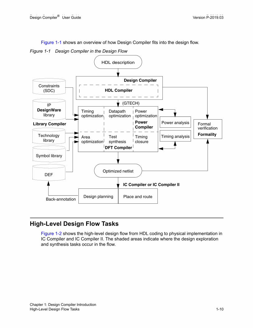
Design Compiler® User Guide P-2019.03Design Compiler® User Guide Version P-2019.03
Figure 1-1 shows an overview of how Design Compiler fits into the design flow.
Figure 1-1 Design Compiler in the Design Flow
High-Level Design Flow Tasks
Figure 1-2 shows the high-level design flow from HDL coding to physical implementation in IC Compiler and IC Compiler II. The shaded areas indicate where the design exploration and synthesis tasks occur in the flow.
Design planning Place and route
HDL description
HDL Compiler
Design Compiler
Optimized netlist
Formal verification
Back-annotation
Timingoptimization optimization optimization
optimization
Datapath Power
Area Testsynthesis
Timing closure
Constraints(SDC)
DesignWarelibrary
Technologylibrary
Symbol library
DEF
IC Compiler or IC Compiler II
Formality
Library Compiler
IP
Power Compiler
DFT Compiler
(GTECH)
Timing analysis
Power analysis
Chapter 1: Design Compiler IntroductionHigh-Level Design Flow Tasks 1-10

Design Compiler® User Guide Version P-2019.03
Figure 1-2 High-Level Design Flow
The synthesis design flow consists of the design exploration stage and the final design implementation stage. In the design exploration stage, you use DC Explorer to perform what-if analysis of various design configurations early in the design cycle to speed the
Design data preparation:
Yes
Design Compiler
Physical design
Proceed to physical implementation with the IC Compiler or IC Compiler II tool
No
No
Yes
Yes
DC Explorer
Goal specification and functional simulation
No
Within 10%
goals?of timing
Metgoals?
Design ExplorationStage
Design ImplementationStage
Metgoals?
- HDL coding- Constraint generation- Library development
Floorplan(optional)
Chapter 1: Design Compiler IntroductionHigh-Level Design Flow Tasks 1-11Chapter 1: Design Compiler IntroductionHigh-Level Design Flow Tasks 1-11

Design Compiler® User Guide P-2019.03Design Compiler® User Guide Version P-2019.03
development of high-quality RTL and constraints and drive a faster, more convergent design flow. In the design implementation stage, you use the full power of Design Compiler to synthesize the design.
Using the high-level design flow shown in Figure 1-2, you perform the following tasks:
1. Write an HDL description of your design in Verilog or VHDL. Use good coding practices to facilitate successful Design Compiler synthesis of the design.
2. Perform design exploration and functional simulation in parallel.
❍ In design exploration, use DC Explorer to (a) implement specific design goals, such as design rules and optimization constraints, (b) detect mismatches and missing constraints, and (c) resolve mismatches and design data inconsistencies.
You can also create and modify floorplans early in the design cycle with floorplan exploration.
❍ If design exploration fails to meet timing goals by more than 10 percent, modify your design goals and constraints, or improve the HDL code. Then repeat both design exploration and functional simulation.
❍ In functional simulation, determine whether the design performs the desired functions by using an appropriate simulation tool.
❍ If the design does not function as required, you must modify the HDL code and repeat both design exploration and functional simulation.
❍ Continue performing design exploration and functional simulation until the design is functioning correctly and is within 10 percent of the timing goals.
3. Perform design implementation synthesis by using Design Compiler to meet design goals.
After synthesizing the design into a gate-level netlist, verify that the design meets your goals. If the design does not meet your goals, generate and analyze various reports to determine the techniques you might use to correct the problems.
4. After the design meets functionality, timing, power, and other design goals, proceed to the physical implementation stage in the IC Compiler or IC Compiler II tool.
5. Analyze the physical design’s performance by using back-annotated data. If the results do not meet design goals, resolve them in IC Compiler or return to step 3. If the results meet your design goals, you are finished with the design cycle.
See Also
• Design Compiler in the Design Flow
• The Synthesis Flow
Chapter 1: Design Compiler IntroductionHigh-Level Design Flow Tasks 1-12

Design Compiler® User Guide Version P-2019.03
Design Terminology
Even though the following terms have slightly different meanings, they are often used synonymously in the Design Compiler documentation:
• Synthesis is the process that generates a gate-level netlist for an IC design that has been defined with a hardware description language (HDL). Synthesis includes reading the HDL source code and optimizing the design created from that description.
• Optimization is the step in the synthesis process that implements a combination of library cells that best meet the functional, timing, area, and power requirements of the design.
• Compile is the Design Compiler process that executes the synthesis and optimization steps. After you read in the design and perform other necessary tasks, you run the compile_ultra or compile command to generate a gate-level netlist for the design.
Different companies use different terminology for designs and their components. The following topics describe the terminology used in the Synopsys synthesis tools and the relationship between design instances and references.
• Designs
• Design Objects
• Relationship Between Designs, Instances, and References
Designs
Designs are circuit descriptions that perform logical functions. Designs are described in various design formats, such as VHDL or Verilog HDL. Logic-level designs are represented as sets of Boolean equations. Gate-level designs, such as netlists, are represented as interconnected cells.
Designs can exist and be compiled independently of one another, or they can be used as subdesigns in larger designs. Designs are flat or hierarchical:
• Flat Designs
Flat designs contain no subdesigns and have only one structural level. They contain only library cells.
• Hierarchical Designs
Hierarchical designs contains one or more designs as subdesigns. Each subdesign can further contain subdesigns, creating multiple levels of design hierarchy. Designs that contain subdesigns are called parent designs.
Chapter 1: Design Compiler IntroductionDesign Terminology 1-13Chapter 1: Design Compiler IntroductionDesign Terminology 1-13

Design Compiler® User Guide P-2019.03Design Compiler® User Guide Version P-2019.03
Design Objects
Synopsys commands, attributes, and constraints are directed toward the specific design objects described in this topic. Figure 1-3 shows the design objects in a design called TOP.
Figure 1-3 Design Objects
Design
A design consists of instances, nets, ports, and pins. It can contain subdesigns and library cells. In Figure 1-3, the designs are TOP, ENCODER, and REGFILE. The active design (the design being worked on) is called the current design. Most commands are specific to the current design, that is, they operate within the context of the current design.
Reference
A reference is a library component or design that can be used as an element in building a larger circuit. The structure of the reference can be a simple logic gate or a more complex design (a RAM core or CPU). A design can contain multiple occurrences of a reference; each occurrence is an instance.
INV1
INV0U2
U3
U1
Q0
Q1
A
B
C
D
D0
D1
U4
OUT[1:0]
ENCODER REGFILE
CLK
Q[1:0]
AIN
BIN
BUS0
BUS1
INV
INV
TOP
Design Port Instance or Net
D0
D1
Pin
Design: {TOP, ENCODER, REGFILE}
Reference: {ENCODER, REGFILE, INV}
Instance: {U1, U2, U3, U4}
CIN
DIN
A
B
C
D
Cell
Chapter 1: Design Compiler IntroductionDesign Terminology 1-14

Design Compiler® User Guide Version P-2019.03
References enable you to optimize every cell (such as a NAND gate) in a single design without affecting cells in other designs. The references in one design are independent of the same references in a different design. In Figure 1-3, the references are INV, ENCODER, and REGFILE.
Instance or Cell
An instance is an occurrence in a circuit of a reference (a library component or design) loaded in memory; each instance has a unique name. A design can contain multiple instances; each instance points to the same reference but has a unique name to distinguish it from other instances. An instance is also known as a cell.
A unique instance of a design within another design is called a hierarchical instance. A unique instance of a library cell within a design is called a leaf cell. Some commands work within the context of a hierarchical instance of the current design. The current instance defines the active instance for these instance-specific commands. In Figure 1-3, the instances are U1, U2, U3, and U4.
Ports
Ports are the inputs and outputs of a design. The port direction is designated as input, output, or inout.
Pins
Pins are the input and output of cells (such as gates and flip-flops) within a design. The ports of a subdesign are pins within the parent design.
Nets
Nets are the wires that connect ports to pins and pins to each other.
Chapter 1: Design Compiler IntroductionDesign Terminology 1-15Chapter 1: Design Compiler IntroductionDesign Terminology 1-15

Design Compiler® User Guide P-2019.03Design Compiler® User Guide Version P-2019.03
Relationship Between Designs, Instances, and References
Figure 1-4 shows the relationships among designs, instances, and references.
Figure 1-4 Instances and References
The EXREF design contains two references: NAND2 and MULTIPLIER. NAND2 is instantiated three times, and MULTIPLIER is instantiated one time.
The names given to the three instances of NAND2 are U1, U2, and U3. The references of NAND2 and MULTIPLIER in the EXREF design are independent of the same references in different designs.
See Also
• Linking Designs
Provides information about resolving references
• Working With Designs in Memory
Provides information about changing designs, such as grouping or ungrouping subdesigns or changing subdesign references
Selecting and Using a Compile Strategy
To compile a design, you use the compile command in DC Expert or the compile_ultra command in DC Ultra or DC Graphical. Command options allow you to customize and control optimization. When you compile a design, Design Compiler reads the HDL source code and optimizes the design created from that description. The tool uses heuristics to implement a combination of library cells that meets the functional, speed, and area requirements of the design according to the attributes and constraints placed on it. The optimization process trades off timing and area constraints to provide the smallest possible circuit that meets the specified timing requirements.
EXREF
NAND2
MULTIPLIER
U1
NAND2
U3
NAND2
U2
U4
Designs loaded in memory
NAND2
MULTIPLIER
(references)
Chapter 1: Design Compiler IntroductionSelecting and Using a Compile Strategy 1-16
Design Compiler® User Guide Version P-2019.03
Design Compiler supports the following compile flows:
• Full compile
During a full compile, Design Compiler maps and optimizes the entire design, resulting in a gate-level netlist of the design. Any mapped cells are unmapped to their logic function first; no attempt is made to preserve existing netlist structures.
• Incremental compile
During an incremental compile, Design Compiler can improve quality of results (QoR) by improving the structure of your design after the initial compile. Incremental mapping uses the existing gates from an earlier compilation as a starting point for the mapping process. It improves the existing design cost by focusing on the areas of the design that do not meet constraints and affects the second pass of compile. The existing structure is preserved where all constraints are already met. Mapping optimizations are accepted only if they improve the circuit speed or area.
In topographical mode, you can perform a second-pass, incremental compile to enable topographical-based optimization for post-topographical-based synthesis flows such as retiming, design-for-test (DFT), DFTMAX, and minor netlist edits. The primary focus in Design Compiler topographical mode is to maintain QoR correlation; therefore, only limited changes to the netlist can be made.
Different pieces of your design require different compilation strategies, such as a top-down hierarchical compile or bottom-up compile. You need to develop a compilation strategy before you compile.
You can use various strategies to compile, depending on your design, and you can mix strategies. The following strategies compile hierarchical designs in either wire load mode or topographical mode:
• Top-down compile
The top-level design and all its subdesigns are compiled together.
• Bottom-up compile
The individual subdesigns are compiled separately, starting from the bottom of the hierarchy and proceeding up through the levels of the hierarchy until the top-level design is compiled.
• Mixed compile
You can take advantage of the benefits of the top-down and the bottom-up compile strategies by using both strategies.
❍ Use the top-down compile strategy for small hierarchies of blocks.
❍ Use the bottom-up compile strategy to tie small hierarchies together into larger blocks.
Chapter 1: Design Compiler IntroductionSelecting and Using a Compile Strategy 1-17Chapter 1: Design Compiler IntroductionSelecting and Using a Compile Strategy 1-17

Design Compiler® User Guide P-2019.03Design Compiler® User Guide Version P-2019.03
See Also
• Full and Incremental Compilation
Provides more information about full and incremental compilation
• Compile Strategies
Provides detailed steps for top-down, bottom-up, and mixed compile strategies
• Compile Flows in Topographical Mode
Provides more information about performing an incremental compile and steps for performing a bottom-up (hierarchical) compile in topographical mode
Optimization Basics
Optimization is the Design Compiler synthesis step that maps the design to an optimal combination of specific target logic library cells, based on the design’s functional, speed, and power requirements. You use the compile or the compile_ultra command to start the synthesis and optimization processes. Optimization transforms the design into a technology-specific circuit based on the attributes and constraints you place on the design.
During optimization, Design Compiler uses heuristics to meet the constraints you have set on the design. Design Compiler’s optimization algorithms use costs to determine if a design change is an improvement. Design Compiler calculates two cost functions: one for design rule constraints and one for optimization constraints. Optimization accepts a change if it decreases the cost of one component without increasing more-important costs. By default, the design rule constraints (transition, fanout, capacitance, and cell degradation) have a higher priority than the optimization constraints (delay and area).
Design Compiler performs the following levels of optimization in the following order:
1. Architectural Optimization
2. Logic-Level Optimization
3. Gate-Level Optimization
Experimenting with speed and area to get the smallest or fastest design is called exploring the design space. Using Design Compiler, you can examine different implementations of the same design in a relatively short time. Figure 1-5 shows a design space curve. The shape of the curve demonstrates the tradeoff between area-efficient and speed-efficient circuits.
Chapter 1: Design Compiler IntroductionOptimization Basics 1-18

Design Compiler® User Guide Version P-2019.03
Figure 1-5 Design Space Curve
See Also
• Optimization Constraints
• Optimizing the Design
AREA
DELAY
1,100
3000
Chapter 1: Design Compiler IntroductionOptimization Basics 1-19Chapter 1: Design Compiler IntroductionOptimization Basics 1-19

Design Compiler® User Guide P-2019.03Design Compiler® User Guide Version P-2019.03
Chapter 1: Design Compiler IntroductionOptimization Basics 1-20

2Working With Design Compiler 2
Design Compiler offers the following interfaces for synthesis and timing analysis: the dcnxt_shell and the dc_shell command-line interfaces, and the Design Vision user interface (GUI). The dcnxt_shell or dc_shell command-line interfaces are a text-only environments in which you enter commands at the command-line prompt. Design Vision is the GUI for the Synopsys logic synthesis environment; use it for visualizing design data and analyzing results.
To learn how to use the Design Compiler tools to run a synthesis flow, see the following topics:
• Running Design Compiler
• The Synthesis Flow
• A Design Compiler Session Example
• Using Multicore Technology
• Runtime Improvement Techniques Outside of Synthesis
2-1

Design Compiler® User Guide P-2019.03Design Compiler® User Guide Version P-2019.03
Running Design Compiler
To learn how to run Design Compiler using dcnxt_shell or dc_shell, see the following topics:
• Design Compiler Modes
• Working With Licenses
• The Setup Files
• Starting the Tool in Wire Load Mode
• Starting the Tool in Topographical Mode
• Design Compiler Startup Tasks
• Entering dcnxt_shell or dc_shell Commands
• Redirecting the Output of Commands
• Interrupting or Terminating Command Processing
• Finding Session Information in the Log Files
• Using Script Files
• Getting Help on the Command Line
• Saving Designs and Exiting Design Compiler
You can also use the GUI to perform many of the tasks in this topic. For more information, see the Design Vision User Guide.
Design Compiler Modes
You can use Design Compiler in the following modes. Wire load mode and topographical mode are tool modes. When you start Design Compiler, you must choose either wire load mode or topographical mode. Multimode and UPF mode are not tool modes. Multimode allows you to operate the tool under multiple operating conditions and multiple modes, such as test mode and standby mode. UPF mode allows you to specify advanced low-power methodologies. Multimode and UPF mode are available only in topographical mode.
• Wire Load Mode (Default)
• Topographical Mode
• Multimode
• UPF Mode
Chapter 2: Working With Design CompilerRunning Design Compiler 2-2

Design Compiler® User Guide Version P-2019.03
Wire Load Mode (Default)
When you invoke Design Compiler with the dcnxt_shell or dc_shell command, the tool runs in the default mode, which uses wire load models for delay estimation:
% dcnxt_shell
or
% dc_shell
In this mode, you can run the following compilation commands:
• compile
The compile command runs DC Expert. DC Expert synthesizes your HDL descriptions into optimized, technology-dependent, gate-level designs. It supports a wide range of flat and hierarchical design styles and can optimize both combinational and sequential designs for area, timing, and power.
• compile_ultra
The compile_ultra command in wire load mode runs DC Ultra without the topographical mode features. DC Ultra provides concurrent optimization of timing, area, power, and test for high performance designs. It also provides advanced delay and arithmetic optimization, advanced timing analysis, automatic leakage power optimization, and register retiming. For more information, see The compile_ultra Command.
See Also
• DC Expert
• DC Ultra
Topographical Mode
If you are using physical constraints on your design, you must use Design Compiler in topographical mode. Topographical mode allows you to accurately predict post-layout timing, area, and power during synthesis without the need for timing approximations based on wire load models. It uses placement and optimization technologies to drive accurate timing prediction within synthesis and automatically performs leakage power optimization, ensuring better correlation with the final physical design.
To invoke Design Compiler NXT in topographical mode, run the dcnxt_shell command with the -topographical_mode option:
% dcnxt_shell -topographical_mode
Chapter 2: Working With Design CompilerRunning Design Compiler 2-3Chapter 2: Working With Design CompilerRunning Design Compiler 2-3

Design Compiler® User Guide P-2019.03Design Compiler® User Guide Version P-2019.03
To invoke Design Compiler Graphical in topographical mode, run the dc_shell command with the -topographical_mode option:
% dc_shell -topographical_mode
In the topographical mode, you can run the following compilation commands:
• compile_ultra
Uses the DC Ultra tool with the topographical mode features enabled. Topographical technology derives a “virtual layout” of the design so the tool can accurately predict and use real net capacitances instead of statistical net approximations based on wire load models. This generates a better starting point for place and route, eliminating costly iterations. Topographical technology ensures better correlation with the final physical design.
• compile_ultra -spg
Uses the Design Compiler NXT and Design Compiler Graphical tools, which are the extension of DC Ultra topographical technology.
The Design Compiler NXT tool provides
❍ Better QoR through advanced optimizations
❍ Enhanced physical guidance to IC Compiler II, with improved RC and timing correlation
❍ Faster runtime, with improved multithreading synthesis for better scalability
❍ Plug-and-play user interface and script compatibility with Design Compiler Graphical
❍ Buffering-aware placement
❍ Automatic timing control
❍ Congestion-driven restructuring
❍ Better QOR with high performance cores
The Design Compiler Graphical tool
❍ Optimizes multicorner-multimode designs
❍ Reduces routing congestion
❍ Improves correlation with IC Compiler and IC Compiler II
❍ Improves runtime in IC Compiler and IC Compiler II by using Synopsys physical guidance
❍ Allows you to create and modify floorplans
Chapter 2: Working With Design CompilerRunning Design Compiler 2-4

Design Compiler® User Guide Version P-2019.03
See Also
• DC Ultra
• Design Compiler Graphical
• Design Compiler NXT
Multimode
Designs are often required to operate under multiple modes, such as test or standby mode, and under multiple operating conditions, sometimes referred to as corners. Such designs are known as multicorner-multimode designs. The Design Compiler NXT and Design Compiler Graphical tools can analyze and optimize designs across multiple modes and corners concurrently.
The multicorner-multimode feature in the Design Compiler NXT and Design Compiler Graphical tools provides compatibility between Design Compiler and IC Compiler flows.
For details about defining modes and corners and setting up multicorner-multimode analysis, see Optimizing Multicorner-Multimode Designs.
UPF Mode
You can use IEEE 1801—also known as Unified Power Format (UPF)—commands in a UPF file to specify low-power design intent for multivoltage designs when you use the Power Compiler tool. The UPF set of Tcl-like commands provide the ability to specify the power intent early in the design process. In addition, UPF is supported throughout the design flow.
For information about multivoltage design concepts and using UPF mode to synthesize your multivoltage designs in Power Compiler, see the Power Compiler User Guide.
Working With Licenses
You need to determine which licenses are in use and know how to obtain and release licenses. You can use dcnxt_shell or dc_shell commands or the GUI to view, check out, and release licenses.
To learn about working with licenses, see the following topics:
• License Requirements
• Enabling License Queuing
• Listing the Licenses in Use
• Checking Out Licenses
Chapter 2: Working With Design CompilerRunning Design Compiler 2-5Chapter 2: Working With Design CompilerRunning Design Compiler 2-5

Design Compiler® User Guide P-2019.03Design Compiler® User Guide Version P-2019.03
• Releasing Licenses
• Checking DesignWare Licenses
License Requirements
You need the appropriate licenses to run Design Compiler in wire load or topographical mode. Design Compiler NXT, Design Compiler Graphical, DC Ultra, and DC Expert require their own licenses. Some features require additional licenses or add-ons to the Design Compiler NXT, Design Compiler Graphical, DC Ultra, and DC Expert licenses. To determine which licenses your need for your design flow, contact your Synopsys representative.
When you start the tool, Design Compiler automatically checks out the necessary license or licenses. When you exit from Design Compiler, the licenses are automatically checked in, allowing others at your site to use them.
Enabling License Queuing
Design Compiler has a license queuing functionality that allows your application to wait for licenses to become available if all licenses are in use. To enable this functionality, set the SNPSLMD_QUEUE environment variable to true before you start the Design Compiler tool. When you invoke the tool, Design Compiler displays the following message:
Information: License queuing is enabled. (DCSH-18)
When you have enabled the license queuing functionality, you might run into a situation where you hold license L1 while waiting for license L2, and another user holds license L2 while waiting for license L1. In that case, both you and the other user might wait indefinitely, unless more licenses become available.
To prevent such situations, use the SNPS_MAX_WAITTIME and the SNPS_MAX_QUEUETIME environment variables. You must set the SNPSLMD_QUEUE environment variable to true before using these two variables.
• The SNPS_MAX_WAITTIME variable specifies the maximum wait time in seconds for the first license that you require.
• The SNPS_MAX_QUEUETIME variable specifies the maximum wait time in seconds for checking out subsequent licenses within the same dcnxt_shell or dc_shell process. You use this variable after you have successfully checked out the first license to start dcnxt_shell or dc_shell.
Consider the following scenario: You have already started Design Compiler and are running a command that requires a DC-Ultra-Features license. The queuing functionality attempts to check out the license within the specified wait time. The default is 28,800 seconds (or eight hours). If the license is still not available after the predefined time, you might see a message similar to the following:
Chapter 2: Working With Design CompilerRunning Design Compiler 2-6

Design Compiler® User Guide Version P-2019.03
Information: Timeout while waiting for feature 'DC-Ultra-Features.'(DCSH-17)
When you run your design through the synthesis flow, the queuing functionality might display other status messages as follows:
Information: Started queuing for feature 'HDL-Compiler'. (DCSH-15)Information: Still waiting for feature 'HDL-Compiler'. (DCSH-16)Information: Successfully checked out feature 'HDL-Compiler'. (DCSH-14)
Listing the Licenses in Use
To view the licenses that you currently have checked out using Design Compiler in wire load or topographical mode, use the following command:
prompt> list_licenses
Licenses in use:DC-ExtensionDesign-Compiler-NXTDC-Expert (3)DC-Ultra-Features (3)DC-Ultra-Opt (3)Design-CompilerDesignWare
1
To display which licenses are already checked out, use the following command:
prompt> license_users
bill@eng1 Design-Compilermatt@eng2 Design-Compiler, DC-Ultra-Opt2 users listed.1
Checking Out Licenses
When you invoke Design Compiler in topographical or wire load mode, the Synopsys Common Licensing software automatically checks out the appropriate license. For example, if you read in an HDL design description, Synopsys Common Licensing checks out a license for the appropriate HDL compiler.
If you know the tools and interfaces you need, you can use the get_license command to check out those licenses. This ensures that each license is available when you are ready to use it. By default, only one license is checked out for each feature. After a license is checked out, it remains checked out until you release it or exit dcnxt_shell or dc_shell.
If multiple licenses are required for a multicore run, use the -quantity option to specify the total number of licenses needed. If licenses have already been checked out, Design
Chapter 2: Working With Design CompilerRunning Design Compiler 2-7Chapter 2: Working With Design CompilerRunning Design Compiler 2-7

Design Compiler® User Guide P-2019.03Design Compiler® User Guide Version P-2019.03
Compiler acquires only the additional licenses needed to bring the total to the specified quantity.
In the following example, Design Compiler in topographical mode checks out a license for the multivoltage feature:
prompt> get_license Galaxy-MV
In the following example, Design Compiler in topographical mode checks out two of the licenses required to run a multicore compile_ultra command:
prompt> get_license -quantity 2 \ {DC-Expert DC-Ultra-Opt DC-Ultra-Features}
The tool checks out a copy of the license if one is available or displays an error message if all the licenses are already taken.
Checking DesignWare Licenses
If any DesignWare component set in the synthetic_library variable requires a DesignWare license, Design Compiler checks for this license. You do not need to specify the standard synthetic library, standard.sldb, that implements the built-in HDL operators. Design Compiler automatically uses this library.
You can force Design Compiler to wait for a DesignWare license by setting the synlib_wait_for_design_license variable to DesignWare as follows:
prompt> set_app_var synlib_wait_for_design_license "DesignWare"
See Also
• DesignWare Libraries
Releasing Licenses
To release a license that is checked out to you in topographical or wire load mode, use the following command:
prompt> remove_license HDL-Compiler
For multicore runs, where multiple licenses might be required for certain features, use the -keep option to specify how many licenses should be retained for each feature after the command has completed.
The following example removes some, but not all, of the licenses required for a multicore compile_ultra run in Design Compiler:
prompt> list_licensesLicenses in use:
DC-Extension
Chapter 2: Working With Design CompilerRunning Design Compiler 2-8

Design Compiler® User Guide Version P-2019.03
Design-Compiler-NXT DC-Expert (4) DC-Ultra-Features (4) DC-Ultra-Opt (4) Design-Compiler1prompt> remove_license -keep 2 \
{DC-Expert DC-Ultra-Opt DC-Ultra-Features}
prompt> list_licensesLicenses in use:
DC-ExtensionDesign-Compiler-NXT
DC-Expert (2) DC-Ultra-Features (2) DC-Ultra-Opt (2) Design-Compiler1
The Setup Files
Before starting Design Compiler, make sure your $SYNOPSYS variable is set, and the path to the bin directory is included in your $PATH variable. Be sure to specify the absolute path to indicate the Synopsys root that contains the Design Compiler installation, as shown:
/tools/synopsys/2014.09/bin/
If you use a relative path (../), as shown, Design Compiler cannot access the libraries that are located in the root directory:
../../2014.09/bin/
When you invoke Design Compiler in wire load or topographical mode, it automatically executes commands in three setup files. These files have the same file name, .synopsys_dc.setup, but reside in different directories. The files can contain commands that initialize parameters and variables, declare design libraries, and so on.
Design Compiler reads the setup files from three directories in the following order:
1. The Synopsys root directory ($SYNOPSYS/admin/setup)
This system-wide setup file contains system variables defined by Synopsys and general Design Compiler setup information for all users at your site. Only the system administrator can modify this file.
2. Your home directory
This user-defined setup file can contain variables that define your preferences for the Design Compiler working environment. The variables in this file override the corresponding variables in the system-wide setup file.
Chapter 2: Working With Design CompilerRunning Design Compiler 2-9Chapter 2: Working With Design CompilerRunning Design Compiler 2-9

Design Compiler® User Guide P-2019.03Design Compiler® User Guide Version P-2019.03
3. The current working directory (the directory from which you start Design Compiler)
This design-specific setup file can contain project-specific or design-specific variables that affect the optimizations of all designs in this directory. To use the file, you must invoke Design Compiler from this directory. Variables defined in this file override the corresponding variables in the user-defined and system-wide setup files.
Example 2-1 shows a .synopsys_dc.setup file.
Example 2-1 .synopsys_dc.setup File
# Define the target logic library, symbol library, # and link librariesset_app_var target_library lsi_10k.dbset_app_var symbol_library lsi_10k.sdbset_app_var synthetic_library dw_foundation.sldbset_app_var link_library “* $target_library $synthetic_library"set_app_var search_path [concat $search_path ./src]set_app_var designer "Your Name"
# Define aliasesalias h historyalias rc “report_constraint -all_violators"
Some ASIC and EDA vendors have a program that creates a .synopsys_dc.setup file that includes the appropriate commands to convert names to their conventions. For an example of a naming rules section in a .synopsys_dc.setup file, see Example 2-2.
See Also
• Synthesis Tools Installation Notes
Provides information about defining the $PATH and $SYNOPSYS variables
• Naming Rules Section of the .synopsys_dc.setup File
Naming Rules Section of the .synopsys_dc.setup File
Example 2-2 shows sample naming rules created by a specific layout tool vendor. These naming rules do the following:
• Limit object names to alphanumeric characters
• Change DesignWare cell names to valid names (changes “*cell*” to “U” and “*-return” to “RET”)
Your vendor might use different naming conventions. Check with your vendor to determine the naming conventions you need to follow. If you need to change any net or port names, use the define_name_rules and change_names commands.
Chapter 2: Working With Design CompilerRunning Design Compiler 2-10

Design Compiler® User Guide Version P-2019.03
Example 2-2 Naming Rules Section of .synopsys_dc.setup File
define_name_rules simple_names -allowed "A-Za-z0-9_" \-last_restricted "_" \-first_restricted "_" \-map { {{"\*cell\*","U"}, {"*-return","RET"}} }
Starting the Tool in Wire Load Mode
You start Design Compiler by entering the following commands in a UNIX or Linux shell:
• The dcnxt_shell command.
% dcnxt_shell
Be sure to specify the absolute path to indicate the Synopsys root that contains the Design Compiler NXT installation, as shown:
% /tools/synopsys/2019.03/bin/dcnxt_shell
If you use a relative path (../), as shown, Design Compiler NXT cannot access the libraries that are located in the root directory:
% ../../2019.03/bin/dcnxt_shell
• The dc_shell command.
% dc_shell
Be sure to specify the absolute path to indicate the Synopsys root that contains the Design Compiler installation, as shown:
% /tools/synopsys/2019.03/bin/dc_shell
If you use a relative path (../), as shown, Design Compiler cannot access the libraries that are located in the root directory:
% ../../2019.03/bin/dc_shell
To execute a script file before displaying the initial dcnxt_shell or dc_shell prompt, specify the -f option with the dcnxt_shell or dc_shell command. To include any command statements that you want to be executed automatically at startup, specify the -x option.
You can also open the GUI when you start Design Compiler by specifying the -gui option with the dcnxt_shell and dc_shell commands. You must have a Design Vision license to use the GUI from a dcnxt_shell and dc_shell session.
You can open the GUI at any time from the Design Compiler command-line interface by entering the gui_start command at the dcnxt_shell or dc_shell prompt:
prompt> gui_start
Chapter 2: Working With Design CompilerRunning Design Compiler 2-11Chapter 2: Working With Design CompilerRunning Design Compiler 2-11

Design Compiler® User Guide P-2019.03Design Compiler® User Guide Version P-2019.03
For more information about using the GUI, see the Design Vision User Guide.
For information about the options you can use when you start the tool, see the dcnxt_shell and dc_shell man pages.
When you start the command-line interface, the dcnxt_shell or dc_shell prompt appears in the UNIX or Linux shell:
dcnxt_shell>
or
dc_shell>
Starting the Tool in Topographical Mode
If you are using Design Compiler in topographical mode, following the instructions in Starting the Tool in Wire Load Mode and specify the -topographical_mode option with the dcnxt_shell or dc_shell command:
For Design Compiler NXT,
• % dcnxt_shell -topographical_mode
The resulting command prompt is
dcnxt_shell-topo>
For Design Compiler Graphical,
• % dc_shell -topographical_mode
The resulting command prompt is
dc_shell-topo>
Design Compiler Startup Tasks
At startup, dcnxt_shell or dc_shell does the following tasks:
1. Creates a command log file.
2. Reads and executes the .synopsys_dc.setup files, as described in The Setup Files.
3. Executes any script files or commands specified by the -f and -x options, respectively, on the command line.
4. Displays the program header and dcnxt_shell or dc_shell prompt in the window from which you invoked dcnxt_shell or dc_shell. The program header lists all features for which your site is licensed.
Chapter 2: Working With Design CompilerRunning Design Compiler 2-12

Design Compiler® User Guide Version P-2019.03
Entering dcnxt_shell or dc_shell Commands
Design Compiler shell (dcnxt_shell or dc_shell) commands are based on the tool command language (Tcl), including certain command extensions needed to implement specific Design Compiler functionality. The Design Compiler command language provides capabilities similar to UNIX command shells, including variables, conditional execution of commands, and control flow commands. You can
• Enter individual commands interactively at the dcnxt_shell or dc_shell prompt
• Run one or more Tcl command scripts, which are text files that contain dcnxt_shell or dc_shell commands
You enter commands in dcnxt_shell or dc_shell the same way you enter commands in a standard UNIX or Linux shell. When entering a command, option, or file name, you can minimize your typing by pressing the Tab key when you have typed enough characters to specify a unique name; Design Compiler completes the remaining characters. If the characters you typed could be used for more than one name, Design Compiler lists the qualifying names from which you can select by using the arrow keys and the Enter key.
To get a list of all dcnxt_shell or dc_shell commands on the command line, enter
prompt> help
You can reuse a command from the output for a command-line interface by copying and pasting it to the dcnxt_shell or dc_shell command line.
When the GUI is open, you can enter commands on the console command line and use the commands available through the menu interface. You can select commands in the console history view and either rerun them or copy them to the command line, where you can edit them. For more information, see the “Viewing the Command History” topic in Design Vision Help.
See Also
• Using Tcl With Synopsys Tools
Chapter 2: Working With Design CompilerRunning Design Compiler 2-13Chapter 2: Working With Design CompilerRunning Design Compiler 2-13

Design Compiler® User Guide P-2019.03Design Compiler® User Guide Version P-2019.03
Redirecting the Output of Commands
You can redirect or append the output of the commands to a file you can review. This way, you can archive runtime messages for future reference.
Note: The pipe character ( | ) has no meaning in the dcnxt_shell or dc_shell interface.
Interrupting or Terminating Command Processing
If you enter the wrong options for a command or enter the wrong command, you can interrupt command processing and remain in dcnxt_shell or dc_shell. To interrupt or terminate a command, press Ctrl+C.
Some commands and processes, such as the update_timing command, cannot be interrupted. To stop these commands or processes, you must terminate dcnxt_shell or dc_shell at the system level. When you terminate a process or the shell, no data is saved.
When you press Ctrl+C, remember the following points:
• If a script file is being processed and you interrupt one of its commands, the script processing is interrupted and no further script commands are processed.
• If you press Ctrl+C three times before a command responds to your interrupt, dcnxt_shell or dc_shell is interrupted and exits with the following message:
Information: Process terminated by interrupt.
This behavior has a few exceptions, which are documented in the man pages for the applicable commands.
Table 2-1 Redirecting the Command Output
To do this Use this
Divert command output to a file. > (redirection operator)
Append command output to a file. >> (append operator)
Redirect command output to a file. The redirect command
Chapter 2: Working With Design CompilerRunning Design Compiler 2-14

Design Compiler® User Guide Version P-2019.03
Finding Session Information in the Log Files
You can find session information, such as the dcnxt_shell or dc_shell commands that were processed and the files that were accessed, in the following log files:
• Command Log Files
• Compile Log Files
• File Name Log Files
Command Log Files
The command log file records the dcnxt_shell or dc_shell commands processed by Design Compiler, including setup file commands and variable assignments. By default, Design Compiler writes the command log to a file called command.log in the directory from which you invoked dcnxt_shell or dc_shell.
You can change the name of the command.log file by setting the sh_command_log_file variable in the .synopsys_dc.setup file. You should make any changes to this variable before you start Design Compiler. If your user-defined or project-specific .synopsys_dc.setup file does not define the variable, Design Compiler automatically creates the command.log file.
Each Design Compiler session overwrites the existing command log file. To save a command log file, move or rename it. You can use the command log file to
• Produce a script for a particular synthesis strategy
• Record the design exploration process
• Document any problems you are having
Compile Log Files
Each time you compile a design, Design Compiler creates the following compile log files:
• ASCII log file
The log displays the output, such as the commands that are processed and the error messages for each Design Compiler run, on the screen for quick viewing and debugging.
Chapter 2: Working With Design CompilerRunning Design Compiler 2-15Chapter 2: Working With Design CompilerRunning Design Compiler 2-15

Design Compiler® User Guide P-2019.03Design Compiler® User Guide Version P-2019.03
For example, each time Design Compiler begins a step, it prints a message in the compile log, indicating its progress:
prompt> compile_ultraBeginning Mapping Optimizations (Medium effort)
• HTML log file
The file resides under the current working directory. It contains the complete contents of the ASCII log but in HTML format. At the end of this file, a summary table provides an overview of all occurrences of messages grouped by the message ID. You can click the message ID link to display the message.
To generate the HTML log file in dcnxt_shell or dc_shell, set the html_log_enable variable to true before reading in the design. For example,
prompt> set_app_var html_log_enable true
By default, the html_log_enable variable is set to false, and only the ASCII log file is generated. The contents of the ASCII and HTML log files are identical. However, the way the contents are displayed is different. In the HTML log file, you can control the level of detail that is displayed by clicking the plus (+) or minus (-) buttons to expand or collapse multiple lines of messages.
By default, the HTML file name is default.html. To specify a different file name, set the html_log_filename variable. For example,
prompt> set_app_var html_log_filename my_HTML_log.html
Important: You must have the Python programming language installed to generate an HTML log file. For download information, go to the following address:
http://www.python.org/download
See Also
• Analyzing Your Design During Optimization Using the Compile Log
Trials Area Delta delay Total neg slack Design rule cost
3 1296477.2 7.58 3468.1 2.9
1 1296538.9 7.48 3382.7 2.9
Chapter 2: Working With Design CompilerRunning Design Compiler 2-16

Design Compiler® User Guide Version P-2019.03
File Name Log Files
By default, Design Compiler lists the names of the files that it has read to a log file in the directory from which you invoked dcnxt_shell or dc_shell. You can use the log file to identify data files needed to reproduce an error if Design Compiler terminates abnormally. To specify the name of the log file, set the filename_log_file variable in the .synopsys_dc.setup file.
Using Script Files
Scripts are used to accomplish repetitive routines, such as setting constraints or defining other design attributes. You can use your existing Tcl scripts in the Design Compiler command-line interface and GUI.
You can create a script file by placing a sequence of dcnxt_shell or dc_shell commands in a text file. You can also define scripts in your setup files. Any dcnxt_shell or dc_shell command can be executed within a script file.
In Tcl, a pound sign (#) at the beginning of a line denotes a comment:
# This is a comment.
To execute a script file before displaying the initial dcnxt_shell or dc_shell prompt, specify the -f option with the dcnxt_shell or dc_shell command. For example,
% dc_shell -f script_file_name
To execute a script file within the tool, use the source command at the command prompt and specify the file name:
prompt> source script_file_name
For example, the following command executes the dc.tcl top-down compile script in topographical mode that is shown in Example 2-3:
prompt> source dc.tcl
See Also
• Using Tcl With Synopsys Tools
• The “Using Tcl Scripts” topic in Design Vision Help
Chapter 2: Working With Design CompilerRunning Design Compiler 2-17Chapter 2: Working With Design CompilerRunning Design Compiler 2-17

Design Compiler® User Guide P-2019.03Design Compiler® User Guide Version P-2019.03
Getting Help on the Command Line
Design Compiler provides a variety of user-assistance tools. The following online information resources are available while you are using the Design Compiler tool:
• Command help lists the options and arguments used with a specified dcnxt_shell or dc_shell command and displays them in the Design Compiler shell and also in the console log view when the GUI is open.
To get information about the options available for a specific dcnxt_shell or dc_shell command, enter the command name with the -help option:
prompt> command_name -help
• Man pages are displayed in the Design Compiler shell and also in the console log view when the GUI is open.
To get the man page for a specific dcnxt_shell or dc_shell command or variable, enter
prompt> man command_or_variable_name
• The man page viewer displays command, variable, and error message man pages that you request while using the GUI.
To open the man page viewer, choose Help > Man Pages.
For information about using the GUI to get command help, display man pages, and access the Design Vision Help system, which contains topics that explain tasks that you can perform, see the Design Vision User Guide.
Saving Designs and Exiting Design Compiler
You can exit Design Compiler at any time and return to the operating system. By default, dcnxt_shell and dc_shell save the session information in the command.log file. However, if you change the name of the log file using the sh_command_log_file variable after you start the tool, session information might be lost.
Also, dcnxt_shell and dc_shell do not automatically save the designs loaded in memory. To save these designs before exiting, use the write_file command. For example,
prompt> write_file -format ddc -hierarchy -output my_design.ddc
To exit dcnxt_shell or dc_shell, do one of the following:
• If you are in the command-line interface, enter quit or exit.
• If you are running Design Compiler in interactive mode, and the tool is busy, press Ctrl+D.
Chapter 2: Working With Design CompilerRunning Design Compiler 2-18

Design Compiler® User Guide Version P-2019.03
The Synthesis Flow
Figure 2-1 shows a basic synthesis flow. You can use this synthesis flow during design exploration and design implementation.
The figure lists the basic DC Expert and DC Ultra commands that are commonly used in each step of the flow. All the commands shown in the figure can accept options, but no options are shown in the figure.
Note: In the “Select Compile Strategy” step, top down and bottom up are not commands. They refer to two commonly used compile strategies that use different combinations of commands.
Chapter 2: Working With Design CompilerThe Synthesis Flow 2-19Chapter 2: Working With Design CompilerThe Synthesis Flow 2-19

Design Compiler® User Guide P-2019.03Design Compiler® User Guide Version P-2019.03
Figure 2-1 Synthesis Flow
Define
Select
design environment
compile strategy
Setdesign constraints
Synthesize and optimize the design
Analyze and resolvedesign problems
Read design
Save thedesign database
Design rule constraints
Design optimization constraints
Specify libraries
Library objects
Develop HDL files
link_library
analyze
read_fileelaborate
set_operating_conditionsset_driveset_driving_cellset_loadset_fanout_load
Top downBottom up
set_max_transitionset_max_fanoutset_max_capacitance
create_clockset_clock_latencyset_propagated_clockset_clock_uncertaintyset_clock_transition
compile_ultra
check_design
report_areareport_constraintreport_timing
write_file
target_librarysymbol_librarysynthetic_library
set_input_delay
set_min_library
set_max_areaset_output_delay
create_mw_lib
create_qor_snapshotquery_qor_snapshot
set_wire_load_model
compile
Chapter 2: Working With Design CompilerThe Synthesis Flow 2-20

Design Compiler® User Guide Version P-2019.03
The following steps provide an overview of the synthesis flow:
1. Develop the HDL files.
The input design files for Design Compiler are written using a hardware description language (HDL) such as Verilog or VHDL. When preparing the HDL code, you need to consider design data management, design partitioning, and your HDL coding style.
For details, see Preparing for Synthesis and the HDL Compiler documentation.
2. Specify the libraries.
Specify the link, target, symbol, synthetic, and physical libraries.
For details, see Setting Up and Working With Libraries.
3. Read the design.
Design Compiler can read both RTL designs and gate-level netlists. Design Compiler uses HDL Compiler to read Verilog and VHDL RTL designs and Verilog and VHDL gate-level netlists. You can also read gate-level netlists in .ddc format.
For details, see Working With Designs in Memory.
For information about the recommended reading methods, see the HDL Compiler documentation.
4. Define the design environment.
Design Compiler requires that you model the environment of the design to be synthesized. This model comprises the external operating conditions (manufacturing process, temperature, and voltage), loads, drives, fanouts, and so on. It directly influences design synthesis and optimization results. If you are not using topographical mode, you need to specify wire load models to estimate the effect of wire length on design performance.
For details, see Defining the Design Environment.
5. Set the design constraints.
You define these constraints by using commands such as those listed under this step in Figure 2-1.
Note: Design constraint settings are influenced by the compile strategy you choose. Flow steps 5 and 6 are interdependent. Compile strategies are discussed in step 6.
For details, see Defining Design Constraints and Using Floorplan Physical Constraints
6. Select the compile strategy.
If your design is hierarchical, you must choose a compile strategy. You can use a top-down or bottom-up strategy. Both strategies have advantages and disadvantages, depending on your particular designs and design goals. You can use either strategy to
Chapter 2: Working With Design CompilerThe Synthesis Flow 2-21Chapter 2: Working With Design CompilerThe Synthesis Flow 2-21

Design Compiler® User Guide P-2019.03Design Compiler® User Guide Version P-2019.03
process the entire design, or you can use a mix of strategies, using the most appropriate strategy for each subdesign.
For details, see Compile Strategies.
7. (Optional) Provide the floorplan information.
If you are using topographical mode, you can provide a floorplan or floorplan constraints. If you do not specify a floorplan, Design Compiler creates one for you. However, specifying floorplan constraints ensures more accurate placement area and improved timing correlation with the post-place-and-route design.
For details, see Using Floorplan Physical Constraints and Performing a Bottom-up Hierarchical Compile.
8. Synthesize and optimize the design with the compile_ultra or compile command.
For details, see Optimizing the Design and Using Topographical Technology.
9. Insert scan chains.
Run the insert_dft command to insert scan chains.
For details, see the DFT Compiler User Guide.
10. Perform incremental synthesis.
Perform an incremental compile by using the compile_ultra -incremental -scan command or the compile -incremental_mapping -scan command.
The main goal for compile_ultra -incremental is to enable topographical-based optimization for post-topographical-based synthesis flows such as retiming, design-for-test (DFT), DFTMAX, and minor netlist edits.
For details, see Performing an Incremental Compile.
11. (Optional) Visually inspect the floorplan and placement results.
In topographical mode, use the GUI layout window to verify your floorplan and placement results. You can
❍ Examine the placement and orientation of objects such as macro cells, port locations, and physical constraints
❍ Examine the placement of critical timing path objects
❍ Analyze floorplan-related congestion and identify the causes of congestion hotspots
For details, see Using Design Compiler Graphical and the Design Vision Help.
12. Analyze and resolve design problems.
Design Compiler can generate numerous reports, such as area, constraint, and timing reports, on the synthesis and optimization results. You use reports to analyze and resolve any design problems or to improve synthesis results. You can use the
Chapter 2: Working With Design CompilerThe Synthesis Flow 2-22

Design Compiler® User Guide Version P-2019.03
check_design command to check the synthesized design for consistency. Other check_* commands are available.
You can also create a categorized timing report in HTML format by using the create_qor_snapshot and query_qor_snapshot commands. The report lets you quickly find paths with certain problems, such as large fanouts or transition degradation. You can then modify the constraints and generate a new report based on the constraints you specified.
For details, see Analyzing and Resolving Design Problems.
13. Save the design.
Use the write_file command to save the synthesized design. Design Compiler does not automatically save designs before exiting. You can write out the design in .ddc, Milkyway, or Verilog format.
For details, see Working With Designs in Memory. If you are using topographical mode, see Inputs and Outputs in Design Compiler Topographical Mode.
You can also save the design attributes and constraints used during synthesis in a script file. Script files are ideal for managing your design attributes and constraints. For details, see the information about using script files in Using Tcl With Synopsys Tools.
See Also
• Compile Flows in Topographical Mode
A Design Compiler Session Example
Example 2-3 shows a Tcl script that performs a top-down compile run. It uses the basic synthesis flow in topographical mode. The script contains comments that identify each step in the flow. Some of the script command options and arguments have not yet been explained in this manual. Nevertheless, from the previous discussion of the basic synthesis flow, you can begin to understand this example of a top-down compile.
Note: Only the set_driving_cell command is not discussed in the section on basic synthesis design flow. The set_driving_cell command is an alternative way to set the external drives on the ports of the design to be synthesized.
Example 2-3 Top-Down Compile Script in Topographical Mode
# Specify the librariesset_app_var search_path "$search_path ./libraries"set_app_var link_library "* max_lib.db" set_app_var target_library "max_lib.db"create_mw_lib -technology $mw_tech_file \-mw_reference_library $mw_reference_library $mw_lib_name
Chapter 2: Working With Design CompilerA Design Compiler Session Example 2-23Chapter 2: Working With Design CompilerA Design Compiler Session Example 2-23

Design Compiler® User Guide P-2019.03Design Compiler® User Guide Version P-2019.03
open_mw_lib $mw_lib_name
# Read the design read_verilog rtl.v
# Define the design environmentset_load 2.2 soutset_load 1.5 coutset_driving_cell -lib_cell FD1 [all_inputs]
# Set the optimization constraintscreate_clock clk -period 10set_input_delay -max 1.35 -clock clk {ain bin}set_input_delay -max 3.5 -clock clk cinset_output_delay -max 2.4 -clock clk coutextract_physical_constraints def_file_name
# Map and optimize the design compile_ultra
# Analyze and debug the designreport_timing
change_names -rules verilog -hierarchy
# Save the design databasewrite_file -format ddc -hierarchy -output top_synthesized.ddcwrite_file -format verilog -hierarchy -output netlist.v write_sdf sdf_file_namewrite_parasitics -output parasitics_file_name write_sdc sdc_file_name write_floorplan -all phys_cstr_file_name.tcl
You can execute these commands in any of the following ways:
• Enter dcnxt_shell or dc_shell and type each command in the order shown in the example.
• Enter dcnxt_shell or dc_shell and execute a script file by using the source command.
For example, if you are running Design Compiler and the script is in a file called run.scr, you can execute the script file by entering the following command:
prompt> source run.scr
• Run the script from the Linux command line by using the dcnxt_shell or dc_shell command with the -f option.
For example, the following command invokes Design Compiler in topographical mode and executes the run.scr script file from the Linux prompt:
% dc_shell -topographical_mode -f run.scr
Chapter 2: Working With Design CompilerA Design Compiler Session Example 2-24

Design Compiler® User Guide Version P-2019.03
Using Multicore Technology
The multicore technology in Design Compiler allows you to use multiple cores to improve the tool runtime. During synthesis, multicore functionality divides large optimization tasks into smaller tasks for processing on multiple cores. All compile_ultra command options support the use of multiple cores for optimization.
Multicore technology is supported in DC Ultra in wire load mode and topographical mode, Design Compiler NXT, and Design Compiler Graphical. It is not supported in DC Expert.
Multicore processing requires one Design Compiler license for every eight cores.
To enable multicore processing and report multicore runtime speedup, see
• Enabling Multicore Functionality
• Measuring Runtime
Enabling Multicore Functionality
To enable multicore functionality in Design Compiler, use the set_host_options command. For example, the following command enables the tool to use six cores to run your processes:
prompt> set_host_options -max_cores 6
Design Compiler automatically checks for the maximum number of CPU cores available on the execution host. If you specify a higher number of CPU cores than are available, the tool limits the CPU cores to the maximum cores available and issues a warning message. Design Compiler also checks the load of the multiple cores on multicore machines. If most of the cores are overloaded, the tool limits the number of cores based on the load, and it issues a warning message.
If you are in multicore mode, the log file contains an information message similar to the following message:
Information: Running optimization using a maximum of 8 cores. (OPT-1500)
Chapter 2: Working With Design CompilerUsing Multicore Technology 2-25Chapter 2: Working With Design CompilerUsing Multicore Technology 2-25

Design Compiler® User Guide P-2019.03Design Compiler® User Guide Version P-2019.03
Measuring Runtime
When you measure the runtime speedup using multicore optimization, use the wall clock time of the process. The CPU time does not correctly account for multicore runtime speedup.
To report the overall compile wall clock time, run the report_qor command, as shown in the following example. The command reports the combined wall clock time, combining the compile_ultra and compile_ultra -incremental command runs.
prompt> report_qor
****************************************Report : qor...****************************************...
Hostname: machine Compile CPU Statistics ----------------------------------------- Resource Sharing: 21.54 Logic Optimization: 182.63 Mapping Optimization: 230.79 ----------------------------------------- Overall Compile Time: 631.32 Overall Compile Wall Clock Time: 288.11
You can also check the wall clock time using the clock commands shown in the following example:
prompt> set_host_options -max_cores 2prompt> set pre_compile_clock [clock seconds]prompt> compile_ultraprompt> set post_compile_clock [clock seconds]prompt> set diff_clock \
[expr $post_compile_clock - $pre_compile_clock]
See Also
• Displaying Quality of Results
Chapter 2: Working With Design CompilerUsing Multicore Technology 2-26

Design Compiler® User Guide Version P-2019.03
Runtime Improvement Techniques Outside of Synthesis
Executing checking or reporting commands serially in a script can consume a significant portion of the overall runtime. To improve runtime, you can use multiple cores to run checking and reporting commands in the following ways:
• Run a command or a list of commands in the background while other commands run in the foreground
• Run commands in parallel in the foreground or in the background
For details, see the following topics:
• Running Commands in the Background
• Enabling Parallel Command Execution
Note: Multicore technology is supported in DC Ultra in both wire load mode and topographical mode, and it is supported in Design Compiler NXT and Design Compiler Graphical. It is not supported in DC Expert.
Running Commands in the Background
To improve runtime in the Design Compiler NXT and Design Compiler Graphical tools, you can run commands in the background while other commands run in the foreground by using the redirect command with the -bg option. You can run a single command, source a Tcl script to run several commands in parallel, or run a Tcl procedure.
You must specify the number of cores to use to run the background jobs. The number of cores available to redirect -bg is deducted from the cores set by the set_host_options command. When you use the redirect command to run a background job, dc_shell returns immediately to execute the next command.
The following example redirects a Tcl script to run in the background:
set_host_options -max_cores 8read_verilogread_sdc...compile_ultra -spgredirect -bg -max_cores 3 -file y.out {source y.tcl}remote_execute_source1.log {source bg_script.tcl}
Information: redirect -bg with max_cores 3 started. The maximum number of cores available in parent is reduced to 5. (BGE-004)
compile_ultra -spg -incremental
Chapter 2: Working With Design CompilerRuntime Improvement Techniques Outside of Synthesis 2-27Chapter 2: Working With Design CompilerRuntime Improvement Techniques Outside of Synthesis 2-27

Design Compiler® User Guide P-2019.03Design Compiler® User Guide Version P-2019.03
There can be only two background jobs active at a time. If you redirect a third command or script, the command waits until a previous redirect command is completed before starting the new job.
Supported commands include reporting, analysis, and design export commands only. Commands that change the netlist or other data are not supported.
You can also run the parallel_execute command inside the redirect -bg command to run a list of checking and reporting commands in parallel. For details, see Enabling Parallel Command Execution.
Verification Guidance Support
If you want to include the change_names guidance from the background job in your netlist for formal verification, you must stop recording Formality setup information before running the redirect -bg command and use the set_svf command to include an .svf file in the script executed by the redirect -bg command.
In the following example, the y.tcl script includes the set_svf be.svf command to generate verification guidance from the redirect -bg command that you can use in your netlist for formal verification in the Formality tool.
set_host_options -max_cores 8set_svf compile.svfread_verilogread_sdc...compile_ultra -spgset_svf –off redirect -bg -max_cores 3 -file y.out {source y.tcl} \remote_execute_source1.log {source bg_script.tcl} Information: redirect -bg with max_cores 3 started. The maximum number of cores available in parent is reduced to 5. (BGE-004)set_svf post_compile.svfcompile_ultra -spg -incremental
Be sure to use the correct .svf file when you run the Formality tool. For information about using the Formality tool for formal verification, see Verifying Functional Equivalence.
Reporting Jobs Submitted To Run in the Background
To report all the jobs that you have submitted to run in the background by the redirect -bg command, use the report_background_jobs command.
Chapter 2: Working With Design CompilerRuntime Improvement Techniques Outside of Synthesis 2-28

Design Compiler® User Guide Version P-2019.03
The report_background_jobs command reports the completed jobs and the jobs currently running in the background, as shown in the following example:
prompt> report_background_jobs
JOB 'redirect -bg -file {background.log} source bg_script.tcl -max_cores 4 ' completedJOB(pid:13010) 'redirect -bg -file {background_1.log} source bg_script_1.tcl -max_cores 3 ' is running
To omit the completed jobs, use the -reset option with the report_background_jobs command.
Enabling Parallel Command Execution
You can run checking and reporting commands in parallel in the following ways:
• Specify the list the commands you want to run in parallel by running the parallel_execute command.
The tool blocks dc_shell until the longest running command in the parallel execution list is completed. For details, see Running Commands in Parallel in the Foreground.
• Specify the list of commands you want to run in parallel in the background. In this case, you must specify the parallel_execute command and the list of commands to run in parallel using the redirect -bg command.
When you use the redirect -bg command to run a background job, dc_shell returns immediately to execute the next command. For details, see Running Commands in the Background.
Running Commands in Parallel in the Foreground
You must specify the number of cores by using the -max_cores option with the set_host_options command before running the parallel_execute command. Parallel command execution can use up to eight cores. If you specify a number larger than eight, the tool issues a warning message and limits the maximum cores to the number of available cores.
The following example specifies ten cores, but the tool limits parallel command execution to eight cores:
prompt> set_host_options -max_cores 10prompt> parallel_execute [list \"report_cell" "report_timing" "report_area"]Warning: you specified 10 cores to use but 'parallel_execute' can use only up to 8 cores. parallel_execute will override and use only 8 cores. (RPT-110)
Chapter 2: Working With Design CompilerRuntime Improvement Techniques Outside of Synthesis 2-29Chapter 2: Working With Design CompilerRuntime Improvement Techniques Outside of Synthesis 2-29
Design Compiler® User Guide P-2019.03Design Compiler® User Guide Version P-2019.03
If any of the listed reporting commands need updated timing information and the update_timing command is not specified before the parallel_execute command, the tool automatically invokes the update_timing command before parallel command execution. For example, the following script updates the timing information and then executes the report_timing, report_qor, report_cell, and report_area commands in parallel using eight cores:
set_host_options -max_cores 8update_timingparallel_execute [list \
"report_timing > $mylogfile" \"report_qor >> $mylogfile" \"report_cell" \"report_area"]
The following script uses variables, including $MAX, $NWORST, $cstr_log, and $qor_log for the option arguments and log files in the command strings:
set MAX 10000; set_app_var NWORST 10set rpt_const_options "-all_violators"set cstr_log "rpt_cstr.log"set qor_log "rpt_qor.log"parallel_execute [list \
"report_timing -max $MAX -nworst $NWORST > rpt_tim.log" \"report_constraints $rpt_const_options > $cstr_log" \"report_qor > $qor_log"]
Parallel command execution with multicore processing has the same license requirements as serial command execution. By default, you need one Design Compiler license for every eight cores.
Supported Commands for Parallel Execution
Use parallel command execution for reporting and checking commands only. To list the supported commands, specify the -list_all option with the parallel_execute command. If you specify an unsupported command, the tool skips the command and issues a warning message similar to the following:
prompt> parallel_execute [list report_libcell_subset]Warning: 'report_libcell_subset' report command can't run in parallel_execute mode. (RPT-106)
Chapter 2: Working With Design CompilerRuntime Improvement Techniques Outside of Synthesis 2-30

Design Compiler® User Guide Version P-2019.03
Parallel Command Execution Design Flow
Figure 2-2 shows how to run checking and reporting commands in parallel to improve runtime in the Design Compiler design flow.
Figure 2-2 Parallel Command Execution in the Design Compiler Design Flow
See Also
• Checking for Design Consistency
• Analyzing and Resolving Design Problems
Run checking commands in parallel
set_host_options -max_cores 8parallel_execute \[list check_design check_timing ...]
compile_ultra
Run reporting commands in parallel
set_host_options -max_cores 8update_timingparallel_execute \[list report_timing report_qor ...]
RTL design
Link and constrain the design
Chapter 2: Working With Design CompilerRuntime Improvement Techniques Outside of Synthesis 2-31Chapter 2: Working With Design CompilerRuntime Improvement Techniques Outside of Synthesis 2-31

Design Compiler® User Guide P-2019.03Design Compiler® User Guide Version P-2019.03
Chapter 2: Working With Design CompilerRuntime Improvement Techniques Outside of Synthesis 2-32

3Preparing for Synthesis 3
Designs (design descriptions) are stored in design files. Design files must have unique names. If a design is hierarchical, each subdesign refers to another design file, which must also have a unique name. However, different design files can contain subdesigns with identical names.
As you prepare your design for synthesis, it is important that you develop a strategy for managing design files so that data is not lost. It is important also to consider HDL coding strategies. HDL coding is the foundation for synthesis because it implies the initial structure of the design. In addition, consider how constraints will impact your design. Constraints are declarations that define the design’s goals in measurable circuit characteristics. They can be specified interactively on the command line or specified in a script file.
To learn about preparing your design and constraints for synthesis, see the following topics:
• Managing the Design Data
• Partitioning for Synthesis
• HDL Coding for Synthesis
• Performing Design Exploration
• Creating Constraints
3-1
Design Compiler® User Guide P-2019.03Design Compiler® User Guide Version P-2019.03
Managing the Design Data
Use systematic organizational methods to manage the design data. Design data control and data organization, as described in the following topics, are two basic elements of managing design data.
• Controlling the Design Data
• Organizing the Design Data
See Also
• Creating Constraints
Controlling the Design Data
As new versions of your design are created, you must maintain some archival and record-keeping method that provides a history of the design evolution and that lets you restart the design process if data is lost. Establishing controls for data creation, maintenance, overwriting, and deletion is a fundamental design management issue. Establishing file-naming conventions is one of the most important rules for data creation.
Table 3-1 lists the recommended file name extensions for each design data type.
Table 3-1 File Name Extensions
Design data type Extension Description
Design source code .v Verilog
.vhd VHDL
Synthesis scripts .con Constraints
.scr Script
Reports and logs .rpt Report
.log Log
Design database .ddc Synopsys internal database format
Chapter 3: Preparing for SynthesisManaging the Design Data 3-2

Design Compiler® User Guide Version P-2019.03
Organizing the Design Data
Establishing and adhering to a method of organizing data is more important than the method you choose. After you place the essential design data under a consistent set of controls, you can organize the data in a meaningful way. To simplify data exchanges and data searches, you should adhere to this data organization system.
You can use a hierarchical directory structure to address data organization issues. Your compile strategy will influence your directory structure. Figure 3-1 shows directory structures based on the top-down compile strategy, and Figure 3-2 shows directory structures based on the bottom-up compile strategy.
Figure 3-1 Top-Down Compile Directory Structure
Design
src syn
script log unmapped.con .scr
.rpt
.log .ddc
.vhd
.v
work
sim
.synopsys_dc.setup
mapped.ddc
netlist.v .vhd
Chapter 3: Preparing for SynthesisManaging the Design Data 3-3Chapter 3: Preparing for SynthesisManaging the Design Data 3-3

Design Compiler® User Guide P-2019.03Design Compiler® User Guide Version P-2019.03
Figure 3-2 Bottom-Up Compile Directory Structure
See Also
• Compile Strategies
Provides information about top-down, bottom-up, and mixed compile strategies
Partitioning for Synthesis
Partitioning a design effectively can enhance the synthesis results, reduce compile time, and simplify the constraint and script files.
Partitioning affects block size, and although Design Compiler has no inherent block size limit, you should be careful to control block size. If you make blocks too small, you can create artificial boundaries that restrict effective optimization. If you create very large blocks, compile runtimes can be lengthy.
Use the following strategies to partition your design and improve optimization and runtimes:
• Partitioning for Design Reuse
• Keeping Related Combinational Logic Together
• Registering Block Outputs
• Partitioning by Design Goal
• Partitioning by Compile Technique
• Keeping Sharable Resources Together
Design
src syn sim.vhd .v
work
.synopsys_dc.setup
script log mapped netlist.con .scr
.rpt
.log .ddc .v
.vhd
pass2pass1
unmapped.ddc
script log mapped netlist.con .scr
.rpt
.log .ddc .v
.vhd
unmapped.ddc
Chapter 3: Preparing for SynthesisPartitioning for Synthesis 3-4

Design Compiler® User Guide Version P-2019.03
• Keeping User-Defined Resources With the Logic They Drive
• Isolating Special Functions
Partitioning for Design Reuse
Design reuse decreases time-to-market by reducing the design, integration, and testing effort. When reusing existing designs, partition the design to enable instantiation of the designs.
To enable designs to be reused, follow these guidelines during partitioning and block design:
• Thoroughly define and document the design interface.
• Standardize interfaces whenever possible.
• Parameterize the HDL code.
Keeping Related Combinational Logic Together
Dividing related combinational logic into separate blocks introduces artificial barriers that restrict logic optimization.
For best results, apply these strategies:
• Group related combinational logic and its destination register together.
When working with the complete combinational path, Design Compiler has the flexibility to merge logic, resulting in a smaller, faster design. Grouping combinational logic with its destination register also simplifies the timing constraints and enables sequential optimization.
• Eliminate glue logic.
Glue logic is the combinational logic that connects blocks. Moving this logic into one of the blocks improves synthesis results by providing Design Compiler with additional flexibility. Eliminating glue logic also reduces compile time, because Design Compiler has fewer logic levels to optimize.
For example, assume that you have a design containing three combinational clouds on or near the critical path. Figure 3-3 shows poor partitioning of this design. Each of the combinational clouds occurs in a separate block, so Design Compiler cannot fully exploit its combinational optimization techniques.
Chapter 3: Preparing for SynthesisPartitioning for Synthesis 3-5Chapter 3: Preparing for SynthesisPartitioning for Synthesis 3-5

Design Compiler® User Guide P-2019.03Design Compiler® User Guide Version P-2019.03
Figure 3-3 Poor Partitioning of Related Logic
Figure 3-4 shows the same design with no artificial boundaries. In this design, Design Compiler has the flexibility to combine related functions in the combinational clouds.
Figure 3-4 Keeping Related Logic in the Same Block
Critical path
Critical path
Chapter 3: Preparing for SynthesisPartitioning for Synthesis 3-6

Design Compiler® User Guide Version P-2019.03
Registering Block Outputs
To simplify the constraint definitions, make sure that registers drive the block outputs, as shown in Figure 3-5.
Figure 3-5 Registering All Outputs
This method enables you to constrain each block easily because
• The drive strength on the inputs to an individual block always equals the drive strength of the average input drive
• The input delays from the previous block always equal the path delay through the flip-flop
Because no combinational-only paths exist when all outputs are registered, time budgeting the design and using the set_output_delay command are easier. Given that one clock cycle occurs within each module, the constraints are simple and identical for each module.
This partitioning method can improve simulation performance. With all outputs registered, a module can be described with only edge-triggered processes. The sensitivity list contains only the clock and, perhaps, a reset pin. A limited sensitivity list speeds simulation by having the process triggered only one time in each clock cycle.
Partitioning by Design Goal
Partition logic with different design goals into separate blocks. Use this method when certain parts of a design are more area and timing critical than other parts.
To achieve the best synthesis results, isolate the noncritical speed constraint logic from the critical speed constraint logic. By isolating the noncritical logic, you can apply different constraints, such as a maximum area constraint, on the block.
set_driving_cell my_flop [all_inputs]set_input_delay 2 -clock CLK
Chapter 3: Preparing for SynthesisPartitioning for Synthesis 3-7Chapter 3: Preparing for SynthesisPartitioning for Synthesis 3-7

Design Compiler® User Guide P-2019.03Design Compiler® User Guide Version P-2019.03
Figure 3-6 shows how to separate logic with different design goals.
Figure 3-6 Blocks With Different Constraints
Partitioning by Compile Technique
Partition logic that requires different compile techniques into separate blocks. Use this method when the design contains highly structured logic along with random logic.
• Highly structured logic, such as error detection circuitry, which usually contains large exclusive OR trees, is better suited to structuring.
• Random logic is better suited to flattening.
See Also
• Logic-Level Optimization
Provides information about structuring and flattening
Keeping Sharable Resources Together
Design Compiler can share large resources, such as adders or multipliers, but resource sharing can occur only if the resources belong to the same VHDL process or Verilog always block.
For example, if two separate adders have the same destination path and have multiplexed outputs to that path, keep the adders in one VHDL process or Verilog always block. This approach allows Design Compiler to share resources (using one adder instead of two) if the constraints allow sharing. Figure 3-7 shows possible implementations of a logic example.
Non-criticalpath
Criticalpath
Goal: Minimum area Goal: Maximum performance
Chapter 3: Preparing for SynthesisPartitioning for Synthesis 3-8

Design Compiler® User Guide Version P-2019.03
Figure 3-7 Keeping Sharable Resources in the Same Process
See Also
• Resource Sharing
• The HDL Compiler documentation
Keeping User-Defined Resources With the Logic They Drive
User-defined resources are user-defined functions, procedures, or macro cells, or user-created DesignWare components. Design Compiler cannot automatically share or create multiple instances of user-defined resources. Keeping these resources with the logic they drive, however, gives you the flexibility to split the load by manually inserting multiple instantiations of a user-defined resource if timing goals cannot be achieved with a single instantiation.
AB
Z
D
CTL
C
+
+
CTL
AC
BD
+
Unshared Resources
Shared Resources
Z
Chapter 3: Preparing for SynthesisPartitioning for Synthesis 3-9Chapter 3: Preparing for SynthesisPartitioning for Synthesis 3-9

Design Compiler® User Guide P-2019.03Design Compiler® User Guide Version P-2019.03
Figure 3-8 illustrates splitting the load by multiple instantiation when the load on the signal PARITY_ERR is too heavy to meet constraints.
Figure 3-8 Duplicating User-Defined Resources
Isolating Special Functions
Isolate special functions, such as I/O pads, clock generation circuitry, boundary-scan logic, and asynchronous logic from the core logic. Figure 3-9 shows the recommended partitioning for the top level of the design.
Figure 3-9 Recommended Top-Level Partitioning
User-DefinedResource
PARITY_ERR
User-DefinedResource
Top
Core logic
Clockgeneration
Boundary
Middle
Pads
scan
Asynchronouslogic
Chapter 3: Preparing for SynthesisPartitioning for Synthesis 3-10

Design Compiler® User Guide Version P-2019.03
The top level of the design contains the I/O pad ring and a middle level of hierarchy that contains submodules for the boundary-scan logic, the clock generation circuitry, the asynchronous logic, and the core logic. The middle level of hierarchy exists to allow the flexibility to instantiate I/O pads. Isolation of the clock generation circuitry enables instantiation and careful simulation of this module. Isolation of the asynchronous logic helps confine testability problems and static timing analysis problems to a small area.
HDL Coding for Synthesis
HDL coding is the foundation for synthesis because it implies the initial structure of the design. When writing your HDL source code, always consider the hardware implications of the code. A good coding style can generate smaller and faster designs.
The quality of optimization results depends on how the HDL description is written. In particular, the partitioning of the hierarchy in the HDL, if done well, can enhance optimization.
To learn how to write efficient code so that you can achieve your design target in the shortest possible time, see
• Writing Technology-Independent HDL
• Using HDL Constructs
• Writing Effective Code
See Also
• Instantiating RTL PG Pins
Writing Technology-Independent HDL
The goal of high-level design that uses a completely automatic synthesis process is to have no instantiated gates or flip-flops. If you meet this goal, you will have readable, concise, and portable high-level HDL code that can be transferred to other vendors or to future processes.
In some cases, the HDL Compiler tool requires compiler directives to provide implementation information while still maintaining technology independence. In Verilog, compiler directives begin with the characters // or /*. In VHDL, compiler directives begin with two hyphens (--) followed by pragma or synopsys.
Chapter 3: Preparing for SynthesisHDL Coding for Synthesis 3-11Chapter 3: Preparing for SynthesisHDL Coding for Synthesis 3-11

Design Compiler® User Guide P-2019.03Design Compiler® User Guide Version P-2019.03
To learn various methods for keeping your HDL code technology independent, see
• Inferring Components
• The HDL Compiler documentation
Inferring Components
HDL Compiler can infer multiplexers, registers, three-state drivers, and multibit components.
To learn about these inference capabilities, see
• Inferring Multiplexers
• Inferring Registers
• Mixing Register Types
• Inferring Registers Without Control Signals
• Inferring Registers With Control Signals
• Inferring Three-State Drivers
• Inferring Multibit Components
Inferring Multiplexers
HDL Compiler can infer a generic multiplexer cell (MUX_OP) from case statements in your HDL code. If your target logic library contains at least a 2-to-1 multiplexer cell, Design Compiler maps the inferred MUX_OPs to multiplexer cells in the target logic library. Design Compiler determines the MUX_OP implementation during compile based on the design constraints. For information about how Design Compiler maps MUX_OPs to multiplexers, see Multiplexer Mapping and Optimization.
Use the infer_mux compiler directive to control multiplexer inference. When attached to a block, the infer_mux directive forces multiplexer inference for all case statements in the block. When attached to a case statement, the infer_mux directive forces multiplexer inference for that specific case statement.
Inferring Registers
Register inference allows you to specify technology-independent sequential logic in your designs. A register is a simple, 1-bit memory device, either a latch or a flip-flop. A latch is a level-sensitive memory device. A flip-flop is an edge-triggered memory device.
HDL Compiler infers a D latch whenever you do not specify the resulting value for an output under all conditions, as in an incompletely specified if or case statement. HDL Compiler can also infer SR latches and master-slave latches. For examples of designs that use various types of latches, see Latch-Based Design Code Examples.
Chapter 3: Preparing for SynthesisHDL Coding for Synthesis 3-12

Design Compiler® User Guide Version P-2019.03
HDL Compiler infers a D flip-flop whenever the sensitivity list of a Verilog always block or VHDL process includes an edge expression (a test for the rising or falling edge of a signal). HDL Compiler can also infer JK flip-flops and toggle flip-flops.
Mixing Register Types
For best results, restrict each Verilog always block or VHDL process to a single type of register inferencing: latch, latch with asynchronous set or reset, flip-flop, flip-flop with asynchronous set or reset, or flip-flop with synchronous set or reset.
Be careful when mixing rising- and falling-edge-triggered flip-flops in your design. If a module infers both rising- and falling-edge-triggered flip-flops and the target logic library does not contain a falling-edge-triggered flip-flop, Design Compiler generates an inverter in the clock tree for the falling-edge clock.
Inferring Registers Without Control Signals
For inferring registers without control signals, make the data and clock pins controllable from the input ports or through combinational logic. If a gate-level simulator cannot control the data or clock pins from the input ports or through combinational logic, the simulator cannot initialize the circuit, and the simulation fails.
Inferring Registers With Control Signals
You can initialize or control the state of a flip-flop by using either an asynchronous or a synchronous control signal.
For inferring asynchronous control signals on latches, use the async_set_reset compiler directive (attribute in VHDL) to identify the asynchronous control signals. HDL Compiler automatically identifies asynchronous control signals when inferring flip-flops.
For inferring synchronous resets, use the sync_set_reset compiler directive (attribute in VHDL) to identify the synchronous controls.
Inferring Three-State Drivers
Assign the high-impedance value (1’bz in Verilog, 'Z' in VHDL) to the output pin to have Design Compiler infer three-state gates. Three-state logic reduces the testability of the design and makes debugging difficult. Where possible, replace three-state buffers with a multiplexer.
Never use high-impedance values in a conditional expression. HDL Compiler always evaluates expressions compared to high-impedance values as false, which can cause the gate-level implementation to behave differently from the RTL description.
For additional information about three-state inference, see the HDL Compiler documentation.
Chapter 3: Preparing for SynthesisHDL Coding for Synthesis 3-13Chapter 3: Preparing for SynthesisHDL Coding for Synthesis 3-13

Design Compiler® User Guide P-2019.03Design Compiler® User Guide Version P-2019.03
Inferring Multibit Components
Multibit inference allows you to map registers to regularly structured logic or multibit library cells. Using multibit components can have the following results:
• Smaller area and delay, due to shared transistors and optimized transistor-level layout
• Reduced clock skew in sequential gates
• Lower power consumption by the clock in sequential banked components
• Improved regular layout of the data path
Multibit components might not be efficient in the following instances:
• As state machine registers
• In small bused logic that would benefit from single-bit design
You must weigh the benefits of multibit components against the loss of optimization flexibility when deciding whether to map to multibit or single-bit components.
Attach the infer_multibit compiler directive to bused signals to infer multibit components. You can also change between a single-bit and a multibit implementation after optimization by using the create_multibit and remove_multibit commands.
For more information about how Design Compiler handles multibit components, see Optimizing Multibit Registers.
Using HDL Constructs
For information and guidelines about HDL constructs, see
• General HDL Constructs
• Using Verilog Macro Definitions
• Using VHDL Port Definitions
General HDL Constructs
The following information applies to both Verilog and VHDL:
• Sensitivity Lists
• Value Assignments
• if Statements
Chapter 3: Preparing for SynthesisHDL Coding for Synthesis 3-14

Design Compiler® User Guide Version P-2019.03
• case Statements
• Constant Definitions
Sensitivity Lists
You should completely specify the sensitivity list for each Verilog always block or VHDL process. Incomplete sensitivity lists (shown in the following examples) can result in simulation mismatches between the HDL and the gate-level design.
Example 3-1 Incomplete Sensitivity List (Verilog)
always @ (A) C <= A | B;
Example 3-2 Incomplete Sensitivity List (VHDL)
process (A) C <= A or B;
Value Assignments
Both Verilog and VHDL support the use of immediate and delayed value assignments in the RTL code. The hardware generated by immediate value assignments—implemented by Verilog blocking assignments (=) and VHDL variables (:=)—is dependent on the ordering of the assignments. The hardware generated by delayed value assignments—implemented by Verilog nonblocking assignments (<=) and VHDL signals (<=)—is independent of the ordering of the assignments.
For correct simulation results,
• Use delayed (nonblocking) assignments within sequential Verilog always blocks or VHDL processes
• Use immediate (blocking) assignments within combinational Verilog always blocks or VHDL processes
if Statements
When an if statement used in a Verilog always block or VHDL process as part of a continuous assignment does not include an else clause, Design Compiler creates a latch. The following examples show if statements that generate latches during synthesis.
Example 3-3 Incorrect if Statement (Verilog)
if ((a == 1) && (b == 1)) z = 1;
Chapter 3: Preparing for SynthesisHDL Coding for Synthesis 3-15Chapter 3: Preparing for SynthesisHDL Coding for Synthesis 3-15
Design Compiler® User Guide P-2019.03Design Compiler® User Guide Version P-2019.03
Example 3-4 Incorrect if Statement (VHDL)
if (a = ’1’ and b = ’1’) then z <= ’1’;end if;
case Statements
If your if statement contains more than three conditions, consider using the case statement to improve the parallelism of your design and the clarity of your code. The following examples use the case statement to implement a 3-bit decoder.
Example 3-5 Using the case Statement (Verilog)
case ({a, b, c}) 3’b000: z = 8’b00000001; 3’b001: z = 8’b00000010; 3’b010: z = 8’b00000100; 3’b011: z = 8’b00001000; 3’b100: z = 8’b00010000; 3’b101: z = 8’b00100000; 3’b110: z = 8’b01000000; 3’b111: z = 8’b10000000; default: z = 8’b00000000;endcase
Example 3-6 Using the case Statement (VHDL)
case_value := a & b & c;CASE case_value IS WHEN "000" => z <= "00000001"; WHEN "001" => z <= "00000010"; WHEN "010" => z <= "00000100"; WHEN "011" => z <= "00001000"; WHEN "100" => z <= "00010000"; WHEN "101" => z <= "00100000"; WHEN "110" => z <= "01000000"; WHEN "111" => z <= "10000000"; WHEN OTHERS => z <= "00000000";END CASE;
Chapter 3: Preparing for SynthesisHDL Coding for Synthesis 3-16

Design Compiler® User Guide Version P-2019.03
An incomplete case statement results in the creation of a latch. VHDL does not support incomplete case statements. In Verilog you can avoid latch inference by using either the default clause or the full_case compiler directive.
Although both the full_case directive and the default clause prevent latch inference, they have different meanings. The full_case directive asserts that all valid input values have been specified and no default clause is necessary. The default clause specifies the output for any undefined input values.
For best results, use the default clause instead of the full_case directive. If the unspecified input values are don’t care conditions, using the default clause with an output value of x can generate a smaller implementation.
If you use the full_case directive, the gate-level simulation might not match the RTL simulation whenever the case expression evaluates to an unspecified input value. If you use the default clause, simulation mismatches can occur only if you specified don’t care conditions and the case expression evaluates to an unspecified input value.
Constant Definitions
Use the Verilog `define statement or the VHDL constant statement to define global constants. Keep global constant definitions in a separate file. Use parameters (Verilog) or generics (VHDL) to define local constants.
Example 3-7 shows a Verilog code fragment that includes a global `define statement and a local parameter. Example 3-8 shows a VHDL code fragment that includes a global constant and a local generic.
Example 3-7 Using Macros and Parameters (Verilog)
// Define global constant in def_macro.v‘define WIDTH 128
// Use global constant in reg128.vreg regfile[WIDTH-1:0];
// Define and use local constant in module my_modulemodule my_module (a, b, c); parameter WIDTH=128; input [WIDTH-1:0] a, b; output [WIDTH-1:0] c;
Chapter 3: Preparing for SynthesisHDL Coding for Synthesis 3-17Chapter 3: Preparing for SynthesisHDL Coding for Synthesis 3-17

Design Compiler® User Guide P-2019.03Design Compiler® User Guide Version P-2019.03
Example 3-8 Using Global Constants and Generics (VHDL)
-- Define global constant in synthesis_def.vhdconstant WIDTH : INTEGER := 128;
-- Include global constantslibrary my_lib;USE my_lib.synthesis_def.all;
-- Use global constant in entity my_designentity my_design is port (a,b : in std_logic_vector(WIDTH-1 downto 0); c: out std_logic_vector(WIDTH-1 downto 0));end my_design;
-- Define and use local constant in entity my_designentity my_design is generic (WIDTH_VAR : INTEGER := 128); port (a,b : in std_logic_vector(WIDTH-1 downto 0); c: out std_logic_vector(WIDTH-1 downto 0));end my_design;
Using Verilog Macro Definitions
In Verilog, macros are implemented using the `define statement. Follow these guidelines for `define statements:
• Use `define statements only to declare constants.
• Keep `define statements in a separate file.
• Do not use nested `define statements.
Reading a macro that is nested more than twice is difficult. To make your code readable, do not use nested `define statements.
• Do not use `define inside module definitions.
When you use a `define statement inside a module definition, the local macro and the global macro have the same reference name but different values. Use parameters to define local constants.
Using VHDL Port Definitions
When defining ports in VHDL source code, observe these guidelines:
• Use the STD_LOGIC and STD_LOGIC_VECTOR packages.
By using STD_LOGIC, you avoid the need for type conversion functions on the synthesized design.
Chapter 3: Preparing for SynthesisHDL Coding for Synthesis 3-18
Design Compiler® User Guide Version P-2019.03
• Do not use the buffer port mode.
When you declare a port as a buffer, the port must be used as a buffer throughout the hierarchy. To simplify synthesis, declare the port as an output, then define an internal signal that drives the output port.
Writing Effective Code
For guidelines for writing efficient, readable HDL source code for synthesis, see
• Guidelines for Identifiers
• Guidelines for Expressions
• Guidelines for Functions
• Guidelines for Modules
Guidelines for Identifiers
A good identifier name conveys the meaning of the signal, the value of a variable, or the function of a module; without this information, the hardware descriptions are difficult to read.
Observe the following naming guidelines to improve the clarity of your HDL source code:
• Ensure that the signal name conveys the meaning of the signal or the value of a variable without being verbose.
For example, assume that you have a variable that represents the floating point opcode for rs1. A short name, such as frs1, does not convey the meaning to the reader. A long name, such as floating_pt_opcode_rs1, conveys the meaning, but its length might make the source code difficult to read. Use a name such as fpop_rs1, which meets both goals.
• Use a consistent naming style for capitalization and to distinguish separate words in the name.
Commonly used styles include C, Pascal, and Modula.
❍ C style uses lowercase names and separates words with an underscore, for example, packet_addr, data_in, and first_grant_enable.
❍ Pascal style capitalizes the first letter of the name and first letter of each word, for example, PacketAddr, DataIn, and FirstGrantEnable.
❍ Modula style uses a lowercase letter for the first letter of the name and capitalizes the first letter of subsequent words, for example, packetAddr, dataIn, and firstGrantEnable.
Choose one convention and apply it consistently.
Chapter 3: Preparing for SynthesisHDL Coding for Synthesis 3-19Chapter 3: Preparing for SynthesisHDL Coding for Synthesis 3-19

Design Compiler® User Guide P-2019.03Design Compiler® User Guide Version P-2019.03
• Avoid confusing characters.
Some characters (letters and numbers) look similar and are easily confused, for example, O and 0 (zero); l and 1 (one).
• Avoid reserved words.
• Use the noun or noun followed by verb form for names, for example, AddrDecode, DataGrant, PCI_interrupt.
• Add a suffix to clarify the meaning of the name.
Table 3-2 shows common suffixes and their meanings.
Guidelines for Expressions
Observe the following guidelines for expressions:
• Use parentheses to indicate precedence.
Expression operator precedence rules are confusing, so you should use parentheses to make your expression easy to read. Unless you are using DesignWare resources, parentheses have little effect on the generated logic. An example of a logic expression without parentheses that is difficult to read is
bus_select = a ^ b & c~^d|b^~e&^f[1:0];
Table 3-2 Signal Name Suffixes and Their Meanings
Suffix Meaning
_clk Clock signal
_next Signal before being registered
_n Active low signal
_z Signal that connects to a three-state output
_f Register that uses an active falling edge
_xi Primary chip input
_xo Primary chip output
_xod Primary chip open drain output
_xz Primary chip three-state output
_xbio Primary chip bidirectional I/O
Chapter 3: Preparing for SynthesisHDL Coding for Synthesis 3-20
Design Compiler® User Guide Version P-2019.03
• Replace repetitive expressions with function calls or continuous assignments.
If you use a particular expression more than two or three times, consider replacing the expression with a function or a continuous assignment that implements the expression.
Guidelines for Functions
Observe these guidelines for functions:
• Do not use global references within a function.
In procedural code, a function is evaluated when it is called. In a continuous assignment, a function is evaluated when any of its declared inputs changes.
Avoid using references to global names within a function because the function might not be reevaluated if the global value changes. This can cause a simulation mismatch between the HDL description and the gate-level netlist.
For example, the following Verilog function references the global name byte_sel:
function byte_compare; input [15:0] vector1, vector2; input [7:0] length;
begin if (byte_sel) // compare the upper byte else // compare the lower byte ... endendfunction // byte_compare
• Be aware that the local storage for tasks and functions is static.
Formal parameters, outputs, and local variables retain their values after a function has returned. The local storage is reused each time the function is called. This storage can be useful for debugging, but storage reuse also means that functions and tasks cannot be called recursively.
• Be careful when using component implication.
You can map a function to a specific implementation by using the map_to_module and return_port_name compiler directives. Simulation uses the contents of the function. Synthesis uses the gate-level module in place of the function. When you are using component implication, the RTL model and the gate-level model might be different. Therefore, the design cannot be fully verified until simulation is run on the gate-level design.
Chapter 3: Preparing for SynthesisHDL Coding for Synthesis 3-21Chapter 3: Preparing for SynthesisHDL Coding for Synthesis 3-21

Design Compiler® User Guide P-2019.03Design Compiler® User Guide Version P-2019.03
The following functionality might require component instantiation or functional implication:
❍ Clock-gating circuitry for power savings
❍ Asynchronous logic with potential hazards
This functionality includes asynchronous logic and asynchronous signals that are valid during certain states.
❍ Data-path circuitry
This functionality includes large multiplexers; instantiated wide banks of multiplexers; memory elements, such as RAM or ROM; and black box macro cells.
For more information about component implication, see the HDL Compiler documentation.
Guidelines for Modules
Observe these guidelines for modules:
• Avoid using logic expressions when you pass a value through ports.
The port list can include expressions, but expressions complicate debugging. In addition, isolating a problem related to the bit field is difficult, particularly if that bit field leads to internal port quantities that differ from external port quantities.
• Define local references as generics (VHDL) or parameters (Verilog). Do not pass generics or parameters into modules.
Instantiating RTL PG Pins
Design Compiler can accept RTL designs containing a small number of PG pin connections on macros. The tool does not support a full PG netlist for a block. For example, the tool only supports designs that contain a small number of analog macros that have PG pins.
To instantiate PG pins in your RTL design, set the dc_allow_rtl_pg variable to true. The default is false. To preserve the PG connections in a Verilog output, execute the write_file -pg -format verilog command. To preserve the PG connections in a .ddc format output, execute the write_file -format ddc command. Note that when saving the design in .ddc format, you do not need to use the -pg option. When reading the .ddc file back into Design Compiler, make sure that the dc_allow_rtl_pg variable is set to true; otherwise, the tool issues a DDC-21 error:
Error: The feature used to generate this DDC file is not supported by this tool or is not enabled in the current session. (DDC-21)Information: This .ddc file contains RTL PG data. Set the dc_allow_rtl_pgvariable to true before reading the file back into Design Compiler.
Chapter 3: Preparing for SynthesisHDL Coding for Synthesis 3-22

Design Compiler® User Guide Version P-2019.03
To preserve the PG connections in a Milkyway database, use the write_milkyway command. To pass the design netlist to IC Compiler, PrimeTime, or Formality, you can use a Verilog output, .ddc file, or Milkyway database.
To use PG pins in your RTL design, observe the following guidelines:
• PG libraries are required
• FRAM must always have correct PG information
• The tool will not display the PG nets and pins; the get_pins command will not show PG pins
• The RTL design must represent all PG pins as wires, not as supply0, supply1, and so on
• The RTL design must instance PG pins by name, such as ref U1 (.pin(net), …);
• PG nets can only connect to the following:
❍ Macro cells
❍ PG pins on leaf power management cells (power switches, level shifters, and isolation cells)
❍ Hierarchical ports
• PG nets should reach the top level, but do not have to connect to top-level ports
• The tool will mark cells with PG pins with the dont_touch attribute
• If you use UPF with your design, you must convert the PG connections from RTL to UPF by using the convert_pg command before you compile the design
Example 3-9 shows Verilog RTL code that instantiates two PG pins: my_vdd and my_vss.
Example 3-9 Coding PG Pins in the RTL Design
module my_design(a, b, c, my_vdd, my_vss);input a, b, my_vdd, my_vss;output c; my_macro U1(.a(a), .b(b), .c(c), .VDD(my_vdd), .VSS(my_vss));endmodule
Performing Design Exploration
Developing new RTL and integrating it with third-party IP and many legacy RTL blocks can be a time-consuming process when designers lack a fast and efficient way to explore and improve the data, fix design issues, and create a better starting point for RTL synthesis. The DC Explorer tool allows you to perform early RTL exploration, leading to a better starting point for RTL synthesis and accelerating design implementation.
Chapter 3: Preparing for SynthesisPerforming Design Exploration 3-23Chapter 3: Preparing for SynthesisPerforming Design Exploration 3-23
Design Compiler® User Guide P-2019.03Design Compiler® User Guide Version P-2019.03
Use DC Explorer to do the following:
• Implement specific design goals, such as design rules and optimization constraints.
• Detect mismatches and missing constraints.
• Resolve mismatches and design data inconsistencies.
You can also create and modify floorplans early in the design cycle with floorplan exploration.
If design exploration fails to meet timing goals by more than 10 percent, modify your design goals and constraints, or improve the HDL code. Then, repeat both design exploration and functional simulation. If the design does not function as required, you must modify the HDL code and repeat both design exploration and functional simulation. Continue this process until the design is functioning correctly and is within 10 percent of the timing goals.
See Also
• High-Level Design Flow Tasks
• The DC Explorer documentation
Creating Constraints
Constraints are declarations that define the design’s goals in measurable circuit characteristics, such as timing, area, power, and capacitance. The logic library defines implicit design rule constraints. These constraints are required for a design to function correctly. You can also define explicit optimization constraints. In topographical mode, physical constraints improve timing correlation with post-place-and-route tools, such as IC Compiler and IC Compiler II, by considering floorplanning information during optimization. Design Compiler needs these constraints to effectively optimize the design.
You can specify constraints interactively on the command line or specify them in a script file. If you specify constraints in a script file, use the .con extension.
To learn about the concepts and tasks necessary for defining design constraints, see Defining Design Constraints and Using Floorplan Physical Constraints.
See Also
• Using Script Files
Chapter 3: Preparing for SynthesisCreating Constraints 3-24

4Setting Up and Working With Libraries 4
Design Compiler uses logic, symbol, and DesignWare libraries to implement design function and display synthesis results graphically. The logic libraries that Design Compiler maps to during optimization are called target libraries. Target libraries contain the cells used to generate the netlist and definitions for the design’s operating conditions. The target libraries are the subset of the link libraries that are used to compile or translate a design. Link libraries define the delay models that are used to calculate timing values and path delays.
In DC Ultra, you can characterize your target logic library and create a pseudolibrary called ALIB, which maps Boolean functional circuits to actual gates from the target library. ALIB files provide Design Compiler with greater flexibility and a larger solution space to explore tradeoffs between area and delay during optimization.
In topographical mode, Design Compiler uses logic, symbol, and DesignWare libraries, plus physical libraries to obtain physical design information. In addition, you can use TLUPlus files for RC estimation and black box cells during synthesis.
To learn about libraries, how to set up libraries in wire load mode and topographical mode, and how to restrict the optimization of certain cells to a subset of the target library, see the following topics:
• Selecting a Semiconductor Vendor
• Library Requirements
• Specifying Logic Libraries
• Specifying Physical Libraries
4-1

Design Compiler® User Guide P-2019.03Design Compiler® User Guide Version P-2019.03
• Using TLUPlus Files for RC Estimation
• Working With Libraries
• Target Library Subsets
• Library Subsets for Sequential Cells and Instantiated Combinational Cells
• Link Library Subsets
• Library-Aware Mapping and Synthesis
• Analyzing Multithreshold Voltage Library Cells
• Handling Black Boxes
Chapter 4: Setting Up and Working With Libraries4-2

Design Compiler® User Guide Version P-2019.03
Selecting a Semiconductor Vendor
One of the first things you must do when designing a chip is to select the semiconductor vendor and technology you want to use. Consider the following issues during the selection process:
• Maximum frequency of operation
• Physical restrictions
• Power restrictions
• Packaging restrictions
• Clock tree implementation
• Floorplanning
• Back-annotation support
• Design support for libraries, megacells, and RAMs
• Available IP cores
• Available test methods and scan styles
Library Requirements
In wire load mode, Design Compiler uses logic, symbol, and DesignWare libraries. To learn about these libraries, see the following topics:
• Logic Libraries
• Symbol Libraries
• DesignWare Libraries
In topographical mode, Design Compiler uses logic, symbol, and DesignWare libraries, plus physical libraries. Though not required, you can also use TLUPlus files for RC estimation and black boxes. To learn about physical libraries, see the following topic:
• Physical Libraries
Chapter 4: Setting Up and Working With LibrariesSelecting a Semiconductor Vendor 4-3Chapter 4: Setting Up and Working With LibrariesSelecting a Semiconductor Vendor 4-3

Design Compiler® User Guide P-2019.03Design Compiler® User Guide Version P-2019.03
Logic Libraries
Logic libraries, which are maintained and distributed by semiconductor vendors, contain information about the characteristics and functions of each cell, such as cell names, pin names, area, delay arcs, and pin loading. They also define the conditions that must be met, for example, the maximum transition time for nets. These conditions are called design rule constraints. In addition, a logic library specifies the operating conditions and wire load models for a specific technology.
Design Compiler supports logic libraries that use nonlinear delay models (NLDMs), Composite Current Source (CCS) models (either compact or noncompact), or both NLDM and CCS models. Design Compiler automatically selects the type of timing model to use based on the contents of the logic library. If a library contains both NLDM and CCS models, Design Compiler uses the CCS models. During logic synthesis and preroute optimization, the tool might not use all the available CCS data to save runtime.
Design Compiler requires the logic libraries to be in .db format. In most cases, your semiconductor vendor provides you with .db-formatted libraries. If you are provided with only library source code, see the Library Compiler documentation for information about generating logic libraries in .db format. To set up logic libraries, see Specifying Logic Libraries.
Design Compiler uses logic libraries for the following purposes:
• Implementing the design function
The logic libraries that Design Compiler maps to during optimization are called target libraries. Target libraries contain the cells used to generate the netlist and definitions for the design’s operating conditions. The target libraries are the subset of the link libraries that are used to compile or translate a design. Design Compiler saves this information in the design’s local_link_library attribute.
• Resolving cell references
The logic libraries that Design Compiler uses to resolve cell references are called link libraries. Link libraries contain the descriptions of library cells and subdesigns in a mapped netlist and can also contain design files. Link libraries include local link libraries defined in the local_link_library attribute and system link libraries specified by the link_library variable.
• Calculating timing values and path delays
Link libraries define the delay models that are used to calculate timing values and path delays. For information about the various delay models, see the Library Compiler documentation.
Chapter 4: Setting Up and Working With LibrariesLibrary Requirements 4-4

Design Compiler® User Guide Version P-2019.03
• Calculating power consumption
For information about calculating power consumption, see the Power Compiler User Guide.
Design Compiler uses the first logic library found in the link_library variable as the main library. It uses the main library to obtain default values and settings used in the absence of explicit specifications for operating conditions, wire load selection group, wire load mode, and net delay calculation. If other libraries have measurement units different from the main library units, Design Compiler converts all units to those specified in the main library. Design Compiler obtains the following default values and settings from the main library:
• Unit definitions
• Operating conditions
• K-factors
• Wire load model selection
• Input and output voltage
• Timing ranges
• RC slew trip points
• Net transition time degradation tables
The logic library setup contains target libraries and link libraries:
• Target Libraries
• Link Libraries
Target Libraries
Design Compiler selects functionally correct gates from the target libraries to build a circuit during mapping. It also calculates the timing of the circuit by using the vendor-supplied timing data for these gates.
To specify the target libraries, use the target_library variable. Your should specify only the standard cell libraries that you want Design Compiler to use for mapping the standard cells in your design, such as combinational logic and registers. You should not specify any DesignWare libraries or macro libraries, such as pads or memories.
For information about specifying target libraries, see Specifying Logic Libraries.
Chapter 4: Setting Up and Working With LibrariesLibrary Requirements 4-5Chapter 4: Setting Up and Working With LibrariesLibrary Requirements 4-5

Design Compiler® User Guide P-2019.03Design Compiler® User Guide Version P-2019.03
Link Libraries
For a design to be complete, all cell instances in the design must be linked to the library components and designs that are referenced. This process is called linking the design or resolving references. To resolve references, Design Compiler uses the link libraries set by the following variables and attribute:
• The link_library application variable lists the libraries and design files that Design Compiler uses to resolve references.
Design Compiler searches the files listed in the link_library variable from left to right, and it stops searching when it finds a reference. Specifying an asterisk in the link_library variable means that Design Compiler searches loaded libraries in memory for the reference. For example, if you set the link_library variable to {"*" lsi_10k.db}, Design Compiler searches for the reference in memory first and then in the lsi_10k library.
• The local_link_library attribute lists the design files and libraries added to the beginning of the link_library variable during the link process. Design Compiler searches files in the local_link_library attribute first when it resolves references. You can set this attribute by using the set_local_link_library command.
• The search_path variable specifies a list of directory paths that the tool uses to find logic libraries and other files when you specify a plain file name without a path. It also sets the paths where Design Compiler can continue the search for unresolved references after it searches the link libraries.
If Design Compiler does not find the reference in the link libraries, it searches in the directories specified by the search_path variable, as described in Specifying a Library Search Path.
Symbol Libraries
Symbol libraries contain definitions of the graphic symbols that represent library cells in design schematics. Semiconductor vendors maintain and distribute the symbol libraries.
Design Compiler uses symbol libraries to generate schematic views. You must use Design Vision to view the schematic. When you generate a schematic, Design Compiler performs a one-to-one mapping of cells in the netlist to cells in the symbol library.
Each Design Compiler installation includes a default symbol library file, generic.sdb, located in the $SYNOPSYS_ROOT/libraries/syn directory. This file contains generic symbols and all the Verilog standard logic gate symbols.
To load the schematic symbols, Design Vision first checks the symbol library files that you specify with the symbol_library variable. For example, a symbol_library value of tech.sdb prompts the tool to search for the symbols in the file named tech.sdb.
Chapter 4: Setting Up and Working With LibrariesLibrary Requirements 4-6

Design Compiler® User Guide Version P-2019.03
If the specified libraries do not contain the symbols, the tool searches the generic.sdb file in the $SYNOPSYS_ROOT/libraries/syn directory. If no match is found, the tool displays the cell instance as a rectangle, which is the default representation.
DesignWare Libraries
A DesignWare library is a collection of reusable circuit-design building blocks (components) that are tightly integrated into the Synopsys synthesis environment. During synthesis, Design Compiler selects the component with the best speed and area optimization from the DesignWare library.
DesignWare components that implement many of the built-in HDL operators are provided by Synopsys. These operators include +, -, *, <, >, <=, >=, and the operations defined by if and case statements.
You can develop additional DesignWare libraries at your site by using DesignWare Developer, or you can license DesignWare libraries from Synopsys or from third parties. To use licensed DesignWare components, you need a license key for the components.
If any DesignWare component set in the synthetic_library variable requires a DesignWare license, Design Compiler checks for this license. You do not need to specify the standard synthetic library, standard.sldb, that implements the built-in HDL operators. Design Compiler automatically uses this library
By default, if the dw_foundation.sldb library is not in the synthetic library list but the DesignWare license has been successfully checked out, the dw_foundation.sldb library is automatically added to the synthetic library list. This behavior applies to the current command only. The user-specified synthetic library and link library lists are not affected.
All DesignWare hierarchies are, by default, unconditionally ungrouped in the second pass of the compile. You can prevent this ungrouping by setting the compile_ultra_ungroup_dw variable to false. The default is true.
See Also
• Specifying DesignWare Libraries
• The DesignWare Library documentation
Physical Libraries
If you want to use Design Compiler in topographical mode, you need to specify physical libraries in addition to logic libraries. You use the Milkyway design library to specify physical libraries and save designs in Milkyway format.
Chapter 4: Setting Up and Working With LibrariesLibrary Requirements 4-7Chapter 4: Setting Up and Working With LibrariesLibrary Requirements 4-7

Design Compiler® User Guide P-2019.03Design Compiler® User Guide Version P-2019.03
The inputs required to create a Milkyway design library are the Milkyway reference library and the Synopsys technology file:
• Milkyway reference library
The Milkyway reference library contains the physical representation of standard cells and macros. In topographical mode, the Milkyway reference library uses the FRAM abstract view to store information. The reference library also defines the placement unit tile (the width and height of the smallest placeable instance and the routing directions).
• Synopsys technology file
The Milkyway technology file (.tf), contains technology-specific information required to route a design. Design Compiler automatically derives routing layer directions if your Milkyway library file is missing this information. Derived routing layer directions are saved in the .ddc file. To override the derived routing layer direction, use the set_preferred_routing_direction command. To report all routing directions, use the report_preferred_routing_direction command.
If you have only an IC Compiler II reference library with frame views, you can use it to generate Milkyway FRAM views. For more information, contact your Synopsys support representative.
Because multivoltage designs use power domains, these designs usually require certain library cells to be marked as always-on cells and certain library cell pins to be marked as always-on library cell pins. These always-on attributes are necessary to establish any always-on relationships between power domains. For more information, see the Power Compiler User Guide.
Note: Occasionally, new attributes are added to the Synopsys technology file that are not yet supported in the Design Compiler tool. In these cases, the Design Compiler tool issues a TFCHK-009 error message. If the new attributes are safe to ignore, set the ignore_tf_error variable to true, which changes the error condition to a warning. For details, see Fixing Errors Caused by New Unsupported Technology File Attributes.
See Also
• Specifying Physical Libraries
• Using a Milkyway Database
Chapter 4: Setting Up and Working With LibrariesLibrary Requirements 4-8

Design Compiler® User Guide Version P-2019.03
Specifying Logic Libraries
Table 4-1 lists the variables that control library reading for each library type and the typical file name. You use these variables to specify logic libraries and DesignWare libraries.
To set up access to the logic libraries, you must specify the target libraries and link libraries.
You can also use the Application Setup dialog box in the GUI to view, set, or change the library and search path variables for the current session. For more information, see the Design Vision User Guide and the “Setting Library Locations” topic in the Design Vision Help.
In the following example, the target library is the first link library. To simplify the link library definition, the example includes the additional_link_lib_files user-defined variable for libraries such as pads and macros.
prompt> set_app_var target_library [list_of_standard_cell_libraries]prompt> set_app_var synthetic_library [list_of_sldb_files_for_DesignWare]prompt> set additional_link_lib_files [additional_libraries]prompt> set_app_var link_library [list * $target_library \
$additional_link_lib_files $synthetic_library]
If you are performing technology translation, add the standard cell library for the existing mapped gates to the link libraries and the standard cell library being translated to the target library.
Table 4-1 Library Variables
Library type Variable Default File extension
Target library target_library {your_library.db} .db
Link library link_library {* your_library.db} .db
Symbol library symbol_library {your_library.sdb} .sdb
DesignWare library synthetic_library "" .sldb
Chapter 4: Setting Up and Working With LibrariesSpecifying Logic Libraries 4-9Chapter 4: Setting Up and Working With LibrariesSpecifying Logic Libraries 4-9

Design Compiler® User Guide P-2019.03Design Compiler® User Guide Version P-2019.03
Specifying DesignWare Libraries
You do not need to specify the standard synthetic library, standard.sldb, which implements the built-in HDL operators. The Design Compiler tool automatically uses this library.
However, if you are using additional DesignWare libraries, you must specify these libraries by using the synthetic_library variable for optimization and the link_library variable to resolve cell references:
prompt> set_app_var synthetic_library {dw_foundation.sldb}prompt> set_app_var link_library [list * $target_library \ $additional_link_lib_files $synthetic_library]
See Also
• DesignWare Libraries
• The DesignWare Library documentation
Specifying a Library Search Path
You can specify the library location by using either the complete path or only the file name. If you specify only the file name, Design Compiler uses the search path defined in the search_path variable to locate the library files. By default, the search path includes the current working directory and $SYNOPSYS/libraries/syn, where $SYNOPSYS is the path to the installation directory. Design Compiler looks for the library files, starting with the leftmost directory specified in the search_path variable, and uses the first matching library file it finds.
For example, assume that you have logic libraries named my_lib.db in both the lib directory and the vhdl directory. Design Compiler uses the my_lib.db file found in the lib directory because it finds the lib directory first:
prompt> set_app_var search_path "lib vhdl default"
To see the order of the library files as they are found by Design Compiler, use the which command:
prompt> which my_lib.db/usr/lib/my_lib.db, /usr/vhdl/my_lib.db
You can also use the Application Setup dialog box in the GUI to view, set, or change the library search path for the current session. For more information about using the GUI, see the Design Vision User Guide and the Design Vision Help.
Chapter 4: Setting Up and Working With LibrariesSpecifying Logic Libraries 4-10

Design Compiler® User Guide Version P-2019.03
Setting Minimum Timing Libraries
If you are performing simultaneous minimum and maximum timing analysis, the logic libraries specified by the link_library variable are used for both maximum and minimum timing information. To specify a separate minimum timing library, use the set_min_library command. The set_min_library command associates minimum timing libraries with the maximum timing libraries specified in the link_library variable. For example,
prompt> set_app_var link_library {* maxlib.db}prompt> set_min_library maxlib.db -min_version minlib.db
To find out which libraries have been set to be the minimum and maximum libraries, use the list_libs command. In the generated report, the lowercase letter m appears next to the minimum library and the uppercase letter M appears next to the maximum library.
See Also
• Library Requirements
Specifying Physical Libraries
The inputs required to create a Milkyway design library are the Milkyway reference library and the Milkyway technology file.
To create a Milkyway design library,
1. Create the Milkyway design library by using the create_mw_lib command.
For example,
dc_shell-topo> create_mw_lib -technology $mw_tech_file \ -mw_reference_library $mw_reference_library $mw_design_library_name
2. Open the Milkyway library that you created by using the open_mw_lib command.
For example,
dc_shell-topo> open_mw_lib $mw_design_library_name
3. (Optional) Attach the TLUPlus files (which provide more accurate capacitance and resistance data) by using the set_tlu_plus_files command.
For example,
dc_shell-topo> set_tlu_plus_files -max_tluplus $max_tlu_file \-min_tluplus $min_tlu_file -tech2itf_map $prs_map_file
Chapter 4: Setting Up and Working With LibrariesSpecifying Physical Libraries 4-11Chapter 4: Setting Up and Working With LibrariesSpecifying Physical Libraries 4-11

Design Compiler® User Guide P-2019.03Design Compiler® User Guide Version P-2019.03
4. In subsequent sessions, use the open_mw_lib command to open the Milkyway library. If you are using the TLUPlus files for RC estimation, use the set_tlu_plus_files command to attach these files.
For example,
dc_shell-topo> open_mw_lib $mw_design_library_namedc_shell-topo> set_tlu_plus_files -max_tluplus $max_tlu_file \
-min_tluplus $min_tlu_file -tech2itf_map $prs_map_file
Note: The tool does not link physical libraries automatically when you use the analyze and elaborate commands to read your designs. It might issue the LINK-5 error and the OPT-1428 warning messages. To manually link the physical libraries, use the enable_phys_lib_during_elab true variable.
The following Milkyway library commands are also supported: copy_mw_lib, close_mw_lib, report_mw_lib, current_mw_lib, and check_tlu_plus_files.
See Also
• Library Requirements
• Using a Milkyway Database
• Using TLUPlus Files for RC Estimation
Using TLUPlus Files for RC Estimation
If TLUPlus files are available or are used in your back-end flow, you can use them for RC estimation in Design Compiler topographical mode. TLUPlus files contain resistance and capacitance look-up tables and model ultra deep submicron (UDSM) process effects. TLUPlus files provide more accurate capacitance and resistance data, thereby improving correlation with back-end results. Using TLUPlus files is available only in topographical mode.
To specify the TLUPlus files used for virtual route and postroute extraction, use the set_tlu_plus_files command. At a minimum, you must specify the maximum TLUPlus file and the mapping file. The mapping file maps layer names between the Milkyway technology file and the process Interconnect Technology Format (ITF) file. For example,
dc_shell-topo> set_tlu_plus_files -max_tluplus max.tlup \ -tech2itf_map layer_map.map
If the layer names are the same in your technology file and ITF file, you do not need to specify the mapping file; however, if the layer names are different and you do not specify the
Chapter 4: Setting Up and Working With LibrariesUsing TLUPlus Files for RC Estimation 4-12

Design Compiler® User Guide Version P-2019.03
mapping file, an error will occur later in the flow. For more information about the mapping file, see the Milkyway documentation.
To check TLUPlus settings, use the check_tlu_plus_files command. To verify that you are using the TLUPlus files, check the compile_ultra log for the following message:
**********************************************************Information: TLU Plus based RC computation is enabled. (RCEX-141)**********************************************************
You can read nxtgrd files for extraction as an alternative to TLUPlus files. You specify an nxtgrd file the same way you specify a TLUPlus file, by using the set_tlu_plus_files command. Supporting nxtgrd files aligns Design Compiler in topographical mode with the StarRC and PrimeTime tools, eliminating the need to maintain a separate TLUPlus file.
The following example sets the NXTGRD_file_max.nxtgrd file for the maximum condition calculation of the resistance and capacitance:
dc_shell-topo> set_tlu_plus_files -max_tluplus NXTGRD_file_max.nxtgrd \-tech2itf_map layer_map.map
You must generate the nxtgrd file using the grdgenxo tool version N-2017.12 or later.
To read nxtgrd files for 5 nm and smaller technology nodes, the DC-Synth-AdvGeo license is required. If the license is not available, the tool issues an error message.
If you used the set_tlu_plus_files command to specify the TLUPlus technology files, the tool performs extraction based on TLUPlus technology. Otherwise, the tool performs extraction using the extraction parameters in your physical library. Use the set_extraction_options command to specify the parameters that influence extraction and the report_extraction_options command to report the parameters that influence the post-route extraction.
To perform RC extraction for the virtual routing of design nets, use the extract_rc command. The command calculates delays based on the Elmore delay model and can update back-annotated delay and capacitance numbers on nets. This command is available only in Design Compiler in topographical mode. Use the command after editing the netlist.
Working With Libraries
You can perform the following tasks by using simple library commands:
• Loading Libraries
• Listing Libraries
• Reporting Library Contents
Chapter 4: Setting Up and Working With LibrariesWorking With Libraries 4-13Chapter 4: Setting Up and Working With LibrariesWorking With Libraries 4-13

Design Compiler® User Guide P-2019.03Design Compiler® User Guide Version P-2019.03
• Specifying Library Objects
• Excluding Cells From the Target Libraries
• Verifying Library Consistency
• Removing Libraries From Memory
• Saving Libraries
Loading Libraries
Design Compiler uses binary libraries, .db format for logic libraries and .sdb format for symbol libraries, and automatically loads these libraries when needed. To manually load a binary library, use the read_file command:
prompt> read_file my_lib.dbprompt> read_file my_lib.sdb
If your library is not in the appropriate binary format, use the read_lib command to compile the library source. The read_lib command requires a Library-Compiler license.
Listing Libraries
Design Compiler refers to a library loaded in memory by its name. The library statement in the library source defines the library name. To list the names of the libraries loaded in memory, use the list_libs command:
prompt> list_libsLogical Libraries:Library File Path------- ---- ----my_lib my_lib.db /synopsys/librariesmy_symbol_lib my_lib.sdb /synopsys/libraries
Reporting Library Contents
To report the contents of a library, use the report_lib command. The command reports the following information:
• Library units
• Operating conditions
• Wire load models
• Cells (including cell exclusions, preferences, and other attributes)
Chapter 4: Setting Up and Working With LibrariesWorking With Libraries 4-14

Design Compiler® User Guide Version P-2019.03
Specifying Library Objects
Library objects are the vendor-specific cells and their pins. To specify library objects, use the following naming convention:
[file:]library/cell[/pin]
where file is the file name of a logic library, library is the name of a library loaded in memory, cell is a library cell, and pin is a cell’s pin. If you have multiple libraries loaded in memory with the same name, you must specify the file name.
For example, to set the dont_use attribute on the AND4 cell in the my_lib library, enter
prompt> set_dont_use my_lib/AND4
To set the disable_timing attribute on the Z pin of the AND4 cell in the my_lib library, enter
prompt> set_disable_timing [get_pins my_lib/AND4/Z]
Excluding Cells From the Target Libraries
When Design Compiler maps a design to a logic library, it selects library cells from this library. To specify cells in the target library to be excluded during optimization, use the set_dont_use command. For example, to prevent Design Compiler from using the INV_HD high-drive inverter, enter
prompt> set_dont_use MY_LIB/INV_HD
This command affects only the copy of the library that is currently loaded in memory and has no effect on the version that exists on disk. However, if you save the library, the exclusions are saved, and the cells are permanently excluded.
To remove the dont_use attribute set by the set_dont_use command, use the remove_attribute command. For example,
prompt> remove_attribute MY_LIB/INV_HD dont_useMY_LIB/INV_HD
You can also restrict optimization of a design block by a subset of the target library by using the set_target_library_subset command. You can restrict the library cells to be used in a particular block or filter the target library cells on a block-by-block basis.
See Also
• Target Library Subsets
Chapter 4: Setting Up and Working With LibrariesWorking With Libraries 4-15Chapter 4: Setting Up and Working With LibrariesWorking With Libraries 4-15

Design Compiler® User Guide P-2019.03Design Compiler® User Guide Version P-2019.03
Verifying Library Consistency
Consistency between the logic library and the physical library is critical to achieving good results. Before you process your design, make sure that your libraries are consistent by running the check_library command. If the check_library command reports any inconsistencies, you must fix these inconsistencies before you process your design.
prompt> check_library
The check_library command performs the following checks:
• Checks the integrity of individual logical and physical libraries
• Checks consistency between logic libraries
• Checks consistency between logic libraries and physical libraries
• Checks consistency between physical libraries and technology files
By default, the check_library command performs consistency checks between the logic libraries specified in the link_library variable and the physical libraries in the current Milkyway design library. You can also explicitly specify logic libraries by using the -logic_library_name option or Milkyway reference libraries by using the -mw_library_name option. If you explicitly specify libraries, these override the default libraries.
You can use the set_check_library_options command to set options for the check_library command to perform various logic library and physical library checks, such as the bus naming style, area of each cell, and so forth.
To see the enabled library consistency checks, run the report_check_library_options -logic_vs_physical command.
See Also
• See the Library Compiler documentation for more information about logic libraries.
• See the Milkyway documentation for more information about physical libraries.
Removing Libraries From Memory
To remove libraries from dc_shell memory, use the remove_design command. If you have multiple libraries with the same name loaded into memory, you must specify both the path and the library name. To see the path for each library in memory, use the list_libs command.
Chapter 4: Setting Up and Working With LibrariesWorking With Libraries 4-16

Design Compiler® User Guide Version P-2019.03
Saving Libraries
The write_lib command saves (writes to disk) a compiled library in the Synopsys database or VHDL format. To write out the shell commands to save the current link library settings for design instances, use the write_link_library command.
To optimize tool performance, the write_lib command is disabled upon startup of the tool. To enable usage of the write_lib command, you must execute the enable_write_lib_mode command at the beginning of the tool session. Use this command before any library files have been read in, either explicitly or implicitly. You should use this tool session only for library file generation, not optimization.
You can determine whether the write_lib command is enabled by using the report_write_lib_mode command.
Target Library Subsets
Design Compiler allows you to restrict optimization of a design block using a subset of the target library. You can check for errors and conflicts introduced by target library subsets, find out which target library subsets have been defined both for the hierarchical cells and at the top level, and remove a target library subset constraint from the design or a design instance:
• Specifying Target Library Subsets
• Checking Target Library Subsets
• Reporting Target Library Subsets
• Removing Target Library Subsets
See Also
• Target Libraries
Specifying Target Library Subsets
Design Compiler allows you to restrict optimization of a design block using a subset of the target library. Normally, optimization can select any library cell from the target library. However, you can restrict the library cells to be used in a particular block or filter the target library cells on a block-by-block basis with the set_target_library_subset command. For example, you can omit specific double-height cells in some blocks even though they are mixed with other needed library cells in the target library. The subset restriction only applies
Chapter 4: Setting Up and Working With LibrariesTarget Library Subsets 4-17Chapter 4: Setting Up and Working With LibrariesTarget Library Subsets 4-17
Design Compiler® User Guide P-2019.03Design Compiler® User Guide Version P-2019.03
to new cells that are created or mapped during optimization. It does not affect cells that are already mapped unless Design Compiler encounters a reason to modify the cells during optimization.
When you use the set_target_library_subset command, the subset applies to the specified blocks and their subblocks. Applying the set_target_library_subset command to a hierarchical cell or to the top-level design enforces the library restriction on all lower cells in the hierarchy, except for those cells that have a different library subset constraint explicitly set on them. A subset at a lower level overrides any subset specified at a higher level. Design Compiler does not incrementally refine the upper subset.
You cannot ungroup a subdesign if a subset restriction is applied to it by the set_target_library_subset command. Similarly, the tool’s auto ungrouping capability cannot ungroup the subdesign.
To restrict a list of blocks or top-level cells to a specific target library subset during optimization, use the -object_list option. The cells are instances of hierarchical designs, and the subset restriction applies to these cells and their child instances. The target library subset cannot be specified on leaf-level cells. If you do not specify the -object_list option, Design Compiler sets the target library subset on the current design.
To specify a list of libraries that are available to optimize the identified design instances, use the library_list argument. These libraries must also be specified by the target_library variable. If you do not specify the library_list argument, all the libraries listed in the target_library variable can be used.
To specify library cells that cannot be used for optimization even if they are inside the libraries specified by the library_list argument, use the -dont_use option. You can specify the library cells by name or by collection in a space-separated list. You can also use a wildcard (*).
Use the -only_here option to specify library cells that can be used for optimization within the block but cannot be used in other blocks (unless those blocks also list the library cell in an -only_here option). This essentially applies a -dont_use option on these cells for all other target library subsets in the design, including the target library subset at the top level, unless the subsets also contain an -only_here option for these cells. You can specify the library cells by name or by collection in a space-separated list. You can also use a wildcard (*).
If the -dont_use cell list and the -only_here cell list include the same cell name after wildcard expansion, the -only_here cell list takes precedence, and Design Compiler reports this with an information message.
If you specify a library name with the -dont_use and -only_here options, Design Compiler ignores the specified library and reports an information message. For example, if you run the following command, Design Compiler issues a message saying that library name lib1 is irrelevant and is ignored:
Chapter 4: Setting Up and Working With LibrariesTarget Library Subsets 4-18
Design Compiler® User Guide Version P-2019.03
set_target_library_subset -top -dont_use {AN2 */OR* lib1/NOR2}
In this case, Design Compiler restricts the use of all library cells named NOR2.
You cannot override a dont_use attribute if it is set in a library. If the dont_use attribute is set on a target library cell, it cannot be used even if listed in the -only_here cell list. Design Compiler issues a warning if you apply the -only_here option to a target library cell that has a dont_use attribute set on it. If you want to make target library cells selectively available for use with the set_target_library_subset command, you must first remove the dont_use attribute from the library with the remove_attribute command.
To restrict the scope of the set_target_library_subset command to only cells in clock paths, not data paths, specify the -clock_path option. This option has priority over any conflicting target library subset specified for the same instances without the -clock_path option. You can use this feature to guide the mapping of clock-gating and clock-steering logic in clock paths.
Setting Target Library Subset Examples
The following example shows how to set the target library for the design to the full set of libraries “lib1.db lib2.db” but restrict the library cells used in block u1 to the cells in library lib2.db:
dc_shell-topo> set_app_var target_library "lib1.db lib2.db"dc_shell-topo> set_target_library_subset "lib2.db" -object_list \ [get_cells u1]
The following example restricts the library cells avoid1 and avoid2 so they will not be used in blocks u1 and u2:
dc_shell-topo> set_target_library_subset -object_list "u1 u2" \ -dont_use "avoid1 avoid2"
The following example restricts library cell SPECIAL so it can only be used in blocks u1 and u2:
dc_shell-topo> set_target_library_subset -object_list "u1 u2" \ -only_here "SPECIAL"
The following example achieves the same effect as the previous example. The second set_target_library_subset command gives no restrictions and opens up the entire target library in blocks u1 and u2, including SPECIAL.
dc_shell-topo> set_target_library_subset -top -dont_use "SPECIAL"dc_shell-topo> set_target_library_subset -object_list "u1 u2"
The following example restricts the use of the INVX1, MUX1, and NOR2 library cells so they are used on the clock path during optimization:
dc_shell-topo> set_target_library_subset clocklib.db \–clock_path –use [INVX1 MUX1 NOR2]
Chapter 4: Setting Up and Working With LibrariesTarget Library Subsets 4-19Chapter 4: Setting Up and Working With LibrariesTarget Library Subsets 4-19

Design Compiler® User Guide P-2019.03Design Compiler® User Guide Version P-2019.03
Checking Target Library Subsets
To check for errors and conflicts introduced by target library subsets, use either the check_mv_design -target_library_subset or check_target_library_subset command. The commands check for the following conditions:
• Conflicts between target library subsets and the global target_library variable
• Conflicts between operating condition and target library subset
• Conflicts between the library cell of a mapped cell and target library subset
The check_mv_design -target_library_subset command searches the design for any cells that do not follow the rules for the subset. If encountered, Design Compiler reports them as warnings. They are not reported as errors because they might have already existed in the design before the subset was specified. Using the check_mv_design -target_library_subset command can be helpful to identify issues if you run the command before optimization and then run the command again after optimization to see if you get the same results.
Reporting Target Library Subsets
To find out which target library subsets have been defined both for the hierarchical cells and at the top level, use the report_target_library_subset command with the appropriate library cell list.
Reports that are generated by reporting commands, such as report_cell and report_timing, include a td attribute, indicating that a cell specified with the -dont_use option or the -only_here option is used somewhere in the design.
Removing Target Library Subsets
To remove a target library subset constraint from the design or a design instance, use the remove_target_library_subset command with the appropriate library list and cell list, or use the reset_design command.
Library Subsets for Sequential Cells and Instantiated Combinational Cells
Design Compiler in topographical mode allows you to restrict the mapping and optimization of sequential cells and instantiated combinational cells in a design to a user-specified subset of library cells in a target library.
Chapter 4: Setting Up and Working With LibrariesLibrary Subsets for Sequential Cells and Instantiated Combinational Cells 4-20

Design Compiler® User Guide Version P-2019.03
To learn how to apply, report, and remove library cell subset specifications, see
• Specifying the Library Cell Subsets
• Reporting the Library Cell Subsets
• Removing the Library Cell Subsets
See Also
• Target Libraries
Specifying the Library Cell Subsets
Design Compiler in topographical mode allows you to restrict the mapping and optimization of sequential cells and instantiated combinational cells in a design to a user-specified subset of library cells in a target library. To define a subset of library cells, use the define_libcell_subset command. The command specifies a list of library cells and defines them as a family if they meet the following criteria:
• They must have the same functional identification.
• They must be sequential library cells or instantiated combinational cells.
• They cannot belong to another family.
You can define multiple subsets. However, when library cells are grouped into a subset family, they are not available for general mapping during the compile run. Design Compiler uses the library cells that you specified in the subset exclusively to map the sequential cells or instantiated combinational cells.
After you define the library cell subset, you must list the sequential cells or instantiated combinational cells to be mapped and optimized and then specify the library cell subset by using the set_libcell_subset command:
• To specify a list of sequential cells or instantiated combinational cells, use the -object_list option. The cells must be either unmapped or instantiated as one of the library cells in the library cell subset.
• To specify the library cell subset to be used during optimization, use the -family_name option.
When you specify the define_libcell_subset command followed by the set_libcell_subset command, Design Compiler restricts all optimizations, including cell sizing and cell swapping, to the cells specified within the library cell subset. The subset restriction applies only to cells that are created, mapped, or modified during optimization. The subset does not affect any unoptimized portions of the design.
Chapter 4: Setting Up and Working With LibrariesLibrary Subsets for Sequential Cells and Instantiated Combinational Cells 4-21Chapter 4: Setting Up and Working With LibrariesLibrary Subsets for Sequential Cells and Instantiated Combinational Cells 4-21

Design Compiler® User Guide P-2019.03Design Compiler® User Guide Version P-2019.03
In the following example, the define_libcell_subset command groups logic library cells SDFLOP1 and SDFLOP2 into a family called “specialflops.” Next, the set_libcell_subset command sets the library cell subset for instances reg01 and reg02 to the user-defined cell family, specialflops, which consists of the cells SDFLOP1 and SDFLOP2:
dc_shell-topo> define_libcell_subset -libcell_list {SDFLOP1 SDFLOP2} \ -family_name specialflopsdc_shell-topo> set_libcell_subset -object_list [get_cells {reg01 reg02}] \
-family_name specialflops
Reporting the Library Cell Subsets
To report information about a library cell subset that is specified for sequential cells or instantiated combinational cells, use the report_libcell_subset command. The command only reports library subset information that is explicitly user-defined. In other words, it reports the library cell subset family specified by the define_libcell_subset command.
The following example reports the library cell subset family for the reg01 sequential cell:
dc_shell-topo> report_libcell_subset -object_list [get_cells reg01]
****************************************Report : library cell subsetDesign : chipVersion: ...Date : ...****************************************
Libcell Family Libcells-------------------------------------------------------------------------specialflops sff0 sff1 sff2-------------------------------------------------------------------------Object Reference Libcell Family-------------------------------------------------------------------------reg01 sff0 specialflops------------------------------------------------------------------------1
See Also
• Specifying the Library Cell Subsets
Chapter 4: Setting Up and Working With LibrariesLibrary Subsets for Sequential Cells and Instantiated Combinational Cells 4-22

Design Compiler® User Guide Version P-2019.03
Removing the Library Cell Subsets
To remove a library cell subset constraint from specified sequential cells or instantiated combinational cells or remove a library cell subset that was created by the define_libcell_subset command, use the remove_libcell_subset command.
A library cell can only belong to one subset; therefore, if you need to change the subset of a library cell, you should remove the existing subset definition first by using the remove_libcell_subset command.
In the following example, the library subset constraint that was set by the set_libcell_subset command is removed from the reg01 and reg02 instances:
dc_shell-topo> remove_libcell_subset -object_list [get_cells {reg01 reg02}]
In the following example, the user-defined specialflops library cell subset that was created by the define_libcell_subset command is removed:
dc_shell-topo> remove_libcell_subset -family_name specialflops
See Also
• Specifying the Library Cell Subsets
Link Library Subsets
Design Compiler allows you to restrict the selection of library cells so they are chosen from a subset of the libraries specified by the link_library variable. You can report the link library subset on the design and remove a link library subset from the design or a design instance.
• Specifying Link Library Subsets
• Reporting Link Library Subsets
• Removing Link Library Subsets
See Also
• Link Libraries
Specifying Link Library Subsets
Design Compiler allows you to restrict the selection of library cells so they are chosen from a subset of the libraries specified by the link_library variable. Normally, library cells are selected from any library in the link_library variable. However, when you use the
Chapter 4: Setting Up and Working With LibrariesLink Library Subsets 4-23Chapter 4: Setting Up and Working With LibrariesLink Library Subsets 4-23

Design Compiler® User Guide P-2019.03Design Compiler® User Guide Version P-2019.03
set_link_library_subset command, Design Compiler restricts the selection of library cells, which can resolve ambiguity among libraries with the same voltage, temperature, and process.
The command resolves ambiguity among libraries that are characterized for the same voltage, temperature, and process, but that are characterized differently for other known arbitrary parameters. For example, in a multivoltage or multicorner design, the tool would normally determine a cell’s timing and power from a library in the link_library whose voltage, temperature, and process match the cell. If more than one library satisfies these conditions, the tool issues an “Ambiguous Libraries” warning (MV-086). You can use the set_link_library_subset command to identify which library is appropriate for a particular block or scenario.
The set_link_library_subset command does not override existing library selection rules; it augments them. The tool still matches voltage, temperature, and process within the libraries listed in the subset. The link library subset provides an additional filter on the libraries to be considered. You could, for example, use the command to make macro libraries unambiguous by specifying just the relevant macro library, without the need to list all the other libraries in the link library.
To specify a list of cells for which the link library subset will be used, use the set_link_library_subset command with the -object_list option. The cells must be instances of hierarchical designs, macros, or pads. The subset restriction applies to these cells and their child instances.
To specify a subset of libraries belonging to the link_library variable, use the set_link_library_subset command with the library_list argument. For any reference name that appears in a library of the subset, only library cells within the subset are used. For reference names that do not appear in the subset, library cells are selected from any library in the link_library variable, as usual.
Note: The set_link_library_subset command does not work the same way as the set_target_library_subset command. You do not need to specify anything to make optimization work correctly with the link library subsets. Link library subsets are taken into account when Design Compiler decides which library cells have suitable characterizations. The set_target_library_subset command restricts the library cells to be used in a particular block or filters the target library cells on a block-by-block basis. However, the set_target_library_subset command does not select individual characterizations.
Chapter 4: Setting Up and Working With LibrariesLink Library Subsets 4-24

Design Compiler® User Guide Version P-2019.03
Setting Link Library Subset Examples
The following example has two libraries, lib1.db and lib2.db, with the same voltage, temperature, and process. Ordinarily this would result in an “Ambiguous Libraries” warning, but it does not because the ambiguity is resolved. Library values are taken from lib1.db everywhere in the design, except for the hierarchy under cell u1, which uses values from lib2.db.
dc_shell-topo> set_app_var link_library "* lib1.db lib2.db"dc_shell-topo> set_link_library_subset "lib1.db" -topdc_shell-topo> set_link_library_subset "lib2.db" -object_list [get_cells u1]
The following example uses two macro libraries, extracted as models by PrimeTime with different parasitics in effect.
dc_shell-topo> set_app_var link_library "* stdlib.db macro_corner1.db \ macro_corner2.db"
dc_shell-topo> create_scenario Adc_shell-topo> set_link_library_subset "macro_corner1.db" \
-object_list [get_cells u1/my_macro]dc_shell-topo> create_scenario Bdc_shell-topo> set_link_library_subset "macro_corner2.db" \
-object_list [get_cells u1/my_macro]
Reporting Link Library Subsets
To report the link library subset on the design based on the specified options, use the report_link_library_subset command.
The following example reports the link library subset for the top-level design and for the u1 instance:
dc_shell-topo> report_link_library_subset -top -object_list [get_cells u1]
Removing Link Library Subsets
To remove a link library subset from the design or a design instance, use the remove_link_library_subset or reset_design command.
The following example removes the link library subset from the top-level design and from the u1 instance:
dc_shell-topo> remove_link_library_subset -object_list [get_cells u1] -top
Chapter 4: Setting Up and Working With LibrariesLink Library Subsets 4-25Chapter 4: Setting Up and Working With LibrariesLink Library Subsets 4-25

Design Compiler® User Guide P-2019.03Design Compiler® User Guide Version P-2019.03
Library-Aware Mapping and Synthesis
Using DC Ultra in wire load mode or topographical mode, you can characterize (or analyze) your target logic library and create a pseudolibrary called ALIB, which maps Boolean functional circuits to actual gates from the target library. Design Compiler reads the ALIB file during compile. The ALIB file provides Design Compiler with greater flexibility and a larger solution space to explore more intelligent tradeoffs between area and delay during optimization. You must use the compile_ultra command to get the benefits from the ALIB library.
Library characterization occurs during the initial stage of compile. Because it can take time for Design Compiler to characterize each logic library, it is recommended that you generate the ALIB file when you install Design Compiler, and store it in a single repository so that multiple users can share the library.
Generating the ALIB File
To generate the ALIB library corresponding to your target logic library, use the alib_analyze_libs command. The tool creates a release-specific subdirectory in the location specified by the alib_library_analysis_path variable and stores the generated ALIB files in this directory. For example, the following sequence of commands creates the x.db.alib file for the target library x.db and stores it in /remote/libraries/alib/alib-51.
prompt> set_app_var target_library “x.db”prompt> set_app_var link_library “x.db”prompt> set_app_var alib_library_analysis_path “/remote/libraries/alib”prompt> alib_analyze_libs
Design Compiler creates the alib-51 directory for version control; each release has a different version.
Using the ALIB Library
To load the previously generated ALIB library, use the alib_library_analysis_path variable to point to the location of the file. For example,
prompt> set_app_var alib_library_analysis_path “remote/libraries/alib”
During compile, if no pre-generated ALIB libraries exist, Design Compiler performs library characterization automatically. It generates the ALIB library in the location specified by the alib_library_analysis_path variable. If you have not set this variable, the ALIB library is stored in the current working directory. The tool uses this ALIB library for subsequent runs.
It is recommended that you generate the ALIB library for your target logic library when you install Design Compiler. Create a directory structure similar to the one you use for storing
Chapter 4: Setting Up and Working With LibrariesLibrary-Aware Mapping and Synthesis 4-26

Design Compiler® User Guide Version P-2019.03
libraries as shown in Figure 4-1. If you install a new version of Design Compiler, you must regenerate the ALIB library.
Figure 4-1 Directory Structure for ALIB Library
Analyzing Multithreshold Voltage Library Cells
To compare the leakage power with respect to the timing characteristics of the target library cells belonging to each threshold voltage group, Design Compiler supports the analyze_library -multi_vth command. Example 4-1 shows the report generated by the command.
Example 4-1 Report Generated by the analyze_library -multi_vth Command
***************************************************************** Multi-VT Library Analysis Report
Vth Group/Library Name Avg. Avg.(don't use cells/total cells) Leakage Timing*****************************************************************SVT (0/998) 1.00 1.00 (Baseline)LVT (0/793) 1.80 1.59ULVT (0/998) 4.88 3.75*****************************************************************
You can also generate a graphical representation of the information using the -graph option as shown in Figure 4-2. The results of the analyze_library command are shown relative to a baseline library. In this figure, the baseline library is the SVT voltage threshold group. This is the library that the tool considers to have the least leakage; it is also known as an HVt
/remote/libraries
Target library ALIB
x.dby.dbz.db
alib-51 alib-52
x.db.aliby.db.alib
z.db.alib
x.db.aliby.db.alib
z.db.alib
Chapter 4: Setting Up and Working With LibrariesAnalyzing Multithreshold Voltage Library Cells 4-27Chapter 4: Setting Up and Working With LibrariesAnalyzing Multithreshold Voltage Library Cells 4-27
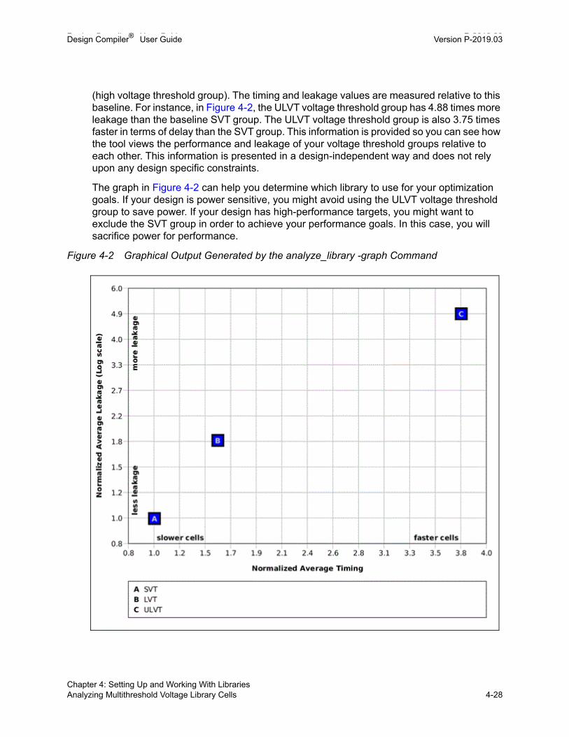
Design Compiler® User Guide P-2019.03Design Compiler® User Guide Version P-2019.03
(high voltage threshold group). The timing and leakage values are measured relative to this baseline. For instance, in Figure 4-2, the ULVT voltage threshold group has 4.88 times more leakage than the baseline SVT group. The ULVT voltage threshold group is also 3.75 times faster in terms of delay than the SVT group. This information is provided so you can see how the tool views the performance and leakage of your voltage threshold groups relative to each other. This information is presented in a design-independent way and does not rely upon any design specific constraints.
The graph in Figure 4-2 can help you determine which library to use for your optimization goals. If your design is power sensitive, you might avoid using the ULVT voltage threshold group to save power. If your design has high-performance targets, you might want to exclude the SVT group in order to achieve your performance goals. In this case, you will sacrifice power for performance.
Figure 4-2 Graphical Output Generated by the analyze_library -graph Command
Chapter 4: Setting Up and Working With LibrariesAnalyzing Multithreshold Voltage Library Cells 4-28
Design Compiler® User Guide Version P-2019.03
See Also
• Leakage Power Optimization Based on Threshold Voltage
Handling Black Boxes
Design Compiler in topographical mode supports synthesis with black boxes. Black boxes can be cells where the logic functionality is not known, cells that do not link to a cell in the logic library, or cells that do not have physical representation.
For information about working with black boxes, see
• Supported Black Boxes
• Black Box Flow
• Defining Timing in Quick Timing Model Format
• Identifying Black Box Cells
Supported Black Boxes
The following types of black boxes are supported:
• Functionally unknown black boxes
These are cells where the logic functionality is not known. Examples include the following types of cells:
❍ Macro cells
❍ Empty hierarchy cells or black-boxed modules
❍ Unlinked or unresolved cells
• Logical black boxes
These are cells that do not link to a cell in the logic library. This type of black box is categorized under functionally unknown black box cells. Examples include the following types of cells:
❍ Empty hierarchy cells or black-boxed modules
❍ Unlinked or unresolved cells
You can define the timing for logical black box cells by using Design Compiler in wire load mode or topographical mode, as described in Defining Timing in Quick Timing Model Format.
Chapter 4: Setting Up and Working With LibrariesHandling Black Boxes 4-29Chapter 4: Setting Up and Working With LibrariesHandling Black Boxes 4-29

Design Compiler® User Guide P-2019.03Design Compiler® User Guide Version P-2019.03
• Physical black boxes
These are cells that do not have physical representation. Examples include the following types of cells:
❍ Empty hierarchy cells or black-boxed modules
❍ Unlinked or unresolved cells
Topographical technology allows you to define the physical dimensions for physical black box cells, as described in Defining Physical Dimensions.
If the physical representation of a cell is not available with the user-supplied physical libraries, Design Compiler in topographical mode defines it automatically. For more information, see Automatic Creation of Physical Library Cells.
Black Box Flow
Figure 4-3 shows the flow for defining the timing and physical dimensions for black box cells and synthesizing the design.
Figure 4-3 Supported Black Box Flow
You can visually examine black boxes in your floorplan by viewing them in the Design Vision layout window. You can control the visibility, selection, and display style properties of black-box cells in the active layout view by setting options on the View Settings panel. Black boxes are visible and enabled for selection by default. For more information about controlling the visibility of black boxes in the active layout view, see Design Vision Help.
Load design with black boxes
Create and load quick timing models for black box cells
Provide physical dimensions for black box cells
Run compile_ultra to perform synthesis
Chapter 4: Setting Up and Working With LibrariesHandling Black Boxes 4-30

Design Compiler® User Guide Version P-2019.03
Defining Timing in Quick Timing Model Format
Design Compiler allows you to define timing for logical black box cells. You can create logic library cells and provide a timing model for the new cells in the quick timing model format. A quick timing model is an approximate timing model that is useful early in the design cycle to describe the rough initial timing of a black box. You create a quick timing model for a black box by specifying the model ports, the setup and hold constraints on the inputs, the clock-to-output path delays, and the input-to-output path delays. You can also specify the loads on input ports and the drive strength of output ports. Design Compiler saves the timing models in .db format, which can then be used during synthesis.
To create a quick timing model for a simple black box in Design Compiler in wire load mode or in topographical mode, perform the following steps:
1. Create a new model using the create_qtm_model command:
dc_shell-topo> create_qtm_model BB
BB is the model name.
2. Specify the technology information, such as the name of the logic library, the maximum transition time, the maximum capacitance, and the wire load information.
dc_shell-topo> set_qtm_technology -library library_namedc_shell-topo> set_qtm_technology -max_transition trans_valuedc_shell-topo> set_qtm_technology -max_capacitance cap_value
3. Specify global parameters, such as setup and hold characteristics.
dc_shell-topo> set_qtm_global_parameter -param setup -value setup_valuedc_shell-topo> set_qtm_global_parameter -param hold -value hold_valuedc_shell-topo> set_qtm_global_parameter -param clk_to_output \
-value cto_value
4. Specify the ports using the create_qtm_port command:
dc_shell-topo> create_qtm_port -type input Adc_shell-topo> create_qtm_port -type input Bdc_shell-topo> create_qtm_port -type output OP
5. Specify delay arcs using the create_qtm_delay_arc command:
dc_shell-topo> create_qtm_delay_arc -name A_OP_R -from A \-from_edge rise -to OP -value 0.10 -to_edge rise
dc_shell-topo> create_qtm_delay_arc -name A_OP_F -from A \-from_edge fall -to OP -value 0.11 -to_edge fall
dc_shell-topo> create_qtm_delay_arc -name B_OP_R -from B \ -from_edge rise -to OP -value 0.15 -to_edge rise
dc_shell-topo> create_qtm_delay_arc -name B_OP_F -from B \-from_edge fall -to OP -value 0.16 -to_edge fall
Chapter 4: Setting Up and Working With LibrariesHandling Black Boxes 4-31Chapter 4: Setting Up and Working With LibrariesHandling Black Boxes 4-31

Design Compiler® User Guide P-2019.03Design Compiler® User Guide Version P-2019.03
6. (Optional) Generate a report that shows the defined parameters, the ports, and the timing arcs in the quick timing model.
dc_shell-topo> report_qtm_model
7. Save the quick timing model using the save_qtm_model command:
dc_shell-topo> save_qtm_model
8. Write out the .db file for the quick timing model using the write_qtm_model command:
dc_shell-topo> write_qtm_model -out_dir QTM
9. Add the .db file to the link_library variable to load the quick timing model:
dc_shell-topo> lappend link_library "QTM/BB.db"
Defining Physical Dimensions
Design Compiler allows you to set the size for physical black box cells based on an estimation of the objects that it will contain when replaced with real logic. You can also define the base unit area for gate equivalence calculations for estimating the size of black boxes. The following topics discuss these strategies for defining the physical dimensions of black box cells:
• Estimating the Size of Black Boxes
• Determining the Gate Equivalent Area
Estimating the Size of Black Boxes
To set the size and shape for physical black box cells based on an estimation of the objects that it will contain, use the estimate_fp_black_boxes command.
To set the width and height, use the -sm_size option:
dc_shell-topo> estimate_fp_black_boxes -sm_size size
To create a rectilinear black box, use the -polygon option:
dc_shell-topo> estimate_fp_black_boxes -polygon polygon_area
The following example estimates a black box named alu1 and specifies it as a soft macro with a size of 100x100 and a utilization of 0.7:
dc_shell-topo> estimate_fp_black_boxes \ -sm_size {100 100} -sm_util 0.7 \ [get_cells -filter "is_physical_black_box==true" alu1]
Chapter 4: Setting Up and Working With LibrariesHandling Black Boxes 4-32

Design Compiler® User Guide Version P-2019.03
The following example estimates a black box named alu1 and specifies it as a rectilinear soft macro:
dc_shell-topo> estimate_fp_black_boxes \ -polygon {{1723.645 1925.365} {1723.645 1722.415} \ {1803.595 1722.415} {1803.595 1530.535} \ {799.915 1530.535} {799.915 1925.365} \ {1723.645 1925.365}}\ [get_cells -filter "is_physical_black_box==true" alu1]
In the following example, the size of the black box named U1 is estimated from the size of hard macro ram16x128:
dc_shell-topo> estimate_fp_black_boxes -hard_macros ram16x128 U1
Determining the Gate Equivalent Area
Design Compiler also allows you to define the base unit area for gate equivalence calculations for estimating the size of black boxes. Use the set_fp_base_gate command to specify either a library leaf cell area or a user-specified cell area as the base unit area to be used for gate equivalence calculations.
To specify a gate from the library as the base unit area to be used for the calculations, use the -cell option:
dc_shell-topo> set_fp_base_gate -cell UNIT
In this example, UNIT specifies the reference name of the library leaf cell to be used as the base unit area for gate equivalence calculations.
To specify the cell area in square microns as the base unit area to be used for the calculations, use the -area option:
dc_shell-topo> set_fp_base_gate -area 10
In this example, the base gate area is set to 10 square microns.
Identifying Black Box Cells
Design Compiler sets the following attributes on black box cells:
• is_black_box
When you specify the is_black_box attribute with the get_cells command, Design Compiler identifies functionally unknown black boxes:
dc_shell-topo> get_cells -hier -filter "is_black_box==true"
Chapter 4: Setting Up and Working With LibrariesHandling Black Boxes 4-33Chapter 4: Setting Up and Working With LibrariesHandling Black Boxes 4-33

Design Compiler® User Guide P-2019.03Design Compiler® User Guide Version P-2019.03
• is_logical_black_box
When you specify the is_logical_black_box attribute with the get_cells command, Design Compiler identifies the logical black boxes in the design:
dc_shell-topo> get_cells -hier -filter "is_logical_black_box==true"
• is_physical_black_box
When you specify the is_physical_black_box attribute with the get_cells command, Design Compiler identifies the physical black boxes in the design:
dc_shell-topo> get_cells -hier -filter "is_physical_black_box==true"
Automatic Creation of Physical Library Cells
If the physical representation of a cell is not available with the user-supplied physical libraries, Design Compiler defines it automatically. The tool can create physical library cells for the following:
• Logic library cells (leaf cells and macros)
• Empty hierarchy cells or black-boxed modules
• Unlinked or unresolved cells
• Unmapped cells
The tool issues the following warning message when it creates physical library cells:
Warning: Created physical library cell for logical library %s. (OPT-1413)
Chapter 4: Setting Up and Working With LibrariesHandling Black Boxes 4-34

5Using a Milkyway Database 5
The Milkyway database is the unifying design storage format for the Synopsys Galaxy™ Design Platform. The database provides persistent storage of physical design data that links Galaxy platform tools together. The database is periodically updated with new features to support advances in EDA technology.
Design Compiler writes a mapped, uniquified design into the Milkyway database, including the netlist, synthesis constraints, and any physical guidance information, when you use the write_milkyway command. You can use a single Milkyway library across the entire Galaxy flow.
Note: Design Compiler does not support the read_milkyway command.
When you use a Milkyway database, you do not need to use an intermediate netlist file exchange format such as Verilog or VHDL to communicate with other Synopsys Galaxy platform tools. Before you can use a Milkyway database within Design Compiler, you must prepare a design library and a reference library and understand the following concepts and tasks:
• About the Milkyway Database
• Guidelines for Using the Milkyway Database
• Preparing to Use the Milkyway Database
• Writing the Milkyway Database
5-1
Design Compiler® User Guide P-2019.03Design Compiler® User Guide Version P-2019.03
About the Milkyway Database
The Milkyway database stores design data in the Milkyway design library and physical library data in the Milkyway reference library.
• Milkyway design library
The Milkyway directory structure used to store design data—that is, the uniquified, mapped netlist and constraints—is referred to as the Milkyway design library. You specify the Milkyway design library for the current session by setting the mw_design_library variable to the root directory path.
• Milkyway reference library
The Milkyway directory structure used to store physical library data is referred to as the Milkyway reference library. Reference libraries contain standard cells, macro cells, and pad cells. For information about creating reference libraries, see the Milkyway documentation.
You specify the Milkyway reference library for the current session by setting the mw_reference_library variable to the root directory path. The order in the list implies priority for reference conflict resolution. If more than one reference library has a cell with the same name, the first reference library has precedence.
Before you use a Milkyway database, see
• Required License and Files
• Invoking the Milkyway Environment Tool
Required License and Files
Before you use a Milkyway database, you need to have the following required license and files:
• The Milkyway-Interface license
Design Compiler provides this license, which is used to run the write_milkyway command.
• Source for logic libraries (.lib)
• Compiled databases
❍ Logic libraries (.db), which contains standard cell timing, power, function, test, and so forth
❍ Milkyway library (FRAM), which contains technology data
Chapter 5: Using a Milkyway DatabaseAbout the Milkyway Database 5-2

Design Compiler® User Guide Version P-2019.03
Invoking the Milkyway Environment Tool
To invoke the Milkyway Environment tool, enter
% Milkyway -galaxy
The command checks out the Milkyway-Interface license. The Milkyway Environment tool is a graphical user interface (GUI) that enables manipulation of the Milkyway libraries. You can use the tool to maintain your Milkyway design library, such as delete unused versions of your design.
See Also
• The Milkyway documentation
Guidelines for Using the Milkyway Database
When you use the write_milkyway command, observe these guidelines:
• Make sure all the cells present in the Milkyway reference library have corresponding cells in the timing library. The port direction of the cells in the Milkyway reference libraries are set from the port direction of cells in the timing library. If cells are present in the Milkyway reference library but are not in the timing library, the port direction of cells present in the Milkyway reference library is not set.
• Run the uniquify command before you run the write_milkyway command.
• You must make sure the units in the logic library and the Milkyway technology file are consistent.
The SDC file does not contain unit information. If the units in the logic library and Milkyway technology file are inconsistent, the write_milkyway command cannot convert them automatically. For example, if the logic library uses femtofarad as the capacitance unit and the Milkyway technology file uses picofarad as the capacitance unit, the output of the write_sdc command shows different net load values.
In the following example, the capacitance units in the logic library and the Milkyway technology file are not consistent. The following set_load information is shown for the net gpdhi_word_d_21_ before the write_milkyway command is run:
set_load 1425.15 [get_nets {gpdhi_word_d_21_}]
After the write_milkyway command is run, the SDC file shows
set_load 8.36909 [get_nets {gpdhi_word_d_21_}]
Chapter 5: Using a Milkyway DatabaseGuidelines for Using the Milkyway Database 5-3Chapter 5: Using a Milkyway DatabaseGuidelines for Using the Milkyway Database 5-3

Design Compiler® User Guide P-2019.03Design Compiler® User Guide Version P-2019.03
• Design Compiler is case-sensitive. You can use the tool in case-insensitive mode by doing the following tasks before you run the write_milkyway command:
❍ Prepare uppercase versions of the libraries used in the link library.
❍ Use the change_names command to make sure the netlist is uppercased.
Preparing to Use the Milkyway Database
You use the Milkyway design library to specify physical libraries and save designs in the Milkyway format. The inputs required to create a Milkyway design library are the Milkyway reference library and the Milkyway technology file.
To create a Milkyway design library,
1. Create the Milkyway design library by using the create_mw_lib command.
For example,
dc_shell-topo> create_mw_lib -technology $mw_tech_file \ -mw_reference_library $mw_reference_library $mw_design_library_name
2. Open the Milkyway library that you created by using the open_mw_lib command.
For example,
dc_shell-topo> open_mw_lib $mw_design_library_name
3. (Optional) Attach the TLUPlus files by using the set_tlu_plus_files command.
For example,
dc_shell-topo> set_tlu_plus_files -max_tluplus $max_tlu_file \-min_tluplus $min_tlu_file -tech2itf_map $prs_map_file
4. In subsequent sessions, use the open_mw_lib command to open the Milkyway library. If you are using the TLUPlus files for RC estimation, use the set_tlu_plus_files command to attach these files.
For example,
dc_shell-topo> open_mw_lib $mw_design_library_namedc_shell-topo> set_tlu_plus_files -max_tluplus $max_tlu_file \
-min_tluplus $min_tlu_file -tech2itf_map $prs_map_file
See Also
• Using TLUPlus Files for RC Estimation
Describes how to useTLUPlus files to provide more accurate capacitance and resistance data
Chapter 5: Using a Milkyway DatabasePreparing to Use the Milkyway Database 5-4
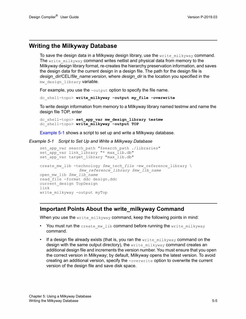
Design Compiler® User Guide Version P-2019.03
Writing the Milkyway Database
To save the design data in a Milkyway design library, use the write_milkyway command. The write_milkyway command writes netlist and physical data from memory to the Milkyway design library format, re-creates the hierarchy preservation information, and saves the design data for the current design in a design file. The path for the design file is design_dir/CEL/file_name:version, where design_dir is the location you specified in the mw_design_library variable.
For example, you use the -output option to specify the file name.
dc_shell-topo> write_milkyway -output my_file -overwrite
To write design information from memory to a Milkyway library named testmw and name the design file TOP, enter
dc_shell-topo> set_app_var mw_design_library testmwdc_shell-topo> write_milkyway -output TOP
Example 5-1 shows a script to set up and write a Milkyway database.
Example 5-1 Script to Set Up and Write a Milkyway Database
set_app_var search_path "$search_path ./libraries"set_app_var link_library "* max_lib.db"set_app_var target_library "max_lib.db"
create_mw_lib -technology $mw_tech_file -mw_reference_library \$mw_reference_library $mw_lib_name
open_mw_lib $mw_lib_nameread_file -format ddc design.ddccurrent_design TopDesignlinkwrite_milkyway -output myTop
Important Points About the write_milkyway Command
When you use the write_milkyway command, keep the following points in mind:
• You must run the create_mw_lib command before running the write_milkyway command.
• If a design file already exists (that is, you ran the write_milkyway command on the design with the same output directory), the write_milkyway command creates an additional design file and increments the version number. You must ensure that you open the correct version in Milkyway; by default, Milkyway opens the latest version. To avoid creating an additional version, specify the -overwrite option to overwrite the current version of the design file and save disk space.
Chapter 5: Using a Milkyway DatabaseWriting the Milkyway Database 5-5Chapter 5: Using a Milkyway DatabaseWriting the Milkyway Database 5-5

Design Compiler® User Guide P-2019.03Design Compiler® User Guide Version P-2019.03
• The command does not modify in-memory data.
• Attributes present in the design in memory that have equivalent attributes in Milkyway are translated (not all attributes present in the design database are translated).
• A hierarchical netlist translated by using the write_milkyway command retains its hierarchy in the Milkyway database.
Limitations When Writing Milkyway Format
The following limitations apply when you write your design in Milkyway format:
• The design must be mapped.
Because the Milkyway format describes physical information, it supports mapped designs only. You cannot use the Milkyway format to store design data for unmapped designs.
• The design must not contain multiple instances.
You must uniquify your design before saving it in Milkyway format. Use the check_design -multiple_designs command to report information related to multiply-instantiated designs.
• The write_milkyway command saves the entire hierarchical design in a single Milkyway design file. You cannot generate separate design files for each subdesign.
• When you save a design in Milkyway format, the write_milkyway command does not save the block abstraction instances in the Milkyway design library. You must explicitly save each block abstraction in .ddc format. For more information about block abstraction usage, see Using Hierarchical Models.
Chapter 5: Using a Milkyway DatabaseWriting the Milkyway Database 5-6

6Working With Designs in Memory 6
The Design Compiler tool reads designs into memory from design files. Many designs can be in memory at any time. After a design is read in, you can change it in numerous ways, such as grouping or ungrouping its subdesigns or changing subdesign references.
To learn how to work with designs in memory, see
• Reading Designs
• Listing Designs in Memory
• Setting the Current Design
• Linking Designs
• Listing Design Objects
• Specifying Design Objects
• Creating Designs
• Copying Designs
• Renaming Designs
• Changing the Design Hierarchy
• Editing Designs
• Translating Designs From One Technology to Another
6-1

Design Compiler® User Guide P-2019.03Design Compiler® User Guide Version P-2019.03
• Removing Designs From Memory
• Saving Designs
Chapter 6: Working With Designs in Memory6-2

Design Compiler® User Guide Version P-2019.03
Reading Designs
See the following topics for an overview of the design formats supported by Design Compiler and the commands you can use to read designs:
• Supported Design Input Formats
• Reading HDL Files
• Reading .ddc Files
• Reading .db Files
Supported Design Input Formats
Before you read a design, make sure that your design is in one of the following formats listed in Table 6-1.
Reading HDL Files
You can open HDL design files by using one of the following methods:
• Reading Designs With Dependencies Automatically
You can read designs with dependencies automatically by using the -autoread option with the analyze or read_file command. The tool automatically analyzes and elaborates designs and any files dependent on them in the correct order.
Table 6-1 Supported Input Formats
Format Description
.ddc Synopsys internal database format (recommended)
.db Synopsys internal database format
Verilog IEEE standard Verilog (see the HDL Compiler documentation)
VHDL IEEE standard VHDL (see the HDL Compiler documentation)
SystemVerilog IEEE standard SystemVerilog (see the HDL Compiler documentation)
equation Synopsys equation format
pla Berkeley (Espresso) PLA format
Chapter 6: Working With Designs in MemoryReading Designs 6-3Chapter 6: Working With Designs in MemoryReading Designs 6-3

Design Compiler® User Guide P-2019.03Design Compiler® User Guide Version P-2019.03
• Running the read_file Command
The read_file command analyzes the design and translates it into a technology-independent (GTECH) design in a single step.
• Running the analyze and elaborate Commands
The analyze command checks the design and reports errors. The elaborate command translates the design into a technology-independent design (GTECH) from the intermediate files produced during analysis.
• Running the read_verilog or read_vhdl Command
The commands checks the code for correct syntax and build a generic technology (GTECH) netlist that Design Compiler uses to optimize the design. You can use the read_verilog or read_vhdl commands to do both functions automatically.
See Also
• The HDL Compiler documentation
Reading Designs With Dependencies Automatically
You can read designs with dependencies automatically by using the -autoread option with the read_file or analyze command:
prompt> read_file -autoread verilog my_design.v
The tool automatically analyzes and elaborates designs and any files dependent on them in the correct order.
The read_file -autoread command analyzes and elaborates the top-level design; the analyze -autoread command analyzes the design but does not perform elaboration.
When you use the -autoread option, the resulting GTECH representation is retained in memory. Dependencies are determined only from the files or directories in the file_list; if the file_list changes between consecutive -autoread option runs, the tool uses the latest set of files to determine the dependencies. You can use the -autoread option with any VHDL, Verilog, or SystemVerilog language version.
See Also
• Running the read_file Command
• Running the analyze and elaborate Commands
Chapter 6: Working With Designs in MemoryReading Designs 6-4

Design Compiler® User Guide Version P-2019.03
Running the read_file Command
The read_file command analyzes the design and translates it into a technology-independent (GTECH) design in a single step:
prompt> read_file -format verilog my_design.v
The following HDL formats are supported:
• Verilog format–the .v, .verilog, .v.gz, and .verilog.gz extensions
The command does not create intermediate files for Verilog. To create intermediate files, set the hdlin_auto_save_templates variable to true.
• SystemVerilog–the .sv, .sverilog, .sv.gz, and .sverilog.gz extensions
• VHDL–the .vhd, .vhdl, vhd.gz, and .vhdl.gz extensions
The command creates .mr and .st intermediate files for VHDL.
If you do not specify the design format, the read_file command infers the format based on the file extension. If no known extension is used, the tool uses .ddc format. Supported extensions for automatic inference are not case-sensitive.
The read_file command can read compressed files for all formats except the .ddc format, which is compressed internally as it is written. To enable the tool to automatically infer the file format for compressed files, use the following naming structure: filename.format.gz.
For designs in memory, Design Compiler uses the path_name/design.ddc naming convention. The path_name argument is the directory from which the original file was read, and the design argument is the name of the design. If you later read in a design that has the same file name, Design Compiler overwrites the original design. To prevent this, use the -single_file option with the read_file command.
The read_file command does not execute the link command automatically. For more information, see Linking Designs.
See Also
• Differences Between the read_file Command and the analyze and elaborate Commands
Running the analyze and elaborate Commands
The analyze command performs the following tasks:
• Reads an HDL source file
• Checks for errors without building generic logic for the design
• Creates HDL library objects in an HDL-independent intermediate format
Chapter 6: Working With Designs in MemoryReading Designs 6-5Chapter 6: Working With Designs in MemoryReading Designs 6-5

Design Compiler® User Guide P-2019.03Design Compiler® User Guide Version P-2019.03
• Stores the intermediate files in a location you define
If the analyze command reports errors, fix them in the HDL source file and then run the analyze command again. After a design is analyzed, you must reanalyze it only when you change it.
The elaborate command performs the following tasks:
• Translates the design into a technology-independent design (GTECH) from the intermediate files produced during analysis
• Allows changing of parameter values defined in the source code
• Allows VHDL architecture selection
• Replaces the HDL arithmetic operators in the code with DesignWare components
• Automatically executes the link command, which resolves design references
To use this method, analyze the top-level design and all subdesigns in bottom-up order and then elaborate the top-level design and any subdesigns that require parameters to be assigned or overwritten:
prompt> analyze -format verilog -library -work RISCTYPES.vprompt> analyze -format verilog -lib -work {ALU.v STACK_TOP.v \
STACK_MEM.v ...} prompt> elaborate RISC_CORE -architecture STRUCT -library WORK -update
See Also
• Differences Between the read_file Command and the analyze and elaborate Commands
Differences Between the read_file Command and the analyze andelaborate Commands
Table 6-2 summarizes the differences between using the read_file command and using the analyze and elaborate commands to read design files.
Table 6-2 The read_file Command Versus the analyze and elaborate Commands
Comparison read_file command analyze and elaborate commands
Input formats All formats are supported. VHDL and Verilog formats are supported.
When to use Use to synthesize netlists, precompiled designs, and so on.
Use to synthesize VHDL or Verilog files.
Chapter 6: Working With Designs in MemoryReading Designs 6-6

Design Compiler® User Guide Version P-2019.03
Running the read_verilog or read_vhdl Command
The read_verilog and read_vhdl commands are derived from the read_file command. Both commands check the code for correct syntax and build a generic technology (GTECH) netlist that Design Compiler uses to optimize the design. To run either command, specify the file type:
prompt> read_vhdl my_design.vhdl
See Also
• Running the read_file Command
Reading .ddc Files
To read the design data from a .ddc file, use the read_ddc command or the read_file -format ddc command:
prompt> read_ddc design_file.ddc
The .ddc format is backward compatible but not forward compatible. You can read a .ddc file that was generated with an earlier software version, but you cannot read a .ddc file that was generated with a later software version.
See Also
• Running the read_file Command
Parameters Does not allow you to pass parameters. You must use directives in HDL.
You can set parameter values with the elaborate command. For parameterized designs, you can use the analyze and elaborate commands to build a new design with nondefault values.
Architecture Does not allow you to specify the architecture to be elaborated.
You can specify the architecture to be elaborated.
Linking designs You must use the link command to resolve references.
The elaborate command executes the link command automatically to resolve references.
Table 6-2 The read_file Command Versus the analyze and elaborate Commands (Continued)
Comparison read_file command analyze and elaborate commands
Chapter 6: Working With Designs in MemoryReading Designs 6-7Chapter 6: Working With Designs in MemoryReading Designs 6-7

Design Compiler® User Guide P-2019.03Design Compiler® User Guide Version P-2019.03
Reading .db Files
Note: Although you can read files in Synopsys database .db format, it is recommended that you use .ddc format.
To read in a .db file, use the read_db command or the read_file -format db command:
prompt> read_db my_design_file.db
Design Compiler supports the .db, .sldb, .sdb, .db.gz, .sldb.gz, and .sdb.gz file extensions. The version of a .db file is the version of Design Compiler that created the file. For a .db file to be read into Design Compiler, its file version must be the same as or earlier than the version of Design Compiler you are running. If you attempt to read in a .db file generated by a Design Compiler version that is later than the Design Compiler version you are using, an error message appears. The error message provides details about the version mismatch.
See Also
• Running the read_file Command
• Reading .ddc Files
Listing Designs in Memory
To list the names of the designs loaded in memory, use the list_designs command.
prompt> list_designsA (*) B C1
The asterisk (*) next to design A shows that A is the current design.
To list the memory file name corresponding to each design name, use the -show_file option.
prompt> list_designs -show_file
/user1/designs/design_A/A.ddcA (*)
/home/designer/dc/B.ddcB C1
The asterisk (*) next to design A shows that A is the current design. File B.ddc contains both designs B and C.
Chapter 6: Working With Designs in MemoryListing Designs in Memory 6-8

Design Compiler® User Guide Version P-2019.03
Setting the Current Design
You can set the current design (the design you are working on) in the following ways:
• With the read_file command
When the read_file command successfully finishes processing, it sets the current design to the design that was read in.
prompt> read_file -format ddc MY_DESIGN.ddcReading ddc file ’/designs/ex/MY_DESIGN.ddc’Current design is ’MY_DESIGN’
• With the elaborate command
• With the current_design command
Use this command to set any design in dc_shell memory as the current design.
prompt> current_design ANY_DESIGNCurrent design is ’ANY_DESIGN’.{ANY_DESIGN}
You should avoid writing scripts that use a large number of current_design commands, such as in a loop. Using a large number of current_design commands can increase runtime. For more information, see Using Tcl With Synopsys Tools.
To display the name of the current design, enter the following command:
prompt> printvar current_designcurrent_design = "test"
Linking Designs
For a design to be complete, it must connect to all the library components and designs it references. This process is called linking the design or resolving references.
To link designs, uses the link command. The link command uses the link_library and search_path system variables and the local_link_library attribute to resolve design references.
By default, the case sensitivity of the linking process depends on the source of the references. To explicitly define the case sensitivity of the linking process, set the link_force_case variable.
To learn how Design Compiler links designs and resolves references, see How the Tool Resolves References.
Chapter 6: Working With Designs in MemorySetting the Current Design 6-9Chapter 6: Working With Designs in MemorySetting the Current Design 6-9

Design Compiler® User Guide P-2019.03Design Compiler® User Guide Version P-2019.03
In addition to linking designs and resolving references, you can perform the following tasks:
• Locating Designs by Using a Search Path
• Changing Design References
• Querying Design References
• Mapping Physical Variant Cells in Netlists or DEF Files
How the Tool Resolves References
The Design Compiler tool resolves references by carrying out the following steps:
1. It determines which library components and subdesigns are referenced in the current design and its hierarchy.
2. It searches the link libraries to locate these references.
a. Design Compiler first searches the libraries and design files defined in the current design’s local_link_library attribute.
b. If an asterisk is specified in the value of the link_library variable, Design Compiler searches in memory for the reference.
c. Design Compiler then searches the libraries and design files defined in the link_library variable.
3. If it does not find the reference in the link libraries, it searches in the directories specified by the search_path variable.
For more information, see Locating Designs by Using a Search Path.
4. It links (connects) the located references to the design.
Note: In a hierarchical design, Design Compiler considers only the top-level design’s local link library. It ignores local link libraries associated with the subdesigns.
Design Compiler uses the first reference it locates. If it locates additional references with the same name, it generates a warning message identifying the ignored, duplicate references. If Design Compiler does not find the reference, a warning appears advising that the reference cannot be resolved.
The arrows in Figure 6-1 show the connections that the linking process added between the instances, references, and link libraries. In this example, Design Compiler finds library component NAND2 in the LIBRARY_2 logic library; it finds subdesign MULTIPLIER in a design file.
Chapter 6: Working With Designs in MemoryLinking Designs 6-10

Design Compiler® User Guide Version P-2019.03
Figure 6-1 Resolving References
Locating Designs by Using a Search Path
You can specify the design file location by using the complete path or only the file name. If you specify only the file name, the Design Compiler tool uses the search path defined in the search_path variable. The tool looks for the design files starting with the leftmost directory specified in the search_path variable and uses the first design file it finds. By default, the search path includes the current working directory and $SYNOPSYS/libraries/syn, where $SYNOPSYS is the path to the installation directory. To see where Design Compiler finds a file when using the search path, use the which command. For example, enter
prompt> which my_design.ddc{/usr/designers/example/my_design.ddc}
To specify other directories in addition to the default search path, use the following command:
prompt> lappend search_path project
See Also
• Specifying a Library Search Path
References
NAND2
MULTIPLIER
NAND2
U1
NAND2
U3
NAND2
U2
U4
EXREF Link libraries
LIBRARY_1
LIBRARY_2
Logic libraries
MULTIPLIER
ADDER
Design files
AND2NAND2OR2
MULTIPLIER
Chapter 6: Working With Designs in MemoryLinking Designs 6-11Chapter 6: Working With Designs in MemoryLinking Designs 6-11
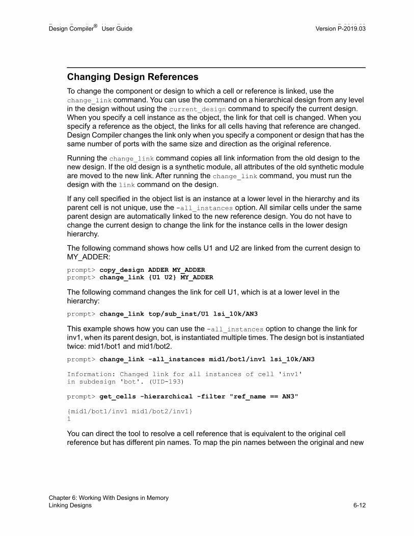
Design Compiler® User Guide P-2019.03Design Compiler® User Guide Version P-2019.03
Changing Design References
To change the component or design to which a cell or reference is linked, use the change_link command. You can use the command on a hierarchical design from any level in the design without using the current_design command to specify the current design. When you specify a cell instance as the object, the link for that cell is changed. When you specify a reference as the object, the links for all cells having that reference are changed. Design Compiler changes the link only when you specify a component or design that has the same number of ports with the same size and direction as the original reference.
Running the change_link command copies all link information from the old design to the new design. If the old design is a synthetic module, all attributes of the old synthetic module are moved to the new link. After running the change_link command, you must run the design with the link command on the design.
If any cell specified in the object list is an instance at a lower level in the hierarchy and its parent cell is not unique, use the -all_instances option. All similar cells under the same parent design are automatically linked to the new reference design. You do not have to change the current design to change the link for the instance cells in the lower design hierarchy.
The following command shows how cells U1 and U2 are linked from the current design to MY_ADDER:
prompt> copy_design ADDER MY_ADDERprompt> change_link {U1 U2} MY_ADDER
The following command changes the link for cell U1, which is at a lower level in the hierarchy:
prompt> change_link top/sub_inst/U1 lsi_10k/AN3
This example shows how you can use the -all_instances option to change the link for inv1, when its parent design, bot, is instantiated multiple times. The design bot is instantiated twice: mid1/bot1 and mid1/bot2.
prompt> change_link -all_instances mid1/bot1/inv1 lsi_10k/AN3
Information: Changed link for all instances of cell 'inv1' in subdesign 'bot'. (UID-193)
prompt> get_cells -hierarchical -filter "ref_name == AN3"
{mid1/bot1/inv1 mid1/bot2/inv1}1
You can direct the tool to resolve a cell reference that is equivalent to the original cell reference but has different pin names. To map the pin names between the original and new
Chapter 6: Working With Designs in MemoryLinking Designs 6-12

Design Compiler® User Guide Version P-2019.03
cell references, use the -pin_map {{old_pin1 new_pin1} {old_pin2 new_pin2}...} option with the change_link command.
For example, the following command links the U1 cell in the current design to the AN21 cell reference and maps the old pin names (A1, A2, and Z) to new pin names (A, B, and Y):
prompt> change_link [get_cells U1] AN21 \ -pin_map {{A1 A} {A2 B} {Z Y}}
Querying Design References
You can query design references by using the following methods:
• To report information about all the references in the current instance or the current design, use the report_reference command. To display information across the hierarchy, use the -hierarchy option.
• To return a collection of instances that have a specific reference, use the get_references command.
For example, the following command returns a collection of instances in the current design that have the reference AN2:
prompt> get_references AN2{U2 U3 U4}
• To report the reference names, use the report_cell command.
For example,
prompt> report_cell [get_references AN*]
Cell Reference Library Area Attributes--------------------------------------------------------------------U2 AN2 lsi_10k 2.000000U3 AN2 lsi_10k 2.000000U4 AN2 lsi_10k 2.000000U8 AN3 lsi_10k 2.000000
Mapping Physical Variant Cells in Netlists or DEF Files
You can map physical variant cells in a netlist or a DEF file to the master cell in the library. Physical variant cells differ from the master library cell in mask color or small physical geometry. For advanced technology nodes, the timing characteristics of these cells do not vary, so you can use the same Liberty model for the master cell and its variants.
To enable this feature, set the link_allow_physical_variant_cells variable to true. The default is false.
Chapter 6: Working With Designs in MemoryLinking Designs 6-13Chapter 6: Working With Designs in MemoryLinking Designs 6-13

Design Compiler® User Guide P-2019.03Design Compiler® User Guide Version P-2019.03
To manage the library with efficiency, you need to define a list of physical variant cells of a master library cell by using the physical_variant_cells attribute in Liberty syntax. When reading a netlist or DEF file containing physical variant cells, the Design Compiler tool
• Resolves the physical variant cell references by searching the list specified by the physical_variant_cells attribute
• Maps the physical variant cells to their master cell and preserves the cells throughout the design flow
Listing Design Objects
The Design Compiler tool provides commands for accessing various design objects. These commands refer to design objects located in the current design. Each command in Table 6-3 performs one of the following actions:
• List
Provides a listing with minimal information.
• Display
Provides a report that includes characteristics of the design object.
• Return
Returns a collection that can be used as input to another dc_shell command.
Table 6-3 lists the commands and the actions they perform.
Table 6-3 Commands to Access Design Objects
Object Command Action
Instance list_instances
report_cell
Lists instances and their references.
Displays information about instances.
Reference report_reference Displays information about references.
Port report_port
report_bus
all_inputs
all_outputs
Displays information about ports.
Displays information about bused ports.
Returns all input ports.
Returns all output ports.
Net report_net
report_bus
Displays information about nets.
Displays information about bused nets.
Chapter 6: Working With Designs in MemoryListing Design Objects 6-14
Design Compiler® User Guide Version P-2019.03
You can also use the GUI to list design objects and attribute values, provide reports, and return collections. To list and display information about designs, cells, nets, ports, and pins, use the List menu commands. To generate design object reports, use the Design menu commands. For more information about using the GUI, see the Design Vision User Guide and the Design Vision Help.
Specifying Design Objects
You can specify design objects by using either a relative path or an absolute path:
• Using a Relative Path
• Using an Absolute Path
• Using Attributes
Using a Relative Path
If you use a relative path to specify a design object, the object must be in the current design. Specify the path relative to the current instance. The current instance is the frame of reference within the current design. By default, the current instance is the top level of the current design. Use the current_instance command to change the current instance.
For example, to place a dont_touch attribute on hierarchical cell U1/U15 in the Count_16 design, you can enter either
prompt> current_design Count_16Current design is ’Count_16’.{Count_16}prompt> set_dont_touch U1/U15
or
Clock report_clock
all_clocks
Displays information about clocks.
Returns all clocks.
Register all_registers Returns all registers.
Collections get_* Returns a collection of cells, designs, libraries and library cell pins, nets, pins, and ports.
Table 6-3 Commands to Access Design Objects (Continued)
Object Command Action
Chapter 6: Working With Designs in MemorySpecifying Design Objects 6-15Chapter 6: Working With Designs in MemorySpecifying Design Objects 6-15

Design Compiler® User Guide P-2019.03Design Compiler® User Guide Version P-2019.03
prompt> current_design Count_16Current design is ’Count_16’.{Count_16}prompt> current_instance U1Current instance is ’/Count_16/U1’./Count_16/U1prompt> set_dont_touch U151
In the first command sequence, the frame of reference remains at the top level of design Count_16. In the second command sequence, the frame of reference changes to instance U1. Design Compiler interprets all future object specifications relative to instance U1.
To reset the current instance to the top level of the current design, enter the current_instance command without an argument.
prompt> current_instanceCurrent instance is the top-level of the design ‘Count_16’
The current_instance variable points to the current instance. To display the current instance, enter the following command:
prompt> printvar current_instancecurrent_instance = "Count_16/U1"
Using an Absolute Path
When you use an absolute path to specify a design object, the object can be in any design in dc_shell memory. Use the following syntax to specify an object by using an absolute path:
[file:]design/object
file
The path name of a memory file followed by a colon (:). Use the file argument when multiple designs in memory have the same name.
design
The name of a design in dc_shell memory.
object
The name of the design object, including its hierarchical path. If several objects of different types have the same name and you do not specify the object type, Design Compiler looks for the object by using the types allowed by the command.
To specify an object type, use the get_* command. For more information about these commands, see Using Tcl With Synopsys Tools.
Chapter 6: Working With Designs in MemorySpecifying Design Objects 6-16

Design Compiler® User Guide Version P-2019.03
For example, to place a dont_touch attribute on hierarchical cell U1/U15 in the Count_16 design, enter
prompt> set_dont_touch /usr/designs/Count_16.ddc:Count_16/U1/U51
Using Attributes
An attribute is a string or value associated with an object in the design that carries some information about that object. Attributes can describe logical, electrical, physical, and other properties. They are attached to the design object and saved with the design database.
Design Compiler uses attributes on the following types of objects:
• Entire designs
• Design objects, such as clocks, nets, pins, and ports
• Design references and cell instances within a design
• Library cells and cell pins
Each attribute has a name, a type, and a value. Attributes can have the following types: string, numeric, or logical (Boolean).
Some attributes are predefined and are recognized by Design Compiler; other attributes are user-defined.
Some attributes are read-only. Design Compiler sets these attribute values and you cannot change them. Other attributes are read/write. You can change these attribute values at any time.
Most attributes apply to one object type; for example, the rise_drive attribute applies only to input and inout ports. Some attributes apply to several object types; for example, the dont_touch attribute can apply to a net, cell, port, reference, or design. You can get detailed information about the predefined attributes that apply to each object type by using the commands listed in Table 6-4.
Table 6-4 Commands to Get Attribute Descriptions
Object type Command
All man attributes
Designs man design_attributes
Cells man cell_attributes
Clocks man clock_attributes
Chapter 6: Working With Designs in MemorySpecifying Design Objects 6-17Chapter 6: Working With Designs in MemorySpecifying Design Objects 6-17

Design Compiler® User Guide P-2019.03Design Compiler® User Guide Version P-2019.03
Setting Attribute Values
To set the value of an attribute, use one of the following:
• Using an Attribute-Specific Command
• Using the set_attribute Command
Using an Attribute-Specific Command
Use an attribute-specific command to set the value of the command’s associated attribute.
For example,
prompt> set_dont_touch U1
Using the set_attribute Command
Use the set_attribute command to set the value of any attribute or to define a new attribute and set its value.
For example, to set the dont_touch attribute on the lsi_10k/FJK3 library cell, enter
prompt> set_attribute lsi_10K/FJK3 dont_touch true
The set_attribute command enforces the predefined attribute type and generates an error if you try to set an attribute with a value of an incorrect type.
For example, the predefined type for the max_fanout attribute is float. Therefore, if you enter the following command, Design Compiler returns an error message:
prompt> set_attribute lib/lcell/lpin max_fanout 1 -type integer
Nets man net_attributes
Pins man pin_attributes
Ports man port_attributes
Libraries man library_attributes
Library cells man library_cell_attributes
References man reference_attributes
Table 6-4 Commands to Get Attribute Descriptions (Continued)
Object type Command
Chapter 6: Working With Designs in MemorySpecifying Design Objects 6-18

Design Compiler® User Guide Version P-2019.03
To determine the predefined type for an attribute, use the list_attributes -application command. This command generates a list of all application attributes and their types. To generate a smaller report, you can use the -class attribute to limit the list to attributes that apply to one of the following classes: design, port, cell, clock, pin, net, lib, or reference.
If an attribute applies to more than one object type, Design Compiler searches the database for the named object. For information about the search order, see The Object Search Order.
When you set an attribute on a reference (subdesign or library cell), the attribute applies to all cells in the design with that reference. When you set an attribute on an instance (cell, net, or pin), the attribute overrides any attribute inherited from the instance’s reference.
Viewing Attribute Values
To see all attributes on an object, use the report_attribute command:
prompt> report_attribute object_list
For example,
dc_shell> report_attribute myAdd
****************************************Report : AttributeDesign : test...****************************************Design Object Type Attribute Name Value----------------------------------------------------------------------test myAdd cell verification_priority hightest myAdd cell operator_label myAdd
To see the value of a specific attribute on an object, use the get_attribute command. For example, to get the value of the maximum fanout on port OUT7, enter
prompt> get_attribute OUT7 max_fanoutPerforming get_attribute on port ’OUT7’.{3.000000}
When you run Design Compiler NXT and Design Compiler Graphical, you can also query the bounding box information for pins and ports. For example, the following commands report the bbox attribute on the Q pin of register reg_1 and the test_mode port of the current design:
dc_shell-topo> get_attribute [get_pins reg_1/Q] bbox dc_shell-topo> get_attribute [get_ports test_mode] bbox
Note: The bbox attribute is not supported in wire load mode. Querying placed pins and ports in topographical mode requires additional licensing. For details about licensing, contact your Synopsys representative.
Chapter 6: Working With Designs in MemorySpecifying Design Objects 6-19Chapter 6: Working With Designs in MemorySpecifying Design Objects 6-19

Design Compiler® User Guide P-2019.03Design Compiler® User Guide Version P-2019.03
If an attribute applies to more than one object type, Design Compiler searches the database for the named object. For information about the search order, see The Object Search Order.
You can use the Properties dialog box in the GUI to view attributes and other object properties for selected designs, design objects, or timing paths. You can also set, change, or remove the attribute values for certain properties.
For more information about using the GUI, see the Design Vision User Guide and the Design Vision Help.
Saving Attribute Values
Design Compiler does not automatically save attribute values when you exit dc_shell. Use the write_script command to generate a dc_shell script that re-creates the attribute values.
By default, the write_script command writes the dc_shell commands to standard output. Use the redirection operator (>) to redirect the output to a file.
prompt> write_script > attr.scr
The write_script command does not support user-defined attributes.
Defining Attributes
To define a new attribute, use the define_user_attribute command. To set the attribute to a specified value on a specified list of objects, use the set_attribute command.
The following example defines an integer cell attribute named X and then sets this attribute to 30 on all cells in this level of the hierarchy:
prompt> define_user_attribute -type int -classes cell Xcellprompt> set_attribute [get_cells *] X 30{U1}
If you want to change the value of an attribute, remove the attribute and then re-create it to store the desired type.
See Also
• Setting Attribute Values
Chapter 6: Working With Designs in MemorySpecifying Design Objects 6-20

Design Compiler® User Guide Version P-2019.03
Propagating Attributes
To propagate user-defined attributes set on cell instances of lower-level designs to cell instances in the higher-level hierarchy, use the propagate_user_attributes command. For example in Figure 6-2,
• The current design is set to mid, and the user-defined attribute is defined as XYZ with a value of false on all cells in the mid design.
• The user-defined attribute is set on the B1 and B2 instances of the bot design with cell instances U1.
Figure 6-2 Cell Instances U1 in the bot Design
• When the current design (mid) is changed to Top as shown in Example 6-1, use the propagate_user_attributes command to propagate all the user-defined attributes set on all the cell instances in the bot design to the Top design.
Example 6-1 Cell Instances U1 in the bot Design Propagate to the Top Design
prompt> current_design midCurrent design is 'mid'.{mid}
prompt> define_user_attribute -type boolean -classes cell XYZXYZ
prompt> set_user_attribute [get_cells -hierarchical *] XYZ falseInformation: Attribute 'XYZ' is set on 4 objects. (UID-186)B1/U1 B2/U1 B1 B2
prompt> current_design TopCurrent design is 'top'.{top}
prompt> get_cells -hierarchical -filter "XYZ==false"{M1/B1 M1/B2 M2/B1 M2/B2}
prompt> propagate_user_attributes {XYZ}1
prompt> get_cells -hierarchical -filter "XYZ==false"{M1/B1 M1/B1/U1 M1/B2 M1/B2/U1 M2/B1 M2/B1/U1 M2/B2 M2/B2/U1}
Top
mid (M1)
bot (B1)
U1
bot (B2)
U1
mid (M2)
bot (B1)
U1
bot (B2)
U1
Chapter 6: Working With Designs in MemorySpecifying Design Objects 6-21Chapter 6: Working With Designs in MemorySpecifying Design Objects 6-21

Design Compiler® User Guide P-2019.03Design Compiler® User Guide Version P-2019.03
See Also
• Setting Attribute Values
Removing Attributes
To remove a specific attribute from an object, use the remove_attribute command.
You cannot use the remove_attribute command to remove inherited attributes. For example, if a dont_touch attribute is assigned to a reference, remove the attribute from the reference, not from the cells that inherited the attribute.
For example, to remove the max_fanout attribute from port OUT7, enter
prompt> remove_attribute OUT7 max_fanout
You can remove selected attributes by using the remove_* commands. Note that some attributes still require the set_* command with a -default option specified to remove the attribute previously set by the command. See the man page for a specific command to determine whether it has the -default option or uses a corresponding remove command.
To remove all user-defined attributes from the current design, except those defined with the set_attribute command, use the reset_design command:
prompt> reset_designResetting current design ’EXAMPLE’.1
The reset_design command removes all design information, including clocks, input and output delays, path groups, operating conditions, timing ranges, and wire load models. The result of using reset_design is often equivalent to starting the design process from the beginning. To remove attributes defined with set_attribute, use the remove_attribute command.
The Object Search Order
When Design Compiler searches for an object, the search order is command dependent. Objects include designs, cells, nets, references, and library cells.
If you do not use a get_* command, Design Compiler uses an implicit find to locate the object. Commands that can set an attribute on more than one type of object use this search order to determine the object to which the attribute applies.
For example, the set_dont_touch command operates on cells, nets, references, and library cells. If you define an object, X, with the set_dont_touch command and two objects (such as the design and a cell) are named X, Design Compiler applies the attribute to the first object type found. In this case, the attribute is set on the design, not on the cell.
Chapter 6: Working With Designs in MemorySpecifying Design Objects 6-22

Design Compiler® User Guide Version P-2019.03
Design Compiler searches until it finds a matching object, or it displays an error message if it does not find a matching object.
You can override the default search order by using the get_* command to specify the object.
For example, assume that the current design contains both a cell and a net named critical. The following command sets the dont_touch attribute on the cell because of the default search order:
prompt> set_dont_touch critical1
To place the dont_touch attribute on the net instead, use the following command:
prompt> set_dont_touch [get_nets critical]1
Creating Designs
To create a new design, use the create_design command. The memory file name is my_design.db, and the path is the current working directory. For example,
prompt> create_design my_design1prompt> list_designs -show_file
/work_dir/mapped/test.ddctest (*) test_DW01_inc_16_0 test_DW02_mult_16_16_1
/work_dir/my_design.dbmy_design1
Designs created with create_design contain no design objects. Use the appropriate create commands, such as create_clock, create_cell, or create_port to add design objects to the new design.
See Also
• Editing Designs
Copying Designs
To copy a design in memory and rename the copy, use the copy_design command. The new design has the same path and memory file as the original design. For example,
Chapter 6: Working With Designs in MemoryCreating Designs 6-23Chapter 6: Working With Designs in MemoryCreating Designs 6-23

Design Compiler® User Guide P-2019.03Design Compiler® User Guide Version P-2019.03
prompt> copy_design test test_newInformation: Copying design /designs/test.ddc:to designs/test.ddc:test_new1prompt> list_designs -show_file
/designs/test.ddctest (*) test_new
You can use the copy_design command with the change_link command to manually create unique instances. For example, assume that a design has two identical cells, U1 and U2, both linked to COMP. Enter the following commands to create unique instances:
prompt> copy_design COMP COMP1Information: Copying design /designs/COMP.ddc:COMP to
designs/COMP.ddc:COMP11
prompt> change_link U1 COMP1Performing change_link on cell ’U1’.1
prompt> copy_design COMP COMP2Information: Copying design /designs/COMP.ddc:COMP to
designs/COMP.ddc:COMP21
prompt> change_link U2 COMP2Performing change_link on cell ’U2’.1
Renaming Designs
To rename a design in memory, use the rename_design command. You can assign a new name to a design or move a list of designs to a file. To save a renamed file, use the write_file command.
In the following example, the list_designs command is used to show the design before and after you use the rename_design command:
prompt> list_designs -show_file/designs/test.ddctest(*) test_new1
prompt> rename_design test_new test_new_1Information: Renaming design /designs/test.ddc:test_new to
/designs/test.ddc:test_new_11
Chapter 6: Working With Designs in MemoryRenaming Designs 6-24

Design Compiler® User Guide Version P-2019.03
prompt> list_designs -show_file/designs/test.ddctest (*) test_new test_new_11
To rename designs and update cell links for the entire design hierarchy, use the -prefix, -postfix, and -update_links options. For example, the following script prefixes the string NEW_ to the name of the design D and updates links for its instance cells:
prompt> get_cells -hierarchical -filter "ref_name == D"{b_in_a/c_in_b/d1_in_c b_in_a/c_in_b/d2_in_c}
prompt> rename_design D -prefix NEW_ -update_linksInformation: Renaming design /test_dir/D.ddc:D to
/test_dir/D.ddc:NEW_D. (UIMG-45)
prompt> get_cells -hierarchical -filter "ref_name == D" # no such cells!
prompt> get_cells -hierarchical -filter "ref_name == NEW_D"{b_in_a/c_in_b/d1_in_c b_in_a/c_in_b/d2_in_c}
Cells b_in_a/c_in_b/d1_in_c and b_in_a/c_in_b/d2_in_c instantiate design D. After you have run the rename_design D -prefix NEW -update_links command, the instances are relinked to the renamed reference design NEW_D.
Changing the Design Hierarchy
When possible, reflect the design partitioning in your HDL description. If your HDL code is already developed, Design Compiler allows you to change the hierarchy without modifying the HDL description.
To display the design hierarchy, use the report_hierarchy command. Use this command to understand the current hierarchy before making changes and to verify the hierarchy changes.
Design Compiler provides the following hierarchy manipulation capabilities:
• Adding Levels of Hierarchy
• Removing Levels of Hierarchy
• Preserving Hierarchical Pin Timing Constraints During Ungrouping
• Merging Cells From Different Subdesigns
Chapter 6: Working With Designs in MemoryChanging the Design Hierarchy 6-25Chapter 6: Working With Designs in MemoryChanging the Design Hierarchy 6-25

Design Compiler® User Guide P-2019.03Design Compiler® User Guide Version P-2019.03
Adding Levels of Hierarchy
Adding a level of hierarchy is called grouping. You can create a level of hierarchy by grouping cells or related components into subdesigns.
To group cells (instances) in the design into a new subdesign, creating a new level of hierarchy, use the group command. The grouped cells are replaced by a new instance that references the new subdesign.
The ports of the new subdesign are named after the nets to which they are connected in the design. The direction of each port of the new subdesign is determined from the pins of the corresponding net.
When the parent design is unique, the cell list that you specify can include cells from a lower level in the hierarchy; however, these cells should be at the same level of hierarchy in relation to one another.
If you do not specify an instance name, Design Compiler creates one for you. The created instance name has the format Un, where n is an unused cell number (for example, U107).
Note: Grouping cells might not preserve all the attributes and constraints of the original cells.
To group two cells into a new design named SAMPLE with an instance name U, enter
prompt> group {u1 u2} -design_name SAMPLE -cell_name U
To group all cells that begin with alu into a new design uP with cell name UCELL, enter
prompt> group "alu*" -design_name uP -cell_name UCELL
In the following example, three cells—bot1, cell1, and j—are grouped into a new subdesign named SAMPLE, with an instance name U1. The cells are at a lower level in the hierarchy and at the same hierarchical level; the parent design is unique.
prompt> group {mid1/bot1 mid1/cell1 mid1/j} \-cell_name U1 -design_name SAMPLE
The preceding command is equivalent to issuing the following two commands:
prompt> current_design midprompt> group {bot1 cell1 j} -cell_name U1 -design_name SAMPLE
To group all cells in the HDL function bar in the ftj process into the new_block design, enter
prompt> group -hdl_block ftj/bar -design_name new_block
To group all bused gates beneath the ftj process into separate levels of hierarchy, enter
prompt> group -hdl_block ftj -hdl_bussed
Chapter 6: Working With Designs in MemoryChanging the Design Hierarchy 6-26

Design Compiler® User Guide Version P-2019.03
See Also
• Keeping Related Combinational Logic Together
Removing Levels of Hierarchy
Removing a level of hierarchy is called ungrouping. Ungrouping merges subdesigns of a specific level of the hierarchy into the parent cell or design. You can perform ungrouping manually before optimization, or you can perform ungrouping during optimization, either manually or automatically.
Note: Designs, subdesigns, and cells that have the dont_touch attribute cannot be ungrouped (including automatic ungrouping) before or during optimization.
To learn how to remove levels of hierarchy, see
• Ungrouping Hierarchies Before Optimization
• Ungrouping Hierarchies Explicitly During Optimization
• Ungrouping Hierarchies Automatically During Optimization
Ungrouping Hierarchies Before Optimization
To ungroup one or more designs before optimization, use the ungroup command. You can use the ungroup command on a hierarchical design from any level in the design without using the current_design command to specify the current design.
When the parent design is unique, the cell list can include cells from a lower level in the hierarchy (that is, the ungroup command can accept instance objects).
The ungroup command can ungroup all cells in the current design or current instance, ungroup each cell recursively until all levels of hierarchy within the current design (instance) are removed, or ungroup cells recursively starting at any hierarchical level.
Note: If you ungroup cells and then use the change_names command to modify the hierarchy separator (/), you might lose attribute and constraint information.
To ungroup a list of cells, enter
prompt> ungroup {high_decoder_cell low_decoder_cell}
To ungroup the cell U1 and specify the prefix to use when creating new cells, enter
prompt> ungroup U1 -prefix "U1:”
Chapter 6: Working With Designs in MemoryChanging the Design Hierarchy 6-27Chapter 6: Working With Designs in MemoryChanging the Design Hierarchy 6-27

Design Compiler® User Guide P-2019.03Design Compiler® User Guide Version P-2019.03
To completely collapse the hierarchy of the current design, enter
prompt> ungroup -all -flatten
To recursively ungroup cells belonging to CELL_X, which is three hierarchical levels below the current design, enter
prompt> ungroup -start_level 3 CELL_X
To recursively ungroup cells that are three hierarchical levels below the current design and belong to cells U1 and U2 (U1 and U2 are child cells of the current design), enter
prompt> ungroup -start_level 2 {U1 U2}
To recursively ungroup all cells that are three hierarchical levels below the current design, enter
prompt> ungroup -start_level 3 -all
This example illustrates how the ungroup command can accept instance objects (cells at a lower level of hierarchy) when the parent design is unique. In the example, MID1/BOT1 is a unique instantiation of design BOT. The command ungroups the cells MID1/BOT1/CELL1 and MID1/BOT1/CELL2.
prompt> ungroup {MID1/BOT1/CELL1 MID1/BOT1/CELL2}
The preceding command is equivalent to issuing the following two commands:
prompt> current_instance MID1/BOT1prompt> ungroup {CELL1 CELL2}
Ungrouping Hierarchies Explicitly During Optimization
You can control which designs are ungrouped during optimization by using the set_ungroup command followed by the compile_ultra command or the compile -ungroup_all command.
• Use the set_ungroup command when you want to specify the cells or designs to be ungrouped. This command assigns the ungroup attribute to the specified cells or referenced designs. If you set the attribute on a design, all cells that reference the design are ungrouped.
For example, to ungroup cell U1 during optimization, enter the following commands:
prompt> set_ungroup U1prompt> compile_ultra
To see whether an object has the ungroup attribute set, use the get_attribute command.
prompt> get_attribute object ungroup
Chapter 6: Working With Designs in MemoryChanging the Design Hierarchy 6-28
Design Compiler® User Guide Version P-2019.03
To remove an ungroup attribute, use the remove_attribute command or set the ungroup attribute to false.
prompt> set_ungroup object false
• Use the -ungroup_all option with the compile command to remove all lower levels of the current design hierarchy (including DesignWare parts). For example, enter
prompt> compile -ungroup_all
Ungrouping Hierarchies Automatically During Optimization
The compile_ultra command automatically ungroups logical hierarchies. Ungrouping merges subdesigns of a given level of the hierarchy into the parent cell or design. It removes hierarchical boundaries and allows Design Compiler to improve timing by reducing the levels of logic and to improve area by sharing logic.
During optimization, Design Compiler performs the following types of automatic grouping:
• Area-based automatic ungrouping
Before initial mapping, the compile_ultra command performs area-based automatic ungrouping. The tool estimates the area for unmapped hierarchies and removes small subdesigns; the goal is to improve area and timing quality of results. Because the tool performs automatic ungrouping at an early stage, it has a better optimization context.
Additionally, datapath extraction is enabled across ungrouped hierarchies. These factors improve the timing and area quality of results.
• Delay-based automatic ungrouping
During delay optimization, the compile_ultra command performs delay-based automatic ungrouping. It ungroups hierarchies along the critical path and is used essentially for timing optimization.
• QoR-based automatic ungrouping
When you use the -spg option with the compile_ultra command, Design Compiler NXT and Design Compiler Graphical ungroup additional hierarchies to improve QoR.
See Also
• Automatic Ungrouping
Provides more information about the compile_ultra automatic ungrouping capabilities
Chapter 6: Working With Designs in MemoryChanging the Design Hierarchy 6-29Chapter 6: Working With Designs in MemoryChanging the Design Hierarchy 6-29

Design Compiler® User Guide P-2019.03Design Compiler® User Guide Version P-2019.03
Preserving Hierarchical Pin Timing Constraints During Ungrouping
Hierarchical pins are removed when a cell is ungrouped. Depending on whether you are ungrouping a hierarchy before optimization or after optimization, Design Compiler handles timing constraints placed on hierarchical pins in different ways.
When preserving timing constraints, Design Compiler reassigns the timing constraints to appropriate adjacent, persistent pins (that is, pins on the same net that remain after ungrouping). The constraints are moved forward or backward to other pins on the same net. Note that the constraints can be moved backward only if the pin driving the given hierarchical pin drives no other pin. Otherwise the constraints must be moved forward.
If the constraints are moved to a leaf cell, that cell is assigned a size_only attribute to preserve the constraints during a compile. Thus, the number of size_only cells can increase, which might limit the scope of the optimization process. To counter this effect, when both the forward and backward directions are possible, Design Compiler chooses the direction that helps limit the number of newly assigned size_only attributes to leaf cells.
You can disable this behavior by setting the auto_ungroup_preserve_constraints variable to false. The default is true.
When you apply ungrouping to an unmapped design, the constraints on a hierarchical pin are moved to a leaf cell and the size_only attribute is assigned. However, the constraints are preserved through the compile process only if there is a one-to-one match between the unmapped cell and a cell from the target library.
Only the timing constraints set with the following commands are preserved:
• set_false_path
• set_multicycle_path
• set_min_delay
• set_max_delay
• set_input_delay
• set_output_delay
• set_disable_timing
• set_case_analysis
• create_clock
• create_generated_clock
• set_propagated_clock
• set_clock_latency
Chapter 6: Working With Designs in MemoryChanging the Design Hierarchy 6-30

Design Compiler® User Guide Version P-2019.03
Note: The set_rtl_load constraint is not preserved. Also, only the timing constraints of the current design are preserved. Timing constraints in other designs might be lost as a result of ungrouping hierarchy in the current design.
Merging Cells From Different Subdesigns
To merge cells from different subdesigns into a new subdesign,
1. Group the cells into a new design.
2. Ungroup the new design.
For example, the following command sequence creates a new alu design that contains the cells that initially were in subdesigns u_add and u_mult.
prompt> group {u_add u_mult} -design aluprompt> current_design aluprompt> ungroup -allprompt> current_design top_design
Editing Designs
Design Compiler provides commands for incrementally editing a design that is in memory. These commands allow you to change the netlist or edit designs by using dc_shell commands instead of an external format.
Table 6-5 Design Editing Tasks and Commands
Object Task Command
Cells Create a cell
Delete a cell
create_cell
remove_cell
Nets Create a net
Connect a net
Disconnect a net
Delete a net
create_net
connect_net
disconnect_net
remove_net
Ports Create a port
Delete a port
create_port
remove_port
remove_unconnected_ports
Pins Connect pins connect_pin
Chapter 6: Working With Designs in MemoryEditing Designs 6-31Chapter 6: Working With Designs in MemoryEditing Designs 6-31

Design Compiler® User Guide P-2019.03Design Compiler® User Guide Version P-2019.03
For unique designs, these netlist editing commands accept instance objects—that is, cells at a lower level of hierarchy. You can operate on hierarchical designs from any level in the design without using the current_design command. For example, you can enter the following command to create a cell called cell1 in the design mid1:
prompt> create_cell mid1/cell1 my_lib/AND2
When connecting or disconnecting nets, use the all_connected command to see the objects that are connected to a net, port, or pin. For example, this sequence of commands replaces the reference for cell U8 with a high-power inverter.
prompt> get_pins U8/*{"U8/A", "U8/Z"}prompt> all_connected U8/A{"n66"}prompt> all_connected U8/Z{"OUTBUS[10]"}prompt> remove_cell U8Removing cell ’U8’ in design ’top’.1prompt> create_cell U8 IVPCreating cell ’U8’ in design ’top’.1prompt> connect_net n66 [get_pins U8/A]Connecting net ’n66’ to pin ’U8/A’.1prompt> connect_net OUTBUS[10] [get_pins U8/Z]Connecting net ’OUTBUS[10]’ to pin ’U8/Z’.1
Note: You can achieve the same result by using the change_link command instead of the series of commands listed previously. For example, the following command replaces the reference for cell U8 with a high-power inverter:
prompt> change_link U8 IVP
Tasks you can perform, include
• Resizing a cell
To return a collection of equivalent library cells for a specific cell or library cell, use the get_alternative_lib_cells command. You can then use the collection to replace or
Buses Create a bus
Delete a bus
create_bus
remove_bus
Table 6-5 Design Editing Tasks and Commands (Continued)
Object Task Command
Chapter 6: Working With Designs in MemoryEditing Designs 6-32

Design Compiler® User Guide Version P-2019.03
resize the cell. The size_cell command allows you to change the drive strength of a leaf cell by linking it to a new library cell that has the required properties.
• Inserting buffers or inverter pairs
To add a buffer at pins or ports, use the insert_buffer command. The -inverter_pair option allows you specify that a pair of inverting library cells is to be inserted instead of a single non-inverting library cell. To retrieve a collection of all buffers and inverters from the library, you can use the get_buffers command.
• Inserting repeaters
To select a driver of a two-pin net and insert a chain of single-fanout buffers in the net driven by this driver, use the insert_buffer command with the -no_of_cells option.
• Removing buffers
To remove buffers, use the remove_buffer command.
Translating Designs From One Technology to Another
To translate a design from one technology to another, use the translate command. If you are using Design Compiler in topographical mode, use the compile_ultra -incremental command. Designs are translated cell by cell from the original logic library to a new logic library, preserving the gate structure of the original design. The translator uses the functional description of each existing cell (component) to determine the matching component in the new logic library (target library). If no exact replacement exists for a component, it is remapped with components from the target library.
You can influence the replacement-cell selection by preferring or disabling specific library cells (using the set_prefer and set_dont_use commands) and by specifying the types of registers (using the set_register_type command). The target libraries are specified in the target_library variable. The local_link_library attribute of the top-level design is set to the target_library value after the design is linked.
The translate command does not operate on cells or designs having the dont_touch attribute. After the translation process, Design Compiler reports cells that are not successfully translated.
For details, see
• Translating Designs in Design Compiler Wire Load Mode
• Translating Designs in Design Compiler Topographical Mode
• Restrictions on Translating Between Technologies
Chapter 6: Working With Designs in MemoryTranslating Designs From One Technology to Another 6-33Chapter 6: Working With Designs in MemoryTranslating Designs From One Technology to Another 6-33
Design Compiler® User Guide P-2019.03Design Compiler® User Guide Version P-2019.03
Translating Designs in Design Compiler Wire Load Mode
The following procedure works for most designs, but manual intervention might be necessary for some complex designs.
To translate a design,
1. Read in your mapped design.
dc_shell> read_file design.ddc
2. Set the target library to the new logic library.
dc_shell> set target_library target_lib.db
3. Invoke the translate command.
dc_shell> translate
After a design is translated, you can compile it to improve the implementation in the new logic library.
Translating Designs in Design Compiler Topographical Mode
To map a design to a new technology in Design Compiler topographical mode,
1. Add the original logic library to the link library:
dc_shell-topo> lappend link_library tech_orig.db
2. Set up your Design Compiler environment for the new target technology.
a. Specify the logic libraries.
b. Specify the physical libraries.
3. Read in your mapped design:
dc_shell-topo> read_verilog design.v
4. Run the compile_ultra -incremental command to translate the design to the new technology.
Chapter 6: Working With Designs in MemoryTranslating Designs From One Technology to Another 6-34

Design Compiler® User Guide Version P-2019.03
Restrictions on Translating Between Technologies
Keep the following restrictions in mind when you translate a design from one technology to another:
• The translate command translates functionality logically but does not preserve drive strength during translation. It always uses the lowest drive strength version of a cell, which might produce a netlist with violations.
• Buses driven by CMOS three-state components must be fully decoded (Design Compiler can assume that only one bus driver is ever active). If this is the case, bus drivers are translated into control logic. To enable this feature, set the compile_assume_fully_decoded_three_state_buses variable to true before translating.
• If a three-state bus within a design is connected to one or more output ports, translating the bus to a multiplexed signal changes the port functionality. Because translate does not change port functionality, this case is reported as a translation error.
Removing Designs From Memory
To remove designs from dc_shell memory, use the remove_design command. For example, after completing a compilation session and saving the optimized design, you can use remove_design to delete the design from memory before reading in another design.
By default, the remove_design command removes only the specified design. To remove its subdesigns, specify the -hierarchy option. To remove all designs and libraries from memory, specify the -all option.
If you defined variables that reference design objects, Design Compiler removes these references when you remove the design from memory. This prevents future commands from attempting to operate on nonexistent design objects. For example,
prompt> set PORTS [all_inputs]{"A0", "A1", "A2", "A3"}prompt> query_objects $PORTSPORTS = {"A0", "A1", "A2", "A3"}prompt> remove_designRemoving design ‘top’1prompt> query_objects $PORTSError: No such collection ‘_sel2’ (SEL-001)
Chapter 6: Working With Designs in MemoryRemoving Designs From Memory 6-35Chapter 6: Working With Designs in MemoryRemoving Designs From Memory 6-35

Design Compiler® User Guide P-2019.03Design Compiler® User Guide Version P-2019.03
Saving Designs
You can save (write to disk) the designs and subdesigns of the design hierarchy at any time, using different names or formats. After a design is modified, you should manually save it. Design Compiler does not automatically save designs before it exits.
For information about supported output formats, using the GUI, and ensuring naming consistency, see
• Supported Design File Output Formats
• Writing a Design Netlist or Schematic
• Writing To a Milkyway Database
• Saving Designs Using GUI Commands
• Ensuring Name Consistency Between the Design Database and the Netlist
Supported Design File Output Formats
Design Compiler supports the design file formats listed in Table 6-6.
In topographical mode,
• The .ddc format contains back-annotated net delays and constraints. Subsequent topographical mode sessions restore virtual layout data. The .ddc format is recommended for subsequent topographical mode optimizations and verification.
Table 6-6 Supported Design File Output Formats
Format Description
.ddc Synopsys internal database format
Verilog IEEE Standard Verilog (see the HDL Compiler documentation)
svsim SystemVerilog netlist wrapper
Note: The write_file -format svsim command writes out only the netlist wrapper, not the gate-level DUT itself. To write out the gate-level DUT, you must use the existingwrite_file -format verilog command. For details, see the HDL Compiler for SystemVerilog User Guide.
VHDL IEEE Standard VHDL (see the HDL Compiler documentation)
Milkyway Format for writing a Milkyway database within Design Compiler
Chapter 6: Working With Designs in MemorySaving Designs 6-36

Design Compiler® User Guide Version P-2019.03
• The Milkyway format contains back-annotated net delays and constraints. The Milkyway format cannot be read back into topographical mode for subsequent optimizations. This format is recommended if you intend to use Synopsys tools for the back-end flow.
• The ASCII format, either in a Verilog or a VHDL netlist, does not contain back-annotated delays or Synopsys design constraints (SDC constraints). Use the write_sdc command to write out the SDC constraints and the write_parasitics command to write out parasitics. This format is recommended only if you intend to use a third-party tool.
Writing a Design Netlist or Schematic
Design Compiler does not automatically save the designs loaded in memory. To write a design netlist or schematic to a file before exiting, use the write_file command:
prompt> write_file -format ddc -hierarchy -output my_design.ddc
By default, the write_file command saves just the top-level design. To save the entire design, specify the -hierarchy option.
If you do not use the -output option with the write_file command to specify the output file name, the tool creates a file called top_design.ddc, where top_design is the name of the current design.
Writing To a Milkyway Database
To write to a Milkyway database, use the write_milkyway command. The write_milkyway command creates a design file based on the netlist in memory and saves the design data for the current design in that file.
Note: You cannot use the Milkyway format to store design data for unmapped designs or non-uniquified designs. Before you use the write_milkyway command, run the following command:
prompt> uniquify -force -dont_skip_empty_designs
See Also
• Using a Milkyway Database
Saving Designs Using GUI Commands
You can also use the GUI to save the current design and each of its subdesigns. To learn how to save designs from the GUI, see the Design Vision User Guide.
Chapter 6: Working With Designs in MemorySaving Designs 6-37Chapter 6: Working With Designs in MemorySaving Designs 6-37

Design Compiler® User Guide P-2019.03Design Compiler® User Guide Version P-2019.03
Ensuring Name Consistency Between the Design Database and the Netlist
Before writing a netlist from within dc_shell, make sure that all net and port names conform to the naming conventions for your layout tool. Also ensure that you are using a consistent bus naming style.
Some ASIC and EDA vendors have a program that creates a .synopsys_dc.setup file that includes the appropriate commands to convert names to their conventions. If you need to change any net or port names, use the define_name_rules and change_names commands. For more information, see Naming Rules Section of the .synopsys_dc.setup File.
To define the name mapping and replacement rules and resolve naming problems, see
• Specifying the Name Mapping and Replacement Rules
• Resolving Naming Problems in the Flow
• Avoiding Bit-Blasted Ports in SystemVerilog and VHDL Structures
Specifying the Name Mapping and Replacement Rules
To define the name mapping and replacement rules to avoid an error in the format of the string, use the -map option with the define_name_rules command, as shown in Example 6-2. If you do not follow this convention, an error appears.
Example 6-2 Using define_name_rules -map
define_name_rules naming_convention -map { {{string1, string2}} } -type cell
For example, to remove trailing underscores from cell names, enter
prompt> define_name_rules naming_convention \-map {{{_$, ""}} } -type cell
Resolving Naming Problems in the Flow
You might encounter conflicts in naming conventions in design objects, input and output files, and tool sets. In the design database file, you can have many design objects (such as ports, nets, cells, logic modules, and logic module pins), all with their own naming conventions. Furthermore, you might be using several input and output file formats in your flow. Each file format is different and has its own syntax definitions. Using tool sets from several vendors can introduce additional naming problems.
Correct naming eliminates name escaping and mismatch errors in your design. To resolve naming issues, use the change_names command to make sure that all the file names match,
Chapter 6: Working With Designs in MemorySaving Designs 6-38

Design Compiler® User Guide Version P-2019.03
and make the name changes in the design database file before you write any files. Follow this flow:
1. Read in your design RTL, and apply constraints.
No changes to your method need to be made here.
2. Compile the design to produce a gate-level description.
Compile or reoptimize your design as you normally would, using your standard set of scripts.
3. Apply name changes and resolve naming issues. Use the change_names command and its Verilog or VHDL option before you write the design.
Important: Always use the change_names -rules [verilog|vhdl] -hierarchy command whenever you want to write out a Verilog or VHDL design because naming in the design database file is not Verilog or VHDL compliant. For example, enter
prompt> change_names -rules verilog -hierarchy
4. Write the files to disk. Use the write_file -format verilog command.
Look for reported name changes, which indicate you need to repeat step 3 and refine your name rules.
5. If all the appropriate name changes have been made, your output file should match the design database file. Enter the following commands and compare the output.
prompt> write_file -format verilog -hierarchy -output "consistent.v"prompt> write_file -format ddc -hierarchy -output "consistent.ddc"
6. Write the files for third-party tools.
If you need more specific naming control, use the define_name_rules command.
See Also
• Specifying the Name Mapping and Replacement Rules
Avoiding Bit-Blasted Ports in SystemVerilog and VHDL Structures
You can use the change_names command to avoid bit-blasted ports in SystemVerilog structs and VHDL records (packed or unpacked). To enable this capability, specify the -preserve_struct_ports option with the define_name_rules command. Add this option to the existing Verilog naming rules as follows:
prompt> define_name_rules verilog -preserve_struct_portsprompt> change_names -hierarchy -rules verilog
Chapter 6: Working With Designs in MemorySaving Designs 6-39Chapter 6: Working With Designs in MemorySaving Designs 6-39

Design Compiler® User Guide P-2019.03Design Compiler® User Guide Version P-2019.03
Note that using either of the following options of the define_name_rules command overrides the -preserve_struct_ports option:
• -remove_port_bus
• -dont_change_bus_members
As shown in the following examples, the Verilog netlist 2 preserves the struct ports using the naming rules specified by the define_name_rules and change_names commands:
• Original RTL
typedef struct {logic blue; logic red;} color;module top ( input color i_color, output color o_color);assign o_color = i_color;endmodule
• Netlist 1 with bit-blasted struct ports
module top ( i_color_blue_, i_color_red_, o_color_blue_, o_color_red_ ); input i_color_blue_, i_color_red_; output o_color_blue_, o_color_red_; wire o_color_blue_, o_color_red_; assign o_color_blue_ = i_color_blue_; assign o_color_red_ = i_color_red_;endmodule
• Netlist 2 with preserved struct ports
module top ( i_color, o_color ); input [1:0] i_color; output [1:0] o_color;assign o_color[1] = i_color[1];assign o_color[0] = i_color[0];endmodule
Summary of Commands for Changing Names
Table 6-7 summarizes commands for changing names.
Table 6-7 Summary of Commands for Changing Names
To do this Use this
Change the names of ports, cells, and nets in a design to be Verilog or VHDL compliant.
change_names
Show effects of change_names without making the changes.
report_names
Chapter 6: Working With Designs in MemorySaving Designs 6-40

Design Compiler® User Guide Version P-2019.03
Define a set of rules for naming design objects. Name rules are used by change_names and report_names.
define_name_rules
List available name rules. report_name_rules
Table 6-7 Summary of Commands for Changing Names (Continued)
To do this Use this
Chapter 6: Working With Designs in MemorySaving Designs 6-41Chapter 6: Working With Designs in MemorySaving Designs 6-41

Design Compiler® User Guide P-2019.03Design Compiler® User Guide Version P-2019.03
Chapter 6: Working With Designs in MemorySaving Designs 6-42

7Defining the Design Environment 7
Before a design can be optimized, you must define the environment in which the design is expected to operate. You define the environment by specifying operating conditions, system interface characteristics, and wire load models (used only when Design Compiler is not operating in topographical mode). Operating conditions include temperature, voltage, and process variations. System interface characteristics include input drivers, input and output loads, and fanout loads. The environment model directly affects design synthesis results.
In Design Compiler, the model is defined by a set of attributes and constraints that you assign to the design using specific dc_shell commands. Figure 7-1 illustrates commands used to define the design environment.
Figure 7-1 Commands Used to Define the Design Environment
set_drive
set_driving_cell
set_fanout_load
set_load
set_operating_conditions
set_load set_wire_load_model
7-1

Design Compiler® User Guide P-2019.03Design Compiler® User Guide Version P-2019.03
To learn how to define the design environment, see
• Operating Conditions
• Defining Operating Conditions
• Reporting Operating Conditions
• Modeling the System Interface
• Setting Logic Constraints on Ports
• Wire Load Models
• Specifying Wire Load Models and Modes
• Defining the Environment Using Topographical Mode
• Leakage Power and Dynamic Power Optimization
• Comparing Design Compiler Topographical and IC Compiler Environments
• Comparing Design Settings Between Design Compiler and IC Compiler II
Chapter 7: Defining the Design Environment7-2

Design Compiler® User Guide Version P-2019.03
Operating Conditions
In most technologies, variations in operating temperature, supply voltage, and manufacturing process can strongly affect circuit performance (speed). These factors, called operating conditions, have the following general characteristics:
• Operating temperature variation
Temperature variation is unavoidable in the everyday operation of a design. Effects on performance caused by temperature fluctuations are most often handled as linear scaling effects, but some submicron silicon processes require nonlinear calculations.
• Supply voltage variation
The design’s supply voltage can vary from the established ideal value during day-to-day operation. Often a complex calculation (using a shift in threshold voltages) is employed, but a simple linear scaling factor is also used for logic-level performance calculations.
• Process variation
This variation accounts for deviations in the semiconductor fabrication process. Usually process variation is treated as a percentage variation in the performance calculation.
When performing timing analysis, Design Compiler must consider the worst-case and best-case scenarios for the expected variations in process, temperature, and voltage.
See Also
• Defining Operating Conditions
• Reporting Operating Conditions
Defining Operating Conditions
Most logic libraries have predefined sets of operating conditions. Before you set the operating conditions, you can
• List the operating conditions defined in a logic library by using the report_lib command.
The library must be loaded in memory before you run the report_lib command. To see which libraries are loaded in memory, use the list_libs command.
The following example generates a report for the my_lib library that is stored in my_lib.db:
prompt> read_file my_lib.dbprompt> report_lib my_lib
Chapter 7: Defining the Design EnvironmentOperating Conditions 7-3Chapter 7: Defining the Design EnvironmentOperating Conditions 7-3

Design Compiler® User Guide P-2019.03Design Compiler® User Guide Version P-2019.03
• List the operating conditions defined for the current design by using the current_design command.
If the logic library contains operating condition specifications, you can use them as the default conditions. To specify explicit operating conditions that supersede the default library conditions, use the set_operating_conditions command.
The following example sets the operating conditions for the current design to worst-case commercial:
prompt> set_operating_conditions WCCOM -library my_lib
Reporting Operating Conditions
To see the operating conditions that are defined for the current design, use the report_design command.
Example 7-1 shows an operating conditions report.
Example 7-1 Operating Conditions Report
****************************************Report : libraryLibrary: my_lib...****************************************...Operating Conditions:
Name Library Process Temp Volt Interconnect Model --------------------------------------------------------------------------- WCCOM my_lib 1.50 70.00 4.75 worst_case_tree WCIND my_lib 1.50 85.00 4.75 worst_case_tree WCMIL my_lib 1.50 125.00 4.50 worst_case_tree...
Modeling the System Interface
To model the design’s interaction with the external system, perform the following tasks:
• Defining Drive Characteristics for Input Ports
• Defining Loads on Input and Output Ports
• Defining Fanout Loads on Output Ports
Chapter 7: Defining the Design EnvironmentReporting Operating Conditions 7-4

Design Compiler® User Guide Version P-2019.03
Defining Drive Characteristics for Input Ports
To determine the delay and transition time characteristics of incoming signals, Design Compiler needs information about the external drive strength and the loading at each input port. Drive strength is the reciprocal of the output drive resistance, and the transition delay at an input port is the product of the drive resistance and the capacitance load of the input port. Design Compiler uses drive strength information to buffer nets appropriately in the case of a weak driver.
By default, Design Compiler assumes zero drive resistance on input ports, meaning infinite drive strength. To set a realistic drive strength, use one of the following commands:
• set_driving_cell
Use the set_driving_cell command to specify drive characteristics on ports that are driven by cells in the logic library. This command is compatible with all the delay models, including the nonlinear delay model and piecewise linear delay model. The set_driving_cell command associates a library pin with an input port so that delay calculators can accurately model the drive capability of an external driver.
• set_drive
• set_input_transition
Both the set_driving_cell and set_input_transition commands affect the port transition delay, but they do not place design rule requirements, such as max_fanout and max_transition, on input ports. However, the set_driving_cell command does place design rules on input ports if the driving cell has design rule constraints.
Both the set_drive and the set_driving_cell commands affect the port transition delay. The set_driving_cell command can place design rule requirements, such as the max_fanout or max_transition attributes, on input ports if the specified cell has input ports. The most recently used command takes precedence. For example, setting a drive resistance on a port with the set_drive command overrides previously run set_driving_cell commands.
Use the set_drive or set_input_transition command to set the drive resistance on the top-level ports of the design when the input port drive capability cannot be characterized with a cell in the logic library.
Figure 7-2 shows a hierarchical design. The top-level design has two subdesigns, U1 and U2. The I1 and I2 ports of the top-level design are driven by the external system and have a drive resistance of 1.5.
Chapter 7: Defining the Design EnvironmentModeling the System Interface 7-5Chapter 7: Defining the Design EnvironmentModeling the System Interface 7-5

Design Compiler® User Guide P-2019.03Design Compiler® User Guide Version P-2019.03
Figure 7-2 Drive Characteristics
To set the drive characteristics for this example, follow these steps:
1. Because ports I1 and I2 are not driven by library cells, use the set_drive command to define the drive resistance:
prompt> current_design top_level_designprompt> set_drive 1.5 {I1 I2}
2. To describe the drive capability for the ports on design sub_design2, change the current design to sub_design2:
prompt> current_design sub_design2
3. An IV cell drives port I3. Use the set_driving_cell command to define the drive resistance. Because IV has only one output and one input, define the drive capability as follows:
prompt> set_driving_cell -lib_cell IV {I3}
4. An AN2 cell drives port I4. Because the different arcs of this cell have different transition times, select the worst-case arc to define the drive. For checking setup violations, the worst-case arc is the slowest arc. For checking hold violations, the worst-case arc is the fastest arc.
For this example, assume that you want to check for setup violations. The slowest arc on the AN2 cell is the B-to-Z arc, so define the drive as follows:
prompt> set_driving_cell -lib_cell AN2 -pin Z -from_pin B {I4}
AN2
IV I3
I4
U1 U2
PAD
PAD
External
System
sub_design1 sub_design2
set_driving_cell
set_drive
1.5
1.5
top_level_design
logic
I2
I1
Chapter 7: Defining the Design EnvironmentModeling the System Interface 7-6
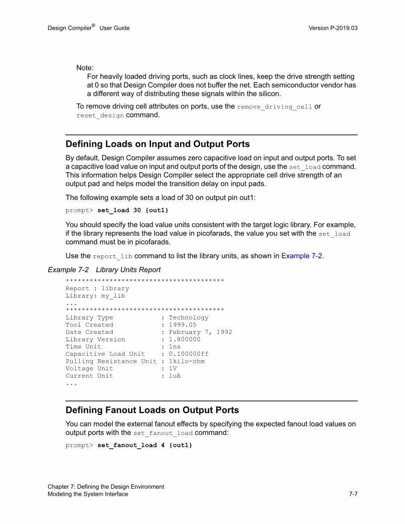
Design Compiler® User Guide Version P-2019.03
Note: For heavily loaded driving ports, such as clock lines, keep the drive strength setting at 0 so that Design Compiler does not buffer the net. Each semiconductor vendor has a different way of distributing these signals within the silicon.
To remove driving cell attributes on ports, use the remove_driving_cell or reset_design command.
Defining Loads on Input and Output Ports
By default, Design Compiler assumes zero capacitive load on input and output ports. To set a capacitive load value on input and output ports of the design, use the set_load command. This information helps Design Compiler select the appropriate cell drive strength of an output pad and helps model the transition delay on input pads.
The following example sets a load of 30 on output pin out1:
prompt> set_load 30 {out1}
You should specify the load value units consistent with the target logic library. For example, if the library represents the load value in picofarads, the value you set with the set_load command must be in picofarads.
Use the report_lib command to list the library units, as shown in Example 7-2.
Example 7-2 Library Units Report
****************************************Report : libraryLibrary: my_lib...****************************************Library Type : TechnologyTool Created : 1999.05Date Created : February 7, 1992Library Version : 1.800000Time Unit : 1nsCapacitive Load Unit : 0.100000ffPulling Resistance Unit : 1kilo-ohmVoltage Unit : 1VCurrent Unit : 1uA...
Defining Fanout Loads on Output Ports
You can model the external fanout effects by specifying the expected fanout load values on output ports with the set_fanout_load command:
prompt> set_fanout_load 4 {out1}
Chapter 7: Defining the Design EnvironmentModeling the System Interface 7-7Chapter 7: Defining the Design EnvironmentModeling the System Interface 7-7

Design Compiler® User Guide P-2019.03Design Compiler® User Guide Version P-2019.03
Design Compiler tries to ensure that the sum of the fanout load on the output port plus the fanout load of cells connected to the output port driver is less than the maximum fanout limit of the library, library cell, and design.
Fanout load is not the same as load. Fanout load is a unitless value that represents a numerical contribution to the total fanout. Load is a capacitance value. Design Compiler uses fanout load primarily to measure the fanout presented by each input pin. An input pin normally has a fanout load of 1, but it can have a higher value.
See Also
• Defining Maximum Fanout
Setting Logic Constraints on Ports
To improve optimization results, you can set logic constraints on ports to eliminate redundant ports or inverters by using the following methods:
• Setting logic equivalence
Some input ports are driven by logically related signals. For example, the signals driving a pair of input ports might always be the same (logically equal) or might always be different (logically opposite). To specify that two input ports are logically equivalent or logically opposite, use the set_equal or set_opposite command, respectively.
The following example specifies that the IN_X and IN_Y ports are logically equal:
prompt> set_equal IN_X IN_Y
• Assigning constant values to input ports
Setting a constant value to an input allows Design Compiler to simplify the surrounding logic function during optimization and create a smaller design. To assign a don’t care, logic 1, or logic 0 value to inputs in the current design, use the set_logic_dc, set_logic_one, or set_logic_zero command, respectively.
Figure 7-3 shows a simplified input port logic.
Figure 7-3 Simplified Input Port Logic
1
IN2IN2
Chapter 7: Defining the Design EnvironmentSetting Logic Constraints on Ports 7-8

Design Compiler® User Guide Version P-2019.03
The following example sets the A and B inputs to don't care and the IN input to logic 1:
prompt> set_logic_dc {A B}prompt> set_logic_one IN
To reset the values set by these commands, use the remove_attribute command.
For more information, see Allowing Assignment of Any Signal to an Input and Specifying Input Ports as Always One or Zero.
• Specifying unconnected output ports
If an output port is not used, that is, if it is unconnected, the logic driving the port can be minimized or eliminated during optimization, as shown in Figure 7-4.
Figure 7-4 Minimizing Logic Driving an Unconnected Output Port
To specify output ports to be unconnected to outside logic, use the set_unconnected command:
prompt> set_unconnected OUT
To undo this command, use the remove_attribute command.
Allowing Assignment of Any Signal to an Input
The set_logic_dc command specifies an input port driven by a dont_care to create smaller designs during compile. After optimization, a port connected to a dont_care usually does not drive anything inside the optimized design.
Use set_logic_dc to allow assignment of any signal to that input, including but not limited to 0 and 1 during compilation. The outputs of the design are significant only when the inputs that are not dont_care completely determine all the outputs, independent of the dont_care inputs.
Use the set_logic_dc command on input ports:
prompt> set_logic_dc { A B }
For a 2:1 multiplexer design with inputs S, A, B, and output Z, the function is computed as
Z = S*A + S'*B
unused unused
Chapter 7: Defining the Design EnvironmentSetting Logic Constraints on Ports 7-9Chapter 7: Defining the Design EnvironmentSetting Logic Constraints on Ports 7-9

Design Compiler® User Guide P-2019.03Design Compiler® User Guide Version P-2019.03
The command set_logic_dc B implies that the value of Z is significant when S = 1 and is a don’t care when S = 0. The resulting simplification, done during compilation, gives the reduced logic as a wire and the function is
Z = A
To undo this command, use the remove_attribute command.
To specify output ports as unused, use the set_unconnected command.
Specifying Input Ports as Always One or Zero
If an input port is always logic-high or -low, Design Compiler might be able to simplify the surrounding logic function during optimization and create a smaller design.
You can specify that input ports are connected to logic 1 or logic 0:
• Tying input ports to logic 1
The set_logic_one command lists the input ports tied to logic 1. After optimization, a port connected to logic 1 usually does not drive anything inside the optimized design.
Use the set_logic_one command on input ports. To specify output ports as unused, use the set_unconnected command.
To undo this command, use the remove_attribute command.
• Tying input ports to logic 0
The set_logic_zero command lists input ports tied to logic 0. After optimization, a port connected to logic 0 usually does not drive anything inside the optimized design.
Use the set_logic_zero command on input ports:
prompt> set_logic_one IN
To specify output ports as unused, use the set_unconnected command.
Wire Load Models
Wire load models are used only when Design Compiler is not operating in topographical mode. Wire load models estimate the effect of wire length and fanout on the resistance, capacitance, and area of nets. Design Compiler uses these physical values to calculate wire delays and circuit speeds.
Semiconductor vendors develop wire load models, based on statistical information specific to the vendors’ process. The models include coefficients for area, capacitance, and resistance per unit length, and a fanout-to-length table for estimating net lengths (the number of fanouts determines a nominal length).
Chapter 7: Defining the Design EnvironmentWire Load Models 7-10

Design Compiler® User Guide Version P-2019.03
In the absence of back-annotated wire delays, Design Compiler uses the wire load models to estimate net wire lengths and delays. Design Compiler determines which wire load model to use for a design based on the following factors, listed in order of precedence:
1. Explicit user specification
2. Automatic selection based on design area
3. Default specification in the logic library
If none of this information exists, Design Compiler does not use a wire load model. Without a wire load model, Design Compiler does not have complete information about the behavior of your target technology and cannot compute loading or propagation times for your nets; therefore, your timing information will be optimistic.
In hierarchical designs, Design Compiler must also determine which wire load model to use for nets that cross hierarchical boundaries. The tool determines the wire load model for cross-hierarchy nets based on one of the following factors, listed in order of precedence:
1. Explicit user specification
2. Default specification in the logic library
3. Default mode in Design Compiler
For information about selecting wire load models for nets and designs, see
• Hierarchical Wire Load Models
• Determining Available Wire Load Models
• Specifying Wire Load Models and Modes
Hierarchical Wire Load Models
Design Compiler supports three modes for determining which wire load model to use for nets that cross hierarchical boundaries:
• Top
Design Compiler models nets as if the design has no hierarchy and uses the wire load model specified for the top level of the design hierarchy for all nets in a design and its subdesigns. The tool ignores any wire load models set on subdesigns with the set_wire_load_model command.
Use top mode if you plan to flatten the design at a higher level of hierarchy before layout.
Chapter 7: Defining the Design EnvironmentWire Load Models 7-11Chapter 7: Defining the Design EnvironmentWire Load Models 7-11

Design Compiler® User Guide P-2019.03Design Compiler® User Guide Version P-2019.03
• Enclosed
Design Compiler uses the wire load model of the smallest design that fully encloses the net. If the design enclosing the net has no wire load model, the tool traverses the design hierarchy upward until it finds a wire load model. Enclosed mode is more accurate than top mode when cells in the same design are placed in a contiguous region during layout.
Use enclosed mode if the design has similar logical and physical hierarchies.
• Segmented
Design Compiler determines the wire load model of each segment of a net by the design encompassing the segment. Nets crossing hierarchical boundaries are divided into segments. For each net segment, Design Compiler uses the wire load model of the design containing the segment. If the design contains a segment that has no wire load model, the tool traverses the design hierarchy upward until it finds a wire load model.
Use segmented mode if the wire load models in your technology have been characterized with net segments.
Figure 7-5 shows a sample design with a cross-hierarchy net, cross_net. The top level of the hierarchy (design TOP) has a wire load model of 50x50. The next level of hierarchy (design MID) has a wire load model of 40x40. The leaf-level designs, A and B, have wire load models of 20x20 and 30x30, respectively.
Figure 7-5 Comparison of Wire Load Mode
50X50
30X3020X20
TOPMID
A B
40X40
50X50
30X3020X20
TOP
MIDA B
40X40
50X50
30X3020X20
TOPMID
A B
40X40
mode = top
mode = enclosed mode = segmented50X50
40X40 40X4020X20 30X30
Chapter 7: Defining the Design EnvironmentWire Load Models 7-12

Design Compiler® User Guide Version P-2019.03
In top mode, Design Compiler estimates the wire length of net cross_net, using the 50x50 wire load model. Design Compiler ignores the wire load models on designs MID, A, and B.
In enclosed mode, Design Compiler estimates the wire length of net cross_net, using the 40x40 wire load model (the net cross_net is completely enclosed by design MID).
In segmented mode, Design Compiler uses the 20x20 wire load model for the net segment enclosed in design A, the 30x30 wire load model for the net segment enclosed in design B, and the 40x40 wire load model for the segment enclosed in design MID.
Determining Available Wire Load Models
Most logic libraries have predefined wire load models. To list the wire load models defined in a logic library, use the report_lib command. The library must be loaded in memory before you run the report_lib command. To see a list of libraries loaded in memory, use the list_libs command.
The wire load report contains the following sections:
• Wire Loading Model section
This section lists the available wire load models.
• Wire Loading Model Mode section
This section identifies the default wire load mode. If a library default does not exist, Design Compiler uses top mode.
• Wire Loading Model Selection Group section
The presence of this section indicates that the library supports automatic area-based wire load model selection.
To generate a wire load report for the my_lib library, enter
dc_shell> read_file my_lib.dbdc_shell> report_lib my_lib
Example 7-3 shows the resulting wire load models report. The library my_lib contains three wire load models: 05x05, 10x10, and 20x20. The library does not specify a default wire load mode (so Design Compiler uses top as the default wire load mode), and it supports automatic area-based wire load model selection.
Example 7-3 Wire Load Models Report
****************************************Report : libraryLibrary: my_lib...****************************************...
Chapter 7: Defining the Design EnvironmentWire Load Models 7-13Chapter 7: Defining the Design EnvironmentWire Load Models 7-13

Design Compiler® User Guide P-2019.03Design Compiler® User Guide Version P-2019.03
Wire Loading Model:
Name : 05x05Location : my_libResistance : 0Capacitance : 1Area : 0Slope : 0.186Fanout Length Points Average Cap Std Deviation---------------------------------------------------- 1 0.39
Name : 10x10Location : my_libResistance : 0Capacitance : 1Area : 0Slope : 0.311Fanout Length Points Average Cap Std Deviation---------------------------------------------------- 1 0.53
Name : 20x20Location : my_libResistance : 0Capacitance : 1Area : 0Slope : 0.547Fanout Length Points Average Cap Std Deviation---------------------------------------------------- 1 0.86Wire Loading Model Selection Group:
Name : my_lib
Selection Wire load name min area max area ------------------------------------------- 0.00 1000.00 05x05 1000.00 2000.00 10x10 2000.00 3000.00 20x20...
Specifying Wire Load Models and Modes
The logic library can define a default wire load model that is used for all designs implemented in that technology. The default_wire_load library attribute identifies the default wire load model for a logic library.
Chapter 7: Defining the Design EnvironmentSpecifying Wire Load Models and Modes 7-14

Design Compiler® User Guide Version P-2019.03
Some libraries support automatic area-based wire load selection. Design Compiler uses the library function wire_load_selection to choose a wire load model based on the total cell area. The wire load model selected the first time you compile is used in subsequent compiles.
For large designs with many levels of hierarchy, automatic wire load selection can increase runtime. To manage runtime, set the wire load manually.
You can turn off automatic selection of the wire load model by setting the auto_wire_load_selection variable to false:
dc_shell> set auto_wire_load_selection false
The logic library can also define a default wire load mode. The default_wire_load_mode library attribute identifies the default mode. If the current library does not define a default mode, Design Compiler looks for the attribute in the libraries specified in the link_library variable. In the absence of a library default and an explicit specification, Design Compiler uses the top mode, which sets the wire load model to the top-level design.
To change the wire load model or mode specified in a logic library, use the set_wire_load_model and set_wire_load_mode commands. The wire load model and mode you define override all defaults. Explicitly selecting a wire load model also disables area-based wire load model selection for that design.
The following example selects the 10x10 wire load model:
dc_shell> set_wire_load_model "10x10"
The following example selects the 10x10 wire load model and specifies enclosed mode:
dc_shell> set_wire_load_mode enclosed
The wire load model you choose for a design depends on how that design is implemented in the chip. Consult your semiconductor vendor to determine the best wire load model for your design.
Use the report_design command or the report_timing command to see the wire load model and mode defined for the current design.
To remove the wire load model, use the remove_wire_load_model command with no model name.
Chapter 7: Defining the Design EnvironmentSpecifying Wire Load Models and Modes 7-15Chapter 7: Defining the Design EnvironmentSpecifying Wire Load Models and Modes 7-15

Design Compiler® User Guide P-2019.03Design Compiler® User Guide Version P-2019.03
Defining the Environment Using Topographical Mode
In topographical mode, Design Compiler derives the virtual layout of the design so that the tool can accurately predict and use real net capacitances instead of statistical net approximations based on wire load models. In ultra deep submicron designs, interconnect parasitics have a major effect on path delays; accurate estimates of resistance and capacitance are necessary to calculate path delays.
Topographical mode supports
• General Gate-Level Power Optimization
• Power Correlation
• Multivoltage Designs
• Low Power Intent
• Multicorner-Multimode Designs
Note: Do not specify wire load models. If you do, Design Compiler ignores them.
Sometimes Design Compiler in topographical mode and the IC Compiler or IC Compiler II tool have different environment settings. These differences can lead to correlation problems. For more information, see
• Comparing Design Compiler Topographical and IC Compiler Environments
• Comparing Design Settings Between Design Compiler and IC Compiler II
General Gate-Level Power Optimization
To perform power optimization, Design Compiler reduces power consumption on paths with positive timing slack. The more paths in the design with positive slack, the more opportunity for Design Compiler to reduce power consumption by using low-power cells. Designs with excessively restrictive timing constraints have little or no positive slack to trade for power reductions.
Designs that have black box cells, such as RAM and ROM, and customized subdesigns that have the dont_touch attribute, benefit from power optimization.
In Design Compiler topographical mode, to set the positive timing slack limit, use the physopt_power_critical_range variable. In the following example, Design Compiler optimizes only the timing paths with positive slack of 0.2 or more:
dc_shell-topo> set_app_var physopt_power_critical_range 0.2
Chapter 7: Defining the Design EnvironmentDefining the Environment Using Topographical Mode 7-16

Design Compiler® User Guide Version P-2019.03
Power Correlation
Design Compiler in topographical mode can perform power correlation by estimating the clock tree power. In addition, you can use the set_power_prediction command with the -ct_references option to specify clock tree references to improve correlation. The set_power_prediction command enables the tool to correlate post-synthesis power numbers with those after clock tree synthesis.
To perform power correlation in topographical mode, run a script similar to the following after you set up your design environment and apply synthesis constraints:
read_verilog set_power_prediction truecompile_ultra -gate_clock -scanreport_powerwrite_file -format ddc -output synthesized.ddc
The report_power command splits the power numbers into two categories: netlist power (based on cells already in the design) and estimated power (an estimate of the clock tree power).
See Also
• The Power Compiler User Guide
Multivoltage Designs
Design Compiler in topographical mode supports power optimization and power correlation for single voltage and multivoltage designs. For multivoltage designs, the subdesign instances (blocks) operate at different voltages. To reduce power consumption, multivoltage designs typically make use of power domains. The blocks of a power domain can be powered up and down, independent of the power state of other power domains (except where a relative always-on relationship exists between two power domains). In particular, power domains can be defined and level shifter and isolation cells can be used as needed to adjust voltage differences between power domains and to isolate shut-down power domains.
A power domain is defined as a grouping of one or more hierarchical blocks in a design that share the following:
• Primary voltage states or voltage range (that is, the same operating voltage)
• Power net hookup requirements
• Power-down control and acknowledge signals (if any)
• Power switching style
Chapter 7: Defining the Design EnvironmentDefining the Environment Using Topographical Mode 7-17Chapter 7: Defining the Design EnvironmentDefining the Environment Using Topographical Mode 7-17

Design Compiler® User Guide P-2019.03Design Compiler® User Guide Version P-2019.03
• Same process, voltage, and temperature (PVT) operating condition values (all cells of the power domain except level shifters)
• Same set or subset of nonlinear delay model (NLDM) target libraries
Using IEEETM 1801 Unified Power Format (UPF) Standard commands, you can specify the power domains of the design and the desired multivoltage implementation and verification strategies for each domain, including the domain’s isolation cells, retention cells, and level shifters. During a compile operation, Design Compiler automatically inserts these power management cells according to the specified strategies. The same set of UPF commands can be used throughout the design, analysis, verification, and implementation flow.
Power domains are not voltage areas. A power domain is a grouping of logic hierarchies, whereas the corresponding voltage area is a physical placement area into which the cells of the power domain’s hierarchies are placed. This correspondence is not automatic. You are responsible for correctly aligning the hierarchies to the voltage areas. You use the create_voltage_area command to set voltage areas.
Note: Because multivoltage designs use power domains, these designs usually require that certain library cells are marked as always-on cells and certain library cell pins are marked as always-on library cell pins. These always-on attributes are necessary to establish any always-on relationships between power domains. For more information, see the Power Compiler User Guide.
See Also
• The Power Compiler User Guide
Provides descriptions of the principal power domain commands
Low Power Intent
The IEEE 1801, also known as Unified Power Format (UPF), standard establishes a set of commands used to specify the low-power design intent for electronic systems. Using UPF commands, you can specify the power domains of the design and the desired multivoltage implementation and verification strategies for each domain, including the domain’s isolation cells, retention cells, and level shifters. During a compile operation, Design Compiler automatically inserts these power management cells according to the specified strategies. The same set of UPF commands can be used throughout the design, analysis, verification, and implementation flow. A Power Compiler license is required for using UPF commands in Design Compiler.
See Also
• Power Optimization in Multicorner-Multimode Designs
Chapter 7: Defining the Design EnvironmentDefining the Environment Using Topographical Mode 7-18

Design Compiler® User Guide Version P-2019.03
• The Power Compiler User Guide
Provides information about using UPF commands and details about the UPF flow for multicorner-multimode design optimization.
Multicorner-Multimode Designs
Designs are often required to operate under multiple modes, such as test or standby mode, and multiple operating conditions, sometimes referred to as corners. Such designs are referred to as multicorner-multimode designs. Design Compiler NXT and Design Compiler Graphical can analyze and optimize designs across multiple modes and corners concurrently. The multicorner-multimode feature in Design Compiler NXT and Design Compiler Graphical provides compatibility between flows in Design Compiler and IC Compiler.
You define modes and corners by using the create_scenario command. A scenario definition includes commands that specify the TLUPlus libraries, operating conditions, and constraints. You can also include other commands. For example, you can set leakage power optimization constraints on specific scenarios by using the set_scenario_options -leakage_power true command and set dynamic power constraints on specific scenarios by using the set_scenario_options -dynamic_power true command. For multiple dynamic power scenarios, optimization uses the average switching activity calculated from data in the SAIF files.
See Also
• Optimizing Multicorner-Multimode Designs
Leakage Power and Dynamic Power Optimization
Design Compiler automatically performs leakage power optimization (except in DC Expert, in which case you must specifically enable the optimization). During leakage power optimization, Design Compiler tries to reduce the overall leakage power in your design without affecting the performance. To do this, the optimization is performed on paths that are not timing-critical. When the target libraries are characterized for leakage power and contain cells characterized for multiple threshold voltages, Design Compiler uses the library cells with appropriate threshold voltages to reduce the leakage power of the design.
When using DC Expert, use the following command to enable leakage power optimization:
prompt> set_leakage_optimization true
You can also perform dynamic power optimization to reduce dynamic power consumption without affecting the performance. Dynamic power optimization requires switching activity information. The tool optimizes the dynamic power by placing nets with high switching
Chapter 7: Defining the Design EnvironmentLeakage Power and Dynamic Power Optimization 7-19Chapter 7: Defining the Design EnvironmentLeakage Power and Dynamic Power Optimization 7-19

Design Compiler® User Guide P-2019.03Design Compiler® User Guide Version P-2019.03
activity close to each other. Because the dynamic power saving is based on the switching activity of the nets, you need to annotate the switching activity by using the read_saif command. You can also optimize dynamic power incrementally to provide better QoR and reduce the runtime.
To enable dynamic optimization in all Design Compiler tools, use the following command:
prompt> set_dynamic_optimization true
For more information about dynamic power optimization, see the Power Compiler User Guide.
Note: When both leakage and dynamic power optimization are enabled in DC Expert, the tool performs only leakage power optimization.
To learn more about leakage power optimization, see the following topics:
• Leakage Power Optimization Based on Threshold Voltage
• Leakage Optimization for Multicorner-Multimode Designs
Leakage Power Optimization Based on Threshold Voltage
Leakage power optimization can use single threshold voltage or multithreshold voltage libraries. However, multithreshold voltage libraries can save more leakage power.
Leakage power is very sensitive to threshold voltage. The leakage power can vary up to 40 times or more based on the threshold voltage used. The higher the threshold voltage, the lower the leakage power. For the same library, timing varies by a much smaller amount, up to 30 percent. The lower the threshold voltage, the faster the timing. For the single-voltage library, the variance of threshold voltage and timing is of a similar magnitude.
For designs that have strict timing constraints, optimize for leakage power only on the non timing-critical paths, using the higher threshold-voltage cells from the multithreshold voltage libraries. When your design has a relatively easy-to-meet timing constraint, you might have a large number of low threshold-voltage cells in your design, resulting in higher leakage power consumption. For optimum results you should start with 1 to 5 percent of the number of cells in the design for the low threshold-voltage cells and gradually increase the percentage until the timing constraint is met. With this technique, your design meets the timing constraint with minimal leakage power consumption.
Multithreshold Voltage Library Attributes
To define threshold voltage groups in the libraries, use the set_attribute command and add the following attributes:
• Library-level attribute:
Chapter 7: Defining the Design EnvironmentLeakage Power and Dynamic Power Optimization 7-20

Design Compiler® User Guide Version P-2019.03
default_threshold_voltage_group :string;
• Library-cell-level attribute:
threshold_voltage_group :string;
With these attributes, the threshold voltages are differentiated by the string you specify. When the library has at least two threshold voltage groups or if you have defined threshold voltage groups for your library cells using the set_attribute command, the library cells are grouped by the threshold voltage. For accurate multiple threshold voltage optimization, define the threshold voltage group attributes.
For information about comparing the leakage power with respect to the timing characteristics of the target library cells belonging to each threshold voltage group, see Analyzing Multithreshold Voltage Library Cells.
Setting Multithreshold Voltage Constraints
To set the multithreshold voltage constraint, use the set_multi_vth_constraint command. The command specifies the maximum percentage of cells, by cell count or area, that the design can contain from the specified low-threshold-voltage groups.
You can also specify whether the set_multi_vth_constraint constraint should have a higher or lower priority than the timing constraint by using the -type option. When you specify -type hard, Design Compiler tries to meet the set_multi_vth_constraint constraint, even if it results in timing degradation. When you specify -type soft, Design Compiler tries to meet the set_multi_vth_constraint constraint without degrading the timing.
Note: The -type soft option is supported only in Design Compiler topographical mode.
While calculating the percentage of low-threshold-voltage cells in the design, the tool does not consider the black box cells. To consider the black box cells in the percentage calculation, specify the -include_blackboxes option.
After synthesis, use the report_threshold_voltage_group command to see the percentage of the total design, by cell count and by area, that is occupied by the low threshold-voltage cells.
In the following example, the maximum percentage of low-threshold-voltage cells in the design is set to 15 percent. Design Compiler tries to meet this constraint without compromising the timing constraint.
dc_shell-topo> set_multi_vth_constraint \ -lvth_groups {lvt svt} -lvth_percentage percentage \ -type soft -include_blackboxes
Chapter 7: Defining the Design EnvironmentLeakage Power and Dynamic Power Optimization 7-21Chapter 7: Defining the Design EnvironmentLeakage Power and Dynamic Power Optimization 7-21
Design Compiler® User Guide P-2019.03Design Compiler® User Guide Version P-2019.03
Note: If you use the set_multi_vth_constraint command, it takes precedence over leakage optimization.
Leakage Optimization for Multicorner-Multimode Designs
For multicorner-multimode designs, you can specify the leakage power optimization for specific scenarios by using the set_scenario_options command.
For more information about leakage power optimization for multicorner-multimode designs, see Power Optimization in Multicorner-Multimode Designs.
Comparing Design Compiler Topographical and IC Compiler Environments
Sometimes Design Compiler in topographical mode and IC Compiler have different environment settings. These differences can lead to correlation problems. To help fix these correlation issues, use the consistency_checker command in your Linux shell to compare the respective environments.
Before you can compare the two environments, you need to determine the environments of each tool. To do this, use the write_environment command as shown in Example 7-4 and Example 7-5. Use the -output option to specify the name of your output report. In the Design Compiler tool, run the write_environment command before compile_ultra; in the IC Compiler tool, run the write_environment command before place_opt.
Example 7-4 Using write_environment in Design Compiler
dc_shell-topo> write_environment -consistency -output DCT.env
Example 7-5 Using write_environment in IC Compiler
icc_shell> write_environment -consistency -output ICC.env
To write compressed environment files, specify the -compress option when you run the write_environment -consistency command. You must decompress the output file by using the gunzip Linux command before using the consistency_checker command.
After you have the environments for each tool, compare the environments using the consistency_checker command, as shown in Example 7-6.
Example 7-6 Comparing Design Compiler and IC Compiler Environments
% consistency_checker –file1 DCT.env –file2 ICC.env \-folder temp \-html html_report | tee cc.log
Chapter 7: Defining the Design EnvironmentComparing Design Compiler Topographical and IC Compiler Environments 7-22

Design Compiler® User Guide Version P-2019.03
The resulting HTML output report lists mismatched commands and variables. In Example 7-6, the HTML output report is written to the ./html_report directory. To access this report, open the ./html_report/index.html file in any Web browser. To reduce correlation problems, fix these mismatches before proceeding to optimization.
In addition to the HTML output report, the tool prints a summary report to the shell while the consistency_checker command is running. You can use the Linux tee command, as shown in Example 7-6, to save this report to a file. In Example 7-6, the report is saved to the ./cc.log file.
Note: The ./temp directory stores intermediate files the tool uses when executing the consistency_checker command. After the command completes, you can remove the./temp directory.
See Also
• SolvNet article 026366, “Using the Consistency Checker to Automatically Compare Environment Settings Between Design Compiler and IC Compiler”
• Comparing Design Settings Between Design Compiler and IC Compiler II
Comparing Design Settings Between Design Compiler and IC Compiler II
Sometimes the Design Compiler and IC Compiler II tools have different design settings, which might lead to correlation and QoR problems. Checking the design settings manually can be time consuming. To resolve the correlation issues and other problems, use the Design Compiler to IC Compiler II consistency checker to extract and automatically compare the settings.
The Design Compiler to IC Compiler II consistency checker is supported in the Design Compiler tool in wire load mode, topographical mode, Design Compiler NXT, and Design Compiler Graphical.
Before you use the consistency checker, you must download the consistency_checker.tar.gz tar file. Extracting the files produces a directory containing the following scripts:
• snps_settings.tcl – Tcl script to write the tool settings into a file that works in both tools.
• snps_consistency_checker.pl – Perl script to compare the setting files generated by the Design Compiler and IC Compiler II tools.
Chapter 7: Defining the Design EnvironmentComparing Design Settings Between Design Compiler and IC Compiler II 7-23Chapter 7: Defining the Design EnvironmentComparing Design Settings Between Design Compiler and IC Compiler II 7-23

Design Compiler® User Guide P-2019.03Design Compiler® User Guide Version P-2019.03
To use the consistency checker, perform the following steps after loading the design and applying the constraints and before running the compile_ultra command in Design Compiler and the place_opt command in IC Compiler II:
1. Source the snps_settings.tcl file in both the Design Compiler and IC Compiler II shells:
prompt> source consistency_checker/snps_settings.tcl
2. Run the report_settings procedure and redirect the output to a file. For example, in the Design Compiler tool, enter
dc_shell> report_settings > dc_settings
In the IC Compiler II tool, enter
icc2_shell> report_settings > icc2_settings
3. In Linux, run the snps_consistency_checker.pl script and specify the Design Compiler and IC Compiler II setting files:
% consistency_checker/snps_consistency_checker.pl \dc_settings icc2_settings
Comparing timer settings:-------------------------Warning: Variable mismatch: DC: timing_enable_through_paths = false ICC2: timing_enable_through_paths = trueWarning: Variable mismatch: DC: disable_auto_time_borrow = false ICC2: disable_auto_time_borrow = trueComparing placer settings:-------------------------Warning: Variable mismatch: DC: placer_enable_enhanced_router equiv_value = medium ICC2: place.coarse.congestion_analysis_effort = highWarning: Variable mismatch: DC: placer_enable_enhanced_soft_blockages = true ICC2: place.coarse.enable_enhanced_soft_blockages = false
You can now analyze the mismatches and debug the inconsistencies.
To download the Design Compiler to IC Compiler II consistency checker, see SolvNet article 2112936, “Automatically Finding Inconsistent Settings Between Design Compiler or IC Compiler and IC Compiler II.”
See Also
• Comparing Design Compiler Topographical and IC Compiler Environments
Chapter 7: Defining the Design EnvironmentComparing Design Settings Between Design Compiler and IC Compiler II 7-24

8Defining Design Constraints 8
Constraints are declarations that define your design’s goals in measurable circuit characteristics, such as timing, area, and capacitance. Design Compiler needs these constraints to effectively optimize the design.
To learn the concepts and tasks necessary for defining design constraints, see
• Constraint Types
• Design Rule Constraints
• Optimization Constraints
• Managing Constraint Priorities
• Disabling the Cost Function
• Reporting Constraints
• Reporting Runtime Issues Related to SDC Constraints
• Propagating Constraints in Hierarchical Designs
8-1

Design Compiler® User Guide P-2019.03Design Compiler® User Guide Version P-2019.03
Constraint Types
When Design Compiler optimizes your design, it uses two types of constraints:
• Design Rule Constraints
The logic library defines these implicit constraints. These constraints are required for a design to function correctly. They apply to any design that uses the library. By default, design rule constraints have a higher priority than optimization constraints.
• Optimization Constraints
You define these explicit constraints. Optimization constraints apply to the design on which you are working for the duration of the dc_shell session and represent the design’s goals. During optimization, Design Compiler attempts to meet these goals, but no design rules are violated by the process. To optimize a design correctly, you must set realistic constraints.
You specify constraints interactively on the command line or in a constraints file. Design Compiler tries to meet both design rule constraints and optimization constraints, but design rule constraints take precedence.
Figure 8-1 and Figure 8-2 show the major Design Compiler design rule constraints and optimization constraints and the dc_shell interface commands to set the constraints.
Figure 8-1 Major Design Rule Constraints
Design RuleConstraints
set_max_transition
set_max_capacitance
set_cell_degradation set_min_capacitance
Maximum:
Transition TimeFanout
Capacitance
CellDegradation
MinimumCapacitance
set_max_fanout
Chapter 8: Defining Design ConstraintsConstraint Types 8-2
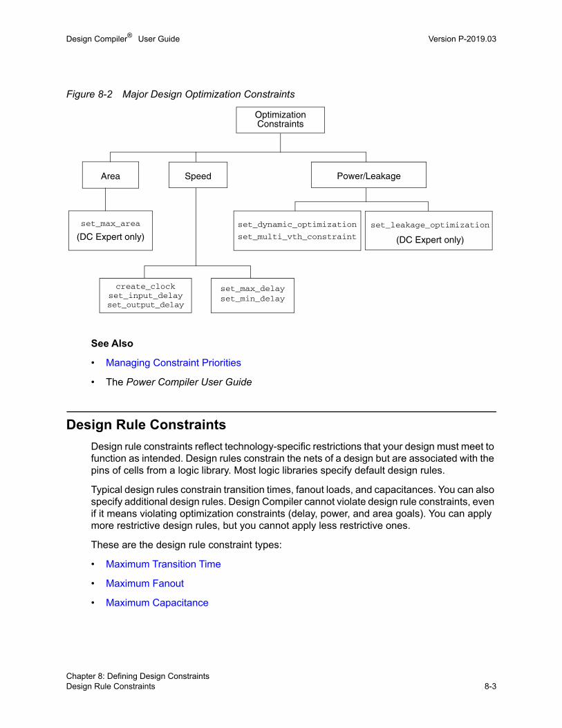
Design Compiler® User Guide Version P-2019.03
Figure 8-2 Major Design Optimization Constraints
See Also
• Managing Constraint Priorities
• The Power Compiler User Guide
Design Rule Constraints
Design rule constraints reflect technology-specific restrictions that your design must meet to function as intended. Design rules constrain the nets of a design but are associated with the pins of cells from a logic library. Most logic libraries specify default design rules.
Typical design rules constrain transition times, fanout loads, and capacitances. You can also specify additional design rules. Design Compiler cannot violate design rule constraints, even if it means violating optimization constraints (delay, power, and area goals). You can apply more restrictive design rules, but you cannot apply less restrictive ones.
These are the design rule constraint types:
• Maximum Transition Time
• Maximum Fanout
• Maximum Capacitance
OptimizationConstraints
set_max_delayset_min_delay
create_clockset_input_delayset_output_delay
SpeedArea Power/Leakage
set_dynamic_optimization
set_multi_vth_constraint
set_max_area
(DC Expert only)set_leakage_optimization
(DC Expert only)
Chapter 8: Defining Design ConstraintsDesign Rule Constraints 8-3Chapter 8: Defining Design ConstraintsDesign Rule Constraints 8-3

Design Compiler® User Guide P-2019.03Design Compiler® User Guide Version P-2019.03
• Minimum Capacitance
• Cell Degradation
• Connection Class
You cannot remove the max_transition, max_fanout, max_capacitance, and min_capacitance attributes set in a logic library, because they are required, but you can set stricter values.
For information about fixing design rule violations, see
• Fixing Design Rule Violations
• Disabling DRC Violation Fixing on Special Nets
See Also
• Summary of Design Rule Commands and Objects
• Design Rule Constraint Precedence
• Design Rule Scenarios
Maximum Transition Time
Maximum transition time is a design rule constraint. The maximum transition time for a net is the longest time required for its driving pin to change logic values. Many logic libraries contain restrictions on the maximum transition time for a pin, creating an implicit transition time limit for designs using that library. Transition times on nets are computed by use of timing data from the logic library.
To change or add to the implicit transition time values from a logic library, use the set_max_transition command. The command sets the max_transition attribute to the specified value on clock groups, ports, or designs. During compile, Design Compiler attempts to ensure that the transition time for each net is less than the specified value, for example, by buffering the output of the driving gate. The max_transition constraint value can vary with the operating frequency of a cell.
If both a library max_transition and a design max_transition attribute are defined, Design Compiler tries to meet the smaller (more restrictive) value.
If your design uses multiple logic libraries and each has a different default max_transition value, Design Compiler uses the smallest max_transition value globally across the design.
If the transition time for a given driver is greater that the max_transition value, Design Compiler reports a design rule violation and works to correct the violation.
Chapter 8: Defining Design ConstraintsDesign Rule Constraints 8-4

Design Compiler® User Guide Version P-2019.03
The following example sets a maximum transition time of 3.2 for the adder design:
prompt> set_max_transition 3.2 [get_designs adder]
To undo a set_max_transition command, use the remove_attribute command:
prompt> remove_attribute [get_designs adder] max_transition
Specifying Clock-Based Maximum Transition
The max_transition value can vary with the operating frequency of a cell. The operating frequency of a cell is defined as the highest clock frequency on the registers driving a cone of logic. Clock frequencies are defined with the create_clock command.
For designs with multiple clock domains, you can use the set_max_transition command to set the max_transition attribute on pins in a specific clock group.
Design Compiler follows these rules in determining the max_transition value:
• When the max_transition attribute is set on a design or port and a clock group, the most restrictive constraint is used.
• If multiple clocks launch the same paths, the most restrictive constraint is used.
• If max_transition attributes are already specified in a logic library, the tool automatically attempts to meet these constraints during compile.
For example, the following command sets a max_transition value of 5 on all pins belonging to the Clk clock group:
prompt> set_max_transition 5 [get_clocks Clk]
Maximum Fanout
Maximum fanout is a design rule constraint. Most logic libraries place fanout restrictions on driving pins, creating an implicit fanout constraint for every driving pin in designs using that library.
You can set a more conservative fanout constraint on an entire library or define fanout constraints for specific pins in the library description of an individual cell.
If a library fanout constraint exists and you specify a max_fanout attribute, Design Compiler tries to meet the smaller (more restrictive) value.
Design Compiler models fanout restrictions by associating a fanout_load attribute with each input pin and a max_fanout attribute with each output (driving) pin on a cell, as shown in Figure 8-3.
Chapter 8: Defining Design ConstraintsDesign Rule Constraints 8-5Chapter 8: Defining Design ConstraintsDesign Rule Constraints 8-5

Design Compiler® User Guide P-2019.03Design Compiler® User Guide Version P-2019.03
Figure 8-3 fanout_load and max_fanout Attributes
To evaluate the fanout for a driving pin (such as X in Figure 8-3), Design Compiler calculates the sum of all the fanout_load attributes for inputs driven by pin X and compares that number with the number of max_fanout attributes stored at the driving pin X.
• If the sum of the fanout loads is not more than the max_fanout value, the net driven by X is valid.
• If the net driven by X is not valid, Design Compiler tries to make that net valid, perhaps by choosing a higher-drive component.
Maximum Fanout Calculation Example
Figure 8-4 shows how maximum fanout is calculated.
Figure 8-4 Calculation of Maximum Fanout
You can set a maximum fanout constraint on every driving pin and input port as follows:
prompt> set_max_fanout 8 [get_designs ADDER]
To check whether the maximum fanout constraint is met for driving pin Z, Design Compiler compares the specified max_fanout attribute against the fanout load. If the calculated fanout load is greater than the max_fanout value, Design Compiler reports a design rule violation and attempts to correct the violation.
In this case, the design meets the constraints.
X max_fanout : 13.0
fanout_load : 1.0
fanout_load : 2.0
fanout_load:1.0
1.0
fanout_load:2.0
Driving pin
Z
U3:NR6
OUT1set_fanout_load 3.0
set_max_fanout 8
Chapter 8: Defining Design ConstraintsDesign Rule Constraints 8-6

Design Compiler® User Guide Version P-2019.03
The fanout load imposed by a driven cell (U3) is not necessarily 1.0. Library developers can assign higher fanout loads (for example, 2.0) to model internal cell fanout effects.
You can also set a fanout load on an output port (OUT1) to model external fanout effects.
Fanout load is a dimensionless number, not a capacitance. It represents a numerical contribution to the total effective fanout.
Defining Maximum Fanout
The set_max_fanout command sets the maximum allowable fanout load for the listed input ports. The set_max_fanout command sets a max_fanout attribute on the listed objects.
To undo a maximum fanout value set on an input port or design, use the remove_attribute command. For example,
prompt> remove_attribute [get_ports port_name] max_fanoutprompt> remove_attribute [get_designs design_name] max_fanout
Defining Expected Fanout for Output Ports
The set_fanout_load command sets the expected fanout load value for listed output ports.
Design Compiler adds the fanout value to all other loads on the pin driving each port in port_list and tries to make the total load less than the maximum fanout load of the pin.
To undo a set_fanout_load command set on an output port, use the remove_attribute command:
prompt> remove_attribute port_name fanout_load
To determine the fanout load, use the get_attribute command. For example, to find the fanout load on the input pin of library cell AND2 in library libA, enter
prompt> get_attribute "libA/AND2/i" fanout_load
To find the default fanout load set on logic library libA, enter
prompt> get_attribute libA default_fanout_load
Total Fanout Load
8 > 1.0 + 1.0 + 3.0 + 2.0
7
Chapter 8: Defining Design ConstraintsDesign Rule Constraints 8-7Chapter 8: Defining Design ConstraintsDesign Rule Constraints 8-7

Design Compiler® User Guide P-2019.03Design Compiler® User Guide Version P-2019.03
Maximum Capacitance
Maximum capacitance is a design rule constraint. It is a pin-level attribute that defines the maximum total capacitive load that an output pin can drive. That is, the pin cannot connect to a net that has a total capacitance (load pin capacitance and interconnect capacitance) greater than or equal to the maximum capacitance defined at the pin.
Design Compiler calculates the capacitance on a net by adding the wire capacitance of the net to the capacitance of the pins attached to the net. You can control capacitance directly and set a maximum capacitance for the nets attached to specified ports or to all the nets in a design by using the set_max_capacitance command. The command places a max_capacitance attribute on the listed objects. The value should be less than or equal to the max_capacitance value of the pin driving the net.
To determine whether a net meets the capacitance constraint, Design Compiler compares the calculated capacitance value with the max_capacitance value of the pin driving the net. If the calculated capacitance is greater than the max_capacitance value, Design Compiler reports a design rule violation and attempts to correct the violation.
The max_capacitance constraint operates similarly to max_transition, but the cost is based on the total capacitance of the net, rather than the transition time. The max_capacitance attribute functions independently, so you can use it with max_fanout and max_transition.
The max_capacitance value can vary with the operating frequency of a cell. You can have Design Compiler annotate each driver pin with a frequency-based max_capacitance value by setting the compile_enable_dyn_max_cap variable to true. For more information, see Specifying Frequency-Based Maximum Capacitance.
The max_capacitance constraint has priority over the cell degradation constraint.
If both a library max_capacitance attribute and a design max_capacitance attribute exist, Design Compiler tries to meet the smaller (more restrictive) value.
To set a maximum capacitance of 3 for the design adder, enter
prompt> set_max_capacitance 3 [get_designs adder]
To undo a set_max_capacitance command, use the remove_attribute command:
prompt> remove_attribute [get_designs adder] max_capacitance
Specifying Frequency-Based Maximum Capacitance
The max_capacitance value can vary with the operating frequency of a cell. You can have Design Compiler annotate each driver pin with a frequency-based max_capacitance value by setting the compile_enable_dyn_max_cap variable to true.
Chapter 8: Defining Design ConstraintsDesign Rule Constraints 8-8

Design Compiler® User Guide Version P-2019.03
Before you use this feature, your logic library should be characterized for multiple frequencies. This characterization consists of associating a max_capacitance value with each driver pin for each frequency and capturing this information in a one-dimensional lookup table. For information about creating the max_capacitance lookup table, see the Library Compiler documentation.
Design Compiler follows these steps in determining the max_capacitance value:
1. It identifies the operating frequency of each cell.
The operating frequency of a cell is defined as the highest clock frequency on the registers driving a cone of logic. Clock frequencies are defined with the create_clock command.
2. It looks up the corresponding max_capacitance value for the identified frequency from the lookup table in the logic library.
3. It annotates each driver pin with the appropriate max_capacitance value and uses these values in synthesis.
Generating Maximum Capacitance Reports
To report maximum capacitance on violating nets only, use the report_constraint command as follows:
prompt> report_constraint -all_violators -max_capacitance... Required Actual Net Capacitance Capacitance Slack ----------------------------------------------------------------- n_6 0.0014226 0.0128121 -0.0113895 (VIOLATED) n_16 0.0014226 0.0115580 -0.0101354 (VIOLATED) n_121 0.0014226 0.0114569 -0.0100343 (VIOLATED) n_21 0.0014226 0.0113311 -0.0099085 (VIOLATED) div_18_17/n_2 0.0014226 0.0044171 -0.0029945 (VIOLATED) div_18_17/n_43 0.0014226 0.0042607 -0.0028381 (VIOLATED)
To report maximum capacitance on all nets, use the report_net command as follows:
prompt> report_net -max_capacitance...Net: Required Capacitance Actual Capacitance Slack---------------------------------------------------------------CMD[0] 1.25 0.25 1.0(Met)CMD[1] 2.50 4.50 -2.0(Violated)
These commands report the following details about nets:
• Required capacitance defined by users or derived using the libraries
• Actual capacitance calculated by the tool
Chapter 8: Defining Design ConstraintsDesign Rule Constraints 8-9Chapter 8: Defining Design ConstraintsDesign Rule Constraints 8-9

Design Compiler® User Guide P-2019.03Design Compiler® User Guide Version P-2019.03
• Slack (the required capacitance minus the actual capacitance)
Minimum Capacitance
Minimum capacitance is a design rule constraint. Some logic libraries specify minimum capacitance. The min_capacitance design rule specifies the minimum load a cell can drive. It specifies the lower bound of the range of loads with which a cell has been characterized to operate. During optimization, Design Compiler ensures that the load driven by a cell meets the minimum capacitance requirement for that cell. When a violation occurs, Design Compiler fixes the violation by sizing the driver.
You can use the min_capacitance design rule with the existing design rules. The min_capacitance design rule has higher priority than the maximum transition time, maximum fanout, and maximum capacitance constraints.
You can set a minimum capacitance for nets attached to input ports to determine whether violations occur for driving cells at the input boundary. If violations are reported after compilation, you can fix the problem by recompiling the module driving the ports. Use the set_min_capacitance command to set minimum capacitance on input or inout ports; you cannot set minimum capacitance on a design.
If library min_capacitance and design min_capacitance attributes both exist, Design Compiler tries to meet the larger (more restrictive) value.
Defining Minimum Capacitance
The set_min_capacitance command sets a defined minimum capacitance value on listed input or bidirectional ports. To set a minimum capacitance for nets attached to input or bidirectional ports, use the set_min_capacitance command.
To set a minimum capacitance value of 12.0 units on the port named high_drive, enter
prompt> set_min_capacitance 12.0 high_drive
To report only minimum capacitance constraint information, use the -min_capacitance option with the report_constraint command.
To get information about the current port settings, use the report_port command.
To undo a set_min_capacitance command, use the remove_attribute command.
Chapter 8: Defining Design ConstraintsDesign Rule Constraints 8-10

Design Compiler® User Guide Version P-2019.03
Cell Degradation
Cell degradation is a design rule constraint. Some logic libraries contain cell degradation tables. The tables list the maximum capacitance that can be driven by a cell as a function of the transition times at the inputs of the cell.
The cell_degradation design rule specifies that the capacitance value for a net is less than the cell degradation value. The cell_degradation design rule can be used with other design rules, but the max_capacitance design rule has a higher priority than the cell_degradation design rule. If the max_capacitance rule is not violated, applying the cell_degradation design rule does not cause it to be violated.
The set_cell_degradation command sets the cell_degradation attribute to a specified value on specified input ports.
During compilation, if cell_degradation tables are specified in a logic library, Design Compiler tries to ensure that the capacitance value for a net is less than the specified value. The cell_degradation tables give the maximum capacitance that a cell can drive, as a function of the transition times at the inputs of the cell.
If cell_degradation tables are not specified in a logic library, you can set cell_degradation explicitly on the input ports.
By default, a port has no cell_degradation constraint.
Note: Use of the set_cell_degradation command requires a DC Ultra license.
This command sets a maximum capacitance value of 2.0 units on the port named late_riser:
prompt> set_cell_degradation 2.0 late_riser
To get information about optimization and design rule constraints, use the report_constraint command.
To remove the cell_degradation attribute, use the remove_attribute command.
Connection Class
The connection class constraint on a port describes the connection requirements for a given technology. Only loads and drivers with the same connection class label can be legally connected. You can specify this constraint, or it can be specified in the library. To set a connection class constraint on a port, use the set_connection_class command.
Chapter 8: Defining Design ConstraintsDesign Rule Constraints 8-11Chapter 8: Defining Design ConstraintsDesign Rule Constraints 8-11

Design Compiler® User Guide P-2019.03Design Compiler® User Guide Version P-2019.03
Summary of Design Rule Commands and Objects
Table 8-1 summarizes the design rule commands and the objects on which to set them.
Fixing Design Rule Violations
Design Compiler helps you fix design rule violations. If there are multiple violations, Design Compiler tries to fix the violation with the highest priority first. When possible, it also evaluates and selects alternatives that reduce violations of other design rules. Design Compiler uses the same approach with delay violations.
Figure 8-5 shows the design rule cost function equation.
Figure 8-5 Design Rule Cost Equation
In a compilation report, the DESIGN RULE COST column reports the cost function for the design rule constraints on the design.
For more information about fixing design rule violations, see Design Rule Fixing.
See Also
• Disabling DRC Violation Fixing on Special Nets
• Managing Constraint Priorities
Table 8-1 Design Rule Command and Object Summary
Command Object
set_max_fanout Input ports or designs
set_fanout_load Output ports
set_load Ports or nets
set_max_transition Ports or designs
set_cell_degradation Input ports
set_min_capacitance Input ports
max di 0 wi
i 1=
m
d = Delta Constraintm = Total Number of Constraintsw = Constraint Weight
i = Index
Chapter 8: Defining Design ConstraintsDesign Rule Constraints 8-12

Design Compiler® User Guide Version P-2019.03
Disabling DRC Violation Fixing on Special Nets
To enable or disable DRC violation fixing on clock, constant, or scan nets, use the set_auto_disable_drc_nets command. The command acts on all the nets of a given type in the current design; that is, depending on the options you specify, it acts on all the clock nets, all the constant nets, all the scan nets, or on any combination of these three net types. Nets that have DRC violation fixing disabled are marked with the auto_disable_drc_nets attribute.
By default, the clock and constant nets of a design have DRC violation fixing disabled. This is the same as using the -default option of the command; the scan nets do not. You can use the -all option to disable DRC violation fixing on all three net types.
Alternatively, you can independently disable or enable DRC violation fixing for the clock nets, constant nets, or scan nets by assigning a true or false value to the -on_clock_network, -constant, or -scan options, respectively. You can use the -none option to enable DRC violation fixing on all three types of nets.
It is recommended that you use the -on_clock_network option instead of the -clock option to enable or disable DRC violation fixing for the clock network. The -clock option is supported for backward compatibility. However, it is set to true by default, meaning that it automatically disables DRC violation fixing on clock networks. As shown in Figure 8-6, the -clock option starts at register clock pins and propagates back, but not through, the logic on the clock tree. Optimization might buffer non-DRC disabled clock nets upstream of existing clock logic.
To correctly disable DRC violation fixing on the entire clock tree, use the -on_clock_network option set to true, also shown in Figure 8-6. The option is set to false by default. The default setting has not been changed to true to avoid affecting existing flows.
If both the -on_clock_network option and the -clock option are set to true, the effect is the same as using the -on_clock_network option alone; the -on_clock_network option overrides the -clock option in this case.
Figure 8-6 shows DRC violation fixing disabled for clock nets by the -clock option (on the left) and by the -on_clock_network option (on the right). The DRC-disabled clock nets are represented by dashed lines.
Chapter 8: Defining Design ConstraintsDesign Rule Constraints 8-13Chapter 8: Defining Design ConstraintsDesign Rule Constraints 8-13

Design Compiler® User Guide P-2019.03Design Compiler® User Guide Version P-2019.03
Figure 8-6 DRC Violation Fixing Disabled for Clock Nets
Clock nets are ideal nets by default. Using the set_auto_disable_drc_nets command to enable design rule fixing does not affect the ideal timing properties of clock nets. You must use the set_propagated_clock command to affect the ideal timing of clock nets.
You cannot use the set_auto_disable_drc_nets command to override disabled design rule fixing on ideal networks marked with ideal network attributes. This command never overrides the settings specified by the set_ideal_net or set_ideal_network command.
See Also
• Fixing Design Rule Violations
Design Rule Constraint Precedence
Design Compiler follows this descending order of precedence when it tries to resolve conflicts among design rule constraints:
1. Minimum capacitance
2. Maximum transition
3. Maximum fanout
4. Maximum capacitance
5. Cell degradation
DRC violation fixing disabled by-clock -on_clock_network
DRC violation fixing disabled by
clkB
clkA
clkCclksel
clkD
clkE
clkB
clkA
clkCclksel
clkD
clkE
Chapter 8: Defining Design ConstraintsDesign Rule Constraints 8-14
Design Compiler® User Guide Version P-2019.03
The following rules determine the precedence of design rule constraints:
• Maximum transition has precedence over maximum fanout. If a maximum fanout constraint is not met, investigate the possibility of a conflicting maximum transition constraint. Design Compiler does not make a transition time worse to fix a maximum fanout violation.
• Maximum fanout has precedence over maximum capacitance.
• Design Compiler calculates transition time for a net in two ways, depending on the library.
❍ For libraries using the CMOS delay model, Design Compiler calculates the transition time by using the drive resistance of the driving cell and the capacitive load on the net.
❍ For libraries using a nonlinear delay model, Design Compiler calculates the transition time by using table lookup and interpolation. This is a function of capacitance at the output pin and of the input transition time.
• The set_driving_cell and set_drive commands behave differently, depending on your logic library.
❍ For libraries using the CMOS delay model, drive resistance is a constant. In this case, the set_drive command and the set_driving_cell command give the same result.
❍ For libraries using a nonlinear delay model, the set_driving_cell command calculates the transition time dynamically, based on the load from the tables. The set_drive command returns one value when the command is issued and uses a value from the middle of the range in the tables for load.
Both the set_driving_cell and the set_drive commands affect the port transition delay. The set_driving_cell command places the design rule constraints, annotated with the driving cell, on the affected port.
The set_load command places a load on a port or a net. The units of this load must be consistent with your logic library. This value is used for timing optimizations, not for maximum fanout optimizations.
See Also
• Managing Constraint Priorities
Chapter 8: Defining Design ConstraintsDesign Rule Constraints 8-15Chapter 8: Defining Design ConstraintsDesign Rule Constraints 8-15

Design Compiler® User Guide P-2019.03Design Compiler® User Guide Version P-2019.03
Design Rule Scenarios
Typical design rule scenarios are
• set_max_fanout and set_max_transition commands
• set_max_fanout and set_max_capacitance commands
Typically, a logic library specifies a default max_transition or max_capacitance, but not both. To achieve the best result, do not mix max_transition and max_capacitance.
Optimization Constraints
Optimization constraints represent speed, area, and power design goals and restrictions that you want but that might not be crucial to the operation of a design. By default, optimization constraints are secondary to design rule constraints. However, that priority can be changed; see Managing Constraint Priorities.
The optimization constraints consist of
• Input and output delays (timing constraints)
• Minimum and maximum delay (timing constraints)
• Maximum area
• Power optimization
To define optimization constraints, see
• Defining Timing Constraints
• Defining Area Constraints (DC Expert Only)
• Defining Power Constraints
See Also
• Compile Cost Function
Chapter 8: Defining Design ConstraintsOptimization Constraints 8-16

Design Compiler® User Guide Version P-2019.03
Defining Timing Constraints
When defining timing constraints you should consider that your design has synchronous paths and asynchronous paths. Synchronous paths are constrained by specifying clocks in the design. Use the create_clock command to specify a clock. After specifying the clocks, it is recommended you also specify the input and output port timing specifications. Use the set_input_delay and set_output_delay commands.
Asynchronous paths are constrained by specifying minimum and maximum delay values. Use the set_max_delay and set_min_delay commands to specify these point-to-point delays.
For information about maximum and minimum delay calculation, see
• Maximum Delay
• Minimum Delay
See Also
• The Synopsys Timing Constraints and Optimization User Guide
Maximum Delay
Maximum delay is an optimization constraint. Design Compiler contains a built-in static timing analyzer for evaluating timing constraints. A static timing analyzer calculates path delays from local gate and interconnect delays but does not simulate the design.
The Design Compiler timing analyzer performs critical path tracing to check minimum and maximum delays for every timing path in the design. The most critical path is not necessarily the longest combinational path in a sequential design because paths can be relative to different clocks at path startpoints and endpoints. The timing analyzer calculates minimum and maximum signal rise and fall path values based on the timing values and environmental information in the logic library.
Maximum delay is usually the most important portion of the optimization cost function. The maximum delay optimization cost guides Design Compiler to produce a design that functions at the speed you want. Figure 8-7 shows the maximum delay cost equation.
Figure 8-7 Cost Calculation for Maximum Delay
vi wi
i 1=
m
v = worst violationi = Index
m = number of path groupsw = weight
Chapter 8: Defining Design ConstraintsOptimization Constraints 8-17Chapter 8: Defining Design ConstraintsOptimization Constraints 8-17

Design Compiler® User Guide P-2019.03Design Compiler® User Guide Version P-2019.03
You can specify a maximum delay target for paths in the current design by using the set_max_delay command. Maximum delay target values for each timing path in the design are automatically determined after considering clock waveforms and skew, library setup times, external delays, multicycle or false path specifications, and set_max_delay commands. Load, drive, operating conditions, wire load model, and other factors are also taken into account.
The maximum delay cost is affected by how paths are grouped by the group_path and create_clock commands.
• If only one path group exists, the maximum delay cost is the cost for that group: the amount of the worst violation multiplied by the group weight.
• If multiple path groups exist, the costs for all the groups are added together to determine the maximum delay cost of the design. The group cost is always zero or greater.
Delta = max(delta(pin1), delta(pin2), ... delta(pinN))
Design Compiler supports two methods for calculating the maximum delay cost:
• Worst Negative Slack Method (default behavior)
• Critical Range Negative Slack Method
Worst Negative Slack Method
By default, Design Compiler uses the worst negative slack method to calculate the maximum delay cost. With the worst negative slack method, only the worst violator in each path group is considered.
A path group is a collection of paths that to Design Compiler represent a group in maximum delay cost calculations. Each time you create a clock with the create_clock command, Design Compiler creates a path group that contains all the paths associated with the clock. You can also create path groups by using the group_path command. Design Compiler places in the default group any paths that are not associated with any particular group or clock. To see the path groups defined for your design, run the report_path_group command.
Because the worst negative slack method does not optimize near-critical paths, this method requires fewer CPU resources than the critical negative slack method. Because of the shorter runtimes, the worst negative slack method is ideal for the exploration phase of the design. Always use the worst negative slack method during default compile runs.
With the worst negative slack method, the equation for the maximum delay cost is
vi wi
i 1=
m
Chapter 8: Defining Design ConstraintsOptimization Constraints 8-18

Design Compiler® User Guide Version P-2019.03
m is the number of path groups.
vi is the worst violator in the i th path group.
wi is the weight assigned to the i th path group (the default is 1.0).
Design Compiler calculates the maximum delay violation for each path group as
max (0, (actual_path_delay - max_delay))
Because only the worst violator in each path group contributes to the maximum delay violation, how you group paths affects the maximum delay cost calculation.
• If only one path group exists, the maximum delay cost is the amount of the worst violation multiplied by the group weight.
• When multiple path groups exist, the costs for all the groups are added to determine the maximum delay cost of the design.
During optimization, the Design Compiler focus is on reducing the delay of the most critical path. This path changes during optimization. If Design Compiler minimizes the initial path’s delay so that it is no longer the worst violator, the tool shifts its focus to the path that is now the most critical path in the group.
Critical Range Negative Slack Method
If your design has complex clocking, complex timing requirements, or complex constraints, you can create path groups to focus Design Compiler on specific critical paths in your design.
Use the group_path command to create path groups. The group_path command allows you to
• Control the optimization of your design
• Optimize near-critical paths
• Optimize all paths
When you add a critical range to a path group, you change the maximum delay cost function from worst negative slack to critical negative slack. The critical range negative slack method considers all violators in each path group that are within a specified delay margin (referred to as the critical range) of the worst violator. Design Compiler optimizes all paths within the critical range.
For example, if the critical range is 2.0 ns and the worst violator has a delay of 10.0 ns, Design Compiler optimizes all paths that have a delay between 8.0 and 10.0 ns.
Chapter 8: Defining Design ConstraintsOptimization Constraints 8-19Chapter 8: Defining Design ConstraintsOptimization Constraints 8-19

Design Compiler® User Guide P-2019.03Design Compiler® User Guide Version P-2019.03
The critical range negative slack is the sum of all negative slack values within the critical range for each path group. When the critical range is large enough to include all violators, the critical negative slack is equal to the total negative slack.
Using the critical negative slack method, the equation for the maximum delay cost is
m is the number of path groups.
n is the number of paths in the critical range in the path group.
vij is a violator within the critical range of the i th path group.
wi is the weight assigned to the i th path group.
Design Compiler calculates the maximum delay violation for each path within the critical range as
max (0, (actual_path_delay - max_delay))
Specifying a critical range can increase runtime. To limit the runtime increase, use critical range only during the final implementation phase of the design, and use a reasonable critical range value. A guideline for the maximum critical range value is 10 percent of the clock period.
Use one of the following methods to specify the critical range:
• Use the -critical_range option of the group_path command.
• Use the set_critical_range command.
For example, Figure 8-8 shows a design with three outputs, A, B, and C.
Figure 8-8 Critical Range Example
Assume that the clock period is 20 ns, the maximum delay on each of these outputs is 10 ns, and the path delays are as shown. By default, Design Compiler optimizes only the worst
vijj 1=
n
wi
i 1=
m
in1
in2
ABC
13 ns12 ns11 ns
10 ns
delay
Worst violatorABC
Path
Goal
Chapter 8: Defining Design ConstraintsOptimization Constraints 8-20

Design Compiler® User Guide Version P-2019.03
violator (the path to output A). To optimize all paths, set the critical delay to 3.0 ns. For example,
create_clock -period 20 clkset_critical_range 3.0 $current_designset_max_delay 10 {A B C}group_path -name group1 -to {A B C}
See Also
• Creating Path Groups
• Optimizing Near-Critical Paths
Minimum Delay
Minimum delay is an optimization constraint, but Design Compiler fixes the minimum delay constraint when it fixes design rule violations. Minimum delay constraints are set explicitly when you use the set_min_delay command or implicitly based on hold time requirements. The minimum delay to a pin or port must be greater than the target delay.
The minimum delay cost for a design is different from the maximum delay cost. The minimum delay cost is not affected by path groups, and all violations contribute to the cost. Figure 8-9 shows the minimum delay cost equation.
Figure 8-9 Cost Calculation for Minimum Delay
The minimum delay cost function has the same delta for single pins or ports and multiple pins or ports:
Delta = min_delay - minimum delay(pin or port)
Design Compiler considers the minimum delay cost only if you apply the set_fix_hold command to related clocks to fix hold violations at registers during compilation. If fix_hold or min_delay attributes are set, the minimum delay cost is a secondary optimization cost.
You can override the default path delay for paths affected by the set_fix_hold command by using the set_false_path or set_multicycle_path commands.
See Also
• Delay Optimization
vii 1=
m
m = number of paths affected byset_min_delay or set_fix_hold
v = minimum delay violation
i = index
max (0, required_path_delay - actual_path_delay)
Chapter 8: Defining Design ConstraintsOptimization Constraints 8-21Chapter 8: Defining Design ConstraintsOptimization Constraints 8-21

Design Compiler® User Guide P-2019.03Design Compiler® User Guide Version P-2019.03
Defining Area Constraints (DC Expert Only)
By default, DC Ultra in wire load mode, DC Ultra in topographical mode, Design Compiler NXT, and Design Compiler Graphical optimize the design to reduce area whenever possible, unless optimization adversely affects timing and power performance.
In DC Expert, you can specify the maximum allowable area for the current design by using the set_max_area command. Defining a maximum area directs Design Compiler to optimize the design for area after timing optimization is complete.
The set_max_area command specifies an area target and places a max_area attribute on the current design:
dc_shell> set_max_area 0.0dc_shell> set_max_area 14.0
The maximum area represents the number of gates in the design, not the physical area the design occupies. Usually the area requirements for the design are stated as the smallest design that meets the performance goal. Design Compiler computes the area of a design by adding the areas of each component on the lowest level of the design hierarchy and the area of the nets. The cell and net areas are technology dependent. Design Compiler obtains this information from the logic library.
Design Compiler calculates the maximum area cost as
max (0, actual_area - max_area)
Design Compiler ignores the following components when it calculates circuit area:
• Unknown components
• Components with unknown areas
• Technology-independent generic cells
Determining the smallest design can be helpful. The following script guides Design Compiler to optimize for area only. It constrains a design only for minimum area, when you do not care about timing. For the timing to make sense, you must apply clocking and input and output delay.
# Example script for smallest designremove_constraint -allremove_clock -allset_max_area 0
To prioritize area over total negative slack during area optimization, use the -ignore_tns option with the set_max_area command. When you use this option, the ignore_tns attribute is set on the design and compile might increase delay violations at an endpoint to improve area (if the new delay violation is smaller than the violation on the endpoint of the most critical path in the same path group).
Chapter 8: Defining Design ConstraintsOptimization Constraints 8-22

Design Compiler® User Guide Version P-2019.03
See Also
• Area Recovery
Defining Power Constraints
Design Compiler automatically performs leakage power optimization (except in DC Expert, in which case you must specifically enable the optimization). During leakage power optimization, Design Compiler tries to reduce the overall leakage power in your design without affecting the performance. To do this, the optimization is performed on paths that are not timing-critical. When the target libraries are characterized for leakage power and contain cells characterized for multiple threshold voltages, Design Compiler uses the library cells with appropriate threshold voltages to reduce the leakage power of the design.
When using DC Expert, use the following command to enable leakage power optimization:
prompt> set_leakage_optimization true
You can also perform dynamic power optimization to reduce dynamic power consumption without affecting the performance. Dynamic power optimization requires switching activity information. The tool optimizes the dynamic power by placing nets with high switching activity close to each other. Because the dynamic power saving is based on the switching activity of the nets, you need to annotate the switching activity by using the read_saif command. You can also optimize dynamic power incrementally to provide better QoR and reduce the runtime.
To enable dynamic optimization in all Design Compiler tools, use the following command:
prompt> set_dynamic_optimization true
Calculating Maximum Power Cost
Design Compiler computes the maximum power cost only if your logic library is characterized for power.
The maximum power cost has two components:
• Maximum dynamic power
Design Compiler calculates the maximum dynamic power cost as
max (0, actual_power - max_dynamic_power)
• Maximum leakage power
Design Compiler calculates the maximum leakage power cost as
max (0, actual_power - max_leakage_power)
For more information about the maximum power cost, see the Power Compiler User Guide.
Chapter 8: Defining Design ConstraintsOptimization Constraints 8-23Chapter 8: Defining Design ConstraintsOptimization Constraints 8-23

Design Compiler® User Guide P-2019.03Design Compiler® User Guide Version P-2019.03
See Also
• Leakage Power and Dynamic Power Optimization
Managing Constraint Priorities
During optimization, Design Compiler uses a cost vector to resolve any conflicts among competing constraint priorities. Table 8-2 shows the default order of priorities. The table shows that, by default, design rule constraints have priority over optimization constraints. However, you can reorder the priorities of the constraints listed in bold type by using the set_cost_priority command.
For example, in the following circumstances, you might want to move the max_delay optimization constraint ahead of the maximum design rule constraints:
• In many logic libraries, the only significant design rule violations that cannot be fixed without hurting delay are overconstrained nets, such as input ports with large external
Table 8-2 Constraints Default Cost Vector
Priority (descending order) Notes
connection classes Design rule cost
multiple_port_net_cost Design rule cost
min_capacitance Design rule constraint
max_transition Design rule constraint
max_fanout Design rule constraint
max_capacitance Design rule constraint
cell_degradation Design rule constraint
max_delay Optimization constraint
min_delay Optimization constraint
power Optimization constraint
area Optimization constraint
cell count
Chapter 8: Defining Design ConstraintsManaging Constraint Priorities 8-24

Design Compiler® User Guide Version P-2019.03
loads or around logic marked dont_touch. Placing max_delay ahead of the design rule constraints in priority allows these design rule constraint violations to be fixed in a way that does not hurt delay. Design Compiler might, for example, resize the drivers in another module.
• In compilation of a small block of logic, such as an extracted critical region of a larger design, the possibility of overconstraints at the block boundaries is high. In this case, design rule fixing might better be postponed until the small block has been regrouped into the larger design.
To prioritize the max_delay constraint ahead of the maximum design rule constraints, enter
prompt> set_cost_priority -delay
To assign top priority to max_capacitance, max_delay, and max_fanout—in that order—enter
prompt> set_cost_priority {max_capacitance max_delay max_fanout}
Design Compiler assigns any costs you do not list to a lower priority than the costs you do list. This example does not list max_transition, cell_degradation, or min_delay, so Design Compiler assigns them priority following max_fanout.
If you specify set_cost_priority more than one time on a design, Design Compiler uses the most recent setting.
Disabling the Cost Function
You can avoid design rule fixing or compile with only design rule fixing. Use the following options with the compile_ultra command or compile command to control design rule fixing:
• To exit the compile process before fixing design rule violations, use the -no_design_rule option. This allows you to check the results in a constraint report.
• To perform only design rule fixing during compile, use the -only_design_rule option. Mapping optimizations are not performed. If you are using the compile_ultra command, you must use the -only_design_rule option with the -incremental option.
• To fix only the hold time violations during compile, use the -only_hold_time option with the compile command. You must specify the set_fix_hold command for hold time fixing to be performed. The compile_ultra command does not support this option.
Note: Another way to limit design rule fixing is by using the set_cost_priority command with the -delay option.
Chapter 8: Defining Design ConstraintsDisabling the Cost Function 8-25Chapter 8: Defining Design ConstraintsDisabling the Cost Function 8-25

Design Compiler® User Guide P-2019.03Design Compiler® User Guide Version P-2019.03
Reporting Constraints
To report the constraint values in the current design to check design rules and optimization goals, use the report_constraint command.
The constraint report lists the following for each constraint in the current design:
• Whether the constraint was met or violated and by how much
• The design object that is the worst violator
• The maximum delay information, showing cost by path group. This includes violations of setup time on registers or ports with output delay as well as violations of the set_max_delay command.
• The minimum delay cost, which includes violations of hold time on registers or ports with output delay as well as violations of the set_min_delay command.
The constraint report summarizes the constraints in the order in which you set the priorities. Constraints not present in your design are not included in the report.
To include more information in a constraint report, use the -verbose option with the report_constraint command. To list all constraint violators, use the report_constraint command with the -all_violators option.
Chapter 8: Defining Design ConstraintsReporting Constraints 8-26

Design Compiler® User Guide Version P-2019.03
Reporting Runtime Issues Related to SDC Constraints
Long tool runtime might be due to factors such as constraint complexity or a high number of timing paths, clocks, or fanout nets. Identifying the runtime issues helps in fixing the runtime issues. You can analyze the SDC constraints that cause long runtime issues
• When you use the compile_ultra command
Or
• By analyzing the mapped netlist
The following table shows how to enable this feature:
The Design Compiler tool writes information messages related to SDC constraints in the sdc_runtime.log file. To specify a different log file name or a standard output file, use the sdc_runtime_analysis_log_file variable:
dc_shell-topo> set_app_var sdc_runtime_analysis_log_file \ my_log_file.log
Table 8-3 lists the variables that affect the contents of the sdc_runtime.log file.
During Compile Analyzing a Mapped Netlist
1. Read the design.
2. Load the constraints.
3. Set the sdc_runtime_analysis_enable variable to true.
4. Use the compile_ultra command, as shown in the following example. The sdc_runtime.log file is generated with the list of SDC constraints that cause long runtime issues.
1. Load the .ddc file.
2. Use the link command.
3. Use the check_timing -sdc_runtime command, as shown in the following example. The sdc_runtime.log file is generated with the list of SDC constraints that cause long runtime issues.
read_verilog rtl.v ... set_app_var sdc_runtime_analysis_enable true compile_ultra
read_ddc compiled.ddc ... check_timing -sdc_runtime
Table 8-3 SDC Variables to Report Runtime Issues
Variable Name Default
sdc_runtime_tightly_constrained_path_group_slack_percentage 75
sdc_runtime_tightly_constrained_same_clock_path_groups 50
Chapter 8: Defining Design ConstraintsReporting Runtime Issues Related to SDC Constraints 8-27Chapter 8: Defining Design ConstraintsReporting Runtime Issues Related to SDC Constraints 8-27

Design Compiler® User Guide P-2019.03Design Compiler® User Guide Version P-2019.03
Table 8-4 describes information messages related to SDC constraints.
sdc_runtime_nets_missing_exceptions_fanout_threshold 500
sdc_runtime_top_fanout_nets_missing_exceptions 100
sdc_runtime_port_clock_constraint_threshold 20
sdc_runtime_paths_missing_inter_clock_constraints 5
Table 8-4 TIM Messages Controlled by the SDC Variables
Information Message
Description
TIM-601 The tool issues this message when there are unused clocks in a design.
TIM-604 The tool issues this message when there are path groups with infeasible paths at different stages in the flow.
TIM-605 Multiple clocks reaching a pin might cause long runtime. This can be due to missing false paths, multicycle paths, or timing exception constraints on a path. In this case, the tool issues TIM-605 messages to identify paths with missing constraints between clock pins.
TIM-610 The tool issues this message when constraints are applied on paths that do not exist.
TIM-615TIM-616TIM-617
Missing inter-clock constraints in clock-domain-crossing paths might cause long runtime. In this case, the tool issues one of these messages based on the number of inter-clock constraints specified in the design.
TIM-602 The tool reports tightly constrained paths with a critical slack more than 75 percent of the clock period. Use the sdc_runtime_tightly_constrained_path_group_slack_percentage variable to set the threshold for reporting the paths. The variable does not impact optimization. For example,
• By default, if the clock period is 2.0 ns, the paths with a critical slack more than 1.5 ns are reported.
• If you set the variable to 50, the paths with a critical slack more than 1 ns are reported.
Note that the QoR remains the same in both the instances.
Table 8-3 SDC Variables to Report Runtime Issues(Continued)
Variable Name Default
Chapter 8: Defining Design ConstraintsReporting Runtime Issues Related to SDC Constraints 8-28

Design Compiler® User Guide Version P-2019.03
Propagating Constraints in Hierarchical Designs
Hierarchical designs are composed of subdesigns. You can propagate constraints up or down the hierarchy in the following ways:
• Characterizing Subdesigns
The characterizing method captures information about the environment of specific cell instances and assigns the information as attributes on the design to which the cells are linked.
• Modeling
The modeling method creates a characterized design as a library cell.
TIM-603 The tool reports tightly constrained paths when more than 50 path groups are created from a single clock. Use the sdc_runtime_tightly_constrained_same_clock_path_groups variable to set the threshold to identify whether there are too many path groups using the same clock.
TIM-606 The tool reports the top 100 tightly constrained paths with a fanout more than 500 when high-fanout nets are not set with the set_ideal_network or set_dont_touch command. Use the sdc_runtime_nets_missing_exceptions_fanout_threshold and sdc_runtime_top_fanout_nets_missing_exceptions variables to set the fanout threshold and the number of nets to display. The defaults are 500 and 100, respectively.
TIM-607 Multiple clocks associated with input and output ports might cause long runtime. In this case, the tool reports the port and the associated multiple clocks when the set_input_delay or set_output_delay command setting applied on a port is more than 20. Use the sdc_runtime_port_clock_constraint_threshold variable to set the threshold for reporting the paths.
TIM-608 Missing multicycle or false path constraints might cause high worst negative slack during the generation of the first QoR. In this case, the tool reports the top 5 tightly constrained paths per path group. Use the sdc_runtime_paths_missing_inter_clock_constraints variable to set the threshold for reporting the paths. Note that this variable also impacts how the critical paths are identified to report this message.
Table 8-4 TIM Messages Controlled by the SDC Variables (Continued)
Information Message
Description
Chapter 8: Defining Design ConstraintsPropagating Constraints in Hierarchical Designs 8-29Chapter 8: Defining Design ConstraintsPropagating Constraints in Hierarchical Designs 8-29

Design Compiler® User Guide P-2019.03Design Compiler® User Guide Version P-2019.03
• Propagating Constraints up the Hierarchy
This method propagates clocks, timing exceptions, and disabled timing arcs from lower level subdesigns to the current design.
Characterizing Subdesigns
When you compile subdesigns separately, boundary conditions such as the input drive strengths, input signal delays (arrival times), and output loads can be derived from the parent design and set on each subdesign. You can do this in the following ways:
• Manually
Use the set_drive, set_driving_cell, set_input_delay, set_output_delay, and set_load commands.
• Automatically
Use the characterize command.
Using the characterize Command
The characterize command places on a design the information and attributes that characterize its environment in the context of a specified instantiation in the top-level design.
The primary purpose of characterize is to capture the timing environment of the subdesign. This occurs when you use characterize with no arguments or when you use its -constraints, -connections, or -power options.
The characterize command derives and asserts the following information and attributes on the design to which the instance is linked:
• Unless the -no_timing option is specified, the characterize command places on the subdesigns any timing characteristics previously set by the following commands:
create_clock set_load
group_path set_max_delay
read_timing set_max_time_borrow
set_annotated_check set_min_delay
set_annotated_delay set_multicycle_path
set_auto_disable_drc_nets set_operating_conditions
set_drive set_output_delay
Chapter 8: Defining Design ConstraintsPropagating Constraints in Hierarchical Designs 8-30

Design Compiler® User Guide Version P-2019.03
• If you specify the -constraint option, the characterize command places on the subdesigns any area, power, connection class, and design rule constraints previously set by the following commands:
• If you specify the -connection option, the characterize command places on the subdesigns the connection attributes set by the following commands. Connection class information is applied only when you use the -constraint option.
• If you specify the -power option, the characterize command places on the subdesigns the switching activity information, toggle rates, and static probability previously set, calculated, or saved by the following commands:
set_driving_cell set_resistance
set_false_path set_timing_ranges
set_ideal_net set_wire_load_model
set_ideal_network set_wire_load_mode
set_input_delay set_wire_load_selection_group
set_wire_load_min_block_size
set_cell_degradation set_max_fanout
set_connection_class set_max_power
set_dont_touch_network set_max_transition
set_fanout_load set_min_capacitance
set_max_area set_max_capacitance
set_equal set_logic_zero
set_logic_dc set_opposite
set_logic_one set_unconnected
report_power set_switching_activity
Chapter 8: Defining Design ConstraintsPropagating Constraints in Hierarchical Designs 8-31Chapter 8: Defining Design ConstraintsPropagating Constraints in Hierarchical Designs 8-31

Design Compiler® User Guide P-2019.03Design Compiler® User Guide Version P-2019.03
Removing Previous Annotations
In most cases, characterizing a design removes the effects of a previous characterization and replaces the relevant information. However, in the case of back-annotation (set_load, set_resistance, read_timing, set_annotated_delay, set_annotated_check), the characterize step removes the annotations and cannot overwrite existing annotations made on the subdesign. In this case, you must explicitly remove annotations from the subdesign (using reset_design) before you run the characterize command again.
Optimizing Bottom Up Versus Optimizing Top Down
During optimization, you can use characterize with set_dont_touch to maintain hierarchy. This is known as bottom-up optimization, which you can apply by using a golden instance or a uniquify approach (either manually with the uniquify command or automatically as part of the compile command). An alternative to bottom-up optimization is top-down optimization, also called hierarchical compile. During top-down optimization, the tool automatically performs characterization and optimization for subdesigns.
Deriving the Boundary Conditions
The characterize command automatically derives the boundary conditions of a subdesign based on its context in a parent design. It examines an instance’s surroundings to obtain actual drive, load, and timing parameters and computes the following types of boundary conditions:
• Timing conditions
Expected signal delays at input ports.
• Constraints
Inherited requirements from the parent design, such as maximum delay.
• Connection relations
Logical relationships between ports or between ports and power or ground, such as always logic 0, logical opposite of another port, or unconnected.
The characterize command summarizes the boundary conditions for one instance of a subdesign in one invocation. The result is applied to the reference.
Chapter 8: Defining Design ConstraintsPropagating Constraints in Hierarchical Designs 8-32

Design Compiler® User Guide Version P-2019.03
Figure 8-10 shows instances and references.
Figure 8-10 Instances and References
If a subdesign is used in more than one place, you must either characterize it manually or create a copy of the design for each instantiation and characterize each. For more information, see Characterizing Multiple Instances.
Saving Attributes and Constraints
The characterize command captures the timing environment of the subdesign. Use the write_script command with characterize to save the attributes and constraints for the current design. For more information about saving and re-creating attribute values, see Saving Attribute Values.
The characterize Command Calculations
The characterize command derives specific load and timing values for ports. The command uses values that allow the timing numbers on the output ports of a characterized design to be the same as if the design were flattened and then timed.
The Load Calculations and Input Delay Calculations sections use the hierarchical design example in Figure 8-11 to describe the load and input delay calculations used by the characterize command.
A B
TOPU2U1
Instances
References
Chapter 8: Defining Design ConstraintsPropagating Constraints in Hierarchical Designs 8-33Chapter 8: Defining Design ConstraintsPropagating Constraints in Hierarchical Designs 8-33

Design Compiler® User Guide P-2019.03Design Compiler® User Guide Version P-2019.03
Figure 8-11 Hierarchical Design Example
Load Calculations
Figure 8-12 provides values for wire loads and input pin capacitances for the example shown in Figure 8-11.
Figure 8-12 Hierarchical Design With Annotated Loads
In Figure 8-12, a through f are wire segments used in the calculations. This example assumes a segmented wire loading model, which takes the interconnection net loads on the blocks into account and uses a linear function for the wire loads.
• The calculation for the outside load of pin P of hierarchical block B is
outside load = sum of the loads of all pins on the net loading P that are not in B plus the sum of the loads of all segments of net driving or loading P that are not in B
• The calculation for each segment’s load is
segment load = number of fanouts * wire load
A
B
IN1
IN2OUT
(net NET)
TOP
X
Y••
(net NET)
A
IN1
IN2OUT
Wire load at TOPlevel =
Wire load for blocks A and B =2 units load/fanout
5 units load/fanout
1
1
1
Load values onall input pins = 1 unit load
a bd
c
e
f
pin PX
Y••
Load values on
1
1
1
pin PX
Y••
B
Chapter 8: Defining Design ConstraintsPropagating Constraints in Hierarchical Designs 8-34

Design Compiler® User Guide Version P-2019.03
❍ The calculation for the outside load on input IN1 to block A uses 0 driving pins, a fanout count of 1 for segment a, and the TOP wire load of 5 loads per fanout.
The calculation is
load pins on driving net + load of segment a= 0 + (1 * 5)= 5
❍ The calculation for the outside load on the output of block A is
load pins on net+ load of segment c + load of segment d
= 1 (for load pin P)+ (1 * 5) + (1 * 2) = 8
For each segment in the calculation, the local wire load model is used to calculate the load. That is, the calculation for block A’s output pin uses TOP’s wire load of 5 loads per fanout for segment c and block B’s wire load of 2 loads per fanout for segment d.
• The calculation for the outside load on the output of block B is
load pins on net + load of segment e = 0 + (1 * 5) = 5
• The calculation for the outside load on the input pin X of block B is
load pins on net + load of segment b + load of segment c = 0 + (1 * 2) + (1 * 5)= 7
• The calculation for the outside load on the input pin Y is
pin loads on driving net + load of segment f = 0 + 1 * 5= 5
Figure 8-13 shows the modified version of Hierarchical Design Example with the outside loads annotated.
Chapter 8: Defining Design ConstraintsPropagating Constraints in Hierarchical Designs 8-35Chapter 8: Defining Design ConstraintsPropagating Constraints in Hierarchical Designs 8-35

Design Compiler® User Guide P-2019.03Design Compiler® User Guide Version P-2019.03
Figure 8-13 Loads After Characterization
Input Delay Calculations
Because characterizing provides accurate details of outside loads, the path delays of input signals reflect only the delay through the intrinsic delay of the last gate driving the port. The path delays of input signals do not include the gate’s load delay or the connect delay on the net.
For example, the characterized input delay on the input pins of block B is calculated from the delay to the pin that drives the port being characterized, without the gate’s load delay or the connect delay on the net.
The timing calculations for characterizing block B follow Figure 8-14.
Figure 8-14 shows the default drive strengths and intrinsic delays of block A and signal IN1.
Figure 8-14 Design With Annotations for Timing Calculations
A
B
IN1
IN2OUT
7
5
X
Y5
5 8
Wire load at toplevel =
Wire load for Aand B =2 units cap/load
5 units cap/load
1
1
1
Load values onall input pins = 1 unit load
Block B’s input ports
•• •
••a bc
de
IN1
IN2OUT
31
1
Drive Strength
LoadIntrinsic Delay
5 8
A
B
NET2
X
Y••
Chapter 8: Defining Design ConstraintsPropagating Constraints in Hierarchical Designs 8-36

Design Compiler® User Guide Version P-2019.03
The delay calculation for input pin X is
drive strength at IN1 * (wire load + pin load) + intrinsic delay of A’s
cell = 3 * (5 + 2 + 1) + 1 = 25
Characterizing Subdesign Port Signal Interfaces
The characterize command with no options replaces a subdesign’s port signal information (clocks, port drive, input and output delays, maximum and minimum path delays, and port load) with information derived from the parent design. The subdesign also inherits operating conditions and timing ranges from the top-level design.
You can manually set port signal information by using the following commands:
create_clockset_clock_latencyset_clock_uncertaintyset_driveset_driving_cellset_input_delayset_loadset_max_delayset_min_delayset_output_delayset_propagated_clock
The characterize command sets the wire loading model selection group and model for subdesigns. The subdesigns inherit the top-level wire loading mode. The wire loading model for subdesigns is determined as follows:
• If the top-level mode is top, the subdesigns inherit the top-level wire loading model. Unless an instance specific model or selection group has be specified. Instance specific model and selection group settings take precedence over design level settings.
• If the top-level mode is enclosed or segmented, the wire loading model is based on the following:
❍ If no wire loading model is defined for the lower block and the wire load cannot be determine by the area, the wire loading model of the top-level design is used.
❍ If no wire loading model is defined for the lower block but the wire load can be determine by the area, the wire loading model is reselected at compile time, based on the cell area.
Chapter 8: Defining Design ConstraintsPropagating Constraints in Hierarchical Designs 8-37Chapter 8: Defining Design ConstraintsPropagating Constraints in Hierarchical Designs 8-37

Design Compiler® User Guide P-2019.03Design Compiler® User Guide Version P-2019.03
Combinational Design Example
Figure 8-15 shows subdesign block in the combinational design top. Set the port interface attributes either manually or automatically.
• Script 1 uses characterize to set the attributes automatically.
• Script 2 sets the attributes manually.
Figure 8-15 Characterizing Drive, Timing, and Load Values—Combinational Design
current_design topset_input_delay 0 Aset_max_delay 10 -to B
Script 1current_design topcharacterize U2
Script 2current_design block1set_driving_cell -lib_cell INV {C}set_input_delay 3.3 Cset_load 1.3 D set_max_delay 9.2 -to D current_design top
In Script 2,
• Line 2 captures driving cell information.
• Line 3 sets the arrival time of net n2 as 3.3.
• Line 4 sets the load of U3 as 1.3.
• Line 5 sets the inherited set_max_delay, which is 10 – .8 (.4 for each inverter).
n1 n2 n3 n4
block1
A B
U2
top
U3U1
INVINV DC ■■INVINV
Chapter 8: Defining Design ConstraintsPropagating Constraints in Hierarchical Designs 8-38

Design Compiler® User Guide Version P-2019.03
Sequential Design Example
Figure 8-16 shows subdesign block in the sequential design top. Set the port interface information either manually or automatically.
• Script 1 sets the information manually.
❍ The input delay (from ff1/CP to u5/in1) is 1.8
❍ The output delay (through u4 plus the setup time of ff2) is 1.2
❍ The outside load on the out1 net is 0.85
• Script 2 uses the characterize command to set the information automatically.
Figure 8-16 Characterizing Sequential Design Drive, Timing, and Load Values
Script 1current_design topcreate_clock -period 10 -waveform {0 5} clockcurrent_design blockcreate_clock -name clock -period 10 -waveform {0 5} clock1create_clock -name clock_bar -period 10 \ -waveform {5 10} clock2set_input_delay -clock clock 1.8 in1set_output_delay -clock clock 1.2 out1set_driving_cell -lib_cell INV -input_transition_rise 1 in1set_driving_cell -lib_cell CKINV clock1set_driving_cell -lib_cell CKBUF clock2set_load 0.85 out1 current_design top
block
topff1 u1
u2
u4
u5
in1
clock1
clock2
out1
clock
ff2
INV
CKINV
CKBUF
u2
Chapter 8: Defining Design ConstraintsPropagating Constraints in Hierarchical Designs 8-39Chapter 8: Defining Design ConstraintsPropagating Constraints in Hierarchical Designs 8-39
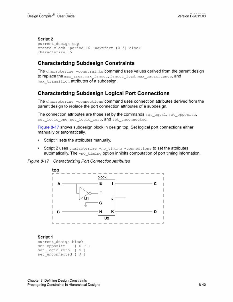
Design Compiler® User Guide P-2019.03Design Compiler® User Guide Version P-2019.03
Script 2current_design topcreate_clock -period 10 -waveform {0 5} clockcharacterize u5
Characterizing Subdesign Constraints
The characterize -constraints command uses values derived from the parent design to replace the max_area, max_fanout, fanout_load, max_capacitance, and max_transition attributes of a subdesign.
Characterizing Subdesign Logical Port Connections
The characterize -connections command uses connection attributes derived from the parent design to replace the port connection attributes of a subdesign.
The connection attributes are those set by the commands set_equal, set_opposite, set_logic_one, set_logic_zero, and set_unconnected.
Figure 8-17 shows subdesign block in design top. Set logical port connections either manually or automatically.
• Script 1 sets the attributes manually.
• Script 2 uses characterize -no_timing -connections to set the attributes automatically. The -no_timing option inhibits computation of port timing information.
Figure 8-17 Characterizing Port Connection Attributes
Script 1current_design blockset_opposite { E F }set_logic_zero { G }set_unconnected { J }
A
B
U1
U2
top
block
E
F
G
H
I
J
K
C
D
Chapter 8: Defining Design ConstraintsPropagating Constraints in Hierarchical Designs 8-40

Design Compiler® User Guide Version P-2019.03
Script 2current_design topcharacterize U2 -no_timing -connections
Characterizing Multiple Instances
The characterize command summarizes the boundary conditions for one instance of a subdesign in each invocation. If a subdesign is used more than one time, use the uniquify command to make each instance distinctive before using characterize for each instance.
The uniquify command creates copies of subdesigns that are referenced more than one time. It then renames the copies and updates the corresponding cell references.
Figure 8-18 shows how to use uniquify and characterize for the subdesign block, which is referenced in cells U1 and U2.
Figure 8-18 Characterizing a Subdesign Referenced Multiple Times
prompt> current_design topprompt> uniquify -reference block
prompt> characterize U1prompt> characterize U2
Characterizing Designs With Timing Exceptions
When paths crossing design hierarchies contain different timing exceptions, characterize creates timing constraints with virtual clocks to capture this information.
U2
top
block
block
U1
MultipleInstances
U2
top
block_0
block_1
U1
MultipleInstances
Uniquified
Chapter 8: Defining Design ConstraintsPropagating Constraints in Hierarchical Designs 8-41Chapter 8: Defining Design ConstraintsPropagating Constraints in Hierarchical Designs 8-41

Design Compiler® User Guide P-2019.03Design Compiler® User Guide Version P-2019.03
Possible timing exceptions include set_multicycle_path, set_false_path, set_max_delay, and set_min_delay. The virtual clock scheme can also handle multiple clocks.
Figure 8-19 shows a sample design in which the path from the ALARM input port to HOURS_OUT_reg* in U3 is constrained as a two-cycle path. Example 8-1 shows the a portion of the uncompressed characterize -verbose result of U0 block.
Figure 8-19 characterize -verbose Result of U0 Block
Example 8-1 characterize -verbose Output
create_clock -period 10 -waveform {0 5} [get_ports {CLK}]create_clock -name "CLK_virtual1" -period 10 -waveform {0 5}create_clock -name "CLK_virtual2" -period 10 -waveform {0 5}create_clock -name "CLK_virtual3" -period 10 -waveform {0 5}create_clock -name "CLK_virtual4" -period 10 -waveform {0 5}create_clock -name "CLK_virtual5" -period 10 -waveform {0 5}set_input_delay 2 -clock "CLK" [get_ports {MINUTES_BUTTON}]set_input_delay 2 -clock "CLK" [get_ports {HOURS_BUTTON}]set_input_delay 2 -clock "CLK_virtual1" [get_ports {ALARM_BUTTON}]set_output_delay 7.62796 -max -rise -clock "CLK" [get_ports {MINS}]set_output_delay 6.93955 -max -fall -clock "CLK" [get_ports {MINS}]set_output_delay 2.20324 -min -rise -clock "CLK" [get_ports {MINS}]set_output_delay 2.40013 -min -fall -clock "CLK" [get_ports {MINS}]set_output_delay 8.05575 -add_delay -max -rise -clock "CLK_virtual2" \
[get_ports {MINS}]set_output_delay 6.83933 -add_delay -max -fall -clock "CLK_virtual2" \
[get_ports {MINS}]set_output_delay 2.89679 -add_delay -min -rise -clock "CLK_virtual2" \
[get_ports {MINS}]set_output_delay 2.80452 -add_delay -min -fall -clock "CLK_virtual2" \
[get_ports {MINS}]...
ALARM_BLOCK
U0
ALARMU3
HOURS
MINS
AM_PM_OUT_reg
HOURS_OUT_reg*
Chapter 8: Defining Design ConstraintsPropagating Constraints in Hierarchical Designs 8-42

Design Compiler® User Guide Version P-2019.03
set_output_delay 10.232 -add_delay -max -rise -clock "CLK_virtual5" \[get_ports {MINS}]
set_output_delay 9.4791 -add_delay -max -fall -clock "CLK_virtual5" \[get_ports {MINS}]
set_output_delay 3.90222 -add_delay -min -rise -clock "CLK_virtual5" \[get_ports {MINS}]
set_output_delay 3.57818 -add_delay -min -fall -clock "CLK_virtual5" \[get_ports {MINS}]
...set_multicycle_path 2 -from [get_clocks {CLK_virtual1}] -to \
[get_clocks {CLK_virtual2}]set_multicycle_path 2 -from [get_clocks {CLK_virtual1}] -to \
[get_clocks {CLK_virtual3}]set_multicycle_path 2 -from [get_clocks {CLK_virtual1}] -to \
[get_clocks {CLK_virtual4}]set_multicycle_path 2 -from [get_clocks {CLK_virtual1}] -to \
[get_clocks {CLK_virtual5}]
Limitations of the characterize Command
The characterize command provides many useful features, but do not always rely on this command to derive constraints for the subdesigns in a design hierarchy. Before you characterize a design, keep in mind the following limitations:
The characterize command
• Does not derive timing budgets. (It reflects the current state of the design.)
• Ignores clock_skew and max_time_borrow attributes placed on a hierarchical boundary (generally not an issue, because these attributes are usually placed on clocks and cells).
With no options, the characterize command replaces a subdesign’s port signal information (clocks, port drive, input and output delays, maximum and minimum path delays, and port load) with information derived from the parent design.
The characterize command recognizes when the top-level design has back-annotated information (load, resistance, or delay) and to move this data down to the subdesign in preparation for subsequent optimization.
Propagating Constraints up the Hierarchy
If you have hierarchical designs and compile the subdesigns, then move up to the higher-level blocks (bottom-up compilation), you can propagate clocks, timing exceptions, and disabled timing arcs from lower-level .ddc files to the current design, using the propagate_constraints command. If you do not use this command, you can propagate constraints from a higher-level design to the current_instance, but you cannot propagate constraints set on a lower-level block to the higher-level blocks in which it is instantiated.
Chapter 8: Defining Design ConstraintsPropagating Constraints in Hierarchical Designs 8-43Chapter 8: Defining Design ConstraintsPropagating Constraints in Hierarchical Designs 8-43

Design Compiler® User Guide P-2019.03Design Compiler® User Guide Version P-2019.03
Note: Using the propagate_constraints command might cause memory usage to increase.
Example 8-2 shows a methodology in which constraints are propagated upward. Assume that A is the top-level and B is the lower-level design.
Example 8-2 Propagating Constraints Upward
current_design Bsource constraints.tclcompilecurrent_design Apropagate_constraints -design Breport_timing_requirementscompilereport_timing
To generate a report of all the constraints that were propagated up, use the -verbose and -dont_apply options and redirect the output to a file:
prompt> propagate_constraints -design name \ -verbose -dont_apply -output report.cons
Use the write_file -format ddc command to save the .ddc file with the propagated constraints so there is no need to go through the propagation again when restarting a new dc_shell session.
Handling Conflicts Between Designs
Conflicts between the lower-level and top-level designs causes the following:
• Clock name conflict
The lower-level clock has the same name as the clock of the current design (or another block).
The clock is not propagated. A warning is issued.
• Clock source conflict
A clock source of a lower-level block is already defined as a clock source of a higher-level block.
The lower-level clock is not propagated. A warning is issued.
• Exceptions from or to an unpropagated clock
This can be either a virtual clock, or a clock that was not propagated from that block due to a conflict.
Chapter 8: Defining Design ConstraintsPropagating Constraints in Hierarchical Designs 8-44

Design Compiler® User Guide Version P-2019.03
• Exceptions
A lower-level exception overrides a higher-level exception that is defined on the same path.
Chapter 8: Defining Design ConstraintsPropagating Constraints in Hierarchical Designs 8-45Chapter 8: Defining Design ConstraintsPropagating Constraints in Hierarchical Designs 8-45

Design Compiler® User Guide P-2019.03Design Compiler® User Guide Version P-2019.03
Chapter 8: Defining Design ConstraintsPropagating Constraints in Hierarchical Designs 8-46

9Using Floorplan Physical Constraints 9
Design Compiler in topographical mode supports high-level physical constraints such as die area, core area and shape, port locations, cell locations and orientations, keepout margins, placement blockages, preroutes, bounds, vias, tracks, voltage areas, and wiring keepouts.
Using floorplan physical constraints in topographical mode improves timing correlation with post-place-and-route tools, such as IC Compiler and IC Compiler II, by considering floorplanning information during optimization.
You provide floorplan physical constraints to Design Compiler topographical mode using one of the following methods:
• Export the floorplan information in DEF files from IC Compiler or IC Compiler II or a Tcl script from IC Compiler and import this information into Design Compiler
• Create the constraints manually
You can examine most of these objects visually in your floorplan by using the Design Vision layout window. For more information about using the GUI to view physical constraints, see the “Viewing the Floorplan” topic in Design Vision Help.
To learn how to create, import, reset, save, and report floorplan physical constraints, see
• Importing Floorplan Information
• Manually Defined Physical Constraints
• Including Physical-Only Cells
9-1

Design Compiler® User Guide P-2019.03Design Compiler® User Guide Version P-2019.03
• Specifying Relative Placement
• Magnet Placement
• Resetting Physical Constraints
• Saving Physical Constraints Using the write_floorplan Command
• Saving Physical Constraints Using the write_def Command
• Reporting Physical Constraints
Chapter 9: Using Floorplan Physical Constraints9-2

Design Compiler® User Guide Version P-2019.03
Importing Floorplan Information
The main reason to use floorplan constraints in topographical mode is to accurately represent the placement area and improve timing correlation with the post-place-and-route design. You can provide high-level physical constraints that determine core area and shape, port location, macro location and orientation, voltage areas, placement blockages, and placement bounds. These physical constraints can be derived from the IC Compiler or IC Compiler II floorplan data, extracted from an existing Design Exchange Format (DEF) file, or created manually.
You can import floorplan information into the Design Compiler tool by using one of the following methods:
• Using DEF Files
To provide floorplan physical constraints in DEF files to the Design Compiler tool, you export the floorplan information from the IC Compiler or IC Compiler II tool by using the write_def command and import this information into the Design Compiler tool by using the extract_physical_constraints command. For more information, see the following topics:
❍ Using the write_def Command in IC Compiler or IC Compiler II
❍ Reading DEF Information in Design Compiler
• Using a Tcl Script
Export the floorplan information from IC Compiler by using the write_floorplan command and import this information into the Design Compiler tool by using the extract_physical_constraints command. For more information, see the following topics:
❍ Using the write_floorplan Command in IC Compiler
❍ Reading the Floorplan Script in Design Compiler
See Also
• Physical Constraints Imported in the DEF File
• Physical Constraints Imported in the Floorplan File
• Manually Defined Physical Constraints
Chapter 9: Using Floorplan Physical ConstraintsImporting Floorplan Information 9-3Chapter 9: Using Floorplan Physical ConstraintsImporting Floorplan Information 9-3

Design Compiler® User Guide P-2019.03Design Compiler® User Guide Version P-2019.03
Using the write_def Command in IC Compiler or IC Compiler II
To improve timing and power correlation between Design Compiler and IC Compiler or IC Compiler II,
• Read your mapped Design Compiler netlist into IC Compiler or IC Compiler II.
• Create a basic floorplan in IC Compiler or IC Compiler II.
• Export this floorplan from IC Compiler or IC Compiler II.
• Read the floorplan back into Design Compiler.
To export floorplan information from IC Compiler or IC Compiler II in a Design Exchange Format (DEF) file for use in Design Compiler topographical mode, use the write_def command in IC Compiler or IC Compiler II. Example 9-1 uses the write_def command to write physical design data to the my_physical_data.def file.
Example 9-1 Using the write_def Command to Extract Physical Data From IC Compiler or IC Compiler II
icc_shell> write_def -version 5.7 -rows_tracks_gcells -macro -pins \ -blockages -specialnets -vias -regions_groups -verbose \
-output my_physical_data.def
See Also
• Reading DEF Information in Design Compiler
Reading DEF Information in Design Compiler
To import floorplan information from a DEF file, use the extract_physical_constraints command. This command imports physical information from the specified DEF file and applies these constraints to the design. The applied floorplan information is saved in the .ddc file and does not need to be reapplied when you read in the .ddc file in subsequent topographical mode sessions.
The following command shows how you can import physical constraints from multiple DEF files:
dc_shell-topo> extract_physical_constraints \{des_1.def des2.def … des_N.def}
By default, the extract_physical_constraints command runs in incremental mode. That is, if you use the command to process multiple DEF files, the command preserves existing physical annotations on the design. In incremental mode, the placement area is imported based on the current core area and site rows in the DEF file. When incremental
Chapter 9: Using Floorplan Physical ConstraintsImporting Floorplan Information 9-4

Design Compiler® User Guide Version P-2019.03
mode is disabled, the placement area is imported based on the site rows in the DEF files. Conflicts are resolved as follows:
• Physical constraints that can have only one value are overwritten by the value from the latest DEF file. That is, port location and macro location are overwritten.
• Physical constraints that can have accumulated values are recomputed. That is, core area can be recomputed based on the existing value and the site row definitions in the latest DEF file. Placement keepouts from different DEF files are accumulated and the final keepout geometry is computed internally during synthesis.
Figure 9-1 shows an example of incremental extraction performed by the extract_physical_constraints command.
Figure 9-1 Incremental Extraction With the extract_physical_constraints Command
dc_shell-topo> extract_physical_constraints DEF1.def DEF2.def
To disable running the command in the incremental mode, specify the -no_incremental option with the extract_physical_constraints command. In the non-incremental mode, the placement area is extracted based on the site rows in the DEF file. If there are no site rows in the DEF file, other constraints are not extracted and the following physical constraints are reset:
• Core area
• Route guide
• Layer preferred routing direction
• Voltage area
• Die Area
• Placement Area
• Macro Location and Orientation
• Hard, Soft, and Partial Placement Blockages
• Wiring Keepouts
(300,300)
(0,0)
P1
P2
DEF1Core Area {0,0, 200, 200}Port P1 P2 locationKeepout K1
DEF1Core Area {0,50, 300, 300}Port P2 locationKeepout K2
K1
K2
Chapter 9: Using Floorplan Physical ConstraintsImporting Floorplan Information 9-5Chapter 9: Using Floorplan Physical ConstraintsImporting Floorplan Information 9-5
Design Compiler® User Guide P-2019.03Design Compiler® User Guide Version P-2019.03
• Placement Bounds
• Port Location
• Preroutes
• Site Array Information
• Vias
• Routing Tracks
• Keepout Margins
To learn about the imported DEF physical constraints and port and macro name matching considerations, see
• Physical Constraints Imported in the DEF File
• Extracting Physical-Only Cells From a DEF File
• Macro and Port Name Matching With the extract_physical_constraints Command
• Site Name Matching
Physical Constraints Imported in the DEF File
The following high-level floorplan physical constraints can be imported into Design Compiler in topographical mode from a DEF file with the extract_physical_constraints command:
• Die Area
• Placement Area
• Macro Location and Orientation
• Hard, Soft, and Partial Placement Blockages
• Wiring Keepouts
• Placement Bounds
• Port Location
• Preroutes
• Site Array Information
• Vias
• Routing Tracks
Chapter 9: Using Floorplan Physical ConstraintsImporting Floorplan Information 9-6
Design Compiler® User Guide Version P-2019.03
• Keepout Margins
You can visually inspect your extracted physical constraints by using the layout view in the Design Vision layout window. All physical constraints extracted from the DEF file are automatically added to the layout view.
Note: Voltage areas are not defined in a DEF file. Therefore, for multivoltage designs, you have to use the create_voltage_area command to define voltage areas for the tool. If you are using IC Compiler as your floorplanning tool, you can use the write_floorplan and read_floorplan commands to obtain floorplan information that automatically includes voltage areas. You do not need to define voltage areas manually when using these commands.
Die Area
The extract_physical_constraints command automatically extracts the die area from a DEF file. DEF files are generated by floorplanning tools and used by Design Compiler to import physical constraints. The tool can extract both rectangular and rectilinear die areas that are defined in the DEF file. The die area is also known as the cell boundary. The die area represents the silicon boundary of a chip and encloses all objects of a design, such as pads, I/O pins, and cells.
The following example shows a die area definition in a DEF file:
DEF UNITS DISTANCE MICRONS 1000 ; DIEAREA ( 0 0 ) ( 0 60000 ) ( 39680 60000 ) ( 39680 40000 ) \ ( 59360 40000 ) ( 59360 0 ) ;
The following example shows how Design Compiler in topographical mode translates the DEF definition into Tcl when you write out your physical constraints using the write_floorplan -all command:
create_die_area -polygon { { 0.000 0.000 } { 0.000 60.000 } \ { 39.680 60.000 } { 39.680 40.000 } { 59.360 40.000 } \ { 59.360 0.000 } { 0.000 0.000 } }
Placement Area
Placement area is computed as the rectangular bounding box of the site rows.
Macro Location and Orientation
When you use the extract_physical_constraints command, for each cell with a location and the FIXED attribute specified in the DEF, Design Compiler sets the location on the corresponding cell in the design. Example 9-2 shows DEF macro location and orientation information.
Chapter 9: Using Floorplan Physical ConstraintsImporting Floorplan Information 9-7Chapter 9: Using Floorplan Physical ConstraintsImporting Floorplan Information 9-7

Design Compiler® User Guide P-2019.03Design Compiler® User Guide Version P-2019.03
Note: E = east rotation and W = west rotation
Example 9-2 DEF Macro Location and Orientation Information
COMPONENTS 2 ;- macro_cell_abx2 + FIXED ( 4350720 8160 ) E ;- macro_cell_cdy1 + FIXED ( 4800 8160 ) W ;
END COMPONENTS
The Tcl equivalent commands are shown in Example 9-3.
Example 9-3 Tcl Equivalent Macro Location and Orientation Information
set_cell_location macro_cell_abx2 -coordinates { 4350.720 8.160 } \ -orientation E -fixed
set_cell_location macro_cell_cdy1 -coordinates { 4.800 8.160 } \ -orientation W -fixed
Hard, Soft, and Partial Placement Blockages
The extract_physical_constraints command can import hard, soft, and partial placement blockages defined in the DEF file.
Example 9-4 shows DEF hard placement blockage information.
Example 9-4 DEF Hard Placement Blockage Information
BLOCKAGES 50 ;...
- PLACEMENT RECT ( 970460 7500 ) ( 3247660 129940 )...END BLOCKAGES
The Tcl equivalent command is shown in Example 9-5.
Example 9-5 Tcl Equivalent Hard Placement Blockage Information
create_placement_blockage -name def_obstruction_23 \-bbox { 970.460 7.500 3247.660 129.940 }
For a soft placement blockage, if your extracted DEF information is as shown in Example 9-6 (DEF version 5.6) or Example 9-7 (DEF version 5.7), then the Tcl equivalent command is shown in Example 9-8.
Note: If your floorplanning tool creates a DEF file with DEF version 5.6, you need to manually add the #SNPS_SOFT_BLOCKAGE directive to specify a soft blockage, as shown in Example 9-6.
Example 9-6 DEF Version 5.6 Soft Placement Blockage Information
BLOCKAGES 50 ;...
Chapter 9: Using Floorplan Physical ConstraintsImporting Floorplan Information 9-8

Design Compiler® User Guide Version P-2019.03
- PLACEMENT RECT ( 970460 7500 ) ( 3247660 129940 ) ; #SNPS_SOFT_BLOCKAGE...END BLOCKAGES
Example 9-7 DEF Version 5.7 Soft Placement Blockage Information
BLOCKAGES 50 ;...- PLACEMENT + SOFT RECT ( 970460 7500 ) ( 3247660 129940 ) ; ...END BLOCKAGES
Example 9-8 Tcl Equivalent Soft Placement Blockage Information
create_placement_blockage -name def_obstruction_23 \-bbox { 970.460 7.500 3247.660 129.940 } \-type soft
Example 9-9 shows DEF partial placement blockage information. The Tcl equivalent command is shown in Example 9-10.
Note: DEF versions prior to version 5.7 did not support partial blockages.
Example 9-9 DEF Partial Placement Blockage Information
BLOCKAGES 50 ;...- PLACEMENT + PARTIAL 80 RECT ( 970460 7500 ) ( 3247660 129940 ) ; ...END BLOCKAGES
Example 9-10 Tcl Equivalent Partial Placement Blockage Information
create_placement_blockage -name def_obstruction_23 \-bbox { 970.460 7.500 3247.660 129.940 } \-type partial \
-blocked_percentage 80
Wiring Keepouts
For wiring keepouts defined in the DEF, Design Compiler creates wiring keepouts on the design.
Example 9-11 shows DEF wiring keepout information.
Example 9-11 DEF Wiring Keepout Information
BLOCKAGES 30 ;...
- LAYER METAL6 RECT ( 0 495720 ) ( 4050 1419120 );...END BLOCKAGES
Chapter 9: Using Floorplan Physical ConstraintsImporting Floorplan Information 9-9Chapter 9: Using Floorplan Physical ConstraintsImporting Floorplan Information 9-9

Design Compiler® User Guide P-2019.03Design Compiler® User Guide Version P-2019.03
Placement Bounds
If REGIONS defining bounds exist in the DEF, extract_physical_constraints imports placement bounds. Also, if there are cells in the related GROUP attached to the region, these cells are matched with the ones in the design using rule-based name matching, and the matched cells are attached to the bounds in the following two ways:
• If there are regions in the design with the same name as in the DEF, the cells in the related group are attached to the region by the update_bounds command in incremental mode.
• If the region does not exist in the design, it is created with the same name as in the DEF file by applying the create_bounds command; matched cells in the related group are also attached.
Example 9-12 shows imported placement bounds information.
Example 9-12 DEF Placement Bounds Information
REGIONS 1 ; - c20_group ( 201970 40040 ) ( 237914 75984 ) + TYPE FENCE ;END REGIONS GROUPS 1 ; - c20_group cell_abc1 cell_sm1 cell_sm2 + SOFT + REGION c20_group ;END GROUPS
The Tcl equivalent commands are shown in Example 9-13.
Example 9-13 Tcl Equivalent Placement Bounds Information
create_bounds \ -name "c20_group" \ -coordinate {201970 40040 237914 75984} \ -exclusive \ {cell_abc1 cell_sm1 cell_sm2}
Port Location
When you use the extract_physical_constraints command, for each port with the location specified in the DEF, Design Compiler sets the location on the corresponding port in the design.
Example 9-14 shows imported port location information.
Example 9-14 DEF Port Information
PINS 2 ;-Out1 + NET Out1 + DIRECTION OUTPUT + USE SIGNAL +
LAYER M3 (0 0) (4200 200) + PLACED (80875 0) N;
Chapter 9: Using Floorplan Physical ConstraintsImporting Floorplan Information 9-10
Design Compiler® User Guide Version P-2019.03
-Sel0 + NET Sel0 + DIRECTION INPUT + USE SIGNAL + LAYER M4 (0 0)(200 200) + PLACED (135920 42475) N;
END PINS
The Tcl equivalent commands are shown in Example 9-15.
Example 9-15 Tcl Equivalent Port Information
create_terminal -name Out1 -port Out1 -layer M3 -bbox {{80.875 0} {85.075 0.200}}create_terminal -name Sel0 -port Sel0 -layer M4 \
-bbox {{135.920 42.475} {136.120 42.675}}
Ports with changed names and multiple layers are supported. Example 9-16 shows DEF information for such a case.
Example 9-16 DEF Port Information
PINS 2 ;- sys_addr\[23\].extra2 + NET sys_addr[23] + DIRECTION INPUT + USE SIGNAL +
LAYER METAL4 ( 0 0 ) ( 820 5820 ) + FIXED ( 1587825 2744180 ) N ; - sys_addr[23] + NET sys_addr[23] + DIRECTION INPUT + USE SIGNAL + LAYER
METAL3 ( 0 0 ) ( 820 5820 ) + FIXED ( 1587825 2744180 ) N ;END PINS
The corresponding Tcl commands are shown in Example 9-17.
Example 9-17 Tcl Equivalent Port Information
create_terminal -name {sys_addr[23]} -port {sys_addr[23]} -layer METAL3 \-bbox {{1587.825 2744.180} {1588.645 2750.000}}
create_terminal -name {sys_addr[23]_1} -port {sys_addr[23]} -layer METAL4 \-bbox {{1587.825 2744.180} {1588.645 2750.000}}
Port orientation is also supported. Example 9-18 shows DEF information for such a case.
Example 9-18 DEF Port Information
PINS 1;- OUT + NET OUT + DIRECTION INPUT + USE SIGNAL
+ LAYER m4 ( -120 0 ) ( 120 240 ) + FIXED ( 4557120 1726080 ) S ;
END PINS
The corresponding Tcl commands are shown in Example 9-19.
Example 9-19 Tcl Equivalent Port Information
create_terminal -name OUT -port OUT -layer m4 \-bbox {{4557.000 1725.840} {4557.240 1726.080}}
Preroutes
Design Compiler extracts preroutes that are defined in the DEF file.
Chapter 9: Using Floorplan Physical ConstraintsImporting Floorplan Information 9-11Chapter 9: Using Floorplan Physical ConstraintsImporting Floorplan Information 9-11

Design Compiler® User Guide P-2019.03Design Compiler® User Guide Version P-2019.03
Example 9-20 shows imported preroute information.
Example 9-20 DEF Preroute Information
SPECIALNETS 2 ;- vdd + ROUTED METAL3 10000 + SHAPE STRIPE ( 10000 150000 ) ( 50000 * ) + USE POWER ; ...END SPECIALNETS
The Tcl equivalent commands are shown in Example 9-21.
Example 9-21 Tcl Equivalent Preroute Information
create_net_shape -no_snap -type path -net vdd -datatype 0 -path_type 0 \-route_type pg_strap -layer METAL3 -width 10.000 \-points {{10.000 150.000} {50.000 150.000}}
Site Array Information
Design Compiler imports site array information that is defined in the DEF file. Site arrays in the DEF file define the placement area.
Example 9-22 shows imported site array information.
Example 9-22 DEF Site Array Information
ROW ROW_0 core 0 0 N DO 838 BY 1 STEP 560 0;
The Tcl equivalent commands are shown in Example 9-23.
Example 9-23 Tcl Equivalent Site Array Information
create_site_row -name ROW_0 -coordinate {0.000 0.000}\-kind core -orient 0 -dir H -space 0.560 -count 838
Vias
The extract_physical_constraints command extracts vias that are defined in the DEF file. Vias are stored in the .ddc file in the same way as other physical constraints.
Example 9-24 shows how Design Compiler in topographical mode translates the DEF definition into Tcl when you write out your physical constraints using the write_floorplan -all command.
Example 9-24 Tcl Equivalent Via Information
create_via -type via -net VDD -master VIA67 -route_type pg_strap \-at {746.61 2279} -orient N
create_via -type via_array -net VDD -master FATVIA45 -route_type pg_strap \-at {1491.79 2127.8} -orient N -col 5 -row 2 -x_pitch 0.23 -y_pitch 0.23
Chapter 9: Using Floorplan Physical ConstraintsImporting Floorplan Information 9-12

Design Compiler® User Guide Version P-2019.03
See Also
• Creating Vias
Routing Tracks
The extract_physical_constraints command extracts any track information that is defined in the DEF file. Tracks define the routing grid for standard cell-based designs. They can be used during routing, and track support can enhance congestion evaluation and reporting in Design Compiler in topographical mode to make congestion routing more precise and match more closely with IC Compiler or IC Compiler II. Track information is stored in the .ddc file in the same way as other physical constraints. If you have a floorplan with track information, such as track type and location, the track information is passed to IC Compiler or IC Compiler II during floorplan exploration.
The following example shows track data in a DEF file:
TRACKS X 330 DO 457 STEP 660 LAYER METAL1 ;TRACKS Y 280 DO 540 STEP 560 LAYER METAL1 ;
Example 9-25 shows how Design Compiler in topographical mode translates the DEF definition into Tcl when you write out your physical constraints using the write_floorplan -all command.
Example 9-25 Tcl Equivalent Track Information
create_track \-layer metal1 \-dir X \-coord 0.100 \-space 0.200 \-count 11577 \-bounding_box {{0.000 0.000} {2315.400 2315.200}}
create_track \-layer metal1 \-dir Y \-coord 0.200 \-space 0.200 \-count 11575 \-bounding_box {{0.000 0.000} {2315.400 2315.200}}
See Also
• Creating Routing Tracks
Keepout Margins
The extract_physical_constraints command extracts keepout margins that are defined in the DEF file. Keepout margins are stored in the .ddc file in the same way as other physical constraints.
Chapter 9: Using Floorplan Physical ConstraintsImporting Floorplan Information 9-13Chapter 9: Using Floorplan Physical ConstraintsImporting Floorplan Information 9-13

Design Compiler® User Guide P-2019.03Design Compiler® User Guide Version P-2019.03
The following example shows a keepout margin definition in a DEF file:
COMPONENTS 2 ;- U542 OAI21XL + FIXED ( 80000 80000 ) FN + HALO 10000 10000 50000 50000 ;- U543 OAI21XL + FIXED ( 10000 20000 ) FN + HALO SOFT 15000 15000 15000 15000 ;
END COMPONENTS
See Also
• Creating Keepout Margins
Extracting Physical-Only Cells From a DEF File
To extract physical-only cells from a DEF file, use the extract_physical_constraints command with the -allow_physical_cells option.
See Also
• Including Physical-Only Cells
Macro and Port Name Matching With the extract_physical_constraints Command
When the extract_physical_constraints command applies physical constraints, it automatically matches macros and ports in the DEF file with macros and ports in memory. When it does not find an exact match, it uses the rule-based name-matching capability.
Name mismatches can be caused by automatic ungrouping and the change_names command. Typically, hierarchy separators and bus notations are sources of these mismatches.
For example, automatic ungrouping by the compile_ultra command followed by the change_names command might result in the forward slash (/) separator being replaced with an underscore (_) character. Therefore, a macro named a/b/c/macro_name in the RTL might be named a/b_c_macro_name in the mapped netlist, which is the input to the back-end tool. The extract_physical_constraints command automatically resolves these name differences when extracting physical constraints from the DEF file.
By default, the following characters are considered equivalent:
• Hierarchical separators { / _ . }
For example, a cell named a_b_c/d_e is automatically matched with the string a/b_c/d/e in the DEF file.
• Bus notations { [ ] __ ( ) }
For example, a cell named a[4][5] is automatically matched with the string a_4__5_ in the DEF file.
Chapter 9: Using Floorplan Physical ConstraintsImporting Floorplan Information 9-14

Design Compiler® User Guide Version P-2019.03
When you use the -verbose option with the extract_physical_constraints command, the tool displays an informational message indicating that rule-based name matching has matched the cell with an instance in the DEF file.
You can define the rules used by the rule-based name-matching capability by using the set_query_rules command. Use the set_query_rules -show command to display the default query rules.
To disable rule-based name matching, specify the -exact option with the extract_physical_constraints command. In this case, the tool matches objects in the netlist in memory exactly with the corresponding objects in the DEF file.
See Also
• Site Name Matching
Site Name Matching
When you use the extract_physical_constraints command to read a DEF file, the tool automatically matches the site name in the floorplan with the name of the tile in the Milkyway reference libraries. Milkyway reference libraries usually have the site name set to unit by default. However, you might still need to define the name mappings if the site dimension does not match unit or if more than one site type is used in the DEF files. To define the name mappings, use the mw_site_name_mapping variable. For example,
dc_shell-topo> set mw_site_name_mapping { {def_site_name1 mw_ref_lib_site_name} \ {def_site_name2 mw_ref_lib_site_name} }
You can specify multiple pairs of values for the mw_site_name_mapping variable.
Using the write_floorplan Command in IC Compiler
To improve timing, area, and power correlation between Design Compiler and IC Compiler, you can read your mapped Design Compiler netlist into IC Compiler, create a basic floorplan in IC Compiler, export this floorplan from IC Compiler, and read the floorplan back into Design Compiler.
To export floorplan information from IC Compiler into a file that can be used in Design Compiler in topographical mode, use the write_floorplan command in IC Compiler. The command writes a Tcl script that you read into Design Compiler to re-create elements of the floorplan for the specified design.
Example 9-26 uses the write_floorplan command to write out all placed standard cells to a file called placed_std.fp.
Example 9-26 Using write_floorplan to Export Physical Data From IC Compiler
icc_shell> write_floorplan -placement {io terminal hard_macro soft_macro}\
Chapter 9: Using Floorplan Physical ConstraintsImporting Floorplan Information 9-15Chapter 9: Using Floorplan Physical ConstraintsImporting Floorplan Information 9-15

Design Compiler® User Guide P-2019.03Design Compiler® User Guide Version P-2019.03
-create_terminal -row -create_bound \ -preroute -track floorplan_for_DC.fp
See Also
• Reading the Floorplan Script in Design Compiler
Reading the Floorplan Script in Design Compiler
The IC Compiler write_floorplan command generates a Tcl script that contains commands that describe floorplan information for the current design or a design that you specify. You can use this file to re-create elements of the floorplan in Design Compiler. Run the read_floorplan command in topographical mode to read the script generated by the write_floorplan command and restore the floorplan information.
The imported physical constraints are automatically saved to your .ddc file. To save the physical constraints in a separate file, use the write_floorplan command after extraction. The command saves the floorplan information so you can read the floorplan back into Design Compiler.
You can also use the source command to import the floorplan information. However, the source command reports errors and warnings that are not applicable to Design Compiler. The read_floorplan command removes these unnecessary errors and warnings. In addition, you need to enable rule-based name matching manually when you use the source command. The read_floorplan command automatically enables rule-based name matching.
The read_floorplan command should not be used to perform incremental floorplan modifications. The read_floorplan command imports the entire floorplan information exported from IC Compiler with the write_floorplan command and overwrites any existing floorplan. The write_floorplan command usually includes commands to remove any existing floorplan.
You can visually inspect your imported physical constraints by using the layout view in the Design Vision layout window.
To learn more about imported physical constraints and port and macro name matching considerations, see
• Physical Constraints Imported in the Floorplan File
• Macro and Port Name Matching With the read_floorplan Command
Physical Constraints Imported in the Floorplan File
The following physical constraints are imported from the floorplan file (Tcl script) when you run the read_floorplan command:
Chapter 9: Using Floorplan Physical ConstraintsImporting Floorplan Information 9-16

Design Compiler® User Guide Version P-2019.03
• Voltage areas
• Die Area
The die area represents the silicon boundary of a chip and encloses all objects of a design, such as pads, I/O pins, and cells.
• Placement Area
• Macro Location and Orientation
For each cell with a location and the FIXED attribute specified, Design Compiler sets the location on the corresponding cell in the design.
• Hard and Soft Placement Blockages
For defined placement blockages, Design Compiler creates placement blockages on the design.
• Wiring Keepouts
Wiring keepout information is imported from the floorplan file. The create_route_guide command creates a wiring keepout.
• Placement Bounds
Placement bounds are extracted from the floorplan file in the following two ways:
1. If there are regions in the design with the same name as in the floorplan file, the cells in the related group are attached to the region by the update_bounds command in incremental mode.
2. If the region does not exist in the design, it is created with the same name as in the floorplan file by applying the create_bounds command. Matched cells in the related group are also attached.
• Port Locations
For each port with the location specified in the floorplan file, Design Compiler sets the location on the corresponding port in the design.
Ports with changed names and multilayers are supported.
• Preroutes
Design Compiler imports preroutes that are defined in the floorplan file. A preroute is represented with the create_net_shape command.
• User Shapes
Design Compiler imports user shapes that are defined in the floorplan file and includes them in the preroute section.
• Site Array Information
Chapter 9: Using Floorplan Physical ConstraintsImporting Floorplan Information 9-17Chapter 9: Using Floorplan Physical ConstraintsImporting Floorplan Information 9-17

Design Compiler® User Guide P-2019.03Design Compiler® User Guide Version P-2019.03
Design Compiler extracts site array information that is defined in the floorplan file. Site arrays define the placement area.
• Vias
Design Compiler imports vias that are defined in the floorplan file and includes them in the preroute section.
• Tracks
Design Compiler imports any track information that is defined in the floorplan file.
Macro and Port Name Matching With the read_floorplan Command
When the read_floorplan command applies physical constraints in topographical mode, it automatically matches macros and ports in the floorplan file with macros and ports in memory. When it does not find an exact match, it uses the rule-based name-matching capability.
Name mismatches can be caused by automatic ungrouping and the change_names command. Typically, hierarchy separators and bus notations are sources of these mismatches.
For example, automatic ungrouping by the compile_ultra command followed by the change_names command might result in the forward slash (/) separator being replaced with an underscore (_) character. Therefore, a macro named a/b/c/macro_name in the RTL might be named a/b_c_macro_name in the mapped netlist, which is the input to the back-end tool. The extract_physical_constraints command automatically resolves these name differences when extracting physical constraints from the DEF file.
By default, the following characters are considered equivalent:
• Hierarchical separators { / _ . }
For example, a cell named a.b_c/d_e is automatically matched with the string a/b_c.d/e in the floorplan file.
• Bus notations { [ ] __ ( ) }
For example, a cell named a[4][5] is automatically matched with the string a_4__5_ in the floorplan file.
To define the rules used by the rule-based name-matching capability, use the set_query_rules command.
Note: Using the source command is not recommended. However, if you use the source command to import your floorplan information, you must enable rule-based name matching manually by setting the enable_rule_based_query variable to true before you source the floorplan file. For example,
Chapter 9: Using Floorplan Physical ConstraintsImporting Floorplan Information 9-18

Design Compiler® User Guide Version P-2019.03
dc_shell-topo> set_query_rules...dc_shell-topo> set_app_var enable_rule_based_query truedc_shell-topo> source design.fpdc_shell-topo> set enable_rule_based_query false
Reading and Writing Preroute Information for Power and Ground Nets and Physical-Only Cells
The floorplan that is written from IC Compiler using the write_floorplan command can include preroute information and the location of physical-only cells. However, when the floorplan file is read into Design Compiler in topographical mode, the information is not used during optimization because the power and ground nets and physical cells do not exist in the logical netlist.
To use preroute information and physical-only cells in Design Compiler, you need to create the power and ground nets and physical-only cells before reading the floorplan file. When you run the write_floorplan -preroute command, Design Compiler writes out the preroute information and the location of the physical-only cells, and the command generates a secondary floorplan. This secondary floorplan file is generated with an .objects suffix added to the floorplan file name. The secondary floorplan file contains Tcl commands that the tool will use to create the power and ground nets and physical-only cells.
The following example creates the floorplan files, floorplan.tcl and floorplan.tcl.objects:
dc_shell-topo> write_floorplan -preroute floorplan.tcl
The following example shows a floorplan.tcl.objects file:
if {! [sizeof_collection [get_nets -quiet -all "VDD"]]} {create_net -power VDD}if {! [sizeof_collection [get_nets -quiet -all "VSS"]]} {create_net -ground VSS}if {! [sizeof_collection [get_cells -quiet -all "FIL_1"]]} { create_cell -only_physical FIL_1 FILLERX1}
In the UPF flow, the power and ground nets are typically specified in the UPF file. If you are using the UPF flow, you must read the UPF file before you read the floorplan files.
If your power and ground nets are not defined yet, it is important that you read the secondary floorplan file before you read the main floorplan file, as shown in Example 9-27. When you read the secondary floorplan file, the tool creates the power and ground nets and physical-only cells in the logical netlist. When you read the main floorplan file, the tool applies the floorplan information for the power and ground nets and the physical-only cells to the corresponding objects. This allows the tool to use the preroute information for the power and ground nets and physical-only cells during optimization.
Chapter 9: Using Floorplan Physical ConstraintsImporting Floorplan Information 9-19Chapter 9: Using Floorplan Physical ConstraintsImporting Floorplan Information 9-19

Design Compiler® User Guide P-2019.03Design Compiler® User Guide Version P-2019.03
Example 9-27 Creating and Applying Power and Ground Nets and Physical-Only Cells
dc_shell-topo> read_floorplan floorplan.tcl.objects1dc_shell-topo> read_floorplan floorplan.tclInformation: Successfully applied 2 of the 2 'create_net_shape'commands read. (DCT-143)1
Manually Defined Physical Constraints
If you do not provide any physical constraints from a floorplanning tool, either in a DEF file or in a Tcl script, Design Compiler uses the following default physical constraints:
• Aspect ratio of 1.0 (that is, a square placement area)
• Utilization of 0.6 (that is, forty percent of empty space in the core area)
You can also manually define physical constraints as described in the following topics:
• Defining Physical Constraints Overview
• Defining the Die Area
• Defining the Core Placement Area With the create_site_row Command
• Defining Placement Area With the set_aspect_ratio and set_utilization Commands
• Defining Port Locations
• Defining Macro Location and Orientation
• Defining Placement Blockages
• Defining Voltage Areas
• Defining Placement Bounds
• Creating Wiring Keepouts
• Creating Preroutes
• Creating User Shapes
• Defining Physical Constraints for Pins
• Creating Design Via Masters
• Creating Vias
• Creating Routing Tracks
• Creating Keepout Margins
Chapter 9: Using Floorplan Physical ConstraintsManually Defined Physical Constraints 9-20

Design Compiler® User Guide Version P-2019.03
• Computing Polygons
Defining Physical Constraints Overview
This topic describes the commands you can use to define the floorplan’s physical constraints manually. Design Compiler in topographical mode can read physical constraints (floorplan information) from a Tcl-based script of physical commands.
You manually define physical constraints when you cannot obtain this information from a DEF file using the extract_physical_constraints command or from a Tcl script using the read_floorplan command. For details, see Reading DEF Information in Design Compiler and Reading the Floorplan Script in Design Compiler.
After you have manually defined your physical constraints in a Tcl script file, use the source command to apply these constraints. Keep the following points in mind when you manually define physical constraints:
• You must read in the design before applying user-specified physical constraints.
• You must apply user-specified physical constraints during the first topographical mode session.
Table 9-1 lists the commands that you use to set physical constraints.
Table 9-1 Commands That Define Physical Constraints
To define this physical constraint Use these commands
Die Area For details, see Defining the Die Area.
create_die_area
Floorplan estimate when exact area is not knownFor details, see Defining Placement Area With the set_aspect_ratio and set_utilization Commands.
set_aspect_ratio and set_utilization
Exact core area For details, see Defining the Core Placement Area With the create_site_row Command.
create_site_row
Relative port locationsFor details, see Defining Relative Port Locations.
set_port_side
Exact port locationsFor details, see Defining Exact Port Locations.
create_terminal
Chapter 9: Using Floorplan Physical ConstraintsManually Defined Physical Constraints 9-21Chapter 9: Using Floorplan Physical ConstraintsManually Defined Physical Constraints 9-21

Design Compiler® User Guide P-2019.03Design Compiler® User Guide Version P-2019.03
Macro location and orientationFor details, see Defining Macro Location and Orientation.
set_cell_location
Placement keepout (blockages)For details, see Defining Placement Blockages.
create_placement_blockage
Voltage areaFor details, see Defining Voltage Areas.
create_voltage_area
Placement boundsFor details, see Defining Placement Bounds.
create_bounds
Wiring keepoutsFor details, see Creating Wiring Keepouts.
create_route_guide
PreroutesFor details, see Creating Preroutes.
create_net_shape
User shapesFor details, see Creating User Shapes.
create_user_shape
Pin physical constraintsFor details, see Defining Physical Constraints for Pins.
set_pin_physical_constraints
create_pin_guide
Design via mastersFor details, see Creating Design Via Masters.
create_via_master
ViasFor details, see Creating Vias.
create_via
TracksFor details, see Creating Routing Tracks.
create_track
Keepout marginsFor details, see Creating Keepout Margins.
set_keepout_margin
PolygonsFor details, see Computing Polygons.
compute_polygons
Table 9-1 Commands That Define Physical Constraints (Continued)
To define this physical constraint Use these commands
Chapter 9: Using Floorplan Physical ConstraintsManually Defined Physical Constraints 9-22

Design Compiler® User Guide Version P-2019.03
Defining the Die Area
Design Compiler topographical technology allows you to manually define the die area, also known as the cell boundary. The die area represents the silicon boundary of a chip, and it encloses all objects of a design, such as pads, I/O pins, and cells. There should be only one die area in a design.
Typically, you create floorplan constraints, including the die area, in your floorplanning tool, and import these physical constraints into Design Compiler topographical mode. However, if you are not using a floorplanning tool, you need to manually create your physical constraints. The create_die_area command allows you to define your die area from within Design Compiler in topographical mode.
When using the create_die_area command, you can use the -coordinate option if your die area is a rectangle. If your die area is rectilinear, you must use the -polygon option. You can use the -polygon option to specify rectangles, but you cannot use the -coordinate option to specify rectilinear die areas. For example, the following commands create the same rectangular die area:
create_die_area -coordinate { 0 0 100 100 }create_die_area -coordinate { {0 0} {100 100} }create_die_area -polygon { {0 0} {100 0} {100 100} {0 100} }
You can use the get_die_area command to return a collection containing the die area of the current design. If the die area is not defined, the command returns an empty string.
Use the get_attribute command to get information about the die area, such as the object class, bounding box information, coordinates of the current design’s die area, die area boundary, and die area name.
You can use the report_attribute command to browse attributes, such as object_class, bbox, boundary, and name.
For example, you can create a new die area, as shown:
dc_shell-topo> create_die_area -polygon {{0 0} {0 400} {200 400} {200 200} \{400 200} {400 0}}
Then, use the get_attribute command to get the following information about the die area:
• To return the object class, use the object_class attribute, as shown:
dc_shell-topo> get_attribute [get_die_area] object_classdie_area
• To return the bounding box information and the coordinates of the current design’s die area, use the bbox attribute, as shown:
dc_shell-topo> get_attribute [get_die_area] bbox{0.000 0.000} {400.000 400.000}
Chapter 9: Using Floorplan Physical ConstraintsManually Defined Physical Constraints 9-23Chapter 9: Using Floorplan Physical ConstraintsManually Defined Physical Constraints 9-23

Design Compiler® User Guide P-2019.03Design Compiler® User Guide Version P-2019.03
• To return the die area boundary, use the boundary attribute, as shown:
dc_shell-topo> get_attribute [get_die_area] boundary{0.000 0.000} {0.000 400.000} {200.000 400.000} {200.000 200.000}{400.000 200.000} {400.000 0.000} {0.000 0.000}
• To return the die area name, use the name attribute, as shown:
dc_shell-topo> get_attribute [get_die_area] name{my_design_die_area}
Defining the Core Placement Area With the create_site_row Command
You can define the core placement area with the create_site_row command. The core placement area is a box that contains all rows. It represents the placeable area for standard cells. The core area is smaller than the cell boundary (the die area). Pads, I/O pins, and top-level power and ground rings are found outside the core placement area. Standard cells, macros, and wire tracks are typically found inside the core placement area. There should be only one core area in a design.
You use the create_site_row command to create a row of sites or a site array at a specified location. A site is a predefined valid location where a leaf cell can be placed; a site array is an array of placement sites and defines the placement core area.
To create a horizontal row of 100 CORE_2H sites with a bottom-left corner located at (10,10) and rows spaced 5 units apart, enter
dc_shell-topo> create_site_row -count 100 -kind CORE_2H -space 5 \-coordinate {10 10}
To report physical information, such as core area, aspect ratio, utilization, total fixed cell area, and total movable cell area, use the report_area -physical command.
Defining Placement Area With the set_aspect_ratio andset_utilization Commands
If you have not defined your die area with the create_die_area command, defined a floorplan area with the create_site_row command, or imported floorplan information from a floorplanning tool, you can use the set_aspect_ratio and set_utilization commands to estimate the placement area.
The aspect ratio is the height-to-width ratio of a block; it defines the shape of a block. Utilization specifies how densely you want cells to be placed within the block. Increasing utilization reduces the core area.
Figure 9-2 illustrates how to use these commands.
Chapter 9: Using Floorplan Physical ConstraintsManually Defined Physical Constraints 9-24

Design Compiler® User Guide Version P-2019.03
Figure 9-2 Using the set_aspect_ratio and set_utilization Commands
Defining Port Locations
You can define constraints that restrict the placement and sizing of ports by using the set_port_side command or create_terminal command. You can specify relative or exact constraints.
To learn how to define relative and exact port locations, see
• Defining Relative Port Locations
• Defining Exact Port Locations
Defining Relative Port Locations
Use the set_port_side command to define relative port locations as follows:
set_port_side port_name -side {L|R|T|B}
Valid sides are left (L), right (R), top (T), or bottom (B). A port can be placed at any location along the specified side. If the port side constraints are provided, the ports are snapped to the specified side. Otherwise, by default, the ports are snapped to the side nearest to the port location assigned by the coarse placer. Figure 9-3 shows how you define port sides by using the set_port_side command.
width
heig
ht
width
heig
ht
set_aspect_ratio 1 set_aspect_ratio 0.5
width
heig
ht
set_utilization 0.6
width
heig
ht
set_utilization 0.85
Chapter 9: Using Floorplan Physical ConstraintsManually Defined Physical Constraints 9-25Chapter 9: Using Floorplan Physical ConstraintsManually Defined Physical Constraints 9-25

Design Compiler® User Guide P-2019.03Design Compiler® User Guide Version P-2019.03
Figure 9-3 Setting Relative Port Sides
Defining Exact Port Locations
Use the create_terminal command to create a terminal for the specified logical port, specifying the bounding box of the terminal as follows:
dc_shell-topo> create_terminal -bbox {x1 y1 x2 y2} \-layer layer_name -port port_name
The -bbox option specifies the bounding box of the terminal; the -layer option specifies the layer of the terminal; and the -port option specifies the name of the associated logical port of the terminal.
The following example creates a terminal for the Z port, a top-level port in the current design, with a bounding box of {0 0 100 500} on metal layer METAL1:
dc_shell-topo> create_terminal -port Z -bbox {0 0 100 500} -layer METAL1
These options allow you to define long ports so that connections to the long port can be made along any point on the specified metal layer during virtual-layout based optimization. A long port can be an input, output, or bidirectional port. You specify a long port location by using a dimension greater than the minimum metal area. Figure 9-4 illustrates the different types of port dimensions: Long port, flushed port, and multiple port.
• A long port has the metal area defined with a single metal layer and touches only one side of the block core area boundary.
• A flushed port has the metal area defined with a single metal layer and touches the block core area boundary on two sides.
• A multiple port has more than one connection to the block and can touch the block boundary on two or more sides and can use one or more layers.
For multiple terminals associated with the same port, the first terminal has the same name as the port and subsequent terminal names have the format port_name_number where port_name is the port name and number is a unique number.
set_port_side -side {R} Port_N
Port_N
set_port_side -side {B} Port_MPort_M
Chapter 9: Using Floorplan Physical ConstraintsManually Defined Physical Constraints 9-26

Design Compiler® User Guide Version P-2019.03
Figure 9-4 Types of Port Dimension Specifications
Defining Macro Location and Orientation
You can define exact macro locations by setting the following command:
set_cell_location cell_name -coordinates {x y} -fixed-orientation {N|S|E|W|FN|FS|FE|FW}
where the -coordinates option specifies the coordinate of the lower-left corner of the cell’s bounding box. Specify the coordinates in microns relative to the block orientation. The orientation value is one of the rotations listed in the following table.
Orientation Rotation
N (default) Nominal orientation, 0-degree rotation (north)
S 180 degrees (south)
E 270 degrees counterclockwise (east)
W 90 degrees counterclockwise (west)
FN Reflection in the y-axis (flipped north)
FS 180 degrees, followed by reflection in the y-axis (flipped south)
FE 270 degrees counterclockwise, followed by reflection in the y-axis (flipped east)
FW 90 degrees counterclockwise, followed by reflection in the y-axis (flipped west)
(50,160)
(400,140)
RAM1Blockage1
Port A
(50,160)
(400,140)
RAM1Blockage1
Port A
(50,160)
(400,140)
RAM1Blockage1
Port APort A
Port A
Long Port Flushed Port Multiple Port
Chapter 9: Using Floorplan Physical ConstraintsManually Defined Physical Constraints 9-27Chapter 9: Using Floorplan Physical ConstraintsManually Defined Physical Constraints 9-27

Design Compiler® User Guide P-2019.03Design Compiler® User Guide Version P-2019.03
Defining Placement Blockages
Use the create_placement_blockage command to define placement blockages. The -bbox option specifies the coordinates of the bounding box of the blockage. Use the -type option to specify the type of placement blockage to be created—hard, soft, or partial.
The -type values are described as follows:
• A hard placement blockage prevents the placer from placing any standard cells or hard macros in the specified region. This is the -type option default.
• A soft placement blockage prevents the coarse placer from placing any standard cells or hard macros in the specified region. However, cells might be placed there during optimization or legalization.
• A partial placement blockage limits the amount of area used to place cells to the specified percent of the blockage area. When you create a partial blockage, you must use the -blocked_percentage option to specify the blocked percentage value.
During coarse placement, Design Compiler can evenly distribute cells outside the partial blockages and prevent the clumping of cells around their perimeters. To do this, set the placer_enable_redefined_blockage_behavior variable to true if your design contains partial blockages created by using the -type partial option.
You can define a blockage area where only buffers or inverters can be placed by specifying the -buffer_only option with the -type partial option. You must set the placer_enable_redefined_blockage_behavior variable to true when using the -buffer_only option.
The following example shows a blockage created with the -buffer_only option. The blocked percentage is 50 percent:
dc_shell-topo> create_placement_blockage -buffer_only -name my_blockage \-type partial -blocked_percentage 50 -bbox {{0 0} {100 100}}
The -buffer_only option cannot be used with the -type hard, -type soft, -no_hard_macro, -no_rp_group, -no_register, -no_pin, or -category options.
You can specify either to include specific library cells or cell instances in a blockage area or to exclude them from a blockage area by using the -category option with the -type partial option. You must set the placer_enable_redefined_blockage_behavior variable to true when using the -category option.
To create a predefined category of cells, you must first define an attribute for the library cells or cell instances by using the define_user_attribute command. Then apply the attribute to the desired library cells or cell instances by using the set_attribute command. After you do this, you can create a category blockage by using the attribute name as the argument to the -category option.
Chapter 9: Using Floorplan Physical ConstraintsManually Defined Physical Constraints 9-28

Design Compiler® User Guide Version P-2019.03
To prevent library cells or cell instances from being placed within the specified blockage area, set your user-defined attribute to true for the specific library cells or cell instances. By default, all cells are allowed within the specified blockage area. This is equivalent to the user-defined attribute set to false.
In the following example, Design Compiler blocks all cells except isolation (bfiso*) cells:
dc_shell-topo> define_user_attribute -type boolean -classes lib_cell only_isodc_shell-topo> set_attribute [get_lib_cell mylib/*] only_iso truedc_shell-topo> set_attribute [get_lib_cell mylib/bfiso*] only_iso falsedc_shell-topo> create_placement_blockage -bbox {{230 795} {830 1940}} \
-name blk_VA_edge -type partial -blocked_percentage 20 -category only_iso
Each cell or lib_cell class can have multiple user attributes defined for it, controlling the library cell or cell instance behavior in multiple regions. If a cell instance has attributes defined for it and its library cell has different attributes defined for it, the cell instance’s attribute takes precedence.
User attributes defined on cell instances are saved when the design is written in .ddc format; however, user attributes defined on library cells are not saved when the design is written. You need to re-create the lib_cell user-attribute and reapply it to the library cell if you reload your design in another session.
Multiple blockages can use the same attribute. However, each blockage can accept only one attribute. The -blocked_percentage option setting affects all cells in the blockage area, regardless of the attribute.
The -category option cannot be used with the -type hard, -type soft, -no_hard_macro, -no_rp_group, -no_register, -no_pin, or -buffer_only options.
Use the -no_rp_group option to specify relative placement group blockages. This option prevents the placement of relative placement groups within the specified area. The option only affects cells that belong to relative placement groups. The -no_rp_group option must be used with the -type partial option, and it cannot be used with the -no_hard_macro, -no_register, and -no_pin options.
To restrict Design Compiler from placing any register cells within the specified partial blockage area during coarse placement, specify the -no_register option with the -type partial option. However, this restriction does not apply to optimization performed after coarse placement. If you specify the -retime option with the compile_ultra command, the registers that are moved during optimization can be placed in this area.
Chapter 9: Using Floorplan Physical ConstraintsManually Defined Physical Constraints 9-29Chapter 9: Using Floorplan Physical ConstraintsManually Defined Physical Constraints 9-29

Design Compiler® User Guide P-2019.03Design Compiler® User Guide Version P-2019.03
Figure 9-5 uses the create_placement_blockage command to define a hard placement blockage named Blockage1.
Figure 9-5 Defining a Hard Placement Blockage
You can use the get_placement_blockages command to return a collection of placement blockages from the current design. The command returns a collection of placement blockages if one or more blockages meet the specified criteria. If no blockages match the criteria, it returns an empty string. You can use the get_placement_blockages command as an argument to another command or assign its result to a variable.
To create a collection containing all blockages within a specified region, use the -within region option with the get_placement_blockages command. The region boundary can be a rectangle or a polygon. In the following example, Design Compiler returns one rectangular placement blockage based on the specified region. In the example, the first xy pair {2 2} represents the lower-left corner of the rectangle, and the second xy pair {25 25} represents the upper-right corner of the rectangle:
dc_shell-topo> get_placement_blockages * -within {{2 2} {25 25}}{"PB#5389"}
To filter the collection with an expression, use the -filter expression option with the get_placement_blockages command. In the following example, Design Compiler returns all placement blockages that have an area greater than 900:
dc_shell-topo> get_placement_blockages * -filter "area > 900"{"PB#4683"}
Defining Voltage Areas
You define voltage areas by using the create_voltage_area command. This command enables you to create a voltage area on the core area of the chip. The voltage area is associated with hierarchical cells. The tool assumes the voltage area to be an exclusive,
(300,280)
(50,160)
Blockage1
create_placement_blockage\-name Blockage1 -type hard \-bbox {50 160 300 280}
Chapter 9: Using Floorplan Physical ConstraintsManually Defined Physical Constraints 9-30

Design Compiler® User Guide Version P-2019.03
hard move bound and tries to place all the cells associated with the voltage area within the defined voltage area, as well as place all the cells not associated with the voltage area outside the defined voltage area.
Example 9-28 uses the create_voltage_area command to constrain the instance INST_1 to lie within the voltage area whose coordinates are lower-left corner (100 100) upper-right corner (200 200).
Example 9-28 Using the create_voltage_area Command With the -name Option
dc_shell-topo> create_voltage_area -name my_design \-coordinate {100 100 200 200} INST_1
Example 9-29 uses the create_voltage_area command to constrain cells in power domain PD1 to lie within the voltage area whose coordinates are lower-left corner (100 100) upper-right corner (200 200).
Example 9-29 Using the create_voltage_area Command With the -power_domain Option
dc_shell-topo> create_voltage_area -power_domain PD1 \ -coordinate {100 100 200 200}
Note: The -name option and the -power_domain option of the create_voltage_area command are mutually exclusive.
In addition to the create_voltage_area command, the following commands are supported: remove_voltage_area and report_voltage_area
Voltage areas are automatically defined when you import your floorplan information from IC Compiler or IC Compiler II with the read_floorplan command. For details, see Reading the Floorplan Script in Design Compiler. You need to define voltage areas manually when importing floorplan information from a DEF file.
To visually inspect your defined voltage areas, use the visual mode in the Design Vision layout window.
Defining Placement Bounds
To learn how to create and use placement bounds, see
• Placement Bounds Overview
• Creating Placement Bounds
• Order for Creating Placement Bounds
• Guidelines for Defining Placement Bounds Effectively
Chapter 9: Using Floorplan Physical ConstraintsManually Defined Physical Constraints 9-31Chapter 9: Using Floorplan Physical ConstraintsManually Defined Physical Constraints 9-31

Design Compiler® User Guide P-2019.03Design Compiler® User Guide Version P-2019.03
• Returning a Collection of Bounds
Placement Bounds Overview
A placement bound is a rectangular or rectilinear area within which to place cells and hierarchical cells. You use the create_bounds command to specify placement constraints for coarse placement.
Defining a placement bound enables you to group cells such as clock-gating cells or extremely timing-critical groups of cells that you want to guarantee will not be disrupted during placement by other logic. During placement, the tool ensures that the cells you grouped remain together. Placement bounds are placement constraints.
Usually, it is best not to impose bounds constraints and instead allow the tool full flexibility to optimize placement for timing and routability. However, if QoR does not meet your requirements, you might improve QoR by using the create_bounds command.
To use placement bounds effectively, make the number of cells you define in placement bounds relatively small compared with the total number of cells in the design. When you define placement bounds, the solution space available to the placer to reach the optimal result gets smaller.
Creating Placement Bounds
Use the create_bounds command to specify placement bounds. You can specify two different types of bounds: move bounds and group bounds. Move bounds restrict the placement of cells to a specific region of the core area. Group bounds are floating region constraints. Cells in the same group bound are placed within a specified bound but the absolute coordinates are not fixed. Instead, they are optimized by the placer. For more information, see the following topics:
• Move Bounds
• Group Bounds
• Repelling Bounds
Move Bounds
Move bounds require absolute coordinates to be specified using the -coordinate option. Move bounds can be soft, hard, or exclusive:
• Soft bounds specify placement goals, with no guarantee that the cells will be placed inside the bounds. If timing or congestion cost is too high, cells might be placed outside the region. This is the default.
dc_shell-topo> create_bounds -coordinate {0 0 10 10} \-name mb_soft INST2
Chapter 9: Using Floorplan Physical ConstraintsManually Defined Physical Constraints 9-32

Design Compiler® User Guide Version P-2019.03
• Hard bounds force placement of the specified cells inside the bounds. To specify hard bounds, use the -type hard option. Note that overusing hard bounds can lead to inferior placement solutions.
dc_shell-topo> create_bounds -type hard -coordinate {0 0 10 10} \-name mb_hard INST4
• Exclusive move bounds force the placement of the specified cell inside the bounds. All other cells must be placed outside the bounds. To specify exclusive bounds, use the -exclusive option.
dc_shell-topo> create_bounds -exclusive -type hard \-coordinate {0 0 10 10} -name mb_excl INST5
For the GUI, you can specify color for move bounds by using the following options with the create_bounds command:
• -color
Specify the move bound color either by specifying an integer value between 0 and 63 or by specifying a color name string with one of the following values: black, blue, green, cyan, brown, purple, red, magenta, salmon, orange, yellow, or white. The default is no_color, meaning that no color is applied.
• -cycle_color
The -cycle_color option allows the tool to automatically assign a move bound color. By default, this option is turned off.
Group Bounds
Group bounds are floating region constraints that you specify with the -dimension option set to {width height}. Cells in the same group bound are placed within the specified bound, but the absolute coordinates are not fixed. Instead, they are optimized by the placer. If you do not use the -dimension option, the tool creates a group bound with the bounding box computed internally by the tool.
Group bounds can be soft or hard:
• Soft bounds specify placement goals, with no guarantee that the cells will be placed inside the bounds. If timing or congestion cost is too high, cells might be placed outside the region. This is the default.
dc_shell-topo> create_bounds -dimension {100 100} -name gb_soft INST1
• Hard bounds force placement of the specified cells inside the bounds. To specify hard bounds, use the -type hard option with the -dimension option set to {width height}. Note that overusing hard bounds can lead to inferior placement solutions.
dc_shell-topo> create_bounds -type hard -dimension {100 100} \ -name gb_hard INST3
Chapter 9: Using Floorplan Physical ConstraintsManually Defined Physical Constraints 9-33Chapter 9: Using Floorplan Physical ConstraintsManually Defined Physical Constraints 9-33

Design Compiler® User Guide P-2019.03Design Compiler® User Guide Version P-2019.03
You can also create diamond bounds by using the -diamond option. A diamond bound is a soft group bound that constrains the placement of the cells associated with the bound to be within a specified Manhattan distance from a specified cell, port, or pin. In this case, specify a single value with the -dimension option.
The following example shows how to create a diamond bound to constrain the placement of the cells of the INST6 hierarchical instance so that they are placed within a 50-micron Manhattan distance from the data1 pin:
dc_shell-topo> create_bounds -diamond [get_pins data1] \ -dimension 50 -name db_soft INST6
Repelling Bounds
Repelling bounds are similar to group bounds. However, instead of specifying a floating area where objects should be placed, a repelling bound specifies a floating area between a pair of objects to keep them apart in the bound.
To create a repelling bound, use the -repelling option with the create_bounds command. You can specify a diamond-shaped bound (diamond) or a rectangle-shaped bound (rect).
The following example creates a rectangular hard repelling bound with a height and width of 100:
dc_shell-topo> create_bounds -repelling rect -dimension { 100 100 } \ -type hard -name my_bound [get_cells {RG1 RG2}]
The following example creates a diamond soft repelling bound with a Manhattan length of 50:
dc_shell-topo> create_bounds -repelling diamond -dimension { 50 } \-type soft -name my_bound [get_cells {RG1 RG2}]
Figure 9-6 shows how the bound contents are spread apart in the diamond-shaped and rectangle-shaped bound regions.
Chapter 9: Using Floorplan Physical ConstraintsManually Defined Physical Constraints 9-34

Design Compiler® User Guide Version P-2019.03
Figure 9-6 Diamond-Shaped Bound and Rectangle-Shaped Bound Regions
To report bounds in the design, use the report_bounds command.
To hand off information to the following tools, write the repelling bound information to the floorplan.tcl script file in ASCII format by using the following commands:
• IC Compiler II: Use the write_icc2_files or write_floorplan -format icc2 command.
• Another Design Compiler Graphical session: Use the write_floorplan command.
Order for Creating Placement Bounds
If you impose placement bounds constraints, create them in the following order:
1. Floating group bounds where the location and dimension are optimized by the tool. For these bounds, do not specify dimensions.
2. Floating group bounds with fixed dimensions that are defined by the -dimension option.
3. Fixed move bounds with a fixed location and dimension that are defined by the -coordinate option.
Guidelines for Defining Placement Bounds Effectively
Use the following guidelines when you create placement bounds:
• Use soft and hard move bounds sparingly in your design.
Diamond bound
Rectangle bound
Pessimism
Chapter 9: Using Floorplan Physical ConstraintsManually Defined Physical Constraints 9-35Chapter 9: Using Floorplan Physical ConstraintsManually Defined Physical Constraints 9-35

Design Compiler® User Guide P-2019.03Design Compiler® User Guide Version P-2019.03
• Avoid placing cells in more than one bound.
• Be aware that including small numbers of fixed cells in group bounds can move the bound.
• Do not use placement bounds as keepouts.
• Maintain even cell density distribution over the chip.
Returning a Collection of Bounds
You can use the get_bounds command to return a collection of bounds from the current design based on the criteria you specify. You can use the get_bounds command at the command prompt, or you can nest it as an argument to another command, such as the query_objects or report_bounds command. In addition, you can assign the get_bounds result to a variable.
When issued from the command prompt, the get_bounds command behaves as though you have called the query_objects command to report the objects in the collection. By default, it displays a maximum of 100 objects. You can change this maximum by using the collection_result_display_limit variable.
In the following example, Design Compiler returns all bounds that have a name starting with my_bound:
dc_shell-topo> get_bounds my_bound*
Creating Wiring Keepouts
You can create wiring keepouts by using the create_route_guide command. Example 9-30 uses the create_route_guide command to create a keepout named my_keepout_1 in the METAL1 layer at coordinates {12 12 100 100}.
Example 9-30
dc_shell-topo> create_route_guide -name "my_keepout_1" \-no_signal_layers "METAL1" \-coordinate {12 12 100 100}
You can control the naming convention used by the create_route_guide command by using the route_guide_naming_style variable. The value must contain one %s and one %d in the character sequence, where %s indicates the user-defined route guide name and %d indicates an integer assigned by the tool to make the name unique. To use a percent sign in the route guide name, you must specify two of them in the string (%%). If the value of the variable is invalid, the tool uses the default naming convention, which is %s_%d. Using the variable helps to prevent issues caused by a conflict between a user route guide and the wiring keepouts that are automatically derived by the tool from other route guides.
Chapter 9: Using Floorplan Physical ConstraintsManually Defined Physical Constraints 9-36

Design Compiler® User Guide Version P-2019.03
Creating Preroutes
You can preroute a group of nets, such as clock nets, before routing the rest of the nets in the design. During global routing, the tool considers these preroutes while computing the congestion map; this map is consistent with IC Compiler and IC Compiler II. This feature also addresses correlation issues caused by inconsistent floorplan information.
To define preroutes, you use the create_net_shape command. You can create three different types of net shapes as shown in Figure 9-7: path, wire (horizontal and vertical), and rectangle.
Figure 9-7 Types of Preroutes
The following examples show how to create the net shapes shown in Figure 9-7.
Example 9-31 uses the create_net_shape command to create two wire net shapes.
Example 9-31 Creating Two Wire Net Shapes
dc_shell-topo> create_net_shape -type wire -net VSS \-bbox {0 60 80 80} \-layer METAL5 \-route_type pg_strap \-net_type ground
dc_shell-topo> create_net_shape -type wire -net VSS \-origin {50 100} \-width 20 \-length 80 \-layer METAL4 -route_type pg_strap -vertical
50
Path net shape
Rectangle net shape
Wire net shape
Wire net shape
100
150
Chapter 9: Using Floorplan Physical ConstraintsManually Defined Physical Constraints 9-37Chapter 9: Using Floorplan Physical ConstraintsManually Defined Physical Constraints 9-37

Design Compiler® User Guide P-2019.03Design Compiler® User Guide Version P-2019.03
Example 9-32 uses the create_net_shape command to create the path net shape.
Example 9-32 Creating a Path Net Shape
dc_shell-topo> create_net_shape -type path -net VSS \-points {70 30 110 30 110 90 150 90 150 110} \-width 0.20 -layer M3 \-route_type pg_std_cell_pin_conn
Example 9-33 uses the create_net_shape command to create the rectangle net shape.
Example 9-33 Creating a Rectangle Net Shape
dc_shell-topo> create_net_shape -type rect -net VSS \-bbox {{80 140} {160 180}} \-layer METAL1 -route_type pg_strap
Creating Preroutes for Power and Ground Nets
Design Compiler uses preroute data for congestion analysis during optimization only for preroutes that are created on nets that exist in the design. When preroute data is extracted from a DEF file by the extract_physical_constraints command, Design Compiler also extracts the power and ground nets from the DEF file and creates the preroutes on them.
Design Compiler takes the power and ground nets into account when you run the compile_ultra command. However, when preroutes are created by the create_net_shape command, you need to create the power and ground nets before creating the preroutes on them because the power and ground nets are not in the logical netlist.
You can create power and ground nets in Design Compiler in topographical mode by using the create_net command. This allows the tool to use the preroute information created by the create_net_shape command for the power and ground nets.
In the following example, the tool creates the power and ground nets and then creates preroutes on the power and ground nets:
dc_shell-topo> create_net -power vdd1dc_shell-topo> create_net -power vss1dc_shell-topo> create_net_shape -net vdd -points {{0 20} {80 20}} \
-width 10 -layer M1 -route_type pg_ring -no_snapInformation: net shape with type path will be created during compile.(DCT-020)1dc_shell-topo> create_net_shape -net vss -points {{20 0} {20 80}} \
-width 10 -layer M3 -route_type pg_ring -no_snapInformation: net shape with type path will be created during compile. (DCT-020)1
Chapter 9: Using Floorplan Physical ConstraintsManually Defined Physical Constraints 9-38

Design Compiler® User Guide Version P-2019.03
When a preroute is created on a net that does not exist in the design, Design Compiler does not use the preroute data when you run the compile_ultra command. It removes the preroute data.
This behavior is consistent with the place_opt command in IC Compiler and IC Compiler II.
If you want to preserve preroute data for nets that do not exist in the design, set the dct_preserve_all_preroutes variable to true before you run the compile_ultra command. When this variable is set to true, Design Compiler does not remove the preroutes during optimization, but it does not use the preroute data on the non-existing net during optimization. The default for the variable is false. After you run the compile_ultra command, generate the floorplan file using the write_floorplan command.
Creating User Shapes
You can create user shapes by using the create_user_shape command. A user shape is a metal shape that is not associated with a net. You can specify the following types of user shapes by using the -type option: wire (horizontal or vertical), path, rectangle, polygon, and trapezoid.
If you do not specify the -type option, the user shape type is determined by the following rules, in order of precedence:
1. If you use the -origin option, the user shape is a wire. The wire is horizontal unless you also specify the -vertical option.
2. If you use the -bbox option, the user shape is a wire if you also use the -path_type, -route_type, or -vertical options. If you do not use any of these additional options, the user shape is a rectangle.
3. If you use the -points option, the user shape is a path.
In the following example, Design Compiler creates a wire user shape:
dc_shell-topo> create_user_shape -type wire \ -origin {0 0} -length 10 -width 2 -layer M1
Use the write_floorplan -user_shape command to save user shapes to the generated floorplan file. Alternatively, use the write_floorplan -preroute command to save user shapes and net shapes to the floorplan file.
The create_user_shape commands are saved in the Preroute section of the floorplan file, as shown in the following example:
#*************************************************# SECTION: Preroutes, with number: 6#*************************************************remove_user_shape *create_user_shape -no_snap -type wire -layer METAL1 -datatype 0 \
Chapter 9: Using Floorplan Physical ConstraintsManually Defined Physical Constraints 9-39Chapter 9: Using Floorplan Physical ConstraintsManually Defined Physical Constraints 9-39

Design Compiler® User Guide P-2019.03Design Compiler® User Guide Version P-2019.03
-path_type 0 -width 2000 -route_type signal_route -length 3000 -origin {100 1500}create_user_shape -no_snap -type wire -layer METAL2 -datatype 0 -path_type 0 \-width 2000 -route_type signal_route -length 3000 -origin {100 1500}create_user_shape -no_snap -type path -layer METAL4 -datatype 0 -path_type 0 \-width 200 -route_type signal_route -points {{100 100} {400 100} {400 400} {600 400}}create_user_shape -no_snap -type rect -layer METAL5 -datatype 0 \-route_type user_enter -bbox {{100 100} {600 600}}create_user_shape -no_snap -type poly -layer METAL6 -datatype 0 -boundary {{100 100} \{300 200} {600 600} {400 400} {200 400} {100 100}}create_user_shape -no_snap -type trap -layer METAL3 -datatype 0 -boundary {{100 100} \{600 100} {400 600} {200 600}}
To remove objects that are user shapes, use the remove_user_shape command. Use an asterisk (*) to indicate that all user shapes in the design be removed, or use the user_shapes argument to specify a list of user shapes to be removed:
dc_shell-topo> remove_user_shape *
You can use the layout window in Design Compiler Graphical to view user shapes in the floorplan. You control the visibility of user shapes in the active layout view by setting options on the View Settings panel. For more information about viewing user shapes in the floorplan, see the “Examining Preroutes” topic in Design Vision Help.
Defining Physical Constraints for Pins
Design Compiler in topographical mode supports the following commands to control the placement of I/O cells and terminals:
• set_pin_physical_constraints
• create_pin_guide
Note: Design Compiler in topographical mode supports only the placement of top-level design ports. It does not support the plan group or macro pin placement that is supported in IC Compiler and IC Compiler II design planning.
You can set physical constraints, such as the width and depth, on specified pins by using the set_pin_physical_constraints command. The following example shows the typical usage for the set_pin_physical_constraints command:
dc_shell-topo> set_pin_physical_constraints -pin_name {CCEN} -width 1.2 \ -depth 1.0 -side 1 -offset 10 -order 2
In the example, the command sets constraints on the CCEN pin. The geometry width is 1.2 microns, the depth is 1.0 micron, and the pin abuts to the side 1 edge, which is the lower left-most vertical edge. The offset distance is 10 microns, and the relative placement order is 2. Therefore, the pin is placed at a location on the left-most edge.
Chapter 9: Using Floorplan Physical ConstraintsManually Defined Physical Constraints 9-40

Design Compiler® User Guide Version P-2019.03
You can also use the create_pin_guide command to create a pin guide to constrain the pin assignment to a specified bounding box. This allows you to specify which area the port should be placed. The following example creates a pin guide named abc for all ports whose name begins with the string xyz.
dc_shell-topo> create_pin_guide -bbox {{-20 50} {20 800}} \[get_ports xyz*] -name abc
The constraints that you specify are honored during the compile_ultra run.
By default, Design Compiler in topographical mode snaps ports to tracks during pin placement. However, you can prevent the snapping of ports to tracks by setting the dct_port_dont_snap_onto_tracks variable to true.
The pin constraints are saved to the design in the .ddc file. When you read the .ddc file in to a new Design Compiler topographical session, the pin constraints are restored.
The write_floorplan and report_physical_constraints commands do not report the pin constraint information. However, you can use the layout window in Design Compiler Graphical to verify that the pin constraints are placed correctly in the floorplan. To view the pin constraints in the layout view, select the Pin Guide visibility option (Vis) on the View Settings panel in the layout window. For more information, see the “Examining Physical Constraints” topic in Design Vision Help.
Design Compiler Graphical does not pass the pin constraints to floorplan exploration, and floorplan exploration does not pass the pin constraints to Design Compiler Graphical.
Creating Design Via Masters
Design via masters are created when
• A design via master is not in the technology file but it is in the DEF file being read by Design Compiler.
• You use the create_via_master command.
Via instances that are created from design via masters defined in a DEF file can be written out by using the write_floorplan command and then read in to Design Compiler by using the read_floorplan command. After the design via master is created, you can use it anywhere in the design, similar to a ContactCode definition in the technology file. The design via master is stored as an object together with the design cell in the binary design database, and therefore it can be used only in that design. To add an instance of a via defined as a design via master, use the create_via command. For more information, see the Creating Vias.
You can use the report_physical_constraints command to report design via masters. For a report example, see Reporting Design Via Masters.
Chapter 9: Using Floorplan Physical ConstraintsManually Defined Physical Constraints 9-41Chapter 9: Using Floorplan Physical ConstraintsManually Defined Physical Constraints 9-41
Design Compiler® User Guide P-2019.03Design Compiler® User Guide Version P-2019.03
Creating Vias
You can create vias by using the create_via command if the master via is defined in the technology file. Use the -type option to specify the type of via you want to create. The following example shows the creation of a via instance with its center specified as {213 215} and with an orientation of E. The via’s size is determined by the via master, via1, which is defined in the technology file:
dc_shell-topo> create_via -type via -net vdd -master via1 \-route_type pg_strap -at {213 215} -orient E
The following example shows the creation of a via array with four columns and three rows. The via master is via4:
dc_shell-topo> create_via -type via_array -net vdd -master via4 \-route_type signal_route -at {215 215} -orient W -col 4 -row 3 \-x_pitch 0.4 -y_pitch 0.5
Use the -name option to specify the via’s name. If the via name is not specified, its name is automatically assigned internally in the Milkyway database, and the via name is passed to the .ddc file.
If a via is defined in the DEF file and it does not exist in the logic library, a FRAM view is created in the Milkyway design library to save that via master. When that via is instantiated as a preroute in the floorplan, its instance is saved as a via cell that references the via master in the FRAM view.
You can visually examine preroute vias in your floorplan by viewing them in the Design Vision layout window. You can display or hide vias in the active layout view by setting options on the View Settings panel. Vias are visible by default. For more information about controlling the visibility of vias in the active layout view, see Design Vision Help.
Creating Routing Tracks
You can create tracks for routing layers and polygon layers by using the create_track command. Tracks cover the entire die area. If the die area is a polygon, the tracks cover the die area in a rectangle, stretching outside the polygon die area.
The create_track command creates a group of tracks on the floorplan so the router can use them to perform detail routing. You must specify either a polygon layer or a routing layer for the tracks. Creating the track on a polygon layer is not intended to support routing on the polygon layer.
The following example creates routing tracks for a routing layer named m3 on the floorplan:
dc_shell-topo> create_track \ -layer MET3 \
-dir Y \
Chapter 9: Using Floorplan Physical ConstraintsManually Defined Physical Constraints 9-42

Design Compiler® User Guide Version P-2019.03
-coord 0.000 \ -space 0.290 \ -count 4827 \ -bounding_box {{0.000 0.000} {1460.000 1400.000}}
dc_shell-topo> create_track \ -layer MET3 \ -dir X \ -coord 0.000 \ -space 0.290 \ -count 5034 \ -bounding_box {{0.000 0.000} {1460.000 1400.000}}
To return a collection of tracks in the current design that meet your selection criteria, use the get_tracks command. For example, you can use the -within rectangle option to create a collection containing all tracks within the specified rectangle. The format of a rectangle specification is {{llx lly} {urx ury}}, which specifies the lower-left and upper-right corners of the rectangle. The coordinate unit is specified in the technology file.
The following example returns the tracks within the rectangle with the lower-left corner at {2 2} and the upper-right corner at {25 25}:
dc_shell-topo> get_tracks * -within {{2 2} {25 25}} {"USER_TRACK_5389"}
The following example returns all tracks:
dc_shell-topo> get_tracks "*TRACK_*" {"DEF_TRACK_4683 USER_TRACK_5389"}
Table 9-2 summarizes the commands related to tracks. The create_track and remove_track commands are written out by the write_floorplan command, while the other commands listed in the table are not.
Table 9-2 Summary of Routing Track Commands
Command Description
create_track Creates tracks for routing layers and polygon layers.
remove_track Removes tracks from the current design.
report_track Reports the routing tracks for a specified layer or for all layers.
get_tracks Returns a collection of tracks in the current design that meet the selection criteria.
Chapter 9: Using Floorplan Physical ConstraintsManually Defined Physical Constraints 9-43Chapter 9: Using Floorplan Physical ConstraintsManually Defined Physical Constraints 9-43

Design Compiler® User Guide P-2019.03Design Compiler® User Guide Version P-2019.03
Creating Keepout Margins
You can create a keepout margin for the specified cell or library cell by using the set_keepout_margin command. Use the -type hard option or the -type soft option to specify the type of keepout, either hard or soft. The default is hard. Use the -all_macros option to apply the keepout margins to all macros, the -macro_masters object_list option for all instances of specified macro masters, or the -macro_instances object_list option for specified instances of macros.
You can specify explicit keepout margins by using the -outer {lx by rx ty} option, where the four numbers are the left, bottom, right, and top margins. A value of 0 results in no keepout margin for that side. The -north option sets the margins with respect to the north orientation of the cell.
Instead of specifying the keepout margins explicitly, you can have them derived automatically by using the -tracks_per_macro_pin value option, as shown in the following example. In this case, the keepout margin is calculated from the track width, the number of macro pins, and the specified track-to-pin ratio, which is typically set to a value near 0.5. A larger value results in larger keepout margins.
dc_shell-topo> set_keepout_margin -tracks_per_macro_pin .6 \-min_padding_per_macro .1 -max_padding_per_macro 0.2
The derived keepout margin is always hard; the -type option setting is ignored. The -all_macros, -macro_masters, and -macro_instances options are not allowed for derived margins. The derived margins are subject to minimum and maximum values that are specified by the -min_padding_per_macro and -max_padding_per_macro options.
Table 9-3 summarizes the commands related to keepout margins.
Table 9-3 Summary of Keepout Margin Commands
Command Description
set_keepout_margin Creates a keepout margin of the specified type for the specified cell or library cell
remove_keepout_margin Removes keepout margins of a specified type for the specified cells or library cells in the design
report_keepout_margin Reports keepout margins of a specified type for the specified cells in the design
Chapter 9: Using Floorplan Physical ConstraintsManually Defined Physical Constraints 9-44

Design Compiler® User Guide Version P-2019.03
Computing Polygons
The compute_polygons command returns a list or collection of polygons that exactly cover the region computed by performing a Boolean operation on the input polygons. The command performs an AND, OR, NOT, or XOR operation between two polygons or between two sets of polygons that are specified as lists of vertexes or as polygon collections. The typical scenario is to compute the geometry operations of physical objects, such as net shapes, user shapes, blockages, and so on. For example, assume you have two polygons, A-B-C-D-A and A1-B1-C1-D1-A1, as shown in Figure 9-8.
Figure 9-8 Example of an OR Operation on Two Polygons
The following example performs the Boolean OR operation on these polygons. The result is the B-E-B1-C1-D1-F-D-A-B polygon.
dc_shell-topo> compute_polygons -boolean or \{{0 30} {30 30} {30 10} {0 10} {0 30}} \{{10 20} {40 20} {40 0} {10 0} {10 20}} {{30.000 30.000} {30.000 20.000} {40.000 20.000} {40.000 0.000} {10.000 0.000}{10.000 10.000} {0.000 10.000} (0.000 30.000} {30.000 30.000}}
A
A1 B1
B
C
C1
FD
D1
E
Chapter 9: Using Floorplan Physical ConstraintsManually Defined Physical Constraints 9-45Chapter 9: Using Floorplan Physical ConstraintsManually Defined Physical Constraints 9-45

Design Compiler® User Guide P-2019.03Design Compiler® User Guide Version P-2019.03
Figure 9-9 shows the resulting polygon.
Figure 9-9 Resulting Polygon
Table 9-2 summarizes the commands related to polygons.
Including Physical-Only Cells
You can include physical cells that do not have logic functions in your floorplan. These cells are referred to as physical-only cells. Examples of physical-only cells include filler cells, tap cells, flip-chip pad cells, endcap cells, and decap cells. Although physical-only cells have no logic function, they create placement blockages that the tool considers during optimization and congestion analysis.
Table 9-4 Summary of Polygon Commands
Command Description
compute_polygons Returns a list or collection of polygons that exactly cover the region computed by performing a Boolean operation on the input polygons.
convert_to_polygon Returns a polygon list or collection for the specified objects. Bounds and placement blockage objects are supported.
convert_from_polygon Converts each polygon into a list or collection of mutually exclusive rectangles. You can specify a single polygon or multiple polygons.
resize_polygon Resizes the input polygon. You can specify a single polygon or multiple polygons.
get_polygon_area Calculates the area of the input polygon.
A
B1
B
C
C1
FD
D1
E
Chapter 9: Using Floorplan Physical ConstraintsIncluding Physical-Only Cells 9-46

Design Compiler® User Guide Version P-2019.03
To learn about physical-only cells, see
• Specifying Physical-Only Cells Manually
• Extracting Physical-Only Cells From a DEF File
• Creating Collections With Physical-Only Cells
• Reporting Physical-Only Cells
• Saving Physical-Only Cells
Specifying Physical-Only Cells Manually
To specify physical-only cells manually, perform the following steps:
1. Create the physical-only cell by using the create_cell command with the -only_physical option:
dc_shell-topo> create_cell -only_physical MY_U_PO_CELL MY_FILL_CELLInformation: create physical-only cell 'MY_U_PO_CELL'Warning: The newly created cell does not have location. Timing will be inaccurate. (DCT-004)
This creates the physical-only cell MY_U_PO_CELL, which references the MY_FILL_CELL physical library cell, and sets the is_physical_only attribute on the created cell.
2. Assign a location to the cell.
Unlike physical cells with logic functions, Design Compiler topographical does not assign a location to a physical-only cell during synthesis.
To assign a location to a physical-only cell, use one of the following methods:
❍ Assign a location by using a DEF file.
You can define the location of a physical-only cell in a DEF file, as shown in the following example:
COMPONENTS 1 ;- MY_U_PO_CELL MY_FILL_CELL + FIXED ( 3100000 700000 ) N ;END COMPONENTS
After you have defined the location in a DEF file, apply the location to the physical-only cell by using the extract_physical_constraints command.
Chapter 9: Using Floorplan Physical ConstraintsIncluding Physical-Only Cells 9-47Chapter 9: Using Floorplan Physical ConstraintsIncluding Physical-Only Cells 9-47

Design Compiler® User Guide P-2019.03Design Compiler® User Guide Version P-2019.03
❍ Assign a location using Tcl commands.
You can define the location of physical-only cells in a Tcl floorplan file. For example, the following commands define the location of the MY_U_PO_CELL cell:
set obj [get_cells {MY_U_PO_CELL} -all]set_attribute -quiet $obj orientation Nset_attribute -quiet $obj origin {3100.000 700.000}set_attribute -quiet $obj is_fixed true
The is_fixed attribute must be assigned to the cell. Otherwise, the tool ignores the location specification. To assign the location to the physical-only cell, read the Tcl floorplan file into Design Compiler topographical mode using the read_floorplan command.
❍ Assign a location using the set_cell_location command.
You can define the location of physical-only cells by using the set_cell_location command in Design Compiler topographical mode, as shown:
set_cell_location -coordinates {3100.00 700.00} -orientation N \ -fixed MY_U_PO_CELL
Extracting Physical-Only Cells From a DEF File
To extract physical-only cells from a DEF file and add them to the design, use the -allow_physical_cells option with the extract_physical_constraints command. The physical-only cell definition in the DEF file must contain the +fixed attribute. Otherwise, the tool ignores the location specification.
For example, if you want to extract the filler cells in the my_design.def file shown in Example 9-34, use the following command:
dc_shell-topo> extract_physical_constraints \-allow_physical_cells my_design.def
Example 9-34 DEF Definitions for Two Filler Cells
COMPONENTS 2 ;- fill_1 FILL_CELL + FIXED ( 3100000 700000 ) N ;- fill_2 FILL_CELL + FIXED ( 3000000 600000 ) N ;END COMPONENTS
The following types of cells are considered physical-only cells. Design Compiler marks these cells with the is_physical_only attribute when you run the extract_physical_constraints -allow_physical_cells command:
• Standard cell fillers
• Pad filler cells
Chapter 9: Using Floorplan Physical ConstraintsIncluding Physical-Only Cells 9-48

Design Compiler® User Guide Version P-2019.03
• Corner cells
• Chip cells
• Cover cells
• Tap cells
• Cells containing only power and ground ports
In addition to extracting physical-only cells from the DEF file, the extract_physical_constraints -allow_physical_cells command also extracts some cells in the DEF file that are not identified as physical-only cells. These cells could be logic cells such as ROM or RAM cells. The tool updates the current design with these new logic cells and they are included in your Verilog netlist.
Design Compiler in topographical mode sets a logical_cell_from_def attribute on logic cells that are created from a DEF file. You can identify these logic cells by using the following command:
dc_shell-topo> get_cells -hierarchical \-filter "logical_cell_from_def == true"
Note: The physical-only cell definitions in the DEF file must include cell locations. Design Compiler does not assign locations to physical-only cells during synthesis. For more information about assigning a location to a physical-only cell, see Specifying Physical-Only Cells Manually.
Creating Collections With Physical-Only Cells
To return a collection of all cells in the design, including physical-only cells, use the get_cells command with the -all option:
dc_shell-topo> get_cells -all{fill_1 fill_2 U0 U1 U2 U3...}
To return a collection of all physical-only cells in the design, use the all_physical_only_cells command:
dc_shell-topo> all_physical_only_cells{fill_1 fill_2}
See Also
• Reporting Physical-Only Cells
Chapter 9: Using Floorplan Physical ConstraintsIncluding Physical-Only Cells 9-49Chapter 9: Using Floorplan Physical ConstraintsIncluding Physical-Only Cells 9-49

Design Compiler® User Guide P-2019.03Design Compiler® User Guide Version P-2019.03
Reporting Physical-Only Cells
By default, the tool sets the is_physical_only attribute on all physical-only cells. To check if a cell is a physical-only cell, run the following command:
dc_shell-topo> get_attribute [get_cells -all $cell_name] is_physical_only
You can report physical-only cells in the following ways:
• To report physical-only cell information for the current design, use the report_cell command with the -only_physical option.
Example 9-35 shows the report for the fill_1 and fill_2 physical-only cells.
Example 9-35 Reporting Physical-Only Cell Information
dc_shell-topo> report_cell -only_physical****************************************Report : cell -only_physicalDesign : test...****************************************Cell Reference Library Area Orient. Location----------------------------------------------------------------------fill_1 FILL_CELL xyz.mw 26.61 0 (3100.00, 700.00)fill_2 FILL_CELL xyz.mw 26.61 0 (3000.00, 600.00)----------------------------------------------------------------------Total 2 cells 53.221
• To report the current design floorplan information that includes physical-only cell information, use the report_physical_constraints command.
Example 9-36 shows a sample report_physical_constraints report.
Example 9-36 report_physical_constraints Output for Physical-Only Filler Cells
Cell2 Location Orientation Fixed----------------------------------------------------------------------fill_1 {3100.000 700.000} N Yesfill_2 {3000.00, 600.00} N Yes----------------------------------------------------------------------
See Also
• Creating Collections With Physical-Only Cells
Chapter 9: Using Floorplan Physical ConstraintsIncluding Physical-Only Cells 9-50

Design Compiler® User Guide Version P-2019.03
Saving Physical-Only Cells
The write_floorplan command writes out the physical-only cell information while writing out the floorplan. Example 9-37 shows the write_floorplan output for the two filler cells described in Example 9-34.
Example 9-37 write_floorplan Output for Physical-Only Filler Cells
#*************************************************# SECTION: Std Cells, with number: 2#*************************************************set obj [get_cells {"fill_cell_1"} -all]set_attribute -quiet $obj orientation Nset_attribute -quiet $obj origin {3100.000 700.000}set_attribute -quiet $obj is_fixed TRUEset obj [get_cells {"fill_cell_2"} -all]set_attribute -quiet $obj orientation Nset_attribute -quiet $obj origin {3000 600.00}set_attribute -quiet $obj is_fixed TRUEThe read_floorplan command extracts floorplan information
Similarly, the read_floorplan command reads the physical-only cell information while reading in the saved floorplan.
The physical-only cell information is saved in the .ddc file, along with other constraints, such as timing, and can be read back into Design Compiler.
Note: Similar to all other physical information, the physical-only cell information is not written out in the ASCII netlist or the MilkyWay interface. It cannot be passed to IC Compiler through the .ddc file. The only way to pass physical information to IC Compiler is to use physical guidance or floorplan exploration in Design Compiler Graphical. Design Compiler in topographical mode does not pass any physical information to IC Compiler.
Specifying Relative Placement
The relative placement capability provides a way for you to create structures in which you specify the relative column and row positions of instances. These structures are called relative placement structures, which are placement constraints.
During placement and optimization, these structures are preserved and the cells in each structure are placed as a single entity.
To learn how to use relative placement, see
• Relative Placement Overview
Chapter 9: Using Floorplan Physical ConstraintsSpecifying Relative Placement 9-51Chapter 9: Using Floorplan Physical ConstraintsSpecifying Relative Placement 9-51

Design Compiler® User Guide P-2019.03Design Compiler® User Guide Version P-2019.03
• Benefits of Relative Placement
• Methodology for the Relative Placement Flow
• Creating Relative Placement Using HDL Compiler Directives
• Summary of Relative Placement Tcl Commands
• Creating Relative Placement Groups
• Anchoring Relative Placement Groups
• Applying Compression to Relative Placement Groups
• Specifying Alignment
• Adding Objects to a Group
• Querying Relative Placement Groups
• Checking Relative Placement Constraints
• Saving Relative Placement Information
• Removing Relative Placement Group Attributes
• Sample Script for a Relative Placement Flow
Relative Placement Overview
Relative placement is usually applied to datapaths and registers, but you can apply it to any cells in your design, controlling the exact relative placement topology of gate-level logic groups and defining the circuit layout. You can use relative placement to explore QoR benefits, such as shorter wire lengths, reduced congestion, better timing, skew control, fewer vias, better yield, and lower dynamic and leakage power.
The relative placement constraints implicitly generate a matrix structure of instances and control the placement of these instances. You use the resulting annotated netlist for optimization, during which the tool preserves the structure and places it as a single entity or group, as shown in Figure 9-10.
Chapter 9: Using Floorplan Physical ConstraintsSpecifying Relative Placement 9-52

Design Compiler® User Guide Version P-2019.03
Figure 9-10 Relative Placement in a Floorplan
You can specify relative placement constraints in Design Compiler in topographical mode by using a dedicated set of Tcl commands, similar to the commands in IC Compiler. For information about the relative placement Tcl commands, see Summary of Relative Placement Tcl Commands.
Design Compiler in topographical mode also supports relative placement information embedded within the Verilog or VHDL description. You specify relative placement data within Verilog and VHDL by using HDL compiler directives. For more information, see Creating Relative Placement Using HDL Compiler Directives.
RAM
(already FIXEDin place)
Structured placementextracted fromdesign database
Cells are movedaround floorplanas a single unit.
CellsObstructions
Chapter 9: Using Floorplan Physical ConstraintsSpecifying Relative Placement 9-53Chapter 9: Using Floorplan Physical ConstraintsSpecifying Relative Placement 9-53

Design Compiler® User Guide P-2019.03Design Compiler® User Guide Version P-2019.03
Benefits of Relative Placement
Relative placement provides the following benefits:
• Provides a method for maintaining structured placement for legacy or intellectual property (IP) designs
• Reduces the placement search space in critical areas of the design, which means greater predictability of QoR (wire length, timing, power)
• Correlates better with IC Compiler
• Can minimize congestion and improve routability
Methodology for the Relative Placement Flow
The relative placement flow follows these major steps:
1. Read one or more of the following files in Design Compiler in topographical mode:
❍ An RTL design with relative placement constraints specified by HDL compiler directives.
❍ A GTECH netlist with relative placement constraints specified by HDL compiler directives.
❍ A mapped gate-level netlist with relative placement constraints specified by HDL compiler directives.
❍ A mapped gate-level netlist without relative placement constraints; you will specify the constraints with Tcl commands in step 2.
For information about specifying relative placement using HDL compiler directives, including guidelines and restrictions, see the HDL Compiler for VHDL User Guide and the HDL Compiler for Verilog User Guide.
2. Define the relative placement constraints using Tcl commands. If the constraints have already been specified with HDL compiler directives, this step is optional. For information about specifying relative placement using HDL compiler directives, including guidelines and restrictions, see the HDL Compiler for VHDL User Guide and the HDL Compiler for Verilog User Guide.
a. Create the relative placement groups by using the create_rp_group command. See Creating Relative Placement Groups.
b. Add relative placement objects to the groups by using the add_to_rp_group command. See Adding Relative Placement Groups.
Topographical mode annotates the netlist with the relative placement constraints and places an implicit size_only constraint on these cells.
Chapter 9: Using Floorplan Physical ConstraintsSpecifying Relative Placement 9-54

Design Compiler® User Guide Version P-2019.03
3. Read floorplan information. For example, enter
dc_shell-topo> extract_physical_constraints floorplan.def
4. Check the relative placement by using the check_rp_groups command.
The command reports relative placement failures, such as:
Warning: The height ‘%f’ of the RP group ‘%s’ is more thanthe height ‘%f’ of the core area. (RPGP-028)
Warning: Relative placement leaf cell data may have been lost. (RPGP-035)
Note: The check_rp_groups command reports only the Tcl relative placement constraints at this stage in the flow. The command does not report constraints specified by HDL compiler directives until after the compile_ultra step.
5. Synthesize and optimize the design by using the compile_ultra command.
6. Visually verify the placement by using the layout view in the Design Vision layout window.
The Design Vision layout window allows you to visually verify that your floorplan is laid out according to your expectations. The layout view automatically displays floorplan constraints read in with extract_physical_constraints or read in with Tcl commands. You need to link all applicable designs and libraries to obtain an accurate floorplan.
For more information about using the GUI to view physical constraints, see the “Viewing the Floorplan” topic in Design Vision Help.
7. Write out the relative placement constraints to a Tcl file by using the write_rp_groups command. You can import this file into IC Compiler either by sourcing it or by using the import_designs command with the -rp_constraint option.
Relative Placement Flow Overview
Figure 9-11 shows the relative placement flow in topographical mode.
Chapter 9: Using Floorplan Physical ConstraintsSpecifying Relative Placement 9-55Chapter 9: Using Floorplan Physical ConstraintsSpecifying Relative Placement 9-55

Design Compiler® User Guide P-2019.03Design Compiler® User Guide Version P-2019.03
Figure 9-11 Relative Placement Flow
Keep the following points in mind when you use relative placement:
• Topographical mode automatically places a size_only attribute on the relative placement cells to preserve the relative placement structure.
• Relative placement constraints are handled appropriately and preserved by using the uniquify and ungroup commands.
• Make sure that relative placement is applicable to your design. A design can contain both structured and unstructured elements. Some designs such as datapaths and pipelined designs are more appropriate for structured placement. Specifying relative placement constraints for cells that would be placed better by the tool can deliver poor results.
• Relative placement constraints are kept in the .ddc file for subsequent topographical mode sessions. These relative placement constraints are visible in Design Compiler in topographical mode only.
These relative placement constraints are not automatically transferred to IC Compiler. You can use the write_rp_groups command to write out the relative placement
.ddc with
constraintsUpdated
constraints
Milkyway/Verilog
Design Compiler in topographical mode
IC Compiler
relative placementrelative placement
RTL design
Files that require relative placement constraints
Read one or more of the following files:
with HDL compilerdirectives
GTECH netlistwith HDL compilerdirectives
Mapped netlistwith HDL compilerdirectives
Mapped netlist(relative placement is specifiedlater using Tcl commands)
(not visible in IC Compiler)
Chapter 9: Using Floorplan Physical ConstraintsSpecifying Relative Placement 9-56

Design Compiler® User Guide Version P-2019.03
constraints to a Tcl script that can be read into IC Compiler. For information about using relative placement in IC Compiler, see the IC Compiler Implementation User Guide.
Creating Relative Placement Using HDL Compiler Directives
Design Compiler topographical mode supports relative placement information embedded within the Verilog or VHDL description. This capability is enabled by HDL compiler directives that can specify and modify relative placement information. Using these compiler directives to specify relative placement increases design flexibility and simplifies relative placement because you no longer need to update the location of many cells in the design.
Using the embedded HDL compiler directives, you can place relative placement constraints in an RTL design, a GTECH netlist, or a mapped netlist. For information about specifying relative placement in Verilog and VHDL using HDL compiler directives, including guidelines and restrictions, see the HDL Compiler for VHDL User Guide and the HDL Compiler for Verilog User Guide.
Summary of Relative Placement Tcl Commands
You can specify relative placement constraints by using a dedicated set of Tcl commands, similar to the commands in IC Compiler. Table 9-5 summarizes the Tcl commands available in Design Compiler topographical mode for relative placement.
Table 9-5 Summary of Relative Placement Tcl Commands
Command Description
create_rp_group Creates new relative placement groups.
add_to_rp_group Adds items to relative placement groups.
set_rp_group_options Sets relative placement group attributes.
report_rp_group_options Reports attributes for relative placement groups.
get_rp_groups Creates a collection of relative placement groups that match certain criteria.
write_rp_groups Writes out relative placement information for specified groups.
all_rp_groups Returns a collection of specified relative placement groups and all subgroups in their hierarchy.
all_rp_hierarchicals Returns a collection of hierarchical relative placement groups that are ancestors of specified groups.
Chapter 9: Using Floorplan Physical ConstraintsSpecifying Relative Placement 9-57Chapter 9: Using Floorplan Physical ConstraintsSpecifying Relative Placement 9-57

Design Compiler® User Guide P-2019.03Design Compiler® User Guide Version P-2019.03
Creating Relative Placement Groups
A relative placement group is an association of cells, other groups, and keepouts. A group is defined by the number of rows and columns it uses. To create a relative placement group in Design Compiler topographical mode, use the create_rp_group command. Topographical mode creates a relative placement group named design_name::group_name, where design_name is the design specified by the -design
all_rp_inclusions Returns a collection of hierarchical relative placement groups that include specified groups.
all_rp_instantiations Returns a collection of hierarchical relative placement groups that instantiate specified groups.
all_rp_references Returns a collection of relative placement groups that contain specified cells (either leaf cells or hierarchical cells that contain instantiated relative placement groups).
check_rp_groups Checks relative placement constraints and reports failures.
remove_rp_groups Removes a list of relative placement groups.
remove_rp_group_options Reports attributes for the specified relative placement groups.
remove_from_rp_group Removes an item (cell, relative placement group, or keepout) from the specified relative placement groups.
rp_group_inclusions Returns collections for directly embedded included groups (added to a group by using the add_to_rp_group -hierarchy command) in all or specified groups.
rp_group_instantiations Returns collections for directly embedded instantiated groups (added to a group by using the add_to_rp_group -hierarchy -instance command) in all or specified groups.
rp_group_references Returns collections for directly embedded leaf cells (added to a group by using the add_to_rp_group -leaf command), directly embedded included cells that contain hierarchically instantiated cells (added to the included group by using the add_to_rp_group -hierarchy -instance command), or both in all or specified relative placement groups.
Table 9-5 Summary of Relative Placement Tcl Commands (Continued)
Command Description
Chapter 9: Using Floorplan Physical ConstraintsSpecifying Relative Placement 9-58

Design Compiler® User Guide Version P-2019.03
option; if you do not use the -design option, the tool uses the current design. You must use this name or a collection of relative placement groups when referring to this group in other relative placement commands.
If you do not specify any options, the tool creates a relative placement group that has one column and one row. The group will not contain any objects. To add objects (leaf cells, relative placement groups, or keepouts) to a relative placement group, use the add_to_rp_group command, which is described in Adding Objects to a Group.
For example, to create a group named designA::rp1, having six columns and six rows, enter
dc_shell-topo> create_rp_group rp1 -design designA -columns 6-rows 6
Figure 9-12 shows the positions of columns and rows in a relative placement group.
Figure 9-12 Relative Placement Column and Row Positions
In this figure,
• Columns count from column 0 (the leftmost column).
• Rows count from row 0 (the bottom row).
• The width of a column is the width of the widest cell in that column.
• The height of a row is determined by the height of the tallest cell in that row.
• It is not necessary to use all positions in the structure. For example, in this figure, positions 0 3 (column 0, row 3) and 4 1 (column 4, row 1) are not used.
Anchoring Relative Placement Groups
By default, topographical mode can place a relative placement group anywhere within the core area. You can control the placement of a top-level relative placement group by anchoring it.
0 5
0 4
0 2
1 5
1 4
1 3
3 5
3 4
3 3
4 52 5
3 2
2 3
4 2
0 0 1 0 3 0 4 02 0
5 5
5 4
5 2
5 0
2 4
5 3
0 1 1 1 3 12 1 5 1
col 0
row 0
row 2
row 4
row 5
row 3
row 1
col 1 col 2 col 4 col 5col 3
1 2 2 2
4 4
4 3
Chapter 9: Using Floorplan Physical ConstraintsSpecifying Relative Placement 9-59Chapter 9: Using Floorplan Physical ConstraintsSpecifying Relative Placement 9-59

Design Compiler® User Guide P-2019.03Design Compiler® User Guide Version P-2019.03
To anchor a relative placement group, use the create_rp_group or the set_rp_group_options command with the -x_offset and -y_offset options. The offset values are float values, in microns, relative to the chip’s origin.
If you specify both the x- and y-coordinates, the group is anchored at that location. If you specify only one coordinate, IC Compiler can determine the placement by sliding the group along the unspecified coordinate.
For example, to specify a relative placement group anchored at (100, 100), enter the following command:
dc_shell-topo> create_rp_group misc1 -design block1 \-columns 3 -rows 10 -x_offset 100 -y_offset 100
Applying Compression to Relative Placement Groups
You can apply compression to a relative placement group in the horizontal direction during placement by using the -compress option with the create_rp_group or set_rp_group_options command. Setting this option enables bit-stack placement that places each row of a relative placement group without any gaps between leaf cells, lower-level hierarchical relative placement groups, or keepouts. Note that column alignment is not maintained when you use compression.
If you specify both the -utilization and -compress options, the utilization constraints are observed with gaps between leaf elements in a relative placement row. The -compress option does not propagate from a parent group to child groups. To disable relative placement with compression, use the remove_rp_group_options -compress command.
Supporting Compression with Mixed Alignment
Relative placement groups with alignment, such as bottom left, bottom right, or pin alignment, and the relative placement group that is created by using -compress can be placed on the same top-level groups as shown in Figure 9-13. The individual groups of the top level are aligned with compression only if you specify the -compress option. Note that the compression specified at the top level does not propagate to the child groups. The default alignment of the top-level groups is bottom left and the -compress option is disabled by default.
Chapter 9: Using Floorplan Physical ConstraintsSpecifying Relative Placement 9-60

Design Compiler® User Guide Version P-2019.03
Figure 9-13 Compression of Relative Placement Groups With Mixed Alignment
Specifying Alignment
To specify the default alignment method to use when placing leaf cells and relative placement groups, use the -alignment option with the create_rp_group or set_rp_group_options command.
dc_shell-topo> set_rp_group_options -alignment bottom-right \[get_rp_groups *]
Controlling the cell alignment can improve the timing and routability of your design. You can specify a bottom-left, bottom-right or bottom-pin alignment. If you do not specify an option, the tool uses a bottom-left alignment.
The script in Example 9-38 defines a relative placement group that is bottom-left aligned. The resulting structure is shown in Figure 9-14. The add_to_rp_group commands are indented to show their relationship to the preceding create_rp_group command.
Example 9-38 Definition for Bottom-Left-Aligned Relative Placement Group
create_rp_group rp1 -design pair_design -columns 1 -rows 4add_to_rp_group pair_design::rp1 -leaf U1 -column 0 -row 0add_to_rp_group pair_design::rp1 -leaf U2 -column 0 -row 1add_to_rp_group pair_design::rp1 -leaf U3 -column 0 -row 2add_to_rp_group pair_design::rp1 -leaf U4 -column 0 -row 3
Top: -compressGroup_0_0: bottom_leftGroup_0_1: -compressGroup_1_0: -compressGroup_1_1: bottom_left
Chapter 9: Using Floorplan Physical ConstraintsSpecifying Relative Placement 9-61Chapter 9: Using Floorplan Physical ConstraintsSpecifying Relative Placement 9-61

Design Compiler® User Guide P-2019.03Design Compiler® User Guide Version P-2019.03
Figure 9-14 Bottom-Left-Aligned Relative Placement Group
To align a group by pin location, use the -alignment bottom-pin and -pin_align_name options of the create_rp_group or set_rp_group_options command.
dc_shell-topo> set_rp_group_options -alignment bottom-pin \-pin_align_name align_pin
Topographical mode looks for the specified alignment pin in each cell in the column. If the alignment pin exists in a cell, the cell is aligned by use of the pin location. If the specified alignment pin does not exist in a cell, the cell is aligned at the bottom-left corner and the tool generates an information message. If the specified alignment pin does not exist in any cell in the column, the tool generates a warning message.
The script in Example 9-39 defines a relative placement group that is aligned by pin A. The resulting structure is shown in Figure 9-15.
Example 9-39 Definition for Relative Placement Group Aligned by Pins
create_rp_group rp1 -design pair_design -columns 1 -rows 4 -pin_align_name Aadd_to_rp_group pair_design::rp1 -leaf U1 -column 0 -row 0add_to_rp_group pair_design::rp1 -leaf U2 -column 0 -row 1add_to_rp_group pair_design::rp1 -leaf U3 -column 0 -row 2add_to_rp_group pair_design::rp1 -leaf U4 -column 0 -row 3
U4
U3
U2
U1
row 3
row 2
row 1
row 0
col 0
Chapter 9: Using Floorplan Physical ConstraintsSpecifying Relative Placement 9-62

Design Compiler® User Guide Version P-2019.03
Figure 9-15 Relative Placement Group Aligned by Pins
When you specify an alignment pin for a group, the pin applies to all cells in the group. You can override the group alignment pin for specific cells in the group by specifying the -pin_align_name option when you use the add_to_rp_group command to add the cells to the group.
Adding Objects to a Group
You can add leaf cells, other relative placement groups, and keepouts to relative placement groups (created with the create_rp_group command). You use the add_to_rp_group command to add objects.
When you add an object to a relative placement group, keep the following points in mind:
• The relative placement group to which you are adding the object must exist.
• The object must be added to an empty location in the relative placement group.
Adding Leaf Cells
To add a leaf cell to a relative placement group, use the add_to_rp_group command. In a relative placement group, a leaf cell can occupy multiple column positions or multiple row positions, which is known as leaf cell straddling. You can create a more compact relative placement group by straddling leaf cells. To define straddling, you specify multiple column or row positions by using the -num_columns or -num_rows options respectively. If you do not specify these options, the default is 1. For example, to create a leaf cell of two columns and one row, enter
dc_shell-topo> add_to_rp_group rp_group_name -leaf cell_name \-column 0 -num_columns 2 -row 0 -num_rows 1
U4
U3
U2
U1
row 3
row 2
row 1
row 0
col 0
is pin A
Chapter 9: Using Floorplan Physical ConstraintsSpecifying Relative Placement 9-63Chapter 9: Using Floorplan Physical ConstraintsSpecifying Relative Placement 9-63

Design Compiler® User Guide P-2019.03Design Compiler® User Guide Version P-2019.03
You should not place a relative placement keepout at the same location of a straddling leaf cell. In addition, straddling is for leaf cells only, but not for hierarchical groups or keepouts.
Note: You should not apply compression to a straddling leaf cell that has either multiple column positions, multiple row positions, or both. You can apply right alignment or pin alignment to a straddling leaf cell with multiple row positions, but not to a cell with multiple column positions.
Include the -orientation option with a list of possible orientations when you add the cells to the group with the add_to_rp_group command.
Aligning Leaf Cells Within a Column
You can align the leaf cells in a column of a relative placement group by using the following alignment methods:
• Bottom left (default)
• Bottom right
• Pin alignment
Controlling the cell alignment can improve the timing and routability of your design.
Aligning by Bottom-Left Corners
To align the leaf cells by aligning the bottom-left corners, use the -alignment bottom-left option with the create_rp_group command or the set_rp_group_options command:
dc_shell-topo> set_rp_group_options -alignment bottom-left [get_rp_groups *]
The script in Example 9-40 defines a relative placement group that is bottom-left aligned. The resulting structure is shown in Figure 9-16.
Example 9-40 Definition for Bottom-Left Aligned Relative Placement Group
create_rp_group rp1 -design pair_design -columns 1 -rows 4add_to_rp_group pair_design::rp1 -leaf U1 -column 0 -row 0add_to_rp_group pair_design::rp1 -leaf U2 -column 0 -row 1add_to_rp_group pair_design::rp1 -leaf U3 -column 0 -row 2add_to_rp_group pair_design::rp1 -leaf U4 -column 0 -row 3
Chapter 9: Using Floorplan Physical ConstraintsSpecifying Relative Placement 9-64

Design Compiler® User Guide Version P-2019.03
Figure 9-16 Bottom-Left-Aligned Relative Placement Group
Aligning by Bottom-Right Corners
To align a group by aligning the bottom-right corners, use the -alignment bottom-right option with the create_rp_group command or the set_rp_group_options command:
dc_shell-topo> set_rp_group_options -alignment bottom-right \[get_rp_groups *]
Note: For hierarchical relative placement groups, the bottom-right alignment does not propagate through the hierarchy.
The script in Example 9-41 defines a relative placement group that is bottom-right aligned. The resulting structure is shown in Figure 9-17.
Example 9-41 Definition for Bottom-Right Aligned Relative Placement Group
create_rp_group rp1 -design pair_design -columns 1 -rows 4 \-alignment bottom-right
add_to_rp_group pair_design::rp1 -leaf U1 -column 0 -row 0add_to_rp_group pair_design::rp1 -leaf U2 -column 0 -row 1add_to_rp_group pair_design::rp1 -leaf U3 -column 0 -row 2add_to_rp_group pair_design::rp1 -leaf U4 -column 0 -row 3
U4
U3
U2
U1
row 3
row 2
row 1
row 0
col 0
Chapter 9: Using Floorplan Physical ConstraintsSpecifying Relative Placement 9-65Chapter 9: Using Floorplan Physical ConstraintsSpecifying Relative Placement 9-65

Design Compiler® User Guide P-2019.03Design Compiler® User Guide Version P-2019.03
Figure 9-17 Bottom-Right Aligned Relative Placement Group
Aligning by Pin Location
To align a group by pin location, use the -alignment bottom-pin and -pin_align_name options of the create_rp_group or set_rp_group_options command.
dc_shell-topo> set_rp_group_options -alignment bottom-pin \-pin_align_name align_pin
Design Compiler looks for the specified alignment pin in each cell in the column. If the alignment pin exists in a cell, the cell is aligned by use of the pin location. If the specified alignment pin does not exist in a cell, the cell is aligned at the bottom-left corner and Design Compiler generates an information message. If the specified alignment pin does not exist in any cell in the column, Design Compiler generates a warning message.
If you specify both pin alignment and cell orientation, Design Compiler resolves potential conflicts as follows:
• User specifications for cell orientation take precedence over the pin alignment done by Design Compiler.
• Pin alignment done by Design Compiler takes precedence over the cell orientation optimization done by Design Compiler.
The script in Example 9-42 defines a relative placement group that is aligned by pin A. The resulting structure is shown in Figure 9-18.
Example 9-42 Definition for Relative Placement Group Aligned by Pins
create_rp_group rp1 -design pair_design -columns 1 -rows 4 -pin_align_name Aadd_to_rp_group pair_design::rp1 -leaf U1 -column 0 -row 0add_to_rp_group pair_design::rp1 -leaf U2 -column 0 -row 1add_to_rp_group pair_design::rp1 -leaf U3 -column 0 -row 2add_to_rp_group pair_design::rp1 -leaf U4 -column 0 -row 3
U4
U3
U2
U1
row 3
row 2
row 1
row 0
col 0
Chapter 9: Using Floorplan Physical ConstraintsSpecifying Relative Placement 9-66

Design Compiler® User Guide Version P-2019.03
Figure 9-18 Relative Placement Group Aligned by Pins
When you specify an alignment pin for a group, the pin applies to all cells in the group. You can override the group alignment pin for specific cells in the group by specifying the -pin_align_name option when you use the add_to_rp_group command to add the cells to the group.
Note: You cannot specify a cell-specific alignment pin when you add a leaf cell from the relative placement hierarchy browser.
The script in Example 9-43 defines relative placement group misc1, which uses pin A as the group alignment pin; however, instances I5 and I6 use pin B as their alignment pin, rather than the group alignment pin. The resulting structure is shown in Figure 9-19.
Example 9-43 Definition for Aligning a Group and Leaf Cells by Pins
create_rp_group misc1 -design block1 -columns 3 -rows 10 \-pin_align_name A
add_to_rp_group block1::misc1 -leaf I3 -column 0 -row 0add_to_rp_group block1::misc1 -leaf I4 -column 0 -row 1add_to_rp_group block1::misc1 -leaf I5 -column 0 -row 2 \-pin_align_name B
add_to_rp_group block1::misc1 -leaf I6 -column 0 -row 3 \-pin_align_name B
add_to_rp_group block1::misc1 -leaf I7 -column 0 -row 4add_to_rp_group block1::misc1 -leaf I8 -column 0 -row 5
U4
U3
U2
U1
row 3
row 2
row 1
row 0
col 0
is pin A
Chapter 9: Using Floorplan Physical ConstraintsSpecifying Relative Placement 9-67Chapter 9: Using Floorplan Physical ConstraintsSpecifying Relative Placement 9-67

Design Compiler® User Guide P-2019.03Design Compiler® User Guide Version P-2019.03
Figure 9-19 Relative Placement Group Aligned by Pins
Adding Relative Placement Groups
Hierarchical relative placement allows relative placement groups to be embedded within other relative placement groups. The embedded groups then are handled similarly to leaf cells. You can use hierarchical relative placement to simplify the expression of relative placement constraints. With hierarchical relative placement, you do not need to provide relative placement information multiple times for a recurring pattern.
There are two methods for adding a relative placement group to a hierarchical group. You can include the group or instantiate the group. You use the add_to_rp_group command for both methods:
• Include the group
If the relative placement group to be added is in the same design as its parent group, it is an included group. You can include groups in either flat or hierarchical designs. When you include a relative placement group in a hierarchical group, it is as if the included group is directly embedded within its parent group. An included group can be used only in a group of the same design and only one time. However, a group that contains an included group can be further included in another group in the same design or can be instantiated in a group of a different design.
• Instantiate the group
If the relative placement group to be added is in an instance of a subdesign of its parent group, it is an instantiated group. You can instantiate groups only in hierarchical designs.
The group specified in the -hierarchy option must be defined in the reference design of the instance specified in the -instance option. In addition, the specified instance must be in the
I5
I4
I3
row 3
row 2
row 1
row 0
col 0
I6
I7
I8
row 4
row 5
aligned by pin A
aligned by pin B
Chapter 9: Using Floorplan Physical ConstraintsSpecifying Relative Placement 9-68

Design Compiler® User Guide Version P-2019.03
same design as the hierarchical group in which you are instantiating the specified group. Using an instantiated group is a useful way to replicate relative placement information across multiple instances of a design and to create relative placement relationships between those instances.
The script in Example 9-44 creates a hierarchical group (rp2) that contains three instances of group rp1. Group rp1 is in the design pair_design and includes leaf cells U1 and U2. Group rp2 is a hierarchical group in the design mid_design that instantiates group rp1 three times (mid_design must contain at least three instances of pair_design). Group rp2 is treated as a leaf cell. You can instantiate rp2 multiple times and in multiple places, up to the number of times mid_design is instantiated in your netlist.
The resulting hierarchical relative placement group is shown in Figure 9-20.
Example 9-44 Instantiating Groups in a Hierarchical Group
create_rp_group rp1 -design pair_design -columns 2 -rows 1add_to_rp_group pair_design::rp1 -leaf U1 -column 0 -row 0add_to_rp_group pair_design::rp1 -leaf U2 -column 1 -row 0
create_rp_group rp2 -design mid_design -columns 1 -rows 3add_to_rp_group mid_design::rp2 \
-hierarchy pair_design::rp1 -instance I1 -column 0 -row 0add_to_rp_group mid_design::rp2 \
-hierarchy pair_design::rp1 -instance I2 -column 0 -row 1add_to_rp_group mid_design::rp2 \
-hierarchy pair_design::rp1 -instance I3 -column 0 -row 2
Figure 9-20 Instantiating Groups in a Hierarchical Group
rp1 (I3)
rp1 (I2)
rp1 (I1)
U1 U2rp2
rp1
U1 U2
U1 U2
U1 U2
U1 U2
rp1
U1 U2
rp1
row 0
row 0
row 0
col 0 col 1
col 0 col 1
col 0 col 1
row 2
row 0
row 1
col 0
Chapter 9: Using Floorplan Physical ConstraintsSpecifying Relative Placement 9-69Chapter 9: Using Floorplan Physical ConstraintsSpecifying Relative Placement 9-69

Design Compiler® User Guide P-2019.03Design Compiler® User Guide Version P-2019.03
Adding Keepouts
To add a keepout to a relative placement group, use the add_to_rp_group command. For example, to create a keepout named gap1, enter
dc_shell-topo> add_to_rp_group TOP::misc -keepout gap1 \-column 0 -row 2 -width 15 -height 1
where TOP::misc is the group list.
Querying Relative Placement Groups
Table 9-6 lists the commands available for querying particular types of relative placement groups to annotate, edit, and view.
For example, to create a collection of relative placement groups that start with the letter g in a design that starts with the letter r, enter
dc_shell-topo> get_rp_groups r*::g*{ripple::grp_ripple}
To set the utilization to 95 percent for all relative placement groups, enter
dc_shell-topo> set_rp_group_options [all_rp_groups] -utilization 0.95
Table 9-6 Commands for Querying Relative Placement Groups
To return collections for this Use this command
Relative placement groups that match certain criteria get_rp_groups
All or specified relative placement groups and the included and instantiated groups they contain in their hierarchies
all_rp_groups
All or specified relative placement groups that contain included or instantiated groups
all_rp_hierarchicals
All or specified relative placement groups that contain included groups
all_rp_inclusions
All or specified relative placement groups that contain instantiated groups
all_rp_instantiations
All or specified relative placement groups that directly embed leaf cells (added to a group by add_to_rp_group -leaf) or instantiated groups (added to a group by add_to_rp_group -hierarchy -instance) in all or specified relative placement groups in a specified design or the current design
all_rp_references
Chapter 9: Using Floorplan Physical ConstraintsSpecifying Relative Placement 9-70
Design Compiler® User Guide Version P-2019.03
Checking Relative Placement Constraints
To check whether the relative placement constraints have been met, run the check_rp_groups command. The command reports relative placement failures such as the following:
Warning: The height ‘%f’ of the RP group ‘%s’ is more than the height ‘%f’ of the core area. (RPGP-028)
Warning: Relative placement leaf cell data may have been lost. (RPGP-035)
The check_rp_groups command checks for the following failures:
• The relative placement group cannot be placed as a whole.
• The height or width of the relative placement group is greater than the height or width of the core area.
• The user-specified orientation cannot be met.
If a failure prevents the group from being placed as a single entity, as defined by the relative placement constraints, the failure is considered critical. If the failure does not prevent placement but causes the relative placement constraints to be violated, the failure is considered noncritical. The generated report contains separate sections for critical and noncritical failures.
Note that the check_rp_groups command does not check for the failure: the keepouts are not created correctly in the relative placement group.
You can check all relative placement groups by specifying the -all option or you can specify which relative placement groups to check. By default, the report is output to the screen. To save the generated report to a file, specify the file name by using the -output option.
For example, to check the relative placement constraints for groups compare17::seg7 and compare17::rp_group3 and to save the output in a file called rp_failures.log, run the following command:
dc_shell-topo> check_rp_groups "compare17::seg7 compare17::rp_group3" \-output rp_failures.log
Chapter 9: Using Floorplan Physical ConstraintsSpecifying Relative Placement 9-71Chapter 9: Using Floorplan Physical ConstraintsSpecifying Relative Placement 9-71

Design Compiler® User Guide P-2019.03Design Compiler® User Guide Version P-2019.03
The generated report is similar to this:
****************************************Report : The RP groups, which could not be placed....No. of RP groups:1****************************************RP GROUP: compare17::seg7-------------------------------ERROR: Could not get clean area for placing RP group compare17::seg7.
****************************************Report : The RP groups, not meeting all constraints but placed....No. of RP groups:1****************************************RP GROUP: compare17::rp_group_3-------------------------------WARNING: Could not set user specified orientation for cell u[8].
To display a detailed report, use the -verbose option, as shown:
dc_shell-topo> check_rp_groups -all -verbose
The -verbose option reports all possible relative placement failures in the design.
Saving Relative Placement Information
To write out relative placement constraints, use the write_rp_groups command.
For example, to save all the relative placement groups to disk, remove the information from the design, and then re-create the information about the design, enter
dc_shell-topo> get_rp_groups{mul::grp_mul ripple::grp_ripple example3::top_group}dc_shell-topo> write_rp_groups -all -output my_groups.tcl1dc_shell-topo> remove_rp_groups -all -quiet1dc_shell-topo> get_rp_groupsError: Can’t find objects matching ’*’. (UID-109)dc_shell-topo> source my_groups.tcl{example3::top_group}dc_shell-topo> get_rp_groups{example3::top_group ripple::grp_ripple mul::grp_mul}
By default, the write_rp_groups command writes out commands for creating the specified relative placement groups and to add leaf cells, hierarchical groups, and keepouts to these groups. The commands for generating subgroups within hierarchical groups are not written. The write_rp_groups command writes out updated relative placement constraints and includes names changes from uniquification or ungrouping.
Chapter 9: Using Floorplan Physical ConstraintsSpecifying Relative Placement 9-72

Design Compiler® User Guide Version P-2019.03
If you specified multiple column positions or multiple row positions for a cell using the -num_columns or -num_rows options with the add_to_rp_group command, the write_rp_groups command writes out the multiple-location cell as well.
You can modify the default behavior of the write_rp_groups command by using the options described in the man page.
Removing Relative Placement Group Attributes
To remove relative placement groups, run the remove_rp_groups command. You can remove all relative placement groups (by specifying the -all option), or you can specify which relative placement groups to remove. If you specify a list of relative placement groups, only the specified groups (and not groups included or instantiated within the specified group) are removed. To remove the included and instantiated groups of the specified groups, you must specify -hierarchy.
For example, to remove the relative placement group named grp_ripple and confirm its removal, enter
dc_shell-topo> get_rp_groups{mul::grp_mul ripple::grp_ripple example3::top_group}dc_shell-topo> remove_rp_groups ripple::grp_rippleRemoving rp group ’ripple::grp_ripple’1dc_shell-topo> get_rp_groups *grp_rippleError: Can’t find object ’grp_ripple’. (UID-109)dc_shell-topo> remove_rp_groups -allRemoving rp group ’mul::grp_mul’Removing rp group ’example3::top_group’1
To remove relative placement group attributes, run the remove_rp_group_options command. You must specify the group name and at least one option; otherwise, this command has no effect.
For example, to remove the x_offset attribute for the block1::misc1 group, enter
dc_shell-topo> remove_rp_group_options block1::misc1 -x_offset{block1::misc1}
The command returns a collection of relative placement groups for which attributes have been changed. If no attributes change for any object, an empty string is returned.
To remove objects from a relative placement group, use the remove_from_rp_group command. You can remove leaf cells (-leaf), included groups (-hierarchy), instantiated groups (-hierarchy -instance), and keepouts (-keepout).
For example, to remove leaf cell carry_in_1 from grp_ripple, enter
dc_shell-topo> remove_from_rp_group ripple::grp_ripple -leaf carry_in_11
Chapter 9: Using Floorplan Physical ConstraintsSpecifying Relative Placement 9-73Chapter 9: Using Floorplan Physical ConstraintsSpecifying Relative Placement 9-73

Design Compiler® User Guide P-2019.03Design Compiler® User Guide Version P-2019.03
If you specified multiple column positions or multiple row positions for a cell using the -num_columns or -num_rows options with the add_to_rp_group command, the remove_from_rp_group command removes the cell from all its locations.
Sample Script for a Relative Placement Flow
Example 9-45 is a sample script for running a relative placement flow.
Example 9-45 Sample Script for the Relative Placement Flow
# Set library and design pathssource setup.tclread_ddc design_namecurrent_design toplink
# Create relative placement constraintscreate_rp_group grp_ripple -design ripple -rows 8...add_to_rp_group ripple::grp_ripple -leaf carry_in_1...
# Apply design constraintssource constraints.tcl
# Read physical constraintsextract_physical_constraints top.def
# Check relative placementcheck_rp_groups
# Perform synthesiscompile_ultra -scan
# Write out the netlist and relative placementchange_names -rules verilogwrite_file -format verilog -hierarchy -output ripple.vwrite_rp_groups -all -output ripple.rp.tcl
Magnet Placement
Magnet placement improves timing and congestion correlation between Design Compiler and IC Compiler or IC Compiler II. Magnet placement moves standard cells closer to objects specified as magnets. You can use magnet placement with any netlist that is fully mapped. Use the magnet_placement command to enable magnet placement if magnet_placement was used in IC Compiler or IC Compiler II.
Chapter 9: Using Floorplan Physical ConstraintsMagnet Placement 9-74

Design Compiler® User Guide Version P-2019.03
The tool will only perform magnet placement if the standard cells are placed. If you use the magnet_placement command before the standard cells are placed, the tool will not pull any objects to the specified magnet. The tool will issue a warning for this condition.
To perform magnet placement, use the magnet_placement command with a specification of the magnets and options for any special functions you need to perform:
dc_shell-topo> magnet_placement [options] magnet_objects
To specify the fanout limit, use the magnet_placement_fanout_limit variable. If the fanout of a net exceeds the specified limit, the magnet_placement command does not pull cells of the net toward the magnet objects. The default setting is 1000.
By default, the magnet placement operation is terminated before the sequential cell when you use the magnet_placement command with the -stop_by_sequential_cells option. If you want to terminate the magnet placement operation after the sequential cell, set the magnet_placement_stop_after_seq_cell variable to true. The default is false.
Magnet placement allows cells to overlap by default. To prevent overlapping of cells, set the magnet_placement_disable_overlap variable to true.
To return a collection of cells that can be moved with magnet placement, use the get_magnet_cells command with the options you need:
dc_shell-topo> get_magnet_cells [options] magnet_list
Resetting Physical Constraints
To reset all physical constraints, use the reset_physical_constraints command. Use this command to clear all existing physical constraints before reading in a new or modified floorplan.
Saving Physical Constraints Using the write_floorplan Command
To save floorplan information, use the write_floorplan command, as described in the following sections. The write_floorplan command writes out individual floorplan commands relative to the top-level design, regardless of the current instance.
• Saving Physical Constraints in IC Compiler Format
• Saving Physical Constraints in IC Compiler II Format
Chapter 9: Using Floorplan Physical ConstraintsResetting Physical Constraints 9-75Chapter 9: Using Floorplan Physical ConstraintsResetting Physical Constraints 9-75

Design Compiler® User Guide P-2019.03Design Compiler® User Guide Version P-2019.03
Saving Physical Constraints in IC Compiler Format
By default, the write_floorplan command writes out physical constraint information in IC Compiler format. The output is a command script file that contains floorplan information such as bounds, placement blockages, route guides, plan groups, and voltage areas.
When writing out the floorplan from Design Compiler, you should use the -all option to write out the complete floorplan information. The write_floorplan command also provides options that allow you to write out partial floorplan information.
To use this output to create the floorplan in IC Compiler, you must read it in from the top level of the design with the read_floorplan command. You can also use the source command to import the floorplan information. However, the source command reports errors and warnings that are not applicable to Design Compiler in topographical mode. The read_floorplan command removes these unnecessary errors and warnings. In addition, you need to enable rule-based name matching manually when you use the source command. The read_floorplan command automatically enables rule-based name matching.
Saving Physical Constraints in IC Compiler II Format
To save physical constraints in IC Compiler II format, use the write_floorplan –format icc2 command. The output is a directory that contains files in Tcl and DEF format. The following table lists the files generated by the command and the constraints transferred through these files.
Table 9-7 Files Generated by the write_floorplan -format icc2 Command and Constraints Transferred to IC Compiler II
File name Constraints transferred
floorplan.def Die area, rows, tracks, components, pins, vias, special nets, keepout margins and so on
floorplan.tcl Route guides, placement blockages, bounds, layer routing directions, voltage areas
rp.tcl Relative placement groups
routing_rule.layer.tcl Routing layer constraints on nets
routing_rule.tcl Nondefault routing rule definitions
routing_rule.net.tcl Routing rules on nets
Chapter 9: Using Floorplan Physical ConstraintsSaving Physical Constraints Using the write_floorplan Command 9-76

Design Compiler® User Guide Version P-2019.03
When you specify the -format icc2 option, Design Compiler Graphical writes out the complete floorplan information. Any write_floorplan command options that allow you to write out partial floorplan information are ignored.
Design Compiler Graphical specifies all layer promotion information as tool generated in the routing_rule.layer.tcl file. To accomplish this, Design Compiler Graphical writes out the set_routing_rule commands in the routing_rule.layer.tcl file with the -min_layer_is_user and -max_layer_is_user options set to false. Marking both the user-generated and tool-generated constraints as tool generated allows IC Compiler II to change the constraints.
To create the floorplan in IC Compiler II, read in the constraints from the top-level design in IC Compiler II by sourcing the floorplan.tcl file in the Design Compiler Graphical output directory.
Saving Physical Constraints Using the write_def Command
You can write out the physical constraints to a design exchange format (DEF) file by using the write_def command. The output DEF file contains floorplan information, such as bounds, placement blockages, route guides, plan groups, cell placement, pin locations, and so on. Design Compiler writes out the file using DEF syntax version 5.7 only.
If you reuse the DEF output, you must read it in from the top level of the design with the extract_physical_constraints command.
The following example uses the write_def command to write the placement information to a DEF file:
dc_shell-topo> write_def –components -placed -output dct.def
Design Compiler Graphical requires additional licensing to write out a DEF file. If you do not meet these licensing requirements, the DEF file that is written out cannot be read by third-party tools. For details about licensing, contact your Synopsys representative.
Note: The write_def -scan option is not supported in Design Compiler. Use the write_scan_def command to capture the scan chain information.
Chapter 9: Using Floorplan Physical ConstraintsSaving Physical Constraints Using the write_def Command 9-77Chapter 9: Using Floorplan Physical ConstraintsSaving Physical Constraints Using the write_def Command 9-77

Design Compiler® User Guide P-2019.03Design Compiler® User Guide Version P-2019.03
Reporting Physical Constraints
To report any physical constraints that are applied to the design, use the report_physical_constraints command. The command reports the following physical constraints:
• Die area
• Placement area
• Utilization
• Aspect ratio
• Rectilinear outline
• Port side
• Port location
• Cell location
• Placement blockage
• Wiring keepouts
• Vias
• Design via masters
• Voltage area
• Site rows
• Bounds
• Preroutes
• User shapes
• Routing tracks
• Keepout margins
To report the create_net_shape commands (preroutes), use the -pre_route option with the report_physical_constraints command. If you do not want the report to show site row information, use the -no_site_row option.
Chapter 9: Using Floorplan Physical ConstraintsReporting Physical Constraints 9-78

Design Compiler® User Guide Version P-2019.03
For information about reporting physical constraints, see
• Reporting Routing Tracks
• Reporting Preroutes
• Reporting Design Via Masters
• Reporting Keepout Margins
Reporting Routing Tracks
You can use the report_physical_constraints command or the report_track command to report routing tracks. The following example shows the report_physical_constraints report format:
TRACK_NAME LAYER DIRECTION COORDINATE STEP COUNTUSER_TRACK_1 METAL1 X 0.330 0.660 457USER_TRACK_2 METAL1 Y 0.280 0.560 540
The report_track command reports the routing tracks for a specified layer or for all layers. The -layer layer option specifies which routing layer to report. You can specify a layer name, a layer number, or a collection containing one layer object. By default, Design Compiler reports the routing tracks on all layers.
You can use the -dir option to specify the routing direction. The valid values are either X or Y. By default, Design Compiler reports routing tracks in both directions.
To get a report similar to Example 9-46 that shows the metal layer, the metal direction, the starting point, the number of tracks, the metal pitch, and the origin of the attributes, run the report_track command without any options:
dc_shell-topo> report_track
In Example 9-46, all the attributes are defined from the DEF file, as indicated in the Attr column. However, the attributes could also be user defined (usr) or route defined (rt).
Example 9-46 Routing Track Report
****************************************Report trackDesign : frc_sys......****************************************Layer Direction Start Tracks Pitch Attr------------------------------------------------------------------------Attributes : usr : User defined rt : Route66 defined def : DEF defined
Chapter 9: Using Floorplan Physical ConstraintsReporting Physical Constraints 9-79Chapter 9: Using Floorplan Physical ConstraintsReporting Physical Constraints 9-79

Design Compiler® User Guide P-2019.03Design Compiler® User Guide Version P-2019.03
metal1 X 0.100 11577 0.200 defmetal1 Y 0.200 11575 0.200 defmetal2 Y 0.200 11575 0.200 def
Reporting Preroutes
You can report preroutes, including user shapes, net shapes, vias, via arrays, via cells, and preroute net types by using the -pre_route option with the report_physical_constraints command.
The following example shows the report output from the report_physical_constraints -pre_route command:
report_physical_constraints -pre_route **************************************** report_physical_constraints
... **************************************** Design top Physical Nets Number: 3 NAME TYPE vdd power vss ground net1 signal 1
Reporting Design Via Masters
You can use the report_physical_constraints command to report design via masters, as shown in the following example. The VIA MASTER section reports the via master definitions. The PREROUTES section includes the instantiation of vias using the via master definitions:
...
VIA MASTER total number: 35INDEX NAME RECT_NUM LAYER RECTANGLES/VIA RULES#0 via23_array1 6 MET2 { -0.28 -0.35 0.28 0.35 } MET3 { -0.28 -0.35 0.28 0.35 } VIA2 { -0.22 -0.22 -0.08 -0.08 } VIA2 { -0.22 0.08 -0.08 0.22 } VIA2 { 0.08 -0.22 0.22 -0.08 } VIA2 { 0.08 0.08 0.22 0.22 }
#1 via23_array2 6 MET2 { -0.28 -0.42 0.28 0.42 } MET3 { -0.28 -0.42 0.28 0.42 } VIA2 { -0.22 -0.22 -0.08 -0.08 } VIA2 { -0.22 0.08 -0.08 0.22 } VIA2 { 0.08 -0.22 0.22 -0.08 } VIA2 { 0.08 0.08 0.22 0.22 }...
Chapter 9: Using Floorplan Physical ConstraintsReporting Physical Constraints 9-80

Design Compiler® User Guide Version P-2019.03
PREROUTES total number: 352486TYPE LAYER NETS ROUTE_TYPE DATA_TYPE GEOMETRY ATTRIBUTEvia via23_array1 vdd! pg_strap at(375.5 438.5), Nvia via23_array2 vdd! pg_strap at(487.5 438.5), N...
Reporting Keepout Margins
You can use the report_physical_constraints command or the report_keepout_margin command to report keepout margins. The report_physical_constraints command reports keepout margins in the following format:
CELL_KEEPOUT_MARGIN TYPE MARGIN_VALUEU542 HARD {10.000 10.000 50.000 50.000}U543 SOFT {15.000 15.000 15.000 15.000}
The report_keepout_margin command reports keepout margins of a specified type for the specified cells in the design. Use the -type option to specify the type of keepout to be reported. The valid values are either hard or soft. By default, both soft and hard keepouts are reported for the cells or library cells.
You can use the -parameters option to report the following pin-count-based parameter values:
• tracks_per_macro_pin
• min_padding_per_macro
• max_padding_per_macro
The following example reports hard keepouts for cells in an object list named MY_CELL:
dc_shell-topo> report_keepout_margin -type hard MY_CELL
The following example reports all the pin-count-based parameters to be used during the calculation of pin-count-based keepout margins for macro cells:
dc_shell-topo> report_keepout_margin -parameters
Chapter 9: Using Floorplan Physical ConstraintsReporting Physical Constraints 9-81Chapter 9: Using Floorplan Physical ConstraintsReporting Physical Constraints 9-81

Design Compiler® User Guide P-2019.03Design Compiler® User Guide Version P-2019.03
Chapter 9: Using Floorplan Physical ConstraintsReporting Physical Constraints 9-82

10Compiling the Design 10
When you compile a design, Design Compiler reads the HDL source code and optimizes the design created from that description. The tool uses heuristics to implement a combination of library cells that meets the functional, speed, and area requirements of the design according to the attributes and constraints placed on it. The optimization process trades off timing and area constraints to provide the smallest possible circuit that meets the specified timing requirements.
To learn about compile flows and strategies, see the following topics:
• Compile Commands
• Full and Incremental Compilation
• Compile Strategies
• Performing a Top-Level Compile
• Compile Log
• Resolving Multiple Instances of a Design Reference
• Test-Ready Compile
10-1
Design Compiler® User Guide P-2019.03Design Compiler® User Guide Version P-2019.03
Compile Commands
To compile a design, use the compile command if you are using DC Expert or the compile_ultra command if you are using DC Ultra or DC Graphical. Command options allow you to customize and control optimization.
• The compile Command
• The compile_ultra Command
The compile Command
The compile command runs DC Expert. DC Expert synthesizes your HDL descriptions into optimized, technology-dependent, gate-level designs. It supports a wide range of flat and hierarchical design styles and can optimize both combinational and sequential designs for area, timing, and power.
The following list highlights compile command features:
• Command-line interface and graphical user interface
For more information, see Running Design Compiler.
• Hierarchical compile (top down or bottom up)
For more information, see Compile Strategies.
• Full and incremental compile techniques
For more information, see Full and Incremental Compilation.
• Sequential optimization for complex flip-flops and latches
For more information, see Optimizing the Design.
• Timing analysis
For more information, see Analyzing Timing.
See Also
• DC Expert
Chapter 10: Compiling the DesignCompile Commands 10-2

Design Compiler® User Guide Version P-2019.03
The compile_ultra Command
Use the compile_ultra command for designs that have significantly tight timing constraints. The command is the best solution for timing-critical, high performance designs, and it allows you to apply the best possible set of timing-centric variables or commands during compile for critical delay optimization as well as QoR improvements.
The following list highlights compile_ultra command features that are in addition to the features listed in The compile Command. Note that some features require additional licensing.
• DesignWare components
A DesignWare library is a collection of reusable circuit-design building blocks (components) that are tightly integrated into the Synopsys synthesis environment. When you use the compile_ultra command, Design Compiler selects the component with the best speed and area optimization from the DesignWare library during synthesis. For more information, see DesignWare Libraries.
• Library-aware mapping and structuring
This capability characterizes your target logic library and creates a pseudolibrary called ALIB, which has mappings from Boolean functional circuits to actual gates from the target library. The ALIB file provides Design Compiler with greater flexibility and a larger solution space to explore tradeoffs between area and delay during optimization. For more information, see Library-Aware Mapping and Synthesis.
• Automatic ungrouping
The compile_ultra command automatically ungroups certain logical hierarchies. Ungrouping merges subdesigns of a given level of the hierarchy into the parent cell or design. It removes hierarchical boundaries and allows Design Compiler to improve timing by reducing the levels of logic and to improve area by sharing logic. For more information about the automatic ungrouping of hierarchies, see Automatic Ungrouping.
• Automatic boundary optimization
By default, the compile_ultra command optimizes across hierarchical boundaries. Boundary optimization is a strategy that can improve a hierarchical design by allowing the compile process to modify the port interface of lower-level designs. For more information about boundary optimization, see Optimizing Across Hierarchical Boundaries.
• Automatic datapath extraction and optimization
Datapath extraction transforms arithmetic operators (for example, addition, subtraction, and multiplication) into datapath blocks. During datapath implementation, the tool uses a datapath generator to generate the best implementations for these extracted components. For more information, see Datapath Extraction and Datapath Optimization.
Chapter 10: Compiling the DesignCompile Commands 10-3Chapter 10: Compiling the DesignCompile Commands 10-3

Design Compiler® User Guide P-2019.03Design Compiler® User Guide Version P-2019.03
• Register retiming
The compile_ultra command supports the -retime option, which enables Design Compiler to automatically perform register moves during optimization. This capability, called adaptive retiming, enables the tool to move registers and latches to improve timing. Adaptive retiming is intended for use in optimizing general designs; it does not replace the regular retiming engine available with the optimize_registers command. For more information, see Adaptive Retiming.
• Topographical technology
When you run Design Compiler in topographical mode, the compile_ultra command uses topographical technology, which provides
❍ Accurate post-layout timing, area, and power predictions without the need for wire load model-based timing approximations, ensuring better correlation to the final physical design.
❍ Infrastructure to support multicore execution for faster runtimes.
❍ Support for multivoltage and multiple supply designs.
❍ Concurrent multicorner-multimode optimization, which reduces iterations and provides faster time-to-results.
For more information, see Using Topographical Technology.
• Design Compiler NXT and Design Compiler Graphical
The Design Compiler NXT and Design Compiler Graphical tools, which are enabled with the compile_ultra -spg command, extends topographical technology by
❍ Enabling physical guidance technology, which includes enhanced placement and the ability to pass seed placement to IC Compiler to improve quality of results (QoR), correlation, and routability
❍ Reducing routing congestion during synthesis
❍ Enabling automatic layer optimization
❍ Allowing you to create and modify floorplans using floorplan exploration
For more information, see Design Compiler NXT and Design Compiler Graphical.
See Also
• DC Ultra
Chapter 10: Compiling the DesignCompile Commands 10-4

Design Compiler® User Guide Version P-2019.03
Full and Incremental Compilation
Design Compiler supports the following compile flows:
• Full compile
During a full compile, Design Compiler maps and optimizes the entire design, resulting in a gate-level netlist of the design. Any mapped cells are unmapped to their logic function first; no attempt is made to preserve existing netlist structures.
• Incremental compile
During an incremental compile, Design Compiler can improve quality of results (QoR) by improving the structure of your design after the initial compile. Incremental mapping uses the existing gates from an earlier compilation as a starting point for the mapping process. It improves the existing design cost by focusing on the areas of the design that do not meet constraints and affects the second pass of compile. The existing structure is preserved where all constraints are already met. Mapping optimizations are accepted only if they improve the circuit speed or area.
To perform an incremental compile, use the -incremental_mapping option with the compile command or use the -incremental option with the compile_ultra command.
Keep the following points in mind when you do an incremental compile:
❍ The option enables only gate-level optimizations.
❍ Gates are not converted back to the generic technology (GTECH) level.
❍ Flattening and structuring are not done on the mapped portion of the design.
❍ Implementations for DesignWare operators are reselected if optimization costs can be improved.
In topographical mode, you can perform a second-pass, incremental compile to enable topographical-based optimization for post-topographical-based synthesis flows such as retiming, design-for-test (DFT), DFTMAX, and minor netlist edits. The primary focus in Design Compiler topographical mode is to maintain QoR correlation; therefore, only limited changes to the netlist can be made. Use the -incremental option with the compile_ultra command to run an incremental compile in topographical mode.
Chapter 10: Compiling the DesignFull and Incremental Compilation 10-5Chapter 10: Compiling the DesignFull and Incremental Compilation 10-5

Design Compiler® User Guide P-2019.03Design Compiler® User Guide Version P-2019.03
Compile Strategies
To optimize successfully, do the following before you compile the design:
• Ensure that partitioning is the best possible for synthesis. The quality of optimization results depends on how the HDL description is written. In particular, the partitioning of the hierarchy in the HDL, if done well, can enhance optimization.
• Define constraints as accurately as possible but do not overconstrain your design.
• Use a good synthesis library.
• Identify all multicycle and false paths.
• Instantiate clock gating elements.
• Optionally, define scan style.
• Determine the best strategy for optimizing your design.
Different pieces of your design require different compilation strategies, such as a top-down compile or bottom-up compile. You need to develop a compilation strategy before you compile. You can use the following compile strategies in Design Compiler to compile hierarchical designs in either wire load mode or topographical mode:
• Top-Down Compilation
The top-level design and all its subdesigns are compiled together.
• Bottom-Up Compilation
The individual subdesigns are compiled separately, starting from the bottom of the hierarchy and proceeding up through the levels of the hierarchy until the top-level design is compiled.
• Mixed Compile
The top-down or bottom-up strategy, whichever is most appropriate, is applied to the individual subdesigns.
The top-down and bottom-up compile strategies are demonstrated using the simple design shown in Figure 10-1.
Chapter 10: Compiling the DesignCompile Strategies 10-6

Design Compiler® User Guide Version P-2019.03
Figure 10-1 Design to Illustrate Compile Strategies
The top-level, or global, specifications for this design, given in Table 10-1, are defined by the script in Example 10-1. These specifications apply to TOP and all its subdesigns.
Example 10-1 Constraints File for Design TOP (defaults.con)
set_operating_conditions WCCOMset_wire_load_model "20x20"create_clock -period 25 clkset_input_delay 3 -clock clk \
[remove_from_collection [all_inputs] [get_ports clk]]set_output_delay 2 -clock clk [all_outputs]set_load 1.5 [all_outputs]set_driving_cell -lib_cell IV [all_inputs]set_drive 0 clk
Table 10-1 Design Specifications for Design TOP
Specification type Value
Operating condition WCCOM
Wire load model "20x20"
Clock frequency 40 MHz
Input delay time 3 ns
Output delay time 2 ns
Input drive strength drive_of (IV)
Output load 1.5 pF
U1U2
U3 U4 U5(A)
(B)
(C) (D) (E)
TOP
Chapter 10: Compiling the DesignCompile Strategies 10-7Chapter 10: Compiling the DesignCompile Strategies 10-7

Design Compiler® User Guide P-2019.03Design Compiler® User Guide Version P-2019.03
Note: To prevent buffering of the clock network, the script sets the input drive resistance of the clock port (clk) to 0 (infinite drive strength).
Top-Down Compilation
In the top-down compile method, all environment and constraint settings are defined with respect to the top-level design. Although this strategy automatically takes care of interblock dependencies, the method is not practical for large designs because all designs must reside in memory at the same time. Therefore, you should only use the top-down compile strategy for designs that are not limited by memory or CPU.
You can use an alternate approach to compile a top-level design on a system that is memory limited. By replacing some of the subdesigns with hierarchical model representations, such as block abstractions, you can greatly reduce the memory requirements for the subdesign instantiation in the top-level design. For information about how to generate and use block abstractions, see Using Hierarchical Models.
Design Compiler automatically compiles the hierarchical circuits without collapsing the hierarchy. After each module in the design is compiled, Design Compiler continues to optimize the circuit until the constraints are met. This process sometimes requires recompiling subdesigns on a critical path. When the performance goals are achieved or when no further improvement can be made, the compile process stops.
Hierarchical compilation is automatic when the design being compiled has multiple levels of hierarchy that are not marked dont_touch. Design Compiler preserves the hierarchy information and optimizes individual levels automatically, based on the constraints at the top level of hierarchy (dont_touch attributes placed on the top level of hierarchy are ignored).
The top-down compile strategy has these advantages:
• Provides a push-button approach
• Takes care of interblock dependencies automatically
Using the Top-Down Hierarchical Compile StrategyNote:
If your top-level design contains one or more block abstractions, use the compile flow described in Using Hierarchical Models.
To implement a top-down compile, perform the following steps:
1. Read in the entire design.
2. Apply attributes and constraints to the top level.
Chapter 10: Compiling the DesignCompile Strategies 10-8
Design Compiler® User Guide Version P-2019.03
Attributes and constraints implement the design specification. You can assign local attributes and constraints to subdesigns, provided that those attributes and constraints are defined with respect to the top-level design.
3. Compile the design.
The constraints are applied by including the constraint file (defaults.con) shown in Example 10-1. A top-down compile script for the TOP design is shown in Example 10-2. The script contains comments that identify each of the steps.
Example 10-2 Top-Down Compile Script
# read in the entire designread_verilog E.vread_verilog D.vread_verilog C.vread_verilog B.vread_verilog A.vread_verilog TOP.vcurrent_design TOPlink
# apply constraints and attributessource defaults.con
# compile the designcompile_ultra
See Also
• Using Attributes
• Defining the Design Environment
• Defining Design Constraints
Top-Down Hierarchical Compile Strategy Example
This example of a top-down hierarchical compile uses a hierarchical, 4-bit adder design named ADDER. ADDER is composed of four 1-bit full adders with A, B, and CIN (carry in) inputs and SUM and COUT (carry out) outputs.
Chapter 10: Compiling the DesignCompile Strategies 10-9Chapter 10: Compiling the DesignCompile Strategies 10-9

Design Compiler® User Guide P-2019.03Design Compiler® User Guide Version P-2019.03
Figure 10-2 shows a diagram of design ADDER.
Figure 10-2 Hierarchical Design
1. Read in as much of the design hierarchy as you need to use in this session. For example, enter
dc_shell> read_file -format ddc adder.ddcReading ddc file ’/usr/design/adder.ddc’Current design is ’ADDER’.
2. Run the check_design -multiple_designs command to determine whether any subdesigns (components) are referenced more than once (unresolved) or whether the hierarchy is recursive. The command reports all multiply instantiated designs along with instance names and associated attributes (dont_touch, black_box, and ungroup).
For example, enter
dc_shell> check_design -multiple_designsInformation: Design ’FULL_ADDER’ is instantiated 4 times. Cell ’ADD0’ in design ’ADDER’ Cell ’ADD1’ in design ’ADDER’ Cell ’ADD2’ in design ’ADDER’ Cell ’ADD3’ in design ’ADDER’
3. Resolve multiple instances.
For each cell referencing a subdesign that is not unique, you can let compile automatically uniquify the multiple instances, or, before running compile, you can do one of the following actions (you can use each action with one or more cells):
❍ Combine the cell into the surrounding circuitry (ungroup).
❍ Compile the cell separately, then use set_dont_touch.
You can manually force the tool to uniquify designs before compile by running the uniquify command, but this step contributes to longer runtime because the tool automatically “re-uniquifies” the designs when you compile the design. You cannot turn off the uniquify process.
b3a3
sum3
cout
b2a2
sum2
c2
b1a1
sum1
c1
b0a0
sum0
c0cin
ADDER
Chapter 10: Compiling the DesignCompile Strategies 10-10

Design Compiler® User Guide Version P-2019.03
4. Check the design again to verify that all multiple instances have been uniquified, or ungrouped or have the dont_touch attribute set. For example, enter
dc_shell> check_design -multiple_designs
5. Compile the design.
dc_shell> compile_ultra
See Also
• Resolving Multiple Instances of a Design Reference
Bottom-Up Compilation
Use the bottom-up compile strategy for medium-sized and large designs. In the bottom-up strategy, individual subdesigns are constrained and compiled separately and then incorporated into the top-level design. The top-level constraints are applied, and the design is checked for violations. Although it is possible that no violations are present, this outcome is unlikely because the interface settings between subdesigns usually are not sufficiently accurate at the start.
The bottom-up compile strategy provides these advantages:
• Compiles large designs by using the divide-and-conquer approach
• Requires less memory than top-down compile
• Allows time budgeting
The bottom-up compile strategy requires
• Iterating until the interfaces are stable
• Manual revision control
Bottom-up compilation is also known as the compile-characterize-write_script-recompile method. To improve the accuracy of the interblock constraints, you read in the top-level design and all compiled subdesigns and apply the characterize command to the individual cell instances of the subdesigns. Based on the more realistic environment provided by the compiled subdesigns, the characterize command captures environment and timing information for each cell instance and then replaces the existing attributes and constraints of each cell’s referenced subdesign with the new values.
Using the improved interblock constraint, you recompile the characterized subdesigns and again check the top-level design for constraint violations. You should see improved results, but you might need to iterate the entire process several times to remove all significant violations.
Chapter 10: Compiling the DesignCompile Strategies 10-11Chapter 10: Compiling the DesignCompile Strategies 10-11

Design Compiler® User Guide P-2019.03Design Compiler® User Guide Version P-2019.03
After successful compilation, the designs are assigned the dont_touch attribute to prevent further changes to them during subsequent compile phases. Then, the compiled subdesigns are assembled to compose the designs of the next higher level of the hierarchy, which can also contain unmapped logic, and these designs are compiled. This compilation process is continued up through the hierarchy until the top-level design is synthesized. This method lets you compile large designs because Design Compiler does not need to load all the uncompiled subdesigns into memory at the same time. At each stage, however, you must estimate the interblock constraints, and typically you must iterate the compilations, improving these estimates, until all subdesign interfaces are stable.
When applying the bottom-up compile strategy, consider the following:
• The read_file command runs most quickly with the .ddc format. If you will not be modifying your RTL code after the first time you read (or elaborate) it, save the unmapped design to a .ddc file. This will save time when you reread the design.
• The compile_ultra command affects all subdesigns of the current design. If you want to optimize only the current design, you can remove or not include its subdesigns in your database, or you can place the dont_touch attribute on the subdesigns by using the set_dont_touch command.
• The subdesign constraints are not preserved after you perform a top-level compile. To ensure that you are using the correct constraints, always reapply the subdesign constraints before compiling or analyzing a subdesign.
• By default, compile modifies the original copy in the current design. This could be a problem when the same design is referenced from multiple modules, which are compiled separately in sequence. For example, the first compile could change the interface or the functionality of the design by boundary optimization. When this design is referenced from another module in the subsequent compile, the modified design is uniquified and used.
You can set the compile_keep_original_for_external_references variable to true, which enables compile to keep the original design when there is an external reference to the design. When the variable is set to true, the original design and its subdesigns are copied and preserved before doing any modifications during compile if there is an external reference to this design.
Typically, you require this variable only when you are doing a bottom-up compile without setting a dont_touch attribute on all the subdesigns, especially those with boundary optimizations turned on. If there is a dont_touch attribute on any of the instances of the design or in the design, this variable has no effect.
Chapter 10: Compiling the DesignCompile Strategies 10-12

Design Compiler® User Guide Version P-2019.03
Using the Bottom-Up Hierarchical Compile Strategy
The bottom-up compile strategy requires these steps:
1. Develop both a default constraint file and subdesign-specific constraint files.
The default constraint file includes global constraints, such as the clock information and the drive and load estimates. The subdesign-specific constraint files reflect the time budget allocated to the subblocks.
2. Compile the subdesigns independently.
3. Read in the top-level design and any compiled subdesigns not already in memory.
4. Set the current design to the top-level design, link the design, and apply the top-level constraints.
If the design meets its constraints, you are finished. Otherwise, continue with the following steps.
5. Apply the characterize command to the cell instance with the worst violations.
6. Use write_script to save the characterized information for the cell.
You use this script to re-create the new attribute values when you are recompiling the cell’s referenced subdesign.
7. Use remove_design -all to remove all designs from memory.
8. Read in the RTL design of the previously characterized cell.
Recompiling the RTL design instead of the cell’s mapped design usually leads to better optimization.
9. Set current_design to the characterized cell’s subdesign and recompile, using the saved script of characterization data.
10. Read in all other compiled subdesigns.
11. Link the current subdesign.
12. Choose another subdesign, and repeat steps 3 through 9 until you have recompiled all subdesigns, using their actual environments.
Note: When performing a bottom-up compile, if the top-level design contains glue logic as well as the subblocks (subdesigns), you must also compile the top-level design. In this case, to prevent Design Compiler from recompiling the subblocks, you first apply the set_dont_touch command to each subdesign.
Chapter 10: Compiling the DesignCompile Strategies 10-13Chapter 10: Compiling the DesignCompile Strategies 10-13

Design Compiler® User Guide P-2019.03Design Compiler® User Guide Version P-2019.03
Bottom-Up Compile Script Example
Example 10-3 shows a bottom-up compile script for the TOP design. The script contains comments that identify each of the steps in the bottom-up compile strategy. In the script it is assumed that block constraint files exist for each of the subblocks (subdesigns) in design TOP. The compile script also uses the default constraint file (defaults.con) shown in Example 10-1.
Note: This script shows only one pass through the bottom-up compile procedure. If the design requires further compilations, you repeat the procedure from the point where the top-level design, TOP.v, is read in.
Example 10-3 Bottom-Up Compile Script
set all_blocks {E D C B A}
# compile each subblock independentlyforeach block $all_blocks { # read in block set block_source "$block.v" read_file -format verilog $block_source current_design $block link # apply global attributes and constraints source defaults.con # apply block attributes and constraints set block_script "$block.con" source $block_script # compile the block compile_ultra}
# read in entire compiled designread_file -format verilog TOP.vcurrent_design TOPlinkwrite -hierarchy -format ddc -output first_pass.ddc
# apply top-level constraintssource defaults.consource top_level.con
# check for violationsreport_constraint
# characterize all instances in the designset all_instances {U1 U2 U2/U3 U2/U4 U2/U5}characterize -constraint $all_instances
# save characterize informationforeach block $all_blocks {
Chapter 10: Compiling the DesignCompile Strategies 10-14

Design Compiler® User Guide Version P-2019.03
current_design $block set char_block_script "$block.wscr" write_script > $char_block_script}
# recompile each blockforeach block $all_blocks {
# clear memory remove_design -all
# read in previously characterized subblock set block_source "$block.v" read_file -format verilog $block_source
# recompile subblock current_design $block link # apply global attributes and constraints source defaults.con # apply characterization constraints set char_block_script "$block.wscr" source $char_block_script # apply block attributes and constraints set block_script "$block.con" source $block_script # recompile the block compile_ultra}
See Also
• Using Hierarchical Models
• Performing a Bottom-up Hierarchical Compile
Provides steps for performing a bottom-up compile in topographical mode
Mixed Compile
You can take advantage of the benefits of both the top-down and the bottom-up compile strategies by using both.
• Use the top-down compile strategy for small hierarchies of blocks.
• Use the bottom-up compile strategy to tie small hierarchies together into larger blocks.
Chapter 10: Compiling the DesignCompile Strategies 10-15Chapter 10: Compiling the DesignCompile Strategies 10-15

Design Compiler® User Guide P-2019.03Design Compiler® User Guide Version P-2019.03
Figure 10-3 shows an example of the mixed compilation strategy.
Figure 10-3 Mixing Compilation Strategies
Performing a Top-Level Compile
The -top option of the compile and compile_ultra commands invokes the top-level optimization process. The top-level optimization capability fixes constraint violations occurring at the top level after the subblocks in a design are assembled. These violations might occur due to changes in the environment around the subblocks as a result of the optimizations that have been performed in the subblocks.
Top-level optimization fixes only violations of top-level nets because it is assumed that the subblocks have been compiled separately and are meeting timing. However, any design rule violations present in the design will be fixed regardless of where the violation occurs.
The -top option works with mapped designs only and runs significantly faster than an incremental compilation because of its emphasis on top-level nets. Additionally, it does not perform any incremental implementation selection of synthetic components, structuring, or area recovery on the design.
TOP
A B C D
Specification has detailed time budgetsfor first level of hierarchy: A, B, C, and D.
Top-down compile is used forhierarchy below D.
Bottom-up compile is usedfor hierarchy below B.
Chapter 10: Compiling the DesignPerforming a Top-Level Compile 10-16

Design Compiler® User Guide Version P-2019.03
Using the -top Option With Other Compile Options
The compile_ultra -top option is incompatible with the following options:
• -incremental
• -timing_high_effort_script
• -area_high_effort_script
The compile -top option is incompatible with the following options:
• -incremental_mapping
• -exact_map
• -no_map
• -area_effort
Limiting Optimization to Paths Within a Specific Range
By default, the -top option aims to fix all design rule violations in the entire design but only the intermodule timing paths with violations. It does not address the intramodule timing paths. To direct Design Compiler to attempt to optimize the intermodule paths with timing delay violations within a specific range, set the critical_range attribute before you compile with the -top option.
Fixing Timing Violations For All Paths
By default, when the -top option is used, Design Compiler fixes all design rules but only those timing violations whose paths cross top-level hierarchical boundaries.
Setting the compile_top_all_paths environment variable to true causes the –top option to attempt to fix timing violations for all paths.
Chapter 10: Compiling the DesignPerforming a Top-Level Compile 10-17Chapter 10: Compiling the DesignPerforming a Top-Level Compile 10-17
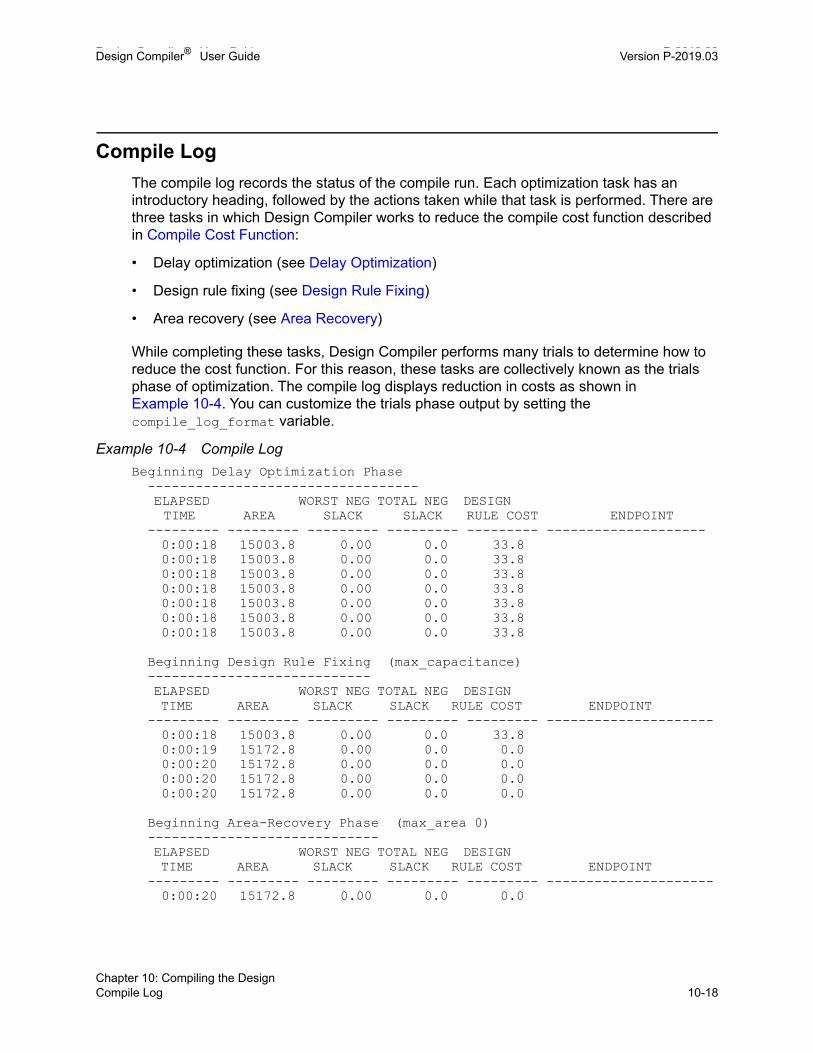
Design Compiler® User Guide P-2019.03Design Compiler® User Guide Version P-2019.03
Compile Log
The compile log records the status of the compile run. Each optimization task has an introductory heading, followed by the actions taken while that task is performed. There are three tasks in which Design Compiler works to reduce the compile cost function described in Compile Cost Function:
• Delay optimization (see Delay Optimization)
• Design rule fixing (see Design Rule Fixing)
• Area recovery (see Area Recovery)
While completing these tasks, Design Compiler performs many trials to determine how to reduce the cost function. For this reason, these tasks are collectively known as the trials phase of optimization. The compile log displays reduction in costs as shown in Example 10-4. You can customize the trials phase output by setting the compile_log_format variable.
Example 10-4 Compile Log
Beginning Delay Optimization Phase ---------------------------------- ELAPSED WORST NEG TOTAL NEG DESIGN TIME AREA SLACK SLACK RULE COST ENDPOINT --------- --------- --------- --------- --------- -------------------- 0:00:18 15003.8 0.00 0.0 33.8 0:00:18 15003.8 0.00 0.0 33.8 0:00:18 15003.8 0.00 0.0 33.8 0:00:18 15003.8 0.00 0.0 33.8 0:00:18 15003.8 0.00 0.0 33.8 0:00:18 15003.8 0.00 0.0 33.8 0:00:18 15003.8 0.00 0.0 33.8
Beginning Design Rule Fixing (max_capacitance) ---------------------------- ELAPSED WORST NEG TOTAL NEG DESIGN TIME AREA SLACK SLACK RULE COST ENDPOINT --------- --------- --------- --------- --------- --------------------- 0:00:18 15003.8 0.00 0.0 33.8 0:00:19 15172.8 0.00 0.0 0.0 0:00:20 15172.8 0.00 0.0 0.0 0:00:20 15172.8 0.00 0.0 0.0 0:00:20 15172.8 0.00 0.0 0.0
Beginning Area-Recovery Phase (max_area 0) ----------------------------- ELAPSED WORST NEG TOTAL NEG DESIGN TIME AREA SLACK SLACK RULE COST ENDPOINT --------- --------- --------- --------- --------- --------------------- 0:00:20 15172.8 0.00 0.0 0.0
Chapter 10: Compiling the DesignCompile Log 10-18

Design Compiler® User Guide Version P-2019.03
0:00:21 15085.7 0.00 0.0 0.0 0:00:21 15085.7 0.00 0.0 0.0 0:00:21 15085.7 0.00 0.0 0.0 0:00:21 15085.7 0.00 0.0 0.0 Loading db file '/remote/srm147/LS_IMAGES/D20061217/libraries/syn/tc6a_cbacore.db' Optimization Complete ---------------------1
See Also
• Analyzing Your Design During Optimization Using the Compile Log
Resolving Multiple Instances of a Design Reference
In a hierarchical design, subdesigns are often referenced by more than one cell instance, that is, multiple references of the design can occur. For example, Figure 10-4 shows the design TOP, in which design C is referenced twice (U2/U3 and U2/U4).
Figure 10-4 Multiple Instances of a Design Reference
To report information messages related to multiply-instantiated designs, use the check_design -multiple_designs command. The command lists all multiply instantiated
U1 U2
U3 U4 U5(A)
(B)
(C) (C) (D)
TOP
DCA
Top-level design with instances
Design Compiler memory: loaded designs
Chapter 10: Compiling the DesignResolving Multiple Instances of a Design Reference 10-19Chapter 10: Compiling the DesignResolving Multiple Instances of a Design Reference 10-19
Design Compiler® User Guide P-2019.03Design Compiler® User Guide Version P-2019.03
designs along with instance names and associated attributes (dont_touch, black_box, and ungroup). The following methods are available for handling designs with multiple instances:
• The Uniquify Method
The tool automatically uniquifies designs as part of the compile process. You can manually force the tool to uniquify designs before compile by running the uniquify command. However, this step contributes to longer runtimes because the tool automatically “re-uniquifies” the designs when compiling the design. You cannot turn off the uniquify process.
• Compile-Once-Don’t-Touch Method
This method uses the set_dont_touch command to preserve the compiled subdesign while the remaining designs are compiled.
• Ungroup Method
This method uses the ungroup command to remove the hierarchy.
The Uniquify Method
The uniquify process copies and renames any multiply referenced design so that each instance references a unique design. The process removes the original design from memory after it creates the new, unique designs. The original design and any collections that contain it or its objects are no longer accessible.
The tool automatically uniquifies designs as part of the compile process. The uniquification process can resolve multiple references throughout the hierarchy the current design (except those having a dont_touch attribute). After this process finishes, the tool can optimize each design copy based on the unique environment of its cell instance.
You can also create unique copies for specific references by using the -reference option of the uniquify command, or you can specify specific cells by using the -cell option. Design Compiler makes unique copies for cells specified with the -reference or the -cells option, even if they have a dont_touch attribute.
The uniquify command accepts instance objects—that is, cells at a lower level of hierarchy. When you use the -cell option with an instance object, the complete path to the instance is uniquified. For example, the following command uniquifies both instances mid1 and mid1/bot1, assuming that mid1 is not unique:
prompt> uniquify -cell mid1/bot1
Chapter 10: Compiling the DesignResolving Multiple Instances of a Design Reference 10-20
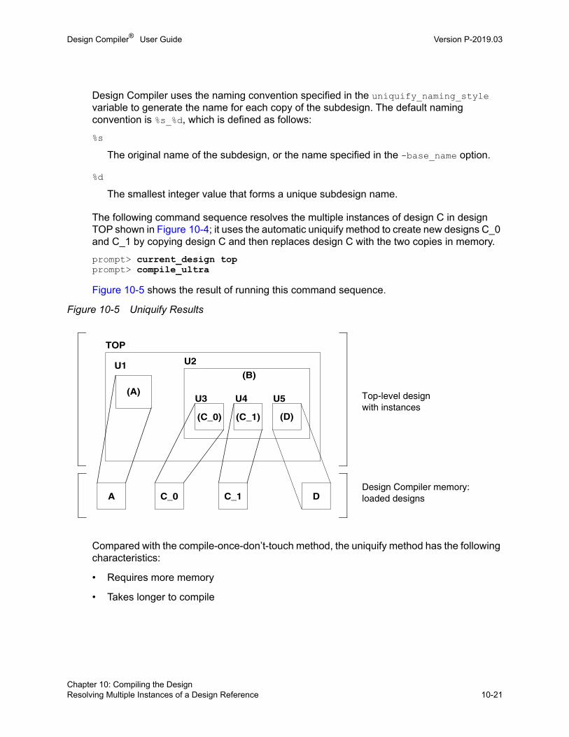
Design Compiler® User Guide Version P-2019.03
Design Compiler uses the naming convention specified in the uniquify_naming_style variable to generate the name for each copy of the subdesign. The default naming convention is %s_%d, which is defined as follows:
%s
The original name of the subdesign, or the name specified in the -base_name option.
%d
The smallest integer value that forms a unique subdesign name.
The following command sequence resolves the multiple instances of design C in design TOP shown in Figure 10-4; it uses the automatic uniquify method to create new designs C_0 and C_1 by copying design C and then replaces design C with the two copies in memory.
prompt> current_design topprompt> compile_ultra
Figure 10-5 shows the result of running this command sequence.
Figure 10-5 Uniquify Results
Compared with the compile-once-don’t-touch method, the uniquify method has the following characteristics:
• Requires more memory
• Takes longer to compile
U1 U2
U3 U4 U5(A)
(B)
(C_0) (C_1) (D)
TOP
DC_0A C_1
Top-level designwith instances
Design Compiler memory:loaded designs
Chapter 10: Compiling the DesignResolving Multiple Instances of a Design Reference 10-21Chapter 10: Compiling the DesignResolving Multiple Instances of a Design Reference 10-21

Design Compiler® User Guide P-2019.03Design Compiler® User Guide Version P-2019.03
Compile-Once-Don’t-Touch Method
If the environments around the instances of a multiply referenced design are sufficiently similar, use the compile-once-don’t-touch method. In this method, you compile the design, using the environment of one of its instances, and then you use the set_dont_touch command to preserve the subdesign during the remaining optimization.
To use the compile-once-don’t-touch method to resolve multiple instances, follow these steps:
1. Characterize the subdesign’s instance that has the worst-case environment.
2. Compile the referenced subdesign.
3. Use the set_dont_touch command to set the dont_touch attribute on all instances that reference the compiled subdesign.
4. Compile the entire design.
For example, the following command sequence resolves the multiple instances of design C in design TOP by using the compile-once-don’t-touch method (assuming U2/U3 has the worst-case environment). In this case, no copies of the original subdesign are loaded into memory.
prompt> current_design topprompt> characterize U2/U3prompt> current_design Cprompt> compile_ultraprompt> current_design topprompt> set_dont_touch {U2/U3 U2/U4}prompt> compile_ultra
Figure 10-6 shows the result of running this command sequence. The X drawn over the C design, which has already been compiled, indicates that the dont_touch attribute has been set. This design is not modified when the top-level design is compiled.
Chapter 10: Compiling the DesignResolving Multiple Instances of a Design Reference 10-22

Design Compiler® User Guide Version P-2019.03
Figure 10-6 Compile-Once-Don’t-Touch Results
The compile-once-don’t-touch method has the following advantages:
• Compiles the reference design one time
• Requires less memory than the uniquify method
• Takes less time to compile than the uniquify method
The principal disadvantage of the compile-once-don’t-touch method is that the characterization might not apply well to all instances. Another disadvantage is that you cannot ungroup objects that have the dont_touch attribute.
See Also
• Preserving Subdesigns
Ungroup Method
The ungroup method has the same effect as the uniquify method (it makes unique copies of the design), but in addition, it removes levels of hierarchy. This method uses the ungroup command to produce a flattened netlist. For details about the ungroup command, see Removing Levels of Hierarchy.
U1 U2
U3 U4 U5(A)
(B)
(C) (C) (D)
TOP
DCA
Top-level designwith instances
Design Compiler memory:loaded designs
Chapter 10: Compiling the DesignResolving Multiple Instances of a Design Reference 10-23Chapter 10: Compiling the DesignResolving Multiple Instances of a Design Reference 10-23
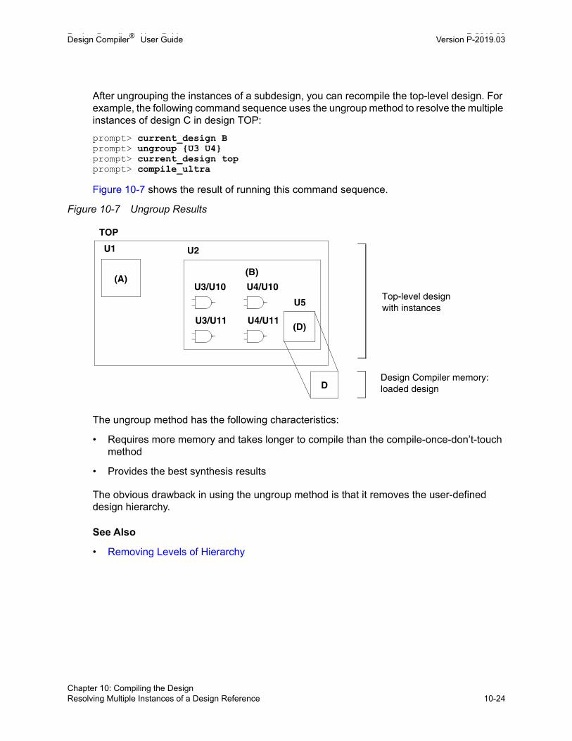
Design Compiler® User Guide P-2019.03Design Compiler® User Guide Version P-2019.03
After ungrouping the instances of a subdesign, you can recompile the top-level design. For example, the following command sequence uses the ungroup method to resolve the multiple instances of design C in design TOP:
prompt> current_design Bprompt> ungroup {U3 U4}prompt> current_design topprompt> compile_ultra
Figure 10-7 shows the result of running this command sequence.
Figure 10-7 Ungroup Results
The ungroup method has the following characteristics:
• Requires more memory and takes longer to compile than the compile-once-don’t-touch method
• Provides the best synthesis results
The obvious drawback in using the ungroup method is that it removes the user-defined design hierarchy.
See Also
• Removing Levels of Hierarchy
TOP
U1 U2
U5
(A)(B)
(D)
U3/U10
U3/U11
U4/U10
U4/U11
D
Top-level designwith instances
Design Compiler memory:loaded design
Chapter 10: Compiling the DesignResolving Multiple Instances of a Design Reference 10-24
Design Compiler® User Guide Version P-2019.03
Test-Ready Compile
Test-ready compile reduces iterations and design time, by accounting for the impact of the scan implementation during the logic optimization process. The optimization cost functions consider the impact of the scan cells themselves and the additional loading due to the scan-chain routing. By accounting for the timing impact of scan design from the start of the synthesis process, test-ready compilation eliminates the need to recompile your design after scan insertion. Use the -scan option of the compile_ultra command or the compile command to enable test-ready compile. When you use this option, the tool replaces all sequential elements during optimization.
See Also
• Performing a Test-Ready Compile
Chapter 10: Compiling the DesignTest-Ready Compile 10-25Chapter 10: Compiling the DesignTest-Ready Compile 10-25

Design Compiler® User Guide P-2019.03Design Compiler® User Guide Version P-2019.03
Chapter 10: Compiling the DesignTest-Ready Compile 10-26

11Optimizing the Design 11
Optimization is the Design Compiler synthesis step that maps the design to an optimal combination of specific target logic library cells, based on the design’s functional, speed, and area requirements. You use the compile_ultra command or the compile command to start the compile process, which synthesizes and optimizes the design. Design Compiler provides options that enable you to customize and control optimization. Several of the many factors affecting the optimization outcome are discussed in the following topics.
To learn about Design Compiler optimization processes and techniques, see the following topics:
• Overview of the Optimization Process
• Optimization Phases
• Compile Cost Function
• Optimization Flow
• Optimization Techniques
11-1

Design Compiler® User Guide P-2019.03Design Compiler® User Guide Version P-2019.03
Overview of the Optimization Process
Optimization is the step in the synthesis process that attempts to implement a combination of library cells that meets the functional, speed, and area requirements of your design. Optimization transforms the design into a technology-specific circuit based on the attributes and constraints you place on the design.
Design Compiler performs the following levels of optimization in the following order:
1. Architectural Optimization
2. Logic-Level Optimization
3. Gate-Level Optimization
Architectural Optimization
Architectural optimization works on the HDL description. It includes such high-level synthesis tasks as
• Sharing common subexpressions
• Sharing resources
• Selecting DesignWare implementations (not available in DC Expert)
• Reordering operators
• Identifying arithmetic expressions for datapath synthesis (not available in DC Expert)
Except for DesignWare implementations, these high-level synthesis tasks occur only during the optimization of an unmapped design. DesignWare selection can recur after gate-level mapping.
High-level synthesis tasks are based on your constraints and your HDL coding style. After high-level optimization, circuit function is represented by GTECH library parts, that is, by a generic, technology-independent netlist.
See Also
• Preparing for Synthesis
Provides information about how your coding style affects architectural optimization
• Resource Sharing
Provides information about resource sharing, which reduces the amount of hardware needed to implement operators in your Verilog or VHDL description
Chapter 11: Optimizing the DesignOverview of the Optimization Process 11-2

Design Compiler® User Guide Version P-2019.03
• DesignWare Libraries
Provides information about using DesignWare components and developing additional DesignWare libraries using a DesignWare Developer license
Logic-Level Optimization
Logic-level optimization works on the GTECH netlist. It consists of the following two processes:
• Structuring
This process adds intermediate variables and logic structure to a design, which can result in reduced design area. Structuring is constraint based. It is best applied to noncritical timing paths.
During structuring, Design Compiler searches for subfunctions that can be factored out and evaluates these factors, based on the size of the factor and the number of times the factor appears in the design. Design Compiler turns the subfunctions that most reduce the logic into intermediate variables and factors them out of the design equations.
• Flattening
The goal of this process is to convert combinational logic paths of the design to a two-level, sum-of-products representation. Flattening is carried out independently of constraints. It is useful for speed optimization because it leads to just two levels of combinational logic.
During flattening, Design Compiler removes all intermediate variables, and therefore all its associated logic structure, from a design.
Gate-Level Optimization
Gate-level optimization works on the generic netlist created by logic synthesis to produce a technology-specific netlist. It includes the following processes:
• Mapping
This process uses gates (combinational and sequential) from the target libraries to generate a gate-level implementation of the design whose goal is to meet timing and area goals. You can use the various options of the compile_ultra or compile command to control the mapping algorithms used by Design Compiler. For more information, see Sequential Mapping.
Chapter 11: Optimizing the DesignOverview of the Optimization Process 11-3Chapter 11: Optimizing the DesignOverview of the Optimization Process 11-3

Design Compiler® User Guide P-2019.03Design Compiler® User Guide Version P-2019.03
• Delay optimization
The process goal is to fix delay violations introduced in the mapping phase. Delay optimization does not fix design rule violations or meet area constraints. For more information, see Delay Optimization.
• Design rule fixing
The process goal is to correct design rule violations by inserting buffers or resizing existing cells. Design Compiler tries to fix these violations without affecting timing and area results, but if necessary, it does violate the optimization constraints. For more information, see Design Rule Fixing.
• Area optimization
The process goal is to meet area constraints after the mapping, delay optimization, and design rule fixing phases are completed. However, Design Compiler does not allow area recovery to introduce design rule or delay constraint violations as a means of meeting the area constraints. For more information, see Area Recovery.
You can change the priority of the constraints by using the set_cost_priority command. Also, you can disable design rule fixing by specifying the -no_design_rule option when you run the compile_ultra command or compile command. However, if you use this option, your synthesized design might violate design rules.
See Also
• Optimization Constraints
• Managing Constraint Priorities
Optimization Phases
During optimization, Design Compiler attempts to meet the constraints you have set on the design. Design Compiler’s optimization algorithms use costs to determine if a design change is an improvement. Design Compiler calculates two cost functions: one for design rule constraints and one for optimization constraints and accepts an optimization move if it decreases the cost of one component without increasing more-important costs. By default, the design rule constraints (transition, fanout, capacitance, and cell degradation) have a higher priority than the optimization constraints (delay and area).
Chapter 11: Optimizing the DesignOptimization Phases 11-4

Design Compiler® User Guide Version P-2019.03
To learn more about the types of optimizations Design Compiler performs, see the following topics:
• Combinational Optimization
• Sequential Optimization
• Local Optimizations
Combinational Optimization
The combinational optimization phase transforms the logic-level description of the combinational logic to a gate-level netlist.
Combinational optimization includes
• Technology-Independent Optimization
This optimization operates at the logic level. Design Compiler represents the gates as a set of Boolean logic equations.
• Mapping
During this process, Design Compiler selects components from the logic library to implement the logic structure.
• Technology-Specific Optimization
This optimization operates at the gate level.
Figure 11-1 shows the logic-level description of the combinational logic and the gate-level optimization for design LED.
Chapter 11: Optimizing the DesignOptimization Phases 11-5Chapter 11: Optimizing the DesignOptimization Phases 11-5

Design Compiler® User Guide P-2019.03Design Compiler® User Guide Version P-2019.03
Figure 11-1 Logic-Level and Gate-Level Optimization for Design LED
Technology-Independent Optimization
Technology-independent optimization applies algebraic and Boolean techniques to a set of logic equations. This optimization implements the logic equations to meet your timing and area goals.
Mapping
During mapping, Design Compiler selects components from the logic library to implement the logic structure. Design Compiler tries different logic combinations, using only components that approach the defined speed and area goals. Figure 11-2 shows examples of mapped gates.
a
bd
c
z0
z1
z2
z3
z4
z5
z6
Total Area = 32
design_name LED.inputnames a b c d
.outputnames z0 z1 z2 z3 z4 z5 z6
n1 = c’ ;
n2 = d’ ;
n3 = a’ ;
n4 = ((n2’ + n6’) * (d’ + b’)) ;
n5 = ((n2’ + n1’) * (d’ + c’)) ;n6 = b’ ;n7 = ((n2’ + n6’) * (a’ + b’)) ;
n8 = ((n12’ + n1’) * (n2’ + c’)) ;
n9 = ((a’ * n2’) + c’) ;
n10 = ((n1’ * n2’) + b’) ;
n11 = ((n1’ + b’) * (c’ + n6’)) ;
n12 = (n6’ * n2’) ;
z0 = ((n1’ * n2’) + n3’ + n4’) ;
z1 = (n5’ + n3’ + b’) ;
z2 = (c’ + n3’ + n6’ + n2’) ;
z3 = ((b’ * n1’) + n7’ + n8’) ;
z4 = (n7’ + n9’) ;
z5 = ((d’ * c’) + n10’ + n3’) ;
z6 = ((d’ * n1’) + n3’ + n11’) ;
Chapter 11: Optimizing the DesignOptimization Phases 11-6

Design Compiler® User Guide Version P-2019.03
Figure 11-2 Mapped Gates
Technology-Specific Optimization
Technology-specific optimization synthesizes a gate-level design that attempts to meet your timing and area constraints.
Sequential Optimization
Sequential optimization includes the initial optimization phase, which maps sequential cells to cells in the library, and the final optimization phase, where Design Compiler optimizes timing-critical sequential cells (cells on the critical path):
• Initial Sequential Optimization
• Final Sequential Optimization
Initial Sequential Optimization
Initial sequential optimization maps sequential cells to cells in the target library. You can map to either standard sequential cells or scan-equivalent cells. Initial sequential optimization takes place during the first phase of gate-level optimization.
b
ab
de
fg
c
a
c
de
fg
out
out
Chapter 11: Optimizing the DesignOptimization Phases 11-7Chapter 11: Optimizing the DesignOptimization Phases 11-7

Design Compiler® User Guide P-2019.03Design Compiler® User Guide Version P-2019.03
At this point in the optimization process, information about the delay through the combinational logic is incomplete. Design Compiler does not have enough information to select the optimum sequential cell. The tool can correct this lack of information later, in the final sequential optimization phase.
Final Sequential Optimization
Design Compiler has accurate values for all delays through the I/O pads and combinational logic before it enters the final sequential optimization phase. In this phase, Design Compiler optimizes timing-critical sequential cells (cells on the critical path).
The tool examines each sequential cell and its surrounding combinational logic to determine whether they might be replaced by more-optimal sequential cells from the target library in order to meet timing and area constraints.
Final sequential optimization can achieve the following:
• Improve design timing by choosing higher-performance sequential cells.
• Possibly reduce area and delay in the design if more optimal sequential cells exist in the library. The tool incorporates the combinational logic in the sequential cell, as shown in Figure 11-3 and Figure 11-4.
• Further improve area by remapping sequential elements.
Figure 11-3 Sequential Optimization
A
B
CLK
D Latch MUXed D Latch
A
BD Q
CLK
D Q1
0
Chapter 11: Optimizing the DesignOptimization Phases 11-8
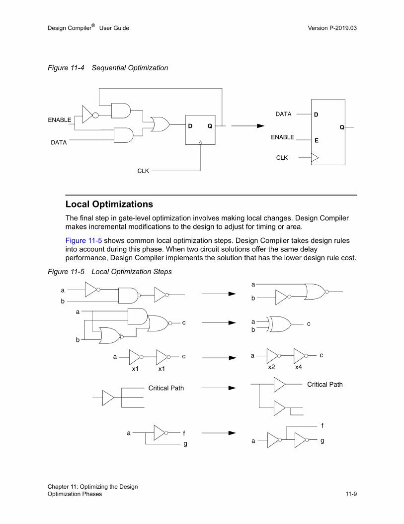
Design Compiler® User Guide Version P-2019.03
Figure 11-4 Sequential Optimization
Local Optimizations
The final step in gate-level optimization involves making local changes. Design Compiler makes incremental modifications to the design to adjust for timing or area.
Figure 11-5 shows common local optimization steps. Design Compiler takes design rules into account during this phase. When two circuit solutions offer the same delay performance, Design Compiler implements the solution that has the lower design rule cost.
Figure 11-5 Local Optimization Steps
CLK
D Q
DATA
ENABLE
ENABLE
DATA
CLK
Q
D
E
a
b
a
b
ab
a f
g a
f
g
a
b
c c
Critical Path
a c a c
x1 x2x1 x4
Critical Path
Chapter 11: Optimizing the DesignOptimization Phases 11-9Chapter 11: Optimizing the DesignOptimization Phases 11-9

Design Compiler® User Guide P-2019.03Design Compiler® User Guide Version P-2019.03
Compile Cost Function
During compile, Design Compiler’s optimization algorithms use costs to determine if a design change is an improvement. Design Compiler calculates two cost functions, one for design rule constraints and one for optimization constraints, and accepts an optimization move if it decreases the cost of one component without increasing more-important costs. The tool reports the value of each cost function whenever a change is made to the design.
By default, Design Compiler prioritizes costs in the following order:
1. Design rule costs
a. Connection class
b. Multiple port nets
c. Maximum transition time
d. Maximum fanout
e. Maximum capacitance
f. Cell degradation
The goal of Design Compiler is to meet all constraints. However, by default, it gives precedence to design rule constraints because design rule constraints are functional requirements for designs. Using the default priority, Design Compiler fixes design rule violations even at the expense of violating your delay or area constraints.
2. Optimization costs
a. Maximum delay
b. Minimum delay
c. Maximum power
d. Maximum area
During the first phase of mapping, Design Compiler works to reduce the optimization cost function. Speed (timing) constraints automatically have a higher priority than area; therefore, an optimization move that improves maximum delay cost is always accepted. Optimization stops when all costs are zero or no further improvements can be made to the cost function.
The compile cost function considers only those components that are active in your design. Design Compiler evaluates each cost function component independently, in order of importance. When evaluating cost function components, Design Compiler considers only violators (positive difference between actual value and constraint) and works to reduce the cost function to zero.
Chapter 11: Optimizing the DesignCompile Cost Function 11-10

Design Compiler® User Guide Version P-2019.03
You can change the priority of the maximum design rule costs and the delay costs by using the set_cost_priority command to specify the ordering. You must run the set_cost_priority command before compiling the design.
You can disable evaluation of the design rule cost function by using the -no_design_rule option or the optimization cost function by using the -only_design_rule option when you run the compile or compile_ultra command.
See Also
• Managing Constraint Priorities
• Design Rule Constraints
• Optimization Constraints
Optimization Flow
Figure 11-6 shows the optimization flow. Steps that are not supported in the DC Expert flow are marked with an asterisk. The sections following the figure describe the steps in the flow.
Chapter 11: Optimizing the DesignOptimization Flow 11-11Chapter 11: Optimizing the DesignOptimization Flow 11-11

Design Compiler® User Guide P-2019.03Design Compiler® User Guide Version P-2019.03
Figure 11-6 Optimization Flow
Auto-Uniquification
Sequential Mapping
Boolean Optimization and Mapping
Register Retiming*
Design Rule Fixing
Area Recovery
Automatic Area Ungrouping*
Multiplexer Optimization and Mapping
Implement Synthetic Parts
Timing-Driven and Power-Driven Combinational Optimization
High-Level OptimizationDatapath Optimization*
Delay and Leakage Optimization
An asterisk (*) indicates steps that do not occur in DC Expert.
Chapter 11: Optimizing the DesignOptimization Flow 11-12

Design Compiler® User Guide Version P-2019.03
Automatic Ungrouping
The compile_ultra command automatically ungroups logical hierarchies. Ungrouping merges subdesigns of a given level of the hierarchy into the parent cell or design. It removes hierarchical boundaries and allows Design Compiler to improve timing by reducing the levels of logic and to improve area by sharing logic. For information about the automatic ungrouping of hierarchies, see Automatic Ungrouping.
You can also manually ungroup hierarchies by using the ungroup command or the set_ungroup command followed by compile_ultra. For information about manually ungrouping hierarchies, see Removing Levels of Hierarchy.
High-Level Optimization and Datapath Optimization
During high-level optimization, resources are allocated and shared, depending on timing and area considerations. Resource sharing enables the tool to build one hardware component for multiple operations, which typically reduces the hardware required to implement your design. Additional optimizations, such as arithmetic optimization and the sharing of common subexpressions, are also performed. In addition, if you are using the DC Ultra tool, advanced datapath transformations are performed. For more information, see High-Level Optimization and Datapath Optimization.
Multiplexer Mapping and Optimization
In this phase, Design Compiler maps combinational logic representing multiplexers in the HDL code directly to a single multiplexer (MUX) or a tree of multiplexer cells from the target logic library. Design Compiler reorders SELECT signals for better area and shares multiplexer trees. For more information, see Multiplexer Mapping and Optimization.
Sequential Mapping
This phase consists of two steps: register inferencing by HDL Compiler and technology mapping by Design Compiler. The RTL is translated into a technology-independent representation called SEQGEN; the SEQGEN is then mapped to gates from the logic library. A SEQGEN is a generic sequential element that is used by Synopsys tools to represent registers and latches in a design. SEQGENs are created during elaboration and are mapped to flip-flops or latches during compile. For more information, see Sequential Mapping.
Chapter 11: Optimizing the DesignOptimization Flow 11-13Chapter 11: Optimizing the DesignOptimization Flow 11-13
Design Compiler® User Guide P-2019.03Design Compiler® User Guide Version P-2019.03
Structuring and Mapping
In this phase, the tool optimizes unmapped unstructured logic and maps it to technology gates. Structuring is an optimization step that adds intermediate variables and logic structure to a design. During structuring, Design Compiler searches for subfunctions that can be factored out, then evaluates these factors based on the size of the factor and the number of times the factor appears in the design. The subfunctions that most reduce the logic are turned into intermediate variables and factored out of the design equations. Design Compiler offers timing-driven structuring to minimize delays and Boolean structuring to reduce area.
Automatic Uniquification
The uniquify process copies and renames any multiply referenced design so that each instance references a unique design. The process removes the original design from memory after it creates the new, unique designs. The original design and any collections that contain it or its objects are no longer accessible. The tool automatically uniquifies designs as part of the compile process. For more information about the uniquification process, see The Uniquify Method.
Implementing Synthetic Parts
HDL operators (either built-in operators like + and * or HDL functions and procedures) are associated with synthetic parts, which are bound in turn to synthetic modules. Each synthetic module can have multiple architectural realizations, called implementations.
For example, when you use the HDL addition operator (+), HDL Compiler infers the need for an adder resource and puts an abstract representation of the addition operation in the netlist. During high-level optimization, the tool manipulates this abstract representation—called a synthetic operator— and applies optimizations such as arithmetic optimization or resource sharing.
During the high-level optimization phase, the tool used abstract representations for synthetic parts. During the implement synthetic parts phase, the tool maps synthetic modules to architectural representations (implementations). For more information about synthetic parts, see Synthetic Operators and the HDL Compiler and DesignWare documentation on SolvNet.
Chapter 11: Optimizing the DesignOptimization Flow 11-14

Design Compiler® User Guide Version P-2019.03
Timing-Driven Combinational Optimization
During this phase, Design Compiler performs optimization of combinational parts. This phase has two components: timing-driven structuring and incremental implementation selection. During timing-driven structuring, the tool restructures logic in the critical paths to improve delay cost. During incremental implementation selection, the tool explores alternative implementations for each synthetic operator. It evaluates and replaces synthetic implementations along the critical path to improve delay cost.
Register Retiming
Register retiming is available in DC Ultra only. Register retiming is a sequential optimization technique that moves registers through the combinational logic gates of a design to optimize timing and area. Register retiming adds an opportunity for improving circuit timing.
Design Compiler provides the following ways to perform register retiming:
• The optimize_registers command performs retiming of sequential cells (edge-triggered registers or level-sensitive latches) for pipelined designs. For more information about this retiming strategy, see Pipelined-Logic Retiming.
• The compile_ultra command supports the -retime option, which enables Design Compiler to automatically perform local retiming moves to improve worst negative slack (WNS). This capability, called adaptive retiming, optimizes an entire design. It works best with general non-pipelined logic. For more information about this retiming strategy, see Adaptive Retiming.
Delay and Leakage Optimization
In this phase, Design Compiler attempts to fix existing delay violations by traversing the critical path. During delay optimization, Design Compiler reevaluates existing implementations to determine if they meets constraints. If constraints are not met, Design Compiler selects a different implementation. It applies local transformations such as upsizing, load isolation and splitting, and revisits mapping of sequential paths. Constraints affecting delay include clocks, input and output delays, external loads, input driving cells, operating conditions, and wire load tables. For more information, see Delay Optimization.
During this stage of optimization, Design Compiler automatically performs leakage power optimization (except in DC Expert). During leakage power optimization, Design Compiler tries to reduce the overall leakage power in your design without affecting the performance. To do this, the optimization is performed on paths that are not timing-critical. When the target libraries are characterized for leakage power and contain cells characterized for multiple threshold voltages, Design Compiler uses the library cells with appropriate threshold voltages to reduce the leakage power of the design.
Chapter 11: Optimizing the DesignOptimization Flow 11-15Chapter 11: Optimizing the DesignOptimization Flow 11-15
Design Compiler® User Guide P-2019.03Design Compiler® User Guide Version P-2019.03
For more information about leakage power optimization for all Design Compiler tools, see Leakage Power and Dynamic Power Optimization.
Design Rule Fixing
Design rules are provided in the vendor logic library to ensure that the product meets specifications and works as intended. In this phase, Design Compiler fixes any design rule violations. Whenever possible, Design Compiler fixes design rule violations by resizing gates across multiple logic levels—as opposed to adding buffers to the circuitry. For more information, see Design Rule Fixing.
Area Optimization
During area optimization, Design Compiler attempts to minimize the number of gates in the design without degrading delay cost.
In DC Ultra (wire load mode and topographical mode), you can use the compile_ultra and optimize_netlist -area commands to provide significant area improvements. The optimize_netlist -area command performs monotonic gate-to-gate optimization to improve area without degrading timing or leakage.
You can use the optimize_netlist -area command as the final area recovery step at the end of the synthesis flow. You can also use the command on legacy netlists. To maximize area benefits, run synthesis using the compile_ultra command and then run the optimize_netlist -area command. For more information, see Area Recovery.
Optimization Techniques
The following topics provide techniques you can use to control optimization and improve results:
• Optimizing Once for Best- and Worst-Case Conditions
• Optimizing With Multiple Libraries
• Preserving Subdesigns
• Preserving the Clock Network After Clock Tree Synthesis
• Optimizing Datapaths
• Creating Path Groups
• Controlling Automatic Path Group Creation
Chapter 11: Optimizing the DesignOptimization Techniques 11-16

Design Compiler® User Guide Version P-2019.03
• Isolating Input and Output Ports
• Fixing Heavily Loaded Nets
• Fixing Nets Connected to Multiple Ports
• Optimizing Buffer Trees
• Optimizing Multibit Registers
• Optimizing for Multiple Clocks Per Register
• Defining a Signal for Unattached Master Clocks
• Optimizing Total Negative Slack During Placement
Optimizing Once for Best- and Worst-Case Conditions
You can constrain your design once for both minimum (best-case) and maximum (worst-case) optimization and timing analysis. The tool then optimizes and analyzes the timing in a single compile run.
You can constrain the design by using either a single logic library or multiple libraries. Whether you use one or multiple libraries, the general methodology is as follows:
1. Set up a logic library file or files. Make sure the files contain
❍ Best- and worst-case operating conditions
❍ Optimistic and pessimistic wire load models
❍ Minimum and maximum timing delays
If you use multiple libraries, see Optimizing With Multiple Libraries.
2. Specify minimum and maximum constraints.
❍ Environmental—including operating conditions and wire loads
❍ Clock information—including clock skew and clock transition
❍ Optimization—including input and output delays, drive, load, and resistance
❍ Design rule—including transition time, fanout, and capacitance
3. Optimize the design for simultaneous minimum and maximum timing. To ensure that minimum delay constraints are optimized with respect to a particular clock, specify the fix_hold attribute for that clock, using the set_fix_hold command.
4. Report and analyze the paths showing constraint violations.
Chapter 11: Optimizing the DesignOptimization Techniques 11-17Chapter 11: Optimizing the DesignOptimization Techniques 11-17

Design Compiler® User Guide P-2019.03Design Compiler® User Guide Version P-2019.03
The following constraint-related, reporting, and back-annotation commands support both minimum and maximum optimization and timing analysis.
Constraint-Related Commandsset_min_libraryset_operating_conditionsset_wire_load_modelset_wire_load_modeset_wire_load_min_block_sizeset_wire_load_selection_groupset_clock_uncertaintyset_clock_transitionset_driveset_loadset_port_fanout_numberset_resistance
The set_min_library command is described in the next section, Optimizing With Multiple Libraries.
Reporting Commandsreport_annotated_delayreport_areareport_attributereport_busreport_cachereport_cellreport_clockreport_clustersreport_compile_optionsreport_constraintreport_delay_calculationreport_designreport_design_libreport_fsmreport_hierarchyreport_internal_loadsreport_libreport_name_rulesreport_netreport_path_groupreport_portreport_powerreport_qorreport_referencereport_resourcesreport_synlibreport_timingreport_timing_requirements
Chapter 11: Optimizing the DesignOptimization Techniques 11-18

Design Compiler® User Guide Version P-2019.03
report_transitive_faninreport_transitive_fanoutreport_wire_load
Other commands, including report_design, report_port, and report_wire_load, generate reports on the minimum and maximum constraints on your design. You do not need to specify the -min option.
Optimizing With Multiple Libraries
The set_min_library command directs Design Compiler to use multiple technology libraries for minimum- and maximum-delay analyses in one optimization run. Thus, you can choose libraries that contain all of the following:
• Best- and worst-case operating conditions
• Optimistic and pessimistic wire load models
• Minimum and maximum timing delays
You can direct Design Compiler to analyze them simultaneously. To accomplish this analysis, use the set_min_library command to create a link between the data in the two libraries. Use the library file name (not the library name) with the set_min_library command.
The set_min_library command creates a minimum/maximum relationship between two library files. You specify a max_library to be used for maximum delay analysis and a min_library to be used for minimum delay analysis. Only max_library should be used for linking and as the target library.
When Design Compiler needs to compute a minimum delay value, it first analyzes the library cell in the max_library, then it looks to the min_library to determine if a match exists. If a library cell with the same name, the same pins, and the same timing arcs exists in the min_library, Design Compiler uses the timing information from the min_library. If the tool cannot find a matching cell in the min_library, it uses the cell in the max_library.
Example 11-1 shows how you might use set_min_library with set_operating_conditions to control and report delay analysis. If you do not specify a minimum, Design Compiler uses the maximum condition for both minimum and maximum delay analysis. You cannot use the -min option without also using the -max option.
Example 11-1 Controlling and Reporting Delay Analysis
set link_library "LIB_WC_COM.db"set target_library $link_libraryset_min_library LIB_WC_COM.db -min_version LIB_BC_COM.dbset_operating_conditions -max WC_COM -min BC_COMsource minmax.consset_fix_hold clk
Chapter 11: Optimizing the DesignOptimization Techniques 11-19Chapter 11: Optimizing the DesignOptimization Techniques 11-19

Design Compiler® User Guide P-2019.03Design Compiler® User Guide Version P-2019.03
compilereport_timing -delay_type max report_timing -delay_type min
Preserving Subdesigns
You can preserve a subdesign during optimization by using the set_dont_touch command. The command places the dont_touch attribute on cells, nets, references, and designs in the current design to prevent these objects from being modified or replaced during optimization.
To control the preservation of subdesigns during optimization, see
• Preserving Cells, References, and Designs
• Preserving Nets
• Removing a dont_touch Setting
Preserving Cells, References, and Designs
Use the set_dont_touch command on subdesigns that you do not want optimized with the rest of the design hierarchy. The dont_touch attribute does not prevent or disable timing through the design.
When you use the set_dont_touch command on cells, references, and designs in the current design, consider the following:
• Setting the dont_touch attribute on a hierarchical cell sets an implicit dont_touch on all cells below that cell.
• Setting the dont_touch attribute on a library cell sets an implicit dont_touch on all instances of that cell.
• Setting the dont_touch attribute on a reference sets an implicit dont_touch on all cells using that reference during subsequent optimizations of the design.
• Setting the dont_touch attribute on a design has an effect only when the design is instantiated within another design as a level of hierarchy. In this case, the dont_touch attribute on the design implies that all cells under that level of hierarchy are subject to the dont_touch attribute. Setting dont_touch on the top-level design has no effect because the top-level design is not instantiated within any other design.
• You cannot manually or automatically ungroup objects marked as dont_touch. That is, the ungroup command and the compile -ungroup_all and -auto_ungroup options have no effect on objects marked as dont_touch.
Chapter 11: Optimizing the DesignOptimization Techniques 11-20

Design Compiler® User Guide Version P-2019.03
Preserving Nets
When you use the set_dont_touch command on nets in the current design, consider the following:
• By default, if you set a dont_touch attribute on a net, Design Compiler sets an implicit dont_touch only on mapped combinational cells that are connected to that net. If the net is connected only to unmapped cells, optimization might remove the net.
The dont_touch attribute is ignored on nets that have unmapped cells on them. During compilation, Design Compiler issues warnings for dont_touch nets connected to unmapped cells (generic logic).
• You can preserve specific nets throughout the compilation process by setting the enable_keep_signal_dt_net variable to true before using the set_dont_touch command on the net. When you do this, the dont_touch attribute on the net sets an implicit size_only attribute on logic connected to that net even if logic connected to it is unmapped and not combinational.
Warning: Preserving specific nets throughout compilation can cause quality of results (QoR) degradation. If you preserve a net that is in the critical path, the QoR degradation can be severe. This net preservation functionality is intended to facilitate verification. It should not be used when you are trying to achieve final QoR goals.
Design Compiler issues warnings during compilation to indicate nets that are user-preserved.
In the following example, the enable_keep_signal_dt_net variable is enabled to preserve the my_net net throughout compilation.
1. Make sure the net to be preserved is present in the design and then use the enable_keep_signal_dt_net variable and the set_dont_touch command to preserve the net:
prompt> get_nets *my_net* prompt> set enable_keep_signal_dt_net trueprompt> set_dont_touch [get_nets *my_net*] true
2. Run the compile_ultra command:
prompt> compile_ultra
Check for OPT-154 warning messages at the beginning of compilation to indicate that the net is preserved:
Warning: Preserving net 'my_net'. Expect QoR impact. (OPT-154)
3. Make sure the net is preserved after compilation:
prompt> get_nets *my_net*
Chapter 11: Optimizing the DesignOptimization Techniques 11-21Chapter 11: Optimizing the DesignOptimization Techniques 11-21

Design Compiler® User Guide P-2019.03Design Compiler® User Guide Version P-2019.03
Removing a dont_touch Setting
To remove the dont_touch attribute, use the remove_attribute command or the set_dont_touch command set to false.
Preserving the Clock Network After Clock Tree Synthesis
To preserve a clock network after clock tree synthesis, use the set_dont_touch_network command. This command sets a dont_touch_network attribute on a net group. When placed on a clock tree, the dont_touch_network attribute ensures that your clock network is preserved during subsequent optimizations.
To list the clock networks in the design, use the report_transitive_fanout -clock_tree command.
Starting at the specified source object, the set_dont_touch_network command propagates the dont_touch_network attribute throughout the hierarchy of the clock network. By default, the propagation stops at output ports, or at sequential components if setup and hold relationships exist. If you use the -no_propagate option, the propagation stops at any logical cell.
The propagation of the dont_touch_network attribute occurs only in a forward direction, starting from the specified source object and spreading to objects driven by the source. The propagation cannot go backward, even to electrically connected nets in the same net group. This method of propagation highlights an important difference between the set_dont_touch_network and the set_ideal_network commands: the set_ideal_network command propagates in both the forward and backward directions.
For example, if your design is represented by the simple circuit in Figure 11-7, and you issue the following command:
set_dont_touch_network U1/A
the dont_touch_network attribute is propagated from U1/A to U1/N2, U1/IV, U1/N3, and N4. If you issue the command
set_dont_touch_network U1/A -no_propagate
the dont_touch_network parameter is propagated from U1/A to U1/N2. It is not propagated past net U1/N2.
Chapter 11: Optimizing the DesignOptimization Techniques 11-22

Design Compiler® User Guide Version P-2019.03
Figure 11-7 set_dont_touch_network -no_propagate option
Note: Use the set_auto_disable_drc_nets command when you do not have an accurate representation of the clock tree and you want Design Compiler to treat the clock net as ideal. Typically, you would use this command when a clock tree has not yet been inserted in your design.
The set_dont_touch_network command cannot be used if the network has unmapped logic.
You can use the get_attribute command to check if an object has either the dont_touch_network or the dont_touch_network_no_propagate attribute.
See Also
• Using Attributes
Optimizing Datapaths
Datapath design is commonly used in applications that contain extensive data manipulation, such as 3-D, multimedia, and digital signal processing (DSP). Datapath optimization is comprised of two steps: Datapath extraction, which transforms arithmetic operators (for example, addition, subtraction, and multiplication) into datapath blocks, and datapath implementation, which uses a datapath generator to generate the best implementations for these extracted components. Datapath optimization is enabled by default when you use the compile_ultra command.
U1
N1 outin A N2 N3 N4Z
IV
Chapter 11: Optimizing the DesignOptimization Techniques 11-23Chapter 11: Optimizing the DesignOptimization Techniques 11-23

Design Compiler® User Guide P-2019.03Design Compiler® User Guide Version P-2019.03
Datapath optimization provides the following benefits:
• Shares datapath operators
• Extracts the datapath
• Explores better solutions that might involve a different resource-sharing configuration
• Allows the tool to make better tradeoffs between resource sharing and datapath optimization
See Also
• Datapath Extraction
• Datapath Implementation
Creating Path Groups
By default, Design Compiler groups paths based on the clock controlling the endpoint (all paths not associated with a clock are in the default path group). If your design has complex clocking, complex timing requirements, or complex constraints, you can create path groups to focus Design Compiler on specific critical paths in your design.
Use the group_path command to create path groups. The group_path command allows you to
• Control the optimization of your design
• Optimize near-critical paths
• Optimize all paths
Controlling the Optimization of Your Design
You can control the optimization of your design by creating and prioritizing path groups, which affect only the maximum delay cost function. By default, Design Compiler works only on the worst violator in each group.
You set path group priorities by assigning weights to each group. The weight can be from 0.0 to 100.0. The default weight is 1.0. Do not use very small values (for example, 0.0001); smaller values can prevent the tool from implementing small improvements to the design during compilation.
For example, Figure 11-8 shows a design that has multiple paths to flip-flop FF1.
Chapter 11: Optimizing the DesignOptimization Techniques 11-24

Design Compiler® User Guide Version P-2019.03
Figure 11-8 Path Group Example
To indicate that the path from input in3 to FF1 is the highest-priority path, use the following command to create a high-priority path group:
prompt> group_path -name group3 -from in3 -to FF1/D -weight 2.5
Optimizing Near-Critical Paths
When you add a critical range to a path group, you change the maximum delay cost function from worst negative slack to critical negative slack. The critical range negative slack method considers all violators in each path group that are within a specified delay margin (referred to as the critical range) of the worst violator. Design Compiler optimizes all paths within the critical range.
For example, if the critical range is 2.0 ns and the worst violator has a delay of 10.0 ns, Design Compiler optimizes all paths that have a delay between 8.0 and 10.0 ns.
The critical range negative slack is the sum of all negative slack values within the critical range for each path group. When the critical range is large enough to include all violators, the critical negative slack is equal to the total negative slack.
Using the critical negative slack method, the equation for the maximum delay cost is
m is the number of path groups.
n is the number of paths in the critical range in the path group.
vij is a violator within the critical range of the i th path group.
wi is the weight assigned to the i th path group.
Design Compiler calculates the maximum delay violation for each path within the critical range as
max (0, (actual_path_delay - max_delay))
Specifying a critical range might increase runtime. To limit the runtime increase, use critical range only during the final implementation phase of the design, and use a reasonable critical range value. A guideline for the maximum critical range value is 10 percent of the clock period.
in3
in4FF1
vijj 1=
n
wi
i 1=
m
Chapter 11: Optimizing the DesignOptimization Techniques 11-25Chapter 11: Optimizing the DesignOptimization Techniques 11-25
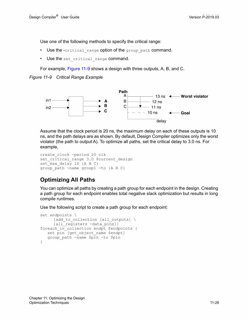
Design Compiler® User Guide P-2019.03Design Compiler® User Guide Version P-2019.03
Use one of the following methods to specify the critical range:
• Use the -critical_range option of the group_path command.
• Use the set_critical_range command.
For example, Figure 11-9 shows a design with three outputs, A, B, and C.
Figure 11-9 Critical Range Example
Assume that the clock period is 20 ns, the maximum delay on each of these outputs is 10 ns, and the path delays are as shown. By default, Design Compiler optimizes only the worst violator (the path to output A). To optimize all paths, set the critical delay to 3.0 ns. For example,
create_clock -period 20 clkset_critical_range 3.0 $current_designset_max_delay 10 {A B C}group_path -name group1 -to {A B C}
Optimizing All Paths
You can optimize all paths by creating a path group for each endpoint in the design. Creating a path group for each endpoint enables total negative slack optimization but results in long compile runtimes.
Use the following script to create a path group for each endpoint:
set endpoints \[add_to_collection [all_outputs] \[all_registers -data_pins]]
foreach_in_collection endpt $endpoints {set pin [get_object_name $endpt]group_path -name $pin -to $pin
}
in1
in2
ABC
13 ns12 ns11 ns
10 ns
delay
Worst violatorABC
Path
Goal
Chapter 11: Optimizing the DesignOptimization Techniques 11-26

Design Compiler® User Guide Version P-2019.03
Controlling Automatic Path Group Creation
Design Compiler allows you to control the automatic creation of path groups in the design to improve quality of results (QoR). You can control whether the tool creates the path groups before optimization or only for blocks that fail timing after optimization.
• To create path groups before optimization, run the create_auto_path_groups command after reading the RTL, analyzing and elaborating, and reading the SDC constraints:
prompt> create_auto_path_groups -mode rtlprompt> compile_ultraprompt> remove_auto_path_groupsprompt> report_qor
This creates one path group per hierarchy within the design. If there are multiple levels of hierarchy, the tool creates path groups for each level.
The advantage of creating path groups at this stage is that the tool can perform all optimizations during the initial compile. However, the number of hierarchical levels within the design can be large, leading to a large number of path groups and causing excessive runtime.
You can prevent the creation of path groups for hierarchies that have a small number of registers by using the -min_regs_per_hierarchy option. This option specifies the minimum number of registers per hierarchy. No path group is created for hierarchies with a number of registers lower than this value.
• To create path groups after the design completes the initial compile, run the create_auto_path_groups command after the compile_ultra command:
prompt> compile_ultraprompt> create_auto_path_groups -mode mappedprompt> compile_ultra -incrementalprompt> remove_auto_path_groupsprompt> report_qor
This creates one path group per hierarchy only for those hierarchical blocks in the design that do not meet timing. If multiple levels of hierarchy do not meet timing, the tool creates path groups for each of those levels.
The tool creates fewer path groups when you use the -mode mapped option compared to the -mode rtl option because the tool assigns separate path groups only to those hierarchical blocks that fail timing. As a result, the runtime is reduced. In most cases, use the create_auto_path_groups command with the -mode mapped option after the initial compile.
The create_auto_path_groups command automatically creates specific path groups for I/Os, macros, and integrated clock-gating cells. To prevent the creation of specific path
Chapter 11: Optimizing the DesignOptimization Techniques 11-27Chapter 11: Optimizing the DesignOptimization Techniques 11-27

Design Compiler® User Guide P-2019.03Design Compiler® User Guide Version P-2019.03
groups, specify the -exclude option with any combination of the following values: IO, macro, and ICG. For example,
prompt> create_auto_path_groups -mode rtl -exclude {IO macro}
The create_auto_path_groups command saves user-created path groups before automatically creating path groups. To remove the path groups created by the create_auto_path_groups command, use the remove_auto_path_groups command. The remove_auto_path_groups command does not remove the user-created path groups.
Use the remove_auto_path_groups command in the following cases:
• After the initial or incremental compile to get a QoR report with only the user-created path groups.
• After the initial compile to remove the path groups created with the create_auto_path_groups -mode rtl command before creating new path groups with the create_auto_path_groups -mode mapped command.
Controlling Path Group Weights During High-Effort Area Optimization
You can ignore the path group weights during high-effort area optimization by setting the optimize_area_ignore_path_group_weights variable to true. When you enable the variable, the weights of all path groups are set to 1 when the optimize_netlist -area command performs monotonic gate-to-gate optimization to improve area. After area optimization, the weight on each path group is restored to the original user-specified value. By default, the variable is false.
Isolating Input and Output Ports
You can isolate input and output ports to improve the accuracy of timing models. To insert isolation logic at specified input or output ports, use the set_isolate_ports command.
Input ports are isolated in the following cases:
• When they drive one or more input pins of a cell having several input pins (as a result of boundary optimization)
• When they drive one or more input pins belonging to different cells having several input pins
Output ports are isolated in the following cases:
• To ensure that the cell driving an output port does not also drive some internal logic within the design
Chapter 11: Optimizing the DesignOptimization Techniques 11-28

Design Compiler® User Guide Version P-2019.03
• To specify particular driver cells at the output ports
This is useful when you want each output port to be driven explicitly by its own driver (no sharing of output drivers by two or more ports) or when you want to compile the design in the context of the environment in which the design will be used.
The isolation logic can be a buffer or a pair of inverters. Either Design Compiler selects the buffer or inverter from the target library, or you specify a particular cell from the target library. However, a user-specified cell must be a buffer or an inverter. Otherwise, Design Compiler outputs an error message.
The inserted isolation logic has the size_only attribute assigned to it. Therefore, when you compile the design, only sizing optimization is allowed for this logic. If the isolation logic is composed of an inverter pair, the size_only attribute is assigned only to the second inverter, which allows flexibility in optimizing the first inverter.
It is important to understand that port isolation can be applied only to the input or output ports of the current design. Therefore, to apply port isolation to a subdesign of your top-level design, you must first make the subdesign the current design.
Port isolation is currently intended for use only during bottom-up compile. That is, isolating hierarchical instance pins of lower-level designs from the top-level design in a top-down compilation is not supported.
Also, in a bottom-up compilation, you cannot simply isolate the ports of a subblock that you have temporarily designated as the current design and then expect that isolation logic automatically to propagate upward when you compile the top-level design. To ensure that the isolation logic of a subblock remains while the top-level design is compiled, you must use the propagate_constraints command to propagate the constraints upward after the subblock ports are isolated and before you compile the top-level design.
Port isolation does not work if
• A dont_touch net is connected to the port
• The specified isolation cell is not in the target library
• The specified port is not an output or input port (inout ports and tristate ports are not supported)
• The specified type option (in the set_isolate_ports command) is not a buffer or an inverter
Chapter 11: Optimizing the DesignOptimization Techniques 11-29Chapter 11: Optimizing the DesignOptimization Techniques 11-29

Design Compiler® User Guide P-2019.03Design Compiler® User Guide Version P-2019.03
Examples
Issue the set_isolate_ports command before the compile_ultra command. The isolation logic is inserted before the design is compiled. To insert the isolation logic cell IVDAP on all output ports of the current design, enter the following command:
dc_shell> set_isolate_ports [all_outputs] -driver IVDAP
Example 11-2 shows a sample script.
Example 11-2 Inserting Isolation Logic on Output Ports
set_app_var target_library lsi_10k.dbset_app_var link_library {* lsi_10k.db}read_verilog ./t1.vcurrent_design test1linkset_isolate_ports [all_outputs] -driver IVDAPcompile_ultra
The following script fragments shows you how to compile a subdesign with port isolation, followed by a top-level compile:
current_design test1linkset_isolate_ports [all_outputs] -type buffer -forcecompile_ultracurrent_design toppropagate_constraintscompile_ultra
Removing and Reporting Port Isolation Cells
You can remove the port isolation attribute from designs by using the remove_isolate_ports command. The isolation cells are then removed during the next compile. You can also use the remove_attribute command.
To obtain a list of isolated input or output ports in a design, use the report_isolate_ports command. When you issue the report_isolate_ports command, you see a report similar to the following:
****************************************Report : isolate_portsDesign : topVersion: ...Date : ...****************************************
Port Name Cell Name Inst. Name Type Forced Insertion----------------------------------------------------------stp IVDA U35 buffer yesrhcp IVP U34 inverter yes
Chapter 11: Optimizing the DesignOptimization Techniques 11-30

Design Compiler® User Guide Version P-2019.03
hip_1 IVDA U32 buffer no----------------------------------------------------------
The report_constraint and report_compile_options commands also provide information about the isolated input or output ports.
Other commands that support the port isolation feature are
• reset_design
This command removes the port isolation attribute, as well as other attributes from the design.
• write_script
This command writes any set_isolate_ports commands (along with the other dc_shell commands) into the script file.
Fixing Heavily Loaded Nets
Heavily loaded nets often become critical paths. To reduce the load on a net, you can use either of two approaches:
• If the large load resides in a single module and the module contains no hierarchy, fix the heavily loaded net by using the balance_buffer command. For example, enter
source constraints.concompile_ultrabalance_buffer -from [get_pins buf1/Z]
Note: The balance_buffer command provides the best results when your library uses linear delay models. If your library uses nonlinear delay models, the second approach provides better results. In addition, the balance_buffer command is supported only in wire load mode, not in topographical mode.
• If the large loads reside across the hierarchy from several modules, apply design rules to fix the problem. For example,
source constraints.concompile_ultra set_max_capacitance 3.0 compile_ultra -only_design_rule
In rare cases, hierarchical structure might disable Design Compiler from fixing design rules.
In the sample design shown in Figure 11-10, net O1 is overloaded. To reduce the load, group as many of the loads (I1 through In) as possible in one level of hierarchy by using the group command or by changing the HDL. Then you can apply one of the approaches.
Chapter 11: Optimizing the DesignOptimization Techniques 11-31Chapter 11: Optimizing the DesignOptimization Techniques 11-31

Design Compiler® User Guide P-2019.03Design Compiler® User Guide Version P-2019.03
Figure 11-10 Heavily Loaded Net
Fixing Nets Connected to Multiple Ports
By default, Design Compiler does not buffer nets that are connected to multiple ports. As shown in Figure 11-11, multiple-port connections are nets that connect:
• An input port to an output port (feedthrough) or
• Multiple output ports (logically equivalent outputs)
Figure 11-11 Multiple-Port Connection Types
To represent such nets, Design Compiler uses assign statements in the gate-level netlist. Back-end tools could potentially have problems with assign statements in the netlist.
To prevent multiple-port connections, use the set_fix_multiple_port_nets command to set the fix_multiple_port_nets attribute on a design.
O1
I1
I2
In
• • •
Feedthrough Logically equivalent outputs
Chapter 11: Optimizing the DesignOptimization Techniques 11-32

Design Compiler® User Guide Version P-2019.03
Use the set_fix_multiple_port_nets command to control
• Feedthroughs
Specify the -feedthroughs option to insert buffers so that input ports are isolated from output ports. A feedthrough net occurs when an input port and output port are connected directly with no intervening logic.
• Multiple output ports
Specify the -outputs option to insert buffers so that no cell driver pin drives more than one output port.
• Constants
Specify the -constants option to duplicate constant logic so that no constant drives more than one output port. Alternatively, you can use the -buffer_constants option to buffer logic constants instead of duplicating them.
To exclude clock network nets from buffering during multiple-port nets fixing, use the -exclude_clock_network option.
You can also fix multiple-port nets, feedthroughs, and constant-driven ports by rewiring the connections elsewhere in the hierarchy first. Any remaining feedthroughs, nets with logically equivalent outputs, and constants that could not be fixed by rewiring are fixed by buffering. To enable this feature, set the compile_advanced_fix_multiple_port_nets variable to true. It is set to false by default.
Note: Design Compiler does not rewire across the hierarchy if boundary optimization is disabled.
The following figure shows a feedthrough in Design B that is fixed by rewiring up through the hierarchy as a result of the compile_advanced_fix_multiple_port_nets variable set to true. The feedthrough wire is moved up one level of hierarchy and reconnected to the net in Design A.
Chapter 11: Optimizing the DesignOptimization Techniques 11-33Chapter 11: Optimizing the DesignOptimization Techniques 11-33

Design Compiler® User Guide P-2019.03Design Compiler® User Guide Version P-2019.03
Figure 11-12 Feedthrough Fixed By Rewiring Up Through the Hierarchy
Optimizing Buffer Trees
Design Compiler allows you to build balanced buffer trees to fix design rule violations and improve timing delays caused by high-fanout nets. You can also generate a report for buffer trees and remove buffer trees.
Note: The balance_buffer command is only supported in wire load mode. It is not supported in topographical mode.
For information about working with buffer trees, see the following topics:
• Building Balanced Buffer Trees
• Reporting Buffer Trees
• Removing Buffer Trees
Building Balanced Buffer Trees
You can build balanced buffer trees on user-specified nets and drivers of a mapped design by using the balance_buffer command. Use this command to fix design rule violations and improve timing delays caused by high fanout nets.
The balance_buffer command first removes any existing buffer tree on the specified net or driver and then builds a new buffer tree, free of design rule violations. The tree can span hierarchies downstream of the specified net or driver. However, the balance_buffer command does not change the hierarchical pin configuration to balance out loads across the hierarchies. Within each hierarchy, Design Compiler builds the buffer tree, taking into account the loads and drivers of the next downstream hierarchy.
Design B
Design A
Design B
Design A
Feedthrough Feedthrough fixed by rewiring
Chapter 11: Optimizing the DesignOptimization Techniques 11-34

Design Compiler® User Guide Version P-2019.03
The generated buffer tree consists of layered stages of buffers or inverters. Each stage uses the same buffer or inverter, and each gate of a given stage drives roughly the same load capacitance. The buffer and inverter cells are optimally chosen by Design Compiler from the logic library, unless you use the -prefer option to specify a particular cell from the logic library.
Technology libraries provide various kinds of delay models, including linear and nonlinear models. The balance_buffer command can use any delay model provided by the logic library to build the buffer tree.
When all loads have approximately the same value, balanced buffering creates an optimal buffer tree. When loads are not equal, balanced buffering still creates an optimal buffer tree with respect to the delay and design rule constraints, but the tree structure might not be balanced.
An input port driving a net to be buffered by balance_buffer must have its drive value set. If you omit the value, no buffer tree is created, because the default value implies that the input port has infinite drive.
Balanced buffering is constraint driven. It fixes design rules first, then optimizes for timing and area.
Note: The balance_buffer command is not recommended for clock trees because the command does not take clock skew into account.
You can force buffer tree construction by using the -force option. However, if you do, the balance_buffer command might build buffer trees that worsen design cost. Note that if the design has no design rules or timing cost, buffer trees are not built even when the -force option is specified.
In the following example, a buffer tree is built first from the io port, and then two additional buffer trees are built to drive load1 and load2:
prompt> set_driving_cell -lib_cell IV ioprompt> balance_buffer -from ioprompt> balance_buffer -to {load1 load2}
To perform a functional verification or comparison between the initial mapped design and the mapped design after the balance_buffer command is run, use the Formality tool. For more information, see Verifying Functional Equivalence.
Reporting Buffer Trees
You can generate a report for a buffer tree at the specified driver pins or driver nets by using the report_buffer_tree command. The command reports the full name of the driver pin, including the name of the cell, the name of the library cell, and the level of the driver, relative to the starting point. The starting point is defined as level 0 of the tree. For an example, see Removing Buffer Trees.
Chapter 11: Optimizing the DesignOptimization Techniques 11-35Chapter 11: Optimizing the DesignOptimization Techniques 11-35

Design Compiler® User Guide P-2019.03Design Compiler® User Guide Version P-2019.03
Removing Buffer Trees
You can remove buffer trees at a specified driver pin, load pin, or driver net on a mapped design by using the clean_buffer_tree command.
To remove the entire buffer tree in the fanin up to a specified object, use the -source_of option with the clean_buffer_tree command. The object list must contain only output ports or input pins. You cannot use the -source_of option with the -from, -to or -net options.
The following example removes the entire buffer tree up to a particular pin.
1. Report the buffer tree from the b pin:
prompt> report_buffer_tree -from bDriver (level 0): b (**in_port**)Driver (level 1): abufa/ZDriver (level 2): abufa_clk/ZDriver (level 3): abufa_clk1/ZDriver (level 4): abufa_clk2/ZLoad (level 5): reg1/CP
2. Remove the buffer tree up to the reg1/CP pin:
prompt> clean_buffer_tree -source_of reg1/CP
3. Report the buffer tree again from the b pin to view the modified buffer tree:
prompt> report_buffer_tree -from bDriver (level 0): b (**in_port**)Load (level 1): reg1/CP
Optimizing Multibit Registers
A multibit component is a group of cells with identical functionality. Two cells can have identical functionality even if they have different bit widths. Thus, a group of cells that includes one 3-bit register and one 5-bit register is a multibit component if the cells have identical functionality. A group of eight single-bit cells could also be considered a multibit component.
Design Compiler can replace single-bit register cells with multibit register cells if such cells are available in the logic library and physical library. Replacing single-bit cells with multibit cells reduces
• Clock tree power and the number of clock tree buffers
• Area due to shared transistors and optimized transistor-level layout
• The total clock tree net length
Chapter 11: Optimizing the DesignOptimization Techniques 11-36

Design Compiler® User Guide Version P-2019.03
These benefits must be balanced against the loss of optimization flexibility in placing the register bits and routing the connections to them.
Figure 11-13 shows how multiple single-bit registers can be replaced with a multibit register.
Figure 11-13 Replacing Multiple Single-Bit Register Cells With a Multibit Register Cell
The area of the 2-bit cell is less than that of two 1-bit cells due to transistor-level optimization of the cell layout, which might include shared logic, shared power supply connections, and a shared substrate well. The scan bits in the multibit register can be connected together in a chain as in this example, or each bit can have its own scan input and scan output.
Design Compiler supports the following methods for replacing single-bit register cells with multibit register cells:
• RTL bus inference flow (in wire load mode and topographical mode)
Design Compiler groups the register bits belonging to each bus (as defined in the RTL) into multibit components. You can also group bits manually by using the create_multibit command. The bits in each multibit component are targeted for implementation using multibit registers. The actual replacement of register bits occurs during execution of the compile_ultra command.
The following script shows a typical RTL bus inference flow for multibit register synthesis:
# Infer multibit registers for all buses during RTL readingset hdlin_infer_multibit default_all
# Read RTL
# Manually assign bits to specific multibit registerscreate_multibit -name my_multi_reg1 {reg_xy*}
# Choose timing-driven multibit register mappingset_multibit_options –mode timing_driven
# Compile design with scan cell replacement and # clock gating optimizationcompile_ultra –scan –gate_clock
Two 1-bit register cells One 2-bit register cell
Replace with
D Q D Q2 2
D QSISE
SISE
SISE
Chapter 11: Optimizing the DesignOptimization Techniques 11-37Chapter 11: Optimizing the DesignOptimization Techniques 11-37

Design Compiler® User Guide P-2019.03Design Compiler® User Guide Version P-2019.03
# Insert DFT scan logicinsert_dft
# Incremental compile to optimize scan chainscompile_ultra –incremental -scan
• Placement-based register banking flow (in Design Compiler Graphical)
Design Compiler Graphical groups single-bit register cells that are physically near each other into a register bank and replaces each register bank using one or more multibit register cells. This method works with both logically bused signals and unrelated register bits that meet the banking requirements. The register bits assigned to a bank must use the same clock signal and the same control signals, such as preset and clear signals.
The following script example shows the placement-based multibit banking flow in Design Compiler Graphical:
# Read the RTL design# Apply logic and physical constraints
# Enable placement-aware clock_gatingset_app_var power_cg_physically_aware_cg true
# Initial compilecompile_ultra -spg –scan –gate_clockwrite_file –hierarchy –format ddc –output initial_compile.ddc
# Multibit register bankingidentify_register_banks -input_map_file input.map \
-output_file create_reg_bank.tcl \-register_group_file reg_group.txt \-common_net_pins {CP RN SN}
source create_reg_bank.tcl
# DFT scan insertionset_scan_configuration ...insert_dft
# Incremental compilecompile_ultra –scan –incremental –gate_clock -spgwrite_scan_def –output mapped.scandefcheck_scan_defwrite_file –hierarchy –format ddc –output mapped.ddc
For more information about optimizing multibit registers, see the Multibit Register Synthesis and Physical Implementation Application Note.
Chapter 11: Optimizing the DesignOptimization Techniques 11-38

Design Compiler® User Guide Version P-2019.03
Optimizing for Multiple Clocks Per Register
When a sequential device is driven by different clocks, you can either restrict the optimization to one clock at a time or allow multiple clocks to propagate to the sequential device.
To restrict the propagation of clocks so that exactly one reaches the register, you can use either of the following commands: set_case_analysis or set_disable_timing. You use these commands when you want to select a single active clock for timing analysis and optimization; this method requires multiple iterations for all clocks.
By default, the tool analyzes and optimizes the timing based on all clocks operating together, including interactions between different clocks, such as data launch by one clock and capture by another. To restrict operation to only one clock at a time, set the timing_enable_multiple_clocks_per_reg variable to false.
For example, consider the circuit in Figure 11-14. By default, the tool considers the following clock interactions: CLKA to CLKC, CLKA to CLKD, CLKB to CLKC, and CLKB to CLKD.
Figure 11-14 Multiple Clocks per Register
To allow multiple clocks to propagate to a register:
1. Ensure that the timing_enable_multiple_clocks_per_reg variable is set to true.
2. Define multiple clocks at a pin or port by using the -add option with the create_clock command.
This option allows you to add clocks to the existing clocks; otherwise the existing clocks are overwritten.
If your design has generated clocks, use the following options with the create_generated_clock command:
❍ The -add option to specify multiple generated clocks on the same source or pin. Ideally, one generated clock must be specified for each clock that fans into the master pin.
❍ The -master_clock option to specify which clock is the master clock.
FF 1
QD
FF 2
QD
CLKA
CLKB
CLKC
CLKD
CP CP
Chapter 11: Optimizing the DesignOptimization Techniques 11-39Chapter 11: Optimizing the DesignOptimization Techniques 11-39

Design Compiler® User Guide P-2019.03Design Compiler® User Guide Version P-2019.03
❍ The -source option to specify the clock source from which the clock is generated, that is, the pins or ports where the clock waveform is applied to the design.
Additionally, when you use the -add option along with the create_clock and create_generated_clock commands, you must use the -name option so that clocks that are defined on the same pin or port have unique names.
3. (Optional) Define a network latency for each clock signal that passes through a specific pin or port to a set of fanout registers.
When multiple clock signals traverse the same pins of a design, any register clock pins that are in the fanout of these clock signals are assigned the same network latency.
You can, however, set clock network latency on a pin or port with reference to a specific clock. To do so, use the -clock option with the set_clock_latency command. When computing the network latency along the path from a clock definition point to a register clock pin, Design Compiler uses the network latency value associated with the pin or port closest to the register, ignoring network latencies that do not reference the clock of interest.
Important: For latch-based designs that have more than two clocks, it is strongly recommended that you set false paths between mutually exclusive clocks; otherwise you might observe longer runtime and higher memory usage. Unrelated clocks are those that do not interact with one another. For example, consider Figure 11-14. By default, Design Compiler analyzes the interactions between all combinations of clocks. However, the logic enables only two possible interactions: CLKA to CLKC and CLKB to CLKD. Therefore, set false paths between the unrelated clocks as follows:
set_false_path -from CLKA -through FF1/CP -to CLKDset_false_path -from CLKB -through FF1/CP -to CLKC
4. To report registers with multiple clock pins, use the check_timing -multiple_clock command and report_clock command.
The check_timing command generates a warning message if the timing_enable_multiple_clocks_per_reg variable is set to false and more than one clock signal reaches a register. The report_clock command provides you with the following information about a generated clock: the name of the master clock, the name of the master clock source pin, and the name of the generated clock pin.
Example
The following commands create two clocks on the same port and associate a network latency with each clock signal traversing a particular pin. The commands also set false paths between unrelated clocks.
create_clock -name CLKA -period 10 [get_ports CLK]create_clock -name CLKB -period 8 -add [get_ports CLK]set_clock_latency 1.16 -clock CLKA [get_pins b1/Z]
Chapter 11: Optimizing the DesignOptimization Techniques 11-40

Design Compiler® User Guide Version P-2019.03
set_clock_latency 1.26 -clock CLKB [get_pins b1/Z]set_input_delay .85 -clock CLKA [get_ports d]set_input_delay .95 -clock CLKB -add_delay [get_ports d]set_false_path -from CLKA -to CLKBset_false_path -from CLKB -to CLKA
Defining a Signal for Unattached Master Clocks
Design Compiler can connect master clock pins to a specified signal when it translates or optimizes to flip-flops that have master- and slave-clock pins. In your HDL code, you describe the master-slave latch as a flip-flop by specifying only the slave clock. Specify the master clock as an input port but do not connect it. In addition, set the clocked_on_also attribute on the master clock port. Design Compiler then maps the logic to a master-slave cell in the library.
You use the set_attribute command to set the signal_type attribute to clocked_on_also on the master clock port. Design Compiler then maps the logic to a master-slave cell in the library. For multiple clock designs, you use the -associated_clock option to specify the associated slave clock.
Example 1
This example illustrates how you use the set_attribute command to describe a master-slave latch with a single master-slave clock pair.
module MSDFF (Q, D, MCLK, SCLK)
input D, MCLK, SCLK;output Q;
reg Q;
//synopsys_dc_tcl_script_begin//set_attribute -type string MCLK signal_type
clocked_on_also//set_attribute -type boolean MCLK level_sensitive true//synopsys dc_tcl_script_end
always @ (posedge SCLK)Q <= DATA;
endmodule
Alternatively, instead of embedding the set_attribute command in the RTL, you can include the following commands in your script:
create_clock -period 10 [get_ports SCLK]set_attribute -type string MCLK signal_type clocked_on_alsoset_attribute -type boolean MCLK level_sensitive true
Chapter 11: Optimizing the DesignOptimization Techniques 11-41Chapter 11: Optimizing the DesignOptimization Techniques 11-41
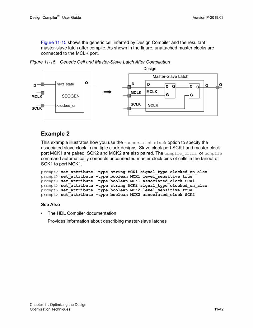
Design Compiler® User Guide P-2019.03Design Compiler® User Guide Version P-2019.03
Figure 11-15 shows the generic cell inferred by Design Compiler and the resultant master-slave latch after compile. As shown in the figure, unattached master clocks are connected to the MCLK port.
Figure 11-15 Generic Cell and Master-Slave Latch After Compilation
Example 2
This example illustrates how you use the -associated_clock option to specify the associated slave clock in multiple clock designs. Slave clock port SCK1 and master clock port MCK1 are paired; SCK2 and MCK2 are also paired. The compile_ultra or compile command automatically connects unconnected master clock pins of cells in the fanout of SCK1 to port MCK1.
prompt> set_attribute -type string MCK1 signal_type clocked_on_alsoprompt> set_attribute -type boolean MCK1 level_sensitive trueprompt> set_attribute -type boolean MCK1 associated_clock SCK1prompt> set_attribute -type string MCK2 signal_type clocked_on_alsoprompt> set_attribute -type boolean MCK2 level_sensitive trueprompt> set_attribute -type boolean MCK2 associated_clock SCK2
See Also
• The HDL Compiler documentation
Provides information about describing master-slave latches
SEQGEN
Master-Slave Latch
SCLK
D
MCLK
SCLK
D
MCLK
D D
G G
Design
Q QQnext_state
clocked_on
Q D
MCLK
SCLK
Q
Chapter 11: Optimizing the DesignOptimization Techniques 11-42

Design Compiler® User Guide Version P-2019.03
Optimizing Total Negative Slack During Placement
To control whether the tool optimizes the design for total negative slack or worst negative slack, set the following variables in Design Compiler topographical mode:
• placer_tns_driven
To optimize the design to reduce the total negative slack instead of the worst negative slack, set the placer_tns_driven variable to true before running the initial compile_ultra command. By default, the placer optimizes the worst negative slack.
• placer_tns_driven_in_incremental_compile
By default, the tool optimizes the total negative slack in the design only when the total negative slack exceeds a certain threshold. During incremental compile, to optimize the total negative slack even if the total negative slack is low, set the variable to true.
Chapter 11: Optimizing the DesignOptimization Techniques 11-43Chapter 11: Optimizing the DesignOptimization Techniques 11-43

Design Compiler® User Guide P-2019.03Design Compiler® User Guide Version P-2019.03
Chapter 11: Optimizing the DesignOptimization Techniques 11-44

12Optimizing Across Hierarchical Boundaries 12
Boundary optimization and automatic ungrouping are the strategies by which Design Compiler optimizes logic across subdesigns when the design has levels of hierarchy. Boundary optimization performs optimization across design hierarchies while retaining the levels of hierarchy and provides Design Compiler with opportunities to simplify the logic. Ungrouping removes levels of hierarchy and allows Design Compiler more freedom to share common terms in the design.
To learn how to control these optimization techniques, see the following topics:
• Boundary Optimization
• Port Punching in Design Compiler Graphical
• Port Punching and Phase Inversion With Automatic High-Fanout Synthesis
• Other Optimizations That Affect Hierarchical Boundaries
• Automatic Ungrouping
12-1

Design Compiler® User Guide P-2019.03Design Compiler® User Guide Version P-2019.03
Boundary Optimization
The compile_ultra command performs the following types of boundary optimization by default:
• Propagation of constants across the hierarchy:
• Propagation of equal and opposite information across the hierarchy:
• Propagation of unconnected port information across the hierarchy:
Without boundary optimization With boundary optimization
Without boundary optimization With boundary optimization
Without boundary optimization With boundary optimization
Chapter 12: Optimizing Across Hierarchical BoundariesBoundary Optimization 12-2

Design Compiler® User Guide Version P-2019.03
• Pushing of inverters across the hierarchy (phase inversion):
To learn how to control boundary optimization, see the following topics:
• Disabling Boundary Optimization Throughout the Design
• Disabling Boundary Optimization for a Specific Design
• Controlling Constant Propagation
• Controlling Phase Inversion
• Propagating Unconnected Registers and Unconnected Bits of Multibit Registers Across Hierarchies With Boundary Optimization Disabled
Disabling Boundary Optimization Throughout the Design
To disable all types of boundary optimization for the entire design, use either of the following commands:
• compile_ultra -no_boundary_optimization
You do not need to use the compile_preserve_subdesign_interfaces variable to disable the downward and upward propagation of constant and equal and opposite information when you use the -no_boundary_optimization option with the compile_ultra command.
In addition, when you use the compile_ultra command with the -no_boundary_optimization option, the Design Compiler tool automatically sets the -no_autoungroup option, which disables automatic ungrouping for the entire design.
• optimize_netlist -area -no_boundary_optimization
The command disables boundary optimization across the design. However, any set_boundary_optimization command settings take higher priority and are honored.
Without boundary optimization With boundary optimization
Chapter 12: Optimizing Across Hierarchical BoundariesBoundary Optimization 12-3Chapter 12: Optimizing Across Hierarchical BoundariesBoundary Optimization 12-3
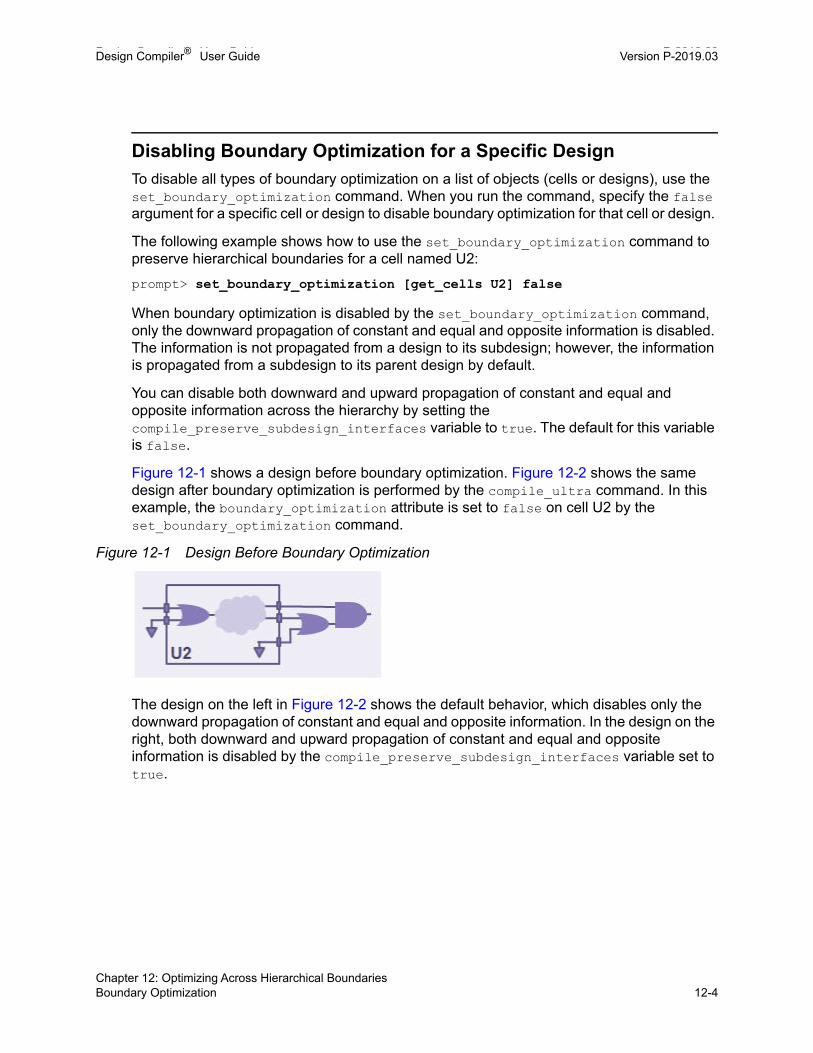
Design Compiler® User Guide P-2019.03Design Compiler® User Guide Version P-2019.03
Disabling Boundary Optimization for a Specific Design
To disable all types of boundary optimization on a list of objects (cells or designs), use the set_boundary_optimization command. When you run the command, specify the false argument for a specific cell or design to disable boundary optimization for that cell or design.
The following example shows how to use the set_boundary_optimization command to preserve hierarchical boundaries for a cell named U2:
prompt> set_boundary_optimization [get_cells U2] false
When boundary optimization is disabled by the set_boundary_optimization command, only the downward propagation of constant and equal and opposite information is disabled. The information is not propagated from a design to its subdesign; however, the information is propagated from a subdesign to its parent design by default.
You can disable both downward and upward propagation of constant and equal and opposite information across the hierarchy by setting the compile_preserve_subdesign_interfaces variable to true. The default for this variable is false.
Figure 12-1 shows a design before boundary optimization. Figure 12-2 shows the same design after boundary optimization is performed by the compile_ultra command. In this example, the boundary_optimization attribute is set to false on cell U2 by the set_boundary_optimization command.
Figure 12-1 Design Before Boundary Optimization
The design on the left in Figure 12-2 shows the default behavior, which disables only the downward propagation of constant and equal and opposite information. In the design on the right, both downward and upward propagation of constant and equal and opposite information is disabled by the compile_preserve_subdesign_interfaces variable set to true.
Chapter 12: Optimizing Across Hierarchical BoundariesBoundary Optimization 12-4

Design Compiler® User Guide Version P-2019.03
Figure 12-2 Design After Boundary Optimization With the compile_ultra Command
When you use the set_boundary_optimization command and specify the false argument, Design Compiler automatically prevents designs and cells from being ungrouped when you run the compile_ultra command.
Controlling Constant Propagation
Design Compiler automatically propagates constants, unconnected pins, and complement information when you use the compile_ultra command unless you disable boundary optimization. To learn how to control constant propagation when boundary optimization is disabled and how to disable constant propagation through specific hierarchical pins, see
• Controlling Constant Propagation When Boundary Optimization is Disabled
• Disabling Constant Propagation Through Specific Hierarchical Pins
Controlling Constant Propagation When Boundary Optimization is Disabled
Constant propagation is enabled by default even when boundary optimization is disabled. When the compile_enable_constant_propagation_with_no_boundary_opt variable is set to true (the default), constants are propagated across hierarchical boundaries even when boundary optimization is disabled. When the variable is set to true,
• The compile_ultra -no_boundary_optimization command performs constant propagation throughout the design.
• The compile_ultra command without the -no_boundary_optimization option performs constant propagation throughout the design, including the blocks that have the boundary_optimization attribute set to false on them by the set_boundary_optimization command.
To disable constant propagation along with other boundary optimizations across hierarchical boundaries, set the compile_enable_constant_propagation_with_no_boundary_opt variable to false.
compile_preserve_subdesign_interfacesset to false set to true
compile_preserve_subdesign_interfaces(default)
Chapter 12: Optimizing Across Hierarchical BoundariesBoundary Optimization 12-5Chapter 12: Optimizing Across Hierarchical BoundariesBoundary Optimization 12-5

Design Compiler® User Guide P-2019.03Design Compiler® User Guide Version P-2019.03
If you disable boundary optimization of a subdesign to perform hierarchical formal verification, and you verify the subdesign and the rest of the design separately, allowing constant propagation on the subblock could cause verification problems. You need to set the compile_enable_constant_propagation_with_no_boundary_opt variable to false to disable constant propagation along with other boundary optimizations.
Disabling Constant Propagation Through Specific Hierarchical Pins
You can prevent the propagation of constants through specific hierarchical pins by using the set_compile_directives command with the -constant_propagation option set to false for a specific hierarchical pin or a list of hierarchical pins. When you do this, Design Compiler sets a const_prop_off attribute on the specified pins and disables constant propagation through them.
Controlling Phase Inversion
You can control phase inversion, which is the moving of inverters across hierarchical boundaries during boundary optimization, by using the compile_disable_hierarchical_inverter_opt variable.
To prevent inverters from moving across hierarchical boundaries during boundary optimization, set the compile_disable_hierarchical_inverter_opt variable to true. When the variable is set to true, Design Compiler does not move inverters across hierarchical boundaries even if doing so could improve the design. The variable is set to false by default, allowing phase inversion. This variable has no effect on the design when boundary optimization is disabled.
During phase inversion, Design Compiler adds a _BAR suffix to the port name. The port_complement_naming_style variable defines the convention for renaming ports complemented as a result of boundary optimization. However, using the port_complement_naming_style variable is not recommended because it is not supported in Formality.
Chapter 12: Optimizing Across Hierarchical BoundariesBoundary Optimization 12-6
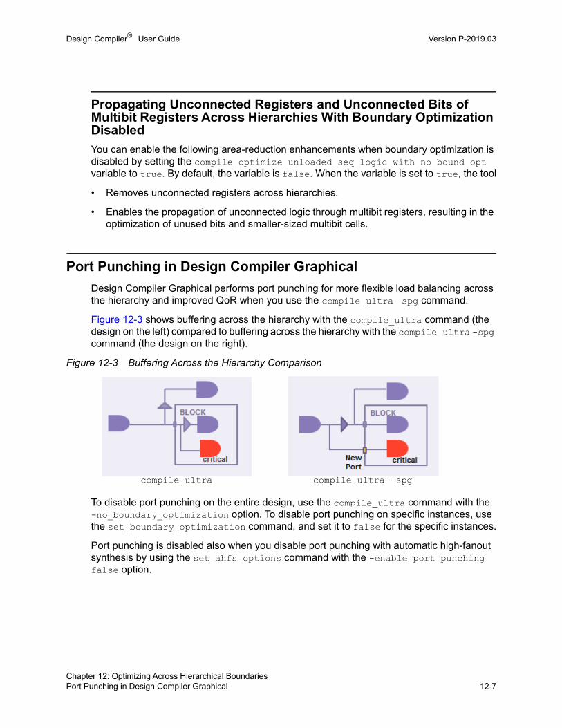
Design Compiler® User Guide Version P-2019.03
Propagating Unconnected Registers and Unconnected Bits of Multibit Registers Across Hierarchies With Boundary Optimization Disabled
You can enable the following area-reduction enhancements when boundary optimization is disabled by setting the compile_optimize_unloaded_seq_logic_with_no_bound_opt variable to true. By default, the variable is false. When the variable is set to true, the tool
• Removes unconnected registers across hierarchies.
• Enables the propagation of unconnected logic through multibit registers, resulting in the optimization of unused bits and smaller-sized multibit cells.
Port Punching in Design Compiler Graphical
Design Compiler Graphical performs port punching for more flexible load balancing across the hierarchy and improved QoR when you use the compile_ultra -spg command.
Figure 12-3 shows buffering across the hierarchy with the compile_ultra command (the design on the left) compared to buffering across the hierarchy with the compile_ultra -spg command (the design on the right).
Figure 12-3 Buffering Across the Hierarchy Comparison
To disable port punching on the entire design, use the compile_ultra command with the -no_boundary_optimization option. To disable port punching on specific instances, use the set_boundary_optimization command, and set it to false for the specific instances.
Port punching is disabled also when you disable port punching with automatic high-fanout synthesis by using the set_ahfs_options command with the -enable_port_punching false option.
compile_ultra compile_ultra -spg
Chapter 12: Optimizing Across Hierarchical BoundariesPort Punching in Design Compiler Graphical 12-7Chapter 12: Optimizing Across Hierarchical BoundariesPort Punching in Design Compiler Graphical 12-7

Design Compiler® User Guide P-2019.03Design Compiler® User Guide Version P-2019.03
Port Punching and Phase Inversion With Automatic High-Fanout Synthesis
Automatic high-fanout synthesis performs port punching and phase inversion in Design Compiler topographical mode. By default, automatic high-fanout synthesis inserts buffers or inverters across hierarchy boundaries to achieve better QoR.
Port punching in automatic high-fanout synthesis is disabled under the following conditions:
• When you disable boundary optimization by using the compile_ultra command with the -no_boundary_optimization option, Design Compiler automatically disables port punching and phase inversion for the entire design.
• When you use the set_boundary_optimization command and set it to false for specific instances, port punching and phase inversion is disabled for those instances.
• When you use the set_ahfs_options command with the -enable_port_punching option set to false, port punching is disabled during automatic high-fanout synthesis.
When you use the set_ahfs_options command with the -preserve_boundary_phase option set to true, inverters cannot move across hierarchical boundaries and the logical phase of the boundary is unchanged during automatic high-fanout synthesis.
Other Optimizations That Affect Hierarchical Boundaries
Design Compiler performs boundary optimization for nets connected to multiple ports and constant-driven ports when the advanced multiple-port net and constant-driven port fixing capability is enabled. For more information, see Fixing Nets Connected to Multiple Ports.
Hierarchical clock gating also performs optimization across hierarchical boundaries. For information, see the Power Compiler User Guide.
Automatic Ungrouping
The compile_ultra command automatically ungroups certain logical hierarchies. Ungrouping merges subdesigns of a given level of the hierarchy into the parent cell or design. It removes hierarchical boundaries and allows Design Compiler to improve timing by reducing the levels of logic and to improve area by sharing logic.
You can also manually ungroup hierarchies by using the ungroup command or the set_ungroup command followed by the compile_ultra command. For information about manually ungrouping hierarchies, see Removing Levels of Hierarchy.
Chapter 12: Optimizing Across Hierarchical BoundariesPort Punching and Phase Inversion With Automatic High-Fanout Synthesis 12-8

Design Compiler® User Guide Version P-2019.03
To lean more about automatic ungrouping, see
• Automatic Ungrouping of Hierarchies
• Automatic Ungrouping of Designs With Timing Exceptions
• Exceptions to Automatic Ungrouping
Automatic Ungrouping of Hierarchies
Figure 12-4 shows the hierarchy before and after ungrouping.
Figure 12-4 Automatic Ungrouping of Hierarchies
During optimization, Design Compiler performs the following types of automatic grouping:
• Area-based automatic ungrouping
Before initial mapping, the compile_ultra command performs area-based automatic ungrouping. The tool estimates the area for unmapped hierarchies and removes small subdesigns; the goal is to improve area and timing quality of results. Because the tool performs automatic ungrouping at an early stage, it has a better optimization context.
Before Ungrouping
After Ungrouping
Chapter 12: Optimizing Across Hierarchical BoundariesAutomatic Ungrouping 12-9Chapter 12: Optimizing Across Hierarchical BoundariesAutomatic Ungrouping 12-9

Design Compiler® User Guide P-2019.03Design Compiler® User Guide Version P-2019.03
Additionally, datapath extraction is enabled across ungrouped hierarchies. These factors improve the timing and area quality of results.
• Delay-based automatic ungrouping
During delay optimization, the compile_ultra command performs delay-based automatic ungrouping. It ungroups hierarchies along the critical path and is used essentially for timing optimization.
• QoR-based automatic ungrouping
When you use the compile_ultra command with the -spg option, Design Compiler Graphical ungroups additional hierarchies to improve QoR.
To disable automatic ungrouping on a hierarchical design and its subdesigns, use the -no_autoungroup option with the compile_ultra command. To disable automatic ungrouping on specific instances, use the set_ungroup command to set the ungroup attribute to false on specific designs, cells, or references.
See Also
• Optimization Flow
Shows how automatic ungrouping fits into the overall compile flow
Automatic Ungrouping of Designs With Timing Exceptions
When preserving timing constraints, Design Compiler reassigns the timing constraints to appropriate adjacent, persistent pins (that is, pins on the same net that remain after ungrouping). The constraints are moved forward or backward to other pins on the same net. Note that the constraints can be moved backward only if the pin driving the given hierarchical pin drives no other pin. Otherwise the constraints must be moved forward.
If the constraints are moved to a leaf cell, that cell is assigned a size_only attribute to preserve the constraints during a compile. Thus, the number of size_only cells can increase, which might limit the scope of the optimization process. To counter this effect, when both the forward and backward directions are possible, Design Compiler chooses the direction that helps limit the number of newly assigned size_only attributes to leaf cells.
You can disable this behavior by setting the auto_ungroup_preserve_constraints variable to false. The default is true.
Hierarchies are ungrouped when the following timing constraints are set on hierarchical pins:
• set_false_path
• set_multicycle_path
Chapter 12: Optimizing Across Hierarchical BoundariesAutomatic Ungrouping 12-10

Design Compiler® User Guide Version P-2019.03
• set_min_delay
• set_max_delay
• set_input_delay
• set_output_delay
• set_disable_timing
• set_rtl_load
• create_clock -period
Exceptions to Automatic Ungrouping
Hierarchies are not automatically ungrouped in the following cases:
• The hierarchy has user-specified constraints such as dont_touch, size_only, or set_ungroup attributes.
• When boundary optimization is disabled, automatic ungrouping is also disabled.
• In non-topographical mode, the wire load model for the hierarchy is different from the wire load model of the parent hierarchy.
You can override this behavior by setting the compile_auto_ungroup_override_wlm variable to true. The default is false. When the variable is set to true, the ungrouped child cells of the hierarchy inherit the wire load model of the parent hierarchy. Consequently, the child cells might have a more pessimistic wire load model.
Chapter 12: Optimizing Across Hierarchical BoundariesAutomatic Ungrouping 12-11Chapter 12: Optimizing Across Hierarchical BoundariesAutomatic Ungrouping 12-11

Design Compiler® User Guide P-2019.03Design Compiler® User Guide Version P-2019.03
Chapter 12: Optimizing Across Hierarchical BoundariesAutomatic Ungrouping 12-12

13High-Level Optimization and Datapath Optimization 13
During high-level optimization, Design Compiler performs arithmetic simplifications and resource sharing. A resource is an arithmetic or comparison operator read in as part of an HDL design. A datapath block contains one or more resources that are grouped and optimized by a datapath generator. During the high-level optimization phases, resources are allocated and shared, depending on timing and area considerations. Resource sharing enables the tool to build one hardware component for multiple operations, which typically reduces the hardware required to implement your design.
High-level optimizations are performed when you use the compile command or the compile_ultra command. The compile_ultra command explores additional optimization opportunities by performing automatic datapath extraction and advanced datapath transformations. To learn about these topics, see
• Design Compiler Arithmetic Optimization
• Synthetic Operators
• High-Level Optimizations
• Datapath Optimization
• Analyzing Datapath Extraction
• Reporting Resources and Datapath Blocks
13-1

Design Compiler® User Guide P-2019.03Design Compiler® User Guide Version P-2019.03
Design Compiler Arithmetic Optimization
Figure 13-1 shows how Design Compiler optimizes arithmetic components within the optimization flow. The shaded boxes pertain to the arithmetic optimization flow.
Figure 13-1 Optimization of Arithmetic Expressions
The steps in the Design Compiler arithmetic optimization flow are as follows:
1. When HDL Compiler elaborates a design, it maps HDL operators (either built-in operators like + and * or HDL functions and procedures) to synthetic (DesignWare) operators that appear in the generic netlist. For more information, see Synthetic Operators.
2. Design Compiler checks for any required licenses and initializes the synthetic library. For more information, see Checking DesignWare Licenses.
Area-based structuring and mapping
Timing-driven combinational optimization
Check DesignWare license
RTL
Analyze and elaborate
Datapath Synthesis interface
Datapath generator
DesignWare
Library
Design Compiler
HDL Compiler
High-level optimization
Implement synthetic parts
and initialize synthetic library
Incremental implementationselection Rest of compile
Chapter 13: High-Level Optimization and Datapath OptimizationDesign Compiler Arithmetic Optimization 13-2

Design Compiler® User Guide Version P-2019.03
3. During high-level optimization, Design Compiler manipulates the synthetic operators and applies optimizations such as arithmetic simplifications and resource sharing. See High-Level Optimizations. If you are using DC Ultra, Design Compiler performs automatic datapath extraction. For more information, see Datapath Optimization.
4. During the implement synthetic parts phase, the tool maps synthetic modules to architectural representations (implementations). For more information on synthetic parts, see the DesignWare documentation.
Design Compiler uses the datapath generator to implement arithmetic components and generate the best implementations. In addition, if you are using DC Ultra, Design Compiler performs advanced datapath transformations on the extracted datapath blocks. For more information, see Datapath Optimization.
5. During incremental implementation selection, Design Compiler explores alternative implementations for each arithmetic component. The tool evaluates and replaces synthetic implementations along the critical path to improve delay cost.
See Also
• Optimization Flow
Shows how high-level optimizations and datapath optimizations fit into the overall compile flow
Synthetic Operators
Synopsys provides a collection of intellectual property (IP), referred to as the DesignWare Building Block IP Library, to support the synthesis products. Building Block IP provides basic implementations of common arithmetic functions that can be referenced by HDL operators in your RTL source code.
The DesignWare library is built on a hierarchy of abstractions. HDL operators, either built-in operators, such as addition (+) and multiplication (*), or HDL functions and procedures, are associated with synthetic operators, which are bound in turn to synthetic modules. Each synthetic module can have multiple architectural realizations, called implementations. For example, when you use the HDL addition operator in a design description, HDL Compiler infers the need for an adder resource and puts an abstract representation of the addition operation into your circuit netlist. See Figure 13-2.
During high-level optimization, Design Compiler manipulates these synthetic operators and applies optimizations such as arithmetic transformations and resource sharing.
To display information about the standard synthetic library that is included with a Design Compiler license, use the report_synlib command:
prompt> report_synlib standard.sldb
Chapter 13: High-Level Optimization and Datapath OptimizationSynthetic Operators 13-3Chapter 13: High-Level Optimization and Datapath OptimizationSynthetic Operators 13-3

Design Compiler® User Guide P-2019.03Design Compiler® User Guide Version P-2019.03
Figure 13-2 DesignWare Overview
See Also
• The DesignWare documentation
Provides information about DesignWare synthetic operators, modules, and libraries
High-Level Optimizations
During high-level optimization, Design Compiler applies techniques such as tree delay minimization and arithmetic simplifications; it also performs resource sharing.
Tree Delay Minimization and Arithmetic Simplifications
During tree delay minimization, Design Compiler arranges the inputs to arithmetic trees. For example, the expression a + b + c + d describes three levels of cascaded addition operations. The tool can rearrange this expression to (a + b) + (c + d), which might result in faster logic (only two levels of cascaded operations).
Additional simplification is available with the compile_ultra command; some examples are as follows:
• Sink cancellation
The expression (a + b - a) is simplified to b.
• Constant folding
The expression (a * 3 * 5) is transformed to (a * 15)
HDL operator
Synthetic operator
Synthetic modules
Implementations
ADD_UNS_OP
ProprietaryRipple
X YX + Y
DW01_ADD
Chapter 13: High-Level Optimization and Datapath OptimizationHigh-Level Optimizations 13-4

Design Compiler® User Guide Version P-2019.03
Resource Sharing
Resource sharing reduces the amount of hardware needed to implement operators such as addition (+) in your Verilog or VHDL description. Without this feature, each operation is built with separate hardware. For example, every + operator builds an adder. This repetition of hardware increases the area of a design.
There are two basic types of resource sharing: Common subexpression elimination and sharing mutually exclusive operations.
To learn about resource sharing, see
• Common Subexpression Elimination
• Sharing Mutually Exclusive Operations
• Enhanced Resource Sharing
Common Subexpression Elimination
This type shares redundant computations in a design. To understand common subexpression elimination, consider Example 13-1.
Example 13-1 Original RTL
X = A > B;Y = A > B && C;
This code contains two comparators and a logical add. In common subexpression elimination, the common subexpression, A > B, is grouped and the code is transformed to Example 13-2.
Example 13-2 Expression A > B Shared
Temp = A > B;X = Temp;Y = Temp && C;
This transformation reduces the number of comparators from two to one.
Both HDL Compiler and Design Compiler perform common subexpression elimination. However, HDL Compiler does not share the +, *, and – operators by default because it might reduce the sharing options available to Design Compiler during compile. Design Compiler shares these operators and all other operators by default during timing-driven optimization.
The following operators are shared by default when Design Compiler does common subexpression elimination:
• Relational (=, <, >, <=, >=, !=)
• Shifting (<<, >>, <<<, >>>)
Chapter 13: High-Level Optimization and Datapath OptimizationHigh-Level Optimizations 13-5Chapter 13: High-Level Optimization and Datapath OptimizationHigh-Level Optimizations 13-5

Design Compiler® User Guide P-2019.03Design Compiler® User Guide Version P-2019.03
• Arithmetic (+, -, *, /, **, %)
These are selectors that drive arithmetic operators.
Additionally, if you use the compile_ultra command, the tool can identify common subexpressions automatically; you do not need to use parentheses or write them in the same order. For example, the expressions (A + B + C) and (B + A + D), A + B and B + A are recognized as a common subexpression.
Furthermore, the tool can either share common subexpressions or reverse the sharing depending on constraints. Consider the following expressions: Z1 <= A + B + C, Z2<= B + C + D, and arrival time is A < B < D < C; Figure 13-3 shows how the tool might reverse the sharing of common subexpressions depending on constraints. The tool determines whether to share or reverse the sharing of operators during a later phase—that is, during timing-driven optimization.
Figure 13-3 Sharing and Unsharing of Arithmetic Subexpressions
Sharing Mutually Exclusive Operations
This type of resource sharing shares operators in a single process when there is no execution path that reaches both operators from the start of the block to the end of the block—that is, operations that cannot be performed simultaneously are shared. To understand this type of resource sharing, consider Example 13-3.
+
A B
+
C
Z1
+
B D
+
C
Z2
+
A B D
+ +
C
Z1 Z2
Smaller Area
Better Timing
Chapter 13: High-Level Optimization and Datapath OptimizationHigh-Level Optimizations 13-6

Design Compiler® User Guide Version P-2019.03
Example 13-3 Sharing Two + Operators
module resources(A,B,C,SEL); input A,B,C;D input SEL; output [1:0] Z;
reg [1:0] Z;
always @(A or B or C or D or SEL) begin
if(SEL) Z = B + A;
else Z = C + D;
endendmodule
Example 13-3 shows code that adds either A + B or D + C; what is added depends on whether the condition SEL is true.
Without resource sharing, the tool builds two adders and one MUX, and with resource sharing, the tool uses only one adder to build the design, as shown in Figure 13-4.
Figure 13-4 Design With and Without Sharing
Similar to common subexpression sharing, the tool determines whether to share or reverse sharing depending on timing constraints. For example, when the arrival of the SEL signal is late and sharing the adder worsens timing quality of results (QoR), Design Compiler does not share the adder.
Enhanced Resource Sharing
You can perform enhanced resource sharing by using the compile_enhanced_resource_sharing variable. It is useful to enable the variable for designs that contain numerous arithmetic operators. If you set the variable to true, Design Compiler identifies more opportunities for sharing in the design, such as common
+
A B
+
C
Z
With sharing
Without sharing
+
C D
Z
SEL
A DB
SEL
Chapter 13: High-Level Optimization and Datapath OptimizationHigh-Level Optimizations 13-7Chapter 13: High-Level Optimization and Datapath OptimizationHigh-Level Optimizations 13-7

Design Compiler® User Guide P-2019.03Design Compiler® User Guide Version P-2019.03
subexpression sharing of nonidentical comparators and sharing of mutually exclusive operators that do not drive the same selector directly. By default, the compile_enhanced_resource_sharing variable is set to false.
Datapath Optimization
Datapath design is commonly used in applications that contain extensive data manipulation, such as 3-D, multimedia, and digital signal processing (DSP). DC Ultra enables datapath optimization by default when you use the compile_ultra command. Datapath optimization is comprised of two steps: Datapath extraction, which transforms arithmetic operators (for example, addition, subtraction, and multiplication) into datapath blocks, and datapath implementation, which uses a datapath generator to generate the best implementations for these extracted components.
Note: Datapath optimization requires a DC Ultra license and a DesignWare license. The DesignWare license is pulled when you run the compile_ultra command.
During datapath optimization, the tool does the following:
• Shares (or reverses the sharing) of datapath operators
• Uses the carry-save arithmetic technique
• Extracts the datapath
• Performs high-level arithmetic optimization on the extracted datapath
• Explores better solutions that might involve a different resource-sharing configuration
• Makes better tradeoffs between resource sharing and datapath optimization
For details about the datapath optimization steps, see
• Datapath Extraction
• Datapath Implementation
• Advanced Datapath Transformations
Datapath Extraction
Datapath extraction transforms arithmetic operators (for example, addition, subtraction, and multiplication) into datapath blocks to be implemented by a datapath generator. This transformation improves the quality of results (QoR) by utilizing the carry save arithmetic technique.
Chapter 13: High-Level Optimization and Datapath OptimizationDatapath Optimization 13-8

Design Compiler® User Guide Version P-2019.03
Carry save arithmetic does not fully propagate carries but instead stores results in an intermediate form. The carry-save adders are faster than the conventional carry-propagate adders because the carry-save adder delay is independent of bit-width. These adders use significantly less area than carry-propagate adders because they do not use full adders for the carry.
Example 13-4 shows the code for the expression a * b + c + d = z. Figure 13-5 shows that the conventional implementation of the expression a * b + c + d = z would use three carry-propagate adders (CPAs); whereas, the carry save technique requires only one carry-propagate adder and two carry-save adders (CSAs). Figure 13-5 also shows the timing and area numbers for both implementations.
Example 13-4 Code Example
module dp (a,b,c,d,e); input [15:0] a,b; input [31:0] c,d; output [31:0] e;
assign e = ( a * b )+ c + d;endmodule
Figure 13-5 Conventional Carry-Propagate Adder and Faster, Smaller Carry-Save Adder
X
+
+
X
+
+
a b a b
c
c
z
c
d
z
s
s
c
dCPA
CPA
CPA
CSA
CSA
CPAConventional carry-propagateadder implementation ofa * b + c + d = z
Improved carry-saveadder implementation ofa * b + c + d = z
Timing: Met
Area: 15870
Timing: -0.25 violation
Area: 24924
Chapter 13: High-Level Optimization and Datapath OptimizationDatapath Optimization 13-9Chapter 13: High-Level Optimization and Datapath OptimizationDatapath Optimization 13-9
Design Compiler® User Guide P-2019.03Design Compiler® User Guide Version P-2019.03
When DC Ultra datapath optimization is used to compile design dp in Example 13-4, the following improvements are realized:
• 8.3 percent timing improvement, compared to DC Expert results
• 36 percent area improvement, compared to DC Expert results
The DC Ultra datapath solution supports extraction of the following components:
• Arithmetic operators that can be merged into one CSA tree
• Operators extracted as part of a datapath: *, +, -, >, <, <=, >=, ==, !=, and MUXes
• Variable shift operators (<<, >>, <<<, >>> for Verilog and sll, srl, sla, sra, rol, ror for VHDL)
• Operations with bit truncation
The datapath flow can extract these components only if they are directly connected to each other—that is, no nonarithmetic logic between components. Keep the following points in mind:
• Extraction of mixed signed and unsigned operators is allowed only for adder trees
• Instantiated DesignWare components cannot be extracted
Datapath Implementation
All the synthetic operators and the extracted datapath elements are implemented by the DesignWare datapath generator in DC Ultra.
The DesignWare datapath generator uses the smart generation technology to perform the following tasks:
• Implement datapath blocks using context-driven optimizations
• Revisit high-level optimization decisions for a given timing context
• Consider logic library characteristics
For further fine tuning, the control of the smart generation strategies is available by using the Design Compiler set_dp_smartgen_options command.
See Also
• The DesignWare documentation
Provides more information about the datapath smart generation strategies
Chapter 13: High-Level Optimization and Datapath OptimizationDatapath Optimization 13-10

Design Compiler® User Guide Version P-2019.03
Advanced Datapath Transformations
DC Ultra performs advanced datapath transformations on the extracted datapath blocks, such as the following:
• Sum-of-products to Product-of-Sums
The expression (A*C + B*C) is transformed to (A + B) * C.
• Comparator sharing
Expressions such as A>B, A<B, A<=B are transformed to use single subtractors with multiple comparison outputs.
• Optimization of parallel constant multipliers
• Operand reordering
The tool can rearrange operands of multipliers or comparators to produce different quality of results (QoR).
• Explore trade-offs between common subexpression elimination (CSE) sharing and mutually exclusive operations (MUTEX) sharing. Design Compiler can undo the CSE sharing in the GTECH netlist generated by HDL Compiler to facilitate the optimum combination of CSE and MUTEX sharing.
Analyzing Datapath Extraction
To get the best QoR results from DC Ultra datapath optimization, it is important that the biggest possible datapath blocks are extracted from the RTL code. To examine how the datapath blocks will be extracted from your RTL before you run the compile_ultra command, use the analyze_datapath_extraction command. The command analyzes the arithmetic contents of the design and provides feedback so you can improve the RTL code as needed. For information about coding styles to help improve datapath extraction, see SolvNet article 015771, “Coding Guidelines for Datapath Synthesis.”
When the analyze_datapath_extraction command detects an arithmetic operator that is not extracted, it reports the information about what is blocking the datapath extraction, including the file name of the RTL and the line number of the operator it is inferred from. The following example shows an analysis report about fanout truncation that breaks the datapath block:
prompt> analyze_datapath_extractionInformation: Checking out the license 'DesignWare'. (SEC-104)Analyzing datapath extraction ...Information: Operator associated with resources 'add_440 (test.v:446)’ indesign 'test' breaks the datapath block because there is leakage due totruncation on its fanout. (HDL-120)
Chapter 13: High-Level Optimization and Datapath OptimizationAnalyzing Datapath Extraction 13-11Chapter 13: High-Level Optimization and Datapath OptimizationAnalyzing Datapath Extraction 13-11

Design Compiler® User Guide P-2019.03Design Compiler® User Guide Version P-2019.03
To generate an HTML report instead of a text-based report, specify the -html_file_name option with the analyze_datapath_extraction command. The HTML report provides direct links to the RTL file. Figure 13-6 shows an excerpt from an HTML report. You can open the test.v file shown in the figure by clicking the test.v link. The number after the test.v file name refers to the line number in the file.
Figure 13-6 Datapath Report in HTML Format
In the GUI, you can cross-probe from the datapath extraction report to the RTL file in the RTL browser to inspect the RTL and determine if any changes are needed. For more information about cross-probing, see the Design Vision Help.
To disable the automatic ungrouping of hierarchies during analysis, use the -no_autoungroup option. This ensures that all hierarchies are preserved unless otherwise specified. The -no_autoungroup option behavior is the same in the analyze_datapath_extraction command as it is in the compile_ultra command. If you plan to specify the -no_autoungroup option with the compile_ultra command, you should also specify it with the analyze_datapath_extraction command.
To filter messages in the datapath extraction report, use the -filter_msg option. Messages with severity levels less than or equal to the specified level are filtered out. For example, the following command filters out the analyze_datapath_extraction command warnings that have a priority of medium or lower, and only warnings that have a high priority are displayed:
prompt> analyze_datapath_extraction –filter_msg medium
To sort the warning messages for each subdesign from high-to-low priority, use the -sort_msg option. Warnings that point to datapath leakage and unsigned subtraction, such as the HDL-120 and HDL-132 warnings, have a higher priority. This option also provides a high-level summary of the high-priority warnings issued for each subdesign.
As the following example shows, the tool provides a high-level summary of leakage warnings followed by the actual warnings for each subdesign:
prompt> analyze_datapath_extraction –sort_msg *********************************************Leakage detections on design DW_mult_add********************************************* Msg type | Msg count | Max lkg width | Avg. lkg width--------------------------------------------------------------- HDL-120 3 35 19---------------------------------------------------------------***Sorted leakage messages...
Chapter 13: High-Level Optimization and Datapath OptimizationAnalyzing Datapath Extraction 13-12

Design Compiler® User Guide Version P-2019.03
For more information about datapath leakage, including examples showing how leakage occurs, see SolvNet article 015771, “Coding Guidelines for Datapath Synthesis,” the analyze_datapath_extraction man page, and the HDL-120 and HDL-132 message man pages.
To specify the maximum number of leakage detection messages (HDL-120 and HDL-132) to display for each design, use the -max_msgs option. The -sort_msg option is enabled automatically when you use the -max_msgs option. This ensures that only the top leakage messages are reported.
For large designs, analyzing one or more subdesigns can be useful. You can perform hierarchical analysis on specified designs by using the get_designs command with the analyze_datapath_extraction command:
prompt> analyze_datapath_extraction [get_designs design_list]
The analyze_datapath_extraction command generates separate reports for each specified design.
After the analysis, a report shows the contained resources in the design. This report helps to find the resources in the design source code. Note that the datapath names in this report might differ from the datapath names in the report generated using the report_resources command after compilation. However, the names of the contained resources will be the same.
For information about interpreting the resource report, see Reporting Resources and Datapath Blocks.
Reporting Resources and Datapath Blocks
To generate a report that lists the resources and datapath blocks used in a design during compilation, run the report_resources command. By default, the command returns a report for the current design; however, you can specify a particular design or a list of designs by using the design_list argument.
To understand the report_resources report, consider the code in Example 13-5.
Example 13-5 RTL for Datapath Module
module datapath (a, b, c, d, sel, z1, z2);input [7:0] a, b, c, d;input sel;output [15:0] z1, z2;wire [15:0] prod = sel? a * b : a * c;assign z1 = prod + d;assign z2 = c * d;endmodule
Chapter 13: High-Level Optimization and Datapath OptimizationReporting Resources and Datapath Blocks 13-13Chapter 13: High-Level Optimization and Datapath OptimizationReporting Resources and Datapath Blocks 13-13

Design Compiler® User Guide P-2019.03Design Compiler® User Guide Version P-2019.03
When this code is compiled, the report_resources command generates the report shown in Example 13-6.
Example 13-6 Datapath Report for Design Datapath Generated by the report_resources Command
****************************************Report : resourcesDesign : test...****************************************
Resource Report for this hierarchy in file /usr/.../test.v=============================================================================| Cell | Module | Parameters | Contained Operations |=============================================================================| mult_x_1 | DW_mult_uns | a_width=8 | mult_7 (test.v:7) || | | b_width=8 | || DP_OP_11J1_124_796 | | || | DP_OP_11J1_124_796 | | |=============================================================================
Datapath Report for DP_OP_11J1_124_796==============================================================================| Cell | Contained Operations |==============================================================================| DP_OP_11J1_124_796 | mult_5 (test.v:5) mult_5_2 (test.v:5) || | add_6 (test.v:6) |==============================================================================
==============================================================================| | | Data | | || Var | Type | Class | Width | Expression |==============================================================================| I1 | PI | Unsigned | 8 | || I2 | PI | Unsigned | 8 | || I3 | PI | Unsigned | 8 | || T5 | IFO | Unsigned | 16 | I1 * I2 (test.v:5) || O1 | PO | Unsigned | 16 | T5 + I3 (test.v:6) |==============================================================================
Implementation Report===============================================================================| | | Current | Set || Cell | Module | Implementation | Implementation |===============================================================================| mult_x_1 | DW_mult_uns | apparch (area) | || DP_OP_11J1_124_796 | DP_OP_11J1_124_796 | str (area) | |===============================================================================No multiplexors to report1
Chapter 13: High-Level Optimization and Datapath OptimizationReporting Resources and Datapath Blocks 13-14

Design Compiler® User Guide Version P-2019.03
The report_resources report consists of the following reports:
• Resource report
The Resource report shows arithmetic operators that are mapped to individual DesignWare components. The report example shows that a mult_x_7_1 multiplier cell is mapped to a DW_mult_uns unsigned DesignWare multiplier.
• Datapath report
The Datapath report shows arithmetic operators that are merged into a single datapath block by datapath extraction. The report example shows that the operators are merged into a single datapath cell, DP_OP_11J1_124_796. The contained operations show the list of operations that are contained in each cell. Note that the _5 suffix in the operation names represents the line number in the RTL code in Example 13-5. If more than one operator appears in a line, it is reflected in the suffix. Two operators appear in line 5 in Example 13-5; therefore, the second multiplier is identified in the report with a _5_2 suffix.
The Datapath report table shows the input (PI) and output (PO) ports of the datapath cell. It also shows the datapath expression with the intermediate fanout (IFO) and its data class. Note that the expression in this report is just a functional representation of each datapath block. The data class shows whether the signal should be zero extended (unsigned) or sign extended (signed) in computation when the signal is used for subsequent operations. The report does not describe the actual internal implementation of the block.
• Implementation report
The Implementation report shows the implementation of each DesignWare block. The report includes the implementation name and the optimization mode that is used to implement each DesignWare cell. The implementation report is generated for both detected DesignWare cells and ungrouped DesignWare cells.
• Datapath Extraction report
The Datapath Extraction report shows arithmetic operators that block datapath extraction. When the report_resources command detects operators that block datapath extraction, the tool reports the following messages in the Datapath Extraction report, depending on the issue:
❍ HDL-120: Datapath leakage blocks the datapath extraction
❍ HDL-125: Instantiated DesignWare component cannot be extracted
❍ HDL-132: Mixed-signal data type blocks the datapath abstraction
Chapter 13: High-Level Optimization and Datapath OptimizationReporting Resources and Datapath Blocks 13-15Chapter 13: High-Level Optimization and Datapath OptimizationReporting Resources and Datapath Blocks 13-15

Design Compiler® User Guide P-2019.03Design Compiler® User Guide Version P-2019.03
For example,
Datapath Extraction ReportInformation: The output of subtractor associated with resources 'sub_388 (test.v:388)' is treated as signed signal. (HDL-132)
To generate an HTML report instead of a text-based report, specify the -html_file_name option with the report_resources command. The HTML report provides direct links to the RTL file. For example, you can open the test.v file shown in Figure 13-7 by clicking the test.v link. The number after the test.v file name refers to the line number in the file.
In the GUI, you can cross-probe from the design resources report to the RTL file in the RTL browser to inspect the RTL and determine if any changes are needed. Similarly, you can cross-probe from the RTL file to the design resources report. For more information about cross-probing, see the Design Vision Help.
In Figure 13-7, the Resource report shows that the mult_x_1 cell is inferred from line 7 in the test.v file. The Datapath report shows that the DP_OP_11J1_124_796 datapath cell has operators inferred from lines 5 and 6 in the test.v file.
Figure 13-7 Resource and Datapath Report in HTML Format. . .
. . .
Line numberFile
Chapter 13: High-Level Optimization and Datapath OptimizationReporting Resources and Datapath Blocks 13-16

14Multiplexer Mapping and Optimization 14
Design Compiler can map combinational logic representing multiplexers in the HDL code directly to a single multiplexer (MUX) or a tree of multiplexer cells from the target logic library. Before you read further, see Optimization Flow to understand how multiplexer mapping and optimization fit into the overall compile flow.
Multiplexers are commonly modeled with if and case statements. To implement this logic, HDL Compiler uses SELECT_OP cells, which Design Compiler maps to combinational logic or multiplexers in the logic library. If you want Design Compiler to preferentially map multiplexing logic to multiplexers—or multiplexer trees—in your logic library, you must infer MUX_OP cells.
The MUX_OP cell should be inferred when you want Design Compiler to build a multiplexer tree structure for the case statement blocks in your HDL. MUXs can be implemented efficiently (in speed and area) in the library. This type of structure can provide advantages in circuit performance and savings in wiring area, compared to implementation constructed from random logic. This feature is supported only with the use of the case statement in VHDL or Verilog code.
During compilation, Design Compiler replaces each MUX_OP cell with the best multiplexer tree implementation of the N-input M-output multiplexer. The implementation depends on the constraints given for the design and the arrival times of the selector inputs.
To learn about multiplexer mapping and optimization, see
• Inferring SELECT_OPs
• Inferring MUX_OPs
14-1

Design Compiler® User Guide P-2019.03Design Compiler® User Guide Version P-2019.03
• Library Cell Requirements for Multiplexer Optimization
• Mapping Multiplexers on Asynchronous Signal Lines
• Mapping to One-Hot Multiplexers
Chapter 14: Multiplexer Mapping and Optimization14-2

Design Compiler® User Guide Version P-2019.03
Inferring SELECT_OPs
By default, HDL Compiler uses SELECT_OP components to implement conditional operations implied by if and case statements. An example of a SELECT_OP cell implementation for an 8-bit data signal is shown in Figure 14-1.
Figure 14-1 SELECT_OP Implementation for an 8-bit Data Signal
SELECT_OPs behave like one-hot multiplexers; the control lines are mutually exclusive, and each control input allows the data on the corresponding data input to pass to the output of the cell. To determine which data signal is chosen, HDL Compiler generates selection logic, as shown in Figure 14-2.
output
For an 8-bit data signal, 8 selection bits are needed.This is called a one-hot implementation.
data signals
select signals
CONTROL1_0
CONTROL4_0
CONTROL5_0
CONTROL3_0
CONTROL2_0
CONTROL6_0
CONTROL7_0
CONTROL8_0
DATA1_0
DATA1_0
DATA1_0
DATA1_0
DATA1_0
DATA1_0
DATA1_0
DATA1_0
Z_0
Chapter 14: Multiplexer Mapping and OptimizationInferring SELECT_OPs 14-3Chapter 14: Multiplexer Mapping and OptimizationInferring SELECT_OPs 14-3

Design Compiler® User Guide P-2019.03Design Compiler® User Guide Version P-2019.03
Figure 14-2 Verilog Output—SELECT_OP and Selection Logic
Depending on the design constraints, Design Compiler implements the SELECT_OP with either combinational logic or multiplexer cells from the logic library. For more information on SELECT_OP inference, see the HDL Compiler documentation.
Inferring MUX_OPs
If you want Design Compiler to preferentially map multiplexing logic in your RTL to multiplexers—or multiplexer trees—in your logic library, you need to infer MUX_OP cells. These cells are hierarchical generic cells optimized to use the minimum number of select signals. They are typically faster than the SELECT_OP cell, which uses a one-hot implementation. Although MUX_OP cells improve design speed, they also might increase area. During optimization, Design Compiler preferentially maps MUX_OP cells to multiplexers—or multiplexer trees—from the logic library, unless the area costs are prohibitive, in which case combinational logic is used.
You can embed an attribute or directive in the HDL code or use variables to tell HDL Compiler which part of the HDL description to implement as a single multiplexer or a tree of multiplexers. When the HDL is read in, a generic cell called MUX_OP cell represents the multiplexer functionality. During optimization, Design Compiler maps the logic inside the MUX_OP cell to an implementation, using multiplexer cells from the library.
The MUX_OP cell is a generic representation of an N:1 multiplexer with M output bits. When VHDL or Verilog code is read in, the resulting design contains a MUX_OP cell for every case block inside a process that contains the infer_mux directive. A MUX_OP cell also is inferred for each signal (including bused signals) assigned inside the same case block. The signals in the HDL that compute the selector are connected to the select inputs of the MUX_OP cell. Figure 14-3 shows a generic MUX_OP cell for an 8-bit data signal.
Selection logicSelect signals
Data signals Output
SELECT_OP
Chapter 14: Multiplexer Mapping and OptimizationInferring MUX_OPs 14-4

Design Compiler® User Guide Version P-2019.03
Figure 14-3 MUX_OP Generic Cell for an 8-bit Data Signal
The MUX_OP cell contains internal selection logic to determine which data signal is chosen; HDL Compiler does not need to generate any selection logic, as shown in Figure 14-4.
Figure 14-4 HDL Compiler Output—MUX_OP Generic Cell for 8-Bit Data
The naming convention for MUX_OP cells in a design is
_MUX_OP_N_S_M
data signals
select signals
For an 8-bit word, only 3 selection bitsare needed.
S2
S1
S0
DATA1_0
DATA3_0
DATA5_0
DATA6_0
DATA7_0
DATA8_0
DATA4_0
DATA2_0Z_0
Select signalsMUX_OP
Data signals Output
Chapter 14: Multiplexer Mapping and OptimizationInferring MUX_OPs 14-5Chapter 14: Multiplexer Mapping and OptimizationInferring MUX_OPs 14-5

Design Compiler® User Guide P-2019.03Design Compiler® User Guide Version P-2019.03
Because the MUX_OP cell is implemented as a level of hierarchy, certain types of logic sharing that might otherwise take place are no longer possible. In some cases, this can lead to a design that is less suitable than one having no MUX_OP cells.
The MUX_OP feature enables you to direct Design Compiler to generate a MUX tree structure for a given case statement when you already know that a MUX tree is the best representation for that statement. Design Compiler optimizes the tree based on constraints and yields the best-possible MUX tree.
To generate MUX_OP cells for a specific case or if statement, use the infer_mux directive in the HDL description as shown in Example 14-1. For more information on this directive and inference limitations, see the HDL Compiler documentation.
Example 14-1 Using the infer_mux directive in the HDL Description
always@(SEL) begin case (SEL) // synopsys infer_mux 2’b00: DOUT <= DIN[0]; 2’b01: DOUT <= DIN[1]; 2’b10: DOUT <= DIN[2]; 2’b11: DOUT <= DIN[3]; endcase
Observe the following when you use MUX_OP cells:
• Do not set the HDL Compiler variable hdlin_infer_mux to all when you compile. Setting this variable to all results in implementing MUX_OP cells for every case statement in your HDL. MUX_OP cells should be inferred for case statements that can benefit most from a multiplexer tree structure.
• Incompletely specified case statements can result in MUX_OP cells with unused inputs or a partially collapsed multiplexer tree structure. In such cases, the difference between using a MUX_OP cell and implementing the multiplexer with random logic might not be significant.
• In general, most gains are realized when you use a MUX_OP cell for fully specified case statements that implement large multiplexer logic. If your design uses mostly small (2:1 or 4:1) multiplexers, you might get better results by not using MUX_OP cells.
Argument Description
N The number of data inputs.
S The number of select inputs.
M The width of the output signal.
Chapter 14: Multiplexer Mapping and OptimizationInferring MUX_OPs 14-6

Design Compiler® User Guide Version P-2019.03
• To ensure that MUX_OP cells are mapped to MUX technology cells, you must apply a size_only attribute to the cells to prevent logic decomposition during the optimization steps. You can set the size_only attribute on each MUX_OP manually or allow HDL Compiler to set it automatically when reading the RTL. You can control the automatic behavior by using the hdlin_mux_size_only variable. For more information about the hdlin_mux_size_only variable, see the HDL Compiler documentation.
See Also
• Mapping to One-Hot Multiplexers
Provides information about recognizing and mapping to one-hot multiplexers
Library Cell Requirements for Multiplexer Optimization
The multiplexer optimization requires the presence of at least a 2:1 multiplexer cell in the logic library. The inputs or outputs of this cell can be inverted. If a 2:1 multiplexer primitive cell does not exist in the library, you see the following warning message:
Warning: Target library does not contain any 2-1 multiplexer. (OPT-853)
An implementation of the MUX_OP cell from the target library is created, but it might not be the best implementation possible. All multiplexer cells in the target library can be used to construct the implementation of the MUX_OP cell except
• Enabled multiplexer cells
• Bused output multiplexer
• Multiplexers larger than 32 : 1
For Design Compiler to make the best use of the multiplexer cells available in your logic library, recompile the library or obtain a library compiled with version V3.4a or later from your ASIC vendor.
Mapping Multiplexers on Asynchronous Signal Lines
Design Compiler can map MUX_OP cells and two-input SELECT_OP cells on asynchronous set and reset signals and clock signals to MUX cells, reducing glitches on asynchronous register pins. By default, the compile or compile_ultra commands preserve multiplexers in the fanin cone of asynchronous register pins. Specifically, if Design Compiler finds multiplexing logic (any MUX_OP or two-input SELECT_OP cell) in the fanin of only asynchronous register pins (clock or asynchronous set and reset pins), the
Chapter 14: Multiplexer Mapping and OptimizationLibrary Cell Requirements for Multiplexer Optimization 14-7Chapter 14: Multiplexer Mapping and OptimizationLibrary Cell Requirements for Multiplexer Optimization 14-7

Design Compiler® User Guide P-2019.03Design Compiler® User Guide Version P-2019.03
multiplexing logic is mapped to a multiplexer and a size_only attribute is applied to the multiplexer. To turn this capability off, set the compile_enable_async_mux_mapping variable to false.
You do not need to set the size_only attribute, either manually or with the hdlin_mux_size_only variable. Design Compiler sets the size_only attribute automatically.
If the MUX_OP or SELECT_OP cell is specified as dont_touch, Design Compiler does not map the cell to a multiplexer.
Mapping to One-Hot Multiplexers
Design Compiler also supports inference and mapping of one-hot multiplexers as described in the following topics:
• Inferring One-Hot Multiplexers
• Library Requirements for One-Hot Multiplexers
• Optimization of One-Hot Multiplexers
Inferring One-Hot Multiplexers
A one-hot multiplexer is a library cell that behaves functionally as an AND/OR gate such as an AO22 or AO222. The difference is that in case of a one-hot MUX, there are as many control inputs as data inputs and the function of the cell ANDs each control input with the corresponding data input. For example, a 4-to-1 one-hot MUX has the following function:
Z = (D_0 & C_0) | (D_1 & C_1) | (D_2 & C_2) | (D_3 & C_3)
One-hot MUXes are generally implemented using passgates, which makes them very fast and allows their speed to be largely independent of the number of data bits being multiplexed. However, this implementation requires that exactly one control input be active at a time. If no control inputs are active, the output remains floating. If more than one control input is active, there could be an internal drive fight.
Design Compiler allows you to control one-hot MUX inference and mapping. Because of the restriction on the control inputs of a one-hot MUX (that is, one control input is active at all times), Design Compiler cannot automatically make use of these gates. The tool cannot verify that the control inputs behave as required. Therefore, it does not automatically map to these cells. Instead, it maps only to cells that you specify can be mapped. Also, after the tool maps these cells, they cannot be unmapped. The cells can only be sized.
Example 14-2 and Example 14-3 show the coding styles that are supported.
Chapter 14: Multiplexer Mapping and OptimizationMapping to One-Hot Multiplexers 14-8

Design Compiler® User Guide Version P-2019.03
Example 14-2 Supported Coding Style Example
case (1'b1) //synopsys full_case parallel_case infer_onehot_muxsel1 : out = in1;sel2 : out = in2;sel3 : out = in3;
Example 14-3 Supported Coding Style Example
case({sel3, sel2, sel1}) //synopsys full_case parallel_case infer_onehot_mux001: out = in1;010: out = in2;100: out = in3;
Note: The parallel_case and full_case directives are required. The infer_onehot_mux directive is supported only in Verilog and SystemVerilog.
See Also
• The HDL Compiler documentation
Provides information about coding styles and directives
Library Requirements for One-Hot Multiplexers
Design Compiler can recognize and map to a one-hot MUX cell in the target library only if the one-hot MUX cell meets with all of the following requirements:
• It is a single-output cell.
• Its inputs can be divided into two disjoint sets of the same size as follows:
C={C_1, C_2, ..., C_n} and D={D_1, D_2, ..., D_n}
where n is greater than 1 and is the size of the set. Actual names of the inputs can be different from the connotation shown.
• The contention_condition attribute must be set on the cell. The value of the attribute is a combinational function, FC, of inputs in set C that defines prohibited combinations of inputs as shown in the following examples (where the size n of the set is 3):
FC = C_0' & C_1' & C_2' | C_0 & C_1 | C_0 & C_2 | C_1 & C_2
or
FC = (C_0 & C_1' & C_2' | C_0' & C_1 & C_2' | C_0' & C_1' & C_2)'
Chapter 14: Multiplexer Mapping and OptimizationMapping to One-Hot Multiplexers 14-9Chapter 14: Multiplexer Mapping and OptimizationMapping to One-Hot Multiplexers 14-9

Design Compiler® User Guide P-2019.03Design Compiler® User Guide Version P-2019.03
• The cell must have a combinational function FO defined on the output with respect to all its inputs. This function FO must logically define, together with the contention condition, a base function F* that is the sum of n product terms, where the ith term contains all the inputs in C, with C_i high and all others low and exclusively one input in D. Examples of the defined function are as follows (for n = 3):
F* = C_0 & C_1' & C_2' & D_0 | C_0' & C_1 & C_2' & D_1 | C_0' & C_1' &C_2 & D_2'
or
F* = C_0 & C_1' & C_2' & D_0' + C_0' & C_1 & C_2' & D_1' + C_0' & C_1'& C_2 & D_2'
The function FO itself can take many forms, as long as it satisfies the following condition:
FO & FC' == F*
That is, when FO is restricted by FC', it should be equivalent to F*. The term FO = F* is acceptable; other examples are as follows (for n = 3):
FO = (D_0 & C_0) | (D_1 & C_1) | (D_2 & C_2)
or
FO = (D_0' & C_0) | (D_1' & C_1) | (D_2' & C_2)
Note that when FO is restricted by FC, inverting all inputs in D is equivalent to inverting the output; however inverting only a subset of D would yield an incompatible function. Although Design Compiler supports any form of FO that satisfies the condition FO & FC' == F*, it is recommended that you use a simple form (such as those described previously or F*).
An example of a properly specified cell is as follows. For more information on cell definition, see the Library Compiler documentation.
Example 14-4 One-hot MUX Cell Definition
cell(OHMUX2) {... ...contention_condition : "(C0 C1 + C0' C1')";... ...pin(D0) {direction : input;... ...}pin(D1) {direction : input;... ...}pin(C0) {direction : input;
Chapter 14: Multiplexer Mapping and OptimizationMapping to One-Hot Multiplexers 14-10

Design Compiler® User Guide Version P-2019.03
... ...}pin(C1) {direction : input;... ...}pin(Z) {direction : output;function : "(C0 D0 + C1 D1)";... ...}}
Optimization of One-Hot Multiplexers
Because a one-hot MUX implementation requires that exactly one control input be active at a time, composition is not supported. Composition of larger cells from smaller ones requires extra logic to ensure that exactly one control input is active at any time, which is inconsistent with the intention of the use of one-hot MUXes; in addition, the implementation of composition also depends on the actual electronic structure of the library cells.
However, if Design Compiler does not find an exact match in the library, it generates a warning message and maps an RTL MUX to a larger MUX—that is, more inputs—from the library and tie the additional inputs to ground. If the RTL one-hot MUX cannot fit into the largest one-hot MUX cell from the target library, the tool does not perform one-hot MUX mapping and issues a warning message. The MUX in this case is mapped the normal way.
Chapter 14: Multiplexer Mapping and OptimizationMapping to One-Hot Multiplexers 14-11Chapter 14: Multiplexer Mapping and OptimizationMapping to One-Hot Multiplexers 14-11

Design Compiler® User Guide P-2019.03Design Compiler® User Guide Version P-2019.03
Chapter 14: Multiplexer Mapping and OptimizationMapping to One-Hot Multiplexers 14-12

15Sequential Mapping 15
Sequential mapping phase consists of two steps: register inferencing and technology mapping. Synopsys uses the term register for both edge-triggered registers and level-sensitive latches. Before you read further, see Optimization Flow to understand how sequential mapping fits into the overall compile flow.
Register inferencing is the process by which the RTL description of a register is translated into a technology-independent representation called a SEQGEN. SEQGENs are created during elaboration and are usually mapped to flip-flops during compile. Technology mapping is the process by which a SEQGEN is mapped to gates from a specified target logic library. It is performed when you use the compile_ultra or compile command.
To learn about register inferencing and technology mapping, see
• Register Inference
• Directing Register Mapping
• Specifying the Default Flip-Flop or Latch
• Reporting Register Types
• Unmapped Registers in a Compiled Design
• Automatically Removing Unnecessary Registers
• Merging Equal and Opposite Registers
• Inverting the Output Phase of Sequential Elements
15-1
Design Compiler® User Guide P-2019.03Design Compiler® User Guide Version P-2019.03
• Mapping to Falling-Edge Flip-Flops
• Resizing Black Box Registers
• Preventing the Exchange of the Clock and Clock Enable Pin Connections
• Mapping to Registers With Synchronous Reset or Preset Pins
• Performing a Test-Ready Compile
• Using Register Replication
Chapter 15: Sequential Mapping15-2

Design Compiler® User Guide Version P-2019.03
Register Inference
When HDL Compiler reads in a Verilog or VHDL RTL description of the design, it translates the design into a technology-independent representation (GTECH). In GTECH, both registers and latches are represented by a SEQGEN cell, which is a technology-independent model of a sequential element as shown in Figure 15-1. SEQGEN cells have all the possible control and data pins that can be present on a sequential element.
Figure 15-1 Generic SEQGEN Cell
Table 15-1 lists the pins of a SEQGEN cell. Only a subset of these pins is used depending on the type of cell that is inferred. Unused pins are tied to zero.
Table 15-1 Pins of a SEQGEN Cell
Direction Pin name Function name and description Cell type
Input clear Asynchronous clear(level-sensitive reset)
flip-flop or latch
preset Asynchronous preset(level-sensitive set)
flip-flop or latch
enable Asynchronous load(level-sensitive load of data_in)
flip-flop1 or latch
data_in Asynchronous data(loaded when enable==1)
flip-flop1 or latch
Q
QN
synch_preset
synch_toggle
next_state
clocked_on
synch_enable
data_in
enable
clear
preset
synch_clear
Chapter 15: Sequential MappingRegister Inference 15-3Chapter 15: Sequential MappingRegister Inference 15-3

Design Compiler® User Guide P-2019.03Design Compiler® User Guide Version P-2019.03
Incorrect register inferencing results in incorrect technology mapping. One way to examine the type of register inferred is to examine the register inference reports in HDL Compiler. Set the following variable in HDL Compiler to generate additional information on inferred registers:
prompt> set_app_var hdlin_reporting_level verbose
Example 15-1 shows an HDL Compiler inference report for a D flip-flop with a synchronous preset control.
Example 15-1 Inference Report
========================================================================|Register Name | Type |Width | Bus | MB | AR | AS | SR | SS | ST |========================================================================| Q_reg | Flip-flop | 1 | N | N | N | N | N | Y | N |========================================================================Sequential Cell (Q_reg)Cell Type: Flip-FlopMultibit Attribute: NClock: CLK
clocked_on Synchronous clock(rising edge-triggered clock)
flip-flop
next_state Synchronous data(loaded at clocked_on edge)
flip-flop
synch_enable Synchronous load(load next_state at clocked_on edge)
flip-flop
synch_clear Synchronous clear(reset at clocked_on edge)
flip-flop
synch_preset Synchronous preset(set at clocked_on edge)
flip-flop
synch_toggle Synchronous toggle(toggle at clocked_on edge)
flip-flop
Output Q non-inverting output flip-flop or latch
QN inverting output flip-flop or latch
1. For register cells, the enable and data_in signals can specify synchronous reset or preset functionality when the hdlin_ff_always_async_set_reset variable is set to false.
Table 15-1 Pins of a SEQGEN Cell (Continued)
Direction Pin name Function name and description Cell type
Chapter 15: Sequential MappingRegister Inference 15-4

Design Compiler® User Guide Version P-2019.03
Async Clear: 0Async Set: 0Async Load: 0Sync Clear: 0Sync Set: SETSync Toggle: 0Sync Load: 1
The inference report can help troubleshoot issues by indicating the type of register inferred (latch or flip-flop, single or multibit) and the control signals inferred for that register. The report shows the names of the nets connecting the pins on the SEQGEN elements in GTECH. In most cases, these control pins are tied to zero (inactive). If you are attempting to infer a synchronous or asynchronous reset or preset and it does not correctly appear in the inference report, check for issues in the specification of the register at the RTL level.
Correct inferencing of synchronous and asynchronous reset or preset control signals in the RTL results in connections to the synch_preset, synch_clear, preset, and clear pins on the SEQGEN GTECH cell. During technology mapping, Design Compiler uses the SEQGEN as the starting point for mapping. The sequential mapper checks the connections to the pins and the information present in the library cell descriptions when it maps to a logic library register.
Incorrect register inferencing or incomplete library information can produce unexpected results in mapping to the reset or preset pins of the register.
Design Compiler does not infer synchronous resets by default. To indicate to the tool which signals should be treated as synchronous resets, use the sync_set_reset Synopsys compiler directive in Verilog source files or the corresponding sync_set_reset Synopsys attribute in VHDL source files. HDL Compiler then connects these signals to the synch_clear and synch_preset pins on the SEQGEN in order to communicate to the mapper that these are the synchronous control signals and they should be kept as close to the register as possible. For information about inference of these signals, see the HDL Compiler documentation. For information about how Design Compiler maps these signals, see “Mapping to Registers With Synchronous Reset or Preset Pins” on page 15-17.
The correct mapping of asynchronous reset or preset registers requires that these registers be correctly described in the RTL and that corresponding cells exist in the logic library. As long as you follow the recommended coding guidelines for coding asynchronous registers, no special compiler directives are needed in order to infer asynchronous set or reset signals. For more information on inference of these signals, see the HDL Compiler documentation.
Directing Register Mapping
You can control register mapping in the following ways:
• Use the set_register_type command.
Chapter 15: Sequential MappingDirecting Register Mapping 15-5Chapter 15: Sequential MappingDirecting Register Mapping 15-5

Design Compiler® User Guide P-2019.03Design Compiler® User Guide Version P-2019.03
For more information, see Specifying the Default Flip-Flop or Latch.
• Use exact mapping with the -exact_map option.
Use the -exact_map option with the compile_ultra or compile command to restrict the mapping to sequential cells with simple behavior (synchronous set and reset, synchronous toggle, synchronous enable, asynchronous set and reset, and asynchronous load and data). When you use the -exact_map option, sequential mapping does not try to encapsulate combinational logic originally outside the generic sequential element (SEQGEN) into the sequential cell.
• Use test-ready compile with the compile_ultra -scan or compile -scan command.
For more information, see Performing a Test-Ready Compile.
Specifying the Default Flip-Flop or Latch
The set_register_type command specifies the default flip-flop or latch library cell type for some or all registers in the current design or current instance. A flip-flop type is represented by an example flip-flop; any flip-flop that has the same sequential characteristics as the specified flip-flop is considered to be of that type.
Use the set_register_type command to direct Design Compiler to infer a particular flip-flop or latch.
Note: This mechanism for directing register types is not needed if you write the HDL to directly infer the correct register type.
You can specify a latch, a flip-flop, or both.
To set the default flip-flop type to FFX and the default latch type to LTCHZ, enter
prompt> set_register_type -flip_flop FFX -latch LTCHZ
Specifying a Constant Value for Disabled Registers
If your design has registers that are never enabled, the tool assumes that the disabled register is a constant (either 0 or 1) register when it performs optimization. You can specify a constant value for a disabled register as an initial state by using the set_uninitialized_register_value command. The constant value can either be 0 or 1. After you specify the constant value, as shown in the following example, the tool optimizes the register and the logic connected to the register using the value you specified.
dc_shell> set_uninitialized_register_value u1/reg[0] -value 0
Chapter 15: Sequential MappingSpecifying the Default Flip-Flop or Latch 15-6

Design Compiler® User Guide Version P-2019.03
In this example, the command sets the value of the u1/reg[0] register to 0. The tool uses this value to optimize the register and the logic connected to the register.
If you use the set_uninitialized_register_value command on a register whose enable input is not disabled, the tool ignores the command and does not issue any warning message.
Reporting Register Types
To learn how to report the current default register type specification for the design and for cells, see
• Reporting the Register Type Specifications for the Design
• Reporting the Register Type Specifications for Cells
Reporting the Register Type Specifications for the Design
To list the current default register type specifications, use the report_design command:
prompt> report_design
****************************************Report : designDesign : DESIGNVersion: ...Date : ...****************************************. . .Flip-Flop Types: Default: FFX, FFXHP, FFXLP
Reporting the Register Type Specifications for Cells
To lists the current register type specifications for cells, use the report_cell and all_registers commands.
The following example shows a report:
****************************************Report : cellDesign : reg_typeVersion: ...Date : ...**************************************** Attributes:
Chapter 15: Sequential MappingReporting Register Types 15-7Chapter 15: Sequential MappingReporting Register Types 15-7

Design Compiler® User Guide P-2019.03Design Compiler® User Guide Version P-2019.03
n - noncombinational... Cell Reference Library Area Attributes----------------------------------------------------------ffa FFY MY_LIB 9.00 1,nffb FFY MY_LIB 9.00 1,nffc FFY MY_LIB 9.00 1,nffd FFY MY_LIB 9.00 1,n----------------------------------------------------------Total 4 cells 36.00 Flip-Flop Types: 1 - Exact type FFY
Unmapped Registers in a Compiled Design
When Design Compiler fails to find a match for a register in the available target logic library, it issues the following warning in the compile log:
Warning: Target library contains no replacement for register 'Q_reg' (**FFGEN**). (TRANS-4)
In addition, the compiled gate-level netlist has the following type of cell:
\**FFGEN** Q_reg ( .next_state(D), .clocked_on(CLK), .force_00(1'b0), .force_01(N0), .force_10(1'b0), .force_11(1'b0), .Q(Q) );
**FFGEN** is a model of the register functionality, similar to the SEQGEN. It is not a cell that you find in any logic library. Check the names of the cells mapped to **FFGEN**; these are the cells for which Design Compiler could not find a match in the logic library. This behavior usually occurs when asynchronous registers or latches are inferred in the RTL but a cell with the corresponding asynchronous functionality is not available for mapping in the specified target libraries.
Check the failing registers to see the types of registers that you are attempting to infer:
• Are you inferring positive-edge or negative-edge clocked registers?
• What sets of asynchronous control pins are being inferred (reset only, preset only, both reset and preset)?
• Are you performing power gating on these cells (using retention registers)?
• Are you using a test-ready compile (compile_ultra –scan or compile -scan)?
Make sure that your target library has cells with all the features that you are attempting to use for register mapping. Verify that you have not disabled the use of the required cells with
Chapter 15: Sequential MappingUnmapped Registers in a Compiled Design 15-8

Design Compiler® User Guide Version P-2019.03
the set_dont_use command. Use the following command to check the set_dont_use settings:
prompt> write_environment –environment_only
Automatically Removing Unnecessary Registers
During sequential mapping, Design Compiler can save area significantly by automatically detecting and removing unconnected registers and constant registers:
• Removing Unconnected Registers
• Eliminating Constant Registers
Removing Unconnected Registers
During optimization, Design Compiler deletes registers having outputs that do not drive any loads. The combinational logic cone associated with the input of the register can also be deleted if the cell is not used elsewhere in the design. Register outputs can become unconnected due to redundancy in the circuit or as a result of constant propagation. In some designs where the registers have been instantiated, the outputs might already be unconnected.
You can preserve such registers if you need to maintain consistency between the compiled design and the HDL source or for other design reasons, such as in the case of instantiated cells. To direct Design Compiler to preserve the registers, set the compile_delete_unloaded_sequential_cells variable to false before you compile. The default is true. When this variable is set to false, a warning message appears during compilation, indicating the presence of unloaded registers:
Warning: In design ‘design_name’, there are sequential cells not connected to any load. (OPT-109)Information: Use the ‘check_design’ command for more information about warnings. (LINT-99)
You can use the check_design command after compile to identify cell instances that have unconnected outputs.
In cases where a feedback loop exists with no path from any section of the loop to a primary output, no warning appears because the output of the register is theoretically connected. When the compile_delete_unloaded_sequential_cells variable is set to true, such cells are optimized away. Setting the value to false retains the cells and the logic cone associated with the inputs to the cells.
Chapter 15: Sequential MappingAutomatically Removing Unnecessary Registers 15-9Chapter 15: Sequential MappingAutomatically Removing Unnecessary Registers 15-9

Design Compiler® User Guide P-2019.03Design Compiler® User Guide Version P-2019.03
Eliminating Constant Registers
Certain registers in a design might never change their state because they have constant values on one or more input pins. These constant values can either be directly at the input or result from the optimization of fanin logic that eventually leads to a constant input of the register. Eliminating such registers can improve area significantly.
During compile, Design Compiler performs constant propagation to automatically find and replace such sequential elements with a constant.
Table 15-2 lists cases in which a sequential element can be eliminated.
Controlling Constant Propagation Optimization
Constant propagation optimization is controlled by the following:
• Constant register removal is enabled by default when you run the compile_ultra command and the compile_seqmap_propagate_constants variable is set to true (the default).
When the variable setting is true, the Design Compiler tool performs constant propagation, and issues an informational message in the log file when it removes a constant register in the design:
Information: The register ’Z_reg’ is a constant and will be removed. (OPT-1206)
Constant propagation occurs for both unmapped and mapped designs when the compile_seqmap_propagate_constants variable is set to true. However, the best
Table 15-2 Cases for Which Sequential Elements Are Eliminated
Type of register Data Preset Reset
Simple, constant data 1 or 0
Preset and constant data 1 1 X
Constant preset X 1
Reset and constant data 0 0 X
Constant reset X 1
Preset, reset, and constant data 1; reset always inactive 1 X 0
Preset, reset, and constant data 0; preset always inactive 0 0 X
Chapter 15: Sequential MappingAutomatically Removing Unnecessary Registers 15-10

Design Compiler® User Guide Version P-2019.03
results are obtained when constant propagation is enabled during the initial sequential mapping from an unmapped design.
Constant register removal takes the value of DFT control signals into account to identify constant registers in non-scan mode. For example, if you apply the following constraints before running the compile_ultra command, the tool assumes that the value of the test_mode and test_se signals are 0 when it identifies the constant registers:dc_shell> set_dft_signal -view spec -type TestMode -port test_mode \
-active_state 1
dc_shell> set_dft_signal -view spec -type ScanEnable -port test_se \-active_state 1
Checking the value of the DFT control signals allows Design Compiler to remove the registers that have constant input only in non-scan mode. Design Compiler generates guide_scan_input command guidance in the .svf file to store the DFT signal value information for these registers that have constant input only in non-scan mode. The registers that are already scan stitched are not removed. This constant register removal functionality is not performed during incremental compile.
You can disable the constant register removal algorithm in the compile_ultra command by setting the compile_seqmap_propagate_high_effort variable to false. You can disable constant register removal completely by setting the compile_seqmap_propagate_constants variable to false. Both variables are true by default.
• Constant register removal is enabled by default when you run the optimize_netlist -area command. You can disable constant register removal in the optimize_netlist -area command by setting either of the compile_seqmap_propagate_constants or compile_seqmap_propagate_high_effort variable to false. Both variables are true by default.
Constant Propagation Optimization for Complex Conditions
Design Compiler removes sequential elements for which the logic leading to a constant value is particularly complex. That is, it attempts to identify more complex conditions leading to a register input. It analyzes each sequential element to determine its reset state. If a known reset state can be determined, Design Compiler checks whether the sequential element can switch state after it has reached its known reset state. If the sequential element cannot escape its reset state, Design Compiler replaces it with a constant equivalent to its reset state.
Figure 15-2 illustrates such a case. A feedback path leads from the Q pin of the register back to the D input; the register cannot escape its reset state.
Chapter 15: Sequential MappingAutomatically Removing Unnecessary Registers 15-11Chapter 15: Sequential MappingAutomatically Removing Unnecessary Registers 15-11

Design Compiler® User Guide P-2019.03Design Compiler® User Guide Version P-2019.03
Figure 15-2 Constant Output Sequential Element That Cannot Escape Its Reset State
Merging Equal and Opposite Registers
By default, Design Compiler identifies and merges equal and opposite registers. Two registers that are equal in all states that can be reached from the reset state can be replaced with a single register driving both sets of loads. The same principle applies to registers that are opposite to each other. In addition to removing the registers, this type of optimization enables equal and opposite information to propagate beyond the registers so that subsequent logic can be optimized in the context of equal and opposite relationships. Equal and opposite register merging is shown in Figure 15-3.
Figure 15-3 Merging Equal and Opposite Registers
Design Compiler issues the following message when it merges registers:
Information: In design 'test', the register 'u2/op_reg' is removed because it is merged to 'u2/op1_reg'. (OPT-1215)
To disable register merging on specific cells or blocks, set the set_register_merging command to false on those cells or blocks. If you want to prevent register merging on all registers in your design, set the compile_enable_register_merging variable to false. If
A
BD Q
RST
0 0 0
Data
Clock
D QD Q
D Q
D Q
Clock
Data
Output1
Output2
Output1
Output2
Chapter 15: Sequential MappingMerging Equal and Opposite Registers 15-12

Design Compiler® User Guide Version P-2019.03
you set the compile_enable_register_merging variable to false, you cannot enable any register merging, that is, the compile_enable_register_merging variable setting takes precedence over the set_register_merging command.
To make sure that the register_merging attribute is set on a cell or design, use the report_attribute command. For example,
prompt> report_attribute u1/op_reg
Design Object Type Attribute Name Value-------------------------------------------------------------------------test u1/op_reg cell register_merging falsetest u1/op_reg cell is_a_generic_seq truetest u1/op_reg cell ff_edge_sense
See Also
• Boundary Optimization
Provides information about the propagation of equal and opposite information across the hierarchy
Inverting the Output Phase of Sequential Elements
Sequential phase inversion (allowing sequential elements to have their output phase inverted) is enabled by default when you use the compile_ultra command. In certain cases, you might be inferring a register that has one type of asynchronous control but your library has the opposite type of pin. For example, you might be inferring an asynchronous set but your library has only registers with asynchronous clear pins.
During mapping, Design Compiler issues the following warning message:
Warning: Target library contains no replacement for register ‘Q_reg’ (**FFGEN**). (TRANS-4)
In such cases, Design Compiler maps to the opposite type of register and inverts all the data inputs and outputs.
Chapter 15: Sequential MappingInverting the Output Phase of Sequential Elements 15-13Chapter 15: Sequential MappingInverting the Output Phase of Sequential Elements 15-13

Design Compiler® User Guide P-2019.03Design Compiler® User Guide Version P-2019.03
Figure 15-4 shows an example of output inversion transformations.
Figure 15-4 Output Inversion Transformations
Information about inverted registers is written to the verification guidance .svf file. The following informational message appears in the log file to remind you that you must include the .svf file in Formality when verifying designs with output inversion:
Information: Sequential output inversion is enabled. SVF file must be used for formal verification. (OPT-1208)
You can disable sequential output inversion during synthesis by using either of the following commands:
• compile_ultra -no_seq_output_inversion
• optimize_netlist -area -no_seq_output_inversion
Mapping to Falling-Edge Flip-Flops
Falling-edge flip-flops are inferred by HDL Compiler by referencing the falling edge of the clock in the process describing the register. The resulting SEQGEN shows an inversion of the clocked_on pin as shown in Figure 15-5.
HDL Compiler creates the SEQGEN shown in Figure 15-5 for the following Verilog design:
module dff_inv_clk (D,CLK,Q);input D,CLK;output reg Q;
D Q
SET
D Q
RST
D
QN
RST
Chapter 15: Sequential MappingMapping to Falling-Edge Flip-Flops 15-14

Design Compiler® User Guide Version P-2019.03
always @ (negedge clock) Q = D;endmodule
Figure 15-5 SEQGEN Created by HDL Compiler
Note: The inverter on the clock net in the GTECH is only used by the tool to represent an inverted clock for mapping the registers. It does not imply that an inverter is put on the clock net.
Example 15-2 shows the inference report.
Example 15-2 Inference Report
=========================================================================| Register Name | Type | Width | Bus | MB | AR | AS | SR | SS | ST |=========================================================================| Q_reg | Flip-flop | 1 | N | N | N | N | N | N | N |=========================================================================Sequential Cell (Q_reg) Cell Type: Flip-Flop Multibit Attribute: N Clock: CLK' Async Clear: 0 Async Set: 0 Async Load: 0 Sync Clear: 0 Sync Set: 0 Sync Toggle: 0 Sync Load: 1
CLK
logic 0
Q
QN
clear
preset
next_state
clocked_on
data_in
enable
synch_clear
synch_preset
synch_toggle
synch_enable
D
Q_reg
**SEQGEN**
logic 1
Chapter 15: Sequential MappingMapping to Falling-Edge Flip-Flops 15-15Chapter 15: Sequential MappingMapping to Falling-Edge Flip-Flops 15-15

Design Compiler® User Guide P-2019.03Design Compiler® User Guide Version P-2019.03
HDL Compiler sets attributes so that the register is mapped to a flip-flop with an inverted clock input as shown in Figure 15-6. You do not have to define any constraints to enable mapping to falling-edge flip-flops. Given a library with both positive edge and negative edge-triggered flip-flops, Design Compiler creates the optimized negative edge-triggered design as shown in Figure 15-6.
Figure 15-6 Register Mapped To Logic Library
Resizing Black Box Registers
Design Compiler supports the user_function_class attribute for cells that cannot be functionally modeled for synthesis. Design Compiler treats black box cells with the same user_function_class attribute and the same number of pins as functionally equivalent. The tool can resize such cells by using other cells with the same user_function_class attribute value, as long as timing arcs to the output pins of the cells are provided in the target logic library. This capability works for both combinational and sequential library cells.
If this attribute has not already been set on your black box registers in the library source (.lib) file, you can set it by using the set_attribute command. During register-sizing optimizations, registers with the attribute setting can be exchanged with other registers having the same user_function_class attribute. For example,
set_attribute [get_lib_cells my_lib/DFFX*]\ user_function_class DFFX -type string
Information: Attribute 'user_function_class' is set on 4 objects. (UID-186)my_lib/DFFX1 my_lib/DFFX2 my_lib/DFFX4 my_lib/DFFX8
Note that by default, Design Compiler does not resize integrated clock-gating cells. Such cells have the clock_gating_integrated_cell attribute set on the library cell and can only be sized by Power Compiler. Use the identify_clock_gating command to identify existing integrated clock-gating cells in the design.
FDN1AQ_reg
CLK
D Q
QNCPN
Chapter 15: Sequential MappingResizing Black Box Registers 15-16

Design Compiler® User Guide Version P-2019.03
Preventing the Exchange of the Clock and Clock Enable Pin Connections
Some libraries have flip-flops with both clock and clock enable pins. Although Design Compiler can successfully map to both of these pins, incomplete information in the library can lead to situations in which the clock and clock enable pins are exchanged during mapping.
In the library description of the flip-flop (.lib file), all pins included in the clocked_on attribute are treated as clocks by default. The pin_func_type attribute alone is not sufficient to distinguish a clock enable pin from a clock pin. You must also set the clock attribute to false on clock enable pins to prevent these pins from being treated as clocks by the sequential mapper.
Clock nets are distinguished from clock enable nets in the design based on clock constraints propagated to these nets. The following simplified library example shows how you can distinguish the clock enable pin (CE in the example) from the clock pin (CLK in the example) by specifying the pin_func_type attribute as clock_enable and also by setting the clock attribute to false on this pin.
cell (DFFCE) {ff (IQ, IQN) {next_state : "D" ;clocked_on : "CLK & CE" ;}pin (CLK) {direction : input;clock : true;}pin (CE) {direction : input;pin_func_type : clock_enable;clock : false ;}…
Mapping to Registers With Synchronous Reset or Preset Pins
Before you read further, see Register Inference for information on inference of synchronous reset or preset pins.
By default, Design Compiler does not map to synchronous reset or preset flip-flops or preserve the synchronous reset or preset logic close to the flip-flop. However, you can enable this behavior by setting the compile_seqmap_honor_sync_set_reset variable to true. When the variable is enabled, flip-flops with synchronous resets or presets are mapped in one of the following ways:
Chapter 15: Sequential MappingPreventing the Exchange of the Clock and Clock Enable Pin Connections 15-17Chapter 15: Sequential MappingPreventing the Exchange of the Clock and Clock Enable Pin Connections 15-17

Design Compiler® User Guide P-2019.03Design Compiler® User Guide Version P-2019.03
• If your library has registers with synchronous reset (or preset) pins, the reset (or preset) net is connected to the reset (or preset) pin of a register with a dedicated reset pin.
• If your library does not have any registers with synchronous reset (or preset) pins, the tool adds extra logic to the data input to generate the reset (or preset) condition on a register without a reset (or preset) pin. In these cases, Design Compiler attempts to map the logic as close as possible to the data pin to minimize X-propagation problems that lead to synthesis/simulation mismatches.
Figure 15-7 shows examples of mapping to registers with and without a synchronous reset pin.
Figure 15-7 Mapping To Registers With and Without Synchronous Reset Pins
If your library does have registers with synchronous reset (or preset) pins, it is still important to use the sync_set_reset directive in your RTL so that Design Compiler can distinguish the reset (or preset) signals from other data signals and connect the reset signal as close to the register as possible.
Note: Synchronous reset and preset signals are not inferred for level-sensitive latches. A synchronous reset or preset coding style on a latch always results in combinational logic on the data signal even if the library has latches with synchronous reset or preset pins.
Even if your library does contain registers with synchronous reset or preset pins, these registers are used for mapping. However, you must ensure that the synchronous pins in the library have the nextstate_type attribute correctly defined for each of these pins to correctly connect the pins.
The nextstate_type attribute is predefined for use in the .lib file as follows:
D Q
RSTD Q
RST
D
Synchronous Reset Using a Reset Pin
Synchronous Reset Using a Gate on the Data Pin
D
Chapter 15: Sequential MappingMapping to Registers With Synchronous Reset or Preset Pins 15-18

Design Compiler® User Guide Version P-2019.03
nextstate_type : data | preset | clear | load | scan_in | scan_enable;
The nextstate_type attribute is used by the sequential mapper in order to distinguish between the different types of synchronous input pins. Without this information, the synchronous data, reset, and clear pins are all treated as synchronous data pins and may be exchanged during mapping.
Table 15-3 describes the attribute values and their corresponding short integer value.
Example 15-3 shows how the nextstate_type attribute (in bold type) is specified in the library for a synchronous reset register. Other necessary attributes have been omitted for the sake of clarity.
Example 15-3 Specifying the nextstate_type Attribute
cell (DFFSRST) {ff (IQ, IQN) {next_state : "RN D" ;clocked_on : "CLK" ;}pin (CLK) {direction : input ;clock : true ;}pin (D) {direction : input ;nextstate_type : data;}pin (RN) {direction : input ;nextstate_type : clear;}
Table 15-3 Values Used for the nextstate_type Attribute
Enum value used in the .lib file
Short type value in Design Compiler
How the pin is identified
data 0 Synchronous data pin (the default)
preset 1 Synchronous preset pin
clear 2 Synchronous reset pin
load 3 Synchronous load pin
scan_in 4 Synchronous scan in pin
scan_enable 5 Synchronous scan enable pin
Chapter 15: Sequential MappingMapping to Registers With Synchronous Reset or Preset Pins 15-19Chapter 15: Sequential MappingMapping to Registers With Synchronous Reset or Preset Pins 15-19

Design Compiler® User Guide P-2019.03Design Compiler® User Guide Version P-2019.03
pin (Q) {direction : output ;function : "IQ" ;}} /* end of cell DFFSRST
Note how the nextstate_type attribute has been added to the pin groups for the data and synchronous reset pins. Pins included in the next_state attribute have a default nextstate_type of data unless otherwise specified. This setting might result in the swapping of the data and synchronous reset or preset pins if the nextstate_type attribute is not assigned.
You should therefore check to ensure that the nextstate_type attribute has been correctly added to the synchronous input pins of registers with synchronous reset or preset pins in your library.
If you are compiling the .lib file using Library Compiler, pay special attention to the following types of warnings for your synchronous set or reset registers:
Warning: Line 5905, The 'DFFSRST' cell is missing the "nextstate_type" attribute for some input pin(s) specified in 'next_state" of its ff/ff_bank group. (LIBG-243)
You can examine the .lib file if it is available. Otherwise you can check the library by querying for the attribute in dc_shell. The following example shows that the attributes have been correctly defined in the library.
prompt> read_db mytechlib.dbprompt> get_attribute [get_lib_pin MYTECHLIB/DFFSRST/D] nextstate_type0
prompt> get_attribute [get_lib_pin MYTECHLIB/DFFSRST/RN] nextstate_type2
The following example shows that the attributes are not correctly defined in the library:
prompt> get_attribute [get_lib_pin MYTECHLIB/DFFSRST/D] nextstate_typeWarning: Attribute 'nextstate_type' does not exist on port 'D'. (UID-101)
Ideally, you should add the attributes to the library source .lib file. Otherwise, you can add the attributes to the library pins in Design Compiler prior to using the library for synthesis. Note that you use the short type integer value in Design Compiler to add the missing attributes. See Table 15-3 for the appropriate value to use for each input pin type.
prompt> set_attribute [get_lib_pins MYTECHLIB/DFFSRST/D] \nextstate_type 0 -type short
prompt> set_attribute [get_lib_pins MYTECHLIB/DFFSRST/RN] \
nextstate_type 2 -type short
Chapter 15: Sequential MappingMapping to Registers With Synchronous Reset or Preset Pins 15-20

Design Compiler® User Guide Version P-2019.03
After updating the library in memory by using these commands, you can save an updated version of the library by using the write_lib command as follows:
prompt> write_lib -format db MYTECHLIB -output mytechlib.fixed.db
For more information, see the Library Compiler documentation.
If the reset or preset registers are not being correctly mapped, check the following:
• Have you used the sync_set_reset compiler directive in your RTL to identify the set or reset?
• Does the register inference report from show that synchronous set or reset has been correctly inferred?
• Does the library have the nextstate_type attribute defined for the synchronous input pins?
Performing a Test-Ready Compile
Test-ready compile integrates logic optimization and scan replacement. During the first synthesis pass of each HDL design or module, test-ready compile maps all sequential cells directly to scan cells. The optimization cost function considers the impact of the scan cells themselves and the additional loading due to the scan chain routing.
For a test-ready compile, you specify a scan style by using the test_default_scan_style or the set_scan_configuration -style command. Include the -scan option to the compile_ultra command or compile command when compiling the design. This section describes the following topics:
• Overview of Test-Ready Compile
• Scan Replacement
• Selecting a Scan Style
• Mapping to Libraries Containing Only Scan Registers
• Mapping to the Dedicated Scan-Out Pin
• Automatic Identification of Shift Registers
See Also
• Test Synthesis in Topographical Mode
Chapter 15: Sequential MappingPerforming a Test-Ready Compile 15-21Chapter 15: Sequential MappingPerforming a Test-Ready Compile 15-21

Design Compiler® User Guide P-2019.03Design Compiler® User Guide Version P-2019.03
Overview of Test-Ready Compile
During test-ready compile, the tool replaces regular flip-flops with flip-flops that contain logic for testability. Figure 15-8 shows an example of how a D flip-flop is replaced with a scan register during test-ready compile. This type of architecture, a multiplexed flip-flop, incorporates a two-input MUX at the input of the D flip-flop. The select line of the MUX enables two modes—functional mode (normal data input) or test mode (scanned data input). In this example, the scan-in pin is si, the scan-enable pin is se, and the scan-out pin, so, is shared with the functional output pin, Q.
Other architectures are supported: clocked scan, level-sensitive scan design (LSSD), and auxiliary-clock LSSD. The scan style dictates the appropriate scan cells to insert during optimization. You can change the default scan style by using the test_default_scan_style or the set_scan_configuration -style command. For more information, see the DFT Compiler documentation.
Figure 15-8 Example of a Scan Register Used During Test-Ready Compile
Note: Scan connections are removed and modeled internally with pin or net capacitance. This results in improved QoR for both test-ready and scan-stitched designs. It also leads to better optimization opportunities, such as optimal cell sizing.
When you use test-ready compile, Design Compiler does the following:
• Maps all sequential cells directly to scan registers in your library
• Ties the test control pins to the appropriate state to enable functional mode
D
si1
0
Q/so
se
CLK
D
Chapter 15: Sequential MappingPerforming a Test-Ready Compile 15-22

Design Compiler® User Guide Version P-2019.03
Figure 15-9 shows the result of a test-ready compile.
Figure 15-9 Result of Test-Ready Compile
After test-ready compile, you have a design that contains unrouted scan cells (prescan design) and you are ready to perform scan assembly. When you use the insert_dft command, DFT Compiler stitches the scan registers to form a scan chain, similar to a serial shift register. During scan mode, a combination of patterns are applied to the primary input and shifted out through the scan chain, providing fault coverage for the combinational and sequential logic in the design. For more information, see the DFT Compiler documentation.
Scan Replacement
When you perform a test-ready compile on an unmapped design, the tool maps sequential cells directly to scan registers in your library. If you map a design without using the -scan option to the compile_ultra command or the compile command and then include the -scan option in a subsequent compile, the tool uses the scan replacement algorithm as shown in Figure 15-10. However, the recommended method for test-ready compile is to use the -scan option of the compile_ultra command or the compile command on an unmapped design.
D
si
se
Q
“0”
D
si
se
Q
“0”
D
E
A
B
CLK
Scan register inserted during compile
“0”
“0”
Chapter 15: Sequential MappingPerforming a Test-Ready Compile 15-23Chapter 15: Sequential MappingPerforming a Test-Ready Compile 15-23

Design Compiler® User Guide P-2019.03Design Compiler® User Guide Version P-2019.03
Figure 15-10 Mapping to Scan Cells
In the scan replacement flow shown in Figure 15-11, compile first maps sequential cells to nonscan cells from the logic library and then scan-replaces the nonscan cells with scan cells from the logic library.
Figure 15-11 Scan Replacement
Therefore, it is important to have a complete set of nonscan cells as well as equivalent scan cells to obtain the best mapping for test-ready compile. If your library is missing a nonscan equivalent cell for a scan cell, then the tool does not use that scan cell. For example,
Mapdirectly to available
scan cells
No
Register alreadymapped to nonscan
Performscan
replacement
Yescells?
No
No
Yes
Yes
DONE
DONE
PerformIdentical-Function
Search
Scan EquivalentFound?
PerformSequential-Mapping
Search
Scan EquivalentFound?
CANNOT MAP TOSCAN CELL (nonscan cell
remains in netlist)
Chapter 15: Sequential MappingPerforming a Test-Ready Compile 15-24

Design Compiler® User Guide Version P-2019.03
assume that you have a scan cell with a synchronous enable pin but you do not have a nonscan cell with this pin. Registers with an enable condition are mapped by using extra logic on the data pin because no nonscan cell is available with an enable pin for the initial mapping.
Identical-function search locates a scan equivalent, using the information in the test_cell group of the library description. A valid scan equivalent must meet the following conditions:
• The scan cell and the nonscan cell must have the same functional input and output pins.
• The functional description in the test_cell group of the library description must exactly match the functional description of the nonscan cell.
Sequential-mapping search locates a scan equivalent by using the Design Compiler sequential-mapping algorithms. DFT Compiler uses this search only for edge-triggered nonscan sequential cells. Sequential mapping selects the lowest-cost scan equivalent, which can be a scan cell plus combinational gates.
Identical-function search is faster than sequential-mapping mode but might not find a scan equivalent in some cases, such as for complex flip-flops. If neither identical-function search nor sequential-mapping search can find a scan equivalent, DFT Compiler leave the nonscan cell in the design without performing scan replacement and issues the following message:
TEST-120(Warning)No scan equivalent exists for cell
If you did not use test-ready compile, DFT Compiler can also perform scan replacement during scan assembly. However, for best results, use test-ready compile to map to scan cells when your starting point is an HDL description.
For additional information about how to assemble scan structures and analyze scan operations, see the DFT Compiler documentation.
Selecting a Scan Style
If you are using test-ready compile to insert scan structures in your design, you must select a scan style before you perform logic synthesis. You must use the same scan style for all modules of your design.
Select a scan style based on your design style and on the types of scan cells available in your target logic library. See the DFT Compiler documentation for more information on considerations for selecting a scan style.
Specify the scan style by setting the test_default_scan_style variable. The scan style defined by the test_default_scan_style variable applies to all the designs in the current session. You can also use the set_scan_configuration -style command to specify the scan style. However, this command applies only to the current design. If your selected scan style differs from the default scan style, you must execute this command for each module.
Chapter 15: Sequential MappingPerforming a Test-Ready Compile 15-25Chapter 15: Sequential MappingPerforming a Test-Ready Compile 15-25

Design Compiler® User Guide P-2019.03Design Compiler® User Guide Version P-2019.03
See the DFT Compiler documentation for details on the set_scan_configuration command.
Table 15-4 shows the scan style keywords to use when specifying the scan style. You can use these keywords with either the test_default_scan_style variable or the set_scan_configuration -style command.
Mapping to Libraries Containing Only Scan Registers
Design Compiler automatically maps directly to scan registers from your library without going through a scan-replacement step. Scan-replacement is not possible with a scan-only library. You must always use the -scan option of the compile_ultra command for these libraries.
Mapping to the Dedicated Scan-Out Pin
Some registers in your library might have both a functional output pin and a dedicated scan-out pin. These dedicated scan-out pins must be identified by the setting following attribute on the output pins in the .lib file:
test_output_only:true;
By default, the compile –scan command does not use these pins for functional output connections. This behavior is controlled by the following integer variable (set to 1 by default):
set compile_dont_use_dedicated_scanout 1
If you observe that compile is making use of these pins for functional connections, be sure that this variable is not set to 0 in your scripts, and make sure that your library pins have the correct attribute settings.
Table 15-4 Scan Style Keywords
Scan style Keyword
Multiplexed flip-flop multiplexed_flip_flop
Clocked scan clocked_scan
Level-sensitive scan design (LSSD) lssd
Auxiliary-clock LSSD aux_clock_lssd
Chapter 15: Sequential MappingPerforming a Test-Ready Compile 15-26

Design Compiler® User Guide Version P-2019.03
Automatic Identification of Shift Registers
Test-ready compile with DC Ultra can automatically identify shift registers in the design and perform scan replacement on only the first register. This capability improves the sequential design area and reduces congestion by using fewer scan-signals for routing. Figure 15-12 shows an example.
Figure 15-12 Example of Shift Register Identification
When DC Ultra identifies these shift registers, DFT Compiler recognizes these identified shift registers as shift-register scan segments. If required, DFT Compiler breaks these scan segments to satisfy the test setup requirements, such as maximum chain length.
Shift register identification is not performed across hierarchical boundaries when only a 2-bit shift register would be created. This typically occurs with registered interfaces where a single register at the output of one design is connected to a single register at the input of another design. This behavior reduces port punching performed during test insertion when the tool connects scan chains to shift registers that cross hierarchical boundaries, and it can help improve congestion and scan wire length results. Shift register identification is performed across hierarchical boundaries for 3-bit and longer shift registers.
Shift registers containing synchronous logic between the registers can be identified if the synchronous logic is controlled such that the data can be shifted from the output of the first register to the input of the next register. This synchronous logic can either be internal to the register, such as synchronous reset and enable, or it can be external synchronous logic, such as multiplexor logic between the registers. Figure 15-13 shows an example of shift register identification with synchronous reset.
Chapter 15: Sequential MappingPerforming a Test-Ready Compile 15-27Chapter 15: Sequential MappingPerforming a Test-Ready Compile 15-27

Design Compiler® User Guide P-2019.03Design Compiler® User Guide Version P-2019.03
Figure 15-13 Example of Shift Register Identification with Synchronous Reset
SYNC_RSTN
D QD Q
FF1
D Q
FF2
D Q
FF3
DQD
SISE
Q
FF1
D Q
FF2
D Q
FF3SI
MY_SE
SYNC_RSTN
Logic added to scan enable to allow shifting of data
After compile_ultra -scan
After insert_dft
Chapter 15: Sequential MappingPerforming a Test-Ready Compile 15-28
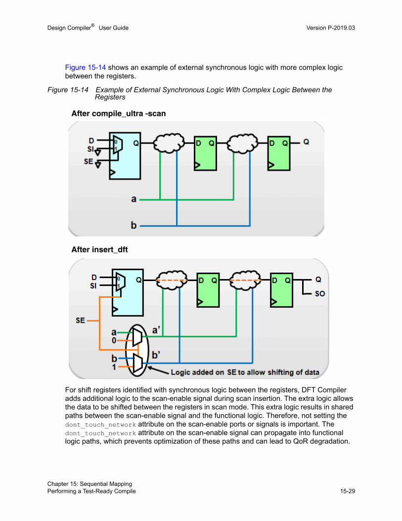
Design Compiler® User Guide Version P-2019.03
Figure 15-14 shows an example of external synchronous logic with more complex logic between the registers.
Figure 15-14 Example of External Synchronous Logic With Complex Logic Between the Registers
For shift registers identified with synchronous logic between the registers, DFT Compiler adds additional logic to the scan-enable signal during scan insertion. The extra logic allows the data to be shifted between the registers in scan mode. This extra logic results in shared paths between the scan-enable signal and the functional logic. Therefore, not setting the dont_touch_network attribute on the scan-enable ports or signals is important. The dont_touch_network attribute on the scan-enable signal can propagate into functional logic paths, which prevents optimization of these paths and can lead to QoR degradation.
After compile_ultra -scan
After insert_dft
Chapter 15: Sequential MappingPerforming a Test-Ready Compile 15-29Chapter 15: Sequential MappingPerforming a Test-Ready Compile 15-29

Design Compiler® User Guide P-2019.03Design Compiler® User Guide Version P-2019.03
If the dont_touch_network attribute is found on the scan-enable signal in your design and shift registers have been identified where extra logic was inserted on the scan-enable signal, the following warning message is stored in the log file:
Warning: dont_touch_network attribute on scan-enable port or signal '%s'can result in QoR degradation after scan insertion. (TEST-2040).
On scan-enable ports, you can use the set_case_analysis command to disable timing optimization and the set_ideal_network command to disable design rule fixing. However, if you need to use the dont_touch_network attribute, use the dont_touch_network -no_propagate command instead. By using this command, you can avoid the propagation of the dont_touch attribute into the functional logic.
Shift-register identification is available only in DC Ultra with the compile_ultra -scan command. When the compile_seqmap_identify_shift_registers variable is set to its default, which is true, shift register identification is enabled.
The compile_seqmap_identify_shift_registers_with_synchronous_logic variable controls the ability to identify shift registers with synchronous logic between the registers. The default is false. The default setting preserves multibit registers better between the compile and insert_dft steps, which can provide additional area savings. However, you can enable the identification of shift registers with synchronous logic by setting the compile_seqmap_identify_shift_registers_with_synchronous_logic to true if it provides an area benefit for your particular design.
Note that setting the compile_seqmap_identify_shift_registers variable to false disables all forms of shift-register identification, including shift registers that contain synchronous logic between the registers.
If you want to exclude specific registers from being identified as shift registers, apply the dont_use_for_shift_registers attribute on the registers that should be excluded. For example,
prompt> set_attribute [get_cells regs_to_exclude] dont_use_for_shift_registers true\ –type boolean
For best results, you should write out the design in .ddc format to preserve the information about the shift registers that are identified. When you write out the design in .ddc format, the compile -incremental -scan command or DFT Compiler can recognize already identified shift registers from a previous compile using the information stored in the .ddc binary file.
If your flow requires you to work with an ASCII netlist rather than a .ddc file, you must use the set_scan_state command when reading the netlist back into Design Compiler. The set_scan_state command updates the design to indicate that a test-ready compile has already been performed. The set_scan_state command also searches for and re-identifies shift registers in the design.
Chapter 15: Sequential MappingPerforming a Test-Ready Compile 15-30

Design Compiler® User Guide Version P-2019.03
The following example reads in an ASCII design and uses the set_scan_state command to set the scan state status:
read_verilog mapped_design.vcurrent_design toplinkset_scan_state test_ready
DC Ultra also supports the identification of shift registers with synchronous logic during the set_scan_state command run in the ASCII netlist flow. To enable this capability, you must set the following variable to true before you run the set_scan_state command:
set_app_var compile_seqmap_identify_shift_registers_with_synchronous_logic_ascii true
The compile_seqmap_identify_shift_registers_with_synchronous_logic_ascii variable is set to false by default. When the variable is set to true, the set_scan_state command performs full identification of all types of shift registers in the design. As a result, the set of newly identified shift registers might be different from the original set of shift registers in the design.
Both of the following default variable settings should be set in all Design Compiler sessions to enable this flow:
set_app_var compile_seqmap_identify_shift_registers true set_app_var compile_seqmap_identify_shift_registers_with_synchronous_logic true
When you enable the identification of shift registers with synchronous logic in the ASCII netlist flow, DC Ultra issues the following informational message when running the set_scan_state command:
Information: Performing full identification of complex shift registers.(TEST-1190)
The following ASCII netlist flow script example includes shift registers with synchronous logic:
# Turn on ASCII flow support for shift registers with synchronous logicset compile_seqmap_identify_shift_registers_with_synchronous_logic_ascii trueread_verilog design.vgcurrent_design toplinkread_sdc design.sdcif {[shell_is_in_topographical_mode]} {extract_physical_constraints floorplan.def}# Reapply preexisting DFT constraints (for example, set_scan_element false)set_scan_state test_ready # Continue with DFT Compiler flow
Chapter 15: Sequential MappingPerforming a Test-Ready Compile 15-31Chapter 15: Sequential MappingPerforming a Test-Ready Compile 15-31
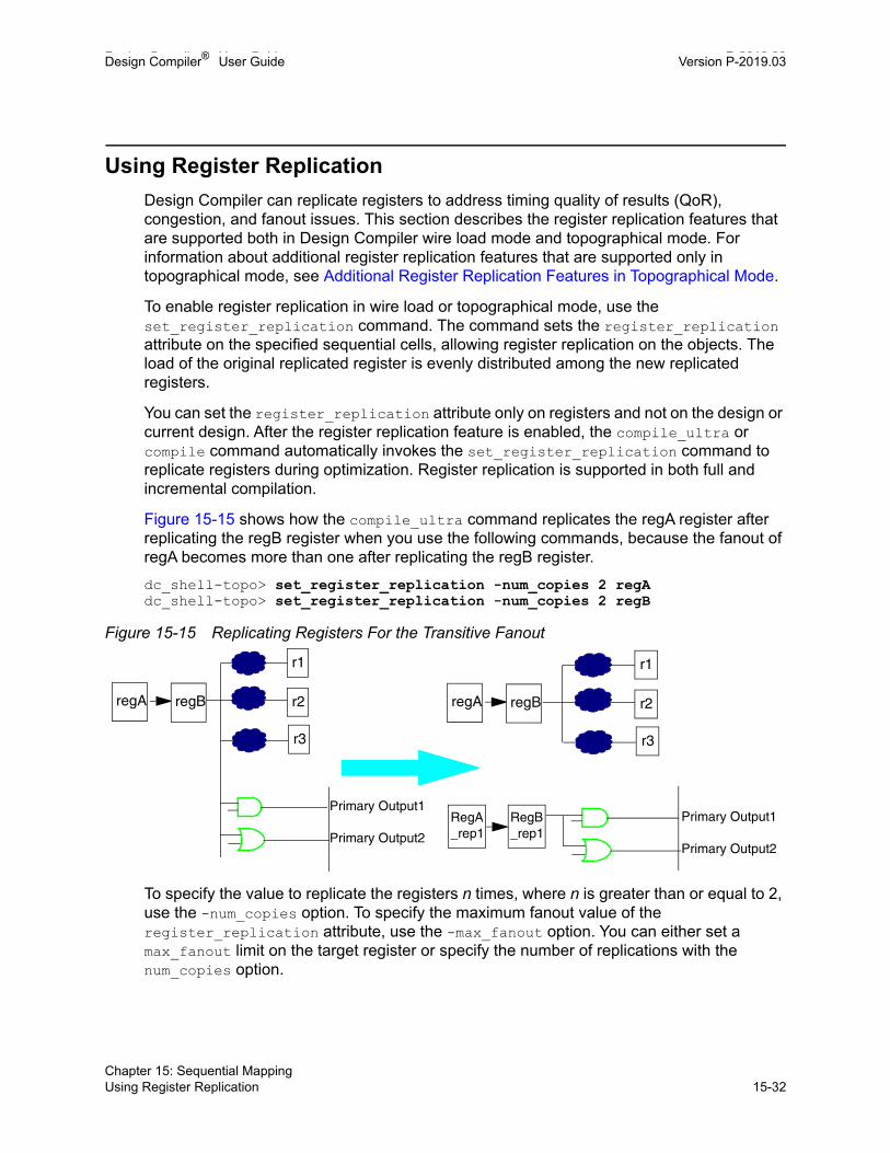
Design Compiler® User Guide P-2019.03Design Compiler® User Guide Version P-2019.03
Using Register Replication
Design Compiler can replicate registers to address timing quality of results (QoR), congestion, and fanout issues. This section describes the register replication features that are supported both in Design Compiler wire load mode and topographical mode. For information about additional register replication features that are supported only in topographical mode, see Additional Register Replication Features in Topographical Mode.
To enable register replication in wire load or topographical mode, use the set_register_replication command. The command sets the register_replication attribute on the specified sequential cells, allowing register replication on the objects. The load of the original replicated register is evenly distributed among the new replicated registers.
You can set the register_replication attribute only on registers and not on the design or current design. After the register replication feature is enabled, the compile_ultra or compile command automatically invokes the set_register_replication command to replicate registers during optimization. Register replication is supported in both full and incremental compilation.
Figure 15-15 shows how the compile_ultra command replicates the regA register after replicating the regB register when you use the following commands, because the fanout of regA becomes more than one after replicating the regB register.
dc_shell-topo> set_register_replication -num_copies 2 regAdc_shell-topo> set_register_replication -num_copies 2 regB
Figure 15-15 Replicating Registers For the Transitive Fanout
To specify the value to replicate the registers n times, where n is greater than or equal to 2, use the -num_copies option. To specify the maximum fanout value of the register_replication attribute, use the -max_fanout option. You can either set a max_fanout limit on the target register or specify the number of replications with the num_copies option.
r1
r2
r3
Primary Output1
Primary Output2
r1
r2
r3
Primary Output1
Primary Output2
RegB_rep1
regA
RegA_rep1
regB regA regB
Chapter 15: Sequential MappingUsing Register Replication 15-32

Design Compiler® User Guide Version P-2019.03
When you use the -num_copies option, the number of register copies is determined by whichever is smaller: the number specified by the -num_copies option or the fanout of the register at the time register replication occurs. If you specify a -num_copies value of 10 and the register has a fanout of 6, the register is only replicated 5 times for a total of 6 registers, one for each fanout.
The tool implements the fanout or -num_copies value that you set by replicating registers, not by inserting buffers.
You can replicate post-compile mapped logic containing high fanout within a few logic levels before or after the register by using the -include_fanin_logic and -include_fanout_logic options with the set_register_replication command. You can specify any startpoint or endpoint in the fanin and fanout of the register.
The following example replicates a path from the A_reg register to a U1 cell that is in the fanout of A_reg:
prompt> set_register_replication –num_copies 2 A_reg -include_fanout_logic U1
Note the following when you enable the register replication capability:
• If the fanout of the register is 17 and you specified -fanout 8 or-num_copies 3, the tool replicates the register three times with fanout 6, 6, and 5. That is, it evenly distributes the fanouts to each register.
• If boundary optimization is disabled, Design Compiler does not replicate registers across hierarchical boundaries.
• If you use both the set_max_fanout command and the set_register_replication -max_fanout command, the set_register_replication command has a higher priority.
• If the -max_fanout and -num_copies options are applied together, the -num_copies option has the higher priority and the tool reports a warning message that the -max_fanout option will be ignored.
Example 15-4 shows how to enable register replication on registers.
Example 15-4 Enabling Register Replication
prompt> set_register_replication –max_fanout 10 [get_cells -h * \-f "@ref_name==*regA*"]
prompt> set_register_replication –num_copies 10 [get_cells -h * \ -f "@ref_name==*regA*"]
To specify the style used in naming replicated registers, use the register_replication_naming_style variable. The default format is <%s_rep%d>. For example, if the original register is named PLL, by default, the replicated registers would be named PLL_rep1, PLL_rep2, PLL_rep3, and so forth.
Chapter 15: Sequential MappingUsing Register Replication 15-33Chapter 15: Sequential MappingUsing Register Replication 15-33
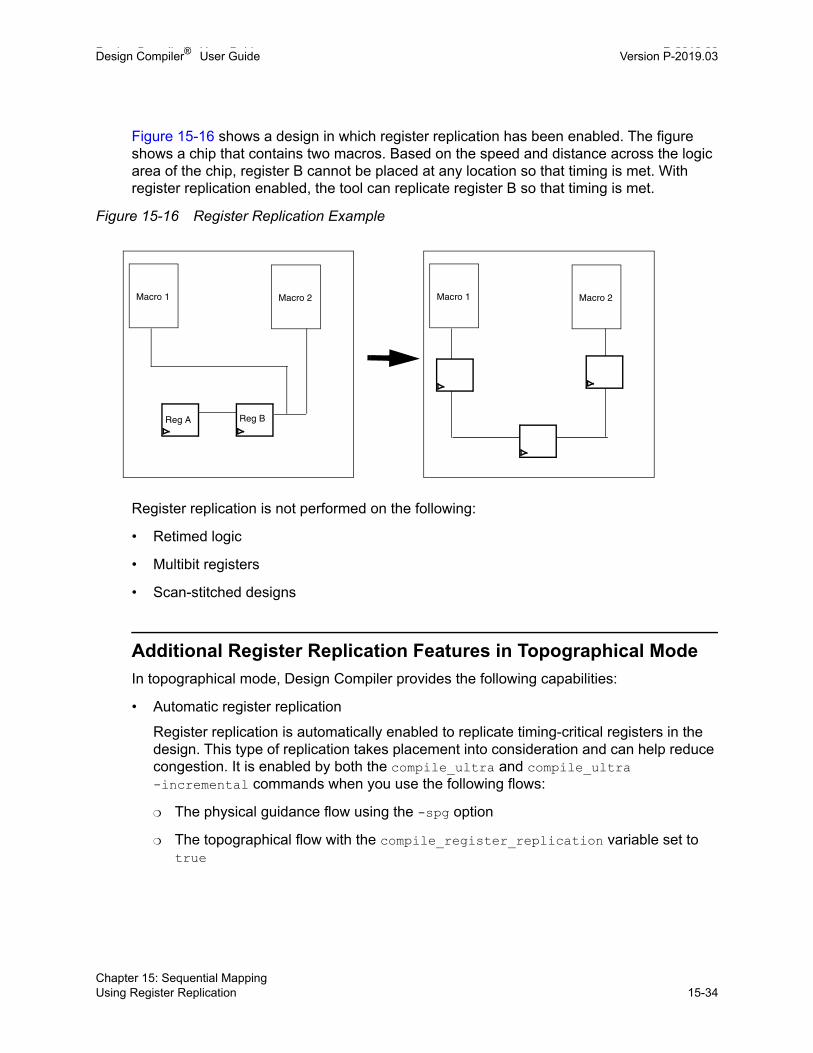
Design Compiler® User Guide P-2019.03Design Compiler® User Guide Version P-2019.03
Figure 15-16 shows a design in which register replication has been enabled. The figure shows a chip that contains two macros. Based on the speed and distance across the logic area of the chip, register B cannot be placed at any location so that timing is met. With register replication enabled, the tool can replicate register B so that timing is met.
Figure 15-16 Register Replication Example
Register replication is not performed on the following:
• Retimed logic
• Multibit registers
• Scan-stitched designs
Additional Register Replication Features in Topographical Mode
In topographical mode, Design Compiler provides the following capabilities:
• Automatic register replication
Register replication is automatically enabled to replicate timing-critical registers in the design. This type of replication takes placement into consideration and can help reduce congestion. It is enabled by both the compile_ultra and compile_ultra -incremental commands when you use the following flows:
❍ The physical guidance flow using the -spg option
❍ The topographical flow with the compile_register_replication variable set to true
Reg A
Macro 1 Macro 2 Macro 1 Macro 2
Reg B
Chapter 15: Sequential MappingUsing Register Replication 15-34
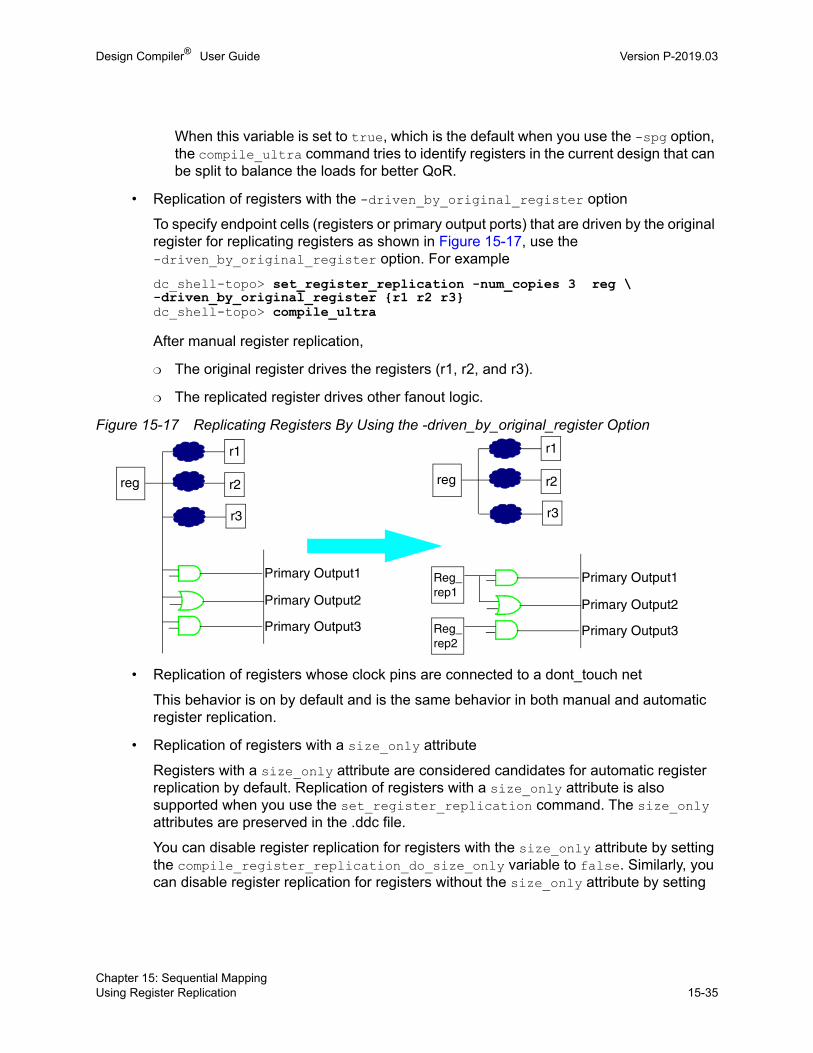
Design Compiler® User Guide Version P-2019.03
When this variable is set to true, which is the default when you use the -spg option, the compile_ultra command tries to identify registers in the current design that can be split to balance the loads for better QoR.
• Replication of registers with the -driven_by_original_register option
To specify endpoint cells (registers or primary output ports) that are driven by the original register for replicating registers as shown in Figure 15-17, use the -driven_by_original_register option. For example
dc_shell-topo> set_register_replication -num_copies 3 reg \ -driven_by_original_register {r1 r2 r3}dc_shell-topo> compile_ultra
After manual register replication,
❍ The original register drives the registers (r1, r2, and r3).
❍ The replicated register drives other fanout logic.
Figure 15-17 Replicating Registers By Using the -driven_by_original_register Option
• Replication of registers whose clock pins are connected to a dont_touch net
This behavior is on by default and is the same behavior in both manual and automatic register replication.
• Replication of registers with a size_only attribute
Registers with a size_only attribute are considered candidates for automatic register replication by default. Replication of registers with a size_only attribute is also supported when you use the set_register_replication command. The size_only attributes are preserved in the .ddc file.
You can disable register replication for registers with the size_only attribute by setting the compile_register_replication_do_size_only variable to false. Similarly, you can disable register replication for registers without the size_only attribute by setting
reg
r1
r2
r3
Primary Output1
Primary Output2
Primary Output3
reg
r1
r2
r3
Primary Output1
Primary Output2
Primary Output3
Reg_rep1
Reg_rep2
Chapter 15: Sequential MappingUsing Register Replication 15-35Chapter 15: Sequential MappingUsing Register Replication 15-35

Design Compiler® User Guide P-2019.03Design Compiler® User Guide Version P-2019.03
the size_only attribute on the register and then setting the compile_register_replication_do_size_only variable to false.
• Register replication across hierarchies
When the compile_register_replication_across_hierarchy variable is set to true in topographical mode, Design Compiler enables register replication across hierarchies. In addition, it creates new ports on instances of subdesigns while performing register replication if it is necessary to improve the timing of the design. Register replication across hierarchies might change the interfaces among subdesign instances. If the interfaces need to be preserved, this variable should be set to false (the default).
Chapter 15: Sequential MappingUsing Register Replication 15-36

16Adaptive Retiming 16
Adaptive retiming allows the tool to move registers and latches during optimization to improve timing. Design Compiler in wire load mode and topographical mode automatically performs adaptive retiming when you use the compile_ultra command with the -retime option. Before you read further, see Optimization Flow to understand how register retiming fits into the overall compile flow.
Adaptive retiming is intended for use in optimizing general designs; it does not replace the pipelined-logic retiming engine available with the optimize_registers and set_optimize_registers commands. For information about pipelined-logic retiming, see Pipelined-Logic Retiming.
To learn how to use adaptive retiming, see the following topics:
• Comparing Adaptive Retiming With Pipelined-Logic Retiming
• Adaptive Retiming Examples
• Performing Adaptive Retiming
• Controlling Adaptive Retiming
• Reporting the dont_retime Attribute
• Removing the dont_retime Attribute
• Verifying Retimed Designs
16-1

Design Compiler® User Guide P-2019.03Design Compiler® User Guide Version P-2019.03
Comparing Adaptive Retiming With Pipelined-Logic Retiming
Adaptive retiming moves registers and latches to improve worst negative slack (WNS). For datapath designs, you should still use either the optimize_registers command or the set_optimize_registers command followed by the compile_ultra command.
You can use both adaptive retiming and pipelined-logic retiming if you use the set_optimize_registers command on the pipelined portions of the design prior to running compile_ultra -retime, as shown in the following example:
set_optimize_registers [get_designs pipelined_ALU]compile_ultra -retime
The commands in the previous example apply pipeline retiming on the pipelined portions of the design and adaptive retiming on the remainder of the design.
See Also
• Pipelined-Logic Retiming
Adaptive Retiming Examples
When you describe circuits prior to logic synthesis, it is usually time-consuming and difficult to find the optimal register locations and code them into the HDL description. With retiming, the locations of the registers and latches in a sequential design can be automatically adjusted to equalize as nearly as possible the delays of the stages. This capability is particularly useful when some stages of a design exceed the timing goal while other stages fall short. If no path exceeds the timing goal, adaptive retiming can be used to reduce the number of registers, where possible.
During retiming, registers are moved forward or backward through the combinational logic of a design as shown in Figure 16-1.
Chapter 16: Adaptive RetimingComparing Adaptive Retiming With Pipelined-Logic Retiming 16-2

Design Compiler® User Guide Version P-2019.03
Figure 16-1 Adaptive Retiming
Design Compiler can improve worst negative slack by performing the following tasks during adaptive retiming:
• Retiming registers with conflicting reset requirements
• Retiming registers with extra synchronous input pins (tied high or low)
• Decomposing registers without SEQGEN correspondence
Design Compiler can also improve area by performing the following tasks:
• Allowing forward moves on non-critical registers
• Merging registers with equal and opposite next states
Figure 16-2 shows an example of how Design Compiler handles registers with conflicting reset requirements.
D QD Q
D Q
D Q
Backward Move
Forward Move
D Q
D Q
D QD Q
Chapter 16: Adaptive RetimingAdaptive Retiming Examples 16-3Chapter 16: Adaptive RetimingAdaptive Retiming Examples 16-3

Design Compiler® User Guide P-2019.03Design Compiler® User Guide Version P-2019.03
Figure 16-2 Adaptive Retiming for Registers with Conflicting Reset Values
The values (0 or 1) above the registers in the netlists indicate their reset values when a common reset or preset signal (not shown) becomes active. Assume that all three registers R1, R2, R3 in the first netlist move backward across the driver cells of their input nets. The second netlist is a possible result of the moves. Registers R4 and R7 have unique reset or preset values; however, R5 and R6 can have either preset (1) for R5 and reset (0) for R6 as in the second netlist or the reverse as in the third netlist.
Design Compiler can retime registers with these conflicting reset requirements. The two input XOR gate has two possible input assignments resulting in an output value of 1. In the second netlist, conflicting reset values can prevent further backward moves. The third netlist, however, allows such backward moves if they are required.
R1
R2
R3
C3
C5
C4
0
1
0
C1
C2
R4
R5
R6
C5
C4
1
0
C2
0
R7
1
C1 C3
R4
R5
R6
C5
C4
0
1
C2
0
R7
1
C1 C3
Netlist 1
Netlist 2 Netlist 3
Chapter 16: Adaptive RetimingAdaptive Retiming Examples 16-4

Design Compiler® User Guide Version P-2019.03
Figure 16-3 shows how Design Compiler can execute forward local retiming moves on non-critical registers to improve area by decreasing the number of registers.
Figure 16-3 Forward Moves for Non-Critical Registers
Design Compiler can move registers with common timing exceptions, including max_delay, min_delay, multicycle_path, false_path, and group_path, as long as all the registers being moved have the same exceptions. After executing a move involving registers with exceptions, the new registers inherit all the exceptions from the original registers.
Two registers have the same exceptions if they appear in the same point-to-point timing exception setting commands, such as set_max_delay, set_min_delay, set_multicycle_path, set_false_path, and group_path.
In the following example, registers r0 and r1 have the same exceptions.
set_max_delay 10 -to [list r0/D r1/D]
Alternatively, if this set_max_delay command is split into two set_max_delay commands, both with the same delay value, the two registers still have the same exceptions:
set_max_delay 10 -to r0/Dset_max_delay 10 -to r1/D
However, if the two set_max_delay commands have different delay values, the two registers have different exceptions, and they cannot be moved together:
set_max_delay 10 -to r0/Dset_max_delay 15 -to r1/D
By default this feature is disabled: to enable this feature, set the compile_retime_exception_registers variable to true.
R1
R2
R3
C1
C2
R4
R5
C1
C2
Chapter 16: Adaptive RetimingAdaptive Retiming Examples 16-5Chapter 16: Adaptive RetimingAdaptive Retiming Examples 16-5

Design Compiler® User Guide P-2019.03Design Compiler® User Guide Version P-2019.03
Performing Adaptive Retiming
You use the -retime option of the compile_ultra command to perform adaptive retiming and to improve the delay during optimization.
Adaptive retiming honors attributes, such as dont_touch, size_only, and dont_retime; retiming is prevented if these attributes are set. Registers that are moved as a result of adaptive retiming are renamed with a prefix of R and a numbered suffix (R_xxx); you cannot match these retimed registers to the original registers.
Adaptive retiming supports all compile_ultra options except the following:
• -top
• -only_design_rule
Controlling Adaptive Retiming
You can use the set_dont_retime command to include or exclude designs or cells from being retimed. For example, the following command specifies that the design a1 should not be retimed:
set_dont_retime [get_designs a1] true
Setting the dont_retime attribute on a hierarchical cell implies that the attribute is also set on all cells below it. However, you can override the attribute at a lower-level of the hierarchy by explicitly setting the dont_retime attribute at that level. For example, the following command specifies that the cells z1_reg and z2_reg should be retimed:
set_dont_retime [get_cells {z1_reg z2_reg}] false
If you use the set_dont_retime command without specifying either true or false, a value of true is assumed.
The following sequence of commands will create the scenario shown in Figure 16-4:
set_dont_retime [get_cells U1]set_dont_retime [get_designs mid] trueset_dont_retime [get_cells U_mid/U3] falseset_dont_retime [get_cells U_mid/U_bot]falsecompile_ultra -retime
Chapter 16: Adaptive RetimingPerforming Adaptive Retiming 16-6

Design Compiler® User Guide Version P-2019.03
Figure 16-4 Design With Both Retimable and Nonretimable Cells
Note: The dont_retime attribute on a child cell has priority over the attribute set on any ancestor cell or design.
You can also use the set_dont_retime command to prevent retiming on specific cells or designs when you use the optimize_registers command. For more information, see Pipelined-Logic Retiming.
Reporting the dont_retime Attribute
To check which cells or designs have the dont_retime attributes, use the report_attribute or get_attribute command.
Removing the dont_retime Attribute
To remove the dont_retime attribute, use the remove_attribute command.
Verifying Retimed Designs
When Design Compiler performs any retiming, an automated setup file is necessary for verification with the Formality tool. The automated setup file includes retiming optimization information that helps Formality verify retimed designs. To remind you that Formality requires an automated setup file, Design Compiler displays the following message when retiming is performed:
Information: Retiming is enabled. SVF file must be used for formal verification. (OPT-1210)
If you run multiple compile_ultra -retime commands, you must run multiple formal verifications, each one verifying only the changes made by the most recent compile_ultra -retime command.
D Q D Q
bot
mid
U_mid
U_bot
U1 U3
Can be retimed
Will not be retimed
Chapter 16: Adaptive RetimingReporting the dont_retime Attribute 16-7Chapter 16: Adaptive RetimingReporting the dont_retime Attribute 16-7

Design Compiler® User Guide P-2019.03Design Compiler® User Guide Version P-2019.03
The following example shows a Design Compiler script that runs the compile_ultra -retime command followed by an incremental compile with the -retime option. In the script, the verification is run by comparing the RTL to the compile_1.ddc netlist using the compile_1.svf verification setup file and comparing the compile_1.ddc netlist to the compile_2.ddc netlist using the compile_2.svf verification setup file.
set_svf compile_1.svfread_verilog rtl.vcompile_ultra –retimewrite_file -hierarchy -output compile_1.ddcset_svf compile_2.svfcompile_ultra –incremental –retimewrite_file -hierarchy -output compile_2.ddc
See Also
• Verifying Functional Equivalence
Provides information about design verification
• The Formality User Guide
Chapter 16: Adaptive RetimingVerifying Retimed Designs 16-8

17Pipelined-Logic Retiming 17
Register retiming is a sequential optimization technique that DC Ultra uses to move registers through the combinational logic gates of a design to optimize timing and area. In this context, the term register refers to both edge-triggered registers and level-sensitive latches unless stated otherwise. Both types of sequential cells can be retimed.
You enable pipelined-logic retiming by using the optimize_registers command or by using the set_optimize_registers command followed by the compile_ultra command.
To learn how to retime circuits using pipelined-logic retiming, see the following topics:
• Pipelined-Logic Retiming Overview
• Register Retiming Concepts
• Retiming the Design
• Analyzing Retiming Results
• Verifying Retimed Designs
17-1

Design Compiler® User Guide P-2019.03Design Compiler® User Guide Version P-2019.03
Pipelined-Logic Retiming Overview
DC Ultra supports the following methods for retiming registers:
• Adaptive retiming
You enable this retiming method by using the -retime option with the compile_ultra command. In this case, DC Ultra locally adjusts the register location.
This method is not covered in this chapter. For more information, see the Adaptive Retiming chapter.
• Pipelined-logic retiming
You enable this retiming method by using either the optimize_registers command or the set_optimize_registers command followed by the compile_ultra command.
This method is designed to balance the multiple stages of pipelined registers into combinational logic. This is particularly useful to pipeline datapath blocks.
When you describe circuits at the RTL level before logic synthesis, it is usually very difficult and time consuming to find the optimal register locations and code them into the HDL description. With register retiming, the locations of the flip-flops in a sequential design can be automatically adjusted to equalize as nearly as possible the delays of the stages.
The retiming techniques that the optimize_registers and set_optimize_registers commands use are particularly useful to pipeline datapath blocks. You first specify the desired number of pipeline stages and place all the pipeline registers at the inputs or outputs of the combinational logic in your RTL. During retiming, the tool moves these pipeline registers into the combinational logic, balances the delay of each pipeline stage, and archives the optimal timing and area results based on the given clock period.
Register retiming leaves the behavior of the circuit at the primary inputs and primary outputs unchanged (unless you add pipeline stages or choose special options that do not preserve the reset state of the design). Therefore, you do not need to change any simulation test benches developed for the original RTL design.
Retiming does, however, change the location, contents, and names of registers in the design. A verification strategy that uses internal register inputs and outputs as reference points will no longer work. Retiming can also change the function of hierarchical cells inside a design and add clock, clear, set, and enable pins to the interfaces of the hierarchical cells.
The following topics describe the commands that enable pipelined-logic retiming and an example of a circuit before and after retiming:
• Pipelined-Logic Retiming Commands
• Register Retiming Example
Chapter 17: Pipelined-Logic RetimingPipelined-Logic Retiming Overview 17-2

Design Compiler® User Guide Version P-2019.03
Pipelined-Logic Retiming Commands
You can use either of the following command sequences to enable pipelined-logic retiming:
• Using the optimize_registers command
This method performs retiming on a mapped netlist. You must compile the design using the compile_ultra command before enabling retiming with the optimize_registers command.
This method is also known as two-pass retiming because retiming is performed in two steps: The first step moves and minimizes the sequential cells, and the second step performs an incremental compile, which adjusts the design to the changed fanout structure.
• Using the set_optimize_registers command followed by the compile_ultra command
This method performs retiming during synthesis when you run the compile_ultra command after reading your RTL. You must run the set_optimize_registers command before running compile_ultra. The set_optimize_registers command sets the optimize_registers attribute on the specified design or on the current design so that the attribute is automatically invoked during compile and the design is retimed during optimization.
This method is also known as one-pass retiming because retiming is performed in one step by the compile_ultra command.
Register Retiming Example
During retiming, registers are moved forward or backward through the combinational logic of a design. Figure 17-1 and Figure 17-2 illustrate an example of delay reduction through backward retiming of a register.
Chapter 17: Pipelined-Logic RetimingPipelined-Logic Retiming Overview 17-3Chapter 17: Pipelined-Logic RetimingPipelined-Logic Retiming Overview 17-3
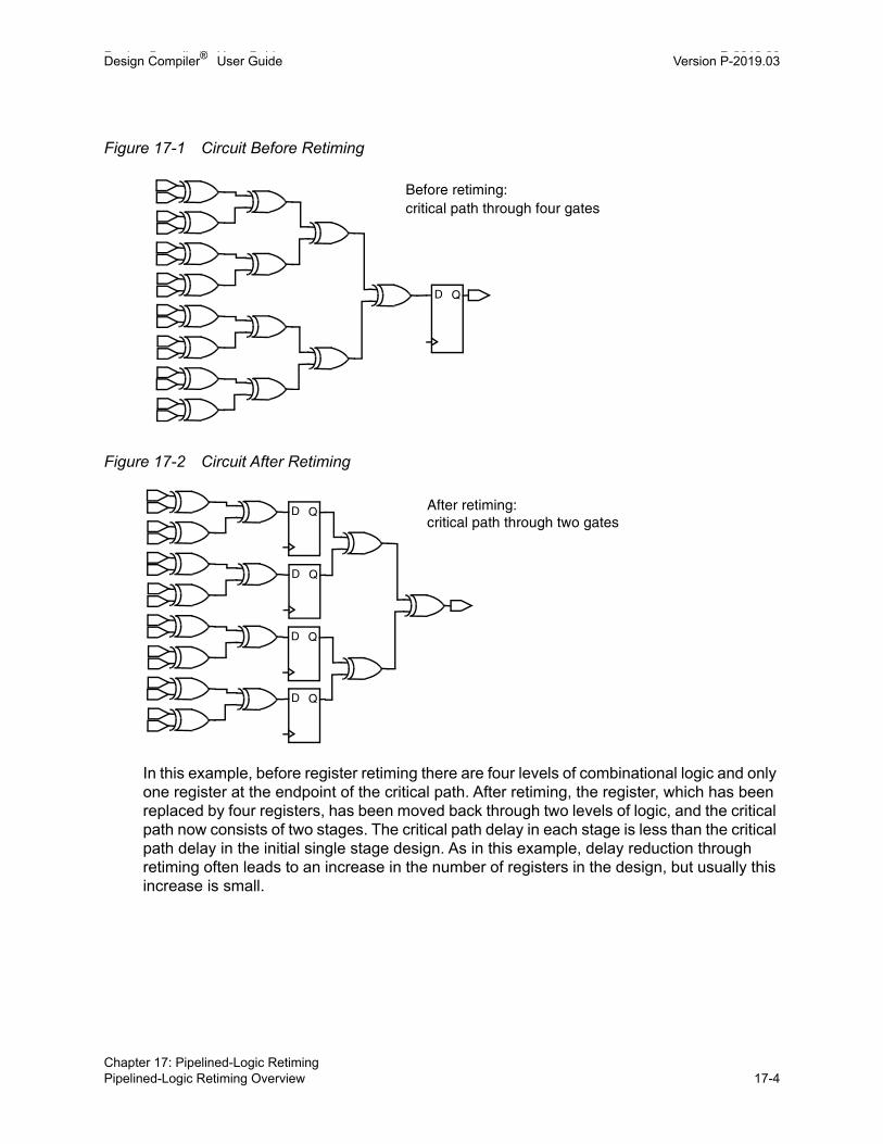
Design Compiler® User Guide P-2019.03Design Compiler® User Guide Version P-2019.03
Figure 17-1 Circuit Before Retiming
Figure 17-2 Circuit After Retiming
In this example, before register retiming there are four levels of combinational logic and only one register at the endpoint of the critical path. After retiming, the register, which has been replaced by four registers, has been moved back through two levels of logic, and the critical path now consists of two stages. The critical path delay in each stage is less than the critical path delay in the initial single stage design. As in this example, delay reduction through retiming often leads to an increase in the number of registers in the design, but usually this increase is small.
D Q
Before retiming:critical path through four gates
D Q
D Q
D Q
D Q
After retiming:critical path through two gates
Chapter 17: Pipelined-Logic RetimingPipelined-Logic Retiming Overview 17-4

Design Compiler® User Guide Version P-2019.03
Register Retiming Concepts
The following topics describe the fundamentals of register retiming to help you make the best use of the Design Compiler register retiming capabilities:
• Basic Definitions and Concepts
• Forward Retiming
• Backward Retiming
• Register Transformation Methods
• Reset State Justification
Basic Definitions and Concepts
To understand how register retiming works, you must first understand certain basic definitions and concepts. In particular, you must understand what sequential generic elements (SEQGENs), control nets, and register classes are. These are important because during retiming, mapped registers are temporarily replaced by SEQGENs according to their classifications as determined by their control nets.
Note: The following terms are not defined in this topic because they are used the same way as in other Synopsys documentation: design, cell, leaf cell, hierarchical cell, combinational cell, and sequential cell.
Flip-Flops and Registers
Flip-flop, register, synchronous register, asynchronous register, and latch are familiar terms; however, with respect to register retiming, these terms have the following specialized usage:
• A flip-flop is an element of a technology library (target library) that has, unlike the combinational cells, a state and a distinguished clock input. Flip-flops can be edge triggered or level sensitive.
• A register is technically an instance of an edge-triggered flip-flop in the design. But for the purposes of register retiming, because both edge-triggered flip-flops and level-sensitive latches can be retimed, the term register refers to both types of sequential devices unless stated otherwise.
• A synchronous register is a register that can change its state only at the active edge of the clock signal.
Chapter 17: Pipelined-Logic RetimingRegister Retiming Concepts 17-5Chapter 17: Pipelined-Logic RetimingRegister Retiming Concepts 17-5

Design Compiler® User Guide P-2019.03Design Compiler® User Guide Version P-2019.03
• An asynchronous register is a register that, in addition to changing its state on a clock edge, can also change its state according to the control levels of asynchronous signals, which are independent of its clock signal.
• A latch is an instance of a level-sensitive flip-flop in the design. Register retiming supports designs with latches and retimes them instead of the registers if the -latch option is used.
The essential point here to understand is that flip-flops are technology library elements, while registers and latches are their design instances.
SEQGENs
A SEQGEN is a generic sequential element that is used by Synopsys tools to represent registers and latches in a design. SEQGENs are created during elaboration and are usually mapped to flip-flops during compilation. Because mapped flip-flops are temporarily replaced by SEQGENs during register retiming, it is important that you understand the basic functionality of these elements.
Figure 17-3 shows the pins that are used when the SEQGEN cell describes a synchronous or asynchronous register. (Additional pins occur when the SEQGEN is operated as a latch.)
Figure 17-3 Relevant Pins of the SEQGEN Cell
In register retiming, the operation of SEQGEN cells is as follows:
• The synchronous toggle pin (ST) has an inactive value of 0. Therefore, the SEQGEN cell is retimed only if the ST pin is connected to a constant net with value 0.
• The clock (CLK) pin is always connected to the clock net of the design.
• The synchronous state changes occur at the rising edge of the clock signal.
• If set to 1, the synchronous load (SL) pin enables the next-state D input to become the next state. The SL pin should be tied to a constant 1 net when unused.
ACASDSCSSSLST CLK
QN
asynch_clearasynch_set
next_statesynch_clear
synch_setsynch_load
synch_toggleclocked_on
ENAD
Enable (clock if operated as latch)asynch_data (data if operated as latch)
Q
Chapter 17: Pipelined-Logic RetimingRegister Retiming Concepts 17-6

Design Compiler® User Guide Version P-2019.03
• The synchronous clear (SC) pin sets the state to 0 if active. This pin preempts the SL input and, to be inactive, must be tied to a constant 0 net.
• The synchronous set (SS) pin sets the state to 1 if active. This pin preempts the SL input and, to be inactive, must be tied to a constant 0 net.
• If both SC and SS are active, the constant set as an attribute on the particular SEQGEN instance becomes the new state.
• The asynchronous inputs AC and AS override all settings of the synchronous inputs; these pins change the state and output of a SEQGEN instance, independent of the clock input.
• The AC input sets the Q output to 0 if active; the AS input sets the Q output to 1 if active. Both inputs must be 0 to be inactive.
• The EN input replaces the CLK clock pin if the SEQGEN cell operates as a level-sensitive latch.
• The AD pin input replaces the D pin input if the SEQGEN cell operates as a level-sensitive latch.
Control Nets
A control net is a net connected to one of the SL, SC, SS, AC, or AS pins of a SEQGEN instance. The equivalence of control nets plays a crucial role in the movement of registers during retiming.
By definition, a set of control nets are equivalent if they meet either of the following conditions:
• All the nets can be reached from a common source, and between this common source and the SEQGEN instances, all the nets have an odd number of inverters or all the nets have an even number of inverters. (A net with no inverters is regarded as having an even number of inverters.)
• The control nets are constant and have the same constant values (0 or 1).
Thus, two nonconstant nets with a common source, one that includes an odd number of inverters and the other an even number of inverters, are not equivalent nets. Note that any number of buffers is allowed between the common source and the SEQGEN pin of an equivalent net.
Figure 17-4 shows an example of equivalent and nonequivalent nets. Nets n1 and n3, which have even number of inverters (0 and 2), are equivalent, while net n2, which has an odd number of inverters (1), is not equivalent to either of them.
Chapter 17: Pipelined-Logic RetimingRegister Retiming Concepts 17-7Chapter 17: Pipelined-Logic RetimingRegister Retiming Concepts 17-7

Design Compiler® User Guide P-2019.03Design Compiler® User Guide Version P-2019.03
Figure 17-4 Equivalent Control Net Example
Register Classes
The SEQGEN instances are grouped into register classes according to their connections to control nets. Grouping is necessary because only registers belonging to the same group can be moved together across a combinational gate without violating the circuit logic.
Two SEQGEN instances belong to the same register class if the following conditions are fulfilled:
• Their SL pins are connected to equivalent control nets.
• Their SC and SS pins are connected to equivalent control nets. That is, a given control net can be connected to the corresponding SC or SS pins in the SEQGEN instances or to the SC pin of one SEQGEN instance and to the SS pin of the other.
• Their AC and AS pins are connected to equivalent control nets. The same conditions hold for the asynchronous pins as for the synchronous pins.
Figure 17-5 shows an example in which registers A and B belong to the same class.
ACASDSCSSSLST CLK
Q
QN
ACASDSCSSSLST CLK
Q
QN
ACASDSCSSSLST CLK
Q
QNn1 n2
n3
R1 R2 R3
Chapter 17: Pipelined-Logic RetimingRegister Retiming Concepts 17-8

Design Compiler® User Guide Version P-2019.03
Figure 17-5 Swapping of Control Net for Registers in the Same Class
In Figure 17-4 on page 17-8, if all pins not connected to nets n1, n2, and n3 are connected to their inactive constants, registers R1 and R3 belong to the same class, but register R2 belongs to a different class.
When registers belonging to the same class are moved, it is possible to swap their control nets as needed to accomplish the retiming. This swapping capability is true for both synchronous and asynchronous register pins.
Forward Retiming
To retime forward across a combinational cell, each net in the immediate fanin of the cell must be driven by the Q pin of a register, and all these registers must belong to the same class. After the forward retiming move, the registers in the fanout of the cell belong to the same class as those in the fanin before the move.
Figure 17-6 shows an example of retiming forward across the combinational cell g1.
Note: In this and the following sections, the explicit control nets for registers are not drawn unless there is a special reason to do so. Register classes are denoted by class names (for example, C1 and C2).
ACASDSCSSSLST CLK
Q
QN
ACASDSCSSSLST CLK
Q
QN
n1
n2A B
Chapter 17: Pipelined-Logic RetimingRegister Retiming Concepts 17-9Chapter 17: Pipelined-Logic RetimingRegister Retiming Concepts 17-9

Design Compiler® User Guide P-2019.03Design Compiler® User Guide Version P-2019.03
Figure 17-6 Forward Retiming Example
Before the retiming move is executed, all the registers in the immediate fanin of the g1 cell belong to class C1. Notice that after the move the three registers have been replaced by two registers belonging to the same class C1. It is not possible to retime forward the next slice of registers in the fanin of the g1 cell because not all these registers belong to the same class. Also, after the first retiming, it is not possible to retime forward the class C1 register that drives one of the g2 cell inputs because only one input pin of the cell has a register driving it.
If during retiming the maximum number of forward retiming moves across a cell has been performed, the cell has reached its forward retiming boundary limit.
Backward Retiming
Rules similar to the forward retiming rules govern backward retiming across a combinational cell is possible. All nets in the fanout of a combinational cell must fan out to the D pin of the registers, and all these registers must belong to the same class. After the backward retiming move, the registers in the fanin of the cell belong to the same class as those in the fanout before the move.
Figure 17-7 shows how the combinational cell g1 can be retimed backward after the cell g2 has been retimed backward. Note that two backward timing moves have been carried out.
C1
C1
C1C1
C2
C2
C1
C1C1
C2
C2
g1
g2
g3
C3
C3 C3
C3
g1
g2
g3
Before retiming After retiming
Chapter 17: Pipelined-Logic RetimingRegister Retiming Concepts 17-10

Design Compiler® User Guide Version P-2019.03
Figure 17-7 Backward Retiming Example
If during retiming the maximum possible number of backward retiming moves across a cell has been performed, the cell has reached its backward retiming boundary limit.
Register Transformation Methods
You can choose which register transformation method pipelined-logic retiming uses when it moves registers. Design Compiler supports the following transformation methods:
• Transforming Synchronous Input Pins Through Combinational Decomposition
• Multiclass Retiming
Transforming Synchronous Input Pins Through Combinational Decomposition
Combinational decomposition transforms synchronous input pins by
• Using combinational cells to implement the synchronous functionality, and
• Connecting the output of the combinational cells to the D pin of a SEQGEN cell
Note: Combinational decomposition can be applied to the synchronous pins of asynchronous registers.
Figure 17-8 shows the combinational decomposition of the register with synchronous clear and enable signals.
C1
C1
C1C1
C2
C2
g1
g2
g3
C3
C3
C1
C1
C1C1
C2
C2
g1
g2
g3
C3C3
C3
C3
Before retiming After retiming g2 and then g1
Chapter 17: Pipelined-Logic RetimingRegister Retiming Concepts 17-11Chapter 17: Pipelined-Logic RetimingRegister Retiming Concepts 17-11

Design Compiler® User Guide P-2019.03Design Compiler® User Guide Version P-2019.03
Figure 17-8 Transformation by Decomposition Example
An advantage of combinational decomposition is that all purely synchronous registers belong to the same class after they are transformed to SEQGENs. Consequently, there are no limits to the number of forward or backward moves possible at multiple input or output gates due to registers belonging to different classes. Not using decomposition (multiclass retiming) can lead to register class conflicts, which ultimately limit the number of forward or backward retiming moves possible.
Figure 17-9 shows how registers with different enable control nets can be moved forward after decomposition. (To simplify the figure, the clock net is not drawn.) These registers could not be moved after multiclass retiming. Notice, however, that two D flip-flops remain with the fanouts belonging to synchronous combinational logic and cannot be forward retimed; the third flip-flop is free to move by forward retiming.
D
EN
RST
Q
D
CLK
Q
SEQGEN
EN
RST
D
CLK
01
Chapter 17: Pipelined-Logic RetimingRegister Retiming Concepts 17-12

Design Compiler® User Guide Version P-2019.03
Figure 17-9 Forward Retiming of Decomposed Cells With Load Enable
Combinational decomposition can also limit the movability of registers. Figure 17-10 shows how decomposition applied to a sequence of two synchronous clear registers leaves the left register without the possibility of a forward move because the newly introduced AND gate does not have a register at its second port. (The right register is forward retimed through an inverter.) Alternatively, multiclass retiming allows both registers to move forward: The right register can be moved across two inverters and the left register across one buffer.
Figure 17-10 Reduced Mobility After Decomposition
D QLE
D QLE
D Q
D Q
D Q
D Q
D Q
Decompose Retime
le1
le2
D QR
D QR
D QD Q
D QD Q
D QR
D QS
Retime (multiclass) Retime
Decompose
No forward move possible
Chapter 17: Pipelined-Logic RetimingRegister Retiming Concepts 17-13Chapter 17: Pipelined-Logic RetimingRegister Retiming Concepts 17-13

Design Compiler® User Guide P-2019.03Design Compiler® User Guide Version P-2019.03
See Also
• Selecting Transformation Options
Describes how to specify a register transformation method
Multiclass Retiming
Multiclass retiming can offer significant area savings compared with retiming after decomposition. A multiclass example is shown in Figure 17-11. The situation is similar to the example in Figure 17-9 except that the two load enable registers belong to the same class and therefore can be moved across the AND gate, leading to a single register. Using decomposition leads to a higher number of registers and additional cells after retiming.
Figure 17-11 Reduced Area Through Multiclass Retiming
See Also
• Selecting Transformation Options
Describes how to specify a register transformation method
D QLE
D QLE
D Q
D Q
D Q
D QLE
Decomposeand retime
Multiclassretime
Chapter 17: Pipelined-Logic RetimingRegister Retiming Concepts 17-14

Design Compiler® User Guide Version P-2019.03
Reset State Justification
When you move the registers in a circuit, it is not sufficient to follow only the rules for retiming of a single gate. In addition, it is usually necessary to preserve an equivalent reset state.
The circuit state is defined by the values of all the registers in the circuit at a given point in time. A circuit and its retimed version have an equivalent state if they produce the same sequences of values at corresponding primary outputs for identical sequences of values at the corresponding primary inputs.
When power is switched on in a circuit, its state is unknown. Depending on the type of circuit, you might need to have an external reset or set input to reset the registers to a known value. This step ensures that the circuit has reproducible behavior after the input becomes active for the first time.
If a circuit is designed this way, by default, register retiming ensures that the reset state of the retimed circuit is equivalent to that of the original circuit, and that the behavior is identical when a finite number of clock cycles has passed after the activation of the reset. If all registers are properly reset, output sequences should match immediately.
However, a typical case where the first few output values might not match is that of a pipelined datapath where the registers do not have any set or clear connections. The maximum duration of the mismatch is the number of stages of the pipeline multiplied by the clock period.
The computation of the equivalent reset state is called justification. Justification for registers that have been moved forward across combinational gates is always possible and does not require significant amounts of CPU time. Justification for registers moved backward across combinational gates can be more complicated. Figure 17-12 shows an example of the difficulty with backward justification.
Figure 17-12 Impossible Backward Justification Example
The numbers inside the register symbols are the given reset values. When the registers are moved to the post-retiming positions, it is not possible to find an equivalent state for the
Before retiming After retiming
0
0
1
?
?
?
?
Chapter 17: Pipelined-Logic RetimingRegister Retiming Concepts 17-15Chapter 17: Pipelined-Logic RetimingRegister Retiming Concepts 17-15

Design Compiler® User Guide P-2019.03Design Compiler® User Guide Version P-2019.03
circuit. Register retiming handles this case by finding a position for the registers where an equivalent state is found that is as close to the optimal position as possible.
Backward justification also can cost more CPU time than forward justification. If the circuit to be retimed has a reset but does not need to have an equivalent reset state after retiming, there is a method available that does not perform justification. This method can be applied to pipelined datapaths, but it is not suitable for controllers.
To specify the justification effort level during backward justification, use the -justification_effort option with the optimize_registers or set_optimize_registers command. The option can take one of the following values: low, high, or medium.
Retiming the Design
The following topics describes the register retiming steps and how to control retiming:
• Register Retiming Steps
• Preventing Retiming
• Selecting Transformation Options
• Retiming Designs With Multiple Clocks
• Retiming Registers With Path Group Constraints
• Netlist Changes Performed by Register Retiming
• Delay Threshold Optimization
Register Retiming Steps
When you enable register retiming with either retiming method, Design Compiler moves registers using the following two-step approach:
1. Minimizes the clock period
The registers are moved to ensure the smallest clock period for the retimed circuit.
2. Minimizes the register count
The minimum clock period determined in the first step is compared to a user-defined clock period target. If the minimum clock period is smaller than or equal to the target clock period, the target clock period is used and a register distribution is computed that accommodates the target clock period with the smallest number of registers possible. If the target clock period is smaller than the minimum clock period, the number of registers is minimized for the minimum clock period.
Chapter 17: Pipelined-Logic RetimingRetiming the Design 17-16

Design Compiler® User Guide Version P-2019.03
Preventing Retiming
Sometimes it is best to avoid retiming some registers in a design. For example, registers driving primary outputs that have to stay in place because of a particular design style should not be retimed. In this case, set the dont_retime attribute on these output registers.
Another example of not moving certain registers occurs when you want to keep the controller registers of a design in place while allowing the datapath registers to move. Keeping the controller registers in place lets you easily identify these registers and relate them to the original HDL code. In this case, you can set the dont_retime attribute on the registers in the controller or on the controller cell itself (if it is a hierarchical cell).
The dont_retime attribute prevents a register from moving during retiming but allows sequential mapping to map the register to a different flip-flop.
Use the set_dont_retime command to control the designs or cells that can be retimed. When set to true (the default), the command sets the dont_retime attribute on specific cells and designs in the current design so that sequential cells are not moved during retiming optimizations. For example,
prompt> set_dont_retime [get_cells {z1_reg z2_reg}] true
Setting the dont_retime attribute on a hierarchical cell implies that the attribute is set on all sequential cells below it that do not have the dont_retime attribute set to false. A leaf-level cell that has the dont_retime attribute is not retimed if it is a sequential cell. When the dont_retime attribute is set on a design, all sequential cells that do not have the dont_retime attribute set to false are not retimed. For example, consider the following sequence of commands:
prompt> set_dont_retime [get_cells U1]prompt> set_dont_retime [get_designs mid] trueprompt> set_dont_retime [get_cells U_mid/U3] falseprompt> set_dont_retime [get_cells U_mid/U_bot]falseprompt> optimize_registers
Figure 17-13 shows that cells U1 and design mid are not retimed.
Figure 17-13 Cells U1 and Design mid Are Not Retimed
D Q D Q
bot
mid
U_mid
U_bot
U1 U3
Retimed
Not retimed
Chapter 17: Pipelined-Logic RetimingRetiming the Design 17-17Chapter 17: Pipelined-Logic RetimingRetiming the Design 17-17

Design Compiler® User Guide P-2019.03Design Compiler® User Guide Version P-2019.03
Note: The set_dont_retime command overrides the set_transform_for_retiming command. That is, if the value of the dont_retime attribute is true, setting the transform_for_retiming attribute to decompose or multiclass does not make a register retimable. A movable register cannot be moved across a register with the dont_retime or the dont_touch attribute.
Selecting Transformation Options
The optimize_registers and set_optimize_registers commands allow you to specify how the mapped registers are transformed to SEQGEN cells for retiming. There is one transformation option for synchronous registers and another for asynchronous registers. A synchronous register does not have any asynchronous input pins and an asynchronous register has at least one asynchronous input pin.
The transformation option for synchronous registers is -sync_transform. The values are multiclass, decompose, and dont_retime. The multiclass value specifies that the synchronous clear, set, and enable functionality is moved with the synchronous sequential cells (if they are moved during retiming). The decompose value specifies that any synchronous sequential cell is decomposed (transformed into an instance of a D flip-flop or latch and additional combinational logic to create the necessary synchronous functionality). The dont_retime value specifies that these registers are not to be moved. The default for this option is multiclass.
The transformation option for asynchronous registers is -async_transform. The values are multiclass, decompose, and dont_retime. The multiclass value specifies that the asynchronous clear and set as well as any synchronous clear, set, and enable functionality are moved with the asynchronous sequential cells (if they are moved during retiming). The decompose value specifies that any asynchronous sequential cell is decomposed. The dont_retime value specifies that these registers are not to be moved. The default for this option is multiclass.
Registers that are already SEQGEN instances are not affected by these settings. Their set, clear, and enable connections are controlled by HDL Compiler options.
Recommended Transformation Options for Pipelines
For pipelined designs, it is recommended that you use the following transformation options with the optimize_registers or set_optimize_registers command:
-sync_transform multiclass -async_transform multiclass
Because there are no class conflicts preventing registers in pipelines from being moved across combinational cells, using multiclass retiming for all types of registers is best. These settings give the best timing results with the smallest possible register count and area.
Chapter 17: Pipelined-Logic RetimingRetiming the Design 17-18

Design Compiler® User Guide Version P-2019.03
Note: Individual attribute settings on cells or their parent cells override these option settings.
Recommended Transformation Options for Nonpipelines
For nonpipelined designs, it is recommended that you use the following transformation options with the optimize_registers or set_optimize_registers command:
-sync_transform decompose -async_transform decompose
In most cases, decomposing all synchronous functionality ensures that no unnecessary class conflicts occur to limit the movability of the registers. The solution with the smallest possible delay or target delay should be found. An exception to this result can occur when the forward movability of registers is limited because of additional AND gates or OR gates as shown in Figure 17-10. In this situation, setting the individual retiming attributes might help.
Note: Individual attribute settings on cells or their parent cells override these option settings.
Figure 17-14 Reduced Mobility After Decomposition
D QR
D QR
D QD Q
D QD Q
D QR
D QS
Retime (multiclass) Retime
Decompose
No forward move possible
Chapter 17: Pipelined-Logic RetimingRetiming the Design 17-19Chapter 17: Pipelined-Logic RetimingRetiming the Design 17-19

Design Compiler® User Guide P-2019.03Design Compiler® User Guide Version P-2019.03
Retiming Designs With Multiple Clocks
If the registers of the design are triggered by multiple different clocks or by both the rising and the falling edge of the same clocks, the retiming can be performed on only one clock at a time. The optimize_registers and set_optimize_registers commands offer you two ways to achieve this retiming, namely, by using the -clock option or not using this option.
With the -clock option you can specify that the registers for a single clock are retimed during one invocation of the optimize_registers or set_optimize_registers command. By default, only the registers triggered by the rising edge of the clock are retimed. If you want to retime the registers triggered by the falling edge of the clock, you have to use the -edge option with the value fall.
If the -clock option is not used, registers for all clocks are retimed during the first (register moving) phase of retiming. The retiming is performed one clock at a time. Clocks with a larger clock period are retimed before clocks with a smaller clock period. If two clocks have the same clock period, the clock with the larger number of registers is retimed first. For each single clock, the registers triggered by the rising edge are retimed before those triggered by the falling edge. Note that this default order might not yield the best possible results. Also, retiming all clocks in the first phase means that there is no incremental optimization of the combinational logic when different clocks are retimed. Therefore it is recommended that you determine the best order for retiming clocks yourself and apply that order by using multiple retiming runs with the -clock option.
When retiming latches, a two-phase clock system is being retimed. This means that the rising and falling edges of a clock or two or more different clocks have to be retimed together. If you specify a clock using the -clock option while using the -latch option, the optimize_registers or set_optimize_registers command retimes all the clocks and edges that need to be retimed with this clock. Note that even though the -clock option take only one argument, the command finds the other clock of the two-phase clock system.
Chapter 17: Pipelined-Logic RetimingRetiming the Design 17-20

Design Compiler® User Guide Version P-2019.03
Retiming Registers With Path Group Constraints
Registers with path group constraints can be retimed if the new registers inherit the constraints from the original registers and contain no other timing exceptions except those defined on the path groups. Registers that belong to different path groups are considered separately during pipelined-logic retiming.
The tool allows the following pipelined-logic retiming for registers with path group constraints:
• Forward moves
The tool allows forward moves when the registers belong to the same path groups; otherwise, no retiming is performed. Registers resulting from combinational logic through forward moves inherit the path group constraints from the original registers before retiming. For example,
Chapter 17: Pipelined-Logic RetimingRetiming the Design 17-21Chapter 17: Pipelined-Logic RetimingRetiming the Design 17-21

Design Compiler® User Guide P-2019.03Design Compiler® User Guide Version P-2019.03
• Backward moves
Duplicate registers created as a result of backward moves inherit the path group constraints from the original registers before retiming. For example,
• Retiming in multicorner-multimode designs
The tool identifies registers that belong to the same path groups in all scenarios and performs retiming. Retiming is not allowed across path groups.
In the following table, the reg_0 and reg_1 registers share the same path group specifications of all multicorner-multimode scenarios, so they are grouped together during retiming. However, the reg_2 and reg_3 registers do not share the same path group specifications; they remain two separate groups.
Chapter 17: Pipelined-Logic RetimingRetiming the Design 17-22

Design Compiler® User Guide Version P-2019.03
• Forward moves in multicorner-multimode designs
The tool allows forward moves only when the registers share the same path group specifications across all scenarios. For example,
The tool does not allow retiming in the following situations:
• Path groups are created using register pins instead of register cells. For example,
create_path_group -to A_reg/D
• Path groups include paths originating from and ending at the same register. For example,
create_path_group -from [get_cells ff_reg*] -to [get_cells ff_reg*]
Chapter 17: Pipelined-Logic RetimingRetiming the Design 17-23Chapter 17: Pipelined-Logic RetimingRetiming the Design 17-23

Design Compiler® User Guide P-2019.03Design Compiler® User Guide Version P-2019.03
Netlist Changes Performed by Register Retiming
Because retiming moves registers in the design, it is no longer possible to associate each register in the retimed design with exactly one register in the design before retiming. Therefore, new names have to be given to the registers. Registers that have the dont_touch or dont_retime attribute set on them are not retimed and not renamed.
Also, registers can be moved into hierarchical cells where there were no registers before retiming or into hierarchical cells where registers are not connected to the same set, clear, or enable signals. In these situations, additional pins have to be added to the hierarchical cells to have the necessary clock, set, clear, and enable nets. Adding these pins to a hierarchical cell changes its name and the name of its design.
Finally, if retiming cannot improve the delay or reduce the number of registers of the circuit, no register is moved or renamed and no incremental compilation is performed. The design is unchanged.
Delay Threshold Optimization
By default, retiming stops optimization when it detects paths that cannot be further improved by moving registers. Design Compiler reports these paths that limit further delay optimization as the critical loop in the log file when you specify the -print_critical_loop option with the optimize_registers or set_optimize_registers command. For more information about critical loops, see Displaying the Sequence of Cells That Limits Delay Optimization.
When you specify the optimize_registers or set_optimize_registers command with the -delay_threshold option, retiming continues to improve paths until subcritical paths have delays less than or equal to the specified threshold.
Analyzing Retiming Results
When register retiming is running, the tool displays information to help you understand and improve results. In addition to the standard information output to dc_shell, you can get additional information by using various options with the optimize_registers or set_optimize_registers command.
For information about the messages that are displayed during retiming and the options you can use to find potential problems in the design, see the following topics:
• Standard Output
• Checking for Design Features That Limit the Quality of Results
Chapter 17: Pipelined-Logic RetimingAnalyzing Retiming Results 17-24

Design Compiler® User Guide Version P-2019.03
• Displaying the Sequence of Cells That Limits Delay Optimization
Standard Output
By default, the tool provides the following informational messages that are in addition to the warning and error messages:
• Name and setup time of the preferred flip-flop.
• Worst, best, and median clock-to-Q delay obtained, using the preferred flip-flop.
• A table with histogram information for the clock-to-Q delays found from computing the median clock-to-Q delay.
• Two values for the combinational delay between registers after registers are moved. These values, obtained from the retiming delay calculator, are referred to as the lower bound estimate and the critical path length. They are computed using slightly different methods.
• The value used for the clock correction and its components (setup time, clock-to-Q delay, and clock uncertainty).
Checking for Design Features That Limit the Quality of Results
Sometimes it is useful to obtain more statistical information about the design being retimed. You can do this by using the -check_design option with the optimize_registers or set_optimize_registers command. The additional information can help you find potential problems in the design.
You can display the cells by name by using the -verbose option with the -check_design option. Using the -verbose option might produce many lines of output for large designs, but it can help identify the exact cause of a problem.
To properly analyze retiming results, you need to examine the output before and after the registers are moved. The Output Before Registers Are Moved and Output After Registers Are Moved topics describe the types of output.
Output Before Registers Are Moved
You should analyze the following output before the registers are moved by retiming:
• All base clocks in the design that trigger registers
For each base clock, all gated clocks that are derived from this base clock are printed. And for each gated clock, its polarity relative to its base clock is provided. A positive polarity means that a rising edge of the base clock results in a rising edge of the gated
Chapter 17: Pipelined-Logic RetimingAnalyzing Retiming Results 17-25Chapter 17: Pipelined-Logic RetimingAnalyzing Retiming Results 17-25

Design Compiler® User Guide P-2019.03Design Compiler® User Guide Version P-2019.03
clock. A negative polarity means that a rising edge of the base clock results in a falling edge of the gated clock. If the -verbose option is also used, then for each gated clock, all the registers derived from the gated clock and their polarities relative to the gated clock are printed.
• The five timing arcs with the largest delay in all the combinational cells
If a single cell has a large delay, this can severely limit the smallest delay the retiming can achieve. Therefore cells with a delay larger than a particular percentage (for example, ten percent) of the target clock period should be avoided. Two reasons such cells might exist are as follows:
First, a dont_touch attribute was put on a combinational hierarchical cell. Such a hierarchical cell appears as a single cell during the register moving phases. Consider removing the dont_touch attribute if the cell’s delay is too large.
Second, the presence of a combinational cell from the library that is either very complex or has low drive strength and therefore a large delay. Consider compiling the design again after putting a dont_use attribute on this particular type of library cell.
• Delay distribution for all timing arcs in the design
The histogram information can indicate whether there are a few cells with a particularly large delay compared to others.
• Detailed description of the selection process for the preferred flip-flop
• Total number of combinational leaf cells in the design
The larger this number, the more complex the retiming becomes, and as a result CPU times might increase.
• Number of hierarchy cells with the dont_touch attribute
• Number of black box cells
Black box cells are cells without timing information. No registers are moved across them. If you do not want to have black box cells, check the linking of your design and the completeness of the library information.
• Total number of movable sequential cells
• Number of movable synchronous sequential cells with the decompose attribute
• Number of movable asynchronous sequential cells with the decompose attribute
• Number of movable synchronous sequential cells with the multiclass attribute
• Number of movable asynchronous sequential cells with the multiclass attribute
• Number of movable sequential cells with an asynchronous clear pin
• Number of movable sequential cells with an asynchronous set pin
Chapter 17: Pipelined-Logic RetimingAnalyzing Retiming Results 17-26

Design Compiler® User Guide Version P-2019.03
• Total number of immovable sequential cells
If this number is large relative to the number of movable cells or if you suspect that some registers are not movable because of attributes or constraints you are unaware of, check the categories next in this list to find and possibly change the movability of some cells.
• Number of sequential cells that are not movable due to having the dont_touch attribute set
If the dont_touch attribute is not necessary, remove it.
• Number of sequential cells that are not movable due to having the dont_touch attribute set on one of their parent cells
If the dont_touch attribute is not necessary, remove it.
• Number of sequential cells that are not movable due to point-to-point exceptions
Check whether your design has to be implemented using multicycle or false paths. Change the design or timing constraints, if possible, to eliminate these immovable sequential cells.
• Number of sequential cells that are not movable due to insufficient technology library information
The information given on the flip-flop in the technology library is not sufficient to transform the instances of these flip-flops to SEQGEN cells. Try to compile the design before retiming, after you put a dont_use attribute on these flip-flop library cells.
• Number of asynchronous sequential cells that have the dont_retime attribute set
If the attribute is not necessary, remove it.
• Number of synchronous sequential cells that have the dont_retime attribute set
If the attribute is not necessary, remove it.
Output After Registers Are Moved
You should analyze the following output after the registers are moved by retiming:
• Total number of movable sequential cells.
• Number of movable sequential cells with an asynchronous clear pin.
• Number of movable sequential cells with an asynchronous set pin.
Chapter 17: Pipelined-Logic RetimingAnalyzing Retiming Results 17-27Chapter 17: Pipelined-Logic RetimingAnalyzing Retiming Results 17-27

Design Compiler® User Guide P-2019.03Design Compiler® User Guide Version P-2019.03
Displaying the Sequence of Cells That Limits Delay Optimization
In addition to using the -check_design argument with the optimize_registers or set_optimize_registers command, you can also use the -print_critical_loop option to find the part of the design that is limiting delay improvement.
When you use the -print_critical_loop option, the tool displays a sequence of combinational cells, ports, and nonmovable registers in the design. The location of the registers between these cells before and after retiming is also displayed. For each cell, the rise and fall delays and the total delays from the last register or port to the output of the cell are displayed. The names of the cells and output pins are those used in the netlist before retiming. Therefore you can recognize them by looking at a schematic for this netlist in a graphical display tool such as Design Vision.
The only exceptions are the cells inserted into the netlist when registers are decomposed. You cannot find these cells in the netlist before retiming, but some of them can show up in the critical loop display. Sometimes the same sequence of cells is displayed several times. This has no particular significance.
The three different classifications of critical loops that can be printed before the sequence of cells are as follows:
• Loop without primary Input/Outputs
In this case, the loop does not contain a primary output, a primary input, or a pin of a register that cannot move. Such a register is regarded as fixed (for example, because it has the dont_touch attribute set). The total delay of the cells in the loop and the number of registers in the loop determine the minimal delay that retiming can achieve. To further reduce delay, you might have to reduce the delay inside the loop (for example, by recoding the design or recompiling with different constraints). If the design allows such a modification, you can also add an additional register to the loop.
• Loop from primary input to primary output
This case includes loops that go from actual primary input to primary outputs as well as those that begin or end at a fixed register. If the loop begins or ends at a fixed register, you might want to check whether the dont_touch or dont_retime attribute placed on that register, or on any of its parent cells, is really needed. If the startpoint and endpoint are a primary input and a primary output, you can either reduce the combinational delay between the ports by recoding and recompiling the design, or you can add registers to the design at one or more of these ports (which increases the latency).
• Loop limited by node bounds
This case occurs when different classes of registers are present in the fanin or fanout of a cell (also referred to as a node), limiting the delay that can be achieved by retiming. To find which cells contribute to the register class conflict, look at the cells at the beginning and the end of the sequence. If the cells are combinational cells (that is, not fixed
Chapter 17: Pipelined-Logic RetimingAnalyzing Retiming Results 17-28

Design Compiler® User Guide Version P-2019.03
registers, black boxes, or primary ports), they are the cells responsible for the class conflict.
If the cell at the beginning of the sequence is combinational, look at the registers in its fanin. Some of them will belong to different classes or be clocked by different base clocks. If this class difference is due to the control nets to synchronous pins, you might be able to reduce the delay further by using the decompose option or putting the decompose transformation attribute on these registers.
Alternatively, if the combinational cell at the end of the sequence has the bound, you can apply a similar process to the registers in the fanout of the cell.
Example 17-1 shows the critical loop output with a node bound.
Example 17-1 Critical Loop Output With a Node Bound
Critical Loop(s) for Minimum Period Retiming------------------------------------------------ loop limited by node bound(s) ---- Point Incr Path-------------------------------------------------------------------------xstack_4k/U52/Z (MX21LC) ( 0.19 0.18) 0.19 0.18xstack_4k/U47/Z (MX21LB) ( 0.12 0.13) 0.30 0.32xstack_4k/U65/Z (ND2C) ( 0.06 0.09) 0.38 0.39xalu/U90/Z (MX21LC) ( 0.16 0.19) 0.55 0.57xalu/U91/Z (N1F) ( 0.08 0.10) 0.66 0.66xalu/add_59/plus/plus/U24/Z (NR2C) ( 0.12 0.10) 0.78 0.76xalu/add_59/plus/plus/U18/Z (EON1C) ( 0.07 0.10) 0.83 0.88xalu/add_59/plus/plus/U31/Z (EN3A) ( 0.21 0.22) 1.09 1.10xalu/U96/Z (N1B) ( 0.05 0.06) 1.15 1.15*** 1 register(s) AFTER min. period retiming here ***xalu/U86/Z (OR2B) ( 0.15 0.19) 0.15 0.19xalu/U85/Z (ND2B) ( 0.22 0.27) 0.41 0.42*** 1 register(s) BEFORE min. period retiming here ***xseg7dec/U6/Z (NR2L) ( 0.22 0.11) 0.64 0.52xseg7dec/U13/Z (AO2A) ( 0.17 0.28) 0.69 0.92xseg7dec/U30/Z (ND2B) ( 0.06 0.08) 0.98 0.77g/**outside** (**out_port**) ( 0.34 0.34) 1.32 1.32 (++)-------------------------------------------------------------------------(+) I/O port resulting from a pin of a fixed register or black box(++) Delay may have been corrected by clock to Q (input) or setup (output)
The cell xstack_4k/U52 is the one that has the conflict. Figure 17-15 shows the fanin of this cell.
Chapter 17: Pipelined-Logic RetimingAnalyzing Retiming Results 17-29Chapter 17: Pipelined-Logic RetimingAnalyzing Retiming Results 17-29

Design Compiler® User Guide P-2019.03Design Compiler® User Guide Version P-2019.03
Figure 17-15 Analyzing Node Bounds Example
The three registers in the fanin all belong to different classes because their LD (load enable) pins are driven by different nets. Because the design is not a pure pipeline, you could improve performance by following the general recommendation of using decomposition for all registers. If this increases the area too much, an alternative tactic is to set the decompose attribute on these registers individually while using the multiclass option for all other registers in the optimize_registers or set_optimize_registers command.
prompt> set_transform_for_retiming \[get_cells "xstack_4k/breg_reg[1]"] decompose
prompt> set_transform_for_retiming \[get_cells "xstack_4k/dreg_reg[1]"] decompose
prompt> set_transform_for_retiming \[get_cells "xcontrol/adr_count/qi_reg[1]"] decompose
prompt> optimize_registers -sync_transform multiclass \ -async_transform multiclass
You might have to repeat this process for class conflicts at other nodes, depending on the outcome of subsequent runs of the optimize_registers or set_optimize_registers command.
Verifying Retimed Designs
When Design Compiler performs any retiming, an automated setup file is necessary for verification with the Formality tool. The automated setup file includes retiming optimization information that helps Formality verify retimed designs. To remind you that Formality
D Q
LD
D Q
LD
D Q
LD
xstack_4k/breg_reg[1]
xstack_4k/dreg_reg[1]
xcontrol/adr_count/qi_reg[1]
n223
n271
cb
xstack_4k/U52
Chapter 17: Pipelined-Logic RetimingVerifying Retimed Designs 17-30

Design Compiler® User Guide Version P-2019.03
requires an automated setup file, Design Compiler displays the following message when retiming is performed:
Information: Retiming is enabled. SVF file must be used for formal verification. (OPT-1210)
The Formality tool supports the verification of designs that are one-pass retimed by the set_optimize_registers command followed by the compile_ultra command. To verify these designs, Formality uses an automated checkpoint verification flow that verifies checkpoint netlists in the .svf file generated by Design Compiler.
To enable checkpoint verification in Formality, Design Compiler automatically generates .svf guidance with checkpoints when retiming is triggered by the compile_ultra command. You must use the set_optimize_registers command before running the compile_ultra command to enable this feature.
At each checkpoint, Design Compiler creates a netlist and writes a guide_checkpoint guidance command to the .svf file. When a guide_checkpoint command is found in the .svf file, the Formality tool verifies the checkpoint netlist against the RTL. Formality verifies the checkpoint netlists in sequence using a single verify command. If the verification succeeds, Formality replaces the reference design with the verified implementation checkpoint netlist for the subsequent verification of either the next checkpoint netlist or the final retimed netlist. However, if the checkpoint verification is not successful, the reference design is retained for the verification of the subsequent netlist.
Using checkpoint guidance to verify the designs reduces the inherent complexity of the two-pass verification flow, results in higher completion rates, and results in better QoR.
The reports and functionality to debug the verifications also support the use of checkpoint netlists.
Limitation: Checkpoint verification is not supported in some cases. You still need to use the two-pass verification flow for successful verification in the following cases:
❍ When retiming is performed multiple times in various scenarios, typically with these commands:
■ The compile_ultra -retime command followed by the compile_ultra -incremental -retime command
■ The set_optimize_registers and compile_ultra commands followed by the compile_ultra -retime command
Chapter 17: Pipelined-Logic RetimingVerifying Retimed Designs 17-31Chapter 17: Pipelined-Logic RetimingVerifying Retimed Designs 17-31

Design Compiler® User Guide P-2019.03Design Compiler® User Guide Version P-2019.03
See Also
• Verifying Functional Equivalence
Provides information about design verification
• The Formality User Guide
Chapter 17: Pipelined-Logic RetimingVerifying Retimed Designs 17-32

18Gate-Level Optimization 18
During gate-level optimizations, Design Compiler implements the final netlist by making optimal selections of library cells. It performs tasks such as delay optimization, design rule fixing, and area recovery.
Before you read further, see Optimization Flow to understand how gate-level optimizations fit into the overall compile flow.
Gate-level optimization performs the following tasks:
• Delay Optimization
• Power Optimization
• Design Rule Fixing
• Area Recovery
18-1

Design Compiler® User Guide P-2019.03Design Compiler® User Guide Version P-2019.03
Delay Optimization
In this phase, Design Compiler attempts to fix existing delay violations by traversing the critical path. It applies local transformations such as upsizing, load isolation and splitting, and revisits mapping of sequential paths.
Design Compiler also identifies the critical path and attempts to do a full compile on only the logic along that path. This process then repeats on the new critical path. Additionally, Design Compiler resizes or speeds up sequential cells on the critical path. The tool also uses a high-effort algorithm to remove sequential elements for which the logic leading to a constant value is particularly complex. If you do not want Design Compiler to perform this extra optimization, set the compile_seqmap_propagate_high_effort variable to false (the default is true). For more information, see Automatically Removing Unnecessary Registers.
The following strategies can help achieve a faster design:
• Automatically ungroup hierarchies along the critical path by using the compile_ultra command. See Automatic Ungrouping.
• Ungroup all or part of the hierarchy. This can give optimization more freedom to change logic that previously spanned a hierarchical boundary. See Removing Levels of Hierarchy.
• Enable boundary optimization. See Optimizing Across Hierarchical Boundaries.
• Use the group_path command to create path groups. See Creating Path Groups.
• Specify a critical range, so that Design Compiler optimizes not only the critical path but paths within that range of the critical path as well. See Optimizing Near-Critical Paths.
• In the design exploration phase, you might want to give delay a higher priority than design rules by using the set_cost_priority -delay command.
• Fix heavily loaded nets by using the balance_buffer command or by fixing design rules. See Fixing Heavily Loaded Nets.
Figure 18-1 shows some common local optimization steps. Design Compiler takes design rules into account during this phase. When two circuit solutions offer the same delay performance, Design Compiler implements the solution that has the lower design rule cost.
Chapter 18: Gate-Level OptimizationDelay Optimization 18-2

Design Compiler® User Guide Version P-2019.03
Figure 18-1 Delay Optimization Steps
The compile log displays the delay optimization phase as shown in Example 18-1.
1x
Upsizing
Load Isolation
Load Splitting
critical
critical
2x2x
2x1x
1x 4x
critical critical
2x
Chapter 18: Gate-Level OptimizationDelay Optimization 18-3Chapter 18: Gate-Level OptimizationDelay Optimization 18-3

Design Compiler® User Guide P-2019.03Design Compiler® User Guide Version P-2019.03
Example 18-1 Delay Optimization in Compile Log
Beginning Delay Optimization Phase----------------------------------ELAPSED WORST NEG TOTAL NEG DESIGN TIME AREA SLACK SLACK RULE COST ENDPOINT --------- --------- --------- --------- --------- ----------------------0:00:05 136 2.11 23.2 18.0 out_reg[10]/D0:00:05 138 1.53 16.9 18.0 out_reg[10]/D
Power Optimization
Design Compiler automatically performs leakage power optimization (except in DC Expert, in which case you must specifically enable the optimization). During leakage power optimization, Design Compiler tries to reduce the overall leakage power in your design without affecting the performance. To do this, the optimization is performed on paths that are not timing-critical. When the target libraries are characterized for leakage power and contain cells characterized for multiple threshold voltages, Design Compiler uses the library cells with appropriate threshold voltages to reduce the leakage power of the design.
When using DC Expert, use the following command to enable leakage power optimization:
prompt> set_leakage_optimization true
You can also perform dynamic power optimization to reduce dynamic power consumption without affecting the performance. Dynamic power optimization requires switching activity information. The tool optimizes the dynamic power by placing nets with high switching activity close to each other. Because the dynamic power saving is based on the switching activity of the nets, you need to annotate the switching activity by using the read_saif command. You can also optimize dynamic power incrementally to provide better QoR and reduce the runtime.
To enable dynamic optimization in all Design Compiler tools, use the following command:
prompt> set_dynamic_optimization true
For more information about dynamic power optimization, see the Power Compiler User Guide.
See Also
• Leakage Power and Dynamic Power Optimization
Chapter 18: Gate-Level OptimizationPower Optimization 18-4

Design Compiler® User Guide Version P-2019.03
Design Rule Fixing
Design rules are provided in the vendor logic library to ensure that the product meets specifications and works as intended. During design rule fixing, the goal is to correct design rule violations by inserting buffers or resizing existing cells. Design Compiler tries to fix the violations without affecting timing and area results, but if necessary, it does violate the optimization constraints. Whenever possible, Design Compiler fixes design rule violations by resizing gates across multiple logic levels—as opposed to adding buffers to the circuitry.
The compile log displays the design rule fixing phase as shown in Example 18-2.
Example 18-2 Design Rule Fixing in Compile Log
Beginning Design Rule Fixing (max_capacitance)(max_fanout)(max_capacitance)-----------------------------ELAPSED WORST NEG TOTAL NEG DESIGN TIME AREA SLACK SLACK RULE COST ENDPOINT --------- --------- --------- --------- --------- -----------------------0:00:08 153 0.60 6.6 8.00:00:08 146 0.60 6.6 5.0
You can direct Design Compiler to avoid design rule fixing or to compile with only design rule fixing. For more information, see Managing Constraint Priorities.
In topographical mode, you can perform additional design rule fixing, if it is needed, by setting the compile_final_drc_fix variable. This variable is supported when you use the compile_ultra or the compile_ultra -spg command. Set the variable before running a full or incremental compile. Use the available values to specify whether to fix the maximum transition, maximum fanout, maximum capacitance, or all of the design rule constraints.
Area Recovery
During area optimization, the Design Compiler tool attempts to minimize the number of gates in the design without degrading delay cost.
In DC Ultra (in wire load mode and topographical mode) and in the Design Compiler Graphical tool, you can use the compile_ultra and optimize_netlist -area commands to provide significant area improvements. To maximize area benefits, run synthesis using the compile_ultra command and then run the optimize_netlist -area command as the final area recovery step at the end of the synthesis flow. The optimize_netlist -area command performs monotonic gate-to-gate optimization to improve area without degrading timing or leakage. You can also use the command on legacy netlists.
Chapter 18: Gate-Level OptimizationDesign Rule Fixing 18-5Chapter 18: Gate-Level OptimizationDesign Rule Fixing 18-5

Design Compiler® User Guide P-2019.03Design Compiler® User Guide Version P-2019.03
In DC Expert, if you have placed area constraints on your design with the set_max_area command, Design Compiler now attempts to minimize the number of gates in the design. The goal is to reduce design area without introducing design rule and delay violations. The tool downsizes cells to recover area. It performs downsizing only on paths that have positive slack as shown in Figure 18-2.
Figure 18-2 Example of Downsizing Cells During Area Recovery
In addition, the tool includes a fast back-end sequential mapper that does automatic sequential area recovery. It identifies clusters of registers with similar functionality and timing and optimizes the area of these register clusters as a whole. See Automatically Removing Unnecessary Registers.
The compile log displays the area recovery phase as shown in Example 18-3.
Example 18-3 Area Recovery in Compile Log
Beginning Area-Recovery Phase (max_area 145)-----------------------------
ELAPSED WORST NEG TOTAL NEG DESIGN TIME AREA SLACK SLACK RULE COST ENDPOINT --------- --------- --------- --------- --------- -----------------------0:00:09 149.0 1.05 8.5 0.0
If you do not place area constraints on your design, Design Compiler performs a limited series of downsizing and area cleanup steps as shown in Example 18-4.
Example 18-4 Area Recovery in Compile Log
Beginning Area-Recovery Phase (cleanup)-----------------------------ELAPSED WORST NEG TOTAL NEG DESIGN TIME AREA SLACK SLACK RULE COST ENDPOINT --------- --------- --------- --------- --------- -----------------------0:00:10 16413.4 0.00 0.0 0.0 0:00:10 16413.4 0.00 0.0 0.0 0:00:10 16408.2 0.00 0.0 0.0
Using the -map_effort or -area_effort option of the compile command, you can direct Design Compiler to put a medium, or high effort into area optimization.
1X
2X2X
3X
1X
1X1X
2X
non-critical path non-critical path
Chapter 18: Gate-Level OptimizationArea Recovery 18-6

Design Compiler® User Guide Version P-2019.03
• Medium effortDesign Compiler does gate sizing and buffer and inverter cleanup.
• High effortDesign Compiler tries still more gate minimization strategies. The tool adds gate composition to the process and allocates more CPU time than medium effort.
Note: Whichever area optimization effort level you choose, the overall constraints cost vector (described in Compile Cost Function) prevails. Even during area optimization, if the Design Compiler tool finds a new opportunity to improve delay cost, it makes the change—even if it increases area cost. Area always has a lower priority than delay.
Chapter 18: Gate-Level OptimizationArea Recovery 18-7Chapter 18: Gate-Level OptimizationArea Recovery 18-7

Design Compiler® User Guide P-2019.03Design Compiler® User Guide Version P-2019.03
Chapter 18: Gate-Level OptimizationArea Recovery 18-8
19Using Topographical Technology 19
Topographical technology allows you to accurately predict post-layout timing, area, and power during RTL synthesis without the need for timing approximations based on wire load models. It uses Synopsys’ placement and optimization technologies to drive accurate timing prediction within synthesis, ensuring better correlation with the final physical design. This technology is built in as part of the DC Ultra feature set and is available only by using the compile_ultra command in topographical mode.
Design Compiler topographical mode requires a DC Ultra license and a DesignWare license. A Milkyway-Interface license is also necessary if the Milkyway flow is used; this license is automatically included with the DC Ultra license.
To learn how to use Design Compiler in topographical mode, see
• Overview of Topographical Technology
• Inputs and Outputs in Design Compiler Topographical Mode
• Defining the Design Environment
• Performing Automatic High-Fanout Synthesis
• Performing Manual High-Fanout Synthesis
• Test Synthesis in Topographical Mode
• Compile Flows in Topographical Mode
• Reducing Runtime
19-1

Design Compiler® User Guide P-2019.03Design Compiler® User Guide Version P-2019.03
• Handling Unsupported Commands, Options, and Variables
• Using Design Compiler Graphical
Chapter 19: Using Topographical Technology19-2

Design Compiler® User Guide Version P-2019.03
Overview of Topographical Technology
In ultra deep submicron designs, interconnect parasitics have a major effect on path delays; accurate estimates of resistance and capacitance are necessary to calculate path delays. In topographical mode, Design Compiler leverages the Synopsys physical implementation solution to derive the “virtual layout” of the design so that the tool can accurately predict and use real net capacitances instead of statistical net approximations based on wire load models. If wire load models are present, they are ignored.
In addition, the tool updates capacitances as synthesis progresses. That is, it considers the variation of net capacitances in the design by adjusting placement-derived net delays based on an updated virtual layout at multiple points during synthesis. This approach eliminates the need for overconstraining the design or using optimistic wire load models in synthesis. The accurate prediction of net capacitances drives Design Compiler to generate a netlist that is optimized for all design goals including area, timing, test, and power. It also results in a better starting point for physical implementation.
When you run the compile_ultra command in topographical mode, Design Compiler automatically uses topographical technology. All compile_ultra command options are supported.
Note: Design Compiler in topographical mode supports only a subset of dc_shell commands, command options, and variables. For more information, see Handling Unsupported Commands, Options, and Variables.
Topographical technology supports all synthesis flows, including the following:
• Automatic high-fanout synthesis
• Test-ready compilation flow (basic scan and DFT MAX scan compression)
• Clock-gating flow
• Register retiming
See Also
• DC Ultra
• Topographical Mode
• The Synthesis Flow
Chapter 19: Using Topographical TechnologyOverview of Topographical Technology 19-3Chapter 19: Using Topographical TechnologyOverview of Topographical Technology 19-3

Design Compiler® User Guide P-2019.03Design Compiler® User Guide Version P-2019.03
Inputs and Outputs in Design Compiler Topographical Mode
Figure 19-1 shows the inputs and outputs in Design Compiler topographical mode. The sections that follow provide more information.
Figure 19-1 Inputs and Outputs in Design Compiler Topographical Mode
Table 19-1 and Table 19-2 describe the inputs and outputs in topographical mode.
Table 19-1 Inputs in Design Compiler Topographical Mode
Input Description
Design RTL or gate-level netlist.
Constraints Timing and optimization constraints. Note that if you specify wire load models, Design Compiler ignores them.
Logic library Liberty format (.lib or .db). For more information, see Specifying Logic Libraries.
Physical library Milkyway format. For more information, see Specifying Physical Libraries.Note: The .pdb format is not supported.
Floorplan or physical constraints
High-level physical constraints that determine items such as core area and shape, port location, macro location and orientation, voltage areas, placement blockages, and placement bounds. For more information, see Using Floorplan Physical Constraints.
RTL Constraints
Synthesized design
DesignCompiler
Physicallibrary
Logiclibrary
Floorplan orphysical constraints
(optional)
topographical
mode
Chapter 19: Using Topographical TechnologyInputs and Outputs in Design Compiler Topographical Mode 19-4

Design Compiler® User Guide Version P-2019.03
Note: You cannot use the Milkyway format to store design data for unmapped designs or non-uniquified designs. Before you use the write_milkyway command, run the following command:
uniquify -force -dont_skip_empty_designs
Defining the Design Environment
Before a design can be optimized, you must define the environment in which the design is expected to operate. You define the environment by specifying operating conditions and system interface characteristics. For information about defining the design environment in topographical mode, see Defining the Environment Using Topographical Mode.
See Also
• Comparing Design Compiler Topographical and IC Compiler Environments
Table 19-2 Outputs in Design Compiler Topographical Mode
Output Description
.ddc This format contains back-annotated net delays and constraints. Subsequent topographical mode sessions restore virtual layout data. The .ddc format is recommended for subsequent topographical mode optimizations and verification.
Milkyway This format contains back-annotated net delays and constraints. The Milkyway format cannot be read back into topographical mode for subsequent optimizations. This format is recommended if you intend to use Synopsys tools for the back-end flow.
ASCII This format does not contain back-annotated delays or Synopsys design constraints (SDC constraints). Use the write_sdc command to write out the SDC constraints and the write_parasitics command to write out parasitics. This format is recommended only if you intend to use a third-party tool.
Chapter 19: Using Topographical TechnologyDefining the Design Environment 19-5Chapter 19: Using Topographical TechnologyDefining the Design Environment 19-5

Design Compiler® User Guide P-2019.03Design Compiler® User Guide Version P-2019.03
Performing Automatic High-Fanout Synthesis
Design Compiler in topographical mode performs automatic high-fanout synthesis by default. During high-fanout synthesis, the tool analyzes the buffer trees to determine the fanout thresholds, and then it removes and builds buffer trees to improve performance. The high-fanout synthesis engine does not buffer nets that are set as ideal nets, nets that are disabled due to design rule constraints, or nets that have a dont_touch_network setting.
To specify the constraints to be used when running automatic high-fanout synthesis, use the set_ahfs_options command. For example, you can control port punching by specifying the -enable_port_punching and -no_port_punching options, and you can specify a list of buffers or inverters to be used when constructing new buffer or inverter trees by specifying the -default_reference option.
After automatic high-fanout synthesis, Design Compiler automatically sets a global design-based attribute that prevents IC Compiler from doing automatic high-fanout synthesis. If you need to enable automatic high-fanout synthesis in IC Compiler, for example, if you are changing any ideal or dont_touch_network settings, apply the set_ahfs_options command in the back-end script.
By default, Design Compiler uses the virtual router during automatic high-fanout synthesis. However, you can enable Zroute-based global buffering in Design Compiler Graphical to reduce congestion along narrow channels in macro-intensive designs. Zroute-based global buffering provides more accurate congestion information than virtual routing.
To enable Zroute-based global buffering during automatic high-fanout synthesis, set the -global_route option of the set_ahfs_options command to true before compile. When enabled, the command takes effect during the compile and incremental compile stages. Zroute-based global buffering might increase runtime and impact area and timing; therefore, use it only on macro-intensive designs with narrow channels.
To report all the options set for running automatic high-fanout synthesis, use the report_ahfs_options command:
prompt> report_ahfs_optionsReport AHFS options:*********************************************AHFS options for the design: Enable port punching: ON Default Reference : buffer_1 Preserve Boundary Phase : OFF No Port Punching on these hier cells : "" Global Route: ON
See Also
• Reducing Routing Congestion
• Performing Manual High-Fanout Synthesis
Chapter 19: Using Topographical TechnologyPerforming Automatic High-Fanout Synthesis 19-6

Design Compiler® User Guide Version P-2019.03
Performing Manual High-Fanout Synthesis
By default, Design Compiler in topographical mode performs automatic high-fanout synthesis when you run the compile_ultra command. You can manually run high-fanout synthesis to identify and resolve any suboptimal buffering that was performed by the compile_ultra command.
Perform manual high-fanout synthesis on a mapped netlist using the following flow:
1. Run the report_buffer_tree command to report the current buffer tree implementation.
2. Identify any suboptimal buffering that was performed by the compile_ultra command.
3. Remove the existing buffer trees and create additional buffer trees as needed using the clean_buffer_tree and create_buffer_tree commands, respectively.
You can preserve preexisting buffer trees by specifying the -incremental option when you run the create_buffer_tree command. In this case, the create_buffer_tree command constructs a buffer tree, if needed, on each net specified by the -from option to reduce the high fanout of each net. The tool does not remove any existing buffers or inverters; the scope of buffer tree creation is a single specified net.
The inserted buffers and inverters might be optimized further by other optimization commands, such as compile_ultra -incremental and optimize_netlist -area. You can preserve specific buffers and inverters during optimization by setting optimization restriction attributes on them, such as size_only or dont_touch.
See Also
• Performing Automatic High-Fanout Synthesis
Test Synthesis in Topographical Mode
Topographical mode supports test synthesis. The flow is similar to the one in Design Compiler wire load mode except that the insert_dft command is used for stitch-only. Topographical mode supports basic scan and scan compression.
To perform scan insertion within topographical mode, use a script similar to the following:
dc_shell -topographical_moderead_ddc top_elaborated.ddcsource top_constraint.sdcsource physical_constraints.tclcompile_ultra -gate_clock -scan
## Provide DFT specifications
Chapter 19: Using Topographical TechnologyPerforming Manual High-Fanout Synthesis 19-7Chapter 19: Using Topographical TechnologyPerforming Manual High-Fanout Synthesis 19-7

Design Compiler® User Guide P-2019.03Design Compiler® User Guide Version P-2019.03
set_dft_signal ...
create_test_protocoldft_drcpreview_dftinsert_dftdft_drc
compile_ultra -incremental -scanwrite_scan_def -output dft.scandef
For more information about scan insertion, see the DFT Compiler documentation.
See Also
• Performing a Test-Ready Compile
Compile Flows in Topographical Mode
In addition to supporting a top-down compile_ultra flow, as described in Top-Down Compilation, Design Compiler topographical mode supports incremental and hierarchical flows:
• Performing an Incremental Compile
The -incremental option of the compile_ultra command allows you to employ a second-pass, incremental compile strategy.
• Performing a Bottom-up Hierarchical Compile
Topographical mode supports a hierarchical flow if you need to address design and runtime challenges or use a divide and conquer synthesis approach. In topographical mode, the -top option of the compile_ultra command enables you to stitch compiled physical blocks into the top-level design.
Performing an Incremental Compile
You can perform a second-pass, incremental compile by using the -incremental option with the compile_ultra command. This enables topographical-based optimization for post-topographical-based synthesis flows such as retiming, design-for-test (DFT), DFT MAX, and minor netlist edits. The primary focus in Design Compiler topographical mode is to maintain QoR correlation; therefore, only limited changes to the netlist can be made.
Use the incremental compile strategy to meet the following goals:
• Improve design QoR
Chapter 19: Using Topographical TechnologyCompile Flows in Topographical Mode 19-8

Design Compiler® User Guide Version P-2019.03
• Fix the netlist after manual netlist edits or constraint changes
• Fix the netlist after various synthesis steps have been performed on the compiled design, for example, after insert_dft or register retiming
• Control design rule fixing by using the -no_design_rule or -only_design_rule option in combination with the -incremental option
The incremental compile also supports adaptive retiming with the compile_ultra -incremental -retime command.
Running the compile_ultra -incremental command on a topographical netlist results in placement-based optimization only. This compile should not be thought of as an incremental mapping.
Note: When you use the insert_buffer command and remove_buffer command described in Editing Designs, the report_timing command does not report placement-based timing for the edited cells. To update timing, run the compile_ultra -incremental command.
When using the -incremental option, keep the following in mind:
• Marking library cells with the dont_use attribute does not work for an incremental flow when it is applied to a topographical netlist. Make sure to apply any set_dont_use attributes before the first pass of a topographical-based synthesis.
• If you intend to use boundary optimization and scan insertion, apply them to the first pass of a topographical-based synthesis.
• Avoid significant constraint changes in the incremental pass.
Note: Physical constraint changes are not supported.
Performing a Bottom-up Hierarchical Compile
In a bottom-up hierarchical compile flow, you compile the subdesigns separately and then incorporate them in the top-level design.
The recommended strategy is a top-down compile flow. However, topographical mode supports a hierarchical bottom-up flow if you need to address design and runtime challenges or use a divide-and-conquer synthesis approach. In the bottom-up strategy, individual subblocks are constrained and compiled separately. The compiled subblocks are then included in subsequent top-level synthesis. In topographical mode, the tool can read the following types of hierarchical blocks:
• Netlists generated in topographical mode
Chapter 19: Using Topographical TechnologyCompile Flows in Topographical Mode 19-9Chapter 19: Using Topographical TechnologyCompile Flows in Topographical Mode 19-9

Design Compiler® User Guide P-2019.03Design Compiler® User Guide Version P-2019.03
• Block abstractions generated in topographical mode or IC Compiler
That is, you can compile the subblock in topographical mode and provide it to the top-level design as a full .ddc netlist or a block abstraction. Alternatively, you can continue working on the subblock in IC Compiler to create a placed-and-routed block abstraction, which you can then provide to the top-level design in topographical mode. Timing and physical information of the subblock are propagated to the top-level for physical synthesis in topographical mode. In addition, you can provide the placement location for a subblock during top-level synthesis to maintain correlation with IC Compiler.
In the hierarchical or bottom-up flow, use the compile_ultra -scan -gate_clock command to perform top-level design integration. The tool automatically propagates block-level timing and placement to the top level and uses them to drive optimization. In addition, you can specify the placement location for the subblock. Top-level optimization is placement-aware and can be driven with the same physical constraints as your back-end tool.
The following topics describe the Design Compiler topographical mode hierarchical flow:
• Overview of Bottom-Up Compile
• Compiling the Subblock
• Compiling the Design at the Top Level
Overview of Bottom-Up Compile
In the bottom-up flow, first you compile the subblock in topographical mode and save the mapped subblock as a netlist in .ddc format. Then, you can continue working on the subblock (.ddc netlist) in IC Compiler to generate a block abstraction.
Alternatively, you can compile the subblock in topographical mode and save the mapped subblock as a block abstraction in .ddc format.
Top-level synthesis can accept the following types of mapped subblocks:
• .ddc netlist synthesized in topographical mode
• Block abstraction created in topographical mode
• Block abstraction created in IC Compiler
Note: IC Compiler cannot accept Design Compiler block abstractions.
Chapter 19: Using Topographical TechnologyCompile Flows in Topographical Mode 19-10

Design Compiler® User Guide Version P-2019.03
Figure 19-2 Overview of the Hierarchical Flow for Designs Containing Block Abstractions
set_top_implementation_options...compile_ultra -scan -gate_clockinsert_dft
blk.ddc
Top-level RTL
top.ddc
blk.ddc
block RTLBlock-level
Top-levelcompile
Finish
block RTL block RTL
IC Compiler Block Abstractions
Block Abstraction CEL
compile
blk.ddc
.ddc
top-only netlist
Block AbstractionsDesign Compiler Design Compiler
create_floorplan / read_floorplanplace_optclock_optroute_optcreate_block_abstraction
IC Compiler Block Abstractions
compile_ultra -scan -gate_clockinsert_dftwrite_file -format ddc \ -output blk.ddc
compile_ultra -scan \ -gate_clockinsert_dftcreate_block_abstractionwrite_file -format ddc \ -output blk.ddc
compile_ultra -scan -gate_clockinsert_dftwrite_file -format ddc \ -output blk.ddc
create_floorplan / read_floorplanplace_opt
Design Compiler Design CompilerDesign Compiler
Design Compiler
IC Compiler
logic macrohard macro logic macro
Chapter 19: Using Topographical TechnologyCompile Flows in Topographical Mode 19-11Chapter 19: Using Topographical TechnologyCompile Flows in Topographical Mode 19-11

Design Compiler® User Guide P-2019.03Design Compiler® User Guide Version P-2019.03
The bottom-up flow requires these main steps:
1. Compile the subdesigns independently. See Compiling the Subblock.
2. Read in the top-level design and any compiled subdesigns not already in memory; compile the top-level design. See Compiling the Design at the Top Level.
Compiling the Subblock
Compiling the subblock requires the following steps:
1. Specify the logic and physical libraries as described in Setting Up and Working With Libraries.
2. Read in the subblock (Verilog, VHDL, netlist, or .ddc) and set the current design to the subblock.
3. Apply block-level timing constraints and power constraints.
4. (Optional) Provide physical constraints as described in Using Floorplan Physical Constraints.
You can provide floorplan constraints that determine core area and shape, port location, macro location and orientation, voltage areas, placement blockages, placement bounds, and so on. Using floorplan constraints ensures more accurate placement area and improved timing correlation with the post-place-and-route design.
5. (Optional) Visually verify the floorplan.
Use the GUI layout window to visually verify that your pre-synthesis floorplan is laid out according to your expectations. The layout window can display floorplan constraints read in with the extract_physical_constraints command or with Tcl floorplanning commands. You need to link all applicable designs and libraries to obtain an accurate floorplan.
For more information about using the GUI to view physical constraints, see the “Viewing the Floorplan” topic in Design Vision Help.
6. Check the design and libraries to make sure the necessary data is available by using the compile_ultra -check_only command.
The -check_only option reports potential problems that could cause the tool to stop during the compile_ultra run or to produce unsatisfactory correlation with your physical implementation.
For details, see Checking Designs and Libraries Before Synthesis.
7. Perform a test-ready and clock-gating compile of the subblock by using the compile_ultra -scan -gate_clock command.
Chapter 19: Using Topographical TechnologyCompile Flows in Topographical Mode 19-12
Design Compiler® User Guide Version P-2019.03
Use the -scan option to perform test-ready compilation. During test-ready compilation, the tool employs the scan insertion design-for-test technique, which replaces regular flip-flops with flip-flops that contain testability logic. Test-ready compilation reduces iterations and design time by accounting for the impact of the scan implementation during the logic optimization process.
Use the -gate_clock option to implement clock gating in the design according to options set by the set_clock_gating_style command. For more information about the set_clock_gating_style command, see the Power Compiler User Guide.
8. Specify the design-for-test (DFT) configuration and run the insert_dft command as described in Test Synthesis in Topographical Mode.
You use the insert_dft command to insert scan chains, if the subblock is to be included in the top-level scan chain.
9. Perform an incremental compile by using the compile_ultra -scan -incremental command.
10.Use the uniquify_naming_style variable to specify the unique naming convention to be used by the uniquify command, and use the uniquify -force command to uniquify the subblock. This prevents naming conflicts during top-level design integration.
11. Run the change_names -rules verilog -hierarchy command to apply the Verilog naming rules to all the design objects prior to writing out the design data files.
12. Write the SCANDEF and core test language (CTL) model files by running the following commands:
dc_shell-topo> write_scan_def -output design.scandefdc_shell-topo> write_test_model -format ctl -output design.ctl
The SCANDEF file contains information about scan ordering requirements, and the .ctl file contains information about the DFT logic. The information in these files is also stored in the .ddc file, to be used by top-level DFT insertion and reordering. However, the ASCII files can be used for reference.
Note: You must execute the write_scan_def command to annotate the scan ordering information onto the current design.
The steps you perform from this point forward depend on whether you are creating a full .ddc netlist for the subblock in topographical mode, generating a block abstraction for the subblock in topographical mode, or continuing to implement the subblock in IC Compiler:
• If you are creating a full .ddc netlist for the subblock in topographical mode, save the mapped subblock in .ddc format by using the write_file -format ddc command. During top-level synthesis, read in the mapped subblock or add it to the link_library variable. See Compiling the Design at the Top Level.
Chapter 19: Using Topographical TechnologyCompile Flows in Topographical Mode 19-13Chapter 19: Using Topographical TechnologyCompile Flows in Topographical Mode 19-13

Design Compiler® User Guide P-2019.03Design Compiler® User Guide Version P-2019.03
• If you are generating a block abstraction for the subblock in topographical mode, continue with the steps in Generating a Block Abstraction for the Subblock in Topographical Mode.
• If you are continuing to implement the subblock in IC Compiler, continue with the steps in Generating a Block Abstraction for the Subblock in IC Compiler.
Generating a Block Abstraction for the Subblock in Topographical Mode
To generate a block abstraction for the subblock in topographical mode, continue with the following steps after completing the steps in Compiling the Subblock:
1. Generate the block abstraction by running the create_block_abstraction command.
The create_block_abstraction command identifies the interface logic of the current design and annotates the design in memory with the interface logic.
2. Save the block abstraction by using the write_file command. For example,
dc_shell-topo> write_file -hierarchy -format ddc -output my_file.mapped.ddc
It is important that you use the write_file command to save the block abstraction immediately after you create it. The write_file command writes the complete design, including the block abstraction information, into a single .ddc file.
To use this block as a block abstraction or as a physical hierarchy .ddc at the top level, continue with the steps in Compiling the Design at the Top Level.
Generating a Block Abstraction for the Subblock in IC Compiler
You can continue to implement the subblock in IC Compiler. To create a block abstraction for top-level integration when the block is completed in IC Compiler, perform the following steps. For more information about IC Compiler commands, see the IC Compiler documentation.
1. Write out the block-level design in Design Compiler using the write_file -format ddc command.
2. In IC Compiler, set up the design and Milkyway libraries.
3. Read in the .ddc format of the mapped subblock and block SCANDEF information generated in topographical mode.
4. Create the floorplan by using IC Compiler commands or read in floorplan information from a DEF file by using the read_def command.
5. Run the place_opt -optimize_dft command to perform placement and placement-aware scan reordering.
6. Run the clock_opt command to perform clock tree synthesis.
Chapter 19: Using Topographical TechnologyCompile Flows in Topographical Mode 19-14

Design Compiler® User Guide Version P-2019.03
7. Run the route_opt command to route the design.
8. Run the create_block_abstraction command to create the block abstraction.
9. Run the save_mw_cel command to create the CEL view.
Compiling the Design at the Top Level
To compile the design at the top level,
1. Specify the logic and physical libraries as described in Setting Up and Working With Libraries.
If you are using a block abstraction created by IC Compiler, you need to add the Milkyway design library that contains the block abstraction CEL view to the Milkyway reference library list at the top level.
2. For block abstractions created in Design Compiler topographical mode or IC Compiler, use the set_top_implementation_options command to specify which blocks should be integrated with the top-level design as block abstractions.
❍ Block abstraction created in topographical mode (.ddc)
a. Use the -block_references option with the set_top_implementation_options command before opening the block. If you do not use this command, the full block netlist will be loaded.
b. (Optional) Set the -optimize_block_interface option to true to enable transparent interface optimization, which optimizes the interface logic within the blocks to achieve faster timing closure.
c. (Optional) Use the -block_update_setup_script option, which specifies the setup file to be sourced during the block update of the specified block. The file name should not include relative paths.
This setting is useful for passing any variable settings for the block update process.
d. (Optional) Use the -block_update_cmd_script option, which specifies the script file with the commands to be run to update the specified block. The file name should not include relative paths.
If this option is not specified, the tool automatically runs the extract_rc -estimate command for the block update.
For example,
dc_shell-topo> set_top_implementation_options \-block_references ${BLOCK_ABSTRACTION_DESIGNS} \-optimize_block_interface true
Chapter 19: Using Topographical TechnologyCompile Flows in Topographical Mode 19-15Chapter 19: Using Topographical TechnologyCompile Flows in Topographical Mode 19-15

Design Compiler® User Guide P-2019.03Design Compiler® User Guide Version P-2019.03
❍ Block abstraction created in IC Compiler (CEL)
Use the set_top_implementation_options command to set the top-level design options for linking. If you do not use this command, the tool cannot link to the IC Compiler block abstraction.
The block abstraction is automatically loaded when you link the top-level design if the Milkyway design library that contains the block abstraction CEL view was added to the Milkyway reference library list at the top level.
Note: A block abstraction can contain register-to-register paths that are entirely within the block. These paths are the result of combinational logic in the block abstraction that is shared by input-to-register and register-to-output paths. Paths entirely within blocks are optimized during block-level optimization, and ignoring them during top-level optimization enables transparent interface optimization to focus on other paths. For information about ignoring these register-to-register paths, see Ignoring Timing Paths That Are Entirely Within Block Abstractions.
3. Read in the top-level design (Verilog, VHDL, netlist, or .ddc) file.
4. Read in the mapped subblock.
The subblocks can be any of the following:
❍ Complete netlist in .ddc format created in Design Compiler topographical mode.
If set_top_implementation_options command options are not set for the block, the full netlist .ddc is read in for the block.
❍ Block abstraction in .ddc format created in Design Compiler.
You must use the set_top_implementation_options command before the .ddc file is loaded in order to load the block as a block abstraction. Only the interface logic is loaded, not the full block.
❍ Block abstraction created in IC Compiler.
You must use the set_top_implementation_options command before linking the top-level design. The block abstraction is automatically loaded when you link the top level if the Milkyway design library that contains the block abstraction CEL view was added to the Milkyway reference library list at the top level.
Note: You can add the .ddc file to the link_library variable instead of reading it in directly. If you do this, the tool automatically loads it when it is linked to the top level.
5. In topographical mode, set the current design to the top-level design.
6. Use the set_physical_hierarchy command for complete topographical netlists in .ddc format to specify that the subblock should be treated as a physical subblock. When you do this, top-level synthesis preserves both the logic structure and cell placement inside
Chapter 19: Using Topographical TechnologyCompile Flows in Topographical Mode 19-16

Design Compiler® User Guide Version P-2019.03
the block. If you do not want to treat a topographical netlist as a physical block, omit the set_physical_hierarchy command. When you do this, the block is not treated as a physical block and the cells inside the block undergo virtual placement during top-level synthesis.
The set_physical_hierarchy and set_dont_touch commands do not need to be used on block abstractions. Block abstractions will automatically have these settings to preserve the logical structure and placement.
7. Use the link command to link the subblocks specified in the previous step to the top level.
8. Apply top-level timing and power constraints.
9. (Optional) Provide physical constraints as described in Using Floorplan Physical Constraints.
You can specify locations for the subblock by using the set_cell_location command or by using the extract_physical_constraints command to extract physical information from the Design Exchange Format (DEF) file.
10. (Optional) Visually verify the floorplan.
Use the Design Vision layout window to visually verify that your pre-synthesis floorplan is laid out according to your expectations. The layout view automatically displays floorplan constraints read in with extract_physical_constraints or read in with Tcl commands. You need to link all applicable designs and libraries to obtain an accurate floorplan.
For more information about using the GUI to view physical constraints, see the “Viewing the Floorplan” topic in Design Vision Help.
11. Run the compile_ultra -scan -gate_clock command.
The -scan option enables the mapping of sequential cells to appropriate scan flip-flops. The -gate_clock option enables clock-gating optimization.
12. Apply the DFT configuration and run the insert_dft command to insert scan chains at the top level, followed by the compile_ultra -scan -incremental command.
13. Write out the SCANDEF information by using the write_scan_def command.
Top-level scan chain stitching connects scan chains up to the interfaces of test pins of the subblock. In the top-level SCANDEF, you can control whether physical blocks are described using the “BITS” construct or as complete scan chains.
If you are using Design Compiler block abstractions or physical hierarchy blocks, you use the write_scan_def command with the -expand_elements option to write out the SCANDEF information. You do not maintain the test hierarchy partition during top-level physical implementation in IC Compiler. The SCANDEF must directly reference the scan
Chapter 19: Using Topographical TechnologyCompile Flows in Topographical Mode 19-17Chapter 19: Using Topographical TechnologyCompile Flows in Topographical Mode 19-17

Design Compiler® User Guide P-2019.03Design Compiler® User Guide Version P-2019.03
leaf objects of the physical block instead of the BITS construct to run the IC Compiler top-level flat flow. For example,
write_scan_def -expand_elements block_instance
If you are using IC Compiler block abstractions, you maintain the test hierarchy partition during top-level physical implementation. Therefore, the top-level SCANDEF is written out with the block containing the BITS construct; you use the write_scan_def command without the -expand_elements option to write out the SCANDEF information.
If your flow contains both Design Compiler and IC Compiler models, you should only specify the -expand_elements option for Design Compiler block abstractions or physical hierarchies. Omit the blocks modeled by IC Compiler from the block list when you specify the -expand_elements option.
14. Write out the top-level netlist by using the write_file -hierarchy -format ddc command.
When you do this, all physical blocks are removed automatically. If you enabled transparent interface optimization, you need to save the updated blocks. Use the write_file command to save each optimized block abstraction to a separate .ddc file.
You can use the following script to save each optimized block abstraction to a .ddc file:
foreach design ${BLOCK_ABSTRACTION_DESIGNS}{ write_file -hierarchy -format ddc \ -output ${design}.mapped_tio.ddc \ ${design}}
The write_file command merges the changes with the original .ddc design and writes the complete block as a new .ddc file.
Reducing Runtime
The Design Compiler tool allows you to set numerous commands, variables, and options to give you flexibility and control over the Design Compiler flow. However, sometimes these settings are runtime intensive. You can use the compile_prefer_runtime command to override these runtime-intensive settings and use the settings described in Table 19-3 to reduce runtime.
Use the compile_prefer_runtime command only if runtime is a concern. The command disables runtime-intense optimizations, and therefore it might impact QOR. The effect of the setting changes depends on the design. You might not see runtime improvements on all designs.
Chapter 19: Using Topographical TechnologyReducing Runtime 19-18

Design Compiler® User Guide Version P-2019.03
When you run the compile_prefer_runtime command in topographical mode,
• The tool overrides the runtime intensive settings described in Table 19-3. User-specified settings overridden by the command during optimization are reverted back to their original settings at the end of the optimization flow.
The compile_prefer_runtime command settings take effect when you run the compile_ultra, compile_ultra -incremental, or optimize_netlist -area command.
• The tool reports the changed commands and variables and their settings in the log file under the UIO-232 message ID.
• Zroute is disabled for the report_congestion command.
• The placer_max_cell_density_threshold variable value is as follows:
❍ If the design utilization is greater than 50%, the tool sets the default value of -1.
❍ If the design utilization is low (less than 50%), the tool sets a value of 0.7.
❍ If the design utilization is greater than 50% and you set a value less than 0.5, the tool overrides your setting and sets a value of -1.
Table 19-3 Values That Are Changed When You Use the compile_prefer_runtime Command
Command, variable, or setting Default value (if not user-defined)
Value when you run the compile_prefer_runtimecommand
set_ahfs_option -global_route false false
placer_enable_enhanced_router false false
placer_congestion_effort auto auto
placer_reduce_high_density_regions false false
placer_channel_detect_mode false false
spg_congestion_placement_in_incremental_compile
false false
Chapter 19: Using Topographical TechnologyReducing Runtime 19-19Chapter 19: Using Topographical TechnologyReducing Runtime 19-19

Design Compiler® User Guide P-2019.03Design Compiler® User Guide Version P-2019.03
See Also
• Reporting Runtime Issues Related to SDC Constraints
placer_max_cell_density_threshold -1 • -1 if utilization > 50%
• 0.7 if utilization < 50%
• Overridden to 0.7 if the user-specified setting is < 0.5 on low-density designs
• Overridden to -1 if the user-specified setting is < 0.5 on designs with utilization greater than 50%
compile_final_drc_fix none none
spg_enhanced_timing_model false false
spg_enable_via_resistance_support false false
compile_enable_register_merging true false
timing_enable_multiple_clocks_per_reg true Disabled if over 20 clocks per pin
spg_incremental_enhanced_placement false false
Layer optimization Automatic layer optimization enabled
If you specify the -no_auto_layer_optimization option with the compile_ultra command to disable automatic layer optimization, the tool overrides the user setting and enables auto layer optimization.
Table 19-3 Values That Are Changed When You Use the compile_prefer_runtime Command
Command, variable, or setting Default value (if not user-defined)
Value when you run the compile_prefer_runtimecommand
Chapter 19: Using Topographical TechnologyReducing Runtime 19-20

Design Compiler® User Guide Version P-2019.03
Handling Unsupported Commands, Options, and Variables
In topographical mode, if Design Compiler encounters an unsupported command or variable in a script, it issues an error message; however, the script continues. For example,
Error: Command set_wire_load_mode is not supported in DC Topographicalmode. (OPT-1406)
Variables that are read-only in topographical mode are indicated as read-only variables in the error message.
If Design Compiler in topographical mode encounters any unsupported command options (except wire load model options), it issues an error message and the script stops executing. Wire load model options are ignored, and the script continues.
Check your scripts and update them as needed.
Using the Design Compiler Graphical Tool
The Design Compiler Graphical tool extends topographical technology by optimizing multicorner-multimode designs, reducing routing congestion, and improving both area correlation with IC Compiler and runtime in IC Compiler with Synopsys physical guidance. In addition, Design Compiler Graphical allows you to create and modify floorplans using floorplan exploration.
Running Design Compiler Graphical requires a DC Ultra license and a Design Compiler Graphical license.
See Also
• Using Design Compiler Graphical
Chapter 19: Using Topographical TechnologyHandling Unsupported Commands, Options, and Variables 19-21Chapter 19: Using Topographical TechnologyHandling Unsupported Commands, Options, and Variables 19-21

Design Compiler® User Guide P-2019.03Design Compiler® User Guide Version P-2019.03
Chapter 19: Using Topographical TechnologyUsing the Design Compiler Graphical Tool 19-22

20Using Design Compiler Graphical 20
The Design Compiler Graphical tool extends topographical technology by
• Optimizing multicorner-multimode designs
• Reducing routing congestion
• Improving correlation with IC Compiler and IC Compiler II
• Improving runtime in IC Compiler and IC Compiler II by using Synopsys physical guidance
• Allowing you to create and modify floorplans using floorplan exploration
To learn how to use the Design Compiler Graphical tool, see
• Using Synopsys Physical Guidance
• Floorplan Exploration Floorplanning With IC Compiler
• Floorplan Exploration Floorplanning With IC Compiler II
• Working With Via Ladders
• Working With Must-Join Pins
• Inbound Cell Optimization
• Optimizing Multicorner-Multimode Designs
20-1

Design Compiler® User Guide P-2019.03Design Compiler® User Guide Version P-2019.03
Using Synopsys Physical Guidance
Synopsys physical guidance technology enables Design Compiler Graphical to perform enhanced placement that is consistent with the IC Compiler place_opt command functionality and enhanced post-placement delay optimization in order to provide a better optimized starting point for physical implementation. The placement information is passed to the IC Compiler place_opt command and is used as seed placement to guide physical implementation of the design. As a result, placement is aligned between Design Compiler and IC Compiler, improving runtime, quality of results (QoR), correlation, and routability. In addition, physical guidance enables congestion optimization, which reduces routing-related congestion.
Using the physical guidance flow, IC Compiler no longer needs to create a coarse placement by running commands such as create_placement, remove_buffer_tree, or psynopt.
The following topics describe the physical guidance functionality:
• Physical Guidance Overview
• Reducing Routing Congestion
• Controlling Placement Density
• Specifying Design Constraints and Power Settings
• Using Layer Optimization to Increase the Accuracy of Net Delay Estimation
• Enabling Net Promotion to Multiple Layers
• Working With Nondefault Routing Rules
• Enabling the Physical Guidance Flow
• Enabling the Physical Guidance Incremental Flow
• Using Physical Guidance in IC Compiler
• Using the Design Compiler Graphical and IC Compiler Hierarchical Flow
• Improved Timing Correlation Between Design Compiler Graphical and IC Compiler II
• Incremental ASCII Flow With a Third-Party DFT Flow Example
• Exporting the Design
• Reporting Physical Guidance Information
• Physical Guidance Limitations
Chapter 20: Using Design Compiler GraphicalUsing Synopsys Physical Guidance 20-2

Design Compiler® User Guide Version P-2019.03
Physical Guidance Overview
The physical guidance flow is jointly supported in Design Compiler and IC Compiler to improve runtime, correlation, and routability and to reduce routing-related congestion. Physical guidance significantly speeds up IC Compiler runtime because IC Compiler uses the physical guidance information from Design Compiler Graphical as its starting point and therefore goes through fewer placement steps.
To ensure good QoR and correlation between Design Compiler and IC Compiler, you need to use consistent design and tool setup between Design Compiler Graphical and IC Compiler. You should use the same sets of logic and physical libraries to drive both tools and use consistent library settings. Also, use consistent design goal specifications, such as timing constraints and design rule settings to drive logical and physical implementation.
You enable the physical guidance flow by using the –spg option with the compile_ultra command in Design Compiler Graphical and by using the –spg option with the place_opt command in IC Compiler. The –spg option works seamlessly with the existing compile_ultra options in Design Compiler and with the place_opt options in IC Compiler.
Physical guidance performs the following functions:
• In Design Compiler Graphical, the –spg option provides the following:
❍ Further refined placement that is consistent with the place_opt command in IC Compiler
❍ Enhanced post-placement delay optimization to provide a better optimized starting netlist for physical implementation
❍ Optimizes the design for congestion to improve routability
You can save the placement information derived by Design Compiler Graphical in binary format, in a .ddc file or a Milkyway CEL view, or you can save it in a .def file.
• In IC Compiler, the -spg option enables the place_opt command to use the Design Compiler Graphical placement as its seed placement. The place_opt command is enhanced to use topographical mode placement as the starting point in physical guidance mode.
Chapter 20: Using Design Compiler GraphicalUsing Synopsys Physical Guidance 20-3Chapter 20: Using Design Compiler GraphicalUsing Synopsys Physical Guidance 20-3

Design Compiler® User Guide P-2019.03Design Compiler® User Guide Version P-2019.03
Figure 20-1 shows an example of a typical physical guidance flow.
Figure 20-1 Physical Guidance Flow Example
The physical guidance flow in IC Compiler supports all the compile options used by Design Compiler in topographical mode, such as -scan, -clock_gate, and -incremental. In addition, the flow supports the -congestion option, which reduces routing-related congestion. Note that the -congestion option is not needed in Design Compiler because Design Compiler reduces routing-related congestion by default with the -spg option.
The physical guidance flow in IC Compiler also supports the multicorner-multimode based flow, the multivoltage-UPF flow, the power flow, the DFT flow, and the hierarchical flow.
Use the following guidelines to maintain good QoR and correlation between Design Compiler and IC Compiler when you use the physical guidance flow:
• Use consistent design and tool setup between Design Compiler topographical mode and IC Compiler. That is, you should use the same sets of logic and physical libraries to drive both tools and use consistent library settings, including the dont_use list. Also, use consistent design goal specifications, such as timing constraints and design rule settings to drive logical and physical implementation.
RTLSDC
constraints Floorplan
Design Compiler GraphicalPhysical Guidance Flow
compile_ultra -scan -spg
compile_ultra -scan -incremental -spginsert_dft
IC Compiler
Physical Guidance Flow
place_opt -area_recovery \
-congestion -optimize_dft -spg
Milkyway .ddc file, CEL, or Verilog file with a .def file
Chapter 20: Using Design Compiler GraphicalUsing Synopsys Physical Guidance 20-4

Design Compiler® User Guide Version P-2019.03
You should load the same sets of the following files in both tools:
❍ Logic library (.db)
❍ Milkyway reference library
❍ Technology file (.tf)
❍ Mapping file (maps the technology file layer names to TLUPlus layer names)
❍ Min and max TLUPlus files for net parasitics
Make sure that each standard cell and macro in the logic libraries has a corresponding abstract physical view in the Milkyway reference library. Otherwise, the cells are treated as dont_use cells for mapping and optimization.
In addition, you should use consistent library-specific attribute settings with IC Compiler. For instance, your library cell dont_use list, dont_touch settings, and design rule settings (maximum allowable fanout load and transition time) should be aligned with the settings used in IC Compiler.
• Apply a complete set of physical constraints by using a floorplan DEF file or Tcl commands before the first compile_ultra command step in Design Compiler. Also, reapply the same sets of physical constraints in IC Compiler to preserve the placement consistency for physical guidance.
The same DEF file must be used by both tools. The DEF file contains floorplan information that must be consistent between tools. The tools issue various errors and warnings if your constraints, floorplan information, and libraries are not consistent.
• Since the physical guidance information is restored when you run the IC Compiler place_opt command, it is recommended that you run the place_opt -spg command as the first placement-related command in IC Compiler so that Design Compiler placement is restored properly. Using other placement-related commands (such as create_placement, remove_buffer_tree, and so on) might degrade correlation and can lead to the loss of some physical guidance information.
Chapter 20: Using Design Compiler GraphicalUsing Synopsys Physical Guidance 20-5Chapter 20: Using Design Compiler GraphicalUsing Synopsys Physical Guidance 20-5

Design Compiler® User Guide P-2019.03Design Compiler® User Guide Version P-2019.03
Reducing Routing Congestion
Designs are considered congested when the wires needed to connect design components do not fit in the space available to put the wires. The following sections describe how physical guidance reduces routing congestion:
• Routing Congestion Overview
• Reducing Congestion in Highly Congested Designs
• Enabling MUX Congestion Optimization
• Optimizing High-Pin-Density Cells
• Reducing Congestion in Incremental Compile
• Reducing Congestion by Optimizing RTL Structures
• Specifying Block-Level Congestion Optimization
• Controlling Congestion Optimization
• Reporting Congestion
• Viewing Congestion With the Design Vision Layout Window
• Congestion Map Calculations
• Reducing Congestion in the Floorplan
Routing Congestion Overview
Wire-routing congestion in a design occurs when the number of wires traversing a particular region is greater than the capacity of the region. If the ratio of usage-to-capacity is greater than 1, the region is considered to have congestion problems. Congestion can be caused by standard cells or the floorplan. Typically, standard cell congestion is caused by the netlist topology, for example, large multiplexer trees, large sums of products (ROMs), test decompression logic, or test compression logic. Floorplan congestion can be caused by macro placement or port location.
If Design Compiler passes a congested design to IC Compiler, it might be difficult and time consuming for IC Compiler to reduce the congestion. Design Compiler can reduce congestion more easily than IC Compiler because Design Compiler can optimize RTL structures. Traditionally, to minimize congestion related to the netlist topology, you would use scripting solutions to restrict technology mapping tools, such as Design Compiler and IC Compiler, from choosing library cells that you perceive as poor for congestion. But these solutions do not significantly improve congestion; instead, they often create poor timing or area results.
Chapter 20: Using Design Compiler GraphicalUsing Synopsys Physical Guidance 20-6

Design Compiler® User Guide Version P-2019.03
Design Compiler Graphical predicts wire-routing congestion hot spots during RTL synthesis and uses its interactive capability to visualize the design’s congestion. When the tool determines that the design has congestion problems, it minimizes congestion through congestion optimization, resulting in a better starting point for layout.
Design Compiler uses the Synopsys virtual routing technology to predict wire-routing congestion. In this technology, congestion is estimated by dividing the design into a virtual grid of global routing cells followed by a global route to count the number of wires crossing each grid edge. The capacity and size of each global routing cell is calculated by using the physical library information. A cell is considered congested if the number of wires passing through it is greater than the number of available tracks.
Design Compiler predicts the congestion number by subtracting the maximum wires allowed for a particular edge direction from the total number of wires crossing per edge. Any number over zero is a congestion violation. This calculation is represented by the following equation:
Congestion = (number of wires) - (maximum wires allowed)
Figure 20-2 shows how Design Compiler Graphical predicts congestion. The red areas indicate congestion.
Figure 20-2 Predicting Congestion Using Virtual Grid Route
The tool considers floorplan-related physical constraints when it estimates routing congestion. In particular, the wiring keepout physical constraint ensures that the tool is aware of areas that must be avoided during routing. This physical constraint helps to achieve consistent congestion correlation with layout.
Chapter 20: Using Design Compiler GraphicalUsing Synopsys Physical Guidance 20-7Chapter 20: Using Design Compiler GraphicalUsing Synopsys Physical Guidance 20-7

Design Compiler® User Guide P-2019.03Design Compiler® User Guide Version P-2019.03
Reducing Congestion in Highly Congested Designs
For highly congested designs, you can use Zroute-based congestion-driven placement to enable more accurate, congestion-aware placement instead of using congestion estimation based on virtual routing, which estimates congestion based on wire-routing predictions. When you set the placer_enable_enhanced_router variable to true, Zroute-based congestion estimation is enabled on designs that meet the internal congestion threshold. Any designs that are not congested enough to meet the threshold are estimated by virtual routing (the default).
Design Compiler Graphical and IC Compiler use the same internal congestion thresholds. As a result, Zroute-based congestion-driven placement provides better optimization and congestion correlation between Design Compiler Graphical and IC Compiler than virtual routing. However, using Zroute congestion-driven placement might increase runtime and affect area and timing. Therefore, use it only on highly congested designs.
To control which congestion estimator is used during congestion-driven placement, use the placer_congestion_effort variable. For the placer_congestion_effort variable settings to take effect, you must first set the placer_enable_enhanced_router variable to true.
When the placer_congestion_effort variable is set to auto (the default) and the placer_enable_enhanced_router variable is set to true, the tool first runs a fast internal estimator to determine how much congestion there is in the placement. If the tool determines that there is not enough congestion to meet the internal congestion threshold, it uses the fast estimator’s placement map to drive congestion-driven placement. If the congestion meets the internal threshold, the tool uses the Zroute global router to perform a more accurate congestion estimation and uses that placement map to drive congestion-driven placement.
To enable Zroute-based congestion estimation even if the design does not meet the internal congestion threshold, set the placer_congestion_effort variable to medium.
See Also
• Performing Automatic High-Fanout Synthesis
Provides information about using Zroute-based global buffering to reduce congestion along narrow channels in macro-intensive designs
Enabling MUX Congestion Optimization
You can implement more MUXes in a design by using the compile_prefer_mux variable in the Design Compiler Graphical tool. Enabling the variable can lead to lower congestion for designs that have congestion due to multiplexing logic in the RTL.
Enable the compile_prefer_mux variable by setting it to true before running the initial compile:
Chapter 20: Using Design Compiler GraphicalUsing Synopsys Physical Guidance 20-8

Design Compiler® User Guide Version P-2019.03
dc_shell-topo> set_app_var compile_prefer_mux truedc_shell-topo> compile_ultra -spg
The compile_prefer_mux variable is supported only in the initial compile step, not in incremental compile. You can use the variable as an alternative to the map_to_mux attribute, which requires you to manually investigate where the attribute needs to be applied.
Optimizing High-Pin-Density Cells
You can replace high-pin-density cells in regions with high utilization to improve routability with minimal impact to QoR. The Design Compiler Graphical tool divides the design into smaller areas and computes the regional utilization of these regions. When the utilization of a region is above the user-specified threshold, the high-pin-density cells in these regions are replaced with equivalent low-pin-density electrically equivalent (EEQ) cells that can be routed more easily.
Note: The library must contain EEQ cells.
To replace high-pin-density cells in regions with high utilization,
1. Enable high-pin-density cell optimization.
dc_shell-topo> set_app_var \ compile_high_pin_density_cell_optimization true
The variable is off (false) by default.
2. Specify the regional utilization threshold.
dc_shell-topo> set_app_var \ compile_high_pin_density_cell_optimization_utilization_threshold 0.3
The utilization threshold is 0.5 by default.
3. Run synthesis in physical guidance mode.
dc_shell-topo> compile_ultra -spg -scan
During compile, the Design Compiler Graphical tool replaces the high-pin-density cells in high-utilization regions with equivalent low-pin-density electrically equivalent cells.
Reducing Congestion in Incremental Compile
To enable congestion-driven placement during incremental compile, set the spg_congestion_placement_in_incremental_compile variable to true. The variable improves congestion while preserving quality of results. The variable also improves congestion correlation results, comparing post-incremental compile results in Design
Chapter 20: Using Design Compiler GraphicalUsing Synopsys Physical Guidance 20-9Chapter 20: Using Design Compiler GraphicalUsing Synopsys Physical Guidance 20-9

Design Compiler® User Guide P-2019.03Design Compiler® User Guide Version P-2019.03
Compiler and post placement optimization results in IC Compiler. You do not need to enable Zroute to use the variable. If Zroute is enabled, it runs congestion-driven placement in incremental compile by default.
Reducing Congestion by Optimizing RTL Structures
Congestion optimization is primarily beneficial for designs in which RTL logic structures result in congestion. Minimizing the congestion for such designs often requires significant changes in the netlist topology, which cannot be done during place and route. Such large changes are best done early in the flow during synthesis.
You can report pre-synthesis congestion analysis for the current design by using the analyze_rtl_congestion command. The command evaluates the RTL for potential congestion issues and reports the issues so you can resolve them early in the design flow. The report includes the line numbers in the RTL where the issues occurred to help you identify where RTL changes might be needed.
The following example is an excerpt from an RTL congestion report:
dc_shell-topo> analyze_rtl_congestion ****************************************Report : RTL congestionDesign : my_design......****************************************
########################################Large MUX details######################################## -------------------------------------------------------------------------Structure Cell name Size (width) Line No RTL File-------------------------------------------------------------------------MUX_OP C10567 16 x 1 (163) 83 /u/9000560869.vMUX_OP C10566 16 x 1 (163) 82 /u/9000560869.v
...
Design Compiler Graphical automatically reduces congestion when you use the -spg option with the compile_ultra command. The tool produces logic structures that are better suited for a placement that minimizes congestion and improves routability.
In addition, you can specify options, such as the amount of resources available for a given layer, by using the create_route_guide command. For more information, see Controlling Congestion Optimization.
Chapter 20: Using Design Compiler GraphicalUsing Synopsys Physical Guidance 20-10

Design Compiler® User Guide Version P-2019.03
Figure 20-3 shows an example of how the tool optimizes an RTL structure to minimize congestion. In this example, the tool optimizes the single large multiplexer into three smaller multiplexers, which reduces routing congestion by restructuring the RTL.
Figure 20-3 Optimizing RTL Structures to Minimize Congestion
Specifying Block-Level Congestion Optimization
By default, Design Compiler optimizes the complete design for congestion. However, you can also enable or disable congestion optimization for a specific design or instance by using the set_congestion_optimization command. The design must be loaded in memory. When you specify the command on an instance, it is hierarchical and applies to all subinstances.
In the following example, congestion optimization is disabled for cell sub_a:
dc_shell-topo> set_congestion_optimization [get_cells top/sub_a] false
To specify congestion optimization on only one instance, first disable the optimization on all designs by setting the set_congestion_optimization command to false on the top-level design. Then, enable optimization on the instance, as shown:
dc_shell-topo> set_congestion_optimization [current_design] false
compile_ultra -spg
Chapter 20: Using Design Compiler GraphicalUsing Synopsys Physical Guidance 20-11Chapter 20: Using Design Compiler GraphicalUsing Synopsys Physical Guidance 20-11

Design Compiler® User Guide P-2019.03Design Compiler® User Guide Version P-2019.03
dc_shell-topo> set_congestion_optimization [get_cells top_level/i_sub]\ true
After you have enabled or disabled the optimization as needed, you must run the compile_ultra command with the -spg option. The -spg option is required for the set_congestion_optimization settings to be applied.
Controlling Congestion Optimization
Specifying congestion optimization options helps achieve consistent congestion correlation between Design Compiler in topographical mode and IC Compiler and ensures that both tools see the same congestion setup.
You can control congestion optimization by using the create_route_guide command. For example, you can specify how much routing resource is available to be used for specific metal layers. The following example specifies 85% availability on layers M2 and M3:
dc_shell-topo> create_route_guide -coordinate {0.0 0.0 100.0 100.0} \–horizontal_track_utilization 0.85 \–vertical_track_utilization 0.85 \–track_utilization_layers {M2 M3}
The route guides with utilization are stored in the .ddc file, but they are not passed to IC Compiler. They must be reapplied in IC Compiler.
The tool minimizes congestion by moving cells from congested regions to uncongested regions. To specify the maximum utilization the tool allows as cells migrate into uncongested areas, use the set_congestion_options command with the -max_util option. For example, setting a value of 0.9 allows the tool to place cells in an area with up to 90 percent utilization.
To remove congestion options, use the remove_congestion_options command.
See Also
• Reporting Congestion
Reporting Congestion
To report details about congestion, run the report_congestion command. This executes global routing, which generates a log that shows statistical information for global routing and the intermediate congestion results at each global routing phase. The final text-based report provides a quick estimate of the congestion status of the design. You can use this report to assess the severity of congestion in the design.
In cases where the design is reported as significantly congested, you can further analyze congestion by generating a congestion map. A congestion map is a graphical representation of the congested areas that you can view and analyze in the Design Vision layout window.
Chapter 20: Using Design Compiler GraphicalUsing Synopsys Physical Guidance 20-12

Design Compiler® User Guide Version P-2019.03
For an overview, see Viewing Congestion With the Design Vision Layout Window. For more details, see the Design Vision User Guide or Design Vision Help.
To specify the global routing effort level when the tool generates a global route congestion map, use the -effort option with the report_congestion command. The option allows you to control the tradeoff between runtime and accuracy. The lower effort has a faster runtime but results in a more pessimistic congestion number. The higher effort has a better congestion result but requires a longer runtime. The default is medium.
Example 20-1 shows a sample output generated by the report_congestion command.
Example 20-1 The report_congestion Command Output
****************************************Report : congestionDesign : my_design...****************************************Both Dirs: Overflow = 4225 Max = 10 (1 GRCs) GRCs = 2397 (0.75%)H routing: Overflow = 675 Max = 4 (5 GRCs) GRCs = 503 (0.16%)V routing: Overflow = 3550 Max = 10 (1 GRCs) GRCs = 1894 (0.59%)
You interpret this report as follows:
• Overflow is the total number of wires in the design global routing cells that do not have a corresponding track available. The following equation shows how overflow is measured:
• Max corresponds to the highest number of over-utilized wires in a single global routing cell. It is the worst-case violation and the number of global routing cells that have the violation. The report shows that the worst-case violation is five and it occurs for ten global routing cells in the design.
• GRC is the total number of over-congested global routing cells in the design. The report indicates that there are 3401 violating GRCs in the design, which account for 0.59% of the design.
Overflow violation(i) GRCs with violation(i)
i 1=
Max
=
Chapter 20: Using Design Compiler GraphicalUsing Synopsys Physical Guidance 20-13Chapter 20: Using Design Compiler GraphicalUsing Synopsys Physical Guidance 20-13

Design Compiler® User Guide P-2019.03Design Compiler® User Guide Version P-2019.03
Viewing Congestion With the Design Vision Layout Window
You can identify areas of high congestion in your design by viewing the congestion map in the Design Vision layout window. Visually examining congested areas in your design allows you to determine whether the design is routable and identify the causes of the congestion if the design is not routable.
You can inspect the RTL code for cells that are causing congestion by cross-probing cells from the layout view or congestion map to the RTL browser. You can cross-probe cells from the list of cells in congested areas or all cells in highly congested areas. After identifying the RTL code that is causing congestion, open the RTL source file and modify the RTL code as needed. For details, see the Design Vision Help.
You can display or hide the congestion map at any time when a layout view is open in the layout window. In some cases, it can be useful to open the layout window and display the congestion map or visual mode images with your script. You can also save an image of the layout in a file.
To generate a congestion map, you must load a .ddc netlist synthesized in topographical mode. For information about displaying the congestion map and viewing cells in congested areas, see the Design Vision User Guide and Design Vision Help.
See Also
• Congestion Map Calculations
• The “Cross-Probing the RTL for Cells or Paths” topic in Design Vision Help for information about identifying RTL code that causes congestion
• The “Cross-Probing Cells in Congested Areas” topic in Design Vision Help
Congestion Map Calculations
You can control how Design Compiler in topographical mode calculates and reports global route congestion (GRC) by selecting one of the following congestion calculation options on the Map Mode panel of the GUI. Both congestion calculation options are for reporting purposes only and do not affect optimization.
• To calculate congestion as the sum of the overflow for each layer, select the new “Sum of overflow for each layer” option and click Apply. This option is selected by default.
• To calculate congestion as the total demand minus the total capacity, select the “Total demand minus total supply” option and click Apply.
The following figure shows a calculation example for both modes. The example explains one direction through a global route cell in a design with congestion.
Chapter 20: Using Design Compiler GraphicalUsing Synopsys Physical Guidance 20-14

Design Compiler® User Guide Version P-2019.03
Figure 20-4 Congestion Example
In this example, Layer METAL2 is heavily congested, with a demand of 13 routing tracks and a supply of only 7 tracks, for an overflow of 6. Layer METAL 4 is moderately congested with an overflow of 4. Layer METAL6 is not congested and contains an underflow of 3. Other layers are not used in the congestion calculation in this example.
The sum of overflow calculation is the default calculation mode and considers only the overflow for each layer. In this example, the overflow on METAL2 is 6, the overflow on METAL4 is 4, for a total sum of overflow of 6+4=10. No overflow exists on METAL6 and this layer is not used in the calculation, even though it is selected. In a region that contains only underflow, the tool sums the underflow for each selected layer.
The total demand minus total supply calculation sums the total demand and subtracts the total supply. In this example, the total demand is 24, the total supply is 17, and the result is 24-17=7. Note that the total demand minus total supply calculation produces a more optimistic congestion result in regions that contain both overflow and underflow.
See Also
• Viewing Congestion With the Design Vision Layout Window
• The “Analyzing Congestion” topic in Design Vision Help
Layer Dem Sup Over and ply flowMETAL2 13 7 +6METAL4 10 6 +4METAL6 1 4 -3
Chapter 20: Using Design Compiler GraphicalUsing Synopsys Physical Guidance 20-15Chapter 20: Using Design Compiler GraphicalUsing Synopsys Physical Guidance 20-15

Design Compiler® User Guide P-2019.03Design Compiler® User Guide Version P-2019.03
Reducing Congestion in the Floorplan
You can improve congestion in the floorplan by using Design Compiler Graphical floorplan exploration. Floorplan exploration allows you to perform floorplanning tasks, including floorplan analysis and modification from within the synthesis environment. For example, if your macro placement appears to be causing congested “hot spots,” you can move the macro locations to reduce congestion. For more information about using floorplan exploration to view and modify floorplans, see SolvNet article 030613, “Design Compiler Graphical Floorplan Exploration Application Note.”
Controlling Placement Density
You can control how densely cells are packed during placement by using the following strategies:
• Separating High-Pin-Density Cells
• Allowing Cell Clusters
• Improving Placement of Wide Cells
Separating High-Pin-Density Cells
High-pin-density cells are hard to route when they are placed too close together. You can reduce congestion and improve routability for designs with high-pin-density cells by setting the following variables before running the compile_ultra command:
1. To direct the tool to spread out cells with a high pin density, set the compile_high_pin_density_cell_spreading variable to true:
dc_shell-topo> set_app_var \ compile_high_pin_density_cell_spreading true
The variable is false by default.
2. To specify a pin-density threshold percentage, specify a value with the compile_high_pin_density_cell_spreading_threshold variable. The cells with a pin density that exceeds the threshold percentage are spread out during placement.
dc_shell-topo> set_app_var \ compile_high_pin_density_cell_spreading_threshold 0.75
If you enable the compile_high_pin_density_cell_spreading variable but do not specify a pin-density threshold, the default threshold is 0.9 percent.
Chapter 20: Using Design Compiler GraphicalUsing Synopsys Physical Guidance 20-16

Design Compiler® User Guide Version P-2019.03
Allowing Cell Clusters
For placement that is not focused on removing congestion, you can enable a mode of coarse placement in which cells are not distributed evenly across the surface of the chip but are allowed to clump together. This avoids long route QoR issues for low-utilization designs.
To set the threshold of how tightly the cells are allowed to clump, use the placer_max_cell_density_threshold variable. Set the variable to a value that is above the overall utilization of the design but below 1.0. For example, if your overall utilization is 50 percent (0.5), a reasonable value for this variable is a value between 0.5 and 1.0. The higher the value, the more tightly the cells clump together.
For example, if the global utilization is 50 percent, choose a value between 0.5 and 1:
dc_shell-topo> set_app_var placer_max_cell_density_threshold 0.7
If you do not set this variable, and the tool detects a design with low utilization, the tool sets the placer_max_cell_density_threshold variable dynamically, based on the utilization at that stage:
• For utilization less than 40 percent, the tool sets the cell density threshold to 0.7 during compile and incremental compile
• For utilization between 40 percent to 60 percent, the tool sets the cell density threshold to 0.6 during compile and sets it to 0.7 during incremental compile
• For utilization between 60 percent to 65 percent, the tool sets the cell density threshold to -1 (the default) during compile and sets it to 0.7 during incremental compile
• For utilization more than 65 percent, the tool sets the cell density threshold to -1 (the default) during compile and incremental compile
The tool restores the variable back to its default (-1) when the command completes.
The placer_max_cell_density_threshold value is not transferred to the IC Compiler tool. You must set it to be consistent with Design Compiler Graphical.
As with Design Compiler Graphical, the IC Compiler user-specified placer_max_cell_density_threshold value takes precedence even if the design has low utilization and the user-specified value is set lower than 0.5; however, the tool issues a warning.
Improving Placement of Wide Cells
You can improve the placement of wide cells in a design. Wide cells are cells with a width that exceeds half the distance between adjacent M1 power and ground (PG) straps. When wide cells are placed too close to each other, cells are displaced during legalization, which might affect QoR and congestion.
Chapter 20: Using Design Compiler GraphicalUsing Synopsys Physical Guidance 20-17Chapter 20: Using Design Compiler GraphicalUsing Synopsys Physical Guidance 20-17

Design Compiler® User Guide P-2019.03Design Compiler® User Guide Version P-2019.03
The following variables improve the placement of wide cells:
• placer_wide_cell_use_model
Distributes wide cells evenly to minimize displacement of cells during legalization and reduce congestion. The default is true.
• placer_wide_cell_pg_strap_distance
Specifies the pitch of the PG straps in the design. The default is 0.
To improve the placement of wide cells in a region, set these variables together as shown in the following example:
dc_shell-topo> set_app_var placer_wide_cell_use_model truedc_shell-topo> set_app_var placer_wide_cell_pg_strap_distance 0.3
Clustering Logic Modules to Minimize QoR Variations
You can perform initial placement during compile in a mode that minimizes QoR variations for subsequent compile runs that are based on small design changes by using the spg_place_enable_precluster variable.
By default (true), the placer is more aware of logic modules and clusters groups of logic in the netlist, as follows:
• The relative placement of modules and logic clusters are more predictable from run to run. Small changes in your netlist or constraints do not determine where modules are placed.
• Logic modules are more likely to be placed near fixed connections, such as ports and macros.
• Logic modules and logic clusters are more likely to be placed in one physical area instead numerous areas. However, some logic modules might be composed of several loosely connected clusters. These loosely connected modules are divided if it helps quality of results.
You can disable this behavior by setting the spg_place_enable_precluster variable to false.
Specifying Design Constraints and Power Settings
Before performing design implementation, you must first specify the design QoR objectives for synthesis. You need to apply the design constraints and power settings that will be used to perform mapping and placement-driven optimization in Design Compiler topographical mode.
Chapter 20: Using Design Compiler GraphicalUsing Synopsys Physical Guidance 20-18

Design Compiler® User Guide Version P-2019.03
In the physical guidance synthesis flow, it is especially important that you fully specify your design goals before you run the first compile_ultra command step in order to achieve good QoR results that correlate to IC Compiler.
Keeping in mind that Design Compiler physical guidance information is used as seed placement for the place_opt command in IC Compiler, the following design objectives should be consistent so the placement is aligned and the timing context is the same between both tools:
• Design-Specific Settings
• Physical Constraints
• Power Optimization Settings
Design-Specific Settings
Align your design settings in Design Compiler with the settings used in IC Compiler. For example, if your back-end flow disables the use of certain metal layers for routing or uses any commands that affect net parasitic (resistance and capacitance) estimation, you need to specify the same design settings in Design Compiler.
The following list shows the type of design settings that should be consistent between Design Compiler and IC Compiler:
• Use the set_ignored_layers command to disable the routing resources on certain metal layers. Ignoring metal layers affects Design Compiler placement-driven net capacitance and resistance computation. The ignored metal layer is not considered part of the routing resource; its effect on the resistance and capacitance is not considered during optimization and congestion estimation in topographical mode.
• Use the set_delay_estimation_options command to specify scaling factors for derived resistance (R) and capacitance (C) from the library or override the per-unit R and C values of any metal layers specified in the physical library. A scaling factor within 5% to 10% is usually sufficient.
• Use the set_ahfs_options command to fine-tune automatic high-fanout synthesis options. By default, Design Compiler performs placement-based automatic high-fanout synthesis for high-fanout nets (with fanout above 100) such as reset and scan-enable, with the exception of dont_touch nets, ideal nets, and DRC-disabled clock and constant nets. Placement of fanout influences buffering. As a result, you need to allow Design Compiler to perform the default automatic high-fanout synthesis and only configure automatic high-fanout synthesis options to the same options as IC Compiler for consistent buffering behavior. IC Compiler automatically performs incremental automatic high-fanout synthesis as needed when you run the place_opt command.
• Use the dont_touch and size_only attributes to control cell mapping and optimization. The usage of these attributes limits optimization flexibility and affects QoR and
Chapter 20: Using Design Compiler GraphicalUsing Synopsys Physical Guidance 20-19Chapter 20: Using Design Compiler GraphicalUsing Synopsys Physical Guidance 20-19

Design Compiler® User Guide P-2019.03Design Compiler® User Guide Version P-2019.03
correlation. Thus, you should use the same sets of dont_touch and size_only attributes in both tools.
• Use the same set of set_ideal_network constraints that are defined during place_opt in IC Compiler to ensure correlation.
You should only use these commands when they are being used in your back-end flows because they affect placement, parasitic estimation, mapping, and placement-based optimization in topographical mode the same way as in IC Compiler. Using consistent commands in both tools results in improved correlation for physical implementation.
Physical Constraints
In the physical guidance flow, you should drive placement-based optimization in synthesis with the same set of physical constraints used in IC Compiler to preserve placement consistency and improve correlation with IC Compiler.
Design Compiler supports a number of physical constraints. The physical constraints are extracted from your design floorplan DEF file with the extract_physical_constraints command, or they are written out from the Tcl output when you use the write_floorplan command in IC Compiler, and they are read into Design Compiler topographical mode when you use the read_floorplan command. For more information about the physical constraints supported in Design Compiler topographical mode, see Using Floorplan Physical Constraints.
In addition to supporting physical constraints, Design Compiler also supports constraints for specifying the following:
• Net shapes or preroutes
• Relative placement
• Voltage area
• Tracks
You should consider the following physical constraint specification and usability guidelines for physical guidance flows and comply with the minimum set of floorplan requirements before you run the compile_ultra command:
• Use the same floorplan and set of physical constraints in Design Compiler as in IC Compiler. It is recommended that you drive synthesis with the same floorplan used for physical implementation in IC Compiler. However, as a minimum, you must specify the die area before proceeding with mapping and placement-based optimization using the compile_ultra –spg command.
It is recommended that you specify the macro and block abstraction locations, the site arrays, and the port locations for all primary I/Os.
Chapter 20: Using Design Compiler GraphicalUsing Synopsys Physical Guidance 20-20

Design Compiler® User Guide Version P-2019.03
To ensure that you have provided the required floorplan information, explicit physical guidance usability checks are automatically performed at the onset of the compile_ultra -spg command run in topographical mode. You can also run the compile_ultra –check_only –spg command to get information about any missing physical constraints.
• Use the same floorplan information between the initial compile_ultra step and subsequent incremental compilation steps with the exception of creating new test ports and specifying locations for the new test ports. If you do not provide the floorplan information before the initial compile_ultra step, you might see warning messages.
If you need to modify the floorplan, you can use the Design Compiler Graphical floorplan exploration capability. For more information about using Design Compiler Graphical floorplan exploration, see Floorplan Exploration Floorplanning With IC Compiler.
Design Compiler Graphical also allows you to make floorplan changes interactively on the command line between the initial compile_ultra -spg step and subsequent -incremental -spg compilation steps without updating the floorplan constraints with the write_floorplan command. In this case, you must use the supported floorplan modification commands described in SolvNet article 1502496, “Making Floorplan Changes After Running the compile_ultra -spg Command.” However, the tool issues a warning message, indicating that it detected floorplan changes.
Power Optimization Settings
Design Compiler Graphical supports power prediction and optimization in the physical guidance flow, which provides accurate power estimation and correlates post-synthesis power numbers with the numbers obtained after place and route. The power optimization and prediction settings are used during the initial or incremental physical guidance runs. For more information, see Power Correlation.
Design Compiler Graphical automatically performs leakage power optimization, which reduces the leakage power of your design whenever possible without affecting the performance. To reduce the overall leakage power of the design, leakage power optimization is performed on paths that are not timing-critical. When the target libraries are characterized for leakage power and contain cells characterized for multiple threshold voltages, Design Compiler Graphical uses the library cells with appropriate threshold voltages to reduce the leakage power of the design.
Dynamic power optimization and low-power placement are also supported in Design Compiler Graphical when you use the following commands:
• set_dynamic_optimization true
• power_low_power_placement true
When you enable the low-power placement feature, the tool optimizes the dynamic power by placing nets with high switching activity close to each other. Because the dynamic power
Chapter 20: Using Design Compiler GraphicalUsing Synopsys Physical Guidance 20-21Chapter 20: Using Design Compiler GraphicalUsing Synopsys Physical Guidance 20-21

Design Compiler® User Guide P-2019.03Design Compiler® User Guide Version P-2019.03
saving is based on the switching activity of the nets, annotate the switching activity by using the read_saif command. Then, synthesize the design using the compile_ultra -spg command. Example 20-2 shows how to enable and use the low-power placement feature.
Example 20-2 Enabling and Using Low-Power Placement
prompt> set_dynamic_optimization trueprompt> set_power_low_power_placement trueprompt> read_saif -input s1.saif -instance_name inst_1prompt> compile_ultra -spgprompt> report_power
It is recommended, but not required, to read in the RTL SAIF prior to optimization. If the RTL SAIF is not available, the tool will use the defaults, static probability of 0.5 and toggle rate of 0.1. If you want to annotate your own values, use the set_switching_activity command.
When you enable dynamic power optimization, you must use multiple threshold voltage libraries. For accurate results, set the dynamic power before running the compile_ultra -spg command. You can also optimize dynamic power incrementally to provide better QoR and reduce the runtime.
To enable clock-gating optimization, use the -gate_clock option with the -spg option of the compile_ultra command. The tool automatically inserts, modifies, or deletes a clock-gating cell unless you have marked the cell or its parent hierarchical cell with the dont_touch attribute.
If you enable power correlation by using the set_power_prediction command, the tool performs clock tree estimation during the last phase of the compile_ultra or compile_ultra -incremental command run. Any subsequent incremental compilations cause clock tree estimation to run again.
To provide a list of library cells to be used for clock tree estimation, use the –ct_references option with the set_power_prediction command. Using the same clock buffers that are used in IC Compiler clock tree synthesis helps ensure that the predicted power is further correlated with IC Compiler.
If you enable power prediction, the report_power command reports the correlated power if the design is mapped to technology-specific cells. If power prediction is disabled, the report_power command reports only the total power, static power, and dynamic power used by the design without accounting for the estimated clock-tree power.
See Also
• Power Correlation
Provides information about configuring power optimization and power prediction
• Leakage Power and Dynamic Power Optimization
Chapter 20: Using Design Compiler GraphicalUsing Synopsys Physical Guidance 20-22

Design Compiler® User Guide Version P-2019.03
Provides information about leakage power optimization using multithreshold voltage libraries
• The Power Compiler User Guide
Provides information about dynamic power optimization and low-power placement
Using Layer Optimization to Increase the Accuracy of Net Delay Estimation
Design Compiler Graphical layer-aware optimization models parasitic variation across metal layers in a way that benefits optimization. This on-by-default optimization helps remove excess pessimism, leading to better area and power.
Soft constraints are passed from the Design Compiler Graphical tool to the IC Compiler II tool as needed to maintain good correlation. To read the soft constraints into the IC Compiler II tool, run the write_icc2_files command to write out the constraints, and then source the top-level script generated by the write_icc2_files command in the IC Compiler II tool.
You can also control layer optimization by using a net-pattern approach or by setting specific constraints. This section provides an overview. For more information about layer-optimization commands, related commands, and the layer optimization flow, see SolvNet article 037946, “How to Implement Net Layer Optimization With Design Compiler Graphical.”
Layer optimization is supported only in the Design Compiler Graphical tool, and it is performed automatically when you use the -spg option with the compile_ultra command.
In addition to the default layer-aware optimization, you can also specify net constraints for layer optimization using the following methods:
• A net pattern
Use the create_net_search_pattern command to define a pattern to identify nets, and then use the set_net_search_pattern_delay_estimation_options command to define which layers to use for a specific pattern.
• User constraints
Use the set_net_routing_layer_constraints command to specify which nets will have specific layer assignment constraints applied to them.
The net-pattern and user-constraints layer optimization methods might affect runtime.
Note: If layer optimization and nondefault routing rules both apply to a net, the optimization cost factor considers them both.
Chapter 20: Using Design Compiler GraphicalUsing Synopsys Physical Guidance 20-23Chapter 20: Using Design Compiler GraphicalUsing Synopsys Physical Guidance 20-23

Design Compiler® User Guide P-2019.03Design Compiler® User Guide Version P-2019.03
Enabling Net Promotion to Multiple Layers
You can enable the promotion of nets to multiple layers (more than the top two layers) by setting the spg_enable_zroute_layer_promotion variable to true in the Design Compiler Graphical tool. When you enable the variable, the tool
• Chooses a range of layers for promotion.
• Chooses candidate nets based on length and timing.
• Uses global routing to determine the best set of nets to promote and the exact range of layers for each net.
• Optimizes buffering for the nets.
You can also use pattern-based matching to control the candidate nets. To use pattern-based layer promotion, perform the following steps before running the compile_ultra or compile_ultra -incremental command:
1. Set the spg_enable_zroute_layer_promotion variable to true.
2. Create patterns to identify candidate nets for promotion by using the create_net_search_pattern command:
set pat1 [create_net_search_pattern -setup_slack_upper_limit "-1.0" \ -connect_to_port ]set pat2 [create_net_search_pattern -setup_slack_upper_limit "-2.0" \
-net_length_lower_limit 50 ]
3. Apply the patterns using the set_net_search_pattern_delay_estimation_options command:
set_net_search_pattern_delay_estimation_options -pattern $pat1 \-min_layer_name M7 -max_layer_name M10
set_net_search_pattern_delay_estimation_options -pattern $pat2 \-min_layer_name M9 -max_layer_name M10
This determines the net candidates. Global routing determines the exact promotions.
Enabling the spg_enable_zroute_layer_promotion variable uses Zroute for global routing; therefore, it might have a significant impact on runtime. By default, the variable is false.
Working With Nondefault Routing Rules
You can define nondefault routing rules to define stricter (wider) wire width and spacing requirements for certain nets, such as long nets and timing-critical signal nets. Using wider metal and increased spacing can improve timing and reduce crosstalk for these nets.
Chapter 20: Using Design Compiler GraphicalUsing Synopsys Physical Guidance 20-24

Design Compiler® User Guide Version P-2019.03
For information about working with nondefault routing rules, see the following topics:
• Defining Nondefault Routing Rules
• Applying Nondefault Routing Rules
• Reporting Nondefault Routing Rules
• Removing Nondefault Routing Rules
• Managing Nondefault Routing Rules in the Design Flow
Defining Nondefault Routing Rules
You define nondefault routing rules by using the define_routing_rule command. When you define a nondefault routing rule, you must specify a name for the nondefault routing rule. If you attempt to redefine a nondefault routing rule that already exists, the tool issues an error. To change an existing rule, use the remove_routing_rules command to remove the rule and then use the define_routing_rule command to redefine the rule.
The define_routing_rule command defines a named rule but does not apply it to the design; rules are applied to the design using separate commands.
Design Compiler Graphical supports a subset of the nondefault routing rules (width and spacing) used in the IC Compiler tool. To see if a particular option is supported, see the option description in the define_routing_rule man page.
A single routing rule definition can contain multiple requirements, such as width and spacing requirements together.
The following topics describe the tasks associated with defining nondefault routing rules.
Defining Minimum Wire Width Rules
You can use a nondefault routing rule to define minimum wire width rules that are stricter (wider) than the minimum width rules defined in the Milkyway technology file.
To define a minimum wire width rule, use the define_routing_rule command. You can specify the minimum width by specifying a multiplier that is applied to the default width for each layer, or by specifying the minimum width in microns for each layer, or both.
• To use a multiplier to specify the minimum width, use the following syntax:
define_routing_rule rule_name[-default_reference_rule | -reference_rule_name ref_rule][-multiplier_width layer_width]
The default width for each layer is determined from the reference rule, which is either the default routing rule or the reference rule specified in the -reference_rule_name option.
Chapter 20: Using Design Compiler GraphicalUsing Synopsys Physical Guidance 20-25Chapter 20: Using Design Compiler GraphicalUsing Synopsys Physical Guidance 20-25

Design Compiler® User Guide P-2019.03Design Compiler® User Guide Version P-2019.03
• To specify the minimum width values for each layer, use the following syntax:
define_routing_rule rule_name[-default_reference_rule | -reference_rule_name ref_rule][-widths {layer1 width1 layer2 width2 … layern widthn}]
Specify the routing layers by using the layer names from the technology file. You can define a single width value per layer. By default, the tool uses the wire width from the reference rule, which is either the default routing rule or the reference rule specified in the -reference_rule_name option, for any layers not specified in the -widths option.
• If you specify both the -multiplier_width option and the -widths option, the tool uses the -widths option to determine the base width, and then applies the multiplier to that value to determine the minimum width requirement.
For example, to define a nondefault routing rule named new_width_rule that uses the default routing rule as the reference rule and defines nondefault width rules for the METAL1 and METAL4 layers, use the following command:
dc_shell-topo> define_routing_rule new_width_rule \ -widths {METAL1 0.8 METAL4 0.9}
To define a nondefault routing rule named relative_width_rule that defines nondefault widths of two times the width defined in the default routing rule for all layers, use the following command:
dc_shell-topo> define_routing_rule relative_width_rule \ -multiplier_width 2.0
Defining Wire Spacing Rules
You can use a nondefault routing rule to define minimum wire spacing rules that are stricter (more widely spaced) than the minimum spacing rules defined in the Milkyway technology file.
To define a minimum wire spacing rule, use the define_routing_rule command. You can specify the minimum spacing by specifying a multiplier that is applied to the default spacing for each layer, by specifying the minimum spacing in microns for each layer, or both.
• To use a multiplier to specify the minimum spacing, use the following syntax:
define_routing_rule rule_name[-default_reference_rule | -reference_rule_name ref_rule][-multiplier_spacing layer_spacing]
The default spacing for each layer is determined from the reference rule, which is either the default routing rule or the reference rule specified in the -reference_rule_name option.
Chapter 20: Using Design Compiler GraphicalUsing Synopsys Physical Guidance 20-26

Design Compiler® User Guide Version P-2019.03
• To specify the minimum spacing values for each layer, use the following syntax:
define_routing_rule rule_name[-default_reference_rule | -reference_rule_name ref_rule][-spacings {layer1 spacing1 layer2 spacing2 … layern spacingn}]
Specify the routing layers by using the layer names from the technology file. You can define a single spacing value per layer. By default, the tool uses the wire spacing from the reference rule, which is either the default routing rule or the reference rule specified in the -reference_rule_name option, for any layers not specified in the -spacings option.
• If you specify both the -multiplier_spacing option and the -spacing option, the tool uses the -spacings option to determine the base spacing, and then applies the multiplier to that value to determine the minimum spacing requirement.
For example, to define a nondefault routing rule named new_spacing_rule that uses the default routing rule as the reference rule and defines nondefault spacing rules for the METAL1 and METAL4 layers, use the following command:
dc_shell-topo> define_routing_rule new_spacing_rule \ -spacings {METAL1 0.8 METAL4 0.9}
To define a nondefault routing rule named relative_spacing_rule that defines nondefault spacings of two times the spacing defined in the default routing rule for all layers, use the following command:
dc_shell-topo> define_routing_rule relative_spacing_rule \ -multiplier_spacing 2.0
To define a nondefault routing rule with single-side spacing, which limits spacing to one side of the net, use the -single_side_spacing option. For example, the following command defines single-side spacing rules on metal layers METAL2, METAL3, and METAL4:
dc_shell-topo> define_routing_rule NDR_1 -spacings { METAL2 1.3 \METAL3 1.4 METAL4 1.5 } -single_side_spacing
Applying Nondefault Routing Rules
To apply a nondefault routing rule to one or more nets, use the set_net_routing_rule command. It is recommended that you set nondefault routing rule constraints after compiling your design, before running an incremental compile. Otherwise, the logic associated with the nets might get optimized away during compile, and, as a result, the nets would be optimized away and the nondefault routing rules would be lost.
To assign a nondefault routing rule called WideMetal to nets named DATA*, use the following command:
dc_shell-topo> set_net_routing_rule -rule WideMetal [get_nets DATA*]
Chapter 20: Using Design Compiler GraphicalUsing Synopsys Physical Guidance 20-27Chapter 20: Using Design Compiler GraphicalUsing Synopsys Physical Guidance 20-27
Design Compiler® User Guide P-2019.03Design Compiler® User Guide Version P-2019.03
To apply a nondefault routing rule to nets that meet a pattern previously defined with the create_net_search_pattern command, use the following command:
dc_shell-topo> set_net_search_pattern_delay_estimation_options \ -pattern $pattern_id -rule WideMetal
This method is particularly useful in a synthesis flow where exact net names are not yet available during initial synthesis or net names change during optimization.
Zroute does not consider nondefault routing rules applied with this method; it only considers rules applied by net name.
Note: If layer optimization and nondefault routing rules are both applied to a net, the optimization cost factor considers them both.
Reporting Nondefault Routing Rules
To report the nondefault routing rules for specific nets, use the report_net_routing_rules command.
dc_shell-topo> report_net_routing_rules [get_nets *]
To output a Tcl script that contains the define_routing_rule commands used to define the nondefault routing rules for the specified nets, use the -output option when you run the report_net_routing_rules command.
To report the design-specific nondefault routing rules defined by the define_routing_rule command, use the report_routing_rules command. By default, this command reports all the nondefault routing rules for the current design. To limit the report to a specific nondefault routing rule, specify the rule name as an argument to the command.
dc_shell-topo> report_routing_rules rule_name
To output a Tcl script that contains the define_routing_rule commands used to define the specified nondefault routing rule or all nondefault routing rules for the design if you do not specify a routing rule, use the -output option when you run the report_routing_rules command.
Removing Nondefault Routing Rules
To remove the nondefault routing rules for specific nets, use the set_net_routing_rule command to reset the routing rule for the nets to the default routing rule.
dc_shell-topo> set_net_routing_rule -rule default [get_nets my_ndr_nets]
Chapter 20: Using Design Compiler GraphicalUsing Synopsys Physical Guidance 20-28

Design Compiler® User Guide Version P-2019.03
Managing Nondefault Routing Rules in the Design Flow
Nondefault routing rules are saved when the design is written to a binary .ddc file. They are restored only when the .ddc file is read back into a Design Compiler Graphical session. They are not restored when the .ddc file is read back into the IC Compiler tool. They are not restored when reading an ASCII netlist back into either tool.
To ensure correlation between the tools, respecify the nondefault routing rules in the IC Compiler tool.
You can use the report_routing_rules -output command to generate a Tcl script that can be read into the Design Compiler Graphical or IC Compiler tool.
Chapter 20: Using Design Compiler GraphicalUsing Synopsys Physical Guidance 20-29Chapter 20: Using Design Compiler GraphicalUsing Synopsys Physical Guidance 20-29

Design Compiler® User Guide P-2019.03Design Compiler® User Guide Version P-2019.03
Automatic Assignment of Nondefault Routing Rules on Nets
Instead of manually applying nondefault routing rules to define stricter wire width and spacing requirements for certain nets, you can allow the tool to choose candidate nets based on slack and length and use timing-driven optimization to finalize nondefault routing rule net promotion.
You can enable the automatic assignment of nondefault routing rules on nets in the Design Compiler Graphical tool as follows:
1. Define the nondefault routing rules by using the define_routing_rule command.
2. Set the optimize_ndr_user_rule_names variable to a prioritized list of nondefault routing rules that you want to use for automatic net assignment, for example:
dc_shell-topo> define_routing_rule "ndr_1w2s" –multiplier_spacing 2dc_shell-topo> define_routing_rule "ndr_2w3s" –multiplier_spacing 3 \ –multiplier_width 2dc_shell-topo> set optimize_ndr_user_rule_names { ndr_1w2s ndr_2w3s } dc_shell-topo> compile_ultra –spg
You can also use the following variables to further control the automatic assignment of nondefault routing rules on nets:
• To set a limit on the maximum number of nets to be assigned nondefault routing rules during optimization, use the optimize_ndr_max_nets variable.
For example, if you set the variable to 500, the tool automatically generates nondefault routing rules for up to 500 nets in the design. The default is 2000.
dc_shell-topo> set_app_var optimize_ndr_max_nets 500
• To set a minimum length threshold on the nets considered for nondefault routing rules during optimization, use the spg_auto_ndr_net_length_threshold variable.
The value you specify is multiplied by the minimum height of the unit tile. The default is 100; therefore, by default the minimum length of the nets considered for nondefault routing rule assignment is 100 times the minimum height of the unit tile.
• To choose nets within a specific slack range for nondefault routing rules during optimization, use the optimize_ndr_critical_range variable.
The nets that fall within the following range are considered for nondefault routing rules:
[WNS, WNS*(1-optimize_ndr_critical_range)]
By default, the optimize_ndr_critical_range variable is 0.008. Therefore, if the worst negative slack (WNS) is -1000, the range is [-1000, -992] where -992 = -1000 * (1-0.008). If the delay value falls into this range, it is considered critical.
Chapter 20: Using Design Compiler GraphicalUsing Synopsys Physical Guidance 20-30

Design Compiler® User Guide Version P-2019.03
The tool chooses the candidate nets when you run the compile_ultra -spg or optimize_netlist -area command.
To write out the routing rules and nondefault routing rule specifications for use in the IC Compiler II tool, run the write_icc2_files command. The Design Compiler Graphical tool creates the following files in the <design_name>.floorplan directory:
• routing_rule.tcl—Includes the routing rules
• routing_rule.net.tcl—Includes the nondefault routing rule specifications
The -rule_is_user option setting (true or false) indicates whether the nondefault routing rule is user-specified or tool-generated.
The IC Compiler II tool treats user-specified constraints as hard constraints and tool-generated constraints as soft constraints.
Note: Some define_routing_rule command options are not supported. See the man page for details.
Enabling the Physical Guidance Flow
To enable physical guidance in Design Compiler, use the compile_ultra command with the -spg option. You must specify the die area at a minimum to ensure floorplan consistency between Design Compiler and IC Compiler. It is recommended that you also specify the macro and block abstraction locations, the site arrays, and the port locations for all primaryI/Os.
Design Compiler performs explicit physical guidance usability checks the first time you run the compile_ultra -spg command in topographical mode to ensure that you have provided the required floorplan information, and error messages and warning messages are issued for any missing floorplan information. For example, Design Compiler issues a warning message if a macro location is missing during a physical guidance flow; however, the compile_ultra -spg command assigns the macro location automatically.
If a port, macro, or block abstraction location is missing, you can proceed with synthesis. However, you must provide the location information in IC Compiler. Otherwise, correlation could be affected. Alternatively, you can use Design Compiler Graphical floorplan exploration to place the ports, macros, or block abstractions. After you specify the physical constraints, update the floorplan in floorplan exploration. The compile_ultra -spg command can move ports incrementally to enhance timing if the port locations have not been defined.
The IC Compiler restore_spg_placement command restores the port locations created by the Design Compiler compile_ultra -spg command for ports that were not constrained by the create_terminal command or defined in the DEF file. The restore_spg_placement
Chapter 20: Using Design Compiler GraphicalUsing Synopsys Physical Guidance 20-31Chapter 20: Using Design Compiler GraphicalUsing Synopsys Physical Guidance 20-31

Design Compiler® User Guide P-2019.03Design Compiler® User Guide Version P-2019.03
command also restores the standard cell placement created by the compile_ultra -spg command. For more information, see the IC Compiler documentation.
In the physical guidance flow, the tool uses both RTL congestion optimization and congestion-aware cell placement to consider cell density and provide a more accurate net model for optimization in topographical mode. This helps to ensure that timing is consistent between the endpoint in Design Compiler and the startpoint in IC Compiler. In addition, placement and placement-based optimization in physical guidance enhances the delay optimization effort in Design Compiler so it is consistent with IC Compiler behavior.
At the end of the compile_ultra -spg command run, Design Compiler creates signatures of the physical constraints that were used. The signatures are saved in binary format, in either the .ddc file or the Milkyway CEL, to be later matched in IC Compiler against the physical constraints used for the place_opt –spg command run. This allows you to ensure that the physical constraints used in Design Compiler match the physical constraints used in IC Compiler.
At this point in the flow, the mapped top-level design is marked with a read-only dct_spg_flow_done attribute to signify that the design was implemented with physical guidance. You can query the attribute to help determine if your design .ddc file or Milkyway CEL was generated using physical guidance.
The derived placement for standard cells and the design floorplan information used to drive synthesis are retained on the in-memory implemented design. You can save the physical guidance information in a .ddc file by using the write_file command or to a Milkyway CEL view by using the write_milkyway command. In the ASCII flow, you can save the physical guidance information in a .def file by using floorplan exploration.
Enabling the Physical Guidance Incremental Flow
Design Compiler Graphical also provides an incremental physical guidance flow. The information in the full compile_ultra –spg command section, Enabling the Physical Guidance Flow, also applies to the compile_ultra –incremental –spg command. In addition, the following applies to the incremental flow:
• When you run the compile_ultra –incremental –spg command on an input .ddc file, Design Compiler Graphical performs an explicit check for the presence of the read-only dct_spg_flow_done attribute to ensure that the design was initially implemented in physical guidance mode.
The tool issues an error message when you run subsequent compile_ultra –incremental –spg commands on a .ddc file that was not generated using physical guidance.
Chapter 20: Using Design Compiler GraphicalUsing Synopsys Physical Guidance 20-32

Design Compiler® User Guide Version P-2019.03
• When Design Compiler Graphical confirms that the .ddc file that is being read was generated using physical guidance, any subsequent placement-based optimization using the compile_ultra –incremental command uses physical guidance regardless of whether you include the –spg option. That is, the compile_ultra –incremental and compile_ultra –incremental –spg commands have the same effect. At this point, the tool issues a warning message informing you that you are in physical guidance mode and that the design was compiled with physical guidance optimizations.
• You can set the spg_congestion_placement_in_incremental_compile variable to true to enable congestion-driven placement during incremental compile to improve congestion while preserving quality of results. This variable also improves congestion correlation results, comparing post-incremental compile in Design Compiler and post-placement optimization in IC Compiler. You do not need to enable Zroute to use the variable. If Zroute is enabled, it runs congestion-driven placement in incremental compile by default.
• When you run the compile_ultra -incremental -spg -scan command, Design Compiler Graphical reorders and repartitions the scan elements during incremental compile to further reduce congestion. To disable reordering and repartitioning, set the test_enable_scan_reordering_in_compile_incremental variable to false.
Scan chain reordering and repartitioning are enabled in binary and ASCII flows. For more information about performing scan chain reordering and repartitioning using an ASCII flow, see Incremental ASCII Flow With a Third-Party DFT Flow Example.
The physical guidance flow accepts any of the input source formats that are supported by Design Compiler. The following describes the expected behavior for the compile_ultra -incremental -spg command on various input source types:
• .ddc file generated with the -spg option
The compile_ultra -incremental -spg command proceeds with placement-based optimization in physical guidance mode.
• .ddc file generated without the -spg option
The compile_ultra -incremental -spg command issues a DCT-054 error message. You must first use compile_ultra -spg to map the design.
• ASCII mapped netlist
If you provide standard cell placement information by using the -standard_cell spg option with the extract_physical_constraints command, the compile_ultra -incremental -spg command proceeds with placement-based optimization in physical guidance mode. The tool does not support a netlist that contains both mapped and unmapped cells in this flow.
If you provide standard cell placement information by using the -standard_cell topo option with the extract_physical_constraints command, the compile_ultra
Chapter 20: Using Design Compiler GraphicalUsing Synopsys Physical Guidance 20-33Chapter 20: Using Design Compiler GraphicalUsing Synopsys Physical Guidance 20-33

Design Compiler® User Guide P-2019.03Design Compiler® User Guide Version P-2019.03
-incremental -spg command issues a DCT-054 error message because the design was not compiled with Design Compiler topographical physical guidance optimizations.
If you do not provide standard cell placement information, the compile_ultra -incremental -spg command runs limited mapping optimizations and then performs placement-based optimization in physical guidance mode.
If you use other mapping commands, such as optimize_registers or netlist editing commands that perform various degrees of design modification, it is recommended that you run an explicit incremental compilation flow afterward with the –spg option. However, it is not required. The place_opt –spg command in IC Compiler can handle cells that do not have physical guidance defined.
It is recommended, but not required, that you run an incremental compilation flow after running the following commands:
• optimize_registers
• insert_dft
• insert_buffer
• remove_buffer
• balance_buffer
• change_link
The compile_ultra -incremental -spg command can move ports incrementally to enhance timing if the port locations have not been defined.
Using Physical Guidance in IC Compiler
To enable physical guidance in IC Compiler, use the -spg option with the place_opt command. When you run the place_opt -spg command, the stored physical guidance information from Design Compiler is used as the initial seed placement.
For more information about using physical guidance in IC Compiler, see SolvNet article 031198, “Design Compiler and IC Compiler Physical Guidance Technology Application Note.”
Chapter 20: Using Design Compiler GraphicalUsing Synopsys Physical Guidance 20-34

Design Compiler® User Guide Version P-2019.03
Using the Design Compiler Graphical and IC Compiler Hierarchical Flow
You can use physical guidance with a hierarchical flow in Design Compiler Graphical and IC Compiler. If the hierarchical blocks in Design Compiler correspond to physical blocks, use IC Compiler block abstractions to model the physical blocks at the top level in both tools. This ensures optimal correlation and alignment between the tools.
If IC Compiler hierarchical models are not available, Design Compiler physical blocks (full netlist .ddc files or Design Compiler block abstractions) can be used at the top level in Design Compiler Graphical. However, IC Compiler does not support Design Compiler physical blocks, so when you run the top-level design in IC Compiler, you must generate IC Compiler block abstractions.
The design that is written out from Design Compiler Graphical after completing top-level synthesis will contain physical guidance data only for the top-level logic. Physical guidance information will not be included for the physical blocks. Each physical block should be passed to IC Compiler separately to complete the physical guidance flow for each block.
If the hierarchical blocks in Design Compiler do not correspond to physical blocks, do not use block abstractions for those blocks when performing top-level synthesis. You should read in the block-level .ddc file at the top level without using the set_physical_hierarchy command on those blocks. The logic in blocks that are not physical blocks will be placed during top-level synthesis and will be included in the physical guidance information at the top level.
In the hierarchical Design Compiler Graphical and IC Compiler flow using physical guidance, specify the compile_ultra -spg command in Design Compiler Graphical, and specify the place_opt -spg command in IC Compiler. For more information about running a hierarchical flow, see Performing a Bottom-up Hierarchical Compile.
Improved Timing Correlation Between Design Compiler Graphical and IC Compiler II
To improve timing correlation between the Design Compiler Graphical and IC Compiler II tools, use the set_compile_spg_mode ICC2 command. When you specify the ICC2 value with the set_compile_spg_mode command, the Design Compiler Graphical settings are aligned to the timer settings in the IC Compiler II tool. For example, the ICC2 mode
• Removes long net pessimism
• Enables placement pre-clustering
• Enables recovery removal checks in the Design Compiler Graphical tool
• Enables layer-aware optimization
Chapter 20: Using Design Compiler GraphicalUsing Synopsys Physical Guidance 20-35Chapter 20: Using Design Compiler GraphicalUsing Synopsys Physical Guidance 20-35

Design Compiler® User Guide P-2019.03Design Compiler® User Guide Version P-2019.03
The command settings take effect when you run the compile_ultra, compile_ultra -incremental, or optimize_netlist -area command.
When you run the set_compile_spg_mode command,
• The tool reports a table with the updated tool settings.
You can also get a report of the updated settings by using the report_compile_spg_mode command.
• The tool settings that you have already set are preserved; they are not overwritten.
• Be sure to measure the results after running the place_opt command.
The Design Compiler Graphical tool stores these enhanced physical guidance settings in the .ddc file. Use the write_icc2_files command to write out the settings, along with other user settings that are supported in the IC Compiler II tool.
To read the settings into the IC Compiler II tool, source the top-level script generated by the write_icc2_files command in the IC Compiler II tool. You must enable physical guidance to use this improved timing correlation flow.
Incremental ASCII Flow With a Third-Party DFT Flow Example
Physical guidance information is automatically saved with your design when you use the .ddc or Milkyway file format. However, some flows require you to use a Verilog or VHDL (ASCII) netlist output format. Verilog and VHDL formats are not suitable for physical guidance storage. Therefore, you need to save the physical guidance information in a separate DEF file along with the gate-level Verilog or VHDL netlist. This section provides an overview of the incremental ASCII flow using a third-party DFT flow as an example.
Saving the physical guidance information in DEF format allows you to retain the placement of the standard cells after the initial compile_ultra -spg command run. The standard cell placement is restored for the netlist coming back from test insertion and is used in the incremental compilation when you run the compile_ultra -incremental -spg command. During the incremental step, Design Compiler uses the placement information that was saved in the DEF file as the seed placement, allowing better correlation between the compile_ultra -spg and compile_ultra -incremental -spg steps. You must use a fully mapped netlist in this flow.
Chapter 20: Using Design Compiler GraphicalUsing Synopsys Physical Guidance 20-36
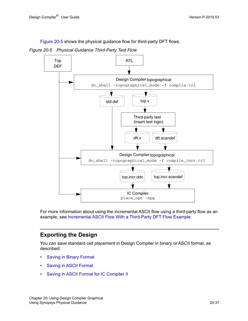
Design Compiler® User Guide Version P-2019.03
Figure 20-5 shows the physical guidance flow for third-party DFT flows.
Figure 20-5 Physical Guidance Third-Party Test Flow
For more information about using the incremental ASCII flow using a third-party flow as an example, see Incremental ASCII Flow With a Third-Party DFT Flow Example.
Exporting the Design
You can save standard cell placement in Design Compiler in binary or ASCII format, as described:
• Saving in Binary Format
• Saving in ASCII Format
• Saving in ASCII Format for IC Compiler II
DEF Top
Design Compiler topographical dc_shell -topographical_mode -f compile.tcl
IC Compiler place_opt -spg
Third-party test
RTL
top.vstd.def
top.incr.scandeftop.incr.ddc
(insert test logic)
Design Compiler topographical dc_shell -topographical_mode -f compile_incr.tcl
dft.scandefdft.v
Chapter 20: Using Design Compiler GraphicalUsing Synopsys Physical Guidance 20-37Chapter 20: Using Design Compiler GraphicalUsing Synopsys Physical Guidance 20-37

Design Compiler® User Guide P-2019.03Design Compiler® User Guide Version P-2019.03
Saving in Binary Format
You can save standard cell placement in .ddc format by using the write_file -format ddc command, or save it in Milkyway CEL format by using the write_milkyway command.
In regular topographical mode, the standard cell placement can only be used by Design Compiler for further optimization. IC Compiler does not use it. However, in the physical guidance flow, the standard cell placement information is propagated to IC Compiler through the .ddc file or the Milkyway CEL.
The physical constraints and floorplan information used for synthesis are not passed from Design Compiler to IC Compiler. However, physical constraint signatures are created from the physical constraints at the end of the compile_ultra -spg and the compile_ultra -incremental -spg command steps in the physical guidance flow. These signatures are saved in the .ddc file or Milkyway CEL view. IC Compiler reads the signatures when the physical guidance information is restored and matches them to the physical guidance information in IC Compiler to ensure consistency between the floorplan used in synthesis and the floorplan used for physical implementation.
All binary netlists that are generated in the physical guidance synthesis flow, whether a .ddc file or a Milkyway CEL, also contain a read-only dct_spg_flow_done attribute to signify that the design was implemented with the physical guidance flow. You can query the attribute to determine if your design .ddc file or Milkyway CEL was generated using the physical guidance flow.
Saving in ASCII Format
When you save the design in ASCII format, either in a Verilog or a VHDL netlist, the file that is created does not contain standard cell placement information or physical constraint signatures.
You can save the standard cell placement information in a DEF file by using the write_def command in Design Compiler or in floorplan exploration. You can then read the DEF file, along with the ASCII netlist, back into Design Compiler to be optimized with the compile_ultra -incremental -spg command, or you can read it into IC Compiler before the place_opt -spg step.
Design Compiler Graphical requires additional licensing to write out a DEF file. If you do not meet these licensing requirements, the DEF file that is written out cannot be read by third-party tools. For details about licensing, contact your Synopsys representative.
Note: The write_def -scan option is not supported in Design Compiler. Use the write_scan_def command to capture the scan chain information.
Chapter 20: Using Design Compiler GraphicalUsing Synopsys Physical Guidance 20-38

Design Compiler® User Guide Version P-2019.03
Saving in ASCII Format for IC Compiler II
You can generate all the files needed to load a design into IC Compiler II by using the write_icc2_files command.
The command writes the design files and Tcl scripts for the current design into the directory specified by the -output option. The files can include the following data:
• Netlist in Verilog format
• Propagated switching activity information (backward SAIF file)
• Tcl floorplan and DEF files
• Design’s power intent as a UPF command script
• Scan chain information in SCANDEF format
• Constraints in SDC format
• Cell expansion data
• Timing contexts (scenarios)
These scenarios are written in a format that can be read into IC Compiler II to create the same set of scenarios as specified in Design Compiler.
To write these design data files, the write_icc2_files command uses the write_file, write_saif, write_floorplan, save_upf, and write_timing_context commands.
In addition, the write_icc2_files command writes the following scripts:
• The Design Compiler settings in IC Compiler II format
• The top-level script to load all data generated in IC Compiler II
The scripts generated by the write_icc2_files command do not include scripts for library creation in IC Compiler II. You need to create a library that is consistent with the library used in Design Compiler and then source the top-level script.
When used with the set_host_options command, the write_icc2_files command uses up to the user-specified number of CPU cores on the same computer for parallel execution. See the description of the -max_cores option in the set_host_options man page for more information.
The write_icc2_files command uses the write_floorplan -format icc2 command to write out the physical constraints. For more information, see Saving Physical Constraints in IC Compiler II Format.
Chapter 20: Using Design Compiler GraphicalUsing Synopsys Physical Guidance 20-39Chapter 20: Using Design Compiler GraphicalUsing Synopsys Physical Guidance 20-39

Design Compiler® User Guide P-2019.03Design Compiler® User Guide Version P-2019.03
Writing Standard Cell Placement Only
You can write out the standard cell placement information exclusively by using the -golden_floorplan option with the write_icc2_files command:
dc_shell-topo> write_icc2_files -output icc2_files \-golden_floorplan my_golden.floorplan.tcl
All other floorplan information is excluded from the output files. For example, routing optimization performed by the Design Compiler Graphical tool, including layer promotion and nondefault routing rule definitions are excluded. You must set these floorplan constraints in the golden floorplan file to include them.
When you source the top-level script generated by the write_icc2_files command in the IC Compiler II tool, as shown in the following icc2_script.tcl file, the tool reads the golden floorplan file and the DEF file with the Design Compiler Graphical standard cell placement information to the IC Compiler II floorplan file:
################################################################### Read golden floorplan##################################################################if {[file exists my_golden.floorplan.tcl]} {source -continue_on_error my_golden.floorplan.tcl}################################################################### Read Design Compiler DEF (std cells)##################################################################if {[file exists ${_DCG_ICC2_DIR_}/my_design.floorplan/floorplan.def]}{read_def ${_DCG_ICC2_DIR_}/my_design.floorplan/floorplan.def }
Examples
The following examples show how to use the write_icc2_files command in Design Compiler Graphical to write the design files and Tcl scripts for the current design and then how to use the top-level script in IC Compiler II to load the design:
Example 20-3 Writing the Design Information From Design Compiler in IC Compiler II Format
# Perform synthesis and DFT insertiondc_shell-topo> compile_ultra -scan -gate_clock -spgdc_shell-topo> insert_dftdc_shell-topo> compile_ultra -scan –spg –incrementaldc_shell-topo> optimize_netlist –area
# Change names if neededdc_shell-topo> change_names -rules verilog –hierarchy
# Save the file for IC Compiler II using the write_icc2_files commanddc_shell-topo> write_icc2_files –output ./icc2_filesdc_shell-topo> quit
Chapter 20: Using Design Compiler GraphicalUsing Synopsys Physical Guidance 20-40

Design Compiler® User Guide Version P-2019.03
Example 20-4 Reading the Design into the IC Compiler II Tool
# Perform library setting in IC Compiler IIicc2_shell> source -echo –verbose icc2_lib_setting.tcl
# Load the design using script created by the write_icc2_files commandicc2_shell> source –echo –verbose icc2_files/ORCA.icc2_script.tcl
# Continue with the flowicc2_shell> commit_upficc2_shell> place_opt
If you run the write_icc2_files command and warnings or errors occur, the tool issues an information message that points to the location of the log file that contains the warning or error message information:
dc_shell-topo> write_icc2_files -output ./icc2_filesInformation: During the execution of write_icc2_files error messages wereissued, please check ./icc2_files/write_icc2_files.log files. (DCT-228)
Limitations
The write_icc2_files command currently has the following limitations:
• Hierarchical flows are not supported.
• Constraints set on library cells are not included except for the following:
❍ SDC constraints: set_timing_derate and set_driving_cell
❍ UPF constraints: map_isolation_cell, map_retention_cell, and map_level_shifter_cell
• The following commands are partially supported:
❍ set_congestion_options
The -max_util option is included only for global settings, not for regional settings.
❍ set_multi_vth_constraint
The setting is passed only for threshold-voltage groups defined in the library; the settings in user-defined groups are not included.
• The following variables are partially supported:
❍ power_default_toggle_rate_type
The equivalent IC Compiler II variable only supports the fastest_clock value. The absolute setting is not passed.
❍ placer_channel_detect_mode
Chapter 20: Using Design Compiler GraphicalUsing Synopsys Physical Guidance 20-41Chapter 20: Using Design Compiler GraphicalUsing Synopsys Physical Guidance 20-41
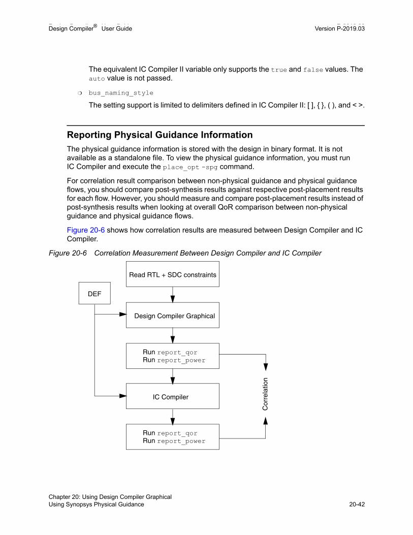
Design Compiler® User Guide P-2019.03Design Compiler® User Guide Version P-2019.03
The equivalent IC Compiler II variable only supports the true and false values. The auto value is not passed.
❍ bus_naming_style
The setting support is limited to delimiters defined in IC Compiler II: [ ], { }, ( ), and < >.
Reporting Physical Guidance Information
The physical guidance information is stored with the design in binary format. It is not available as a standalone file. To view the physical guidance information, you must run IC Compiler and execute the place_opt -spg command.
For correlation result comparison between non-physical guidance and physical guidance flows, you should compare post-synthesis results against respective post-placement results for each flow. However, you should measure and compare post-placement results instead of post-synthesis results when looking at overall QoR comparison between non-physical guidance and physical guidance flows.
Figure 20-6 shows how correlation results are measured between Design Compiler and IC Compiler.
Figure 20-6 Correlation Measurement Between Design Compiler and IC Compiler
Read RTL + SDC constraints
Design Compiler Graphical
Run report_qor Run report_power
IC Compiler
Run report_qor Run report_power
Cor
rela
tion
DEF
Chapter 20: Using Design Compiler GraphicalUsing Synopsys Physical Guidance 20-42

Design Compiler® User Guide Version P-2019.03
Physical Guidance Limitations
Physical guidance has the following limitations:
• IC Compiler does not support block abstractions created by Design Compiler. Therefore, in the hierarchical flow between Design Compiler and IC Compiler, you must use block abstractions created by IC Compiler.
• Design Compiler does not support the –top option with the compile_ultra command in the physical guidance flow.
Floorplan Exploration Floorplanning With IC Compiler
Design Compiler Graphical floorplan exploration allows you to use the IC Compiler floorplanning tools in the IC Compiler layout window. The following topics describe how to create, modify, and analyze floorplans in IC Compiler using Design Compiler Graphical.
• Floorplan Exploration Overview
• Enabling Floorplan Exploration
• Running Floorplan Exploration
• Using the Floorplan Exploration GUI
• Creating and Editing Floorplans
• Analyzing the Data Flow for Macro Placement
• Saving the Floorplan or Discarding Updates
• Saving the Floorplan into a Tcl Script File or DEF File
• Exiting the Session
• Incremental or Full Synthesis After Floorplan Changes
• Using Floorplan Exploration With a dc_shell Script
• Black Box Support
• Handling Physical Hierarchies and Block Abstractions
Floorplan Exploration Overview
Floorplan exploration allows you to perform floorplanning tasks, including floorplan analysis, floorplan creation, and floorplan modification from within the synthesis environment. Design Compiler Graphical floorplan exploration uses the IC Compiler floorplanning tools in the
Chapter 20: Using Design Compiler GraphicalFloorplan Exploration Floorplanning With IC Compiler 20-43Chapter 20: Using Design Compiler GraphicalFloorplan Exploration Floorplanning With IC Compiler 20-43

Design Compiler® User Guide P-2019.03Design Compiler® User Guide Version P-2019.03
IC Compiler layout window. Although you use the IC Compiler layout window, the interface between floorplan exploration in Design Compiler Graphical and the IC Compiler layout window is transparent, allowing you to move seamlessly between the Design Vision and IC Compiler layout windows.
Figure 20-7 shows a typical floorplan exploration flow. You read an RTL file, specify the physical and logic libraries, define the Synopsys design constraints, specify a floorplan (if you have one), and synthesize the design in Design Compiler Graphical. After synthesis, you evaluate the QoR results and use floorplan exploration to create a new floorplan or improve an existing floorplan, as needed.
Figure 20-7 Floorplan Exploration Flow
Enabling Floorplan Exploration
Before you begin floorplan exploration, you must have the following:
• A synthesized design
Design Compiler Graphical issues an error message if it finds any unmapped logic.
• Both the physical and logic libraries
All cells in the design must link to the physical and logic libraries.
After you have a synthesized design that links to the physical and logic libraries, you must set the design planning options, as described in the following steps:
1. In Design Compiler Graphical, open the GUI by entering the gui_start command.
2. In the GUI, open the layout window by choosing Window > New Layout Window.
3. Choose Floorplan > Set Design Planning Options.
The Set Design Planning Options dialog box appears, as shown in Figure 20-8.
Design Compiler Graphical
(RTL + SDC constraints + floorplan)
Synthesize design
Design Compiler Graphicalfloorplan exploration session
Save floorplan
Modify or create floorplan
Perform floorplan exploration
Chapter 20: Using Design Compiler GraphicalFloorplan Exploration Floorplanning With IC Compiler 20-44
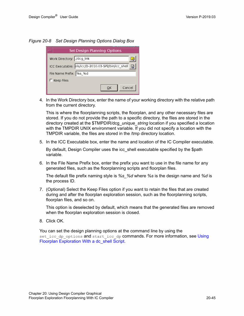
Design Compiler® User Guide Version P-2019.03
Figure 20-8 Set Design Planning Options Dialog Box
4. In the Work Directory box, enter the name of your working directory with the relative path from the current directory.
This is where the floorplanning scripts, the floorplan, and any other necessary files are stored. If you do not provide the path to a specific directory, the files are stored in the directory created at the $TMPDIR/dcg_unique_string location if you specified a location with the TMPDIR UNIX environment variable. If you did not specify a location with the TMPDIR variable, the files are stored in the /tmp directory location.
5. In the ICC Executable box, enter the name and location of the IC Compiler executable.
By default, Design Compiler uses the icc_shell executable specified by the $path variable.
6. In the File Name Prefix box, enter the prefix you want to use in the file name for any generated files, such as the floorplanning scripts and floorplan files.
The default file prefix naming style is %s_%d where %s is the design name and %d is the process ID.
7. (Optional) Select the Keep Files option if you want to retain the files that are created during and after the floorplan exploration session, such as the floorplanning scripts, floorplan files, and so on.
This option is deselected by default, which means that the generated files are removed when the floorplan exploration session is closed.
8. Click OK.
You can set the design planning options at the command line by using the set_icc_dp_options and start_icc_dp commands. For more information, see Using Floorplan Exploration With a dc_shell Script.
Chapter 20: Using Design Compiler GraphicalFloorplan Exploration Floorplanning With IC Compiler 20-45Chapter 20: Using Design Compiler GraphicalFloorplan Exploration Floorplanning With IC Compiler 20-45

Design Compiler® User Guide P-2019.03Design Compiler® User Guide Version P-2019.03
Running Floorplan Exploration
After you set the design planning options as described in Enabling Floorplan Exploration, you can start a floorplan exploration session by choosing Floorplan > Start Design Planning in the GUI. When you do this, the following actions are performed automatically:
• Design Compiler Graphical invokes floorplan exploration with simplified floorplanning menus in the IC Compiler layout window.
• Design Compiler Graphical transfers the design and its floorplan to the IC Compiler layout window.
• Design Compiler Graphical transfers all SDC constraints, attributes, and library setup files to IC Compiler for floorplanning.
• All Design Compiler Graphical windows and the Design Compiler Graphical shell are disabled until you exit the IC Compiler floorplanning session.
Chapter 20: Using Design Compiler GraphicalFloorplan Exploration Floorplanning With IC Compiler 20-46

Design Compiler® User Guide Version P-2019.03
Using the Floorplan Exploration GUI
Floorplan exploration in Design Compiler Graphical uses the IC Compiler layout window. By default, when you enable floorplan exploration, Design Compiler Graphical configures the IC Compiler layout window so that it includes only the menus and menu commands you need to perform Design Compiler Graphical floorplanning. Figure 20-9 shows the simplified floorplanning menu structure.
Figure 20-9 IC Compiler Simplified Layout Window Features
If you are an experienced IC Compiler user, you can use the full set of design planning menus.
You can access the full set of IC Compiler design planning menus by choosing File > Task > Design Planning, as shown in Figure 20-10. To switch from the full design planning menu structure back to the simplified menu structure, choose File > Task > DCG-DP Link.
Layout view
Menus
Toolbars
Overview
ViewSettings
panel
panel
Status bar
Floorplan menu
Chapter 20: Using Design Compiler GraphicalFloorplan Exploration Floorplanning With IC Compiler 20-47Chapter 20: Using Design Compiler GraphicalFloorplan Exploration Floorplanning With IC Compiler 20-47

Design Compiler® User Guide P-2019.03Design Compiler® User Guide Version P-2019.03
Figure 20-10 Switching Between Simplified and Full Design Planning Menu Structures
Any work you complete using the full set of IC Compiler design planning menus is available when you switch back to the simplified floorplanning menus.
For general information about working in the IC Compiler layout window, see the IC Compiler Help system and the IC Compiler Design Planning User Guide.
Creating and Editing Floorplans
Whether you use the simplified Design Compiler Graphical floorplanning menus or the full set of IC Compiler design planning menus, the IC Compiler layout window provides interactive tools and commands that you can use to create or modify your floorplan. You can
• Use editing tools to move, resize, copy, split, reshape, align, distribute, spread, or remove objects.
• Use editing commands to rotate or expand objects or to change cell orientations.
Shortcut keys are available for the most frequently performed editing operations. Online Help pages are provided for each of the editing tools.
In addition, you can use commands on the Floorplan menu to create physical objects such as placement blockages, bounds, and routing keepouts. When you create an object, you can specify its coordinates or draw the object in the layout view.
For more information about working with editing tools and commands in the IC Compiler layout window, see the IC Compiler Help system. For sample flows that show how to create a floorplan using Design Compiler Graphical floorplan exploration and how to modify a floorplan to improve timing or congestion, see SolvNet article 030613, “Design Compiler Graphical Floorplan Exploration Application Note.”
Access the full set of
Access the simplified floorplanning menus
design planning menus
Chapter 20: Using Design Compiler GraphicalFloorplan Exploration Floorplanning With IC Compiler 20-48

Design Compiler® User Guide Version P-2019.03
Analyzing the Data Flow for Macro Placement
Floorplan exploration allows you to analyze and improve the data flow through the physical design using the IC Compiler design planning data flow analysis tools. Information about the data flow can help you to decide what to do next to improve the placement of hard macros in your design.
After performing your initial macro placement in IC Compiler, you should analyze your floorplan to find areas of high congestion. If your macro placement appears to be causing congested hot spots, you can use the data flow analysis tools to examine hard macro placement and connectivity and to edit the macro placement.
To open the data flow analyzer window, choose Floorplan > Analyze Logic Connectivity. Alternatively, you can use the analyze_logic_connectivity command.
For information about using the data flow analysis tools, see the IC Compiler Help system and the IC Compiler Implementation User Guide.
Saving the Floorplan or Discarding Updates
You can save or discard floorplan updates in Design Compiler Graphical from the IC Compiler floorplanning session at any time using the “Update DC Floorplan” command. To save or discard the floorplan, perform the following steps:
1. Choose Floorplan > Update DC Floorplan.
The Update DC Floorplan dialog box appears, as shown in Figure 20-11.
Figure 20-11 Update DC Floorplan Dialog Box
The “Update DC Floorplan” command is available only in the simplified floorplanning menu structure for Design Compiler Graphical. For information about switching from the full set of design planning menus to the simplified floorplanning menu structure, see Using the Floorplan Exploration GUI.
2. Choose one of the following options:
❍ To save the current floorplan in Design Compiler Graphical, select the “Save current floorplan for DC” option.
Chapter 20: Using Design Compiler GraphicalFloorplan Exploration Floorplanning With IC Compiler 20-49Chapter 20: Using Design Compiler GraphicalFloorplan Exploration Floorplanning With IC Compiler 20-49
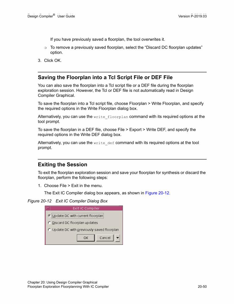
Design Compiler® User Guide P-2019.03Design Compiler® User Guide Version P-2019.03
If you have previously saved a floorplan, the tool overwrites it.
❍ To remove a previously saved floorplan, select the “Discard DC floorplan updates” option.
3. Click OK.
Saving the Floorplan into a Tcl Script File or DEF File
You can also save the floorplan into a Tcl script file or a DEF file during the floorplan exploration session. However, the Tcl or DEF file is not automatically read in Design Compiler Graphical.
To save the floorplan into a Tcl script file, choose Floorplan > Write Floorplan, and specify the required options in the Write Floorplan dialog box.
Alternatively, you can use the write_floorplan command with its required options at the tool prompt.
To save the floorplan in a DEF file, choose File > Export > Write DEF, and specify the required options in the Write DEF dialog box.
Alternatively, you can use the write_def command with its required options at the tool prompt.
Exiting the Session
To exit the floorplan exploration session and save your floorplan for synthesis or discard the floorplan, perform the following steps:
1. Choose File > Exit in the menu.
The Exit IC Compiler dialog box appears, as shown in Figure 20-12.
Figure 20-12 Exit IC Compiler Dialog Box
Chapter 20: Using Design Compiler GraphicalFloorplan Exploration Floorplanning With IC Compiler 20-50

Design Compiler® User Guide Version P-2019.03
2. Choose one of the following options:
❍ Select the “Update DC with current floorplan” option to save the current floorplan in Design Compiler Graphical and exit the floorplan exploration session.
❍ To exit the floorplan exploration session and discard the floorplan, including any previously saved floorplans, select the “Discard DC floorplan updates” option.
❍ To keep the floorplan that you saved previously in Design Compiler Graphical, discard any subsequent changes that you have not saved, and exit the floorplan exploration session, select the “Update DC with previously saved floorplan” option.
3. Click OK.
When you exit the floorplan exploration session, the Design Compiler Graphical windows and shell interface become active.
If you update the floorplan, the tool closes the original Design Vision layout window. To see the floorplan changes, open a new Design Vision layout window.
Incremental or Full Synthesis After Floorplan Changes
The floorplan changes affect the design during synthesis. After you create a floorplan or modify an existing floorplan using floorplan exploration, you need to update the floorplan constraints by using the write_floorplan command, as shown, before continuing with any additional synthesis runs:
dc_shell-topo> write_floorplan -all DESIGN.fp
Then, use the read_floorplan command to read the floorplan in Design Compiler for synthesis. After you read the RTL file, the SDC constraints, and the new floorplan file, you can perform incremental synthesis by using the compile_ultra -incremental command for a quick assessment of the floorplan’s QoR benefits. Incremental synthesis might not meet the requirements for achieving good QoR results or the requirements for a final implementation flow. In these cases, perform full synthesis using the compile_ultra command.
Design Compiler Graphical also allows you to make floorplan changes interactively on the command line between the initial compile_ultra -spg step and subsequent -incremental -spg compilation steps without updating the floorplan constraints with the write_floorplan command. In this case, you must use the supported floorplan modification commands described in SolvNet article 1502496, “Making Floorplan Changes After Running the compile_ultra -spg Command.” However, the tool issues a warning message, indicating that it detected floorplan changes.
Chapter 20: Using Design Compiler GraphicalFloorplan Exploration Floorplanning With IC Compiler 20-51Chapter 20: Using Design Compiler GraphicalFloorplan Exploration Floorplanning With IC Compiler 20-51

Design Compiler® User Guide P-2019.03Design Compiler® User Guide Version P-2019.03
See Also
• Using Floorplan Physical Constraints
Provides information about the read_floorplan and write_floorplan commands
• Overview of Topographical Technology
Provides information about synthesizing the design in topographical mode
Using Floorplan Exploration With a dc_shell Script
You can perform floorplan exploration from a script. Scripts allow you to create and modify floorplans on the command line.
Use the following commands in Design Compiler Graphical to perform floorplan exploration with a script:
1. Use the set_icc_dp_options command to specify the IC Compiler executable and other setup requirements.
The following options are available with the set_icc_dp_options command:
❍ -work_dir directory
Specifies the directory where the temporary files are created and stored.
If you do not provide the path to a specific directory, the files are stored in the directory created at the $TMPDIR/dcg_unique_string location if you specified a location with the TMPDIR UNIX environment variable. If you did not specify a location with the TMPDIR variable, the files are stored in the /tmp directory location.
❍ -icc_executable executable
Specifies the path to icc_shell.
❍ -check
Performs permission checks and reports any errors that would prevent the start_icc_dp command from successfully launching the floorplan exploration session.
❍ -file_name_prefix file_name
Specifies the prefix for the name of any generated files.
❍ -keep_files
Specifies to keep the temporary files.
2. (Optional) Use the report_icc_dp_options command to report the options specified by the set_icc_dp_options command.
Chapter 20: Using Design Compiler GraphicalFloorplan Exploration Floorplanning With IC Compiler 20-52

Design Compiler® User Guide Version P-2019.03
If you do not specify any options using the set_icc_dp_options command, report_icc_dp_options reports the default settings.
The following options are available with the report_icc_dp_options command:
❍ -check
Performs permission checks and reports any errors that would prevent the start_icc_dp command from successfully launching the floorplan exploration session.
❍ -verbose
Prints verbose messages.
3. Use the start_icc_dp command to launch the floorplan exploration session.
The start_icc_dp command uses the IC Compiler executable specified by the set_icc_dp_options command. To source a script, use the -f option with the start_icc_dp command:
dc_shell-topo> start_icc_dp -f ../../scripts/script_file_name.tcl
The start_icc_dp command sources the file specified with the -f option and runs the script in floorplan exploration.
The following options are available with the start_icc_dp command:
❍ -check_only
Performs permission checks and reports any errors that would prevent the start_icc_dp command from successfully launching the floorplan exploration session.
❍ -verbose
Prints verbose messages.
❍ -f file_name
Specifies the path to the script file to be sourced.
Note: If you run floorplan exploration from a batch script, by using the -f option on the command line when you start the tool, the start_icc_dp command closes the GUI automatically before starting the floorplan exploration session.
To ensure that IC Compiler saves the floorplan to Design Compiler Graphical when exiting the floorplan exploration session, you must include the update_dc_floorplan command in the IC Compiler floorplanning script after the floorplan creation or modification steps. After
Chapter 20: Using Design Compiler GraphicalFloorplan Exploration Floorplanning With IC Compiler 20-53Chapter 20: Using Design Compiler GraphicalFloorplan Exploration Floorplanning With IC Compiler 20-53

Design Compiler® User Guide P-2019.03Design Compiler® User Guide Version P-2019.03
the update_dc_floorplan command, you must include the exit command in the IC Compiler floorplanning script to return to the Design Compiler Graphical shell interface:
# After many IC Compiler floorplanning script commands:update_dc_floorplanexit
The following example shows a Design Compiler Graphical script used in a floorplan exploration session. It sources an IC Compiler floorplanning script called iccdp_script.tcl.
compile_ultra –scanset_icc_dp_options -icc_executable \
"/global/apps5/icc_2010.03-SP1-1/bin/icc_shell"start_icc_dp –f iccdp_script.tclcompile_ultra –scan -incremental
Black Box Support
Design Compiler Graphical supports floorplan exploration with netlists that contain black box cells. If a design has black box cells, you do not need to perform any additional steps or modify the floorplan exploration flow. The black boxes that are defined or created in Design Compiler Graphical are transferred to IC Compiler design planning automatically. Using IC Compiler, you can edit the floorplan with black boxes during the floorplanning session and transfer the modifications back to Design Compiler Graphical.
See Also
• Handling Black Boxes
Handling Physical Hierarchies and Block Abstractions
Design Compiler Graphical transfers Design Compiler topographical physical hierarchies and Design Compiler topographical block abstractions to IC Compiler design planning automatically during floorplan exploration. Both physical hierarchies and block abstractions are transferred as macros with quick timing models in the block. For multicorner-multimode designs, only the current scenario timing information is transferred to IC Compiler.
When transferring Design Compiler topographical physical hierarchies and block abstractions to IC Compiler for design planning, Design Compiler Graphical automatically sets the dct_physical_hier attribute to true on the instances.
Chapter 20: Using Design Compiler GraphicalFloorplan Exploration Floorplanning With IC Compiler 20-54

Design Compiler® User Guide Version P-2019.03
Querying Hierarchical Blocks and Pin Connections
To return all the Design Compiler topographical hierarchical blocks, including physical hierarchies and block abstractions, use the dct_physical_hier attribute as shown:
icc_shell> get_cells –hierarchical –filter dct_physical_hier==true{GPRs Multiplier}
The Design Compiler topographical physical hierarchies and block abstractions are preserved when brought back to Design Compiler Graphical.
To query the nets connected to the pin of a hierarchical block, use the -boundary_type lower or -boundary_type upper option with the get_nets command for the net inside or outside the hierarchical block, respectively. To query both nets, specify the both keyword. If you do not specify the -boundary_type option, the command returns the net outside the hierarchical block. When using this option, you must specify a pin by using the -of_objects option.
For example, the following two commands return the topnet net connected to the in pin outside the u2 hierarchical block:
dc_shell-topo> get_nets -of_objects u2/in{topnet} dc_shell-topo> get_nets -of_objects u2/in -boundary_type upper {topnet}
The following command returns the u2/in net connected to the in pin inside the u2 hierarchical block:
dc_shell-topo> get_nets -of_objects u2/in -boundary_type lower{u2/in}
See Also
• Using Hierarchical Models
Floorplan Exploration Floorplanning With IC Compiler II
Design Compiler Graphical allows you to perform floorplan exploration using the IC Compiler II design planning tools in the IC Compiler II layout window. After synthesis, you can evaluate the quality of results and use floorplan exploration to create a floorplan or improve an existing floorplan in IC Compiler II. The interface between floorplan exploration in Design Compiler and the IC Compiler II layout window is seamless.
• License Requirements
• Prerequisites for Floorplan Exploration
• Command Summary
Chapter 20: Using Design Compiler GraphicalFloorplan Exploration Floorplanning With IC Compiler II 20-55Chapter 20: Using Design Compiler GraphicalFloorplan Exploration Floorplanning With IC Compiler II 20-55

Design Compiler® User Guide P-2019.03Design Compiler® User Guide Version P-2019.03
• Running the Floorplan Exploration Flow
• Data Transfer to IC Compiler II
See Also
• Floorplan Exploration Floorplanning With IC Compiler
• SolvNet article 030613, “Design Compiler Graphical Floorplan Exploration Application Note” for sample flows that show how to create a floorplan using Design Compiler Graphical floorplan exploration and how to modify a floorplan to improve timing or congestion
License Requirements
Running the floorplan exploration flow using the start_icc2 command requires an IC Compiler II license in addition to a Design Compiler Graphical license. For licensing details, contact your Synopsys representative.
Prerequisites for Floorplan Exploration
Before performing floorplan exploration in IC Compiler II, you must perform the following tasks:
• Synthesize the design
You must run IC Compiler II on a synthesized (mapped) design.
• Generate IC Compiler II reference libraries
Because the reference libraries are not automatically converted by Design Compiler, you must generate the libraries using the IC Compiler II Library Manager.
• Specify the golden UPF if the golden UPF flow is enabled in Design Compiler
Chapter 20: Using Design Compiler GraphicalFloorplan Exploration Floorplanning With IC Compiler II 20-56

Design Compiler® User Guide Version P-2019.03
Command Summary
The following table summarizes the commands to use floorplan exploration in IC Compiler II.
When you run the start_icc2 command, the files needed to invoke IC Compiler II are written to the $TMPDIR/dcg_unique_string working directory if you specified a location with the TMPDIR UNIX environment variable. If you did not specify a location with the TMPDIR variable, the files are stored in the /tmp directory location. To change the default directory, specify the -work_dir option with the set_icc2_options command.
Note: Do not use the start_icc2 and start_icc_dp commands in the same Design Compiler session.
Table 20-1 Commands to Use Floorplan Exploration in IC Compiler II
Command Description
set_icc2_options Specifies the IC Compiler II executable, IC Compiler II reference libraries, and other setup requirements.
report_icc2_options Reports the options specified by the set_icc2_options command.
start_icc2 Launches a design planning session in IC Compiler II.
update_dc_floorplan Saves the floorplan created or edited in the IC Compiler II design planning session to Design Compiler Graphical.
Note: The update_dc_floorplan command works only in an IC Compiler II session invoked using start_icc2.
Chapter 20: Using Design Compiler GraphicalFloorplan Exploration Floorplanning With IC Compiler II 20-57Chapter 20: Using Design Compiler GraphicalFloorplan Exploration Floorplanning With IC Compiler II 20-57

Design Compiler® User Guide P-2019.03Design Compiler® User Guide Version P-2019.03
Running the Floorplan Exploration FlowThe following figure shows an overview of floorplan exploration from Design Compiler Graphical to design planning in IC Compiler II.
Figure 20-13 Flow From Design Compiler Graphical to Floorplan Exploration in IC Compiler II
Before running floorplan exploration, you must complete the following tasks:
1. Synthesize the design by using the compile_ultra command.
2. Specify IC Compiler II reference libraries by using the set_icc2_options command.
For example,
dc_shell-topo> set_icc2_options -icc2_executable ../icc2_shell \-ref_libs "lib1.ndm lib2.ndm"
When you create a DEF file in Design Compiler NXT or Design Compiler Graphical to hand off a design while invoking IC Compiler II, the site name in the DEF file is from the Milkyway reference library. When you read this DEF file in the IC Compiler II link, mismatch between the site name in the Milkyway reference library and the tile name in technology file might occur resulting in the following DEFR-004 error message:
Error: Cannot find site 'unit'. (DEFR-004)
To avoid the tool from issuing the DEFR-004 error message due to site name mismatch, use the -convert_sites {from_site to_site} option as shown in the following example:
RTLFloorplan
Design Compiler
Physicallibrary
IC Compiler IIreference libraries Design Planning
(optional)
IC Compiler II
start_icc2
Constraints
update_dc_floorplan
FloorplanNetlist +floorplan +constraints
Logiclibrary
Chapter 20: Using Design Compiler GraphicalFloorplan Exploration Floorplanning With IC Compiler II 20-58

Design Compiler® User Guide Version P-2019.03
prompt> set_icc2_options -ref_libs "lib1.ndm" -technology tech.tf \ -convert_sites {unit CORE}
In this example,
• from_site (unit) is the site name in the Milkyway reference library
• to_site (Core) is the tile name in the technology file that is passed to the IC Compiler II tool
The set_icc2_options -convert_sites command converts the site name from "unit" to "CORE" when the tool reads the DEF file after invoking IC Compiler II and issues the following message:
Information: Converted site definition 'unit' to 'CORE'. (DEFR-031)
The following sections describe the floorplan exploration steps in interactive mode and in batch mode using a dc_shell script.
In Interactive Mode
To start the floorplan exploration flow,
1. In Design Compiler Graphical, start an IC Compiler II design planning session by using the start_icc2 command.
The start_icc2 command opens the IC Compiler II layout window and the icc2_shell> prompt is displayed.
2. In IC Compiler II, perform floorplan exploration.
You can create a floorplan or edit an existing floorplan using the design planning tools in the IC Compiler II layout window.
3. Save the updated floorplan by using the update_dc_floorplan command in icc2_shell.
The floorplan data in IC Compiler II is transferred to Design Compiler Graphical. If you do not perform this step, the floorplan changes performed in IC Compiler II are not updated in Design Compiler Graphical and are lost.
4. (Optional) To preserve the floorplan files in step 3, specify the -keep_files option with the set_icc2_options command.
5. End the design planning session by entering the exit command in icc2_shell.
You are returned to the dc_shell-topo> prompt.
Chapter 20: Using Design Compiler GraphicalFloorplan Exploration Floorplanning With IC Compiler II 20-59Chapter 20: Using Design Compiler GraphicalFloorplan Exploration Floorplanning With IC Compiler II 20-59

Design Compiler® User Guide P-2019.03Design Compiler® User Guide Version P-2019.03
In Batch Mode
To run floorplan exploration from a batch script, specify the -f script_file option with the start_icc2 command when you start Design Compiler Graphical. In batch mode, the start_icc2 command invokes IC Compiler II and executes the specified script, but it does not open the GUI.
The following script shows an example of the general floorplan exploration flow with IC Compiler II:
#Perform synthesis using compile_ultracompile_ultra –scan –gate_clock -spg
#Set the IC Compiler II options set_icc2_options -icc2_executable ../icc2_shell \-ref_libs "lib1.ndm lib2.ndm"
#Launch IC Compiler II session in batch modestart_icc2 -f my_icc2.tcl
my_icc2.tcl batch script example:
#This example script moves the macro I_RAM by 10 micronsset_placement_status placed [get_cells I_RAM] move_objects -delta {10 10} [get_cells I_RAM]set_placement_status fixed [get_cells I_RAM]
#Update the floorplan changes before exitupdate_dc_floorplanexit
Chapter 20: Using Design Compiler GraphicalFloorplan Exploration Floorplanning With IC Compiler II 20-60

Design Compiler® User Guide Version P-2019.03
Data Transfer to IC Compiler II
When you launch IC Compiler II within Design Compiler Graphical, design data is automatically transferred to IC Compiler II. The following table shows which design and environment settings are and are not transferred from Design Compiler Graphical to IC Compiler II.
Table 20-2 Design and Environment Settings That Are and Are Not Transferred to IC Compiler II
Transfer Design and environment settings
Transferred Verilog netlist
Timing constraints (in a format compatible with IC Compiler II)
Floorplan constraints using a DEF file and a Tcl floorplan file that is compatible with IC Compiler II
Technology file
TLUPlus file
UPF file
Attributes:
• dont_touch
• size_only
• dont_use on library cells
• Note: Other attributes need to be reapplied in IC Compiler II
Layer-related constraints
• Net routing layer constraints
• Preferred routing directions
• Ignored layer settings
Not transferred Hierarchical models
• Design Compiler and IC Compiler block abstractions and physical hierarchies are treated as unresolved references in icc2_shell.
Estimations of physical black boxes
• These physical cells are created by the estimate_fp_black_boxes command.
Relative placement constraints
• These constraints are created in Design Compiler.
Chapter 20: Using Design Compiler GraphicalFloorplan Exploration Floorplanning With IC Compiler II 20-61Chapter 20: Using Design Compiler GraphicalFloorplan Exploration Floorplanning With IC Compiler II 20-61

Design Compiler® User Guide P-2019.03Design Compiler® User Guide Version P-2019.03
Working With Via Ladders
A via ladder, also known as a via pillar, is a stacked via that starts from the pin layer and extends into an upper layer where the router connects to it. Via ladders are used to improve timing QoR and electromigration robustness.
To learn how to work with via ladders in the Design Compiler Graphical tool, see the following topics:
• Reading In Via Ladders Defined in the Technology File
• Creating, Querying, Removing, and Reporting Via Ladders
• Performing What-If Analysis With Via Ladders
• Performing Via-Ladder-Aware Optimization
Reading In Via Ladders Defined in the Technology File
Via ladders are usually defined in the technology file and read in by the tool. If via ladders are not defined in the technology file, you can create them with Tcl commands.
The following example shows a via ladder defined in the technology file:
ViaRule "VL3" { cutLayerNameTbl = (VIA1,VIA2,VIA3) cutNameTbl = (Vs,Vs,Vs) numCutRowsTbl = (2,2,1) numCutsPerRowTbl = (1,2,2) }
Creating, Querying, Removing, and Reporting Via Ladders
If via ladders are not defined in the technology file, you can use the following commands to create, query, report, and remove via ladders:
• create_via_rule—Creates new via ladders.
• get_via_rules—Returns the via rules created by the create_via_rule command and the via rules read in from the technology file.
• report_via_rules—Reports the via ladder rules created by the create_via_rule command and the via rules read in from technology file.
• remove_via_rules—Removes via rules created by the set_via_ladder_rules command.
Chapter 20: Using Design Compiler GraphicalWorking With Via Ladders 20-62

Design Compiler® User Guide Version P-2019.03
There are two flows for using via ladders:
• The “what-if analysis” flow in which you manually associate a pin with a via ladder and check its impact on timing
• The “via-ladder-aware optimization” flow in which you allow the tool to infer via ladders during synthesis to improve timing QoR or electromigration robustness.
Performing What-If Analysis With Via Ladders
In the what-if analysis flow, you manually associate a pin with a via ladder and check its impact on timing.
Before starting the what-if analysis flow,
1. Confirm that via ladders are defined in the technology file or create them with Tcl commands.
2. Enable the use of enhanced timing models during RC estimation by setting the spg_enhanced_timing_model variable to true.
3. Enable via resistance support for the driver pin of the cells by setting the physopt_enable_root_via_res_support variable to true.
4. Compile the design with the compile_ultra -spg command.
Follow these steps to perform what-if analysis with via ladders:
1. Set a via ladder on a pin of a cell instance or on a pin of a library reference by using the set_via_ladder_constraints or set_via_ladder_rules command.
2. (Optional) Report the via ladder settings by using the report_via_ladder_constraints or report_via_ladder_rules command.
3. (Optional) Remove the via ladder settings by using the remove_via_ladder_constraints or remove_via_ladder_rules command.
4. Re-estimate the timing of the design or timing path using the extract_rc -estimate command.
5. Check the timing impact on the design or path using the report_timing and report_qor commands. A “v” symbol in the report indicates via ladders.
Chapter 20: Using Design Compiler GraphicalWorking With Via Ladders 20-63Chapter 20: Using Design Compiler GraphicalWorking With Via Ladders 20-63

Design Compiler® User Guide P-2019.03Design Compiler® User Guide Version P-2019.03
Performing Via-Ladder-Aware Optimization
In the via-ladder-aware optimization flow, you allow the tool to infer via ladders during synthesis.
Before starting the via-ladder-aware flow,
1. Confirm that via ladders are defined in the technology file or create them with Tcl commands.
2. Enable the use of enhanced timing models during RC estimation by setting the spg_enhanced_timing_model variable to true.
3. Enable via resistance support for the driver pin of the cells by setting the physopt_enable_root_via_res_support variable to true.
4. Enable via-ladder optimization by setting the spg_enable_via_ladder_opto variable to true.
Follow these steps to perform via-ladder-aware optimization:
1. Specify the via ladder candidates on library pins by using the set_via_ladder_candidate command.
2. (Optional) Report the via ladder candidates by using the report_via_ladder_candidates command.
3. (Optional) Remove the via ladder candidates by using the reset_via_ladder_candidate command.
4. (Optional) Specify the is_em_via_ladder_required attribute on the library pin if electromigration via ladders are required to improve electromigration robustness.
5. Run synthesis in physical guidance mode.
6. (Optional) Report via ladders in the design after optimization by using the report_via_ladder_constraints command.
7. Provide via ladders and settings to the IC Compiler II tool by using the write_icc2_files command.
The report_timing report displays a “v” to indicate where there are via ladders on pins. You can also report the via ladders added during optimization by using the report_via_ladder_constraints command.
For more details, see SolvNet article 2624185 “Via Ladder Support in Design Compiler Graphical.”
Chapter 20: Using Design Compiler GraphicalWorking With Via Ladders 20-64
Design Compiler® User Guide Version P-2019.03
Assigning of Via Ladders on Nets
To control the assignment of via ladders on nets, use the following variables:
• To set a minimum length threshold on the nets considered for via ladder assignment during optimization, use the optimize_via_ladder_net_length_threshold variable.
The value you specify is multiplied by the minimum height of the unit tile. For example, if you set the variable to 125, the minimum length threshold for nets considered for via ladder assignment is 125 times the minimum height of the unit tile. The default is 100.
dc_shell-topo> set_app_var optimize_via_ladder_net_length_threshold 125
• To choose via ladders on driver pins in a timing path within a specific slack range during optimization, use the optimize_via_ladder_critical_range variable.
The driver pins in the timing path that fall within the following range are considered for via ladder insertion:
[WNS, WNS*(1 - optimize_via_ladder_critical_range)]
By default, the optimize_via_ladder_critical_range variable is 0.5. Therefore, if the worst negative slack (WNS) is -1000, the range is [-1000, -500] where -500 = -1000 * (1-0.05). If the delay value falls into this range, it is considered critical.
The tool chooses the driver pins for via ladder insertion when you run the compile_ultra -spg or optimize_netlist -area command.
Working With Must-Join Pins
Some standard cells have multiple output terminals that must be connected together. When these must-join pins have a pattern_must_join attribute, the IC Compiler II router uses a predefined pattern to join the pin shapes together. The Design Compiler Graphical tool can recognize pattern_must_join attributes on library pins in the Milkyway FRAM view and perform RC extraction taking the pattern_must_join attributes into consideration.
To enable RC estimation based on pattern_must_join attributes in the Design Compiler Graphical tool,
1. Make sure the Milkyway library has pins with the pattern_must_join attribute.
2. Enable the following variables. The variables are false by default.
a. Enable the enhanced timing model:
dc_shell-topo> set_app_var spg_enhanced_timing_model true
b. Enable via resistance support for the driver pin of the cells:
Chapter 20: Using Design Compiler GraphicalWorking With Must-Join Pins 20-65Chapter 20: Using Design Compiler GraphicalWorking With Must-Join Pins 20-65

Design Compiler® User Guide P-2019.03Design Compiler® User Guide Version P-2019.03
dc_shell-topo> set_app_var physopt_enable_root_via_res_support true
c. Enable via ladder optimization and pattern_must_join attribute recognition:
dc_shell-topo> set_app_var spg_enable_via_ladder_opto true
3. Synthesize the design in physical guidance mode:
dc_shell-topo> compile_ultra -scan -spg
When you enable the variables, the tool performs RC estimation based on the pattern_must_join attributes during optimization. If a library pin has both a pattern_must_join attribute and via ladder candidates, the via ladder has higher priority if the estimated delay based on the pattern_must_join attribute and the via ladder is the same.
The pattern_must_join attributes are stored in the .ddc file and available in future Design Compiler Graphical sessions.
See Also
• Querying and Reporting the pattern_must_join Attribute
• Checking the Inconsistency of pattern_must_join Attributes on Library Pins
Querying and Reporting the pattern_must_join Attribute
You can query the pattern_must_join attribute as shown:
• dc_shell-topo> get_attribute [get_pins */BUFF/Z] pattern_must_join
• dc_shell-topo> get_attribute [get_lib_pins */BUFF/Z] pattern_must_join
You can get a list of pins that have the pattern_just_join attribute as shown:
dc_shell-topo> get_lib_pins my_library/*/* \-filter {pattern_must_join == true}
You can report the cells that have a pattern_must_join attribute as shown:
dc_shell-topo> get_cells -of_objects [get_pins -hierarchical \ -filter {pattern_must_join == true}]
The report_timing report also reports the pattern_must_join attribute. A “v” in the report indicates a cell with the pattern_must_join attribute.
Chapter 20: Using Design Compiler GraphicalWorking With Must-Join Pins 20-66

Design Compiler® User Guide Version P-2019.03
Checking the Inconsistency of pattern_must_join Attributes on Library Pins
You can report inconsistencies among pattern_must_join attributes on library pins in the Design Compiler Graphical tool by using the following options with the report_lib command:
• -pattern_must_join_pin
Reports inconsistencies in pattern_must_join attributes that are set on library pins. Inconsistencies that are reported include
❍ Output pins with multiple shapes on the same metal layer that do not have a pattern_must_join attribute set on them
❍ Output pins with multiple shapes on different metal layers that have a pattern_must_join attribute set on them
• -pattern_must_join_pin_exclusion_list
Excludes pins from being reported when specified with the -pattern_must_join_pin option
Before you use the report_lib command to report pattern_must_join attribute inconsistencies, you must
1. Ensure that the Library Compiler tool is installed and its executable is located in the Design Compiler installation directory
2. Enable via ladder optimization and pattern_must_join attribute recognition by setting the spg_enable_via_ladder_opto variable to true
The following example reports all inconsistencies among pattern_must_join attributes in the specified library:
dc_shell-topo> report_lib library -pattern_must_join_pin****************************************Report : library...****************************************#BEGIN_REPORT_PATTERN_MUST_JOIN_PIN------------------------------------------------------------------target library: my_lib------------------------------------------------------------------Report of single metal layer multi-terminals ports withoutpattern-must-join setting:Warning: All terminals of the port 'ZN' of cell 'xyz' are on asingle metal layer 'M1'. However, the 'pattern_must_join' attributeis not set as true on this port, which makes conflicts. (FRAM-075)Total number of cells with single metal layer multi-terminals portwithout pattern-must-join setting: 1 (out of 197)
Chapter 20: Using Design Compiler GraphicalWorking With Must-Join Pins 20-67Chapter 20: Using Design Compiler GraphicalWorking With Must-Join Pins 20-67

Design Compiler® User Guide P-2019.03Design Compiler® User Guide Version P-2019.03
Report of pattern-must-join ports with terminals on multiple metallayers:Total number of cells with terminals on multiple metal layers but withpattern must-join ports: 0 (out of 0)
#END_REPORT_PATTERN_MUST_JOIN_PIN
The following example excludes the Z pin in the XOR2 library cell from the report:
dc_shell-topo> report_lib library -pattern_must_join_pin \-pattern_must_join_pin_exclusion_list [get_lib_pins */XOR2/Z]
Inbound Cell Optimization
Inbound cells are standard cells that extend beyond PG pins in placement rows so that the PG pins are completely inside the cell boundary. Inbound cells are generally faster than other library cells, but they pose challenges during legalization and placement. For example, same-color edges cannot be abutted, and inbound cells lead to half-row fragmentation during placement because they extend beyond placement rows.
The Design Compiler tool generally uses inbound cells during synthesis for better post-synthesis QoR. However, the QoR can degrade after placement, especially in high-density designs, due to half-row fragmentation and displacement as a result of the legalization constraints. Inbound cell optimization allows you to control the inbound cell percentage in the synthesized netlist to avoid QoR degradation during placement.
To enable inbound cell optimization in the Design Compiler Graphical tool, do the following before running the compile_ultra, compile_ultra -incremental, or optimize_netlist -area command:
1. Get the inbound cell site definition name from the technology file, and specify the inbound cell site definition name in the tool using the same name. For example:
dc_shell-topo> set_app_var compile_inbound_sitedef_name ibunit
2. Enable inbound cell optimization by setting the following variable to true (the default is false):
dc_shell-topo> set_app_var compile_inbound_cell_optimization true
3. (Optional) Limit the number of inbound cells to a specific percentage of cells by setting the following variable (by default, the tool allows up to 10 percent):
dc_shell-topo> set_app_var compile_inbound_max_cell_percentage 5.0
The percentage value can change based on the design characteristics. However, as a general guideline, limit inbound cell usage to a smaller percentage for high-density designs.
Chapter 20: Using Design Compiler GraphicalInbound Cell Optimization 20-68

Design Compiler® User Guide Version P-2019.03
The write_icc2_files output includes the inbound cell site definition name for the IC Compiler II tool.
To report inbound cell usage in a design, use the report_inbound_cell command:
dc_shell-topo> report_inbound_cell
****************************************Report : inbound_cellDesign : my_design...**************************************** Inbound Cell Design Summary ------------------------------------------------------------ | Inbound max cell percentage | 10.00% | | | | | Number of inbound cells used | 4879 | | | | | Percentage of inbound cells used | 9.48% | -----------------------------------------------------------
Chapter 20: Using Design Compiler GraphicalInbound Cell Optimization 20-69Chapter 20: Using Design Compiler GraphicalInbound Cell Optimization 20-69

Design Compiler® User Guide P-2019.03Design Compiler® User Guide Version P-2019.03
Optimizing Multicorner-Multimode Designs
Multicorner-multimode design optimization is a feature available only in the Design Compiler Graphical tool. This feature enables you to analyze and optimize designs across multiple modes and multiple corners concurrently.
This section describes multicorner-multimode design optimization, in the following subsections:
• Multicorner-Multimode Concepts
• Multicorner-Multimode Feature Support
• Unsupported Features for Multicorner-Multimode Designs
• Basic Multicorner-Multimode Flow
• Creating a Scenario
• Concurrent Multicorner-Multimode Optimization and Timing Analysis
• Power Optimization in Multicorner-Multimode Designs
• Setting Up the Design for a Multicorner-Multimode Flow
• Handling Libraries in the Multicorner-Multimode Flow
• Scenario Management Commands
• Reporting Commands for Multicorner-Multimode Designs
• Supported SDC Commands for Multicorner-Multimode Designs
• Multicorner-Multimode Script Example
• Using Block Abstractions in Multicorner-Multimode Designs
Chapter 20: Using Design Compiler GraphicalOptimizing Multicorner-Multimode Designs 20-70
Design Compiler® User Guide Version P-2019.03
Multicorner-Multimode Concepts
Designs must often operate under multiple operating conditions, often called corners, and in multiple modes. Such designs are referred to as multicorner-multimode designs. Design Compiler Graphical extends the topographical technology to analyze and optimize these designs across multiple modes and multiple corners concurrently.
The multicorner-multimode feature also provides ease-of-use and compatibility between flows in Design Compiler and IC Compiler due to the similar user interface. The following terms are commonly used to describe multicorner-multimode technology:
• Corner
A corner is defined as a set of libraries characterized for process, voltage and temperature (PVT) variations. Corners are not dependent on functional settings; they are meant to capture variations in the manufacturing process, along with expected variations in the voltage and temperature of the environment in which the chip will operate.
• Mode
A mode is defined by a set of clocks, supply voltages, timing constraints, and libraries. It can also have annotation data, such as SDF or parasitics files. Multicorner-multimode designs can operate in many modes such as the test mode, mission mode, standby mode and so forth.
• Scenario
A scenario is a combination of modal constraints and corner specifications. In a design, the tool uses a scenario or a set of scenarios as the unit for multimode-multicorner analysis and optimization. Some constraints can be part of both the mode and corner specification. Optimization of multicorner-multimode design involves managing the scenarios of the design. For more details on scenario management, see Scenario Management Commands.
Multicorner-Multimode Feature Support
The multicorner-multimode feature in Design Compiler Graphical provides compatibility between flows in Design Compiler and IC Compiler through the use of a similar user interface.
Keep the following points in mind when running multicorner-multimode optimizations:
• All options of the compile_ultra command are supported.
• Leakage power optimization is supported.
See Power Optimization in Multicorner-Multimode Designs.
Chapter 20: Using Design Compiler GraphicalOptimizing Multicorner-Multimode Designs 20-71Chapter 20: Using Design Compiler GraphicalOptimizing Multicorner-Multimode Designs 20-71

Design Compiler® User Guide P-2019.03Design Compiler® User Guide Version P-2019.03
• Dynamic power optimization is supported.
See Power Optimization in Multicorner-Multimode Designs
• The UPF flow is supported only for multivoltage designs.
Unsupported Features for Multicorner-Multimode Designs
The following features are not supported in Design Compiler Graphical for multicorner-multimode designs:
• Clock tree estimation is not supported.
• k-factor scaling is not supported.
Because multicorner-multimode design libraries do not support the use of k-factor scaling, the operating conditions that you specify for each scenario must match the nominal operating conditions of one of the libraries in the list of the link libraries.
• The set_min_library command is not supported for individual scenarios.
The set_min_library command applies to all scenarios. If you use set_min_library to define one scenario, the tool will use the library for all scenarios.
Basic Multicorner-Multimode Flow
Figure 20-14 shows the basic multicorner-multimode flow. The key step in multicorner-multimode optimization involves creating the scenarios. At a minimum, a scenario definition includes commands that specify the TLUPlus libraries, operating conditions, and constraints. You can create multiple scenarios. For each scenario, you set constraints specific to the scenario mode and you set operating conditions specific to the scenario corner. For an example script, see Multicorner-Multimode Script Example.
Chapter 20: Using Design Compiler GraphicalOptimizing Multicorner-Multimode Designs 20-72

Design Compiler® User Guide Version P-2019.03
Figure 20-14 Basic Multimode Flow
Set up design
Read design
Create scenario
Set TLUPlus
Set operating conditions
Set constraints
Analyze
Optimize
per scenario
... additional commands...
Chapter 20: Using Design Compiler GraphicalOptimizing Multicorner-Multimode Designs 20-73Chapter 20: Using Design Compiler GraphicalOptimizing Multicorner-Multimode Designs 20-73

Design Compiler® User Guide P-2019.03Design Compiler® User Guide Version P-2019.03
Creating a Scenario
To define modes and corners, use the create_scenario command. A scenario definition includes commands that specify the TLUPlus libraries, operating conditions, and constraints, as shown in Example 20-5.
Example 20-5 Basic Scenario Definition
create_scenario s1set_operating_conditions WORST -library stdcell.setup.typ.db:stdcell_typset_tlu_plus_files -max_tluplus design.tlup -tech2itf_map layermap.txtread_sdc s1.sdc
A scenario definition must include the set_operating_conditions and set_tlu_plus_files commands. The following sections describe these commands along with the associated library setup information that is needed to run multicorner-multimode design optimization.
Other commands can be included in the scenario definition. For example, you can use the set_scenario_options -leakage true command to control leakage power on a per-scenario basis or you can use the read_sdf command to set the correct net RC and pin-to-pin delay information in the respective scenarios.
After you configure all the scenarios, you can activate a subset of these scenarios by using the set_active_scenarios command.
Figure 20-15 shows how to set various constraints on different scenarios of a multicorner-multimode design.
Figure 20-15 Setting Different Constraints on Different Scenarios
Operating Condition2: Timing SDC2
Operating Condition1: Leakage SDC1: Leakage-Only Scenario
Scenario1
WC Leakage: Operating Condition1WC Timing: Operating Condition2
Design Compiler Graphical
Single ReportTiming, Power
Chapter 20: Using Design Compiler GraphicalOptimizing Multicorner-Multimode Designs 20-74

Design Compiler® User Guide Version P-2019.03
Concurrent Multicorner-Multimode Optimization and Timing Analysis
Concurrent multicorner-multimode optimization works on the worst violations across all scenarios, eliminating the convergence problems observed in sequential approaches.
Timing analysis is carried out on all scenarios concurrently, and cost is measured across all scenarios for timing and design rules. As a result, the timing and constraint reports show worst-case timing across all scenarios.
To run timing analysis, use one of the following methods:
• Traditional minimum-maximum analysis
To use this analysis method, define your analysis type as bc_wc, for example,
set_operating_conditions -analysis_type bc_wc
• Early-late analysis
To use this analysis method, define your analysis type as on_chip_variation, for example,
set_operating_conditions -analysis_type on_chip_variation
The PrimeTime tool also uses the on-chip variation (OCV) method.
• Parametric on-chip variation (POCV) analysis
In this mode, the tool computes arrival times, required times, and slack as statistical distributions rather than fixed minimum and maximum values. The timing results are less pessimistic, which provides a better basis for timing optimization, and they have better correlation with the PrimeTime tool when POCV analysis is enabled in that tool.
To use this analysis method, see “Parametric On-Chip Variation Analysis” in Chapter 4, “Operating Conditions,” in the Synopsys Timing Constraints and Optimization User Guide.
The PrimeTime tool also supports the POCV analysis method.
Power Optimization in Multicorner-Multimode Designs
Typically, in a multicorner-multimode design, leakage power optimization and timing optimization are done on different corners. Therefore, the worst case leakage corner might be different from the worst case timing corner. To perform leakage power optimization on specific corners, set the leakage power option on specific scenarios of the multicorner-multimode design by using the set_scenario_options command as follows:
set_scenario_options -scenarios S1 \ -setup false \
Chapter 20: Using Design Compiler GraphicalOptimizing Multicorner-Multimode Designs 20-75Chapter 20: Using Design Compiler GraphicalOptimizing Multicorner-Multimode Designs 20-75

Design Compiler® User Guide P-2019.03Design Compiler® User Guide Version P-2019.03
-hold false \-leakage_power true
Note: The get_dominant_scenarios command is not supported in Design Compiler Graphical.
When you optimize for leakage power in multicorner-multimode designs,
• Define the leakage power option on specific scenarios targeted for leakage power optimization.
• Do not use the set_leakage_optimization command inside a scenario. This command is not supported for multicorner-multimode designs.
Leakage and timing optimizations can be performed concurrently across multiple scenarios. The worst case leakage corner is different from the worst case timing corner.
Note: The set_dynamic_optimization command enables dynamic power optimization on all scenarios of a multicorner-multimode design. Dynamic power optimization is scenario-independent.
If no leakage scenario is defined, the average leakage value of all the scenarios is used for leakage optimization.
When you use the set_multi_vth_constraint command, you must specify a leakage corner using the set_scenario_options -scenarios command.
The following example shows how to enable leakage power on a multicorner-multimode design by specifying the -leakage_power option to true. In this example, leakage power optimization is performed on only two scenarios, scenario_1 and scenario_3:
prompt> set_scenario_options -scenarios {scenarios_1, scenarios_3} \ -leakage_power trueprompt> set_scenario_options -scenarios {scenarios_2, scenarios_4} \ -leakage_power false
Chapter 20: Using Design Compiler GraphicalOptimizing Multicorner-Multimode Designs 20-76

Design Compiler® User Guide Version P-2019.03
Example 20-6 shows how to create a scenario and set the leakage power option on the scenario:
Example 20-6 Leakage Power Optimization in a Multicorner-Multimode Design
read_verilog top.vcurrent_design toplinkcreate_scenario s1 set_operating_conditions WCCOM -library slow.db:slowset_tlu_plus_files -max_tluplus max.tlu_plus -tech2itf_map tech.mapread_sdc ./s1.sdcset_switching_activity -toggle_rate 0.25 \ -base_clock p_Clk -static_probability 0.015 -type inputsset_scenario_options -scenarios s1 -setup false -hold false \-leakage_power true
create_scenario s2 set_operating_conditions BCCOM -library fast.db:fastset_tlu_plus_files -max_tluplus max.tlu_plus -tech2itf_map tech.mapread_sdc ./s2.sdc
create_scenario s3set_operating_conditions TCCOM -library typ.db:typset_tlu_plus_files -max_tluplus max.tlu_plus -tech2itf_map tech.mapread_sdc ./s3.sdc
create_scenario s4set_operating_conditions NCCOM -library typ2.db:typ2set_tlu_plus_files -max_tluplus max.tlu_plus -tech2itf_map tech.mapread_sdc ./s4.sdcset_scenario_options -scenarios s4 -setup false -hold false \-leakage_power true
report_scenarioscompile_ultra -scan -gate_clockreport_power –scenarios [all_scenarios]report_timing -scenarios [all_scenarios]report_scenariosreport_qorreport_saif
See Also
• Leakage Power and Dynamic Power Optimization
Setting Up the Design for a Multicorner-Multimode Flow
To setup a design for a multicorner-multimode flow, you must specify the TLUPlus files, operating conditions, and Synopsys Design Constraints for each scenario. Design Compiler uses the nominal process, voltage, and temperature (PVT) values to group the libraries into
Chapter 20: Using Design Compiler GraphicalOptimizing Multicorner-Multimode Designs 20-77Chapter 20: Using Design Compiler GraphicalOptimizing Multicorner-Multimode Designs 20-77

Design Compiler® User Guide P-2019.03Design Compiler® User Guide Version P-2019.03
different sets. Libraries with the same PVT values are grouped into the same set. For each scenario, the PVT of the maximum operating condition is used to select the appropriate set. Setup considerations are described in the following sections:
• Specifying TLUPlus Files
• Specifying Operating Conditions
• Specifying Constraints
Specifying TLUPlus Files
Use the set_tlu_plus_files command to specify the TLUPlus files for each scenario, as shown in Example 20-7.
Example 20-7 Specifying TLUPlus Files for a Scenario
create_scenario s1set_operating_conditions WORST -library stdcell.setup.typ.db:stdcell_typset_tlu_plus_files -max_tluplus design.tlup -tech2itf_map layermap.txtread_sdc s1.sdc
If you do not specify a TLUPlus file, the tool returns an error message similar to the following:
Error: tlu_plus files are not set in this scenario s1.RC values will be 0.
If a TLUPlus library is not correct, the tool issues the following error message:
Error: TLU+ sanity check failed (OPT-1429)
If you want to enable temperature scaling, the TLUPlus files must contain the GLOBAL_TEMPERATURE and CRT1 variables. The CRT2 variable is optional. The following example is an excerpt from a TLUPlus file:
TECHNOLOGY = 90nm_libGLOBAL_TEMPERATURE = 105.0CONDUCTOR metal8 {THICKNESS= 0.8000 CRT1=4.39e-3 CRT2=4.39e-7...
Specifying Operating Conditions
You must define the operating condition for each scenario. You specify different operating conditions for different scenarios using the set_operating_conditions command, as shown in Example 20-8.
Chapter 20: Using Design Compiler GraphicalOptimizing Multicorner-Multimode Designs 20-78

Design Compiler® User Guide Version P-2019.03
Example 20-8 Specifying Operating Conditions for a Scenario
create_scenario s1set_operating_conditions SLOW_95 -library max_vmax_v95_t125set_tlu_plus_files -max_tluplus design.tlup -tech2itf_map layermap.txtread_sdc s1.sdc
If you do not define an operating condition for a scenario, the tool issues MV-020 and MV-021 warnings.
Specifying Constraints
For each scenario, you must specify the design constraints specific to that scenario, as shown in Example 20-9.
Example 20-9 Specifying SDC Constraints for a Scenario
create_scenario s1set_operating_conditions WORST -library stdcell.setup.typ.db:stdcell_typset_tlu_plus_files -max_tluplus design.tlup -tech2itf_map layermap.txtread_sdc s1.sdc
The tool discards any previous scenario-specific constraints after you execute the create_scenario command and reports an MV-020 warning, as shown in Example 20-10.
Example 20-10 Tool Removes Previous Constraints
dc_shell-topo> create_scenario s1Warning: Any existing scenario-specific constraints
are discarded. (MV-020)dc_shell-topo> report_timingWarning: No operating condition was set in scenario s1 (MV-021)
Handling Libraries in the Multicorner-Multimode Flow
The following sections discuss how to handle libraries in multicorner-multimode designs:
• Using Link Libraries That Have the Same PVT Nominal Values
• Using Unique PVT Names to Prevent Linking Problems
• Unsupported k-factors
• Automatic Detection of Driving Cell Library
• Defining Minimum Libraries
Chapter 20: Using Design Compiler GraphicalOptimizing Multicorner-Multimode Designs 20-79Chapter 20: Using Design Compiler GraphicalOptimizing Multicorner-Multimode Designs 20-79

Design Compiler® User Guide P-2019.03Design Compiler® User Guide Version P-2019.03
Using Link Libraries That Have the Same PVT Nominal Values
The link library lists all the libraries that are to be used for linking the design for all scenarios. Furthermore, because several libraries are often intended for use with a particular scenario, such as a standard cell library and a macro library, Design Compiler automatically groups the libraries in the link library list into sets and identifies which set must be linked with each scenario.
The tool groups libraries according to the PVT value of the library. Libraries with the same PVT values are grouped into the same set. The tool uses the PVT value of a scenario’s maximum operating condition to select the appropriate set for the scenario.
If the tool finds no suitable cell in any of the specified libraries, an error is reported as shown in the following example,
Error: cell TEST_BUF2En_BUF1/Z (inx4) is not characterizedfor 0.950000V, process 1.000000,temperature -40.000000. (MV-001)
You should verify the operating conditions and library setup. You must fix this error before you can optimize your design.
Link Library Example
To understand how library linking works, consider Table 20-3.
Table 20-3 shows the libraries in the link library list, their nominal PVT values, and the operating condition, if any, that is specified in each library. The design has instances of combinational, sequential, and macro cells.
Table 20-3 Link Libraries With PVT and Operating Conditions
Link library (in order) Nominal PVT Operating conditionsin library (PVT)
Combo_cells_slow.db 1/0.85/130 WORST (1/0.85/130)
Sequentials_fast.db 1/1.30/100 None
Macros_fast.db 1/1.30/100 None
Macros_slow.db 1/0.85/130 None
Combo_cells_fast.db 1/1.30/100 BEST (1/1.3/100)
Sequentials_slow.db 1/0.85/130 None
Chapter 20: Using Design Compiler GraphicalOptimizing Multicorner-Multimode Designs 20-80

Design Compiler® User Guide Version P-2019.03
To create the scenario, s1, with cell instances linked to the Combo_cells_slow, Macros_slow, and Sequential_slow libraries, you run
dc_shell-topo> create_scenario s1dc_shell-topo> set_operating_conditions -max WORST -library slow
where the library “slow” is defined within the Combo_cells_slow.db file. Note that using the -library option with the set_operating_conditions command helps the tool identify the correct PVT for the operating conditions. The PVT of the maximum operating condition is used to find the correct matches in the link library list during linking.
Using this library linking method, you can link libraries that do not have operating condition definitions. The method also enables you to have multiple library files. For example, you can have one library file for standard cells, another for macros, and so forth.
Inconsistent Libraries Warning
When you use multiple libraries, if library cells with the same name are not functionally identical or do not have identical sets of library pins with the same name and order, the tool issues a warning stating that the libraries are inconsistent.
You should run the check_library command before running a multicorner-multimode flow, as shown in the following example,
set_check_library_options -mcmmcheck_library -logic_library_name {a.db b.db}
When you use the -mcmm option with the set_check_library_options command, the check_library command performs multicorner-multimode specific checks, such as determining operating condition or power-down inconsistencies. When inconsistencies are detected, the tool generates a report that lists the inconsistencies. In addition, the tool issues the following summary information message:
Information: Logic library consistency check FAILED for MCMM. (LIBCHK-360)
When you get a LIBCHK-360 message, check the report to identify the cause of the problem and fix the library inconsistencies. The LIBCHK-360 man page describes possible causes for the library inconsistencies.
Setting the dont_use Attribute on Library Cells in the Multicorner-Multimode Flow
When you set the dont_use attribute on a library cell, the multicorner-multimode feature requires that all characterizations of this cell have the dont_use attribute. Otherwise, the tool might consider the libraries as inconsistent. You can use the wildcard character to set the dont_use attribute as follows:
set_dont_use */AN2
Chapter 20: Using Design Compiler GraphicalOptimizing Multicorner-Multimode Designs 20-81Chapter 20: Using Design Compiler GraphicalOptimizing Multicorner-Multimode Designs 20-81

Design Compiler® User Guide P-2019.03Design Compiler® User Guide Version P-2019.03
When the library cells that have a dont_use attribute have a pin order that does not match exactly in the libraries of various corners, the tool continues with the flow without any error or warning messages. If you remove the dont_use attribute on these cells, the tool issues the MV-087 error message.
Note that you do not have to issue the command multiple times to set the dont_use attribute on all characterizations of a library cell.
Using Unique PVT Names to Prevent Linking Problems
To prevent linking problems, make sure your PVT operating conditions have unique names. If the maximum libraries associated with each scenario do not have distinct PVT values, your cell instances might be incorrectly linked, resulting in incorrect timing values. This happens because the nominal PVT values that are used to group the link libraries into sets group the maximum libraries of different corners into one set. Consequently, the cell instances are linked to the first cell with a matching type in that set, for example, the first AND2_4 cell, even though the -library option is specified for each of the scenario-specific set_operating_conditions commands. That is, the -library option locates the operating condition and its PVT but not the library to link.
The following paragraphs describe a linking problem due to non-unique PVT names. For the conditions given in Table 20-4, Table 20-5, and Example 20-11, the tool groups the Ftyp.db and TypHV.db libraries into a set with Ftyp.db as the first library in the set. Therefore, the cell instances in scenario s2 are not linked to the library cells in TypHV.db, as intended. Instead, they are incorrectly linked to the library cells in the Ftyp.db library, assuming that all the libraries include the library cells required to link the design.
Table 20-4 shows the libraries in the link library, listed in order; their nominal PVT; and the operating condition that is specified in each library.
Table 20-4 Link Libraries With PVT and Operating Conditions
Link library (in order) Nominal PVT Operating conditionsin library (PVT)
Ftyp.db 1/1.30/100 WORST (1/1.30/100)
Typ.db 1/0.85/100 WORST (1/0.85/100)
TypHV.db 1/1.30/100 WORST (1/1.30/100)
Holdtyp.db 1/0.85/100 BEST (1/0.85/100)
Chapter 20: Using Design Compiler GraphicalOptimizing Multicorner-Multimode Designs 20-82
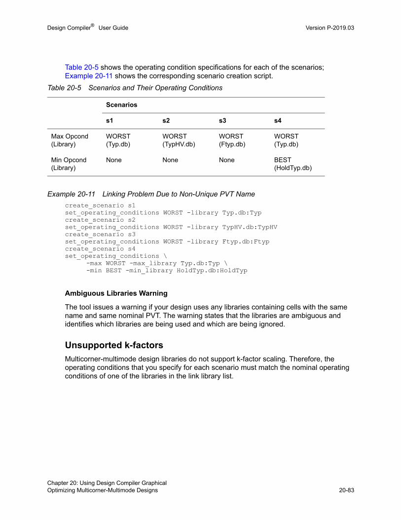
Design Compiler® User Guide Version P-2019.03
Table 20-5 shows the operating condition specifications for each of the scenarios; Example 20-11 shows the corresponding scenario creation script.
Example 20-11 Linking Problem Due to Non-Unique PVT Name
create_scenario s1set_operating_conditions WORST -library Typ.db:Typcreate_scenario s2set_operating_conditions WORST -library TypHV.db:TypHVcreate_scenario s3set_operating_conditions WORST -library Ftyp.db:Ftypcreate_scenario s4set_operating_conditions \
-max WORST -max_library Typ.db:Typ \-min BEST -min_library HoldTyp.db:HoldTyp
Ambiguous Libraries Warning
The tool issues a warning if your design uses any libraries containing cells with the same name and same nominal PVT. The warning states that the libraries are ambiguous and identifies which libraries are being used and which are being ignored.
Unsupported k-factors
Multicorner-multimode design libraries do not support k-factor scaling. Therefore, the operating conditions that you specify for each scenario must match the nominal operating conditions of one of the libraries in the link library list.
Table 20-5 Scenarios and Their Operating Conditions
Scenarios
s1 s2 s3 s4
Max Opcond(Library)
WORST(Typ.db)
WORST(TypHV.db)
WORST(Ftyp.db)
WORST(Typ.db)
Min Opcond(Library)
None None None BEST(HoldTyp.db)
Chapter 20: Using Design Compiler GraphicalOptimizing Multicorner-Multimode Designs 20-83Chapter 20: Using Design Compiler GraphicalOptimizing Multicorner-Multimode Designs 20-83

Design Compiler® User Guide P-2019.03Design Compiler® User Guide Version P-2019.03
Automatic Detection of Driving Cell Library
In multicorner-multimode flow, the operating condition setting is different for different scenarios. To build the timing arc for the driving cell, different libraries are used for different scenarios. You can specify the library using the -library option of the set_driving_cell command. But specifying the library is optional because the tool can automatically detect the driving cell library.
When you specify the library using the -library option of the set_driving_cell command, the tool searches for the specified library in the link library set. If the specified library exists, it is used. If the specified library does not exist in the link library, the tool issues the UID-993 error message as follows:
Error: Cannot find the specified driving cell in memory.(UID-993)
When you do not use the -library option of the set_driving_cell command, the tool searches all the libraries for the matching operating conditions. The first library in the link library set that matches the operating condition is used. If no library in the link library set matches the operating condition, the first library in the link library set that contains the matching library cell is used. If no library in the link library set contains the matching library cell, the tool issues the UID-993 error message.
Defining Minimum Libraries
Minimum libraries are usually defined with the set_operating_conditions command. You can use the set_min_library command, but it is not scenario-specific. If you use set_min_library to define a minimum library for a scenario, the tool uses that library as the minimum library for all scenarios, even if you do not define that library in all your scenarios. If you want to define different minimum libraries for each scenario, use the set_operating_conditions command.
For example, you could not relate two different minimum libraries – say, Fast_0yr.db and Fast_10yr.db – with the maximum library, Slow.db, in two separate scenarios. The first minimum library you specify would apply to both scenarios. Table 20-6 shows the unsupported configuration.
Table 20-6 Unsupported Multiple Minimum Library Configuration
Scenarios
s1 s2
Max library Slow.db Slow.db
Min library Fast_0yr.db Fast_10yr.db
Chapter 20: Using Design Compiler GraphicalOptimizing Multicorner-Multimode Designs 20-84

Design Compiler® User Guide Version P-2019.03
Note, however, that a minimum library can be associated with multiple maximum libraries. As shown in Table 20-7, the minimum library Fast_0yr.db is paired with both the maximum library Slow.db of scenario 1 and the maximum library SlowHV.db of scenario 2.
Scenario Management Commands
Use the following commands to create and manage scenarios:
• create_scenario
• current_scenario
• all_scenarios
• all_active_scenarios
• set_active_scenarios
• set_scenario_options
• set_preferred_scenario
• check_scenarios
• remove_scenario
• report_scenarios
• report_scenario_options
The following subsections describe how you use these commands to manage scenarios:
• Creating Scenarios
• Defining Active Scenarios
• Scenario Reduction
• Specifying Scenario Options
• Removing Scenarios
Table 20-7 Supported Min-Max Library Configuration
Scenarios
s1 s2
Max library Slow.db SlowHV.db
Min library Fast_0yr.db Fast_0yr.db
Chapter 20: Using Design Compiler GraphicalOptimizing Multicorner-Multimode Designs 20-85Chapter 20: Using Design Compiler GraphicalOptimizing Multicorner-Multimode Designs 20-85

Design Compiler® User Guide P-2019.03Design Compiler® User Guide Version P-2019.03
Creating Scenarios
You use the create_scenario command to create a new scenario. When the first scenario is created, all previous scenario-specific constraints are removed from the design and the following warning is issued:
dc_shell-topo> create_scenario s1Warning: Any existing scenario-specific constraints
are discarded. (MV-020)Current scenario is: s1
Use the current_scenario command to specify the name of the current scenario. Without arguments, the command returns the name of the current scenario. Note that the current_scenario command merely specifies the focus scenario and that when you define more than one scenario, the tool performs concurrent analysis and optimization across all scenarios, independent of the current scenario setting.
Use the set_tlu_plus command to set the TLUPlus files in the scenario specified by the current_scenario command. Note that each scenario must have a set of TLUPlus files specified, or the following error is reported:
Error: tlu_plus files are not set in this scenario <name>. RC values will be 0.
Defining Active Scenarios
During concurrent analysis and optimization, you can significantly reduce memory usage and runtime by limiting the number of active scenarios to those that are “essential” or “dominant.” An essential or dominant scenario has the worst slack among all the scenarios for at least one of its constrained objects. (Constrained objects can include delay constraints associated with a pin, the design rule constraints for a net, leakage power, and so on.) Any scenario for which one of its constrained objects is the worst slack value is a dominant scenario.
You use the set_active_scenarios command to define active scenarios. Other commands related to active scenarios are all_scenarios and all_active_scenarios.
Scenario Reduction
Topographical mode automatically performs scenario reduction on the current set of active scenarios to reduce memory and runtime. In general, restricting concurrent analysis and optimization to a subset of dominant scenarios does not lead to a significant difference in QoR. The tool analyzes all the active scenarios and automatically determines a set of dominant scenarios, based on the number of violating endpoints, and optimizes them for timing, power, and design rule. In the current version, topographical mode does not support the get_dominant_scenarios command, which IC Compiler supports. However, you can choose a preferred scenario by using the set_preferred_scenario command. When you
Chapter 20: Using Design Compiler GraphicalOptimizing Multicorner-Multimode Designs 20-86

Design Compiler® User Guide Version P-2019.03
set the preferred scenario, the tool treats it as the most constraining scenario. It still performs scenario reduction to determine the dominant scenarios but treats the user-specified preferred scenario as the most constraining one.
Specifying Scenario Options
To define specific constraint options, such as leakage power, that you want optimized in a scenario, use the set_scenario_options command. You can apply the constraint option to more than one scenario at a time by using the -scenarios option. The options can be specified on both active and inactive scenarios. If you do not specify any scenario, the options are applied only to the current scenario.
To enable or disable the leakage power optimization, use the -leakage_power option. The default for the -leakage_power option is false. Set the -leakage_power option with the set_scenario_options command to true to enable leakage power optimization on specific scenarios in a multicorner-multimode design. The following command shows how to enable leakage power optimization on specific scenarios only.
dc_shell-topo> set_scenario_options -leakage_power true \-scenarios scenario_list
To enable or disable the dynamic power optimization, use the -dynamic_power option. The default for the -dynamic_power option is false.
To enable or disable the setup or maximum delay optimization for specified scenarios, use the -setup option. The default for the -setup option is true, so maximum delay optimization is enabled by default. The following example shows how to disable maximum delay optimization on specific scenarios.
dc_shell-topo> set_scenario_options -setup false -scenarios scenario_list
To enable or disable the hold or minimum delay optimization for the specified scenarios, use the -hold option. The default for the -hold option is true. When you set the -hold option to false, the tool ignores the hold or the minimum delay violations in the specified scenarios.
dc_shell-topo> set_scenario_options -reset_all true \-scenarios [all_scenarios]
To report the scenario options, use the report_scenario_options command.
Removing Scenarios
To remove the specified scenarios, use the remove_scenario command. All scenario-specific constraints defined in the removed scenario are deleted. For example,
dc_shell-topo> remove_scenarios1 s2
Chapter 20: Using Design Compiler GraphicalOptimizing Multicorner-Multimode Designs 20-87Chapter 20: Using Design Compiler GraphicalOptimizing Multicorner-Multimode Designs 20-87

Design Compiler® User Guide P-2019.03Design Compiler® User Guide Version P-2019.03
dc_shell-topo> remove_scenario -allRemoved scenario 's2'Removed scenario 's1'dc_shell-topo> all_scenarios
Reporting Commands for Multicorner-Multimode Designs
This section describes the commands that you can use for reporting multicorner-multimode designs in Design Compiler Graphical:
• report_scenarios Command
• report_scenario_options Command
• Reporting Commands That Support the -scenario Option
• Commands That Report the Current Scenario
• Reporting Examples
report_scenarios Command
The report_scenarios command reports the scenario setup information for multicorner-multimode designs. This command reports all the defined scenarios. The scenario specific information includes the logic library used, the operating condition, and TLUPlus files.
The following example shows a report generated by the report_scenarios command:
***************************************Report : scenariosDesign : DESIGN1scenario(s) : SCN1 ...***************************************
All scenarios (Total=4): SCN1 SCN2 SCN3 SCN4All Active scenarios (Total=1): SCN1 Current scenario : SCN1
Scenario #0: SCN1 is active.Scenario options:Has timing derate: NoLibrary(s) Used: logic library name (File: library.db)
Operating condition(s) Used: Analysis Type : bc_wc Max Operating Condition: library:WCCOM Max Process : 1.00
Chapter 20: Using Design Compiler GraphicalOptimizing Multicorner-Multimode Designs 20-88

Design Compiler® User Guide Version P-2019.03
Max Voltage : 1.08 Max Temperature: 125.00 Min Operating Condition: library:BCCOM Min Process : 1.00 Min Voltage : 1.32 Min Temperature: 0.00
Tlu Plus Files Used: Max TLU+ file: tlu_plus_file.tf Tech2ITF mapping file: tf2itf.map
report_scenario_options Command
Use the report_scenario_options command to report the scenario options set by the set_scenario_options command. You can specify a list of scenarios to be reported by using the -scenarios option. By default, this command reports scenario options for the current, active scenario.
To illustrate the report generated by the report_scenario_options command, consider Example 20-12 where the set_scenario_options -leakage_power falsecommand is executed. This command sets the -leakage_power option to false. With the -leakage_power option set to false, the tool will not optimize the current, active scenario for leakage power. This status is shown by the report_scenario_options report in Example 20-12.
Example 20-12
dc_shell-topo> set_scenario_options -leakage_power falsedc_shell-topo> report_scenario_options****************************************Report : scenario optionsDesign : TEST03...****************************************
Scenario: MODE1 is active.
setup : truehold : trueleakage_power : falsedynamic_power : true
Reporting Commands That Support the -scenario Option
Some reporting commands support the -scenario option to report scenario-specific information. You can specify a list of scenarios to the -scenario option, and the tool reports scenario details for the specified scenarios.
Chapter 20: Using Design Compiler GraphicalOptimizing Multicorner-Multimode Designs 20-89Chapter 20: Using Design Compiler GraphicalOptimizing Multicorner-Multimode Designs 20-89

Design Compiler® User Guide P-2019.03Design Compiler® User Guide Version P-2019.03
The following reporting commands support the -scenario option:
• report_timing
• report_timing_derate
• report_power
• report_clock
• report_path_group
• report_extraction_options
• report_tlu_plus_files
• report_constraint
Commands That Report the Current Scenario
The following reporting commands report scenario-specific details for the current scenario. The header section of the report contains the name of the current scenario. No additional options are required to report the scenario-specific details of the current scenario.
• report_net
• report_annotated_check
• report_annotated_transition
• report_annotated_delay
• report_attribute
• report_case_analysis
• report_ideal_network
• report_internal_loads
• report_clock_gating_check
• report_clock_tree
• report_delay_calculation
• report_delay_estimate_options
• report_transitive_fanout
• report_disable_timing
• report_latency_adjustment_options
Chapter 20: Using Design Compiler GraphicalOptimizing Multicorner-Multimode Designs 20-90

Design Compiler® User Guide Version P-2019.03
• report_net
• report_power_calculation
• report_noise
• report_signal_em
• report_timing_derate
• report_timing_requirements
• report_transitive_fanin
• report_crpr
• report_clock_timing
Reporting Examples
This section contains sample reports for some of the multicorner-multimode reporting commands.
report_qor Command
The report_qor command reports by default the QoR details for all the scenarios in the design. The following example shows a report generated by the report_qor command:
****************************************Report : qorDesign : DESIGN1**************************************** Scenario 's1' Timing Path Group 'reg2reg' ----------------------------------- Levels of Logic: 33.00 Critical Path Length: 694.62 Critical Path Slack: -144.52 Critical Path Clk Period: 650.00 Total Negative Slack: -4533.01 No. of Violating Paths: 136.00 ----------------------------------- Scenario 's2' Timing Path Group 'reg2reg' ----------------------------------- Levels of Logic: 33.00 Critical Path Length: 393.61 Critical Path Slack: 61.18 Critical Path Clk Period: 500.00 Total Negative Slack: 0.00 No. of Violating Paths: 0.00 -----------------------------------
Chapter 20: Using Design Compiler GraphicalOptimizing Multicorner-Multimode Designs 20-91Chapter 20: Using Design Compiler GraphicalOptimizing Multicorner-Multimode Designs 20-91

Design Compiler® User Guide P-2019.03Design Compiler® User Guide Version P-2019.03
report_timing -scenario
This command reports timing results for the active scenarios in the design. You can specify a list of scenarios with the -scenario option. When the -scenario option is not specified only the current scenario is reported.
****************************************Report : timing -path full -delay max -max_paths 1Design : DESIGN1...********************************************
* Some/all delay information is back-annotated.
# A fanout number of 1000 was used for high fanout net computations.
Startpoint: TEST_BUF2En (input port clocked by clk)Endpoint: TEST1/TEST2_SYN/latch_3 (non-sequential rising-edge timing check clocked by clk)Scenario: s1Path Group: clkPath Type: maxPoint Incr Path Lib:OC-----------------------------------------------------------------------------clock clk (rise edge) 0.00 0.00clock network delay (propagated) 0.00 0.00input external delay 450.00 450.00 fTEST_BUF2En (in) 0.00 450.00 f stdcell_typ:WORSTTEST_BUF2En_BUF1/Z (inx4) 9.75 459.75 r stdcell_typ:WORSTU468/Z (inx10) 10.21 469.96 f stdcell_typ:WORSTTEST_BUF2En_BUF/Z (inx11) 8.74 478.70 r stdcell_typ:WORSTU293/Z (inx11) 9.30 488.00 f stdcell_typ:WORSTTEST1/TEST2_SYN/U74963/Z (nr2x4) 12.78 500.78 r stdcell_typ:WORSTU31662/Z (inx4) 10.58 511.37 f stdcell_typ:WORSTTEST1/TEST2_SYN/U75093/Z (aoi21x6) 18.98 530.34 r stdcell_typ:WORSTU42969/Z (nd2x6) 14.16 544.51 f stdcell_typ:WORSTTEST1/TEST2_SYN/U53046/Z (inx8) 13.35 557.86 r stdcell_typ:WORSTU2765/Z (inx8) 11.48 569.33 f stdcell_typ:WORSTU32442/Z (inx6) 7.61 576.94 r stdcell_typ:WORSTU33615/Z (nd2x3) 18.14 595.09 f stdcell_typ:WORSTU32269/Z (nd2x6) 8.74 603.82 r stdcell_typ:WORSTTEST1/TEST2_SYN/clk_gate/EN (cklan2x1) 0.00 603.82 r stdcell_typ:WORSTdata arrival time 603.82
Chapter 20: Using Design Compiler GraphicalOptimizing Multicorner-Multimode Designs 20-92

Design Compiler® User Guide Version P-2019.03
clock clk (rise edge) 650.00 650.00clock network delay (propagated) 0.00 650.00TEST1/TEST2_SYN/clk_gate/CLK (cklan2x1) 0.00 650.00 rlibrary setup time -56.25 593.75data required time 593.75--------------------------------------------------------------data required time 593.75data arrival time -603.82--------------------------------------------------------------slack (VIOLATED) -10.07
report_constraint
This command reports constraints for all active scenarios. Each scenario is reported separately. When used with the -scenario option, it reports constraints for a specified list of scenarios.
****************************************Report : constraintDesign : DESIGN1Scenarios: 0, 1...**************************************** WeightedGroup (max_delay/setup) Cost Weight Cost Scenario-----------------------------------------------------------------CLK 10.07 1.00 10.07 s1in2out 372.89 1.00 372.89 s1in2reg 199.73 1.00 199.73 s1reg2out 467.99 1.00 467.99 s1reg2reg 171.16 1.00 171.16 s1default 0.00 1.00 0.00 s1CLK 90.60 1.00 90.60 s2in2out 474.97 1.00 474.97 s2in2reg 166.88 1.00 166.88 s2reg2out 326.46 1.00 326.46 s2reg2reg 0.00 1.00 0.00 s2default 0.00 1.00 0.00 s2-----------------------------------------------------------------max_delay/setup 4404.52
... Multi-ScenarioConstraint Cost-----------------------------------------------------multiport_net 0.00 (MET)min_capacitance 0.00 (MET)max_transition 45.28 (VIOLATED)max_fanout 150.00 (VIOLATED)max_capacitance 0.00 (MET)max_delay/setup 4404.52 (VIOLATED)critical_range 4404.52 (VIOLATED)min_delay/hold 0.00 (MET)max_area 714233.56 (VIOLATED)
Chapter 20: Using Design Compiler GraphicalOptimizing Multicorner-Multimode Designs 20-93Chapter 20: Using Design Compiler GraphicalOptimizing Multicorner-Multimode Designs 20-93

Design Compiler® User Guide P-2019.03Design Compiler® User Guide Version P-2019.03
report_tlu_plus_files
This command reports the TLUPlus files associations; it shows each minimum and maximum TLUPlus and layer map file per scenario:
dc_shell-topo> current_scenario s1Current scenario is: s1
dc_shell-topo> report_tlu_plus_filesMax TLU+ file: /snps/testcase/s1max.tluplusMin TLU+ file: /snps/testcase/s1min.tluplusTech2ITF mapping file: /snps/testcase/tluplus_map.txt
report_power
The report_power command supports the -scenario option. Without the -scenario option, only the current scenario is reported. To report power information for all scenarios, use the report_power -scenarios [all_scenarios] command.
Note: In the multicorner-multimode flow, the report_power command does not perform clock tree estimation. The command reports only the netlist power in this flow.
The following example shows the report generated by the report_power -scenario command.
****************************************Report : powerDesign : Design_1Scenario(s): s1...****************************************
Library(s) Used: slow (File: slow.db)
Global Operating Voltage = 1.08Power-specific unit information : Voltage Units = 1V Capacitance Units = 1.000000pf Time Units = 1ns Dynamic Power Units = 1mW (derived from V,C,T units) Leakage Power Units = Unitless
Warning: Could not find correlated power. (PWR-725)
Power Breakdown--------------- Cell Driven Net Tot Dynamic Cell Internal Switching Power (mW) Leakage Cell Power (mW) Power (mW) (% Cell/Tot) Power(nW)------------------------------------------------------------------------Netlist Power 4.8709 1.2889 6.160e+00 (79%) 1.351e+05Estimated Clock Tree Power N/A N/A (N/A) N/A------------------------------------------------------------------------
Chapter 20: Using Design Compiler GraphicalOptimizing Multicorner-Multimode Designs 20-94

Design Compiler® User Guide Version P-2019.03
Supported SDC Commands for Multicorner-Multimode Designs
Table 20-8 lists the SDC commands supported in the multicorner-multimode flow.
Table 20-8 Supported SDC Commands
Commands
all_clocks set_fanout_load
create_clock set_input_delay
create_generated_clock set_input_transition
get_clocks set_latency_adjustment_options
group_path set_load
set_annotated_delay set_max_capacitance
set_capacitance set_max_delay
set_case_analysis set_dynamic_optimization
set_clock_gating_check set_max_time_borrow
set_clock_groups set_max_transition
set_clock_latency set_min_delay
set_clock_transition set_multicycle_path
set_clock_uncertainty set_output_delay
set_data_check set_propagated_clock
set_disable_timing set_resistance
set_drive set_timing_derate
set_false_path
Chapter 20: Using Design Compiler GraphicalOptimizing Multicorner-Multimode Designs 20-95Chapter 20: Using Design Compiler GraphicalOptimizing Multicorner-Multimode Designs 20-95

Design Compiler® User Guide P-2019.03Design Compiler® User Guide Version P-2019.03
Multicorner-Multimode Script Example
Example 20-13 shows a basic sample script for the multicorner-multimode flow.
Example 20-13 Basic Script to Run a Multicorner-Multimode Flow
#......path settings......set search_path ". $DESIGN_ROOT $lib_path/dbs \
$lib_path/mwlibs/macros/LM"set target_library "stdcell.setup.ftyp.db \
stdcell.setup.typ.db stdcell.setup.typhv.db"set link_library [concat * $target_library \
setup.ftyp.130v.100c.db setup.typhv.130v.100c.db \setup.typ.130v.100c.db]
set_min_library stdcell.setup.typ.db -min_version stdcell.hold.typ.db
#......MW setup......#......load design......
create_scenario s1set_operating_conditions WORST -library stdcell.setup.typ.db:stdcell_typset_tlu_plus_files -max_tluplus design.tlup -tech2itf_map layermap.txtread_sdc s1.sdcset_scenario_options -scenarios s1-setup false -hold false \-leakage_power true
create_scenario s2set_operating_conditions BEST -library stdcell.setup.ftyp.db:stdcell_ftypset_tlu_plus_files -max_tluplus design.tlup -tech2itf_map layermap.txtread_sdc s2.sdc
create_scenario s3set_operating_conditions NOM -library stdcell.setup.ftyp.db:stdcell_ftypset_tlu_plus_files -max_tluplus design.tlup -tech2itf_map layermap.txtread_sdc s3.sdc
set_active_scenarios {s1 s2}report_scenarioscompile_ultra -scan -gate_clockreport_qorreport_constraintreport_timing -scenario [all_scenarios]..insert_dft..compile_ultra –incremental -scan
Chapter 20: Using Design Compiler GraphicalOptimizing Multicorner-Multimode Designs 20-96

Design Compiler® User Guide Version P-2019.03
Using Block Abstractions in Multicorner-Multimode Designs
A block abstraction is a structural model of a circuit that is modeled as a smaller circuit representing the interface logic of the block. The model contains cells whose timing is affected by or affects the external environment of a block. Block abstractions enhance capacity and reduce runtime for the optimization of the top-level design. For block abstraction details, see Using Hierarchical Models.
Block abstractions are compatible with multicorner-multimode scenarios. You can apply multicorner-multimode constraints to a block abstraction and use the block abstraction in a top-level design.
The following requirements apply to the use of block abstractions with multicorner-multimode scenarios:
• For each top-level multicorner-multimode scenario, an identically named scenario must exist in each of the block abstraction blocks used in the design.
If there is a mismatch, use the select_block_scenario command to map the scenarios in the block abstraction to the top-level design. Mapping scenarios enables Design Compiler Graphical to support name mismatches between the top-level design and the block abstraction.
To reset user-specified multicorner-multimode scenario mapping, use the –reset option.
• A block abstraction can have additional scenarios that are not used at the top level.
• By default, in a top-level design without multicorner-multimode scenarios, only block abstractions without multicorner-multimode scenarios can be used. Using the select_block_scenario command to specify scenario mapping allows you to use multicorner-multimode block abstractions even if the top-level design does not have multicorner-multimode scenarios.
• For each TLUPlus file that is used, the block abstraction stores the extraction data and the specified operating condition. In the top-level design, you cannot use additional TLUPlus files or define additional temperature corners for the existing TLUPlus files.
• A top-level design with multicorner-multimode scenarios can be used with block abstractions that do not have any multicorner-multimode scenario definitions. No log message is issued in this case, and the same block data is used in all the top-level scenarios.
Chapter 20: Using Design Compiler GraphicalOptimizing Multicorner-Multimode Designs 20-97Chapter 20: Using Design Compiler GraphicalOptimizing Multicorner-Multimode Designs 20-97

Design Compiler® User Guide P-2019.03Design Compiler® User Guide Version P-2019.03
Methodology for Using Block Abstractions With Scenarios at the Top Level
Follow these steps to use a block abstraction at the top level when it has scenario information:
1. Set the current design to the top-level design.
2. Remove all scenarios:
remove_scenario -all
3. Define scenarios for the top-level design.
The scenarios defined in the top-level design must match the scenario definitions in the block abstraction blocks of the design. In the top-level design, all the scenarios must be defined before the next step.
4. Perform optimization:
compile_ultra
At the beginning of compilation, the compile_ultra command performs the following checks to ensure that there are no scenario mismatches between the top-level design and the block abstractions. The compilation is terminated when any of the following mismatches are encountered:
❍ The number of scenarios in the top-level design does not match the number of scenarios in the block abstraction blocks.
If the tool detects that the top-level design has more scenarios than block abstraction blocks, a TL-70 error message is issued, and compilation is terminated:
Error: Scenario S6 is not available in block reference Block1.(TL-70)
❍ The scenario information in the top-level design is not consistent with the scenario information in the block abstraction blocks.
If scenarios are not defined in the top-level design and the block abstraction blocks have scenario definitions, a TL-151 error message is issued and compilation is terminated:
Error: No scenario data loaded from block reference 'BlockInit'.(TL-151)
You can also use the check_scenarios command to check consistency between scenarios.
Chapter 20: Using Design Compiler GraphicalOptimizing Multicorner-Multimode Designs 20-98

21Using Design Compiler NXT 21
The Design Compiler NXT tool extends topographical technology by providing
• Better QoR through advanced optimizations
• Enhanced physical guidance to IC Compiler II, with improved RC and timing correlation
• Faster runtime, with improved multithreading synthesis for better scalability
• Plug-and-play user interface and script compatibility with Design Compiler Graphical
For features supported in both Design Compiler NXT and Design Compiler Graphical, see Using Design Compiler Graphical.
The following features are supported only in the Design Compiler NXT tool:
• Performing Buffering-Aware Placement With the IC Compiler II Link
• Performing Automatic Timing Control With the IC Compiler II Link
• Performing Congestion-Driven Restructuring With the IC Compiler II Link
• Performing RC Extraction With the RC Model
• Applying Required Settings for High Performance Cores
21-1
Design Compiler® User Guide P-2019.03Design Compiler® User Guide Version P-2019.03
Performing Buffering-Aware Placement With the IC Compiler II Link
Buffering-aware placement considers high-fanout nets and long nets during the initial placement to improve QoR. To enable the buffering-aware timing-driven placement when you use the compile_ultra -spg command, use the placer_buffering_aware variable. The default is false.
To use the buffering-aware placement feature, you must use the set_icc2_options command as follows:
dcnxt_shell-topo> set_app_var placer_buffering_aware truedcnxt_shell-topo> set_icc2_options –ref_libs "lib1.ndm lib2.ndm" \ -technology tech.tf
When you set the placer_buffering_aware variable to true during the initial placement with the compile_ultra -spg command ,
• Design Compiler NXT enables timing-driven placement with an approximate timing model that estimates the effects of buffering high-fanout nets and long nets. The netlist does not change.
• Before invoking the IC Compiler II tool, Design Compiler NXT issues the following message:
Information: Buffering aware placement is enabled. (SPG-129)
• After invoking the IC Compiler II tool, the following message is issued in the IC Compiler II log file:
Create Placement Options:Buffering Aware Timing Driven: true
Performing Automatic Timing Control With the IC Compiler II Link
Automatic timing control improves total negative slack (TNS) during direct timing-driven placement. To enable automatic timing control when you use the compile_ultra -spg and compile_ultra -incremental -spg commands, use the placer_auto_timing_control variable. The default is false.
Note: If you set both the placer_buffering_aware and placer_auto_timing_control variables to true, the tool performs both buffering-aware placement and automatic timing control during the initial placement. However, the tool still performs automatic timing control during the direct timing-driven placement.
Chapter 21: Using Design Compiler NXTPerforming Buffering-Aware Placement With the IC Compiler II Link 21-2

Design Compiler® User Guide Version P-2019.03
To use the automatic timing control feature, you must use the set_icc2_options command as follows:
dcnxt_shell-topo> set_app_var placer_auto_timing_control truedcnxt_shell-topo> set_icc2_options –ref_libs "lib1.ndm lib2.ndm" \ -technology tech.tf
When you set the placer_auto_timing_control variable to true,
• Design Compiler NXT enables the IC Compiler II direct timing-driven placement along with the Zroute-based congestion-driven placement when you use the compile_ultra -spg command.
• Design Compiler NXT enables only the IC Compiler II direct timing-driven placement when you use the compile_ultra -incremental -spg command. However, to enable the IC Compiler II Zroute-based congestion-driven placement during the incremental compile, you must set the spg_congestion_placement_in_incremental_compile variable to true.
• The direct timing-driven placement tries to focus the timing optimization on the most critical timing paths to balance between reducing the worst negative slack (WNS) and reducing the total negative slack (TNS)
• Before invoking the IC Compiler II tool, Design Compiler NXT issues the following message:
Information: Auto timing control is enabled in the placer. (SPG-129)
• After invoking the IC Compiler II tool, the following message is issued in the IC Compiler II log file:
Printing options for 'place.coarse.*' (non-default only)place.coarse.auto_timing_control: true
Performing Congestion-Driven Restructuring With the IC Compiler II Link
Congestion in the design can be caused by commutative and associative logic trees, such as OR trees, AND trees, and XOR trees. You can improve congestion by rewiring input signals of the logic trees with the congestion-driven restructuring feature.
To enable congestion-driven restructuring when you use the compile_ultra -spg command, use the placer_cong_restruct variable. The default is false. To use the congestion-driven restructuring feature, you must use the set_icc2_options command as follows:
dcnxt_shell-topo> set_app_var placer_cong_restruct truedcnxt_shell-topo> set_icc2_options –ref_libs "lib1.ndm lib2.ndm" \ -technology tech.tf
Chapter 21: Using Design Compiler NXTPerforming Congestion-Driven Restructuring With the IC Compiler II Link 21-3Chapter 21: Using Design Compiler NXTPerforming Congestion-Driven Restructuring With the IC Compiler II Link 21-3

Design Compiler® User Guide P-2019.03Design Compiler® User Guide Version P-2019.03
When you set the placer_cong_restruct variable to true,
• Design Compiler NXT performs restructuring of the net during the initial placement with the compile_ultra -spg command
• Before invoking the IC Compiler II tool, Design Compiler NXT issues the following message:
Information: Congestion driven restructuring placement is enabled. (SPG-131)
• After invoking the IC Compiler II tool, the following message is issued in the IC Compiler II log file:
Printing options for 'place.coarse.*' (non-default only)place.coarse.cong_restruct: on
Performing RC Extraction With the RC Model
You can perform RC extraction for improving the RC correlation with the pre place_opt results from the IC Compiler II tool. To perform the RC extraction, use the spg_icc2_rc_correlation variable to correlate the RC value of Design Compiler NXT with the IC Compiler II tool, which helps in solving timing miscorrelation issues.
This feature is available only
• When you use the compile_ultra -spg command
• In the advanced-technology nodes (16 nm and lower-process nodes) when metal layers have a significant difference in resistance value
When you set this variable to true (the default is false),
• The extract_rc command performs RC extraction by using the advanced RC model
• The tool issues the “Turning on advanced RC model” message to indicate that this feature is enabled for optimization and extraction when you use the compile_ultra, compile_ultra - incremental, and optimize_netlist commands and explicitly run the extract_rc command
Applying Required Settings for High Performance Cores
You can apply tool settings required for achieving the best QoR for high performance cores by using the set_technology and set_hpc_options commands. The applied settings affect synthesis, placement, optimization, and timing analysis. The 16, 12, and 7 nanometer technology nodes are supported with the set_technology command.
Chapter 21: Using Design Compiler NXTPerforming RC Extraction With the RC Model 21-4

Design Compiler® User Guide Version P-2019.03
As shown in the following example, you must use
• The set_technology command to apply technology-node settings before using the set_hpc_options command
• The set_hpc_options command before using the compile_ultra and compile_ultra -incremental commands to set the stage-specific settings
# read the setup, design, and constraintsset_technology –node 7set_hpc_options –core A55 -stage compilecompile_ultra -spg...insert_dft...set_hpc_options –core A55 -stage compile_inccompile_ultra -spg -incremental
Note: If you apply any tool settings after using the set_hpc_options command, the last setting overrides the previous settings.
To report the core and technology-node settings applied by the tool, use the -report_only option of the set_hpc_options command.
Chapter 21: Using Design Compiler NXTApplying Required Settings for High Performance Cores 21-5Chapter 21: Using Design Compiler NXTApplying Required Settings for High Performance Cores 21-5

Design Compiler® User Guide P-2019.03Design Compiler® User Guide Version P-2019.03
Chapter 21: Using Design Compiler NXTApplying Required Settings for High Performance Cores 21-6

22Using Hierarchical Models 22
Hierarchical models are used in Design Compiler to reduce the number of design objects and the memory requirements when the tool performs top-level optimization on large designs. The term hierarchical models refers to block abstractions and physical hierarchies.
To learn about generating and using hierarchical models in Design Compiler, see
• Overview of Hierarchical Models
• Block Abstraction Hierarchical Flow
For information about using hierarchical models in a bottom-up compile flow, see Performing a Bottom-up Hierarchical Compile.
22-1

Design Compiler® User Guide P-2019.03Design Compiler® User Guide Version P-2019.03
Overview of Hierarchical Models
Hierarchical models are used in Design Compiler to reduce the number of design objects and the memory requirements when the tool performs top-level optimization on large designs. For interface logic models (ILMs), the gate-level netlist for a block is modeled by a partial gate-level netlist that contains only the required interface logic of the block and possibly the logic that you manually associate with the interface logic. All other logic is removed. However, Design Compiler does not support ILMs. Instead, Design Compiler uses block abstractions.
Block abstractions are an extension to interface logic models. Unlike an ILM where the internal logic is removed and saved in a separate .ddc file, when you use block abstractions, the full design and the block abstraction information are both saved in the same .ddc file. The interface logic is marked, and only the interface logic is loaded when using the block abstraction.
Design Compiler can create block abstractions, and it can use block abstractions created either in Design Compiler or in IC Compiler. However, IC Compiler can only use block abstractions created in IC Compiler. For optimal correlation and alignment between the tools, use IC Compiler block abstractions to model the physical blocks in both tools.
Figure 22-1 shows a block and its hierarchical model, where the logic is preserved between
• The input port and the first register of each timing path
• The last register of each timing path and the output port
Logic associated with pure combinational input-port-to-output-port timing paths (A to X) is also preserved. Clock connections to the preserved registers are kept as well. The register-to-register logic is discarded.
Chapter 22: Using Hierarchical ModelsOverview of Hierarchical Models 22-2

Design Compiler® User Guide Version P-2019.03
Figure 22-1 A Block and Its Hierarchical Model
Design Compiler supports the use of hierarchical models in a variety of flows, including
• Multicorner-multimode
Design Compiler automatically detects the presence of multiple corners and multiple modes and retains the interface logic involved in the interface timing paths of each scenario.
• Designs with multiple levels of physical hierarchy
You can use nested block abstractions to model designs with multiple levels of physical hierarchy. For more information about nested block abstractions, see Creating Block Abstractions for Nested Blocks.
See Also
• Information Used in Hierarchical Models
• Using Hierarchical Models in a Multicorner-Multimode Flow
• Viewing Hierarchical Models in the GUI
A
B
CLK
X
Y
Block
A
B
CLK
X
Y
Hierarchical Model
Chapter 22: Using Hierarchical ModelsOverview of Hierarchical Models 22-3Chapter 22: Using Hierarchical ModelsOverview of Hierarchical Models 22-3

Design Compiler® User Guide P-2019.03Design Compiler® User Guide Version P-2019.03
Information Used in Hierarchical Models
By default, hierarchical models include the following netlist objects:
• Leaf cells and macro cells in the four critical timing paths that lead from input ports to output ports (combinational input-to-output paths), input ports to edge-triggered registers, and edge-triggered registers to output ports
• Abstracted clock trees that include clock paths to interface registers, minimum and maximum clock paths that could also be connected to noninterface registers, and the clock tree synthesis exceptions that are a part of these clock paths
Design Compiler treats generated clocks like clock ports. Design Compiler retains interface registers that are driven by a generated clock. However, internal registers driven by generated clocks are not retained. When the design contains generated clocks, the logic along the timing path between the master clock and the generated clock is also retained.
• Clock-gating circuitry—if it is driven by external ports
• Logic along the timing path between a master clock and any generated clocks derived from it
• Side-load cells for all nets
Side-load cells are cells that can affect the timing of an interface path but are not directly part of the interface logic.
Note: By default, latches are treated as combinational logic.
Apart from the netlist objects, the following information is also stored in a hierarchical model:
• Cell or pin location information
• Parasitic information
• Timing constraints
• Pin-to-pin delay for internal nets
• Power consumption
A block abstraction can contain register-to-register paths that are entirely within the block. These paths are the result of combinational logic in the block abstraction that is shared by input-to-register and register-to-output paths. Paths entirely within blocks are optimized during block-level optimization, and ignoring them during top-level optimization enables transparent interface optimization to focus on other paths. For information about ignoring these register-to-register paths, see Ignoring Timing Paths That Are Entirely Within Block Abstractions.
Chapter 22: Using Hierarchical ModelsOverview of Hierarchical Models 22-4

Design Compiler® User Guide Version P-2019.03
Figure 22-2 shows the elements contained in a hierarchical model, emphasizing the clock tree. The darkly shaded elements are the elements on the clock path; the lightly shaded elements are the side-load cells. Unshaded elements are not included in the model.
Figure 22-2 Hierarchical Model
Using Hierarchical Models in a Multicorner-Multimode Flow
You can apply multicorner-multimode constraints to a hierarchical model and use those constraints in a top-level design.
The following requirements apply to using blocks that are modeled using a hierarchical model with multicorner-multimode scenarios:
• For each top-level multicorner-multimode scenario, an identically named scenario must exist in each of the blocks used in the design.
If there is a mismatch, use the select_block_scenario command to map the scenarios in the blocks to the top-level design. A block can have additional scenarios that are not used at the top level.
The syntax for using the select_block_scenario command is
select_block_scenario[-scenarios top_scenarios][-block_references list_design_names]-block_scenario block_scenario_name | -reset
To reset user-specified multicorner-multimode scenario mapping, use the –reset option.
• You can use a top-level design with multicorner-multimode scenarios with blocks that do not have multicorner-multimode scenarios. This does not require the use of the select_block_scenario command.
Data
Clock
Datain out
Chapter 22: Using Hierarchical ModelsOverview of Hierarchical Models 22-5Chapter 22: Using Hierarchical ModelsOverview of Hierarchical Models 22-5

Design Compiler® User Guide P-2019.03Design Compiler® User Guide Version P-2019.03
• By default, in a top-level design without multicorner-multimode scenarios, only blocks without multicorner-multimode scenarios can be used.
To use multicorner-multimode blocks with non-multicorner-multimode top-level designs, specify the scenario mapping by using the select_block_scenario command.
• For each TLUPlus file, a block stores the extraction data at the specified temperature, which is an operating condition. For accurate results during parasitic extraction at the top level, the TLUPlus files and temperature corners at the top level should match the TLUPlus and temperature corners used during block-level implementation. However, you can use additional TLUPlus and temperatures at the top level with loss in accuracy.
Viewing Hierarchical Models in the GUI
In the Design Compiler GUI, a hierarchical model instance is displayed as a level of physical hierarchy: a rectangular or rectilinear shape with a fill pattern. The View Settings panel provides additional control over the block abstraction display.
• To display the hierarchical models, select the Cell > ILM/Block Abstraction visibility option.
• To display the hierarchical model pins, select the Pin visibility option.
• To expand the hierarchical model to show the leaf cells, pins, nets, and macros within, type or select a positive integer in the “Level” box.
• To reset the display to the default view, the unexpanded view, type or select 0 in the “Level” box.
For more information about using the GUI to view physical hierarchy blocks, see the “Examining Physical Hierarchy Blocks” topic in Design Vision Help.
Block Abstraction Hierarchical Flow
A top-level flow using block abstractions allows optimization of only the top-level logic. Block abstractions are an extension to interface logic models (ILMs). Unlike an ILM where the internal logic is removed, all the logic is retained in a block abstraction, but only the interface logic is loaded. This supports faster top-level design closure by allowing optimization of block-level interface logic during top-level synthesis.
When you create and save block abstractions, they are stored in a single .ddc file in the same file that includes the complete design netlist. You do not need to maintain two .ddc files, one for interface logic and the other for the full netlist, as you needed to do for ILMs.
Chapter 22: Using Hierarchical ModelsBlock Abstraction Hierarchical Flow 22-6

Design Compiler® User Guide Version P-2019.03
Figure 22-3 illustrates the difference between an ILM and a block abstraction. Design Compiler does not support ILMs. The figure is for comparison only.
Figure 22-3 ILM and Block Abstraction Comparison
By default, block abstractions are not modified or optimized. If you are using Design Compiler in topographical mode, you can optimize the block abstractions using top-level transparent interface optimization. Transparent interface optimization is the process that optimizes the interface logic within the blocks during top-level synthesis to achieve faster timing closure.
Transparent interface optimization provides the following benefits:
• Supports faster top-level design closure by performing concurrent optimization of top-level logic and block-level interfaces.
• Reduces iterations between top-level and block-level implementation.
Design Compiler can create block abstractions and use block abstractions created either in Design Compiler or in IC Compiler. However, IC Compiler can only use block abstractions created in IC Compiler. For information about creating a block abstraction in IC Compiler, see the IC Compiler Implementation User Guide.
Note: You cannot combine block abstractions and ILMs in the same flow.
The following sections describe the block abstraction hierarchical flow:
• Creating and Saving Block Abstractions
• Setting Top-Level Implementation Options
• Resetting Implementation Options
• Controlling the Extent of Logic Loaded for Block Abstractions
.ddc.ddc
ILM
.ddc
.ddc
.ddc
Requires two files:-- Full .ddc-- ILM .ddc
Single .ddc filewith complete design and block abstraction
Block abstraction
Top
Top-level optimization flowwith block abstractions
Block A
Block B
Top-level path
Chapter 22: Using Hierarchical ModelsBlock Abstraction Hierarchical Flow 22-7Chapter 22: Using Hierarchical ModelsBlock Abstraction Hierarchical Flow 22-7

Design Compiler® User Guide P-2019.03Design Compiler® User Guide Version P-2019.03
• Loading Block Abstractions
• Reporting Implementation Options
• Reporting Block Abstractions
• Querying Block Abstractions
• Checking Block Abstractions
• Ignoring Timing Paths That Are Entirely Within Block Abstractions
• Performing Top-Level Synthesis
• Saving Optimized Block Abstractions After Top-Level Synthesis
• Limitations
Creating and Saving Block Abstractions
To generate a block abstraction for the current design, use the create_block_abstraction command at the end of synthesis. The create_block_abstraction command adds the block abstraction information to the design in memory.
To save the block abstraction, you must use the write_file command immediately after creating the block abstraction:
dc_shell-topo> create_block_abstractiondc_shell-topo> write_file -hierarchy -format ddc -output ${DESIGN_NAME}.mapped.ddc
The .ddc file contains both the complete design and the Design Compiler block abstraction.
You can create block abstractions in either Design Compiler or Design Compiler in topographical mode. However, you must use topographical mode to optimize block abstractions, and only block abstractions created in topographical mode are optimized.
To specify the list of block references that you want to link to block abstractions and integrated with the top-level design, and to optimize the block abstractions using transparent interface optimization, use the set_top_implementation_options command as described in Setting Top-Level Implementation Options.
Chapter 22: Using Hierarchical ModelsBlock Abstraction Hierarchical Flow 22-8

Design Compiler® User Guide Version P-2019.03
Information Used in Block Abstractions
When you use the create_block_abstraction command, the tool
• Identifies the interface logic.
The following netlist objects are part of interface logic:
❍ All cells, pins, and nets in timing paths from input ports to registers or output ports.
❍ All cells, pins, and nets in timing paths to output ports from registers or input ports.
❍ Any logic in the connection from a master clock to generated clocks.
❍ The clock trees that drive interface registers, including any logic in the clock tree.
❍ The longest and shortest clock paths from the clock ports.
❍ The side-load cells of all non-ideal and non-DRC disabled nets.
• Ignores an input or inout port if the percentage of the total registers in the transitive fanout of the port is greater than or equal to the threshold percentage that is specified by using the abstraction_ignore_percentage variable.
The following netlist objects are retained for ports that are ignored:
❍ Connections to the already identified interface logic of the other ports.
❍ Minimum and maximum critical timing paths.
• Ignores any case analysis settings. Any case analysis settings that are required must be specified at the top level by using the set_case_analysis command.
• Assumes all latches found in interface logic are potential borrowers; thus, all logic from I/O ports to flip-flops or output ports are identified as belonging to interface logic.
• Extracts and stores detailed parasitics as part of the abstraction information for each specified TLUPlus file and temperature.
• Calculates power consumption of the design and stores that information in attributes in the design. This information is used by the report_power command during the final assembly step of the entire chip.
To include additional leaf cells and nets in the block abstraction, use the create_block_abstraction command with the -include option. Logical hierarchical cells and pins are ignored.
If either of the following conditions exist, the entire block is included in the block abstraction:
• The number of leaf cells included exceeds 95 percent of the total leaf cells in the block.
• The number of nets included exceeds 95 percent of the total nets in the block.
Chapter 22: Using Hierarchical ModelsBlock Abstraction Hierarchical Flow 22-9Chapter 22: Using Hierarchical ModelsBlock Abstraction Hierarchical Flow 22-9

Design Compiler® User Guide P-2019.03Design Compiler® User Guide Version P-2019.03
Block Abstractions for Multicorner-Multimode Usage
The create_block_abstraction command automatically detects the presence of multiple scenarios (multiple modes or corners) and determines the interface logic for each scenario. The interface logic identified for each scenario is retained as the interface logic of the block abstraction. If an interface timing path is disabled in one scenario but enabled in another, the path is included in the interface logic.
Setting Top-Level Implementation Options
To use block abstractions at the top level, use the set_top_implementation_options command with the -block_references option to specify the list of block references that you want to link to the block abstraction. Do this for both Design Compiler block abstractions and IC Compiler block abstractions.
Use the set_top_implementation_options command before reading the .ddc file with the block abstraction into memory; otherwise, the full block netlist is loaded. When linking, the tool loads only the interface logic to the top level.
When using IC Compiler block abstractions, use the set_top_implementation_options command before running any link command in Design Compiler. The IC Compiler block abstractions are automatically read from the list of Milkyway reference libraries while linking the top-level design.
You can use multiple set_top_implementation_options commands to specify the options for all of the block abstractions at the top level.
The command settings in Example 22-1 and Example 22-2 are equivalent.
Example 22-1 Specifying Options for Block Abstractions in One Command
set_top_implementation_options -block_references {blk1 blk2}
Example 22-2 Specifying Options for Block Abstractions in Multiple Commands
set_top_implementation_options -block_references {blk1}set_top_implementation_options -block_references {blk2}
To verify the options set by the set_top_implementation_options command and ensure that the block abstractions are loaded correctly, see Reporting Implementation Options.
Chapter 22: Using Hierarchical ModelsBlock Abstraction Hierarchical Flow 22-10

Design Compiler® User Guide Version P-2019.03
Transparent Interface Optimization
By default, block abstractions are not modified or optimized. If you are using Design Compiler in topographical mode, you can optimize the block abstractions using top-level transparent interface optimization. Transparent interface optimization is a process that optimizes the interface logic within the blocks during top-level synthesis to achieve faster timing closure.
To enable transparent interface optimization, use the set_top_implementation_options -optimize_block_interface true command and specify the list of blocks whose interface logic should be optimized during top-level synthesis before you run the compile_ultra or compile_ultra -incremental command. During top-level synthesis, Design Compiler links the block abstractions to the top-level design, optimizes and modifies each block’s interface logic, updates the top-level interface logic, and performs full optimization.
Optimization of block abstractions is limited to cell sizing only; therefore, the -size_only_mode option has no effect. Transparent interface optimization is available only in Design Compiler in topographical mode for block abstractions created in topographical mode. Transparent interface optimization cannot be performed on block abstractions created in IC Compiler; these can only be optimized in IC Compiler.
The following example sets the top-level implementation options for the blk1 and blk2 blocks:
dc_shell-topo> set_top_implementation_options -block_references {blk1 blk2}
The following example enables transparent interface optimization for the blk1 block:
dc_shell-topo> set_top_implementation_options -block_references blk1 \ -optimize_block_interface true
As a part of performing transparent interface optimization, parallel Design Compiler sessions are run during compile in order to update the parasitics of the block abstractions. Multicore optimization is used to run the block update sessions in parallel. You can control the number of cores that are used by using the set_host_options command. If multicore optimization is not enabled, all the updates are performed in serial in the same session.
Figure 22-4 shows how this process works in compile. Transparent interface optimization performs sizing of the logic inside the block abstractions. Then, extraction of the updated parasitics is performed on the modified blocks using parallel Design Compiler sessions. Next, the updated block abstractions are reloaded back into the main compile session to continue the optimization.
Chapter 22: Using Hierarchical ModelsBlock Abstraction Hierarchical Flow 22-11Chapter 22: Using Hierarchical ModelsBlock Abstraction Hierarchical Flow 22-11

Design Compiler® User Guide P-2019.03Design Compiler® User Guide Version P-2019.03
Figure 22-4 Automatic Block Update in Transparent Interface Optimization
To specify a setup file to be sourced during the block update, use the -block_update_setup_script option with the set_top_implementation_options command. This is useful for passing variable settings for the block update process.
To specify a script file to run commands to update specific blocks, use the -block_update_cmd_script option. If you do not specify this option, Design Compiler automatically runs the extract_rc -estimate command to perform RC estimation for the block update. If you specify the option, Design Compiler sources the specified script file and does not run the extract_rc -estimate command automatically. Make sure that you include the extract_rc -estimate command in your command script file. Design Compiler automatically runs the create_block_abstraction and write_file commands after sourcing the script file.
The following example specifies the setup file to be sourced during the block update and a script to run the block update. You must specify the absolute paths to both file names. The example also enables multicore optimization to allow parallel processing of the blocks in multiple Design Compiler sessions.
dc_shell-topo> set_top_implementation_options -block_references {blkA blkB} \ -optimize_block_interface true \
-block_update_setup_script block_update_setup.tcl \-block_update_cmd_script block_update_command.tcl \
dc_shell-topo> set_host_options -max_cores 4
Example 22-3 shows the flow used to automatically update the blocks after transparent interface optimization. Example 22-4 shows the flow used to update the blocks when user-specified setup and command scripts are specified.
compile_ultra
Transparent interface optimization
Blocks with transparent interface
Block update
Link updated blocks
Continueoptimization
optimization changes
Parallel block update sessions extract_rc -estimate
Updated block abstractionswith new parasitics
Chapter 22: Using Hierarchical ModelsBlock Abstraction Hierarchical Flow 22-12
Design Compiler® User Guide Version P-2019.03
Example 22-3 Automatic Block Update Flow
set_app_var link_library ...set_app_var target_library ...set_app_var search_path ...open_mw_lib top_MWread_ddc block.tio.ddccurrent_design blockAlinkextract_rc -estimatecreate_block_abstractionwrite_file -hierarchy -format ddc ...
Example 22-4 Block Update Flow Using User-Specified Setup and Command Scripts
set_app_var link_library ...set_app_var target_library ...set_app_var search_path ...source -echo -verbose block_update_setup.tclopen_mw_lib top_MWread_ddc block.tio.ddccurrent_design blockAlinksource -echo -verbose block_update_cmd.tclcreate_block_abstractionwrite_file -hierarchy -format ddc ...
Each block update iteration creates a new subdirectory where all the parallel block update sessions are run. The directory names use a TIO_current_date prefix and increments a number suffix for each iteration:
TIO_20130923/TIO_20130923.1/TIO_20130923.2/
The compile log contains information about which transparent interface optimization block update directories were created during each compile step:
Information: Directory information for distributed jobs:Main directory:
.../TIO_20130923.1 Block CORE_A’s distributed job’s working directory: .../TIO_20130923.1/blk_CORE_A.1
Block CORE_B’s distributed job’s working directory:.../TIO_20130923.1/blk_CORE_B.1
Creating Block Abstractions for Nested Blocks
You can use the create_block_abstraction command to create block abstractions for blocks that include nested block abstractions. The command does not create block abstractions with other types of physical hierarchy.
Chapter 22: Using Hierarchical ModelsBlock Abstraction Hierarchical Flow 22-13Chapter 22: Using Hierarchical ModelsBlock Abstraction Hierarchical Flow 22-13

Design Compiler® User Guide P-2019.03Design Compiler® User Guide Version P-2019.03
When you use nested block abstractions, you must specify the references of the blocks instantiated in all levels of the hierarchy, as shown:
dc_shell-topo> set_top_implementation_options -block_references {MID BOT}
Figure 22-5 Block Abstraction With Nested Physical Hierarchy
You can use transparent interface optimization to optimize the interface logic at any level.
For multicorner-multimode designs, you need to specify scenario mapping from the top level to each of the levels by using the select_block_scenario command.
Note: Visibility of nested block abstractions in the layout view is not yet available.
Resetting Implementation Options
You can reset the top implementation options by using the -reset option with the set_top_implementation_options command. This causes the full design netlist to be loaded for the block instead of loading the block abstraction.
The following example resets the top implementation options for the blk2 block. In this example, the block abstraction for blk1 is loaded, and the full netlist for blk2 is loaded:
dc_shell-topo> set_top_implementation_options -block_references {blk1 blk2}dc_shell-topo> set_top_implementation_options -block_references {blk2} -reset
Controlling the Extent of Logic Loaded for Block Abstractions
When loading blocks as block abstractions at the top level, you can control the extent of logic that is loaded, either loading the blocks with a full interface or a compact interface. When you create a block abstraction by using the create_block_abstraction command, the tool identifies both full interface logic and compact interface logic at the same time.
TOP
B0 {Ref: BOT}
M0 {Ref: MID}
Chapter 22: Using Hierarchical ModelsBlock Abstraction Hierarchical Flow 22-14

Design Compiler® User Guide Version P-2019.03
When you load blocks with a compact interface, only the min/max and rise/fall interface logic is retained. For blocks with ports that fan out to a large number of boundary registers, using a compact interface can improve runtime and memory usage.
To choose the type of interface logic to load at the top-level, use the load_logic option with the set_top_implementation_options command as follows:
• To load the entire block abstraction, consisting of all the interface logic, use the -load_logic full_interface option setting, which is the default.
When you load the full interface, the following logic is marked as interface logic:
❍ All the logic from input ports to registers or output ports
❍ All the logic to output ports from registers or input ports
• To load a compact version of the block abstraction, consisting of only the logic for the timing-critical paths of every input and output port, use the -load_logic compact_interface option setting.
For compact block abstractions, the following logic is marked as interface logic:
❍ The logic that belongs to min/max rise/fall from input ports to registers or output ports
❍ The logic that belongs to min/max rise/fall to output ports from registers or input ports
When transparent interface optimization is not performed on a block, you can load the block with a compact interface. However, when you perform transparent interface optimization at the top level with the compile_ultra command, load the entire block abstraction for the blocks you want to optimize by using the -load_logic full_interface option setting.
The following clock-gating circuitry is marked as interface logic whether you load the full interface or the compact interface:
• Any logic in the path from the master clock to the generated clocks
• The clock trees that drive interface registers, including any logic in the clock tree
• The longest and shortest clock paths from the clock ports
• The side-load cells of all non-ideal and non-DRC disabled nets
The tool retains the following IEEE 1801 Unified Power Format (UPF) objects in a block abstraction whether you load the full interface or the compact interface:
• All retention registers, whether or not they are part of the interface logic
• Level-shifter cells and isolation cells that are part of the interface logic
• Control logic for the retained retention registers, isolation cells, and level-shifter cells
Chapter 22: Using Hierarchical ModelsBlock Abstraction Hierarchical Flow 22-15Chapter 22: Using Hierarchical ModelsBlock Abstraction Hierarchical Flow 22-15

Design Compiler® User Guide P-2019.03Design Compiler® User Guide Version P-2019.03
When the tool removes a UPF netlist object, it either removes or updates the associated UPF constraint. The tool ensures that the UPF strategies stored in the block abstraction are consistent with the UPF netlist objects.
To propagate the UPF objects in the block abstraction to the top level, run the propagate_constraints -power_supply_data command.
See Also
• Loading Block Abstractions
Loading Block Abstractions
To load Design Compiler block abstractions to be linked to the top-level design, use the read_ddc command after you have used the set_top_implementation_options command:
dc_shell-topo> read_ddc {DesignA.mapped.ddc DesignB.mapped.ddc}
The following message indicates that the Design Compiler block abstraction is being loaded while reading in the block .ddc file:
Information: Reading block abstraction for design 'blk1' and its hierarchy. (DDC-27)
Make sure that your Milkyway reference libraries include the IC Compiler block abstraction designs. IC Compiler block abstractions are automatically loaded from the list of Milkyway reference libraries when linking the top-level design.
The following message indicates that the IC Compiler block abstraction is being loaded while linking the top-level design:
Information: Auto loading blk2.CEL (version 1) from Milkyway library blk2.mw ...(TL-102)
After a block abstraction is loaded, you can perform the tasks discussed in the following sections to ensure the block abstraction is ready for top-level synthesis:
• Reporting Implementation Options
• Reporting Block Abstractions
• Querying Block Abstractions
• Checking Block Abstractions
Chapter 22: Using Hierarchical ModelsBlock Abstraction Hierarchical Flow 22-16

Design Compiler® User Guide Version P-2019.03
Reporting Implementation Options
To verify the options set by the set_top_implementation_options command and ensure that the block abstractions are correctly loaded, use the report_top_implementation_options command. The report_top_implementation_options command reports the options as shown in the following example:
dc_shell-topo> report_top_implementation_options
****************************************Report : Top implementation options...****************************************
-----------------------------------------------------------------------Block Optimize Optimize Size Only HostReference Interface Shared Logic Mode Options-----------------------------------------------------------------------block1 true false off --block2 true false off -------------------------------------------------------------------------
Reporting Block Abstractions
To report block abstractions that are linked to the current design, use the report_block_abstraction command. The command reports the following information:
• Block reference name
• Block instance name
• Block version
• Full path of the library from which the block was loaded
• Date and time of the last modification of the block
• Cell count and compression statistics for each of the blocks
• Cell count and compression statistics for the top-level design with blocks
• TLUPlus settings
• Parasitics data of the block
• User-defined multicorner-multimode scenario mappings between the top level and blocks
• UPF information
Chapter 22: Using Hierarchical ModelsBlock Abstraction Hierarchical Flow 22-17Chapter 22: Using Hierarchical ModelsBlock Abstraction Hierarchical Flow 22-17
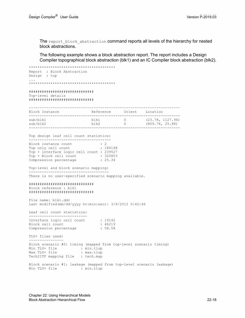
Design Compiler® User Guide P-2019.03Design Compiler® User Guide Version P-2019.03
The report_block_abstraction command reports all levels of the hierarchy for nested block abstractions.
The following example shows a block abstraction report. The report includes a Design Compiler topographical block abstraction (blk1) and an IC Compiler block abstraction (blk2).
****************************************Report : Block AbstractionDesign : top...****************************************
##############################Top-level details##############################
----------------------------------------------------------------------Block Instance Reference Orient Location----------------------------------------------------------------------sub/blk1 blk1 0 (23.78, 1127.96)sub/blk2 blk2 0 (809.74, 25.88)----------------------------------------------------------------------
Top design leaf cell count statistics:--------------------------------------Block instance count : 2Top only cell count : 184148Top + interface logic cell count : 239527Top + Block cell count : 320803Compression percentage : 25.34
Top-level and block scenario mapping:-------------------------------------There is no user-specified scenario mapping available.
##############################Block reference : blk1##############################
File name: blk1.ddcLast modified(mm/dd/yyyy hr:min:sec): 3/6/2012 0:42:46
Leaf cell count statistics:---------------------------Interface logic cell count : 19142Block cell count : 46219Compression percentage : 58.58
TLU+ files used:----------------Block scenario #0: timing (mapped from top-level scenario timing)Min TLU+ file : min.tlupMax TLU+ file : max.tlupTech2ITF mapping file : tech.map
Block scenario #1: leakage (mapped from top-level scenario leakage)Min TLU+ file : min.tlup
Chapter 22: Using Hierarchical ModelsBlock Abstraction Hierarchical Flow 22-18
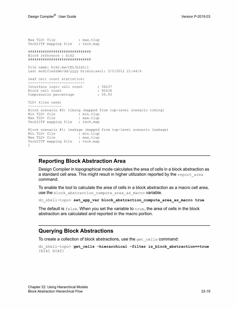
Design Compiler® User Guide Version P-2019.03
Max TLU+ file : max.tlupTech2ITF mapping file : tech.map
##############################Block reference : blk2##############################
File name: blk2.mw/CEL/blk2:1Last modified(mm/dd/yyyy hr:min:sec): 3/5/2012 21:44:9
Leaf cell count statistics:---------------------------Interface logic cell count : 36237Block cell count : 90436Compression percentage : 59.93
TLU+ files used:----------------Block scenario #0: timing (mapped from top-level scenario timing)Min TLU+ file : min.tlupMax TLU+ file : max.tlupTech2ITF mapping file : tech.map
Block scenario #1: leakage (mapped from top-level scenario leakage)Min TLU+ file : min.tlupMax TLU+ file : max.tlupTech2ITF mapping file : tech.map1
Reporting Block Abstraction Area
Design Compiler in topographical mode calculates the area of cells in a block abstraction as a standard cell area. This might result in higher utilization reported by the report_area command.
To enable the tool to calculate the area of cells in a block abstraction as a macro cell area, use the block_abstraction_compute_area_as_macro variable.
dc_shell-topo> set_app_var block_abstraction_compute_area_as_macro true
The default is false. When you set the variable to true, the area of cells in the block abstraction are calculated and reported in the macro portion.
Querying Block Abstractions
To create a collection of block abstractions, use the get_cells command:
dc_shell-topo> get_cells -hierarchical -filter is_block_abstraction==true{blk1 blk2}
Chapter 22: Using Hierarchical ModelsBlock Abstraction Hierarchical Flow 22-19Chapter 22: Using Hierarchical ModelsBlock Abstraction Hierarchical Flow 22-19

Design Compiler® User Guide P-2019.03Design Compiler® User Guide Version P-2019.03
Checking Block Abstractions
Use the check_block_abstraction command to check the readiness of a block abstraction before optimization. The check_block_abstraction command checks the blocks linked to the top-level design to ensure they are ready for top-level synthesis.
The command checks for the following:
• Scenario consistency in multicorner-multimode blocks.
• The existence of dont_touch settings on blocks and cells.
All objects must have the dont_touch attribute so they cannot be modified.
The following example checks the blocks in the current design and reports the errors to be resolved:
dc_shell-topo> check_block_abstractionError: No scenario data loaded from block reference ’blk1’. (TL-151)Error: dont_touch attribute incorrectly set to false on block design ’blk2’. (TL-121)0
You can also use the compile_ultra -check_only command to verify that the design and libraries have all the data that compile_ultra requires to run successfully. The -check_only option is only available in Design Compiler in topographical mode.
Ignoring Timing Paths That Are Entirely Within Block Abstractions
A block abstraction can contain register-to-register paths that are entirely within the block. These paths are the result of combinational logic in the block abstraction that is shared by input-to-register and register-to-output paths. Paths entirely within blocks are optimized during block-level optimization, and ignoring them during top-level optimization enables transparent interface optimization to focus on other paths.
To ignore register-to-register paths that are entirely within block abstractions, set the timing_ignore_paths_within_block_abstraction variable to true. The default is false. Setting the variable to true does not affect paths that begin within a block abstraction, traverse outside, and return to the block abstraction.
Performing Top-Level Synthesis
After you create the block abstraction, specify the settings linking it to the top-level design, enable transparent interface optimization (if you are using topographical mode and want to optimize the block abstraction), run a report to check the top implementation settings, run a report to get details about the block abstraction, and check the readiness of the block abstraction, you can perform top-level synthesis.
Chapter 22: Using Hierarchical ModelsBlock Abstraction Hierarchical Flow 22-20

Design Compiler® User Guide Version P-2019.03
The following script shows part of a top-level synthesis flow with transparent interface optimization enabled. The top-level design contains the DesignA and DesignB blocks and their corresponding block abstractions, DesignA.mapped.ddc and DesignB.mapped.ddc.
set BLOCK_ABSTRACTION_DESIGNS "DesignA DesignB"set_top_implementation_options -block_references ${BLOCK_ABSTRACTION_DESIGNS} \-optimize_block_interface true... #Read in the top-level RTLread_ddc {DesignA.mapped.ddc DesignB.mapped.ddc}current_design toplinkreport_block_abstractionget_cells -hierarchical -filter is_block_abstraction==truereport_top_implementation_options...# Read in constraintscheck_block_abstractioncompile_ultra -check_onlycompile_ultra
For the complete top-level hierarchical flow using block abstractions, see Performing a Bottom-up Hierarchical Compile.
Saving Optimized Block Abstractions After Top-Level Synthesis
When you save the top-level design after optimization, block abstractions are not written to the top.ddc file. If you enabled transparent interface optimization, you need to save the updated blocks. Use the write_file command to save each optimized block abstraction to a separate .ddc file. You cannot write more than one block abstraction design in a single output .ddc file. The write_file command merges the changes with the original .ddc design and writes the complete block as a new .ddc file.
The -hierarchy and -output options are required with the write_file command when you write out block abstractions at the top level, and you must provide only the top-level block abstraction design name as an argument.
The following script shows how to save the top-level design and the optimized block abstractions into separate .ddc files:
write_file -hierarchy -format ddc -output top.mapped.ddcforeach design ${BLOCK_ABSTRACTION_DESIGNS}{ write_file -hierarchy -format ddc \ -output ${design}.mapped_tio.ddc \ ${design}}
Limitations
Block abstractions have the following limitations:
Chapter 22: Using Hierarchical ModelsBlock Abstraction Hierarchical Flow 22-21Chapter 22: Using Hierarchical ModelsBlock Abstraction Hierarchical Flow 22-21

Design Compiler® User Guide P-2019.03Design Compiler® User Guide Version P-2019.03
• IC Compiler does not support the loading of block abstractions that were created in Design Compiler.
• You cannot view nested block abstractions in the layout view.
Chapter 22: Using Hierarchical ModelsBlock Abstraction Hierarchical Flow 22-22

23Incremental ASCII Flow With a Third-Party DFT Flow Example 23
Some flows require you to use a Verilog or VHDL (ASCII) netlist output format. The following topics describe the incremental ASCII flow using a third-party design-for-test (DFT) flow as an example. The flow is described in compile.tcl and compile_incr.tcl scripts that are typical Tcl scripts that you can use for the initial compilation and incremental compilation flows.
Note: A DFTMAX license is required for the flow in this example.
• Performing Initial Compilation Using the compile.tcl Script
• Performing Incremental Compilation Using the compile_incr.tcl Script
• Using the Netlist SCANDEF Flow
23-1

Design Compiler® User Guide P-2019.03Design Compiler® User Guide Version P-2019.03
Figure 23-1 shows an example of an incremental ASCII physical guidance flow with a third-party DFT flow.
Figure 23-1 Incremental ASCII Physical Guidance Flow With a Third-Party DFT Flow
DEF Top
Design Compiler Graphical dc_shell -topographical_mode -f compile.tcl
IC Compiler place_opt -spg
Third-party test
RTL
top.vstd.def
top.incr.scandeftop.incr.ddc
(insert test logic)
Design Compiler topographical dc_shell -topographical_mode -f compile_incr.tcl
dft.scandefdft.v
Chapter 23: Incremental ASCII Flow With a Third-Party DFT Flow Example23-2

Design Compiler® User Guide Version P-2019.03
Performing Initial Compilation Using the compile.tcl Script
Example 23-1 shows a compile.tcl script that you can use for a typical initial compile_ultra physical guidance flow. It uses Design Compiler Graphical floorplan exploration after the compile_ultra step to generate the complete floorplan constraints that contain the standard cell placement. The floorplan exploration step is run with the start_icc_dp –f icc_dp.tcl command.
Example 23-1 Initial Compilation Using the compile.tcl Script
# Analyze and elaborate stepanalyze -f verilog top_design.velaborate top_design
# Load UPF constraintsload_upf upf_constraints.upf
# Set timing constraintssource timing_constraints.tcl
# Set power settings if required# set_clock_gating_style# set_max_leakage_power# set_max_dynamic_power
extract_physical_constraints -allow_physical_cells top.def
compile_ultra -spg -scan -gate_clock
change_names -rules verilog -hierarchyset write_sdc_output_net_resistance falseset write_sdc_output_lumped_net_capacitance falsewrite_sdc top.sdcsave_upf top.upfwrite_file -format verilog -hierarchy -output top.vstart_icc_dp -f icc_dp.tcl
The icc_dp.tcl script generates the standard cell placement so you can reuse it during the compile_ultra -incremental step. Example 23-2 shows the commands included in the icc_dp.tcl script:
Example 23-2 Commands in icc_dp.tcl Script
write_def -version 5.7 -component -verbose -output std.defexit
Chapter 23: Incremental ASCII Flow With a Third-Party DFT Flow ExamplePerforming Initial Compilation Using the compile.tcl Script 23-3Chapter 23: Incremental ASCII Flow With a Third-Party DFT Flow ExamplePerforming Initial Compilation Using the compile.tcl Script 23-3

Design Compiler® User Guide P-2019.03Design Compiler® User Guide Version P-2019.03
Performing Incremental Compilation Using the compile_incr.tcl Script
Example 23-3 shows a compile_incr.tcl script that you can use for a typical incremental compile_ultra physical guidance flow. The script reads in the Verilog netlist after DFT insertion and reads the placement from the first compile_ultra run so that the incremental step can use the standard cell placement as seed placement during placement optimization.
If your initial compilation used physical guidance, as is the case in Example 23-3, you must specify the -standard_cell spg option with the extract_physical_constraints command to read the standard cell placement in addition to the floorplan constraints. When you run the incremental compilation, specify the -spg option.
If your initial compilation did not use physical guidance, use the -standard_cell topo option with the extract_physical_constraints command to read the standard cell placement in addition to the floorplan constraints. If you do not use the -standard_cell topo option, Design Compiler is forced to redo a full placement. This can hurt runtime and correlation because the incremental step cannot use the standard cell placement from the original compile_ultra run.
The compile_incr.tcl script also reads the SCANDEF file from the DFT insertion step using the read_scan_def command and runs the write_scan_def command after the compile_ultra -incremental command in order to pass the SCANDEF file with all the changes performed during the incremental optimization to IC Compiler. You must use the -output option with the write_scan_def command if the handoff to IC Compiler is in ASCII format.
For more information about using the netlist SCANDEF flow to import and export scan chain information when the test implementation has been performed outside the Synopsys flow, see “Using the Netlist SCANDEF Flow” on page 23-5.
After you run the compile_ultra -incremental command step, you can save the design in .ddc format, along with the SCANDEF file, and proceed with physical implementation in IC Compiler with the place_opt -optimize_dft command.
Example 23-3 Incremental Compilation Using the compile_incr.tcl Script
# Read the DFT netlistread_verilog top.dft.v
# Load UPF constraintsload_upf top.upf
# Set timing constraintsread_sdc top.sdc
# Restore floorplan constraints and standard cell placement from the # compile_ultra stepextract_physical_constraints -allow_physical_cells top.def
Chapter 23: Incremental ASCII Flow With a Third-Party DFT Flow ExamplePerforming Incremental Compilation Using the compile_incr.tcl Script 23-4

Design Compiler® User Guide Version P-2019.03
extract_physical_constraints -allow_physical_cells \-standard_cell spg std.def
# Read the SCANDEF file from the DFT insertion stepset dct_placement_ignore_scan trueread_scan_def dft.scandef
compile_ultra -incremental -spg
write_scan_def -output top.incr.scandefwrite_file -format ddc -hierarchy -output top.incr.ddc
Using the Netlist SCANDEF Flow
Design Compiler can import and export scan chain information when the test implementation has been performed outside the Synopsys flow with the netlist SCANDEF flow. In the netlist SCANDEF flow, you use the read_scan_def and write_scan_def commands to identify and preserve the scan chain structure and write out the new scan chain structure after optimization.
The scan chains are described in a SCANDEF file. The SCANDEF format, which is part of the DEF open format, is used to describe the scan chain elements. You use the read_scan_def command to read the SCANDEF file, after reading the netlist, to identify all cells that are part of scan chains. This identification allows the write_scan_def command to generate the new SCANDEF file with the same scan chain structure after optimization. You can then pass the SCANDEF file with all the changes performed during the incremental optimization, such as ungrouping, to IC Compiler.
Design Compiler only preserves the scan chains. It does not reorder them. You cannot change or add new scan chains. Therefore, the insert_dft command is not supported between the read_scan_def and write_scan_def commands and errors out. The netlist SCANDEF flow does not support a hierarchical approach; Design Compiler does not read multiple SCANDEF files.
To learn how to use the netlist SCANDEF flow, see the following topics:
• Identifying the Scan Chain Structure
• Performing Scan Chain Reordering in Design Compiler Graphical
• Writing Out the New Scan Chain Structure
Chapter 23: Incremental ASCII Flow With a Third-Party DFT Flow ExampleUsing the Netlist SCANDEF Flow 23-5Chapter 23: Incremental ASCII Flow With a Third-Party DFT Flow ExampleUsing the Netlist SCANDEF Flow 23-5

Design Compiler® User Guide P-2019.03Design Compiler® User Guide Version P-2019.03
Identifying the Scan Chain Structure
Test structure includes scan chains as well as controlling logic. Controlling logic includes the scan enable, scan-in, scan-out, and test mode signals as well as other logic, such as compressors, decompressors, on-chip clocking (OCC), and memory BIST. The netlist SCANDEF flow identifies scan chains only.
Scan chains are identified by SCANDEF files. SCANDEF files can be generated by most DFT tools. Example 23-4 shows an example of a SCANDEF file.
Example 23-4 SCANDEF File Example
VERSION 5.5 ;NAMESCASESENSITIVE ON ;DIVIDERCHAR "/" ;BUSBITCHARS "[]" ;DESIGN TOP ;SCANCHAINS 1 ;- 1+ START U20 o+ FLOATING regA ( IN ti ) ( OUT q ) regB ( IN ti ) ( OUT q ) regF ( IN ti ) ( OUT q ) regE ( IN ti ) ( OUT q )+ ORDERED regC ( IN ti ) ( OUT q ) U10 ( IN i_1 ) ( OUT o ) regD ( IN d ) ( OUT q )+ PARTITION clk_i_45_45+ STOP regG ti ;
To identify all cells that are part of a scan chain, read the SCANDEF file using the read_scan_def command after you read the top-level design. The read_scan_def command performs the following tasks automatically:
• Reads the SCANDEF file
• Checks the SCANDEF file for consistency with the netlist
Example 23-5 shows a read_scan_def consistency report. If the scan chains pass all structural checks, the Status column reports a V for VALIDATED. If a scan chain fails the structural checks, the Status column reports an F for FAILED. This example shows that the top.scandef SCANDEF file is consistent with the netlist.
Example 23-5 read_scan_def Consistency Report
dc_shell> read_scan_def top.scandef Reading DEF file top.scandef Checking SCANDEF... Checking for duplication in SCANDEF... Checking scan cell correspondence between SCANDEF and netlist...
Chapter 23: Incremental ASCII Flow With a Third-Party DFT Flow ExampleUsing the Netlist SCANDEF Flow 23-6

Design Compiler® User Guide Version P-2019.03
Start scan chain checking... All checks completed.****************************************Report : Scan DEF checkDesign : top......****************************************Information from SCANDEF file: Number of SCANCHAINS: 3Checking between SCANDEF file and design: Total SCANCHAINS checked: 3 VALIDATED : 3 FAILED : 0
Chain name Status #cells PARTITION Scan IN Scan OUT---------- ------ ------ --------- ------- --------1 V 2751 clk_45_45 scanin[1] scanout[1]2 V 2751 clk_45_45 scanin[2] scanout[2]3 V 2751 clk_45_45 scanin[3] scanout[3]
Make sure that all scan chains are validated before you optimize the design. Any scan chains that fail are ignored and are not read in by the read_scan_def command.
Using the netlist SCANDEF flow, you can improve the timing of the functional logic while preserving the scan chain structure. Figure 23-2 shows an example of a netlist SCANDEF flow. It is recommended that you use the -incremental option with the compile_ultra command. Other options, such as -spg, are also supported. Be sure to use the appropriate design constraint commands for flows, such as UPF or multicorner-multimode.
Chapter 23: Incremental ASCII Flow With a Third-Party DFT Flow ExampleUsing the Netlist SCANDEF Flow 23-7Chapter 23: Incremental ASCII Flow With a Third-Party DFT Flow ExampleUsing the Netlist SCANDEF Flow 23-7

Design Compiler® User Guide P-2019.03Design Compiler® User Guide Version P-2019.03
Figure 23-2 Netlist SCANDEF Flow Example
Read top-level design read_verilog top.v
Apply design constraints read_sdc top_level.sdc
Read SCANDEF file
read_scan_def top.scandef
Optimize design
compile_ultra -incremental
Apply name rules
change_names -rules verilog
Write SCANDEF file
write_scan_def -output top.incr.scandef
Write out design
write_file -format verilog -hierarchywrite_file -format ddc -hierarchy
Chapter 23: Incremental ASCII Flow With a Third-Party DFT Flow ExampleUsing the Netlist SCANDEF Flow 23-8

Design Compiler® User Guide Version P-2019.03
Performing Scan Chain Reordering in Design Compiler Graphical
In a Design Compiler Graphical flow, Synopsys physical guidance technology enables enhanced placement that is consistent with IC Compiler. The -spg option of the compile_ultra command enables this physical guidance technology.
In the netlist SCANDEF flow, you can perform an incremental compile using this physical guidance technology by using the following command:
dc_shell-topo> compile_ultra -scan -spg -incremental
In this case, Design Compiler further reduces scan chain wire length and congestion by performing scan chain reordering during the incremental compile, and the tool issues the following message:
Information: Performing SCANDEF-based scan chain reordering in the SPGflow. (SPG-127)
The reordering process honors any scan order constraints imposed by the input SCANDEF file. Scan reordering is enabled by default during incremental compile when you use the -spg and -scan options.
When reordering is enabled, repartitioning is also performed unless explicitly disabled with the set_optimize_dft_options -repartitioning_method none command.
Before running the incremental compile, you can use the set_optimize_dft_options command to configure scan repartitioning, just as you would in IC Compiler. For example,
dc_shell-topo> set_optimize_dft_options \-repartitioning_method single_directional
By default, repartitioning uses the multi_directional repartitioning method.
To disable both scan reordering and repartitioning, set the following variable:
dc_shell-topo> set_app_var \test_enable_scan_reordering_in_compile_incremental false
Note the following requirements and limitations:
• Hierarchical SCANDEF is not supported; only a flat DFT flow is supported.
• Post-DFT DRC is not supported after reordering. Perform DRC checking in the ATPG tool to verify scan chain integrity.
Chapter 23: Incremental ASCII Flow With a Third-Party DFT Flow ExampleUsing the Netlist SCANDEF Flow 23-9Chapter 23: Incremental ASCII Flow With a Third-Party DFT Flow ExampleUsing the Netlist SCANDEF Flow 23-9

Design Compiler® User Guide P-2019.03Design Compiler® User Guide Version P-2019.03
Writing Out the New Scan Chain Structure
When you run the write_scan_def command, Design Compiler generates a SCANDEF file that contains the same scan chain structure as the input SCANDEF file. It traces the scan chains based on the SCANDEF file that was read by the read_scan_def command. If the write_scan_def is unable to trace a scan chain because the scan chain element cannot be found in the netlist, Design Compiler issues an error.
In general, you do not need to use the -output option with the write_scan_def command. If you omit the option, the SCANDEF file is included in the saved .ddc file for handoff to IC Compiler. However, the -output option is required if the handoff to IC Compiler is in ASCII format.
The output SCANDEF file contains all changes performed during the incremental optimization and change_names command specification steps.
The write_scan_def command does not support the -expand_elements option in the netlist SCANDEF flow because the read_scan_def command does not support hierarchical flows.
Chapter 23: Incremental ASCII Flow With a Third-Party DFT Flow ExampleUsing the Netlist SCANDEF Flow 23-10

24Analyzing and Resolving Design Problems 24
Use the reports generated by Design Compiler to analyze and debug your design. You can generate reports both before and after you compile your design. Generate reports before compiling to check that you have set attributes, constraints, and design rules properly. Generate reports after compiling to analyze the results and debug your design.
To learn about analyzing and resolving design problems, see
• Resolving Bus Versus Bit-Blasted Mismatches Between the RTL and Macros
• Fixing Errors Caused by New Unsupported Technology File Attributes
• Using Register Replication to Solve Timing QoR, Congestion, and Fanout Problems
• Assessing Design and Constraint Feasibility in Mapped Designs
• Checking for Design Consistency
• Checking Designs and Libraries Before Synthesis
• Analyzing Your Design During Optimization Using the Compile Log
• Analyzing Design Problems
• Analyzing Area
• Analyzing Timing
• Reporting Quality of Results
• Reporting Infeasible Paths
24-1

Design Compiler® User Guide P-2019.03Design Compiler® User Guide Version P-2019.03
• Debugging Cells and Nets With dont_touch
• Reporting size_only Cells
• RTL Cross-Probing in the GUI
• RTL Cross-Probing on the Command Line
Chapter 24: Analyzing and Resolving Design Problems24-2

Design Compiler® User Guide Version P-2019.03
Resolving Bus Versus Bit-Blasted Mismatches Between the RTL and Macros
Typically, the RTL pin names and the logical library pin names match. Signals are defined one way in both the RTL and the library. They are defined as buses or the bus is defined by its individual wires. Occasionally, mismatches occur during development when, for example, you port from one technology to another, or when the libraries and the RTL are in flux. When mismatches occur, you can set the enable_bit_blasted_bus_linking variable to true and read your design into Design Compiler, even though your RTL and libraries do not match with respect to bus verses bit-blasted pin names. When the enable_bit_blasted_bus_linking variable is set to true, the linker rules are relaxed such that you can read your design when mismatched pin names occur. The default for the enable_bit_blasted_bus_linking variable is false.
Note that when the enable_bit_blasted_bus_linking variable is set to true, the tool will match names in accordance with the bus_inference_style and bus_inference_descending_sort variable settings.
Fixing Errors Caused by New Unsupported Technology File Attributes
Occasionally, IC Compiler adds support for new technology file attributes that are not yet supported in Design Compiler. In these cases, a TFCHK-009 error message is issued in Design Compiler but not in IC Compiler when using the same technology file.
If you get TFCHK-009 errors when reading in your technology file, check the spelling of the attributes and make sure that the attributes are spelled correctly. If you still have TFCHK-009 errors, you can use either of the following two methods to remove the TFCHK-009 errors. Before using either of the following methods, make sure that you can safely remove or ignore the new attributes without affecting the tool functionality. In most cases, new attributes are associated with new routing rules and should not affect the functionality of Design Compiler.
• Remove the new attributes from the specified section in the technology file.
• If the new attributes are safe to ignore, you can set the ignore_tf_error variable to true which issues TFCHK-009w warnings for the unsupported attributes instead of TFCHK-009 errors.
Chapter 24: Analyzing and Resolving Design ProblemsResolving Bus Versus Bit-Blasted Mismatches Between the RTL and Macros 24-3Chapter 24: Analyzing and Resolving Design ProblemsResolving Bus Versus Bit-Blasted Mismatches Between the RTL and Macros 24-3
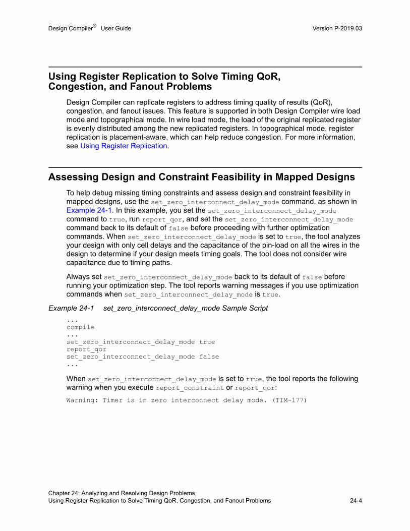
Design Compiler® User Guide P-2019.03Design Compiler® User Guide Version P-2019.03
Using Register Replication to Solve Timing QoR, Congestion, and Fanout Problems
Design Compiler can replicate registers to address timing quality of results (QoR), congestion, and fanout issues. This feature is supported in both Design Compiler wire load mode and topographical mode. In wire load mode, the load of the original replicated register is evenly distributed among the new replicated registers. In topographical mode, register replication is placement-aware, which can help reduce congestion. For more information, see Using Register Replication.
Assessing Design and Constraint Feasibility in Mapped Designs
To help debug missing timing constraints and assess design and constraint feasibility in mapped designs, use the set_zero_interconnect_delay_mode command, as shown in Example 24-1. In this example, you set the set_zero_interconnect_delay_mode command to true, run report_qor, and set the set_zero_interconnect_delay_mode command back to its default of false before proceeding with further optimization commands. When set_zero_interconnect_delay_mode is set to true, the tool analyzes your design with only cell delays and the capacitance of the pin-load on all the wires in the design to determine if your design meets timing goals. The tool does not consider wire capacitance due to timing paths.
Always set set_zero_interconnect_delay_mode back to its default of false before running your optimization step. The tool reports warning messages if you use optimization commands when set_zero_interconnect_delay_mode is true.
Example 24-1 set_zero_interconnect_delay_mode Sample Script
...compile...set_zero_interconnect_delay_mode truereport_qorset_zero_interconnect_delay_mode false...
When set_zero_interconnect_delay_mode is set to true, the tool reports the following warning when you execute report_constraint or report_qor:
Warning: Timer is in zero interconnect delay mode. (TIM-177)
Chapter 24: Analyzing and Resolving Design ProblemsUsing Register Replication to Solve Timing QoR, Congestion, and Fanout Problems 24-4

Design Compiler® User Guide Version P-2019.03
Checking for Design Consistency
A design is consistent when it does not contain errors, such as unconnected ports, constant-valued ports, cells with no input or output pins, mismatches between a cell and its reference, multiple driver nets, connection class violations, or recursive hierarchy definitions.
Design Compiler runs the check_design -summary command on all designs that are compiled. You can also run the command explicitly to verify design consistency. The command reports a list of warning and error messages as follows:
• It reports an error if it finds a problem that Design Compiler cannot resolve. For example, recursive hierarchy (when a design references itself) is an error. You cannot compile a design that has check_design errors.
• It reports a warning if it finds a problem that indicates a corrupted design or a design mistake not severe enough to cause the compile command to fail.
The report is displayed in standard output format by default. The report begins with a summary section that shows the type of check and how many violations have been detected. Next, it lists the error and warning messages.
You can specify a report in HTML format by using the -html_file_name option with the check_design command. When you specify this option and the file name, Design Compiler creates an HTML file in the current directory.
Figure 24-1 shows an example of a check_design report in HTML format. The report organizes the information into sections, such as Input/Outputs, Cells, Designs, Nets, and so on. Each section lists the type of check and the number of violations. If there are violations, the number is an HTML link that you can click to display more information. The report in Figure 24-1 shows five black box violations. Clicking the number 5 expands the report to show the five highlighted violations.
Chapter 24: Analyzing and Resolving Design ProblemsChecking for Design Consistency 24-5Chapter 24: Analyzing and Resolving Design ProblemsChecking for Design Consistency 24-5

Design Compiler® User Guide P-2019.03Design Compiler® User Guide Version P-2019.03
Figure 24-1 HTML check_design Report Example
By default, during compilation or execution of the check_design command, Design Compiler issues a warning message if a tristate bus is driven by a non-tristate driver. You can have Design Compiler display an error message instead by setting the check_design_allow_non_tri_drivers_on_tri_bus variable to false. The default is true. When the variable is set to false, the compile command stops after reporting the error; however, the check_design command continues to run after the error is reported.
You can use options with the check_design command to filter the messages based on the type of check, such as warning messages related to ports, nets, and cells, information messages related to multiply-instantiated designs, and so on. For example, if you specify the -multiple_designs option, the report displays a list of multiply-instantiated designs along with instance names and associated attributes, such as dont_touch, black_box, and ungroup. By default, messages related to multiply-instantiated designs are suppressed.
Use the -no_connection_class option when you are working on a GTECH design or netlist in which connection class violations are expected. Doing so improves runtime, especially if the GTECH design is large and has several connection class violations.
Chapter 24: Analyzing and Resolving Design ProblemsChecking for Design Consistency 24-6

Design Compiler® User Guide Version P-2019.03
Checking Designs and Libraries Before Synthesis
Before synthesizing your design, check that all designs and libraries have the necessary data for the compilation to run successfully by using the compile_ultra command with the -check_only option. The -check_only option reports potential problems that could cause the tool to stop during the compile_ultra run or to produce unsatisfactory correlation with your physical implementation. Use the -check_only option to help debug such problems as
• Missing TLUPlus files and missing physical library cells
• Multiple logic library cells with the same names
• Discrepancies in technology data between multiple physical libraries
• Missing placement location for cells and ports of physical hierarchical modules or block abstractions
• Missing dont_touch attributes for physical hierarchical modules or block abstractions
• Missing floorplan information such as core area constraints (through site row definition), port location, macro location, physical hierarchy location, and block abstraction location
Important: Always execute the compile_ultra optimization step with the same set of options that were used when you executed the compile_ultra -check_only command.
Analyzing Your Design During Optimization Using the Compile Log
The compile log records the status of the compile run. Each optimization task has an introductory heading, followed by the actions taken while that task is performed. There are three tasks in which Design Compiler works to reduce the compile cost function:
• Delay optimization
• Design rule fixing
• Area optimization
While completing these tasks, Design Compiler performs many trials to determine how to reduce the cost function. For this reason, these tasks are collectively known as the trials phase of optimization.
By default, Design Compiler logs each action in the trials phase by providing the following information:
• Elapsed time
Chapter 24: Analyzing and Resolving Design ProblemsChecking Designs and Libraries Before Synthesis 24-7Chapter 24: Analyzing and Resolving Design ProblemsChecking Designs and Libraries Before Synthesis 24-7

Design Compiler® User Guide P-2019.03Design Compiler® User Guide Version P-2019.03
• Design area
• Worst negative slack
• Total negative slack
• Design rule cost
• Endpoint being worked on
You can customize the trials phase output by setting the compile_log_format variable. Table 24-1 lists the available data items and the keywords used to select them.
For information about generating a log file in HTML format, see Compile Log Files.
Table 24-1 Compile Log Format Keywords
Column Column header Keyword Column description
Area AREA area Shows the area of the design.
CPU seconds CPU SEC cpu Shows the process CPU time used (in seconds).
Design rule cost DESIGN RULE COST drc Measures the difference between the actual results and user-specified design rule constraints.
Elapsed time ELAPSED TIME elap_time Tracks the elapsed time since the beginning of the current compile or reoptimization of the design.
Endpoint ENDPOINT endpoint Shows the endpoint being worked on. When delay violations are being fixed, the endpoint is a cell or a port. When design rule violations are being fixed, the endpoint is a net. When area violations are being fixed, no endpoint is printed.
Maximum delay cost
MAX DELAY COST max_delay Shows the maximum delay cost of the design.
Megabytes of memory
MBYTES mem Shows the process memory used (in MB).
Chapter 24: Analyzing and Resolving Design ProblemsAnalyzing Your Design During Optimization Using the Compile Log 24-8

Design Compiler® User Guide Version P-2019.03
Analyzing Design Problems
Table 24-2 shows the design analysis commands provided by Design Compiler.
Minimum delay cost
MIN DELAY COST min_delay Shows the minimum delay cost of the design.
Path group PATH GROUP group_path Shows the path group of an endpoint.
Time of day TIME OF DAY time Shows the current time.
Total negative slack
TOTAL NEG SLACK tns Shows the total negative slack of the design.
Trials TRIALS trials Tracks the number of transformations that the optimizer tried before making the current selection.
Worst negative slack
WORST NEG SLACK wns Shows the worst negative slack of the current path group.
Table 24-2 Commands to Analyze Design Objects
Object Command Description
Design report_design
report_area
report_hierarchy
report_resources
Reports design characteristics.Reports design size and object counts.Reports design hierarchy.Reports resource implementations.
Instances report_cell Displays information about instances.
References report_reference Displays information about references.
Pins report_transitive_fanin
report_transitive_fanout
Reports fanin logic.Reports fanout logic.
Table 24-1 Compile Log Format Keywords (Continued)
Column Column header Keyword Column description
Chapter 24: Analyzing and Resolving Design ProblemsAnalyzing Design Problems 24-9Chapter 24: Analyzing and Resolving Design ProblemsAnalyzing Design Problems 24-9
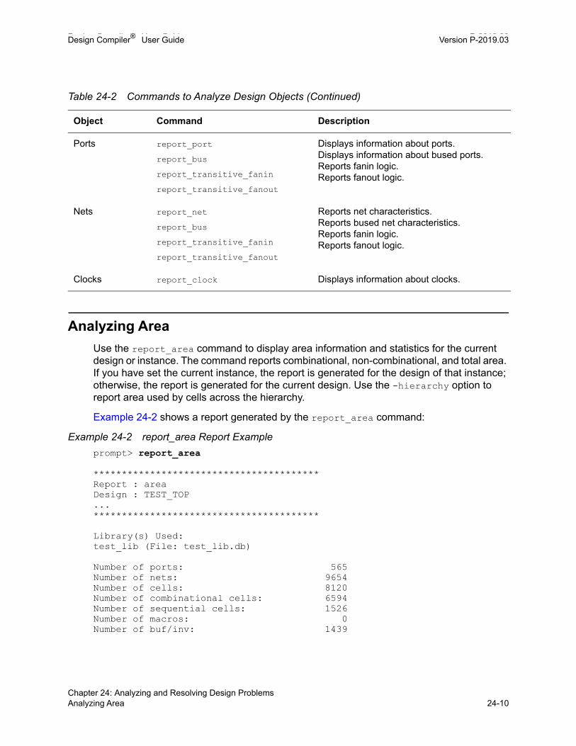
Design Compiler® User Guide P-2019.03Design Compiler® User Guide Version P-2019.03
Analyzing Area
Use the report_area command to display area information and statistics for the current design or instance. The command reports combinational, non-combinational, and total area. If you have set the current instance, the report is generated for the design of that instance; otherwise, the report is generated for the current design. Use the -hierarchy option to report area used by cells across the hierarchy.
Example 24-2 shows a report generated by the report_area command:
Example 24-2 report_area Report Example
prompt> report_area ****************************************Report : areaDesign : TEST_TOP...****************************************
Library(s) Used:test_lib (File: test_lib.db) Number of ports: 565Number of nets: 9654Number of cells: 8120Number of combinational cells: 6594Number of sequential cells: 1526Number of macros: 0Number of buf/inv: 1439
Ports report_port
report_bus
report_transitive_fanin
report_transitive_fanout
Displays information about ports.Displays information about bused ports.Reports fanin logic.Reports fanout logic.
Nets report_net
report_bus
report_transitive_fanin
report_transitive_fanout
Reports net characteristics.Reports bused net characteristics.Reports fanin logic.Reports fanout logic.
Clocks report_clock Displays information about clocks.
Table 24-2 Commands to Analyze Design Objects (Continued)
Object Command Description
Chapter 24: Analyzing and Resolving Design ProblemsAnalyzing Area 24-10

Design Compiler® User Guide Version P-2019.03
Number of references: 163
Combinational area: 562404.432061Noncombinational area: 6720840.351067Net Interconnect area: undefined (Wire load has zero net area)Total cell area: 7283244.783128Total area: undefined
Analyzing Timing
Use the report_timing command to generate timing reports for the current design or the current instance. By default, the command lists the full path of the longest maximum delay timing path for each path group. Design Compiler groups paths based on the clock controlling the endpoint. All paths not associated with a clock are in the default path group. You can also create path groups by using the group_path command.
Before you begin debugging timing problems, verify that your design meets the following requirements:
• You have defined the operating conditions.
• You have specified realistic constraints.
• You have appropriately budgeted the timing constraints.
• You have properly constrained the paths.
• You have described the clock skew.
If your design does not meet these requirements, make sure it does before you proceed.
After producing the initial mapped netlist, use the report_constraint command to check your design’s performance.
Table 24-3 lists the timing analysis commands.
Table 24-3 Timing Analysis Commands
Command Analysis task description
report_design Shows operating conditions, wire load model and mode, timing ranges, internal input and output, and disabled timing arcs.
check_timing Checks for unconstrained timing paths and clock-gating logic.
report_port Shows unconstrained input and output ports and port loading.
report_timing_requirements Shows all timing exceptions set on the design.
Chapter 24: Analyzing and Resolving Design ProblemsAnalyzing Timing 24-11Chapter 24: Analyzing and Resolving Design ProblemsAnalyzing Timing 24-11

Design Compiler® User Guide P-2019.03Design Compiler® User Guide Version P-2019.03
Reporting Quality of Results
You can generate a report on the quality of results (QoR) for the design in its current state by using reporting commands, such as create_qor_snapshot, query_qor_snapshot, and report_qor. The create_qor_snapshot command measures and reports the quality of the design in terms of timing, design rules, area, power, congestion, clock tree synthesis, routing, and so on. It stores the quality information in a set of snapshot files. You can later retrieve the snapshot with the query_qor_snapshot command and view the information in a categorized timing report. You can also selectively retrieve, sort, and display the information based on your preferences. The report_qor command displays QoR information and statistics for the current design.
For information about generating and viewing QoR reports, see
• Measuring Quality of Results
• Analyzing Quality of Results
• Displaying Quality of Results
Measuring Quality of Results
Note: The create_qor_snapshot command is available only in Design Compiler in topographical mode.
To measure the quality of results of the design in its current state and store the quality information in a set of report files, use the create_qor_snapshot command. You can capture the QoR information when using different optimization strategies or at different stages of the design and compare the quality of results. For example, you can use the
report_clock Checks the clock definition and clock skew information.
report_path_group Shows all timing path groups in the design.
report_timing Checks the timing of the design.
report_constraint Checks the design constraints.
report_delay_calculation Reports the details of a delay arc calculation.
Table 24-3 Timing Analysis Commands (Continued)
Command Analysis task description
Chapter 24: Analyzing and Resolving Design ProblemsReporting Quality of Results 24-12

Design Compiler® User Guide Version P-2019.03
create_qor_snapshot command to create a snapshot after the first time you compile the design, after DFT insertion, and again after an incremental compilation.
The command options let you specify the conditions for analysis, such as zero wire load, maximum paths per timing group, and maximum paths per endpoint.
When you use the create_qor_snapshot command to create a snapshot, you must at least specify a name for the snapshot by using the -name option. For example,
dc_shell-topo> create_qor_snapshot -name snapshot1
The report is written to a set of files in a directory called “snapshot” in the current working directory. The set of files act as a database for the snapshot report. You do not need to access these files, and you must not modify them. Later, when you run the query_qor_snapshot command and specify the -name option with the same name you used to create the snapshot (snapshot1 in this example), the query_qor_snapshot command displays the results in text or HTML format.
Analyzing Quality of Results
Note: The query_qor_snapshot command is available only in Design Compiler in topographical mode.
To read a QoR snapshot previously generated by the create_qor_snapshot command, analyze the results, and display the information in a categorized timing report, use the query_qor_snapshot command. The query_qor_snapshot command does not perform any additional analysis of the design but merely processes the report information already saved in the snapshot files.
The query_qor_snapshot command can display the categorized timing report in HTML format or in text format. If you open the report in HTML format, you can modify the constraints and generate a new categorized timing report. The text version of the report allows you to view the results but does not allow you to make modifications.
Use the following command to specify a snapshot and specify the name of the generated output file. You can include an .html or .txt file extension to specify the file format. If you do not specify a file format, Design Compiler creates both a text and an HTML output file.
dc_shell-topo> query_qor_snapshot -name snapshot1 -output_file file_name
Chapter 24: Analyzing and Resolving Design ProblemsReporting Quality of Results 24-13Chapter 24: Analyzing and Resolving Design ProblemsReporting Quality of Results 24-13

Design Compiler® User Guide P-2019.03Design Compiler® User Guide Version P-2019.03
Figure 24-2 shows a categorized timing report in HTML format.
Figure 24-2 Categorized Timing Report in HTML Format
The HTML report lets you quickly find paths with certain problems, such as large fanouts or transition degradation. You can then modify the constraints and generate a new HTML report based on the constraints you specified. To change the constraints and generate a new HTML report, perform the following steps:
1. Select a parameter that you want to change.
For example, in Figure 24-2, Input Delay is selected.
2. Enter a new value for a specific path or paths.
In Figure 24-2, a new input delay value of 2.0 is set on the enable input pin of the REGS1/a_reg/E register.
/...
Chapter 24: Analyzing and Resolving Design ProblemsReporting Quality of Results 24-14

Design Compiler® User Guide Version P-2019.03
3. Click the Create Exceptions button.
Design Compiler opens a new browser window that contains a set of commands based on the constraints you specified. Update your SDC constraints with these commands, and then rerun Design Compiler.
The query_qor_snapshot command options let you filter and sort the search results. You can specify which data columns to display. For example, you can generate set_false_path constraints for a specified value range, such as WNS, logic level, and so on. (The set_false_path command removes timing constraints from specified paths that you know do not affect circuit operation.)
You apply filters to the paths by using the -filters option. For example, the following command reports all paths that have a worst negative slack less than zero:
dc_shell-topo> query_qor_snapshot -name my_snapshot -filters "-wns ,0"
The following example reports all paths that meet any of the specified filter requirements:
dc_shell-topo> query_qor_snapshot -name my_snapshot \-filters "-wns -4.0 -fanout 20"
If you do not specify the -filters option, the query_qor_snapshot command automatically applies a set of default filters. The default filter settings for the maximum condition are shown in the following example:
dc_shell-topo> query_qor_snapshot -name my_snapshot \-filters "-wns ,0 -zero_path ,0 -fanout 40 -logic_level 50"
For a complete list of filters, see the query_qor_snapshot man page.
The following additional examples demonstrate the query_qor_snapshot command usage.
Example 24-3 analyzes the snapshot named my_snapshot1 and reports the paths having a worst negative slack between –4.0 and –3.0 time units.
Example 24-3 Reporting Paths With Worst Negative Slack
dc_shell-topo> query_qor_snapshot -name my_snapshot1 -filters "-wns -4.0,-3.0"... Path Group Start Point End Point WNS ... ... ... -3.312 ... ... ... -3.277
Example 24-4 reports the paths having a slack worse than –1.0 time units and a fanout greater than 40.
Example 24-4 Reporting Paths for Slack and Fanout
dc_shell-topo> query_qor_snapshot -name my_snapshot2 \ -filters "-wns ,-1.0 -fanout 40"...
Chapter 24: Analyzing and Resolving Design ProblemsReporting Quality of Results 24-15Chapter 24: Analyzing and Resolving Design ProblemsReporting Quality of Results 24-15

Design Compiler® User Guide P-2019.03Design Compiler® User Guide Version P-2019.03
Path Group Start Point End Point WNS Large Fanout ... ... ... -3.312 42 ... ... ... -3.277 42
Example 24-5 reads the snapshot named max_logic_level and specifies the -filters option to report all paths between logic levels 2 and 14.
Example 24-5 Reporting All Paths Between Specified Logic Levels
dc_shell-topo> query_qor_snapshot -name max_logic_level \ -filters "-logic_level 2,15"
Note that the paths of logic level 2 are included in the report, but the paths of logic level 15 are excluded.
Sometimes the paths with the worst timing start in one hierarchical block and end in another. Identifying and grouping these paths can be a challenging task. The -hierarchy option enables the top-level view and automates the process of finding potential path groupings that cross hierarchical boundaries so that the problem paths can be analyzed more efficiently. When you use the -hierarchy option, you must specify the -to, -from, or -through option. Example 24-6 finds the violating paths that cross hard macros starting at module A and ending at module B.
Example 24-6 Reporting Timing Violations Across Hierarchical Boundaries
dc_shell-topo> query_qor_snapshot -name snap_shot3 -hierarchy \-from {A/*} -to {B/*}
The query_qor_snapshot command automatically generates a report of all violating paths between the extracted timing models (ETMs), block abstractions, and hard macros. You can apply filters or expand the top-level paths by specifying the -to, -from, and -through options. Example 24-7 finds violating paths that pass through modules A, B, or C:
Example 24-7 Reporting Violating Paths That Pass Through Specified Modules
dc_shell-topo> query_qor_snapshot -name snap_shot4 -hierarchy \ -through {A B C}
Example 24-8 uses the -incremental option, which keeps the previous analysis results (through modules A, B, and C), and applies an additional query about paths starting from module A or B and ending at module A or B.
Example 24-8 Incremental Reporting
dc_shell-topo> query_qor_snapshot -hierarchy -incremental \ -from {A/* B/*} -to {A/* B/*}
Example 24-9 reports paths that start from module C and end at module B, having a worst negative slack worse than –3.0 ns or a fanout more than 40.
Example 24-9 Reporting Paths for WNS and Fanout Passing Through Specified Modules
dc_shell-topo> query_qor_snapshot -name my_snapshot5 \
Chapter 24: Analyzing and Resolving Design ProblemsReporting Quality of Results 24-16

Design Compiler® User Guide Version P-2019.03
-hierarchy -from top/A/C/* -to top/B/* \ -filters "-wns ,-3.0 -fanout 40"
Displaying Quality of Results
To display information about the quality of results and other statistics for the current design, use the report_qor command. The command reports information about timing path group details and cell count and current design statistics, including combinational, noncombinational, and total area. The command also reports static power, design rule violations, and compile time details. Note that the report_qor command is not part of the create_qor_snapshot and query_qor_snapshot command set.
Example 24-10 shows a report generated by the report_qor command. In the Overall Compile Wall Clock Time section, the reported time is the runtime of the compile command run just before the execution of the report_qor command. If the report_qor command is run just after reloading the .ddc file in a new Design Compiler session (without running any compile), the reported wall clock time is the runtime of the last compile command that was run in the previous session.
In the Cell Count section, the report shows the number of macros in the design. To qualify as a macro cell, a cell must be nonhierarchical and have the is_macro_cell attribute set on its library cell.
Example 24-10 report_qor Report Example
prompt> report_qor
****************************************Report : qorDesign : TEST_TOP...****************************************
Timing Path Group 'clk' ----------------------------------- Levels of Logic: 1.00 Critical Path Length: 0.02 Critical Path Slack: -0.68 Critical Path Clk Period: 8.00 Total Negative Slack: -393.61 No. of Violating Paths: 1066.00 Worst Hold Violation: 0.00 Total Hold Violation: 0.00 No. of Hold Violations: 0.00 -----------------------------------
Cell Count ----------------------------------- Hierarchical Cell Count: 7 Hierarchical Port Count: 2360
Chapter 24: Analyzing and Resolving Design ProblemsReporting Quality of Results 24-17Chapter 24: Analyzing and Resolving Design ProblemsReporting Quality of Results 24-17

Design Compiler® User Guide P-2019.03Design Compiler® User Guide Version P-2019.03
Leaf Cell Count: 43978 Buf/Inv Cell Count: 6764 CT Buf/Inv Cell Count: 4 Combinational Cell Count: 37212 Sequential Cell Count: 6773 Macro Count: 0 -----------------------------------
Area ----------------------------------- Combinational Area: 562404.432061 Noncombinational Area: 6720840.351067 Net Area: 0.000000 Net XLength : 2836623.25 Net YLength : 2555007.75 ----------------------------------- Cell Area: 7283244.783128 Design Area: 7283244.783128 Net Length : 5391631.00
Design Rules ----------------------------------- Total Number of Nets: 47207 Nets With Violations: 5 Max Trans Violations: 3 -----------------------------------
Hostname: machine Compile CPU Statistics ----------------------------------------- Resource Sharing: 21.54 Logic Optimization: 182.63 Mapping Optimization: 230.79 ----------------------------------------- Overall Compile Time: 631.32 Overall Compile Wall Clock Time: 288.11
Reporting Infeasible Paths
Infeasible timing paths can exist for the following reasons:
• Missing boundary conditions
• Unrealistic timing goals for input or output delays
During optimization, the compile_ultra command automatically detects infeasible paths in the design. To control the focus of optimization effort on other paths, the command temporarily sets these infeasible paths as false paths and issues an OPT-1720 information message. At the end of optimization, these false path settings are removed.
Chapter 24: Analyzing and Resolving Design ProblemsReporting Infeasible Paths 24-18

Design Compiler® User Guide Version P-2019.03
After running the compile_ultra command, you can report the infeasible paths that were temporarily set as false paths by using either of these methods:
• Reporting Infeasible Paths in an HTML Categorized Timing Report
• Reporting Infeasible Paths in a Timing Report
Reporting Infeasible Paths in an HTML Categorized Timing Report
You can view the tool-detected infeasible paths in a categorized timing report by specifying the -infeasible_paths option with the create_qor_snapshot and query_qor_snapshot commands in Design Compiler in topographical mode. You can use the -infeasible_paths option with any of the create_qor_snapshot and query_qor_snapshot options to generate a customized report that indicates which paths are detected by the tool as infeasible. In the following example, the maximum number of paths in the report is limited to 30.
dc_shell-topo> compile_ultradc_shell-topo> create_qor_snapshot -max_paths 30 -infeasible_paths \ -name snap1dc_shell-topo> query_qor_snapshot -name snap1 -infeasible_paths \ -columns {path_group infeasible_paths startpoint \
endpoint wns zero_path} -output_file snap1.htmldc_shell-topo> sh firefox snap1.html
Figure 24-3 shows the categorized timing report in HTML format generated by the previous command sequence. If a path was detected as infeasible during optimization, it is indicated with a YES under the Infeasible Path column.
Figure 24-3 Categorized Timing Report in HTML Format
Chapter 24: Analyzing and Resolving Design ProblemsReporting Infeasible Paths 24-19Chapter 24: Analyzing and Resolving Design ProblemsReporting Infeasible Paths 24-19

Design Compiler® User Guide P-2019.03Design Compiler® User Guide Version P-2019.03
You can also specify exceptions and create constraints from the categorized timing HTML report by following these steps:
1. Click Append.
2. Click False Paths.
3. Select the check box under the Exceptions column of each infeasible path for which you want to create an exception.
4. Click the Create Exceptions button.
A new browser window that contains a set of commands based on the exceptions you specified appears. For example, when you select the first five infeasible paths, the following commands are displayed in the pop-up window:
set_false_path -from u_clk2/X_out_reg/CLK -to out3;set_false_path -from in1 -to u_in1/A_out_reg/D;set_false_path -from in1 -to u_in2/A_out_regD;set_false_path -from in3 -to u_clk2/A_out_reg/D;set_false_path -from u_out3/X_out_reg/CLK -to out1;
5. Update your SDC file with these commands.
Reporting Infeasible Paths in a Timing Report
You can view the tool-detected infeasible paths by generating a timing report with the report_timing -attributes command in either Design Compiler in topographical mode or wire load mode, as shown in the following example. The inf attribute in the report denotes the infeasible paths that were detected during compile. The timing report shows an infeasible path whose startpoint and endpoint are marked with the inf attribute.
prompt> report_timing -attributes ......Attributes:
d - dont_touchu - dont_use
mo - map_onlyso - size_onlyi - ideal_net or ideal_network
inf - infeasible path
Point Incr Path Attributes-------------------------------------------------------------------------clock clk2 (rise edge) clock network delay (ideal)u_clk2/X_out_reg/CLK (DFFX1-LVT) 0.00 0.10 r infu_clk2/X_out_reg/Q (DFFX1_LVT) 0.36 0.46 fu_clk2/X_out (unit_1) 0.00 0.46 fout 3 (out) 0.00 0.46 f infdata arrival time 0.46
Chapter 24: Analyzing and Resolving Design ProblemsReporting Infeasible Paths 24-20

Design Compiler® User Guide Version P-2019.03
...
To exclude all paths that are flagged as infeasible from the report, use the -ignore_infeasible_paths option with the report_timing command. Similarly, you can use the -ignore_infeasible_paths option with the report_constraint and report_qor commands.
Debugging Cells and Nets With dont_touch
If Design Compiler did not optimize or remove a cell or net, it is often due to a dont_touch on the object. Explicit dont_touch attributes are straightforward to debug. However, it can be difficult to determine why an object has an implicit dont_touch, especially when there are multiple overlapping types of implicit dont_touch on the object. Even if you remove the dont_touch setting on the object, you might still see the object reported as having a dont_touch. This happens in cases where the object has a dont_touch for multiple reasons.
For information about debugging why an object in a cell or net is marked as dont_touch, see
• Reporting dont_touch Cells and Nets
• Creating a Collection of dont_touch Cells and Nets
Reporting dont_touch Cells and Nets
To report all the dont_touch cells and nets in the design and the types of dont_touch that apply to each reported object, use the report_dont_touch command. The dont_touch objects are reported for the complete design hierarchy.
Objects that are not dont_touch cells or nets are skipped. You can also specify a collection of cells or nets with the report_dont_touch command.
The following example shows a report of the dont_touch types for a specific net. In this example, the report_dont_touch command is used to investigate the types of dont_touch on the Multiplier/Product[0] net. The net is listed with all the types of dont_touch that are on the net. The table legend provides a detailed description for each type of dont_touch that is reported. There are many possible dont_touch types, but only the relevant types are listed.
prompt> report_dont_touch [get_nets Multiplier/Product[0]]...Description for Net dont_touch Types: inh_parent - Net inherits dont_touch from parent mv_iso - Prevents buffering between isolation cells and power domain boundary
Object Class Types------------------------------------------------------------------Multiplier/Product[0] net inh_parent, mv_iso
Chapter 24: Analyzing and Resolving Design ProblemsDebugging Cells and Nets With dont_touch 24-21Chapter 24: Analyzing and Resolving Design ProblemsDebugging Cells and Nets With dont_touch 24-21

Design Compiler® User Guide P-2019.03Design Compiler® User Guide Version P-2019.03
-------------------------------------------------------------------
As the example shows, the Multiplier/Product[0] net inherited one dont_touch from a parent cell. This net is inside a hierarchical block on which an explicit dont_touch was set on the parent hierarchical cell. The net also has an implicit dont_touch on it as a result of multivoltage synthesis.
The following example shows a dont_touch report for all the cells in the design:
prompt> report_dont_touch -class cell -nosplit...Description for Cell dont_touch Types: inh_ref - Cell inherits dont_touch from reference design or library cell ph_fixed_placement - Cell with fixed placement
Object Class Types--------------------------------------------------------------------------------headerfooter5_HDRDID1BWPHVT_R5_C0 cell ph_fixed_placementheaderfooter6_HDRDID1BWPHVT_R6_C0 cell ph_fixed_placementu_des_soft_macro/u_8/u_mem cell inh_ref--------------------------------------------------------------------------------Total 3 dont_touch cells1
To return an alphabetically sorted list of currently defined cell and net dont_touch types and their descriptions, use the list_dont_touch_types command. This command is useful when you want to look up the types available for building a collection of dont_touch objects. By default, the list_dont_touch_types command lists all dont_touch types for cell and net object classes.
Use the -class class_name option to limit the list of dont_touch types to either the cell or net object class. The class_name value can be either cell or net.
The following example shows an excerpt of the default list_dont_touch_types command output, which lists all dont_touch types for nets and cells:
prompt> list_dont_touch_types
**************************************************Report : Types of dont_touch...**************************************************Class Type Description--------------------------------------------------------------------------------------net cts_synthesized Net is synthesized with clock tree synthesisnet dft_scanbuf Net connected to input pin of scan compression buffer cellnet dtn Net in dont_touch network set by set_dont_touch_network commandnet dtn_charz Net in dont_touch network through characterizationnet fp_abutted Net is floorplan abutted netnet fp_border Net is dangling on floorplan bordernet idn Net in ideal network set by set_ideal_network command...cell cg_mo Clock-gating cell has dont_touch derived from map_only settingcell charz Cell has dont_touch derived from characterizationcell dft_scan Cell is a DFT scan cell
Chapter 24: Analyzing and Resolving Design ProblemsDebugging Cells and Nets With dont_touch 24-22

Design Compiler® User Guide Version P-2019.03
cell dft_scandef Cell is SCANDEF generation cellcell dft_scg DFT scan cell has dont_touch because it is replaced by clock-gating cellcell dt_conn Cell connected to dont_touch netcell dtn Cell in dont_touch network set by set_dont_touch_network command...--------------------------------------------------------------------------------------1
Creating a Collection of dont_touch Cells and Nets
You can create a collection of dont_touch cells and nets in the current design, relative to the current instance, by using the get_dont_touch_cells and get_dont_touch_nets commands, respectively. If no cells or nets match the specified criteria, the command returns an empty string.
You can use the get_dont_touch_cells and get_dont_touch_nets commands at the command prompt, or you can nest them as an argument to another command, such as the query_objects command. You can also assign the command results to a variable.
When issued from the command prompt, the get_dont_touch_cells and get_dont_touch_nets commands behave as if the query_objects command has been called to display the objects in the collection. By default, the commands display a maximum of 100 objects. You can change this value by setting the collection_result_display_limit variable.
The following example queries the cells with dont_touch due to an ideal_network setting under the InstDecode block:
prompt> get_dont_touch_cells -type idn InstDecode/*{InstDecode/reset_UPF_LS InstDecode/U38 InstDecode/U36}
The following example queries the multivoltage type dont_touch nets that begin with NET in a block named block1:
prompt> get_dont_touch_nets -type mv* block1/NET*{block1/NET1QNX block1/NET2QNX}
Reporting size_only Cells
You can generate a report of cells with the size_only setting and why the cells have a size_only setting by using the report_size_only command. You can generate a report for all the cells in the design, a collection of cells, or a specific cell instance. The command reports size_only cells for the complete design hierarchy. Cells that are not size_only cells are skipped.
Chapter 24: Analyzing and Resolving Design ProblemsReporting size_only Cells 24-23Chapter 24: Analyzing and Resolving Design ProblemsReporting size_only Cells 24-23
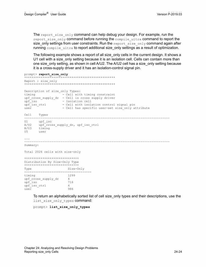
Design Compiler® User Guide P-2019.03Design Compiler® User Guide Version P-2019.03
The report_size_only command can help debug your design. For example, run the report_size_only command before running the compile_ultra command to report the size_only settings from user constraints. Run the report_size_only command again after running compile_ultra to report additional size_only settings as a result of optimization.
The following example shows a report of all size_only cells in the current design. It shows a U1 cell with a size_only setting because it is an isolation cell. Cells can contain more than one size_only setting, as shown in cell A/U2. The A/U2 cell has a size_only setting because it is a cross-supply driver and it has an isolation-control signal pin.
prompt> report_size_only************************************************** Report : size_only **************************************************
Description of size_only Types:timing - Cell with timing constraint upf_cross_supply_dr - Cell is cross supply driverupf_iso - Isolation cellupf_iso_ctrl - Cell with isolation control signal pinuser - Cell has specific user-set size_only attribute
Cell Types-------------------------------------------------------------------------------- U1 upf_isoA/U2 upf_cross_supply_dr, upf_iso_ctrlB/U3 timingU5 user
...-------------------------------------------------------------------------------- Summary:
Total 2026 cells with size-only
****************************** Distribution By Size-Only Type ****************************** Type Size-Only ------------------------------------- timing 1299 upf_cross_supply_dr 4upf_iso 716upf_iso_ctrl 4user 986
To return an alphabetically sorted list of cell size_only types and their descriptions, use the list_size_only_types command:
prompt> list_size_only_types
Chapter 24: Analyzing and Resolving Design ProblemsReporting size_only Cells 24-24

Design Compiler® User Guide Version P-2019.03
RTL Cross-Probing in the GUI
Design Compiler offers cross-probing capabilities in the GUI so you can check your RTL design in the RTL browser. You can cross-probe cells, pins, or timing paths in a design from one view, such as a schematic, cell list, layout, or timing view, and examine the corresponding RTL file. This allows you to identify lines in the code that can be modified to improve timing, congestion, or datapath extraction.
Note: To use these cross-probing capabilities, you must have an elaborated or synthesized design from Design Compiler version I-2013.12 or later.
Design Compiler provides the following cross-probing capabilities in the GUI to the RTL file in the RTL browser:
• You can select a critical path and cross-probe to the corresponding RTL files to help debug the worst-case timing paths.
• You can cross-probe the cells in a highly congested area and inspect the RTL code for cells that are causing congestion.
• You can cross-probe from a datapath extraction or design resources report to the corresponding RTL file to help you understand the datapath extraction, which can help you improve the coding style for better extraction.
You can also open an RTL file that you used to elaborate or compile the design and cross-probe to cells associated with a line in the file. Similarly, you can cross-probe from an RTL file to the design resources report.
The tool does not allow you to
• Cross-probe from various design views to the UPF file.
• Select nets as cross-probing objects.
Figure 24-4 shows cross-probing between the Design Vision layout view and the RTL browser.
Chapter 24: Analyzing and Resolving Design ProblemsRTL Cross-Probing in the GUI 24-25Chapter 24: Analyzing and Resolving Design ProblemsRTL Cross-Probing in the GUI 24-25

Design Compiler® User Guide P-2019.03Design Compiler® User Guide Version P-2019.03
Figure 24-4 Cross-Probing Between the Layout View and the RTL Browser
See Also
• The “Cross-Probing the RTL for Cells or Paths” topic in Design Vision Help
RTL Cross-Probing on the Command Line
To improve timing, congestion, or datapath extraction, you can check the RTL design and identify lines in the code to be modified by using the RTL cross-probing capabilities on the command line.
You must have a design that was analyzed and elaborated or synthesized using Design Compiler version I-2013.12 or later to use the following cross-probing commands:
• get_cross_probing_info
The command returns cross-probing data for specified cells or ports as a string, specifying where the cell or port was created and which file and line number the object came from. Some objects in the design might have been merged, resulting in multiple source locations that are returned.
The results of each object are separated by a pair of braces between each source position and between each object. For example, if you specify two objects, obj1 and obj2,
Chapter 24: Analyzing and Resolving Design ProblemsRTL Cross-Probing on the Command Line 24-26

Design Compiler® User Guide Version P-2019.03
where obj1 has one source position and obj2 has two source positions, the tool returns the results in the following format:
{ {obj1_file1:obj1_line1} } { {obj2_file1:obj2_line1} {obj2_file2:obj2_line2} }
To prevent duplicate file:linenumber combinations in the results, use the -unique_source option with the get_cross_probing_info command. In this case, the tool returns the results in the following format:
obj1_file1:obj1_line1 obj2_file1:obj2_line1 obj2_file2:obj2_line2
The following example shows results from the get_cross_probing_info command with the -unique_source option:
prompt> get_cross_probing_info [get_cells -hierarchical] \ -unique_source/usr/joe/my_design/m.v:21 /usr/joe/my_design/m.v:22 /usr/joe/my_design/m.v:28 /usr/joe/my_design/m.v:12 /usr/joe/my_design/m.v:13 /usr/joe/my_design/m.v:14 /usr/joe/my_design/m.v:4
• cross_probing_filter
The command allows you to filter a collection by specifying a source file and line number in the following format:
"file_pattern[:line_pattern]"
The following example shows results from the cross_probing_filter command, returning cells that originated in a source file ending in m.v on line 21:
prompt> cross_probing_filter [get_cells -hierarchical] \-source "*m.v:21"
{mid1/bot1/c1 mid1/bot2/c1}
Objects in the design that were merged, resulting in multiple source locations, are returned in the collection if any of the source positions match any of the specified source patterns.
• report_cross_probing
The command returns cross-probing data for specified cells or ports in a report. If the object was generated by the tool, the file and line number are not applicable and are represented by a hyphen (-). In this case, the report specifies whether the origin of the object comes from UPF, the DFT engine, or another source. Objects that were merged are displayed in the report multiple times, once for each source location.
The tool reports the following information for each specified object:
❍ Type: The type of design object, either cell or port.
Chapter 24: Analyzing and Resolving Design ProblemsRTL Cross-Probing on the Command Line 24-27Chapter 24: Analyzing and Resolving Design ProblemsRTL Cross-Probing on the Command Line 24-27

Design Compiler® User Guide P-2019.03Design Compiler® User Guide Version P-2019.03
❍ Reference: For cells, this is the library reference cell. For ports, it is one of the following: IN, OUT, INOUT.
❍ Filename: The base name of the file. If this information is not available, the tool displays a hyphen (-).
❍ Line: The line number associated with the file. If this information is not available, the tool displays a hyphen (-).
❍ Origin: The origin associated with the object. For example, this value can be rtl, datapath, upf, clock_gating, self_gating, or dft. If this information is not available, the tool displays a hyphen (-).
❍ Object: The object name. If an object has multiple source positions, the object name is indented for lines other than the first source line.
You can also display the original RTL hierarchical name to help identify where the cell originated by using the -original_hierarchy option. When you specify this option with the report_cross_probing command, the Object column in the report is displayed as Object/Original Hierarchy. For each object, the first row in this column shows the object name, and the second row in the column shows the object’s original hierarchy.
Repeating RTL Cross-Probing
Each time the tool reads an RTL file for cross-probing, it stores the RTL line numbers and file paths in the database. If the RTL file was moved to a different location after the cross-probing, repeating the same cross-probing sequence no longer reflects the previous line numbers. As a result, the tool cannot locate the file and issues an error message.
To repeat a cross-probing sequence or reference previous cross-probing data, you must first find the status of the files that were cross-probed. You can obtain the status by running the following commands:
• report_cross_probing_files
The command reports the status of the cross-probed files, including OK, Missing, Modified, and No Permissions.
• update_cross_probing_files
The command updates the locations of the files that were cross-probed and lists the previous and current paths of the files. The command does not update the cross-probed files if they have been modified.
Chapter 24: Analyzing and Resolving Design ProblemsRTL Cross-Probing on the Command Line 24-28

Design Compiler® User Guide Version P-2019.03
RTL Cross-Probing Report Example
The following example shows a command-line RTL cross-probing report with the original hierarchy information of the objects included:
prompt> report_cross_probing [get_cells U1*] –original_hierarchy****************************************Report : cross_probing_filesDesign : data_switch_512Version: ...Date : ...****************************************Type Reference Filename Line Origin Object/Original Hierarchy-----------------------------------------------------------------------------------cell HS65_STF_AOI test1.v 21536 rtl U129
I_CORE/I_SUB1cell HS65_STF_AND2 test2.v 21548 rtl U104
I_CORE/I_SUB2...
Chapter 24: Analyzing and Resolving Design ProblemsRTL Cross-Probing on the Command Line 24-29Chapter 24: Analyzing and Resolving Design ProblemsRTL Cross-Probing on the Command Line 24-29

Design Compiler® User Guide P-2019.03Design Compiler® User Guide Version P-2019.03
Chapter 24: Analyzing and Resolving Design ProblemsRTL Cross-Probing on the Command Line 24-30
25Verifying Functional Equivalence 25
After optimization, you can use an equivalence checking tool to verify that your gate-level netlist is functionally equivalent to your RTL. This verification step ensures that the synthesis process or manual design changes did not introduce functional errors. You can use the Synopsys Formality tool or a third-party formal verification tool to perform functional equivalence checking, as described in the following topics:
• Setting Up SVF Generation
• The Formality Tool
• Adjusting Optimization for Successful Verification
• Using Third-Party Formal Verification Tools
25-1

Design Compiler® User Guide P-2019.03Design Compiler® User Guide Version P-2019.03
Setting Up SVF Generation
The Design Compiler tool records setup information to facilitate alignment of compare points during matching in formal verification tools.
To record a setup information file for
• The Formality tool, use the set_svf command
• Other formal verification tools, use the set_vsdc command
To stop running the set_svf command, use the set_svf -off command or exit from the dc_shell prompt.
When you use the set_svf command, the Design Compiler tool records the following information in the .svf file:
• Name changes that occur during synthesis when you use commands such as group, ungroup, uniquify, and change_names
• Operations performed by the compile command
• UPF information
• Other relevant operations
To overwrite the existing SVF file, use the following command:
prompt> set_svf my_design.svf
To append the information to the existing SVF file, use the following command:
prompt> set_svf -append xyz.svf
The guide_hier_map (GHM) Flow
The guide_hier_map (GHM) flow adds guide_hier_map guidance to the SVF file for capturing all logical hierarchy transformations, including multi-level elaborations, parameterized elaborations, and so on.
To use the guide_hier_map (GHM) flow, create your verification guidance as follows:
1. (Optional) Specify the file name to use for your Formality automated setup file:
dc_shell> set_svf ./guidance/top.svf
By default, the tool creates a file named default.svf in the current directory.
Chapter 25: Verifying Functional EquivalenceSetting Up SVF Generation 25-2
Design Compiler® User Guide Version P-2019.03
2. Set the following variable before reading or analyzing any RTL files:
dc_shell> set_app_var hdlin_enable_hier_map true
This tracks all logical hierarchy transformations performed by the tool.
3. Execute all analyze, read, and elaborate commands.
4. Use the following command after reading or elaborating all RTL and linking the top-level design:
dc_shell> set_verification_top
This writes guide_hier_map guidance directives into the verification guidance, which provides an accurate reference for subsequent hierarchical transformations and name changes.
For example,
# specify SVF output fileset_svf ./guidance/top.svf
# read design filesset_app_var hdlin_enable_hier_map trueanalyze -format sverilog {sub.sv top.sv}elaborate topcurrent_design toplink
# issue this command after reading last RTL file# (and before other commands that can modify hierarchy)set_verification_top
# apply SDC, UPF, hierarchy manipulation, perform synthesis...
Note that the tool issues error messages if you forget to set the variable or forget to run the set_verification_top command after setting the variable.
You can create verification guidance without setting the hdlin_enable_hier_map variable or issuing the set_verification_top command. However, the resulting guidance might not handle complex logical hierarchy transformations. This flow is provided for backward compatibility only.
The Formality Tool
The Formality tool is an equivalence checking tool that can verify that your gate-level netlist is functionally equivalent to your RTL. This verification step ensures that the synthesis process or manual design changes did not introduce functional errors.
Chapter 25: Verifying Functional EquivalenceThe Formality Tool 25-3Chapter 25: Verifying Functional EquivalenceThe Formality Tool 25-3

Design Compiler® User Guide P-2019.03Design Compiler® User Guide Version P-2019.03
Formality uses formal techniques to prove or disprove the functional equivalence of two designs. It performs RTL-to-RTL, RTL-to-gate, and gate-to-gate verifications. Functional equivalence checking does not take into account timing; it is a static verification process.
Verification Guidance
By default, Design Compiler automatically creates a Formality automated setup file, which is also known as verification guidance, in your working directory. This file has an .svf extension and is named default.svf. The automated setup file provides a method for automatically conveying setup information to Formality. It alleviates the need to enter setup information manually, a task that can be time-consuming and error-prone.
The automated setup file is a binary file. When Formality reads this binary data, it automatically converts it to ASCII and writes it to a text file. This gives you to opportunity to review the setup information before you use it in the verification process.
The automated setup file can contain the following information:
• The settings of certain Tcl variables that affect how the names of design objects in the netlist are created, such as the bus_naming_style and template_* variables
• Optimizations that occur during RTL elaboration
• Name changes resulting from operations, such as ungroup, group, uniquify, rename_design, or the automatic uniquify process in compile with combinations of group and ungroup (these operations can change the names of design objects such as registers, black boxes, and top-level ports)
• Phase inversion and constant propagation optimizations performed during sequential mapping
• Datapath transformations, including information about multiplier architectures chosen during synthesis
• Retiming optimizations
• Information about FSM extraction
Additionally, the automated setup file records implicit ungroup operations. Implicit ungroup operations can occur in the following situations:
• During automatic ungrouping with the compile_ultra command, the compile -ungroup -all command, or the compile -auto_ungroup command
• If a design has an ungroup attribute set on it
• When DesignWare auto-ungroups DesignWare parts
• When certain user hierarchies are auto-ungrouped for datapath optimization
Chapter 25: Verifying Functional EquivalenceThe Formality Tool 25-4

Design Compiler® User Guide Version P-2019.03
You can use the Design Compiler set_svf command to control the name of the automated setup file or to save it to a location other than your current working directory. To disable the generation of the .svf file, use the -off option. If you use the set_svf command, you must do so at the beginning of the synthesis process, before you read your design files.
See Also
• The Formality User Guide
Adjusting Optimization for Successful Verification
When Formality cannot complete verification due to issues, such as design complexity, it is considered a failing verification, or a hard verification. Datapath intensive designs or designs containing complex design components, such as parity generators, XOR trees, or very large cones of logic, can cause Formality to issue hard verifications or inconclusive verifications.
Design Compiler adjusts some of the optimizations to help reduce inconclusive and hard verifications, as discussed in the following sections. The first method, using the set_verification_priority command, is the recommended method for resolving inconclusive and hard verifications because it targets specific blocks or operators while minimizing QoR impact.
• Using the set_verification_priority Command
• Using Single-Pass Verification
Using the set_verification_priority Command
The set_verification_priority command sets the verification_priority attribute on the specified objects. During the compile_ultra command run, the optimizations of the design with the verification_priority attribute are adjusted depending on the verification priority level so that the potential for hard verification is reduced. The set_verification_priority command is available only in DC Ultra.
When you have inconclusive verifications in Formality, you can use the analyze_points command to examine the hard points and determine the possible cause of the hard verifications. The analyze_points command runs analysis on the most recent failed or hard verification. The analyze_points command generates a recommendation as to which blocks or operators the set_verification_priority command can be used with in Design Compiler to reduce hard verifications.
To adjust the optimizations to reduce hard verifications,
1. Run Design Compiler.
Chapter 25: Verifying Functional EquivalenceAdjusting Optimization for Successful Verification 25-5Chapter 25: Verifying Functional EquivalenceAdjusting Optimization for Successful Verification 25-5

Design Compiler® User Guide P-2019.03Design Compiler® User Guide Version P-2019.03
2. Run Formality.
3. Analyze the Formality verification reports.
The analyze_points command runs analysis on the most recent failed or hard verification. The command generates a recommendation regarding which blocks the set_verification_priority command can be used with in Design Compiler to reduce hard verifications.
The following example shows the output of the analyze_points command in Formality:
Try adding the following command(s) to your Design Compiler script rightbefore the first compile_ultra command:current_design testset_verification_priority [ get_cells { add_21 mult_21 mult_30 sub_30} ]
4. Rerun Design Compiler, as follows:
a. Specify the set_verification_priority command with the problem blocks that were identified by the analyze_points command in Formality. Add the commands that were suggested by Formality to your Design Compiler scripts.
b. Run the compile_ultra command.
For more information about the analyze_points command, see the man page in Formality and the Formality User Guide. For more information about the set_verification_priority command, see the man page in Design Compiler.
Using Single-Pass Verification
Design Compiler single-pass verification functionality adjusts optimization so that formal verification compatibility is prioritized over QoR. This is helpful if you do not have tight QoR constraints in your design, you do not have register retiming, and you want to pass formal verification with as little effort as possible. You can enable the single-pass verification flow by setting the simplified_verification_mode variable to true. The variable is set to false by default.
By default, designs with the optimize_registers attribute and DW_div_pipe DesignWare components are not retimed because they can adversely affect verification success. However, optimizing designs with the optimize_registers attribute and DW_div_pipe DesignWare components without retiming them can have a large impact on QoR and runtime. To enable the retiming of these designs, set the simplified_verification_mode_allow_retiming variable to true when you enable the simplified_verification_mode variable.
Chapter 25: Verifying Functional EquivalenceAdjusting Optimization for Successful Verification 25-6

Design Compiler® User Guide Version P-2019.03
Using Third-Party Formal Verification Tools
To record setup information for formal verification tools other than Formality, use the set_vsdc command. The command records setup information in V-SDC format for efficient compare point matching in third-party formal verification tools. The V-SDC format is a subset of the automated setup file used by Formality. The V-SDC file is written in plain text, whereas the automated setup file is encrypted and compressed.
The set_vsdc command records the following operations:
• Name changes resulting from operations such as ungroup, group, or uniquify, or the automatic uniquify process in compile with combinations of group and ungroup. These operation can change the names of design objects such as registers, black boxes, and top-level ports
• Operations performed by the compile command that result in register optimizations.
Chapter 25: Verifying Functional EquivalenceUsing Third-Party Formal Verification Tools 25-7Chapter 25: Verifying Functional EquivalenceUsing Third-Party Formal Verification Tools 25-7

Design Compiler® User Guide P-2019.03Design Compiler® User Guide Version P-2019.03
Chapter 25: Verifying Functional EquivalenceUsing Third-Party Formal Verification Tools 25-8

ADesign Example A
Optimizing a design can involve using different compile strategies for different levels and components in the design. This appendix shows a design example that uses several compile strategies. Earlier chapters provide detailed descriptions of how to implement each compile strategy. Note that the design example used in this appendix does not represent a real-life application.
This appendix includes the following sections:
• Design Description
• Setup File
• Default Constraints File
• Read Script
• Compile Scripts
You can access the files described in these sections at $SYNOPSYS/doc/syn/guidelines, where $SYNOPSYS is the path to the installation directory.
A-1

Design Compiler® User Guide P-2019.03Design Compiler® User Guide Version P-2019.03
Design Description
The design example shows how you can constrain designs by using a subset of the commonly used dc_shell commands and how you can use scripts to implement various compile strategies.
The design uses synchronous RTL and combinational logic with clocked D flip-flops.
Figure A-1 shows the block diagram for the design example. The design contains seven modules at the top level: Adder16, CascadeMod, Comparator, Multiply8x8, Multiply16x16, MuxMod, and PathSegment.
Figure A-1 Block Diagram for the Design Example
CounterComparator
Adder8Adder8 Adder16
CascadeMod
PathSegment
Multiply
Multiply
MuxMod
ChipLevel
8x8
16x16
Comparator
Appendix A: Design ExampleDesign Description A-2

Design Compiler® User Guide Version P-2019.03
Figure A-2 shows the hierarchy for the design example.
Figure A-2 Hierarchy for the Design Example
The top-level modules and the compilation strategies for optimizing them are
Adder16
Uses registered outputs to make constraining easier. Because the endpoints are the data pins of the registers, you do not need to set output delays on the output ports.
CascadeMod
Uses a hierarchical compile strategy. The compile script for this design sets the constraints at the top level (of CascadeMod) before compilation.
The CascadeMod design instantiates the Adder8 design twice. The script uses the compile-once-don’t-touch method for the Comparator module.
Comparator
Is a combinational block. The compile script for this design uses the virtual clock concept to show the use of virtual clocks in a design.
The ChipLevel design instantiates Comparator twice. The compile script (for CascadeMod) uses the compile-once-don’t-touch method to resolve the multiple instances.
The compile script specifies wire load model and mode instead of using automatic wire load selection.
Multiply8x8
Shows the basic timing and area constraints used for optimizing a design.
ChipLevel
Adder16
Adder8Adder8 CounterComparator
MultiplyCascadeMod MuxMod PathSegment8x8Multiply16x16Comparator
Chapter A: Design ExampleDesign Description A-3Appendix A: Design ExampleDesign Description A-3

Design Compiler® User Guide P-2019.03Design Compiler® User Guide Version P-2019.03
Multiply16x16
Ungroups DesignWare parts before compilation. Ungrouping your hierarchical module might help achieve better synthesis results. The compile script for this module defines a two-cycle path at the primary ports of the module.
MuxMod
Is a combinational block. The script for this design uses the virtual clock concept.
PathSegment
Uses path segmentation within a module. The script uses the set_multicycle_path command for a two-cycle path within the module and the group command to create a new level of hierarchy.
Example A-1 through Example A-11 provide the Verilog source code for the ChipLevel design.
Example A-1 ChipLevel.v
/* Date: May 11, 1995 *//* Example Circuit for Baseline Methodology for Synthesis *//* Design does not show any real-life application but rather it is used to illustrate the commands used in the Baseline Methodology */
module ChipLevel (data16_a, data16_b, data16_c, data16_d, clk, cin, din_a, din_b, sel, rst, start, mux_out, cout1, cout2, s1, s2, op, comp_out1, comp_out2, m32_out, regout);
input [15:0] data16_a, data16_b, data16_c, data16_d; input [7:0] din_a, din_b; input [1:0] sel; input clk, cin, rst, start; input s1, s2, op; output [15:0] mux_out, regout; output [31:0] m32_out; output cout1, cout2, comp_out1, comp_out2;
wire [15:0] ad16_sout, ad8_sout, m16_out, cnt;
Adder16 u1 (.ain(data16_a), .bin(data16_b), .cin(cin), .cout(cout1), .sout(ad16_sout), .clk(clk));
CascadeMod u2 (.data1(data16_a), .data2(data16_b), .cin(cin), .s(ad8_sout), .cout(cout2), .clk(clk), .comp_out(comp_out1), .cnt(cnt), .rst(rst), .start(start) );
Comparator u3 (.ain(ad16_sout), .bin(ad8_sout), .cp_out(comp_out2));
Multiply8x8 u4 (.op1(din_a), .op2(din_b), .res(m16_out), .clk(clk));
Multiply16x16 u5 (.op1(data16_a), .op2(data16_b), .res(m32_out), .clk(clk));
MuxMod u6 (.Y_IN(mux_out), .MUX_CNT(sel), .D(ad16_sout), .R(ad8_sout),
Appendix A: Design ExampleDesign Description A-4

Design Compiler® User Guide Version P-2019.03
.F(m16_out), .UPC(cnt));
PathSegment u7 (.R1(data16_a), .R2(data16_b), .R3(data16_c), .R4(data16_d), .S2(s2), .S1(s1), .OP(op), .REGOUT(regout), .clk(clk));endmodule
Example A-2 Adder16.v
module Adder16 (ain, bin, cin, sout, cout, clk);/* 16-Bit Adder Module */output [15:0] sout;output cout;input [15:0] ain, bin;input cin, clk;
wire [15:0] sout_tmp, ain, bin;wire cout_tmp;reg [15:0] sout, ain_tmp, bin_tmp;reg cout, cin_tmp;
always @(posedge clk) begin cout = cout_tmp; sout = sout_tmp; ain_tmp = ain; bin_tmp = bin; cin_tmp = cin;end assign {cout_tmp,sout_tmp} = ain_tmp + bin_tmp + cin_tmp;endmodule
Example A-3 CascadeMod.v
module CascadeMod (data1, data2, s, clk, cin, cout, comp_out, cnt, rst, start);input [15:0] data1, data2;output [15:0] s, cnt;input clk, cin, rst, start;output cout, comp_out;wire co;
Adder8 u10 (.ain(data1[7:0]), .bin(data2[7:0]), .cin(cin), .clk(clk), .sout(s[7:0]), .cout(co));Adder8 u11 (.ain(data1[15:8]), .bin(data2[15:8]), .cin(co), .clk(clk), .sout(s[15:8]), .cout(cout));Comparator u12 (.ain(s), .bin(cnt), .cp_out(comp_out));
Counter u13 (.count(cnt), .start(start), .clk(clk), .rst(rst));endmodule
Chapter A: Design ExampleDesign Description A-5Appendix A: Design ExampleDesign Description A-5

Design Compiler® User Guide P-2019.03Design Compiler® User Guide Version P-2019.03
Example A-4 Adder8.v
module Adder8 (ain, bin, cin, sout, cout, clk);/* 8-Bit Adder Module */output [7:0] sout;output cout;input [7:0] ain, bin;input cin, clk;
wire [7:0] sout_tmp, ain, bin;wire cout_tmp;reg [7:0] sout, ain_tmp, bin_tmp;reg cout, cin_tmp;
always @(posedge clk) begin cout = cout_tmp; sout = sout_tmp; ain_tmp = ain; bin_tmp = bin; cin_tmp = cin;end assign {cout_tmp,sout_tmp} = ain_tmp + bin_tmp + cin_tmp;endmodule
Example A-5 Counter.v
module Counter (count, start, clk, rst);/* Counter module */ input clk; input rst; input start; output [15:0] count;
wire clk; reg [15:0] count_N; reg [15:0] count;
always @ (posedge clk or posedge rst) begin : counter_S if (rst) begin count = 0; // reset logic for the block end else begin count = count_N; // set specified registers of the block end end
always @ (count or start) begin : counter_C count_N = count; // initialize outputs of the block if (start) count_N = 1; // user specified logic for the block else count_N = count + 1; endendmodule
Appendix A: Design ExampleDesign Description A-6

Design Compiler® User Guide Version P-2019.03
Example A-6 Comparator.v
module Comparator (cp_out, ain, bin);/* Comparator for 2 integer values */output cp_out;input [15:0] ain, bin; assign cp_out = ain < bin;endmodule
Example A-7 Multiply8x8.v
module Multiply8x8 (op1, op2, res, clk);/* 8-Bit multiplier */input [7:0] op1, op2;output [15:0] res;input clk;
wire [15:0] res_tmp;reg [15:0] res;
always @(posedge clk) begin res = res_tmp;endassign res_tmp = op1 * op2;endmodule
Example A-8 Multiply16x16.v
module Multiply16x16 (op1, op2, res, clk);/* 16-Bit multiplier */input [15:0] op1, op2;output [31:0] res;input clk;
wire [31:0] res_tmp;reg [31:0] res;
always @(posedge clk) begin res = res_tmp;endassign res_tmp = op1 * op2;endmodule
Example A-9 def_macro.v
`define DATA 2’b00`define REG 2’b01`define STACKIN 2’b10`define UPCOUT 2’b11
Chapter A: Design ExampleDesign Description A-7Appendix A: Design ExampleDesign Description A-7

Design Compiler® User Guide P-2019.03Design Compiler® User Guide Version P-2019.03
Example A-10 MuxMod.v
module MuxMod (Y_IN, MUX_CNT, D, R, F, UPC);‘include "def_macro.v" output [15:0] Y_IN; input [ 1:0] MUX_CNT; input [15:0] D, F, R, UPC;
reg [15:0] Y_IN;
always @ ( MUX_CNT or D or R or F or UPC ) begin case ( MUX_CNT ) `DATA : Y_IN = D ; `REG : Y_IN = R ; `STACKIN : Y_IN = F ; `UPCOUT : Y_IN = UPC; endcaseend
endmodule
Example A-11 PathSegment.v
module PathSegment (R1, R2, R3, R4, S2, S1, OP, REGOUT, clk);/* Example for path segmentation */input [15:0] R1, R2, R3, R4;input S2, S1, clk;input OP;output [15:0] REGOUT;
reg [15:0] ADATA, BDATA;reg [15:0] REGOUT;reg MODE;
wire [15:0] product ;
always @(posedge clk)begin : selector_block case(S1) 1’b0: ADATA <= R1; 1’b1: ADATA <= R2; default: ADATA <= 16’bx; endcase case(S2) 1’b0: BDATA <= R3; 1’b1: BDATA <= R4; default: ADATA <= 16’bx; endcaseend
/* Only Lower Byte gets multiplied */
Appendix A: Design ExampleDesign Description A-8

Design Compiler® User Guide Version P-2019.03
// instantiate DW02_multDW02_mult #(8,8) U100 (.A(ADATA[7:0]), .B(BDATA[7:0]), .TC(1’b0), .PRODUCT(product));
always @(posedge clk)begin : alu_block case (OP) 1’b0 : begin REGOUT <= ADATA + BDATA; end 1’b1 : begin REGOUT <= product; end default : REGOUT <= 16’bx; endcaseend
endmodule
Setup File
When running the design example, copy the project-specific setup file in Example A-12 to your project working directory. This setup file is written in the Tcl subset and can be used in the Tcl command language. For more information about the Tcl subset, see Using Tcl With Synopsys Tools.
For details on the synthesis setup files, see The Setup Files.
Example A-12 .synopsys_dc.setup File
# Define the target logic library, symbol library, # and link librariesset target_library lsi_10k.dbset symbol_library lsi_10k.sdbset link_library [concat $target_library "*"]set search_path [concat $search_path ./src]set designer "Your Name"set company "Synopsys, Inc."# Define path directories for file locationsset source_path "./src/"set script_path "./scr/"set log_path "./log/"set ddc_path "./ddc/"set db_path "./db/"set netlist_path "./netlist/"
Chapter A: Design ExampleSetup File A-9Appendix A: Design ExampleSetup File A-9

Design Compiler® User Guide P-2019.03Design Compiler® User Guide Version P-2019.03
Default Constraints File
The file shown in Example A-13 defines the default constraints for the design. In the scripts that follow, Design Compiler reads this file first for each module. If the script for a module contains additional constraints or constraint values different from those defined in the default constraints file, Design Compiler uses the module-specific constraints.
Example A-13 defaults.con
# Define system clock periodset clk_period 20
# Create real clock if clock port is found if {[sizeof_collection [get_ports clk]] > 0} { set clk_name clk create_clock -period $clk_period clk}
# Create virtual clock if clock port is not found if {[sizeof_collection [get_ports clk]] == 0} { set clk_name vclk create_clock -period $clk_period -name vclk}
# Apply default drive strengths and typical loads# for I/O ports set_load 1.5 [all_outputs]set_driving_cell -lib_cell IV [all_inputs]
# If real clock, set infinite drive strength if {[sizeof_collection [get_ports clk]] > 0} { set_drive 0 clk}
# Apply default timing constraints for modules set_input_delay 1.2 [all_inputs] -clock $clk_nameset_output_delay 1.5 [all_outputs] -clock $clk_nameset_clock_uncertainty -setup 0.45 $clk_name
# Set operating conditions set_operating_conditions WCCOM
# Turn on auto wire load selection # (library must support this feature) set auto_wire_load_selection true
Appendix A: Design ExampleDefault Constraints File A-10

Design Compiler® User Guide Version P-2019.03
Read Script
Example A-15 provides the Tcl script used to read in the ChipLevel design.
The read.tcl script reads design information from the specified Verilog files into memory.
Example A-14 read.tcl
read_file -format verilog ChipLevel.vread_file -format verilog Adder16.vread_file -format verilog CascadeMod.vread_file -format verilog Adder8.vread_file -format verilog Counter.vread_file -format verilog Comparator.vread_file -format verilog Multiply8x8.vread_file -format verilog Multiply16x16.vread_file -format verilog MuxMod.vread_file -format verilog PathSegment.v
Compile Scripts
Example A-15 through Example A-26 provide the Tcl scripts used to compile the ChipLevel design.
The compile script for each module is named for that module to ease recognition. The initial Tcl script files have the .tcl suffix. Scripts generated by the write_script command have the .wtcl suffix.
Example A-15 run.tcl
# Initial compile with estimated constraintssource "${script_path}initial_compile.tcl"
current_design ChipLevelif {[shell_is_in_xg_mode]==0}{write -hier -o "${db_path}ChipLevel_init.db"} else {write -format ddc -hier -o "${ddc_path}ChipLevel_init.ddc"}
# Characterize and write_script for all modules source "${script_path}characterize.tcl"
# Recompile all modules using write_script constraints remove_design -allsource "${script_path}recompile.tcl"
current_design ChipLevelif {[shell_is_in_xg_mode]==0}{write -hier -out "${db_path}ChipLevel_final.db"
Chapter A: Design ExampleRead Script A-11Appendix A: Design ExampleRead Script A-11

Design Compiler® User Guide P-2019.03Design Compiler® User Guide Version P-2019.03
} else {write -format ddc -hier -out "${ddc_path}ChipLevel_final.ddc"}
Example A-16 initial_compile.tcl
# Initial compile with estimated constraints source "${script_path}read.tcl"
current_design ChipLevelsource "${script_path}defaults.con"
source "${script_path}adder16.tcl"source "${script_path}cascademod.tcl"source "${script_path}comp16.tcl"source "${script_path}mult8.tcl"source "${script_path}mult16.tcl"source "${script_path}muxmod.tcl"source "${script_path}pathseg.tcl"
Example A-17 adder16.tcl
# Script file for constraining Adder16 set rpt_file "adder16.rpt"set design "adder16"
current_design Adder16source "${script_path}defaults.con"
# Define design environment set_load 2.2 soutset_load 1.5 coutset_driving_cell -lib_cell FD1 [all_inputs]set_drive 0 $clk_name
# Define design constraints set_input_delay 1.35 -clock $clk_name {ain bin}set_input_delay 3.5 -clock $clk_name cinset_max_area 0
compile
if {[shell_is_in_xg_mode]==0}{write -hier -o "${db_path}${design}.db"} else {write -format ddc -hier -o "${ddc_path}${design}.ddc"}
source "${script_path}report.tcl"
Appendix A: Design ExampleCompile Scripts A-12
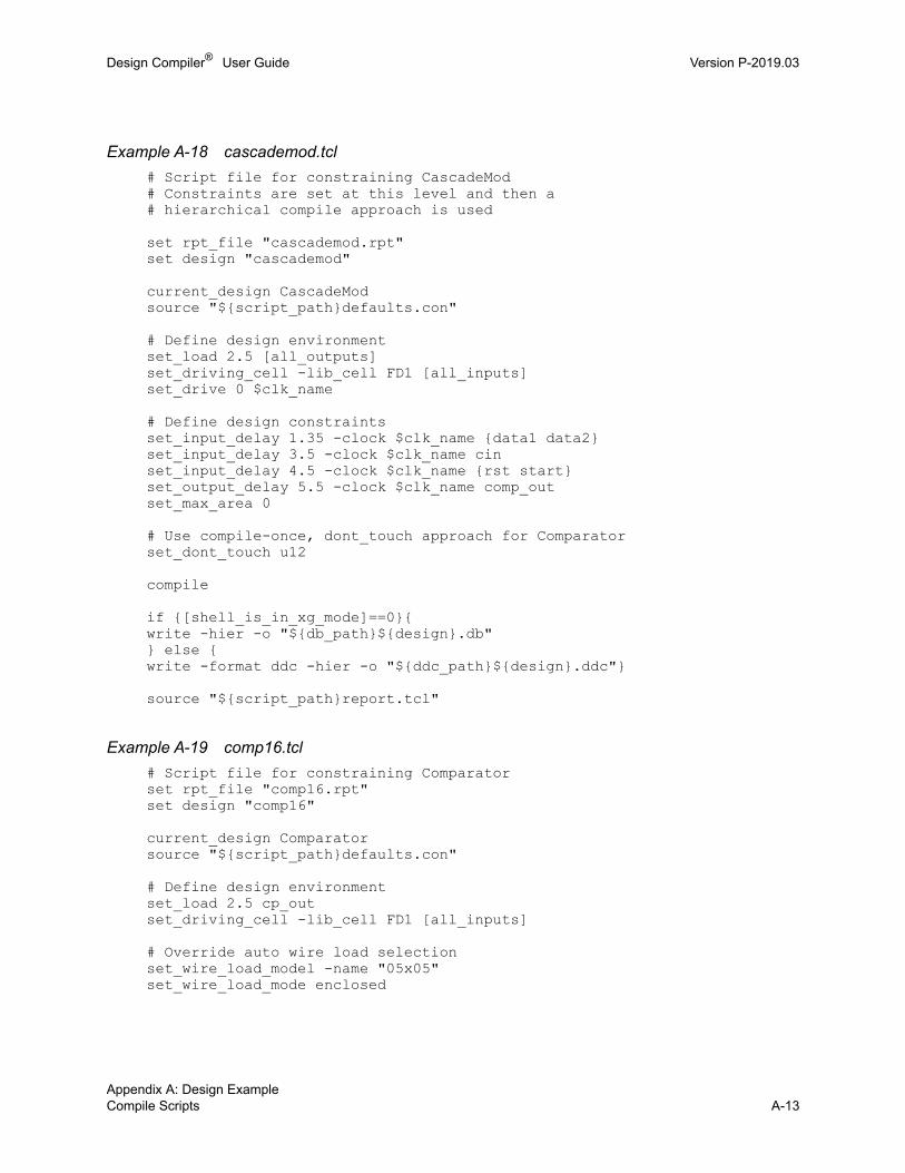
Design Compiler® User Guide Version P-2019.03
Example A-18 cascademod.tcl
# Script file for constraining CascadeMod # Constraints are set at this level and then a # hierarchical compile approach is used
set rpt_file "cascademod.rpt"set design "cascademod"
current_design CascadeModsource "${script_path}defaults.con"
# Define design environment set_load 2.5 [all_outputs]set_driving_cell -lib_cell FD1 [all_inputs]set_drive 0 $clk_name
# Define design constraints set_input_delay 1.35 -clock $clk_name {data1 data2}set_input_delay 3.5 -clock $clk_name cinset_input_delay 4.5 -clock $clk_name {rst start}set_output_delay 5.5 -clock $clk_name comp_outset_max_area 0
# Use compile-once, dont_touch approach for Comparator set_dont_touch u12
compile
if {[shell_is_in_xg_mode]==0}{write -hier -o "${db_path}${design}.db"} else {write -format ddc -hier -o "${ddc_path}${design}.ddc"}
source "${script_path}report.tcl"
Example A-19 comp16.tcl
# Script file for constraining Comparator set rpt_file "comp16.rpt"set design "comp16"
current_design Comparatorsource "${script_path}defaults.con"
# Define design environment set_load 2.5 cp_outset_driving_cell -lib_cell FD1 [all_inputs]
# Override auto wire load selection set_wire_load_model -name "05x05"set_wire_load_mode enclosed
Chapter A: Design ExampleCompile Scripts A-13Appendix A: Design ExampleCompile Scripts A-13

Design Compiler® User Guide P-2019.03Design Compiler® User Guide Version P-2019.03
# Define design constraints set_input_delay 1.35 -clock $clk_name {ain bin}set_output_delay 5.1 -clock $clk_name {cp_out}set_max_area 0
compile
if {[shell_is_in_xg_mode]==0}{write -hier -o "${db_path}${design}.db"} else {write -format ddc -hier -o "${ddc_path}${design}.ddc"}
source "${script_path}report.tcl"
Example A-20 mult8.tcl
# Script file for constraining Multiply8x8 set rpt_file "mult8.rpt"set design "mult8"
current_design Multiply8x8source "${script_path}defaults.con"
# Define design environment set_load 2.2 resset_driving_cell -lib_cell FD1P [all_inputs]set_drive 0 $clk_name
# Define design constraints set_input_delay 1.35 -clock $clk_name {op1 op2}set_max_area 0
compile
if {[shell_is_in_xg_mode]==0}{write -hier -o "${db_path}${design}.db"} else {write -format ddc -hier -o "${ddc_path}${design}.ddc"}
source "${script_path}report.tcl"
Appendix A: Design ExampleCompile Scripts A-14

Design Compiler® User Guide Version P-2019.03
Example A-21 mult16.tcl
# Script file for constraining Multiply16x16 set rpt_file "mult16.rpt"set design "mult16"
current_design Multiply16x16source "${script_path}defaults.con"
# Define design environment set_load 2.2 resset_driving_cell -lib_cell FD1 [all_inputs]set_drive 0 $clk_name
# Define design constraints set_input_delay 1.35 -clock $clk_name {op1 op2}set_max_area 0
# Define multicycle path for multiplier set_multicycle_path 2 -from [all_inputs] \ -to [all_registers -data_pins -edge_triggered]
# Ungroup DesignWare parts set designware_cells [get_cells \
-filter "@is_oper==true"]if {[sizeof_collection $designware_cells] > 0} { set_ungroup $designware_cells true}
compile
if {[shell_is_in_xg_mode]==0}{write -hier -o "${db_path}${design}.db"} else {write -format ddc -hier -o "${ddc_path}${design}.ddc"}
source "${script_path}report.tcl"report_timing_requirements -ignore \ >> "${log_path}${rpt_file}"
Chapter A: Design ExampleCompile Scripts A-15Appendix A: Design ExampleCompile Scripts A-15

Design Compiler® User Guide P-2019.03Design Compiler® User Guide Version P-2019.03
Example A-22 muxmod.tcl
# Script file for constraining MuxMod set rpt_file "muxmod.rpt"set design "muxmod"
current_design MuxModsource "${script_path}defaults.con"
# Define design environment set_load 2.2 Y_INset_driving_cell -lib_cell FD1 [all_inputs]
# Define design constraints set_input_delay 1.35 -clock $clk_name {D R F UPC}set_input_delay 2.35 -clock $clk_name MUX_CNTset_output_delay 5.1 -clock $clk_name {Y_IN}set_max_area 0
compile
if {[shell_is_in_xg_mode]==0}{write -hier -o "${db_path}${design}.db"} else {write -format ddc -hier -o "${ddc_path}${design}.ddc"}
source "${script_path}report.tcl"
Example A-23 pathseg.tcl
# Script file for constraining path_segment set rpt_file "pathseg.rpt"set design "pathseg"
current_design PathSegmentsource "${script_path}defaults.con"
# Define design environment set_load 2.5 [all_outputs]set_driving_cell -lib_cell FD1 [all_inputs]set_drive 0 $clk_name
# Define design rules set_max_fanout 6 {S1 S2}
# Define design constraints set_input_delay 2.2 -clock $clk_name {R1 R2}set_input_delay 2.2 -clock $clk_name {R3 R4}set_input_delay 5 -clock $clk_name {S2 S1 OP}set_max_area 0
# Perform path segmentation for multiplier group -design mult -cell mult U100
Appendix A: Design ExampleCompile Scripts A-16
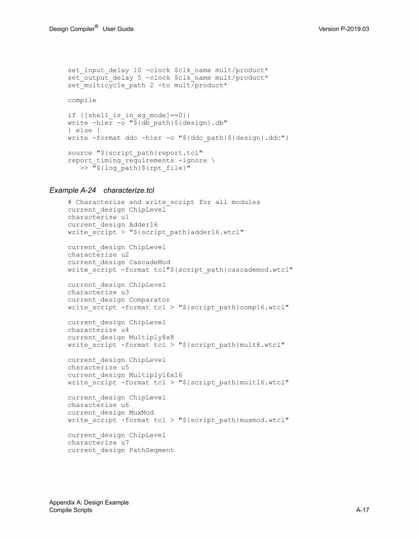
Design Compiler® User Guide Version P-2019.03
set_input_delay 10 -clock $clk_name mult/product*set_output_delay 5 -clock $clk_name mult/product*set_multicycle_path 2 -to mult/product*
compile
if {[shell_is_in_xg_mode]==0}{write -hier -o "${db_path}${design}.db"} else {write -format ddc -hier -o "${ddc_path}${design}.ddc"}
source "${script_path}report.tcl"report_timing_requirements -ignore \ >> "${log_path}${rpt_file}"
Example A-24 characterize.tcl
# Characterize and write_script for all modules current_design ChipLevelcharacterize u1current_design Adder16write_script > "${script_path}adder16.wtcl"
current_design ChipLevelcharacterize u2current_design CascadeModwrite_script -format tcl"${script_path}cascademod.wtcl"
current_design ChipLevelcharacterize u3current_design Comparatorwrite_script -format tcl > "${script_path}comp16.wtcl"
current_design ChipLevelcharacterize u4current_design Multiply8x8write_script -format tcl > "${script_path}mult8.wtcl"
current_design ChipLevelcharacterize u5current_design Multiply16x16write_script -format tcl > "${script_path}mult16.wtcl"
current_design ChipLevelcharacterize u6current_design MuxModwrite_script -format tcl > "${script_path}muxmod.wtcl"
current_design ChipLevelcharacterize u7current_design PathSegment
Chapter A: Design ExampleCompile Scripts A-17Appendix A: Design ExampleCompile Scripts A-17

Design Compiler® User Guide P-2019.03Design Compiler® User Guide Version P-2019.03
echo "current_design PathSegment" > \"${script_path}pathseg.wtcl"
echo "group -design mult -cell mult U100" >> \"${script_path}pathseg.wtcl"
write_script -format tcl >> "${script_path}pathseg.wtcl"
Example A-25 recompile.tcl
source "${script_path}read.tcl"
current_design ChipLevelsource "${script_path}defaults.con"
source "${script_path}adder16.wtcl"compileif {[shell_is_in_xg_mode]==0}{write -hier -o "${db_path}adder16_wtcl.db"} else {write -format ddc -hier -o "${ddc_path}adder16_wtcl.ddc"}set rpt_file adder16_wtcl.rptsource "${script_path}report.tcl"
source "${script_path}cascademod.wtcl"dont_touch u12compileif {[shell_is_in_xg_mode]==0}{write -hier -o "${db_path}cascademod_wtcl.db"} else {write -format ddc -hier -o "${ddc_path}cascademod_wtcl.ddc"}set rpt_file cascade_wtcl.rptsource "${script_path}report.tcl"
source "${script_path}comp16.wtcl"compileif {[shell_is_in_xg_mode]==0}{write -hier -o "${db_path}comp16_wtcl.db"} else {write -format ddc -hier -o "${ddc_path}comp16_wtcl.ddc"}set rpt_file comp16_wtcl.rptsource "${script_path}report.tcl"
source "${script_path}mult8.wtcl"compileif {[shell_is_in_xg_mode]==0}{write -hier -o "${db_path}mult8_wtcl.db"} else {write -format ddc -hier -o "${ddc_path}mult8_wtcl.ddc"}set rpt_file mult8_wtcl.rptsource "${script_path}report.tcl"
source "${script_path}mult16.wtcl"
Appendix A: Design ExampleCompile Scripts A-18

Design Compiler® User Guide Version P-2019.03
compile -ungroup_allif {[shell_is_in_xg_mode]==0}{write -hier -o "${db_path}mult16_wtcl.db"} else {write -format ddc -hier -o "${ddc_path}mult16_wtcl.ddc"}set rpt_file mult16_wtcl.rptsource "${script_path}report.tcl"report_timing_requirements -ignore \
>> "${log_path}${rpt_file}"
source "${script_path}muxmod.wtcl"compileif {[shell_is_in_xg_mode]==0}{write -hier -o "${db_path}muxmod_wtcl.db"} else {write -format ddc -hier -o "${ddc_path}muxmod_wtcl.ddc"}set rpt_file muxmod_wtcl.rptsource "${script_path}report.tcl"
source "${script_path}pathseg.wtcl"compileif {[shell_is_in_xg_mode]==0}{write -hier -o "${db_path}pathseg_wtcl.db"} else {write -format ddc -hier -o "${ddc_path}pathseg_wtcl.ddc"}set rpt_file pathseg_wtcl.rptsource "${script_path}report.tcl"report_timing_requirements -ignore \ >> "${log_path}${rpt_file}"
Example A-26 report.tcl
# This script file creates reports for all modulesset maxpaths 15
check_design > "${log_path}${rpt_file}"report_area >> "${log_path}${rpt_file}"report_design >> "${log_path}${rpt_file}"report_cell >> "${log_path}${rpt_file}"report_reference >> "${log_path}${rpt_file}"report_port -verbose >> "${log_path}${rpt_file}"report_net >> "${log_path}${rpt_file}"report_compile_options >> "${log_path}${rpt_file}"report_constraint -all_violators -verbose \ >> "${log_path}${rpt_file}"report_timing -path end >> "${log_path}${rpt_file}"report_timing -max_path $maxpaths \ >> "${log_path}${rpt_file}"report_qor >> "${log_path}${rpt_file}"
Chapter A: Design ExampleCompile Scripts A-19Appendix A: Design ExampleCompile Scripts A-19

Design Compiler® User Guide P-2019.03Design Compiler® User Guide Version P-2019.03
Appendix A: Design ExampleCompile Scripts A-20

BBasic Commands B
This appendix lists some of the basic dc_shell commands for synthesis and provides a brief description for each command. The commands are grouped in the following sections:
• Commands for Defining Design Rules
• Commands for Defining Design Environments
• Commands for Setting Design Constraints
• Commands for Analyzing and Resolving Design Problems
Within each section the commands are listed in alphabetical order.
B-1

Design Compiler® User Guide P-2019.03Design Compiler® User Guide Version P-2019.03
Commands for Defining Design Rules
The commands that define design rules are
set_max_capacitance
Sets a maximum capacitance for the nets attached to the specified ports or to all the nets in a design.
set_max_fanout
Sets the expected fanout load value for output ports.
set_max_transition
Sets a maximum transition time for the nets attached to the specified ports or to all the nets in a design.
set_min_capacitance
Sets a minimum capacitance for the nets attached to the specified ports or to all the nets in a design.
Commands for Defining Design Environments
The commands that define the design environment are
set_drive
Sets the drive value of input or inout ports. The set_drive command is superseded by the set_driving_cell command.
set_driving_cell
Sets attributes on input or inout ports, specifying that a library cell or library pin drives the ports. This command associates a library pin with an input port so that delay calculators can accurately model the drive capability of an external driver.
set_fanout_load
Defines the external fanout load values on output ports.
set_load
Defines the external load values on input and output ports and nets.
set_operating_conditions
Defines the operating conditions for the current design.
Appendix B: Basic CommandsCommands for Defining Design Rules B-2

Design Compiler® User Guide Version P-2019.03
set_wire_load_model
Sets the wire load model for the current design or for the specified ports. With this command, you can specify the wire load model to use for the external net connected to the output port.
Commands for Setting Design Constraints
The basic commands that set design constraints are
create_clock
Creates a clock object and defines its waveform in the current design.
set_clock_latency, set_clock_uncertainty, set_propagated_clock, set_clock_transition
Sets clock attributes on clock objects or flip-flop clock pins.
set_input_delay
Sets input delay on pins or input ports relative to a clock signal.
set_max_area
Specifies the maximum area for the current design.
set_output_delay
Sets output delay on pins or output ports relative to a clock signal.
The advanced commands that set design constraints are
group_path
Groups a set of paths or endpoints for cost function calculation. This command is used to create path groups, to add paths to existing groups, or to change the weight of existing groups.
set_false_path
Marks paths between specified points as false. This command eliminates the selected paths from timing analysis.
set_max_delay
Specifies a maximum delay target for selected paths in the current design.
set_min_delay
Specifies a minimum delay target for selected paths in the current design.
Chapter B: Basic CommandsCommands for Setting Design Constraints B-3Appendix B: Basic CommandsCommands for Setting Design Constraints B-3

Design Compiler® User Guide P-2019.03Design Compiler® User Guide Version P-2019.03
set_multicycle_path
Allows you to specify the time of a timing path to exceed the time of one clock signal.
Commands for Analyzing and Resolving Design Problems
The commands for analyzing and resolving design problems are
all_connected
Lists all fanouts on a net.
all_registers
Lists sequential elements or pins in a design.
check_design
Checks the internal representation of the current design for consistency and issues error and warning messages as appropriate.
check_timing
Checks the timing attributes placed on the current design.
get_attribute
Reports the value of the specified attribute.
link
Locates the reference for each cell in the design.
report_area
Provides area information and statistics on the current design.
report_attribute
Lists the attributes and their values for the selected object. An object can be a cell, net, pin, port, instance, or design.
report_cell
Lists the cells in the current design and their cell attributes.
report_clock
Displays clock-related information about the current design.
report_constraint
Lists the constraints on the current design and their cost, weight, and weighted cost.
Appendix B: Basic CommandsCommands for Analyzing and Resolving Design Problems B-4

Design Compiler® User Guide Version P-2019.03
report_delay_calculation
Reports the details of a delay arc calculation.
report_design
Displays the operating conditions, wire load model and mode, timing ranges, internal input and output, and disabled timing arcs defined for the current design.
report_hierarchy
Lists the subdesigns of the current design.
report_net
Displays net information for the design of the current instance, if set; otherwise, displays net information for the current design.
report_path_group
Lists all timing path groups in the current design.
report_port
Lists information about ports in the current design.
report_qor
Displays information about the quality of results and other statistics for the current design.
report_resources
Displays information about the resource implementation.
report_timing
Lists timing information for the current design.
report_timing_requirements
Lists timing path requirements and related information.
report_transitive_fanin
Lists the fanin logic for selected pins, nets, or ports of the current instance.
report_transitive_fanout
Lists the fanout logic for selected pins, nets, or ports of the current instance.
Chapter B: Basic CommandsCommands for Analyzing and Resolving Design Problems B-5Appendix B: Basic CommandsCommands for Analyzing and Resolving Design Problems B-5

Design Compiler® User Guide P-2019.03Design Compiler® User Guide Version P-2019.03
Appendix B: Basic CommandsCommands for Analyzing and Resolving Design Problems B-6
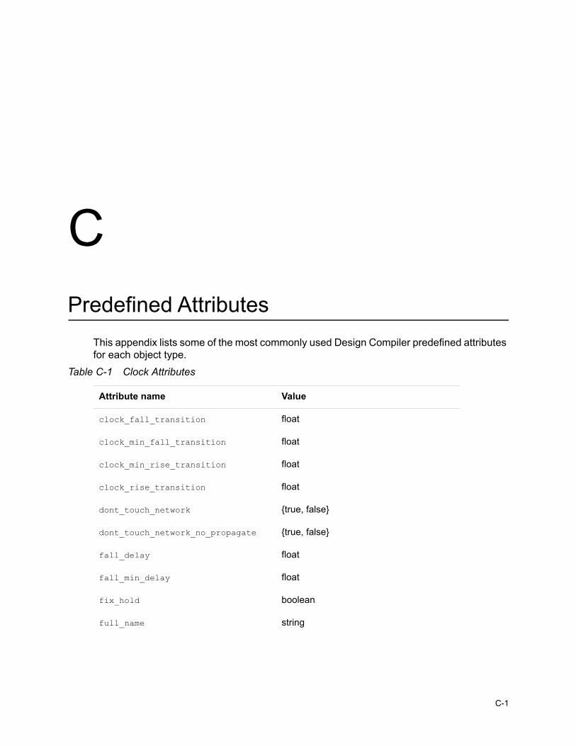
CPredefined Attributes C
This appendix lists some of the most commonly used Design Compiler predefined attributes for each object type.
Table C-1 Clock Attributes
Attribute name Value
clock_fall_transition float
clock_min_fall_transition float
clock_min_rise_transition float
clock_rise_transition float
dont_touch_network {true, false}
dont_touch_network_no_propagate {true, false}
fall_delay float
fall_min_delay float
fix_hold boolean
full_name string
C-1

Design Compiler® User Guide P-2019.03Design Compiler® User Guide Version P-2019.03
max_time_borrow float
minus_uncertainty float
name string
object_class string
period float
plus_uncertainty float
propagated_clock boolean
rise_delay float
rise_min_delay float
Table C-2 Design Attributes
Attribute name Value
actual_max_net_capacitance float
actual_min_net_capacitance float
boundary_optimization {true, false}
default_flip_flop_type internally generated string
default_flip_flop_type_exact library_cell_name
default_latch_type library_cell_name
design_type {equation, fsm, pla, netlist}
dont_touch {true, false}
dont_touch_network {true, false}
driven_by_logic_one {true, false}
Table C-1 Clock Attributes (Continued)
Attribute name Value
Appendix C: Predefined AttributesC-2

Design Compiler® User Guide Version P-2019.03
driven_by_logic_zero {true, false}
driving_cell_dont_scale string
driving_cell_fall string
driving_cell_from_pin_fall string
driving_cell_from_pin_rise string
driving_cell_library_fall string
driving_cell_library_rise string
driving_cell_multiplier float
driving_cell_pin_fall string
driving_cell_pin_rise string
driving_cell_rise string
fall_drive float
fanout_load float
flatten {true, false}
flatten_effort {true, false}
flatten_minimize {true, false}
flatten_phase {true, false}
flip_flop_type internally generated string
flip_flop_type_exact library_cell_name
is_black_box {true, false}
is_combinational {true, false}
is_hierarchical {true, false}
Table C-2 Design Attributes (Continued)
Attribute name Value
Chapter C: Predefined AttributesC-3
Appendix C: Predefined AttributesC-3

Design Compiler® User Guide P-2019.03Design Compiler® User Guide Version P-2019.03
is_mapped {true, false}
is_sequential {true, false}
is_test_circuitry {true, false}
is_unmapped {true, false}
latch_type internally generated string
latch_type_exact library_cell_name
load float
local_link_library design_or_lib_file_name
max_capacitance float
max_fanout float
max_time_borrow float
max_transition float
min_capacitance float
minus_uncertainty float
output_not_used {true, false}
pad_location (XNF only) string
part (XNF only) string
plus_uncertainty float
port_direction {in, inout, out, unknown}
port_is_pad {true, false}
ref_name reference_name
rise_drive float
Table C-2 Design Attributes (Continued)
Attribute name Value
Appendix C: Predefined AttributesC-4

Design Compiler® User Guide Version P-2019.03
structure {true, false}
ungroup {true, false}
wired_logic_disable {true, false}
Table C-3 Library Attributes
Attribute name Value
default_values float
k_process_values float
k_temp_values float
k_volt_values float
nom_process float
nom_temperature float
nom_voltage float
Table C-4 Library Cell Attributes
Attribute name Value
area float
dont_touch {true, false}
dont_use {true, false}
preferred {true, false}
Table C-2 Design Attributes (Continued)
Attribute name Value
Chapter C: Predefined AttributesC-5
Appendix C: Predefined AttributesC-5

Design Compiler® User Guide P-2019.03Design Compiler® User Guide Version P-2019.03
Table C-5 Net Attributes
Attribute name Value
ba_net_resistance float
dont_touch {true, false}
load float
subtract_pin_load {true, false}
wired_and {true, false}
wired_or {true, false}
Table C-6 Pin Attributes
Attribute name Value
disable_timing {true, false}
max_time_borrow float
pin_direction {in, inout, out, unknown}
Table C-7 Reference Attributes
Attribute name Value
dont_touch {true, false}
is_black_box {true, false}
is_combinational {true, false}
is_hierarchical {true, false}
is_mapped {true, false}
is_sequential {true, false}
is_unmapped {true, false}
ungroup {true, false}
Appendix C: Predefined AttributesC-6

DLatch-Based Design Code Examples D
For code examples of designs that use various types of latches, see the following topics:
• SR Latch
• D Latch
• D Latch With Asynchronous Reset
• D Latch With Asynchronous Set and Reset
• D Latch With Enable (Avoiding Clock Gating)
• D Latch With Enable and Asynchronous Reset
• D Latch With Enable and Asynchronous Set
• D Latch With Enable and Asynchronous Set and Reset
D-1

Design Compiler® User Guide P-2019.03Design Compiler® User Guide Version P-2019.03
SR Latch
The following topics show a code example of an SR latch in VHDL and Verilog and the resulting inference report and synthesized design:
• VHDL and Verilog Code Examples for SR Latch
• Inference Report for an SR Latch
• Synthesized Design for an SR Latch
VHDL and Verilog Code Examples for SR Latch
To implement an SR latch in either VHDL or Verilog, you must set the hdlin_report_inferred_modules variable to true, and you must set the following attribute:
attribute async_set_reset of RESET, SET : signal is "true";
Example D-1 shows the VHDL code that infers an SR latch.
Example D-1 VHDL Code for an SR Latch
library IEEE, SYNOPSYS;use IEEE.std_logic_1164.all;use SYNOPSYS.attributes.all; entity SR_LATCH is port ( RESET, SET : in std_logic; Y : out std_logic );end SR_LATCH; architecture BEHAVIORAL of SR_LATCH isattribute async_set_reset of RESET, SET : signal is "true";begin infer : process ( RESET, SET ) begin if ( RESET = ’0’ ) then y <= ’0’; elsif ( SET = ’0’ ) then y <= ’1’; end if; end process infer;end BEHAVIORAL;
Chapter D: Latch-Based Design Code ExamplesSR Latch D-2
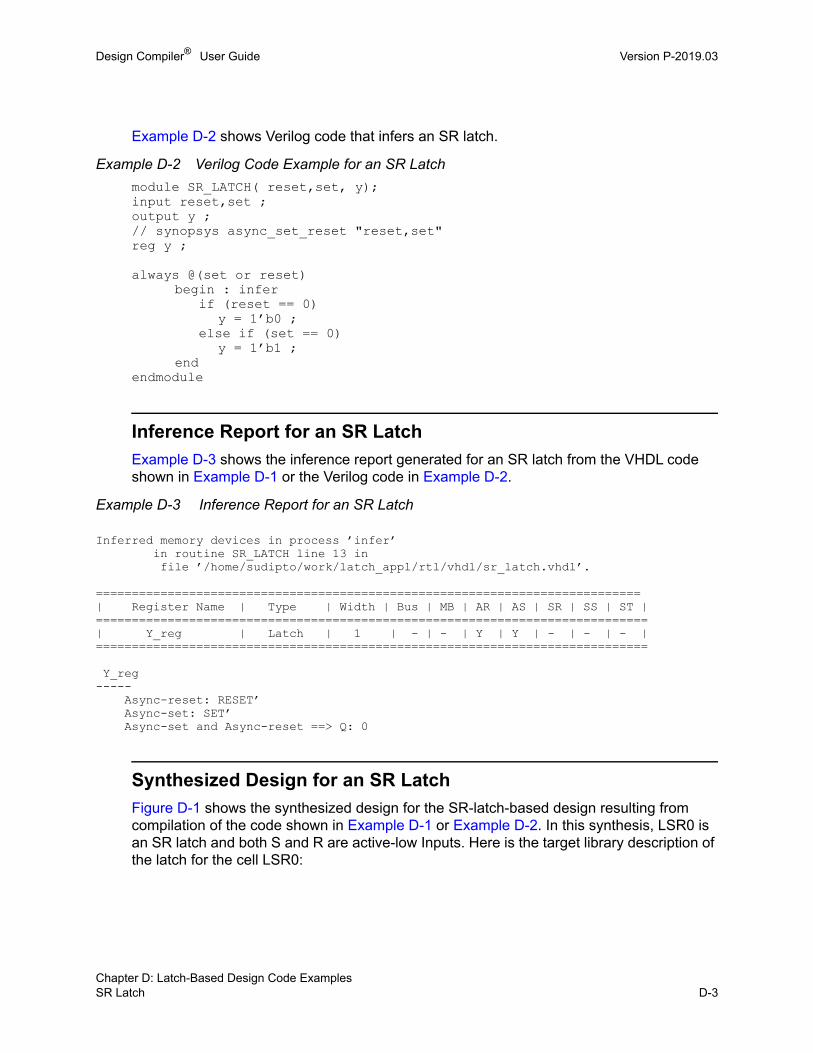
Design Compiler® User Guide Version P-2019.03
Example D-2 shows Verilog code that infers an SR latch.
Example D-2 Verilog Code Example for an SR Latch
module SR_LATCH( reset,set, y);input reset,set ;output y ;// synopsys async_set_reset "reset,set"reg y ;
always @(set or reset)begin : infer if (reset == 0)
y = 1’b0 ; else if (set == 0)
y = 1’b1 ;end
endmodule
Inference Report for an SR Latch
Example D-3 shows the inference report generated for an SR latch from the VHDL code shown in Example D-1 or the Verilog code in Example D-2.
Example D-3 Inference Report for an SR Latch
Inferred memory devices in process ’infer’ in routine SR_LATCH line 13 in file ’/home/sudipto/work/latch_appl/rtl/vhdl/sr_latch.vhdl’.
============================================================================| Register Name | Type | Width | Bus | MB | AR | AS | SR | SS | ST |=============================================================================| Y_reg | Latch | 1 | - | - | Y | Y | - | - | - | =============================================================================
Y_reg----- Async-reset: RESET’ Async-set: SET’ Async-set and Async-reset ==> Q: 0
Synthesized Design for an SR Latch
Figure D-1 shows the synthesized design for the SR-latch-based design resulting from compilation of the code shown in Example D-1 or Example D-2. In this synthesis, LSR0 is an SR latch and both S and R are active-low Inputs. Here is the target library description of the latch for the cell LSR0:
Chapter D: Latch-Based Design Code ExamplesSR Latch D-3Chapter D: Latch-Based Design Code ExamplesSR Latch D-3

Design Compiler® User Guide P-2019.03Design Compiler® User Guide Version P-2019.03
latch ("IQ","IQN") { clear : "R’"; preset : "S’"; clear_preset_var1 : L; clear_preset_var2 : L; }
Figure D-1 Synthesized Design for an SR Latch
D Latch
The following topics show the VHDL code that implements a design that uses a simple D latch and the resulting inference report and synthesized design:
• VHDL Code for a D Latch
• Inference Report for a D Latch
• Synthesized Design for a D Latch
VHDL Code for a D Latch
To implement a D latch in VHDL, you must set the hdlin_report_inferred_modules variable to true. Example D-4 shows the VHDL code that implements a design using a simple D latch.
Chapter D: Latch-Based Design Code ExamplesD Latch D-4

Design Compiler® User Guide Version P-2019.03
Example D-4 VHDL Code for a D Latch
library IEEE, SYNOPSYS;use IEEE.std_logic_1164.all;use SYNOPSYS.attributes.all; entity d_latch is port ( enable, data : in std_logic; y : out std_logic );end d_latch; architecture behavioral of d_latch isbegin infer : process ( enable, data ) begin if ( enable = ’1’ ) then y <= data; end if; end process infer;end behavioral;
Inference Report for a D Latch
Example D-5 shows the inference report for a D latch resulting from compilation of the code in Example D-4.
Example D-5 Inference Report for a D Latch
Inferred memory devices in process ’infer’ in routine d_latch line 13 in file ’/home/sudipto/work/latch_appl/rtl/vhdl /d_latch.vhdl’.==============================================================================| Register Name | Type | Width | Bus | MB | AR | AS | SR | SS | ST |==============================================================================| y_reg | Latch | 1 | - | - | N | N | - | - | - |==============================================================================y_reg-----reset/set: none
Chapter D: Latch-Based Design Code ExamplesD Latch D-5Chapter D: Latch-Based Design Code ExamplesD Latch D-5

Design Compiler® User Guide P-2019.03Design Compiler® User Guide Version P-2019.03
Synthesized Design for a D Latch
Figure D-2 shows the synthesized design for the D latch resulting from compilation of the code in Example D-4. In this design, LD1 is the simple D latch. Here is the target library description of the latch for the cell LD1:
latch ("IQ","IQN") { enable : "G"; data_in : "D"; }
Figure D-2 Synthesized Design for a D Latch
D Latch With Asynchronous Reset
The following topics show a VHDL and Verilog code example of a D latch with asynchronous reset and the resulting inference report and synthesized design:
• VHDL and Verilog Code for a D Latch With Asynchronous Reset
• Inference Report for a D Latch With Asynchronous Reset
• Synthesized Design for a D Latch With Asynchronous Reset
VHDL and Verilog Code for a D Latch With Asynchronous Reset
To implement a D latch with asynchronous reset in either VHDL or Verilog, you must set the hdlin_report_inferred_modules variable to true. You must also set the following attribute, as illustrated by the code examples:
attribute async_set_reset of RESET, SET : signal is "true";
Chapter D: Latch-Based Design Code ExamplesD Latch With Asynchronous Reset D-6

Design Compiler® User Guide Version P-2019.03
Example D-6 shows VHDL code for a D latch with asynchronous reset.
Example D-6 VHDL Code for a D Latch With Asynchronous Reset
library IEEE, SYNOPSYS;use IEEE.std_logic_1164.all;use SYNOPSYS.attributes.all; entity d_latch_async_reset is port ( enable, reset, data : in std_logic; q : out std_logic );end d_latch_async_reset; architecture behavioral of d_latch_async_reset isattribute async_set_reset of reset : signal is "true";begin infer : process ( enable, reset, data ) begin if ( reset = ’1’ ) then q <= ’0’; elsif ( enable = ’1’ ) then q <= data; end if; end process infer;end behavioral;
Example D-7 shows Verilog code for the D latch with asynchronous reset.
Example D-7 Verilog Code for a D Latch With Asynchronous Reset
module d_latch_async_reset (enable, reset, data, q) ;input enable, data, reset ;output q ;// synopsys async_set_reset "reset"reg q ;
always @(reset or enable or data)begin : infer if (reset == 1)
q = 1’b0 ; else if (enable == 1)
q = data ;end
endmodule
Chapter D: Latch-Based Design Code ExamplesD Latch With Asynchronous Reset D-7Chapter D: Latch-Based Design Code ExamplesD Latch With Asynchronous Reset D-7

Design Compiler® User Guide P-2019.03Design Compiler® User Guide Version P-2019.03
Inference Report for a D Latch With Asynchronous Reset
Example D-8 shows the inference report for a D latch with asynchronous reset resulting from compilation of the code in Example D-6 or Example D-7.
Example D-8 Inference Report for a D Latch With Asynchronous Reset
Inferred memory devices in process ’infer’ in routine d_latch_async_reset line 13 in file ’/home/sudipto/work/latch_appl/rtl/vhdl/d_latch_async_reset.vhdl’.==============================================================================| Register Name | Type | Width | Bus | MB | AR | AS | SR | SS | ST |==============================================================================| q_reg | Latch | 1 | - | - | Y | N | - | - | - |==============================================================================
q_reg----- Async-reset: reset
Synthesized Design for a D Latch With Asynchronous Reset
Figure D-3 shows the synthesized design for the D latch resulting from compilation of the code shown in Example D-6 and Example D-7. In this design, LD3 is the simple D latch. Here is the target library description of the latch for the cell LD3:
LD3 is a D latch with asynchronous active-low reset (CD). The description of the latch for the cell LD3 in the target library is as follows:
latch ("IQ","IQN") { enable : "G"; data_in : "D"; clear : "CD’"; }
Chapter D: Latch-Based Design Code ExamplesD Latch With Asynchronous Reset D-8

Design Compiler® User Guide Version P-2019.03
Figure D-3 Synthesized Design for a D Latch With Asynchronous Reset
D Latch With Asynchronous Set and Reset
The following topics show a code example of a D latch with asynchronous set and reset in VHDL and Verilog and the resulting inference report and synthesized design:
• VHDL and Verilog Code for a D Latch With Asynchronous Set and Reset
• Inference Report for a D Latch With Asynchronous Set and Reset
• Synthesized Design for a D Latch With Asynchronous Set and Reset
VHDL and Verilog Code for a D Latch With Asynchronous Set and Reset
To implement a D latch with asynchronous set and reset in either VHDL or Verilog, you must set the hdlin_report_inferred_modules variable to true. You must also set the following attributes, as illustrated by the code examples:
attribute async_set_reset of set, reset : signal is "true";attribute one_hot of set, reset : signal is "true";
Chapter D: Latch-Based Design Code ExamplesD Latch With Asynchronous Set and Reset D-9Chapter D: Latch-Based Design Code ExamplesD Latch With Asynchronous Set and Reset D-9

Design Compiler® User Guide P-2019.03Design Compiler® User Guide Version P-2019.03
Example D-9 shows the VHDL code for a D latch with asynchronous set and reset attributes.
Example D-9 VHDL Code for a D Latch With Asynchronous Set and Reset
library IEEE, SYNOPSYS;use IEEE.std_logic_1164.all;use SYNOPSYS.attributes.all; entity d_latch_async_set_reset is port ( enable, set, reset, data : in std_logic; q : out std_logic );end d_latch_async_set_reset; architecture behavioral of d_latch_async_set_reset isattribute async_set_reset of set, reset : signal is "true";attribute one_hot of set, reset : signal is "true";begin infer : process ( enable, set, reset, data ) begin if ( reset = ’1’ ) then q <= ’0’; elsif ( set = ’1’) then q <= ’1’; elsif ( enable = ’1’ ) then q <= data; end if; end process infer;end behavioral;
Chapter D: Latch-Based Design Code ExamplesD Latch With Asynchronous Set and Reset D-10

Design Compiler® User Guide Version P-2019.03
Example D-10 shows the Verilog code for a D latch with asynchronous set and reset attributes.
Example D-10 Verilog Code for a D Latch With Asynchronous Set and Reset
module d_latch_async_set_reset (enable, set, reset, q, data) ;
input enable, set, reset, data ;output q ;
// synopsys async_set_reset "set, reset"// synopsys one_hot "set, reset"
reg q ;
always @(enable or set or reset or data) begin : infer
if (reset == 1)q = 1’b0 ;
else if (set == 1)q = 1’b1 ;
else if (enable == 1)q = data ;
endendmodule
Inference Report for a D Latch With Asynchronous Set and Reset
Example D-11 shows the inference report for a D latch with asynchronous set and reset resulting from compilation of the code shown in Example D-9 on page D-10 or Example D-10.
Example D-11 Inference Report for a D Latch With Asynchronous Set and Reset
Inferred memory devices in process ‘infer’ in routine d_latch_async_set_reset line 14 in file ’/home/sudipto/work/latch_appl/rtl/vhdl/d_latch_async_set_reset.vhdl’.============================================================================| Register Name | Type | Width | Bus | MB | AR | AS | SR | SS | ST |============================================================================| q_reg | Latch | 1 | - | - | Y | Y | - | - | - |============================================================================ q_reg----- Async-reset: reset Async-set: set Async-set and Async-reset ==> Q: X
Chapter D: Latch-Based Design Code ExamplesD Latch With Asynchronous Set and Reset D-11Chapter D: Latch-Based Design Code ExamplesD Latch With Asynchronous Set and Reset D-11

Design Compiler® User Guide P-2019.03Design Compiler® User Guide Version P-2019.03
Synthesized Design for a D Latch With Asynchronous Set and Reset
Figure D-4 shows the synthesized design for the D latch resulting from compilation of the code in Example D-9 and Example D-10. In this design, LDSR is a D latch with active-low asynchronous set (SET) and reset (CLR).
The description of the latch for the cell LDSR in the target library is as follows:
latch ("IQ","IQN") { enable : "G"; data_in : "D"; clear : "CLR’"; preset : "SET’"; clear_preset_var1 : L; clear_preset_var2 : L; }
Figure D-4 Synthesized Design for a D Latch With Asynchronous Set and Reset
D Latch With Enable (Avoiding Clock Gating)
The following topics show a VHDL and Verilog code example of a D latch with the enable attribute to avoid clock gating and the resulting inference report and synthesized design:
• VHDL and Verilog Code for a D Latch With Enable
• Inference Report for a D Latch With Enable
Chapter D: Latch-Based Design Code ExamplesD Latch With Enable (Avoiding Clock Gating) D-12

Design Compiler® User Guide Version P-2019.03
• Synthesized Design for a D Latch With Enable
• Inferring Gated Clocks
VHDL and Verilog Code for a D Latch With Enable
To implement a D latch with enable in either VHDL or Verilog, you must set the hdlin_report_inferred_modules variable to true. You must also set the hdlin_keep_feedback attribute to true.
Example D-12 shows the VHDL code for a D latch with enable.
Example D-12 VHDL Code for a D Latch With Enable
library IEEE;use IEEE.STD_LOGIC_1164.all; entity d_latch_enab is port ( enable, clock, data : in std_logic; q : buffer std_logic );end d_latch_enab; architecture behavioral of d_latch_enab isbegin infer : process ( enable, clock, data ) begin if ( clock = ’1’ ) then if ( enable = ’1’ ) then q <= data; else q <= q; end if; end if; end process infer;end behavioral;
Chapter D: Latch-Based Design Code ExamplesD Latch With Enable (Avoiding Clock Gating) D-13Chapter D: Latch-Based Design Code ExamplesD Latch With Enable (Avoiding Clock Gating) D-13
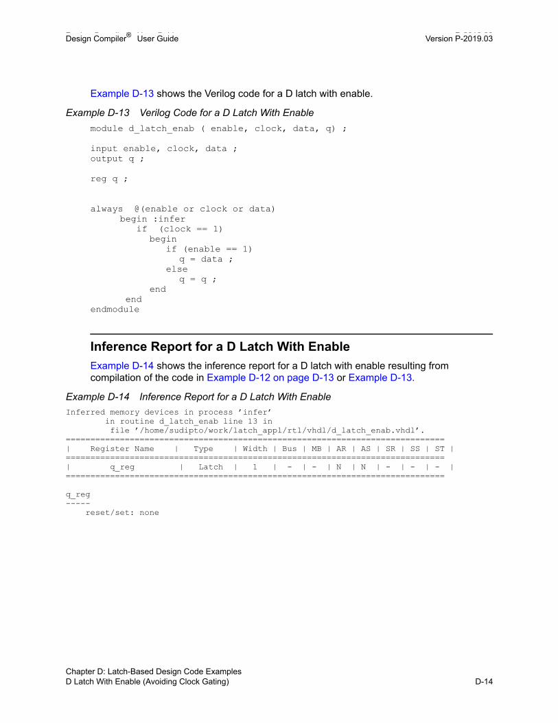
Design Compiler® User Guide P-2019.03Design Compiler® User Guide Version P-2019.03
Example D-13 shows the Verilog code for a D latch with enable.
Example D-13 Verilog Code for a D Latch With Enable
module d_latch_enab ( enable, clock, data, q) ;
input enable, clock, data ;output q ;
reg q ;
always @(enable or clock or data)begin :infer if (clock == 1) begin if (enable == 1) q = data ; else q = q ; end end
endmodule
Inference Report for a D Latch With Enable
Example D-14 shows the inference report for a D latch with enable resulting from compilation of the code in Example D-12 on page D-13 or Example D-13.
Example D-14 Inference Report for a D Latch With Enable
Inferred memory devices in process ’infer’ in routine d_latch_enab line 13 in file ’/home/sudipto/work/latch_appl/rtl/vhdl/d_latch_enab.vhdl’.=============================================================================| Register Name | Type | Width | Bus | MB | AR | AS | SR | SS | ST |=============================================================================| q_reg | Latch | 1 | - | - | N | N | - | - | - |============================================================================= q_reg----- reset/set: none
Chapter D: Latch-Based Design Code ExamplesD Latch With Enable (Avoiding Clock Gating) D-14
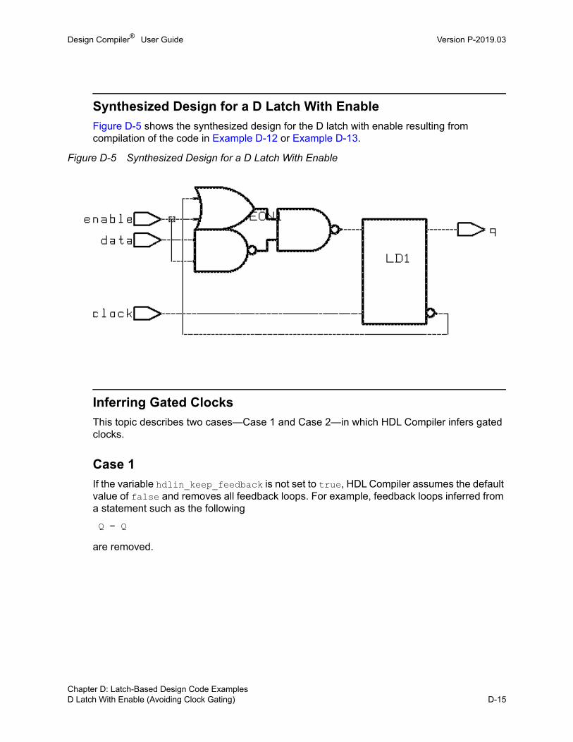
Design Compiler® User Guide Version P-2019.03
Synthesized Design for a D Latch With Enable
Figure D-5 shows the synthesized design for the D latch with enable resulting from compilation of the code in Example D-12 or Example D-13.
Figure D-5 Synthesized Design for a D Latch With Enable
Inferring Gated Clocks
This topic describes two cases—Case 1 and Case 2—in which HDL Compiler infers gated clocks.
Case 1
If the variable hdlin_keep_feedback is not set to true, HDL Compiler assumes the default value of false and removes all feedback loops. For example, feedback loops inferred from a statement such as the following
Q = Q
are removed.
Chapter D: Latch-Based Design Code ExamplesD Latch With Enable (Avoiding Clock Gating) D-15Chapter D: Latch-Based Design Code ExamplesD Latch With Enable (Avoiding Clock Gating) D-15

Design Compiler® User Guide P-2019.03Design Compiler® User Guide Version P-2019.03
The loop that is inferred from the following statement, shown in VHDL code, is removed.
if ( enable = ’1’ ) then q<= data; else q <= q; end if;
The code indicates that the gated clock in the synthesized design in Figure D-6, which does not have a feedback loop, is removed.
Case 2
Gated clocks can also be inferred from the coding style used to implement a design. For example, if the VHDL code is written in either of the coding styles in Example D-15 or Example D-16, regardless of whether hdlin_keep_feedback is set to true, Design Compiler will create a gated clock for the design.
Example D-15 implies a priority coding style— that is, the clock value is assessed first and enable is considered only if the clock is a certain value.
Example D-15 Coding Style A
library IEEE;use IEEE.STD_LOGIC_1164.all; entity d_latch_enab is port ( enable, clock, data : in std_logic; q : out std_logic );end d_latch_enab; architecture behavioral of d_latch_enab isbegin infer : process ( enable, clock, data ) begin if ( clock = ’1’ ) then if ( enable = ’1’ ) then q <= data; end if; end if; end process infer;end behavioral;
Chapter D: Latch-Based Design Code ExamplesD Latch With Enable (Avoiding Clock Gating) D-16

Design Compiler® User Guide Version P-2019.03
For Example D-16, no priority is implied.
Example D-16 Coding Style B
library IEEE;use IEEE.STD_LOGIC_1164.all; entity d_latch_enab is port ( enable, clock, data : in std_logic; q : out std_logic );end d_latch_enab; architecture behavioral of d_latch_enab isbegin infer : process ( enable, clock, data ) begin if ( clock = ’1’ and enable = ’1’) q <= data; end if; end process infer;end behavioral;
Synthesized Design With Enable and Gated Clock
Figure D-6 shows the synthesized design for the D latch with enable and clock gating resulting from compilation of the code in Example D-15 on page D-16 and Example D-16.
Figure D-6 D Latch With Enable and Gated Clock
Chapter D: Latch-Based Design Code ExamplesD Latch With Enable (Avoiding Clock Gating) D-17Chapter D: Latch-Based Design Code ExamplesD Latch With Enable (Avoiding Clock Gating) D-17

Design Compiler® User Guide P-2019.03Design Compiler® User Guide Version P-2019.03
D Latch With Enable and Asynchronous Reset
The following topics show the VHDL and Verilog code that implements a design that uses a D latch with the enable and asynchronous reset attributes:
• VHDL and Verilog Code for a D Latch With Enable and Asynchronous Reset
• Synthesized Design for a D Latch With Enable and Asynchronous Reset
VHDL and Verilog Code for a D Latch With Enable and Asynchronous Reset
To implement a D latch with enable and asynchronous reset in either VHDL or Verilog, you must set the hdlin_report_inferred_modules and hdlin_keep_feedback variables to true. You must also set the following attribute:
attribute async_set_reset of reset : signal is "true";
Example D-17 shows the VHDL code for a D latch with enable and asynchronous reset.
Example D-17 VHDL Code for a D Latch With Enable and Asynchronous Reset
library IEEE, SYNOPSYS;use IEEE.STD_LOGIC_1164.all;use SYNOPSYS.attributes.all; entity d_latch_enab_async_reset is port ( enable, clock, reset, data : in std_logic; q : buffer std_logic );end d_latch_enab_async_reset; architecture behavioral of d_latch_enab_async_reset isattribute async_set_reset of reset : signal is "true";begin infer : process ( enable, clock, reset, data ) variable temp : std_logic; begin temp := q; if ( reset = ’1’ ) then q <= ’0’; elsif ( clock = ’1’ ) then case enable is when ’1’ => q <= data; when others => q <= temp; end case; end if; end process infer;end behavioral;
Chapter D: Latch-Based Design Code ExamplesD Latch With Enable and Asynchronous Reset D-18

Design Compiler® User Guide Version P-2019.03
Example D-18 shows the Verilog code for a D latch with enable and asynchronous reset.
Example D-18 Verilog Code for a D Latch With Enable and Asynchronous Reset
module d_latch_enab_async_reset (enable, clock, reset, q, data) ;
input enable, clock, reset, data ;output q ;
// synopsys async_set_reset "reset"
reg q ;
always @(enable or clock or reset or data) begin : infer
if (reset == 1)q = 1’b0 ;
else if (clock == 1) begin if (enable == 1)
q = data ; else q = q ;end
endendmodule
Chapter D: Latch-Based Design Code ExamplesD Latch With Enable and Asynchronous Reset D-19Chapter D: Latch-Based Design Code ExamplesD Latch With Enable and Asynchronous Reset D-19

Design Compiler® User Guide P-2019.03Design Compiler® User Guide Version P-2019.03
Synthesized Design for a D Latch With Enable and Asynchronous Reset
Figure D-7 shows the synthesized design for the D latch with enable and asynchronous reset resulting from compilation of the code in Example D-17 or Example D-18.
Figure D-7 Synthesized Design for a D Latch With Enable and Asynchronous Reset
D Latch With Enable and Asynchronous Set
The following topics show the VHDL and Verilog code that implements a design that uses a D latch with the enable and asynchronous set attributes:
• VHDL and Verilog Code for a D Latch With Enable and Asynchronous Set
• Synthesized Design for D Latch With Enable and Asynchronous Set
VHDL and Verilog Code for a D Latch With Enable and Asynchronous Set
To implement a D latch with enable and asynchronous set in either VHDL or Verilog, you must set the hdlin_report_inferred_modules and hdlin_keep_feedback variables to true. You must also set the following attribute:
attribute async_set_reset of set : signal is "true";
Chapter D: Latch-Based Design Code ExamplesD Latch With Enable and Asynchronous Set D-20

Design Compiler® User Guide Version P-2019.03
Example D-19 shows the VHDL code for a D latch with enable and asynchronous reset.
Example D-19 VHDL Code for D Latch With Enable and Asynchronous Set
library IEEE, SYNOPSYS; use IEEE.STD_LOGIC_1164.all;use SYNOPSYS.attributes.all; entity d_latch_enab_async_set is port ( enable, clock, set, data : in std_logic; q : buffer std_logic );end d_latch_enab_async_set;
architecture behavioral of d_latch_enab_async_set isattribute async_set_reset of set : signal is "true";begin infer : process ( enable, clock, set, data ) begin if ( set = ’1’ ) then q <= ’1’; elsif ( clock = ’1’ ) then if ( enable = ’1’ ) then q<= data; else q <= q; end if; end if; end process infer;end behavioral;
Chapter D: Latch-Based Design Code ExamplesD Latch With Enable and Asynchronous Set D-21Chapter D: Latch-Based Design Code ExamplesD Latch With Enable and Asynchronous Set D-21

Design Compiler® User Guide P-2019.03Design Compiler® User Guide Version P-2019.03
Example D-20 shows the Verilog code for a D latch with enable and asynchronous set.
Example D-20 Verilog Code for D Latch With Enable and Asynchronous Set
module d_latch_enab_async_set (enable, clock, set, q, data) ;
input enable, clock, set, data ;output q ;
// synopsys async_set_reset "set"
reg q ;
always @(enable or clock or set or data) begin : infer
if (set == 1)q = 1’b1 ;
else if (clock == 1) begin if (enable == 1)
q = data ; else q = q ;end
endendmodule
Chapter D: Latch-Based Design Code ExamplesD Latch With Enable and Asynchronous Set D-22

Design Compiler® User Guide Version P-2019.03
Synthesized Design for D Latch With Enable and Asynchronous Set
Figure D-8 shows the synthesized design for the D latch with enable and asynchronous set resulting from compilation of the code shown in Example D-19 or Example D-20.
Figure D-8 Synthesized Design for D Latch With Enable and Asynchronous Set
D Latch With Enable and Asynchronous Set and Reset
The following topics show the VHDL and Verilog code that implements a design that uses a D latch with the enable and asynchronous set and reset attributes:
• VHDL and Verilog Code for D Latch With Enable and Asynchronous Set and Reset
• Synthesized Design for D Latch With Enable and Asynchronous Set and Reset
Chapter D: Latch-Based Design Code ExamplesD Latch With Enable and Asynchronous Set and Reset D-23Chapter D: Latch-Based Design Code ExamplesD Latch With Enable and Asynchronous Set and Reset D-23

Design Compiler® User Guide P-2019.03Design Compiler® User Guide Version P-2019.03
VHDL and Verilog Code for D Latch With Enable and Asynchronous Set and Reset
To implement a D latch with enable and asynchronous set and reset in either VHDL or Verilog, you must set the hdlin_report_inferred_modules and hdlin_keep_feedback variables to true. You must also set the following attributes:
attribute async_set_reset of set : signal is "true";attribute one_hot of set, reset: signal is "true";
Example D-21 shows the VHDL code for a D latch with enable and asynchronous set and reset.
Example D-21 VHDL Code for D Latch With Enable and Asynchronous Set and Reset
library IEEE, SYNOPSYS;use IEEE.STD_LOGIC_1164.all;use SYNOPSYS.attributes.all; entity d_latch_enab_async_set_reset is port ( enable, clock, set, reset, data : in std_logic; q : buffer std_logic );end d_latch_enab_async_set_reset; architecture behavioral of d_latch_enab_async_set_reset isattribute async_set_reset of set, reset : signal is "true";attribute one_hot of set, reset : signal is "true";begin infer : process (enable,clock, set, reset, data) begin if ( set = ’1’ ) then q <= ’1’; elsif ( reset = ’‘1’ ) then q <= ’0’; elsif ( clock = ’1’ ) then if ( enable = ’1’) then q <= data; else q <= q; end if; end if; end process infer;end behavioral;
Chapter D: Latch-Based Design Code ExamplesD Latch With Enable and Asynchronous Set and Reset D-24

Design Compiler® User Guide Version P-2019.03
Example D-22 shows the Verilog code for a D latch with enable and asynchronous set and reset.
Example D-22 Verilog Code for D Latch With Enable and Asynchronous Set and Reset
module d_latch_enab_async_set_reset (enable, clock, set, reset, q, data);input enable, clock, set, reset, data ;output q ;// synopsys async_set_reset "set, reset"”// synopsys one_hot "set, reset"reg q ;
always @(enable or clock or set or reset or data) begin : infer
if (reset == 1)q = 1’b0 ;
else if (set == 1)q = 1’b1 ;
else if (clock == 1) begin if (enable == 1)
q = data ; else q = q ;end
endendmodule
Chapter D: Latch-Based Design Code ExamplesD Latch With Enable and Asynchronous Set and Reset D-25Chapter D: Latch-Based Design Code ExamplesD Latch With Enable and Asynchronous Set and Reset D-25

Design Compiler® User Guide P-2019.03Design Compiler® User Guide Version P-2019.03
Synthesized Design for D Latch With Enable and Asynchronous Set and Reset
Figure D-9 shows the synthesized design for the D latch with enable and asynchronous set and reset resulting from compilation of the code shown in Example D-21 or Example D-22.
Figure D-9 Synthesized Design for D Latch With Enable and Asynchronous Set and Reset
Chapter D: Latch-Based Design Code ExamplesD Latch With Enable and Asynchronous Set and Reset D-26