
Influence of Burner Nozzle Parameters Analysis on the ... - MDPI
Upload
independentCategory
view
3download
0
JOURNAL OF ELECTRONIC TESTING: Theory and Applications 18, 285–294, 2002c© 2002 Kluwer Academic Publishers. Manufactured in The Netherlands.
Design and Test of a Certifiable ASIC for a Safety-Critical GasBurner Control System
F.M. GONCALVES, M.B. SANTOS, I.C. TEIXEIRA AND J.P. TEIXEIRAIST/INESC-ID, Rua Alves Redol, 9, 1000-029 Lisboa, Portugal
Received June 15, 2001; Revised October 25, 2001
Editors: D. Nikolos, J.P. Hayes, M. Nicolaidis and C. Metra
Abstract. The purpose of this paper is to present a methodology and tools for the design and test of an EN298compliant ASIC chip for a safety-critical gas burner control system. Safe operation, as far as the critical variable isconcerned, is guaranteed in the presence of two simultaneous faults. Emphasis is put on circumventing methodology,EDA (Electronic Design Automation) and foundry limitations and on product certification requirements.
Keywords: safety-critical, self-checking, fault simulation
1. Introduction
Information society relies more and more on electronicbased products. All aspects of human living are beingshaped by the extensive use of hardware/software elec-tronic based systems. As our lives depend on safe oper-ation of such systems, in many application areas safety-critical (s-c) requirements are being added to functional(mission) requirements, thus significantly increasingthe overall system functionality. Safety-critical over-head (in terms of system complexity, power consump-tion and speed degradation) is tolerated to guaranteesafe operation, provided that the resulting products stillare competitive. Therefore, cost-effective design solu-tions are mandatory for products in this market seg-ment. Significant research is being pursued in the area,and panoply of techniques is available (see, e.g., [1, 3,5–7, 9–11, 16, 18]).
Cost effectiveness of safety-critical products de-pend on NRE (Non Recurring Engineering) costs,and on production costs. Since the s-c market is
still growing, design productivity is still limited byavailable EDA (Electronic Design Automation) sys-tems and designers-foundry interface. Additionally,s-c Product Development (PD) costs include a signif-icant overhead-product certification. In fact, the com-mercial distribution of these products is naturally de-pendent on the fulfillment of legal requirements, toprotect the public from harm. These requirements in-clude the certification process, in which a recognizedCertifying Institution interacts with the PD team andthe Si foundry to guarantee that, technically, the prod-uct complies with the law. The law, in this case, isan accepted safety standard. Time-to-market (T-t-M)constraints also put a heavy burden in the PD pro-cess, as the certification process introduces an addi-tional delay, and may compromise right-first-time de-sign solutions.
The purpose of this paper is to present a methodologyand tools for the development of a new s-c product,an ASIC (Application-Specific Integrated Circuit) fora gas burner control system, and to describe the main
286 Goncalves, Santos and Teixeira
constraints the authors faced to support an ASIC designhouse in the new PD.
The paper is organized as follows. In Section 2, theproblem is characterized. Section 3 deals with the archi-tectural solutions used to design the s-c ASIC. Section 4describes the methodology to support the verificationthat the designed ASIC guarantees safe operation forthe conditions stated in the correspondent Europeanstandard. Section 5 presents the simulation results, andSection 6 summarizes the main conclusions.
2. Problem Statement
State-of-art gas burning systems for home or industrialapplications are equipped with electronic automatic gasburner control units. The required functionality is triv-ial, but s-c requirements make the design and certifi-cation of such units a non-trivial task. The Europeanstandard specifying the constraints for safe operationis EN 298 [2].
Regardless of the architecture that implements sys-tem functionality, the safety standard requires that asafe operation of the unit must be guaranteed in thepresence of one or two simultaneous faults (bridging(BRI) or open (LOP) defects) in the unit. The safe op-eration requires that any critical signal cannot assumea “dangerous” value for more than 3 seconds.
An industrial consortium has developed a prod-uct with an ASIC, using triple redundancy technique(Fig. 1). The simplicity of this system introduced onlyone critical output signal. The unit is under production.However, the need to continuously reduce costs madenew PD mandatory. Hence, a novel solution has beenderived, namely exploring the possibility of buildinga unit with a single ASIC. This implied the develop-ment of an architectural solution for the new ASIC thatguarantees safe operation (according to EN 298 defini-tion) in the presence of one or two simultaneous open orbridging faults (either internal, or external to the ASIC).
Fig. 1. Triple redundancy solution.
The design process of the s-c ASIC face limitationsregarding design methodology, available EDA tools,verification methodology to prove safe operation underEN 298 constraints, and designer/Si foundry interface.Safe operation verification enables product certifica-tion. Designer/Si foundry interface is crucial as, foreconomic reasons, a low-cost gate array (GA) solutionwas used. These limitations and the way to overcomethem are detailed in the following.
3. ASIC Design for Safe Operation
The control system under development exhibits a singlesafety-critical output. Hence, the safety techniques tobe applied in the final product focus this particular criti-cal output. A solution must be developed, not to ensurecorrect operation under the presence of (one or two)faults ( fault tolerance concept), nor to provide infor-mation to system user’s on the occurrence of erroneousbehavior (self-checking concept), but to guarantee that,in the presence of (one or two) faults, a safety valueis necessarily assigned to the critical output (the safetyconcept). A set of techniques for fault tolerance, self-checking and fault secureness has been proposed inthe literature [5–7]. However, these techniques usuallytarget single fault conditions. Hence, such techniquesmust be complemented (and/or combined) in order toguarantee safe operation, under double-faults condi-tions, as specified in the EN 298 standard.
In order to force the system into a safe state, evenin the presence of 2 external faults, as specified in EN298, the following two conditions must be verified:
1. In each state, the Finite State Machine (FSM) im-plementing the mission functionality must foreseeall possible combinations of the inputs of the ASIC(even those situations that would not occur in normaloperation). This requirement is the result of possiblefaulty conditions at the ASIC i/o terminals, namelyBRI or LOP defects that involve ASIC inputs, whichwill lead to unexpected values at some of the inputs.
2. The critical output must be disabled. Additionally,extra outputs must be included in order to allow thecritical signal to be disabled, leading the system toa non-volatile lockout.
In order to satisfy EN 298 standard, the CertifyingInstitution proposes the architecture shown in Fig. 2.Block 1 implements the mission functionality. The Pri-mary Safeguard (Block 2) monitors the behaviour of

Design and Test of a Certifiable ASIC 287
Fig. 2. Architecture proposed by the certifying institution.
Block 1 and must be able to perform a safety actionwithin 3 seconds. As soon as an abnormal situationis detected in Blocks 1 and 2, the Secondary Safe-guard (Block 3) drives the system to a safe state. Theso far certified solutions have at least 2 ICs (ASICsor microcontrollers) to implement the architecture ofFig. 2.
The solution proposed in this paper also comprises3 main blocks (Fig. 3). The mission functionality isexecuted by Block 1, as proposed by the CertifyingInstitution. Blocks 2 and 3 act as safeguards. However,three main differences can be identified:
1. There is no distinction between primary and sec-ondary safeguards
2. Either one of the safeguards can drive the system toa safe state
3. Blocks 2 and 3 monitor some points of the exter-nal circuitry (i.e., the status of the critical variable).This monitoring is used to compare the state of crit-ical signal with the foreseen state obtained from thepresent state of the FSM.
CrtOut1 and CtrOut2 are pulsed outputs with oppo-site phases, while CtrOut3 is an active low signal. TheCrtIn2 feedback signal is active ‘0’, while CrtIn3 isactive ‘1’.
Block 2 analyzes the present state of the FSM,in order to determine the status of the critical sig-
Fig. 3. ASIC block diagram.
nal. This status is compared with the critical sig-nal real status (CrtIn2 input). In case of inconsis-tency between these two values, the system goesinto a non-volatile lockout and all the critical signaloutputs are disabled (CrtOut1, 2 and 3). The onlyway to reactivate the ASIC is by external reset. Be-yond the appropriate differences imposed by dissim-ilar control signal levels, Block 3 duplicates Block 2hardware. This way, a single fault does not destroythe whole safety functionality performed by those 2blocks.
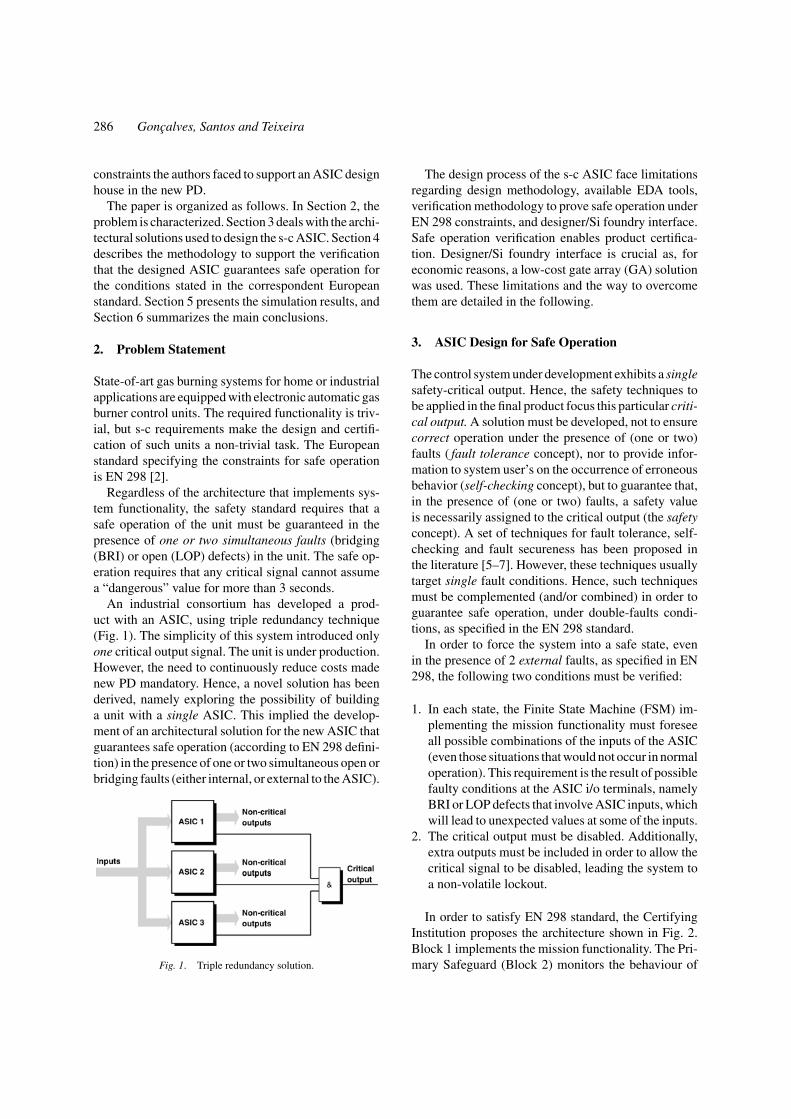
In order to detect lifetime failures, a concurrenterror detection technique is needed. Hence, a self-checking technique [5] is used. The basics of thistechnique are the encoding of the outputs of eachblock. The m-out-of-n error detection code was cho-sen, which enables the detection of all unidirectionalerrors. An unidirectional error occurs when any in-ternal fault in the block leads to some output tran-sitions, either from ‘0’ to ‘1’ or from ‘1’ to ‘0’.In order to generate only unidirectional errors, thecombinational blocks were implemented using a non-inverting logic. An internal fault in this block willgenerate a non-codeword that will be detected by averification circuit, the checker. Basically, Block 1is a classical FSM (Fig. 4) where 3 checkers havebeen inserted. The checkers monitor the next state
288 Goncalves, Santos and Teixeira
Fig. 4. Finite state machine including checkers.
Fig. 5. Redundancy used in timersimplementation.
generation block (Combinational block #1), the out-put generation block (Combinational block #2) andthe state variables. Each checker is able to detectone single stuck-at fault in the correspondent block.Due to the non-inverting logic implementation ofthese blocks, the combination of any number of iden-tical stuck-at faults within the same block is alsodetected.
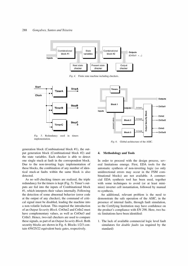
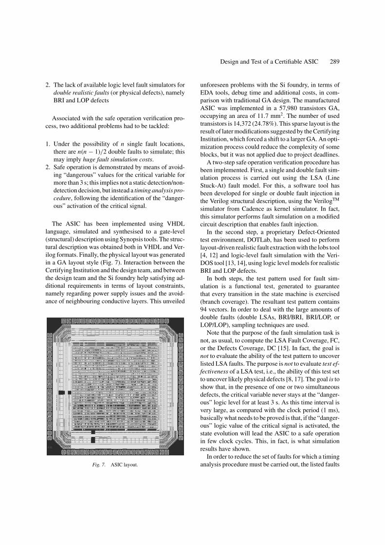
As no self-checking timers are realized, the tripleredundancy for the timers is kept (Fig. 5). Timer’s out-puts are fed into the inputs of Combinational block#1, which interprets their values internally. Followingthe detection of some abnormal behavior (error codeat the output of any checker), the command of criti-cal signal must be disabled, leading the machine intoa non-volatile lockout. This required the introductionof an Output Security Block. CrtOut2 and CrtIn2 musthave complementary values, as well as CrtOut3 andCrtIn3. Hence, two-rail checkers are used to comparethese signals, as part of an Output Security Block. Bothsecurity blocks are shown in Fig. 6. Blocks 1/2/3 con-tain 459/25/22 equivalent basic gates, respectively.
Fig. 6. Global architecture of the ASIC.
4. Methodology and Tools
In order to proceed with the design process, sev-eral limitations emerge. First, EDA tools for theautomatic synthesis of non-inverting logic (so onlyunidirectional errors may occur in the FSM com-binational blocks) are not available. A commer-cial EDA synthesis tool has been used, togetherwith some techniques to avoid (or at least mini-mize) inverter cell instantiation, followed by manualre-synthesis.
An additional, relevant problem is the need todemonstrate the safe operation of the ASIC, in thepresence of internal faults, through fault simulation,so the Certifying Institution may have confidence onthe product’s compliance with EN 298. Here, two ba-sic limitations have been identified:
1. The lack of available commercial logic level faultsimulators for double faults (as required by thestandard)
Design and Test of a Certifiable ASIC 289
2. The lack of available logic level fault simulators fordouble realistic faults (or physical defects), namelyBRI and LOP defects
Associated with the safe operation verification pro-cess, two additional problems had to be tackled:
1. Under the possibility of n single fault locations,there are n(n − 1)/2 double faults to simulate; thismay imply huge fault simulation costs.
2. Safe operation is demonstrated by means of avoid-ing “dangerous” values for the critical variable formore than 3 s; this implies not a static detection/non-detection decision, but instead a timing analysis pro-cedure, following the identification of the “danger-ous” activation of the critical signal.
The ASIC has been implemented using VHDLlanguage, simulated and synthesised to a gate-level(structural) description using Synopsis tools. The struc-tural description was obtained both in VHDL and Ver-ilog formats. Finally, the physical layout was generatedin a GA layout style (Fig. 7). Interaction between theCertifying Institution and the design team, and betweenthe design team and the Si foundry help satisfying ad-ditional requirements in terms of layout constraints,namely regarding power supply issues and the avoid-ance of neighbouring conductive layers. This unveiled
Fig. 7. ASIC layout.
unforeseen problems with the Si foundry, in terms ofEDA tools, debug time and additional costs, in com-parison with traditional GA design. The manufacturedASIC was implemented in a 57,980 transistors GA,occupying an area of 11.7 mm2. The number of usedtransistors is 14,372 (24.78%). This sparse layout is theresult of later modifications suggested by the CertifyingInstitution, which forced a shift to a larger GA. An opti-mization process could reduce the complexity of someblocks, but it was not applied due to project deadlines.
A two-step safe operation verification procedure hasbeen implemented. First, a single and double fault sim-ulation process is carried out using the LSA (LineStuck-At) fault model. For this, a software tool hasbeen developed for single or double fault injection inthe Verilog structural description, using the VerilogTM
simulator from Cadence as kernel simulator. In fact,this simulator performs fault simulation on a modifiedcircuit description that enables fault injection.
In the second step, a proprietary Defect-Orientedtest environment, DOTLab, has been used to performlayout-driven realistic fault extraction with the lobs tool[4, 12] and logic-level fault simulation with the Veri-DOS tool [13, 14], using logic level models for realisticBRI and LOP defects.
In both steps, the test pattern used for fault sim-ulation is a functional test, generated to guaranteethat every transition in the state machine is exercised(branch coverage). The resultant test pattern contains94 vectors. In order to deal with the large amounts ofdouble faults (double LSAs, BRI/BRI, BRI/LOP, orLOP/LOP), sampling techniques are used.
Note that the purpose of the fault simulation task isnot, as usual, to compute the LSA Fault Coverage, FC,or the Defects Coverage, DC [15]. In fact, the goal isnot to evaluate the ability of the test pattern to uncoverlisted LSA faults. The purpose is not to evaluate test ef-fectiveness of a LSA test, i.e., the ability of this test setto uncover likely physical defects [8, 17]. The goal is toshow that, in the presence of one or two simultaneousdefects, the critical variable never stays at the “danger-ous” logic level for at least 3 s. As this time interval isvery large, as compared with the clock period (1 ms),basically what needs to be proved is that, if the “danger-ous” logic value of the critical signal is activated, thestate evolution will lead the ASIC to a safe operationin few clock cycles. This, in fact, is what simulationresults have shown.
In order to reduce the set of faults for which a timinganalysis procedure must be carried out, the listed faults
290 Goncalves, Santos and Teixeira
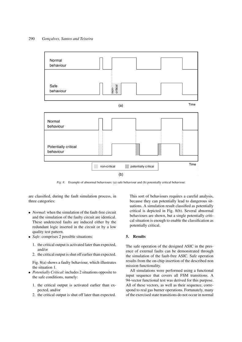
Fig. 8. Example of abnormal behaviours: (a) safe behaviour and (b) potentially critical behaviour.
are classified, during the fault simulation process, inthree categories:
• Normal: when the simulation of the fault-free circuitand the simulation of the faulty circuit are identical.These undetected faults are induced either by theredundant logic inserted in the circuit or by a lowquality test pattern.
• Safe: comprises 2 possible situations:
1. the critical output is activated later than expected,and/or
2. the critical output is shut off earlier than expected.
Fig. 8(a) shows a faulty behaviour, which illustratesthe situation 1.
• Potentially Critical: includes 2 situations opposite tothe safe conditions, namely:
1. the critical output is activated earlier than ex-pected, and/or
2. the critical output is shut off later than expected.
This sort of behaviours requires a careful analysis,because they can potentially lead to dangerous sit-uations. A simulation result classified as potentiallycritical is depicted in Fig. 8(b). Several abnormalbehaviours are shown, but a single potentially criti-cal situation is enough to enable the classification aspotentially critical.
5. Results
The safe operation of the designed ASIC in the pres-ence of external faults can be demonstrated throughthe simulation of the fault-free ASIC. Safe operationresults from the on-chip insertion of the described nonmission functionality.
All simulations were performed using a functionalinput sequence that covers all FSM transitions. A94-vector functional test was derived for this purpose.All of these vectors, as well as their sequence, corre-spond to real gas burner operations. Fortunately, manyof the exercised state transitions do not occur in normal
Design and Test of a Certifiable ASIC 291
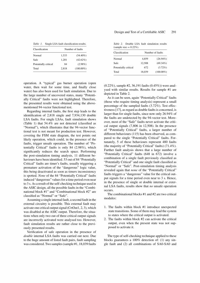
Table 1. Single LSA fault classification results.
Classification Number of faults
Normal 1,533 (54.40%)
Safe 1,201 (42.62%)
Potentially critical 84 (2.98%)
Total 2,818 (100.00%)
operation. A “typical” gas burner operation (openwater, then wait for some time, and finally closewater) has also been used for fault simulation. Due tothe large number of uncovered states, many “Potenti-ally Critical” faults were not highlighted. Therefore,the presented results were obtained using the above-mentioned 94-vector functional test.
Regarding internal faults, the first step leads to theidentification of 2,818 single and 7,934,130 doubleLSA faults. For single LSAs, fault simulation shows(Table 1) that 54.4% are not detected (classified as“Normal”), which illustrates that the 94-vector func-tional test is not meant for production test. However,covering the FSM state diagram, the test points outlikely operation, which could, in the presence of thefaults, trigger unsafe operation. The number of “Po-tentially Critical” faults is only 84 (2.98%), whichsignificantly reduces the search space. Performingthe post-simulation timing analysis, 11 different be-haviours have been identified. 53 out of 84 “PotentiallyCritical” faults are timer’s faults, usually triggering apremature activation of the “dangerous” logic value,this being deactivated as soon as timers inconsistencyis spotted. None of the 84 “Potentially Critical” faultsinduced “dangerous” values for a time period even nearto 3 s. As a result of the self-checking technique used inthe ASIC design, all the possible faults in the “Combi-national block #1” and “Combinational block #2” areclassified as “Normal” or “Safe”.
Assuming a single internal fault, a second fault in theexternal circuitry is possible. This external fault mayactivate one critical output signal (CrtOut1, 2, 3), whichwas disabled at the ASIC output. Therefore, the situa-tions when only two out of three critical output signalsare incorrectly activated were analysed too. However,fault simulation results are rather close to the previ-ously presented results.
Verification of safe operation in the presence ofdouble internal LSA faults was carried out next. Dueto the huge amount of listed fault pairs, fault samplingwas considered. Two samples (sample #1, 18,039 faults
Table 2. Double LSA fault simulation results(sample size = 0.22%).
Classification Number of faults
Normal 4,859 (26.94%)
Safe 12,508 (69.34%)
Potentially critical 672 (3.72%)
Total 18,039 (100.00%)
(0.22%), sample #2, 36,191 faults (0.45%)) were anal-ysed with similar results. Results for sample #1 aredepicted in Table 2.
As it can be seen, again “Potentially Critical” faults(those who require timing analysis) represent a smallpercentage of the sampled faults (3.72%). Test effec-tiveness [17], as regard as double faults is concerned, islarger than for single faults, since now only 26.94% ofthe faults are undetected by the 94-vector test. More-over, most of the “Safe” faults never activate the criti-cal output signals (7,806 in 12,508). In the presenceof “Potentially Critical” faults, a larger number ofdifferent behaviours (115) has been observed, as com-pared to the single “Potentially Critical” faults. For-tunately, 5 of these behaviours represent 480 faults(the majority of “Potentially Critical” faults) (71.4%).Further fault analysis shows that a large number of“Potentially Critical” faults (648 in 672) involve acombination of a single fault previously classified as“Potentially Critical” and one single fault classified as“Normal” or “Safe”. Post-simulation timing analysisrevealed again that none of the “Potentially Critical”faults triggers a “dangerous” value for the critical out-put signals for a time period even near to 3 s. Hence,in the presence of single or double internal or exter-nal LSA faults, results show that no unsafe operationoccurs.
The combinational blocks #1 and #2 are two criticalmodules:
1. The faults within block #1 introduce unexpectedstate transitions. Some of them may lead the systemto states where the critical output is activated.
2. The faults within block #2 can activate the criticaloutput, even when the present state was not sup-posed to activate it.
The type of self-checking technique applied to theseblocks guarantees a 100% detection of: (1) any sin-gle fault and (2) all combinations of SA0-SA0 and
292 Goncalves, Santos and Teixeira
SA1-SA1 faults. The combination of different “stuck-at” faults (SA0-SA1) is usually detected, but the detec-tion has to be ascertained by fault simulation.
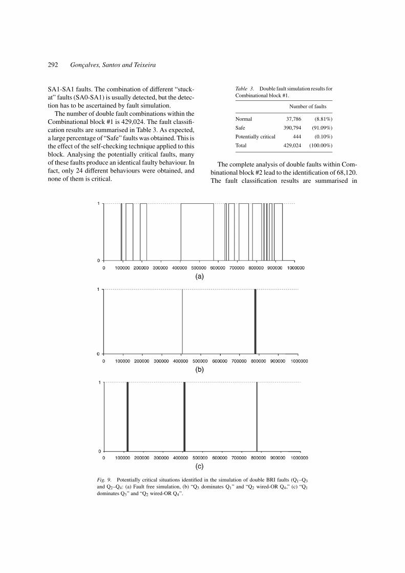
The number of double fault combinations within theCombinational block #1 is 429,024. The fault classifi-cation results are summarised in Table 3. As expected,a large percentage of “Safe” faults was obtained. This isthe effect of the self-checking technique applied to thisblock. Analysing the potentially critical faults, manyof these faults produce an identical faulty behaviour. Infact, only 24 different behaviours were obtained, andnone of them is critical.
Fig. 9. Potentially critical situations identified in the simulation of double BRI faults (Q1–Q3
and Q2–Q4: (a) Fault free simulation, (b) “Q3 dominates Q1” and “Q2 wired-OR Q4,” (c) “Q1
dominates Q3” and “Q2 wired-OR Q4”.
Table 3. Double fault simulation results forCombinational block #1.
Number of faults
Normal 37,786 (8.81%)
Safe 390,794 (91.09%)
Potentially critical 444 (0.10%)
Total 429,024 (100.00%)
The complete analysis of double faults within Com-binational block #2 lead to the identification of 68,120.The fault classification results are summarised in
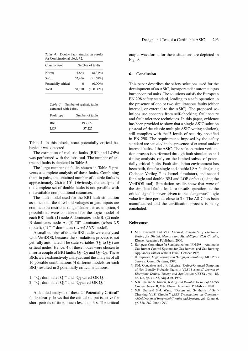
Design and Test of a Certifiable ASIC 293
Table 4. Double fault simulation resultsfor Combinational block #2.
Classification Number of faults
Normal 5,664 (8.31%)
Safe 62,456 (91.69%)
Potentially critical 0 (0.00%)
Total 68,120 (100.00%)
Table 5. Number of realistic faultsextracted with lobs.
Fault type Number of faults
BRI 193,572
LOP 37,225
Table 4. In this block, none potentially critical be-haviour was detected.
The extraction of realistic faults (BRIs and LOPs)was performed with the lobs tool. The number of ex-tracted faults is depicted in Table 5.
The large number of faults shown in Table 5 pre-vents a complete analysis of these faults. Combiningthem in pairs, the obtained number of double faults isapproximately 26.6 × 10⁹. Obviously, the analysis ofthe complete set of double faults is not possible withthe available computational resources.
The fault model used for the BRI fault simulationassumes that the threshold voltages at gate inputs areconfined to a restricted range. Under this assumption, 4possibilities were considered for the logic model ofeach BRI fault: (1) node A dominates node B; (2) nodeB dominates node A; (3) “0” dominates (wired-ORmodel); (4) “1” dominates (wired-AND model).
A small number of double BRI faults were analysedwith VeriDOS, because the simulations process is notyet fully automated. The state variables (Q1 to Q7) arecritical nodes. Hence, 4 of these nodes were chosen toinsert a couple of BRI faults: Q1–Q3 and Q2–Q4. TheseBRIs were exhaustively analyzed and the analysis of all16 possible combinations (4 different models for eachBRI) resulted in 2 potentially critical situations:
1. “Q3 dominates Q1” and “Q2 wired-OR Q4”2. “Q1 dominates Q3” and “Q2wired-OR Q4”
A detailed analysis of these 2 “Potentially Critical”faults clearly shows that the critical output is active forshort periods of time, much less than 3 s. The critical
output waveforms for these situations are depicted inFig. 9.
6. Conclusion
This paper describes the safety solutions used for thedevelopment of an ASIC, incorporated in automatic gasburner control units. The solutions satisfy the EuropeanEN 298 safety standard, leading to a safe operation inthe presence of one or two simultaneous faults (eitherinternal, or external to the ASIC). The proposed so-lutions use concepts from self-checking, fault secureand fault tolerance techniques. In this paper, evidencehas been provided to show that a single ASIC solution(instead of the classic multiple ASIC voting solution),still complies with the 3 levels of security specifiedin EN 298. The requirements imposed by the safetystandard are satisfied in the presence of external and/orinternal faults of the ASIC. The safe operation verifica-tion process is performed through fault simulation andtiming analysis, only on the limited subset of poten-tially critical faults. Fault simulation environment hasbeen built, first for single and double LSA faults (usingCadence VerilogTM as kernel simulator), and secondfor single and double BRI and LOP defects (using theVeriDOS tool). Simulation results show that none ofthe simulated faults leads to unsafe operation, as thecritical signal is never driven to the “dangerous” logicvalue for time periods close to 3 s. The ASIC has beenmanufactured and the certification process is beingconcluded.
References
1. M.L. Bushnell and V.D. Agrawal, Essentials of ElectronicTesting for Digital, Memory and Mixed-Signal VLSI Circuits,Kluwer Academic Publishers, 2000.
2. European Committee for Standardization, “EN 298—AutomaticGas Burner Control Systems for Gas Burners and Gas BurningAppliances with or without Fans,” October 1993.
3. H. Fujiwara, Logic Testing and Design for Testability, MIT PressSeries in Comp. Systems, 1985.
4. F.M. Goncalves and J.P. Teixeira, “Defect-Oriented Samplingof Non-Equally Probable Faults in VLSI Systems,” Journal ofElectronic Testing, Theory and Application (JETTA), vol. 15,no. 1/2, pp. 41–52, Aug./Oct. 1999.
5. N.K. Jha and S. Kundu, Testing and Reliable Design of CMOSCircuits, Norwell, MA: Kluwer Academic Publishers, 1990.
6. N.K. Jha and S.-J. Wang, “Design and Synthesis of Self-Checking VLSI Circuits,” IEEE Transactions on Computer-Aided Design of Integrated Circuits and Systems, vol. 12, no. 6,pp. 878–887, June 1993.

294 Goncalves, Santos and Teixeira
7. M. Lubaszewski and B. Courtois, “Reliable Fail-Safe Systems,”in Proc. Asian Test Symp. (ATS), 1993, pp. 32–37.
8. E.J. McCluskey and Ch.-W. Tseng, “Stuck-Fault Tests vs. Ac-tual Defects,” in Proc. Int. Test Conf. (ITC), 2000, pp. 336–343.
9. C. Metra, M. Favalli, P. Olivo, and B. Ricco, “Design ofCMOS Checkers with Improved Testability of Bridging andTransistor Stuck-on Faults,” Journal of Electronic Testing:Theory and Applications (JETTA), vol. 6, pp. 7–22, Feb.1995.
10. S. Mitra and E.J. McCluskey, “Which Concurrent Error Detec-tion Scheme to Choose?” in Proc. Int. Test Conf. (ITC), 2000,pp. 985–994.
11. M. Nicolaidis, “Fault Secure Property Versus Strongly Code Dis-joint Checkers,” IEEE Transactions on Computer-Aided Design(CAD), vol. 13, no. 5, pp. 651–658, May 1994.
12. M.B. Santos, F.M. Goncalves, I.C. Teixeira, and J.P. Teixeira,“Defect-Oriented Test Quality Assessment Using Fault Sam-pling and Simulation,” in Proc. Int. Test Conf. (ITC), 1998,pp. 35–42.
13. M.B. Santos, F.M. Goncalves, I.C. Teixeira, and J.P. Teixeira,“Defect-Oriented Verilog Fault Simulation of SoC Macros usinga Stratified Fault Sampling Technique,” in Proc. IEEE VLSI TestSymp. (VTS), 1999, pp. 326–332.
14. M.B. Santos and J.P. Teixeira, “Defect-Oriented Mixed-LevelFault Simulation of Digital Systems-on-a-Chip Using HDL,” inProc. Design Automation and Test in Europe (DATE), March1999, pp. 549–553.
15. J.J.T. Sousa, F.M. Goncalves, J.P. Teixeira, C. Marzocca,F. Corsi, and T.W. Williams, “Defect Level Evaluation in an ICDesign Environment,” IEEE Transactions. on Computer-AidedDesign (CAD), vol. 15, no. 10, pp. 1286–1293, 1996.
16. J.F. Wakerly, Error Detecting Codes, Self-Checking Circuits andApplications, Amsterdam: North-Holland, 1978.
17. L.C. Wang, R. Mercer, and T.W. Williams, “On the De-cline of Testing Efficiency as Fault Coverage Approaches100%,” in Proc. IEEE VLSI Test Symp. (VTS), 1995, pp. 74–83.
18. Ch. Zeng, N. Saxena, and E.J. McCluskey, “Finite State MachineSynthesis with Concurrent Error Detection,” in Proc. Int. TestConf. (ITC), 1999, pp. 672–679.
Fernando Manuel Goncalves received the electrical engineeringdegree in 1988, the M.Sc. in 1992, and the Ph.D. in 1999, all fromInstituto Superior Tecnico (Technical University of Lisbon), Lisbon,Portugal. He joined the Instituto Superior Tecnico in 1990, where heis currently a Professor in the Department of Electrical Engineeringand Computer Science. He is a researcher of the Quality, Test andHardware/Software Co-design (QTHS) Group at INESC-ID (Insti-tute for Systems and Computer Engineering). His research interestsinclude reconfigurable computing, VLSI design and test, algorithmsfor layout analysis, and defect-oriented testing.
Marcelino Bicho dos Santos has got his Degree on Electrical andComputer Engineering, in 1990, and his M.Sc. degree, in 1994, andhis Ph.D. last January at IST (Instituto Superior Tecnico) from theTechnical University of Lisbon. He is a Assistant Professor at ISTand a researcher at INESC-id (Instituto de Engenharia de Sistemas eComputadores), in the Quality, Test and Hardware/Software Co-design (QTHS) Group. His scientific and technical interests includedefect-oriented test, DFT, BIST, IDDX testing, low-power testing, andsystem-level fault modeling and simulation.
Joao Paulo Teixeira has got his Degree on Electrical Engineer-ing (Telecommunications and Electronics) and his Ph.D. in AppliedElectronics in 1982, at IST from the Technical University of Lisbon.He is currently an Associate Professor at IST. He is a Senior re-searcher at INESC-id, where he is co-chairing the QTHS Group. HisR&D interests include the analysis, specification, design, productionand test of hardware/software systems, which use microelectronics assupporting technologies. Emphasis is given to the design and test ofdigital, analog and mixed-signal circuits and systems, implementedin CMOS or CMOS-compatible semiconductor technologies, andto the development of EDA (Electronic Design Automation) tools,especially CAT (Computer-Aided Testing) tools.
Copyright © 2022 FDOKUMEN