Design and test issues of an FPGA based data acquisition system for medical imaging using PEM
9
IEEE TRANSACTIONS ON NUCLEAR SCIENCE, VOL. 53, NO. 3, JUNE 2006 761 Design and Test Issues of an FPGA Based Data Acquisition System for Medical Imaging Using PEM Carlos Leong, Pedro Bento, Pedro Lousã, João Nobre, Joel Rego, Pedro Rodrigues, José C. Silva, Isabel C. Teixeira, J. Paulo Teixeira, Andreia Trindade, and João Varela Abstract—The main aspects of the design and test (D&T) of a reconfigurable architecture for the Data Acquisition Electronics (DAE) system of the Clear-PEM detector are presented in this paper. The application focuses medical imaging using a compact PEM (Positron Emission Mammography) detector with 12288 channels, targeting high sensitivity and spatial resolution. The DAE system processes data frames that come from a front-end (FE) electronics, identifies the relevant data and transfers it to a PC for image processing. The design is supported in a novel D&T methodology, in which hierarchy, modularity and parallelism are extensively exploited to improve design and testability features. Parameterization has also been used to improve design flexibility. Nominal frequency is 100 MHz. The DAE must respond to a data acquisition rate of 1 million relevant events (coincidences) per second, under a total single photon background rate in the detector of 10 MHz. Trigger and data acquisition logic is imple- mented in eight 4-million, one 2-million and one 1-million gate FPGAs (Xilinx Virtex II). Functional Built-In Self Test (BIST) and Debug features are incorporated in the design to allow on-board FPGA testing and self-testing during product lifetime. Index Terms—Functional built-in self test, hierarchy, modu- larity, parallelism, parameterization, pipelining, process diagrams, re-use. I. INTRODUCTION B REAST cancer early detection is recognized as a world- wide priority, since it constitutes the most effective way to deal with this illness. Nevertheless, the detection specificity of present diagnosis systems is low [1]. Therefore, research on new diagnosis processes and systems for this type of cancer are actively pursued. Positron Emission Tomography (PET) based technology is one of these promising research lines. PET technology is used in the development of the Clear-PEM scanner, a high-resolution Positron Emission Mammography (PEM) system, capable of detecting tumors with diameters Manuscript received June 19, 2005; revised March 30, 2006. This work was supported in part by AdI (Innovation Agency) and POSI (Operational Program for Information Society), Portugal. P. Rodrigues and A. Trindade were sup- ported by the FCT under Grant SFRH/BD/10187/2002 and Grant SFRH/BD/ 10198/2002. C. Leong and P. Bento are with INESC-ID, Lisboa, Portugal. P. Lousã, J. Nobre, and J. Rego are with INOV, Lisboa, Portugal. P. Rodrigues and A. Trindade are with the Laboratório de Instrumentação e Física de Partículas, Lisboa, Portugal. J. C. Silva is with the Laboratório de Instrumentação e Física de Partículas, Lisboa, Portugal, and also with CERN, Geneva, Switzerland. I. C. Teixeira and J. P. Teixeira are with INESC-ID, Lisboa, Portugal, and also with the Instituto Superior Técnico, Universidade Técnica de Lisboa, Portugal. J. Varela is with the Laboratório de Instrumentação e Física de Partículas, Lisboa, Portugal, and also with CERN, Geneva, Switzerland, and the Instituto Superior Técnico, Universidade Técnica de Lisboa, Portugal. Digital Object Identifier 10.1109/TNS.2006.874841 down to 2 mm [1]–[5]. Based on the detection of radiation emitted by human cells when a radioactive substance is injected into the human blood stream [3], PET identifies, by image reconstruction, the spatial origin of the radiation source (the cancerous cells). Image reconstruction algorithms demand millions of pixels for providing acceptable accuracy. Hence, for a correct med- ical diagnosis, huge amount of data must be generated and pro- cessed. The purpose of this paper is to present key aspects of a novel design and test methodology for high data-volume, data stream digital systems and to apply it to the development of the Data Acquisition Electronic (DAE) system responsible for the digital data processing in the Clear-PEM scanner. Along with innovative high resolution PEM technology, new physical data, algorithms and methodologies are under intensive research. Therefore, hardware/software solutions using recon- figurable hardware (i.e., FPGA-based) constitute an adequate choice. Additionally, reconfigurable hardware solutions are also adequate for the volume production of the envisaged product. The main design challenge in this context is the need to process huge amounts of data [4] and to perform tumor cell identification (if resident in the patient tissues) in the shortest time possible. We refer this as the medical diagnosis process. These constraints demand an efficient electronic system, which means, hardware data processing and extensive use of par- allelism and pipelining. In order to meet the functional and performance requirements, moderate speed and high pin count complex FPGA should be used (For the design in which the novel methodology is implemented, Xilinx Virtex II devices have been used). The paper is organized as follows. In Section II, a brief de- scription of the Clear-PEM detector system architecture is pre- sented. Section III presents the main aspects of the proposed methodology, including key functional, performance and testa- bility issues. In Section IV, DAE implementation details are pro- vided. Design validation and prototype verification procedures are presented in Section V. Finally, Section VI summarizes the main conclusions of this work. II. CLEAR-PEM DETECTOR SYSTEM The Clear-PEM detector system is a PET camera for breast imaging designed to optimize the detection sensitivity and spatial resolution [1], [2]. It consists of two parallel detector heads, corresponding to a total of 12288 readout channels. The system is designed to support a data acquisition rate of 1 million events per second, under a total single photon background rate of 10 MHz [2]. An event or hit (photoelectric event or Compton—according to the associated energy) is 0018-9499/$20.00 © 2006 IEEE
-
Upload
independent -
Category
Documents
-
view
1 -
download
0
Transcript of Design and test issues of an FPGA based data acquisition system for medical imaging using PEM
IEEE TRANSACTIONS ON NUCLEAR SCIENCE, VOL. 53, NO. 3, JUNE 2006 761
Design and Test Issues of an FPGA Based DataAcquisition System for Medical Imaging Using PEM
Carlos Leong, Pedro Bento, Pedro Lousã, João Nobre, Joel Rego, Pedro Rodrigues, José C. Silva,Isabel C. Teixeira, J. Paulo Teixeira, Andreia Trindade, and João Varela
Abstract—The main aspects of the design and test (D&T) of areconfigurable architecture for the Data Acquisition Electronics(DAE) system of the Clear-PEM detector are presented in thispaper. The application focuses medical imaging using a compactPEM (Positron Emission Mammography) detector with 12288channels, targeting high sensitivity and spatial resolution. TheDAE system processes data frames that come from a front-end(FE) electronics, identifies the relevant data and transfers it to aPC for image processing. The design is supported in a novel D&Tmethodology, in which hierarchy, modularity and parallelism areextensively exploited to improve design and testability features.Parameterization has also been used to improve design flexibility.Nominal frequency is 100 MHz. The DAE must respond to adata acquisition rate of 1 million relevant events (coincidences)per second, under a total single photon background rate in thedetector of 10 MHz. Trigger and data acquisition logic is imple-mented in eight 4-million, one 2-million and one 1-million gateFPGAs (Xilinx Virtex II). Functional Built-In Self Test (BIST) andDebug features are incorporated in the design to allow on-boardFPGA testing and self-testing during product lifetime.
Index Terms—Functional built-in self test, hierarchy, modu-larity, parallelism, parameterization, pipelining, process diagrams,re-use.
I. INTRODUCTION
BREAST cancer early detection is recognized as a world-wide priority, since it constitutes the most effective way
to deal with this illness. Nevertheless, the detection specificityof present diagnosis systems is low [1]. Therefore, research onnew diagnosis processes and systems for this type of cancerare actively pursued. Positron Emission Tomography (PET)based technology is one of these promising research lines.PET technology is used in the development of the Clear-PEMscanner, a high-resolution Positron Emission Mammography(PEM) system, capable of detecting tumors with diameters
Manuscript received June 19, 2005; revised March 30, 2006. This work wassupported in part by AdI (Innovation Agency) and POSI (Operational Programfor Information Society), Portugal. P. Rodrigues and A. Trindade were sup-ported by the FCT under Grant SFRH/BD/10187/2002 and Grant SFRH/BD/10198/2002.
C. Leong and P. Bento are with INESC-ID, Lisboa, Portugal.P. Lousã, J. Nobre, and J. Rego are with INOV, Lisboa, Portugal.P. Rodrigues and A. Trindade are with the Laboratório de Instrumentação e
Física de Partículas, Lisboa, Portugal.J. C. Silva is with the Laboratório de Instrumentação e Física de Partículas,
Lisboa, Portugal, and also with CERN, Geneva, Switzerland.I. C. Teixeira and J. P. Teixeira are with INESC-ID, Lisboa, Portugal, and also
with the Instituto Superior Técnico, Universidade Técnica de Lisboa, Portugal.J. Varela is with the Laboratório de Instrumentação e Física de Partículas,
Lisboa, Portugal, and also with CERN, Geneva, Switzerland, and the InstitutoSuperior Técnico, Universidade Técnica de Lisboa, Portugal.
Digital Object Identifier 10.1109/TNS.2006.874841
down to 2 mm [1]–[5]. Based on the detection of radiationemitted by human cells when a radioactive substance is injectedinto the human blood stream [3], PET identifies, by imagereconstruction, the spatial origin of the radiation source (thecancerous cells).
Image reconstruction algorithms demand millions of pixelsfor providing acceptable accuracy. Hence, for a correct med-ical diagnosis, huge amount of data must be generated and pro-cessed. The purpose of this paper is to present key aspects of anovel design and test methodology for high data-volume, datastream digital systems and to apply it to the development of theData Acquisition Electronic (DAE) system responsible for thedigital data processing in the Clear-PEM scanner.
Along with innovative high resolution PEM technology, newphysical data, algorithms and methodologies are under intensiveresearch. Therefore, hardware/software solutions using recon-figurable hardware (i.e., FPGA-based) constitute an adequatechoice. Additionally, reconfigurable hardware solutions are alsoadequate for the volume production of the envisaged product.
The main design challenge in this context is the need toprocess huge amounts of data [4] and to perform tumor cellidentification (if resident in the patient tissues) in the shortesttime possible. We refer this as the medical diagnosis process.These constraints demand an efficient electronic system, whichmeans, hardware data processing and extensive use of par-allelism and pipelining. In order to meet the functional andperformance requirements, moderate speed and high pin countcomplex FPGA should be used (For the design in which thenovel methodology is implemented, Xilinx Virtex II deviceshave been used).
The paper is organized as follows. In Section II, a brief de-scription of the Clear-PEM detector system architecture is pre-sented. Section III presents the main aspects of the proposedmethodology, including key functional, performance and testa-bility issues. In Section IV, DAE implementation details are pro-vided. Design validation and prototype verification proceduresare presented in Section V. Finally, Section VI summarizes themain conclusions of this work.
II. CLEAR-PEM DETECTOR SYSTEM
The Clear-PEM detector system is a PET camera for breastimaging designed to optimize the detection sensitivity andspatial resolution [1], [2]. It consists of two parallel detectorheads, corresponding to a total of 12288 readout channels.The system is designed to support a data acquisition rateof 1 million events per second, under a total single photonbackground rate of 10 MHz [2]. An event or hit (photoelectricevent or Compton—according to the associated energy) is
0018-9499/$20.00 © 2006 IEEE
762 IEEE TRANSACTIONS ON NUCLEAR SCIENCE, VOL. 53, NO. 3, JUNE 2006
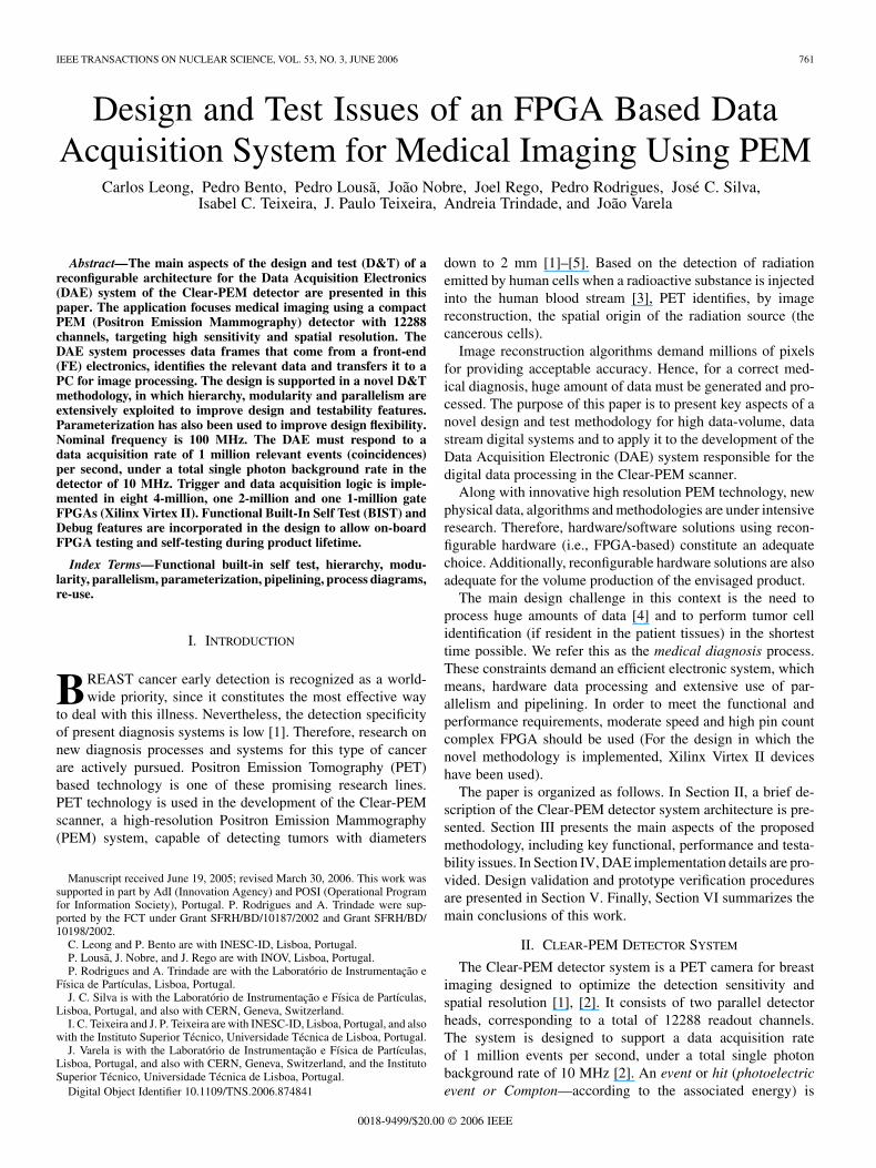
Fig. 1. Sampled energy pulse associated with a hit.
defined as the interaction of a ray with a crystal. Data to beanalyzed and processed correspond to the energy originatedin the different crystals as a consequence of these collisions.Relevant data are associated with relevant events. An eventis defined as relevant if it corresponds to a coincidence, thatis, the simultaneous occurrence of hits in both crystal planes.In this context, simultaneous means within the same discretetime window characterized by a pair of parameters - TimeTag/Delta. Time Tag (TT) is the time instant associated withthe data sample that corresponds to highest value in the energypulse associated with one hit. Delta is the difference betweenthe time instant associated with the analog energy peak and theTime Tag (sample) (see Fig. 1).
System functionality is partitioned between the Front-End(FE) electronics (details in [3], [4]) on the detector heads, andthe off-detector DAE. The FE is responsible for the constructionand distribution of the analog data frames that correspond to theoccurrence of hits. This work focus on the novel design and testmethodology applied to the DAE development. The proposedDAE architecture is described in the following section.
III. DESIGN AND TEST METHODOLOGY
The proposed Design and Test (D&T) methodology targetshigh volume, high rate data processing systems for which dataare concurrently delivered to them. Such a system must satisfythe following objectives: 1) functional and performance com-pliance to the functional and timing specifications; 2) testa-bility and debugging capabilities to allow functional self-testand prototype debug and 3) easily modifiable functionality toallow low-cost system design adaptation to requirements mod-ifications, that may occur, e.g., as the result of algorithms andcalibration procedures refinements.
To meet these objectives, the following system attributes arepursued in the hardware D&T methodology: hierarchy, modu-larity, module re-use, parallelism, pipelining and parameteriza-tion.
Cost-effective prototype validation of such a complex systemis a mandatory requirement. This excludes the use of only ex-ternal test equipment. Therefore, unassigned FPGA resourcesshould be used, as much as possible, to implement built-in teststructures to support system diagnosis and debug, and self-testduring product lifetime. FPGA devices integrated in the DAEsystem are assumed defect-free (they are marketed after produc-tion test). Hence, FPGA test resources are not built-in to performthe structural test (as is usual in manufacturing), but rather tocarry out functional test. We refer this feature of the proposedD&T methodology as functional BIST.
The complexity and the specificity of the problem justifiedthe development of a new D&T methodology. The followingaspects have been taken into consideration in the developmentof the proposed methodology. Although huge amount of data ar-rive at the DAE at a relatively high rate, the information flowingfrom each channel is identical (since it comes from similar crys-tals) and should be submitted to identical processing. Therefore,the electronic system architecture should reflect this character-istic by exhibiting high replication, or re-use of identical pro-cessing modules. An important aspect to be addressed is thechoice of the granularity of the modules. Should a module cor-respond to a single crystal, since a crystal is the source of data,or should it correspond to some crystal cluster?
It has been decided that the DAE architecture should map theorganization of the crystal arrays. Data are provided by 12288readout channels (two channels/crystal, one for the top and onefor the bottom plane). These channels are organized in 2 96identical detector modules distributed by two crystal planes.Data arrive at the DAE in parallel. Thus, it should, has muchas possible, be processed in parallel.
On the other hand, data are transmitted from the FE to theDAE by a large number of cables that may introduce diversedelays. However, to guarantee that a detected coincidence is ef-fectively a coincidence, it is mandatory to guarantee system syn-chronism.
The random nature of data generation is another aspect thathas been considered. In fact, huge amounts of randomly gener-
LEONG et al.: DESIGN AND TEST ISSUES 763
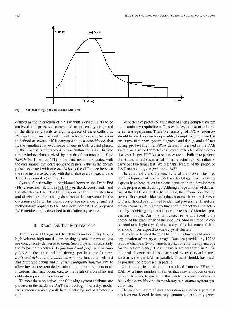
Fig. 2. Top-level model of PEM DAE electronic system.
Fig. 3. Process diagram corresponding to the normal/random mode Scenario.
ated data arrive at the DAE and require processing to determineif it should be considered as relevant or not. Irrelevant data mustbe discarded as quickly as possible.
Therefore, the D&T methodology should lead to a DAE ar-chitecture that reflects the DAE hierarchy and the modular char-acter of the scanner, as well as data flow parallelism using mul-tiple instantiation (re-use) of identical modules.
In order to take into account the random nature of data al-location of enough memory banks in the architecture must beperformed to temporarily store data until they can be safely dis-carded. Moreover, it should consider the physical limitationsimposed on the timing requirements by the interconnection ca-
bles, which demands adequate design techniques to guaranteesynchronism.
In the next sections, the rationale behind the methodologywill emerge in the explanation of DAE architecture.
A. DAE Architecture
The main functionality of the DAE is, to identify relevantdata coming from the FE electronics. Fig. 2 depicts the top-levelarchitecture of the DAE system. This figure highlights the hier-archical nature of the design. In fact, the system is composed offour identical DAQ boards, each one with two identical FPGAs(DAQ FPGA) that implement the Data Acquisition (DAQ) func-
764 IEEE TRANSACTIONS ON NUCLEAR SCIENCE, VOL. 53, NO. 3, JUNE 2006
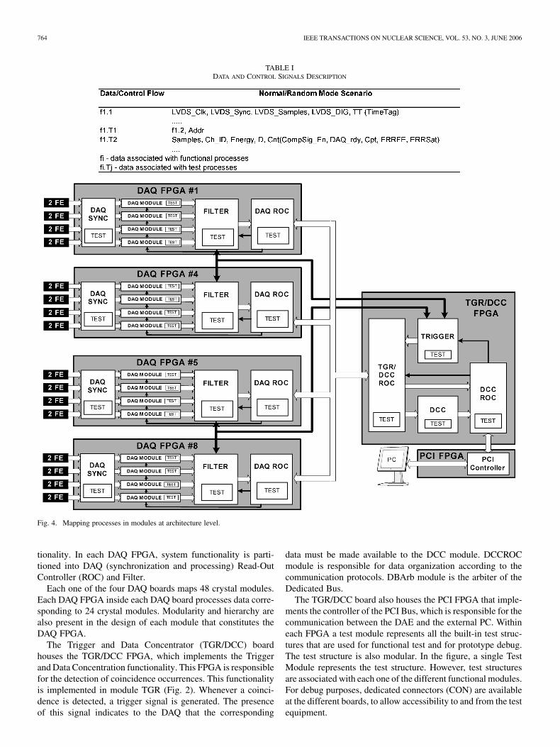
TABLE IDATA AND CONTROL SIGNALS DESCRIPTION
Fig. 4. Mapping processes in modules at architecture level.
tionality. In each DAQ FPGA, system functionality is parti-tioned into DAQ (synchronization and processing) Read-OutController (ROC) and Filter.
Each one of the four DAQ boards maps 48 crystal modules.Each DAQ FPGA inside each DAQ board processes data corre-sponding to 24 crystal modules. Modularity and hierarchy arealso present in the design of each module that constitutes theDAQ FPGA.
The Trigger and Data Concentrator (TGR/DCC) boardhouses the TGR/DCC FPGA, which implements the Triggerand Data Concentration functionality. This FPGA is responsiblefor the detection of coincidence occurrences. This functionalityis implemented in module TGR (Fig. 2). Whenever a coinci-dence is detected, a trigger signal is generated. The presenceof this signal indicates to the DAQ that the corresponding
data must be made available to the DCC module. DCCROCmodule is responsible for data organization according to thecommunication protocols. DBArb module is the arbiter of theDedicated Bus.
The TGR/DCC board also houses the PCI FPGA that imple-ments the controller of the PCI Bus, which is responsible for thecommunication between the DAE and the external PC. Withineach FPGA a test module represents all the built-in test struc-tures that are used for functional test and for prototype debug.The test structure is also modular. In the figure, a single TestModule represents the test structure. However, test structuresare associated with each one of the different functional modules.For debug purposes, dedicated connectors (CON) are availableat the different boards, to allow accessibility to and from the testequipment.
LEONG et al.: DESIGN AND TEST ISSUES 765
In Fig. 2, LVDS stands for Low Voltage Differential Sig-naling, which is a low noise, low power, low amplitude methodfor high-speed (gigabits per second) data transmission overcopper wire.
Two proprietary buses, the Generic Bus and the DedicatedBus, are responsible for the fast information flow within theDAE system.
B. Process Diagrams
In the proposed D&T methodology, system functionality ispartitioned into sub-functions, in a hierarchical way to satisfydesign, testability and diagnostic requirements.
The partitioning procedure is based on the characterization ofdata and data streams, as well as on the processes that transformdata.
Process Diagrams, PD, (e.g., Fig. 3) are used to describedata storage, processing and data and control flow. ProcessDiagrams eases problem characterization and modeling. Thisprocedure has been adapted from the software domain [7],[8] where this kind of modeling is used as a “thinking tool”to characterize the problem under analysis, as completely aspossible, prior to initiate system design.
In Fig. 3, ellipses represent processes, rectangles representexternal objects that dialog with the processes and arrows rep-resent information flow.
A process is defined as a set of functions that carry out a givenfunctionality. Each ellipse conveys the process name and thenumber of instances of that process (e.g., x4 means that thereare 4 instances of this module in the architecture). Each processcan be instantiated more than once. For instance, DAQ Sync isinstantiated 4 times. By doing so, modularity, reuse and paral-lelism are highlighted.
Each arrow conveys data and control signal information. Dif-ferent types of arrows represent different types of information.In this particular case, distinction is made between functionaloperation mode (dot lines) and test mode (dash and continuouslines).
In test mode, distinction is also pointed out between data orig-inated by the test modules, that is, the test vectors (dash lines)and the modules response to the test vectors, that is, modulessignatures (continuous lines).
In a good design, Process Diagrams should present low con-nectivity, that is, processes should be designed so that its asso-ciated functionality should be executed as independently fromthe other processes as possible. This eases the implementationof hierarchy and parallelism in the design structures.
Another aspect that is contemplated in the Process Diagramsis the time variable. In fact, although it does not appear explicitlyin the diagrams, it is conveyed in the control signal that, togetherwith data, defines the flow of information between processes.
To guarantee, as much as possible, the completeness of thefunctional description the concept of operational scenario is in-troduced. In this context, a scenario is defined as the set of pro-cesses and corresponding data and control flow that representsthe complete execution of the functionality in a given operationmode.
Fig. 5. Complete FPGA Test Procedure.
Scenario identification is indicated by the index in fi. As anexample, f1.T15 means the test flow T15 in scenario 1. If nec-essary, additional meaning can be associated with the remnantindexes (indicating, e.g., the source and the target modules).
For the DAE, five operational scenarios have been identified,namely, 1) normal/random mode, 2) single mode (for calibra-tion), 3) constant loading parameters (for calibration), 4) func-tion mode loading and 5) error request. For the sake of complete-ness, all different scenarios that correspond to the DAE opera-tion modes must be described in terms of Process Diagrams.
As an example, Fig. 3 depicts the Process Diagram (PD) ofthe DAE normal/random mode scenario. In this diagram, pro-cesses corresponding to functional BIST structures are alreadyincluded (test process). As shown, data and control signal are theinputs and outputs of the transforming processes. Each processcan be further decomposed into sub-processes, and described inmore detailed PDs that correspond to lower hierarchical levels.In this way, hierarchy emerges.
Table I provides some examples of the data and control signalof the PD described in Fig. 3. Although, in the software domain,PD typically describes static flow and processing of data, theirreuse in the context of our methodology take dynamic featuresin consideration.
C. Mapping Processes Into Design Modules
At the design level, hopefully, each process should corre-spond to a hardware module, or sub-module. In Fig. 4 the corre-spondence between processes in the Process Diagram and mod-ules in the FPGA architecture is shown.
Design documentation (and test planning) requires the spec-ification of data and control signal identified in the Process Di-agrams, according to their format and timing requirements.
Lastly, all these modules are designed so they can be con-figured off and/or online, a very useful feature for a prototypevalidation.
D. Performance Issues
Taking into account that the main objective of the system isthe identification of coincidences, it is easy to understand that
766 IEEE TRANSACTIONS ON NUCLEAR SCIENCE, VOL. 53, NO. 3, JUNE 2006
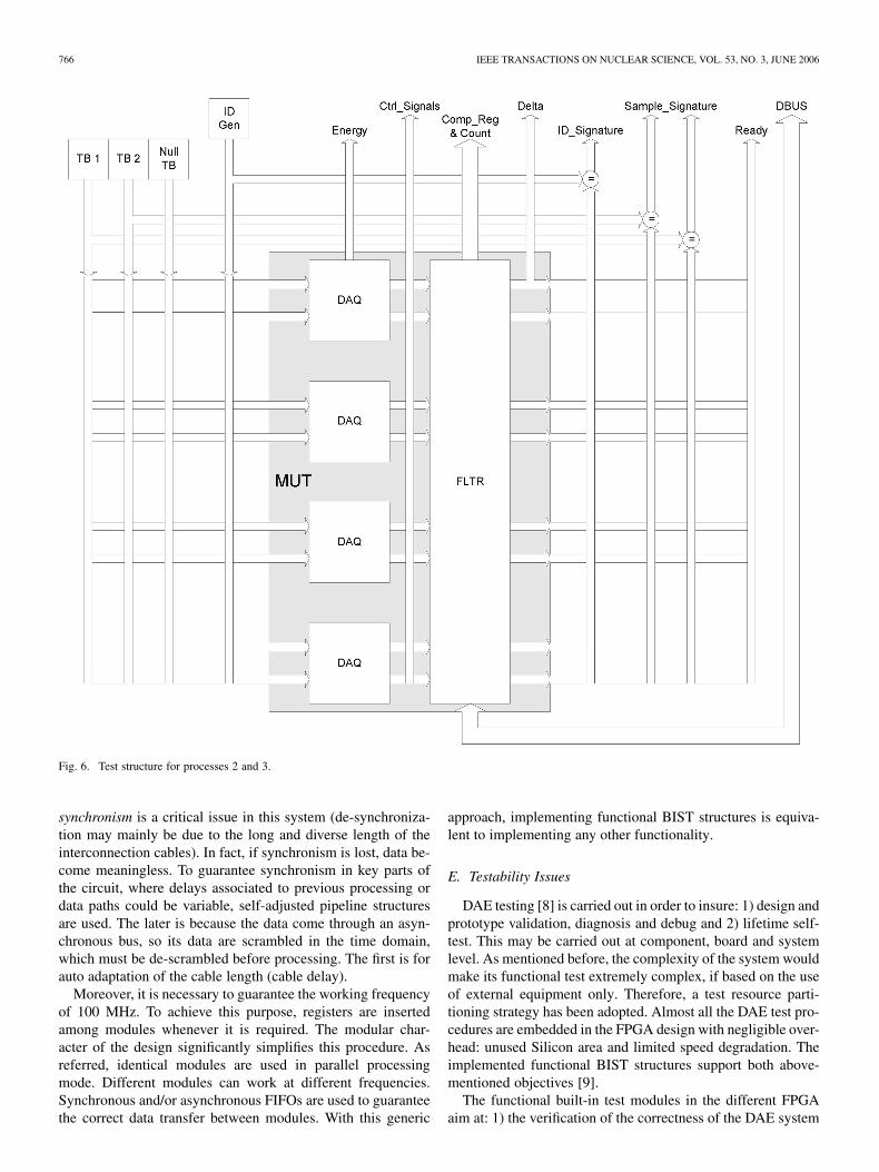
Fig. 6. Test structure for processes 2 and 3.
synchronism is a critical issue in this system (de-synchroniza-tion may mainly be due to the long and diverse length of theinterconnection cables). In fact, if synchronism is lost, data be-come meaningless. To guarantee synchronism in key parts ofthe circuit, where delays associated to previous processing ordata paths could be variable, self-adjusted pipeline structuresare used. The later is because the data come through an asyn-chronous bus, so its data are scrambled in the time domain,which must be de-scrambled before processing. The first is forauto adaptation of the cable length (cable delay).
Moreover, it is necessary to guarantee the working frequencyof 100 MHz. To achieve this purpose, registers are insertedamong modules whenever it is required. The modular char-acter of the design significantly simplifies this procedure. Asreferred, identical modules are used in parallel processingmode. Different modules can work at different frequencies.Synchronous and/or asynchronous FIFOs are used to guaranteethe correct data transfer between modules. With this generic
approach, implementing functional BIST structures is equiva-lent to implementing any other functionality.
E. Testability Issues
DAE testing [8] is carried out in order to insure: 1) design andprototype validation, diagnosis and debug and 2) lifetime self-test. This may be carried out at component, board and systemlevel. As mentioned before, the complexity of the system wouldmake its functional test extremely complex, if based on the useof external equipment only. Therefore, a test resource parti-tioning strategy has been adopted. Almost all the DAE test pro-cedures are embedded in the FPGA design with negligible over-head: unused Silicon area and limited speed degradation. Theimplemented functional BIST structures support both above-mentioned objectives [9].
The functional built-in test modules in the different FPGAaim at: 1) the verification of the correctness of the DAE system
LEONG et al.: DESIGN AND TEST ISSUES 767
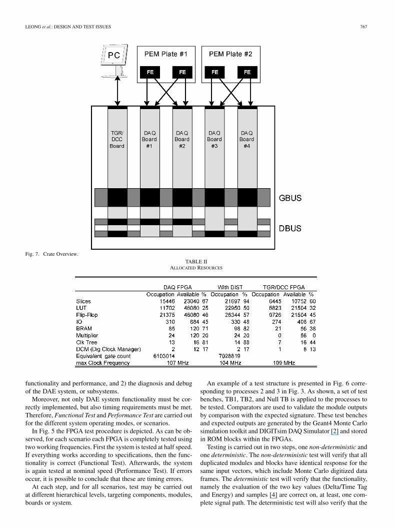
Fig. 7. Crate Overview.
TABLE IIALLOCATED RESOURCES
functionality and performance, and 2) the diagnosis and debugof the DAE system, or subsystems.
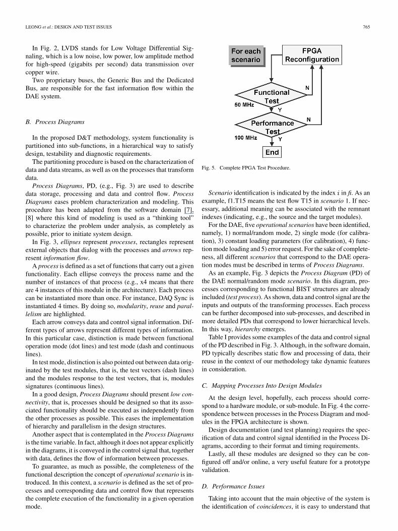
Moreover, not only DAE system functionality must be cor-rectly implemented, but also timing requirements must be met.Therefore, Functional Test and Performance Test are carried outfor the different system operating modes, or scenarios.
In Fig. 5 the FPGA test procedure is depicted. As can be ob-served, for each scenario each FPGA is completely tested usingtwo working frequencies. First the system is tested at half speed.If everything works according to specifications, then the func-tionality is correct (Functional Test). Afterwards, the systemis again tested at nominal speed (Performance Test). If errorsoccur, it is possible to conclude that these are timing errors.
At each step, and for all scenarios, test may be carried outat different hierarchical levels, targeting components, modules,boards or system.
An example of a test structure is presented in Fig. 6 corre-sponding to processes 2 and 3 in Fig. 3. As shown, a set of testbenches, TB1, TB2, and Null TB is applied to the processes tobe tested. Comparators are used to validate the module outputsby comparison with the expected signature. These test benchesand expected outputs are generated by the Geant4 Monte Carlosimulation toolkit and DIGITsim DAQ Simulator [2] and storedin ROM blocks within the FPGAs.
Testing is carried out in two steps, one non-deterministic andone deterministic. The non-deterministic test will verify that allduplicated modules and blocks have identical response for thesame input vectors, which include Monte Carlo digitized dataframes. The deterministic test will verify that the functionality,namely the evaluation of the two key values (Delta/Time Tagand Energy) and samples [4] are correct on, at least, one com-plete signal path. The deterministic test will also verify that the
768 IEEE TRANSACTIONS ON NUCLEAR SCIENCE, VOL. 53, NO. 3, JUNE 2006
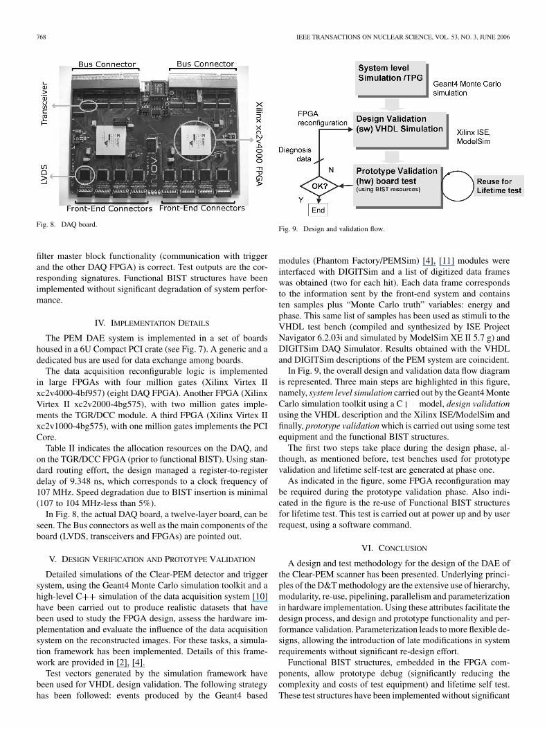
Fig. 8. DAQ board.
filter master block functionality (communication with triggerand the other DAQ FPGA) is correct. Test outputs are the cor-responding signatures. Functional BIST structures have beenimplemented without significant degradation of system perfor-mance.
IV. IMPLEMENTATION DETAILS
The PEM DAE system is implemented in a set of boardshoused in a 6U Compact PCI crate (see Fig. 7). A generic and adedicated bus are used for data exchange among boards.
The data acquisition reconfigurable logic is implementedin large FPGAs with four million gates (Xilinx Virtex IIxc2v4000-4bf957) (eight DAQ FPGA). Another FPGA (XilinxVirtex II xc2v2000-4bg575), with two million gates imple-ments the TGR/DCC module. A third FPGA (Xilinx Virtex IIxc2v1000-4bg575), with one million gates implements the PCICore.
Table II indicates the allocation resources on the DAQ, andon the TGR/DCC FPGA (prior to functional BIST). Using stan-dard routing effort, the design managed a register-to-registerdelay of 9.348 ns, which corresponds to a clock frequency of107 MHz. Speed degradation due to BIST insertion is minimal(107 to 104 MHz-less than 5%).
In Fig. 8, the actual DAQ board, a twelve-layer board, can beseen. The Bus connectors as well as the main components of theboard (LVDS, transceivers and FPGAs) are pointed out.
V. DESIGN VERIFICATION AND PROTOTYPE VALIDATION
Detailed simulations of the Clear-PEM detector and triggersystem, using the Geant4 Monte Carlo simulation toolkit and ahigh-level C simulation of the data acquisition system [10]have been carried out to produce realistic datasets that havebeen used to study the FPGA design, assess the hardware im-plementation and evaluate the influence of the data acquisitionsystem on the reconstructed images. For these tasks, a simula-tion framework has been implemented. Details of this frame-work are provided in [2], [4].
Test vectors generated by the simulation framework havebeen used for VHDL design validation. The following strategyhas been followed: events produced by the Geant4 based
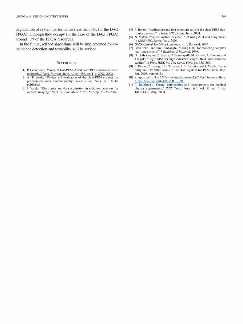
Fig. 9. Design and validation flow.
modules (Phantom Factory/PEMSim) [4], [11] modules wereinterfaced with DIGITSim and a list of digitized data frameswas obtained (two for each hit). Each data frame correspondsto the information sent by the front-end system and containsten samples plus “Monte Carlo truth” variables: energy andphase. This same list of samples has been used as stimuli to theVHDL test bench (compiled and synthesized by ISE ProjectNavigator 6.2.03i and simulated by ModelSim XE II 5.7 g) andDIGITSim DAQ Simulator. Results obtained with the VHDLand DIGITSim descriptions of the PEM system are coincident.
In Fig. 9, the overall design and validation data flow diagramis represented. Three main steps are highlighted in this figure,namely, system level simulation carried out by the Geant4 MonteCarlo simulation toolkit using a C model, design validationusing the VHDL description and the Xilinx ISE/ModelSim andfinally, prototype validation which is carried out using some testequipment and the functional BIST structures.
The first two steps take place during the design phase, al-though, as mentioned before, test benches used for prototypevalidation and lifetime self-test are generated at phase one.
As indicated in the figure, some FPGA reconfiguration maybe required during the prototype validation phase. Also indi-cated in the figure is the re-use of Functional BIST structuresfor lifetime test. This test is carried out at power up and by userrequest, using a software command.
VI. CONCLUSION
A design and test methodology for the design of the DAE ofthe Clear-PEM scanner has been presented. Underlying princi-ples of the D&T methodology are the extensive use of hierarchy,modularity, re-use, pipelining, parallelism and parameterizationin hardware implementation. Using these attributes facilitate thedesign process, and design and prototype functionality and per-formance validation. Parameterization leads to more flexible de-signs, allowing the introduction of late modifications in systemrequirements without significant re-design effort.
Functional BIST structures, embedded in the FPGA com-ponents, allow prototype debug (significantly reducing thecomplexity and costs of test equipment) and lifetime self test.These test structures have been implemented without significant
LEONG et al.: DESIGN AND TEST ISSUES 769
degradation of system performance (less than 5%, for the DAQFPGA), although they occupy (in the case of the DAQ FPGA)around of the FPGA resources.
In the future, refined algorithms will be implemented for co-incidence detection and testability will be revised.
REFERENCES
[1] P. Lecoq and J. Varela, “Clear-PEM, A dedicated PET camera for mam-mography,” Nucl. Instrum. Meth. A, vol. 486, pp. 1–6, 2002, 2002.
[2] A. Trindade, “Design and evaluation of the clear-PEM scanner forpositron emission mammography,” IEEE Trans. Nucl. Sci., to bepublished.
[3] J. Varela, “Electronics and data acquisition in radiation detectors formedical imaging,” Nucl. Instrum. Meth. A, vol. 527, pp. 21–26, 2004.
[4] P. Bento, “Architecture and first prototype tests of the clear-PEM elec-tronics systems,” in IEEE MIC, Rome, Italy, 2004.
[5] N. Matela, “System matrix for clear-PEM using ART and linograms,”in IEEE MIC, Rome, Italy, 2004.
[6] OMG-Unified Modeling Language, v1.5, Rational, 2003.[7] Bran Selic1 and Jim Rumbaugh2, “Using UML for modeling complex
real-time systems,” 1 Realtime, 2 Rational, 1998.[8] G. Hetherington, T. Fryars, N. Tamarapalli, M. Kassab, A. Hassan, and
J. Rajski, “Logic BIST for large industrial designs: Real issues and casestudies,” in Proc. IEEE Int. Test Conf., 1999, pp. 358–367.
[9] P. Bento, C. Leong, I. C. Teixeira, J. P. Teixeira, and J. Varela, Testa-bility and DfT/DfD Issues of the DAE System for PEM, Tech. Rep.Jan. 2005, version 3.1.
[10] S. Agostinelli, “GEANT4—A simulation toolkit,” Nucl. Instrum. Meth.A, vol. 506, pp. 250–303, 2003, 1995.
[11] P. Rodrigues, “Geant4 applications and developments for medicalphysics experiments,” IEEE Trans. Nucl. Sci., vol. 51, no. 4, pp.1412–1419, Aug. 2004.