DES MOD IGN AN DULE VYS ND IMP OKÉ U PLEME UČENÍ ...
92
DES MOD NÁVRH MAST DIPLOM AUTH AUTOR SUPE VEDOUC BRNO 2 IGN AN DULE A VÝROBA TER’S TH MOVÁ PRÁC HOR PRÁCE ERVISOR CÍ PRÁCE 2012 VYS BRNO U FAKU ÚSTA BIOM FACULT INSTITU BIOMEC ND IMP KAMEROVÉ HESIS E B R d OKÉ U UNIVERSITY ULTA STR AV MECH ECHANIK TY OF MECH UTE OF SOL CHANICS PLEME ÉHO MODUL Bc. OND doc. Ing. UČENÍ T OF TECHNO ROJNÍHO HANIKY T KY HANICAL EN LID MECHAN NTATIO LU ŘEJ VOK ROBERT TECHN OLOGY O INŽENÝ TĚLES, M NGINEERING NICS, MECH ON OF KOUN T GREPL NICKÉ V ÝRSTVÍ MECHATR G HATRONICS F CAME L, Ph.D. V BRN RONIKY AND ERA Ě A
-
Upload
khangminh22 -
Category
Documents
-
view
2 -
download
0
Transcript of DES MOD IGN AN DULE VYS ND IMP OKÉ U PLEME UČENÍ ...

DESMODNÁVRH
MASTDIPLOM
AUTHAUTOR
SUPEVEDOUC
BRNO 2
IGN ANDULE
A VÝROBA
TER’S THMOVÁ PRÁC
HOR PRÁCE
ERVISORCÍ PRÁCE
2012
VYSBRNO U
FAKUÚSTABIOM FACULTINSTITUBIOMEC
ND IMP
KAMEROVÉ
HESIS E
B
R d
OKÉ UUNIVERSITY
ULTA STRAV MECH
ECHANIK
TY OF MECHUTE OF SOLCHANICS
PLEME
ÉHO MODUL
Bc. OND
doc. Ing.
UČENÍ TOF TECHNO
ROJNÍHOHANIKY TKY
HANICAL ENLID MECHAN
NTATIO
LU
ŘEJ VOK
ROBERT
TECHNOLOGY
O INŽENÝTĚLES, M
NGINEERINGNICS, MECH
ON OF
KOUN
T GREPL
NICKÉ V
ÝRSTVÍ MECHATR
G HATRONICS
F CAME
L, Ph.D.
V BRN
RONIKY
AND
ERA
Ě
A

Vysoké učení technické v Brně, Fakulta strojního inženýrství Ústav mechaniky těles, mechatroniky a biomechaniky Akademický rok: 2011/2012
ZADÁNÍ DIPLOMOVÉ PRÁCE student(ka): Bc. Ondřej Vokoun který/která studuje v magisterském navazujícím studijním programu obor: Mechatronika (3906T001) Ředitel ústavu Vám v souladu se zákonem č.111/1998 o vysokých školách a se Studijním a zkušebním řádem VUT v Brně určuje následující téma diplomové práce:
Návrh a výroba kamerového modulu v anglickém jazyce:
Design and implementation of camera module Stručná charakteristika problematiky úkolu: Práce se bude zabývat návrhem jednoduchého a levného kamerového modulu s vlastním zpracováním dat. Předzpracování dat bude provedeno pomocí FPGA, následné zpracování a komunikace s nadřazeným systémem pomocí mikrokontroléru PIC (RS232, CAN). Typickou úlohou modulu bude nalezení několika "bílých" bodu na "tmavém" pozadí. Cíle diplomové práce: 1) Rešerše dostupných kamerových modulu, rešerše možných způsobů komunikace modulu a mikrokontroléru. Výběr kamerového modulu. 2) Definice dílcích úloh a návrh vhodného rozdělení výpočetního výkonu mezi FPGA a PIC. 3) Implementace algoritmu do FPGA, PIC. 4) Důkladné otestování vlastností navrženého systému včetně dokumentace experimentů.
Seznam odborné literatury: [1] http://www.electronics123.com/s.nl/sc.8/category.241/.f [2] http://cgm.cs.mcgill.ca/~godfried/teaching/pr-web.html [3] PIC32 Starter Kit User’s Guide [4] Xilinx - System generator for DSP Vedoucí diplomové práce: doc. Ing. Robert Grepl, Ph.D. Termín odevzdání diplomové práce je stanoven časovým plánem akademického roku 2011/2012. V Brně, dne 29.11.2011
L.S.
_______________________________ _______________________________ prof. Ing. Jindřich Petruška, CSc. prof. RNDr. Miroslav Doupovec, CSc., dr.h.c.
Ředitel ústavu Děkan fakulty
Abstrakt Cílem diplomové práce je navrhnout levný, avšak dostatečně výkonný a univerzální systém, schopný snímání a zpracování obrazu z digitální kamery. Další částí je návrh a implementace funkcí pro zpracování obrazu a komunikace s nadřazeným systémem. Klíčová slova: CMOS, digitální kamera, zpracování obrazu, FPGA, PIC, SCCB, RGB Bayer interpolace, UART
Abstract Master thesis is aimed on the design of cheap and universal system, but also powerful enough to be able to obtain and process images from the digital camera sensor. Further part of the work is design and implementation of functions for image processing applications and communication with superior system. Keywords: CMOS, FPGA, image processing, digital camera, SCCB, RGB Bayer interpolation, UART
Bibliographical citation of thesis VOKOUN, O. Design and implementation of camera module. Brno: Brno University of Technology, Faculty of mechanical Engineering, 2012. 92 p. Supervisor. Ing. Robert Grepl, Ph.D.. Affidavit I announce that I have produced this master thesis on my own, with guidance of my supervisor and all used resources are listed at the end of the thesis. Ondřej Vokoun, Brno, 2012 …..………………..

Acknowledgements I would like to thanks to all those who let and helped me to create this thesis, especially my family for huge support and my supervisor doc. Ing. Robert Grepl Ph.D. for guidance.
- 8 -
Content: 1. Introduction .............................................................................................................. 10
Initial thesis assignment: .................................................................................................................................. 10 2. Problem analysis ....................................................................................................... 11
2.1. Camera module selection .................................................................................................................... 11 2.1.1. Notes ........................................................................................................................................... 11 2.1.2. Comparison of cameras .............................................................................................................. 12 2.1.3. Resume for camera selection ..................................................................................................... 13
2.2. Interface design ................................................................................................................................... 15 2.2.1. Communication ........................................................................................................................... 15 2.2.2. Direct connection ........................................................................................................................ 17 2.2.3. Indirect connection with FIFO buffer .......................................................................................... 22 2.2.4. Resume for interface design ....................................................................................................... 24
2.3. Possible image processing tasks .......................................................................................................... 24 2.4. Timing - Performance .......................................................................................................................... 25
2.4.1. Data specification ....................................................................................................................... 25 2.4.2. Manufacturers specification – data stream and pattern ............................................................ 27 2.4.3. Resume for the performance and timing ................................................................................... 33
2.5. Simulation results for PIC32 and sample BW image ............................................................................ 34 2.5.1. Test grayscale image ................................................................................................................... 34 2.5.2. Simulation program - Center of gravity in 2D of simple object .................................................. 34 2.5.3. Resume for the simulation test .................................................................................................. 37
2.6. Operation with camera and MF624 .................................................................................................... 38 2.6.1. Real-time toolbox (RTT) and real-time windows target (RTWT) ................................................. 38 2.6.2. Resume ....................................................................................................................................... 39
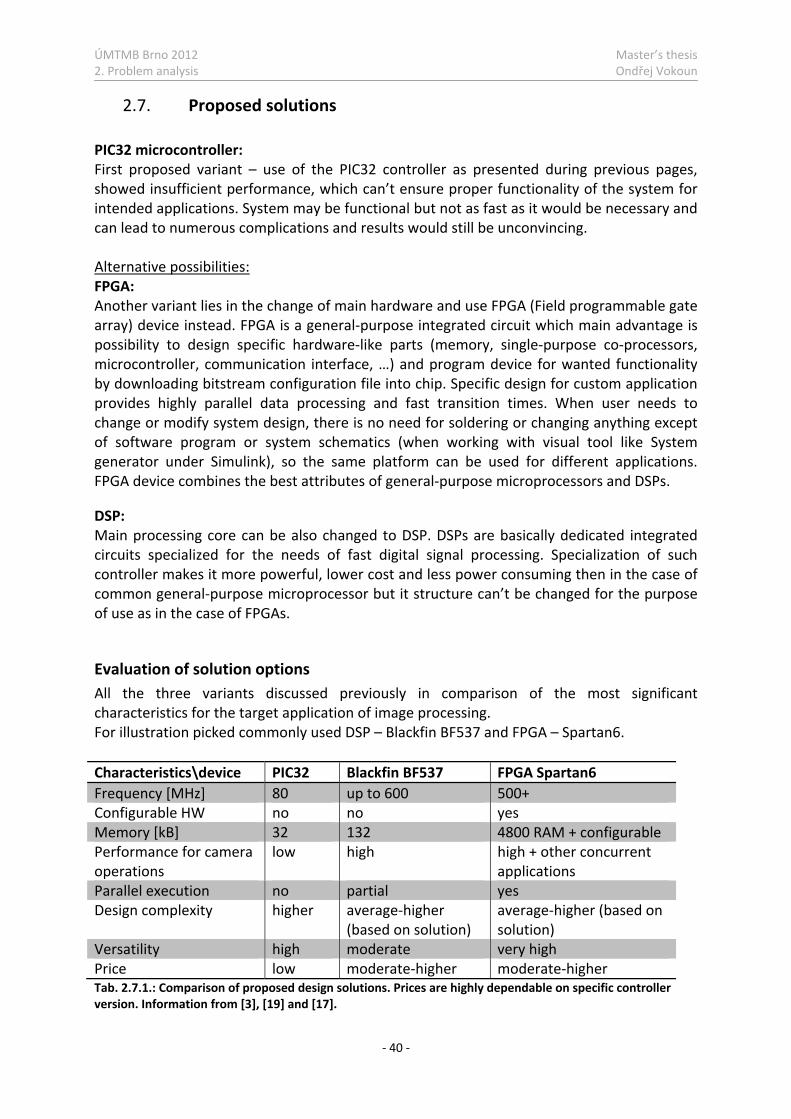
2.7. Proposed solutions .............................................................................................................................. 40 Evaluation of solution options ..................................................................................................................... 40
3. Formulation of the new thesis assignment ................................................................ 41
3.1. Justification .......................................................................................................................................... 41 3.2. Draft of the new thesis assignment ..................................................................................................... 41 3.3. Final approved assignment .................................................................................................................. 41
4. System implementation design ................................................................................. 42
4.1. Hardware implementation .................................................................................................................. 42 4.2. Software design with System generator under Simulink .................................................................... 44
4.2.1. Overall system design ................................................................................................................. 45 4.2.1.1. Camera input domain ........................................................................................................ 46 4.2.1.2. System domain ................................................................................................................... 48 4.2.1.3. Drive camera block ............................................................................................................. 49
5. Image Preprocessing and Processing ......................................................................... 51
5.1. RGB interpolation from RAW Bayer RGB ............................................................................................. 51 5.2. Color RGB into black and white conversion ........................................................................................ 55 5.3. BW image segmentation ..................................................................................................................... 56 5.4. Color segmentation ............................................................................................................................. 63 5.5. COG of standalone object .................................................................................................................... 65
6. Communication ......................................................................................................... 68
6.1. SCCB communication interface ........................................................................................................... 68 6.2. UART communication .......................................................................................................................... 70

- 9 -
6.2.1. Transmitter – FPGA ..................................................................................................................... 70 6.2.2. Receiver – computer ................................................................................................................... 72
7. Software and hardware simulations of the FPGA designed system ........................... 75
7.1. Simulation in Matlab-Simulink ............................................................................................................ 76 7.1.1. Software simulation in Simulink ................................................................................................. 76 7.1.2. HW-cosimulation under Simulink ............................................................................................... 78 7.1.3. Timing and power analysis .......................................................................................................... 78
7.2. Simulation in Xilinx ISE ......................................................................................................................... 80 7.2.1. ISim ............................................................................................................................................. 80 7.2.2. ChipScope ................................................................................................................................... 82
7.3. Simulation and results of real implemented system ........................................................................... 84 8. Results and evaluation .............................................................................................. 87 9. Bibliography .............................................................................................................. 90 Appendix A – Used abbreviations ..................................................................................... 91 Appendix B – List of enclosed files .................................................................................... 92
ÚMTMB Brno 2012 Master’s thesis 1. Introduction Ondřej Vokoun
- 10 -
1. Introduction
Initial motivation of solving problems is usually person’s will to create something new, challenging and interesting to be concerned with. Problem about camera operations and image recognition is usually helpful and usable in variety of driving and automate regulation applications in robotics, mechatronics and of course, then also in products for everyday life. Main goal of this thesis is development of image processing camera system (IPCAM), supervised under the Mechlab – Mechatronics laboratory at Brno University of Technology. IPCAM system should be created as the universal system for possibility of further arbitrary modifications and simple reconfiguration by the students for image processing applications or vision and motion systems. Whole problematic is very complex and consists of several different areas, including:
• hardware design (camera selection and connection with controller) • communication between camera and controller • data acquisition from the camera • software design of the system • data preprocessing and processing • communication with superior devices
Initial thesis assignment: Objectives that should be reached: - appropriate camera module selection - connection of camera module and PIC microcontroller - example of simple SW implementation - implementation of communication over serial line Problem characteristics: Main target of the work is design of simple and cheap camera module with own data processing. Assumed usage of B&W CMOS sensor and own data processing in the PIC microcontroller. PIC should be programmed by the c-code generated from Simulink model. This access represents modern technique for mechatronics systems design. Part of the work will be implementation of simple algorithm for: “searching for the dark object on the bright background”. Camera system should communicate with the superior system over serial link.

ÚMTMB Brno 2012 Master’s thesis 2. Problem analysis Ondřej Vokoun
- 11 -
2. Problem analysis
2.1. Camera module selection At the beginning of the given assignment that involves real hardware, it’s necessary to define what kind of hardware needs to be used to fulfill expectations and goals of given task. In the first part, we need to pick optimal camera module that will fit to our design.
2.1.1. Notes a) Cam. sensor types CCD:
• better quality (uniformity) than CMOS • lower noise, higher sensitivity and dynamic range • lower sensor complexity vs. higher system complexity
CMOS:
• lower power demands and price than CCD • possibility to pick and send only a part of a scanning area (window-of-interest
readout) for motion detection or target tracking • better response and higher speed • inbuilt basic image processing circuits • newer designs are equal in image quality with CCD • higher sensor complexity vs. lower system complexity
b) Field of final use Still camera:
• bigger image sensor with higher resolution for better picture quality • rewritable fast memory buffer for picture processing before storing • another big memory storage where to save encoded images (or just raw data) or
communication channel for sending the whole pictures out • usage aimed on the creation of natural-like pictures with rich colors • unnecessary to obtain more than just a few pictures/frames per second(FPS)
Camera for image processing, recognition or navigation (IPCAM):
• lower resolution of image sensor, aimed on higher frame rates, not quality • emphases on fast transfers and small delays, fast processing of obtained data from
the sensor during receiving process • fast memory buffer/buffers for the needs of image processing routines, huge storage
for the whole images is usually unnecessary • used in color or monochromatic mode based on intended application
ÚMTMB Brno 2012 Master’s thesis 2. Problem analysis Ondřej Vokoun
- 12 -
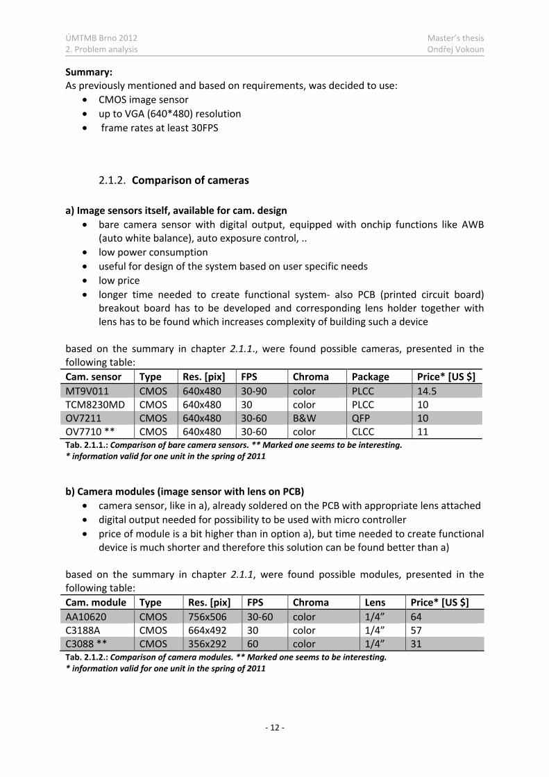
Summary: As previously mentioned and based on requirements, was decided to use:
• CMOS image sensor • up to VGA (640*480) resolution • frame rates at least 30FPS
2.1.2. Comparison of cameras a) Image sensors itself, available for cam. design
• bare camera sensor with digital output, equipped with onchip functions like AWB (auto white balance), auto exposure control, ..
• low power consumption • useful for design of the system based on user specific needs • low price • longer time needed to create functional system- also PCB (printed circuit board)
breakout board has to be developed and corresponding lens holder together with lens has to be found which increases complexity of building such a device
based on the summary in chapter 2.1.1., were found possible cameras, presented in the following table: Cam. sensor Type Res. [pix] FPS Chroma Package Price* [US $] MT9V011 CMOS 640x480 30-90 color PLCC 14.5 TCM8230MD CMOS 640x480 30 color PLCC 10 OV7211 CMOS 640x480 30-60 B&W QFP 10 OV7710 ** CMOS 640x480 30-60 color CLCC 11 Tab. 2.1.1.: Comparison of bare camera sensors. ** Marked one seems to be interesting. * information valid for one unit in the spring of 2011
b) Camera modules (image sensor with lens on PCB)
• camera sensor, like in a), already soldered on the PCB with appropriate lens attached • digital output needed for possibility to be used with micro controller • price of module is a bit higher than in option a), but time needed to create functional
device is much shorter and therefore this solution can be found better than a) based on the summary in chapter 2.1.1, were found possible modules, presented in the following table: Cam. module Type Res. [pix] FPS Chroma Lens Price* [US $] AA10620 CMOS 756x506 30-60 color 1/4” 64 C3188A CMOS 664x492 30 color 1/4” 57 C3088 ** CMOS 356x292 60 color 1/4” 31 Tab. 2.1.2.: Comparison of camera modules. ** Marked one seems to be interesting. * information valid for one unit in the spring of 2011

ÚMTMB Brno 2012 Master’s thesis 2. Problem analysis Ondřej Vokoun
- 13 -
c) So-called smart cameras (module + controller + others) • already created system with all necessary items like camera module, controller,
memory, communication module and predefined functions for image capturing and operations
• user isn’t usually allowed to modify hardware, but whole system is working from the beginning and user can concentrate on image processing instead of HW design
• this solution is much more expensive than both previously mentioned options, but amount of HW design and programming itself is several times lower – just “plug and play”
S.C. uC/MHz Res. FPS I/O ports Program. Price*[$] NI 1722 PowerPc/400 640x480 60 Dig.I/O, RS232, Ethernet LabVIEW 2600 leanXcam DSP/500 752x480 60 Dig.I/O, RS232, Ethernet C 437 Tab. 2.1.3.:Comparison of smart cameras. leanXcam seems to be interesting. * information valid for one unit in the spring of 2011
2.1.3. Resume for camera selection Use of bare sensor gives us opportunity to implement complete system the way we design and gives us then full control over the operations of image pre- and processing. On the other hand, everything has to be done by the user and nothing is prepared to make device faster operational. Price of the whole system is the lowest from discussed options, but together with price, extensive development time has to be also taken in account (hardware and software development + testing). Camera module has the same advantages as the use of bare sensor, but sensor is already soldered on the PCB and we can’t use it on one board together with microcontroller and other necessary modules for possibility to create compact and small camera system. In the comparison with bare sensor - time to create working system is lower because one doesn’t need to design own PCB and search for appropriate lens. Difference in prices between solution a) and b) isn’t so high when we take on mind amount of saved development time. Smart cameras are definitely easier to be implemented and are for sure working without need of hours and hours of HW designing and programming just to make system running. Smart cameras are also equipped with the large library of image processing and analysis routines from the manufacturer (edge detection, object classification, …), which leads to significant decrease of time period to create functional system. Another possibility is to search for the commercially offered Webcam with the known image sensor that can be used to be connected to PIC32 Starter Kit

ÚMTMB Brno 2012 Master’s thesis 2. Problem analysis Ondřej Vokoun
- 14 -
Solution Selection: design requirements:
• low price • higher frame rates to be able to work with the real dynamic systems • appropriate time to create functional system • possibility to connect and control the camera with PIC32 controller • possibility to use color mode
Summary: After consideration of facts from previously mentioned chapter 2. and design requirements
→ picked option 2.1.2. b) Camera module → especially Camera C3088, which was available for design
Fig. 2.1.3.1.: Picture of C3088 camera module with lens attached.
Advantages/disadvantages: + cmos color sensor, which can be used alternatively in color or black/white mode + already created camera module with appropriate lens attached + good documentation + wide range of different modes and options of use, controlled by the user + needed input voltage is the same as the target controller is providing on the output (5VDC) + includes also analog output (useful for viewing the image while setting up the digital out.) - lower maximal image resolution (only CIF – 356x292) - older device with worse image quality +/- lens has aperture size only F2.8, which is good in the case of low-light conditions, but bad
for small depth of field C3088 module specification: Imager OV6620, CMOS sensor Array size 356x292 pixels Pixel size 9.0x8.2 μm Scanning Progressive Effective image area 3.1x2.5 mm Electronic exposure 500:1 Gamma correction 0.45/0.55/1.0 Min illumination [email protected] Dark current <0.2 nA/cm2 Dynamic range 72dB Operation Voltage 5 VDC Operation current Active 80mW/ standby 30μW Lens (optional) F2.8 Tab. 2.1.4.: Table of camera C3088 specification. Adopted from [7].

ÚMTMB Brno 2012 Master’s thesis 2. Problem analysis Ondřej Vokoun
- 15 -
Camera sensor OV6620 features: Camera sensor OV6620 features: • 101,376 pixels, 1/4” lens, CIF/QCIF format• Read out - progressive / Interlace • Data format - YCrCb 4:2:2, GRB 4:2:2, RGB
Raw Data • 8/16 bit video data: CCIR601, CCIR656, ZV
port • frame rates up to 60 fps • Wide dynamic range, anti-blooming, zero
smearing • Monochrome composite video signal
output (50 Hz)
• SCCB (Serial Camera Control Bus) interface • Electronic exposure / Gain / white balance
control • Image enhancement - brightness, contrast,
gamma, saturation, sharpness, window, etc.• Internal / external synchronization scheme • Frame exposure / line exposure option • 5 Volt operation, low power dissipation • Small size: 40 x 28 mm
Tab. 2.1.5.: OV6620 camera sensor features. Adopted from [6]
2.2. Interface design Pic32 Starter Kit gives us possibility to create at least two different solutions of connection between camera module and controller. Two of the most promising designs will be introduced and described below and than one will be picked for the final construction. As a reference camera sensor was picked Omnivision product – OV6620 as can be found on C3088 camera module and HW design will be based on the possibilities of this device. When speaking broadly about data transfer, we have to consider also various possibilities of data formats that can be used and are provided by the image sensor - YCrCb 4:2:2, GRB 4:2:2, RGB Raw Data, and so on. Based on the type of application should be picked the one to provide the best results in desired task (amount of data, speed, image quality …). We have also several methods of data scanning from sensor- interlaced and progressive, where interlaced is used usually in analog TV’s and broadcasting, when scanning odd and even lines occurs in two different consequent times (so refresh rate can be visibly taken as twice as high). When progressive method is being used (usually in computer applications like camera vision, LCD’s and so on), all the lines are scanned and processed (whole image) during one cycle. But for image processing (IP), progressive scanning is definitely the one that should be used.
2.2.1. Communication At first, very important decision on the base of communication has to be made. We can think of data transfer in two different methods: A) Serial communication
• data sent one bit after another in a sequence through one channel/cable/bus…

ÚMTMB Brno 2012 Master’s thesis 2. Problem analysis Ondřej Vokoun
- 16 -
• used for longer distances and when there is no space for more cables or lines and also this solution is cheaper because number of pins and cables is reduced
• problem with this type of communication is timing- to clearly distinguish between each data bit, timing is determined by another channel with clock signal or previously set the same communication speed for sending and receiving device
• in comparison with parallel communication - serial can’t send more data per a clock cycle, but on the other hand, transfer rates can be increased by faster clocking because there is no need to synchronize all the channels together, just one, and also better insulation around one cable/channel develops less noise affecting the data path
B) Parallel communication • whole data information (created from several bits) can be send simultaneously
during one clock cycle through the several data paths (number of data paths equals to number of data bit length: 8bit word -> 8 data lines) and together with data information, clock signal for data validation is also send through another line
• implementation of parallel communication is easier without need for complex signal arbitration (incoming data are valid on the rising/falling clock edge)
• used usually on shorter distances to avoid loses of data because of interference between several data lines and other noise sources
• in such application as working with camera, this communication can be taken more suitable and faster and data can be obtained and processed in fewer clock cycles with less controller operations, which increases final performance
• usually, small camera modules and other devices like memory that can be connected to microcontroller are equipped with parallel port and not serial
Summary: As camera module, together with PIC32 controller are both equipped with parallel data interface, and parallel data transfer seems to be faster and easier to be implemented here. Then parallel communication will be used for data exchange and serial won’t be discussed later for this purpose.
Fig. 2.2.1.1.: Figure showing different methods of one-way serial communication.
destination source data clock
source (defined comm. speed)
destination (defined comm. speed)
data
sourcen-bit data bus clock
destination
Fig. 2.2.1.2.: Image showing one-way parallel communication with n-bit wide data bus and clock signal for data validation.

ÚMTMB Brno 2012 Master’s thesis 2. Problem analysis Ondřej Vokoun
- 17 -
But both of these devices are also equipped with inter integrated circuit (I2C), which is a “multi-master, serial, single-ended computer bus”. But object of this interface is control and communication between devices, therefore it’s not possible to be used for data transfer.
2.2.2. Direct connection Principle of direct connection on hardware level lies in “simple” interconnection between two essential parts for camera design – camera sensor and controller. Connection diagram with necessary signals and relevant ports of the both devices is graphically presented on Fig. 2.2.2.1. with detailed explanation under the figure. When direct connection is used, we have two different methods for how to obtain the data, or how to access each of the components – camera can be set alternatively in master or slave mode, which brings different behavior of the system. Both options will be discussed later in this subchapter. But for both options the same rule can be applicable – the camera output frame rate should be set to be as fast, as the controller is able to process without losses of the data (e.g. pixels in here). Which means, the time between two incoming neighbor values has to be big enough, that controller is able to process them the way as expected and return back to the waiting state for another incoming value. In direct type of connection, no addressing of data is necessary, so parallel address port can be left unused. Interconnection specification from Fig. 2.2.2.1.: A) External clock (XCLK1 <> RD0):
Camera module needs certain input clock frequency for correct functionality, desired operational frequency is based on the camera module and lies between 10 and 30 MHz. This value also affects frame rate of outputted data from camera. Camera has already
XCLK1 SIO-1, SIO-0
RESET
Y[0:7]/Y[0:7]+UV[0:7]
PCLK HREF
VSYNC
Camera module OV6620
GND VDD
Fig. 2.2.2.1.: Schematic of direct connection between camera module and PIC32 Starter Kit.
external clock I2C interface reset data[0:7]/[0:15] pixel clock horizontal synch. vertical synch.
RD0 SCL1, SDA1 RA5 PMPD[0:7]/ PMPD[0:15] PMPWR PMPCS1 RA0 +5V_EXT
PIC32 Starter Kit - controller

ÚMTMB Brno 2012 Master’s thesis 2. Problem analysis Ondřej Vokoun
- 18 -
crystal with 17.73MHz soldered, but in the case when there is a request to change frame rate, it’s possible to unsolder this crystal and feed camera with another clock frequency. PIC32 is able to generate desired clock frequency by generating PWM signal, so PWM port can be connected to camera. PIC32 starter kit provides possibility to store duty cycle values for PWM in a memory and with the use of DMA to provide PWM signal without wasting controller computational capacity.
B) I2C interface (SIO-1, SIO-0 <> SCL1, SDA1): I2C interface is serial interface that both devices support for control operations (although OV camera is equipped with the serial camera control bus (SCCB), but this platform is similar to I2C). SCL1 port on PIC32 sends signal for correct data reconstruction into SIO-1 port of the camera. While PIC port SDA1 and SIO-1 on the camera serves for bi-directional control data exchange. Control can be used for example for setting output data format, frame speed, scanning window size, white balance, exposure control and so on.
C) Reset (Reset <> RA5): Reset, when triggered to high from low, serves for resetting whole chip into default mode, including all registers. This function is optional and for connection with PIC32 can be used GPIO port (for example suggested RA5).
D) Data bus (Y[0:7]/Y[0:7]+UV[0:7] <> PMPD[0:7]/ PMPD[0:15]): Data exchange is the crucial part and high demands on data transfer rates and also transfer data correctness are submit. Camera uses two 8-bit wide parallel ports and PIC32 is equipped with 16-bit wide parallel master port (PMP). When used only 8-bit port “Y” on the camera, then user has choice of color mode operation or monochromatic (B&W) mode. Monochromatic mode is definitely the fastest one in the way of the less arithmetical operations needed to get one valid pixel from obtained data, regarding to the sensor array structure. If operating in color mode, amount of data is the same as when operating in 16-bit configuration, but here we can say that necessary data for one pixel are incoming almost serially and then additional arithmetical operations takes further time to generate appropriate pixel. When together with “Y” port also used 8-bit “UV” port, we have then 16-bits and it’s supposed to work in color mode. Data are coming from two ports at once, so fewer cycles are needed to process this data, but still don’t forget about more arithmetical operations in comparison with B&W mode.
E) Pixel clock (PCLK <> PMPWR): PCLK port on the camera is streaming out clock signal that informs about data updates on the data port. When connected to PMPWR port, which serves as write signal on the parallel port, target device can notice the event of new incoming data and store them into suitable register to make them available for further operations.
F) Horizontal sync (HSYNC <> PMPCS1): When camera pixel clock signal is used as a write signal for notification of ready data on the controllers input port, then exists also situations where such a data are not valid or
ÚMTMB Brno 2012 Master’s thesis 2. Problem analysis Ondřej Vokoun
- 19 -
not wanted. Because camera is bursting out pixel clock signal synchronously, with no respect to data presence, horizontal synchronization has to be used to validate correctness of incoming data. Then we can say that data are valid and present on the port, therefore possible to be read only if HSYNC signal is set high and at the same time PCLK informs about presence.
G) Vertical sync (VSYNC <> RA0): Optional connection for vertical synchronization output, which serves, on a rising edge, as an information about beginning of a new frame. Can be left unused (if not needed) and in design connected to GPIO port (for example suggested RA0).
Possible maximal image resolution Very crucial part in every image processing application is image resolution and frame rate of incoming scanned images. Both of these characteristics depend on each other and based on type of requests for desired application and computational capacity available: higher resolution is picked for better quality or lower resolution in order to get higher frame rates. When picture resolution is higher, then logically amount of data is higher during the same time period and higher frame rate also results in the same way. Possible maximal frame rate in dependence on image resolution will be discussed later in Performance tests section and won’t be mentioned here. Image resolution is in this case of system design limited only by the resolution of used camera sensor and by the computational capacity of the controller. No other limitation comes from this solution, as any other hardware is involved in data transfers between camera and controller before direct processing without data storing. When speaking about operational mode of devices, we can discuss two possibilities: Master camera operation and slave parallel port (PSP) Camera is by the default settings working as the master unit - so data and reference signals are sent in the requested frame speeds (set by the incoming clock frequency and I2C configuration) with no feedback from the other side if everything was accepted right. And as mentioned earlier, data processing by the controller has to be faster than camera is sending the data out. But when all the functions are set correctly, this can be easier task because controller just initiates the camera and after this procedure has nothing else on schedule than obtaining and processing of incoming data. One problem could be mentioned with this connection – as referred in specification of PIC32, PIC32 provides only possibility to work with 8-bit data width on PSP (when parallel port is set to be slave unit), cooperating with other master unit. Timing of data receiving process on PSP is demonstrated on the next figure Fig. 2.2.2.2., picture was assumed from microchip PSP manual.
ÚMTMB Brno 2012 Master’s thesis 2. Problem analysis Ondřej Vokoun
- 20 -
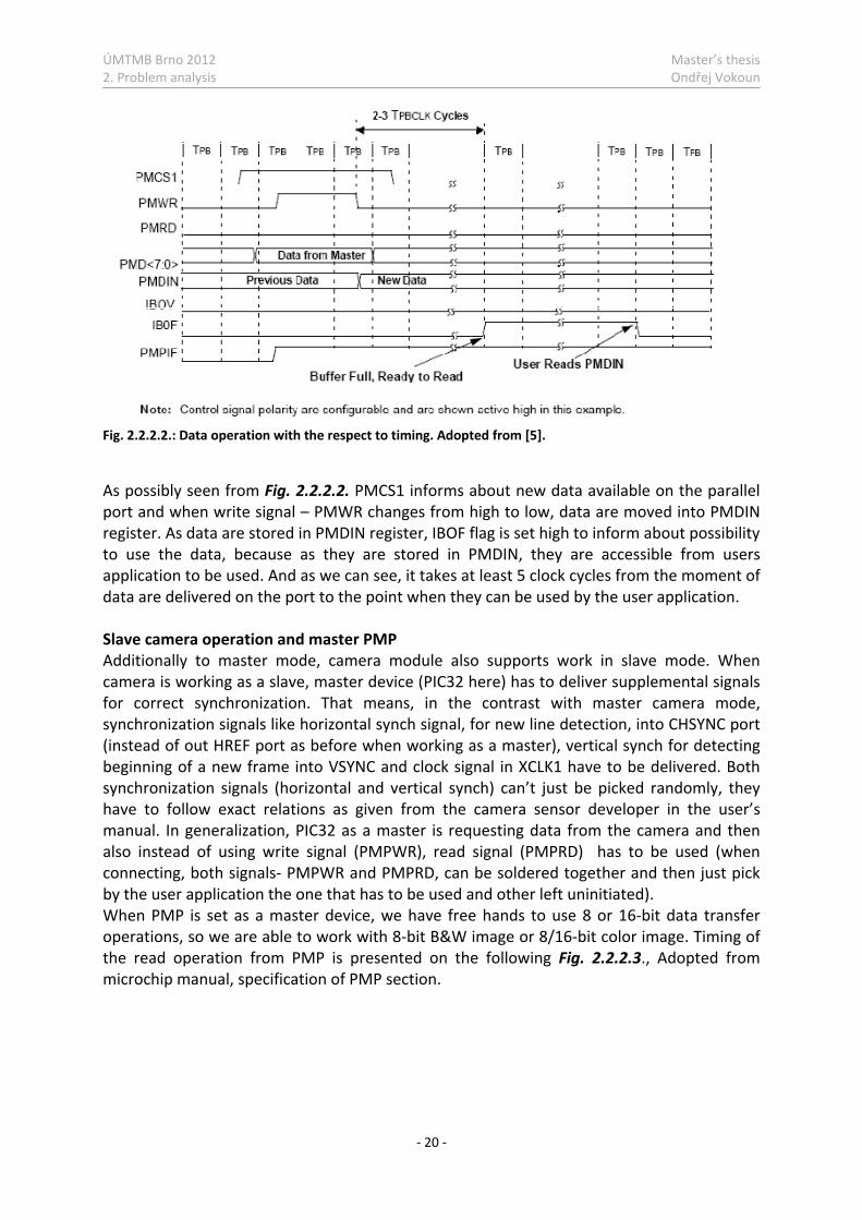
Fig. 2.2.2.2.: Data operation with the respect to timing. Adopted from [5].
As possibly seen from Fig. 2.2.2.2. PMCS1 informs about new data available on the parallel port and when write signal – PMWR changes from high to low, data are moved into PMDIN register. As data are stored in PMDIN register, IBOF flag is set high to inform about possibility to use the data, because as they are stored in PMDIN, they are accessible from users application to be used. And as we can see, it takes at least 5 clock cycles from the moment of data are delivered on the port to the point when they can be used by the user application. Slave camera operation and master PMP Additionally to master mode, camera module also supports work in slave mode. When camera is working as a slave, master device (PIC32 here) has to deliver supplemental signals for correct synchronization. That means, in the contrast with master camera mode, synchronization signals like horizontal synch signal, for new line detection, into CHSYNC port (instead of out HREF port as before when working as a master), vertical synch for detecting beginning of a new frame into VSYNC and clock signal in XCLK1 have to be delivered. Both synchronization signals (horizontal and vertical synch) can’t just be picked randomly, they have to follow exact relations as given from the camera sensor developer in the user’s manual. In generalization, PIC32 as a master is requesting data from the camera and then also instead of using write signal (PMPWR), read signal (PMPRD) has to be used (when connecting, both signals- PMPWR and PMPRD, can be soldered together and then just pick by the user application the one that has to be used and other left uninitiated). When PMP is set as a master device, we have free hands to use 8 or 16-bit data transfer operations, so we are able to work with 8-bit B&W image or 8/16-bit color image. Timing of the read operation from PMP is presented on the following Fig. 2.2.2.3., Adopted from microchip manual, specification of PMP section.

ÚMTMB Brno 2012 Master’s thesis 2. Problem analysis Ondřej Vokoun
- 21 -
Fig. 2.2.2.3.: Timing of 8/16-bit demultiplexed read operation on PMP set in master mode, no wait states included. Adopted from [5].
When PIC32 works in master mode, it is possible to see that data are requested from the master to be sent on the PMP, but from that part whole procedure is the same as before when working in slave mode. After end of read signal, user application can access new data from PMDIN register to be used. Summary: Direct connection camera design seems to be applicable in the system, which is intended to be used for “on-fly” data capture together with image processing routine, that are running in the highest priority and usually no other hardware for the operations with obtained data is needed in such system. Image resolution is in this case limited by the resolution of used camera sensor and by the computational capability of controller, together with desired frame rate of the image scanning. In the case of parallel execution of several applications, running on the same priority level as image processing and data capturing, unwanted behavior can occur when interrupt service routine allocates computational resources for different application. Which means some pixel values can be missed and then obtained data will be imprecise, we can more or less say that obtained data will be wrong. So in the case of multi-application use, different system design has to be used. Advantages/disadvantages: + direct connection without other HW/functional blocks promises fast data transfers + with less devices used, design implementation can be considered easier + universal solution - wide variety of different modes that can be used - when more than one application will be running, incoming data can be missed - if IP task demands more computational time in only several passages, overall frame rate is
reduced to don’t miss incoming data, although in some other parts core remains idle

ÚMTMB Brno 2012 Master’s thesis 2. Problem analysis Ondřej Vokoun
- 22 -
2.2.3. Indirect connection with FIFO buffer In contrast with direct connection, data path leads from camera (set to master mode) into memory storage, suitable for camera application is use of FIFO buffer (external FIFO chip or inner RAM memory of PIC32). Also pixel clock and horizontal synchronization signals from camera, together with write enable signal from controller can be used for setting write enable signal for FIFO to successfully store valid data into memory (external AND-gate logic would be necessary for the use with external FIFO). Then controller is accessing memory and requesting the oldest data (from the definition of FIFO buffer) in the frame rate as controller is able to process them. PIC32 (set to master mode) can use direct memory access (DMA) interface to redirect data from camera into onboard SRAM memory and then also pick stored data from SRAM and send them into controller for processing. DMA is running at the same speed level as controller itself and is designed to save computational capacity and increase overall performance, because for all the transfers by DMA, controller is idle or can perform other computations without being interrupted (DMA works independently).
Hardware connection (camera with Starter kit) in this case is the same as described in chapter 2.2.2 - Direct connection and won’t be repeated again. But instead of data leading from data bus directly into computational core, they are used by the DMA to be stored into memory and then later send finally into core. As FIFO option by itself isn’t mentioned in the reference manual from Microchip Company regarding to the use of DMA and memory, then addressing has to be used to ensure correct functionality for this application. Then function
XCLK1SIO-1, SIO-0
RESET
Y[0:7]/Y[0:7]+UV[0:7]
PCLKHREF
VSYNC
Camera module OV6620
GND VDD
RD0 SCL1, SDA1 RA5 PMPD[0:7]/ PMPD[0:15] PMPWR PMPCS1 RA0 +5V_EXT
PIC32
wr/rd event
DMA
SRAM
external clock I2C interface reset data[0:7]/[0:15] pixel clock horizontal synch. vertical synch.
thick arrow used to represent data transfers
thick gray arrow used to represent address transfers
Fig. 2.2.3.1.: Overall design of indirectly connected camera with controller with DMA used, with interconnections
ÚMTMB Brno 2012 Master’s thesis 2. Problem analysis Ondřej Vokoun
- 23 -
of FIFO can be implemented as part with fixed addresses in the memory, where incoming data would be saved one after another with rising address. Reading, to be sent into core, would be based on order numbering from counter in data processing part. After successful data process of one image, counter is reset and another image starts from the beginning. Also synchronization signals are used by the DMA - PCLK clock can be used together with HREF signal for triggering the write events. Detection of start or abort interrupt request events is done by the controller of DMA itself, independently on PIC32 or user intervention. User can provide write and read enable signals to start saving the data into memory and then requesting them for use. Possible maximal image resolution As in the previous case, we have to consider limitations coming from system design. In the system with indirect connection with memory involved, maximum image resolution is limited by the highest memory capacity available on PIC32 – when we discuss case, where all the incoming data of one image are stored in the memory and not overwritten during processing. RAM memory capacity: 32kB (2.2.3:1)
Then maximum image resolution that can fit into available memory, when for simplification taken 8bit precision for each image pixel (aspect ratio depends on the needs of target application, mentioned ratios were picked for illustration): 8bpp: 240 ∗ 120 ∗ 1 = 28.8 < 32 (2.2.3:2) 250 ∗ 120 ∗ 1 = 30 < 32 (2.2.3:3) 230 ∗ 138 ∗ 1 = 31.7 < 32 (2.2.3:4) As possibly seen from comparison of (2.2.3:1) and (2.2.3:2) - (2.2.3:4), usable image sizes aren’t really high, but for easier image processing tasks can be such a resolution big enough. Summary: Problem can occur, when data from camera are incoming faster than controller is able to process. At the beginning no data are lost, but later, as the memory capacity is overflowed by continuously increasing number of stored data, no new data can be stored, or old data are rewritten without being used. So information is then in this case corrupted and we can’t create valid image. Another problem can be immixture of separate image frames, or impossibility of start and end of the picture recognition when using the data from a “big pile” of data, when vertical synchronization wouldn’t be working synchronously with data processing by the controller. Then solution could be to use addressing of data in RAM as proposed in design or use VSYNC signal to set or reset counter, which would be counting number of pixels obtained and therefore to control where actual picture ends. But such function depends on actual design – if external FIFO used or internal ram with addressing. Advantages/disadvantages: + when computational demands changes over the whole frame, core can avoid idle states by
requesting next data from memory, if available and then to increase performance + processing of data can be done parallel with other processes as data are stored
ÚMTMB Brno 2012 Master’s thesis 2. Problem analysis Ondřej Vokoun
- 24 -
- additional HW leads to increase of transfer delays and probably decrease of frame rate - with additional HW, complexity of system design increases together with time to create
functional system
2.2.4. Resume for interface design Direct connection seems to be easier to be implemented and faster for data processing when used for basic tasks. Indirect connection provides possibility to perform more tasks at once as data are saved into memory without need of core assistance. Both design solutions presented (without external FIFO buffer), share the same hardware connections and swap between them can be done just by the change of control software. Easy change gives us opportunity to use different functional method for different image processing task to take advantage from such a design to fulfill requirements the best possible way. Final decision which approach fits better to the problem can be draft from the tests with real hardware in comparison with times between separate data transfers from camera together with processing time of a data.
2.3. Possible image processing tasks Image processing is wide and general problematic involving many different applications on camera system, then draft of several problems that could be possibly solved is presented as follows: Center of gravity (COG) of single object in 2D plane definition:
• main point of such a problem is searching for the center of single visible object and calculation its position in horizontal and vertical coordinates – relative coordinates (Euclidean distance between actual point and center of the visible camera plane, or other selected point in this plane) or absolute coordinates, bounded to certain outer coordinate system
notes: • task can be performed for both Monochromatic and color image • universal algorithm that can find COG of any object shape • extension of this problem can be sending information of object position to superior
driving equipment or storing this points to later provide trace of object movement • if needed for a real-time control, then as high as possible FPS also needed • computation can be fast (direct connection of camera and controller applicable)
Searching for the object of certain color: definition:
• main point is to find object of certain known color (or similar one) between several other objects with different colors
notes: • camera needs to be operating in color mode
ÚMTMB Brno 2012 Master’s thesis 2. Problem analysis Ondřej Vokoun
- 25 -
• required color can be picked from the library of basic predefined colors or by aiming with the camera at a single object with such color
• when used on static scene, one frame can be enough, if scene is dynamic, then as high FPS as the scene dynamic needs or as user requests is awaited
• computation can be fast (direct connection of camera and controller applicable) Basic 2D pattern recognition: definition:
• program has to recognize one given simple geometrical object (shape) in 2D plane notes:
• recognition based on matching mathematical/geometrical properties - called “Hu-moments” of investigated object with stored properties of known objects
• program has to recognize one object, so one frame obtained from camera can provide sufficient amount of data for Hu-moments computation, but this task itself requires more core computational time due to its complexity and amount of calculations, also together with matching with the right pattern properties, stored in memory
• database of some basic objects for comparison has to be created
2.4. Timing - Performance As already mentioned earlier, crucial part of, more than one, mutually communicating units is timing. For camera system with direct parallel communication (communicating on short distances without any data buffer), the same as for other similar data transfer applications, can be said that data obtained from the source has to be processed before arrival of another data or before another data are ready to be processed. If data are coming faster than the system is able to: a) accept them and move from parallel port into core register (accessible by the user application), or b) read them from the core register, process them and return back to the point of register reading (where it is possible parallel execution of this two points, otherwise both points has to be taken together). Then some values are missed and information isn’t complete, therefore system design has to follow overall system abilities. When system isn’t able to process all the consecutive incoming data, but system abilities are still acceptable for less powerful solution. Then buffer that would be filled with incoming data has to be used and as the system is able to process them, they are read from the buffer. In this chapter, timing with reference to hardware datasheet of PIC32 and camera module will be discussed.
2.4.1. Data specification At first, when speaking broadly about data, this term has to be specified deeper. In digital camera operation when image processing task is to be performed, usually every single point from the picture has to be (in most applications) taken in account- this point is called image

ÚMTMB Brno 2012 Master’s thesis 2. Problem analysis Ondřej Vokoun
- 26 -
pixel. But data, we usually obtain from the camera, isn’t complete information about the image pixel – with information we think intensity, color property... Light sensitive area on the camera sensor have square pattern created from photodiodes. Black and white camera stores intensity of incoming light into every photodiode with similar characteristics, which gives as a result B&W image. Color camera is different - these photodiodes are equipped with a color filters - usually nowadays color CMOS cameras have mosaic Bayer filter design (Fig. 2.4.1.1.), but many more different design solution exists. This color filter array (CFA) consists of three color filters - Red, Green and Blue (RGB), that provides opportunity to capture different intensity of each color. Later then, natural colors on the picture can be expressed by combining different amount of these three main colors to restore photographed scenery in computer/camera. But for Bayer filter, Green color – Luminance, has twice more sensors than Red and Blue, because this design comply the best with the human eyes, as they are most sensitive to green light during the daylight. Then there are twice more Green components obtained and from this fact it is apparent, that further operations have to be done to create complete image pixel from incoming data.
Fig. 2.4.1.1.: Camera sensor with photodiodes and Bayer CFA. Adopted from [21].
Example of commonly used different camera output data formats: RAW RGB:
• data output consist of separate unprocessed (except for AWB, AGC, …) color components in RGB color space, following processing required to interpolate conventional image pixels with RGB values
• different output based on CFA design (2x2 color block) - RGBG, GRGB or BGGR • 16bit output: sequence of pairs with two 8bit values (e.g.: BG, GR, BG, GR, ...) • 8bit output: sequence of 8bit values (e.g.: B, G, R, G, B, G, R, G, …)
RGB (RGB565/555):
• raw RGB processed and interpolated inside the camera sensor to provide RGB components of separate image pixels directly on the output
• 16bit (15bit) output: consist of 5bits Red, 6bits Green (or 5bits) and 5bits Blue • 8bit output: former 16bit value split into two 8bit blocks, send consecutively
2x2 Bayer color block
Green color filter
Photodiode
ÚMTMB Brno 2012 Master’s thesis 2. Problem analysis Ondřej Vokoun
- 27 -
YCbCr:
• format suitable for digital encoding in YUV color space, closer to human perception - then used more for digital photography or video to be stored for viewing purposes and not for image processing
• Y component is luma (brightness - can be used alone as grayscale image), Cb and Cr components are blue and red difference chroma components
• 8bit/16bit out: sequence of separate components (similar to raw RGB output)
Grayscale: • black-white (shades of grey) image intensity representation, widely used in many IP
applications due to lower complexity when using 8bit value of complete information • 8bit output: usually 8bit precise value of intensity
Monochromatic:
• 1bit output, 2 value representation of image (binary image) – just black and white
2.4.2. Manufacturers specification – data stream and pattern Process timing and performance is possible to be evaluated from the fundamental system functionalities depicted in manufacturer’s datasheets. Necessary specifications are - functionality of parallel master port for communication of PIC32 and data output specification of OV6620 camera sensor. Pic32 - PMP 8/16bit usage PMP on PIC32 works independently of core, so it’s possible to process data while the next another incoming are being read and moved to core’s register. Core of PIC32 spends capacity here “just” on checking (polling) buffer flag, if can be read and obtained data used. Parallel bus clock (PBCLK - TPB): duration of one parallel bus clock - TPB can be set alternatively in accord with the system clock (SYSCLK) in a ration of 1:1 to 1:8, based on the specification from PIC32 manual [5]. PIC32: clock frequency: = 80
(2.4.2:1)
• PMP operating in slave mode (PSP) – 8bit only When reading from master, therefore operating in slave mode, chip select signal (‘PMCS1’) and write signal (‘PMWR’) from master device have to be delivered to make operation possible. PMP module is only able to be used in 8-bit mode when connected and configured as a slave device.

ÚMTMB Brno 2012 Master’s thesis 2. Problem analysis Ondřej Vokoun
- 28 -
Fig. 2.4.2.1.: PSP timing diagram of read operation. Adopted from [5].
From Fig. 2.4.2.1. can be seen time of 2-3 ‘PBCLK’ cycles, after data are available on the bus pins from master to be captured into ‘PMDIN’ register for further processing.
• PMP operating in master mode with no wait states – 8/16bit PMP working as master can operate in 8-bit or even in 16-bit mode. PMP must provide necessary control signals for camera (that has to be set into slave mode this time) like ‘PMCS’ and ‘PMRD’ signals, serving as clocking and synchronization signals.
Fig. 2.4.2.2.: PMP timing diagram of read operation. Adopted from [5].
In this configuration, read operation needs 2 PBCLK clock cycles as can be seen from Fig. 2.4.2.2.: → : = 2 ∗ = 25 ∙ 10 (2.4.2:2)

ÚMTMB Brno 2012 Master’s thesis 2. Problem analysis Ondřej Vokoun
- 29 -
Summary: As mentioned earlier in the text, PIC32 offer two modes of operation for parallel exchange of data. In slave mode is port driven by incoming signals and needs time of 2-3 PBCLK clock cycles to move obtained data into internal core registers, but is able to operate only in 8-bit mode. PIC set in master mode of operation has to generate synchronization and other driving signals (which demands computational resources), but time to move obtained data is about 2 PBCLK clock cycles and can operate also in 16-bit mode. Camera OV6620 Camera outputs data in specified format, performance is independent on the operational mode (master or slave) but data rate depends on input clock frequency and prescaler setting. In default mode camera outputs CIF image at 50 frames per second and maximal speed is limited by A-to-D onchip converters operating up to 9MHz (conversion rate is function of desired frame rate).
• 8bit setting, RAW RGB color output: Only Y port is used to output data and all the substances of R, G and B are send by this one line, while UV port is tri-state.
Fig. 2.4.2.3.: Pixel timing in 8-bit color mode. Adopted from [6].
Note, that when operating in 8bit mode, Tclk (pixel clock period) is half the time of Tclk operating in 16bit mode, then also data transfer rate is twice higher to follow desired frame speed (same amount of data transferred over half the data transfer routes). When OV6620 system clock is set to 17.73MHz: = 117.73 = 56 ∙ 10 (2.4.2:3)
• 8bit setting, grey-scale: Camera can operate in default 16bit YUV mode, where only Y channel is used to obtain intensity values for grey-scale image, UV out will be left unused.

ÚMTMB 2. Proble
Luminatransfer
Fig. 2.4.2
When Ooutput
• Both Y acamera incomin RGB RaWhen w
• Y•
This givdesign. OV6620
Brno 2012 m analysis
nce Y valuer pixel into g
2.4.: Pixel timi
OV6620 opepixel clock i
16bit settinand UV por
set to colng rate for t
w data in pworking in rY port outpUV port out
ves us oppoOutput seq
0:
e is calculatgrey scale (=
ing in 8-bit gr
erates in 16is set to hal=ng: rts are usedor mode to
the same am
progressive aw RGB mo
puts data setputs data s
ortunity to pquence can
ted inside twhere R, G,0.59 + 0
ayscale mode
bit mode anf of the syst= 217.73
d for data tro obtain n
mount of da
mode: ode, both caquence: G Gsequence: Bpick between be inferre
- 30 -
the camera , B is equiva0.31 + 0.1
e. Adopted fro
nd when sytem clock a= 112∙ 10ransfer. Useecessary co
ata.
amera 8-bitG G G … (whB R B R (wheen differented from the
logic basedalent color c1
om [6].
stem inputand time clo0
eful when aolor values
wide outpuhen set, or en set, or det output foe following
d on the focomponent
clock is 17.ock constan
application nin less ste
ut ports Y adefault G Refault B G Brmats that
g visualizatio
MastOndř
ollowing fort in each pix
(2
73MHz, thet:
(2
needs to weps and als
UV are ena G R …)
B G…) fit the beston of CFA
er’s thesis ej Vokoun
rmula to xel):
.4.2:4)
en
.4.2:5)
ork with so lower
abled.
t system used on

ÚMTMB Brno 2012 Master’s thesis 2. Problem analysis Ondřej Vokoun
- 31 -
Tab. 2.4.1.: Color filter array format and numbering example of OV6620 camera image sensor. Adopted from [6].
progressive YG method for output data format (according to table Tab. 2.4.1.): 1st HREF (horizontal synch.): unstable data 2nd HREF: Y – G21 G12 G23 G14 … UV – B11 R22 B13 R24 … Then for example first image pixel is created from G21 and G12 together with B11 and R22. So as it can be seen from the presented format above, one valid pixel can be completed during two consequent camera PCLK cycles with just need of 16bit wide register to hold values for the next computational step.
Fig. 2.4.2.5.: Pixel timing in 16-bit mode with reference signals. Adopted from [6].
When OV6620 system clock is set to 17.73MHz, then for 16bit output: = . = 112∙ 10 (2.4.2:6)
Time optimization possibilities:
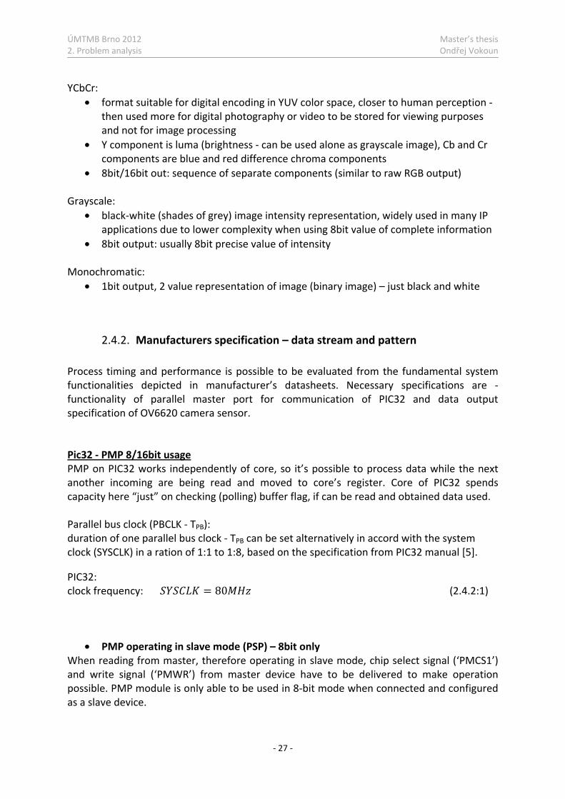
1) Image windowing: Window sizing can decrease amount of data that has to be processed and this possibility helps when system isn’t able to work with the full camera physical resolution at desired frame rate in a real time. But due to design of camera module, still all the data, even invalid data out of inactive window, is being sent to PIC32. Invalid data can be distinguished from the data we want to process by checking the HREF signal and thus spare time, when camera
ÚMTMB Brno 2012 Master’s thesis 2. Problem analysis Ondřej Vokoun
- 32 -
is sending this data, can be used for image processing routines to finish computations on actual row or after the whole active image was obtained and processed (for this possibility, memory storage like FIFO buffer would be needed). It can be taken as - we can reach the same FPS by setting smaller active window together with corresponding lower clock speed to get longer times between separate pixels to obtain same amount of valid data during time period. But as mentioned, whole image array together with invalid data is send, no matter on window size, so this functionality really can help only on decreasing the amount of data that has to be processed.
Fig. 2.4.2.6.: Window sizing: HS/HE –horizontal start/end pixel, VS/VE – vertical start/end row. Adopted from [6].
2) Pixel binning:
When core needs more time to do necessary calculations between separate pixels – or in fact to decrease data transfer rate, camera can be set to work in QCIF mode. Maximal resolution is then half the initial resolution (176x144pix) - every line output only half the data (like every second pixel that prolong times between them). This function also improves sensitivity when working with smaller resolution. Summary: default time calculations for 17.73MHz clock input (note: all the pixels on sensor included):
pixel clock step: (8 ) =56 ∙ 10 (2.4.2:7) (16 ) =112 ∙ 10 (2.4.2:8) one line: = ∗ 572 = 64.064 ∙ 10 (2.4.2:9) one frame: = 310 ∗ = 0.0199 (2.4.2:10) final frame rate: = 1 = 50 (2.4.2:11)
- lower system clock, when other characteristics remains the same, leads to longer time between every pixel and in lower FPS
ÚMTMB Brno 2012 Master’s thesis 2. Problem analysis Ondřej Vokoun
- 33 -
- optimization possibility of windowing doesn’t lead to longer times between separate pixels, pixel binning prolongs times between separate pixels and both of them leads to decreased amount of data for processing
2.4.3. Resume for the performance and timing At first, possible applications for camera use are proposed and presented as follows – COG of single object in 2D plane, searching for the object of certain color, Basic 2D pattern recognition. Secondly, timing propagation in order to follow wanted operations is examined, based on manufacturer’s specification for PIC32 microcontroller and OV6620 color camera sensor. Data format of nowadays color cameras with output data format is described in the beginning to clarify connections between timing and data output – where the most significant characteristic is bus data width (8bit or 16bit) and data format which denotes possibility to transfer whole necessary information for the computation during one transfer cycle. Main timing problem, that can be examined based on manufacturers datasheet information, lies in comparison of results from PIC32 and OV6620 timing of data transfer in previous chapter. As already mentioned, time to obtain and move data into accessible register in the controller has to be faster than camera is sending them out: camera output time: (8 ) =56∙ 10 = 0.056 (2.4.3:1) (8 ) =56∙ 10 = 0.056 (2.4.3:2) controller input to register time: - together with the time to move data into register, data from the register has to be also moved by the user application to release register for another data input _ = 2~3 ∗ = 25~37.8 ∙ 10 (2.4.3:3) = 2~3 ∗ + (1~2) ∗ = 37.8~50 ∙ 10 (2.4.3:4) -> comparison of (2.4.3:1) and (2.4.3:2) with (2.4.3:4) gives final result: (37.8~50 ∙ 10 ) < (8 )(56 ∙ 10 ) ≪ (16 )(112 ∙ 10 ) Then we can say that PIC32 is able to accept and allow user to read wanted data before another data is present at the input port in both 8bit and 16bit connection.
ÚMTMB Brno 2012 Master’s thesis 2. Problem analysis Ondřej Vokoun
- 34 -
2.5. Simulation results for PIC32 and sample BW image
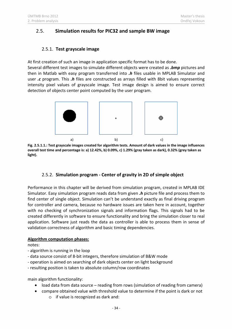
2.5.1. Test grayscale image At first creation of such an image in application specific format has to be done. Several different test images to simulate different objects were created as .bmp pictures and then in Matlab with easy program transferred into .h files usable in MPLAB Simulator and user .c program. This .h files are constructed as arrays filled with 8bit values representing intensity pixel values of grayscale image. Test image design is aimed to ensure correct detection of objects center point computed by the user program.
a) b) c) Fig. 2.5.1.1.: Test grayscale images created for algorithm tests. Amount of dark values in the image influences overall test time and percentage is: a) 12.42%, b) 0.09%, c) 1.29% (gray taken as dark), 0.32% (grey taken as light).
2.5.2. Simulation program - Center of gravity in 2D of simple object Performance in this chapter will be derived from simulation program, created in MPLAB IDE Simulator. Easy simulation program reads data from given .h picture file and process them to find center of single object. Simulation can’t be understand exactly as final driving program for controller and camera, because no hardware issues are taken here in account, together with no checking of synchronization signals and information flags. This signals had to be created differently in software to ensure functionality and bring the simulation closer to real application. Software just reads the data as controller is able to process them in sense of validation correctness of algorithm and basic timing dependencies. Algorithm computation phases: notes: - algorithm is running in the loop - data source consist of 8-bit integers, therefore simulation of B&W mode - operation is aimed on searching of dark objects center on light background - resulting position is taken to absolute column/row coordinates main algorithm functionality:
• load data from data source – reading from rows (simulation of reading from camera) • compare obtained value with threshold value to determine if the point is dark or not
o if value is recognized as dark and:
ÚMTMB Brno 2012 Master’s thesis 2. Problem analysis Ondřej Vokoun
- 35 -
is the first one dark in the row - then remember position of this point, store as column_start position and increase point counter
is not the first one dark in the row - then remember position of this point and store temporarily as column_end position (usually there are more points and we wait for the last one in the row)
o if value is recognized as light – do nothing to spare computational capacity • at the end of actual row – compute center point from known start and end position
and store number of row, if row is the first one with dark points, then lets save this position as row_start to be able to determine center of object in second axis, and then increase the value of row_end in every row where dark points were found
• after the last row, or at the end of processed image, compute final central position from stored values in axis that leads through rows and also second axis which leads through columns to have complete information of object center in 2D plane
Summary: Algorithm works well for searching center of test objects. Some additional calculation conditions and formulas for special shapes of objects or special cases had to be also implemented for full functionality. Algorithm with minor changes can be used for implementation in software for image processing of real data from camera for the task – COG of simple objects in 2D plane. Timing and test image properties: This part is aimed on software simulation timing dependencies based on test image properties. Note: timing of simulation depends on complexity and amount of computations and also on optimization level of the code itself. Following timing is just for coarse imagination and can’t be taken seriously as done on a real system. As can be seen from following timing, performance depends on the number of dark pixels, because time to process one dark pixel is longer in the comparison of processing light one, where nothing is computed.
• test images: 100x100 pixels, 8-bit word each • volume percentage of dark area in the picture: 0.09 - 12.42 % • controller speed: 80MHz
→ = = ∙ = 12.5 ∙ 10 = 0.0125 (2.5.2:1)
main algorithm part to process separate pixel:
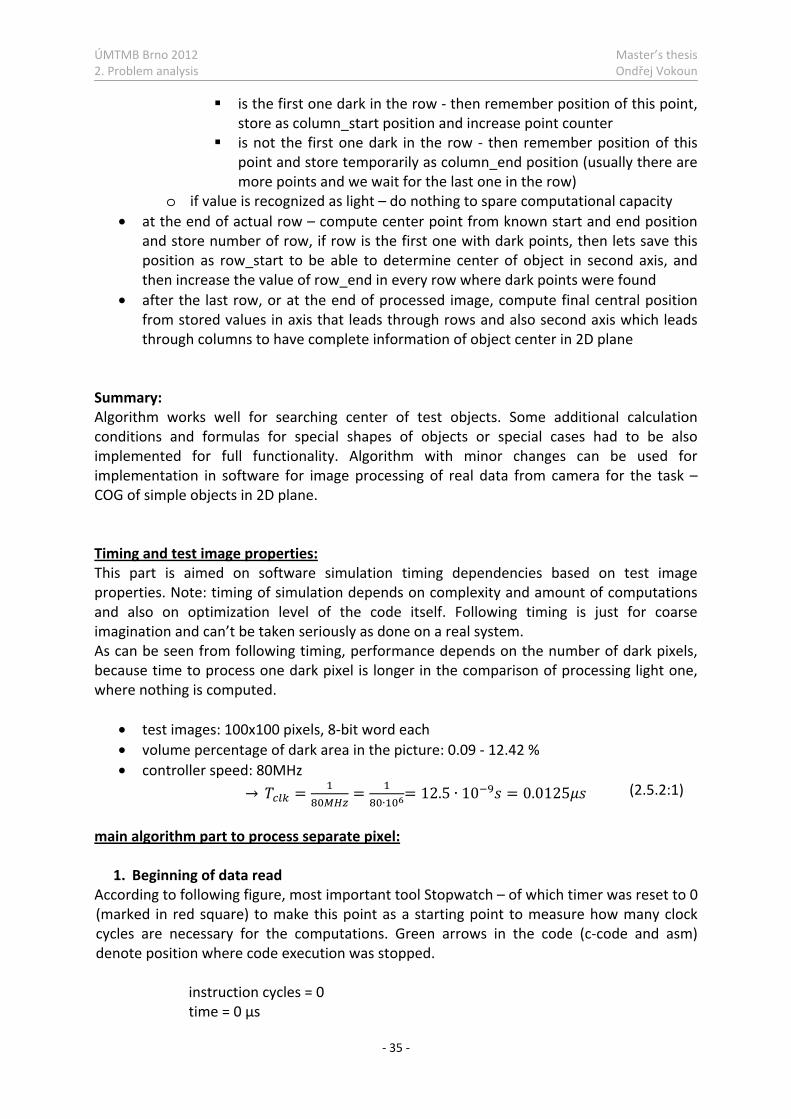
1. Beginning of data read According to following figure, most important tool Stopwatch – of which timer was reset to 0 (marked in red square) to make this point as a starting point to measure how many clock cycles are necessary for the computations. Green arrows in the code (c-code and asm) denote position where code execution was stopped. instruction cycles = 0 time = 0 μs
ÚMTMB Brno 2012 Master’s thesis 2. Problem analysis Ondřej Vokoun
- 36 -
Fig. 2.5.2.1.: Image showing crucial part of the program stopped in the position of calling data read. From the left - code in c-language, the same in assembly code as compiled from c-lang., then memory usage and stopwatch.
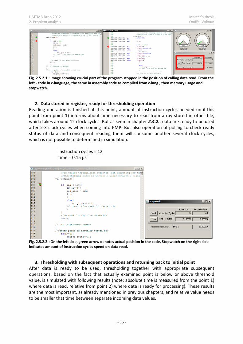
2. Data stored in register, ready for thresholding operation
Reading operation is finished at this point, amount of instruction cycles needed until this point from point 1) informs about time necessary to read from array stored in other file, which takes around 12 clock cycles. But as seen in chapter 2.4.2., data are ready to be used after 2-3 clock cycles when coming into PMP. But also operation of polling to check ready status of data and consequent reading them will consume another several clock cycles, which is not possible to determined in simulation.
instruction cycles = 12 time = 0.15 μs
Fig. 2.5.2.2.: On the left side, green arrow denotes actual position in the code, Stopwatch on the right side indicates amount of instruction cycles spend on data read.
3. Thresholding with subsequent operations and returning back to initial point
After data is ready to be used, thresholding together with appropriate subsequent operations, based on the fact that actually examined point is below or above threshold value, is simulated with following results (note: absolute time is measured from the point 1) where data is read, relative from point 2) where data is ready for processing). These results are the most important, as already mentioned in previous chapters, and relative value needs to be smaller that time between separate incoming data values.

ÚMTMB Brno 2012 Master’s thesis 2. Problem analysis Ondřej Vokoun
- 37 -
a) recognized as light point (lies above the threshold), relative time: instruction cycles = 20 – 12 = 8 time = 0.25 – 0.15 = 0.10 μs
b) recognized as dark point (lies below the threshold) , relative time:
instruction cycles = 24 – 12 = 12 time = 0.30 – 0.15 = 0.15 μs
a) b)Fig. 2.5.2.3.: Absolute timing taken to the point 1) where Stopwatch belongs to: a)light point, b)dark point.
2.5.3. Resume for the simulation test COG recognition of several simple test images is performed to observe timing properties of this operation, which functionality is presented together with obtained results. Basic recognition works pretty well and with slight changes could be possible used for real application processing real images from camera sensor. Timing dependencies from chapters - 2.4.2, 2.4.3 and 2.5.2: time necessary to process single pixel from the simulation: ≈ 0.10 − 0.15 (2.5.3:1) time between separate pixels from the camera on max frame rate (based on output mode): ≈ 0.056 − 0.112 (2.5.3:2) comparison of results (2.5.3:1) and (2.5.3:2) give us information, that processing of one 8bit value for one pixel on maximal frame rate (even in slower 16bit mode) is longer than pixels are arriving at the port, which leads to several results:
• internal memory to store pixels for further processing would be needed for system with camera set in default mode with max. FPS and full image size
• decrease camera frame rate to the level the PIC would be able to process pixel during obtaining of another one, no memory would be necessary now
• use optimization methods in the camera to decrease data rate – as windowing or/and pixel binning, while max. FPS would still be reachable, no memory would be necessary
• use different and more powerful HW than PIC32
ÚMTMB Brno 2012 Master’s thesis 2. Problem analysis Ondřej Vokoun
- 38 -
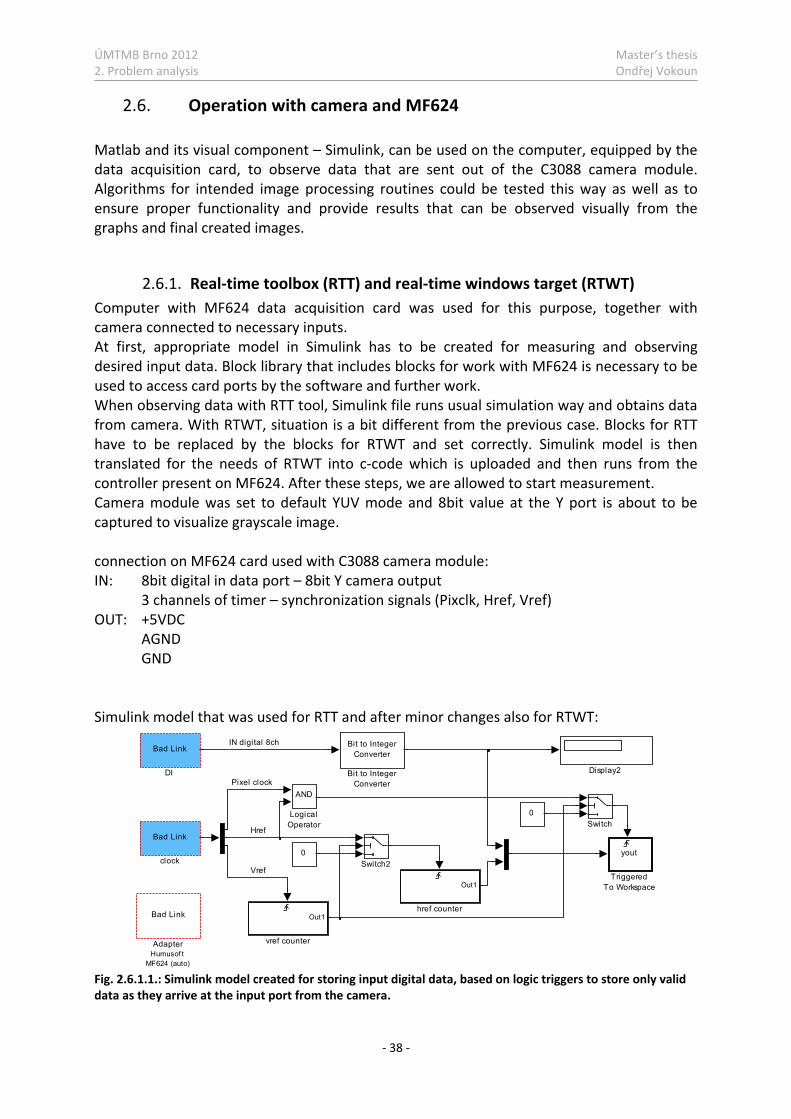
2.6. Operation with camera and MF624 Matlab and its visual component – Simulink, can be used on the computer, equipped by the data acquisition card, to observe data that are sent out of the C3088 camera module. Algorithms for intended image processing routines could be tested this way as well as to ensure proper functionality and provide results that can be observed visually from the graphs and final created images.
2.6.1. Real-time toolbox (RTT) and real-time windows target (RTWT) Computer with MF624 data acquisition card was used for this purpose, together with camera connected to necessary inputs. At first, appropriate model in Simulink has to be created for measuring and observing desired input data. Block library that includes blocks for work with MF624 is necessary to be used to access card ports by the software and further work. When observing data with RTT tool, Simulink file runs usual simulation way and obtains data from camera. With RTWT, situation is a bit different from the previous case. Blocks for RTT have to be replaced by the blocks for RTWT and set correctly. Simulink model is then translated for the needs of RTWT into c-code which is uploaded and then runs from the controller present on MF624. After these steps, we are allowed to start measurement. Camera module was set to default YUV mode and 8bit value at the Y port is about to be captured to visualize grayscale image. connection on MF624 card used with C3088 camera module: IN: 8bit digital in data port – 8bit Y camera output 3 channels of timer – synchronization signals (Pixclk, Href, Vref) OUT: +5VDC AGND GND Simulink model that was used for RTT and after minor changes also for RTWT:
Fig. 2.6.1.1.: Simulink model created for storing input digital data, based on logic triggers to store only valid data as they arrive at the input port from the camera.
IN digital 8ch
Pixel clock
Href
Vref
Out1
vref counter
Out1
href counter
Bad Link
clockyout
TriggeredTo Workspace
Switch2
Switch
AND
LogicalOperator
Display2
Bad Link
DI
0
0
Bit to IntegerConverter
Bit to IntegerConverter
Bad Link
AdapterHumusof t
MF624 (auto)
ÚMTMB Brno 2012 Master’s thesis 2. Problem analysis Ondřej Vokoun
- 39 -
Principle of model operation: Camera function, or observable function, lies in clocked bursting out of digital data. Validity of data is ensured by the arriving pixel clock that synchronizes whole process. Together with pixel clock, camera in master mode provides also vertical and horizontal reference signals that informs us about start of the new frame and valid readout line of the frame. As the data are coming to the system, we need to determine which data to store and when. Counter on horizontal ref. signal is stored together with the data to inform later to which line of the frame stored data has to be assigned. Vertical ref. signal with counter informs how many frames were already sent and we can also pick how many frames can be ignored before and after storing of one wanted frame, because camera usually needs some time to stabilize after the start and send valid image frames.
2.6.2. Resume Camera is by the default equipped with the crystal oscillator running at 17.73MHz, so data are clocked at the speed of 17MHz (but when working in 16-bit mode it’s half the speed – 8.5MHz). Based on this information, we have to set correct step of the simulation to prevent unwanted situations like aliasing or better to say – missing data information. input clock time: = . = 112
maximal simulation step: = = 56 Simulation was set to discrete fixed step and tried for several time step settings. On higher time values is program missing incoming data and even when tried minimal possible step the program was able to run, simulation was highly unstable and still missing data values. RTT min possible Simulink step: = 1 >> → this method is inappropriate and different access has to be used for observation RTWT min possible Simulink step: = 1 >> → this method is also inappropriate and different access has to be used for observation Computer equipped with MF624 data acquisition card is inapplicable for operation of direct connection with camera module and real-time data processing, because incoming data rate is faster than data acquisition card is able to work with.
ÚMTMB Brno 2012 Master’s thesis 2. Problem analysis Ondřej Vokoun
- 40 -
2.7. Proposed solutions PIC32 microcontroller: First proposed variant – use of the PIC32 controller as presented during previous pages, showed insufficient performance, which can’t ensure proper functionality of the system for intended applications. System may be functional but not as fast as it would be necessary and can lead to numerous complications and results would still be unconvincing. Alternative possibilities: FPGA: Another variant lies in the change of main hardware and use FPGA (Field programmable gate array) device instead. FPGA is a general-purpose integrated circuit which main advantage is possibility to design specific hardware-like parts (memory, single-purpose co-processors, microcontroller, communication interface, …) and program device for wanted functionality by downloading bitstream configuration file into chip. Specific design for custom application provides highly parallel data processing and fast transition times. When user needs to change or modify system design, there is no need for soldering or changing anything except of software program or system schematics (when working with visual tool like System generator under Simulink), so the same platform can be used for different applications. FPGA device combines the best attributes of general-purpose microprocessors and DSPs. DSP: Main processing core can be also changed to DSP. DSPs are basically dedicated integrated circuits specialized for the needs of fast digital signal processing. Specialization of such controller makes it more powerful, lower cost and less power consuming then in the case of common general-purpose microprocessor but it structure can’t be changed for the purpose of use as in the case of FPGAs.
Evaluation of solution options All the three variants discussed previously in comparison of the most significant characteristics for the target application of image processing. For illustration picked commonly used DSP – Blackfin BF537 and FPGA – Spartan6. Characteristics\device PIC32 Blackfin BF537 FPGA Spartan6 Frequency [MHz] 80 up to 600 500+ Configurable HW no no yes Memory [kB] 32 132 4800 RAM + configurable Performance for camera operations
low high high + other concurrent applications
Parallel execution no partial yes Design complexity higher average-higher
(based on solution) average-higher (based on solution)
Versatility high moderate very high Price low moderate-higher moderate-higher Tab. 2.7.1.: Comparison of proposed design solutions. Prices are highly dependable on specific controller version. Information from [3], [19] and [17].
ÚMTMB Brno 2012 Master’s thesis 3. Formulation of the new thesis assignment Ondřej Vokoun
- 41 -
3. Formulation of the new thesis assignment
3.1. Justification After a deep study of given problematic, range of simulation tests performed and then comparison of obtained results with the specifications presented in manufacturer documentation. We can say that for the satisfactory results of camera operation wouldn’t be initially intended platform based on the PIC32 powerful enough. Suggested alternative designed on the FPGA platform is way more powerful and brings more opportunities to create different target applications or change functionality for different task without need of changing anything else than driving software structure.
3.2. Draft of the new thesis assignment - appropriate camera module selection - interconnection between camera module and controlling HW - implementation of driving software for camera work - implementation of proposed method for image processing - communication implementation
3.3. Final approved assignment Goal that should be reached:
1) Research of currently available camera modules, research of possible communication between camera module and controller. Camera module selection.
2) Task definition for camera system together with computation process division between FPGA and PIC.
3) Algorithm implementation into FPGA, PIC. 4) Thorough testing of designed system together with experiment documentation.
Problem characteristics: Main target of the work is design of simple and cheap camera module with own data processing. Data pre-processing will be accomplished in the FPGA, while following processing and communication with higher-level device will be done by the PIC controller (RS232, CAN). Typical system task will be searching for the dark spot on bright background.

ÚMTMB Brno 2012 Master’s thesis 4. System implementation design Ondřej Vokoun
- 42 -
4. System implementation design
Based on the poor results of PIC32 mentioned in the chapter 2.5.3 - Resume was decided to create whole target system on the FPGA device. Market with possible FPGA devices isn’t that rich as in the case of microcontrollers and primarily two companies produce most of the FPGAs – Xilinx and Altera company. Due to supervisors recommendation was used complete digital circuit platform - Atlys development board with Xilinx Spartan-6 FPGA. Big advantage of Xilinx chip is possibility to use Xilinx software, which is provided for free for noncommercial and educational purposes and offers a lot of design and simulation tools for FPGA system development, including toolbox for Matlab/Simulink called System generator.
4.1. Hardware implementation The main target of camera system problematic was software implementation and not system development from the base of electrical circuitry design. Together with request to speed up the whole process – “ready-to-use” development platform with the FPGA chip, as specified further, was picked for realization. Platform picked: Atlys™ Spartan-6 FPGA Development Board
Atlys board attributes: Spartan-6 LX45 offers: • Xilinx Spartan-6 LX45 FPGA, 324-pin BGA package• 128Mbyte DDR2 16-bit wide data • 10/100/1000 Ethernet PHY • On-board USB2 ports for programming • USB-UART and USB-HID port • Two HDMI video in & two HDMI out ports • AC-97 Codec with line-in, line-out, mic, &
headphone • 16Mbyte x4 SPI Flash for configuration & data
storage • 100MHz CMOS oscillator • 48 I/O’s routed to expansion connectors • GPIO includes 8 LEDs, 6 buttons, 8 slide switches
• 6,822 slices each containing four 6-input LUTs and eight flip-flops
• 2.1Mbits of fast block RAM • 4 clock tiles (8 DCMs & 4 PLLs) • 6 phased-locked loops • 58 DSP slices • 500MHz+ clock speeds
Tab. 4.1.1.: Table of Atlys properties. Adopted from [17].
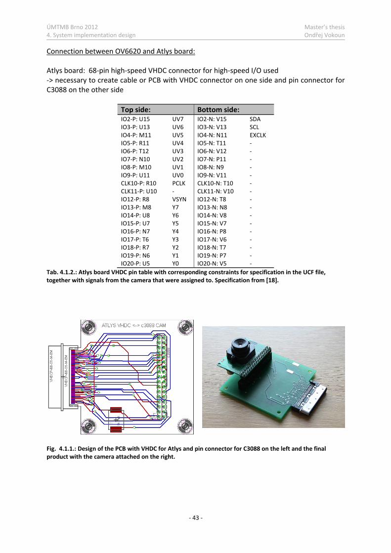
ÚMTMB Brno 2012 Master’s thesis 4. System implementation design Ondřej Vokoun
- 43 -
Connection between OV6620 and Atlys board: Atlys board: 68-pin high-speed VHDC connector for high-speed I/O used -> necessary to create cable or PCB with VHDC connector on one side and pin connector for C3088 on the other side
Top side: Bottom side: IO2-P: U15 UV7IO3-P: U13 UV6 IO4-P: M11 UV5 IO5-P: R11 UV4 IO6-P: T12 UV3 IO7-P: N10 UV2 IO8-P: M10 UV1 IO9-P: U11 UV0 CLK10-P: R10 PCLK CLK11-P: U10 - IO12-P: R8 VSYN IO13-P: M8 Y7 IO14-P: U8 Y6 IO15-P: U7 Y5 IO16-P: N7 Y4 IO17-P: T6 Y3 IO18-P: R7 Y2 IO19-P: N6 Y1 IO20-P: U5 Y0
IO2-N: V15 SDAIO3-N: V13 SCL IO4-N: N11 EXCLK IO5-N: T11 - IO6-N: V12 - IO7-N: P11 - IO8-N: N9 - IO9-N: V11 - CLK10-N: T10 - CLK11-N: V10 - IO12-N: T8 - IO13-N: N8 - IO14-N: V8 - IO15-N: V7 - IO16-N: P8 - IO17-N: V6 - IO18-N: T7 - IO19-N: P7 - IO20-N: V5 -
Tab. 4.1.2.: Atlys board VHDC pin table with corresponding constraints for specification in the UCF file, together with signals from the camera that were assigned to. Specification from [18].
Fig. 4.1.1.: Design of the PCB with VHDC for Atlys and pin connector for C3088 on the left and the final product with the camera attached on the right.
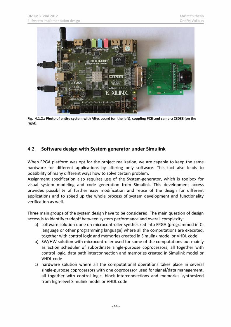
ÚMTMB Brno 2012 Master’s thesis 4. System implementation design Ondřej Vokoun
- 44 -
Fig. 4.1.2.: Photo of entire system with Altys board (on the left), coupling PCB and camera C3088 (on the right).
4.2. Software design with System generator under Simulink When FPGA platform was opt for the project realization, we are capable to keep the same hardware for different applications by altering only software. This fact also leads to possibility of many different ways how to solve certain problem. Assignment specification also requires use of the System-generator, which is toolbox for visual system modeling and code generation from Simulink. This development access provides possibility of further easy modification and reuse of the design for different applications and to speed up the whole process of system development and functionality verification as well. Three main groups of the system design have to be considered. The main question of design access is to identify tradeoff between system performance and overall complexity:
a) software solution done on microcontroller synthesized into FPGA (programmed in C-language or other programming language) where all the computations are executed, together with control logic and memories created in Simulink model or VHDL code
b) SW/HW solution with microcontroller used for some of the computations but mainly as action scheduler of subordinate single-purpose coprocessors, all together with control logic, data path interconnection and memories created in Simulink model or VHDL code
c) hardware solution where all the computational operations takes place in several single-purpose coprocessors with one coprocessor used for signal/data management, all together with control logic, block interconnections and memories synthesized from high-level Simulink model or VHDL code

ÚMTMB Brno 2012 Master’s thesis 4. System implementation design Ondřej Vokoun
- 45 -
Architecture comparison: Coprocessors under Sys-gen Picoblaze (KPCSM3) Microblaze (EDK Processor ) - 8-bit RISC 32-bit RISC 1 clk per process 2 clks per instruction 1 clk per instruction Parallel processing, very high performance
Sequential, low performance
Sequential, moderate-higher performance
pipelining for DSP operations - 3/5 stage pipeline fixed point (64bit+) fixed point (8bit) Floating Point Unit (FPU) ? 64bit+ registers 16 8-bit registers 32 32-bit registers 1K instruction code Caches (2-64kB) RAM configurable (onboard+ onchip synthesizable)
64B internal RAM RAM configurable (onboard+ onchip synthesizable)
VHDL signals VHDL signals Buses (PLB, FSL, …) ISE, System generator(Simulink) ISE + Sys-gen EDK(XPS,SDK) + ISE + Sys-gen VHDL, Simulink + Matlab code Assembly language C/C++ 24 instructions 82 instructions Size – depends on design Size estimation – 96 LUTs
(0.35% of spartan6 LUTs) Size estimation – 3689 LUTs ( 13.52% of spartan6 LUTs)
Tab. 4.2.1.: Table of different system design comparison, information valid for system generator v12.3 and used version of spartan6 usable slice size is 27288LUTs. Information Adopted from [14] and [17].
Summary: After consideration of different design abilities, together with request to speed-up the whole design process and easy reconfiguration under Simulink and system-generator for different tasks, variant c) was picked for system implementation. Main advantages of variant c):
• high versatility and easy reconfigurability for different tasks • possibility to design coprocessors with m-functions in standard Matlab language • designed system can be easily simulated under Simulink to observe results without
real target device • powerful solution
4.2.1. Overall system design Whole camera system is divided into two different main parts – exactly into two separate clock domains running on a different clock frequency. The first part – Camera input domain, primary obtains data from the camera and store valid and wanted data into shared FIFO buffer. Shared FIFO buffer serves as interconnection between both parts and therefore second domain – System domain can read from the FIFO and perform wanted image processing tasks.

ÚMTMB Brno 2012 Master’s thesis 4. System implementation design Ondřej Vokoun
- 46 -
Fig. 4.2.1.1.: Overall system design. At the top - System generator token for generating multiple subsystems, and from the left - camera subsystem and IP subsystem.
4.2.1.1. Camera input domain Functionality of the system domain lies in signal manipulation and redirection, together with basic control logic for writing into shared FIFO buffer, other superior system can read from and process the data. Signals from the board inputs connected to the FPGA I/O buffers (IOBs) are read in this block - that means signals the camera is sending out. Reading from the input ports has to be running on a certain frequency to prevent unwanted phenomena like aliasing that could lead into corruption or loss of input data. FPGA system also needs reference input clock signal for task execution, as mentioned earlier, thus camera output clock signal was used. When system is clocked from the camera and is then synchronized with incoming data, we can be sure of valid data presence at the input ports when triggered for read by the input clock – according to timing graphs in chapter 2.4.2 Manufacturers specification – data stream and pattern. Design is universal and can be used for different cameras, but equipped with necessary pixel clock output, horizontal and vertical reference signals and up to 16 parallel data lines for parallel data transfer. Data structure is aimed on 16bit wide input signal, but signal with lower bit precision can also be used (of course with necessary shift or cut manipulation later in the system block before data usage).
Camera subsystem IP subsystem
System domain
Multiple SubsystemGenerator
Camera input domain
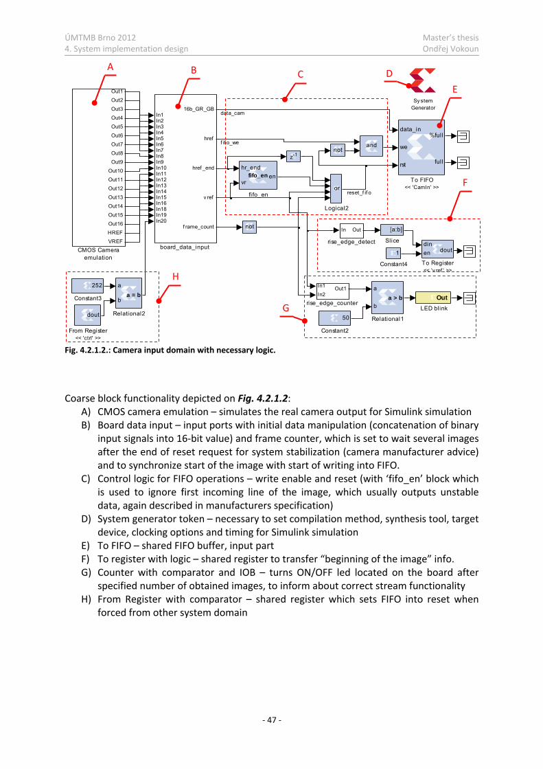
ÚMTMB Brno 2012 Master’s thesis 4. System implementation design Ondřej Vokoun
- 47 -
Fig. 4.2.1.2.: Camera input domain with necessary logic.
Coarse block functionality depicted on Fig. 4.2.1.2:
A) CMOS camera emulation – simulates the real camera output for Simulink simulation B) Board data input – input ports with initial data manipulation (concatenation of binary
input signals into 16-bit value) and frame counter, which is set to wait several images after the end of reset request for system stabilization (camera manufacturer advice) and to synchronize start of the image with start of writing into FIFO.
C) Control logic for FIFO operations – write enable and reset (with ‘fifo_en’ block which is used to ignore first incoming line of the image, which usually outputs unstable data, again described in manufacturers specification)
D) System generator token – necessary to set compilation method, synthesis tool, target device, clocking options and timing for Simulink simulation
E) To FIFO – shared FIFO buffer, input part F) To register with logic – shared register to transfer “beginning of the image” info. G) Counter with comparator and IOB – turns ON/OFF led located on the board after
specified number of obtained images, to inform about correct stream functionality H) From Register with comparator – shared register which sets FIFO into reset when
forced from other system domain
In Out
rise_edge_detect
In1
In2Out1
rise_edge_counter
hr_end
vrenfifo_en
fi fo_en
In1In2In3In4In5In6In7In8In9In10In11In12In13In14In15In16In18In19In20
16b_GR_GB
href
href _end
v ref
f rame_count
board_data_input dinen dout
To Register<< 'v ref ' >>
data_in
we
rst
%full
ful l
To FIFO<< 'CamIn' >>
[a:b]
Slice
a
ba = b
Relational2
a
ba > b
Relational1
or
Logical2
and
Out LED blink
not
not
dout
From Register<< 'ctrl' >>
z-1
1
Constant4
252
Constant3
50
Constant2
Out1
Out2
Out3
Out4
Out5
Out6
Out7
Out8
Out9
Out10
Out11
Out12
Out13
Out14
Out15
Out16
HREF
VREFCMOS Camera
emulation
Sy stemGenerator
data_cam
f if o_we
reset_f if o
A B
EC
H
F
D
G
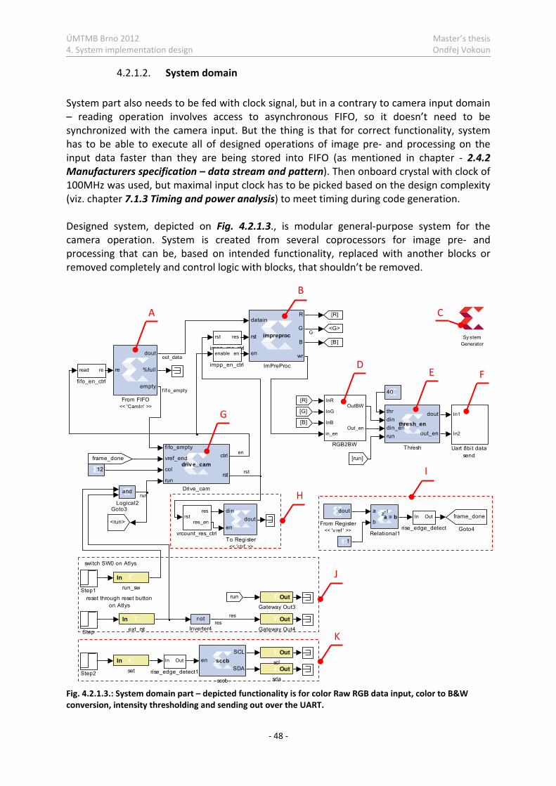
ÚMTMB Brno 2012 Master’s thesis 4. System implementation design Ondřej Vokoun
- 48 -
4.2.1.2. System domain System part also needs to be fed with clock signal, but in a contrary to camera input domain – reading operation involves access to asynchronous FIFO, so it doesn’t need to be synchronized with the camera input. But the thing is that for correct functionality, system has to be able to execute all of designed operations of image pre- and processing on the input data faster than they are being stored into FIFO (as mentioned in chapter - 2.4.2 Manufacturers specification – data stream and pattern). Then onboard crystal with clock of 100MHz was used, but maximal input clock has to be picked based on the design complexity (viz. chapter 7.1.3 Timing and power analysis) to meet timing during code generation. Designed system, depicted on Fig. 4.2.1.3., is modular general-purpose system for the camera operation. System is created from several coprocessors for image pre- and processing that can be, based on intended functionality, replaced with another blocks or removed completely and control logic with blocks, that shouldn’t be removed.
Fig. 4.2.1.3.: System domain part – depicted functionality is for color Raw RGB data input, color to B&W conversion, intensity thresholding and sending out over the UART.
switch SW0 on Atlys
reset through reset buttonon Atlys
rstres
res_en
vrcount_res_ctrl
In
set Out sda
Out sclen
SCL
SDAsccb
sccb
In
run_sw
In Out
rise_edge_detect1
In Out
rise_edge_detect
rst res
impp_res_ctrlenable en
impp_en_ctrlread re
fifo_en_ctrl
In
ext_rst
In1
In2
Uart 8bit datasend
din
endout
To Register<< 'ctrl' >>
thrdindin_enrun
dout
out_en
thresh_en
Thresh
Step2
Step1
Step
a
ba = bz-1
Relational1
InR
InG
InB
in_en
OutBW
Out_en
RGB2BW
and
Logical2
not
Inverter4
datain
rst
en
R
G
B
wr
impreproc
ImPreProc
frame_done
Goto4<run>
Goto3
[B]
<G>
[R]
Out Gateway Out4
Out Gateway Out3
[B]
[G]
[R]
[run]
run
frame_done
dout
From Register<< 'v ref ' >>
re
dout
%full
empty
From FIFO<< 'CamIn' >>
fifo_empty
vref_end
col
run
ctrl
rst
driv e_cam
Drive_cam
12
40
1
Sy stemGenerator
out_data
f if o_empty
en
rst
G
run
resres
A
G
DE F
C
B
J
K
H
I

ÚMTMB Brno 2012 Master’s thesis 4. System implementation design Ondřej Vokoun
- 49 -
Coarse block functionality depicted on Fig. 4.2.1.3.: A) From FIFO – shared FIFO buffer, output part B) ‘ImPreProc’ – image preprocessing part for Raw RGB into RGB interpolation (viz.
chapter - 5.1) C) System generator token D) ‘RGB2BW’ – RGB color into black-white conversion (viz. chapter - 5.2) E) ‘Thresh – intensity thresholding of B&W image based on defined threshold value (viz.
chapter - 5.3) F) ‘Uart 8bit data send’ – communication interface for sending whole image out over
the serial port (viz. chapter - 6.2) G) ‘Drive_cam’ – high level driving and synchronization of other blocks (viz. further) H) To Register with logic – shared register, sends out FIFO reset signal I) From register with logic - shared register input of “beginning of the image” info. J) Inputs and outputs on the board – board switches and leds K) ‘SCCB’ with logic and I/Os – SCCB communication for camera setting with “send”
button and outputs to camera (viz. chapter - 6.1) As mentioned, above presented system awaits RAW RGB 16bit data input for basic introduced operations, but instead of used B&W conversion and thresholding, block for color thresholding based on picked color can be used (viz. chapter - 5.4) or searching for COG of single object based on the output from ‘RGB2BW’ (viz. chapter - 5.5) and much more. Also system can work with YCbCr output from the camera, where only 8MSB bits would be used for B&W system, where no ‘IMPP’ block with ‘RGB2BW’ is needed to have gray-scale image for desired application. Summary: As it can be seen, modular system is very variable in the possibilities of use and can be changed fast and easily from one provided functionality into another, which is big advantage of such design under Simulink with System generator.
4.2.1.3. Drive camera block “Drive_cam” block is essentially state machine that controls read and reset state of FIFO buffer together with read synchronization of another block directly connected to obtain data from FIFO. But also control operations of other blocks present in the system can be included. Requests from user (like inputs from switch buttons) can be connected and evaluated in ‘Drive_cam’ block or in the blocks whose functionality is about to be controlled, but main switch to run camera operation or remain idle has to be connected with this block to ensure correct functionality of whole system.
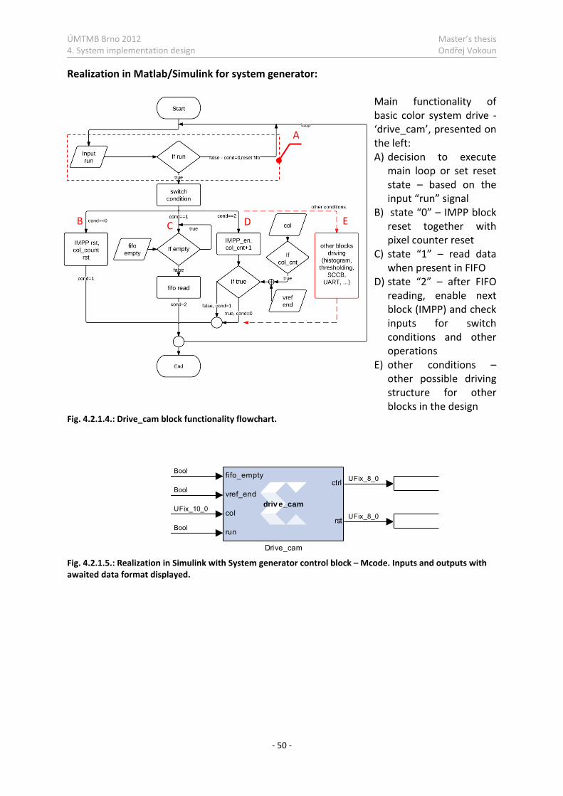
ÚMTMB Brno 2012 Master’s thesis 4. System implementation design Ondřej Vokoun
- 50 -
Realization in Matlab/Simulink for system generator: Main functionality of
basic color system drive - ‘drive_cam’, presented on the left: A) decision to execute
main loop or set reset state – based on the input “run” signal
B) state “0” – IMPP block reset together with pixel counter reset
C) state “1” – read data when present in FIFO
D) state “2” – after FIFO reading, enable next block (IMPP) and check inputs for switch conditions and other operations
E) other conditions – other possible driving structure for other blocks in the design
Fig. 4.2.1.4.: Drive_cam block functionality flowchart.
Fig. 4.2.1.5.: Realization in Simulink with System generator control block – Mcode. Inputs and outputs with awaited data format displayed.
fifo_empty
vref_end
col
run
ctrl
rst
driv e_cam
Drive_cam
Bool
Bool
UFix_8_0
UFix_8_0
Bool
UFix_10_0
A
B C D E

ÚMTMB Brno 2012 Master’s thesis 5. Image Preprocessing and Processing Ondřej Vokoun
- 51 -
5. Image Preprocessing and Processing
As the data is obtained from the camera doesn’t indicate the end of successful operation, on the contrary it indicates the beginning of the image pre- and processing operations necessary to fulfill awaited functionality of the system. At the beginning, obtained data has to be converted to the usual form and then we are able to perform mathematical operations that are necessary for image recognition and similar applications.
5.1. RGB interpolation from RAW Bayer RGB As mentioned earlier, camera is set to provide on the output port RAW Bayer RGB data (viz. Fig. 5.1.1.). For subsequent operations, this raw format needs to be interpolated into common RGB image. Several options of interpolation can be used and all of them are different in complexity, computational demands, quality of final image output and also suitability for different applications and different speed of execution.
Fig. 5.1.1.: Raw RGB image of intensities with magnified detail, showing Bayer array pattern with 2x2 GRBG blocks. This picture is then used for test purposes on different interpolation methods.
Tested RGB interpolations in Matlab: Matlab “demosaic” function - gradient-corrected linear interpolation - definition:
• designed as 5x5 filter centered at interpolated position moved through the whole image (basically this method is 2D convolution)
• different coefficients based on column/row position (viz. Fig. 5.1.2.)
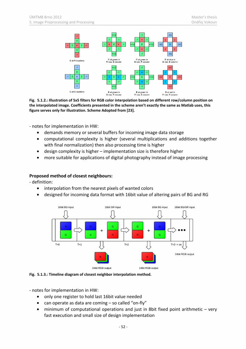
ÚMTMB Brno 2012 Master’s thesis 5. Image Preprocessing and Processing Ondřej Vokoun
- 52 -
Fig. 5.1.2.: Illustration of 5x5 filters for RGB color interpolation based on different row/column position on the interpolated image. Coefficients presented in the scheme aren’t exactly the same as Matlab uses, this figure serves only for illustration. Scheme Adopted from [23].
- notes for implementation in HW:
• demands memory or several buffers for incoming image data storage • computational complexity is higher (several multiplications and additions together
with final normalization) then also processing time is higher • design complexity is higher – implementation size is therefore higher • more suitable for applications of digital photography instead of image processing
Proposed method of closest neighbours: - definition:
• interpolation from the nearest pixels of wanted colors • designed for incoming data format with 16bit value of altering pairs of BG and RG
Fig. 5.1.3.: Timeline diagram of closest neighbor interpolation method.
- notes for implementation in HW:
• only one register to hold last 16bit value needed • can operate as data are coming – so called “on-fly” • minimum of computational operations and just in 8bit fixed point arithmetic – very
fast execution and small size of design implementation

ÚMTMB Brno 2012 Master’s thesis 5. Image Preprocessing and Processing Ondřej Vokoun
- 53 -
Summary: Comparison of both mentioned methods in the meaning of visual quality of interpolated output image:
a) b)Fig. 5.1.4.: Result pictures from the interpolation process: a) Matlab demosaic, b) closest neighbour method.
details D in comparison:
Da DbFig. 5.1.5.: Details Da and Db of interpolated images on Fig. 5.1.4. in the comparison.
Complete images presents that both methods are almost equivalent in the term of final quality – we can clearly discern between different shapes of different colors. Of course, more complex Matlab method based on gradient-corrected linear interpolation, shows a bit better results with a real colors, but for the use in basic image processing applications or image recognition. Colors and nature like reconstruction of the pictures isn’t really what is crucial, but what really matters is the speed of execution and memory demands and for such conditions, proposed method of closest neighbours can be considered as a better solution. Realization in Matlab/Simulink for system generator: Realization under Simulink was done by the use of Mcode block preprocessor programmed for desired functionality. Note.: when ‘impreproc’ function is used, number of columns is reduced by one, so blocks that follows this block and needs to be informed about amount of columns in the image should have connected: (col-1).
Da Db
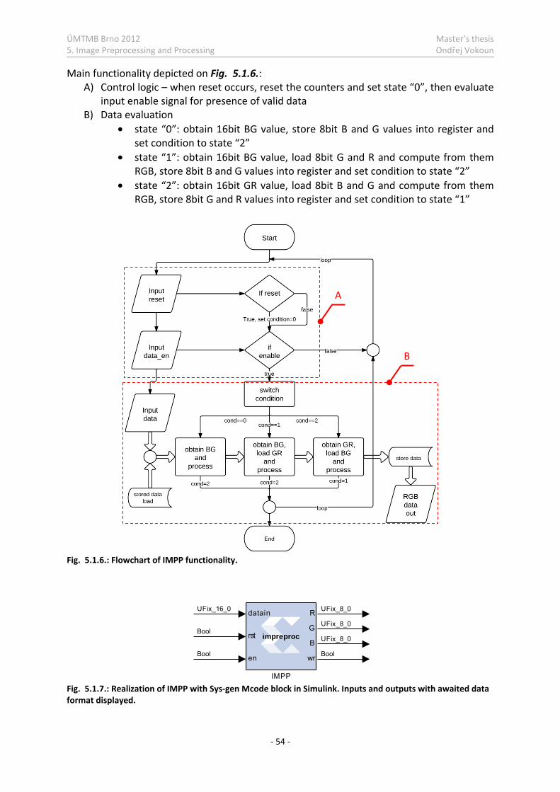
ÚMTMB Brno 2012 Master’s thesis 5. Image Preprocessing and Processing Ondřej Vokoun
- 54 -
Main functionality depicted on Fig. 5.1.6.: A) Control logic – when reset occurs, reset the counters and set state “0”, then evaluate
input enable signal for presence of valid data B) Data evaluation
• state “0”: obtain 16bit BG value, store 8bit B and G values into register and set condition to state “2”
• state “1”: obtain 16bit BG value, load 8bit G and R and compute from them RGB, store 8bit B and G values into register and set condition to state “2”
• state “2”: obtain 16bit GR value, load 8bit B and G and compute from them RGB, store 8bit G and R values into register and set condition to state “1”
Fig. 5.1.6.: Flowchart of IMPP functionality.
Fig. 5.1.7.: Realization of IMPP with Sys-gen Mcode block in Simulink. Inputs and outputs with awaited data format displayed.
datain
rst
en
R
G
B
wr
impreproc
IMPP
UFix_16_0
Bool
Bool
Bool
UFix_8_0
UFix_8_0
UFix_8_0
A
B
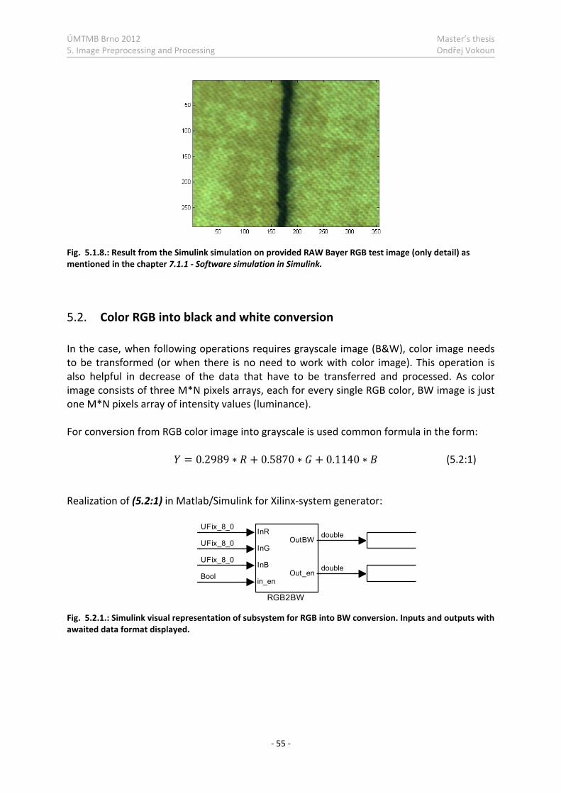
ÚMTMB Brno 2012 Master’s thesis 5. Image Preprocessing and Processing Ondřej Vokoun
- 55 -
Fig. 5.1.8.: Result from the Simulink simulation on provided RAW Bayer RGB test image (only detail) as mentioned in the chapter 7.1.1 - Software simulation in Simulink.
5.2. Color RGB into black and white conversion In the case, when following operations requires grayscale image (B&W), color image needs to be transformed (or when there is no need to work with color image). This operation is also helpful in decrease of the data that have to be transferred and processed. As color image consists of three M*N pixels arrays, each for every single RGB color, BW image is just one M*N pixels array of intensity values (luminance). For conversion from RGB color image into grayscale is used common formula in the form: = 0.2989 ∗ + 0.5870 ∗ + 0.1140 ∗ (5.2:1) Realization of (5.2:1) in Matlab/Simulink for Xilinx-system generator:
Fig. 5.2.1.: Simulink visual representation of subsystem for RGB into BW conversion. Inputs and outputs with awaited data format displayed.
InR
InG
InB
in_en
OutBW
Out_en
RGB2BW
UFix_8_0
UFix_8_0
UFix_8_0
Bool
double
double
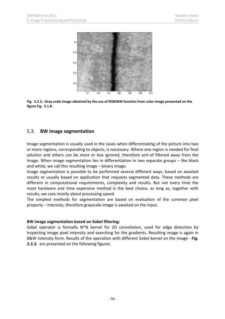
ÚMTMB Brno 2012 Master’s thesis 5. Image Preprocessing and Processing Ondřej Vokoun
- 56 -
Fig. 5.2.2.: Gray-scale image obtained by the use of RGB2BW function from color image presented on the figure Fig. 5.1.8.
5.3. BW image segmentation Image segmentation is usually used in the cases when differentiating of the picture into two or more regions, corresponding to objects, is necessary. Where one region is needed for final solution and others can be more or less ignored, therefore sort-of filtered away from the image. When image segmentation lies in differentiation in two separate groups – like black and white, we call this resulting image – binary image. Image segmentation is possible to be performed several different ways, based on awaited results or usually based on application that requests segmented data. These methods are different in computational requirements, complexity and results. But not every time the most hardware and time expensive method is the best choice, as long as, together with results, we care mostly about processing speed. The simplest methods for segmentation are based on evaluation of the common pixel property – intensity, therefore grayscale image is awaited on the input. BW image segmentation based on Sobel filtering: Sobel operator is formally N*N kernel for 2D convolution, used for edge detection by inspecting image pixel intensity and searching for the gradients. Resulting image is again in B&W intensity form. Results of the operation with different Sobel kernel on the image - Fig. 5.3.3. are presented on the following figures.
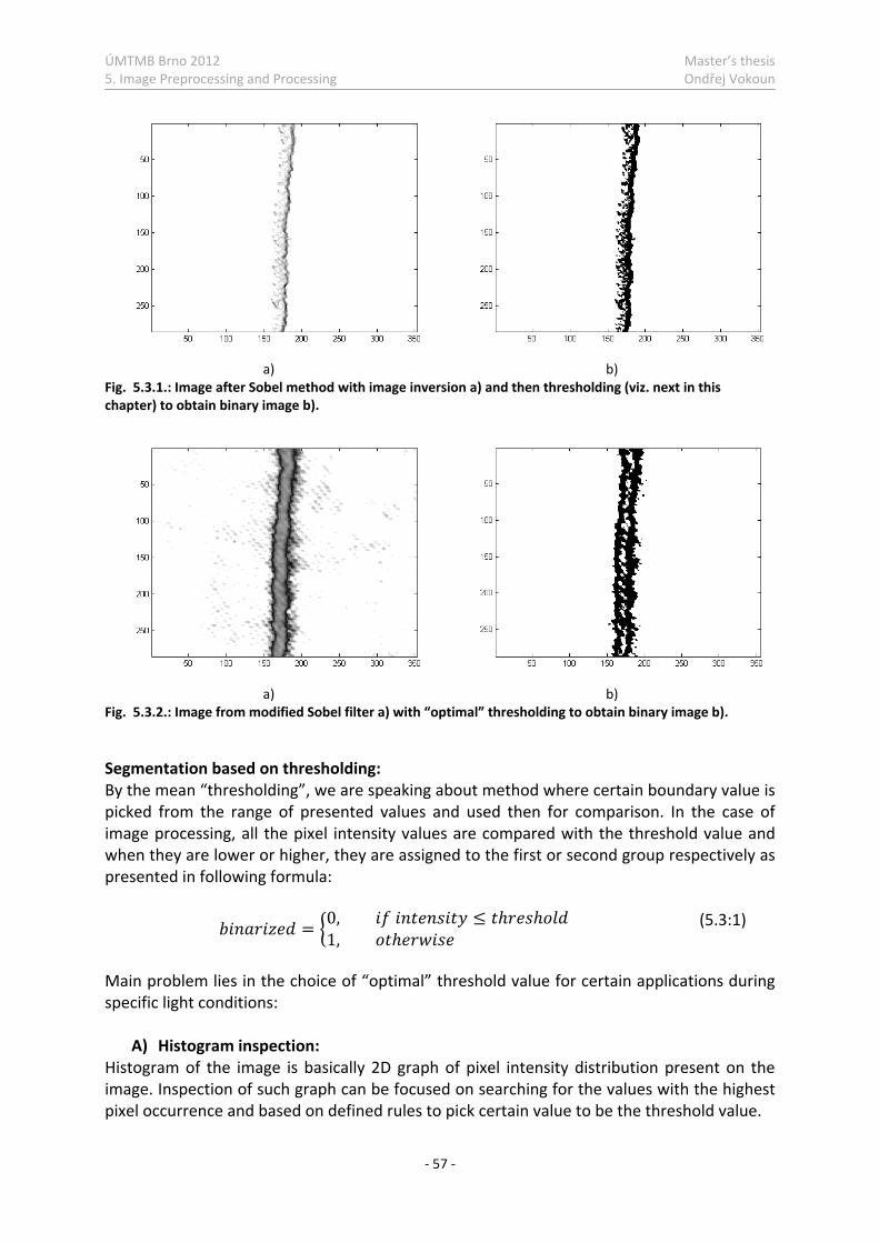
ÚMTMB Brno 2012 Master’s thesis 5. Image Preprocessing and Processing Ondřej Vokoun
- 57 -
a) b)Fig. 5.3.1.: Image after Sobel method with image inversion a) and then thresholding (viz. next in this chapter) to obtain binary image b).
a) b)Fig. 5.3.2.: Image from modified Sobel filter a) with “optimal” thresholding to obtain binary image b).
Segmentation based on thresholding: By the mean “thresholding”, we are speaking about method where certain boundary value is picked from the range of presented values and used then for comparison. In the case of image processing, all the pixel intensity values are compared with the threshold value and when they are lower or higher, they are assigned to the first or second group respectively as presented in following formula: = 0, ≤ ℎ ℎ1, ℎ (5.3:1)
Main problem lies in the choice of “optimal” threshold value for certain applications during specific light conditions:
A) Histogram inspection: Histogram of the image is basically 2D graph of pixel intensity distribution present on the image. Inspection of such graph can be focused on searching for the values with the highest pixel occurrence and based on defined rules to pick certain value to be the threshold value.
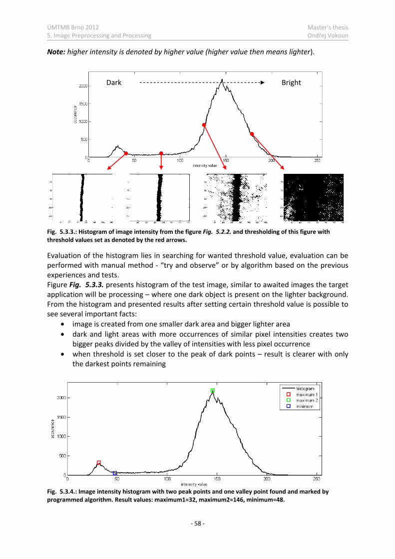
ÚMTMB Brno 2012 Master’s thesis 5. Image Preprocessing and Processing Ondřej Vokoun
- 58 -
Note: higher intensity is denoted by higher value (higher value then means lighter).
Fig. 5.3.3.: Histogram of image intensity from the figure Fig. 5.2.2. and thresholding of this figure with threshold values set as denoted by the red arrows.
Evaluation of the histogram lies in searching for wanted threshold value, evaluation can be performed with manual method - “try and observe” or by algorithm based on the previous experiences and tests. Figure Fig. 5.3.3. presents histogram of the test image, similar to awaited images the target application will be processing – where one dark object is present on the lighter background. From the histogram and presented results after setting certain threshold value is possible to see several important facts:
• image is created from one smaller dark area and bigger lighter area • dark and light areas with more occurrences of similar pixel intensities creates two
bigger peaks divided by the valley of intensities with less pixel occurrence • when threshold is set closer to the peak of dark points – result is clearer with only
the darkest points remaining
Fig. 5.3.4.: Image intensity histogram with two peak points and one valley point found and marked by programmed algorithm. Result values: maximum1=32, maximum2=146, minimum=48.
Dark Bright
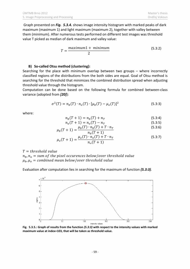
ÚMTMB Brno 2012 Master’s thesis 5. Image Preprocessing and Processing Ondřej Vokoun
- 59 -
Graph presented on Fig. 5.3.4. shows image intensity histogram with marked peaks of dark maximum (maximum 1) and light maximum (maximum 2), together with valley between them (minimum). After numerous tests performed on different test images was threshold value T picked as median of dark maximum and valley value: = 1 +2 (5.3:2)
B) So-called Otsu method (clustering): Searching for the place with minimum overlap between two groups – where incorrectly classified regions of the distributions from the both sides are equal. Goal of Otsu method is searching for the threshold that minimizes the combined distribution spread when adjusting threshold value through the histogram. Computation can be done based on the following formula for combined between-class variance (adopted from [20]): ( ) = ( ) ∙ ( ) ∙ ( ) − ( ) (5.3:3) where: ( + 1) = ( ) + (5.3:4) ( + 1) = ( ) − (5.3:5) ( + 1) = ( ) ∙ ( ) + ∙( + 1)
(5.3:6)
( + 1) = ( ) ∙ ( ) + ∙( + 1) (5.3:7)
= ℎ ℎ , = ℎ / ℎ ℎ , = / ℎ ℎ Evaluation after computation lies in searching for the maximum of function (5.3:3).
Fig. 5.3.5.: Graph of results from the function (5.3:3) with respect to the intensity values with marked maximum value at index=103, that will be taken as threshold value.
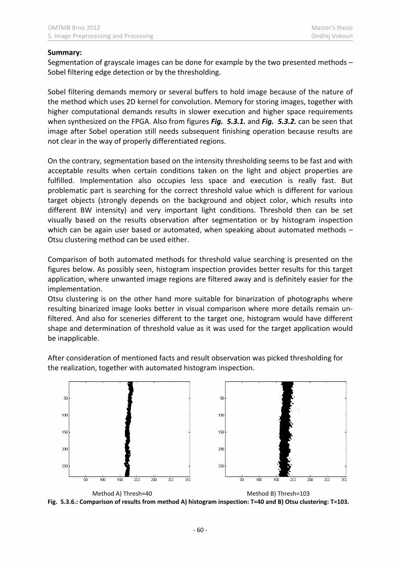
ÚMTMB Brno 2012 Master’s thesis 5. Image Preprocessing and Processing Ondřej Vokoun
- 60 -
Summary: Segmentation of grayscale images can be done for example by the two presented methods – Sobel filtering edge detection or by the thresholding. Sobel filtering demands memory or several buffers to hold image because of the nature of the method which uses 2D kernel for convolution. Memory for storing images, together with higher computational demands results in slower execution and higher space requirements when synthesized on the FPGA. Also from figures Fig. 5.3.1. and Fig. 5.3.2. can be seen that image after Sobel operation still needs subsequent finishing operation because results are not clear in the way of properly differentiated regions. On the contrary, segmentation based on the intensity thresholding seems to be fast and with acceptable results when certain conditions taken on the light and object properties are fulfilled. Implementation also occupies less space and execution is really fast. But problematic part is searching for the correct threshold value which is different for various target objects (strongly depends on the background and object color, which results into different BW intensity) and very important light conditions. Threshold then can be set visually based on the results observation after segmentation or by histogram inspection which can be again user based or automated, when speaking about automated methods – Otsu clustering method can be used either. Comparison of both automated methods for threshold value searching is presented on the figures below. As possibly seen, histogram inspection provides better results for this target application, where unwanted image regions are filtered away and is definitely easier for the implementation. Otsu clustering is on the other hand more suitable for binarization of photographs where resulting binarized image looks better in visual comparison where more details remain un-filtered. And also for sceneries different to the target one, histogram would have different shape and determination of threshold value as it was used for the target application would be inapplicable. After consideration of mentioned facts and result observation was picked thresholding for the realization, together with automated histogram inspection.
Method A) Thresh=40 Method B) Thresh=103 Fig. 5.3.6.: Comparison of results from method A) histogram inspection: T=40 and B) Otsu clustering: T=103.
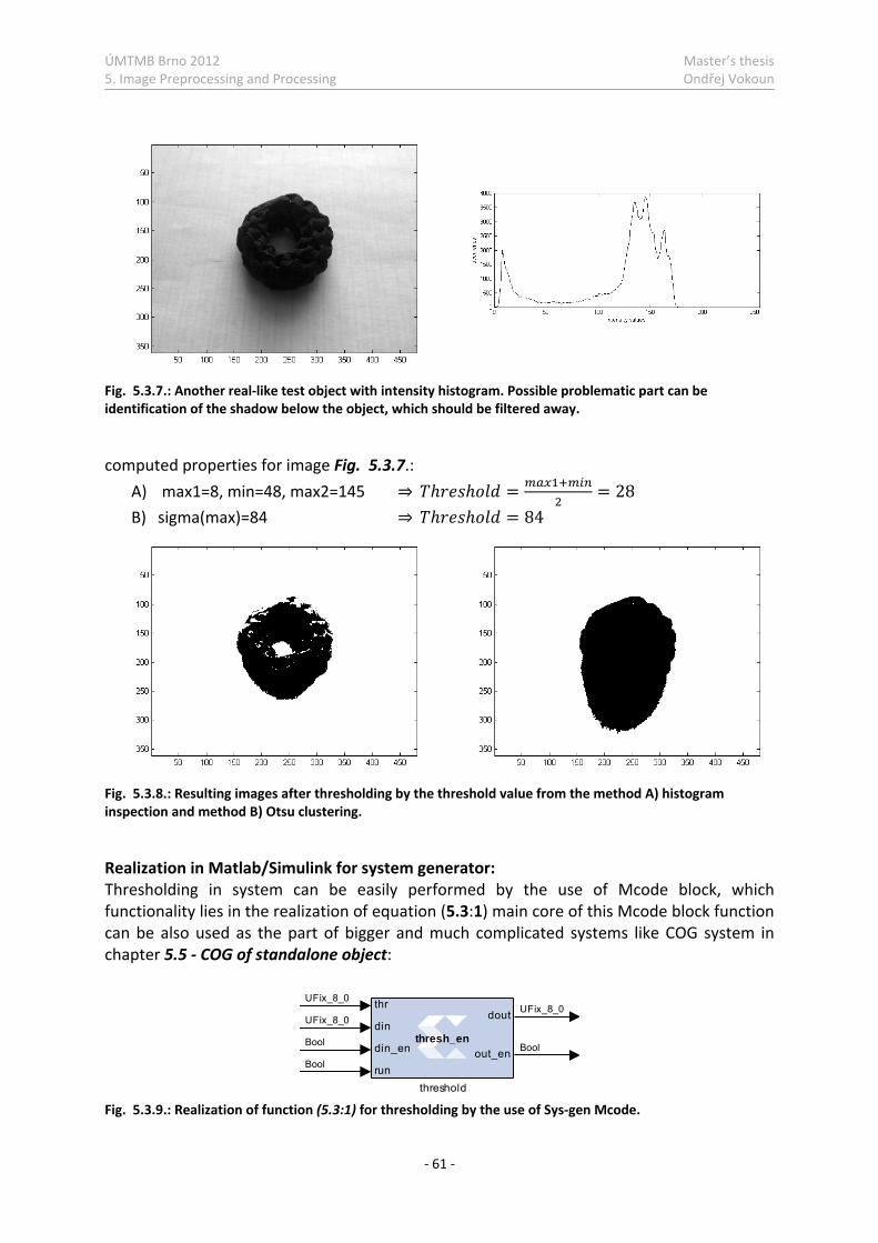
ÚMTMB Brno 2012 Master’s thesis 5. Image Preprocessing and Processing Ondřej Vokoun
- 61 -
Fig. 5.3.7.: Another real-like test object with intensity histogram. Possible problematic part can be identification of the shadow below the object, which should be filtered away.
computed properties for image Fig. 5.3.7.:
A) max1=8, min=48, max2=145 ⇒ ℎ ℎ = = 28
B) sigma(max)=84 ⇒ ℎ ℎ = 84
Fig. 5.3.8.: Resulting images after thresholding by the threshold value from the method A) histogram inspection and method B) Otsu clustering.
Realization in Matlab/Simulink for system generator: Thresholding in system can be easily performed by the use of Mcode block, which functionality lies in the realization of equation (5.3:1) main core of this Mcode block function can be also used as the part of bigger and much complicated systems like COG system in chapter 5.5 - COG of standalone object:
Fig. 5.3.9.: Realization of function (5.3:1) for thresholding by the use of Sys-gen Mcode.
thr
din
din_en
run
dout
out_enthresh_en
threshold
UFix_8_0
UFix_8_0
Bool
Bool
Bool
UFix_8_0
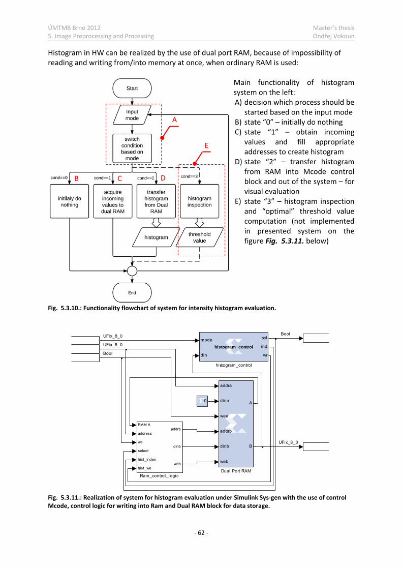
ÚMTMB Brno 2012 Master’s thesis 5. Image Preprocessing and Processing Ondřej Vokoun
- 62 -
Histogram in HW can be realized by the use of dual port RAM, because of impossibility of reading and writing from/into memory at once, when ordinary RAM is used:
Main functionality of histogram system on the left: A) decision which process should be
started based on the input mode B) state “0” – initially do nothing C) state “1” – obtain incoming
values and fill appropriate addresses to create histogram
D) state “2” – transfer histogram from RAM into Mcode control block and out of the system – for visual evaluation
E) state “3” – histogram inspection and “optimal” threshold value computation (not implemented in presented system on the figure Fig. 5.3.11. below)
Fig. 5.3.10.: Functionality flowchart of system for intensity histogram evaluation.
Fig. 5.3.11.: Realization of system for histogram evaluation under Simulink Sys-gen with the use of control Mcode, control logic for writing into Ram and Dual RAM block for data storage.
UFix_8_0
UFix_8_0
UFix_8_0
Bool
Bool
mode
din
sel
ind
wr
histogram_control
histogram_control
RAM A
address
we
select
hist_index
hist_we
addrb
dinb
web
Ram_control_logic
addra
dina
wea
addrb
dinb
web
A
B
Dual Port RAM
0
A
B C D
E
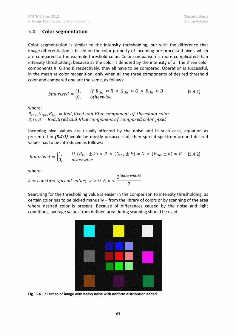
ÚMTMB Brno 2012 Master’s thesis 5. Image Preprocessing and Processing Ondřej Vokoun
- 63 -
5.4. Color segmentation Color segmentation is similar to the intensity thresholding, but with the difference that image differentiation is based on the color property of incoming pre-processed pixels which are compared to the example threshold color. Color comparison is more complicated than intensity thresholding, because as the color is denoted by the intensity of all the three color components R, G and B respectively, they all have to be compared. Operation is successful, in the mean as color recognition, only when all the three components of desired threshold color and compared one are the same, as follows: = 1, ≈ ∧ ≈ ∧ ≈0, ℎ (5.4:1)
where: , , = , ℎ ℎ , , = , Incoming pixel values are usually affected by the noise and in such case, equation as presented in (5.4:1) would be mostly unsuccessful, then spread spectrum around desired values has to be introduced as follows:
= 1, ( ± ) ≈ ∧ ( ± ) ≈ ∧ ( ± ) ≈0, ℎ (5.4:2)
where: = ; > 0 ∧ < 2( _ )2
Searching for the thresholding value is easier in the comparison to intensity thresholding, as certain color has to be picked manually – from the library of colors or by scanning of the area where desired color is present. Because of differences caused by the noise and light conditions, average values from defined area during scanning should be used.
Fig. 5.4.1.: Test color image with heavy noise with uniform distribution added.
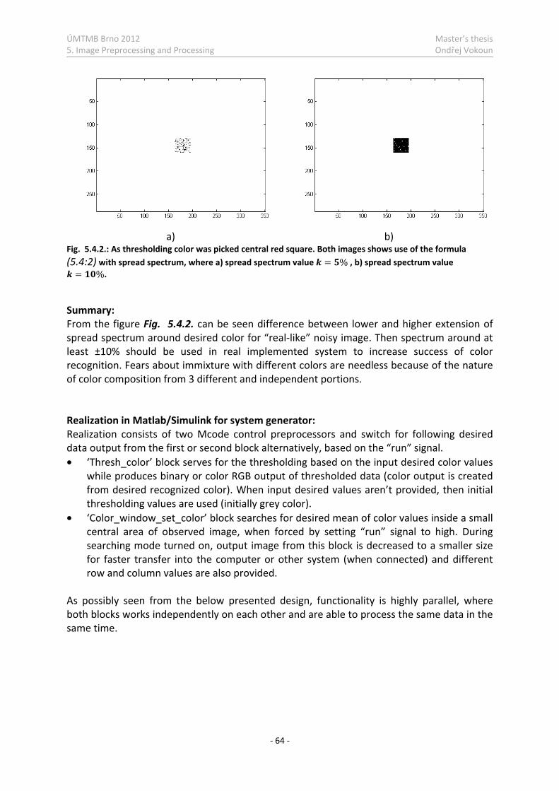
ÚMTMB Brno 2012 Master’s thesis 5. Image Preprocessing and Processing Ondřej Vokoun
- 64 -
a) b) Fig. 5.4.2.: As thresholding color was picked central red square. Both images shows use of the formula (5.4:2) with spread spectrum, where a) spread spectrum value = % , b) spread spectrum value = %.
Summary: From the figure Fig. 5.4.2. can be seen difference between lower and higher extension of spread spectrum around desired color for “real-like” noisy image. Then spectrum around at least ±10% should be used in real implemented system to increase success of color recognition. Fears about immixture with different colors are needless because of the nature of color composition from 3 different and independent portions. Realization in Matlab/Simulink for system generator: Realization consists of two Mcode control preprocessors and switch for following desired data output from the first or second block alternatively, based on the “run” signal. • ‘Thresh_color’ block serves for the thresholding based on the input desired color values
while produces binary or color RGB output of thresholded data (color output is created from desired recognized color). When input desired values aren’t provided, then initial thresholding values are used (initially grey color).
• ‘Color_window_set_color’ block searches for desired mean of color values inside a small central area of observed image, when forced by setting “run” signal to high. During searching mode turned on, output image from this block is decreased to a smaller size for faster transfer into the computer or other system (when connected) and different row and column values are also provided.
As possibly seen from the below presented design, functionality is highly parallel, where both blocks works independently on each other and are able to process the same data in the same time.
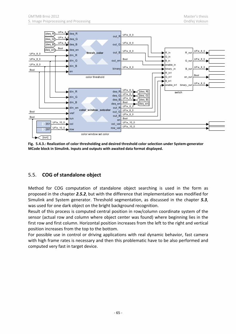
ÚMTMB Brno 2012 Master’s thesis 5. Image Preprocessing and Processing Ondřej Vokoun
- 65 -
Fig. 5.4.3.: Realization of color thresholding and desired threshold color selection under System-generator MCode block in Simulink. Inputs and outputs with awaited data format displayed.
5.5. COG of standalone object Method for COG computation of standalone object searching is used in the form as proposed in the chapter 2.5.2, but with the difference that implementation was modified for Simulink and System generator. Threshold segmentation, as discussed in the chapter 5.3, was used for one dark object on the bright background recognition. Result of this process is computed central position in row/column coordinate system of the sensor (actual row and column where object center was found) where beginning lies in the first row and first column. Horizontal position increases from the left to the right and vertical position increases from the top to the bottom. For possible use in control or driving applications with real dynamic behavior, fast camera with high frame rates is necessary and then this problematic have to be also performed and computed very fast in target device.
287
351
R_in
G_inB_in
enable_in
binary _inR_in1
G_in1
B_in1enable_in1
R_out
G_out
B_out
en_out
binary _out
switchdin_R
din_G
din_B
din_en
vref
run
col
row
des_Rdes_Gdes_B
des_enout_Rout_Gout_B
encol_valrow_val
color_window_setcolor
color window set color
des_R
des_G
des_B
des_en
din_R
din_G
din_B
en
out_R
out_G
out_B
out_en
binary
thresh_color
color threshold
[run]
[des_en][des_B][des_G][des_R]
[des_en]
[des_B]
[des_G]
[des_R]
UFix_8_0
UFix_8_0UFix_8_0
UFix_8_0
UFix_8_0
UFix_8_0
Bool
Bool
UFix_8_0
UFix_8_0
UFix_8_0
Bool
UFix_8_0
UFix_8_0
UFix_8_0
UFix_8_0Bool
UFix_8_0
UFix_8_0
UFix_8_0
Bool
UFix_8_0
UFix_10_0
UFix_10_0
Bool
UFix_8_0
UFix_8_0
UFix_8_0
Bool
Bool
UFix_10_0
UFix_10_0

ÚMTMB Brno 2012 Master’s thesis 5. Image Preprocessing and Processing Ondřej Vokoun
- 66 -
Realization in Matlab/Simulink for system generator:
Fig. 5.5.1.: Flowchart of COG block functionality created in Simulink, System-generator Mcode.
Fig. 5.5.2.: Realization of object center recognition based on the thresholding under System generator Mcode block in Simulink. Inputs and outputs with awaited data format displayed.
thr
din
din_en
rst
vref
col
row
horizontal
vertical
done
thresh_objrec
threshold + center computation
UFix_8_0
Bool
UFix_8_0
Bool
UFix_10_0
UFix_10_0
Bool
Bool
UFix_10_0
UFix_10_0

ÚMTMB Brno 2012 Master’s thesis 5. Image Preprocessing and Processing Ondřej Vokoun
- 67 -
Summary: Several figures with resulting center presenting functionality of COG algorithm.
Fig. 5.5.3.: Source image with cross mark at the computed position after COG operation, as possibly seen – when object is larger than image size in certain axis, center is logically in the middle.
As mentioned earlier, COG searching depends on image segmentation and threshold value dependency is presented on the following figure:
a) thr=25 b) thr=80 Fig. 5.5.4.: COG performed on the same test image with different threshold value set, in the first row are shown binary images after thresholding operation and in the second row original image with marked central position, that was computed. As possibly seen, binarized objects and then central positions are different.
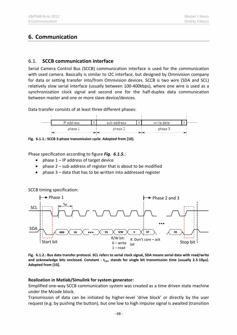
ÚMTMB Brno 2012 Master’s thesis 6 Communication Ondřej Vokoun
- 68 -
6. Communication
6.1. SCCB communication interface Serial Camera Control Bus (SCCB) communication interface is used for the communication with used camera. Basically is similar to I2C interface, but designed by Omnivision company for data or setting transfer into/from Omnivision devices. SCCB is two wire (SDA and SCL) relatively slow serial interface (usually between 100-400kbps), where one wire is used as a synchronization clock signal and second one for the half-duplex data communication between master and one or more slave device/devices. Data transfer consists of at least three different phases:
Fig. 6.1.1.: SCCB 3-phase transmission cycle. Adopted from [10].
Phase specification according to figure Fig. 6.1.5.:
• phase 1 – IP address of target device • phase 2 – sub-address of register that is about to be modified • phase 3 – data that has to be written into addressed register
SCCB timing specification:
Fig. 6.1.2.: Bus data transfer protocol. SCL refers to serial clock signal, SDA means serial data with read/write and acknowledge bits enclosed. Constant - tcyc, stands for single bit transmission time (usually 2.5-10μs). Adopted from [10].
Realization in Matlab/Simulink for system generator: Simplified one-way SCCB communication system was created as a time driven state machine under the Mcode block. Transmission of data can be initiated by higher-level ‘drive block’ or directly by the user request (e.g. by pushing the button), but one low to high impulse signal is awaited (transition
Phase 1 Phase 2 and 3
Start bit Stop bit X: Don’t care – ack bit
R/W bit: 0 – write 1 – read
SDA
SCL
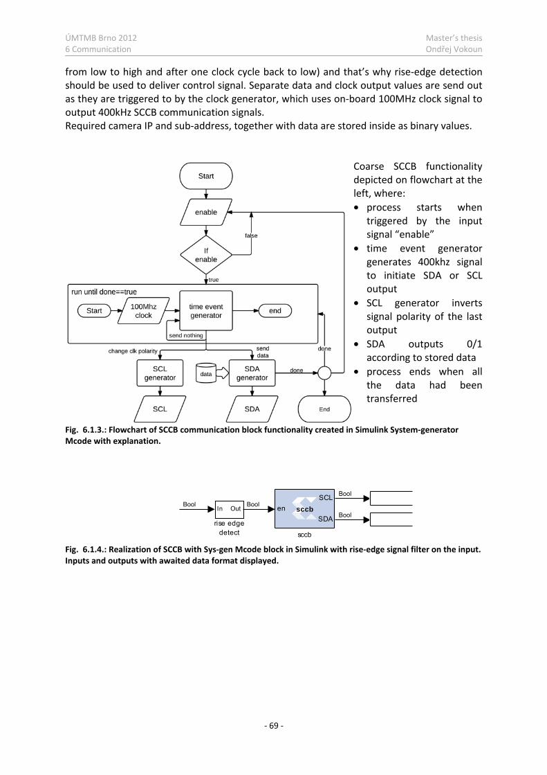
ÚMTMB Brno 2012 Master’s thesis 6 Communication Ondřej Vokoun
- 69 -
from low to high and after one clock cycle back to low) and that’s why rise-edge detection should be used to deliver control signal. Separate data and clock output values are send out as they are triggered to by the clock generator, which uses on-board 100MHz clock signal to output 400kHz SCCB communication signals. Required camera IP and sub-address, together with data are stored inside as binary values.
Coarse SCCB functionality depicted on flowchart at the left, where: • process starts when
triggered by the input signal “enable”
• time event generator generates 400khz signal to initiate SDA or SCL output
• SCL generator inverts signal polarity of the last output
• SDA outputs 0/1 according to stored data
• process ends when all the data had beentransferred
Fig. 6.1.3.: Flowchart of SCCB communication block functionality created in Simulink System-generator Mcode with explanation.
Fig. 6.1.4.: Realization of SCCB with Sys-gen Mcode block in Simulink with rise-edge signal filter on the input. Inputs and outputs with awaited data format displayed.
enSCL
SDAsccb
sccb
In Out
rise edgedetect
Bool
Bool
BoolBool
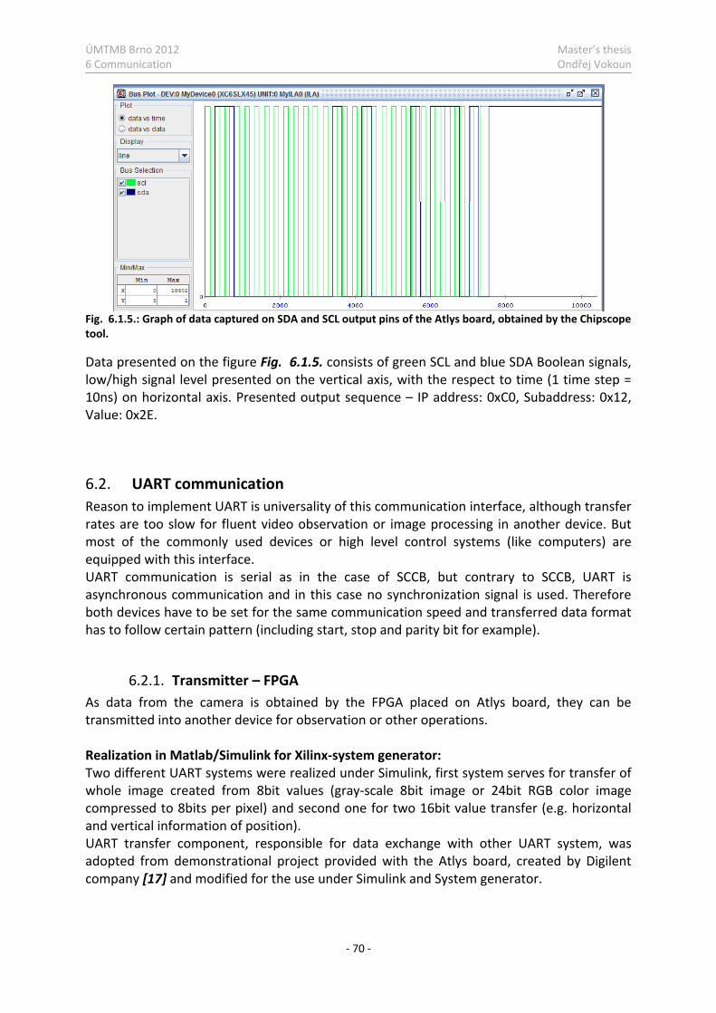
ÚMTMB Brno 2012 Master’s thesis 6 Communication Ondřej Vokoun
- 70 -
Fig. 6.1.5.: Graph of data captured on SDA and SCL output pins of the Atlys board, obtained by the Chipscope tool.
Data presented on the figure Fig. 6.1.5. consists of green SCL and blue SDA Boolean signals, low/high signal level presented on the vertical axis, with the respect to time (1 time step = 10ns) on horizontal axis. Presented output sequence – IP address: 0xC0, Subaddress: 0x12, Value: 0x2E.
6.2. UART communication Reason to implement UART is universality of this communication interface, although transfer rates are too slow for fluent video observation or image processing in another device. But most of the commonly used devices or high level control systems (like computers) are equipped with this interface. UART communication is serial as in the case of SCCB, but contrary to SCCB, UART is asynchronous communication and in this case no synchronization signal is used. Therefore both devices have to be set for the same communication speed and transferred data format has to follow certain pattern (including start, stop and parity bit for example).
6.2.1. Transmitter – FPGA As data from the camera is obtained by the FPGA placed on Atlys board, they can be transmitted into another device for observation or other operations. Realization in Matlab/Simulink for Xilinx-system generator: Two different UART systems were realized under Simulink, first system serves for transfer of whole image created from 8bit values (gray-scale 8bit image or 24bit RGB color image compressed to 8bits per pixel) and second one for two 16bit value transfer (e.g. horizontal and vertical information of position). UART transfer component, responsible for data exchange with other UART system, was adopted from demonstrational project provided with the Atlys board, created by Digilent company [17] and modified for the use under Simulink and System generator.
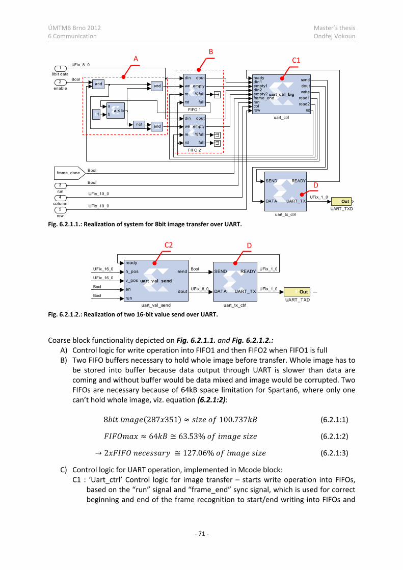
ÚMTMB Brno 2012 Master’s thesis 6 Communication Ondřej Vokoun
- 71 -
Fig. 6.2.1.1.: Realization of system for 8bit image transfer over UART.
Fig. 6.2.1.2.: Realization of two 16-bit value send over UART.
Coarse block functionality depicted on Fig. 6.2.1.1. and Fig. 6.2.1.2.:
A) Control logic for write operation into FIFO1 and then FIFO2 when FIFO1 is full B) Two FIFO buffers necessary to hold whole image before transfer. Whole image has to
be stored into buffer because data output through UART is slower than data are coming and without buffer would be data mixed and image would be corrupted. Two FIFOs are necessary because of 64kB space limitation for Spartan6, where only one can’t hold whole image, viz. equation (6.2.1:2): 8 (287 351) ≈ 100.737 (6.2.1:1)≈ 64 ≅ 63.53% (6.2.1:2)→ 2 ≅ 127.06% (6.2.1:3)
C) Control logic for UART operation, implemented in Mcode block: C1 : ‘Uart_ctrl’ Control logic for image transfer – starts write operation into FIFOs,
based on the “run” signal and “frame_end” sync signal, which is used for correct beginning and end of the frame recognition to start/end writing into FIFOs and
UFix_8_0
Bool
Bool
UFix_10_0
UFix_10_0
Bool
UFix_1_0
SEND
DATA
READY
UART_TX
uart_tx_ctrl
readydin1empty1din2empty2frame_endruncolrow
senddoutwrite
read1read2
rst
uart_ctrl_big
uart_ctrl
frame_done
Out UART_TXD
a
ba < b
and
and
and
notdin
we
re
rst
dout
empty
%full
full
FIFO 2
din
we
re
rst
dout
empty
%full
full
FIFO 11
5row
4column
3run
2enable
18bit data
ready
h_pos
v_pos
en
run
send
dout
uart_v al_send
uart_val_send
SEND
DATA
READY
UART_TX
uart_tx_ctrl
Out UART_TXD
UFix_1_0
Bool
UFix_8_0
UFix_1_0UFix_16_0
UFix_16_0
Bool
Bool
A B
D
C1
C2 D
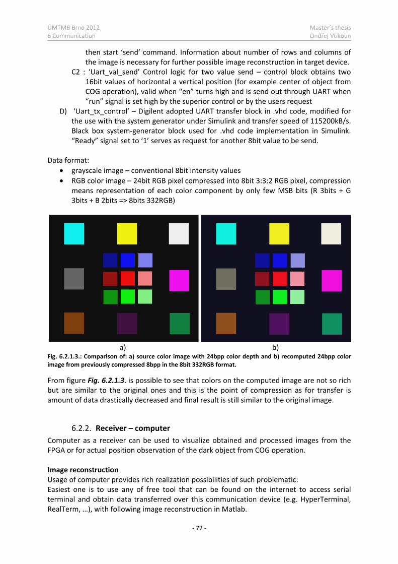
ÚMTMB Brno 2012 Master’s thesis 6 Communication Ondřej Vokoun
- 72 -
then start ‘send’ command. Information about number of rows and columns of the image is necessary for further possible image reconstruction in target device.
C2 : ‘Uart_val_send’ Control logic for two value send – control block obtains two 16bit values of horizontal a vertical position (for example center of object from COG operation), valid when “en” turns high and is send out through UART when “run” signal is set high by the superior control or by the users request
D) ‘Uart_tx_control’ – Digilent adopted UART transfer block in .vhd code, modified for the use with the system generator under Simulink and transfer speed of 115200kB/s. Black box system-generator block used for .vhd code implementation in Simulink. “Ready” signal set to ‘1’ serves as request for another 8bit value to be send.
Data format: • grayscale image – conventional 8bit intensity values • RGB color image – 24bit RGB pixel compressed into 8bit 3:3:2 RGB pixel, compression
means representation of each color component by only few MSB bits (R 3bits + G 3bits + B 2bits => 8bits 332RGB)
a) b) Fig. 6.2.1.3.: Comparison of: a) source color image with 24bpp color depth and b) recomputed 24bpp color image from previously compressed 8bpp in the 8bit 332RGB format.
From figure Fig. 6.2.1.3. is possible to see that colors on the computed image are not so rich but are similar to the original ones and this is the point of compression as for transfer is amount of data drastically decreased and final result is still similar to the original image.
6.2.2. Receiver – computer Computer as a receiver can be used to visualize obtained and processed images from the FPGA or for actual position observation of the dark object from COG operation. Image reconstruction Usage of computer provides rich realization possibilities of such problematic: Easiest one is to use any of free tool that can be found on the internet to access serial terminal and obtain data transferred over this communication device (e.g. HyperTerminal, RealTerm, …), with following image reconstruction in Matlab.

ÚMTMB Brno 2012 Master’s thesis 6 Communication Ondřej Vokoun
- 73 -
Another, bit more complicated, can be use of Matlab/Simulink for data receive and further image reconstruction or other universal program as LabView or custom program in C++/C#.
Fig. 6.2.2.1.: Simulink model for gray-scale image visualization.
Camera test color pattern image:
Fig. 6.2.2.2.: Reconstruction of color image send compressed over UART. Reconstruction was done in Matlab and data were obtained and stored with the Realterm software.
Previous image on Fig. 6.2.2.2. presents color output from the camera which was set by the SCCB to output color test pattern, poor image quality is because of compression during data transfer and light incoming to sensor which affects the output image. Note: Instead of sending compressed color image in poor quality, Raw RGB un-pre-processed data input could be used and then later in the computer processed to provide better quality images, but this access is not the target of such operation, because computer is used only for results observation.
VideoViewer
ImageImageImage
Video Viewer
COM4Data
Status
Serial Receive
COM4115200
8,none,1
Serial Configuration
Scope Memory
din
img_in
imgImCreate
EmbeddedMATLAB Function
single
single
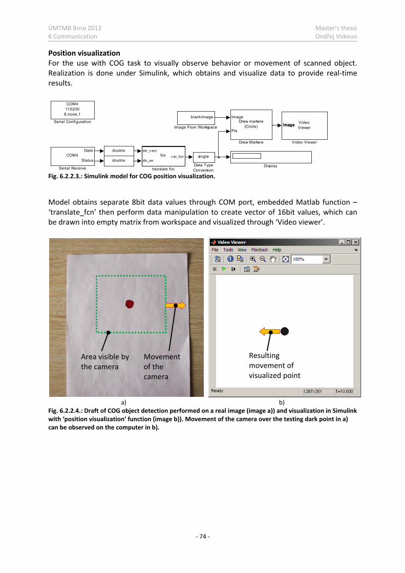
ÚMTMB Brno 2012 Master’s thesis 6 Communication Ondřej Vokoun
- 74 -
Position visualization For the use with COG task to visually observe behavior or movement of scanned object. Realization is done under Simulink, which obtains and visualize data to provide real-time results.
Fig. 6.2.2.3.: Simulink model for COG position visualization.
Model obtains separate 8bit data values through COM port, embedded Matlab function – ‘translate_fcn’ then perform data manipulation to create vector of 16bit values, which can be drawn into empty matrix from workspace and visualized through ‘Video viewer’.
a) b)Fig. 6.2.2.4.: Draft of COG object detection performed on a real image (image a)) and visualization in Simulink with ‘position visualization’ function (image b)). Movement of the camera over the testing dark point in a) can be observed on the computer in b).
din_v ect
din_env er_horfcn
translate fcn
VideoViewer
ImageImageImage
Video Viewer
COM4Data
Status
Serial Receive
COM4115200
8,none,1
Serial ConfigurationblankImage
Image From WorkspaceDraw markers
(Circle)
Image
Pts
Draw Markers
Display
double
doublesingle
Data TypeConversion
Area visible by the camera
Movement of the camera
Resulting movement of visualized point

ÚMTMB Brno 2012 Master’s thesis 7 Software and hardware simulations of the FPGA designed system Ondřej Vokoun
- 75 -
7. Software and hardware simulations of the FPGA designed system
Simulations are necessary to verify operation correctness of designed system and give overall look on the processes in the progress and their results before real camera can be attached. Two minor ways of how to perform such simulation/verification can be undertaken – software and hardware testing. Software testing lies only in the pure software access that means testing of simulated system on the computer. Hardware testing needs real hardware (FPGA chip) the software was created and compiled for, but in the difference to final use – test data can be still provided from the computer and also results can be observed on the computer as well. Last method of simulation is usage of the system on real hardware with real data from the camera and results observing on the computer or another device that allows it.
Fig. 7.1.: Design flow- Matlab/Simulink->Xilinx ISE->FPGA device. (Image Adopted from [13])
For the tests was as the reference design used color system, which process Raw RGB data into common RGB and after conversion from RGB into BW undertakes COG inspection. System design is depicted in the chapter 4.2.1 - Overall system design, but block for thresholding was replaced with the COG Mcode block. For several test operations was impossible to simulate multiclock system with different time domains as a one part, so both domains had to be examined separately.
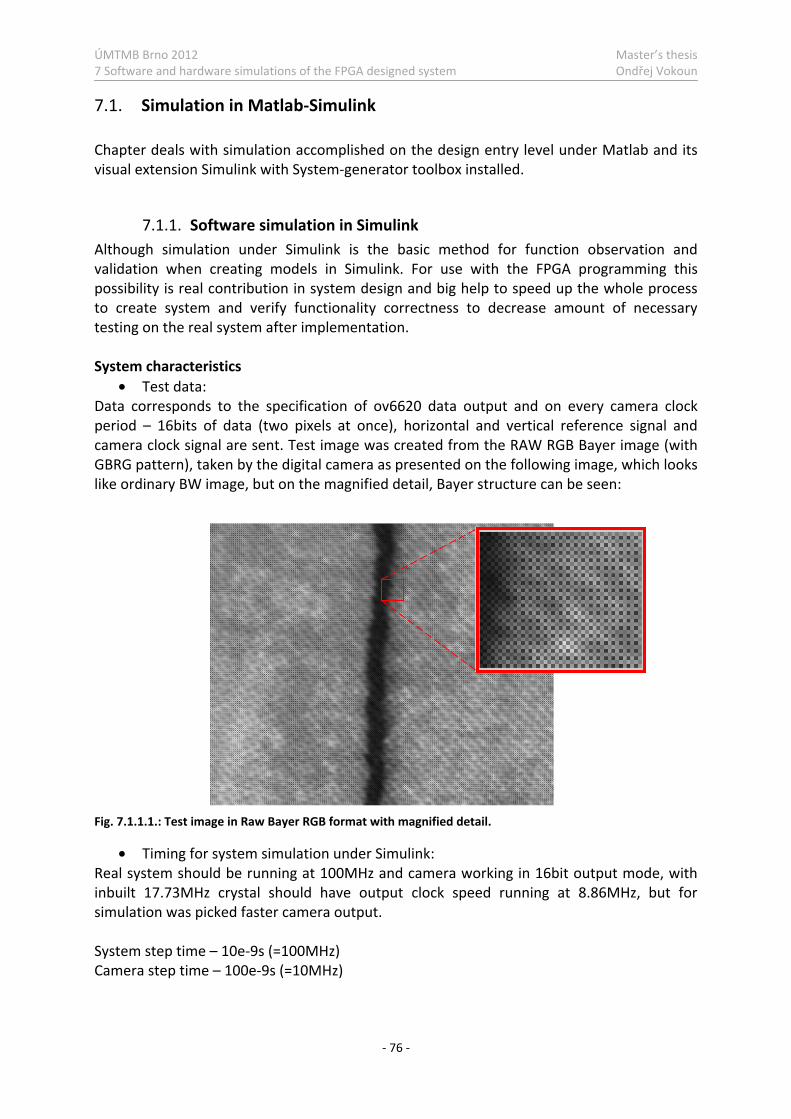
ÚMTMB Brno 2012 Master’s thesis 7 Software and hardware simulations of the FPGA designed system Ondřej Vokoun
- 76 -
7.1. Simulation in Matlab-Simulink Chapter deals with simulation accomplished on the design entry level under Matlab and its visual extension Simulink with System-generator toolbox installed.
7.1.1. Software simulation in Simulink Although simulation under Simulink is the basic method for function observation and validation when creating models in Simulink. For use with the FPGA programming this possibility is real contribution in system design and big help to speed up the whole process to create system and verify functionality correctness to decrease amount of necessary testing on the real system after implementation. System characteristics
• Test data: Data corresponds to the specification of ov6620 data output and on every camera clock period – 16bits of data (two pixels at once), horizontal and vertical reference signal and camera clock signal are sent. Test image was created from the RAW RGB Bayer image (with GBRG pattern), taken by the digital camera as presented on the following image, which looks like ordinary BW image, but on the magnified detail, Bayer structure can be seen:
Fig. 7.1.1.1.: Test image in Raw Bayer RGB format with magnified detail.
• Timing for system simulation under Simulink: Real system should be running at 100MHz and camera working in 16bit output mode, with inbuilt 17.73MHz crystal should have output clock speed running at 8.86MHz, but for simulation was picked faster camera output. System step time – 10e-9s (=100MHz) Camera step time – 100e-9s (=10MHz)
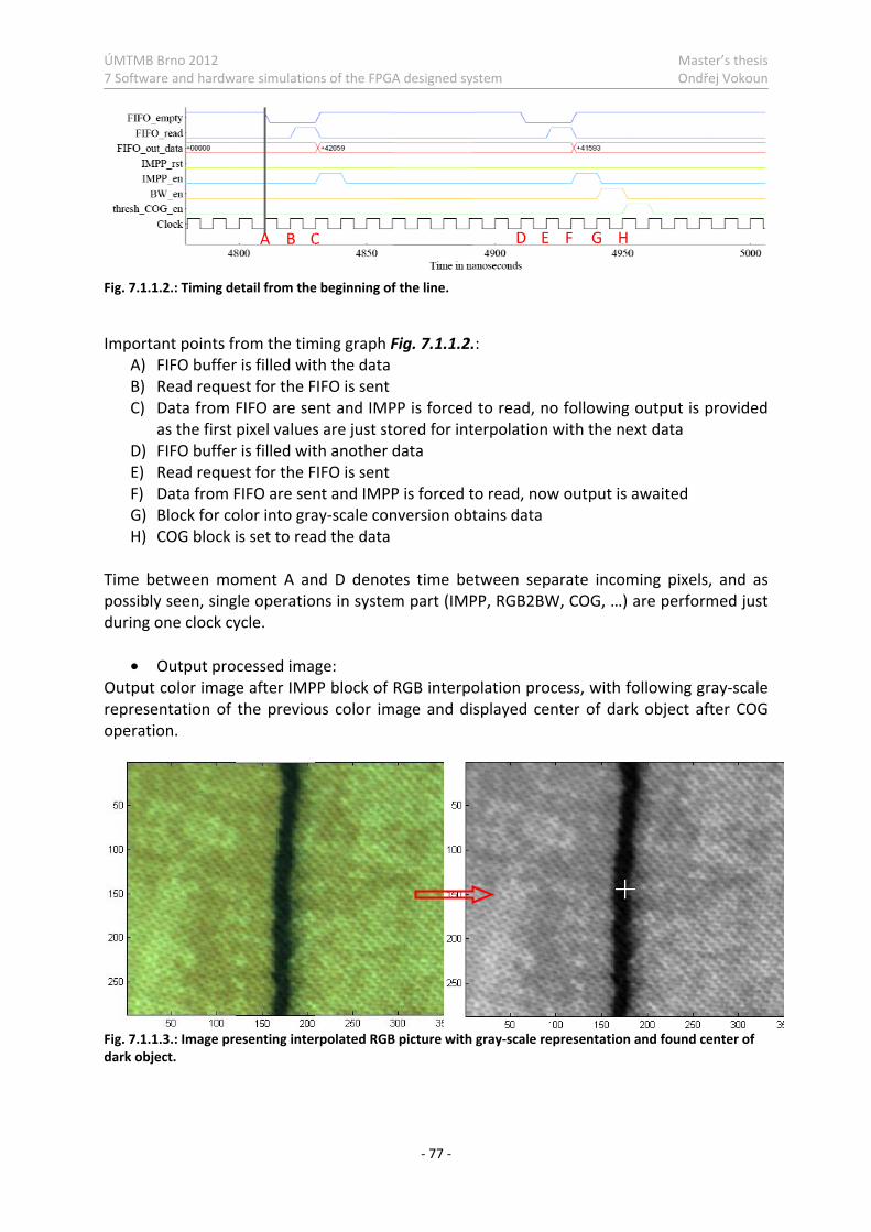
ÚMTMB 7 Softwar
Fig. 7.1.1
Importa
A) B) C)
aD) E) F) G) H)
Time bepossiblyduring o
• Output represeoperatio
Fig. 7.1.1dark obje
Brno 2012 re and hardwa
1.2.: Timing de
ant points frFIFO bufferRead requeData from as the first FIFO bufferRead requeData from FBlock for coCOG block i
etween moy seen, singone clock cy
Output procolor imag
entation of on.
1.3.: Image preect.
are simulation
etail from the
rom the timr is filled witest for the FFIFO are sepixel values
r is filled witest for the FFIFO are senolor into grais set to rea
oment A angle operatioycle.
cessed imae after IMPthe previou
esenting inte
A B C
ns of the FPGA
e beginning of
ming graph Fth the dataFIFO is sentent and IMPs are just stth another dFIFO is sentnt and IMPPay-scale conad the data
nd D denotons in system
ge: PP block of us color im
rpolated RGB
C
A designed sy
- 77 -
f the line.
Fig. 7.1.1.2.
PP is forcedored for intdata
P is forced tnversion ob
tes time bem part (IMP
RGB interpomage and di
B picture with
ystem
.:
to read, noterpolation
to read, nowtains data
etween sepPP, RGB2BW
olation procsplayed cen
gray-scale re
D E
o following with the ne
w output is
arate incomW, COG, …)
cess, with fnter of dar
epresentation
F G H
MastOndř
output is pext data
awaited
ming pixelsare perform
following grrk object af
n and found ce
er’s thesis ej Vokoun
provided
, and as med just
ray-scale fter COG
enter of
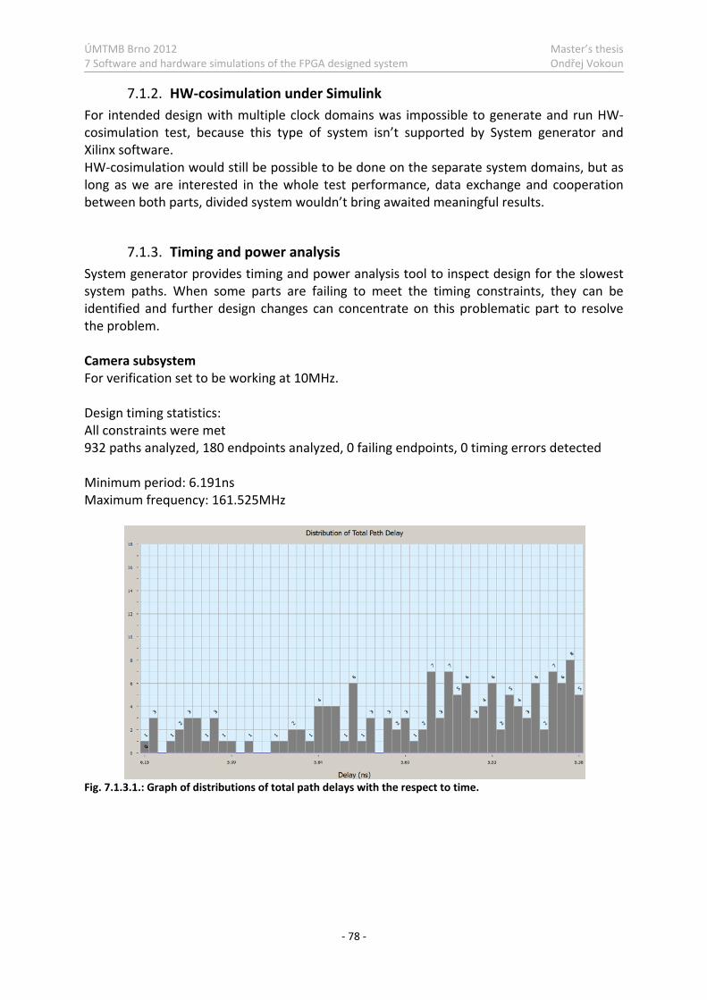
ÚMTMB Brno 2012 Master’s thesis 7 Software and hardware simulations of the FPGA designed system Ondřej Vokoun
- 78 -
7.1.2. HW-cosimulation under Simulink For intended design with multiple clock domains was impossible to generate and run HW-cosimulation test, because this type of system isn’t supported by System generator and Xilinx software. HW-cosimulation would still be possible to be done on the separate system domains, but as long as we are interested in the whole test performance, data exchange and cooperation between both parts, divided system wouldn’t bring awaited meaningful results.
7.1.3. Timing and power analysis System generator provides timing and power analysis tool to inspect design for the slowest system paths. When some parts are failing to meet the timing constraints, they can be identified and further design changes can concentrate on this problematic part to resolve the problem. Camera subsystem For verification set to be working at 10MHz. Design timing statistics: All constraints were met 932 paths analyzed, 180 endpoints analyzed, 0 failing endpoints, 0 timing errors detected Minimum period: 6.191ns Maximum frequency: 161.525MHz
Fig. 7.1.3.1.: Graph of distributions of total path delays with the respect to time.
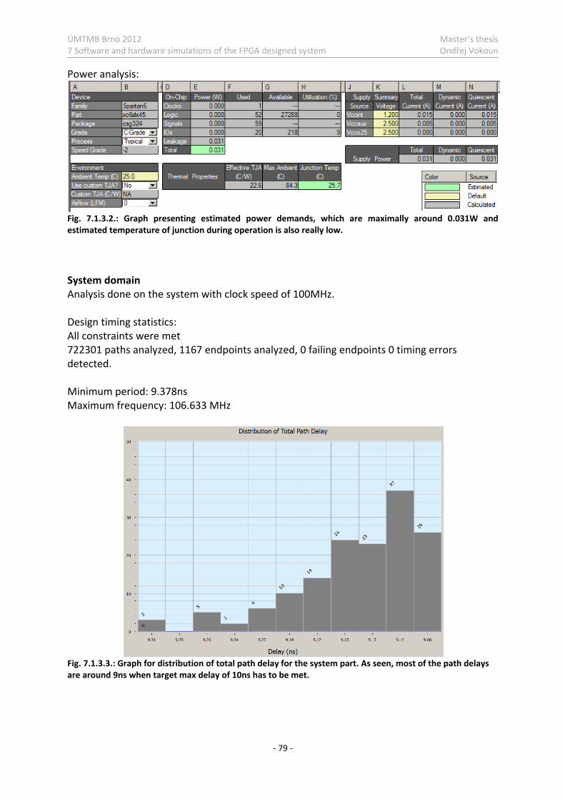
ÚMTMB Brno 2012 Master’s thesis 7 Software and hardware simulations of the FPGA designed system Ondřej Vokoun
- 79 -
Power analysis:
Fig. 7.1.3.2.: Graph presenting estimated power demands, which are maximally around 0.031W and estimated temperature of junction during operation is also really low.
System domain Analysis done on the system with clock speed of 100MHz. Design timing statistics: All constraints were met 722301 paths analyzed, 1167 endpoints analyzed, 0 failing endpoints 0 timing errors detected. Minimum period: 9.378ns Maximum frequency: 106.633 MHz
Fig. 7.1.3.3.: Graph for distribution of total path delay for the system part. As seen, most of the path delays are around 9ns when target max delay of 10ns has to be met.
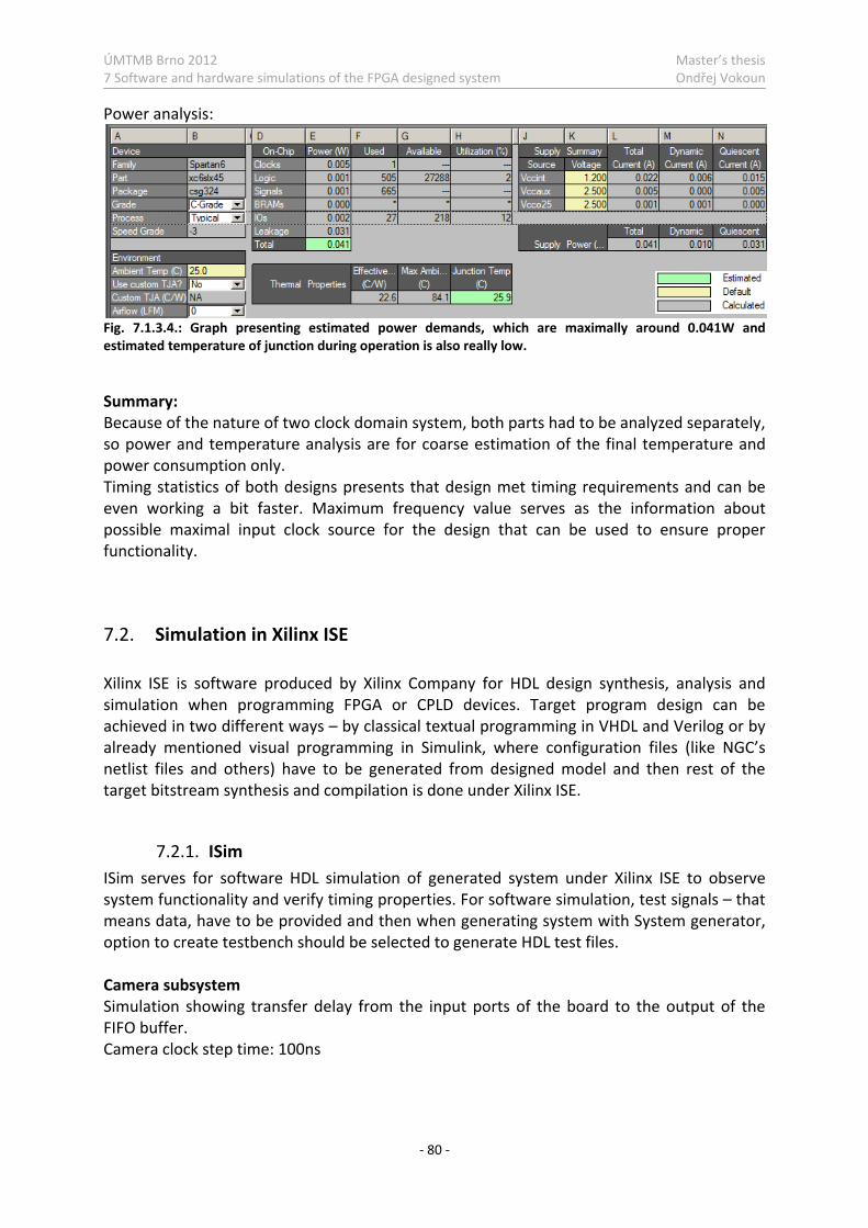
ÚMTMB Brno 2012 Master’s thesis 7 Software and hardware simulations of the FPGA designed system Ondřej Vokoun
- 80 -
Power analysis:
Fig. 7.1.3.4.: Graph presenting estimated power demands, which are maximally around 0.041W and estimated temperature of junction during operation is also really low.
Summary: Because of the nature of two clock domain system, both parts had to be analyzed separately, so power and temperature analysis are for coarse estimation of the final temperature and power consumption only. Timing statistics of both designs presents that design met timing requirements and can be even working a bit faster. Maximum frequency value serves as the information about possible maximal input clock source for the design that can be used to ensure proper functionality.
7.2. Simulation in Xilinx ISE Xilinx ISE is software produced by Xilinx Company for HDL design synthesis, analysis and simulation when programming FPGA or CPLD devices. Target program design can be achieved in two different ways – by classical textual programming in VHDL and Verilog or by already mentioned visual programming in Simulink, where configuration files (like NGC’s netlist files and others) have to be generated from designed model and then rest of the target bitstream synthesis and compilation is done under Xilinx ISE.
7.2.1. ISim ISim serves for software HDL simulation of generated system under Xilinx ISE to observe system functionality and verify timing properties. For software simulation, test signals – that means data, have to be provided and then when generating system with System generator, option to create testbench should be selected to generate HDL test files. Camera subsystem Simulation showing transfer delay from the input ports of the board to the output of the FIFO buffer. Camera clock step time: 100ns
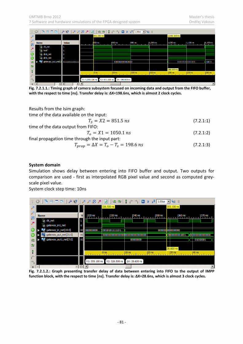
ÚMTMB Brno 2012 Master’s thesis 7 Software and hardware simulations of the FPGA designed system Ondřej Vokoun
- 81 -
Fig. 7.2.1.1.: Timing graph of camera subsystem focused on incoming data and output from the FIFO buffer, with the respect to time [ns]. Transfer delay is: ΔX=198.6ns, which is almost 2 clock cycles.
Results from the Isim graph: time of the data available on the input: = 2 = 851.5 (7.2.1:1) time of the data output from FIFO: = 1 = 1050.1 (7.2.1:2) final propagation time through the input part: = ∆ = − = 198.6 (7.2.1:3)
System domain Simulation shows delay between entering into FIFO buffer and output. Two outputs for comparison are used - first as interpolated RGB pixel value and second as computed grey-scale pixel value. System clock step time: 10ns
Fig. 7.2.1.2.: Graph presenting transfer delay of data between entering into FIFO to the output of IMPP function block, with the respect to time [ns]. Transfer delay is: ΔX=28.6ns, which is almost 3 clock cycles.
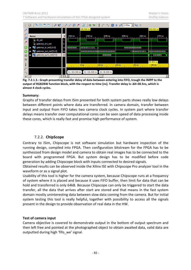
ÚMTMB Brno 2012 Master’s thesis 7 Software and hardware simulations of the FPGA designed system Ondřej Vokoun
- 82 -
Fig. 7.2.1.3.: Graph presenting transfer delay of data between entering into FIFO, trough the IMPP to the output of RGB2BW function block, with the respect to time [ns]. Transfer delay is: ΔX=38.5ns, which is almost 4 clock cycles.
Summary: Graphs of transfer delays from ISim presented for both system parts shows really low delays between different points where data are transferred. In camera domain, transfer between input and output from FIFO takes two camera clock cycles. In system part where transfer delays means transfer over computational cores can be seen speed of data processing inside these cores, which is really fast and promise high performance of system.
7.2.2. ChipScope Contrary to ISim, Chipscope is not software simulation but hardware inspection of the running design, compiled into FPGA. Then configuration bitstream for the FPGA has to be synthesized from design model and camera to obtain real images has to be connected to the board with programmed FPGA. But system design has to be modified before code generation by adding Chipscope block with inputs connected to desired signals. Obtained results can be observed inside the Xilinx ISE with Chipscope Pro analyzer tool in the waveform or as a signal plot. Usability of this tool is higher for the camera system, because Chipscope runs at a frequency of system where it is placed and because it uses FIFO buffer, then limit for data that can be hold and transferred is only 64kB. Because Chipscope can only be triggered to start the data transfer, all the data that arrives after start are stored and that means in the fast system domain mostly uninteresting data between slow data coming from the camera. But for initial system testing this tool is really helpful, together with possibility to access all the signals present in the design to provide observation of real data in the HW. Test of camera input Camera objective is covered to demonstrate output in the bottom of output spectrum and then left free and pointed at the photographed object to obtain awaited data, valid data are outputted during high ‘fifo_we’ signal.

ÚMTMB Brno 2012 Master’s thesis 7 Software and hardware simulations of the FPGA designed system Ondřej Vokoun
- 83 -
Fig. 7.2.2.1.: “Black” data output intensity with the respect to time [1e-8 s], when camera objective is covered. Several small peaks which differ from the same level are caused by the noise.
Fig. 7.2.2.2.: Output of one line of standard image, with several peaks caused by the character of “photographed” image. Pixel intensity with the respect to time [1e-8 s].
Fig. 7.2.2.3.: Time waveform of obtained data from camera subsystem at the beginning of the line.
Previous figure presents beginning of the line with data, data are valid at ‘fifo_we’ high transition, in which moment are stored into FIFO buffer for further use, as possibly seen, before ‘href’ turns into high, camera outputs value “16” as a bottom value, top value is set to “240” to have free spectrum of values for synchronization flags.
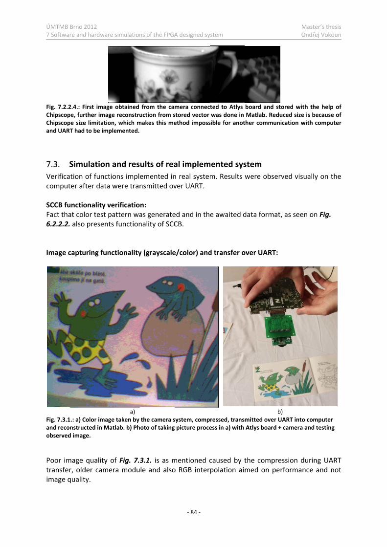
ÚMTMB 7 Softwar
Fig. 7.2.2ChipscopChipscopand UART
7.3. SVerificacomput SCCB fuFact tha6.2.2.2. Image c
Fig. 7.3.1and recoobserved
Poor imtransferimage q
Brno 2012 re and hardwa
2.4.: First imape, further impe size limitatT had to be im
Simulatiotion of func
ter after dat
unctionalityat color test also presen
capturing fu
1.: a) Color imnstructed in M
d image.
mage qualityr, older camquality.
are simulation
age obtained age reconstru
tion, which mmplemented.
n and resctions implta were tran
y verificatiot pattern wants function
unctionality
a) age taken by Matlab. b) Ph
y of Fig. 7.3mera modu
ns of the FPGA
from the camuction from s
makes this me
ults of reaemented innsmitted ov
n: as generatenality of SCC
y (grayscale
the camera soto of taking
3.1. is as mle and also
A designed sy
- 84 -
mera connecstored vector ethod imposs
al implemn real systemver UART.
ed and in thCB.
e/color) and
system, comppicture proce
mentioned co RGB inter
ystem
ted to Atlys was done in
sible for anot
mented sysm. Results
e awaited d
d transfer o
ressed, transess in a) with
caused by tpolation aim
board and stMatlab. Redu
ther commun
stem were obser
data format
over UART:
bmitted over UAtlys board +
the compremed on pe
MastOndř
tored with thuced size is bication with
rved visually
t, as seen on
b) UART into com+ camera and
ession durinrformance
er’s thesis ej Vokoun
he help of because of
computer
y on the
n Fig.
mputer testing
ng UART and not

ÚMTMB 7 Softwar
Fig. 7.3.2UART intcamera a
Fig. 7.3.3color of testing o
Brno 2012 re and hardwa
2.: a) Obtainedo computer a
and testing ob
3.: a) Threshothe cat frombserved imag
are simulation
a) d gray-scale imand reconstrubserved image
a)lded color im
m target imagge.
ns of the FPGA
mage after thucted in Matlae.
mage taken byge. b) Photo o
A designed sy
- 85 -
hresholding taab. b) Photo o
y camera systof taking pict
ystem
aken by the caof taking pictu
em, where asture a) proce
bamera systemure a) process
b)s threshold coess with Atlys
MastOndř
b) m, transmitteds with Atlys bo
olor was picks board + ca
er’s thesis ej Vokoun
d over oard +
ked brown mera and
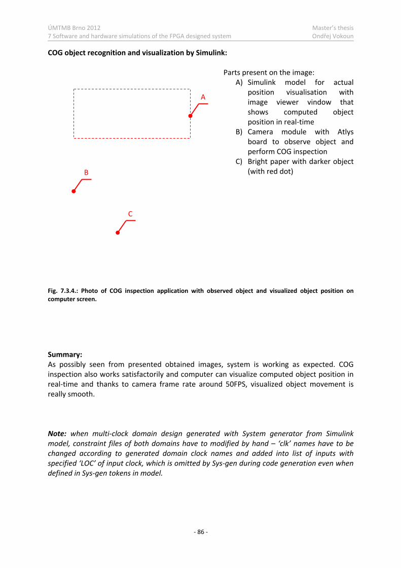
ÚMTMB 7 Softwar
COG ob
Fig. 7.3.4compute
SummaAs possinspectireal-timreally sm Note: wmodel, changedspecifiedefined
Brno 2012 re and hardwa
bject recogn
4.: Photo of er screen.
ary: sibly seen fion also wo
me and thanmooth.
when multiconstraint fd accordingd ‘LOC’ of in
d in Sys-gen
B
are simulation
nition and v
COG inspect
from preseorks satisfacnks to cam
i-clock domfiles of botg to generanput clock, tokens in m
C
ns of the FPGA
visualization
ion applicatio
ented obtaictorily and c
mera frame
main designh domains ated domawhich is om
model.
A designed sy
- 86 -
n by Simulin
on with obse
ined imagecomputer crate aroun
n generatedhave to moin clock na
mitted by Sy
A
ystem
nk:
Parts presA) Si
poimshpo
B) Cabope
C) Br(w
erved object
es, system can visualizend 50FPS, v
d with Systodified by hames and ays-gen durin
sent on themulink mosition v
mage viewhows coosition in reamera mooard to oberform COGright paper
with red dot
and visualiz
is working e computed
visualized o
tem generahand – ‘clk’added into ng code gen
MastOndř
e image: model for
isualisationwer vindowomputed eal-time odule withbserve obj
G inspectionwith darke
t)
zed object po
as expected object pobject move
ator from S’ names halist of inpu
neration eve
er’s thesis ej Vokoun
actual n with w that
object
h Atlys ect and
n er object
osition on
ed. COG osition in ement is
Simulink ve to be uts with en when
ÚMTMB Brno 2012 Master’s thesis 8 Results and evaluation Ondřej Vokoun
- 87 -
8. Results and evaluation
Many different problems had to be solved during process of the thesis evaluation. At the beginning appropriate camera sensor had to be picked according to design requirements and presented camera possibilities. Color CMOS camera module - C3088 with up to 60FPS was picked for implementation (chapter 2.1.3 - Resume for camera selection). After camera selection, possibilities of camera and target MCU interconnection, including data and control signal transfers, were examined and several different designs were discussed - according to camera datasheet specification and PIC32 family manual (chapter 2.2.4 - Resume for interface design). Computer vision and image processing problematic also consist of possible problems that could be solved – it can be for example: Center of gravity of single moving object recognition, Defined color identification and others. Device performance has to be examined to decide if platform based on PIC32 is powerful enough to fulfill given requirements. At first - performance, timing and data format is investigated based on the camera and PIC controller specifications. Then simulation was done on the testing gray-scale images and COG of single object recognition was performed. Results from the chapter - 2.5.3 - Resume for the simulation test, gives us information, that simple processing of B&W image values on maximal frame rate is longer than new data are arriving at the port, which leads to the result that PIC32 is not powerful enough even for the basic operations - then use different and more powerful HW than PIC32 is necessary. After evaluation of different solution possibilities (chapter 2.7 - Proposed solutions), was decided to use FPGA device for the data capture, processing and communication. FPGA provides high performance, versatility and in the case of Spartan FPGA - system can be modeled visually under Matlab/Simulink with System-generator extension from Xilinx Inc. As decision to use FPGA instead of PIC MCU was made during the first - study and research thesis phase, thesis assignment was then changed for the second part - development phase and new goals and problems that had to be solved were added, including use of the FPGA as the main processing device. For the possibility to start work immediately, thesis supervisor recommended use of the so-called “FPGA starter kit” and provided Atlys development board for project realization. Hardware implementation then lies in connection between camera module and Atlys board as presented in the chapter - 4.1 - Hardware implementation. Software implementation includes overall system design and draft of all of necessary computational operations. FPGA platform provides lot of implementation possibilities of main computing core design – general purpose MCU can be synthesized on the FPGA core (Microblaze EDK processor and Picoblaze controller) or interconnection of several single-purpose coprocessors (functional modules). Main question is then to identify tradeoff between system performance, processing speed and complexity, together with requirement
ÚMTMB Brno 2012 Master’s thesis 8 Results and evaluation Ondřej Vokoun
- 88 -
for the fast and easy system reconfiguration for different target tasks (more details in chapter 4.2 - Software design with System generator under Simulink). After consideration of different design possibilities, together with performance and design advantages/disadvantages was decided to use single-purpose coprocessors. Coprocessors designed for concrete computations and image processing applications and also one (or more) for high-level control and synchronization of all the blocks present in the system. Modular system is very variable in the possibilities of use and can be changed fast and easily from one provided functionality into another, which is big advantage of such design under Simulink with System generator. Overall system design was split into two parts – “Camera input domain” which is responsible for data capture from the camera and for the best results runs on the same frequency and synchronously with the camera output. More complex part – “System domain” runs at higher frequency, provided by the Atlys board, to grant maximal possible performance required for successful data processing. System domain is responsible for data preprocessing (incoming data manipulation) and then for operations and computations that needs to be done, for example (viz. chapter- 5 - Image Preprocessing and Processing):
• RGB interpolation when output data is in Raw RGB Bayer format • B&W conversion from RGB color if required by following operations • Image segmentation to differentiate observed object from the background –
threshold intensity segmentation or color segmentation • COG inspection of single observed object to determine center of such object
Communication control interfaces (viz. chapter 6 - Communication) also takes place in system part and these interfaces are responsible for communication with the camera – for setting camera operation modes (SCCB module) and for communication with superior devices – sending processed images or computed position information out of the FPGA (UART module). Another fact has to be mentioned through the use of FPGA for the system design – FPGA is powerful enough to compute everything necessary and communicate with other higher-level systems and therefore PIC implementation isn’t needed for the use as asked for in the thesis assignment and therefore wasn’t implemented to the final solution. Tests for validation of system correctness were performed, including: software simulations, timing and power analysis under Simulink and Xilinx ISE. Hardware tests with camera and FPGA board - observed through Chipscope plug-in and finally obtained images or computed values were transferred by the UART for visual evaluation in the computer. Summary: System built on the FPGA platform accomplished all the goals given, presented high performance for desired camera processing applications and promises even more possibilities for the future work and usage for the real applications. System is able to capture color image, convert it into grey-scale image or compute binarized images after segmentation operations, and transfer into computer to observe results.

ÚMTMB Brno 2012 Master’s thesis 8 Results and evaluation Ondřej Vokoun
- 89 -
System is also able to successfully perform searching for the center of single object at the frame rates of 50FPS and even higher and visualize real-time resulting position on the computer. Possible future use and extensions: System can be used to drive, stabilize or follow certain object in robotics (based on the color or intensity difference) or as digital camera to obtain and store/transfer digital photos. Platform can be also used by the students to study and perform image processing tasks on the real applications. Another possible field of use could be for car-like robots to follow desired leading stripe or automotive industry as driving assistant to keep car in the lane. Although system works and provides functionality given in the thesis assignment, other functionalities can be included and/or actual modules enhancements can be done to provide better image quality or processing performance. For example several buffer lines for convolution filtering could be implemented (usable for extended RGB interpolation, edge detection or other IP filtering). Also even if communication with computer was implemented and successfully used, it doesn’t allow to observe obtained and processed images fluently due to insufficient data transfer speed when UART is used and different communication interface – like Ethernet, could be used. Another possibility to provide faster data transfer would be implementation of image data compression into common image formats directly in the FPGA. Used software: Matlab R2009a Xilinx ISE v 12.3 + System generator MPLAB IDE v8.6 Microsoft Visual C++ 2008 Eagle 4.13
ÚMTMB Brno 2012 Master’s thesis 9 Bibliography Ondřej Vokoun
- 90 -
9. Bibliography
[1] The Mathworks Inc., Matlab product help, ver. 7.8.0.347 (R2009a) [2] Microchip corp., Microchip webpage, http://www.microchip.com/, 20.04.2011 [3] Microchip corp., PIC32MX360F512L product specification,
http://www.microchip.com/wwwproducts/Devices.aspx?dDocName=en532441, 20.04.2011
[4] Microchip corp., PIC32 Starter Kit User’s Guide, DS61159A 2010 [5] Microchip corp., PIC32MX3XX/4XX Family data sheet, DS61143F 2009 [6] OmniVision Technologies Inc., OV6620 data sheet, ver.1.4 [7] COMedia Ltd., C3088 product specification, http://www.comedia.com.hk/, 23.4.2011 [8] Camera modules sale website,
http://www.electronics123.com/s.nl/sc.8/category.241/.f, 12.04.2011 [9] OmniVision Technologies Inc. - product webpage, http://www.ovt.com/products/,
20.05.2011 [10] OmniVision Technologies Inc., Omnivision SCCB functional specification, ver. 2.2 [11] Beyong logic webpage, http://www.beyondlogic.org/imaging/camera.htm, 19.09.2011 [12] National Instruments Corporation, NI Vision systems webpage,
http://www.ni.com/vision/, 20.05.2011 [13] Bob Stewart and Louise Crockett, DSP for FPGAs Primer - System Generator Tools
Workbook (ISE v12.3/4, Atlys), ver. 6.4/11/11 [14] Xilinx Inc., Product support and documentation webpage,
http://www.xilinx.com/support/, 20.04.2012 [15] Xilinx Inc., System generator for DSP user guide, UG640 (v 12.3) [16] Xilinx Inc., System generator for DSP reference guide, UG638 (v 12.3) [17] Digilent Inc., Atlys product webpage,
http://www.digilentinc.com/Products/Detail.cfm?NavPath=2,400,836&Prod=ATLYS, 15.04.2012
[18] Digilent Inc., Atlys board reference manual, rev. 19.12.2011 [19] Analog Devices Inc., Blackfin processor specification webpage,
http://www.analog.com/en/processors-dsp/blackfin/adsp-bf537/processors/ product.html, 14.9.2011
[20] Bryan S. Morse, “Lecture 4: Thresholding”, Brigham Young University, 12.1.2000 [21] Wikipedia encyclopedia, “Thresholding”,
http://en.wikipedia.org/wiki/Thresholding_(image_processing), 20.9.2011 [22] Tadashi Sakamoto, Chikako Nakanishi and Tomohiro Hase, “Software pixel
interpolation for digital still cameras suitable for a 32-bit MCU”, IEEE Transactions on Consumer Electronics, Vol. 44, No. 4, NOVEMBER 1998
[23] Henrique S. Malvar, Li-Wei He, and Ross Cutler, “HIGH-QUALITY LINEAR INTERPOLATION FOR DEMOSAICING OF BAYER-PATTERNED COLOR IMAGES”, Microsoft research, 2004
[24] Frank Vahid and Tony Givargis, “Embedded System Design: A Unified Hardware/Software Introduction” - lecture 7. Digital Camera Example, 03.11.2002
- 91 -
Appendix A – Used abbreviations
AGC automatic gain control asm assembly code AWB automatic white balance B&W black-white bpp bits-per-pixel CCD charge-coupled device CFA color filter array CMOS active-pixel sensor, name derived from the production CMOS process COG Center of Gravity DMA direct memory access FIFO first in, first out FPGA field programmable gate array FPS frames per second HDL hardware description language HDL hardware description language HW hardware I/O input-output I2C Inter-Integrated Circuit IOB input output buffer IP Image processing IPCAM image processing camera MCU microcontroller unit PCB printed circuit board PMP parallel master port PSP parallel slave port RGB red, green and blue RTT real time toolbox RTWT real time windows target SCCB serial camera control bus SW software UART Universal Asynchronous Receiver/Transmitter UCF user constraint file VHDC very-high-density cable (interconnect) VHDL VHSIC (very-high-speed integrated circuits) hardware description language
- 92 -
Appendix B – List of enclosed files
Files enclosed on the CD: Documentation:
• pdf. file of thesis work • related datasheets of used components • pictures and photos generated during thesis development
Source codes:
• models and source codes necessary for FPGA implementation in Matlab and Simulink • source codes for PIC in c-language • development notes related to source codes
FPGA configuration files:
• generated configuration bitstream files • development notes related to the use of configured device functionality