
December 1993 - - Nottingham ePrints - University of Nottingham
178
THE UNIVERSITY OF NOTTINGHAM Department of Electrical and Electronic Engineering INTER-CHIP COMMUNICATION IN AN ANALOGUE NEURAL NETWORK UTILISING FREQUENCY DIVISION MULTIPLEXING by M. P. Craven B.Sc,M. Sc. Thesis submitted to the University of Nottingham for the Degree of Doctor of Philosophy December 1993
-
Upload
khangminh22 -
Category
Documents
-
view
0 -
download
0
Transcript of December 1993 - - Nottingham ePrints - University of Nottingham
THE UNIVERSITY OF NOTTINGHAM
Department of Electrical and Electronic Engineering
INTER-CHIP COMMUNICATION IN AN ANALOGUE NEURAL
NETWORK UTILISING FREQUENCY DIVISION MULTIPLEXING
by
M. P. Craven B. Sc, M. Sc.
Thesis submitted to the University of Nottingham for the Degree of Doctor of Philosophy
December 1993
CONTENTS
CONTENTS
ABSTRACT v
ACKNOWLEDGEMENTS vii
CHAPTER 1- INTRODUCTION 1 1.1 Connectivity Issues in VLSI and Neural Networks 1
1.2 Aims and Objectives 4
1.3 Structure of the Thesis 5
1.4 Novel Work 7
CHAPTER 2- ARTIFICIAL NEURAL NETWORKS AND THEIR
HARDWARE IMPLEMENTATIONS 9
2.1 Artificial Neural Network Models and Architectures 9
2.2 Hardware Implementations 15
2.2.1 Interface 16
2.2.2 Synapses and Neurons 17
2.2.3 Interconnect 22
2.2.4 Learning 24
2.2.5 General Issues and Trade-offs in VLSI Implementations 25
2.2.6 State-of-the-Art Analogue Neural Network Systems 27
CHAPTER 3- FREQUENCY DIVISION MULTIPLEXING FOR ANALOGUE COMMUNICATIONS 33 3.1 Communications, Modulation, and Multiplexing 33 3.2 Multiplexing and Modulation Schemes for Neural Networks 35 3.3 Frequency Division Multiplexing 39 3.4 Neural Network Architecture Utilising FDM 45 3.5 Comparison of FDM and TDM 48
ll

CONTENTS
CHAPTER 4- SOFTWARE SIMULATIONS 56 4.1 Multilayer Perceptron Networks -A Brief Overview 56
4.1.1 The Backpropagation Learning Algorithm 59
4.1.2 The Weight Perturbation Learning Algorithm 63
4.2 Software Requirements for Simulation of Overlap in the MLP 66
4.2.1 Incorporating Overlap into the Standard MLP Model 66
4.2.2 Computer Hardware and Software Considerations 66
4.2.3 Data Acquisition and Storage 67
4.2.4 Network Parameters 68
4.2.5 Optimisation of Computation 71
4.3 Formal Software Design 73
4.4 Simulation Results 79
4.4.1 Three Bit Parity with Floating Point Weights 79
4.4.2 Text-to-Speech with Floating Point Weights 90
4.4.3 Text-to-Speech with Quantized Weights 94
4.4.4 Five Bit Parity comparing Backpropagation
and Weight Perturbation 100
4.5 Discussion 105
CHAPTER 5- VLSI IMPLEMENTATION OF FDM 107
5.1 Simulation Issues in Analogue VLSI 107 5.2 MOS Process Variations, Temperature Gradients, 109
and their Effects on Analogue Circuit Design 5.2.1 Process Variations 109 5.2.2 Temperature Gradients 112
5.3 Operational Transconductance Amplifiers 112 5.3.1 OTA Based Filters and Oscillators 113 5.3.2 Design of Linearised MOS Transconductors 117
in
CONTENTS
CHAPTER 5- (continued) 5.4 OTA Design and Simulation
5.4.1 Route to Silicon
5.4.2 Circuit Design
5.4.3 Layout and Post-layout Simulations
5.4.4 Simulation of OTA Filter and Oscillator Circuits
5.4.5 Post-fabrication Testing
5.4.6 SPICE Level 3 Simulations
5.5 Adaptive Tuning Techniques
5.5.1 Switched Capacitor Filter Limitations
5.5.2 Continuous Time Filters
5.6 VLSI Architecture for FDM Communications
5.7 Discussion
CHAFFER 6- CONCLUSIONS
6.1 Objectives Achieved
6.2 Further Work
6.2.1 Direct Extension of the Research
6.2.2 Other Ideas and Applications
6.3 Summary
REFERENCES
APPENDIX
Publications List
119
119
120
125
130
134
138
142
142
142
146
149
151
151
154
154
158
159
160
171
171
iv

ABSTRACT
ABSTRACT
As advances have been made in semiconductor processing technology, the
number of transistors on a chip has increased out of step with the number of
input/output pins, which has introduced a communications 'bottle-neck' in the
design of computer architectures. This is a major issue in the hardware design
of parallel structures implemented in either digital or analogue VLSI, and is
particularly relevant to the design of neural networks which need to be highly
interconnected.
This work reviews hardware implementations of neural networks, with an
emphasis on analogue implementations, and proposes a new method for
overcoming connectivity constraints, by the use of Frequency Division
Multiplexing (FDM) for the inter-chip communications. In this FDM scheme,
multiple analogue signals are transmitted between chips on a single wire by
modulating them at different frequencies.
The main theoretical work examines the number of signals which can be
packed into an FDM channel, depending on the quality factors of the filters
used for the demultiplexing, and a fractional overlap parameter which was
defined to take into account the inevitable overlapping of filter frequency
responses. It is seen that by increasing the amount of permissible overlap, it
is possible to communicate a larger number of signals in a given bandwidth.
Alternatively, the quality factors of the filters can be reduced, which is
advantageous for hardware implementation. Therefore, it was found necessary
to determine the amount of overlap which might be permissible in a neural
network implementation utilising FDM communications.
V

ABSTRACT
A software simulator is described, which was designed to test the effects of
overlap on Multilayer Perceptron neural networks. Results are presented for
networks trained with the backpropagation algorithm, and with the alternative
weight perturbation algorithm These were carried out using both floating point
and quantised weights to examine the combined effects of overlap and weight
quantisation. It is shown using examples of classification problems, that the
neural network learning is indeed highly tolerent to overlap, such that the
effect on performance (i. e. on convergence or generalisation) is negligible for
fractional overlaps of up to 30%, and some tolerence is achieved for higher
overlaps, before failure eventually occurs. The results of the simulations are
followed up by a closer examination of the mechanism of network failure.
The last section of the thesis investigates the VLSI implementation of the
FDM scheme, and proposes the use of the operational transconductance
amplifier (OTA) as a building block for implementation of the FDM circuitry
in analogue VLSL
A full custom VLSI design of an OTA is presented, which was designed and fabricated through Eurochip, using HSPICE/Mentor Graphics CAD tools and
the Mietec 2.4p CMOS process. A VLSI architecture for inter-chip FDM is
also proposed, using adaptive tuning of the OTA-C filters and oscillators.
This forms the basis for a program of further work towards the VLSI
realisation of inter-chip FDM, which is outlined in the conclusions chapter.
vi

ACKNOWLIDGENUKN S
ACKNOWLEDGEMENTS
This work has been greatly assisted by the support and enthusiasm of my PhD
advisors, Dr. Mervyn Curtis and Dr. Barrie Hayes-Gill.
In addition, I would like to acknowledge the following people for their input
and discussions throughout the course of this project; Karl Sammut, Jim
Burniston, Mingjun Liu, Kalyani Char, Mark Rouse, Kate Knill, John Nicholls,
Piotr Wielinski, and Laurent Noel.
Thanks for financial support are due to the Science and Engineering Research
Council, and the The Royal Academy of Engineering.
vu

CHAPTER 1 IlVTRODUCTION
CHAPTER 1- INTRODUCTION
This introductory chapter begins by explaining the problem of connectivity
constraints in the implementation of parallel computer architectures,
particularly with respect to neural network hardware. The next section goes on
to put forward the aims and objectives of this thesis, to be espoused in the
following chapters. The structure of the thesis is then described and finally, the
novel ideas presented are summarised.
1.1 Connectivity Issues in VLSI and Neural Networks
Advances made in semiconductor processing technology have reduced the
minimum feature size and increased the sizes of chip possible in recent years,
making possible the design of VLSI circuits with several millions of
transistors. Studies have shown that this figure is likely to increase by an order
of magnitude up to the turn of the centurytu]. However, it is also the case that
packaging technology has not kept pace with process improvements. This has
had the effect of reducing the number of input/output pins on a chip relative
to the transistor count, thus introducing an I/O bottleneck in VLSI design.
The effect is particularly noticable in parallel (concurrent) processing
architectures, due to the large amount of data movement required between
processors, and between processors and memory. Construction of massively parallel architectures requires the consideration of connectivities at different
levels; the chip level, board level, and system (or 'backplane') level.
Two paradigms have emerged for concurrent processing. The parallel
1

CHAPTER 1 WTRODUCTION
supercomputer paradigm has tended towards the use of a smaller number of
powerful state-of-the-art digital processors, and complex signal routing
strategies. The artificial neural network paradigm tends towards the use of
larger numbers of simpler processors, which may be digital or analogue and
which are highly connected.
In supercomputing and for digital computing in general, the emphasis is on
methods for achieving the highest computation speeds for ever increasing chip
size and complexity"'-Z2. Communicating signals off and between chips is seen
as the main obstacle to increasing overall system speed. The I/O bottleneck
situation has ensured that intense research will continue into packaging
technology over the next decade1l'-51, for both inter-chip and inter-board
connections. The past 10 years have seen a rapid migration from Dual Inline
Packages (DIP) to ceramic Pin Grid Arrays (PGA), Plastic Lead Chip Carriers
(PLCC) and Plastic Quad Flat Packs (PQFP), all developed to increase the
number of available external I/O pads. Surface Mount Technology (SMT) has
been used to achieve higher board level packing of chips. More recently,
Multichip Modules (MCM) using several chips on a single substrate have
enabled the production of packages with even more I/Os. Flip-chip-bonding
techniques are starting to find use for aligning chips on MCMs, and for
interfacing silicon to optoelectronic devices. The former gives the potential for
construction of three-dimensional (stacked) structures with vertical connections between chips, thus utilising the chip area for interconnect in addition to the
perimeter. The latter will enable high bandwidth optical connections to be used between chips. Both methods counteract latency by shortening connection time
delays between system elements. VLSI routing chips are also being used to
provide programmable interconnect between chips and boards. Advances in
2

CHAPTER 1 INTRODUCTION
some of these technologies are finding their place in lower-end products, and
will continue to do so as the technologies mature and costs lower.
In the artificial neural network case, it is hoped that massive parallelism can
be used to overcome the limitations of processor simplicity, lower accuracy,
and slower speeds which are the inevitable result of reducing the size and
complexity of the individual processor, or of using analogue processing. The
artificial neural network approach is inspired by the fact that the brain, which
consists of millions of highly connected neuron cells, is capable of very
sophisticated computation in spite of the slow processing speed of an
individual cell. Since high connectivity is very desirable in neural network
hardware, the number of achievable connections quickly becomes a serious
issue at all levels of physical design.
In the case of digital neural networks, the number of pins required for data
transfer between each processor and its memory increases linearly with the
number of processors, which can be a large increase for wide data paths. There
is therefore a tradeoff between data path width and the number of processors
per chip, necessitating processing of data over several clock cycles.
In analogue implementations, each signal needs to use no more than one wire
since analogue values are continuous (although the choice of a differential
representation may increase this to two). However, because the use of compact analogue techniques allows the integration of more processors per chip, the
number of external data paths required can still be very large, and the problem of connectivity remains. Neural networks have the potential to exploit massive
parallelism and adaptive capabilities in order to overcome the limitations of
3

CHAPTER 1 INTRODUCTION
analogue electronics, which is by its very nature of lower accuracy and more
subject to the physical realities of integrated circuit processing than its digital
counterpart.
Whilst the aforementioned advances in packaging will also find their use in
neural network VLSI implementations, any other method which can be used
to reduce the number of physical connections required whilst maintaining
adequate bandwidth is a subject for useful research.
This thesis presents the results of an investigation into one such method, that
of Frequency Division Multiplexing (FDM) of the inter-chip communications.
The vehicle chosen for the method is an analogue neural network architecture.
It will be argued that FDM is a solution to connectivity constraints in analogue
neural networks, especially when the neural network learning is able to
compensate for errors introduced by the use of a lower accuracy
implementation.
1.2 Aims and Objectives
The aim of this thesis is to present the idea of FDM for neural network
communications in a formal manner, and investigate the VLSI implementation
of such a technique.
This objective cannot be achieved out of context, and it is therefore necessary to bring together the ideas which surround the research. To this end, this thesis
aims to review the current state of neural network hardware research, with an emphasis on state-of-the-art analogue implementations. It aims also to provide
a review of analogue VLSI design techniques required before hardware
4

CHAPTER 1 INTRODUCTION
implementations can be considered.
The core of the thesis aims to construct a relevant theoretical basis for the
FDM technique, and investigate these claims by software simulations,
theoretical analysis, and some hardware implementations as far as allowed by
limited time and budgets.
The ultimate aim of such a project would be the VLSI implementation of a
neural network architecture utilising FDM, fully integrated into a system
environment with software interface. This is not a feasible prospect for a three
year funded postgraduate project, and it has been necessary to limit the work
to the communications part of the system. Thus, a further aim of this project
is to provide the necessary groundwork and results for continuation after this
thesis is written. For this reason, not only are the results from VLSI designs
presented here, but also a description of the CAD route used, and the
previously mentioned review of relevant analogue techniques. This reflects the
need of the full-custom integrated circuit designer to understand not only the
circuit theory for a design, but also the tools to be employed, and the features
of the fabrication process itself.
1.3 Structure of the Thesis
The main flow of the following chapters is from review, to software simulation, and through to hardware implementation. The beginning of each chapter contains a summary of the subject matter to be covered, and a brief
review of the background needed to fully understand it, in addition to that covered in the main review chapter. The following is a short description of the
contents of the next five chapters.
5

CHAPTER 1 WTRODUCTION
Chapter 2 contains an introduction to artificial neural networks. The majority
of the chapter is focused on general issues, and the particulars of digital and
analogue VLSI implementations, with emphasis on analogue.
Chapter 3 presents the FDM technique. The chapter starts with a look at
multiplexing and modulation techniques for communications in analogue neural
networks, followed by development of the theoretical basis for inter-chip FDM.
This chapter also presents a layered neural network system level architecture
utilising FDM, and an implementation based comparison of FDM with Time
Division Multiplexing (TDM) for the communication of analogue information.
Chapter 4 is the software implementation chapter which begins with a more
detailed account of the particular multilayer neural network model chosen for
this work. The next part of the chapter describes the software development of
a simulator for the network. Software analysis is aimed at testing the
hypothesis put forward, that neural network learning algorithms are tolerant to
crosstalk which occurs due to overlap of amplitude responses in the FDM
channel. The final part of the chapter presents the results of these
investigations.
Chapter 5 is the VLSI chapter. The review section at the beginning looks at
analogue design techniques required for the design of active filter circuits, and
other circuits for implementing FDM communications between integrated
circuits. This is followed by a section on operational transconductance
amplifiers (OTAs), put forward here as the best building block for the VLSI
designs. The design of a prototype OTA chip is then presented including
theory, design route and results from fabrication. The final part of the chapter
6

CHAPTER 1 INTRODUCTION
considers the adaptive tuning of the filters and oscillators in the FDM system.
Chapter 6 concludes the thesis by bringing together the preceding chapters and
examining the actual objectives achieved, and presents a plan for future
developments of the technique and other related work.
1.4 Novel Work
A thesis of this sort is always the result of a mixture of work carried out by
the author, and review of work done by others. Whilst the work of others is
always credited and referenced throughout this thesis, the new ideas and results
are best summarised as follows.
Frequency Division Multiplexing is proposed and investigated for inter-chip
conmmunications. It is intended that the technique may be seen as not
necessarily restricted to neural networks, and will find applications in the VLSI
realisation of other highly connected systems.
In the process of this work, it was discovered that neural network learning is
highly tolerant to the mixing of signals in the FDM channel, caused by
overlapping of filter responses. A fractional overlap parameter is introduced
to enable the analysis of this effect. It is shown that the adaptive nature of a
neural network enables it to compensate for overlap errors. This has been
shown to be the case for linear overlap error in a multilayer perceptron
network trained to do pattern classification, using the backpropagation
algorithm.
A software simulator was designed to test the effects of overlap. Methods are
7

CHAPTER 1 INTRODUCTION
presented in this thesis for optimisation of simulator operation for binary-coded
inputs and outputs. The use of an output activation tolerance (defined as the
difference between the desired binary output activation used for the training,
and the analogue output activation which can be tolerated) is proposed as a
performance metric and for deciding when training is complete. Whilst not
particularly sophisticated, these techniques have been used to good advantage
in the simulator design and contributed to a reduction in training time.
An existing linearisation technique was used in the design of the OTA for
which the results from fabrication are presented. However, the technique had
not previously been reported in monolithic form and thus the implementation,
if not the circuit design itself, can be presented as novel.
8

CHAPTER 2 ANN HARDWARE IMPLEMENTATIONS
CHAPTER 2- ARTIFICIAL NEURAL NETWORKS AND
THEIR HARDWARE IMPLEMENTATIONS
At the initiation of this project, there were few general texts on neural
networks. Today there are many, so rather than repeat the details of this work,
the following chapter presents only a brief overview of neural network
philosophy and models, pointing the reader towards the relevant texts for more
details. The majority of the chapter is concentrated in the area of Very Large
Scale Integration (VLSI) hardware implementations, which is not so well
catalogued in the literature. This description is more detailed for analogue
VLSI, but digital VLSI and general issues are also covered in some depth. No
attempt is made to cover optical implementations, although some references are
made to their existence.
2.1 Artificial Neural Network Models and Architectures
Interest in neural networks began as a desire to understand processes in the
biological brain and explain the workings of the senses and memory. Present
day models for artificial neural networks are based on, or at least inspired by,
this earlier work. The human brain is known to consist of -1010 neuronal cells,
with around 103-105 connections to any one cell from others. Electrical pulses
are communicated across synaptic clefts between neurons by means of
chemical ion transport, with a strength depending on the ion concentrations. The higher level structure of the brain is a hierarchy of sub-networks of
neurons specialised to particular tasks. The collective parallel action of this
system is capable of performing computations which cannot be matched by the
fastest of supercomputers, in spite of the fact that the processing speed of a
9

CHAPTER 2 ANN HARDWARE IMPLEMENTATIONS
biological neuron is only of the order of a millisecond compared to the sub-
nanosecond speed of a typical transistor. According to the connectionist
paradigm, as developed extensively by the Parallel Distributed Processing
(PDP) group of Rumelhart and McClellandi''1, the nature of brain-like systems is contained in the massive parallelism of the networks, and both the
information and processing is distributed throughout. Since the neuron time-
constant is so large, many of the computations in the brain must take less than
100 computational steps, unthinkable for any of the algorithms used in present
day systems for sensory computation. Furthermore, the PDP group showed that
connectionist solutions to simple problems can reveal insights into how larger
collections of neurons might act. Connectionism is described as a micro-theory for psychology, complementing many existing macro-theories.
In the understanding that it is the architecture of the brain which gives it its
power, simplified models have been developed which hope to exploit the
barest features of massive parallelism, both to help explain the operation of biological neural networks, and to enable the use of artificial neural networks in scientific and engineering applications. McCulloch and Pitti22J are credited
with the earliest massively parallel neural network model for explaining
computation in biological nets, published in 1943. In this model a neural
network is a fixed structure consisting of neurons connected by inhibitory and
excitatory synapses. Each neuron is an all-or-nothing process which outputs an
excitatory signal only if the sum of the signals accumulated from other neurons
exceeds a certain threshold. In addition, a neuron is switched off by any inhibitory signal. Timing in the network is described by a period of latent
addition over which the summation of signals is performed, and a delay
associated with each synapse.
10

CHAPTER 2 ANN HARDWARE IMPLEMENTATIONS
In 1949, Hebb17-31 proposed a theory for learning in neural networks whereby
connections to a neuron are strengthened if that neuron is excited. The variable
connection strengths are known as synaptic weights. The Hebbian Hypothesis
asserts that the alteration of synaptic weights during learning is the main
mechanism for information storage in biological neural networks.
A generic artificial neuron structure is shown in Fig 2.1. The neuron function
aggregates the weighted inputs according to some model. The synaptic weights
are modified by the learning process.
E: bemal Inpuft
of Nam Stoss
from
other neaLmoB
INPUT OUTPUT
Fig 2.1 Artificial Neuron
To
Exbrnd ouqm
(ir
other neurons
The above ideas laid the foundations not only for further biological models, but also for networks designed to solve specific types of problem. These can be divided roughly into two categories, namely classification and association problems.
11
sync Wdg

CHAPTER 2 ANN HARDWARE IMPLEMENTATIONS
Classification uses the features present in input data to cluster like patterns and
distinguish unlike ones, thus partitioning the data into classes. Networks to
accomplish this can be trained using input patterns in known classes.
Alternatively, a network can be designed to perform its own clustering without
the need for a teacher.
Association is used either to reconstruct an input pattern from noisy or
incomplete data called Auto-association, or to perform a retrieval from an input
pattern to an associated output pattern called Hetero-association. Associative
networks perform memory-like functions.
Various models have been proposed to carry out the above tasks. All involve
architectures of interconnected neurons, so a general model can be used for a
low level description. Grossberg's neurodynamical model1244 is a good general
model which may be specialised to obtain many of the network architectures
and learning algorithms popular today, and is thus an important starting point
for neural network theory.
Grossberg's model is a set of linked differential equations describing the time
evolution of both the neuron states and the synaptic weights. In one set of
equations the change of each neuron state is expressed as a combination of its
present state, external inputs, and inhibitory or excitatory stimuli from other
neurons modified through the synaptic weights. At the same time, the weight change for each synapse is expressed as a combination of the present weight and the neuron state used as a learning stimulus. Since learning (or forgetting)
occurs constantly, the rate of change of weights must be slower than the rate of change of neuron states in order for the network to perform any useful
12

CHAPTER 2 ANN HARDWARE IMPLEMENTATIONS
function.
Neural network architectures can be divided usefully into categories. The main
divisions are Feedforward or Recurrent (Feedback), and Supervised or
Unsupervised (Self-Organising).
Feedforward networks consist of layers of neurons in which the information
flow from input to output of the network does not contain any feedback paths.
At any particular time, an input pattern results in an output determined
completely by the mapping function of the weights. The power of these
networks is in the internal representations formed by the hierarchy of neuron
layers. This type of network has the advantage of being unconditionally stable,
and fast. Examples of feedforward networks are the Multilayer Perceptron
(explained more fully in Chapter 4) or MadalineI79, and the
Cognitron/Neocognitronr'6''3 networks.
Recurrent networks contain feedback connections, and as such are more
general dynamical systems with the possibility of being stable or unstable. On
applying an input pattern to a stable network, it will settle into a non-varying
state in a short time, or after a few iterations in a discrete time system.
Recurrent networks are well suited to associative memory, optimisation, or
retrieval type tasks, as exemplified by the Hopfield network 81. Information
storage capacity is improved in comparison to feedforward networks.
Supervised networks are trained by an external teacher, so that a trained
supervised network gives specified responses to input stimuli. The weights are
calculated from examples of correct input/output mappings, by minimising the
13

CHAPTER 2 ANN HARDWARE IMPLEMENTATIONS
error between the correct output and the output obtained by applying the input
to the untrained network. In the original Hopfield network, weights are
computed directly in order to minimise a global error function. In most other
networks, the weights are calculated iteratively by changing the weights in
small steps until the error is minimised.
Unsupervised networks do not require a teacher to provide the desired outputs,
and the weights are computed from example inputs only. In most examples
competitive learning is used, so that the weight vectors of certain neurons only
are modified. For each winning neuron (having the largest response to an
input), the weight vector is changed to be more like the input vector i. e. the
scalar product of the two vectors is increased. After training in this way,
different groups of neurons will respond to different inputs, so that automatic
clustering is achieved. Inhibitory stimuli can be used to ensure good
differentiation between the outputs of the winning neuron and its competitors.
These are most often implemented as lateral connections from one neuron to
other neurons in the same layer, over a limited spatial radius. The Kohonen
self-organising feature map is a good example using this local feedback
between neurons 91.
Both unsupervised and supervised networks as introduced above are less
general than the Grossberg model, where learning is a continuous plastic
process, adapting to new input data as need be. In most current neural network
models, the neuron is trained first with training data, after which the weights
are fixed and the network response is then stable. It is required that the
training set be complex enough so that the network can generalise its response
for any other input within the same statistical distribution. This is a reasonable
14

CHAPTER 2 ANN HARDWARE IMPLEMENTATIONS
assumption to make unless there is a large shift in the form of the distribution
of input data after training, or the amount of available training data is limited.
On the other hand, too much adaptability can prevent the network from
learning long term regularities, forgetting old distributions as quickly as new
ones are learnt. Grossberg himself has attempted to address this trade-off
between stability and plasticity, in the development of the Adaptive Resonance
Theory (ART) together with Carpenter"'° ". ART networks retain the ability
to adapt to new data without upsetting that which is previously learnt, which
may be seen as the state-of-the-art in neural networks architectures, if not the
easiest to implement.
Texts describing the above (and more) models and architectures in greater
detail are to be found in the references 21 . Some of these are important early
books or papers on specific neural network models, some are collections of
papers, and some are the more recent general text books covering a wider
field.
2.2 Hardware Implementations
Most artificial neural network models have been implemented in software, but
the size and complexity of many problems has quickly exceeded the power of
conventional computer hardware. It is the goal of neural network engineers to
transfer the progress made into new hardware systems. These are intended to
accelerate future developments of algorithms and architectures, and to make
possible the use of dedicated neural networks in industrial applications.
The ideal logical model of a neural network is an arbitrarily large number of
neuron units, and an even larger number of synapses, one for each inter-neuron
15

CHAPTER 2 ANN HARDWARE IMPLEMENTATIONS
connection. Signals are communicated from any neuron to any other as
required. For implementation purposes, this logical model must be mapped on
to the physical technology. At present there are three main avenues of
research, each with its own merits and associated problems, namely the digital
VLSI, analogue VLSI and optical approaches. This section does not consider
optical implementations which are altogether different from the VLSI
approach. (However, a useful starting article can be found in the
references12'61. )
The stated advantage of using a particular technology depends greatly on
which part of the problem is being addressed. For this reason is is instructive
to split the neural network system into parts, namely; interface, synapses,
neurons, interconnect and learning.
The interface is between the physical neural network and its environment.
Inside the network, the synapses associated with a neuron modify signals from
other neurons usually by multiplying each signal by a weight value. The
synapse is also responsible for local storage of the weight value i. e. memory.
The neuron body performs the processing of the modified signals typically by
performing summing and thresholding operations. Interconnect is the means
by which the signals are transferred around the network, and learning is the
process of adapting the synaptic weights. The following sub-sections consider
these parts in detail for electronic implementations.
2.2.1 Interface
In all envisaged implementations in the development phase, the neural network
will form the heart of a system interfaced to a host computer. The host may
16

CHAPTER 2 ANN HARDWARE IMPLEMENTATIONS
be necessary not only to provide a user interface for controlling the network,
but also for long term storage of network values and parameters. The
communications overhead between host and dedicated hardware should be
considered in the overall performance of any system.
2.2.2 Synapses and Neurons
Because of their large number, small dimension synapses and neurons are
required if a neural network model is to be mapped directly into hardware.
Synapses in particular must be small because they are by far the most
numerous elements. In this case analogue VLSI technology is most suited to
the task, and is considered first in this sub-section.
In an early implementation, Graf and Jackell"I implemented a neural network
using resistors to perform the multiplication of neuron output voltages by
means of Ohm's Law. The resulting currents were summed into an amplifier
on a single wire making use of Kirchhoff's Current Law, thus performing part
of the neuron function. Similar current-mode processing has been adopted in
most analogue implementations to date. However, the use of fixed resistors in
this particular example means that the weights could not be made
electronically programmable. Switching of different resistor values could be
used to introduce a crude programmability, but unused resistors in every
synapse would consume a large amount of chip area.
In MOS technology, direct implementation of resistors is in any case
undesirable11, and multiplication can be achieved instead by the use of transistors operating in the linear (triode) region[129], by analogue multipliersUL3°', and by variable gain transconductance amplifierss2311. More
17
CHAPTER 2 ANN HARDWARE IMPLEMENTATIONS
importantly, these methods also provide the means for implementing and
storing electronically programmable weights. One way of achieving local
weight storage in conventional technologies is by digital-to-analogue
conversion from local digital memory using a multiplying digital-to-analogue
converter (mDAC) for each synapse or group of synapses. If output from the
synapse is in the form of a current, it may be switched on to one of two wires
(excitatory or inhibitory) depending on the value of a sign bit, and summed
with currents from other synapses. The total resultant current may then be
computed by subtracting the currents on the two wires with a current mirror.
This method is practical only for very low resolution weights because of the
chip area required for the mDAC and local memory. Device matching may
also be a problem for higher resolutions, especially for the weighted-resistor
type DAC which requires a doubling in device area per bit resolution. Ladder-
resistor type DACs do not suffer so much from this problem2322.
Alternatively, the weight may be stored as charge on a capacitorr1331, but this
must be continually refreshed because of leakage. Refresh from external digital
memory may be done using a single multiplexed DAC or multiple DACs, in
which case the number of synapses is limited by the total refresh interval.
Local refresh is also possible. Vittoz 1 and Castellod23-q both describe local
analogue refresh schemes whereby weights are updated in parallel to the
nearest quantisation level of a global staircase voltage. In this case the step
size must be larger than the maximum voltage drop due to charge leakage, and
care must be taken to avoid charge injection due to switching. The advantage of the method is in the use of a single "clock-like" signal for refreshing all the synapses, removing the need for complex addressing.
18

CHAPTER 2 ANN HARDWARE IMPLEMENTATIONS
Differential charge storage on pairs of capacitors helps to reduce the effects of
leakage, and also enables the storage of signed analogue weights depending on
which of the two capacitors has the larger charge. Here, charge injection has
been used beneficially to move charge between capacitor pairs whilst keeping
the total charge constantt2*.
The neuron itself is responsible for aggregating the inputs and thresholding the
output. Sigmoidal thresholding or hard-limiting is readily achieved due to
amplifier saturation for large inputs, but the load must be designed to sink or
source the maximum possible sum of currents from the synapses. It is therefore
necessary to increase the load if more synapses are added. To overcome this
problem, it has been suggested that the neuron function be distributed to each
synapse or group of synapses, so that the load grows in proportion to the
number of synapses requiredP-.
The above techniques have been used in continuous time analogue systems.
Where neuron information is represented as pulses, additional methods can be
used to perform the multiplication and summing operations'2'. Multiplication
can be carried out by modifying the rate, width and/or amplitude of the pulses, depending on the coding technique used. Summation can be achieved by time
integration, or by the logical-ORing of pulse trains.
Less conventional techniques also have been found to be suitable for storing analogue weights, especially for reducing leakage and refresh requirements. One method employs Charge-Coupled-Device (CCD) techniques for storage
[2.391 and computation.
19
CHAPTER 2 ANN HARDWARE IMPLEMENTATIONS
EEPROM type technology using MOS floating gatesl24° is also showing
promise for non-volatile storage. The gate threshold voltage is controlled by
the amount of charge in the floating gate. Refresh is unnecessary which is the
main advantage of the technique. Disadvantages are a charging time of the
order of lOms, and a limited number of read/write cycles before device failure,
which make it unsuitable for continuous adaption. In addition, external
voltages of around 20V are required for programming. More recently,
amorphous silicon has been investigated for use in neural network
applicationsi"411. The devices have a variable resistance, programmable by
voltage pulses in the range 1-5V.
Digital VLSI techniques are also suited to implementations of neurons and
synapsei"421. The main advantage of the digital approach is that it enables
short term solutions to the neural network hardware problem. Digital VLSI is
well established so that reliable design and testing may be carried out using
CAD tools, and results are readily reproducable so that performance is more
easily evaluated. Chips may be programmed to accommodate different network
architectures and learning algorithms. This flexibility is important for
developing and evaluating new learning algorithms, and provides a clear route
from existing neural networks implemented in software.
Unlike analogue implementations however, fully digital ones cannot attempt to map a neural network directly to silicon. Due to the chip area consumed by
a digital multiplier, it is simply not possible to attempt to implement one
multiplier per synapse as in the analogue case. In order to implement a large
network, it is also necessary to map it to a smaller number of physical neurons. The building block for dedicated digital implementations thus favours
20
CHAPTER 2 ANN HARDWARE IMPLEMENTATIONS
a special purpose processing unit (containing, for example, a single synapse
and neuron) of which several may be integrated on a single chip or wafer.
Processors can then be multiplexed to implement a network.
Some issues facing the digital neural network designer are similar to those
facing the designer of any parallel system. For example, the choices between
Single-Instruction-Multiple-Data stream (SIMD) or Multiple-Instruction-
Multiple-Data stream (MIMT)) parallelism, distributed or shared memory, and
processor granularity are all relevant"".
S]MD schemes exploit well the regularity of neural network models, and
require only one controller for the processor array. In the ideal SIMD array,
each neuron would perform the same instruction at the same time. In practice,
some algorithms require different sets of neurons (e. g. in different layers) to
perform different functions, and so time-slicing of instructions is necessary.
Systolic array architectures have been proposed which allow an efficient use
of available processors for calculating sums of products1«, 11. Other SIND
machines use broadcast communication similar to that used in the Ring Array
Processor"'.
Alternatively, M MD schemes may be used. Most examples in the literature
have utilised existing microprocessor chips. This approach tends to be
expensive and limits implementation to the board level, but vastly reduces development time compared to dedicated processor design. Digital signal
processors such as those in the Texas Instruments TMS320 or Motorola
DSP56000 families are an obvious choice for sums-of-products
calculationsc471. Inmos Transputers have also been used"'"', although the
21
CHAPTER 2 ANN HARDWARE IMPLEMENTATIONS
hardware architecture of such a system is limited by the small number of direct
interconnects possible. In general, MIMD schemes are not optimal for neural
networks because of the chip area wasted in having one controller per
processor. In addition, MIMD control is complicated by the need to ensure
process sychronisation and to avoid deadlock in computation. As a result, there
are few reported dedicated designs of M tvID processors for neural networks.
Different methods of data representation may obviate the need for multipliers
in digital implementions. If weights and inputs are stored as binary logarithms,
multiplication and division can be achieved by addition and subtraction12 493.
Multiplication by table look-up has also been considered °. Emulating non-
linear thresholds is not straightforward, and a few researchers have developed
digital methods for efficient computation of sigmoids"sl"s31. Otherwise, a look-
up table must be used. Other issues for digital implementation include how to
best map a logical network on to the limited number of physical units 1, and
how to achieve global clocking to a large number of processors. Self-timing
has been investigated as an alternative to synchronous design, especially for
use in wafer-scale arrayst25 ].
2.2.3 Interconnect
Both analogue and digital VLSI implementations suffer from a
communications bottle-neck due to the planar nature of the technology, which is not good for parallel computing in general, nor neural networks in particular. This is the case both at the chip level and the system level.
In a typical neural network of N neurons the interconnect requirement is of order N2 wires if full interconnection is required, an area increase of order N3
22
CHAPTER 2 ANN HARDWARE IMPLEMENTATIONS
with N. For increasing N, the chip (or board) area will be consumed by
interconnect unless a third dimension is found to accommodate it. In analogue
implementations, certain signals may be communicated on a single wire if the
wire is allowed to perform the summing of the signals. This is the case where
currents are used, and where pulses are wire-Ored. Otherwise, some form of
explicit multiplexing must be usedt2'63.
Time division multiplexing (TDM) is the standard method for increasing the
number of logical commmunication channels in VLSI systems, without the use
of more interconnect wires. TDM is suited to digital communications since the
data is already represented as pulses. The main problem with TDM is the
inherent loss of parallelism which may be unacceptable in systems where there
is one processor for each neuron, as in analogue implementations"". In fully
digital implementations however, where it is also necessary to multiplex
processors, this may not represent such a large overhead increase.
Frequency division multiplexing (QDM) in VLS#2,8) has not been considered
by any group other than the author's. This is an alternative technique which
may provide a solution to the communications bottleneck in analogue
implementations without a serious loss of parallelism.
In addition to communication of activity between neurons, channels are needed for communicating, updating and refreshing weights values. Clearly, in a typical modular neural network system, many of the signals must be
communicated between modules and across the host/network interface. In
VLSI implementations, the number of I/O pads on a chip will therefore be a limiting factor. There is no point having a neural network which can operate
23
CHAPTER 2 ANN HARDWARE IMPLEMENTATIONS
internally at a high speed, if the inputs and results cannot be communicated off
the system in a comparable time. In digital VLSI, memory may be placed off-
chip to maximise the chip area for processors, replacing interprocessor I/O
with memory I/O. Analogue VLSI may suit single chip solutions where inter-
chip processor I/O is eliminated. However, in both cases there will be a need
to look at inter-chip I/O very carefully if expandable systems are to be
produced without loss in performance.
2.2.4 Learning
The learning algorithms used for modifying weights values using inputs and
training data are as an important part of the network system as the architecture
itself. Implementation of learning in VLSI systems takes three forms; off-chip,
'chip-in-the-loop' and on-chip learning.
In off-chip learning, weights values are calculated externally by software and
are then downloaded to the neural network which is then used only for recall. This is the easiest but least favoured method, since braining times can be long.
It may be suitable for networks which do not need to adapt to new data once
trained, but it is not very well suited to analogue implementations where it
may be difficult to develop an accurate software model. Off-chip learning does
have the advantage in that it is easy to change the learning algorithm simply
by modification of software. It also allows the use of floating point arithmetic for the algorithms which may not be feasible on a neural network chip.
'Chip-in-the-loop' training, as used by Intel for fine-tuning their commercial ETANN chipr', may also be considered as an off-chip method since the
training algorithm is still run in software. However, in this case the neural 24
CHAPTER 2 ANN HARDWARE IMPLEMENTATIONS
network is used in the training loop which removes the need for a software
model of the network itself, and compensates for device variability. The main
drawback of this method is the communications overhead in continually
reading and writing data across the network/host interface.
On-chip learning must be seen as the most desirable method, since it may open
the way to stand-alone neural network chips. The main advantage of running
the learning algorithm in hardware is the gain in speed. There is however, a
trade-off in flexibility, especially in analogue implementations where
'programming' of the learning algorithm is difficult. Other obstacles to the
development of on-chip learning are the extra chip area used, and the fact that
many of the current or popular algorithms (e. g. backpropagation) require global
data. One of the oldest algorithms, Hebbian Learning (which is local), was
implemented by Card and Moorer'6°°. On-chip learning feasability will benefit
greatly from the development of new local algorithms so that synapse
modification may be carried independently for individual neurons, and the need
for additional wiring for learning is removed. At the time of writing, on-chip
learning is emerging in both digital and analogue implementations2 61,21 .
2.2.5 General Issues and Trade-offs for VLSI Imvlementations
In hardware implementations which attempt to maximise the number of neuron
processors and synapses on chip, trade-offs between chip area and performance
are inevitable. The main area trade-offs are with resolution and dynamic range.
In digital implementions using multiply-accumulate neuron processors, the chip
area required per processor depends on the word lengths used in the system.
For maximum resolution, fixed point rather than floating point solutions are to
25
CHAPTER 2 ANN HARDWARE IMPLEMENTATIONS
be preferred. The accumulator width limits the dynamic range, and hence the
maximum number of inputs, of a neuron. Weights values tend to be
problematic since the values change during training, and vary in range
depending on the application. Since the maximum absolute weight value tends
to increase during learning, some researchers have opted for a variable-fixed-
point method, which involves moving the binary point to increase range at the
expense of resolution during the training process. Scaling down of all weights
as soon as any weight overflows is another possibility.
Unfortunately, performance of some neural learning algorithms, notably
backpropagation, have been shown to become severely degraded as bit
resolution of weights is reduced, because quantisation limits the minimum step
size for the weight updates. Recently, probabalistic rounding or 'dithering'
methods using pseudo-random noise have been used to add extra bit resolution
to weight increments without increasing the word length in the multiplies 63 41.
Other parts of the system do not appear to be affected by lower resolutions,
due to the massive parallelism which means errors in one synapse or neuron
can be compensated by others. The fact that it is the algorithm rather than the
network which requires the higher resolution is an important concept.
Analogue implementations are similarly affected. Only in a few
implementations are values truly continuous. Quantisation of inputs and
weights occurs during D/A conversion and refresh26-9. Resolution is also
technology limited to about eight bits, after which device variations such as
mismatch and offsets tend to dominate, or synapse area becomes too large, as
mentioned earlier with reference to mDAC design. As another example, it has
been estimated that 30-bit resolution would be possible in EEPROM memory
26
CHAPTER 2 ANN HARDWARE IMPLEMENTATIONS
if single electron charge increments could be used, but in practice the neuron
cicuitry is only capable of controlling or registering a 0.4% change' °'.
Fortunately, device variability is also compensated for by the parallelism and
the training process. For instance, offsets can be tuned away by the use of an
extra synapse trained specially for that purposer'663. In analogy with the use of
pseudo-random noise in digital circuits, analogue noise has been found to
improve convergence in network training even with high levels of
quantisation26. Use of noise is in fact an explicit training mechanism in some
physically inspired algorithms such as simulated annealing (used in the
Boltzmann MachineI2"), which uses a lowering of a temperature parameter to
reduce the 'thermal' noise as the network converges.
Dynamic range could be a problem, considering the move to lower power
supply voltages by many IC manufacturers, but the use of current-mode
processing helps to alleviate this somewhat. Gain normalisation has been used
to keep the maximum neuron output voltage constant automatically as more
synapses are addedi"'. Alternatively, the sigmoid gain may be set explicitly
depending on the fan-in 2. Modified algorithms which exert dynamic control
over the size of the weight increment also help to optimise learning in limited
precision implementationsr'610.
2.2.6 State-of-the-Art Analogue Neural Network Systems
The emphasis of this thesis is on analogue neural networks. Much progress has
been made in the field since the start of this project, and it is useful to
compare three of the most developed implementations. These are the
reconfigurable distributed neuron-synapse chip developed by AT&T' , the
multiple chip modular system of the University of Pennsylvania/Corticon
27

CHAPTER 2 ANN HARDWARE IMPLEMENTATIONS
Inc? "3 and the Electrically Trainable Artificial Neural Network (ETANN) chip
of Intel Corporation'a401. All fully working experimental systems were reported
early in 1991.
The AT&T chip developed by Graf et al uses two modules which are repeated
on a single chip, expandable as a multichip system. The first module is a
square 4x4 distributed neuron-synapse array consisting of four fully
interconnected neurons each with four synapses. Each neuron-synapse is a
differential multiplying voltage-to-current (V-I) converter, with capacitive
weight storage. The combined loads of connected neuron-synapses performs
the sigmoid function. The second module is a 4x4 switch matrix designed to
sit between the faces of the first, which allows the input or output of any
neuron-synapse in a module adjacent to the switch matrix to be connected to
another. The configuration of the switches is set using a digital shift register.
The prototype chip was fabricated in 0.9}nn CMOS technology comprising 64
neuron-synapse modules (equivalent to 1024 synapses and 256 neurons) and
144 switch modules. The chip was embedded in a microcomputer system
which performs the learning algorithm and long term data storage.
Configuration data is downloaded from an off-chip EPROM. 8-bit Input data
and 7-bit+sign weights data is stored in off-chip digital memory and
transferred to the chip as analogue voltages using eight off-chip D/A
converters for the inputs and eight for the weights. Eight off-chip A/D
converters are also used to convert the network outputs back to 8-bit digital
values for use by the microcomputer. Training is accomplished using a chip-in-
the-loop weight perturbation method.
This chip has the advantage of being dynamically reconfigurable, by virtue of
28
CHAPTER 2 ANN HARDWARE IMPLEMENTATIONS
its distributed structure and its programmable connections. The connectivity of
any neuron is, however, limited to those in adjacent modules. Results from
experiments with this chip have been reported as successful. Although not yet
demonstrated, the authors propose larger network implementations using
multiple chips or wafer scale integration.
In constrast, the University of Pennsylvania chip developed by Mueller et al
for acoustical pattern recognition is a board level design using combinations
of four IC modules. These consist of an 8 neuron block, an 8x16 synapse array
with 16 inputs, a 16x16 switch array, and a time constant module. The synapse
multiplies an analogue input by a digital value stored in a 6-bit logarithmic
form, to give a current output. A selection of signed weights between 1/400
and 10 are possible representing a range of 12-bits+sign. The neuron module
consists of 8 neurons performing the current summing and thresholding, and
an analogue multiplexer which allows the sampling of any neuron output
without interfering with network operation. The switch module allows
connection between any of the 16 horizontal wires and any of the 16 vertical
ones, and lines can be either routed though the switch modules or terminated
within the module if required. The switches are set digitally in order to
configure the connectivity of the network. The time constant module consists
of passive capacitors and variable active resistances implemented using
transconductance amplifiers. The neural network is constructed around the
neuron block, with up to two adjacent synapse arrays allowing a maximum of
32 inputs to a neuron. Neuron outputs are routed to other synapse arrays via
the switch modules, with optional time constant modules in between used to
introduce variable delays between neuron inputs and outputs. Two editors may
be used to set up the network, a physical editor to allow the setting of
29

CHAPTER 2 ANN HARDWARE IMPLEMENTATIONS
parameters on a particular chip and a logical editor to set chip parameters
according to a symbolic description of the network. The network board is
controlled by a Programmable Array Logic (PAL) based controller, supervised
by a PC microcomputer. Chip-in-the-loop learning is performed using outputs
sampled from the network. A prototype system implementing 72 neurons has
been reported, consisting of 99 chips fabricated using a 2µm CMOS process,
assembled on three boards. The network has been tested on a variety of tasks
including the intended application in speech analysis. The system is being
developed in two ways. Firstly, it is intended to redesign the system for a
larger number of inputs per neuron so that a larger networks of over 1000
neurons will be possible. Secondly, software is being developed to allow
network compilation from a logical description, including automatic placing
and routing of network modules.
This idea has an advantage in its inherent modularity at the chip level, which
gives it flexibility over a single chip design, and there is room for
improvements with a scaling down of technology. On the other hand, the
overall network architecture must be decided before the modules are placed
and routed. Interconnectivity is better than the AT&T chip, but the weights
resolution is somewhat limited by the use of only 6 bits.
The Intel Electronically Trainable Artificial Neural Network (ETANN) chip is
a single chip solution as is the AT&T one, expandable to a multichip system. The design consists of 64 neurons which have 64 direct analogue inputs and 64 additional feedback inputs. Two synapse arrays are used, with a synapse for
each of the two types of input to every neuron, and 16 internal bias weights in each array giving a total of 10240 synapses. All the synapses are analogue
30

CHAPTER 2 ANN HARDWARE IMPLEMENTATIONS
floating gate EEPROM cells with 6-bit typical resolution performing four-
quadrant analogue multiplication of input voltages to give output currents. The
64 neurons are implemented as 64 current summers and 64 sigmoids. Weights
are programmed serially by address using multiplexors. The chip has 64
analogue outputs. Training is accomplished by off-chip learning, and chip-in-
the-loop learning for fine tuning based on Widrow's Madaline III algorithm.
Off-chip training using an accurate software model is carried out initially
because of the long training time for EEPROM cells and their degradation with
repeated write cycles, and because weights may only be trained serially. Fine
tuning is necessary to optimise the weights for a particular chip, since no chip
will be identical because of process variability. The chip was fabricated using
a fpm CMOS process in a 208 pin package. The prototype system is based on
an eight socket board interfaced to a PC. The chip may be used in two modes,
depending on whether the feedback array is to be used in a recurrent network
such as the Hopfield net, or as a second synapse layer in a multilayer
feedforward net achieved by multiplexing the neuron layer.
The Intel chip has the advantage of maximum parallelism for the 64 neurons
available, making it fast in the the recall phase. Most of the I/O pins are used
for direct inputs and outputs of the 64 neurons. The full connectivity is not
scalable to the multiple chip system but direct connections between chips
avoids an I/O bottleneck. The chip is not at all optimised for learning.
Comparing the three implementations, some common strands are noticed. Firstly, all synapses are implemented as V-I converters, so summing is
performed on a single wire for a row of synapses associated with a neuron. The neuron acts as a load to convert back to the voltage domain. All use chip-
31

CHAPTER 2 ANN HARDWARE IMPLEMENTATIONS
in-the-loop learning where the algorithm is performed off-chip, but outputs
from the physical chip are used in the calculations. This is required for
fabrication process invariance. All use analogue input and outputs to the
neurons, necessary to conserve pins. All suffer from limited connectivity to
some extent. All three systems require a digital host computer to control
learning and set network parameters, requiring external D/A and A/D
converters. The implementations are contrasted by their use of different
methods for weight storage, and their different approaches to modularity in
constructing a network from the chips.
In the next chapter, the problem of inter-chip communication is examined
further for analogue implementations, and the use of Frequency Division
Multiplexing is proposed as a technique for overcoming this.
32
CHAPTER 3 FDM FOR ANALOGUE COMMUNICATIONS
CHAPTER 3- FREQUENCY DIVISION MULTIPLEXING
FOR ANALOGUE COMMUNICATIONS
In this chapter, a unique Frequency Division Multiplexing (FDM) scheme is
presented for communications in analogue neural networks. The concept and
its features are explained, in the context of electronic implementations where
a reduction in the number of chip pad I/Os is required. The choice of method
is justified in the context of other possible forms of modulation and
multiplexing schemes. A detailed theoretical analysis of the FDM method and
its comparison with Time Division Multiplexing (TDM) is made. The use of
overlap of FDM channels is proposed as a method for better utilising the
available bandwidth without causing degradation in neural network
performance, a hypothesis which this thesis aims to prove in Chapter 4.
3.1 Communications, Modulation and Multiplexing
Before continuing specifically with communications in neural networks, it is
helpful to consider the general criterion for deciding on a communications
scheme.
In standard information theoretic terms, a communications scheme consists of
an information source, a transmitter, channel, receiver and destination. Into the
channel are injected noise and distortion. The message is the original form of
the information which is converted by the transmitter into a signal of a form
suited to the channel chosen. After passing through the channel, the distorted
and noisy signal is decoded by the receiver into the destination message.
33

CHAPTER 3 FDM FOR ANALOGUE COMMUNICATIONS
With this framework in mind, it is possible to decide on a communications
scheme suited to the type of information to be transferred.
In a telecommunications application, the information will consist either of
digital or analogue waveforms which are interfaced to a physical channel. The
transmitter typically modulates the waveform, and the receiver carries out the
detection and demodulation. Multiplexing may be used to make the best use
of an available physical channel by allowing many different messages to use
it.
The suitability of a modulation scheme is determined by the form of the signal
and tradeoffs between power requirements, signal-to-noise power ratio (SNR),
and bandwidth availability, which will be different depending on the
implementation and the physical environment. In addition to these general
criterion, the cost and complexity of the interface and channel, and speed of
transmission must also be considered for a specific application.
Traditionally, communications involved direct modulation of analogue
quantities such as speech and visual information. Analogue channels are also
often used for purely digital information e. g. in modem telephone
communications. Conversely, with the present availability of cheap and fast
computation, analogue signals are being represented and processed more often
as digital quantities e. g. in digital tape, compact disc, and NICAM stereo, and in future commercialisation of digital TV and digital video. Telephone
systems have moved away from analogue towards digital representations, since
the expense of more complicated modulation schemes is less than that of
analogue amplifiers and repeaters which are replaced by simpler and more
34

CHAPTER 3 FDM FOR ANALOGUE COMMUNICATIONS
reliable digital ones.
This trend has much to do with the predominance of digital technology for
integrated circuits and the use of optical fibres. The digital methods of
communications chosen complement digital processing to good advantage.
Now, with a re-emergence of analogue computation (especially in neural
networks) and advances in analogue VLSI techniques, analogue signal
communications deserves another look.
3.2 Multiplexing and Modulation Schemes for Neural Networks
To a great extent, the best multiplexing and modulation schemes to choose,
will depend on each other and on the form of the signal.
In analogue neural networks, the neural processing is analogue. At an instant,
this analogue quantity is most simply expressed as the DC value of a charge,
voltage or current. It may also be expressed as the amplitude, frequency, or
phase of a sinusoidal waveform, where conversion to these are by the
respective AM, FM and PM modulation schemes. Alternatively it can be
expressed as the amplitude, duration, position, width, or rate, of a pulsed
waveform, by respective modulation schemes PAM, PDM, PPM, PWM and
PRM. Combinations of these schemes are also possible. The final option
involves conversion to pure digital form by Pulse Code Modulation (PCM), or
Delta Modulation (DM).
Pulse-stream arithmetic for neural networks has been pioneered by A. F.
Murray et al of Edinburgh Universityt3.121, and is being developed by many
others. The paradigm is described as bringing together the simplicity of
35
CHAPTER 3 FDM FOR ANALOGUE COMMUNICATIONS
analogue processing and the robustness of digital communication. Three
methods of modulation have subsequently been seriously considered for coding
the neural state, using PAM, PRM and PWM. PAM has been rejected by the
Edinburgh group for communication because of its potential succeptability to
amplitude noise and distortion, although variable pulse height has been used
for multiplication. PWM and PRM use only digital levels. PWM codes the
analogue neural state as the width of a single pulse of fixed amplitude, PPM
as the frequency of a series of pulses.
More importantly, the pulse-stream work has attempted to address the real
problem of inter-chip communications necessary for the construction of
expandable networks with many neurons and synapses. Along with the pulsed
form of the signals, Time Division Multiplexing (TDM) is a suitable form of
multiplexing to be used for the inter-chip communications, in order to reduce
the I/O count. A conventional synchronous TDM scheme has been proposed
utilising a fixed time frame, split into slotted segments with each neural state
occupying the same slot in each segmenF. 3]. A novel asynchronous TDM
scheme has also been reported which converts the time difference between
pulses in a PRM stream to a single pulse with a width equal to this interval13.41
Handshaking between chips is then used to transfer the pulse for each neuron
state in turn as soon as the previous pulse has been acknowledged, in a self-
timed manner. The pulse is then integrated to recover an analogue voltage
proportional to the width. The scheme also enables communication to several
chips by requiring all receiving chips to acknowledge before new data is
transmitted.
There are in general, however, some drawbacks to the use of TDM in neural
36

CHAPTER 3 FDM FOR ANALOGUE COMMUNICATIONS
networks. The first of these is the increase in transmission time with the
number of channels, which is linear for synchronous TDM, and proportional
to the average neuron activation in the case of asynchronous TDM. In order
to maintain the same throughput per neuron, this increase in transmission time
requires an increase in bandwidth. This is of course a problem for any
multiplexing scheme, and it can easily be proved through application of the
sampling theorem that the theoretical minimum bandwidth for TDM is the
same as that for FDM (i. e. when comparing PAM with Single Side Band AM).
However, some modulation schemes are worse than others in exacerbating the
increase in bandwidth requirement, especially when one or other of amplitude
or phase information is exchanged for better noise immunity or simpler
circuitry. The second is a loss of parallelism inherent to the sequential nature
of TDM, which counteracts the central idea of neural network processing.
Thirdly, TDM is not necessarily suited to analogue processing if pulsed
modulation is not used, for example in a network where neurons perform the
direct sum of current values.
Frequency Division Multiplexing (FDM) is the other main form of
multiplexing in communication systems. Whereas in TDM signals occupy the
same frequencies at different times, in FDM the signals are transmitted at the
same time but at different frequencies. This makes FDM an inherently parallel
communication scheme, with no synchronisation required between signals
during transmission.
Two main forms of modulation are possible; amplitude modulation, and angle
modulation which encompasses both FM and PM. Of the two, amplitude
modulation is the most bandwidth efficient, but is subject to amplitude noise,
37
CHAPTER 3 FDM FOR ANALOGUE COMMUNICATIONS
and cannot be broadbanded to increase the SNR. Angle modulation generally
requires a much higher bandwidth, but the SNR may be increased by
broadbanding according to the modulation index. Since the amplitude does not
carry any information, amplitude noise is not such a problem. Furthermore,
angle modulation generally requires more complex transmitters and receivers
than amplitude modulation.
Of the two FDM modulation schemes, it is proposed to use an amplitude
modulation method for neural network communications, for the following
reasons. Bandwidth efficiency is important if a largest number of signals are
to be multiplexed, which must be the aim of any multiplexing scheme for
neural networks. VLSI circuits will generally be less complex and more
compact than those for angle modulation, which is important for the technique
since it would not be desirable for an excessive silicon area to be consumed
by the communications circuitry. In addition, some analogue VLSI techniques
for design of suitable on-chip filter and oscillator circuits are already well
established, as covered in Chapter 5, which is useful for initial investigations.
The trade-off against noise immunity is therefore justified. This is not to say
that FM or PM methods should not be considered in future work. For example,
it has been proposed recently that angle modulation be used in VLSI neural
networks for encoding and multiplying weights valuestl-".
38

CHAPTER 3 FDM FOR ANALOGUE COMMUNICATIONS
3.3 Frequency Division Multiplexing
The concept of the proposed FDM scheme for neural networks is shown in Fig
3.1. The neuron state modulates a unique carrier frequency generated by a
oscillator of constant frequency. The amplitude of the carrier represents the
neuron state which is retrieved by the use of a bandpass filter tuned to the
carrier frequency and a peak detector, together forming the demodulation
circuitry.
RECOVERED NEURON STATES
1ý T
BmxV= Bandpass Filter and --- Filter and Peak Detect Peak Detect
Faxpmncy c1 Proqua1cy c
Single FDM link
rw Fte1ucy w
Cxmiaonea --- commnea osdawr osauator
NEURON STATES
Fig 3.1 Concept of FDM in a Analogue Neural Network
39

CHAPTER 3 FDM FOR ANALOGUE COMMUNICATIONS
It is necessary to define a specification for the communications scheme in
terms of bandwidth. For example, a neural network could be used to process
continuous real-time acoustic signals. For amplitude modulation of telephone
quality speech a 4kHz baseband bandwidth is needed, or 8kHz for good quality
speech. Full audio range requires a bandwidth of 15-20kHz. In these cases
therefore, filters used for demodulation must be specified and spaced according
to the source bandwidth.
At the other extreme, if information throughput is not such an important
criterion, the network may be allowed to settle for as long as necessary to
perform the correct mapping. This would be the case where the neural network
inputs are in the form of slowly varying input patterns. For example in an
application such as letter-to-phoneme classification from binary coded inputs,
real-time performance is achieved at a rate of about 1 input/output mapping
per lOms, or a bandwidth of 100Hz. For such a small bandwidth, the
bandwidth allocation per neuron would then be defined mainly by the filter
characteristic rather than the source, and in particular by the quality factor, Q
and resonant angular frequency wo.
In both cases, the total bandwidth for the FDM channel is calculated from the
sum of the bandwidths of the individual filters. For ideal bandpass filters, with
vertical sidewalls as shown in Fig 3.2(a), this calculation is simple since it is
understood without ambiguity what is the value of each filter bandwidth. For
real filters, the filter characteristics must overlap to some extent as shown in
Fig 3.2(b). Crosstalk between channels is inevitable here, but the amount of crosstalk depends on the degree to which the filter characteristics are allowed to overlap. The conventional definition of filter bandwidth, between the -3dB
40

CHAPTER 3 FDM FOR ANALOGUE COMMUNICATIONS
points, is not a very useful one here, since significant crosstalk would occur
outside this region. This is the situation to be covered by the following
arguments. An additional parameter will be used, as well as Q, to specify the
total bandwidth of a bank of filters by the degree of permissible overlap.
Amplitude Response
(a) Ideal Filters
Amplitude Response
ý1 ý2
(b) Real filters
Fig 3.2 Amplitude Response for a bank of bandpass filters
(1)3 (1)4
Frequency
Consider the standard transfer function for a 2-pole bandpass filter as follows,
H(s) _ (wJQ)s / [s 2+ (w, Q)s + 4] (3.1)
where wo is the resonant frequency. The normalised amplitude response is,
A((4 = (W, wYQ) /( -uß)2 + (tý, týQ)2 (3.2)
Rearranging equation (3.2) in terms of A(W) gives,
two = 1(A -2 _ 1)/4Q 2+1t (A -z _ 1ý 4Q
(3.3)
Equation (3.3) describes the two frequencies Co (either side of the resonant
peak) at which the gain of the filter is A, compared to the unity response at wo. Thus, any signal of frequency outside this range will be attenuated by an
amount smaller than A. If the frequency responses of a bank of adjacent filters
41
wl 4) 2 03 04
Frequency

CHAPTER 3 FDM FOR ANALOGUE COMMUNICATIONS
are overlapped so that the centre frequency of each successive filter coincides
with the frequency at amplitude A of its nearest neighbours, then the amplitude
A can be described as the fractional overlap for the bank of filters. Since this
overlap parameter is by definition a constant for the bank of filters, it is best
denoted by a different symbol, e.
The number or 'density' of filters per octave is then given by,
n= log 2/ logo fo ) (3.4)
where the positive root of equation (3.3) is used. Figure 3.3 shows the Q
dependence of equation (3.3). It can be seen that the same filter density can
be obtained for lower values of Q if the value of fractional overlap is allowed
to increase. Alternatively, higher filter densities can be obtained for a particular
Q by increasing the overlap.
Filter Density/Octave 100
80
so
40
20
Fig 3.3 Filter Density vs. Fractional Overlap for a Bank of Second Order Filters, showing Q dependence.
42
0 0 0.2 0.4 0.6 0.6
Fractional Band Overlap

CHAPTER 3 FDM FOR ANALOGUE COMMUNICATIONS
Similar curves are obtained for higher order filters. Fig 3.4 is the
corresponding set of curves for a commercial switched-capacitor filter MF8,
calculated from the transfer function for a fourth order Chebyshev
implementation as specified in the manufacturer's data sheetd3'61.
Filter Density/Octave B0
60
40
20
Fig 3.4 Filter Density vs. Fractional Overlap for a Bank of MF8 Fourth Order Chebyshev Filters, showing Q dependence.
The previous theoretical analysis is independent of the low and high frequency
cutoffs of the FDM channel and these must also be specified. The highest
frequency is technology dependent. The lowest frequency is determined by the
throughput required.
At best, an interval equal to one cycle of the lowest frequency is required in
order to obtain the amplitude of any signal using a peak detector. Information
43
0 0.2 0.4 0.6 0.8 Fractional Band Overlap
CHAPTER 3 FDM FOR ANALOGUE COMMUNICATIONS
throughput is, however, also limited by the transient response of the system,
notably by filter settling time. For a second order system stimulated with a step
input, it is well known that the 5%, 2% and 1% settling times (specified as a
percentage of final output) are approximately given by 6Q/w� 8Q/wo and 9Q/w0
respectively. It can thus be seen that in addition to frequency, Q is also an
important factor for specifying transient response. In particular, it is noted that
bandpass filters with high Q (good selectivity) have the slowest transient
response, which introduces a trade-off of throughput with filter density.
Up to now it has been assumed that we are dealing with a linear system. Non-
linearities are introduced in analogue computations and communications by the
non-ideal behaviour of the system elements, such as amplifier non-linearities.
Intermodulation distortion, which causes signals from one frequency band to
appear in others, is the main symptom of this, and, as is the case with any
non-linear system, the effects are difficult to analyse. Non-linearity should
therefore be avoided as far as possible in the design of the system elements.
Having introduced the ground-rules for FDM communications, the next section
describes a generic neural network architecture using the technique.
44
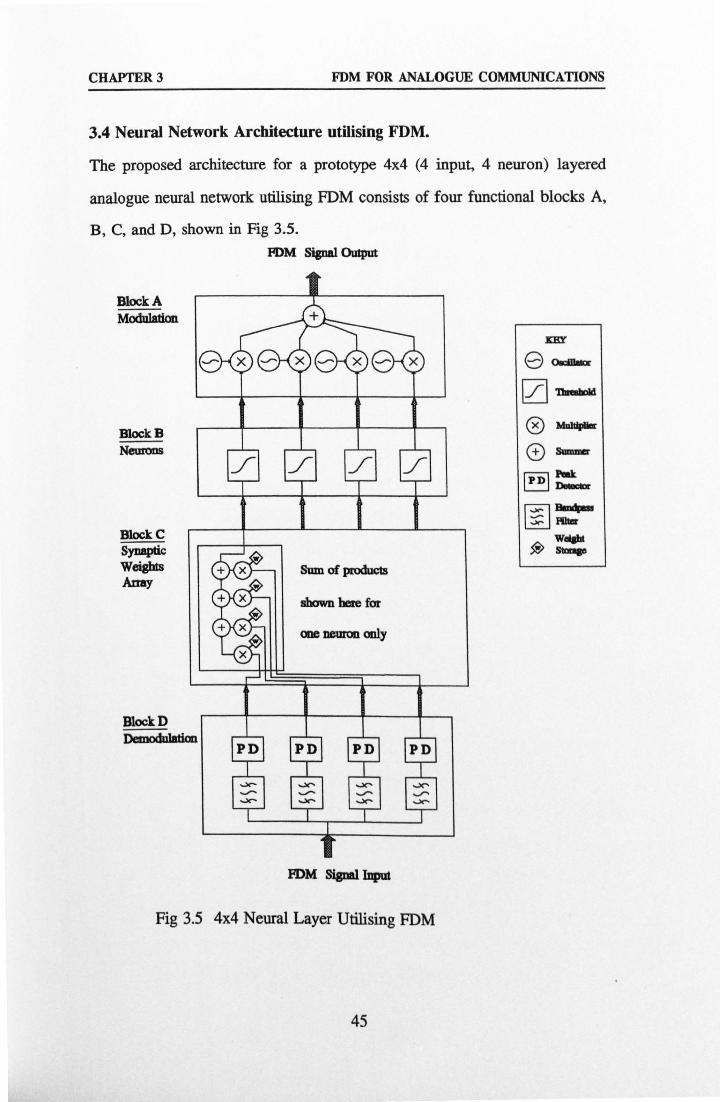
CHAPTER 3 FDM FOR ANALOGUE COMMUNICATIONS
3.4 Neural Network Architecture utilising FDM.
The proposed architecture for a prototype 4x4 (4 input, 4 neuron) layered
analogue neural network utilising FDM consists of four functional blocks A,
B, C, and D, shown in Fig 3.5. PDM Signal Output
Block A Modulation
Block B Neuruns
XI if Block C Synaptic Weigbts +xw Snap of products Army
+x shown here for +x one neuron
Block D DemodubWm
IPD PD P PD
ýi iii iii iý FDM Signallau
Fig 3.5 4x4 Neural Layer Utilising FDM
irEr
n Mimabcdd
0
O+ Oma
PD Pmk Daecýor
Bo*M Faff
wawit Slams
45
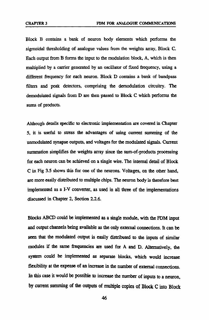
CHAPTER 3 FDM FOR ANALOGUE CONEWUMCATIONS
Block B contains a bank of neuron body elements which performs the
sigmoidal thresholding of analogue values from the weights array, Block C.
Each output from B forms the input to the modulation block, A, which is then
multiplied by a carrier generated by an oscillator of fixed frequency, using a
different frequency for each neuron. Block D contains a bank of bandpass
filters and peak detectors, comprising the demodulation circuitry. The
demodulated signals from D are then passed to Block C which performs the
sums of products.
Although details specific to electronic implementation are covered in Chapter
5, it is useful to stress the advantages of using current summing of the
unmodulated synapse outputs, and voltages for the modulated signals. Current
summation simplifies the weights array since the sum-of-products processing
for each neuron can be achieved on a single wire. The internal detail of Block
C in Fig 3.5 shows this for one of the neurons. Voltages, on the other hand,
are more easily distributed to multiple chips. The neuron body is therefore best
implemented as a IN converter, as used in all three of the implementations
discussed in Chapter 2, Section 2.2.6.
Blocks ABCD could be implemented as a single module, with the FDM input
and output channels being available as the only external connections. It can be
seen that the modulated output is easily distributed to the inputs of similar
modules if the same frequencies are used for A and D. Alternatively, the
system could be implemented as separate blocks, which would increase
flexibility at the expense of an increase in the number of external connections. In this case it would be possible to increase the number of inputs to a neuron, by current summing of the outputs of multiple copies of Block C into Block
46

CHAPTER 3 FDM FOR ANALOGUE COMMUNICATIONS
B. In any case, the first layer of weights in the neural network requires direct
inputs into block C. It would therefore be necessary, in the single module
implementation, to use a separate input module without the demodulation
circuitry. The final outputs are also required in unmodulated form which would
also require a different output module.
It is not the intention of this thesis to design a fully operational neural
network, but rather to concentrate on the FDM communications technique.
Thus, for the purposes of this work the system is kept divided into its separate
blocks as described, and efforts are prioritised towards the specification and
prototyping of the communications circuitry i. e. blocks A and D. It is intended
that the communications circuitry may be integrated into an existing
experimental board level neural network, for future testing purpose.
47
CHAPTER 3 FDM FOR ANALOGUE COMMUNICATIONS
3.5 Comparison of FDM and TDM
Although qualitative and quantitative comparisons of FDM and TDM are made
in many communications textbooks, it is difficult to make a fair comparison
for specific system implementation constraints. The following analysis attempts
to make a comparison of the bandwidth and power consumption of electronic
implementations of FDM and TDM communications by defining two building
blocks which can be used in either system. These are a voltage controlled
current source (transconductor) of maximum transconductance G, and a
minimum size capacitor C. In addition a maximum supply voltage of value V,
is specified. The use of a transconductance element is justified by the fact that
it has been chosen as a neural network building block by many designers,
(including the author) since it performs the desired voltage-to-current
transformation.
In order to compare the two implementations for the optimal bandwidth, a
PAM channel is chosen for the TDM system. For the FDM system, an AM
channel is used. The comparison is carried out for communicating N analogue
values Vth across a single wire, which are present in parallel as analogue
voltages at the input of the system and must end up as parallel voltages V..
at the output.
Considering first the TDM system, the analogue voltages are transmitted in
sequence as pulses with height Vth not greater than V,, and of fixed width r. The transconductor and capacitor are used in a sample and hold configuration,
one for each signal, with final output voltages V... Since V0 jr=I/C, and I=GVt, the total time for TDM transmission of N signals, N x, is given by,
48
CHAPTER 3 FDM FOR ANALOGUE COMMUNICATIONS
Ta, =NC V°`" (3.5)
G V.
where V,, /Vm is the ratio of the final output voltage and input pulse height,
which is a constant value for all pulses since it is dependent only on the pulse
width.
For minimum transmission time, it makes sense to choose a small Vp f Vth so
that the output does not have to ramp for too long. This must be traded off
with the noise immunity of the output which is best for large V(JVi.. The total
power consumption for the communication is (in the worst case with Vi . 7V, ),
Pan = NkGV, 2 (3.6)
where k is a proportionality factor depending on the number of current mirrors
in each transconductor. The driver power requirement is assumed negligible in
comparison, a fair assumption for a transconductor with high input impedence.
For the FDM system, is it necessary to consider the allowed frequency range.
For a typical second order filter constructed from transconductors and
capacitors, the maximum angular frequency attainable is G/C, and the quality
factor can be determined by the use of a smaller feedback transconductor (for
an example of this see Chapter 5, Fig 5.4). For a similarly constructed
oscillator, the highest frequency of oscillation is also G/C, and feedback
controls the oscillation condition. The low frequency limit tom� can be
determined by summing the bandwidths of the N filters starting from
c=G/C. This is done by iterating equation (3.3) with A=: e (using the
negative root since the iteration is carried out for decreasing Co. The iteration
is started with uu, '4na, then o), is replaced by the calculated W at each iteration.
49

CHAPTER 3 FDM FOR ANALOGUE COMMUNICATIONS
The resulting equation is,
N -1 cob. = (G /CJ
C (E-z _1 )/4Q 2+1- (E-2 -1)/4Q 2) (3.7)
Thus, the maximum period T is given by 2n/%.,
(N1 1)/4Q2
) (3.8) per = 2ýt (C IG) 1)ý4Q i+1+ (E-z -1)/4
here using the fact that the two roots of equation (3.3) are reciprocal to change
the sign from - to + when the reciprocal of equation (3.7) is used.
In the worst case, for a step increase in amplitude, the 1% settling time T11.,
for the bank of filters is 9Q/q... So the worst case total transmission time for
FDM, Tfdm is approximately given by the sum of Td. and Tom,
N -1 Tfd�ý _ (2n + 9Q) (C /G)
((T-2 _ 1)/4Q 2+1+ (E -z _ 1)14Q 2) (3.9)
Equation (3.9) is minimised by choosing the value of overlap, e, and
optimising Q for the required number of signals, N. Clearly, increasing e
reduces Tfd. independently of Q and N, so the overlap should be as large as
allowed by the system. The effect of increasing or decreasing Q is not as
straightforward since it has opposing effects on rise time and filter density.
Minimisation of equation (3.9) is difficult to carry out analytically, but from
qualitative and numerical analysis it can be shown that for a 1% overlap
(E=0.01), and a range of values of Q (10-50), the value of T« increases
rapidly as Q is decreased and/or as N is increased, and is approximately
proportional to Q(Qc)''N for the smallest Q. (Note that this approximation is
valid because (Qe)<1 in these cases). For larger values of c (0.1-0.3), the
value of wem� is much less strongly dependent on Q and thus a minimum Tfd.
occurs when the rise time term begins to dominate. For the largest values of
50

CHAPTER 3 FDM FOR ANALOGUE COMMUNICATIONS
e and Q in the above ranges, Tfd,, is approximately linearly proportional to
both N and -Q.
The total power consumption of the system of N filters and oscillators is,
N-i Pf =2nk Vat E G1 (3.10)
i-O
where n is the number of transconductors in each filter, and G; is the
transconductance value required for each frequency, as follows,
G1 =G (yc_2_1,4Q2+1
_ (c-2_1)/4Q2)t (3.11)
Lower frequencies require smaller transconductance values and therefore less
power (since the frequency G/C is lowered by reducing G with constant Q.
The factor of two in equation (3.10) assumes the use of similarly constructed
oscillators and filters.
It is necessary to put some figures into the above equations to obtain some
realistic timings and power consumption for the two implementations. The
minimum pulse width for PAM is usually specified as 0.5BT, where BT is the
baseband bandwidth for the technologyP"'". For a typical technology bandwidth
of 10MHz, this gives a value of t=50ns transmission time per signal. If N
outputs are to be added together as might be expected in a neuron, it is
reasonable to arrive at a figure of V. /Vi. =1/N, so that the total output would
not exceed the supply even if each of the Vt. were equal to V. This assumes
a situation where synapse weights are limited in the range [-1,1] so that the
largest possible sum-of-products is NV3. For a larger weight range V /Vi
would have to be proportionally smaller.
51

CHAPTER 3 FDM FOR ANALOGUE COMMUNICATIONS
1000000
100000
10000
1000
100
10
I
Transmission Time (Microseconds)
05 10 15 20 25 30 35 40
Number of Signals In Channel
TDM Fal CO. O1/2O)-f- wl CO. O1/5O] FIJI CD. 1/20D
8 FORA CO. 1/50) )f FC CO. 3120) 0ý FDA CO. 3/50)
Fig 3.6 Transmission times for FDM channels vs. Number of Signals, N for various c and Q (individual FDM plots are labelled FDM(E/Q) ).
Accepting these assumptions and using a minimum capacitance of 10pF, a
value of G=2001A/V would give the required drive for TDM. Using the same
G and C in the FDM implementation, ao of 20Mrads/s (3.18MHz) is
obtained. Substituting these values in equation 3.9 and plotting the values of
Tfd,, against N for different values of e and Q, yields the graph shown in Fig
3.6. Each line on the graph for FDM is labelled FDM(e/Q), and the lower plot
of the corresponding TDM plot is also shown for comparison.
For Eß. 01, Q=20, equation (3.9) gives an FDM transmission time of 1.3ms
for 4 signals. In comparison the TDM system requires only 2µs. Increasing the
Q to 50 reduces the FDM time to 320µs. However, doubling the number of
signals to 8 increases the FDM transmission time by several orders of
magnitude, whereas TDM time is only doubled. However, if e is allowed to
52

CHAPTER 3 FDM FOR ANALOGUE COMMUNICATIONS
increase to 0.1 with Q remaining at 20, the same 4 signals are transmitted in
2Ops, and 8 signals in 50ps. For e=0.3 this is reduced further to 10µs for 4
signals, and only 16ps for 8 signals.
Comparing the timing for a larger number of signals, for example 40, TDM
takes 20ps, and FDM with eß. 3 and Q=20 takes 200ps. Whilst still an order
of magnitude larger than the TDM transmission time, this is much more
practical than a scheme which requires minimal overlap. FDM is simply not
realisable with e=0.01 for this many signals.
For the value of G chosen above, a supply of 10V, and a typical value of k=3
current mirrors per transconductor, the power consumption for the TDM
communication is 60mal per signal. For FDM the power consumption is
360mal for the highest frequency signal, using a value of n=3 transconductors
per filter and oscillator. Subsequent power consumption values depend on the
number and spacing of the lower frequencies. For c=0.3 and Q=20, the next
3 values are 332mW, 307mal, 283mal.
The conclusions of this comparison of FDM and TDM can now be made as
follows.
PAWFDM appears to have certain advantages over AM/FDM in terms of both
bandwidth and power consumption. For FDM, deliberate overlapping of second
order filter responses is necessary in order to achieve a practical transmission
time which is an order of magnitude longer than that for TDM in the above
analysis. Power consumption from the calculations is about 6 times greater for
FDM, although this figure is variable, depending on overlaps and quality
53

CHAPTER 3 FDM FOR ANALOGUE COMMUNICATIONS
factors.
FDM has the advantage of being asynchronous and continuous time i. e. no
clock is needed in principle. However, it may be desirable in practice to use
a clock to delay the computation of the received signals until after the settling
time has elapsed. If this is the case, it is hard to see an advantage to using
FDM in this way, since this is not much different than waiting for all TDM
signals to appear at the output.
From the theory developed above, it is clear that practical FDM bandwidths
are achievable only if overlapping of filter responses is allowed, or if large
values of Q are used. It has been shown that increasing Q is not always the
correct solution, since this also has a detrimental effect on settling time.
Furthermore, electronic implementations of high Q circuits suffer from high
sensitivity to component values, which causes problems in matching oscillator
and filter centre frequencies. Also, high Q circuits generally use large ratios
of component values which often translates to large chip area requirements in
VLSL For the same reasons, the use of higher order filters is not desirable.
It is, however, reasonable to propose that the errors introduced by overlapping
filter characteristics will be compensated for when FDM is implemented as
part of an adaptive system such as a neural network, and therefore that larger
overlaps may be permissible than those required in straightforward
communications applications. This hypothesis requires proof, which is the
subject of the next chapter.
In defence of FDM, it should be stated that it has been necessary in the
54

CHAPTER 3 FDM FOR ANALOGUE COMMUNICATIONS
analysis of this chapter to present the worst case scenario for FDM
communication in comparison with TDM, so as to justify the scheme in a fair
manner. In practice however, the FDM implementation constraints may not be
as great. If filters are not subject to step changes of input amplitude, the
settling times will be less than calculated. For slowly varying inputs settling
time is not such a problem, and since it is the settling time which dominates
the overall transmission time, this would be greatly reduced. As for TDM,
alternative implementations may introduce additional problems. If PWM is
used instead of PAM, the pulse widths must be greater for two reasons. Firstly,
width information is being used to code the neural state, so it is the maximum
(or average, for asynchronous PWM) width rather than the minimum width
which determines the transmission time. The minimum width itself must also
be greater so as to preserve sharp pulse transitions i. e. 'fine' pulse
reproduction. The 0-5/BT rule used for PAM does not apply to PWM since this
estimate ensures only 'coarse' pulse reproductionn3"71. Typical pulse widths
quoted in the literature are microseconds rather than nanoseconds. The same
arguments apply to PPM. The minimum width can be used for PRM, but in
this case, several pulses may need to be used in order to compute the rate.
Thus, the difference between transmission times for FDM and TDM may not
be as great as that predicted by the above analysis, depending on the form of
modulation employed.
In conclusion, the results from the analysis show that FDM can be justified as
a method of neural network communications, if overlap errors are proved not
to be a unsurmountable problem. The following chapter will show that
tolerance to overlap errors is indeed a feature of neural networks.
55

CHAPTER 4 SOFTWARE SIMULATIONS
CHAPTER 4- SOFTWARE SIMULATIONS
This chapter describes in detail the software implementation of a multilayer
perceptron (MLP) neural network, in which the usual model is modified to
incorporate the effect of overlap of neuron activations in the forward pass. The
software design is presented as a set of structured Warnier Diagrams, which
implements the MLP using floating point arithmetic, and training using the
backpropagation algorithm. This model is then modified further to include the
effect of weight quantization, and to allow a comparison of results with the
alternative weight perturbation training algorithm. The rest of the chapter is
devoted to simulations using the software. It is shown, using results from
various applications, that the neural network is remarkably tolerant to overlap
errors, confirming the hypothesis of the previous chapter. The first application
involves backpropagation learning of the 3-bit parity problem with various
degrees of overlap, using floating point weights. The second problem is text-
to-speech conversion based on the well known NETtalk application, which is
used to investigate the effect of overlap when weight values are quantized. The
third problem compares the learning of 5-bit parity using backpropagation and
weight perturbation algorithms, with varying degrees of overlap and weight
quantization.
4.1 Multilayer Perceptron Networks -A Brief Overview
The perceptron was a neuron-like adaptive element invented by Frank Rosenblatt in 1958, followed two years later by a method of training called the
'perceptron rule' which used the difference between target and actual binary
56
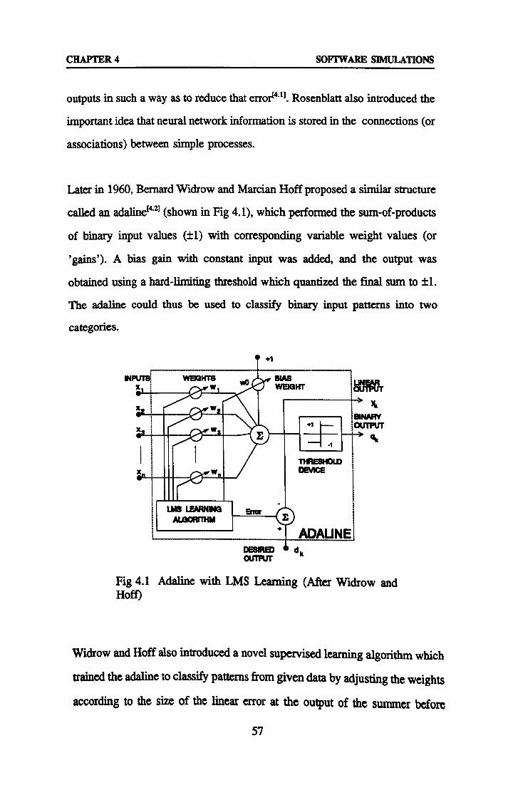
CHAPTER 4 SOFTWARE SIMULATIONS
outputs in such a way as to reduce that error 4.13. Rosenblatt also introduced the
important idea that neural network information is stored in the connections (or
associations) between simple processes.
Later in 1960, Bernard Widrow and Marcian Hoff proposed a similar structure
called an adaline'4,21 (shown in Fig 4.1), which performed the sum-of-products
of binary input values (±1) with corresponding variable weight values (or
'gains'). A bias gain with constant input was added, and the output was
obtained using a hard-limiting threshold which quantized the final sum to ±1.
The adaline could thus be used to classify binary input patterns into two
categones.
+1
WEIGHTS w auks /-"-w WI WEIGHT
i BINARY OUTPUT
Qt
LIAS LEARNMIO ALGORITHM
THMHOLD DEVICE
ADAUN DMWD dk OUTPUT
Fig 4.1 Adaline with LMS Learning (After Widrow and Hoff)
Widrow and Hoff also introduced a novel supervised learning algorithm which
trained the adaline to classify patterns from given data by adjusting the weights
according to the size of the linear error at the output of the summer before
57

CHAPTER 4 SOFTWARE SIMULATIONS
quantization. This algorithm was shown to be equivalent to minimising the
mean squared error for all patterns, and is thus commonly called the Least
Mean Squares (LMS) algorithm. Other common names are the Gradient
Descent Rule, Delta Rule or Widrow-Hoff algorithm.
The modem perceptron is essentially the same as the above, but some use
linear or smooth non-linear output functions rather than the hard-limiting
quantizer, and may or may not be limited to binary inputs.
It became clear also that by applying the same input vector to several neurons,
with different weights, a vector output could be obtained. This was introduced
in the Madaline networkta. 31.
Multilayer perceptron networksl4 4I are an extension of these ideas. Single layer
perceptron networks can only correctly classify linearly separable sets of input
vectors, which was recognised early on as a severe limitation"". By
connecting the outputs of a layer of neurons to the input of the next, a
multilayer network is obtained which gives an extra dimension. The network
now has two layers of neurons and weights, a 'hidden' layer and an 'output'
layer, and is usually called a two layer network. Networks with multiple
hidden layers are also possible. It can easily be proved that only MLPs with
non-linear hidden neurons are worth constructing, since a multilayer network
with linear hidden layers can always be reduced to a single layer network.
58

CHAPTER 4 SOFTWARE SIMULATIONS
M HIDDEN N OUTPUT L INPUTS LAYER NEURONS LAYER NEURONS
yp1 _
Wji 81
Xpjý---IYpi wk) ek
XP ypkjp_
Iý ý E F
Fig 4.2 Two Layer Perceptron Network
Fig 4.2 shows a two layer perceptron network, with L inputs, M hidden layer
neurons and N output layer neurons. The output function F is the sigmoidal
non-linearity, or logistic function 1/(l+e") which limits the output range
between 0 and 1. The inputs and outputs of each layer for a particular pattern
p are denoted by y,,; for the inputs to hidden layer (15i5G), yp; for the inputs
to the output layer (15j5M), and y, for the final outputs (15k5N). The
corresponding signals into the sigmoidal function are denoted by x,, and x Pe The hidden layer weights are denoted by wj, ' and the output layer weights by
wk; ` and the corresponding threshold biases are O' and 8, t, at iteration t.
4.1.1 The Backpropagation Learning Algorithm
The problem with training multilayered networks with a supervised learning
algorithm is that the output values of the hidden layer neurons are not
specified in the training data, so the errors in the hidden layer cannot simply
be specified as the difference between the actual and desired responses, and so
the required weight changes cannot be found directly. The Backpropagation
59

CHAPTER 4 SOFTWARE SIMULATIONS
algorithm of Rumelhart, Hinton and Williams'" ' (also claimed to have been
discovered independently by Werbos and later by Parkerl4-71) was a real
breakthrough in that it enabled the training of hidden layer weights by
calculating the error terms for the hidden layer as a weighted combination of
the errors from the output layer. This is the 'backpropagation of errors' which
gives the algorithm its name. The process may be carried out repeatedly to
train networks with larger numbers of layers. The algorithm is often called the
generalised delta rule, since it can be seen as a extension of the single layer
delta rule. However, it should be noted that unlike the single layer algorithm,
backpropagation is not guaranteed to find the global minimum error, because
local minima may also exist.
Fig 4.3 describes the steps of the backpropagation algorithm It consists of two
phases, a recall phase (or forward pass) in which an input is presented to the
network and the actual outputs are calculated, and a learning phase (or
backward pass) in which the errors are calculated and the weights adjusted.
The weight changes for each neuron are determined by multiplying the
corresponding inputs by the error term 8 (constant for that neuron at iteration
t) and a learning rate 11 (constant for the entire network).
In this description of the backpropagation algorithm, each step in the algorithm
is repeated for all neurons in that layer before proceeding to the next step.
When the two phases are completed for one input pattern, the process is
repeated until each pattern in the training set has been presented. This is one
training epoch. In this work, weight updates are njade after each pattern is
presented. Alternatively weights changes may be accumulated over several
patterns, or over the whole epoch, before the updates are made.
60
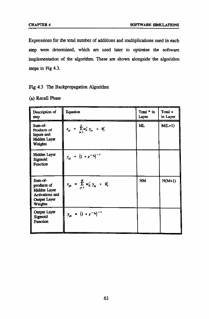
CHAPTER 4 SOFTWARE SIMULATIONS
Expressions for the total number of additions and multiplications used in each
step were determined, which are used later to optimise the software
implementation of the algorithm. These are shown alongside the algorithm
steps in Fig 4.3.
Fig 4.3 The Backpropagation Algorithm
(a) Recall Phase
Description of Equation Total * in Total + step Layer in Layer
Sum-of- f
Lt +e X =Ew 3'
ML M(L+1) Products o i vi , ,
ý' Inputs and Kidden Layer Weights
Hidden Layer y; _ (1 +e Sigmoid
Function
Sum-of- products of
M X=EW; yp, + 8k
NM N(M+1)
Hidden Layer Activations and Output Layer weights
output Layer ya ý1 +e Sigmoid
Function
61

CHAPTER 4 SOFTWARE SIMULATIONS
Fig 4.3 The Backpropagation Algorithm (continued)
(b) Learning Phase
Description of Equation Total * in Total + step Layer in Layer
Output Layer sk = y, k (1 - y1 )(d, _ yam 2N 2N
Error Term
IfidIden Layer Error Term
N SP; yP; (1 - yPj) E ww SA
(N+2)M M+N
k- I
pdate Output [J ww wp + spk yP; 2M(N+1) M(N+1) Layer weights and Thresholds ek '= e" + Tj sý Biases
Update Hidden Wo I_ wit + ,nsy P, P
2L(M+1) L(M+1) Layer weights and Thresholds 07 ()j' +qS ; Biases P
A modification to the basic backpropagation algorithm (also introduced int4'6))
involves the addition of an 'acceleration' (or momentum) term to the weight
update equations which is usually a fraction of the weight change from the last
epoch. The weight change equation becomes;
w'. 1 = W' + 11 8y+a W-W ,_ 1)
where a is the momentum. Momentum can speed up training by biasing the
current weight change in favour of the last weight change. This effectively acts like a low pass filter on small fluctuations in the weight step at successive
62
CHAPTER 4 SOFTWARE SIMULATIONS
iterations.
In general, backpropagation suffers from very slow (or lack of) convergence,
and the performance can be greatly affected by the choice of learning rate,
momentum, and the actual random weights chosen. Network paralysis and
local minima are also potential problems1`8 , although the latter seems not to
be as serious as was once feared.
For these reasons, many variations of backpropagation have been proposed and
research in this area is still very active. None, however, appear to have become
accepted as the best approach for all problems. Recent publications have
shown some advantage in using symmetric inputs and activation functions such
as the hyperbolic tangentt4-9.101. However, the bipolar nature of the inputs and
outputs may cause problems in some hardware implementations. Furthermore,
it does not allow the use of the optimisation methods to be proposed in Section
4.2. Most other variations use second derivatives to optimise the size of the
weight changes"-`-", which is equivalent to using a dynamically varying
learning rate. In these cases, learning speed (in terms of number of epochs)
and convergence tends to be improved over the standard backpropagation.
However there is a trade off with the increase in computational complexity,
and increased storage requirements which are not beneficial for hardware
implementations.
4.1.2 The Weight Perturbation Learning Algorithm
In the backpropagation algorithm, weight updates are calculated analytically
by use of the chain rule, starting with the error at the network outputs and
working back to find the gradient of the error with respect to the neuron
63
CHAPTER 4 SOFTWARE SIMULATIONS
weights. On-chip implementation of backpropagation learning in Analogue
VLSI is made difficult by the need to ensure sufficient accuracy in the
modelling of the algorithm, in the face of process variations. This may limit
successful implementation of backpropagation to a chip-in-the-loop training
type strategy, as proposed for use in this thesis. However, it is useful to
consider other algorithms where a fully on-chip neural network may be
required.
In weight perturbationl¢' , weight updates are calculated by changing each
weight value by a small amount, and examining the change in Mean Squared
Error (MSE), A,, at the outputs. If the perturbation, At, is small enough, a
good approximation to the error gradient, AE. JAt, is obtained directly, and the
algorithm has been shown to work well with larger perturbationsi¢'9. This has
an advantage for on-chip analogue implementation, since it is not necessary to
know the exact form of the sigmoidal transfer function, nor need the function
be the same for each neuron. Therefore the algorithm is likely to be more
tolerant to process variations. Furthermore, the number of steps in the
calculation of a weight change are reduced, so that any inaccuracies in one
step are not amplified to the extent they would be in an algorithm with more
steps, like backpropagation.
The main disadvantage of the algorithm is the number of times the simple
steps must be repeated - once for each weight in the network at every iteration.
In particular, a recall phase must be repeated for each weight perturbation in
order to calculate the new MSE, which is particularly intensive in sequentially
processed simulations.
64

CHAPTER 4 SOFTWARE SIMULATIONS
The learning phase for weight perturbation is shown in Fig 4.4, together with
the total number of multiplications and additions for each step. Note that it is
only necessary to find the Sum Squared Error (SSE), since division by the
number of outputs N and multiplication by ý can be carried out during weight
update, effectively incorporating them into the learning rate i. e. -AEp=
(Tl/2N)(Sp SP'). The total number of weights and threshold biases is denoted in
Fig 4.4 by W=M(L+1)+N(M+1).
Fig 4.4 The Weight Perturbation Algorithm Learning Phase
Description of Equation Total * Total +
step
Calculate initial N 2N S=d
vi - y1 )2 P( SSE (once
only)
Temporary wý = w;; + Ar
Weight
Perturbation
Perform Recall See Fig 43(a) WM(L+r V2
Calculate new ýN+ S; (dp - yp; )2 WN 2WN
SSE
Update Weight tun,, wÄ +
(S WN 2WN
65
CHAPTER 4 SOFTWARE SIMULATIONS
4.2 Software Requirements for Simulation of Overlap in the MLP
4.2.1 Incorporating Overlap into the Standard MLP Model
It is possible to approximate the band overlap which occurs in demultiplexing
a frequency division multiplexed channel by mixing a proportion of the signal
from the adjacent bands into each band. This is incorporated into the standard
multilayer perceptron model using the fractional overlap parameter defined in
Chapter 3, which is multiplied by the activation of each adjacent neuron, and
then the two values are added to the activation of the central neuron before
multiplying by the weights, since in the proposed hardware system the weights
array is after the demultiplexing.
Thus, the recall phase is modified as follows;
m xpk = Ewp (ye, +£ YP;
-1+8 Yp; . 1) + ek
where y. 0 and ypM+, are made zero to account for overlap at one side only at
the ends of the layer. c is the fractional overlap which can range from 0 (no
overlap) to 1 (full overlap). For cam, the software will implement the standard
multilayer perception architecture.
4.2.2 Computer Hardware and Software Considerations
Calculations in neural networks are by their nature computationally intensive
and require a large amount of storage for weights and neuron activations. For
small networks, a PC based system may be appropriate, but for larger
problems a mainframe solution may be required. The PC implementation is
often limited by a 64k segmentation of memory to ensure 8086 microprocessor
compatibility, and so large data structures cannot be defined easily. Neither is
it feasible to use disk storage and process the network data in blocks, because
66
CHAPTER 4 SOFTWARE SIMULATIONS
disk access would slow down the system. Both the backpropagation and weight
perturbation algorithms require all weights to be available at each iteration, and
if momentum is used weight changes from the last iteration must also be
available in memory.
It was decided to develop the software on an IBM PC to take advantage of the
good quality editing and debugging facilities, but to reserve the option of
porting it to a VAX mainframe as required. The high level language Pascal
was chosen for the programming since it is well supported on both systems
and is portable enough to be transferred between systems with only minor
modification. Borland Turbo Pascaff4171 was used for the PC software
development and smaller networks, and VAX Pascall4. ' for the larger
networks. In the later simulations involving weight quantization and weight
perturbation, aC language version of the software was also developed, for use
on Sun platforms.
4.2.3 Data Acquisition and Storage
The software system consists of the neural network program and its training
and weights data files. The program works most efficiently with all the data
stored in global memory arrays which can be loaded from disk files just once
at the start of the program It was decided to store the training data as ASCII
text, so that it could be generated by different computers and ported by
network to the program location. The data is efficiently stored as alternate lines
of input-output pairs separated by NewLine characters. This is a particularly
compact form of storage for the binary training data which is used for the two
applications in this study. Weights are continuous so must be stored as floating
point real numbers for compactness. Two weights files were specified, one
67
CHAPTER 4 SOFTWARE SIMULATIONS
with the initial weights which can be random or from a previous training
session, and one working weights file. This enables the network to be trained
several times with the same initial conditions, and thus compare the effects of
varying degrees of overlap with the same starting point.
4.2.4 Network Parameters
The parameters required by the backpropagation algorithm are the learning rate
and momentum, which can be varied according to the application. The weight
perturbation algorithm also requires a learning rate (momentum was not
specified for weight perturbation, since it is unlikely to be used in an on-chip
implementation). Some work has been done in an attempt to eliminate the need
for user input of the learning rateP`1, however in most applications the optimal
value is found experimentally. In addition, other parameters are needed to
initialise the network and monitor the learning. Unless existing weights are
available, the network must be initialised with small random values. The range
of these weights also depends on the application and size of network, but
typical values from the literature range from ±0.01 to ±1, with smaller ranges
used for larger networks.
It is also necessary to define a performance metric in order to decide when to
stop the training process. Since both learning algorithms act to minimise the
MSE, learning can be stopped when this error reaches a specified minimum
value. There are a number of problems with this approach, particularly for
classification problems. Firstly, because the error is averaged over all the
output neurons, some neurons may be more in error than others and so a large
error in a few neurons may be masked by lower errors in the majority.
68

CHAPTER 4 SOFTWARE SIMULATIONS
Secondly, the error is averaged over all input patterns which does not allow for
the potential of some patterns being more difficult to learn than others. It is
thus not always clear what is an acceptable minimum error. The calculation of
the sum-of-squares is also a computationally expensive process, especially
since it must be carried out at each iteration. It is noted that the MSE still
needs to be calculated for weight perturbation. However it is advantageous to
use the following method in addition, since it allows simple comparison of the
different algorithms, but introduces little computation in excess of that required
for the MSE.
It was decided to use a different metric which is clearer to analyses and
cheaper to compute. An output activation tolerance was defined for the output
neurons, similar to that suggested by Rumelhart et d4.61 where it was used to
help limit weight values. This is defined here as the difference between the
desired binary output activation used for the training, and the actual analogue
output activation which can be tolerated in a particular application. Learning
of a pattern is said to be complete when all neurons have been trained within
that tolerance. For example, using an output tolerance of 0.1, the neuron
activation would be correct if it was 0.9 for a desired output of 1, or 0.1 for
a desired output of 0. In this case 0.1 and 0.9 are the thresholds for correct
classification. Learning can be stopped when this condition is satisfied for a
given number of patterns, or prematurely after a given number of epochs. The
number of patterns learnt after each epoch can be calculated simply by
checking the outputs of the neurons at each iteration and comparing them to
the threshold. Therefore, squaring and summing operations are replaced by
comparing and counting operations. The metric also defines zero global error
relative to the threshold when all outputs are at or above threshold for all input
69

CHAPTER 4 SOFTWARE SIMULATIONS
patterns. Using thresholds in this way is also good for classification problems
because it allows selection of a margin of separation between classes. In
hardware implementations, it can also help to guard against noisy input data.
Use of a noise margin has also been suggested by Fahlman in his
backpropagation benchmarking studies, as an analogy with digital logic gate
thresholdsta. la3 To incorporate these ideas into the software, the output
activation tolerance and the number of patterns to be learnt to this tolerance
are the extra parameters required.
After training, the network may be tested using data not in the training set.
The output response for unknown data will rarely be as clear-cut as for the
training set. Therefore two options can be used for recall of test set data.
Firstly, the same performance measure can be used as before but with the
option of increasing the output tolerance if desired. Alternatively, the neuron
with the largest response can be chosen whatever the value.
During learning, a whole host of values can potentially be monitored and
displayed, including the values of the output activations, errors, weights values,
number of epochs elapsed and number of patterns learnt. These should be kept
to a minimum to reduce the overall computation time. It was decided to allow
the amount of display information to be varied by the user. Output activations,
number of epochs, and number of patterns learnt, can be selected for display
frequency. Rather than displaying the weights in the program, it was decided
to save the working weights file to disk at specified intervals. Infrequent disk
access does not slow down the simulation to any great extent, and also guards
against computer power failure during long simulation runs since the software
can be restarted from the last saved weights files rather than the beginning. An
70

CHAPTER 4 SOFTWARE SIMULATIONS
extra program was used to display the weights files in a readable format, since
they are stored as real values rather than text.
All the above techniques can be used for any neural network simulator. In
addition to the standard parameters, a single overlap parameter is required to
specify the amount of overlap between neuron activations.
4.2.5 Optimisation of Computation
Combining the expressions derived earlier, the number of calculations needed
per iteration to train a L-M-N MLP network is (NM+ML) multiplications and
(NM+ML+N+M) additions in the forward pass. In the backward pass the
number of multiplications is (3NM+2ML+2N+4M+2L) for backpropagation and
approximately (NM+ML)2+(NM)2 for weight perturbation. The number of
additions is (NM+ML+N+M) for backpropagation and approximately
(NM+ML)Z+5N(NM+ML) for weight perturbation. In addition there are (N+M)
sigmoid calculations in the forward pass which involve division and calculation
of exponentials. It can be seen that learning is more computationally intensive
than recall especially in the weight perturbation method, but that both
algorithms have to perform a very large number of calculations in both phases.
By examining the forms of the training data and the algorithms, it is possible
to reduce the computation time.
Firstly, if binary input data is used, it is not necessary to perform any
multiplications in the hidden layer during recall, and the sum-of-products is
calculated by simply adding a weight if the input is a 1, and ignoring the
calculation if the input is a zero. The computation is reduced to L comparisons
71

CHAPTER 4 SOFTWARE SIMULATIONS
and ML(, )+M additions, where L(J) is the number of l's in the input pattern.
The number of sigmoidal calculations in both layers may also be reduced since
the function saturates rapidly and is within 5E-8 of 0 or 1 (or 1 bit in 24) for
inputs greater than ±20. This procedure is also necessary to avoid floating
point overflow errors in calculating exponentials of large numbers. Thus, the
output is rounded safely to 0 or 1. It should be noted, however, that saturation
of neurons in this way is not necessarily desirable, since learning is very slow
for saturated outputs and is stopped when truncation occurs.
In backpropagation, a weight update is zero if either the output of the sigmoid
is truncated to zero, or if the input to that neuron is zero. The computation in
the backward pass is thus reduced to 2L(1)(M+1) multiplications and L(j)(M+1)
in the hidden layer. In the case of weight perturbation, a change to any weight
connected to an input which is a zero cannot influence the MSE, so those
weights need not be trained at that iteration. Furthermore, it is only necessary
to perform a partial recall for any particular weight perturbation, especially for
weights in the output layer where only one neuron is affected by the change.
In addition, there will be a small reduction in computation due to the number
of saturated neurons in either the hidden or output layer, which will increase
during learning.
If momentum is used there is an increase in computation which cannot be
eliminated by the above techniques without examining extra data from
previous iterations. Therefore, no further savings are possible. The additional
computational overhead is one multiplication and two additions per weight
update, or (2NM+2ML+2M+2L) multiplications and the same number of
72

CHAPTER 4 SOFTWARE SIMULATIONS
additions per iteration. It would therefore be sensible to ignore these steps if
momentum is zero by the use of a comparison, especially if momentum is
rarely used.
4.3 Formal Software Design
Incorporating the above considerations, the software was designed using the
Warnier-Orr formal design methodologyt4 20].
Use of a formal methodology increases the speed of design, reduces errors, and
ensures that the code produced conforms to specification. In the Warnier-Orr
technique, the program is combined from a hierarchy of procedures separated
using braces ({), called sequence constructs. The exclusive-or (®) symbol, or
selection construct, is used to denote exclusive choices specified by the
program or user. Numbers in brackets denote the repetition construct, used in
the form (n times) for a loop and in the form (0 or n times) for conditional
loops.
The Warnier Diagram for the software design is shown in Fig 4.5, which
describes the original design implementing backpropagation using floating
point arithmetic. Changes required by the extension of the design to include
quantization and weight perturbation algorithm are explained later.
Pascal code was then written to implement the design. The program was
written as a set of procedures to conform to the Warner diagram. The exact
code is not presented here since the program could be easily coded from the Warner diagram in any chosen programming language, or on a different
hardware platform. It was found that the PC version could be converted to the
73
CHAPTER 4 SOFTWARE SIMULATIONS
VAX version by modifying only the code for the file declarations, the
date/time function and the randomization function. Translation to C was
achieved by use of an automatic Pascal-to-C converter, followed by
optimisation of the code.
It was noted that the recall phase during learning is almost the same as that for
recall only. Therefore the forward pass was written as a single procedure to be
called either directly from the main procedure, or as a call from the learn
procedure, but the actual function is dependent on the origin of the call in
order to implement the differences between the two.
74
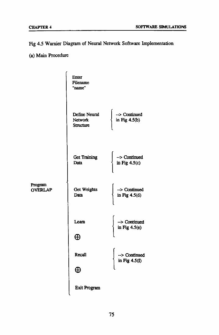
CHAPTER 4
Fig 4.5 Warner Diagram of Neural Network Software Implementation
SOFTWARE SIMULATIONS
(a) Main Procedure
Program OVERLAP
Enter Filename "name"
Define Neural Network structure
Get Training Data
Get Weights Data
--> Continued in Fig 4.5(b)
--> Continued in Fig 4.5(c)
--> Continued in Fig 4.5(d)
Lear
ED
Recall
(1)
Exit Program
-> Continued
in Fig 4.5(e)
--> Continued in Fig 4.5(t)
75

CHAPTER 4 SOFTWARE SIMULATIONS
Fig 4.5 (b), (c) & (d) Warnier Diagram (continued)
Inputs, L Enter Layer Sizes Hidden, M
Output, N Enter
(b) Define Number of Neural Test Network Patterns, P Structure
Existing choose weights
Weights Type Random
Weights
Open file "name". in
Get an Input Get an (L times)
(C) Get Training Input-Output Data Pair Get a
(P times) Desired Output (N times)
close file "name". in
Open working weights file "nmme". wgt Get a
Hidden
weight Get Hidden (L times) Neuron Weights Get a
ýd) Get Weights (M times) Hidden Data Tbzeshdd
Get Output Get Output Neuron Weight Weights (M times) (N times)
Get Output Threshold
close file "name". wgt
76
Enter weights Range
Create initial file "name". sav
Crate woddng file
"wgt
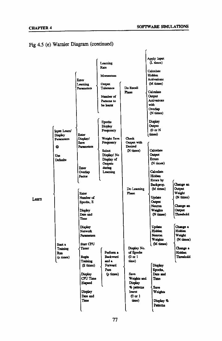
CHAPTER 4 SOFTWARE SIMULATIONS
Fig 4.5 (e) Warner Diagram (continued)
input Leaw Display puameten
Use Defaults
Learn
Start a Training Rum (n times)
Learning Rate
Momentum
g OQVM >acameters Tolemce
Number of Patterns to be learnt
Epochs Display Frequency
Enter Display/ Weight Save Save Frequency Parameters
Select Display! No Display of Out uts Enter p daring
Overlap Factor
lumber of Epochs, E
Display Date and rime
Display Netwoh Parmmaua
Start CPU Timer
Peifoam a Begin Backward Training and a (E times) Forward
Pass Display (P fimes) CPU Time Elapsed
Display Data and rune
Do Recau Phase
Check Output with De: iied (N times)
Do Learning Phase
Apply Input (L wes)
Calculate Hidden Activations (M rimes)
calculate Output Activalicas with Overlap (N times)
Display Output (0 or N times)
Calculate Oaepnt Enax (N times)
C achte Hidden Errors by BadcP . (M times)
Update Oast Neuron wette (N tinm)
a np an Output weight (N cam)
Gange an Om d Threshdd
Update ifidd Neuron Weights (M times)
Display No. of Epochs (0 or 1 time)
Display Epochs,
Save Date and Weights and Time Display % patums Save lams weights (0 or 1 time) Display %
Patterns
Change a Hidden Weight (N tb na)
Change a Hidden Tlueshdd
77
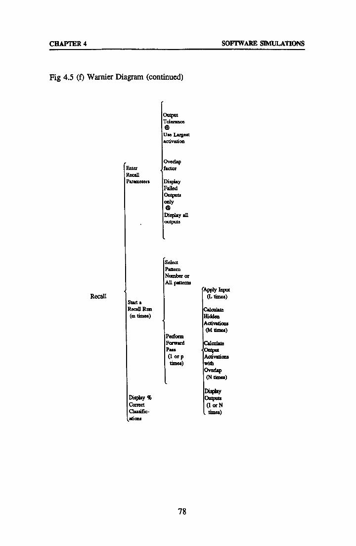
CHAFFER 4 SOFTWARE SIMULATIONS
Fig 4.5 (f) Warner Diagram (continued)
Output Tolerance
Use Largest activation
Overlap inter factor tecall Paz etea Display
Failed Outputs Only
Display an outputs
Select Pattern Number or All patterns
Apply Input Recall (L times)
Sit a Recall Ran Calculate (m times) Hidden
Activatims (M times)
Perform Forward Calcalate Pass output (1 or p Activations times) with
Overlap (N times)
Display Display % Outputs Correct (1 or N clauific- times)
78

CHAPTER 4 SOFTWARE SIMULATIONS
4.4 Simulation Results
4.4.1 Three Bit Parity using Floating Point Weights
The first simulation involved training a 3-3-1 two layer perceptron network
with the three-bit parity problem, using the backpropagation algorithm with
floating point weights. The training set consists of the eight three bit binary
input patterns and the corresponding desired binary outputs. The output neuron
has a desired output ' 1' if the number of 'I's in the input is odd, otherwise the
desired output is V. Training neural networks to learn parity has been studied
by numerous workerst444 and it is therefore a good benchmark for testing a new
simulator, and for studying the effect of overlap on the learning performance.
It is a generalisation of the XOR problem and so it cannot be done with a
single layer network. It is a 'hard' problem because patterns differing by the
smallest Hamming distance (i. e. 1 bit), must be classified differently.
The network was trained with a learning rate of 0.5 and a momentum of 0.9,
as used by Rumelhart et at"'. The network was trained to an output activation
tolerance of 0.1 of the desired outputs for all eight patterns and learning was
said to be complete when all patterns were learnt. The number of epochs of the
8 input patterns was recorded for a set of 100 trials (i, e. the network was
trained on the same problem 100 times) for each value of overlap used,
ranging from 0 to 1 at intervals of 0.05. Each trial was started with a different
random set of weights in the range ±0.1. If learning was not complete by
10000 epochs, training was stopped and the trial was recorded as non-
converged. It is important to record the data in a way which captures the
overall effects of overlap on the learning. Some researchers have suggested
using the mean number of epochs of the converged trials as a measure of
network performance'4.21). This method has been criticised by Fablman14'41 since
79

CHAPTER 4 SOFTWARE SIMULATIONS
it gives no indication of the overall performance, especially if convergence is
poor. Fahlman decided instead to restart unconverged trials after a certain
number of epochs with new random weights, and record the sum of the
number of epochs in all trials until convergence was reached. However, this
method is again not very good if the proportion of non-converged trials is very
high as it may be for a large overlap. It was decided therefore to include the
10000 epochs for each non-converged trial in the calculation of the mean to
give a fairer weighting to trials with higher non-convergence, and to record the
number of non-converged trials separately. All the information can be
contained on a single graph shown in Fig 4.6, with the number of non-
converged trials in brackets.
Mean No. of Epochs for Convergence /1000 81
6
4
2
Fig 4.6 Learning Time vs. Overlap
As a general trend, the number of trials which did not converge is seen to
increase with increased overlap. The percentage of failures is insignificant for
an overlap up to 0.3, where it is seen that even without overlap the network
80
0 0 0.1 0.2 0.3 0.4 0.5 0.6 0.7 0.8 0.9
Fractional Overlap

CHAPTER 4 SO1W TWARIE: SIMULATIONS'
may still not converge to the required solution. The larger percentages of
failures are apparent for overlaps above 0.5.
% Trials 80
over I 89P. 0.0
Ov. r lp=0.1
60 Overlap-0.2
Orr 1m0.3
® Ovw IapK0.4
D~ I upa. 5 40 ®
Over Iu0. S
[ý 0
Owrlep-0.7
20
0 0.500.1000.1500.2000.2500+ 3000.3500.4000.4500+ 5000. N. C.
fpocre
Fig 4.7 Learning Time Distributions for Varying Degrees of Overlap
Fig 4.7 shows in more detail, the distribution in the number of epochs needed
for convergence for the 100 trials, shown in groups of 500 epochs. Each group
of bars shows how the percentage of total trials requiring a specific range of
epochs varied as overlap was increased. The first group of bars shows the
percentage of trials which required between 500 and 999 epochs to converge,
which are seen to first increase, then decrease as overlap was increased from
0.1 to 0.7 at intervals of 0.1. The second group shows a similar variation.
Examination of the other groups reveal that as overlap is increased, there are
a small number of trials which require an increasingly larger number of epochs
to achieve convergence. For example at an overlap of 0.5, a sizable proportion
of the trials required between 1500 and 2999 epochs to converge, and at 0.6,
81
CHAPTER 4 SOFTWARE SIMULATIONS
there are more trials requiring over 4000 epochs. The N. C. (Not Converged)
group shows how the number of non-converged trials increased steadily for
overlaps greater than 0.3.
On examination of the results from both Fig 4.6 and 4.7, an overall
degradation of performance is observed. This is mainly due to the increase in
the number of unconverged trials, as the overlap between adjacent hidden layer
neurons was increased. However, it is clear from the variation of the learning
speed distributions in Fig 4.7 that for trials which did converge, the average
number of epochs needed for convergence was actually decreased for moderate
amounts of overlap. This decrease in learning time is most probably due to an
overall positive reinforcement of a neuron's output activation from overlap of
adjacent neurons, causing an increase in weight change increment and a
consequent increase in the learning speed. The increased number of non-
converged trials is due to negative reinforcement which causes non-
convergence by training of weights values in the wrong direction. Eventually,
even positive reinforcement may also cause non-convergence due to overly
large weight increments which could saturate a neuron irreversibly. This would
explain the eventual reduction in the mean learning speed of trials which did
converge, as well as the increased number of non-converged trials for larger
values of overlap. This phenomenon is now examined in more detail in the
following analyses.
Two sets of trials were carried out starting each set with a different random
weights file. For each set the trial was repeated for different values of overlap,
using the same starting weights file. The variation in the number of epochs
needed for convergence, as overlap was increased at intervals of 0.05, is shown
82

CHAPTER 4 SOFTWARE SIMULATIONS
in Fig 4.8. Both graphs start at zero overlap, and end at the highest overlap
value for which convergence was achieved. As before, a trial was said to be
not-converged if convergence was not achieved in 10000 presentations of the
training set.
No. of Epochs to Convergence /1000 7.
6
5
4
3
2
1
Fig 4.8 Variation in learning time with overlap for two sets of trials
Set (a) showed a gradual decrease in the learning time, followed a by rapid
failure as overlap was increased past 0.65. Set (b) initially showed the same
gradual decrease in learning time, but a gradual failure is also apparent starting
at an overlap of 0.45, with final non-convergence occurring at overlap greater
than 0.60. These observations conform to the shift in distributions of training
times shown in Fig 4.7, where an increase in overlap gave a decrease in the
average number of epochs required for convergence, provided convergence
occurred. However, the difference in the type of failure still needs to be
explained.
83
0 0 0.1 0.2 0.3 0.4 0.5 0.6 0.7
Fractional Overlap
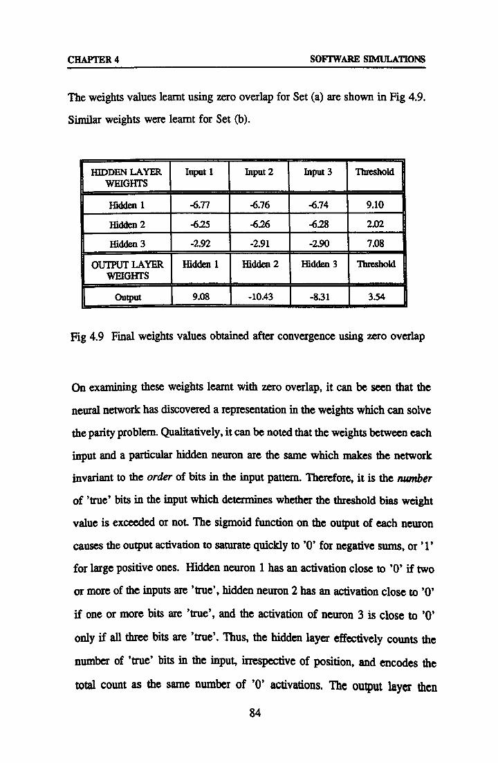
CHAPTER 4 SOFTWARE SIMULATIONS
The weights values learnt using zero overlap for Set (a) are shown in Fig 4.9.
Similar weights were learnt for Set (b).
IDEN LAYER WEIGHTS
Input 1 Input 2 Input 3 Threshold
Hidden 1 -6.77 -6.76 -6.74 9.10
Hidden 2 -625 -6.26 -6.28 2.02
Hidden 3 -2.92 -2.91 -2.90 7.08
OUTPUT LAYER WEIGHTS
Hidden 1 Hidden 2 Hidden 3 Threshold
Output 9.08 -10.43 -831 3.54
Fig 4.9 Final weights values obtained after convergence using zero overlap
On examining these weights learnt with zero overlap, it can be seen that the
neural network has discovered a representation in the weights which can solve
the parity problem. Qualitatively, it can be noted that the weights between each
input and a particular hidden neuron are the same which makes the network
invariant to the order of bits in the input pattern. Therefore, it is the number
of 'true' bits in the input which determines whether the threshold bias weight
value is exceeded or not. The sigmoid function on the output of each neuron
causes the output activation to saturate quickly to '0' for negative sums, or ' 1'
for large positive ones. Hidden neuron 1 has an activation close to '0' if two
or more of the inputs are 'true', hidden neuron 2 has an activation close to '0'
if one or more bits are 'true', and the activation of neuron 3 is close to '0'
only if all three bits are 'true'. Thus, the hidden layer effectively counts the
number of 'true' bits in the input, irrespective of position, and encodes the
total count as the same number of '0' activations. The output layer then
84

CHAPTER 4 SOFTWARE SIMULATIONS
decodes the hidden layer activations. The output threshold bias is a small
positive number, the weights from hidden neurons 2 and 3 to the output are
large and negative, and the weight from hidden neuron 1 to the output is large
and positive. Therefore the output will be close to a '1' for hidden activations
'0 0 0' and 10 1' corresponding to even parity, and close to a '0' for hidden
activations 11 1' and '0 0 1', corresponding to odd parity. It can be seen that
the actual values of the weights and thresholds are not critical, for a similar
internal representation to be achieved. Fig 4.10 shows the internal values of the
network for all eight input patterns, rounded to integer values for clarity. The
same representation was discovered by the network in Set (b).
Inputs 'true' =T 'false' F 123
Hidden Layer Sum of
Products 123
approximate Hidden Layer Activations
123
output Sum of
Products
Approximate output
Activation
FFF 000 111 -9 0
FFT -7 -6 -3 101 1 1
FTF -7 -6 -3 101 1 1
FTT -14 -12 -6 001 -8 0
TFF -7 -6 -3 101 1 1
TFT -14 -12 -6 001 -8 0
TTF -14 -12 -6 001 -8 0
TTT -21 -18 -9 000 0 1
Fig 4.10 Internal Representation for Backpropagation Learning of 3-bit Parity with zero overlap
Rather than show all the available data, the direction of change (positive or
negative) of the final weight values as overlap was increased is shown in Fig
4.11 for Set (a). This helps to give an insight into why the network eventually
85
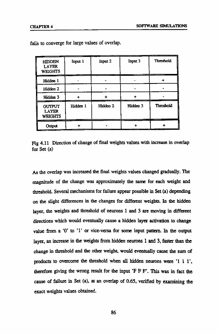
CHAPTER 4 SOFTWARE SIMULATIONS
fails to converge for large values of overlap.
HIDDEN Input 1 Input 2 Input 3 Threshold LAYER
WEIGHTS
Hidden i - - - +
Hidden 2 - - - - Hiý3 + + + -
OUTPUT Hidden 1 Hidden 2 Hidden 3 Threshold LAYER
WEIGHTS I Output + - + +
Fig 4.11 Direction of change of final weights values with increase in overlap for Set (a)
As the overlap was increased the final weights values changed gradually. The
magnitude of the change was approximately the same for each weight and
threshold. Several mechanisms for failure appear possible in Set (a) depending
on the slight differences in the changes for different weights. In the hidden
layer, the weights and threshold of neurons 1 and 3 are moving in different
directions which would eventually cause a hidden layer activation to change
value from a '0' to '1' or vice-versa for some input pattern. In the output
layer, an increase in the weights from hidden neurons 1 and 3, faster than the
change in threshold and the other weight, would eventually cause the sum of
products to overcome the threshold when all hidden neurons were '11 1',
therefore giving the wrong result for the input 'F F F. This was in fact the
cause of failure in Set (a), at an overlap of 0.65, verified by examining the
exact weights values obtained.
86

CHAPTER 4 SOFTWARE SIMULATIONS
In Set (b), the weights movements were of similar magnitude but with different
directions, shown in Fig 4.12.
HIDDEN Input 1 Input 2 Input 3 Threshold LAYER
WEIGHTS
Hidden i - - - - Hidden 2 - - - +
Hidden 3 - - - +
OUTPUT Hidden 1 Hidden 2 Hidden 3 Threshold LAYER
WEIGHTS
Output - + - -
Fig 4.12 Direction of change of final weights values with increase in overlap for Set (b)
In this case the first signs of failure occurred when the weights of the third
hidden neuron became too small to overcome the rising threshold at an overlap
of 0.5, rather than a failure in the output layer as experienced in Set (a). At
this point the network weights changed in an entirely new way, some changing
direction, breaking the symmetry of the usual method, and the output layer
weights rose to much higher values. This 'phase' change was accompanied by
a great increase in the number of epochs required to find the new solution. The
new internal representation discovered is shown in Fig 4.13.
87

CHAPTER 4 SOFTWARE SIMULATIONS
Inputs 'true' =T 'false' =F 123
Hidden Layer Sum of Products
123
Hidden Layer
Activations 123
Hidden Layer Activations Modified by
Overlap
Output Sum of Products
output Activation
FFF 000 111 1.52.01.5 -3 0
FFT -9 -7 -7 011 0.5 1.5 1.5 4 1
FTF -2 -10 -12 110 1.5 1.5 0.5 2 1
FTT -11 -17 -3 001 0.00.51.5 -15 0
TFF -2 -10 -12 110 1.5 1.5 0.5 2 1
TFT -11 -17 -5 001 0.00.51.5 -15 0
TTF -4 -20 -24 100 1.50.50.0 -18 0
TTT -13 -27 -15 000 0.00.00.0 0 1
Fig 4.13 Alternative Internal Representation for Neural Network Learning of 3-bit Parity with overlap, Set (b)
It can be seen that the network has exploited the symmetry in the output layer
weights which allows the order of hidden activations to be exchanged without
affecting the final result. The number of '0' hidden layer activations is the
same as that for smaller amounts of overlap for the same input pattern. This
new weight combination will work even without overlap, but without the
additional constraint, the network finds the simpler solution first. The
subsequent large rise in learning time with overlap until non-convergence
shows that the alternative solution is more sensitive to the overlap value than
the first. Final non-convergence in Set (b) occurred at an overlap of 0.6, due
to a second hidden layer failure. The two sets of trials reveal two typical
responses of the parity network to overlap.
In summary, for the first case Set (a), changes in the output layer due to
88

CHAPTER 4 SOFTWARE SIMULATIONS
overlap eventually caused rapid, unrecoverable failure. In the second case,
changes in the hidden layer results in an alternative route to convergence,
requiring longer training, before final non-convergence occurs. In Fig 4.7, the
results from the 100 trials are split between these two cases for large overlap
which explains the overall nature of the graph. In both Set (a) and Set (b),
small overlaps, up to 0.5 have little effect on the way the solution is found,
which is an interesting and beneficial result.
In the light of these results it appears that the neural network is highly tolerant
to the mixing of hidden layer neuron outputs for the three bit parity problem,
and it is noteworthy that even for a large overlap the network can still
converge to the correct solution, albeit in a smaller number of cases.
89

CHAPTER 4 SOFTWARE SEMI ATIONS
4.4.2 Text-to-Speech using Floating Point Weights
The second network implementation was for a larger problem, involving a
larger number of hidden layer neurons. A network similar to the NETtalk text-
to-speech architecture of Sejnowski and Rosenbere-3' was chosen because
of the network's proven ability to generalise for unknown input data. (Learning
of the above parity problem cannot be used to examine generalisation because
the entire set of input/output patterns must be used to train the network
correctly). NETtalk cannot be described as a state-of-the-art system, since it
relies only on statistical pattern recognition, and is lacking in the
morphological analysis and other higher level knowledge bases present in more
advanced systems"41, but it is useful as a demonstration of a typical
application for neural networks and gives an insight into how internal
representations are formed in hidden layers'" 1. NETtalk was a multilayer
perceptron network trained to learn text-to-speech conversion by training on
example pairs of letter and phoneme data from English text, using the
backpropagation algorithm The input data was presented as a window of seven
characters which was moved along the running text. The network was trained
to pick out the correct phoneme for the central letter of the seven, the other
letters being used to provide a context for the transcription. Fig 4.14 shows a
schematic of the NETtalk architecture. In this implementation` 1a 196-100-46
network was used, which is different to NETtalk only by virtue of how the
training data was obtained.
The inputs consist of 7 groups of 28 bits, of which one bit in each group is a '1' and the rest '0'. The ' 1' represents the selection from a set of 28 possible
characters, the 26 letters of the alphabet plus 2 for punctuation. Hence, only
seven of the inputs are ' 1' for any input pattern. A hidden layer of 80-120
90
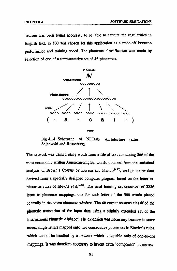
CHAPTER 4 SOFTWARE SIMULATIONS
neurons has been found necessary to be able to capture the regularities in
English text, so 100 was chosen for this application as a trade-off between
performance and training speed. The phoneme classification was made by
selection of one of a representative set of 46 phonemes.
PHONEME
/
000000000
000000000000000 000000000
0000 0000 0000 0000 0000 0000 0000
a-c a t- TDR
Fig 4.14 Schematic of NETtalk Architecture (after Sejnowsld and Rosenberg)
The network was trained using words from a file of text containing 566 of the
most commonly written American-English words, obtained from the statistical
analysis of Brown's Corpus by Kucera and Francis' , and phoneme data
derived from a specially designed computer program based on the letter-to-
phoneme rules of Elovitz et at4"281. The final training set consisted of 2856
letter to phoneme mappings, one for each letter of the 566 words placed
centrally in the seven character window. The 46 output neurons classified the
phonetic translation of the input data using a slightly extended set of the
International Phonetic Alphabet. The extension was necessary because in some
cases, single letters mapped onto two consecutive phonemes in Elovitz's rules,
which cannot be handled by a network which is capable only of one-to-one
mappings. It was therefore necessary to invent extra 'compound' phonemes.
91

CHAPTER 4 SOFTWARE SIMULATIONS
It was decided not to be overly concerned with obtaining good performance
of the rule-based program in producing 'correct' spoken English for every
word, since the aim of the exercise is not to produce the best text-to-speech
system, rather to test the effect of overlap on a large neural network. All data
produced by the rule-base can be treated as correct for the purpose of training
the neural network, since the performance of neural network can be measured
against the rule-base data, correct or otherwise.
A few initial trials with zero overlap were done to find an optimum learning
rate and momentum, which were found to be 0.9 and 0.0 respectively. An
output activation tolerance of 0.3 was chosen. For each value of overlap, the
network was trained starting with the same (initially random) weights file, and
the number of patterns learnt after each pass of the data set was recorded for
80 epochs.
Percentage of Patterns Learnt
100
80
60
40
20
Fig 4.15 Learning curves for text-to-speech showing overlap dependence
92
a 0 10 20 30 40 50 60 70 80 90
No. of Presentations of Inputs CEpochs)

CHAFFER 4 SOFTWARE SIMULATIONS
Fig 4.15 shows the learning curves obtained. Even without overlap, the
network was unable to learn the entire training set in 80 epochs. The reasons
for this are as follows. Firstly, two of the words in the training set, 'Thought'
and 'Though', cannot be distinguished by this method using only a seven
character window. Secondly, the network learns to distinguish between 'c', 's'
and 'z' sounds fairly late on in the training run, and does not achieve the
correct results for all words at 80 epochs. This second case could have been
overcome by further training, but it was decided that to do this for all trials
would not warrant the extra computer processing time required.
The learning curves for the network with overlap, and the network with zero
overlap, are almost indistinguishable for overlaps up to 0.3. The performance
of the network is then seen to degrade gracefully up to an overlap of 0.5. At
0.5 overlap a slight peak in the percentage of patterns learnt is noticeable at
about 50 epochs after which the number learnt decreases slowly. The network
failed to converge at an overlap of 0.6, and the number of patterns learnt
decreased rapidly to zero after pealing at about 17 epochs.
Generalisation for unknown inputs was then tested, for the values of overlap
up to 0.5. For each input pattern, the 'correct' phoneme was chosen as the
output neuron with the largest activation. The network was tested initially on
the original training set for each value of overlap, using the final weights learnt
in the first part of the simulation. A 720 word sample of text containing words
not in the original training set was then tested on the network and the
percentage of correct letter-to-phoneme transcriptions was recorded. Fig 4.16
shows the results obtained for the generalisation experiment. From the graphs
93
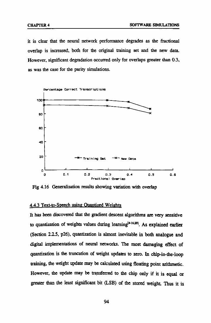
CHAPTER 4 SOFTWARE SIMULATIONS
it is clear that the neural network performance degrades as the fractional
overlap is increased, both for the original training set and the new data.
However, significant degradation occurred only for overlaps greater than 0.3,
as was the case for the parity simulations.
Percentage Correct Transcriptions
100
90
60
40
2C
Fig 4.16 Generalisation results showing variation with overlap
4.4.3 Text-to-Syeech using Quantized Weights
It has been discovered that the gradient descent algorithms are very sensitive
to quantization of weights values during learnine16-'I. As explained earlier
(Section 2.2.5, p26), quantization is almost inevitable in both analogue and
digital implementations of neural networks. The most damaging effect of
quantization is the truncation of weight updates to zero. In chip-in-the-loop
training, the weight update may be calculated using floating point arithmetic.
However, the update may be transferred to the chip only if it is equal or
greater than the least significant bit (LSB) of the stored weight. Thus it is
94
0 0.1 0.2 0.3 0.4 0.5 0,6 FractIonnI Overlap

CHAPTER 4 SOFTWARE SIMULATIONS
necessary to consider the combined effects of weight quantization and overlap
on neural network learning, and to discover if either has a dominant effect.
Typical weight quantization in analogue neural networks is 12 bits or less.
Therefore the text-to-speech simulations were repeated for 12,10, and 8-bit
quantization of weights. In addition a probabilistic update strategy, 4"30' was also
tested for the 8-bit case, whereby a weight is updated by one LSB with
probability Aw/LSB, if the calculated weight update Aw is less than the LSB
value.
Quantization as used in the simulations is defined as follows. Firstly the
integer part of each weight is clipped to ±16, using 5 bits. This choice is made
on the basis of the weight ranges required by floating point simulations. The
remaining bits are available for the fractional part. Thus the LSB values of 12,
10 and 8-bit weights are 1/128,1/32,1/8 respectively.
The Pascal code was first ported to C to take advantage of newer Sun
workstation performance, and then modified in two ways. The random weight
generation procedure was altered to introduce quantization to the initial random
weights file. The weights are generated, as before, as real numbers in a fixed
range after which each value is quantized. In C this is easily done by
multiplying a real valued weight by the LSB denominator (i. e. 128,32 or 8),
converting to integer type, converting back to real, then finally dividing by the
same LSB denominator. Since the magnitudes of initial weights are much
smaller than 16, clipping is not necessary.
The same procedure is also carried out for each weight update during learning.
Furthermore each updated weight value is checked to see whether it is now
95

CHAPTER 4 SOFTWARE SIMULATIONS
greater then 16, or less than -16. If so, the value is clipped. The above
procedure ensures that weights continue to be quantized throughout learning.
In order to implement probabilistic update for the 8-bit case a random number
is generated in the range 0 to 1/8. If this number is less than the magnitude of
the calculated update, the weight is updated by one LSB in the direction of the
calculated update, otherwise the weight is not updated.
Simulations of text-to-speech learning were carried out as follows. For each
value of overlap from 0.0 to 0.5 at intervals of 0.1, the network was trained
for 80 epochs on the training set used in the previous section. The fully
floating point simulation was repeated first, since a different initial random
weights file was used. Next, weights were clipped to ±16 but were not
quantized. Then, various levels of quantized weights were used with 12,10
and 8 bits. Finally the 8-bit with probabilistic update simulation was
performed. During each training run, the number of patterns learnt, MSE,
maximum and minimum weights, mean and standard deviation of the weight
set, and the average number of zero weight updates per epoch, were monitored.
The generalisation simulation was then carried out for each network. Graphical
results for the learning and generalisation simulations are shown in Fig 4.17
and Fig 4.18. Fig 4.19 shows the data obtained from monitoring the learning
simulation.
96

CHAPTER 4 SOFTWARE SIMULATIONS
% Patterns warnt
so
40
213 -
0.1 0.2 0.3 0.4 0.5 0.8
Fractional Overlap
Fleati Point --4- FP Clipped /-18 12 bit
10 bit --X- 8 lilt 08 bit " Qm. £tt
Fig 4.17 Text-to-speech learning with overlap for various degrees of weight quantization
x Patterns correct 100
eo
50,
40
20
OR- lot p 0.1 0.2 0.3 0.4 0.5 0.6
Fractional Overlap
-'- FIYKInt Point W Clipped N-16 It bit
-e- 10 bit " bit 6 bit " dab. Isst.
Fig 4.18 Text-to-Speech generalisation with overlap for various degrees of weight quantization
97

CHAPTER 4 SOFPWARE SIMULATIONS
Fig 4.19 Table of data measured after training text-to-speech for 80 epochs
Description Overlap Final
MSE
(x10a)
Maximum
Weight
Minimum
Weight
Mean
Weight
Standard
Deviation
of Weight
Set
% Zero
Updates
Floating 0.0 0.47 172.16 272.24 -0.187 7.579 0
Paint
Weights 0.1 0.72 620.13 -438.88 -0.263 11.747 0
02 0.93 640.82 -506.52 -0.074 16.221 0
0.3 0.76 664.95 -363.03 -0.349 14.060 0
0.4 1.65 390.93 -667.03 -0.284 16.411 0
0.5 3.92 2003.43 -772.78 -0281 26.2076 0
Floating 0.0 0.52 16.00 -16.00 -0.242 4.780 0
Paint
Wem, 0.1 0.63 16.00 -16.00 -0.273 4.874 0
Clippw 0.2 0.80 16.00 -16.00 -0.262 5.364 0
+/-16 0.3 1.18 16.00 -16.00 -0.314 5.920 0
0.4 138 16.00 -16.00 -0.379 7.615 0
0.5 4.70 16.00 -16.00 -0.311 9.815 0
12-bit 0.0 1.86 16.00 -16.00 -0.118 3.844 98.45
Qwmdzad 0.1 2.35 16.00 -16.00 -0.093 4.200 98.61
0.2 338 16.00 -16.00 -0.108 3.907 98.88
0.3 2.80 16.00 -16.00 -0.104 5.078 98.64
0.4 4.00 16.00 -16.00 -0.174 5.949 98.87
0.5 6.45 16.00 -16.00 -0.068 4.660 98.86
98
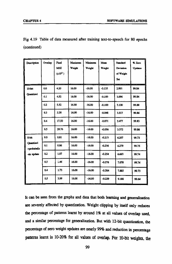
CHAPTER 4 SOFTWARE SIMULATIONS
Fig 4.19 Table of data measured after training text-to-speech for 80 epochs
(continued)
Description Overlap Final
MSE
(x103)
Maximum
Weight
Minimum
Weight
Mean
Weight
Standard
Deviation
of Weight
Set
% Zero
Updates
10-bit 0.0 4.20 16.00 -16.00 -0.135 2.991 99.84
Qaantized 0.1 4.52 16.00 -16.00 -0.100 3.096 99.84
0.2 5.52 16.00 -16.00 -0.100 3.100 99.88
03 5.58 16.00 -16.00 -0.048 3517 99.86
0.4 1750 16.00 -16.00 -0.071 3.477 99.83
0.5 28.76 16.00 -16.00 -0.056 3.372 99.86
8-bit 0.0 0.81 16.00 -16.00 -0213 6.207 99.73
Qtumfised
+Pmbabala 0.1 0.86 16.00 -16.00 -0.236 6.279 99.75
-tic update 0.2 1.07 16.00 -16.00 -0.254 6.663 99.74
03 1.46 16.00 -16.00 -0.276 7.078 99.74
0.4 1.73 16.00 -16.00 -0384 7.883 99.73
05 3.99 16.00 -16.00 -0229 9.180 99.64
It can be seen from the graphs and data that both learning and generalisation
are severely affected by quantization. Weight clipping by itself only reduces
the percentage of patterns learnt by around 1% at all values of overlap used,
and a similar percentage for generalization. But with 12-bit quantization, the
percentage of zero weight updates are nearly 99% and reduction in percentage
patterns learnt is 10-20% for all values of overlap. For 10-bit weights, the
99
CHAPTER 4 SOFTWARE SEM ULATIONS
percentage of zero weight updates is over 99.8%, and the reduction in
percentage patterns learnt is 30-40% up to an overlap of 0.3, above which
rapid failure ensues. With 8-bit quantization the number of zero updates is over
99.9%, such that learning is impossible for any value of overlap. With 8-bit
probabilistic update however, the results are much better, with a reduction of
only 2% in the percentage of patterns learnt for all values of overlap, even
though the number of zero weight updates is nearly the same as in the 10-bit
case.
From this data it appears that quantization has the dominant effect, causing a
severe reduction in performance in both learning and generalization ability.
The overlap has a consistent effect, which is to further reduce performance of
both learning and generalisation. The added effect of overlap is more marked
as quantization is introduced. However with probabilistic update, the results
show that the backpropagation algorithm has a good tolerance to overlap which
is similar to that achieved in simulations with floating point weights.
It is also noted that the standard deviation of the weight set for the 8-bit
probabilistic update simulation is no larger than that of the floating point
algorithm without overlap (which was used to determine a suitable weight
range) for overlaps up to 0.3. In these cases, more than 95% of weights have
magnitudes less than 16, which justifies the weight range chosen.
4.4.4 Five Bit Parity comparing Backurovaaation and Weight Perturbation
In order to compare the performance of backpropagation and weight
perturbation algorithms with weight quantization and overlap, a 5-10-1 MLP
network was trained to learn 5-bit parity. A new problem was chosen for two
100

CHAPTER 4 SOFTWARE SIMULATIONS
reasons. Firstly, the 3-bit parity network was considered too trivial for an
adequate comparison. Secondly, it was not feasible to repeat the text-to-speech
training with weight perturbation, because of the large number of weights in
the text-to-speech network which would require an excessive amount of time
to train.
A few initial training runs were carried out to find the optimum learning rate
for the learning of all 32 binary patterns, which was found to be 1.0.
Momentum was not used since it is unlikely to be employed in on-chip
training algorithms because of the extra memory required. The existing weight
range of ±16 was found to be adequate for the simulations - none of the
weights were clipped in the initial training runs.
Floating point backpropagation was first compared with weight perturbation
using a very small perturbation of 0.0001. Backpropagation took 2715 epochs
for complete convergence, and weight perturbation took 14595 epochs, which
Mwn epUM-w MT-W 0.1+
0.42
0.1
0.09
0.0
0.04
a. 02
Epochs Clbrk. d every 50)
-0 .V Ion - . IOrrt Pwreiaattm
Fig 4.20 Learning Trajectories for 5-bit Parity comparing Backpropagation and Weight Perturbation with a small perturbation Aß. 0001
101

CHAPTER 4 SOFTWARE SIMULATIONS
was surprising since the results were expected to be the same. However the
reason for this is seen by comparing the learning trajectories as shown in Fig
4.20. The trajectories are plotted up to the point that the backpropagation run
converged, using an output activation tolerance of 0.1. Although the learning
trajectories are almost identical to begin with (less than 0.2% difference after
200 epochs) as expected due to the close approximation of the error gradient
when a small perturbation is used, the learning trajectories are then seen to
diverge. This suggests that learning of 5-bit parity is very sensitive to small
differences in weight values.
The size of perturbation was then increased to 0.125 which is the size of the
LSB for an 8-bit quantized weight, and is about 1% of the maximum weight.
The increase in perturbation size is necessary to test the effect of quantization,
since it must be at least as big as the maximum LSB value used. This new
value of perturbation was used in all subsequent simulations.
The training was repeated for values of overlap from 0.0 to 0.5 at intervals of
0.1, using weights clipped to ±16, then 12,10, and 8-bit quantized weights,
and finally 8-bit weights with probabilistic update. The results from the
simulations are shown in Fig 4.21, which gives the number of epochs required
to train the network to correctly classify all 32 patterns, where possible. The
numbers in brackets denote the number of patterns learnt after 30000 epochs,
if the network did not converge.
For backpropagation the overall results are comparable to those for text-to-
speech, in that performance is severely reduced by quantization.
102

CHAPTER 4 SOFTWARE SIMULATIONS
Fig 4.21 5-bit Parity Results
(a) Backpropagation
Overlap
0.0 0.1 0.2 0.3 0.4 0.5
FP Clipped
+1-16
2715 4924 3256 (29) (24) 4968
12-bit (24) (6) 1493 1531 (25) (28)
10-bit (10) (0) (0) (9) (1) (3)
8-bit (0) (0) (0) (0) (0) (0)
8-bit +
prob-
romAing
3419 5447 1816 1120 5573 (26)
(b) Weight Perturbation
Overlap
0.0 0.1 0.2 0.3 0.4 0.5
PP Clipped
+/- 16
11708 2272 1775 1832 2082 3312
1 2-bit t (26) 1317 (25) (26) (21) (2)
10-bit (0) (0) (7) (2) (8) (10)
8-bit (0) (0) (0) (0) (0) (0)
8arit+
Pich
romfing
(30) 2410 9024 10600 10963 4309
103
CHAPTER 4 SOFTWARE SIMULATIONS
For the floating point simulation, the network is able to converge for values
of overlap up to 0.2 but the number of epochs required is increased over that
for zero overlap. Strangely, the speed of convergence is increased for 12-bit
quantization but this is only achieved for overlaps of 0.2 and 0.3. The network
fails to converge for 10-bit and 8-bit quantization. However, for 8-bit
quantization with probabilistic update, the network is able to converge for
overlaps up to 0.4 at a rate which is sometimes faster and sometimes slower
than in the corresponding floating point simulations.
In the case of weight perturbation, the qualitative results are similar, with
reduced performance at 12-bit quantization, and no convergence for the 10-bit
and 8-bit simulations for any amount of overlap. However, with clipped
weights, the network converges for all overlaps up to 0.5, and at a much faster
rate than the case with zero overlap. The 8-bit probabilistic update simulation
converges for all overlaps except zero.
on this limited amount of data, it is only possible to draw general conclusions
and to make some speculations. Firstly both training algorithms exhibit a
tolerance to overlap for both the floating point and 8-bit probabilistic update
training runs, but this tolerance is not as good as for the text-to-speech
problem. The reason for the poor performance of weight perturbation at zero
overlap cannot be explained at this time. However, it is interesting to note that
the networks trained by weight perturbation converged more consistently at
higher overlaps than by backpropagation. This may have something to do with
the fact that the learning phase for weight perturbation explicitly incorporates
the effect of overlap, since calculation of the perturbed MSE involves a recall
phase. This may be seen as further evidence of the tolerance of weight
104
CHAPTER 4 SOFTWARE SIMULATIONS
perturbation to particular constraints imposed by hardware implementation.
4.4.5 Discussion
Different simulations were carried out to investigate the effect of the mixing
of hidden neuron outputs, in order to simulate the band overlap which would
occur between the frequency responses of closely spaced filters in the proposed
frequency division multiplexed communication system between neural layers
in a neural network.
The effects of gradual degradation on the ability of the backpropagation
algorithm to train a neural network has been investigated by examining the
weights values learnt, as overlap was increased, in the 3-bit parity problem. It
was seen that failure to converge is due to the training of weights (or
thresholds) in the wrong direction, due to the modification in the outputs of
neurons by others. Failure may occur in either the hidden layer or the output
layer. In the 3-bit parity simulations, it was shown that the network may find
an alternative path to convergence when constrained by overlap. This is not
necessarily a desirable feature and it would not be wise to implement a
network architecture using such a high degree of overlap, but it is interesting
that an alternative method was found by the network for solving the parity
problem, which would not have been found without the additional constraints
being present
The results of the text-to-speech simulations using backpropagation with
quantized weights, suggest that weight storage on-chip may be quantized to 8
bits without a severe loss in performance, provided a probabilistic update
strategy is used in the chip-in-the-loop training. The reduction in the
105
CHAPTER 4 SOFTWARE SIMULATIONS
percentage of patterns learned using 8-bit weights and probabilistic update with
an overlap of 0.3 is only 5%, compared to the fully floating point simulation
with no overlap.
The results from the comparison of backpropagation with weight perturbation
learning 5-bit parity are somewhat less conclusive. However, it is clear that a
probabilistic update strategy must by employed in either algorithm, in order for
the network to converge consistently with quantized weights.
Although it is not possible to say with certainty that the algorithms will exhibit
a similar degree of tolerance for other problems, some tolerance to overlap is
probable, since the mechanisms for compensating the overlap errors will be
similar. The tolerance to overlap exhibited by the networks and algorithm
justifies the proposed use of moderate degrees of overlapping of filter
responses in the implementation of FDM communications. An overlap of 0.3
appears to be an upper limit for minimal degradation. This will allow the use
of lower Q filters, and/or increase the number of signals able to be transmitted
in a given bandwidth.
106
CHAPTER 5 VLSI IMPLEMENTATION OF FDM
CHAPTER 5- VLSI IMPLEMENTATION OF FDM
This chapter turns to the VLSI part of this thesis, starting with remarks on the
use of SPICE simulation for analogue VLSI design. The next section discusses
techniques for minimising the effects of fabrication process variations. This is
followed by a brief introduction to filter and oscillator VLSI design using
Operational Transconductance Amplifier (OTA) building blocks. The design
of a CMOS differential OTA chip is then presented, including a description of
the route through to fabrication and testing. Simulation results using the OTA
in filter and oscillator circuits are also presented. The remaining sections of the
chapter cover tuning techniques needed to ensure matching of frequencies
between chips, and the specification for VLSI implementation of the FDM
communications.
5.1 Simulation Issues in Analogue VLSI
Whereas many high level simulators exist for digital systems, the device level
simulator, SPICE (including variants HSPICE, PSPICE), is still the accepted
tool for use in most analogue circuit designs. This is because analogue design
is much more susceptible to the characteristics of particular devices, making
'black-box' behavioral modelling much less straightforward. This is also true
for analogue VLSI design. There are numerous SPICE transistor models of
varying accuracy suitable for analogue VLSI, which use as input, process
parameter values supplied by the chip manufacturer. Since the exact values of
transistor parameters are important in defining analogue operation, any
inaccuracies or variations in the SPICE parameters can have a significant effect
on performance. Passive components are also a problem for analogue VLSI
107
CHAPTER 5 VLSI IMPLEMENTATION OF FDM
simulation. In the case of on-chip capacitors or resistors, these are as much
subject to process effects as transistors, but they are not modelled as such by
SPICE.
When compared to digital, analogue VLSI circuits are much more sensitive to
the exact layout of the components. Layout is more involved than in digital
systems, where it is often possible to use the schematic information to
accomplish layout automatically. Gate arrays and standard cell libraries are
readily available. In contrast, high performance analogue circuits often require
a full custom layout. Some layout information may be back-annotated into
SPICE after layout (such as MOS transistor source/drain dimensions), and a
more accurate simulation can then be carried out. Even so, this approach may
result in a circuit being rejected after the lengthy design and layout procedure,
for other reasons. Fabrication variations can cause mismatch in components on
chip, and variations from chip to chip, which are difficult to include in
simulations. A further problem for system level simulations is lengthy
simulation times, although this may be overcome if higher level sub-circuit
models are available.
In the light of these problems, it is often desirable to try to minimise and
cancel out vors where possible by careful design, rather than attempt to
simulate the devices more accurately. In addition, where absolute component
values cannot be guaranteed, adaptive methods can be used to ensure accurate
performance of the system. This is the approach taken in the work to be
described in this chapter, since the accuracy of simulation possible was limited
by the availability of process data from the foundry.
108

CHAPTER 5 VLSI IMPLEMENTATION OF FDM
5.2 MOS Process Variations, Temperature Gradients, and their Effects on
Analogue Circuit Design
5.2.1 Process Variations
With the increasing trend towards mixed analogue and digital integrated
circuits and the use of CMOS technology, it is usually necessary to design
analogue VLSI circuits capable of being manufactured using a digital CMOS
process. It is important to have an understanding of the uncertainties in the
fabrication process and to be able to analyse the effect of these variations on
circuit parameters, thus making it possible to minimise errors.
It is generally accepted that the uncertainties in the absolute values of MOS
passive components or transistors are around 10%, mainly due to variations in
oxide thickness and doping in the fabrication process. In the case of integrated
RC filters, Gregorian and Teures point out 11 that the combination of errors in
resistor and capacitor values lead to overall errors of around 20% in RC time
constants, since resistors and capacitors are produced in different IC processing
steps, so that errors are independent. This magnitude of error is clearly
unacceptable even for low selectivity filters or oscillators.
Relative errors between similar components on the same chip however, are not
as serious, since process variations have a more uniform effect on similar
components, resulting in a good matching characteristics. J. this case, it is the
accuracy of the ratio of component values which must be considered. The
error in this ratio is called the tracking error which is around 1% for a typical
process, an order of magnitude lower than the absolute error. The same ratios
are also reproducible on chips from different wafers, even though the absolute
109

CHAPTER 5 VLSI IMPLEMENTATION OF FDM
values may be very different.
Some matching is also to be expected over a single wafer, and errors may be
smaller than those between chips on completely different wafers. However, for
a large number of chips, some will inevitably be on different wafers so it is
not really sensible to rely on matching except for components on the same
chip.
The main causes of physical fabrication errors in addition to variations in
oxide thickness and mobility, are mask undercut and random errors. Additional
errors are due to parasitics such as stray capacitances. The effects of these
depend very much on the physical geometry of the device.
Gregorian and TemesE511 discuss all these effects on integrated MOS capacitors.
Undercut is the lateral etching which occurs at the same time as the desired
vertical etching through a mask in the manufacturing process. The reduction
in area leads to a reduction in C, which depends on the perimeter of the
component. The smallest practical perimeter-to-area ratio is best achieved by
making the capacitor square. In addition, the capacitance is subject to a
random variation, due to uneven edges of both the masks and the materials
deposited, caused by non-uniform etching. The effect of the random errors is
such that an 8-bit accuracy in the absolute value is the best that can be
expected from the processes 21. Values for bottom plate stray capacitance are 15-
30% of C for metal/poly over diffusion capacitors depending on oxide
thickness and the construction of the device, and 5-20% of C for poly-over-
poly and metal-over-poly devices. Poly-over-poly capacitors are generally
preferred due to the uniformity of the oxide layer which can be achieved
110

CHAPTER 5 VLSI IMPLEMENTATION OF FDM
between polysilicon layers.
Minimum tracking errors are obtained by ensuring a constant ratio of area to
perimeter, and a uniform etch around the capacitor plates"". In practice this
means designing a small unit capacitor square, and combining squares in rows
and columns to obtain higher values, since the amount of under-etching will
be approximately the same for each square.
Common centroid layout154,51 is used to make a layout insensitive to first order
variations, by distributing the component topology and using symmetry to
cancel out the errors, using the fact that process parameter gradients across
chip (e. g. oxide thickness) are approximately constant over small distances.
Sensitivity analysis is often used to quantify the effect of mismatch or
temperature gradient on system design parameters, such as frequency or Q in
filters, where sensitivity is defined as the relative change in a parameter due
to a change in a component value. Conventional design aims to minimise
sensitivities whilst satisfying the specification. In the case of common centroid
layout, it is not necessary to know the absolute value of the sensitivities
because they cancel out.
According to Eric Vittozts'63, the main mismatch in transistors can be described
by the variation in the threshold voltage and transconductance parameter. The
effect on circuit parameters depends on the circuit configuration.
111
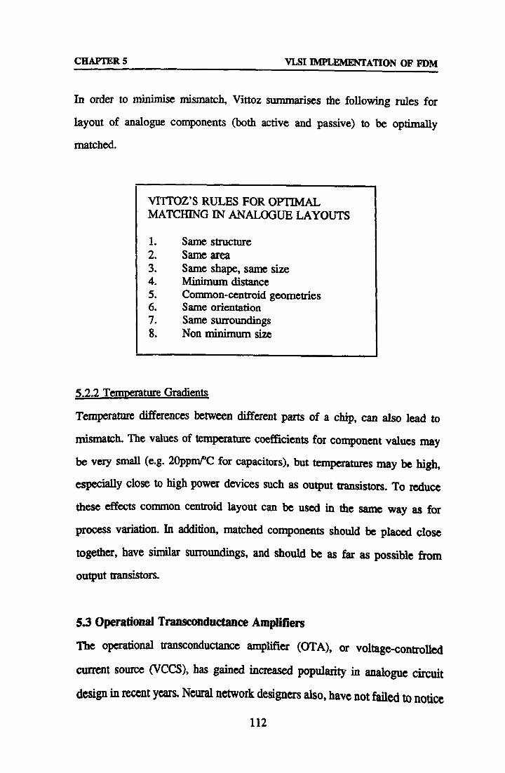
CHAPTER 5 VLSI IMPLEMENTATION OF FDM
In order to minimise mismatch, Vittoz summarises the following rules for
layout of analogue components (both active and passive) to be optimally
matched.
VITTOZ'S RULES FOR OPTIMAL MATCH NG IN ANALOGUE LAYOUTS
1. Same structure 2. Same area 3. Same shape, same size 4. Minimum distance 5. Common-centroid geometries 6. Same orientation 7. Same surroundings 8. Non minimum size
5 . 2.2 2 Temperature Gradients
Temperature differences between different parts of a chip, can also lead to
mismatch. The values of temperature coefficients for component values may
be very small (e. g. 20ppm/C for capacitors), but temperatures may be high,
especially close to high power devices such as output transistors. To reduce
these effects common centroid layout can be used in the same way as for
process variation. In addition, matched components should be placed close
together, have similar surroundings, and should be as far as possible from
output transistors.
5.3 Operational Transconductance Amplifiers
The operational transconductance amplifier (OTA), or voltage-controlled
current source (VCCS), has gained increased popularity in analogue circuit
design in recent years. Neural network designers also, have not failed to notice
112

CHAPTER 5 VLSI IMPLEMENTATION OF FDM
the advantages of using OTAs in analogue implementations [5. '_l0 , and it is in
this spirit that the use of the OTA is proposed as the building block for the
FDM circuitry. The subsequent sub-sections introduce the use of OTAs in filter
and oscillator circuits and explain the need for linearising techniques.
5.3.1 OTA Based Filters and Oscillators
The OTA symbol and equivalent circuit are shown in Fig 5.1. The transfer
function i.. /v;, is determined by the small signal transconductance gain gm. Cm
and go are the lumped input capacitance and output conductance, which model
the main parasitics, but will be neglected at this stage.
gout
Vin 9m
i out
vin Cis 9 9o
.T M$ y
Fig 5.1 OTA Symbol and Equivalent Circuit Model
Initial research using the OTA as a building block for filter and oscillator
circuits has been proposed and carried out by several groups, initially using the
commercial CA3080 IC, and more recently using specially designed OTAs.
H. S. Malvarý5 "1 used the differential CA3080 in the place of analogue
multipliers to synthesise a second order bandpass filter configuration (Fig 5.2).
Malvar combined the OTA with a fixed capacitor load C to form an integrator
building block with transfer function H(s)=gm/sC. The integrators were used
to replace the fixed integrators of the usual biquad circuit, and a third OTA of
gain gq was used to control the Q of the filter independently of w,. The gm
and gq are, in turn, controlled by the respective external currents Is and IBQ.
113

CHAPTER 5 VLSI IMPLEMENTATION OF FDM
Is
VLP
Fig 5.2 OTA based filter with Q control (after Malvar 1982)
The resistors Rl and KR, were used for attenuation to ensure linear operation,
since the CA3080 is only linear for a small input range. This should be
contrasted with the performance of filter circuits using conventional op-amps,
which are highly linear, but cannot be easily tuned electronically.
A. R. Saha et aP'22 describe an RC sinewave oscillator using differential OTAs
shown in Fig 5.3. The oscillation condition g jý: 1 is controlled by gm, and the
oscillating frequency w,, =g. N{C1C2(1+R/r)} is controlled independently using
resistor K Advantages of this configuration were reported as low component
count, low sensitivity and simple control of frequency by a single resistor. The
use of low valued, grounded capacitors also make it more suitable for IC
fabrication.
114
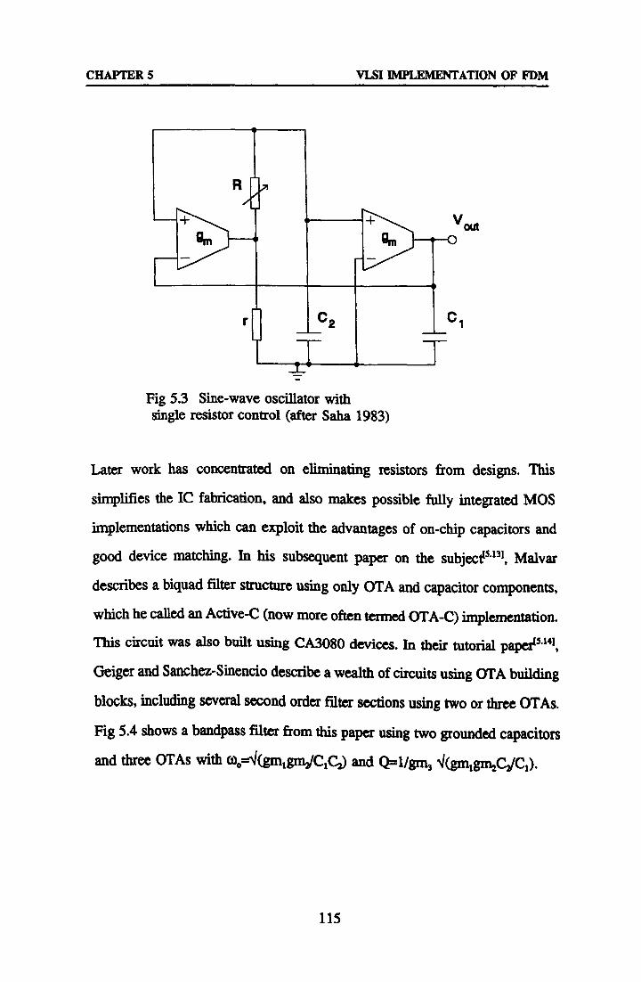
CHAPTER 5 VLSI IMPLEMENTATION OF FDM
/Ota
1
Fig 5.3 Sine-wave oscillator with single resistor control (after Saha 1983)
Later work has concentrated on eliminating resistors from designs. This
simplifies the IC fabrication, and also makes possible fully integrated MOS
implementations which can exploit the advantages of on-chip capacitors and
good device matching. In his subsequent paper on the subjectis'13i, Malvar
describes a biquad filter structure using only OTA and capacitor components,
which he called an Active-C (now more often termed OTA-C) implementation.
This circuit was also built using CA3080 devices. In their tutorial pap&5141, Geiger and Sanchez-Sinencio describe a wealth of circuits using OTA building
blocks, including several second order filter sections using two or three OTAs.
Fig 5.4 shows a bandpass filter from this paper using two grounded capacitors
and three OTAs with 0)1=sl(gm, gm2/C1C2) and Q=-1/gm3 AgmIgm2C jCl)"
115
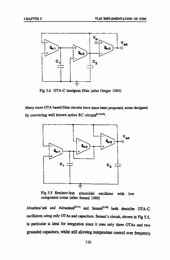
CHAPTER 5 VLSI I PLEMENI'ATION OF FDM
out
Fig 5.4 OTA-C bandpass filter (after Geiger 1985)
Many more OTA based filter circuits have since been proposed, some designed
by converting well known active RC circuitsP15 "
/Out
Fig 5.5 Resistor-less sinusoidal oscillator with low component count (after Senani 1989)
Abuelma'atti and Ahnaskatits 171 and Senanils"181 both describe OTA-C
oscillators using only OTAs and capacitors. Senani's circuit, shown in Fig 5.5,
in particular is ideal for integration since it uses only three OTAs and two
grounded capacitors, whilst still allowing independent control over frequency
116

CHAPTER 5 VLSI IMPLEMENTATION OF FDM
w. =4(gm1gm, JC1C2) and oscillation condition Cgra2>CIgm3. A technique for
generating all possible OTA-C sinusoidal oscillator structures employing two
capacitors has also been reported, some being suitable for integratiods191.
To date, the latest research in OTA based filters and oscillators has
concentrated on adaptive tuning methods (see later), design techniques for
achieving ever higher resonant frequencies15 20.21], and improvements in OTA
design, particularly in CMOS technology.
5.3.2 Design of Linearised MOS Transconductors
The simplest CMOS differential OTA is the standard op-amp input stage which
is constructed from a source-coupled differential pair with differential-to-single
ended conversion using a current mirror load (Fig 5.6).
V
vini
_ss
Fig 5.6 Basic CMOS Transconductance Amplifier
Large signal analysis of this circuit using the square-law relationship for MOS
transistors shows that the dynamic range is limited to 20% of the supply
voltage in order to maintain less than 1% non-linearity, measured as percentage
117

CHAPTER 5 VLSI IMPLEMENTATION OF FDM
deviation from ideal output for a given gain and input voltage1s-22]. The non-
linearity is caused by the transistors going out of the saturation region.
Non-linearity in analogue signal processing systems causes harmonic distortion
(mainly third order), and the creation of intermodulation products. It can be
shown that the input range must be limited to 40% of supply in order to
achieve a Total Harmonic Distortion of less than 1%. For these reasons,
linearisation of OTA circuits is highly desirable, and is the subject of much
fruitful current research often directly related to filter and oscillator
2"35] designts'
118

CHAPTER 5 VLSI IMPLEMENTATION OF FDM
5.4 OTA Design and Simulation
5.4.1 Route to Silicon
It was decided to design an OTA using techniques which would yield a
compact yet linearised design, which would be able to be used in filter and
oscillator configurations" IC design fabrication facilities were provided
through the Esprit/EUROCHIP scheme, using the CMOS 2.4pm n-well
Double-Layer-MetalDouble-Layer-Polysilicon (DLM/DLP) process of Mietec
in Belgium. HSPICE and Mentor Graphics CAD software were available for
simulation and layout.
The CAD route is described as follows. The initial design was simulated using
HSPICE. Mentor Graphics NETED schematic entry was used and designs were
simulated using ACCUSIM, the Mentor SPICE simulator, using the SPICE
MOS transistor Level 2 parameters provided in the Mieter documentation. The
graphical input of the netlist using NETED was preferred over the HSPICE
netlist entry. Final checking was done using HSPICE, also with Level 2
parameters, carried out by exporting the SPICE file from ACCUSIM. Level 3
MOS transistor parameters were not available until after fabrication.
Since compact circuitry was required, it was decided not to use the Mietec
Analogue Standard Cell Library throughout and opt instead for a full custom
design. In addition, the lack of any simulation models for the analogue core
cells would have made accurate design difficult, if not impossible. It was
however decided to use the standard cell I/O pads to speed up the design
process. The initial layout was drawn up on paper which was transferred to
software using Mentor CHIPGRAPH together with mask definitions contained
119

CHAPTER 5 VLSI IMPLEMENTATION OF FDM
in the Mietec Design Kit software supplied by Eurochip. Design-Rule-
Checking (DRC) files for use with the Mentor REMEDI DRC package were
not available as part of the first release of the Design Kit. Therefore all DRC
for the chip was done using the Mietec design rule document at the layout
stage, and then by the lead-site at Rutherford Laboratories using the automatic
design rule checker, DRACULA.
5.4.2 Circuit Design
The linearisation technique used was the Bias Offset technique of Wang and
Guggenbiihl 2 -", which uses the square law characteristics of MOS transistors
in saturation to synthesise a linear transfer function. Manipulation of the
square-law has been used by numerous researchers to eliminate unwanted
terms in the construction of building blocks for analogue computation,
including the author of this thesisis']. Fig 5.7 shows the OTA architecture as
proposed by Wang, using identical nMOS transistors for both the differential
pairs and the voltage shifters. In the diagram, I. is the value of the current
source, V,. is the input voltage, and Vb is the bias offset voltage. Il and 12 are
the output currents.
It can be shownts*2'281 that the output currents of the cross coupled pairs are,
11 22 12= KVjVj. C)
22
where K=µC01W/L and p, Cam, W, and L are the mobility, gate oxide
capacitance per unit area, channel width and channel length respectively.
120

CHAPTER 5 VLSI IMPLEMENTATION OF FDM
The single ended output current is,
low _ (Il - I2) = KVbVý (5.2)
The slope of the transfer function is therefore controlled linearly by the bias
offset Vb, (gm=KVb) and is independent of I. which offers a significant
advantage over previous designs which control the gain by adjusting the source
bias current I., in terms of sensitivity and ease of control. Linearity is
maintained provided all transistors remain in saturation. The range of Vm is
limited to,
J['.. 3Vb Vb (5.3)
K42
Since K and Vb should be small to maximise linearity for a particular I,,, but
large to maximise gain, it can be seen that there is a trade-off between gain
and input range which necessitates careful design of W and L values.
'M
Fig 5.7 Linearised CMOS OTA (after Wang 1990)
121
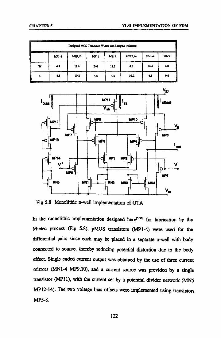
CHAPTER 5 VLSI IMPLEMENTATION OF FDM
Designed MOS Transistor Widths and Lengths (miemm)
MP1-8 MP9,10 ! W11 M212 Mn3,14 MN1-4 MN5
W 4.8 11.6 240 19.2 4.8 14.4 4.8
L 4.8 19.2 4.8 4.8 19.2 4.8 9.6
Lwl I Vsb
iMI 111b MOPG Mº, o
MP13 i vpT
Mpg IMP4
MP14 WI MP2
V+
MPb
MN5 I MNI 1! 11 MN2 UNS
Fig 5.8 Monolithic n-well implementation of OTA
Vdd -o lomwx
We
I Out
P---!:
MPS
MN4 I va
In the monolithic implementation designed herels-111 for fabrication by the
Mietet process (Fig 5.8), pMOS transistors (MP1-4) were used for the
differential pairs since each may be placed in a separate n-well with body
connected to source, thereby reducing potential distortion due to the body
effect. Single ended current output was obtained by the use of three current
mirrors (MN1-4 MP9,10), and a current source was provided by a single
transistor (MP11), with the current set by a potential divider network (MN5
MP12-14). The two voltage bias offsets were implemented using transistors
MP5-8.
122
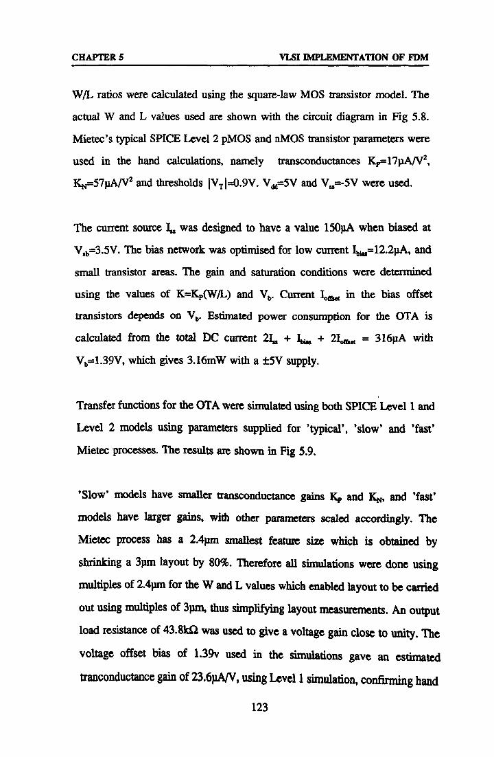
CHAPTER 5 VLSI IMPLEMENTATION OF FDM
W/L ratios were calculated using the square-law MOS transistor model. The
actual W and L values used are shown with the circuit diagram in Fig 5.8.
Mietec's typical SPICE Level 2 pMOS and nMOS transistor parameters were
used in the hand calculations, namely transconductances Kp=17pA/V2,
KN=57pA/V2 and thresholds IVTI=0.9V. V(-5V and V,, =-5V were used.
The current source L was designed to have a value 15NA when biased at
Vab=3.5V. The bias network was optimised for low current I=12.2pA, and
small transistor areas. The gain and saturation conditions were determined
using the values of K=Kp(W/L) and Vb. Current L,.. in the bias offset
transistors depends on Vb. Estimated power consumption for the OTA is
calculated from the total DC current 2L +I+ 21, E = 316µA with
Vb=1.39V, which gives 3.16mW with a ±5V supply.
Transfer functions for the OTA were simulated using both SPICE Level 1 and
Level 2 models using parameters supplied for 'typical', 'slow' and 'fast'
Mietec processes. The results are shown in Fig 5.9.
'Slow' models have smaller transconductance gains Kp and KN, and 'fast'
models have larger gains, with other parameters scaled accordingly. The
Mietec process has a 2.4pm smallest feature size which is obtained by
shrinking a 3pm layout by 80%. Therefore all simulations were done using
multiples of 2.4pm for the W and L values which enabled layout to be carried
out using multiples of 3pm, thus simplifying layout measurements. An output
load resistance of 43.8kf2 was used to give a voltage gain close to unity. The
voltage offset bias of 1.39v used in the simulations gave an estimated
tranconductance gain of 23.6pA/V, using Level 1 simulation, confirming hand
123
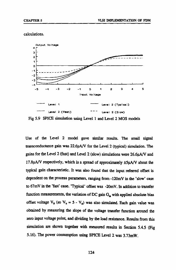
CHAPTER 5 VLSI EVIPLEMENTATION OF FDM
calculations.
Output Voltage 4
3
2
0
-1
-2
-3
-4 -5 -4 -3
Level 1 Level 2 CTyPIcal)
Level 2C Fest) --- Level 2 (Slow)
Fig 5.9 SPICE simulation using Level 1 and Level 2 MOS models
Use of the Level 2 model gave similar results. The small signal
transconductance gain was 22.6pA/V for the Level 2 (typical) simulation. The
gains for the Level 2 (fast) and Level 2 (slow) simulations were 26.6pA/V and
17.8pA/V respectively, which is a spread of approximately ±5pA/V about the
typical gain characteristic. It was also found that the input referred offset is
dependent on the process parameters, ranging from -120mV in the 'slow' case
to 67mV in the 'fast' case. 'Typical' offset was -20mV. In addition to transfer
function measurements, the variation of DC gain G. with applied absolute bias
offset voltage VB (so Vb =5- VB) was also simulated. Each gain value was
obtained by measuring the slope of the voltage transfer function around the
zero input voltage point, and dividing by the load resistance. Results from this
simulation are shown together with measured results in Section 5.4.5 (Fig
5.16). The power consumption using SPICE Level 2 was 3.73mW.
124
-2 -1 012345
Input Voltage

CHAPTER 5 VLSI IMPLEMENTATION OF FDM
5.4.3 Layout and Post-layout Simulations
The OTA was divided into 3 main sections for the purpose of layout; the OTA
body consisting of differential pairs and current mirrors, the current source
transistor, and the potential divider network for biasing the current source. It
was decided to design these as seperate cells of height 260µm so as to fit the
Mietec Standard Cell format specified in the Mietec Design Kit. The drawn
cell width for the cells were 70µm, 40pm and 160pm respectively for the
current source bias, current source and OTA body. Non-minimum sizes were
used wherever possible to reduce the effect of area reductions due to mask
undercut and overetching. Therefore all transistors have minimum drawn
lengths or widths of 6µm except the current source, which was redesigned to
length 4.5pm in order to reduce its overall size. The OTA body was designed
to be as symmetrical as possible, not only in the position of the transistors, but
also in the connections between them. All pMOS Transistors with different
source voltages are placed in seperate n-wells with body-to-source connections
in order to minimise body effect. All nMOS transistors have source-to-
substrate connections.
Fig 5.10 shows the 3 cells connected together revealing the compact nature of
the overall design. The total drawn OTA dimensions are 260µm x 270µm
which gives a total area after the 80% shrink of 45000pm2. It was noted that
since the exact size of the current source is not critical, it may be possible to
use the same current source bias network for several OTAs, with a saving in
area and power consumption.
After layout, the MOS transistor source and drain areas were measured, for use in AC characterisation. SPICE Level 2 models junction and sidewall parasitic
125
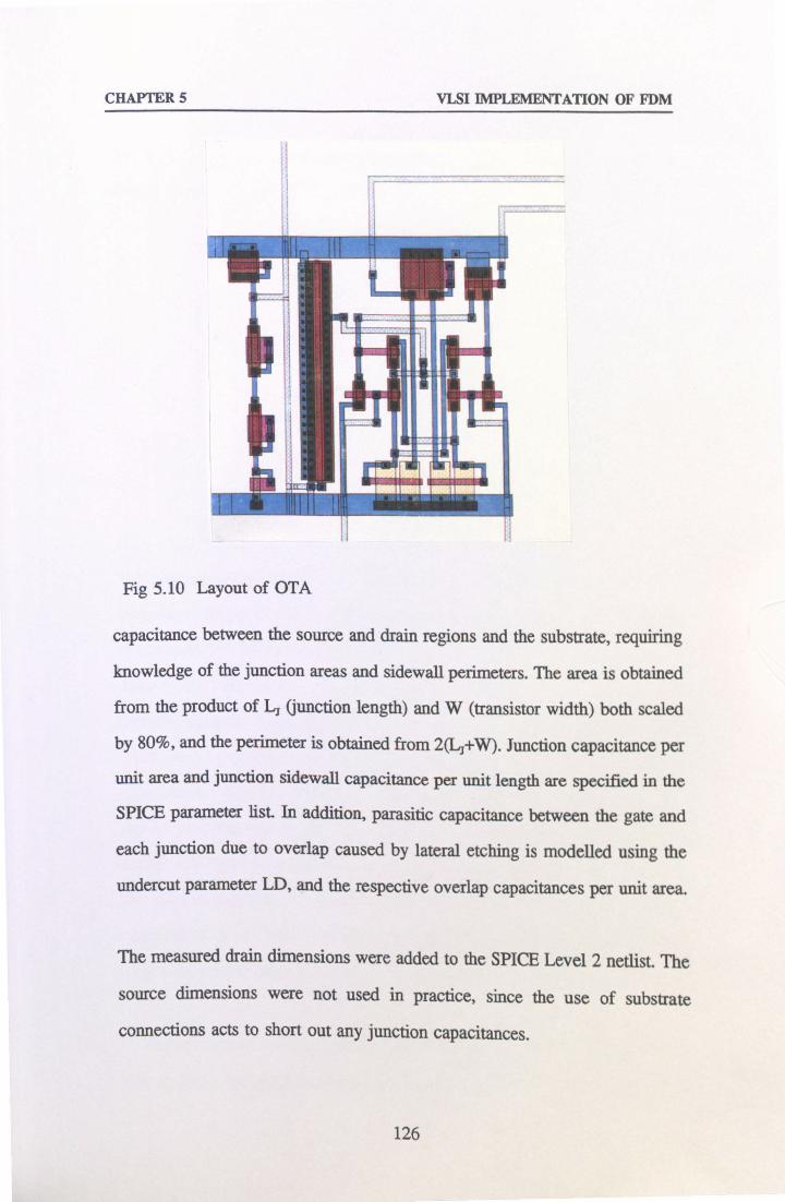
CHAPTER 5 VLSI IMPLEMENTATION OF FDM
Fig 5.10 Layout of OTA
capacitance between the source and drain regions and the substrate, requiring
knowledge of the junction areas and sidewall perimeters. The area is obtained
from the product of LJ (junction length) and W (transistor width) both scaled
by 80%, and the perimeter is obtained from 2(L, J+W). Junction capacitance per
unit area and junction sidewall capacitance per unit length are specified in the
SPICE parameter list. In addition, parasitic capacitance between the gate and
each junction due to overlap caused by lateral etching is modelled using the
undercut parameter LD, and the respective overlap capacitances per unit area.
The measured drain dimensions were added to the SPICE Level 2 netlist. The
source dimensions were not used in practice, since the use of substrate
connections acts to short out any junction capacitances.
126
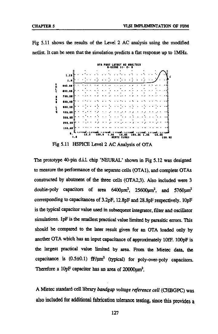
CHAPTER 5 VLSI IMPLEMENTATION OF FDM
Fig 5.11 shows the results of the Level 2 AC analysis using the modified
netlist. It can be seen that the simulation predicts a flat response up to 1MHz.
0Th POST LAYOUT AC ANALYSIS 0. OEC09 ii' 0' 0
1.16
Ö 9IS. IN _--"... "......
N Fit. IN _
ti 0 mm E-
c3
N ill. IN C, eä
Sol. IM=
all. IN:
1. E 1.111161 . '. tuud. ' a. uni. I'iu, . samel, 'J send. 'aiiu . us 1u,
ä 30.1 311.1 1.89 30.0[ 100.1E 1.11 ion
l. 1 NEITZ CL00I 311.01
Fig 5.11 HSPICE Level 2 AC Analysis of OTA
The prototype 40-pin d. i. l. chip 'NEURAL' shown in Fig 5.12 was designed
to measure the performance of the separate cells (OTA1), and complete OTAs
constructed by abutment of the three cells (OTA2,3). Also included were 3
double-poly capacitors of area 6400µm2,25600pm2, and 5760µm2
corresponding to capacitances of 3.2pF, 12.8pF and 28.8pF respectively. lOpF
is the typical capacitor value used in subsequent integrator, filter and oscillator
simulations. 1pF is the smallest practical value limited by parasitic errors. This
should be compared to the later result given for an OTA loaded only by
another OTA which has an input capacitance of approximately 10fF. 100pF is
the largest practical value limited by area. From the Mietec data, the
capacitance is (0.5±0.1) fF/}un2 (typical) for poly-over-poly capacitors.
Therefore a lOpF capacitor has an area of 20000pm2.
A Mieter standard cell library bandgap voltage reference cell (CHBGPC) was
also included for additional fabrication tolerance testing, since this provides a
127

CHAPTER 5 VLSI IMPLEMENTATION OF FDM
simple comparison with documented values. Two pins were connected
internally in order to provide an independent measure of I/O pad capacitance
if required. Four types of standard cell I/O pad were used. Power pads PFVDD
and PFVSS were used for the power supplies. Diode protected pads PFPDD
were used for inputs, except for the capacitors since the use of such pads
might introduce unwanted parasitic. Direct PFPAD pads were used for all
outputs and the capacitors. Two pins, In and Out, were connected internally via
pads PFPDD and PFPAD in order to provide an independent measure of I/O
pad capacitance. The pins Vdda are separate positive (+5V) power rails, Vssa
is the negative (-5V) power rail connected to substrate. For each OTA; Vsb is
a test output to measure the current source bias voltage, Vb is the bias offset
input, Vminus and Vplus are the inverting and non-inverting inputs, and lout
is the current output. In OTA1, extra test pins were used; Vsblin and Isslout
are the current source input and output nodes used for independent
measurement of the current When Vsblin and Isslout are connected to
V sb 1 out and Isslin respectively, OTA 1 is architecturally equivalent to
OTA2,3. C1-3 are the top plates of each capacitor.
128

CHAPTER 5 VLSI JMPLEMENTATION OF FDM
Pm Name Dae/eim Band Pin Type Pm Name 1a itim Band Pm T )p
1 Vdda3 OTA3 +5v Sapply I PFVDD 21 VddIk1 OTAI +5v SuFoy 21 PPVDD 2 Vsb3 OTA3 Bin * 2 PPPAD 22 l Iaat OTA1 Sowoe qp 22 PPPAD 3 bat3 OTA3 Oatput 3 PPPAD 23 ILlä OTAI Scum j/p 23 PFPAD 4 Vb3 OTA3 Clan CmaW 4 PPPPD 24 Imtl OTAI Output 24 PFPAD S NC Na C r. r -d 25 Vbl 0TA1 Gain Col 25 PPPPD 6 NC Na Cited 26 NC Na Geed 7 NC Na C®ected 27 Vmmsl OTAI -ve iipat 27 PPPPD 8 Vmmm3 OTA3 -w spat 8 PPPPD 28 VpIusl OTAI +ve mpat 28 PFPPD 9 Vpms3 OTA3 +ve mpm 9 PPPPD 29 Vsblm OTAI Bin äpt 29 PPPPD 10 ST Vruf Ststop j/p 10 PFPPD 30 Viblaat OTAI Bin q'p 30 PPPAD 11 Vref Vdtye Ref, q/p 11 PPPAD 31 Visa -ve Supply (-SV) 31 PFVSS 12 Out OaW Pad 12 PPPAD 32 VpI 2 0TA2 +ve mpt 32 PPPPD 13 In Ii ist Pad 13 PPPPD 33 Vm®d OTA2 -we iipst 33 P1'PPD 14 Vddb4 Vref +Sv Soppty 14 PFVDD 34 NC Not Camxrod 15 NC Na t', wd 35 NC Na '.. -. ' 16 NC Na t' wd 36 NC Na C®eeed 17 NC Not C®ecod 37 Vb2 OTA1(3ain Cm4d 37 PPPPD 18 C3 Capýeioý 80p. 80µ 18 PPPAD 38 Icad OTA2 OaVu 38 PPPAD 19 C2 C 160p: 16Dp 19 PPPAD 39 Vsb2 OTA2 Bin 4 39 PPPAD 20 Cl Cýpýcilor 240pz240µ 20 PPPAD 40 Vddm2 OTA2 +5v Supply 40 PPVDD
NEURAL. IC (EURE 351&_01) 1 OTA3 OrTA2 I
Vb3
MC NC
NC
Vmhiu, 3 =
VpIut3 8T
Vrd
out In T
Vdds4 1
NC 1
WC
NC
Ref.
1+- I
cs -1
C
cl
OTA1
Fig 5.12 'NEURAL' IC pin allocation
Vdds2 °ý- vob2
kM2 sL Vb2
NC 21-
NC 34 NC
vmkxn2
- vpkm2 ML visa
Vublout Vublin
pd v-sl vminwl
NC
Vb1 84
bjn 123 1a1 1n
Iplout Vdda1
129

CHAPTER 5 VLSI IMPLEMENTATION OF FDM
5.4.4 Simulation of OTA Filter and Oscillator Circuits
Further information is obtained from small signal (AC) analysis at the circuit
level. Ideally, the OTA is a voltage controlled current source. As stated
previously, the main non-idealities can be modelled adequately by introducing
a lumped input capacitance, and output conductance to the ideal VCCS. The
output conductance can be determined from the small signal values given by
SPICE, using an integrator circuit, since the combination of output
conductance and integrator capacitor form a low pass filter. The capacitor can
be chosen to be much larger than any parasitic capacitances, so that these
higher frequency poles can be neglected in the analysis. The 'leaky' integrator
has the amplitude response,
A(uO = gm
(5.4) uoC2 + g0
where gm and g, are the small signal transconductance gain and output
conductance respectively. C is the integrator capacitor. The DC voltage gain
is given by gm/go and the -3dB frequency by gJC. Therefore it is simple to
obtain gm and go from the SPICE AC analysis.
Fig 5.13 shows the values of gm and g, obtained for varying values of bias
offset Vb using a lOpF capacitor. It is clear that the output conductance cannot
be ignored in the calculation of filter transfer characteristics. There is a small
variation in go with Vb due to variation in the DC bias point, but the value will be assumed constant in the following simplified analysis.
130
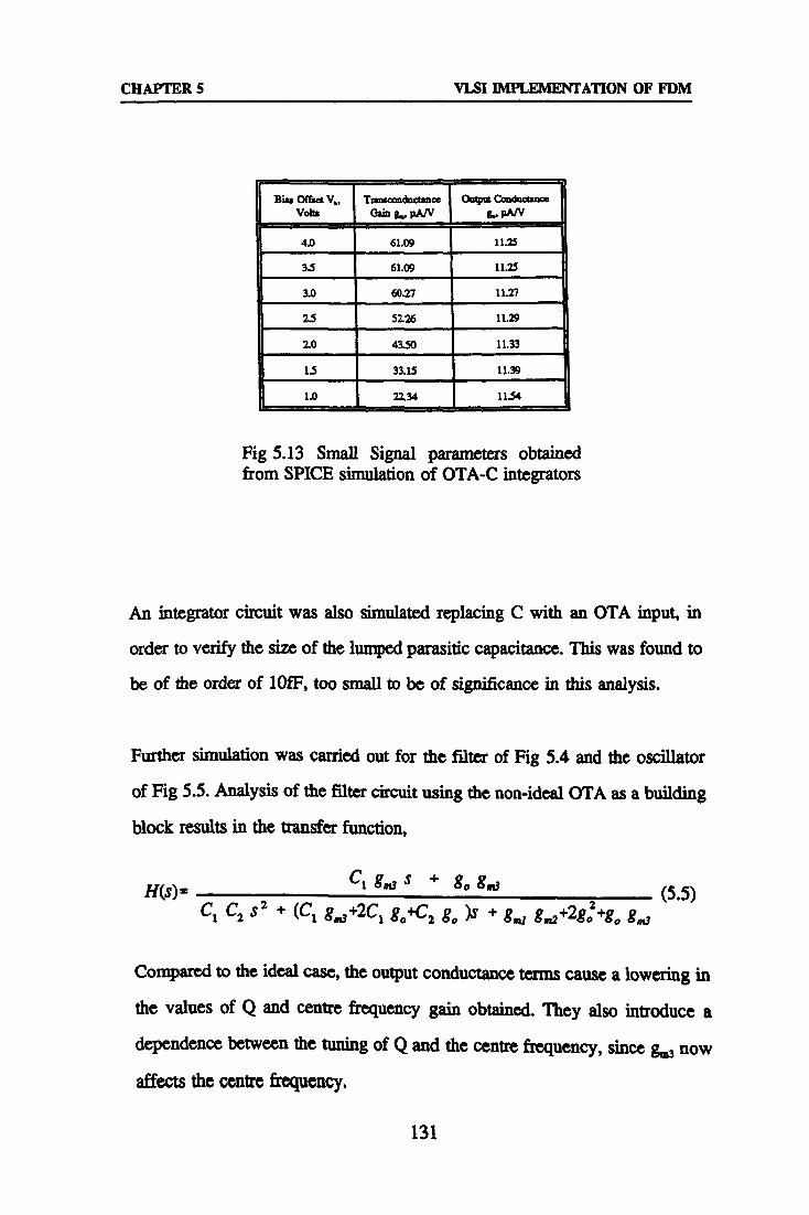
CHAPTER 5 VLSI IMPLEMENTATION OF FDM
Bias Offset V., Vohs
Tnmooadndan Gain g. pA/V
Outp Condudaax g,. pAN
4.0 61.09 11.25
3.5 61.09 11.25
3.0 60.27 11.27
2.5 52.26 11.29
2.0 43.50 11.33
13 33.15 11.39
1.0 22.34 11.54
Fig 5.13 Small Signal parameters obtained from SPICE simulation of OTA-C integrators
An integrator circuit was also simulated replacing C with an OTA input, in
order to verify the size of the lumped parasitic capacitance. This was found to
be of the order of 10fF, too small to be of significance in this analysis.
Further simulation was carried out for the filter of Fig 5.4 and the oscillator
of Fig 5.5. Analysis of the filter circuit using the non-ideal OTA as a building
block results in the transfer function,
H(s)= Cl 8m3 s+ 8o 8m3 (5.5)
Ci C2 s2+ (Cl g +2C, 80+C2 8o )s + 8mu 8, ßz+280 +8,9=3
Compared to the ideal case, the output conductance terms cause a lowering in
the values of Q and centre frequency gain obtained. They also introduce a dependence between the tuning of Q and the centre frequency, since g. 3now affects the centre frequency.
131

CHAPTER 5 VLSI IMPLEMENTATION OF FDM
Fig 5.14 shows the values of centre frequency and corresponding gains for
different values of offset bias Vb3 and C2 obtained from both SPICE Level 2
simulation and analytical determination of the amplitude response using
equation (5.5). In this simulation Vbl and Vb2 were both fixed at 3V and C,
was fixed at lOpF. The values of g1 and go used in the calculations were
obtained from Fig 5.13. The results show that the analytical approach is a
reasonably good approximation to that of the full simulation approach, when
the values of gm and go are known.
Cl. Bias Oct Ba Vb3, Vohs
SPICE Cwae FtegomaykBz
Glcalated Cerra
Frequmcy kHz
SPICE Cmbe C1 th d Ftegomcy Ceare
Voltage Gain Fregoeocy Voltage Gain
3.0 324 324 0.353 0.351
1.0 310 312 0.167 0.163
3.0 1060 1061 0.671 0.650
1.0 995 1017 0,433 OA04
Fig 5.14 Comparison of SPICE Level 2 simulations and analytical calculations of OTA-C Bandpass filter characteristics.
For the oscillator, similar analysis using the non-ideal OTA results in the
characteristic equation,
C1C2s 2+[Cl(g�a+g)-C2(g�ý-2gý)]s+8 8, ý+2g +go(2gý g2) =0 (5.6)
Again, the ideal equation is modified by the output conductance. In particular,
132

CHAPTER 5 VLSI IMPLEMENTATION OF FDM
the oscillation condition is modified to,
C2 gna > Cl (gw + go) + 2C2 go (5.7)
It is seen that non-zero output conductance also introduces a dependence
between oscillation condition and oscillation frequency.
SPICE transient analysis was used to simulate the OTA-C oscillator circuit,
using capacitor values of lOpF, and Vbl and Vb3 fixed at 3V. Vb2 was gradually
increased until oscillation occurred, and then further increased to determine the
approximate frequency of oscillation. This was necessary because simulation
time is much reduced for a small deviation in Vb2 above the point of onset of
oscillation. The error introduced by this approximation is not very large.
Using the previously determined values for gm and go, oscillation was predicted
to occur for g., =57. OpA/V corresponding to Vbz=2.8V. SPICE Level 2
transient analysis yielded Vb2=2.9V as the minimum voltage required for
oscillation to occur, corresponding to gw7-58.5pA/V.
A comparison of the SPICE simulation and calculated values of oscillation
frequency, for Vb2 3. OV, gave 360kHz and 340kHz respectively.
These simulations conclude the SPICE Level 2 results obtained for the OTA,
showing how it fits into the overall scheme as a building block for filter and
oscillator designs. From the above results it is clear that further design could
have been carried out to reduce the output conductance of the OTA, and thus
minimise the non-ideal behaviour of the filter and oscillator circuits. However,
133

CHAPTER 5 VLSI IMPLEMENTATION OF FDM
it was decided to proceed with fabrication in part to verify the feasibility of the
Mietec route to silicon, and in part to obtain results quickly enough to obtain
a comparison of simulated and actual performance of the IC, so as to verify
the accuracy of the simulation models used.
5.4.5 Post-fabrication Testing
Seven chips were used for testing. The test procedure was begun with static
measurements, followed by transfer function determination and dynamic
testing. A power supply of ±5V was used throughout. For the DC tests the
output of each OTA was measured by connecting the output to a grounded
43.8kg2 resistor, the same value as used in the simulations.
DC tests included the Mietec Standard Cell (CHBGPC) bandgap reference
voltage measured with respect to Vss, the Source Bias Voltages Vb of OTA1-3
on each chip, and the power supply current of each OTA. The outputs were
buffered using a zeroed FET input op-amp, the output of which was measured
with a calibrated voltmeter. The buffering is especially important for the
voltage reference, since it has high output impedance. By virtue of the voltage
reference and each OTA having a separate power supply, it was possible to
ground all pins not being used in each test, and thus isolate different parts of
the chip during measurement.
Results from all chips were consistent, with little variation from chip to chip
and between OTAs on the same chip, but were found to be quite different
from those predicted by simulation. The measurement of source bias voltage V, bfor all 21 OTAs gave values 3.61±0.01V. In comparison with simulation
results 3.52V (typ), 3.31V (slow), and 3.74V (fast) this indicates a process
134
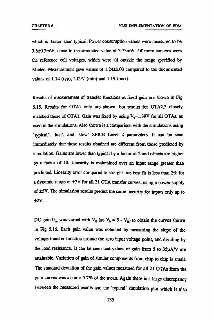
CHAPTER 5 VLSI IMPLEMENTATION OF FDM
which is 'faster' than typical. Power consumption values were measured to be
3.6±0.3mW, close to the simulated value of 3.73mW. Of more concern were
the reference cell voltages, which were all outside the range specified by
Mietec. Measurement gave values of 1.24±0.03 compared to the documented
values of 1.14 (typ), 1.09V (min) and 1.19 (max).
Results of measurement of transfer functions at fixed gain are shown in Fig
5.15. Results for OTAI only are shown, but results for OTA2,3 closely
matched those of OTA1. Gain was fixed by using Vb=1.39V for all OTAs, as
used in the simulations. Also shown is a comparison with the simulations using
'typical', 'fast', and 'slow' SPICE Level 2 parameters. It can be seen
immediately that these results obtained are different from those predicted by
simulation. Gains are lower than typical by a factor of 2 and offsets are higher
by a factor of 10. Linearity is maintained over an input range greater than
predicted. Linearity error compared to straight line best fit is less than 2% for
a dynamic range of ±3V for all 21 OTA transfer curves, using a power supply
of ±5V. The simulation results predict the same linearity for inputs only up to
±2V.
DC gain G. was varied with VB (so Vb =5- VB) to obtain the curves shown
in Fig 5.16. Each gain value was obtained by measuring the slope of the
voltage transfer function around the zero input voltage point, and dividing by
the load resistance. It can be seen that values of gain from 5 to 35pA/V are
attainable. Variation of gain of similar components from chip to chip is small.
The standard deviation of the gain values measured for all 21 OTAs from the
gain curves was at most 5.7% of the mean. Again there is a large discrepancy
between the measured results and the 'typical' simulation plot which is also
135

CHAPTER 5 VLSI IMPLEMENTATION OF FDM
shown in the diagram.
Common mode rejection ratio (CMRR), and power supply rejection ratios were
measured for balanced supply (PSRR) and single rail (PSRR+) supply
deviations.
CMRR is defined as gnVgnn expressed in dB, where gnu is a common mode
gain derived from the rate of change of offset voltage with applied common
mode input voltage. The measured value of CMRR was 22±2dB for all OTAs.
PSRR is defined as gm/gm1 expressed in dB, where grn1 is a balanced power
supply gain derived from the rate of change of offset voltage with power
supply voltage, where both positive and negative supplies are deviated
simultaneously in opposite directions. The measured value of PSRR was
30±1dB for all OTAs.
PSRR+ is defined as gni/gm expressed in dB, where gm is a power supply
gain derived from the rate of change of offset voltage with power supply
voltage, where only the positive rail is deviated. The measured value of PSRR+
was 46±3dB for all OTAs.
Capacitor measurements were carried out using a Boonton capacitance meter
(model 72B) with zero bias. Values for Cl, C2 and C3 were found to be 33pF,
18.3pF and 7. OpF respectively. Differential measurement was used to cancel
out I/O and lead capacitance which was carried out by connecting the 'in' and
'out' terminals of the chip to the DIFF input of the meter.
136
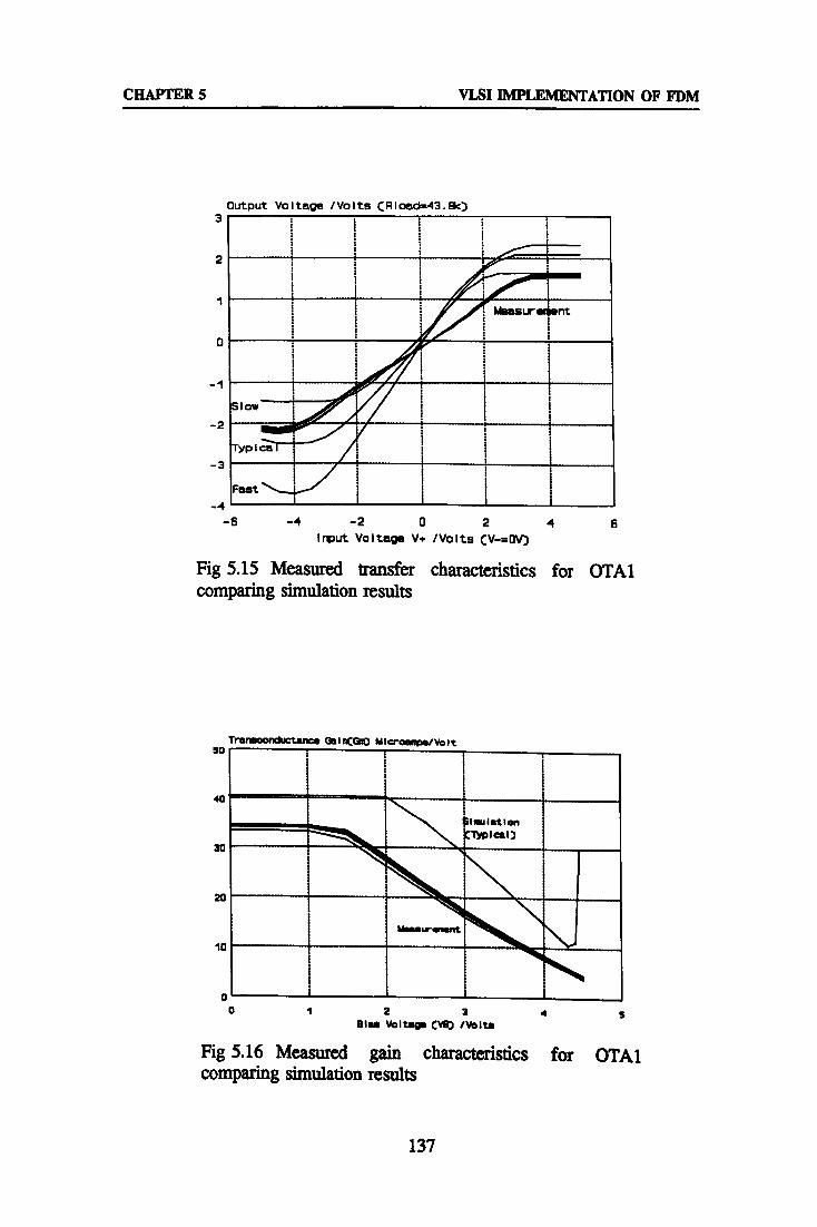
CHAPTER 5 VLSI IMPLEMENTATION OF FDM
z
1
0
-1
-p
-3
Output Voltage /Volts (Rload=43.8k) 3
-4 -6 -4 -2 0246
Input Voltage V+ /Volts (V-=OVA
Fig 5.15 Measured transfer characteristics for OTA1 comparing simulation results
t}} =i}}
} }
MnsLr M
E Y /
[[[ I OO O
} Slow
ý; e-,
Oo Now
ypica r- I
Fast
Traroeonduotanee GalnEGO Mlcrosnot/Volt su
40 {
Imulation Typical)
80
20
MM rMrý
10
0 0123fs
Blas Volta" CVID Aft its
Fig 5.16 Measured gain characteristics for OTA1 comparing simulation results
137

CHAPTER 5 VLSI IMPLEMENTATION OF FDM
5.4.6 SPICE Level 3 Simulations
It is clear from the above comparison of measurements with SPICE Level 2
simulations that the accuracy of the simulation was not good enough. At the
time of design, only MOS Level 2 model parameters were available from
Mietec. After the chips were received and tested, extracted Level 3 parameters
from the process were received via Eurochip which has enabled further
simulation to be carried out retrospectively, in an attempt to reconcile
simulation and measurement. The following graphs from HSPICE show much
better agreement between simulation and measurement using MOS Level 3
model parameters. Fig 5.17 shows the comparison of the transfer functions and
Fig 5.18 shows the comparison of the gain characteristic. In both figures, the
solid line is the measurement and the broken line is the simulation. Fig 5.19
shows the simulated SPICE Level 3 frequency response curve. The range of
the flat response is the same as that predicted by SPICE Level 2 (Fig 5.11).
The DC gain is smaller since gm is smaller but the same resistive load was
used as in the Level 2 simulations.
A comparison of the Level 3 simulation with the analytical approach using
equation (5.6) was also carried out for the bandpass filter circuit of Fig 5.13.
Values of gm and g, were obtained from Level 3 simulation of an integrator
with a lOpF load and equation (5.5) and are shown in Fig 5.20. The values of
capacitors in the filter were also lOpF. The result of the comparisons are
shown in Fig 5.21.
It is seen that the simplified calculations using equation (5.6) give a good
approximation to the simulated results, as they did for Level 2. This also suggests that the values of gm and go are critical in determining the difference
138

CHAPTER 5 VLSI EWPLEMENTATION OF FDM
in the results obtained in Level 2 and Level 3 simulations. Both values are
strongly dependent on the value of channel length modulation parameter ?.
used in the SPICE MOS models as the gradient of the Ift-V4, characteristic. In
the case of Level 2, ?. is supplied by the foundary and entered explicitly into
the model as a fixed parameter i. e. the I1-Vd, slope is assumed constant. In
Level 3, channel length modulation is calculated by SPICE, so that the It-Vth
slope may vary with V. It is suggested that the reason for the poor
performance of the Level 2 simulations is due to the highly non-linear Iý, -Vd,
slope of the Mietec transistors, which cannot be modelled in Level 2. Mietec
have also recently recommended (in document MIE/F/02, Revision 2,20/8/92)
an empirical method for calculating ? for different transistor lengths, in an
attempt to improve the Level 2 simulation, but preliminary investigations using
the technique have not shown any improvement in the accuracy of simulation
of the OTA.
/TO TRANSFER FUNCTION - EXTRACTED NOR LEVEL 1 PARRNETER$ 14-DECSR 14,1115$
1.58 NEORRLJIEIItt
1.1.
V 511. IN. .................. Z
T 1.
=
L-- _ .... ."..
". 518. IN
-1.51.. ..
-4.1 -2.1 1. R. 1 4.1 -5.1 INPUT_YOLTNIE (LIN) 5.1
Fig 5.17 Comparison of OTA transfer function measurement (solid line) and HSPICE Level 3 simulation (broken line).
139

CHAPTER 5 VLSI IMPLEMENTATION OF FDM
OTA AAIM CHARACTERISTIC - M09 LEVEL 9 PARAHETER9 14-DEC9t I4i9I'4!
L E5.1 _ \
15.1. ---
5.1 =i'ý' i' i' 1' ii 'ý i1'i "i "i " i' 1' ý'i 1.1 E. 1 9.1
84.18 VI (LIN)
NEURAL-GAIN, ." 15
Ct-
"J
"1
J
". y"- -V
I-
4. t f . 49$
Fig 5.18 Comparison of OTA gain characteristic measurement (solid line) and HSPICE Level 3 simulation (broken line).
OTR FREOUENCT RESPONSE - EXTRACTED 10$ LEVEL 3 PRRRNETERS ! 4-OEC9t l5itts11
= NEDRRLJIC. 3
r .... . M. IN
L T
'. .
'. '. . '. '. IM.
N
1. t. .. ion.. i mud. I Alud. I I, uia. $. iilink IJnr.. sjiud. L11u1a 11.1 111.1 1. IK 11.1E 111.1E 1. SX 11.11 1.1 HERTZ (LOO) 111.11
Fig 5.19 HSPICE Level 3 AC Analysis of OTA
140

CHAPTER 5 VLSI IMPLEMENTATION OF FDM
Bias Off* Vb. Volts
Trai caa&xctance Ciam S. pA/V
Output Conductance &. PAN
4.0 36.8 3.13
3.5 36.80 3.13
3.0 32.80 3.16
23 25.81 3.17
2.0 19.77 3.19
1' 14.25 3.23
1.0 9.10 3.26
Fig 5.20 Small Signal Parameters obtained from SPICE Level 3 simulation of OTA-C integrators.
Bias Offsets, Volts
Vbl Vb2 Vb3
SPICE Cmae
X07. kHz
Cal fated Cmae
X07. kHz
SPICE croft
F eq c7 Voltage
Gain
Calailued COMM
Fm4-w7 Voltage
Gain
3.0 3.0 1.0 532 534 0ä71 0.541
2.5 2.5 1.0 428 426 0.352 0.533
2.0 2.0 1.0 336 334 0.539 0331
1.5 1.5 1.0 252 253 0.332 0.531
1.0 1.0 1.0 174 184 0.522 0333
3.0 3.0 3.0 563 551 0.830 0.779
3.0 3.0 2.5 558 546 0.792 0.734
3.0 3.0 2.0 553 542 0.742 0.676
3.0 3.0 1.5 546 537 0.672 0.603
Fig 5.21 Comparison of SPICE Level 3 simulations and analytical calculations of OTA-C bandpass filter characteristics.
141

CHAPTER S VLSI IMPLEMENTATION OF FDM
5.5 Adaptive Tuning Techniques
This section considers the VLSI implementation of filters and oscillator circuits
with respect to process variation, and discusses in particular existing methods
for adaptive tuning of OTA-C circuits.
5.5.1 Switched Capacitor Filter Limitations
Designers of switched capacitor filters generally use ratios throughout the
circuit and the transfer functions thus obtained are subject only to tracking
errors, which may be minimised by careful design. Broad tuning is
accomplished using the switching clock frequency. At higher baseband
frequencies lowering of the switching-to-signal frequency ratio is often
required which puts additional constraints on the anti-aliasing filters used to
prevent aliasing of higher frequencies back into the baseband. As sampled data
systems, all switched capacitor circuits are susceptible to the aliasing of h. f.
noise and clock/signal mixing products, and detailed analysis is difficult . Switch feedthrough is also a problem. Therefore switched capacitor filters are
used extensively for audio applications, but not so much for higher
frequencies, although some examples exist--9j in addition, specw simulators
are often required for switched capacitor circuits which makes simulation of
mixed designs (digital, switched analogue and continuous-time analogue) a
difficult task.
5.5.2 Continuous Time Filters
For higher frequencies, continuous-time active filters are preferable. VLSI
implementations are based on MOS resistors'5'w or operational
transconductance amplifiersis"'41, and capacitors. The latter is the OTA-C type
of circuit discussed in section 5.3.1.
142

CHAPTER 5 VLSI IMPLEMENTATION OF FDM
In continuous-time filter design, the filter poles usually depend on absolute
values of the circuit components rather than ratios, so ratios cannot be used
directly to ensure accurate transfer characteristics. Consequently, since absolute
values cannot be guaranteed, the circuit must be adaptively tuned by an
external signal. OTA-C filters are particularly good candidates for adaptive
tuning since the OTA gain is used as a design parameter of the transfer
function, which is controlled by an external voltage (or current).
The most obvious tuning technique is to use a Phase Locked Loop (PLL),
where a voltage controlled oscillator (VCO) is locked in phase to an external
signal, and therefore oscillates at the same frequency.
This technique, usually called master-slave tuning, was first used by Tan in
1977 for audio frequencies1540] and later by othersI5*41-'31 for higher frequencies.
The master is the VCO which incorporates a minimal 2nd order stage of
similar architecture to that present in the filter to be tuned (the slave), so that
the same control voltage (or current) is applied to the VCO and the filter
simultaneously, thus fixing the filter pole frequency relative to that of the
VCO. Fig 5.22 shows the basic technique. Accuracy depends on the good
tracking between VCO and filter component values on chip, i. e. on precise
component value ratios between master and slave.
There is a trade-off in practice between the need to make the VCO frequency
outside the filter pass band in order to avoid cross-talk between the filter and VCO signals due to capacitive coupling, and the need to make the master and
slave identical in order to minimise matching error" A
143

CHAPTER 5 VLSI IMPLEMENTATION OF FDM
Fig 5.22 Adaptive ladder filter with tuning using an on- chip VCO (after Tan 1977)
A more recent variation uses another filter as the master rather than a VCO,
sometimes called a Frequency Locked Loop (FLL)15 4. Using a master filter
rather than a VCO is thought to better model the slave's response, since the
slave is also a filteii5,461. In this case the master filter has an external fixed-
frequency input, and the filter is tuned by adapting the (frequency dependent)
phase difference between output and input so that it is consistent with the
desired resonant frequency. For a bandpass filter this can be achieved by
comparing the phase of the reference input signal with the lowpass (or
highpass) output of the master bandpass filter, as shown in Fig 5.23. For a bandpass filter the output of the phase comparator is constant when the two
144

CHAPTER 5 VLSI I PLEMENTATION OF FDM
inputs differ in phase by 90 degrees, which occurs only at the bandpass centre
frequency.
MASTER FILTER
Vtd v1owpm
Vca01ol
SLAVE FILTER
Vin Vast
Fig 5.23 Frequency Locked Loop using a master filter
Comparison of an on-chip MOS resistor with a precise external resistance has
also been used for tuning continuous time monolithic filters"-').
At high frequencies there are inevitable phase shifts due to parasitics.
However, Van Peteghem shows that these effects do not cause frequency
tuning problems in the filter because the parasitic poles are at much higher
frequencies than the passbandt5*181 Parasitic phase shifts can, however, affect
gain at resonance and Q. For this reason, some designers have used multiple
tuning loops to control not only the cutoff or centre frequency, but also This necessitates the use of several external signal frequencies. These
techniques are used mainly for high Q, high frequency circuits with tight
specification. Q control is not needed in systems requiring less fine selectivity.
145

CHAFFER 5 VLSI IMPLEMENTATION OF FDM
5.6 VLSI Architecture for FDM Communications
Considering the previous five sections, it is now possible to define the type of
architecture required for the VLSI inter-chip FDM communication system.
OTA-C circuits can be used to construct banks of oscillator and filter
circuitsts''s 491 This allows the use of a single OTA building block throughout
the system which will speed up the design process considerably. Typical OTA-
C implementations of oscillators and filters (as shown in Section 5.2) have
resonant frequencies proportional to products of the capacitances or
transconductance gains. Ratios of these products can then be used from filter
to filter and oscillator to oscillator, so that relative frequency values within
each bank can be ensured within the limitations of tracking error.
However, the modulation and demodulation circuitry are on different chips and
are therefore subject to the larger absolute errors caused by differences in the
fabrication process. Therefore, tuning is required for both chips. Precise
absolute frequencies are not necessary so long as the set of oscillator and filter
frequencies match up, which is a much reduced constraint when compared to
the specification for most filter designs. This situation is ideally suited to an
adaptive technique where both chips are tuned using the same external signal.
Because of low tracking errors on a chip, it is possible to use a single tuning
circuit for a bank of oscillators or filters. In contrast, a bank of switched-
capacitor filters would require a bank of anti-aliasing and/or smoothing filters.
This is, of course essential to the technique, because only one pin will be
necessary per chip for this purpose. In addition, the same phase comparator
circuits can be used for the modulation and demodulation systems.
146

CHAPTER 5 VLSI IMPLEMENTATION OF FDM
Since the intended application for the FDM is a neural network, overlap of
filter responses can be tolerated up to 30%1'-"1 Therefore low Q filters can be
used, which have the advantage of reducing chip area requirements. In
addition, low Q filters will not be so severely affected by any parasitic phase
shifts in a tuning loop, because a small mismatch between oscillator and filter
frequencies will not cause such a large amplitude response error.
Therefore, the proposed VLSI implementation of the FDM communication is
constructed from OTA-C filter and oscillator circuits, with tuning based on the
master-slave technique. The form of this architecture is shown in Fig 5.24.
The filter chip has an on-chip master filter which models the architecture of
the bank of demodulation bandpass filters, and is used in a FLL. Because of
the intended simple nature of the slave filters, each filter (master and slaves)
can be constructed from a single second order stage. The master is locked in
centre frequency to an external clock folkand the same control voltage V gu
sets the centre frequency of all the filters in the bank which differ in frequency
by fixed component ratios.
The oscillator bank has an on-chip master oscillator which is locked to the
same external clock as the filter bank by a PLL The same control voltage
V sets the frequency of all oscillators in the bank. The amplitude of each
oscillator is modulated by its neural input.
In addition to frequency control, amplitude control is also needed for the
oscillators, to ensure start-up and for amplitude limiting. This can take the
form of the Automatic Gain Control circuits of Barrance"521.
147

CHAPTER 5 VLSI IMPLEMENTATION OF FDM
to : Neuron Inputs in Upper Layer
VIOWPM
Piicmmvv.
ha
chip 2
Chip 1
p hm
III Sk" I
Pilow 21-1---l mave
N Mtw low
1n2
Sleeve 1 Slave 2 Slave N Ooduatot Oedlhtor -- Qýd]Llor
ial in2 ioN
from: - Neuron Oaf in Lower Layer
Fig 5.24 Block diagram of the proposed FDM inter-chip communications system VLSI implementation.
148
CHAPTER 5 VLSI IMPLEMENTATION OF FDM
5.7 Discussion
The results of the VLSI design can be analysed in two ways. Firstly, it is seen
that the qualitative functional behaviour of the OTA circuit is correct. However
the output conductance may be improved and the chip area reduced by
subsequent design iterations. The output conductance can be improved by the
use of current mirrors with lower output conductance (such as the Wilson
current mirror). The overall chip area consumed by an OTA-C filter or
oscillator can be estimated by adding the areas of the OTAs and on-chip
capacitors. For a typical design consisting 3 OTAs and 2 capacitors of lOpF,
this area estimate is 200000µm2, which is rather large. The area of the OTA
is approximately twice that of a lOpF capacitor. Power consumption is
approximately l0mW. To reduce the chip area, some restructuring of the OTA
area would be advantageous. Optimisation of cell area at the filter/oscillator
level may be preferable to optimising a single OTA. A reduction in both the
transistor sizes of the OTA and the capacitance values should be considered.
Secondly, it has been shown that whereas the HSPICE simulation with Level
2 MOS models does not give adequate agreement of simulated and measured
results, use of Level 3 Models gives much better results and should therefore
be used in all future work.
It has also been shown in this chapter that analysis using a simplified OTA
model (specifying only gm and g, ) can be used to give results which
approximate to those achieved by simulation, which is useful for hand
calculations. Variation in process parameters also give rise to different values
of frequency, Q, and different oscillation conditions than those calculated from
simulation, which also justifies the use of the analytical approach for hand
149
CHAPTER 5 VLSI IMPLEMENTATION OF FDM
calculations of approximate values. This could prove invaluable in the
appraisal of future designs of filter and oscillator circuits using OTAs.
A design route though to silicon has been proven using the Mietec 2.4µm
CMOS process for a full custom analogue design, which forms a basis for
future work on the VLSI implementation of the FDM system.
An adaptive solution to process variability in the FDM system has been
proposed, using the master-slave tuning method for both the filter and
oscillator circuits, employing the OTA as a functional building block.
150

CHAPTER 6 CONCLUSIONS
CHAPTER 6- CONCLUSIONS
This final chapter brings together the work presented in the thesis, with
reference to the Aims and Objectives summarised in Chapter 1. This chapter
also points the way to further work and research possibilities, using the thesis
as a starting point.
6.1 Objectives achieved
The first aim of the work was to investigate the proposed VLSI design of an
inter-chip Frequency Division Multiplexed (FDM) communication technique
with respect to past and current research in neural network hardware design.
This was achieved in Chapter 2 through a detailed coverage of published
research in the field, including a critical review of several state-of-the-art
analogue hardware implementations. It is seen that the communications
bottleneck is a real problem for the implementation of large neural networks
where the network must be implemented using several neural chips.
The next objective was to introduce the idea of FDM as a communication
method for highly connected architectures. This was carried out in Chapter 3,
comprising a mathematical formulation for the bandwidth achievable for a
bank of filters, as used to demodulate the FDM channel. This took into
account the effect of overlapping the amplitude response curves of the filters,
by introducing a fractional overlap parameter to the formulations. As
explained, increasing this overlap acts to increase the number of signals it is
possible to multiplex, at the expense of errors caused by crosstalk between
signals. Further analysis was carried out, this time using analogue electronic
151

CHAPTER 6 CONCLUSIONS
building blocks to construct a model of a hypothetical multiplexed
communication system utilising either TDM or FDM. This enabled a good
comparison to be made between the bandwidths achievable in these
implementations, and allowed estimates of power consumption to be made,
based on realistic architectures. It was concluded that FDM is indeed a
candidate for inter-chip communication of analogue information, provided a
degree of overlapping of filter responses is allowed, so as to give an
acceptably small spacing between carrier frequencies in the channel.
Chapter 4 examined the effect of such an overlap on neural network
performance. To this end, a flexible software simulator was designed to enable
the simulation of a multi-layer-perceptron neural network. The software
incorporated the fractional overlap defined earlier in the thesis, in order to
examine the effect of this overlap on the learning of classification problems.
The results of this work were encouraging, since it was shown that the neural
network model was highly tolerant to large overlap errors, even when weights
are quantised. Analysis of the learning performance for the classification
problems used, with varying amounts of overlap, showed there is practically
no degradation in either the speed of learning or number of classifications
learnt for overlaps of up to 30% of adjacent signal amplitudes. Even for
overlaps of 30-50%, it was shown that the neural network is still able to learn
many of the classifications, although both overall learning time and proportion
of non-converged trials is increased. It was shown that both the
backpropagation and weight perturbation learning algorithms perform well with
weights quantised to 8-bits, provided a probabilistic update strategy is
employed. The implications of this for electronic implementations are two-fold. It is possible to overlap filter response so that as much as 30% crosstalk of
152

CHAPTER 6 CONCLUSIONS
adjacent signals have negligible effect on network operation, and the network
can still learn for larger overlaps. Thus, signals can be multiplexed in a given
bandwidth. Alternatively, lower Q factors for the filters can be tolerated.
Complementing the theoretical and software work, Chapter 5 achieved the
objective of defining the implementation of FDM in VLSI, including a review
of relevant analogue design techniques, active filter design, and the
presentation of results from the design of a prototype full-custom analogue
chip. This chip, an Operational Transconductance Amplifier, is a building
block for both oscillator and filter circuits which can be used in FDM circuitry.
The review sections show the advances which are being made in analogue
VLSI design of active circuits, which provides the basis for realisation of the
FDM scheme. In spite of the difficulty in achieving a good agreement between
the measured characteristics of the fabricated chip and the original simulations
using the SPICE Level 2 MOS transistor model, a more accurate Level 3
model used in retrospect gave a much closer agreement, and gives confidence for the accuracy of future designs using the Mieter 2.4p process.
In addition, Chapter 5 has presented the architecture of a VLSI implementation
of FDM using an adaptive tuning method, which is necessary to ensure the
system will be tolerant to fabrication parameter variations. It was seen that
only one tuning circuit is needed per chip, since on-chip matching of
components ensures accurate ratios of frequencies to be achieved.
In summary, this work has developed the ideas for a technique which stands to further the field of analogue neural network design by removing the communications bottleneck in the system.
153

CHAPTER 6 CONCLUSIONS
6.2 Further Work
There are a number of ways in which further work may be carried out, using
this thesis as a basis.
6.2.1 Direct Extension of the Research
Firstly, direct extension of the work will involve more VLSI design. Chapter
5 provides a clear path for the realisation of the system architecture in VLSI,
but more work will be necessary to complete the design at the silicon level.
This will involve further simulation using circuit simulator and IC design CAD
tools, and fabrication of the chips thus designed. This will benefit from the
availability of more advanced design tools, such as interactive extraction of IC
layout information, and the existence of more accurate MOS transistor models
suited to analogue design.
The following text proposes a detailed work plan for the next stage of the
work. The final goal of this work is a complete FDM neural network. The
research is divided into three phases, which will yield intermediate results, and
allow the project to be evaluated at fixed stages. Phase 1 will be the
refinement and design of the FDM communications circuitry. Phase 2 will be
to implement in VLSI a small analogue FDM neural network, to verify the
idea. Phase 3 will be to extend Phase 2, and will be to construct a complete
neural network system under software control, implementing a large number
of neurons, which will be used for real world applications. Details of the three
phases are as follows.
PHASE 1: The goal of this first phase is to produce a prototype FDM inter-
chip communications system using around 8 different frequencies. This system
154

CHAPTER 6 CONCLUSIONS
will not contain any of the neural network components and will involve the
following tasks: -
11 Refine the existing OTA building block.
The transconductance amplifier will be refined to improve output conductance and reduce
chip area. Consequently, new prototypes will be produced and tested.
1.2 Design, layout, fabrication and testing of filter, oscillator, peak detector and phase-
locked loop (PLL) control circuitry.
OTA oscillators and filters will be designed, laid out and verified using the Eurochip
Mentor/Mietec route. Also included on this chip will be the PLL control circuitry and
peak detectors. A prototype chip will be fabricated and the results analysed. If necessary,
a second prototype will be produced before proceeding to task 13.
1.3 Integration of a small FDM system.
This is the goal of the first phase. Here a small non-neural network FDM system is to be
fabricated. This will incorporate the FDM modulation/demodulation scheme on two chips
implementing around 8 multiplexed channels (the exact number depending upon the
silicon area used). These two chips will communicate with each other via a single FDM
pin.
PHASE 2: The goal of the second phase will be to implement a small neural
network using a single FDM wire to communicate between chips. This will
involve the following tasks: -
2.1 VLSI design of neural synapses and neurons.
The synapses will be implemented as analogue multipliers and the neurons as current
summers incorporating a non-linearity function.
2.2 VLSI layout and prototyping of neural components.
The neural components in task 2.1 will be laid out and verified at the silicon level. A
155
CHAPTER 6 CONCLUSIONS
prototype chip will be fabricated and tested. Again, a second iteration may be necessary
at this stage.
23 Integration of a small neural network FDM system.
This is the goal of the second phase. Here, a small neural network system is to be
implemented, with around 8 neurons, the exact number depending upon the silicon area
taken up by each neuron. The FDM circuits from Phase 1 and the new neural components
will be laid out together on two chips, which will communicate using FDM. These
prototypes will be tested and the ability of the neural network to cope with various filter
overlaps will be analysed. The network will be trained using a number of test problems,
designed not to exceed the number of neurons available.
PHASE 3: The third phase will extend the work of Phase 2, and lead to the
realisation of a larger neural network architecture. It will then be possible to
train the network on a number of real world problems. This will include the
following tasks: -
31 Integration of a larger number of neurons.
This will be achieved by producing a larger chip and by combining multiple chips to form layers of neurons, all communicating by FDM. The system will be embedded in a
microprocessor system with a software interface.
3.2 Train the neural network on real-world data.
The performance of the extended network will be verified by applying it to pattern
recognition problems. This will include speech and visual image data.
There is a great scope for the full realisation of this idea and the potential for
many important intermediate designs and spin-offs, for example; analogue VLSI filter and oscillator designs, tuning techniques, and methods to ensure invariance to IC processing parameters.
156
CHAPTER 6 CONCLUSIONS
Apart from this thesis, some work is being carried out in the research group
towards the realisation of the FDM technique in hardware at the system level,
which is currently in a stage of development. This work has involved
construction of analogue neural network hardware prototypes using off-the-
shelf components, implementing a small number of neurons which can
communicate using FDM. These neural network circuit boards are designed to
be interfaced to a host computer so that learning can be carried out in
software, using the neural network in the training loop.
A development route is therefore possible combining the above and the work
of this thesis, which would involve gradual replacement of the off-the-shelf
components on the circuit boards by the VLSI prototypes. In this way, it will
be possible to test individual VLSI circuits in a system environment before an
entirely VLSI neural network is constructed. This is a top-down hardware
approach for the neural system, but a bottom-up approach for the VLSI, which
enables all chips to be evaluated as the hardware design progresses without
losing sight of the system as a whole.
Between the system and VLSI circuit level, this project would also benefit
from more computer modelling of the neural network, as an extension of the
software simulation work reported on in Chapter 3. The simulations of Chapter
3 are somewhat abstracted from hardware implementation in that once the
overlap parameter is chosen, the mixing of neuron outputs are simply the linear
addition of a neuron's amplitude with its nearest neighbour's, multiplied by the
overlap parameter. This is justified for 'ideal' linear transfer functions for the
filters, but does not include the effects of non-linearity, nor of process
variations which may cause deviations from the desired frequency responses.
157

CHAPTER 6 CONCLUSIONS
These effects could be included into a more sophisticated computer model, to
further test the neural network learning performance.
Design of analogue memories and realisation of on-chip learning is a great
priority in the field of neural network hardware. Although the systems
considered above use a learning method based on an external digital
microprocessor for learning and permanent weight storage, work should be
carried out in the areas of on-chip weight storage and on-chip learning. It
should be possible to apply the FDM technique for the communication of
weight values in the neural network system, in addition to its use for
communicating the inputs and outputs.
6.2.2 Other Ideas and Applications
Analogue VLSI design is an exciting, active, and growing field. The findings
from further investigation in the FDM technique will be of importance for
applications in neural networks, and analogue signal processing in general.
The proposed chip consisting of a bank of analogue filters, would find
applications in speech processing, as an analogue spectral analyser for speech.
Similarly, a bank of oscillators would be used for the construction of a flexible
voice source.
The FDM technique will find use in a general sense for communication of
analogue information between chips and circuit boards. Considering the ability
of a neural network to compensate for crosstalk interference, it would be worth
investigating their application in other analogue and digital systems.
158
CHAPTER 6 CONCLUSIONS
6.3 Summary
In summary, the main points of this thesis are as follows.
* Frequency Division Multiplexing was proposed and justified as a
technique for inter-chip communication of analogue information.
* Neural Network learning has been discovered to be highly tolerant to
crosstalk between signals in an FDM channel, due to the adaptive
nature of neural networks. Defining an overlap parameter for the filter
frequency responses enables the analysis of the effects of this crosstalk.
* Overlapping of filter responses allows an increase in information
bandwidth, or the use of smaller quality factors which eases VLSI
design.
* Hardware implementation of the FDM idea can be achieved using
analogue VLSI techniques. Transconductance amplifiers are a good
building block for this.
* The full-custom analogue design route using Mentor Graphics full-
custom CAD software and the Mietec foundry was proven in the course
of this research, which is of benefit to other participants in the Ecad
and Eurochip schemes.
Adaptive tuning techniques should be used to compensate for VLSI fabrication process variability, when applied to the tuning of banks of filters and oscillators.
159
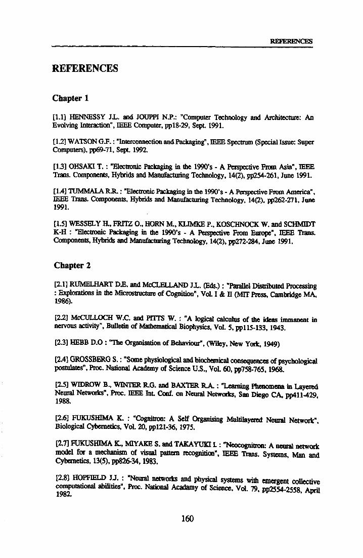
RF. FF. RENCES
REFERENCES
Chapter 1
[1.1] HENNESSY J. L. and JOUPPI N. P.: "Computer Technology and Architecture: An Evolving Interaction", IEEE Computer, ppl8-29, Sept. 1991.
[1.2] WATSON G. F.: "Interconnection and Packaging", IEEE Spectrum (Special Issue: Super Computers), pp69-71, Sept. 1992.
[13] OHSAKI T.: "Electronic Packaging in the 1990's -A Perspective From Asia", IEEE Trans. Components, Hybrids and Manufacturing Technology, 14(2), pp254-261, June 1991.
[1.4] TUMMALA R. R.: "Electronic Packaging in the 1990's -A Perspective From America", IEEE Trans. Components, Hybrids and Manufacturing Technology, 14(2), pp262-271, June 1991.
[1.5] WESSELY H., FRITZ 0., HORN M., KLIMKE P., KOSCHNOCK W. and SCH1MMT K-H : "Electronic Packaging in the 1990's -A Perspective Fmom Europe", IEEE Trans. Components, Hybrids and Manufacturing Technology, 14(2), pp272-284, June 1991.
Chapter 2
[2.1] RUMELHART D. E. and McCLELLAND J. L. (Eds. ) : "Parallel Distributed Processing : Explorations in the Microstructure of Cognition", Vol. I& II (MIT Press, Cambridge MA, 1986).
[22] McCULLOCH W. C. and PITTS W.: "A logical calculus of the ideas immanent in nervous activity", Bulletin of Mathematical Biophysics, Vol. 5, ppl15-133,1943.
[2.3] HEBB D. O : "The Organisation of Behaviour", (Wiley, New York, 1949)
[2.4] GROSSBERG S.: "Some physiological and biochemical consequences of psychological postulates", Proc. National Academy of Science U. S., Vol. 60, pp758-765,1968.
[2.5] WIDROW B., WINTER R. G. and BAXTER RA.: "Learning Phenomena in Layered Neural Networks", Proc. IEEE Int. Conf. on Neural Networks, San Diego CA, pp4ll-429, 1988.
[2.6] FUKUSHIMA K. : "Cognitron: A Self Organising Multilayered Neural Network", Biological Cybernetics, Vol. 20, ppl21-36,1975.
[2.7] FUKUSHIMA K., MIYAKE S. and TAKAYUKI L: "Neocognitron: A neural network model for a mechanism of visual pattern recognition", IEEE Trans. Systems, Man and Cybernetics, 13(5), pp826-34,1983.
[2.8] HOPFIELD JJ.: "Neural networks and physical systems with emergent collective computational abilities", Proc. National Academy of Science, Vol. 79, pp2554-2558, April 1982.
160

REFERENCES
[2.9] KORONEN T. "The neural phonetic typewriter", IEEE Computer 21(3), ppl 1-22, March 1988.
[2.10] CARPENTER GA and GROSSBERG S.: "The ART of adaptive pattern recognition by a self-organising neural network", IEEE Computer, 21(3), pp77-88, March 1988.
[2.11] CARPENTER GA and GROSSBERG S.: "An 3: Hierarchical search using chemical transmitters in self organising pattern recognition architectures", Neural Networks, Vol. 3, ppl29-152,1990.
[2.12] ROSENBLATT F.: 'Principles of Neurodynaznics', (Spartan Books, New York 1962)
[2.13] MINSKY M. L. and PAPERT S.: 'Perceptrons', (MIT Press, Cambridge MA, 1969).
[2.14] DENKER J. S. (ed. ) : "Neural Networks for Computing, Proceedings of the Conference of the American Institute of Physics held at Snowbird, Utah, 13-16 April 1986", (AIP, New York, 1986).
[2.15] ANDERSON J. A. and ROSENFELD E. (eds. ) : "Neurocomputing: Foundations for Reasearch", (Mrr Press, Cambridge MA, 1988.
[2.16] HAKEN H. (ed. ) : "Neural and Synergetic Computers, Proc. Int. Sym. at Schloss Elmau, Bavaria, June 13-17,1988", (Springer, Berlin, 1988).
[2.17] NADEL L. et al. (eds. ) : "Neural connections, mental computation", (MIT Press, Cambridge MA, 1989).
[2.18] PAO Y-H : "Adaptive pattern recognition and neural networks", (Addison-Wesley, Reading MA, 1989).
[2.19] ALEXANDER I. (ed. ) : "Neural computing architectures: the design of brain-like machines", (North Oxford, London, 1989).
[2.20] WASSERMAN P. D. : "Neural Computing: Theory and Practice", (Van Nostrand Reinhold, New York, 1989).
[2.21] ALEXANDER I. and MORTON H.: "An introduction to neural computing", (Chapman and Hall, London, 1990).
[2.22] HECHT-NIELSON R.: "Neurocomputing", (Addison-Wesley, Reading MA, 1990).
[2.23] MAREN AJ., HARSTON C. T. and ROBERT M. P.: "Handbook of neural computing applications", (Academic Press, San Diego CA, 1990).
[2.24] EBERHART R. C. and DOBBINS R. W. (eds. ) : "Neural Networks PC Tools -A Practical Guide", (Academic Press, San Diego CA, 1990).
[225] CARPENTER G. A. and GROSSBERG S. (eds. ) : "Pattern recognition by self. organising neural networks", (MIT Press, Cambridge MA, 1991).
[2.26] FARHAT NIL : "Optoelectronic Neural Networks and Learning Machines", IEEE Circuits and Devices Magazine, pp32.. 41, Sept 1989.
161

REFERENCES
[227] GRAF H. P. and JACKEL L. D.: "Analog Electronic Neural Network Circuits", IEEE Circuits and Devices Magazine, pp44-50, July 1989.
[228] MEAD C. A. and MAHOWALD KA: "A Silicon Model of Early Visual Processing", Neural Networks, 1, pp91-97,1988.
[229] LU T. C., CHIANG M. L. and KUO J. B : "A One-Transistor Synapse Circuit with an Analog LMS Adaptive Feedback for Neural Network VLSI", Proc. IEEE Int. Symp. Circuits and Systems, Singapore, pp1303-1306, June 1991.
[2.30] PAULOS J. J. and HOLLIS P. W.: "Neural Networks Using Analog Multipliers", IEEE Proc. Int. Symp. Cicuits and Systems, pp498-502,1988
[2.31] REED R. D. and GEIGER RL.: "A Multiple-Input OTA Circuit for Neural Networks", IEEE Trans. Circuits and Systems 36(5), pp767-769, May 1989.
[2.32] ZURADA J. M.: "Introduction to Artificial Neural Systems", p600, (West Publishing Co. 1992)
[2.33] TSIVIDIS Y. and SATYANARAYANA S. : "Analogue Circuits for Variable-Synapse Electronic Neural Networks", IEE Elec. Lett. 23(24), pp1313-1314, March 1987.
[2.34] VITPOZ E., OGUEY H., MAHER MA., NYS 0., DIJKSTRA E. and CHEVROULET M.: "Analog Storage of Adjustable Synaptic Weights", Proc. IEEPJITG Ist Int. Workshop on Microelectronics for Neural Networks, Dortmund, pp69-79, June 1990.
[2.35] CASTELLO It, CAVIGLIA D. D., FRANCIOTTA M. and MONTECCHI F. : "Self- refreshing Analogue Memory Cell for Variable Synaptic Weights", IEE Elec. Lett 27(20), pp1871-2, Sept 1991.
[2.36] SCHWARTZ D. B., HOWARD R. E. and HUBBARD W. E.: "A Programmable Analog Neural Network Chip", IEEE J. Solid State Circuits 24(2), pp313-319, April 1989.
[2.37] SATYANARAYANA S., TSIVIDIS Y. and GRAF H. P.: "Analogue Neural Network with Distributed Neurons", lEE Elec. Lett. 25(5), pp302-3, March 1989.
[2.38] MURRAY AF., DEL CORSO D. and TARASSENKO L.: "Pulse-Stream VLSI Neural Networks Mixing Analog and Digital Techniques", IEEE Trans. Neural Networks, 2(2), pp193- 204, March 1991.
[2.39] AGRANAT AJ., NEUGEBAUER C. F., NELSON R. D. and YARIV A., "The CCD Neural Processor: A Neural Network Integrated Circuit with 65536 Programmable Analog Synapses", IEEE Trans. Circuits and Systems 37(8), pp1073-1075, August 1990.
[2.40] HOLLER M., TAM S., CASTRO H. and BENSON R. : "An Electrically Trainable Artificial Neural Network (ETANN) with 10240 'Floating Gate' Synapses", IEEE Int. Joint Conference on Neural Networks", Washington DC, June 1989.
[2.41] REEDER A. A., THOMAS I. P., SMITH C., WITI'GREFFE J. P. and GODFREY D. J. : "Application of analogue amorphous silicon memory devices to resistive synapses for neural networks", British Telecom Journal, 10(3), ppl55-160, July 1992.
162

REFERENCES
[2.42] ATLAS L . E. and SUZUKI Y.: "Digital systems for Artificial Neural Networks", IEEE Circuits and Devices Magazine, pp2O-24, Nov 1989.
[2.43] JESSHOPE C. R., O'GORMAN R. and STEWART J. M. : "Design of SIMI) microprocessor array", IEE Proceedings, Part E, 136(3), pp197-204, May 1989.
[2.44] KUNG S. Y. and HWANG JN.: "Digital VLSI Architectures for Neural Networks", IEEE Proc. Int. Symp. Circuits and Systems, Vol 1, pp445-448,1989.
[2.45] JONES S. and SAN MUT K.: "Toroidal Neural Network: Architecture and Processor Granularity Issues", Proc. IEEE/ITG Ist Int. Workshop on Microelectronics for Neural Networks, Dortmund, pp142-152, June 1990.
[2.46] HAIvIMERSTROM D.: "A Highly Parallel Digital Architecture for Neural Network Emulation", in J. G. Delgado-Frias, W. 1Vloore (Eds. ), 'VLSI for Artificial Intelligence and Neural Networks', Plenum Press 1991, pp357-366.
[2.47] MORGAN N., BECK J., KOHN P., BILMES J., ALLMAN E., and BEER J.: "The RAP. A Ring Array Processor for Layered Network Calculations", Proc. Int. Conf. Application Specific Array Processors, pp296-308,1990.
[2.48] AGLAN F., BRU B., DURANTON M., MAUDUI T N. and FRYDLENDER IL : "L: Neuro Boards : Implementing some applications", Proc. IEEE/ITG/IFIP 2nd Int. Workshop on Microelectronics for Neural Networks, Munich, pp447-453, Oct 1991.
[2.49] SPAANENBURG L., HOEFFLINGER B., NEUSSER S., NIJHUIS J. A. G. and SIGGELKOW A. : "A Multiplier-less Digital Neural Network", Proc. IEEEJITG/IFIP 2nd Int. Workshop on Microelectronics for Neural Networks, Munich, pp281-289, Oct 1991.
[230] AE. T and AIBARA R.: "Memory-based Architecture for Artificial Neural Networks", Proc. IEEE/ITG/1FIP 2nd Int. Workshop on Microelectronics for Neural Networks, Munich, pp135-142, Oct 1991.
[2.51] SAMMUT K. M. and JONES S. R.: "Implementing Nonlinear Activations in Neural Network Emulators", IEE Elec. Lett 27(12), pp1037-1038, June 1991.
[232] ALIPPI C. and STORTI-GAJANI G.: "Simple Approximation of Sigmoid Functions: Realistic Design of Digital Neural Networks Capable of Learning", IEEE Proc. Int. Symp. Circuits and Systems, Singapore, pp1505-1508, June 1991.
[2.53] MYERS D. and HUTCHINSON R.: "Efficient Implementation of Piecewise Linear Activation Function for Digital Neural Networks", IEE Elec. Lett. 25(4), pp1662-1663, Nov 1989.
[2.54] NAYLOR D. and JONES S. R : "How to efficiently map multilayer networks into linear arrays", Proc. IFEE/ITG/IFIP 2nd lat. Workshop on Microelectronics for Neural Networks, Munich, pp151-162, Oct 1991.
[2.55] NIELSON C. D., STRAUSTRUP J. and JONES S. R. : "Potential Performance Advantages of Delay-Insensitivity", IFIP workshop on silicon architectures for neural nets, St. Paul-de-Vence, France, Nov 1990.
163

REFERENCES
[2.56] BAILEY J. and HAMMERSTROM D. : "Why VLSI Implementations of Associative VLCN Require Connection Multiplexing", Proc. IEEE Proc. Int. Conf. Neural Networks, San Diego CA, Vol. 2, pp 173-180,1988.
[2.57] CRAVEN M. P., CURTIS K. M. and HAYES-GILL BR : "Frequency Division Multiplexing in Analogue Neural Network", IEE Elec. Lett. 27(11) pp918-920, May 1991.
[2.58] CURTIS K. M., CRAVEN M. P. and HAYES-GILL BR : "A Novel Neural Network VLSI Implementation", Proc. IEEE/iTG Ist Int. Workshop on Microelectronics for Neural Networks, Dortmund, pp120-128, June 1990.
[2.59] CURTIS K. M., CRAVEN MP., HAYES-GILL BR and LIU M.: "An Optimised VLSI Implementation for Analogue Neural Communications", Proc. IEEF, /ITG/IFIP 2nd Int. Workshop on Microelectronics for Neural Networks, Munich, pp273-290, Oct 1991.,
[2.60] CARD H. C. and MOORE WR "Implementation of Plasticity in MOS Synapses", Ist IEE Int. Conf. on Artificial Neural Networks, pp33-36,1989.
[2.61] YASUNAGA M., MASUDA N., YAGYU M., ASAI M., SHIBATA K., OOYAMA M., YAMADA M., SAKAGUCHI T. and HASHIMOTO M.: "A Self-Learning Digital Neural Network Using Wafer-Scale LSI", IEEE J. Solid-State Circuits 28(2), pp106-114, February 1993.
[2.62] SHIMA T., KIMURA T., KAMATANI Y., ITAKURA T. and FUJITA Y. and IIDA T.: "Neuro Chips with On-Chip Back-Propagation and/or Hebbian Learning", IEEE J. Solid- State Circuits 27(2), pp1868-1876, December 1992.
[2.63] HOHFELD M. and FAHLMAN S. E.: "Probabalistic Rounding in Neural Network Learning with Limited Precision", Proc. IEEE/ITG/IFIP 2nd lat. Workshop on Microelectronics for Neural Networks, Munich, ppl-8, Oct 1991.
[2.64] ORREY D. A., MYERS DJ. and VINCENT J. M. "A High Performance Digital Processor for Implementing Large Artificial Neural Networks", Proc. Custom Integrated Circuits Conference, San Diego, May 1991.
[2.65] REYNARI L. M. and FILIPPI E. : "An Analysis on the Performance of Silicon Implementations of Backpropagration Algorithms for Artificial Neural Networks", IEEE Trans. Computers 40(12), pp1380-1389, Dec 1991.
[2.66] SATYANARAYANA S., TSIVIDIS Y. and GRAF H. P.: "A Reconfigurable VLSI Neural Network", IEEE J. Solid State Circuits 27(1), pp67-81, Jan 1992.
[2.67] MURRAY AF.: "Analogue Noise-Enhanced Learning in Neural Network Circuits", IEE Elec. Lett. 27(17), pp1546-1548, Aug 1991.
[2.68] HOLLIS P. W. and PAULOS JJ.: "Dynamic Gain Adaption for Learning with Limited Resolution Bounded Weights", Technical Report NETR-90/5, North Carolina State University, 1990.
[2.69] VAN der SPIEGEL J., MUELLER P., BLACKMAN D., CHANCE P., DONHAM C., ETTIENNNE-CUMMIINGS R. and KINGET P.: "An Analog Neural Computer with Modular Architecture fayReal-Tune Dynamic Computations", IEEE J. Solid State Circuits 27(1), pp82-
164

REFERENCES
92, Jan 1992.
Chapter 3
[3.1] MURRAY A. F., DEL CORSO D., and TARASSENKO L.: "Pulse-Stream VLSI Neural Networks Mixing Analog and Digital Techniques", IEEE Trans. Neural Networks, 2(2), pp193- 204, March 1991.
[3.2] HAMILTON A., MURRAY AF., BAXTER DJ., CHURCHER S., REEKIE H. M. and TARASSENKO L.: "Integrated Pulse-Stream Neural Networks: Results, Issues, and Pointers", IEEE Trans. Neural Networks, 3(3), pp385-393, May 1992.
[3.3] DEL CORSO D., GREGORETTI F., PELLEGRINI C., and REYNERI LM.: "An Artificial Neural Network Based on Multiplexing Pulse Streams, IEEEIITG Ist Int. Workshop on Microelectronics for Neural Networks, Dortmund, pp120-128, June 1990.
[3.4] MURRAY AF., HAMILTON A., REEKIE H. M., CHURCHER S., BAXTER DJ., BUTLER Z. and TARASSENKO L.: "Innovations in Pulse Stream Neural VLSI - Arithmetic and Communications", IEEE/ITG Ist Int. Workshop on Microelectronics for Neural Networks, Dortmund, pp8-27, June 1990.
[3S] NUNALLY P. and HALLSE B. : "Introduction of New Angle Modulated Architectures for the Realisation of Large Scale Neural Network Hardware", International Joint Conference on Neural Networks 1990, Washington DC, Vol. 2, ppl71-174, January 1990.
[3.6] National Semiconductor Corp. Data Sheet, MF8 4th-Order Switched Capacitor Filter.
[3.7] STANLEY W. D : "Electronic Communication Systems", (Reston Publishing Co. Inc, Reston Virginia, 1981), pp112-116.
Chapter 4
[4.1] ROSENBLATT F.: 'Principles of Neurodynamics', (Spartan Books, New York 1962)
[4.2] WIDROW B. and HOFF M. E. : 'Adaptive Switching Circuits' in IRE WESCON Convention Record, Part 4 pp96-104,1960.
[43] WIDROW B., WINTER R. G. and BAXTER RA : 'Learning Phenomena in Layered Neural Networks', Proc. IEEE Int. Conf. on Neural Networks, San Diego CA, pp411-429, 1988.
(4.4] RUMELHART D. E., and McCLELLAND (Eds. ) : 'Parallel Distributed Processing : Explorations in the Microstructure of Cognition, Vol I: Foundations' (MIT Press 1986).
[4.5] MINSKY M. L. and PAPERT S. : 'Perceptions', (Cambridge MA, MIT Press, 1969).
[4.6] RUMELHART D. E., HINTON G. E. and WILLIAMS M. J. : 'Learning Internal Representations by Backpropagation of Errors', Nature 323, pp533-536,1986.
[4.7] WERBOS P. J : 'Backpropagation: Past and Future', Proc. IEEE Int. Conf. on Neural
165
REF tMCES
Networks, San Diego CA, pp343-353,1988.
[4.8] WASSERMAN P. D.: "Neural Computing: Theory and Practice", p57, (Van Nostrand Reinhold, New York, 1989)
[4.9] STORNETTA W. S. and HUBERMAN B. A. : "An Improved Three-Layer, Back Propagation Algorithm", Proc. IEEE Int Conf. on Neural Networks, San Diego CA, pp637- 642,1987.
[4.10] SMITH G. and WILSON WH.: "Back Propagation with Discrete Weights and Activations", Technical Report, Discipline of Computer Science, Flinders University of South Australia, June 1989.
[4.11] PARKER D. B. : "Optimal Algorithms for Adaptive Networks: Second Order Backpropagation, Second Order Direct Propagation, and Second Order Hebbian Learning", Proc. IEEE Int. Conf. on Neural Networks, San Diego CA, pp593-600,1987.
[4.12] WATROUS R. L.: "Learning Algorithms for Connectionist Networks: applied Gradient Methods of Non-Linear Optimisation", Proc. IEEE Int. Conf. on Neural Networks, San Diego CA, pp617-627,1987.
[4.13] KOLLIAS S. and ANASTASSIOUS D.: "Adaptive Training of Multilayer Neural Networks Using A Least Squares Estimation Technique", Proc. IEEE Int. Conf. on Neural Networks, San Diego CA, pp383-390,1987.
[4.14] FAHLMAN S. E.: "An Empirical Study of Learning Speed in Back-Propagation Networks", Technical Report CMU-CS-88-162, Carnegie Mellon University, Pittsburgh PA, June 1988.
[4.15] JABRI M. and FLOWER B. : "Weight Perturbation: An Optimal Archictecture and Learning Technique for Analog VLSI Feedforward and Recurrent Multilayer Networks", Neural Computation, 3, pp546-565,1991.
[4.16] TARRASENKO J. and TOMBS J. : "On-chip Learning With Analogue VLSI Neural Networks", Proc. 3nd Int. Workshop on Microelectronics for Neural Networks, Edinburgh, pp163-174, April 1993.
(4.17] Borland International, Turbo Pascal Owners Manual.
[4.18] Digital Equipment Corporation, VAX Pascal Reference Manual, AA-L369D-TE, December 1989.
[4.19] REYNERI L. M. and FI[.. IPPI E.: "An Analysis on the Silicon Implementations of the Backpropagation Algorithms for Artificial Neural Networks", IEEE Trans. Computers 40(12), pp1380-1389, Dec 1991
[4.20] PRESSMAN RS., 'Software Engineering: A Practitioner's Approach', (McGraw-]Hill, Singapore, 1982).
(4.21] JACOBS R. A.: 'Increased rates of Convergence Through Learning Rate Adgpaon', Technical Report COINS TR 87-117, University of Massachusetts at Amherst, Dept, of Computer and Information Science, Amherst MA, 1987.
166

REFERENCES
[4.22] SEJNOWSKI TJ., and ROSENBERG CR.: 'NETtalk :a parallel network that learns to read aloud', Technical Report JHU/EESC-86/01, John Hopkins University, 1986.
[4.23] SEJNOWSKI T. J., and ROSENBERG CR.: 'Parallel Networks that Learn to Pronouce English Text', Complex Systems 1, pp145-168,1987.
[424] KLATT D. H.: 'Review of text-to-speech conversion for English', J. Acoustical Society America 82(3), pp737-793, Sept 1987.
[4.25] ROSENBERG CR : 'Revealing the Structure of NETtalk's Internal Representations', Proc. 9th Annual Conf. of The Cognitive Science Society, pp537-554, July 16-18,1987.
[4.26] CRAVEN M. P., CURTIS K. M., HAYES-GILL B Zt.: 'Frequency Division Multiplexing in Analogue Neural Network', Elec. Lett. 27(11), pp918-920,1991.
[427] KUCERA H. and FRANCIS WN.: 'Computational Analysis of Present Day American English', (Brown University Press, Providence RI, 1970).
[4.28] ELOVITZ H. S., JOHNSON R., McHUGH A., and SHORE JB.: 'Letter-to-Sound Rules for Automatic Translation of English Text to Phonetics', IEEE Trans. Acoustics, Speech, and Signal Processing, 24(6), 1976.
[4.29] HOLLIS P. W., HARPER J. S. and PAULOS JJ. : "The Effects of Precision Constraints in a Backpropagation Learning Network", Neural Computation 2, pp363-373,1990
[4.30] HOME _D M. and FAHLMAN SM. : "Probabilistic Rounding in Neural Network learning with Limited Precision", Proc. IEEE/1TG/IF1P 2nd Int. Workshop on Microelectronics for Neural Networks, Munich, ppl-8, Oct 1991.
Chapter 5
[5.1] GREGORIAN K and TEMES G. C.: "Analog MOS Integrated Circuits", (Wiley 1986)
[52] SHYU J-B., TEMES G. C. and KRUMNIENACHER F.: "Random Error Effects in Matched MOS Capacitors and Current Sources", Proc. IEEE Int. Symp. Circuits and Systems, pp1415-1418,1985
[5.3] HODGES D. A., GRAY P. R.: "Potential of MOS Technologies for Analog Integrated Circuits", MEE J. Solid State Circuits 13(3), pp285-294, June 1978.
[5.4] ALLEN P. E. and HOLBERG D. P.: "CMOS Analog Circuit Design", (Holt Rinehart and Winston, New York, 1987).
[5.5] SACKINGER E. and FORNERA L.: "On the placement of Critical Devices in Analog Integrated Circuits", MEE Trans. Circuits and Systems 37(8), pp1052-1057, August 1990.
[5.6] VITTOZ E.: "The Design of High Performance Analog Circuits on Digital CMOS Chips", IEEE J. Solid State Circuits 20(3), pp657-665, June 1985
[5.7] TSWIDIS Y. and SATYANARAYANA S.: "Analogue Circuits for Variable-synapse Electronic Neural Networks", IEE Elec. Lett. 23(24), pp1213-1214, Nov 1987.
167

RFýýER LACES
[5.8] SATYANARAYANA S., TSIVIDIS Y. and GRAF H. P.: "Analogue Neural Network with Distributed Neurons", IEE Elec. Lett. 25(5), pp302-304, Jan 1989.
[5.9] REED R. D. and GEIGER R. L.: "A Multiple Input OTA Circuit for Neural Networks", IEEE Trans. Circuits and Systems 36(5), pp767-770, May 1989.
[5.10] LINARES-BARRANCO B, SANCHEZ-SINENCIO E., RODRIGUEZ-VAZQUEZ A. and HUERTAS J. L.: "A Modular T-Mode Design Approach for Analog Neural Network Hardware Implementaions", IEEE J. Solid State Circuits 27(5), pp701-713, May 1992.
[5.11] MALVAR H. S. : "Electronically Tunable Active Filters with Operational Transconductance Amplifiers", IEEE Trans. Circuits and Systems 29(5), pp333-336, May 1982.
[5.12] SAHA A. R., NANDI R. and NANDI S.: "Integrable Tunable Sinusoid Oscillator using DVCCS", IEE Elec. Lett. 19(18), pp745-746, Sept 1983.
[5.13] MALVAR H. S. : "Electronically Controlled Active-C Filters and Equalizers with Operational Transconductance Amplifiers", IEEE Trans. Circuits and Systems 31(7), pp645- 649, July 1984.
[5.14] GEIGER R. L. and SANCHEZ-SINENCIO E.: "Active Filter Design Using Operational Transconductance Amplifiers: A Tutorial", IEEE Circuits and Devices Magazine, pp20-32, March 1985
[5.15] SANCHEZ-SINENCIO E., GEIGER R. L., and NEVAREZ-LOZANO H.: "Generation of continuous time two integrator loop OTA filter structures", IEEE Trans. Circuits and Systems 35(8), pp936-946, Aug 1988.
[5.16] ANANDA MOHAN P. V.: "Generation of OTA-C Filter Structures from Active RC Filter Structures", IEEE Trans. Circuits and Systems 37(5), pp656-660, May 1990.
[5.17] ABUELMA'ATTI and ALMASKATI RH.: "Active-C Oscillator", Electronics and Wireless World, pp796-797, No. 93,1987.
[5.18] SENANI R.: "New Electronically Tunable OTA-C Sinusoidal Osci lator", IEE Elec. Lett. 25(4), pp286-287, Feb 1989.
[5.19] SENANI R., KUMAR B. A., TRIPATHI M. P. and KUMAR B. A.: "Systematic Generation of OTA-C Sinusoidal Oscillators", IEE Elec. Lett., 26(18), pp1457-1459, Aug 1990.
[5.20] WANG Y. and ABIDI A. A: "CMOS Active Filter Design at Very High Frequencies", IEEE J. Solid State Circuits 25(6), ppl562-1574, Dec 1990.
[5.21] SNELGROVE W. M. and SHOVAL A.: "A Balanced 0.9-µm CMOS Transconductance. C Filter Tunable Over the VHF Range", IEEE J. Solid State Circuits 27(3), pp314-323, March 1992.
[5.22] DUPUIE S. T. and ISMAIL M.: "High Frequency CMOS Transconductors", in "Analogue IC design: the current mode approa h" (C. Totm azou, FJ. Lidgey & D. G. Haigh Eds. ), Chap 5, ppl8l-238, (Peter Peregrinus Ltd, London 1990).
(523] NEDUNGADI A. and VISWANTHAN T. R. : "Design of linear CMOS
168

REFERENCES
transconductance elements", IEEE Trans. Circuits and Systems 31(10), pp891-894, Oct 1984.
[5.24] TORRANCE R. R., VISWANATHAN T. R. and HANSON J. V.: "CMOS Voltage to Current Transducers", IEEE Trans. Circuits and Systems 32(11), pp1097-1104, Nov 1985.
[525] TSIVIDIS Y., CZARNUL Z. and FANG S. C.: "MOS Transconductors and Integrators with High Linearity", IEE Elec. Lett 22(5), pp245-246, Feb 1986.
[5.26] CZARNUL Z. and TSIVIDIS Y. : "MOS Tunable Transconductor", BEE Elec. Lett. 22(13), pp721-722, June 1986.
[527] WANG Z. : "Novel Linearisation Technique for Implementing Large Signal MOS Tunable Transconductor", IEE Elec. Lett. 26(2), pp138-139, Jan 1990.
[528] WANG Z. and GUGGENBUHL W. : "A Voltage-Controllable Linear MOS Transconductor Using Bias Offset Technique", IEEE J. Solid State Circuits 25(1), pp315-317, Feb 1990.
[529] VAN PETEGHAM P. M., FOSSATI H. M., RICE G. L. and LEE S.: "Design of a Very Linear CMOS Transconductance Input Stage for Continuous-Tune Filters", IEEE J. Solid State Circuits 25(2), pp497-501.
[530] STEFANELLI B. and KAISER A.: "CMOS Triode Transconductor with High Dynamic Range", IEE Elec. Lett. 26(13), pp880-881, June 1990.
[53 11 WANG Z.: "Making CMOS OTA a Linear Transconductor", IEE Elec. Lett. 26(18), pp1448-1449, Aug 1990.
[532] CZARNUL Z. and FUJII N.: "Highly-Linear Transconductor Cell Realised by Double MOS Transistor Differential Pairs", IEE Elec. Lett. 26(21), pp1819-1821, Oct 1990.
[533] CZARNUL Z. and TAKAGI S.: "Design of Linear Tunable CMOS Differential Transconductor Cells", IEE Elec. Lett 26(21), pp1809-1811, Oct 1990.
[534] INOUE T., UENO F., ARAMAKI Y., MATSUMOTO 0. and SUEFUJI M.: "A Design of CMOS OTA's using Simple linearizing Techniques and their Application to High- Frequency Continuous-Time Filters", Proc. MEE Int. Symp. Circuits and Systems, June 11-14 1991, Singapore, pp1741-1744.
[535] SEVENHANS J. and VAN PAEMEL M.: "Novel CMOS Linear OTA using Feedback Control on Common Source Node", IEE Elec. Lett. 27(20), pp1873-1875, Sept 1991.
[536] CRAVEN M. P., HAYES-GILL B. R. and CURTIS K. M.: "A Fun Custom Analogue IC using the Eurochip design route -A start-up experience with the Mietec 2.4 Micron Process", Proc. 3rd Eurochip Workshop on VLSI Design Training, Grenoble France, Sept 30- Oct 2 1992, pp136-141.
[537] CRAVEN M. P., HAYES-GILL BR and CURTIS K. M.: "Two Quadrant Analogue Squarer Circuit Based on MOS Square-Law Characteristic", IBE Elec. Lett,, 27(25), Doc 1991.
[538] TSIVIDIS Y., BANU M. and KHOURY J. : "Continuous-T'une MOSFET-C Filters in VLSI", IEEE Trans. Circuits and Systems 33(2), pp125-140, Feb. 1986
169
REFERENCES
[5.39] SONG B-S : "A 10.7MHz Switched-Capacitor Bandpass Filter", IEEE Custom Integrated Circuits Conference, ppl2.3.1-12.3.4,1988.
[5.40] TAN K -S. and GRAY P. R.: "Fully integrated analogue filters using bipolar-JFET technology", IEEE J. Solid State Circuits 13(6), pp814-821, Dec. 1978
[5.41] BANU M. and TSIVIDIS Y.: "An Elliptic Continuous-Time CMOS Filter with on-chip automatic tuning", IEEE J. Solid State Circuits 20(6), pp1114-1121, Dec. 1985
[5.42] KRUMMENACHER F. and JOEHL N.: "A 4-MHz CMOS Continuous-TIME Filter with On-Chip Automatic Tuning", IEEE J. Solid State Circuits 23(3), pp750-758, June 1988
[5.43] PARK C. S. and SCHAUMANN R. : "Design of a 4-MHz Analogue Integrated CMOS Transconductance-C Bandpass Filter", IEEE J. Solid State Circuits 23(4), pp987-996, August 1988
[5.44] SCHAUMANN R. and TAN MA.: "The Problem of On-Chip Automatic Tuning in Continuous Time Integrated Filters", Proc. IEEE Int. Symp. Circuits and Systems, Vol 1, pp106-109,1989.
[5.45] GOPINATHAN V., TSIVIDIS Y., TAN K -S. and HESTER RK. : "Design Considerations for Iiigh-Frequency Continuous-Time Filters and Implementation of an Antialiasing Filter for Digital Video", IEEE J. Solid State Circuits 25(6), pp1368-1378, Dec 1990
[5.46] KHORRAMABADI IL and GRAY P. R.: "High-Frequency CMOS Continuous-Time Filters", IEEE Solid State Circuits 19(9), pp939-948, Dec. 1984
[5.47] CHIOU C -F. and SCHAUMANN R. : "Design and Performance of a Fully Integrated Bipolar 10.7-MHz Analog Bandpass Filter", IEEE Trans. Circuits and Systems 33(2), pp116- 124, Feb. 1986
[5A8] VANPETEGHEM P. M. and SONG R.: "Tuning Strategies in High Frequency Integrated Continuous-Time Filters", IEEE Trans. Circuits and Systems 36(1), pp136-139, Jan. 1989
[5.49] CURTIS K. M., CRAVEN M. P. and HAYES-GILL BK : "A Novel Neural Network Architecture VLSI Implementation", 1TG/fEE 1st Ins. Workshop on Microelectronics for Neural Networks, Dortmund, June 1990, pp120-128.
[5.50] CURTIS LM., CRAVEN M. P., HAYES-GILL BR I. M. M: "An Optimised VLSI Implementation for Analogue Neural Communicaoions", TTG/IEEE 2nd Int. Workshop on Microelectronics for Neutal Networics, Munich, June 1990, pp273-279.
[5.51] CRAVEN M. P., CURTIS K. M., HAYES-GILL B. R.: "Frequency Division Multiplexing in an Analogue Neural Network", IEE Elec. Leu. 27(11), May 1991.
[5.52] LINARES-BARRANCO B., Phd Thesis : "Design of High Frequency Transconductance Mode CMOS Voltage Controlled Oscillators", University of Seville, Spain, May 1990.
170

APPENDIX
APPENDIX
Publications List
The following papers were published jointly by the author of this thesis during the course of the research program.
[1] CRAVEN M. P., CURTIS K. M. and HAYES-GILL B. R.: "Frequency Division Multiplexing in Analogue Neural Network", IEE Electronics Letters, 27(11), May 1991.
[2] CRAVEN M. P., HAYES-GILL B. R. and CURTIS K. M.: "Two Quadrant Analogue Squarer Circuit based on MOS Square-Law Characteristic", IEE Electronics Letters, 27(25), December 1991.
[3] CRAVEN M. P., HAYES-GILL B. R. and CURTIS K. M.: "A Full Custom Analogue IC using the Eurochip design route -A start-up experience with the Mietec 2.4p process", Proc. 3rd Eurochip Workshop on VLSI design training, Grenoble France, Sept 30- Oct 2 1992, pp136-141.
[4] CURTIS K. M., CRAVEN M. P. and HAYES-GILL B. R : "A Novel Neural Network Architecture VLSI Implementation", Proc. 1st International Workshop on Microelectronics for Neural Networks, Dortmund, June 1990.
[5] CURTIS K. M., CRAVEN M. P. and HAYES-GILL B. R. : "An Optimised VLSI Implementation for Analogue Neural Communications", Proc. IEEEE/ITO 2nd International Workshop on Microelectronics for Neural Networks, Munich, August 1991.
[6] BURNISTON J., CURTIS K. M. and CRAVEN M. P. "A Hybrid Rule Based/Rule Following Parallel Processing Architecture", Proc. International Conference and Exhibition on Parallel Computing and Transputer Applications 1992, Barcelona Spain, 21-24 September 1992, Part 1, pp729-735.
171