Lead (Pb) interfacing with epitaxial graphene - RSC Publishing
Upload
independentCategory
view
2download
0
ARTICLE
Received 16 Apr 2012 | Accepted 14 Dec 2012 | Published 22 Jan 2013
Creation of helical Dirac fermions by interfacingtwo gapped systems of ordinary fermionsZ.F. Wang1,*, Meng-Yu Yao2,*, Wenmei Ming1, Lin Miao2, Fengfeng Zhu2, Canhua Liu2, C.L. Gao2, Dong Qian2,
Jin-Feng Jia2 & Feng Liu1
Topological insulators are a unique class of materials characterized by a Dirac cone state of
helical Dirac fermions in the middle of a bulk gap. When the thickness of a three-dimensional
topological insulator is reduced, however, the interaction between opposing surface states
opens a gap that removes the helical Dirac cone, converting the material back to a normal
system of ordinary fermions. Here we demonstrate, using density function theory calculations
and experiments, that it is possible to create helical Dirac fermion state by interfacing two
gapped films—a single bilayer Bi grown on a single quintuple layer Bi2Se3 or Bi2Te3. These
extrinsic helical Dirac fermions emerge in predominantly Bi bilayer states, which are created
by a giant Rashba effect with a coupling constant of B4 eV �Šdue to interfacial charge
transfer. Our results suggest that this approach is a promising means to engineer topological
insulator states on non-metallic surfaces.
DOI: 10.1038/ncomms2387
1 Department of Materials Science and Engineering, University of Utah, Salt Lake City, Utah 84112, USA. 2 Key Laboratory of Artificial Structures and QuantumControl (Ministry of Education), Department of Physics, Shanghai Jiao Tong University, Shanghai 200240, China. * These authors contributed equally to thiswork. Correspondence and requests for materials should be addressed to D.Q. (email: [email protected]) or to F.L. (email: [email protected]).
NATURE COMMUNICATIONS | 4:1384 | DOI: 10.1038/ncomms2387 | www.nature.com/naturecommunications 1
& 2013 Macmillan Publishers Limited. All rights reserved.

Topological insulators (TIs) have attracted a great deal ofrecent interest as a new class of materials1–9. One uniqueproperty of TIs is its electronic structure characterized by
the helical Dirac cone states residing in the middle of a bulkinsulating gap. Charge carriers in such Dirac states are helicalDirac fermions (HDFs), which, different from ordinary fermions,are massless relativistic particles with their spin locked to theirmomentum ideally in perpendicular direction. On one hand, theHDFs are expected to give rise to a range of fundamentally newphysical phenomena, such as anomalous half-integer quantumHall effect10,11, Majorana Fermions12 and fractionally chargedquantum particles13. On the other hand, the spin transport ofHDFs is protected against back scattering by time-reversalsymmetry, which affords a promising paradigm of spintronicdevices.
So far, the HDFs are considered to be an intrinsic property ofTIs, which only exist in TIs with sufficient size. If the dimensionof three-dimentional TIs is reduced, the coupling between thesurface states coupled with quantum confinement effect will openan energy gap, eliminating the HDF states, that is, the linear Diracbands of HDFs revert to the parabolic conventional bands ofnormal fermions upon gap opening14–16. For example, when thethickness of Bi2Se3 (or Bi2Te3), two well-known three-dimensional TIs, is reduced to less than six quintuple layers(QLs), a gap opens14–16. While the ultrathin Bi (111) films of lessthan four bilayers (BLs), a two-dimensional TI system, ischaracterized with a finite gap17–20. Therefore, the commonexpectation is that the HDFs cannot survive in the gappedsystems.
Here we report the discovery of extrinsic formation of HDFs byinterfacing two gapped thin films: a single BL Bi (111) film grownon a single QL Bi2Se3 or Bi2Te3 substrate. Using density functiontheory (DFT) band calculations, we predict the existence ofhelical Dirac cone in such supposedly ordinary fermion systemsand the prediction is directly confirmed by experiment. Furthertheoretical analysis shows that the extrinsically created helicalDirac cone consists of predominantly Bi bilayer states. It isinduced by a giant Rashba effect of band splitting with a couplingconstant up to B4 eV Å, resulting from the internal electric fielddue to interfacial charge transfer. Our findings provide apromising new method to manipulate the electronic andtopological states by interface engineering.
ResultsConstruction of two gapped systems. Our idea of interfacingtwo gapped films of single BL Bi (111) film and single QL Bi2Se3
or Bi2Te3 is partly motivated by existing knowledge of growing Bifilm on different substrates. It is known that when Bi grown onmetal21,22 or semiconductor substrates (for example, Si, Ge)23–25,an extrinsic helical Dirac surface state can be created by thesubstrate induced spin-splitting of Bi bands, that is, the Rashbaeffect. However, generally there exist strong interactions betweenthe Bi and the substrate leading to strong hybridization of surfaceand bulk states, and additionally metal substrate is undesirable fordevice applications. Recent experiments have grown Bi (111)bilayer on TI Bi2Te3 (refs 26,27) and Bi2Se3, which also seeextrinsic formation of the helical Dirac states from Bi. However,the problem remains that there exists the intrinsic Dirac state andother bulk states of Bi2Te3 substrate that can hybridize with theextrinsic surface Dirac state of Bi BL27. Therefore, one needs tofind a suitable gapped substrate for growing Bi that will avoidstrong hybridization between the extrinsic Bi Dirac states andsubstrate states, so as to better isolate surface Dirac transport. Inthis regard, growing Bi bilayer on a gapped 1QL Bi2Te3 (orBi2Se3) substrate versus on a semimetal thick (46 QL) Bi2Te3
(or Bi2Se3) substrate makes a significant difference. Further,experimentally growing high quality 1QL Bi2Te3 (or Bi2Se3) filmturns out to be much harder than thick films, as we discuss below.
DFT band structures. A single BL Bi (111) film is predicted to bea gapped two-dimensional TI17–20. Our calculations show that atthe equilibrium substrate lattice constant of Bi2Se3 and Bi2Te3, thestrained Bi (111) film has an energy gap of B0.17 eV (Fig. 1a)and B0.44 eV (Supplementary Fig. S1a), respectively. On theother hand, Bi2Se3 and Bi2Te3 are well-known three-dimentionalTIs with a single helical Dirac cone below Fermi level. However,when their thickness is reduced to o6 QL, a finite energy gapopens removing the Dirac cone. As shown in Fig. 1b andSupplementary Fig. S1b, we can clearly see an energy gap in 1QLBi2Se3 (B0.5 eV) and Bi2Te3 (B0.3 eV), which are consistentwith previous works15,16. After 1BL Bi (111) is deposited onto1QL Bi2Se3 (or Bi2Te3), the band structures are found to changedramatically. Most surprisingly, the gap vanishes as a lineardispersive band emerges around the ! point to form the Diraccone, marked with ‘D’ in Fig. 1c,d and Supplementary Fig. S1c,d.For the Bi/Bi2Se3 (Fig. 1c,d), the Dirac point locates at B0.1 eVbelow the Femi level with a Fermi velocity (VF)B5.3� 105 m s� 1; for the Bi/Bi2Te3 (Supplementary Fig.S1c,d), the Dirac point locates at B0.2 eV below the Femi levelwith a VFB4.5� 105 m s� 1. We note that the extrinsic Diracpoint formed in our system is not perfect as the second derivativeof E(k) doesn’t exactly vanish. However, the E(k) is almost linearwith spin-momentum locking property, having a very large Fermivelocity comparable to that in graphene or other TIs. Therefore,from charge and spin transport point of view, our system worksequivalently well for spintronics device applications.
Angle-resolved photoemission spectroscopy band structures.Our DFT predictions are directly confirmed by experiments, as
1.0a b
c d
0.5
E–E
f (eV
)E
–Ef (
eV)
0.0
KM
DD
Γ
–0.5
–0.5 0.0
M – Γ – M (Å–1) M – Γ – M (Å–1)
M – Γ – M (Å–1) K – Γ – K (Å–1)
0.5
–0.5 0.0 0.5 –0.5 0.0 0.5
–0.5 0.0 0.5–1.0
1.0
0.5
0.0
–0.5
–1.0
1.0
0.5
0.0
–0.5
–1.0
1.0
0.5
0.0
–0.5
–1.0
Figure 1 | Theoretical bands along the high-symmetry directions. (a) Bare
Bi (111) BL along M-G-M direction at the bulk Bi2Se3 lattice constant. The
inset is the first Brillouin zone with high symmetric points of G, M and K.
(b) Bare 1QL Bi2Se3 along M-G-M direction. (c,d) 1BL Bi (111) on 1QL Bi2Se3
along M-G-M and K-G-K directions, respectively. The newly created Dirac
cone is marked with ‘D’. The relative intensity of bands at different k-points
scales with the number of local density of states.
ARTICLE NATURE COMMUNICATIONS | DOI: 10.1038/ncomms2387
2 NATURE COMMUNICATIONS | 4:1384 | DOI: 10.1038/ncomms2387 | www.nature.com/naturecommunications
& 2013 Macmillan Publishers Limited. All rights reserved.
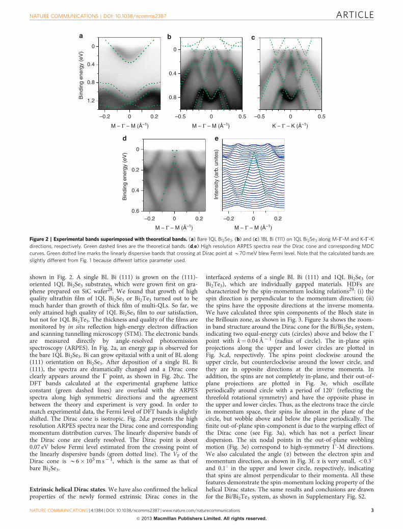
shown in Fig. 2. A single BL Bi (111) is grown on the (111)-oriented 1QL Bi2Se3 substrates, which were grown first on gra-phene prepared on SiC wafer28. We found that growth of highquality ultrathin film of 1QL Bi2Se3 or Bi2Te3 turned out to bemuch harder than growth of thick film of multi-QLs. So far, weonly attained high quality of 1QL Bi2Se3 film to our satisfaction,but not for 1QL Bi2Te3. The thickness and quality of the films aremonitored by in situ reflection high-energy electron diffractionand scanning tunnelling microscopy (STM). The electronic bandsare measured directly by angle-resolved photoemissionspectroscopy (ARPES). In Fig. 2a, an energy gap is observed forthe bare 1QL Bi2Se3. Bi can grow epitaxial with a unit of BL along(111) orientation on Bi2Se3. After deposition of a single BL Bi(111), the spectra are dramatically changed and a Dirac coneclearly appears around the G point, as shown in Fig. 2b,c. TheDFT bands calculated at the experimental graphene latticeconstant (green dashed lines) are overlaid with the ARPESspectra along high symmetric directions and the agreementbetween the theory and experiment is very good. In order tomatch experimental data, the Fermi level of DFT bands is slightlyshifted. The Dirac cone is isotropic. Fig. 2d,e presents the highresolution ARPES spectra near the Dirac cone and correspondingmomentum distribution curves. The linearly dispersive bands ofthe Dirac cone are clearly resolved. The Dirac point is about0.07 eV below Fermi level estimated from the crossing point ofthe linearly dispersive bands (green dotted line). The VF of theDirac cone is B6� 105 m s� 1, which is the same as that ofbare Bi2Se3.
Extrinsic helical Dirac states. We have also confirmed the helicalproperties of the newly formed extrinsic Dirac cones in the
interfaced systems of a single BL Bi (111) and 1QL Bi2Se3 (orBi2Te3), which are individually gapped materials. HDFs arecharacterized by the spin-momentum locking relations29: (i) thespin direction is perpendicular to the momentum direction; (ii)the spins have the opposite directions at the inverse momenta.We have calculated three spin components of the Bloch state inthe Brillouin zone, as shown in Fig. 3. Figure 3a shows the zoom-in band structure around the Dirac cone for the Bi/Bi2Se3 system,indicating two equal-energy cuts (circles) above and below the !point with k¼ 0.04 Å� 1 (radius of circle). The in-plane spinprojections along the upper and lower circles are plotted inFig. 3c,d, respectively. The spins point clockwise around theupper circle, but counterclockwise around the lower circle, andthey are in opposite directions at the inverse momenta. Inaddition, the spins are not completely in-plane, and their out-of-plane projections are plotted in Fig. 3e, which oscillateperiodically around circle with a period of 1201 (reflecting thethreefold rotational symmetry) and have the opposite phase inthe upper and lower circles. Thus, as the electrons trace the circlein momentum space, their spins lie almost in the plane of thecircle, but wobble above and below the plane periodically. Thefinite out-of-plane spin-component is due to the warping effect ofthe Dirac cone (see Fig. 3a), which has not a perfect lineardispersion. The six nodal points in the out-of-plane wobblingmotion (Fig. 3e) correspond to high-symmetry !-M directions.We also calculated the angle (a) between the electron spin andmomentum direction, as shown in Fig. 3f. a is very small, o0.31and 0.11 in the upper and lower circle, respectively, indicatingthat spins are almost perpendicular to their momenta. All thesefeatures demonstrate the spin-momentum locking property of thehelical Dirac states. The same results and conclusions are drawnfor the Bi/Bi2Te3 system, as shown in Supplementary Fig. S2.
0
0.4
0.8
1.2
–0.2
–0.2 0.2 –0.2 0.2
0.2
0.2
0.4
0.6
–0.5 –0.50.50
0
0 0
0 0.50
0
0.4
0.8Bin
ding
ene
rgy
(eV
)
Bin
ding
ene
rgy
(eV
)
Inte
nsity
(ar
b. u
nite
s)
M – Γ – M (Å–1)
M – Γ – M (Å–1) M – Γ – M (Å–1)
M – Γ – M (Å–1) K – Γ – K (Å–1)
Figure 2 | Experimental bands superimposed with theoretical bands. (a) Bare 1QL Bi2Se3. (b) and (c) 1BL Bi (111) on 1QL Bi2Se3 along M-G-M and K-G-K
directions, respectively. Green dashed lines are the theoretical bands. (d,e) High resolution ARPES spectra near the Dirac cone and corresponding MDC
curves. Green dotted line marks the linearly dispersive bands that crossing at Dirac point at B70 meV blew Fermi level. Note that the calculated bands are
slightly different from Fig. 1 because different lattice parameter used.
NATURE COMMUNICATIONS | DOI: 10.1038/ncomms2387 ARTICLE
NATURE COMMUNICATIONS | 4:1384 | DOI: 10.1038/ncomms2387 | www.nature.com/naturecommunications 3
& 2013 Macmillan Publishers Limited. All rights reserved.

DiscussionNext, we explain where the Dirac cone states come from, the 1BLBi or 1QL Bi2Se3 (or Bi2Te3)? Previous studies18 showed that theBi (111) film represents a special class of system having anintermediate inter-bilayer coupling strength, which has asignificant influence on its topological property. At equilibrium,the interfacial distance (d) between Bi BL and Bi2Se3 QL is B3 Åand the interface energy is B0.16 eV per unit cell, which arenoticeably larger than the typical values of van der Waals bond butsmaller than those of typical chemical bond. To gain some insightabout the influence of the interfacial coupling on the helical spinstates, we have performed a set of model DFT calculations byartificially increasing the interfacial distance between the Bi BLand Bi2Se3 QL to gradually tune the interface coupling strength18,as shown in Fig. 4. At a large interfacial distance (for example,dB6 Å in Fig. 4a), without the interfacial coupling, the bandstructure would be a simple superposition of the bare Bi BL andBi2Se3 QL bands. However, we observe a slight band splitting inthe double-degenerated Bi and Bi2Se3 band. With the decreasinginterfacial distance, the increased interfacial coupling continues tofurther split and reshape the bands, leading eventually to theformation of helical Dirac cone. By analysing the spectralcomponents of Dirac cone states during this process, we foundthat the Dirac cone is predominantly coming from the Bi BL, withB95% spectral weight of Bi BL states at the equilibrium distance,as shown in Fig. 4c. Similar results are found for the interfacebetween Bi BL and Bi2Te3 QL, with B90% Bi BL states in thehelical Dirac cone at the equilibrium distance, as shown inSupplementary Fig. S3a–c.
Lastly, we will address how the Dirac cone states are formed.From the above calculations and analyses, we learnt that theextrinsic HDFs originate from the Bi BL, while the QL of Bi2Se3
(or Bi2Te3) substrate provides possibly a triggering mechanismthat induces the Dirac cone states in Bi BL. We also know that Bi(111) BL has a strong spin-orbit coupling, and by itself its bandsare double-degenerate conserving the inversion symmetry.
Deposition of Bi BL on Bi2Se3 (or Bi2Te3) will break suchsymmetry, and hence lift the band degeneracy. However, thiseffect of symmetry breaking is limited, likely insufficient to induce
0.2
UpperUpper
LowerE
–Ef (
eV)
Lower
Upper Lower
0.0
–0.2
–0.4–0.08
0.05 0.05
0.05–0.05 –0.05
–0.05
0.00 0.00
0.00 0.05–0.05 0.00
0.00
94
92
90
88
86
90.4
90.0
89.6
0 120 240 360
0 120 240 360
0.08
s
k
ky
kz
kx
M – Γ – M (Å–1)
kx (Å–1) kx (Å
–1)
k y (
Å–1
)
�
�
�
�
�
�
�
Figure 3 | Helical states near the Dirac cone. (a) Two equal-energy cuts as marked above and below Dirac point for calculating the helical Dirac states in
Bi/Bi2Se3. (b) Definitions of the y (angle between k and kx axis), f (angle between S and kz axis) and a (angle between k and S), which are used to
characterize the spin direction (S) with respect to the momentum direction (k). (c,d) In-plane spin-momentum relation in the upper and lower cut in (a),
respectively. (e) Out-of-plane spin-momentum relation in the upper and lower cuts in (a). (f) Angle between spin and momentum in the upper and lower
cuts in (a).
1.0
0.5
0.0
0.0
–0.5
–0.5 0.5 0.0–0.5 0.5–1.0
100
95
90
10
5
00 1 2 3 4 630
0
10
20
30
40
BL BiQL Bi2Se3
–3–6
1.0
0.5
0.0
–0.5
–1.0
Rat
io (
%)
E–E
f (eV
)
Z (
Å)
+d (Å)
+3 Å +1 Å
D
a b
c d
D
Δ� (10–2 e/Å)
M – Γ – M (Å–1) M – Γ – M (Å–1)
Figure 4 | Model DFT bands as a function of interfacial distance.
(a,b) Bands at the artificially increased interfacial distance by 3 and 1 Å,
respectively, showing the creation process of helical Dirac cone. (c)
Spectral weight at the Dirac point resolved between the Bi BL and Bi2Se3 QL
as a function of interfacial distance. (d) Interfacial charge transfer between
Bi BL and Bi2Se3 QL at the equilibrium distance, showing the internal
electrical field.
ARTICLE NATURE COMMUNICATIONS | DOI: 10.1038/ncomms2387
4 NATURE COMMUNICATIONS | 4:1384 | DOI: 10.1038/ncomms2387 | www.nature.com/naturecommunications
& 2013 Macmillan Publishers Limited. All rights reserved.

a band splitting and reshaping as dramatic as we have observed.To further understand the interaction between the Bi BL andBi2Se3 (or Bi2Te3), we calculated the differential charge density atthe interface, defined as rdiff¼ rBLþQL�rBL� rQL, as shown inFig. 4d (see also Supplementary Fig. S3d for Bi/Bi2Te3). Clearly, asubstantial charge transfer at the interface has occurred. The BiBL acts as a donor and the Bi2Se3 (or Bi2Te3) as an acceptor, withthe electrons transferring from the former to the latter. Thischarge transfer generates a large internal electric field at theinterface region, with a field direction pointing from the Bi BL tothe Bi2Se3 (or Bi2Te3), and field intensity estimated as high asB1 V/Å. Thus, we propose this phenomenon is very similar tothe external electric field (or band bending) effect that inducesRashba band splitting in the surface state of TIs30–32. Weestimated the Rashba coupling constant (using the two-dimentional free electron gas model) from the calculated bandsplitting at the equilibrium structures, which is B4 eV �Å.Therefore, the HDFs are extrinsically created by a giant Rashbaeffect due to the interfacial charge transfer.
To further support the charge transfer induced Rashba effect isthe dominated factor for realizing the extrinsic helical Diracstates, we also studied the band structure for Bi BL on 1QL In2Se3
and 5-layer Cu (111) substrate, as shown in Supplementary FigsS4 and S5, respectively. A clearly charge transfer between the BiBL and these non-TI substrates (Supplementary Figs. S4i and S5i)can be observed in both cases (one semiconductor and onemetal), and the similar Dirac cone states are also generated.However, the Bi BL become metallic at the In2Se3 lattice constant,and the Cu (111) substrate is also metallic. Thus, comparing toBi/Bi2Se3 and Bi/Bi2Te3 system, these Dirac cone states are notwithin the gapped region of Bi/In2Se3 and Bi/Cu. The previousstudies for Bi grown on Si (111) only showed the monomer ortrimer Bi configuration on the substrate, which cannot maintainthe intrinsic structure of the Bi BL.
MethodsCalculation method. DFT calculations for a single BL Bi (111) on a single QLBi2Se3 and Bi2Te3 are carried out in the framework of the Perdew-Burke-Ernzerhof-type generalized gradient approximation using VASP package33. Theexperimental bulk lattice constants of the substrate are used (a¼ 4.138 Å for Bi2Se3
and a¼ 4.386 Å for Bi2Te3), and the Bi BL is strained to match the substrate latticeconstant. All calculations are performed with a plane-wave cutoff of 400 eV on an11� 11� 1 Monkhorst-Pack k-point mesh, and the vacuum layer is over 20 Åthick to ensure decoupling between neighbouring slabs. During structuralrelaxation, all the atoms are allowed to relax until the forces are smaller than0.01 eV/Å. To reproduce the ARPES band for Bi/Bi2Se3 in Fig. 2, we use a largerlattice constant a¼ 4.37 Å, which can match the graphene/SiC wafer in theexperiment.
Experiment method. Flat Bi2Se3 single QL films is grown by molecular beamepitaxy method on graphene/SiC wafer and on highly ordered pyrolytic graphitesubstrates. Bi films are deposited on Bi2Se3 at 200 K and then annealed at roomtemperature. The thickness of Bi2Se3 and Bi films is monitored by reflection high-energy electron diffraction oscillation and scanning tunnelling microscopy. Thesample temperature is kept at 100 K during measurement. ARPES measurementsare performed with in-lab He discharge lamp (He-I 21.2 eV). Energy resolution isbetter than 25 meV and angular resolution is better than 0.02 � 1.
References1. Kane, C. L. & Mele, E. J. Quantum spin hall effect in graphene. Phys. Rev. Lett.
95, 226801 (2005).2. Bernevig, B. A. & Zhang, S.-C. Quantum spin hall effect. Phys. Rev. Lett. 96,
106802 (2006).3. Bernevig, B. A. et al. Quantum spin hall effect and topological phase transition
in HgTe Quantum Wells. Science 314, 1757–1761 (2006).4. Fu, L. & Kane, C. L. Topological insulators with inversion symmetry. Phys. Rev.
B 76, 045302 (2007).5. Hsieh, D. et al. A tunable topological insulator in the spin helical dirac
transport regime. Nature 460, 1101–1105 (2009).6. Xia, Y. et al. Observation of a large-gap topological-insulator class with a single
dirac cone on the surface. Nat. Phys. 5, 398–402 (2009).
7. Zhang, H. J. et al. Topological insulators in Bi2Se3, Bi2Te3 and Sb2Te3 with asingle Dirac cone on the surface. Nat. Phys. 5, 438–442 (2009).
8. Chen, Y. L. et al. Experimental realization of a three-dimensional topologicalinsulator Bi2Te3. Science 325, 178–181 (2009).
9. Hasan, M. Z. & Kane, C. L. Topological insulators. Rev. Mod. Phys. 82,3045–3067 (2010).
10. Fu, L. et al. Topological insulators in three dimensions. Phys. Rev. Lett. 98,106803 (2007).
11. Qi, X.-L. et al. Topological field theory of time-reversal invariant insulators.Phys. Rev. B 78, 195424 (2008).
12. Akhmerov, A. R. et al. Electrically detected interferometry of majoranafermions in a topological insulator. Phys. Rev. Lett. 102, 216404 (2009).
13. Seradjeh, B. et al. Exciton condensation and charge fractionalization in atopological insulator film. Phys. Rev. Lett. 103, 066402 (2009).
14. Zhang, Y. et al. Crossover of the three-dimensional topological insulator Bi2Se3
to the two-dimensional limit. Nat. Phys. 6, 584–588 (2010).15. Park, K. et al. Robustness of topologically protected surface states in layering of
Bi2Te3 thin films. Phys. Rev. Lett. 105, 186801 (2010).16. Yazyev, O. V. et al. Spin polarization and transport of surface states in the
topological insulators Bi2Se3 and Bi2Te3 from first principles. Phys. Rev. Lett.105, 266806 (2010).
17. Murakami, S. Quantum spin hall effect and enhanced magnetic response byspin-orbit coupling. Phys. Rev. Lett. 97, 236805 (2006).
18. Liu, Z. et al. Stable nontrivial Z2 topology in ultrathin Bi (111) films: a first-principles study. Phys. Rev. Lett. 107, 136805 (2011).
19. Koroteev, Y. M. et al. First-principles investigation of structural and electronicproperties of ultrathin Bi films. Phys. Rev. B 77, 045428 (2008).
20. Wada, M. et al. Localized edge states in two-dimensional topological insulators:ultrathin Bi films. Phys. Rev. B 83, 121310(R) (2011).
21. Ast, C. R. et al. Giant spin splitting through surface alloying. Phys. Rev. Lett. 98,186807 (2007).
22. Mathias, S. et al. Quantum-well-induced giant spin-orbit splitting. Phys. Rev.Lett. 104, 066802 (2010).
23. Gierz, I. et al. Silicon surface with giant spin splitting. Phys. Rev. Lett. 103,046803 (2009).
24. Ohtsubo, Y. et al. Spin-polarized semiconductor surface states localized insubsurface layers. Phys. Rev. B. 82, 201307(R) (2010).
25. Hatta, S. & Aruga, T. Large rashba spin splitting of surface resonance bands onsemiconductor surface. Phys. Rev. B. 80, 113309 (2009).
26. Hirahara, T. et al. Interfacing 2D and 3D topological insulators: Bi (111) bilayeron Bi2Te3. Phys. Rev. Lett. 107, 166801 (2011).
27. Yang, F. et al. Spatial and energy distribution of topological edge states in singleBi (111) bilayer. Phys. Rev. Lett. 109, 016801 (2012).
28. Song, C.-L. et al. Topological insulator Bi2Se3 thin films grown on double-layer graphene by molecular beam epitaxy. Appl. Phys. Lett. 97, 143118(2010).
29. Zhao, Y. et al. Helical states of topological insulator Bi2Se3. Nano Lett. 11,2088–2091 (2011).
30. King, P. D. C. et al. Large tunable rashba spin splitting of a two-dimensionalelectron gas in Bi2Se3. Phys. Rev. Lett. 107, 096802 (2011).
31. Zhu, Z.-H. et al. Rashba spin-splitting control at the surface of the topologicalinsulator Bi2Se3. Phys. Rev. Lett. 107, 186405 (2011).
32. Benia, H. M. et al. Reactive chemical doping of the Bi2Se3 topological insulator.Phys. Rev. Lett. 107, 177602 (2011).
33. Kresse, G. & Hafner, J. Ab initio molecular dynamics for liquid metals. Phys.Rev. B 47, 558–561 (1993).
AcknowledgementsThe theoretical work was supported by US DOE-BES (Grant No. DE-FG02-04ER46027)and we thank the CHPC at University of Utah and NERSC for providing the computingresources. The experimental work was supported by National Basic Research Programmeof China (Grant No. 2012CB927401, 2011CB921902, 2013CB921902, 2011CB922200),NSFC (Grant No. 91021002, 11174199, 11134008, 11274228), Shanghai Committee ofScience and Technology, China (No. 11JC1405000, 11PJ1405200, 12JC1405300),Shanghai Municipal Education Commission (11ZZ17) and SRF for ROCS, SEM. Z.F.W.acknowledges additional support from ARL (Cooperative Agreement No. W911NF-12-2-0023). W.M.M. acknowledges additional support from NSF-MRSCE (Grant No. DMR-1121252). D.Q. acknowledges additional support from ‘ShuGuang’ project supported byShanghai Municipal Education Commission and Shanghai Education DevelopmentFoundation and from Programme for Professor of Special Appointment (EasternScholar) at Shanghai Institutions of Higher Learning.
Author contributionsZ.F.W. carried out the theoretical calculations with assistance from W.M.M. and F.L.;M.Y.Y. did the experiments with assistance from L.M., F.F.Z., C.H.L., C.L.G., D.Q. andJ.F.J., F.L, D.Q., and J.F.J. were responsible for the overall direction. Z.F.W., F.L. and D.Q.wrote the paper.
NATURE COMMUNICATIONS | DOI: 10.1038/ncomms2387 ARTICLE
NATURE COMMUNICATIONS | 4:1384 | DOI: 10.1038/ncomms2387 | www.nature.com/naturecommunications 5
& 2013 Macmillan Publishers Limited. All rights reserved.
Additional informationSupplementary Information accompanies this paper at http://www.nature.com/naturecommunications
Competing financial interests: The authors declare no competing financialinterests.
Reprints and permission information is available online at http://npg.nature.com/reprintsandpermissions/
How to cite this article: Wang, Z.F. et al. Creation of helical Dirac fermions byinterfacing two gapped systems of ordinary fermions. Nat. Commun. 4:1384doi: 10.1038/ncomms2387 (2013).
ARTICLE NATURE COMMUNICATIONS | DOI: 10.1038/ncomms2387
6 NATURE COMMUNICATIONS | 4:1384 | DOI: 10.1038/ncomms2387 | www.nature.com/naturecommunications
& 2013 Macmillan Publishers Limited. All rights reserved.
Copyright © 2022 FDOKUMEN