Conditions for the growth of smooth La0.7Sr0.3MnO3 thin films by pulsed electron ablation
25
Conditions for the growth of smooth La 0.7 Sr 0.3 MnO 3 thin films by pulsed electron ablation P. Graziosi a,b,* , M. Prezioso b , A. Gambardella b , C. Kitts b,1 , R.K. Rakshit b,2 , A. Riminucci b , I. Bergenti b , F. Borgatti b , C. Pernechele c , M. Solzi c . D. Pullini d , D. Busquets-Mataix a,e , V. A. Dediu b a Instituto de Tecnología de Materiales, Universidad Politécnica de Valencia, Camino de Vera s/n, 46022, Valencia, Spain b CNR - ISMN, Consiglio Nazionale delle Ricerche - Istituto per lo Studio dei Materiali Nanostrutturati, v. Gobetti 101, 40129, Bologna, Italy c Dipartimento di Fisica, Università di Parma, Area delle Scienze 7/A, 43124, Parma, Italy d Centro Ricerche Fiat, 10043, Orbassano (TO), Italy e Departamento de Ingeniería Mecánica y de Materiales, Universidad Politécnica de Valencia, Camino de Vera s/n, 46022, Valencia, Spain 1 Present address: Department of Physical Chemistry, Chalmers University of Technology, 41296, Gothenburg, Sweden 2 Present address: Quantum Phenomena and Applications Division, National Physical Laboratory, Council of Scientific and Industrial Research, Dr. K. S. Krishnan Marg, New Delhi 110012, India * Corresponding author: [email protected], tel. +39 0516398505, +39 0516398517, fax +39 0516398540
Transcript of Conditions for the growth of smooth La0.7Sr0.3MnO3 thin films by pulsed electron ablation

Conditions for the growth of smooth La0.7Sr0.3MnO3 thin films by pulsed
electron ablation
P. Graziosi a,b,*
, M. Prezioso b, A. Gambardella
b, C. Kitts
b,1, R.K. Rakshit
b,2, A. Riminucci
b, I. Bergenti
b, F. Borgatti
b, C. Pernechele
c, M. Solzi
c. D. Pullini
d, D. Busquets-Mataix
a,e,
V. A. Dediu b
a Instituto de Tecnología de Materiales, Universidad Politécnica de Valencia, Camino de Vera s/n,
46022, Valencia, Spain
b CNR - ISMN, Consiglio Nazionale delle Ricerche - Istituto per lo Studio dei Materiali
Nanostrutturati, v. Gobetti 101, 40129, Bologna, Italy
cDipartimento di Fisica, Università di Parma, Area delle Scienze 7/A, 43124, Parma, Italy
d Centro Ricerche Fiat, 10043, Orbassano (TO), Italy
e Departamento de Ingeniería Mecánica y de Materiales, Universidad Politécnica de Valencia,
Camino de Vera s/n, 46022, Valencia, Spain
1 Present address: Department of Physical Chemistry, Chalmers University of Technology, 41296,
Gothenburg, Sweden
2 Present address: Quantum Phenomena and Applications Division, National Physical Laboratory,
Council of Scientific and Industrial Research, Dr. K. S. Krishnan Marg, New Delhi 110012, India
* Corresponding author: [email protected], tel. +39 0516398505, +39 0516398517, fax
+39 0516398540

Abstract
We report on the optimisation of the growth conditions of manganite
La0.7Sr0.3MnO3 (LSMO) thin films prepared by Channel Spark Ablation (CSA). CSA
belongs to pulsed electron deposition methods and its energetic and deposition
parameters are quite similar to those of pulsed laser deposition. The method has been
already proven to provide manganite films with good magnetic properties, but the
films were generally relatively rough (a few nm coarseness). Here we show that
increasing the oxygen deposition pressure with respect to previously used regimes,
reduces the surface roughness down to unit cell size while maintaining a robust
magnetism. We analyse in detail the effect of other deposition parameters, like
accelerating voltage, discharging energy, and temperature and provide on this basis a
set of optimal conditions for the growth of atomically flat films. The thicknesses for
which atomically flat surface was achieved is as high as about 10-20 nm,
corresponding to films with room temperature magnetism. We believe such magnetic
layers represent appealing and suitable electrodes for various spintronic devices.

1. Introduction
Manganese perovskites are among the most employed laboratory materials for
various spintronic devices [1]. Impressive efforts have been made in order to
understand the complex physics characteristic for these materials, implicating
massive experimental and theoretical investigations [2, 3]. In addition the interest
towards device applications stimulated detailed surface studies including a wide
spectrum of various spectroscopy [4] and microscopy techniques [5], supported often
by thorough ab initio simulations [6, 7].
A substantial revival of the interest towards manganites has been stimulated
recently by the demonstration of the extremely efficient utilization of La0.7Sr0.3MnO3
as spin polarized electrode in various spintronic devices with organic semiconductors
spacers in both tunnelling [8] and injection regimes [9, 10]. Although the commercial
application of this and other manganites is still strongly questioned by their relatively
low Curie temperature (about 350-370K) [11], they represent an excellent tool for
unravelling most basic and important effects in spintronic systems involving organic
semiconductors [8, 12, 13]. Such application advances nevertheless extremely tough
requirements to the sharpness of all the involved interfaces, and hence to the
smoothness of all the components surfaces. For example, an interface roughness
exceeding 1-2 nm (approximately molecular size) seriously questions the
reproducibility of main spintronic effects [14]. This pushes the investigators to
develop atomically flat device components combined in as sharp as possible
multilayered assembly.

Ablation techniques have proven so far to be extremely efficient in the
deposition of thin films of complex oxides, like High-TC superconductors (HTC),
ferroelectric oxides and colossal magnetoresistive manganites (CMR) [15]. Among
different ablation techniques, several modifications of the pulsed electron deposition
(PED) method are recently successfully competing in the deposition of oxide
superconductors and manganites with the most widespread ablation technique -
Pulsed Laser Deposition (PLD). Thus the Channel Spark Ablation (CSA) [16] has
proved the deposition of high quality thin films of simple oxides, such as Al2O3 [17,
18], and complex oxides such as cuprates [19] and manganites [20]. Previous X-ray
Diffraction and Raman investigations on selected samples of different thicknesses
have ALWAYS indicated (001) growth orientation on both STO (100) and NGO
(110). This paper is dedicated to morphology and we did not perform sample by
sample XRD characterizations, such characterizations together with Transmission
Electron Microscopy (TEM) analysis are currently in progress and will be published
elsewhere.
Especially successful was the application of CSA to LSMO films, where
excellent magnetic, electric and structural properties have been achieved [20-22].
Moreover, manganite electrodes grown by CSA have so far shown best performances
in organic spintronics including highest achieved tunnelling magnetoresistance
(TMR) exceeding 300% [8] and room temperature operation of injection devices [9,
23].

The surface roughness of these films was nevertheless relatively high and also
the thinnest LSMO films (below 10 nm) presented a rms roughness of a few
nanometers due to the presence of particulate and/or outgrowths [21].
In order to compare state of the art roughnesses for films produced by CSA and
other deposition methods we describe below selected cases for few mainly involved
techniques. The lowest roughness achieved by an ablation technique was performed
by PLD and found to be about 0.2 nm on about 10 nm thick films [24]. Similar results
were featured by Metalorganic Aerosol Deposition (MAD) [25, 26], but in that case
the 0.2 nm roughness is claimed for thicker films of 80 nm. Best MBE roughness
reached as low as 0.4 nm [27] and was found for 9 nm films. Noteworthy the lowest
roughness presented in literature was achieved by sputtering technique and was
represented by 0.11 nm value for 7 nm thick films [28]. Unfortunately in the latter
case the films of this distinguished flatness were not ferromagnetic at room
temperature – moreover, RT magnetism was achieved only for films exceeding 27
nm thickness.
With this picture in mind and considering exceptional results achieved by CSA
manganites in organic spintronic devices, the ability of CSA to reach roughness
values comparable to best reported ones represents the main goal and motivation of
this paper. We will concentrate our efforts on very thin films, which, once achieved
stable room temperature magnetism, offer most versatile electrode performances, like
for example homogeneous (throughout the thickness) strain engineering, oxygen
control, low density of defects etc. . Very thin films (10-20 nm and below) are much

less investigated but they are considered as most appropriate for spintronic
applications and a deep investigation in order to achieve very thin film with robust
magnetotransport properties is going on [24]. Working with very thin films is thus
one of the explicit goals of our paper. We will show indeed that 0.2 nm roughness
can be achieved by CSA technique for thicknesses suitable for the described above
applications.
2. Experimental details
The CSA system is depicted in Figure 1. The principle consists in the ablation
of a stoichiometric target by means of a pulsed electron beam [29]. A plasma is
triggered in order to extract electrons for the beam. A negative high voltage (5-30
KV) power supply is directly connected to a hollow cathode (a) and a capacitor (b).
The latter is grounded through an air gap (c) having a floating electrode which is
decoupled from the capacitor by a charging resistor (d). Between the charging resistor
(d) and the floating electrode of the air gap a triggering anode plate (e) is located and
inserted in the bulb (f). At a sufficient high voltage a spark brakes down the air gap
(c), a rapid variation of the electric field between the hollow cathode and the anode
plate ionizes the gas molecules in the bulb triggering plasma in the cathode cavity (a),
where the amplification of the discharge happens. Because of the high resistance of
the charging resistor, the capacitor discharge happens through the low impedance
electron beam (g). The negative high voltage accelerates the electrons of the beam in
the Pyrex channel (h), where the beam is further amplified by secondary emission

from the channel wall. The active role of the channel gives the technique its name.
The electron beam current would be continuous if the power supply could provide a
sufficient current, but since it is limited in current the electron beam cannot be
sustained and the discharge extinguishes up to the new spark in the air gap. As a
consequence the beam assumes a pulsed character. The current supplied to charge the
capacitors defines the charging time and, hence, the operating frequency. The high
voltage and the capacitance determine the accumulated charge and the total energy.
The energy distribution of the electrons in the beam and the length of the pulse is
determined by the accelerating voltage and the gas pressure. Since the environment
gas “stuffs” the beam, which is space charge neutralized the gas acts like a “window”
which the electrons pass through and by the pressure one controls the electron energy
distribution in the beam. As a consequence only a narrow range of pressures is able to
stabilize the beam, from 1 to 5 ∙10-2
mbar, according to the specific design of the gun.
Clearly, a part of the electric energy will get dissipated via extended plasma
generation, partial heating and other processes. In what follows we will not discuss
these losses and will consider the useful (ablating) part of the energy as proportional
to the total energy.
Epitaxial LSMO thin films were deposited on matching substrates: NdGaO3
(110) and SrTiO3 (001) (NGO and STO, respectively); the mismatch is -0.3 % for
NGO and 0.9 % for STO. A profilometer was used for thickness calibration.
Films morphology was analysed by means of atomic force microscopy (AFM),
the magnetotransport behaviour was characterised by measuring the films resistance

and magnetoresistance from 100 K up to 350 K. The magnetotransport measurements
were taken as R(H) at different temperatures. The magnetoresistance MR was defined
as (R(0)-R(3 kOe))/R(0) · 100. The magnetometry characterization as a function of
temperature was carried out by means of Superconducting QUantum Interference
Device (SQUID) magnetometry in the temperature range 100-370 K, with an applied
magnetic field of 1kOe. Extensive Scanning Tunnelling Microscopy (STM)
characterizations fully confirmed the AFM results and obtained clear atomic
resolution, these data will be published elsewhere.
Figure 1: CSA scheme
Scheme of the Channel Spark Ablation system. The generator consists of a transient
hollow cathode connected to a dielectric acceleration tube and the trigger. The
dielectric tube is connected through a narrow exit to the transient hollow cathode and
picks up the electron flow for the final acceleration which form the electron beam.
The inner wall of the deposition chamber is the actual anode. The trigger circuit
consists of the air gap with a floating electrode (c), the charging resistor (d), bottom
anode (e).

3. Results
LSMO films were grown at substrate temperatures in the range between 700
and 950 °C. The temperature was calibrated by a pyrometer pointing on a black and
opaque Nb:STO dummy substrate. The discharge voltage was varied from 7 to 10.5
kV. The pressure was tuned between 2.2 and 4.3 · 10-2
mbar and actually the
accuracy of its detection in the used setup was about 0.1 ∙ 10-2
mbar (Leybold
thermovac). This range enables an efficient CSA processing given its plasma based
operation. An additional conditioning is routinely performed on all the samples
involving a soft (400°C) annealing in vacuum for a time corresponding to 1.5 ∙ tD,
where tD is deposition time. This procedure was found to increase considerably the
reproducibility of the main film parameters and was tentatively ascribed to the
removal of the over-oxygenation [20].
3.1 Oxygen Pressure
We investigate first the influence of the growth pressure on film morphology.
The pressure in the chamber is a very important parameter given the fact that CSA
deals with plasma initiation, evolution and propagation. We start from thick films
(more than 30 nm), that is films exceeding the thickness where any substrate induced
strain is substantially removed. Figure 2 reports the AFM morphology of 45 nm thick
films deposited at two different pressures: 2.2 ∙ 10-2
mbar and 4.2 ∙ 10-2
mbar. The
film deposited at lower pressure has a high roughness Rrms above 7 nm and features a
highly granular surface with a number of outgrowths. Contrarily, the high pressure

regime provides a considerably reduced roughness and Rrms values of about 2 nm is
achieved. It can be seen thus that the pressure has a crucial influence on the surface
roughness both for the presence of outgrowths and particulate.
Figure 2: Chamber pressure effect
Surface of two 45 nm thick LSMO films deposited at the same condition but the
chamber pressure, as indicated. Rrms is 7.2 nm for the film deposited at lower pressure
and 2.1 nm for the sample deposited at higher pressure.
Considering that the roughness in manganite films is known to be thickness
dependent [30], the high enough thickness of the above discussed films (45 nm) does
not allow the realization of atomically flat surfaces. This is achieved on the next
batch of samples where three 10 nm films have been fabricated while tuning further
the working pressure: pressure values of 3.0∙10-2
mbar, 3.9∙10-2
mbar, and 4.3∙10-2
mbar were investigated. The respective morphologies are reported in Fig. 3. The
surface clearly becomes cleaner (no outgrowths) and smoother by increasing the
pressure but what is more important, the film deposited at 4.3 ∙ 10-2
mbar shows a
roughness confined below 1 nm for a large area of 5 x 5 m2. Such a roughness
detected on reasonably large area matches various device constrains allowing the

fabrication of atomically flat interfaces in photolithography based microsystems. This
surface quality is extended at least up to 20 nm thick films (Figure 7) but the
thickness evolution of optimized films is beyond the aim of the presented work.
Figure 3: Pressure driven morphology
AFM measured morphologies of 10 nm thick LSMO/STO thin films deposited at
different pressures. The images are 5 x 5 m2 in size. The relative metal-insulator
transition temperature TMI and deposition oxygen pressures ( ) are reported in the
figure.
3.2 Pulse energy
The role of the energy accumulated in capacitors (see Fig. 1) and afterwards
transferred (partially) into ablation capability has been studied by analyzing
separately different accelerating voltages and capacitances. These effects were
investigated on 10 nm thick LSMO films deposited at 815 °C at the fixed pressure of
3.9 · 10-2
mbar.
2OP

Figure 4 reports the morphology of LSMO films of 10 ± 1 nm deposited at
different voltages ranging from 7 to 10.5 kV on STO and NGO. The main result is
the increase of the rms roughness of the film surfaces with voltage for both
substrates. Increasing voltage from 7 to 10.5 kV the surface changes from a very
smooth state, with an rms roughness below half a unit cell, to a quite harsh one, with
rms roughness of almost three unit cells and a peak to valley roughness of several
nanometres. Since all the deposition parameters were kept the same, the morphology
dependence on the accelerating voltage is ascribed to the ablation.
Optimized parameters for the channel spark deposition of LSMO.
Figure 4: Voltage effect
AFM images of 10 nm LSMO films deposited on STO or NGO at different
accelerating voltages. The roughness increases with the voltage, i.e. the pulse energy.
The dependence of the particulate density on the capacitance of the CSA has
been studied at optimized pressure and voltage. By varying the capacitance from 20

nF (left) to 13.4 nF (right) capacitances no significant variation in the particulate
density is detected as function of capacitance (Figure 5). This result is in contrast
with other studies claiming the reduction of the particulate density for lower
capacitances as a consequence of the decreased beam energy [31-33]. Nevertheless,
in those studies the accelerating voltages were much higher and the working pressure
was much lower than our optimized conditions.
Figure 5: Capacitance effect
AFM images of two 10 nm thick LSMO films deposited with a capacitance of 20 nF
(right) and 13.4 nF (left) under optimised pressure and voltage conditions. The step-
terrace morphology appears identical.
3.3 Substrate Temperature
The substrate temperature effect on perovskite thin film morphology has been
investigated since the early studies in HTC superconductor films [34] . Very recently
studies have been reported also for LSMO where the temperature was identified as a
powerful instrument acting on the kinetics of the growth via a considerable diffusion
modification [35].

We investigated the temperature dependence of the morphology (Figure 6) on
three 10 nm thick films deposited respectively at 950, 850 and 750°C. One can see
that at the highest temperature the growth appears dominated by the formation of
crystallites with regular shape and facets oriented at 90° each other. This shape
remembers the substrate orientations and could correspond to non-stoichiometric
aggregates which nucleate on top of the surface [36-38], where the non-stoichiometry
could be also represented by local oxygen variations [20]. Decreasing temperature the
surface becomes smoother and at 750 °C one can see terraces coming from the
substrate as a signature of the possible step flow growth.
Figure 6: Temperature effect
AFM images of samples grown at different substrate temperatures, as indicated.
Decreasing substrate temperature the surface becomes smoother and smoother.
3.4 Magnetic characterizations
The optimization of the surface morphology will lead to a real enhancement of
LSMO performances only if magnetic properties of such optimized films would
remain at least as robust as for rougher films. We start magnetic investigations from
the SQUID magnetometry of a most standard optimised 20 nm thick film deposited
on STO (Figure 7). The sample was zero field cooled and the magnetic moment was
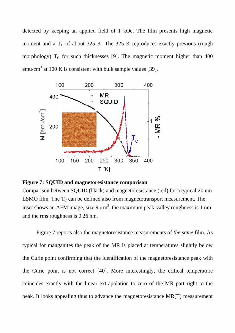
detected by keeping an applied field of 1 kOe. The film presents high magnetic
moment and a TC of about 325 K. The 325 K reproduces exactly previous (rough
morphology) TC for such thicknesses [9]. The magnetic moment higher than 400
emu/cm3 at 100 K is consistent with bulk sample values [39].
Figure 7: SQUID and magnetoresistance comparison
Comparison between SQUID (black) and magnetoresistance (red) for a typical 20 nm
LSMO film. The TC can be defined also from magnetotransport measurement. The
inset shows an AFM image, size 9 m2, the maximum peak-valley roughness is 1 nm
and the rms roughness is 0.26 nm.
Figure 7 reports also the magnetoresistance measurements of the same film. As
typical for manganites the peak of the MR is placed at temperatures slightly below
the Curie point confirming that the identification of the magnetoresistance peak with
the Curie point is not correct [40]. More interestingly, the critical temperature
coincides exactly with the linear extrapolation to zero of the MR part right to the
peak. It looks appealing thus to advance the magnetoresistance MR(T) measurement
as an appropriate and an extremely simple method for the TC definition via
magnetotransport. This appears to be especially useful for ultrathin films, where most
standard magnetic techniques could fail. The inset in Figure 7 reports a typical AFM
image for a 20 nm thick film showing a rms roughness of 0.26 nm and a maximum
height of the roughness of 1 nm.
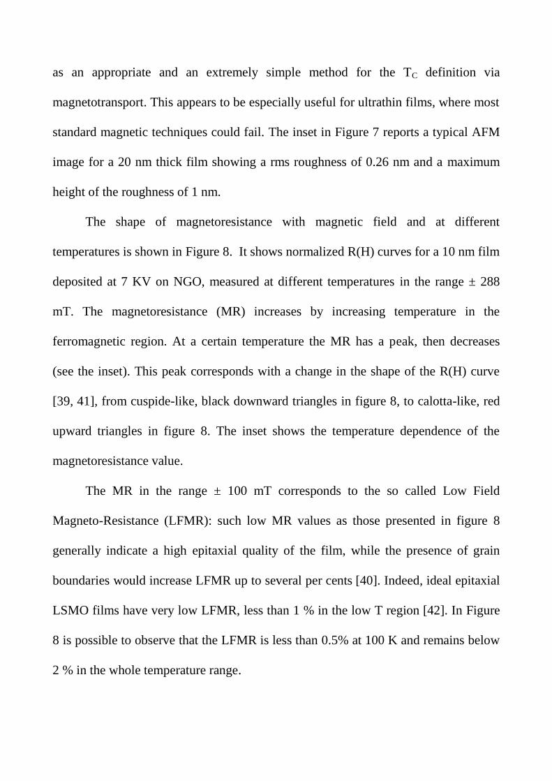
The shape of magnetoresistance with magnetic field and at different
temperatures is shown in Figure 8. It shows normalized R(H) curves for a 10 nm film
deposited at 7 KV on NGO, measured at different temperatures in the range ± 288
mT. The magnetoresistance (MR) increases by increasing temperature in the
ferromagnetic region. At a certain temperature the MR has a peak, then decreases
(see the inset). This peak corresponds with a change in the shape of the R(H) curve
[39, 41], from cuspide-like, black downward triangles in figure 8, to calotta-like, red
upward triangles in figure 8. The inset shows the temperature dependence of the
magnetoresistance value.
The MR in the range ± 100 mT corresponds to the so called Low Field
Magneto-Resistance (LFMR): such low MR values as those presented in figure 8
generally indicate a high epitaxial quality of the film, while the presence of grain
boundaries would increase LFMR up to several per cents [40]. Indeed, ideal epitaxial
LSMO films have very low LFMR, less than 1 % in the low T region [42]. In Figure
8 is possible to observe that the LFMR is less than 0.5% at 100 K and remains below
2 % in the whole temperature range.

Figure 9 communicates an extremely important result of this paper – the
transport and magnetotransport properties of these optimized films are weakly
dependent on the morphology. We show this on the basis of a set of films grown at
different voltages (and hence different morphologies, see Figure 4), but the property
holds also for other growth parameters variations. The temperature dependence of
resistance and MR for several 10 nm films is reported in Figure 9, where the sample
from Figure 8 corresponds to blue data set. Both MR(T) (full circles) and the R(T)
(open circles) of four 10 nm thick films deposited at indicated voltages are compared.
The R(T) curves display the resistance at zero magnetic field while the MR(T) curves
report the resistance change between 0 Oe and ± 288 mT, where each data point is
obtained by measuring R(H) at a constant temperature. One can see that R(T) curves
are nearly identical while the variation of the MR(T) peaks could be ascribed to the
possible inaccuracy in the thickness definition (rather than to morphology variation).
The lower values of MR for the films deposited on NGO can be ascribed to the better
substrate-film lattice matching. It would be interesting to compare the
magnetoresistive properties with literature data for manganite films of similar
thickness. Unfortunately similar characterizations for this range of fields and
thicknesses are not available in the literature. The only data for very thin films
features several percents of MR but are measured at 2.5 T and R(H) curves are not
shown [24]. The comparison with thicker films reveals that the magnetoresistive
behaviour of our films is comparable with the epitaxial ones [40, 42].
The list of the optimized parameters ranges are reported in table I. The effect of
the substrate temperature on the magnetotransport properties will require further
work.
Figure 8: Magnetoresistance of a selected 10 nm film
R(H) at constant temperatures, normalized at the value at zero field, for a 10 nm thick
LSMO film on NGO (110). The black curves are descending while the red ones are
asceding. Also the shape of the curves changes when the temperature trend is
inverted. The inset reports the temperature trend of the LFMR ( ± 100mT )
amplitude.
Table I : Optimized parameters
Optimized parameters for the channel spark deposition of LSMO.
PO2 [10-2
mbar] V [kV] C [nF] TS [°C]

3.5 to 4.5 7 to 8 Not affecting 750 to 800
Figure 9: Magnetotransport of 10 nm LSMO films
MR(T) and R(T) of 10 ± 1 nm thick films deposited at different voltages, as
indicated.
4. Discussion
The straightforward role of the pressure in diminishing the particulate density
on the film surface is enlightened by the ablation concepts developed for PLD. First
we have to note that the problem of particulate coming from the target is inherent in
the ablation processes [43, 44]. Commonly one observes two classes of particulate
roughly distinguished in over-micron round shaped particles and submicron round or

faceted particulate [45, 46]. The bigger particles are thought to come from the target
as a result of microcracks, pits and weakly attached particles. The submicron particles
are due to the superheating of the subsurface region [46], which reaches a higher
temperature than the surface, cooled by the latent heat of evaporation. In this latter
case the gaseous phases nucleate and cause volume expansion which leads to
explosive sublimation. In the superheated regions target material segregates and after
some pulses is ejected in form of submicron particles [47], known to have a different
chemical composition from the target as observed in HTC [36, 47] and LSMO [37,
38].
In order to avoid sub-micron particulate due to subsurface heating effect one
has to use very dense (94-97% of the theoretical value) and freshly polished targets
[36, 45]. Since the subsurface superheating model describes that the superheated
region depth increases with pulse energy and duration, one should work just above
the ablation threshold and use short pulses [46, 48]. Also the penetration depth does
matter: less it is, less deep the superheated region, with a strong improvement in the
morphology [43, 48].
In channel spark discharge it is known that increasing the background gas
pressure the electrons beam energy distribution is shifted towards lower values, the
beam power decreases and the pulse duration is shorter [49, 50]. Thus by tuning one
parameter we are moving towards the minimization of the subsurface superheating.
The above argument enables us to rationalize not only our data but also qualitatively
similar, but not commented, results found in pulsed electron ablation of HTC
precursor [31].
The role voltage dependence of the roughness is explained by the fact that
increasing the accelerating voltage the ablation becomes strenger and hence the rate
per pulse is higher. This observation fits well with the Venables model for the sub-
monolayer epitaxial growth [51]. Provided the density of stable nuclei, having size
bigger than the critical one i (the minimum size in order to avoid the dissociation of
the nucleus), is dnx/dt = iDniR/a + xDnxR/a + RZ, where i and x are rispectively
the capture numbers for critical and stable nuclei, ni and nx are the surface density of
critical and stable nuclei, D the adatoms diffusivity, R the arrival rate of adatoms and
a their desorption time, Z the covered surface ratio, it appears that the increased flux
of adatoms, consequence of a stronger ablation, is thought to be responsible for the
rapid aggregation and the increased roughness.
It is our opinion that the capacitance does not have a straightforward role for
the investigated ranges of pressure and voltage. This can be rationalised via simple
qualitative considerations. The energy stored in the capacitors is ½·C·U2, where C is
the capacitance and U the accelerating voltage. The quadratic dependence makes U
more influent than C. Moreover decreasing the capacitance also the RC constant is
decreased, the stored energy is transferred in a shorter time so the power transferred
to the target remains the same. This argument can explain why, once pressure and
voltage are optimized, the capacitance plays a minor role.

The fact that bidimensional growth is stabilized at relatively low temperature
was found in LSMO also by Bachelet et al. [35]. The interpretation relies on the fact
that at higher temperature (higher diffusivity) adatoms can move longer on the
surface and eventually find the minimum energy position. This does not imply
necessarily atomically flatness but rather regular atoms positioning, which can as
well arrange in three dimensional way. Decreasing substrate temperature the surface
diffusion is decreased and the bidimensional step flow is preferred to 3D nuclea,
provided the substrate temperature is still sufficient to ensure a diffusion length
comparable with the terrace length DDs 400 nm for STO substrate. The
terrace sides are kinks, i.e. points with higher density of dangly bonds and
consequently represent sites of preferential nucleation. If the temperature is too low
(DDs) the adatoms cannot reach the kinks, resulting in a rough 3D growth
with poor epitaxy. Oppositely, for too high substrate temperatures, the adatoms have
sufficient energy to detach from the kink and to form stable nuclei also in the middle
of the terrace (also 3D like growth tendency).
All the observations are summarized in the fact that the whole film growth is
completely determined by the energy density transferred from the beam to the target
and by the substrate temperature. The control of these two factors enables the control
of the morphology and magnetic and transport properties of the CSA deposited
manganite thin films.
5. Conclusions

In this work we have defined and described a robust set of protocols for the
growth of low roughness (rms roughness below the unit cell size) LSMO manganite
thin films by means of the Channel Spark Ablation technique, a cheap and home
building setting. This surface smoothening did not modify the magnetic properties,
which remained robust and in line with literature data for similar thicknesses. On the
basis of the performed magnetotransport analysis we propose as a very versatile and
simple method the definition of the TC from the magnetoresistance slope. Presented
results confirm that CSA is fully competitive with the more wide spread PLD
technique for the growth of high quality manganite thin films.
Aknowledgements
The authors thank Federico Bona for technical help. The extensive use of the
scanning probe microscope at the “Centro Interfacoltà Misure” of the University of
Parma is acknowledged. The authors also acknowledge the financial support from the
FP7 project NMP3-LA-2010-246102 (IFOX) and from NMP-2010-SMALL-4-
263104 (HINTS).
References
[1] M. Bowen, J.-L. Maurice, A. Barthélémy, M. Bibes, D. Imhoff, V. Bellini, R. Bertacco, D.
Wortmann, P. Seneor, E. Jacquet, A. Vaurès, J. Humbert, J.-P. Contour, C. Colliex, S. Blugel, P.H.
Dederichs, Journal of Physics: Condensed Matter 19/31 (2007) 315208.
[2] E. Dagotto, T. Hotta, A. Moreo, Physics Reports 344/1–3 (2001) 1.
[3] Y. Tokura, Reports on Progress in Physics 69/3 (2006) 797.
[4] E. Beyreuther, S. Grafström, L.M. Eng, C. Thiele, K. Dörr, Phys. Rev. B J1 - PRB 73/15
(2006) 155425.
[5] T. Becker, C. Streng, Y. Luo, V. Moshnyaga, B. Damaschke, N. Shannon, K. Samwer,
Physical Review Letters 89/23 (2002) 237203.

[6] C. Ma, Z. Yang, S. Picozzi, Journal of Physics: Condensed Matter 18/32 (2006) 7717.
[7] Y. Taguchi, H. Sakai, D. Okuyama, S. Ishiwata, J. Fujioka, T. Fukuda, D. Hashizume, F.
Kagawa, Y. Takahashi, R. Shimano, Y. Tokunaga, Y. Kaneko, A. Nakao, H. Nakao, Y. Murakami,
K. Sugimoto, M. Takata, K. Yamauchi, S. Picozzi, A.Q.R. Baron, T. Arima, Y. Tokura, Physica B:
Condensed Matter/0.
[8] C. Barraud, P. Seneor, R. Mattana, S. Fusil, K. Bouzehouane, C. Deranlot, P. Graziosi, L.
Hueso, I. Bergenti, V. Dediu, F. Petroff, A. Fert, Nat Phys 6/8 (2010) 615.
[9] V. Dediu, L.E. Hueso, I. Bergenti, A. Riminucci, F. Borgatti, P. Graziosi, C. Newby, F.
Casoli, M.P. De Jong, C. Taliani, Y. Zhan, Phys. Rev. B J1 - PRB 78/11 (2008) 115203.
[10] V.A. Dediu, L.E. Hueso, I. Bergenti, C. Taliani, Nat Mater 8/9 (2009) 707.
[11] N. Mathur, Nat Mater 5/11 (2006) 849.
[12] F. Li, P. Graziosi, Q. Tang, Y. Zhan, X. Liu, V. Dediu, M. Fahlman, Phys. Rev. B J1 - PRB
81/20 (2010) 205415.
[13] M. Prezioso, A. Riminucci, I. Bergenti, P. Graziosi, D. Brunel, V.A. Dediu, Advanced
Materials 23/11 (2011) 1371.
[14] F. Borgatti, I. Bergenti, F. Bona, V. Dediu, A. Fondacaro, S. Huotari, G. Monaco, D.A.
MacLaren, J.N. Chapman, G. Panaccione, Appl. Phys. Lett. 96/4 (2010) 043306.
[15] D.P. Norton, Mater. Sci. Eng. R 43/5–6 (2004) 139.
[16] Q.D. Jiang, F.C. Matacotta, M.C. Konijnenberg, G. Müller, C. Schultheiss, Thin Solid Films
241/1–2 (1994) 100.
[17] Y.Q. Zhan, X.J. Liu, E. Carlegrim, F.H. Li, I. Bergenti, P. Graziosi, V. Dediu, M. Fahlman,
Appl. Phys. Lett. 94/5 (2009) 053301.
[18] A.A. Sidorenko, C. Pernechele, P. Lupo, M. Ghidini, M. Solzi, R. De Renzi, I. Bergenti, P.
Graziosi, V. Dediu, L. Hueso, A.T. Hindmarch, Appl. Phys. Lett. 97/16 (2010) 162509.
[19] V. Dediu, A. Kursumovic, O. Greco, F. Biscarini, F.C. Matacotta, Phys. Rev. B J1 - PRB
54/3 (1996) 1564.
[20] V.A. Dediu, J. López, F.C. Matacotta, P. Nozar, G. Ruani, R. Zamboni, C. Taliani, phys.
stat. sol. (b) 215/1 (1999) 625.
[21] I. Bergenti, V. Dediu, M. Cavallini, E. Arisi, A. Riminucci, C. Taliani, Current Applied
Physics 7/1 (2007) 47.
[22] I. Bergenti, A. Riminucci, E. Arisi, L.E. Hueso, M. Cavallini, M. Solzi, V. Dediu, J. Magn.
Magn. Mater. 310/2, Part 3 (2007) e780.
[23] V. Dediu, M. Murgia, F.C. Matacotta, C. Taliani, S. Barbanera, Solid State Communications
122/3–4 (2002) 181.
[24] H. Boschker, M. Huijben, A. Vailionis, J. Verbeeck, S.v. Aert, M. Luysberg, S. Bals, G.v.
Tendeloo, E.P. Houwman, G. Koster, D.H.A. Blank, G. Rijnders, Journal of Physics D: Applied
Physics 44/20 (2011) 205001.
[25] V. Moshnyaga, I. Khoroshun, A. Sidorenko, P. Petrenko, A. Weidinger, M. Zeitler, B.
Rauschenbach, R. Tidecks, K. Samwer, 74, Appl. Phys. Lett., AIP, 1999.
[26] V. Moshnyaga, L. Sudheendra, O.I. Lebedev, S.A. Köster, K. Gehrke, O. Shapoval, A.
Belenchuk, B. Damaschke, G. van Tendeloo, K. Samwer, Physical Review Letters 97/10 (2006)
107205.
[27] A.Y. Petrov, C. Aruta, S. Mercone, C. Adamo, I. Alessandri, L. Maritato, The European
Physical Journal B - Condensed Matter and Complex Systems 40/1 (2004) 11.
[28] P.M. Leufke, A.K. Mishra, A. Beck, D. Wang, C. Kübel, R. Kruk, H. Hahn, Thin Solid
Films 520/17 (2012) 5521.
[29] P. Graziosi, Material engineering in hybrid spintronic devices, Lambert Academic
Publishing, 2010.
[30] M. Bibes, L. Balcells, S. Valencia, S. Sena, B. Martinez, J. Fontcuberta, S. Nadolski, M.
Wojcik, E. Jedryka, J. Appl. Phys. 89/11 (2001) 6686.
[31] J.E. Mathis, H.M. Christen, Physica C 459/1–2 (2007) 47.

[32] M. Nistor, N.B. Mandache, J. Perrière, J. Physics D: Appl. Phys. 41/16 (2008) 165205.
[33] M. Nistor, N.B. Mandache, Romanian Rep. Phys. 60 (2008) 615.
[34] H.P. Lang, H. Haefke, R. Sum, H.-J. Güntherodt, L. Berthold, D. Hesse, Physica C:
Superconductivity 202/3–4 (1992) 289.
[35] R. Bachelet, D. Pesquera, G. Herranz, F. Sanchez, J. Fontcuberta, Appl. Phys. Lett. 97/12
(2010) 121904.
[36] H.-U. Habermeier, G. Beddies, B. Leibold, G. Lu, G. Wagner, Physica C 180/1–4 (1991)
17.
[37] P. Abellan, C. Moreno, F. Sandiumenge, X. Obradors, M.-J. Casanove, Appl. Phys. Lett.
98/4 (2011) 041903.
[38] C. Moreno, P. Abellén, A. Hassini, A. Ruyter, A.P. del Pino, F. Sandiumenge, M.-J.
Casanove, J. Santiso, T. Puig, X. Obradors, Adv. Funct. Mater. 19/13 (2009) 2139.
[39] G.J. Snyder, R. Hiskes, S. DiCarolis, M.R. Beasley, T.H. Geballe, Phys. Rev. B J1 - PRB
53/21 (1996) 14434.
[40] W. Prellier, P. Lecoeur, B. Mercey, J. Phys.: Condens. Matter 13/48 (2001) R915.
[41] J.M.D. Coey, M. Viret, S. von Molnár, Advances in Physics 48/2 (1999) 167.
[42] M. Bibes, D. Hrabovsky, B. Martinez, A.R. Fert, V. Trtik, M. Varela, J. Fontcuberta, J.
Appl. Phys. 89/11 (2001) 6958.
[43] G. Koren, A. Gupta, R.J. Baseman, M.I. Lutwyche, R.B. Laibowitz, Appl. Phys. Lett. 55/23
(1989) 2450.
[44] S. Witanachchi, K. Ahmed, P. Sakthivel, P. Mukherjee, Appl. Phys. Lett. 66/12 (1995)
1469.
[45] H.-U. Habermeier, Eur. J. Solid state Inorg. Chem. 21 (1991) 619.
[46] R.K. Singh, D. Bhattacharya, J. Narayan, Appl. Phys. Lett. 57/19 (1990) 2022.
[47] Y. Watanabe, M. Tanamura, S. Matsumoto, Y. Seki, J. Appl. Phys. 78/3 (1995) 2029.
[48] R.K. Singh, D. Bhattacharya, J. Narayan, Appl. Phys. Lett. 61/4 (1992) 483.
[49] E. Dewald, K. Frank, D.H.H. Hoffmann, A. Tauschwitz, IEEE Trans. Plasma Sci 30/1
(2002) 363.
[50] E. Dewald, K. Frank, D.H.H. Hoffmann, A. Tauschwitz, IEEE Trans. Plasma Sci 30/5
(2002) 1820.
[51] J.A. Venables, G.D.T. Spiller, M. Hanbucken, Rep. Progr. Phys. 47/4 (1984) 399.