Concurrent calculations on reconfigurable logic devices applied to the analisys of video images
6
CONCURRENT CALCULATIONS ON RECONFIGURABLE LOGIC DEVICES APPLIED TO THE ANALISYS OF VIDEO IMAGES Sergio R. Geninatti Facultad de Ciencias Exactas, Ingenieria y Agrimensura, Universidad de Rosario Ave. Pellegrini 250, Rosario, Argentina E-mail: [email protected] Manuel Hernandez Calvifio Dpto. Fisica General, Facultad de Fisica Universidad de La Habana Colina Universitaria EI Vedado, La Habana, Cuba E-mail: [email protected] ABSTRACT This paper presents the design and implementation on FPGA devices of an algorithm for computing the similarity between neighbor photograms in a video sequence using luminance information. Making use of the well-known flexibility of Reconfigurable Logic Devices, we have designed a hardware implementation of the algorithm used in video segmentation and indexation. The experimental work has established a tradeoff between concurrent sequential resources and functional blocks, in order to achieve maximum operation speed with minimum silicon area. In order to evaluate the efficiency of the designed system, we have compared the performance of the hardware solution with that of calculations done via software using general-purpose processors with and without the MMX extension. 1. INTRODUCTION The large possibilities that Reconfigurable Logic offers for making massive concurrent computation makes it well- suited to implement complex algorithms. This feature has brought digital design a new scope, as shown by several papers where dedicated circuits implemented on FPGA have been proposed [1], [2], [3]. In almost all cases, the topology and the performance obtained depend on the specific application. Thus, each case should be analyzed individually. This paper intends for profiting from concurrency and parallelism to implement video temporal segmentation on Reconfigurable Logic devices, putting emphasis on the advantages and limitations of FPGA technology and its development tools. 978-1-4244-3846-4/09/$25.00 ©2009 IEEE Jose Ignacio Benavides Benitez Escuela Politecnica Superior Universidad de Cordoba Menendez Pidal sIn, Cordoba, Espana E-mail: [email protected] Nicolas Guil Mata Dpto. Arquitectura de Computadoras Universidad de Malaga C. Teatinos, Malaga Espana E-mail: [email protected] We choose to implement a function widely studied in [6] that can measure the similarity between two photograms based on its luminance distribution. After fragmenting the algorithm, we propose specific solutions for each part, making it clear that obtaining the optimum hardware solution is an iterative process which profits from all features of FPGA devices [4]. In Section 2, we briefly present the design philosophy of dedicated hardware, showing several alternatives using CLBs (distributed) or functional blocks (concentrated). In addition, we describe an interface with external memory, a mandatory complement when dealing with huge volumes of data. Section 3 offers an introduction to video temporal segmentation through the artificial synthesis of visual human perception and presents the algorithm to calculate similarity that inspires this paper. Section 4 describes in detail the implementation and optimization of the proposed algorithm, emphasizing the design and evaluation criteria. Finally, the conclusion section shows quantitative results obtained from comparing computing time using: the proposed hardware solution and pure software running in a pc. 2. DESIGN WITH DEDICATED CIRCUITS Optimization criteria to achieve maximum performance are no longer homogenous when dealing with different parts of the same design, especially when the designer has the freedom to implement configurations on dedicated circuits. The use of distributed logic, together with dedicated functional blocks and data supply, are critical aspects of the design to be taken into account. 109
-
Upload
independent -
Category
Documents
-
view
2 -
download
0
Transcript of Concurrent calculations on reconfigurable logic devices applied to the analisys of video images

CONCURRENT CALCULATIONS ON RECONFIGURABLE LOGIC DEVICES APPLIEDTO THE ANALISYS OF VIDEO IMAGES
Sergio R. GeninattiFacultad de Ciencias Exactas, Ingenieria y
Agrimensura, Universidad de RosarioAve. Pellegrini 250, Rosario, Argentina
E-mail: [email protected]
Manuel Hernandez CalvifioDpto. Fisica General, Facultad de Fisica
Universidad de La HabanaColina Universitaria EI Vedado, La Habana, Cuba
E-mail: [email protected]
ABSTRACT
This paper presents the design and implementation onFPGA devices of an algorithm for computing the similaritybetween neighbor photograms in a video sequence usingluminance information.
Making use of the well-known flexibility ofReconfigurable Logic Devices, we have designed ahardware implementation of the algorithm used in videosegmentation and indexation.
The experimental work has established a tradeoffbetween concurrent sequential resources and functionalblocks, in order to achieve maximum operation speed withminimum silicon area.
In order to evaluate the efficiency of the designedsystem, we have compared the performance of thehardware solution with that of calculations done viasoftware using general-purpose processors with andwithout the MMX extension.
1. INTRODUCTION
The large possibilities that Reconfigurable Logic offers formaking massive concurrent computation makes it wellsuited to implement complex algorithms. This feature hasbrought digital design a new scope, as shown by severalpapers where dedicated circuits implemented on FPGAhave been proposed [1], [2], [3]. In almost all cases, thetopology and the performance obtained depend on thespecific application. Thus, each case should be analyzedindividually.
This paper intends for profiting from concurrency andparallelism to implement video temporal segmentation onReconfigurable Logic devices, putting emphasis on theadvantages and limitations of FPGA technology and itsdevelopment tools.
978-1-4244-3846-4/09/$25.00 ©2009 IEEE
Jose Ignacio Benavides BenitezEscuela Politecnica Superior
Universidad de CordobaMenendez Pidal sIn, Cordoba, Espana
E-mail: [email protected]
Nicolas Guil MataDpto. Arquitectura de Computadoras
Universidad de MalagaC. Teatinos, Malaga Espana
E-mail: [email protected]
We choose to implement a function widely studied in[6] that can measure the similarity between twophotograms based on its luminance distribution.
After fragmenting the algorithm, we propose specificsolutions for each part, making it clear that obtaining theoptimum hardware solution is an iterative process whichprofits from all features ofFPGA devices [4].
In Section 2, we briefly present the design philosophyof dedicated hardware, showing several alternatives usingCLBs (distributed) or functional blocks (concentrated). Inaddition, we describe an interface with external memory, amandatory complement when dealing with huge volumesof data.
Section 3 offers an introduction to video temporalsegmentation through the artificial synthesis of visualhuman perception and presents the algorithm to calculatesimilarity that inspires this paper.
Section 4 describes in detail the implementation andoptimization of the proposed algorithm, emphasizing thedesign and evaluation criteria.
Finally, the conclusion section shows quantitativeresults obtained from comparing computing time using: theproposed hardware solution and pure software running in apc.
2. DESIGN WITH DEDICATED CIRCUITS
Optimization criteria to achieve maximum performance areno longer homogenous when dealing with different parts ofthe same design, especially when the designer has thefreedom to implement configurations on dedicated circuits.The use of distributed logic, together with dedicatedfunctional blocks and data supply, are critical aspects ofthe design to be taken into account.
109
2.1 Distributed logic and Dedicated blocks
The main drawback of using a hardware reconfigurabledevice is the loss of performance imposed by thereconfiguration circuit itself [5]. For this reason, devicemanufacturers often include dedicated blocks capable ofdoing frequent and specialized tasks. Among them, we canfind RAM blocks, multipliers, timers and communicationdevices whose performance is far superior to that ofequivalent functions implemented using only general logic(CLBs).
Another important issue is the time delay introduced byrouting. This justifies the inclusion on the FPGA ofdifferent purpose and quality routes (clocks, near, long,etc.).
This work will show the many possible alternatives forcombining all this elements in a specific design. Theadoption of each of them will depend on the specificimplementation carried out.
2.2. Data supply
Video processing is a task characterized by a very highdemand of data. For this reason, it must be borne in mindthat when using a FPGA only a limited storage capacity isavailable on chip. Thus, an efficient interface is requiredwith external memory capable of feeding and receivingdata at the necessary rate. In this case, a Xilinx Spartan-3development board is used, which is provided with a 32bits width and IOns-access time static external memorybank. This bus width allows us to read and process fourbytes at a time.
The reading and modification of data storage into theSpartan BlockRAM requires two clock cycles peroperation. This memory is synchronous and can operate upto 200 MHz clock frequency, which matches perfectly withthe IOns access time of the external memory.
3. APPLICATION: TEMPORAL VIDEOSEGMENTATION
An important application of this work is the temporalsegmentation of a video for the purpose of identifyingsequences, or certain scenes [10]. The technique is basedon giving a quantitative value to the human perception ofsimilarity between frames. In this theory, it is assumed thatthe properties of a certain stimulus, in this case an image,can be represented as a vector in a space of characteristicsand, as a consequence, the similarity between two imagesis reduced to the appropriate measurement of a distance ina metric psychological space [6].
One of the main features of an image is its luminancehistogram, defined as the frequency of occurrence of thepixel's luminance values in each photogram.
The similarity between two photograms is inverselyrelated to the distance between vectors representing itscharacteristics. In the case of a histogram of luminance, itcan be defined through the following normalized equation[6]:
(1)
Where:
Hi[bJ is the histogram at level "b" from photogram "i".
W;[bJ) is the windowed histogram at level "b" fromphotogram "i"
4. ALGORITHM SEGMENTATION
In order to implement and optimize the expression (1), wedivide the procedure in five sequential stages:
1. Calculation of the histogram2. ID windowing using modulo 3 (Wi[b])3. Sum ofproducts4. Square root5. Division
Multipliers needed for stage 3 were not inferred fromVHDL, because the Spartan 3 device has dedicatedeighteen-bit multiplier blocks, with a much betterperformance than that attainable using distributed logic.
4.1. Calculating the Histogram
The real bottleneck occurs at the stage responsible forobtaining the histogram, and its interface with externalmemory is which limits the overall circuit performance.Therefore, it is very useful to reduce the amount of data tobe processed.
It can be proved that the former calculation isequivalent to calculate the similarity from DC coefficientsof an image compressed in the MPEG format [7]. Thesecoefficients strongly reduce the size of the image by a 64: 1ratio.
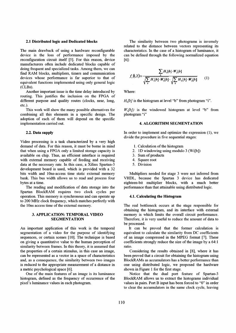
Considering the results obtained in [8], where it hasbeen proved that a circuit for obtaining the histogram usingBlockRAMs as accumulators has a better performance thanone using distributed logic, we proposed the hardwareshown in Figure 1 for the first stage.
Notice that the dual port feature of Spartan-3BlockRAM allows us to extract the histograms individualvalues in pairs. Port B input has been forced to "0" in orderto clear the accumulators in the same clock cycle, leaving
110

PA5 PB5
El E2 E3 E4 E5 E6J HO HI H2 H3 H4 H5 H6 H71~PA4 PB4 - - ==:;.:J
two memories are also used for obtaining the sum termsneeded for the correlation.
the hardware ready for processing the followingphotogram.
Several registers were inserted between output addersand at the address input of BlockRAMs in order to pipelinethe stage, so as to optimize the interface with externalmemory and double the internal clock frequency.
4.2. Calculating the windowed terms Wi[b] Fig. 2 Concurrent windowing definition
In order to reduce the influence of slight variations inimage luminance, each term of the histogram has beenreplaced with the sum of its adjacent neighbors.
Figure 2 shows how the E i windowed values aregenerated, as well as the convenience of using concurrentcalculations, due to the fact that the majority of Hi valuesare used in more than one E i calculation. Excluding the twoboundary values, each Hi value contributes to Ei-], Ei andE i +1
Figure 3 shows how the algorithm symmetry allowsthe same sum term to be used twice in calculating thewindowed value.
These two new blocks bring four 32-bits-width outputports, capable of supplying the eight necessary histogramvalues simultaneously.
Figure 4 shows the first version of this stage. Thefolded buses that appear at Port B inputs of both blocksaim at repeating some histogram values in particularpositions of the memory bank, thus solving the boundaryproblem mentioned in the above calculation.
The output summing stages were also pipelined to keepthe whole stage maximum clock frequency near 200 MHz,while the three output buses allow extracting concurrentlysix windowed values in each clock cycle.
Input ofFRAME
Output ofhistogram
16
4.3. Coupling considerations
In order to prevent the delay introduced by the nextcalculation from piling up, BlockRAMs 4 and 5 will retaindata belonging to a photogram, while the following one isbeing processed in a different memory page.The BlockRAM dual port feature allows for decouplingand behaves like another pipeline stage. The onlydifference in this case is that the retention time unit is thewhole photogram duration and not a single clock cycle.
Bearing in mind that 64 is the number of establishedhistogram levels, each one represented by a 16 bit integer,
Fig. 3 Grouping the windowed sum terms
Fig. 1 Circuit for calculating the histogram
This stage was designed to calculate six windowedvalues concurrently, starting from eight histogram valuesat the input.
The concurrence of these eight values is achieved byusing two storage BlockRAMs. As we will see later, these
the proposed structure allows to process photogramscontaining up to 65,536 pixels. Taking as a reference aphotogram of only 1600 pixels, Table 1 shows thecalculation time expressed in normalized clock cycles.
Storing and windowing were done on the previoushistogram. At the same time, the input stage builds thefollowing histogram.
111

16
Fig. 4 Circuit for calculating the windowed terms
After the first photogram is complete, the rest of thecalculations are done in parallel within the 800 clock
Input ofhistogram
16
Output ofwindowechistogram
32
cycles taken by the first stage.
Histogram calculation 800Intermediate storage 32Windowing 11
Table I Number of clock cycles per operation
4.4. Calculating the correlation and the sum
To implement this stage, we have modified the circuit ofFigure 4 in order to calculate two correlation sum termssimultaneously.Next to the windowing stage we have placed sixmultipliers followed by a matrix of a three-level adder,responsible for obtaining the correlation. The whole blockhas been pipelined using six registered stages, keeping theclock frequency near 140 MHz.
Two of the partial sums needed to calculate thesimilarity coefficient as defined by equation (1) are storedin the output. Partial terms of the denominator will bereused in the following photogram calculation; hence theyare stored to avoid repeating the calculation (see Figure 5).
P3 (192 bits) P4 (96 bits) P5 (64 bits)E (32 bits) PO (128 bits) PI (176 bits) P2 (192 bits)
F(n) F(n-l) F(n)
P6 (64 bits) S (64 bits)
F(n-l)
Lh(n-l)W(n)
Lh(n)w(n)
Output ofwindowed sum
Fig. 5 Circuit for calculating the windowed correlation (includes windowed calculation pipelined)
Note that both summing terms use the windowed term ofthe same photogram W;[b], only that while one ismultiplied by the current histogram Hi[b], the other one ismultiplied by the previous one H i-1[b]. The term W;[b] isretained during two clock cycles in the registers (shadowedin Figure 5) placed at the input of the multipliers, assuringthat in each clock cycle the right histogram corresponds
with its associated sum term.Starting from the histogramsstored in BlockRAM belonging to two photograms, thestage takes only 28 clock cycles to complete twowindowed sums.
The key of this high performance is in the concurrencyof operations, the organization of the data and the pipelinestructure.
112
It is also easy to interface this block with its neighborsdue to the fact that the input and output buses are only 32and 64 bits wide, respectively. In contrast, the internal buswidth parallelism reaches up to 192 bits in the multiplierslayer.
4.5. Square root calculation
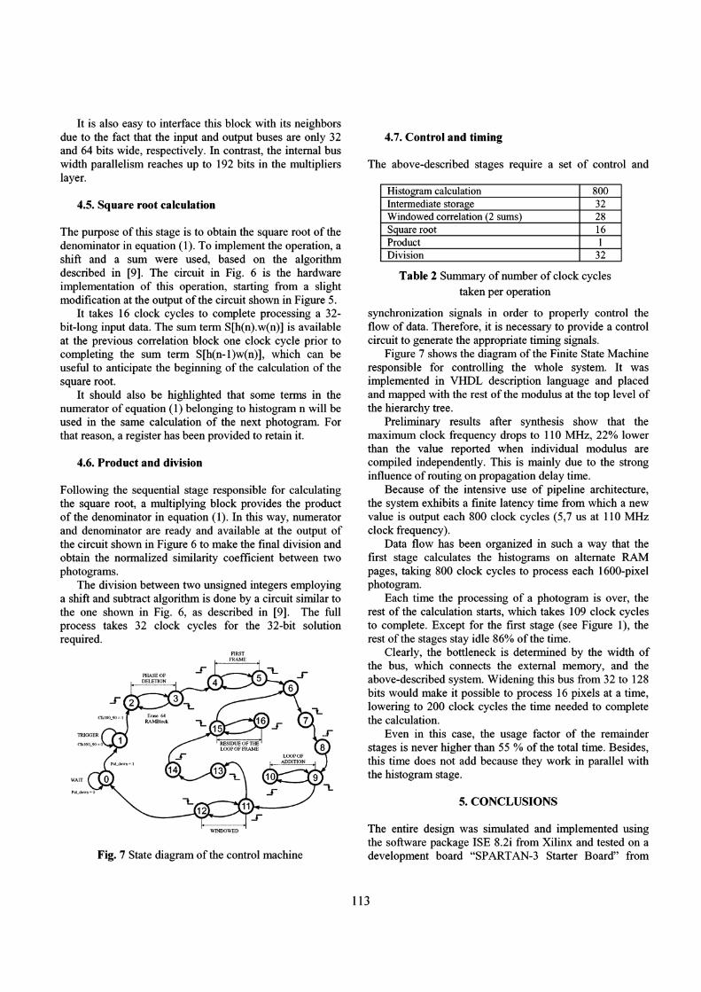
The purpose of this stage is to obtain the square root of thedenominator in equation (1). To implement the operation, ashift and a sum were used, based on the algorithmdescribed in [9]. The circuit in Fig. 6 is the hardwareimplementation of this operation, starting from a slightmodification at the output of the circuit shown in Figure 5.
It takes 16 clock cycles to complete processing a 32bit-long input data. The sum term S[h(n).w(n)] is availableat the previous correlation block one clock cycle prior tocompleting the sum term S[h(n-l)w(n)], which can beuseful to anticipate the beginning of the calculation of thesquare root.
It should also be highlighted that some terms in thenumerator of equation (1) belonging to histogram n will beused in the same calculation of the next photogram. Forthat reason, a register has been provided to retain it.
4.6. Product and division
Following the sequential stage responsible for calculatingthe square root, a multiplying block provides the productof the denominator in equation (1). In this way, numeratorand denominator are ready and available at the output ofthe circuit shown in Figure 6 to make the final division andobtain the normalized similarity coefficient between twophotograms.
The division between two unsigned integers employinga shift and subtract algorithm is done by a circuit similar tothe one shown in Fig. 6, as described in [9]. The fullprocess takes 32 clock cycles for the 32-bit solutionrequired.
FIRSTFRAME
WINDOWED
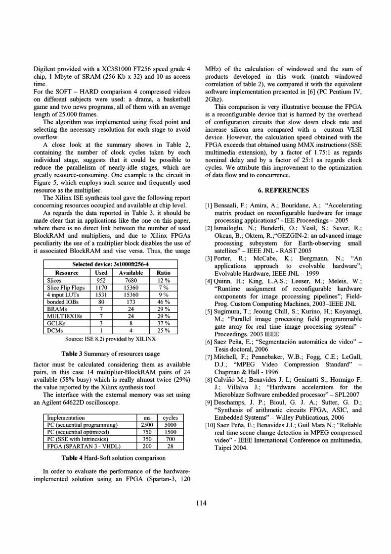
Fig. 7 State diagram of the control machine
4.7. Control and timing
The above-described stages require a set of control and
Histogram calculation 800Intermediate storage 32Windowed correlation (2 sums) 28Square root 16Product 1Division 32
Table 2 Summary of number of clock cyclestaken per operation
synchronization signals in order to properly control theflow of data. Therefore, it is necessary to provide a controlcircuit to generate the appropriate timing signals.
Figure 7 shows the diagram of the Finite State Machineresponsible for controlling the whole system. It wasimplemented in VHDL description language and placedand mapped with the rest of the modulus at the top level ofthe hierarchy tree.
Preliminary results after synthesis show that themaximum clock frequency drops to 110 MHz, 22% lowerthan the value reported when individual modulus arecompiled independently. This is mainly due to the stronginfluence of routing on propagation delay time.
Because of the intensive use of pipeline architecture,the system exhibits a finite latency time from which a newvalue is output each 800 clock cycles (5,7 us at 110 MHzclock frequency).
Data flow has been organized in such a way that thefirst stage calculates the histograms on alternate RAMpages, taking 800 clock cycles to process each 1600-pixelphotogram.
Each time the processing of a photogram is over, therest of the calculation starts, which takes 109 clock cyclesto complete. Except for the first stage (see Figure 1), therest of the stages stay idle 86% of the time.
Clearly, the bottleneck is determined by the width ofthe bus, which connects the external memory, and theabove-described system. Widening this bus from 32 to 128bits would make it possible to process 16 pixels at a time,lowering to 200 clock cycles the time needed to completethe calculation.
Even in this case, the usage factor of the remainderstages is never higher than 55 % of the total time. Besides,this time does not add because they work in parallel withthe histogram stage.
5. CONCLUSIONS
The entire design was simulated and implemented usingthe software package ISE 8.2i from Xilinx and tested on adevelopment board "SPARTAN-3 Starter Board" from
113
Digilent provided with a XC3S1000 FT256 speed grade 4chip, 1 Mbyte of SRAM (256 Kb x 32) and 10 ns accesstime.For the SOFT - HARD comparison 4 compressed videoson different subjects were used: a drama, a basketballgame and two news programs, all of them with an averagelength of25.000 frames.
The algorithm was implemented using fixed point andselecting the necessary resolution for each stage to avoidoverflow.
A close look at the summary shown in Table 2,containing the number of clock cycles taken by eachindividual stage, suggests that it could be possible toreduce the parallelism of nearly-idle stages, which aregreatly resource-consuming. One example is the circuit inFigure 5, which employs such scarce and frequently usedresource as the multiplier.
The Xilinx ISE synthesis tool gave the following reportconcerning resources occupied and available at chip level.
As regards the data reported in Table 3, it should bemade clear that in applications like the one on this paper,where there is no direct link between the number of usedBlockRAM and multipliers, and due to Xilinx FPGAspeculiarity the use of a multiplier block disables the use ofit associated BlockRAM and vise versa. Thus, the usage
Selected device: 3s1000ft256-4
Resource Used Available RatioSlices 952 7680 12 %Slice Flip Flops 1170 15360 7%4 input LUTs 1531 15360 9%bonded lOBs 80 173 46%BRAMs 7 24 29%MULT18X18s 7 24 29%GCLKs 3 8 37%DCMs 1 4 25%
Source: ISE 8.2i provided by XILINX
Table 3 Summary of resources usage
factor must be calculated considering them as availablepairs, in this case 14 multiplier-BlockRAM pairs of 24available (58% busy) which is really almost twice (29%)the value reported by the Xilinx synthesis tool.
The interface with the external memory was set usingan Agilent 64622D oscilloscope.
Implementation ms cyclesPC (sequential programming) 2500 5000PC (sequential optimized) 750 1500PC (SSE with Intrincsics) 350 700FPGA (SPARTAN 3 - VHDL) 200 28
Table 4 Hard-Soft solution comparison
In order to evaluate the performance of the hardwareimplemented solution using an FPGA (Spartan-3, 120
MHz) of the calculation of windowed and the sum ofproducts developed in this work (match windowedcorrelation of table 2), we compared it with the equivalentsoftware implementation presented in [6] (PC Pentium IV,2Ghz).
This comparison is very illustrative because the FPGAis a reconfigurable device that is harmed by the overheadof configuration circuits that slow down clock rate andincrease silicon area compared with a custom VLSIdevice. However, the calculation speed obtained with theFPGA exceeds that obtained using MMX instructions (SSEmultimedia extension), by a factor of 1.75:1 as regardsnominal delay and by a factor of 25:1 as regards clockcycles. We attribute this improvement to the optimizationof data flow and to concurrence.
6. REFERENCES
[1] Bensaali, F.; Amira, A.; Bouridane, A.; "Acceleratingmatrix product on reconfigurable hardware for imageprocessing applications" - lEE Proceedings - 2005
[2] Ismailoglu, N.; Benderli, 0.; Yesil, S.; Sever, R.;Okcan, B.; Oktem, R.;"GEZGIN-2: an advanced imageprocessing subsystem for Earth-observing smallsatellites" - IEEE JNL - RAST 2005
[3] Porter, R.; McCabe, K.; Bergmann, N.; "Anapplications approach to evolvable hardware";Evolvable Hardware, IEEE JNL - 1999
[4] Quinn, H.; King, L.A.S.; Leeser, M.; Meleis, W.;"Runtime assignment of reconfigurable hardwarecomponents for image processing pipelines"; FieldProg. Custom Computing Machines, 2003-IEEE JNL
[5] Sugimura, T.; Jeoung Chill, S.; Kurino, H.; Koyanagi,M.; "Parallel image processing field programmablegate array for real time image processing system" Proceedings. 2003 IEEE
[6] Saez Pefia, E.; "Segmentaci6n automatica de video" Tesis doctoral, 2006
[7] Mitchell, F.; Pennebaker, W.B.; Fogg, C.E.; LeGall,D.J.; "MPEG Video Compression Standard" Chapman & Hall - 1996
[8] Calvifio M.; Benavides J. I.; Geninatti S.; Hormigo F.J.; Villalva J.; "Hardware accelerators for theMicroblaze Software embedded processor" - SPL2007
[9] Deschamps, J. P.; Bioul, G. J. A.; Sutter, G. D.;"Synthesis of arithmetic circuits FPGA, ASIC, andEmbedded Systems" - Willey Publications, 2006
[10] Saez Pefia, E.; Benavides J.I.; Guil Mata N.; "Reliablereal time scene change detection in MPEG compressedvideo" - IEEE International Conference on multimedia,Taipei 2004.
114