
Competitive learning with floating-gate circuits
13
732 IEEE TRANSACTIONS ON NEURAL NETWORKS, VOL. 13, NO. 3, MAY 2002 Competitive Learning With Floating-Gate Circuits David Hsu, Miguel Figueroa, and Chris Diorio, Member, IEEE Abstract—Competitive learning is a general technique for training clustering and classification networks. We have developed an 11-transistor silicon circuit, that we term an automaximizing bump circuit, that uses silicon physics to naturally implement a similarity computation, local adaptation, simultaneous adaptation and computation and nonvolatile storage. This circuit is an ideal building block for constructing competitive-learning networks. We illustrate the adaptive nature of the automaximizing bump in two ways. First, we demonstrate a silicon competitive-learning circuit that clusters one-dimensional (1-D) data. We then illustrate a general architecture based on the automaximizing bump circuit; we show the effectiveness of this architecture, via software simu- lation, on a general clustering task. We corroborate our analysis with experimental data from circuits fabricated in a 0.35- m CMOS process. Index Terms—Analog very large scale integration (VLSI), com- petitive learning. I. INTRODUCTION C OMPETITIVE learning (Fig. 1) comprises a style of neural learning algorithms that has proved useful for training many classification and clustering networks [1]. In a competitive-learning network, a neuron’s synaptic weight vector typically represents a set of related data points. Upon re- ceiving an input, each neuron adapts, decreasing the difference between its weight vector and the input based on the following rule: (1) where is the weight vector of the th neuron, is the learning rate, is the activation of the th neuron, and is the input vector (we follow the convention that variables denoted in boldface correspond to vectors or matrices). The activation depends on the similarity between a neuron’s synaptic weights and the input and can be inhibited by other neurons; hence neu- rons compete for input data. An example of is a hard winner-take-all (WTA) [2], where if is the weight vector most similar to the input, or zero otherwise. Different kinds of inhibition lead to different learning rules. A hard WTA leads to the basic competitive learning rule where the most similar neuron updates its weight vector according to the rule (2) Manuscript received July 31, 2000. This work was supported by the NSF under Grants BES 9720353 and ECS 9733425 and by a Packard Foundation Fellowship. The authors are with the Department of Computer Science and Engineering, University of Washington, Seattle, WA 98195-2350 USA (e-mail: hsud@ cs.washington.edu; [email protected]; [email protected]). Publisher Item Identifier S 1045-9227(02)04434-X. Fig. 1. A framework for competitive learning. Each neuron computes the difference between the input vector and the values stored in its synapses. Each synapse computes the distance between its input and a stored value. The neuron aggregates its synaptic outputs and updates its synaptic weights in an unsupervised fashion. The adaptation typically decreases the difference between the neuron’s input and weight vector. Competition among neurons ensures that only neurons that are close to the input adapt. and the other neurons do not adapt. A soft WTA [3], [4] leads to an online version of maximum likelihood competitive learning [5]. Imposing topological constraints on the inhibition leads to learning rules appropriate for self-organizing feature maps [6]. These learning routines can be used to train nearest neighbor style classifiers [7], [8], adaptive vector quantizers, ART net- works [1], mixtures of experts and radial basis functions [9]. The synapses in a competitive-learning network typically follow a common adaptation dynamic, increasing the similarity between the synaptic weight vector and the present input. Consequently, a silicon synapse that exhibits this behavior can be combined with external circuitry to implement many neural learning algorithms. Very large scale integration (VLSI) implementations of com- petitive-learning synapses have been reported in the literature [10]–[13]. These synapses typically use digital or capacitive weight storage. Digital storage is expensive in terms of die area and limits the precision of synaptic weight updates. Capacitive storage requires a refresh scheme to prevent weight decay. In addition, these implementations all require separate weight-up- date and computation phases, adding complexity to the control circuitry. More importantly, neural networks built with these synapses do not typically adapt during normal operation. A no- table exception is the analog synapse designed by Fusi et al. [14], which integrates the capacitive refresh into the weight up- date dynamics. However, their synapse does not perform com- petitive learning. 1045-9227/02$17.00 © 2002 IEEE
-
Upload
independent -
Category
Documents
-
view
0 -
download
0
Transcript of Competitive learning with floating-gate circuits
732 IEEE TRANSACTIONS ON NEURAL NETWORKS, VOL. 13, NO. 3, MAY 2002
Competitive Learning With Floating-Gate CircuitsDavid Hsu, Miguel Figueroa, and Chris Diorio, Member, IEEE
Abstract—Competitive learning is a general technique fortraining clustering and classification networks. We have developedan 11-transistor silicon circuit, that we term an automaximizingbump circuit, that uses silicon physics to naturally implement asimilarity computation, local adaptation, simultaneous adaptationand computation and nonvolatile storage. This circuit is an idealbuilding block for constructing competitive-learning networks.We illustrate the adaptive nature of the automaximizing bumpin two ways. First, we demonstrate a silicon competitive-learningcircuit that clusters one-dimensional (1-D) data. We then illustratea general architecture based on the automaximizing bump circuit;we show the effectiveness of this architecture, via software simu-lation, on a general clustering task. We corroborate our analysiswith experimental data from circuits fabricated in a 0.35- mCMOS process.
Index Terms—Analog very large scale integration (VLSI), com-petitive learning.
I. INTRODUCTION
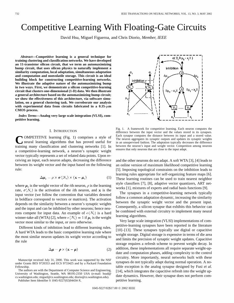
COMPETITIVE learning (Fig. 1) comprises a style ofneural learning algorithms that has proved useful for
training many classification and clustering networks [1]. Ina competitive-learning network, a neuron’s synaptic weightvector typically represents a set of related data points. Upon re-ceiving an input, each neuron adapts, decreasing the differencebetween its weight vector and the input based on the followingrule:
(1)
where is the weight vector of theth neuron, is the learningrate, is the activation of theth neuron, and is theinput vector (we follow the convention that variables denotedin boldface correspond to vectors or matrices). The activationdepends on the similarity between a neuron’s synaptic weightsand the input and can be inhibited by other neurons; hence neu-rons compete for input data. An example of is a hardwinner-take-all (WTA) [2], where if is the weightvector most similar to the input, or zero otherwise.
Different kinds of inhibition lead to different learning rules.A hard WTA leads to the basic competitive learning rule wherethe most similar neuron updates its weight vector according tothe rule
(2)
Manuscript received July 31, 2000. This work was supported by the NSFunder Grants BES 9720353 and ECS 9733425 and by a Packard FoundationFellowship.
The authors are with the Department of Computer Science and Engineering,University of Washington, Seattle, WA 98195-2350 USA (e-mail: [email protected]; [email protected]; [email protected]).
Publisher Item Identifier S 1045-9227(02)04434-X.
Fig. 1. A framework for competitive learning. Each neuron computes thedifference between the input vector and the values stored in its synapses.Each synapse computes the distance between its input and a stored value.The neuron aggregates its synaptic outputs and updates its synaptic weightsin an unsupervised fashion. The adaptation typically decreases the differencebetween the neuron’s input and weight vector. Competition among neuronsensures that only neurons that are close to the input adapt.
and the other neurons do not adapt. A soft WTA [3], [4] leads toan online version of maximum likelihood competitive learning[5]. Imposing topological constraints on the inhibition leads tolearning rules appropriate for self-organizing feature maps [6].These learning routines can be used to train nearest neighborstyle classifiers [7], [8], adaptive vector quantizers, ART net-works [1], mixtures of experts and radial basis functions [9].
The synapses in a competitive-learning network typicallyfollow a common adaptation dynamic, increasing the similaritybetween the synaptic weight vector and the present input.Consequently, a silicon synapse that exhibits this behavior canbe combined with external circuitry to implement many neurallearning algorithms.
Very large scale integration (VLSI) implementations of com-petitive-learning synapses have been reported in the literature[10]–[13]. These synapses typically use digital or capacitiveweight storage. Digital storage is expensive in terms of die areaand limits the precision of synaptic weight updates. Capacitivestorage requires a refresh scheme to prevent weight decay. Inaddition, these implementations all require separate weight-up-date and computation phases, adding complexity to the controlcircuitry. More importantly, neural networks built with thesesynapses do not typically adapt during normal operation. A no-table exception is the analog synapse designed by Fusiet al.[14], which integrates the capacitive refresh into the weight up-date dynamics. However, their synapse does not perform com-petitive learning.
1045-9227/02$17.00 © 2002 IEEE
HSU et al.: COMPETITIVE LEARNING WITH FLOATING-GATE CIRCUITS 733
Synapse transistors [15]–[18] address the problems raisedin the previous paragraph. These devices use a floating-gatetechnology similar to that found in digital EEPROMs to pro-vide nonvolatile analog storage and local adaptation in silicon.The adaptation mechanisms do not significantly perturb theoperation of the device, thus enabling simultaneous adaptationand computation. Despite these advantages, the adaptationmechanisms provide dynamics that are difficult to translateinto existing neural-network learning rules. Thus, so far, thistechnology has not been used to build competitive learningnetworks in silicon.
To avoid the difficult task of mimicking existing competitive-learning rules in silicon, we instead constructed a circuit thatnaturally exhibited competitive learning dynamics and then de-rived a learning rule directly from the physics of the componentsynapse transistors. Our 11-transistor silicon circuit, termed anautomaximizing bump circuit, computes a similarity measure,provides nonvolatile storage and local adaptation and performssimultaneous adaptation and computation. As we show in thispaper, our circuit provides the functionality we desire in a com-petitive-learning primitive.
By employing different feedback error signals to our bumpcircuit, we can develop a large class of competitive-learningnetworks in silicon. Consequently, we envision this circuit as afundamental building block for many large-scale clustering andclassification networks. As a first example, we have fabricateda circuit that clusters one-dimensional (1-D) data.
We begin this paper by reviewing synapse transistors. In Sec-tion III, we describe the automaximizing bump circuit. In Sec-tion IV, we show data from a 1-D competitive learning network,fabricated in a 0.35-m CMOS process, that learns to clusterdata drawn from a mixture of Gaussians. The network architec-ture is readily scalable to-dimensional inputs. The later sec-tions discuss issues related to this architecture and demonstrate,via software simulation, that the competitive learning rule de-rived from the bump synapses can perform effective clustering.Finally we provide some discussion and conclusions.
II. SYNAPSE TRANSISTORS
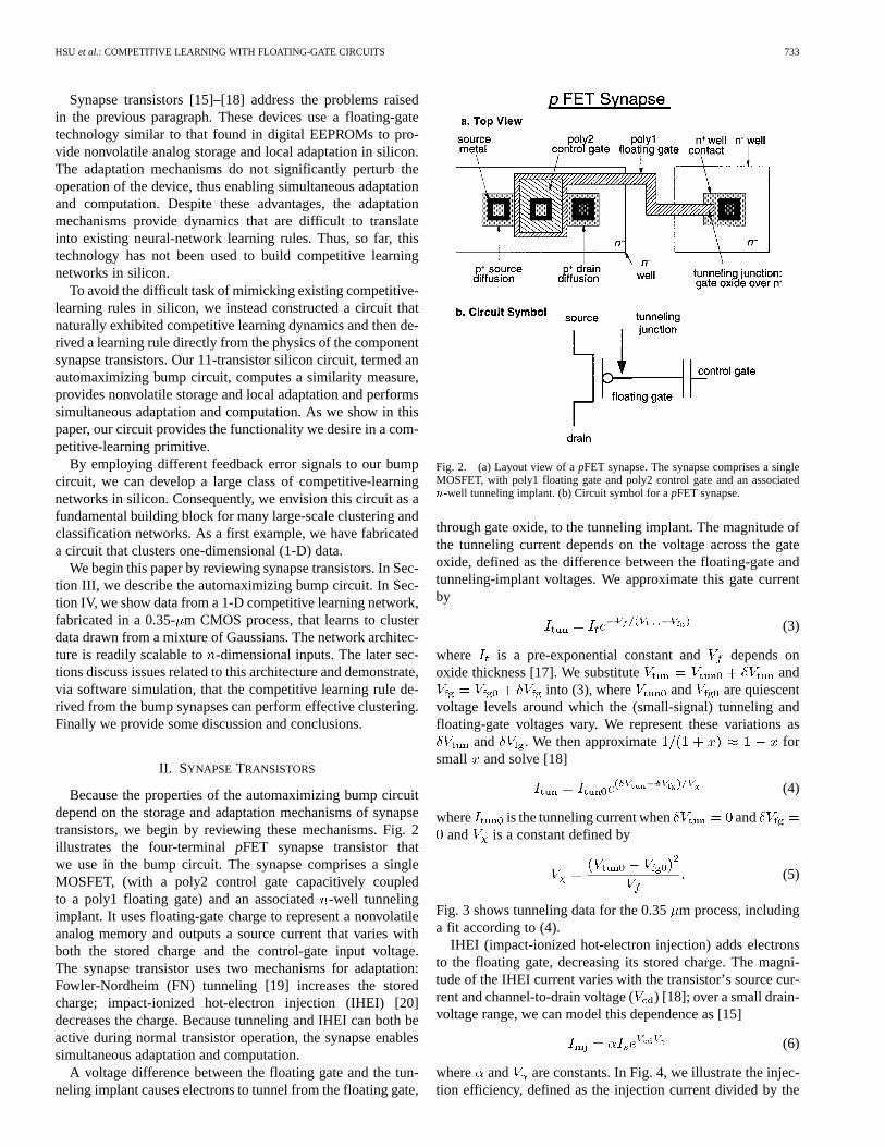
Because the properties of the automaximizing bump circuitdepend on the storage and adaptation mechanisms of synapsetransistors, we begin by reviewing these mechanisms. Fig. 2illustrates the four-terminalpFET synapse transistor thatwe use in the bump circuit. The synapse comprises a singleMOSFET, (with a poly2 control gate capacitively coupledto a poly1 floating gate) and an associated-well tunnelingimplant. It uses floating-gate charge to represent a nonvolatileanalog memory and outputs a source current that varies withboth the stored charge and the control-gate input voltage.The synapse transistor uses two mechanisms for adaptation:Fowler-Nordheim (FN) tunneling [19] increases the storedcharge; impact-ionized hot-electron injection (IHEI) [20]decreases the charge. Because tunneling and IHEI can both beactive during normal transistor operation, the synapse enablessimultaneous adaptation and computation.
A voltage difference between the floating gate and the tun-neling implant causes electrons to tunnel from the floating gate,
Fig. 2. (a) Layout view of apFET synapse. The synapse comprises a singleMOSFET, with poly1 floating gate and poly2 control gate and an associatedn-well tunneling implant. (b) Circuit symbol for apFET synapse.
through gate oxide, to the tunneling implant. The magnitude ofthe tunneling current depends on the voltage across the gateoxide, defined as the difference between the floating-gate andtunneling-implant voltages. We approximate this gate currentby
(3)
where is a pre-exponential constant and depends onoxide thickness [17]. We substitute and
into (3), where and are quiescentvoltage levels around which the (small-signal) tunneling andfloating-gate voltages vary. We represent these variations as
and . We then approximate forsmall and solve [18]
(4)
where is the tunneling current when andand is a constant defined by
(5)
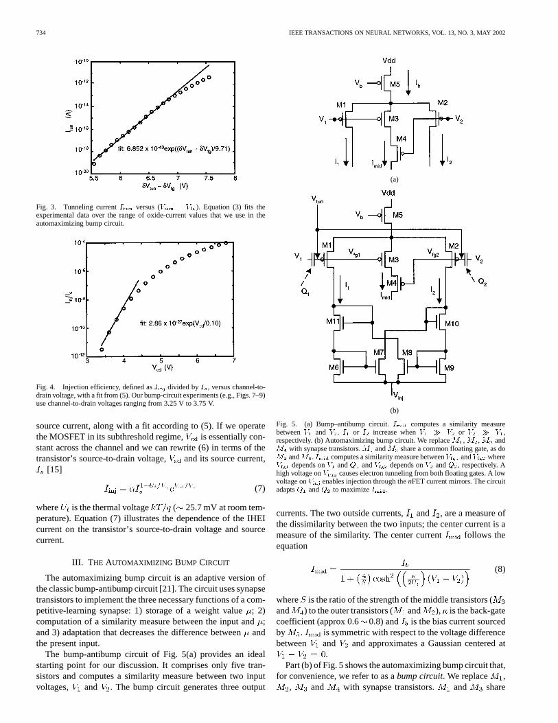
Fig. 3 shows tunneling data for the 0.35m process, includinga fit according to (4).
IHEI (impact-ionized hot-electron injection) adds electronsto the floating gate, decreasing its stored charge. The magni-tude of the IHEI current varies with the transistor’s source cur-rent and channel-to-drain voltage ( ) [18]; over a small drain-voltage range, we can model this dependence as [15]
(6)
where and are constants. In Fig. 4, we illustrate the injec-tion efficiency, defined as the injection current divided by the
734 IEEE TRANSACTIONS ON NEURAL NETWORKS, VOL. 13, NO. 3, MAY 2002
Fig. 3. Tunneling currentI versus (V � V ). Equation (3) fits theexperimental data over the range of oxide-current values that we use in theautomaximizing bump circuit.
Fig. 4. Injection efficiency, defined asI divided byI , versus channel-to-drain voltage, with a fit from (5). Our bump-circuit experiments (e.g., Figs. 7–9)use channel-to-drain voltages ranging from 3.25 V to 3.75 V.
source current, along with a fit according to (5). If we operatethe MOSFET in its subthreshold regime, is essentially con-stant across the channel and we can rewrite (6) in terms of thetransistor’s source-to-drain voltage, and its source current,
[15]
(7)
where is the thermal voltage ( 25.7 mV at room tem-perature). Equation (7) illustrates the dependence of the IHEIcurrent on the transistor’s source-to-drain voltage and sourcecurrent.
III. T HE AUTOMAXIMIZING BUMP CIRCUIT
The automaximizing bump circuit is an adaptive version ofthe classic bump-antibump circuit [21]. The circuit uses synapsetransistors to implement the three necessary functions of a com-petitive-learning synapse: 1) storage of a weight value; 2)computation of a similarity measure between the input and;and 3) adaptation that decreases the difference betweenandthe present input.
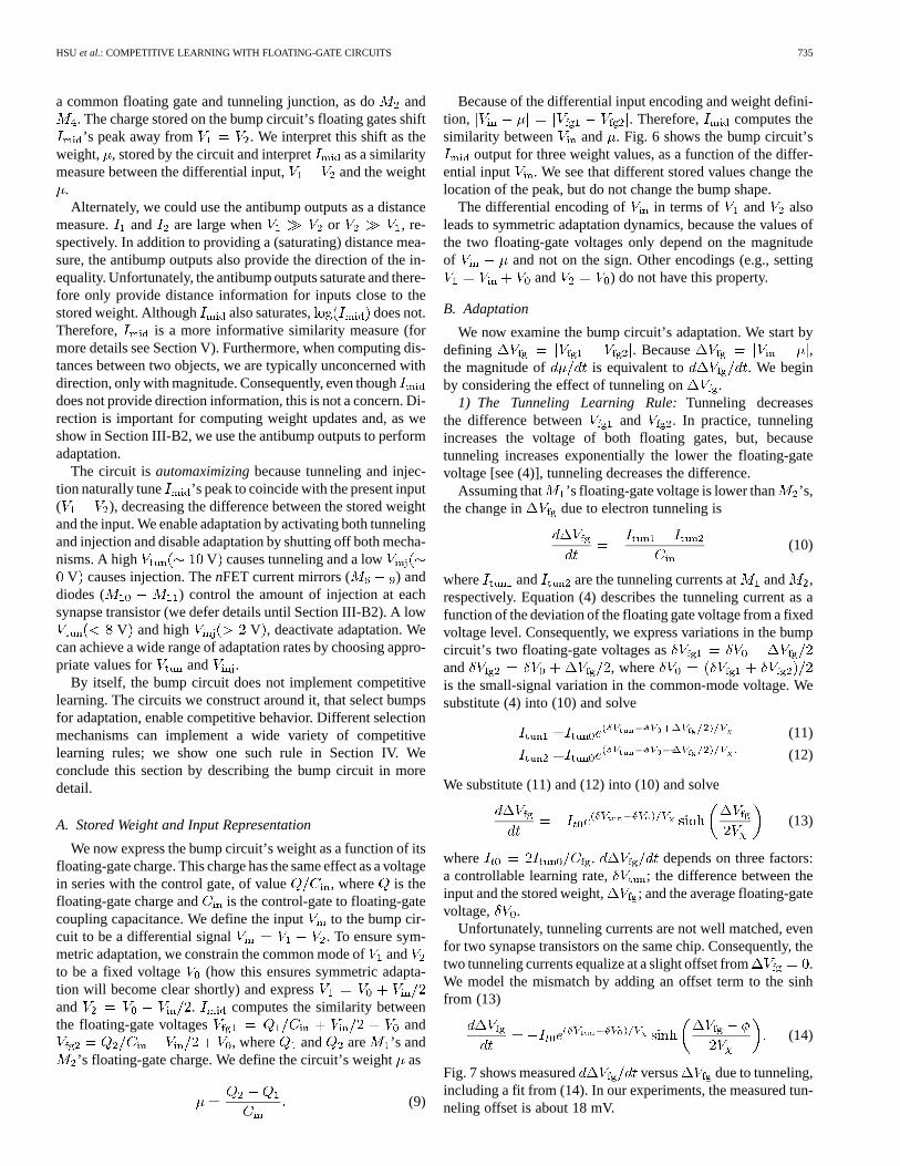
The bump-antibump circuit of Fig. 5(a) provides an idealstarting point for our discussion. It comprises only five tran-sistors and computes a similarity measure between two inputvoltages, and . The bump circuit generates three output
(a)
(b)
Fig. 5. (a) Bump–antibump circuit.I computes a similarity measurebetweenV and V . I or I increase whenV � V or V � V ,respectively. (b) Automaximizing bump circuit. We replaceM ,M , M andM with synapse transistors.M andM share a common floating gate, as doM andM . I computes a similarity measure betweenV andV whereV depends onV andQ andV depends onV andQ , respectively. Ahigh voltage onV causes electron tunneling from both floating gates. A lowvoltage onV enables injection through thenFET current mirrors. The circuitadaptsQ andQ to maximizeI .
currents. The two outside currents,and , are a measure ofthe dissimilarity between the two inputs; the center current is ameasure of the similarity. The center current follows theequation
(8)
where is the ratio of the strength of the middle transistors (and ) to the outer transistors ( and ), is the back-gatecoefficient (approx 0.6 0.8) and is the bias current sourcedby . is symmetric with respect to the voltage differencebetween and and approximates a Gaussian centered at
.Part (b) of Fig. 5 shows the automaximizing bump circuit that,
for convenience, we refer to as abump circuit. We replace ,, and with synapse transistors. and share
HSU et al.: COMPETITIVE LEARNING WITH FLOATING-GATE CIRCUITS 735
a common floating gate and tunneling junction, as do and. The charge stored on the bump circuit’s floating gates shift’s peak away from . We interpret this shift as the
weight, , stored by the circuit and interpret as a similaritymeasure between the differential input, and the weight
.Alternately, we could use the antibump outputs as a distance
measure. and are large when or , re-spectively. In addition to providing a (saturating) distance mea-sure, the antibump outputs also provide the direction of the in-equality. Unfortunately, the antibump outputs saturate and there-fore only provide distance information for inputs close to thestored weight. Although also saturates, does not.Therefore, is a more informative similarity measure (formore details see Section V). Furthermore, when computing dis-tances between two objects, we are typically unconcerned withdirection, only with magnitude. Consequently, even thoughdoes not provide direction information, this is not a concern. Di-rection is important for computing weight updates and, as weshow in Section III-B2, we use the antibump outputs to performadaptation.
The circuit isautomaximizingbecause tunneling and injec-tion naturally tune ’s peak to coincide with the present input( ), decreasing the difference between the stored weightand the input. We enable adaptation by activating both tunnelingand injection and disable adaptation by shutting off both mecha-nisms. A high V causes tunneling and a low
V causes injection. ThenFET current mirrors ( ) anddiodes ( ) control the amount of injection at eachsynapse transistor (we defer details until Section III-B2). A low
V and high V , deactivate adaptation. Wecan achieve a wide range of adaptation rates by choosing appro-priate values for and .
By itself, the bump circuit does not implement competitivelearning. The circuits we construct around it, that select bumpsfor adaptation, enable competitive behavior. Different selectionmechanisms can implement a wide variety of competitivelearning rules; we show one such rule in Section IV. Weconclude this section by describing the bump circuit in moredetail.
A. Stored Weight and Input Representation
We now express the bump circuit’s weight as a function of itsfloating-gate charge. This charge has the same effect as a voltagein series with the control gate, of value , where is thefloating-gate charge and is the control-gate to floating-gatecoupling capacitance. We define the input to the bump cir-cuit to be a differential signal . To ensure sym-metric adaptation, we constrain the common mode ofandto be a fixed voltage (how this ensures symmetric adapta-tion will become clear shortly) and expressand . computes the similarity betweenthe floating-gate voltages and
, where and are ’s and’s floating-gate charge. We define the circuit’s weightas
(9)
Because of the differential input encoding and weight defini-tion, . Therefore, computes thesimilarity between and . Fig. 6 shows the bump circuit’s
output for three weight values, as a function of the differ-ential input . We see that different stored values change thelocation of the peak, but do not change the bump shape.
The differential encoding of in terms of and alsoleads to symmetric adaptation dynamics, because the values ofthe two floating-gate voltages only depend on the magnitudeof and not on the sign. Other encodings (e.g., setting
and ) do not have this property.
B. Adaptation
We now examine the bump circuit’s adaptation. We start bydefining . Because ,the magnitude of is equivalent to . We beginby considering the effect of tunneling on .
1) The Tunneling Learning Rule:Tunneling decreasesthe difference between and . In practice, tunnelingincreases the voltage of both floating gates, but, becausetunneling increases exponentially the lower the floating-gatevoltage [see (4)], tunneling decreases the difference.
Assuming that ’s floating-gate voltage is lower than ’s,the change in due to electron tunneling is
(10)
where and are the tunneling currents at and ,respectively. Equation (4) describes the tunneling current as afunction of the deviation of the floating gate voltage from a fixedvoltage level. Consequently, we express variations in the bumpcircuit’s two floating-gate voltages asand , whereis the small-signal variation in the common-mode voltage. Wesubstitute (4) into (10) and solve
(11)
(12)
We substitute (11) and (12) into (10) and solve
(13)
where . depends on three factors:a controllable learning rate, ; the difference between theinput and the stored weight, ; and the average floating-gatevoltage, .
Unfortunately, tunneling currents are not well matched, evenfor two synapse transistors on the same chip. Consequently, thetwo tunneling currents equalize at a slight offset from .We model the mismatch by adding an offset term to the sinhfrom (13)
(14)
Fig. 7 shows measured versus due to tunneling,including a fit from (14). In our experiments, the measured tun-neling offset is about 18 mV.

736 IEEE TRANSACTIONS ON NEURAL NETWORKS, VOL. 13, NO. 3, MAY 2002
Fig. 6. Experimental measurements ofI versusV for a single auto-maximizing bump circuit, for three stored values labeled� , � and� . Thestored weight changes the location of the bump peak, but not the bump shape.
Fig. 7. Derivative of�V plotted versus�V due to electron tunneling. Wefit these data using (14). We measured the change in the location ofI ’s peakdue to a short tunneling pulse when the floating gates were�V apart. Differentvalues for�V merely change the magnitude of adaptation, not the generalshape. We followed the same measurement procedure for the experiments ofFigs. 8 and 9.
2) The Injection Learning Rule:IHEI decreases the differ-ence between and . We bias the circuit so that onlyand experience IHEI. From (7), we see that IHEI varies sub-linearly with the transistor’s source current, but exponentiallywith its source-to-drain voltage. Consequently, we decrease
by controlling the drain voltages of and .We use cross-coupled current mirrors ( and
) at the drains of and , to raise the drainvoltage of the floating-gate transistor that is sourcing a largercurrent and to lower the drain voltage of the floating-gatetransistor that is sourcing a smaller current. The transistor withthe smaller source current experiences a largerand thusexponentially more IHEI, causing its source current to rapidlyincrease. Diodes ( ) raise the drain voltage ofthe transistor with the larger current yet further. The net effectis that IHEI equalizes the source currents of the floating-gatetransistors and, likewise, their floating-gate voltages. Negativefeedback from the cross-coupled current mirrors is necessaryfor the automaximizing behavior; circuits that do not incor-porate such feedback exhibit runaway IHEI [18]. Appendix Aprovides a small-signal stability analysis of this feedback.
To see this behavior more clearly, let us first examine the casewhere the two floating-gate voltages are equal. Ifand are
equal, then the drain voltages of and will likewise beequal. If we set low enough to cause injection, both tran-sistors will inject at the same rate, because their source currentsand drain voltages will be the same. Therefore, injection doesnot change . In addition, because transistors andhave the same gate voltage,will split evenly at the drain of
. The same is true for at the drain of .Now consider the case where is lower than. now tries to sink a current that is larger than . Con-
sequently, sink less than , causing ’s drainvoltage to fall and, in turn, decreasing the current thatsinks.This further increases the amount of current that flows through
. The positive feedback process causesto sink all ofand and to sink all of . As a result, ’s drain voltagedrops to and ’s drain voltage rises to
. This process will exhibit hysteresis if the gain of either cur-rent mirror exceeds unity (see Appendix A).
The weight change for injection follows a similar form to thatof tunneling
(15)
The final IHEI weight update rule follows by substituting theexpressions for and from (7) into (15). To determinevalues for the drain voltages of and , we assume that allof flows through and all of flows through . We de-rive the update rule from a large-signal analysis in Appendix B.The final form is
(16)where , , and
. is the transistor’s pre-exponential current. Thetwo functions, and , are
(17)
(18)
where ,and is
(19)
Like tunneling, due to IHEI depends on three fac-tors: A controllable learning rate, ; the difference betweenthe stored weight and the input, ; and .
Fig. 8 shows experimental measurements of versusdue to IHEI, along with a fit from (16). As increases,
the weight-update magnitude reaches its peak between 0.1 Vand 0.2 V and then decreases afterwards. The increase in mag-nitude between 0 V and 0.14 V occurs because the differencebetween the drain voltages of and increases asincreases. At , the difference between ’s and
’s drain voltages has reached its maximum value; therefore,further increasing only causes the source current for the
HSU et al.: COMPETITIVE LEARNING WITH FLOATING-GATE CIRCUITS 737
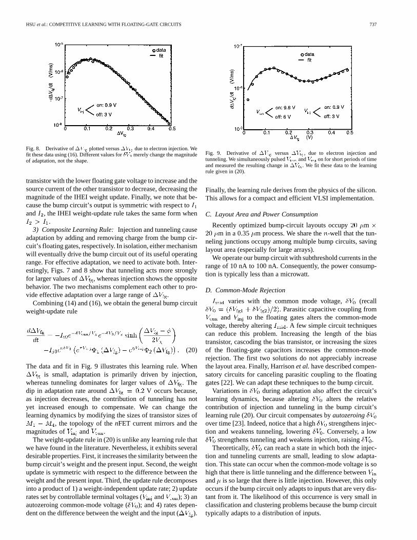
Fig. 8. Derivative of�V plotted versus�V due to electron injection. Wefit these data using (16). Different values for�V merely change the magnitudeof adaptation, not the shape.
transistor with the lower floating gate voltage to increase and thesource current of the other transistor to decrease, decreasing themagnitude of the IHEI weight update. Finally, we note that be-cause the bump circuit’s output is symmetric with respect toand , the IHEI weight-update rule takes the same form when
.3) Composite Learning Rule:Injection and tunneling cause
adaptation by adding and removing charge from the bump cir-cuit’s floating gates, respectively. In isolation, either mechanismwill eventually drive the bump circuit out of its useful operatingrange. For effective adaptation, we need to activate both. Inter-estingly, Figs. 7 and 8 show that tunneling acts more stronglyfor larger values of , whereas injection shows the oppositebehavior. The two mechanisms complement each other to pro-vide effective adaptation over a large range of .
Combining (14) and (16), we obtain the general bump circuitweight-update rule
(20)
The data and fit in Fig. 9 illustrates this learning rule. Whenis small, adaptation is primarily driven by injection,
whereas tunneling dominates for larger values of . Thedip in adaptation rate around V occurs because,as injection decreases, the contribution of tunneling has notyet increased enough to compensate. We can change thelearning dynamics by modifying the sizes of transistor sizes of
, the topology of thenFET current mirrors and themagnitudes of and .
The weight-update rule in (20) is unlike any learning rule thatwe have found in the literature. Nevertheless, it exhibits severaldesirable properties. First, it increases the similarity between thebump circuit’s weight and the present input. Second, the weightupdate is symmetric with respect to the difference between theweight and the present input. Third, the update rule decomposesinto a product of 1) a weight-independent update rate; 2) updaterates set by controllable terminal voltages ( and ); 3) anautozeroing common-mode voltage ( ); and 4) rates depen-dent on the difference between the weight and the input ().
Fig. 9. Derivative of�V versus�V , due to electron injection andtunneling. We simultaneously pulsedV andV on for short periods of timeand measured the resulting change in�V . We fit these data to the learningrule given in (20).
Finally, the learning rule derives from the physics of the silicon.This allows for a compact and efficient VLSI implementation.
C. Layout Area and Power Consumption
Recently optimized bump-circuit layouts occupy mm in a 0.35 m process. We share the-well that the tun-
neling junctions occupy among multiple bump circuits, savinglayout area (especially for large arrays).
We operate our bump circuit with subthreshold currents in therange of 10 nA to 100 nA. Consequently, the power consump-tion is typically less than a microwatt.
D. Common-Mode Rejection
varies with the common mode voltage, (recall. Parasitic capacitive coupling from
and to the floating gates alters the common-modevoltage, thereby altering . A few simple circuit techniquescan reduce this problem. Increasing the length of the biastransistor, cascoding the bias transistor, or increasing the sizesof the floating-gate capacitors increases the common-moderejection. The first two solutions do not appreciably increasethe layout area. Finally, Harrisonet al.have described compen-satory circuits for canceling parasitic coupling to the floatinggates [22]. We can adapt these techniques to the bump circuit.
Variations in during adaptation also affect the circuit’slearning dynamics, because altering alters the relativecontribution of injection and tunneling in the bump circuit’slearning rule (20). Our circuit compensates byautozeroingover time [23]. Indeed, notice that a high strengthens injec-tion and weakens tunneling, lowering . Conversely, a low
strengthens tunneling and weakens injection, raising.Theoretically, can reach a state in which both the injec-
tion and tunneling currents are small, leading to slow adapta-tion. This state can occur when the common-mode voltage is sohigh that there is little tunneling and the difference betweenand is so large that there is little injection. However, this onlyoccurs if the bump circuit only adapts to inputs that are very dis-tant from it. The likelihood of this occurrence is very small inclassification and clustering problems because the bump circuittypically adapts to a distribution of inputs.
738 IEEE TRANSACTIONS ON NEURAL NETWORKS, VOL. 13, NO. 3, MAY 2002
Fig. 10. A CLC, comprising two bump circuits, a WTA and feedback circuitrythat derive localV andV signals from the WTA output.
IV. COMPETITIVE LEARNING CIRCUIT
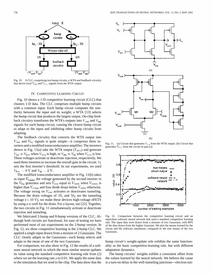
Fig. 10 shows a 1-D competitive learning circuit (CLC) thatclusters 1-D data. The CLC comprises multiple bump circuitswith a common input. Each bump circuit computes the sim-ilarity between the input and its weight; a WTA [13] selectsthe bump circuit that produces the largest output. On-chip feed-back circuitry transforms the WTA’s outputs into andsignals for each bump circuit, causing the closest bump circuitto adapt to the input and inhibiting other bump circuits fromadapting.
The feedback circuitry that converts the WTA output intoand signals is quite simple—it comprises three in-
verters and a modified transconductance amplifier. The invertersshown in Fig. 11(a) take the WTA output ( ) and generate
when is high, or when is low.These voltages activate or deactivate injection, respectively. Weused three inverters to increase the overall gain in the circuit.sets the first inverter’s threshold. In our experiments, we used
V and V.The modified transconductance amplifier in Fig. 11(b) takes
as input , the voltage generated by the second inverter inthe generator and sets equal to when ishigher than and four diode drops below otherwise.The voltage swing on activates or deactivates tunneling.Because the drain voltages of and are the tunnelingvoltage ( 10 V), we make these devices high-voltagenFETSby using a -well for the drain. For a layout, see [22]. Together,the two circuits in Fig. 11 simultaneously activate or deactivateinjection and tunneling.
We fabricated 2-bump and 8-bump versions of the CLC. Al-though both circuits are functional, for ease of testing we haveperformed most of our experiments on the 2-bump version. InFig. 12, we show competitive learning in the 2-bump CLC. Weapplied a single input drawn from a mixture of 2 Gaussians. TheCLC clearly adapts to the Gaussians—each bump selects andadapts to the mean of one of the two Gaussians.
For comparison, we also show in Fig. 12 the results of a soft-ware neural network in which the most similar neuron updatesits value using the standard competitive learning rule from (2)where we set the learning rateto 0.01. We apply the same datato the simulation that we send to the chip. The data show that the
(a)
(b)
Fig. 11. (a) Circuit that generatesV from the WTA output. (b) Circuit thatgeneratesV from the circuit in part (a).
Fig. 12. Comparison between the competitive learning circuit and anequivalent software neural network that used a standard competitive learningrule. The input data were drawn from a mixture of two Gaussians, with 80%of the data drawn from the higher Gaussian. We plot the means learned by thecircuit and the software simulation, compared to the true means of the twoGaussians.
bump circuit’s weight-update rule exhibits the same function-ality as the basic competitive-learning rule, but with differentadaptation dynamics.
The bump circuits’ weights exhibit a consistent offset fromthe values learned by the neural network. We believe the causeis a turn-on delay in the well-tunneling junctions—electron tun-

HSU et al.: COMPETITIVE LEARNING WITH FLOATING-GATE CIRCUITS 739
neling does not actually occur until several secondsafter weraise the tunneling voltage. We have observed a similar effectpreviously (see [17]: the section on bowl-shaped tunneling junc-tions), although not in the tunneling junction that we show inFig. 2 ( in well). If the latency between the two synapsesin a bump circuit differs, the weight may drift away from theinput; only when both tunneling junctions finally turn on doesthe weight adapt toward the input. The tunneling latency mayalso explain why one bump circuit adapts so quickly to one ofthe true means, while the other bump circuit exhibits sloweradaptation. Each bump circuit, because of the latency, may bestrongly biased toward adaptation in one direction. We have de-veloped an alternative tunneling junction that tunnels overrather than over ; in experiments on isolated tunneling junc-tions, the revised design does not exhibit a turn-on delay. We arecurrently incorporating the revised design in future versions ofthe automaximizing bump circuit.
Although both the software neural network and the CLC driftabout the true Gaussian centers, the CLC shows fluctuationsof greater magnitude. We believe the reason is that the CLCslearning rate is greater than the software neural network’slearning rate Unfortunately, because the CLC operates com-pletely asynchronously, it is hard to quantify the learning ratethat the circuit uses.
Our competitive learning architecture can be scaled to-dimensional inputs and any number of neurons. Each neuron
requires one bump circuit per synapse. Most important, eachneuron requires only one feedback block, because all thesynapses receive the same and . We illustrate theapproach in Fig. 13. Each bump circuit corresponds to asynapse of a neuron; the WTA from Fig. 10 is an example ofan inhibitory circuit; and the circuits of Fig. 11 are examplesof feedback circuits.
V. NEURON DESIGN
Because a bump circuit computes a similarity measure, themethod we should use to combine bump outputs is not obvious.The bump circuit output is a current; since addition of currentsis particularly easy to implement in analog VLSI, we might sur-mise that addition is the correct way to combine bump outputs.In fact, in at least one previous hardware neural network, withsynapses that compute a similarity measure, the neurons addthese similarity measures [24]. However, the way we combinebump similarities implicitly defines a distance measure. If wewant to approximate some natural distance measures like Man-hattan distance or squared distance1 in our network, then wewill show that multiplication provides a more sensible way tocombine bump similarities.
Intuitively, the bump circuit’s similarity measure approxi-mates the probability that an inputwas generated by a 1-DGaussian (with mean and variance ), wherecorresponds to the bump circuit’s stored weight
(21)
1For two vectorsx andy, the Manhattan distance is� jx � y j and thesquared distance is� (x � y ) .
Fig. 13. Generalized competitive learning architecture.
Fig. 14. Comparison of the bump distance measure to Manhattan and squareddistance. Distances are scaled to facilitate a comparison.
Fig. 15. Circuit that multiplies the output of two bump circuits. Each diodetransforms its input current (I or I ) into a voltage that is logarithmic with thecurrent. ThenFET on the right is a floating-gate transistor with two controlgates; one for each diode voltage. If the floating gatenFET is biased in itssubthreshold regime, its output current will be proportional to the product ofthe two bump-circuit currents.
A Gaussian is an exponential function of the squared Eu-clidean distance between inputand mean . Consequently,multiplying a set of Gaussian similarities is equivalent to addingthe corresponding Euclidean distances. Conversely, addingGaussian similarities does not correspond to any sensible
740 IEEE TRANSACTIONS ON NEURAL NETWORKS, VOL. 13, NO. 3, MAY 2002
(a) (b)
(c) (d)
Fig. 16. Comparison of the standard competitive learning rule (+), bump-learning rule (o) and optimal solution (�) for learning the means of a mixture ofGaussians where each Gaussian had a diagonal covariance matrix and the standard deviation of each dimension was (a) 0.1 V, (b) 0.2 V, (c) 0.3 V, and (d) 0.4 V.
operation on Euclidean distance. Consequently, we believe thatthe correct way to combine similarities that have a Gaussianshape is through multiplication.
We express as a negative exponential of a distance func-tion (similar to a Gaussian), by rewriting (8) as follows:
(22)
where . is given by
(23)
Fig. 14 compares this function with Manhattan distance andsquared distance. looks like squared distance when the inputand bump weight are similar and like Manhattan distance whenthe two values are dissimilar. In contrast, there is no obviousway to extract a distance function from the addition of bumpsimilarities.
Finally, we consider the qualitative behavior of adding bumpsimilarities versus multiplying bump similarities. Becausehas a Gaussian-like shape, it only provides an informativedistance measure for inputs close to the weight. However,
provides an informative distance measure for anydistance between the input and.
Fig. 15 illustrates one way to implement a multiplying neuronfor our competitive-learning architecture. We use a subthreshold
floating-gate MOSFET to multiply the currents from two bumpcircuits. We capacitively couple a floating gate to diode volt-ages derived from the bump-circuit currents. The MOSFET con-nected to this floating-gate implements a translinear multiply[25]. This approach requires an extra diode and capacitor foreach bump.
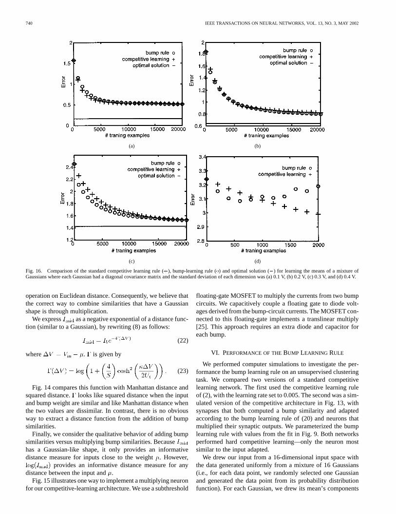
VI. PERFORMANCE OF THEBUMP LEARNING RULE
We performed computer simulations to investigate the per-formance the bump learning rule on an unsupervised clusteringtask. We compared two versions of a standard competitivelearning network. The first used the competitive learning ruleof (2), with the learning rate set to 0.005. The second was a sim-ulated version of the competitive architecture in Fig. 13, withsynapses that both computed a bump similarity and adaptedaccording to the bump learning rule of (20) and neurons thatmultiplied their synaptic outputs. We parameterized the bumplearning rule with values from the fit in Fig. 9. Both networksperformed hard competitive learning—only the neuron mostsimilar to the input adapted.
We drew our input from a 16-dimensional input space withthe data generated uniformly from a mixture of 16 Gaussians(i.e., for each data point, we randomly selected one Gaussianand generated the data point from its probability distributionfunction). For each Gaussian, we drew its mean’s components
HSU et al.: COMPETITIVE LEARNING WITH FLOATING-GATE CIRCUITS 741
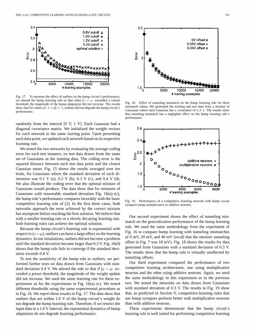
Fig. 17. To measure the effect of outliers on the bump circuit’s performance,we altered the bump learning rule so that whenjx � �j exceeded a certainthreshold, the magnitude of the bump adaptation did not increase. The resultsshow that for values ofjx��j < 1, outliers did not degrade the bump circuit’sperformance.
randomly from the interval [0 V, 1 V]. Each Gaussian had adiagonal covariance matrix. We initialized the weight vectorsfor each network to the same starting point. Upon presentingeach data point, we updated each network based on its respectivelearning rule.
We tested the two networks by evaluating the average codingerror for each test instance, on test data drawn from the sameset of Gaussians as the training data. The coding error is thesquared distance between each test data point and the closestGaussian mean. Fig. 15 shows the results averaged over tentrials, for Gaussians where the standard deviation of each di-mension was 0.1 V (a), 0.2 V (b), 0.3 V (c), and 0.4 V (d).We also illustrate the coding error that the optimal mixture ofGaussians would produce. The data show that for mixtures ofGaussians with reasonable standard deviation Fig. 16(a)–(c),the bump rule’s performance compares favorably with the basiccompetitive learning rule of (2). In the first three cases, bothnetworks approach the error achieved by the correct mixturebut asymptote before reaching the best solution. We believe thatwith a smaller learning rate or a slowly decaying learning rate,both learning rules can achieve the optimal solution.
Because the bump circuit’s learning rule is exponential withrespect to ( ), outliers can have a large effect on the learningdynamics. In our simulations, outliers did not become a problemuntil the standard deviation became larger than 0.3 V. Fig. 16(d)shows that the bump rule fails to converge if the standard devi-ation exceeds 0.4 V.
To test the sensitivity of the bump rule to outliers, we per-formed further tests on data drawn from Gaussians with stan-dard deviation 0.4 V. We altered the rule so that if ex-ceeded a preset threshold, the magnitude of the weight updatedid not increase. We used the same learning rate for these ex-periments as for the experiments in Fig. 16(a)–(c). We testeddifferent thresholds using the same experimental procedure asin Fig. 16. We report these results in Fig. 17. The data show thatoutliers that are within 1.0 V of the bump circuit’s weight donot degrade the bump learning rule. Therefore, if we restrict theinput data to a 1.0 V interval, the exponential dynamics of bumpadaptation do not degrade learning performance.
Fig. 18. Effect of tunneling mismatch on the bump learning rule for threemismatch values. We generated the training and test data from a mixture ofGaussians where each Gaussian has a covariance of0:3 I . The results showthat tunneling mismatch has a negligible effect on the bump learning rule’sperformance.
Fig. 19. Performance of a competitive learning network with bump circuitsynapses using multiplicative or additive neurons.
Our second experiment shows the effect of tunneling mis-match on the generalization performance of the bump learningrule. We used the same methodology from the experiment ofFig. 16 to compare bump learning with tunneling mismatchesof 0 mV, 20 mV, and 40 mV (recall that the intrinsic tunnelingoffset in Fig. 7 was 18 mV). Fig. 18 shows the results for datagenerated from Gaussians with a standard deviation of 0.3 V.The results show that the bump rule is virtually unaffected bytunneling offsets.
Our third experiment compared the performance of twocompetitive learning architectures, one using multiplicativeneurons and the other using additive neurons. Again, we usedthe same methodology in this experiment as in the previoustwo. We tested the networks on data drawn from Gaussianswith standard deviation of 0.3 V. The results in Fig. 19 showthat, as predicted in Section V, competitive-learning rules thatuse bump synapses perform better with multiplicative neuronsthan with additive neurons.
These experiments demonstrate that the bump circuit’slearning rule is well suited for performing competitive learning
742 IEEE TRANSACTIONS ON NEURAL NETWORKS, VOL. 13, NO. 3, MAY 2002
in silicon. In addition, the asymmetry due to tunneling mis-match does not greatly affect the performance of the learningrule.
VII. CONCLUSION
We have demonstrated an 11-transistor circuit primitive thatincorporates a similarity function, nonvolatile storage and localadaptation; we can use this circuit in analog VLSI implemen-tations of competitive learning. This circuit leverages synapsetransistors to afford nonvolatile storage and to perform simul-taneous adaptation and computation. The circuit’s learning ruleoriginates from the physics of the synapse transistors; conse-quently, it is unlike any rule that we know of in the literature.Even so, the learning rule provides the correct dynamics forcompetitive learning and exhibits symmetric adaptation. Moreimportantly, software simulations show that the learning rule isas effective as the traditional competitive learning rule for clus-tering data drawn from a mixture of Gaussians.
To test our circuit primitive, we used it in a competitivelearning circuit that clustered 1-D data. The circuit learned todiscriminate data drawn from a mixture of Gaussians, providingevidence that this learning rule, while natural to the physics ofour devices, is also useful in a learning context. This circuit isreadily extensible to -dimensional inputs and any number ofneurons. We intend to use this circuit primitive and variationsof the competitive learning architecture as building blocks forsilicon chips that perform clustering and classification tasks.
APPENDIX I
The sizing of current-mirror transistors determineswhether injection increases or decreases the similarity betweenthe floating-gate voltages of transistors and in Fig. 5. Weperformed a small-signal analysis of injection in and , todetermine sizing constraints on that ensure injectionwill increase the similarity. Fig. 20 shows a small-signal model.We study the change in injection due to a small increasein
’s source current (and the symmetric decreasein ’ssource current). The values for the circuit elements in Fig. 20are
(24)
(25)
(26)
(27)
(28)
where is the equilibrium current in diodes and , isthe current-mirror gain, is the Early voltage and andare the drain voltages of floating-gate transistors and ,
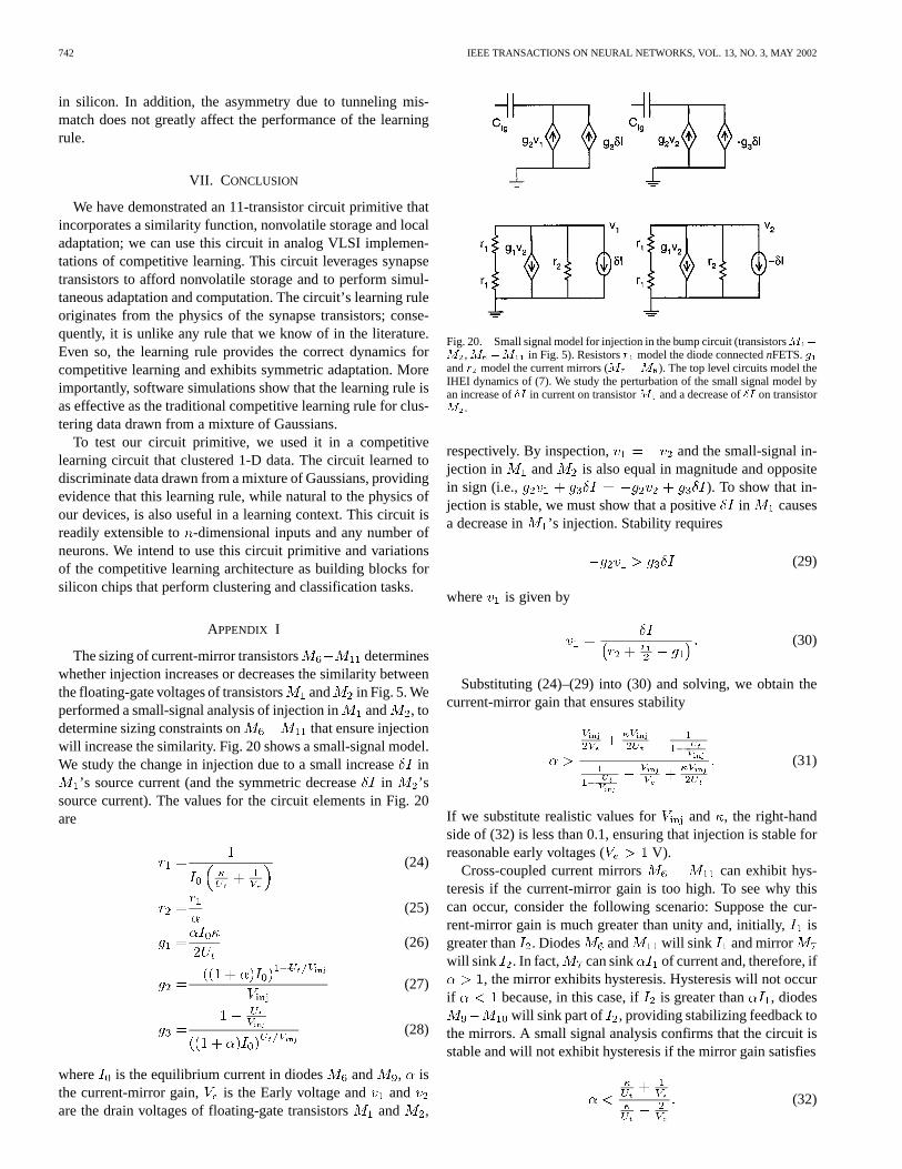
Fig. 20. Small signal model for injection in the bump circuit (transistorsM �
M ,M �M in Fig. 5). Resistorsr model the diode connectednFETS.gandr model the current mirrors (M �M ). The top level circuits model theIHEI dynamics of (7). We study the perturbation of the small signal model byan increase of�I in current on transistorM and a decrease of�I on transistorM .
respectively. By inspection, and the small-signal in-jection in and is also equal in magnitude and oppositein sign (i.e., ). To show that in-jection is stable, we must show that a positivein causesa decrease in ’s injection. Stability requires
(29)
where is given by
(30)
Substituting (24)–(29) into (30) and solving, we obtain thecurrent-mirror gain that ensures stability
(31)
If we substitute realistic values for and , the right-handside of (32) is less than 0.1, ensuring that injection is stable forreasonable early voltages ( V).
Cross-coupled current mirrors can exhibit hys-teresis if the current-mirror gain is too high. To see why thiscan occur, consider the following scenario: Suppose the cur-rent-mirror gain is much greater than unity and, initially,isgreater than . Diodes and will sink and mirrorwill sink . In fact, can sink of current and, therefore, if
, the mirror exhibits hysteresis. Hysteresis will not occurif because, in this case, if is greater than , diodes
will sink part of , providing stabilizing feedback tothe mirrors. A small signal analysis confirms that the circuit isstable and will not exhibit hysteresis if the mirror gain satisfies
(32)
HSU et al.: COMPETITIVE LEARNING WITH FLOATING-GATE CIRCUITS 743
APPENDIX II
We use a large-signal analysis to derive the bump circuit’sIHEI weight-update rule. To begin, assume that sourcesmore current than (the analysis is symmetric forsourcing more current than ). due to IHEI derivesfrom the difference between the injection currents in transistors
and [see (11)]. We obtain the injection currents bysubstituting (7) into (15) and solving for the 1) source currents;2) source voltages; and 3) drain voltages of and .
A. Source Current
To derive for and , recall that transistors andform a differential pair on that fraction of that is not part
of . and in terms of are
(33)
(34)
where is
(35)
B. Source Voltage
and share their source node, so is the same forboth. We can calculate by equating (33) and (34) with theequivalent subthreshold expressions for a transistor’s sourcecurrent in terms of its source and gate voltages. We solve for
, [see (7)]
(36)
C. Drain Voltage
We solve for the drain voltages of and separately. Wemake the approximation that all of flows through and
and all of flows through . Therefore, to solve forand (the drain voltages of and , respectively),
we equate (33) and (34) with the equivalent subthreshold ex-pressions for annFETs source current in terms of its gate andsource voltages. The current in and are
(37)
We solve for by equating (33) and (37)
(38)
We solve for using the following relationship:
(39)
We substitute into (39)
(40)
Solving for from (40) we obtain
(41)
Substituting (36), (38) and (41) into (7), we obtain
(42)
(43)
where , )and . Substituting (38) and (39) into (15), we obtain(16)–(18)
(44)where , and
. The two functions, and are
(45)
(46)
This result is the bump circuit’s weight-update rule (due to in-jection) shown in (16).
ACKNOWLEDGMENT
The authors would like to thank J. Nichols for help withlayout and A. Doan, K. Partridge, M. Richardson, P. Tressel,A. Schon, and E. Vee for their suggestions and constructivecriticism. Finally, the authors thank J. Dugger for initialdiscussions that led to this research.
REFERENCES
[1] M. A. Arbib, The Handbook of Brain Theory and Neural Networks, M.A. Arbib, Ed. Cambridge, MA: MIT Press, 1995.
[2] J. Lazzaro, S. Ryckebusch, M. A. Mahowald, and C. A. Mead, “Winner-take-all networks ofO(n) complexity,” inAdvances in Neural Informa-tion Processing Systems. San Mateo, CA: Morgan Kauffman, 1989,vol. 1, pp. 703–711.
[3] I. M. Elfadel and J. L. Wyatt Jr., “The softmax nonlinearity: Derivationusing statistical mechanics and useful properties as a multiterminalanalog circuit element,” inAdvances in Neural Information ProcessingSystems. San Mateo, CA: Morgan Kaufmann, 1994, vol. 6, pp.882–887.
[4] S.-C. Liu, “A winner-take-all circuit with controllable soft maxproperty,” in Advances in Neural Information Processing Systems, S.A. Solla, T. K. Leen, and K. R. Muller, Eds. Cambridge, MA: MITPress, 2000, vol. 12, pp. 717–723.
[5] S. J. Nowlan, “Maximum likelihood competitive learning,” inAdvancesin Neural Information Processing Systems. San Mateo, CA: MorganKauffman, 1990, vol. 2, pp. 574–582.
[6] T. Kohonen,Self Organizing Feature Maps, 2nd ed. Berlin, Germany:Springer-Verlag, 1997.
[7] R. O. Duda and P. E. Hart,Pattern Classification and Scene Anal-ysis. New York: Wiley, 1973.
[8] R. Coleet al., Survey of the State of the Art in Human Language Tech-nology, R. Coleet al., Eds. Cambridge, U.K.: Cambridge Univ. Press,1998.
[9] C. M. Bishop, Neural Networks for Pattern Recognition. Oxford,U.K.: Clarendon, 1995.
744 IEEE TRANSACTIONS ON NEURAL NETWORKS, VOL. 13, NO. 3, MAY 2002
[10] H. C. Card, D. K. McNeill, and C. R. Schneider, “Analog VLSI cir-cuits for competitive learning networks,”Analog Integrated Circuits andSignal Processing, vol. 15, pp. 291–314, 1998.
[11] J. Lubkin and G. Cauwenberghs, “A learning parallel analog-to-digitalvector quantizer,”IEEE J. Circuits, Syst., Comput., vol. 8, pp. 604–614,1998.
[12] D. Macq, M. Verleysen, P. Jespers, and J. D. Legat, “Analog implemen-tation of a Kohonen map with on-chip learning,”IEEE Trans. NeuralNetworks, vol. 4, pp. 456–461, May 1993.
[13] Y. He and U. Cilingiroglu, “A charge-based on-chip adaptation Kohonenneural network,”IEEE Trans. Neural Networks, vol. 4, pp. 462–469,May 1993.
[14] S. Fusi, M. Annunziato, D. Badoni, A. Salamon, and D. J. Amit, “Spike-driven synaptic plasticity: Theory, simulation, VLSI implementation,”Neural Comput., 2000.
[15] C. Diorio, “A p-Channel MOS synapse transistor with self-convergentmemory writes,”IEEE Trans. Electron Devices, vol. 47, 2000.
[16] C. Diorio, P. Hasler, B. A. Minch, and C. Mead, “A complementarypair of four-terminal silicon synapses,”Analog Integrated Circuits andSignal Processing, vol. 13, no. 1/2, pp. 153–166, 1997.
[17] C. Diorio, “Neurally Inspired Silicon Learning: From Synapse Transis-tors to Learning Arrays,” Ph.D. dissertation, California Inst. Technol.,Pasadena, 1997.
[18] P. Hasler, “Foundations of Learning in Analog VLSI,” Ph.D. disserta-tion, California Inst. Technol., Pasadena, 1997.
[19] M. Lenzlinger and E. H. Snow, “Fowler-Nordheim tunneling into ther-mally grown SiO ,” J. Appl. Phys., vol. 40, no. 1, pp. 278–283, 1969.
[20] E. Takeda, C. Yang, and A. Miura-Hamada,Hot Carrier Effects in MOSDevices. San Diego, CA: Academic, 1995.
[21] T. Delbruck, “Bump Circuits for Computing Similarity and Dissimilarityof Analog Voltages,” California Inst. Technol., Pasadena, CNS Memo26, 1993.
[22] R. R. Harrison, J. A. Bragg, P. Hasler, B. A. Minch, and S. P. Deweerth,“A CMOS programmable analog memory-cell array using floating-gatecircuits,” IEEE Trans. Circuits. Syst. II, vol. 48, pp. 4–11, 2001.
[23] P. Hasler, B. A. Minch, and C. Diorio, “An autozeroing floating-gateamplifier,” IEEE Trans. Circuits Syst. II, vol. 48, pp. 65–73, 2001.
[24] J. Anderson, J. C. Platt, and D. B. Kirk, “An analog VLSI chip for ra-dial basis functions,” inAdvances in Neural Information Processing Sys-tems. San Mateo, CA: Morgan Kaufmann, 1995, vol. 7, pp. 765–772.
[25] B. A. Minch, C. Diorio, P. Hasler, and C. A. Mead, “Translinear circuitsusing subthreshold floating-gate MOS transistors,”Analog IntegratedCircuits and Signal Processing, vol. 9, pp. 167–179, 1996.
David Hsu received the B.S. degree from the University of California, Berkeley,in 1996 and the M.S. degree in computer science from the University of Wash-ington, Seattle, in 2001. He is currently pursuing the Ph.D. degree at the sameuniversity.
His research includes VLSI design, machine learning and neural networks.
Miguel Figueroa received the B.S. degree, a professional degree, and the M.S.degree in electrical engineering from the University of Concepcion, Chile, in1988, 1991, and 1997, respectively. He received the M.S. degree in computerscience from the University of Washington, Seattle, in 1999 and is currentlypursuing the Ph.D. degree at the same university.
His research interests include VLSI design, neurobiology-inspired computa-tion, and reconfigurable architectures.
Chris Diorio (M’88) received the B.A. degree in physics from Occidental Col-lege, Los Angeles, CA, in 1983 and the M.S. and Ph.D. degrees in electricalengineering from the California Institute of Technology, Pasadena, in 1984 and1997, respectively.
He is an Associate Professor of Computer Science and Engineering at theUniversity of Washington. His research includes the interface of computing andbiology and involves both building electronic circuits that mimic the computa-tional and organizational principles used by nerve tissue and implanting elec-tronic circuits into nerve tissue.
Dr. Diorio received a University of Washington Distinguished TeachingAward in 2001, an ONR Young Investigator Award in 2001, an Alfred P. SloanFoundation Research Fellowship in 2000, a Presidential Early Career Award inScience and Engineering (PECASE) in 1999, a Packard Foundation Fellowshipin 1998, an NSF CAREER Award in 1998 and the Electron Devices Society’sPaul Rappaport Award in 1996. He has worked as a Senior Staff Engineer atTRW, Inc., as a Senior Staff Scientist at American Systems Corporation and asa Technical Consultant at The Analytic Sciences Corporation.


![Matrix floating[1]](https://static.fdokumen.com/doc/165x107/63234342078ed8e56c0ac6f9/matrix-floating1.jpg)