COMMUNICATION LAB –I (20EC47L) Prepared by Dr. Gayitri ...
34
1 Communication Lab-1 Sri Jayachamarajendra College of Engineering JSS MAHAVIDYAPEETHA JSS SCIENCE & TECHNOLOGY UNIVERSITY, MYSURU DEPARTMENT OF ELECTRONICS AND COMMUNICATION ENGINEERING COMMUNICATION LAB –I (20EC47L) Prepared by Dr. Gayitri H M
-
Upload
khangminh22 -
Category
Documents
-
view
9 -
download
0
Transcript of COMMUNICATION LAB –I (20EC47L) Prepared by Dr. Gayitri ...
1
Communication Lab-1 Sri Jayachamarajendra College of Engineering
JSS MAHAVIDYAPEETHA
JSS SCIENCE & TECHNOLOGY UNIVERSITY,
MYSURU
DEPARTMENT OF ELECTRONICS AND
COMMUNICATION ENGINEERING
COMMUNICATION LAB –I
(20EC47L)
Prepared by
Dr. Gayitri H M
2
Communication Lab-1 Sri Jayachamarajendra College of Engineering
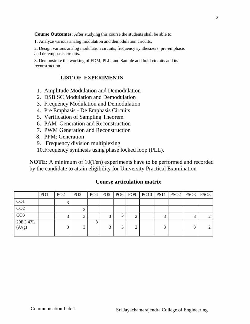
Course Outcomes: After studying this course the students shall be able to:
1. Analyze various analog modulation and demodulation circuits.
2. Design various analog modulation circuits, frequency synthesizers, pre-emphasis
and de-emphasis circuits.
3. Demonstrate the working of FDM, PLL, and Sample and hold circuits and its
reconstruction.
LIST OF EXPERIMENTS
1. Amplitude Modulation and Demodulation
2. DSB SC Modulation and Demodulation
3. Frequency Modulation and Demodulation
4. Pre Emphasis - De Emphasis Circuits
5. Verification of Sampling Theorem
6. PAM Generation and Reconstruction
7. PWM Generation and Reconstruction
8. PPM: Generation
9. Frequency division multiplexing
10. Frequency synthesis using phase locked loop (PLL).
NOTE: A minimum of 10(Ten) experiments have to be performed and recorded
by the candidate to attain eligibility for University Practical Examination
Course articulation matrix
PO1 PO2 PO3 PO4 PO5 PO6 PO9 PO10 PS11 PSO2 PSO3 PSO3
CO1 3
CO2 3
CO3 3 3
3 3 2 3 3 2
20EC 47L
(Avg) 3 3
3
3 3 2
3 3 2
3
JSS Science and Technology University Communication Lab-1
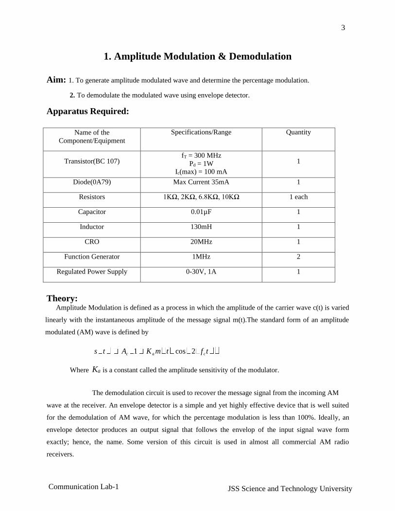
1. Amplitude Modulation & Demodulation
Aim: 1. To generate amplitude modulated wave and determine the percentage modulation.
2. To demodulate the modulated wave using envelope detector.
Apparatus Required:
Name of the
Component/Equipment
Specifications/Range Quantity
Transistor(BC 107) fT = 300 MHz
Pd = 1W Ic(max) = 100 mA
1
Diode(0A79) Max Current 35mA 1
Resistors 1KΩ, 2KΩ, 6.8KΩ, 10KΩ 1 each
Capacitor 0.01µF 1
Inductor 130mH 1
CRO 20MHz 1
Function Generator 1MHz 2
Regulated Power Supply 0-30V, 1A 1
Theory: Amplitude Modulation is defined as a process in which the amplitude of the carrier wave c(t) is varied
linearly with the instantaneous amplitude of the message signal m(t).The standard form of an amplitude
modulated (AM) wave is defined by
s t Ac 1 K a m t cos 2 f ct
Where Ka is a constant called the amplitude sensitivity of the modulator.
The demodulation circuit is used to recover the message signal from the incoming AM
wave at the receiver. An envelope detector is a simple and yet highly effective device that is well suited
for the demodulation of AM wave, for which the percentage modulation is less than 100%. Ideally, an
envelope detector produces an output signal that follows the envelop of the input signal wave form
exactly; hence, the name. Some version of this circuit is used in almost all commercial AM radio
receivers.
4
JSS Science and Technology University Communication Lab-1
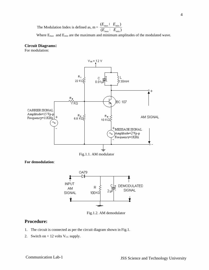
The Modulation Index is defined as, m =
(Emax Emin )
(Emax Emin ) Where Emax and Emin are the maximum and minimum amplitudes of the modulated wave.
Circuit Diagrams: For modulation:
Fig.1.1. AM modulator
For demodulation:
Procedure:
Fig.1.2. AM demodulator
1. The circuit is connected as per the circuit diagram shown in Fig.1.
2. Switch on + 12 volts VCC supply.
5
JSS Science and Technology University Communication Lab-1
3. Apply sinusoidal signal of 1 KHz frequency and amplitude 2 V (p-p) as modulating signal, and carrier
signal of frequency 11 KHz and amplitude 15 V (p-p).
4. Now slowly increase the amplitude of the modulating signal up to 7V and note down values of Emax
and Emin.
5. Calculate modulation index using equation
6. Repeat step 5 by varying frequency of the modulating signal.
7. Plot the graphs: Modulation index vs. Amplitude & Frequency
8. Find the value of R from fm
1
2 R
C
Taking C = 0.01µF
9. Connect the circuit diagram as shown in Fig.2.1
10. Feed the AM wave to the demodulator circuit and observe the output
11. Note down frequency and amplitude of the demodulated output waveform.
12. Draw the demodulated wave form .,m=1
Observations
Table 1: fm= 1KHz, fc=11KHz, Ac=15 V p-p.
S.No. Vm(Volts) Emax(volts) Emin (Volts) m %m (m x100)
Table 2: Am= 4 Vp-p fc =11KHz, Ac=15 V p-p.
S.No. fm(KHz) Emax(volts) Emin(Volts) m %m (m x100)
6
JSS Science and Technology University Communication Lab-1
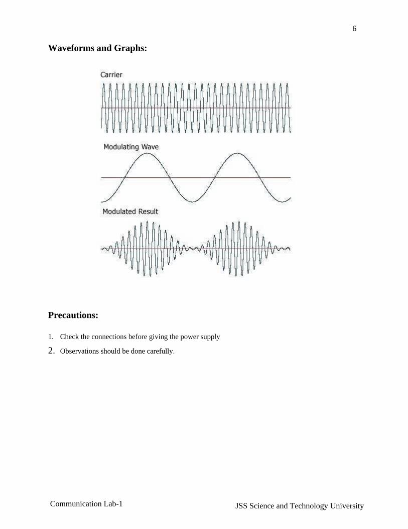
Waveforms and Graphs:
Precautions:
1. Check the connections before giving the power supply
2. Observations should be done carefully.
7
JSS Science and Technology University Communication Lab-1
2. DSB-SC Modulation and Demodulation
Aim: To generate AM-Double Side Band Suppressed Carrier (DSB-SC) signal.
Apparatus Required:
Name of the
Component/Equipment
Specifications/Range
Quantity
IC 1496
Wide frequency response up to 100 MHz
Internal power dissipation – 500mw(MAX)
1
Resistors
6.8KΩ
10 KΩ, 3.9 KΩ
1KΩ ,51 KΩ
1
2 each
3 each
Capacitors 0.1 µF 4
Variable Resistor
(Linear Pot)
0-50KΩ
1
CRO 100MHz 1
Function Generator 1MHz 2
Regulated Power Supply 0-30 v, 1A 1
Theory:
Balanced modulator is used for generating DSB-SC signal. A balanced modulator consists of two
standard amplitude modulators arranged in a balanced configuration so as to suppress the carrier wave.
The two modulators are identical except the reversal of sign of the modulating signal applied to them.
8
JSS Science and Technology University Communication Lab-1
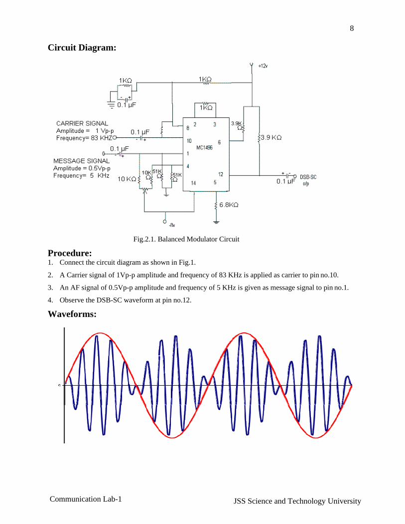
Circuit Diagram:
Procedure:
Fig.2.1. Balanced Modulator Circuit
1. Connect the circuit diagram as shown in Fig.1.
2. A Carrier signal of 1Vp-p amplitude and frequency of 83 KHz is applied as carrier to pin no.10.
3. An AF signal of 0.5Vp-p amplitude and frequency of 5 KHz is given as message signal to pin no.1.
4. Observe the DSB-SC waveform at pin no.12.
Waveforms:
9
JSS Science and Technology University Communication Lab-1
3. Frequency Modulation and Demodulation
Aim: 1. To generate frequency modulated signal and determine the modulation index and
bandwidth for various values of amplitude and frequency of modulating signal.
2. To demodulate a Frequency Modulated Signal using FM Detector.
Apparatus required:
Name of the
Component/Equipment Specifications/Range Quantity
IC 566 Operating voltage –Max-24 Volts
Operating current-Max.12.5 mA
1
IC 8038 Power dissipation – 750mW
Supply voltage - ±18V or 36V total
1
IC 565 Power dissipation -1400mw
Supply voltage - ±12V
1
Resistors 15 K Ω, 10 K Ω, 1.8 K Ω,
39 K Ω, 560 Ω
1,2,1
2,2
Capacitors 470 pF, 0.1µF
100pF , 0.001µF
2,1
1,1 each
CRO 100MHz 1
Function Generator 1MHz 2
Regulated Power Supply 0-30 v, 1A 1
Theory: The process, in which the frequency of the carrier is varied in accordance with the
instantaneous amplitude of the modulating signal, is called “Frequency Modulation”. The FM signal is
expressed as
s t Ac cos 2 f c sin 2 f mt
Where AC is amplitude of the carrier signal, fC is the carrier frequency
is the modulation index of the FM wave
10
JSS Science and Technology University Communication Lab-1
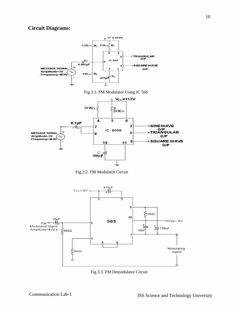
Circuit Diagrams:
Fig.3.1. FM Modulator Using IC 566
Fig.3.2. FM Modulator Circuit
Fig.3.3. FM Demodulator Circuit
11
JSS Science and Technology University Communication Lab-1
Procedure: Modulation:
1. The circuit is connected as per the circuit diagram shown in Fig.3.2
2. Without giving modulating signal observe the carrier signal at pin no.2 (at pin no.3 for IC 566).
Measure amplitude and frequency of the carrier signal. To obtain carrier signal of desired frequency,
find value of R from f = 1/ (2ΠRC) taking C=100pF.
3. Apply the sinusoidal modulating signal of frequency 4 KHz and amplitude 3Vp-p at pin no.7. ( pin
no.5 for IC 566)
Now slowly increase the amplitude of modulating signal and measure fmin and maximum frequency
deviation ∆f at each step. Evaluate the modulating index (mf = β) using ∆f / fm where ∆f = |fc - fmin|.
Calculate Band width. BW = 2 (β + 1)fm = 2(∆f + fm)
4. Repeat step 4 by varying frequency of the modulating signal.
Demodulation:
1. Connections are made as per circuit diagram shown in Fig.3.3
2. Check the functioning of PLL (IC 565) by giving square wave to input and observing the
output
3. Frequency of input signal is varied till input and output are locked.
4. Now modulated signal is fed as input and observe t he demodulated signal on CRO.
5. Draw the demodulated wave form.
Table: 1 fc = 45KHz
S.No. fm(KHz) Tmax (µsec) fmin(KHz) ∆f (KHz) β BW (KHz)
Table 2: fm = 4 KHz, fc = 45 KHz
S.No. Am (Volts) T (µsec) fmin(KHz) ∆f (KHz) β BW(KHz)
12
JSS Science and Technology University Communication Lab-1
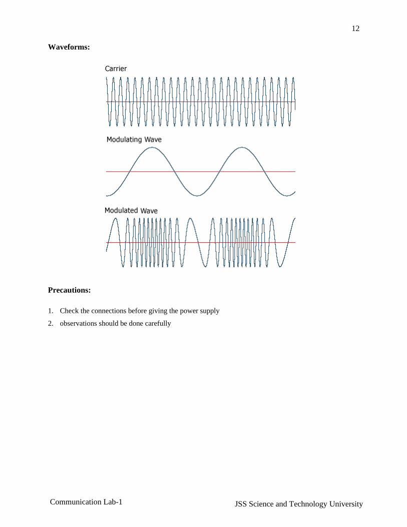
Waveforms:
Precautions:
1. Check the connections before giving the power supply
2. observations should be done carefully

13
JSS Science and Technology University Communication Lab-1
4. Pre-Emphasis & De-Emphasis
Aim:
I) To observe the effects of Pre-emphasis on given input signal.
ii) To observe the effects of De-emphasis on given input signal.
Apparatus Required:
Name of the
Component/Equipment Specifications/Range Quantity
Transistor (BC 107)
fT = 300 MHz
Pd = 1W
Ic(max) = 100 mA
1
Resistors 10 KΩ, 7.5 KΩ, 6.8 KΩ 1 each
Capacitors 10 nF
0.1 µF
1
2
CRO 20MHZ 1
Function Generator 1MHZ 1
Regulated Power Supply 0-30V, 1A 1
Theory:
The noise has a effect on the higher modulating frequencies than on the lower ones. Thus, if the
higher frequencies were artificially boosted at the transmitter and correspondingly cut at the receiver, an
improvement in noise immunity could be expected, thereby increasing the SNR ratio. This boosting of the
higher modulating frequencies at the transmitter is known as pre-emphasis and the compensation at the
receiver is called de-emphasis.
14
JSS Science and Technology University Communication Lab-1
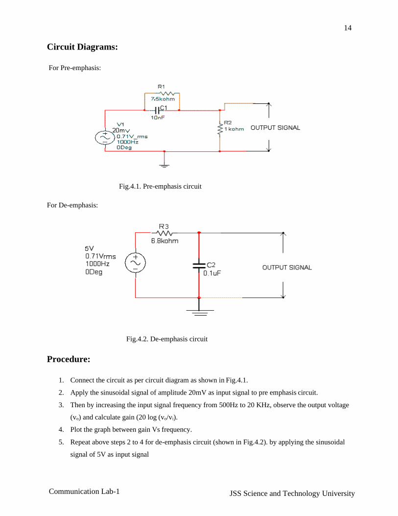
Circuit Diagrams:
For Pre-emphasis:
Fig.4.1. Pre-emphasis circuit
For De-emphasis:
Fig.4.2. De-emphasis circuit
Procedure:
1. Connect the circuit as per circuit diagram as shown in Fig.4.1.
2. Apply the sinusoidal signal of amplitude 20mV as input signal to pre emphasis circuit.
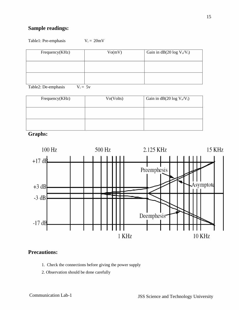
3. Then by increasing the input signal frequency from 500Hz to 20 KHz, observe the output voltage
(vo) and calculate gain (20 log (vo/vi).
4. Plot the graph between gain Vs frequency.
5. Repeat above steps 2 to 4 for de-emphasis circuit (shown in Fig.4.2). by applying the sinusoidal
signal of 5V as input signal
15
JSS Science and Technology University Communication Lab-1
Sample readings:
Table1: Pre-emphasis Vi = 20mV
Frequency(KHz) Vo(mV) Gain in dB(20 log Vo/Vi)
Table2: De-emphasis Vi = 5v
Frequency(KHz) Vo(Volts) Gain in dB(20 log Vo/Vi)
Graphs:
Precautions:
1. Check the connections before giving the power supply
2. Observation should be done carefully
16
JSS Science and Technology University Communication Lab-1
5. SAMPLING THEOREM VERIFICATION
Aim: To verify the Flat Top sampling theorem.
Apparatus Required:
1. Function Generator (1MHz)
2. Dual trace oscilloscope (20 MHz)
3. Power Supply
4. Op-amps, SL 100,MOSFET, Resisters, and capacitors
Theory:
The analog signal can be converted to a discrete time signal by a process called sampling. The
sampling theorem for a band limited signal of finite energy can be stated as,
‘’A band limited signal of finite energy, which has no frequency component higher than W Hz is
completely described by specifying the values of the signal at instants of time separated by 1/2W
seconds.’’
It can be recovered from knowledge of samples taken at the rate of 2W per second.
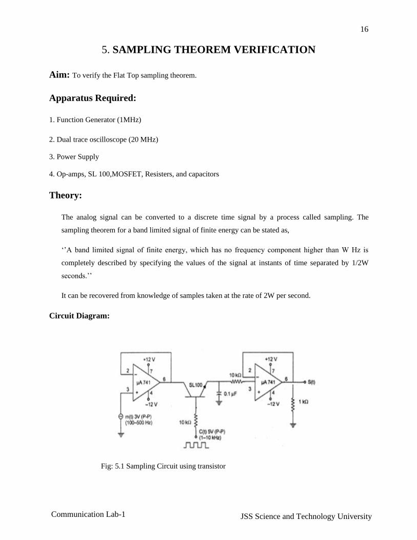
Circuit Diagram:
Fig: 5.1 Sampling Circuit using transistor
17
JSS Science and Technology University Communication Lab-1
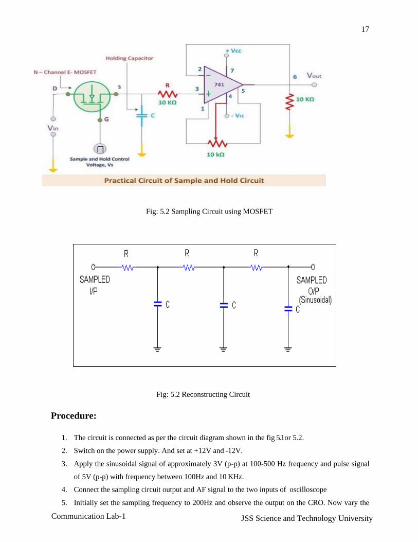
Fig: 5.2 Sampling Circuit using MOSFET
Fig: 5.2 Reconstructing Circuit
Procedure:
1. The circuit is connected as per the circuit diagram shown in the fig 5.1or 5.2.
2. Switch on the power supply. And set at +12V and -12V.
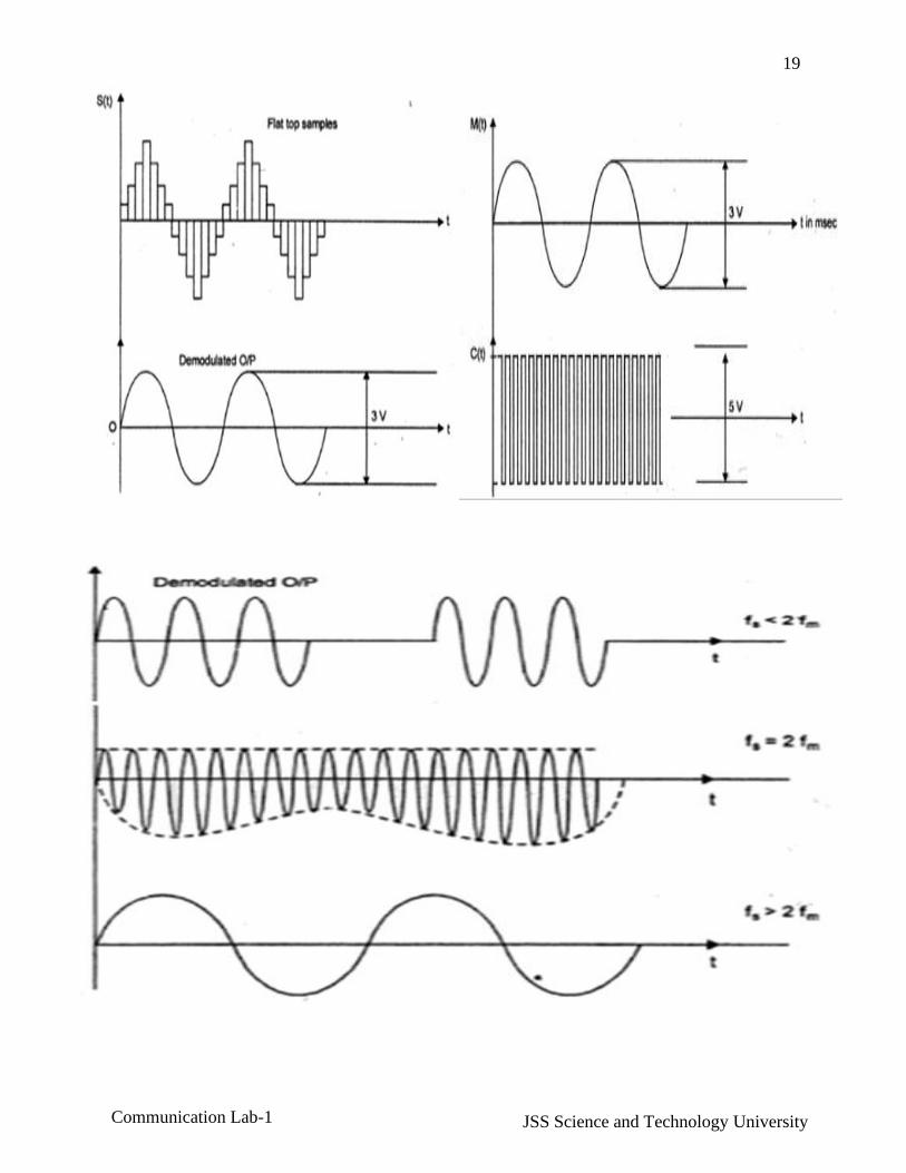
3. Apply the sinusoidal signal of approximately 3V (p-p) at 100-500 Hz frequency and pulse signal
of 5V (p-p) with frequency between 100Hz and 10 KHz.
4. Connect the sampling circuit output and AF signal to the two inputs of oscilloscope
5. Initially set the sampling frequency to 200Hz and observe the output on the CRO. Now vary the

18
JSS Science and Technology University Communication Lab-1
amplitude of modulating signal and observe the output of sampling circuit. Note that the
amplitude of the sampling pulses will be varying in accordance with the amplitude of the
modulating signal.
6. Design the reconstructing circuit. Depending on sampling frequency, R & C values are calculated
using the relations Fs = 1/Ts, Ts = RC. Choosing an appropriate value for C, R can be found using
the relation R=Ts/C
7. Connect the sampling circuit output to the reconstructing circuit shown in Fig 5.2 or 5.3
8. Observe the output of the reconstructing circuit (AF signal) for different sampling frequencies.
The original AF signal would appear only when the sampling frequency is 200Hz to 500Kz.
Waveforms:
Fig: 5.3 Reconstructing Circuit
19
JSS Science and Technology University Communication Lab-1
20
JSS Science and Technology University Communication Lab-1
6. PULSE AMPLITUDE MODULATION & DEMODULATION
Aim: To generate the Pulse Amplitude modulated and demodulated signals.
Apparatus required:
Name of the Apparatus Specifications/Range Quantity
Resistors 1KΩ, 10KΩ, 100KΩ, 5.8KΩ,
2.2KΩ, Each one
Transistor BC 107 2
Capacitor 10µF, 0.001µF each one
CRO 30MHz 1
Function generator 1MHz 1
Regulated Power Supply 0-30V,1A 1
CRO Probes --- 1
Theory: PAM is the simplest form of data modulation .The amplitude of uniformly spaced pulses is varied in
proportion to the corresponding sample values of a continuous message m (t).
A PAM waveform consists of a sequence of flat-topped pulses. The amplitude of each pulse corresponds
to the value of the message signal x (t) at the leading edge of the pulse.
The pulse amplitude modulation is the process in which the amplitudes of regularity spaced rectangular
pulses vary with the instantaneous sample values of a continuous message signal in a one-one fashion. A
PAM wave is represented mathematically as,
S (t) = [1+Ka x (nTs)] P (t-nTs)
N= -
21
JSS Science and Technology University Communication Lab-1
Where
x (nTs) ==> represents the nth sample of the message signal x(t)
K= ==> is the sampling period.
Ka ==> a constant called amplitude sensitivity
P (t) ==>denotes a pulse
PAM is of two types
1) Double polarity PAM ==> This is the PAM wave which consists of both positive and negative pulses
shown as
2) Single polarity PAM ==> This consists of PAM wave of only either negative (or)
Positive pulses. In this the fixed dc level is added to the signal to ensure single polarity signal. It is
represented as
Waveforms
Fig. Bipolar PAM signal Fig. Single polarity PAM
22
JSS Science and Technology University Communication Lab-1
Circuit Diagram:
Fig: 6.1 Pulse Amplitude Modulation Circuit
Fig .6.2 Demodulation Circuit
Procedure:
1. Connect the circuit as per the circuit diagram shown in the fig 6.1
2. Set the modulating frequency to 1KHz and sampling frequency to 12KHz
3. Observe the o/p on CRO i.e. PAM wave.
4. Measure the levels of Emax & Emin.
5. Feed the modulated wave to the low pass filter as in fig 6.2.
6. The output observed on CRO will be the demodulated wave.
7. Note down the amplitude (p-p) and time period of the demodulated wave. Vary the amplitude and
frequency of modulating signal. Observe and note down the changes in output.
8. Plot the wave forms on graph sheet.
23
JSS Science and Technology University Communication Lab-1
7. PULSE WIDTH MODULATION AND DEMODULATION
Aim: To generate the pulse width modulated and demodulated signals
Apparatus required:
Name of the Apparatus Specifications/Range Quantity
Resistors 1.2kΩ, 1.5 kΩ, 8.2 kΩ 1,1,2
Capacitors 0.01 µF, 1 µF 2,2
Diode 0A79 1
CRO 0-30, MHz 1
Function Generator 1MHz 1
RPS 0-30v,1A 1
IC 555
Operating tem :SE 555 -55oC to 125oC
NE 555 0o to 70oC
Supply voltage :+5V to +18V
Timing :µSec to Hours
Sink current :200mA
Temperature stability :50 PPM/oC change
in temp or 0-005% /oC.
1
CRO Probes -- 1
Theory:
Pulse Time Modulation is also known as Pulse Width Modulation or Pulse Length Modulation. In PWM,
the samples of the message signal are used to vary the duration of the individual pulses. Width may be
varied by varying the time of occurrence of leading edge, the trailing edge or both edges of the pulse in
accordance with modulating wave. It is also called Pulse Duration Modulation.
24
JSS Science and Technology University Communication Lab-1
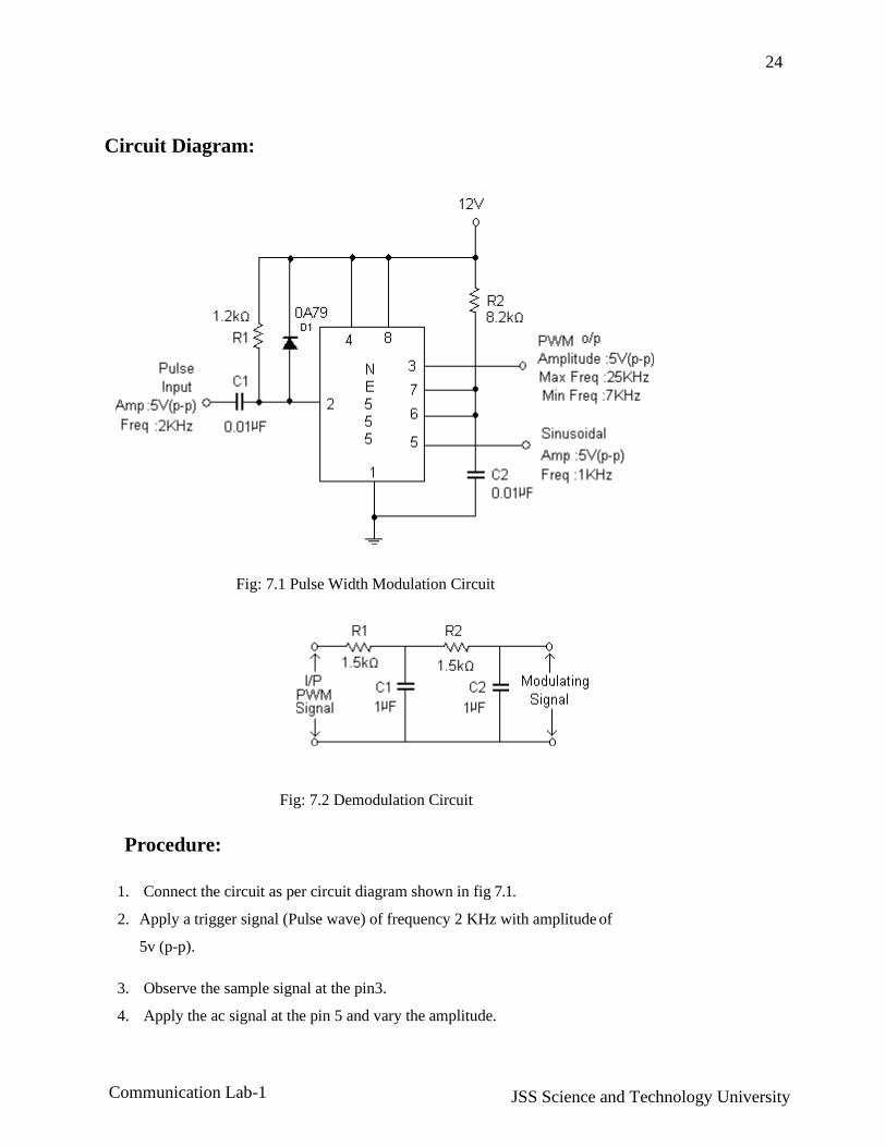
Circuit Diagram:
Fig: 7.1 Pulse Width Modulation Circuit
Fig: 7.2 Demodulation Circuit
Procedure:
1. Connect the circuit as per circuit diagram shown in fig 7.1.
2. Apply a trigger signal (Pulse wave) of frequency 2 KHz with amplitude of
5v (p-p).
3. Observe the sample signal at the pin3.
4. Apply the ac signal at the pin 5 and vary the amplitude.
25
JSS Science and Technology University Communication Lab-1
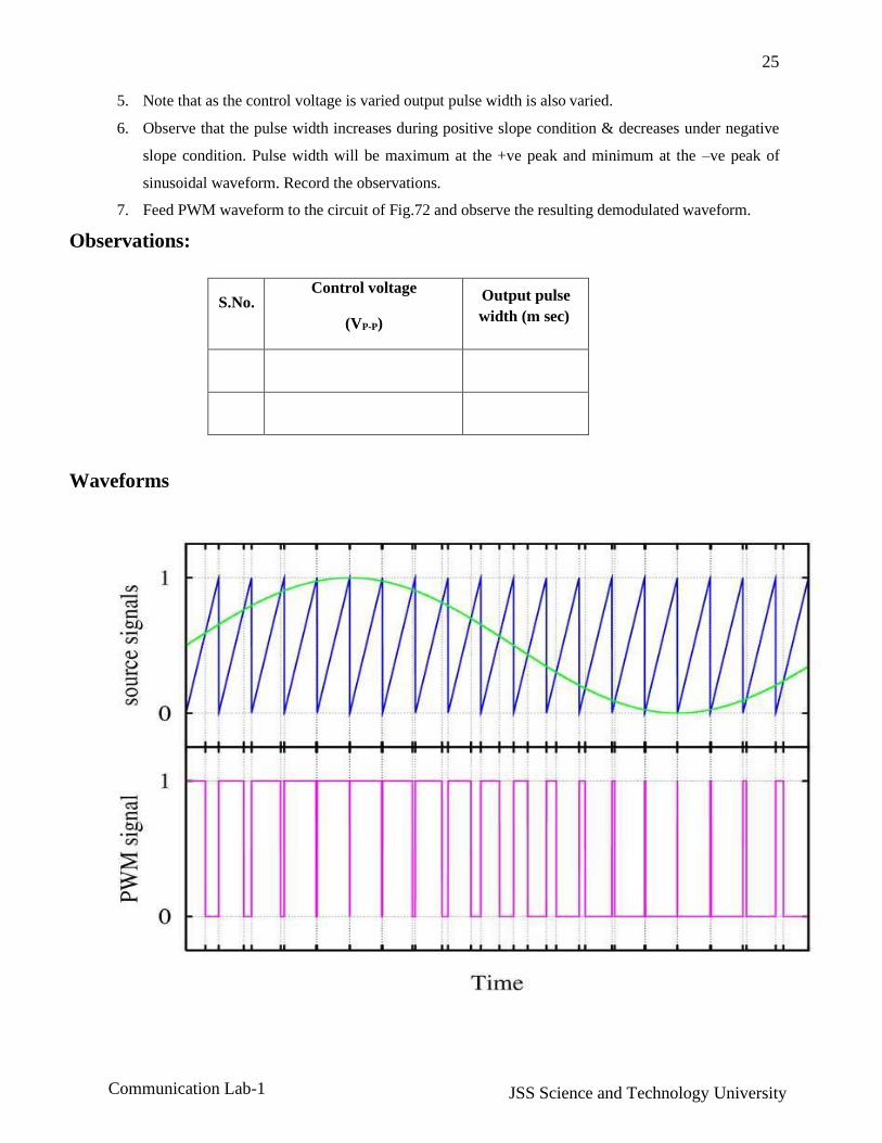
5. Note that as the control voltage is varied output pulse width is also varied.
6. Observe that the pulse width increases during positive slope condition & decreases under negative
slope condition. Pulse width will be maximum at the +ve peak and minimum at the –ve peak of
sinusoidal waveform. Record the observations.
7. Feed PWM waveform to the circuit of Fig.72 and observe the resulting demodulated waveform.
Observations:
S.No. Control voltage
(VP-P)
Output pulse
width (m sec)
Waveforms

26
JSS Science and Technology University Communication Lab-1
8. PULSE POSITION MODULATION & DEMODULATION
Aim: To generate pulse position modulation and demodulation signals and to study the effect of
amplitude of the modulating signal on output.
Apparatus required:
Name of the apparatus Specifications/Range Quantity
Resistors 3.9kΩ, 3kΩ, 10kΩ, 680kΩ Each one
Capacitors 0.01µF, 60µF 2,1
Function Generator 1MHz 1
RPS 0-30v,1A 1
CRO 0-30MHz 1
IC 555
Operating tem :SE 555 -55oC to 125oC
NE 555 0o to 70oC
Supply voltage :+5V to +18V
Timing :µSec to Hours
Sink current :200mA
Temperature stability :50 PPM/oC
change in temp or 0-005% /oC.
1
CRO Probes ---- 1
Theory: In Pulse Position Modulation, both the pulse amplitude and pulse duration are held constant but the
position of the pulse is varied in proportional to the sampled values of the message signal. Pulse time
modulation is a class of signaling techniques that encodes the sample values of an analog signal on to
the time axis of a digital signal and it is analogous to angle modulation techniques. The two main types
of PTM are PWM and PPM. In PPM the analog sample value determines the position of a narrow pulse
relative to the clocking time. In PPM rise time of pulse decides the channel bandwidth. It has low noise
interference.
27
JSS Science and Technology University Communication Lab-1
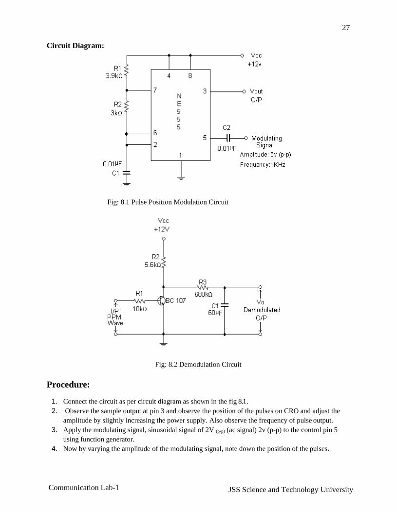
Circuit Diagram:
Fig: 8.1 Pulse Position Modulation Circuit
Fig: 8.2 Demodulation Circuit
Procedure:
1. Connect the circuit as per circuit diagram as shown in the fig 8.1.
2. Observe the sample output at pin 3 and observe the position of the pulses on CRO and adjust the
amplitude by slightly increasing the power supply. Also observe the frequency of pulse output.
3. Apply the modulating signal, sinusoidal signal of 2V (p-p) (ac signal) 2v (p-p) to the control pin 5
using function generator.
4. Now by varying the amplitude of the modulating signal, note down the position of the pulses.
28
JSS Science and Technology University Communication Lab-1
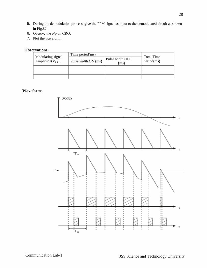
5. During the demodulation process, give the PPM signal as input to the demodulated circuit as shown
in Fig.82.
6. Observe the o/p on CRO.
7. Plot the waveform.
Observations:
Modulating signal
Amplitude(Vp-p)
Time period(ms) Total Time
period(ms) Pulse width ON (ms) Pulse width OFF
(ms)
Waveforms

29
JSS Science and Technology University Communication Lab-1
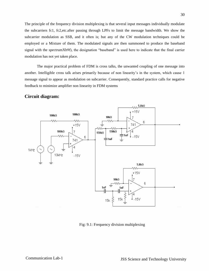
9. FREQUENCY DIVISION MULTIPLEXING
Aim: To construct the frequency division multiplexing and demultiplexing circuit and to verify its
operation
Apparatus required:
Name of the apparatus Specifications/Range Quantity
Resistors 3.9kΩ, 3kΩ, 10kΩ, 680kΩ Each one
Capacitors 0.01µF, 60µF 2,1
Function Generator 1MHz 1
RPS 0-30v,1A 1
CRO 0-30MHz 1
IC 555
Operating tem :SE 555 -55oC to 125oC
NE 555 0o to 70oC
Supply voltage :+5V to +18V
Timing :µSec to Hours
Sink current :200mA
Temperature stability :50 PPM/oC
change in temp or 0-005% /oC.
1
CRO Probes ---- 1
Theory: When several communications channels are between the two same point’s significant economics may be
realized by sending all the messages on one transmission facility a process called multiplexing.
Applications of multiplexing range from the vital, if prosaic, telephone networks to the glamour of FM
stereo and space probe telemetry system. There are two basic multiplexing techniques
1. Frequency Division Multiplexing (FDM)
2. Time Division Multiplexing (TDM)
30
JSS Science and Technology University Communication Lab-1
The principle of the frequency division multiplexing is that several input messages individually modulate
the subcarriers fc1, fc2,etc.after passing through LPFs to limit the message bandwidth. We show the
subcarrier modulation as SSB, and it often is; but any of the CW modulation techniques could be
employed or a Mixture of them. The modulated signals are then summoned to produce the baseband
signal with the spectrumXb9f), the designation “baseband” is used here to indicate that the final carrier
modulation has not yet taken place.
The major practical problem of FDM is cross talks, the unwanted coupling of one message into
another. Intelligible cross talk arises primarily because of non linearity’s in the system, which cause 1
message signal to appear as modulation on subcarrier. Consequently, standard practice calls for negative
feedback to minimize amplifier non linearity in FDM systems
Circuit diagram:
Fig: 9.1: Frequency division multiplexing
31
JSS Science and Technology University Communication Lab-1
Procedure:
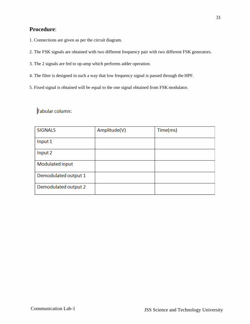
1. Connections are given as per the circuit diagram.
2. The FSK signals are obtained with two different frequency pair with two different FSK generators.
3. The 2 signals are fed to op-amp which performs adder operation.
4. The filter is designed in such a way that low frequency signal is passed through the HPF.
5. Fixed signal is obtained will be equal to the one signal obtained from FSK modulator.
32
JSS Science and Technology University Communication Lab-1
10. Phase Locked Loop
Aim: . To study phase lock loop and its capture range, lock range and free running VCO
Theory:
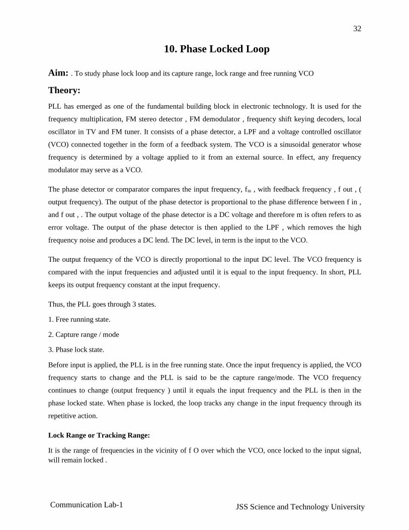
PLL has emerged as one of the fundamental building block in electronic technology. It is used for the
frequency multiplication, FM stereo detector , FM demodulator , frequency shift keying decoders, local
oscillator in TV and FM tuner. It consists of a phase detector, a LPF and a voltage controlled oscillator
(VCO) connected together in the form of a feedback system. The VCO is a sinusoidal generator whose
frequency is determined by a voltage applied to it from an external source. In effect, any frequency
modulator may serve as a VCO.
The phase detector or comparator compares the input frequency, fin , with feedback frequency , f out , (
output frequency). The output of the phase detector is proportional to the phase difference between f in ,
and f out , . The output voltage of the phase detector is a DC voltage and therefore m is often refers to as
error voltage. The output of the phase detector is then applied to the LPF , which removes the high
frequency noise and produces a DC lend. The DC level, in term is the input to the VCO.
The output frequency of the VCO is directly proportional to the input DC level. The VCO frequency is
compared with the input frequencies and adjusted until it is equal to the input frequency. In short, PLL
keeps its output frequency constant at the input frequency.
Thus, the PLL goes through 3 states.
1. Free running state.
2. Capture range / mode
3. Phase lock state.
Before input is applied, the PLL is in the free running state. Once the input frequency is applied, the VCO
frequency starts to change and the PLL is said to be the capture range/mode. The VCO frequency
continues to change (output frequency ) until it equals the input frequency and the PLL is then in the
phase locked state. When phase is locked, the loop tracks any change in the input frequency through its
repetitive action.
Lock Range or Tracking Range:
It is the range of frequencies in the vicinity of f O over which the VCO, once locked to the input signal,
will remain locked .
33
JSS Science and Technology University Communication Lab-1
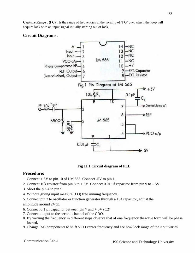
Capture Range : (f C) : Is the range of frequencies in the vicinity of ‘f O’ over which the loop will
acquire lock with an input signal initially starting out of lock .
Circuit Diagrams:
Fig 11.1 Circuit diagram of PLL
Procedure:
1. Connect + 5V to pin 10 of LM 565. Connect -5V to pin 1.
2. Connect 10k resistor from pin 8 to + 5V Connect 0.01 µf capacitor from pin 9 to – 5V
3. Short the pin 4 to pin 5.
4. Without giving input measure (f O) free running frequency.
5. Connect pin 2 to oscillator or function generator through a 1µf capacitor, adjust the
amplitude around 2Vpp.
6. Connect 0.1 µf capacitor between pin 7 and + 5V (C2)
7. Connect output to the second channel of the CRO.
8. By varying the frequency in different steps observe that of one frequency the wave form will be phase
locked.
9. Change R-C components to shift VCO center frequency and see how lock range of the input varies
34
JSS Science and Technology University Communication Lab-1