COLOR MONITOR SERVICE MANUAL
31
COLOR MONITOR SERVICE MANUAL Website:http://biz.LGservice.com CAUTION BEFORE SERVICING THE UNIT, READ THE SAFETY PRECAUTIONS IN THIS MANUAL. CHASSIS NO. : LM83A MODEL: W2600H(W2600H-PFS.A**QAF) ( ) **Same model for Service Internal Use Only
-
Upload
khangminh22 -
Category
Documents
-
view
0 -
download
0
Transcript of COLOR MONITOR SERVICE MANUAL

COLOR MONITORSERVICE MANUAL
Website:http://biz.LGservice.com
CAUTIONBEFORE SERVICING THE UNIT, READ THE SAFETY PRECAUTIONS IN THIS MANUAL.
CHASSIS NO. : LM83A
MODEL: W2600H(W2600H-PFS.A**QAF)( ) **Same model for Service
Internal Use Only

- 2 -
CONTENTS
CONTENTS .............................................................................................. 2
PRECAUTION ...........................................................................................3
SPECIFICATION ........................................................................................7
ADJUSTMENT ..........................................................................................9
SERVICE OSD .........................................................................................12
TROUBLE SHOOTING ............................................................................13
BLOCK DIAGRAM...................................................................................17
EXPLODED VIEW ...................................................................................20
REPLACEMENT PARTS LIST ............................................................... 22
SVC. SHEET ........................................................................................... 25
Copyright 2008 LG Electronics. Inc. All right reserved.Only for training and service purposes
LGE Internal Use Only

- 3 -
PRECAUTION
Copyright 2008 LG Electronics. Inc. All right reserved.Only for training and service purposes
LGE Internal Use Only
WARNING FOR THE SAFETY-RELATED COMPONENT.
• There are some special components used in LCDmonitor that are important for safety. These parts aremarked on the schematic diagram and thereplacement parts list. It is essential that these criticalparts should be replaced with the manufacturer’sspecified parts to prevent electric shock, fire or otherhazard.
• Do not modify original design without obtaining writtenpermission from manufacturer or you will void theoriginal parts and labor guarantee.
TAKE CARE DURING HANDLING THE LCD MODULEWITH BACKLIGHT UNIT.
• Must mount the module using mounting holes arrangedin four corners.
• Do not press on the panel, edge of the frame stronglyor electric shock as this will result in damage to thescreen.
• Do not scratch or press on the panel with any sharpobjects, such as pencil or pen as this may result indamage to the panel.
• Protect the module from the ESD as it may damage theelectronic circuit (C-MOS).
• Make certain that treatment person’s body aregrounded through wrist band.
• Do not leave the module in high temperature and inareas of high humidity for a long time.
• The module not be exposed to the direct sunlight.
• Avoid contact with water as it may a short circuit withinthe module.
• If the surface of panel become dirty, please wipe it offwith a softmaterial. (Cleaning with a dirty or rough clothmay damage the panel.)
WARNING
BE CAREFUL ELECTRIC SHOCK !
• If you want to replace with the new backlight (CCFL) orinverter circuit, must disconnect the AC adapterbecause high voltage appears at inverter circuit about650Vrms.
• Handle with care wires or connectors of the invertercircuit. If the wires are pressed cause short and mayburn or take fire.
Leakage Current Hot Check Circuit
CAUTIONPlease use only a plastic screwdriver to protect yourselffrom shock hazard during service operation.
1.5 Kohm/10W
To Instrument'sexposed METALLIC PARTS
Good Earth Groundsuch as WATER PIPE,CONDUIT etc.
AC Volt-meter

- 4 -
SERVICING PRECAUTIONS
Copyright 2008 LG Electronics. Inc. All right reserved.Only for training and service purposes
LGE Internal Use Only
CAUTION: Before servicing receivers covered by thisservice manual and its supplements and addenda, readand follow the SAFETY PRECAUTIONS on page 3 of thispublication.NOTE: If unforeseen circumstances create conflictbetween the following servicing precautions and any of thesafety precautions on page 3 of this publication, alwaysfollow the safety precautions. Remember: Safety First.
General Servicing Precautions1. Always unplug the receiver AC power cord from the AC
power source before;a. Removing or reinstalling any component, circuit
board module or any other receiver assembly.b. Disconnecting or reconnecting any receiver electrical
plug or other electrical connection.c. Connecting a test substitute in parallel with an
electrolytic capacitor in the receiver.CAUTION: A wrong part substitution or incorrectpolarity installation of electrolytic capacitors mayresult in an explosion hazard.
d. Discharging the picture tube anode.2. Test high voltage only by measuring it with an
appropriate high voltage meter or other voltagemeasuring device (DVM, FETVOM, etc) equipped witha suitable high voltage probe.Do not test high voltage by "drawing an arc".
3. Discharge the picture tube anode only by (a) firstconnecting one end of an insulated clip lead to thedegaussing or kine aquadag grounding system shieldat the point where the picture tube socket ground leadis connected, and then (b) touch the other end of theinsulated clip lead to the picture tube anode button,using an insulating handle to avoid personal contactwith high voltage.
4. Do not spray chemicals on or near this receiver or anyof its assemblies.
5. Unless specified otherwise in this service manual,clean electrical contacts only by applying the followingmixture to the contacts with a pipe cleaner, cotton-tipped stick or comparable non-abrasive applicator;10% (by volume) Acetone and 90% (by volume)isopropyl alcohol (90%-99% strength)CAUTION: This is a flammable mixture.Unless specified otherwise in this service manual,lubrication of contacts in not required.
6. Do not defeat any plug/socket B+ voltage interlockswith which receivers covered by this service manualmight be equipped.
7. Do not apply AC power to this instrument and/or any ofits electrical assemblies unless all solid-state deviceheat sinks are correctly installed.
8. Always connect the test receiver ground lead to thereceiver chassis ground before connecting the testreceiver positive lead.Always remove the test receiver ground lead last.
9. Use with this receiver only the test fixtures specified inthis service manual.CAUTION: Do not connect the test fixture ground strapto any heat sink in this receiver.
Electrostatically Sensitive (ES) DevicesSome semiconductor (solid-state) devices can bedamaged easily by static electricity. Such componentscommonly are called Electrostatically Sensitive (ES)Devices. Examples of typical ES devices are integratedcircuits and some field-effect transistors andsemiconductor "chip" components. The followingtechniques should be used to help reduce the incidence ofcomponent damage caused by static by static electricity.1. Immediately before handling any semiconductor
component or semiconductor-equipped assembly, drainoff any electrostatic charge on your body by touching aknown earth ground. Alternatively, obtain and wear acommercially available discharging wrist strap device,which should be removed to prevent potential shockreasons prior to applying power to the unit under test.
2. After removing an electrical assembly equipped withES devices, place the assembly on a conductivesurface such as aluminum foil, to prevent electrostaticcharge buildup or exposure of the assembly.
3. Use only a grounded-tip soldering iron to solder orunsolder ES devices.
4. Use only an anti-static type solder removal device.Some solder removal devices not classified as "anti-static" can generate electrical charges sufficient todamage ES devices.
5. Do not use freon-propelled chemicals. These cangenerate electrical charges sufficient to damage ESdevices.
6. Do not remove a replacement ES device from itsprotective package until immediately before you areready to install it. (Most replacement ES devices arepackaged with leads electrically shorted together byconductive foam, aluminum foil or comparableconductive material).
7. Immediately before removing the protective materialfrom the leads of a replacement ES device, touch theprotective material to the chassis or circuit assemblyinto which the device will be installed.CAUTION: Be sure no power is applied to the chassisor circuit, and observe all other safety precautions.
8. Minimize bodily motions when handling unpackagedreplacement ES devices. (Otherwise harmless motionsuch as the brushing together of your clothes fabric orthe lifting of your foot from a carpeted floor cangenerate static electricity sufficient to damage an ESdevice.)

- 5 -Copyright 2008 LG Electronics. Inc. All right reserved.Only for training and service purposes
LGE Internal Use Only
General Soldering Guidelines1. Use a grounded-tip, low-wattage soldering iron and
appropriate tip size and shape that will maintain tiptemperature within the range or 500 F to 600 F.
2. Use an appropriate gauge of RMA resin-core soldercomposed of 60 parts tin/40 parts lead.
3. Keep the soldering iron tip clean and well tinned.4. Thoroughly clean the surfaces to be soldered. Use a
mall wire-bristle (0.5 inch, or 1.25cm) brush with ametal handle.Do not use freon-propelled spray-on cleaners.
5. Use the following unsoldering techniquea. Allow the soldering iron t ip to reach normal
temperature.(500 F to 600 F)
b. Heat the component lead until the solder melts.c. Quickly draw the melted solder with an anti-static,
suction-type solder removal device or with solderbraid.CAUTION: Work quickly to avoid overheating thecircuitboard printed foil.
6. Use the following soldering technique.a. Allow the soldering iron tip to reach a normal
temperature (500 F to 600 F)b. First, hold the soldering iron tip and solder the strand
against the component lead until the solder melts.
c. Quickly move the soldering iron tip to the junction ofthe component lead and the printed circuit foil, andhold it there only until the solder flows onto andaround both the component lead and the foil.CAUTION: Work quickly to avoid overheating thecircuit board printed foil.
d. Closely inspect the solder area and remove anyexcess or splashed solder with a small wire-bristlebrush.
IC Remove/ReplacementSome chassis circuit boards have slotted holes (oblong)through which the IC leads are inserted and then bent flatagainst the circuit foil. When holes are the slotted type,the following technique should be used to remove andreplace the IC. When working with boards using thefamiliar round hole, use the standard technique asoutlined in paragraphs 5 and 6 above.
Removal1. Desolder and straighten each IC lead in one operation
by gently prying up on the lead with the soldering irontip as the solder melts.
2. Draw away the melted solder with an anti-staticsuction-type solder removal device (or with solderbraid) before removing the IC.
Replacement1. Carefully insert the replacement IC in the circuit board.2. Carefully bend each IC lead against the circuit foil pad
and solder it.3. Clean the soldered areas with a small wire-bristle
brush. (It is not necessary to reapply acrylic coating tothe areas).
"Small-Signal" Discrete TransistorRemoval/Replacement1. Remove the defective transistor by clipping its leads as
close as possible to the component body.2. Bend into a "U" shape the end of each of three leads
remaining on the circuit board.3. Bend into a "U" shape the replacement transistor leads.4. Connect the replacement transistor leads to the
corresponding leads extending from the circuit boardand crimp the "U" with long nose pliers to insure metalto metal contact then solder each connection.
Power Output, Transistor DeviceRemoval/Replacement1. Heat and remove all solder from around the transistor
leads.2. Remove the heat sink mounting screw (if so equipped).3. Carefully remove the transistor from the heat sink of the
circuit board.4. Insert new transistor in the circuit board.5. Solder each transistor lead, and clip off excess lead.6. Replace heat sink.
Diode Removal/Replacement1. Remove defective diode by clipping its leads as close
as possible to diode body.2. Bend the two remaining leads perpendicular y to the
circuit board.3. Observing diode polarity, wrap each lead of the new
diode around the corresponding lead on the circuitboard.
4. Securely crimp each connection and solder it.5. Inspect (on the circuit board copper side) the solder
joints of the two "original" leads. If they are not shiny,reheat them and if necessary, apply additional solder.
Fuse and Conventional ResistorRemoval/Replacement1. Clip each fuse or resistor lead at top of the circuit board
hollow stake.2. Securely crimp the leads of replacement component
around notch at stake top.3. Solder the connections.
CAUTION: Maintain original spacing between thereplaced component and adjacent components and thecircuit board to prevent excessive componenttemperatures.

- 6 -Copyright 2008 LG Electronics. Inc. All right reserved.Only for training and service purposes
LGE Internal Use Only
Circuit Board Foil RepairExcessive heat applied to the copper foil of any printedcircuit board will weaken the adhesive that bonds the foilto the circuit board causing the foil to separate from or"l i f t-off" the board. The following guidelines andprocedures should be followed whenever this condition isencountered.
At IC ConnectionsTo repair a defective copper pattern at IC connections usethe following procedure to install a jumper wire on thecopper pattern side of the circuit board. (Use thistechnique only on IC connections).
1. Carefully remove the damaged copper pattern with asharp knife. (Remove only as much copper asabsolutely necessary).
2. carefully scratch away the solder resist and acryliccoating (if used) from the end of the remaining copperpattern.
3. Bend a small "U" in one end of a small gauge jumperwire and carefully crimp it around the IC pin. Solder theIC connection.
4. Route the jumper wire along the path of the out-awaycopper pattern and let it overlap the previously scrapedend of the good copper pattern. Solder the overlappedarea and clip off any excess jumper wire.
At Other ConnectionsUse the following technique to repair the defective copperpattern at connections other than IC Pins. This techniqueinvolves the installation of a jumper wire on thecomponent side of the circuit board.1. Remove the defective copper pattern with a sharp
knife.Remove at least 1/4 inch of copper, to ensure that ahazardous condition will not exist if the jumper wireopens.
2. Trace along the copper pattern from both sides of thepattern break and locate the nearest component that isdirectly connected to the affected copper pattern.
3. Connect insulated 20-gauge jumper wire from the leadof the nearest component on one side of the patternbreak to the lead of the nearest component on theother side.Carefully crimp and solder the connections.CAUTION: Be sure the insulated jumper wire isdressed so the it does not touch components or sharpedges.

- 7 -
SPECIFICATIONS
Copyright 2008 LG Electronics. Inc. All right reserved.Only for training and service purposes
LGE Internal Use Only
1. LCD CHARACTERISTICSType : TFT Color LCD ModuleActive Display Area : 26 inch (756.228mm) diagonalPixel Pitch : 0.2505 (H) x 0.2505 (V)Color Depth : 16,777,216 colorsSize : 677.30 (H) x 436.80 (V) x 42.30(D) Electrical Interface : LVDSSurface Treatment : Anti-Glare, Hard-coating(3H)Operating Mode : Normally WhiteBacklight Unit : 4 CCFL
2. OPTICAL CHARACTERISTICS2-1. Viewing Angle by Contrast Ratio ≥ 5
Left : -80°(Typ) Right : +80°(Typ)Top :+80°(Typ) Bottom : -80°(Typ)
2-2. Luminance : 180(typ) (Typ. 30) -sRGB: 200(min), 350(Typ), 400(max)(Full white pattern, 0.7V)-6500K
: 150(min), 250(Typ), 350(max)(Full white pattern, 0.7V)-9300K
: 75%(min), 80%(typ)
2-3. Contrast Ratio : 500(Min), 1000(Typ) DFC->5000:1(Typ)
3. SIGNAL (Refer to the Timing Chart)3-1. Sync Signal
• Type : Separate Sync, SOG, Digital
3-2. Video Input Signal1) Type : R, G, B Analog2) Voltage Level : 0~0.71 Va) Color 0, 0 : 0 Vp-pb) Color 7, 0 : 0.467Vp-pc) Color 15, 0 : 0.714Vp-p
3) Input Impedance : 75Ω
3-3. Operating FrequencyHorizontal(Analog) : 30 ~ 83kHzHorizontal(Digital) : 30 ~ 83kHzVertical : 56 ~ 75Hz
4. Max. ResolutionD-sub Analog : 1920 x 1200@60HzDigital : 1920 x 1200@60Hz
5. POWER SUPPLY5-1. Power : AC 100-240V~, 50/60Hz , 0.8A
5-2. Power Consumption
6. ENVIRONMENT6-1. Operating Temperature : 10°C~35°C (50°F~95°F)
(Ambient)6-2. Relative Humidity : 10%~80% (Non-condensing)6-3. MTBF : 50,000 HRS with 90% Confidence
Lamp Life : 50,000 Hours(Min)
7. DIMENSIONS (with TILT/SWIVEL)
Width : 601.9 mm (23.70'')Depth : 270.2 mm (10.64'')Height : 463.2 mm (18.24'')
8. WEIGHT (with TILT/SWIVEL)
Net. Weight : 12.3 kg (27.12 lbs)Gross Weight : 15.4 kg (33.96 lbs)
MODE
POWER ON (NORMAL)
STAND-BY
SUSPEND
DPMS OFF
POWER S/W OFF
H/V SYNC
ON/ON
OFF/ON
ON/OFF
OFF/OFF
-
POWER CONSUMPTION
less than 110W(typ)
130W (USB Full load)
less than 1 W
less than 1 W
less than 1 W
less than 1 W
LED COLOR
BLUE
AMBER
AMBER
AMBER
OFF
VIDEO
ACTIVE
OFF
OFF
OFF
-

- 8 -
TIMING CHART
Copyright 2008 LG Electronics. Inc. All right reserved.Only for training and service purposes
LGE Internal Use Only
VIDEO
SYNC
B
C
E
A
D
* H/V Timming

- 9 -LGE Internal Use OnlyCopyright 2008 LG Electronics. Inc. All right reserved.
Only for training and service purposes
ADJUSTMENT INSTRUCTION1. Coverage
Apply to 26" Wide WGC monitor made in MonitorFactory(Kumi Korea) or made in accordance with thestandard of Kumi Factory process.
2. Appointment2.1 Adjustment must be done as fixed sequence, and
adjustment sequence can be modified after agreementwith the responsible R&D engineer considering mass-production condition.
2.2 Power : AC100~240 Voltage (Free)2.3 Input signal : As Product Standard (Signal ROM : ...V1.1)2.4 Warm-up Time : Over than 30 minutes2.5 Adjustment equipment : White balance equipment (CA-
210), Display adjust equipment, VG-819 (or VG828),Oscilloscope, PC (More than 486 computer ) & Whitebalance adjust program. HDCP Adjusting Jig equipment.
3. Adjustment3.1 Overview
Use factory automation equipment and adjust automaticmovement. But, do via passivity adjust in erroroccurrence.
3.2 Adjustment order(refer to the Adjustment standard andadjustment command table)
3.2.1 Board Assembly LineConnect input signal to 15pin D-sub.Ready for adjustment : check whether adjustmentcommand works normally or not and the operatingstate of each mode. Check the display state of gray color when 256 grayscale pattern is embodied.Read by EEPROM Read Command to checkwhether initial value is correct or not.
3.2.2 Total Assembly Line Input analog signal. (1920x1200@60Hz, Model #127)Write HDCP Key to EEPROM(24C16) by usingDDC2AB protocol & HDCP Adjusting Jig equipment[Address 0xAC 80, 292 bytes]If error is occurred, write and check again.Send Adjust Command [E6 00] to Refresh HDCPFunction.Ready : Heat-run during 30 minutes in the state withsignalConnect input signal to D-sub.Default value before adjustment : Contrast "70" ,Brightness "100(Max)"
3.2.3 Adjustment of Horizontal/Verticality screen position,Clock and Clock Phase at each Mode.
There is no special factory mode adjustment. Writing initial value of EEPROM in Board Assemblyline is adjusting Preset Mode and Reset mode.(EEPROM is initialized when AC Power is ON first.)If the change of FOS data is needed after M.P, it ispossible by writing Mode Data with EEPROM writecommand or modifying the Mode Data in MICOMitself.
# Caution) Must keep power-on more than 3seconds after AC Power-on first time.
3.2.4 Color coordinates adjustment and Luminanceadjustment.
3.2.4.1 Color coordinates adjustmentMonitor Contrast / Brightness
- Contrast : 70- Brightness : 100(Max)
CA-210 : Channel 13 (For WCG Monitor)Signal Generator : At cut-off and drive ‡ 16 steppattern for ADC
- Output Voltage : 700 mVp-p- Output Mode : Mode 127(WUXGA 60Hz)
mode Setting.
3.2.4.2 Adjustment : Board Assembly Line.Input 16 step pattern for ADC (Mode127, pattern29). (Video level : 700 mVp-p)Adjust by commanding AUTO_COLOR_ADJUSTConfirm "Success" message in Screen or Checkthe data of 0XC0, 0XC1 address ofEEPROM(0xAA) is 0xAA after waiting 5 seconds.If there is "FAULT" message or the data of 0xCO,0xC1 address of EEPROM(0xAA) is not 0xAA, doadjust again.If all Adjustment is completed, the values of6500K, User Color and 9300K are savedautomatically.
3.2.4.3 Confirm at Total Assembly Line : adjustment.Check the data of 0xC0, 0xC1 address ofEEPROM(0xAA) is 0xAA.If the data of 0XC0, C1 address ofEEPROM(0xAA) is not 0xAA, do adjust again by3.2.4.2.
3.2.4.4 Confirm PRESET 6500K Color coordinates andConfirm PRESET 9300K Color coordinates .Set as Aging mode ON, by commandingAGING_ON/OFF command code.Select Module that is being used in presentproduction by commanding MODULE SELECT.Send SYSTEM RESET command to set Moduledata. Input Full White Pattern (Video level : 700 mVp-p).Set as 9300K by commandingCOLOR_MODE_CHANGE Command code.Confirm to meet x = 0.283 0.03, y=0.298 0.03Save 9300K Color by commanding COLOR SAVECommand code.Input Full White Pattern (Video level : 700 mVp-p)Set as 6500K by commandingCOLOR_MODE_CHANGE Command code.Confirm to meet x = 0.313 0.03, y=0.329 0.03Set as sRGB by commandingCOLOR_MODE_CHANGE Command code.Adjust to meet Y = 180 50, and confirm.

- 10 -Copyright 2008 LG Electronics. Inc. All right reserved.Only for training and service purposes
LGE Internal Use Only
3.2.4.5 Confirm User color coordinates .Confirm Whether User color is saved same as6500K.After confirming Color coordinates, Must return to6500KConfirm whether user color is 50. If the value ofuser color(R/G/B) is 30, do adjust again by3.2.4.2.
3.2.5 Confirm Operation state.3.2.5.1 Operation mode : Confirm whether each appointed
mode operate correctly or not
3.2.5.2 Confirmation of Adjustment condit ion andoperation : Confirm whether it meet Auto/Manualequipement Adjustment standard or not.Confirm Analog screen state : Confirm screenstate at below mode.Appointment mode : 640*480 @60Hz (Mode 2),800*600@75Hz(Mode 5)1024*768@60Hz(Mode 6),1280*1024@60Hz(Mode 9),1680*1050@60Hz(Mode 12), 1920*1200@60Hz SMPTE pattern(Check 0%,5%,95%,100%)-Modecan be added.Check HDCP signal screen by using Videogenerator that generate HDCP signal
3.2.5.3 Confirm Auto adjustment operation.Input Analog 1 line on/off & Rectangle Pattern atMode 10(1920x1200@60Hz)Confirm adjustment operation by changing Clock,Phase,H/V Position.Check Clock, Phase by pressing AUTO Key.Confirm first set of new lot by periods
3.2.5.4 Other qualityConfirm that each items satisfy under standardcondition that was written product spec.Confirm Applying Module & MICOM Setting ‡Confirm with Service OSD
-> Confirm at Service OSD by "Menu + Power key"on .(from Power off)
-> Confirm first set of new lot by periods, andconfirm periodically when there is Processchange or Adjustment setting change.
3.2.5.5 OSD & Adjustment device Confirmation : Confirmoperation mentioned as product spec.Vary Brightness and Contrast and confirm thevariation of Luminance and display status.Operate the f.engine function and confirmvariation of Luminance.Make sure to do FACTORY RESET afterconfirmation of OSD function.
3.2.5.6 Confirm the display state by inputting 8 color BarPattern & 256 Gray Scale pattern
3.2.5.7. DPM operation confirmation : Check if Power LEDColor and Power Consumption operates asstandard. Measurement Condition : 230V@ 50Hz (Analog)Confirm DPM operation at the state of screenwithout Video Signal.(refer to Spec at Page 11)
3.2.5.8 DDC EDID Write- Digital part EDID data
Confirm whether module selection is correct or noton the self-diagnostics OSD with signal cabledisconnected.Connect Digital Signal Cable to DVI-D wafer.Write EDID DATA to EEPROM(24C02) by usingDDC2B protocol.Check whether written EDID data is correct or not.(refer to Product spec).- Analog part EDID dataConnect analog Signal Cable to D-sub wafer.Write EDID DATA to EEPROM(24C02) by usingDDC2B protocol.Check whether written EDID data is correct or not.(refer to Product spec).
-> After writing EDID, send Elapsed Time Clearcommand. (Elapsed time should not bedisplayed, after EDID writing): Confirm periodically (in the first set of new lot,process change) whether module name andaging time disappeared on the self-diagnosticsOSD with signal cable disconnected.
-> If Elapsed Time Clear command isn’t executed,module name, aging time and TCO word appearon the self-diagnostics OSD.(Module name andaging time should not appear after writing EDID)
-> Make sure to do FACTORY RESET at the finalprocess.
3.2.5.9. Shipping conditionContrast : 70Power Switch : OffBrightness : 100(Max) Color Select : Preset (6500K)Language Select : Refer to product specOSD Position : CenterPower indicator : ONFlatron f-engine : Normal
3.2.6 USB 2.0 CheckTo check USB 2.0 High-Speed, We need a PC whichhas CATC Test program.Connect ups-tream to Monitor and PCConnect down-stream to Monitor and PC.Run CATC Program and Check OK or not

- 11 -Copyright 2008 LG Electronics. Inc. All right reserved.Only for training and service purposes
LGE Internal Use Only
Windows EDID V1.0 User Manual
Operating System: MS Windows 98, 2000, XPPort Setup: Windows 98 => Don’t need setup
Windows 2000, XP => Need to Port Setup.This program is available to LCD Monitor only.
1. Port Setupa) Copy “UserPort.sys” file to
“c:\WINNT\system32\drivers” folderb) Run Userport.exe
c) Remove all default numberd) Add 300-3FF
e) Click Start button.f) Click Exit button.
2. EDID Read & Write1) Run WinEDID.exe
2) Edit Week of Manufacture, Year of Manufacture, Serial Numbera) Input User Info Datab) Click “Update” buttonc) Click “ Write” button
- 12 -Copyright 2008 LG Electronics. Inc. All right reserved.Only for training and service purposes
LGE Internal Use Only
220
IBMCompatible PC
PARALLEL PORT
Power inlet (required)
Power LED
ST Switch
Power Select Switch(110V/220V)
Con
trol
Lin
e
Not u
sed
RS232
C
PARAL
LEL
V-SY
NC
POW
ER
ST
VGS
MONITOR
E
E
V-Sync On/Off Switch(Switch must be ON.)
F
F
A
A
BB
C
C
15105
5
69
1
1
1
14
13
25
6
5V
5V
5V
4.7K4.7K
4.7K
74LS06
74LS06
OFF ON
OFF
ON
11Video SignalGenerator
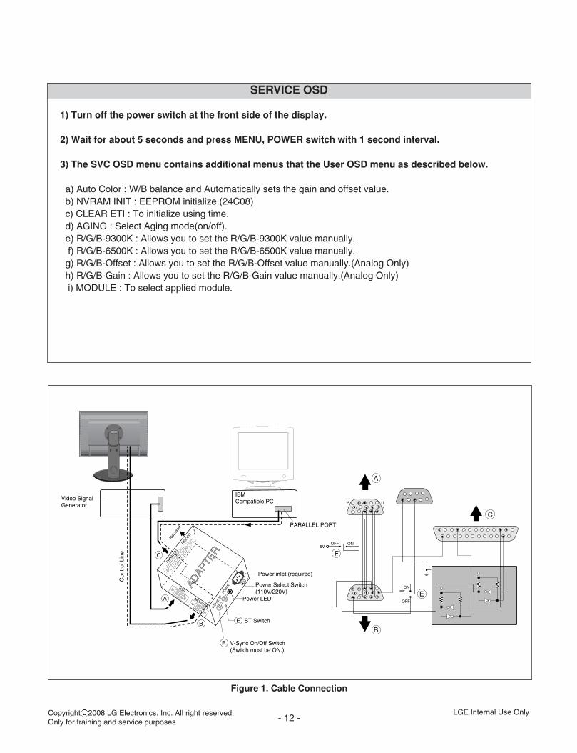
Figure 1. Cable Connection
SERVICE OSD
1) Turn off the power switch at the front side of the display.
2) Wait for about 5 seconds and press MENU, POWER switch with 1 second interval.
3) The SVC OSD menu contains additional menus that the User OSD menu as described below.
a) Auto Color : W/B balance and Automatically sets the gain and offset value.b) NVRAM INIT : EEPROM initialize.(24C08)c) CLEAR ETI : To initialize using time.d) AGING : Select Aging mode(on/off).e) R/G/B-9300K : Allows you to set the R/G/B-9300K value manually.f) R/G/B-6500K : Allows you to set the R/G/B-6500K value manually.g) R/G/B-Offset : Allows you to set the R/G/B-Offset value manually.(Analog Only) h) R/G/B-Gain : Allows you to set the R/G/B-Gain value manually.(Analog Only)i) MODULE : To select applied module.

- 13 -
TROUBLESHOOTING GUIDE
Copyright 2008 LG Electronics. Inc. All right reserved.Only for training and service purposes
LGE Internal Use Only
1. NO POWER
1
2
3
Waveforms
NO POWER(POWER INDICATOR OFF)
Flash ROM Problem.
NO
NO
CHECK POWER BOARD,AND FIND OUT A SHORTPOINT AS OPENING EACH POWER LINE
CHECK U901(3.3V),U902(1.8V) LINE.
YES
CHECK P305VOLTAGE
PIN9~ PIN12 (5V)?
IS IC302 PIN2(3.3V),IC303 PIN2(1.8V)?
4NO
CHECK CRYSTAL(X200)
YES
CHECK X200Frequency
NOCHECK IC202Do ISP. Then
Recover?
YES
YES
1 P305 #9~12 2 IC302 #2 3 IC303 #2 4 X200
- 14 -Copyright 2008 LG Electronics. Inc. All right reserved.Only for training and service purposes
LGE Internal Use Only
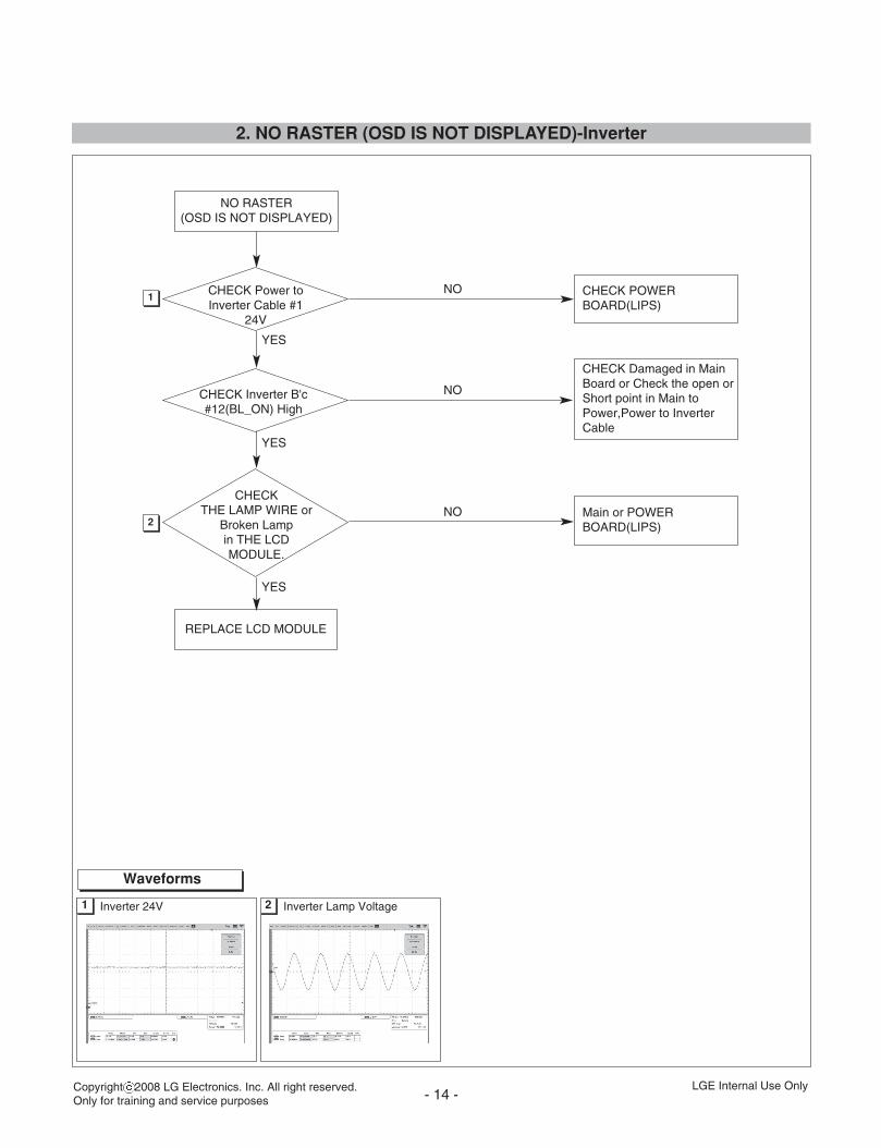
2. NO RASTER (OSD IS NOT DISPLAYED)-Inverter
NO RASTER(OSD IS NOT DISPLAYED)
NO
NO
NO
REPLACE LCD MODULE
CHECK POWERBOARD(LIPS)
CHECK Damaged in MainBoard or Check the open orShort point in Main toPower,Power to InverterCable
Main or POWERBOARD(LIPS)
CHECK Power toInverter Cable #1
24V
CHECK Inverter B'c#12(BL_ON) High
CHECK THE LAMP WIRE or
Broken Lampin THE LCD MODULE.
YES
YES
YES
1
2
Waveforms
1 Inverter 24V 2 Inverter Lamp Voltage

- 15 -Copyright 2008 LG Electronics. Inc. All right reserved.Only for training and service purposes
LGE Internal Use Only
3. NO RASTER (OSD IS NOT DISPLAYED)-MAIN
NO RASTER(OSD IS NOT DISPLAYED)
NO
NO
NO
TROUBLE IN LCDMODULE
CHECK P303W2600H-Pxx : 5VW2600HP-Bxx : 12V
CHECK IC202
CHECK CONNECTIONLINE FROM D-SUB TOIC202
YES
CHECK P303 #1,2
CHECK P303#10,11,22,23
CHECK LINK CABLE
YES
YES
1
Waveforms
1 P303 #10

- 16 -Copyright 2008 LG Electronics. Inc. All right reserved.Only for training and service purposes
LGE Internal Use Only
4. TROUBLE IN DPM
TROUBLE IN DPM
NO
NO
NO
TROUBLE IN IC202
CHECK PC.PC IS GOING TO THEDPM MODE.
CHECK PC.PC IS GOING TO THEDPM MODE.
CHECK H/V SYNC LINE
YES
If DSUBCHECK R185
AND R187 SYNCAPPEARED?Is R183 Level
is LOW?
If DVICHECK R133.
CHECK IC202PIN172,173
SYNC PULSE
YES
YES
1
2
Waveforms
1 H-SYNC 2 V-SYNC
- 17 -LGE Internal Use OnlyCopyright 2008 LG Electronics. Inc. All right reserved.
Only for training and service purposes
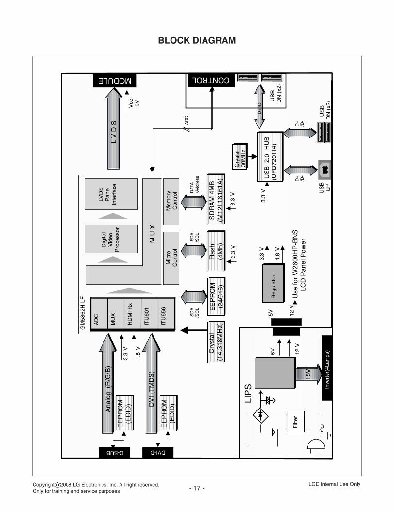
BLOCK DIAGRAM
L V
D S
DV
I (T
MD
S)
5V
3.3
V
Vcc 5V
LIP
S
Filt
er
5V 12V
Inve
rter
(4La
mps
)
15V
Fla
sh(4
Mb)
1.8
V
1.8
V
3.3
V
SD
A/S
CL E
EP
RO
M(2
4C16
)
3.3
V
EE
PR
OM
(ED
ID)
Cry
stal
(14.
318M
Hz)
Ana
log
(R/G
/B)
EE
PR
OM
(ED
ID)
3.3
V
US
B
2.0
HU
B(U
PD
7201
14)
Cry
stal
30M
Hz
US
BU
P
D+
/D-
US
BD
N (
x2)
DVI-DD-SUB
SD
A/S
CL
Dig
ital
Vid
eoP
roce
ssor
LVD
SP
anel
Inte
rfac
e
Mic
roC
ontr
ol
GM
5862
H-L
F
ITU
656
ITU
601
HD
MI R
x
MU
X
AD
C
Mem
ory
Con
trol
SD
RA
M 4
MB
(M12
L161
61A
)
DA
TA/A
ddre
ss
M U
X
Reg
ulat
or
MODULE CONTROL
AD
C
D+
/D-
D+
/D-
US
BD
N (
x2)
3.3
V
12V
Use
for
W26
00H
P-B
NS
LCD
Pan
el P
ower

- 18 -
DESCRIPTION OF BLOCK DIAGRAM
Copyright 2008 LG Electronics. Inc. All right reserved.Only for training and service purposes
LGE Internal Use Only
1. Video Controller Part.This part amplifies the level of video signal for the digital conversion and converts from the analog video signal to thedigital video signal using a pixel clock.The pixel clock for each mode is generated by the PLL.The range of the pixel clock is from 25MHz to 165MHz.This part consists of the Scaler, ADC and TMDS receiver .The Scaler gets the video signal converted analog to digital, interpolates input to 1920 x 1200 resolution signal andoutputs 8-bit R, G, B signal to transmitter.
2. Power Part.This part consists of the 3.3V and 1.8V regulator to convert power which is provided 5V,5V in Power board and Micom5V is provided for LCD panel.(W2600H-PFS)12V is used for LPL LCD Panel Power.(W2600HP-BNS)
3. MICOM Part.This part consists of EEPROM IC which stores control data and the Micom.The Micom distinguishes polarity and frequency of the H/V sync are supplied from signal cable.The controlled data of each modes is stored in EEPROM.
*refer to the each frequency of crystal oscillators and working frequency.Video processor : 14.31818MHz.USB Hub : 30MHzLVDS Clock Freq. : 154MHz MEMORY Clock Freq. : 183MHz

- 19 -
LIPS Board Block Diagram
Copyright 2008 LG Electronics. Inc. All right reserved.Only for training and service purposes
LGE Internal Use Only
EMICOMPONENTS
LINE100 ~ 240V
INPUT RECTIFIERAND FILTER
SWITCHINGTRANSFORMER
OUTPUT RECTIFIERAND FILTER
15V
5V
GND
SIGNALCOLLENT-
IONPHOTO-COUPLER
ISOLATION
PWM CONTROLCIRCUIT
HVDC 67KHz
PRIMARY SECONDARY
50 ~ 60Hz
Operation description_Power
1. EMI components.This part contains of EMI components to comply with global marketing EMI standards like FCC,VCCI CISPR, thecircuit included a line-filter, across line capacitor and of course the primary protection fuse.
2. Input rectifier and filter.This part function is for transfer the input AC voltage to a DC voltage through a bridge rectifier and a bulk capacitor.
3. Energy Transfer.This part function is for transfer the primary energy to secondary through a power transformer.
4. Output rectifier and filter.This part function is to make a pulse width modulation control and to provide the driver signal to power switch, toadjust the duty cycle during different AC input and output loading condition to achieve the dc output stabilized, andalso the over power protection is also monitor by this part.
5. Photo-Coupler isolation.This part function is to feed back the DC output changing status through a photo transistor to primary controller toachieve the stabilized DC output voltage.
6. Signal collection.This part function is to collect the any change from the DC output and feed back to the primary through phototransistor.

- 20 -
EXPLODED VIEW
Copyright 2008 LG Electronics. Inc. All right reserved.Only for training and service purposes
LGE Internal Use Only
300
540
530
200
440
510
500
52043
0
420
410
400
900
920
910

5VR
68pF
50V
C127
5.6BREADY
ZD110
4.7KR106
0.1
uF
C1
18
DD
C5V
A
RE
D(
2)
DD
C5V
A
5 .6BZD109
68
R1
87
HSY
NC
(2
)
5VR
4.7KR177
75R180
5.6BZD112
/WP
10
0R
11
3
ST
_D
ET
4.7KR179
KD
S184
D1
06 A
2
C
A1
DD
C_S
DA
_VG
A
5 .6BZD113
5VR
0.1
uF
C1
01
68pF 50V
C12575R182
4.7KR105
0.1
uF
C1
21
0.1
uF
C1
190 .1uF 5
0V
C120
5.6BZD114
68
R1
85
0R
18
6
DD
C_S
DA
_VG
A
VSY
NC
(2
)
68pF
50V
C126
4.7
KR
18
4
47
0R
18
3
MMBD301LT1G
D101
BL
U(
2)
75R181
5.6BZD111
68pF 50V
C124
DD
C_S
CL
_VG
A
GR
N(
2)
DD
C_S
CL
_VG
A
5V
_D
VI
DD
C_SD
A_D
VI
DV
I_R
XC
-
ID_D
VI
10
0p
FC
106
JP
10
0
5V
R
DV
I_R
X2+
READYZD102
HPD
_D
VI
READYZD104
JP
10
1
47
0R
133
DV
I_R
X1+
QH
11121-D
N0-D
P1
00
12345678
9
10
11
12
13
14
15
16
17
18
19
20
21
22
23
24
25
5.6BZD100
DV
I_R
X0+
DV
I_R
XC
+
DD
C_SC
L_D
VI
1KR
13
0
DV
I_R
X0-
10
0p
FC
104
0.1
uF
C108
DV
I_R
X1-
5.6BZD101
5.6B
ZD103
DV
I_R
X2-
MMBD301LT1G
D100
5V
_D
VI
4.7KR104
5VR
0.1
uF
C1
00
10
0R
11
0
DD
C_S
CL
_DV
I
4.7KR102
/WP
DD
C_S
DA
_DV
I
KD
S184
D1
05 A
2
C
A1
5V
R10K
R2
00
4
0.1
uF
50V
C1
28
0.1
uF
50V
C1
29
0.1
uF
50V
C1
30
0.1
uF
50V
C1
31
0.1
uF
50V
C1
32
0.1
uF
50V
C1
33
0.1
uF
50V
C1
34
0.1
uF
50V
C1
35
HP
D_D
VI
KC
N-D
S-3
-00
62
P1
01
12345
678910
11
12
13
14
15
16
4.7KR107
4.7KR103
33
R1
11
33
R1
12
33
R1
08
33
R1
09
ENKMC2837-T112D109
AAC
C
ENKMC2837-T112D117
AAC
C
ENKMC2837-T112D110
AAC
C
ENKMC2837-T112D111
AAC
C
ENKMC2837-T112D104
AAC
C
ENKMC2837-T112D108
AAC
C
ENKMC2837-T112D118
AAC
C
ENKMC2837-T112D103
AAC
C
ENKMC2837-T112D119
AAC
C
ENKMC2837-T112D107
AAC
C
ENKMC2837-T112D102
AAC
C
CA
T24C
02W
I-GT
3IC
10
0
3A
2
2A
1
4V
SS
1A
0
5SD
A
6S
CL
7W
P
8V
CC
CA
T24C
02W
I-GT
3IC
10
1
3A
2
2A
1
4V
SS
1A
0
5SD
A
6S
CL
7W
P
8V
CC
18
R131
18
R139
18
R137
18
R134
18
R138
18
R136
18
R135
18
R132
AN
AL
OG
ED
ID
#1
W2600H
IN
PU
T
DV
I ED
ID
- 25 -
SCHEMATIC DIAGRAM
Copyright 2008 LG Electronics. Inc. All right reserved.Only for training and service purposes
LGE Internal Use Only
1. INPUT

- 26 -Copyright 2008 LG Electronics. Inc. All right reserved.Only for training and service purposes
LGE Internal Use Only
2. SCALER
DQ
_A_9
(2
)
4.7KR292
A9
(2
)
0 .1uF
C273
DQ
_B
_1
(2
)
DQ
M(
2)
DQ
_A_3
(2
)
0 .1uFC202
/WE
(2
)
A10
(2
)
22
AR
267
10KR218
5VR
(1
,2,3
)M
12
L1
61
61
A-5
TG
[SH
RIN
K 0
.11
UM
]IC
20
4
26
27
28
29
30
31
32
33
34
35
36
37
38
39
40
41
42
43
44
45
46
47
48
49
50
17
3616
15
14
13
12
11
10
9 8 7 4525
24
23
222
21
120
19
18
0
R2
03
RE
AD
YC
25
5
DQ
_B
_9
(2
)
0
R2
06
A0
(2
)
BA
(2
)
DQ
_B
_11
(2
)
DQ
_B
_10
(2
)
DQ
_A_4
(2
)
0 .1uFC203
0.1uFC208
M1
2L
16
16
1A
-5T
G[S
HR
INK
0.1
1U
M]
IC2
03
26
27
28
29
30
31
32
33
34
35
36
37
38
39
40
41
42
43
44
45
46
47
48
49
50
17
3616
15
14
13
12
11
10
9 8 7 4525
24
23
222
21
120
19
18
0R
25
8
22
R2
87
SH
OR
T_C
HK
(2
,3)
3.3
_V
DD
(2
,3)
0 .1uFC227
DQ
_A
_15
(2
)
DQ
_A
_14
(2
)
HSY
NC
(1
,2)
A6
(2
)
22
AR
263
A1
(2
)
22
AR
270
DQ
_A_6
(2
)
3.3
_D
(2
)
A2
(2
)
0 .1uFC229
3.3
_M
EM
(2
)
BL
U(
1,2
)
10K
R2
78
DQ
_A_7
(2
)
3.3
_D
(2
)
0.1
uF
C2
62
8p
F
RE
AD
Y
C2
52
DQ
_A_2
(2
)
10K
R2
80
A1
(2
)
/CA
S(
2)
DQ
_A
_12
(2
)
SM
W200-0
4
P2
00
15V
2T
XD
3R
XD
4G
ND
3.3
_M
EM
(2
)
0 .1uFC239
47
0R
21
9
TX
B1-
(2
,3)
0 .1uFC237
0.1uFC226
DQ
_A
_15
(2
)
3.3
_L
VD
S(1
,2,3
)
DQ
_B
_13
(2
)
0 .1uFC247
DQ
_A_5
(2
)T
XB
3-
(2
,3)
3.3
_D
(2
)
0 .1uFC231
3.3
_A
(2
)
DV
I_R
X2+
(1
,2)
KE
Y0
(2
,3)
DQ
_A
_13
(2
)
DD
C_S
DA
_DV
I(
1,2
)
A0
(2
)
INV
_ON
(3
)
0 .1uFC207
DQ
M(2
)
DQ
_B
_5
(2
)
0 .1uFC216
A1
(2
)
0 .1uFC205
DV
I_R
X0+
(1
,2)
10
0R
22
4
0 .1uFC213
DQ
_B
_6
(2
)
0
R2
07
3.3
_A
(2
)
0.1
uF
C2
66
0 .1uFC220
MC
LK
(2
)
0 .1uFC243
RE
AD
YR
27
9
5VR
A5
(2
)
DQ
_B
_10
(2
)
A9
(2
)
22
AR
264
A10
(2
)
0 .1uFC212
ST
_D
ET
(1
,2)
DQ
_A_1
(2
)
15
pF
C2
58
/RA
S(
2)
1.8
_D
(2
)
BA
(2
)
24
0
R2
47
DD
C_S
CL
_DV
I(
1,2
)
3.3
_A
(2
)
DV
I_RX
C+
(1
,2)
A8
(2
)
2KR
29
9
0 .1uFC206
DQ
_A_0
(2
)
0 .1uFC222
DV
I_R
XC
-(
1,2
)
1.8
_V
DD
(2
,3)
0 .1uFC211T
XA
1-
(2
,3)
4.7KR291
TX
BC
+(
2,3
)
3.3
_L
VD
S(
2)
A2
(2
)
A7
(2
)
0 .1uFC201
22
AR
272
10KR214
DV
I_R
X1+
(1
,2)
DQ
_B
_12
(2
)
DQ
_B
_5
(2
)
1.8
_A
(2
)
/WE
(2
)
33
R2
89
/RA
S(
2)
0R
26
2
0 .1uFC234
A4
(2
)
0 .1uFC219
/WE
(2
)0
R2
59
A4
(2
)
22
0p
F50V
C2
50
0.1
uF
C2
60
A4
(2
)
TX
B1+
(2
,3)
10KR213
0.1uFC204
RE
AD
YR
23
8
DQ
_B
_13
(2
)
0.1
uF
C2
65
DQ
_B
_1
(2
)
DV
I_R
X1
-(
1,2
)
DQ
_B
_14
(2
)
0 .1uFC210
0.1uFC228
/RA
S(
2)
DQ
_B
_4
(2
)
DQ
_A
_11
(2
)
0R
29
3
A3
(2
)
0 .1uFC214
DQ
_B
_15
(2
)
DQ
_A_4
(2
)
0 .1uF
READY
C272
2KR
20
09
RE
D(
1,2
)
VSY
NC
(1
,2)
0 .1uFC215T
XA
C-
(2
,3)
DQ
_B
_7
(2
)
0 .1uFC244
DQ
_A_0
(2
)
0 .1uFC241
DQ
_B
_0
(2
)
3.3
_V
DD
(2
,3)
0 .1uFC209
GR
N(
1,2
)
MA
IN_PW
R(
3)
14
.31
81
8M
Hz
X2
00
0
R2
04
/CA
S(
2)
22
R2
86
0 .1uFC224
1.8
_D
TX
B3+
(2
,3)
DQ
_B
_8
(2
)
8p
F
RE
AD
YC
25
3
0 .1uFC223
DQ
_B
_2
(2
)
DQ
_B
_6
(2
)
22
AR
273
MC
LK
(2
)
DQ
_A_8
(2
)
DQ
_A_9
(2
)
A2
(2
)
TX
B0-
(2
,3)
DQ
_A
_14
(2
)
TX
B2-
(2
,3)
0 .1uFC230
A6
(2
)
DD
C_S
CL
_VG
A(
1,2
)
DQ
_B
_0
(2
)
1.8
_V
DD
(2
,3)
DQ
_B
_3
(2
)
3.3
_D
(2
)
22
AR
266
DQ
_A
_12
(2
)
DV
I_R
X2
-(
1,2
)
DQ
_B
_11
(2
)
A0
(2
)
10K
R2
81
LE
D_A
M(
3)
TX
A3-
(2
,3)
HB
-1M
16
08
-12
1JT
L
20
0
KE
Y1
(2
,3)
DQ
_A_2
(2
)
0 .1uFC238
BA
(2
)
DQ
_B
_4
(2
)
3.3
_M
EM
(2
)
TX
B0+
(2
,3)
0 .1uFC242
0.1uFC245
TX
A3+
(2
,3)
TX
A1+
(2
,3)
DQ
_A
_10
(2
)
A10
(2
)
A6
(2
)
DQ
_A
_13
(2
)
TX
A0+
(2
,3)
0.1
uF
C2
63
0
R2
02
0.1
uF
C2
61
DQ
_B
_9
(2
)
DD
C_S
DA
_VG
A(
1,2
)
A7
(2
)
10K
R234
22
AR
268
0R
26
1
RE
AD
Y
10K
R237
DQ
_B
_12
(2
)
10
0R
22
2
DQ
_A_3
(2
)
MC
LK
(2
)
0 .1uFC246
DQ
_B
_3
(2
)
33
R2
88
A5
(2
)
DQ
M(2
)
DQ
_A_1
(2
)
MO
DO
N(
3)
0 .1uFC236
0R
29
0
TX
BC
-(
2,3
)
10KR215
TX
A2-
(2
,3)
1.8
_A
(2
)
22
AR
271
TX
A0-
(2
,3)
0 .1uFC218
22
AR
269
LE
D_B
U(
3)
DQ
_A_5
(2
)
3.3
_D
(2
)
DQ
_A
_10
(2
)
A7
(2
)
10K
R2
74
A5
(2
)
0.1
uF
C2
64
A3
(2
)
0 .1uFC240
DQ
_A_7
(2
)
0 .1uFC2320
R2
05
3.3
_M
EM
(2
)
10KR232
TX
A2+
(2
,3)
A3
(2
)
3.3
_M
EM
(2
)
DQ
_A_8
(2
)
0 .1uF
READY
C271
DQ
_B
_15
(2
)
DQ
_A
_11
(2
)
0 .1uFC217
0.1uFC248
M24C
16-W
MN
6T
IC2
05
33
22
44
11
55
66
77
88
A9
(2
)
DV
I_R
X0
-(
1,2
)
8p
F
RE
AD
Y
C2
56
/WP
(1
,2)
DQ
_A_6
(2
)
A8
(2
)
1.8
_D
(2
)
10
0R
22
30 .1uFC249
/CA
S(
2)
DQ
_B
_7
(2
)
DQ
_B
_14
(2
)
3.3
_A
(2
)
TX
B2+
(2
,3)
0 .1uFC233
0.1uFC221
DQ
_B
_2
(2
)
15
pF
C2
59
TX
AC
+(
2,3
)
DQ
_B
_8
(2
)
A8
(2
)
22
AR
265
12V
47
0R
20
8
RE
SE
T
RE
SE
T
3KR2
09
RE
SE
T
10KR211
RESET
9.1
VZ
D200
RE
SE
T
0.1
uF
C2
35
MM
BT
3904Q
20
0
RE
SE
TE
B
C
47
0R
20
0
5VR
0.1
uF
50V
C2
00
RE
SE
T
RE
SE
T_C
ON
TR
OL
KIA
70
42
AP
IC2
00
2
G
3O
1V
22K
R2
10
22K
R2
12
RE
SE
T
MM
BT
3904Q
20
1
RE
SE
TE
B
C
10
uF
C2
25
MM
BT
3904Q
20
2
RE
SE
TE
B
C
5VR
RE
SE
T
DD
IM(
2)
RE
SE
T_C
ON
TR
OL
5VR
4.7
K
R2
01
RE
SE
T
DD
IM_A
DJ
DD
IM
ID_
DV
I
AC
_DE
T
10
0R
22
8
0 R2
00
0
TP
53
70 R
20
06
0 R2
00
7
AD
IM(
2)
AD
IM_A
DJ
AD
IM
BU
ZZ
ER
TP
53
9
1u
F10V
C2
20
0
RE
AD
Y1u
F10V
C2
51
LP
L
SE
2K R2
00
2
RE
AD
Y
TP
54
1
33
R2
44
33
R2
42
33
R2
45
33
R2
43
GM
5862H
-LF
-AA
IC
20
2
1CRVSS_1
2IT
U6
01
_4
/GP
IO_
36
3IT
U6
01
_3
/GP
IO_
35
4IT
U6
01
_2
/GP
IO_
34
5IT
U6
01
_1
/GP
IO_
33
6IT
U6
01
_0
/GP
IO_
32
7 RVDD_33_1
8D
Q7_A
9D
Q6_A
10
DQ
5_A1
1D
Q4_A
12
DQ
3_A1
3D
Q2_A
14CRVSS_2
15
DQ
1_A1
6D
Q0_A
17
DQ
15_A1
8D
Q14_A
19
DQ
13_A2
0D
Q12_A
21
DQ
11_A2
2D
Q10_A
23
DQ
9_A2
4D
Q8_A
25CRVSS_3
26 RVDD_33_2
27
WE
#2
8C
AS
#2
9R
AS
#
30CVDD_18_1
31
BA
32
MC
LK
33
A9
34CRVSS_4
35 RVDD_33_3
36
A8
37
A7
38
A6
39
A5
40
A4
41
A3
42
A2
43
A1
44
A0
45
A10
46 RVDD_33_4
47CRVSS_5
48
DQ
7_B4
9D
Q6_B
50
DQ
5_B5
1D
Q4_B
52
DQ
3_B5
3D
Q2_B
54
DQ
1_B5
5D
Q0_B
56
DQ
15_B
57CRVSS_6
58
DQ
14_B
59
DQ
13_B
60
DQ
12_B
61
DQ
11_B
62
DQ
10_B
63
DQ
9_B6
4D
Q8_B
65 RVDD_33_5
66 CVDD_18_2
67CRVSS_7
68
DQ
M
69
GP
O_0
70
GP
O_1
71
GP
O_2
72
GP
O_3
73CRVSS_8
74
GP
O_4
75
GP
O_5
76
NC
_1
77
GP
O_6
78CRVSS_9
79
PPWR
80
PB
IAS
81 AVDD_LV_33
82AVSS_LV
83 AVDD_OUT_LV_33_1
84
CH
3P
_L
V_E
/R0
85
CH
3N
_L
V_E
/R1
86
CL
KP
_L
V_E
/R2
87
CL
KN
_L
V_E
/R3
88
CH
2P
_L
V_E
/R4
89
CH
2N
_L
V_E
/R5
90
CH
1P
_L
V_E
/R6
91
CH
1N
_L
V_E
/R7
92
CH
0P
_L
V_E
/G0
93
CH
0N
_L
V_E
/G1
94AVSS_OUT_LV_1
95 AVDD_OUT_LV_33_2
96
CH
3P
_L
V_O
/G2
97
CH
3N
_L
V_O
/G3
98
CL
KP
_L
V_O
/G4
99
CL
KN
_L
V_O
/G5
10
0C
H2P
_L
V_O
/G6
10
1C
H2N
_L
V_O
/G7
10
2C
H1P
_L
V_O
/B0
10
3C
H1N
_L
V_O
/B1
10
4C
H0P
_L
V_O
/B2
10
5C
H0N
_L
V_O
/B3
106AVSS_OUT_LV_2
107 AVDD_OUT_LV_33_3
10
8G
PIO
_1
0/B
41
09
GP
IO_
11
/B5
11
0G
PIO
_1
2/B
61
11
GP
IO_
13
/B7
112CRVSS_10
113 CVDD_18_3
114 RVDD_33_6
11
5G
PIO
_14/D
CL
K1
16
GP
IO_
15
/DE
N1
17
GP
IO_
16
/DH
S1
18
GP
IO_
17
/DV
S
11
9G
PIO
_1
8/S
CL
_0
[2W
_M
ST
]1
20
GP
IO_
19
/SD
A_
0[2
W_
MS
T]
12
1G
PIO
_2
0/S
CL
_1
[2W
_M
ST
]1
22
GP
IO_
21
/SD
A_
1[2
W_
MS
T]
123 CVDD_18_4
124CRVSS_111
25
SC
AN
_EN
12
6G
PO
_7
12
7N
C_2
12
8N
C_3
129VSSA_DVI_1
13
0R
EX
T
13
1V
DD
_D
VI_
18_1
132VSSA_DVI_2
13
3R
X2+
13
4R
X2
-
13
5V
DD
A_D
VI_
33_1
13
6R
X1+
13
7R
X1
-
138VSSA_DVI_3
13
9V
DD
_D
VI_
18_2
140VSSA_DVI_4
14
1R
X0+
14
2R
X0
-
14
3V
DD
A_D
VI_
33_2
14
4R
XC
+
14
5R
XC
-
146VSS_DVI
14
7V
DD
_D
VI_
18_3
14
8D
DC
_SC
L_C
H2
14
9D
DC
_SD
A_C
H2
150CRVSS_12
151 RVDD_33_7
15
2D
DC
_SC
L_C
H1
15
3D
DC
_SD
A_C
H1
15
4U
AR
T_D
I
15
5U
AR
T_D
O/B
OO
T[3
]
156CRVSS_13
15
7G
PIO
_7/JT
AG
_M
OD
E1
58
GP
IO_6/JT
AG
_C
LK
15
9G
PIO
_5
/JTA
G_
TD
I1
60
GP
IO_4/JT
AG
_T
DO
161 RVDD_33_8
162CRVSS_14
16
3G
PIO
_3/JT
AG
_R
ES
ET
16
4G
PIO
_2
16
5G
PIO
_4
9
16
6G
PIO
_4
8
167 RVDD_33_9
16
8H
SY
NC
2
16
9V
SY
NC
2
170 CVDD_18_5
171CRVSS_15
17
2H
SY
NC
1
17
3V
SY
NC
1
174VSSA_ADC_1
17
5B
LU
E2+
17
6V
DD
A_A
DC
_33_1
17
7SO
GM
CSS2
17
8G
RE
EN
2+
179VSSA_ADC_2
18
0R
ED
2+
181VSSA_ADC_3
18
2B
LU
E-
18
3G
RE
EN
-
18
4R
ED
-
185VSSA_ADC_4
18
6B
LU
E1+
18
7V
DD
A_A
DC
_33_2
18
8SO
GM
CSS1
18
9G
RE
EN
1+
19
0V
DD
A_A
DC
_33_3
19
1R
ED
1+
192VSSA_ADC_5
19
3N
C_4
19
4N
C_5
19
5N
C_6
196VSS1_ADC
19
7V
DD
1_AD
C_18
19
8V
BU
FC
_RPL
L
19
9V
DD
_R
PL
L_18
200VSS_RPLL
20
1X
TA
L
20
2T
CL
K
20
3A
VD
D_R
PL
L_33
20
4R
ESE
TN
205LBADC_RTN/GND
20
6L
BA
DC
_IN
3
20
7L
BA
DC
_IN
2
20
8L
BA
DC
_IN
1
209 LBADC_VDD_33
21
0JT
AG
_B
S_E
N
21
1G
PIO
_2
2/IN
T1
212CRVSS_16
213 CVDD_18_6
21
4G
PIO
_2
3/IN
T0
21
5G
PIO
_2
4/V
DA
[0]
21
6G
PIO
_2
5/V
DA
[1]
21
7G
PIO
_2
6/V
DA
[2]
21
8G
PIO
_2
7/V
DA
[3]
21
9G
PIO
_2
8/V
DA
[4]
22
0G
PIO
_2
9/V
DA
[5]
22
1G
PIO
_3
0/V
DA
[6]
22
2G
PIO
_3
1/V
DA
[7]
22
3V
CL
K
224 RVDD_33_10
225CRVSS_17
22
6S
PI_
CS
N/B
OO
T[0
]
22
7S
PI_
CL
K/B
OO
T[1
]
22
8S
PI_
DI
22
9S
PI_
DO
/BO
OT
[2]
23
0G
PIO
_0/D
DC
_S
CL
_0
23
1G
PIO
_1/D
DC
_S
DA
_0
23
2IT
U6
01
_D
E
23
3IT
U6
01
_F
LD
23
4IT
U601_C
LK
235 CVDD_18_7
236CRVSS_18
23
7IT
U6
01
_H
S
23
8IT
U6
01
_V
S
23
9IT
U6
01
_1
5/G
PIO
_4
7
24
0IT
U6
01
_1
4/G
PIO
_4
6
24
1P
WM
0/B
OO
T[5
]2
42
PW
M1/B
OO
T[4
]2
43
GP
O_8/P
WM
2/B
OO
T[6
]2
44
GP
O_9/P
WM
3/B
OO
T[7
]
245CRVSS_19
246 CVDD_18_8
247 RVDD_33_11
24
8IT
U6
01
_1
3/G
PIO
_4
5
24
9IT
U6
01
_1
2/G
PIO
_4
4
25
0IT
U6
01
_1
1/G
PIO
_4
3
25
1IT
U6
01
_1
0/G
PIO
_4
2
25
2IT
U6
01
_9
/GP
IO_
41
25
3IT
U6
01
_8
/GP
IO_
40
25
4IT
U6
01
_7
/GP
IO_
39
25
5IT
U6
01
_6
/GP
IO_
38
25
6IT
U6
01
_5
/GP
IO_
37
10
0R
20
08
CP
T
VSE
L
TP
54
2
TP
54
3
TP
54
4
TP
54
5
TP
54
6
TP
54
7
TP
54
8
TP
54
9TP
55
0
TP
55
1T
P5
52
TP
55
3
TP
55
4TP
55
7
TP
55
8
TP
55
9
TP
56
0
TP
56
1
TP
56
2
TP
56
3
TP
56
4
TP
56
5
TP
56
6
TP
56
7
TP
56
8T
P5
69
TP
57
0
TP
57
1
TP
57
2
TP
57
3
TP
57
4T
P5
75
TP
57
7
TP
57
8
TP
57
9
TP
58
0
TP
58
1
W25X
40V
SSIG
IC2
01
3W
P
2D
O
4G
ND
1C
S
5D
IO
6C
LK
7H
OL
D
8V
CC
10
0R
22
0
10
0R
22
5
10
0R
22
1
2K R2
00
8-*
1
LP
L
A1
A0
VS
S
VD
DQ
A10
A4
VD
D
DQ
14
A2
DQ
8
A5
DQ
2
DQ
5
DQ
7
DQ
1
VSSQ
NC
/CS
VSSQ
A2
A3
DQ
6
A7
VSSQ
VD
D
VD
DQ
DQ
2
A6
VD
DQ
DQ
11
WP
CK
E
DQ
0
A0
DQ
12
VSSQ
VSSQ
DQ
15
VD
DQ
A3
DQ
4
LD
QM
/WE
#2
NC
VD
DQ
VSSQ
UD
QM
DQ
10
/CA
SC
LK
/RA
S
/RA
S
/CA
S
VD
D
LD
QM
NC
SDA
DQ
3
A9
VD
D
DQ
12
VD
DQ
DQ
7
VD
DQ
DQ
8
DQ
6
DQ
14
W2600H
SC
AL
ER
/CS
DQ
1
DQ
10
A1
BA
A9
VSSQ
VC
C
VD
DQ
A1
UD
QM
DQ
0
VSSQ
VS
S
SC
L
A8
DQ
4
CL
K
DQ
13
A8
DQ
9
DQ
9
DQ
11
A0
A2
VS
S
A6
A5
/WE
NC
DQ
13
A4
A10
CK
E
DQ
3
VS
S
VS
S
DQ
15
DQ
5
A7
BA

- 27 -Copyright 2008 LG Electronics. Inc. All right reserved.Only for training and service purposes
LGE Internal Use Only
3. POWER
1u
F10V
C3
12
0R
30
42W 3
.3R
30
5
1u
F10V
C3
10
0.0
1u
F50V
C317
MO
DO
N
2W 3.3
R3
06
3.3
_V
DD
(2
1u
F10V
C3
09
0.0
1u
F50V
C315
1.8
_V
DD
(2
,3)
0.0
1u
F50V
C316
2W 0.3
3RE
AD
Y
R3
03
0.0
1u
F50V
C318
5V
R(1
,2
,3
)
3.3
_V
DD
(2
,3
10
0u
F16V
C306
1.8
_V
DD
(2
,3)
0R
30
2
0.1
uF
50V
C3
28
12V
SM
W200-2
8C
P3
02
RE
AD
Y
19
14
9
4
18
13
8
317
12
7
2
16
11
6
1
20
15
10
521
22
23
24
25
26
27
28
TX
B0-
TX
B0+
TX
B1-
TX
B1+
TX
B2-
TX
B2+
TX
BC
-T
XB
C+
TX
B3-
TX
B3+
TX
A0-
TX
A0+
TX
A1-
TX
A1+
TX
A2-
TX
A2+
TX
AC
-T
XA
C+
TX
A3-
TX
A3+
AC
_D
ET
(2
)
AD
IM_A
DJ
(2
)IN
V_O
N(2
)
5V
R5V
R
12V
12V
10
0R
31
0
5V
R
MA
IN_PW
R
(2
)
MM
BT
3904
Q3
02
E
B
C
47K
R3
11
4.7
KR
31
2
DD
IM_A
DJ
TP
53
5
TP
53
6
10
0u
F16V
C3
40
0.01uFC354
1KR334
CPT
1KR344CPT
0.1uFC353
1KR333
CPT
1KR335CPT
SH
OR
T_C
HK(
2)
100KR336
CPT
51K
R3
27
JP
20
3
JP
20
4
JP
20
5
JP
20
8
JP
21
0
BU
ZZ
ER
10K
R3
21
5.1
K
RE
AD
Y
R3
26
KS
T3906-M
TF
RE
AD
Y
Q3
01
E
B
C
10K
RE
AD
Y
R3
23
5VR
MM
BT
3904Q
30
0
E
B
C
TP
30
0
MM
BT
3904
RE
AD
Y
Q3
03
E
B
C
0R3
00
2.2
K
RE
AD
Y
R3
32
10
0u
FR
EA
DY
C3
00
51
0
RE
AD
Y
R3
19
5VR
22
0R
EA
DY
R3
22
SE
5V
R1
/10
W
10K
R3
50
10KR367
MM
BT
3904Q
30
5
E
B
C
1KR380
CPT
PW_M
OD
PW_M
OD
VSE
L(
2)
10
0R
39
1
TP
54
0
TX
B1+
TX
B3+
TX
B0-
TX
A2+
TX
B0+
TX
B1-
PW_M
ODT
XB
2+
TX
B2-
TX
BC
+
12
50
7W
R-3
0
P3
03
12345678910
11
12
13
14
15
16
17
18
19
20
21
22
23
24
25
26
27
28
29
30
31
TX
A1+
TX
AC
+
TX
A3+
TX
A2-
TX
A1-
TX
A3-
TX
A0+
TX
BC
-
TX
AC
-
TX
B3-
TX
A0-
10K
R3
01
4
0 R3
13
CP
T
5VR
0R307
4.7
uF
35V
C3
69
TP
32
4
TP
32
5
TP
32
6
TP
32
7
TP
32
8
TP
32
9
TP
33
0
TP
33
1
TP
33
2
TP
33
3
TP
33
4
TP
33
5
TP
33
6
TP
33
7
TP
33
8
TP
33
9
TP
34
0
TP
34
1
TP
34
2
TP
34
3
TP
34
4
TP
34
7
TP
34
6
TP
34
8
TP
34
9T
P3
50T
P3
51
TP
35
2
TP
35
3
TP
35
4
TP
35
5
TP
35
6
SM
W200-2
4C
P3
05
19
14
9
4
18
13
8
317
12
7
2
16
11
6
1
20
15
10
521
22
23
24
PK
M1
3E
PY
-40
02
-B0
BU
30012
JP
21
1
JP
34
5
AZ
11
17
H-3
.3
IC3
02
2
OUTPUT
3 INPUT1ADJ/GND
AZ
10
86
S-1
.8T
RE
1
IC3
03
1
AD
J/GN
D
2O
UT
PU
T3
INP
UT
RSR025P03Q306
S
D
G
TP
58
4
TP
58
5
TP
58
6
10
0u
F16V
C3
61
10
0u
F16V
C304
0R
30
1
1K
R3
18
0L
30
3
LP
L
10KR380-*1LPL
270KR336-*1
LPL
#3
W2600H
P
OW
ER

- 28 -Copyright 2008 LG Electronics. Inc. All right reserved.Only for training and service purposes
LGE Internal Use Only
4. USB
15R509
/OC
3
RE
AD
YC
51
6
0.1
uF
C5
12
5VR
/OC
3
39
pF
C5
00
OU
T2
DN
1-
HH
-1M
20
12
-60
0JT
L5
00
DN
2-
0R
51
3
560KR520
OU
T2
560KR521
DN
3+
0.1
uF
C5
21
0R
50
8
1u
FC
51
4
0.1
uF
C5
18
HH
-1M
20
12
-60
0JT
L5
04
10KR516
5.6BZD500
UP
_D+
4.7
uF
C5
06
KDS226
READY
D5
04
AAC
C
HH
-1M
20
12
-60
0JT
L5
02
0 .1uFC509
OU
T1
US
B_5V
DN
3-
15R511
/OC
1
1u
FC
50
2
0.1
uF
C5
22
UP
_D
-
/EN
2
TPS2042A
DR
G4
IC5
01
3E
N1
2IN
4E
N2
1G
ND
5O
C2
6O
UT
2
7O
UT
1
8O
C1
0 .1uFC508
0.1
uF
C5
17
0.1
uF
C5
15
UP
_D+
10K
R512
0R
50
7
0.1
uF
C5
19
/EN
3
2.4K
R510
USB DOWN STREAM
UAR64-8K2300P500
134 2
5678
DN
2+
33
R5
02
OU
T1
HH
-1M
20
12
-60
0JT
L5
01
DN
2-
0R
50
4
DN
1+
5VR
TPS2042A
DR
G4
IC5
02
3E
N1
2IN
4E
N2
1G
ND
5O
C2
6O
UT
2
7O
UT
1
8O
C1
US
B_
3.3
V
RE
AD
Y
R5
03
15KR501
10K
R5
00
0.1
uF
C5
05
0.1
uF
C5
07
10KR514
560KR518
30MH
zX
50
0
0.1
uF
C5
20
/OC
2
/EN
4
0R
50
6
10KR515
DN
1+
US
B_5V
/EN
4
12
pF
C5
01
DN
4+
KDS226
READY
D5
05
AAC
C
OU
T3
UP
D720114G
A-9
EU
-A
IC5
00
1V
DD
25OU
T
2V
SSR
EG
3L
ED
4
4L
ED
3
5L
ED
2
6L
ED
1
7G
RE
EN
8A
MB
ER
9V
DD
33_1
10
X1
11
X2
12
VD
D25_1
13BUS_B
14TEST
15RREF
16AVSS[R]
17AVDD_1
18AVSS
19AVDD_2
20VDD33_2
21DMU
22DPU
23VSS_1
24VDD25_2
25
DM
12
6D
P1
27
VS
S_2
28
DM
22
9D
P2
30
VD
D33_3
31
DM
33
2D
P3
33
VD
D25_3
34
DM
43
5D
P4
36
VS
S_3
37 SYSRSTB38 PPB439 CSB440 PPB341 CSB342 VSS_443 PPB244 CSB245 PPB146 CSB147 VBUSM48 VDD33REG
DN
2+
0 .1uFC513
HH
-1M
20
12
-60
0JT
L5
03
5 .6BZD501
560KR519
/EN
1
OU
T4
/EN
3
4.7
uF
C5
10
0R
50
5
DN
4-
/OC
1
4.7
uF
C5
11
/EN
1
/OC
4
/OC
2
UP
_D
-
US
B_
3.3
V
US
B_5V
10KR517
5VR
/EN
2
/OC
4
DN
1-
USB UP STREAM
UAR24-4K2300P501
1
34
2
5
OU
T3
5VR
DN
4-
DN
3-
OU
T4
KE
Y0
(2
)
DN
3+
LE
D_A
M(
2
KE
Y1
(2
)
LE
D_B
U(
DN
4+
US
B_
3.3
V
4.7
uF
C5
24
RE
AD
Y1
uF
C5
25
FA
N1117A
S33X
IC5
03
1
AD
J/GN
D
2O
UT
3IN
5VR
4.7
K
R5
22
0.1
uF
C5
26
US
B_
3.3
V
JP
50
3
JP
50
4
JP
50
5
JP
50
6
JP
50
7
5 .6BZD508
5.6BZD509
5.6BZD510
5.6BZD511
5.6BZD512
ENKMC2837-T112
D5
00
A AC
C
ENKMC2837-T112
D5
02
A AC
C
ENKMC2837-T112
D5
01
A AC
C
ENKMC2837-T112
D5
03
A AC
C
TP
58
2
TP
58
3
10
0u
F
16V
C5
03
10
0u
F16V
C5
04
10
0u
F16V
C5
23
PA
R2
25
-16
G0
14
00
1
P5
02
123456789
10
11
12
13
14
15
16
W2600H
US
B#
4

- 29 -Copyright 2008 LG Electronics. Inc. All right reserved.Only for training and service purposes
LGE Internal Use Only
5. CONTROL
KE
Y2
PA
D_K
EY
7
B2
22
0K
R9
10
0.0
1u
F
C9
03
5V
PA
D_K
EY
6
2KR
90
4
A1
5V
5V
B3
0.0
1u
F
C9
02
47
0K
R9
00
2KR
90
8
0R
90
1
B4
12
50
5W
S-0
6A
00
P9
00
123456
7
5V
A2
1u
FC
90
4
39
0R
90
5
A3 0.0
1u
FC
90
0A4
39
0R
90
9
B2
OU
T
LE
D-A
M
PA
D_K
EY
1
B3
KE
Y1
LE
D-B
U
5V
PA
D_K
EY
2
8.2
KR
90
6
B4
KE
Y2
OU
T
1u
FC
90
1
PA
D_K
EY
3
A4
4.3
KR
90
3
LE
D-A
M
BM
05B
-SR
SS
-TB
P9
01
12345
6
A3
PA
D_K
EY
4
LE
D-B
U
5V
A2
KE
Y1
PA
D_K
EY
8
5V
4.3
KR
90
7
5V
A1
9.1
K
R9
11
9.1
K
R9
12
8.2
KR
90
2
AD
A04
IC9
00
1R
BIA
S
3C
S5
7C
DE
G1
9CDEG3
10CDEG4
11CDEG5
12CDEG6
13VSS
14CDEG7
15CDEG8
16RESET
17
OU
T1/S
DO
18
OU
T2/C
LK
19
OU
T3/E
N
20
OU
T4
/INT
21
SP
I
22
OU
T5
/SD
I
23
OU
T6
24
OU
T7
25 OUT8
26 SLEEP
27 OPT/SYNC
28 VDD
29 CS1
30 CS2
31 CS3
32 CS4
5C
S7
8C
DE
G2
6C
S8
4C
S6
2S
RB
IAS
DO
WN
ME
NU
INPU
T
UP
LE
FT
PIP
OK
DO
WN
OK
ME
NU
INPU
T
PIP
LE
FT
UP
PO
WE
R
#W
2600H
&3000H
CO
NT
RO
L K
EY

- 30 -Copyright 2008 LG Electronics. Inc. All right reserved.Only for training and service purposes
LGE Internal Use Only
6. POWER + LED
4.7
KR
80
4
KE
Y-P
OW
ER
5V
KS
T3906-M
TF
Q8
00
E
B
C
4.7KR807
4.7KR806
5.6BZD800
KS
T3906-M
TF
Q8
01
E
B
C
LE
D-A
M
5 .6BZD801
LE
D-B
U
47
0R
80
2
LE
D-B
U-C
TL
BM
05B
-SR
SS
-TB
P8
00
12345
6
LE
D-A
M
LE
D-A
M-C
TL
LE
D-B
U
5V
5V
5V
KE
Y-P
OW
ER
4.7
KR
80
5
LE
D-A
M-C
TL
B
Y
BL-HKBB533B-TRBD800
1
2
3
4
LE
D-B
U-C
TL
KD
S226
D8
01
RE
AD
Y
AAC
C
5V
0.1
uF
C8
03
RE
AD
Y
5.6
B
ZD
802
AD
A01
IC8
01
3IN
-
2A
DJ
4IN
+
1V
DD
6O
UT
5G
ND
10
00
pF
C8
00
10K
R8
08
AV
R-M
1608C270M
TA
AB
VR
1
PO
WE
R-T
C10K
R8
09
0.1
uF
C8
06
22
pF
C8
01
22
pF
C8
04 0
R8
00
33
pF
50V
C8
05
22
0R
80
3
#W
3000H
PO
WE
R K
EY

- 31 -Copyright 2008 LG Electronics. Inc. All right reserved.Only for training and service purposes
LGE Internal Use Only
7. USB
KDS226
D1
01
A AC
C
DN
3+
ST
5V
HH
-1M
20
12
-60
0JT
L1
01
5.6
B
ZD
101
ST
5V
OU
T3
DN
4-
5 .6BZD100
0.1
uF
C1
03
KDS226
D1
03
A AC
C
KDS226
D1
02
A AC
C
DN
4+
USB DOWN STREAM
UAR27-4K2300P103
12345
KDS226
D1
00
A AC
C
DN
3-
OU
T4
USB DOWN STREAM
UAR27-4K2300P104
12345
0.1uFC102
HH
-1M
20
12
-60
0JT
L1
00
ST
5V
KE
Y-1
KE
Y-2
LE
D-A
M
LE
D-B
U
OU
T3
DN
3+
DN
3-
OU
T4
DN
4+
DN
4-
KEY-1
KEY-2
LED-BU
ST5V
LED-AM
12
50
5W
R-1
5A
00
P1
01
W3000
1 2 3 4 5 6 7 8 9 10
11
12
13
14
16
15
12505WR-06A00
P102
1
2
3
4
5
6
7
10
0u
F25V
C1
01
10
0u
F25V
C1
00
FA
R2
85
-16
G0
1
P1
00
W2000
123456789
10
11
12
13
14
15
16
# W
26
00
/ W3
00
0 U
SB

- 32 -Copyright 2008 LG Electronics. Inc. All right reserved.Only for training and service purposes
LGE Internal Use Only
PRINTED CIRCUIT BOARD
MAIN (TOP)

- 33 -Copyright 2008 LG Electronics. Inc. All right reserved.Only for training and service purposes
LGE Internal Use Only
MAIN (BOTTOM)

- 34 -Copyright 2008 LG Electronics. Inc. All right reserved.Only for training and service purposes
LGE Internal Use Only
CONTROL (TOP)
CONTROL (BOTTOM)
POWER + LED (TOP)
POWER + LED (BOTTOM)
USB (TOP) USB (BOTTOM)
Jan. 2008P/NO : MFL42084802 Printed in Korea