Characterization of noise on PDN and ... - Scholars' Mine
96
Scholars' Mine Scholars' Mine Masters Theses Student Theses and Dissertations Fall 2007 Characterization of noise on PDN and electromagnetic shielding Characterization of noise on PDN and electromagnetic shielding Sandeep K. R. Chandra Follow this and additional works at: https://scholarsmine.mst.edu/masters_theses Part of the Electrical and Computer Engineering Commons Department: Department: Recommended Citation Recommended Citation Chandra, Sandeep K. R., "Characterization of noise on PDN and electromagnetic shielding" (2007). Masters Theses. 6886. https://scholarsmine.mst.edu/masters_theses/6886 This thesis is brought to you by Scholars' Mine, a service of the Missouri S&T Library and Learning Resources. This work is protected by U. S. Copyright Law. Unauthorized use including reproduction for redistribution requires the permission of the copyright holder. For more information, please contact [email protected].
-
Upload
khangminh22 -
Category
Documents
-
view
2 -
download
0
Transcript of Characterization of noise on PDN and ... - Scholars' Mine

Scholars' Mine Scholars' Mine
Masters Theses Student Theses and Dissertations
Fall 2007
Characterization of noise on PDN and electromagnetic shielding Characterization of noise on PDN and electromagnetic shielding
Sandeep K. R. Chandra
Follow this and additional works at: https://scholarsmine.mst.edu/masters_theses
Part of the Electrical and Computer Engineering Commons
Department: Department:
Recommended Citation Recommended Citation Chandra, Sandeep K. R., "Characterization of noise on PDN and electromagnetic shielding" (2007). Masters Theses. 6886. https://scholarsmine.mst.edu/masters_theses/6886
This thesis is brought to you by Scholars' Mine, a service of the Missouri S&T Library and Learning Resources. This work is protected by U. S. Copyright Law. Unauthorized use including reproduction for redistribution requires the permission of the copyright holder. For more information, please contact [email protected].

CHARACTERIZATION OF NOISE ON PDN
AND
ELECTROMAGNETIC SHIELDING
by
SANDEEP KAMALAKAR REDDY CHANDRA
A THESIS
Presented to the Faculty of the Graduate School of the
UNIVERSITY OF MISSOURI-ROLLA
In Partial Fulfillment of the Requirements for the Degree
MASTER OF SCIENCE IN ELECTRICAL ENGINEERING
2007
Approved by
J Marina Koledintsev:
Richard E. Du ff

©2007
Sandeep Kamalakar Reddy Chandra
All Rights Reserved

1ll
ABSTRACT
Modem FPGA and microprocessor have complex logic inside them, which draw
current from the Power Distribution Network (PDN). This current drawn from the PDN
creates disturbance on the PDN, which then propagates to other IC in different places on
the Printed Circuit Board (PCB), and appears as a noise voltage. Ability to predict noise
voltage at any point on the PCB gives a greater ability to carefully design the board and
the PDN. In order to accurately predict the noise, it is important to accurately predict the
current drawn and the transfer impedance from the source to the victim point. A
methodology is presented herein to accurately predict noise at any point on the PCB for
any given logic running inside the FPGA.
The second problem in this work is the study of composite absorbing and
reflecting shielding materials capable of providing shielding to electronic equipment.
Both composite dielectric materials and carbon-filled foam materials are studied for
advantages, disadvantages, and for their practical use. For the carbon-filled materials, the
frequency dependence of S-parameter data is approximated using the parameters of the
corresponding Debye dielectric frequency dependencies. These Debye parameters are
used in simulating the complex structures in 3-D full-wave simulation tools for
evaluating their electromagnetic shielding performance.
Another problem studied in this work is an antenna calibration benchmark
validation problem. This problem is studied using such software as EZ-FDTD and
WireMoM. Different geometries (without ground plane, with infinite ground plane, and
with finite ground plane) are analyzed, using these numerical tools and the results are
compared.

IV
ACKNOWLEDGMENTS
I would like to express my sincere gratitude to Dr. James L. Drewniak, my
graduate advisor, for his inspiration, support and direction during the pursuit of my M.S.
degree. I appreciate the precious directions from Dr. Koledintseva, Dr. Pommerenke and
Dr. DuBroff and their support during the research. I would like to thank Peter Boyle
(Altera) and Dr. Bruce Archambeault (IBM) for advising me during the research work
and for giving me an inestimable feedback from the industry world. I would also like to
thank Iliya Zamek (Altera) and Zhe Li (Altera) for all the help, suggestions and hints
during several conference calls with Altera.
I would like to thank other faculty m the Electromagnetic Compatibility
Laboratory (EMC Lab) at the University of Missouri, Rolla for sharing their know ledge
and expertise during my study and research. I would also thank my fellow students in the
EMC Laboratory for their help, friendship and for making the working environment like
an extended family. I would also like to thank Summer Young for editing the thesis
document.
I would like to express my gratitude to my parents for their unconditional love
and support, and to them I dedicate this work. I would like to thank my sister and brother
for their support and encouragement throughout all my life.

v
TABLE OF CONTENTS
Page
ABSTRACT ....................................................................................................................... iii
ACKNOWLEDGMENTS ................................................................................................. iv
LIST OF ILLUSTRATIONS ............................................................................................ vii
LIST OF TABLES ............................................................................................................. xi
INTRODUCTION .............................................................................................................. 1
1.1. CHARACTERIZATION OF NOISE ON PDN ................................................. 1
1.1.1. Altera Stratix II GX .................................................................................. 1
1.1.2. Quartus ..................................................................................................... 2
1.2. ELECTROMAGNETIC SHEILDING ............................................................... 3
1.3. MODELING AND VALIDATION .................................................................... 4
2. CHARACTERIZATION OF NOISE ON PDN ......................................................... 5
2.1. PATTERN ........................................................................................................... 5
2.2. CORE NOISE TEST VEHICLE ........................................................................ 6
2.3. IMPEDANCE MODELING ............................................................................. 13
2.3.1. Transfer Impedance- Measurements vs. Simulations ........................... 14
2.3.2. Modeling FPGA as a Capacitor- Low Frequency Model. .................... 17
2.3.3. Modeling Transfer Impedance from Core to Measurement Points ........ 21
2.4. CURRENT SOURCE MODELING ................................................................. 24
2.4.1. Modeling Using TCO Distribution ......................................................... 24
2.4.2. Modeling Using PowerPlay Power Analyzer Tool. ............................... 28
2.5. MEASUREMENTS .......................................................................................... 32
2.6. NOISE SPECTRUM ESTIMATION AND RESULTS ................................... 36
2.7. FUTURE WORK AND CONCLUSION ......................................................... 4.3
3. ELECTROMAGNETIC SHIELDING ..................................................................... 44
3.1. MATERIALS FOR SHIELDING ..................................................................... 44
3.1.1. Composite Materials ............................................................................... 44
3.1.2. Carbon-filled Foam Materials ................................................................ 49
3.2. MODELING ..................................................................................................... 54

VI
3.2.1. Analytical Modeling ............................................................................... 54
3.2.2. Full Wave 3-D Modeling ....................................................................... 56
3.3. CONCLUSION AND FUTURE WORK ......................................................... 62
4. MODELING AND VALIDATION ......................................................................... 64
4.1. PROBLEM DESCRIPTION ............................................................................. 64
4.2. MODLEING ..................................................................................................... 65
4.2.1. Without Ground Plane ............................................................................ 65
4.2.2. With Infinite Ground Plane .................................................................... 71
4.2.3. Finite Ground- Perfectly Conducting .................................................... 76
4.3. CONCLUSION ................................................................................................. 81
BIBLIOGRAPHY ............................................................................................................. 82
VITA ................................................................................................................................ 84

Vll
LIST OF ILLUSTRATIONS
B~ ~
1.1. Quartus Interface ......................................................................................................... 2
2.1. Parallel TFF Pattern .................................................................................................... 5
2.2. Parallel TFF Block Containing 5% of Logic .............................................................. 6
2.3. Test PCB Board .......................................................................................................... 7
2.4. Board Stack Up ........................................................................................................... 7
2.5. Stack Up ...................................................................................................................... 8
2.6. Backdrilling ofVias .................................................................................................... 9
2.7. FPGA Placement. ....................................................................................................... 9
2.8. Importance ofFPGA Placement ............................................................................... 10
2.9. SMA Connectors on Board ....................................................................................... 11
2.1 0. Capacitor Placement for Power Planes ................................................................... 12
2.11. Capacitor Placement Around FPGA ....................................................................... 12
2.12. Simulation Setup ..................................................................................................... 13
2.13. Target Impedance Check ........................................................................................ 14
2.14. Port Locations and Port Names ............................................................................... 15
2.15. Transfer Impedance Between Far Point (Port 1) and Near Point (Port 2) .............. 15
2.16. Port Location and Port Name for FPGA ................................................................. 16
2.17. Simulation Without Considering Effect of FPGA vs. Measurements .................... 16
2.18. Low Frequency FPGA Model.. ............................................................................... 17
2.19. Simulation vs Measurements of Transfer Impedance ............................................. 18
2.20. Simulated vs. Measured Transfer Impedance with Board Powered On ................. 19
2.21. Simulated vs. Measured Transfer Impedance with 15 Decoupling Capacitors ...... 20
2.22. Simulated vs. Measured Transfer Impedance with 37 Decoup1ing Capacitors ...... 20
2.23. Spice Model of Package and PCB .......................................................................... 21
2.24. Transfer and Selflmpedance from Die (Port 2) to Far Point (Port 1) .................... 22
2.25. Simulated vs. Measured Input Impedance at Far Point .......................................... 23
2.26. Simulated vs. Measured Input Impedance at Far Point with Series Inductance ..... 23
2.27. Current Source Model ............................................................................................. 24
Vlll
2.28. Clock to Output Delay Report Shown in Quartus Timing Analysis Report ........... 25
2.29. TFF Switching Delays ............................................................................................ 25
2.30. Total Current Estimated (One Pulse) ...................................................................... 26
2.31. FPGA Logic of a Single Electrical Path ................................................................. 27
2.32. Total Current Using Two Frequencies Model ........................................................ 27
2.33. Total Current Spectrum Using Two Frequencies Model.. ...................................... 28
2.34. PowerPlay Power Analyzer Tool.. .......................................................................... 28
2.35. PPPA Reporting Details .......................................................................................... 29
2.36. PPP A Current Estimation ....................................................................................... 30
2.37. PPPA Restricted Time Analysis ............................................................................. 30
2.38. Current Estimated Using PPPA .............................................................................. 31
2.39. Current Spectrum Estimated Using PPPA .............................................................. 31
2.40. Measurement Setup ................................................................................................. 32
2.41. Near Point SMA Connection .................................................................................. 33
2.42. Spectrum Measurement at Far Point.. ..................................................................... 34
2.43. Spectral Component Comparison at Far Point ....................................................... 35
2.44. Spectrum Measurement at Near Point .................................................................... 35
2.45. Spectral Component Comparison at Near Point.. ................................................... 36
2.46. Noise Power Estimation Circuit.. ............................................................................ 3 7
2.47. Noise Spectrum Calculated at 25 MHz, 10% TFF Using TCO Current Distribution ............................................................................................................. 38
2.48. Noise Spectrum Calculated at 25 MHz, 30% TFF Using TCO Current Distribution ............................................................................................................. 39
2.49. Noise Spectrum Calculated at 10 MHz, 10% TFF Using TCO Current Distribution ............................................................................................................. 39
2.50. Noise Spectrum Calculated at 10 MHz, 30% TFF Using TCO Current Distribution ............................................................................................................. 40
2.51. Noise Spectrum Calculated at 10 MHz, 30% TFF Using PPPA Current Distribution ............................................................................................................. 41
2.52. Noise Spectrum Calculated at 10 MHz, 30% TFF Using PPPA Current Distribution at Far Point .......................................................................................... 41
2.53. Time Domain Noise Voltage at Far Point.. ............................................................. 42
3.1. Composite Stack Shielding Estimator ...................................................................... 44
IX
3.2. Analytical Shielding Effectiveness of Composite Slab of lOmm thick .................... 45
3 3 M. . v· fC . M . 1 . . Icroscoptc 1ew o ompostte atena s .............................................................. 46
3.4. Composite Material Setup in TEM Cell ................................................................... 48
3.5. Composite Materials Measured Shielding Effectiveness ......................................... 48
3 .6. Sensitivity of Shielding Effectiveness to Volume Fraction oflnclusions ................ 49
3.7. TEM Cell Measurement Setup .................................................................................. 51
3.8. Shielding Effectiveness of Carbon Filled Foam Material.. ....................................... 51
3.9. Debye Parameter Extraction Tool.. ........................................................................... 52
3.10. GA Curve Fitted Data vs. Measurements ............................................................... 53
3.11. Analytical Calculation of Shielding Effectiveness ................................................. 55
3.12. Analytical S.E. of Stack ofMaterials ...................................................................... 56
3.13. Modeling Debye Dielectric Slab for Estimating Shielding Effectiveness ............. 57
3 .14. FDTD Infinite De bye Sheet Shielding Effectiveness ............................................ 58
3.15. Debye Material Box- No Gap ............................................................................... 59
3.16. E and H Field Shielding Effectiveness ofBox -No Gap ........................................ 60
3.17. De bye Material Box - With Gap ............................................................................ 61
3.18. E and H Field Shielding Effectiveness ofBox- With Gap .................................... 62
4.1. Geometry Description ............................................................................................... 64
4.2. FDTD Model -No Ground ...................................................................................... 66
4.3. WireMoM Model- No Ground ................................................................................ 66
4.4. E-Field -0.5m Above Antenna Reference- No Ground .......................................... 67
4.5. E-Field -1m Above Antenna Reference- No Ground .............................................. 68
4.6. E-Field -1.5m Above Antenna Reference- No Ground ........................................... 68
4.7. E-Field -2m Above Antenna Reference- No Ground .............................................. 69
4.8. E-Field -2.5m Above Antenna Reference- No Ground ........................................... 69
4.9. E-Field -3m Above Antenna Reference- No Ground .............................................. 70
4.10. E-Field -3.5m Above Antenna Reference- No Ground ......................................... 70
4.11. FDTD Model - Infinite Ground .............................................................................. 71
4.12. FDTD Model Side View- Infinite Ground ............................................................ 72
4.13. E-Field -1m Above Antenna Reference- Infinite Ground ..................................... 73
4.14. E-Field -1.5m Above Antenna Reference- Infinite Ground .................................. 73

X
4.15. E-Field -2m Above Antenna Reference- Infinite Ground ..................................... 74
4.16. E-Field -2.5m Above Antenna Reference- Infinite Ground .................................. 74
4.17. E-Field -3m Above Antenna Reference- Infinite Ground ..................................... 75
4.18. E-Field -3.5m Above Antenna Reference- Infinite Ground .................................. 75
4.19. E-Field -4m Above Antenna Reference- Infinite Ground ..................................... 76
4.20. FDTD Model - Finite Ground ................................................................................. 77
4.21. E-Field -1.5m Above Antenna Reference - Finite Ground .................................... 78
4.22. E-Field -2m Above Antenna Reference- Finite Ground ....................................... 78
4.23. E-Field -2.5m Above Antenna Reference- Finite Ground .................................... 79
4.24. E-Field -3m Above Antenna Reference- Finite Ground ....................................... 79
4.25. E-Field -3.5m Above Antenna Reference- Finite Ground .................................... 80
4.26. E-Field -4m Above Antenna Reference- Finite Ground ....................................... 80
XI
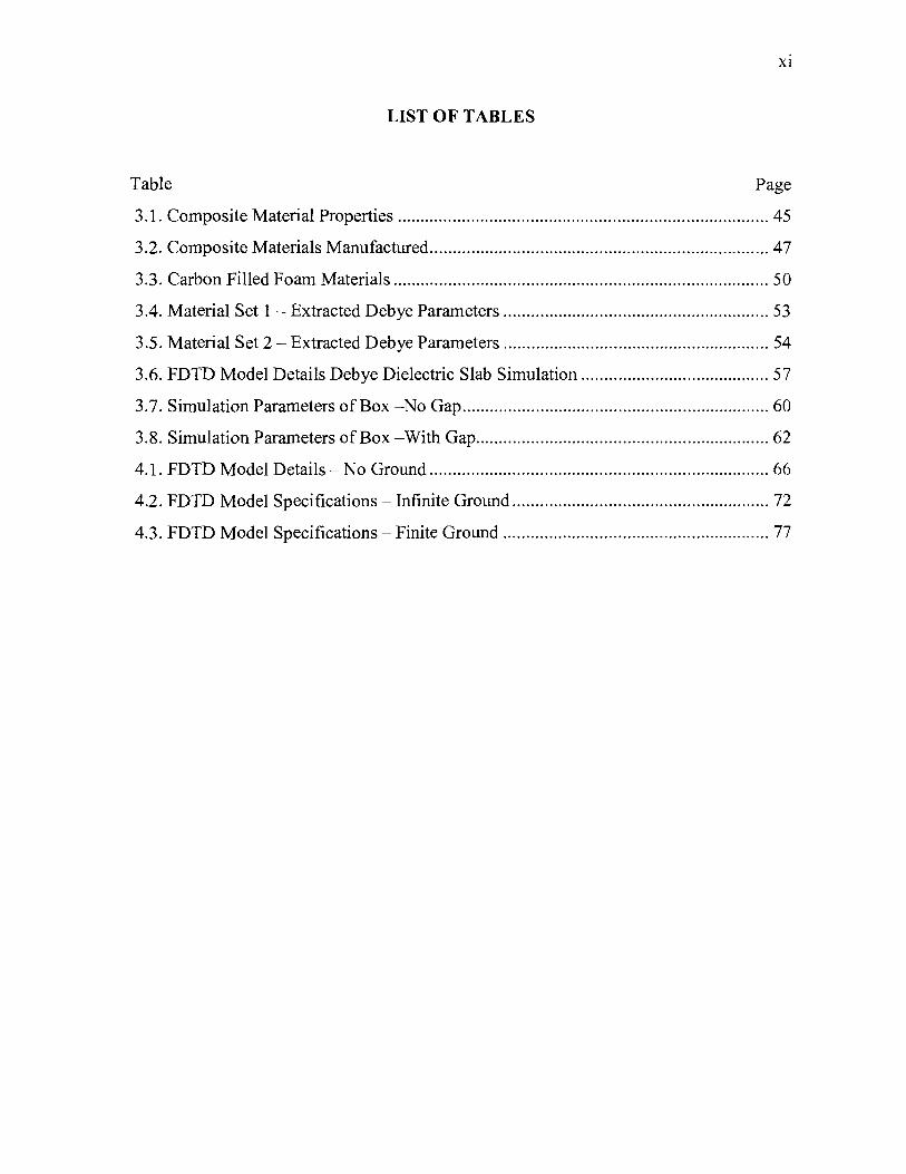
LIST OF TABLES
Table Page
3.1. Composite Material Properties ................................................................................. 45
3.2. Composite Materials Manufactured .......................................................................... 47
3.3. Carbon Filled Foam Materials .................................................................................. 50
3.4. Material Set 1- Extracted Debye Parameters .......................................................... 53
3.5. Material Set 2- Extracted Debye Parameters .......................................................... 54
3.6. FDTD Model Details Debye Dielectric Slab Simulation ......................................... 57
3.7. Simulation Parameters of Box -No Gap ................................................................... 60
3.8. Simulation Parameters of Box -With Gap ................................................................ 62
4.1. FDTD Model Details- No Ground .......................................................................... 66
4.2. FDTD Model Specifications -Infinite Ground ........................................................ 72
4.3. FDTD Model Specifications- Finite Ground .......................................................... 77

INTRODUCTION
1.1. CHARACTERIZATION OF NOISE ON PDN
Modem FPGA and microprocessors contain complex circuits which draw a
significant current during switching. The switching current creates a disturbance on the
power distribution network (PDN) on the PCB. DC components of the current are
relatively simple to predict and account for. However, AC current components have
frequency contents, which must be carefully analyzed in power distribution network
design of dies, packages, and printed circuit boards. Traditional techniques call for broad
band frequency compensation, which adds cost and complexity to designs. This research
presents a methodology to model the FPGA noise source and use the model to predict the
dynamic current draw ofFPGA devices in time and frequency domains [1]. With an
accurate prediction of the noise currents frequency components, the power distribution
network can be optimized for obtaining maximum benefit and minimum cost. Other
benefits include prediction of voltage fluctuations in the power network during switching
activity.
Stratix® II GX FPGAs are the third generation of Altera's FPGAs with embedded
transceivers. Stratix II GX devices provide a robust solution for the growing number of
applications and protocols requiring multi-gigabit serial 110.
Quartus® II design software[2] provides the most advanced suite of tools for
system-level design, embedded software programming, FPGA and CPLD design,
synthesis, place-and-route, verification, and device programming. Quartus II software
supports all of Altera's latest device families.
1.1.1. Altera Stratix II GX. The Stratix II GX is the Altera's third generation
FPGA for combining high speed serial transceivers with high performance logic arrays
[2]. Stratix II GX includes 4 to 20 high speed transceiver channels, each incorporating a
clock/data recovery unit and embedded SERDES capability up to 6.375 Gbps. The
transceivers are grouped into 4-channel transceiver blocks.
The main features of Altera Stratix II GX are listed below:
• TriMatrix™ memory blocks with dual-ports and FIFO buffers implemented with
performance up to 550 MHz.
1

• 16 global clock trees and 32 regional clock trees.
• High speed DSP blocks with dedicated multipliers (upto 450 MHz), multi-
accumulators, and FIR filters.
• Support ofnumerous single-ended and differential I/0 standards.
• High-speed, source-synchronous differential I/0 up to 71 channels.
• The FPGA used in the experiments has 15 I/0 banks with 1152 FBGA
encapsulation.
• The FPGA supports SSTL, L VTTL, and other I/0 standards. Its core power level
is 1.2V.
2
1.1.2. Quartos. Quartus is Altera's integrated VHDL design system. It supports
VHDL, Verilog HDL, AHDL, and schematic design. Quartus also provides its own built
in Intellectual Property (IP) library with many built functionalities. The Quartus interface
is shown in Figure 1.1.
•'Bi§'*M 1M!414QM@!IIM iiMHilfi@i tli filo tdt ~ l!lo;oct /10- ""' ...... 1""'- to~>
II D ~ !;! 1• 1 j, ~ e "' c. IW llm,,u... ::J i )( I' <1 . • G:i I • ") •• I ~ • t• l ~ ::_ • • Tine .:J.!!l -~·~~::::::=::::::::::::;:::;.:::::::::;.;:,.:.:;..,.,.,_~.,.!..::.,......::..=~~~~~...-!...-.~~~~~~~-:-
A ••
· ·~
L~~ ~~M- .i.I.!J ""' ---------------- -- -
I"Gr/iltl,preHI"I 31SS, XH
Figure 1.1. Quartus Interface
2
3
Special patterns are developed in Quartus to analyze the current drawn in a known
way. For example, aT-Flip Flop (TFF) will switch once every two clock cycles and
hence has halfthe frequency as a clock. Thousands ofTFF's can be made to switch
together to draw a huge amount of current at a single time. Such patterns have predictive
behavior and are implemented at the initial stages to help predict the current drawn.
Measurements and simulations are then performed using these patterns and then
compared to each other.
1.2. ELECTROMAGNETIC SHEILDING
In today's world there is a need to reduce unwanted electromagnetic radiation, emitted by
electronic devices, and also there is a need to protect sensitive circuits from the outside
electromagnetic radiation. Sometimes, electromagnetic radiation can be intentionally
generated to disrupt the electronic devices. Shielding material can be used to shield
sensitive equipment to reduce the emissions and improve the immunity of electronic
equipment. Usually a highly conductive material (metal) is used to form a shielding
enclosure. The effectiveness of such shielding enclosure is mainly determined by the
presence of slots and aperture arrays for heat dissipation. Moreover, metal enclosures are
massive, large size, and difficult to move around and manipulate. Materials designed
from the conductive fibers and carbon-rich foam materials tend to absorb and reflect
electromagnetic waves, and, hence, can be used to design shielding enclosures. Shields
made of these kinds of materials tend to be lighter and easy to shape, move, and
manipulate. These materials can be stacked up together to provide better shielding.
Shielding is characterized by the parameter called Shielding Effectiveness (S.E). It can be
calculated as
(SEts =lOlog(P;ncidenr / . ) / ptransmztred
(1.1)
Composite materials, including carbon-filled ones, are measured for their
shielding effectiveness. The Debye dielectric parameters are obtained by approximating
frequency dependencies of S-parameters taken from measurements. The De bye
parameters are then used to simulate complex structures using 3-D simulation tools to
evaluate shielding effectiveness [7].
3

4
1.3. MODELING AND VALIDATION
Full-wave modeling is an important method to solve complex electromagnetic
models. There are many commercially available tools out in the market, and each is
designed to solve a specific set of problems. Common methods that are employed in
commercial tools to solve the Maxwell equations are Finite Difference Time Domain
method (FDTD), Finite Element Method (FEM), Integral Equation Solution or Method of
Moments (MOM). Each method has its own advantages and disadvantages. A method to
be employed should be chosen depending on a type o fa problem to be solved and
accuracy required. However, solution offered by new 3-D simulation software cannot be
considered correct, until it is validated by different method. Validating the solution can
be done either by using the other software with a different solution method, or by making
real measurements, or by analytically solving the problem. Measurements of an adequate
prototype are not always possible, and analytically solving a problem can be too
complicated. Thus, using two different software solutions to the same problem is a good
validation approach. An antenna over different ground planes is studied herein, using the
EZ-FDTD tool and the WireMoM. These two types of software use different numerical
methods- Finite Difference Time Domain (FDTD) technique and Method of Moments
(MoM).
4

2. CHARACTERIZATION OF NOISE ON PDN
Special patterns are developed in Quartus to understand and estimate the current
drawn from the PDN in a known way.
2.1. PATTERN
5
In this experiment, the FPGA logic (pattern) is called the single frequency parallel
toggling flip-flop (TFF) pattern with one single clock input and one testing output pin
terminated using LVTTL standard [2].
To implement different percentages of the FPGA utilization using this pattern,
simply connect the enabled bits from different blocks to the GND or vee, as shown in
Figure 2.1. Parallel TFF Pattern the top 2 blocks are connected to the vee and the res
are connected to the ground, thus implementing a 1 0% parallel TFF pattern.
The clock input pin (PIN_U31) directly drives six parallel TFF modules, each of
which includes around 2.7K TFFs or about 5% ofthe total FPGA logic utilization as
shown in Figure 2.2. A total of30% ofthe FPGA utilization can be implemented using
this pattern.
The advantage of using all6 blocks for percentages between 0% and 30% is to
maintain certain amounts of routing and clock tree structures so that it will be easy to
quantize the resulting core noise.
Figure 2.1. Parallel TFF Pattern
5

All TFFs are then connected with the OR gate to the output pin (A19) to use the
oscilloscope to check if the signal is correctly passed through the FPGA. The output pin
will create a certain amount of I/0 noise despite the core noise created by the parallel
toggling logic inside the chip. The I/0 noise is a constant compared to the core noise.
CNG_FF _5
f-- tff _elk tff_output f--
- enable
inst7
Figure 2.2. Parallel TFF Block Containing 5% of Logic
It is not possible to eliminate the output pin because the Quartus will then
optimize and remove any logic that does not have a direct output associated with it.
2.2. CORE NOISE TEST VEHICLE
In order to characterize and correctly depict the noise from the FPGA core it is
important to have a good test vehicle. A special board shown in Figure 2.3 was designed
and manufactured to achieve the following goals:
• Isolate core power plane from rest of the power planes.
• A void any loss of resonances associated FPGA placement.
• Provide good measurements points to measure noise directly on the power plane.
• Provide enough decoupling capacitor pads.
• Provide enough signal measurement pins from all banks of the FPGA.
In order to achieve the goals listed above, several steps were taken during the
board design stages. Stack up as shown in Figure 2.4 was chosen carefully to provide
enough isolation and backdrilling was used to ensure that there was no coupling from the
via. Capacitor pads for V cc were all placed at the top layer. Capacitor pads were mainly
concentrated around FPGA. FPGA was placed asymmetrically to avoid missing any
6 6
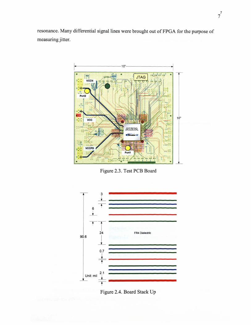
resonance. Many differential signal lines were brought out ofFPGA for the purpose of
measuring jitter.
Figure 2.3. Test PCB Board
3 _L
6 T
_L
TT 24 FR4 Dielectric
90.6 j_ 0.7
j_ T
2.1 Unit: mil _j_ T--------
Figure 2.4. Board Stack Up
7 7

8
The first phase during the development of the test vehicle is to choose the stack
up of the board. The Altera Stratix II-GX FPGA required three power levels vee, vee
VO, and VDD- pre driver for VO. Research interest is in the core power layer vee. The
main concern during stack up design was to make sure that any noise observed in the
vee layer is due to switching activity in the vee layer only, not to coupling between
vee-VO or vee-PD. In order to achieve this isolation, the vee layer was placed at the
top of the stack and rest of the power layers were placed below as shown in Figure 2.5.
SIG1
-:-:.:-:.;.;.;.;.;.;.·.·.
GND lllllllllllllllllllllllllllllllllllllllllllllllllllllllllllllllllllllllllllllllllllllllllllllllllllllllllllllllllllllllllllllllllllllll ·.·.·.·.·.·.·.·.·.·. ·.·.· . .·. :-:-:-: .·-:·:-:-: -:-: -:-: PWR1 • VCC- Core power
GND lllllllllllllllllllllllllllllllllllllllllllllllllllllllllllllllllllllllllllllllllllllllllllllllllllllllllllllllllllllllllllllllllllllll
SIG2
GND
GND
IIIIIIIIIIIIIUIII!!H!HUIIUIIIIIIIIIIIIIIIIIIIIIIIIIIIIIIIIIIIIIIIIIIIIIIIIIIIIIIIIIIIIIIIIIIIIIIIIIIU!IUIH!IIIIIIIIIIIIIIIIIIII PWR3 - VCCN - 10 power GND ..... · .. :- . :- · .-:·. · · · ::- · : · -:: . . · .. ·.· . .. . .
IIIIIIIIIIIIIIIIIIIIIIIIIIIIIIIIIIIIII!HIIII!HIIIIIIIIIIIIIIIIIIIIIIIII!HIIIIIIIIIIIIIIIIIIIIIIIIIIIIIIIIIIIIII!HIIIIIIIIIIIIIIIIII ·.·.·.· .· . ·.·.
SIG3
GND
Stack up is chosen carefully to minimize the coupling between the three power layers
!HIIIIIIIIIIIIIIII!H!HIIIIIIIIIIIIIIIIIIIIIIIIIIIIIIIIIIIIIIIIIIIIIIIIIIIIIIIIIIIIIIIIIIHIIIIIIIIIIIIIIIIIIIIIIII!HIIIIIIIIIIIIIII PWR2 - VCC PO - Pre-driver power GND
.;.;-:-:-:- ·.·.·.· . . . ;.;. .. . ::::-: ·. ·. ·.· . SIG4
Figure 2.5. Stack Up
In order to present coupling between the power planes due to via-coupling, all the
vias were back drilled as shown in Figure 2.6. Back drilling was performed on following
pms:
• All SMA connectors connected to power planes and signal traces.
• All capacitor pads.
• From the bottom of the board for vee layer and from top of the board for other
two layers.
The pins from FPGA were not back drilled in order to provide signal probing
underneath the FPGA. Also, all ground was stitched together.
8

Back Drilling was used in order to minimize the coupling between power planes due to vias.
Back drilling was used to drill out the capacitor and power vias
LAYUl c
I ,AYI[R)
, l AY(R.
lAYtRr
, LAY .. R I
LAYlAn
, lAYDI: t2
. lAY[_A t~
Back drilling from the top to remove the vias for capacitors
:<--- -==-that are placed on the bottom layer
Figure 2.6. Backdrilling of Vias
9
Another important consideration during board design was the FPGA placement as
shown in Figure 2.7. FPGA is the noise source that has to be characterized. If the noise
source is exactly at the center, then the noise produced at some of the resonant modes
will not be picked up by the observation points. This will be demonstrated with an
example using simulations.
Board
~Asymmetric Placement
Figure 2. 7. FPGA Placement
9

10
The importance ofFPGA placement is shown by an example using simulations as
shown in Figure 2.8. Three ports were placed on a board. Port 1, assumed to be the
location of the FPGA, was placed at the center in one simulation and asymmetrically in
another. [Z12[ was compared between two simulations. The simulation clearly shows that
when the Port 1 is at the center not all the resonances can be observed at port 2 and 3. So,
any noise produced at these frequencies cannot be observed at any observation point and,
hence, cannot be characterized correctly. These are only simulations, to prove the point
that placing an FPGA at the center will result in improper observation of noise at the
measurement points.
~--;r-- Port 1 -exactly at the center
Board hrt2 • Port 1 - placed asymmetrically
-70 '---~-'--'-~'-"-::-~~~ ........... -,----~~~ 10"3 10-l 10.1 10°
Frequtncy (GHz)
Figure 2.8. Importance ofFPGA Placement
In order to directly measure noise on the power plane, the SMA connector is
attached directly to the power layer. Two such SMAs are attached to one power layer
with a total of6 SMA for three power layers as shown in Figure 2.9. The purpose of this
SMA is to measure noise voltage on the power plane. Placing one SMA closer to the
FPGA and the other far from FPGA provides two different measurement points for noise
observation. Ideally, a measurement point would have been placed directly underneath
10

11
the FPGA, but due to routing issues the SMA must be placed at least1.5 inches away
from the FPGA. To avoid the stub effect, the probing point was also placed at least 1 inch
away from the FPGA instead of directly underneath it.
/ SMA connected to VCCPD- pre-driver power
SMA connected to /vee- core power
· · SMA connected to VCCN - 10 power
1 inch
Actual Board
Figure 2.9. SMA Connectors on Board
Placement of capacitor pads was also carefully considered during the broad
design [3]. All the capacitors for the VCC power plane were placed on the top side of the
board and all the capacitors for the VCCN and the VCC PD were placed on the bottom
side of the board as shown in Figure 2.10. This ensured minimal inductance associated
with capacitor vias especially for vee power plane and also eliminates coupling between
11
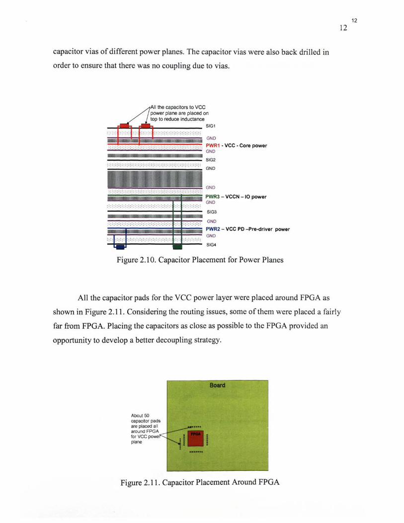
capacitor vias of different power planes. The capacitor vias were also back drilled in
order to ensure that there was no coupling due to vias.
All the capacitors to vee power plane are placed on top to reduce inductance
SIG1
.. ·.·.·.· ..
111111111111111111111111111111111111111111111111111111111111111111111111111111111111111111111111111111111111111111111 SIG2
·-:-::: .. .. · . . . . . . . . . . . . . . . . . . . . . . . . . . . . . . ' . . : . . . . . GND
GND
1111111111111111111111111111111111111111111111111111 111111111111111111111111111 1111111111111111111111 PWR3 - veeN - 10 power GND
SIG3 1111111111111111111111111111111111111111111111111111111111111111111111111111111111111111111111111111111111111111
.-.·:·>:. ·.·-:-:-:···· . . GND
111111111111111111111 1111111111111111111111111111111111111111111111111111111 1111111 1111111111111111111111111 PWR2 - vee PD -Pre-driver power
: :: :j: :: :::. · .· .· .·. ·.· :-:-· . . ·.· ... :-:-:-:-:-: - GND
SIG4
Figure 2.1 0. Capacitor Placement for Power Planes
12
All the capacitor pads for the VCC power layer were placed around FPGA as
shown in Figure 2.11. Considering the routing issues, some ofthem were placed a fairly
far from FPGA. Placing the capacitors as close as possible to the FPGA provided an
opportunity to develop a better decoupling strategy.
About 50 capacitor pads are placed all around FPGA forVCC powe plane
Figure 2.11. Capacitor Placement Around FPGA
12
13
2.3. IMPEDANCE MODELING
One of the main requirements for the project's success is correct modeling of the
broad's impedance profile. The self impedance and transfer impedance between any ports
on the board should be estimated accurately both with and without capacitors. A Maxwell
equation solver tool- EZ-Power Plane [6] developed by UMR was used for estimation.
Also, commercially available HSPieE was used to include the effects of package and
port inductances.
Simulations using these tools were then compared to measurements in order to
verify modeling accuracy. Simulations were also used during the design of the board to
roughly estimate the number of capacitor pads required for the vee power plane as
shown in Figure 2.12.
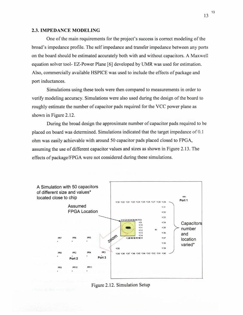
During the broad design the approximate number of capacitor pads required to be
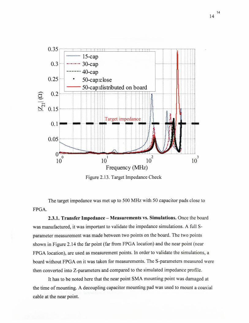
placed on board was determined. Simulations indicated that the target impedance of 0.1
ohm was easily achievable with around 50 capacitor pads placed closed to FPGA,
assuming the use of different capacitor values and sizes as shown in Figure 2.13. The
effects of package/FPGA were not considered during these simulations.
A Simulation with 50 capacitors of different size and values* located close to chip
Pft7
Assumed FPGA Location
PRS
Pft2 Pft4 Pft3
Port 3 .
Port2
Pft10 PR1 1
yr---------------------------------~
•CJO -<:22 -<:21 -<:23 -<:24 -<:25 •C26 '07 -<:28 -<:29
-<:31
"(;33
< 10 <11 <35 -<:12 R1
'CJ6
-<:37
'(:38
-cso OC39
--' OC49 oe<a OC47 OC46 -<:45 OC44 -<:43 'C42 -<:41 -<:40
•PR1
Port 1
Capacitor number and location varied*
Figure 2.12. Simulation Setup
13
FPGA.
0.3
0.25
0.1
··········· 15-cap -·-·-·- 30-cap ------ 40-cap
• 50-cap:close 50-cap:distnbuted on board
Figure 2.13. Target Impedance Check
__ ,_ __ ,_ __ _._ ..
-'---'-- _.J_J
- 2-+ -~-~ 41\ I I I
3 10
The target impedance was met up to 500 MHz with 50 capacitor pads close to
14
2.3.1. Transfer Impedance- Measurements vs. Simulations. Once the board
was manufactured, it was important to validate the impedance simulations. A full S
parameter measurement was made between two points on the board. The two points
shown in Figure 2.14 the far point (far from FPGA location) and the near point (near
FPGA location), are used as measurement points. In order to validate the simulations, a
board without FPGA on it was taken for measurements. The S-parameters measured were
then converted into Z-parameters and compared to the simulated impedance profile.
It has to be noted here that the near point SMA mounting point was damaged at
the time of mounting. A decoupling capacitor mounting pad was used to mount a coaxial
cable at the near point.
14

15
Far point
Figure 2.14. Port Locations and Port Names
The simulations matched the measurements taken on the board between the ports
near point and far points on the board as shown in Figure 2.15, please note here that the
board does not have FPGA on it and it is completely bare without any capacitors. The
board was not powered up and did not have any type of DC connection.
IZ21 1 Bareboard without FPGA
20 ~:-::~rr:-:-::.~ .. ~ .. ~ .. --:,=c=~~==~
0
-20
-40
-60
I I I I I I I I I I I I I II I I I I I I I I I I I I I I I I I I I I I I I I I I I I I I I I I I I I I I I I 0 I I I I I I I I I I I I 0 I I I I I I I I I I
--,----, -c-c--------:----i--i--t-t-ti·:-~----
' '
I I I I I II I _ _. ____ ,. __ _. __ - -'- "' -'-'--------·----' I I I I II I j I I I I I I
I I I II
I Ill I I II
I I II I I II
1 I I I I I I I I I I I I I
I I II I I I 1 I I I II I I I I I I I I I I
-;---- ~ -- -:-- - -i ~ -:-:--------:---- ~-- ~-- ~- ~ -:- ~ -:-:------- -:-- -- ~--I I I I I II I I I I I I I I I I I 1 1 I I I II I I I I I I I I I I I I I I I I II I I I I I I I I I I I I I I I I II I I I I I I I I I I I I 1 1 I I I II I I I I I I I I I I I I I I I I I II I I I I I I I I I I I I I I I I I II I I I I I I I I I I I I I I I I I I I I I I I I I I I I I I I I I I I I II I I I I I I I I I I I I I I I I I I I I I I I I I I I I I I I I I I I I II I I I I I I I II 0 I I
--- ---:----+---:- - - -H-:-:--------:----1--~--+-r-H-:-:--------:----~---:-' ' ' '' '' ' ' ' ' ' '' '' ' ' ' t 0 0 0 01 I I I I 0 0 I 0 I I I t
: ' ! '1: ; : ! ! .. !i! " -8oL-~~~~~--~~~~~--~~~~~9~~
6 7 8 10 10 10 10
Frequency [Hz]
Figure 2.15. Transfer Impedance Between Far Point (Port 1) and Near Point (Port 2)
15

16
Figure 2.16 illustrates the board sirnulation points with FPGA on it.
Figure 2.16. Port Location and Port Name for FPGA
Once the FPGA was placed on the board, the sarne measurements as above were
repeated and compared to simulations. Simulations in this case still did not consider the
effects of FPGA on the board as shown in Figure 2.17. The board again did not contain
any capacitors, was not powered up and did not have any type of DC connection.
-60 L6~;......· ._;_· ~___;_;_;_;.t.J 0-7 ...___;__;__-'---.:_~1-'--08 _ _;__' _ . .__.,__~~9____;.____, 10 ]0
Frequnecy [liz]
Figure 2.17. Sirnvlation Without Considerio~ Effect ofFPGA vs. Measurements
16

Figure 2.17 illustrate that the FPGA is contributing a great deal of, more like a big
capacitor. Simulations, on the other hand, are just two ports between two power planes
and did not take anything else into account. So, the simulations which did not take this
effect into account did not match the measurements.
17
2.3.2. Modeling FPGA as a Capacitor- Low Frequency Model. Taking into
account the effects of FPGA requires accurately modeling. If FPGA is thought of as one
big capacitor sitting on the top of the board, then it can be modeled as a simple capacitor
with some capacitance and series inductance. In order to obtain the capacitance of FPGA,
two transfer or self impedance measurements were made, one on the board with out
FPGA and one on the board with FPGA. By calculating the difference in capacitive slope
at low frequencies, the value of capacitance contributed by FPGA alone was obtained.
The series inductance can be obtained by carefully studying the resonant peaks from the
measurements. The calculated values for capacitance ofFPGA and inductance ofFPGA
from these measurements for a powered down board were 238.3nF and 10pH,
respectively.
Remember that these values are for the powered down board. Powering up the
board changes the capacitance contributed by FPGA. The calculated values for
capacitance of FPGA and inductance of FPGA from these measurements for powered up
board were 440nF and 10pH respectively. Low frequency model ofFPGA as a capacitor
is shown in Figure 2.18. Low Frequency FPGA Model is only valid for low frequency.
GND
PWR
Port2 Port1
CFPGA = 238.3nF
Figure 2.18. Low Frequency FPGA Model
17

18
With the capacitance and inductance values extracted from calculations, it is
possible to model the FPGA as a capacitor in the simulations. A capacitor was placed
between power and ground planes with values extracted and simulation is done using EZ
powerplane. It can be seen from the above Figure 2.19 that the simulation, in which
considering the FPGA is modeled as a capacitor, matches up with the measurements.
O r-:-::::n::~::::--:::::m:--:r~~rrrr==~
I I< I I I
I I < I I I I 10 I I I I <I I II I I I < I I I - ------ -----;--TTr-r-rTr---------,---TTTrrr I I I I I I I I I I I I I I
I I I I I I I I I I I I I 0 1 I I I I I I I I I I I I I
I I I I I I I I I I I I I I I 1 I I I I I I I I I I I I I I 1 I I I I I I I I I I I I I I I I I I I I I I I I I I I I I I I I I I I I I I I I I I I I I< I I I I I I I I I I 20 I I I I I I 01 I I I I I I I I - ----- --~----T-n- : : -:Tr --------r--TTTT~ : F--• I I < I I I I I I I I I I I I I I I I I I I I I I I I I I I I I I I I I I I I I I I I I I I I I I I I I I I I I I I I I I I I 1 I I I I I I I I I I I I I I I I I I I I I I I I I I I I I I I I I II I 0 I I I I I I I 0 I I I I I I I I I I I I I I I I I I I I I I I I I I I I I I
1 I I I I I I I I I I I I I I I I I --------.-----·--- .. -- ... -- .. -....... ,_,. _____ --.------.----.-- ... -.. -.. ... -·--------- -----.---1 I I I I I I I I I I I I I I I I I I I I 1 I I I I I I I I I I I I I I I I I I I I I I I I I I I I I I I I l I I I I I I I I I I I I I I I I I I I I I I I I II I I I I I 1 1 1 1 1 o I 1 I I I I I I I I I I I I I I I I I I I I I I I I I I I I I I I I I 1 1 I I I I I I I I I I I I I I I I I I I I I I I I I I I I I I I I I I I I I I I I I I I I
-------1-----!---~--L- ~ -~-~-:- ~ ---------~--- -~ ~--~-~-~~-~--------- _____ :_ __ - -~-L~~---------~--- -·
' l i i iii li ' ' ; i i l iii ' ' i : : I I I I I I I I I I I I I I I I I I I I I 1 I 1 I o -50 ----- --~-- ---:---:-- ~--~ - ~ - ~ -:-~-- ---- ---~----~- ~ --~--~-~-:~- :--------- ---- -~-- ~- :-- -~-~-~ ~--- ------ ~----1 1 1 I I 1 I I I I I I I I I I I I I I I I I I I I I I j I I I I I I I I I I I
-60 6
10
1 1 1 1 1 I 1 I I I I I I I I I o I 1 1 1 I 1 I I I I I I I I I I I I I 1 1 1 I I II I I I I I I I I I I I 1 I I I I I I I I I I I I I I I I 1 1 1 1 1 II I I I I I I I I I I 1 I I I I I I I I I I I I I I I I 1 1 I I I I I I I I I I I I I I I 1 I I I I I I I I I I I I I I I I 1 1 1 1 1 I I I I I I I I I I I I I I I I I I I I I I I I I I
7 8
10 10 10 Frequency (Hz)
9
Figure 2.19. Simulation vs Measurements of Transfer Impedance
The measurements and simulations are between the near point and far point. The
board here again does not contain any capacitors. The board is powered down and does
not have any type of DC connection to it. The simulated model is also with board
powered down. The capacitance of FPGA is 238.3 nF with a series inductance of 10 pH.
Figure 2.20 show that the simulation, in which considering the FPGA is modeled as a
capacitor, matched the measurements.
18
19
O r--:::::~~~~~.~.~ .. ~--~~~~--~ I I I I I I I I
I I I I
-------~----- ---H-- --+ --------+--+-~---f-i--i-: : : I : : i : : : : : : : : : I I I I I I I I I
: : ' : : : : :::: -20
I I I I I I I I I I I
--1---1--- - -:- ---------~-- - --:----:---1---f- -1-H--: : : : : : : :::
I I I I I I I I I I I I I I I I I 1 I I I I I I I I I I I I I I I I I I I I I I I I I I I I I I I I
------+---1--+H- -~ : . ---------[---++ ; +-H-H---------~-----i--- -c-• I I I I I II I I 1 I I I 1 I I I I I I II I I I I I I
I I I I I II I I I I 11 I I I I I II I 1 I 1 I 1 I I I I I II I I I I I 1
••••••• '• • ••I• ••1•1• •I• •Ill•••• ••·· ·, -· ·1••1•1•·111••• ••• ••:•• •• 1 •••[··~· '•1•1 'I••• • • •• • •: • •• I I I I I I II I I I I I I I I I
-60 ------+---:--+H- -~-~:--------+ -+- - +--~-H~-:+-- - ----- --Measured I I I I I I I I I I I I I I I I I
I I I I I I I 0 I I I I I I I I I I I I I I I I I I I I
: : ' ::: : : : :::: · · ! ! : : ! ! ! j ! : Simulated
-70 L6--~~~LU~7--~~~LU~8--~==riiLrrc9==~~
10 10 10 10 Frequency (Hz)
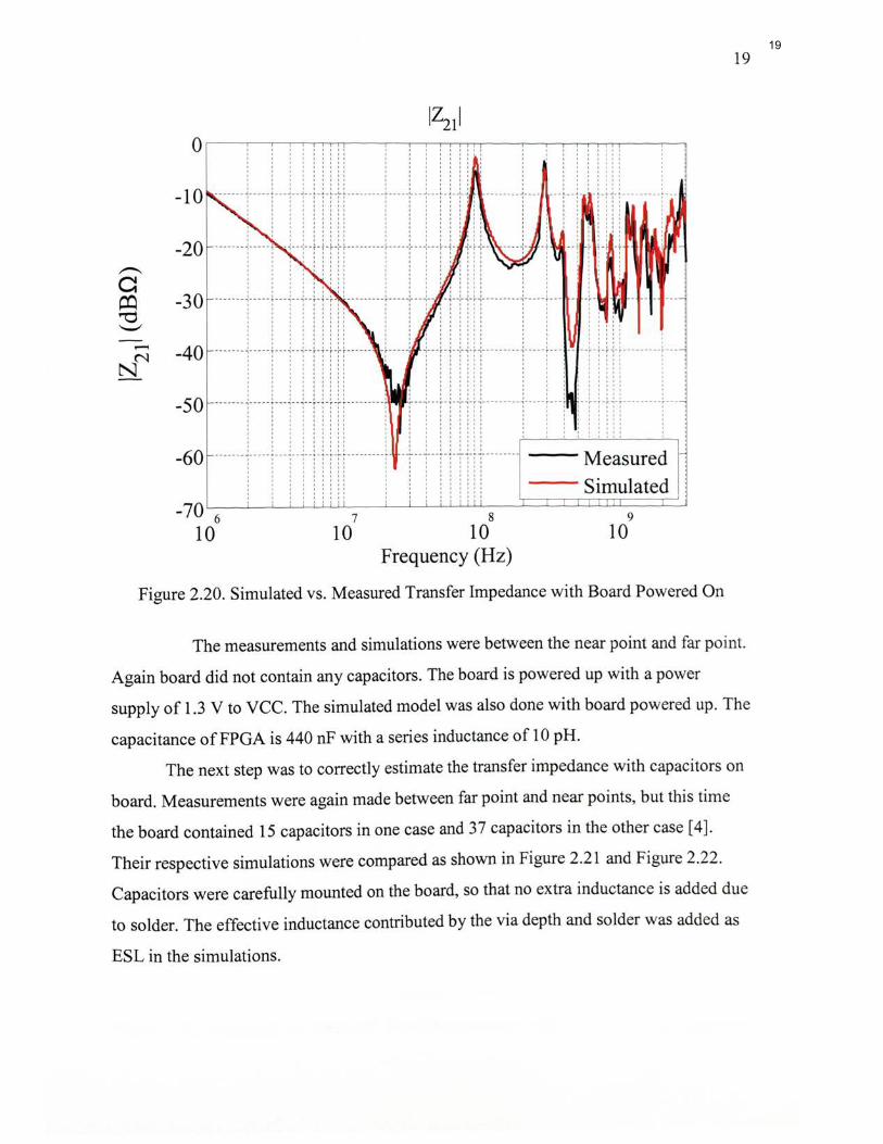
Figure 2.20. Simulated vs. Measured Transfer Impedance with Board Powered On
The measurements and simulations were between the near point and far point.
Again board did not contain any capacitors. The board is powered up with a power
supply of 1.3 V to VCC. The simulated model was also done with board powered up. The
capacitance of FPGA is 440 nF with a series inductance of 10 pH.
The next step was to correctly estimate the transfer impedance with capacitors on
board. Measurements were again made between far point and near points, but this time
the board contained 15 capacitors in one case and 3 7 capacitors in the other case [ 4] .
Their respective simulations were compared as shown in Figure 2.21 and Figure 2.22.
Capacitors were carefully mounted on the board, so that no extra inductance is added due
to solder. The effective inductance contributed by the via depth and solder was added as
ESL in the simulations.
19

-10
-20 ,-..., a ~ ::3--30
...... NN
-40
[Z21 [ with 15 capacitors
--Measured
-- Simulated I I I I I I II I I I I I I II I I I I I I I I I I I I I I 01 I I I I I I II I I I I I I 01 I I I I I I 01 I I I I I I II I I I I I I II I I I I I I II I I I I I I II
-,-,-,-~-.--- ----;---
' I I I I I -.,-.,-,-.,-,--------T---1 I 0 I I I
I I I I I I I I I I I I I I
-60 ~~~~~~--~~~~~--~i-~~il_--~
6 7 8 9 10 10 10 10
Frequency (Hz)
20
Figure 2.21. Simulated vs. Measured Transfer Impedance with 15 Decoupling Capacitors
[Z21 [ with 37 capacitors o~~~----------~~--~~~~--~
--Measured
-- Simulated I I I I I II I I I I I II I I I I I II I I I I I II I I I I I II I I I I I II I I I I I II
-5
-70L_~~~~L_~~~~~~~~~~~~
6 7 8 9 10 10 10 10
Frequency (Hz)
Figure 2.22. Simulated vs. Measured Transfer Impedance with 37 Decoupling Capacitors
20

21
The difference in low frequency capacitive slope and a slight shift in resonances
could be a result of actual capacitor value on board and capacitor value taken for
simulation. There may be a slight difference between each capacitor value specified in
the data sheet and the actual value on board.
2.3.3. Modeling Transfer Impedance from Core to Measurement Points. In
order to estimate the noise produced by switching current in the core and then make a
comparison at a known measurement point, it is important to estimate transfer impedance
from the switching core to the measurement point. Both EZPP and HSPICE were used to
simulate the model. First, the board alone with out any capacitors was simulated with
EZPP and with three ports. EZPP produces a HSPICE model for the complete board,
which is then imported into HSPICE. For the port at core point the inductance,
capacitance and resistance are added as shown in the Figure 2.23. Then the complete
HSPICE model is simulated to get fullS-Parameters between all three ports. Then the S
Parameters are converted into Z-Parameters to get the transfer and self impedances ofthe
model as shown in Figure 2.24.
PCB PDN
PCB via
Ball
Package & Die
PTH Pkg C4 Plane
FPGA
Figure 2.23. Spice Model of Package and PCB
Figure 2.24 show the transfer from the die side of the core to the far point and
input impedance observed at far point.
21

' ' '
20 -------- -----" I I I I 1 o -- 12111 ---~--- - -~---~--i+i- i-- --------~ -----: --,--~--~- -~-H----------~---
0
c co ~ -20 Q) "0
~ Ci -40 E <(
-60
-80
::1 i,i j : i i ' : : : : ::: ' I I I I I I I
---:--·j--~--:-~-~-:~----------"·--- i -rr:·t -!r--------~- ----r··-f--r-·r- -r-r1·---------~--- ~ : : : : : :: : : : : ::: : : : : : :: : : : : ::: I I I I I I I I I I I I 1 1
·:·1·1·!~·· .................... !.·>··· ·! ...................... : ................ r··· ' ' ' ' ' ' ' ' "' ' ~
.. ······> .... ·> ... < .. <·i·<i. <1· ....... ·> .... ·> .. ·>. ·:··:•1•1•1 ! ..••••••• r· ..• ~ •• l. •I• •l• •! I1•• .• ·····r··· J I I I I I I I I I I I I I I I I I I I I I I I I 11 1 I I I I I I I I I I I I I I I I I I I I I
------ r- --- -r---~---:--+--:-1-+-:--- -------r-----r-- -r-- -:--r -.; -+ -r-:- ---------:------:-- --r : : : : : :::: : : : : : :::: : : I
... i !!iii . ; ; !!iT : 108
frequency [Hz]
Figure 2.24. Transfer and Self Impedance from Die (Port 2) to Far Point (Port 1)
22
There is no practical way to validate these results, but they are assumed to be
correct based on the validation done between far and near point as previously explained.
The transfer impedance thus obtained from the SPICE model was used to estimate the
noise voltage at any given measurement port. In this case, it is either at the far point or at
the near point.
Another important parameter in estimating the noise power at the measurement
point is to estimate the input impedance looking into the board at the measurement point.
The EZPP model does not take the inductance associated with ports into account as seen
in Figure 2.25. Input impedance of the near point can not be simulated accurately because
of a poor SMA connection which causes extra capacitance and inductance.
22

5 0
4 0
3 0
2 0
0 I"-c: 0
1--.
!§ -10
-20
-30
-40
-50 J
10
IZul-far }Xlint- mounted sma
~ ~
I
10
.M
~I
1'\ \
101
Frequency [Hz]
11 - Measured l n - simulated
v
1\/
• 10
1/
1/
17
IN\'
• 10
Figure 2.25. Simulated vs. Measured Input Impedance at Far Point
23
Once again HSPICE is used to include the port inductance and to obtain the input
impedance of the measurement points. An inductance of 5nH was added at the far port
measurement point. In the Figure 2.26 comparison is made between the measured and
simulated self impedance.
IZ11 1 at far point
1 l 1 I I I i 11 I I I I 0 I Ill I I I I I I 111 1 1 1 I I I 111 I I I I I I Ill I I I I I I I l l 1 I I I I I I tl I I I I I I Ill I I I I I I I l l 1 1 1 I 1 I 111 I I I I I I Ill I I I I I I I II I
40 ------ ~ - -- t-- t- ~- ~- ~ t -:-:-------:--- -~ --:-- f -~ -:- ~ t t - ------:----:---:- -~ -:--:-:- ~ t------ ~--1 1 1 I 1 I 111 I I I I I I Ill I I I I I I I II I 1 1 1 I I I I I I I I I I I Jill I I I I I I Ill I I I I I I Ill I I I I I II II I I I I I I Ill 1 I 1 I I I Ill I I I I I II II I I I I I I Ill I
30 ----- - ~--- t --t- -:--:-H-:-:---- ---:----~--:--t-~-:-}t-:-------:----:---:--:--:--:-1.. I-- ---:--
1 1 1 I I I j II I I I I I I Ill I I I I I I I 1 I I I I I I II I I I I I I Ill I I I I I I I 1 I 1 I I j I 11 I I I I I I Ill I I I I I I I
20 ------~---t--t-~-1-H-j-;-------j----~--j- -t -~ -Htt ------+-- : -:- ; :-i-~~r------t--10 -- --- - ~---t--t--f-~-H+l-------l----~-+-1-~-~- ~ : ~ --- :·---!--+++-H-H------~--
~ ., : ··········1· •1•1 ! •l !~•••• • •t •• ·i •• t.i•i~!J'• •• • ••, • •t•' l [I' if • • ••••1••
-j-FHi-------~---t--H-H+----+--H--~-H-H-----+-. : : : : : :: : : : : : : ::: : --Measurment l--1-Trflir----T---;--;-l-fTfli ______ T --s imulation
1 1 I 111 I 1 I I I I Ill
-50 L____;____;__;__l_' .:....:· ·:__:_· .:.1' _ __;___· __;___' __;_' __;'__;_' _;_' ;_;_' 'L:-~·~·~· -"--'--....w.J--;;-~__j
106 107 108 109
Frequency [Hz]
Figure 2.26. Simulated vs. Measured Input Impedance at Far Point with Series Inductance
23

2.4. CURRENT SOURCE MODELING
Apart from impedance modeling, another most important parameter required to
estimate noise is to model the current drawn. Current drawn can be estimated using two
methods: TCO distribution method and PPP A analysis method which are described as
follows.
24
2.4.1. Modeling Using TCO Distribution. The core noise is due the internal
activity of the FPGA. To model the noise current, a triangular current source based on
one register's activity can be constructed as shown in Figure 2.27. The pulse width of the
triangular wave is determined by the speed of the transistor or how fast could the Flip
flop toggles. The other parameter, per unit pulse width, is determined by the correlation
between the transistors and power plane. This parameter is shared to measure.
Time [ns]
Figure 2.27. Current Source Model
c:: ::1
From the per unit noise current can derive the total current based on the
Quartus™ statistics. Quartus provides electrical path statistics (clock to output delay) in
its timing analysis functionality. As shown in Figure 2.28, the actual clock to output
delay is provided in the timing analysis report.
24

25
...
Figure 2.28. Clock to Output Delay Report Shown in Quartus Timing Analysis Report
The information is then extracted from the Quartus and processed by Matlab to
create an electrical length distribution. Despite the phase information, Figure 2.29 shows
the electrical length distribution had an approximate width of 10 ns using 30% of the
toggling flip-flops utilization or 16,300 TFFs. The distribution had a standard deviation
of 1.32 ns.
30% TFFs 500
450
400
350
300 ,., 'E 250 3 CT
200
150
100
50
8 11 16 17
Delay lime (ns]
Figure 2.29. TFF Switching Delays
25

26
Using the integral equation below, the total current by the overall utilization of the
FPGA could be derived,
hFF = F(t- !teo),
1 T
!total=- I fTFF .dt
T t=O '
(2.1)
(2.2)
where !teo is the time delay obtained from Quartus. F ( t - itco) gives the total
current associated with all the TFF switching at a particular instance of time. Integrating
over the time period sums up all the current.
Figure 2.30 shows the shape of the total current pulse.
' ' ' I I I I I I I I I I
0.06 -----:------:------:------ -- ----:-- - --: ------:------:-------:-------:------:---1 I I I I I I I I I I I I I I I I I I
' ' '
' '
~ 0.04 ----r··--j------1-- ---1-------~-----+ ---(·--1------r·--·-r·-----:---~ 0.03 -----f------1------' -- --- ~-------~------f--- -1-----+-----~-----+-----1---{/) I I I I I I I I I I ·o : : , : : : : : ~ i i ' ' ' ' ' ' i i
0.02 -----: ------r -r----:· ----T-----r·-----. -----r----r-----r------:---• I I I
0.01 ···+·····: ·····1·····+·····r····+····+·· ··i·······:·······r··-···j··· 0
2 3 4 5 6 7 10 11
Figure 2.30. Total Current Estimated (One Pulse)
For the pattern used in the experiment, the electrical paths were split into two
parts. One is the path from the input pin spell out a number of buffers to the clock input
of the TFF, the other part is from the TFF to the output pin. As shown in Figure 2.31, the
logic is a frequency splitter. The input path has a frequency of 2f and output path has a
freuency off
26

U3
Ut U2 ~~
~=-~PAD
Figure 2.31. FPGA Logic of a Single Electrical Path
by clock transition, with a frequency the same as the clock frequency. The other was
caused by the TFF toggling, the frequency is toggling frequency, half of the clock
frequency. When both of noise current path were considered, the current amplitude at 0
ns, 200 ns, 400 ns was higher than 100 ns, 300 ns, and on 500 ns.
27
To more accurately model the noise current, an the following equation to include
both electrical paths was developed :
1 T 1 2T
!total = - f fTFF .dt +- f fclock.dt
T t=O 2T t=O . (2.3)
!cLock and lrFF is the total current drawn by clock tree and TFF, respectively. A
sum of the total current is shown in Figure 2.32.
time-domain current wa-.efoon 0.07 r-r-...--,---...---.------r--r---...,
• --( ! I I I I o.oe ------r---------~---------r---------:----------:- -------·-; i : I I
' ' ' I I I I I
0.05 ---, ------,---------,-------T-------r------T -l I I I I
I I I I I
~ 0.04 ---~ ------:---------:---------:---------:---------: - I I I I I C: 1 I I I I I Q) 1 1 I I I I
8 003 ---! -------:---------(-------:---------!---------! -------t 0.02 --~ - ------~---------~---------~--------+--------+ - -----+
1 I I I I I 1 1 I I I I I I I I I
0.01 -----f---------r-- --- ----r--------+---------r-1 I I I
: : : : 0~0~~2~0 --~~--~00~--~00--~100~~~120
lime [ns]
Figure 2.32. Total Current Using Two Frequencies Model
27

Frequency patterns of the estimated current are shown in Figure 2.33. The
frequency between two harmonics is a half of the input frequency. Based on the
parameters chosen, the odd and even harmonics showed different amplitude.
0 ----- ------
-20 - -- -
~ ~ -40 - - 'E ~ il -60 - - -., "' ·c; <::
-80 - --
-100
-120
, -
i i 10 20
frequency-<lomain current wawform
'- ,'-- '- ,-
i i i i i i 30 40 50 60 70 80 90 100
Frequency [MHz]
Figure 2.33. Total Current Spectrum Using Two Frequencies Model
28
2.4.2. Modeling Using Power Play Power Analyzer Tool. Another way of
predicting the current consumption in the core is by using the PowerPlay Power Analyzer
Tool built by Quartus shown in Figure 2.34.
' l'tiWI"rl'l.tyl'owtt An. tl 'l/11 lt 1ul - -~
Deldt<We•atesfOt\.Npeclied Signll•--
Doleultogglo•••Uiedlc<..,..l/0...,. =112.-=-5 --lx
[
DeleuiiQ!Xje '"" Uled Ia ,.,.,.;,.;ng Ognalo
I> UsedeleulvoiJe: 11 2.5
r Usevectofteuostination
0001:15
Figure 2.34. PowerPlay Power Analyzer Tool
28

This tool basically estimates the power consumed by the FPGA for a particular
pattern and a particular clock signal simulated.
29
The Quartus II software includes the Power Play power analyzer feature [ 5]. This
feature improves the accuracy of power consumption estimations given by the early
power estimator spreadsheets by:
• accounting for device resource usage and place-and-route results;
• accounting for functional and timing simulation input/output stimuli;
• performing statistical analysis of expected design-node activity rates
when simulation vector inputs are not available;
• Producing detailed reports that can pinpoint which device structures, and even
which design hierarchy blocks, are dissipating the most thermal power;
Figure 2.35 shows the available PowerPlay power analyzer reports.
8 ~ PowerPiay Power Analyzer r ~m summary · ~- Operating Conditions Used
H ~- Thermal Power Dissipation by Block Type ~-Thermal Power Dissipation by Hierarchy
~ --~ Power Drawn from Voltage Supplies L ... ~- Confidence Metric Details
····~lm Signal Activities • ~!i Messages
Figure 2.35. PPPA Reporting Details
In order to use the PowerPlay tool as a current predicting tool, the pattern should
be first simulated with a frequency of interest using the Simulator tool in Quartus. A
successful simulation will produce a Value Change Dump file VCD file. A Value Change
Dump file is an ASCII file which contains header information, variable definitions, and
the value changes for specified variables, or all variables, of a given design. The value
changes for a variable are given in scalar or vector format, based on the nature of the
variable. The PowerPlay tool can be used to import this VCD file. The resulting power
29
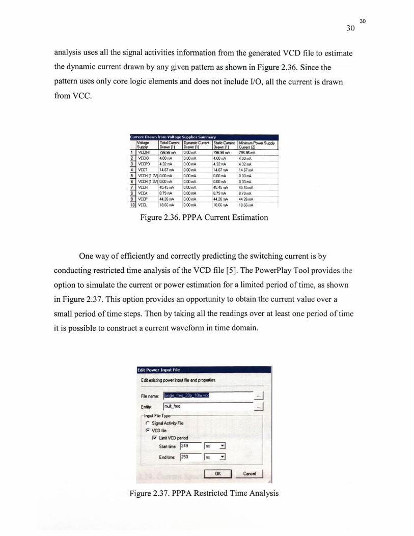
30
analysis uses all the signal activities information from the generated VCD file to estimate
the dynamic current drawn by any given pattern as shown in Figure 2.36. Since the
pattern uses only core logic elements and does not include 110, all the current is drawn
from vee.
. . . . .. .. .
~= Toto17nr;·nt Dynamic Current Static Current Minimum Power Supply Drown ) Drown[1) Or<!Wn[1) Current [2)
~ VCCINT 796.96 mA 0.00 mil 796.96~-~~mA --- I 2 VCCIO 4.00 mil 0.00 mil 4.00 mil 4.00 mil
3 VCCPD 4.32 mA 0.00 mil 4.32 mil 4.32 mA 4 VCCT 14.67 mA 0.00 mil 14.67 mil 14.67 mA 5 VCCH [1.2V) O.OOmA 0.00 mil OOOmA O.OOmA 6 VCCH [1.5V) O.OOmA 0.00 mil 0.00 mil 0.00 mil
7 VCCR 45.45 mA 0.00 mil 45.45 mA 45.45 mil - -8 VCCA 8.79mA 0.00 mil 8.79 mil 8.79 mil
9 VCCP 44.26mA 0.00 mil 44.26 mA 44.26 mil -· 10 VCCL 18.66 mA 0.00 mil 18.66 mA 18.66 mil
Figure 2.36. PPP A Current Estimation
One way of efficiently and correctly predicting the switching current is by
conducting restricted time analysis of the VCD file [5]. The PowerPlay Tool provides the
option to simulate the current or power estimation for a limited period of time, as shown
in Figure 2.37. This option provides an opportunity to obtain the current value over a
small period of time steps. Then by taking all the readings over at least one period oftime
it is possible to construct a current waveform in time domain.
Edrt Power Input Ftle
Edit existing power input fie and properties.
File name: lij&W••AWaiiiiiiiiiir-----_j Entity: lmult_freq _j
Input File Type------------,
r Siglal Activly Fie
c;" VCD file
P Linit VCD period
Start tine: r:-j24:':'9 -- ~ ns ::J End time: pso Ins ::J
OK Cancel I
Figure 2.37. PPPA Restricted Time Analysis
30

31
A unique current signature is obtained for any given pattern simulated. Hence,
this method can also be generalized to more complex patterns such as counters. A current
waveform obtained from restricted time analysis is shown in Figure 2.38 in time domain
and Figure 2.39 in frequency domain.
time-domain current wal/llforrn 4000 ..----.,--,--------,--,.-----.---,--,-----,
3500
3000
Ci) 2500
~ §. 2000 c ~ 8 1500
1000
' ' ' -- ---- -- ------ --.. ------------ ------.-------- ---------- ~- - -- -- ------ -----' ' '
' ' ... ____ -------------' ' ' '
' ' _ .. ____ ---------- - --' ' ' '
' ' ' ' -.----------- ------, ------ --r---- ------
-i---- ------
nme [ns]
Figure 2.38. Current Estimated Using PPPA
frequency-domain current wa'lllform 50 ~-~~~~~,--.--,-.~<IT~~~~~
0
·50
:t E -100 IIl s 1: jg :::> <.> ., "' .i5 c
Figure 2.39. Current Spectrum Estimated Using PPPA
31
32
2.5. MEASUREMENTS
In order to validate simulations, good and accurate measurements are very
important. One part of the measurement consists of measuring full two port S-parameters
using a network analyzer at any given two ports on the board. Another part consists of
spectrum measurements using a spectrum analyzer at any given observation point. These
measurements, an actual test board, three power supplies, a signal generator, a computer,
a network analyzer and a spectrum analyzer are needed.
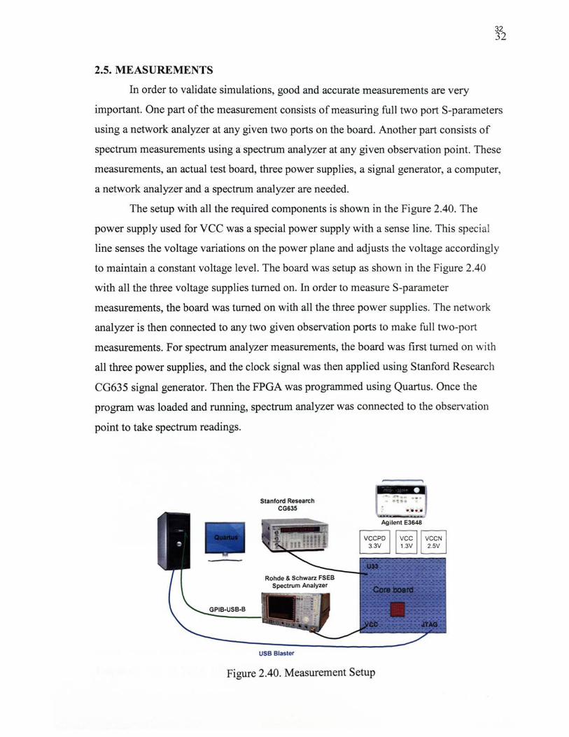
The setup with all the required components is shown in the Figure 2.40. The
power supply used for vee was a special power supply with a sense line. This special
line senses the voltage variations on the power plane and adjusts the voltage accordingly
to maintain a constant voltage level. The board was setup as shown in the Figure 2.40
with all the three voltage supplies turned on. In order to measure S-parameter
measurements, the board was turned on with all the three power supplies. The network
analyzer is then connected to any two given observation ports to make full two-port
measurements. For spectrum analyzer measurements, the board was first turned on with
all three power supplies, and the clock signal was then applied using Stanford Research
eG635 signal generator. Then the FPGA was programmed using Quartus. Once the
program was loaded and running, spectrum analyzer was connected to the observation
point to take spectrum readings.
Stanford Research CG635
USB Blaster
Agilent E3648
~~~ ~~~
Figure 2.40. Measurement Setup
32
33
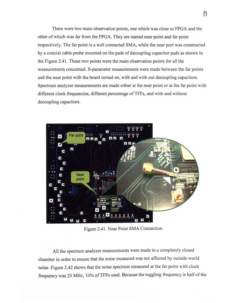
There were two main observation points, one which was close to FPGA and the
other of which was far from the FPGA. They are named near point and far point
respectively. The far point is a well connected SMA, while the near port was constructed
by a coaxial cable probe mounted on the pads of decoupling capacitor pads as shown in
the Figure 2.41. These two points were the main observation points for all the
measurements concerned. S-parameter measurements were made between the far points
and the near point with the board turned on, with and with out decoupling capacitors.
Spectrum analyzer measurements are made either at the near point or at the far point with
different clock frequencies, different percentage ofTFFs, and with and without
decoupling capacitors.
Figure 2.41. Near Point SMA Connection
All the spectrum analyzer measurements were made in a completely closed
chamber in order to ensure that the noise measured was not affected by outside world
noise. Figure 2.42 shows that the noise spectrum measured at the far point with clock
frequency was 25 MHz, 10% of TFFs used. Because the toggling frequency is half of the
33

clock frequency, the frequency interval between peaks was 12.5 MHz. The resolution
bandwidth was 5KHz, to make the noise floor low (about -105 dBm).
E ID ~
RBWSKHz; VBW:5KHz; SWT:10000mS, Att:OdB
40 ------~-------- -------+-------+------+------+------+------+------+------' I I I I
-50 -- --- --- --- - -----+- ----- l-------+-----+-----+------~-- --- - -+- --- --
-00 -- --- --- --- ___ -- --"- ---------------- -------:-------·j- ----- --~-- ------' ' ' ' '
Cll -70 - --- --- - -"0
------ -j--------1--------j--------~
--- --- ---- -- - - ------ -~- ------ -
-90 --- ---- --- --- -- --- -----
-100 1..u,-- ---- -- - ~ -- --- - - -li, -- -J - :~:~i. --_-J: ~-~
50 1 00 150 200 250 300 350 400 450 500 Frequency [MHz]
Figure 2.42. Spectrum Measurement at Far Point
34
Noise spectrum at 0%, 10%, 20%, and 30% ofTFFs is compared. The value of
each spectral component was then studied according to the percentage of TFF used. As
shown in Figure 2.43, noise power was proportional to the amount ofTFFs used. Noise
spectrum at 0% is nothing but buffers toggling in the clock tree. Clock is routed
significantly to all places of inside the FPGA. The routing requires buffers which consist
of registers toggling at the frequency of the clock. This toggling of clock tree alone will
contribute to noise generated. Figure 2.43 is a graphical representation of individual
spectral component.
34

'E CD ::!:!. Q) "0
:€ a. E <(
-40
-50
····· - --- - -- ~---- -- - - --- --[- - - --~--- ~---- -~-----~"-----~- - - - -'1'--
20 25 30 Percentage of Parallel TFFs [%]
Figure 2.43. Spectral Component Comparison at Far Point
35
Similarly, the spectrum analyzer measurements were made at the near point with 25 MHz
clock and 10% TFF used, as shown in Figure 2.44.
RBW5KHz; VBW:5KHz; SWT:10000mS, Att:OdB
-50 --- --- --- ---
~ --- --- --- ---
'E Ill ~ -70 - - --- --- - -<ll "0
:2 c.. E -80 - ------ <t:
-90 - - - - - - -
--- --- --------:·-------:-------
' ' --- --- --------:-------- 1.. --- ---
---- ---·--------1-------- ·-------. ' . ' ' ' '
' ' ' ------- ,.--------..-------- ,-------
' ' ' _____ __ ~.. ________ ._ ____ ___ ~.. ______ _ ' ' ' ' ' '
' ' ' --- --- ~ ------ - ..... ------- ~ -------' ' ' ' ' '
------------ --.... - ------ --- ---
-100 -------. .....a..;...-.1 --- ---J IIi - - - - l ~:.d--J-- -.-~~- -~1.
Figure 2.44. Spectrum Measurement at Near Point
35

36
Noise spectrum at 0%, 10%, 20%, 30% of TFFs is compared. Value of each
spectral component is then studied according to the percentage of TFF used. As shown in
Figure 2.45 noise power is proportional to the amount ofTFFs used even for the near
point.
·50
' ' ------------.,------------ ~ -----------
' ' ' ' ' '
----------+-----------
5 10 15 20 25 30 Percentage of Parallel TFFs [%]
Figure 2.45. Spectral Component Comparison at Near Point
All the measurements with 0%, 10%, 20%, and 30% TFF used are taken along
with different clock input of 1 OMHz, 25MHz, 50MHz , 70MHz, and 1 OOMHz are taken
both with and without decoupling capacitors at both far point and near points.
2.6. NOISE SPECTRUM ESTIMATION AND RESULTS
Once the current waveform is obtained and the estimated, either by using a TCO
distribution or by using Power Play Analyzer, it is possible to obtain noise power at any
given observation point. As shown in Figure 2.46 by using the transfer and self
impedance associated for that point, noise is estimated as given by the following
equations:
36
37
{Z Simulated) 0
Zo =50 o
Figure 2.46. Noise Power Estimation Circuit
(2.4)
Where v; =II X son (2.5)
(2.6)
(2.7)
(2.8)
While estimating the noise power spectrum using a TCO distribution, the initial
value of per unit current pulse width and amplitude were curve fitted. The initial value of
per unit pulse width and amplitude were determined using one measured result at
25MHz, 1 0% of TFF implementation in the FPGA. The estimated power spectrum was
then calculated using the equation above. To determine whether the fitted parameters can
be applied to the measurements for the other frequencies, the same parameters were
applied to calculate the estimated spectrum at different frequencies and different
locations. The measurements were done on the bare board and do not include any
capacitors.
37

Spectrum of noise [F = 25 MHz, p = 10p) -20 r---.--,-,-,,.Tn----,--.-..-~~----~~~
'' _,. _ .. ___ ___ __ __ .. __ ____ ,_ __ _ I I I I I I I I
'---~-~~--.-1 : : : ' : I I I I I I I I I I I I I I I I I I I I I I I I 1
- - - - ---- ~ - ---- ~---- ~ -- -~- -~ - ~ - ~- ~ - ~ - -- - -- - --- ~ --: : : : : : ::: : I I I I I I I I I I
I I I I I I I I 1 I I I I I I I I I I I I I I I I I 1
I I I I I I I I I 1
'E -- -- --- - -~-----~----T---:---:--+--l-1-r-------- --1--
, I I I I I I I I
' : : : : : ::: a:l ~ -60 .... ~ 0 a.. -70 Q) en ·a 2 -80
: : : : : ::: I I I I I I I I I I
-- - - ---- - ~- ---- ~- --- t -- -~- -~- t- ~- ~- ~--------- - ~ --I I I I I I I I I 1 I I I I I I I I I I
----- - ---~ _____ j ___ _L __l_ _U_j_L_ : : : : ::::: -· ··----'--
; i i i i i iii ---------:-----r--:--rrrnr
-90 -- - - -----~----- 1---- 1 ---rTlTT-··--- --{--·
--~ -+-~--~ - ~ ---~~ - -- - ~-:
101
Frequency [MHz]
Figure 2.47. Noise Spectrum Calculated at 25 MHz, 10% TFF Using TCO Current Distribution
The fitted parameters are the following:
• single TFF current pulse amplitude = 5.5e-6 A;
• single TFF current pulse width = 1 e-9 s;
• clock pulse amplitude = 45e-6 A;
• clock pulse width = 1 e-9 s;
38
Once these parameters were detennined by curve fitting any one of the spectral
component, then the same parameters were used to calculate for other frequencies and
other percentage oflogic used, as shown in Figure 2.48, Figure 2.49, Figure 2.50 and
2.51. In Figure 2.48, 25 MHz clock and 30% TFF logic was used. In Figure 2.49 15 MHz
clock and 10% TFF logic was used. In Figure 2.50 15 MHz clock and 30% TFF logic
was used. Same parameters were used for simulations and measurements. Curve fitting
was used only on one of the measurement data. Use of curve fitting will be very difficult
when using complex patterns. Low frequency components are curve fitted, however high
frequency components do not match with the measurements.
38
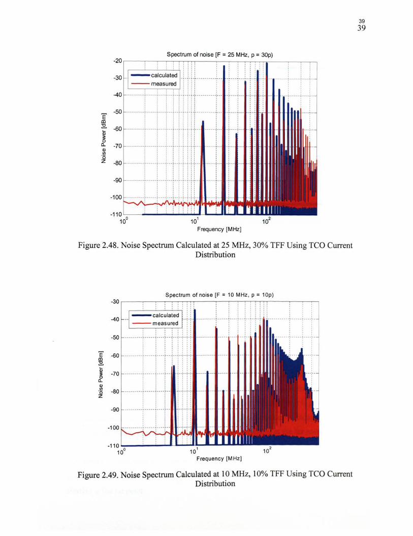
Spectrum of noise [F = 25 MHz, p = 30p) -20 ,---~--~~~~~----~--~~~~~----~~--~
-40
E' -50
a:l :£ -60 .._ Q) ;:: 0 0.. -70 Q) If)
"5 z -80
-90
-100
-110 10° 101 102
Frequency [MHz)
Figure 2.48. Noise Spectrum Calculated at 25 MHz, 30% TFF Using TCO Current Distribution
Spectrum of noise [F = 10 MHz, p = 10p)
----- ---- ~- -~-- -
' ' ' ' ' ' ' '
-50 ' ' ' -------- -~----- ~---- ~--
'E -60 a:l ~
' ' ' --------r---:---r :v
-70 ~ 0...
' ' ' ---------;-----1----:-- llfJ--f-+·f ·
Q) V>
-80 ·o z
' ' ' _________ .. _____ ... ____ .. _ ' ' ' ' ' ' ' ' ' ' ' '
-90 _________ .. _____ .. ____ .. __
' ' '
-100
-110 ~-...O..-:....o...J:....t:......._OLL_..L-11..&.&11.& 1 0° 101
Frequency [MHz]
Figure 2.49. Noise Spectrum Calculated at 10 MHz, 10% TFF Using TCO Current Distribution
39 39
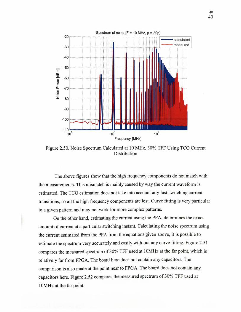
-20
-30
-40
E' -50
co ~ -60 .._
~ 0 a_ -70 Q) <ll ·a z -80
-90
Spectrum of noise (F = 10 MHz, p = 30p)
I I I I I I I 1 I I I I I I
I I I I I I I I I I I I I I
••••••••• ••••··~··· •••~tl~ __________ .. __ _ --------- ------r
--------- ------:---+--U : +-~-:-•
------- -- ------:--- -~---·-1 !-~--f - :-
101
Frequency [MHz]
' ' ' ' __ _. _________ _. __
Figure 2.50. Noise Spectrum Calculated at 10 MHz, 30% TFF Using TCO Current Distribution
40
The above figures show that the high frequency components do not match with
the measurements. This mismatch is mainly caused by way the current waveform is
estimated. The TCO estimation does not take into account any fast switching current
transitions, so all the high frequency components are lost. Curve fitting is very particular
to a given pattern and may not work for more complex patterns.
On the other hand, estimating the current using the PP A, determines the exact
amount of current at a particular switching instant. Calculating the noise spectrum using
the current estimated from the PP A from the equations given above, it is possible to
estimate the spectrum very accurately and easily with-out any curve fitting. Figure 2.51
compares the measured spectrum of 30% TFF used at 1 OMHz at the far point, which is
relatively far from FPGA. The board here does not contain any capacitors. The
comparison is also made at the point near to FPGA. The board does not contain any
capacitors here. Figure 2.52 compares the measured spectrum of 30% TFF used at
1 OMHz at the far point.
40

Spectrum of noise [F = 10 MHz, p = 30p) -20 r;:::===:::c==c=:!:=~TT!--:--;---;--;;:--;--:---;:-----:--r--lr--J
- calculated -30 ----··----+-------- -----
-40
'E -50
co ~ -60 Cii ~ c.. -70 Cl> Ill "6 z -80 -- - ---- - - · ------ -- ---;-·· 11 - ~--~ - ;.
-90 -- - ---- - -.l-- - ---1.-- - -:-·-· -~ - -~+
-100
101
Frequency [M Hz]
Figure 2.51. Noise Spectrum Calculated at 10 MHz, 30% TFF Using PPPA Current Distribution
Spectrum of noise [F = 10 MHz, p = 30p)
'E co :2..
! -70 c.. Q) (/)
-80 "6 z
-90
-100
-110 10°
Frequency [MHz]
Figure 2.52. Noise Spectrum Calculated at 10 MHz, 30% TFF Using PPPA Current Distribution at Far Point
41 41

This method can be used for any complex pattern apart from parallel switching
TFF. The noise power is mainly modulated by transfer function from the source to
observation point. Based on the noise predicted on the bare board, the decoupling
strategy can be developed accordingly.
42
The noise measured at the observation points can also be analyzed in time
domain. Measurements are made with an oscilloscope and the estimated current spectrum
noise is converted back to time domain.
> .§. Q) Cl 2l 0 >
20 ,----.---,,---~---,----,----,----,----,----,----,
10 0 0 r- ----------,-----
0 0
---- --L----- -----'----0 0 0 0 0 0 0
'
-10 0 0 0 -------r---------.,------ ----,----0 0 0
0 0 ------- --.- ------ ----.----0 0 0 0 0
0 0
-20 0 0
- ----- - --~----------:--- -1 I I I ------:-----------r---------:----------i----
' ' 0 0 0 I I I I I
-30 -- ----··t··-----~----- ---:-----------:-----------:-----------:---------- ~-- ---
Measurement
--Calculation
0 0 --.,----------.,.---------0 '
40 L_ __ _L __ ~----~---L----L---~--~----L----L--~
0 20 40 60 80 100 120 140 160 180 200 Time (ns]
Figure 2.53. Time Domain Noise Voltage at Far Point
The measurement shown in Figure 2.53 was taken at the far point with no
capacitors on board and with 30% ofTFF logic used at lOMHz clock input. The DC
offset was removed and then compared with the estimated noise voltage in time domain.
This comparison was exactly the same as in Figure 2.51 , but in time domain.
42

43
2.7. FUTURE WORK AND CONCLUSION
The method of predicting noise, using a PPA restricted time analysis, should be
extended to complex patterns. A wide range of frequency and logic can be studied in
order to quantify the associated noise and error associated. Time domain analysis of noise
voltage on the power plane is also possible to obtain. It is possible to develop a
decoupling strategy, based on the noise estimated for a bare board. Capacitors can be
chosen selectively and accurately based on the estimated noise spectrum. More
measurements and simulations have to be performed in order to validate the theory and
characterize the error associated with the estimations.
The methodology of predicting noise has been developed and proven. This
methodology provides a new way of predicting noise on the PDN just by using
simulations, even before the board is actually manufactured. Designers can more
carefully design and decouple the board with an anticipated calculation in hand.
43

3. ELECTROMAGNETIC SHIELDING
3.1. MATERIALS FOR SHIELDING
Two types of materials are studied for their shielding effectiveness and
simulations are done to support the theory.
3.1.1. Composite Materials. Previous work done by the student (8], shows
44
that composite materials can provide effective shielding [9] when manufactured
accordingly. The program developed in [8] , can estimate the shielding effectiveness of a
composite material with any given properties. An example of the screen view for this
program is shown in Figure 3 .1.
1 ( ompos1tc s labs u1 sttu:k llr>rt rom.w,nPiu: ( ompclflblhty I olho r.1101 y. UmvNsliY nt Mw:.oun Holl.1 G._ rQ_.l8._1 mero-nono
Thickness [mml
Layers number ~~ ~ Layer1 10
Layer1ype
0 absort>lng
0 renec11ng
o ...... -Enter the properties of the inclusions Base material properties
~ rMio VOUne traction(%) Perca.tion 1hr0$1loid(~)
Layer 1 - 70000 __ ] BOO 0.07
·--_j '------'
0.00125 2.2 l 00001
Figure 3.1. Composite Stack Shielding Estimator
Using the composite material properties from Table 3.1 , shielding effectiveness is
estimated is as shown in Figure 3.2.
44

Table 3.1. Composite Material Properties
Carbon fiber composite material properties
Fiber conductivity 70000 S/m
Fiber shape cylindrical
Concentration 0.0007 vol. fraction
Aspect ratio (length/diameter) 800
Percolation threshold (equation 3.32) 0.00125 vol. fraction
40
20
0 -1
10
Diameter of the fiber < 10 J.1l12
Base material Teflon ( & = 2.2)
The Shielding Effectiveness
0 10
Frequency (GHz)
45
1 10
Figure 3.2. Analytical Shielding Effectiveness of Composite Slab of 10 mm thick
45

46
A 10 mm thick composite slab made ofthe materials in Table 3.1 has a promising
shielding effectiveness, when the parameters of the material are controlled and uniform.
Maxwell Garnett formalism has been successfully applied for engineering microwave
absorbing materials containing carbon particles [ 1 0],
1 n 3 & - Lh(&; -&b)I b 3 i=l j =i &b +Nu(&; -&b)
& = & + -------------=-----ef b 1 n 3 N ..
1- - Lh(&; -&b)I lJ
3 i=l j = i &b +Nu(&; -&b)
(3.1)
where, /; is the volume fraction occupied by the inclusions, N iJ are the
depolarization factors of the i -th kind of inclusions , & b is the relative permittivity of a
base dielectric, &; is the relative permittivity of i -th kind of inclusions. Index j=1, 2, 3
corresponds to x, y and z coordinates. Two depolarization factors are close to
N;, ,z ~ 1 I 2 for cylindrical inclusions. The third depolarization factor is calculated
as N;3 ~ (1 I a Y ln(a ), where a =l I d , or a ratio (length/diameter), is an aspect ratio of an
inclusion.
The analytical formulation assumes that the inclusion aspect ratio is constant, and
the length of each inclusion is much longer than its diameter, i.e. 1 I d >> 1. However,
practically manufacturing such a material with a constant and high aspect ratio is difficult
given today's technology. As shown in Figure 3.3, the particles look broken and do not
maintain uniform aspect ratio.
Figure 3.3. Microscopic View of Composite Materials
46

Aside from the non-uniform aspect ratios [13] in practically manufactured
materials, it is also very difficult to control the volume fraction of inclusions. The
inclusions tend to orient in one single direction as opposed to random orientation in
analytical formulation. All these variations cause significant degradation of shielding
effectiveness from analytical formulation. Several samples of the composite materials
shown in Table 3.2 were manufactured. They were tested for shielding effectiveness
using a TEM cell.
Table 3.2. Composite Materials Manufactured
Material N arne Type Volume Fraction of Thickness
Inclusions -
R1 Reflecting 1.3% 3mm
R2 Reflecting 2.3% 3mm
47
--A4 Absorbing 0.07% 3mm
A5 Absorbing 0.5% 3mm
A6 Absorbing 0.15% 3mm
The composite material was cut into rectangular sheets. Each rectangular sheet
was then inserted into the TEM cell perpendicular to septum and touching all the sides of
the TEM. Two sheets were inserted: one above the septum, and the other below the
septum, so a plane wave propagating through the TEM cell must pass through the
composite sheet. Such a setup is shown in Figure 3.4. After setting up the composite
material in the manner described, the TEM cell was connected to a Agilent network
analyzer. Port 1 of the network analyzer is connected to one end ofTEM cell and Port 2
of the network analyzer was connected to another end of the TEM cell. S-parameters are
then measured to obtain IS12I which gives the materials shielding effectiveness. The
measured shielding effectiveness of these materials, as shown in Figure 3.5, was not so
promising as their analytically calculated values. In order to investigate this discrepancy,
I
l I
I
I
47
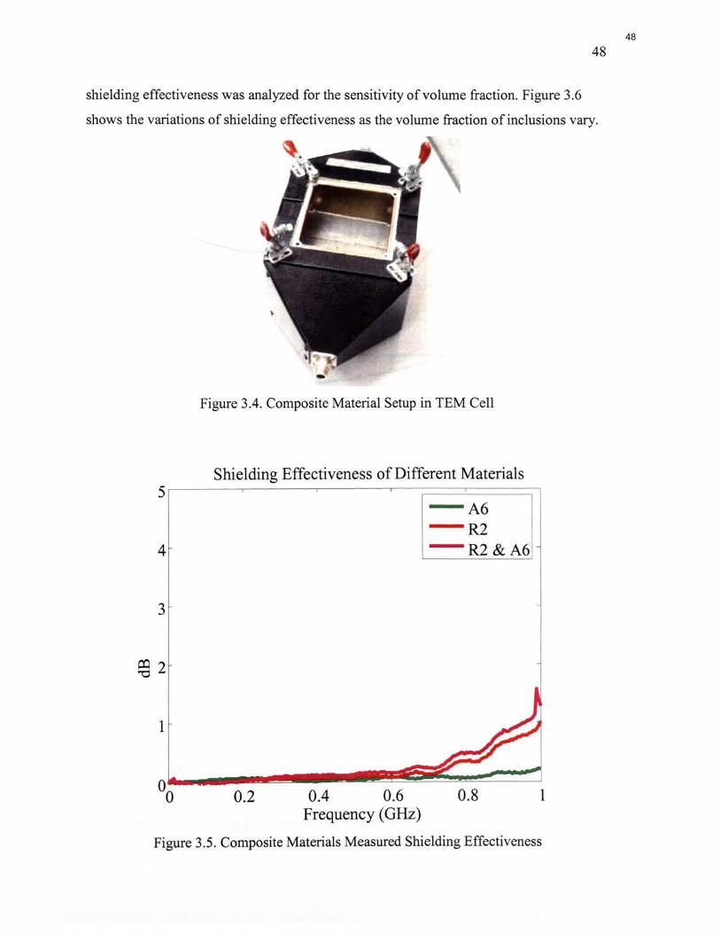
48
shielding effectiveness was analyzed for the sensitivity of volume fraction. Figure 3.6
shows the variations of shielding effectiveness as the volume fraction of inclusions vary.
Figure 3.4. Composite Material Setup in TEM Cell
Shielding Effectiveness of Different Materials s ~----~----~----~~==~====~
- A6 - R2
4 - R2&A6
3
1
0.2 0.4 0.6 0.8 1 Frequency (GHz)
Figure 3.5. Composite Materials Measured Shielding Effectiveness
48
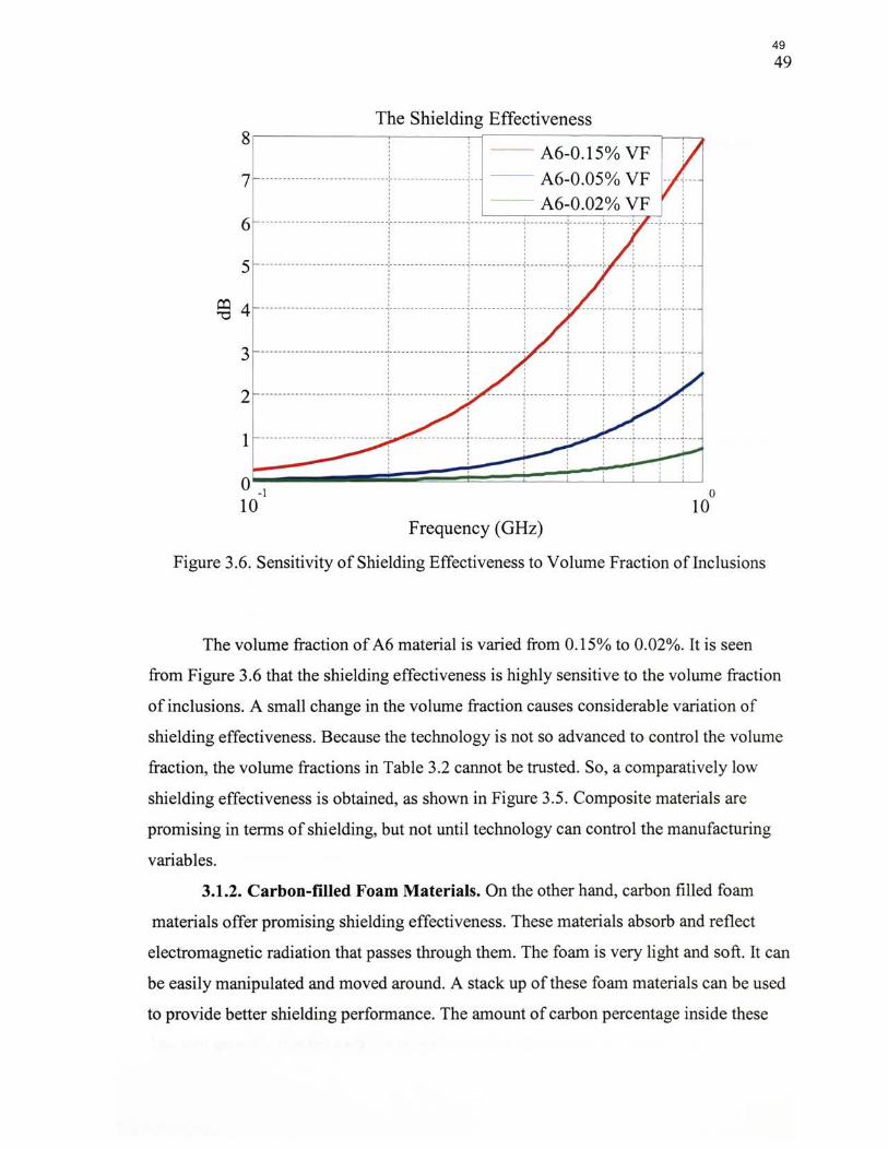
The Shielding Effectiveness 8 r---------~------~---------------r~~
-- A6-0.15% VF ------------------------------:-------------------1-- -- A6-0.05% VF
'''T''' 5 ------------------------------:------------------1------------~---------T-------r
' ' ' I I I I ' ' ' ------------------------------,------------------.,------------,----------.- - ----r- ------r------ ----.,---' ' ' ' ' ' ' ' ' ' ' ' '
I I I I
-------~--------~------~-- --- --- --t---' ' ' ' ' '
3 - ------- ---- ---- ------------- -:---- - ------- ---- --~------------~-
I I I I ________ ., _________ _, ________ ,... ______ ,.. ___ _ I I I I
' ' ' ' '
' '
1 ______________ .,. ___________ _ .,. ______ __ _ _, ___ _
' ' ' ' '
Frequency (GHz)
0 10
Figure 3.6. Sensitivity of Shielding Effectiveness to Volume Fraction of Inclusions
49
The volume fraction of A6 material is varied from 0.15% to 0.02%. It is seen
from Figure 3.6 that the shielding effectiveness is highly sensitive to the volume fraction
of inclusions. A small change in the volume fraction causes considerable variation of
shielding effectiveness. Because the technology is not so advanced to control the volume
fraction, the volume fractions in Table 3.2 cannot be trusted. So, a comparatively low
shielding effectiveness is obtained, as shown in Figure 3.5. Composite materials are
promising in terms of shielding, but not until technology can control the manufacturing
variables.
3.1.2. Carbon-filled Foam Materials. On the other hand, carbon filled foam
materials offer promising shielding effectiveness. These materials absorb and reflect
electromagnetic radiation that passes through them. The foam is very light and soft. It can
be easily manipulated and moved around. A stack up of these foam materials can be used
to provide better shielding performance. The amount of carbon percentage inside these
49

materials determines the shielding effectiveness. Many samples of these materials were
obtained for testing purposes. Table 3.3 shows the materials manufactured for testing.
Table 3.3. Carbon Filled Foam Materials
Material N arne Properties Specified
Material 1 (80 ohm) 80 Qm
Material 2 (200 ohm) 200 Qm
Material 3 (300 ohm) 300 Qm
Material 4(800 ohm) 800 Qm
Material 5 (soft kind) NIA
Material6 (medium hard kind) N/A
Material 7 (hard kind) NIA
50
The materials "80 ohm", "200 ohm", and so on are the names given to the
materials (these are not the properties of the materials). These materials are all 2.5cm
thick with different textures. In order to measure the shielding effectiveness of each, they
must be cut into rectangular blocks to fit into a TEM cell. Each block of foam was placed
on the top and the bottom ofthe septum as shown in Figure 3.7. After setting up the
material in the manner described, the TEM cell was connected to an Agilent 8753ES
network analyzer. Port 1 of network analyzer was connected to the first end ofTEM cell
and Port 2 of the network analyzer was connected to the other end ofTEM cell. S
parameters were then measured to obtain !S12I, which gives the shielding effectiveness of
the material. Figure 3.8 shows the measured shielding effectiveness of each material. It
can be seen that the "80 ohm" material gave the highest shielding in the tested materials.
In order to determine how complex structures made out of these foam materials behave,
full wave 3D simulation tools were used. The properties of these materials should first be
known when performing simulations. The dielectric Debye-curve parameter extraction
tool developed in [8] is used herein to get Debye values from the measured S-parameters.
The tool assumes that the data is obtained from the plane wave excitation. An
!
I
50
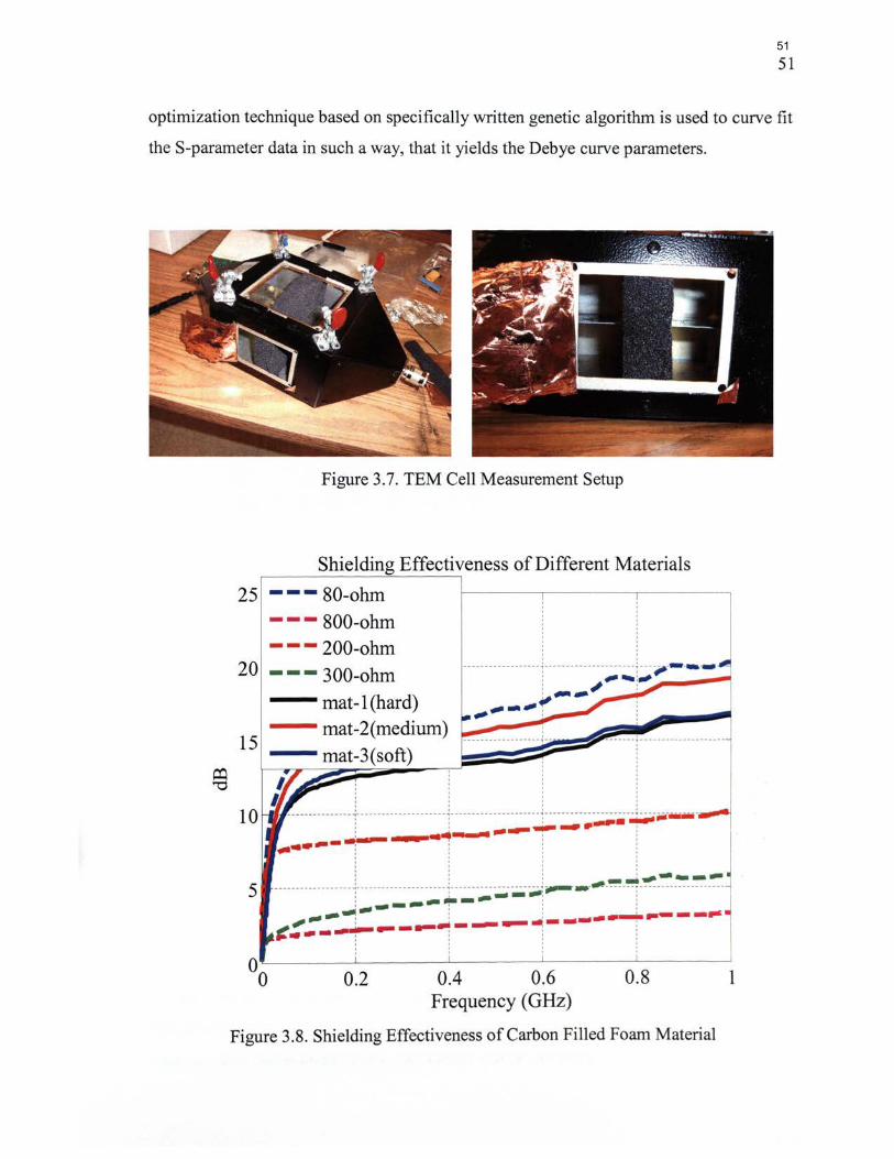
51
optimization technique based on specifically written genetic algorithm is used to curve fit
the S-parameter data in such a way, that it yields the Debye curve parameters.
Figure 3.7. TEM Cell Measurement Setup
Shielding Effectiveness of Different Materials
25 --- 80-ohm
--- 800-ohm
---------------~--------------------- ~ --------------------- ~ ---------------------:-------: : : ...... ~ ' ·------- ' ·- . ..,. : :
--·--~ : : : ' :
10
: ' : _ ... ..-.----5 ------------------i---------------------.t -.: -;;~;.;.;;-.j,_-~-------;--------------------·----- : : : - ... --'! : :- ---.. --. .. -- _.,. ,, -------~---~ i p~--- . ' ' '
i i i 1
0.2 0.4 0.6 0.8 Frequency (GHz)
Figure 3.8. Shielding Effectiveness of Carbon Filled Foam Material
1
51

52
Figure 3.9 illustrates the graphical user interface of the Debye parameter extractor tool.
Measured and Calculated absolute(S21) Vs Frequency 0 • .
; ! - MauurtdOata
·2 ····--····(·········t···· -- ~ Calculat•~ from GA
-4 ---- --- --~--- - ··· · · · .; . -· ·· -- ----:.-- ..•.... • ; • ..•... . •. ~ : : : :
-6 ~: . ...... •i• .. -... -... ~ ...... -... i··-- ...... ·l·-....... . ~-a i. ........................ .. .......... .
Ci ·10 . \. .... ; ....... [·" . . . "': · ... ..
·12 ..... : ., .......... . ~ .......... i .......... j ....... ..
I CLEAR I -14 ·····-···+··-·······[·····--··: >:.-:-.:.-:-.·t--...... =·;..· ,
·16 .......... ; ........... ; ........ + ......... , . ...... .
Figure 3.9. Debye Parameter Extraction Tool
The tool accepts the S-parameter data in magnitude alone or with both magnitude
and phase as input. The user has to select how many layers are to be used, and how many
of them are of the Debye type. Then an initial range of the Debye parameters is entered.
Range of thickness, or even the exact thickness of the material, should be entered as well.
Finally, the genetic algorithm variables of population size and generations number should
be specified. Once all the parameters are entered into the tool, the tool can be run for
curve fitting of the S-parameter data to obtain the De bye parameters. The results can be
analyzed to see which set of parameter ranges must be changed to obtain a good curve
fitting. The genetic algorithm varies and optimizes all the given variables simultaneously
until the error with measured data is minimized. The solution given is one of many
similar solutions. An example of such curve-fitted comparison between the measured
data and the data obtained from the GA optimization is shown in Figure 3.1 0. Once the
data has been curve-fitted, De bye parameters can be extracted.
52

53
0 MtaStJred ~nd Cllcul~ed absolute(S21) Vs Frequency
. : : ~-Measured DMa I \ : : - · - Calcul~ed from GA I
-5 , . . ·····7·········i··········:··········:········· \ ~ ~
~: ~~ : : : :
'25o:--:!'-~--!'~~---:',o
Frequency [Hz] x l08
Figure 3.10. GA Curve Fitted Data vs. Measurements
All the materials were measured in the TEM cell as described earlier, and then the
properties of each material were extracted using the GA tool. Table 3.4 and Table 3.5
show the values of the Debye parameters extracted using this tool for material set 1 and
material set 2, respectively. The curve fitting column shows how good the approximation
is, and, hence, gives an idea how accurate the extracted parameters can be.
Table 3.4. Material Set 1 - Extracted Debye Parameters
Material
80ohm
(0.025m thick)
200 ohm
(0.025m thick)
300 ohm
(0.025m thick)
800 ohm
(0.025m thick)
Curve fitting using GA
(up to 1GHz)
o:--h:J_, __ -:::-··:.:- · I .
I .
:
Estimated Debye parameters
Epsilon Static: 192.3 Epsilon Infinite : 39.2 Relaxation constant: 5.1e-10 s Conductivity : 0.012 S/m
Epsilon Static : 99.47
Epsilon Infinite : 1.0565 Relaxation constant : 2.1 e-9s Conductivity : 0.005011 S/m
Epsilon Static: 61.38 Epsilon Infinite : 9.65 Relaxation constant : 5.5e-9
Conductivity : 0.00331 S/m
Epsilon Static : 57.61 Epsilon Infinite : 5.38
Relaxation constant : 8.1 e-9 s Conductivity : 0.0011075 S/m
53

Table 3.5. Material Set 2- Extracted Debye Parameters
Material Curve fitting using GA Estimated Debye parameters (up to 1GHz)
Mat - 1 hard kind
[_:] Epsilon Static : 199.56
(0.025m thick) . . . Epsilon Infinite : 1.55 .. . ! • ' . . .. . ,. . Relaxation constant : 2.2e-9s ::: --~---·~-- ---- Conductivity : 0.000535 S/m .. -
- 0 0 . ----Mat- 2 medium hard kind
ill:] Epsilon Static : 249.67
(0.025m thick) .. ·- . . - Epsilon Infinite : 1.3326 \, .... Relaxation constant: 2.1e-9s ! .: ·. : : .. : . .: ·;--~~ ---t-----
Conductivity : 0.0077 S/m ... ' ' ' ~
Mat -3 soft kind __ , .... -~, ..... ,_
Epsilon Static : 199.825 -- ( .......... -....
(0.025m thick) . Epsilon Infinite: 1.17 I: I Relaxation constant : 2.05e-9 ... ~~-.
" . Conductivity : 0.00092 S/m ... ~"-'" --- . ·• -~"-..
3.2. MODELING
After extracting the Debye parameters from the materials, it is possible to use
them for further analytical modeling or 3-D full wave numerical modeling of structures
containing such materials. Full wave modeling helps in predicting the behavior of
materials in complex geometry and at higher frequencies. Analytical modeling can be
used to validate the full-wave model in the known environment.
3.2.1. Analytical Modeling. Analytical modeling using a plane-wave
54
formulation is basically calculating the transmission and reflection coefficients for the
material of the given thickness. Plane wave propagation is assumed through the air and
through the material. The effective complex permittivity of the material is calculated,
which is then used to calculate the complex propagation constant across the material.
ABCD parameters are obtained using this propagation constant. The ABCD are
converted to S-parameters to obtain the shielding effectiveness of an infinitely long sheet
for a plane wave excitation. Once the ABCD parameters are known, they can be cascaded
for any number of layers, giving an opportunity to calculate the total parameters of
interest for any stack of layers. The ABCD parameters are then converted into S
parameters to get the shielding effectiveness of interest [ 11].
54
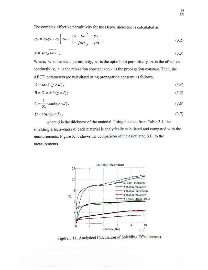
55
The complex effective permittivity for the Debye dielectric is calculated as
( 8s-&oJ (J'e
8 a = 8 o8 r = 8 o EPo + --1 + jmr jm ' (3.2)
r=Jm~, (3.3)
Where, &s is the static permittivity, &oo is the optic limit permittivity, a eis the effective
conductivity, r is the relaxation constant and r is the propagation constant. Then, the
ABCD parameters are calculated using propagation constant as follows,
A = cosh(y x d) ; (3.4)
B = Zo X sinh(y X d) ; (3.5)
C = _!_x sinh(yx d); Zo
(3.6)
D = cosh(yx d), (3.7)
where dis the thickness of the material. Using the data from Table 3.4, the
shielding effectiveness of each material is analytically calculated and compared with the
measurements. Figure 3.11 shows the comparison ofthe calculated S.E. to the
measurements.
Shielding Effectiveness 25 ~----.-----,-----,-----.-----,
20 - ----- -----+----------+---------- - -~ ----- ' : ' 80 ohrr- measur
, __...,-.::::::::::;::..--~ - :- 200 ohm-measur 15 ---- - ---+-------------i-------------~ ----- -:m<r<>$n -:meas-ur d
! , - ;- 800 oJ1m-measur : : - :-All bllick -from bye
----~-------- ---- --'--------- - ----'--- - --- - ---- - -1...- --' '
2 4 6 frequency [HZ]
8 10 8
X JO
Figure 3 .11. Analytical Calculation of Shielding Effectiveness
55

56
Similarly, a stack of different materials is measured and then compared to the
analytically calculated shielding effectiveness, as shown in Figure 3.12. Measurements
here are done using the TEM cell, as described earlier. Each material is cut into a 1.25 em
thick block and stacked together inside the TEM cell.
shielding effectiveness 30 -------------------------------------------------------------------------------------------
25 -- -------- ------1---------- --- --- --[---------------- -+---
' ' ' ' _ ____ __________ .J __________________ •
' ' ' ' 20 ---------------+----------------+-
' '
' ' ' I I I I
----,------------------ r------------------:------ ----- ---- ---1------------------l
i i : i I I I I I -- --------- -- --l------------------r------------------!-----------------;------------------·
- Measured -80 ohm(l.25cm) : 200ohm(1.25cm) : 80 ohm(1.25cm)
- Calcualted
0.2 0.4 0.6 0.8 1 Frequency (GHz)
Figure 3.12. Analytical S.E. of Stack ofMaterials
3.2.2. Full Wave 3-D Modeling. Analytical modeling has the ability to model
infinitely long sheets with only plane wave excitation. It is not possible to analyze how
the fields inside complex structures behave in different conditions. Thus, for analyzing
complex structures a model that employs a full wave 3D Maxwell equation solver is
needed. EZ-FDTD is used in this case to model complex box structures made of the
material with the given Debye characteristics.
Before analyzing complex structures, it is important to validate 3-D modeling
with the known analytical solution. The Debye dielectric material is placed in between
the PEC plates, and these PEC plates are extended into the boundaries to make it infinite.
The setup is shown in the Figure 3.13, where FD1 is the Debye dielectric material, P1
56
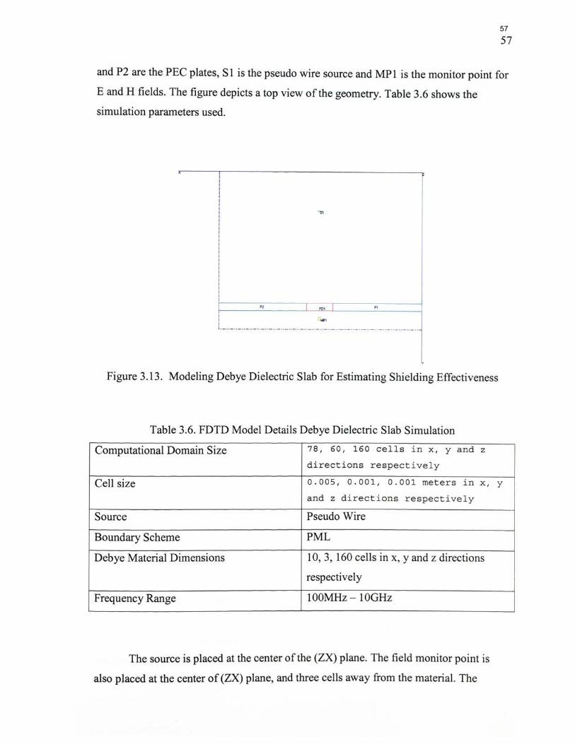
57
and P2 are the PEC plates, S 1 is the pseudo wire source and MP 1 is the monitor point for
E and H fields. The figure depicts a top view of the geometry. Table 3.6 shows the
simulation parameters used.
P2 P1
I c..., I l----------- ------------ --- --- --------------- ----·- ··-··- ··- ··---- -- ----··-··
Figure 3.13. Modeling Debye Dielectric Slab for Estimating Shielding Effectiveness
Table 3.6. FDTD Model Details Debye Dielectric Slab Simulation
Computational Domain Size 78, 60, 160 cells in x, y and z
directions respectively
Cell size 0.005, 0 . 001, 0.00 1 meters in x,
and z directions respectiv ely
Source Pseudo Wire
Boundary Scheme PML
Debye Material Dimensions 10, 3, 160 cells in x, y and z directions
respectively
Frequency Range 1 OOMHz - 1 OGHz
The source is placed at the center of the (ZX) plane. The field monitor point is
also placed at the center of (ZX) plane, and three cells away from the material. The
y
57

58
material simulated was the "80-ohm" material with the properties detailed in Table 3.4.
In order to obtain shielding effectiveness, it also important to simulate an empty
computational domain with out the Debye material. The model has the exact properties
shown in Figure 3.13 and Table 3.6, but with out the Debye material. Once theE and H
fields are obtained from both of simulations, the ratio of E or H field with empty space to
E or H field with the material gives the shielding effectiveness of the simulated material.
Figure 3.14 shows the comparison of the simulation result to the analytically calculated
result.
Shielding Effectiveness
' ' -- -- -!- -- -------;----------:----------;--
o L_~ __ _L __ _L __ ~--~--~--~--~--~~
1 2 3 4 5 6 7 8 9 10 Frequency [ GHz]
Figure 3.14. FDTD Infinite Debye Sheet Shielding Effectiveness
The difference between the analytical and simulated result is mainly because due
to the observation point. The analytical solution, as in equations (3 .1) - (3. 7), assumes far
field, while the full-wave simulation includes the near-field region. Once it has been
ensured that the 3-D simulation works as expected, more complex geometries made of
this material can be simulated.
58
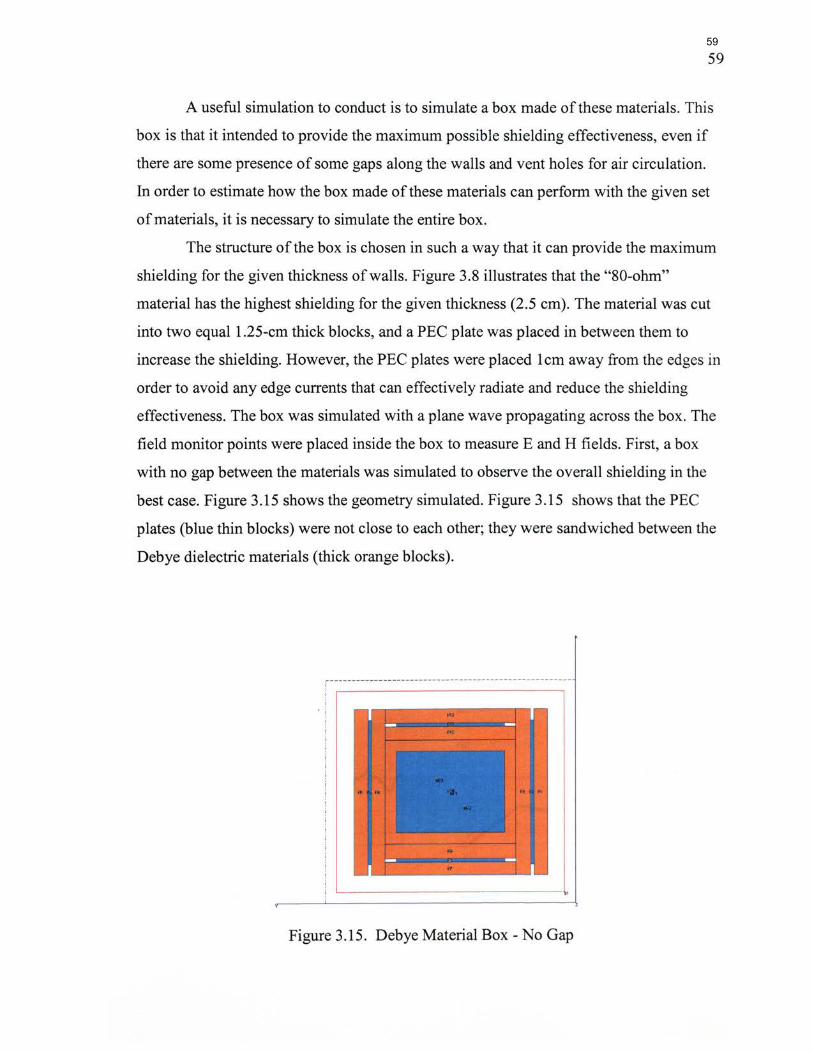
59
A useful simulation to conduct is to simulate a box made of these materials. This
box is that it intended to provide the maximum possible shielding effectiveness, even if
there are some presence of some gaps along the walls and vent holes for air circulation.
In order to estimate how the box made of these materials can perform with the given set
of materials, it is necessary to simulate the entire box.
The structure of the box is chosen in such a way that it can provide the maximum
shielding for the given thickness of walls. Figure 3.8 illustrates that the "80-ohm"
material has the highest shielding for the given thickness (2.5 em). The material was cut
into two equal1.25-cm thick blocks, and a PEC plate was placed in between them to
increase the shielding. However, the PEC plates were placed 1 em away from the edges in
order to avoid any edge currents that can effectively radiate and reduce the shielding
effectiveness. The box was simulated with a plane wave propagating across the box. The
field monitor points were placed inside the box to measure E and H fields. First, a box
with no gap between the materials was simulated to observe the overall shielding in the
best case. Figure 3.15 shows the geometry simulated. Figure 3.15 shows that the PEC
plates (blue thin blocks) were not close to each other; they were sandwiched between the
Debye dielectric materials (thick orange blocks).
-------------------------------------------------------i
Figure 3.15. Debye Material Box- No Gap
59
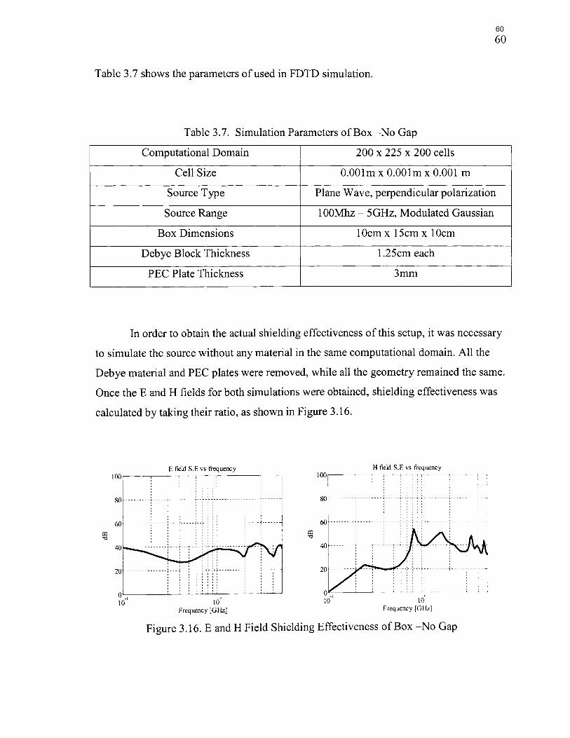
60
Table 3.7 shows the parameters ofused in FDTD simulation.
Table 3.7. Simulation Parameters ofBox -No Gap
Computational Domain 200 x 225 x 200 cells
Cell Size 0.001m x 0.001m x 0.001 m
Source Type Plane Wave, perpendicular polarization
Source Range 1 OOMhz - SGHz, Modulated Gaussian
Box Dimensions 10cm x 15cm x 10cm ··----
Debye Block Thickness 1.25cm each
PEC Plate Thickness 3mm
In order to obtain the actual shielding effectiveness of this setup, it was necessary
to simulate the source without any material in the same computational domain. All the
Debye material and PEC plates were removed, while all the geometry remained the same.
Once the E and H fields for both simulations were obtained, shielding effectiveness was
calculated by taking their ratio, as shown in Figure 3 .16.
0 -1
10
E field S.E vs frequency
0 10
Frequency [GHz]
H field S.E vs frequency
10,,
Frequency [GHz]
Figure 3.16. E and H Field Shielding Effectiveness of Box -No Gap
60

61
Figure 3.16 shows that the S .E for both E and H fields was on the order of 40 dB
average. With a combined effect of the PEC added to the Debye material, it was possible
to achieve 40 dB of shielding in the best case.
However, it is not always possible to build a box with completely closed edges.
The walls of the box can have a gap between them, through which fields can penetrate. In
order to study a more practical case, gaps of 2-mm wide were left all around the walls of
the box, as shown in Figure 3.17. The (XZ) plane plot also looks the same, since the box
is almost a square. Table 3.8 shows the simulation parameters used in this simulation .
.------------·---·------------------------------------------------------------------------------
PI
Figure 3.17. Debye Material Box- With Gap
61

62
Table 3.8. Simulation Parameters ofBox -With Gap
Computational Domain 200 x 225 x 200 cells
Cell Size 0.001m x 0.001m x 0.001 m
Source Type Plane Wave
Source Range 1 OOMhz - 5GHz, Modulated Gaussian
Box Dimensions lOcm x 15cm x lOcm
Debye Block Thickness 1.25cm each
PEC Plate Thickness 3mm
Gap Between Walls 2mm
Presence of gaps between the walls greatly reduced the shielding effectiveness, as
predicted. Figure 3.18 illustrates that there is a 25-dB average shielding effectiveness for
a box with gaps in the frequency range of 100 MHz to 5 GHz.
E field S.E vs frequency 100~--~~~~~~----~~~
< I I I I I I I 1 f I I I
0 0 I I 0 I I I I i I I I I L I I I
w ... ······· . ····~ ······1·:· ... 1 .................. ·j·.
~ ro • r .11 H' . . . 1
40 ---------r ---:---rn--.--.--:-;----------:-- ---:-
0 -1
10
.._,.. ..... .....-:--·--·-,-·------' ' ' '' I I I I I
0 10
Frequency [GHz]
H field S.E vs frequency
20- ----
OL_J--~'--~~~~· ~· •-"-o 10 10
-~~~---i
Frequency [GHz)
Figure 3.18. E and H Field Shielding Effectiveness of Box- With Gap
3.3. CONCLUSION AND FUTURE WORK
Simulations reveal that the boxes made of carbon-filled composite materials can
provide reasonable shielding effectiveness even if gaps between the walls are present.
62

63
Increasing the thickness of the material will further increase the shielding effectiveness.
With a PEC plate, sandwiched between the Debye dielectric materials, it is allowed to
have small holes in the PEC for air ventilation, but not fields. Given these promising
results, it is possible to build an actual box made of these materials.
It is important to validate these simulations with actual measurements. Also, the
materials have to be tested for shielding effectiveness at higher frequencies. A
measurement setup has to be designed to measure and validate the shielding effectiveness
above 1 GHz. Experimental results conclude that carbon-filled foam materials are
perspective for effective and cheap shielding purposes.
63
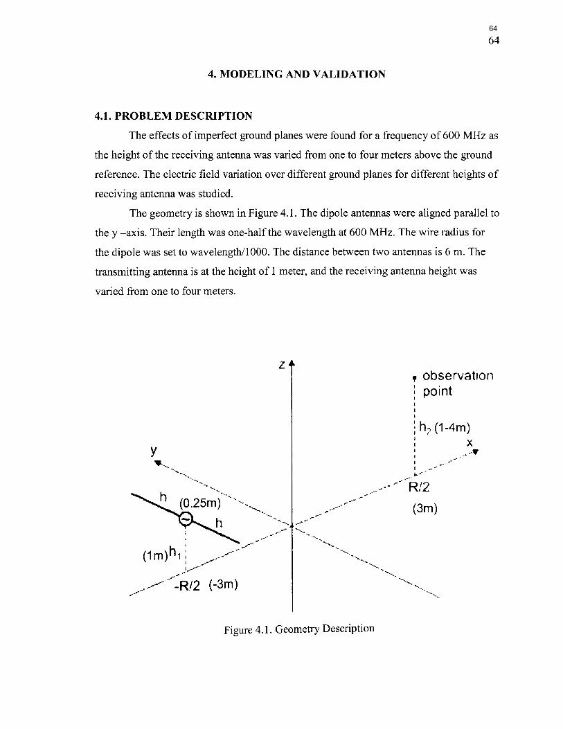
64
4. MODELING AND VALIDATION
4.1. PROBLEM DESCRIPTION
The effects of imperfect ground planes were found for a frequency of 600 MHz as
the height of the receiving antenna was varied from one to four meters above the ground
reference. The electric field variation over different ground planes for different heights of
receiving antenna was studied.
The geometry is shown in Figure 4.1. The dipole antennas were aligned parallel to
they -axis. Their length was one-half the wavelength at 600 MHz. The wire radius for
the dipole was set to wavelength! I 000. The distance between two antennas is 6 m. The
transmitting antenna is at the height of 1 meter, and the receiving antenna height was
varied from one to four meters.
z
y
.. -~
·-.... ..---'--...-... -~ ...-·.--· ,.._
__ .- ·--...................
·-.......__ ..................
-~ ..... ~
Figure 4.1. Geometry Description
__ .. -
, observation point
h? (1-4m) X
.-··· j.. -·
---- ~ R/2
(3m)
.......... _
·--..... __
64
65
The ground (image) plane conditions are varied as follows:
• Ground 1: Perfectly conducting infinite ground plane at z=O.
• Ground 2: Perfectly conducting ground plane at z=O with finite dimensions of 2m
x 4m. The ground is located from x =+/-2m andy=+/- lm.
• Ground 3: Wet soil modeled by a homogeneous dielectric media for z<O with a
relative permittivity of 12 and conductivity of0.04 S/m. The relative permeability
of the soil =I.
• Ground 4: Dry soil modeled by a homogeneous dielectric media for z<O with a
relative permittivity of 8 and conductivity of 0.04 S/m. The relative permeability
of the soil =1.
The task required that electric field (in dBuv/m) for each type of ground be
plotted for receive antenna heights of 1.0, 1.5, 2.0, 2.5, 3.0 3.5 and 4 meters.
4.2. MODLEING
The problem requires modeling an extremely thin and long wire with a large
computational domain. Commercially available software like Microwave studio and
HFSS cannot model this geometry because of its extremely thin radius
(wavelength/ I 000= 0.0005m). Hence, they cannot be used to solve this problem.
However, EZ-FDTD, which is developed EMC laboratory, can model these using special
sub-cellular algorithms. One of these algorithms is "Thin Wire" algorithm. A thin wire
can be defined as a percent of the actual cell. It is possible to define a wire with a very
thin radius. The second software used for validation is WireMom, which is an open
source software downloadable from the web. This software basically uses the Method of
Moment approach to solve the problem.
4.2.1. Without Ground Plane. The geometry was modeled in both EZ-FDTD
and WireMoM without any ground plane. The model is shown in Figure 4.2 and
simulation details are given in Table 4.1. The WireMoM model is similar to the FDTD
model, but there is no need to define cell size and computational domain. Only a wire
with a voltage source is defined, as shown in Figure 4.3. The models were both simulated
over a frequency range of 400 - 800 MHz and compared for different heights of an
observation point. The FDTD model was designed in such way that the speed and results
65

were not compromised. Computational domain can be bigger than the one used in this
simulation, it will yield more accurate results, but will take longer time to compute.
z ' .._...: '
10 cells
_I ______ ---------
20cel s
. --------------
20~~~ ------- - -·""-.------------' --- ' ' x:
120 cells
Figure 4.2. FDTD Model - No Ground
Table 4.1. FDTD Model Details - No Ground
Computational Domain 20 x 120 x 20 cells
Cell Size 0.0025 m
Wire Radius 20% of cell size
y
Source Voltage resist - 1 v, 50 ohm
Monitor Points Far field monitor points
Point source
••-- 0.25m _ __.~
Figure 4.3. WireMoM Model - No Ground
6 66

6
Observation points here were far field points. Neglecting the higher order terms c
11 rn for the far filed, E field has only B and tjJ components [12]:
Ee =- j(J)Ae;
E¢ =- j(J)A¢;
and Etoral = ~( ( £8)2 + ( E¢)2),
(4.1
(4.2
(4.3
where AB and A¢ are the B and tjJ components of the vector magnetic potential and ar
obtained from the simulations.
Figure 4.4 shows theE-field observed at the observation point which is 0.5 m
above the transmitting antenna reference. Figure 4.5 shows theE-field observed at the
observation point which is 1m above the transmitting antenna reference. Figure 4.6
shows E-field observed at the observation point which is 1.5m above the transmitting
antenna reference. Figure 4.7 shows E-field observed at the observation point which is
2.0m above the transmitting antenna reference. Figure 4.8 shows E-field observed at the
observation point which is 2.5m above the transmitting antenna reference. Figure 4.9
shows E-field observed at the observation point which is 3m above the transmitting
antenna reference. Figure 4.10 shows E-field observed at the observation point which is
3.5m above the transmitting antenna reference.
E field - 0.5m above antenna reference 009 --------- ---------- ----------- ----------- ----------- -------- ---. : : : : - FDTD
I I I I
0.08 ----- --- -~----------~----- - ~-----------j- - WireMoM ' ' '
0.07 --------+---------+ ------+ --------j-----------f-----------1 I I I I I I I I I
0.06 --------+----------' ---------1----- ----1-----------f-----------1 I I I
:€ 0.05 ----- --- -!--- ------ :----------+---------: ----------i-----------> ' ' ' ' ' ~ 0.04 -- -------!- ---- -- --~---------- - ~ - ----------j ___________ ; -------
' 1 I I I I I I I I
o. 03 -- -- ---- +-- -----+----------i-----------1-----------f-----------1 1 I I I
I I I I :
0.02 ------- : ---------+--- -----+---------j-----------:-----------1 I I I I I I I I I
0.01 --------+----------+----------i----------+----------f-----------1 I I I I
' ' '
400 500 600 700 800 900 Frequency (MHz)
Figure 4.4. E-Field -0.5m Above Antenna Reference - No Ground
67

,..-.,
0.07
0.06
i 0.05
~ 0.04
0.03
0.02
0.01
E field- lm above antenna reference
·· · ··········~··· · ········ · ································! I l l l l --FDTD --------------!----------------!------- - --~--------- - -----!- --W,ireMoM
' ' ' ' ' '
I I I I I I
--------------~----------- - ---, --------------~------ ------:----------------:----------------r I I I I
' ' ' ' '
' ' I I I I I ____ _______ ___ .,. _________ __ _ .,. ____________ ___ ... _________ ____ __ -------------->----------------1-, I I I I I I I I I I I
' ' ' ' ' ' '
0 0
I I I I I I ____ ____ ______ ,_ ____ --- - -- - -.... ------------ ---o-- --- -- --- - -----1---------------->----------------o-' I I I
' ' ' ' ' '
I I I I I ---- -------- ---------- - ----;--- - - - ------ - --,--------- - -----,----------------,------------- - --; ' ' ' ' ' ' '
I I I I I I __________ __ ,_ ________ _______ ,_ ___ ____________ ,_ _______________ ,_ _______________ ... _______________ ,_ I I I I I I
I I I I I I I I I
' ' ' ' ' ' ' '
400 500 600 700 800 900 Frequency (MHz)
Figure 4.5. E-Field -1m Above Antenna Reference - No Ground
E field- 1.5m above antenna reference 0.09
0.08 nuuuluuuuuuu+ u + uun'nj =::~oM I ' ' ' ' ' ' ' ' ' '
0.07 ' ' ' __ _____ _____ ., _______________ .. ________________ .. __ _ ' '
0.06 ' ' ' ' ' ' -----------:----------------, --------------:------ - ------ ~--------------- ·:----------------r---
' ' ' ,..-., ' ' '
_§ > 0.05 '-"
' ' ' ' ' ' ' ' ___________ .. ______________ ,.... _______________ .. ______________ _ ____________ .. ________________ .. __ _ ' ' ' ' ' ' ' ' ' ' ' ' ' ' '
~ 0.04
' ' ' ' ' ' ' ' ' ' -----------:--------- ----:----------------;---------------;-------------- : ______________ i __ _
' '
0.03 ' ' ' ' ' ' ----------- .. ----- _________ ,_ _______________ ,. _______________ .. _______________ _, ________________ ,. __ _ ' ' ' ' ' ' ' ' ' ' ' ' ' '
0.02 ' ' ' ' ' -------- -- ---------------.------ -------- --,----------------, ----- --- --------.----- -----------r---' ' ' ' ' ' ' '
0.01 400 500 600 700 800 900
Frequency (MHz)
Figure 4.6. E-Field -1.5m Above Antenna Reference - No Ground
6 68

E field- 2m above antenna reference o.o9 r--~---=---=---:--~---=---=---=----:--~---=---=---~---:--=---=---=----~--:---;:::::---=---=---:::J--=---=---=---=---::::::r---:;=j--
- FDTD . '
o.o8 ------------r----------T----- -- -j----- ------------ --~ireMo~
0.07 ____________ 1 ______________ 1 ___ ---------:- -----------:--------------1------- - ------~---
,-..._
_§ 0.05 G ~ 0.04
0.03
0.02
0.01
' ' ' ' ' ________ ___ _ .. ______ ______ .. ______________ .. ____________ _ ____________ .. __ ____________ .. __ _ I I I I I I I I I
. ' '
:_:-1-_ . __ :· '_ L , I I I I I ----- ------ -------- ------,--------------,-- ------------,--------------,----------- ---,---
' I I I I I . ' ' . ' ' . ' ' . ' ' . ' ' I I I I I
__________ .. ______________ .. __ _______ _____ .. ______________ .. ______________ .., ______________ .., __ _ I I I I I I I 0 I I I I 0 0 I I I I I I I
400 500 600 700 800 900 Frequency (MHz)
Figure 4.7. E-Field -2m Above Antenna Reference - No Ground
0.09
0.08
0.07
0.06 ,-..._
_§ G o.o5 ~
0.04
0.03
0.02
0.01
E field- 2.5m above antenna reference
! - FDTD ---------- ----------------;-------- -- +--------------r - wrreMoM
I I I I I
---------- ----------------r--- --------- -- -------------:------- --------T-------- ----- --1' . . . . . .
I I I I
---------- ------ --------- :----------------~----------------~----------------:----------------j-
1 I I I ---------- _______________ .. ________________ .. ________________ .,. ____ _______ _____ ,_ _______________ .,_
1 I I I I
' ' ' ' ' ' ' ' ' . ' ' ' ' ' ' ' ' . ' '
400 500 600 700 800 900 Frequency (MHz)
Figure 4.8. E-Field -2.5m Above Antenna Reference - No Ground
69
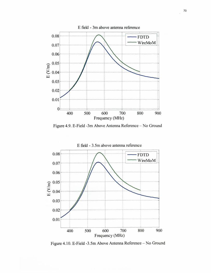
0.08
0.07
0.06
--. 0.05 _§ G o.o4 ~
0.01
E field - 3m above antenna reference
• • • • •
uuT T mmm :m u T =:~~oM ' ' ' ' -------,-----------------r ' ' ' ' ' '
400 500 600 700 800 900 Frequency (MHz)
Figure 4.9. E-Field -3m Above Antenna Reference - No Ground
8 o.o5 -G o.o4 ~
0.03
0.02
0.01
E field- 3.5m above antenna reference
--FDTD --wireMoM
' ' I I I I I ------- ----------------,------------ ----- ,-----------------.-----------------,----------------1 I I I I I I I I I I I I I I I
' ' ' ' ' ' ' ' ' ' ------- .. ---------------- -·-----------------~ --------- -- - - - -- .,... ------- --------- .----------------
I I I I
' '
400 500 600 700 800 900 Frequency (MHz)
Figure 4.10. E-Field -3.5m Above Antenna Reference - No Ground
70

The above figures show that the agreement between FDTD and WireMoM is
agreeable over a frequency range. However, as the height of the observation point
increases, the error also increases. The reason for this disagreement is unknown and
requires further investigation.
4.2.2. With Infinite Ground Plane. The geometry was modeled in the EZ-FDT
with a PEC plane touching the computational domain. The transmitting antenna was
placed at the center of the ground plane, so that the plane was touching the boundary to
simulate the effect of an infinite ground plane. Far-field monitor points were used to
calculate the fields at 6 m away from the transmitting antenna.
Figure 4.11 and Figure 4.12 describe this geometry. Table 4.2 shows the FDTD model
specifications. The WireMoM model was similar to that specified in Figure 4.3 but with
an infinite ground plane. Simulations with both software tools were compared for
different observation point heights.
40 cells
z
----
---
I I 141
100 cells
-----------)f---
Figure 4.11. FDTD Model - Infinite Ground
20 cells
__ .10 .c.clls
71
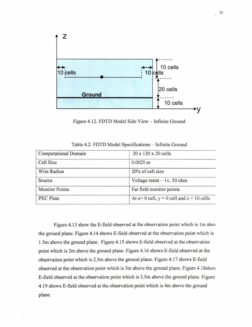
z
~ 10 :cells -
20 cells Ground
~------------------------------~ - - - - ---10 cells y
Figure 4.12. FDTD Model Side View - Infinite Ground
Table 4.2. FDTD Model Specifications - Infinite Ground
Computational Domain 20 x 120 x 20 cells
Cell Size 0.0025 m
Wire Radius 20% of cell size
Source Voltage resist - 1 v, 50 ohm
Monitor Points Far field monitor points
PEC Plate At x= 0 cell, y = 0 cell and z = 10 cells
Figure 4.13 show theE-field observed at the observation point which is 1m abm
the ground plane. Figure 4.14 shows E-field observed at the observation point which is
1.5m above the ground plane. Figure 4.15 shows E-field observed at the observation
point which is 2m above the ground plane. Figure 4.16 shows E-field observed at the
observation point which is 2.5m above the ground plane. Figure 4.17 shows E-field
observed at the observation point which is 3m above the ground plane. Figure 4.18sho~
E-field observed at the observation point which is 3.5m above the ground plane. Figure
4.19 shows E-field observed at the observation point which is 4m above the ground
plane.
72

E field - 1m above ground I I I I I I
0.15 :-----------~------------:------ - ---t-------- ---1---------- --:- --FDTD ' '
--wireMoM
o.1 :-----------:----- -------r--- --- -----~ ------ ----1---------- --· ---------- -~ -----------:-------I I I I I I I I I I I I . . ' . ' ' . ' . ' . ' . ' . ' ' ' ' ' ' ' ' ' ' ' . '
0.05 _______ , ___________ ; ________ --~------------·------ - ----; __ __ __ _
o~--~~~~~~----~--~----~--~~
300 400 500 600 700 800 900 1000 Frequency (MHz)
Figure 4.13. E-Field -1m Above Antenna Reference - Infinite Ground
E field- 1.5m above ground
0.06
0.05
e o.04
~ ~ 0.03 ' ' ' -,-- -----------, --------- --,. ----------
' ' '
0.02 - ·-------- ---·-------------· -----------' ' ' ' '
0.01
Oc======================================= 300 400 500 600 700 800 900 1 000
Frequency (MHz)
Figure 4.14. E-Field -1.5m Above Antenna Reference - Infinite Ground
73

,.-.._
E field - 2m above ground
--FDTD ' '
0.1 i· -- ----------~----- ------- j- ---- - -- -- -- ---------- -~--------- --wireMoM
0.08
' '
j-------------1·-----------;---------·-r··-------+--------- -1-------------:------------:--, '
~ 0.06 1------------+----- ---+- --------!-------------r·----------+-----------:---------- ---r---- . :
0.04
0.02
o~====~===±====~===d=====k====~-=--=---=--=---d--d-
300 400 500 600 700 800 900 1000 Frequency (MHz)
Figure 4.15. E-Field -2m Above Antenna Reference - Infinite Ground
E field - 2.5m above ground
' ' ' --~ --- --- ------~ --------- ---~-- --------- ~---- --------:-------------:------- ------~--- -------- -~--
I I I I I I I 1
' ' ! : : ! ' ! 0.12
I 1 I I I I 1 o :g o.l --:-----------+-----------~ -----------r--- ------:------------r-----------;------------'--
~ __ j _____ ---- ---~------------ j_ ------- ----~---- ---- ____ L ________ -- _..:.._----- ----- -~---- ---- --- -~--c_., 0.08 ' ' ' ' ' ' ' '
__ L_ _________ ~------ ----+- -------+--------- J_ __________ J __________ _j ____________ ~--' I : : : : :
0.06 ' ' ' ' ' ' ' ' ' '
0.04
0.02
300 400 500 600 700 800 900 1000 Frequency (MHz)
Figure 4.16. E-Field -2.5m Above Antenna Reference - Infinite Ground
74

E field - 3m above ground
0.12 ~m nn nn nnlnn ~ m+nm j =:~~oM I 0. 1 ·!············ ············1·········· 1············1············,············: ............ ~ .. .
I I I 1 I I I 1
' ' '
8 o.o8 ~
-r------------------------(----------:----------+-----------;------------(-----------1----
~ 0.06
0.04
0.02
300 400 500 600 700 800 900 1000 Frequency (MHz)
Figure 4.17. E-Field -3m Above Antenna Reference - Infinite Ground
0.02
E field - 3.5m above ground
- FDTD
. : - :- Wir~MoM :
:---- - --------r------------~----- -------r-------- --~- - -------- --;------ - ------ ~----------- -- -·
' ' ' ' ' r-------- ---:-------------r---------
300 400 500 600 700 800 900 1000 Frequency (MHz)
Figure 4.18. E-Field -3.5m Above Antenna Reference - Infinite Ground
75

~
~ >
0.12
0.1
0.08
~ 0.06
0.04
0.02
E field - 4m above ground
--r----- - -------i------ - -------i---------------~-- --- ------------------ --FDTD
' ' I I I 1
·· · · · · · ···· · 1··· i · · ··········· r ·· · · · ··· i · · · · :. · ·· ··· ··· · ·! ····· .. ··.. i
' '
, I ~ ~ r I , :::: , : ~~ ' ' ' ' ' '
-----~----- -------- -~----- ---- ----:--------------:---------------: . . ' ' ' I : :
300 400 500 600 700 800 900 1000 Frequency (MHz)
Figure 4.19. E-Field -4m Above Antenna Reference - Infinite Ground
~
I
The above figures illustrate that there is no match between theE Field simulated
by FDTD and WireMoM. The reason for this mismatch has not been known yet. It could
be due to the way this software considers the infinite ground settings. Moreover, there is
a shift on transmitting antenna, between the current on the wire simulated with FDTD
and the one simulated with WireMoM, which can also be the reason for the difference in
E-field at the distant points. This shift increases with the increase of the transmitting
antenna height with respect to the ground plane. This problem needs more investigation.
4.2.3. Finite Ground - Perfectly Conducting. The geometry was modeled in
the EZ - FDTD and WireMoM by placing a finite PEC plane at z=O. The transmitting
antenna was placed at x= Om, and fields were measured using a far-field monitor placed
at x=6m. Figure 4.20 and Table 4.3 describe the model and specifications, used to model
inFDTD.
76
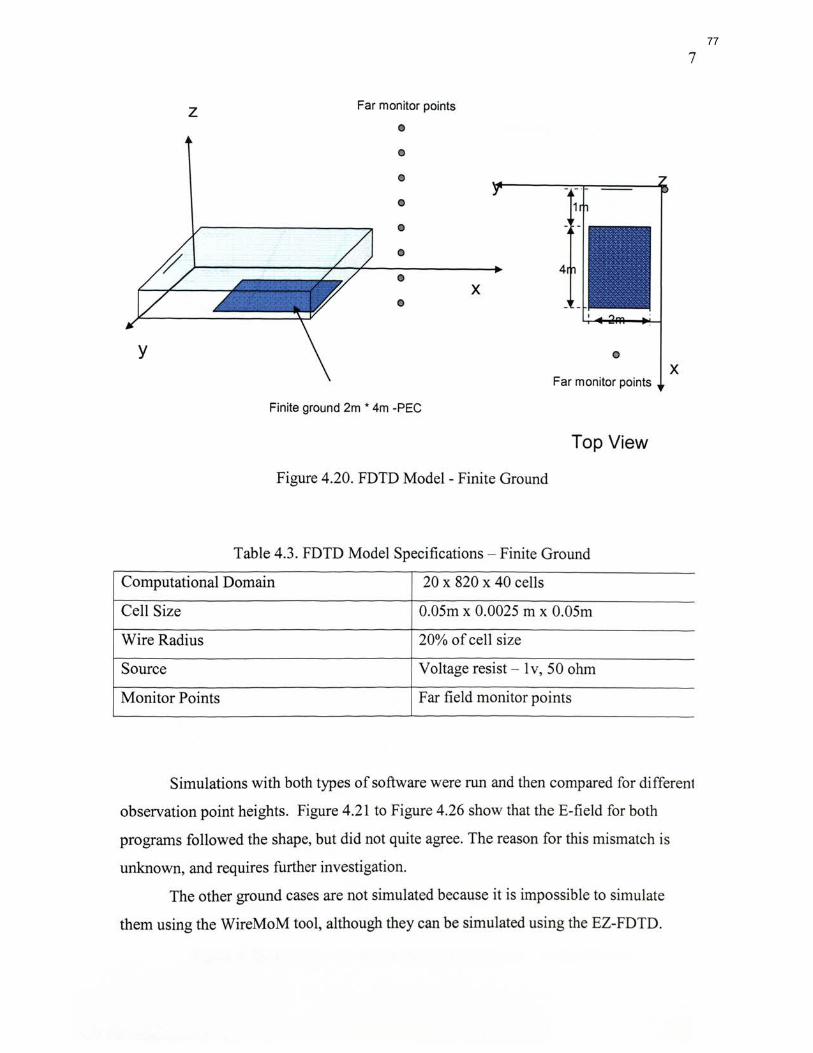
z Far monitor points
e
Finite ground 2m * 4m -PEC
X
Figure 4.20. FDTD Model - Finite Ground
4
0
Far monitor points
Top View
Table 4.3. FDTD Model Specifications - Finite Ground
Computational Domain 20 x 820 x 40 cells
Cell Size 0.05m x 0.0025 m x 0.05m
Wire Radius 20% of cell size
Source Voltage resist - 1 v, 50 ohm
Monitor Points Far field monitor points
7
X
Simulations with both types of software were run and then compared for different
observation point heights. Figure 4.21 to Figure 4.26 show that theE-field for both
programs followed the shape, but did not quite agree. The reason for this mismatch is
unknown, and requires further investigation.
The other ground cases are not simulated because it is impossible to simulate
them using the WireMoM tool, although they can be simulated using the EZ-FDTD.
77

7
E field - 1.5m above ground
--FDTD 0.07 -----(-----------~ ------ ____ ! ______________ ( __________ --WireMoM -
. ' ' ' ' ' ' ' ' '
0.06
. 0.05
0.03
0.01
300 400 500 600 700 800 900 Frequency (MHz)
Figure 4.21. E-Field -1.5m Above Antenna Reference - Finite Ground
E field - 2m above ground
--FDTD
0.1
' ' ' ' ' ___ ., ______________ ,. ______________ ,. __ ' ' ' ' ' ' ' ' ' ' ' ' ' '
I I I 0 ---- ----r··------------:-- -------- --:--------------: ----. ' ' ' ' ' ' '
0.08
,-....
~ 0.06 "'-'
0.04
0.02
o b=k====d====dU==-=-=--=---~-=---=---=--=---=--~--=--=---=--=---=---~-=---=--=---=--d=~
500 600 700 800 300 900 400 Frequency (MHz)
Figure 4.22. E-Field -2m Above Antenna Reference - Finite Ground
78
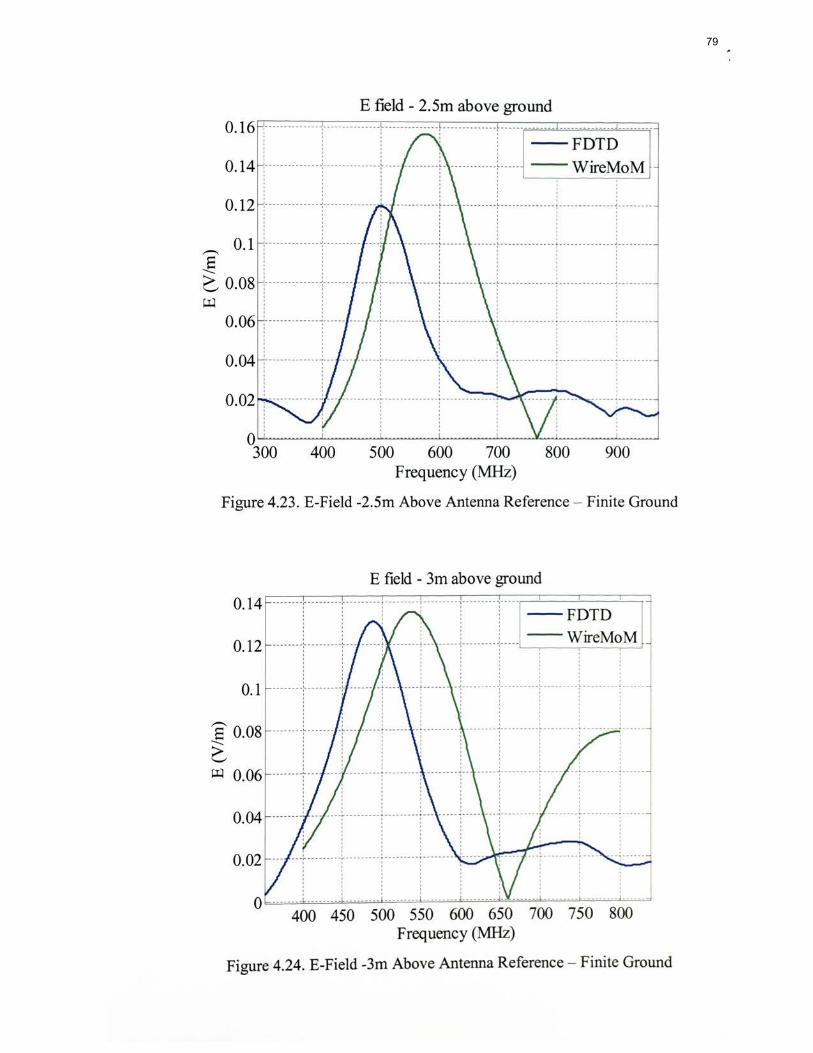
~ 0.1 _§ c, o.o8 j:il
400
E field - 2.5m above ground
500 600 700 800 900 Frequency (MHz)
Figure 4.23. E-Field -2.5m Above Antenna Reference - Finite Ground
E field - 3m above ground
0.1
~ a o.o8 -2: ~ 0.06
0.04
0.02
0 6=~=---=---=---~-=---=---=--b-=-=d===±==~~=L==~==~~
400 450 500 550 600 650 700 750 800 Frequency (MHz)
Figure 4.24. E-Field -3m Above Antenna Reference - Finite Ground
79

,-..,
E field- 3.5m above ground 0.12~:-~----r---:-~======:r=~
- FDTD
0.1 --~-- - --OOoooooooo~oooooo o o oooooo OOOOOoOOOOOOOjooooo.oooooo --WireMoM ' '
0.08
_§ > 0.06 '-'
0.04
0.02
400 500 600 700 800 Frequency (MHz)
Figure 4.25. E-Field -3.5m Above Antenna Reference - Finite Ground
E field - 4m above ground
0.12 ooooooOO[oooooooooooooooooo[ooooooooo-ooo o oOOolOO o-o- oo- ooo o o - FDTD ' ' ' ' ' ' ' ' ' ' ' '
0.1
0.08 ,-..,
_§ 2: o.o6 ~
0.04
' ' --------~-- ------------ - ---~---
: :
0 oo oo o oOO oo o o OOO
500 600 700 Frequency (MHz)
400
Figure 4.26. E-Field -4m Above Antenna Reference - Finite Ground
80 80

8:
4.3. CONCLUSION
The importance of validation can be seen in these cases. Even though a tool is
able to simulate geometry, it is not always correct. It is impossible to tell whether the tool
is correct or not unless tools validate each other with the same answers. For this particulru
case, one of the tools might be giving the correct answer, or all of them might give the
wrong results. It is necessary to investigate the problem by using the third tool, by setting
up the problem for a real measurement, or by analytically calculating the fields. There is
a very good reason to investigate the problem more, but with limited time available, the
problem has not been investigated. At this point, there is no proper tool available at the
moment to simulate this kind of geometry. Hence, validation using these tools has not
been investigated thoroughly.
81
[1]
[2]
[3]
[4]
[5]
[6]
[7]
[8]
8
BIBLIOGRAPHY
Gstottner, A., Steinecke, T., Huemer, M., "Activity based high level modeling of dynamic switching currents in digital IC modules, " Electromagnetic Compatibility, 17th International Zurich Symposium on EMC-Zurich 2006.
Quartus II Development Software Handbook v 7.2, http://www.altera.com/literature/lit-qts.jsp. Oct 2007.
Knighten, J., B. Archambeault, J. Fan, G. Selli, L. Xue, S. Connor, J. Drewniak, "PDN Design Strategies: I1 Ceramic SMT Decoupling Capacitors- Does Location Matter?, " IEEE EMC Society Newsletter, Issue No. 208, Winter 2006, pp. 56-67.
Knighten, James L., Bruce Archambeault, Jun Fan, Giuseppe Selli, Samuel Connor, James L. Drewniak, "PDN Design Strategies: 1 Ceramic SMT Decoupling Capacitors- What Values Should I Choose?," IEEE EMC Society Newsletter, Issue No. 207, Fall2005, pp. 34-41.
Quartus II PowerPlay Power Analysis and Optimization Technology, http://www.altera.com/products/software/products/quartus2/design/gtspower analysis.html. Oct 2007.
Chen Wang, Giuseppe Selli, Shaofeng Luan, Lin Zhang, Jun Fan, David J. Pommerenke, Richard E. Dubroff, James L.Drewniak, "An Efficient Approachfo, Power Delivery Network Design with Closed- Form Expressions for Parasitic Interconnect Inductances, " lEE Transactions on Advanced Packaging.
M. Y. Koledintseva, J. Wu, J. Zhang, J. L. Drewniak, and K. N. Rozanov "Representation of permittivity for multi-phase dielectric mixtures in FDTL modeling, " Proc. IEEE Symp. Electromag. Compat., 9-13 Aug. 2004, Sant: Clara, CA, vol. 1, pp.309-314, 2004.
Pooma Chander Ravva, "Polygon Decomposition into Minimum Number q Primitives and Electromagnetic Shielding Using Composite Materials, " A thesi presented to the faculty of the Graduate School of the University of Missouri Rolla, in partial fulfillment of the requirements for the degree Master of Scienc1
in Electrical Engineering 2006.
82

8.
[9] Koledintseva, M.; Ravva, P.C., R.E. DuBroff, Drewniak, J., Rozanov, K Archambeault, B., "Engineering of composite media for shields at microwav frequencies," Electromagnetic Compatibility, 2005. EMC 2005 lntemationa Symposium on, vol.l, no. pp. 169- 174 Vol. 1, 8-12 Aug. 2005.
[10] A.Sihvola, "Effective permittivity of dielectric mixtures," IEEE Trans. Geosc Remote Sens., vol. 26, no. 4, pp. 420-429, 1988.
[11] D.M.Pozar, "Microwave Engineering," 2nd ed., New York: Wiley, 1998.
[12] Constantine A. Balanis, "Antenna Theory," 2nd ed, page 125.
[13] M.Y. Koledintseva, S.K.R. Chandra, R.E. DuBroff, and R.W. Schwartz "Modeling of dielectric mixtures containing conducting inclusions wit} statistically distributed aspect ratio", Progress in Electromagnetic Researd (PIER) vol. 66, pp. 213-228, 2006.
83

VITA
Sandeep Kamalakar Reddy Chandra was born in Kumool, Andhra Pradesh <
August 261h, 1984 in India. He received his primary and secondary education from Vik
Junior College, Guntur and graduated with a Bachelor of Engineering degree
Electronics and Communications Engineering from G. Pulla Reddy Engineering Colle1
(Affiliated to Sri Krishna Devaraya University), Kumool, India July 2005.
He has been enrolled in the Graduate School at the University of Missouri- Rol
since Fall 2005, majoring in Electrical Engineering with an emphasis in electromagnet
compatibility and signal integrity. He received his Master of Science in Electric
Engineering degree from the University of Missouri, Rolla in Dec 2007.
84