
CHAPTER ONE - CiteSeerX
207
SANTA CLARA UNIVERSITY Department of Computer Engineering Date: January 26, 2004 I HEREBY RECOMMEND THAT THE THESIS PREPARED UNDER MY SUPERVISION BY Nien-Tsu Wang ENTITLED Processing and Storage Models for MPEG-2 Main Level and High Level Video Decoding — A Block-Level Pipeline Approach BE ACCEPTED IN PARTIAL FULFILLMENT OF THE REQUIREMENTS FOR THE DEGREE OF DOCTOR OF PHILOSOPHY IN COMPUTER ENGINEERING Thesis Advisor Thesis Reader Chairman of Department Thesis Reader Thesis Reader Thesis Reader
-
Upload
khangminh22 -
Category
Documents
-
view
2 -
download
0
Transcript of CHAPTER ONE - CiteSeerX

SANTA CLARA UNIVERSITY Department of Computer Engineering
Date: January 26, 2004
I HEREBY RECOMMEND THAT THE THESIS PREPARED UNDER MY SUPERVISION BY
Nien-Tsu Wang
ENTITLED
Processing and Storage Models for MPEG-2 Main Level and High Level Video Decoding
— A Block-Level Pipeline Approach
BE ACCEPTED IN PARTIAL FULFILLMENT OF THE REQUIREMENTS FOR THE DEGREE
OF
DOCTOR OF PHILOSOPHY IN COMPUTER ENGINEERING
Thesis Advisor Thesis Reader Chairman of Department Thesis Reader
Thesis Reader
Thesis Reader

Processing and Storage Models for MPEG-2
Main Level and High Level Video Decoding
— A Block-Level Pipeline Approach
By
Nien-Tsu Wang
DISSERTATION
Submitted in Partial Fulfillment of the Requirements for the Degree of Doctor of Philosophy
in Computer Engineering in the School of Engineering of Santa Clara University, 2004
Santa Clara, California

Dedicated to
my mother Mei-Ying and father Hsieh-Chung, and
my wife Mei-Chuan, and children Terrance and Angelica
for their love and care

Acknowledgements
I would first like to thank Professor Nam Ling for serving as my advisor
during my time at SCU. His total support of my project and countless
contributions to my technical and professional development made for a truly
enjoyable and fruitful experience.
To Professors Silvia Figueira, Tokunbo Ogunfunmi, Weijia Shang, and Shoba
Krishnan for serving on my Ph.D. committee. Their detailed and illuminating
comments strengthened this dissertation considerably and widened my
research knowledge.
To all past and current graduate students, and Mrs. Duan-Juat Ho in our
research group, for their valuable interaction and technical discussion.
To my wife Mei and family, for their unconditional support and everlasting
love.
To Medianix Semiconductor Inc. and NJR corporation, for their financial
support of my project.

TABLE OF CONTENTS Acknowledgements
List of Figures
List of Tables
Abstract
Chapter 1 Introduction . . . . . . . . . . . . . . . . . . . . . . . . . . . 1
1.1 Introduction . . . . . . . . . . . . . . . . . . . . . . . . . . . . 1
1.2 Overview of the Dissertation . . . . . . . . . . . . . . . . . . . 2
1.3 Terminology of MPEG . . . . . . . . . . . . . . . . . . . . . . 4
1.4 Overview of the MPEG-2 Video Decoding Process . . . . . . . 11
1.5 The Design of an MPEG-2 Video Decoder . . . . . . . . . . . . 14
1.6 Research Objectives . . . . . . . . . . . . . . . . . . . . . . . . 18 Chapter 2 Processing and Storage Models for MPEG-2 MP@ML
Video Decoding —Review of Prior Art . . . . . . . . . . . . . 22
2.1 Introduction . . . . . . . . . . . . . . . . . . . . . . . . . . . . 22
2.2 Review of Related Work . . . . . . . . . . . . . . . . . . . . . 23
2.2.1 Processing Model . . . . . . . . . . . . . . . . . . . . . 23
2.2.2 Memory Storage Organization and Interface . . . . . . . 25
2.2.3 External Memory Access Scheduling . . . . . . . . . . . 29
2.2.4 Variable-Length Decoder (VLD) . . . . . . . . . . . . . 31
2.2.5 Inverse Discrete Cosine Transform (IDCT) . . . . . . . . 34
2.2.6 Motion Compensator (MC) . . . . . . . . . . . . . . . . 36
v

2.3 Motivations and Challenge . . . . . . . . . . . . . . . . . . . . . 37
2.4 Research Direction . . . . . . . . . . . . . . . . . . . . . . . . . 38
Chapter 3 Block-Level Pipeline Scheme for MPEG-2 MP@ML Video Decoding — Processing, Storage, and Scheduling . . . . . . . 40
3.1 Introduction . . . . . . . . . . . . . . . . . . . . . . . . . . . . 40
3.2 Designing for Data Transfer Efficiency . . . . . . . . . . . . . . 40
3.3 The BLP Processing Model . . . . . . . . . . . . . . . . . . . . 43
3.3.1 Semantics of the BLP Processing Model . . . . . . . . . 43
3.3.2 Comparison with the Macroblock Level Processing Model . . . . . . . . . . . . . . . . . . . . . 46
3.4 Memory Storage Organization . . . . . . . . . . . . . . . . . . . 51
3.4.1 Data Storing Profile . . . . . . . . . . . . . . . . . . . . 51
3.4.2 Features of SDRAM . . . . . . . . . . . . . . . . . . . 51
3.4.3 Data Storage Organization in SDRAM . . . . . . . . . . 53
3.5 External Memory Access Scheduling . . . . . . . . . . . . . . . 64
3.5.1 Review of Related Work . . . . . . . . . . . . . . . . . 64
3.5.2 Fixed Priority Scheduling Model . . . . . . . . . . . . . 66
3.5.3 The Proposed Bus Scheduling and Internal Buffer Size Reduction . . . . . . . . . . . . . . 71
3.6 Conclusion . . . . . . . . . . . . . . . . . . . . . . . . . . . . . 77
Chapter 4 Design of a Video Decoder for DVD: Block-Level Pipeline Scheme Application Example I . . . . . 78
4.1 Introduction . . . . . . . . . . . . . . . . . . . . . . . . . . . . 78
4.2 Design Procedure . . . . . . . . . . . . . . . . . . . . . . . . . 79
4.3 Overall Decoding System . . . . . . . . . . . . . . . . . . . . . 84
vi

4.4 BLP Controller Mechanism . . . . . . . . . . . . . . . . . . . . 87
4.5 Architectures of Video Processing Units . . . . . . . . . . . . . 91
4.5.1 Variable-Length Decoder (VLD) . . . . . . . . . . . . . 91
4.5.2 Inverse Quantization Unit (IQ) . . . . . . . . . . . . . . 95
4.5.3 Inverse Discrete Cosine Transform Unit (IDCT) . . . . . 96
4.5.4 Motion Compensation Unit (MC) . . . . . . . . . . . . . 100
4.6 Display Model . . . . . . . . . . . . . . . . . . . . . . . . . . . 107
4.7 Performance Simulation Model . . . . . . . . . . . . . . . . . . 109
4.8 Simulation Results . . . . . . . . . . . . . . . . . . . . . . . . . 112
Chapter 5 Processing and Storage Models for MPEG-2 MP@HL Video Decoding — Review of Prior Art . . . . . . . . . . . . 119
5.1 Introduction . . . . . . . . . . . . . . . . . . . . . . . . . . . . 119
5.2 Overview of the Grand Alliance HDTV System . . . . . . . . . 119
5.3 Review of Related Work . . . . . . . . . . . . . . . . . . . . . 122
5.3.1 Processing Model . . . . . . . . . . . . . . . . . . . . . 122
5.3.2 Memory Storage Organization and Interface . . . . . . . 124
5.3.3 External Memory Access Scheduling . . . . . . . . . . 126
5.3.4 Variable-Length Decoder (VLD) . . . . . . . . . . . . . 128
5.3.5 Inverse Discrete Cosine Transform (IDCT) . . . . . . . 131
5.3.6 Motion Compensator (MC) . . . . . . . . . . . . . . . . 132
5.4 Motivations and Challenge . . . . . . . . . . . . . . . . . . . . 134
5.5 Research Direction . . . . . . . . . . . . . . . . . . . . . . . . 135
vii

Chapter 6 Design of a Video Decoder for HDTV: Block-Level Pipeline Scheme Application Example II . . . . . 138
6.1 Introduction . . . . . . . . . . . . . . . . . . . . . . . . . . . . 138
6.2 Overview of the Proposed Decoding Approach . . . . . . . . . 140
6.3 Overall Decoding System . . . . . . . . . . . . . . . . . . . . . 142
6.4 BLP Controller Mechanism . . . . . . . . . . . . . . . . . . . . 145
6.4.1 Overall Controller Scheme . . . . . . . . . . . . . . . . 145
6.4.2 Memory I/O Scheduling . . . . . . . . . . . . . . . . . 147
6.5 Memory Interface Scheme . . . . . . . . . . . . . . . . . . . . 150
6.6 Architecture of Video Processing Units . . . . . . . . . . . . . . 152
6.6.1 Inverse Discrete Cosine Transform Unit (IDCT) . . . . 153
6.6.2 Motion Compensation Unit (MC) . . . . . . . . . . . . 155
6.7 Performance Simulation Model . . . . . . . . . . . . . . . . . . 159
6.8 Simulation Results . . . . . . . . . . . . . . . . . . . . . . . . 161
6.9 Conclusion . . . . . . . . . . . . . . . . . . . . . . . . . . . . 175
Chapter 7 Conclusions . . . . . . . . . . . . . . . . . . . . . . . . . . . . 177
7.1 Additional Applications of BLP . . . . . . . . . . . . . . . . . . 177
7.2 Conclusions and Future Research . . . . . . . . . . . . . . . . . 178
References . . . . . . . . . . . . . . . . . . . . . . . . . . . . . . . . . . . . . 183
Publications . . . . . . . . . . . . . . . . . . . . . . . . . . . . . . . . . . . . 192
Biographical Sketch . . . . . . . . . . . . . . . . . . . . . . . . . . . . . . . . 193
viii

LIST OF FIGURES Figure 1.1 Data hierarchy and functionality of MPEG-2 video bitstream . . . . . . . 7 Figure 1.2 Two methods for scanning DCT coefficients are available in MPEG-2 . . 9
Figure 1.3 Motion compensation interpolation using bi-directional prediction . . . . 10
Figure 1.4 A simplified and high-level functional diagram of the MPEG-2 video
decoding process . . . . . . . . . . . . . . . . . . . . . . . . . . . . . . 13
Figure 1.5 Analyzing phases for MPEG-2 video decoder architecture design . . . . . 16 Figure 1.6 Data flow of the Block Level Pipeline processing scheme . . . . . . . . . 19 Figure 2.1 Data flow of the macroblock-level pipeline decoding scheme . . . . . . . 23 Figure 2.2 Data flow of the amended macroblock-level pipeline decoding scheme . . 24 Figure 2.3 Three typical memory mapping structures for the frame buffer . . . . . . 27 Figure 2.4 Storage structure of picture data in DRAM . . . . . . . . . . . . . . . . . 28 Figure 2.5 State diagram of data bus scheduling for distributed FSM scheme . . . . . 30 Figure 2.6 State diagram of data bus scheduling for polling scheme . . . . . . . . . . 31 Figure 2.7 Block diagram of the Lei-Sun VLD architecture . . . . . . . . . . . . . . 33 Figure 2.8 Block diagram of the Lee Motion Compensator architecture . . . . . . . . 37 Figure 3.1 Generic timing diagram for decoding non-intra macroblocks under
the BLP scheme and the proposed bus scheduling scheme . . . . . . . . . 44 Figure 3.2 Generic timing diagram for decoding non-intra macroblocks under
MB-level pipeline scheme and fixed-priority bus scheduling scheme . . . 47 Figure 3.3 Data bus utilization comparison for the BLP scheme and the amended
macroblock-level scheme . . . . . . . . . . . . . . . . . . . . . . . . . . 50 Figure 3.4 Comparison of reading cycles for EDO DRAM and SDRAM
(source: adapted from Micron Technology) . . . . . . . . . . . . . . . . 52 Figure 3.5 Reference Macroblock storage configuration in 64-bit and 32-bit
data-word SDRAM and corresponding redundant data overhead . . . . . 54 Figure 3.6 VBV buffer data storing configuration and accessing pattern
in SDRAM . . . . . . . . . . . . . . . . . . . . . . . . . . . . . . . . . 56 Figure 3.7 Reference macroblock access for motion compensation . . . . . . . . . . 57
ix

Figure 3.8 Interlaced macroblock-row memory mapping for the frame buffer . . . . 58 Figure 3.9 Reference macroblock access pattern under the interlaced
macroblock-row storage structure . . . . . . . . . . . . . . . . . . . . . . 59 Figure 3.10 Specifying the memory addresses of reference blocks . . . . . . . . . . . 61 Figure 3.11 Worst-case page-breaks during reference data access under
macroblock-level processing . . . . . . . . . . . . . . . . . . . . . . . . 63 Figure 3.12 Data flow model of the bus and internal buffers for an MPEG-2
video decoder . . . . . . . . . . . . . . . . . . . . . . . . . . . . . . . . 67 Figure 3.13 State diagram of the proposed bus scheduling scheme . . . . . . . . . . . 71 Figure 3.14 Average number of filling requests for different VLD buffer sizes . . . . . 75 Figure 4.1 Proposed design methodology of the MPEG-2 video decoder . . . . . . . 80 Figure 4.2 Data flow block diagram of DVD-Video . . . . . . . . . . . . . . . . . . 81 Figure 4.3 Block diagram of the proposed DVD video decoder . . . . . . . . . . . . 86 Figure 4.4 The flow chart of BLP decoding process for non-intra macroblocks . . . . 88 Figure 4.5 The flow chart of BLP decoding process for intra macroblocks . . . . . . 89 Figure 4.6 Block diagram of the Variable Length Decoder . . . . . . . . . . . . . . 93 Figure 4.7 The FSM for VLD processing and error handling . . . . . . . . . . . . . 94 Figure 4.8 Block diagram of the Inverse Quantization Unit . . . . . . . . . . . . . . 95 Figure 4.9 Block diagram of the IDCT unit and word lengths for
interconnections . . . . . . . . . . . . . . . . . . . . . . . . . . . . . . . 97 Figure 4.10 A novel read-write sequence for transpose RAM in the IDCT unit . . . . 99 Figure 4.11 Output timing diagram for the proposed IDCT unit . . . . . . . . . . . . 99 Figure 4.12 Outline of motion compensation . . . . . . . . . . . . . . . . . . . . . . 101 Figure 4.13 Block diagram of the Motion Vector Decoder . . . . . . . . . . . . . . . 102 Figure 4.14 Block diagram of the MC unit . . . . . . . . . . . . . . . . . . . . . . . . 104 Figure 4.15 Data processing pattern, pipeline stages, and output timing diagrams
for MC processing of B- and P-type macroblocks . . . . . . . . . . . . . 105 Figure 4.16 Timing diagram of displaying order, decoding order, and the proposed
recovery mechanism . . . . . . . . . . . . . . . . . . . . . . . . . . . . . 108
x

Figure 4.17 Processing diagram of the proposed DVD video decoder performance simulation model . . . . . . . . . . . . . . . . . . . . . . . . . . . . . . 110
Figure 4.18 Timing diagrams for I-, P-, and B-type macroblocks . . . . . . . . . . . . 113 Figure 5.1 Transport packet format . . . . . . . . . . . . . . . . . . . . . . . . . . . 120 Figure 5.2 Structure of a video decoding approach using slice-level scheme . . . . . 122 Figure 5.3 Examples of dual memory bus interface and corresponding
data storage structure . . . . . . . . . . . . . . . . . . . . . . . . . . . . 125 Figure 5.4 Reordering memory access sequences to avoid page-breaks and
latency of read/write switches . . . . . . . . . . . . . . . . . . . . . . . . 127 Figure 5.5 Codeword-length tree for two-level concurrent decoding.
(Source: [Hsieh 96]) . . . . . . . . . . . . . . . . . . . . . . . . . . . . . 129 Figure 5.6 Architecture diagram for two-level concurrent-decoding VLD
(Source: [Hsieh96]) . . . . . . . . . . . . . . . . . . . . . . . . . . . . . 130
Figure 5.7 Block diagram of the Masaki Motion Compensator architecture . . . . . . 133 Figure 6.1 Basic set-top box architecture for DVB-T digital TV . . . . . . . . . . . . 139 Figure 6.2 Block diagram of the proposed HDTV video decoder architecture . . . . . 144 Figure 6.3 Flow chart of the controller setting the demultiplexor . . . . . . . . . . . 146 Figure 6.4 Flow chart of HDTV BLP decoding process for non-intra
macroblocks . . . . . . . . . . . . . . . . . . . . . . . . . . . . . . . . . 148 Figure 6.5 Flow chart of HDTV BLP decoding process for intra macroblocks . . . . 149 Figure 6.6 Block diagram of memory interface scheme . . . . . . . . . . . . . . . . 152 Figure 6.7 Block diagram of IDCT core processor for HDTV video decoder . . . . . 153 Figure 6.8 Writing and reading order in the transpose RAM . . . . . . . . . . . . . . 154 Figure 6.9 Output timing diagram for the proposed IDCT unit for
HDTV decoder . . . . . . . . . . . . . . . . . . . . . . . . . . . . . . . 154 Figure 6.10 Block diagram of the MC unit for the HDTV video decoder . . . . . . . . 156 Figure 6.11 Data processing pattern, pipeline stages, and output timing diagram for
the MC processing of B- and P-type macroblocks . . . . . . . . . . . . . 157 Figure 6.12 Processing diagram of the proposed HDTV video decoder performance
simulation model . . . . . . . . . . . . . . . . . . . . . . . . . . . . . . 160 Figure 6.13 Average number of filling requests for different VLD buffer sizes
(The threshold for VLD buffer refilling is at 15 bytes) . . . . . . . . . . . 164
xi

Figure 6.14 Average number of filling requests for different VLD buffer sizes
(The threshold for VLD buffer refilling is half the VLD buffer size) . . . 166 Figure 6.15 Timing diagram for I-, P-, and B-type macroblocks for Women.m2v . . . 168 Figure 6.16(a) Statistical distributions of macroblock decoding cycles for I-, P-, and
B- pictures for women.m2v . . . . . . . . . . . . . . . . . . . . . . . 172 Figure 6.16(b) Statistical distributions of macroblock decoding cycles for I-, P-, and
B- pictures for flowers.m2v . . . . . . . . . . . . . . . . . . . . . . . 173
xii

LIST OF TABLES Table 1.1 Parameter bounds of video streams for MPEG-2 five different
profiles . . . . . . . . . . . . . . . . . . . . . . . . . . . . . . . . . . . 6 Table 2.1 Comparison of computational complexity of various IDCT algorithms
for an 8x8 point block . . . . . . . . . . . . . . . . . . . . . . . . . . . . 36 Table 3.1 Characteristics of I/O processes on the memory bus . . . . . . . . . . . . 55 Table 3.2 Procedure for determining the memory address of reference blocks . . . . 62 Table 3.3 Comparison of average page-break occurrence under different
reference picture storage structures . . . . . . . . . . . . . . . . . . . . . 64 Table 3.4 Comparison of different internal buffer sizes under macroblock-level
decoding mode and the proposed BLP decoding mode . . . . . . . . . . . 73 Table 3.5 Average data amount per one macroblock within I-, P-, and
B-pictures . . . . . . . . . . . . . . . . . . . . . . . . . . . . . . . . . . 76 Table 4.1 DVD-Video parameters summary and comparisons with
MPEG-2 MP@ML . . . . . . . . . . . . . . . . . . . . . . . . . . . . . 82 Table 4.2 Sizes of internal buffers adopted for the simulation model for
the proposed DVD architecture . . . . . . . . . . . . . . . . . . . . . . . 112 Table 4.3 Number of decoding cycles per macroblock and bus utilization under
different VLD buffer sizes: Mobile.m2v bitstream @ 10 Mbps . . . . . . 116 Table 4.4 Number of decoding cycles per macroblock and bus utilization under
different VLD buffer sizes: Gi_bitstream.m2v @ 15 Mbps . . . . . . . . . 117 Table 4.5 Comparison of the proposed MPEG-2 MP@ML video decoder LSI and
other video decoder designs using macroblock level processing . . . . . . 118 Table 5.1 GA-HDTV video parameters summary . . . . . . . . . . . . . . . . . . . 121 Table 6.1 Upper bounds for picture resolution and allowable processing time for
each macroblock in MPEG-2 MP@ML and GA-HDTV . . . . . . . . . . 140 Table 6.2 Sizes of internal buffers adopted for the simulation model for
the proposed HDTV architecture . . . . . . . . . . . . . . . . . . . . . . 161 Table 6.3 Average data amount per one macroblock within I-, P-, and
B-pictures . . . . . . . . . . . . . . . . . . . . . . . . . . . . . . . . . . 163 Table 6.4 Bus utilization and percentage of MBs exceeding 221 decoding cycles
for the two video bitstreams . . . . . . . . . . . . . . . . . . . . . . . . . 175
xiii

Processing and Storage Models for MPEG-2 Main Level and High Level Video Decoding
— A Block-Level Pipeline Approach
Nien-Tsu Wang
Department of Computer Engineering
Santa Clara University, 2003
ABSTRACT
A novel MPEG-2 video processing model, termed Block-Level-Pipeline (BLP) processing scheme,
is introduced. Under BLP control, not only does each processing unit process video data on a block-by-
block basis in a video decoder, but also accesses external frame memory for motion compensation on a
block-by-block basis. Thus, the data bus width requirement and the associated internal buffer sizes can be
minimized because the BLP processing model can evenly distribute data bus traffic in time. Besides
providing the compact design of data bus and internal buffers, the BLP scheme also can simplify the
architecture design of each processing unit because their computation load can be relieved on this block-by-
block basis. The description of the BLP design methodology is complete and precise because it takes
processing model, resource management, and process management into account. This methodology can
provide valuable estimations for system requirements in the early design stages of MPEG-2 products.
An efficient interlacing frame memory storage organization and a deterministic fairness-priority bus
scheduling scheme are also presented. This simple storing pattern can efficiently lower the probability of
occurrence of page-break when accessing the external frame memory. Reducing DRAM access latencies is
an important issue in a limited bandwidth system design. Unlike other real-time systems, the bus scheduler
can be simplified to a deterministic and fairness-priority approach due to only one block of data being
conveyed on the bus at one time. With this short-duration data transfer approach, a complicated bus
scheduler to prevent starvation conditions is not needed.
Based on these work, two designs of MPEG-2 video decoders for DVD and HDTV applications are
demonstrated collectively in this dissertation.
xiv

CHAPTER ONE
Introduction
1.1 Introduction
In recent years, many significant improvements in algorithms and architectures for
signal processing of still image, video, and audio have allowed multimedia information to
be easily stored, transmitted, and manipulated. These improvements have also fertilized the
bloom of such multimedia industries as the telecommunications industry, the consumer
electronics industry, and the electronic games industry. However, the need to build a
common audio-video coding standard comes along with these multimedia applications.
With such a standard in place, all multimedia industries can accelerate their digital audio-
video technology development, reduce the costs associated with redundant development,
and, more fundamentally for users, guarantee the flow of content unrestricted by defensive
technical barriers [Chia97].
In 1988, in response to this growing need, the International Organization for
Standardization established the Moving Pictures Expert Group (MPEG) to develop
standards for the coded representation of moving pictures and associated audio information
on digital storage media. Because the goal of MPEG is to standardize audiovisual coding
for a wide range of applications, the MPEG-established standardization principles should
be generic, specifying minimum criteria. Thus, the MPEG standards do not specify an
encoding process. Instead, they only specify formats for representing data input to a
decoder and a decoding process. Therefore, every standards-compliant decoder should be
able to understand the syntax of an incoming bitstream and decode it. How to encode the
bitstream is irrelevant. This decoder-only specification provides enough flexibility for
manufacturers to design encoders of different complexities for different applications.
1

Although the MPEG standards specify the decoding process, this approach is
nevertheless different from specifying a decoder implementation. According to Haskell et
al. [Hask97], “The rules for interpreting the data are called decoding semantics; an ordered
set of decoding semantics is referred to as a decoding process.” Therefore, even after the
standards are established, manufacturers can still continually improve and optimize
decoding implementation algorithms or specific elements in a decoder if these
improvements comply with the semantics defined in the MPEG standards.
1.2 Overview of the Dissertation
Chapter 1 presents a brief description of MPEG-2 video decoding and its design
issues, including the hierarchy definition of MPEG-2 video stream data and an overview of
the video decoding process. Different types of architecture implementation for the video
decoder are mentioned. A well-defined analyzing paradigm for a decoder design is
proposed. This paradigm consists of four main design phases: processing model, process
management, resource management, and optimal architecture. Design considerations for
and characteristics of each phase will be discussed in detail. A general outline of the
research objectives is also introduced.
Chapter 2 features a review on published works for MP@ML video decoding. This
review will cover the processing models, memory storage organizations and interfaces, and
external memory access scheduling schemes. Under the video specification of MPEG-2, the
architecture designs of some of the functional units in a video decoder are straightforward,
with the design concept and design performance defined in the specification. Examples are
the Inverse Quantization Unit and the Motion Compensation Unit. Other functional units
can be implemented by using any of a variety of design approaches. Examples are the
Variable-Length Decoder and the Inverse Discrete Cosine Transform Unit. A review is also
given on existing architecture design approaches for the latter two major functional units.
The limitations of existing overall design approaches are then discussed, followed by a
2

look at the resulting motivations and challenges in developing a new, efficient, overall
design approach. Research directions for how to overcome the limitations of existing
approaches are also presented.
Chapter 3 shows a complete description of the framework for and techniques of the
proposed design approach, which is called the Block-Level-Pipeline (BLP) processing
scheme. The BLP scheme is a full-range design approach that consists of three major
techniques: an efficient data processing model, an efficient memory storage structure, and
an efficient bus scheduling approach for MPEG-2 applications. The strategic design
direction for each technique will be discussed in detail. A comparison of decoding
performance between the BLP approach and other decoding approaches is also presented.
In Chapter 4, a MP@ML application example (a DVD video decoder) is provided to
illustrate how the BLP scheme is applied to produce an efficient architecture design. First,
a guide for determining the efficiency of the video decoder architecture is discussed, which
takes advantage of the proposed analyzing paradigm to balance interrelated design factors
such as the width of the data bus, the sizes of internal buffers, and the degree of complexity
of the bus controller. Second, the proposed DVD architecture and the specific
implementation of the BLP scheme are presented. Third, the architectures of the key
functional units are illustrated. Finally, a simulation model and simulation results are
presented showing decoding performance under the proposed architecture with the BLP
scheme.
Chapters 5 and 6 then focus on an MPEG MP@HL application (an HDTV video
decoder). In Chapter 5, a review of existing design work is presented, which covers the
following design issues: processing models, external memory interfaces, external memory
access scheduling schemes, and architecture of functional units. The disadvantages and
limitations of these design approaches are discussed. The resulting motivation and a
research direction for overcoming the limitations are also presented.
Chapter 6 presents how the BLP scheme is applied to the decoding process for the
HDTV application under the proposed dual-decoder architecture. A novel external memory
3

interface is presented in order to adopt the minimum data bus width that can accommodate
the heaviest bus traffic. For the proposed HDTV decoder design, one of the important
advantages is that its functional units can re-use the designs for MP@ML applications
(presented in Chapter 4), reducing the manufacturing cost. However, due to the requirement
for high data processing throughput, the Motion Compensation Unit and the Inverse
Discrete Cosine Transform Unit need minor improvements. These circuit modifications and
the new corresponding timing diagrams will be presented. Also presented will be
simulation results showing the decoding performance under a low processing frequency
with the proposed dual-decoder architecture and the BLP scheme.
Finally, in Chapter 7, the advantages of the BLP scheme are further emphasized by
implementing an MPEG decoder on portable devices. In addition to decoder applications,
the BLP scheme can benefit MPEG encoder design. These benefits will be illustrated.
Future research directions are also discussed in this final chapter.
1.3 Terminology of MPEG
Until now, MPEG has developed three standards to meet the needs of different
applications. The first standard developed by MPEG, with the nickname MPEG-1 [ISO92],
is intended to code moving pictures and associated audio for intermediate data rates on the
order of 1.5 Mbits/sec. This standard is motivated by the need for storing video signals on a
compact disc with a quality comparable to VHS cassettes. The second standard, nicknamed
MPEG-2 [ISO94], is a syntactic superset of MPEG-1 that provides more input-format
flexibility, higher data rates (up to 18 Mbits/sec as required by high-definition TV), and
better error resilience. The third standard, nicknamed MPEG-4 [ISO99], is a coding
standard for very low bit rates (about 64 Kbits/sec or less). It is intended to support
interactivity (based on audiovisual data content), universal decoding downloadability, and
better coding efficiency.
4

This dissertation focuses on MPEG-2 video decoder implementation analysis and
architecture design. There are a number of basic terms that will be used throughout. A brief
explication of these terms may be helpful to further discussion. More extensive discussions
of these terms are found in Haskell, Mitchell, or Wiseman [Hask97, Mitc96, Wise98].
(1) Profiles/Levels: the MPEG-2 standard intends to satisfy a wide range of applications;
however, design complexity and cost will increase if a decoder is designed to meet the
requirements of all applications [Okub95]. Therefore, MPEG defines five distinct
profiles to specify subsets of the MPEG-2 video syntax and functionality for different
purposes. Each profile can be further constrained on its parameters (e.g., picture size)
by levels. Four levels are defined in MPEG-2. Table 1.1 shows a snapshot of level
bounds for different profiles. This dissertation will be only concerned with the
required functionality and parameter bounds on MP@ML (main profile at main level)
and MP@HL (main profile at high level).
(2) The Hierarchy of MPEG Video Stream Data: For ease of error handling, random
search and editing, and synchronization, MPEG video consists of several well-defined
hierarchical layers with header and data field as shown in Figure 1.1. The first layer is
known as the video sequence layer, which contains one or more groups of pictures.
The second layer from the top is the group of pictures (GOP), which is composed of
one or more groups of intra (I) pictures and/or non-intra Predicted (P) and Bi-
directional (B) pictures. I-pictures are coded separately by themselves, while P-
pictures are coded with respect to immediately previous I- or P-pictures, and B-
pictures are coded with respect to the immediately previous or immediately following
I- or P-pictures. The third layer is the picture layer itself, and the layer beneath that is
called the slice layer. Each slice is a contiguous sequence of raster-ordered
macroblocks. A macroblock (MB) is one 16x16 array of luminance (Y) pixels with
two 8x8 arrays of associated chrominance (Cb and Cr) pixels, which forms a 4:2:0
format. Two 8x16 arrays of chrominance pixels form a 4:2:2 format. The MBs can be
5

further divided into distinct 8x8 blocks for further processing, such as transform
coding.
High Profile(HP)
1920 pels/line1152 lines/frame60 frames/sec
100 Mbit/sec All 3 layers80 Mbit/sec Base + Middle
25 Mbit/sec Base layer
720 pels/line576 lines/frame30 frames/sec
20 Mbit/sec All 3 layers15 Mbit/sec Base + Middle
4 Mbit/sec Base layer
1440 pels/line1152 lines/frame60 frames/sec
80 Mbit/sec All 3 layers60 Mbit/sec Base + Middle
20 Mbit/sec Base layer
Spatially Scalable(SPATIAL)
1440 pels/line1152 lines/frame60 frames/sec
60 Mbit/sec All 3 layers40 Mbit/sec Base + Middle
15 Mbit/sec Base layer
SNR Scalable Profile(SNR)
352 pels/line288 lines/frame30 frames/sec
4 Mbit/sec Both layers3 Mbit/sec Base layer
720 pels/line576 lines/frame30 frames/sec
15 Mbit/sec Both layers10 Mbit/sec Base layer
Main Profile(MP)
352 pels/line288 lines/frame30 frames/sec
4 Mbit/sec
720 pels/line576 lines/frame30 frames/sec
15 Mbit/sec
1440 pels/line1152 lines/frame60 frames/sec
60 Mbit/sec
1920 pels/line1152 lines/frame60 frames/sec
80 Mbit/sec
Simple Profile(SP)
720 pels/line576 lines/frame30 frames/sec
15 Mbit/sec
Low
Lev
el(L
L)M
ain
Leve
l(M
L)H
igh-
1440
(H-1
440)
Hig
h Le
vel
(HL)
Table 1.1 Parameter bounds of video streams for MPEG-2 five different profiles
6

Group of Pictures
Video Sequence
Picture
macroblock
(4:2:2 format)
Cb(8x16)
Cr(8x16)
Y(16x16pels)
slice
(4:2:0 format)
Y(16x16 pels)
Cr(8x8)
Cb(8x8)
(a) Video stream data hierarchy
Sequence layer Random access unit: context
Group of pictures layer Random access unit: video
Picture layer Primary coding unit
Slice layer Resynchronization unit
Macroblock layer Motion compenstation unit
Block layer DCT unit
Layers of Syntax Function
(b) Function of each layer
block
8 pels
8pels
m
Figure 1.1 Data hierarchy and functionality of MPEG-2 video bitstrea7

(3) Discrete Cosine Transform: In general, neighboring pixels within an image tend to be
highly correlated, which is spatial redundancy. Therefore, MPEG uses invertible
block-based discrete cosine transform (DCT) coding of 8x8 pel blocks to decompose
the signal into underlying spatial frequencies for energy concentration and
decorrelation of image data [Ahme74]. The general idea in the computation of DCT is
that each block of image data is represented as a set of basis functions and scaling
factors. The results from the DCT computation process are called DCT coefficients. In
each block, the DCT coefficient located at the extreme upper left-hand corner is
called the DC coefficient, while other DCT coefficients are called AC coefficients. In
the video decoder, a similar computation of DCT is implemented in an inverse
discrete cosine transform unit (IDCT) to transform the DCT coefficients to the
original image data.
(4) Quantization: The human visual system is less sensitive to high frequency signals.
Hence, it is desirable that the DCT coefficients belonging to higher frequency parts
are more coarsely quantized in their representation. The process of quantization is
described as follows. Each DCT coefficient is divided by a corresponding quantization
matrix value that is supplied from an intra-quantization matrix. Each value in this
matrix is pre-scaled by multiplying by a single value, known as the quantiser scale
code. This quantiser scale is modifiable on a macroblock basis, making it useful as a
fine-tuning parameter for the bit-rate control. The goal of this operation is to force as
many of the DCT coefficients to zero as possible within the boundaries of the
prescribed bit-rate and video quality parameters. When a bitstream is decoded in a
decoder, the inverse processing of quantization is implemented in an inverse
quantization (IQ) unit.
(5) Run Length Coding and Zigzag Scanning Order: After quantization, most of the
energy (non-zero DCT coefficients) is concentrated within the lower frequency
portion (upper left-hand corner) of the matrix, and most of the higher frequency
coefficients have been quantized to zero. Hence run length coding can be used to
8

represent the large number of zero coefficients in a more effective manner, and a
zigzag scanning pattern can be used to maximize the probability of achieving long
runs of consecutive zero coefficients. This zigzag pattern is shown in the left portion
of Figure 1.2. An alternate scanning pattern defined in MPEG-2 is shown in the right
portion of the figure. This scanning pattern may be chosen by the encoder on a frame
basis, and has been shown to be effective on interlaced video images. This
dissertation will focus only on usage of the standard zigzag pattern.
(a) Normal Zig-Zag Scan. Mandatory in MPEG-1.
Optional in MPEG-2.
(b) Alternate Zig-Zag Scan. Not used in MPEG-1. Optional in MPEG-2.
For frame DCTcoding of inter-laced video, moreenergy existshere, so runlength coding ismore efficient.
DCDC
Figure 1.2 Two methods for scanning DCT coefficients are available in MPEG-2
(6) Motion Compensation: In general, there are many similarities between adjacent
pictures, which are called temporal redundancy. MPEG-2 exploits this redundancy by
computing interframe differences relative to areas that are shifted with respect to the
area being coded. The whole process is known as motion compensation (MC) and the
9

interframe difference is called the prediction error. An example of motion
compensation is sketched in Figure 1.3. The encoder uses a motion estimation
technique to find the set of displaced MBs in the reference pictures that best matches
the current coded MB. The motion vectors (MV) that are then encoded and transmitted
to the decoder as part of the bitstream indicate the positions of these displaced MBs.
The prediction error is then transmitted using the DCT encoding technique as
described above. The decoder then knows which areas of the reference pictures were
used for each prediction, and adds the decoded prediction errors to this motion
compensation prediction to obtain the output.
Current B Picture
PreviousReference Picture
Future ReferencePicture
Current MB to becoded(aligned to MB grid)
MB GridPosition of "best match" MB(to half-pel accuracy -- neednot be aligned to MB grid)
Motion Vector(e.g., [-10.5, -5.5])
Time
Figure 1.3 Motion compensation interpolation using bi-directional prediction. A displaced MB in the previous picture is used as one prediction of the coded MB in the current B picture, and a displaced MB in the future picture is used as a second prediction. One, or an average of both, can be used as the final prediction.
10

(7) Variable Length Coding: For reducing the coding redundancy, MPEG uses a Huffman
type entropy coding [Huff52] to encode a sequence of symbols, such as MB
addressing, MB type, motion vectors, and DCT coefficients, to the shortest possible
bitstream. The basic coding principle is shorter codewords assigned to more probable
symbols. Therefore, at the MPEG-2 decoder, there is a variable length decoder (VLD)
to recover these codewords, recreating the original data.
(8) Video Buffer Verifier: MPEG-2 has one important encoder restriction, namely, a
limitation on the variation in bits per picture, especially in the case of constant bitrate
operation. Hence, MPEG defines an idealized model of the decoder called the video
buffer verifier (VBV). The VBV is used to constrain the instantaneous bitrate of an
encoder such that the average bitrate is met without an overflow or underflow of the
decoder’s compressed data buffer.
1.4 Overview of the MPEG-2 Video Decoding Process As mentioned in Section 1.1, the MPEG-2 standard only specifies the decoding
process such that all decoders shall produce numerically identical results with the
exception of the IDCT [ISO94]. The IDCT is defined statistically in order for different
implementations of this function to be allowed. A simplified and high-level functional
diagram of the MPEG-2 video decoding process [Isnr98] is shown in Figure 1.4 and
described below:
1. A compressed video bitstream supplied from the system demultiplex is written to a
VBV buffer on an external DRAM through the channel FIFO and data bus.
2. This compressed video bitstream is then read from the DRAM into a bitstream-
parsing unit, extracting the fixed-length and variable-length coded data. The fixed-
length coded data belongs to the high layer syntax of a video stream, including the
sequence header, the GOP header, and the slice header. The variable-length coded
11
data includes MB headers and quantized DCT coefficients and will be decoded in a
VLD unit. The decoded DCT coefficients will then be transferred to IZZ, IQ, and
IDCT units for further processing.
3. If the current decoded MB is a non-intra MB, motion vectors are extracted from the
MB header by the VLD unit and sent to an addressing unit for deriving the actual
addresses of reference MBs. A video may be encoded in a progressive or interlaced
scanning pattern, while the reference pictures also can be stored in one of these
patterns. Therefore, the actual address computing depends on the field/frame
prediction signal [Puri93]. The MVs for chrominance pixels are derived from the
luminance MVs by a scaling that depends on the chrominance sampling density. For
example, the chrominance MVs of 4:2:0 video are derived from dividing both
horizontal and vertical components of the luminance MVs by two. If MVs are given in
the half-pixel boundary, the reference MBs need an interpolating computation.
Finally, if the decoded MB depends on more than one reference MB, their average is
used as the final prediction.
4. The quantized DCT coefficients are first de-zigzagged and inverse-quantized in the
IZZ and IQ units. These values are then forwarded to the IDCT unit to recover the
original pixels or residual values. Finally, if the current decoded MB is a non-intra
MB, the outputs are added to an anchor MB coming from an MC unit to produce a
reconstructed MB. The reconstructed MB is then stored into external DRAM. For an
intra-MB, the IDCT results directly compose an original MB that can be immediately
stored into DRAM.
5. After one picture is decoded, the reconstructed image may be re-read from the DRAM
to a display processor for displaying, or to the decoder chip again to become the
reference data.
12

VLD IZZ IQ IDCT
Parsing
FIFO
DCTCoeffs
Zig-Zag Scan Mode
Quant Scale Factor & Quant Matrices
VLD Scaling forChroma
CombinePredictions
Half-PelPredictionFiltering
+
Motion Vectors
VectorPredictors
Half-Pel Info
ExternalDRAM
DRAMAddressing
Field/Frame Prediction Selection
Decoded Pixelsfor Displaying
MPEG-2Bitstream
Figure 1.4 A simplified and high-level functional diagram of the MPEG-2
video decoding process
13

1.5 The Design of an MPEG-2 Video Decoder MPEG-2 is targeted on the wide range of applications that may reside in workstations,
personal computers, and consumer products. Basically there are three types of
implementation for the decoding process [Lin95]:
(1) Generic processor
(2) Custom data path engine
(3) Application-specific processing engine
A generic processor may be based on reduced instruction set computing (RISC) or
other all-purpose PC-based architecture. Recently, the rapid progress of generic processor
technology [White93, Trem95, Saav95] has given new impulse to software MPEG decoding
[Ikek97, Hsiau97]. Software decoders usually have advantages in shortening the design
time compared to hardware decoders and providing versatile and adaptive functions
[Lee99]. However, unless special programming solutions are adopted [Bhas95, Bagl96], the
software decoders turn out to be extremely inefficient. This is due to the fact that there are
no compilers that can automatically detect and generate efficient machine code. Moreover,
the computing power of present generic processors still cannot satisfy the requirements for
a digital HDTV (high-definition television) video decoder performing real-time decoding of
MPEG-2 MP@HL pictures, which requires a computing power of about four to five billion
operations per second [Lee96].
Custom data path engines are special-purpose processors that are based on
application-specific instruction sets. Typical examples of such custom data path engines are
today’s digital signal processors (DSPs) [Veen94, Brin96]. Usually, a DSP core that is
refined to constitute a decoder needs a pixel I/O controller and a specific parallel
functional unit [Balm94]. The advantage of this approach is flexibility, since codec
functions are completely realized by microcodes. Therefore, developers can quickly
respond to changes and improvements in compression algorithms, even after the silicon is
built. However, the disadvantage is the cost in terms of silicon area. A DSP core can take
14

up to five times the area and dissipate more power than its dedicated hardware counterparts
[Ackl94]. The user-programmable part may also incur substantial software development
costs since these special instructions are less convenient to learn and are difficult to
optimize automatically.
Application-specific processing engines are hardware-dedicated data processing units
for specific functions. For example, an MPEG-2 decoder may be constituted of different
dedicated processing units, such as a VLD unit for decoding Huffman codes, an IDCT unit
for efficient IDCT processing, and an IQ unit for inverse quantization. The application-
specific processing engines, significantly differing from DSP cores and generic processors,
can move the processing along in hardware instead of demanding instruction cache and data
paths for decoding instructions; therefore, they are compact and highly efficient. This
property clearly leads to tradeoffs in efficiency, flexibility, and cost. However, such
applications as HDTV decoders are suitable for implementing with these dedicated
processing engines because the required computing power has to be very high and the cost
constraints are very low, and standards will be settled before products become available.
This dissertation is only concerned with the implementation of application-specific
processing engines to the video decoding architecture of MPEG-2 MP@ML and MP@HL.
Given the implementation approach of the MPEG-2 video decoder, there are many
ways to build a video processing IC for specific applications. To obtain an optimal design
for high-end applications, or to obtain a more cost-efficient design, an analyzing paradigm
can be derived from parts of a well-defined analysis model for multimedia operation system
proposed by Steinmetz [Stei95]. The proposed paradigm consists of four main phases:
processing model, process management, resource management, and optimal architecture.
The interdependence of these phases is depicted in Figure 1.5. Any design change or design
problem occurring in any phase may require designers to return to the preceding phases for
appropriate modification or clarification. A short discussion of the four phases is presented
below:
15

Processing Model
ProcessManagement
ResourceManagement
OptimalArchitecture
Figure 1.5 Analyzing phases for MPEG-2 video decoder architecture design
1. Processing Model: This phase presents a model of how a video decoder processes the
video data in an application. It depends closely on the characteristics of the video
data, such as frame size, frame rate, incoming bitrate, and the data processing rate of
each functional unit. Generally a processing model includes two different
viewpoints—implementation architecture and bitstream structure. From an
implementation architecture viewpoint, this model can be linear pipeline style or
parallel processing style. From the bitstream structure viewpoint, following the specs
of MPEG-2 bitstream hierarchical structure, this model may start from slice layer,
macroblock layer, or block layer.
16

2. Process Management: This phase shows how process management must take into
account the timing requirement imposed by the processing model and then apply
appropriate scheduling approaches. A proper scheduling scheme must consider timing
and logical dependencies, both internal and external, among different, related tasks
processed at the same time. Therefore, the responsibility of process management is
not only to be a guide for errorless computations in each functional unit in the video
decoder according to the specification, but also to direct the output of each
processing unit to arrive on time.
3. Resource Management: To accommodate timing requirements, resource management
treats each single component as a resource reserved prior to data processing. In the
MPEG-2 video decoder, the resources are frame memory, data bus, and internal
buffers. As described in Section 1.4, the frame memory is for storing an incoming
compressed bitstream and reconstructed pictures, while the data bus is for delivering
these video data. An internal buffer is associated with each processing unit for
buffering the processed data because the throughput rate of every processing unit is
different. Each resource has a capacity measured by a task’s ability to perform in a
given time-span using the resource. In this context, “capacity” refers to each
functional unit’s data processing rate, frequency range, or amount of storage.
4. Optimal Architecture: The main characteristic of a multimedia system is the need for
correct response time. For example, the playback of a video sequence in multimedia
is acceptable only when the video is presented neither too fast nor too slow.
Furthermore, research at IBM Heidelberg [Stei96] shows that users may not perceive
a slight jitter in a media presentation, depending on the medium and the application.
Therefore, the best method to achieve an optimal architecture in the MPEG-2 video
decoder system is not to focus on the architecture’s processing speed, but to ensure
that the most video data can be decoded by a specific deadline. Resolving the above
three issues will lead to an optimal architecture for the MPEG-2 video decoder
system.
17

1.6 Research Objectives Recently, visual communications is a rapidly evolving field for the media, computer,
and telecommunication industries. Hence, many decoding algorithms/implementations are
being proposed and developed for solving problems in these areas. Among these proposals,
the DCT/IDCT and VLD techniques are well developed for different applications. However,
proper processing models developed for decoding controllers, and resource analyses such as
mapping memory storage and determining internal buffer size, are still rare and have some
limitations (see Chapter 2 and Chapter 5). The main objective of this research is developing
a solid and efficient processing model, memory storage mapping organization, and bus
scheduling approach so that users can combine the proposed techniques with already well-
developed MPEG-2 video processing units, or derive an optimal architecture design for
every processing unit to better satisfy different applications. Essential for the introduction
of new video communication services is low cost. It is also our intention to minimize the
data bus width and internal buffer sizes so as to reduce the chip size and thus lower the
manufacturing cost.
The proposed processing model is called a Block-Level-Pipeline (BLP) processing
scheme [Ling98, Wang98, Wang99b] due to the fact that the video decoding process/path is
based on the block layer that is defined as the lowest partition unit in the hierarchical
syntax of the MPEG-2 video bitstream. Under BLP control, not only does each processing
unit process video data on a block-by-block basis, but also accesses external frame memory
for motion compensation on a block-by-block basis. Also developed is an interlaced frame
memory storage organization and a deterministic fairness-priority bus scheduling scheme to
cooperate with the BLP scheme. A video decoder designer can apply this BLP scheme to a
set of processing units to derive a suitable MPEG-2 video decoding architecture for any
application. Figure 1.6 depicts the data flow of this BLP scheme.
18

VLD
IQ/IZZ
IDCT
MC
Write-Back
Maximum time for a MB processing
block 5
block 5
block 5
block 4
block 4
block 4
block 5
block 5
block 3
block 3
block 3
block 4
block 4
block 2
block 2
block 2
block 3
block 3
block 1
block 1
block 2
block 1
block 2
block 0
block 0
block 0
block 1
block 1
block 0
block 0
Maximum time forprocessing one block
Figure 1.6 Data flow of the Block Level Pipeline processing scheme
The main objective of this research is to develop the BLP scheme to serve as a
decoding model. Given a set of video processing units, one can specify the design in six
areas. The first three areas apply to both MP@ML and MP@HL applications:
1. The description of this design is complete and precise because it takes processing
model, resource management, and process management into account.
2. The data bus traffic is more evenly distributed in time due to the block-by-block
access method for frame memory. Minimization of the bus width requirement is the
result.
3. The associated internal buffer size of each processing unit (IQ, IDCT, and MC units)
can be reduced to a minimum because each time, every processing unit only decodes
one block of video data.
The next three areas are for MP@HL applications such as HDTV, in which multiple
decoding paths for parallel processing are needed on account of the larger amount of video
data characterizing these kinds of applications. The BLP scheme can still be applied to this
19

parallel architecture design because every decoding path decodes alternating blocks while
the whole decoding process works on the same MB. The three design considerations are as
follows:
4. Frame memory I/O contention occurs when every decoding path needs to access
external frame memory for motion compensation at the same time. This contention
can be avoided with the alternate switching process. Frame memory access will
follow the same alternation pattern.
5. The synchronization among these decoding paths can be simplified because they work
on the same macroblock.
6. This processing model can balance the computation load of a video decoder because
each decoding path receives evenly dispensed blocks of data during decoding of one
macroblock. Therefore, the system performance of a decoder can reach an optimum.
The second objective of this research is to develop both an interlacing frame memory
storage organization and a deterministic fairness-priority bus scheduling scheme. These two
techniques can help BLP succeed in the following ways:
1. This simple frame-storing pattern can efficiently lower the probability of occurrence
of page-break when accessing the external frame memory. Reducing DRAM access
latencies is an important issue in a limited bandwidth system design.
2. Unlike other real-time systems, the bus scheduler can be simplified to a deterministic
and fairness-priority approach due to only one block of data being conveyed on the
bus at one time. With this short-duration data transfer approach, a complicated bus
scheduler to prevent starvation conditions is not needed.
Besides all the above, another advantage of the BLP scheme is minimizing power
consumption of the video decoder. During decoding of a macroblock, not all processing
units are always in operation; hence, a clock supply controller can be designed to supply
clock signals to processing units and the associated internal buffers only when they are
working. With the BLP scheme, this clock supply controller can easily predict which
processing units are going to be idle. In summary, the above objectives for and advantages
20

of BLP make it practical for the cost-effective design environment of the consumer
electronics industry.
21

CHAPTER TWO
Processing and Storage Models for MPEG-2 MP@ML Video Decoding — Review of Prior Art
2.1 Introduction
Visual applications, services, and equipment play important roles in people’s lives as
a preferred means of communication. As a core technology in the digital compression
system for consumer electronic devices, MPEG decoders are rapidly growing in popularity
as they are adopted by the consumer electronics industry. For the designer of a decoder, the
major issue is not only how to decode each received bitstream in real-time but also how to
reduce the silicon area of the decoder and how to integrate functional units on a single chip
with low power consumption. In the last decade, significant improvements in VLSI
technology have relieved hardware problems caused by hardware systems having high
complexity; but the high demands for video decoding still require special architecture
approaches adapted to the video-decoding scheme. As explained in Chapter 1, the MPEG
standards do not specify a decoder implementation but define the decoding process.
Therefore, much research on processing models, memory storage organization structures,
bus scheduling schemes, and hardwired functional units has been done. Before presenting
the proposal for the Block-Level-Pipeline (BLP) processing scheme, it is worthwhile to
review related MP@ML work from other researchers in order to easily point out the
differences between the BLP model and other processing models. However, a design does
not exist that provides "total" solution for all applications. The advantages or disadvantages
of a design vary with the different needs of different applications.
22

VLD
IQ/IZZ
IDCT
MC
Write-Back
MB 0
Pixel-level pipeline
T 0 T 1 T 2 T 3 T 4 T 5 T 6 T 7 T 8
Maximum time forprocessing one MB
MB 0
MB 0
MB 1
MB 2
MB 1
MB 1
MB 2
MB 3
MB 0
MB 6
MB 7
MB 8
MB 5
MB 5
MB 4
MB 6
MB 7
MB 4
MB 4
MB 5
MB 3
MB 6
MB 3
MB 3
MB 4
MB 5
MB 2
MB 2
MB 2
MB 3
MB 4
MB 1
MB 0
MB 1
Y 0 Y 1 Y 2 Y 3 Cb Cr
Y 0 Y 1 Y 2 Y 3 Cb Cr
Figure 2.1 Data flow of the macroblock-level pipeline decoding scheme
2.2 Review of Related Work
2.2.1 Processing Model
Due to the characteristics of the MPEG algorithm and the huge computational
demands for video processing, all MPEG video decoders adopt two-level or three-level
parallelism and pipeline structure in their design. For applications using MPEG-2 MP@ML,
such as DVD players, the macroblock-level pipeline scheme combined with a pixel-level
pipeline scheme is a common processing model adopted by designers [Fern96, Iwata97,
Toyo94, Yasu97].
As shown in Figure 2.1, the video data of a macroblock is processed in pipeline style
between functional units, and a pixel-level pipeline scheme is performed within each
functional unit. The pixel-level pipeline is obtained by means of a conventional pipeline
design, which optimizes the ratio of operations per second to silicon area by balancing the
23

throughput of all functional units. This macroblock-level pipeline is obtained by scheduling
operations and data between functional units and external DRAMs. Therefore, to maintain
the correct pipelining, the decoder needs to couple with a global pipeline controller to
delimit the processing time of each functional unit. The decoder also needs to be equipped
with many buffers possessing a reasonable size (usually holding two or three macroblocks)
associated with functional units for buffering data due to the difference of processing rate
between concatenate functional units.
Based on the above conventional macroblock-level-pipeline decoding scheme, Lin
proposed an amended macroblock-level-pipeline decoding scheme [Lin96], as illustrated in
Figure 2.2. In this decoding scheme, all functional units and I/O transactions still operate
on a macroblock basis, but they must wait for other functional units to finish their tasks
before beginning to decode a new macroblock. This scheme can minimize the problem of
huge internal buffer size in the conventional macroblock-level decoding scheme. But, from
a resource utilization viewpoint, it is not an efficient design because the functional units
are often in an idle state.
VLD
IQ/IZZ
IDCT
MC
Write-Back
MB 0
T 0 T 1 T 2 T 3 T 4 T 5 T 6 T 7 T 8
Maximum time forprocessing one MB
MB 0
MB 0
MB 0
MB 2
MB 2
MB 1
MB 1
MB 2MB 1
MB 2MB 1
MB 0
MB 1 MB 2
Figure 2.2 Data flow of the amended macroblock-level pipeline decoding scheme
24

In general, the processing models described above are fixed-capability models
because they are running at a specific constant clock frequency for decoding. The selection
of a clock frequency for decoding is made according to the worst-case performance
requirement among all stages within the process of pipeline decoding. Hence, system
resource utilization is sometimes low. To solve this problem, a frequency-scaling
processing model was proposed [Kim96]. This processing model adjusts the clock
frequency for decoding according to the amount of coded data in a picture. If the job load
is heavy, the clock frequency is increased to satisfy the performance requirements;
otherwise, the clock frequency is decreased to adjust the throughput and save on the power
consumption. However, this frequency-scaling scheme encounters two problems. First, the
amount of data in a picture is hard to predict; hence, a precise clock frequency is difficult
to choose in advance. The goals of this model, such as increasing system resource
utilization and lowering power consumption, are very difficult to reach. Second, the
hardwire design of each functional unit must be sophisticated because the wide range of
clock frequency will easily cause timing issues between gates. Therefore, this clock
frequency scaling model is rarely employed in industry products.
2.2.2 Memory Storage Organization and Interface
For MPEG-2 decoding systems, there are at least three frame memories required for
storing two reference pictures and an output B-picture. Therefore, three data streams
frequently cross the memory interface during the decoding process: reading reference
macroblocks, writing decoded macroblocks, and transferring display pictures. To cope with
such a memory access bottleneck, many new memory architectures to improve bandwidth
have been constructed [Prin96]. Among these new designs, conventional DRAM
architecture with Fast-Page mode [Lee95, Uram95] and synchronous DRAM (SDRAM)
architecture [Hama99, Onoy95, Taka99, Winz95] are widely adopted in MPEG-2 MP@ML
applications. Besides the architectural properties of DRAMs, the characteristics of picture
data access have to be taken into account. Thus, frame memory storage organization needs
25

to be concerned with reducing such access latency as bank pre-charge time and page-
breaks.
Scan-line storage organization is a simple and easy method for storing the picture
data. From the viewpoint of a display processor, it is straightforward for the display
processor to access the picture data because the display process is in scan-line style.
However, motion compensation, for reading pre-decoded reference data and for writing the
current decoded data, consumes more than 60 percent of memory bandwidth [Liu96]. This
reading and writing accesses the frame memory on a macroblock basis. There are three data
storage organization structures commonly proposed, which are based on the macroblock-
type accessing pattern. One structure sequentially stores macroblocks in a conventional
DRAM [Uram95], as shown in Figure 2.3(a). The pel data in a macroblock is put in a
memory page in order to take advantage of the features of Fast Page mode. The second
structure sequentially stores macroblock-rows in multiple banks of SDRAM [Winz95], as
shown in Figure 2.3(b). This storage structure takes advantage of the alternative bank
access feature in the special SDRAM architecture in order to reduce precharge latency. The
third structure sequentially stores 2x2 macroblock-sets in multiple banks of SDRAM
[Taki01], as shown in Figure 2.3(c). Figure 2.4 (a) shows an example of macroblock-basis
access, in which a DRAM word (e.g. 64 bits) contains either eight horizontal neighboring
luminance pels, or their corresponding four Cb and four Cr chrominance pels [Demu94].
For dealing with interlaced pictures, top-field and bottom-field separately stored into
different banks of a frame memory is a common approach [Onoy95, Winz95], as shown in
Figure 2.4 (b).
26

one
page
data word length
one macroblock row
EDO DRAMpre-decoded reference picture
(a) Sequential storage structure in EDO DRAM
SDRAMBank 0 Bank 1
pre-decoded reference picture
(b) Sequential storage structure in SDRAM
SDRAMBank 0 Bank 1
pre-decoded reference picture
(c) 2x2 macroblock-set storage structure in SDRAM
Figure 2.3 Three typical memory mapping structures for the frame buffer
27

Macroblock
Y YYYYYYY
8 bits
Luminance word (64 bits)
Cb CrCrCrCrCbCbCb
8 bits
chrominance word (64 bits)
Cb Cr
Y Y
Y Y
Macroblock
Cb Cr
Y
(a) Storage structure of pixel data in DRAM
Y
Y Y
the bottom field of Y pixels in a reference
picture
the Cb and Cr pixels in a reference picture
the top field of Y pixels in a reference picture
the Cb and Cr pixels in a reference picture
(a) Storage structure for the interlaced picture format
bank 0 bank 1
M
Figure 2.4 Storage structure of picture data in DRA
28

The frame size and frame rate of the MP@ML applications, as indicated in Table 1.1,
are 720x480 at 30 frames per second. The memory size needs to be at least 11.9 Mbits,
which includes a frame buffer for storing two reference frames and one B-picture output
buffer. The VBV buffer size for MP@ML is 1.7 Mbits. Thus, 16 Mbits for the total DRAM
size will be enough. Under the macroblock-level processing model, the motion
compensation unit in a video decoder needs to read one or two macroblocks of reference
data from external DRAM. To speed bus response and avoid starvation of other functional
units, a 64-bit data bus is a common choice for the video decoder [Demu94, Lee95, Lin96,
Toyo94].
2.2.3 External Memory Access Scheduling
In MP@ML applications, the buffers storing the incoming compressed bitstream,
reference pictures, and display pictures are usually together in the external DRAM to
reduce the number of DRAMs and the number of pins. Because many functional units,
during video decoding, need to read or write data through the same data bus to or from
external DRAM, there must be efficient bus scheduling to arrange timely data delivery for
the functional units. Sharing the data bus also implies that the processing model is an
important factor in the bus scheduling issue. In the macroblock-level processing model, the
amount of data exchanged between external DRAM and the functional units of the decoder
would be one macroblock (16x16 pels) each time. A long duration of data transfer means a
bus with high utilization but slow response, which can either cause an increase of internal
buffer size or result in hardware idle. Hence, under a given processing model, a careful
design for external memory access scheduling is essential to balance the needs of bus
utilization and bus response time.
A traditional and straightforward data bus arbiter is the fixed-priority scheme
[Faut94]. Due to the heavy load on the data bus, given the algorithm characteristics of
MPEG-2 with ITU-R and higher resolution, this approach may cause functional units to
starve without large internal buffers for I/O buffering.
29

Ling’s and Uramoto’s priority schemes are a similar approach, but they add a
centralized controller [Ling97, Uram95]. Here, different priorities are assigned to the five
requests for memory access, and distributed finite state machines (FSMs) are assigned to
control individual requests on a cycle-by-cycle basis. The centralized controller
synchronizes the entire architecture on a macroblock-by-macroblock basis. This is shown in
Figure 2.5.
CentralController
FIFOstatus
DRAMstatus
Displaystatus
Baseline FSM MC FSM
Synchronization & communication
Figure 2.5 State diagram of data bus scheduling for distributed FSM scheme
A more sophisticated scheme to reduce the internal buffer requirement is a
combination of priority assignment and polling [Demu94]. As shown in Figure 2.6, five
requests for memory access are classified into three priority groups and a grant to use the
data bus is given corresponding to the priority group. If the requests from plural members
in the first priority group are issued, the grant is allocated by polling.
30
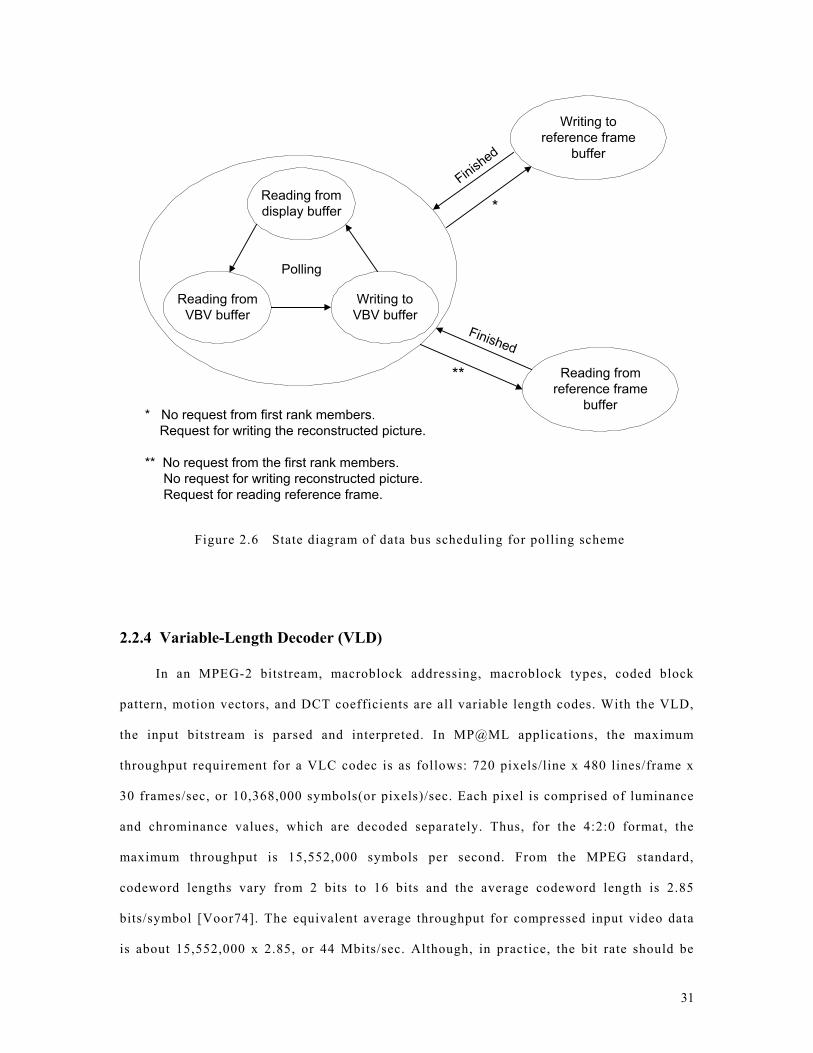
Reading fromdisplay buffer
Reading fromVBV buffer
Writing toVBV buffer
Polling
Writing toreference frame
buffer
Reading fromreference frame
buffer
Finished
Finished
*
**
* No request from first rank members. Request for writing the reconstructed picture.
** No request from the first rank members. No request for writing reconstructed picture. Request for reading reference frame.
Figure 2.6 State diagram of data bus scheduling for polling scheme
2.2.4 Variable-Length Decoder (VLD)
In an MPEG-2 bitstream, macroblock addressing, macroblock types, coded block
pattern, motion vectors, and DCT coefficients are all variable length codes. With the VLD,
the input bitstream is parsed and interpreted. In MP@ML applications, the maximum
throughput requirement for a VLC codec is as follows: 720 pixels/line x 480 lines/frame x
30 frames/sec, or 10,368,000 symbols(or pixels)/sec. Each pixel is comprised of luminance
and chrominance values, which are decoded separately. Thus, for the 4:2:0 format, the
maximum throughput is 15,552,000 symbols per second. From the MPEG standard,
codeword lengths vary from 2 bits to 16 bits and the average codeword length is 2.85
bits/symbol [Voor74]. The equivalent average throughput for compressed input video data
is about 15,552,000 x 2.85, or 44 Mbits/sec. Although, in practice, the bit rate should be
31

reduced by DCT and quantization processes, architecture design needs to consider the worst
case. Therefore, the maximum processing rate of a VLC decoder should be constructed to
have a capability of 44 Mbits/sec.
There are two classes of VLC decoders: constant-input-rate decoders and constant-
output-rate decoders. The constant-input-rate decoder, such as the tree-search-based
decoder, processes input bits at a fixed rate, but codewords are decoded at a variable output
rate. There are two kinds of implementations on this constant-input-rate decoder. One
implementation is a sequential decoding process that can be considered as traversing down
a path of the Huffman tree from the root, the path determined by the encoded bitstream
being input [Chang92, Mukh91, Park93]. This implementation has a processing throughput
of about 40Mbps. The other implementation is also a tree search, but traces multiple bits at
a time rather than one bit at a time. This implementation is based on dividing the Huffman
table into two parts, leading-0 bits and following bits [Hash94, Ooi94, Park99]. In other
words, a binary tree can be transformed into many clusters based on the number of leading-
0’s. Within a cluster, the following bits determine the offset of the decoded symbol. This
kind of implementation has the capability to enable 162 Mbps decoding.
The constant-output-rate VLD is a kind of lookup-table-based method that yields a
constant symbol-decoding rate. These codeword lookup tables are constructed at the
decoder from the symbol-to-codeword mapping table and can be implemented by
programmable logic arrays (PLAs), content-addressable memories (CAMs), read only
memories (ROMs), or random access memories (RAMs). Due to the trade-off between the
referencing speed and die size cost of the lookup table, many constant-output-rate VLD
constructions are based on the PLA implementation proposal from Lei and Sun, which uses
parallel operations to decode each codeword in one cycle regardless of its length [Lei91].
Figure 2.7 shows a block diagram of the Lei-Sun VLD that includes two data registers, a
barrel shifter, a set of VLC tables, and an adder. An incoming codeword is stored into the
upper and lower registers and then the decoder operates on these two registers
simultaneously. The barrel shifter is controlled by the adder, which accumulates the lengths
32

of the decoded codewords. At each cycle, the output of the barrel shifter is matched in
parallel with all the entries in the codeword table. When a match is found, the codeword
table outputs the corresponding source symbol and the length of the decoded codeword, and
then the barrel shifter is shifted to the beginning of the next codeword. If the adder
overflows, which indicates the upper register has been fully decoded, the content of the
lower register is transferred into the upper register. Then, the decoder loads new data into
the low register, and operations continue. Lei and Sun’s VLD has a constant output rate of
52 million codewords per second, which equals an average processing throughput of 145
Mbps when average codeword length is 2.8 bits.
Upper Register Lower Register
Barrel Shifter
Adder
Codeword Table
AND-Plane
Decoded symbolTable
OR-Plane
Symbol-length Table
OR-Plane
Data Input
Load
Carry-out
Sum
Code-length
Codeword
Data OutputVLC Tables
Figure 2.7 Block diagram of the Lei-Sun VLD architecture
33

2.2.5 Inverse Discrete Cosine Transform (IDCT)
The discrete cosine transform (DCT) and the inverse discrete cosine transform
(IDCT) are transforms between spatial domains and frequency domains. Due to the
importance of spatial compression in digital image processing, many fast algorithms and
architectures have been proposed for their implementations. In this section, several fast
implementations of the IDCT algorithm for MPEG video decoders will be briefly reviewed.
Detailed comparisons and in-depth analysis can be found in the literature [Bhas96, Hung94,
Pirs95].
The 2-D IDCT applied to an 8x8 block is expressed as
)7
0
7
0 16)12(
cos()16
)12(cos(
4)()(
∑=
∑=
++=
k l
ljkilckcklyijx
ππ (2.1)
where xij denotes pixel data associated with spatial coordinates i and j (i, j = 0, 1,…, 7) in
the pixel domain, ykl represents DCT coefficients with respect to coordinates k and l (k, l =
0, 1,…, 7) in the transform domain, and the normalization coefficients, c(k) and c(j), are
defined as
≠
==
0, if 1
0, if 2
1 )(),(
lk
lklckc
The 2-D IDCT transformation can also be expressed in vector-matrix form as
(2.2) klij yTx =
where xij and ykl are denoted as the pixel data and DCT coefficients, respectively, and T is a
64x64 transform matrix whose elements are the product of the cosine functions defined in
Eq. (2.1).
Various implementation algorithms and architectures have been proposed for speeding
up this process. These approaches can be categorized into two main groups. The first group
includes algorithms from polynomial transforms. For example, Vetterli’s and Duhamel’s
algorithms mapped the 2-D DCT into a 2-D DFT plus a number of rotations [Duha90,
Vett85]. Although polynomial transforms require fewer multiplications, they have irregular
34

structure and complex interconnection schemes among processing elements. Therefore,
these algorithms may be suitable for a software implementation on a general-purpose
processor.
The second group includes techniques from linear matrix analysis and decomposition.
Most of the fast DCT/IDCT implementation algorithms in this group exploit the properties
of the transformation matrix T of Eq. (2.2). Basically, the matrix T can be factorized so that
T = T1T2…Tk, where each of the matrices T1, T2,…,Tk is sparse, which means most of the
elements of the matrix are zero. Thus, the calculation of Eq. (2.2) can be performed in a
sequential manner, xij = T1T2…Tkykl; and then, due to the sparseness property, the number of
operations for performing the 2-D IDCT can be reduced. Another important property of the
2-D DCT and IDCT transforms is separability. From Eq. (2.1), the 2-D IDCT formulation
can be expressed as
)16
)12(cos()16
)12(cos(2
)(2
)( 7
0
7
0
ππ kiljylckcxk l
klij+
+= ∑ ∑
= =
(2.3)
Let
7 ..., 1, 0, , )16
)12(cos(2
)( 7
0
=+
= ∑=
kljylczl
klkjπ (2.4)
denote the output of the 1-D IDCTs from the rows of ykl . Eq. (2.3) and Eq. (2.4) imply that
the implementation of 2-D IDCT can be obtained by first performing 1-D IDCTs on the
rows of ykl followed by 1-D IDCTs on the columns of zkj. This kind of implementation is
also called the row-column decomposition approach. Table 2.1 shows the computational
complexity of some of the most commonly used row-column and direct 2-D IDCT
algorithms. From the standpoint of computational demands caused by multiplication and
addition, the direct 2-D approaches are faster than the row-column decomposition
approaches. On the other hand, the 2-D approaches suffer the problem of irregular data
addressing, which introduces additional overhead from address calculations and leads to a
difficult wiring problem for VLSI design. Therefore, most VLSI architecture
35

implementations, including that of this dissertation, adopt the row–column approach for
their IDCT unit design.
DCT/IDCT Algorithms
Row-Column method Direct 2-D method
Chen’s [Chen77]
B.G. Lee’s [Lee84]
Loeffler’s [Loef89]
Kamangar’s[Kama82]
Cho’s [Cho91]
Feig’s [Feig92]
1-D 2-D 1-D 2-D 1-D 2-D 2-D 2-D 2-D
Multiplications 16 256 12 192 11 176 128 96 54
Additions 26 416 29 464 29 464 430 466 462
Total operations for an 8x8 IDCT
672 656 640 558 562 516
Table 2.1 Comparison of computational complexity of various IDCT algorithms for an 8x8 point block
2.2.6 Motion Compensator (MC)
For an intra macroblock, the prediction errors decoded from the IDCT unit directly
form a decoded macroblock. But, for an inter macroblock, a current decoded macroblock is
formed by adding the prediction errors and the previously decoded reference macroblocks.
Hence, the functionality of the motion compensator is to load reference macroblocks and
compute half-pixel accuracy according to the decoded header information; and then, to add
them with the prediction errors. The performance of a motion compensator depends mainly
on latency of loading reference macroblocks because the computations of the motion
compensator itself are very straightforward. Figure 2.8 shows an architecture design by
Yung-Pin Lee for a motion compensator [Lee95]. It includes some operations of adding and
shifting. The latency of loading reference macroblocks is in turn affected by the factors of
memory storage organization and memory access scheduling.
36

AS
AS
MU
XM
UX
+
+ sat
prediction errors
macroblock_motion_backward
macroblock_motion_forwardVH
MU
X1
0 +
a
b
dout
sel
AS block
a'
b'
c'
d'
a"
b"
c"
d"
doutA
SA
SA
SA
S
10
10
Figure 2.8 Block diagram of the Lee Motion Compensator architecture
2.3 Motivations and Challenge
Digitizing audiovisual information for multimedia transmission is an efficient way to
exploit the bandwidth of delivery systems and an easy way to preserve the quality of the
original audio and/or video material. The appearance of MPEG provides a standard,
sophisticated source coding scheme for impeccably transferring audiovisual information
between various multimedia applications. Inevitably, for both encoders and decoders, this
source coding scheme will incur complicated hardware system design and increase the cost
37

of manufacture. When introducing new multimedia products or services, especially
consumer electronics, price is one of the most important factors. From a VLSI viewpoint,
reducing costs essentially relies on reducing system chip size and lowering system power
consumption. Reducing chip size is a direct way to decrease cost of manufacture, and
lowering power consumption makes a system more stable and safe without involving extra
design effort or cooling devices. Although much has been proposed in these two areas, most
of it has the following limitations:
1. For reducing chip size, most existing work only focuses on simplifying and refining the
algorithms applied to an individual functional unit. It does not provide system analyses
or evaluation models to determine applicability to whole video decoder design.
2. Most existing research do not present a bus architecture design that is related to data
transfer traffic, and bus arbitration strategies and scheduling algorithm analyses.
3. Most existing processing models for decoders adopt the macroblock-level pipeline
scheme. The naturally long duration for data-transfer under this scheme results in the
need for a wide data bus, which makes the 64-bit width common. The wide bus design
not only increases chip size but also increases power consumption.
Developing a new processing model for decoding, an efficient memory storage
organization, and reliable memory access scheduling are the main challenges taken on by
this dissertation. However, for most multimedia rendering applications, real-time decoding
is all-important. Hence, when an optimized processing model and an architecture design are
proposed to lower processing rate or reduce chip size and thereby decrease manufacturing
cost, the fundamental requirements of real-time decoding must still be provided for. In fact,
the current proposal provides for real-time functionality with ease.
2.4 Research Direction
Based on the objectives stated in Section 1.6, the current effort is to develop a cost-
efficient processing model and optimal architecture model for MPEG-2 MP@ML real-time
38

video decoding applications. At the same time, the limitations of many current techniques
need to be overcome, as follows:
1. This dissertation provides a complete and precise analysis paradigm for MPEG-2
application design and sound reasoning for verification. The analysis paradigm contains
a processing model, process management, resource management, and optimal
architecture, as described in Section 1.5.
2. The processing model is a high-level decoding process controller and fully conforms to
the MPEG-2 standard. Therefore, it cannot only lower the video decoder system
requirements, such as bus width and buffer size associated with functional units, but
can also be applied to the various existing architecture designs of functional units in
order to lower the design time and cost.
3. By taking advantage of all the unique features of SDRAM, the proposal provides an
efficient memory storage organization for reference pictures, which can reduce the
probability of occurrence of page-breaks when accessing the reference pictures, thereby
increasing the data transfer rate.
By following the objectives and skirting the limitations cited above, a strategic
direction has been chosen for developing an efficient processing model, an efficient
memory storage organization, and an efficient bus scheduling approach for MPEG-2
MP@ML applications. This strategy is called the Block-Level-Pipeline (BLP) processing
scheme [Ling98, Wang99a], since it is based on the block layer that is defined as the lowest
partition unit in the hierarchical syntax of MPEG-2 video bitstreams. A complete
description of the framework for and techniques of the BLP scheme is given in Chapter 3.
The corresponding simulations have been run to verify decoding performance under
different processing models, different buffer sizes for functional units, and different
memory storage organizations. These simulation results are also detailed in the next
chapter.
39

CHAPTER THREE
Block Level Pipeline Scheme for MPEG-2 MP@ML Video Decoding — Processing, Storage, and Scheduling
3.1 Introduction
In this chapter, the new video decoding model, a scheme named Block Level Pipeline
(BLP), is formally introduced. First, Section 3.2 introduces two key design factors, the
video decoding model and the external memory interface, affect the performance and cost
of a video decoder. Also introduced is a calculated value, data bus cycle utilization, for
measuring design efficiency. In Section 3.3, a semantic description and analysis of the
decoding process with BLP is presented. We also compare the difference between the
macroblock-level pipeline scheme and the BLP scheme. For implementing BLP, we need
not only efficient memory storage organization and a data locative profile, which are
explained in Section 3.4, but also a simple and virtuous bus scheduling for managing
functional units that access data from external memory, which is illustrated and proved in
Sections 3.5.1 and 3.5.2. In Section 3.5.3, the discussion turns to how the BLP scheme can
lower the bus width and size requirement of functional internal buffers in a video decoder.
3.2 Designing for Data Transfer Efficiency
For real-time playback, the decoding process of each macroblock(MB) should be done
within a specific time. This upper bound, which is measured in cycles, can be calculated as
follows:
40

rate)(display frame) ain smacroblock of (no.
decoder videoof rateclock cyclesin MB one decodingfor boundupper = (3.1)
Under this upper bound limitation of decoding one MB in real-time while keeping an
optimized video-decoder architecture, one of the key measurements is the decoding cycle
utilization. An optimized video decoding hardware solution is one where every dedicated,
hardwired functional unit, as well as the external memory interface, can utilize 100% of the
decoding cycles during each decoding of a macroblock.
For functional unit design, the desired data processing rate should not be concerned
only with the time for data processing itself, but also take into account the arrival delay
latency of related data, which results from waiting for transferred data from/to external
memory or waiting for results from other functional units. Otherwise, an efficient logic
design must increase the data processing rate of each functional unit in order to compensate
for data transfer latency and then meet the time requirement for real-time decoding. This
increase usually results in the need for complicated and large-size architecture design for
functional units. But the proposed block-level processing model can minimize the waiting
period while a functional unit is executing. Shorter waiting periods can relax the
performance constraints on the functional unit and allow every functional unit to have high
decoding cycle utilization with simple hardware module design and that still meet the real-
time decoding requirement.
An optimized external memory interface design which includes the factors of data bus
width, data storage organization in DRAM, and bus access scheduling must make sure the
data can be delivered to the right places on time in order to guarantee the performance of
each functional unit. This capability can be measured with a calculated quantity called the
decoding cycle utilization. This utilization also can be called data bus cycle utilization.
From a bus system viewpoint, this calculated value can be used to evaluate the overall
efficiency of the memory interface design. This data bus cycle utilization, Ubus, can be
estimated by the following equation,
11
1≤
++= ∑
=
n
ibreakiinit
bus
i
MBbus CBC
RM
CU (3.2)
41

where
• n denotes the number of tasks which need to access external DRAM for transferring
data
• CMB denotes the decoding cycles of each macroblock under the real-time decoding
limitation
• Mi denotes the amount of transferring data (in bytes) during each memory access
• Rbus denotes the transaction rate of a data bus (bytes/cycle), depending on the width
of the bus
• Cini t denotes the initial setup cycles at the beginning of each memory access
• Bi denotes the number of occurring page-breaks during each memory access
• Cbreak denotes the data access delay (in cycles) due to a page-break
Obviously, the total number of memory accessing cycles for all I/O tasks must be equal to
or less than the upper bound for decoding one macroblock in real-time. And, if the total
number of memory accessing cycles is closer to this upper bound, the memory interface
design is closer to an optimum condition because it means the design doesn’t waste system
resources such as data bus width and video decoding clock rate. Also from this equation, it
is clear that wider data bus width can reduce data transfer delay, and better data storage
organization can minimize page-breaks. These two factors play an important and explicit
role in memory interface design. However, the bus access scheduling scheme also plays an
important role, but an implicit one. A better bus access scheduling scheme should deliver
data from memory before a functional unit needs it. Thus, this scheme can increase the data
bus cycle utilization, and there is no need for a wider data bus. On the other hand, if a bus
access scheduling scheme is designed to deliver data after a functional unit requests it, the
waiting period will increase before a functional unit can process data, necessitating a wider
data bus design to reduce this waiting period. Data bus cycle utilization will still decrease.
Efficient data storage structures for all I/O tasks can minimize unnecessary page-
breaks, allowing all data transactions to be easily finished within the time limit for
decoding a macroblock in real-time. To make a suitable data bus width selection, a balance
42

between bus cycle utilization and bus response time must be achieved. A wider data bus can
provide a quick bus response for data delivery, which means decreasing bus cycle
utilization (but will also consume more power). On the other hand, a narrower data bus can
keep a data bus busy all the time, which means increased bus cycle utilization, but may
slow the bus response time, requiring an increase in internal buffer size to prevent
functional units from often being idle. As described in Section 1.4, a lot of internal buffers
are associated in a video decoder for buffering the processed data between functional units
in order to prevent the functional units from starving. However, large internal buffer
memories not only increase the chip size, but also consume more power. From the above
analysis, the design goal is to build a new video decoding model, new data storage
organization, and new external memory bus access scheduling in order to lower the
requirements for both data bus width and internal buffer size.
3.3 The BLP Processing Model
3.3.1 Semantics of the BLP Processing Model
The decoding semantics of BLP are based on the block layer syntax of the MPEG
standard. BLP processes data in each video-decoding functional unit one block at a time.
The detailed definitions for data partition in the MPEG video stream and video-decoding
functional units have been presented in Section 1.3. Figure 3.1 illustrates the generic
decoding timing diagram for memory bus activities and functional units in a video decoder
under the BLP scheme and the proposed memory bus access scheduling scheme. In this
figure, we can see how the BLP scheme applies to each functional unit.
1. In BLP, the lowest level of control of the video decoder is done by the block decoding
sequence in the variable length decoding (VLD) unit. According to the MPEG-2 video
stream syntax definition, each coded block will end with an EOB (end of block) VLC
symbol. Therefore, after VLD decodes the EOB symbol, it can directly or indirectly
(through the system controller) inform the inverse discrete cosine transform (IDCT) and
43

motion compensation (MC) units to continuously process this block. The VLD and
inverse zigzag and inverse quantization (IZZ/IQ) units do not decode the next coded
block until IDCT and MC finish their tasks.
Rn : reading reference blocks for MC of block n,Wn : writing decoded block n to frame buffer, * : processing time of each block in a functional unit depends on the amount of coded data, algorithms, and architecture design
VLD buffer reading data from VBV buffercompressed bitstream written to VBV buffer
display buffer reading datamacroblock header information decoding
calculating motion vectors and generating addresses of reference blocks
(time)
DRAMAccess*
MC*block 0 block 3 block 4 block 5block 1 block 2
IDCT*block 0 block 1 block 3 block 4 block 5block 2
IZZ/IQ*block 0 block 1 block 3 block 4 block 5block 2
VLD*block4 block5block0 MBn+1block1 block2 block3
W5R0
MVdecoder*
R2W0 W1R3 W2 R4 W3R5 W4R1
Figure 3.1
e
2. A symbol deco
scanning order a
and run indicate
These nonzero
then enter the in
quantizer step
element. The we
the processes o
Generic timing diagram for decoding non-intra macroblocks
under the BLP scheme and the proposed bus scheduling schem
ded from the VLD unit is scanned based on the zigzag or alternate
nd is represented by run and level, where level denotes a nonzero value
s the number of successive zero entries preceding this nonzero value.
values are also called quantized DCT coefficients. These coefficients
verse quantizer, where a quantized DCT coefficient is multiplied by the
size that is the product of a quantizer scale and a weighting matrix
ighting matrix can be accessed in an inverse scanning order. Therefore,
f VLD and IZZ/IQ can be pipelined. In a nutshell, at the first stage a
44

symbol’s run and level are decoded from the VLD unit, and then, at the second stage,
the level is multiplied by the quantizer scale and the corresponding weighting matrix
element that can be found according to the value of run.
3. The decoding of header information attached to the next macroblock is performed
during IDCT and/or MC unit processing of the last coded block of the currently
decoding macroblock. Obviously, this scheme can raise the efficiency of the pipeline
decoding circuits because the VLD unit can analyze the next header information while
the pipelined IDCT and MC units are decoding the block data. Compared with the
conventional scheme of decoding the header along with the associated coded video data
of a macroblock, at least 7% of the operating cycles can be saved. This is especially
true when a coded bitstream has a lot of “stuff-bits” inside.
4. The MPEG-2 specification clearly defines that data processing in the IDCT unit be done
one block at a time. Thus, after the processing of the current block, the IDCT unit will
be in an idle state until the VLD unit or system controller informs it to process the next
block.
5. The main task of the motion compensation unit is to average each pair of adjacent pels
horizontally and/or vertically within each reference macroblock if the motion vector is
specified to an accuracy of one half sample, and to add the prediction errors decoded
from the IDCT unit to the reference macroblocks. Although a motion vector is pointed
toward a 16x16 macroblock, we can easily locate the position of each block in memory
by developing a special addressing formula to make the averaging process on a block-
by-block basis. On the other hand, the adding process is simply done block by block
because the prediction error output from the IDCT unit is in block mode.
6. A combination bus scheduler that consists of time-line scheduling and fixed-priority
scheduling is adopted to cooperate with the BLP decoding scheme. The above analysis
provides an in-depth knowledge of the data flow in a video decoder and the target
functions of each functional unit. From this, the bus accessing order can be scheduled
for each functional unit and the required data transfer duration can be allocated in
45

advance. This bus scheduling approach will create a bus system that acts as a dedicated
channel to a functional unit at a specific time. There is also detailed information about
the data location accessed by the functional units. Hence, on the memory bus accessing
order, a pair of I/O tasks can be arranged whose data may be in the same memory page,
in order to eliminate initial addressing setup cycles for the second one, such as when
reading reference blocks for motion compensation of block 1 and block 2. This
arrangement can save about 5% of the operation cycles. Under these sophisticated
designs, bus scheduling can improve data bus cycle utilization for a video decoder
system. The detailed description of the proposed bus scheduling scheme and its effect
on the different internal buffer sizes will be discussed in Section 3.5.3.
From the above analysis, we know that every functional unit in a video decoder is suitable
for the BLP scheme if we supply an addressing formula for an MC unit in order to easily
access reference data block by block. This addressing formula has to be straightforward and
simple without incurring extra computational effort, which will be discussed in the next
section.
3.3.2 Comparison with the Macroblock Level Processing Model
Figure 3.2 shows the generic decoding timing diagram for memory bus and functional
unit activity in a video decoder under the macroblock-level-pipeline decoding scheme and
the fixed-priority memory bus access scheduling scheme. Figure 3.2 (a) illustrates the
conventional MB-level-pipeline scheme [Fern96, Iwata97, Toyo94, Yasu97] where all
functional units and I/O tasks operate macroblock by macroblock through one slice of a
picture or through a whole picture. This figure shows that the conventional decoding
scheme allows all functional units and I/O tasks to almost fully utilize the decoding clock
cycles. However, the biggest disadvantage of this decoding scheme is that the size of each
internal buffer is huge. For example, a size of at least four macroblocks (1536 bytes) is
needed for the MC buffer in order to store reference data, and a two-macroblock size (768
bytes) is needed for storing results from the IQ process, which are waiting for IDCT unit
46

processing. Compared to the BLP scheme and the proposed bus scheduling scheme, only a
four-block size (about 298 bytes) is needed for the MC buffer, and only a two-block size
(128 bytes) is needed for the IQ process buffer.
(b) a amended macroblock level pipeline decoding scheme
IZZ/IQ*
VLD*
MC*
IDCT*
DRAMAccess*
(time)
microprocessor*
(time)(a) a conventional macroblock level pipeline decoding scheme
IZZ/IQ*
VLD*
MC*
IDCT*
DRAMAccess*
microprocessor*
MBn
Reading referencemacroblocks for MBn
Write backdecoded
data of MBn
MBn+1
Reading referencemacroblocks for MBn+1
MBn
MBn
MBn
MBn+1
MBn+1
MBn MBn+1
MBn+2
MBn+2
MBn+2
MBn+3
MBn+3
MBn+3
* : processing time of each block in a functional unit depends on the amount of coded data, algorithms, and architecture design
VLD buffer reading data from VBV buffercompressed bitstream written to VBV buffer
display buffer reading datamacroblock header information decodingcalculating motion vectors and generating addresses of reference blocks
MBn
Reading reference macroblocks forMBn
MBn+1
MBn+1
MBn
MBn
MBn
MBn+1
MBn
Write back decoded data of MBn
Figure 3.2
Generic timing diagram for decoding non-intra macroblocks underMB-level pipeline scheme and fixed-priority bus scheduling scheme
47

An amended macroblock-level-pipeline decoding scheme [Lin96] is illustrated in
Figure 3.2 (b). In this decoding scheme, all functional units and I/O tasks still operate on a
macroblock basis, but they must wait for other functional units to finish their tasks before
beginning to decode a new macroblock. This scheme can minimize the problem of huge
internal buffer size in the conventional decoding scheme. The IQ process buffer needs at
least 192 bytes of storage space (half macroblock size) and the MC buffer needs about 800
bytes (two macroblock size). Compared with the BLP decoding scheme, they are still
larger. From the viewpoint of data bus cycle utilization, this amended design has lower bus
utilization than the conventional decoding scheme or the BLP scheme. This phenomenon
results from a 64-bit width of data bus commonly adopted in the macroblock-level scheme.
In the macroblock-level scheme, the amount of transferred data is large because these I/O
transactions stem from requests by functional units for entire macroblocks. And, these I/O
requests may occur at the same time under the fixed-priority bus access scheme. Therefore,
the macroblock-level scheme needs a wider data bus to reduce this traffic jam. However,
under the BLP scheme, these I/O transfer data are just blocks. And, these I/O transactions
are scheduled in a specific order under the proposed bus access scheme, which can even
distribute the peak bandwidth in order to eliminate traffic jam conditions. Hence, the BLP
scheme only needs a narrow data bus.
For an I, P, or B picture, Figure 3.3 shows data bus cycle utilizations for each
macroblock. Figure 3.3 (a) shows I-, P-, and B-picture data bus cycle utilization of a video
decoder adopting 32-bit width of data bus under the BLP scheme and the proposed bus
accessing scheme while Figure 3.3 (b) shows data bus cycle utilization with 64-bit width of
data bus under the amended macroblock-level scheme and fixed-priority bus accessing
scheme. The B-frames in the test bitstream, mobile.m2v, consist mainly of intensive, bi-
directionally predicted macroblocks, and hence lay stress on the bus bandwidth test. Under
the BLP scheme, the average data bus cycle utilization is 0.86 for a B-frame, 0.71 for a P-
frame, and 0.54 for an I-frame. All values are higher than those under the amended
macroblock-level scheme, which are 0.59 for a B-frame, 0.47 for a P-frame, and 0.35 for an
48

I-frame. Basically, the data bus utilization during decoding of B-pictures is very high
because loading two reference macroblocks is often needed during the motion compensation
process. Data bus utilization during decoding of P-pictures is intermediate among the three
types of picture decoding because only one reference macroblock is needed for the motion
compensation process. Data bus utilization during decoding of I-pictures is lowest because
there is no motion compensation process in I-picture decoding. In conclusion, the BLP
scheme can more efficiently utilize the resource of a video decoder than macroblock-level
schemes.
49

mobile.m2v (15 Mbps)
0
0.2
0.4
0.6
0.8
1
MB number
data
bus
uti
liza
tion
I picture (u = 0.54) P picture (u = 0.71) B picture (u = 0.86)
(a) 32-bit wide of data bus under the BLP scheme and the proposed bus scheduling scheme
mobile.m2v (15 Mbps)
0
0.2
0.4
0.6
0.8
1
MB number
data
bus
uti
liza
tion
I picture (u = 0.35) P picture (u = 0.47) B picture (u = 0.59)
(b) 64-bit wide of data bus under the amended macroblock-level scheme and the proposed fixed-priority bus scheduling scheme
Figure 3.3 Data bus utilization comparison for the BLP scheme and the amended
macroblock-level scheme
50

3.4 Memory Storage Organization
3.4.1 Data Storing Profile
In conventional design of MPEG-2 decoders, external DRAM space is mapped into
various regions:
• VBV buffer a small region that stores the incoming compressed bitstream cyclically.
The size of the VBV buffer is specified as 1.75 Mbits in the Main Level
• Frame buffer a two-picture memory space is reserved to accommodate decoded
reference pictures (I and P pictures). They will be accessed for motion compensation.
These reference pictures can be stored in frame mode or field mode. The two-picture
space should be about 8 Mbits for 720x480 resolution and 4:2:0 sampling.
• Display memory one-picture memory space (4 Mbits) is reserved for decoupling of
the decoding and the display, the conversion of frame and field format, and frame rate
conversion. Usually this display memory is combined with the region of the frame
buffer to make a three-picture space.
Thus, 16 Mbits of total DRAM size should be enough. The memory interface design is
significantly influenced by the performance and capacity of a specific external memory
type. Hence, selection of DRAM must take into consideration a high data access rate and a
high storage capacity, while at the same time using only a few memory devices to ensure
low cost design. These demands can be met by 16 Mbit synchronous DRAM (SDRAM).
3.4.2 Features of SDRAM
SDRAM can latch onto I/O information from a processor under the control of the
system clock. The processor can be told how many clock cycles it takes for the SDRAM to
complete its task, so the processor can safely go off and do other tasks while the SDRAM is
processing its requests. Therefore, the performance of the whole system can be improved.
Besides that, SDRAM also offers substantial advances over DRAM operating performance,
including the ability to synchronously burst data at a high data rate with automatic column-
address generation, the ability to interleave between internal banks in order to hide
51

precharge time, and the capability to randomly change column address on each clock cycle
during a burst access.
RAS
CAS
Data
col N
DN
Access time = 60 ns
ADDR row D
tRCD
tRAD
tRAC
tCAC
tAA
col N+1
tCSH
col N+2
DN+1 DN+2
tCP
tRASP
row D
tRASP - RAS# pulse width (between 60 ns and 125,000 ns)tCSH - CAS# hold time (min 45 ns)tPC - EDO-PAGE-MODE READ or WRITE cycle time (min 25 ns)tRCD - RAS# to CAS# delay time (min 14 ns)tCP - CAS# precharge time (min 10 ns)tRAD - RAS# to column-address delay time (min 12 ns)tCAC - access time from CAS# (max 15 ns)tAA - access time from column address (max 30 ns)tRAC - access time from RAS# (max 60 ns)
tPC
tRCD
bank A, row E
Active
CASLatency
0 1 2 3 4 5 6 7 8 9 10 11 12 13 14 15 16
Precharge
tRAS
bank B, row C
Active
tRP
tRC
col D col N
AED AED+1 AED+2 AED+3 BCN B CN+1 BCN+2 BCN+3
17 18 19 20 21 22
Precharge
CLK
tRCD - ACTIVE to READ or WRITE delay (min 30 ns)tRAS - ACTIVE to PRECHARGE command period (between 60 ns and 120,000 ns)tRP - PRECHARGE command period (min 30 ns)tRC - ACTIVE to ACTIVE command period (min 96 ns)
selectBank A
read Bank A
selectBank B
read Bank B
don't care
(a) Read cycle timing in Fast-Page-Mode of EDO DRAM
(b) Read cycle timing of two-bank operation in an SDRAM
Figure 3.4 Comparison of reading cycles for EDO DRAM and SDRAM(source: adapted from Micron Technology)
52

Figure 3.4 illustrates that, in SDRAM, all of the data in one row is accessible after a
single column address changes; on the other hand, in conventional DRAM, the column
address should be changed every time data is output. In SDRAM architecture, a READ
command can be initiated on any clock cycle following a previous READ command; thence,
full-speed random read access within a page can be performed. In alternating bank access, a
subsequent ACTIVE command to the other bank can be issued while the first bank is being
accessed, resulting in a reduction of precharge overhead and then providing seamless high-
speed random access operation. Therefore, it is an important goal in video decoder design
to develop an efficient data storing arrangement in SDRAM for practical use of these
SDRAM features in order to accelerate data access.
3.4.3 Data Storage Organization in SDRAM
While we discuss the data storing arrangement in SDRAM, there are two kinds of data
access overhead to be considered: redundant data transferring overhead and page-break
overhead.
First, the redundant data overhead is more serious when using a wider memory data
bus. If the memory data word is 64-bit length which means that each column (or data
word) can store 8 pels the memory bus often transfers 24 pel data for each macroblock
row while reading reference macroblock data, as shown in Figure 3.5. There are 8 pels of
redundant data out of 24 pels of retrieved data. This redundant data wastes about 30% of
memory bandwidth. For a 32-bit width memory bus, this overhead can be reduced to only
15% of memory bandwidth. From the depiction in Section 3.3, we know that one of the key
advantages of the BLP scheme is to spread out the peak memory bandwidth requirement.
Therefore, we can use a 32-bit memory bus to reduce the redundant data overhead.
Second, when succeeding data is on a different row of the same bank, DRAM will
suffer a page-break latency to close the current row and then precharge the other row for
subsequent data. A page-break latency will result in an average six-clock cycle delay
(estimated in a 27 MHz time domain). However, SDRAM provides multiple-bank
53

architecture to hide this precharge latency. Hence, we can minimize the page-break
overhead if we fully take advantage of multiple-bank architecture for organizing the stored
data. This storing organization needs to be capable of avoiding unnecessary page-breaks
and easily determining the data location for retrieval.
(a) 64-bit data word SDRAM
64-bit dataword
desired referencemacroblcok
MBmMBm+1
MBn MBn+1
desired data
redundant data
retrieved data
(b) 32-bit data word SDRAM
32-bit dataword desired data
redundant data
desiredreference
Macroblcok
MBm MBm+1
MBn MBn+1
desired referencemacroblcok
retrieved data
Figure 3.5
Reference Macroblock storage configuration in 64-bit and 32-bit data-word
SDRAM and corresponding redundant data overhead
54

Figure 3.1 clearly shows that there are five decoding processes having I/O
transactions with external DRAM during decoding of one macroblock. They are compressed
bitstream writing (bits_write) to VBV buffer, VLD FIFO reading (vld_read) from VBV
buffer, MC reference data reading (mc_read) from frame buffer, MC reconstructed data
writing (mc_write) to frame buffer, and display buffer reading (display_read) from frame
buffer. Each of these processes has been depicted in Section 1.4 in detail. The bandwidth
requirement and characteristics of each memory I/O transaction in the MPEG MP@ML
video decoder are listed in Table 3.1. The processes of bits_write and vld_read actually
access the same region in SDRAM, the VBV buffer, while the other three processes
(mc_read, mc_write, and display_read) access another region, the frame buffer. Therefore,
the analysis of data storage organization can be narrowed down to two categories.
Type of Memory I/O Process
Accessing Characteristics
Bandwidth (bytes/sec) Condition Notes
Compressed Bitstream Write Stochastic 1.875 M The upper bound of input
bitrate
Compressed Bitstream Read Stochastic 1.875 M The actual bitrate is to avoid
VBV buffer overflow and underflow
Reference Data Read for MC Process Deterministic 36.5 M The worst case in half-pel
prediction
Decoded Data Write Deterministic 15.5 M Constant value for write-back of one decoded macroblock
Display Data Read Deterministic 15.5 M Constant value to meet the 30 frames/sec display rate
Table 3.1 Characteristics of I/O processes on the memory bus
55

For convenience and simplification of the discussion, dual bank SDRAM architecture
can be adopted to illustrate the proposed data organization structure, where each bank
includes 1024 rows and each row has 256 columns (or data words) and each column is 32-
bit width. The same structure can be easily applied to quad-bank SDRAM architecture.
First, 1.7 Mbits of memory space can be allocated for the VBV buffer, which lies across the
two banks and uses circular addressing as shown in Figure 3.6. Under the proposed bus
access scheduling scheme, a sufficient time period is allocated to empty the compressed
bitstream FIFO and refill the VLD buffer during each macroblock decoding, where the two
I/O transactions will execute successively. Hence, the data for the bits_write and vld_read
processes is small each time and therefore the data accessed by the two processes should be
on the same memory page. Therefore, there is only one latency of row activation for
processing these two I/O transactions.
256 cols (data words) perpage
1024pages(rows)
32 bitsper data
word
VBV buffer VBV buffer
Bank 0 Bank 1
109pages
bitstream FIFO writeVLD buffer read
one
row
Figure 3.6
VBV buffer data storing configuration and accessing pattern inSDRAM
56

In the frame buffer, the data is read to the display buffer in scan-line style while the
processes, mc_read and mc_write, access data in macroblock style. From Table 3.1, the
bandwidth for the motion compensation process, including reading reference data and
writing decoded data, consumes about 60% of memory bandwidth. Therefore, in the frame
buffer, the data storage scheme should be considered from the viewpoint of the motion
compensation unit.
A 16x16 or 17x17 pel region (called the reference macroblock) in a reference picture
that has to be read for motion compensation depends on the motion vector. This reference
macroblock often belongs to four different macroblocks that may lie in different memory
pages, as shown in Figure 3.7.
pagebreak
MB n - 1
MB n
MB n + 1
MB m - 1
MB m
MB m + 1
motion vector
The two reference MBs may lie in different banks or different pages
reference MB
Figure 3.7 Reference macroblock access for motion compensation
57

bank 0
720 pel/line (45 MBs)
240
line
s (3
0 M
Bs)
bank 1
6 pa
ges
ref. picture 1 - top field
ref. picture 2 - top field
the top field of reference picture with 45 x 30 field-MBs ( one field-MB is 16 x 8 pel)
the bottom field of reference picture
0 1 2 3 43 4446 47 48 8988
150
32
7
ref. picture 1 - top field
ref. picture 2 - top field
816 2324 31
40
45
61
77
52
6853
6984
85
60
7639
41 42 43 44 86 87 88 89
VBV buffer VBV buffer
ref. picture 1 - bottom field
ref. picture 2 - bottom field
43 448988
046 47 48
1 2 3
ref. picture 1 - bottom field
ref. picture 2 - bottom field
157
233139
0
32
81624
40
45
61
77
53
69
85
52
68
84
60
76
41 42 43 44 86 87 88 89
Figure 3.8 Interlaced macroblock-row memory mapping for the frame buffer
58

In this macroblock-type memory access, there is a high probability of suffering page-
break if the data is stored in scan-line structure. To relieve this page-break penalty from
macroblock-type memory access, an interlaced macroblock-row storage structure is derived
for the frame buffer. In this structure, even and odd macroblock-rows of a picture are
stored into different banks and pel data from each macroblock is stored in scan-line
structure (every 4 pels of data are stored in a data word), as shown in Figure 3.8.
MBn MBn+1
MBm MBm+1
a0
a1
a2
a3
b0
b1
c0 c1 d0
page break
differen
t ban
k
block 0 block 1
block 2 block 3
Figure 3.9 -
In the pro
reading one re
are both locate
described in S
block pattern f
0, the a0 part o
Reference macroblock access pattern under the interlaced macroblock
row storage structure
posed storage organization, a maximum of two page-breaks is necessary for
ference macroblock. As shown in Figure 3.9, macroblocks MBn and MBn+1
d in one bank while MBm and MBm+1 are located in the other bank. As
ection 3.3, under the BLP scheme the reference data is read in a block by
or the motion compensation process. Therefore, during the reading of block
f block 0 is read first; at the same time, the other bank is precharged. Thus,
59

after reading a0, a1 can be immediately read without a page-break occurring. The same
situation occurs in the reading of the rest of block 0, parts a2 and a3, and in reading the
next block (b0 and b1). Only two page-breaks occur, both associated with block 2 , one at
the beginning of c0 reading (because b1 and c0 are in the same bank but a different page),
and the other during reading of c0 and c1 (because c0 and c1 are likewise in the same bank
but a different page). In a word, the proposed storage structure takes advantage of the dual
banks in SDRAM to reduce page-breaks.
One important factor in making the BLP scheme successful stems from the memory
position of each reference block being easily located. A simple procedure for addressing
each reference block in the frame buffer can be outlined as follows.
In the proposed storage structure for storing reference pictures, the physical memory
address in the frame buffer is fixed for each reference-picture macroblock. Hence, the
memory address of the upper-left pel of every macroblock within a reference picture can be
considered as the base address, and then the relative address of other pels within a
macroblock can be simply represented as the column address denoted from 0 to 63 as shown
in Figure 3.10 (a).
A 32-bit data word length SDRAM configuration is adopted in this illustration; hence,
each column in SDRAM can store 4 pels. Figure 3.10 (a) shows an example of the
geographic relationship between a retrieved reference macroblock and the four reference-
picture macroblocks it lies within. In Figure 3.10 (b), the position of block 0 is the position
of the desired reference MB that can be decoded from the motion vector. The location of
block 1 is horizontally adjacent to block 0; thus, they are in the same bank. The row
address of block 1 depends on the value of x. If the value of x is less than or equal to
seven, block 0 and block 1 have the same row address; otherwise, when one memory row
stores eight MBs, and if the MBn mod 8 equals seven, a page-break occurs, and the row
address of block 1 is the row address of block 0 plus one. The column address of block 1
also depends on the value of x. Figure 3.10 (a) clearly shows that the column address of
block 1 is the column address of block 0 plus two if the value of x is less than or equal to
60

seven; otherwise, the column address of block 1 is that of block 0 minus two. As for the
position of block 2, its row address is the same as that of block 0 because it is vertically
adjacent to block 0. However, its bank location and column address depend on the value of
y. In a similar way, we can specify the position of block 3. After determining the relative
row and column address of each reference block, the physical memory address of that
reference block can be specified by adding the relative address to the base address of the
corresponding macroblock. The method of determining each block’s position in the video
memory is very straightforward, and we only use three comparisons and four additions to
determine the positions of the three additional blocks. Table 3.2 summaries the procedure
for deciding the position of each block in the frame buffer under the proposed data storage
organization.
0 1 2 34 5 6 78 9 10 1112 13 14 1516 17 18 1920 21 22 2324 25 26 2728 29 30 3132 33 34 3536 37 38 3940 4144 45 46 4748 49 50 5152 53 54 5556 57 58 5960 61 62 630 1 2 34 5 6 78 9 10 1112 13 14 1516 17 18 1920 21 22 2324 25 26 2728 29 30 3132 33 34 3536 37 38 3940 41 42 4344 45 46 4748 49 50 5152 53 54 5556 57 58 5960 61 62 63
0 1 2 34 5 6 78 9 10 11
12 13 14 1516 17 18 1920 21 22 2324 25 26 2728 29 30 3132 33 34 3536 37 38 3940 41 42 4344 45 46 4748 49 50 5152 53 54 5556 57 58 5960 61 62 630 1 2 34 5 6 78 9 10 11
12 13 14 1516 17 18 1920 21 22 2324 25 26 2728 29 30 3132 33 34 3536 37 38 3940 41 42 4344 45 46 4748 49 50 5152 53 54 5556 57 58 5960 61 62 63
x
y
MBn MBn+1
MBm
MBm+1
4342
differen
t ban
k
Block 0 Block 1
Block 2 Block 3
(a) Relative column address of a MB in the frame buffer
(b) Relationship between reference blocks and motion vector
Figure 3.10 Specifying the memory addresses of reference blocks
61

Block 1 Block 2 Block3
Bank selection same as block 0
if (y ≤ 7) same as block 0; else the other bank;
same as block 2
Specifying row address
if (x ≤ 7) same as the row
address of block 0; else if ((MB# mod 8)==1) the row address of
block 0 + 1; else same as the row
address of block 0;
same as block 0 same as block 2
Specifying column address
if (x ≤ 7) the column address
of block 0 + 2; else the column address
of block 0 – 2;
if (y ≤ 7) the column address
of block 0 + 32; else the column address
of block 0 – 32;
if (y ≤ 7) the column address
of block 1 + 32; else the column address
of block 1 – 32;
Table 3.2 Procedure for determining the memory address of reference blocks
There are three typical data storage organization structures in macroblock-type data
access, which are depicted in Section 2.2.2. All three structures are designed for the
macroblock-level processing model, which involves loading whole reference macroblocks
and then activating the motion compensation process. Figure 3.11 (a) shows that a
maximum of three page-breaks will be encountered when accessing one reference
macroblock if the macroblocks of a reference picture are sequentially stored in
conventional DRAM [Uram95]. Clearly, this structure causes higher probabilities of
encountering page-breaks during data access than the proposed interlaced macroblock-row
storage organization. On the other hand, Figure 3.11 (b) shows that a maximum of one
page-break will be encountered if the macroblocks are sequentially stored into dual banks
of SDRAM [Winz95] or are stored into SDRAM in a 2x2 macroblock-set [Taki01].
62

Although there may be a lower probability of page-break occurrence when reading whole
reference macroblocks under the macroblock-level processing model, this probability will
increase if these storage structures are applied to the BLP scheme; in the worst case, as
many as six page-breaks may be encountered. Compared to the macroblock-level processing
model, under the BLP scheme the MC buffer only holds two blocks of data, instead of two
macroblocks, and the MC process can be activated as soon as reference block 0 data
arrives, instead of after whole macroblocks arrive.
page break
MBn
MBn+1
MBn-1
MBm MBm+1MBm-1
pag
e break
MBn
MBn+1
MBn-1
MBm MBm+1MBm-1
pag
e break
a b
c d
a
b
(b (a) Three page-breaks occurring during reading of reference data
Figure 3.11
Table 3.3 shows a field-based simulation
occurring during the reading of one reference
proposed storage structure, a scan-line structure, a
structures mentioned above. In the MPEG-2 specif
or frame-based. But the encoder and the display u
MPEG-2 applications. Therefore, for purposes of
stored in the frame buffer on a field-basis for the p
) One page-break occurring duringreading of reference data
-
Worst-case page-breaks during reference data access under macroblocklevel processing
of the average number of page-breaks
macroblock under five structures, the
nd the typical macroblock-type storage
ication, a picture structure can be field-
se field-basis for picture access in most
efficiency, the reference pictures are
roposed data storage organization.
63

Macroblock-level processing scheme BLP scheme
Type Scan-line structure
Sequential structure in DRAM [Uram95]
Sequential structure in SDRAM [Winz95]
2x2 MB-set structure [Taki01]
Proposed interlaced-MB structure
Luma (Y) 11.1 1.73 0.24 0.703 0.32
Chroma (Cb, Cr) 5.2 0.86 0.10 0.328 0.17
Table 3.3 Comparison of average page-break occurrence under different reference
picture storage structures
3.5 External Memory Access Scheduling
As described in Section 2.2.3, most designers have adopted fixed-priority scheduling
for external memory accessing. However, they have not provided a bus scheduling model to
explore such design issues as the effect of different priority level assignments, the effect of
task period transformation, and the effect of DRAM refresh periods. Without this system
level bus scheduling model, it is difficult work to optimize the decoder architecture at the
hardware level and also tedious work to develop a real-time controller at the firmware
level. The next sub-section reviews the relative amount work of involved in the fixed-
priority scheduling model. The second sub-section proposes a generic mathematical model
for fixed priority bus-scheduling in MPEG-2 applications, and addresses the size
requirements of different internal buffers under this model. Finally, the third sub-section
proposes a combination of fixed time-line scheduling and fixed-priority scheduling to
address problems of buffer size and traffic jams.
3.5.1 Review of Related Work
A generic fixed-priority assignment for single resource scheduling has been used for
a long time [Liu73, Leho89]. Let τ1, τ2, …,τn be a fixed-priority ordered task set with τn
64

being the lowest priority task. Each task τ i in this set is defined by a worst-case execution
time, Ci, a fixed priority level, Pi, a period, Ti, and a deadline, Di, where Di ≤ Ti. According
to the above researchers’ theorems, the task set can be scheduled if the following inequality
is met:
1min10
≤
∑
=≤<
i
j j
j
iDt Tt
tC
∀i, 1 ≤ i ≤ n
This inequality is cumulative with respect to tasks of higher priority than the i th level task.
We evaluate each task τ i over its period, but only up to its deadline. For the i th level task, if
the minimum value of the cumulative workload normalized by the time is less than unity,
which means the cumulative work is less than the elapsed time, then task τ i is schedulable.
If all n tasks meet the inequality, then the entire task set is schedulable.
The above model assumes a perfect pre-emption with no overhead or blocking costs
associated with the mechanisms of an operating system or underlying hardware. Therefore,
some researchers expanded the above model by including non-ideal effects [Rajk89,
Katc93]. The generic scheduling model that incorporates these non-ideal contributions is
shown below:
1min10
≤+
×+
×∑
+
=≤< tBlocking
Tt
tOverhead
Tt
tOverheadC i
sys
sys
j
i
j
jj
iDt ∀i, 1 ≤ i ≤ n
The blocking effect, Blockingi, represents a delay time for starting to process a task τ i,
which is due to the execution of higher priority tasks. Two kinds of overheads are modeled.
Overheadj is due to the execution of a task τ j, such as context swapping and interrupt.
Overheadsys is not directly attributable to an individual task but to a system such as
arbitration and timer. Based on this model, Kettler presented a methodology for analyzing
bus structure, specifically a bus carrying continuous media and using fixed priority
scheduling [Kett94]. Kettler’s model introduced such analysis parameters as DRAM
refreshing periods, the effect of task period transformation, and the effect of different task
transaction modes.
65

3.5.2 Fixed Priority Scheduling Model
Kettler’s generic model, which describes fixed-priority scheduling in the personal
computer environment, can provide a well-defined foundation for external memory bus
scheduling in an MPEG-2 video decoder, but modifications must be made. In order to
acquire high data throughput and simplify the system design, the proposed scheduling mode
is constrained by the following assumptions:
(a) On the memory bus, all I/O transaction tasks are non-preemptive.
(b) The I/O transactions will access DRAM by burst in order to take advantage of the page
mode feature.
(c) Each of the I/O processes supports only one task whose characteristics remain fixed
through time.
(d) The priority level of each I/O process is static.
The notations used in the proposed bus scheduling model to be introduced in the
following sections are as follows:
n: the number of tasks in the task set
τ j: a task τ j belonging to a task setτ1, τ2, …,τn that is a fixed-priority ordered task set with
τn being the lowest priority task
Pj: the priority level of task τ j in the task set
Mj: the number of bytes to transfer for task τ j
Rbus: the transaction rate of a data bus (bytes/cycle), depending on the width of the bus
Cj: the cycles for transferring data for task τ j, calculated by Mj ⁄ Rbus
Dj: the deadline of task τ j
Tj: the cycles between two transactions of task τ j, with Dj ≤ Tj
Oj: overhead directly bound to the task τ j (In MPEG-2 applications, this overhead
includes bus arbitration, memory address generation, and DRAM page break)
Oref: overhead of the DRAM refreshing cycles
Bi: the worst-case blocking cycles associated with the i th level task
66

Li: the length (in bytes) of the internal buffer associated with task τ j
Ri: the filling or emptying rate (bytes/cycle) of the internal buffer associated with the task
τ j
THi: a threshold (in bytes) for refilling the internal buffer associated with task τ j
The following is the proposed MPEG-2 fixed-priority bus scheduling model:
1min10
≤+
+
∑
+
=≤< tB
Tt
tO
Tt
tOC i
ref
refi
j j
jj
iDt (3.3)
Because of the above assumptions, this real-time scheduling model for I/O processes on the
memory bus is in small burst mode and in non-preemptive mode. For MPEG-2 video
decoding, there is a set of five I/O processes τ1, …,τ5 with priority level P1, …, P5, where
P1 > P2 >…> P5. Task τ i will not miss its deadline for any transaction release time under
fixed-priority scheduling if the above inequality is met.
Lbits_write
THbits_write
Rbits_write
Rbus
Ldisplay_read
Rbus
THdisplay_read
Rdisplay_read
Lvld_read
THvld_read
Rbus
Rvld_read
MC bufferfor
reference datareconstructed data
Rbus Rbus
data bus
Compressed bitstream FIFO
Display buffer
VLD FIFO
Motion Compensation
buffer
Figure 3.12
Data flow model of the bus and internal buffers for an MPEG-2 videodecoder
67

Most MPEG-2 video decoders are designed with single bus architecture in order to
reduce the complexity of DRAM interface circuitry. Therefore, a suitable I/O buffer size
for each I/O process is needed in order to keep the associated functional unit from
starvation. Figure 3.12 shows the bus and internal buffer model for a generic MPEG-2
video decoder. The five buffers are associated with the five I/O processes, and these
buffers have different buffer size requirements and threshold settings which depend on the
characteristics of the applied MPEG-2 Profile@Level, the underlying bus scheduling, and
the data bus architecture. However, the motion compensation functional unit must read two
reference macroblocks under the amended macroblock-level scheme (or read four reference
macroblocks under the conventional macroblock scheme) and write back one decoded
macroblock. Therefore, its buffer size is fixed at about 884 bytes for storing reference data
under the amended macroblock-level scheme (or about 1768 bytes under the conventional
macroblock-level scheme) and 384 bytes for storing decoded data; both sizes are estimated
for the macroblock-level decoding model. The other buffers will be filled or emptied by
their associated functional units with a rate Ri and by external memory (through the data
bus) with a rate Rbus. While a buffer is filling or emptying, the buffer data level will
change. If this data level is lower or higher than the threshold of the buffer, this buffer will
generate a bus request to refill buffer data or remove data from the buffer, respectively.
From the above MPEG-2 fixed-priority bus scheduling formula Eq. (3.3), we can
derive a buffer model that includes a suitable buffer size and threshold setting for each I/O
process if all I/O processes can be scheduled.
First, the deadline Di (in cycles) of an I/O process τ i can be defined as the time when
the buffer associated with τ i enters an underflow or overflow condition. Then Di is:
i
ii R
THD = (3.4)
Secondly, the worst case blocking time, Bi (in cycles), of τ i can be defined as the maximum
execution time that includes overhead for all lower priority I/O processes:
( kknki
i OCB +=≤≤+1
max ) (3.5)
68

Lastly, let t = Dj and then, under the conditions of Eq. (3.4) and Eq. (3.5), the bus
scheduling model Eq. (3.3) can be re-written to:
( )1
max11
1≤
+++
∑
+ ≤≤+−
=
i
i
kknki
ref
refi
j j
jj
RTH
OC
TO
TOC
Rearranging the terms, the buffer threshold THi for an I/O process can be estimated by:
( )i
ref
refi
j j
jj
kknki
i R
TO
TOC
OCTH
+
∑
+−
+≥
−
=
≤≤+
1
1
1
1
max (3.6)
To avoid data loss or discontinuation of the decoding process, every I/O process buffer is
designed as a dual port buffer, which means sending data and receiving data can occur
simultaneously. Hence, the buffer size Li also can be estimated by:
ibusiii THRRCL +−= (3.7)
To provide a smooth viewing experience for the audience, the priority level of the display
buffer reading should have the highest priority level among the I/O processes. Under a
frame rate requirement of 30 frames/sec, viewers cannot easily notice a loss of a few
macroblocks. Hence, the priority levels of MC-reference data reading and MC-
reconstructed data writing can be set lower than other I/O priority levels. Therefore, the
priority level of the five I/O processes can be set to Pdisplay_read > Pbits_wri te > Pvld_read >
Pmc_read > Pmc_wri te. With this priority level settings, the buffer size estimation (Eq. 3.7), and
the buffer filling/emptying threshold estimation (Eq. 3.6), the lower bound of the buffer
size for I/O processing, compressed bitstream FIFO writing, VLD FIFO reading, and
display buffer reading can be determined by the following:
( )
) 3.8 (
-1
,,,max
_
________
___
readdisplay
ref
ref
writemcwritemcreadmcreadmcreadvldreadvldwritebitswritebits
busreaddisplayreaddisplayreaddisplay
R
TO
OCOCOCOC
RRCL
×
+++++
−≥
69

( )
) 3.9 (
1
,,max
_
_
__
______
___
writebits
ref
ref
readdisplay
readdisplayreaddisplay
writemcwritemcreadmcreadmcreadvldreadvld
buswritebitswritebitswritebits
R
TO
TOC
OCOCOC
RRCL
×
+
+−
++++
−≥
( )
) 3.10 (
1
,max
_
_
__
_
__
____
___
readvld
ref
ref
writebits
writebitswritebits
readdisplay
readdisplayreaddisplay
writemcwritemcreadmcreadmc
busreadvldreadvldreadvld
R
TO
TOC
TOC
OCOC
RRCL
×
+
++
+−
+++
−≥
In these three equations, the first term to the right of the inequality accounts for buffer
capacity resulting from filling and emptying via bursts of data going to and from external
memory and the associated functional unit. The second term accounts for buffer capacity
resulting from the blocking and overhead effects that are contributed by other I/O
transactions.
From the equations, the disadvantages of the macroblock-level-pipeline decoding
model and the fixed-priority bus scheduling scheme can be clearly seen. To acquire high
data throughput, each I/O transaction is in non-preemptive mode; hence, each I/O
transaction request is subject to blocking by other I/O requests. This blocking delay will be
proportional to the transfer data burst size. If the macroblock-level decoding model is
adopted, the delay is more serious because each data burst size is at a maximum. As a
result, the real-time decoding requirement may not be met because critical data may not be
delivered to decoding blocks in time. Therefore, increasing buffer size or increasing bus
width are the only two ways to solve this problem. Unfortunately, both larger buffer
memories and wider data buses not only increase chip size, but also consume more power.
70

3.5.3 The Proposed Bus Scheduling and Internal Buffer Size Reduction
According to the characteristics of the five I/O tasks, a bus-scheduling scheme is
proposed that combines time-line scheduling and fixed-priority scheduling. The time-line
schedule allocates fixed non-preemptable execution sequences for the deterministic I/O
tasks. The bus arbiter only needs to monitor a few stochastic I/O tasks, which will reduce
the blocking effect in Eq. (3.8), (3.9), and (3.10). Therefore, this scheduler can
accommodate larger data transaction length for each I/O process without the necessity of
increasing the associated buffer size.
request to emptybitstream FIFO
request to refillVLD FIFO
time for readingdisplay data
time for writingreconstructed datatime for reading
reference data
time for emptyingbitstream FIFO
time for refillingVLD FIFO
Transition line Description
request for refilled/empty buffer under fixed-priority scheduling
request for refilled/empty buffer under fixed time-line scheduling
transaction ends
Figure 3.13 State diagram of the proposed bus scheduling scheme
71

Conventional fixed-priority scheduling is a kind of pure stochastic scheduling
scheme. However, from Table 3.1, it can be seen that only the I/O processes of compressed
bitstream writing and VLD FIFO reading are stochastic; the other three I/O transactions,
MC-reference data reading, MC-reconstructed data writing, and display buffer reading, are
deterministic. And, these deterministic transactions dominate most of the transfer time on
the data bus. Therefore, an off-line schedule analysis can be made in advance for these
three I/O tasks during the decoding of one macroblock and for allocation of the required
duration and order of bus access for each task under the worst case data transfer condition.
Also allocated is a slot of time to fill or remove data from VLD FIFO and compressed
bitstream FIFO in order to reduce their interrupt possibility due to the occurrence of buffer
overflow/underflow. Figure 3.13 shows the state diagram of the bus scheduling scheme.
Normally, the bus arbiter monitors the requests from compressed bitstream FIFO and VLD
FIFO. When it is time for scheduled I/O transactions, the bus will be allocated to those
processes until the scheduled transaction ends. The bus arbiter will then resume monitoring
the requests from compressed bitstream FIFO and VLD FIFO.
Under the BLP decoding model and the proposed bus scheduling, the buffer sizes of
the five I/O tasks can be reduced, compared to the sizes under the two macroblock-level-
pipeline decoding models and fixed-priority bus scheduling. Assuming a video decoder
running at 27 MHz, 15 Mbits/sec bitstream input rate, 30 frames/sec display rate, and
720x480 frame resolution, the following Table 3.4 summarizes the differences in buffer
size requirements under the three decoding approaches. A 64-bit bus width and 64-bit data-
word SDRAM are used in this simulation for the two macroblock-level decoding modes,
while a 32-bit bus width and 32-bit data-word SDRAM are used for the BLP decoding
mode.
As shown in Figure 3.2, the buffer space for the MC process needs to store four
reference macroblocks under the conventional macroblock-level-pipeline decoding model.
Hence, it needs about 1768 bytes, which is large enough to include the redundant data
described in Section 3.4.3. An 884-byte MC buffer is needed for the amended macroblock-
72

level decoding scheme in order to store two reference macroblocks and the redundant data.
On the other hand, under the BLP decoding model, only four blocks of space (about 298
bytes) are needed, which is large enough to accommodate the smaller amount of redundant
data. Two blocks of space store reference data for MC processing of the current block, and
at the same time the other two blocks of space store reference data for the next block’s MC
processing. Writing back a reconstructed macroblock in the conventional macroblock-level
decoding mode requires a two-macroblock space, which is 768 bytes. (Or a one-macroblock
space for the amended macroblock-level mode.) In the BLP model, only two blocks of
space (128 bytes) are needed.
1768
768
512
96152
768
432384 384
96152
256216
48 40 72
884
192128128
298
0
200
400
600
800
1000
1200
1400
1600
1800
2000
MC buffer Write-back
buffer
Display buffer Bistream FIFO VLD buffer IQ/IZZ buffer IDCT buffer
bytes
Conventional MB-level mode
Amended MB-level mode
Proposed BLP mode
Table 3.4 Comparison of different internal buffer sizes under macroblock-level decoding mode and the proposed BLP decoding mode
73

Under the conventional decoding model, the display buffer must theoretically read at
least 512 bytes each time, according to Eq. (3.8). In practice, this buffer size is usually
larger in order to guarantee smooth display; for example, a 768-byte display buffer is put in
Demura’s design [Demu94]. In the amended macroblock-level scheme, this size can be
reduced to 384 bytes because one time slot is allocated for data transfer to the display
buffer during each period of macroblock decoding. However, under the proposed bus
scheduling scheme, two time slots are allocated to the display buffer for reading data
during each period of macroblock decoding; hence, the display buffer only needs 192 bytes.
A time slot can be allocated for data transfer of compressed bitstream FIFO and VLD
FIFO. The length of compressed bitstream FIFO can be estimated by:
(longest macroblock decoding cycle) x Rbi ts_wri te (3.11)
Because of real-time display constraints, one macroblock must be decoded within 667
cycles at 27 MHz video decoder speed and Rbits_wri te must be 0.07 bytes/cycle at a 15
Mbits/sec bitstream input rate. Hence, the space for compressed bitstream FIFO only needs
to be 48 bytes. According to Eq. (3.9), both the conventional and amended macroblock-
level decoding modes need at least 96 bytes for bitstream FIFO. To avoid data loss, the
industry adopts larger buffer sizes such as 192 bytes [Demu94].
A large enough buffer size for VLD FIFO is one that can hold one macroblock of
data, in order to reduce the probability of issuing an interrupt to request VLD buffer
refilling during the period when decoding one macroblock. The three bitstream simulations
(mobile.m2v, flowers.m2v, and susie.m2v) in Figure 3.14 show the average number of extra
requests for refilling the VLD buffer during decoding of the I, P, and B pictures under
different VLD buffer sizes. The extra requests are in addition to the proposed regular
schedule of VLD filling at the beginning of decoding for each macroblock. Basically, the
larger the VLD buffer size chosen, the fewer the extra requests for refilling encountered.
But if a larger buffer is chosen, it will increase chip area and consume more power.
74

0
2
4
6
8
10
12
14
16 20 24 28 32 36 40 44 48 52 56 60 64
VLD buffer size (bytes)
VL
D b
uffe
r re
fill
tim
es
I picture P picture B picture
)
0
2
4
6
8
10
12
14
16 20 24 2
VL
D b
uffe
r re
fill
tim
es
0
2
4
6
8
10
12
14
16 20 24 2
VL
D b
uffe
r re
fill
tim
es
Figure 3.14 Average num
(a) mobile.m2v (bit-rate: 15 Mbps
8 32 36 40 44 48 52 56 60 64
VLD buffer size (bytes)
I picture P picture B picture
)
(b) flowers.m2v (bit-rate: 15 Mbps8 32 36 40 44 48 52 56 60 64
VLD buffer size (bytes)
I picture P picture B picture
b
(c) susie.m2v (bit-rate: 15 Mbps)
er of filling requests for different VLD buffer sizes
75

Figure 3.3 has clearly showed that data bus utilization during decoding of B-pictures
is very high. Any extra bus access requests such as VLD buffer refilling may decrease the
performance of other functional units during B-picture decoding. Therefore, a suitable
choice of VLD buffer size is for it to be only big enough to contain one macroblock of B-
picture data in order to avoid having the normal bus access schedule disturbed by extra
requests for VLD buffer refilling. Table 3.5 shows the data characteristics for the three
picture types in the three test bitstreams. The I-type macroblocks contain the most data, the
P-type macroblocks contain less data, and the B-type macroblocks contain the least data.
The proposed VLD buffer size is 40 bytes, which is a large enough buffer size to contain
one macroblock of data for a B-picture. Although this buffer size is not large enough to
contain one macroblock of data for I- or P-pictures, frequent requests for VLD buffer
refilling will not affect decoding performance because data bus utilization in these two
types of picture decoding is low. Hence, VLD buffer refilling will infrequently delay the
delivery of data to other functional units. Under the macroblock-level decoding modes, a
theoretical 152-byte minimum space is derived by Eq. (3.10). To cover this minimum, a
larger size, 256 bytes, has been adopted by the industry [Demu94].
I picture P picture B picture
Avg. data per MB
% of MB data ≥ 40 bytes
Avg. data per MB
% of MB data ≥ 40 bytes
Avg. data per MB
% of MB data ≥ 40 bytes
Mobile 48 bytes 100% 23 bytes 92% 6 bytes 0.51%
Flowers 28 bytes 98% 17 bytes 85% 7 bytes 0.13%
Susie 31 bytes 99% 22 bytes 90% 7 bytes 0.17%
Table 3.5 Average data amount per one macroblock within I-, P-, and B-pictures
76

In addition to the buffers described above, two internal buffers, the IQ/IZZ buffer and
the IDCT buffer, are also required during the video decoding process. DCT coefficients
after the inverse quantization process are going to be stored in the IQ/IZZ buffer to await
the IDCT process. Similarly, the data output from the IDCT functional unit is stored in the
IDCT buffer to await being added to the output of the MC unit. Under both macroblock-
level decoding modes, the two buffer sizes mainly depend on the data processing rate of the
IDCT and MC functional units. To accommodate worst-case processing rates, a two-
macroblock IQ/IZZ buffer (768 bytes) and a one-macroblock IDCT buffer (432 bytes) are
needed for the conventional macroblock-level mode. And for the amended macroblock-level
mode, a four-block IQ/IZZ buffer (256 bytes) and a three-block IDCT buffer (216 bytes)
are needed. On the other hand, in the BLP mode, each functional unit only processes one
block of data each time. Therefore, the two internal buffers can be reduced to 128 bytes for
the IQ/IZZ buffer and 72 bytes for the IDCT buffer. As shown in Table 3.4, an average
savings of 85% of internal buffer space can be achieved under the BLP scheme.
3.6 Conclusion
The BLP decoding scheme associated with special frame buffer storage organization
and data bus access scheduling has been discussed in detail here. In a word, the architecture
of a BLP MPEG-2 video decoder can be tailored to include a narrow data bus (32-bit wide),
much smaller internal buffers, and a simple bus access mechanism. Therefore, this decoder
has two main advantages: small silicon area and low power. The two advantages can not
only reduce the price of the product, but can also benefit the design of mobile applications.
In the next chapter, design guidelines for constructing a DVD video decoder under the BLP
scheme will be presented with simulation results to verify the efficiency of the scheme.
77

CHAPTER FOUR
Design of a Video Decoder for DVD: Block-Level Pipeline Scheme Application Example I
4.1 Introduction
The improved storage capacity of DVD (Digital Versatile Disc) finds wide
applications in both the computer and consumer electronics industries. As DVD is mainly
an application for the low-cost consumer market, it is important that its architecture be
efficient and cost effective. A limited version of MPEG-2 MP @ML is used in the DVD
video format.
However, due to the nature of inter-frame coding in the MPEG-2 algorithm, the
relatively low access speed for traditional DRAMs, and the large data transfer delay
between processing units and external DRAMs under the macroblock-level processing
model, video decoder architectures in most of the reported literature [Deum94, Fern96,
Li97, Lin96, Iwata97, Toyo94, Yasu97] use a 64-bit data bus to communicate with the
external DRAM, the display, and the incoming FIFO. Moreover, long data transfer
durations also delay functional blocks in the processing unit from accessing the bus, and
thus a more complex bus arbitration scheme combining priority assignment and polling has
been adopted to resolve conflicts on the bus [Demu94, Ling97].
To overcome the problem described above, a low-cost MPEG-2 video decoding
system is proposed for DVD, which uses a high performance single-chip MPEG-2 decoder
with a Block-Level-Pipeline (BLP) decoding scheme. Moreover, individual processes are
also classified as either deterministic or stochastic. The proposed BLP decoding model and
data bus scheduling controller allocates DRAM access for deterministic processes of
functional units according to a pre-determined schedule, and each time it only loads one or
78

two reference blocks from the DRAM for the motion compensator. As a result, the peak bus
bandwidth (Mbytes/sec) can be lowered and the system bus width can be reduced from 64
bits to 32 bits. Additionally, the controller complexity is significantly simpler than most
existing ones. Computation and I/O operation are also balanced to minimize the sizes of
embedded buffers in the decoder. Clock frequency is chosen to be 27 MHz, a simple
multiple of the video sampling rate, for low power consumption. The proposed architecture
also employs 2 Mbytes SDRAM running at 81 MHz to store two reference pictures, one B-
picture, and the incoming compressed bitstream.
4.2 Design Procedure
A DVD player is a consumer electronic device marketed at a low price, so it is
important to note that an efficient and condensed design for the video decoder architecture
directly affects the product price. The width of data bus, the sizes of internal buffer, the
degree of complexity of system and bus controller, and the performance constraints of
functional units determine the efficiency of the video decoder architecture. However,
among these factors, there often exists a reciprocal correlation between them; for example,
as described in Section 3.2, narrower data bus width can reduce the silicon area but may
require larger internal buffers. Therefore, the analysis paradigm for the MPEG system
depicted in Section 1.5 provides a complete design methodology in order to balance the
requirements of these factors and then implement an optimum video decoder. This analysis
paradigm, with its four interconnected but sequential phases, processing model, process
management, resource management, and optimal architecture, can serves a guide for design.
Figure 4.1 gives an overview of the design procedure for the MPEG-2 video decoder using
this analysis paradigm. In each phase, the main design issues are listed with the design
constraints. The arrows in this figure depict design iteration loops.
79

MB-level model or BLP model:
system level data transfer profile analysiseach functional unit processing rate analysisprocessing clock rate analysisdata bus width analysis
Constraints:
real-time decodinglow memory bandwidthlow power consumptionsmall chip size
Selection of processing models
decoding path configurationdecoding process controller designexternal memory access scheduling scheme
Constraints:
target clock ratetarget processing ratelow control complexitysmall chip size
Process management evaluation
external memory space estimationexternal memory configuration evaluationdata storage organizationexternal memory clock rateinternal buffer sizes
Constraints:
real-time decodinglow memory bandwidthlow page-break latencysmall chip size
Resource management evaluation
different algorithms evaluationrequirements analysisevaluation of design trade-offs
Constraints:
real-time decodingtarget clock ratetarget processing ratesmall chip sizelow power consumptionVLSI technology
Optimal architecture design
Performance simulationtool
r
Figure 4.1 Proposed design methodology of the MPEG-2 video decode80

8/16demodulation
errorcorrection
buffermemory demux
variable dataratemax : 10.08 Mb/s
(audio + video +subpicture)
26.16 Mbps
13.08 Mbps 11.08 Mbps
audio decoder
video decoder
sub-picturedecoder
SystemController
<= 6.144 Mbps
<= 9.8 Mbps
<= 3.36 Mbps
Figure 4.2 Data flow block diagram of DVD-Video
First, the processing model phase is about designing an efficient video data
processing model. This model will of course affect the other three phases of design. As
described in Section 3.2, the processing model will affect the choice of data bus width, and
some internal buffer sizes such as the IQ buffer and MC buffer. It also will affect the
performance constraints of functional units, which can alter the degree of architectural
complexity of functional units. Hence, an in-depth knowledge of the system data transfer
requirement is required in order to tailor an efficient design. The video specification of
DVD-ROM from the DVD Forum states that MP@ML video in MPEG-2 is used for DVD
video format. There are two main differences between the MP@ML format and the DVD
format, the incoming video bitstream rate and VBV buffer size. The maximum input bit-rate
of compressed video data is less than or equal to 9.8 Mbits/sec, instead of the 15 Mbits/sec
defined in the original MP@ML specification. The VBV buffer size in the DVD
specification is 1.8535 Mbits, which is a little larger than the 1.75 Mbits defined in the
original MP@ML specification. Figure 4.2 shows a simplified DVD-Video data-flow block
diagram. Compared to MP@ML, DVD has more restrictions on the incoming bitstream rate.
81

DVD-Video Parameters Comparison Notes
Coded Representation
MPEG-1
MPEG-2 (MP@ML)
Frame Rate 29.97 fps or 25 fps MP@ML also includes
23.976, 24, and 30 fps
TV System 525/60 or 625/50
Aspect Ratio 4:3 (for all frame size)
16:9 (for all frame size except 352 pels / line)
MP@ML also includes
2.21:1
Display Mode Pan Scan or Letterbox
Coded Frame Size
525/60 : 720x480, 704x480, 352x480, 352x240
625/50 : 720x576, 704x576, 352x576, 352x288
(MPEG-1 is only allowed in 352x240 or 352x288)
GOP Size Max 36 fields or 18 frames (NTSC)
Max 30 fields or 15 frames (PAL)
MP@ML has no GOP size
restriction
VBV Buffer Size MPEG-2 : 1.8535008 Mbits
MPEG-1 : max 327689 bits
MP@ML is 1.75 Mbits
Transfer Method MPEG-2 : VBR or CBR
MPEG-1 : CBR
Maximum Bitrate 9.8 Mbit/sec MP@ML is 15 Mbits/sec
Table 4.1 DVD-Video parameters summary and comparisons with MPEG-2 MP@ML
82

When the video stream is 9.8 Mbits/sec, the bit-rate for the audio stream should be lower.
Table 4.1 then summarizes the MP@ML subset that comprises the video data specifications
that are defined by the DVD Forum. The BLP decoding scheme proposed in Chapter 3 can
be applied to the DVD video decoder because the DVD specifications are a subset of
MP@ML. Under this processing model, the corresponding system architecture of the video
decoder can be specified, which will be presented in Section 4.3.
The second phase, process management, is about how the processing model manages a
system operation profile for functional units and the corresponding external memory access
scheduling. A microprocessor is needed in a decoder to control data flow and operations of
the functional units. According to the decoding sequence in a processing model, the
microprocessor will activate a functional unit at the right time. According to external
memory access scheduling, the microprocessor will also schedule external memory access
for a functional unit or handle an interrupt signal for data access from a functional unit.
Therefore, straightforward process management and external memory access scheduling
will simplify this microprocessor on the hardware and firmware levels. Section 4.4 will
present the decoder operation profile for functional units under the BLP decoding scheme.
The proposed external memory access scheduling has been discussed in Section 3.5.3.
The third phase, resource management, is about the requirements of external memory
space and internal buffer sizes, and the selection of data bus width. Resource management
must take into account the first two phases, especially the specifications for a given
application, the processing model, and external memory access scheduling. Because the
DVD video decoder takes its the specifications from MPEG-2 MP@ML, external memory
space should be 16 Mbits as described in Section 3.4.1. The requirements for internal
buffer sizes under the BLP scheme have been discussed in Sections 3.3.2 and 3.5.3. They
will be applied in Section 4.7 (Performance Simulation Model) to the DVD application.
Data bus width affects data bus utilization (an important factor in determining the
efficiency of decoder architectures) and internal buffer sizes, as described in Section 3.2.
Under the BLP scheme and the proposed bus access scheme shown in Figure 3.3 (a), data
83

bus cycle utilization of a video decoder adopting a 32-bit data bus is higher than other
macroblock-level decoding schemes. For video decoder architectures, the more important
thing is real-time decoding, which means each macroblock in a picture should be decoded
within the time limitation for decoding one macroblock (Eq. 3.1). Simulation results
demonstrating successful resolution of real-time decoding issues under the proposed video
decoder architecture and BLP processing model are presented in Section 4.8.
The fourth phase of the analysis paradigm, optimal architecture, is about deriving the
processing rate of each functional unit after taking into account the determinants of
processing model, process management, and resource management. The proposed
architecture design for each functional unit will be presented in Section 4.5.
4.3 Overall Decoding System
A block diagram of the proposed decoder architecture is shown in Figure 4.3. The
architecture consists of one external memory device, an SDRAM interface, a 32-bit wide
data bus, a microprocessor, and one baseline unit. The functionality and configuration of
key units in this decoding system are briefly discussed as follows:
• One external memory device accommodates two required reference pictures, one picture
size of display memory, and the video buffer verifier (VBV) buffer (for incoming
compressed bitstream). SDRAM can be used for this memory device and this adopted
SDRAM is internally configured as a dual bank with 32-bit wordlength for each bank.
Total memory size for this video decoder is 2 Mbytes.
• The SDRAM interface is an external memory interface circuit for SDRAM access
operations. It includes one set of data pins and one set of address pins. Its functions
are, firstly, to automatically generate a row address strobe/column address strobe
(RAS/CAS) for accessing or refreshing memory cells; and secondly, to buffer data
transactions under two different clock speeds – that of the SDRAM and that of the
video decoder. The decoding simulation runs at 27 MHz and uses 81 MHz SDRAMs.
84

• The microprocessor takes the responsibility of setting up decoding parameters, such as
the current macroblock types and addresses, and calculates the actual motion vectors.
Another important function: the microprocessor is like a controller, directing the flow
of operations among the functional units as well as the flow of data to/from the DRAM.
• The baseline unit consists of a VLD, the IQ/IZZ unit, the IDCT unit, the MC unit, and
the associated internal buffers.
To simplify the discussion but without losing generality, NTSC-format bitstreams are used
as the decoding target in this dissertation. The data specifications of the NTSC-format are a
frame size of 720x480 pels (1,350 macroblocks in a frame) and a display rate of 30 frames
per second. Therefore, under real-time playback restriction, each MB should be decoded
within 667 cycles at a 27 MHz video decoder clock rate, and 1,334 cycles at a 54 MHz
clock rate. Obviously, the video decoder can have a larger margin of decoding time if it is
running at 54 MHz; but it will consume 10 % more power in comparison with using the
lower clock speed of 27 MHz. As described in Section 2.3, power consumption is one of the
key factors for consumer products. The proposed MPEG MP@ML video decoder will adopt
the 27 MHz clock rate to contribute to the low power consumption of the whole
architecture.
85

32 Bit Data Bus
Command Bus
Microprocessor
InstructionCache
DataCache
RegisterFile
Host Interface
DisplayData
Buffer
2 MByte SDRAM
32 bit
SDRAM Interface
Dispaly Interface
Display Engine
MC
/ W
BBu
fferMC
UnitIQ /IZZ
IDCTIQ/IZZBuffer
IDCTBuffer
VLDBuffer
VLDBaseline Unit
Block Decoding Engine
BitstreamFIFO
Coded Bitstream In
DataBuffer
SDRAM Controller
SchedulingController
AddressGenerator
MV Decoder
V and HScalingFilter C
olor
Con
vert
or
Sub-PictureDecoder
Ove
rlay
Con
trol
ler
Figure 4.3 Block diagram of the proposed DVD video decoder
86

4.4 BLP Controller Mechanism
The pipelined processing flow chart for decoding P-type or B-type macroblocks under
the proposed decoder architecture (Figure 4.3) is illustrated in Figure 4.4. The flow chart in
Figure 4.5 then shows the pipelined decoding process for an I-type macroblock. The only
difference between the two flow charts is that there is no motion compensation process
during the decoding of I-type macroblocks. The decoding of a B-type macroblock requires
more processing than any other type and is thus used here to illustrate the controller
technique. In this discussion, the BLP scheme is illustrated by the 4:2:0 chroma sampling
bitstream, where each macroblock consists of 6 blocks, designated as numbers 0 to 5. The
BLP decoding scheme can be easily extended and applied to a 4:2:2 chroma sampling
bitstream.
Macroblock decoding in MPEG-2 follows a specific sequence. The required tasks (in
order) are the Bitstream FIFO write, VLD buffer read, VLD process, IQ/IZZ process, and
IDCT process. If motion compensation is required, the MC task is also scheduled after the
VLD unit has decoded the macroblock header. However, as described in Section 3.3.1, the
decoding of header information attached to the current macroblock is performed during
IDCT and/or MC unit processing of the last coded block of the previously decoded
macroblock. With this decoding order, at least 7% of the operation cycles can be saved. The
results from IDCT and MC units are then combined to form decoded data and written back
to the memory for display and as future reference if necessary. The controller synchronizes
the MC and the IDCT units on a block basis and also manages the synchronization of the
tasks between blocks. In summary, the baseline functional units process video data in a
pipelined fashion and on a block-by-block basis. After finishing the decoding of one block
according to the fixed schedule, the functional units in the baseline then begin the decoding
process for the next block. The strategy of the BLP decoding scheme is to take advantage
of this sequence and impose two fixed schedules on the data bus transactions to minimize
buffer requests and waiting cycles.
87

Bitstream FIFO write
VLD buffer read
Load reference blocks for block 0's MC
VLD and IQ/IZZ units process block 0
IDCT and MC units process block 0
VLD and IQ/IZZ units process block 1
Load reference blocks for block 1's MC
Display buffer read
IDCT and MC units process block 1
VLD and IQ/IZZ units process block 2
Write back decoded block 0
Load reference blocks for block 2's MC
Write back decoded block 3
VLD and IQ/IZZ units process block 5
IDCT and MC units process block 4
Load reference blocks for block 5's MC
Write back decoded block 4
Display buffer read IDCT and MC units process block 5
START
Write back decoded block 5
END
The next step begins after all the proceding units are completed
Write back decoded block 1
Load reference blocks for block 3's MC
Write back decoded block 2
Load reference blocks for block 4's MC
VLD and IQ/IZZ units process block 3
IDCT and MC units process block 2
VLD and IQ/IZZ units process block 4
IDCT and MC units process block 3
VLD unit processes next MB's Header Info
SDRAM interfacedecodes MVs
s
Figure 4.4 The flow chart of BLP decoding process for non-intra macroblock88

Bitstream FIFO write
VLD buffer read
VLD and IQ/IZZ units process block 0
IDCT unit processes block 0
VLD and IQ/IZZ units process block 1
Display buffer read
IDCT unit processes block 1
VLD and IQ/IZZ units process block 2Write back decoded block 0
Write back decoded block 3 VLD and IQ/IZZ units
process block 5IDCT unit processes
block 4
Write back decoded block 4
Display buffer read IDCT unit processes block 5
START
Write back decoded block 5
END
The next step begins after all the proceding units are completed
Write back decoded block 1
Write back decoded block 2
VLD and IQ/IZZ units process block 3
IDCT unit processes block 2
VLD and IQ/IZZ units process block 4
IDCT unit processes block 3
VLD unit processes next MB's Header Info
SDRAM interfacedecodes MVs
Figure 4.5 The flow chart of BLP decoding process for intra macroblocks
89

With the BLP decoding scheme, two fixed schedules, time-line scheduling and fixed-
priority scheduling, are adopted to create a scheduling scheme for data transfer between
functional units and external memory, as described in Section 3.5.3. The time-line schedule
allocates non-preemptable execution sequences for the tasks of video decoding because
these tasks are deterministic. Therefore, the bus-scheduling program in the SDRAM
controller performs the I/O process arbitration sequence as shown in the DRAM access
steps in Figures 4.4 and 4.5. For example, when it is time to read reference data for the MC
task, the bus-scheduling program allocates the data bus to that task until this transaction
ends. Under this time-line scheduling scheme, the SDRAM controller only needs to monitor
Compressed Bitstream FIFO overflow and VLD buffer underflow. If overflow and
underflow occur at the same time, the proposed fixed-priority scheduling handles the two
I/O requests in the order Pbits_wri te > Pvld_read, where P refers to the priority. When reading
reference data for the MC task for block 0, for example, if the fullness of the Bitstream
FIFO is over its threshold and the VLD buffer is under its threshold, both buffers request
data transfer to/from external SDRAM at the same time, and the SDRAM controller will act
according to the following sequential order. It will first finish reading reference data for
block 0, then transfer FIFO data to SDRAM, then transfer data from SDRAM to the VLD
buffer, and then go on to read reference data reading for the MC task for block 1.
90

4.5 Architectures of Video Processing Units
4.5.1 Variable-Length Decoder (VLD)
In a hierarchical MPEG-2 bitstream, the DCT coefficients in a block layer, and the
header information in a macroblock layer (such as addressing, macroblock types, coded
block pattern, and motion vectors) are all variable-length codes. The other header
information above the macroblock layer is encoded in fixed-length codes. These variable-
length codes have no explicit boundaries between codewords. Within the VLD unit, the
input bitstreams can be parsed and then codewords can be interpreted. As described in
Section 2.2.4, there are two kinds of implementations for the VLD unit: constant-input-rate
decoders and constant-output-rate decoders. The proposed VLD architecture is based on
one of the constant-output-rate approaches, Lei-Sun’s design [Lei91], and then adds header
information decoding and error recovery mechanism circuits for MP@ML applications.
Figure 4.6 shows the block diagram of the proposed VLD architecture. It shows a number
of key components. There is a bitstream feeder. There are VLC tables for interpreting all
variable-length data. There is a header analyzer which includes a start-code detector for
searching various start-codes, and look-up tables for interpreting fixed-length data. And
there is a finite state machine (FSM) to monitor the variable-length and fixed-length
decoding processes, and to indicate the current processing position in a bitstream.
The bitstream feeder feeds aligned 32-bit compressed data that comes from external
DRAM and is kept in the VLD buffer. The upper and lower registers, which are each 32 bits
wide, contain the current data to be processed. The barrel shifter operates like a sliding
window on the contents of these two registers. The window size (the length of output from
the shifter) is 32 bits, the same length as the start codes of the sequence layer, the GOP
layer, the picture layer, and the slice layer, which is the maximum code-length among the
codewords. During VLC decoding, the output of the barrel shifter is matched, in parallel,
with all entries in the VLC tables that consist of three PLAs containing the decoded data
and corresponding length information. When a match is found, the corresponding source
symbol and the length of the decoded data are output. The barrel shifter is then shifted to
91

the beginning of the next codeword according to the accumulated code length. When the
carry-out signal goes to “high,” it indicates that the upper register has been fully consumed.
The content of the lower register is transferred to the upper register and a new 32-bit data
unit is loaded into the lower register. The decoded macroblock header information is sent to
the finite state machine and the microprocessor while the motion vectors are sent to the
SDRAM interface for DRAM address generation. The decoded DCT coefficients are sent to
the next pipeline stage of IZZ/IQ for further processing. Consequently, the VLD unit can
achieve the decoding capability of one symbol per cycle, which is the performance required
for an MP@ML video decoder with a 27 MHz clock speed, even in a worst-case situation
involving decoding of long symbols. The longest-length symbol is 28 bits in MPEG-1 and
is 24 bits in MPEG-2.
The proposed VLD unit design also implements decoding of fixed-length header
information. At each cycle, the FSM needs to determine which tables, variable-length or
fixed-length, are to be used according to the current position in a bitstream. Figure 4.7
illustrates a simplified FSM for error handling and determining decoding tables. When the
VLD unit detects an invalid variable-length symbol or illegal header parameter, it will
issue an error signal to the FSM. Then, depending on the current position, the FSM
commands the Start_code Detector to look for an appropriate start-code. This start-code
searching process is an error handling mechanism that can be called re-synchronization.
The sequence_start_code, GOP_start_code, picture_start_code, and slice_start_code in the
MPEG-2 bitstream syntax are used for re-synchronization. With this VLD architecture, no
external control is needed to achieve re-synchronization, which results in minimum
recovery time from error detection.
92

VLD Buffer
UpperRegister
LowerRegister
64 to 32 Barrel Shifter
Demux
Variable-LengthCoding
Tables
Fixed-LengthCoding
Tables
Start_cod
e D
etector
Demux
ControlLogic A
dder
decoded data to IZZ
/IQ
symbol length to A
dder
status info to FSM
and m
icroprocessor
symbol length to A
dder
status info to FSM
and m
icroprocessor
symbol length to A
dder
status info to FSM
and m
icroprocessor
decoded symbol length
32
3232
32
Carry-out
FSM
FSM
Finite StateMachine
status info from VLC tables, header analyzer,
and microprocessor
Header Analyzer
Bitstream Feeder
VLC Tables
r
Figure 4.6 Block diagram of the Variable Length Decode
93

Decoding Sequence start_codeand related header information
Any error ?
Decoding GOP start_codeand related header information
Any error ?
Decoding Picture start_codeand related header information
Any error ?
Decoding Slice start_codeand related header information
Any error ?
Decoding MB header information
Any error ?
re-loading video data
Start_code Detectorsearching next GOP
start_code
Start_code Detectorsearching next
Picture start_code
Start_code Detectorsearching next Slice
start_code
Start_code Detectorsearching next Slice
start_code
y
n
y
y
y
y
n
n
n
i <=block_count
n
Decoding DCT coefficientsin blocki
Any error ?
y
nBegin decoding of next MB
y
n
EOB ?n
y
Variable-lengthdecoding
Fixed-lengthdecoding
Figure 4.7 The FSM for VLD processing and error handling
94

4.5.2 Inverse Quantization Unit (IQ)
The process of IQ defined in the MPEG specification is straightforward. Therefore,
the design of the proposed IQ architecture (as shown in Figure 4.8) possesses an elegant
structure. A quantized DCT coefficient is multiplied by the quantizer step size that is the
product of a quantizer scale (Q) and one element from the weighting matrices (W). The
user-defined weighting matrix is stored in a RAM, and the default weighting matrix is
stored in a ROM. These RAMs and ROMs are accessed in the inverse scanning order used
for the inverse-zigzag process. The inverse quantized DCT coefficients are saturated in the
range from –2048 to 2047. Then, these saturated coefficients of a block enter the correction
process called mismatch control in order to produce DCT coefficients.
user defined Interweighting matrix
RAM
default Interweighting matrix
ROM
user defined Intraweighting matrix
RAM
default Intraweighting matrix
ROMM
uxM
ux
Mux
1
0
intra
quantizer_scaletable
quantizer_scale_code x 2
Mux
q_scale_type
Q x W W ' x QF' / 32
Saturation(-2048 ~ 2047)
mismatchcontrol
Mux
MultiplierQF x 2 + k
k= 1, 0, or -1
1 0
7
Q
W W '
QF '
8 12
F ''
13
13
F '
12
F
12
intra
sig (QF)
~ (intra)
QF
QF[0][0]intra_dc_mult
accessed in inverse -scanning order
load_intra_q_matrix
load_nonintra_q_matrix
10
01
t
Figure 4.8 Block diagram of the Inverse Qaantization Uni95

4.5.3 Inverse Discrete Cosine Transform Unit (IDCT)
As described in Section 2.2.5, there have been many implementation algorithms and
architectures for the DCT/IDCT process. In the proposed DVD decoder, the IDCT
architecture is based on Chen’s algorithm [Chen77] due to its regularity, its reduced
arithmetic operations, and its ability to retain accuracy for limited word lengths [Li99].
These attributes are suitable for VLSI implementation. The eight-point 1-D IDCT algorithm
is described in Eqs. 4.1 and 4.2.
(4.1) 21
21
7
5
3
1
6
4
2
0
3
2
1
0
−−−
−−−+
−−−
−−=
XXXX
DEFGEGDFFDGE
GFED
XXXX
CABABACABACA
CABA
YYYY
(4.2) 21
21
7
5
3
1
6
4
2
0
4
5
6
7
−−−
−−−−
−−−−
−−=
XXXX
DEFGEGDFFDGE
GFED
XXXX
CABABACABACA
CABA
YYYY
where A = cos(π⁄4), B = cos(π⁄8), C = sin(π⁄8), D = cos(π⁄16), E = cos(3π⁄16), F = sin(3π⁄16), G = sin(π⁄16)
From the matrix operation, the eight-point IDCT results are easily obtained. Figure 4.9
shows the overall architecture for 2D-IDCT operations using row-column decomposition
from 1-D IDCTs.
The proposed IDCT architecture is implemented by a multiplier-adder architecture
[Li99], rather than a distributed arithmetic architecture that needs to be operated at a higher
clock rate than the 27 MHz clock rate of the proposed system. Furthermore, a higher clock
frequency means more register stages are required and power consumption is increased
proportionally. The cycle time at 27 MHz is enough for the data to go through a multiply-
accumulate operation. A systolic multiplier-accumulator (MAC) array is used to carry out
the IDCT implementation. Compared to a design with an SIMD (single instruction multiple
data) approach, this systolic array avoids complex wiring and results in a highly regular
96

and modular chip design. The word lengths of interconnecting buses in the IDCT
architecture are determined in order to minimize the hardware cost under the IEEE standard
accuracy test.
Cosine ROM
MAC
X2
X4X6
X1X3X5X7
Adder andShifter
X019
13
1212
MAC
MACMAC
0
13
12 12
Adder andShifter
Roundand Clip
Roundand Clip19
15
150
Transpose RA
M
Cosine ROM
MAC 20
12
MAC
MACMAC
12
20
1515
1515
Adder andShifter
Adder andShifter
Roundand Clip
Roundand Clip
9
9
Y1Y0
Y7 Y6
Row-wise 1-D IDCT
0
0
Column-wise 1-D IDCT
MAC Yout
X
C
Y Yout = X * C + Y
: 1 cycle delay
Figure 4.9 Block diagram of the IDCT unit and word lengths for interconnections
97

The proposed design for an eight-point 1-D IDCT uses four MACs to form a systolic
array. Data is pumped into this computing array in a special sequence on every clock cycle.
The X’s (inputs), C’s (cosine values from the cosine ROM), and 0’s form three data streams
flowing into this array, where the intermediate results of the inner products are transferred
to the next, neighboring MACs and accumulated along the MAC paths. Determination of
optimal word length for different computing stages in the IDCT operation is important in
order to minimize hardware cost while maintaining maximum accuracy to satisfy the IEEE
specification. The optimum word length determined by Kim [Kim98b] is adopted in the
proposed IDCT design. The width of the interconnection bus between MACs and the output
from the cosine ROM in the row-wise 1-D IDCT process are 19 bits wide and 13 bits wide,
respectively. For the column-wise 1-D IDCT process, the widths are 20 bits and 12 bits,
respectively. The word length of the intermediate results from the row-wise 1-D IDCT is 15
bits after the rounding and clipping process. The word length of the final results from the
IDCT unit is 9 bits.
A pair of intermediate results flows out every other cycle after the fourth cycle from
the beginning, and then is written into the transpose RAM. The transpose RAM in the
proposed design is a dual-port RAM, where reading and writing operations can be active at
the same time. For the separable 2-D IDCT implementation, the transpose RAM is used to
keep the intermediate results from the first 1-D IDCT unit, which will then be processed by
the second 1-D IDCT unit. The first 1-D IDCT unit writes to the transpose RAM in a
row/column-wise manner and the second 1-D IDCT unit reads from the transpose RAM in
the column/row-wise manner. The earliest time for the second IDCT unit to fetch data from
the transpose RAM is determined in order to reduce the total latency of 2-D IDCT. The
read-write sequence is shown in Figure 4.10. The earliest time for the second 1-D IDCT
unit to read data from the transpose RAM is the fiftieth writing cycle of the first 1-D IDCT
unit. Through correct timing and sequencing, the read/write operations for each unit are
carried out in the manner of chasing each other without destroying the data in the transpose
RAM or getting incorrect data from it. The data output timing diagram is shown in Figure
98

4.11. The processing time for the first block is 120 cycles, and is 64 cycles for the
remaining blocks.
: read cell: write cell: no data in cells
Writing direction(1st 1-D DCT)
Reading direction
(2nd 1-D
DC
T)
Reading direction
(2nd 1-D
DC
T)
Writing direction(1
st 1-D D
CT)
: read cell: data of current block: write cell (next block)
Writing direction(1
st 1-D D
CT)
Reading direction
(2nd 1-D
DC
T)
: read cell (current block): write cell (next block)
t
4 cy1st 1
to
Figure 4.10 A novel read-write sequence for transpose RAM in the IDCT uni
cles for writing -D IDCT results Trans. RAM
4 50 4 62
After 50 cycles,2 nd IDCT unit can read
from Trans. RAM
4 cycles for first 2 results output from
2 nd 1-D IDCT unit
After 62 more cycles,all 64 results
in block 1 are output
64
The results in block 2 are output
The results in block 3 are output
64
t
Figure 4.11 Output timing diagram for the proposed IDCT uni99

4.5.4 Motion Compensation Unit (MC)
As described in Chapter 1, P- and B-pictures in an MPEG bitstream use macroblock-
based motion compensation to reduce inter-picture temporal redundancy, where motion
estimation is used to search for the spatial difference between the predicted macroblock and
the reference macroblock, and the DCT is used to compress the content difference
(prediction error). The spatial differences are specified by the motion vectors that are
coded differentially with respect to previously decoded motion vectors. A video decoder
then constructs a predicted macroblock pixel by pixel from one or two reference
macroblocks from within one or two previously decoded pictures. Figure 4.12 shows an
outline of the motion compensation process in the proposed decoder. Motion vectors (MV)
from the VLD are sent to an MV Decoder to reconstruct the original motion vectors. These
original motion vectors are then sent to an Address Generator in order to generate the
physical SDRAM address in order to fetch reference macroblocks in block by block order.
The reference data from SDRAM is read out to the MC unit, where temporal interpolation
and half-pixel manipulations are performed if necessary. The output from the MC unit is
combined with prediction errors from the IDCT unit in order to obtain the reconstructed
blocks, which are then sent to SDRAM for further reference or display.
Figure 4.13 illustrates the proposed architecture for the motion vector decoder. As
mentioned above, MVs are coded differentially with respect to a previously transmitted MV
called the Prediction Motion Vector (PMV). In order to decode the MVs, the MV decoder
must maintain four motion vector predictors (each with a horizontal and vertical
component) denoted PMV[r][s][t], where r represents the first or the second MV in a MB, s
represents forward or backward MV, and t represents the horizontal or vertical component.
In a straightforward process, the parameters in the bitstream such as motion_code and
motion_residual are calculated in order to derive differential motion vector, delta, which
must lie in the range of [low:high]. The final reconstructed motion vector, vector’[r][s][t],
is then derived for the luminance component of the MB. It is then scaled depending on the
sampling structure (e.g., 4:2:0 or 4:2:2) for each chrominance component.
100

SDRAM
MVDecoder
AddressGenerator
DataBuffer
memory interface
MC Input Buffer
MC Unit
MC Output Buffer
MV information from VLD
control signals from Microprocessor(e.g. MB type, and half-pel)
prediction errors from IDCT Unit
off chip
on chip
Figure 4.12 Outline of motion compensation
101

PMVcompute
|delta|, range,high, and low
MUXMUX
/ 2
r
s
t
mv_type && picture_structure
mv_type && picture_structure
MUX
x (-1)
| delta |
sign (motion_code)
motion_code
motion_residual
f_code
Adder
delta prediction
if vector ' < low vector ' += rangeif vector ' > high vector ' -= range
vector '
x 2
vector '[r][s][t]
r
After all o
necessary to up
fewer than the m
that may be use
they are subsequ
The propo
hardware cost an
Figure 4.14 show
two data paths f
prediction, leadi
Figure 4.13 Block diagram of the Motion Vector Decode
f the motion vectors present in the MB have been decoded, it is sometimes
date other motion vector predictors because, in some prediction modes,
aximum possible number of MVs are used. The remainder of the predictors
d in the following decoding process must retain “sensible” values in case
ently used.
sed MC unit is based on a pipelined architecture that can minimize the
d also meet the requirements of the NTSC and PAL systems at MP@ML.
s the proposed architecture for the motion compensation unit. There are
rom the MC input buffer, one for forward prediction and one for backward
ng to the F-register set and the B-register set. Each set is 4 pixels wide and
102

serves as a data pool for pre-loading pixels from the MC buffer. If a motion vector has
half-pel precision, spatial interpolation is performed in add/shifter units. In the case of bi-
directional prediction, the results from both the forward prediction and backward prediction
paths are added and shifted to obtain the reference pixels. Finally, the reference pixels are
combined with the prediction errors that come from the IDCT unit to form the reconstructed
pels.
Figure 4.15 illustrates the timing diagram for the MC unit. There are two kinds of
pipelines in the MC unit, 4-stage and 3-stage for bi-directional prediction (B-type)
macroblocks, and one 2-stage pipeline for prediction (P-type) macroblocks. For B-type
macroblock processing, the first pixel of each row in a reconstructed block is produced in
the 4-stage pipeline. The first stage of this pipeline is a loading stage which reads 4 pixels
at a time to the forward register. Likewise, the second stage is a loading stage which reads
4 pixels to the backward register. The last two stages are computing stages. The remaining
pixels of each reconstructed row are produced in the 3-stage pipeline. The first stage is the
only loading stage. It reads 2 pixels to the forward register and 2 pixels to the backward
register. There is a latency of two cycles between rows in a block. This latency results from
loading a new row of data from the MC input buffer to the F- and B-registers. In a 2-stage
pipeline for P-type macroblock processing, the first stage is for loading reference pixels
and computing half-pel precision, and the last stage is for producing the reconstructed
pixels. Because a P-type macroblock only references one frame (I- or P-picture), only one
pixel-loading stage is needed, and the bi-directional prediction computing stage can be
removed. With the pixel-level pipeline, parallelism is achieved, which provides high
throughput. The processing time for each reconstructed block is 74 cycles for B-type
macroblock data, and 65 cycles for P-type macroblock data.
103

MC inputbuffer
2-pixelReg
Adder &Shifter
results from IDCT Unit
F-reg. B-reg.
2-pixelReg
2-pixelReg
2-pixelReg
Adder &Shifter
Reconstructed pixel
Adder
Shifter
buffer
Adder
ControlLogic
control signals fromMicroprocessor
from Control Logic
from Control Logic
t
Figure 4.14 Block diagram of the MC uni
104

loading 4 pixels toForward Reg. &
computing half pixelprecision
loading 4 pixels toBackward Reg. &
computing half pixelprecision
computing bi-directionalprediction
reconstruction
loading 2 pixels toForward Reg. &
computing half pixelprecision
loading 2 pixels toBackward Reg. &
computing half pixelprecision
computing bi-directionalprediction
reconstruction
One row of data generated One row of data generated
loading 4-pel (1st stage) in the 4-stage pipeline
loading 2-pel (1st stage) in the 3-stage pipeline
one
bloc
k of
dat
a
(a) block-level data processing pattern in the proposed MC unit
computing stages in the 4-stage pipeline
computing stages in the 3-stage pipeline
(b) pipeline stages and timing diagram of the proposed MC unit for bi-directional non-intra (B-type) MB processing
Figure 4.15(a)(b) Data processing pattern, pipeline stages, and output timing diagrams for MC processing of B- and P-type macroblocks
105

One row of data generated
loading 4 or 2 pel to F-Regcomputing half pixel
precision
reconstructing
(c) pipeline stages and timing diagram of the proposed MC unit for non-intar (P-type) MB processing
One row of data generated
Figure 4.15(c) Data processing pattern, pipeline stages, and output timing diagramsfor MC processing of B- and P-type macroblocks
106

4.6 Display Model
In the DVD format, the restrictive GOP sequence (compared to MPEG-2) is an
IBBPBBPBBP…. sequence. However, the picture order for decoding is different from the
order for displaying. Figure 4.16 illustrates the picture order relationship. The first I
picture, I1, is decoded, followed by P4, B2, then B3. The display order is I1, B2, B3, P4, etc.
As described in Section 3.4, there is one extra picture space in the frame buffer to store B-
pictures for display in addition to I- and P-pictures for prediction. The extra space allows
for decoupling of decoding and displaying.
In NTSC format, the display rate is a constant 30 pictures per second, so the display
time of one frame (T) is fixed at 33 ms. However, the decoding time varies according to the
picture type and characteristics. The decoding time for a B-picture is the longest, followed
by that for a P- and then an I-picture. During decoding of a picture, decoding time
sometimes exceeds the real-time decoding constraint of 33 ms. This is usually caused either
by long duration due to page-breaks associated with transferring large quantities of
reference data for motion compensation, or caused by delays from processes requesting
DRAM access due to various internal buffer underflow/overflow conditions occurring at the
same time. This means that a lot of macroblocks in a picture require more than 667 cycles
to process. A recovery mechanism must be adopted in order to guarantee a smooth display.
There are two common mechanisms [Stei96]. First, dropping the currently decoding picture
and then continuing with decoding of the next picture. Second, dropping the currently
decoding picture and then repeating the previous decoded picture.
A new recovery mechanism is proposed here. Taking advantage of the DVD format,
where two B pictures occur between I- and P-pictures, or between two P-pictures, the
decoding and display order can be synchronized with a single set of three pictures. The real
time decoding constraint changes to tP4 + tB2 + tB3 < 3T instead of tP4 < T, tB2< T, and tB3< T
(where tP4, tB2 and tB3 refer to the decoding times for the P4, B2 and B3 frames,
respectively). If a picture exceeds the real-time decoding constraint, this overhead can be
107

easily absorbed into the time left over from decoding the other two pictures with this
scheme. With the two conventional recovery mechanisms, when the decoding time for a P-
picture exceeds 33 ms, the P-picture may be dropped, degrading the quality of the two
following B-pictures. However, with the proposed recovery mechanism, the excess time for
decoding a P-picture may be absorbed by decoding the two following B-pictures. Even if
the excess time cannot be absorbed because the decoding tasks for the following two B-
pictures are also heavy, only the last B-picture is dropped and the overall video quality can
be kept higher.
P4 B2
Display Order I1, B2, B3, P4, B5, B6, P7, ...
Decoding Order I1, P4, B2, B3, P7, B5, B6, ...
P7 B5
B2 P4 B5 P7
T
tP4 tB2 tB3
3T
I1
I1
B3 B6
B3 B6
Figure 4.16
Timing diagram of displaying order, decoding order, and the proposedrecovery mechanism
108

4.7 Performance Simulation Model
After the architecture design is completed, a performance simulation model is
required in order to evaluate whole system performance. Performance metrics include clock
rate determination, various buffer usage statistics, buffer overflow/underflow conditions,
data bus task scheduling determination, bus bandwidth utilization, hardware/software
module utilization, and excessive decoding time frequency analysis. Good performance on
many of these metrics is necessary to ensure smooth display appearance. The simulation
model should be simple to build, flexible for changing simulation targets, and fast in
showing results. Thus, designers can quickly adjust architecture design and resolve
performance issues in an early design stage.
As described in Section 4.2, a real-time decoding system is complex, with many
design factors having reciprocal correlativity. If analysis of the performance simulation is
performed with paper and pencil, the results are neither precise nor reliable. If the
simulation is done by RT level in an HDL, the simulation process is very slow and costly,
and usually focuses on verifying the performance of hardware modules themselves, not the
performance of the whole system.
The proposed performance simulation model is a C-code software simulator. This
simulator monitors and operates the decoding process at the level of block data transfers
according to the proposed architecture and controller scheme that are described above.
Figure 4.17 shows the block diagram of the proposed simulation model. It actually parses
bitstreams to build an accurate timing model for data dependent operations such as
processing time of VLD and IQ/IZZ units. From the proposed architecture configuration of
the VLD and IQ/IZZ units and the amount of compressed data in each macroblock, the
decoding cycle time used by the two functional units can be measured. Some functional
units, such as IDCT and MC, consume a fixed processing cycle time for processing data,
which is independent of the actual amount of data in a macroblock. These modules are
109

assigned fixed delay times that are estimated from the corresponding architecture designs
and timing diagrams that have been described above.
VLD & IQ/IZZunits
IDCT unit
MC unit
MV information
MB type
decoding cycles
decoding cycles
decoding cycles
decoding cyclecounter
internal buffer spacecapacity monitor
(for VLD, IQ, IDCT, andMC buffers)
SDRAM data transfercycle counter
bus arbiterSDRAMconfiguration
data storagestructure
data transfer cycles
input bitstream
codeword length
MV information
data transfer latencybuffer refilling
request
Figure 4.17 Processing diagram of the proposed DVD video decoder performancesimulation model
110

Data, including picture types, motion vector information, and coded DCT
coefficients, is precisely interpreted during bitstream parsing. The reason is that some
information, such as picture types and the coded EOB symbol, is critical to governing the
operation of the decoder under the BLP scheme, as described in Sections 3.3.1 and 4.3. On
the other hand, some information helps in constructing an accurate timing model of data
transfer between the video decoder and external DRAM. An example of this is motion
vectors. The transfer cycle time (including page-break and SDRAM refresh latencies) used
for loading the reference macroblocks for the MC process can also be measured for a given
SDRAM configuration, storage organization of the frame buffer, and decoded motion
vectors.
In addition to processing time estimation for data routing among functional units and
utilization estimation for data bus bandwidth, this simulation model also provides a means
to verify the space sufficiency of various internal buffers, and the efficiency of bus access
scheduling. For example, the bitstream parser of the simulation model can monitor the extra
requests for refilling the buffer for a specific size of VLD buffer during decoding of each
macroblock. The decoder performance delay resulting from these refilling requests can be
estimated by combining analyses of the information from data bus access scheduling and
information from the data transfer timing model.
In real hardware implementation, the activities of all functional units and memory
accesses are in parallel. However, the C programming language is sequential. Hence, one of
the greatest difficulties in the design of this simulation model is simulating this parallel
working style with a sequential tool. Another design option for the model is to use an HDL
language, Verilog or VHDL. One advantage of these HDL languages is that they already
contain the hardware parallel mechanisms. But, in the initial design stage, engineers may
want to evaluate different algorithms or implementation approaches for each functional unit
under different system environments, such as different internal buffer sizes or memory
configurations. Under these complicated conditions, HDL languages will require longer
coding time than C language, especially when each implementation approach is not yet
111

fully understood. Therefore, the performance simulation model uses C language not only to
provide extremely fast simulation (several frames a second), but also to allow designers to
quickly obtain estimations for such critical system level issues as clock rate, data bus
width, buffer sizes, and storage structures. These estimations can help designers to make
design trade-offs.
4.8 Simulation Results
A 2MByte 81 MHz SDRAM and a 27 MHz video decoder processing rate are used in
the proposed performance simulation model. Input bitstreams are simulated at 10 Mbps, a
real-world worst case. The sizes of internal buffers adopted in the performance simulation
are listed in Table 4.2. The detailed analyses for determining different buffer sizes are
depicted in Section 3.5.3. The decoder performance is evaluated with various sizes of VLD
buffer.
Bitstream FIFO VLD buffer IQ/IZZ
buffer IDCT buffer
MC buffer
Write-back buffer
Display buffer
48 bytes 16 bytes, or 24 bytes, or 40 bytes
128 bytes 72 bytes 298 bytes 128 bytes 192 bytes
Table 4.2 Sizes of internal buffers adopted for the simulation model for the proposed DVD architecture
The tested bitstream, Mobile.m2v at MP@ML, has 150 frames and each frame has
1320 macroblocks. This movie has 11 I frames, 40 P frames, and 99 B frames. Figure 4.18
shows the decoding timing diagrams for I-, P-, and B-type macroblocks produced by the
proposed performance simulation model.
112

(b) Timing diagram for decoding the 61th MB in picture 1 (P-picture). Amount of compressed data in each block: block 0 having 86 bits, block 1 having 182 bits, block 2 having 95 bits, block 3 having 191 bits, block 4 having 41 bits, block 5 having 19 bits
(time)
DRAMAccess*
MC*
IDCT*
IZZ/IQ*
VLD*
MVdecoder*
19
75
53W021
W121
W216
W321 53
W421
W516
block 5
72
block 4
72
block 3
72
VLD buffer refill VLD buffer refill
block 0
120
block 0
74
block 1
64
block 1
72
VLD buffer refill
0 44
block 3
64
block 4
64
block3
28
block 330block 2
64
block 2
72
164 236 308 380 452 542
R025
R122
R222
R320
R425
R525
block0
11
block 013
block1
28
block 130
9
block2
13
block 215
9
block4
5
block 47
66
block 5
64
MB62
14
block5
5
block 57
(a) Timing diagram for decoding the 61th MB in picture 0 (I-picture). Amount of compressed data in each block: block 0 having 146 bits, block 1 having 60 bits, block 2 having 126 bits, block 3 having 119 bits, block 4 having 19 bits, block 5 having 27 bits
(time)
DRAMAccess*
MC*
IDCT*
IZZ/IQ*
VLD*
MVdecoder*
19
50
53W021
W121
W216
W321 53
W421
W516
block 5
72
block 4
72
block 3
72
VLD buffer refill VLD buffer refill
block 0
120block 0
74
block 1
64block 1
72
VLD buffer refill
0 19
block 3
64
block 4
64
block 2
64block 2
72
174 246 318 390 462 552
block0
31
block 033
9 9
block4
5
block 47
66
block 5
64
MB62
14
block5
6
block 58
9
block1
12
block 115
block2
25
block 227
block3
23
block 325
54
Figure 4.18(a)(b) Timing diagrams for I-, P-, and B-type macroblocks
113

Rn : reading reference blocks for MC of block n, Wn : writing decoded block n to frame buffer, * : processing time of each block in a functional unit depends on the amount of coded data, algorithms, and architecture design
compressed bitstream written to VBV buffer
display buffer reading data
calculating motion vectors and generating addresses of reference blocks
VLD buffer reading data from VBV buffer
macroblock header information decoding
(time)
DRAMAccess*
MC*
IDCT*
IZZ/IQ*block 0 block 4
VLD*block4block0 MBn+1
MVdecoder*
20 2
22 4
20
16
108
53R150
R050
W021
R244
R340
W121
W216
R450
R550
W321 53
W421
W516
block 5
72
block 4
72
block 3
72
6VLD buffer refill VLD buffer refill
block1
14
block 116
block 0
120block 0
74
block 1
64block 1
72
block 229
block2
27
VLD buffer refill VLD buffer refill
0 66
9 8 6
block 3
64
block 4
64
block3
29
block 331
block 2
64block 2
72
186 260 332 404 476 566
(c) Timing diagram for decoding the 22th MB in picture 2 (B-picture). Amount of compressed data in each block: block 0 having 90 bits, block 1 having 71 bits, block 2 having 145 bits, block 3 having 119 bits, block 4 having 4 bits, block 5 having 0 bits
s
Figure 4.18(c) Timing diagrams for I-, P-, and B-type macroblock
114

Simulation results, such as average decoding cycles per macroblock and bus
utilizations under different VLD buffer sizes, are shown in Table 4.3. The results clearly
show that even with a VLD buffer of 16 bytes, bus utilization is still well below 0.85 for all
three types of pictures. The reason is that the BLP controller can efficiently arrange I/O
tasks. From system design viewpoint, the data bus utilization for video part should be less
than 0.9 because the remainder of 0.1 must be reserved for the audio and other system data
transfer. Average decoding cycles are well below the 667-cycle upper bound for real-time
decoding. Less than 1% of the macroblocks exceed 667 decoding cycles. The exceeding
macroblocks are easily absorbed into the time left over from other, less process-intensive
macroblocks, and thus cause no delay in real-time decoding. Further simulation shows that
none of the frames take more than 30 msec to decode. The simulation also shows that the
Bitstream FIFO buffer does not overflow at 48 bytes.
Another test bitstream, Gi_bitstream, is also used to test the robustness of the
proposed decoder architecture, even though its input rate of 15 Mbps far exceeds the upper
bound of the DVD specification. For B frames, this bitstream consists entirely of predicted
macroblocks, unlike those of Mobile.m2v. This bitstream composition means that the
motion compensation process is needed for every macroblock (there is no SKIP mode);
hence, this bitstream can provide a strenuous test of the efficiency of the proposed bus
interface and scheduling scheme. On the other hand, the amount of compressed data in each
macroblock is smaller than that in Mobile.m2v. Less data means there are fewer requests
for extra VLD buffer refilling. The results are shown in Table 4.4.
115

I picture P picture B picture Avg. Max. Avg. Max. Avg. Max.
VLD : 40 bytes
Macroblock decoding cycles 565 742 545 753 550 750
Avg. bus utilization 0.42 0.71 0.84
Avg. amount of compressed data stored in Bitstream FIFO during decoding one MB: 30 bytes % of macroblocks in I frames exceeding 667 decoding cycles = 0.04 % % of macroblocks in P frames exceeding 667 decoding cycles = 0.17 % % of macroblocks in B frames exceeding 667 decoding cycles = 0.03 %
VLD : 24 bytes
Macroblock decoding cycles 569 903 551 830 552 853
Avg. bus utilization 0.42 0.71 0.84
Avg. amount of compressed data stored in Bitstream FIFO during decoding one MB: 30 bytes % of macroblocks in I frames exceeding 667 decoding cycles = 0.07 % % of macroblocks in P frames exceeding 667 decoding cycles = 0.65 % % of macroblocks in B frames exceeding 667 decoding cycles = 0.21 %
VLD : 16 bytes
Macroblock decoding cycles 577 923 558 862 555 882
Avg. bus utilization 0.45 0.72 0.85
Avg. amount of compressed data stored in Bitstream FIFO during decoding one MB: 30 bytes % of macroblocks in I frames exceeding 667 decoding cycles = 0.11 % % of macroblocks in P frames exceeding 667 decoding cycles = 1.30 % % of macroblocks in B frames exceeding 667 decoding cycles = 0.49 %
Table 4.3 Number of decoding cycles per macroblock and bus utilization under different VLD buffer sizes: Mobile.m2v bitstream @ 10 Mbps
116

I picture P picture B picture Avg. Max. Avg. Max. Avg. Max.
VLD : 40 bytes
Macroblock decoding cycles 561 981 555 950 556 760
Avg. bus utilization 0.44 0.72 0.85
Avg. amount of compressed data stored in Bitstream FIFO during decoding one MB: 44 bytes % of macroblocks in I frames exceeding 667 decoding cycles = 0.60 % % of macroblocks in P frames exceeding 667 decoding cycles = 0.90 % % of macroblocks in B frames exceeding 667 decoding cycles = 0.03 %
VLD : 24 bytes
Macroblock decoding cycles 580 1056 567 1000 558 854
Avg. bus utilization 0.48 0.73 0.86
Avg. amount of compressed data stored in Bitstream FIFO during decoding one MB: 44 bytes % of macroblocks in I frames exceeding 667 decoding cycles = 0.80 % % of macroblocks in P frames exceeding 667 decoding cycles = 2.50 % % of macroblocks in B frames exceeding 667 decoding cycles = 0.40 %
VLD : 16 bytes
Macroblock decoding cycles 594 1211 581 1101 563 899
Avg. bus utilization 0.50 0.74 0.86
Avg. amount of compressed data stored in Bitstream FIFO during decoding one MB: 46 bytes % of macroblocks in I frames exceeding 667 decoding cycles = 0.90 % % of macroblocks in P frames exceeding 667 decoding cycles = 5.00 % % of macroblocks in B frames exceeding 667 decoding cycles = 1.10 %
Table 4.4 Number of decoding cycles per macroblock and bus utilization under
different VLD buffer sizes: Gi_bitstream.m2v @ 15 Mbps
117

The results also clearly show that even with a VLD buffer of 16 bytes, bus utilization
is still well below 0.86 for all three types of pictures. Even though 1% of the macroblocks
exceed the 667 decoding cycles required in the worst case B frames, this overhead was
easily absorbed into the time left over from other, less process-intensive macroblocks. This
can be seen in the maximum decoding time for worst-case B frames being only about 32
msec. This value comes in just under the 33 msec real-time decoding limit, thus causing no
delays for real time display.
One of the important advantages of the BLP scheme is the power consumption
reduction achieved through smaller internal buffer sizes and smaller bus width. The
specifications of the proposed video decoder are summarized in Table 4.5. This decoder is
implemented by a 0.25 µm triple metal CMOS process technology. This table also shows
two other MP@ML video decoder designs, both using macroblock level processing. The
advantages of the Block-Level scheme, a small gate count of about 1 million gates and low
power consumption of about 800 mW, are readily apparent.
Proposed BLP decoder
Yasuda’s [Yasu97]
Uramoto’s [Uram95]
Technology 0.25 µm CMOS 0.35 µm CMOS 0.5 µm CMOS
Transistor count
About 1 million (including test circuit) About 1.8 million About 1.2 million
Video processing rate 27 MHz 54 MHz 27 MHz
Power supply 3.3 V 3.3 V 3.3 V
Power consumption About 800 mW About 1 W About 1.4 W
Table 4.5 Comparison of the proposed MPEG-2 MP@ML video decoder LSI and other video decoder designs using macroblock level processing
118

CHAPTER FIVE
Processing and Storage Models for MPEG-2 MP@HL Video Decoding — Review of Prior Art
5.1 Introduction
Today, television provides more than just entertainment, but such applications as
video conferencing, desktop video, telemedicine, and distance learning. These newer
applications and viewing habits are exposing various limitations of the current television
system. Therefore, the Advisory Committee on Advanced Television Service (ACATS) was
formed in 1987 to advise the United States Federal Communications Commission (FCC) on
the technology and systems that are suitable for delivery of high definition television
(HDTV) service over terrestrial broadcast channels. There were 23 systems proposed to
ACATS. After rigorous tests, only 5 proposals survived [Chal95]. Finally, the proponents
of these proposals agreed to combine their efforts, and the resulting organization was called
the “Digital HDTV Grand Alliance”. The GA-HDTV system is based on the MPEG-
2MP@HL video compression standard with several enhancements to the encoder. The
characteristic of MPEG compatibility has resulted in this standard HDTV video decoder to
be adopted not just by North America, but also by most countries in the world.
5.2 Overview of the Grand Alliance HDTV System
The Technical Subgroup of the ACATS has approved the specifications of the Grand
Alliance HDTV system [Grand94]. The input video conforms to SMPTE proposed standards
for the 1920x1080 system or the 1280x720 system. In either case, the number of horizontal
119

picture elements, 1920 or 1280, results in square pixels because the aspect ration is 16:9.
With 1080 active lines, the display rate can be 60 fields per second with interlaced scan, or
30 frames or 24 frames per second with progressive scan. With 720 active lines, the display
rate can be 60, 30, or 24 frames per second with progressive scan. Video compression is
accomplished in accordance with the MPEG-2 MP@HL video standard. The reason for
adopting the MPEG-2 syntax is that it has been accepted worldwide, which can smooth the
path of the HDTV specification toward computer and multimedia compatibility. Audio
compression is accomplished using the AC-3 system [ATSC95], which includes full
surround sound.
The video and audio encoder output is packetized in variable-length packets of data
called Packetized Elementary Stream (PES) packets. The video and audio PES packets are
presented to a multiplexer. The output of the multiplexer is a stream of fixed-length 188-
byte MPEG-2 Transport Stream packets, as shown in Figure 5.1. At the receiver side, a
demultiplexer sorts the encoded video and audio data to the video and audio decoders. The
video decoding procedures are the same as those described in Chapter 1. A summary of the
video specifications of the Grand Alliance HDTV system is listed in Table 5.1 [Hopk94].
Video AuxiliaryInfo Video Audio Video Video Audio Video
188-byte packet
184-byte payload (includes optional adaptation header)
4-byte packet header includes:
Packet synchronizationType of data in packetPacket loss/misordering protectionEncryption controlPriority (optional)
Adaptation header (variable length)includes:
Time synchronizationMedia synchronizationRandom-access flagBit-stream splice point flag
payload
t
Figure 5.1 Transport packet forma120

Video Parameters Format 1 Format 2
Active pixels 1280 (H) x 720 (V) 1920 (H) x 1080 (V)
Total samples 1600 (H) x 787 (V) 2200 (H) x 1125 (V)
Frame rate
60 Hz progressive /
30 Hz progressive /
24 Hz progressive
60 Hz interlaced /
30 Hz progressive /
24 Hz progressive
Chrominance sampling 4 : 2 : 0
Aspect ratio 16 : 9
Data rate Selected fixed rate (10 – 45 Mbits/sec) / Variable
Picture coding type Intra coded (I) / Predictive coded (P) /
Bi-directionally predictive coded (B)
Picture structure Frame Frame /
Field (interlaced only)
Coefficient scan pattern Zigzag Zigzag / Alternate zigzag
DCT modes Frame Frame /
Field (interlaced only)
Motion Compensation modes
Frame Frame /
Field (interlaced only) / Dual Prime (interlaced only)
Motion vector precision ½ pixel precision
DC coefficient precision 8 bits / 9 bits / 10 bits
Film mode processing Automated 3:2 pulldown detection and coding
Maximum VBV buffer size 8 Mbits
Intra / Inter quantization Downloadable matrices (scene dependent)
VLC coding Separate intra and inter run-length tables
Table 5.1 GA-HDTV video parameters summary
121

5.3 Review of Related Work
5.3.1 Processing Model
Compared to standard definition television (SDTV), digital HDTV provides
significantly better visual and audio resolution at the expense of higher bandwidth
requirement and decoder cost. One of the most commonly adopted HDTV formats is the
1920x1080 lines interlaced at 30 frames per second. To perform MPEG-2 MP@HL, video
decoding involves processing six times as much data as when performing MP@ML. There
exist two common design approaches to meet this high computational requirement.
SystemController
An HDTV Video Picture
A Video Decoder Module
FIFO
VideoDecoder
FIFO
Mem
VideoDecoder
FIFO
Mem
VideoDecoder
Mem
Figure 5.2 Structure of a video decoding approach using slice-level scheme
122

The first approach is a multiple-decoder design where multiple MP@ML video
decoders are used for decoding the data of one video picture and each decoder is
responsible for decoding multiple macroblock slices of a picture [Cugn95, Lee96, Duar97,
Yu98]. This design approach can be described as a slice-level processing scheme between
decoding engines with a macroblock-level decoding scheme in each decoding engine, as
described in Chapter 2. A simplified architectural configuration of this decoding scheme is
shown in Figure 5.2. The main disadvantage of this design approach is a large FIFO buffer
in each decoding engine needed for storing compressed video data for a single or multiple
slice bars. Likewise, each decoding engine needs a large local memory for storing reference
macroblocks in order to reduce bus contention. Additionally, a sophisticated system
controller is needed for synchronizing internal processor communication and memory I/O
scheduling. All of these requirements result in increasing decoder die size and consumption
of more power.
The second approach is a single-decoder design. Within the single decoder, there are
two processing models: macroblock-level-pipeline architecture, and dataflow architecture.
In the macroblock-level-pipeline processing model [Masa95, Sita98, Deis98,
Yama01], each functional unit has to be redesigned to have a higher data processing rate
than that in a regular MP@ML decoder. Moreover, Sita’s macroblock-level-pipeline design
is different from others using the same model. In his proposal, the MB-level-pipeline is
implemented with a concurrent VLD that can decode two source symbols at a time and with
dual decoding paths that are each composed of an IQ, an IDCT, and an MC functional unit.
When decoding a macroblock, the even and odd pixels are separately decoded into either
decoding path. The even-odd separation enables the two IDCT units to be implemented as
two independent partial IDCTs, each of which is realized using distributed arithmetic
techniques; and the IDCT units are followed by a special reformatter memory that combines
the even and odd pixels into a macroblock and then produces two parallel outputs in a 16x8
format for motion compensation processing.
123

In the other single-decoder design, data flow architecture [Kim98a, Wang01b], the
basic idea is that the operation of each functional unit for each macroblock is automatically
executed as soon as all the needed data have arrived. Data availability detection is done by
comparing the data tags that indicate which current data belongs to which macroblock.
Although the data flow architecture can eliminate the need for a central controller, every
functional unit introduces an extra delay for tag matching [Hwan93]. Also, a local finite-
state-machine logic circuit and a buffer-status-checking logic circuit must be associated
with each functional unit in order to synchronize the operations among functional units.
No matter which of the three processing models is adopted, each functional requires
complex algorithms and elaborate architecture design in order to reach the high computing
power requirement.
5.3.2 Memory Storage Organization and Interface
Due to the demands of high-resolution pictures, the memory bandwidth required in
the MPEG-2 MP@HL decoding system is about 720 Mbytes/sec [Kim98a]. To relieve this
serious memory bus traffic, a dual-memory-bus design is an almost unavoidable choice,
with either dual 64-bit buses [Onoy96, Duar97], dual 32-bit buses [Yama01], or a 64-bit
bus coupled with a 32-bit bus [Kim98a].
Some designers have used a kind of downscaling algorithm to reduce the frame size
so that they can still adopt a single-bus solution [Sita98, Peng99]. The idea is that the
reference frame size is decimated in the horizontal lines so that the bandwidth requirement
of the motion compensation process can be lowered. However, this approach includes an
extra-complicated up-scaling process in the MC unit or display.
Figure 5.3 shows examples of dual-bus design with dual port memory devices. The
pixel data from forward and backward reference pictures is transferred to the MC via a pair
of bi-directionally accessed buses followed by a pair of MC buffers.
124

Bottom-fieldTop-field
Frame Memory
Bottom-fieldTop-field
Frame Memory
I/O ControllerPixel I/OBuffer
Pixel I/OBuffer
MC
off chip
on chip
bus 2bus 1
3232
(a) Top-field or bottom-field video data accessed by each bus
Luma (Y)Luma (Y)
Frame Memory
Chroma(Cb, Cr)
Chroma(Cb, Cr)
Frame Memory
I/O ControllerPixel I/OBuffer
Pixel I/OBuffer
MC
off chip
on chip
bus 2bus 1
3264
(a) Luma or chroma video data accessed by each bus
Figure 5.3 Examples of dual memory bus interface and corresponding data storage structure
125

To reduce the probability of occurrence of page break and therefore maintain high-
speed data transfer, all video data storage structures described in Section 2.2.2 also are
adopted in the designs of HDTV decoders. Some designers take advantage of dual bus
architecture to make both buses simultaneously load top-field and bottom-field video data
[Onoy96, Duar97], as shown in Figure 5.3 (a), or simultaneously load luma and chroma
video data [Kim98a, Yama01], as shown in Figure 5.3 (b).
5.3.3 External Memory Access Scheduling
The fixed-priority schemes that are outlined in Chapter 2 are also commonly used in
the HDTV application [Lee96, Bruni98, Duar99]. However, memory access scheduling for
multiple decoding paths, as described above, is more complicated than for a single
decoding path. The reason stems from this multiple-path being a kind of MIMD scheme
(Multiple Instruction Multiple Data) [Flynn66]. Pure MIMD architectures provide a private
control unit and data memory for each data path so that there is no performance degradation
due to a limited number of instructions, or data, issued in parallel. In reality, because of
cost considerations, multiple decoding paths need to share an external DRAM that stores
compressed bitstreams, reference frames, and display frames. Therefore, the implicit
asynchronous nature of MIMD increases the difficulty of developing a memory accessing
arbiter. Duardo’s research has shown that distributed internal storage of sufficient size is
needed for buffering data to keep processes active until the SDRAM bus is granted. And, a
careful priority-order selection can make some contribution to minimizing the storage size
requirement for each functional unit [Duar97]. But such priority-order selection again
increases the complexity of the arbiter.
A dynamic memory arbitration mechanism has been developed in order to reorder
memory access sequences dynamically to avoid page breaks and latency of read/write
switches [Taki01]. Figure 5.4 shows reordering of memory accesses can minimize access
overhead for different functional units. The basic strategy of this mechanism is to assign
multi-level priority to each memory access task.
126

bank 0 bank 0 bank 1 bank 1
bank 0 bank 0bank 1 bank 1
bank 0 bank 0bank 1 bank 1
Case 1 (worst)
Case 2
Case 3 (best)
read write read write
Case 1 (worst)
read readwrite write
Case 2
read read write write
Case 3 (best)
: page-break : latency of read/write switch
sam
e ba
nk a
cces
s re
orde
ring
sam
e re
ad/w
rite
acc
ess
reor
deri
ng
Figure 5.4 Reordering memory access sequences to avoid page-breaks and latency of read/write switches
127

The priority level of the current task will rise when the prior task addressed a
different bank from the current task, and/or the prior task has the same read/write access as
the current task. However, this priority level is also affected by the waiting duration for
accessing memory in order to avoid overflow or underflow of the corresponding buffer.
Obviously this bus scheduling mechanism is not easy to implement because the decoder
needs to be equipped with a sophisticated timer. Alternatively, one could use larger buffers
to avoid overflow/underflow conditions. Furthermore, the access sequences sometimes
cannot be changed because the decoding process must follow a fixed sequence, for
example, in MC processing, when the write-back data task must come after the read
reference data task.
5.3.4 Variable-Length Decoder (VLD)
In the HDTV application, the largest picture size is 1920 pixels/line x 1080
lines/frame = 2,073,600 pixels. When the frame-display rate is 30 frames/sec, the video
decoder must be able to output 62.2M pixels per second. Thus, for the 4:2:0 format, the
maximum throughput for the VLC-IQ/IZZ decoder is 93.3M symbols per second. In
practice, additional time is required for video syntax parsing and control information
decoding from the input bitstream. Also, the idle time of the VLD for globally
synchronizing with other functional units in the video decoder also needs to be considered.
Based on these requirements, a minimum sustained VLD-IQ/IZZ decode rate for HDTV
could be 100M symbols per second [Park95, Sita98]. The equivalent average throughput is
about 285Mbits/sec assuming that the average codeword length of the source symbols is
about 2.85 bits, which has been discussed in Chapter 2. Therefore, a VLC decoder should
be constructed to have a 100M symbols per second minimum capability.
Based on the above estimation, many designers have suggested the importance of
concurrent decoding for the VLC decoder, in which it can decode two source symbols at a
time under best-case conditions [Lin92, Hsieh96, Bae98, Sita98]. As in the discussion in
Chapter 1, VLC coding is based on the probability distributions of input source symbols;
128

that is, more common data receives shorter codewords, and shorter codewords therefore
appear more often. Making use of this outcome, concurrent VLC decoding algorithms match
two or more shorter codewords concurrently in order to speed up the decoding process.
Figure 5.6 presents a simplified concurrent-decoding VLD architecture diagram designed
by Hsieh and Kim [Hsieh96]. The basic operation is shown in Figure 5.5. It is a general
two-level codeword matching tree for decoding two codewords concurrently. Each level in
the tree represents one codeword to be decoded. At the first level, the decoding process is
the same as regular bit-pattern matching. Thus, the input length at the first level is the
maximum length in a codebook (k bits in Figure 5.5). The decoding path for the second
level of matching is chosen by following the matched node of the first level. The matching
length range for the second level is determined by the tradeoff between system performance
and hardware cost. Usually the codes with shorter length (higher probability) are preferred
in order to minimize extra silicon area. Other concurrent-decoding VLDs adopt similar
methods, using different grouping approaches. Figure 5.6 shows the problem of concurrent-
decoding VLD architectures suffering extra silicon area from the second level matching
blocks.
root
2
23k2
3
23k3
k
23kk
start
1st level matching
2nd level matching
the number in each node is the codeword length
Figure 5.5 Codeword-length tree for two-level concurrent decoding.(Source: [Hsieh 96])
129

Alignment Buffer
Com
binational Logics and Barrel Shifters
SymbolRAMand
Buffer
SymbolRAMand
Buffer
2-bit to 16-bit Codewords'Matching Block
2-bit to 10-bit Codewords'Matching Block
2-bit to 10-bit Codewords'Matching Block
2-bit to 10-bit Codewords'Matching Block
bit0 - bit19
bit0 - bit16
bit2 - bit11
bit3 - bit12
bit10 - bit19
grpupnumber
(1st level)1st
level
2ndlevel
group andlength data
group andlength data
group andlength data
group andlength data
shifting length(combined 2 levels) output
input
remainder(1st level)
grpupnumber
(2nd level)
remainder(2nd level)
Figure 5.6 Architecture diagram for two-level concurrent-decoding VLD (Source: [Hsieh96])
130

In addition to the concurrent decoding approach, there exist improved parallel
decoding approaches that are based on Lei and Sun’s design, which has been discussed in
Chapter 2 [Park95, Wei95]. The improvements are made in algorithms and circuit
implementation in order to raise the decoding throughput so that it can support an HDTV
rate.
5.3.5 Inverse Discrete Cosine Transform (IDCT)
In the MPEG video decoder system, the IDCT process that needs a lot of
multiplications and additions continuously attracts a considerable amount of research
attention to find more efficient ways of reducing calculation complexity. In the HDTV
application, the IDCT process faces two more technical challenges: the high input rate for
pixel processing (minimum 100M symbol/sec as described in the above section), and the
rigorous computational accuracy requirement. Most of the related research focuses on
advanced algorithm improvements and corresponding architecture implementations for
handling the most stringent part of the high processing rate requirement of the HDTV
application. In this section, some advance IDCT technologies for the HDTV application are
reviewed.
The most commonly proposed high-speed IDCT implementations are based on a
distributed arithmetic Look-Up-Table (LUT) architecture which can result in accurate,
high-speed performance. Sun et al. were among the first to present a DCT implementation
based on this architecture [Sun87]. Uramoto et al. developed a fast algorithm along with
the distributed arithmetic LUT technique to achieve a 100 MHz processing rate [Uram92].
Matsui et al. also used this technique with low-swing differential logic to achieve higher
speed (200 MHz) and smaller size [Mats94]. Choi et al. proposed a new distributed
arithmetic architecture featuring a predefined addition architecture that exploits the multi-
bit coding of the IDCT cosine weighting matrix coefficients in order to eliminate the need
of LUT ROMs [Choi97]. These ROMs have been replaced by hardwired matrix
multiplication. Hence, the silicon area of the IDCT core can be reduced by almost 40%
131

relative to other distributed arithmetic architectures and the processing speed can be pushed
to 400Mpixels per second.
In the traditional design, the IDCT process cannot begin the calculation until the
whole block of DCT coefficients is available. As, for zero-value coefficients, the
traditional IDCT process still has to process them and cannot effectively utilize them to
reduce its computation. Yang et al. have developed a novel direct 2-D IDCT algorithm and
architecture based on coefficient-by-coefficient implementation for HDTV receivers
[Yang95], which can eliminate the disadvantages of the traditional methods. This algorithm
divides the original 8x8 cosine weighting matrix into four 4x4 matrices. A DCT coefficient
decoded from the VLD unit is sent to one of the four processing kernel units according to
its run length information. The throughput performance of this algorithm depends on the
number of non-zero DCT coefficients, but average performance is six orders of magnitude
higher than that of row-column based methods. However, its architecture is more
complicated; for example, it needs eighty adders that are six orders higher than row-column
based methods.
The above research literature only focuses on the performance improvement so that a
single IDCT unit can reach the high throughput requirement of HDTV applications.
However, from the whole decoder design viewpoint, each functional unit should have
relatively similar processing capacity along a decoding path. If only one or two functional
units have such outstanding processing capacity, they do not benefit decoder performance,
and designers must still make extra effort to smooth processing flow (usually by increasing
internal buffer sizes and adopting a sophisticated controlling scheme).
5.3.6 Motion Compensator (MC) Just as the designs of other functional units had to be enhanced for HDTV
applications, the MC design must have an increased the data processing rate in order to
produce decoded video pictures in real time. Figure 5.7 shows a high-throughput MC
architecture [Masa95].
132

frame memory
pixel buffer
pixelgeneratorpixel
generatorpixelgeneratorpixel
generator
predicted picture generator
motion vectordecoder
pred
ictio
n er
ror f
rom
IDC
T
off-chip
on-chip
bitstream
motion compensator
(a) Outline of motion compensator
half-
pel
man
ipul
ator
half-
pel
man
ipul
ator
4-in
put W
alac
e-Tr
ee A
dder
CSA
CPA
IDCT
D'
C'
B'
A'
D
C
B
A
back
war
d pr
edic
tion
forw
ard
pred
ictio
n
Stage 1 Stage 2 Stage 3
(b) Block diagram of pipelined pixel generator
e
This MC
design,
not take
Figure 5.7 Block diagram of the Masaki Motion Compensator architectur
is constructed of four pixel generators for decoding four pixels in parallel. In this
the high processing rate is clearly at the expense of gate count. This design does
advantage of reusing input pixels for reconstructing decoded pixels.
133

5.4 Motivations and Challenge
The HDTV video decoder research reviewed above can be grouped into two distinct
decoding approaches: the multiple-decoder approach and the single-decoder approach.
In the multiple-decoder approach, each picture is divided into a number of horizontal
bars by a bitstream parser using the slice layer syntax of the MPEG-2 standard. The bars
are then dispatched to multiple decoding engines. The engines are either sets of MPEG-2
MP@ML ASIC functional units or programmable digital signal processors (DSPs). With
either ASIC design or DSP design, every decoding engine processes data in the
macroblock-level processing model. The four shortcomings that emerge from this approach
are listed below [Ling03].
1. Memory I/O contention: Every decoding engine needs to access external memory for
motion compensation. This causes serious memory bus contention and increases
decoding delay.
2. Computation load balancing: For the sake of performance, each decoding engine should
be kept as busy as possible. However, the processing time for slice bars can vary
significantly. It is difficult to balance the computational load among these decoding
engines.
3. Synchronization problem: The tasks in each decoding engine are executed
independently and in parallel. Additional overhead is necessary for the sophisticated
system controller that needs to synchronize inter-processor communication and memory
I/O scheduling when an interrupt occurs.
4. High local memory and embedded buffer requirement: A large FIFO buffer is needed in
each decoding engine to store the compressed video data of a slice bar. Likewise, each
decoding engine needs a large local memory for storing reference macroblocks in order
to reduce bus contention.
In the single-decoder approach, there are two adopted decoding architectures: re-
modified macroblock-level-pipeline architecture and dataflow architecture. As described
134

above, complex hardware and firmware design is involved in either architecture. These
sophisticated designs negatively impact engineering design cycles and manufacturing costs.
Compressed video streams for both DVD and HDTV applications are in the MPEG-2
format. The only differences are input bit rates and picture resolutions. Therefore, if the
video decoder design for DVD applications can be re-used for HDTV applications, design
cycles and costs can be reduced. But, as described in Section 5.3.1, a dual-MP@ML-
decoder architecture configuration is an unavoidable choice under the re-use framework.
Therefore, if the current proposal can overcome the four disadvantages that emerge from
such multiple decoding engines, the main design challenge can be met: constructing a
simple, low cost, but high-efficiency video decoder.
5.5 Research Direction
The details of the BLP decoding scheme for MP@ML applications has been
discussed and validated in Chapters 3 and 4. But, for HDTV applications, how to map the
BLP decoding scheme to a dual-MP@ML-decoder architecture configuration is the first
research issue. Applying the BLP decoding scheme to a dual-decoder configuration should
not involve a lot of hardware changes to original MP@ML decoder design. Moreover, it
should eliminate the need for a large FIFO buffer to store compressed data under the slice-
level decoding scheme.
The second research issue is how to simplify the memory access scheduling scheme
for a dual-decoding path configuration. Section 5.3.1 clearly shows that traditional dual-
decoding path configurations for HDTV applications need various large internal buffers in
order to avoid performance degradation resulting from the starvation condition of
functional units. The main cause of the starvation condition is that the decoding process on
each decoding path is independent. In other words, each decoding process accesses memory
only according to its own decoding status. If the two processes access memory at the same
time and both are in a critical situation, one of them must be sacrificed. As a result, the
135

whole system performance must be affected. Therefore, the research direction should focus
on putting both decoding paths under control of the same decoding process. Consequently,
the complexity of memory access scheduling can be simplified and internal buffer size can
be reduced.
The third research issue is to derive an optimal architecture for each functional unit.
The essence of optimal architecture means every functional unit having an appropriate data
processing rate for accomplishing the fundamental requirements of real-time decoding in
HDTV applications. Faced with processing much larger data in HDTV video streams (six
times the size of MP@ML video streams), designers must construct a real-time HDTV
video decoder while keeping minimal power consumption and chip size. A review of prior
art reveals that traditional designs usually adopt two methods at the same time to reach the
high speed decoding requirements of HDTV. The first method is using complicated
architectures to increase the data throughput rate of each functional unit, which causes
increased decoder gate count. The other method is running the decoder and its memory at
high frequency rates. Both methods use more power and produce more heat. Power
consumption in general is an important safety issue for television applications because a
television is usually in a continuous-use environment that can easily lead to the problem of
high heat. Many components in a television system consume power and produce heat,
including the display device, the video and audio decoders, the graphic engine, and the
sound system. For an HDTV video decoder, heat generation is no less a problem. As
described in Chapters 3 and 4, many design considerations affect decoder power
consumption, including such interrelated factors as the operation frequencies of the video
decoder and memory, the size of internal buffers, and the data bus configuration. To
evaluate the trade-off among these factors, the proposed analysis paradigm described in
Section 1.5, and the design procedure for the DVD application described in Section 4.2, are
a good starting point.
Based on the proposed BLP scheme, a novel dual-path architecture for HDTV video
decoding is detailed in Chapter 6. An efficient dual-bus configuration for lowering external
136

memory operation frequency rate is also discussed. Complete simulations have been run to
verify decoding performance under the new architecture. These simulation results are also
presented in the chapter.
137

CHAPTER SIX
Design of a Video Decoder for HDTV: Block Level Pipeline Scheme Application Example II
6.1 Introduction
With the establishment of the European Digital Video Broadcasting (DVB) standard
and the American Advanced Television Systems Committee (ATSC) standard, digital TV
(DTV) broadcasting is now a reality in several countries. In Japan, much effort has been
put into the development of the Integrated Services Digital Broadcasting (ISDB) standard.
The same thing has happened in China. The Chinese government defined a new DTT HDTV
standard in 2003. They have also scheduled the broadcasting system to be deployed in
2005, and the HDTV channels to start ahead of the 2008 Beijing Olympics. Terrestrial
broadcast DTV programs are transmitted in either the standard definition television (SDTV)
format or in the high definition television (HDTV) format. HDTV provides significantly
better visual and audio resolution at the expense of higher bandwidth requirement and set-
top box cost.
A typical set-top box system architecture for DVB-T (terrestrial) is presented in
Figure 6.1. Orthogonal frequency division multiplexing (OFDM) signals are demodulated
using the fast Fourier transform (FFT) technique [Fres99]. The resulting channel signals are
decoded by the convolutional (inner) and Reed-Solomon (outer) decoders, are
demultiplexed by MPEG-2 transport demultiplexors, and finally, are decompressed to
generate video and audio information for display by the MPEG-2 video and audio decoders.
The ATSC set-top box is generally similar to that of Figure 6.1, with the FFT replaced by a
vestigial side band (VSB) demodulator and the MPEG-2 audio decoder replaced by a Dolby
AC-3 audio decoder.
138

Both the U.S. Grand Alliance HDTV standard and the European DVB standard adopt
the MPEG-2 MP@HL video standard [ISO94] for the encoding and decoding of video
information. One of the most commonly adopted HDTV formats is the 1920x1080
pixels/frame format interlaced at 60 fields (or 30 frames) per second, with a compressed
bitstream from 18 to 20 Mbps. This bitstream has six times the amount of video data as
SDTV, which is MPEG-2 MP@ML. A major task for researchers in building HDTV
receiving and decoding systems is thus to design a set of video decoding chips that can
handle this heavy data load in real time, but still be competitive in terms of manufacturing
cost and power consumption [Ling02].
De-randomizer
Tuner SAW A/D
IF AGC
Ref.oscillator
FFTIQDemod. (
Carrierrecovery
fine)
FFTframing
Carrierrecovery(coarse)
RSDecoder
ViterbiDecoder
InnerDe-interleaver
Removepilot
Detectpilot
SymbolTiming(coarse)
Demapper.ConvoDe-interleaver
MPEG-2Syst.
DEMUX
MPEG-2 VideoDecoder
MPEG-2 AudioDecoder
Data / controlinformation
SymbolTiming
( fine)
Equalizer
Figure 6.1 Basic set-top box architecture for DVB-T digital TV
139

6.2 Overview of the Proposed Decoding Approach
An ideal solution for constructing an HDTV video decoder would be based on an
existing MP@ML video design in order to reduce design cost. Table 6.1 shows the upper
bounds for picture resolution, display rate, macroblock processing rate, and allowable
processing time for each macroblock in MPEG-2 MP@ML and GA-HDTV format 2 (as
described in Table 5.1). Due to the large quantity of data in an HDTV picture, multiple-
decoder parallel processing is necessary to achieve the required computing performance
and to lower processing frequency.
MP@ML GA-HDTV format 2
Picture resolution 720x480 1920x1080
Display frame rate (frames/sec) 30 30
Macroblock processing rate (macroblocks/sec) 40,500 244,800
Allowable processing time for each macroblock, in µs 24.7 4.08
Allowable processing time for each macroblock, in cycles 667 @ 27 MHz
111 @ 27 MHz 221 @ 54 MHz 333 @ 81 MHz
Table 6.1 Upper bounds for picture resolution and allowable processing time for each macroblock inMPEG-2 MP@ML and GA-HDTV
Multiple-decoder design often includes three or four MP@ML decoders, but from a
consideration of such manufacturing costs as increased chip area and extra cooling devices
for the increased power consumption, a dual-decoder configuration can be excellent
compromise between the computing power requirement and manufacturing cost
considerations. However, Table 6.1 clearly shows HDTV pictures require six times more
140

processing performance than MP@ML pictures. Hence, just doubling the computing
performance by using dual existing MP@ML decoders cannot provide the high data
processing throughput of the HDTV application. These MP@ML decoders still need some
modifications.
The dual-decoder configuration will face the same disadvantages as the multiple-
decoder approach described above if its controller mechanism also adopts the macroblock-
level processing model. Therefore, the proposed dual-decoder configuration adopts the BLP
scheme, where both decoding paths work on the same macroblock while each decoding path
processes a block. The proposed design approach has four improvements are listed below
[Wang99a, Wang01a].
1. No memory I/O contention: The BLP scheme can eliminate the memory I/O contention
problem because both decoding paths work on the same macroblock, after which
memory I/O scheduling can be the same as that of the DVD decoder (a combination of
fixed time-line scheduling and fixed priority scheduling) described in Chapter 4.
2. Good computational load balancing: The computational load in both decoding paths
can be kept largely the same because the data quantity between blocks in the same
macroblock varies much less than the data quantity between different slices.
3. No synchronization problem: With both decoding engines working on the same
macroblock and no memory I/O contention, both decoding paths can be synchronized
under a simple control mechanism.
4. Low local memory and embedded buffer requirement: The BLP approach can relieve the
requirements of high internal buffer sizes and wide data-bus width because memory I/O
contention has been eliminated and data are captured in each decoding path in a block
manner.
In addition to adopting the BLP scheme, a writing-back scheme is designed to
separate the bus traffic of retrieved picture data for the display process from the bus traffic
of other decoding processes. This scheme can furthermore minimize data bus loading and
allow the proposed decoding architecture to operate at 54 MHz with a 64-bit data bus.
141

6.3 Overall Decoding System
Figure 6.2 shows the proposed dual-path decoder architecture. The architecture
consists of two external memory devices, an SDRAM interface, a 64-bit wide data bus, a
micro-controller, a variable-length decoder (VLD), a one-to-two demultiplexor (DEMUX),
and two sets of baseline units. The functionality and configuration of the key units in this
decoding system are as follows:
• Two groups of external memory devices, one for storing two pictures for display and
the other for storing two required reference pictures separately and accommodating the
video buffer verifier (VBV) buffer (basically for incoming compressed bits).
Synchronous DRAM (SDRAM) can be used for these memory devices, with each
SDRAM internally configured as a dual bank and a 32-bit wordlength for each bank.
Total memory size for this video decoder is 13 Mbytes.
• The SDRAM interface is the external memory interface circuit for SDRAM access
operations. It includes two sets of data pins and one set of address pins. Its functions
are, firstly, to automatically generate row address strobe/column address strobe
(RAS/CAS) for accessing or refreshing memory cells; and secondly, to buffer data
transactions under two different clock speeds – that of the SDRAM and that of the
video decoder. A 54 MHz decoding speed and 162 MHz SDRAMs are adopted in the
proposed architecture.
• The microprocessor takes the responsibility of setting up decoding parameters, such as
the current macroblock (MB) types and addresses, or calculating the actual motion
vectors. Another important microprocessor function is to synchronize the processing of
the two baselines and to trigger the processing of the Inverse Discrete Cosine
Transform (IDCT) and Motion Compensation (MC) units in each baseline.
• The responsibility of the VLD is to decode variable-length coded data from macroblock
headers and quantized discrete cosine transform (DCT) coefficients.
142

• Each baseline unit consists of three functional units: the IQ/IZZ (for inverse
quantization and inverse zigzag ordering), the IDCT (for inverse DCT operation), and
the MC (for motion compensation). The basic internal structure of each functional unit
was discussed in Chapter 4.
To simplify the discussion but without losing generality, GA-HDTV format 2
bitstreams are used as the decoding target in this dissertation. The data specifications of
format 2 (as described in Table 6.1) are a frame size of 1920x1080 pels (8,160 macroblocks
in a frame) and a display rate of 30 frames per second. Therefore, under real-time playback
restriction, each MB should be decoded within 221 cycles at a 54 MHz video decoder clock
rate, or 333 cycles at an 81 MHz clock rate. Obviously, the video decoder can have a larger
margin of decoding time if it is running at 81 MHz; but it will consume 15 % more power
in comparison with using the lower clock speed of 54 MHz. As described in Section 2.3,
power consumption is one of the key factors for consumer products. The proposed HDTV
video decoder will adopt the 54 MHz clock rate to contribute to the low power consumption
of the whole architecture.
Real-time decoding is the all-important consideration in this architecture design. The
proposed performance simulation model is used to ensure this low frequency rate will not
sacrifice real-time decoding requirements.
143

64-Bit Data Bus
6 MByte SDRAM
7 MByte SDRAM
Dispaly Interface
Microprocessor
InstructionC
ache
Data
Cache
RegisterFile
SDRAM Interface
Data Buffer
Display B
ufferHost Interface
Display Engine
Command Bus
VLDBuffer
VLD
DEMUX10
Block Decoding Engine
MC / WBBuffer
MCUnit
Baseline Unit 0
IQ/IZZBuffer
IDCTBuffer
IDCT
IQ /IZZ
Baseline Unit 1
IQ/IZZBuffer
IQ /IZZ
IDCTBuffer
IDCT
MC / WBBuffer
MCUnit
SDRAM Controller
SchedulingController
AddressGenerator
V and HScalingFilter
Color
SpaceC
onvertor
OSDDecoder
Overlay
Controller
32-bit 32-bit
BitstreamFIFO
Coded Bitstream In
Figure 6.2 Block diagram of the proposed HDTV video decoder architecture
144

6.4 BLP Controller Mechanism
6.4.1 Overall Controller Scheme
Macroblock decoding in MPEG-2 follows a specific sequence. The required tasks (in
order) are Bitstream FIFO writing, VLD buffer reading, VLD decoding, IQ/IZZ, and IDCT.
If motion compensation is required, the MC task is also scheduled after the VLD unit has
decoded the MB header. The results from IDCT and MC units are then combined to form
decoded data and written back to the memory for display and as future reference if
necessary. The proposed HDTV decoder takes advantage of this sequence and applies the
BLP scheme to the dual-decoding path for HDTV decoding. The two baseline units in the
dual-decoding path process video data on a block-by-block basis in parallel. Within each
baseline, the functional units process data in a pipelined fashion. In a word, the BLP
scheme synchronizes the dual-decoding paths between blocks and also manages
synchronization of the decoding tasks on a block basis. In addition to the BLP scheme, the
two fixed schedules (as described in Chapter 3) are also applied to bus transactions in order
to minimize buffer requests and waiting cycles. However, due to the large amount of video
data in an HDTV picture, an efficient memory interface scheme is proposed to reduce
processing time. The detailed description of the memory interface scheme is discussed in
Section 6.5.
According to the syntax definition of an MPEG-2 video stream, each coded block will
end with an end of block (EOB) symbol. The proposed controller takes advantage of this
feature to synchronize the two baseline decoding paths. In other words, each baseline unit
decodes video data on a block-by-block basis in the manner shown in the demultiplexor
mechanism of Figure 6.3. For a non-coded block, the proposed controller is signaled in
advance through information in CBP (coded block pattern), which is included in the MB
header. Therefore, the controller can still assign a decoding path for the motion
compensation of this non-coded block without losing the overall decoding pattern.
145

VLD decodes a symbol in block i .
Controller is signaled andchecks (i += 1) >
block_count ?
Controller checkspattern_block [ i ] = 1 ?
Controller reverses Demux to 1 / 0
n
y
yn
Start same procedure for next macroblock
STARTDemux = 0
Is the symbol anEOB ? Demux = ?
y
n
IQ/IZZ and IDCT in Baseline 0 process block i
IQ/IZZ and IDCT in Baseline 1 process block i
0
1
MC unit in Baseline 0 processes block i
Demux = ?
MC unit in Baseline 1 processes block i
1
0
Figure 6.3 Flow chart of the controller setting the demultiplexor
146

6.4.2 Memory I/O Scheduling
In each baseline, two fixed schedules (time-line scheduling and fixed priority
scheduling) are adopted, as in the descriptions in Chapters 3 and 4. The following
paragraph summarizes information from Sections 3.5.3 and 4.4.
The time-line schedule allocates fixed non-preemptable execution sequences for the
tasks of video decoding because these tasks are deterministic. When it is time for reading
reference data for the MC task, for example, the bus-scheduling program allocates the data
bus to that task until this transaction ends. Under this time-line scheduling scheme, the
SDRAM controller only needs to monitor Compressed Bitstream FIFO overflow and VLD
buffer underflow (display data transfer has been excluded from the I/O process of
macroblock decoding). If these two situations occur at the same time, fixed priority
scheduling is adopted to handle these I/O requests in the order of Pbits t ream FIFO > PVLD buf fer,
where P refers to the priority. During the period when reading reference data for the MC
task for block 0, for example, if the fullness of Bitstream FIFO and VLD buffer are
over/under their respective thresholds and both request data transfer to/from external
SDRAM at the same time, the SDRAM controller will act according to the following
sequential order. It will first finish reference data reading for block 0, then transfer FIFO
data to SDRAM, then transfer data from SDRAM to the VLD buffer, and then continue with
reference data reading for the MC task for block 1. The order of the processing between
functional units is thus maintained, which eliminates the need for complex bus arbitration
schemes.
Figure 6.4 shows the flow chart of the proposed deterministic controller schedule for
two processing baselines decoding a non-intra MB (a non-intra MB is an MB that is
decoded using a reference MB from a reference picture). The MC buffer and the Write-back
buffer are filled/emptied from/to the bus according to the fixed schedule scheme. The VLD
unit immediately decodes the header information of the next macroblock after decoding all
of the DCT coefficients in the current macroblock. With this decoding order, at least 25%
of the operation cycles can be saved.
147

Baseline 0 Baseline 1
START
Start same procedure for next macroblock
Load ref.blocks for block 0's
MC
IQ/IZZ processes
block 0
trigger IDCT to process block 0
Load ref.blocks for block 2's
MC
IQ/IZZ processes
block 2
IDCT MC
process block 0
Load ref.blocks for block 4's
MC
IQ/IZZ processes
block 4
IDCT MC
process block 2
Controller is signaled block 0 complete
IDCT MC
process block 4
Controller is signaled block 2 complete
Controller is signaled block 4 complete
IQ/IZZ processes
block 1
Demux = 0 ?ny
trigger IDCT to process block 1
IQ/IZZ processes
block 3
IDCT MC
process block 1
Write back block 2 i to external DRAM
the block 2 icompleted ?
y
n
2 (i+1) >block_count ?
y
n
Load ref.blocks for block 1's
MC
IDCT MC
process block 3
Controller is signaled block 1 complete
IQ/IZZ processes
block 5
IDCT MC
process block 5
Controller is signaled block 3 complete
Controller is signaled block 5 complete
Load ref.blocks for block 3's
MC
Load ref.blocks for block 5's
MC
Start same procedure for next macroblock
Write back block 2 i +1 to external DRAM
the block 2 i +1completed ?
y
n
2 (i+1) + 1 >block_count ?
y
n
VLD decodes block i
(i+1) >block_count ?
VLD/FLD decode next MB header
information
n
y
bitstream FIFO write
Figure 6.4 Flow chart of HDTV BLP decoding process for non-intra macroblocks
148

Baseline 0 Baseline 1
Start same procedure for next macroblock
IQ/IZZ processes
block 0
trigger IDCT to process block 0
IQ/IZZ processes
block 2
IDCT process block 0
IQ/IZZ processes
block 4
IDCT process block 2
Write back
block 0
IDCT process block 4
Write back
block 2
Write back
block 4
IQ/IZZ processes
block 1
Demux = 0 ?ny
trigger IDCT to process block 1
IQ/IZZ processes
block 3
IDCT process block 1
IDCT process block 3
Write back
block 1
IQ/IZZ processes
block 5
IDCT process block 5
Write back
block 3
Write back
block 5
Start same procedure for next macroblock
VLD decodes block i
(i+1) >block_count ?
VLD/FLD decode next MB header
information
n
y
START
bitstream FIFO write
s
Figure 6.5 Flow chart of HDTV BLP decoding process for intra macroblock149

A similar method is also applied to decoding an intra MB (an intra MB is a MB that is
decoded without referencing any MB in the reference picture), as shown in Figure 6.5. The
main difference from the former case is that each reconstructed block can immediately be
written back to external SDRAM because the data bus is usually in the idle state when
decoding an intra MB. Under the tight time constraints of HDTV video decoding, the
design strategy for memory I/O scheduling is to avoid any factor that may cause data access
delay. For example, unlike the write-back scheme during non-intra MB decoding in the
DVD application (in Section 4.4), this scheme is amended to group together the six I/O
processes of writing back reconstructed block data in order to eliminate unnecessary
memory-page open latency.
6.5 Memory Interface Scheme
During MPEG-2 video decoding, there are many required DRAM accesses such as
compressed bitstream FIFO writing, VLD buffer reading, reference macroblock reading,
and reconstructed video data writing. Among these memory I/O transactions, the required
bandwidth for reference macroblock reading is much higher than the bandwidth
requirements of other I/O transactions. One of the advantages of the BLP decoding
approach is that it can spread out the peak bandwidth requirement for reference macroblock
reading, owing to the fact that only one or two blocks of anchor data are loaded each time.
Hence, a 64-bit wide data bus is sufficient.
In conventional design of MPEG-2 decoders, external RAM space basically has to
accommodate two reference pictures, one display picture, and a VBV buffer for the
incoming compressed bitstream. The DRAM size for a typical HDTV application is thus
about 10 Mbytes. In earlier designs [Duar97, Geib97], when DRAMs were still relatively
expensive, display and reference pictures occupied the same physical external DRAM.
Therefore, during the decoding process, the display engine had to compete with the decoder
for the bus and external DRAM in order to extract a picture for display. Such
150

implementation uses up a lot of bus cycles and is quite inefficient for real-time HDTV
decoding.
In the proposed memory interface scheme, as shown in Figure 6.6, the display
memory is physically separated from the anchor memory, and is added to the display
engine, not to the decoder-memory bus. The size of SDRAM for the video decoder is 7
Mbytes (6 Mbytes for storing two reference pictures, 1 Mbyte for the VBV buffer). The
display memory takes 6 Mbytes. The two-picture space included in the display memory is
needed because the decoding order and the displaying order are different in MPEG. With
the low cost of DRAMs today, such sizes are acceptable. In the memory interface scheme,
the reconstructed macroblocks belonging to reference pictures (I and P) are sent to both the
SDRAM frame buffer that stores reference pictures and (at the same time) to the SDRAM
display memory (for immediate or later display). On the other hand, the reconstructed
macroblocks of B-pictures are only written to the display memory, and not to the frame
buffer. Although this scheme requires more memory space, the separation of display and
reference memories reduces bus traffic and contention between the decoder and the display
engine, as compared to many conventional schemes. It saves about 60 clock cycles per
macroblock (measured at 54 MHz), which is 27% of video decoding cycles. This result is
worthwhile for real-time HDTV decoding.
The proposed storage organization for the VBV buffer and for reference pictures (the
interlaced macroblock-row memory structure) in the frame buffer is the same as the
description in Section 3.4.3. The average probability of page-break occurrence when
reading reference macroblocks is only 1.5% during decoding one picture. The storage
organization for the display buffer can be the same scan-line pattern used by the display
device.
151

VideoDecoder
DisplayEngine
referencepicture
referencepicture
displaypicture
displaypicture
I / PI / P / B
Display MemoryFrame Buffer
VBVbuffer
Figure 6.6 Block diagram of memory interface scheme
6.6 Architecture of Video Processing Units
The architecture designs of the VLD and IQ/IZZ functional units for DVD
applications can be directly applied to the proposed HDTV decoder without any hardware
changes. Because two parallel decoding paths with IQ/IZZ functional units follow the VLD
unit, the data processing rate of the VLD unit becomes 108M symbols per second at a 54
MHz decoding frequency rate. This output rate meets the VLD processing rate requirement
of 100M symbols per second for HDTV applications (Section 5.3.4).
Therefore, this section focuses on the architecture designs of the IDCT and MC
functional units. The proposed HDTV video decoder is running at 54 MHz, which is a very
low processing rate compared to other designs. For real-time decoding of such a large
quantity of data as HDTV pictures, the architectures of the two units need to be amended in
order to increase data output rate from one decoded pixel per cycle (for DVD applications)
to two decoded pixel per cycle. In order to minimize design cost, the proposed
modifications only involve minor changes to the original designs.
152

6.6.1 Inverse Discrete Cosine Transform Unit (IDCT)
The simplified overall 2-D IDCT architecture being proposed is shown in Figure 6.7.
Basically, this architecture is the same as the proposed IDCT unit for the DVD decoder
described in Section 4.5.3, except for the transpose RAM. An 8-point 1-D IDCT uses 4
MAC’s to form a systolic array in order to carry out IDCT calculation.
To reduce the latency from the read/write operations in the transpose RAM, the I/O
port of RAM needs a minor modification, such that read and write operations can be active
at the same time and two intermediate results can be transferred in each operation. The
read-write sequence is shown in Figure 6.8. In this way, a pair of intermediate results are
put into the transpose RAM every cycle after the fourth cycle from the beginning. Then, the
earliest time for the second 1-D IDCT unit to read data from the transpose RAM is the 25th
waiting cycle of the first 1-D IDCT unit. Therefore, the total processing time for 3 blocks
(in one baseline) is 128 cycles. The timing diagram is shown in Figure 6.9.
Rou
nd &
Cli
p
Rou
nd &
Cli
p
Transpose R
AM
1-D IDCT processing unit
1-D IDCT processing unit
output
output
MAC
Cosine ROM
MAC
MAC MAC
Add
er &
Shi
fter
Add
er &
Shi
fter
input
input
MAC
Cosine ROM
MAC
MAC MAC
Add
er &
Shi
fter
Add
er &
Shi
fter
r
Figure 6.7 Block diagram of IDCT core processor for HDTV video decode
153

writing sequency reading sequency
32
2
4
6 10 14 18 22 26 30
8 12 16 20 24 28
2 24 4
7 76 68 8
10 1012 12
14 1416 16
18 1820 20
22 2224 24
26 2628 28
30 3032 32
1
3
5 9 13 17 21 25 29
7 11 15 19 23 27 31
1 13 3
5 5
9 911 11
13 131515
17 1719 19
21 2123 23
2527 27
29 2931 31
25
Figure 6.8 Writing and reading order in the transpose RAM
* In pipeline processing, a pair of results can be output every cycle. Hence, blocks other than the first one are decoded every 32 cycles.
4 cycles for writing 1st 1-D IDCT results
to Trans. RAM
4 25 4 31
After 25 cycles,2 nd IDCT unit can read
from Trans. RAM
4 cycles for first 2 results output from
2 nd 1-D IDCT unit
After 31 more cycles,all 64 results
in block 1 are output
32*
The results in block 2 are output
The results in block 3 are output
32*
Figure 6.9 Output timing diagram for the proposed IDCT unit for HDTV decoder
154

6.6.2 Motion Compensation Unit (MC)
Basically, this MC architecture is the same as the proposed MC unit for the DVD
decoder described in Section 4.5.4, except for the F- and B-register size. The simplified
overall MC architecture being proposed is shown in Figure 6.10. Two paths that begin from
the MC buffer separately connect to the F- and B- registers, which serve as forward
prediction and backward prediction. Each register is expanded to 6 pixels wide. The
adder/shifter unit immediately following the register sets is for interpolating the half-pel
precision of a motion vector. If bi-directional prediction is needed, the results from both
the forward- and backward-prediction paths are added and shifted to obtain the reference
pixels.
The timing diagram is shown in Figure 6.11. The MC process still follows the two
kinds of pipeline model (4-stage and 3-stage) for bi-directional non-intra (B-type)
macroblocks, and one 2-stage pipeline model for non-intra (P-type) macroblocks. In a 4-
stage pipeline for B-type macroblock processing, the first two stages are for loading
reference pixels and computing half-pel precision. The third stage is for bi-directional
prediction computing. The last stage is for producing the reconstructed pixels by adding the
prediction errors from the IDCT unit. In a 2-stage pipeline for P-type macroblock
processing, the first stage is for loading reference pixels and computing half-pel precision.
Computing bi-directional prediction is not needed because the MC process of P-type
macroblock only references one frame (I- or P-picture). The last stage is for producing the
reconstructed pixels. Therefore, the total number of cycles needed to process 3 blocks (in
one baseline) of B-type macroblock data is 122 cycles, and 95 cycles for 3 blocks of P-type
macroblock processing.
155

from Control Logic
Adder &Shifter
Adder &Shifter
MC inputbuffer
F-reg. B-reg.
2-pixelReg
2-pixelReg
2-pixelReg
2-pixelReg
2-pixelReg
2-pixelReg
results fromIDCT Unit
Reconstructed pixel
Adder
Shifter
buffer
Adder
ControlLogic
control signals fromMicroprocessor
Adder &Shifter
Adder &Shifter
Adder
Shifter
buffer
Adder
results fromIDCT Unit
from Control Logic
from Control Logic
from Control Logic
Reconstructed pixel
r
Figure 6.10 Block diagram of the MC unit for the HDTV video decode
156

loading 4 pel to F-Regcomputing half pixel
precision
loading 4 pel to B-Regcomputing half pixel
precision
computingbi-directional
prediction
reconstructing
loading 6 pel to F-Regcomputing half pixel
precision
computing bi-directionalprediction
loading 6 pel to B-Regcomputing half pixel
precision
reconstructing
loading 6-pel (1st stage) in the 4-stage pipeline
loading 4-pel (1st stage) in the 3-stage pipeline
computing stages in the 4-stage pipeline
computing stages in the 3-stage pipeline
one
bloc
k of
dat
a
One row of data generated One row of data generated
(a) block-level data processing pattern in the proposed MC unit
(b) pipeline stages and timing diagram of the proposed MC unit for bi-directional non-intra (B-type) MB processing
Figure 6.11(a)(b) Data processing pattern, pipeline stages, and output timing diagram
for the MC processing of B- and P-type macroblocks
157

One row of data generated One row of data generated
loading 6 or 4 pel to F-Regcomputing half pixel
precision
reconstructing
(c) pipeline stages and timing diagram of the proposed MC unit for non-intar (P-type) MB processing
Figure 6.11(c) Data processing pattern, pipeline stages, and output timing diagram for the MC
processing of B- and P-type macroblocks
158

6.7 Performance Simulation Model
Software to simulate and monitor the proposed HDTV video decoder has been
developed. This simulator is an extended version of the performance simulation model
(Section 4.7) that has been designed for MP@ML single decoding-path applications such as
the DVD video decoder. The processing diagram of this simulation model is shown in
Figure 6.12.
There are three processing blocks to which minor changes have been made to suit the
proposed HDTV architecture. The first block is the decoding cycle counter, which has been
extended to monitor the decoding cycle input from dual decoding paths. The second block
is the internal buffer capacity monitor, which has been extended to monitor the internal
buffers (IQ, IDCT, and MC) of two baselines. The last block is the bus arbiter, in which the
memory accessing order of the functional units has been re-arranged in order to minimize
the data transfer delay caused by opening different memory pages. The general bus arbiter
scheme is described in Section 6.4.2. This access order change does not increase the
complexity of the SDRAM data transfer cycle counter. Although the two decoding paths in
the proposed HDTV architecture must access memory, this counter performs the same
operations as it does in the simulation model for the MP@ML single decoding-path
architecture because the two decoding paths work the same macroblock and the memory
accesses can be activated one by one just like the single decoding-path BLP architecture.
Compared to the complicated external memory access scheduling schemes for multiple
decoding paths proposed in other research work (described in Section 5.3.3), the BLP
decoding model achieves an elegant simplicity.
159

MV information
MB type
decoding cycles
decoding cyclesdecoding cyclecounter
IDCT unit
MC unit
baseline 0
data transferring cycles
codeword length
MV information
VLD unit
input bitstream
internal buffer spacecapacity monitor
(for VLD, IQ, IDCT, andMC buffers)
SDRAM data transfercycle counter
bus arbiterSDRAMconfiguration
data storagestructure
data transfer latency
IQ/IZZ unit
IDCT unit
MC unit
baseline 1
IQ/IZZ unit
decoding cycles
codeword numbers
buffer refilling request
Figure 6.12 Processing diagram of the proposed HDTV video decoder performance
simulation model
160

6.8 Simulation Results
Two 162 MHz SDRAM and a 54 MHz video decoder processing rate are used in the
proposed performance simulation model. The sizes of internal buffers adopted in the
performance simulation are listed in Table 6.2. The table shows that the buffer sizes for the
IQ/IZZ, IDCT, MC, and Write-back buffers are to be equipped on one decoding path (i.e.,
one baseline). Due to the operations of the proposed dual decoding-path being much like
the proposed single decoding-path BLP architecture, the IQ/IZZ, IDCT, and MC buffers are
the same size as those for the proposed DVD video decoder (described in Section 4.8).
Because of the rigid time constraints for decoding HDTV video, the I/O processes of
writing-back reconstructed block data are grouped together in order to reduce memory-page
open delay. Therefore, the Write-back buffer in each baseline has to be expanded to the
capacity needed to hold three blocks of data (192 bytes).
Compared to the proposed DVD video decoder, the bitstream FIFO size is reduced by
half and the VLD buffer size has a double increase. According to Eq. 3.11, the size of
bitstream FIFO can be derived from the FIFO refilling rate multiplied by the maximum
number of macroblock decoding cycles. In the HDTV standard [Grand94] and the digital
television standard [ATSC01], the video bit rate in the high data-rate mode is about 40
Mbps. Hence, the FIFO filling rate is about 0.1 bytes/cycle. Under real-time display
constraints, one macroblock must be decoded within 221 cycles at 54 MHz video decoder
speed. Therefore the space for compressed bitstream FIFO only needs to be 24 bytes.
Bitstream FIFO VLD buffer IQ/IZZ
buffer IDCT buffer MC buffer Write-back buffer
24 bytes 88 bytes 128 bytes 72 bytes 298 bytes 192 bytes
Table 6.2 Sizes of internal buffers adopted for the simulation model for the proposed
HDTV architecture
161

The main reason for increasing VLD buffer space is to allow for complete elimination
of VLD buffer refilling requests during B-frame type macroblock decoding, the decoding
process with heavy bus traffic during reading of reference macroblocks. This means that all
of the bus bandwidth can be devoted to, and efficiently used for, the regular schedule for
data transfer, and the decoding process for one macroblock can be finished within the
stringent time constraint, 221 cycles. Design of a larger VLD buffer requires consideration
of both data transfer scheduling for VLD buffer reading and a suitable threshold setting for
VLD buffer re-filling. The implementation approaches are different from those for the
smaller VLD buffer design in the DVD application (Chapter 4). Detailed discussion of
these approaches is below.
To find a suitable VLD buffer size, two test bitstreams (women.m2v and flowers.m2v)
have been input to the performance simulation model. These bitstreams separately have bit
rates of 18 and 22 Mbps, the second of which is well above the stated maximum of 19.4
Mbps for terrestrial broadcast applications [ATSC01]. This second bitstream makes a good
test of the robustness of the proposed HDTV dual-path decoder configuration. Table 6.3
shows the data characteristics for the two picture types in these bitstreams. The proposed
VLD buffer size is 88 bytes, which is a large enough buffer size to contain most of the
macroblocks of data for B-pictures. Although this buffer size is not large enough to contain
one macroblock of data for I- or P-pictures, frequent requests for VLD buffer refilling will
not affect decoding performance because bus traffic in these types of picture decoding is
low. The bitstream “women.m2v” consists mainly of process intensive, bi-directionally
predicted MBs, and hence lays stress on the bandwidth test. The bitstream “flowers.m2v” is
used to test the VLD unit against large header information, including a frequent slice
pattern. Therefore, in addition to the efficiency test of the proposed hardware architecture,
both bitstreams can be used for efficiency testing of the bus scheduling scheme.
162

I picture P picture B picture
Avg. data per MB
% of MB data ≥ 88 bytes
Avg. data per MB
% of MB data ≥ 88 bytes
Avg. data per MB
% of MB data ≥ 88 bytes
Flowers (22 Mbps) 116 bytes 61.86% 67 bytes 34.99% 42 bytes 12.73%
Women (18 Mbps) 102 bytes 55.89% 55 bytes 18.21% 25 bytes 1.1%
Table 6.3 Average data amount per one macroblock within I-, P-, and B-pictures
The number of filling requests for various buffer sizes of the VLD buffer is shown in
Figure 6.13. In the figure, the x-axis shows the various VLD buffer sizes from 24 bytes to
136 bytes, while the y-axis shows the average number of filling requests per macroblock.
As expected, when the size of the VLD buffer is larger, the number of VLD buffer filling
requests is lower. Fewer requests means less wasting of limited decoding time for data
transfer. For the same reason, the schedule for VLD buffer refilling is also changed, from
fixed being at the beginning of each macroblock decoding process in the DVD application,
to being dynamically requested to fill when the remaining data in the VLD buffer under a
certain threshold. Figure 6.13 clearly shows that the number of filling requests cannot be
significantly reduced when VLD buffer size is greater than 88 bytes. Of course, larger
buffers mean increased chip size and power consumption. Therefore, the proposed VLD
buffer size is set at 88 bytes. According to the performance simulation model, the proposed
88-byte VLD buffer size averages making one request for every three B-type macroblock
decoding processes for the 18 Mbps bitstream, and one request for every two B-type
macroblock decoding processes for the 22 Mbps bitstream. And, the simulation results
show that this size is big enough to support real-time HDTV pictures decoded under the
proposed architecture. After the VLD buffer makes a refilling request, the bus scheduler
will fill the request according to the memory I/O scheduling scheme as described in Section
6.4.2.
163

0123456789
1011121314
24 32 40 48 56 64 72 80 88 96 104 112 120 128 136
bytes
I picture P picture B picture
)
0123456789
1011121314
24 32 40 48
(a) Women.m2v (bit rate @ 18 Mbps
56 64 72 80 88 96 104 112 120 128 136bytes
I picture P picture B picture
(b) Flowers.m2v (bit rate @ 22 Mbps)
Figure 6.13 Average number of filling requests for different VLD buffer sizes
(The threshold for VLD buffer refilling is at 15 bytes)
164

The approach for determining the VLD buffer threshold setting in the HDTV
application is also different from that in the DVD application. An appropriate VLD buffer
threshold setting must reserve enough data to make the VLD unit process continuously until
the VLD buffer is refilled. Determination of proper threshold position must take into
account the memory I/O scheduling scheme. The proposed memory I/O scheduling scheme
is the mix of time-line scheduling and fixed priority scheduling described in Section 6.4.2.
In the worst case, the VLD buffer is going to be refilled after 40 cycles (30 cycles for
loading two reference blocks for the motion compensation of block 0 and ten cycles for
bitstream FIFO writing). During this 40-cycle period, the VLD unit will decode 40
codewords (the processing rate of the proposed VLD architecture is one codeword per
cycle). As described in Section 5.3.4, the average length of one codeword is 2.85 bits.
Hence, the 15-byte threshold setting is big enough to avoid starvation of the VLD unit. The
average filling requests number shown in Figure 6.13 is based on this 15-byte threshold
setting. Figure 6.14 also shows the average number of filling requests per macroblock
under different VLD buffer sizes. However, the threshold for refilling is set to half the size
of the VLD buffer. Compared to Figure 6.13, the number of filling requests has increased
between 25% and 80% for both test bitstreams. For example, when the VLD buffer is 88
bytes, the number of filling requests increases 66%. Frequent filling requests will disturb
normal data transfer scheduling and make worse the problem of heavy data bus traffic.
165

0123456789
1011121314
24 32 40 48 56 64 72 80 88 96 104 112 120 128 136
bytes
I picture P picture B picture
)
0123456789
1011121314
24 32 40 48 5
(a) Women.m2v (bit rate @ 18 Mbps
6 64 72 80 88 96 104 112 120 128 136
bytes
I picture P picture B picture
(b) Flowers.m2v (bit rate @ 22 Mbps)
)
Figure 6.14 Average number of filling requests for different VLD buffer sizes
(The threshold for VLD buffer refilling is half the VLD buffer size
166

Figure 6.15 shows the decoding timing diagram for I-, P-, and B-type macroblocks for
the bitstream women.m2v, as produced by the proposed performance simulation model.
This figure clearly shows that the decoding time of a macroblock in the proposed dual-path
decoding architecture and BLP scheme is mainly affected by only two factors: the
processing cycles of the VLD/IQ units for the first two coded blocks (e.g. block0 and
block1), and reference block loading cycles from external DRAM. No other HDTV video
decoder processing model can be simplified to just two major performance issues.
These two factors are critical because they determine the starting time of the
pipelined tasks in each decoding path where there are three blocks to be processed. In each
decoding path, the completion of the first coded block’s VLD process triggers the three
blocks’ IDCT processes. The three IDCT processes can usually concatenate together
because the VLD processes of the other two blocks will be hidden in the previous or two
previous IDCT processes. Completion of the loading of one or two reference blocks triggers
the corresponding motion compensation process. Among data transaction tasks, only
reference data loading is of concern because it consumes the most time within the whole
data transaction period, and the effect of other transaction tasks, such as data transfer to
avoid buffer underflow/overflow, can be made negligible under the BLP scheme.
Thus, running performance analyses of the BLP HDTV video decoder at a few critical
points can help system designers easily locate performance bottlenecks in the early design
and simulation stages, and quickly debug in the RT level implementation stage.
167

MC unit
0Time 1
1 114 136 146 168 178 200(cycle)
DRAM access11
Base
line
1Ba
selin
e 0
MC unit
IDCT unit
IQ / IZZ
FLD andVLD
IQ / IZZ
IDCT unit
block0
40
block1 block2 block3 block4 block5
3522 1518 16
42
block 0
24
block 1
37
block 2
20
block 3
18
block 4
17
block 5
block 1
64
block 3
32
block 5
32
block 2
32
block 4
32
W5
8
MVDecoder
W0
8
W1
8
W2
8
W3
8
W4
8
MB929
13
block 0
64
12
MC unit
0Time
75 81 97 113 125 145(cycle)
DRAM access10
Base
line
1Ba
selin
e 0
MC unit
IDCT unit
IQ / IZZ
FLD andVLD
IQ / IZZ
IDCT unit
blk0
7
1 2 3 4 blk5
813 154 11
9
block0
15
block 1
10
block2
6
block 3
13
block4
17
block 5
block 1
64
block 3
32
block 5
32
block 2
32
block 4
32
W5
8
MVDecoder
W0
8
W1
8
W2
8
W3
8
W4
8
MB929
20
block 0
64
34
MB929
block 2
31
block 4
31
block 1
33
block 3
31
block 5
31
157
(a) Timing diagram for decoding the 928th MB in picture 0 (I-picture). Amount of compressed data in each block: block 0 having 261 bits, block 1 having 146 bits, block 2 having 199 bits, block 3 having 111 bits, block 4 having 136 bits, block 5 having 117 bits
(b) Timing diagram for decoding the 928th MB in picture 1 (P-picture). Amount of compressed data in each block: block 0 having 22 bits, block 1 having 83 bits, block 2 having 31 bits, block 3 having 19 bits, block 4 having 60 bits, block 5 having 94 bits
R 016
block 0
33
R 19
R 29
R 39
R 411
R 511
Figure 6.15(a)(b) Timing diagram for I-, P-, and B-type macroblocks for Women.m2v
168

(c) Timing diagram for decoding the 928th MB in picture 2 (B-picture). Amount of compressed data in each block: block 0 having 8 bits, block 1 having 10 bits, block 2 having 0 bits, block 3 having 0 bits, block 4 having 0 bits, block 5 having 0 bits
MC unit
0Time
6 180(cycle)
DRAM accessR 0 R 1 R 2 R 3 R 4 R 5
28 22 2218 18 186
W0W1 W2 W3 W4
8 8 8 8 8
Base
line
1Ba
selin
e 0
MC unit block 1
42
IDCT unit
IQ / IZZ
FLD andVLD
IQ / IZZ
IDCT unit
blk0
2
blk1
3
4
block 0
5block 1
block 0
64block 0
42
block 1
64block 3
40
block 5
40
block 2
40
block 4
40
W5
8
MVDecoder
MB929
26
60
MB929
Rn : reference blocks read for MC process of block n (for half pel precision, one or two 9x9 reference blocks loaded),Wn : writing decoded block n to frame buffer, * : stochastic (no asterisk denotes deterministic)
VLD buffer reading data from VBV buffercompressed bitstream written to VBV buffer
calculating motion vectors and generating addresses of reference blocksmacroblock header information decoding
v
Figure 6.15(c) Timing diagram for I-, P-, and B-type macroblocks for Women.m2
169

The statistical distributions of macroblock decoding cycles for I-, P-, and B-pictures
in the two test bitstreams are given in Figure 6.16 and a summary of the simulation for each
bitstream is presented in Table 6.4. In the figure, each x-axis shows the number of
decoding cycles taken for each MB, while the y-axis shows the percentage of MBs in I-, P-,
and B-pictures decoded at a specific number of MB decoding cycles. Extended from the
architecture performance analyses of Figure 6.15, Figure 6.16 charts the characteristics of
intra/non-intra macroblocks in bitstreams of two different bit-rates using two statistical
values: the average decoding cycles, µ, and the standard deviation, σ.
The average number of decoding cycles for I-type macroblocks is larger than those of
P- or B-type macroblocks in both low and high bit-rate streams because most of the I-type
macroblocks contain more compression data than the other two types of macroblocks. The
standard deviation values for I-type macroblocks are also the largest because their decoding
cycles are only determined by the VLD working cycles of the first two coded blocks (no
effect from the motion compensation process). That is, the amount of compressed data can
occur across a wide range.
In decoding the low bit-rate stream, the average number of decoding cycles of P-type
macroblocks is smaller than that of B-types, and vice versa in decoding the high bit-rate
stream. On the other hand, the standard deviation values for P-types are larger than those of
B-type macroblocks in both high and low streams. The reason stems from the amount of
data contained in P- and B-type macroblocks. In a low bit-rate stream, although the amount
of data contained in each P-type macroblock is larger on average than in a B-type, the first
two coded blocks’ VLD processing cycles are fewer than the cycles of the first two tasks of
reference block loading. Hence, the decoding cycles of most of the P-type macroblocks are
mainly determined by reference block reading cycles. And, these reading cycles for P-type
macroblock decoding are usually fewer than for B-types because only one reference
macrobock is needed. Therefore, the average decoding cycles for P-type macroblocks is
fewer than those for B-types in the low bit-rate stream. However, the decoding cycles for
P-type macroblocks that contain more data in the first two coded blocks are determined by
170

the VLD working cycles; hence, the standard deviation values are larger than those of B-
type macroblocks in a low bit-rate stream. On the other hand, in the high bit-rate stream,
most of the P-type macroblocks contain so much compressed data that the number of
decoding cycles is mainly determined by the VLD working cycles. Hence, the average
number of decoding cycles and standard deviation values for P-types are larger than those
of B-type macroblocks.
The B-type macroblocks contain the least compressed data, so the number of
decoding cycles is mainly affected by the number of reference block reading cycles, within
which the variance in data reading time from macroblock to macroblock is usually small.
Two main factors result in this variance: the number of page-break occurrences and some
internal buffers’ refilling requests. However, the effects of these two factors have been
minimized by the proposed video data storage structure and the data bus scheduling
scheme. Hence, the standard deviation values of B-type macroblocks are the smallest in
both high and low bit-rate streams, which means their decoding cycles concentrate in a
small range.
From the above discussion of simulation results, the related issues of memory
interface, such as data storage structures and bus scheduling schemes, become important for
decoder performance. Both P- and B-type performance will be affected by these memory
interface issues. The analyses show that BLP can provide the most efficient memory
interface solution.
171

women: I picture
0.00%
2.00%
4.00%
6.00%
8.00%
10.00%
0 50 100 150 200 250 300 350 400 450 500cycles
(µ = 216, σ = 50)
women: P picture
0.00%
2.00%
4.00%
6.00%
8.00%
10.00%
0 50 100 150 200 250 300 350 400 450 500cycles
(µ = 165, σ = 13)
women: B picture
0.00%
2.00%
4.00%
6.00%
8.00%
10.00%
0 50 100 150 200 250 300 350 400 450 500cycles
(µ = 182, σ = 6)
Figure 6.16(a) Statistical distributions of macroblock decoding cycles for I-, P-, and B- pictures for women.m2v
172

flowers: I picture
0.00%
2.00%
4.00%
6.00%
8.00%
10.00%
0 50 100 150 200 250 300 350 400 450 500cycles
(µ = 231, σ = 80)
flowers: P picture
0.00%
2.00%
4.00%
6.00%
8.00%
10.00%
0 50 100 150 200 250 300 350 400 450 500cycles
(µ = 208, σ = 45)
flowers: B picture
0.00%
2.00%
4.00%
6.00%
8.00%
10.00%
0 50 100 150 200 250 300 350 400 450 500cycles
(µ = 205, σ = 26)
Figure 6.16(b) Statistical distributions of macroblock decoding cycles for I-, P-, and
B- pictures for flowers.m2v
173

It can be seen from this figure that the decoding cycles for most macroblocks of P-
and B-type pictures are well below the 221 cycles upper bound for real-time HDTV
decoding. Very few macroblocks exceed the 221 decoding cycles. For those that exceed 221
cycles, the overhead is easily absorbed into the time left over from other, less process-
intensive macroblocks, and thus causes no delay in overall real-time decoding. Although
the macroblocks in I-pictures associate with the largest dispersion (highest variation in the
number of decoding cycles required), I-pictures occur least frequently in the bitstream
(typically with only one in 15 pictures) and so the additional overhead is easily absorbed
into the time left from P and B pictures. This can also be proved by the One-sided
Chebyshev Inequality (where X is a non-negative random
variable with mean u and standard deviation σ, and for any b > 0) when it is applied to
these simulation data. The probabilities of exceeding the 221 cycles for each MB’s
decoding in I-, P-, and B-pictures are less than 0.88, 0.05, and 0.02, respectively. The
proposed decoder architecture, with the BLP decoding model and the bus controller
scheme, is thus suitable for real-time HDTV bitstreams.
)1/(1}{ 2bbuXP +≤+≥ σ
Another point to note is that in Table 6.4, unlike other existing schemes, the bus
utilization of the proposed memory interface for B-pictures can be lower than 0.9, owing to
the special memory write-back scheme. The proposed memory interface scheme reduces
overall system load by processing B pictures more efficiently.
174

I picture P picture B picture
Ave. bus utilization 0.32 0.55 0.81
% of macroblocks in I frames exceeding 221 decoding cycles = 24.37 %
% of macroblocks in P frames exceeding 221 decoding cycles = 0.21 %
% of macroblocks in B frames exceeding 221 decoding cycles = 0.00 %
“Women.m2v” bitstream
I picture P picture B picture
Ave. bus utilization 0.35 0.57 0.84
% of macroblocks in I frames exceeding 221 decoding cycles = 52.27 %
% of macroblocks in P frames exceeding 221 decoding cycles = 12.01 %
% of macroblocks in B frames exceeding 221 decoding cycles = 4.50 %
“Flowers.m2v” bitstream
Table 6.4 Bus utilization and percentage of MBs exceeding 221 decoding cycles
for the two video bitstreams.
6.9 Conclusion
This research proposes a novel real-time HDTV video decoding scheme based on
MPEG-2 MP@HL. With an efficient block-based fixed schedule controller approach as well
as a memory interface/storage scheme, this new architecture with dual-pipeline-decoding
paths can decode 18 – 22 Mbps HDTV 4:2:0 video bitstreams in real-time at a relatively
low 54 MHz clock rate. The design meets the need to process large amounts of HDTV data
in real-time, and re-uses most of the original functional unit designs of MP@ML
applications, resulting in a low overall architecture cost. The relatively low clock rate for
the video decoding process also helps to reduce power consumption. The decoder is
suitable for digital DVB or ATSC HDTV set-top boxes.
175

This BLP decoding architecture can be easily expanded by adding more decoding
paths in order to meet the performance requirements of the 4:2:2 and 4:4:4 chroma
sampling formats for professional editing applications. The bus access schedule and
memory interface need not be changed. Therefore, this architecture is not a costly solution.
176

CHAPTER SEVEN
Conclusions
7.1 Additional Applications of BLP
Modern communication technologies such as telephone and E-mail can provide
efficient verbal communication tools. But interpersonal communications also consist of
such non-verbal components as gestures and facial expressions. This visual modality can
provide information about a person’s mood and feelings, which can be important factors in
avoiding misunderstandings between people and making correct decisions. For the end-
user’s convenience, communication devices that include the visual modality, such as the
videophone, are usually combined with RF transceivers in order to construct handheld,
wireless multimedia appliances.
To meet the potential market demand, two compression standards has been selected.
MPEG-4 [ISO99] has been approved by ISO/IEC, and H.264 has been approved by ITU-T
as a Recommendation. Both standards have been hot spots for mobile video communicators.
Beyond the preceding MPEG-1 and MPEG-2 standards, MPEG-4 provides many new
data manipulation algorithms for a wide-range of applications, such as interactivity,
universal accessibility, and error resilience. There are two major types of applications
envisioned by the MPEG-4 specification and its designers: frame-based applications and
object-based applications. Until now, only the frame-based subset of the MPEG-4
specification has been widely adopted for use in these mobile video appliances. The video
data representations in the MPEG-4 frame-based subset are the same as those in the MPEG-
2 specification, but MPEG-4 adopts some new compression tools in order to achieve high
data compression ratios and high video quality.
177

On the other hand, H.264 provides a far more efficient mechanism for compressing
motion video by introducing totally different compression tools from any preceding MPEG
standards. Of these advanced compression tools, some tools can enhance the ability to
predict the values of the content of a picture to be encoded, such as variable block-size
motion compensation with small block size, multiple reference picture motion
compensation, and weighted prediction. Some of the other advanced tools can improve
coding efficiency, such as small block-size transform, hierarchical block transform, and
context-adaptive entropy coding [Weig03]. Recently, H.264 has been adopted by ISO/IEC
as International Standard 14496-10 (MPEG-4 part 10) Advanced Video Coding (AVC).
These portable devices give rise to new implementation challenges, particularly with
respect to design of a power-efficient hardware codec appropriate for small-size chip
packages for embedded applications and for the battery-powered environment. Much
research has shown that the dominant power consumption in video decoder design stems
from the data transfer bandwidth requirement and internal data storage size [Itoh95,
Nach98]. Therefore, analysis and minimization of bus bandwidth and internal buffer size is
the first priority for low-power video architectures.
From the discussion in previous chapters, the BLP decoding model has shown an
outstanding capability to efficiently spread the peak data transfer bandwidth in order to
minimize the requirements of bus width and internal buffer space for real-time video
decoding. Furthermore, the BLP decoding model allows for a simpler bus arbiter design.
These advantages enable the BLP model to be readily applied to mobile video appliances.
7.2 Conclusions and Future Research
This dissertation documents a novel MPEG-2 video decoding model called Block-
Level-Pipeline (BLP) that has been developed for construction of efficient hardware video
decoders. This model exploits the MPEG decoding sequence and the EOB (end-of-block)
symbol in the MPEG-2 video bitstream to provide a data flow control mechanism between
178

external SDRAM and the functional units, and internally among the functional units. This
control mechanism can lower the peak data flow from one macroblock of data to one block
of data, and can simplify the state machine design of the bus arbiter. Hence, the bus width,
internal buffer space, and the logic circuit of the bus arbiter can be minimized in size. In
addition to the bus control mechanism, the BLP model also proposes a new video data
storage structure that can allow the SDRAM interface to easily extract reference video data
on a block-by-block basis and can minimize the data transfer delay caused by page-break
latency. For verifying the performance of the video decoder, a C-code software simulator is
proposed. The measured unit within the proposed simulation model is instruction cycles,
not computed at the clock cycle level because the timing models of the functional units are
not designed to take into account the RTL level. This research also proposes the hardware
architecture designs of functional units that are used in the MPEG-2 MP@ML DVD video
decoder and the MP@HL HDTV video decoder. These architecture designs take into
consideration the trade-off between the real-time decoding performance requirement and
the processing throughput of each functional unit. In other words, every functional unit is
constructed to meet the minimum performance requirement in order to save silicon area and
minimize the control effort required in balancing different processing rates between
functional units.
To extend this BLP decoding model, research can continue in the following possible
areas and for the following possible emerging applications:
1. As described in previous chapters, an MPEG-2 decoder requires a relatively large
amount of memory in its system design. This problem is more serious in low-end
embedded systems with a simple Unified Memory Access architecture and in high-
end HDTV systems with large memory demands. Therefore, a memory compression
mechanism is needed in MPEG video decoder design for directly reducing memory
requirements during video decoding and for indirectly reducing power consumption.
However, any introduced memory compression mechanism should not sacrifice
179

decoded video quality too much, increase significant MPEG decoding latency, or
sacrifice random accessibility for the motion compensation process.
2. Much research indicates the clock signal consumes a large percentage (15% - 45%) of
system power [Tell94, Najm92]. In a normal clock tree, the clock signal arrives
regularly at all of the clock sinks. However, clock signals are not needed when the
circuits are idle. According to the data flow mechanism in the BLP model, an
activity pattern for functional units can be built. This activity pattern allows a clock
gating control to stop the clock signal with high accuracy after each task is
completed by a functional unit operating on the block level, and to readily restart
when activity needs to be resumed. This clock gating control can effectively
minimize the system’s power consumption.
3. To minimize power consumption of the MPEG codec applications, both circuit level
and architecture level analyses are important research directions. Several
approaches for each have been proposed. At the circuit level, for example, low-
power on-chip I/O buffers composed of ASIC RAMs have been proposed that use a
Selective Bit Line Precharge scheme to reduce the bit line current [Miura95]. At the
architecture level, for example, the power consumption of VLD functional units can
be minimized by reducing switched capacitance based on a fine grain look-up table
design and a prefix pre-decoding scheme [Cho99]. In addition to these proposals,
research can be done on other components of the MPEG codec system in areas like
special memory circuit design and IDCT computational complexity improvement.
4. For data-intensive applications such as MPEG applications, most of the power is
consumed by memory access [Gonz96, Meng95]. Some research has found that the
switching component dominates the power consumption used in memory access
[Chan95]. Several approaches to reducing this high power consumption for memory
access in the video decoding system have been proposed, including either (1)
reducing the bit switching probability on the data bus or, (2) reducing data transfer
bandwidth (i.e., minimizing the bus width requirement). (1) For reducing bit
180

switching probability, a bus-encoding scheme is usually proposed that exploits data
correlation in the transferred sequence [Stan95, Panda99]. (2) For reducing data
transfer bandwidth, most of the research introduces an extra data compression
scheme between the video decoder and external memory [Sun97, Shih99]. Although
the BLP decoding scheme can effectively spread the peak bandwidth of data
transfer in order to minimize the data bus width, research can still be done on
further reducing data transfer bandwidth and reducing bit switching probability for
low power applications. While promising, the above approaches must be kept
simple in their designs to avoid the delaying normal decoding process too much or
increasing chip size too much, and they must be precise so that there is no apparent
decline in video data fidelity.
5. The proposed performance simulation model is a top-down design model that can
provide designers an effective tool to determine such system level issues as
decoding clock rate, internal buffer sizes, and data bus width. Hence, the next
development stage of this model should include two major directions: providing a
design platform for the RTL level testing of functional units, and providing a
simulation model for the hardware/software co-design environment. In the current
simulation model, the processing time of each functional unit is simulated
according to both the corresponding implementation algorithm and architecture, and
the data access and interrupt delays. The functionality and implementation time of a
functional unit are verified and calculated separately and in advance. Hence, for
further development of RTL level testing, this simulation model can provide
synthesizable RTL tools for functional units ultimately leading to reduce design
time. These tools allow designers to simultaneously reach two design goals:
dynamically changing and verifying the configuration of a functional unit, and
collecting all the corresponding impact information on the system level factors. Up
to now, this simulation model only considers video. A complete multimedia
application usually includes video and audio signals, with the audio signal being
181

decoded in software by a DSP chip or CPU. In addition to audio decoding, a CPU
also needs to manage the task of audio and video synchronization, which includes
the tasks of CPU interrupts and process context switching. Hence, for further
development of the hardware/software co-design environment, this model can
provide simulation tools for CPU behavior simulation and communication
simulation between a CPU and hardware modules.
182

References [Ackl94] B. Ackland, “The Role of VLSI in Multimedia,” IEICE Trans. on Electronics,
Vol. E77-C, No. 5, pp. 711-718, May 1994. [Ahme74] N. Ahmed, T. Natarajan and K.R. Rao, “Discrete Cosine Transform,” IEEE
Trans. on Computers, Vol. C-23, pp. 90-94, Jan. 1974. [ATSC01] United Sates Advanced Television Systems Committee, “Digital Television
Standard, Revision B, with Amendment 1,” ATSC Doc. A/53B, 7 Aug. 2001. [ATSC95] United Sates Advanced Television Systems Committee, “Digital Audio
Compression (AC-3) Standard,” ATSC Doc. A/52, 20 Dec. 95. [Bae98] S.-O. Bae and K.-S. Kim, “Symbol-Parallel VLC Decoding Architecture for
HDTV Application,” Proc. of the IEEE Int. Conf. on Consumer Electronics, pp. 52-53, June 1998.
[Bae99] S-O. Bae et al., “A Single-Chip HDTV A/V Decoder for Low Cost DTV
Receiver,” IEEE Trans. on Consumer Electronics, Vol. 45, No. 3, pp. 887-892, Aug. 1999.
[Bagl96] P. Baglietto, M. Maresca, M. Migliardi, and N. Zingirian, “Image Processing on
High-Performance RISC Systems,” Proc. of the IEEE, Vol. 84, No. 7, pp. 917-930, July 1996.
[Balm94] K. Balmer, N. Ing-Simmons, P. Moyse, and I. Robertson, “A Single Chip
Multimedia Video Processor,” Proc. of the IEEE Custom Integrated Circuits Conf., pp. 91-94, May 1994.
[Bhas96] V. Bhaskaran and K. Konstantinides, Image and Video Compression Standards,
Kluwer Academic Publishers, 1996. [Bhas95] V. Bhaskaran, K. Konstantinides, R. B. Lee, and J. P. Beck, “Algorithm and
Architecture Enhancements for Real-Time MPEG-1 Decoding on a General Purpose RISC Workstation,” IEEE Trans. on Circuits and Systems for Video Tech ., Vol. 5, No. 5, pp. 380-386, Oct. 1995.
[Brin96] D. Brinthaupt, J. Knobloch, J. Othmer, and B. Petryna, “A Programmable
Audio/Video Processor for H.320, H.324, and MPEG,” IEEE Int. Solid State Circuits Conf. Digest of Technical Papers, pp. 244-245, Feb. 1996.
[Bruni98] R. Burni et al., “A Novel Adaptive Vector Quantization Method for Memory
Reduction in MPEG-2 HDTV Decoders,” IEEE Trans. on Consumer Electronics, Vol. 44, No. 3, pp. 537-544, Aug. 1998.
[Chal95] K. Challapali et al., “The Grand Alliance System for US HDTV,” Proceedings
of the IEEE, Vol. 83, No. 2, pp. 158-174, Feb. 1995. [Chan95] A. P. Chandrakasan and R. W. Brodersen, “Minimizing Power Consumption in
Digital CMOS Circuits,” Proceedings of The IEEE , Vol. 83, No. 4, pp. 498-523, April 1995.
183
[Chang92] S.-F. Chang and D.G. Messerschmitt, “Designing High-Throughput VLC Decoder Part I – Concurrent VLSI Architectures,” IEEE Trans. on Circuits and Systems for Video Technology, Vol. 2, No. 2, pp. 187-196, June 1992.
[Chen77] W.-H. Chen, C.H. Smith, and S.C. Fralick, “A Fast Computational Algorithm
for the Discrete Cosine Transform,” IEEE Trans. on Communications, Vol. COM-25, No. 9, pp. 1004-1009, Sep. 1977.
[Chia97] L. Chiariglione, “MPEG and Multimedia Communications,” IEEE Trans. on
Circuits and Systems for Video Tech., Vol. 7, No. 1, pp. 5-18, Feb. 1997. [Cho91] N.I. Cho, and S.U. Lee, “Fast Algorithm and Implementation of 2-D Discrete
Cosine Transform,” IEEE Trans. on Circuits and Systems, Vol. 38, No. 3, pp. 297-305, March 1991.
[Cho99] S.-H. Cho et al., “A Low Power Variable Length Decoder for MPEG-2 Based on
Nonuniform Fine-Grain Table Partition,” IEEE Trans. on VLSI systems, Vol. 7, No. 2, pp. 249-257, Jun. 1999.
[Choi97] J.R. Choi et al., “A 400Mpixels/s IDCT for HDTV by Multibit Coding and
Group Symmetry,” IEEE Int. Solid-State Circuits Conf. Digest of Technical Papers, pp. 262-263, Feb. 1997
[Cugn95] Aido Cugnini and Richard Shen, "MPEG-2 Video Decoder for the Digital HDTV
Grand Alliance System," IEEE Trans. on Consumer Electronics, Vol. 41, No. 3, pp. 748-753, Aug. 1995.
[Deis98] M.S. Deiss, "MP@HL MPEG2 Video Decoder IC for Consumer ATSC
Receivers," Proc. of the IEEE Int. Conf. on Consumer Electronics, pp. 48-49, June 1998.
[Demu94] T. Demura et al., “A Single-Chip MPEG2 Video Decoder LSI,” IEEE Int. Solid-
State Circuits Conf. Digest of Technical Papers, pp. 72-73, Feb. 1994. [Duar97] O. Duardo et al., "An HDTV Video Coder IC for ATV Receivers," IEEE Trans.
on Consumer Electronics, Vol. 43, No. 3, pp. 628-632, Aug. 1997. [Duar99] O. Duardo et al., “A Cost Effective HDTV Decoder IC with Integrated System
Controller, Down Converter, Graphics Engine and Display Processor,” IEEE Trans. on Consumer Electronics, Vol. 45, No. 3, pp. 879-883, Aug. 1999.
[Duha90] P. Duhamel, and C. Guillemot, “Polynomial Transform Computation of The 2-D
DCT,” IEEE Int. Conf. on Acoustics, Speech and Signal Processing, pp. 1515-1518, 1990.
[Faut94] T. Fautier, “VLSI Implementation of MPEG Decoder,” IEEE Int. Symp. on
Circuits and Systems, tutorial paper, May 1994. [Feig92] E. Feig and S. Winograd, “Fast Algorithms for the Discrete Cosine Transform,”
IEEE Trans. on Signal Processing, Vol. 40, No. 9, pp. 2174-2193, Sept. 1992. [Fern96] J.M. Fernandez, F. Moreno and J.M. Meneses, "A High-Performance
Architecture with a Macroblock-Level-Pipeline for MPEG-2 Coding," Real- Time Imaging, pp. 331-340, 1996.
184

[Flynn66] M.J. Flynn, “Very High Speed Computing Systems,” Proc. IEEE, Vol. 54, pp. 1901-1909, Dec. 1966.
[Fres99] F. Frescura et al., “DSP Based OFDM Demodulator and Equalizer for
Professional DVB-T Receivers,” IEEE Trans. Broadcasting, Vol. 45, No. 3, pp. 323-332, Sep. 1999.
[Geib97] H. Geib et al., “Reducing Memory in MPEG-2 Video Decoder Architecture,”
IEEE International Conference on Consumer Electronics, pp. 176-177, April 1997.
[Gonz96] R. Gonzalez and M. Horowitz, “Energy Dissipation in General-Purpose
Microprocessors,” IEEE J. Solid-State Circuits, SC-31, No. 9, pp. 1277-1283, Sep. 1996.
[Grand94] Grand Alliance, Grand Alliance HDTV System Specification, Version 2.0, Dec.
1994. [Hama99] Y. Hamamato et al., “A Low-Power Single-Chip MPEG2 (Half-D1) Video
Codec LSI for Portable Consumer-Products Applications,” IEEE Trans. on Consumer Electronics, Vol. 45, No. 3, pp. 496-499, Aug. 1999.
[Hash94] R. Hashemian, “Design and Hardware Implementation of A Memory Efficient
Huffman Decoding,” IEEE Trans. on Consumer Electronics, Vol. 40, No. 3, pp. 345-352, Aug. 1994.
[Hask97] B.G. Haskell, A. Puri and A.N. Netravali, Digital Video: An Introduction to
MPEG-2, Chapman & Hall, 1997. [Hopk94] R. Hopkins, “Digital Terrestrial HDTV for North America: the Grand Alliance
HDTV System,” IEEE Trans. on Consumer Electronics, Vol. 40, No. 3, pp. 185-198, Aug. 1994.
[Hsiau97] D.Y. Hsiau and J.L. Wu, “Real-Time PC-based Software Implementation of
H.261 Video Code,” IEEE Trans. on Consumer Electronics, Vol. 43, No. 4, pp. 1234-1244, Nov. 1997.
[Hsieh96] C.-T. Hsieh and S. P. Kim, “A Concurrent Memory-Efficient VLC Decoder for
MPEG Application,” IEEE Trans. on Consumer Electronics, Vol. 42, No. 3, pp. 439-446, Aug. 1996.
[Huff52] D.A. Huffman, “A Method for the Construction of Minimum Redundancy
Codes,” Proc. IRE, 40(9): 1098-101, Sep. 1952. [Hung94] A.C. Hung and T. H.-Y. Meng, “A Comparison of Fast Inverse Discrete Cosine
Transform Algorithms,” ACM Multimedia Systems, Vol. 2, pp. 204-217, 1994. [Hwan93] K. Hwang, Advanced Computer Architecture: Parallelism, Scalability,
Programmability, McGraw-Hill, Inc., 1993. [Ikek97] M. Ikekawa, D. Ishii, E. Murata, K. Numata, Y. Takamizawa, and M. Tanaka,
“A Real-Time Software MPEG-2 Decoder for Multimedia PCs,” Proc. of the IEEE Int. Conf. on Consumer Electronics, pp. 2-3, June 1997.
[Isnr98] Michael A. Isnardi, “Understand the ATSC Digital Television Standard,”
Tutorials of IEEE Int. Conf. on Consumer Electronics, May 1998.
185

[ISO92] ISO/IEC JTC1 CD 11172, Coding of Moving Pictures and Associated Audio for Digital Storage Media at up to about 1.5 Mbit/s, International Organization for Standardization, 1991.
[ISO94] ISO/IEC JTC1 CD 13818, Generic Coding of Moving Pictures and Associated
Audio, International Organization for Standardization, 1994. [ISO99] ISO/IEC DIS 14496, Coding of Audio-Visual Objects, International
Organization for Standardization, 1999. [Itoh95] K. Itoh, K. Sasaki, and Y. Nakagome, “Trends in Low-Power RAM Circuit
Technologies,” Proceedings of The IEEE, Vol. 83, No. 4, pp. 524-543, April 1995.
[Iwata97] E. Iwata et al., “A 2.2 GOPS Video DSP with 2-RISC MIMD, 6-PE SIMD
Architecture for Real-Time MPEG2 Video Coding/Decoding,” IEEE Int. Solid-State Circuits Conf. Digest of Technical Papers, pp. 258-259, Feb. 1997.
[Kama82] S. Kamangar, and K.R. Rao, “Fast Algorithms for the 2-D Discrete Cosine
Transform,” IEEE Trans. on Computers, Vol. C-31(9), pp. 899-906, Sept. 1982. [Katc93] D. I. Katcher, H. Arakawa, and J. K. Strosnider, “Engineering and Analysis of
Fixed Priority Schedulers,” IEEE Trans. on Software Engineering, Vol. 19, No. 9, pp. 920-934, Sep. 1993.
[Kett94] K. A. Kettler and J. K. Strosnider, “Scheduling Analysis of the Micro Channel
Architecture for Multimedia Applications”, Proc. of the Int. Conf. on Multimedia Computing and Systems, pp. 403-414, May, 1994.
[Kim96] J.M. Kim and S.I. Chae, “New MPEG2 Decoder Architecture Using Frequency
Scaling,” IEEE Int. Symp. Circuit and System, Vol.4, pp.253-256, May 1996. [Kim98a] J.M. Kim and S. I. Chae, "A Cost-Effective Architecture for HDTV Video
Decoder in ATSC Receivers," IEEE Trans. on Consumer Electronics, Vol. 44, No. 4, pp. 1353-1359, Nov. 1998.
[Kim98b] S. Kim and W. Sung, “Fixed-Point Error Analysis and Word Length
Optimization of 8x8 IDCT Architectures,” IEEE Trans. on Circuits and Systems for Video Tech., Vol. 8, No. 8, pp. 935-940, Dec. 1998.
[Lee84] B.G. Lee, “A New Algorithm to Compute the Discrete Cosine Transform,” IEEE
Trans. on Acoustics, Speech, and Signal Processing, Vol. ASSP-32, No. 6, pp. 1243-1245, Dec. 1984.
[Lee95] Y-P. Lee, L-G. Chen, and C-W. Ku, “Architecture Design of MPEG-2 Decoder
System,” Proc. of the IEEE Int. Conf. on Consumer Electronics, pp. 258-259, May 1995.
[Lee96] C.L. Lee et al., “Implementation of Digital HDTV Video Decoder by Multiple
Multimedia Video Processors,” IEEE Trans. on Consumer Electronics, Vol. 42, No. 3, pp. 395-401, Aug. 1996.
[Lee99] P. Lee, “Performance Analysis of An MPEG-2 Audio/Video Player,” IEEE
Trans. on Consumer Electronics, Vol. 45, No. 1, pp. 141-150, Feb. 1999.
186

[Leho89] J. Lehoczky, L. Sha, and Y. Ding, “The Rate Monotonic Scheduling Algorithm: Exact Characterization and Average Case Behavior,” IEEE Real Time Systems Symposium, 1989.
[Lei91] S.-M. Lei and M.-T. Sun, “An Entropy Coding System for Digital HDTV
Applications,” IEEE Tans. on Circuits and Systems for Video Tech., Vol. 1, No. 1, pp. 147-155, March 1991.
[Li97] Jui-Hua. Li and Nam Lin, “An Efficient Video Decoder Design for MPEG-2
MP@ML,” IEEE Int. Conf. on Application-Specific Systems, Architecture and Processors, pp. 509-518, July 1997.
[Li99] J.-H. Li and Nam Ling, “Architecture and Bus Arbitration Schemes for MPEG-2
Video Decoder,” IEEE Trans. on Circuits and Systems for Video Tech., Vol. 9, No. 5, pp. 727-736, Aug. 1999.
[Lin92] H.-D. Lin and D.G. Messerschmitt, “Design a High-Throughput VLC Decoder
Part II – Parallel Decoding Methods,” IEEE Trans. on Circuits and Systems for Video Tech., Vol. 2, No. 2, pp. 197-206, June 1992.
[Lin95] H.D. Lin, Microsystems Technology for Multimedia Applications: An
Introduction, IEEE Press, 1995. [Lin96] C.-H. Lin et al., “The VLSI Design of MPEG2 Video Decoder,” Proc. of Int.
Conf. on Computer Systems Technology for Industrial Applications, 1996. [Ling97] Nam Ling and Jui-Hua Li, “A Bus-Monitoring Model for MPEG Video Decoder
Design,” IEEE Trans. on Consumer Electronics, Vol. 43, No. 3, pp. 526-530, Aug. 1997.
[Ling98] Nam Ling, Nien-Tsu Wang, and Duan-Juat Ho, “An Efficient Controller Scheme
for MPEG-2 Video Decoder,” IEEE Trans. on Consumer Electronics, Vol.44, No. 2, pp. 451-458, May 1998.
[Ling02] Nam Ling, Nien-Tsu Wang, “Real-time Video Decoding Scheme for HDTV Set-
Top Boxes,” IEEE Transactions on Broadcasting , Vol. 48, No. 4, pp. 353-360, Dec. 2002.
[Ling03] Nam Ling, Nien-Tsu Wang, “A Real-Time Video Decoder for Digital HDTV,”
Journal of VLSI Signal Processing Systems, Vol. 33, No. 3, Kluwer Academic Publishers, pp. 295-306, Mar. 2003.
[Liu73] C. L. Liu, and J. W. Layland, “Scheduling Algorithms for Multiprogramming in
a Hard-Real-Time Environment,” Journal of the ACM, No. 30, pp. 46-61, Jan. 1973.
[Liu96] M.N. Liu, “MPEG Decoder Architecture for Embedded Applications,” IEEE
Trans. on Consumer Electronics, Vol. 42, No. 4, pp. 1021-1028, Nov. 1996. [Loef89] C. Loeffler, A. Ligtenberg, and G.S. Moschytz, “Practical Fast 1-D DCT
Algorithms with 11 Multiplications,” IEEE Int. Conf. on Acoustics, Speech and Signal Processing, pp. 988-991, 1989.
[Masa95] T. Masaki et al., "VLSI Implementation of Inverse Discrete Cosine Transformer
and Motion Compensator for MPEG2 HDTV Video Decoding," IEEE Trans. on Circuits and Systems for Video Tech ., Vol. 5, No. 5, pp. 387-395, Oct. 1995.
187

[Mats94] M. Matsui et al., “200 MHz Compression Macrocells Using Low-Swing Differential Logic,” IEEE Int. Solid-State Circuits Conf. Digest of Technical Papers, pp. 254-255, Feb. 1994.
[Meng95] T. H. Meng et al., “Portable Video-on-Demand in Wireless Communication,”
Proceedings of the IEEE, Vol. 83, No. 4, pp. 659-680, April. 1995. [Mitc96] J.L. Mitchell, W. B. Pennebaker, C. E. Fogg and D. J. LeGall, MPEG Video
Compression Standard, Chapman & Hall, 1996. [Miura95] K. Miura95 et al., “A 600mW Single Chip MPEG2 Video Decoder,” IEICE
Trans. Electron , Vol. E78, No. 12, pp. 1691-1696, Dec. 1995. [Mukh91] A. Mukherjee, N. Ranganathan, “Efficient VLSI Design for Data
Transformation of Tree-Based Codes,” IEEE Trans. on Circuits and Systems, Vol. 38, No. 3, pp. 306-314, March 1991.
[Nach98] L. Nachtergaele et al., “Low Power Data Transfer and Storage Exploration for
H.263 Video Decoder System,” IEEE Journal on Selected Areas in Communications, Vol. 16, No. 1, pp. 120-129, Jan. 1998.
[Okub95] S. Okubo, K. McCann and A. Lippman, “MPEG-2 Requirements, Profiles and
Performance Verification – Framework for Developing a Generic Video Coding Standard,” Signal Processing: Image Commun., Vol. 7, pp. 201-209, 1995.
[Onoy95] T. Onoye et al., “HDTV Level MPEG2 Video Decoder VLSI,” IEEE Int. Conf.
on Microelectronics and VLSI, pp. 468-471, Nov. 1995. [Onoy96] T. Onoye et al., “Single Chip Implementation of MPEG2 Decoder for HDTV
Level Picture,” IEICE Trans. Fundamentals, Vol. E79-A, No. 3, pp. 330-338, Mar. 1996.
[Ooi94] Y. Ooi, A. Taniguchi and S. Demura, “A 162 Mbit/s Variable Length Decoding
Circuit Using an Adaptive Tree Search Technique,” IEEE Custom Integrated Circuits Conference, pp. 107-110, 1994.
[Panda99] P. R. Panda and N. D. Dutt, “Low-Power Memory Mapping Through Reducing
Address Bus Activity,” IEEE Trans. on VLSI systems, Vol. 7, No. 3, pp. 309-320, Sep. 1999.
[Park93] H. Park and V.K. Prasanna, “Area Efficient VLSI Architectures for Huffman
Coding,” IEEE Trans. on Circuits and Systems – II: Analog and Digital Signal Processing, Vol. 40, No. 9, pp. 568-575, Sep. 1993.
[Park95] H. Park, J.-C. Son and S.-R. Cho, “Area Efficient Fast Huffman Decoder for
Multimedia Applications,” IEEE Int. Conf. on Acoustics, Speech and Signal Processing, pp. 3279-3281, 1995.
[Park99] S. Park, H. Cho, and J. Cha, “High Speed Search and An Area Efficient
Huffman Decoder,” IEICE Trans. Fundamentals , Vol. E82-A, No. 6, pp. 1017-1020, June 1999.
[Peng99] S.S. Peng and K. Challapali, “Low-Cost HD to SD Video Decoding,” IEEE
Trans. on Consumer Electronics, Vol. 45, No. 3, pp. 874-878, Aug. 1999.
188

[Pirs95] P. Pirsch, N. Demassieux, and W. Gehrke, “VLSI Architecture for Video Compression – A Survey,” Proceedings of the IEEE, Vol. 83, No. 2, pp. 220-246, Feb. 1995.
[Prin96] B. Prince, High Performance Memories, John Wiley & Sons Ltd., 1996. [Puri93] A. Puri, R. Aravind and B.G. Haskell, “Adaptive Frame/Field Motion
Compensated Video Coding ,” Signal Processing: Image Commun., Vol. 1-5, pp. 39-58, Nov. 1993.
[Rajk89] R. Rajkumar, “Task synchronization in real-time systems,” Ph.D. dissertation,
Carnegie Mellon University, Pittsburgh, PA, 1989. [Saav95] R.H. Saavedra and A.J. Smith, “Measuring Cache and TLB Performance and
Their Effect on Benchmark Runtimes,” IEEE Trans. on Computers, Vol. 44, pp. 1223-1235, Oct. 1995.
[Shih99] C.-W. Shih, Nam Ling, and Tokunbo Ogunfunmi, “Memory Reduction by Haar
Wavelet Transform for MPEG Decoder,” IEEE Trans. on Consumer Electronics, Vol. 45, No. 3, pp. 867-872, Aug. 1997.
[Sita98] R. Sita et al., "A Single-Chip HDTV Video Decoder Design," IEEE Trans. on
Consumer Electronics, Vol. 44, No. 3, pp. 519-526, Aug. 1998. [Stan95] M. R. Stan and W. P. Burleson, “Bus-Invert Coding for Low-Power I/O,” IEEE
Trans. on VLSI systems, Vol. 3, No. 1, pp. 49-58, Mar. 1995. [Stei95] R. Steinmetz, “Analyzing the Multimedia Operating System,” IEEE Multimedia ,
pp. 68-84, Spring 1995. [Stei96] R. Steinmetz, “Human Perception of Jitter and Media Synchronization,” IEEE
Journal on Selected Areas in Communications, Vol. 14, No. 1, pp. 61-72, Jan. 1996.
[Sun87] M.T. Sun, L. Wu, and M.L. Liou, “A Concurrent Architecture for VLSI
Implementation of Discrete Cosine Transform,” IEEE Trans. on Circuits and Systems, CAS-34(8):992-994, Aug. 1987.
[Sun97] H. Sun et al., “A New Approach for Memory Efficient ATV Decoder,” IEEE
Trans. on Consumer Electronics, Vol. 43, No. 3, pp. 517-525, Aug. 1997. [Taka99] M. Takahashi et al., “A Low-Power MPEG-2 Codec LSI for Consumer
Cameras,” IEEE Trans. on Consumer Electronics, Vol. 45, No. 3, pp. 501-506, Aug. 1999.
[Taki01] T. Takizawa, and M. Hirasawa, “An Efficient Memory Arbitration Algorithm
for a Single Chip MPEG2 AV Decoder,” IEEE Trans. on Consumer Electronics, Vol. 47, No. 3, pp. 660-665, Aug. 2001.
[Toyo94] M. Toyokura et al., "A Video DSP with a Macroblock-Level-Pipeline and a
SIMD Type Vector-Pipeline Architecture for MPEG2 CODEC," IEEE Journal of Solid-State Circuits, Vol. 29, No. 12, pp. 1474-1481, Dec. 1994.
[Trem95] M. Tremblay and P. Tirumalai, “Partners in Platform Design,” IEEE Spectrum,
Vol. 32, No. 4, pp. 20-26, Apr. 1995.
189

[Uram92] S.-I. Uramoto et al., “A 100 MHz 2-D Discrete Cosine Transform Core Processor,” IEEE J. Solid-State Circuits, Vol. 27, pp. 492-499, Apr. 1992.
[Uram95] S.-I. Uramoto et al., “An MPEG2 Video Decoder LSI with Hierarchical Control
Mechanism,” IEICE Trans. Electron., Vol. E78-C, No. 12, pp. 1697-1708, Dec. 1995.
[Veen94] H. Veendrick, O. Popp, and G. Postuma, “A 1.5 GIPS Video Signal Processor
(VSP),” Proc. of the IEEE Custom Integrated Circuits Conf., pp. 95-98, May 1994.
[Vett85] M. Vetterli, “Fast 2-D Discrete Cosine Transform,” IEEE Int. Conf. on
Acoustics, Speech and Signal Processing, pp. 1538-1541, 1985. [Voor74] D.C. Voorhis, “Constructing codes with bounded codeword lengths,” IEEE
Trans. on Information Theory, Vol. IT-20, pp. 288-290, March 1974. [Wang98] Nien-Tsu Wang, Chen-Wei Shih, Duan Juat Wong-Ho, and Nam Ling, “MPEG-2
Video Decoder for DVD,” The 8th Great Lakes Symposium on VLSI, pp. 157-160, Lafayette, LA, Feb. 18-21, 1998.
[Wang99a] Nien-Tsu Wang and Nam Ling, “A Novel Dual-Path Architecture for HDTV
Video Decoding,” IEEE Data Compression Conference, pp. 557, Snowbird, Utah, March 29-31, 1999.
[Wang99b] Nien-Tsu Wang and Nam Ling, “Architecture for Real-time HDTV Video
Decoding,” Tamkang Journal of Science and Engineering, Vol. 2, No. 2, pp. 53-60, Nov. 1999.
[Wang01a] Nien-Tsu Wang and Nam Ling, “A Real-Time HDTV Video Decoder,” IEEE
Workshop on Signal Processing Systems (SiPS), Antwerp, Belgium, pp. 259-270, Sep. 26-28, 2001.
[Wang01b] H. Wang et al., “A Novel HDTV Video Decoder and Decentralized Control
Scheme,” IEEE Trans. on Consumer Electronics , Vol. 47, No. 4, pp. 723-728, Nov. 2001.
[Wei95] B. Wei and T. H. Meng, “A Parallel Decoder of Programmable Huffman Codes,”
IEEE Trans. on Circuits and Systems for Video Tech., Vol. 5, No. 2, pp. 175-178, April 1995.
[White93] S.W. White, P.D. Hester, J.W. Kemp, and G.J. McWilliams, “How does
processor performance MHz relate to end-user performance?,” IEEE Micro, Vol. 13, No. 4, pp. 8-16, Aug. 1993.
[Winz95] M. Winzker, P. Pirsch, and J. Reimers, “Architecture and Memory Requirements
for Stand-Alone and Hierarchical MPEG2 HDTV-Decoders with Synchronous DRAMs,” IEEE Int. Symp. on Circuits and Systems, pp. 609-612, Apr. 1995.
[Wise98] J. Wiseman, An Introduction to MPEG Video Compression, Internet:
members.aol.com/symbandgrl/, 1998. [Yama01] H. Yamauchi et al., “Single Chip Video Processor for Digital HDTV,” IEEE
Trans. on Consumer Electronics, Vol. 47, No. 3, pp. 394-404, Aug. 2001.
190

[Yang95] J.-F. Yang, B.-L. Bai, and S.-C. Hsia, “An Efficient Two-Dimensional Inverse Discrete Cosine Transform Algorithm for HDTV Receivers,” IEEE Trans. on Circuits and Systems for Video Tech., Vol. 5, No. 1, pp. 25-30, Feb. 1995.
[Yasu97] M. Yasuda et al., "MPEG2 Video Decoder and AC-3 Audio Decoder LSIs for
DVD Player," IEEE Trans. on Consumer Electronics, Vol. 43, No. 3, pp. 462-468, Aug. 1997.
[Yu98] Z. Yu et al., "Design and Implementation of HDTV Source Decoder," IEEE
Trans. on Consumer Electronics, Vol. 44, No. 2, pp. 384-387, May 1998.
191

Publications 1. Nam Ling, Nien-Tsu Wang, “A Real-Time Video Decoder for Digital HDTV,”
Journal of VLSI Signal Processing Systems, Vol. 33, No. 3, Kluwer Academic
Publishers, pp. 295-306, Mar. 2003.
2. Nam Ling, Nien-Tsu Wang, “Real-time Video Decoding Scheme for HDTV Set-
Top Boxes,” IEEE Transactions on Broadcasting, Vol. 48, No. 4, pp. 353-360,
Dec. 2002.
3. Nien-Tsu Wang and Nam Ling, “A Real-Time HDTV Video Decoder,” IEEE
Workshop on Signal Processing Systems (SiPS), Antwerp, Belgium, pp. 259-270,
Sep. 26-28, 2001.
4. Nien-Tsu Wang and Nam Ling, “Architecture for Real-time HDTV Video
Decoding,” Tamkang Journal of Science and Engineering, Vol. 2, No. 2, pp. 53-
60, Nov. 1999.
5. Nien-Tsu Wang and Nam Ling, “A Novel Dual-Path Architecture for HDTV
Video Decoding,” IEEE Data Compression Conference, pp. 557, Snowbird, Utah,
March 29-31, 1999.
6. Nam Ling, Nien-Tsu Wang, and Duan-Juat Ho, “An Efficient Controller Scheme
for MPEG-2 Video Decoder,” IEEE Trans. on Consumer Electronics, Vol.44,
No. 2, pp. 451-458, May 1998.
7. Nien-Tsu Wang, Chen-Wei Shih, Duan Juat Wong-Ho, and Nam Ling, “MPEG-2
Video Decoder for DVD,” The 8th Great Lakes Symposium on VLSI, pp. 157-160,
Lafayette, LA, Feb. 18-21, 1998.
192

Biographical Sketch
Nien-Tsu Wang received a B.Eng. degree in Mechanical Engineering from Tamkang
University, Taiwan, in 1988. He received an M.S. degree in Computer Science from George
Washington University, Washington D.C., U.S.A., in 1994. He is currently pursuing his Ph.D.
degree in Computer Engineering from Santa Clara University, California, U.S.A.
From 1997 to 1999 he was with Medianix Semiconductor and NJR Corporation as a
Research Assistant. The responsibilities were for defining DVD and HDTV video decoder
architectures. From 2000 to 2001 he was with Oak Technology as a Senior Design Engineer for
the responsibilities of implementing, maintaining DVD video and audio core. From 2001 to 2002
he was with Rise Technology as Senior Software Engineer for the responsibilities of real-time
MPEG-4 codec development management, and the next-generation multimedia CPU architecture
design. He is working at Telewise Communications as R&D manager for the responsibilities of
real-time H.264 codec development management and product management. His research interests
include multimedia data compression, VLSI architecture design for video/audio processing,
parallel computing, and computer graphics.
193