Chapter NINE
25
The x86 PC Assembly Language, Design, and Interfacing By Muhammad Ali Mazidi, Janice Gillespie Mazidi and Danny Causey © 2010, 2003, 2000, 1998 Pearson Higher Education, Inc. Pearson Prentice Hall - Upper Saddle River, NJ 07458 Chapter NINE 8088,80286 MICROPROCESSORS AND ISA BUS
-
Upload
khangminh22 -
Category
Documents
-
view
7 -
download
0
Transcript of Chapter NINE

The x86 PC
Assembly Language, Design, and Interfacing
By Muhammad Ali Mazidi, Janice Gillespie Mazidi and Danny Causey
© 2010, 2003, 2000, 1998 Pearson Higher Education, Inc.
Pearson Prentice Hall - Upper Saddle River, NJ 07458
Chapter NINE
8088,80286 MICROPROCESSORS AND ISA BUS

The x86 PC
Assembly Language, Design, and Interfacing
By Muhammad Ali Mazidi, Janice Gillespie Mazidi and Danny Causey
© 2010, 2003, 2000, 1998 Pearson Higher Education, Inc.
Pearson Prentice Hall - Upper Saddle River, NJ 07458
OBJECTIVES this chapter enables the student to:
• State the function of the pins of the 8088.
• List the functions of the 8088 data, address,
and control buses.
• State the differences in the 8088 microprocessor
in maximum mode versus minimum mode.
• Describe the function of the 8284 clock generator
chip and the 8288 bus controller chip.
• Explain the role of the 8088, 8284A, and 8288.
• Explain how bus arbitration between the CPU
and DMA is accomplished.

The x86 PC
Assembly Language, Design, and Interfacing
By Muhammad Ali Mazidi, Janice Gillespie Mazidi and Danny Causey
© 2010, 2003, 2000, 1998 Pearson Higher Education, Inc.
Pearson Prentice Hall - Upper Saddle River, NJ 07458
9.1: 8088 MICROPROCESSOR address bus
– 8088 has 20 address pins (A0–A19),
allowing it to address a maximum of
one megabyte of memory (220 = 1M).
– To demultiplex address signals, a
latch must be used to grab the
addresses.
Fig. 9-1a 8088 in minimum mode

The x86 PC
Assembly Language, Design, and Interfacing
By Muhammad Ali Mazidi, Janice Gillespie Mazidi and Danny Causey
© 2010, 2003, 2000, 1998 Pearson Higher Education, Inc.
Pearson Prentice Hall - Upper Saddle River, NJ 07458
9.1: 8088 MICROPROCESSOR data bus
– Due to chip packaging limitations in
the 1970s, there was great effort to
use the minimum number of pins
for external connections.
• Intel multiplexed address & data buses,
using the same pins to carry two sets of
information: address & data.
Fig. 9-1a 8088 in minimum mode
– Pins 9-16 (AD0–AD7) are used for
both data and addresses in 8088.
• AD stands for "address/data.”
– The ALE (address latch enable) pin
signals whether the information on
pins AD0–AD7 is address or data.

The x86 PC
Assembly Language, Design, and Interfacing
By Muhammad Ali Mazidi, Janice Gillespie Mazidi and Danny Causey
© 2010, 2003, 2000, 1998 Pearson Higher Education, Inc.
Pearson Prentice Hall - Upper Saddle River, NJ 07458
Fig. 9-1a 8088 in minimum mode
9.1: 8088 MICROPROCESSOR data bus
– When 8088 sends out an address,
it activates (sets high) the ALE, to
indicate the information on pins
AD0–AD7 is the address (A0–A7).
• This information must be latched, then
pins AD0–AD7 are used to carry data.
– When data is to be sent out or in,
ALE is low, which indicates that
AD0–AD7 will be used as data
buses (D0–D7).
– The process of separating address
and data from pins AD0–AD7 is
called demultiplexing.

The x86 PC
Assembly Language, Design, and Interfacing
By Muhammad Ali Mazidi, Janice Gillespie Mazidi and Danny Causey
© 2010, 2003, 2000, 1998 Pearson Higher Education, Inc.
Pearson Prentice Hall - Upper Saddle River, NJ 07458
9.1: 8088 MICROPROCESSOR address bus
Fig. 9-2 Role of ALE in address/data demultiplexing Fig. 9-3 74 LS373 D Latch
The most widely used latch is the 74LS373 IC.
Also used is the 74LS573, a 74LS373 variation.

The x86 PC
Assembly Language, Design, and Interfacing
By Muhammad Ali Mazidi, Janice Gillespie Mazidi and Danny Causey
© 2010, 2003, 2000, 1998 Pearson Higher Education, Inc.
Pearson Prentice Hall - Upper Saddle River, NJ 07458
9.1: 8088 MICROPROCESSOR control bus
• 8088 provides three pins for control signals:
– RD, WR, and IO/M.
• RD & WR pins are both active-low.
• IO/M is low for memory, high for I/O devices.
Four control signals
are generated:
IOR; IOW;
MEMR; MEMW.
All of these signals
must be active-low.

The x86 PC
Assembly Language, Design, and Interfacing
By Muhammad Ali Mazidi, Janice Gillespie Mazidi and Danny Causey
© 2010, 2003, 2000, 1998 Pearson Higher Education, Inc.
Pearson Prentice Hall - Upper Saddle River, NJ 07458
9.1: 8088 MICROPROCESSOR control bus
• 8088 provides three pins for control signals:
– RD, WR, and IO/M.
• RD & WR pins are both active-low.
• IO/M is low for memory, high for I/O devices.
Fig. 9-4 Control signal generation

The x86 PC
Assembly Language, Design, and Interfacing
By Muhammad Ali Mazidi, Janice Gillespie Mazidi and Danny Causey
© 2010, 2003, 2000, 1998 Pearson Higher Education, Inc.
Pearson Prentice Hall - Upper Saddle River, NJ 07458
9.1: 8088 MICROPROCESSOR address bus
In any system, all
addresses must be
latched to provide
a stable, high-drive-
capability address
bus.
Fig. 9-5 Address,Data,and Control Buses in 8088-based System

The x86 PC
Assembly Language, Design, and Interfacing
By Muhammad Ali Mazidi, Janice Gillespie Mazidi and Danny Causey
© 2010, 2003, 2000, 1998 Pearson Higher Education, Inc.
Pearson Prentice Hall - Upper Saddle River, NJ 07458
9.1: 8088 MICROPROCESSOR control bus
Use of simple logic gates (inverters and
ORs) to generate control signals.
CPLD (complex programmable logic
devices) are used in today’s PC chipsets.
Fig. 9-5 Address,Data,and Control Buses in 8088-based System

The x86 PC
Assembly Language, Design, and Interfacing
By Muhammad Ali Mazidi, Janice Gillespie Mazidi and Danny Causey
© 2010, 2003, 2000, 1998 Pearson Higher Education, Inc.
Pearson Prentice Hall - Upper Saddle River, NJ 07458
9.1: 8088 MICROPROCESSOR bus timing of the 8088
– 8088 uses 4 clocks for memory & I/O bus activities.
• In read timing, ALE latches the address in the first clock cycle.
• In the second and third cycles, the read signal is provided.
• By the end of the fourth, data must be at the CPU pins.
• The entire read or write cycle time is only 4 clock cycles.
Fig. 9-6 ALE Timing
If reading/writing
takes more than
4 clocks, wait
states (WS) can
be requested
from the CPU.

The x86 PC
Assembly Language, Design, and Interfacing
By Muhammad Ali Mazidi, Janice Gillespie Mazidi and Danny Causey
© 2010, 2003, 2000, 1998 Pearson Higher Education, Inc.
Pearson Prentice Hall - Upper Saddle River, NJ 07458
9.1: 8088 MICROPROCESSOR other pins
– Pins 24–32 have different functions
depending on whether 8088 is in
minimum or maximum mode.
• In maximum mode, 8088 needs
supporting chips to generate the
control signals.
Fig. 9-1a 8088 in minimum mode

The x86 PC
Assembly Language, Design, and Interfacing
By Muhammad Ali Mazidi, Janice Gillespie Mazidi and Danny Causey
© 2010, 2003, 2000, 1998 Pearson Higher Education, Inc.
Pearson Prentice Hall - Upper Saddle River, NJ 07458
9.1: 8088 MICROPROCESSOR other pins
Functions of 8088 pins 24–32 in minimum mode.
The x86 PC
Assembly Language, Design, and Interfacing
By Muhammad Ali Mazidi, Janice Gillespie Mazidi and Danny Causey
© 2010, 2003, 2000, 1998 Pearson Higher Education, Inc.
Pearson Prentice Hall - Upper Saddle River, NJ 07458
9.1: 8088 MICROPROCESSOR other pins
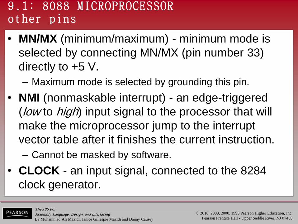
• MN/MX (minimum/maximum) - minimum mode is
selected by connecting MN/MX (pin number 33)
directly to +5 V.
– Maximum mode is selected by grounding this pin.
• NMI (nonmaskable interrupt) - an edge-triggered
(low to high) input signal to the processor that will
make the microprocessor jump to the interrupt
vector table after it finishes the current instruction.
– Cannot be masked by software.
• CLOCK - an input signal, connected to the 8284
clock generator.

The x86 PC
Assembly Language, Design, and Interfacing
By Muhammad Ali Mazidi, Janice Gillespie Mazidi and Danny Causey
© 2010, 2003, 2000, 1998 Pearson Higher Education, Inc.
Pearson Prentice Hall - Upper Saddle River, NJ 07458
9.1: 8088 MICROPROCESSOR other pins
• INTR (interrupt request) - an active-high level-
triggered input signal continuously monitored by
the microprocessor for an external interrupt.
– This pin & INTA are connected to the 8259 interrupt
controller chip.
• READY - an input signal, used to insert a wait state
for slower memories and I/O.
– It inserts wait states when it is low.
• TEST - in maximum mode, an input from the 8087
math coprocessor to coordinate communications.
– Not used In minimum mode.

The x86 PC
Assembly Language, Design, and Interfacing
By Muhammad Ali Mazidi, Janice Gillespie Mazidi and Danny Causey
© 2010, 2003, 2000, 1998 Pearson Higher Education, Inc.
Pearson Prentice Hall - Upper Saddle River, NJ 07458
9.1: 8088 MICROPROCESSOR other pins
• RESET - terminates present activities of the
processor when a high is applied to the RESET
input pin.
A presence of high will
force the microprocessor
to stop all activity and set
the major registers to the
values shown at right.

The x86 PC
Assembly Language, Design, and Interfacing
By Muhammad Ali Mazidi, Janice Gillespie Mazidi and Danny Causey
© 2010, 2003, 2000, 1998 Pearson Higher Education, Inc.
Pearson Prentice Hall - Upper Saddle River, NJ 07458
9.2: 8088 SUPPORTING CHIPS
Fig. 9-1a 8088 in minimum mode Fig. 9-7a 8088 in maximum mode
Comparing Fig. 9-1,
8088 in minimum
mode, with Fig. 9-7,
8088 in maximum
mode, shows that
pins 24–32 have
different functions.

The x86 PC
Assembly Language, Design, and Interfacing
By Muhammad Ali Mazidi, Janice Gillespie Mazidi and Danny Causey
© 2010, 2003, 2000, 1998 Pearson Higher Education, Inc.
Pearson Prentice Hall - Upper Saddle River, NJ 07458
9.3: 8-BIT SECTION OF ISA BUS local bus vs. system bus
An overview
of the 8088
& supporting
chips in the
original PC.
Fig. 9-11 8088 Connections and Buses in the PC/XT
The x86 PC
Assembly Language, Design, and Interfacing
By Muhammad Ali Mazidi, Janice Gillespie Mazidi and Danny Causey
© 2010, 2003, 2000, 1998 Pearson Higher Education, Inc.
Pearson Prentice Hall - Upper Saddle River, NJ 07458
9.3: 8-BIT SECTION OF ISA BUS local bus vs. system bus
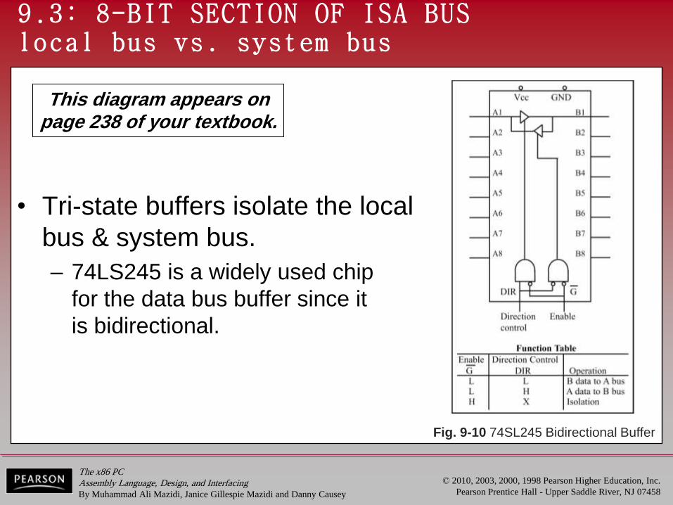
• Tri-state buffers isolate the local
bus & system bus.
– 74LS245 is a widely used chip
for the data bus buffer since it
is bidirectional.
Fig. 9-10 74SL245 Bidirectional Buffer
This diagram appears on page 238 of your textbook.

The x86 PC
Assembly Language, Design, and Interfacing
By Muhammad Ali Mazidi, Janice Gillespie Mazidi and Danny Causey
© 2010, 2003, 2000, 1998 Pearson Higher Education, Inc.
Pearson Prentice Hall - Upper Saddle River, NJ 07458
9.3: 8-BIT SECTION OF ISA BUS data bus
Fig. 9-10 74SL245 Bidirectional Buffer
When DT/R makes DIR low, the
information transfers from the B
to the A side, taking information
from the system data bus and
bringing it to the 8088.
This diagram appears on page 238 of your textbook.
The bidirectional data
bus goes through the
74LS245 transceiver.

The x86 PC
Assembly Language, Design, and Interfacing
By Muhammad Ali Mazidi, Janice Gillespie Mazidi and Danny Causey
© 2010, 2003, 2000, 1998 Pearson Higher Education, Inc.
Pearson Prentice Hall - Upper Saddle River, NJ 07458
9.3: 8-BIT SECTION OF ISA BUS control bus
The timing for control bus activity.

The x86 PC
Assembly Language, Design, and Interfacing
By Muhammad Ali Mazidi, Janice Gillespie Mazidi and Danny Causey
© 2010, 2003, 2000, 1998 Pearson Higher Education, Inc.
Pearson Prentice Hall - Upper Saddle River, NJ 07458
This diagram appears on page 239 of your textbook.
9.3: 8-BIT SECTION OF ISA BUS local bus vs. system bus
74LS245 & 74LS373s
play the role of bridge
to isolate the local &
system buses.
Everything on the left of the 8288, 74LS373s,
and 74LS245 represent
the local bus.
Everything on the right side of those chips are
the system bus.

The x86 PC
Assembly Language, Design, and Interfacing
By Muhammad Ali Mazidi, Janice Gillespie Mazidi and Danny Causey
© 2010, 2003, 2000, 1998 Pearson Higher Education, Inc.
Pearson Prentice Hall - Upper Saddle River, NJ 07458
This diagram appears on page 239 of your textbook.
9.3: 8-BIT SECTION OF ISA BUS control bus
The four most important control
signals of the IBM PC, provided
by the 8288 chip, are
IOR (I/O read)
IOW (I/O write)
MEMR (memory read)
MEMW (memory write)

The x86 PC
Assembly Language, Design, and Interfacing
By Muhammad Ali Mazidi, Janice Gillespie Mazidi and Danny Causey
© 2010, 2003, 2000, 1998 Pearson Higher Education, Inc.
Pearson Prentice Hall - Upper Saddle River, NJ 07458
ENDS ; NINE