Chapter 13 Amines Intext Questions Pg-384 - Praadis Education
Upload
khangminh22Category
view
1download
0
©2010 Cengage Learning
CHAPTER 13
ANALYSIS OF CLOCKED SEQUENTIAL CIRCUITS
This chapter in the book includes:ObjectivesStudy Guide
13.1 A Sequential Parity Checker13.2 Analysis by Signal Tracing and Timing Charts13.3 State Tables and Graphs13.4 General Models for Sequential Circuits
Programmed ExerciseProblems

©2010 Cengage Learning
A Sequential Parity Checker
When binary data is transmitted or stored, an extra bit (called a parity bit) is frequently added for purposes of error detection. For example, if data is being transmitted in groups of 7 bits, an eighth bit can be added to each group of 7 bits to make the total number of 1′s in each block of 8 bits an odd number.
When the total number of 1 bits in the block (including the parity bit) is odd, we say that the parity is odd.
Section 13.1 (p. 394)

©2010 Cengage Learning
Section 13.1, p. 395

©2010 Cengage Learning
Figure 13-1: Block Diagram for Parity Checker

©2010 Cengage Learning
Figure 13-2: Waveforms for Parity Checker

©2010 Cengage Learning
Figure 13-3: State Graph for Parity Checker

©2010 Cengage Learning
Table 13-1: State Table for Parity Checker

©2010 Cengage Learning
Figure 13-4: Parity Checker

©2010 Cengage Learning
Analysis by Signal Tracing and Timing Charts
We can analyze clocked sequential circuits to find the output sequence resulting from a given input sequence by tracing 0 and 1 signals through the circuit. The basic procedure is:
Section 13.2 (p. 397)
1. Assume an initial state of the flip-flops (all flip-flops reset to 0 unless otherwise specified).
2. For the first input in the given sequence, determine the circuit output(s) and flip-flop inputs.
3. Determine the new set of flip-flop states after the next active clock edge.
4. Determine the output(s) that corresponds to the new states.
5. Repeat 2, 3, and 4 for each input in the given sequence.

©2010 Cengage Learning
Figure 13-5: Moore Sequential Circuit to be AnalyzedFigure 13-5: Moore Sequential Circuit to be Analyzed

©2010 Cengage Learning
Figure 13-6: Timing Chart for Figure 13-5
Analysis of previous circuit for input sequence X = 01101
0 1 1 0 1

©2010 Cengage Learning
Figure 13-7: Mealy Sequential Circuit to be Analyzed
Mealy analysis for input sequence X = 10101
Figure 13-7: Mealy Sequential Circuit to be Analyzed

©2010 Cengage LearningFigure 13-8: Timing Chart for Circuit of Figure 13-7
©2010 Cengage Learning
State Tables and Graphs
Although constructing timing charts is satisfactory for small circuits and short input sequences, the construction of state tables and graphs provides a more systematic approach which is useful for the analysis of larger circuits and which leads to a general synthesis procedure for sequential circuits.
The state table specifies the next state and output of a sequential circuit in terms of its present state and input.
Section 13.3 (p. 401)

©2010 Cengage Learning
The following method can be used to construct the state table:
1. Determine the flip-flop input equations and the output equations from the circuit.
2. Derive the next-state equation for each flip-flop from its input equations, using one of the following relations:
D flip-flop Q+ = D (13-1)
D-CE flip-flop Q+ = D•CE + Q•CE′ (13-2)
T flip-flop Q+ = T Q (13-3)
S-R flip-flop Q+ = S + R′Q (13-4)
J-K flip-flop Q+ = JQ′ + K′Q (13-5)

©2010 Cengage Learning
3. Plot a next-state map for each flip-flop.4. Combine these maps to form the state table. Such a state table,
which gives the next state of the flip-flops as a function of their present state and the circuit inputs, is frequently referred to as a transition table.

©2010 Cengage Learning
Figure 13-5
As an example of this procedure, we will derive the state table for the circuit of Figure 13-5:
1. The flip-flop input equations and output equation are
2. The next-state equations for the flip-flops are
DA = X B′ DB = X + A Z = A B
A+ = X B′ B+ = X + A

©2010 Cengage Learning
3. The corresponding maps are
0 1
00
10
11
01
00
10
11
01
0 1

©2010 Cengage Learning
(b)
Table 13-2. Moore State Tables for Figure 13-5
(a)
4. Combining these maps yields the transition table in Table 13-2(a), which gives the next state of both flip-flops (A+B+) as a function of the present state and input. The output function Z is then added to the table. In this example, the output depends only on the present state of the flip-flops and not on the input, so only a single output column is required.

©2010 Cengage LearningFigure 13-9: Moore State Graph for Figure 13-5
Each node in the graph represents a state in the circuit.
Table 13-2
(b)

©2010 Cengage Learning
We can construct the next-state and output equations from the circuit diagram:
A+ = JAA′ + K′AA = XBA′ + X′A
B+ = JBB′ + K′BB = XB′ + (AX)′B = XB′ + X′B + A′B
Z = X′A′B + XB′ + XA
Figure 13-7

©2010 Cengage LearningFigure 13-10
Next, we can plot Karnaugh maps for A+, B+, and Z. We can then use these maps to derive the transition table.

©2010 Cengage Learning
Table 13-3. Mealy State Tables for Figure 13-7
State tables derived from Karnaugh maps.

©2010 Cengage Learning
Figure 13-11: Mealy State Graph for Figure 13-7
Finally, we can draw the state graph from the tables we derived:

©2010 Cengage Learning
Figure 13-12a: Serial Adder
Serial Adder that adds two n-bit binary numbers

©2010 Cengage Learning
Figure 13-12b: Serial Adder Truth Table

©2010 Cengage Learning
Figure 13-13: Timing Diagram for Serial Adder

©2010 Cengage Learning
Figure 13-14: State Graph for Serial Adder

©2010 Cengage Learning
Table 13-4. A State Table with Multiple Inputs and Outputs

©2010 Cengage LearningFigure 13-15: State Graph for Table 13-4

©2010 Cengage Learning
Construction and Interpretation of Timing Charts
Section 13.3 (p. 406)
Several important points concerning the construction and interpretation of timing charts are summarized as follows:
1. When constructing timing charts, note that a state change can only occur after the rising (or falling) edge of the clock.
2. The input will normally be stable immediately before and after the active clock edge.
3. For a Moore circuit, the output can change only when the state changes, but for a Mealy circuit, the output can change when the input changes as well as when the state changes. A false output may occur between the time the state changes and the time the input is changes to its new value.

©2010 Cengage Learning
4. False outputs are difficult to determine from the state graph, so use either signal tracing through the circuit or use the state table when constructing timing charts for Mealy circuits.
5. When using a Mealy state table for constructing timing charts, the procedure is as follows:
(a) For the first input, read the present output and plot it.
(b) Read the next state and plot it (following the active edge of the clock pulse).
(c) Go to the row in the table which corresponds to the next state and read the output under the old input column and plot it (This may be a false output.)
(d) Change to the next input and repeat steps (a), (b), and (c).

©2010 Cengage Learning
6. For Mealy circuits, the best time to read the output is just before the active edge of the clock, because the output should always be correct at that time. A “false” output may occur after the state has changed and before the input has changed.
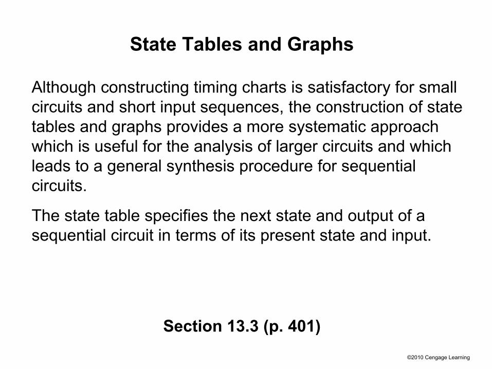
The following example shows the relationships among the state graph, state table, circuits, and timing chart. The input sequence is:
X = 0 1 0
©2010 Cengage Learning
Figure 13-16
Note that the correct output occurs before the rising edge of the clock!

©2010 Cengage Learning
Figure 13-16

©2010 Cengage Learning
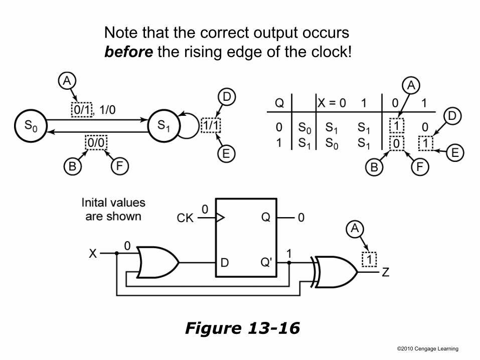
General Models for Sequential Circuits
Section 13.4 (p. 408)
A sequential circuit can be divided conveniently into two parts -- the flip-flops which serve as memory for the circuit and the combinational logic which realizes the input functions for the flip-flops and the output functions.
The combinational logic may be implemented with gates, with a ROM, or with a PLA.
©2010 Cengage Learning
Figure 13-17:
General Model for Mealy Circuit Using ClockedD Flip-Flops

©2010 Cengage Learning
Minimum Clock Period
Section 13.4 (p. 410)
We can determine the fastest clock speed (the minimum clock period) from the general model of the Mealy circuit.
Following the active edge of the clock the flip-flops change state, and the flip-flop output is stable after the propagation delay (tp).
The new values of Q then propagate through the combinational circuit so that the D values are stable after the combinational circuit delay (tc).
Then, the flip-flop setup time (tsu) must elapse before the next active clock edge.

©2010 Cengage Learning
Thus, the propagation delay in the flip-flops, the propagation delay in the combinational subcircuit, and the setup time for the flip-flops determine how fast the sequential circuit can operate, and the minimum clock period is:
tclk (min) = tp + tc + tsu
This assumes that the X inputs are stable no later than tc + tsu before the next active clock edge. If this is not the case, then we must calculate the minimum clock period by:
tclk (min) = tx + tc + tsu
Where tx is the time after the active clock edge at which the X inputs are stable.

©2010 Cengage Learning
Figure 13-18: Minimum Clock Period for a Sequential Circuit

©2010 Cengage Learning
Figure 13-19: General Model for Moore Circuit Using Clocked D Flip-Flops

©2010 Cengage Learning
Table 13-5. Mealy State Table with Multiple Inputs and Outputs
Next state:
Output:
Copyright © 2022 FDOKUMEN