CDC ® CYBER 170 MODELS 175,740,750,160,865,875
202
I";J 1:\ CONTRPL DATA \'::3 r:!I CORPOp<\TION CDC ® CYBER 170 60420300 MODELS 175,740,750,160,865,875 FUNCTIONAL UNITS THEORY OF OPERATION DIAGRAMS HARDWARE MAINTENANCE MANUAL
-
Upload
khangminh22 -
Category
Documents
-
view
0 -
download
0
Transcript of CDC ® CYBER 170 MODELS 175,740,750,160,865,875

I";J 1:\ CONTRPL DATA \'::3 r:!I CORPOp<\TION
CDC ® CYBER 170
60420300
MODELS 175,740,750,160,865,875 FUNCTIONAL UNITS
THEORY OF OPERATION DIAGRAMS
HARDWARE MAINTENANCE MANUAL

REVISION RECORD RreVISION DESCRIPTION
01 Preliminary edition.
( 12-74)
02 Updated diagrams to reflect ECO 36000. This edition obsoletes previous edition.
(2-75)
03 Updated diagrams to reflee t ECOs 35738, 35539, 35693, and 36121. This edition obsoletes pre-
(5-75) vious editions.
A Manual released. This edition obsoletes all previous ed itions.
(7-75)
Jl No change to this manual (ECO 36403).
(9-75)
C Updated manual to reflee t ECO 36429.
( 9-75)
D Updated manual to reflec t ECO 36183.
( 9-75)
E Updated manual to reflect ECO 36724. (ECO PD1346 did not list this manual.)
(9-75)
F Updated manual to reflect ECO/FCO 36194.
(9-75)
G Updated manual to reflect ECO/ FCO 36699.
10-75)
H Updated manual to reflee t ECO 36185.
(11-75)
J Updated manual to reflect ECO 36849.
(12-75)
K Updated manual to reflee t ECO/ FCO 36197. Added secondary block and ESE diagrams. This
(2-76) edition obsoletes all prev io us ed it ions.
L Manual revised; inel udes Field Cha ng e Ord er 37147. Pages vi, 5-1-4, 5-1-5 in voltnne 1, vi, viii,
(12-76) 5-11-11, 5-11-13, 5-11-29, 5-11-33, 5-11-34.8, 5-11-35, 5-11-53, 5-11-71, 5-11-147, 5-12-3, 5-12-17,
5-12-25, 5-12-47, 5-12-49, 5-12-65, and 5-14-3 in vol ume 2 are revised.
H Nanual revi sed, includes Engineering Change Order 37731. Page 5-1-5 in volume 1 and pages 5-12-3,
(8-77 ) 5-12-5, 5-12-{; .1 5-12-6.3 5-12-6.4 5-12-7 5-12-12.2 5-12-13 and 5-14-1 in volume 2 are revised.
N Han ual revi sed· inel udes Field Change Order 37843 (ECO 37767). Pages vi, x, 5-1-5, 5-4-5, 5-5-1,
(8-77 ) 5-7-5, 5-7-15, 5-10-9, and 5-10-13 in vol ume 1 and pages vi, ix, 5-11-5, 5-11-13, 5-11-17, 5-11-19,
5-11-29, 5-11-33, 5-11-35, 5-11-93, 5-11-153, 5-12-1, 5-12-3, 5-12-5, 5-12-7, 5-12-9, 5-12-10.2,
5-12-11 , 5-12-13, 5-12-15, 5-12-17, 5-12-25, 5-12-43, 5-12-63, 5-12-65, 5-12-69, 5-12-71, 5-12-78.5,
Part 13 divider, 5-13-1, and 5-13-9 in volune 2 are revised. Page 5-12-73.1 is added in volume 2.
Publication No. 60420300
REVISION LETTERS I, 0, Q, S, X AND Z ARE NOT USED.
@ 1974, 1975, 1976, 1977, 1978, 1979, 1981, 1983
by Control Data Corporation
All rights reserved
Printed in the United States of America
ii
AA 4005 REV. 3/83
Address comments concerning this manual to:
Control Data Corporation Publ icat ions and Graphics Division 4201 North Lexington Avenue St. Paul, Hinnesota 55112
or use Comment Sheet in the back of this manual.
PRINTED IN U.S.A.

REVISION RECORD (CONT/D) REVISION DESCRIPTION
P Manual revised; includes Engineering Change Order 37722. Removes volume 2 and adds model C
(10-77) information. Front cover, title page and pages iv, v, vi, vii, x, 5-1-2, 5-1-4, and 5-1-5 are
revised.
R Manual revised; includes Engineering Change Order 38980. Pages iii, iv, v, vi, 5-1-4, 5-1-5,
(04-10-78) 5-2-15, 5-3-15, 5-4-23, 5-5-41, 5-6-11, 5-7-81, 5-8-45, 5-8-53, 5-9-11, 5-10-17, 5-10-19, and
5-10-21 are revised. Page iv-at iv-b is added. Pages 5-1-7, 5-2-9, 5-2-11 , 5-2-13, 5-4-3, 5-4-9,
5-4-11, 5-5-1, 5-5-31, 5-6-7, 5-7-17, 5-7-19, 5-7-25, 5-7-29, 5-7-31, 5-7-33, 5-7-35, 5-7-37,
5-7-39, 5-7-41, 5-7-43, 5-7-49, 5-7-51, 5-7-55, 5-7-67, 5-7-69, 5-7-83, 5-8-23, 5-8-27, 5-8-29,
5-8-43, and 5-10-15 are reprinted for purposes of clarity.
S Manual revised; includes Engineering Change Order 39978. Front cover, title page and pages
(05-10-79) iv-a/iv-b, v, vii, viii, ix, x, xi, 5-1-2, 5-1-9, 5-1-11, 5-1-13, 5-8-1, 5-8-3, 5-8-5, 5-8-7,
5-8-19, 5-8-47, and 5-8-49 are revis-ed. Pages 5-1-15 and 5-1-17 are added.
T Eng ineer ing Change Order 39735. No change to this manual.
(07-05-79 )
U Manual revised; includes Engineering Change Order 40383, publications change only. Pages ii-at ii-b,
(07-6-79) iv-a J and v are revised. Page iv-b is added •
V Manual revised; includes Engineering Change Order 40489. Pages ii-a/ii-b, iv-a/iv-b, vii, xi,
(11-26-79 ) 5-1-1, 5-1-2, 5-1-4, 5-1-5, and 5-1-6 are rev i sed .
W Manual revised; includes Engineering Change Order 41276. Grid locators 52B2, 52B4, 52B6, 52B7, 52B8,
(03-16-81) 52B9, 52BIO, . 52B12, 52B13, 52E3/E4, and 52E7/E8 are revised.
y Manual revised to include Engineering Chang e Order 44495 which adds support for models 865 and 875.
(05-30-83) This edition obsoletes the microfiche edition.
M Manual revised; includes Engineering Change Order 44802. Pages iii through iv-c and viii are
(08-05-83) revised. Pages iv-d and iv-e are added.
Publication No. 60420300
ii-a/ii-b


MANUAL TO EQUIPMENT LEVEL CORRELATION SHEET
This manual reflects the equipment configurations listed below.
EXPLANATION: Locate the equipment type and series number, as shown on the equipment FCO log, in the list below. Immediately to the right of the series number is an FCO number. If that number and all of the numbers underneath it match all of the numbers on the equipment FCO log, then this manual accurately reflects the equipment.
EQUIPMENT TYPE SERIES WITH FeOs COMMENTS
-M120 A01 Released
A02 EC035091 A03 EC035467 A04 EC036623 A05 EC036634 A06 EC036637 A06 EC036403 A06 EC036429 A06 EC036183 A06 EC036724 A07 FC036579 A08 FC036699 A09 FC036194 A09 EC036185 A09 EC036849 AlO FCOPDl407 All FCOPDI377 Al2 FCOPDl408 A13 FC036199 Al4 FCOPDl5ll Al5 FCOPDl456 Al6 FCOPD1392 Al7 FCOPDl454 Al8 FCOPDl597 Al9 FCOPDl562 A20 FC036197 A21 FCOPD938 A21 Included A22 FC036639 A23 FC036647 A24 FC036624 A25 FC036641 A26 FC036999 A27 FC036646 A28 FC036645 A29 FC036642 A30 FC036681 A31 FC036644 A32 FC036656 A33 FC036654 A34 FC036630 A35 FC037073 A36 FC037054 A37 FC036631 A38 FC036653 A39 FC036651 A40 FC036652 A41 FC036875 A42 FC036626 A43 FC036192
60420300 M iii

EQUIPMENT TYPE SERIES WITH FCOs COMMENTS
A44 FC0368S4 A4S FC037362 A46 FC037S30 A47 FC037147 A48 FC036643 AS2 EC037731 AS3 FC037843 AS3 FC037949 AS4 FC038031 ASS FC038236 AS6 FC03813S AS7 FC037840 AS8 FC0382S2 AS9 FC038308 A60 FC038171 A60 FC038022 A60 EC037722 A61 FC037813 A62 FC038338 A63 FC038386 A63 FC038712 A64 FC038418 A64 EC038980 A64 EC038856 A64 EC038858 A65 EC038897 A65 EC039044 A66 EC038584 A66 EC038670 A67 EC038764 A67 EC039041 A67 EC038781 A67 EC038871 A68 EC038941 A68 EC039411 A69 EC039368 A69 EC039319 A70 EC038867 A70 EC039978 A70 EC039735 A70 EC040383 A71 FC039396 A7l FC039678 An FC039800/
FC039778 A73 FC039590/
FC039773 A74 FC039732 A74 FC039726 A74 EC040489 A75 FC040748/
FC040843 A75 FC040479 A75 EC041276
BOI Included BOI FC036639 BOI FC036647 BOI FC036624 BOI FC036641 BOl FC036999 BOI FC036646 BOI FC036645 BOI FC036642 BOI FC03668I BOI FC036644 BOI FC036656 BOI FC036654
iv 60420300 AA

EQUIPMENT TYPE SERIES WITH FCOs COMMENTS
BOl FC036630 BOl FC037073 BOI FC037054 BOI FC03663I BOI FC036653 BOI FC03665I BOl FC036652 BOI FC036875 BOl FC036626 BOI FC036I92 BOl FC036854 B02 FC037362 B02 FC037530 B02 FC037I47 B02 FC036643 B05 EC03773I B06 FC037843 B06 FC037949 B07 FC03803I B08 FC038236 B09 FC038I35 BlO FC037840 Bll FC038252 Bll FC038308 BI2 FC038III B13 FC038022 BI3 EC037722 BI4 FC0378I3 BI5 FC038338 BI6 FC038386 Bl7 FC0387I2 BI8 FC0384I8 BI8 EC038980 BI8 EC038856 BI8 EC038858 BI8 EC038897 BI9 EC039044 B20 EC038584 B20 EC038670 B2I EC038764 B22 EC03904I B22 EC03878I B22 EC038871 B23 EC03894I B24 EC039411 B25 EC039368 B25 EC0393I9 B26 EC038867 B26 EC039978 B26 EC039735 B26 EC040383 B27 FC039396 B27 FC039678 B28 FC039800/
FC039778 B29 FC039590/
FC039773 B29 FC039732 B30 FC039726 B30 EC040489 B3I FC040748/
FC040843 B3I FC040479 B3I EC04l276
CO2 FC038I35 CO2 FC037840 CO2 FC038252
60420300 AA iv-a

EQUIPMENT TYPE SERIES WITH FCOs COMMENTS
CO2 FC038308 C03 FC038171 C03 FC038022 C03 EC037722 C03 FC037813 C04 FC038338 C04 FC038386 COS FC038712 C06 FC038418 C06 EC038980 C07 EC0388S6 C08 EC0388S8 C08 EC038897 C09 EC039044 ClO EC038S84 Cll EC038670 Cll EC038764 Cl2 EC039041 C13 EC038781 Cl4 EC03887I CIS EC038941 Cl6 EC039411 Cl7 EC039368 Cl8 EC039319 Cl8 EC038867 Cl8 EC039978 Cl8 EC03973S Cl8 EC040383 Cl9 FC039396 Cl9 FC039678 Cl9 FC039800/
FC039778 C20 FC039S90/
FC039773 C20 FC039732 C21 FC039726 C21 EC040489 C21 FC040748/
FC040843 C22 FC040479 C22 EC04l276
DOl EC039978 DOl EC03973S DOl EC040383 DOl FC039396 DOl FC039678 DOl FC039800/
FC039778 DOl FC039S90/
FC039773 DOl FC039732 DOl FC039726 DOl EC040489 DOl FC040748/
FC040843 DOl FC040479 DOl EC04l276 DOl Released D02 FC039944 D03 FC040112 D04 FC040106 DOS FC039936/
FC040225 D06 FC04020S D07 FC040221 D08 FC040432
iv-b 60420300 AA

EQUIPMENT TYPE SERIES WITH FCOs COMMENTS
D09 EC039947/ FC040364
DIO FC040379 Dil FC039945 Dl2 FC040607 Dl3 FC040658 Dl4 FC040030 Dl5 FC040583 Dl6 FC040589A Dl7 FC040740 Dl8 FC040857 Dl9 FC040830 D20 FC040827 D21 FC0409l5 D22 FC040904 D23 FC04l0l2 D24 FC04102l D25 FC04l043 D26 EC04l358 D27 FC041346 D28 EC04l363 D29 FC04l359 D30 FC04l833 D31 EC041632 D32 EC04l639 D33 FC041636 D34 EC04l790 D35 FC042000 D36 EC041372 D37 FC042050 D38 FC04l736 D39 FC042323 D40 FC042348 D41 FC042913
EOI EC044495
AT364 AOl EC038980 AOl ECo38856 AOI EC038858 AOI EC038897
. AOI EC039044 AOI EC038584 AOI EC038670 AOl EC038764 AOI EC039041 AOI ECo38781 AOI EC038871 AOI EC038941 AOI EC0394il AOI EC039368 AO! EC039319 AOI EC038867 AOI EC039978 AOI EC039735 AOI EC040383 AOI FC039396 AOI FC039678 AOl FC039800/
FC039778 AOI FC039590/
FC039773 AOl FC039732 AOl FC039726 AOl EC040489 AO! FC040748/
FC040843 AOI FC040479
60420300 AA iv-c

EQUIPMENT TYPE SERIES WITH FCOs COMMENTS
AOl EC04l276 AOl Released AOl FC039944 AOl FC040112 AOl FC040106 AOl FC039936/
FC040225 AOl FC040205 AOl FC04022l AOl FC040432 AOl EC039947/
FC040364 AOl FC040379 AOl FC039945 AOl FC040607 AOl FC040658 AOl FC040030 AOl FE:040583 AOl FC040589A AOl FC040740 AOl FC040857 AOl FC040830 AOl FC040827 AOl FC0409l5 AOl FC040904 AOl FC041Ol2 AOl FC04102l AOl FC041043 AOl EC04l358 AOl FC04l346 AOl EC041363 AOl FC041359 AOl FC04l833 AOl EC04l632 AOl EC04l639 AOl FC04l636 AOl EC04l790 AOl FC042000 AOl EC04l372 AOl FC042050 AOl FC04l736 AOl FC042323 AOl FC042348 AOl FC0429l3
BOl EC039978 BOl EC039735 BOl EC040383 BOl FC039396 BOl FC039678 . BOl FC039800/
FC039778 BOl FC039590/
FC039773 BOl FC039732 BOl FC039726 BOl EC040489 BOl FC040748/
FC040843 BOl FC040479 BOl EC041276 BOl Released BOl FC039944 BOl FC040112 BOl FC040106 BOl FC039936/
FC040225 BOl FC040205
iv-d 60420300 AA

EQUIPMENT TYPE SERIES WITH FCOs COMMENTS
BOI FC040221 BOI FC040432 BOI EC039947/
FC040364 BOI FC040379 BOI FC039945 BOI FC040607 BOI FC040658 BOI FC040030 BOI FC040583 BOI FC040589A BOI FC040740 BOI FC040857 BOI FC040830 BOI FC040827 BOI FC040915 BOI FC040904 BOI FC041012 BOI FC041021 BOI FC041043 BOI EC041358 BOI FC041346 BOI EC041363 BOI FC041359 BOI FC041833 BOI Ec041632 BOI EC041639 BOI FC041636 BOI EC041790 BOI FC042000 BOI EC041372 BOI FC042050 BOI FC041736 BOI FC042323 BOI FC042348 BOI FC042913
AT402 AOI EC040383 AOI EC040489 AOI EC041276
60420300 M iv-e

PREFACE
This manual contains theory of operation and diagrams for the functional unit portion of the CONTROL DA!A~AA120-A/B/C/D/E Central Computer and the AA131-D Central Computer with an AT402-A Upgrade Option installed. Also included is information about the AT364-A/B Central Processor Enhancement which is used with the AA120-C/D Central Computer.
Models 740. 750. and 760 are defined as 7XO. Models 865 and 875 are defined as 8XS.
Comparable information on the central processing unit (CPU). central memory control (CHC). central storage unit (CSU). peripheral processor subsystem (PPS), and extended core storage (ECS) coupler is contained in other manuals. The system publication indexes on the following pages graphically list the related publications. Befer to the Literature and Distribution Services catalog for the latest revision of each manual.
This manual contains a manual to equipment level correlation sheet. The last line of this sheet indicates the latest equipment level (series code) that the manual covers. All manuals for the central computer indicate the latest series code even if the particular manual is not affected by the field change order.
60420300 Y v
I

1
1
1
1
1
I I 1
1
SYSTEM PUBLICATION INDEX
I I HARDWARE I LMAINTENANCE MANUAlSI
MODELS 171·174
I CENTRAL COMPUTER THEORY
60455060
I CPU DIAGRAMS
19981800
I
1
CSU DIAGRAMS '9981900 IA/BI. 60454750 ICI
I PPS DIAGRAMS
19982000 IA/BI. 60454970 (CI
I CMCIMSTR ClK DIAGRAMS
19982200
I ECS CPlR DIAGRAMS
19984700
I CPU WIRE LISTS
19983000 IAI. 60455050 (B/CI
I
I
I
CSU WI R E LISTS 19982400 (AiBI. 60455620 (CI
PPS WIRE LISTS 19982500 (AI. 60454880 IBI
I CDC CYBER 170 HARDWARE MANUALS
I
MDDEl175
I 1
PPS.CSU THEDRY 60455060
I
1
FCTNl UNITS THEORY. DGRMS 60420300
I
I
0 I
1
CPU/CMC THEORY. ~ DGRMS 60420310 IAIBICI
60420320 ICI
® I
ECS CPlR/MSTR ClK THEORV, DGRMS. WL
604288001A/BI.604288101C
I
1
CP WIRE LISTS 60420400 IAIBI
60420410 ICI
I
I
I PPS WIRE liSTS 0 I PPS ~. G)
L-________ 6045 __ 56T3_0_(_C_1 ________ .J WIRE 6'o':~;63~HI~FIS 2:
1
I 1
1
1
I I I I
I vi
CMCIMSTR ClK/ECS CPlR WIRE LISTS 19982600 (AI. 60454890 (BI. 60455640 (CI
1 CABLES WIRE LISTS
19982700
I
I
I
I INSTALLATION AND CHECKOUT
19981700 (AI 60420520 (B/CI
I MAINTENANCE AND PARTS
19981600
ECS SUBSYSTEM
J
I
I 1
I
PPS/ECS CPlR/MSTR ClK WIRE LISTS. CHASSIS 4:
60454810 (CI
I CABLES WIRE LISTS I
60420200
I PWR DISTR AND (7\11
WARN SYS \V 60420700 (AI
I
I REFRIG SYS
60427800
I o
INST 8< CHECKOUT 60420500(AI
60420510 (B/CI
I MAl NT 8< PARTS
60420600
60453400 ISUBSYSI. 60404700 IECSI. 60425800 IDDPI. 60440500 (CONTROllER I
I M-G SET THEORY. MAINTENANCE. ETC
60166800 IEMI. 60420800 (KATOI
I M·G SET DIAGRAMS
60423100 IEMI. 60419900 (KATOI
I
I
I
1
1
I
I
1
I
I
I SYSTEM MANUALS I
CDC CYBER 170 HARDWARE REFERENCE 60420000
I ECS SUBSYSTEM HARDWARE REFERENCE
60430000
I
I
1
DISPLAY STATION HARDWARE REFERENCEICE 1 62978200 (A/BI 62952600 ICIDIEIFI
I CDC CYBER 170 COMPUTER SYSTEMS CODES
1 60420010
I ECl MICROCIRCUITS
I 60417700
I SITE PREPARATION·GENERAl J 60275100
I SITE PREPARATION·MAINFRAME I 60420100
I SITE PREPARATION·PERIPHERAL EQUIPMENT I 60275300
I ISITE PREPARATION·MONITORING AND POWER DATAl
60451300
N,9l:.ES: \2J THIS MANUAL CONTAINS All SECTIONS
EXCEPT MAINTENANCE. PARTS. AND INSTAllATION AND CHECKOUT.
CD o 4.
® CD
THIS MANUAL CONTAINS All SECTIONS.
THESE MANUALS INCLUDE DATA CHANNEL CONVERTER AND DISPLAY CONTROllER.
lETTERS WITHIN PARENTHESES INDICATE EOUIPMENT TYPE IDENTIFIERS.
WIRE LISTS FOR MODEL C ARE INCLUDED IN PUBLICATION NUMBER 60454810.
PUBLICATION NUMBER 60420310 INCLUDES AA120A/B/C AND AT364·A. PUBLICATION NUMBER 60420320 INCLUDES AAI20C. AT364-A AND AT374·A.
INCLUDES AT303·C USED WITH AAI20·A/B.
0479
60420300 S

60420300 Y
ECS CPLR THEORY. DIAGRAMS GF 60456190
PPS ICHAS 21 WIRE LIST GF 60456140
M-G SET THEORY. MAINTENANCE, ETC 60166800 IEM!, 60420800 IKATOI
M·G SET DIAGRAMS 60423100 IEMI. 60419900 IKATOI
SYSTEM PUBLICATION INDEX
CDC CYBER 170 HARDWARE REFERENCE GF 60456100
ECS SUBSYSTEM HARDWARE REFERENCE GF 60430000
DISPLAY STATION HARDWARE REFERENCE/CE GF 62952600
CDC CYBER 170 COMPUTER SYSTEMS CODES 60456920
ECL MICROCIRCUITS GF 60417700
SITE PREPARATION-GENERAL GF 60275100
SITE PREPARATION-MAINFRAME GF 60456890
SITE PREPARATION-PERIPHERAL EQUIPMENT GF 60275300
SITE PREPARATION-MONITORING AND POWER DATA GF 60451300
IF AT402·A IS INSTALLED, USE PUBLICATION GF 60456250
PUBLICATIONS 60455990 AND 60458590 ARE USED ONLY WHEN THE ENHANCED BUSY MODE OPTION 40011·10 IS NOT INSTALLED.
PUBLICATIONS 60458600, 60458590, AND 60458580 APPLY TO ESM II ONLY.
11820
vii

• viii
SYSTEM PUBLICATI0N INDEX
PPS THE0RY. DIAGRAMS 60458790
FUNCTI0NAL UNITS THE0RY. DIAGRAMS 60420300
CPU/CMC/5MU Tf£~RY. DIAGRAMS 60458220
PPS (CHAS 2) WIRE LIST GF 60455760
CP/PPS/COO REFRIGERATI~ SYSTEM 604278JO
INSTALLA~ At{) CI£CKmJT 60458690
MAINTENANCE •. PARTS 60458260
ECS OOBSYSTEU GF 60404700 (ECS). GF 60425800 (OOP).
GF 60440500 (CIIINTR~LER)
M-G SET Tl6IRY. MAINTENANCE. DIAGRAMS. ETC 60454720 (40 KVA). 60455810 (80 KVA)
CDC CYBER 170 HARDWARE REFERENCE 60458920
ECS SUBSYSTEM HARDWARE REFERENCE GF 6043OOJO
DISPLAY STATWN HARDWARE REFERENCE/CE GF 62952600
CDC CYBER 170 CIIIMPUTER SYSTEMS ClllDES 60456920
ECL MICR~CIRctJITS GF 60417700
SITE PREPARA~-GENERAL GF 60275100
SITE PREPARATI~-MAINFRAME 60458530
SITE PREPARATWt-PERIPf£RAL EOUIPNENT GF 60275=
SITE PREPARATIl1JN-~T0RING At.!) PI!lWER DATA GF 60451=
~S:
CD PUBLICA~ 60455990 IS USED ~L Y WHEN THE ENHANCED BUSY WOE 1IlP~ 40011-10 IS ~ INSTALLED.
, .... IWWDI
60420300 AA
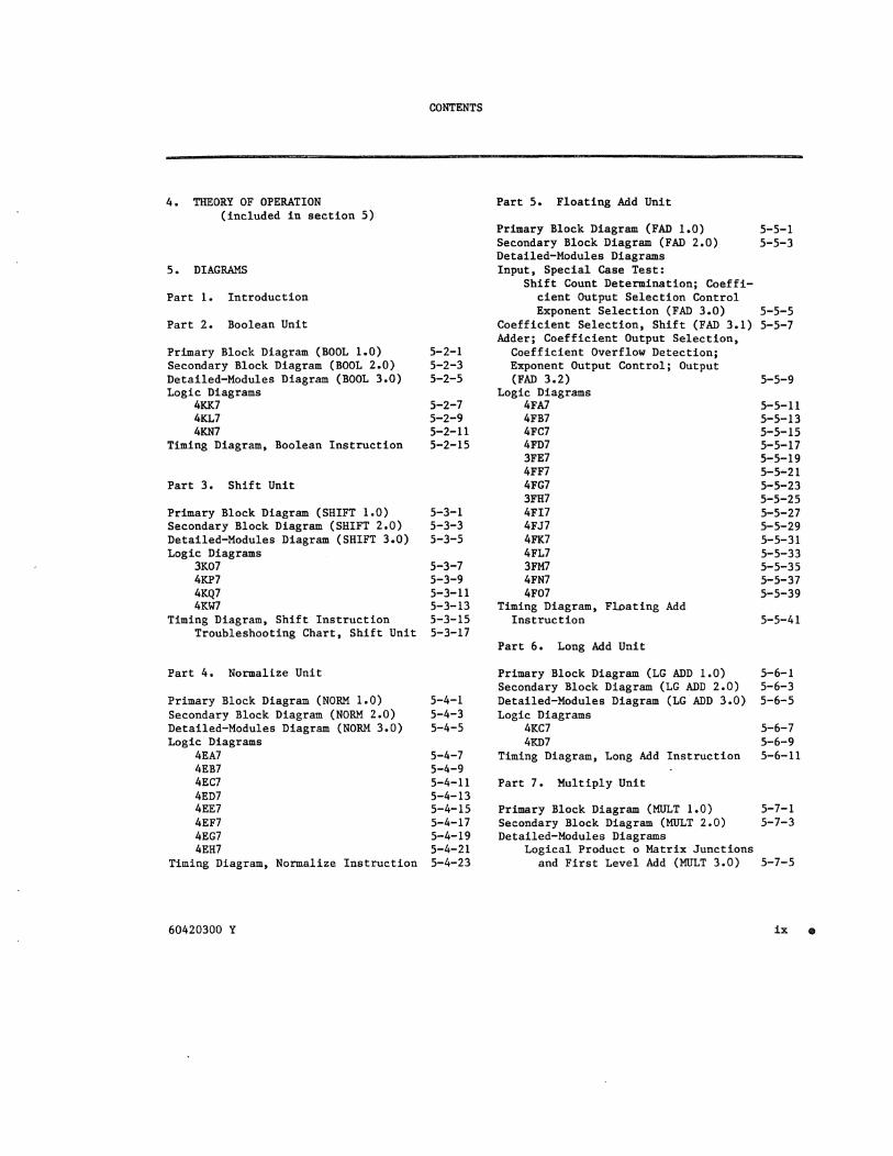
4 • THEORY OF OPERATION (included in section 5)
5. DIAGRAMS
Part 1. Introduction
Part 2. Boolean Unit
Primary Block Diagram (BOOL 1.0) Secondary Block Diagram (BOOL 2.0) Detailed-Modules Diagram (BOOL 3.0) Logic Diagrams
4KK7 4KL7 4KN7
Timing Diagram, Boolean Instruction
Part 3. Shift Unit
Primary Block Diagram (SHIFT 1.0) Secondary Block Diagram (SHIFT 2.0) Detailed-Modules Diagram (SHIFT 3.0) Logic Diagrams
3K07 4KP7 4KQ7 4KWl
Timing Diagram, Shift Instruction Troubleshooting Chart, Shift Unit
Part 4. Normalize Unit
Primary Block Diagram (NORM 1.0) Secondary Block Diagram (NORM 2.0) Detailed-Modules Diagram (NORM 3.0) Logic Diagrams
4EA7 4EB7 4EC7 4ED7 4EE7 4EF7 4EG7 4EH7
Timing Diagram, Normalize Instruction
60420300 Y
CONTENTS
5-2-1 5-2-3 5-2-5
5-2-7 5-2-9 5-2-11 5-2-15
5-3-1 5-3-3 5-3-5
5-3-7 5-3-9 5-3-11 5-3-13 5-3-15 5-3-17
5-4-1 5-4-3 5-4-5
5-4-7 5-4-9 5-4-11 5-4-13 5-4-15 5-4-17 5-4-19 5-4-21 5-4-23
Part 5. Floating Add Unit
Primary Block Diagram (FAD 1.0) Secondary Block Diagram (FAD 2.0) Detailed-Modules Diagrams Input, Special Case Test:
Shift Count Determination; Coefficient Output Selection Control Exponent Selection (FAD 3.0)
Coefficient Selection, Shift (FAD 3.1) Adder; Coefficient Output Selection,
Coefficient Overflow Detection; Exponent Output Control; Output (FAD 3.2)
Logic Diagrams 4FA7 4FB7 4FC7 4FD7 3FE7 4FF7 4FG7 3FH7 4FI7 4FJ7 4FK7 4FL7 3FM7 4FN7 4F07
Timing Diagram, Floating Add Instruction
Part 6. Long Add Unit
Primary Block Diagram (LG ADD 1.0) Secondary Block Diagram (LG ADD 2.0) Detailed-Modules Diagram (LGADD 3.0) Logic Diagrams
4KC7 4KD7
Timing Diagram, Long Add Instruction
Part 7. Multiply Unit
Primary Block Diagram (MOLT 1.0) Secondary Block Diagram (MOLT 2.0) Detailed-Modules Diagrams
Logical Product 0 Matrix Junctions and First Level Add (MOLT 3.0)
5-5-1 5-5-3
5-5-5 5-5-7
5-5-9
5-5-11 5-5-13 5-5-15 5-5-17 5-5-19 5-5"'21 5-5-23 5-5-25 5-5-27 5-5-29 5-5-31 5-5-33 5-5-35 5-5-37 5-5-39
5-5-41
5-6-1 5-6-3 5-6-5
5-6-7 5-6-9 5-6-11
5-7-1 5-7-3
5-7-5
ix •

Second Level Add (MOLT 3.1) Third Level Add (MULT 3.2) Final Add - Lower Half (MULT 3.3) Final Add - Upper Half (MULT 3.4) Exponent and Control (MULT 3.5)
Logic Diagrams 3BA7 4GA7 4GB7 4GB7 4GC7 4GC7 4GD7 4GE7 4GF7 4GG7 4GH7 4GI7 4GJ7 4GK7 4GL7 4GM7 4GN7 4G07 4GP7 4CQ7 4GR7 4GS7 4GT7 4GU7 4GV7 4GW7 4GX7 4KR7 4KS7 4KU7 3KV7
Troubleshooting Diagram, Multiply
5-7-7 5-7-9 5-7-11 5-7-13 5-7-15
5-7-17 5-7-19 5-7-21 5-7-23 5-7-25 5-7-27 5-7-29 5-7-31 5-7-33 5-7-35 5-7-37 5-7-39 5-7-41 5-7-43 5-7-45 5-7-47 5-7-49 5-7-51 5-7-53 5-7-55 5-7-57 5-7-59 5-7-61 5-7-63 5-7-65 5-7-67 5-7-69 5-7-71 5-7-73 5-7-75 5-7-77
Unit 24 x 48 Matrix 5-7-79 Timing Diagram, Multiply Instruction 5-7-81 Troubleshooting Chart, Multiply
Coefficient 5-7-83
Part 8. Divide Unit
Primary Block Diagram (DIV 1.0) Secopdary Block Diagrams
Exponent and Control Networks (DIV 2.0)
Coefficient Networks (DIV 2.1) Detailed-Modules Diagrams
Divisor Multiplication Network (DIV 3.1)
Iteration Network (DIV 3.2) Logic Diagrams
4DA7 4DB7
• x
5-8-1
5-8-3 5-8-5
5-8-9 5-8-11
5-8-13 5-8-15
4DC7 4DD7 4DE7 4DF7 4DG7 4DH7 4DI7 4DJ7 4DK7 4DL7 4DM7 4DN7 4D07 3DP7 4DR7 4DS7 4KR7
Timing Diagram, Divide Instruction
Part 9. Population Count Unit
Primary Block Diagram (POP CT 1.0) Secondary Block Diagram (POP CT 2.0) Detailed-Modules Diagram (POP
CT 3.0) Logic Diagrams
4KA7 4KB7
Timing Diagram, Population Count Instruction
Part 10. Increment Unit
Part lOA. Increment Unit Block Diagrams (Models 175, 740, 750, 760)
5-8-17 5-8-19 5-8-21 5-8-23 5-8-25 5-8-27 5-8-29 5-8-31 5-8-33 5-8-35 5-8-37 5-8-39 5-8-41 5-8-43 5-8-47 5-8-49 5-8-51 5-8-53
5-9-1 5-9-3
5-9-5
5-9-7 5-9-9
5-9-11
Primary Block Diagram (INCR 1.0A) 5-10-1 Secondary Block Diagram (INCR 2.0A) 5-10-3 Detailed-Modules Diagram (INCR 3.0A) 5-10-5
Part lOB. Increment Unit Block Diagrams (Models 865, 875)
Primary Block Diagram (INCR1.0B) 5-10-7 Secondary Block Diagram (INCR 2.0B) 5-10-9 Detailed Modules Diagram (INCR 3.0B) 5-10-11
Part 10C. Logic and Timing Diagrams
4KE7 4KF7 lKGH (8X5) 4KG7 (175, 7XO) 4KH7
Logic Diagrams 1KIH (8X5)
5-10-13 5-10-15 5-10-17 5-10-19 5-10-21
5-10-23
60420300 Y

5-1 5-2 5-3
41(17 (175, 7XO) IKJH (8X5) 3KJ7 (175, 7XO) 4KK7 (175, 7XO)
Key to Diagram Symbols Key to Logic Symbols System Block Diagram, Model 175
5-4 System Block Diagrams, Hodels 740, 750, 760
5-5 System Block Diagram, Models 865, 875
5-1 Modu1e-to-Diagrams CrossReferences
60420300 Y
5-10-25 5-10-27 5-10-29 5-10-31
Timing Diagram, Increment Instruc-tion (175,7XO) 5-10-33
Timing Diagram, Increment Instruc-tion (8X5) 5-10-35
FIGURES
5-1-6 5-6 Interface Diagram, Central 5-1-7 Processor, Model 175 5-1-11 5-1-8 5-7 Interface Diagram, Central
Processor, Models 740, 750, 5-1-9 760 5-1-12
5-8 Interface Diagram, Status/ 5-1-10 Control Register, Model 175 5-1-13
TABLE
5-1-4
xi 0

SECTION 1
GENERAL DESCRIPTION
SECTION 2
OPERATION
(Information for sections 1 and 2 is contained in the CDC CYBER 170 Hardware Reference Manual.)
SECTION 3
INSTALLATION AND CHECKOUT
(Information for section 3 is contained in the CDC CYBER 170 Installation and Checkout Manual.)
SECTION 4
THEORY OF OPERATION
(Information fo= section 4 is combined with the diagrams in section 5 of this manual.)

TABLE OF CONTENTS (Continued)
Logic Diagr ams 3BA7 • • • • • 4GA7 4GB7 • • • • • 4GB7 4GC7 • 4GC7 • • • • • • 4GD7 • 4GE7 • 4GF7 • 4GG7 • • • • • 4GH7 4GI7 • • • • • 4GJ7 4GK7 • 4GL7 • 4GM7 • • • • • 4GN7 4G07 • 4GP7 • 4CQ7 • . 4GR7 • • • • . 4GS7 • . • • • 4GT7 • 4GU7 • 4GV7 4GW7 ••
• 5-7-17 . . • • . . . • . • 5-7-19
••••• 5-7-21 • 5-7-23
• ••••• 5-7-25 • • • • • • 5-7-27
• 5-7-29 • 5-7-31 • 5-7 -33 • 5-7-35
• • • • • • 5-7-37 . . . . . . . . . . . 5-7-39
• • • • • • 5-7-41 • 5-7-43 • 5-7-45 • 5-7-47 • 5-7-49 • 5-7-51 • 5-7-53
• • • • • • 5-7-55 • 5-7-57 • 5-7-59 • 5-7-61 • 5-7 -63 • 5-7-65 • 5-7-67
4GX7 • • • • • • 5-7-69 4KR7 • • • • • • • • • • • • 5-7-71 4KS7 • 5-7-73 4KU7 • . • • • • • . • • • • • 5-7 -75 3KV7 • • • ... • • • • • • • • • • • • 5-7-77
Troubleshooting Diagram, Multiply Unit 24 x 48 Matrix • . • • • • • • • • • • 5-7-79
Timing Diagram, Multiply Instruction •••• 5-7-81 Troubleshooting Chart, Multiply Coefficient. 5-7-83
Part 8. Divide Unit
Primary Block Diagram (DIV 1.0) •••• Secondary Block Diagrams
5-8-1
Exponent and Control Networks (DIV 2.0). 5-8-3 Coefficient Networks (DIV 2.1) • • 5-8-5
Detailed-l-1odules Diagr ams Exponent, Output, and Control (DIV 3.0). 5-8-7 Divisor Multiplication Network (DIV 3.1) 5-8-9 Iteration Network (DIV 3.2). . • 5-8-11
Logic Diagrams 4DA7 4DB7 • 4DC7 • • • • • • •
5-8-13 • 5-8-15 • 5-8-17
4DD7 • • • • • • • • • • • • • • 5-8-19 • • • • • 5-8-21 4DE7 • • • • •
4DF7 •••• 4DG7 • • • • 4DH7
604203008
• 5-8-23 ••••• 5-8-25
• • • • • • • 5-8-27
Fiche/Grid
58B2 58B4 58BIO 58B14 58C2 58C6 58CIO 58C12 5802 58D4 5806 58D8 58DIO 58D12 58D14 58E2 58E6 58E8 58EIO 58E12 58F2 58F4 58F6 58F8 58FIO 58F12 58F14 58G2 58G4 58G8 58G12
58G14 58H2 58H4
59B4
59C2 59C4
59D2 59E2 59F2
60B2 60B6
-60B8 60B12 60C2 60C6 60C8 60CIO
... --. I C3 I 1_- ...
xi

Tf\I3LB OF CON'rEN'rS (Continued)
4D17 • • ••• 5-8-29 4 OJ7 • • • • • • • • • • • 5-8-31 4DK7 • • • • • 4DL7 • 4DM7 • 4DN7 4007 • • • • • • • • 3DP7 • • • • •
• 5-8-33 • 5-8-35
5-8-37 5-8-39
• 5-8 -41 • 5-8-43
3DQ7 • 4DR7 4DS7 • ••• • •
• 5-8-45 • • • • • 5-8-47
5-8-49 4KR7 • • • • • •.• • • • • • •
Timing Diagram, Divide Instruction. • 5-8-51
• ••• 5-8-53
Part 9. Population Count unit
Primary Block Diagram (POP CT 1. 0) •••• Secondary Block Diagram (POP CT 2.0) •• Detailed-Modules Diagram (POP CT 3.0). Logic Diagrams
• 5-9-1 5-9-3
• 5-9-5
4KA7 • • • • • • . • • • . . • . •. 5-9-7 4KB7 • • • • • • • • • • • • • • •• 5-9-9
Timing Diagram, Population Count Instruction 5-9-11
Part 10. Increment Un t
Primary Block Diagram (INCR 1. 0) · Secondary Block Diagram (INCR 2.0) · · Detailed-Module Diagram (INCR 3.0) Logic Diagrams
4KE7 · · · · · · · · · 4KF7 · · · 4KG7 · · · · · · · · · 4KH7 · · · · · · · · 4KI7 3KJ7 · · · · · · · · · · · · 4KK7 · · · · · · · · · · · · · · · Timing Diagram, Increment Instruction.
5-1 5-2
FIGURES
Key to Diagram Symbols • Key to Logic Symbols •
TABLE
· 5-10-1
· · · 5-10-3
· 5-10-5
· · · 5-10-7
· · · 5-10-9
· · · 5-10-11 5-10-13
· 5-10-15
· 5-10-17
· 5-10-19
· 5-10-21
• 5-1-6 • 5-1-7
Fiche/Grid
60C12 60C14 6002 6004 6006 6008 60010 60D12 60E2 60E6 60E8 60ElO 60E12
610B4 6l0BlO 6l0C2
6l0D2 610D6 610DlO
6l0E4 6l0ElO 6l0D2
610G2 6l0G4 6l0G6 6l0G8 6l0G10 6l0H2 610H5 610H8
52D12 52D14
r-- .. I C4 I ��_ __ 1
5-1 Module-to-Diagrams Cross-References •• 5-1-4 52D8
xii 604203008

SECTION 1
GENERAL DESCRIPTION
SECTION 2
OPERATION
(Information for sections 1 and 2 is contained in
the CDC CYBER 170 Hardware Reference Manual,
publication number 60420000.)
SECTION 3
INSTALLATION AND CHECKOUT
(Information for section 3 is contained .in the CDC
CYBER 170 Model 175 Installation and Checkout
Manual, publication number 60420500.)
SECTION 4
THEORY OF OPERATION
(Information for section 4 is combined with the
diagrams in section 5 of this manual.)
r---. I C5 I 1.--.1

SECTION 5
DIAGRAMS
r-IE'iI'" I 01 I 1 ... _ .. 1

PART 1
INTRODUCTION

INTRODUCTION
GLOSSARY
The glossary is a list of terms, mnemonics, and abbreviations used on the diagrams.
MODULE-TO-DIAGRAMS CROSS-REFERENCES
GENERAL
Table 5-1 provides a list of functional unit module types along with the following information on each type.
Quantity Number of modules of this type located on the mainframe
Location All physical locations at which this module type can be found
Diagram Secondary block and detailed-modu1es diagrams on which this module type is depicted.
USES
Table 5-1 can be used to locate a particular module logic diagram in the manual without knowing the functional entity to which it pertains. Another use is to determine the availability and the location of a substitute module during maintenance. The table also helps to locate all modules of the same type without having to scan all module placement diagrams.
KEY TO SYMBOLS (Figures 5-1 and 5-2)
The number of unfamiliar .symbols on the block and detailed-modules diagrams has been kept to a minimum. The symbology has been chosen because it simplifies or clarifies and is therefore essential to the use and understanding of the diagrams. Time spent familiarizing oneself with these conventions is not wasted. Note particularly that the AND and OR symbols define functions, not gates. In some cases, hardware constraints caused the use of AND gates to perform OR functions. Therefore, the block and detailed-modules diagrams depict the OR function, not the AND hardware.
60420300 V 5-1-1

SYSTEM BLOCK AND INTERFACE DIAGRAMS
The system block diagrams (figures 5-3, 5-4, 5-5) provide a comprehensive view of the central computer. In addition to aiding one's understanding of the system, it relates physical to electrical data (for example, multiply functional unit located on chassis 7) and defines the boundaries of the central processor diagrams in the various parts of this section.
The CP interface diagrams (figures 5-6, 5-7) depict all data and control paths between the functional entities. Also. this diagram includes all paths between the CP and the other portions of the central computer which are covered in other manuals.
The status and control register interface diagram (figure 5-8) includes all status/control paths in the central computer.
DIAGRAMS
Within each functional entity, the diagrams are arranged in the following order: primary, secondary, detailed-modules, and module logic. The diagrams are intended to ease the trainee gradually but quickly into the central processor or to allow the initiated to choose from four levels of drawings for maintenance assistance or memory jogging. The primary block diagram shows the basic relationship between the various logical components (registers, adders, and so on) comprising the functional entity. The next, more detailed level is the secondary block diagram. It depicts the physical building blocks (modules) and shows the data and control paths between them. The third and most explicit level is the detailed-modules diagram. This level is similar to the secondary level except that it also features a simplified block diagram of each unique module. From this level, the user must proceed to the module logic diagrams only for test point and connector information. However, when it is necessary to do so, the user arrives at the module logic diagram already familiar with its contents. Supplemental timing and troubleshooting information are provided at the end of each part of this section.
A test point chart is provided with each detailed-modules diagram. These charts list test points associated with signals and registers. Translator test points are not listed. An asterisk adjacent to the module type indicates that additional test points are available but not listed. Unless otherwise specified, all test points display the complement of the data indicated in the charts.
Maintenance personnel may find it helpful to repOSition the pages in this section so the diagrams are not separated by theory of operation pages. Although the present .arrangement is best for training purposes, contiguous diagrams may be easier to use during maintenance.
MODUIE PLACEMENT DIAGRAMS
The module placement diagrams for all CP chassis (5, 6, and 7) are included in the CPU/CMC manual.
5-1-2 60420300 Y

TABLE 5-1. MODULE-TO-DIAGRAMS CROSS-REFERENCES (Cant'd)
Module Module Type Quantity Location. Diagram Type Quantity Location Diagram
4KA7 3 6B06-08 POP CT 2.0, 3.0 4KB7 1 6C06 POP CT 2.0, 3.0 4KC7 5 6B01-05 LG ADD 2.0, 3.0 , 4KD7 5 6COI-{)5 LG ADD 2.0, 3.0 4KE7 4 6K09-I2 INCR 2.0, 3.0 4KF7 1 6K13 INCR 2.0, 3.0 4KG7 2 6KI4-I5 INCR 2.0, 3.0
tIKGH 2 6KI4-I5 INCR 2.0, 3.0 4KH7 1 6K16 INCR 2.0, 3.0 4K17 2 6L14-15 INCR 2.0, 3.0
tiRIlI 2 5KOI-02 INCR 2.0, 3.0 3KJ7 1 6L16 INCR 2.0, 3.0
tlKJH 1 5K03 INCR 2.0, 3.0 4KK7 7
6L12 INCR 2.0, 3.0; 6C07-11 BOOL 2.0, 3.0
4KL7 3 6C12-14 BOOL 2.0, 3.0 4KM7 1 6CI5 BOOL 2.0, 3.0 4KN7 1 6CI6 BOOL 2.0, 3.0 lK07 1 6EI0 SHIFT 2.0, 3.0 4KP7 10 6A07-I6 SHIFT 2.0, 3.0 4KQ7 4 6B09-12 SHIFT 2.0, 3.0 4KR7 2 7P02 DIV 2.0, 3.0
7F16 MUtT 2.0, 3.5 4KS7 1 7G16 MULT 2.0, 3.5 4KU7 1 7H15 MULT 2.0, 3.5 31r&7 1 7H14 MULT 2.0, 3.5 4KW7 4 6B13-16 SHIFT 2.0, 3.0
tHodel 865/875 only.

0)
o ,.j:>. I:\:)
o w o o
OR FUNCTION AND FUNCTION AN~ NOT FUNCTION COMPLEMENTER
CD ® @
THESE SYMBOLS DENJTE THE ~ BEING PERFORMED REGARDLESS
OF THE TYPE OF GATE BEING USED IN THE lOGIC CIRCUIT. THUS,THE
AND FUNCTION IS ENABLED BY COINCIDENT INPUTS AND THE OR FUNCTION
IS SATISFIED BY THE: PRESENCE OF EITHER INPUT.
MODULE ENCLOSURE
MODULE TYPE DESIGNATOR
MODULE LOCATION - ENCLOSURES WITH THE SAME
TYPE DESIGNATOR IlND THE SAME LOCATION CONTAIN
DIFFERENT PARTS <)F THE SAME MODULE.
DESCRIPTION OF MODULE FUNCTION (OPTIONAL)
4 SETS 9 SIGNALS
-Mr
DENOTES NUMBER OF UNIQUE BITS OR SIGNALS
I LOGICAL of--
INPUT IS FORCED "0"
I LOGICAL If--
INPUT IS FORCED ","
----l TERMN I OUTPUT IS TERMINATED
I I I I I I I I I I I I I I I I I I I
-------------------------~ REFERENCES
A REFERENCE IS Loc.nEO AT THE BEGINNING OR END OF ANY LEAD THAT HAS
ITS ORIGIN OR DESTINATION ON A MODULE NOT READilY ACCESSIBLE TO THE LEAD.
MOST REFERENCES AUE MADE TO OTHER SHEETS WITHIN THE UNIT OR TO SHEETS
IN OTHER UNITS, BUT A REFERENCE MAY BE TO ANOTHER POINT ON THE SAllE SHEET.
A REFERENCE CONSI STS OF THE FOLLOWING INFORMATION.
~ r, ®-- CPU 22A ---®
CAl SHEET NUfABER - A :>HEET NUMBER CONSISTS OF THE FOLLOWING PARTS:
CD UNIT ABBREVIATION
® FIGURE NUMBER - FIGURES ARE NUMBERED SEQUENTIALLY: I. X FOR THE
PRIMARY BLOCK [IIAGRAM, 2. X FOR THE SECONDARY BLOCK DIAGRAM, AND
3 X FOR THE O~TAILED-MODULES DIAGRAM.
@ ORAWING NUMBEFI - DRAWINGS ARE NUMBERED SEQUENTIALLY WITHIN THE
FIGURE, BEGINNING WITH ZERO
® LOCATION - QUADRANT OF REFERENCED SHEET TO FURTHER AID IN LOCATING
THE REFERENCED POINT QUADRANTS ARE IDENTIFIED AS SHOWN
A I B I : I ,---.1 : 0 :
MASTER CLEAR I
GATE INPUT
BITS 0-11 12
CLEAR BITS 4-11
BITS O-II-®--<
ENTER DATA
MASTER CLEAR .
3WT7! 6C06 BITS
! 6C05
~ 6C04 81TS
3JR7! 6B06 81TS
! 6B05
~6B04 BITS
1 3RA7 7011 BITS
! ! 7010
~ 7009 BITS
8-11
4-7
0-3
8-11
4-7
0-3
B II
4-7
0-3
STACKED MODULES I/O CONVENTIONS
{
A SOLDER - POINT CONNECTION TO A BRACKET DENOTES
THAT ALL OF THE BITS OR SIGNALS ON THE LEAD ARE
INPUTS TO ALL MODULES ADJACENT TO THE BRACKET;
I.E .• PARALLEL INPUTS.
BITS 0-11 12
THIS TYPE OF CONNECTION ON AN INPUT BRACKET DENOTES THAT THE BITS OR SIGNALS ON THE LEAO
ARE DISTRIBUTED AMONG THE MODULES ADJACENT
TO THE BRACKET THE SPECIFIC INPUTS TO EACH
MODULE IN THE STACK ARE IDENTIFIED WITHIN
THE MODULE. THIS TYPE OF CONNECTION ON AN
OUTPUT BRACKET DENOTES THAT ALL THE
OUTPUTS FROM THE INCLUDED MOOULES MERGE
IN TO ONE LEAD THE MERGING BITS OR SIGNALS
ARE IDENTIFIED BY THE SIGNAL NAME ON THE LEAD.
ANY NUMBER OF CONNECTIONS OF EITHER TYPE MAY BE MADE TO THE SAME BRACKET.
BRACKETS ARE NESTED WHEN CONNECTIONS TO ALL MODULES IN THE STACK ARE
NOT IDENTICAL.
BRACKETS ALONG TOP OR BOTTOM OF STACK ARE EQUIVALENT TO BRACKETS
ADJACENT TO ALL MODULES IN STACK
INDIVIDUAL INPUTS OR OUTPUTS· (NOT BRACKETED) WAY ENTER OR LEAVE INDIVIDUAL
MODULES IN STACK THROUGH BRACKET.
Figure 5-1. Key to Diagram Symbols

0> o tI'> N o W o o
LOGIC LEVELS CURRE,,", SWITCH EMITTER FOUOW[R DRIVEN 'i RfFERENCE
KEY TO LOGIC SYMBOLS
{IN -0.8 V TRANSlST~ '..i ~ TR:NSISTOR
OUT -1.6 V -[}--{]--{
IN -1,6 V LOGICAL t LOGICAL I
OUT -08'11
{IN -08 V {IN 0.0 V
lOGiCAl 0 LOGICAL 0 OUT 0.0 V OUT -08 V
CURRENT SWITCH PROVIOES COMPL£MENTARY
OUTPUTS FALSE FROM DRIVEN XSfR
TRUE FRO'" REf lISTR
EMITTER FOLLOWER SHIfTS VOLTAGE LEVEL 0' CURRENT SWITCH OUTPUT TO VOLTAGE LEVEL RtOUIREO FOR CURRENT SW ITCH INPUT - NO INVERStON,
SET _
INPUTS
j
DATA
CLEAR _ INPUT
AND CIRCUITS
DATA
CLOCK
HOLDING BIT REGISTER
2-INPUT £XCLUSIV[ OR
OR CIRCUIT
lHPUT~ OUTPUT
CLOCk r ~
CLEAR-ENTER BIT REGISTER (FLIP-FLOP)
TEST POINTS - DENOTED 8Y 2-'DIGIT NUMBER 1NS10£ CURRENT swiTCH (SEE FFI THE FIRST DIGIT IS THE MODULE BOARD NUMBER, IT IS FOLLOWED
By THE TEST POINT NUMBEfi:. THE TEST POINT VOLTAGE IS NORMALLY THE COMPLEMENT OF THE SIGNAL IT IS INTENOEO TO INDICATE. IN THIS CASE, IT IS THE OPPOSITE OF THE F' OUTPUT.
EVEN 000 (AOD'L EVEN ( INPUT }AND ODD FF"S)-aJTPUT
CLOCK ~ CLOCK ~
CLOCk CLOCk
TIMING CHAIN EACH EVEN FF IS SET IN THE fiRST CLOCk PERIOD FOLLOWING THE ARRIVAL OF ITS INPUT AND IS CLEARED IN THE CLOCK PERIOD IMMEDIATELY FOLLOWINO THE L.OSS OF INPUT. THE ODD FF IS SET AND CLEARED ONE CLOCK PULSE 1&75±025NSJ LATERTHA'" THE EVEN H A ONE CLOCI< PERIOD DELAY RESULTS BETWEEN Tttf OUTPUTS OF CONSECUTIVE EVEN n's
;: +8
A~A"A.
2-INPUT EQUIVALENCE
>2lNPurs ONE OF THE TWO GAT[S(NOT 80TH) MUST BE ENABLED TO GET AN OUTPUT.
,. 2 INPuTS 90TH GATES MUST BE ENABLEO OR eOTH MUST BE DISABLED TO GfT AN OUTPUT
O:A+B+C E=A+B+C
;;:+8
COLLECTOR LOGIC
AW' B A~A+jj
C -.- -0---0--. o ::;Ai e"'c E"- A+tl +C
CIRCUITS
A STACI{'S OUTPUT IS A LOGICAL ONE WHEN ANY OF ITS INPUTS IS A LOGICAL ZERO.
TWISTED PAIR RECEIVER
TWISTED PAIR DRIVER SIG"''''L N ..... E ON MODULI[ SCHlIIIATIC REFERS TO CONDITION ON TOP PIN.
WHEN AN INPUT IS LEFT OPEN, OUTPUT IS A LOGICAL ZERO {-O IVI
_52 r-,. '--
PIN PAIR
DATA TRANSMISSION RATE IS 75INCHES/NSEC.
CONNECTIONS anWEEN MOOULU ARt: MADE VIA PIN PAIRS. THERE ARE' PER BoARD, Ii4 PER MOOULl. THE FIRST DIGIT OF THE PIN PAIR NUMI!R IS THE IDARD NUMBER, THE SECOND IS THE CONNECTOR ON THAT 10ARD.
1/0 LINE DRIVER
AI~SUM I' -tt-t1 CI -t1-4:1 "-/
1/0 L IHE RECE IVER liTHER OR 10TH OUTPUTS Of tHE CURRENT SWITCH MAY It USED.
CI
AI w' ., w· CI {Si' AI =m3 11 CI A' Bt
CI A I II C I
• • ~~.u. ~~C'OOT
~• c, +.. : SUM 0 • CARRY
B, , II
C
•
3 - INPUT ADDERS
Figure 5-2. Key to Logic Symbols

• VI I .... I
00
PERIII'HUAL EQUIPMENT
DISPLAY CONIOLl
r-------------------------------------------~ I CENTRAL PROCESSOR (CP)
I I I I I I I I L ____________ _
----, ~I E;TENOED 70RE SrORA;;E" -.., I (ECS I SUBSYSTEM Q) :
I I I I I L _______ ,
I I I I I I I I I I I I I I I I I @ I I I L____________ _ __ ~
I I I I I L_ -----------------~
rcENTRAL--~' MEMORY (eM) I
CEnTRAL STORAGE
,,"IT (csul
(eHAS ~}
I I I I I
CENTRAL I ST~:,~GE I
I csu} I leHAS II I
L ______ .J
NOT£9:
Q)
(!)
OPTIONAL IQU''''UNT.
BAIIIC CENTRAL MEMORY CONTAINS 6',S58 60-BIT WORDS. eM IS EXPANDA8l1 TO ",l04, 131,072, "1,s08, AND 212,144 10 - BIT WORDS.
<.!> LOCATIO I!XTfRNAl TO CINTRAL COMPUTU lllA,IN'''A'''.
.OOO-TYP! { PI.IUPHIIlAL EQUIPMENT
}
'OOO-TYPE PERIPHERAL EQUIPMENT
L ___________ ...l
Figure 5-3. System Block Diagram, Model 175

c
B
A
PERIPHERAL EQUIPMENT
DISPLAY CONSOLE
4 3 2
,-------------------------------------------, I CENTRAL PROCESSOR (CP)
I
I I FLOATING I LONG I POP I I BOOLEAN I I SHIFT I NORMALIZE I ADD ADD MULTIPLY I DIVIDE COUNT I INCREMENT
I (CHAS 61 (CHAS 6 I (CHAS 71 (CHAS SJ (CHAS 61 (CHAS 71 (CHAS 71 (CHAS 6 I (CHAS 61
I 1'0- '7' 20 -23~ 24,25 130
-55
36,37 140 -42 144, 45 J47 SO-77
I 26,27 43 IN5TR IN5TR IN5TR INSTR IN5TR IN5TR IN5TA
INSTR INSTR
I I
I CENTRAL PROCESSING UNIT (CPUI I I (CHAS 5, 61 L _____________
-- ---, rE;TENDED 70RE S;:ORA~ --, I
(ECS) SUBSYSTEM <D I I CENTRAL I---I ECS <D I MEMORY
I COUPLER I
CONTROL
I (CHAS 41 (CIICI I--I (CHAS 5,61 L ____ ---, L_ I- ---- ---------------- ---I
I I
ECS ECS I BANKS CONTROLLER
® ® I I I I
DISTRIBUTIVE I DATA PATH I
® I L ____________ --- _..J
I(c~~ j-- - - - - -:---,
PERIPHERAL --7-PROCESSOR
DISPLAY I SUBSYSTEM (PPS-OI
CONTROLLER~J
iCENTRAL- - ®' MEMORY (CM) :
CENTRAL I STORAGE I UNIT
(CSUI I (CHAS 31 I
I CENTRAL I STORAGE I
UNIT I (CSU I
(CHAS II I L ______ ...J
flc;:;Asl~ - - -- - - --l ~ I
PERIPHERAL I I PROCESSOR
I SUBSYSTEM I I (PPS-IJ DATA
<D CHANNEL CONVERTER
NOTES:
<D ®
®
OPTIONAL EQUIPME NT.
BASIC CENTRAL MEM ORY CONTAINS S. CM 65,536 60-BIT WORD
IS EXPANDABLE TO 131,072, 196,608, AND 60 - BIT WORDS.
LOCATED EXTERNAL COMPUTER MAINFRA
98.304, 262,144
TO CENTRAL ME.
PERIPHERAL EQUIPMENT
sOOO-TYPE { PERIPHERAL EQUIPMENT
-H DATA I CHANNEL
~ CONVERTER
DATA I CHANNEL
• CONVERTER
I I I <D I
I } ""-N~ I PERIPHERAL
I EQUIPMENT
I DATA
I CHANNEL I I
CONVERTER
<D I L ___________ .J
4 3
I I L ____________ ...J
SYSTEM BLOCK DIAGRAM CENTRAL COMPUTER
,..-----. I E 1 E2 I """_mil'"
o
c
B
A

r----------------------------------------------~-----------------------------------------------------, CENTRAL ,PROCESSOR (CP) I
10-17, 26,27 INSTR
CHANNELS 0-13,16,
20-33, 36 8
STATUS AND
CONTROL ROTR I (SeR 11
STATUS AND
CONTROL RGTR 0 (SCR 0)
24,25 INSTR
DISPLAY CONSOLE
DISPLAY CONTROLLER
r~---_ (OSC)
NOTES
,~ OPTIO~AL EQUIPMENT
ill BASIC CSU IS 131K OF 68 BIT WORDS (8 SECDED BITS 1 EXPMJDABLE TO 196K AND 262K
& LOCATED EXTERNAL TO MAINFRAME
& OPTIONt,L IN INCREMENTS OF 4 PP (20 23),:3 PP (24-213), 3 PP(27,30,:311.
ill WITH IO-PP CONFIGURATION, CHANNELS 0-7,10-13 AND 16 ARE PRESENT. WITH FIRST PP INCREMENT INSTALLED,CHANNELS 20-27,30-33,AIIIO 36 ARE ALSO PAESENT.
r--------: i~H~iH~~~~E ,..---.. I
I
I I L _________________ J
30- 35 INSTR
31ii,31 INSTR
CENTRAL PROCESSING UNIT (CPU)
(CHASSIS 561
DATA BUS
DATA aus
REAL TIME
CLOCI< (RTC I
lNT CHAN 14
40-42 INSTR
44,45 INSTR
PERIPHERAL PROCESSOR {PPS O}
PERIPHERAL PROCESSOR SUBSYSTEM 1
(PPS 11
47 INSTR
-,
I
CENTRAL MEMORY CONTROL
(CMC}
S 56)
L _______ I
CENTRAL MEMORY
ill CENTRAL STORAGE
u"lIT I CSU)

0\ o .i"N o LV o o t-<:
Y' I-' I
I-' o ~'lTRAL PROCESS0R-O ~;=-Ol- - - - - - - - - - - - - - - - - - - - - - - - - - - - - - - - - - - -I
I " I l I I / I I . F"'ATi:'G I I ~~ I I I I pOP I I I =LEAI,
SHIFT I~U.iALlZE I . ""LTIPLY DIVIDE l INCf"",NT
:,D<ASSIS TI
ADD rntJNT
I ~ADD;
I ((}iASSIS 7) (CHASSIS 6) (D-ltSSIS 6) (D-lASSIS 6) :(CHASSIS 51 : (CHASSIS 6) '(CHASSIS 71 ((}jAGS!S 6)
I I 1O-IT. 120-
23 124, 25 I ~-35 36.", 14~42 I'" 4S 147 1 SO-7T 26. 27 43 ltlSTR INSTR INSTR INSTR INSTR INSTR HISTR INSTR ltlS1R
I < £0'-"" "
I I
CENTRAL PR2lCESSING urm [CPU) I I [CHASSIS 5.61
L ----------------------------------- 1
TERMHlAL
T0 CY8ER TYPE PER EOUIPMEr~
Tel 3QXl PERIPHER EOUIP~jEfl
170 IPHERAL T
TYPE AL T
.. '. REM2ITE
TECHIUCAL ASSISTAtKE
(RTA) "
"
(CHASSI::J 2)
-":~
a ... tltJ 15
CHAMiELS 0-13.15.16,
20-33.36 8
&"
~'~~
(CHASSIS 2)
I ,.: .... "
DATA Q1ArU£L
aJlNERTER (DeC)
(CHlSSIS 2:)
I [ :ADST:RT t-ER a< K' PAflEL
IS Zl ( CHASS
DISPLAY .r--[' C2tl::a..E ffi ).
t~TES'
&<lP ~ BA
EX
ft.", &<lP &WI
TI0NAL EQUIP~ENT.
3IC MEIMlY IS 2:52:K £IF 58-BIT I'I'i'IRDS (8 SECDED BITS) PAtlDABLE 10 524K. TB6K. AnD 10491<:.
CATED EXTERNAL T13 MAINFRAHE.
TI0NAL INa;:EMEtHS I3F 5 PP5 (20-24), (25-27, 3,).311.
TH IO-PP Q'ltFIGURATlI3N. OlAtlt.ELS 0-7. 10-13. 15 [J 15 ARE PRESENT. WITH FIRST PP WCRE~ENT Af
IN AR
STALLED. CHANr-ELS 2:O-Z7. 30-33 AND 36 E AL91' PRESEtn.
STATUS AID CQt.lTR~
D-lAN 36 RGTR I (SOl I)
(CHASSIS 2) DATA rus
DATA eus
CHAtJ 16 STATUS AND cmnR0L
r- RGTR a (SCR 0)
CHAtlO Q-lAN 10 (CHASSIS Z)
~ERNAL~VE~ ----
~ REAL TIME
Illa< MEI.I<:JIY (EEM) (RTC)
I&ft. I EXTEfDED (CHASSIS ZJ S::t.lICl2l!DUCTIm
I '-EU2JlY (ESt.I)
I -I I "EOO" II I I
~ I "ITT
I I DISPLAY I ~ I STATI0r~ STelRAGE
mtnRl:\..LER LlITT (DSC) I I
(01ASSIS Z) I I I I I
EXTEtlDED emE -I STI3RAGE (ECS) I SU6SYSTEt.I I DISTRIBUTIVE _
I DATA PATH
I I I I I II ECS ECS • I
BANKS alNTRIZLLER' I
LJ U !.mELS 865. 875 SYSTEI.I 8l.£1Q( DIAGRAM
INT CHAN 14
I I
PERIPf-ERAl I PR2lCESSOO SUBSYSTEM I
I (PPS I)
&&" (CHASSIS 2)
I PERIPI-ERAL I PR0CES3IJR SUBSYSTEt.I 0 (PPS 0)
I BARREL AND
,----- SlZT I ( BS)
SELECTItlR I PERIPf-£RAL I - PROCESS0R
MEI.mY (PP~) I
I CENTRAL '-IEIICRY L
INTERFAce: (OJI)
(CHASSIS Z) I
I -------- ..J
I I ECS/ESM
INTERFACE STWIAGE:
"''' & "'IT I
ISIIU)
(01ASSIS 5)
I (01ASSIS 5)
CENTRAL '-IEWIRY
rntHRa.. (C'-IC)
(CHASSIS 5.6)
I--
1--1 -+------1
CENTRAL
I PR0CES~-1 (CP-I)
I ~HA~I~'I~
I I 11~~~-
I I CENTRAL
I I ST0RAGE I I LfUT
(CSUl
I I (CHASSIS 3)
I I 875
I I -f----t--. CENTRAL
'''" .. " '''''
~ I I I I I I
I L_ (BAY 4)
--I ~
I I I I I I
L _____ -------- J

'" o .a:N o W o o ><l
\J'I I ..... t .... .....
~""OR DISABLE EXC" C£J
SWITCH 2/1-WOflO
~s DIIAIL!
Mer-DE COINe
SWITCH
I BOOl J I SHIFT I 1'T--..NO ... R ... M...,....,..J I
~~,. ~C:~ ~~ mO,<O "0", :n :, ;', ;,.j', l' ,~"', ;f'; ,' .. ""." ,,,,,<:;- "
AU.
Ees REO CM, fe! BANK INITIATE, Ees CONTINUE R£O,
{
Ees EaT Eel FLAG P E ,}-----------I READ/WRITE DATA. PARITY II
ADR~RtTY XI'
ACCEPT, DATA ON LINE,DRKP'T,m EAR, eMe INPUT ERR
READ/WRITE DATA, PARITY
+-------------~II~------------~ AORS, PARITY
--------4'··}-----------i ACCEPT, DATA ON L.INE. BRKP~BL ERR, eMe INPUT ERR
MM~:E -I PARITY NODE
SWITCH
CPU
CMC
~ .. 8WO-3 RIECON' 4 SWITCH
pps-o~
MAlTER CLEAR
I'lEAO/WAITE o~ $£COCD CODE
tx 68
ADAS PARITY 1----,ZXI5»----_ AOAS Pl.
!-----(,}-----00 BANKS
I------{l!xe,}------_ GO "EFRUH
i---------('r--------
Figure 5-6. Interface Diagram, Central Processor, Model 175
eM IcaU-a,-1)

e.
g, e, ~.
'" e, .... ' Cl Cl
Ees REO tNt. lANK 'PiTIA11. CONTINUE: R!Q, ECS-EOT,FLAGJIOTR OP£MTION PE
{----------------U.,}-------------~
lEel eM READ/WRITE :' IITS O·5t.,ARITY
CPU' clle ACCEPT,DOUBLE ERROR,DATA ON LINE,CSU ADRS PIE CMe INPUT 1EtI"
----------------{5,r---------------i ADRS BITS Q-IT,'ARITY .....
PP. 0-' eMI
{ _
__ WIII_T_._._2._~_'_N._T_ •. _._"_'_N.~~-r;;;,CH REG,PPS 0.1 REG eM RIAD/WRITE DATA I'TS D·S',PARITY
-xii" ADRS ans 0-11. ,ARITY
.. ··r--------------of DATA READr,PPS-D,I ACCEPT CMC
INCR AIIRI
'Ii' SYNOKOlll: IITS 0-" ,'i1NDROME ADIII IITI a-I,ll, T.I, .... FLAI CPO-otSTAT IfTI 4O-H,IIO,lIlIIhClU ADRS P! (STAT I'T 1 hlGDIED ERIOI-l, oaulU: IIIftOft .. S(ITAT IITS 5,IISh CMC IRK,T MATCH. PAR IIUI'I,,,ePT POIIT CODE.1I O,l,IR!AKPODiIT FUNCTION CODE IITS 0,1, tile "ORS/DATA PAil E .... ,CMC Mit EMIITAT 8ITS 77.54'" SI/aT.I •• DlIIH.II)~-D I1'DPP!DtsTAT liT .. ) PPI-
.:- ,ell 8ftKPT tlTM ., "'~,r-------------.. :"o.s :rri~~I~c::sIl~~C!'ffI~&-ra:.'=1=: I'T ISOh MKPT CONDTII CODt IITI .-II(CONT aT11I4-11Th FORCE .[1tO IEC~D COllI AND 'AR(CONT liT II':... ...
.RlTE
READ/WRITE DATA '~I.rcDlD COOl _rs 0-
eM READ/WRITE ~A IITS O-!s','ARITY
IUSUR CLEAN }
I-_AO_'_'_._IT_._'-_"_.A_OOI~.~~'_.'_T__________ ::C':u. II
AUX ..!. ADRS IITS O-11,P"AIT"
'Ii' ACCEPT,IRICPT(STAT BIT 18), OIL E"",CYe INPUT ERR
----------~.~---------L,---------_T----------------~ ~ .. ~-. r ~
Figure 5-7.
..... MOO!
IWITCH
ftUIlY IIODE
Interface Diagram, Central Processor, Models 740, 750, 760
ADRS PE

VI I ..... I ..... ...,
•
Cut eM BUSY (781. SET ca P'ULL (nt, "ORCE ZERO PAR ON CHANS (eo), FORCE ZERO PAR ON PP MIMS Ie". PPS IRKPT MODE SEI.. {S3" INHIBIT PPS REO TO tMt (151. STOP ON PP MEM PE.IVS',PP SELCODE BITS 0·3(120-1251,"!lEI.. AUTO/MNL MODE 11241, FORCE EXIT ON SEL PP\l25), "ORCE PP DEADSTART ON SEI.. PP (12&1, PPS TO eMe ZERO ADRS PAR 11741. PPS TO eMe ZERO DATA PAR (175) SIC RGTR ,.
(PPS-II READ PYR P.E. to),P.£. ON DATA FROM EXIT CHAN(8),P.E ON OATA 'ROM
PPS-I EXT pp 171,CP-O P RGTR PE.(l21,PPO-PP9 MEM P.E. {l4-Z,l, CHAMS 0-7,10-13 PE (24-5'),PP5 P RGTR BITS 0-tlI60-7Il, PP CODE 81TS O~(12-751
BRKPT ADRS BITS 0-17198-11'" 8AKPT CONOTN COOE BITS 111-21 (114-1111 cau, elle, CPU M'STU CLEAR (12.71. 'ORCE ZERO SECDEo • CODE AND PAR 1128), 'ORCE ZERO AORS PAR 11291.
ERR IN 2ND PPS (10 I R[FRESH MARalN SLOW, FAST 1134,I,el
"" CLR eM BUSY {781, SET ea 'ULL(19I, FORCE ZERO PAR CSU-O,-t ~RS PE.(I,2),SECDED ERRQRI31,CMC P.E.I!1J, ON CHANS (eOI,FORCE ZERO PAR ON PP hlEIiS 'el), PPS
IRKPT UODE SELI851,ALL pp's 'OONS MAJOR CYCLE (841, SYNDROME DITS 0-7(40-471, SYNOROtJE ADA! BITS 0-2.
INHIBIT PPS REa TO cue {"51, STOP ON PP MEM P.E (Sl51. PP 115,17,3148-5'1, BRlCPT FCTN CODE BITS 0,1 lea."I.
sa CODE BITS 0-3 \120 -123 J, PP SEL AUTO/MNL MODE IliM I, 'ORCE CNC BRKPT MATCH (77),CNC ADR3/DATA P.E.II39I,
EXIT ON SiL PP 025), FORCE PP DEADSTART ON SEL. PP (1215), PPS TO eNe DBL. ERR "131,CP-0 STOPPED (1921,MOH FL.AG CP-O 11951
ZERO AORS PAR (174), PPS TO CNC ZERO DATA PAR lI75' g "... P.E. PORT CODr. BITS 0,1 U'4, tiel
R£AD PYA Pf (OI,PE ON OATA I'"AOM EXT CHAN IISI. PE. ON DATA FROM I PPS-O EXT PI' 171, CP-O P ROTA P.E.(12), PPo-ppJ MEM P.E. 114-23), BAKPT POOT COD! DITS 0,11515.'71 2
CHANS 0-7,10-13 P.E.124:"3'),PpS P ftGTR BITS o-lIleo-7I', PP CODE DITS 0-3 !72-1!I1, PPS DRtePT 81T (ni)
• ECS IN PROGRESS (194)
r--, PPM RtCONFIOURATION BITS 0-4 {191-201~
CP I CSU-I FAUL.T (9) I SIC RGTR
CSU-I I (PPS-OI SEL HIILO RVM {I!541, SEL. ALL/ONE RVIA {l5!5I,
! DISAB E ADRS P.E. ''0 RVM ODRNT 0-11 SEL 11'6-1671, .-I
RV" MODUL-E AD.?- BITS O-~ {JSB-I73)
csu-o FAULT tsl ~
CSU-O I RVM ADRS EIlTS O-!I STATUS (144-1491, RVW HIILO STATUS
I I!~OI, RVIII AL.L-/ONE STATUS (151)
FORCE ZERO PAR CODE BIT~O, I (132,1331 I .
I ECS CPLR ECS TRANSFER ERROR CODE BITS 0-2{13IS-I3S)
ECS UROR (II)
'4' I MAINS PWR FAILURE (361, SHUTDOWN IMMINENT 1!1)
~ I z
I I
MASTER CLOCte FREO MAGNITUDE 0,1 SLOW/FAST (141-145) I
I , INHI81T
CLOCK L ...J SINGLE ERROR REPORT (1181
NOTES ~ &. Sf.[ SCR lOIN PPS MANUAL FOR MODELS NARROW, WI~{f52,1'31 1!K),160 INFORMATION
Figure 5-8 • Interface Diagram, Status/Cont~ol Register, Model 175
CMC
CPU
DEADSTART PANEL
RVM SCAN
TMPC -I

-',._ .. '
PART 2
BOOLEAN UNIT
\'-.- :'

c
B
.A
PPS-O,I -as
CPU ACCEPl:
~~:g: mb~~1' ON ADRS/WORD
9 CT AT CPU,OK EXCH CPU,ECS TRANSFER ERR .AND CODE
ADRII CPU REQ . WORD CPLR,ECS CT, "AR WRITEt 6 ~t::R~
CPU EXCH REQ,FCRCE ZERO PAR
~ ____ -v.-----J,CODE
ECS CPLR
ADY IFA,NaF,NEN DEAD, MASTER CLEAR,ADV XSK, READ TO X, CNC INPUT ERROR, ADY XdC,
. SHIFT STACK,SET COMP, PAR OR DBL ERR, BRKPT, EXCH ABORT, PPS-O 261 INSTIl, PPS-O 262 INSTR, CPU EXCH REQ,REQ PAUSE, REQ CONTINUE,ECS GATE CPU.-I TO BAK,NO 110 REQ,ECS ADY BAK, CEd/NEd,ALL BANKS FREE, DOUBLE ERROR, FLAG RGTR OPERATION PE
~----------~'S~------------~
CPU
SAMPLE BAK, . SANPLE XJA, TO-T7,ADY BAK,IION FLAG, FIF, SXF,XIF,lCSF,RANGE ERROR,
23 STOPPED,GO INCR TO STDA, CPU-O PAUSED, EXCH 8LOCK 110, GATE EXCH DATA, INCR RANGE ERROR, 1/0 EXCH RESUME CPU-O, ECS WRITE, MASTER CLEAR, SW8 BIT 56, DIY STOP MEM
ECS REQ CMC, BANK INITIATE, CONTINUE REQ, I NCR ADRS ECS- EOT, FLAG RGTR OPERATION PE r ____ .J.....L_...J'-_J....._L..::Iii'-..JIr...._.L....ll-.L_.L..L-lr.... ____ ... ______ -<GIBi}-___________ ~
CM READ/WRITE DATA BITS 0-59,PARITY MON FLAG CP-O(STAT BITS 40-S2,190,1951;CSU ADRS PE
.. !-----------o(!6lll~----------tI (STAT BIT l);SECDED ERROR-i, DOUBLE ERROR-l(STAT ECS BITS 3,183);CMC BRKPT MATCH, PAR ERR/BRKPT PORT {
-------'------{5}-.;...--------_01 SYNDROME BITS 0-7,SYNDROME ADRS BITS 0-2,16,7,3;
CPLR CMC ACCEPT,DOUBLE ERROR ,DATA ON. CODE BITS 0,1; BREAKPOINT FUNCTION CODE BITS 0,1; CMC
PPS 0-1 CIII
AUX
LINE,CSU ADRS PE CNC INPUT ERR ADRS/DATA PAR ERR;CNC PAR ERR (STAT BITS 77,54/56, _--'---------{S 55/57,58,59,139,51; CP-O STOPPED(STAT BIT 192)
ADRS BITS 0-17,PARITY \--------{i26 ~~~--....:.------=-------{i19\------------I
WRITE ,262 INSTR, 261INSTR, EXCH REQ,PPS 0,1 REQ
------------------~2X6~--------------~
CM READ/WRITE DATA BITS 0-S9, PARITY
.-______________ ~X .. ~--------------~
ADRS BITS 0-17; PARITY
-------------------{2X 19~---------------I DATA READY, PPS- 0, I ACCEPT
.-----------------~X3~--------------~
110 ADRS BITS 0-17
.-----------__ ----~18~--------------~
REQ, WRITE __ ---------------{2~------------~ CM READ/WRITE DATA BITS 0-59, PARITY
.-----------@I ADRS BITS 0-17, PARITY
-------------------{19'}-~------------~
ACCEPT, BRKPT (STAT BIT 76), DBL ERR,CIIC INPUT ERR.
.---------------~4
PARITY 1II0DE
CMC
BRKPT (STkT BIT 76)
J------------{:2 ~.?'1 FORCE ;!ERO ADRS PAR (CONT BIT 129); BREAKPOINT ADRS BITS 0-17(CONT BITS 96-1131; DISABLE ADRS PE (CONT BIT 13011 BRKPT CONDTN CODE BITS 18-21 (CONT BITS 114-117); FORCE ;!ERO SEeDED CODE AND PAR (CONT BIT 128)
~------~:2 ~-CSU,CMC,CPU MASTER CLEAR,CEd/MEd
2}---------- ~~;: DISABLE ADRS PE
MASTER CLEAR
WRITE
READ/WRITE DATA BITS, SECDED CODE BITS 0-7
M---------~I~~-----------. ADRS BITS 3-17, ADRS P BIT
1------------{116~----------~~
ADRS PE
GO BANKS 0-7
~-----~B~------~.J
INTERFACE DIAGRAM CENTRAL PROCESSOR MODELS 740, 750, 760
..... """ .. --11 I E7 E8 B "111& ___ .. 9
CM (CSU)
D
c
B
A

4 I 3 2 I 11 CLR CM BUSY (78), SET C5 FULL (79), FORCE ZERO PAR ON CHANS (80), FORCE ZERO PAR ON PP MEMS (81), PPS BRKPT MODE SEL (831, INHIBIT PPS REO TO CMC (85), STOP ON PP MEM P.E.(95), PP SEL CODE BITS 0 -3 (120 -123), PP SEL AUTO/MNL MODE (124), FORCE EXIT ON SEL PP(l25), FORCE PP DEADSTART ON SEL PP (125), PPS TO CMC ZERO ADRS PAR (1741, PPS TO CMC ZERO DATA PAR (175) SIC RGTR
15 (PPS-II 0 READ PYR P.E.(O),P.E.ON DATA FROM EXIT CHAN(51,P.E. ON DATA FROM
PPS-I EXT PP(7),CP-0 P RGTR P.E.(l2),PPO-PP9 MEM P.E. (14-23), D CHANS 0-7,10-13 P.E.(24-35), PPS P RGTR BITS 0-11(60-71), . PP CODE BITS 0-3 (72-75)
2 BRKPT ADRS BITS 0 -17 (96 -113), BRKPT CONDTH CODE BITS CSU,CMC,CPU MASTER CLEAR (127), FORCE ZERO SECDED
18-21 (114-117),
CODE AND PAR (128), FORCE ZERO ADRS PAR (129), ERR IN 2ND PPS (10) REFRESH MARGIN SLOW, FAST (134,135)
7 - CLR CM BUSY (7B), SET C5 FULL (79), FORCE ZERO PAR ON CHANS (80), FORCE ZERO PAR ON PP MEMS (81), PPS .. CS~-Orl ADRS P.E.(I,2),SECDED ERROR(3),CMC P.E.(5), r-BRKPT MODE SEL(83),ALL PP'S 500NS MAJOR CYCLE (84), SYNDROME BITS 0-1(40-47), SYNDROME ADRS BITS 0-2,
INHI81T PPS REO TO CMC (85), STOP ON PP MEM P.E. (95), PP 16,17,3 (48-53L BRKPT FeTN CODE BITS 0,1 (58,59L
SEL CODE BITS 0-3 (120-123), PP SEL AUTO/MNL MODE (124), FORCE CMC BRKPT MATCH (77),CMC ADRS/DATA P.E.(139), CMC EXIT ON SEL PP (125 I, FORCE PP DEADSTART ON SEL PP (126), PPS TO' CMC DBL ERR (183), CP-O STOPPED (192), MON FLAG CP-O (195)
ZERO ADRS PAR (174), PPS TO CMC ZERO DATA PAR (175) 25 ~
READ PYR P.E.(O),P.E.ON DATA FROM EXT 6;:{N (6), P.E. ON DATA FROM
P.E. PORT CODE BITS 0,1 (54,55)
PPS-O EXT PP(7), CP-O P RGTR P.E. (12), PPO-PP9 MEM P.E. (14-23), BRKPT PORT CODE BITS 0,1 (56,57) I 2
C CHANS 0-7,10-13 P.E.(24C35),PPS P RGTR BITS 0-11 (60-71), PP CODE BITS 0-3 (72-75), PPS BRKPT BIT (76) C
3 ECS IN PROGRESS (194) I CPU I
r--, PPM RECONFIGURATION BITS 0-4 (197-201) DEADSTART 5
-+ CP I PANEL
i'-1 CSU-I FAULT (9) I SIC RGTR CSU-I I I (PPS-O) SEL HI/LO RVM (154), SEL ALL/ONE RVM (155),
t DISABLE ADRS P. E. 11301 I RVM ODRNT O-I! SEL (156-167),
~ I RVM MODULE AD~ BITS 0-5 (158-173)
CSU-O I CSU - 0 FAULT (B) I -& I I RVM SCAN
RVM ADRS BITS 0-5 STATUS (144-149), RVM HI/LO STATUS
B I (150), RVM ALL /ONE STATUS (151)
FORCE ZERO PAR CODE BITS 0,1 (132,133) I 8 B
2
ECS CPLR Ees TRANSFER ERROR CODE BITS 0-2(136-138) I ECS ERROR (II) I MAINS PWR FAILURE (36), SHUTDOWN IMMINENT ( 37)
4 2 TMPC I I - I I I-
MASTER CLOCK FREO MAGNITUDE 0,1 SLOW/FAST (141-143) I I
3 INHIBIT
CLOCK L -r-~ SINGLE ERROR REPORT (liB)
1IfIIIIIIII1I£IIlII1IIII--1IIIililIfll
A NOTES' CLOCK PULSE WIDTH I I E9 El0 m A & SEE SCR 1.0 IN PPS MANUAL FOR MODELS NARROW, WIDE (152, 153 ) L.CSIt1lllD:ll!IZBI'& 750,760 INFORMATION. 2
~ INTERFACE DIAGRAM I';~';;~ ron.. r~ DEVElOPMENT STATUS I CONTROL REGISTER
160420300 S
DIVISION MODEL 175 & C I'·'"
r~" 1-17
4 I 3 .. 2- I 1

PART 2
BOOLEAN UNIT
1---. B B 1 I .... -..1

BOOLEAN UNIT
The boolean unit executes the CPU instructions requiring bit-by-bit data manipu
lation. This includes both the logical operations and the transmissive operations.
The instructions providing logical operations are:
11 Logical product of Xj and Xk to Xi
12 Logical sum of Xj and Xk to Xi
13 Logical difference of Xj and Xk to Xi
15 Logical product of Xj and Xk to Xi
16 Logical sum of Xj and Xk,to Xi
17 Logical difference of Xj and Xk to Xi
The instructions providing transmissive operations are:
10 Transmit Xj to Xi
14 Transmit Xk to Xi
26 Unpack Xk to Bj and Xi
27 Pack Xk and Bj to Xi
INPUT REGISTERS
Three data input registers exist for the Bj, Xj, and Xk operands. These
registers are cleared and entered with new data each clock period. The con
tents of the Bj, Xj, and Xk registers are transmitted to the boolean unit each
clock period, without regard to the instruction in the CIW register. These
operands are then available in the boolean unit in the following clock period.
CONTROL
Several bits of control information enter the boolean unit. Instructioridesigna
tors f bit 0 and m bits 0 through 2 are sent to the boolean unit from the CIW
register each clock period. These bits define the particular boolean instruction
being executed. The instruction control translator decodes the bits to determine
the type of logical operation and to select the data paths through the boolean unit
for the various instructions. The control signals generated by the instruction
60420300 K
control translator are:
Extend X: 26 Xk bit 59
Gate Xk upper: 12 + 13 + 14 + 16 + 17
Comp Xk: 14 + 15 I- 17 + 17
Gate Xj: 10 + 12 + 13 + 16 + 17
Gate LP: 11 + 12 + 15 + 16
Gate B: 27
Comp B: 27 Xk bit 59
Gate Xk lower: 12 + 13 + 14 + 16 + 17 + 26 + 27
Go boolean is received by the boolean unit during the clock period following issue
of a boolean instruction. Data is transmitted to the destination registers only
during a clock period in which go boolean is set.
OPERATION
If go boolean is set during a given clock period, a boolean instruction issued
during the previous clock period and the data in the boolean unit input registers
corresponds with the data described by the j and k designators in that instruction.
Data in the input registers is merged in a static network for transmission to the
destination B and/or X registers. The type of logical operation and the selection
of data paths in this static network are determined by the control information.
LOGICAL PRODUCT
The boolean unit forms the logical product (AND function) of 60-bit words from
the Xj and Xk registers (or its complement) and places the product in the Xi
register. The operation is controlled by the gate LP signal. Bits in Xi are set
to one when the corresponding bits in Xj and Xk (or its complement) are one as
in the following examples.
Xj = 0101
Xk = 1100
Xi = 0100
Xj = 0101
Xk = 0011
Xi = 0001
1_ .... IllB - as I 85 86 • 11 _____ 1
5-2-0.1

The boolean unit forms the complemented result. which is recomplemented so
that the true result is transmitted to the X register.
LOGICAL SUM
The boolean unit forms the log:.cal sum (OR function) of 60-bit words from the
Xj and Xk registers (or its complement) and places the logical sum in the Xi
register. This operation is performed in 'two steps and is controlled by the gate
LP. gate Xk upper, gate Xk lower.' and gate Xj signals.
Bits in Xi are set to one if the corresponding bits in Xj and Xk (or its comple
ment) are a one as in the following examples.
Xj = 0101
Xk = 1100
Xi = 1101
Xj = 0101
Xk = DOll
Xi = 0111
The boolean unit forms the complemented result. which is recomplemented so
that the true result is transmitted to the X register.
LOGICAL DIFFERENCE
The boolean unit forms the logical difference (exclusive OR function) of the
quantity from the Xj and Xk registers (or its complement) and places the differ
ence in the Xi register. This operation is controlled by the gate Xk upper.
gate Xk lower. and gate Xj signals.
Bits in Xi are set to one if the corresponding bits in Xj and Xk (or its comple
ment) are unlike as in the following examples.
Xj = 0101
Xk = 1100
Xi = 1001
Xj = 0101
Xk = 00',1
Xi = 0110
The boolean unit forms the conplemented result. which is recomplemented so
that the true result is transmitted to the X register.
60420300 K
TRANSMIT Xj or Xk
Except that it complements Xk. the boolean unit executes both the transmit Xj
and transmit Xk instruction in essentially the same manner. Xj or Xk enter an
equivalence circuit in which the other operand is zero. The result is either Xj
or Xk. This result is recomplemented upon being sent to the Xi register. Trans
mit Xj is controlled by the gate Xk upper. gate Xk lower, and comp Xk signals.
UNPACK
The boolean unit unpacks the floating-point quantity from the Xk register. It sends
the 48-bit coefficient to the Xi register and the 11-bit exponent to the Bj register.
The exponent bias is removed during the unpack operation so that the quantity in
Bj is the true ones complement representation of the exponent. The sign bit of the
exponent is extended to fill the 18-bit B register. The true exponent result is
gated to the Bj register by the go boolean signal. B register access control
allows entry from the boolean unit for only the unpack instructions.
Except that Xk is not complemented. the Xk coefficient bits (0 through 47) follow
the same paths as for the transmit Xk instruction. Gate Xk lower controls this
part of the operation. The extend X signal causes the coefficient sign to be ex
tended to bits 48 through 59 to fill the 60-bit result in the X register.
PACK
The boolean unit packs a floating-point number in Xi. The coefficient of the num
ber is obtained from Xk and the exponent from Bj. The boolean unit adds bias to
the exponent before merging it with the Xk operand. If Xk is positive. the packed
exponent occupying positions 48 through 58 of Xi is obtained from bits 0 through
10 of Bj by complementing bit 10; if Xk is negative, bit 10 is not complemented,
but bits 0 through 9 are complemented. The comp B. gate B. and gate Xk lower
Signals control the pack operation. 1 _____ 111
I 81 88 i " ___ IIIIIliI!I~
5-2-0.2

BITS 0-1-1 (BITS 0-10
Bj RGTR ----... -...(12 FOR 865/875) (CPU)
II 10
Ij BIT 10
R:~R'-~B~i~B~IT~S~0~-~9~ BITS 0-9
CI~~;J~ ______ ~G~O~B~O~O~L~E~A~N~ __ ~~ ______________________ r-________ ~ __________ -4 ________ +-______________ ~----------____________________ ~G~O~B~O~O~L~EAN~~----_+----------~
CIW RGTR fO, m (CPU) 4
EXP Xk RGTR
12 BITS 48-59
(CPU)
COEF
48 BITS 0-47
Xj RGTR ____ .... __ -I60 BITS 0-59 (CPU)
INSTRUCTION CONTROL 8
XLTR
Xk COEF Xk BITS 0-59 RGTR 60 BITS 0-47
Xj ~?J:I-~~ _____ ~60»)-_X~i~B~IT~S~0~-5~9~ ___ .-_________ ~~~
0-59
BOOLEAN UNIT FUNCTION: 10 TRANSMIT Xi TO XI II LOGICAL PRODUCT Xj AND Xk TO XI 12 LOGICAL SUM Xj AND Xk TO XI 13 LOGICAL DIFFERENCE Xj AND Xk TO XI 14 TRANSMIT Xii TO XI 15 LOGICAL PRODUCT Xj AND Xli TO XI 16 LOGICAL SUM Xj AND Xii TO XI 17 LOGICAL DIFFERENCE Xi AND Xii TO XI 26 UNPACK Xk TO BI TO XI 27 PACK Xk AND Bj TO XI
GATE GATE Xk Xk UPPER LOWER
EXTEND X -
Xk UPPER BITS 48-59
Xk LOWER BITS 0-47
60
Xk GATE XI BITS 0-59
PRIMARY BLOCK DIAGRAM BOOLEAN UNIT
Xi RGTR (CPU)

CPU 2.IB _~_ BOO_~~AN _____
CPU2.20
CPu 2.08 (CIW)
CPU 2.S'8
CPI,) 2 20
CPU 2.28
~~
12
4
12
48
60
Xk BITs 48- 59
fO , m
BI BITS 0-11
~rTS 0-47
;ITS 0.-59
~6C15 Xk BITS 48-59
Xk IN PUT RGTR, INSTRUCTION XLTR,
AND UNPACK EXPONENT CKT
(BOOL 3.0)
~6CII xj BITS 48-59 Bj BITS 0-11
Xi AND BI INPU T
REGISTERS
(BOOL 3.0)
"4KK1 6CI0 xj/xk BITS 36-41
SC09 24-35
6COB 12-23
~ 6COr xj/xk BITS 0- II
Xj AND Xk INPUT
REGI STERS
(eOOL 3.0)
8, BITS 0-,
10
r EXTEND Bj SIGN BITS 10, II
EXTEND X, GATE Xk UPPER, COMP Xk, GATE XI, GATE LP, GATE e, COMP e, GATE Xk LOWER
8
Xk BITS 48-59 12
BJ 81TS 0-10 II
cPU 2.18
-
Xk BITS 0-41 4B
XI BITS O-~9 60
t
EXTEOO X, GATE Xk UPPER,
~ 4
GATE e, COMP 8
~ COMP Xk, GATE Xl, 3 GATE LP
GATE Xk LOWER
GO BOOLEAN
BJ BITS 0-9, EXTEND 8: SIGN BITS 10, II AND 12·17
12 CPU 2.:3A (B REGISTER)
EXTEND Bj SIGN BITS 12-17
~6C16 xi BITS 48- ~9
UNPACK OR PACK EXPONENT
AND BOOLEAN CIRCUITS
I I
(BOOL 3~0) I
4KL716CI4 xl BITS 32 4r
~T6C13 16-31
~6C12 Xi BITS 0-15
, X,
t PACK, UNPACK BITS 0-59
AND BOOLEAN CIRCUITS
(BOOL 3.0) j
SECONDARY BLOCK DIAGRAM BOOLEAN UNIT
•
p __ r:a_-, I 811 B12 R LIIIIII&l!5i1lCi1l!!'ll:l1Rl1i
'+-

BOOLEAN UNIT
The boolean unit executes the CPU instructions requiring bit-by-bit data manipu
lation. This includes the logical operations for instructions 11, 12, 13, 15, 16,
and 17 plus the transmissive operations for instructions 10, 14, 26, and 27.
INPUT REGISTERS
The three input registers in the boolean unit receive data from the Bj, Xj, and
Xk registers each clock period, without regard to the instruction in the CIW
register. Data is transmitted to the input registers concurrent with the instruc
tion issue. During the following clock period, data moves from the input registers
through the static selection network and back to the operating registers. Thus,
each instruction is executed in 2 clock periods. The ·boolean unit is free to begin
executing a new instruction every clock period. If a boolean-type instruction does
not issue in a given clock period, the data in the input registers is not used.
New data enters the input registers in the following clock period.
CONTROL
The boolean unit also receives bits of the f and m designators from the CIW
register each clock period. Instruction designators f bit 0 and m bits 0 through
2 are held in registers and ar'~ then translated into control signals that determine
the type of logical operation and select data paths required by the instruction.
The boolean unit receives the go boolean signal in the clock period following issue
of a boolean instruction. The go boolean signal enables the output of the boolean
unit to the destination register3.
The data path to the destinatiO-:l X register for bits 48 through 59 on the 4KN7
module is shared by the variolls boolean instructions. Control signals from the
4KM7 module prevent conflicts by ensuring that only one data path is active at
anyone time. The active data path, containing the complemented result, merges
with all ones on the other two paths. The result is recomplemented upon being
sent to the destination X register.
60420300 K
LOGICAL PRODUCT
The logical product for instructions 11 and 15 is formed on the 4KL7 and 4KN7
modules. Xk is complemented if this operation is being performed for a 15 in
struction. Xj is then ANDed with the corresponding Xk bits and the gate LP
signal.
The complement of the logical product goes to another circuit where it is ANDed
with the results of an equivalence circuit. For instructions 11 and 15, the results
of the equivalence operation are all ones because the Xj and Xk inputs to the
equivalence circuit are not enabled. Thus, this second AND circuit for the logical
product instructions acts like a merge. From the· second AND circuit, the com
plemented logical product is recomplemented and sent to the destination X register.
LOGICAL SUM
The logical sum instructions (12 and 16) use the same circuitry as the logical
product instructions except that the inputs to the equivalence circuit are enabled.
Instead of ones, meaningful data is ANDed with the complement of the logical
product.
For example, if Xj equals 0101 and Xk equals 1100, the follOWing logical operations
take place.
1.
2.
The first AND circuit forms the logical product of Xj and Xk.
Xj = 0101
Xk = 1100
LP = 0100
Both the Xj and Xk
Xj, gate Xk upper,
Xj = 0101
Xk = 1100
EQ =0110
inputs to the equivalence circuit are enabled by gate
and gate Xk lower so the equivalence circuit produces: .-.. __ .... I C5 C6 I • .. ____ 1,
5,..2-4.0

3. The complement of the logical product (LP) is ANDED with EQ to produce:
LP 1011
EQ 0110
Xi = 0010
4. This result is recomplemented and sent to the destination X register as
1001.
LOGICAL DIFFERENCE
The logical difference instructions (13 and 17) use the equivalence circuit to form
the complement of the result. The complemented result is ANDed with all ones
from the logical product circuit, which is not enabled for these two instructions.
The result of this merge operation is recomplemented and sent to the destination
X register.
TRANSMIT X
The boolean unit executes both transmit instructions (10 and 14) in essentially
the same way. Either Xj or Xk is enabled into the equivalence circuit with the
other operand a zero. The result is the complement of whichever operand was
input. The result is then recomplemented upon being sent to the destination X
register.
UNPACK
The unpack operation for instruction 26 requires three separate data paths: one
for the exponent to the destination B register, another for coefficient bits 0 through
47 to the destination X register, and a third for extending Xk sign to bits 48
through 59 of the destination X register.
. Unpacking of the exponent takes place on the 4KM7 module. To remove bias and
provide the proper sign, bits 48 through 57 of Xk enter a complement control
circuit. This circuit complements bits 48 through 57 if the coefficient is positive
60420300 K
(bit 59 is not set). The output of the circuit is recomplemented to become bits 0
through 8 upon being gated to the destination B register. The complement of the
sign of the exponent (B.J sign) is determined by the logical difference of Xk bits 58
and 59. Bj sign is complemented and sent to the B register as bits 10 and 11.
This sign extension is repeated on the 4KN7 module for extending Bj sign to bits
12 through 17 of the B register. Bj and extend Bj sign bits are gated by the go
boolean signal. B register access control prevents entry to the destination B
register from the boolean unit for all instructions except 26.
Bits 0 through 47 of Xk are gated into the equivalence circuit on the three 4KL7
module~ by the gate Xk lower signal. Since the Xj input to the equivalence circuit
is not enabled, the result of the equivalence is the complement of Xk. This is
recomplemented to become bits 0 through 47 in the destination X register.
Note that gate Xk upper is not set for this instruction, thereby preventing trans
mission of Xk bits 48 through 59 to the destination X register. Instead, the co
efficient sign is extended to bits 48 through 59 by the extend X signal on the 4KN7
module. If the coefficient is positive, extend X is set and is ANDed with the go
boolean signal. When ANDed with all ones from the other two paths and recom
plemented, the signal causes all zeros to enter bits 48 through 59 of the destination
X register. When the coefficient is negative, extend X is clear, and the result is
all ones to bits 48 through 59 of the destination X register.
Just as unpack requires separate data paths to the B and X registers, packing for
instruction 27 requires separate data paths from the B and X registers.
Packing of the exponent takes place on the 4KN7 module. Bj bit 11 is discarded
because it is merely an extension of the exponent sign bit (bit 10). Bit 10 is
complemented to add bias, and bits 0 through 10 are then gated into a complement
control circuit by the gate B signal. This circuit complements bits 0 through 10
if the coefficient is positive (Xk bit 59 is not set). The output of the circuit is
Xi bits 48 through 58. These bits and th.e complement of the comp B signal
(Xi bit 59) are ANDed with ones from the other paths and are recomplemented upon
being sent to the destination X register.
Packing of the coefficient is a straightforward transmission of Xk bits 0 through
47 to the X register gated by gate Xk lower. Data paths for Xk bits 48 through
59 are blocked because gate Xk upper is not set for this instruction. .. --II1II .... 1 5-2-4.1
I C7 C8 I I. IIIIIlII liliiii II1II .. _I

BOOL 3.0 TEST POINTS
Module Location Test Point Description Module Location Test Point Description Module Location Test Point Description
4KK7 6C07-11 01 Xj rgtr bit N 04 N+1 4KN7':' 6C16 71,72 Gate B 03 N+2
I I
74,75 Comp B 06 N+3 11 N+4
15,16 Comp Xk
14 N+5 11,12 Gate LP
12 N+6 05,06 Gate Xk upper
16 N+7 01, 02 Gate Xj
21 N+8 53 Extend Bj sign bits
24 N+9 12 through 17
23 N+I0 26 N+ll 46 Xk or Bj rgtr bit N 43 N+1 45 N+2 41 N+3 56 N+4 53 N+5 54 N+6 51 N+7 66 N+8 63 N+9 65 N+10 61 N+ll 33.34 25-nanosecond clock
4KL7* 6C12-14 11,12 Go boolean
I I 21,22 Comp Xk 45.46 Gate Xj 31,32 Gate Xk lower 55.56 Gate LP
4KM7 6C15 01 Xk rgtr bit 48 02 49 05 50 06 51 11 52 12 53 15 54 16 55 21 56 22 57 25 58
26.43.44 59 62 fO holding rgtr 63 mO 65 m1 61 m2 52 Gate Xk lower ,._ .. _- .. 53 Gate Xk upper 56 Extend X I C3 C4 I 55 Comp B 51 Comp Xk 1 ___ --'" 54 Gate B I 74 25-nanosecond clock
60420300 K 5-2-4.2

CPU 2.18
CPU2.20
CPu 2.0B {CIW}
CPU 2.38
CPU 2 28
-.
GO BOOLEAN
Xk
12 BITS 48- 59
4 fO, m
I B/ BITSO-II (BITS 0-10
12 FDA 865/875)
I i
48 ~iTS Q-47
XI
60 BITS Q-59
~ GCI5 Xk BITS 48-59
Xk INPUT RGTR. INSTRUCTION XLTR,
AND UNPACK EXPONENT CKT
(BOOl 3.0)
~GCII xj BITS 48-59 Bj BITS 0-11
l
Xj AND Bj INPU T
REGISTERS
(BOOl 3.0)
'4KK7 GCIO xj/Xk BITS 36-47
GC09 24-35
SCOS 12-23
~ GCO? Xj/xk BITS 0- II
Xj AND Xk
INPUT REGI STERS
(BOOl3.0)
J
BJ BITS 0-9
10
r EXTEND B/ SIGN BITS 10, II
EXTEND X, GATE Xk UPPER, COMP Xk, EXTEND X, GATE Xl, GATE LP, GATE B, COMP e, GATE Xk UPPER, GATE Xk lOWER GATE B, COM P 8
8 4
~ Xk BITS 48-59
J2
BJ BITS 0- \0 \I
COMP Xk, GATE Xl, '---0 GATE lP
GATE Xk lOWER
CPU 2.IB GO BOOLEAN
-
Xk BITS 0-47 48
XI BITS 0-59 60
t
Bj BITS 0-9, EXTEND B} SIGN BITS 10, II Al<.ID 12-17
12
EXTEND Bj SIGN BITS 12-17
~6C16 Xi BITS 48- 59
UNPACK OR PACK EXPONENT
AND BOOLEAN CIRCUITS
(BOOl3.0)
4Kl11 GCI4 Xi BITS 32 41
lGC\3 16-31
~GCI2 xi BITS 0-15
X, PACK, UNPACK BITS
AND BOOLEAN CIRCUITS
I I
(BOOl 3.0) I j
SECONDARY BLOCK DIAGRAM BOOLEAN UN I T
CPU 2.3A (B REGISTER)
0-59 CPU 2.2C
()<. REGI STER)

BOOLEAN UNIT
The boolean unit executes the CPU instructions requiring bit-by-bit data manipu
lation. This includes the logical operations for instructions 11. 12. 13. 15. 16.
and 17 plus the transmissive operations for instructions 10. 14. 26. and 27.
INPUT REGISTERS
The three input registers in the boolean unit receive data from the Bj. Xj. and
Xk registers each clock period, without regard to the instruction in the CIW
register. Data is transmitted to the input registers concurrent with the instruc
tion issue. During the following clock period, data moves from the input registers
through the static selection network and back to the operating registers. Thus,
each instruction is executed in 2 clock periods. The boolean unit is free to begin
executing a new instruction every clock period. If a boolean-type instruction does
not issue in a given clock period. the data in the input registers is not used.
New data enters the input registers in the following clock period.
CONTROL
The boolean unit also receives bits of the f and m designators from the CIW
register each clock period. Instruction designators f bit 0 and m bits 0 through
2 are held in registers and are then translated into control signals that determine
the type of logical operation and select data paths required by the instruction.
The boolean unit receives the go boolean signal in the clock period following issue
of a boolean instruction. The go boolean signal enables the output of the boolean
unit to the destination registers.
The data path to the destination X register for bits 48 through 59 on the 4KN7
module is shared by the various boolean instructions. Control signals from the
4KM7 modu~!! prevent conflicts by ensuring that only one data path is active at
anyone time. The active data path, containing the complemented result. merges
with all ones on the other two paths. The result is recomplemented upon being
sent to the destination X register.
60420300 K
LOGICAL PRODUCT
The logical product for instructions 11 and 15 is formed on the 4KL7 and 4KN7
modules. Xk is complemented if this operation is being performed for a 15 in
struction. Xj is then ANDed with the corresponding Xk bits and the gate LP
signal.
The complement of the logical product goes to another circuit where it is ANDed
with the results of an equivalence circuit. For instructions 11 and 15, the results
of the equivalence operation are all ones because the Xj and Xk inputs to the
equivalence circuit are not enabled. Thus, this second AND circuit for the logical
product instructions acts like a merge. From the second AND circuit. the com
plemented logical product is recomplemented and sent to the destination X register.
LOGICAL SUM
The logical sum instructions (12 and 16) use the same circuitry as the logical
product instructions except that the inputs to the equivalence circuit are enabled.
Instead of ones, meaningful data is ANDed with the complement of the logical
product.
For example, if Xj equals 0101 and Xk equals 1100, the following logical operations
take place.
1. The first AND circuit forms the logical product of Xj and Xk.
Xj = 0101
Xk = 1100
LP ,. (HOO
2. Both the Xj and Xk inputs to the equivalence circuit are enabled by gate
Xj. gate Xk upper, and gate Xk lower so the equivalence circuit produces:
Xj = 0101
Xk ~ 1100
EQ '" 0110
5,..2-4.0

~6CUI Xk BITS 4B-!Ut
CPU 3.2B __ ~ __ t-'.",O,-,.",O",OL:!'", •• ,-___________ ~ ___ ....,.._-.
CPU 3 4B "'{§f-BITS 048-59 xII I RGTR
BITS 48-59
XII BIT 5' HOLDING ROTR AND INSTRUCTION XLTR
EXTEND X: 26. Xk BIT 59 GATE xII UPPER: 12:+13+14+16+17 COMP XII: 14+ 15+16+ 17
CPU 3.18 _____ +_f-<~!l .• _ _!::~~ ~!~ ~~::!!:!:::+17 ICI.W! ~ GATE 8: 2:7
eOMP 8: 27. Xk BIT 59 lATE xII LOWER: 12+13+14+16+11"26
+'7
~6CII Xj BITS 48-5918j 81TS 0-11
CPU 3 58 ----++-4'ir---l
-4KK7 GelD X IXk BITS 36-41
6C09 24-35 6C08 12-23
'~6C07 Xj/Xk BITS
-X, X, X, BITS 0·41 81TS 0-11
RGTR XII BITS 0-11 CPU 3 48 = & BITS _-'i?-
--
XI XI XI BITS ~59 81T::"0-1I RGTR
'Z' XI 81TS 0-11
CPU 348 BITS
-
EXTEND x, GATE XII UPPER. COMP Xk, GATE Xl. GATE LP, GATE B, CaMP B, GATE Xk LOWER
Xk BITS 0-41
=
XI BITS 0-59
XII BITS 48-59
~6C16 XI BITS 48-59
GO BOOLEAN
XII BITS 58.59
r---(!.D-----! b~:~ EXTEND X EXTEND X
.---+---H---"' •• '-'T"'. '::x--', '---+---[}---==-=.::---------8'T~o BOOLEAN
UPPER -EXTEND X
COMP Xk
GATE Xl
GATE LP GATE LP
COMP B
BI I X;
L-_____________ ~--_+--~--_+~-.~"-S{O~-'-O--~ CaMP ~-~~~-~~~~B--"T"'S--'4B--'.-=58~ ~~1 'g,r~ t CONT
f
f GO BOOLEAN
cPU 3.2:8
GATE B
4KL76CI4 xi BITS 32-47 6CI3 16-31
~6C12XI BITS 0-15
GATE XII LOWER
Xl BITS 0-15
~ GATE LP
GO BOOLEAN
x. OITS 0-59 ~CPU34A r r I!:::" ' IX REGISTER I
DETAILED-MODULES DIAGRAM BOOLEAN UNIT

PART 3
SHIFT UNIT
r IIl3I .... DIll - - \I I B 1 B2 m Om; 11::1 IlIiiil1 ~ BiI d

SHIFT l;NlT
The shift unit executes CPU instructions 20. 21. 22. 23. and 43. These instruc
tions shift the entire 60-bit field of data within the operand word. Input operands
are of two types. A 60-bit word is read from either the Xi or the Xk register.
depending upon the type of instruction. A second operand is read from either the
CIW or the Bj register. This operand determines the shift count for the 60-bit
word. Shifted operands are sent from the shift unit to the Xi register.
INSTRUCTIONS EXECUTED
LEFT SHIFT Xi BY jk (20ijk INSTRUCTION)
This instruction causes the shift unit to read one operand from the Xi register.
shift the 60-bit word left circularly by jk bit positions. and write the resulting
60-bit word back into the same Xi register.
The shift unit does not actually shift data in a left circular mode. Instead. it
simulates the shift. The shift count is complemented. a three-bit left circular
shift correction is performed. and the shift is made in a right circular mode.
RIGHT SHIFT Xi BY jk (2lijk INSTRUCTION)
This instruction causes the shift unit to read one operand from the Xi register.
shift the 60-bit word to the right with sign extension by jk positions. and write
the resulting 60-bit word back into the same Xi register.
LEFT SHIFT Xk BY Bj TO Xi (22ijk INSTRUCTION)
This instruction normally causes the shift unit to read one operand from the Xk
register. shift the 60-bit word left circularly by an amount determined by bits 0
through 5 of the Bj register. and write the resulting 60-bit word into the Xi
register. However. if the 1S-bit operand in the Bj register is negative (bit 17 is
a one). the shift is to the right with sign extension. and the shift count is deter-
60420300 K
mined by the complement of Hj bits 0 through 5.
The shift unit always complements Bj bits 0 through 5 during the execution of this
instruction. The left shift is Simulated by making a three-bit left circular shift
correction and shifting in a right circular mode.
RIGHT'SHIFT Xk BY Bj TO Xi (23ijk INSTRUCTION)
This instruction normally causes the shift unit to read one operand from the Xk
register. shift the GO-bit word to the right with sign extension by an amount de
termined by Bj bits 0 through 5. and write the resulting GO-bit word into the Xi
register. However. if the IS-bit operand in the Bj register is negative (bit 17 is
a one). the shift is left circular. and the shift count is determined by the com
plement of Bj bits 0 through 5.
The shift unit does not actually shift data in a left circular mode when Bj is
negative; it simulates the shift. A three-bit left circular shift correction is per
formed and the shift is made in a right circular mode. The shift count is
complemented because the Bj register contains a negative number.
MASK UPPER jk PLACES OF Xi (43ijk INSTRUCTION)
This instruction causes the shift unit to generate a GO-bit word containing ones
in the upper jk bit positions and zeros in the remaining bit positions. The re
sulting GO-bit word is written into the Xi register.
INSTRUCTION TRANSLATION
The instruction translator determines what instruction has been issued by trans
lating thee bits from the instruction deSignators in the CIW register. These are
f bit 1 and m bits 0 and 1. 1-----., I 85 86 I ........ -_1
5-3-0.0
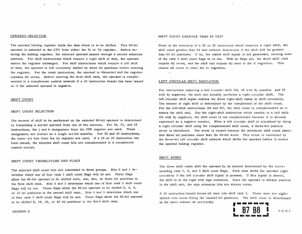
OPERAND SELECTION
The operand holding register holds the data which is to be shifted. This 60-bit
operand is selected in the CPU from either the Xi or Xk register. Before en
tering the holding register. the selected operand passes through a second selection
network. For shift instructions which require a right shift of data. the operand
enters the register unchanged. For shift instructions which require a left shift
of data. the operand is left circularly shifted by three bit positions before entering
the register. For the mask instruction. the operand is discarded and the register
contains all zeros. Before entering the first shift rank. the operand is comple
mented in a complement control network if a 43 instruction (mask) has b.een issued
or if the selected operand is negative.
SHIFT COUNT
SHIFT COUNT SELECTION
The amount of shift to be performed on the selected 60-bit operand is determined
by translating a six-bit operand from one of two sources. For 20. 21. and 43
instructions. the j and k designators from the CIW register are used. These
designators are treated as a single six-bit quantity. For 22 and 23 instructions.
the lower six bits from the Bj register are used. If a 20 or 22 instruction has
been issued. the selected shift count bits are complemented in a complement
control circuit.
SHIFT COUNT TRANSLATORS AND FLAGS
The selected shift count bits are translated in three groups. Bits 0 and 1 de
termine which one of four rank 1 shift count flags will be set. These flags
allow the 60-bit operand to be shifted zero. one. two. or three bit positions in
the first shift rank. Bits 2 and 3 determine Which one bf four rank 2 shift count
flags will be set. These flags allow the 60-bit operand to be shifted O. 4. 8.
or 12 bit positions in the second shift rank.
of four rank 3 shift count flags will be set.
Bits 4 and 5 determine which one
These flags allow the 60-bit operand
to be shifted O. 16. 32. or 48 bit positions in the third shift rank.
60420300 K
SHIFT COUNT GREATER THAN 63 TEST
Prior to the execution of a 22 or 23 instruction which requires a right shift, the
shift count greater than 63 test network determines if the shift will be greater
than 63 bit positions. If so. the enable shift signal is not generated, causing none
of the rank 3 shift count flags to be set. With no flags set, the third shift rank
outputs all zeros. and the shift unit outputs all ones to the X registers. This
causes all zeros to enter the Xi registers.
LEFT CIRCULAR SHlFT SIMULATION
For instructions requiring a left circular shift (20. 22 with Bj positive and 25
with Bj negative). the shift unit actually performs a right circular shift. The
left circular shift signal enables the three right-shift ranks to shift circularly.
The amount of right shift is determined by the complement of the shift count.
For the left-shift instructions (20 and 22). the shift count is complemented as it
enters the shift unit. For the right-shift instruction which results in a left shift
(23 with Bj negative). the shift count is not complemented because it is already
expressed as a negative number. When a left circular shift is simulated by doing
a right circular shift using the complemented shift count. a three-bit position
error is introduced. The error is caused because the maximum shift count speci
fies three bit positions more than the 60-bit word. This error is corrected by
the three-bit left circular shift network which shifts the operand before it enters
the operand holding register.
SHlFT RANKS
The three shift ranks shift the operand by an amount determined by the corre
sponding rank 1. 2. and 3 shift count flags. Each rank shifts the operand right
Circularly if the left circular shift signal is present. If this signal is absent,
the shift is to the right with sign extension. Since the operand is always positive
in the shift unit. the sign extension bits are always zeros.
A 43 instruction (mask) forces all ones into shift rank 1. These ones are right
shifted with zeros filling the vacated bit positions. The shift count is determined in the same manner as previously. 1_ .... __ •
I 87 88 I 1ra .. 1IIIiOII1IiIIIII .. ..I
5-3 -0.1

SIDFT UNIT OUTPUT
The third rank of the shift unit outputs the shifted operand (complemented) to
the X registers whenever a go shift signal is present. If this signal is not
present, all ones are sent to the X registers. If the original operand was
positive, the shifted operand is recomplemented before entering the Xi register.
Negative operands are complemented twice in the shift unit. Therefore, they
are not recomplemented.
60420300 K 5-3-0.2

CIW REG! STER
(CPU)
Bi REGISTER
(CPUI
BJ REGISTER
(CPU I
CIW REGISTER
C C~!J)
[
[
BITS 0-9
SHIFT COUNT > 63 TEST
BITS 0-9
3-81T LEFT
CIRCULAR SHIFT
RIGHT SHIFT
RIGHT SHIFt 121+22-81 17 ... 23.Bj"i71
LEFT SHIFT (ZO+22.BTT-i ... 23-01 171
LEFT CIRCULAR SHIFT (20 + 22· ifT7 + 23· Bj 171
SELECT Bi 122+231
SELECT jk (20+21+43)
FORM MASK I RIGHT SHIFT" LEFT SH'~T)
NOTES:
CD THE SHIFT UNIT PERFORMS THE FOLLOWING FUNCTIONS ~
INSTRUCTION ~
20 SHIFTS 60 BITS IN )( i REGISTER jk PLACES TO LEFT .. 21 SHIFTS 60 81TS IN xl REGISTER jk PLACES TO RIGHT. ZZ SHIFTS 60 BITS IN xk REGISTER Bi 0-5 PLACES TO LEFT IF B i IS POSITIVE
OR' BJ O-S PLACES TO RIGHT IF Bj IS NEGATIVE. RESULT IS PLACED IN I( i REGISTER.
23 SHIFTS 60 BITS IN Kk REGISTER Bj 0-5 PLACES TO RIGHT IF B j IS POSITIVE OR 110=1 PLACES TO LEFT IF Bi (5 NEGATIVE _ RESUL T IS PLACED IN X i REGISTER.
43 PUTS ONES IN UPPER Jk PLACES OF XI REGISTER.
CD L~FT CIRCULAR SHIFT ENABLES BITS TO BE RIGHT SHIFTED END-AROUND.
SHIFT COUNT BITS 0-5
BITS 0-59
BITS 0·59
.ENABLE SHIFT
(IF SHIFT COUNT ~ 63 + 22 .. 23 INSTRUCTION J
CONTROL
BITS 0-99 OPERAND
HOLDING REGISTER
SHIFT COUNT
RANK I SHI"
}-_~'-__ --{2}_ ....... ",COUNT XLTR
AND FLAGS
SHIFT COUNT BITS 2,3
RIGHT SHIFT O,t,2.OR I
BITS BITS 81TS 0-99 0-59 0-59
SHIFT
CONTROl RANKI
FORM MASK OR NEGATIVE OPERAND
LEFT
® CIRCULAR SHIFT
t
RANK Z SHIFT COUNT
XLTR AND . FLAGS
SHIFT RANK 2
RIGHT SHIFT O,4,8,OR 12
BITS 0-5'
RANK 3 SHIFT
COUNT
SHIFT RANK 3
RIGHT SHIFT O,II,a2. OR 41
GO SHIFT CPU
XI "EIISTER
(CPU)
r----.., I 83 84 I 1 _____ •
PRIMARY BLOCK DIAGRAM SHIFT UNIT

~6A16 BITS 51-59, 0-2(IN); 54-59 {OUTI
RANK 3 W 6AI5 45- 56 ( INI, 48- 53 {Oun ; RANK 3 SHIFT 48 FLAG SHIF'T 48
RANK 3 W 6AI4 39-50(lN);42-41(OUn;RANK 3 SHIFT 32 FLAG SHIFT 32
RANK 3 W 6AI3 33-44 (lNI. 36-41 (OUT); RANK 3 SHIFT 16 FLAG SHIFT 16
fl.mo, ml ~6E10 RANK 3 W6AI2 27- 38 (IN I, 30-35 {OUT} ; RANK 3 SHIFT a FLAG
---0--- f-0 SHIFT 0
-d>- K> RANK I SHIFT COUNT BITS 0,1
SHIFT RANK 2 ~6AII 21- 3211NI, 24-29 (OUT) i RANK 2 SHIFT 12 FLAG
-0---CONTROL
f-0 SHIFT 12
Bj BITS 0-10,17 RANK 2 W 6AI0 15- 26 (lNI, 18 -23 (OUT); RANK 2. SHIFT B FLAG
---@---- SH 1FT 8 CPU 2.3A
LEFT CIRCULAR SHI FT
CPU 2.20 XI OR Xk SIGN ( SHIFT 3.0) XiOR Xk SIGN
CPU 2.ZA RANK 2 W 6AO• 9- 20(IN) ,12-17(OUT1J RANK 2. SHI FT 4 FLAG SHJFT 4
. RANK 2 WSA08 3-14{IN),6-lItOUTl; RANK 2. SHIFT 0 FLAG SHIFT 0
II ~ GA07 BITS 0-8,57~59 (IN); Q-SIOUT): LEFT CIRCULAR SHIFT FLAG
CP(~l~j!---
SHIFT RANK I xi OA xk BITS 0-58
59 -€>--c CPU
~liGONR & r ( SHIFT 30) 2.20 [
RANK 3 SHIFT 48
RANK 3 SHIFT 32
RANK 3 SHIFT 16
RANK 3 SHIFT 0
RANK 2 SHIFT 12
RANK 2 SHIFT 8
RANK 2 SHIFT 4
RANK 2. SHIFT a
LEFT CIRCULAR
NOTES:
SHIFT
CD EVER¥ FOURTH BIT lEG 'BITS 0-2 ~ 0,4,6,121
® EVERY EIGHTH 81T (EG-BITS 0-24 = 0,8,16,24)
® SIGN' BIT 59
~ 6816 81TS l"59(INI,7-!55 (OUTI
CD :®
W 6BI5 2-5. IINI, 6-5' (OUTI
CD ®
PSB14 I-57 ClNI,!5-53(OUTl
-0-- CD ®
~6B13 BITS 0-56(IN),4"S2(OUT)
0- CD ®
~6B12 BITS 3-59(IN),3-!59 (OUT)
CD ®
WGBII 2-S80NI,2-S8(OUT)
CD ®
W 6BI0 I-57 IINI,I-57 (OUTI
CD ®
~ 6BO. BITS 0-5S(lN)P-56(OUTl
CPU 2.IOGO SHIFT CD ®
SHIFT RANKS 2 AND 3 BITS 0- 59
BITS 0-59
60
SECONDARY SHIFT UNIT
"-(SHIFT 3.01 ---
CPU 2.ZA
. (x RGTR)
I --, I B 13 B14 I 1ia .. ____ 1
BLOCK 01 AGRAM

SHIFT UNIT
The shift unit executes CPU instructions 20. 21. 22. 23. and 43. These in
structions shift the entire 60-bit field of data within the operand word. Input
operands are of two types. A 60-bit word is read from either the Xi or the
Xk register. depending upon the type of instruction. A second operand is read
from either the CIW or the Bj register. This operand determines the shift count
for the 60-bit word. Shifted operands are sent from the shift unit to the Xi
register.
INSTRUCTIONS EXECUTED
LEFT SHIFT Xi BY jk (20ijk INSTRUCTION)
This instruction causes the shift unit to read one operand from the Xi register.
shift the 60 -bit word left circularly by jk bit positions. and then write' the re
sulting 60-bit word back into the same Xi register.
The shift unit does not actually shift data in a left circular mode. Instead. it
simulates the shift. The shift count is complemented. a three-bit left circular
shift correction is performed. and the shift is made in a right circular mode.
RIGHT SHIFT Xi BY jk (2lijk INSTRUCTION)
This instruction causes the shift unit to read one operand from the Xi register.
shift the 60-bit word to the right with sign extension by jk bit positions. and
write the resulting 60-bit word back into the same Xi register.
LEFT SHIFT Xk BY Bj TO Xi (22ijk INSTRUCTION)
This instruction normally causes the shift unit to read one operand from the
Xk register. shift the 60-bit word left circularly by an amount determined by Bj
bits 0 through 5. and write the resutling 60-bit word into the Xi register. How-
60420300 K
ever. if the l8-bit operand in the Bj register is negative. the shift is to the
right with sign extension. and the shift count is determined by the complement of
Bj hits 0 through 5.
The shift unit always complements Bj bits 0 through 5 during the execution of
this instruction. The left shift is simulated by making a three-bit left circular
shift correction and shifting in a right circular mode.
RIGHT SIDFT Xk BY Bj TO Xi (23ijk INSTRUCTION)
This instruction normally causes the shift unit to read one operand from the Xk
register. shift the 60-bit word to the right with sign extension by an amount de
termined by Bj bits 0 through 5. and write the resulting 60-bit word into the Xi
register. However. if the 18-bit operand in the Bj register is negative. the shift
is left circular and the shift count is determined by complemented bits 0 through
5.
The shift unit does not actually shift data in a left circular mode when Bj is
negative; it simulates the shift. A three-bit left circular correction is performed
and the shift is made in a right circular mode. The shift count is complemented
because the Bj register contains a negative number.
MASK UPPER jk PLACES OF Xi (43ijk INSTRUCTION)
This instruction causes the shift unit to generate a 60-bit word containing ones
in the upper jk bit positions and zeros in the remaining bit positions. The re
sulting 60-bit word is written into the Xi register.
.--_ ....... I C5 C6 I IUD! I,au. IIII!III IIIiIIII .I
5-3-4.1

INSTRUCTION TRANSLATION
The 3K07 module determines what instruction has been issued by translating three
bits from the instruction designators in the CIW register. These are f bit 1 and
m bits 0 and 1.
OPERAND SELECTION
The operand holding register (4KP7 modules) holds the data which is to be shifted.
This 60-bit operand is slected from either the Xi or Xk register. The. selection
is made in the CPU (4RF7 and 4RG7 modules) and is based on the value of m in
the CIW register. The Xi data. path is selected if the m designator has an octal
value of 0, 1, 4, or 5. The Xk data path is selected when this value is 2, 3,
SHIFT COUNT
SHIFT COUNT SELECTION
The shift count to be performed on the selected 60-bit operand is determined by
translating a six-bit operand from one of two sources. The selection of one of
these sources is made in the 3K07 module. For 20, 21, and 43 instructions,
the j .and k designators from the CIW register are used. These designators are
treated as a single six-bit quantity. For 22 and 23 instructions, the lower six
bits from the Bj register are used. If a 20 or 22 instruction has been issued,
the selected shift count bits are complemented.
6, or 7. SHIFT COUNT TRANSLATORS AND FLAGS
Before entering the operand holding register, the selected operand passes through
a second selection network (4K,?7 modules). For 2X series instructions which re
quire a right-shift of data, the operand enters the register unchanged. For 2X
series instructions which requiJ'e a left-shift of data, the operand is left circular
ly shifted by three bit positions before entering the register. For 43 instructions,
the operand is discarded. In tb.is case, the register contains all zeros.
Before entering the first shift rank, the operand is complemented in a complement
control network (4KP7 modules) if the complement control flag is set. This flag
is set when a 43 instruction has been issued or if the selected operand is negative
(operand must be positive). A 43 instruction is indicated when the f deSignator
from the CIW register has a zero in the middle bit (XOX). A negative operand
is indicated when bit 59 (sign) of the selected operand is a one.
The selected shift count bits are translated in three groups. Bits 0 and 1 are
sent to a translator in the 4KP7 modules. This translator determines which one
of four flags will be set. These flags allow the 60-bit operand to be shifted zero,
one, two, or three bit positions in the first shift rank (4KP7 modules). Shift
count bits 2 and 3 are translated in the 3K07 module. This translator determines
which one of four flags in the 4KP7 modules will be set. These flags allow the
60-bit operand to be shifted 0, 4, 8, or 12 bit positions in the second shift rank
(4KQ7 and 4KW7 modules). Shift count bits 4 and 5 are also translated in the
3K07 module. This translator determines which one of four flags in the 4KP7
modules will be set. These flags allow the 60-bit operand to be shifted 0, 16,
32, or 48 bit positions in the third shift rank (4KQ7 and 4KW7 modules).
SHIFT COUNT GREATER THAN 63 TEST
Prior to the execution of a 22 or 23 instruction, a network in the 3K07 module
determines if the right-shift is greater than 63 bit positions. If so, the enable
shift signal is not generated. This causes none of the third shift rank flags to set.
With no flags set, the third shift rank outputs all zeros and the shift unit outputs
all ones to the X registers. This causes all zeros to enter the Xi register. p--_ ...... I C7 C8 I
60420300 K 1. _____ 1 5-3-4.2

LEFT CIRCULAR SmFT SIGNAL AND FLAG
For instructions requiring a left circular shift. the shift unit actually shifts the
operand in a right circular mode. The left circular shift signal generated by
the 3K07 module enables the shift ranks to simulate this shift. This signal
enables a three-bit left circular shift correction in the 4KP7 modules. It also
sets the left circular shift flag (lower 4KP7 module). When this flag is set,
the shift ranks perform a right circular shift.
60420300 K
SHIFT UNIT OUTPUT
The third rank of the shift unit (4KQ7 and 4KW7 modules) outputs the shifted
operand (complemented) to the X registers whenever a go shift signal from the
4LE7 module is present. If this signal is not present, all ones are sent to the
X registers. If the original operand was positive, the shifted operand is re
complemented before entering the :Xi register under control of the X register
sign control. Negative operands are complemented twice in the shift unit.
Therefore. they are not recomplerrlented.
5-3-4.3

SIDFT 3.0 TEST POINTS
Module Location Test Point Description Module Location Test Point Description Module Location Test Point Description
3K07'" 6ElO 54 20 instruction
1 1 53 22 ! 55 23
4KPF 6A07-16 16 Operand holding rgtr hit N
11 Operand holding rgtr hit N+1
·24 Operand holding rgtr hit N+2
23 Operand holding rgtr hit N+3
34 Operand holding rgtr hit N+4
33 Operand holding rgtr hit N+5
43 Operand holding rgtr hit N+6
45 Operand holding rgtr bit N+7
54 Operand holding rgtr bit N+8
01,06 Compl cont flag 74 Rank 1 shift 0 flag 73
1 1
76 2 75 3 41,46 Shift cont flag 71,72 25 -nanosecond clock
4KQ7'" 6B09-12 71 Left circular shift 73 Go shift 02 Rank 2 shift 0 06
1 4
05 8 01 12 74 Rank 3 shift 0 75
1 16
76 32 72 48
4KW7'" 6B13-16 71 Left circular shift 73 Go shift 03 Rank 2 shift 0 06
1 4
05 8 01 12 74 Rank 3 shift 0 75
1 16 ... ----..,. 76 32
72 48 I C3 C4 I I ___ ID_.I
I 60420300 K 5-3-4.4

~6E10
cpe
3.IA 20+21+-43 $HIFT
(CIWI ~k: J, k ITA ~g.~N~:\
--\~j), ,.-'-+-<~!J' ~.}-(~!:. >-G+>} •
Bj ens
CP1J3.~8~7
Ii 81T 11
8j iiTi1
INSTR
t INSTR
I ' ENAIlE ti' _r!, SHIFT \:J
XI OR Xl $IGN
I cp! 3.48
XI em Xk SION
I
LEFT ClftCULAR StlI,l
UFT CIRCULAR -, LEFT
~~ LEFT CIRCULAR 'HIFT Ii>
RINK lilTS SHiff ~,.-e;I ~"T1 0-5' O,I,E, " .. ,
(!)
I -----, "GHT _ ~SltIFT
-
~~------------------------~H-~~T'~b~ ~"AI~ liT, .'-~6 ""u, .1-SlIOUT!; RANII) 'HIFf .. H .....
3'-'" \INI, 'n!-.? lOUT!; R ... N", 3 SHIFT U FL ... G
..... NIC' ... 16 .. 12
L:':::.'::.FT'-'0'-l-H-21·'. IIHI,JO-3S toun, .... NI(' '"1FT 0 FL .. G
.... NK 2 ~e"lo IIS-UIINI, le-n IOUTI; ""NK Z SNIFT , FLAG SHIFT'
RANk 2 --I"" 9-20 IINI. 12·17 ICUTI: R .. NK Z SHltT. 'LAG SHIFT •
..." ~ .. RANI( 3
~
R ... NI( 2 I SHIFT.
GO
.
NOTES.
,.
<D E\IERY FOURnt 'IT CEI-IIT1 O-IZ. 0,., ',IZI
@ MRY [IGtfTH IITIU-IITS O-Z.-O,',II,241
<i> 'ilioN_liT"
cg) RANI( I SKIFT NETWORK ... T LOtATIOHI uor-eAl5 HAVE lOGICAL. ONE INPUT INSTIAO 0' LEFT CIRCULAR SHIFT.
~ FL"'G ..... 0 F ... NOUT ... T LOCATIONS 1A01-6 .. ., .. IU USED FDA SHIFT COHflllOL SIGN .. LS, THIS CIRCUITRY IS NOT USED .. T LOC .. TlON 6 .. 16.
Cl 41CW7 MOOUL£ IS S .... £ AS 4K07 MODULE !XC£PT .kW1 MOOULE OUTPuTS SEVEN IlTl.
<P DURING" 21 OR U INSTRUCTION IRIGHT SHIFTI, THE SHIFT IS RIGHT OP£N-ENDtO: OU"ING .. 20 OR: 22 IH$TRUCTIC»IILEFT SHIFT), THE SHIFT IS "I,"T CIRCULAR.
e IF tl4A1LE SHIFT I' NOT ",DENT,THE R"NK 3 SHIFT NETWORK WILL OU'TPUT "LL ZEROS .. Il10 THE SHIFT UHIT WltL OUTPUT .. LL ONES.
&ell 111$ 3-5t 11141. 'I'-SS 10UTI .... 2-5' UNI.I-!)4 lOUT! .... I-57 IINI S-Il IOUTI , IITS 0-" , WH, .-'2 10UTl
121ITS 3·59 tlNI.3-', (CUTI
" H. UNI Z-5I IOUTI 6810 I-51 (iNI. I-51 touTI
~wwIlTSO-H IiNI,O-M lOUT!
GO SHIFT CPU :u:a.!!J!!. 1-----------_____ -""-='-'--__ ,
cpt '.4" III .. NK 2 ~6"O' '-14 WU, 6-11 lOUT); ""NK l SHIFT 0 FLAG SHIFT 0
..... NIt l "ANIt l Slotl" 01
H" •• ,,""'T..:: ...... _-<-0-:~.r--i ~
~ ~-
~.~""~TT~~'.~"~.~,,~.~.--..~ •• ~T--. •• ~II.~I;~.~-.~I~OU~T~I:~'~"~T-."~"'~U~'M~."~"~T~'~'.-..------------~ ~FT ~ r-- LEn CIRCULAR $HI" CI .. CUL .... SHIFT I
.------. I Cl C2 I .. _--- ...
D£TAIL.ED-IAODULlI DIAGRA.M SHIFT UNIT

4
o
c
3
CLOCK PERIOD
CL.OCK PULSE
TWO SUCCESSIVE SHIFT INSTRUCTIONS IN TOP PARCEL OF crw REGISTER
@ GO ISSUE
GO SHIFT
RESULT REGISTER Xi RESERVED FOR INSTRUCTION I
INSTRUCTION I RESULT ENTERS THE XI REGISTER
RESULT REGISTER Xi RESERVEO FOR INSTRUCnON 2
INSTRUCTION 2 RESULT ENTERS THE Xi REGISTER
NOTES:
<D 431 j' (ASSUMING NO ISSUE CONFLICTS EXIST)
® 23 ijl (OPERAND REGISTER ~ONFLICTS WITH INSTRUCTION I DESTINATION REGISTER)
2
® ENABLE ISSUE IS DELAYED 4 CLOCK PERIODS (THEREFORE, GO ISSUE
IS DELAYED A MJNIMUM OF 4 CLOCK PERIODS) IN THE AAI20-C. THIS DELAY IS REMOVED BY INSTALLING DPTlON AT364 -A.
1
o
c
B B
A III'llIII am D'l IIrll .. IriJ
I D11 D12 I I -.I DIll 1m! 1&1 !:01I!Il d
A
TIMING DIAGRAM
4 3

4 3 2
4RF7 4RF7 4RF7 6010 6009 6007 T
~ 4RG7rM~5~8~5~7~5~6~5~5~5~4~5~3~52~'~5~1~50~4~9~4~8~4~7~4~6~4~5L4~4~4:C3~4~2~4~1~4~0~3~9~36~37~3~6~3~5~3~4~3~3~3=2~3~1~3=OL2=9~2=6~2~7~2~.~2~5~2~4~2~3~22~2~1=2=0~19~18~1~7~1=6~1=5LI~4~1=3~1=2~1~1-='0~9-=8-=7-=6-=5~4-=3-=2~~1_O~
6F01 59
D
HOLDING
OUTPUTS
4t(P7 4KP7 4KP1 5655545352 51 504948474645444342 41 40393837 36 3534333231 3029 28 27 26 25242322 21 20 19 16 17 16 15 14 13 12 II
55 51 47 43 39 35 31 27 23 19 15 II 7
47 39 31 23 15
C C 54 50 46 42 38 34 30 26 22 18 14 10
54 46 38 30 22 I. 6
53 49 45 41 37 33 29 25 21 17 13 9
45 37 29 21 13
6BI3 48 44 .0 36 32 28 24 20 16 12 4
52 44 36 26 20 12 4
4KQ7 6BI2 59 55 51 47 43 39 35 31 27 23 19 15 II 3
59 51 43 35 27 19 II
B 4KQ7 B 68 II 58 54 50 46 42 38 34 30 26 22 18 14 10 2
N
58 50 42 34 26 18 10
4 KQ7
6810 57 53 49 45 41 37 33 29 25 21 17 13 I N
57 49 41 33 25 17
4KQ7
6B09 56 52 48 44 40 36 32 28 24 20 16 12 4 0 N
56 48 40 32 24 16 0
EXAMPLE 4KP1 NOTES:
(j) LS3 TO HOLDING REGISTER ON LEFT SHIFT BIT 57 TO 0, BIT 58 TO I, BIT 59 TO 21 ETC. 4 2 0 INPUTS
® BITS 0-6 TO HOLDING REGISTER BITS 0-8 ON RIGHT SHIFT.
A ~ ~ • @ RSO HOLDING RGTR BITS 0-5 TO OUTPUT BITS 0-5. r-----lUI A 4 0 HOLDI NG REGISTER @ RSI HOLDING RGTR BITS 1- 6 TO OUTPUT BITS 0-5.
I D13 014 I @ RS2 HOLDING RGTR BITS 2-7 TO OUTPUT BITS 0-5.
@ RS3 HOLDING RGTR BITS 3-6 TO OUTPU T BITS 0-5. L _____ I
4 0 OUTPUTS
TROUBLESHOOTING CHART SHIFT UNIT
4 3 'I

PART 4
NORMA LIZE UNIT

NORMALIZE UNIT
The normalize unit executes CPU instructions 24 and 25. These two instructions
are identical except instruction 25 adds a round bit to the coefficient.
The normalize unit operates on operands in positive (true) form so it complements
negative operands before operating on them. It then left-shifts the coefficient by
an amount that causes a one ·~it to appear in the most significant position. The
normalize unit adjusts the exponent by subtracting the shift count.
OPERATION
The normalize instructions require 3 clock periods for execution. Data moves
from the operating registers to the normalize unit in the same clock period in
which the instruction issues from the CIW register. Input registers hold the
information necessary to com,~lete the instruction for use during the second clock
period. During the second clock period, the normalize unit complements the
operand if the sign was negat,ve, and a static network determines the number
of shifts necessary to normaLze the coefficient. The shift count determination
network sends a six-bit shift count to the first stage of the exponent adder for
exponent correction, to a reg!.ster that holds the shift count for transmission to
the B register, and to the sh;.ft count translator. The shift count translator
translates the six-bit binary shift count into control signals: shift 0, 2, 4, 8,
16, 32, 48, and no shift. The decoded shift count register holds this decoded
shift count for use during the third clock period.
The shift count determination network also sends bit zero of the binary shift count
to shift rank 1 where it left-E;hifts the coefficient one position if bit 0 is a one.
During the third clock period, shift ranks 2, 3, and 4 complete the shifting of
the coefficient, and the second stage of the exponent adder completes the sub
traction of the shift count from the exponent. Go normalize gates the shift
count to the B register, and i.f there are no special cases, gates the corrected
exponent and shifted coefficient to the destination X registers.
60420300 K
SPECIAL CASES
After the normalize unit corrects the exponent for sign, it tests for an overflow
or indefinite quantity. If the exponent is overflow or indefinite, the unit blocks
the shift count, the operand passes through the unit unaltered. The quantity
delivered to the B register is zero and a bit is set in the exit condition
register (CPU).
If the coefficient portion of the operand is all zeros after the correction for sign,
the shift count is 48. If this situation occurs in execution of a 25 instruction,
the round bit results in a normalized coefficient. If this situation occurs in
execution of a 24 instruction, the shift count of 48 is a special case and the
result entered in the destination X register is all zeros. The shift count de
livered to the B register is 48 in either of these cases.
The subtraction of the six-bit shift count from the exponent may result in an
underflow of the floating-point exponent range. This situation causes all zeros
to enter the destination X register. The shift count delivered to the B register
is not affected by this situation.
.-_ .. _-. I E5 E6 I .. _ .. _ .... ,,11
5-4-0

Xk RGTR (CPU)
xk RGTR (C~U)
crw RGTR (CPU)
COMP IF xk NEG
COM~ IF Xk NEG
ROUND
STATIC SHIFT COUNT
DETERMINATION NETWORK
SHIFT COUNT BITS 0-5
BIT 0 OF SHIFT COUNT
ROUND
ENABLE SHIFT
BIT ENABLES, BIT BORROWS
CPU GO NORMALIZE
SHIFT COUNT ii'i'T'Ci
t
BIT EHAILES. BIT BOPIROWS
BITS 48-~
EXTEND ZEROS Bj 1-~ __ --+-,,".:.'T:.:S:...6.:.-...:1.:.7_'0'--_""'_"j RGTR
ROUND BIT
LEFT SHIFT 0+2
SHIFT RANK
2
(CPU)
"j RGTR (CPU)
LEFT LEFT SHIFT SHIFT 0+4+ 0+16+ 8+12 32+48
SHIFT SHIFT RANK RANK
3 4
STATIC LEFT SHIFT NETWORK
PRIMARY BLOCK DIAGRAM NORMAL! ZE UNIT
xi RGTR (CPU)
Xi RGTA (CPU)
r- 1IiIIIII1IIIIII1IIIII1IIIIII .,
I E3 E4 I 1_"BllllEllllI!I&1d

CPU [ 2.20
CPU 2.0B (CIIY)
CPU l-2.20
~7J14 ~7J16 xk SIGN. )( SIGN
CPU 2.2A
xk
~ II Hv BITS 0-10 EXPONENT
INPUT RGTR SPEC IAL CASE TEST
AND ONES CHECK ENABLE SHIFT AND FIRST STAGE OF ------- EXP MINUS SHIFT COUNT,
ROUND BIT ENABLES AND BIT
mO SHIFT BORROWS RGTRS, COUNT BIT~ GO NORMALIZE FLAG -2 J (~ORM 3.01
RO!JNO FLAG-2
GO CPU NORMALIZE
I I 2.1B
1
(NORM 3.0)
~7J12
I I ~7J15 I I EXTEND Bj
SHI FT COUNT I DETERM IN ATION St1 I FT COUNT SH I FT COUNT
F~ NETWORK BITS 0-5 BITS 0-5-0-----6
i SHIFT COUNT XLTR,
SHIFT COUNT ~BLE SHIFT COUNT RGTR
L~ BIT 0 SHI FT
~ (NORM 3.0)
I (NORM 3.0) 2 .
~ r 4EC717J07 BITS 31-47
4EA717J04 BITS 32-47 17J06 15 -31
xk 17J03 16-31 ~7J05 BITS 0-15
~ ~ ~7J02 BITS 0- 15 ENABLE SH 1FT
48 4B
SHIFT COUNT BIT 0
Xk SIGN COEF ROUND
INPUT RGTR
~ BITS 0-47
(NORM 3.0)
NOTES:
CD THE Rour;D BIT IS USED AS ONE BIT POSITION LESS THAN O.
® EVERY SECOND BIT (EG. Q-12=O,2,4,6,8,IO,12)
® EVERY FOURTH BIT (EG. 0-12 = 0,4,8,12).
@) NO SHIFT IS USED IN RANK 4 AND MEANS NO SHIFT 16 +32+4B.
LEFT SH I FT RANK I
AND
HOLDING RGTR
(NORM 3.0)
NORM ~7J13 UNDERFLOW
CPU 2.2A ~'TE' INFINITE
CPU 2.5C OR 2.6B(8X5)
f--® BIT ENABLES 0-10
~ BIT BORROWS SECOND STAGE OF
EXP MINUS SHIFT COUNT GATE OUTPUT
I ROUND BIT
1 I EXTEND Bj
j (NORM 3.0)
GATE OUTPUT
L EXTEND ZEROS BJ ~ 7JII BITS 3- 47, ® ~TS 6-11. l BIT I, ROUND BIT
CPU 2.3A BITS 0-5 (B RGTR) ROUND
I--®--------...J BIT (i)
SnlFT 2: D7JI0 BITS 2 -46, ®
BIT 0
NO SHIFT, @) SHIFT 0,4,8, 12,16,32,48
~
l:"""' W7J09 BITS 1-45,®
BIT (i) ROUND BIT
S~
~7JOB BITS 0-44 ®
.--
~ BITS 0-47
LEFT SHIFT
RANK 2,3,4
(NORM 3.0)
SECONDARY BLOCK DIAGRAM NORMALI Z E
i-@~ II
EXTEND ZEROS BITS 12-17
l!iT"S'3-47 0
~
---0 ~-46
12
~-450 12
~-440 12
CPU 2.2A (X RGTR)
Bj
CPU 2.3A (6 RGTR)

NORMALIZE UNIT
The normalize unit executes CPU instructions 24 and 25. These two instructions
are identical except instruction 25 adds a round bit to the coefficient.
The normalize unit operates on operands in positive (true) form so it comple
ments negative operands before operating on them. It then left-shifts the co
efficient by an amount that causes a one bit to appear in the most significant
position (bit 47). The normalize unit adjusts the exponent by subtracting the
shift count.
EXPONENT AND CONTROL
4EE7 MODULE
Xk bits 48 through 59 and instruction designators m bit 0 enter registers in this
module when the instruction issues from the CIW register. A static network
complements bits 48 through 58 if bit 59 is a one to place the exponent in biased
positive format. A ones check is then performed on exponent bit 0 through 9.
Bits 0 through 9 are all ones if an exponent overflow condition (3777) or an ex
ponent indefinite condition (1777) exists. If either -of these conditions exists, the
ones check detects it and blocks enable shift. Blocking enable shift causes the
operand to pass unchanged through the normalize unit and a zero shift count to
be sent to the B register.
This module also sends bit 59 (X sign) to the CPU X register sign control. This
,controls the complement of the result at the input to the destination X register.
If the instruction is a round normalize (25), m bit 0 is a one and sets the round
flag. The round flag sends a round signal to the 3EF7 and 4EC7 modules. Round
causes a bit to be added to the coefficient in a position immediately below the
bit zero position of the coefficient before it is shifted. The shift ranks then
the round bit' along with the coefficient.
60420300 K
3EF7 MODULE
Exponent bits 0 through 10 enter this module from the 4EF7 module during the
second clock period, where the first stage of subtraction of shift count bits 0
through 5 from. the exponent takes place. Enable shift gates shift count bits 0
through 5 into the first stage of the adder. Registers hold the partial difference
for use during the third clock period. The 3EF7 module also tests for a zero
coefficient and a complete underflow.
In the case of a 24 instruction (no round bit) with a coefficient equal to zero, a
normalized result Is impossible. The zero coefficient results in a shift count
of 48, and combined with round and enable shift, blocks gate output. Blocking
gate output causes all ones to be sent to the X registers. A normalize under
flow signal is sent to the X register input control (5CB7 module) which comple
ments the word of ones causing all zeros to enter the destination X register.
If subtraction of the shift count causes the exponent to exceed its negative range,
a complete underflow results. This Is detected by testing the bit enables and
bit borrows. A complete underflow blocks gate output which causes all ones to
be sent to the X registers, A normalize underflow signal is sent to the X regis
ter input control (5CB7 module) which complements the word of ones causing all
zeros to enter the destination X register.
Go normalize enters the module during the second clock period and the go norma
lize flag-2 holds it for use during the third clock period. Go normalize enables
gate output under normal conditions and also causes the extension of zero bits in
B register bits 6 through 17.
This module tests for indefinite or infinite operands. For indefinite operands
(exponent equals 1777), the complement of exponent bit 10 and the complement of
enable shift are ANDed with the go. normalize signal. For infinite operands
(exponent equals 3777), exponent bit 10 and the complement of enable shift are
ANDed - with the go normalize signal. The indefinite and infinite signals are sent
to the CPU to set the corresponding bit in the exit condition register (CPU).
5-4-4.0

4EH7 MODULE
This module performs the Second stage of subtraction of the shift count from the
exponent. Gate output gates the output of the adder to the X registers. The
result is complemented as it is sent to the X registers. If the result is positive,
it is recomplemented by the X register input control (5CB7 module) as it enters
the destination X register.
COEFFICIENT
4EA7 MODULE
Xk bits 0 through 47 enter this module when the instruction issues from the CIW
register. The module contairis the coefficient input register and complements the
coefficient if bit 59 is a one. This changes the coefficient to positive format in
the same way the 4EE7 module corrected the exponent for sign. The 48 co
efficient bits go to the 4EC7 and 4EB7 modules.
4EB7 MODULE
This module contairi6 the static shift count determination network. its output is
a six-bit binary shift count equal to the number of zero bits from the most signi
ficant one bit on the unshifted corfficient up to and including bit 47. All six bits
of this shift count go to the 3EF7 and 4EG7 modules. Shift count bit 0 goes to
the 4EC7 modules.
60420300 K
4EG7 MODULE
Enable shift gates the shift count into these modules during the second clock
period. The shift count translator translates the six-bit shift count into shift
control signals of shift 0, 2, 4, 8, 12, 16, 32, 48, and no shift. Registers hold
them for use in the 4ED7 modules during the third clock period. A register also
holds shift count bits 0 through 5 for use during the third clock period. Extend
Bj gates the shift count to B register bits 0 through 5.
4EC7 MODULE
The coefficient bits 0 through 47 enter these modules during the second clock
period. A left-shift of one takes place in shift rank 1 if shift count bit 0 and
enable shift are both ones. A register holds the output of shift rank 1 for use
in the 4ED7 modules during the third clock period.
4ED7 MODULE
Coefficient bits 0 through 47 enter these modules during the third clock period.
Shift ranks 2, 3, and 4 complete the left shifts needed to normalize the coefficient.
Gate output gates coefficient bits 0 through 47 to the destination X register. The
result is complemented as it is sent to the X registers. If the result is positive,
it is recomplemented by the X register input control as it enters the destination
X register.
r .. -- ...... I F7 F8 I ..... _-_ ...
5-4-4.1

NORM 3.0 TEST POINTS
Module Location Test Point Description Module Location Test Point Description Module Location Test Point Description
4EA7 7J02-04 41.42. Bit 59 norm sign rgtr I I 44 Shift rank 1 rgtr I I 05 Exponent bit 0 45.46 : bit N+8 06 1 01 Coef input rgtr bit N 43 Shift rank 1 rgtr 15 2 03 N+1 bit N+9 16 3 05 N+2 54 Shift rank 1 rgtr 25 4 06 N+3 bit N+10 26 5 11 N+4 53 Shift rank 1 rgtr 35 6 12 N+5 bit N+ll 36 7 15 N+6 64 Shift rank 1 rgtr 42 8 16 N+7 bit N+12 41 9 21 N+8 63 Shift rank 1 rgtr 56 10 23 N+9 bit N+13 71.72 25-nanosecond clock 25 N+IO 72 Shift rank 1 rgtr
3EF7" 7J16 76 Enable shift 26 N+ll bit N+14 03 Bit 0 enable 31 N+12 76 Shift rank 1 rgtr 04 1 32 N+13 bit N+15 13 2 35 N+14 71 25-nanosecond clock 14 3 36 N+15
4EDF 7J08-11 75 Gate output 23 4 52 . Coef bit N 53 N+l 72 No shift 24 5
55 N+2 04 Shift 0 35 6
56 N+3 03
I ,1 32 7
51 N+4 06 42 8
54 N+5 05 45 9
64 N+6 63 16 55 10
66 N+7 52 32 01 Bit 0 borrow·
62 N+8 ~ 55 '18 06
I l I 11 61 N+9 4EE7'" 7J14 51,54, Bit 59 norm sign rgtr 16 63 N+I0 55,62 21 65 N+ll 02 Exponent input rgtr 26 71,72 N+l2 bit 48 52 Extend Bj 73,74 N+l3 04 Exponent input rgtr 75 N+l4 bit 49
72 25-nanosecond clock
76 N+l5 12 Exponent input rgtr 4EG7'" 7J15 56 Enable shift 43,44 25 -nanosecond clock bit 50 62 Shift count bit 0
4EB7'" 7J12 73 Shift count bit 5 14 Exponent input rgtr 63
I 1
bit 51 65 2 4EC7'" 7J05-07 06 Shift rank 1 rgtr 22 Exponent input rgtr 75 3
bit N bit 52 73 4 01 Shift rank 1 rgtr 24 Exponent input rgtr 72 5 ..
bit N+l bit 53 32 No shift 16 Shift rank 1 rgtr 32 Exponent input rgtr 12 Shift 0
bit N+2 bit 54 02,05 Shift 2 11 Shift rank 1 rgtr 34 Exponent input rgtr 15 Shift 4
bit N+3 bit 55 22 I ,: 26 Shift rank 1 rgtr 45 Exponent input rgtr 25 bit N+4 bit 56 35 16
21 Shift rank 1 rgtr 43 Exponent inpu t rgtr 42 32 bit N+5 bit 57 45 48
36 Shift rank 1 rgtr 52 Exponent input rgtr 52.54 25-nanosecond clock bit N+6 bit 58
4EH7'" 7J13 41,42 Gate output -+ i- 31 Shift rank 1 rgtr ~ t 65 Round flag
bit N+7 72 Extena BJ
.60420300 K 1------. I F3 F4 I 1_-----.1
5-4-4.2

!!!!JToIII
~"""'T' }C~'"'H ~I'INITE
liT 10 1 T fS!D'oII4 I _$ liT 10 ENAILE
IIT'I·IO - I~J::':~i~nll -:;
I .- .!.
I "L0 liT EN." .. 0-.1
p.!!!J'oIl:S I -
~IITENAILEI liT IN.ILES 0-' -'i" lOlllGN 11''1' I. • SlIalil i ilTS o-a • . CPU :S.41 f'IO.lI. ' CPU S ..... .EGISTEW J "1111
~ "EGIS"" !> t liT 10."0_!! o-a 'i' .
'~=j: • .. -~ IltSjf.\.1JI II .. Olllllllf eo ... l,flO 10 'IT~ 0"1":"\ .
iiii4i=ii C'U " " ~::~:f~b. 'Ii' c"u '.4.\ ...
ElI"ONEN : " " IX ROT.I SHIFT COUNT -IKIFT COUNT tUT rY -FUtlT STAGE BITS 0-'
l/E UNDERFLOW • • .
CHECIC 'KIFT -
CIl COUNT II
£HULE e GATI: OUT"UT .... TE OUTPUT ElIAIU ENAILE SHIFT SHIFT - FAN· '"1,1 (l)
OUT EXT zuosal FAIilOUT
EXTEND II ...r-J. ,. .. IITS 12-IT CPU 3.5A .0 1t0UN' ..oUND ItOuIIO 1t0UND OUT II RGTRI a-u :S.18 .. AI
I - ROUND Il:tWI
- 1t0UNg lIT FL"'G~Z
iiTo -- =~RF""" CPU GO NOIt'-ALIZ( GO NO ..... EWEND 8, :S ....
IITS :S-"'T. lit I. ROUND liT CPU
~ I ~ToIli
<il i'i'Ti""i=47(t) ... ROUtrlO alT
q) -~1.1I0 8ITS 1(i,1. liT °
4iiTS 2-~(jJ ~?"Il
l ~T?:~:'J -EXT ZUOS II
= -§-- ~ICIJU5U ~lolOlI'TS 1~"'!5. ROUND lIT 4i' iifiT-4~ (f) :-l:
OUT taltOTltI Ii) 'KIF· COUNT !tOUNO liT q)
F-I STATIC SHIFT c(lu.' iiii'O-'i r.m
CPU 54.\ 'HIf'T 'OUNT I'TS 0" COUNT I BITS 0-' CPU 5."" ~'oI0' IITS o@'" IX RGTR)
..... DlTU.INATION ,!, . . , . . REGISTER . :
II RG'R' - IInwo"" '" !!!! IITS 0-' GATE OUTPUT 'Hln cOIINT '.'ICE J .-. I" 0 SHIFT -
iiTi m-r - 'AN' SHIFT Z SH,'T Z
'" 'ITS REGISTE" OUT
• .-, RANIC RANII RANII NO SHIFT. 2 • I
S"IFT DECOOEO
FAN· -@ f:UH,~."'···12.
:!) -@-- SHin SHIFT IKI'" SMI" llTi 0-.7 COUNT . COUNT • OUT ° OR Z o OR. 00.11 _LTIIt
REGISTER O •• OR :sa i'iTs"ii:ii(i)
III OR 12 OR •• 0-3. " "'IA??JOI4 81T Sl- ... ., ~ ~
?0103 11-31 BIT' 0-.'" r--~?J02 'ITS g-I' C7 ~T IITS 51-'" "-'0101 IS-St
STATIC LEFT .. ~-'
~701O''ITS O-IS 'HIFT NETWORK IITS 0-'" cot,. CO....~ 0·",
~ '-- ENULE IHIFT 'HIF'LEn CPu5.48~ I INI'UT I CONT ~TION
••• ISTER (i) J ~ SHIft COUNT liT 0 NOTU:
ROUND CD II' 'IT S9ol, CO.PLEMEHT EXPONENT ... ND COE'. • 1T10-4? IITS 0-11 SHIFT
1< 'ITS O-IS .r.> 'ITS 0-"" ~ IF EXPONENT IS IHOEF OR OyEttFLOW. 00 NOT ENAILE IHIFT • o!! RANK " REGllTEit
~ I -18~ NO""'. (j) aATE OUtl'UT II .LOC"ED FOIt UN .. OUNOED NOltlll. OF UUS •• 8 SlIH
o COE'. OR EX"ONENT UNDERFLOW. "EGIITlR
Ii) COIIIPLEIIIEIIT TO R(1II0V! liAS .
.. ----... (!) THE ROUNO .IT IS USED AI ON( lIT POSITION LESS THAN O.
I Fl F2 I (J)EYUY SECOIID lIT IEe.O·'I.O • .l ••••••• IO.111 .. _--- .... (f)EYERY 'OU"'H liT IEe.O-lt.O."',I,'11
NORMALIZE UNIT N =-DETAILED· MDDULES DIA •• AM r1S4~;~ r60~O'OO r D(:~~=I' 1 0 I'MOII" arlS-... -s

4
c
B
A
4
3
CLOCK PERIOD
CLOCK PULSE
TWO SUCCESSIVE NORMALIZE INSTRUCTIONS IN THE TOP PARCEL OF THE trW REGISTER
@ GO ISSUE
GO NORMALIZE FLAG SET
x. (I) AND 010 (I) IN NORMALIZE UNIT INPUT REGISTERS
Xi 'I) AND 8j (I) RESERVED
INSTRUCTION I RESULTS ENTER XI (I) AND Bj (J)
.. 0 (2) IN NORIIALIZE UNIT INPUT REGISTER
x. (2) II IN NORMALIZE UNIT INPUT REGISTER
XI (2) AND 8; (2) RESERVED
INSTRUCTION 2 RESULTS ENTER XI (2) AND Bj (2)
NOTES:
<D INSTRUCTION I - ASSUME NO ISSUE CONFLICTS
2
:0: 1:2~3!4l5: ~
I I I I I I I I I I I I I I I I I
~ I I I I I I I I I I 1 I I I I I I I I I I
~ I , I I I ' I I I I I I I I
-l ~ ~ ~!---.L..!@l1t2J11 I I I I I I I I I I I I I I I I I I J I II<D~
I 11 i I I i I I I I I I I I I I
~ 1 I I I I I I I I I I I I I <DU I I I I I I I I I I I I I
~ I I I I I I J I I I I I I I I
~ I I I I I j I I I I I I I I I I I I
~ I I I I I I I I I I I I I I I I I I I I I I '®~ I I , I
® INSTRUCTION 2 - ASSUIIE OPERAND REGISTER Xk (2) CONFUCTS WITH
INSTRUCTION I DESTINATION REGISTER XI (I). THAT IS, k (2) = I (I). THUS, ISSUE IS DELAYED TWO CLOCK PERIODS UNTIL THE XI (I)
RESERVATION IS CLEARED.
II THE Xk (2) OUANTITY IS THE INSTRUCTION I RESULT THAT IS ENTERED INTO XI Ill.
@ ENABLE ISSUE IS DELAYED 4 CLOCK PERIODS (THEREFORE, GO ISSUE
IS DELAYED A MINIMUM OF 4 CLOCK PERIODS) IN THE AAI20-C.
THIS OELAY IS REMOVED 8Y INSTALLING OPTION A1364 -A.
3
TIMING DIAGRAM NORMALIZE INSTRUCTION
,..-----. I H9 H10 I' ....... __ ...
D
c
8.
A

PART 5
F LOA TING -A DD UNIT
1---. I B 1 I • __ ..1

FLOATING-ADD UNIT
DIAGRAM LAYOUT
The floating-add unit primary block diagram is drawn with the registers and
flip-flops arranged in vertical columns according to clock periods.
There are three columns of registers. The flrst column on the left has the
m! input flip-flop on top and the borrow register for the first stage of Xk minus
Xj exponent on the bottom. The second column of registers has the m1 flip-flop
on top and the reference sign flip-flop on the bottom. The third column has the
DP flip-flop on top and the borrow register for the first stage of shifted operand
plus reference operand on the bottom.
Because of this arrangement, this diagram shows everything that happens in each
clock period. Everything happening on the left side of the first column of regis
ters, including the setting of the registers, occurs during the first clock period.
Everything happening between the first and second columns of registers, including
the setting of the second column of registers, occurs during the second" clock
period. Everything happening between the second and thtrd columns of regi!lters,
including the setting of the third column of registers, occurs during the third
clock period. Everything happenihg to the right of the third column of registers,
including the setting of the result into the Xi register in the CPU, occurs during
the fourth clock period.
The exponent takes a path from left to right across the upper half of the diagram,
and the coefficient takes a path across the lower half of the diagram. Shift count
determination and shift control are across the middle. The remaining control is
across the top of the diagram.
GENERAL OPERATION
The floating-add unit performs CPU instructions 30 through 35. They are:
Floating sum (30)
Floating difference (31)
Floating double-precision sum (32)
60420300 K
Floating double-precision difference (33)
Round floating sum (34)
Round floating difference (35)
The m deSignator of the instruction controls the type of operation the unit performs.
Bit 0 controls the mode of operation (add or subtract). Bit 1 controls single or
double precision. Bit 2 controls the rounding operation.
Execution time is 4 clock periods.
The unit receives two 60-bit operands in floating-point format from the X registers
specified by the j and k designators of the instruction.
If the instruction is a 31, 33, or 35 (subtract), m designator bit 0 causes the unit
to complement the Xk operand. Thus, the unit subtracts by complementary
addition.
The unit tests both exponents for overflow and indefinite. If a special case is
detected, the output of the unit is blocked and the appropriate special case flag
is sent to the CPU.
Before the two coefficients can be added, they must be aligned in a manner that
causes the exponents to be equal. Thus, each bit in the adder has equal signifi
cance with the bit to which it is added. The unit aligns coefficient bits of equal
Significance by right-shifting the coefficient having the smaller exponent by an
amount equal to the difference between the two exponents. The coefficient selected
for shifting is called the shifted operand. The coefficient having the larger ex
ponent is called the reference operand. The difference between the two exponents
is determined by an ll-bit adder. The output of this adder translates into shift
control signals. These signals control the shift ranks that shift the shift operand.
This adder also determines which exponent is the larger and outputs a Signal called
sign of difference. Sign of difference is equal to one when Xj is the larger ex
ponent. It controls the selection of the exponent and which coefficient becomes the
Shifted operand. ,-----., I 85 86 I ............
5-5-0.1

If the two exponents are equal so that no shifting is required, all the shift con-
trol signals are zero and the shifted operand passes through the shift ranks un
changed: Both coefficients occupy the upper half of the 97-bit shifted and reference
operands with the signs of the two coefficients filling the lower half. The binary
points are in the middle of the 97-bit operands (between bits 47 and 48). If the
exponents are different so that alignment is required, the coefficient selected for
shifting is right-shifted within the 97~bit shifted operand. The sign of this
coefficient fills in above and below as it is shifted.
After the amount of the difference between the two exponents is determined, the
smaller exponent is discarded, under control of sign of difference. The larger
one is selected to continue through the unit to become the exponent of the result.
When the command is a 34 or 35 (round) instruction, m designator bit 2 causes
the unit to add a round bit to one or both operands. If both operands are nor
malized or if the signs of the two operands are different, the round bit is added
to both operands. If the above conditions are not met, the round bit is added
only to the reference operand. The round bit added to the reference operand is
always in bit position 47. This is immediately to the right of the binary point.
If the round bit is also added to the shifted operand, it starts out in bit position
47 but is right-shifted with the rest of the coefficient. If no shifting takes place,
the round bit remains in bit pOSition 47. Round bits are equal to the complement
of the sign of the operands to which they are added. After the alignment, the
two operands are added in a 99-bit ones complement adder.
60420300 K
Instructions 30, 31, 34, and 35 (single precision) cause the unit to deliver the
upper half of the 99-bit result to Xi location 0 through 47. The result exponent
and sign bit are packed in floating-point format into Xl locations 48 through 59.
Instructions 32 and 33 (double precision) cause the unit to deliver the lower half
of the 99-bit result to Xi locations 0 through 47. These 48 bits are to the right
of the binary pOint, so the unit subtracts 48 from the result exponent to correct
for double precision before sending it to the Xi register.
When the coefficient sum overflows the highest order bit of the result coefficient,
the unit detects it by testing the signs of the two operands and determining
whether or not there was a borrow (carry) into bit 96. If the unit determines
that there was a coefficient overflow, the 48-bit coefficient delivered to Xi is
taken from the 99-bit adder result one bit higher than if no overflow occurs.
If overflow occurs, the exponent is increased by one prior to sending it to Xi.
,-----. I 87 88 I 1.----..1
5-5-0.2

mO
.x RGTR Xl BITS 0·'9 (CPU!
t~iTS '8-"
II
xj BIT !l9
X RGTR (CPU)
l Xk SITS 48-~B
Xk ElIT "
NOTES;
ROUND elT CON'TROL.. IFADI
ROUND
.'T CONTROL..
lC" SiGN
Xk 'IGN
[MAILES,80RROWS
SHIFT I,t," SPiN OF DIH
SIGN
0' 0''''
SHII'T :Kj,:Kk ROUND IITS , lIEF Xi, Xk ROUND BITS
• } ""'T OftERAMD
tI'AD)
Xi,:Kk £:KP ItTS 0-10
SHIFT 4 SHI'T 2
SHIFT OPER
SHIFT SIGN
SHIft ~OUND liT
Ret OPERAND
SHIfT SHIFT RANK RANK
RIGHT SHIFT 0,'
RIGHT SHIFT 0,'
SHIFT RANI(
• RIGHT SHIFT 0,8,16,
"
SHIFT RANK • RIGHT SHIH 0,32,'4,
9',01'1
"8
CD
UNDERFLOW
OVERFLOW'
,"O[F·I,IMFINITE 2
SHIFT 121
SHIFTED StGN a>
CD REF OPERAND IS SIGN FILLED FROM BITO TO BIf4'. THE HIGHEST ORDER BtT (&IT 961 IS ALSO FILl£,D WITH SIGN. {
REF' REF OPERAND, R£F' ROUND BIT RU ROUND BIT O~~~~ND ... -@...:::::.....:===::..:=;..::.;,;...~ ____ -J
~~~~~--------~ Xk SIGN
® SHIF1£D SIGN FILLS THE HIGHEST ORDER liT Illf .,1. IFADI
~~XLj~SI~'.~ ______ ~ REF' SIGN
} ;~~:C~~6:UT (1'1001
~~~~L,--~r-
'XP BITS 0·10
EXP OUTPUT CONTROL
}
RGTR (CPU)
EXP +1/0 BITS 48·~9
"
&MROW TO 96 PROPAGATION
NETWORK
ENABLES, IIOftROWS
BO;i"iiOw TO 96
BORROW TO 96
COEF OVERFLOW
TEST
COEF OVERFLOW
COEr OUTPUT SELECTION CONT
(FADI
,--A-,
SAMPLE UPPER, :s SAMPLE CENTFR,
SAMPL.E LOWER
COEF OUTPUT
SELECT ION
COEF BITS 41·9~
COEF BITS 49-96
SHIFTED
COEF BITS 0·47
COEF BITS 1-48
SHIF EO .... _--... I 83 84 I 1 ___ .....
PRIMARY BLOC,," DIAGRAM FLOATING ADD UNIT
X RGTR
{CPUI

XIt,X~
stlIFtxlt,x, ItOUND BITS
SHIFT 1,2,4 . SIGN 0' 01F,.
SHifT IIIt,XI ROUND BITS
.x~ , x",_, con IITS 0·47
UP BITS &-10 , "M SCOI
F=~f---+~H DE~~I:~INI~2; I~N lI",)(IINOEF
SHIFTII,IIi,3! DETERMINATION:
E)(P ULECTION,
~_HIFT£D SIGN
REI'SIGN
SHIFtED SIGN
[XP MINUS GO/O, GO AOe SPECIAL CASE, IHDEF, UNDERFLOW.
S:'~C~~O~::ER~~!T: -<;:L~~~~ __ CPU 2 lA
COEr OUTPUT SELECTION CONTROL
~~-(',ii):P-"-"_ •. -'.-------t_------"-P-"-T-S_.0·'r • .r~';;:'3T -"""'.':---'...Ij;\. BITS 48 59
SAMPLE r)(p SAMPLE EIIP f)CP OI/ERflOW ) AEF SIGN, COARECT ION CPU 2!C
~:'MS:~:LfE~~~ HAL', r--------~~ AN~O~~T I--@.:~'_'I;S=_'_'::~=_-'i"_ III AGTAI
~~-(~~'._P_" __ '~ __ '. __ .'-"---__ +---_______ -, ---L-~=-=-~~
::"~~Tt-I, I-I-~:{'~-__ -CPU ~~~1~~5}
RE' SIGN,
$~GN ______ -'
SIGN OF DltF SIGN L~----j:D--I s!:L[CTEO 11111 !lGnt. ~~~~Fp -b I-'.::.'-=D~"=_' -1-~L---,':;:'G::N-=.=_' .::":.:"--1 SHIFT COUNT RGT" J-<;-b»----l--l--I
L....!!:~!!..j-@~I_ .. 4~C!:-4~_~~~-1SH1~T ~2._4_ J CPU 21B SHIft 81G12 o(4}-too IFAD301 ~ ;:;.:"
CPU 2.0B ':! __ --I._~I~'.~.:..:.~.:!.., _r:!·f---j ICI_I -
~tl81S ~~p:: ~11~T~;(~:i.XI'." SIGN IEkTENDED TMJtOUGH
SHIFTED REF OPER BITS 119-9510UTI
~S'09:~ :~U~':S8?;~2il~~:FT 111. Xk ROUND BITS, REF X.,
SHIFTED. RtF OPER SITS 47-53 loun
~!i8Of :1::: ~II~~ ~;';i SHIFT x,. Xk ROUND 81TS,
SHifTED, REF OPffl BITS 40-4&IOUTI
SHIFT •• 1'.32,
~ SHIFTED SIGN -REP SIGH
fiEF OPER
~5
AEF SIGH
!!!1!IISCIS SIUFTED OPEA BITS 4T-95, SHIFTED SIGN IINI. SHIFTtD OP[R BITS 7-95 ® (OUT I
---l5C14 46 ·94, SHI" T£D SIGN lIN', G-"@ IOUTI
=.f5C13 45·93, SHIFTED SIGN UNI, S-'3Ci) 10UTI
---Istl! 44-92, SHIFT EO SiGN IINI, 4-52@) lOUT}
43-91, SHIFTED SIGN IINI, '!lI@ lOUT}
....-J5CIO 42-90, SHIFTED SIGN ONI. i-90@) 10UTI
.--JSC09 41-89. SHIFTED SIGN IINI, I n@ loull
~!sc01i SHIFTED O,.£R BITS 40-88. SHIFTEO SIGH {IN}, SHIFTED OPEIII Bns o-,.® IOUTI
SHIFTED ');16N
SHltTEO OPER BITS O-!!I~
SECTION [NABLES 1-10, GROUP E "'ABLE elTs 90-'5 .....
GROUP EftABLES""\!!I BITS 90-9!!t
CO[f OVERFLOW OE TERMINATION
SECTION 8ORRO~
GROUP BORROWS r-__ .~"~S~~~"~'~' __ ~4-~I~"~.!'~ZI~J~~F~'~~~------~
G) COEr
'II! SHifTED Fl7S011 SHlrTED, REF (PIER BITS 90-"
• 40GICAL I~ BITS 91,98
SECTIOJiI II ENA8LE) ~r.="''''''''''''''",,--,,:-:,,-.'-o -'-,.-«)-" ___ ~~
-.-1'00' 721. ~ __ ~_ Gl ~ =::::. 1 ~~}'" M '[ •• '
"":=:l'~'~00~1~-----------~,....I II I' g~~:FLOW f----l---." ... ruo • .--.,:-.-,,-l
m SHIFTlEO, REF SIGN ® ~DlO
--l'M)01 SHIFTEO, REF OPE .. BITS 54-82 ~~N T ENA~~_. --15[07
RIGH' SHIFT RANKS I (SHIFT 0,41. 21SHIn 0,21. 3'SHIFT 0,11,
RIGHT SHIFT RANIIS 4 ISHIFT 0,',16.241, !i ISH 1FT 0,32,64,961 H .... --I-W '!!:!!I500. ::~~'A ~;~s O::_A~:,I~~G:5-!i3. ~~~"_"_[_'_'81,-,:,-,,:-_,~ -.o-,.-,,+----+---H ~5E06 BITS 4"-53
GAOUP
S£lfCT SHIft OPEFIAND,
S"IFTED. REF oprAAND RCITIIS
SHIFTED OPERAND
lLL _____ ..::.:~.:.:.... ______ JJ RfF OPER
MOTES
<D 4r11 MODULE .. AHOLtS SEVEN BITS IN THt SAlliE WAY 4'01" MODUUS HANOLf HIN[
® SHIFTED SIGH AND RtF SIGN ON 4'17 MOOUL! GO TO 8/T te
(j) flit ALL 4FIC7 MODULES EXCEPT LOCATION 5£Oe,OP AND IiJo ME SET TO LOGICAL I
@ lilT [NAlilE 9& IS EXT£NDED TO BITS 97 ANO 98 IUNUSED POSITIONS I ON 4FM7 MODULE AT SEll
@ SECTION ENABLES FANOUT TO OTHEIlt 10 SECTIONS 14fl(7 MOOULES! BUT NOT TO CORRESPONDING SECTION 'ECTIONS HAV£ SAME NUMBER AS THE LAST TWO DIGITS OF MODULE LOCATION NO
@ EVEAl' EIGHTH elT
Q) EVERY SIXTH BIT
BIT'!i 4'~5
--15004
;::::J'oo,
SHIFTED OPER PW'5 REF OPER.
FIAST STAGE I ENABLE.
IIORAOW RGTRS
IFAO S21
H-44,
SIGN liT! 27-15.
SIGN e'n 18·2G,
9-17. SIGN lilTS
m!JSDOI SHlfT£D OPEIt lilTS 0-', REF OPER SIGN 81TS
ENABLES
PLUS REF DPEA,
SECOftD STAGE,
SELECTION
~5E02
~!iEOI (lilTS 0-8
SECONDARY BLOCK DIAGRAM FLOATING ADO
COEt 81T 0 SHIFTED _~]

INPUT; SPECIAL CASE TEST; SHIFT COUNT DETERMINATION; COEFFICIENT OUTPUT SELECTION CONTROL; EXPONENT SELECTION
The SO-bit Xj and Xk operands enter the 4FF7 module during the clock period
in which the instruction issues from the CIW register. Instruction designator m
bits 0 and 2 also enter ihe 4FF7 module at the same time. Designator m bit 1
enters the 4RD7 module (which will be discussed later).
Designator m bit 0 differentiates between an add and a subtract command. If
m bit 0 is a one, ihe command is a subtract so it complements all 60 bits of the
Xk operand. The 4FF7 module contains registers which hold both SO-bit operands
for use during ihe second clock period.
ROUND BIT CONTROL
Designator m bit 2 controls the rounding of ihe coefficients. A flip-flop holds
m bit 2 for use during ihe second clock period. The output of the m bit 2 input
flip-flop is round reference. Round reference causes ihe round bit to be added
to the operand with the largest exponent (reference operand) or the Xk operand
if the exponents are equal. A round bit is also added to the operand with the
smaller exponent (shirt operand) if boih operands are normalized or if the signs
of the operands are not equal. The 4FF7 module tests for normalized operands
by comparing bit 47 to ihe sign bit (59). The result of these tests is ANDed
with round reference and causes ihe shift operand to be rounded.
The sign of ihe operand controls ihe binary state of the round bit for that operand.
The state of the round bits is always different than the sign bit. This round bit
preparation takes place on the 4FC7 modules.
The 4FC7 modules prepare round bits before the determination of which operand
will be the reference and which will be the shift operand. Therefore, if the
round reference signal is a one, the 4FC7 modules output a reference round bit
for both the Xk and Xj operands. If the round shift signal is a one, shift round
bits are output for both operands.
60420300 K
BIAS REMOVAL
The 4FC7 modules remove the bias, complement the eXpGloent for negative coeffi
cients, and test for overflow and indefinite. The sign bit (59) controls the re
moval of bias by complementing exponent bits 0 through 9 if the sign is negative.
The sign bit controls bit 10 (bias bit) oppoSite to bits 0 ihrough 9. For example.
if the sign is negative, exponent bits 0 through 9 are complemented, and bit 10
is not complemented. If the sign is positive, exponent bits 0 through 9 are not
complemented, and bit 10 is complemented.
OVERFLOW AND INDEFINITE TEST
The tests for overflow and indefinite take place after the removal of bias. Be
fore removal of bias, an exponent of 3777 or 4000 indicates ove;flow. After
removal of bias, an overflow is 1777. An indefinite exponent before bias removal
is 1777 or 6000. Unbiased, indefinite is 3777.
SHIFT COUNT DETERMINATION
The exponents from the two floating-point format operands enter ihe 4FA7 module
during the clock period ihat the instruction issues from ihe CIW register. Static
networks remove the bias from both exponents and complement the Xk exponent.
The exponents are also complemented if their coefficients are negative. The
exponents then enter ihe first stage of an adder that subtracts the Xj exponent from
ihe Xk exponE'nt by complementary addition. Registers store the partial result for
use in the 4FB7. 4FD7, and 3FE7 modules during the second clock period.
The 4FB7, 4FD7. and 3FE7 modules each contain a second stage adder which
forms results that are shift control signals.

The second stage adder in the 4FB7 module receives enables and borrows from
the 4FA 7 module and forms a result which is shift 1, 2, 4, and sign of difference.
Sign of difference is a one when the Xj exponent is larger than the Xk exponent.
In this case, the shift 1, 2, and 4 signals are in complement form. The 4FB7
module sends shift 1, 2, and 4 signals to shift ranks 1, 2, and 3 where they con
trol the shifting of the shift operand. Sign of difference is used for operand
selection.
The second stage adder in the 4FD7 module receives group enables and group
borrows from the 4FA7 module. The adder also receives Xk and Xj exponent
bits 3 through 5 from the 4FC7 modules. From these inputs, it forms results
which are shift 8, 16, and 32 control signals. These shift terms are always in
true form. A register holds them for use during the third clock period on the
3FH7 modules.
The second stage adder in the 3FE7 module receives group enables and group
borrows from the 4FA7 module. The adder also receives Xk and Xj exponent bits
6 through 10. From these inputs, it forms results which are shift 64 and 128
control signals. A register holds them for use during the third clock period on
the 3FH7 module.
EXPONENT SELECTION
During the second clock period of execution, the unit makes a selection between
the operands. One operand becomes the reference operand, and the other be
comes the shift operand. The coefficient for this shift operand goes to a shift
network where it is right-shifted by an amount equal to the difference between
the two exponents. The unit discards the exponent of the shift operand. The
sign of the shift operand becomes the shifted sign, and the sign of the reference
operand becomes the reference sign.
The selection of which exponent will be the reference exponent takes place in the
4FD7 and 3FE7 modules. The sign of difference makes the choice and gates
the larger exponent into the selected exponent register. Sign of difference is
equal to one when Xj is the larger exponent.
60420300 K
Sign of difference gates the sign of the operand with the smaller exponent into
the shifted sign flip-flop and the sign of the operahd with the larger exponent into
the reference sign flip-flop. These registers and flip-flops hold the selected
exponent, shifted signs, and reference signs for use during the third clock period.
The 4FD7 module handles the selection of exponent bits 0 through 5. The 3FE7
module handles the selection of exponent bits 6 through 10, shifted signs, and
reference signs.
EXPONENT CORRECTION FOR DOUBLE PRECISION
Designator m bit 1 differentiates between a single-precision and a double-precision
instruction. If m bit 1 is a zero, the instruction is single-precision and the unit
selects the upper 48 bits of the 97-bit result as the result coefficient. If m bit 1
is a one, the instruction is double-precision and the unit selects the lower 48 bits
of the 97-bit result register as the result coefficient. Since the binary point is
effectively right-shifted 48 ;Jlaces, it is necessary to adjust the' exponent by sub
tracting 48 from it.
DeSignator m bit 1 enters the 4FD7 module during the clock period in which the
instruction issues from the CIW register. Flip-flops hold it for 2 clock periods
for use during the third clock period. The output of the two flip-flops is double
precision and goes to the 3FM7 module.
During the third clock period, exponent bits 0 through 10 enter the 3FM7 module
from the selected exponent register in the 4FD7 and 3FE7 modules. A static
network in the 3FM7 module complements bits 0 through 10 and feeds them into
an adder that subtracts 60 (octal) if DP is a one. If DP is a zero, exponent bits
o through 10 pass through the adder unaltered. The exponent always leaves this
adder in true form so it needs no complementing. A register holds the result for
use during the fourth clock period.
.------. I· C7 C8 I '- ___ I11III .. 1
5-5-4.1

SPECIAL CASE TEST
The floating-add unit senses overflow, underflow, and indefinite special cases.
The 4FC7 modules test for overflow and indefinite for each operand and send the
results to the 4FD7 module. The 4FD7 module stores Xk and Xj overflow for
use during the third clock period. It also ORs Xk and Xj indefinite and stores
the result in the indefinite flip-flop for use in the 3FM7 module during the third
clock period.
Static networks in the 3FM7 module test these conditions and send the proper
special case flag to the X sign control translator during the third clock pe.riod.
The following table shows which flag is sent to the X sign control translator for
different conditions of overflow and indefinite. For example. if either operand
is indefinite, the indefinite flag is set. If both operands are negative overflow,
the overflow flag is set.
w -00
+00
IND
OVF
60420300 K
Operand with no special cases
Overflow with negative sign
Overflow with postive sign
Indefinite flag
Overflow flag
Xk
W +00
W OVF
+00 OVF OVF Xj
-00 OVF IND
IND IND IND
-00
OVF
IND
OVF
INO
Signs are reference and shifted.
IND
IND
IND
IND
IND
An underflow occurs when the unbiased selected exponent is a number more
negative than 2060 (octal) and the instruction is double-precision. The correction
for double-precision subtracts 60 (octal) from the exponent causing it to exceed
the most negative end of its range. If this happens, the 3FM7 module sends the
underflow signal to the X sign control translator.
During the second clock period, the 4FD7 module receives the go floating-add
signal from the CPU if the instruction code is 30 through 35. The go holding
flip-flop .holds it for use during the third clock period in the 3FM7 module.
During the third clock period, the 'go signal enters a flip-flop in the 3FM7 module
and enables output data to the destination X register during the fourth clock period.
If go floating-add is not set, the data is discarded.
If the go floating-add signal is received and a special case flag is set, go add
special case is set. This signal. together with the special case flag and the sign
of the reference operand" goes to the X sign control translator and causes the X
register input circuits to generate the proper special case result.
The 3FM7 module generates indefinite-l and infinite signals. When these signals
occur, the corresponding bit is set in the exit condition register (CPU). The
indefinite-l signal is generated when go and indefinite signals are present. The
infinite signal is generated when go and either Xk or Xj overflow signals are
present.
COEFFICIENT OUTPUT SELECTION CONTROL
During the fourth clock period, the floating-add unit transmits the results to the
destination X register. There are four possible data paths from the coefficient
portion of the unit to the X registers. The unit selects one of these four paths
on the basis of instruction mode and if coefficient overflow occurred.
.----- ... I C9 Cl0 I a.. ____ aI
5-5-4.2

There are two possible output data paths from the 97-bit re.sult for single-precision
commands. one for normal single precision (bits 48 through 95) and one for co
efficient overflow (bits 49 through 96).
There are also two possible output data paths from the 97-bit result for double
precision commands. one for normal double precision (bits 0 through 47) and one
for coefficient overflow (bits 1 through· 48).
The coefficient output selection control on the 3FM7 module controls the selection
of which half of the 97-bit result is transmitted from the unit.
If the instruction is single precision with no special cases and a go floating-add
is received from the CPU. the sample upper half and sample center signals are
ones. These signals are held for use during the fourth clock period in the 4FK7
module.
60420300 K
If the instruction is double preclslOn with no special cases and go floating-add is
received from the CPU. the sample lower half and sample center signals are ones.
These signals are held in the 3FM7 module for use during the fourth clock period
by the 4FK7 module.
EXPONENT SAMPLE CONTROL
The exponent for the result coefficient is transmitted to the destination X register
during the fourth clock period. Control for enabling the exponent output takes
place on the 3FM7 module. If there are no special cases and go floating-add is
received from the CPU. the sample exponent signal is sent to the 4FL7 module
where it enables the output of the exponent.
11IIlIIII1IiIIIII_1!a_~
• ell C12 m 1 ... ____ .1
5-5-4.3

FAD 3. 0 TEST POINTS
Module Location Test Point Description Module Location Test Point Description Module Location Test Point Description
4FA7" 5B01 74 Bit 0 enable I I 35 Xk coef bit N+24 73 lJ 1
36
1 N+30
71 55 N+36 66 56 N+42 35 Group enable' bits 0-2 65 Xk exPo bit N 43 ! 3-5 63 + N+6 53 6-8 04
Xj 00'1 hi' ~+, 65 9-10 06 72 Bit 0 borrow 24 N+12 76
'* 1 ~ 26 N+18
.36 Group brrow bits ~=~ 31 .
N+24 42 33 N+30 52 6-8 53 N+36 61 9-10 51 N+42 75 25-nanosecond clock 61 Xj exp bit N
4FB7" 5C01 (No signal/rgtr TPs) 62 ~ N+6 71 25-nanosecond clock
4FC7':' 5C02-03 25,42 Sign 3FM7" 5C06 56 Go ~ ~ 51,62 66 Shifted sign
4FD7" 5C04 76 Indefinite 62 Ref sign 71 Xk overflow 33 Exponent bit 0 enable 73 Xj overflow 05 1 06 Exponent bit 0 04 2 01
I 1 03 3
11 2 25 6 16 3 24
! i
! 26 4 23 8 21 5 35 10 64-66 Double precision 32 Exponent bit 0 63 Go 06 1 32,33 Shift 8 01 2 41,46 ! 16 02 3 51,56 32 11 4 61 25-nanosecond clock 12 5
3FE7" 5C05 41,73 Shifted sign 26 6
25 Ref sign 21 7
05 Exponent bit 6 22 8
06
1 7 36 9
11 8 31 10
16 9 75,76 25-nanosecond clock
23 10 31,36 Shift 64 51.55 • 128 75,76 25-nanosecond clock
4FF7" 5B02-07 76 rnO
I I 72 m2 73 Round ref .,.. .. _-- .. 02 Xk coef bit N
I C3 C4 I 01
1 N+6
22 N+12 of ~ 21 N+18
11 _____ .1
I I 60420300 K 5-5-4.4
Q

"" '" ceo '"
ce" '"
" BITS
~
~
" BITS :;;;..-"
I TEST FOR
NORM OP£AS+
X" SIGNol Xi SIGN
I
I ROUND r!l.SHIFT
~ROUND ~~~ ~m="'+t-______ _ .,
INPUT FF
I REF
(CIVil
~~B06 BITS 4-58 @
~SB05 3-57 lID
~5B04
~5B03 I-55 @)
~5B02 BITS 0-54 ®
~5BOI Xk AND Xi OITS 48-59
10
c," H' rr~
)(I!. BITS 48-58
"
lGf["" ,0->, xj (j) ~)(I BITS 48-58
-.:A58 -0 ~~=; II
Xl BIT 59 ExP
xk BIT 59
XII COEF air:", 0-·47
""
XI!. EXP BITS 0-11
XI EXP BITS 0-11
III
GROUP ENABLES GAOUP BITS 0-10
R~~~:iEER~
4FC7 !lC03 Xi EXPONENT
Xk [XP O~ 0-11
11
StGN
~HI"" I-- COMP AOUND BIT
CDNT
~'''' COMP AOUNO 81T CONT
-'FANOUT XI!. SIGN
L
,-b I SHIFT xII, xj
XII, XI
~ X~, XI EXP
~ XI!., XI
~ Xk, xj
~ X!l,XI
~~~~
'1 'P ROUND BIT J l---""::::':::',-',,,' ',,-' ___ fAD '31C ROUND BIT
GROUP EN"'ElLES, GROUP flORROWS
~5COI
~
GROUP ENABLES BITS 3-10
~
.)
Xk EXP BITS (1-10. Xk SIGN
XI EXP BITS 6-10, Xl SIGN
Xk [XP 'G" BITS 0-15
~Xl EXP BITS 0-5
CPU 3.2B
CPU 3 la ICI.W)
~~CO~ BITS 6-10
t:i' GROUP ENABLES
4 GROUP BORROWS
" BITS 6-10 (II
~ ~ .," ~ "'"., S[COND 2 64. iii ISHIFT SHIFT
xj STAGE REGIST£~slhi . '"=' 128
OITS P L---J" 'L-..I"
(i) ~ "SIGN ~ r
t--I." .,.JSHIFTEol SHIFTED I SIGN "'~"~"--+--I-FAO 310
Xl SIGN. 1'1' r 1 " .", p" 4-----,
FAD 32A
..-. ...... ~;I~iGN I. ...... ,..., .....----.I)(P -\!.J- ..... ""'\9 rY"'-6JlSELECTEOI6~TJ
~ . - EXPONENT 1h--6>-1-__ -I-l 'i" ./6\. ~ R~;::I:N I 5
SIGH OF DIFFERENCE
'D
~'C04 alTS o-s
GROUP ENAILES IITS 0-10 , GROUP BORROWS
4 81TS 0-10
XII BITS 3-5 r-.. I
..A.
--0 -V-I,~ xII-XI
( 3 SECOND
... ~
"EF SIGN
FAD 310
SHIFT
, S~,:,'I6~ 1-<3'i)-r;;FA~"o.o"ill' H-'{';':'~;)"."
~!lC06 UP-60/0
[XPaOBIO
4'.0'60. 7
"
B@f,-;;'O:"O
" f--"."~-+-1 :I!I~ ~ FA
~,~,,~,,~.,~c~'~"~'~'~"~.~CO~"~~ OUTPUT SELECTION CONTROL
1i0 ADD SPECIAL CASE:
~Dci:;;;L;W21~:gr'" INOH
GO ADD SPECIAL CASE
INDEF
UNDERFLOW
OVERFLOW
SAMPLE EXPONENT
CPU 3.4A
C PtJ 3.IOB
F"'D 3.08
~V SHIFTED
RGTR FAD 3.18L-HH--""'.'L"",,,,O-"'-''''''"J--+---, SHIFTED, =:"",G.,--~+-l S~~N r
] t 'i' Xk BITS 0-15 •
I, ,P-SIGN OF OlfF
'"L)'-
GO fLTG ADD GO HOLDING
H
m' 2 CLOCK HOLDING
Ff'S
XII OVERfLOW " OVERFLOW
" ,Xl OVERFLOW 'i
OVERFLOW
" Xk INOEf
+ IHDEF
xi IHOfF "
GO
OP
Xk OVERFLOW
xj OVERFLOW
INOH
~ SIGN C
NOTES'
(j) REMOVAL Of BIAS.
<V ROUND SH I FT AND ROUND REF ON 580Z THRU ~006 AAE TERMINATED.
IS> WHEN SIGN Of 011'1'. I. THE SHifT COUNT IS IN COMP FOAM, SIGN OF DIFF .. I WHEN Xl IS LAAGER HUMBER.
@ EVERY SIXTH BIT.
PU 34A
... -----1 I Cl C2 B .... _- ...........
DETAILED - MODULES DIAGRAM - ..... INPUT, SPECIAL CASE TEST; SHIFT CNT DETERMINATION \ COEF OUTPUT $EL CONT; EXP SEL

COEFFICIENT SELECTION, SIDFT
COEFFICIENT SELECTION
Coefficient selection takes place during the second clock period on the 4FG7 and
4F07 modules. The coefficient with the larger exponent b~comes the reference
operand and the other becomes the shifted operand. A register on the 4FG7 and
4F07 modules holds the reference operand for use during the third clock period.
The coefficient having the smaller expqnent becomes the shift operand. The shift
operand enters a shift network which right-shifts it by an amount equal to the
difference between the two exponents;
Sign of difference gates the coefficient having the larger exponent into the" refer
ence operand register. Sign of difference is a ·one when Xj is the larger ex
ponent. Sign of difference also gates the proper round bits. If the Xk coefficient
becomes the shift operand, the shift Xk round bit is selected for the shift operand.
If the Xk coefficient becomes the reference operand, the reference Xk round bit
is selected for the reference operand. The round bit is inserted one bit position
to the right of bit 0 of the original coefficient. Sign of difference gates the
coefficient having the smaller exponent into shift r"n!< 1.
Both coefficients expand into 96-bit operands before entering the adder. Since
the reference operand is not shifted, the original coefficient becomes bits 48
through 95 of the 96-bit reference operand with the round bit in position 47.
Reference sign fills bits 0 through 46 of the reference operand.
If the exponents are equal, there are no shifts so the shifted operand occupies
bits 47 through 95 with bit 47 being the shift round bit. If the exponents are not
equal, this coefficient is right-shifted by the amount of the difference. The bits
on either end of the original coefficient in the 96 -bit shifted operand are filled
wi th shifted Sign.
60420300 K
The shifting takes place in the 4FG7, 4F07. and 3FH7 modules. The 4FG7 and
4F07 modules contain shift ranks 1. 2, and 3. The control signals for these three
shift ranks are shift 1, 2, and 4 which come from the 4FB7 module. If sign of
difference is a one, the 4FB7 module sends these signals in complementary form.
To correct for this, the 4FG7 and 4F07 modules recomplement them if sign of
difference is a one. Therefore, when the shift signals enter the shift ranks.
they are always in true form.
Shift rank 1 performs a right shift of zero or four bit positions under the control
of shift 4. If shift 4 is a one, the shift rank performs a right shift of four bit
positions. If shift 4 is a zero, the operand moves through the shift rank un
changed. Shift ranks 2 and 3 function in the same way under control of shift 2
and shift 1.
These first three shift ranks perform any combination of right shifts up through
seven bit positions. If a shift of seven is performed, the round bit which was
inserted in bit position 47 is shifted to bit position 40. Therefore, the output of
shift rank 3 is shifted operand bits 40 through 95.
Shift ranks 1 and 2 perform their shifts during the second clock period. The
shifted operand register holds the result for use during the third clock period.
Shift rank 3 performs its shift during the third clock period and sends the results
to the 3FH7 modules for further shifting.
Shifted operand bits 40 through 95 enter the 3FH7 module during the third clock
period where the remainder of the shifting takes place in shift ranks 4 and 5.
Control for these shift ranks comes from the 4FD7 and 3FE7 modules during ~e
third clock period. These control signals are shift 8, 16, 32, 64, and 128. Shift 8, 16, 32, and 64 control signals" enter the shift count translator on the
3FH7 module. The translator outputs two groups of shift control signals.
1-----. I D5 D6 I 1_1IIBIII_-_.1
5-5-6.0

The first group of signals is shift 0, 8, 16, and 24. These signals go to shift
rank 4 where they cause this shift rank to right-shift the shifted operand by 0,
8, 16, or 24 bit positions.
The second group of signals is shift 0, 32, 64, and 96. These signals are
ANDed with shift 128 arid go to shift rank 5. Shift 128 goes directly to shift
rank 5.
60420300 K
The output of shift rank 5 is shifted operand bits 0 through 95. The 3FH7
module sends this shifted operand to the 4FJ7 and 4F17 modules for the first
stage of addition.
r - IlIIIII 11m IlIIIII I11III I
I 07 08 I 1m IiI!B EillI BII _ _ II
5-5-6.1

FAD 3.1 TEST POINTS
Module Location Test Point Description Module Location Test Point Description Module Location Test Point Description
4FG7'" 5(B08, 53 Ref operand bit N B10-15) 52
j N+l
51 N+2 56 N+3 55 N+4 54 N+5 15 Shifted operand rgtr
bit N 25 Shifted operand rgtr
bit N+1 .35 Shifted operand rgtr
bit N+2 42 Shifted operand rgtr
bit N+3 16 Shifted operand rgtr
bit N+4 26 Shifted operand rgtr
bit N+5 36 Shifted operand rgtr
bit N+6 41 Shifted operand rgtr
bit N+7
3FH7'" 5C08-15 32,33 Shifted sign
+ + 35,36 ~ 4F07':' 5B09 53 Ref operand bit 47
1 j 52
j 48
51 49 56 50 55 51 54 52
r- 1IIIiI1BI ---,
I 03 D4 I 11 __ liliiiililiiii .. .1
I 60420300 K 5-5-6.2

FAD !.OA Xl, Xk.J!GN
b ~~BI~ xj,)(Ir, BITS 41-41, XI,xlI SIGN (IN), SHIFTED, REF OPERAND BITS 89-9' {OUT}
~~BI4 34-47 82-88
f---J!lBI3 27-40 H-81
~~aI2 20-3! 68-74
f---J~BII 13-2.6 61 -67
~5B10 Xi, XII BITS 6-19 liN), SHIFTEO, REF OPERAND BITS ~4-60 (OUT)
SHIFT 1,2.4 COMP SHIFT I SHIFT I , ~' lit'
FF
SIGN OF DIFF
00-Xl
4 ~ SHIFT SHIFT SHIFT SHIFTEO
J RAN' RAN' ~ RAN' OPERAND Xj, xk 81TS 6-19
""- ~Xk I 2. SHIFTED "3 BITS 54-60
Il OPfRAND B -!.-~
~ Q, RIGHT RIGHT REGISTER RIGHT SHIFT SHIFT SHIFT
~~ ~ ~ Xk BITS 8-12 REF
JOP~~~D I OPERAND
7 BITS ~",,-60
.... x) BITS 6-12-REGISTER
~
~5B09 Xl.)(k BITS 0-12. SHIFT XI. Xk ROUND BITS, REF XI. xk ROUND BITS 11101), SHIFTED, REF OPERAND BITS "7- ~3 (OUT)
SHIFT 1,2,4 , :::; rw if"" "::
SIGN OF DIFF SHIFT SHIFT
-F1- 4 2 ~
.. xi • ~ SHIFT SHIFT SHIFT SHIFTED Xk.Xj
J RAN' RAN' ~ RAN' OPERAND
~ X"Xk BITS 0-12 I 2 SHIFTED 3 BITS ",,7-~3
l , 8 OPERAND e 7
Xk Q, RIGHT RIGHT REGISTER RIGHT
SH"T Xi,Xk I 4 ~ SHIFT SHIFT ,SHIFT
ROUND elTS 1';:;"\
~ ~~ . ~
-V- ~ Xk BITS 0-5 ~ "" REF XII ROUND BIT REF xk ROUND BIT
REF .1 OPERAND BITS 47·53
b., X, BITS 0-5 J?PERAND 7 REGISTER
REF XJ ROUND BIT REF XJ ROUND BIT
FAD 30A
-"l ~ ~B08 Xl. Xk BITS 0-5, SHIFT X/, Xk ROUND BITS, XJ. Xk SIGN IIN1. SHIFTED. REF OPERAND BITS ""0 -"'6 (OUT!
r--0- SHIFT I. Z." COMP SHIFT I SH~FT I , CONT '11 FF
SHIFT SHIFT
L-SIGN OF OIFF oR- 4'
xi g ~ A SHIFT SHIFT SHIFT SHIFTED
Xj,Xk r .~ RAf" ",NX ~ RA:' ..,J.i,~~ •• 61TS 0-5
12 I'" 7
I " ~ RIGHT RIGHT REGISTER FliGHT
SH", Xl, " ' ~' (V " SHIFT SHIFT SHIFT
" r--' 0+4 0+2: 0+1 ROUND BITS
~. '--- -Xk SIGN BITS
-@ Xj. Xk SIGN I: "E' OPERAND
Xj SIGN BITS REGISTER
FAD ,.o.{
REf" SIGN
REF SIGN FAD !.oe
FAO'O'{=
FAD "3OO--<!)-
SHIFTED OPEAAND 81TS 40-9~
FAD3.0B_
REf OPERAND REF SIGN BITS 41-9$
= FAD 3.2C
REF SIGN
"
~5CI~ :~:;~~~~~ ::~ 4~=:~.®I~~~~ISIGN 111011.
--.J~CI4 4:=::, m --15C13
4;::;, ® ---.J~CI2 44-92.
4-92 ® ~CII
4::::. tID -.J:lCIO .. :::~. ® --.-J5C09 41-09.
1-89 ® ~5COa SHIFTED OPER BITS "0-a8. SHIFTED SIGN 111011.
SHIfTED OPER BITS 0-88 ® (OUTI
SHIFT 128
S"'''.4 - SH'" ~ ~ SHIFT %"",96 e
'i'L.~RT ~ '--'
SHIFT 8. SHIFT 0,8,16,2.4
~- 4
SHIFT S~T SHIFTED
~~~~T~g_~9ER~D RAN' RAN' ~:T~~8~P~AND OPER 4 , BITS 0-9~
7 RIGHT RIGHT S SHIFTED SIGN <D SHIFT~rT 0+8+ +32+
16+2"" +96
L...--L:..!!!.
REFERENCE SIGN FAN REF SIGN REF SIGN
OUT
NOTES:
(j) USED TO SIGN EXTEND SHIFTED OPERA.ND.
® EVERY EIGHTH BIT FOR INPUT AND OUTPUT BITS.
.. -_ ...... .~
LJlljl~ DETAILED-MODULES DIAGRAM COEF'SELECTION.SHIF'T
_._1 --
FAD 3.2C
FAD 3.Z

ADDER; COEFFICIENT OUTPUT SELECTION; COEFF1CIENT OVERFLOW DETECTION; EXPONENT OUTPUT CONTROL; OUTPUT
ADDER
Shifted operand bits 0 through 95 and reference operand bits 49 through 95 enter
the 4FJ7 and 4F17 modules during the third clock period. Reference sign fills
bits 0 through 46 of the reference operand. Bit 96 of the reference operand is
filled with reference sign, and bit 96' of the shifted operand is filled with shifted
sign. This makes room for coefficLent overflow and controls the section borrow
from section 11 (end-around borrow). Since the upper two bits of the adder are
sign bits, if both operands are positive the adder always has an end-around borrow.
If both operands are negative, the adder never has an end-around borrow. If the
signs are not alike, the remaining bits control the end-around borrow.
Each 4FJ7 module handles nine bits, and the 4FI7 module handles seven bits.
Both operands are complemented as they enter the 4FJ7 and 4FI7 modules and
then enter the first stage of the adder. The first stage of the adder divides the
operands into bits, groups, and sections and forms a partial sum consisting of
enables and borrows.
ADDER FORMAT
Each module is a section; therefore, sections 1 through 10 are nine bits long
because they are on 4FJ7 modules, and section 11 is seven bits long because it is
on a 4F17 module. A section borrow sets when there is a borrow-out of that
section. A section enable sets when all bit enables in that section are set.
A grou'p is three bits long. There are two groups per section. These two
groups form the lower six bits of each section. A group enable sets when all
bit enables in that group set. A group borrow sets when there is a borrow-out
of that group. This partial sum is held in registers for use during the fourth
clock period.
A second stage of the adder is on 4FK7 modules. The second stage receives the
partial sum inputs and forms the sum. The sum at this point is in ones comple
ment form.
60420300 K
COEFFICIENT OVERFLOW DETECTION
The result of an addition or subtraction instruction may be one bit longer than the
operand's input into the adder. Therefore, since the adder receives 96-bit oper
ands, it is possible to overflow into the 97th bit. When this happens, it is
detected in the 4FL7 module which generates a coefficient overflow signal.
Coefficient overflow causes the result coefficient to be right-shifted one bit position
to retain this overflow bit. Because of this right shift, the exponent is corrected
by adding one to it.
The coefficient overflow detecting network is on the 4FL 7 module and is divided
into two parts. The first part receives section and group enables and borrows
from the first stage of the adder. It tests to see if a borrow will be propagated
to bit 96. The second part receives the output from the first part and the signs
of the two operands. It determines if there was an overflow of the coefficient.
To have a coefficient overflow, the signs of the operands must first be alike.
If the signs are not alike, they actually subtract and cause a smaller result.
If the signs of both operands are positive, the coefficient overflow determination
network receives borrow to 96. If the signs are both negative. the network
receives borrow to 96.
COEFFICIENT OUTPUT SELECTION
There are four coefficient data paths from the 97-bit result coefficient. The
4FK7 modules output the upper 48 bits for single-precision instructions and the
lower 48 bits for double-precision instructions. If coefficient overflow occurred.
the 4FK7 modules select a different set of outputs that perform a wired right-shift
of one bit position to the upperor lower half of the 97-bit result.
Normal output for single precision is bits 48 through 95 of the 97-bit result. This
data path is coefficient bits 48 through 95 and becomes bits 0 through 47 in the X
register. If coefficient overflow occurred, the 4FK7 modules output bits 49 through
1 liliiiiII1II ---.
I E5 E6 I 1 ... 1111111_ ... llUIrI
5-5-8.1
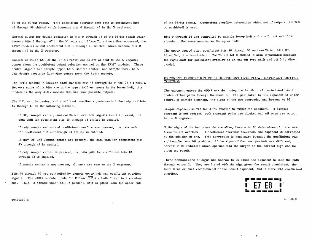
96 of the 97-bit result. This coefficient overflow data path is coefficient bits
49 through 96 shifted which becomes bits 0 through 47 in the X register.
Normal output for double precision is bits 0 through 47 of the 97-bit result which
become bits 0 through ,47 in the X register. If coefficient ,overflow occurred, the
4FK7 modules output coefficient bits 1 through 48 shifted, which become bits 0
through 47 in the X register.
Control of which half of the 97-bit result coefficient is sent to the X register
comes from the coeffiCient output seiection control on the 3FM7 module. These
control signals are sample upper half, sample center, and sample lower half.
The double precision (CP) also comes from the 3FM7 module.
The 4FK7 module in location 5E06 handles bits 45 through 53 of the 97-bit result.
Because some of its bits are in the upper half and some in the lower half, this
module is the only 4FK7 module that has four possible outputs.
The OP, sample center, and coefficient overflow signals control the output of bits
45 through 53 in the following manner.
If OP, sample center, and coefficient overflow signals are all present, the
data path for coefficient bits 45 through 48 shifted is enabled.
If only sample center and coefficient overflow are present, the data path
for coefficient bits 49 through 53 shifted is enabled.
If only OP and sample center are present, the data path for coefficient bits
45 through 47 is enabled.
If only sample center is present, the data path for coefficient bits 48
through 53 is enabled.
If sample center is not present, all ones are sent to the X register.
Bits 54 through 96 are controlled by sample upper half and coefficient overflow
signals. The 4FK7 module inputs for OP and OP are both forced to a constant
one. Thus, if sample upper half is present, data is gated from the upper half
60420300 K
of the 97-bit result. Coefficient overflow determines which set of outputs (shifted
or unshifted) is used.
Bits 0 through 44 are controlled by sample lower half and coefficient overflow
signals in the same manner as the upper half.
The upper unused bits, coefficient bits 96 through 98 and coefficient bits 97,
98 shifted, are terminated. Coefficient bit 0 shifted is also terminated because
the right shift for coefficient overflow is an end-off type shift and bit 0 is dis
carded.
EXPONENT CORRECTION FOR COEFFICIENT OVERFLOW, EXPONENT OUTPUT CONTROL
The exponent enters the 4FN7 module during the fourth clock period and has a
choice of two paths through the module. The path taken by the exponent is under
control of sample exponent, the signs of the two operands, and borrow to 96.
SaIllple exi-".JIJ.ta:..i allows tin:: 4FN7 n~odule to output the exponent. If sample
exponent is not present, both exponent paths are blocked and all ones are output
to the X register.
If the signs of the two operands are alike, borrow to 96 determines if there was
a coefficient overflow. If coefficient overflow occurred, the exponent is corrected
by the addition of one. This correction is necessary because the coefficient was
right-shifted one bit position. If the signs of the two operands are different,
borrow to 96 indicates which operand was the larger so the correct sign can be
gi ven the result.
Three combinations of signs and borrow to 96 cause the exponent to take the path
through output 2. They are listed with the sign given the result coefficient, the
form (true or ones complement) of the result exponent, and if there was coefficient
overflow.
P-----III I E7 E8 I "' .. _IiIa_ .. 1
5-5-8.2

Both Signs Positive
Borrow to 96
+ sign of the result
Output in true form
No coefficient overflow
Both Signs Negative
Borrow to 96
- sign of the result
Output in ones comple
ment form
No coefficient overflow
Unlike Signs
Borrow to 96
+ sign of the result
Output in true form
No coefficient overflow
When both signs are positive and borrow to 96 is a one, there is no coeffi.cient
overflow. Since both signs are positive, the result is positive and expressed in
true form. Complement control 2 controls the form of the result exponent and
adds bias, sign 2 gives it its sign, and output control 2 gates the exponent to the
X register.
When the signs of the two operands are not alike, borrow i.o 96 indicate;' which
operand is larger. In the case of output 2, borrow to 96 is a zero so the
positive operand is the larger of the tIVO. Thus, the sign given the result ex
ponent by sign 2 is positive, and complement control 2 causes the exponent to
be output in true form.
Three combinations of signs and borrow to 96 cause the exponent to take the path
through the exponent plus 1/0 adder and output 1. They are listed with the sign
given the result coefficient, the form of the result exponent, and if there was
coefficien t overflow.
Both Signs Positive
Borrow to 96
+ sign of the result
Output in true form
Coefficient overflow
60420300 K
Both Signs Negative
Borrow to 96
- sign of the result
Output in ones comple
ment form
Coefficient overflow
Unlike Signs
Borrow to 96
- sign of the result
Output in ones comple:
ment form
No coefficient overflow
c
When both signs are positive and borrow to 96 is a zero, there is a coefficient
overflow. The exponent takes the path through the adder where plus 1 causes
the adder to add ones to the exponent. Complement control 1 causes the exponent
to be output in true form and adds bias, sign 1 gives the result coefficient a
positive sign, and output control 1 gates the result exponent to the X register.
Complement control 1 also ensures that the exponent correction for coefficient
overflow does not result in the unit sending out a negative 0 exponent. If both
signs art;. positive and the exponent takes the path through output 1, it is because
coefficient overflow and the adder add one to the exponent. In this case, if the
exponent is negative 1, the addition of one results in a negative 0 exponent.
Complement control 1 senses this and causes the 4FN7 module to output a
positive O.
When the signs of the two operands are not alike and borrow to 96 is a one,
there is no coefficient overflow. The exponent takes the path through the adder
but plus 1 is a zero because the signs are not alike. This causes the exponent
to pass through the adder unchanged. Complement control 1 causes the exponent
to be output in ones complement form, and sign 1 gives a negative sign to the
result coefficient. In this case, borrow to 96 indicates that the negative operand
was the larger of the two.
The resultant leaving output 1 of the 4FN7 module is exponent positive 1/0 bits
48 through 59 and goes to the destination X register.
The result leaving output 2 of the 4FN7 module is exponent bits 48 through 59
and goes to the destination X register.
5-5-8.3

FAD 3.2 TEST POINTS
Module Location Test Point Description Module Location Test Point Description Module Location Test Point Description
4FI7* 5011 34 Bit 90 enable 4FK7'~ 5E01-11 (No signal/rgtr TPs) 36 l"j 4FL7* 5012 (No signal/rgtr TPs) 56 92 45 93 . 4FN7* 5C07 (No signal/rgtr TPs) 46
iL98 52 25 74
Bi<" '"<r 75
191 76 93 73 94 24 96.97 66 Group enable bits 90-92 61 ! 93-95 43 90-95 35 Group borrow bits
90-92 71 Group borrow bits
93-95 42.63 Section enable bits
90-96 31.53 Section borrow bits
90-96 22 25-nanosecond clock
4F.T7'~ 5001-10 32 Bit N enable 33 N+l 45 N+2 44 N+3 65 N+4 66 N+5 55 N+6 54 N+7 56 N+8 71 Bit N borrow 74 r" I 72 N+3 75 N+4 73 N+6 76 . N+7 62 Group enable bits
N-N+2 61 Group enable bits
N+3-N+5 31 Group borrow bits
N-N+2 46 Group borrow bits
N+3-N+5 .-----., 43.63 Section enable bits
I E3 E4 I N-N+8 34.53 Section borrow bits
1 _____ --N-N+8
I 60420300 K
5-5-8.4
(]

1:!f!:!I$012
SHIFTED SI8N
FAD 30D [.--1r··~'-"~"!!:N~_------, I. G~~~I~~A~~~~i~~s I;~~'$ ,,=,-'-=_.l-____ ~ & COEf OVERfLOW OETECTION
GROUP ENA8LES. OVERFLOW: BITt 90·n
10RROW iOiiiiOii IREF SIGN NEG-SHIFTED SIGN NEG BORROW TO '61. 'REF SIGN POS
SHIFTED SIGN POS iOiiiiOi TO '6' :~~~~~"s 1.11 PRO::G:~ION~ I-...!!!~~.!.:.!C~~;i), >+- NETWORK 801tR0W TO ,a:
GRQUP aORRO'!!,- BORROW PROPAGATED INTO 8IT'.
BITS 90.U"i!J"
10RROW TO 9.
~ ao:: :ox:. OUTPUT
r;;u- OUT"UT COIIT NO. I' lOT" IIWlO'- OUTPUT CONT NO.1
~ II!::~~?~~::""LE U .. f-!."" •• =..::NOe;. . .!.' ______ --, ~ COMPCONT
:::PLE CO .... CONT NO.1! 80T" SI8NI NI8 NO.2 'r:"I
~.'~"::":T ':::.0-1-......... """ @ I I m ,..--OUTPUT NO.2-, UP
3 UP BITS 0·' ~H!.o)D-L.~~-.. -<!T}OJD ... 't]';'H-~'~-----+;;;.'.:;TS:.. .. ,;;...; .• ::.]CI'IJ .... II ,--OUTPUT NO I -.. I EXP + 110 (X RGTR}
COM'
(<)
U. IITS 0·10
U .. IITSO-IO 'ii'
I EXP IITS 0-10
I :::·:~ r ' LT::D":'::"~ __ -4-+'l-__ "L~~T~: Sl8NS ALIIlE
SHIFTED FAD 3.0B SIGN
.EF
1 GROUP ENABLESflITS '0-1$
d!!.J~DII SHIFTED. REf OPERAND 8ITS ,o-n, I (!) SHIFTED. REF SIGN BITS <1'1
~~
""'D. " ..... ~ ] <D 'ADIOD ..l'W"!!!N~_I_.l....jr-_ • 10TH $IGN' NEG·E."".-I [·~:!!:'-:F!!:~!!·::.-I-.I....j r __ CO::T~O:I~:IO· .. ~S . E ..... I • SIGNS_
~ " ~:"D :; ~rx!. 'Ii ';' 1i 1IT'41-5'
h CONT <i>
CO .... CONT NO.1 •
SIGN FAD 3.10
~$0I0 SHIFTED. REF OPERAND BI TS BI-.' IA .... I.E .-"""'-'~-l-""'-- .... NO.1: 80TH SIGNS "01
SI ... NO.1
FAO "0
'AD 1.le
FAD 3.10
I--l .... T2 -80
--.Ji5D08
----1~OO7 SHIFTED. REF OPERAND BITS 54-II!,
4FJ715006 SHIFTED OPERAND BITS 45 -53. - REF OPERAND BITS 41-n. SIGN
81T ENABLES
r·::.'T::' ... ::. • ..:-';:,'----<: ... !)-oI :::.ii:..Hi~.:!'.!-T .!. •• :::.!!.L:!'!. ..... ~
. , UCTION" t;NA8U.1
~~""""~_--+---+-_-... 'AD 30B SAMPLE UP"R "AU
GROU;~ 8ITS,0-9S b
OU::RUR~WC~:TI:~ ~~~~7£H EI:::O~~' - f-!D~UT:;."'UT'__"CD"."_T.!.~D.o!' ___________ ___l
~. 80RROW TO '.-SAlilPLE E. L--_
r- IITS 10-,1 (!)
---15E10 81-89
~5EO' n·.o
--.J .... 13 .. .,1 --.J .. ., 54-.1
SHIFTED SHIFTED OPEIIAND OPERAND
___ .'_T'~D.~.~.~ ~.,-T'-{.~~ ... -.e~}_--~~
GROUP ENABLES-815 45-50 2
I ~5E06 ~ITS 45'"
e:'-'~;:.~',;:;~,,,N • .:::;::..A_"_' .. SEE:;~~;L..,o{!'~.N~D~UT!}!:!!!:~!!~L:!'~'-· ..... ;:(i)++_----~ '+_--+__, • 8IT [NAlLlS
,. REGISTEM r I L ___ ~~_ .... _~ ~-{~ilz ,..e'!!!u!!:. • .!!!.! ••• '!W~ ..
.EF OPERAND BITS 4!;9i5
REF OPERAND BITS 47-53 SIGN EXTENDED
SHIFTED OPERAND + REF OPERAND FIRST
, alTs "'-55 i ~::T~I:S 49-53 ~:f:T:JTS 4'-88
U.~' ,:,46 ST~£
V BIT BORROW BITS 45.46,48, 04'.51.52 ..!.. .:~:ow 'i BIT 80RROW
REGISTER
..s ECTION~,·."·TLE.DI 'i'ii'f'i"'4i:ii COl' IITI "8-SS .no COEF 811$ 48·95 ]
~ ;~~::D .,!, ~ ';' COEF 8ITS 4"-47 ~ COU 81TS 0-47 IX ROTR} ~~W~~:.tN ~ CPu ....
GR~~ I - COEF .ITS 4$-4' COEF BITS 1·48
l_~ .. ~T.lr--~==-.~.~~':=t-~~~~~:::::::::t::::::==l ~~.~'T~.~D~ .. ~D~W'~ L-« __ .~ .. ~T'~'~ . .:::-.~.~~-44ft;~.~H~'F~T~.DL---t~ ~~~~.H~"~T~.D~---+--r.o. * GROUP 80RRDWS -
SECTI~~ stCTION 80RROW SECTION • ~ I
L-.~'.:;T~~·~·~··::· ____ ~~;~g~~[~~N~o.r"~T~·D~.~.D~W~~ ~~~IT,,~~_+----t--@~4--J -~ -
-.... REF OPERAND SIGN BITS r --.JSD04 27'- n. !'~F""~71":~:'~'H~'~'T~E~D~D~.E~.~AN~D~.~"~'~'~.~-.~'~'======================1tI·~"~T~'D~.~'~.~~~.~L.~r!=] <D ~i5D03 SIGN 81TS 18-tl, r
COE" OVERFLOW
---15002 SIGN 8ITS '-17 r SIGN BITS
illIJ!001 ~~~~~OER~::~~~N8~~~SO-.. SECTION I INA8Ll
NOTES. CD SECTION ENA8LES FANOUT 70 OTH£R 10 SECTI ONS.14FK1 MOOULESI, NOT TO CORRESPONDING SECTIOft
SECTIONS HAVE THE SAME NUMBE .. A8 THE LAS7 TWO 011lT8 OF THE NODULE LOCATION NO.
C%) 4FI1 MODULE HANDLES SEVEN BITS IN THE SAME WAY 4FJ1 MODULES HANDLE NINE.
(]) ON ALL 04F1l1 MOOULES EXCEPT LOCATION ~E06. DP ANO 'D'Ji ARE EOUAL TO LOGICAL ONE
@ 81T ENABLE 96 IS EXTENDED TO BIT ,1 AND 91 IUNUSED POSITlON8I ON 4FK1 NODULE 'T LOCATION 1111.
@) SHIFTED SIGN AND REF SIGN 10 TO BIT '6.
$ BIASING.
FAD 108 SANPlE LOWER 1fAl' c»
--...!1 SEC ION 8DRRrDW_· ___ ~oEJ. ,-----__ ..1
.!Lr.
17·11
II-II
'-17
~:iEOI 1171 D-B
r-----I I E 1 E2 I .. _---...1
COEF 81T 0 SHIFTE.D
DETAILED ... MOaUlE.S DIAGRAM ADDER I CDEF OUTPUT SEl; COEF OVERFLOW DETECTION· EXP OUTPUT CONT, OUTPUT '
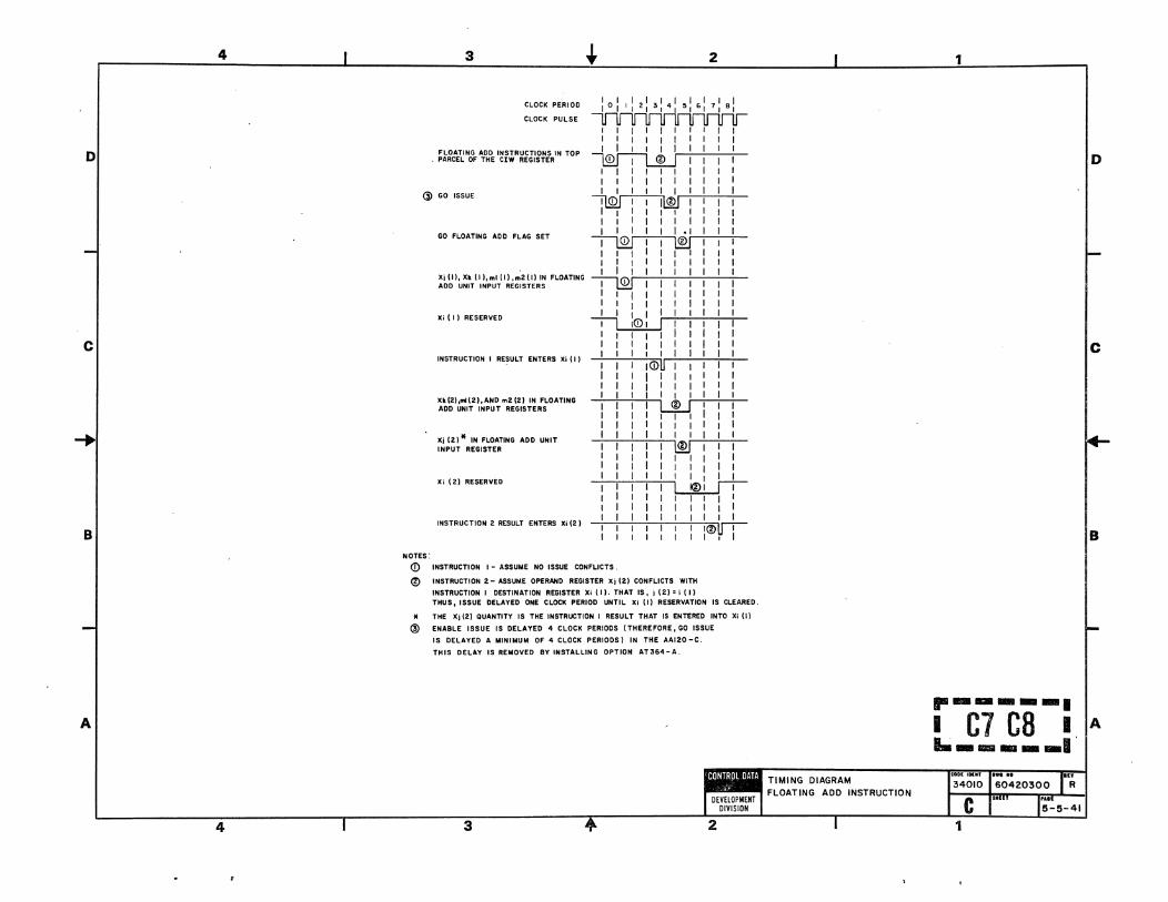
4
c
B
A
4
3
CLOCK PERIOD
CLOCK PULSE
FLOATING ADD INSTRUCTIONS IN TOP . PARCEL OF THE CIW REGISTER
2
a> GO ISSUE
NOTES:
(i)
o
" @
GO FLOATING ADD FLAG SET
Xi (I), Xk (I), ml (I I. m2 (I) IN FLOATING ADD UNIT INPUT REGISTERS
XI ( I) RESERVED
INSTRUCTION I RESULT ENTERS XI (I)
Xk(2),mlI2), AND m2 (21 IN FLOATING ADD UNIT INPUT REGISTERS
Xi (2)" IN FLOATING ADD UNIT INPUT REGISTER
(i) U..-!--!-...!.-..;-!...
I I I
~ I I I
1mJ I I I I I I
XI (21 RESERVED ~
INSTRUCTION 2 RESULT ENTERS XI (21
INSTRUCTiON I - ASSUME NO ISSUE CONFLICTS.
I I I I I I I I I I I I II®~ I I I
INSTRUCTION 2 - ASSUME OPERAND REGISTER Xi (21 CONFLICTS WITH
INSTRUCTION I DESTINATION REGISTER XI (II. THAT IS, i (2) =; (II THUS, ISSUE OELAYED ONE CLOCK PERIOD UNTIL XI (I) RESERVATION IS CLEARED.
THE Xj(21 QUANTITY IS THE INSTRUCTION I RESULT THAT IS ENTERED INTO XI (I)
ENABLE ISSUE IS DELAYED 4 CLOCK PERIODS (THEREFORE, GO ISSUE
IS DELAYEO A MINIMUM OF 4 CLOCK PERIOOS) IN THE AAI20 -C.
THIS DELAY IS REMOVED BY INSTALLING OPTION AT364-A.
D
c
B
p-----, I C7 C8 I A .. _____ 1'
TIMING DIAGRAM FLOATING ADD INSTRUCTION

PART 6
LONG ADD UNIT
r--., I 01 I 1 ___ 1

LONG ADD UNIT
The long add unit executes CPU instructions 36 and 37. It performs a 60-bit
integer addition to X register operands specified by the j and k portions of the
instruction and delivers the 60-bit sum to the X register specified by the i por
tion of the instruction. Prior to addition, the unit complements the Xk and Xj
operands for the 36 instruction (integer sum) and only the Xj operand for the 37
instruction (integer difference).
The long add instructions require 2 clock periods for execution. The operands
move from the X registers to the long add unit in the same clock period in which
the instruction issues from the CIW register. The result moves from the long
add unit to the destination X register during the following clock period. A new
instruction may issue from the CIW register for execution in the long add unit
each clock period.
The long add unit complements the operands as specified by the instruction code
and forms a partial sum in the first stage of addition. The partial sum enters
the second stage of the adder where the result is formed from the partial sum.
At this point, the result is in ones complement form. The go long add flag,
sent from the CPU, gates this sum to the result X register through a static
network which complements it to return it to true form.
Adder Format:
59 11 2 0
lIT 1 X X X X X X X X X X X ~I Xk
X X X X X X X X X X X Xj
Section Group
FIRST STAGE
The first stage of addition forms a partial sum which consists of bit enables,
bit borrow generates, group borrow generates, section borrow generates, and
section enables. Group enables are also generated but are not sent to the
second stage of the adder.
60420300 K
o
Bit enables or
Bit borrow generates
Group borrow generates
Example: 110
010
000 or
101
110
011
o
o
borrow-out of three-bit group
Group enable = all bit enables in group equal to one
Section borrow generates = borrow-out of 12-bit section
Section enable = all group enables in section equal to one
SECOND STAGE
The second stage of the adder forms group borrow inputs and bit borrow inputs
from the partial sum. An exclusive OR of the bit borrow inputs and the bit
enables forms the sum. The sum at this point is in ones complement form.
Group borrow inputs = borrow into group
Bit borrow inputs = borrow into bit
.---_ ..... I 05 06 I 11IlIIIi1lllliJ .. _ ....
5-6-0.1

Example:
The following example uses a 12-bit adder performing a 36 instruction. In this
case, the section borrow generate is the end-around borrow. In the case of the
long add unit, it is the section borrow from the highest-order section.
36 Instruction Example:
4470 Comp 3307 011 011 000 111
1532 Comp. 6245 110 010 100 101
6222 101 001 100 010 Bit enables
010 010 000 101 Bit borrow generates
1 0 0 1 Group borrow generates
1 Section borrow generates
0 Section enable
0 0 Group borrow inputs
100 100 001 111 Bit borrow inputs
001 101 101 101 Exclusive OR of bit
borrow inputs and bit
enables
110 010 010 010 Comp
6 2 2 2 Sum (octal)
60420300 K
.---IIII!IIII-li I D7 D8 I L_"_IIIBl!II_1
5-6-0.2

FIRST CLOCK PERIOD SECOND CLOCK PERIOD
BIT ENABLES
I I
BIT BORROW GENERATES I
~ I 1 I
I I GROUP SECTION
--1-- ENABLES BORROW Xj BIT,b." - 59 INPUTS - I '-7 BIT ENABLES
--L AND SECTION BIT BIT BORROW -- GMOUP ~ BORROW BORROW --Xk BlTbO-59 GENERATES BORROW GENERATES I INPUTS
COMP GENERATES '-" T I GROuP
mO ENABLES
CPU
I
I I
I GROUP BORROW GENERATES
FIRST STAGE SECOND STAGE
EXCLUSIVE OR OF
BIT EN AILES AND
liT BORROW INPUTS GO
CPU LON' ADD
PRIMARY BLOCK DIAGRAM
LONG ADD UNIT
Xi 8ITS~-59
; ....,. CPU
r-----., I D3 04 I 1_l1li8 ___ '"

4KC7 6B05 BITS 48-59
6804 36 -47
6803 24 -35
6B02 12 -23
e---@ X) BITS 0-,59 14KC7 6BOI BITS 0-11
CPU 2.2
o 60}-X-,k'-'..B_' T-,S_O...,-~5_9--<! Xi +Xk FIRST STAGE
( LG ADD 3.0)
SECTION 5 ENABLE
J ' /
CD SECTION 4 ENABL£
SECTION 3 ENABLE
CD I, SECTION £: ENABLE
SECTION I ENABLE
4KD7 6C05 BITS 48-59
6CD4 36 -47
SC03 24 -35
SCOZ 12 -23
4K07 SCOI BITS 0-11 -l
SECTION BORROW
~ GENERATE.
81T BORROW
(-@ GENERATE
~ BIT ENABLES
GROUP BORROW
f-® GENERATE
GO LONG ADO CPU 2.18
J ,
NOTE:
CD SECTION
CD SECTION
SECTION
SECTION
SECTION
t
x i BITS 0-59
6O~---f:U~~ Xi + XII. SECOND STAGE
( LG ADD 3.0)
I ENABLE GOES TO 6COZ. eC03 I SC04, ecoe
2 ENABLE GOES TO SCO I ,SCDS, SC04, SC05
3 ENABLE GOES TO 6COI .6C02. eC04. 6C05
4 E HABLE GOES TO 6COI I 6CO! ,8C03,6CO&
5 ENABLE GOES TO 6tO I ,6C 02 I eco,. 6C04
.... _ .. I11III ....
I D11 012 I II .. IiiJI6 .., ... 11m ad
SECONDARY BLOCK DIAGRAM
LONG ADD

LONG ADD UNIT
The long add unit executes CPU instruction 36 and 37. It performs a 60-bit
integer addition to X register operands specified by the j and k portions of the
instruction and delivers the 60-bit sum to the X register specified by the i
portion of the instruction. Prior to addition, the unit complements the Xk and
Xj operands for the 36 instruction (integer sum).
The long add instructions require 2 clock periods for execution. The operands
move from the X registers to the long add unit in the same clock period in which
the instruction iss'ues from the CIW register. The result moves from the long
add unit to the destination X register during the following clock period. A new
instruction may issue from the CIW register for execution in the long add unit
each clock period.
60420300 K
During the first clock period, the 4KC7 modules complement both operands. If
the instruction is integer difference (37), m bit 0 is a one and the 4KC 7 modules
recomplement the Xk operand. After complementing, the operands enter the first
stage of the adder.
The first stage of the adder is divided into two parts. The first part forms the
bit ena~les, bit borrow generates, and group borrow generates. Registers hold
them for use during the second clock period. The second part of the first stage
of addition takes place during the second clock period. It forms the section borrow
generates and section enables.
The 4KC7 modules send the partial sum to the 4KD7 modules where the second
stage of addition takes place. Go long add gates the result from the second stage
to the result X register.
."'_IIIIIIII_-. I E5 E6 I 1_lII'IIIIIl1'JIIIIIlI!III_aI
5-6-4.1

LG ADD 2 0 TEST POINTS
Module Location Test Point Description Module Location Test Point Description Module Location Test Point Description
4KC7':' 6B01-05 35 Bit N enable 33 N+l 31 N+2 42 N+3 44 N+4 46 N+5 52 N+6 54 N+7 56 N+8 65 N+9 64 N+10 61 N+ll 36 Bit N borrow 34
j""' j 41 N+3 43 N+4 51 N+6 53 N+7 66 N+9 63 N+10 32 Group N borrow 45 ! N+1 1 55 N+2 72 Section enable 71 25 -nanosecond clock
4KD7':' 6C01-05 71.72 Go long add
ra----' I E3 E4 I I ... ___ .. d
I 60420300 K 5-6-4.2

CPU 3.41. [Xi BITS 0-59
Xk BITS 0-59
4KC7 6605 BITS 48 -59 6B04 36 - 47 6B03 24- 35 6B02 12-23
4KC7 6BOI BITS 0 - II
CPU 3.18 -!"'=O ___ --4I-____ -------l (CrW)
NOTE:
CD SECTION I ENABLE GOES TO 6C02, 6C03,6C04, 6C05
® SECTION 2 ENABLE GOES TO 6COI, 6C03, 6C04, 6C05 SECTION 3 ENABLE GOES TO 6COI, 6C02, 6C04, GC05 SECTION .4 ENABLE GOES TO 6COI, 6C02, 6C03, 6C05
SECTION 5 ENABLE GOES TO 6COI, 6C02, 6C03, 6C04
o m' I RECOMPLEMENT Xk OPERAND
,,,n~, '~'''l 4KD7 6C05 BITS 4B -59 SECTION 4 ENABLE ® 6C04 36-47 SECTION 3 ENABLE
6C03 24-35 SECT I ON 2 ENAIII.E 6C02 12~23
4K07 6COI BITS 0-11
SECTION ENABLE CD SECTION BORROW
5 GENERATE
BIT BORROW GENERATES
Xi alTS 0-59 CPU 3.41.
IX RGTR)
15 GROUP BORROWS
CPU 3. 28 _...:GO~l~O~NG~A~D~O~ 1-___ -",G=.O...:l::::ONG=.:A:::D=.O-.....J
.. -_ ... _-. I E 1 E2 I 1.-___ ..1
DETAILED-MODULES DIAGRAM LONG ADD UNIT

4
D
c
B
A
4
NOTES:
3
CLOCK PERIOD
CLOCK PULSE
TWO SUCCESSIVE INSTRUCTIONS THAT USE THE LONG ADD IN THE TOP PARCEL OF THE tIW REGISTER
@ GO ISSUE
GO LONG AOD
RESULT REGISTER Xi RESERVED FOR INSTRUCTION I
INSTRUCTION I RESULT ENTERS THE XI REGISTER
RESULT REGISTER XI RESERVED FOR INSTRUCTION 2
INSTRUCTION 2 RESULT ENTERS THE XI REGISTER
<D 36 I jk (ASSUMING NO ISSUE CONFLICTS EXIST).
2
® 37 Iii (OPERAND REGISTER CONFLICTS WITH INSTRUCTION I DESTINATION REGISTER).
@ ENABLE ISSUE IS DELAYED 4 CLOCK PERIODS (THEREFORE, GO ISSUE
IS DELAYED A MINIMUM OF 4 CLOCK PERIODS) IN THE AAI20-C.
THIS DELAY IS REMOVED BY INSTALLING OPTION AT364-A.
3
o
c
B
'-I!III .. I111111 ....
I F5 F6 I A ... II1I&I IIIi!I!I!I DIll IIiII!I mill &IS
TIMING DIAGRAM LONG AOO INSTRUCTION

PART 7
MULTIPLY UNIT

MULTIPLY UNIT
The floating-multiply unit executes the following three instructions.
40 Floating product of (Xj) times (Xk) to Xi
41 Rounded floating product of (Xj) times (Xk) to Xi
42 Floating double-precision product of (Xj) times (Xk') to Xi
The Xi coefficient and Xi exponent are formed separately with consideration
taken for single or double precision. If single precision is specified, the upper
half of the coefficient result and an exponent (corrected for single precision) are
sent to the X register. For double precision, the lower half of the coefficient
result and the exponent result are sent to the X register.
If both operands are normalized, the result is normalized. If rounding is
specified, a round bit is generated and added to bit 46 of the coefficient result.
The multiply instructions require 5 clock periods for execution. Multiply instruc
tions may enter the multiply unit every other clock period. Thus, dl!:dng a ,,
clock-period segment, more than one multiply instruction may be active in the
unit.
COEFFICIENT MULTIPLY
Coefficient multiply is basically the same as a multiply done with paper and
pencil. Every bit of the multiplier is multiplied by every bit of the multiplicand.
In binary arithmetic, this is the AND (logical product) function.
As in pencil and paper multiplication, the bit-by-bit products are arranged in a
matrix as shown below with each row offset by one bit. The columns of the
matrix are then added to obtain the final product, Xi.
60420300 K
.10 1
jl. k5
/'k5 l'k4
j3. k5 j3. k 4 j3. k3
/ k 5 j4. k4 j4. k3 j4. k2
j5· k4 j5· k 3 j5· k2 j5· k 1
.9 1
.8 1
.6 1
jO'k5 jO'k4
l'k4 /'k3
j2. k3 j2. k2
j3. k 2 l. k 1
j4. kl j4. kO
j5·.k O
.4 1
j2· k l j2· kO
j3, kO
.2 1
.0 1
Xk
Xj
Final product Xi
The multiply is performed in two steps. First, the lower 24 Xj bits are multiplied by
all 48 Xk bits. and the columns of the resulting matrix are partially added. The upper
24 Xj bits are then multiplied by all 48 Xk bits and the resulting matrix is added to
the partial sums and carries from the first pass to form the 96-bit double-precision
product. Each step in the process involves forming 1152 binary products. These 1152
bits of data must then be added in the proper groupings to form a combined sum.
IIiIIiiIi IIIIIi!lI III'liIlI al R!I .,
I B5 86 I LIlilllllIllliilIImlIlllllllBliI
5-7-0.1

60420300 K
The multiply in the previous example appears as follows when executed in two steps.
First pass
jO'k5 jO'k4 jO'kS jO'k2 jO'kl jO'kO
jl'k5 jl'k4 jl'kS jl'k2 jl'kl jl'kO
;'k5 j2· k4 j2· kS j2· k2 j~kl ;'kO
Partial sums Partial carries
Second pass
ps7 pc7
ps6 pc6
ps5 pc5
ps4 pc4
psS pcS
jS'k5 jS'k4 j3· k S jS'k2 jS'kl jS'kO
j4. k5 j4. k4 j4. kS j4. k2 j4. kl j4. kO
j5· k5 j5· k4 j5· k3 j5· k2 j5· k l j5· k O
pslO
pclO
ps9
pc9
pslO ps9
pclO pc9
psS
pcS
psS
pcS
ps7
pc7
ps7
pc7
ps7
pc7
ps6
pc6
ps6
pc6
ps6
pc6
ps5
pc5
ps5
pc5
ps5
pc5
ps4
ps4
pc4
ps4
pc4
psS
pcS
ps3
pcS
ps2 pc2
psi
Results of first level add
ps2
pc2
ps2
psi
psi
PSO} Results of first, second, and third level adds
} Add
psO loop bits . from first pass
PSO} Results of second and third level adds
~----------------------------~--~--~--~-i4 is i2 i l iO Final add .6
1
In a 24-by 4S-bit multiply, in order to handle 1152 bit products in the matrix, the
summing is performed in .several more stages; there are several more levels of sums
and carries. Because of the size of the matrix, there are also several sums or carries
per bit position at some levels of the multiply. Since a complex carry network to re
solve all the carries requires excessive time and hardware, the multiply unit employs
a carry save adder for efficiency.
Using these inputs, the first half of the adder forms pseudo sums and pseudo carries.
,-----. I 87 88 I 1.-___ ...1
5-7-0.2

CARRY SAVE ADDER
The carry save adder permits the addition of columns of numbers without using
the time-consuming carry and satisfy checks typical of full adders. Instead,
each level of add has two outputs, pseudo sums and pseudo carries.
0
Pseudo sums
0
Pseudo carries 0 0
0
1
0
0
0
0
0
0
0
0
(Pseudo carries are displaced. one bit
to the left because they affect the next
significant bit position.)
The sum of these two numbers is the actual answer; however, the sum is not
taken until the final add. Instead, both quantities are put back into the next
level of the adder and are summed with other pseudo sum and carry bits that
represent the same bit position of the final product (that is, sums of bits
in the same column of the matrix or carries to that column).
The inputs to the first level add are the logical products produced by the
matrix. The inputs to the second level add are the pseudo sums and carries
from the first level add. The inputs to the third level add are the pseudo sums
and carries from the second level add. The output from the third level add is
a pseudo sum and carry bit for each bit position of the product.
After the first pass, the output from the third level add is right-shifted 24
places, fed back into the second level add, and added to the results of the
second pass through the matrix. The second and third level adds are then re
peated for the entire product until a pseudo sum and carry bit again represent
each bit position of the product. This time the output of the third level add is
fed to the final add network and is reduced to one bit for each bit position of
the final product (96 bits).
60420300 K
EXPONENT FORMATION
Two adders are used for the formation of the final exponent. The first adder
is a half adder that forms the sum of the complemented exponents of Xj and Xk.
When single precision is selected, this adder adds 60 (octal) to the exponents to
compensate for truncating the coefficient of the product in single-precision mode.
The second adder subtracts one from the result of the first adder if the coefficient
is left-shifted one place to normalize it.
The exponent logic also examines the incoming exponents for special cases in
volving overflow, underflow, or indefinite operands before performing the
additions. Upon receiving the output from the first adder, the exponent logic
checks the result for overflow or underflow of the floating-point range, SUIIl
marizes the special cases, and sets the appropriate special case flags.
Xj + Xk + 60 (OCTAL) ADDER
The Xj + Xk + 60 adder is a static network that sums the two exponents in ones
complement mode during the second and third clock periods of instruction execu
tion. For purposes of this discussion, the exponent portion of the multiply
operand (bits 48 through 58) is referred to as bits 0 through 10.
The add network for bits 0 through 3 and 6 through 10 is a two-input adder that
sums Xj and Xk. Bits 4 and 5 of the add network, however, have three inputs
to allow the single-precision correction to be made. The following example
illustrates the adder inputs.
Bit
Xj
Xk
Correction
10 9 8 7 6 5 4 3 2 1 0
1
1 1
1 0 1 1
101
1
o 1
o 0
rr-lfillllIii!JlBliliiBll I B9 810 I IiII!IIIIIJ II'R! I\t£.;j m:.! IIlIlI ..
5-7-0.3

Using these inputs, the first half o,f the adder forms pseudo sums and carries.
The second half of the adder uses the pseudo sums and carries to determine
enables and carries for three-bit groups. The add network resolves the enables
and carries to form the complemented result.
MINUS ONE NETWORK
The minus one network subtracts one from the output of the first adder by adding
one to the comple'cllent. This add network takes into account any end carry
condition and also makes carry propagat~on checks. Bit 10 is 'compleme~ted to
add the exponent bias value. The complemented output of this add network (true
output) is gated to the X I register when the coefficient has been left-shifted one
place to normalize it.
60420300 K
An alternate network, with no minus one correction, is used when the coefficient
is already normalized or cannot be normalized by a left-shift of one. This
alternate network merely forms the exponent bias and complements the output
so that the true exponent goes to the X register.
CONTROL
Multipl~ busy is the primary control signal in the multiply unit. It is set in
the CPU at the end of the clock .period in which a floating-multiply instruction
issues from the CIW register. The flag is copied to other register ranks as data
is processed by the unit. The flag blocks input to the multiply unit in the clock
period immediately following instruction issue. This flag and copies of it
control data movement through the multiply unit.
..----.., I 811 812 I L .. ____ I'I
5-7-0.4

XI SIG
(CPU) BIT 59
X, SIGN
ICPU! BIT 59
XI EXPONENT BITS 48-58
ICPU!
Xk EXPONENT COMPLEMENT IF
ICPUI BITS 48-58 Xk NEGATIVE
DOUBLE PRECISION ICPUI I1:NHI8IT ADD OF 808 1
EXPONENT
ROUND (SECOND PASS ONLY)
Xi COEFFICIENT LOWER HALF
ICPUI BITS 0-23 COMPLEMENT IF xi NEGATIVE
Xi COEFFICIENT UPPER HALF BITS 24-47 COMPLEMENT IF
(CPU) Xl NEGATIVE
Xk COEFFICIENT (48 BITS)
ICPUI BITS 0-47 COMPLEMENT IF X k NEGATIVE
RGTR NO. I
COEFFICIENT
~ __ .....! FIRST PASS: SELECT LOWER HALF.
SECOND PASS:
J..----01 ~!t~CT UPPER
SAMPLE EXPONENT AND GATE lOOP
RESULT SIGN CONTROL
SPECIAL CASE SIGNALS
NORMALIZATION CORRECTION
FORM 24 X 48
LOGICAL PRODUCTS
} TO )C REGiStER INPUT CONTROL
(CPU I
Xi
XI I FOR SHIFTED COEFFICIENT)
} EXPONENT TO X REGISTERS
(CPU)
FIRST PASS FEEDBACk LOOP (RIGHT SHIFT 24)
RGTR NO.2
NOTE
RGTR NO.3
N o R II A L I Z E
CD
(i)
COEFFICIENT TO X REGISTERS
XI UPPER HALF
SHIFTED I
ICPUI
(8ITS 41-M) ICPUI
Xi LOWER HALF
(IITS 0- 47 LEFT SHIFTED I PLACE)
IC PUI
XI LOWER HALF
(BITS D-47) (CPU)
ICPUI-------------...::.=.:......::=~ GATE EXPONENT RESULT
AND CD ALL OPERANDS ARE TREATED AS POSITlVE.1:F RESULT IS TO
BE NEGATIVE I THE RESULT IS COMPLEMENTED INTO THE
MULTIPLY CONTROL CHAIN
GATE COEFFICIENT RESULT I CPUI
am----., I 83 84 I 1 .. __ IBlII_aI
X REGISTER By THE X REGISTER INPUT CONTROL
IF BOTH OPERANDS WERE NORMALIZED AND THE RESULT IS NOT
NORMALIZED A LEFT SHIFT OF I IS PERFORMED. THIS WILL
PRODUCE A NORMALIZED ~ESUL T.
PRIMARY BLOCK DIAGRAM
MULTIPLY UNIT

'" D,!:. CORR(AOO 60~ IF SINGLE PRECISION)
j I GATE MULt
~FI6.--- ~G16 I:~~_~~.P~O_~~,!! 3BA71 H 16 ~H14 ~~~MU~~~I ~H15 CPU 2.0B~ mo,ml
Xk ICA~S (CIW) PU 22A _ Xk EXPONENT C\ ~ CPU? -BITS 48~59 = EXPONENT - SUM - '--' SUM - SPECIAL CASE I OVERFLOW, EXPONENT
Xi g~g~g~:;N HOLDING Xj AND Xk xj ,Xk Xi AND Xk UNDERFLOW, INDEFINITE, INDEFItlITE- MULTIPLY GATE EX PON ENT RESULT -fi2l-: I CPU2.taMULT BUS' REGISTER FIRST HALF OVERFLOW SECOND HALF
I, INFINITE, PRODUCT SIGN CONTROL INDEFINITE-I, "7 BITS 48-59
~~g~~N~~~ '" INFINITE --f2H..-- CPU HOl DING }"" ~, ,,((j EXPONENT = ~ \,J REGISTER (X RGTR)
~ ~ Lo'op ~ .. ~~ OR = X i EXPONENT BITS 4B-59 =
IMULT 3.5) ''''ULT 3.5) ''''VLT 3.5) CPU 2.IB "ULT BUSY IMULT 3.5) (BX5) (MULT 3.5) \!9 BITS 48-59
xi xk SIGN BITS
IXi+Xii ROUND BIT I I T
-\.V j
4GA CI6 ~~-~~ 4G 47 = LOOP BITS -8---J Xk SIGN, CI5 :g-:r .4 .. = CI4 1:-~ o GATE LOWER HALF, XI SIGN 42 43 BIT 70 OR BIT 9~ SECTION
GATE UPPER HALF CPU2.2B,O~ Cl3 Ti-,~5 40 41 ~GH7 I CI2 :~-, l ~~EDU~~ri'~~~
_., 1F15 ~!~;o. CARRtES '-'
016 2~- riL 3~' 4GG7 ICII ~f14 ~~=~: AND
J 015 24- 27 4GF7 ICIO ~~
ENABLES 12 13 36 37
ICPU 22~~~~0:~:~CIENT = 014 20- 23 4GE7 009 10 II 34 35 SECOND AND PSEUOO SUMS = 013 16- 19 008 14GH7 1012 ~~i AND PSEUDO • 9 2 33 , THIRD
EI6 IZ-I!l D07 4GG7 1011 ~~~ ~b CARRIES • 7 30 31 LEVEL ADDS
~ EI5 8 -II COO :~ 4GF7 1010 ~ -~! @ 45/2829
Icpu 2.l!B Xj COEFFICIENT = EI4 4,7 COB :;' 46E7 IFI~ j4GN7 IGI5 ~;:~~ --' 4GQ7 HI3 88- 95 48X7 11388-951 1l8-'~ 2 3 26 27
BITS 0-47 = ~E13 C07 I FI2 ,48M7 IGI4 ~~-:.~'!. 4GRr HI2 80- 87 4GX7 112 80- 871 80-87
Xk = 0-3 EI2 FII IGI3 ;~:~~ HII 72-79 .GX7 111 72-79 I 72-79
Xj =0,.1/24,25 Ell FlO I GI2 ;;'~,
-< HIO 64-71 <GW7 11064-71 I 64-71
EIO FOg IGII ~~=~ H09,56- 63 ~t;Y/7 109 56 -63 I 56-63 CPU 2.18 MUlT BUSY , -
HOLDING ! E09 F~ I GIO ~~' ~~ HOB 48-55 4GW7 10848- 55 I 48-55
REGISTER ~r<
I EOB F07 I G09 H0740-47 ~ 4GV7 !07W- 471 40-47
AND FANOUT I E07 , FOG GOB 4GR7 HOG 32-39 4GV7 ·!O6 32- 39 I 32-3'
(MULT 3.0) I EOG F05 G07 4GS7 H0524-31 CARRIES
4GV7 !O524-31 I 24-31 I AND
I E05 F04 G06 .GT7 H04 12-23 ENABLES 48U7 !O412-23 I 12 ·23
I~ .. E04 ,
F03 G05 4GT7 H03 0-" ~7_ 1030-11 I -I 'II
@ E03 EOI ... G04 t----'- . -
I HOLDING Xk(0-47) ~;:,:o_'" BIT 70 E02 14GD7 C02 ~~: ~i G03 ' REGISTER AND I N (24-47) OR FiNAL ADD lEFT
BIT 94 002 14G07 I COl ~~ :~! G02 , r-< F"INAl ADD I
FIRST HALF SECOND .HALf SHIFT 001 ~C03~·~~
I ~GOI 37-40 I RESULT
GB7 815 ~~:~ 4GB7 816 i~::~ !4GC7 'A16 006 I BY I 4GB7 AI3 ::~f~ 814 :::~I AI4 ~-~i ',4GC7 AI5 005 ' HOLDING THIRD I
All i8:n BI2 jg=:i AI2 ~::T 14GB7 BI3 , C06 , REGiSTER LEVEL (MULT 33 AND 3 4) MULT 3.3 AND 3.4)!
A09 ~=:~~ BIO ~~:~~ . AIO ~t:~~ iOGB7 BII COS ' ,
-< ADD AND S~CONo
~ B08~:~r A01 :~: ~T ADa ~: _ g~ 14GB7 BOO 14GE7 C04 I _'MULT 3.2) COEF COEF l~r!;E ~~{f~ LEVEL ADD B[TS BITS
4GB7 A05 12 - 19 AOS ~i: ~~ 4GC7 807 14GD7 IDO'l 4GL71 F02 3"o~ l~ 0-47 48-95 Xi=Xj -Xk _ 36-4~
4GB7 A04 8 - 15 ~ B06f.~~ L4GD7 ! 003 i-; I MULT 3.11 ->-,~FOI ,~~;, @ ~ ~ ~nlrE rr Xi=Xj-Xk !--- 32-39
MATRIX ~ B05 2~:; PS ANp PC Xi =Xj _Xk Xi=Xj-Xk
AND FIRST MATRIX HOLDING SECOND AND 1 1/ LEVEL ADD AND FIRST MATRIX MATRIX REGlSTER PSEUDO SUMS THIRD .. AND SECOND AND CARRIES \
LE VEL ADO AND FIRST AND FI RST
LIEJ~tT A30P) LEVEL ADDS V
(MULT 3.0) LEVEL ADD LEVEL AOD CPU 2 2C
(MULT 3.0) 14GJ71 B04 I2-E (X RGTR)
(MULT 3.0) (M Ul T 3.01 ~B03 0-11 (MULT 3.2 j
HOLD[NG CARRIES AND ENABLES
REGISTER NOTES e ~ CD e PSEUDO SUMS AND CARRIES.
Xi ( 0 - 70) FIRST PASS 2. ALL MODULES SHOWN ARE
(24 - 94) SECOND PASS LOCATED ON CHASSIS 7. I MULT 3.1) @ BOTH BIT 70 (FIRST PASS) AND BIT 54 (SECOUD Mea)
ARE SENT TO THE 3BA7 MODULE. BUT ONLY BIT 94 IS USED FOR THE INTEGER MULTIPLY CHEel<.
~ 'C.J PSEUDO SUMS AND CARRIES •• u, •• ,",
SECONDARY BLOCK DIAGRAM
~ ;:\ °60420°300 "y' DIVISION
MULTIPLY UNIT 'M'U'LT 2,0 15~7- ~
fA

LOGICAL PRODUCT OF MATRIX JUNCTIONS AND FIRST LEVEL ADD
INPUT REGISTERS
All instructions performed in the floating-multiply unit require 5 clock periods
for execution. Data ~oves from the operating registers to the multiply coefficient
input registers on the 4GA 7 modules in the same clock period in which a floating
multiply instruction issues from the CIW register. The input registers are cleared
and new data entered whenever the multiply busy flag clears. When the multiply
busy flag sets, the data in the input' registers is held over into the following
clock period. This data is held in the input register for a total of 2 clock periods.
The multiply busy flag serves the purpose of a go multiply flag as well as blocking
further entry to the unit in the clock period following issue. The multiply busy
flag serves as the basic timing control that gates data into the registers of the
unit at the proper time.
As the Xj and Xk coefficients enter the input registers, they are complemented,
if negative, so that the multiply coefficient hardware deals only with positive
numbers. The 12 4GA 7 modules hold 48 Xk bits and 48 Xj bits.
During the first clock period, bits 0 through 47 of the Xk coefficient and bits
o through 23 of the Xj coefficient enter the input registers of the 4GA 7 modules.
The 4GB7 and 4GC7 modules use these bits during the second clock period for
forming the first half of the product. During the first clock period, bits 24
through 47 of the Xj coefficient enter bit holding registers and are held there
until gated into the input registers by the multiply busy Signal in the second clock
period. Xj bits 0 through 23 are discarded at this time. The 4GB7 and 4GC7
modules use Xk bits 0 through 47 and Xj bits 24 through 47 during the third
clock period for forming the second half of the product.
60420300 K
MATRIX AND FIRST LEVEL ADD
The bit-by-bit product of Xk and Xj is formed on the 24 4GB7 and 4GC7 modules
during the second and third clock periods. This product is formed in two passes
through a 24-bit-by-48-bit multiply matrix.
On the .first pass (second clock period), the product of Xk and the lower half of
the Xj coefficient (bits 0 through 23) is formed. During the second pass (third
clock period), the product of Xk and the upper half of Xj (bits 24 through 47) is
formed. Each pass through the matrix produces 1152 binary products, which must
be added in the proper groupings to form a combined sum.
Several bits are produced that represent the same bit position of the product.
(Refer to diagram for 4GC7 module located at B06.) For example, Xi product bit
9 is produced from the following combinations of operand bits.
Xk bit 2 Xj bit 7 Xi bit 9 } First level add pseudo sum bit 9 Xk bit 3 Xj bit 6 Xi bit 9 pseudo carry bit 10
Xk bit 6 Xj bit 3 Xi bit 9 } First level add pseudo sum bit 9 Xk bit 7 Xj bit 2 Xi bit 9 pseudo carry bit 10
The first level add sums these product bits in groups of two or three bits to pro-
duce pseudo sum and carry bits. For example, the first level add of the top two
Xi bits 9 produces a pseudo sum bit 9 and a pseudo carry bit 10. Similarly, the
sum of the lower two Xi bits 9 produces a pseudo sum bit 9 and a carry bit 10.
The first level add of the six Xi bits 8 produces two pseudo carry bits 9. Thus,
four bits are output by the 4GC7 module for Xi bit 9: two pseduo sum bits and
two carry bits.
The results of the first level add (788 bits) are sent to the 4GD7, 4GE7, 4GF7,
4GG7, 4GH7, 4GI7, 4GK7, 4GL7, 4G07, and 4GP7 modules for a second level add.
The result of the add of Xk bit 47 and Xj bit 47 (bit 94) is sent to the 3BA7 module
where it is used in the integer multiply check. If qit 94 is a zero and both oper
ands have underflow exponents, an integer multiply is performed. ,_liliiii ___ • I D5 D6 I 1_ I11III III!IIII _ DIll d' 5-7-4.1

MUL T 3 0 TEST POINTS
Module Location Test Point Description Module Location Test Point Description Module Location Test Point Description
4GA7" 7(C-E) 34 Mult Busy 13-16 04 Xk Bit N
03
1 N+l
24 N+2 23 N+3 41,42 Xj Bit N or N+24 61,62 1 N+1 or N+25 54 N+24 53 N+25
4GB7 7(A04-14, - (No Signal/Rgtr TP's) BOB-16)
4GC7'" 7(A15-16, - (No Signal/Rgtr TP's) B06-07)
r-----, I D3 D4 I
·1 .. liIIIIiII!I!IImIIIII .. aI I
60420300 K 5-7-4.2

I~ I ~ - .
Il) SITS -CPU3.48- 0-47
[email protected]) 81TlIt
CPU 3.2.8------_-1
'" '" '"
". ~m
ItJ BJTS 22,25/46,47
20,2[/44,45
18,19/42,43
16,17/40,41
14,15/38,19
IZ,IH36,U
10,11/54,51S
1,9/32,33
6,1130,31
4,5/21,29
2,5/26,21
XI Ins 0,1/24,U
3$- " l\2-U
J: III liT 1 Olt 25
It B TS ° I HOLt>- FANOUT
~--c;r' COM' L--LJpr..L-----U-'~::AIItI 81TOOll 24t
NEG~~I'I[ z~i!l ~ III SIGN
.... IU.J MULT
NOTES:
CD LOGIC SHOWN IS flEi>RESENTATI'IE OF MATRIX LOGIC i>AODUCTS OF ALL OTHER 8I1'5AR£ SlIllLAfi
2. N'LOWEST ORDER fliT fOR MOOUll
@ NUM8ER SHOWN ODES NOT INCLUDE DUi>UCAT E
4 ALL MODULES SHOWN ARE LOCATED ON CHASSIS 7
~r.,--------~
f It) ~r"-'-"-"-'-"-'-'J~ 24-41 (SECOND PlISS)
4GC7AI6 IlJ BITS IS-23
'" '"
/ It] BITS
12-23
0-11
0-11
12-25
U-35 (UeOND PAUl
YATRIIl JUNCTIONS
It). Ilk
0-11 24-3!!
12-,n 36-47
24-31 (SECOND PASS I
16-21
ilI-" 12-23
24-35
O-Ii
12-23
III BITS 48-!)8 72-1112 ,FIRST PASS) (S[cONO PASSI
56-63
5Z-59
40-47 36-43
XI BITS 12-22
Xi 81TS 0-10 24-34 IflRST PASS) 'SECOND PASS)
G.> MUlT32 THIRDLE'IELADD
11""'-- ....... ., I 01 02 I .. _--_ ....

SECOND LEVEL ADD
The second level add modules receive 788 pseudo sum and pseudo carry bits from
the first level adder and continue to sum groups of bits to form pseudo sum and
pseudo carry bits for each bit position of the result. The resulting bits are held
in registers for 1 clock period.
On the first pass through' the second level add. the only bits summed are from
the first pass through the 4GB7 and 4GC7 modules. However. on the second pass
through the second level add. loop bits from the' first pass through the 4GK7.
4GL7. 4GM7. and 4GN7 modules are merged with the pseudo, sum and pseudo
carry bits from the second pass through the 4GB7 and 4GC7 modules. The
hardware for both passes through the second level adder is the same. except
that the 4GJ7 modules are not used d'uring the first pass. The modules containing
logic for the second level add are 4GJ7. 4GI7. 4GD7. 4GE7. 4GF7. 4GG7. 4GH7.
4GK7. 4GL7. 4G07. and 4GP7. The 4GK7, 4GL7. 4G07. and 4GP7 modules also
contain logic for the third level add.
On the 4GE7 and 4GF7 modules. reference is made to duplicate bits. These bits
are received from fanouts on the 4GB7 and 4GC7 modules. The duplicate bits
provide a means of gen,erating a pseudo carry to bit N from bit N-l. The pseudo
sum for bit N-l is generated by the next lower module. Since separate modules
generate the pseudo sum and pseudo carry bits. duplication of the input bit is
necessary.
FIRST PASS
During the first pass (second clock period). the 4GD7. 4GE7. 4GF7. 4GG7. 4GH7.
and 4GI7 modules receive pseudo sums and carries and sum these bits in groups
to form pseudo sums and carries for each bit position of the low!"r part of the
product (bits 0 through 70). The resulting pseudo sums and carries are held in
registers for use during the third clock period. In the beginnihg of the third
clock period. add logic on the same modules further sums 'the pseudo sums and
carries before sending them to the 4GK7. 4GL7. 4GM7. 4GN7. 4G07. and 4GP7
modules for the third level add.
The 4GJ7 modules are not used during the first pass.
60420300 K
SECOND PASS
During the second pass (third clock period). the 4GD7. 4GE7. 4GF7, 4GG7. 4GH7.
4G17. and 4GJ7 modules merge 141 loop bits (bits 0 through 70) from the first
pass with pseudo sums and carries of the upper half of the product (bits 24 through
94). The loop bits come from the 4GK7. 4GL7. 4GM7. 4GN7. 4G07. and 4GP7
modules and are right-shifted 24 places so that the lower 24 bits enter the 4GJ7
modules and are properly positioned for the merge. Except for the 4GJ7 modules.
the pseudo sums and carries that result from the second level add are held in
registers for use during the fourth clock period. In the beginning of the fourth
clock period. add logic on all except the 4GJ7 modules further sums, the pseudo
sums and carries before sending them to the 4GK7. 4GL 7. 4GM7. 4GN7. 4G07.
and 4GP7 modules for the second pass through the third level add.
The 4GJ7 modules have two loop bits entering for each bit position of the final
product. The two loop bits enter registers on the 4GJ7 modules during the third
clock period and are held there during the fourth clock period when the final add
is performed. This part of the final add generates an enable for each of 12 bit
positions. a carry for each of 9 bit positions. and a group carry and group en
able for each 4 bits of the final product. The output of the 4GJ7 modules goes
directly to the 4GS7 and 4GT7 modules. where the final add is completed.
ROUNDING
If rounding is specified by the multiply instruction. two copies of the round bit
signal enter at bit 46 of the 4GE7 module during the second pass. These two
bits generate a carry into bit 47 of the product during the fourth clock period.
The round bit signals come from the 3KV7 module of the multiply exponent
logic during the third clock period of instruc tion execution.
,----'., I D13 014 I .----_1
5-7-6.1

MULT 3.1 TEST POINTS
Module Location Test Point Description Module Location Test Point Description Module Location Test Point Description
7(COI-02, 25 Second level add bit N I I 46 Second level add bit N+5 4GD7* ·003-04) 34
j N+l
1 31 ~ N+6
22 N+1
1 34 N+6
45 N+l 11,12 25-nanosecond clock 32 N+2 4GI7* 7(B05, C03) 03. Second level add bit N 46 N+2 55 N+2
05 N
56 N+3 01 N+1
01 25-nanosecond clock 02 . N+1 12 N+1
4GE7* 7(C04-09, 24 Second level add bit N 14 N+2 001-02, 23
j N+1 15 N+2
D05-09, 34 N+1 21 N+3 EOl-12, 43 N+1 26 N+3 F03-13) 33 N+2 32 N+3
j 44 N+2 24 N+4 53 N+2 34 N+4 .'
54 N+3 43 N+4 11 25-nanosecond clock 45 N+4
4GF7'~ 7(C-D)10 24 Second level add bit N 64 N+5
23
I N+1
62 N+5
45 N+1 66 N+5
32 N+1 76 N+6
46 N+2 73 N+6
31 N+2 71,72 25-nanosecond clock
55 N+2 4GJ7~' 7B03-04 ·05 Final add bit N 56 N+3 06 N 11 25-nanosecond clock 04 N+1
4GG7'~ 7(C-'D)11 31 Second level add bit N 03 N+1 15 N+2
32
I . N+1 16 N+2
45 N+1 14 N+3 42 N+1 13 N+3 46 N+2 25 N+4 56 N+2 26 N+4 52 N+3 24 N+5· 54 N+3 23 N+5 55 N+3 35 N+6 21 25-nanosecond clock 36 N+6
4GH7" 7(C-D)12 54 Second level add bit N 34 N+7 06 N 33 N+7 26 N+1 42 N+8 21 N+1 41 N+8 45 N+1 43 N+9 05 N+1 44 N+9 55 N+2 52 N+10 51 N+2 51 N+10 42 N+2 53 N+ll - -- .. ~----
44 N+2 54 N+11 • ___ "_l1li 56 N+3 75,76 25-nanosecond clock 25 N+3 I 011 D12 I 24 N+4 32 N+4 1 .. _ .. --.1
•• ., 35 , N+4 I
60420300 K 5-7-6.2

, ----l1iill~!!~iili~I!~I'iG'ITIOOI'lii!1I1I1I1I1I1I GGT COO co.
"""' .n MULT35B
EIO AND Fl.
EOB AND F09 EOl AND FOil
4GE7 E06 AND fOT Xi BITS 10-13 34- 31 (FIRST
56-59 80-83
52: - 55 76-79 !la-53 14-77
72-75 70-73
'4<11-41 4:<!-45 66-69
62-65 60-65 58-61 , -"
X, BITS MULl ~oe
<lJ
, (OUPLICATE
SITS) CD
00'
(FIRST PASSl(SECONO PASS.
xj BITS 6- 9 30-33 (FIRST PASS) (SECcmO PASS)
4GIl COl Xi BITS IZ-19 36-43 x, BITS 0-124-31
(FIRST PASS) (SECOND PASS)
N+7
PSEUDO SUfliiS AND PSEUDO CARRIES BITS 10 -59 (FlflST PASS) BITS '''-8S(SECONO PASSl
" MULT 32.
<lJ
PSEUOO SUM~ AND PSEUpO CARRIES tilTS 0-23IFIIIST PA 81TS 24··0t7(SECQHO
" MULt ;, 2 <ll
'S} PAS51
~ ,",UlT 3.2
40J1 B04 " BITS 12-23
~B03 " BITS 0-11 \SECOND PASS) ::::: ~ ~I~ 2. "1+9 r-
~. f--. f-.<zr.NH ~
--(i)...N+6 r flEGISTEA
'i'- tH:5 r- FINAL
~,. ~Il 2: N1'3 r------(2)- "1 .... 2 r-~
,., r-
N @)
~ r--
, , MULl 3 ,.
SECTION SEello,,"
c~
--(2).-"1+11 ~ N+IO
& "1+9 , '" MULT 33
~1_
.....(2)..'<1+6 BITS D-n CARRIES AND
"i'IH5 ~ " N.'
~~ ~+2 __
'2' lit I
N
GROUP GROUP
& ~:::~S ~:~:~ES ~ --<..!)-E~ ENA8LEs.,..4
'" Xi 81TS MULT 308
<lJ
XI atts SI-S7 7S-11 {FIRST PASSI (StCONO PASSI
XI BITS 48-S2 72-76 (FIRST PASS) (SECOND PASS1
XI BITS 46-49 70-73 (FtRST PASS) (SECOND PASS1
I ALL MODULES SHOWN ARE LOCATED ON CHASSIS 7.
2. xi BITS IDENTIFIED AT TOP OF MOOULE ARE OUTPUT SITS.
@ 7 BITS ON COl
@ I 81T ON 803
@ NUMSER SHOWN DOES NOT INCLUDE DUPLICATE SITS.
® 2: COPIES OF THE ROUND BIT ENTER N-I OF EOI ON THE SECOND PASS INSTEAD OF DUPLICATE 8IT$.
<i> NO DUPLICATE SITS ENTER CO~ AND EOI.
® e SITS ON EOI
PSEUOO SUMS AHD PSEUDO CARRIES (FIRST PASS) BITS 70-94 (SECOND PASS)
MULT 3.2 <ll
...... _-- ... I 09 010 I '-----...
DETAIL.ED - MODUL.ES DIAGRAM SECOND L.EVEL. ADO

THIRD LEVEL ADD
The third level add modules receive pseudo sum and pseudo carries from the
second level adder and continue to sum groups of bits to form a pseudo sum and
carry for each bit position of the result. The modules used for the third level
add are 4GK7. 4GL7. 4GM7. 4GN7. 4G07. and 4GP7. The 4GK7. 4GL7. 4G07.
and 4GP7 modules contain registers that hold some of the pseudo sum. pseudo
carry. and loop bits. All the other pseudo sum and carries received by these
modules were held in registers on the 4GD7. 4GE7. 4GF7. 4GG7. 4GH7. and
4GI7 modules.
On the 4GM7. 4GN7. 4G07. and 4GP7 modules, reference is made to duplicate
bits. These bits are received from fanouts on the second level add modules.
The duplicate bits provide a means of generating a pseudo carry to bit N from
bits N-l and N-2. The pseudo sums for bit N-l are generated on the next
lower module as bit N + 2 pseudo sums. Since separate modules generate the
pseudo sums and carries. duplication of the input bits is necessary.
60420300 K
FIRST PASS
The first pass through these modules takes place during the third clock period.
The third level add further reduces the results of the first pass through the
matrix to a pseudo sum and pseudo carry (loop bits) per bit position of the
lower part of the product. These 141 bits loop back to the 4GJ7. 4GK7. 4GL7.
4GI7. 4GD7. 4GF7. 4GG7. and 4GH7 modules to be added with the results of
the second pass through the matrix. An enable loop signal from the 3KV7
module enables the loop from the 4GM7. 4GN7. 4G07. and 4GP7 modules during
the third clock period and blocks the loop on all other clock periods.
SECOND PASS
The second pass through the third level add takes place during the fourth clock
period. At this time. the third level add further sums the entire product. the
results of both passes through the matrix. until only two bits of data remain in
each bit position of the upper part of the double-precision sum (bits 24 through
95). These 141 pseudo sum and carry bits are delivered to the 4GS7. 4GR7. and
4GQ 7 modules for the final add.
1- I11IIIIIIIIIII _ IIIIIIII •
I E5 [6 I 1_-lIIIII!I/l!IIIIIlSlIIId
5-7-8.1

MULT 3 2 TEST POINTS · Module Location Test Point Description Module Location Test Point Description Module Location Test Point Description
4GK7~' 7FOI 02 Third level add input bit N
04 Third level add input bit N+l
06 Third level add input bit N+2
01 Third level add input bit N+3
03 Third level add input bit N+4
05 Third level add input bit N+5
11 25-nanosecond clock
4GL7'~ 7F02 02 Third level add inpu t bit N
06 Th ird level add input bit N+2
01 Third level add input bit N+3
05 Third level add input bit N+4
03 25-nanosecond clock
4GM7* 7GOId 01 Enable loop
4GN7'" 7G15 01 Enable loop
4G07* 7F14 01,02 Enable loop 16 Third level add input
bit N 13 Third level add input
bit N+l 12 Third level add input
bit N+2 26 Third level add input
bit N+3 23 Third level add input
bit N+4 22 Third level add input
bit N+5 03 25-nanosecond clock
4GP7* 7F15 11,13 Enable loop 05 Third level add input
bit N+l 02 Third level add input
bit N+2 04 Third level add inpu t
bit N+3 01 Third level add input
bit N+4 .-----... 14 Third level add input bit N+5 I E3 E4 I 16 Third level add input bit N+6
1 _____ ..
12 25-nanosecond clock I 60420300 K S-7-B.2

Xi BITS MULT 3.1
LOOP BITS MULT ~.20
xi BIT MULT 3.08
LOOP BITS MULT 3.20
4GL7 F02
N+6
N+~
N+4
N+3
N+2
N+I
N
N+4
N+3
N+2
N
4GK FOI
N+'
N+4
N+3
N+2
N+I
2
(LOOP) N+5
N+4
(LOOP) N+3
(LOOP) N+2
(LOOP) N+I
(LOOP) II
Xi BITS 6-13 (FIRST PASS) ~o- 37 (SECOND PASS)
N+4
Xi BITS 0-7 (FIRST PASS) 24 - 31 (SECOND PASS)
N +1
N
N+7
NOTES: I. X j BITS IDENTIFIED ARE OUTPUT BITS.
2. N ~ LOWEST ORDER OUTPuT BIT.
@ NUMBER OF INPUT BITS VARIES ACCORDING TO MODULE LOCATION.
@ NUMBER GIVEN DOES NOT INCLUDE DUPLICATE BITS.
5. ALL MODULES SHOWN ARE LOCATE~ ON CHASSIS 7.
13
SECOND PASS MULT ~ .3A MULT 3.4C
Xi IITS MULT 3.1
@)
MULT 3.50
FIRST PASS, LOOP MULT 3.IC
4GN7 GIS xi BITS '5 -'9 (FIRST PASS) 79 - 83 (SECOND PASS)
4G,,7 61. xi BITS 52 - 55 76-79
4GM7 GI3 49 -.2 73-76
4GM7 GI2 46 - 4' 70- 73 .
4GM7 Gil 43 - 46 67- 70
4GM7 GIO 40- 43 64- 61
4GM7 G09 37- 40 61 - 64
4GM7 Goa 34- 37 56- 61
4GM7 G07 31 -34 55: .a
4GM7 G06 28- 31 52- 55
4GM7 GO. 25 - 28 49- 52
4GM7 G04 22- 25 46- 49
4GM7 G03 19- 22 43-46
4GM1 G02 16 -19 40- 43
~ GOI x, BITS 13-16 37-40 (FIRST PASS) (SECOND PASS)
@
-0 N+2 N+ 3
~ ~ ~N THIRD LEVEL
~ ADO
~ 6 DUPLICATE) N IT ~ 6 (DUPLICATE) ENABLE LOOP
.......... -. I E 1 E2 I .. Ia ........
4GP7 FI5
BIT 70 OR BIT 9' N+6 MULl 3.50
.IULT 3.5B
4G07 FI4
N+4
GISTEiI
Xi BITS 54-70(FIRST PASS) 88 - 9. (SECOND PASS)
H+6
N+5
N+3
N+2
XI PSEUDO
SUMS AND CARRIES
Xi alTS n-M (FIIIST ~AII) 13-11 (SECOND PAIS) N+5
DETAILED -MODULES DIAGRAM f=o-==-=--r=-I
THIRD LEVEL A DO

FINAL ADD - LOWER HALF
The final add is performed in two parts. The first half of the final add sums
the pseudo sums and pseudo carries and sends the resulting carries and enables
to the second half of the final add. The second half of the ·final add uses a
standard pass and carry check method of carry propagatibn. Both halves of the
final add constitute a full adder. A full adder is not used in the earlier stages
of the multiply unit because of the extra time involved in checking enables and
carries.
The first half of the final add is located on the 4GJ7, 4GS7, 4GR7, and 4GQ7
modules. The output of the 4GJ7 modules goes to the two 4GT7 modules, where
the second half of the final add for bits 0 through 23 takes place during the
fourth clock period.
During the fourth clock period, the 4GS7 module generates enables for bits 24
through 31 by performing an exclusive OR of the pseudo sum and carry·bits in
put for each bit position. These enables are held in regi<lters during thp. fifth
clock period when they are used by the 4GV7 modules for the second part of the
final add.
60420300 K
The 4GS7 module generates carries for bits 25 through 31 during the fourth clock
period by performing an AND of the pseudo sum and carry bits input for each
bit position. The enable and carry bits for bits 24 through 31 of the final
product go to a 4GV7 module.
During the fifth clock period, the 4GS7 module uses the bit enables and carries
to form.a section carry and a section enable. The eight bits of the final
product that are handled by each module constitute a section. The section carry
and section enable generated are fanned out to the 4GU7, 4GV7, 4GW7, and 4GX7
modules of the coefficient hardware and to the 4KU7 module of the exponent hard
ware for coefficient left-shift determination.
, __ lIIIIImIII_, I E13 E14 I 1."IIIIIIII IINIIII II1II_1
5-7-10.1

Module Location Test Point
4GS7'"
4GU7'·<
4GV7" +
60420300 K
7H05 06 45,46 05 56 16 66 15 75 22 23
'26 24 32 33 35 34 25
31,65
36,76
54
7H03-04 01 03 05 11 13 15 56 54 52 66 64 62 71
7I03-04 33-36
7105-07 02,05 of 15
Description
"'"~r"rr ""T""!!'"r Final add bits 26 and 27 enable Final add bits 28 and 29 enable Final add bits 30 and 31 enable 25-nanosecond clock
Xi bit 0 or 12 1 or 13 2 or 14 3 or 15 4 or 16 5 or 17 6 or 18 7 or 19 8 or 20 9 or 21
10 or 22 11 or 23
25-nanosecond clock
Gate lower half
Gate lower half Bit N enable
Module
MULT 3.3 TEST POINTS
Location Test Point Description Module Location Tes t Point Description
1-----., I Ell E12 I 1 _____ ..
I 5-7-10.2

~H05
ID--{
SECTION
~ MULT 3.
----@)--MULT3.2
Xi BITS 24-31
SECTION ENABLE
~ ~ ~ BEGIN
~ FINAL
ADD
~ ~ ~
BIT 24
PSEUDO SUMS AND CARRIES
SECTION
r'M~ 4GT7IH04
~H03
GROUP
1-0- ~ ~ I~ 2 ENAILE
MULT 5.1 D-c ~ ~ ~
I~ N+8
0-23
~ ~ ~
N+4
~ ~ ~
N
Xi BITS
r----,. --l- ------..
l- --~ --I
~. --I FINAL ~GIS"I£R
I- -- ADD
r-- --t- --t- :..........
L.e :.......... ~.
xi BITS 12-23
XI IITS 0-11
,..--N+ II ,....
l,-< N+ 10
l,-< N+ 9
l,-< N+ B
!,-i N+ 7
.... N+ 6
FINAL ~GISTER ADD N+5
f'-;
"""' N+4
"""' N+ 3
N N+ 2
h N+I
c...., N
L-.--
4GV7j [07 Xi BITS 40- 47 MULT 3.4C ----®--{
xi BIT JIOS 32 - 39 ENABLES ~I05 X; BITS 24- 31 AND CARRIES
24-31 BITS 32 - 47
~ -0- SECTION CARRIES
~ TEST FOR ~SHIFT SECTION CARRY MULT 3.50 -0 SECTION ENABLES LEFT SHIFT
MULT 3.40
r@BIT 31 N+7 LEFT SHIFT
1\ ,-0BIT ~ N+6
\ k;' -®-r®81T 29 LEFT SHIFT I
NH
'---@BIT 28 .
T N+4 OMPLETE N-N+7 b-W FINAL 8
'---@BIT 27 iN+3 ADD
'--<VOlT 26 N+2
'---@81T 25 N+I
BIT 24 N BIT ENABLES AND CARRIES
COMPLEMENT OF RESULT
GATE LOWER HALF
XI IITS 12- 23 12 4GU71 [04 xi BITS 12-25
~I03 Xi 81TS 0- "
{-@- f-0 SECTION CARRIES TEST FOR ~ SHIFT
MULT 3.4 _-{!}-- f-<!> IECTION ENABLES LEFT SHIFT
LEFT SHIFT
Wt _ ; .IT-I
xl BITS 0-11 -@-LEFT SHIFT I 12 .
® ~ $ Xi BITS 0-11 Xi BITS 0-11
~ 12 - 12 Xi BITS 0-11 COMPLEMENT OF RESULT
MULT 3.5B-+-GATE LOWER HALF
NOTE 5:
I. ALL MODULES SHOWN ARE LOCATED ON CHASSIS 7.
1>---<24~ __ - CPO 3.4.1. (X RGTR)
Xi BITS 24-47 LEFT 5 HIFTED I
CPU 5.4A (X RGTR)
Xi BITS 24- 41
1>--4Z!1l-....... - CPU ~.4A X; BITS _1_n(X RGTR)
LEFT SHIFTED I (INCLUDES BIT SHIF1?:D IN)
~--(~ ....... - CPU 3.4" x; BITS o-n(X RGTA)
® 12 .,TS ON 104. 103 INCLUDES ONE BIT SHIFTED INTO P" LOWEST ORDER POSITION UF NORMALIZED RESULT, ----..
I E 3. IF THE RESULT IS TO BE NEGATIVE I THE )it REGISTER ACCESS CONTROL COMPLEMENTS THIS RESULT INTO ... THE X REGISTER.
9 El0 I __ ... 1IIIlIIII1IIIIIII
~ DETAIC" - "DOULES DOA,"AM
bEvELOPMENT FINAL ADD - LOWER HALF DIVISION .

FINAL ADD - UPPER HALF
FIRST HALF
The first half of the final add is located on the 4GJ7, 4GSQ, 4GR7, and 4GQ7
modules. During the fourth clock period, the 4GR7 and 4GQ7 modules generate
enables for bits 32 through 94 by performing an exclusive OR of the pseudo sum
and pseudo carry bits input for each bit position. These enables are held in
registers during the fifth clock period when they are used by the 4GW7 and
4GX7 modules for the second part o'f the final add.
The 4GR7 and 4GQ7 modules generate carries for bits 33 through 95 during the
fourth clock period by performing an AND of the pseudo sum and carry bits input
for each bit position. The enable and carI'Y bits for bits 32 through 95 of the
final product go to the 4GV7, 4GW7, and 4GX7 modules.
During the fifth clock period, the 4GR7 and 4GQ7 modules use the bit enables
and carries to form a section carry and a section enable. The eight bits of
the final product that are handled by each module constitute a section. The
section carry and section enable generated are fanned out to the 4GU7, 4GV7,
4GW7, and 4GX7 modules of the coefficient hardware and to the 4KU7 module
of the exponent hardware foI' coefficient left-shift determination.
The section carry generated by the 4GQ7 module includes special circuitry that
prevents the final result from being left-shifted one place when neither of the
source operands was normalized. One of the two bits entering the 4GQ7
module for bit 94 is the pseudo sum for bit 94. This bit is the result of the
logical product of bit 47 of the two source operands. Neither the 4GC7 module
that formed the logical product nor the 4GP7 module has mOdified this product
60420300 K
other than to call it pseudo sum 94. Assuming that the two source operands
were normalized, this bit should be a one, since it would then be the logical
product of two one bits. If it is not a one, the two source operands were not
normalized. The 4GQ7 module uses the complement of pseudo sum 94 to set the
section carry bit and thereby prevents left-shifting the final result when the two
source operands are not normalized.
SECOND HALF
The second half of the final add is performed on the 4GT7, 4GU7, 4GV7, 4GW7,
and 4GX7 modules. The 4GW7 and 4GX7 modules form the final product of bits
48 through 95. The input of these modules is an enable and a carry for each
bit position and an enable and a carry for each section. The result is the com
plement of the final sum and is complemented again as it is gated to the X
registers by the gate upper half signal. This recomplements the final product so
that the X registers receive the positive value of the result. If the result is
negative, it is complemented by the X register input control (CPU) before
it enters the destination X register.
,LEFT SHIFT NETWORK
Before gating the final result, the 4GU7 and 4GV7 modules determine whether to
left-shift the result by one to normalize it. If bit 95, is a one, shifting is not
performed. Bit 95 is a one when the multiply process has generated a carry to
it or it is forced to a one when one or both of the multiply source operands are
normalized. If bit 95 is a zero, the result is not normalized and the hardware
left-shifts it one to normalize it. Bit 95 is a zero only when both source operands are not normalized and there was no carry into bit 95.
5-7-12.1

MULT 3.4 TEST POINTS
Module Location Test Point Description Module Location Test Point Description Module Location Test Point Description
4GQF 7H13 06
FID'Tbi'rr I I 21 Final add bit Nand
43 N+1 enable 05
j j 25,55 Final add bit N+2 and
56 N+3 enable 16 31,65 Final add bit N+4 and 66 N+5 enable 15,75 36,76 Final add bit N+6 and 22 Final add bit 88 enable N+7 enable 23
j 89
j 54 25-nanosecond clock
26 90 . '24 91 4GWF 7108-10 04,05 Gate upper half
32 92 4GX7':' 7111-13 04,05 Gate upper half 33 93
36,35,76 94 21 Final add bits 88 and
89 enable 25,55 Final add bits 90 and
91 enable 31,65 Final add bits 92 and
93 enable 54 25-nanosecond clock
4GR7" 7N06-12 06 Final add bit N+1 carry
42,43 Final add bit N+2 carry
05 Final add bit N+3 carry
56 Final add bit N+4 carry
16 Final add bit N+5 carry
66 Final add bit N+6 carry
15 Final add bit N+7 carry
71 Final add bit N+8 carry
22
TI"T' bi' ~.i"r 23 26 N+2 24 N+3 32 N+4 33 N+5 36 N+6
'* ., 34 N+7
-60420300 K 5-7-12.2

4GQ7 HI3
PSEUDO SUMS AND CARRIES
40R7 HI2
HII
HIO
H09
46R7 H08
xl BITS 88-95
xi BITS 80 -97
7Z -7,
64-71
58 -63
PSEUOO SUMS AND CARRIES
4GR7 H07 xi BITS 40-47
4GR7 HOG Xi BITS 32 -39
BIT 88
N+7
N+6
N+5
NH
NH
N+2
Nt I
MULT 3.50 MULT 3.30
MULT 3.50 MULT 3.30
liT ENABLES AND CARRIES
SECTION
MUL T 3.3 A _C:;.:A.:;.Rc.:R.:,Y..--t-t
MUlT 3.30
~--~~I}---~--~ Xi BIT ENABLES AND CARRIES 4a·87
MULT 3 .58
4GX7 113
N+7
N+6
NH
N+4
N+3
H+2
N+I
SECTION CARRIES
SECTIO .. ENABLES
COMPLEMENT OF RESULT
GATE UPPER HALF
4GX7 112
4GX7 I II
4GW7IIO
10.
4GW7 108
CARRIES
SECTION ENABLES
COMPLEMENT OF RESULT
GATE UPPER HALF
Xi BITS 88-95
TEST FOR
LEFT SHIFT
LEFT SHIFT
BIT 95
,---+---I--~ TERIIN
XillTS '0-17
XIIiTS 72-U
Xi BITS 84-71
51-83
Xi IITS' 41-55
TEST FOR
LEFT SHIFT
LEFT SHIFT
LEFT SHIFT
t>---t!4~-- CPU 3.4A
X; 81TS 72 -'4 IX RGTR) LEFT SHIFTED I
CPU 3.4A
x; BITS 72-95 IX RGTR)
LEFT SHIFT I
H-N+7 CPU 3.441
X; BITS 48-71 I X ROTR)
NOTES:
I. IF THE RESULT IS TO 8E NEGATIVE THE X REalSTER ACCESS CONTROL COMPLEMENTS THIS RESULT INTO THE X REGISTER.
2. ALL MODULES SHOWN ARE LOCATED ON CHASSIS 7.
DETAILED - MODULES DIAGRAM 6:-r::::====--..-.,=-'
FINAL ADD - UPPER HALF

EXPONENT AND CONTROL
EXPONENT ARITHMETIC
EXPONENT INPUT REGISTERS
The exponent input registers, located ,on the 4KR7 module, receive bits 48
through 59 of the multiply operands from the 4RE7 module during the first clock
period. If the coefficient sign (bit 59) is negative, the associated exponent is
complemented to obtain the true value. Bit 59 is then removed and is sent to
the 3BA 7 module. The two resulting ll-bit exponents are sent to the 4K'S7
module. From this point on, bits 48 through 58 are referred to as bits 0 through
10.
ADD NETWORK
During the second clock period, the exponent logic on the 4KS7 module submits
the complement of bits 0 through 9 of both exponents to the add network. Ex
ponent bias is removed by not complementing bit 10.
The add network sums the two exponents in a 13-bit ones complement mode.
Depending upon the instruction mode, this network also adds a third quantity.
If the multiply double-precision flag is set, this third quantity is a zero. If
the multiply double-precision flag is cleared, the third quantity is 60 (octal)
(+48 decimal).
First Half
The first half of the add network forms pseudo sums for bits 0 through 3 and
6 through 10 by performing an equivalence of the two exponents. For these
bits, a pseudo sum is generated when the corresponding bits of the two expo
nents are equal.
60420300 K
Bits 4 and 5 are handled by a three-input adder to allow the single-precision
correction to be made. The add network performs an exclusive OR of the ex
ponents for bits 4 and 5. Then, depending upon whether double precison is
selected or not, it performs an exclusive OR of the result and the double-pre
cision correction signal received from the 3KV7 module during the second clock
period.
The 4KS7 module also generates pseudo carries. The add network forms pseudo
carries to bits 1 through 4 and 7 through 11 by performing an OR of the corre
sponding bits of the two exponents. Pseudo carries to bits 5 and 6 are handled
by a three-input network to allow the single-precision correction to be made.
When the pseudo sums and pseudo carries are half-added, the result is 60 (octal)
added to the exponent if single precision is selected.
Second Half
The 3BA7 module combines the pseudo sums and carries from the 4KS7 module
to 'determine which stages are enables and which stages have carries coming into
them.
A bit enable is produced by an exclusive OR of the pseudo sum and pseudo carry
coming into that stage. Bit and group carries are produced by an AND of the
pseudo sum and pseudo carry into a stage or an AND of an enable and carry
generated by the next lower stage.
The add network uses the resulting bit enables, bit carries, and group carries
to perform carry propagation checks until each bit of the sum is represented by
an enable and a carry. An exclusive OR of these two bits produces the sum in
complemented form. This complemented result is fed to the 4KU7 module.
r---Illlil!llIEl, I 65 G6 I 1 ...... II1II _.
5-7-14.0

PRODUCT SIGN
The 3BA 7 module generates the product sign by performing an exclusive OR of
the sign bits received from the 4KR7 module.
SPECIAL CASE CHECKS
The 4KS7 module receives the true values of the two operand exponents from
the 4KR7 module during the second ciock period and examines them for overflow,
underflow, or indefinite conditions. Overflow of the floating-point range is indi
cated by an operand exponent value of 3777 in packed form, the largest exponent
value that can be represented in floating-point format. Underflow of the floating
point range is indicated by 0000 in packed form, the smallest exponent value
that can be represented in floating~point format. An indefinite condition is in
dicated by a minus zero exponent, 1777 in packed form. The exponent logic
looks for each of these conditions and sends an overflow, underflow, or· indefinite
condition indicator for each operand exponent to the 3BA 7 module.
The 3BA 7 module summarizes the special cases and examines the final result for
overflow or underflow of the floating-point range.
INDEFINITE
An indefinite signal is sent to the 3KV7 module when one of the following con
ditions exists.
One or both of the operands have an indefinite exponent.
One operand has an underflow exponent and the other operand has an
overflow exponent.
60420300 K
OVERFLOW
An overflow signal is sent to the 3KV7 module when one of the following conditions
exists.
One operand has an overflow exponent and the other operand has a normal
exponent.
Both operands have overflow exponents.
The'unpacked exponent of the result (sensed prior to reducing it by one
when a left-shift is performed) is greater than +1777 (octal).
UNDERFLOW
An underflow signal is sent to the 3KV7 module when one of the following conditions
exists.
One operand has an underflow exponent and the other operand has a normal
exponent.
Both operands have underflow exponents.
The unpacked exponent of the result (sensed prior to reducing it by one when
a left-shift is performed) is less than -1776 (octal).
SPECIAL CASE
A special case signal is sent to the 3KV7 module if any of the previous special
conditions exist.
INDEFINITE"'1
An indefinite-1 signal is sent to the 3KV7 module if one or both operands have an
indefinite exponent. The indefinite bit is set in the· exit condition register (CPU)
for this case. p-----. I 67 G8 I 1.---__ 1 5-7-14.1

INFINITE
An infinite signal is sent to the 3KV7 module if one or both operands have an
overflow exponent. The infinite bit is set in the exit condition register (CPU)
for this case.
INTEGER MULTIPLY
If both operands have underflow exponents and the operand coefficients are not
both normalized, an integer multiply is performed.
NOTE
If an integer multiply is performed with one q~~ff~ciep.t p.ormali:z;ed, an undetected overflow result may occur.
An integer multiply forces the second half and result bits 0, 4, and 5 to ones
and forces bit 10 (bias bit) to a zero. This ensures that all zerO bits are sent
to the Xi register for the exponent portion of the result. The complement of the
exponent portion is sent to the Xi register if the sign of the result is negative.
RESULT REGISTER
The exponent result register on the 4KU7 module receives the complemented
result of the exponent add from the 3BA 7 module during the fourth clock period.
The result is used by two. separate output networks.
One output network subtracts one from the output of the first adder by adding
one to the complement. This network, called the minus one network, gates
the exponent to the X register when the coefficient result has been left-shifted
one place to normalize it. The other network, which does not have a minus one
correction, gates the exponent when the coefficient result is not shifted. Both
output networks complement bit 10 to add the exponent bias and then complement
the entire output to form the true output.
60420300 K
The 4KU7 module determines whether or not the coefficient was shifted by checking
for a carry into bit 95 using the section carries and enables from the 4GT7,
4GS7, 4GR7, and 4GQ7 modules. If no carry was generated into bit 95 (forced
or otherwise), the coefficient was shifted and the network with the minus one
correction is gated out.
Gating of the exponent from either network occurs upon receipt of the gate expo
nent signal from the 3KV7 module during the fifth clock period.
MULTIPLY CONTROL LOGIC
The multiply control logic for both the exponent and coefficient arithmetic of the
floating-multiply unit is located on the 3KV7 module. The multiply busy flag,
which is received from the 4LE7 module, controls data movement through the
multiply unit. The multiply busy flag on the 4LE7 module sets at the end of the
first clock period.
Consequently, multiply busy on the 3KV7 module sets during the second clock
period and is ciear on ali others. Similarly, the multiply busy signal on the
3KV7 module is a one during the first clock period and a zero during the second
clock period. A timing chain and the multiply busy signal control the output of
following signals.
ROUND FLAG
Two copies of the round flag cause the addition of a round bit to bit 49 of the
double-precision coefficient during the third clock period of instruction execution.
The round flag sets during the first clock period of execution when rounding is
specified by the multiply instruction. This flag is copied to another register rank
for use during the third clock period when two copies of the flag are sent to
coefficient bit 45 on a 4GE7 module. A carry bit, generated by these two bits,
rounds bit 46 of the coefficient. ,. lID IBI mI !lIB --Ii!
I 69 G10 I 1bma._I111111 ... ......1
5-7-14.2

DP CORRECTION
The DP correction flag sets during the first clock period when double precision
is specified by the multiply instruction and sent immediately to the 4KS7
module to control the exponent arithmetic. This flag is also copied to other
register ranks on the 3KV7 module until the fifth clock period when it gates the
lower half of the double-precison coefficient. The complement of this signal
gates the upper half of the double-precision coefficient.
60420300 K
ENABLE LOOP
The enable loop signal, conditioned by multiply busy, gates the loop bits from
the first pass through the coefficient logic during the third clock period. Looping
is blocked at all other times to prevent the possibility of bits from the second
pass through the matrix from interfering with the execution of a new multiply
instruction that may have entered the multiply unit.
1-"" __ " I G11 G12 I 1" .. IRI_ .. d
5-7-14.3

MUL T 3. 5 TEST POINTS
Module Location Test Point Description Module Location Test Point Description Module Location Test Point Description
I I 3BA7'" 7H16 (No signal/rgtr TPs) :
4KR7'" 7F16 33,34 Mult busy 22 Underflow FF 42 Xk exponent.rgtr bit 48 24 Indefinite FF 45 49 21 Product sign FF 43 50 11 Gate mult 44 51 02 Mult busy FF (MB+1) 52 52 03 Mult busy FF (MB+2) 54 53 05 Mult bUS',Y FF (MB+3) 55 54 64 Gate upper half 56 55 74 Gate lower half 62 56 54,44 Enable loop 64 57 15.16 25-nanosecond clock 65 58 66 59 01 Xj exponent rgtr bit 48 03 49 05 50 06 51 15 52 13 53 12 54 11 55 22 56 25 57 23 58 26 59 73,74 25-nanosecond clock
4KSF 7G16 (No signal/rgtr TPs) 21 Gate exponent
4KU7'" 7H15 25 Sample exponent 02 Exponent bit 0 03 1
i 06 2 05 3 I 14 4 I 16 5 11 6 12 7 24 8 22 9 23 10 26 25-nanosecond clock
3KV7'" 7H14 35 mO FF
I 36 mO FF (MB+l) 33 ml FF lI_l!IIII9ilIllI __ ~ 34 m1 FF (MB+1) 32 m1 FF (MB+2) I G3 64 I : 13 Special case FF 12 Go mult special case 1Rm! IDa _ ma IS3 &d
t t 25 Overflow FF
I 60420300 K 5-7-14.4
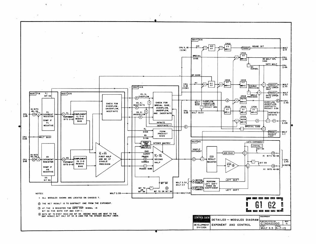
CPU 3.4B
CPU 3.2B
I ,4KR7IFIS xi 1 r---' BIT 591
Xi BITS 48-59 X"
~ EXPO~ENT I' -.:.::rL..J-' - REGISTER
Xk BITS
COIIP IF Xi
NEGATIVE
~G16
~ FOIIPLEIIEN '1'XPONENT XI 0-9
BITS 0-10 REMOVE BIAS I-
CHECK FOR OVERFLOW. UNDERFLOW, INDEFINITE
"
~H16
Xk, XI 1-1-.... +-{2 OVERFLOW
Xk, Xi + CHECK FOR INo FINITE L;J SPECIAL CASE.
1-1-.... +-{2 OVERFLOW,
Xk, Xi ~ UNDERFLOW, UNDERFLOWt;J AND INOEFINITE
I-I-t-+-r-<%=- -0
-
~H14
CPU 3.IB mO .
(CIW)
mO FF
CP02 FF Btl
FANOUTf-'R:;;OU=N;:.D....:,B:..:'T ____ -;-IIULT 3.1A
SPECIAL CASE r---~~~~-----+-----~.
CP03 FF
rr--------~~~~~;-CPU
IIBt2J_ [I-GO:-:-_~-go .. ASE..:II::U"-L::.T..:S"PL::::,-l-3.4A
CPU 3.IB
(CIW)
B. GATE IIULT CPU
NORMAL 3.4A
DP CDRR
ml ~I ~C~~2 ~C;~3 ~ PRECISION ~li LOWER .30
• FF • ..Btl IIBt2JbOUBLE "~"~: r-~ULT
I-----I-----+---------h - ~-+-=~ r- MULT CP03 PRE~~'~ GATE UPPER 3.40
~~GTR HALF I--t-T"--t----. ..... UL ... T-+"'S"'~~"'~"~"'~A~~"'W-. ,-+-I-"'{~ • MB+2 OVERFLOW,€ r-i~UA
BUSY'~:'NDEF'N'TE. UNDERFLOW, . - PRODUCT SIGN CP02 CP03 CP04 INDEFINITE, @-F ~F FF PRODUCT SIGN
INFINITE CP03
~------~ ~------~
~~~ -+M-U-L"T-B::':US~y----""'-If-oIIIB+1 IIB+2 MB+3 "--~NDEF'N'TE-'
~:;:~ 2 • 2 ,-CPU INFINITE 3.1 OB
L-L-L __ ~X~I~=:r='N:D:E:F:IN:I:T:E-:'1:unj-(2)-t---------t===~=-..r- SPECIAL CASE .)
SIGN FORM L....J ~ MULT PRODUCT ENABi::E 3.2
Xk SIGN LOOP SIGN
C~K INTEGER MULTIPLY ~H15 GATE EXPONENT
SAIIPLE BIT 59
- iii +iii .-1-"'++--"'C':A:R;Ry::-01 _ _ ADO BIAS;- . .~_~Q -=oo.4B-59 Xk CPU 12' EXPONENT r--3.4B REGISTER
~~ ~ r---~ ~OGICALlg ~
~ ~ ~
"X~NTFO:-~N /:;s~a:~~ . )I-++-lHH--!£--{:~ v:~~;:D >-4-..... --+f®----4{11I • ~~;;R ~ f-.r=1-... BITX:9 BITS 4B-59 CPU
3.4A
COIIP IF Xk
NEGATIVE
BITS 0-10 RE:,~~E I----- PRECISION §J?-::: f--- ~~P ® k}l L....J t -<!9---:-PSUEOO SUIIS Xi BITS 48-59
Xk 1 BIT 591
I ii'f"M
BIT 70~ @
-MULT 3.3A{ IIULT 3.4
'---
I®:. PERFORM LEFT SHIFT
LEFT SHIFT
~ CHECKON ~ COEFFICIENT I--"'L-;;E"'F';T-::'SH"'I:::F';T--...J
NOTES: IIfRM I ~ BI! 70 OR liT 94
MULT 3.0B-..... -+-....:::.:....;;..;.. .... --'-..;;..-'----f---MULT3.2B .... ___________________________ .....1
I. ALL IIODULES SHOWN ARE LOCATED ON CHASSIS 7.
tID THE NE T RESULT IS TO SUBTRACT ONE FROII THE EXPONENT.
@ AT. THE X REGISTER THE ffiEiiii SIGNAL IS BIT 59 FOR BOTH EXP AND EXP-I.
.. .. _ .. -.. I G1 G2 I ... _ .........
DETAILED - MODULES DIAGRAM I=,...=~_-,-=--I
EXPONENT AND CONTROL

3BA7 MODULE
The 3BA 7 module forms the second half of the exponent add and examines the
complement of the result for overflow or underflow of the floating-point range.
The 3BA 7 module also determines whether an integer multiply should be performed.
The overflow and underflow tests are made primarily by examining bits 10, 11,
and 12 of the result. Since the result is in complement form at this point of the
add operation, bit 12 (term H12) set indicates a positive exponent result, and
term 7H set indicates a negative exponent result. Bit 11 may be set for a posi
tive result, but should never be set when the result is negative. The value of
bit 10 depends upon whether the exponent result is negative or postive.
OVERFLOW
When bits 10 and 11 of a positive result are set (terms H10 and H11), the result
is :£. + 1777. Term 71 indicates the complement of this condition or that the re
sult is > + 1777. Therefore, an overflow condition (term 7I set) occurs when the
result is > + 1777. The overflow signal is sent to the 3KV? module if an in
definite condition does not already exist.
60420300 K
UNDERFLOW
When the result is negative (term 7H set), two possible overflow conditions are
examined. Bit 10 (term HIO) set indicates that overflow has occurred because
the exponent result is S - 2000. Terms JA, JB, and JC set indicate that the
result is equal to - 1777. If either of these conditions exists, an underflow con
dition (te;.rm UF) is detected. The underflow signal is sent to the 3KV7 module
if an indefinite condition does not already exist.
INTEGER MULTIPLY
When both operands have underflow exponents (terms KU and JU are ones) and
the operand coefficients are not both normalized (term BI is one), an integer
multiply is performed. However, if one of the operand coefficients is normalizecl,
an undetected overflow result normally occurs.
When an integer multiply is performed, exponent adder output bits 0, 4, and 5 are
forced to one by term 1M, and the bias bit (bit 10) is forced to a zero. This
ensures that all zero bits are sent to the Xi register for the exponent portion of
the integer result.
During an integer multiply operation, an underflow condition exists, but the
special case condition is blocked by term N1M. Blocking special case to multiply
control (3KV7 module) enables the multiply unit to output to the Xi register even
though the underflow condition exists.
5-7-16

.,
D
c
B
A
4
4GC7
(Ale)
SECOND PASS
4
3
4GB7 4G87
(816) (BIS) IAI4) 1814} (815)
24 )( 48 MATRIX PRODUCT n;" .. s
4GCT MODULE IAI5)
NO. OF BITS 3 .. 5 6 7 8 6 .. 2: INPUT
IBl21 IBlil
4G97 MODULE IUJ
IBIOl
NO. OF BITS INPUT
(B'l
58 57 58 55 54 53 52 51 50 49 48 R£SULT BIT 15 14 13 12 II 10 9 a RESULT BtT
M * * * * * M * * M * * ***M**JII*
M fit M .,
*
• • • II 1323465632ii!
PSUM
PSUM
PSUM
P5UM
PCARRY
PCARRY
NO. OF BITS OUTPUT
• * •
I 3 5
3
• ••
· • · . • • * •
7 7 5 3 I
P$uM
PSUM
PSUM
PSUhI
PCARRY
PCARnv
PCARRY
PCARRY
NO OF 81TS OUTPUT
FIRST LEVEL ADO
2
XJ BITS
4GC7 MODULE «as)
NO. OF BITS INPUT
10 9 8 7 6 5 4 3 2: I 0 RESULT BIT
JI " lit fI M * * If * * * PSUM
*
344&4543121
PSUN
PSUN
PSUN
PCARRY
PCARRY
NO OF BITS OuTPUT
P CARRIES ARE SHOWN LEFT- SHIFTED ONE PLACE.
xi 81TS
, ___ I&:IIID1I!II,
I G13 614 I .l&1liI11III1IIIIIIIII11IIII11III1
TROUBLESHOOTING DIAGRAM MULTIPLY UNIT 24 X 4B MATRIX
D
c
B
A

4
D
c
B
A
4
3
CLOCK PERIOD
CLOCK PULSE
TWO SUCCESSIVE FLOATING MULTIPLY INSTRUCTIONS IN THE TOP PARCEL OF THE CIW REGISTER
@ GO ISSUE UN ISSUE CONTROL)
NOTEs:
MULTIPLY BUSY FLAG SET (IN ISSUE CONTROL.)
Xj(I)(BITS 24-59),x.(I) (BITS 0-50),mO(I),AND ml ") IN MULTIPLY UNIT INPUT REGISTERS
Xj{I) (BITS 0-23) IN MULTIPLY UNIT INPUT REGISTERS
Xi (I) RESERVED
INSTRUCTION I RESULT ENTER"S Xi (II
Xj (2}(BITS 24-59),Xk(2)(BITS 0-59),mO (2), AND ml (2) IN MULTIPLY UNIT INPUT REGISTERS
Xi (2)( BITS 0 -23) Itl MULTIPLY UNIT INPUT REGISTERS
Xi (2) RESERVED
INSTRUCTION 2 RESULT ENTERS x; (2)
<D INSTRUCTION I - ASSUME NO ISSUE CONFLICTS.
2
® INSTRUCTION 2 - ASSUME THAT ONLY ISSUE CONFLICT IS THAT THE MULTIPLY UNIT IS BUSY.
THUS I ISSUE IS DELAYED ONE CLOCK PERIOD.
@ ENABLE ISSUE IS DELATED 4 CLOCK PERIODS (THEREFORE, GO ISSUE
IS DELAYED A MINIMUM OF 4 CLOCK PERIODS) IN THE AAI20-C.
THIS DELAY IS REMOVED BY INSTALLING OPTION AT364 -A.
3
TIMING DIAGRAM MULTIPLY INSTRUCTION
,. .. _---. I .H1 H2 I 1.1ii1II1IIIIIIIl_ .. a-'I
D
c
B
A

-
-
-
-
-
...
-
•
-
.. 10' 41'1 XI'·IT' ... IO·nl ... UCOlD ....
12.4-471
--
Q
f----.
111'1' ...... · , 'AII5 · , ,
IZ •• ., ..... • •
, ,
nlt/SlUI
. ,
Ill • .,
"'1 S
"12' ,
"IOS . ,
!AClY5 . , Itl'7
'oIOS'
I
co
.' 0 \ ~
, 1111'7 ••• ,S · . " ...
II" T ,alii
12.' ., .AIOI
,
II .. " .....
.-. · 'AD45 . ·
()
UO/4TM
, , , , , , · . · · .. · eo, 1. A., · , ,
, . • , , · , · , I . , · , , '" , , , , · eo. , . · " ... · " ...
, ... · , . .. , · . (!) • II .. , . 'oo .. G) • II . , , . ,oo G) • " 00'
ot .. 1.111
" " 11"7 . I
." I Z I' , . .. , +(1)1. · .'~' ,. D. "
I' , .. IE ,.
" IE ,. " I' "a
(I), .. ,.(1)-' .. ... , .. " II
'"11 .. , ,. I' FO. · , OJ 11(j)I' " ,. , -.- · EOI'. -, Z .. ... OI I' ,OS .. , £G. OI I' F05
il>" .. , @I' .. "
ot , .. '. 12Ci)1. " ,. "
I' F05
OJ ... ,. .0 122'7
· , . · " · il>' • .. · .. ,. , DO • .. @" .. · , ,. , ..
I '1 @" .. , , . , , " '0 , .. , .. , , .. , . DO. ,
'!- - .. to ... "
,
· .. • , · _. II .,
o , "
II , ,. , , ... "1 , . I I
" I.
I
P I'T 104 it
.... '\ I F'I",T PAIS
" I 10' I
•
, , ,
" "
, , , , ,.
.. ,.
" ,
LotlCAL PIIODUCT ~IID 'III.T L[VEL ADD • nee LOOP l'tS '110M '11i1T MSS ... (O~41) AND II. (0-11) F.IIIT flASS
NOU.: ... (0 -41' ..... XI (14-411,1EC0IlO PASS I. L[fT. "MI .. 0' II" '" 1_ IIIIIIT ... t .. or I'" OUT I •• II) • lin OUII'\.ICATIO OM II[XT MIIK[II MODULI
4. ID· IIOUIIO '1"
AIIO GO KCOMO LEVEL ADD
I. :l~~LNEA:::: ~il'::~~~SJ:~7,.~.t~E~J.USED ARt UlltE .... IATIONS, ACTUAL
I () t
.. ,.,
(I)
<i>
_C!1
Ci)
, , •
, , ·
.. liS Z · " I
• 114 2. · • 115 ,
· · '. .. " IO.
• .07 · I. . ...
• , , , , , • , , , · , ,
• G04 Z · " •• M I:
,
,
,
,
() • G05 Z , , · G. , _IlL • Gal
, · Ii> • o. · I , ,
· 'L , , , ,
KCTION CAIIIIlIES
~ nUllo LEVEL ADD
III
III
I
4TM/nH c: ..
Mil Z
II ,
2: HII Z · I Gill 2.
. , J. 111 I
X, 'IT ..o.ITIO.
tt
IS
" 10 .. .. " ~IIECTION it liZ I IS 7
II
"
'"~ : ~ISIECT'ON Z III I 7S • I 74 /'
:-;r%
. t • , IECTION
: MI~--i- r-- . "-f.-""-;t--..;; , .00 , --u • . -.~ r-r,
, ,
t. , .... I
•
.. I .... ,
Z G" Z it HO? 2 ,
, I
i-ow
.. .. :r-ik SECTION .. . , .. .. , f: I .. ",," .. .
" I
oM IIIUULT
.. I 44 SECTION .. . .. ..
I ~ ~
HOS it · ."
tT ,
MO' I
.,
" ; ~ jnCTION 2. 101 I S!I I , .. I -ir-': 2~~
i~~ ZGV_'~
: 10S-; r-ii :r--fi
+--- -:~ .. ----~ -~r7.
.
I.GU.~~
, ... , 1 IDS I
.. .
F.IIAL. ADD AliO LEft SHIFT
.-----.. I H3 H4 I 1 _____ .1
I
-
-
...
-

PART 8
DIVIDE. UNIT
rlllllll--lF.ilfm! I B 1 B2 I III111l1:!1 -= CIJI r.:;:l lim ~

DIVIDE UNIT
The floating-divide unit executes the two CPU instructions, floating divide (44)
and round floating divide (45). These instructions direct the computer to divide
Xj by the divisor Xk and send the quotient to Xi. This unit involves a 17-step
iterative process to form the quotient from the two operands. Only one divide
instruction may be executed in the iterative portion of the divide unit at a given
time.
The divide instructions require 20 clock periods for execution. Data moves
from .the operating registers to the divide unit input registers each clock period
in which the divide busy flag is clear. The data is used for. instruction execu
tion only if a divide instruction issues from the CIW register and sets the divide
busy flag. The data which arrives at the divide unit during the clock period of
instruction issue is then used in the execution of the following divide sequence.
The divide busy flag prevents the CIW from issuin& another divide instruction
for the 17 clock periods following instruction issue. However, in the 18th clock
period after instruction issue, a second divide instruction inay issue.
Bit 0 of the m designator is held in an input register along with the operand
data in Xj and Xk. This bit is the divide round flag which distinguishes
between the two instruction modes.
The divide unit operates on positive coefficient values only. Each coefficient
for Xj and Xk is individually complemented in static networks if its sign is
negative. The sign of the result is determined by the divide unit and is sent to
X register input control in the CPU. This sign bit is the logical difference of
the tlVO operand sign bits.
The divide busy flag initiates a chain of divide sequence control flags which
sequence the steps in the instruction execution. This chain controls the sequence
of events for the 19 clock periods following the issue of the divide instruction.
These static conditions then control the data movement within the divide unit and
the data transmission of the X register input path at the end of the divide
sequence.
60420300 K
The format of a floating-point number is k2n , where k is a 48-bit integer
coefficient and n is a 10-bit integer exponent.
Division of floating-point numbers requires the subtraction of the exponents and
the division of two 48-bit coefficients. Double-precision division is not provided
and a remainder cannot be retrieved. Since the divide hardware produces a
quotient in the range, 1. 7777 7777 7777 7777 through 0.0000 0000 0000 0000, the
ratio of Xj to Xk must always be less than 2 to 1. If the divisor is normalized,
this requirement is always met. If this requisite is not met, the resulting
quotient is meaningless. If both the dividend Xj and the divisor Xk are nor
malized, the quotient Xi is also normalized.
The quotient coefficient is formed three bits per clock period in 17 iterative steps.
The result of the first iteration is stored in the control module. The results of
the 16 succeeding iterations (a total of 48 bits) are stored in the quotient shift
register. If the quotient is of the form, O. X--------X (the ratio of Xj to Xk
is less than 1 to I), the result of the first iteration is a zero, and the 48 bits
in the quotient shift register are taken as the coefficient of the result.
Given: Xi Xj/Xk
(Xj) 2057 4400000000000015
(Xk) 2032 6000000000000000
The divide coefficient logic forms:
4400000000000015 ; 0.6000000000000021 6908080000900000
In floating-point format, the coefficient must be an integer. Therefore, the binary
point must be moved 48 places to the right. Since the exponent must be de
creased by one for every place, the binary point is right-shifted, 60 (octal) is
subtracted from the difference of the exponents, and the final result is:
(Xi) ; 1744 6000000000000021 1---lIIIIiIiIlIiIliIIng I B5 86 m LlDDlIlIIIIIlIII:iIllRIIIllilDl
[Final exponent -33 (unbiased) 1744] 2057 - 2032 - 60
5-8-0.0

If the quotient is of the form, 1. X--------X (the ratio of Xj to Xk is 1 to 1 or
greater, but less than 2 to I), the result of the first iteration is a one, and the
upper 47 bits in the shift register are interpreted as bits 0 through 46 of the
quotient coefficient. The X register access control interprets bit 47 as a one.
Given: Xi Xj/Xk
(Xj)
(Xk) 2016 7000000000000000
2025 4000000000000000
The divide logic forms:
7000000000000000
4000000000000000 1.6000000000000000
In order to make this quantity an integer, the binary point must be moved 47
places to the right. Therefore, 57 (octal) is subtracted from the difference of
the exponents and the final result is:
(Xi) = 1711 7000000000000000
[Final exponent = 2016 - 2025 - 57 = -66 (unbiased) = 1711)
If the ratio of Xj to Xk is2 to 1 or greater, the result of the first iteration is
forced to a two by the release remainder control signal. The control network
then sends a special case signal (indefinite) to the X register input control net
work along with an operand conSisting of all ones. The X register input control
network then generates an indefinite result.
The quotient coefficient is formed three bits per clock period. The iteration
network functions exactly like a pencil and paper octal divide. A multiplication
network forms seven multiples of the divisor. Xk through 7Xk. The dividend is
entered into the remainder register. which holds 51 bits (initially bits 48. 49.
and 50 are all 0). The trial subtraction network simultaneously compares each
of the seven divisor multiples with the contents of the remainder register. The
largest multiple that is smaller than the remainder is subtracted from the re
mainder. The resulting quantity is left-shifted three binary (one octal) positions
and entered into the remainder register. The number of the multiple chosen
(pick number) becomes the first quotient digit. The pencil and paper method is:
60420300 K
0.6000 0000 0000 0021
6000 0000 0000 0000 14400 0000 0000 OOQO 0000 0000
0015.0000 0000 0000 0000
4400 0000 0000 4400 0000 0000
0000
0015 0000
0 0
The same division as performed by the functional unit:
15 14
0000 0000 0000 0000
0000 000 0000 000
Dividend (Xj) = 4400 0000 0000 0015 1 0000 0000 0000 0000 6000 0000 0000 0000
Divisor (Xk) = 6000 0000 0000 0000 2000 0000 0000 0000
The multiplication network forms:
Xk 6000 0000 0000 0000 2Xk 1 4000 0000 0000 0000 3Xk 2 2000 0000 0000· 0000 4Xk 3 0000 0000 0000 0000 5Xk 3 6000 0000 0000 0000 6Xk 4 4000 0000 0000 0000 7Xk 5 2000 0000 0000 0000
The dividend enters the remainder register.
RMDR = 0 4400 0000 0000 0015
Initially, the quotient shift register has contents: XXXX XXXX XXXX XXXX
The 17 iterative operations are performed as follows:
1.
2.
Compare RMDR versus Xl< through 7Xk:
IlMbtl is smaiiei- thiln any of them.
Enter octal digit 0 in shift register:
Quotient = XXXX XXXX XXXX XXXO (the quotient
is left-shifted one octal digit each clock period).
Enter chosen digit (in this example, a 0) in con
trol module this iteration only.
Enter RMDR-O and left-shift three:
RMDR = 4 4000 0000 0000 0150-becomes a 2525
1 pattern if in-
struction 45
enter 0 since left-shift
three
Compare RMDR versus Xk th;rough 7Xk: 6Xk:>. RMDR< 'JiXk
Enter second octal digit: QUOT = XXXX XXXX
XXXX XX06
I DlII Rll IiIIJ 1m! 6iLD 1!!9
I B7 B8 I ~lIIII!IIllBmmEm.l1.l~
5-8-0.1

Enter RMDR-6Xk and left-shift three: RMDR =
o 0000 0000 0000 1500
3 through 14 In the next 12 iterations, an octal digit 0 is picked, and
the quotient and remainder are left-shifted three binary
places each clock period.
15.
60420300 K
RMDR
QUaT
o 1500 0000 0000 0000
XX06 0000 0000 0000
·Compare RMDR versus Xk through 7Xk: RMDR < Xk
Enter octal digit 0: QUaT = X060 0000 0000 0000
Enter RMDR-O: RMDR = 1 5000 0000 0000 0000
16.
17.
Compare RMDR versus Xk through 7Xk: 2XkSo RMDR< 3Xk
Enter octal digit 2: QUaT 0600 0000 0000 0002
Enter RMDR-2Xk: RMDR = 1 0000 0000 0000 0000
Compare RMDR versus Xk through 7Xk: XkSo RMDR< 2Xk
Enter octal digit 1: QUaT = 6000 0000 0000 0021
Discard remainder and transmit quotient to Xi
r-----. I 09 810 I 1 ____ .....
5-8-0.2

X REGISTER (CPUI
X REGISTER (CPU)
CPU
Xi SIGN
Xk SIGN
59
58
I
BIT 51
BIT 59 t> LOGICAL DIFFERENCE
48r-~--------------~~~~
COMP IF X' NEG
o REMAINDER
E
~ o N
RESULT SiaN
~ QUOTIENT EXPONENT
R E S U L T
SPECIAL CASE SIGNALS
X REGISTER ACCESS CONTROL (CPU)
XI REGISTER (CPU)
X REGISTER ACCESS CONTROL ('\;PUI
DURING CLOCK PERIOD I, A 0 PICK IS FORCED SO THAT THE DIVIDEND IS CHOSEN. DURING
CLOCK PERIOD 2, THE FIRST ITERATiON TAKES PLACE AND THE PICK OF AN OCTAL DIGIT IS LIMITED TO OIIIOR Z.
A POSITIVE QUOTIENT IS SENT TO THE X REGIITERS.
IF THE RESULT IS TO 8E NEGATIVE, THE X
REGISTER ACCESS CONTROL COMPLEMENTS TIllE POSITIVE R£SUL T AS IT IS ENTERED INTO Till!
XI REGISTER. SPECIAL CASE RESULTS ARE ALSO FORMED BY THE X REGISTER ACCESS CGIfTROL.
DIVIDEND DURING FIRST ITERATION.
ALL OTHER ITERATIONS.
REMAINMR
I V I o ~ ________ ~ ________________ ~t~ ____ ~O~IV~I~D~E~N~D~O~R~R~E=M=A~IN~D~E~R~~~~p-____________ -,
0-4 E
COEFFIC lENT
N D
o I V I S o R
DIVIDE BUSY
R E II A I N D ~.
Ti T2 T3 TI7 Ti8
DIVIDE SEQUENCE CONTROL
r BEGIN DIVIDE
CIRCULATE LOIV) REMAINDER
l X~~C~IV?~EERtA~~l CLEAR DIVIDE BUSY
SAMPLE EXPONENT
TRIAL SUBT
ENABLES
GATE
CHOSEN
-L~~~~~~r-------1 RANK
GROUP BORROWS
END AROUND BORROWS
FINAL SUBT
REMAINDER
S4 H I F T
R QUOTIENT COEFFICIENT XI
REGISTER (CPU!
E
r @ S T E
rm- ........ ~ I 83 84 I 1 ........ _.
PRIMARY BLOCK DIAGRAM
DIVIDE UNIT

..
! SDi~~B Xj EXPONENT
II}---->j
ENTER
Icpu 2.18 EXPONENT
Xi SIGN
~P02
X j EXPONENT -INPUT
REGISTER
COMPLEMENT IF
Xj IS NEGATIVE
i~P_U_ XI\ SIGN 2.2B,D~ _____ _
Xk EXPONENT
" CPU 2.2D
Xk EXPONENT-INPUT
REGISTER
COMPLEMENT IF
Xk IS NEGATIVE (DIV 3.0)
Xi SIGN BIT 59
~PDa
FI RST HALF ADDITION
" OF Xi +Xk +578 OR
X) +Xk + 60 8
II
( DIV 3.0)
Xk SIGN BIT 59
OVERFLOW
CARRIES AND ENABLES
Xi AND Xk
~~RnfbWd~J'11r~FLOW, I-----{ 6)------1
~ 'SPECIAL CASE, 3 INDEFINITE -I,
INFINITE
(PICK 578 OR 608 )
30Q71 POG
CPU 2.IB BEGIN SEQUENCE
TIMING AND
CONTROL MODULE
CPU 2.0B mO
(CIW)
NOTES:
I. ALL MODULES SHOWN ARE LOCATED ON CHASSIS 7.
® OUTPUT AND SHIFT RECISTERS HOLD THE COMPLEMENT OF THE RESULT.
(DIV 3.0)
DIVIDE FAuLT
DIV Ti3
CLEAR DIVIDE BUSY
DIV Tl5
INDEFINITE-I,
~E
~ GATE DIV" GO DIV SPL CASE
2
OVERFLOW,
r
_U_N_D_E_R_F_L_O_W_' _IN--,D_E_F_I_N_I T-;E ____ } CPU 2.2 A
QUOTIENT SIGN
1 t 3DP71 P07 ~P03
SECOND HALF ADOITION
RESULT EXPONENT
1----(11 )----->1 OUTPUT REGISTERS ® BITS 48-59 AND
DIV 2.1B
(DI V 3.0)
CMC 2.4A (8XS)
CPU 2.10
CPU 2.10, 2.3C
CPU 2.5C OR 2.6B (BX5)
DIV 2.IA
CPU 2.2A
QUOTIENT BITS 0-2 BITS 0-2,45-47 ,}---->/
OR 0-1 ,44 -46
~ QUOTIENT BITS 42-44
(01 V 3.0)
~POS
)" QUOTIENT r BITS 0-2
BITS 3-23 OR 2-22
SHIFT REGISTER ®
AND OUTPUT
IDIV 3.0)
~~ 1'BITS 21-23
4DR71 P04 BITS 24 -44 ----' OR 23 -43
SHIFT REGISTER ®
AND OUTPUT
(DIV '.0)
EXPONENT BITS 40 - 59
.--@-->---- CPU 2.2A
COEF BITS (X RGTR) 0-2 45-47
SHIF~ED ~-COEF BITS 0-1,44-46-®-
COEF
~ ~~gO-47 :~ SHIFTED '-f.iBL J.' COEF '~ CPU 22A. BITS 2-22 ,--.B~ 0- 46 SHIFTED (X RGTR)
~ ~}---~--
COEF
~ - --v-----SHIFTED COEF
~~ -- .~~:;--
~ SECONDARY BLOCK DIAGRAM DIVIDE UNIT
DEVELOPMENT EXPONENT AND CONTROL DIVISION" NETWORKS
'cl6'0420300 I "y' DlV 2.0 15='8-3"-

• REMIlINDER BITS 3-50
I WIRED L BITS 0-47 411 BX4B I LEFT SHIFT OF I
THREE PLACES INCLUSIVE
QUOTIENT BIT ENABLES
I I . BITS 0-2 RANKS 0-7 RANKS 1-7 DIV 2.0e
~P06 BITS 48-50 INCLUSIVE
I 1 RELEASE
3
8 BIT REMAINDER (DIV 3.0) ENilBLES 4017 PI6 36-47 RIINK 0
r
4007 MI6 BITS 48-50
PI4 24- 35 INCLUSIVE 4DA7 MI5 45- 47 BIT
PI2 12 -23 >--€)ENABLES' 1t14 42-'44
Xj COEF ~PIO BITS 0-11 MI3 39-41
i 4 BITS 0-4.7
MI2 36- 38 GROUP DIVIDEND INPUT C~ [ REGISTER AND RlINk tAli 33- :IIi ~ 2.tB Xj SIaN o ENABLE NETWORk INCLUSIVE MID 30-32 ENABLES BIT
(DIV 3.2) ~ M09 27-29
DIV ROUND T M08 24-26 GROUP • 2.0C 3 EAB'S M07 21- 23
~ 4DH7 016 BITS 45-47
M06 IB- 20 015' 42-.44
GROUP BORROWS
4DJ7 PI5 BITS 36-47 M05 15 17 014 39-41
Xk COEF BORROW
013 36-38 PI3 24- 35 INPUTS M04 I 12- 14
411 IITt. ()-47 Pl1 12- 23 1403 I 9-11 005 33-35
GROUP 0 M02 I 6-B 004 30-32 ~[ ~ P09 BITS 0-11
BORROWS 2.20
Xk S18M DIVISOR INPUT 40A7 MOl I 3 -5 003 27- 29
~ LDI BITS I 0-2 IGROU0~S ,
002 24-26 REGISTER I CPU 2.IB ENTER Xk BIT (>-2 FINAL SUBTRACTION I FIRST STAGE LI6 21-23
(DIY 3.1) ENABLES NETWORK AND I TRIAL SUIITRACTION
LI5 IB-2O
REMAINDER I NETWORk FOR LI4 15- 17.
t REGISTER RANKS 3,6,7 LI3 12-14 NOTES:
"'" (DIV 3.2) I l05 9-11 I. ALL MODULES SHOWN
"'" L04 6-8 ARE LOCATED ON
tEMAINOER l03 3-5 CHASSIS 7.
40N7 KI6 BITS 48,49 3Xk,.6Xk,7Xk ~ L02 BITS 0-2 BITS 0-47 ® GROUP 0 BORROWS AND
~ .. 4DK7 "3 "-47 Xk -7Xk REMAINDER AND GROUP BORROW INPUTS klO 24- 35 PARTIAL ARE lEFT-SHIFTED ONE
Xk DIVISOR MULTIPLES SUBTRACTION GROUP. K07 12-25
~ CPU 2.IB NETWORK ~ K04 BITS 0-11 Xk .2Xk,4Xk ,SXk (DIV 3.2) MULTIPLICATION ~ 1 rn flANK 1,2
NETWORK '<.:/ BORROWS r---- IIIIIIII -. 3Xk. 2Xk-+Xk
I C3 C4 I 4DE7 NI6 BITS 48-50 ~ L12 RANK 5 (DIY 1.11
4087 NI5 45-47 4OG7 012
NI4 42-44 LII 1 ___ ...... .11
-- 4 NI3 39-41 011
DN7 KI6 BITS 48-SO INCLUSIVE NI2 I "-38 LIO 2 BIT GROUP I--4Dl7 Kr4 "-47
~ Nil I 33- 3~
~ 010 EAB'S %-KII 24- 35 ~ NID I 30- 32 L09 I ENABLES I--kOB 12-23 'C7
EAS'S N09 27- 29 009
~ K05 BITS 0-11 N08 24-26 L08 7
~ I--
MULTIPLICATION N07 21- 23 GROUP 008
GROUP NETWORK BORROW N06 18 - 20
r. BORROWS AND ENABLES L07
6 -5Xk o4Xk +Xk
INPUTS • N05 I 15 - 17 FOR ALL RANKS 1-7 007 GROUP
(DIV 3.1) N04 12 -14 BORROWS 4DF7 LOS
RANK 3 BORROW § N03 9 - 11 006 INPUTS~
GROUP 0 N02 6-8 7XI4
BORROWS I
4 GROUP BORROWS
SECOND STAGE RANKS 1-7 4DB7 NOI I 3-5 TRIAL ®
40N7 kl6 BITS 48- 50 ~ lOI BITS I 0-2 SUBTRACTION I WRDLEFT I NETWORK SHIFT 40~17 KI5 38-47 fINAL I FIRST STAGE (DIV 3.2) 13 PLACES)
~ KI2 24-35 SUBTRACTION I TRIAL
K09 12- 23 ~ HETWOR~ AND SUBTRACTION REMAINDER I NETWORK FOR
~k06 BITS 0-11
~ REGISTER I RANKS 1.2.4,5 t~"" MULTIPLICATION 51 (DIV 3.2) B~OWS
__ NETWORK ~ "CO .. A., BCD" DIAGRAM 7Xk 0 8Xk-Xk
DIVIDE UNIT C'1'60·4203 00 I s· (DIY J.1l DEVELOPMENT COEFFICIENT NETWORKS DtV 2 .. 1 1~8-5 DIVISION
•

EXPONENT, OUTPUT, ANO CONTROL
EXPONENT MANIPULA nON
INPUT REGISTERS
The data input registers for both operand exponents, bits 48 through 59, are on
the 4KR7 module. The data that is ,in the registers when the divide busy flag
sets is held for the 17 clock periods during which the flag remains set. Xj bit
59 and Xk bit 59 are sensed and the exponents (bits 48 through 58) are individually
complemented if they are negative. The output goes to the 4007 module (bits 48
through 58) and the 30P7 module (bit 59).
EXPONENT FORMA nON
The exponent subtraction occurs while the coefficient is being formed. The
quotient exponent is held until the quotient coefficient is completely assembled.
The exponent subtraction network, comprised of the preliminary and final addition
networks, is on the 4007 and 30P7 modules. Instead of subtracting the divisor
exponent and the correction factor from the dividend exponent, the dividend expo
nent is complemented and added to the divisor exponent and to the correction
factor (CF). The CF is determined in CP04 by bit 0 (overflow bit) of the first
quotient coefficient digit. The resulting sum (exponent) is complemented on out
put by the 40S7 module to obtain the quotient exponent. In effect, the exponent
network forms minus (-Xj + Xk + CF) instead of (Xj - Xk - CF).
The exponent addition is performed in two halves. The network that performs
the preliminary exponent addition is on the 4007 module; the final exponent
addition network is on the 30P7 module. The bias is removed from both expo
nents on input to the 4007 module. The exponents and the correction factor are
then added. If the overflow bit from the 4DQ7 module, bit 0 of the first iteration,
is a zero, the quotient is of the form O. XXXX XXXX XXXX XXXX, and the cor
rection factor is 60 (octal). If bit 0 of the first iteration is a one, the quotient
is of the form 1. XXXX XXXX XXXX XXXX, and the correction factor is 57 (octal).
1 I111III _" __ •
I 05 D6 I I- _ II1II __ .I 60420300 K
The result of the first half addition is a bit carry and a bit enable for each
position. These bits are transferred to the final exponent addition network on the
30P7 module.
The final addition network combines the carries and enables in a 13-bit mode.
The two extra bits are formed by sign-extending the exponents. The upper
three bits of the 13-bit sum are sensed to detect special case conditions.
Exponent bias is added, and the lower 11 bits of the sum are then transferred
to the output network on the 40S7 module.
The sign of the quotient is formed by a network on the 30P7 module and sent to
the X register input control. This sign bit is the logical difference of the two
operand sign bits. A network on the 4007 module checks for operand exponent
overflow, underflow, and indefinite exponents. The rest of the special case
checks are performed on the 30P7 module. If any special case exists, the
special case signal to the 4DQ7 module is a one, in which case, a quotient of all
ones is sent to the X register. The three signals to the X register input control
specify which, if any, of the special case conditions exist.
SPECIAL CASE
A number of special cases are treated in the floating-divide unit. If any special
case conditions exist, the special case signal from 30P7 to the 4007 module be
comes a one. When the go divide special case signal from the 400'7 module to the X
register input control becomes a one, the specific condition is indicated by the
exponent indefinite, overflow, and underflow signal from the 30P7 module. In
any special case condition, the transmission of data from the divide unit output
registers to the destination X register is blocked. 'The gate quotient signal from
4DQ7 to 40S7 remains a zero, forcing the exponent output registers to transmit
all ones. The gate output signal (which is the gate quotient signal delayed 1
clock period) forces the coefficient output registers to transmit all ones. Thus,
a quotient of all ones is delivered to the X register and the input control forms
the particular special case word. The special condition flags cause the appro
priate bit to be set in the exit condition register.
5-8-6.0

If no special case conditions exist, the special case signal from 3DP7 to 4DQ7
remains a zero. The go divide special case signal to the X register input con
trol is a zero and the gate divide and the gate quotient signals are ones. The
gate quotient signal gates the quotient output.
SPECIAL CASE OPERANDS
One category of special case conditions involves overflow, underflow, or indefinite
operand values. These situations are sensed in the 4D07 module. The combi
nation of special operand values which cause specific results are sensed 9n the
3DP7 module. If either operand is indefinite, or if both operands are indefinite,
the result is indefinite. The operand coefficients are ignored in this case, and
the resulting word delivered to the Xi register is positive indefinite with a zero
coefficient. The indefinite bit is set in the exit condition register (CPU) for
this case.
If either operand has an overflow exponent, or if both operands have overflow
exponents, the result is infinite. The infinite bit is set in the exit condition re
gister (CPU) for this case.
If Xj has an overflow exponent and Xl< is in floating-point range or has an under
flow exponent, the result is a complete overflow word delivered to the Xi register.
The coefficients of the operands are ignored in this case, and the result is a zero
coefficient. The sign of the result is calculated in the same manner as for
operands in range.
If Xj has an underflow exponent and Xk is in floating-point range or has an over~
flow exponent, the result is a complete underflow word delivered to the Xi
register. The coefficients of the operands are ignored in this case, and the
result is a zero word.
If Xk has an overflow exponent and Xj is in floating-point range, the result is a
complete underflow word delivered to the Xi register. The coefficients of the
operand are ignored in this case, and the result is a zero word.
60420300 K
If Xk has an underflow exponent and Xj is in floating-point range, the result is
a complete overflow word delivered to the Xi register. The coefficients of the
operands are ignored in this case. The sign of the result is calculated in the
same manner as for operands in range.
The combination of operand exponents of overflow divided by overflow and under
flow divided by underflow results in a positive indefinite word delivered to the Xi
register.
SPECIAL CASE QUOTIENT
A second category of special cases occurs if there is an underflow or an over
flow of the floating-point exponent range during the exponent calculation. In these
cases, the special case signal is sent to the X register input control, and the
output from the divide unit is blocked in the same manner as for the. special
case operands.
A complete overflow occurs for this instruction whenever the exponent compu
tation results in an exponent greater than plus 1777 (unbiased). If any combi
nation of operand exponents causes an indefinite condition, the overflow situation
is ignored. Otherwise. this situation is sensed as a special case, and a com
plete overflow word with proper sign is delivered· to the Xi register. The coefficient calculation is ignored in this case.
A complete underflow occurs for this instruction whenever the exponent compu
tation results in an exponent less than minus 1777 (unbiased). If any combination
of operand exponents causes an indefinite condition, this underflow situation is
ignored. Otherwise, this situation is sensed as a special case, and a complete
zero word is delivered to the Xi register. The coefficient calculation is ignored
in this case.
PIIIIIlIIIIliiDIIIlIIII_IIIIIIIIl\l
I D7 DB I 1.----.. 1
5-8-6.1

SPECIAL CASE: DIVIDE FAULT
A third special case category occurs if the dividend coefficient is larger than
the divisor by a factor of two or more. This is a divide fault situation which
can occur if the divisor is not normalized. The initial trial subtraction in the
coefficient calculation results in an octal digit with a value of two. If an over
flow or underflow condition does not exist, an indefinite condition result is in
dicated for this case, and it is treated in the same manner as the other special
cases.
If an overflow or an underflow condition caused by an underflow or infinit~ operand does exist, the divide fault situation is ignored.
PAR TIAL OVERFLOW OR UNDERFLOW
A partial overflow occurs for this instruction whenever the exponent computation
results in exactly plus 1777 (unbiased). The result is delivered to the Xi
register in a normal manner. Subsequent use of this result as an operand in
a floating-point unit may, however, result in overflow detection.
A partial underflow occurs for this instruction whenever the exponent computation
results in exactly minus 1777 (unbiased). The result is delivered to the Xi
register in a normal manner. Subsequent use of this result as an operand in
a floating-point unit may, however, result in underflow detection.
OUTPUT
The exponent output register is on the 4DS7 module. The complemented ll-bit
biased quotient exponent is delivered from the 3DP7 final addition network. In
CP18, a gate quotient signal from the 4DQ7 module enables a clock gate so that
the exponent enters the output register. The exponent is complemented on out
put because the exponent network forms the complement of the quotient exponent.
60420300 K
Since a positive quotient is delivered to the X register, bit 59 is entered as a
zero. The absence of a gate quotient signal in CP18 indicates that one of the
special case conditions exists, in which case, an exponent of 12 ones is delivered
to the X register.
The quotient coefficient is assembled three bits per clock period in the 48-bit shift
register. In each of CP03 through CP19, an octal digit is delivered from 4DD7
to 4DS7. After 17 iterations, the 4DS7 module has bits 0 through 2 and 45 through
47; the .two 4DR7 modules have bits 3 through 44. Every clock period, the
quotient is left-shifted three places, three
the iteration netwo'rk, and the upper three
the shift register contains 48 bits of data.
new quotient bits from 4DD7 enter from
bits are discarded. After 17 iterations,
Bits 0 and 1 of the octal digit formed
in the first iteration are stored in the 3DQ7 module. If bit 1 is a one, a divide
fault condition (the dividend exceeds the divisor by a factor of two or more) exists.
If this condition or any other special case condition exists, the gate quotient
signal remains a zero and the delivery of the quotient is blocked. As a result,
a coefficient of all ones is in the path to the X register in CP19. If bit 1 is a
zero and no other special case conditions eXlst, the gate quotient signal becomes
a one in CP18 and the quotient coefficient is delivered to the X register during
CP19.
If bit 0 of the first iteration digit is a zero, the quotient is of the form O. XXXX
XXXX XXXX XXXX. In this case, a correction factor of 48 is subtracted from
the exponent, the overflow bit is a zero, and the 48 bits in the shift register are
delivered to the X register.
If bit 0 of the first iteration digit is a one, the quotient is of the form 1. XXXX
XXXX XXXX XXXX. In this case, a correction factor of 47 is subtracted from
the exponent. The overflow bit becomes a one, causing a one-bit right-shift of
the coefficient output. The upper 47 bits in the shift register are delivered to the
X register as bits 0 through 46. In this case, the bit 47 output is blocked.
Therefore, bit 47 is entered as a one. All outputs are timed to occur in CP19;
...---- ... I D9 010 I ..............
5-8-6.2

CONTROL
The divide sequence control of the 4DQ7 module times the entire divide instruc
tion. The clock periods on the left of the divide sequence control indicate the
set times. The times on the right are the clear times.
The three remainder bits are part of the coefficient iteration network. They
are. used as rank 0 bit enables in the. 4DD7 and 4DE7 modules.
The special case signal indicates a special case exponent. The gate divide and
go divide signals go to the X register input control to gate in the appropriate
data. The gate quotient signal causes the quotient to be delivered during CP19.
The begin sequence signal initiates the divide timing sequence. The divide fault
signal is bit 1 of the first coefficient iteration digit. This bit is sent to the
3DP7 module where it forces a special case condition if it is a one.
The overflow bit is bit 0 of the first coefficient iteration digit. This bit goes
to the 4D07 module where it determines the correction factor. It also goes to
the 4DR7 and 4DS7 modules where it determines which 48 bits of the coefficient
are delivered to the X register.
60420300 K
The divide round flag (m bit 0) is set when a round floating divide instruction issues
from the CIW register. This flag modifies the dividend in the third clock period
of instruction execution. Octal digits with a value of 25252 are entered in the
lowest order bits of the remainder register if this flag is set. This modification
of the dividend increases the dividend value by one-third of the least significant
bit in the original operand.
The circulate remainder signal goes to the four 4DI7 modules where it gates the
current .remainder to the final subtraction network. When this signal is a zero,
the content of the dividend input register is gated to the final subtraction network.
The release remainder signal goes to the 4DD7 and 4DE7 modules. It allows
the iteration network to generate a digit of three through seven. When this signal
is a zero, no digit greater than a two can be generated by the iteration network.
This signal is a one on the 4DQ7 module from CP02 through CP17.
The divide 15 (T15) condition originates in the divide sequence control and is used
in instruction issue control and in the X register access control. This condition
exists during the 16th clock period of execution for a divide instruction. It is
used in the instruction issue control to block issue of an instruction which would
conflict with the delivery of data from the divide unit to the X register data input
path. It is used in the X register access control to initiate the process of
register access for the destination X register.
The clear divide busy condition originates in the divide sequence control and is
used to clear the divide busy flag. This condition exists during the 18th clock
period of. execution for a divide instruction.
l-malllmll!lllllllllllllllllJ
I 011 D12 I 1III1IIII/IIIIIIBIIIIIiIIIIIIII'lI.I
5-8-6.3

DIV 3. 0 TEST POINTS
Module Location Test Point Description Module Location Test Point Description Module Location Test Point Description
4007* 7P08 (No signal/rgtr TPs) 4DS7~' 7P03 26,73 Gate quotient
3DP7~' 7P07 (No signal/rgtr TPs) 41 Pick number (quotient) bit 0
4DQ7" . 7P06 41 Quotient overflow 42 Pick number (quotient)
I j 42 Divide fault bit 1 06 Release remainder 43 Pick number (quotient) 65 Clear div busy (true) bit 2 71,73 Circulate remainder 36 Quotient bit 45 72,74 25-nanosecond clock 34 ! 46
35 47 4DR7~' 7P04-0e 02 Result shift rgtr bit 3 Exponent bit 0
or 24 1 04 Result shift rgtr bit 4 2 or 25 3 06 Result shift rgtr bit 5 4 or 26 5 12 Result shift rgtr bit 6 6 or 27 7 14 Result shift rgtr bit 7 8 or 28 9
16 Result shift rgtr bit 8 10 or 29 25-nanosecond clock 22 Result shift rgtr bit 9 or 30 4KR7 7P02 33,34 Enter exponent
24 Result shift rgtr bit 10 42 Xk exponent bit 48 or 31 45 49
26 Result shift rgtr bUll 43 50 or 32 44 51
32 Result shift rgtr bit 12 52 52 or 33 54 53
34 Result shift rgtr bit 13 55 54 or 34 56 55
36 Result shift rgtr bit 14 62 56 or 35 64 57
41 Result shift rgtr bit 15 65 58 or 36 66 59
43 Result shift rgtr bit 16 01 Xj exponent bit 48 or 37 03 49
45 Result shift rgtr bit 17 05 50 or 38 06 51
51 Result shift rgtr bit 18 15 52 or 39 13 53
53 Result shift rgtr bit 19 12 54 or 40 11 55
55 Result shift rgtr bit 20 22 56 or 41 25 57
61 Result shift rgtr bit 21 23 58 or 42 26 59
63 Result shift rgtr bit 22 73,74 25-nanosecond clock '.------. or 43 65 Result shift rgtr bit 23 I 03 D4 I or 44 73,74 25-nanosecond clock
1 ____ ....
I 60420300 K 5-8-6.4

•
'" ~ BIT 59 xi AND xk
~ 7P07 BITS 48 -59 AND SPECIAL CASE
14KR71 7 P02 BITS 48 -59 r.'4i[DD;C00i777T717P:po0i8B448B-:-;58S:;A:NN:OD-~======:;-----EEXXPPOONNE'ENNTr----, f---' 59)-----....... ---.----;--1 ~ SPECIAL~ CSE SPECIAL Xj OVERFLOW,UNDERFLOW,
XJ DIFFERENCE ~OGICAL
BIT 59 X I SIGN
Xk / BIT 59 /'
CPU ~ X j EX P 'git CASE CHE CK 3 }--A-N-D-I N-D-E-F-"-"-T-E----;-----,
3.4B r H01COMP IF Xj EXP REMOVE - PRELIM ADO
CPU 3.4A
48-58 1I)-!'.:..:...---"'==:.::... __ --i--t--fE"'NA=B"'LE~" ADD ~ II XI' NEG 11}-_+--+8"'I'::T::'S'-+-{11 BIAS 9<: BIT ENA8LES BIT FINAL
V.~B f-EN-'-T_E_R-'--'-EX--'P ____ -~59)------.----->----;----' ~ X' + Xi +
~Xk EXP <s 57S' + ;~ + BIT CARR IES ~~~RIES ~~ + CPU 12 Xk EXP 11r-::.:..:..--=-=="'------It--t---F==+i
3 4B ~H01 ~~M~E~F II BITS 48-58 1 / VERFUl'N - • )----'
ADD BIAS
EXPoNE'iIT II }-=-""=-'->--+---,
~ 7P06 CONTROL
DIV I---Gt REMAINDER 3.28 BITS 48 - 50
CP02 - CPI7 INFINITE, INDEFINITE-I, SPECIAL CASE
3
BEGIN SEQUENCE CPU 3.2B
CPOI - CPI7
DIVIDE FAULT CP03
OVERFLOW
CP03
CPU 3.IB mO
(CIW) CPOO
DIVIDE
L-+-_-I---(II
608
REMOVE BIAS
SPECIAL CASE CHECK
EXPONENT 3 Xk OVERFLOW,UNDERFLOW,
AND INDEFINITE
6 Xi AND Xk SPECIAL CASE BITS
EXPONENT OVERFLOW, UNDERFLOW,
'1-S-P-E-C-IA-L--,~INDEFIN I TE
CASE CHECK SPECIAL CASE
/ DIVIDE FAULT
CPU 3.4A
L-__ ~~O~V~ER~F~L=O~W-,--,-~~~D~IV~I~D=E~FA=U~L~T ______ +-___________________ --'~ ®INFINITE, J INDEFINITE-I
CP02 _ CPI7 3 )-;:':7IT:;;Ms:;::AC!!I~"~"::;='::O"""---1DIV 3 .2B
GATE QUOTIENT GO DIV SPL CASE
CPI8 Lu- CD GATE DIV }CPU
3.4A
GATE QUOTIENT
OVERFLOW
EXP
CPIB
~7P03 BITS 0-2,4S~59 OUTPUT
OUTPUT REGISTER
EXP 11l-'7""'---{12l-----E-X-P-0 ... N-E-NT--I----{12 BITS 48-59 CPU 3.4A
( BITS 48-S9 (X RGTR)
BIT 59
GATE QUOTIENT FF CPI9
QUOTIENT CPIB GATE OUTPUT CD COEF
r---t---{3 3 SHIFT 47 -; ,----- \V1---;=;--,:,;-::,F:::....--f---f--;,.------{6 CPU 3.4. BITS~2-44 ICP LEFT - L.....r.--" COEF CPlg BITS 0-2,45-47
DELAY 3 45 BITS 45-47 (X RGTR)
~~~~~----~-----4---I~O~V~E~R~F~L~O~W4-~-j-----~==========:i~~ 1-:-:-:-:--,=,:D:'.IV,=,I.::.DE=-::-:F:,-A:.:Uc=LT::""~""' __ + ___ -1 I ~ SHIFTED CP04 - NEXT DIVIDE CP04 RIGHT ~ COEF
SH1IFT 3" ~ I COEF BITS 0,1,44-46 o V E R FLOW QUOT lENT 1----;;=:-;;c;-:;~'--_t-_t-t--;rl5 CPU 3.4110
CP04- NEXT DIVIDE CP04 _+-....... +--_BI-{TS 0-2_ BITS 44-";OEF IX RGTR) OIV3.2A 3 3H-+~----_--->l.t---t------;;-=-;;:~;.::.::.:....+----- (FOR OVERFLOW
BITS 0-2 BIT 41 WILL CP03- CPI9 ALWAYS BE A ONE) SEQUENCE ROUND 3 l--...... ----i}
CONTROL CP02 -CPI1 DIV
CIRCULATE REMAINDER 3.2B
CP02 - CP 17
OVERFLOW
~~I~+ 2 • 2}-__ ~~~~C:,-O~EF-,--,-+-__ +-__ ~ ~ BITSO,i
RELEASE REMAINDER' 1-·---------.... ----i0IV 3.2C CP02 - CPI7
bC~P~13.---~~~:~~~~~:~:-'--'----------;C~~i~D f-:C"'P"'IS:-------'--'-,.:.-I-----t ..... ---jCPU 3.20
L.---_--jCPU 3.6110
I-:CC:P""17::---C:.,:L:.,:E;",A",R....:,D;,;1 V:,-ID:,.E;:...cB;,;U",S;";Y_-iCPU 3. 2C
INFINITE, INDEFINITE-I
1-:-:~----{2r-------~----;CPU CPIB 3.IOB
QUOTIENT BITS 0-2
fBIT I .~t-____________ ~D~IV~I~D~E~F~A~U~L~T~B~IT~I __ ~ __ -+ __ -J _cr_ ~B~IT~O~ ________ ~~r-__ ~OV~E~R~F~L~O~W~~B~I~T~O __ ~_+ __ ~
~~cb~6r-+---l ~~~~~~~ '-- QUOTIENT BITS 42-44
4DR717P04 BITS 24-44 OUTPUT
~ 7POS B~~~TI:N-T23 ~~ ~R~~~i _ BITS 2-22
SHIFTED COEF
SHIFT REGISTER Y' I 21 • 21
QUOTIENT LEFT SHIFT ISITS 3-23 ~ I'-B"'I"-T:!S-'O"'-~2'-+-++B:::I~T:::.S -,O",--=2-{ 3 '3 3 PLACES EACH 2 3 ~ I
GATE OUTPUT CLOCK PERIOD ,r--'7""'r--+--{2 BITS 3-23
GATE OUTPIlT
CPlg
>--@9ITS2-43SHIFTED 42 CPU 3.4110
(X ROTR)
COEF
>-@)-B:;,:I:,-T.::.S..:3:..-..:4c.:4+ CPU 3.4110 (X RGTR)
OVERFLOW AND DIVIDE FAULT
'-"..:.!:!!!.-'=-"-''--________ ..+--.j I~- • 21 rOVERFLOW ---.L ~
NOTES' <D IN CASE OF SPECIAL EXIT. GATE QUOTIENT AND GATE OUTPuT
WILL NOT BE GENERATED,X REGISTER ACCESS CONTROL WILL GENERATE SPECIAL CASE RESULT IN X; . ~ DETAILED - MODULES DIAGRAMr.I.;urQu .. =~.N='>=_ .... -=::-I
EXPONENT, OUTPUT, AND l·c·I':~-:':':,":~"" I V DE~~L?~~~NT CONTROL "6iil~o 15":-a-7'-

DIVISOR MULTIPLICATION NETWORK
The divisor (Xk) coefficient input registers are on the four 40.T7 modules. Each
module handles 12 bits. Every clock period, a 48-bit quantity from the X
register arrives at the modules. The sign bit (bit 59) is delivered along with
the coefficient. The registers are cleared and new data is entered every clock
period in which the enter Xk control signal is a one. When the divide instruc
tion issues in CPOO, enter Xk is a one. The signal becomes a zero in CPOl
and remains a zero until CPI8. The data that arrives at the input register in
the clock period of instruction issue (CPOO) is entered into the register at the
end of CPOO and held until the end of CP18 when a new quantity is gated into
the register. This data is used in executing the divide instruction.
The divide unit uses the coefficient magnitude of the operands in executing the
divide instructions. The coefficient is complemented (40J7 module) if it is
negative. If bit 5 is a one, the operand is negative.
The Xk coefficient magnitude is sent to the multiplication network. The 40K7,
40L7, 40M7, and 40N7 modules form the seven multiples of the divisor co
efficient from Xk to 7Xk.
3Xk ADDER
A network on the 40K7 and 40N7 modules creates a 50-bit quantity 3Xk and
shifts this quantity to form 6Xk. Bits 0 through 47 of 3Xk are created on
the four 40K7 modules, 12 bits to a module. The 12 bits on a 40K7 module
are called a section and are referred to as bits N through N+11. Bits 48
and 49 are created in the 40N7 module.
Each 4DK7 module receives 13 bits of Xk from the divisor input registers on
the 4DJ7 modules. These bits are used as both Xk and 2Xk. 2Xk is formed
by left-shifting Xk one bit position. The 13 Xk bits received are hits N-l through
N+ 11. Of these bits, N-l through N+lO are used as 2Xk hits N through N+l1.
Note that N+ll in one section is N-l in the next higher section. For example:
60420300 K
2 o 5 rl
i~::' ~': to; 1
Used on next higher module as N-l
The four 4DK7 modules form 3Xk by adding bits 0 through 47 of 2Xk to bits 0
through 47 of Xk. A preliminary adder on each module generates section carries
and enables.
The 4DN7 module receives the four section carries and three section enables
from the 40K7 modules and performs carry propagation checks on each section.
The carryout of section 4 (to bit 48) is added to Jo.'K bit 47, which left shifted one
place is 2Xk bit 48. The sum of this bit and the section 4 carry bit produces
bits 48 and 49 of 3Xk.
The other three section carries are fed back into the final add network on the
40K7 modules to produce 3Xk bits 0 through 47.
6Xk NETWORK
6Xk is formed from 3Xk by left-shifting one bit pOSition. The multiples are sent
to partial subtraction and trial subtraction networks. Each module in the two sub
traction networks handles a three-bit grop. Therefore, each module needs three
bits of 3Xk and three bits of 6Xk. The multiplication network sends four 3Xk
bits to each module. These bits are labeled bits N-l through N+2. Bits N-l
through N+l of 3Xk are used by the 4DA7 and 4DH7 modules as bits N through
N+2 of 6Xk. This is equivalent to left-shifting one bit or multiplying by two.
5-8-8.0

5Xk ADDER
The network that forms 5Xk is on the 4DL7 and 4DN7 modules. By left-shifting
Xk two places, 4Xk is formed, 5Xk is formed by adding Xk to this quantity.
Thus, 5Xk is a 51-bit quantity. The 4DL7 modules generate bits 0 through 47;
the 4DN7 module generates bits 48 through 50. Each 4DL7 module receives 14
Xk bits and outputs 12 5Xk bits. The 14Xk bits are left shifted two places to
form bits N to N+11 or 4Xk.
Ell N-2
Xk: 2 6 ! Xk input: 110 001 010 110 01
---....-.-...-.---..-~
4Xk: f 0 5 3 1
Used on next higher module as N- 1 and N-2.
Bits N-2 through N+9 are used as bits N through N+11 of 4Xk. These bits are
added to bits N through N+ll to form 5Xk. Thus, 5Xk is formed by adding
4Xk to Xk. The section carry and enable bits are used in exactly the same
manner as in forming 3Xk. The 4DN7 module is also used in the same manner
as in forming 3Xk.
7Xk SUBTRACTER
The subtraction network that forms 7Xk is on the 4DM7 and 4DN7 modules.
First, 10Xk is formed by left-shifting Xk three places, 7Xk is then formed
by subtracting Xk from this quantity. The 4DM7 modules generate bits 0
through 47; the 4DN7 module generates bits 48 through 50. Each 4DM7 module
receives 15 bits of Xk and outputs 12 bits of 7Xk. The 15Xk bits are left
shifted three places to form bits N through N+11 of 4Xk.
Ell N-3
Xk: 3 4 5 1 Xk input: 010 Oil 100 ill ~
8Xk:
1 3 4 5
Used on next higher module as N-l through N-3.
60420300 K
Bits N- 3 through N+8 of Xk are left-shifted to become bits N through N+11 of lOXk.
Bits N through N+11 of Xk are then subtracted from these bits. Thus, 7Xk is
formed by subtracting Xk from 10Xk. The section borrows and enables are used
in the 4DN7 module in the same manner as the section carries and enables are
used in forming 3Xk and 5Xk.
Xk, 2Xk, and 4Xk NETWORKS
The networks that form Xk, 2Xk, and 4Xk are on the 4DK7, 4DL7, and 4DM7
modules.' These multiples are formed by left-shifting tbe 48 Xk bits. By left
shifting Xk one bit position, 2Xk is formed and has 49 bits. By left-shifting Xk
two bit positions, 4Xk is formed and has 50 bits. These three multiples are
supplied to the trial subtraction network and the partial subtraction network.
PIlllliJIIIlIIIIB ___ 1I
R E7 E8 I ria. Im!li ImJ IIII!lII IIIIm .. Ii
5-8-8,1

DIV 3. 1 TEST POINTS
Module Location Test Point Description Module Location Test Point Description Module Location Test Point Description
4DJ7':' 7P09,l1, 72,73 Enter Xk 13,15 05 Xk coef bit 0, 12, 24,
or 36 03 Xk coef bit 1 14 2 13 3 23 4 24 5 34 6 33 7 45 8 42 9 52 10 55 11 62,65 Xk sign 74,75 25-nanosecond clock
4DK7';' 7K04,07, 71 Section enable 10,13
4DL7'·' 7K05,08, 71 Sec tion enable 11,14
4DM7';' 7K06,09 71 Sec tion enable 12,15
4DN7" 7K16 (No signal/rgtr TPs)
,---"'--. I E3 E4 I 1 ____ lIBIaI
I I
60420300 K 5-8-8.2

.. .
40J717PI5 BITS 36 -47 40K7 7KI3 BITS 36 -47
17 PI3 24 -35 7KIO 24 - 35 Xk BITS 0- 47 BITS 0- 47 ~7PII BITS 12-23 ~7K07 BITS 12 - 23
12 Xk BITS 12 -23 ~DIV3.2C Xk gEF NOTE
I~P~B ~Xk COEF
~~ Xk~~ PRELIM SECTION CARRY OUT ~ION CARRIES 2Xk IS FORMED BY A WIRED 'CI COMP IF Xk ADO. 12
~ LEFT SHIFT I. )(k NEG BITS
ENTER X. ENTER Xk 12- 23 t-® xk SECT ION ENABLE ~ON ENABLES 4xk IS FORMED BY A WIRED CPU
~ 3 3.2B BITS 11-23 LEFT SHIFT 2.
r-'!:- 'I FINAL 8xk IS FORUED BY A WIRED Xk SIGH xt!. SIGN ADD CPU 59 LEFT SHIFT 3. 3.4B ~
SECTION ~~'" J ~ARR1ES IN ~OIV
I SECTION CARRY IN 81TS 12-23 3.2e
40J~L7P09 BITS 0-11
SECTION CARRIES 3
3xk ADDER 40K717K04 BITS 0-11 .
~DL7 7KI4 BITS 36 -47
~1K1I 24-35
~7K08 BITS 12-23 8 Xk BITS 13,14.16,17,19,20,22,23 ~OIV3.2C PRELIM ~ CARRIES ADD. SECTION CARRY our
3 ~ / SECTION ENABLE
~ 7KI6 BITS 48,49,~O
XkBI~ ---@- xk r-=0- ENABLES
14 BITS r- 3 SECTION SECTION
-03Xk CARRIES ADD.
10-23 VL FINAL
~ '-- SECTION CARRIES IN
BITS 0-47 SECT ION 3 ~3Xk ENABLES
5X k ~DIV ~ FINAL
~ • CARRY 4Xk+ Xk 12 BITS 12 -23 3.2C SECTION ADD. SECTlOtJ SECTION IN --0 CARRIES IN 4 CARRY
3xk 2 BITS 48,49 V- DIV 3.2C
l l40Ltl7005 BITS 0-11
5)(k ADDER Xk BIT 47
3
3xk ADDER I- - - - - - - - - - -
x. BITS 45 46,47 SECTION SECTION
4 5Xk CARRIES
~ SEC~ION CARRIES IN
-0--SECTION 5X' ENABLES
3 .. FINAL ADD.
5Xk BITS 48,49,50 3 DIV 3.2C
V Xk BITS 46,47 401.4717015 BITS 36 -47 2 v S
17012 24 - 35 5xk ADDER .~7K09 BITS 12-23 Xk BITS 12 - 23 ~OIV3.2C I- - - - - - - - - - - -
12 SECTION
PREll M ~ION BORROWS SECTION SUBT
1Xk BORROWS
tS> SECTION BORROW OUT 4
SECTION BORROWS IN 0-SECTION 3
~Xk SECTION ENABLE ~ION ENABLES 7xk ENABLES
15 t>- 3 FINAL
~ BITS 9-23 SUBT
FINAL 7xk BITS 48,49,50
·~m 3 DIV 3 2C 9) BITS 0-47 Xk BITS 45,46,41 SECTION ~DIV3.2C
3 BORROWS ex. -Xk 12
~lN SECTION BORROW IN BITS 12-23 7xk SUBTRACTER
9 7xk SUBTRACTER 4oM717K06 BITS 0-11 t DETAILED-MOD ULES DIAGRAM
•• U'.~.NT SECTION CARRIES a BORROWS
';:'\6"042-0300 \ "K - .~ DIVISOR MULTIPLICATION r lID IB II!I!II ISIII IIIIJIIII DIVISION NETWORK 'oiv 3.1 \'5:'8-9

ITERATION NETWORK
TRIAL SUBTRACTION NETWORK
The trial subtraction network determines which of the multiples of the divisor
are . larger than the current remainder. The trial subtraction network also
generates a borrow into every three-bit group. The trial subtraction occurs
in two stages.
FIRST-STAGE TRIAL SUBTRACTION NETWORK
The first-stage trial subtraction network generates a borrow and an enable for
each three-bit group. The first-stage network is on the 4DA7, 4DB7, 4DC7,
4DD7, and 4DE7 modules. Each module in this network handles three bits
(one octal digit). Each of the seven multiples of the divisor is subtracted
from the remainder. The rank of a subtraction refers to the multiple being
subtracted. Thus, the rank 5 subtraction network subtracts 5Xk from the re
mainder. The 4DC7 module handles group 0 (bits 0 through 2) of all seven
ranks. The 15 4DA7 modules handle groups 1 through 15 (bits 3 through 47)
of ranks 3, 6, and 7. The 4DD7 module handles group 16 (bits 48 through
50) of ranks 3, 6, and 7. The 15 4DB7 modules handle groups 1 through
15 (bits 3 through 47) of ranks 1, 2, 4, and 5. The 4DE7 module handles
group 16 (bits 48 through 50) of ranks 1, 2, 4, and 5.
The data for the first-stage subtraction comes from two sources. The re
mainder is held within each module from the final subtraction on the previous
iteration.
Each module in the first-stage trial subtraction network handles a three-bit
group (one octal digit). The remainder digit is compared with each of the
multiples on a module. The 4DC7 module does not generate any enables
since no borrow can be propagated through bits 0 through 2.
The control signals into the 4DD7 and 4DE7 modules can force the rank 1
through 7 group 16 borrow-out bits to be ones. If these borrow bits are
ones, the end-around barrow (EAB) bits for the corresponding ranks are ones,
and rank 0 is selected for the final subtraction. The release remainder signal
60420300 K
from the 4DQ7 module into the 4DD7 and 4DE7 modules forces the rank 3 through
7 group 16 borrow-out bits to ones. The release rank 1 and 2 borrow signal into
the 4DE7 module forces the rank 1 and 2 borrow-out bits to ones. These signals
are used in CP01 and CP02.
In CP01, both signals are zeros; the rank 1 through 7 group 16 borrow-out bits
are all ones; the rank 1 through 7 EAB bits are all ones; the final subtraction
network selects rank 0 for the final subtraction; the dividend is selected by the
4DI7 modules as the rank 0 bit enables; and the dividend is gated into the re
mainder register.
In CP02, the 4DD7 and 4DE7 modules receive the release remainder signal from
the 4DQ7 module. The 4DD7 and 4DE7 modules complement the release remainder
signal and use it to force the rank 3 through 7 group 16 borrow-out bits to ones
during CPOI and CP02. This causes the rank 3 through 7 EAB bits to be ones,
and the final subtraction network selects one of ranks 0, 1, or 2 for the final
subtraction. Thus, if the dividend exceeds the divisor by a factor of two or more,
the 4DD7 module generates a two as the first quotient digit.
SECOND-STAGE TRIAL SUBTRACTION NETWORK
The outputs of the first-stage trial subtraction network go to the second-stage trial
subtraction network on the 4DG7 and 4DF7 modules. The second-stage trial sub
traction network determines which multiples of divisor are larger than the remain
der and generates borrows into all groups for every rank. Each of the seven
4DF7 modules handles a different one of the seven ranks. The same is true of
the seven 4DG7 modules. One 4DF7 module and one 4DG7 module together handle
one rank.
The 4DF7 and 4DG7 modules receive identical inputs. Each module in the second
stage network receives 17 borrows, one from each of 17 groups, and 16 enables,
one from each of 16 groups. All the inputs to one module pertain to the same
rank. .-----. I F5 F6 m ._ ... ___ 1
5-8-10.1

The second-stage network determines which multiples are larger than the re
mainder. If the remainder is smaller than the multiple, that rank subtraction
generates an EAB. Each 4DF7 and 4DG7 module generates an EAB bit
for its rank. If the EAB bit for a particular rank is a one, the remainder is
smaller than the multiple. If this EAB bit is a zero, the remainder is greater
than or equal to the multiple. These bits are sensed in the final subtraction
network to determine which multiple to use for the final subtraction. The 4DF7
EAB bit goes to every 4DA7 and 4DD7 module. The 4DG7 EAB bit goes to
every 4DB7 and 4DE7 module. The EAB bit generated by the 4DF7 module
is a duplicate of the EAB bit generated by the 4DG7 module. This duplication
is simply an additional means of fanning out the EAB bit to all the destination
modules.
The second-stage network (4DF7 and 4DG7 modules) generates borrows into
groups 3 through 16 for each rank. Each 4DF7 module generates borrows into
groups 3, 5, 7, 9, 11, 13, and 15 for its rank. Each 4DG7 module generates
borrows into groups 4, 6, 8, 10, 12, 14, and 16 for its rank. The 4DF7 and
4DG7 modules generate the group borrow inputs for each group in the normal
fashion. However, in transmitting the group borrow inputs to the destination
4DA7, 4DB7, 4DD7, and 4DE7 modules, the group borrow inputs are left
shifted one group to align them properly with the inclusive bit enables from
the 4DH7 modules. Thus, instead of generating a group borrow into group 8,
the following conditions generate a borrow into group 9: group 7 generates a
borrow-out; group 6 generates a borrow-out; group 7 generates an enable; any
of groups 0 through 5 generate a borrow; and all the higher groups (up to and
including group 7) generate an enable.
PARTIAL SUBTRACTION NETWORK
The partial subtraction network provides the inclusive bit enables used in the
final subtraction. The partial subtraction network is on the 16 4DH7 modules.
Bits 0 through 47 are divided into 16 three-bit groups (that is, into 16 octal
digits) with one digit per module.
60420300 K
The partial subtraction network receives the complemented remainder from the
remainder register and seven multiples of the remainder from the multiplication
network. The subtraction network combines the remainder bits and the multiple
bits to generate inclusive bit enables. Each 4DH7 module adds the remainder
digit to each of the seven multiples.
The outputs of the partial subtraction network go to the final subtraction network.
All the outputs from the partial subtraction network are left-shifted one octal
digit (that is, three binary bits). The remainder (rank 0 inclusive bit enables)
is recomplemented to generate the true remainder bits. Remainder bits 45 through
57 are sent to the 4DQ7 module, and bits 0 through 44 are sent to four 4DI7
modules. Because of the three-bit left shift, these bits are labeled bits 48 through
50 at the 4DQ7 module and bits 3 through 47 at the 4DI7 modules. The results of
the computation, seven octal digits on each module, are sent to the final subtrac
tion network on the 4DA7 and 4DB7 modules. The seven octal digits from 4DH7-
016 are sent to the 4DD7 and 4DE7 modules. Because of the left shift, these
are bits 3 through 50 enables.
The remainder digits (rank 0 inclusive bit enables) go through an intermediate
network on the 4DI7 and 4DQ7 modules before they are transmitted to the final
subtraction network. The 4DQ7 module gates bits 48 through 50 to the final sub
traction network in the 4DD7 and 4DE7 modules in clock periods CP02 through
CP17 only. The circulate remainder signal in the 4DI7 modules chooses either
the remainder bits 3 through 47 or the quantity in the dividend register.
In CPOl, the dividend from the divide sequence is in the dividend register. In
CP01, therefore, the complemented dividend is gated to the final subtraction net
work. During CP02 through CP17, the complemented remainder is gated to the
final subtraction network. In CP02 through CP17, bits 0 through 2 are always
zeros with one exception; a 25252 pattern is entered in CP02 if the instruction
is a round floating divide. All output bits (bits 0 through 47 from the 4DI7
modules and bits 48 through 50 from the 4DQ7 module) are complemented to be
come rank 0 inclusive bit enables before transmission to the final subtraction net-
work. r--- .... • I F7 F8 I 1Ia ___ RD ... 1
5-8-10.2

NOTE
When a divide round instruction is executed, bits o through 2 are alternately entered with either a 2 or a 5. This effectively shifts a 25252 .• 5 pattern into the bit positions below the least significant bit of the dividend.
During a round floating divide instruction, a round bit is added to the dividend
which has the effect of increasing the dividend by one-third count. The effect
this has on the quotient varies depending upon the value of the divisor and the
truncation point in the quotient. If the dividend is smaller than the divisor,
the quotient is truncated one bit position lower than if the dividend is equal to,
or larger than, the divisor. These effects cause the rounding to vary in the
quotient from a value of 1/6 of the least significant bit in the result to almost
one. The average rounding bias ovp.r the entire range of coefficient values is
zero.
When a divide instruction is executed, the mO (round) bit is held in the 4DQ7
(control) module. If the instruction is a round floating divide instruction,
this bit is a one. If the instruction is a floating divide instruction, this bit
is a zero, The 4DQ7 module holds this round bit until CP02, when it is trans
mitted to the 4DI7-PIO module. This bit then becomes bits 0 through 2 of the
rank 0 inclus ive bit enables. Since bits 0 through 2 of the rank 0 bit enables
are normally zero, the round bit has an effect only on round instructions (when
the round bit is a one). The 4DC7 module enters the rank 0 bit 0 thl'ough 2
enables into the remainder register every clock period.
FINAL SUBTRACTION NETWORK
The final subtraction network picks one rank, completes that rank subtraction,
and gates the result into the remainder register. An octal digit (pick number)
corresponding to the chosen rank is gated into the quotient shift register. The
remainder is then available to the first-stage trial subtraction network and the
partial subtraction network.
The final subtraction network is on the 4DA7, 4DB7, 4DD7, and 4DE7 modules.
The 4DA7 and 4DB7 modules have identical final subtraction networks, as do
the 4DD7 and 4DE7 modules. The 4DA 7 modules output remainder bits to the
partial subtraction network. The 4DD7 module generates the pick number.
Each module in this network handles a three-bit group. The 15 4DA7 and the 60420300 K
15 4DB7 modules handle groups 1 through 15, bits 3 through 47. The 4DD7 and
4DE7 modules handle group 16, bits 48 through 50. Group 0, bits 0 through 2
are handled in the 4DC7 module and will be discussed later.
The inputs to the subtraction network come from the second-stage trial subtraction
network and the partial subtraction network. Each module in the final subtraction
network receives seven EAB bits, one for each rank. Each 4DA7 or 4DD7 module
receives one EAB from each of the seven 4DF7 modules. Each 4DB7 or 4DE7
module receives one EAB from each of the seven 4DG7 modules. Each module
in the final network receives a group borrow input for each of ranks 1 through 7
from the second-stage trial subtraction network. 4DA7-M02 and 4DB7-N02 re
ceive group 0 borrows (left-shifted one group) from the 4DC7 module. All other
modules in this network receive inputs from a 4DF7 or 4DG7 module, depending
upon the group handled, Each module in the network receives three enable bits
for each of the eight ranks. The ranks 1 through 7 enables come from the 4DG7
modules, and the rank 0 enables come from the 4DI7 modules. The group 16
(bits 48 through 50) rank 0 enables come from the 4DQ7 module.
The data is combined to generait, three remainder bits for each module. The
EAB bits are sensed, and the largest rank that did riot produce EAB is used for
the final subtraction. The borrow bit for that rank is added to the octal digit
and the sum is complemented. The result is entered into the remainder register.
A network on the 4DD7 module senses the EAB bits and generates a pick number. The
digit generated is the same as the rank chosen for the final subtraction. This
digit is entered into a register and sent from there to the coefficient shift register
on the 4DS7 module.
The 4DC7 module holds group 0, bits 0 through 2 of the remainder. In CP01,
bits 0 through 2 of the dividend are entered into the remainder register. In CP02
through C PI 7, zero bits are entered into bi ts 0 through 2. During a round floating
divide instruction, a 25252 pattern is entered in bits 0 through 2 in CP02 through
CP17. These bits increase the value of the dividend by one-third count.
Bits 0 through 47 of the remainder are sent to the partial subtraction network.
These bits are transmitted from the 4DC7 and 4DA7 modules to the 4DH7 modules.
r!ll!llIlililiRmiim~
I f9 flO ~ Lm ___ lllRtd
5-8-10.3

DIV 3. 2 TEST POINTS
Module Location Test Point Description Module Location Test Point Description Module Location Test Point Description
4DA7':' 'r" 33 Remainder bit N 32 ! N+1 34 N+2 04 Rank 3 enable 03 ! ~ ! 11 35 25-nanosecond clock
"I 4DB7':' 7N01-15 33 Remainder bit N
32. ! N+1 34 N+2 04 Rank 1 enable 03
1 2
1 14 4 13 5 35 25-nanosecond clock
4DC7':' 7LOl 63,74 Remainder bit 0
I I 65,73 ! 1 62,72 2 12 Rank 4 borrow 71 25-nanosecond clock
4DDF 7M16 13 Quotient bit 0
j 1
12 t 1 11 2 04 Rank 3 enable 05 t 6 ! 14 7 31 25-nanosecond clock
4DE7':' 7N16 05 Rank 1 enable
j j 06
1 2 ! 16 4
15 5 01 Rank 1 borrow 35 25-nanosecond clock
4DF7':' 7L06-12 02
Grrp~i enre
I 11 21 36 56,46 Group 16 borrow
"I 4DG7':' 7006-12 01
Grrp~i enare
j 11 21 31 56,46 Group 16 borrow
VJ 75 Group 4 borrow input 11II1II .. IEiII _ 1IIIIIIII Btl
il F3 F4 I 1_ .. IIIIIIII !DIll _ ad! .
I 60420300 K

1 "" ,
,,-m
FINAL SUBTRACTION NETWORK '"
, " "
I'" ,,,,"co,, "'~,,~.
""' 'I .".
I':. "" 'I ."'"'''''' """."
~ .... ~
I':~'\~' ::> ... "
~ BITS 11'~O ~
.;"""." '::.:~' H-'> .... 1 . '''''. '" ~ "" '·1
~ -"" ~'"-''''' -" p ..... ,.,., I r ,~',~, f-t3 ~ElITSt8-l!O If,s..l1
~ w .... (:;
~ ,:'.',', ... , , ~
.. ~BllSI8-20 .... ~ ~ ~ ~
1 , , 1 ,
, ~l'LO' flANK I
-~.~ ~ -j~~
''''1 "" , .. ,.
~ 7009 RANK I
~""~~I§r~ __ ''''-________________________ ~~~_',I.~,~,~~:=~:~;?NO STAGETRIAL~~~~~~:S .~
~6 R~S '-IOT[5 ·~-,>~~K·S~ I RANK 7 GflOllP £l01l1!O.5 OUT I R ..... K 7 GfI"", ., •• ,.,~ <D ItlCI..USIVE BIT [N.c.BlES FOR ~-IIIT GROUPS ... UtE"'OY INCLUDE inT ~ ~ ~ "" "V_~
BORROW INPUTS CAUSEO IV In BORROW GENERATES rftOM IITS WITHIN THE ,.NE GROUP, INCLUSIVE BIT E ... 4SL[S ARE L£fT_SHIFf[O THR[[ lilTS.
@) GROuP 0 BORIIOWS ARE LHT-SHI~TEO ONE GROUP TO ENTER I OAOUP 2 OF FINAL SUBTRACTION N£TWORK.
-= GROUPS 4,6,B,IO,I2,14ANDI'@

Nil
B3~B47VB5~B6 ( 3/ I 2 ) ( 4/ I 3 ) ( 5/ 1 4 J • { 6/ I S J
A 0' B 02 1 A 12 1 B " , A 104 , , B 13
BI
B A 18 114. 18 114.
86~/~:,~/~~, I. ~ 18 ~ 2' ~ 26 ~
18 IA 28 214. 28 2. 26 2' 3B 3A
mO (LP) 3.
rO-+ 37
~NI
'C~~'4 (LF)(i)
, 0 13
(RP)
RI 3B
NR~26
e4~
.,~~., DIV TI3
BEGIN SEOIJENCE (LE)
OVERFLOW (OS)
84~ C}-l- T3
63~
46 QUOTIENT
'9~
"O~
~2 OK
70
25 NS CLOCK 7 CL
~? CL r ~Q
CK --.Q-..D T3
~~ ~~ CL --.Q-..D CK --.Q-..D
"~"::: NR 27 N
40 (DO)
41 (OS)
42 (DR) ROUND BITS (OIl
43 (DR) 45
(DP)
OVERFLO~ DIVIDE FAULT (OS) ~
TIS
4B 56
4@ SPECIAL CASE (OP)
86~
89~ TI7 T17~N17
A2~TA
• 2 -fi-{]--O-+ T6
NOTES:
(i) AN XF MODULE IS USED WHEN OPTION AT364-A
IS NOT INSTALLED.
B 2 .....rl-or1-- 75
~ (DO)
82 .....rl-or1-- 76
~ (DE)
CK~ CL~ RELEASE REMAINDER
..--. REf
77
L... P,",R
~P,",R
67
Br T 47 (RD)
(DP)
(DP)
~'8 05
06 o INFINITE (SY)
~'B 02
04 o INDEFINITE (SY)
(SP) OR TERMN DIV TIS
rO-+ 02
~2 ~ 64
~65 02 02
T. TA ,BIT 50
rO-+ 01
51 . ~ 00
50 ~
62 ¥93 01 01
TA TA BIT 49 . REMAINDER
BITS (DH)
TI7 -Q:Q: 66 ~
60 ~61 00 DO
(DO) (DE)
TA TA BIT 48
RANK 0
CLEAR orvrOE BUSY INCLUSIVE BIT ENABLES (XG)
5' TB -Q:Q:71
TIS -&55 GATE QUOTIENT
(OS) TB -Q:Q: 72 5.
TIS -& 5.
GATE DIV TB -Q:Q: 73
(ca)
58
TIS ~ 53 TB -Q:Q: 74
GO DIV SPL CASE (CB) C
4DQ7 MODULE - DIV TIMING AND CONTROL NETWORKS
7P06

PART lOA
INCREMENT UNIT
BLOCK DIAGRAMS
(Models 175. 740. 750. 760)

4
D
c
B
A
4
3 2
I I , I I I I I I I I I I I , I I I I I I I I I I I
CLOCK PERIOD -i~~~r.:..:rH-~~~~~~~~~~~r-f~~~~~~~~~~r-CLOCK PULSE U U U U U - U U U U U U II U U U U -. U U U U U U U U U U
I I I I , I I I I I I I I I I I I I I " "
DIVIDE INSTRUCTIONS IN THE TOP PARCEL " I , 'jf-.! I I , , , , I , , I" I '" I I , OF THE CIW REGISTER ~" " I I®' I I I " I "
I I I I I "I I I ,
@ GO ISSUE --\,~~, I I I' "I " I@J I , I' I ,I I~ .I, I I I , I I " " I ,
DIVIDE BUSY FLAG SET (IN ISSUE CONTROL) 'I' I' I I, " , , II ' I I '<DI, n " ,®, , I I I I I lJ I , I I I I I I I I" I , I , , , " " I I I , I I , I I' , ~~J'I ,
, I I 'I 1.1 'I' I I', I Xj(48-56)AND X'(0-58) IN INPUT REGISTERS ~ I I I :<D' I I I "I "",I , , ,
" I, I : :;; I, I' I II ,I IJ I, , '='1 ~, I, 'I TIMING CHAIN TRANSLATIONS:
T3 ' i"'<D M' I :""~,, I I , , I , ~ . tSQj 'I, , I , " I I , I' I , , I I ,g), I I J.h~', I I ,
I ", 'Lilli " 'I@J I I I I I I " I I' I
Xj (0-47) AND mO IN INPUT REGISTERS
TIME 13
_---''--_.:..' -'---lJJ I I' " I '" lSi2J I " : ~' ,-;---7,--:--;.----.:...-
I 'I :
DIV TI5
--'--'----.:...---.:...~L.f-' ~-;--..:...~..:" I J' ' 'I I I @ji, ~r--'--'-'--, , , I I , , I I , ,
CLEAR DIVIDE BUSY
~~-'-~~~~~--'-~~~~, J~~~ I 1LQ2J' I I , I I , '@J , , I I ' I I , I , , I I I I'
I I , , I I I , I , I I 'I "
~,"' ~~_:::<D~--...:~_fII I ,I I I ® I 'I I I I I ' I I i l'"""'j""i' '" "
TI8
CIRCULATE REMAINDER
, , I I I I I I' I' "---;'1, I <D f"III, I® I ,
: ~~, I I I ; i \""f' , I RELEASE REMAINDER
X I (I) RESERVED ",I ~" , II I I ,,' (!)I ! , ,., , , I I I I I
---!.--,-I ---1..--'---'--IJ f-!' I~--,--,----!..---!..-"--: I , I I
" ' : ~,--,I'--:-i" ® r--I
I I ' I I '-:'---;'_'--'-+-!"f-"'--'-';--'-";-";-";--.!...-';: r-+-h' , I I
" : I<DU : : ., I®tr:
, XI (2) RESERVED
RESULTS ENTER Xi (I) I Xi (2)
NOTES:
<D INSTRUCTION I - ASSUME NO ISSUE CONFLICTS,
® INSTRUCTION 2- ASSUME ONLY ISSUE CONFLICT IS THE PREVIOUS DIVIDE INSTRUCTION.
® ENABLE ISSUE IS DELAYED 4 CLOCK PERIODS (THEREFORE, GO ISSUE
IS DELAYED A MINIMUM OF 4 CLOCK PERIODS) IN THE AAI20-C,
THIS DELAY IS REMOVED BY INSTALLING OPTION AT364 -A.
3
.---_ .. , • Ell E12 I 1_ ..... lID IIIiII'I filii
D
c
B
A

PART 9
POPULATION COUNT UNIT
p--" I B 1 I 1. .. I11III.1

POPULA TION COUNT UNIT
The population count unit executes CPU instruction 47 by counting the number of
one bits in the Xk register and storing the results in the lower order six bits
of the Xi register. Bits 6 through 59 are filled with zeros.
The population count instruction requires 2 clock periods for execution. Data
moves from the Xk register to the popUlation count unit in the same clock period
in which the instruction issues from the CIW register. Data moves from the
population count unit to the Xi register during the following clock period. A new
instruction may be issued for execution in the population count unit each clock
period.
60420300 K
The content of the Xk register is transmitted to the population count unit each
clock period. This data enters a static network that partially s urns the one bits
and enters the partially reduced data into a 27-bit holding register. This register
is cleared and reset with new data each clock period. The data is further
summed in a second static network until six bits represent the complement of the
result. When go pop count is received from CPU instruction control, the six-bit
result is recomplemented and sent to the lower order six bits of the Xi register,
and 54 zero. bits are sent to the rest of the Xi register. If go pop count is not
received, the data in the population count unit is discarded.
.-----, I 85 B6 I • ... l!I;JII- __ iI
5 -9-0

Xk RGTR (CPU)
xi EXTEND ZERO BITS 6-59
} '\J;T"
PRIMARY BLOCK DIAGRAM POP. COUNT UNIT
r llillliill _ IiIIiIII _-,
I 83 84 I 1 .... ___ •

CPU 2.2D
Xk" BITS 0-59
4KA7 6608 Xk BITS 40 -59
6907 20-39
4KA7 6906 Xk 91TS 0-19
FIRST STAGE OF ADDER
AND
BIT HOLDING REGISTER
PARTIAL SUMS AND PARTIAL CARRIES
4KB1 6eos xi BITS 0-59
SECOND STAGE
OF ADDER
GO POP COUNT
CPU 2.19
XI EXTEND ZERO BITS 6-59
XI BITS 0-5
} CPU 2.2C IX RGTR}
SECONDARY BLOCK DIAGRAM POP. COUNT UNIT
r--1IlIII!I1IIIiiIil1ll!llll1 I 89 810 I 1itllllllll!lBl!lllllillllllll!l .. rmI

POPULATION COUNT UNIT
The population count unit counts the number of one bits in the Xk register and
stores the results in the lower order six bits of the Xi register. The population
count unit can be considered to add a column of 60 bits (bits 0 through 59 of the
operand). Instead of attempting to sum all 60 bits in the column at one time,
the population count unit divides the operand into three six-bit sections and six
seven-bit sections. During the first clock period of operation, the first stage
of the adder generates two partial sum bits and a partial carry bit for each of
these, nine sections. Th~ resulting 27 bits are held in a holding register during
the second clock period while the second stage of the adder combines the results
of all nine sections into one six-bit result.
When go pop count is received from the CPU, this six-bit result is sent to the
X register as bits 0 through 5. Go pop count is also complemented and fanned
out to extend zero bits in Xi bits 6 through 59.
FIRST-STAGE ADD
The first-stage add is 'located on three 4KA7 modules. Each module handles
20 bits of the operand. These 20 bits are divided into three sections. Sections
1 and 2 are 7-bit sections that handle the lower order 14 bits of the 20 bits on
the module. Section 3 is a six-bit section that handles the higher order six bits
on the module.
The first-stage add network for each section consists of four adders. Initially,
six bits in each section enter two three-bit adders (X adders) and are partially
added to form two partial sum bits (sum 0) and two partial carry bits (carry 1).
(The numbers represent the position each partial sum or partial carry bit has
relative to the final result.)
In sections 1 and 2, the two sum 0 bits are added to the seventh bit in the sec
tion to produce another partial sum (sum 0) and a partial carry bit (carry 1).
Section 3 merely totals the two sum 0 bits. The resulting sum 0 bit in each
section enters the bit holding register.
60420300 K
There are now three carry 1 bits in each section. They enter the last adder in
the stage (B adder) and are summed to form partial sum bit (sum 1) and a
partial carry bit (carry 2). The sum 1 and the carry 2 bits from each stage
also enter the bit holding register. There are now three sum 0 bits, three
sum 1 bits, and three carry 2 bits in the bit holding register on each module.
SECOND-STAGE ADD
The second-stage add begins on the 4KA7 modules but is primarily located on the
4KB7 module. The add network on each 4KA7 module combines the results from
the three sections in separate adders. The A adder sums the three sum 0 bits,
the C adder sums the three sum 1 bits, and the D adder sums the three carry
2 bits. The sums and carries produced are the complement of the true result
and are recomplemented before being sent to the 4KB7 module. The data sent
to the 4KB7 module from each 4KA7 module, therefore, consists of a sum 0,
sum 1, sum 2, carry 1, carry 2, and carry 3 bit.
The 4KB7 module receives this data from the three 4KA 7 modules and combines
it in a complex add and carry propagation network. The resulting six-bit sum is
the complement of the true result. The result is gated by go pop count and is
recomplemented before being sent to the X register as bits 0 through 5. Go pop
count is also complemented and fanned out to extend zero bits in Xi bits 6 througl
59.
Go pop count is set in the population count unit when a 47 instruction issues from
the CIW register.
IllliIIlIlllllllllllilllllitfIIIlRlllllIIIfl
• C5 (;6 I .. I11III Em IlII'l\lI m1JI IDiIII .I
5-9-4.1

POP CT 3.0 TEST POI::\T';; -,
IVlodule Location Test Point Description :'Iodule Location Test Point Description :'lodule Location Test Point Description
4KAF 6B06 -08 41 Section 1 sum 0 hldg rgtr
51 Section 1 sum 1 hldg rgtr
61 Section 1 carry 2 hldg rgtr
43 Section 2 sum 0 hldg rgtr
53 Section 2 sum 1 hldg rgtr
63 Section 2 carry 2 hldg rgtr
46 Section 3 sum 0 hldg rgtr
56 Section 3 sum 1 hldg rgtr
66 Section 3 carry 2 hldg rgtr
73 25-nanosecond clock
4KB7'" 6C06 71-75 Go pop count
I ..... _--., I C3 C4 I 1 _____ .1
60420300 I\, 5-9-f.2

CPU 3.48
4KA7 6808 X k
6807
4KA1 6806 X k
X ADDERS
X ADDERS
BIT G
X ADDERS
BITS 40 R 59
20- 39
BITS 0- 19
CARRY· I
CARRY I
CARRY I
SECTION 3
CARRY I
CARRY I
CARRY I
CARRY I
CARRY I
CARRY I
SECTION I
FIRST STAGE ADD
SUM 0
SUM I
CARRY 2
8 ADDER
SUM 0
SUM I
CARRY 2
BADDERS
SUM 0
CARRY Z
B ADDER
BIT
HOLDING
RGTR
PARTIAL
SUMS
AND
PARTIAL
CARRIES CARRY
CArRY
CARRY
ADDER
CPU 3.2B
CARRY 3
t
4KB7 seos X i BITS
GO poP, CO"NT
CARRY
PROPAGATION
NET WORK
8ITS 4 AND ~
SUM
CARRY 3
CAR RY 3
0345 ADDER
ADDER
ADDER
SUM 0
SECOND STAGE ADD
X i EXTEND
ZERO BITS
... _ .... IlII!I _.
Bel C2 I ... _-_ ....... DETAILED- MODULES DIAGRAM POP. COUNT UNIT
1 I
I
I
~'8ITS
0-5
6
I CPU 3.4A i (X RGTR) 1

60420300 K
4KA7 MODULE
The three 4KA 7 modules form the first stage of the add network in the population count
unit and hold the results of this add in a 27-bit holding register. These 27 bits are
further reduced to 18 bits before being sent to the second stage of the add in the 4KB7
module.
Each 4KA7 module operates on 20 bits of the 60-bit operand. Within a module, the 20
bits are divided into three sections. Seetions 1 and 2 contain seven bits each, and sec
tion 3 contains six bits.
The six or seven operand bits for each section enter a group of three three-bit adders
called X adders. The first two X adders in each section add six operand bits to pro
duce two sum 0 bits and two carry 1 bits. In sections 1 and 2, the third X adder
sums two of the sum 0 bits just generated (for example, AO and AI) with the seventh
operand bit (X06) to produce a sum 0 bit (A2) and another carry 1 bit (B2). In section
3, the third X adder sums the two sum 0 bits (A6 and A7) from the first two adders
to generate a sum 0 bit (A8) and a carry 1 bit (B8).
The three sum 0 bits (A2, A5, and A8) resulting from the three sections are held in
the bit holding register. At this point, the X adders have also generated three carry
1 bits for each section; These three carry 1 bits enter a B adder and are reduced
to a sum 1 and a carry 2 bit for each section, which are also held in the bit holding
register. There are now three sum 0 bits, three sum 1 bits, and three carry 2 bits
in the bit holding register for each 4KA7 module.
The sum 0, sum I, and carry 2 bits held in the bit holding registers for each section
form an octal number that represents the number of one bits summed in that section.
From the holding register, the three sum 0 bits enter an A adder that sums them to
produce a sum 0 bit and a carry 1 bit. The three sum 1 bits enter a C adder to
become a sum 1 bit and a carry 2 bit, and the three carry 2 bits enter a D adder
to become a sum 2 and a carry 3 bit. These bits are all complemented and sent to
the 4KB7 module.
.------. I D3 D4 I 1 _____ -.1
5-9-6

4
D
c
B
A
4
3
CLOCK PERIOD
CLOCK PULSE
A BOOLEAN INSTRUCTION FOLLOWED By A POP COUNT iNSTRuCTION IN THE TOP PARCEL OF THE CIW REGISTER
@ GO ISSUE
GO BOOLEAN
GO j)OP COUNT
RESULT REGISTER Xi RESERveD FOR INSTRUCTION I
INSTRUCTION I RESULT EHTERS THE XI REGISTER
RESULT REGISTER Xi RESERVED FOR INSTRUCTION 2
INSTRUCTION 2 RESULT ENTERS THE Xi REGISTER
NOTES:
CD
®
112jk XI -t-Xk TO X2 (ASSUMING NO ISSUE CONfLICTS EXIST)
411j2 COUNT OF ONES IN X2 TO XI (X2 OPERAND REGISTER CONFLICTS
WITH INSTRUCTION Z DESTINATION REGISTER).
@ ENABLE ISSUE IS DELAYED 4 CLOCK PERIODS (THEREFORE, GO ISSUE
IS DELAYED A MINIMUM OF 4 CLOCK PERIODS) IN THE A.'20-C.
THIS DELAY IS REMOVED BY INSTALLING OPTION A1364 -A.
3
2 1
D
c
B
A
T)MING DIAGRAM POPULATION COUNT INSTRUCTION

PART 10
INCREMENT UNIT
.---. I El I a __ ..

INCREMENT UNIT
The increment unit executes CPU instructions 50 through 77. These instructions
involve arithmetic operations on two selected 18-bit operands from the A, B, X,
and CIW registers. During 50 through 57 instructions, the result is transmitted
to an A register. The result plus RAC is also sent to the SAS when the A I
through A 7 registers are used. These two arithmetic operations are performed
independently and in parallel with each other. During 60 through 67 instructions,
the result is transmitted to a B register. During 70 through 77 instructions,
the result is transmitted to an X register.
INPUT OPERAND SELECTION
Data arrives at the increment unit from five different input paths. One group
of data paths consists of inputs from the Aj, Bj, and Xj registers. One of
these operands is selected as one of the two increment operands. The selection
is based on the value of the m designator from the CIW register. The second
increment operand is selected from another group of input data paths. This
group consists of the K field in the CIW register, the Bk register, and the
complement of the Bk .register. This selection is also based on the m desig
nator value. The two selected operands enter both parallel computation sections
simultaneously.
COMPUTATION
One computation is performed in a two-operand adder.
ands are partially added in the first stage of the adder.
The two selected oper
The resultant bit/group
borrows and enables are stored in the partial sum holding register. The com
putation is completed in the second stage of the adder.
A second computation is performed in a three-operand adder. This happens
simultaneously with the operation described previously. The two selected oper
ands and bits 0 through 17 from the RAC register are partially added in the first
stage of the adder. The resultant bit/group borrows and enables are stored
in the partial sum holding register. The computation is completed in the second
stage of the adder.
60",20300 K
INCREMENT TEST HOLDING REGISTER
An l8-bit incremented operand is sent to the increment test holding register during
every clock period. The content of this register is compared with FLC in the
CPU. When the incremented operand is equal to or greater than FLC. CMC
blocks the CM write reference and returns a zero word for a CM read reference.
This occurs only when a 50 through 57 instruction causes a CM reference.
DESTINATION REGISTER SELECTION
The IS-bit incremented operand is gated to an A, B, or X register whenever the
CPU generates a go increment signal. The destination register selection is
based on the value of the lower two bits of the f designator from the CIW register.
The Ai register receives the incremented operand during 50 through 57 instructions
(f designator bits equal XOl). When these instructions occur, the CPU generates
a go increment to storage signal. This signal gates the incremented operand
(plus RAC) to the SAS. The Ai register and the SAS receive increment data
simultaneously. If the i designator in the CIW register has an octal value of
zero, the go increment to storage signal is not generated.
The Bi register receives the incremented operand during 60 through 67 instruc
tions (f designator bits equal XIO).
The Xi register receives the incremented operand during 70 through 77 instruc
tions (f designator bits equal Xll). When these instructions occur. the sign bit
is extended in the Xi register.
._am ___ ag
I E5 E6 i I .. ____ r!
5-10-0.0

Ai REGISTER
ICPU)
B i REGISTER
ICPU)
xi REGISTER
ICPU)
CIW REGISTER
ICPU)
CIW REGISTER
ICPU)
Bk REGISTER
(CPU)
BITS 0-17
OPERAND I BITS 0-17 (FIRST
18'}--~--t---- STAGE)
SELECT 3 OPERAND
ALB I ,OR Xi CPU
SELECT REGISTER Ai,Bi,OR Xi
~------}-~~--------------~-----------------------i3
SELECT 3 OPERAND_
K,Bk,OR Bk
OPERAND 2 BITS 0-17
IB}--+-~---------------~
RAC (CPU)
BITS
BORROWS
GO INCREMENT
NOTES:
(0 THE INCREMENT UNIT PERfORMS THE FOLLOWING FUNCTIONS:
INSAUCTI01!! FUNCTIQN
0 @)
50 IA) ) PLUS K TO Ai 51 IBi) PLUS K TO Ai 52 (Xj I PLUS K TO A, 53 IX i) PLUS IBk) TO Ai 54 ~~ I : ~~N~~ m~: ~g Ai 55 Ai 56 IB J) PLUS IBk) TO A, 57 IB )) MINUS IBk) TO Ai 60 IA i) PLUS K TO Bi 61 (9 j I PLUS K TO Bi 62 IX j I PLUS K TO Bi 63 :~ j I ~t~~ ::~: ~g B, 64 Bi 65 : ~ I: ~'~"uU~ \:~: ~g B, 66 B, 67 IB )I MINUS IBkl TO ~i 70 (A J I PLUS K TO xi 71 IB j I PLUS K TO Xi 72 IX J I PLUS K TO Xi 73 IX j) PLUS 18k) TO Xi 74 IA J) PLUS IBk) TO Xi 75 IA J ) MINUS IBkl TO Xi 76 IB J I PLUS IBkl TO xi 77 IB j I MINUSIBk) TO Xi
OPERAND I WILL BE Aj ,8} ,OR xL OPERAND 2 WILL
AI,BI, OR Xi REGISTER ICPU I
BE K,Bk,ORBk
Sl TS INCREMENT 1 BITS 0-17 TEST
HOLDI NG REGISTER
FIELD LENGTH TEST
GO INCREMENT TO STORAGE CPU
PRIMARY BLOCK DIAGRAM INCREMENT UNIT
SAS (CM)
ICPU I

"",,{ m (CIW)
CPU 2.28
""',,{ B j BITS
Bk 81 TS
0-17
0-17
0-17
10, II 41(H7 61(16 BITS 16 117
I-_E_XT_S_'G_N_B_'T_S_'B_-5_9 ___ -r ____ -\19 )-----~ f:UR~;'~~ BIT 16 BORROW
GROUP 4 BaRROW
GROUP 4 ENABLE BITS 0-17
1-=.,..".. __ ,..-:-=---1 C>-------{IS l---------' BITS 12-14 BORROWS
3)---~-+-~~~
GROUP 3 BORROW,ENABLE BITS 0-17
2
6KII BITS 8,10 BORROWS
8-11 1------(
C>-------(llB l------(A RGTR)}
CPU 2.3A BITS 0-17
GROUP 2 BORROW,ENABLE
1-~--(2)_-~~+-~
BITS 4-6 BORROWS
!>--------{IB)-->----(B RGTR)
6KI0 4-71--->-_ _{
GROUP I BORROW, ENABLE
1-----(2)_--~-~
BITS 0 - 2 BORROWS 4KE7 6K09 BITS 0-31-_____ _{ Ali-K,Sj +K,><j+K,
)---------+-1 Xj+Bk,Aj+Bk,Aj
BITS 0-17
!>------------{IB)_~----------------------___{
~l :~kB!;r;~jk~:j'_ Bk,Bj+Bk,ORBjBk
(FIRST STAGE)
(lNCR 3.0)
GROUP 0 BORROW, ENABLE
2 }---------'-1
GO INCR CPU 2.1 B ---__ ------{
Bk,Bj+Bk,ORBjBk
(SECOND STAGE)
(INCR 3.0)
BITS 0-17 ENABLES J L-----~----_{IB)_----~---
K OR Bk BITS 0-17 OR
Bk BITS 0-17
4KI7 6L15 BITS 9-17 BITS 9,lD,17 BORROWS 1-----~-----_{3
GROUPS 4,5 ENABLES
~---~-----~------~----~~ GROUP 4,5 BORROWS
3KJ7 GU6 BITS 0-17
Aj,ej ,ORXj BITS 0-17
~----------~2~--------~-------; RACt
4KK7 6L12 BITS 0-17
I NCR TEST
HOLDING REGISTER
(INCR 3.0)
~4::"K~I-=7~6::"L':"'4:-::8':"IT:::S:-=0--::-l8 BI TS 0 - 17 ENABLES {AJ+ K IB; tK,XJ + K,
t>----...... ------{18)------...... -------j XJ +Bk ,AJ+Bk ,AJBk ,Bj+Bk,OR Bj -
INCR ADRS BITS 0- 17
1-----------(18 - CMC 2.0A Bk I
BITS 0, 1,8 BORROWS RAe +
RAC BITS 0-17 ( SECOND STAGE)
CPU 2.48----"
(Aj'" K,8j~K,Xj +K, XJ+Bk,AJ+Bk, AJSk, Sj+Ek, OR GROUPS 1,2 ENABLES
1-----~------42)_--------8j -Bk)
( FIRST STAGE)
(lNCR 3.0)
G RQUPS 1,2 BORROWS
2)---------~--------~
GO INCR TO STOR CPU 2.10 -------'-->-------j
t
(lNCR 0.0)
SECONDARY BLOCK DIAGRAM INCREMENT UNIT
I BITS 0-17
18)---<~-- CPU 2.5C

INCREMENT UNIT
The increment unit executes CPU instructions 50 through 77. These instructions
involve arithmetic operations on two selected IS-bit operands from the A, B, X,
and CIW registers. During 50 through 57 instructions, the result is transmitted
to an A register. The result plus RAC is also sent to the SAS. These two
arithmetic operations are performed independently and in parallel with each other.
During 60 through 67 instructions, the result is transmitted to a B register.
During 70 through 77 instructions, the result is transmitted to an X register.
INPUT OPERAND SELECTION
Data arrives at the increment unit (4KE7 and 4KF7 modules) from five different
input paths. One group of data paths consists of inputs from the Aj, Bj, and
X.i registers. These IS-bit operands are complemented after entering the 4KE7
and 4KF7 modules. One of these operands is selected as one of the two incre
ment operands. The selection is based on the value of the m designator from
the CIW register. The second increment operand is selected from another group
of input data paths. This group consists of the complement of the K field in the
CIW register, the Bk register data, and the complement of the Bk register data.
This selection is also based on the m designator value. The two selected oper
ands enter both parallel computation sections simultaneously.
COMPUTATION
One computation is performed on the 4KE7, 4KF7, 4KG7, and 4KH7 modules.
The two selected operands are partially added in the first stage of the adder.
The resultant bit/group borrows and enables are stored in the partial sum holding
register (4KE7 and 4KF7 modules). The computation is completed in the second
stage of the adder (4KG7 and 4KH7 modules).
A second computation is performed simultaneously with the one described pre
viously. This computation is performed on the 4Kl7 and 4K.J7 modules. The
two selected operands and bits 0 through 17 from the RAC register are partially
added in the first stage of the adder. The resultant bit/ group borrows and
60420300 K
enables are stored in the partial sum holding register (4K17 modules). The com
putation is completed in the second stage of the adder (3KJ7 module).
INCREMENT TEST HOLDING REGISTER
An IS-bit incremented operand is sent to the increment test holding register (41<1<7
module) every clock period. The content of this register is compared with FLC
in the 4LH7 module. When the incremented operand is equal to or greater than
FLC, CMC blocks the CM write reference and returns a zero word for a CM
read reference. This occurs only when a 50 through 57 instruction causes a CM
reference.
DESTINA TION REGISTER SELECTION
The IS-bit incremented operand is gated to an A, B. or X register whenever the
4LE7 module generates a go increment signal. The destination register selection
is based on the value of the lower two bits of the f designator from the CIW
register. The f designator bits are fanned out in the 41<F7 mddule to a translator
in the 41<G7 and 41<H7 modules.
The Ai register receives the incremented operand during 50 through 57 instructions
(f designator bits equal XOl). When these instructions occur, the 4HG7 module
generates a go increment to storage signal. This signal gates the incremented
operand (plus RAC) ttj the SAS. The SAS can accept an address at a maximum
rate of one every 50 nanoseconds. The Ai register and the SAS receive increment
data simultaneously. If the i designator in the CIW register has an octal value of
zero, the go increment to storage is not generated.
The Bi register receives the incremented operand during 60 through 67 instructions
(f designator bits equal XIO).
The Xi register receives the incremented operand during 70 through 77 instructions (f
designator bits equal X 11). When these instruc tion occur, the sign bit is extended in
the Xi register. A fanout (41<H7 module) extends the sign of bits 17 to bit positions 18
through 59.
5-10-4.1

INCR 3. OA TEST POINTS
Module Location. Test Point Description Module Location Test Point Description Module Location Test Point Description
4KE7" 6K09-12 53 Bit N enable 4KK7 6L12 01 I bit 0 52 Bit N+ 1 enable 04 1 54 ~ N+2 1 03 2 55 N+3 06 3 64 BIt N borrow 11 4 62 Bit N+1 borrow 14 5 65 ~ N+2 ~ 12 6 41 Group enable 16 7 44 Group borrow 21 8 76 Select Xj 24 9 75 Select Aj 23 10 71 Select K 26 11 72 Select Bk 46 12 61 Select ~ 43 13 51 Select J 45 14 66 25-nanosecond clock 41 15
4KF7" 6K13 36 Bit 16 enable 56 16
I j 34 Bit 17 enable 53 17
32 Bit 16 borrow 33,34 25-nanosecond clock
26 Group 4 enable 21 Group 4 borrow 56 fO flag 51 f1 flag 63 25-nanosecond clock
4KG7* 6K14-15 63 Transmit to X
1 ! S7 Transmit to B 65 Transmit to A
4KH7" 6K16 65 Transmit to X
1 1 66 Transmit to B 64 Transmit to A
4KI7':' 6L14-15 04 Bit N enable
j j 14 Bit N+1 enable 13 Bit N+ 2 enable 05 Bit N borrow 06 Bit N+1 borrow 02 Bit N+8 borrow
3KJ7':' 6L16 (No signal/ rgtr T Psl
60420:WO y 5-10-4.2

O'U
'"
CPU '18 ICIWI
'0,11 IIITI68OR~_
~'!~~!'~-"
~OUP 4 1I0RROW_
-:OUP ] BORROW. [IrIABl[ 2
81TS 12-14 1I0RROWS
G!,OUP 2 BORROW,
l ___ ~::~=~:=*===========_[ liltS ~ ~~[S --~---~-
----
---@> INCR 81tS 0-11
CPU] 5C IA RGTR)
CPU 3!'1A I B RGTRI
CIoIC :5 08
DHA I LED - MODULES DI"GRUI ~~~;;,..:.-F.::: INCREMENT UNIT

4
D
c
B
A
4
3
CLOCK PERIOD
CLOCK PULSE
TWO SUCCESSIVE INCREMENT INSTRUCTIONS IN THE TOP PARCEL OF THE crw REGISTER
@ GO ISSUE
NOTES:
GO INCREMENT FLAG
GO INCREMENT TO STORAGE FLAG
Ai (I) RESERVE D
Xi (I) RESERVED
INSTRUCTION I RESULT ENTERS Ai (I)
INSTRUCTION I READ REFERENCE ENTERS Xi (I) (ASSUMING NO CM BANK CONFLICTS)
Bi (2) RESERVED
INSTRUCTION 2 RESULT ENTERS Bi (I)
2
OI~I~1314 56789 I I 1 I I
lfTlJllflfT1lUU * 10 II 12 13 14 15 16 17 18 19 20 21 22: 23 24 25
I ( I I I
~~I--------------------------------~-------1 I I I I I I I"J I 1
~r7---------------------------------7-------1 I I I I I I I 1 I '0' '®'~ __________________________________ ~ ____ ___
Il:::Jt:J I I I I 1 I I I I I
1 101r-~T'----------------------------------------7--------I1:.J I 1 I I I I I I I I I~I, ~~' ____________________________________ ~ ______ _
~-I I I 1 I I I J I ~L~I~~ ______________________________ ~
I ;-1 I I I I
~r7~--------------------------------~-------I I I
I I 1
I ~I ________________________________________ ~---------'--C.-..:.-...;~
I I I I I I
* GO ISSUE FOR INCREMENT MAY BE DELAYED ONE CLOCK PERIOD
IF MEMORY ENABLE IS NOT UP.
o INSTRUCTION I
® INSTRUCTION 2
@ ENABLE ISSUE IS DELAYED 4 CLOCK PERIODS (THEREFORE,GO ISSUE
IS DELAYED A MINIMUM OF 4 CLOCK PERIODS) IN THE AAI20-C.
THIS DELAY IS REMOVED BY INSTALLING OPTION AT364-A.
1
...-----. I H7 H8 I 1.-----1
TIMING DIAGRAM
3
D
B
A

PART lOB
INCREKENT UNIT
BLOCK DIAGRAMS
(Models 865, 875)

The increment unit executes CPU instructions 50 through 77. These instructions involve adds or subtracts of two selected 18-bit operands.from the A. B. X. and CIW registers. The increment unit sends the result to an A register (50 through 57 instructions). a B register (60 through 67 instructions). or an X register (70 through 77 instructions). During 50 through 57 instructions which involve a memory reference. the increment unit also sends the result plus t~e 22-bit RAC to the SAS in CMC.
INPUT OPERAND SELECTION
Operand 1 and 2 select networks determine two operands for computation based on the value of the m designator in the CIW register. The two selected operands enter the increment and increment plus RAC adders simultaneously,
INCREMENT (I8-BIT) ADDER
The 18-bit increment adder produces a one's complement SUm or difference of the selected operands. The first stage generates bit/group borrows and enables stored by the partial sum holding register. The second stage completes the computation.
INCREMENT PLUS RAC (22-BIT) ADDER
The 22-blt increment plus RAC adder produces s one' s complement sum or difference of the 18-bit selected operands and a two's complement Sum of the result plus the 22-bit RAC. The first stage generates group borrows and ensbles. partial sums and carries. and bit enables stored by the partial sum holding register. The second stage completes the computation •
• 5-10-6
INCREMENT UNIT
The second stage monitors the l8-bit adder for end-around carry. If the sum or difference does not produce an end-around carry. a correction factor is added to the 22-bit result. Correction is reqUired because the 18-bit adder can produce an end-around carry. which should be a plus one added to the least significant bit (bit 0) and not psssed from bit 17 to 18 of the 22-bit adder. (A carry that passes from bit 17 to 18 with no correction causes the reSUlting address to be high by 007777777.) The second stage produces the correction factor by blocking the end-around carry from the 18-bit adder and adding plus 1 to complemented bits 18 through 21.
INCREMENT FIELD LENGTH TEST
The increment unit sends I bits 0 through 17 to a field length tester in the CPU every clock period. When this increment operand is equal to or greater than FLC. CMC blocks the CM write reference or returns a zero word for a CM read reference. This occurs only when a 50 through 57 instruction causes a CM reference.
DESTINAIION REGISTER SELECTION
The CPU gates the increment operand to a destination register by generating a go increment signal. The lower 2 bits of the f designator from the CIW register determine wbether an Ai (50 through 57 instructions). Bi (60 through 67 instructions). or Xi (70 through 77 instructions) register is selected. During 50 through 57 instructions with i not equal to zero. the CPU also gates the increment operand plus RAC to the SAS in CMC by generating a go increment to storage-I signal.
60420300 Y

Aj REGISTER
(CPU)
B j REGISTER
(CPU)
X j REGISTER
. (CPU)
CIW REGISTER
(CPU)
CIW REGISTER
(CPU)-
Bk REGISTER
ICPU)
,---------- INCR ADDER ----------,
+ OPERAND I OPERAND 2 BITS 0-17 (FIRST IBI}--,--t---- STAGE)
SELECT OPERAND AI,Bj,OR Xj CPU
SELECT REGISTER Ai,Si,OR Xi
BORROWS
GO INCREMENT
NOTES:
BITS 0-17
IB-BIT END AROUND CARRY
(9 THE INCREMENT UNIT PERFORMS
® ®
THE FOLLOWING FUNCTIONS:
INSRUCTION E!.!~S;:IIS2t:1 50 (Aj) PLUS K TO Ai 51 (Bj) PLUS K TO Ai 52 (Xj) PLUS K TO Ai 53 I! Jl ~~~~ 1::: ~g Ai 54 Ai 55 I: Jl ~~~ I:~: ig Ai 56 Ai 57 (B j) MINUS (Bk) TO Ai 60 (A !) PLUS K TO Oi 61 I~ q m~ ~ ~g Oi 62 Oi 63 IX l) PLUS (Ok) TO Bi 64 (A ) PLUS (Bk) TO Bi 65 IA \) MINUS IBk) TO Bi 66 (0 ) PLUS (Bk) TO Bi 67 (0 ,) MINUS (Bk) TO Si 70 (A ,) PLUS K TO Xi 71 (B j) PLUS K TO Xi 72 (X J) PLUS K TO Xi 73 IX J) PLUS (Bk) TO Xi 74 (A J ) PLUS (Bk) TO Xi 75 (A J ) MINUS (Bk) TO Xi 76 (B J) PLUS (Ok) TO xi 77 (B J) MINUS(Bk) TO Xi
OPERAND I WILL BE Ai ,Bi, OR Xi, OPERAND 2 WILL
Ai,Bi. OR XI REGISTER
(CPU)
BE K, Bk,OR Bk.
FIELD LENGTH TEST (CPU)
SELECT INCR PLUS RAC ADDER ______ ,
3 OPERAND K,Bk,OR Ai
OPERAND 2 BITS 0-17 IB}--+-~--------------~
RAC (CPU)
GO INCREMENT TO STORAGE- I CPU -------.-----------"
PRIMARY BLOCK DIAGRAM INCREMENT UNIT
INCR-I BITS 0-21
J--{2~--SAS (CMC)

CPU 2.0B{ (CIW)
10, II 10, II
2 4KF71SKI3 BITS 16,17
2
BIT 16 BORROW
GROUP 4 8 CRROW
-B- GROUP 4 ENABLE
~ BITS 12-14 BORROWS
~SKI2 BITS 12-15 3
GROUP 3 BORROW,ENABLE I'--
CPU 2.2B ~ ,
2
IS WSKII
BITS 8,10 BORROWS 8-11
3
~ GROUP 2 BORROW,ENABLE
'2
BITS 4-6 BORROWS Bj BITS 0-17 WSKIO 4-7
~ 3
.~ GROUP I BORROW, ENABLE L....,......
2 18
BITS 0 - 2 BORROWS ~eK09 BITS 0-3
3
AJ +K,Bj +,K,Xj +K, GROUP 0 BORROW, ENABLE
Xj +8k ,AI +8 k,Aj- 2 Bk, Bj tBk, OR Bj-Bk
(FI RST STAGE I GO INCR CPU 2.IB
(lNCR 3.0)
I BITS 0-17 ENABLES
IB
~ SK02 BITS 11-21
K OR Bk
BITS 0-17 OR Bk BITS 0-17
---®---< Aj,Bj ,ORXj
0-1°11
~ ~SKOI BITS
18 IJ RAC +
I~ (Aj'" K,Bj,!"K,Xj -1-,1<,
XJ+Bk,AJ+Bk, AJ-CPU 2.S B 22 Bk, Bj+Bk, OR
Bj-Bk)
"- ( FIRST STAGE)
(lNCR 3.0)
~SKle BITS 16,17
EXT SIGN BITS 18-59 19
[ BITS 0-17
18 IKGH ISKI5 BITS 8-15
BITS 0-17
18 " m"} BITS 0-17
18 (B RGTR)
IKGHJeKI4 BITS 0-7
I BITS 0-17
Aj+K,Bj +K,Xj+K, @ . XjtBk,Aj+Bk,Aj -Bk,8j+Bk,ORBj-Bk
I SECOND STAGEI IS-BIT END AROUND CARRY
(lNCR 3.0)
I PARTIAL SUM BITS 11-14
IKJH 15K03 BITS 0-21 4
PARTIAL CARRY BITS 11-13,21
4
GROUP 4 ENABLE
GROUPS 4,5 BORROWS
2 RAC t
BITS 4-10,IS-21 ENABLES (Aj+K,Bj tK,Xj +K, 14 Xj-+Bk ,Aj+Bk,Aj-
Bk ,Bj+Bk,OR Bj -Bk)
PARTIAL SUM BITS 0-3
4 I SECOND STAGE)
PARTIAL CARRY BITS 0-2,10
4 GROUPS 1,2 ENABLES
2
GROUPS 1,2 BORROWS
2
GO INCR TO STOR-I CPU 2.10 (lNCR 3.0)
CPU 2.2C (X RGTR)
CPU 2.3A
~ CPU 2.68
INCR-I BITS 0-21
22 CMC 2.0A
SECONDARY BLOCK DIAGRAM INCREMENT UNIT

INCREMENT UNIT
The increment unit executes CPU instructions 50 through 77. These instructions involve adds or subtracts of two selected IS-bit operands from the A, B, X, and CIW registers. The increment unit sends the result to an A register (50 through 57 instructions), a B register (60 through 67 instructions), or an X register (70 through 77 instructions). During 50 through 57 instructions which involve a memory reference, the increment unit also sends the result plus the 22-bit RAC to the SAS in (MC. ".
INPUT OPERAND SELECTION
The 4KE7 and 4KF7 modules determine two operands for computation based on the value of the m designator in the ClW register. The two selected operands enter the increment and increment plus RAe adders simultaneously.
INCREMENr (18-B IT) ADDER
The IS-bit increment adder produces a one's complement sum or difference of the 18-bit selected operands and a two's complement sum of the result plus the 22-blt RAC. The first stage (4KE7 and 4KF7 mndules) generates bit/group borrows an enables stored by the partial sum holding register. The second stage (IKGH and 4\C117 modules) completes the computation.
INCREMENT PLUS RAC (22-BlT) ADDER
The 22-bit increment plus RAC adder produces a one's complement sum or difference of the IS-bit selected operands and a two's complement sum of the result plus the 22-bit RAC. The first stage (IKIH modules) generates group borrows and enables, partial sums and carries, and bit enables stored by the partial sum holding register. The second stage (llUH module) completes the computation.
The second stage monitors the IS-bit adder for end-around carry. If the sum or difference does not produce an end-around carry, a correction factor is added to the 22-bit result. Correction is required because the 18-bit adder can produce an end-around carry, which should be a plus 1 added to the least significant bit (bit 0) and not passed from bit 17 to 18 of the 22-bit adder. (A carry that passes from bit 17 to 18 with no correction causes the resul ting address to be high by 00777777.) The second stage produces the correction fac tor by blocking the end-around carry from the IS-bit adder sod adding plus 1 to complemented bits 18 through 21.
INCREMENT FIELD LENGTH TEST
The IKGH and 4KH7 modules send I bits 0 through 17 to a field length tester in the CPU every clock period. When this increment operand is equal to or greater than FLC, CMC blocks the CM write reference or returns a zero wrd for a Of read reference. 'Ibis occurs only when a 50 through 57 instruction causes a eM reference.
DESTINATION REGISTER SELECTION
The CPU gates the increment operand to a destination register by sending a go increment signal to the IKGH and 4KH7 modules. The lower 2 bits of the f designator from the CIW register determine whether an Ai (50 through 57 instructions), Bi (60 through 67 instructions), or Xi (70 through 77 instructions) register is selected. During 50 through 57 instructions with i not equal to zero, the CPU also gates the increment
.5-10-10
operand plus RAC to the SAS in (MC by sending a go increment to storage -I signal to the HUH module.
INCR 3.0B TEST POINTS
Kodule Location Test Point Description
4KE7 6K09-12 53 Bit N enable 52 Bit N+I enable 54 N+2 55 N+3 64 Bit N borrow 62 Bit N+I borrow 65 N+2 borrow 41 Group enable 44 Group borrow 76 Select Xj 75 Select Aj 71 Select K 72 Select Bk 61 Select !J. 51 Select Bj 66 25-nano second clock
4KF7* 6K13 36 Bit 16 enable 34 Bit 17 enable 32 Bit 16 borrow 26 Group 4 enable 21 Group 4 borrow 56 fO flag 51 f 1 flag 63 25-nanosecond clock
4KG7* 6K14-15 63 Transmit to X 67 Transmit to B 65 Transmit to A
4\C117* 6K16 65 Transmit to X 66 Transmit to B 64 Transmit to A
1Km 5K01-02 05 Partial Carry Bit 0/11 02 1/12 13 2/13 55 10/21 03 Partial Sum Bit 0/11 04 1/12 16 2/13
HUH 5K03 15 Go Incr to Stor-1
60420300 Y

c
B
A
11
~6k13 BITS 16,11
CPU 3 58 [--:'~ _XI 81lbO-17
CPU349~
NOTES
{ --&----", .. lCIWI~~
B. Brt..h0~ll . -.~
CD 41(F1 MO[)lJLE COttTAINS fLAG AND fANOUr FOf! 10 ANO fl
® :~:;,,~CL~ EC~ET:J~SsrtNN(~g:;~ 18-59 IN X REGISTER
11
7
o
CPU 'fiB
7
AI.B,.Oft If, ~
It OR 811 QiTso:T OR 810 81~ 0-11
RAC~O-21 '"
• 4 2
,----------------INCA ADDER -----------------,
___ T INCR PLUS RAe AOOER ---------------,
~~I(03 BITS 0-2:1
~~k02 BItS 11-21 " PARTIAL CARRY BITS 11-13,21 -
GROUP .. ENABLE l~ 2 GROUPS .. 5 BORROWS BITS J8.zt
"IT' •. '0 ENABLES .---- "OT'" '" 'NA,,-' L I ~I ..,. 1.!J" ~BlTS 4-10,15-21 ENA8LES I ~
~!lIIiOI 81TS 0-10
"'"- DITS O-If J ~ ----~
~JTSOO-f1 III - -- CPU 3~A
(8 RGTRI
~~SO-11 ~- ----_ CPU:) gO
~ PARTIAL SUM BIT~ 11-14 ~
A"",,,,,,, ~ARTlAL~BITSO_3 1 I J ft,C.:.B,f.It, ~ ~ L "","''',A, ••• , ~TS~" 0-17 r-
8IT~IO MRTlAl CARRY BlTSO-2,1O PARTIAL AI-8k BI.~ OR .----- I '"
It Ofi a~TS 0-10 iA~~; 81 HI .. HO~':HG f-----t-"'L ~s?A::S£COND:.----I--0_._ .. ...,~"":'I--,O._"'_.j ~:~~:~:::.~.c:l~~... REGISTER .. PARTIAL SUM BllS 0-3
RAe .% 0-10 (fiRST GROUPS 1.~E'fA8lES 4:.~~P~A.!!T~":h:L5;cA~.~.YiJ.!!ITS!t90~-2!:;,i2'0==t:===--J
tNCR -I &TS 0-21 CMe lOC
r--~""I""I----t STAGEI -(,!)- l ~ GRW~I.~~~WS 1 _______ -t~~~2~~G~.@OO~Pt'r'2~EN~A~.L~Et'=::==~====~
•
'----------W-(22)----I1......--1 ----=---<!) GROUPS 1.2 SORROWS
CPU .3 2C
I 4
~G~O~'N~C~.~TO~ST~O~.~.' ____ i:===::::::=::::=::::::~J
3
DETAILED - MODUlES DIAGRAM INCREMENT UNIT

PART IOC
INCREMENT UNIT
LOGIC AND TIMING DIAGRAMS

AJ INCREMENT ADDER (FIRST STAGE) ----------------------~ ,
"~ Aj • 36
35
8 j. 3
36 8J
Xj 35 XJ
BIT N+3
AJ
'i~ A j • 26
25
8 J. 2
26 BJ
Xj 25 XJ
BIT N+2
AJ
Aj
Bj
Xj
BIT N + I
AJ
SIT N
32
31
Bk
22
21
B.
12
II
B.
02
K (HE) (HF)
B. (RI)
01
8IT N+3
BIT N+2
BIT N+I
BIT N
3'~E3 3 B -{j--.!j '-'
2A-~E2 2 B -{j--.!j '-'
"~E' I B -{j--.!j '-'
~EO
67
3A~B3
3B
2A~82
28
'A~8' , B
A~BO
~CK
OPERAND SELECT ----------" 25 NS CLOCK
r® 72
m24@
r@ 7.
ml L.@
r@ 76
mo~ m (HD)
r'" 77
4.
REF
PWR
7D~XJ
7E
]A
7C AJ 7G 7B 7C
7H+ 7I
7C KK 7J 7. +
78~BK
7F
INSTRUCTION TRANSLATOR
7L
NJ
NK NK~NB.
3. --Q:Q: 33
BIT N+3
3B --Q:Q: 3.
BIT N+3
2. --Q:Q: 23
BIT N+2
2B --Q:Q: 24
BIT N +2-
, A --Q:Q: 13
BIT N+l
, 8 ---q~ ,. BIT N+1
EI
A --Q:Q: 03 E2
BIT N
B --Q:Q: 04
E3
E2
EI
EO
~ N+3
58
~ 58
.?V~ 58
4B GROUP ENABLE (KG) (KH)
56
SS
53
54
BrT N (KI)
B2~6S
CK M CK M ,
CK ~
6A ~ N+2
6B
B'~63
E2
E3
B2
E3 B3
4KE7 MODULE - INCR INCREMENT ADDER BITS 0-15 (FIRST STAGE)
6K09-12
6A. ~ fI+'
6B
.B GROUP BORROW (KG) (KH)
64
(·KG)
43
44
45
.',

BJ (RI) 03
XJ (RE)
BIT 17
BIT 16
r@ 40
m2 L.@
r@ 4S
m) 4@
r@ 43
mO 4@ m (HO)
r REf
77 4, P"'R
AJ
II
B' BIT
01
K (HE) (HF)'
B. (RI) BIT
OPERAND SELECT 4A
4C
~ AJ
4E 4H 4F
4C
4E
40 ~ XJ
4B
4C
~ KK
4E 4K 4E
4A
4B~BK
4f
17
16
4G
4H + BJ
4I
4J
4K + NB
4L
(LPI
r----------------- INCREMENT ADDER (FIRST STAGE)
IA~EI IB --L\--U ~
~EO
5B f 0 FLAG AND FANOUT
51
52
(KH)
54,
55
56
(KH)
IA~BI
, B
A,~BO B
EO
BI
E I
EO
BO
, INSTRUCTION TRANSLATOR -----~-------/
~CK CKM CK~ 64
25 NS CLOCK
BO
4KF7 MODULE -INCR INCREMENT ADDER BITS 16,17 (FIRST STAGE)
6KI3
38
3B
2B
2B
lA~'6
BIT 17
'B~'7
BIT 17
A~06
BIT 16
B~07
BIT 16 (n)
25
26
(KH)
GROUP 4
ENABLE (KG) 3.
16
2.
22
21
GROUP 4
BORRO'" (KG) (KH)
(KH)
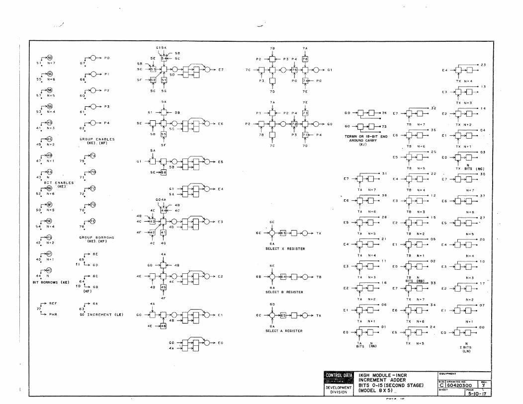
r@ 5 I N+ 7
r>@ 55 N+6
r@ 57 N+5
r@ 53 N-+4
r@ 41 N+3
r@ 45 N+2
r>@ 47 N 1'- 1
r€3 43 N
BIT ENABLES r® '(KE)'
52. N+6
r@ 50 N+5
r@ 54 N+4
r@ 42 N+ 2
r@ 40 N+ 1
r@ 44 .
BIT BORROWS (KE)
r- REF 77
4 PWR
~ PO 67
~ PI
66
~ P2
60
~ P3 61
~P4 62
GROUP ENABLES (KE), (KF')
rl3 7S
r@ 71
rl3 72 . r@
70
r@ 76
GROUP BORROHS '(KE1, (KF)
r- 6E
65 f I 4 6D
r- 6C 64
fO 4 68 (KF)
r- 6A 63 GO' INC R EME N T (LE)
G15A 78 7A
S8
5C E7 7C
SF
5C 5G 7D 7E
SA 7A 7E
5E E6 P2 -
SF 7C 70 SA
G I E5 ~~ SE 56
G1~ E4 SA
G04A
48
4C E3 6£
4F 6C ~ TX
4C 4G 6A SELECT X REGISTER
4A
6E
4E E2 68 ~ TB
6A SELECT B REGISTER
4F
4A 60
GO -~ E 1 6C ~ TA
4£ 46 6A SELECT A REGISTER
GO @=rEO
4A
G 1
GO
GO --v-:o-: 74 E7~ 3'2
GO --v-:o-: 73 T8 N+7
~ 35
TERMN OR IB-BIT END E6 AROUND CARRY
(KJ) T8 N+6
~ 25
ES
T8 N+5
E7~31 ~ 22
E4
TA N+7 T8 N+4
~36 £6 T '--' ~
12
E3
TA N+6 T8 N+ 3
~26 E5 T L-J E2-1~
IS
TA N+5 T8 N+2
~'21
E4 T L-J £1~ 05
TA N+4 TB N+ I
~" E3 r L-J
02
EO~ TA N+3 T8 N
~'6 E2 r L-J
33 E7~ TA N+2 TX N+7
~06 £1 r L-J
~34 E6 r L-J
TA N+' TX N+6
~01 EO T L-J
ES ~ TX
IKGH MODULE -INCR INCREMENT 'ADDER
N+S
BITS 0-15 (SECOND STAGE) (MODEL 8 X 5) ,
24
E4 ~23
TX N+4
~ 13
E3
TX N+3
,~ 14
E2
TX N+2
~ 04
E1
TX N+ 1
~'~ 03
EO
TX BITS (lie)
-6=0=
30 E7
N+7
---6=~ 37
£6
N+6
£5 -6=0=.27
N+5
-6=0=
20 E4
N+4
-6=0=
10 E3
N+3
-6=0=
17 E2
N+2
,...c;-;::::::; 0 7
£I~
N+I
-6=0=
00
EO
N I BITS
(LN)

r® 5 I N+7
r@ S5 N+6
r@ 53 "'1+4
r@ 41 N+3
r@ 43 N
BIT ENABLES r® '(KEr
52 N+6
r@ SO N+5
ri9 42 N + 2
r® 40 "'1+'
r@ 44 .
BIT BORROWS (KE)
r REF 77
4 P"'R
rO- PO 67
rO- PI 66
rO-P2
60 . 6'rO-
P3
rO- P4 62
GROUP ENABLES (KE), (KF')
~ 75
r@ 71
rl9 72 . r@
70
rl9 76
GROUP BORROWS '(KE1, (KF)
r 6E 65
fl 460
r 6e
64 fO 46B
(KF)
r 6A 63 GO' INCREMENT (LE)
5B
5C
SF"
5E
GI
4B 4C
4F
4E
GO
G1SA 7B
E7 7C
5C 5G 70 7E
SA 7A
E6 P2 .
SF 7C 70 SA
E5 ~ 5E 56
Gl~ E4 SA
G04A
E3 6E
6C ~ 40 4G 6A
SELECT X REGISTER 4A
6E
E2 6B ~ 6A
SELECT B REGISTER
4F 4A 60
~ El 6C ~ 4E 46 6A SELECT A REGISTER
GO ~EO 4A
GI
GO
TX
TB
TA
~3'2 E7 r L...J
T8 N+7
~3S E6 r L...J
TB "'1+6
~25 E5 r L...J
T8 "'1+5
E7~31 E4~22
TA N+7 TB N+4
E6 ~36
E3 ~'2
To4 "'1+6 T8 "'1+3
~26 E5 r L...J E2
~'5
E4
E3
E2
EI
EO
fA "'1+ 5 T8 N+2
~'21
El ~05
TA N+4 T8 N+!
~'l EO ~02
TA N+3 TB N
~ 16
~ E7
TA N+2 TX N+7
~ 06
~ E6
TA N+I TX N+6
~ 01
~ E5
TA N BITS (RA)
TX N+5
4KG7 MODULE -INCR INCREMENT ADDER BITS 0-15 (SECOND STAGE)
6K14-15
33
34
24
E4~ 23
TX N+ 4
~ 13
E3
TX N+3
~ 14
E2
TX N+2
~ 04
E1
TX N+'
~ 03
.1'0
TX BITS (lie)
--D=D=
30 E7
N+7
-6{]: 37 E6
N+6
E5 --D=D=.27
N+5
--D=D=
20 E4
N+4
--D=D=
10 E3
N+3
--D=D=
17 E2
N+2
--D=D=
07 E I
N+I
--D=D=
00 EO
N BITS (KK)

r9 52 ENABLE 16
r@ 56 ENABLE 17
r0 53 BORROW 16
(KF)
~ G8 70 GR BORROw a
r@ ~PO 71 60 GR BQRROv.l I GRD ENABLE a 7E 7D
r@ ~PI 75 61 GR BORROIrl 2 GRD ENABLE I PI G8
r@ ~ __ P2
76 65 GR SQRROlt4 3 GR ENABLE 2 78 7C
r@ ~ P3
72 66 GR SORROw 4
(KE) (KF) GR ENABLE 3
r- 6E (KE)
64 60 II L.. 6D
~ 6C TA
r 6C 6A 63 SELECT A REGISTER
10 L.. 68 6E (KF)
~ 68 T8
r- 6A 6A 62 SELECT 8 REG ISTER
6E
GO INCREMENT
~ ( LE) 6C TX
r- REF 77 6A~ TI-J
L.. P""R 61 TV
SELECT x REGISTER
~ SD E4 58
~ 5D E3
58
~~ 5D E2 58
SA
~ E I
58 SC 53
~EO G8
SA
~03 EI BIT 17
TX n04 EO BIT 16
TX (RC)
EI --CS=:O=0O
BIT 17
EO --CS=:O=07
BIT 16 (KK)
-9iF
25 E2 BIT 32-33
TW
-9iF
26 E2
BIT 30-31
TW
,--11 E2 ~28-29
TX
-9iF13 EI BIT 26-27
TX
-9iF
14 EI
BIT 24-25
TX
-9iF
'2 E2
BIT 22-23
TX
-9iF
'5 EI
8IT 20-21
TX
-9iF
'6 EI BIT 18-19
TX EXTEND SIGN (RD)
EI ~01
TABIT17
EO ~06
TA BIT 16 (RA)
EI ~02
TB BIT I 7
~05 EO BIT 16
T8 (R8)
4KH7 MODULE -INCR INCREMENT ADDER BITS 16,17 (SECOND STAGE)
6KI6
-9iF
42 E4 BIT 58-59
TV<
-9iF
44 E4 8IT 56-57
TV
-9iF
45 E4 8IT 54-55
TV
-9iF
31 E3 BIT 52-53
TV
*33 E3
BIT 50-51
TV
-9iF
34 E3
BIT 48-49 TV
-9iF
32 E3 BIT 46-47
TV
-9iF
35 E3
BIT 44-45
TV
-9iF
36 E3 BIT 42-43
TV
-9iF
21 E2 BIT 40-41
T,.,
-9iF
23 E2 BIT 38-39
TW
-9iF
24 E2 8IT 36-37
T,.,
-9iF
22 £2
8IT 34-35 T,., EXTEND $tGN
(RO)

Two lKIH modules and a lKJH module add the 22-bit RAC to the sum or difference of two IS-bit operands. The lKIH modules generate bit enables, group enables, group borrows, partial sums, and partial carries. These signals proceed to the lKJH module where the computation is completed.
lKIH MODULE
The following example shows a pencil-and-paper addition for values which require correction.
Aj K
RAC
,----------, : 123456 : : 654322 : 1..-0 0 0 0 0 0 I
1- J ""0-0".....,0'"""""'0""""'0~1
o 3 0 0 0 000 o 3 0 0 0 0 0 1
IS-bit sum with end around carry correction
22-bit result
The following table shows the conditions of the terms and output signals when the three operands are assigned values of the above example. Refer to the lKJH module for the final result of this example.
Input Signals I II
Output Signals
.5--10-22
Groups Bits
A:f~654321
K:-123455
RAC~4777777
PSIO-PSO terms
PS3-PSO terms
PCIO-PCO terms
PCIO. PC2-PCO terms
E10-E4 terms
Group enables
Group borrows
21
FI
FI
FO I I
X
I
I
I
5 20 19 18
FI FI FI
Fl Fl FI
I 0 0
I 0 0
X X X
I I I
X X X
0 I I
Termn
I
4 17 16 IS 14 13
I I 0 I 0
0 0 I 0 I
I I I I I
0 0 0 0 0
X X X 0 0
I I I I I
X X X X I
I I I X X
I
0
F=Forced
3 2 I 0 12 11 10 9 B 7 6 5 4 3 2 I
I I 0 0 0 I I 0 I 0 0 0
0 0 I I I 0 0 I 0 I I 0
I I I I I I I I I I I I
0 0 0 0 0 0 0 0 0 0 0 I
0 0 X X X X X X X 0 0 I
I I I I I I I I I I I 0
I I I X X X X X X X I 0
X X I I I I I I I X X X
X I I X
X 0 0 X
0
I
I
I
I
I
I
I
X
Partial sums PSO through PSIO are determined by the following truth table.
RAC 1 K Condition
1 1 1 1 1 1 0 0 1 0 1 0 1 0 0 1 0 1 1 0 0 1 0 1 0 0 1 1 0 0 0 0
Partial carries PCO through PCIO are determined by the following truth table.
RAC 1 K Condition
1 1 1 1 1 1 0 1 1 0 1 1 1 0 0 0 0 1 1 1 0 1 0 0 0 0 1 0 0 0 0 0
60420300 Y

4 3 ... 2 1
-6{] -D:o "~ ~SIO r-+KIO
J4:p JIO~ rlo~ zo YO PSIO~EIO PS8 75 -G---o75 52 51
C7 EIO ~ 0 10/21 RAC L-RIO K~LlO K4 T7 LID 4 KIO Z2 NY7 C9
PS9 81T 10/21 R4 510 510 Z7 Y7 4A 74
~J4 ~JIO CS
r4~ rlo~ rlo~ 26 53 L4 TI LID ZO L10 ZI Z4 PSIO Y4 PS9 PS9 76
T L-.I4 T L-IIO R4 SIO RIO C8 9/20
0 r4~ J9::7P JIO" Z2 Y2 PS8 D
r-+K4 ~J9 K4 2 K9 Y7. KIO~
."~'" ~ 25 _ 40 E5 PS4~72 "
K L-L4 j ~r9 S4 R9 RIO ZI NZI YI C3 4/15 P54 72
J43B I930 J7~ NZ2
NZ4 5A C3 ~S4 ~K9 L4 T4 LS YI K7 --D=D 58 55 --00 C4
24 41 54 R9 R7 TO CC3~ XO PS5 74 RAC L-.R4 i<'L-L9
r4~ r9~ r7~ CP34 NX7 E6
81T 4/15 T7
PP4
r-+59 L4 TO K9 Y2 L7 I X7
~J3 S4 59 R7 23 42
L-.I3 RAC L-R9 J33® J9~ rr~ T4 P54 X4 P58
81T 9120 K3 U7 L9 4 K7 P55
r-+K3 .r--J8 R3 59 57 T2 X2
22 45
I3~ r9~ J7~ K L-L3 j L-I8 L3 LJI L9 YO L7 TI XI
R3 59 57 P56 65 E8~
r-+53 ~K8 I3, J8 '.
rr~ -GO -00 E7 E9 73
C 21 46
L7 PS7 EIO 2/5 C RAC ~R3 K~L8 K3j@ K8~ UO WO GRoUP ENABLE
BIT 3/14 53 R8 57 IKJITERMN)
~J2 r-+58 J3~ IS38 J6~ U7 W7 C3
P54 62 _ 15 44 L3 U4 L8 I K6 V7
j ~r2 RAC L-R8 E5 6/17 53 R8 R6 U4 W4 PS7
81T 8/19
I3~ I8~ I6~ ~K2 r-+J7 L3 UO K8 2 L6 VI U2 W2 PS5 67 13 33
i<L-L2 T 'L-..rr 53 S8 R6 C4 5/16
+ J2~ J8)3 r6~ UI WI +
~52 ~K7 K2 P L8 X4 K6 V2
RAC 'LR2 32 R2 58 56
P~ -6{] P57~ PS8~64 K L-H7 C7 8/19
r~ L~~ J6~ VO C6
C7 ~ ENA8LES 81T 2/13 ~2 PI
P58 E6 IKJ) L6 V ~JI ~57
S8 S6 P7 E5 61
03 31 mo ffi M ~
j L-rl RAC L-.R7 I2~ ,:~ I6~ C8 E9 GROUP ENABLEIKJ)
81T 7118 K2 P2 L6 VO P4 PS2 PS6 P59 50
B ~KI ~J6 52 56 EIO 2/5 B 02 _ 34
J2~ f3® J5~ P2 P56~
K L-.LI j L-I6 L2 P K5 07 C5 C2--Q-:D-: 65 52 R5 PI VI C6 r-51 ~K6 2/13
I2)9 ~~ I5~ 01 36 Cl --Q-:D-:60 RAC L-RI i<L-L6
L2 PO L5 01 ---CH3 ---CH3 1/12 81T 1/12 52 5 RS NO MO
C0--Q-:D-: 66 r-+J r-+56 JI~ ~~ I5~
0/11 06 35 KI NT K5 0 N7 M7 07
CIO --Q-:D-:54 j L-.I RAC ~R6 RI 55 81T 6/17 10/21
I')v ~3E J5--,. N4 PSI M4 PSO Q4 PS5 PARTIAL CARRY
r-+K r-+J5 LI NI L5j§ 8IT5IKJ)
05 12 PS3~20 i<L-L ~I5 RI 55 N2 B 04 M2 B 03 Q2
3/14
I'~ I'~ I5~ NN02?W '.'2?W ~K5 NNI CI NMI CO PS2--Q-:D-: 16
~5 KI N LI NO L5 QQ NI MI QI 2113 NN2 NM2 04 10 51 51 S5 NN4 A B 02 NM4 A NQO
A RAC L-R K~L5 B 05 PSI~07 A JI~ NQI 1/12 81T 0/11
(KE,KF,HQ) LI 4~ -16 M M n .r--->REF
r-+S5 51 57 P50~00 77 II
25N; CLOCK 56 CL 0/11
'L-PWR RAC L-R5 CK CK CK CL PARTIAL SUM BITS
IKJ) 81T 5/16
CODE IDENT DwaNO 0 ..
~PWR~ ~ <S2)~~Z' 1 KIH MODULE - INCR ~GND ~GND ~PIVR b"""-GND ~PWR ~PWR
34010 Y 17 27 37 30 43~ 55~ 7°L
INCREMENT + RAC ADDER ~PWR 'Gwv-.-PWR 'Lvvv-..GND 'Lvvv--.,PWR GNDCL CL DEVELOPMENT (FIRST STAGE)(MODEL 8X5) C
SHEET GND GND DIVISION
4 3 .. 2 5KOI-02 1

4KI7 MODULE
Two 4KI7 modules and a 3KJ7 module add RAC to the sum or difference of two
IS-bit operands. Each 4KI7 module performs a partial computation on nine bits
of the three operands. The upper input pin pairs receive complemented data from
the Aj. Bj. or Xj register. The middle input pin pairs receive complemented
data from the CIW register K deSignator or complementary (true or false) data
from the Bk register. The lower input pin pairs receive data from the RAC
register. The KI modules generate bit enables. bit borrows. group enables.
and group borrows. These signals are sent to the 3KJ7 module where the com
putation is completed.
The following table shows the condition of the terms and output signals when the
three operands are assigned arbitrary values. The output signals cause the 3KJ7
module to provide a result of 00236. (Note that Aj and K enter the 4KI7 modules
in a complemented form.)
Groups 5 4 3 2 1 0
Bits 17 16 15 14 13 12 11 10 9 S 7 6 5 4 3 2 1 0
RAC = 777600 1 1 1 11 1 1 1 1 1 1 1 0 0 0 0 0 0 0
AI = 777752 1 1 1 1 1 1 1 1 1 1 1 1 1 0 1 0 1 0
K = 777765 1 1 1 1 1 1 1 1 1 I 1 1 1 1 0 1 0 1
AS-AI terms 1 I 1 I 1 1 1 1 1 1 1 0 0 1 1 1 1 X
BS-Bl terms 1 1 I I 1 1 1 1 1 1 1 1 1 0 0 0 0 X
CS-C3'terms 1 1 1 1 1 1 1 1 1 1 1 1 0 0 0 X XX
Bit enables 1 1 0 1 1 0 1 1 1 1 0 1 0 1 1 1 1 1
Bit borrows 1 X X X X X X 1 1 1 X X X XX X 0 0
Group enables 0 0 X 0 0 X
Group borrows 1 1 X 1 0 X
60420300 Y
The Al through AB. Bl through BS. and C3 through CB terms are the key to deter
mining the enables and borrows for three given input operands. Bit N. N+1. N+2
enables. and At through AB terms are determined by the following truth table.
RA K Condition
1
1 0 0
0 1 0
1 0 0 1
0 1 1 0
0 0 1
0 0
0 0 0 0
Bit N. N+1. N+S borrows. and Bl through BB terms are determined by the following
truth table.
1
o o o o
1
0
0
0
0
K
0
0
1
0
0
Condition
0
1
1
0
0
0
The C3 through CB terms are the B~ through B7 terms left-shifted one bit position.
5-10-24 ,

21 2C 41 4C 4T
r@ .-----49 )~::* LV
23 42 2H 4H 87 C8 88
~" ~ 21 ~ 41
j A4 <'"<~ ~. A8 A8 ~ A 02 N+8
~ j>@ C8
22 43 4N 4P 4T 43 58
~ 2H ~ 4H I( K 2V 4V 86 IV' C7 =S:Ef>0 8 I
~r~·:' ~ 2G ~ 4G AS
2 I 4 I 2L 2F 2T 4L 4F 4T C5
~ L.9 RA BIT N+4 RA BIT N+8 2K 4K 58
~ ~ 85 yv C6
27 47 A3 A7 06
~ 2L ~ 4L
T r4] .-->@ 5B
26 46 2V 4V A6 B
~ 2K ~ 4K B4
Y$1~ C5
I( K I I I C IT 31 3C 3T C6 ~~'" 2J ~ 4J ,
~ •
~ 7C
25 44 lH 3H 7B 71 C7 N+8
~ ~ 5B
RA BIT N+3 RA BrT N+7 A2 A6 A7
.------><@ .-->@ B3 -rv C4
1 3 33 1 N 1 P A7 76
~ II ~ 31 C7
T T I V 3V
r-"O ~ 5B
~71 12 32 I L 1 F 1 T 3L 3F 3T A6
~ lH ~ 3H B2 1$=1 C3 C6
K K 1 K 3K A3 N+6
~ lG ~ 3G I 11 31 Al A5
T~~>" t-g L~ 5B
RA BIT N+2 RA BIT N+6 3R
~ r@ 2A 3A 4A C7 73 I 1 7 37 1 V
~ "+2 A4
~'L ~ 3L 38 3
j T 66
~ r@ lB 82 2B B4 3B -J3N1 B6 4B BB AB C4 X-
16 36
3C ~ 3A
C3 6B
~ lK ~ 3K
~61 I( I( .3
~ lJ ~ 3J lC 2C 3C 4C C3
15 35 C4 63 N+3
Y] ~ 10 20 3D 40 A2 ---Q:Q: 75 RA BIT N+' RA BIT N+5
lE~ .----;.@ N+2
05 ~ REF AS Al ---Q:Q: 65 ~J 77 IE
~ 81 2E B3 3E B5 4E B7 7A
j t- P"'R
r--® IF 1 SID 2D 7B ~74 04 7C "+2
~I 1 F 2F ~ 3F 4F 6A
I( CL
03~H ~ 5B ~54
CK
~ 1J ~ ~ ~ 5C N+l
L.© 52 GROUP ENABLES (KJ)
A BIT N 25 NS ·CLOCK CL CK CK CK CL CL (KE) (KF) (HO)

• 5-10-26
lKJH MODUlE
Two lKIH modules and a lKJH module add the 22-bit RAe to the sum or difference of two lS-bit operands. The lKJH module completes the computation and sends the result to SAS when go increment to storage-l is present. The result is based on input signals received from the lKIH modules.
The following table shows the condition of various terms when the input signals are assigned an arbitrary value. (Note that the input signals are the same as the output signals shown in the lKIH module table.)
Input Signal s
Internal Terms
Output
Croups Bits
ElO-E4 terms PS3-PSO terms PCIO,PC2-PCO terms Group enables Gro up borrows IS-bit end around carry
E3-EO terms CIJ-Cll,C2-CO terms Croup enable GE2-4,GEI-3,GEO-2 terms FS-Fl terms A21-AO terms Inc.r-l
Corree ted resul t
I
I X I
I
X X
I 0
5 4 3 20 19 18 17 16 15 I' 13 12
0 I I I I I X X X X X X X X X 0 0 0 X X X X X X X I I N/A I X
I 0 X I I I
X X X X X X I I I X X X X X X X 0 0 X X I
2-4-1 1-3-1 0 0 0 0 I I I I I I I I 0 I I 0 0 0 0 0 0 ~ - ~
o
2 I 0 II 10 9 8 7 6 5 4 3 2 I 0
X I I I I I I I X X X X 0 X X X X X X X 0 0 I I I I X X X X X X X I 0 I
I I X 0 0 X
I X X X X X X X I 0 0 0 0 X X X X X X X X 0 I I
X X 0 0-2-0
0 I I I I I I I I I 0 0 0 0 0 0 0 0 0 0 0 0 0 0 I ~ ---.- ---.- ---.-
60420300 Y

D
c
.. B
A
4
.r-O--- E21 6"0-- PCI3 .r-O--- PSI4 21 70 13 47 14 46 000
.r-O---E2O 20 60
0
.r-O---E19 19 61
0
GROUP 5
~EIB 16 62
o
rO-EI7 17 63
o
rO-EI6 16 64
o
rO-EI5 IS 65
o GROUP 4
.r-O--- EIO 10 10
0
r@ 9 37
0
r@ 6 36
0
GROUP 2
r@ 7 35
0
r@ 6 34
0
r@ 33 0
r® 4 32
0
GROUP I BIT ENABLES
(KI)
1=O='6C CIB
23
4D
~PCI2 ~PSI3 12 45 13 44
0 0
rO-PCII rO- PSI2 II 42 12 43
0
~CIO
MrPCIO
0
10 41 11
~SII
MrPS1\ 40
o o GROUP 3
rO- PC2 2 07
o
rO-PCI 04 o
rO- PCO o 01
o
rO-PS3 06 o
.r-O--- PS2 2 05
o
rO-+ PSI 00 o
1=O=C21 PC21
1=0= SO PSO
21 03 0 02 0 0
GROUP 0 PARTIAL CARRY PARTIAL SUM
BITS (KI) BITS (KI)
1=O=G5B GB5
22 0
rO-GE4 rO- GB4 4 21 4 20
0 0
rO- GE2 rO-GB2 2 25 2 24
0 0
~GEI .r-O--- GBI 1 27 26
0 0
GROUP ENABLES GROUP BORROWS (KI) (KI)
~CCIB 11 r+REF ~GND 0
IS-BIT 77 12 END AROUND 'L..... PWR 'L...v.-..GND CARRY (KG)
4
E19~A19 FS--{j-{j .....,
E17~A17 EI6
EI5
F4
EI5~AI5 F4 ---tj-{j .....,
3
E20~A20 EI9
F5
:::~AIB E15~ E16~A16 EI5
F4
.. AI3
AI2
ClI
AI3
CI2
F3
AI2
AlI
AI2
ClI
CII
PSI4~AI4 PSI3~CI3
2 1
AI3
,----071
~66
A21 A20 TO BIT 21
AI9 PI
A20~AIB 67
AI9 TO BIT 20
AlB
AI9~Pl 76
AlB TO BIT 19
PI~75 AlB
PI TO BIT 18
PCI3---tj-{j r ~ ~....., PCI2~ L......J .....,
EI4
PSI3~AI3 PSI2~CI2 PCII~ L......J .....,
AII~52 F3 All TB BIT II
INCR BITS
A16~73
TC~ BIT 16
AIS~S7
TC~
A17~74
TC~ BIT 17
AIO~S4
TB~ (ST) PCI2--{j-/j r ~ ~ .....,
EI3
PSI2~AI2 PCI1 --{j-1j r ~ L......J .....,
PSII~CII PCIO~ L......J .....,
PS2~ PCI~ L......J '-"
E21~A21 E20
EI9
BIT 15
AB~55
TB~. - BIT 8
BIT 10
A9~53
TB~. BIT 9
EI2
PSII~AII PCIO ---tj-{j r L......J L......J .....,
PSI~ PCO~ L......J .....,
PSO~ PC21 ....;f-' L......J '-"
~!:=;rFS P4
GBI
GB2
GE3
Ell
E9~ EB
F2
E7~7 E6
E5 FI E4
E5~ E4
FI
E4~ Fl ---tj-{j .....,
EIO~AIO E9
EB
F2
EB~ F2 ---tj-{j .....,
!:~ E4
FI C~~
PS3~ PC2---tj-{j ....., ~ ~ .....,
E2
PSI
E3
PCO
PS2~ PCl ---tj-{j ....., L......J L......J .....,
E3
PS2
PCI
GE4~ GE3 24 GE24
GE2
GE3~ GE2 26 GEI3
GEl
GE2~ GEl 23 GE02
GEO
GB5 ---o-o--v- BG5
GE4
P4
GE4
GE13
GBO
GE4
El CC1B~GB3 GEl GB4 GEO
BGS
GEl F2
GBO
GBI 25
GBO EI2
PS3
E14froo-EI3 42 GE3
EI2
SII
CIO
EI4
E13
PSI2
E14
PSI3
PCI2
Ell
PSO~~ E2 PSI4
GB3
PC21 --{j-1j ....., ~ L......J .....,
E3~ El 02 GEO
EO Cil5)=,~
3
DEVELOPMENT DIVISION
2
BGA
G56
IBC
A2
AI
CO
A2
CI
GB5
AI
AO
AI
CO
EA1B
CIB
A7~51
TB~ BIT 7
r----o30
A4~31
TA --1.J-i.....J-: BIT 4
A5~I6
TA~ BIT S
CIS
GBS
AO
CO
GBS
BGA
GE02
GE3
P4
GEI3
GBO
EAIBT GEO FI
GBO
lKJH MODULE - INCR INCREMENT + RAC ADDER (SECOND STAGE) (MODEL 8X5)
5K03
,----<>14
CCtB*" BGS
GE02
GE2
GEl F3
GBO
GE2 22 GB2
GBt
CODEIDENT
34010
c 1
o
c
B
A

60420300 Y
3KJ7 MODULE
Two 4KI7 modules and a 3KJ7 module add RAe to the sum or difference of two 18-bit
operands. The' 3KJ7 module completes the computation and sends the result to the
SAS when the g" increment to storage signal is present. This result is based on the
condition of bits 0 through 15 enables; bits 0, I, 8, 9, 10, 17 borrows; groups I, 2,
4, 5 enables; and groups I, 2, 4, 5 borrows. These input signals are generated by
the 4K17 modules. The following table shows the condition of various cage wire terms
when the input signals are assigned an arbitrary value. (Note that the input signals
are the same as the output signals shown on the 4KI7 module table.)
:Groups '5 4 3' 2 1 (!)
Bits 17 16 15 14 13 12 11 10 9 8 7 6 S 4 3 2 1 0
Bit enables 1 1 0 1 1 0 1 1 1 1 0 1 0 1 1 1 1 1
Bit borrows 1 X X X X X X 1 1 1 XX X XX X 0 0
Group enables 0 0 X 0 0 X Group borrows 1 1 X 1 0 X
A1S-AO terms X X 1 1 1. 1 Q 0 0 1 0 1 "1 O. O· 1 1 0
BI0, 9, I, 0 terms X X X X X X X 1 1 XXX X XX X 0 1
ES-EO terms X X X X X X X X X XXX 0 o 0 0 0 0
FS-FO terms X X X X X X X X X XXX 1 1 1 1 0 1
GS-GO terms X X X X X X X X X XXX 1 1 1 1 0 1
Result = 000236 X X 0 0 0 0 0 0 0 0 1 0 0 1 1 1 1 0
5-10-28 I

r@ 21 BIT 8
r® 56 BIT 17
5H~ 5D AIS
5E
6F~AII 6E~ '--" L-J L-J '-/
5H~A15 50 --t1---t1 ~
AI7
r@ 23 BIT 7
r@
.-® 51 BIT 16 · rl9 :~~"0:~~Al4
24 BIT 6 50 BIT 15
rB 20 BIT 5 53 BIT 14 68 ~A9
r@ 6 A --{j--.tj ~ '----' L.J '-J
2S BIT 4 52 BIT 13 2E
26 BIT 3 54 BIT 12 ~;~'B GROUP 1 AND 2 GROUP 4 AND 5
ENABLES ENABLES
r® 06 BIT 2
• ENABLE
r® as BIT I
BORROW
r® 04 BIT 1
• ENABLE
reD 03 BIT 0
BORROW
r® 02 BIT a
• ENABLE
r@ 61 BIT II
• ENABLE
rO 62 BIT 1('\
BORROW
r@ 63 BIT 10
• ENABLE
rl:9 64 BIT 9
80RROv.l
r@ 65 BIT 9
• ENABLE
01 BIT 17 66 BIT e · BaRROI-oj BORROW
2D~~,--2H , A"7
2E
~'
2H AS
2D
28
~~~A5 2C~'~~
GROUP a DIGITS GROUP 3 DIGITS
2G~A3 rC>-- E 1 rC>-- G 1
~A -D-U '--' 43 GROUP I 34 GROUP I
rC>-- E2 44 GROUP 2
...0- (4
42 GROUP 4 · rC)-+ ES
45 GROUP 5
GROUP ENABLES (KI)
r REF
77 4 PWR
rC>-- 02 35 GROUP 2
~~A: ~ , .. c -tl-{j ~ '--~ ,---' v
33 GROUP 4
rC)-+G5 ~ 32 GROUP 5 D H ,_ J A1
GROUP BORROWS
(KI)
B~AO
5G~A12 SA -u-.u ~
BID
60
6A~B9
68
D~81
B~BO
A B
GO
68 6H
::~" 6I~ 61 6E
6H~E3 6G
I
H --...l _ . --+[]-{]-O-+ EO
E4
G4~F5 -Y9~~
G5
E3
G3~F4 ~
G4
E2
"~,, E319
03
E1
Gl~F2 :: '~-~ G2
E5
G5~4 EO FO
EO 36
GO
E5
EO~E51 E 1
E4
E5~"E40 EO
E3
E4~E3S E5
E2
E3~E24 E4
El
E2~E13 E3
ED
E1~E02 E2
FO
F3
AIO
A9
Al0
F2
A I
AD
A I
F5
F2
AI7 ~55
TC~BITI747 AI2
TA BIT 12
A9
89 810
E02
89
F2
A3 j5Q= 15
TA BIT 3
AD Al
F2
F5 E35
80 81
BO
F5
~TC
TS
71
GO INCR TA TO STOR
(XGJ
3KJ7 MODULE - INCR INCREMENT + RAC ADDER(SECOND STAGE) (MODELS 175.7 XO)
6LI6
AI6 Pii.::57
TC~8ITIG40 AI5
TA BIT 15
A14~41 T 'sI'r 14
78
AI3 ~46 TA~13
70
A7 j5Q= 73
TB BI T 7
A6 ~7S TB~6
17
AS ~'Z T8~5
r----'4

26
22 6.
NOTES:
(!) AN XF MODULE I S USED WHEN OPTION AT364 -A IS NOT INSTALLED.
II: 24 63 W
l-I/)
II: CI () W Z II: N
I ClO ...J W Ox CD ...J ...J ... ;j
:x: _
20 0 I-It)
67 0 I/)~ ::IE W...J ... I-W
:.: 11: 0 :.: uO ..,. ~~
16 ~ REF 51
77 L...;. PWR
12
, 4 53
, 0 57
72
'-........ _-'---... GND
06
CL-M CL-M
4'
02 45
04 ~~ CK--Q..{]
9 f) CK--Q..{]
43
~3 CK
34
25 NS' CLOCK 3 CL (LHl
47

4
o
c
B
A
4
3
CLOCK PERIOD
CLOCK PULSE
TWO SUCCESSIVE INCREMENT INSTRUCTIONS IN THE TOP PARCEL OF THE CIW REGISTER
@ GO ISSUE
NOTES:
GO INCREMENT FLAG
GO INCREMENT TO STORAGE FLAG
A; (I) RESERVED
x; (I) RESERVED
INSTRUCTION I RESULT ENTERS A; (I)
INSTRUCTION I READ REFERENCE ENTERS x; (I) (ASSUMING NO CM BANK CONFLICTS)
B; (2) RESERVED
INSTRUCTION 2 RESULT ENTERS B; (I)
I I I I
101 ® I I I I I I I I cd I I
~ I I I I I I I I I I 101 I®I ~
I I I I I I I 101
ITI I I I I I I I 101
~ I I I I I I I I I II I
I I I I I I I
IIC5lJ I I I I I I
I I I
I I
~ I I I I I I
:®U
* GO ISSUE FOR INCREMENT MAY BE DELAYED ONE CLOCK PERIOD
IF MEMORY ENABLE IS NOT UP.
o INSTRUCTION I
® INSTRUCTION 2
@ ENABLE ISSUE IS DELAYED 4 CLOCK PERIODS (THEREFORE, GO ISSUE
IS DELAYED A MINIMUM OF 4 CLOCK PERIODS) IN THE AAI20-C.
THIS DELAY IS REMOVED BY INSTALLING OPTION AT364-A.
3
2
* 5 6 7 8 9 10 II 12 13 14 15 16 17 18 19 20 21 22: 23 24 25
0
I 0 1U I
I
TIMING DIAGRAM INCREMENT INSTRUCTION (MODELS 175.7XO)
1
D
C
B
t;

D
c
.. B
A
4 3
CLOCK PERIOD
CLOCK PULSE
THE SUCCESSIVE INCREMENT INSTRUCTIONS IN THE TOP PARCEL OF THE CIW REGISTER.
GO ISSUE
NOTES:
& INSTRUCTION 1 & INSTRUCTION 2
GO INCREMENT TO STORAGE
A; (I) RESERVED
xi 01 RESERVED
INSTRUCTION I RESULT
Bl (21 RESERVED
INSTRUCTION 2 RESULT
& ISSUE MAY WAIT ONE CLOCK PERIOD FOR MEMORY ENABLE ON SINGLE/DUAL MODEL 875.
&, SINGLE/DUAL MODEL 875.
& SINGLE /DUAL MODEL 865.
4 3
I
2
* I 5 6 7 8 9 10 II 12 13 14 15 16 17 18 19 2021 22123 2425
I I
~~~----=~~------------~~~--------~-----I I I I I I
1&1£1 ,...;----7-------;-------:-~-----__;_---~
I I I I I I I I I ~~~---~----~-~----~----
I I I I I I
~~:~~------~----------~--~--------~:-----lEi I I I I &, &.
I I I -rl&:
~~~------~----------~
I I I
~ I
&,
I I I
1& I
CSI~~ TIMING DIAGRAM DEVELOPMENT I NCREMENT INSTRUCTION
DIVISION (MODEL 8 X 5 )
2
1
D
c
B
A
CODEIDENT
c 1

w Z ::::;
~ Z o -' « .... :J U
0-
"'f M « «
COMMENT SHEET
MANUAL TITLE: CDC CYBER 170 Models 175, 740, 750, 760, 865, 875 Functional Units Hardware Maintenance Manual
PUBLICATION NO.: 60420300 REVISION: AA
NAME: __________________________________________________________________ __
COMPANY: ___________________________________ _
STREET ADDRESS: ____________________________________________________ _
CITY: __________________________ STATE: __________ ZIP CODE: ___________ _
This form is not intended to be used as an order blank. Control Data Corporation welcomes your evaluation of this manual. Please indicate any errors, suggested additions or deletions, or general comments below (please include page number references).
o Please Reply o No Reply Necessary
NO POSTAGE STAMP NECESSARY IF MAILED IN U.S.A.

FOLD FOLD ---------------------------------------------------------------------------------------------------------------~
""" BUSINESS REPLY MAIL
FIRST CLASS PERMIT NO. 8241 MINNEAPOLIS, MINN.
POSTAGE WILL BE PAID BY
CONTROL DATA CORPORATION
Publications and Graphics Division
ARH219 4201 North Lexington Avenue
Saint Paul, Minnesota 55112
NO POSTAGE NECESSARY
IF MAILED IN THE
UNITED STATES
I I I I I I I I I
---------------------------------------------------------------------------------------------------------------, FOLD FOLD
w Z :::;
o z o "< I::> u
t'· ..

CORPORATE HEADQUARTERS. P.O. BOX O. MINNEAPOLIS. MINN. 5544<) LITHO IN U.S.A.
SALES OFFICES AND SERVICE CENTERS IN MAJOR CITIES THROUGHOUT THE WORLD
.~~
CONTR.OL DATA CO~OR(\TION