Blu-ray Disc Home Theater Sound System - Index of
144
© Panasonic Corporation 2010. All rights reserved. Unauthorized copying and distribution is a violation of law. PSG1003054CE A6 Blu-ray Disc Home Theater Sound System Model No. SA-BT235P Volume 1 Product Color: (K)...Black Type Notes: 1) These model’s BD Drive/Main P.C.B. Assembly are:- - RFKNBT235PA. 2) Please refer to the original service manual for: • Speaker system SB-BT235P-K, Order No: PSG1001017CE. Caution: Pairing of BD Drive and Main P.C.B. as “BD Drive & Main P.C.B. Assembly” have to be replaced together. If either BD Drive or Main P.C.B. is changed, BD Drive unit has to carry out re-adjustment due to alignment data for BD Drive Unit is stored in the Main P.C.B.
-
Upload
khangminh22 -
Category
Documents
-
view
1 -
download
0
Transcript of Blu-ray Disc Home Theater Sound System - Index of

PSG1003054CEA6
Blu-ray Disc Home Theater Sound System
Model No. SA-BT235PVolume 1Product Color: (K)...Black Type
Notes: 1) These model’s BD Drive/Main P.C.B. Assembly are:- - RFKNBT235PA. 2) Please refer to the original service manual for: • Speaker system SB-BT235P-K, Order No: PSG1001017CE.
Caution:Pairing of BD Drive and Main P.C.B. as “BD Drive & Main P.C.B. Assembly” have to be replaced together. Ifeither BD Drive or Main P.C.B. is changed, BD Drive unit has to carry out re-adjustment due to alignmentdata for BD Drive Unit is stored in the Main P.C.B.
© Panasonic Corporation 2010. All rights reserved.Unauthorized copying and distribution is a violationof law.

TABLE OF CONTENTSPAGE PAGE
1 Safety Precautions -----------------------------------------------31.1. GENERAL GUIDELINES --------------------------------31.2. Before Repair and Adjustment--------------------------31.3. Protection Circuitry-----------------------------------------41.4. Safety Parts Information----------------------------------5
2 Warning --------------------------------------------------------------62.1. Prevention of Electrostatic Discharge (ESD)
to Electrostatic Sensitive (ES) Devices---------------62.2. Precaution of Laser Diode -------------------------------72.3. Service caution based on Legal restrictions---------82.4. Handling Precautions for BD Drive --------------------9
3 Service Navigation---------------------------------------------- 103.1. Service Information -------------------------------------- 103.2. Caution for Replacing Parts --------------------------- 11
4 Specifications ---------------------------------------------------- 125 Location of Controls and Components------------------ 14
5.1. Remote Control Key Button Operations------------ 145.2. Main Unit Key Button Operations -------------------- 155.3. Using BD-LIVE BONUSVIEW in BD-Video-------- 165.4. Using the iPod/iPhone ---------------------------------- 175.5. Speaker Connections ----------------------------------- 195.6. Disc/Cards Playability ---------------------------------- 205.7. SD Information-------------------------------------------- 225.8. File Extension Type Support (MP3/JPEG/
AVCHD/MPEG2 files) ----------------------------------- 236 Operating Instructions ---------------------------------------- 25
6.1. Removing of disc during abnomality ---------------- 257 Self-Diagnostic and Special Mode Setting ------------- 26
7.1. Special Mode Table 1 ----------------------------------- 267.2. Special Mode Table 2 ----------------------------------- 277.3. Error Code Table ----------------------------------------- 287.4. Service Mode---------------------------------------------- 30
8 Troubleshooting Guide---------------------------------------- 358.1. Troubleshooting Guide for F61 and/or F76 -------- 35
9 Service Fixture & Tools --------------------------------------- 399.1. Service Tools and Equipment ------------------------- 39
10 Disassembly and Assembly Instructions --------------- 4010.1. Disassembly Flow Chart-------------------------------- 4110.2. Main Components and P.C.B. Locations ----------- 4210.3. Disassembly of Top Cabinet--------------------------- 4310.4. Disassembly of AC Inlet P.C.B. ----------------------- 4410.5. Disassembly of Optical In P.C.B. --------------------- 4510.6. Disassembly of Rear Panel---------------------------- 4510.7. Disassembly of Front Panel Block Assembly ----- 4610.8. Dissassembly of Panel P.C.B. ------------------------ 4710.9. Dissassembly of Power Button P.C.B. -------------- 48
10.10. Replacement of Cradle Lid ---------------------------- 5010.11. Disassembly of iPod Cradle Assembly ------------- 5110.12. Disassembly of iPod/iPhone P.C.B. ----------------- 5310.13. Replacement of DVD Lid Unit------------------------- 5410.14. Disassembly of Front Shield Plate Unit ------------ 5610.15. Disassembly of BD Drive------------------------------- 5710.16. Disassembly of Main P.C.B. --------------------------- 6310.17. Disassembly of D-Amp P.C.B. ------------------------ 6410.18. Replacement of Digital Amplifier IC (IC5100/
IC5200) ----------------------------------------------------- 6610.19. Disassembly of Power P.C.B. ------------------------- 6710.20. Disassembly of SMPS P.C.B. ------------------------- 67
10.21. Replacement of Switching Regulator IC(IC5701)---------------------------------------------------- 69
10.22. Replacement of Rectifier Diode (D5702) ---------- 7010.23. Replacement of Regulator Diode (D5802) -------- 7210.24. Replacement of Regulator Diode (D5803) -------- 7310.25. Disassembly of Fan ------------------------------------- 74
11 Service Position------------------------------------------------- 7611.1. Checking & Repairing Side B of Main P.C.B. ----- 7611.2. Checking & Repairing Side A of Main P.C.B. ----- 7611.3. Checking & Repairing D-Amp P.C.B. --------------- 7811.4. Checking & Repairing SMPS P.C.B. ---------------- 8011.5. Checking & Repairing Panel P.C.B.----------------- 82
12 Voltage & Waveform Chart ---------------------------------- 8412.1. Main P.C.B. (1/3)----------------------------------------- 8412.2. Main P.C.B. (2/3)----------------------------------------- 8512.3. Main P.C.B. (3/3)----------------------------------------- 8612.4. Panel P.C.B. ---------------------------------------------- 8712.5. D-Amp P.C.B. (1/2) -------------------------------------- 8812.6. D-Amp P.C.B. (2/2) -------------------------------------- 8912.7. Power P.C.B. --------------------------------------------- 8912.8. SMPS P.C.B. --------------------------------------------- 9012.9. Waveform Table------------------------------------------ 91
13 Illustration of ICs, Transistor and Diode ---------------- 9314 Block Diagram --------------------------------------------------- 95
14.1. Main(System Control) ---------------------------------- 9514.2. Main(Audio) ----------------------------------------------- 9614.3. Digital Audio----------------------------------------------- 9814.4. Power Supply(Main Section) ------------------------- 99
15 Wiring Diagram-------------------------------------------------10116 Schematic Diagram Notes ----------------------------------10317 Schematic Diagram -------------------------------------------105
17.1. Main(Micon/Tuner) Circuit ----------------------------10517.2. Panel Circuit --------------------------------------------- 11217.3. D-Amp Circuit-------------------------------------------- 11317.4. SMPS Circuit--------------------------------------------- 11717.5. Power, Power Button & AC Inlet Circuit----------- 11917.6. iPod/iPhone & Optical In Circuit --------------------120
18 Printed Circuit Board-----------------------------------------12118.1. Main P.C.B.-----------------------------------------------12118.2. Panel, Power, Power Button & AC Inlet P.C.B. -12318.3. D-Amp P.C.B. --------------------------------------------12418.4. SMPS P.C.B.---------------------------------------------12518.5. iPod/iPhone & Optical In P.C.B.---------------------126
19 Terminal Function of ICs ------------------------------------12719.1. IC6001(C0HBB0000057): IC FL Driver -----------127
20 Exploded View and Replacement Parts List----------12920.1. Exploded View and Mechanical replacement
Part List ---------------------------------------------------12920.2. Electrical Replacement Part List --------------------135
2

1 Safety Precautions1.1. GENERAL GUIDELINES
1. When servicing, observe the original lead dress. If a short circuit is found, replace all parts which have been overheated ordamaged by the short circuit.
2. After servicing, see to it that all the protective devices such as insulation barriers, insulation papers shields are properlyinstalled.
3. After servicing, carry out the following leakage current checks to prevent the customer from being exposed to shock hazards.
1.1.1. LEAKAGE CURRENT COLD CHECK1. Unplug the AC cord and connect a jumper between the two prongs on the plug.2. Measure the resistance value, with an ohmmeter, between the jumpered AC plug and each exposed metallic cabinet part on
the equipment such as screwheads, connectors, control shafts, etc. When the exposed metallic part has a return path to thechassis, the reading should be between 1MΩ and 5.2MΩ.When the exposed metal does not have a return path to the chassis, the reading must be
(This “Safety Precaution” is applied only in U.S.A.)1. Before servicing, unplug the power cord to prevent an electric shock.2. When replacing parts, use only manufacturer’s recommended components for safety.3. Check the condition of the power cord. Replace if wear or damage is evident.4. After servicing, be sure to restore the lead dress, insulation barriers, insulation papers, shields, etc.5. Before returning the serviced equipment to the customer, be sure to make the following insulation resistance test to prevent
the customer from being exposed to a shock hazard.
1.1.2. LEAKAGE CURRENT HOT CHECK1. Plug the AC cord directly into the AC outlet. Do not use an isolation transformer for this check.2. Connect a 1.5kΩ, 10 watts resistor, in parallel with a 0.15µF capacitors, between each exposed metallic part on the set and a
good earth ground such as a water pipe, as shown in Figure 1.3. Use an AC voltmeter, with 1000 ohms/volt or more sensitivity, to measure the potential across the resistor.4. Check each exposed metallic part, and measure the voltage at each point.5. Reverse the AC plug in the AC outlet and repeat each of the above measurements.6. The potential at any point should not exceed 0.75 volts RMS. A leakage current tester (Simpson Model 229 or equivalent)
may be used to make the hot checks, leakage current must not exceed 1/2 milliamp. In case a measurement is outside of thelimits specified, there is a possibility of a shock hazard, and the equipment should be repaired and rechecked before it isreturned to the customer.
Figure 1
1.2. Before Repair and AdjustmentDisconnect AC power to discharge unit AC Capacitors as such (C5700, C5701, C5702, C5703, C5705, C5706) through a 10 Ω, 10W resistor to ground.Caution:
DO NOT SHORT-CIRCUIT DIRECTLY (with a screwdriver blade, for instance), as this may destroy solid state devices.After repairs are completed, restore power gradually using a variac, to avoid overcurrent.Current consumption at AC 120 V, 60 Hz in NO SIGNAL mode volume minimal should be ~ 900 mA.
3
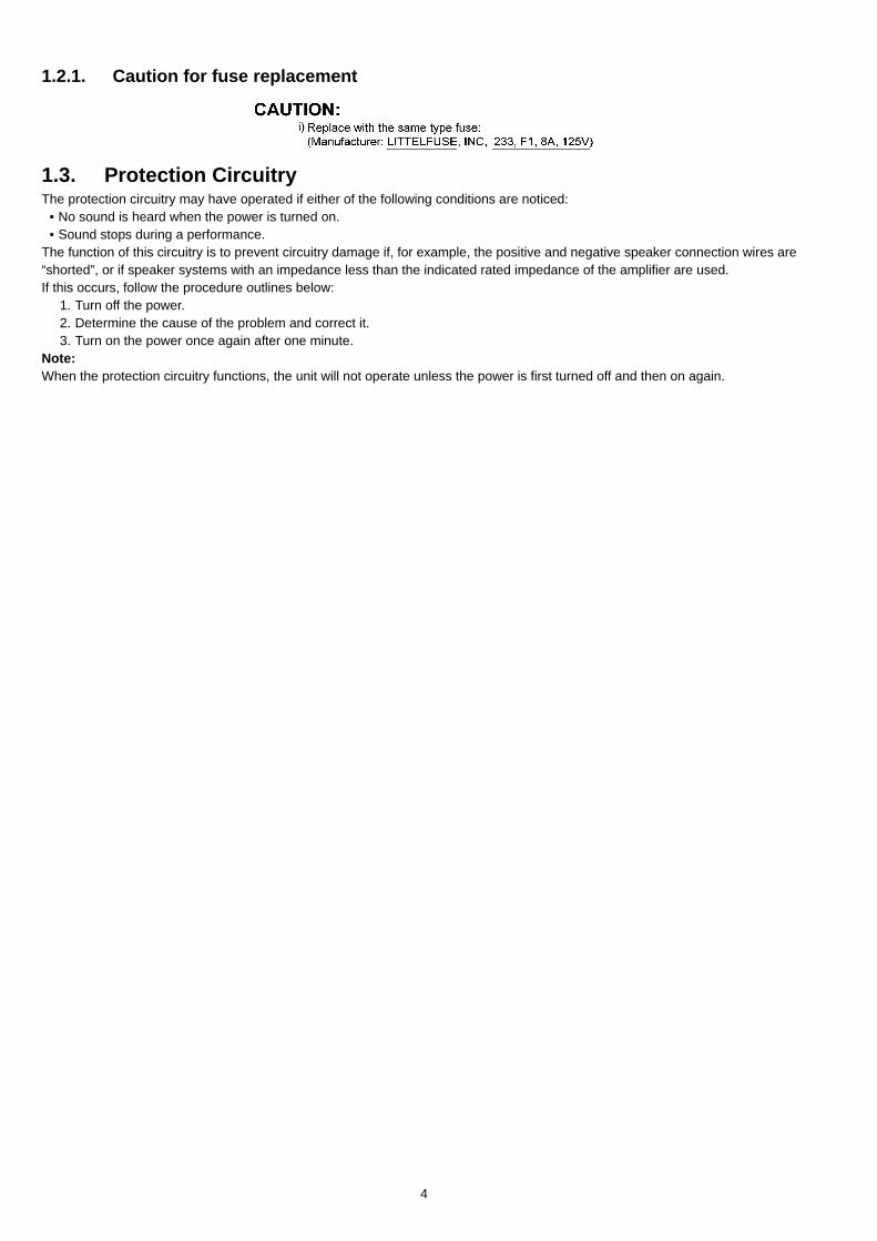
1.2.1. Caution for fuse replacement
1.3. Protection CircuitryThe protection circuitry may have operated if either of the following conditions are noticed:
• No sound is heard when the power is turned on.• Sound stops during a performance.
The function of this circuitry is to prevent circuitry damage if, for example, the positive and negative speaker connection wires are“shorted”, or if speaker systems with an impedance less than the indicated rated impedance of the amplifier are used.If this occurs, follow the procedure outlines below:
1. Turn off the power.2. Determine the cause of the problem and correct it.3. Turn on the power once again after one minute.
Note:When the protection circuitry functions, the unit will not operate unless the power is first turned off and then on again.
4

1.4. Safety Parts InformationSafety Parts List:
There are special components used in this equipment which are important for safety.These parts are marked by ( ) in the Schematic Diagrams & Replacement Parts List. It is essential that these critical partsshould be replaced with manufacturer’s specified parts to prevent shock, fire or other hazards. Do not modify the original designwithout permission of manufacturer.
Safety Ref. No. Part No. Part Name & Description Remarks
2 REX1395-1 BLACK WIRE (AC INLET-SMPS)
3 REX1396-1 RED WIRE (AC INLET-SMPS)
20 RGRX1001Q-A REAR PANEL
29 RKMX1002-K TOP CABINET
49 RFKNBT235PA BD DRIVE / MAIN P.C.B ASS'Y
101 VQL1V70-J LASER CAUTION LABEL
A2 K2CB2CB00021 AC CORD
A3 VQT2M13-5 OI BOOK
PCB1 RFKNBT235PA BD DRIVE / MAIN P.C.B. ASS'Y
PCB5 REPX0803K SMPS P.C.B. (RTL)
PCB6 REPX0803K AC INLET P.C.B. (RTL)
DZ5701 ERZV10V511CS ZNR
L5702 G0B612H00002 LINE FILTER
L5703 G0B932H00002 LINE FILTER
T5701 ETS42BM1GGAC TRANSFORMER
T5751 ETS19AB2A6AG SUB TRANSFORMER
T6100 G4D1A0000142 SWITCHING TRANSFORMER
PC5702 B3PBA0000402 PHOTO COUPLER
PC5720 B3PBA0000402 PHOTO COUPLER
PC5799 B3PBA0000402 PHOTO COUPLER
RY701 K6B1AEA00003 RELAY
F1 K5D802APA008 FUSE
TH5702 D4CAA2R20001 THERMISTOR
P5701 K2AB2B000007 AC INLET
C5700 F1BAF1020020 1000pF
C5701 F0CAF104A105 0.1uF
C5702 F0CAF104A105 0.1uF
C5703 F0CAF104A105 0.1uF
C5705 F1BAF2220023 2200pF
C5706 F1BAF471A013 470pF
5

2 Warning2.1. Prevention of Electrostatic Discharge (ESD) to Electrostatic Sensitive
(ES) DevicesSome semiconductor (solid state) devices can be damaged easily by static electricity. Such components commonly are called Elec-trostatically Sensitive (ES) Devices. Examples of typical ES devices are integrated circuits and some field-effect transistors andsemiconductor “chip” components. The following techniques should be used to help reduce the incidence of component damagecaused by electrostatic discharge (ESD).
1. Immediately before handling any semiconductor component or semiconductor-equipped assembly, drain off any ESD on yourbody by touching a known earth ground. Alternatively, obtain and wear a commercially available discharging ESD wrist strap,which should be removed for potential shock reasons prior to applying power to the unit under test.
2. After removing an electrical assembly equipped with ES devices, place the assembly on a conductive surface such as alumi-num foil, to prevent electrostatic charge buildup or exposure of the assembly.
3. Use only a grounded-tip soldering iron to solder or unsolder ES devices.4. Use only an anti-static solder removal device. Some solder removal devices not classified as “anti-static (ESD protected)” can
generate electrical charge sufficient to damage ES devices.5. Do not use freon-propelled chemicals. These can generate electrical charges sufficient to damage ES devices.6. Do not remove a replacement ES device from its protective package until immediately before you are ready to install it. (Most
replacement ES devices are packaged with leads electrically shorted together by conductive foam, aluminum foil or compara-ble conductive material).
7. Immediately before removing the protective material from the leads of a replacement ES device, touch the protective materialto the chassis or circuit assembly into which the device will be installed.Caution:
Be sure no power is applied to the chassis or circuit, and observe all other safety precautions.8. Minimize bodily motions when handling unpackaged replacement ES devices. (Otherwise harmless motion such as the
brushing together of your clothes fabric or the lifting of your foot from a carpeted floor can generate static electricity (ESD) suf-ficient to damage an ES device).
6

2.2. Precaution of Laser Diode
Caution:This product utilizes a laser diode with the unit turned “on”, invisible laser radiation is emitted from the pickup lens.Wavelength: 790 nm (CDs), 655 nm (DVDs), 405 nm (BDs)Maximum output radiation power from pickup: 100 µW/VDELaser radiation from the pickup unit is safety level, but be sure the followings: 1. Do not disassemble the pickup unit, since radiation from exposed laser diode is dangerous. 2. Do not adjust the variable resistor on the pickup unit. It was already adjusted.3. Do not look at the focus lens using optical instruments.4. Recommend not to look at pickup lens for a long time.
7

2.3. Service caution based on Legal restrictions
2.3.1. General description about Lead Free Solder (PbF)The lead free solder has been used in the mounting process of all electrical components on the printed circuit boards used for thisequipment in considering the globally environmental conservation.
The normal solder is the alloy of tin (Sn) and lead (Pb). On the other hand, the lead free solder is the alloy mainly consists of tin(Sn), silver (Ag) and Copper (Cu), and the melting point of the lead free solder is higher approx.30 degrees C (86°F) more than thatof the normal solder.
Definition of PCB Lead Free Solder being used
Service caution for repair work using Lead Free Solder (PbF)• The lead free solder has to be used when repairing the equipment for which the lead free solder is used.
(Definition: The letter of “PbF” is printed on the PCB using the lead free solder.)• To put lead free solder, it should be well molten and mixed with the original lead free solder.• Remove the remaining lead free solder on the PCB cleanly for soldering of the new IC.• Since the melting point of the lead free solder is higher than that of the normal lead solder, it takes the longer time to melt the
lead free solder.• Use the soldering iron (more than 70W) equipped with the temperature control after setting the temperature at 350±30 degrees
C (662±86°F).Recommended Lead Free Solder (Service Parts Route.)
• The following 3 types of lead free solder are available through the service parts route.RFKZ03D01K-----------(0.3mm 100g Reel)RFKZ06D01K-----------(0.6mm 100g Reel)RFKZ10D01K-----------(1.0mm 100g Reel)
Note* Ingredient: tin (Sn), 96.5%, silver (Ag) 3.0%, Copper (Cu) 0.5%, Cobalt (Co) / Germanium (Ge) 0.1 to 0.3%
The letter of “PbF” is printed either foil side or components side on the PCB using the lead free solder. (See right figure)
8

2.4. Handling Precautions for BD DriveThe laser diode in the optical pickup unit may break down due to static electricity of clothes or human body. Special care must betaken avoid caution to electrostatic breakdown when servicing and handling the laser diode in the BD Drive.
Figure 1
2.4.1. Grounding for electrostatic breakdown preventionSome devices such as the DVD player use the optical pickup (laser diode) and the optical pickup will be damaged by static electric-ity in the working environment. Proceed servicing works under the working environment where grounding works is completed.
2.4.1.1. Worktable grounding1. Put a conductive material (sheet) or iron sheet on the area where the optical pickup is placed, and ground the sheet.
2.4.1.2. Human body grounding1. Use the anti-static wrist strap to discharge the static electricity form your body.
Figure 2
9

3 Service Navigation3.1. Service InformationThis service manual contains technical information which will allow service personnel’s to understand and service this model.Please place orders using the parts list and not the drawing reference numbers.
If the circuit is changed or modified, this information will be followed by supplement service manual to be filed with the original ser-vice manual.
• BD Drive & Digital Circuitries:1) This service manual does not contain the following information, due to the impossibility of servicing at component level.
- Exploded View and Replacement Parts List for individual parts of BD Drive.
2) The following category are recycle module part. Please send them to Central Repair Center. - BD Drive & Main P.C.B. Assembly (RFKNBT235PA)
10

3.2. Caution for Replacing Parts
3.2.1. Items that should be done after replacing parts
Note 1:Download latest Firmware and burn it on CD-R or CD-RW, and update Firmware.
3.2.2. Standard Inspection Specifications after Making RepairsAfter making repairs, we recommend performing the following inspection, to check normal operation.
Use the following checklist to establish the judgment criteria for the picture and sound.
No. Procedure Item to Check 1 Turn on the power, and confirm items pointed out. Items pointed out should reappear. 2 Insert RAM disc. The Panasonic RAM disc should be recognized. 4 Perform playback for one minute using the RAM disc. No abnormality should be seen in the picture, sound or operation.
*Panasonic DVD-RAM disc should be used when recording and play-back.
5 Perform playback for one minute using the BD-Video disc. No abnormality should be seen in the picture, sound or operation.6 If a problem is caused by a BD-Video disc, VCD, DVD-R, DVD-
Video, Audio-CD, or MP3, playback the test disc. No abnormality should be seen in the picture, sound or operation.
7 After checking and making repairs, upgrade the firmware to the latest version.
Make sure that [UPD OK] appears in the FL displays. *[UNSUPPORT] display means the unit is already updated to newest same version. Then version up is not necessary.
8 Transfer [9][9] in the service mode setting, and initialize the ser-vice settings (return various settings and error information to their default values. The laser time is not included in this initial-ization).
Make sure that [CLR] appears in the FL display. After checking it, turn the power off.
Item Contents Check Item Contents Check Picture Block noise Sound Distorted sound
Crosscut noise Noise (static, background noise, etc.) Dot noise The sound level is too low. Picture disruption The sound level is too high. Not bright enough The sound level changes. Too bright Flickering color Color fading
11

4 Specifications
Main unit SA-BT235PGENERAL
Power supply: AC 120 V,60 HziPod/iPhone Connector: DC OUT 5V 500mA MAXPower consumption: 90 WPower consumption in standby mode:
Approx. 0.1 W
Dimensions (W×H×D): 430 mm×54 mm×287 mm(16 15/16”X2 9/64”X11 5/16”)
Mass (Weight): Approx. 3.2 kg (7.1lbs)Operating temperature range: 0 °C to 40 °C
(+32 °F to 104 °F)(no condensation)
AMPLIFIER SECTIONDIN TTL Power Output: 310 W1 kHz, 1.0 % total harmonic distortion
Front:100 W per ch (3 Ω)
100 Hz, 1.0 % total harmonic distortionSubwoofer:
110 W per ch (6 Ω)AMPLIFIER SECTION
RMS TTL Power Output: 1000 W1 kHz, 10 % total harmonic distortion
Front:125 W per ch (3 Ω)
Center:250 W per ch (6 Ω)
Surround:125 W per ch (3 Ω)
100 Hz, 10 % total harmonic distortionSubwoofer:
250 W per ch (6 Ω)FTC TTL Power Output: 446 W120 Hz to 20 kHz, 1.0 % total harmonic distortion
Front:60 W per ch (3 Ω)
Center:106 W per ch (6 Ω)
Surround:60 W per ch (3 Ω)
45 Hz to 120 Hz, 1.0 % total harmonic distortionSubwoofer:
100 W per ch (6 Ω)Audio input
AUX x1Digital audio input
Optical: x2Sampling frequency: 32 kHz, 44.1 kHz, 48 kHzAudio Format: PCM, Dolby Digital
FM TUNER SECTIONFrequency range:
87.9 MHz to 107.9 MHz (200 kHz step)87.5MHz to 108.0MHz (100 kHz Step)
Antenna terminals: 75 Ω (unbalanced)VIDEO SECTION
Signal system: NTSCVideo output
Output level: 1.0 Vp-p (75 Ω)Output connector: Pin jack (1 system)
HDMI AV outputOutput format:
1080p/1080i/720p/480pOutput connector: Type A (19 pin)
HDMI (Deep Color,x.v.ColorTM,High Bit rate Audio )
This unit supports “HDAVI Control 5” function.LASER Specification
Class I LASER ProductWave length:
790 nm (CDs)/655 nm (DVDs)/405 nm (BDs)Laser power:
No hazardous radiation is emitted with the safety protectionTERMINAL SECTION Ethernet: 10BASE-T/100BASE-TX
1systemSD card slot:
Connector : 1 systemNote:
1. Specifications are subject to change without notice.Mass and dimensions are approximate.
2. Total harmonic distortion is measured by the digital spectrum analyzer.
Solder:This model uses lead free solder (PbF).
12

13

5 Location of Controls and Components5.1. Remote Control Key Button Operations
14

5.2. Main Unit Key Button Operations
15

5.3. Using BD-LIVE BONUSVIEW in BD-Video
16

5.4. Using the iPod/iPhone
17

5.4.1. iPod /iPhone Playback
18

5.5. Speaker Connections
Connect to the terminals of the same colour.
Turn off all equipment before connection and read the appropriate operating instructions.
Do not connect the AC power supply cord until all other connections are complete.
AC IN
5 2 1
366FRONTCENTERSUBWOOFER
R L
4 3
3SURROUND
R L
+
6 Main unit
6 PURPLE Subwoofer
5 GREEN Center speaker
2 RED Front speaker (Rch)
1 WHITE Front speaker (Lch)
4 GRAY Surround speaker (Rch)
3 BLUE Surround speaker (Lch)
6 5 4 3 2 1
19

5.6. Disc/Cards Playability
20

5.6.1. Other Information
21

5.7. SD Information
22

5.8. File Extension Type Support (MP3/JPEG/AVCHD/MPEG2 files)
23

5.8.1. File Folders Structures
24

6 Operating Instructions6.1. Removing of disc during abnomality
6.1.1. When the power can be turned off.Step 1 Turn off the power.Step 2 Press & hold [SKIP FWD] button on remote control and [OPEN/CLOSE] button on main unit for 5 seconds.
6.1.2. When the power cannot be turned off.• Press & hold the [POWER] button to turn off the power forcibly, then press & hold [SKIP FWD] button on remote control and
[OPEN/CLOSE] button on main unit for 5 seconds.
6.1.3. Using service eject pin.1. Turn off the power and remove AC cord.2. Remove the Top Cabinet.3. Remove BD Drive.4. Insert Eject Pin (JZJ0484) into the hole on the bottom of BD Drive and slide the eject Pin in the direction of the arrow to eject
tray slightly.5. Remove disc.
25

7 Self-Diagnostic and Special Mode Setting7.1. Special Mode Table 1Self-Diagnostic Function provides information for error to service personnel by Self-Diagnosis Display when any error has occurred.U**, H** and F** are stored in my memory and held.
• You can check latest error code by transmitting [0] [1] of Remote Control in Service Mode.Automatic Display on FL will be cancelled when the power is turned off or AC input is turned off during self-diagnosis display isON.
Item FL display Key operation
Mode name Description Front Key
Initialize Mode *A1) Unit power-up
2) FL shows "Hello" then "goodbye"
3) Unit power-down
4) Unplug & plug AC Cord
ll the main unit’s parameters are initialized. Press & hold [VOL+], [OPEN/
CLOSE] follow by [POWER]
button in sequence during
power off.
Press & hold [VOL+], [OPEN/
CLOSE] & [PLAY] on main
unit for 3S or more during
power off.
Rating password The audiovisual level setting password is ini-
tialized to Level 8.
Service Mode Setting every kind of modes for servicing.
*Details are described in 7.3.1. Service Mode
at a glance.
BD-ROM history cleaning < Persistent Storage> of BD-ROM standard is
cleaned.
Screen display: [The player’s history data has
been cleared] is displayed for five seconds. Same display as before
execution.
When power on press [STOP] on
main unit & [POWER] on remote
control.
When power is off, press [SKIP
FWD] on remote control & [OPEN/
CLOSE] key on main unit
simultaneously for 5 seconds
or more.
Forced disc eject Removing a disc that cannot be ejected.
The tray will open and unit will shift to P-off
mode.
While Demonstration Lock is being set, this
Forced disc eject function is not accepted.
The display before
execution leaves.
Forced power-off When the power button is not effective while
power is ON, turn off the power forcibly.
Display in P-off mode. P
seconds.
ress [POWER] over than 10
Aging Perform sequence of modes as * Aging
Description shown below continually.
Display following the mode. When the power is ON, press
5
seconds and less than 10 seconds.
NOTE1:If Unit has not turned into Aging
mode by operations shown above,
execute TEST MODE once and re-
execute operation shown above.
(*All the main units parameters
include tuner are initialized by TESTmode.)
NOTE2:If the unit has hung-up because of
pressing keys for over 10 seconds,
once turn off the power, and re-exe-
cute this command.
*When releasing Aging mode, press
[POWER] key over 10 seconds.
-----------
INITINIT
SERV
************
******
[SKIP FW], [PLAY] & [OPEN/
CLOSE] simultaneously for over
Press [SKIP REV] on remote
control, follow by [PLAY] on main
unit simultaneously for five
seconds when power-on.
26

7.2. Special Mode Table 2
Demonstration lock/
unlock
Ejection of the disc is prohibited.
The lock setting is effective until unlocking the
tray and not released by Main unit
initialization of service mode.
*When lock the tray.
LOCK is displayed for 3 seconds. Note:When a disc is not in tray, this
setting is not effective.
*When unlock the tray.
UNLOCK is displayed for 3 sec-
onds.
*When press OPEN/CLOSE key
while the tray being locked.
Display LOCK for 3 seconds.
Press [OPEN/CLOSE] key while the
tray is being locked.
Progressive initialization The progressive setting is initialized to Inter-
lace.
The display before execution
leaves.
When the power is on (SS mode),
press [STOP] and [PLAY] simulta-
neously for 5 seconds.
Item FL display Key operation
Mode name Description Front Key
When the power is on, press
[PLAY] and [OPEN/CLOSE] keys
simultaneously for 5 seconds.
When the power is on, press
[PLAY] and [OPEN/CLOSE] keys
simultaneously for 5 seconds.
When the power is on, press &
hold [SKIP REV] on remote control
follow by [POWER] on main unit.
Micro-P version check To check for main & sub firmware version
no., model no. & date of production. FL Display
(i)
(ii)
(iii)
(iv)
M-XXXX
S-YYYY
AA/BB/CC
ZZZZZZ
Main Firmware Version
Sub Firmware Version
Date
Model No.
27

7.3. Error Code Table
7.3.1. Error Code Table (For BD)
Error Code Diagnosis contents Description Monitor Display Automatic FL display
U30 Remote control code error Display appears when main unit and remote
controller codes are not matched.
No display
* is remote controller code of the
main unit.
Display for 5 seconds.
U59 Abnormal inner temperature
detected
Display appears when the drive temperature
exceeds 70 C.
The power is turned off forcibly.
For 30 minutes after this, all key entries are
disabled. (Fan motor operates at the highest
speed for the first 5 minutes. For the remain-
ing 25 minutes, fan motor is also stopped.)
The event is saved in memory as well.
No display
U59 is displayed for 30 minutes.
U71 HDMI incompatible error
(HDCP incompatible)
Display this error when the equipment (com-
patible with DVI such as TV, amplifier etc.)
connected to the unit by HDMI is incompatible
with HDCP.
*HDCP=High-bandwidth Digital Content Pro-
tection
No display
U72 HDMI connection error
(communication error)
This error is displayed when there are any
communication problems with the unit and the
equipments (TV, amplifier etc.) connected to
the unit by HDMI. (or when there is a problem
with the HDMI cable)
No display
U72 display disappears when
error has been solved by Power
OFF/ON of connecting equipment
or by inserting/removing of HDMI
cable.
U73 HDMI connection error
(authentication error)
when authentication error occurs while the
equipments (TV, amplifier etc.) are connected
by HDMI. (or when there is a problem with the
HDMI cable)
No display
U73 display disappears when
error has been solved by Power
OFF/ON of connecting equipment
or by inserting/removing of HDMI
cable.
F99 Hang-up Displayed when communication error has
occurred between Main microprocessor
and Timer microprocessor
No display
Displayed is left until the [POWER]
key is pressed.
H19 Inoperative fan motor When inoperative fan motor is detected after
powered on, the power is turned off
automatically.
The event is saved in memory.
No display No display
F00 No error information Initial setting for error code in memory
(Error code Initialization is possible with error
code initialization and main unit initialization.)
No display No display
F34 Initialization error when main
microprocessor is started up
for program recording
When initialization error is detected after
starting up main microprocessor power
turned automatically.
The event is saved in memory.
No display No display
F58 Drive hardware error When drive unit error is detected, the event is
saved in memory.
No display No display
UNSUP-
PORT
Unsupported disc error *An unsupported format disc was played,
although the drive starts normally.
*The data format is not supported, although
the media type is supported.
*Exceptionally in case of the disc is dirty.
This disc is
incompatible.
NO READ Disc read error *A disc is flawed or dirty.
*A poor quality failed to start.
*The track information could not be read.
Cannot rea d.
Please check the
disc.
HARD
ERR
Drive error The drive detected a hard error. DVD drive error. Display for 5 seconds.
the
is off
UNSUPPORT
HARD ERR
The character indication flows
sideways.
F99
U73
NOREAD
U71
U72
U59
SET *
28

7.3.2. Error Code Table 2 (For BD)
7.3.3. Error Code Table 3 (Power Supply & Digital Amplifier)
SELFCHECK
Restoration operation Since the power cord fell out during a powerfailure or operation, it is under restorationoperation.*It will OK, if a display disappears automati-cally. If a display does not disappear, there isthe possibility that defective Digital P.C.B. /DVD drive.
No display
PLEASEWAIT
Unit is in termination process Unit is in termination process now.BYE is displayed and power will be turned off.
No display
UNFOR-MAT
Unformatted disc error You have inserted an unformatted DVD-RAMor DVD-RW that is unformatted or recordedon other equipment.
The disc is not formatted properly.
No PLAY When there is a viewing restric-tion on a BD-Video or DVD-Video.
Rating password is set. No display
Error Code Diagnosis contents Description Monitor Display Automatic FL display
SELF CHECK
PLEASE WAIT
UNFORMAT
No PLAY
The character indication flowssideways.
Error
Code
F61 The abnormalities In normal operation, when DCDET2 goes Press [ STOP] on main
in an output or power to "L" (Low) (Not during POWER OFF unit for next error.
supply circuit of condition), F61 appears on FLDisplay
POWER AMP for 1 second and PCONT goes to
"L" (Low).This is due to speaker output
has DC voltage or fan is not working.
F76F76
H19
Abnormality in the
Fan Unit & its
circuitries
In normal operation when DCDET1 is
Fan Unit is not operating properly
Press [ STOP] on main
output voltage of detected "L" (Low) for two consecutive unit for next error.
stabilized power times, F76 is displayed on FL for
supply 1 second and after that PCONT will be
turned to "L" (Low). This is due to any of
the DC voltages (+9V, +7V, -7V, +5V,
+5.3V etc.) C22 not available.
Diagnosis Contents Description of error Automatic FL Display Remarks
Press [ STOP] on main
unit for next error.
29
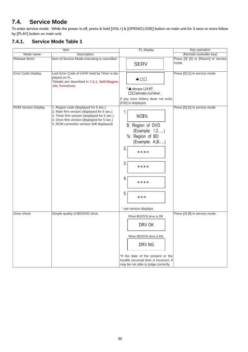
7.4. Service ModeTo enter service mode: While the power is off, press & hold [VOL+] & [OPEN/CLOSE] button on main unit for 3 secs or more followby [PLAY] button on main unit.
7.4.1. Service Mode Table 1
Item FL display Key operation
Mode name Description (Remote controller key)
Release Items Item of Service Mode executing is cancelled. Press [0] [0] or [Return] in service
mode.
Error Code Display Last Error Code of U/H/F held by Timer is dis-
played on FL.
*Details are described in 7.1.1. Self-Diagno-
stic Functions.
If any error history dose not exist,
[F00] is displayed.
Press [0] [1] in service mode
ROM Version Display 1. Region code (displayed for 5 sec.)
2. Main firm version (displayed for 5 sec.)
3. Timer firm version (displayed for 5 sec.)
4. Drive firm version (displayed for 5 sec.)
5. ROM correction version (left displayed)
* are version displays.
Press [0] [2] in service mode
Drive check Simple quality of BD/DVD drive.
*If the date of the present or the
trouble occurred time is incorrect, it
may be not able to judge correctly.
Press [3] [8] in service mode.
SERV
30

7.4.2. Service Mode Table 2
Laser Used Time
Indication
Check laser used time (hours) of drive. Press [4] [1] in service mode.
Item FL display Key operation
Mode name Description (Remote controller key)
Laser used time of BD/DVD/CD
in Playback/Recording mode is
Counted.
******
****BP
****BR
****DP
****DR
****CD
1. Blu-ray Playback:
2. Blu-ray Recording:
4. DVD Recording:
5. CD:
3. DVD Playback:
(******) is the used time display in
hour.
31

7.4.3. Service Mode Table 3
BD/DVD drive last error BD/DVD drive error code display. 1. Error Number is displayed for 5 seconds.
2. Time when the error has occurred is display for 5 seconds.
DD : Dayhh : Hourmm : Minute3. Last drive error (1/2) is displayed for 5 seconds.
00 : Bad disc03 : Bad disc04 : Bad disc or drive malfunction4. Last drive error (2/2) is displayed for five seconds.
5. Error occurring disc type is dis-played for 5 seconds.
Press [4] [2] in service mode.
Item FL display Key operationMode name Description (Remote controller key)
DVDRW
DDhhmm
CDR
NO
CDRW
DVDPR
DVDPRW
BDROM
******
****
******
32

7.4.4. Service Mode Table 4
6. Disc maker ID is displayed for 5seconds.
7. Factor of drive error (hexadeci-mal) occurring is left displayed.
In case that the maker cannot beidentified, display is black out.
Item FL display Key operationMode name Description (Remote controller key)
33

7.4.5. Service Mode Table 5
CEC (H) output Check of the CEC terminal high output ofHDMI.
Press [5] [5] in service mode.
CEC (L) output Check of the CEC terminal low output ofHDMI.
Press [5] [6] in service mode.
Tray OPEN/CLOSE Test The DVD drive tray is opened and closedrepeatedly.
* is number of open/close cycletimes.
Press [9] [1] in service mode*When releasing this mode, pressthe [POWER] button of RemoteController more than 10 seconds.
Delete the Laser UsedTime
Laser used time stored in the memory of theunit is deleted.
Press [9] [5] in service mode.
Delete the Last DriveError
Delete the Last Drive Error information storedon the DVD Drive.
Press [9] [6] in service mode.
Delete the Error History Delete Error History information stored on theunit.
Press [9] [7] in service mode.
Error code initialization Initialization of the last error code held bytimer (Write in F00)
Press [9] [8] in service mode.
Initialize Service Last Drive Error, Error history and ErrorCodes stored on the unit are initialized to fac-tory setting.
Press [9] [9] in service mode.
Finishing service mode Release Service Mode. Display in STOP (SS) mode. Press power button on the frontpanel or Remote controller in ser-vice mode.
Item FL display Key operationMode name Description (Remote controller key)
CECLOK
CECHOK
CECLNG
CLR
CLR
CLR
CLR
CLR
CECHNG
34

8 Troubleshooting Guide8.1. Troubleshooting Guide for F61 and/or F76
Symptom Checking items Possible Fault(s) RemarksSet cannot ON 1 AC Cord 1 Faulty AC Cord,Loose connection Refer to
2 AC Inlet P5701 2 P5701 soldier crack,dry joint,etc. SMPS3 Fuse F1 3 F1 fuse open P.C.B.4 Photocoupler
PC5702,PC57994 PC5702/PC5799 sildier crack,dry joint ,short
circuit,open circuit,etc Fig 1.5 Switching IC IC5701 5 Faulty IC57016 Switching IC IC5799 6 Faulty IC5799
Set can ON 1 Transformer T5701 1a Short circuit between Pin 14 and pin 16then F76 1b Short circuit between Pin 15 and pin 16
1c Short circuit between Pin 16 and 172 Power P.C.B. 2a Check connection between Power P.C.B (CN2916
& CN2917) and SMPS P.C.B (CN5802 & CN5803)
2b L2902 Open (No input to IC2901)2c
Faulty IC2901 (No output voltage at pin 10 & 11)2d Faulty Q2902 & Q2903 (Regulator)2e L2907 open (No DC +12v)2f L2908 op[en (No DC+5v)
3 3 Check cable connection between main (CN2004) and SMPS
4 4a Faulty IC23024b LB2301 Open
5 Photocoupler 5 PC5720 solder crackPC5720 dry joint,short circuit,open circuit,etc
Set can ON 1 Rectifier D5802 1a Improper contact between D5802working normally to heatsinkfor some time 1b Set trigger tempriture protectionthen F76
Refer to PowerP.C.B.
Fig 2.
Refer toMainP.C.B.Fig 3.
Refer toSMPSP.C.B.
Fig 1.
35

8.1.1. SMPS P.C.B.
Figure 1. SMPS P.C.B.
FUSE: F1
Photocouple:PC5702, D5799Switching IC: IC5799
Switching IC: IC5701Transformer: T5701
Rectifier: D5802
36

8.1.2. Power P.C.B.
Fig 2. Power P.C.B.
CN2916,L2907
CN2917,L2908
(Side B of Power P.C.B.)
(Side A of Power P.C.B.)
IC2901
L2902
Q2903 Q2902
37

8.1.3. Main P.C.B.
Fig 3. Main P.C.B.
IC2302,LB2301
CN2004
38

9 Service Fixture & Tools9.1. Service Tools and EquipmentPrepare service tools before process service position.
Service Tools RemarksSMPS P.C.B. (JW2*) - Main P.C.B. (CN2004) REXX1037 (10P Cable)Main P.C.B. (CN2006) - D-Amp P.C.B. (CN5402) RFKZBT230P (18P FFC)
39
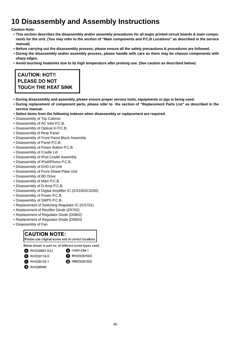
10 Disassembly and Assembly InstructionsCaution Note:
• This section describes the disassembly and/or assembly procedures for all major printed circuit boards & main compo-nents for the unit. (You may refer to the section of “Main components and P.C.B Locations” as described in the servicemanual)
• Before carrying out the disassembly process, please ensure all the safety precautions & procedures are followed.• During the disassembly and/or assembly process, please handle with care as there may be chassis components with
sharp edges.• Avoid touching heatsinks due to its high temperature after prolong use. (See caution as described below)
• During disassembly and assembly, please ensure proper service tools, equipments or jigs is being used.• During replacement of component parts, please refer to the section of “Replacement Parts List” as described in the
service manual.• Select items from the following indexes when disassembly or replacement are required.• Disassembly of Top Cabinet• Disassembly of AC Inlet P.C.B.• Disassembly of Optical In P.C.B.• Disassembly of Rear Panel• Disassembly of Front Panel Block Assembly• Disassembly of Panel P.C.B.• Disassembly of Power Button P.C.B.• Disassembly of Cradle Lid• Disassembly of iPod Cradle Assembly• Disassembly of iPod/iPhone P.C.B.• Disassembly of DVD Lid Unit• Disassembly of Front Shield Plate Unit• Disassembly of BD Drive• Disassembly of Main P.C.B.• Disassembly of D-Amp P.C.B.• Disassembly of Digital Amplifier IC (IC5100/IC5200)• Disassembly of Power P.C.B.• Disassembly of SMPS P.C.B.• Replacement of Switching Regulator IC (IC5701)• Replacement of Rectifier Diode (D5702)• Replacement of Regulator Diode (D5802)• Replacement of Regulator Diode (D5803)• Disassembly of Fan
40

10.1. Disassembly Flow Chart
10.6. Rear Panel
10.16. Main P.C.B.
10.25. Fan
10.20. SMPS P.C.B.
10.4. AC Inlet P.C.B.
10.3.Top Cabinet
10.18. Digital Amplifier
IC
(IC5100/ IC5200)
10.15.BD Drive
Power P.C.B.10.19.
10.21. Switching Regulator
IC (IC5701)
10.22. Rectifier Diode
(D5702)
10.23. Regulator Diode
(D5802)
10.24. Regulator Diode
(D5803)
10.7. Front Panel Block
10.8. Panel P.C.B.
10.14. Front Shield
Plate Unit
10.9. Power Button
P.C.B.
10.12.iPod/iPhone P.C.B.
10.10.Cradle Lid
10.13.DVD Lid Unit
10.11. iPod Cradle
Assembly10.17. D-Amp P.C.B.
10.5. Optical In P.C.B.
41

10.2. Main Components and P.C.B. Locations
42

10.3. Disassembly of Top CabinetStep 1 Remove 2 screws.
Step 2 Remove 3 screws.
Step 3 Slightly pull outwards both side of Top Cabinet.
Step 4 Slightly lift both side of Top Cabinet in an outward direc-tion about 25°.
Step 5 Press down the catches one by one.Caution: To avoid shocked by electricity & injured by high temperature. DO NOT TOUCH electrical components when insert hand under the Top Cabinet.
Step 6 Remove Top Cabinet as arrow shown.
43

Caution: During assembling, ensure that catches of Top Cabinet is insert into Front Panel properly.
Caution: Replace Top Cabinet insulator sheet if broken & ensure it is pasted properly at Top Cabinet.
10.4. Disassembly of AC Inlet P.C.B.• Refer to “Disassembly of Top Cabinet”.
Step 1 Remove 1 screw.
Step 2 Twist the Wire Holder.Step 3 Release Red(TL10) & Black(TL20) wires from the WireHolder.Caution: During assembling, ensure that Red (TL10) & Black(TL20) wires are dressed into Wire Holder.Step 4 Lift up the AC Inlet P.C.B.from the rear panel.
Step 5 Desolder Red (TL10) & Black (TL20) wires on AC InletP.C.B..Step 6 Remove AC Inlet P.C.B..
44

10.5. Disassembly of Optical InP.C.B.
• Refer to “Disassembly of Top Cabinet”.
Step 1 Remove 2 screws.
Step 2 Detach 13P FFC at the connector (CN4002) on OpticalIn P.C.B..
Step 3 Slightly pull Optical In P.C.B. outwards as arrow (1)shown.Step 4 Press Optical In P.C.B. downwards to release it from thelocator as arrow (2) shown.Step 5 Remove Optical In P.C.B..
10.6. Disassembly of Rear Panel• Refer to “Disassembly of Optical In P.C.B.”.
Step 1 Lift up the Wire Clamper.Step 2 Detach the fan unit connector (CN5401) on D-AmpP.C.B..
Step 3 Remove 7 screws.
Step 4 Release the tabs on both side of the Rear Panel in thedirection of arrow.
Step 5 Remove Rear Panel.
45
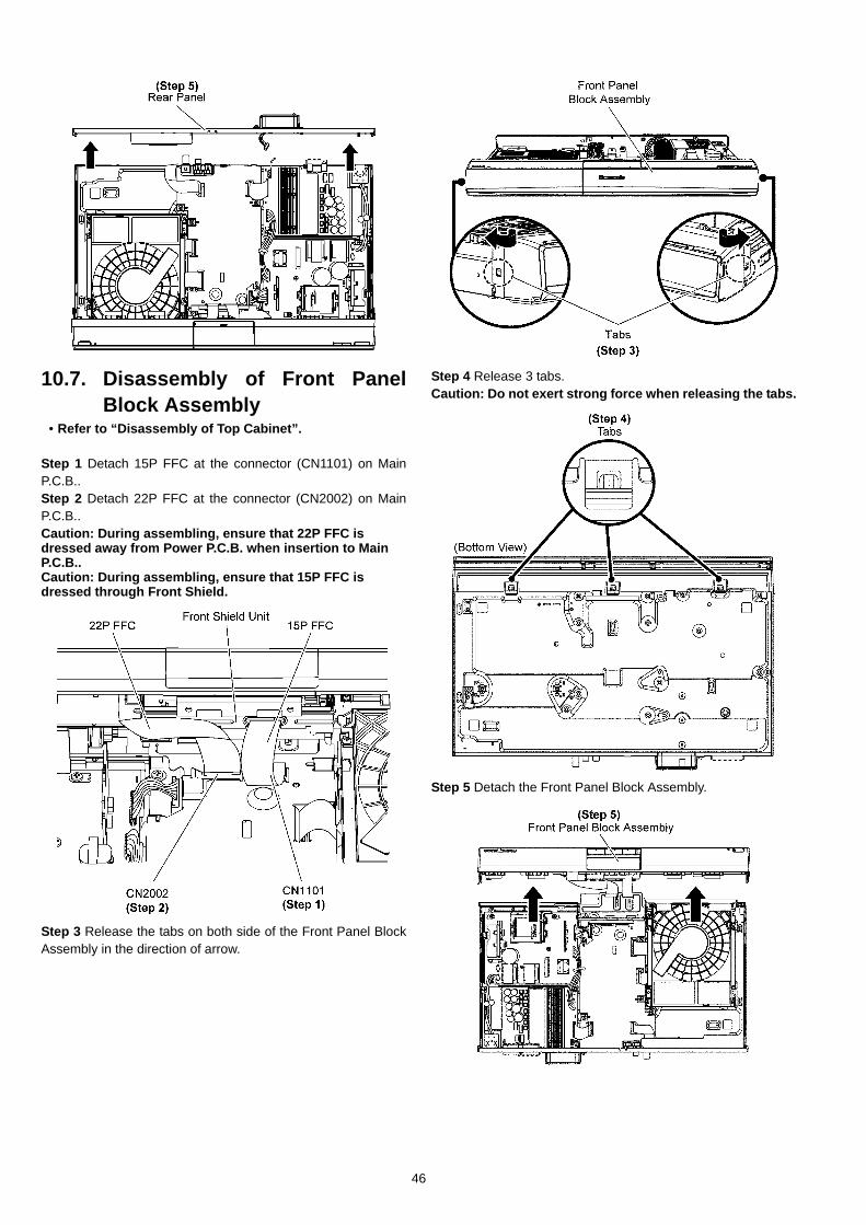
10.7. Disassembly of Front PanelBlock Assembly
• Refer to “Disassembly of Top Cabinet”.
Step 1 Detach 15P FFC at the connector (CN1101) on MainP.C.B..Step 2 Detach 22P FFC at the connector (CN2002) on MainP.C.B..Caution: During assembling, ensure that 22P FFC is dressed away from Power P.C.B. when insertion to Main P.C.B..Caution: During assembling, ensure that 15P FFC is dressed through Front Shield.
Step 3 Release the tabs on both side of the Front Panel BlockAssembly in the direction of arrow.
Step 4 Release 3 tabs.Caution: Do not exert strong force when releasing the tabs.
Step 5 Detach the Front Panel Block Assembly.
46

10.8. Dissassembly of Panel P.C.B.• Refer to “Disassembly of Front Panel Block Assembly”.
Step 1 Remove 5 screws.
Step 2 Release 1 catch.
Step 3 Lift up the Panel P.C.B..
Step 4 Desolder the 4P cable at the connector (CN6001) onPanel P.C.B..Step 5 Remove Panel P.C.B..
• Assembly of Panel P.C.B
Step 1 Solder the 4P cable to the connector (CN6001) onPanel P.C.B..
Step 2 Place the Panel P.C.B. onto the Front Panel.Step 3 Dress 22P FFC according to diagram shown.Caution: Ensure that it is properly located & fully catched.
47

Step 4 Dress 4P cable into the Front Panel’s ribs according todiagram shown.
Step 5 Fix 5 screws.
10.9. Dissassembly of Power ButtonP.C.B.
• Refer to “Disassembly of Front Panel Block Assembly”.
• Disassembly of Power Button P.C.B.Step 1 Remove 1 screw.
Step 2 Lift up the Power Button P.C.B..
Step 3 Desolder the 4P Cable (H6803) on Power ButtonP.C.B..Step 4 Remove Power Button P.C.B..
• Assembly of Power Button P.C.B.
Step 1 Solder 4P cable at (H6803) onto Power Button P.C.B..
48
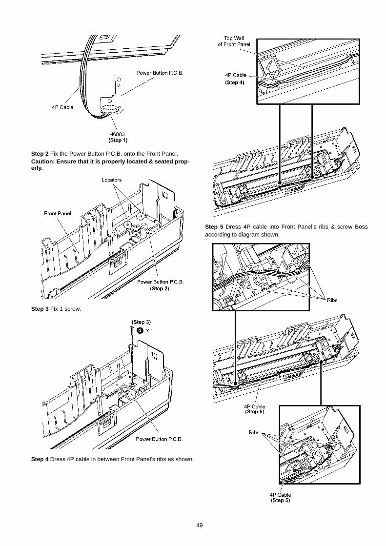
Step 2 Fix the Power Button P.C.B. onto the Front Panel.Caution: Ensure that it is properly located & seated prop-erly.
Step 3 Fix 1 screw.
Step 4 Dress 4P cable in between Front Panel’s ribs as shown.
Step 5 Dress 4P cable into Front Panel’s ribs & screw Bossaccording to diagram shown.
49

10.10. Replacement of Cradle Lid• Refer to “Disassembly of Front Panel Block Assembly”.
10.10.1. Disassembly of Cradle LidStep 1 Release the Cradle Lid Spring by using a flat headscrew driver in the direction of arrow.
Step 2 Slightly push the Cradle Lid inwards.Step 3 Slightly lift up the Cradle Lid.
Step 4 Rotate the Cradle Lid about 45° according to the dia-gram shown.Step 5 Remove Cradle Lid.
50

10.10.2. Assembly of Cradle Lid
Caution: During assembling, replace Cradle Lid Damper if broken. Ensure it is properly pasted & fully pressed onto Cradle Lid.
Step 1 Insert the Cradle Lid (Shaft A) into the Front Panel (SlotA & hole B).
Step 2 Slightly push the Cradle Lid inwards.Step 3 Press the Cradle Lid downward.
Step 4 Fix the Cradle Lid Spring onto Cradle Lid’s Shaft A.
10.11. Disassembly of iPod CradleAssembly
• Refer to “Disassembly of Front Panel Block Assemb-ley”.
Step 1 Detach 15P FFC at the connector (CN1002) on iPod/
51
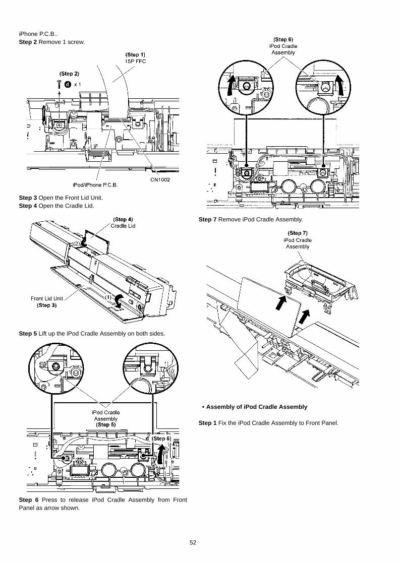
iPhone P.C.B..Step 2 Remove 1 screw.
Step 3 Open the Front Lid Unit.Step 4 Open the Cradle Lid.
Step 5 Lift up the iPod Cradle Assembly on both sides.
Step 6 Press to release iPod Cradle Assembly from FrontPanel as arrow shown.
Step 7 Remove iPod Cradle Assembly.
• Assembly of iPod Cradle Assembly
Step 1 Fix the iPod Cradle Assembly to Front Panel.
52

Step 2 Press the iPod Cradle Assembly downwards.Note: A “click” sound can be heard when the iPod CradleAssembly is fixed onto the Front Panel properly.
Step 3 Press the catch on the iPod Cradle Assembly.Step 4 Fix 1 screw.
10.12. Disassembly of iPod/iPhoneP.C.B.
• Refer to “Disassembly of iPod Cradle Assembly”. Step 1 Remove 2 screws.Step 2 Remove iPod/iPhone P.C.B..
53

Caution: During assembling, ensure that iPod/iPhone P.C.B. is seated properly at the locators.
10.13. Replacement of DVD Lid Unit• Refer to “Disassembly of Front Panel Block Assembly”.
10.13.1. Disassembly of DVD Lid UnitStep 1 Push backward the Shaft B of the DVD Lid Unit in thedirection of arrow.
Step 2 Push forward the Shaft B of the DVD Lid Unit in thedirection of arrow.
Step 3 Lift the DVD Lid Spring at Shaft A in the direction ofarrow.
Step 4 Move the Shaft A of the DVD Lid Unit in the direction ofarrow.Step 5 Remove DVD Lid Unit.
54

Step 6 Move the DVD Lid Unit to remove from Front Panel.
10.13.2. Assembly of DVD Lid UnitStep 1 Insert the DVD Lid Unit into the Front Panel as arrowshown.Caution: Ensure that Shaft A of DVD Lid Unit is fully inserted into Slot A of Front Panel.
Step 2 Locate DVD Lid Spring in between ribs of Front Panel.
Step 3 Insert the DVD Lid Unit (Shaft B) into the Front Panel(Slot B) as arrow shown.
55

Caution: Ensure that the Shaft B of DVD Lid Unit is fully inserted into Slot B of Front Panel.
10.14. Disassembly of Front ShieldPlate Unit
• Refer to “Disassembly of Front Panel Block Assembly”.
Step 1 Remove 2 screws.
Step 2 Remove 1 screw.Note: Replace the Gaskets if broken.
Step 3 Slightly lift up the Front Shield Plate Unit to release 2catches at both sides.
Step 4 Remove Front Shield Plate Unit.
Caution: During assembling, ensure that Front Shield is properly inserted & fully fixed onto the Bottom Chassis.
56

Caution: During assembling, ensure that screwing sequence is strictly followed to illustration shown.
10.15. Disassembly of BD Drive• Refer to “Disassembly of Top Cabinet Assembly”.• Refer to “Disassembly of Front Panel Block Assembly”.• Refer to “Disassembly of Front Shield Plate Unit”.
Caution: Pairing of BD Drive and Main P.C.B. as “BD Drive & Main P.C.B. Assembly” have to be replaced together. If either BD Drive or Main P.C.B. is changed, BD Drive unit has to carry out re-adjustment due to alignment data for BD Drive Unit is stored in the Main P.C.B.
Step 1 Detach 45P FFC at the connector (P55001) on MainP.C.B..Step 2 Detach 18P FFC at the connector (P55002) on MainP.C.B..
Step 3 Remove 4 screws.
Step 4 Lift up to remove the BD Drive.
Caution: During assembling, ensure that 18P FFC is inserted under Main P.C.B. Shield properly.
57

10.15.1. Replacement of Upper Base Ass’y• Refer to “Disassembly of BD Drive”.
Step 1 Remove the 4 screws, and push the Hook in.
Step 2 Lift up the Upper Base Ass’y, and pull it out to the direc-tion of arrow.
10.15.2. Replacement of Tray• Refer to “Disassembly of BD Drive”.• Refer to “Disassembly of Upper Base Assembly”.
Step 1 Insert the Eject Pin into the hole of the bottom side, andslide it to the direction of arrow until it can be.
Step 2 Pull the Tray to the direction of arrow until it can be.
Step 3 Insert the Eject Pin into the hole of the Tray at 45degrees, and lean it to the direction of arrow with pushing thedotted point of the tray forward.Then the one side of the tray is come off from the Drive.
Step 4 Insert the Eject Pin into the Tray as below figure, lift upthe lever using the Eject Pin while pushing the dotted point ofthe Tray.And remove the Tray.
58

10.15.3. Replacement of Pulley Gear & Belt• Refer to “Disassembly of BD Drive”.• Refer to “Disassembly of Upper Base Assembly”.• Refer to “Disassembly of Tray”.
Step 1 Push the Post to the direction of arrow by using the slot-ted screwdriver.
Step 2 Remove the Pulley Gear and Belt.
10.15.4. Replacement Slide Cam• Refer to “Disassembly of BD Drive”.• Refer to “Disassembly of Upper Base Assembly”.• Refer to “Disassembly of Tray”.• Refer to “Disassembly of Pulley Gear & Belt”.
Step 1 Remove the Sheet.Step 2 Disconnect the 3 FFCs.Step 3 Remove the 2 Screws and the Angle.Step 4 Peel off Coppery Sheet from FFC (A) and remove theDrive P.C.B..
Caution: Though the Drive P.C.B. is not supplied as replacement parts, it must be removed for after disassem-bling.Step 5 Open the connector lock, and disconnect the FFC.Step 6 Remove the 2 Screws, and remove the Traverse BaseAss’y with spreading the 2 hooks to the direction of arrows.
Step 7 Remove the Slide Cam.
59

10.15.5. Replacement of Mid Base, DriverGear and Loading Motor
• Refer to “Disassembly of BD Drive”.• Refer to “Disassembly of Upper Base Assembly”.• Refer to “Disassembly of Tray”.• Refer to “Disassembly of Pulley Gear & Belt”.• Refer to “Disassembly of Slide Cam”.
Step 1 Remove the Mid Base and Driver Gear.Step 2 Remove the Screw to remove the Loading Motor.
Step 3 Remove the Screw , and remove the SW P.C.B. with theLoading Motor.Remove the 2 soldering points, and remove the Loading Motor.
60
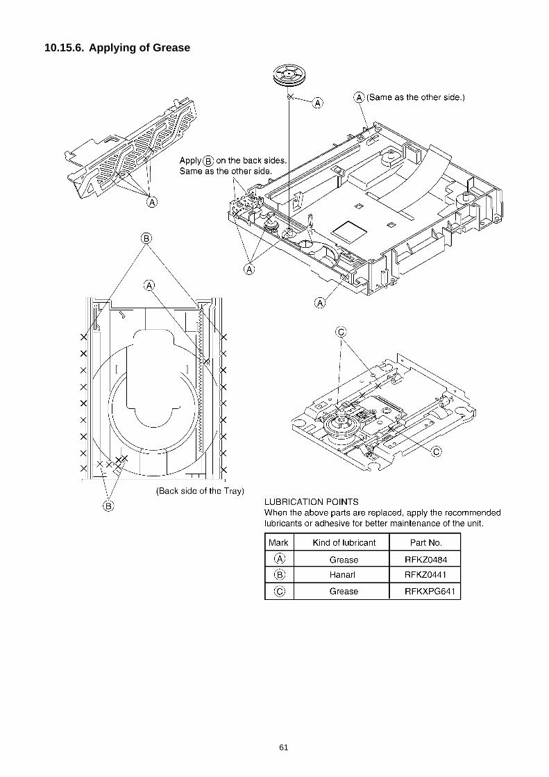
10.15.6. Applying of Grease
61

10.15.7. Cleansing the Lens of Optical Pick-Up Unit• Refer to “Disassembly of BD Drive”.• Refer to “Disassembly of Upper Base Assembly”.
62

10.16. Disassembly of Main P.C.B.• Refer to “Disassembly of Top Cabinet Assembly”.• Refer to “Disassembly of Front Panel Block Assembly”.• Refer to “Disassembly of Front Shield Plate Unit”.
Caution: Pairing of BD Drive and Main P.C.B. as “BD Drive & Main P.C.B. Assembly” have to be replaced together. If either BD Drive or Main P.C.B. is changed, BD Drive unit has to carry out re-adjustment due to alignment data for BD Drive Unit is stored in the Main P.C.B. Step 1 Remove 5 screws.Step 2 Release the tab at the right side of Rear Panel in thedirection of arrow.
Step 3 Detach 45P FFC at the connector (P55001) on MainP.C.B..Step 4 Detach 18P FFC at the connector (P55002) on MainP.C.B..Step 5 Detach 13P FFC at the connector (CN2011) on MainP.C.B..Step 6 Detach 18P FFC at the connector (CN2006) on MainP.C.B..
Step 7 Lift up the Wire Clamper.Step 8 Detach 10P cable at the connector (CN2004) on MainP.C.B..
Caution: During assembling, ensure that 10P cable is prop-erly bend down onto Main P.C.B. Shield Plate according to diagram shown.
Step 9 Remove 6 screws.
Step 10 Remove Gasket Holder unit as arrow shown.Step 11 Remove Main P.C.B. Shield Plate.
63

Step 12 Lift up to remove Main P.C.B..
Caution: During assembling, ensure that Main P.C.B. is seated properly at the locators.
10.17. Disassembly of D-Amp P.C.B.• Refer to “Disassembly of Top Cabinet Assembly”.• Refer to “Disassembly of AC Inlet Assembly”.
Step 1 Lift Up 2 Wire Clampers.Step 2 Detach 3P Wire at the connector (CN5401) on D-AmpP.C.B..Step 3 Detach 6P Cable at the connector (CN5400) on D-AmpP.C.B..Step 4 Detach 18P FFC at the connector (CN5402) on D-AmpP.C.B..
64

Step 5 Remove 2 screws on D-Amp P.C.B..
Step 6 Remove 4 screws.Step 7 Release the tab of the side of the Rear Panel in thedirection of arrow.
Step 8 Remove D-Amp P.C.B. according to direction of arrowshown.
Caution: During assembling, ensure that D-Amp P.C.B. is seated properly at the locators.
65

10.18. Replacement of Digital Ampli-fier IC (IC5100/IC5200)
• Refer to “Disassembly of D-Amp P.C.B.”.
10.18.1. Disassembly of Digital Amplifier IC(IC5100/IC5200)
Step 1 Place the D-Amp P.C.B. on an insulated material.Step 2 Remove 3 screws.
Step 3 Lift up the D-Amp P.C.B..Step 4 Upset the D-Amp P.C.B..Caution: Keep the Heatsink Spacer in safe place. Place it back during assembling.
Step 5 Desolder pins of Digital Amplifier IC (IC5100).Step 6 Remove Digital Amplifier IC (IC5100).Note: For disassembling of Digital Amplifier IC (IC5200), repeatthe (Step 1) to (Step 4) of 10.19.1.
10.18.2. Assembly of Digital Amplifier IC(IC5100/IC5200)
Step 1 Mount the Digital Amplifier IC (IC5100) onto the D-AmpP.C.B..Step 2 Solder pins of Digital Amplifier IC (IC5100).Caution: Ensure that the pins of Digital Amplifier IC (IC5100) is positioned correctly on D-Amp P.C.B. before soldering check solderability.Step 3 Apply grease onto the top side of the Digital Amplifier IC(IC5100).
Step 4 Upset the D-Amp P.C.B..
66

Caution: During assembling, ensure that heatsink spacer is seated properly onto Amp Heatsink.
Caution: Ensure that D-Amp P.C.B. is properly located and fixed on to Amp Heatsink before screwing.Step 5 Fix 3 screws.Caution: During assembling, ensure that screwing sequence is strictly follow to the illustration shown.Note: For assembling of others Digital Amplifier IC (IC5200),repeat the (Step 1) to (Step 5) of 10.19.2.
10.19. Disassembly of Power P.C.B.• Refer to “Disassembly of Top Cabinet”.
Step 1 Release 2 catches.Step 2 Remove Power P.C.B. in the direction of arrow.
Caution: During assembling, ensure that Power P.C.B. is properly inserted & fully connected to SMPS P.C.B..
10.20. Disassembly of SMPS P.C.B.• Refer to “Disassembly of Power P.C.B.”.
Step 1 Release the 2 tabs at each side of the Front Panel in thedirection of arrow.
Step 2 Release the 3 tabs at the Bottom Chassis.
67

Caution: Do not exert strong force when releasing the tabs.
Step 3 Detach the Front Panel Block Assembly slightly forward.
Step 4 Lift up the Wire Clampers.Step 5 Detach 6P Cable at the connector (CN5400) on D-AmpP.C.B..Step 6 Detach 10P Cable at the connector (CN2004) on MainP.C.B..
Caution: During assembling, ensure that 10P cable is bend down properly as diagram shown.
Step 7 Remove 5 screws.
Step 8 Release P.C.B. Spacer by using long nose plier.
68
Caution: During releasing P.C.B. Spacer, as it may lead to electric shock or injuries due to high temperature avoid touching surrounding electrical parts.
Step 9 Lift up SMPS P.C.B..
Step 10 Upset the SMPS P.C.B. according to diagram shown.Step 11 Desolder Black Wire (TL21) and Red Wire (TL11) onsolder side of SMPS P.C.B..Step 12 Remove SMPS P.C.B..
10.21. Replacement of Switching Reg-ulator IC (IC5701)
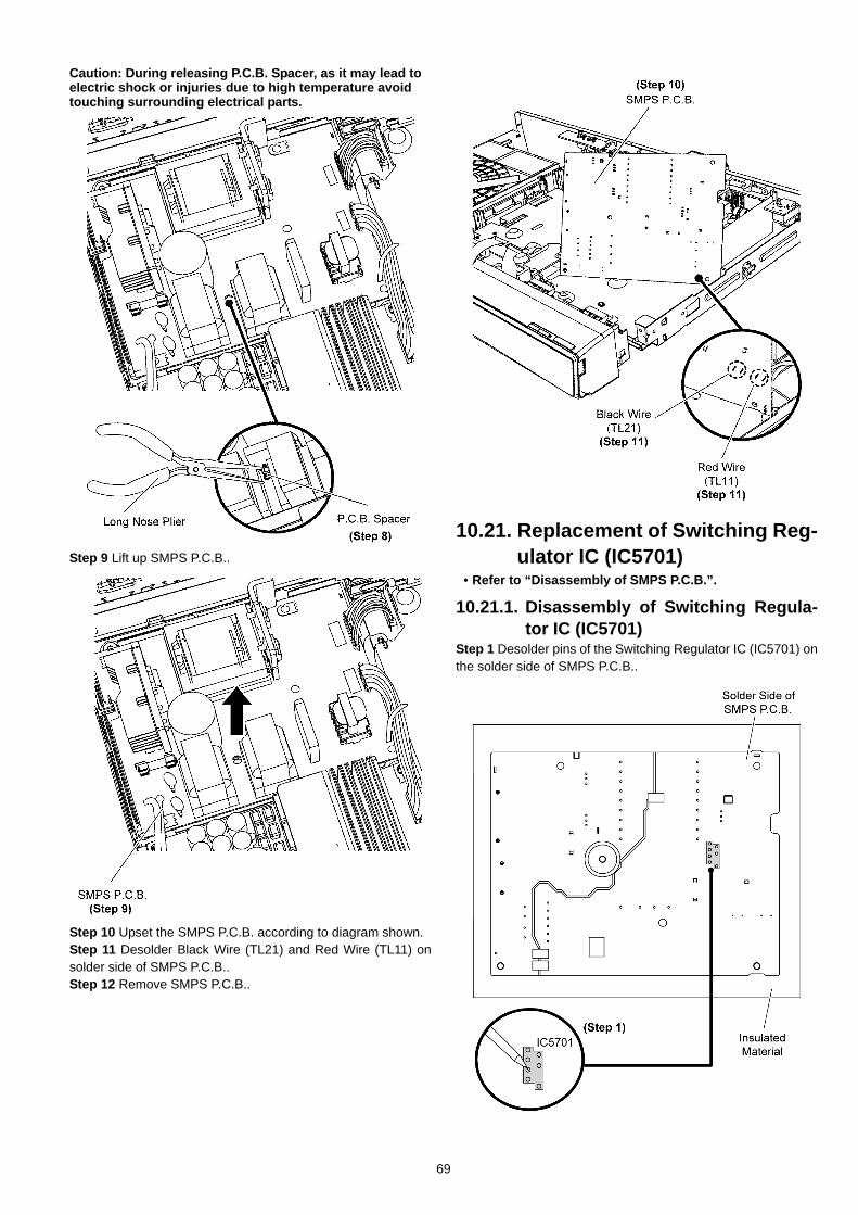
• Refer to “Disassembly of SMPS P.C.B.”.
10.21.1. Disassembly of Switching Regula-tor IC (IC5701)
Step 1 Desolder pins of the Switching Regulator IC (IC5701) onthe solder side of SMPS P.C.B..
69

Step 2 Remove 1 screw from the Switching Regulator IC(IC5701).Step 3 Remove the Switching Regulator IC (IC5701).Caution: Avoid touching the Heatsink Unit B due to its high temperature after prolonged use. Touching it may lead to injuries.Note: Refer to the diagrams of SMPS P.C.B. (Item 18.4) forlocation of the part.
10.21.2. Assembly of Switching RegulatorIC (IC5701)
Step 1 Apply grease to the Heatsink Unit B.Step 2 Fix the Switching Regulator IC (IC5701) onto the SMPSP.C.B..Step 3 Fix and screw the Switching Regulator IC (IC5701) tothe Heatsink Unit BCaution: Ensure the Switching Regulator IC (IC5701) istightly screwed to the Heatsink Unit B.
Step 4 Solder pins of the Switch Regulator IC (IC5701) on thesolder side of SMPS P.C.B..
Caution: Ensure pins of the Switching Regulator IC (IC5701) are properly seated and soldered on SMPS P.C.B..
10.22. Replacement of Rectifier Diode(D5702)
• Refer to “Disassembly of SMPS P.C.B.”.
10.22.1. Disassembly of Rectifier Diode(D5702)
Step 1 Desolder pins of the Rectifier Diode (D5702) on the sol-der side of SMPS P.C.B..Step 2 Desolder pins of the Heatsink Unit B.
70

Step 3 Remove 1 screw from the Switching Regulator IC(IC5701).Step 4 Remove the Heatsink Unit B together with RectifierDiode (D5702).Step 5 Remove 1 screw from the Rectifier Diode (D5702).Step 6 Remove the Rectifier Diode (D5702) from the HeatsinkUnit B.Caution: Avoid touching the Heatsink Unit B due to its high temperature after prolonged use. Touching it may lead to injuries.Note: Refer to the diagrams of SMPS P.C.B. (Item 18.4) forlocation of the part.
10.22.2. Assembly of Rectifier Diode(D5702)
Step 1 Apply grease to the Heatsink Unit B.Step 2 Fix and screw the Rectifier Diode (D5702) to the Heat-sink Unit B.Caution: Ensure the Rectifier Diode (D5702) is tightly screwed to the Heatsink Unit B.Step 3 Fix the Heatsink Unit B with Rectifier Diode (D5702)onto SMPS P.C.B..Caution: Ensure the Heatsink Unit B with Rectifier Diode (D5702) are properly seated on SMPS P.C.B..Step 4 Fix and screw the Switching Regulator IC (IC5701) tothe Heatsink Unit B.
Step 5 Solder pins of the Rectifier Diode (D5702) on the solderside of SMPS P.C.B..Step 6 Solder pins of the Heatsink Unit B on the solder side ofSMPS P.C.B..
71

Caution: Ensure pins of the Rectifier Diode (D5702) are properly seated before soldered onto SMPS P.C.B..
10.23. Replacement of RegulatorDiode (D5802)
• Refer to “Disassembly of SMPS P.C.B.”.
10.23.1. Disassembly of Regulator Diode(D5802)
Step 1 Desolder pins of the Regulator Diode (D5802) on thesolder side of SMPS P.C.B..
Step 2 Remove 1 screw from the Regulator Diode (D5802).Step 3 Remove the Regulator Diode (D5802) from the SMPSP.C.B..Caution: Avoid touching the Heatsink Unit A due to its high temperature after prolonged use. Touching it may lead to injuries.Note: Refer to the diagrams of SMPS P.C.B. (Item 18.4) forlocation of the electrical components.
10.23.2. Assembly of Regulator Diode(D5802)
Step 1 Apply grease to the Heatsink Unit A.Step 2 Mount the Regulator Diode (D5802) on to SMPS P.C.B..Caution: Ensure pins of the Regulator Diode (D5802) are properly seated on SMPS P.C.B..Step 3 Fix and screw the Regulator Diode (D5802) to the Heat-sink Unit A.
72
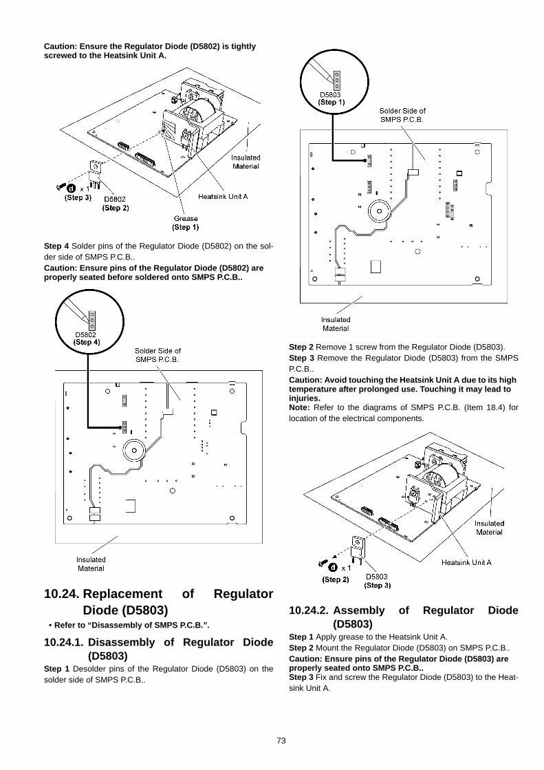
Caution: Ensure the Regulator Diode (D5802) is tightly screwed to the Heatsink Unit A.
Step 4 Solder pins of the Regulator Diode (D5802) on the sol-der side of SMPS P.C.B..Caution: Ensure pins of the Regulator Diode (D5802) are properly seated before soldered onto SMPS P.C.B..
10.24. Replacement of RegulatorDiode (D5803)
• Refer to “Disassembly of SMPS P.C.B.”.
10.24.1. Disassembly of Regulator Diode(D5803)
Step 1 Desolder pins of the Regulator Diode (D5803) on thesolder side of SMPS P.C.B..
Step 2 Remove 1 screw from the Regulator Diode (D5803).Step 3 Remove the Regulator Diode (D5803) from the SMPSP.C.B..Caution: Avoid touching the Heatsink Unit A due to its high temperature after prolonged use. Touching it may lead to injuries.Note: Refer to the diagrams of SMPS P.C.B. (Item 18.4) forlocation of the electrical components.
10.24.2. Assembly of Regulator Diode(D5803)
Step 1 Apply grease to the Heatsink Unit A.Step 2 Mount the Regulator Diode (D5803) on SMPS P.C.B..Caution: Ensure pins of the Regulator Diode (D5803) are properly seated onto SMPS P.C.B..Step 3 Fix and screw the Regulator Diode (D5803) to the Heat-sink Unit A.
73

Caution: Ensure the Regulator Diode (D5803) is tightly screwed to the Heatsink Unit A.
Step 4 Solder pins of the Regulator Diode (D5803) on the sol-der side of SMPS P.C.B..Caution: Ensure pins of the Regulator Diode (D5803) are properly seated before soldered onto SMPS P.C.B..
10.25. Disassembly of Fan• Refer to “Disassembly of Top Cabinet”.
Step 1 Lift up the Wire Clamper.Step 2 Detach the fan unit connector (CN5401) on D-AmpP.C.B..
Step 3 Remove 2 screws.Step 4 Remove Fan Unit.
74
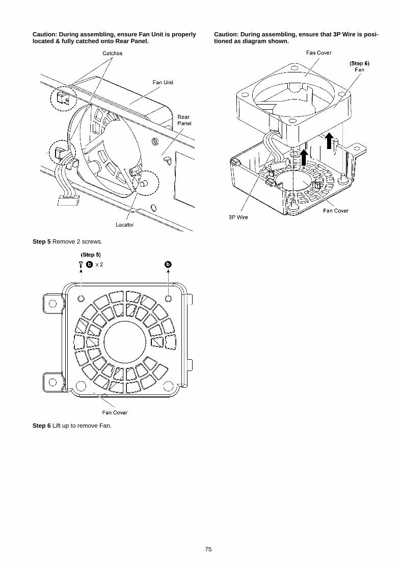
Caution: During assembling, ensure Fan Unit is properly located & fully catched onto Rear Panel.
Step 5 Remove 2 screws.
Step 6 Lift up to remove Fan.
Caution: During assembling, ensure that 3P Wire is posi-tioned as diagram shown.
75

11 Service PositionNote: For description of the disassembly procedures, seethe Section 10.
11.1. Checking & Repairing Side B ofMain P.C.B.
Caution:Pairing of BD Drive and Main P.C.B. as “BD Drive & Main P.C.B. Assembly” have to be replaced together. If either BD Drive or Main P.C.B. is changed, BD Drive unit has to carry out re-adjustment due to alignment data for BD Drive Unit is stored in the Main P.C.B.
Step 1 Remove Top Cabinet.Step 2 Remove Front Panel Block Assembly.Step 3 Remove Front Shield Plate Unit.Step 4 Remove Main P.C.B. Shield plate.Step 5 Connect 45P FFC at the connector (P55001) on MainP.C.B..Step 6 Connect 18P FFC at the connector (P55002) on MainP.C.B..Step 7 Connect 18P FFC at the connector (CN2006) on MainP.C.B..Step 8 Connect 10P FFC at the connector (CN2004) on MainP.C.B..
Step 9 Connect 22P FFC at the connector (CN2002) on MainP.C.B..Step 10 Proceed to check and repair Side B of Main P.C.B..
11.2. Checking & Repairing Side A ofMain P.C.B.
Caution:Pairing of BD Drive and Main P.C.B. as “BD Drive & Main P.C.B. Assembly” have to be replaced together. If either BD Drive or Main P.C.B. is changed, BD Drive unit has to carry out re-adjustment due to alignment data for BD Drive Unit is stored in the Main P.C.B.
Step 1 Remove Top Cabinet.Step 2 Remove Front Panel Block Assembly.Step 3 Remove 5 screws.
Step 4 Release 1 catch.
76

Step 5 Lift up Panel P.C.B..
Step 6 Remove 1 screws.
Step 7 Lift up Power Button P.C.B..
Step 8 Remove Front Shield plate Unit.Step 9 Remove Main P.C.B. Shield Plate.Step 10 Connect 45P FFC at the connector (P55001) on MainP.C.B..Step 11 Connect 18P FFC at the connector (P55002) on MainP.C.B..Step 12 Connect extension 18P FFC RFKZBT230P fromCN2006 to CN5402.Step 13 Connect extension 10P cable REXX1037 fromCN2004 to JW2.
Step 14 Slightly lift up Main P.C.B. according to diagramshown.
77
Step 15 Position Panel P.C.B. & Power Button P.C.B. as dia-gram shown.Step 16 Connect 22P FFC at the connector (CN2002) on MainP.C.B..
Step 17 Flip Main P.C.B. as diagram shown.Step 18 Proceed to check and repair Side A of Main P.C.B..
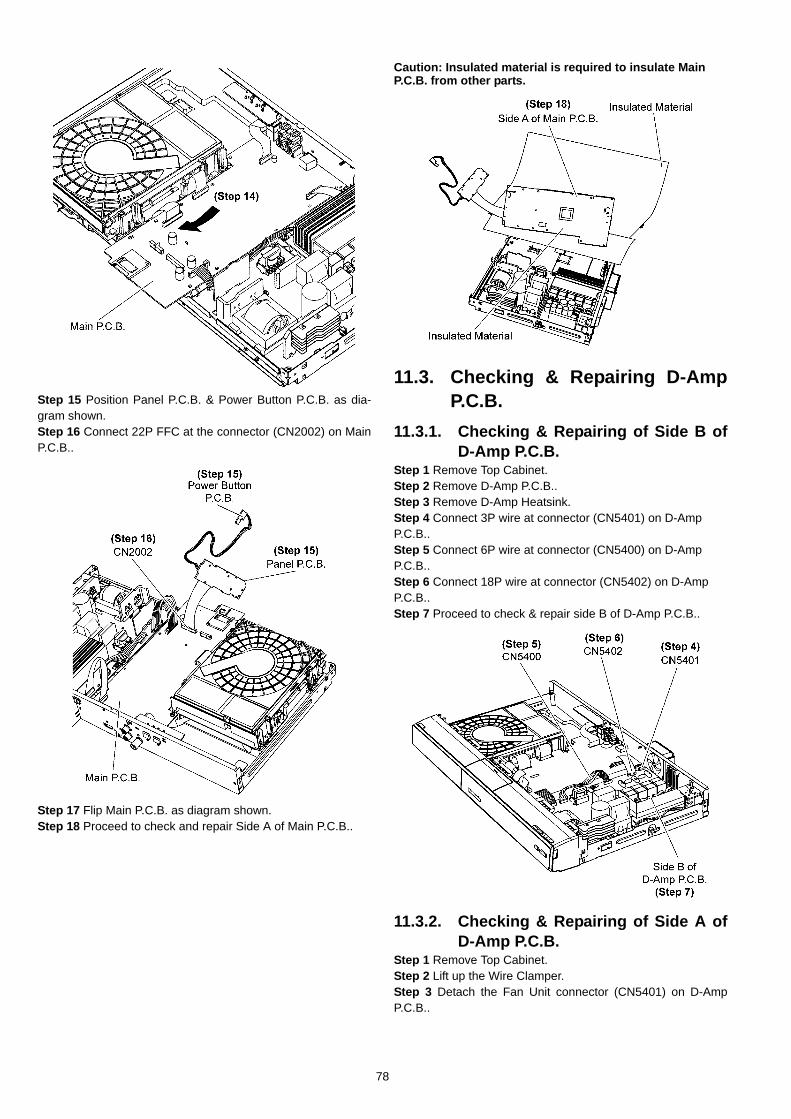
Caution: Insulated material is required to insulate Main P.C.B. from other parts.
11.3. Checking & Repairing D-AmpP.C.B.
11.3.1. Checking & Repairing of Side B ofD-Amp P.C.B.
Step 1 Remove Top Cabinet.Step 2 Remove D-Amp P.C.B..Step 3 Remove D-Amp Heatsink.Step 4 Connect 3P wire at connector (CN5401) on D-Amp P.C.B..Step 5 Connect 6P wire at connector (CN5400) on D-Amp P.C.B..Step 6 Connect 18P wire at connector (CN5402) on D-Amp P.C.B..Step 7 Proceed to check & repair side B of D-Amp P.C.B..
11.3.2. Checking & Repairing of Side A ofD-Amp P.C.B.
Step 1 Remove Top Cabinet.Step 2 Lift up the Wire Clamper.Step 3 Detach the Fan Unit connector (CN5401) on D-AmpP.C.B..
78
Step 4 Twist the Wire Clamper to release 6P Cable.Step 5 Remove 2 screws.
Step 6 Remove 6 screws.Step 7 Remove Fan Unit according to arrow shown.Step 8 Release tab at the side of the Rear Panel in the direc-tion of arrow.
Step 9 Twist the Wire Holder.Step 10 Release Red(TL10) & Black(TL20) wires from the WireHolder.Step 11 Remove AC Inlet P.C.B..
Step 12 Flip the D-Amp P.C.B. and position it according to dia-gram shown.Step 13 Connect Fan Unit to connector (CN5401) on D-AmpP.C.B..Step 14 Proceed to check and repair Side A of D-Amp P.C.B..
79

11.4. Checking & Repairing SMPSP.C.B.
Step 1 Remove Top Cabinet.Step 2 Release the 3 tabs.
Step 3 Release the 2 tabs at each side of the Front Panel BlockAssembly in the direction of arrow.
Step 4 Slightly move Front Panel Block Assembly forward.
Step 5 Remove 1 screw.
Step 6 Twist the Wire Holder.Step 7 Release Red(TL10) & Black (TL20) wires from the WireHolder.Step 8 Remove AC Inlet P.C.B. from Rear Panel.
80

Step 9 Twist the Wire Clampers to release 6P cable (SMPSP.C.B. to D-Amp P.C.B.) & 10P cable (SMPS P.C.B. to MainP.C.B.).
Step 10 Remove 5 screws.
Caution: During releasing of the P.C.B. Spacer, avoid touching the electrical components.Step 11 Release P.C.B. Spacer by using long nose plier.
Step 12 Flip the SMPS P.C.B. and position it according to dia-gram shown.Step 13 Proceed to check and repair SMPS P.C.B..
81

11.5. Checking & Repairing PanelP.C.B.
Step 1 Remove Top Cabinet.Step 2 Remove Front Panel Block Assembly.Step 3 Remove 5 screws.
Step 4 Release 1 catch.
Step 5 Lift up Panel P.C.B..
Step 6 Remove 1 screws.
Step 7 Lift up Power Button P.C.B..
Step 8 Connect 22P FFC to the connector (CN2002) on MainP.C.B..Step 9 Proceed to check and repair Panel P.C.B..
82

83

12 Voltage & Waveform ChartNote:
• Indication Voltage Values are in standard values for the unit measured by the DC electronic circuit tester (high-impedance) withthe chassis taken as standard.Therefore, there may exist some errors in voltage values, depending on the internal impedance of the DC circuit tester.
• Circuit voltage and waveform described herein shall be regarded as reference information when probing defect point because itmay differ from actual measuring value due to difference of Measuring instrument and its measuring condition and product itself.
12.1. Main P.C.B. (1/3)
REF NO.MODE 1 2 3 4 5
CD PLAY 5.2 0 0 3.3 5.2STANDBY 5.2 0 0 3.3 5.2
REF NO.MODE 1 2 3 4 5
CD PLAY 0 0 5.0 1.7 1.7STANDBY 0 0 5.0 1.7 1.7
REF NO.MODE 1 2 3 4 5 6 7 8
CD PLAY 0 0 0 -6.8 0 0 0 6.7STANDBY 0 0 0 -6.8 0 0 0 6.7
REF NO.MODE 1 2 3 4 5 6 7 8 9 10 11 12 13 14 15 16 17 18 19 20
CD PLAY 1.7 0 1.2 0 0 0.1 0 0 0 0 0 3.3 3.3 3.3 3.3 3.3 1.7 0 3.3 0STANDBY 1.7 0 1.2 0 0 0.1 0 0 0 0 0 3.3 0 3.3 3.3 3.3 1.7 0 3.3 0
REF NO.MODE 21 22 23 24 25 26 27 28 29 30 31 32 33 34 35 36 37 38 39 40
CD PLAY 0 0 0 1.5 1.5 0 0 3.3 0.7 0 0 0 0 0 0.6 1.7 1.7 1.2 3.3 1.7STANDBY 0 0 0 1.5 1.5 0 0 3.3 0.7 0 0 0 0 0 0 1.7 1.7 0 3.3 1.7
REF NO.MODE 1 2 3 4 5 6 7 8
CD PLAY 0 0 0 0 0 0 0 3.4STANDBY 0.1 0 0 0 0 0 0 3.4
REF NO.MODE 1 2 3 4 5 6 7 8
CD PLAY 0 0 0 -6.8 0 0 0 6.7STANDBY 0 0 0 -6.8 0 0 0 6.7
REF NO.MODE 1 2 3 4 5 6 7 8
CD PLAY 0 0 0 -6.8 0 0 0 6.7STANDBY 0 0 0 -6.8 0 0 0 6.7
REF NO.MODE 1 2 3 4 5 6 7 8 9 10 11 12 13 14 15 16 17 18 19 20
CD PLAY 3.3 2.8 3.3 0 3.3 0 3.3 0 0 0.8 1.6 3.3 1.6 0 0 3.3 3.3 1.8 2.1 3.4STANDBY 3.3 2.8 3.3 0 3.3 0 3.3 0 0 0.8 1.6 3.3 1.6 0 0 3.3 3.3 1.8 2.1 3.4
REF NO.MODE 21 22 23 24 25 26 27 28 29 30 31 32 33 34 35 36 37 38 39 40
CD PLAY 3.3 0.1 0 0.1 3.2 3.9 2.7 3.3 3.3 2.7 3.3 1.2 0 3.3 0 0 0 0 0 0STANDBY 3.3 0.1 0 0.1 3.2 3.9 2.7 3.3 3.3 2.7 3.3 1.2 0 3.3 0 0 0 0 0 0
IC1001
IC2300
IC2071
IC2201
IC2202
IC1101
IC1102
IC2001
IC2001
IC2300
SA-BT235P MAIN P.C.B.
84

12.2. Main P.C.B. (2/3)
REF NO.MODE 41 42 43 44 45 46 47 48 49 50 51 52 53 54 55 56 57 58 59 60
CD PLAY 0 0 3.3 3.3 0 3.3 3.4 3.4 3.3 3.2 0.9 0.9 3.3 3.3 3.3 0 0 0.9 0 3.3STANDBY 0 0 3.3 3.3 0 3.3 3.4 3.4 3.3 3.2 0.9 0.9 3.3 3.3 3.3 0 0 0.9 0 3.3
REF NO.MODE 61 62 63 64 65 66 67 68 69 70 71 72 73 74 75 76 77 78 79 80
CD PLAY 3.3 3.3 0 0 0 0 3.3 0 3.3 3.3 3.3 0 0 3.3 0 3.4 3.3 3.3 3.3 3.3STANDBY 3.3 3.3 0 0 0 0 3.3 0 3.3 3.3 3.3 0 0 3.3 0 3.4 3.3 3.3 3.3 3.3
REF NO.MODE 81 82 83 84 85 86 87 88 89 90 91 92 93 94 95 96 97 98 99 100
CD PLAY 1.2 0 3.3 3.3 3.3 3.3 0 0 0 0 1.9 1.9 1.0 0 0 0 0 3.3 3.3 3.3STANDBY 1.2 0 3.3 3.3 3.3 3.3 0 0 0 0 1.9 1.9 1.0 0 0 0 0 3.3 3.3 3.3
REF NO.MODE 1 2 3 4 5 6 7 8
CD PLAY 0 0 0 0 3.3 3.3 0 3.3STANDBY 0 0 0 0 3.3 3.3 0 3.3
REF NO.MODE 1 2 3
CD PLAY 3.3 0 6.0STANDBY 3.3 0 6.0
REF NO.MODE 1 2 3 4 5 6 7 8 9 10 11 12 13 14 15 16 17 18 19 20
CD PLAY 0 3.3 0 0 0 0 0 0 0 0 0 0 0 0 0 0 0 0 0 0STANDBY 0 3.3 0 0 0 0 0 0 0 0 0 0 0 0 0 0 0 0 0 0
REF NO.MODE 1 2 3 4 5 6 7 8 9 10 11 12 13 14 15 16
CD PLAY 0 0 0 0 0 0 -6.8 0 0 6.7 0 0 0 0 0 0STANDBY 0 0 0 0 0 0 -6.8 0 0 6.7 0 0 0 0 0 0
REF NO.MODE 1 2 3 4 5 6 7 8 9 10 11 12 13 14 15 16 17 18 19 20
CD PLAY 0 0.3 0 0 3.3 3.3 3.3 3.3 1.5 3.3 3.3 0 0.3 0.3 0.3 0 0.3 3.3 0 0STANDBY 0 0.3 0 0 3.3 3.3 3.3 3.3 1.5 3.3 3.3 0 0.3 0.3 0.3 0 0.3 3.3 0 0
REF NO.MODE 1 2 3 4 5 6 7 8
CD PLAY 3.3 0 0 1.9 5.0 0 0 5.2STANDBY 3.3 0 0 1.9 5.0 0 0 5.2
REF NO.MODE 1 2 3 4 5
CD PLAY 5.0 0 1.4 5.2 5.2STANDBY 5.0 0 1.3 5.2 5.2
IC7003
SA-BT235P MAIN P.C.B.
IC2300
IC7002
IC2400
IC2800
IC2952
IC2300
IC2300
IC2301
IC2302
85

12.3. Main P.C.B. (3/3)
REF NO.MODE 1 2 3 4 5 6 7 8 9 10 11 12 13 14 15 16
CD PLAY 2.5 2.5 0 0 0 5.1 3.3 0 1.2 1.7 1.6 1.7 3.4 0 0 0STANDBY 2.5 2.5 0 0 0 5.1 3.3 0 1.2 1.7 1.6 1.7 3.4 0 0 0
REF NO.MODE 1 2 3 4 5 6 7 8
CD PLAY 0.9 1.0 0 0 0 0 0 3.4STANDBY 1.2 1.1 0 0 3.4 0 0 3.4
REF NO.MODE 1 2 3 4 5 6 7 8
CD PLAY 3.4 0 0 0 3.4 0 0 3.3STANDBY 3.4 3.4 0 0 3.4 0 0 3.3
REF NO.MODE E C B E C B E C B S D G S D G
CD PLAY 0 3.3 0 0 0 0 0 0 0 0 1.7 0 0 1.6 0STANDBY 0 3.3 0 0 0 0 0 0 0 0 1.7 0 0 1.6 0
REF NO.MODE E C B E C B E C B E C B E C B
CD PLAY 0 6.7 0 0 6.7 0 -6.8 -9.8 -7.4 0 -7.4 -0.6 0 11.4 7.3STANDBY 0 6.7 0 0 6.7 0 -6.8 -9.8 -7.4 0 -7.4 -0.6 0 11.4 7.3
REF NO.MODE E C B E C B E C B E C B E C B
CD PLAY 0 3.2 -3.0 0 3.2 -1.6 0 3.2 -1.6 11.4 11.4 10.7 0 0 3.0STANDBY 0 3.2 -3.0 0 3.2 -1.6 0 3.2 -1.6 11.4 11.4 10.7 0 0 3.0
REF NO.MODE E C B S D G S D G E C B E C B
CD PLAY 0 0 3.0 3.3 3.4 3.3 3.3 3.4 3.3 0 3.2 0 0 0 3.0STANDBY 0 0 3.0 3.3 3.4 3.3 3.3 3.4 3.3 0 3.2 0 0 0 3.0
REF NO.MODE E C B E C B E C B
CD PLAY 0 0 3.2 0 0 3.2 0 0 3.2STANDBY 0 0 3.2 0 0 3.2 0 0 3.2
SA-BT235P MAIN P.C.B.
QR7001 QR7014
QR7019 QR7071 QR7081
QR1102 Q56004
IC54900
Q1105Q1101 Q1102 Q1103 Q1104
IC57000
IC57001
Q56005
Q7071Q7008 Q7050 QR1101
Q7006
Q7007
Q2800 Q2805 Q7004 Q7005
86

12.4. Panel P.C.B.
REF NO.MODE 1 2 3 4 5 6 7 8 9 10 11 12 13 14 15 16 17 18 19 20
CD PLAY 0 0 0 0 1.9 0 1.4 2.9 2.1 0 0 0 3.3 -23.4 -23.4 -23.4 -21.2 -16.9 -16.9 -21.2STANDBY 0 0 0 0 1.9 0 1.4 2.9 2.2 0 0 0 3.3 -23.4 -23.4 -23.4 -23.4 -14.8 -16.9 -21.2
REF NO.MODE 21 22 23 24 25 26 27 28 29 30 31 32 33 34 35 36 37 38 39 40
CD PLAY -23.4 -23.4 -23.4 -17.0 -17.0 -23.4 -23.4 -17.0 -17.0 -23.8 -14.9 -23.6 -21.4 -21.4 -21.4 -21.4 -21.4 -21.4 -21.4 -21.4STANDBY -21.2 -23.4 -21.2 -14.8 -14.8 -21.2 -23.4 -14.8 -12.6 -23.9 -17.1 -23.6 -21.4 -21.4 -21.4 -21.4 -21.4 -21.4 -21.4 -21.4
REF NO.MODE 41 42 43 44
CD PLAY -21.4 -21.4 3.3 0STANDBY -21.4 -21.4 3.3 0
REF NO.MODE E C B E C B
CD PLAY 0 8.4 8.4 0 0 5.0STANDBY 0 8.4 8.4 0 0 5.0
SA-BT235P PANEL P.C.B.
IC6001
IC6001
IC6001
Q6100 Q6800
87

12.5. D-Amp P.C.B. (1/2)
REF NO.MODE 1 2 3 4 5 6 7 8 9 10 11 12 13 14 15 16 17 18 19 20
CD PLAY 11.5 3.3 3.3 1.6 3.1 1.6 1.1 0 0 3.5 3.5 0 0 1.5 3.1 1.5 11.6 11.4 11.5 31.9STANDBY 11.5 3.3 3.3 1.6 3.1 1.6 1.1 0 0 3.5 3.5 0 0 1.5 3.1 1.5 11.6 11.4 11.5 31.9
REF NO.MODE 21 22 23 24 25 26 27 28 29 30 31 32 33 34 35 36
CD PLAY 42.4 0 0 0 0 42.4 31.9 31.9 42.4 0 0 0 0 42.4 31.9 11.4STANDBY 42.4 0 0 0 0 42.4 31.9 31.9 42.4 0 0 0 0 42.4 31.9 11.4
REF NO.MODE 1 2 3 4 5 6 7 8 9 10 11 12 13 14 15 16 17 18 19 20
CD PLAY 11.5 3.2 3.3 1.6 3.2 1.6 1.1 0 0 3.2 0 0 3.2 1.6 3.2 1.6 11.6 11.5 11.5 31.8STANDBY 11.5 3.2 3.3 1.6 3.2 1.6 1.1 0 0 3.2 0 0 3.2 1.6 3.2 1.6 11.6 11.5 11.5 31.8
REF NO.MODE 21 22 23 24 25 26 27 28 29 30 31 32 33 34 35 36
CD PLAY 42.4 0 0 0 0 42.4 31.9 31.7 42.4 0 0 0 0 42.4 31.8 11.5STANDBY 42.4 0 0 0 0 42.4 31.9 31.7 42.4 0 0 0 0 42.4 31.8 11.5
REF NO.MODE 1 2 3 4 5 6 7 8 9 10 11 12 13 14 15 16 17 18 19 20
CD PLAY 1.7 3.2 0 0 0.8 0.9 0 1.6 3.2 3.1 3.1 0 0 1.1 1.8 3.2 3.2 3.2 1.5 1.5STANDBY 1.7 3.2 0 0 0.8 0.9 0 1.6 3.2 3.1 3.1 0 0 1.1 1.8 3.2 3.2 3.2 1.5 1.5
REF NO.MODE 21 22 23 24 25 26 27 28 29 30 31 32 33 34 35 36 37 38
CD PLAY 0 0 0 0 0.6 1.2 0 0 0 1.8 3.1 3.1 1.6 1.6 1.5 1.5 1.5 1.5STANDBY 0 0 0 0 0.6 1.2 0 0 0 1.8 3.1 3.1 1.6 1.6 1.5 1.5 1.5 1.5
REF NO.MODE 1 2 3 4 5
CD PLAY 13.1 13.1 0 11.6 1.1STANDBY 13.1 13.1 0 11.6 1.1
REF NO.MODE 1 2 3 4 5
CD PLAY 3.2 3.2 0 0 0STANDBY 3.2 3.2 0 0 0
REF NO.MODE 1 2 3 4 5
CD PLAY 3.2 3.2 0 3.2 3.2STANDBY 3.2 3.2 0 3.2 3.2
REF NO.MODE 1 2 3 4 5 6
CD PLAY 1.5 0 1.5 1.6 3.1 1.6STANDBY 1.5 0 1.5 1.6 3.1 1.6
IC5404
SA-BT235P D-AMP P.C.B.
IC5100
IC5402
IC5301
IC5400
IC5401
IC5100
IC5200
IC5200
IC5301
88

12.6. D-Amp P.C.B. (2/2)
12.7. Power P.C.B.
REF NO.MODE 1 2 3 4 5
CD PLAY 3.2 3.2 0 3.2 3.1STANDBY 3.2 3.2 0 3.2 3.1
REF NO.MODE E C B E C B E C B E C B E C B
CD PLAY 12.0 18.0 12.0 18.0 12.0 0 0 2.9 0 0 2.9 0 0 7.5 0.7STANDBY 12.0 18.0 12.0 18.0 12.0 0 0 2.9 0 0 2.9 0 0 7.5 0.7
REF NO.MODE E C B E C B E C B E C B E C B
CD PLAY 0 3.7 0.1 0 0 0 0 0 0 0 3.3 0 42.4 4.3 0STANDBY 0 3.7 0.1 0 0 0 0 0 0 0 3.3 0 42.4 4.3 0
REF NO.MODE E C B E C B E C B
CD PLAY 0 0 0 0 0 0 12.0 0 5.0STANDBY 0 0 0 0 0.1 5.0 12.0 0 5.0
IC5405
Q5413
Q5414 QR5400 QR5401
Q5405 Q5408 Q5409 Q5412
Q5404
SA-BT235P D-AMP P.C.B.
Q5400 Q5401 Q5402 Q5403
REF NO.MODE 1 2 3 4 5 6 7 8 9 10 11 12 13 14 15 16 17 18 19 20
CD PLAY 1.7 2.5 2.0 1.0 1.6 0 0 16.4 11.2 14.9 14.3 16.5 16.5 0 15.8 1.6 1.0 2.0 2.4 2.5STANDBY 1.7 2.5 2.0 1.0 1.6 0 0 16.4 11.2 14.9 14.3 16.5 16.5 0 15.8 1.6 1.0 2.0 2.4 2.5
REF NO.MODE 1 2 3 4 5 6 1 2 3 4 5 6
CD PLAY 12.0 12.0 16.1 17.8 12.0 12.0 5.0 5.0 16.2 17.8 5.0 5.0STANDBY 12.0 12.0 16.1 17.8 12.0 12.0 5.0 5.0 16.2 17.8 5.0 5.0
Q2902 Q2903
SA-BT235P POWER P.C.B.
IC2901
89

12.8. SMPS P.C.B.
REF NO.MODE 1 2 3 4 5 6 7
CD PLAY 19.5 -11.6 -11.6 -8.1 -11.6 -11.3 -11.5STANDBY 19.5 -11.6 -11.6 -8.1 -11.6 -11.3 -11.5
REF NO.MODE 1 2 3 4 5 6 7 8
CD PLAY -14.0 -15.0 -14.6 -13.0 -15.1 0 -15.1 -15.1STANDBY -14.0 -15.0 -14.6 -13.1 -15.1 0 -15.0 -15.0
REF NO.MODE 1 2 3
CD PLAY 18.3 2.5 0STANDBY 18.3 2.5 0
REF NO.MODE 1 2 3 4
CD PLAY 0 0 3.8 2.3STANDBY 0 0 3.8 2.3
REF NO.MODE E C B E C B E C B E C B E C B
CD PLAY -10.3 -9.9 -10.2 0 0.6 0 0 1.9 0.4 0 0.1 0.7 0 3.1 0STANDBY -10.3 -9.9 -10.2 0 0.6 0 0 1.9 0.4 0 0.1 0.7 0 3.1 0
SA-BT235P SMPS P.C.B.
IC5701
IC5799
IC5801
IC5899
Q5720 Q5863 Q5898 Q5899 QR5862
90

12.9. Waveform Table
WF No. IC2001-3 (PLAY)
5.6Vp-p(2usec/div)
WF No. IC2001-35 (PLAY)
4Vp-p(5usec/div)
WF No. IC2001-38 (PLAY)
4.4Vp-p(500nsec/div)
WF No. IC2300-10 (PLAY)
1Vp-p(10usec/div)
WF No. IC2300-11 (PLAY)
3Vp-p(10usec/div)
WF No. IC2300-13 (PLAY)
3.6Vp-p(50nsec/div)
WF No. IC2300-15 (PLAY)
2Vp-p(50nsec/div)
WF No. IC2800-1,12 (PLAY)
0.24Vp-p(1msec/div)
WF No. IC2800-2,3,13,15 (PLAY)
2.2Vp-p(1msec/div)
WF No. IC2952-2,13,14 (PLAY)
0.24Vp-p(1msec/div)
WF No. IC5100-4,6,14,16 (PLAY)
5.2Vp-p(1usec/div)
WF No. IC5100-22,25,30,33 (PLAY)
80Vp-p(1usec/div)
WF No. IC5200-4,14 (PLAY)
5.6Vp-p(1usec/div)
WF No. IC5200-6,16 (PLAY)
6.8Vp-p(1usec/div)
WF No. IC5200-22,25,30,33 (PLAY)
76Vp-p(1usec/div)
WF No. IC5301-24,25,26 (PLAY)
3.6Vp-p(500nsec/div)
WF No. IC5301-33,34,35,36, 37,38 (PLAY)
6Vp-p(1usec/div)
WF No. IC6001-5 (PLAY)
1.5Vp-p(2usec/div)
WF No. IC6001-8 (PLAY)
3.2Vp-p(2usec/div)
WF No. IC54900-1,2 (PLAY)
1Vp-p(5usec/div)
91

WF No. IC54900-9 (PLAY)
5.2Vp-p(2usec/div)
92
13 Illustration of ICs, Transistor and Diode
A
Ca
Cathode
Anode
A
Ca
Cathode
Anode
A
Ca
Cathode
Anode
2
3
1
4
23
1
54
6
Ca
A
A
Ca
A
A
No.1
No.1
No.1
8
4
5
7
12
3
B
C
E
G
D
S
EC
B
No.1
A
Ca
Cathode
Anode
AnodeAnode
AnodeCathode
A
Ca
Cathode
Anode
A
Ca
Cathode
Anode
1
42
35
1
4
5
23
1
6
8
23
4
5
7
12
3
1
3
4
2
E
B
C
Ca
ACa
A
No.1No.1
1
45
6
23
3
12
12
34
87
65
CaA
Anode
Cathode
B0BC020A0267B0BC6R2A0266B0BC2R4A0263
B0BC3R0A0262B0BC7R5A0266
B0BC027A0264B0BC013A0269
B0EAMM000057B0HAMP000094B0HAJM000005
B0EDKT000009B1CHPD000003 B0HBSM000054
B0ZAZ0000052
C0CBABC00117
MIP2F20MSSCF
C0DBEKG00004C0DBZMC00006
C0DBZYY00018 (8p)
C0EBE0000456
C0JBAB000837
C0JBAA000501
C0ABZA000080
C0DBZHE00026
C0JBAR000434
C0HBB0000057 (44p)
B1ABCF000011
B1ABMF000020
B1ADNB000003
B1ABGC000001
B0HFRJ000012
B1BABK000001B1BAAJ000003
B1CFHA000002
C0JBAR000540 (16p)
C0DBAYY00729 (20p)
C1AB00003260 (36p)
C3EBFC000042 (8p)
C0FBAK000026 (16p)
C0ABBB000189 (8p)
C0ABBB000179 (8p)
C1AB00002461 (30p)
C2HBCA000001 (40p)
VUEALLPT041 (20p)
B1ADCE000012
B1ABCF000176
B1GBCFJJ0051
B1ADBL000010
B1GBCFGG0030
B1GBCFNN0038B1ABEB000002
B0BC6R8A0266B0BC010A0269B0BC030A0264
B0BC024A0267B0BC5R1A0266
B0BC7R5A0268 B0BC012A0269B0JCPG000005B0HCSP000001
B0FBAR000043
B0JCMD000010MA2YF8000L
C5HACYY00004 (7p)C0DABFC00002
B0ACCK000005
RFKWMBT230P
(100p)
MFI341S2164 (20p)
B3ABA0000187
93

94

95
14 Block Diagram14.1. Main(System Control)
SA-BT235P MAIN(SYSTEM CONTROL) BLOCK DIAGRAM
518
P6001CN2002
5SDA
6SCL
MICRO PROCESSORRFKWMBT230P
IC2300
EEPROMC3EBFC000042
X2301
IC2301
FL DISPLAY DRIVERC0HBB0000057
IC6001
FLD DAT 27 7DINFL DATA
419
P6001CN2002FLD CLK 28
FL CLK
320
P6001CN2002
2 2
KEY1 BTNCN6001 H6803
FLD STB 21
EEPROM SCL86
13I2C SDA
MICRO CONTROLLERMFI341S2164
IC2400
iPhone DAT38
12I2C SCL iPhone CLK39
4nRESET iPhone RST40
XCIN10
XCOUT11
X2300
XIN15
LED CONT100
XOUT13
FL STB
617
P6001CN2002 RMT
FLD DAT
FLD CLK
FLD STB
KEY192
EEPROM SDA85
KEY1 INT18
KEY1
POWER
KEY1
LED CTL
8CLK
9STB
5
13
43
VDD
VDD
30 -VP
OSC
P16
P1
P16
P1
G6
G1
G6
G1
G9
G7
G9
G7
DP6001
S6801
STOPS6002
FL DISPLAY
SERIAL
DATA
INTERFACE
OSC
CONTROL
DISPLAY
MEMORY(24bits x 12 Words)
SEGMENT
DRIVER
GRID
DRIVER
GRID
DRIVER
KEY SCAN
OUTPUTTIMING
GENERATOR
KEY MATRIXMEMORY
DIMMINGCIRCUIT
+3.3V
-VP
31
32
F+
F+
F+
1
2
F-
F-
F-
VREF
VREF
1 22
P6001 CN2002
KEY291KEY2
2 21
P6001 CN2002
SELECTORS6007
D6800
OPEN/CLOSES6807
REMOTE CONTROLSENSOR
IR6001
Q6800
LED DRIVE
RMT 5RMT
CECCECCEC 17
VOL -S6006
VOL +S6005
PLAYS6003
Pod OC 80iPod OC
iPod OC
od ACC 83iPod ACC
iPod ACC
RL SW 72iPod CTRL SW
XINTP OUT 53XINTP OUT
SBMTP 48SBMTP
XMPREQ 20XMPREQ
XINTM OUT 54
XINTM 55
XINTM OUT
SBPTM 47SBPTM
SCLK(BP1) 49CLK SCLK
iPod CTRL SW
GOOD 3PW GOOD
PW GOOD
C DET1 25DC DET1
DC DET1
iPod VIDEOSEL
VCOMP MUTE
QUICK PCONT1
PCONT 82BATTPCONT
BATTPCONT
SYNC19SYNC
PCONT50PCONT
ART TX 35UART TX
412
CN100218
CN1001CN1101
od DET 74iPod DET CN1002
30
CN1001CN1101124
RT RX 36UART RX
PCONT 50PCONT
CN100219
CN1001CN1101313
iPod/iPhone
Q1102
SWITCH
PCONT 77
QR1101
PCONT SWITCH
QR1102
PCONT SWITCH
Q1103
SWITCH
11
CN2004JW2*
99
CN2004JW2*
1013
CN2002P600133
CN6001H6803
FROM/TO
POWER SUPPLY TO
MAIN(VIDEO)
TO
MAIN(VIDEO)
FROM/TO
POWER SUPPLY
(MAIN SECTION)
FROM/TO
POWER SUPPLY
(DIGITAL SECTION)
FROM/TO
MAIN(DIGITAL)
iPod VIDEO SEL 66
MUTE 67
iPod VIDEOSEL
VCOMP MUTE
JC P ON HP ON H 1JC P ON H
HDMI P ON HP ON H 78HDMI P ON H
XMPREQ
XINTM OUT
CLK SCLK
SBPTM
PKS STAT 61BP STATE
XBPRST 60XBPRST
XBPRST
BP STATE
TRY OP CL 44TRY OP CL
TRY OP CL
TRY DILECT 81TRY DILECT
TRY PFAIL 84TRY PFAIL
TRY PFAIL
TRY DILECT
XINTP OUT
SBMTP
1423
CN1002CN10012
CN11014 1
ISOLATIONAMPLIFIER
C0ABZA000080
IC1101
iPod VOUT
MAIN P.C.B.
PANEL P.C.B.
PANEL P.C.B.SMPS P.C.B.
POWER BUTTON P.C.B.
iPod/iPhone P.C.B.
: iPod/iPhone VIDEO INPUT SIGNAL LINE
TRY MODE 51TRY MODE
TRY MODE
SEL A89SEL A
SEL A
SEL B90SEL B
DSP CLK29DSP CLK
DSP DAT30DSP DA
DSP RESET69DSP RESET
DSP MUTE70DSP MUTE
SEL B
DAP RST71
DAP MUTE34
TUN SCLK24TUN SCLK
TUN SCLK
TUN SDIO22TUN SDIO
TUN SDIO
APD97APD
APD
i
iP
iPod CT
PW
D
BATT
DC DET226415
CN2006CN5402 DC DET2
ECO CTL4ECO_CTL
DSP RESET
DSP MUTE
OPT IN SEL288OPT IN SEL2
DMIX OUT SEL75DMIX OUT SEL
OPT IN SEL2
OPT IN SEL187OPT IN SEL1
OPT IN SEL1
DMIX OUT SEL
P STANDBY H2P STANDBY H
P STANDBY H
SCL2
DSP DA
DSP CLK
SDA2
U
iP
UA
QUICK
Q56005
LEVEL SHIFTER
Q7050
MUTINGCONTROL
Q56004
LEVEL SHIFTER
3 16
CN5402 CN2006
4 15
CN5402 CN2006
16 3
CN5402 CN2006
FAN ON H79FAN ON H
17 2
CN5402 CN2006
DAP RST
1 18
CN5402 CN2006
DAP MUTE
2 17
CN5402 CN2006
1010
CN2004JW2*(MAIN SECTION)
TO
POWER SUPPLY
(DIGITAL SECTION)
FROM/TO
DIGITAL AUDIO
FROM/TO
MAIN(DIGITAL)
FROM/TO
MAIN(AUDIO)
VCOMP
JC
HDMI
D-AMP P.C.B.

96
14.2. Main(Audio)
SA-BT235P MAIN(AUDIO) (1/2) BLOCK DIAGRAM
TO MAIN(AUDIO)
SECTION (2/2)
FROM/TO
MAIN(SYSTEM CONTROL)
FROM
MAIN(VIDEO)
FROM
MAIN(DIGITAL)
FROM
MAIN(SYSTEM CONTROL)
X2951
MULTIPLEXERC0JBAR000434
IC57001
1 A
6 SELECT
2 B
FM ANT
JK2951
311
CN2011CN4002
MULTIPLEXERC0JBAR000540
IC2800
A/D CONVERTERC0FBAK000026
IC54900
FM RADIO RECEIVERVUEALLPT040
IC2952
L CH3
SDT09
R CH13
AUX L IN
A LIN
A RIN
LOUT 14
2
TUN-LCH
ROUT 13TUN-RCH
L2
2 FMI
AUX R IN15
R2
2AINL
AIN0
SCLK12
SCLK
DELTA-SIGMA
MODULATOR
DECIMATION
FILTER
SERIAL I/O
INTERFACE
CLOCK
DIVIDER
1AINR
1L0
12R0
17 DCLK
9 RCLK
AUX L
AUX R
ARC
OPT IN SEL2
TUN SCLK
TUN SDIO
7 SCLK
8 SDIO
TUN SCLK
TUN SDIOMCLK
11MCLK
LRCK10
LRCK
Y 5
MULTIPLEXERC0JBAR000434
IC57000
1 A
6 SELECTOPT IN SEL1 Y 5
JK3100
OPTICAL 1
DIGITALAUDIO IN
OPT IN 3OPT IN1
59
CN2011CN40022 B
JK3101
OPTICAL 2 OPT IN 3OPT IN2
: AUX/iPod/iPhone/OPTICAL/HDMI AUDIO INPUT SIGNAL LINE : AUDIO OUTPUT SIGNAL LINE : FM SIGNAL LINE
APD
P36
AIN0
TO
MAIN(SYSTEM CONTROL)
FROM/TO
MAIN(DIGITAL)
TO
MAIN(DIGITAL)
OP-AMPC0ABBB000179
IC2201
OP-AMPC0ABBB000179
IC2202
5 7
2 1
6 7
2 1
SCLK
LRCK
MCLK
MAIN P.C.B.
OPTICAL IN P.C.B.
FROM
MAIN(SYSTEM CONTROL)
iPod/iPhone P.C.B.
6 7
2 1
Q2800
INVERTER
iPod/iPhone OP-AMPC0ABBB000189
IC1102
927
CN1002CN10014
L3DOCK L
1128
CN1002
7
CN1101
5
CN1101CN100111
R3
10 A (LSB)
DOCK R
DOCK-LCH
DOCK-RCH
SEL ASEL A
Q2805
INVERTER 9 B (MSB)SEL B
SEL B

97
SA-BT235P MAIN(AUDIO) (2/2) BLOCK DIAGRAM
FROM
MAIN(SYSTEM CONTROL)
FROM
MAIN(DIGITAL)
TO
DIGITAL AUDIO
D-AMP P.C.B.
136
CN5402CN2006
127
CN5402CN2006
118
CN5402CN2006
811
CN5402CN2006
910
CN5402CN2006
613
CN5402CN2006
DIGITAL SOUNDPROCESSOR
C2HBCA000001
IC2001
4 I2S_IN2
5 I2S_IN3
MULTIPLEXERC0JBAR000434
IC2071
1 A
6 SELECT
2 B
Y 5
I2S OUT1 38
I2S OUT2 35
I2S OUT3 34
DSP I2S OUT1
AMCLK OUT 40DSP_MCLK OUT
LRCK OUT 36DSP_LRCK OUT
BCK OUT 37DSP_BCK OUT
DSP I2S OUT2
DSP I2S OUT3
1 BCK_IN
2 LRCK_IN
17 SYSCLK_IN
: AUX/iPod/iPhone/OPTICAL/HDMI AUDIO INPUT SIGNAL LINE : AUDIO OUTPUT SIGNAL LINE : FM SIGNAL LINE
6 I2S_IN4
2 I2S_IN1
ADAC D2
ADAC D1
BCK
LRCK
MCK
ADAC D3
ADAC D0
ADAC MIX
DMIX OUT SEL
ADAC MIX
ADAC D0
ADAC D3
ADAC D1
ADAC D2
MCK
LRCK
BCK
MAIN P.C.B.
TO MAIN(AUDIO)
SECTION (1/2)
FROM/TO
MAIN(SYSTEM CONTROL)
DSP RESETRESETX 12
DSP MUTEMUTEX 13
SCL 14
DSP DA
DSP CLK
SDA 15
DSP RESET
DSP MUTE
DSP CLK
DSP DA

98
14.3. Digital Audio
SA-BT235P DIGITAL AUDIO BLOCK DIAGRAM
: AUDIO OUTPUT SIGNAL LINE
FROM
MAIN(AUDIO)
MAIN P.C.B.
D-AMP P.C.B.
+
-
+
-
+
-
+
-
FAN
+
-
+
-
MUX & VOL PWM
SERIAL DATAINTERFACE
SERIAL CONTROL
PWM FL+
PWM FR+
PWM C+
PWM SW+
PWM SW-
PWM SW+
PWM C-
PWM C+
PWM 336
PWM 435
PWM 534
PWM 633
VALID1VALID1
VALID2
FAN DC OUT
FAN LOCK
3 /SD
4 INPUT A
6 INPUT B
14 INPUT C
16 INPUT D
5 /RESET AB
15 /RESET CD
DIGITAL AMPLIFIERSPEAKERS
CENTER
SUBWOOFER
C1AB00003260
IC5200
PWM FR+
PWM FL+
3 S/D
14 INPUT C
16 INPUT D
5 /RESET AB
15 /RESET CD
OUT D 22
BST D 20
OUT C 25
BST C 27
OUT A 33
BST A 35
OUT B 30
BST B 28
OUT D 22
BST D 20
OUT C 25
BST C 27
DIGITAL AMPLIFIERSPEAKERS
C1AB00003260
IC5100
PWM PROCESSORC1AB00002461
IC5301
VALID2
VALID1
DAP SDIN1 SDIN126
DAP SDIN2 SDIN225
DAP SDIN3 SDIN324
3
JK5001
4
JK5001
1
JK5001
1
CN5401
3
CN5401
2
JK5001
FRONT
(LEFT)7
JK5001
8
JK5001
FRONT
(RIGHT)5
JK5001
6
JK5001
Q5408, Q5409, Q5414
Q5412,Q5413
Q5400,Q5401Q5402,Q5403Q5404,Q5405
DC DETECTDC DETECT
QR5401
DC DETECT
ECO CIRCUIT
QR5400
DC DETECT
FAN CONTROLCIRCUIT
136
CN5402CN2006
127
CN5402CN2006
118
CN5402CN2006
CLOCK RATE / ERROR DETECTION
&PLL
DAP MCLK MCLK8
DAP LRCLK LRCLK19
DAP SCLK SCLK20
811
CN5402CN2006
910
CN5402CN2006
613
CN5402CN2006
DAP SDA 2 SDA17
316
CN5402CN20064
AND GATEC0JBAA000501
IC5405
2
PWM SW-
PWM C-
3 4
1 6
INVERTERC0JBAB000837
IC5404
PWM SL
PWM SR
PWM 138
PWM 237
4 INPUT A
6 INPUT BPWM SR
PWM SLSURROUND
(LEFT)
SURROUND
(RIGHT)
OUT A
BST A
OUT B
BST B
11
JK5001
12
JK5001
9
JK5001
10
JK5001
33
35
30
28
FROM/TO
MAIN(SYSTEM CONTROL)
FROM/TO
MAIN(SYSTEM CONTROL)
FROM
POWER SUPPLY
(MAIN SECTION)
FROM
POWER SUPPLY
(MAIN SECTION)
PWMCONTROL
INTERFACE
SYSTEM CONTROL
31
VALID232
OUT 1
DAP SCL 2 SCL18
415
CN5402CN2006
DAP REST /RESET9
118
CN5402CN2006
DAP MUTE /MUTE16
217
CN5402CN2006
DCDET
154
CN5402CN2006
RESETC0EBE0000456
IC5401
1
4
AND GATEC0JBAA000501
IC5402
1
2
DCDET
ECO
163
CN5402CN2006
FAN SIGNAL
172
CN5402CN2006
109
CN5402CN2006

99
14.4. Power Supply(Main Section)
SA-BT235P POWER SUPPLY(MAIN SECTION) (1/2) BLOCK DIAGRAM
TO POWER SUPPLY
SECTION (2/2)
1
2
3
4
5
6
7
DC18V
AC INLETP5701
F1
DZ5701
L5702
5,65,6
CN5400JW1*
1010
CN2004JW2*
33
CN2004JW2*
11
CN2004JW2*
99
CN2004JW2*
+51V +55V
11
CN5400JW1*FAN 18V +18V FAN
22
CN2004JW2* SYS6VSYS5V
SD 8
S 7
FB 2
VDD 1
D 5
SWITCHING POWERSUPPLY CONTROL
MIP2F20MSSCF
IC5799
SHUNTREGULATOR
C0DABFC00002
IC5801
5
VCC 4
TR 3
6
3
4
2
1
3
2
SUBTRANSFORMER
T5751
7
10
T5701
2 IN
VOLTAGEREGULATOR
C0DBEKG00004
IC5400
VOUT 4
12 VCC
SWITCHINGREGULATORCONTROLLER
C0DBAYY00729
IC2901
OUT2 10
OUT1 11
3
2
4
1
L5703TH5702
D5719
3
2
4
1
RY701
2
1
4
3
D5896
D5716
D7013
D5407
D5405
Q5899
PCONT
118
CN2006CN5402
910
CN2006CN5402
POWER CONT
DCDET
33
CN5803CN2917 DC5VDC5V
33
CN5802
4
JW2*
7
JW2*
4
CN2004
7
CN2004CN2916 DC12VDC12V
11
CN2916CN5802 DC 18VDC18V
SWITCH
QR5862
DC DETECT
Q5863
FEED BACK
CIRCUIT
Q5898
SYNCINVERTER
Q2903
REGULATOR
Q2902
REGULATOR
PC5799FEED BACK
1
2
4
3
PC5702SYNC SWITCH
D5714
PVDD
VDD
DC DET1
3.3V
IC5899
3 K
SHUNTREGULATOR
C0DBZMC00006
VREF 4
DCDET
TO
MAIN(SYSTEM CONTROL)
TO
DIGITAL AUDIO
TO
DIGITAL AUDIO
FROM
MAIN(SYSTEM CONTROL)
TO
MAIN(SYSTEM CONTROL)
FROM
MAIN(SYSTEM CONTROL)
88
CN2004JW2* DC 18V
MAIN P.C.B.SMPS P.C.B.
SMPS P.C.B.
POWER P.C.B.
D-AMP P.C.B.
AC INLET P.C.B.
MAINTRANSFORMER
D5701
D5712D5710
D5802
D5706D5709
Q5720
CURRENTLIMITINGSWITCH
4
3
1
2
PC5720
HOT COLD
FEED BACK
SWITCHINGREGULATOR
C5HACYY00004
IC5701
VCC 4
OCP/BD 7
FB 6
GND 3
D 1
5
4
1
2
12
16
11
15
13
17
14
7
8
9

100
SA-BT235P POWER SUPPLY(MAIN SECTION) (2/2) BLOCK DIAGRAM
TO POWER SUPPLY
SECTION (1/2)
1
2
3
4
FROM/TO
MAIN(SYSTEM CONTROL)
815
P6001CN2002
1211
P6001CN2002
914
P6001CN2002
SWITCHINGTRANSFORMER
T6100
8
9
5
1
7
3
3 IN
VOLTAGE REGULATORC0CBABC00117
IC2302
OUT 1
8 VIN
VOLTAGEREGULATOR
C0DBZYY00018
IC7002
VO 1
5 CONT
D6104
D6101
Q6100
SWITCH
Q1104
SWITCH
Q7006QR7019
DC DETECT
REGULATOR
Q7071
QR7071
POWERCONTROL
POWERSUPPLY
Q7004
CURRENTCONTROL
Q7005
POWERCONTROL
D7033D7037
VREF
PW VREF
5V
3.3V
7V
-7V
PW DC5V A
PW DC12V
12V
PW DC5V DR
PW DC5V D
PW DR12V
3.3V
PW DC12V
iPod CTRL SW
iPod ACC
3.3V
-VP
F+
F-
716
P6001CN2002
44
H6803CN6001
VREF
VREF
iPod/iPhone
88
CN10028
CN1001CN1101
CN100210
CN1001CN110179
Q1105
SWITCHCN1002
20
CN1001CN1101115
Q1101
SWITCHCN1002
13
CN1001CN1101214
TO
POWER SUPPLY
(DIGITAL SECTION)
TO
POWER SUPPLY
(DIGITAL SECTION)
131
CN4002CN20113.3V
QR7014
DC DETECT
MAIN P.C.B.
PANEL P.C.B. POWER BUTTON P.C.B.
OPTICAL IN P.C.B.
iPod/iPhone P.C.B.
5
6
7
FROM/TO
MAIN(SYSTEM CONTROL)
1 IN
HIGH SIDESWITCH
C0DBZHE00026
IC1001
OUT 5
3 EN OC 4
1 IN
HIGH SIDESWITCH
C0DBZHE00026
IC7003
OUT 5
3 EN
D7016
D7021 D7020D7018
D7017
QR7001
DC DETECT
Q7007,Q7008
DC DETECT
QR7081
INVERTER
D7023
D7035
D7038
D7036
PW ST D3R3V
QUICK PCONT1
BATTPCONT
iPod OC
FROM
MAIN(SYSTEM CONTROL)
FROM
POWER SUPPLY
(DIGITAL SECTION)

101
15 Wiring Diagram
SA-BT235P WIRING CONNECTION
CN2003
P51601P51602
P55001
P55002
TO BD DRIVE TO BD DRIVEFOR DEBUG
JK56001
CN1101
CN2002CN2004
CN2006
JK2951
CN2011
HDMI AV OUT(ARC)
FM ANT
SDCARD
JK53001
VIDEO OUT
AUX
12
109
1 6
14
13
121110
9
87654321
45 1
1
218
17
19
1
1
15
2
14
12
2221
1 101
2 18
17
1
218
17
1
1
212
134
2
1
53
P6001
CN6001
2121
22
21 21
22
1
4
CN2916
CN2917
1
3
1
3
120V 60Hz
AC IN
P5701
REDBLKTL10*TL20*
H6803
1
4
T5751
CN5803
CN5802
JW1*
T5701
RED BLKTL21*TL11*
(SUB TRANSFORMER)
(MAIN TRANSFORMER)JW2*
10
7
8
9
6
1
2
3
4
5
1
3
1
3
1
6
18
17
16
15
14
13
12
11
9
8
7
6
5
4
2
1
1
10
DIGITALAUDIO IN
OPTICAL 2OPTICAL 1
CN4002JK3100 JK31011 13
113
13 13
I OPTICAL IN P.C.B.
A MAIN P.C.B.(SIDE B)
D SMPS P.C.B.(SOLDER SIDE)
NEL P.C.B. SIDE)
(SIDE B)
G AC INLET P.C.B.(SOLDER SIDE)
F POWER BUTTON P.C.B.(SOLDER SIDE)
E POWER P.C.B.(SIDE B)
PbF
PbF
PbF
PbF
PbF
PbF
TO uP DOWNLOADER
NOTE: " * " REF IS FOR INDICATION ONLY.
T6100(SWITCHINGTRANSFORMER)
IR6001
SENSOR
11
23
45678
93
CN5400 CN5401CN5402
JK5001
SURROUND
SPEAKERSFRONT
CENTER
SUBWOOFER
61 131
2 1817
1
12
11
10
9
8
7
6
5
4
3
2 CN1001
CN1002
DOCK FOR iPod/iPhone
301
1 15
115
C D-AMP P.C.B.(SIDE B)
B PA(SOLDER
H iPod/iPhone P.C.B.(SIDE B)
PbF
PbF
PbF
TO FAN UNIT

102
16 Schematic Diagram Notes• This schematic diagram may be modified at any time
with the development of new technology.Notes:
• Important safety notice:
Components identified by mark have special characteris-tics important for safety.Furthermore, special parts which have purposes of fire-retar-dant (resistors), high quality sound (capacitors), low-noise(resistors), etc are used.When replacing any of components, be sure to use onlymanufacturer’s specified parts shown in the parts list.
• In case of AC rated voltage Capacitors, the part no. and val-ues will be indicated in the Schematic Diagram.AC rated voltage capacitors:C5700, C5701, C5702, C5703, C5705, C5706
• ResistorUnit of resistance is OHM [Ω] (K=1,000, M=1,000,000).
• CapacitorUnit of capacitance is µF, unless otherwise noted. F=Farads,pF=pico-Farad.
• CoilUnit of inductance is H, unless otherwise noted.
• *Ref. is for indication only.
• Voltage and signal line
S6002: Stop switch ( ).S6003: Play switch ( ).S6005: Vol (+).S6006: Vol (-).S6007: Selector switch.S6801: Power switch ( ).S6807: Open/Close switch ( ).
:+B signal line:-B signal line:Audio output signal line:iPod/iPhone Video input signal line:iPod/iPhone/AUX/Optical/HDMI Audio input signal line:FM signal Line
103

104

105
17 Schematic Diagram17.1. Main(Micon/Tuner) Circuit
A
1 2 3 4 5 6 7 8 9 10 11 12 13 14
C
B
A MAIN(MICON) CIRCUIT
SCHEMATIC DIAGRAM - 18
SA-BT235P MAIN(MICON) CIRCUIT
2/6 3/6
5/6
1/6
4/6 6/6
TO MAIN(MICON)SECTION (2/6)
CTOD-AMP CIRCUIT
(CN5402)
IN SCHEMATIC
DIAGRAM - 26
: +B SIGNAL LINE : iPod/iPhone/AUX/OPTICAL/HDMI AUDIO INPUT SIGNAL LINE : FM SIGNAL LINE: AUDIO OUTPUT SIGNAL LINE: -B SIGNAL LINE : iPod/iPhone VIDEO INPUT SIGNAL LINE
DSP_I2S_OUT3
R2183 220
R2181 220
R2182 220
47R2081
47R2083
47R2082
R2184 220
DSP_BCK_OUT
DSP_MCLK_OUT
DSP_CLK
DAP_MUTE
DAP_RST
QUICK_PCONT1
DSP_DA
DSP_LRCK_OUT
DSP_OUT_GND
MICON_GND
DC_DET2
R2098 0
R2093 220
R2090 220
DSP_I2S_OUT2
DSP_I2S_OUT1 47R2084
47R2086
47R2085
FAN_ON_H
PW_D3R3V_DSP
9
7
5
2
3
1
4
6
8
17
15
13
10
12
11
14
16
18
CN2006
18
1
SCL
MCLK
DGND
DGND
SDIN1
SDIN4
SDIN2
SDIN3
DC_DET2
+3.3V
FAN (CATER AK)
ECO_DAMP
LRCLK
MUTE
DGND
RESET
DAP_SDA
DAP_SCL
BP
_S
TA
TE
XB
PR
ST
QU
ICK
_P
CO
NT
1
R234610K 10K
R2356
8
6 5
7
4
2 1
3D1H83314A024
RX2302
R2367 100
R2370 330
R2366 100
iPod_D
ET
10K
R2345
DS
P_R
ES
ET
iPod_V
IDE
OS
EL
VC
OM
P_M
UT
E
DA
P_R
ST
DS
P_M
UT
E
330
R2374
86
5 7
42
1 3
D1H
83314A
024
RX
2300
FA
N_O
N_H
HD
MI_
PO
N_H
BP
1_A
MU
TE
iPod_O
C
DM
IX_O
UT
_S
EL
SD
_B
OO
T
86
5 7
42
1 3
D1H
83314A
024
RX
2309
0.1C2304
TUN_REST
UART_RX
R2352 10K
UART_TX
R2378 330
DAP_MUTE
R2379 330
SBPTM
SBMTP
iPhone_RST
TRY_OP_CL
iPhone_CLK
iPhone_DA
8
6 5
7
4
2 1
3
024
TUN_GP_IO
R2395330
XIN
TM
XIN
TP
_O
UT
86
5 7
42
1 3
D1H
83314A
024
RX
2310
XIN
TM
_O
UT
R2332 47K
PW_ST_D3R3V
CLK_SCLK
PCONT
R2333 47K
8
6 5
7
4
2 1
3
D1H83314A024RX2304
KEY1
DC_DET1
TUN_SCLK
CEC
DSP_DA
DSP_CLK
DC_DET28
6 5
7
4
2 1
3
D1H83314A024RX2301
TUN_SDIO_DA
6
8
9
7
2
1
4
5
3
10
CN2003
TO uP DOWNLOADER
SYNC
R2341 47K
R2343 330
47KR2301
R2342 47K
80 78 767779
87
86
88
82
84
83
81
85
69 67 65 64666870 51
49
45
47
46
44
43
48
50
53555762 60 596163 58 56 54 5275 73 717274
R2387
4.7
K
R2388
47K
iPod_CTRL_SW
R2386
4.7
K
R2396 330TRY_DILECT
EEPROM_CLK
EEPROM_DA
iPod_ACC
TRY_PFAIL
BATTPCONT
OPT_IN_SEL2
OPT_IN_SEL1
SEL_A
SD
_L
VC
C
FX
_D
O
FX
_D
I
XIN
TM
FX
_IN
T
FX
_C
LK
VS
S
XB
PR
ST
GND
FA
N_O
N_H
HD
MI_
PO
N_H
BP
1_A
MU
TE
QU
ICK
_P
CO
NT
iPod_O
C
[84] TRY_PFAIL[83] iPod_ACC
OPT_IN_SEL2
EEPROM_SCL
EEPROM_SDA
OPT_IN_SEL1
FX_SCS[49] SCLK (BP1)[50] PCONT
TRY_OP_CL
FX_DET
CE
[48] SBMTP[47] SBPTM
CE
TxD
EPM
DGND
CNVSS
RESET
BUSY
RxD
VREF
CLOCK
[82] BATTPCONT[81] TRY_DILECT
SD
_B
OO
T
PK
S_S
TA
T
HP
_M
UT
E
iPod_V
IDE
O_S
EL
VC
OM
P_M
UT
E
BP
1_Z
FLA
G
XIN
TP
_O
UT
TR
Y_M
OD
E
XIN
TM
_O
UT
DA
P_R
ST
DS
P_M
UT
E
iPod_C
TR
L_S
W
iPod_D
ET
DM
IX_O
UT
_S
EL
WS
_O
FF
_S
W
DS
P_R
ES
ET
R2094 220H_MUTE
(BP1): SCHEMATIC DIAGRAM - 1 ~ 2(BP1 CH0): SCHEMATIC DIAGRAM - 3(BP1 CH1): SCHEMATIC DIAGRAM - 4(DIGITAL NET): SCHEMATIC DIAGRAM - 5(EXBUS): SCHEMATIC DIAGRAM - 6 ~ 7(ETHER): SCHEMATIC DIAGRAM - 8(DAC HDMI): SCHEMATIC DIAGRAM - 9 ~ 10(BP1 FE): SCHEMATIC DIAGRAM - 11 ~ 14(BP1 PERI): SCHEMATIC DIAGRAM - 15 ~ 16(VIDEO OUT): SCHEMATIC DIAGRAM - 17(MICON): SCHEMATIC DIAGRAM - 18 ~ 23(TUNER): SCHEMATIC DIAGRAM - 24
TRY_MODE
D
E
G
H
F
TO MAIN(MICON)SECTION (4/6)
P1
R2382 330
R2399 330
R2381 330
10KR2328
D1H83314ARX2305
0.1C2302
47P
C2311
47P
C2310
10K
R2359
H0J327200115
X2301
47PC2301
150KR2315 47KR2361
R2375
330
R233547K
XMPREQ
R2322
100K
330
R2320
330
R2321
MICON_GND
3
1
2
X2300H2D500400006
C23146.3V100
PW_D3R3V
4.7
KR
2325
R2326
4.7
K
R2323
100K
R2327
100K
R2330
10K
R2331
10K
C2321
4700P
C2322
4700P
8
65
7
4
21
3
D1H83314A024RX2308
1
34
2
5
78
6
D1H83314A024RX2307
C2305
0.1
0.1
C2313
C23060.1
3 42 5
98
94
95
92
91
93
97
96
1
100
99
89
90
1614 15 1711 1312
41
42
30
39
37
35
32
31
34
33
36
38
40
22 2320 21 26 282724 2518 19 29976 8 10
RFKWMBT230PMICRO PROCESSOR
IC2300
APD
LED_CONT
C2307 0.1
D2301B0BC3R0A0262
KEY1
ASS_IN
SEL_B
KEY2
PW_GOOD
PW_VREF
R230547K
FLD_CLK
R2310 10K
R2302 2.2K
R2318 1K
R2304 330
R2397 330
R2311 10K
C2308 4700P
C2309 4700P
JC_P_ON_H
ECO_CTL
P_STANBY_H
RMT
FLD_DAT
FLD_STB
ASS_MUTE
RM
T
PW
_G
OO
D
JC
_P
_O
N_H
P_S
TA
ND
BY
_H
KEY1
KEY2
SEL_B
DAC_RESET
ASS_IN
[97] APD
AVSS
DAC_PD
EC
O_C
TL
[100] LED_CONT
SEL_A
DS
P_D
AT
DS
P_C
LK
EPM
TUN_RST
DC
DE
T1
DC
_D
ET
2
[32] DBG_RX
TU
N_S
CLK
[31] DBG_TX
FLD
_C
LK
FLD
_D
AT
TUN_GPIO
UART_RX
UART_TX
DAP_MUTE
iPhone_CLK
iPhone_DAT
iPhone_RST
[33] SCLK(DEBUG/DL)X
IN
VC
C
CE
C
FLD
_S
TB
TU
N_S
DIO
AM
BP
SY
NC
XM
PR
EQ
KE
Y_IN
T
BY
TE
[98] VREF[99] AVCC
VS
S
XC
OU
T
XC
IN
CN
VS
S
AS
S_M
UT
E
DR
_P
_O
N_H
XO
UT
RE
SE
T
BP: MAIND0: MAIND1: MAINDN: MAINEX: MAINET: MAINDH: MAINFE: MAINPE: MAINVO: MAINMA: MAINTN: MAIN

106
15 16 17 18 19 20 21 22 23 24 25 26 27 28
A MAIN(MICON) CIRCUIT
SCHEMATIC DIAGRAM - 19
SA-BT235P MAIN(MICON) CIRCUIT
2/6 3/6
5/6
1/6
4/6 6/6
TO MAIN(MICON)SECTION (1/6)
TO MAIN(MICON)SECTION (3/6)
P1
: +B SIGNAL LINE : iPod/iPhone/AUX/OPTICAL/HDMI AUDIO INPUT SIGNAL LINE : FM SIGNAL LINE: AUDIO OUTPUT SIGNAL LINE: -B SIGNAL LINE : iPod/iPhone VIDEO INPUT SIGNAL LINE
J0JCC0000317LB54900
PW_DC5V_A 4.7R54900
1KR54901
R549021K
220PC54901
C54904
C5490647
10
10C54909
C54902 0.1
33R54909
33R54904
4.7R54908
PW_ST_D3R3V J0JCC0000317LB54901
R54905 33
R54907 33
R54906 33
220PC54900
0.01C54908
0.01C54905
7
5
6
4
3
1
2
10
12
14
15
16
13
11
8 9
C0FBAK000026A/D CONVERTER
IC54900
C54911 1
C54910 1
1C54903
DGND
SCLK
MCLK
AGND
VA
DIF
CKS2
CKS0
PDN
AINL
CKS1
AINR
VCOM
SDTODGND
LRCKVD
A_RIN
A_LIN
AIN_PDN PE
G_SCLK FE
G_MCLK FE
G_LRCK FE
SDTO FE
PW_DC5V_A VO
G_SCL2 EX
G_SDA2 EX
VCOMP_MUTE
TUN-LCH
L2072G1C100M0004910
C2072
PW_D3R3V_TU
TUN_SCLK
TUN_SDIO_DA
TUN_REST
TUN-RCH
TUN_GP_IO
220PC2573
220PC2572
iPod_V_OUT_A
AGND
C21021000P
JC_P_ON_H
iPod_VIDEOSEL
G_TUN-LCHTN
AGNDTN
G_TUN-RCHTN
TUN3R3VTN
BUS_TUN_SDIO_DATN
CLK_TUN_SCLKTN
TUN_RESTTN
G_TUN_GP_IOTN
G_iPod_V_OUT_AVO
VCOMP_MUTEVO
iPod_VIDEOSELVO
JC_P_ON_HVO
AGNDVO
R241110K
R240033 iPhone_RST
PW_D3R3V
R241210K
R24020
C24000.1
R2406 0
R2407 0
R2401 0
iPhone_CLK
iPhone_DA
2
1
2019
15
14
1716 18
67
4
3
5
12
13
10
11
89
MFI341S2164MICRO CONTROLLER
IC2400
2
1
7
8
4
36
5
C3EBFC000042EEPROM
IC2301
R23640 0.1
C2312
GND
WP A1(NC)
A0(NC)VCC
SDA GND
SCL A2
NC
NC
NC
NC
NC
NC
VSS
NC
NC
NC
MODE0
I2C_SCL
I2C_SDA
NC
NC
NC
nRESET
MODE1
NC
VCC
R560392.2K
DSP_CLK
R560382.2K
100KR56044
S D
G
B1CFHA000002Q56005
100KR56045
S D
G
B1CFHA000002
LEVEL SHIFTER
LEVEL SHIFTER
Q56004
AIN(BP1): SCHEMATIC DIAGRAM - 1 ~ 2AIN(BP1 CH0): SCHEMATIC DIAGRAM - 3AIN(BP1 CH1): SCHEMATIC DIAGRAM - 4AIN(DIGITAL NET): SCHEMATIC DIAGRAM - 5AIN(EXBUS): SCHEMATIC DIAGRAM - 6 ~ 7AIN(ETHER): SCHEMATIC DIAGRAM - 8AIN(DAC HDMI): SCHEMATIC DIAGRAM - 9 ~ 10AIN(BP1 FE): SCHEMATIC DIAGRAM - 11 ~ 14AIN(BP1 PERI): SCHEMATIC DIAGRAM - 15 ~ 16AIN(VIDEO OUT): SCHEMATIC DIAGRAM - 17AIN(MICON): SCHEMATIC DIAGRAM - 18 ~ 23AIN(TUNER): SCHEMATIC DIAGRAM - 24
TO MAIN(MICON)SECTION (5/6)
P1
0LB2571
10KR2571
LB25700
R2570 10K AUXR
AUXL
SBMTP
XMPREQ
XINTM_OUT
XINTP_OUT
CLK_SCLK
XINTM
SBPTM
XBPRST
PW_GOOD
HDMI_PON_H
SD_BOOT
CEC
BP1_AMUTE
BP_STATE
PW_ST_D3R3VDNPW_DC12V_DR
PW_DC12V_DRDNPW_DC5V_DR
PW_DC5V_DRDN
PW_VREFDNDHDC12V
PW_DC12VDNDH
SBPTMPE
SBMTPPE
CLK_SCLKPE
XINTP_OUTPE
XINTMPE
XMPREQPE
XINTM_OUTPE
SD_BOOTPEGND_6
GND_6PEGND_3
GND_3PE
TRY_PFAILTRY_PFAILFE
TRY_DILECTTRY_DILECTFE
TRY_OP_CLTRY_OP_CLFE
DRGNDDRGNDDN
G_CECDH
PW_GOODDN
P_STANBY_HDN
HDMI_PON_HDH
BP1_AMUTEPE
BP-STATEBP
XBPRSTBP
G_AUX_R_INVO
G_AUX_L_INVO
PW_VREF
EEPROM_CLK
EEPROM_DA
DSP_DA
P_STANBY_H
BP: MD0: MD1: MDN: MEX: MET: MDH: MFE: MPE: MVO: MMA: MTN: M
TRY_MODETRY_MODEFE
FE

107
29 30 31 32 33 34 35 36 37 38 39 40 41 42
A
C
D
B
E
G
H
F
A MAIN(MICON) CIRCUIT
SCHEMATIC DIAGRAM - 20
SA-BT235P MAIN(MICON) CIRCUIT
2/6 3/6
5/6
1/6
4/6 6/6
P1
DTOSMPS CIRCUIT
(JW2*)
IN SCHEMATIC
DIAGRAM - 30
: +B SIGNAL LINE : iPod/iPhone/AUX/OPTICAL/HDMI AUDIO INPUT SIGNAL LINE : FM SIGNAL LINE: AUDIO OUTPUT SIGNAL LINE: -B SIGNAL LINE : iPod/iPhone VIDEO INPUT SIGNAL LINE
R70560
PW_DC12V_A
QR7001B1GBCFGG0030
R70001.5
DC_DET1
PW_A+7V
ECO_CTL
APD_L
APD
APD_R
PCONT
R70510
D7024B0BC5R1A0266
SYNC
C706710
6
8
9
7
2
1
4
5
3
10
CN2004L7014G1C4R7MA0172
B0BC027A0264D7023
GND_6
PW_DC12V_A
R705010K
C2107 0
C2112 0
C2113 0
R70055.6K
D7022B0ACCK000005
QUICK_PCONT1
PW_SYS6V
C7011
C701610
0.01C7052
PW_A-9V
LB7006J0JHC0000107
1C7054
DC DETECT
1.5R7002
R70114.7K
D70317R5A0266
3.9KR7007
1C7057
DRGND
LB7041J0JGC0000020
LB7042J0JGC0000020
C7056470P
1C7055
D7033 B0BC6R8A0266
10C7041
10C7042
B0ACCK000005D7016
6
7
5
2
4
3
81
C0DBZYY00018VOLTAGE REGULATOR
IC7002
PW_D3R3V_DSP
PW_D3R3V
D7013B0ACCK000005
PW_D3R3V_TU
DGND
iPod_GND
GND
AGND
VGND
C707110
IC7003
CN
VO
NC
GND
VIN
NC
NC
CONT
DC12VDC12V
SYNC
DC18V
DRIVE_GND
PCONT
POWER_CONT
DC5V
GND
SYS6V
DCDET
R70723.3K
B1GBCFJJ0051QR7071
R707110K
Q7071B1ADNB000003
POWER CONTROL
POWER SUPPLY1
C7075
1KR2213
C220610
10KR2211
D2201B0ACCK000005
100KR2207
47PC2204
6.8KR2206
100KR2205
100KR2204
47PC2203
100KR2203
C22120.1
100KR2201
100KR2202
1C2201
1C2202
100KR2214
C22070.1
10KR2215
100R2210
10KR2212
6 75
24 3
8
1
10KR2209
PW_A-7V
10KR2208
0.1C2211
6 75
24 3
8
1
IC2201C0ABBB000179
OP-AMP
IC2202C0ABBB000179
OP-AMP
1C2205
VE
E
VC
C
VC
C
VE
E
R70431K
H_MUTE
R7055100K
Q7050B1ABCF000176
MUTING CONTROL
B1GBCFJJ0051DC DETECT
QR7014
BP: MAIN(BP1): SCHEMATIC DIAGRAM - 1 ~ 2D0: MAIN(BP1 CH0): SCHEMATIC DIAGRAM - 3D1: MAIN(BP1 CH1): SCHEMATIC DIAGRAM - 4DN: MAIN(DIGITAL NET): SCHEMATIC DIAGRAM - 5EX: MAIN(EXBUS): SCHEMATIC DIAGRAM - 6 ~ 7ET: MAIN(ETHER): SCHEMATIC DIAGRAM - 8DH: MAIN(DAC HDMI): SCHEMATIC DIAGRAM - 9 ~ 10FE: MAIN(BP1 FE): SCHEMATIC DIAGRAM - 11 ~ 14PE: MAIN(BP1 PERI): SCHEMATIC DIAGRAM - 15 ~ 16VO: MAIN(VIDEO OUT): SCHEMATIC DIAGRAM - 17MA: MAIN(MICON): SCHEMATIC DIAGRAM - 18 ~ 23TN: MAIN(TUNER): SCHEMATIC DIAGRAM - 24
K20020
TO MAIN(MICON)SECTION (2/6)
TO MAIN(MICON)SECTION (6/6)
LB2301J0JGC0000020 PW_SYS6V
PW_VREF
2 31
IC2302C0CBABC00117VOLTAGE REGULATOR
C23151
C23161
GN
D
INOU
T
R7062 2.7K
D7020 B0ACCK000005
D7038 B0BC013A0269
D7021 B0ACCK000005
D7037B0BC010A0269
R7063 2.7KR7082
10K
D7018 B0ACCK000005
B1ABCF000176Q7008
C702016V470
C702210
C70510.01
C701210
10C7014
10
Q7005B1ADCE000012
C702110
Q7006B1ABMF000020
LB7012J0JHC0000107
LB7013J0JHC0000107
B1GBCFJJ0051QR7081
INVERTER
LB7009J0JGC0000020
LB7007J0JHC0000107
B0BC
R703227K
2.7KR7012
R702868K
R70092.7K
C701710 B1ADNB000003
POWER CONTROL
REGULATOR
CURRENT CONTROL
Q7004
C70581
C70196.3V1000
R7010470
C70591
39KR7031
B1ABCF000176DC DETECT
B1GBCFJJ0051DC DETECT
QR7019
DC DETECT
Q7007
R703339K
PW_DC12V_DR
PW_DC5V_DR
B0BC010A0269D7035
D7036 B0BC6R8A0266
D7017 B0ACCK000005
PW_A+7V
PW_A-7V
2.7KR7061
PW_DC5V_D
PW_DC5V_AQUICK_PCONT1
3
1
2
4
5
C0DBZHE00026HIGH SIDE SWITCH
0.1C7072
IN OUT
EN OC
GND

108
I
8 9 10 11 12 13 14
K
L
J
A MAIN(MICON) CIRCUIT
SCHEMATIC DIAGRAM - 21
SA-BT235P MAIN(MICON) CIRCUIT
2/6 3/6
5/6
1/6
4/6 6/6
TO MAIN(MICON)SECTION (5/6)
TO MAIN(MICON)SECTION (1/6)
P1
P1
BTOPANEL CIRCUIT
: +B SIGNAL LINE : iPod/iPhone/AUX/OPTICAL/HDMI AUDIO INPUT SIGNAL LINE : FM SIGNAL LINE: AUDIO OUTPUT SIGNAL LINE: -B SIGNAL LINE : iPod/iPhone VIDEO INPUT SIGNAL LINE
100R1112
100R1116
C110310
R112122K
22PC1114 C1116
22P
PW_A-7V
DOCK-RCH
R11064.7K
R1110100K
R111175
10C1104
33PC1119
100R1113
R110747K
4.7KR1109
47KR1108
0K105
22KR1114
220R1141
470R1153
R111522K
C111322P
22KR1119
470LB1112
J0JCC0000317LB1114
J0JBC0000014LB1113
B1GBCFJJ0051QR1101
B1GBCFJJ0051QR1102
J0JCC0000316R1128
C111522P
1KR1123
1KR1122
22KR1120
470R1152
22KR1118
C11171
C11181
1102CE000012
Q1103B1ADCE000012
PCONT SWITCH
PCONT SWITCH
WITCH
SWITCH
0.1C1105 C1107
6.3V100
UART_TX
UART_RX
VGND
DGND
iPod_V_OUT_A
C11100.01
AGND
3
1
2
4
5
C0ABZA000080IC1101
PCONT
6 75
24 3
8
1
C0ABBB000189IC1102
OP-AMP
DOCK-LCH
VCC
VEE
V_OUT
VCC
ISOLATION AMPLIFIER
V_GND
V_IN
V_RETURN
1
0.1C1101
PW_DC5V_D
R113147
iPod_GND
6.3V1000C1102
BATTPCONT
iPod_OC
3
1
2
4
5
IC1001C0DBZHE00026
HIGH SIDE SWITCH
GND
INOUT
OC EN
DOCK_R
C111122P
J0JBC0000014LB2831
J0JBC0000014LB2835
J0JBC0000014LB2838
J0JBC0000014LB2836
J0JBC0000014LB2837
J0JBC0000014LB2834
FLD_STB
KEY1
KEY2
RMT
PW_D3R3V
PW_VREF
FLD_CLK
FLD_DAT
J0JBC0000014LB2839
J0JBC0000014LB2840
PW_A-9V
R7003
J0JBC0000014LB2841
J0JBC0000014LB2842
12
18
15
17
16
20
19
13
14
22
21
CN2002
GND
KEY1
VREF
-9V
+3.3V
PGND
PGND
FLD_CLK
FLD_DAT
KEY2
FLD_STB
RMT
BP: MAIN(BP1): SCHEMATIC DIAGRAM - 1 ~ 2D0: MAIN(BP1 CH0): SCHEMATIC DIAGRAM - 3D1: MAIN(BP1 CH1): SCHEMATIC DIAGRAM - 4DN: MAIN(DIGITAL NET): SCHEMATIC DIAGRAM - 5EX: MAIN(EXBUS): SCHEMATIC DIAGRAM - 6 ~ 7ET: MAIN(ETHER): SCHEMATIC DIAGRAM - 8DH: MAIN(DAC HDMI): SCHEMATIC DIAGRAM - 9 ~ 10FE: MAIN(BP1 FE): SCHEMATIC DIAGRAM - 11 ~ 14PE: MAIN(BP1 PERI): SCHEMATIC DIAGRAM - 15 ~ 16VO: MAIN(VIDEO OUT): SCHEMATIC DIAGRAM - 17MA: MAIN(MICON): SCHEMATIC DIAGRAM - 18 ~ 23TN: MAIN(TUNER): SCHEMATIC DIAGRAM - 24
1 2 3 4 5 6 7
M
O
P
N
HTOiPod/iPhone
CIRCUIT (CN1002)
IN SCHEMATIC
DIAGRAM - 33
(P6001)
IN SCHEMATIC
DIAGRAM - 25
LB1106 0
LB1105 0
LB1103 0
R1102 270K
560KR1104
R1125100
R1133100K
R1124 100
B1ABCF000176SWITCH
Q1101
iPod_ACC
iPod_CTRL_SW
10R1
R1103 220K
J0JYC0000070LB1101
470LB1111
330KR1101
C1122 0.01
LB1108
J0JBC0000014
0
LB1102 0
LB1107
J0JCC0000316LB1109
J0JCC0000316R1127
8
9
11
12
10
2
5
6
3
4
1
7
14
13
CN1101
470R1151
QB1AD
S
C11090.01
PW_A+7V
DOCK_AGND
DOCK_R
iPod_DET
iPod_ACC
DO_UART_IN/RX
DO_UART_OUT/TX
DOCK5V_GND
iPod_ACC_PWR
15
15
1
22
iPod_ACC_DET
DOCK5V_GND
DOCK_L
DOCK_R
DOCK_L
DOCK_L
iPod_5V
GND
VGND
VGND
VIDEO
iPod_DET
iPod_GNDLB1104 0
1000PC1131
10C1135
1000PC1134
R1132100K
SD
G
Q1104B1CFHA000002
SD
G
Q1105B1CFHA000002
SWITCH
SWITCH
ASS_IN
LED_CONT
J0JBC0000014LB2819 ASS_MUTE
J0JBC0000014LB2820
AGNDJ0JBC0000014LB2845
J0JBC0000014LB2823
J0JBC0000014LB2818
J0JBC0000014LB2821
3.3J0JBC0000014LB2843
6
5
8
9
11
10
7
2
1
4
3
PW_DC12V_A
-7V
+7V
AGND
HP_RCH
ASS IN
DGND
HP_LCH
ASS_MUTE
+12V
LED_CONT
AGND
LB2846 J0JBC0000014
J0JBC0000014LB2844
109
22 23 24 25 26 27 28
A MAIN(MICON) CIRCUIT
SCHEMATIC DIAGRAM - 22
SA-BT235P MAIN(MICON) CIRCUIT
2/6 3/6
5/6
1/6
4/6 6/6
TO MAIN(MICON)SECTION (2/6)
TO MAIN(MICON)SECTION (6/6)
P1
P1
: +B SIGNAL LINE : iPod/iPhone/AUX/OPTICAL/HDMI AUDIO INPUT SIGNAL LINE : FM SIGNAL LINE: AUDIO OUTPUT SIGNAL LINE: -B SIGNAL LINE : iPod/iPhone VIDEO INPUT SIGNAL LINE
R2059 47
R2060 47
R2058 47
R2057 47
LB2039J0JCC0000396
C2061 0.01
C2060 1
DMIX_OUT_SEL 47R2075
33R2071
LB
2072
J0JG
C000002
0
0R2907
0R2906
0R2905
R2032 33
R2031 33
LB2071J0JCC0000396
47R2074
0.1C2071R2072
33
6
7
5
2
4
3
81
IC2071C0JBAR000434
MULTIPLEXER
DSP_BCK_OUT
DSP_LRCK_OUT
DGND
DSP_MCLK_OUT
DSP_OUT_GND
0R2051
1C2051
1000PC2055
C2052 0.01
1000PC2053
C2054 6.3V100
R20531.5K 0.027
C2058C20592700P
C2056 1
C2057 0.01
R2054 47
R2056 47
DSP_I2S_OUT3R2055 47
22
21
23
25
27
28
26
24
29
37
38
34
35
31
33
32
36
40
39
30
2
1
C2HBCA000001IC2001
DSP_I2S_OUT1
DSP_I2S_OUT2
GND Y
VCC
STB
NC
A
SELECT
EXT I2S_OUT3
IN3 LRCK_OUT
IN4 I2S_OUT2
_EXT I2S_OUT4
MONIK_EXT
LRCK_IN VDD3
AMCLK_OUT
DIGITAL SOUND PROCESSOR
BCK_IN
IN2 BCK_OUT
I2S_OUT1IN1
ANATEST
ADDR
MODE1
DVDDCORE
MODE0
CLK_IN
2
LDOPOFF
REG151
VSS3
PLLFIL
1
ETX
MODE2LK_EXT
EX VDD2
GND_6
DGNDDN
CKG_BCK_BPE
CKG_LRCK_BPE
G_ADAC_D0_BPE
15 16 17 18 19 20 21
TO MAIN(MICON)SECTION (4/6)
R2033 33
R2034 33
R2036 33
R2035 33
PW_ST_D3R3V
0R2909
C204610
MICON_GND
DSP_RESET
DSP_DA
C2045 0.01
C2044 1
R2044 220
R2045 47
C2043 47P
R2046 10K
DSP_MUTE
220R2041
C2041 0.1
R2043 220
C2042 47P
DSP_CLK
R2042 220
19
14
15
13
18
16
17
20
11
9
7
8
10
12
5
3
4
6
CKG_MCK_B
I2S_
I2S_
I2S_
BCK
LRC
I2S_
I2S_
SCL
SYS
XI
VSS
XO
SDA
VDD
VSS
RES
AMC
MUT
GND_3
CKG_MCK_BPE
G_ADAC_D2_BPE
G_ADAC_D1_BPE
G_ADAC_D3_BPE
G_ADAC_MIX_BPEJ0JG
C0000020
LB
2092
BP: MAIN(BP1): SCHEMATIC DIAGRAM - 1 ~ 2D0: MAIN(BP1 CH0): SCHEMATIC DIAGRAM - 3D1: MAIN(BP1 CH1): SCHEMATIC DIAGRAM - 4DN: MAIN(DIGITAL NET): SCHEMATIC DIAGRAM - 5EX: MAIN(EXBUS): SCHEMATIC DIAGRAM - 6 ~ 7ET: MAIN(ETHER): SCHEMATIC DIAGRAM - 8DH: MAIN(DAC HDMI): SCHEMATIC DIAGRAM - 9 ~ 10FE: MAIN(BP1 FE): SCHEMATIC DIAGRAM - 11 ~ 14PE: MAIN(BP1 PERI): SCHEMATIC DIAGRAM - 15 ~ 16VO: MAIN(VIDEO OUT): SCHEMATIC DIAGRAM - 17MA: MAIN(MICON): SCHEMATIC DIAGRAM - 18 ~ 23TN: MAIN(TUNER): SCHEMATIC DIAGRAM - 24

110
I
K
L
J
M
O
P
N
36 37 38 39 40 41 42
A MAIN(MICON) CIRCUIT
SCHEMATIC DIAGRAM - 23
SA-BT235P MAIN(MICON) CIRCUIT
2/6 3/6
5/6
1/6
4/6 6/6
TO MAIN(MICON)SECTION (5/6)
TO MAIN(MICON)SECTION (3/6)
P1
ITOOPTICAL IN
CIRCUIT (CN4002)
IN SCHEMATIC
DIAGRAM - 33
: +B SIGNAL LINE : iPod/iPhone/AUX/OPTICAL/HDMI AUDIO INPUT SIGNAL LINE : FM SIGNAL LINE: AUDIO OUTPUT SIGNAL LINE: -B SIGNAL LINE : iPod/iPhone VIDEO INPUT SIGNAL LINE
1
13
6
7
5
2
4
3
81
IC57000C0JBAR000434
MULTIPLEXER
PW_ST_D3R3V
LB57000J0JGC0000020
C570100.1
7
9
11
10
12
8
2
3
1
5
6
4
13
CN2011
OPT_IN_SEL1
Y
G_OPT_IN_2
DGND
B
NC
ST
GND
NC
NC
NC
NC
NC
NC
NC
SELECT
VCC
DGND
A
DGND
PW_D3R3V
G_OPT_IN_1
SEL_B
SEL_A
AGND
R2806 1K
R2807 1K
R2810 1K
C2806 1
C2807 1
C2811 1
C2812 1
C2813 1
1
0LB2805
0LB2802
0LB2807
0LB2803
0LB2801
0LB2806
0LB2804
0LB2808
R2816 10K
R2815 10K
C28170.1
PW_A-7V
R281247K
C2804680P
R2813C2805
TUN-RCH
DOCK-LCH
AUXR
AUXL
TUN-LCH
R2817
1K
R2814
1K
75 61 432
1012141516 13 11
8
9
IC2800C0JBAR000540
MULTIPLEXER
C28180.1R2821
47K
R282247K
R28231K
R28241K
A_LIN
A_RIN
APD_L
APD_RC2816 47P
C2815 47P
B1GBCFJJ0051Q2805
B1GBCFJJ0051
INVERTER
INVERTER
Q2800
R0
L1
L2
L0
L3
R C
H
VC
C
R1
R2
L C
H
GN
DB
(M
SB
)
R3
INH
A (
LS
B)
VE
E
C2802680P
C2803680P
R2801$10K
R2800$10K
29 30 31 32 33 34 35
G_ARC_INDH
G_IECINET
47R57006
47R57007
C570110.1
6
7
5
2
4
3
81
IC57001C0JBAR000434
MULTIPLEXER
DGND
OPT_IN_SEL2
STB
SELECT
YGND
NC
VCCA
R2811 1K C2814
PW_A+7V
47K680P
DOCK-RCH
BP: MAIN(BP1): SCHEMATIC DIAGRAM - 1 ~ 2D0: MAIN(BP1 CH0): SCHEMATIC DIAGRAM - 3D1: MAIN(BP1 CH1): SCHEMATIC DIAGRAM - 4DN: MAIN(DIGITAL NET): SCHEMATIC DIAGRAM - 5EX: MAIN(EXBUS): SCHEMATIC DIAGRAM - 6 ~ 7ET: MAIN(ETHER): SCHEMATIC DIAGRAM - 8DH: MAIN(DAC HDMI): SCHEMATIC DIAGRAM - 9 ~ 10FE: MAIN(BP1 FE): SCHEMATIC DIAGRAM - 11 ~ 14PE: MAIN(BP1 PERI): SCHEMATIC DIAGRAM - 15 ~ 16VO: MAIN(VIDEO OUT): SCHEMATIC DIAGRAM - 17MA: MAIN(MICON): SCHEMATIC DIAGRAM - 18 ~ 23TN: MAIN(TUNER): SCHEMATIC DIAGRAM - 24

111
A
1 2 3 4 5 6 7 8 9 10 11 12 13 14
8 9 10 11 12 13 14
C
D
B
A
C
D
B
E
G
H
F
A MAIN(TUNER) CIRCUIT
SCHEMATIC DIAGRAM - 24
SA-BT235P MAIN(TUNER) CIRCUIT
: FM SIGNAL LINE: +B SIGNAL LINE
G_TUN-LCH MA
G_TUN-RCH MA
TUN3R3V MA
AGND MA
CLK_TUN_SCLK MA
G_TUN_GP_IO MA
TUN_REST MA
BUS_TUN_SDIO_DA MA
R29592.2K
R2952 1K
R2951 1K
0R2963
L2951G1CR18JA0020
VA2951EZAEG2A50AX
G2
G3
G1
JK2951C29511000P
LB2951J0JBC0000032
C2960
C2959
1
1
X2951
H0A
327200097
R296247K
R296147KR2953
4.7K
R29640
R2955 220
R2957 1K
R2956 220
R29544.7K
0.1C2961
4 12
1
2 14
T1 1719 18 16
15
20
3 13ThermalPad
5 11
108 976
FM RADIO RECEIVERVUEALLPT040
IC2952 22PC2958
22PC2957
SE
N
VIO
RST
NC
ROUT
RC
LK VDD
GND
DOUT
DF
S
LOUT
DC
LK
GC
GP
O2
GC
GP
O1
SC
LK
SD
IO
FMI
FM ANT NC
RFGND
AMI
BP: MAIN(BP1): SCHEMATIC DIAGRAM - 1 ~ 2D0: MAIN(BP1 CH0): SCHEMATIC DIAGRAM - 3D1: MAIN(BP1 CH1): SCHEMATIC DIAGRAM - 4DN: MAIN(DIGITAL NET): SCHEMATIC DIAGRAM - 5EX: MAIN(EXBUS): SCHEMATIC DIAGRAM - 6 ~ 7ET: MAIN(ETHER): SCHEMATIC DIAGRAM - 8DH: MAIN(DAC HDMI): SCHEMATIC DIAGRAM - 9 ~ 10FE: MAIN(BP1 FE): SCHEMATIC DIAGRAM - 11 ~ 14PE: MAIN(BP1 PERI): SCHEMATIC DIAGRAM - 15 ~ 16VO: MAIN(VIDEO OUT): SCHEMATIC DIAGRAM - 17MA: MAIN(MICON): SCHEMATIC DIAGRAM - 18 ~ 23TN: MAIN(TUNER): SCHEMATIC DIAGRAM - 24
1 2 3 4 5 6 7
E
G
H
F
0.1C2962

112
17.2. Panel Circuit
A
1 2 3 4 5 6 7 8 9 10 11 12 13 14
8 9 10 11 12 13 14
C
D
B
A
C
D
B
E
G
H
F
B PANEL CIRCUIT
SCHEMATIC DIAGRAM - 25
FTOPOWER BUTTON
CIRCUIT (H6803)
IN SCHEMATIC
DIAGRAM - 32
: +B SIGNAL LINE : -B SIGNAL LINE
SA-BT235P PANEL CIRCUIT
C610435V47
D6103B0BC2R4A0263
47R6102
L6100J0JBC0000041
D6101B0BC024A0267
5600PC6101
G0C390JA0055L6101
35V33C6102 Q6100
B1BABK000001SWITCH
R61004.7K
R61030
B0HAJM000005D6104
D6102B0JCMD000010
100KR6101
C610510
B0JCMD000010D6100
53
4
8
7
62
1
9
T6100G4D1A0000142
6.3V220C6103
P11
P10
P2
P4
P6
P8
P7
P5
P3
P1
P9
1KR6012
R6010 68
68R6011
100P
C6013
100P
C6014
100P
C6012
P12
P14
P13
C6015
1
C60190.1
G3
G5
G7
G8
G6
G4
G8
G6
G4
G2
G3
G5
G7
G1
G2
G9
G1
P2
P1
G9
P4
P6
P8
P9
P7
P5
P3
P15
P13
P11
P10
P12
P14
P16
P15
P16
C6016100P
R601556K
21
5
6
3
1
2
4
19
9
7
8
16 17
11
10
12 151413 18 20
35374244 43 39 3841 40 36
33
22
31
29
27
24
23
26
25
28
30
32
34
C0HBB0000057IC6001
FL DISPLAY DRIVER
6.3V10C6018
R60161.2K
S6002
R68011.2K
S6807
S6003C60104.7
S6007
4.7KR6024
1
3
2
CN6001L6007 J0JBC0000014
L6006 J0JBC0000014
L6005 0
R60233.3K
R60211.5K
R60222.2K
R60193.3K
S6006
R60182.2K
S6005
0R6004
4.7KR6020R6017
1.5K
G2
21 3
G1
B3RAB0000081REMOTE CONTROL
SENSOR
IR6001
47
100
FL_STB
FL_DATA
FL_CLK
R60081.8
R60071.8
3121 4 5 6 8 2621 232219 20 2524 28 292712 1310 119 14 16 17 18157 32
A2BB00000175FL DISPLAY
DP6001
SWITCHING TRANSFORMER
1C6001
1C6005
P4 P5P1F- NPF- P3P2
+3.3V
OU
T
VC
C
GN
D
OPEN/CLOSE
DGND
KEY1_BTN
LED
4 LED_VREF
SELECTOR
P10
VC
CV
CC
P2
G3
G5
G7
G9
NC
G8
G6
G4
G1
[34] G2 P1
-VP
P17
P15
P13 P9
P8
P11
P12
P14
P16
P6
P4
P3
P5
P7
P18
[11] K2 [22] P10K1
OSC
DOUT
LED3
LED4
CLK
STB
DIN
[1] LED1LED2
GN
DG
ND
P15P14 G2G1 G6 G7G5 NP F+F+G8 G9G3 G4NCP16P11 P13P12
STOP PLAY VOL -VOL +
P7P6 P9P8
16V47C6100
R60250
1 2 3 4 5 6 7
E
G
H
F
ATOMAIN(MICON)
CIRCUIT (CN2002)
IN SCHEMATIC
DIAGRAM - 21
22
1
Q6800B1ABEB000002
LED DRIVE
R603010K
R6031120
FL_CLK
FL_STB
FL_DATA
R6005
R60066
5
8
9
11
12
10
18
15
17
16
20
19
13
14
7
2
1
4
3
22
21
P6001
VREF
-9V
AGND
PGND
PGND
FLD_DAT
+3.3V+3.3V
LED _VREF
FLD_CLK
HP_OUTR
KEY2
ACS
RMT
AGND
+7V
-7V
FLD_STB
HP_OUTL
ACS_MUTE
DGND_ASS
+9V(FL)
LED CTL
KEY1KEY1
LED
KEY2
KEY1
LED
LED_VREF
KEY2

113
17.3. D-Amp Circuit
A
1 2 3 4 5 6 7 8 9 10 11 12 13 14
C
D
B
C D-AMP CIRCUIT
SCHEMATIC DIAGRAM - 26
SA-BT235P D-AMP CIRCUIT
2/4
4/4
1/4
3/4
TO D-AMPSECTION (2/4)
-AMPION (3/4)
P1
: +B SIGNAL LINE : AUDIO OUTPUT SIGNAL LINE
ATOMAIN(MICON)
CIRCUIT (CN2006)
IN SCHEMATIC
DIAGRAM - 18
18
C54340.1
PWM_C-
PWM_FR+
PWM_C+
R5387
47R5383
47R5384
47R5388
C53650.1
47R5382
R5386
47
47
47
R5385
10KR5444
C54360.1
3
1
2
4
5
C0EBE0000456RESET
IC5401
C54320.01
3 GND
1
2
4
5VCC
C0JBAA000501AND GATE
IC5402
GND
GND
VCC
C0JBAA000501AND GATE
IC5405
C54330.1
PWM_FL+
C0JBAB000837INVERTER
IC5404
DAP_SDIN2
DAP_SDIN3R5379 47
47R5375
DAP_SCLK
DAP_MCLK
DAP_LRCLKR5376 47
DAP_SDA_2
DAP_MUTE
DAP_SCL_2
12VSW
R5371 330
DAP_RESTR5370 330
R5391 330
R5390 330
R5377 47
R5447 4.7K
R5380 47
9
7
5
2
3
1
4
6
8
10
12
11
CN5402
VALID2
VALID1
DAP_SCLK
3
1
2
4
5
DAP_SDIN2
DAP_SDIN1
DAP_SDIN3
3
1
2
4
6
5
PWM_SW-
C54350.1
PWM_SW+
37
31
30
29
34
33
35
32
20
23
22
27
28
25
24
26
21
36
38
C1AB00002461PWM PROCESSOR
IC5301SCLK
SDIN3
SDIN4
DVSS
DVSS
SDIN1
/BKND_ERR
SDIN2
SCLK
SDOUT
RESERVED
C
PWM_4
PWM_3
PWM_5
PWM_1
PWM_2
PWM_6
VR_DIG
VALID2
VALID1
LRCLK
SDATA3
SDATA2
SDATA4
MCLK_GND
MUTE
MCLK
NC VSS
NC
VDD
SDA_2
RESET
SCL_2
DGND
OUT
GND VCC
VCC
PWM_SL
PWM_SR
E
G
H
F
TO DSECT
1
SW-
C+
SW+
FR+
FR-
C-
FL+
FL-
1
G1
8
5
6
2
4
3
7
G2JK5001
TO SPEAKERS
DCDET
DAP_SDIN1R5381 47
DAP_REST
R5351 200
R5350 200
ECO
L5300J0JBC0000015
R5470
R54750
47K
0.1C5356
0.01C5357
0.01C5352
DAP_MCLK
C5354 0.1
SPK_GND
/SD
17
15
13
14
16
18
C53500.1
C53510.1
C535910
DAP_SCL_2
DAP_LRCLK
C53580.1
DAP_MUTE
DAP_SDA_2
R5353 18.2K
C5361 0.1
47P
C5363
0.1
C5366
47P
C5362
10
5
7
19
17
15
13
11
12
14
16
18
3
4
6
8
9
2
1
B1GBCFNN0038DC DETECT
QR5400
ECO
VR_OSC
LRCLK
SDA
/MUTE
OSC_RES
DVDD
/PDN
DVSS
DVSS_OS
SCL
AVSS
AVSS
AVDD
VR_ANA
PLL_FLTM
MCLK
/RESET
AVSS
PLL_FLTP
DGND
+3.3V
DCDET
SDATA1
FAN SIGNAL
CENTER -
CENTER +
FRONT R -
FRONT L -
FRONT L +
FRONT R +
SUBWOOFER -
SUBWOOFER +
FAN_SIGNAL
SL-
SR+
SL+
SR-
9
11
10
12SURROUND L -
SURROUND L +
SURROUND R +
SURROUND R -

114
15 16 17 18 19 20 21 22 23 24 25 26 27 28
A
C
D
B
E
G
H
F
C D-AMP CIRCUIT
SCHEMATIC DIAGRAM - 27
SA-BT235P D-AMP CIRCUIT
2/4
4/4
1/4
3/4
TO D-AMPSECTION (1/4)
TO D-AMPSECTION (4/4)
AG
AH AI
AJ
AK
AL
P1
: +B SIGNAL LINE : AUDIO OUTPUT SIGNAL LINE
C51092.2
C51351
1C5142
D5621B0HCSP000001
D5618
B0HCSP000001
D5620B0HCSP000001
D5619B0HCSP000001
C51102.2
C51162.2
C51142.2
C51152.2
C51132.2
3
1
06
R545333K
63V330C5117
0.1C5100
10R5100
0.1C5119
C5118
22KR5102
R5101 100
0.1C5101
10R5109
IC5100C1AB00003260
DIGITAL AMPLIFIER
FL+
FR+
FR-
FL-
2
43
1
L5105G0B9R5K00005
2
43
1
L5106
G0B9R5K00005
B1ABCF000011Q5409
Q5408B1ABCF000011
DC DETECT
DC DETECT
R543122K
C542710
Q5414B1ABCF000011
DC DETECT
C54391
B0ACCK000005D5512
B0ACCK000005
D5510
R51255.6K
R5452100K
R5136100K
R5451100K
R51215.6K
100KR5130
R51325.6K
R51355.6K
C51571000P
C51541000P
C51561000P
C51551000P SPK_GND
/SD
VALID2
PWM_FL+
OUT_A
GND_B
OUT_B
GND_A
BST_A
GND_C
BST_C
BST_B
OUT_C
GND_D
PVDD_C
GVDD_A
PVDD_B
PVDD_A/SD
M3
GND
VREG
AGND
/OTW
INPUT_A
/RESET_AB
OC_ADJ
INPUT_B
GVDD_B
M1
M2
INPUT_C
C513635V330
C513735V470
C514335V330
C514435V470
10
5
7
13
11
12
14
3
4
6
8
9
2
1
31
30
29
34
33
35
32
23
27
28
25
24
26
36
R545447K
0.033
C5112 0.033
C5111 0.033
K5105 0
SL-
SL+
SR+
SR-
2
43
1
2
43
1
L5103
G0B9R5K00005
L5104
G0B9R5K00005
C51531000P
C51511000P
C51501000P
C51521000P
R5113R5133
R5117
D5514
D5513
R5134
5.6K
5.6K
B0ACCK000005
B0ACCK000005
5.6K
5.6K
R5126
R5128100K
100K
D5622
D5623B0HCSP000001
B0HCSP000001
C5127
C512135V330
C513335V470
1
R5449
R5450100K
100K
D5624
B0HCSP000001
C5120
C513435V330
C512835V470
1
D5625B0HCSP000001
2
4 3
1
L5100G0C100M00006
PWM_SR
PWM_SL K5102 0
K5103 0
P1
AA
AC
AD
AE
AF
C51072.2
C51082.2
2
4
L5101
G0C100M000
10
C5102
R5103 100
0.1C5104
0.1C5105
C5103
0.1
10R5105
10R5106
GND
PWM_FR+
10KR5445
BST_D
OUT_D
PVDD_D
GVDD_D
VDD
INPUT_D
/RESET_CD
GVDD_C
VCC
17
15
16
18 19
20
22
21C5106 0.033
K5106 0

115
I
8 9 10 11 12 13 14
K
L
J
C D-AMP CIRCUIT
SCHEMATIC DIAGRAM - 28
SA-BT235P D-AMP CIRCUIT
2/4
4/4
1/4
3/4
TO D-AMPSECTION (4/4)
TO D-AMPSECTION (1/4)
2
1
3
4
P1
: +B SIGNAL LINE : AUDIO OUTPUT SIGNAL LINE
DTOSMPS CIRCUIT
(JW1*)
IN SCHEMATIC
DIAGRAM - 30L5403
G1C4R7MA0172
421 3 5
IC5400C0DBEKG00004VOLTAGE REGULATOR
C5406
25V
33
R5406100K
R540810K
5.6KR5407
R542310K
C54231B0ACCK000005
D5403
D5404B0ACCK000005
RL5003*
2
4
3
1
6
5
CN5400
TO FAN1
3
2
CN5401
L5401J0JKB0000003
J0JKB0000003L5402
C5419 1
C54161000P
Q5400B1BAAJ000003
1.2KR5420R5426
1.8M
R542110
D5406B0BC7R5A0268
R542410K
C541716V10
Q5404B1ABCF000011
CURRENT CONTROL
FAN MOTOR CONTROL
0.1C5421
D5402B0BC012A0269
GND
12VSW
ADJGNDVIN VOUTVC
+55V
+55V
PGND
PGND
FAN GND
FAN DC OUT
FAN LOCK
FAN GND
+18V FAN
PVDD
C54490.1
FA
N_S
IGN
AL
Q5401B1ADCE000012
SWITCH
R543410K
R543510K
Q5402B1ABCF000011
SWITCH
K54010
R54630
1 2 3 4 5 6 7
M
O
P
N
R5438220K
B1ADBL000010DC DETECT
Q5413
R5439220K
R543622K
D5407B0ACCK000005
1C5425
C54245600P
10KR5428
R54374.7K
B1ABCF000011SWITCH
Q5405
R5427100K
R54463.3K B0ACCK000005
D5405R5422330K
C542216V22
DC
DE
T
Q5412B1ABCF000011
Q5403B1GBCFNN0038
DC DETECT
QR5401B1GBCFNN0038
DC DETECT
FAN LOCK DETECT
C54370.1
R542510K
C542016V22
C54186.3V100
PV
DD

116
I
K
L
J
M
O
P
N
22 23 24 25 26 27 28
C D-AMP CIRCUIT
SCHEMATIC DIAGRAM - 29
SA-BT235P D-AMP CIRCUIT
2/4
4/4
1/4
3/4
TO D-AMPSECTION (2/4)
3
4
P1
AA
AH
AG
AC
AD
AE
AF AI
AJ
AK
AL
: +B SIGNAL LINE : AUDIO OUTPUT SIGNAL LINE
C52072.2
C52092.2
C52152.2
C52132.2
D5615B0HCSP000001
D5616B0HCSP000001
B0HCSP000001D5614
C52220.47
B0HCSP000001D5613
D5617B0HCSP000001
C52102.2
C52082.2
C52162.2
C52142.2
2
4 3
1
L5200G0C100M00006
C5217
63V330
C52280.47
2
4 3
1
L5201
G0C100M00006
B0HCSP000001D5610
D5612B0HCSP000001
D5611B0HCSP000001
R5203 100
0.1C5200
10R5200
C52010.1
R5202
22K
C52190.1
10R5209
IC5200C1AB00003260
DIGITAL AMPLIFIER
C+
SW+
SW-
C-
1C5440
R52235.6K
R547112K
2
43
1
G0B9R5K00005L5204
R52133.3
R54726.8K
R547312K
R54741K
D5628B0BC012A0269
D5627B0ACCK000005
1000PC5230
C52291000P
R521510K
R52143.3
0.01C5231
0.01C5232
R5219100K
R5220100K
2
43
1
L5203G0B9R5K00005
0.01C5227
R52113.3
R521210K
C52261000P
3.3R5210
C52231000P
0.01C5224
R5216100K
R5217100K
10C5428
10C5448
1C5447
5.6KR5221
C52351000P
C52361000P
C52371000P
C52381000P
C545016V22
VALID1 100R5201
PWM_C-
PWM_C+
PWM_SW+
OUT_A
GND_B
OUT_B
GND_A
BST_A
GND_C
BST_C
BST_B
OUT_C
OUT_D
GND_D
PVDD_C
GVDD_A
PVDD_B
PVDD_A/SD
M3
GND
VREG
AGND
/OTW
INPUT_A
/RESET_AB
OC_ADJ
INPUT_B
GVDD_B
M1
M2
INPUT_C
/RESET_CD
10
5
7
15
13
11
12
14
3
4
6
8
9
2
1
31
30
29
34
33
35
32
23
22
27
28
25
24
26
36C5218 0.033
C5212 0.033
C5211 0.033
15 16 17 18 19 20 21
TO D-AMPSECTION (3/4)
1
2
P1
C52040.1
10R52050
.1C
5203
C5202
10
10R5206
C52050.1
PWM_SW-
ECO
BST_D
PVDD_D
PVDD
GVDD_D
VDD
INPUT_D
GVDD_C
17
16
18 19
20
21C5206 0.033

117
17.4. SMPS Circuit
P1
2
1
3
4
5
6
7
SA-BT235P SMPS CIRCUIT2/21/2
SMPS CIRCUIT
SCHEMATIC DIAGRAM - 30
TO SMPSSECTION (2/2)
D: +B SIGNAL LINE : -B SIGNAL LINE
CTOD-AMP CIRCUIT
(CN5400)
IN SCHEMATIC
DIAGRAM - 28
A
1 2 3 4 5 6 7 8 9 10 11 12 13 14
8 9 10 11 12 13 14
C
D
B
D5707B0BC6R2A0266
R5804120K
R5814100K
R58035.6K
C58176800P
A
R
3
2
C1
IC5801C0DABFC00002
SHUNT REGULATOR
R580622K
C58184700P
C58690.01
2.2KR5817
6.3V2200C5828
R58056.8K
R581922
22R5818
63000001
R57301K
R580218K
R58082.2K
R5807680
4
3
1
2
B3PBA0000402FEED BACK
PC5720
33KR5702
R570333K
D5712B0EAMM000057
R572022
CH
3
2 1
B0ZAZ0000052
D5702
3 2 1
ZJ5703
47KR5729
D5805B0EAMM000057
25V220C5824
35V330C5813
D5803B0HFRJ000012
11
13
14
12
8
6
5
7
9
18
15
16
17
1
4
2
T5701ETS42BM1GGAC
MAIN TRANSFORMER
0.01C5811
0.01C5827
2.7KR5864
B0ACCK000005D5810
B1GBCFGG0030DC DETECT
QR5862
DCDET
R58338.2K
R5809680
R58328.2K
R5866220
R5801100
2
4
3
1
6
5
JW1*
C579110
D5714B0BC027A0264
R58622.2K
0.01C5840
D5703B0BC020A0267
0.01C5826
0.01C5800
31 2
B0HBSM000054D5802
R58635.6K
D5811B0BC5R1A0266
FAN_13V
GND
+51V
+51V
GND
FAN_GND
63V1000C5805
0.01C5841
+FAN 18V
+55V
VIN
+18V
GND
VCC
0V DRAIN
HEATSINK*
G2G1
ETOPOWER CIRCUIT
(CN2916)
IN SCHEMATIC
DIAGRAM - 32
ETOPOWER CIRCUIT
(CN2917)
IN SCHEMATIC
DIAGRAM - 32
ATOMAIN(MICON)
CIRCUIT (CN2004)
IN SCHEMATIC
DIAGRAM - 20
1 2 3 4 5 6 7
E
G
H
F
R5861100K
R572822K
Q58B1ABGC
SYS5V
SYNC
PCONT
GND
SWITDCDET
1
G1G4
G2
3
2
G3CN5802
1
G1G4
G2
3
2
G3CN5803
DC_18V
6
8
9
7
2
1
4
5
3
10
JW2*
DC_18V
SYS6V
GNG
GNG
DC12V
GNG
DC5V
DC18V
GND
DCDET
DC5V
PGND
SYNC
DC18V
DC12V
PCONT
POWER_CONT

118
P1
SA-BT235P SMPS CIRCUIT2/21/2
D SMPS CIRCUIT
SCHEMATIC DIAGRAM - 31
: +B SIGNAL LINE : -B SIGNAL LINE
GTOAC INLET
CIRCUIT IN
SCHEMATIC
DIAGRAM - 32
15 16 17 18 19 20 21 22 23 24 25 26 27 28
22 23 24 25 26 27 28
A
C
D
B
E
G
H
F
GND
4
3
1
2
B3PBA0000402FEED BACK
PC5799
B3PBA0000402SYNC SWITCH
PC5702
4
3
1
2
R5898820K
D5716B0EAMM000057
R5798100
MA2YF8000LD5711
C5706F1BAF471A013
470P
R5786220K
D5715B0HAMP000094
2200PC5790
R57242.2K
4
3
1
2
D5719B0EDKT000009
R572333K
3
2
4
1
D5701B0FBAR000043
4
3 1
2
K6B1AEA00003RY701
D5899B0ACCK000005
50V10C5798
120KR5704
R5707390K
R5820 2.7K
47KR5899
400V6.8C5799
15KR5797
0.1
C5796
Q5899B1ABCF000176
R5706270K
470KR5795C5795
1000P
7
8
5
1
2
4
3
IC5799MIP2F20MSSCF
SWITCHING POWERSUPPLY CONTROL
C57221000P
D5709B0ACCK000005
R57260.15
470PC5723
C57301
C57241000P
6
3
1
5
7
IC5701C5HACYY00004SWITCHING REGULATOR
47KR5733
C5700F1BAF1020020
1000P
3
2
1
ZJ5702
R5732220
D5713B0BC030A0264
C57473300P
0.1
C5725
D5896B0EAMM000057
SYS5V
C589910V220
R589333K
R589515K
R58923.3K
33KR5891
C58980.1
0.1C5897
SYNCB1ABCF000176
Q5898
R5897
INVERTER
100
100KR5821
1KR5894
R58902.2K
9
10
7
8
2
1
6
4
ETS19AB2A6AGSUB TRANSFORMER
T5751
D
GND
FB
OLP/SS
VCC
S
OCP/BD
S
SD
FB
VDD
VCCD
TR
5
3
4
2
SWITCH
200V820C5712
R57270.15
TL21*(BLK)
TH5702D4CAA2R20001
DZ5701ERZV10V511CS
TL11*(RED)
ZA5701ZA5702
3
2
4
1
C5702
0.1F0CAF104A105
C5703
0.1F0CAF104A105
C5701
0.1F0CAF104A105
C5705
2200PF1BAF2220023
R57001.5M
1.5MR5701
3
2
4
1
L5703G0B932H00002
L5702G0B612H00002
2
3
1
ZJ5701
1 4
2
NC
A 3
VREF
K
IC5899C0DBZMC00006
SHUNT REGULATOR
8A 125VF1
K57210
K57260
G2G1
HEATSINK*
2
3
4
5
6
7
1
TO SMPSSECTION (1/2)
15 16 17 18 19 20 21
D5710B0EAMM000057
C5726
50V10
B0ACCK000005D5706
D5705B0BC020A0267
D5708B0ACCK000005
100PC5720
0.01C5713
B0BC020A0267D5704
R572110K
B1BAAJ000003Q5720
R57222.2K
220P
C5721
PCONT
CURRENT LIMITING SWITCH

119
17.5. Power, Power Button & AC Inlet Circuit
A
1 2 3 4 5 6 7 8 9 10 11 12 13 14
8 9 10 11 12 13 14
C
D
B
A
C
D
B
E
G
H
F
E POWER CIRCUIT
SCHEMATIC DIAGRAM - 32
SA-BT235P POWER / POWER BUTTON / AC INLET CIRCUIT
C INLET CIRCUIT
: +B SIGNAL LINE
UIT
ATIC
- 31
DTOSMPS CIRCUIT
(CN5802)
IN SCHEMATIC
DIAGRAM - 30
DTOSMPS CIRCUIT
(CN5803)
IN SCHEMATIC
DIAGRAM - 30
P5701TL10*
TL20*
(RED)
(BLK)
AC IN120V 60Hz
8.2KR2926
56KR2925
R291622K
0.1C2964
R29245.6K
R291910
R29302.7K
C29530.1
C29811000P
R29173.3K
R29550
R29183.3K
R292710K
0.22C2972
L2902G0A200D00002
1C2974
680PC2961
1C2966
0.22C2977
R29564.7K
R291422K
R290810K
R292139K
R29293.3K
R29208.2K
C29620.01G1
G2
1
3
2
CN2916 R29232.2K
C29760.015
C29710.1
C29731200P
G1
G2
1
3
2
CN2917R2915
0
C29570.01
8
9
7
6
1
2
5
3
4
12
14
16
18
19
20
17
15
13
10 11
SWITCHING REGULATORCONTROLLER
C0DBAYY00729IC2901
35V56C2907
35V220C2901
C2963680P
DC5V
DC18V
GND
GND
GND
DC12V
32
45
S
G
FB2
GND
C5V
CT
DT2
SS2
OCP2-
OCP2+
OUT2
INV2
VCC
OUT1
SS1
DT1
VREF
STB
FB1
INV1
OCP1-
OCP1+
1 2 3 4 5 6 7
E
G
H
F
F POWER BUTTON CIRCUIT G A
BTOPANEL CIRCUIT
(CN6001)
IN SCHEMATIC
DIAGRAM - 25
: +B SIGNAL LINE
DTOSMPS CIRC
IN SCHEM
DIAGRAM
S6801
L6806 0
L6804 0
L6805 0
L6803 0
1
3
2
H6803 POWER
D6800B3ABA0000187
KEY1_BTN
DGND
LED
4LED VREF
31 2
46 5
Q2903
REGULATORB1CHPD000003
Q2902
REGULATORB1CHPD000003
J0JHC0000107L2907
J0JHC0000107L2908 L2904
G0A330ZA0045
6.3V1200C2902
16V820C2903
1C2983C2982
10C2975
10D2912
B0JCPG000005D2911
B0JCPG000005
10R2922
G0A330ZA0045L2903
D
S
G
1
6
D

120
17.6. iPod/iPhone & Optical In Circuit
A
1 2 3 4 5 6 7 8 9 10 11 12 13 14
8 9 10 11 12 13 14
C
D
B
A
C
D
B
E
G
H
F
H iPod/iPhone CIRCUIT I OPTICAL IN CIRCUIT
SCHEMATIC DIAGRAM - 33
SA-BT235P iPod/iPhone / OPTICAL IN CIRCUIT
ATOMAIN(MICON)
CIRCUIT (CN1101)
IN SCHEMATIC
DIAGRAM - 21
ATOMAIN(MICON)
CIRCUIT (CN2011)
IN SCHEMATIC
DIAGRAM - 23
: iPod/iPhone AUDIO INPUT SIGNAL LINE : iPod/iPhone VIDEO INPUT SIGNAL LINE: +B SIGNAL LINE : OPTICAL AUDIO INPUT SIGNAL LINE: +B SIGNAL LINE
R100751K
R100851K
R100675K
L1007J0JGC0000071
L1010J0JGC0000071
L1009J0JFC0000006
L1008
ACC_DET
L1006J0JGC0000071
150R1010
220R1001
220R1002
R1009 150
R1013 1K
TX
RX
USB_D-
USB_D+
0.1C1004
0.1C1003
0.1C1002
USB_PWR_+5V
ACC_ID
CHASSIS_GND
R100575K
R1004100K
AUDIO_RETURN
iPod_DET
L1003J0JGC0000071
L1004J0JGC0000071
L1005J0JGC0000071
L1011J0JFC0000006
6
7
5
9
25
24
26
21
20
22
17
18
13
10
12
11
16
14
15
19
23
28
27
8
1
3
4
2
29
30
CN1001
DOCKFOR iPod/iPhone
J0JFC0000006R1011
OUT_L
OUT_R
L1023
L1025
L1026
L1024
L1021
L1033
L1022
L1002J0JFC0000006
L1001J0JFC0000006
R10150
R1003100K
R10120
L1028
L1030
L1031
L1029
L1027
0
0
0
0
0
0
0
0
0
0
0
0
J0JBC0000015L1032
8
9
13
11
10
12
2
3
1
5
7
6
4
15
15
1
14
CN1002
VIDEO_COMPDOCK_L OUT
S-VIDEO (C)
DPORT_AGNDD GNDREM SENSE
DOCK5V
DOCK5V_GND
RESERVED
DGND
FW PWR +12V
FW PWR +12V
FW TPB+
USB_GND
ACC PWR
RESERVED
FW GND
FW GND
FW TPA -
FW TPA+
FW TPB-
DOCK5V_GNDS-VIDEO (Y)
ACC_PWR
DO_UART_IN/RX
VGND
VGND
IN - RDOCK_R OUT
IN - L
iPod DET
iPhone ACC ID
iPhone ACC DET
DO_UART_OUT/TX
VIDEO
7
9
11
10
12
8
2
3
1
5
6
4
13
13
1
CN4002
C310310
231
OPTICAL 1
JK3100
L3000G1C100K00019
DGND
OPT_IN2
NC
NC
NC
NC
NC
NC
NC
DGND
PW_ST_D3R3V
DGND
VC
C
OP
T IN
GN
D
C310410
231
OPTICAL 2
DIGITALAUDIO IN
JK3101
L3001G1C100K00019
VC
C
OP
T I
N
GN
D
OPT_IN1
0R1014
1 2 3 4 5 6 7
E
G
H
F
J0JFC0000006

121
18 Printed Circuit Board18.1. Main P.C.B.
17 8 9
F
G
H
10 1 12 13
A
SA-BT235PMAIN P.C.B.
MAIN P.C.B. (RFKNBT235PA)
0660AA-30660AA-3
C1101
C2306C2307
C2310
C70
16
C7017
C70
21
C70
22
C7041
C7042
C70
51
C70
52C
7054
C70
55
C7056C7057
C70
59
C70
67
C51004C51006
C51
016
C51
017
C51
720
C52
245
C52
246
5128
C55
133
C58017C58
019
C58
020
C58
026
C58
035
C58
036
C58049
C58050
C58067
C58074
D7013
D7016
D7017
D70
18
D70
20
D7021
D70
22
D70
31D7033
D7035
D7036
D70
37
D7038
IC1001
IC7002
IC58004
LB51301
Q7004Q7005
Q7006
Q7007
Q7008
QR7001
R2304
R23
05
R23
10R23
11
R23
18
R2345R2374
R23
81R
2382
R70
00
R7002
R70
05
R70
07
R70
09 R7010
R70
11
R70
12R
7028
R7031
R7032
R70
33
R70
61
R7062
R70
63
R51003
R51
005
R51011
R51020R51021
R51052
R51304
R51
307
R51385
R51386
R51613
R51
616
R51
639
R51
717
R51
723
R51
730
R51
731
R51
732
R54
003
R54
005
R56
103
R56
531
R56532R56
533
R56536
R58
019
R58020
R58021R58022
R58023
R58024
R58026R58030
R58031
R58
039
R58
051
R58
054
R58057
R58301
RX
2300
RX
2302
RX
2307
RX
5150
9
RX
5151
2
RX
5151
3
RX
5152
1
RX
5153
6
RX
5161
0
RX
5161
3
RX
5700
1
X57
002
X51001
X51003
C23
01
C2302
C23
08C
2309D2301
D58
001
LB7041
LB7042
R23
96
R2397
RX55117
LB51603
R51
618
C7058
R23
66R
2367
L7014
R23
88
R29
07QR7014R7043
IC51301
QR7019
PbF
C51
010
IC51004LB51003
R51
609
R51
614
R51
619
R1151R1153R1152
R51
617
R54006
R54
017
R54
020
C54900 C54901
C54
902
C54903
C54
904
C54
905
C54908 C54
909
C54910
C54
911
IC54900LB54900
LB54
901
R54
900
R54901
R54902
R54904R54905
R54906R54907
R54908
R54909
C28
02
C28
04C28
06
C2807
C2811
C2812C2813
C2814
C2817
C2818
LB2801
LB2802
LB28
03
LB2804
LB28
05
LB2806LB2807
LB2808
R28
00
R2806
R2810
R28
12
R2821 R2822
R2823 R2824
IC2800
C28
03C
2805
C2815C2816
R2801
R28
07R
2811
R28
13
R28
14 R28
15R
2816
R28
17
C29
51
C29
57C
2958
C29
61
C2962
L295
1
LB29
51
R29
56
R29
57
R2959
R2963
R29
64
VA
2951
R53
003
C53101
R53001
R53
002
D53
001
Q53001
QR53002
Q2800
Q2805
IC2952
R56516
R56
517
C53
006
C53008
C53
012
C53013
IC53003
R53017
C53002R53018
R53014
R53019
C11
09
C11
10
C1111
C1113
C1114
C1115
C1116
C1117
C11
18
IC1102
LB1111
LB11
12
R1114
R11
15
R1118 R1119
R1120 R1121
R1122
R11
23
R1141
LB11
14
LB1113R51671R59001
RX51618
RX
5602
7
RX
5602
9
RX
5603
0
RX
5603
1
R51601
R70
50
R7051
R20
98
R7056
R51
703
Q7050
C2071
IC2071
LB2071
LB2072
R20
71R
2072
R2075
R2074
LB56001
LB56002
C56023
C56
031
C56034
R56008
R56
034
R56035 RX56021
C56
015
C56
016
C56
019
FL5
6003
FL5
6004
LB56008
LB56009
R56
019
C56013
R56016R56020
C56
035
C56036
C56037
IC56001
Q56003
C2042
C2043
C20
46
R2043
R2044
LB20
92
R2909
C52247
IC52201
C52
236
IC52202
R52231
R52214
RX
5220
1R
X52
202R
X52
203
C52036
IC52001
C52045C52046
C52
047
IC52002
R52
014
R52
031
RX52003
RX52004RX52005
IC51001
BC
E
B
C
E
B
C
E
B
C
E
BC
E
BC
E
B
C
E
B
C
E
R2906
B
C
E
B
C
E
B
C
E
BC
E
GD
S
1
45
8
1
5
1213
24
1015
20
54
1231
575
80
81859095100
1 5 10 15 24
25354048
20
3045
4
32
1
43
2 1
5
4321
16
12
9 8
4
1
16
12
98
4
12017
16
12
11 6
5
123 4
56
1
1
4
8
12
16 17
20
24
28
32
14
5 8
14
5 8
5
4
123
72 54
8284
72 54
8284
72
5482
8472
5482
84
AP34 AP1
AB22 AB13
N22 N13
A34 A1
1 2 3 4 5 6
A
B
C
D
E
(SIDE A)
C2107C2112C2113
C23
04
C23
05
C23
11
C23
12
C24
00
C55
022
C55
024
C5
C55168
IC2300
IC2301
IC2400IP55005
LB55
002
Q55001Q56004Q56005
R2301 R2315
R23
20
R23
21
R23
22
R23
23
R23
25R
2326
R23
27
R23
28
R2330
R2331
R23
32
R23
33
R23
41R
2342
R23
43 R23
52
R23
59
R2364
R23
70R2375
R24
00
R2401
R2402
R2406R2407
R51
496
R51497
R51
498
R51
499
R51
500
R51501
R55
022
R550232A
R56038
R56039
R56044
R56045
R57
001
RX2301
RX2304RX2305
RX
2308
RX
2309
RX
2310
RX51614
RX51615
R
RX57003
RX57004
X23
00
X2301
C55
080
C55081C55082C55083C55084
R2395
R55210
RX55113
RX55116QR7071R2346
R7072
C23
21C
2322
R23
35
C55
003
C55
004
C55
005
C55
007
C55
031
C55
032
C55
035
C55
036 C55
037
C55
033
C55
034
C55039
C55
040
C55
041
C55042
C55049
C55
060
C55
215
IC55006
IC55007R
5503
2R55204
R55
212
R55
215
R55222
B
C
E
G
D
SG
D
S
1
4 5
8
10
15
20
25
30 51
55
60
65
70
31 35 40 45 50
20 1615
11106
5
1123
654
1
4 5
8
565045403529
28 25 20 15 10 5 1

122
17 8 9
E
F
G
H
10 1 12 13
A
SA-BT235PMAIN P.C.B.
MAIN P.C.B. (RFKNBT235PA)
C51
005
C51007
C51
009
C51
011
C51
012
C51
020
C51023
C51025
C51
029
C51034
C51039
C51
040
C51041
C51
043
C51044 C51045
C51047
C51048
C51
049
C51
050
C51051 C51052
C51
055
C51
056
C51
059
C51
062
C51063
C51
064
C51065 C51
068
C51069
C51070
C51
071
C51072 C51073
C51
076 C
5107
8
C51
079
C51083
C51085
C51086
C51
090
C51
091
C51
092
C51099
C51
100
C51101
C51
103
C52001C52002
C52201
C52202
C55
189
C56503
LB51
001
LB51
002
LB51
007
LB51
016
LB51017
LB51018
LB51
019
R51492
R51
638
R51669
R52218
R56501
RX51601
C55
056R
5505
6
R55
060
R55
061
RX55110
C55006
C55
072
C55
075
C55
159
P55001
R55
042
R55
043
R55
167
R55
168
RX55101
RX55102
C55
038
C55
054 C55
057
C55
058
C55
059
C55103
C55104
C55
107
C55109
C55
110
IC55005
LB55
003
LB55
004
R55055
R55152
R55
154
R55
158
R55
159
R55160
R55
161
R55
163
R55164
RX55106
RX55107
RX55108RX55109
RX55111
R55
001
R20
82R
2083
R20
93
R21
81R
2182
R21
83R
2184
R20
90
C2060C2061
LB2039
R2060
R20
81
R20
84R
2085
R20
86
R56041 R23
02R
2094
R70
55
CN2006
C2051
C2052C2053
C20
54
C20
55
C2056
C20
57
C2058C2059
R2051
R20
53
R20
54R
2055
R20
56R
2057
R20
58R
2059
IC2001
R2031R2032
R20
33R
2034
R20
35R
2036
R59031
C52
248
R52
237
R52
238
C3967C3968 C3970C56022 LB
3909
R3955 R3956R3957
R3958
R56032
RX
5602
3RX
5603
3
C39
71
C39
72R
3959
R56018
R56
001
R56
000
JK56001
C56
512
C56
513
C56
514
C56
515
C56
516
L56007
L56008
C56
009
C56
010
C56
011
R56013
C56
008
C56
012
C56014
C56
017C56020
C56021
RX56022 RX56092
IC56036
R53012JK53001 C
5220
6
C52
207
C52
209
C52211
C52
214
C52
215 C52216C52230
C52
232C52233
C52
249
LB52
202
R52
233
R52
234
R52
235
C52217
C52220
C52
222
C52226
C52227C52241
C52
242
C52
243
R52236
C51097
C51
098
C51102C52
006
R52
018R52
033
R52034R52035
R52036
R52
219
R52228R52229
R52232
RX
5220
4
RX
5220
5
C52008
C52009
C52048LB52002
R52038R52039
C52007
C52
012
C52015
C52
017
C52
030
C52032
C52
033
C52035R51064
R52037
C52019
C52049
LB52
003
R52041R52042
C51093 C51094C51095
C51096
C52
018
C52
020
C52023
C52025
C52
028
C52
041
C52042
C52044
LB51
006
LB51
009
LB51
010
R52
016
R52
017
R52
019
R52
040
C51
027
C51
028R52
028
R52
029
R52032
RX52001RX52002
2
5003
C56502
C56
505
C56506
C56511
R54
004
R56
534
C55
132
C55136
C55
137
C55157C55166
C55204
R55104
C55
001
P55002(TO BD DRIVE)
C55123C55124
C55129
C55130C55131
C55
167
LB51012
LB51015
R55074
R55
132
RX
5510
4
RX55112
C55
135
C55138
C55139
C55
140
R51
065
R51
066
R54
910
C51008
R51
050
R51
384
R51
493
R51
494
RX
5160
4 R51495
C51018
R51
612
R55100
RX51602
RX51603
RX51609
RX
5510
3
RX
5510
5
C51
106
C58
031C
5803
3
C58
043
L580
01
LB58021
P51601
R51
067
R51624
R55
172
R58
056
R55
117
C58012C58015
C58016
C58
023
C58024
C58025
D58
002
IC58003
LB58019
R11
31
R58
034
R58036
R58038
R58049 R58052
R58
053
IC1101 C1103
C1104
C11
05
C55027
C55028 L55002
LB11
02
R11
11
R1112
R1113R1116
TL55002(TO BD DRIVE)
(FOR DEBUG)
TL5
5004
C55142
L550
03
R55
105 C
1119
C1107
C11
22C
1131
C11
34
C11
35
C2102
LB11
01
LB11
03
LB11
04
LB1105LB1106
LB11
07
R1102R1104
R11
05
R1106
R1107
R11
08
R1109
R1124
R1125
C11
02
Q1101
Q1102
Q1103
QR1101
QR1102
C55011
C55021 C55
023
L550
01
C55
009
C55
013
C55
015
C55016
LB51602
LB55001
R55006
R55013
R55
016
R55017
R55020
R55021
TL55001
TL55007
2.5A
IC55002
IP55004
Q1104
Q1105
C23
13C
5160
6C
5160
7
C51
608
C51
609
LB1108
LB51
601
R11
01R
1103
R11
27R
1128
R1132R1133
R23
61
R2378R2379
R51
654
R51660
R51662
R51664
R51665
R2411R2412
LB11
09
CN1101
C2314
C58086
C58091 R51
711
R51745
R58002R58003
R58005R58006
R58
033
R58
060
R58
061
TL58004
Q58006
Q58007 QR58007QR58008
IC51705
C51715C51716
C51
717
C51
718
C51
719
C51721C51723
C51
724
C51
725
C51
726
C51
727
C51728
LB51703
LB51704
LB51
705
R51
714
R51715
R51720
R51733
R51
734
R51
735
R51
737
R51
741
R51742
X51701R29
05
C51722
C70
20
R23
56
(TO uP DOWNLOADER)
LB2818
LB2819LB2820
LB28
21
LB2823
LB2831LB2834
LB2835
LB2836LB2837
LB2838
LB2839
LB2842
LB2845
LB7013
R2386R2387
R2399
LB2844
LB2846 CN2003
CN2002
D70
23
D70
24LB7012
QR58002
QR58006
QR58504
QR58505
CN2004
Q7071
QR7081
C70
11
C70
12
C70
14
LB28
40
LB28
41LB
2843LB
7006
LB7007
LB70
09
R7003
R7071
C70
75
C58
071
C58
072
C58
075
C58
076
C58
083
C58
085
D58007
D58008
L580
05
LB58016R58018
R58517
RX
5800
2
Q58003
Q58004
C2315
C23
16
C7071C7072
LB2301R70
82
IC2302
IC7003
HDMI AV OUT(ARC)
SDCARD
P51602
C20
41
C2044C2045
R20
41
R20
42
R20
45
R2046
C52
218
LB52203
IC3953
R52216R52217
R11
10
C7019
C58
082
C58084 L580
04
RX
5800
3
BC
E
BC
E
B
C
E
BC
EB
CE
SD
G
SD
G
B
C
EB
C
E
BC
EB
CE
BC
E
BC
E
B
C
E
BC
E
45403530252015105120
16
151110
65 1
1 5 15
2 1810
17
40 35 30 25 21
20151051
321
456
19
15
10
5
1
8
5
4
1
8
5
4
1
1
5
10
15
20
25
3032
3335 40 45 50 55 60 64
65
70
75
80
85
90
96
97100105110115120128
155
210
1 2 3 4 5 6
14
5 8
5
4
123
34 25 1
1
5
15
2
14
10
14
13
1211
10
9
8
7
6
5
4
3
2
1
321
456
321
456
48
45
40
37
36353025
24
20
1513
12 10 5 1
4
32
1
12
6
10
5
9
1
5
15
2
10
20
2221
321 4 5 6 7 8 9 10
85
4 1
85
4 11
2
3
5
4
123
1 2 3 4 5 6
A
B
C
D
(SIDE B)
0660AA-30660AA-3PbF
RX
5161
6
RX
5602
8
RX
5603
2
C54906
C53016
C53022
L53001
C53014
CN2011
C2959
C2960
R2951
R2952
R2961
R2962
C22
07R
2214
R2215
C25
72
C25
73
LB25
70
LB25
71R
2570
R25
71
R29
53R
2954
R29
55
X29
51
JK2951
C2072
C22
01
C2202
C22
03
C2204
C22
05
C2206
C22
11C
2212
D2201
IC2201
R22
01R2202
R22
03R2204
R22
05
R22
06
R2207
R2208R2209
R22
10R
2211
R22
12
R2213
L2072
C57010
C57011
R57006
R57007
LB57
000
IC57000
IC57001R56006
RX
5600
1
RX56091
R51620
TL55005
C51
002
C55190
C55191
C56507
C57001
FL57001
LB54
001
LB56502
LB57001
R51
00R
5400
7
R54
008
R54009R54010
R54011
R54
015
R54024
R54
026
R54028
R56502R56503
RX51001
RX55114
RX55115
TL5
FM ANT
VIDEO OUT
AUX
IC2202
K20
02
R54021
4-RCH
2-V
1-GND
5-LCH3-GND
15
21012
13
1
14
5 8
1
45
8
1 4
58
1 4
58
1
18
17

123
18.2. Panel, Power, Power Button & AC Inlet P.C.B.
17 8 9
E
F
G
H
10 1 12 13
B PANEL P.C.B. (REPX0825AA) E POWER P.C.B. (REPX0799AB)
SA-BT235PPANEL / POWER / POWER BUTTON / AC INLET P.C.B.
G AC INLET P.C.B. (REPX0803K)
(SIDE B) (SIDE A)
0653AA0653AA
0662AC-10662AC-1
0661AB0661AB0661AB0661AB
120V 60Hz
AC IN
P5701
REDBLK
W10
1
W10
2
W10
4
W10
3
TL10*TL20*
PbF
R6005
(SWITCHINGTRANSFORMER)
R6006
R6007
R60
08
R60
10R
6011
R60
12
R60
15
R60
16
R6017
R60
18
R60
19
R6021 R6024
R61
00 R61
01
R61
02
C60
01C6005 C6010
C60
12
C6013
C60
14
C60
15
C60
16
C6019C6101
IC6001
D6100
D6101
D6102
D6103
(SELECTOR)
L610
0
R60
20
R60
23
L6007
L600
6
L6005
R60
22
R6801
W6051
W60
59
W6054
W60
60
W60
56
W6061
W60
62
W60
63C
6105
W6052
W6077
W6078R60
04 W60
79
R6025
W60
64
W6057
W60
58
W6066 W6065
R6103
Q6800
R60
31
R6030
W60
81W
6080
C60
18
C6102
(OPEN/CLOSE)(VOL+)
(VOL-)
(STOP)
(PLAY)
D6104
IR6001L610
1
Q6100
S6002
S6003
S6005
T6100
DP6001
S6006
S6007
SENSOR
W6005
S6807
W60
02
W60
03
W6001
W60
07
W60
08
W6006
W60
09
W60
10
W60
70
W60
72
W6076
C6100
P6001
C61
03
C61
04
CN
6001
W6013
C29
01
C29
02
C29
03
C2907
C29
53
C2957C2962
C29
64
C2966
C29
71
C29
72
C29
73
C2974
C29
76
C2977
C2981
IC2901
L290
2
L290
3
L290
4
R2908R2914
R2915
R2916R2917
R29
18
R29
19
R29
20R
2921
R29
23
R2924
R29
25R
2926
R2927
R2929
R2930
R2955
R2956
CN2916
CN2917
L2907
L2908
C2961
C29
63
C29
75C
2982
D2911
D29
12
Q2902
Q2903
R29
22
C2983
PbFPbF
PbF
BCE
B
C
E
11
2
3
45
6
7
8
923
143132 229
2
1
4
3
6
5
8
7
10
9
12
11
14
13
16
15
18
17
20
1921
22
1
2
3
4
1510
11 15 20
1
2
3
1
2
3
1
5
11
12
17
22 23
28
33
34
39
44
4
6 1
3
4
61
3
1 2 3 4 5 6
A
B
C
D
F POWER BUTTON P.C.B. (REPX0825AD)
NOTE: " * " REF IS FOR INDICATION ONLY.
0653AD0653AD
L680
4
L680
5
L6806
L680
3
H6803S6801D6800(POWER)
PbF
1
2
3
4

124
18.3. D-Amp P.C.B.
17 8 9
E
F
G
H
10 1 12 13
C D-AMP P.C.B. (REPX0799AA)
SA-BT235PD-AMP P.C.B.
DE B)
0661AA0661AA
C51
00
C5101
C51
03
C51
04
C51
06
C5111C5112C5118
C52
00
C5201
C52
03
C52
04
C5206C5211C5212
C52
18
C5229
C5230
C5232
C5351
C5416
R5422
C54
23
C54
24
C5427
C5433
C5437
D5402
D5403D54
04
D54
06
D5513
D5611
D56
20
D5622
D56
24
IC5400
L5300
Q5401Q5402
Q5404
Q5405
Q5408
R51
00
R5102
R5105
R52
00
R5202
R5212
R52
13R5214
R5215
R5376R5377R53
79
R53
80R
5381
R5390
R5391
R5406
R54
07R
5408
R5420
R5421
R54
23
R5424
R5425
R5427
R5428
R5431
R5434
R5435
R5446
C51
51
C5448
R54
70 R5475
R5447
C5102
C5105
C5107
C5108
C5109
C5110
C5113
C5114
C5115
C5116
C51
17
C51
19
C5120
C51
21
C5127
C51
28
C51
33
C51
34
C5135
C51
36C
5137
C5142
C51
43C
5144
C51
50
C51
52 C51
53
C51
54C
5155
C51
56C
5157
C5202
C52
05
C5207
C5208
C5209
C5210
C5213
C5214
C5215
C5216
C52
17
C5219
C5223
C52
24
C5226
C5227
C52
35
C52
36
C5237
C52
38
C5350
C53
52
C53
54
C53
56
C5357
C53
58
C5359C5361
C5362C5363
C5365
C5366
C54
06
C54
17
C54
18
(TO FAN UNIT)
C5421
C5422
C5425
C5428
C54
32
C54
34
C54
35
C54
36
CN5400 CN5401CN5402
D54
05
D54
07
D5610D5613 D
5614
D56
15
D5616 D56
17
D5619D5621
IC5100IC5200
HEATSINK
IC5301
IC5401
IC5402
IC5404
K51
02K
5103
K51
05
K51
06
K54
01
L5100L5101
L5103
L5104
L5105
L5106
L5200L5201
L5203
L5204
L540
1
L5402
L540
3
Q5400
Q5403
Q5409
Q5412Q5413
R5101R5103
R51
06
R5109
R5201
R5203R5205
R5206 R52
09
R52
10R
5211
R52
16
R52
17R
5221
R5350
R53
51
R5353
R5370R5371
R5375
R5382
R5383
R5384R5385
R5386R5387
R5388
C5419
ZC1*
R5426
R5436
R54
37
R54
38
R54
39
R5444
R54
45
JK5001
SURROUND
SPEAKERS
C5439
IC5405
Q5414
R54
49R
5450
R54
51R
5452
R54
53
R5454
C54
47
C52
22
C52
28
C5450
QR5400
QR5401
D56
28D5627
R5472R5473 R5474
R54
71
C5449
FRONT
CENTER
SUBWOOFER
C5420
R5463
PbF
B
C
E
B
C
E
B
C
E
B
C
E
B
C
E
BC
E
B
C
E
BC
E
B
C
E
B
C
E
B C E
B
C
E
B
C
E
61 2 3 4 513 2
1 5 15
2 1810
17
363530252019
18 15 10 5 1
363530252019
18 15 10 5 1
15101519
20 25 30 35 38
5
4
123
123
4 5321
456
1 2
43
1 2
43
43
21
43
21
43
21
43
21
1 2
43
1 2
43
43
21
43
211-SW+
12-SL-
11-SL+
10-SR-
9-SR+
8-FL-
7-FL+
6-FR-
5-FR+
4-C-
3-C+
2-SW-
123 4
5
3
5 1
1 2 3 4 5 6
A
B
C
D
(SIDE A) (SI
NOTE: " * " REF IS FOR INDICATION ONLY.
0661AA0661AA
C5231
D55
10D
5512
D55
14
D5612
D5618
D56
23
D56
25
R51
13R
5117
R51
21R
5125
R5126
R5128
R5132
R5130
R5133
R5134
R51
35
R51
36
R5219
R5220
R5223
C54
40
PbF

125
18.4. SMPS P.C.B.
17 8 9
E
F
G
H
10 1 12 13
D SMPS P.C.B. (REPX0803K)
SA-BT235PSMPS P.C.B.
0662AA-10662AA-1
24
C57
90
C5795
C57
96
C5800
C58
11
C58
17
C5818
C58
26
C58
27
C5840
C5841
C5869
C5897
C5898
D5711
3
D5714
D5719
D5810D5811
D5899
IC5899
K57
21HEATSINK
PC5702
PC5799
QR5862
Q5863
Q5898
Q5899
R57
00
R57
01
R5704
R5706
R5707
R57
26
R57
27
R57
28
R5795
R5797
R5798
R5801
R58
02
R58
03
R5804
R5805
R5806
R5809
R58
14
R5817
R5818
R5819
R58
20
R5821
R58
32
R5861
R5862R58
63
R5864
R58
66
R58
90
R5891
R5892R5893
R58
94
R5895
R5897
R5898
R58
99
R58
33
R57
86
C5791
K57
26
C57
01
C57
02
C57
03
C5705
C5706C5712
C5798
C5824
C58
28
C5899
D5701 D57
15
D57
16
D5802
HEATSINK
D58
03
D58
05
D5896
DZ
5701
IC5701
IC5799
IC5801
K57
01
L5702 L5703
RY701
T5751
TH
5702
ZJ5701
ZJ5703
W2
W11
W3
W1
W7
W6
W4
W9
W5
W14
CN5803
CN5802
W12
C57
99
JW1*
W17
W15 W
16
701
ZA5701
8A 125 VF1
RED BLK
ZA5702
ZC8*
ZC7*
C5747Q5720
C58
13
C5805
TL21*TL11*
(SUB TRANSFORMER)
MER)
PRI SEC
CAUTIONRISK OF ELECTRIC SHOCKAC VOLTAGE LINE.PLEASE DO NOT TOUCH THIS P.C.B
JW2*
PbF
231
BC
E
BC
E
BC
E
BC
E
+1-4 ~3 ~2
2
1
1 4
58
2 1
43
2 1
43
43
2
1
10
7
8
9
6
1
2
3
4
5
3
1
2
3
1
2
1
2
3
1
2
3
1
2
3
4
5
6
18
17
16
15
14
13
12
11
3 2
4 1
4
3 2
1
4
32
1
+1
-2~3
~4
1
2
3
4
5
6
7
8
9
10
1 2 3 4 5 6
A
B
C
D
NOTE: " * " REF IS FOR INDICATION ONLY.
C57
20
C57
21C
5722
C5723
C57
C57
25
C57
30
D57
03
D57
04
D57
05
D57
06
D5707
D57
08
D5709
D57
1
PC5720
R57
02R
5703
R5720
R57
21 R5722
R57
23
R57
24
R57
29
R5730
R5732R
5733
R58
07
R58
08
C57
00
C57
13
C5726
D5702
D57
10
D5712
ZJ5702
W10
W8
W13
T5(MAIN TRANSFOR
PRI SEC
B
C
E
76
54
3
3
1
2
9
8
7
6
5
4
2
1
4
3 2
1

126
18.5. iPod/iPhone & Optical In P.C.B.
17 8 9
E
F
G
H
10 1 12 13
SA-BT235PiPod/iPhone / OPTICAL IN P.C.B.
H iPod/iPhone P.C.B. (REPX0790B)
(SIDE A) (SIDE B)
0660AB-30660AB-3
0634A-10634A-1 0634A-10634A-1
L1022
L1026
L1021
L1024L1023
L102
7L1
029L1031
L1025
L1032
L1028 L1033
C10
03
R1008
L100
3L1
004
R1007
R10
05R
1006
L100
1
L100
5
C10
04
R10
13
C1002
L1002
L101
1L1
006
L1010
L100
7 R1009R1010
CN1001
R1012R1011 R1001
R1003R1004R1002
L100
9L1
008
L1030CN1002
R1015
DOCK FOR iPod/iPhone
PbF
R1014
PbF PbF
302520151051
1051 15
1 2 3 4 5 6
A
B
C
D
I OPTICAL IN P.C.B. (REPX0793BB)
(SIDE A) (SIDE B)
0660AB-30660AB-3
C3103C3104
L300
0
L300
1
CN4002JK3100 JK3101
DIGITALAUDIO IN
OPTICAL 2OPTICAL 1
PbF
1 5 10 13
123 123

19 Terminal Function of ICs19.1. IC6001(C0HBB0000057): IC FL
Driver
Pin No.
Terminal Name I/O Function
1 LED1 O No Connection2 LED2 - No Connection3 LED3 - No Connection4 LED4 - No Connection5 OSC I Oscillator Input6 DOUT - No Connection7 DIN I Data Input8 CLK I Clock Input9 STB I Serial Interface Strobe
10 K1 - No Connection11 K2 - No Connection12 GND - GND13 VCC - Power Supply (+5V)14 P18 O Segment Output 1815 P17 O Segment Output 1716 P16 O Segment Output 1617 P15 O Segment Output 1518 P14 O Segment Output 1419 P13 O Segment Output 1320 P12 O Segment Output 1221 P11 O Segment Output 1122 P10 O Segment Output 1023 P9 O Segment Output 924 P8 O Segment Output 825 P7 O Segment Output 726 P6 O Segment Output 627 P5 O Segment Output 528 P4 O Segment Output 429 P3 O Segment Output 330 -VP - Voltage Supply31 P2 O Segment Output 232 P1 O Segment Output 133 G1 O Grid Segment Output 134 G2 O Grid Segment Output 235 G3 O Grid Segment Output 336 G4 O Grid Segment Output 437 G5 O Grid Segment Output538 G6 O Grid Segment Output 639 G7 O Grid Segment Output740 G8 O Grid Segment Output 841 G9 O Grid Segment Output 942 NC - No Connection43 VCC - Voltage Supply (+5V)44 GND - GND
127

128

129
20 Exploded View and Replacement Parts List20.1. Exploded View and Mechanical replacement Part List
20.1.1. Cabinet Parts Location
(SMPS P.C.B.)
(POWER P.C.B.)
(OPTICAL IN P.C.B.)
EL P.C.B.)
(MAIN P.C.B.)(D-AMP P.C.B.)
(AC INLET P.C.B.)
ZJ5703
ZJ5702
ZJ5701
*ZC8*ZC7
*ZC1
*TL21
*TL20
*TL11
*TL10
T5751
T5701
P55002
P55001
02
P51601P5701
*JW2
*JW1
JK56001JK53001
JK5001
JK3101
JK3100
JK2951
F1
CN5803CN5802
CN5402
CN5401
CN5400
CN4002
CN2917
CN2916
CN2011CN2006
CN2004
2003CN2002
CN1101
*HEATSINK UNIT B
*HEATSINK UNIT A
*D-AMP HEATSINK
56
55
54
53
51
50
49
48
47
4545
45
4343
43
41
41
40
37
36
35
29
28-3
28-2
28-1
28-1
28-1
27
26
25
24
24
24
24
24
24
24
24
24
24
24
24
24
24
24
23
23
232323
23
23
23
23
23
23
23
23
2323
22
22
22
22
21
21
21
21
21
20
9
6
5
4 32
1
a
a
b
b
c
c
d
d e
e
g
g
j
j
k
k
l
l
m
m
n
n
o
o
q
r
r
s
s
t
t
u
u
v
w
w
z
z
A A
7 8 9
F
G
H
10 11 12 13
SA-BT235P-K
CABINET DRAWINGS
(POWER
BUTTON
P.C.B.)
(PAN
(iPod / iPhone P.C.B.)
P516P6001
IR6001H6803
DP6001
CN6001
CN
CN1002
CN1001
52
42
39 38
34
33
33
32
31
3028-1
28
24
21
21 2121
21
21
21
18-1
18-1
18
17
16
15
1413
12-1
12-1
12-1
12
11 11
8
f
f
p
p
q
v
1 2 3 4 5 6
A
B
C
D
E
NOTE: " * " PART IS NOT SUPPLIED / REF IS FOR INDICATION ONLY.

130
20.1.2. Mechanism BD Drive

131
20.1.3. Packaging
SB-BT235P
SA-BT235P
ACCESSORIES BOX
SCREWA7
VIDEO CABLEA5
A4 FM INDOOR ANTENNA
A3
A2 AC CORDR/C BATTERY COVERA1-1
A1 REMOTE CONTROL
P3
*P2 *P2
P1
7 8 9
E
F
G
H
10 11 12 13
SC-BT235P-K
PACKAGING DRAWINGS
FRONT
1 2 3 4 5 6
A
B
C
D
POLYFOAM (LEFT)
POLYFOAM (RIGHT)
*P2

132

20.1.4. Mechanical Replacement Part List
Safety Ref. No.
Part No. Part Name & Description
Qty Remarks
CABINET ANDCHASSIS
1 L6FAYYYH0079 FAN UNIT 1
2 REX1395-1 BLACK WIRE (ACINLET-SMPS)
1
3 REX1396-1 RED WIRE (ACINLET-SMPS)
1
4 REXX1096 10P CABLE WIRE(MAIN-SMPS)
1
5 REXX1099 18P FFC (MAIN-BDDRIVE)
1
6 REZ1998 17P FFC (WIRE-LESS-MAIN)
1
8 RGKX1003-K1 CRADLE LID 1
9 REZ1997 22P FFC (PANEL-MAIN)
1
11 VHD1224-1 SCREW 2
12 RYF0894H-K FL LID UNIT 1
12-1 RMG0796-K LID CUSHION 3
13 RFKGBT230P-K FRONT PANELASS'Y
1
14 RGUX1001-K OPEN CLOSE BUT-TON
1
15 RGUX1003-K POWER BUTTON 1
16 RGUX1005-K PLAY STOP BUTTON 1
17 RGUX1006-K1 SELECTOR BUTTTON 4
18 RYF0893-K TRAY LID UNIT 1
18-1 RMG0796-K LID CUSHION 2
20 RGRX1001Q-A REAR PANEL 1
21 RHD26046 SCREW 12
22 RHD30102-1 SCREW 4
23 RHD30119-S SCREW 15
24 RHDX301003 SCREW 16
25 RSC0854 RADIATOR SHEET B 1
26 RSC0927-1 MAIN PCB SHIELD 1
27 RXQX1026 TOP CABINETINSULATOR SHEET
1
28 RXK0625-1 CHASSIS UNIT 1
28-1 RKAX0028-K LEG CUSHION 4
28-2 RMNX1026 PCB SUPPORT 1
28-3 RXQX1013 SMPS BOTTOM PCSHEET UNIT
1
29 RKMX1002-K TOP CABINET 1
30 RMBX1012 DVD LID SPRING 1
31 RMCX1002 CRADLE LIDSPRING
1
32 RMCX1003 FRONT LID SPRINGPLATE
1
33 RMGX1002 CRADLE LIDDAMPER
2
34 RMNX0329 ELECTRICAL PART 1
35 RMNX1025 WIRE HOLDER 1
36 RMQX1037-L GASKET 1
37 RMQX1006-K1 FAN COVER 1
38 RMVX1003-K CRADLE KEY 1
39 RMVX1004N-K1 CRADLE COVER 1
40 RSCX1014-1 SHIELD 1
41 RHD30007-K2J SCREW 2
42 RWJ1104390XX 4P CABLE (POWERBTN-PANEL)
1
43 RHDX261002 SCREW 3
45 RMZX1011 HEAT SINK SPACER 3
47 REEX1116 18P FFC (MAIN-DAMP)
1
48 RSC0839 RADIATOR SHEET A 1
49 RFKNBT235PA BD DRIVE / MAINP.C.B ASS'Y
1
Safety Ref. No.
Part No. Part Name & Description
Qty Remarks
133

50 REEX1114 15P FFC (iPod-MAIN)
1
51 REZ2014 13P FFC (OPTI-CAL IN-MAIN))
1
52 RXQ1863-1 FRONT SHIELDUNIT
1
53 RSQ0111 TOP GASKET 1
54 RSQ0112 GASKET 1
55 RMA2265 GASKET HOLDER 1
56 RMN0941 AC INLET HOLDER 1
101 VQL1V70-J LASER CAUTIONLABEL
1
102 VMA0V86 YOKE 1
103 VMD5751 UPPER BASE 1
104 VMD5752 CLAMPER 1
105 VMT1876-J DUST COVER A 1
106 VMZ3737-J CLAMP COVER 1
107 VXA8619 TRAY ASS'Y 1
108 XTV26+10GFJ SCREW 1
109 XTV26+10GFJ SCREW 1
110 XTV26+10GFJ SCREW 1
111 XTV26+10GFJ SCREW 1
112 VMD5753 MID BASE 1
113 VDG1713 PULLEY GEAR 1
114 VDG1714 MID BASE 1
115 VDG1715 DRIVER GEAR 1
116 VEM0867 LOADING MOTOR U 1
117 VHD1653-1 SCREW 1
118 VMD5748-1 MECHA CHASSIS 1
119 VMD5749 SLIDE CAM 1
120 VMG1809 BELT 1
121 VMT1877-J DUST COVER B 1
122 VHD1518-1 SCREW 1
123 VHD1518-1 SCREW 1
124 VHD1518-1 SCREW 1
125 VHD1518-1 SCREW 1
126 VMG1883 DAMPER 1
127 VMG1883 DAMPER 1
128 VMG1883 DAMPER 1
129 VMG1883 DAMPER 1
PACKING MATERI-ALS
P1 RPGX3291 PACKING CASE 1
P2 RPNX1043 POLYFOAM 1
P3 RPFX1012 MIRAMAT SHEET 1
ACCESSORIES
A1 N2QAKB000089 REMOTE CONTROL 1
A1-1 RKK-PT470EBK R/C BATTERYCOVER
1
A2 K2CB2CB00021 AC CORD 1
A3 VQT2M13-5 OI BOOK 1
A4 RSAX0002 FM INDOORANTENNA
1
A5 K2KA2BA00001 VIDEO CABLE 1
A7 XTN5+10FFJK SCREW 8
Safety Ref. No.
Part No. Part Name & Description
Qty Remarks
134
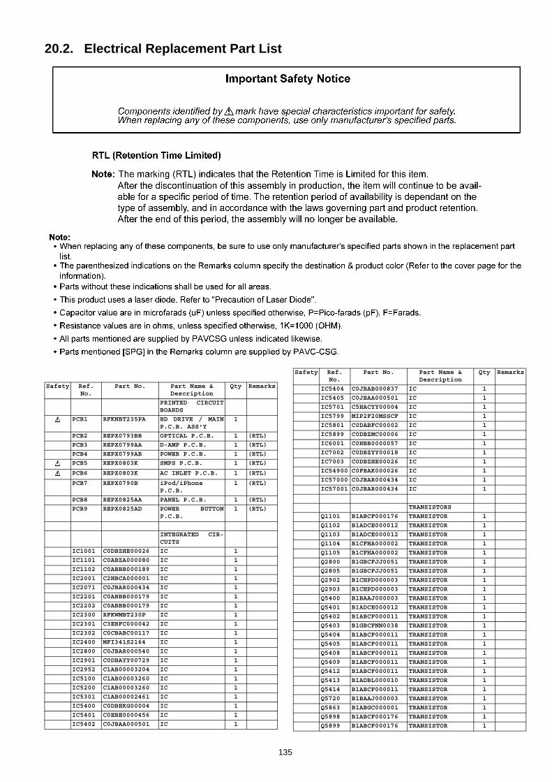
20.2. Electrical Replacement Part List
Safety Ref. No.
Part No. Part Name & Description
Qty Remarks
PRINTED CIRCUITBOARDS
PCB1 RFKNBT235PA BD DRIVE / MAINP.C.B. ASS'Y
1
PCB2 REPX0793BB OPTICAL P.C.B. 1 (RTL)
PCB3 REPX0799AA D-AMP P.C.B. 1 (RTL)
PCB4 REPX0799AB POWER P.C.B. 1 (RTL)
PCB5 REPX0803K SMPS P.C.B. 1 (RTL)
PCB6 REPX0803K AC INLET P.C.B. 1 (RTL)
PCB7 REPX0790B iPod/iPhoneP.C.B.
1 (RTL)
PCB8 REPX0825AA PANEL P.C.B. 1 (RTL)
PCB9 REPX0825AD POWER BUTTONP.C.B.
1 (RTL)
INTEGRATED CIR-CUITS
IC1001 C0DBZHE00026 IC 1
IC1101 C0ABZA000080 IC 1
IC1102 C0ABBB000189 IC 1
IC2001 C2HBCA000001 IC 1
IC2071 C0JBAR000434 IC 1
IC2201 C0ABBB000179 IC 1
IC2202 C0ABBB000179 IC 1
IC2300 RFKWMBT230P IC 1
IC2301 C3EBFC000042 IC 1
IC2302 C0CBABC00117 IC 1
IC2400 MFI341S2164 IC 1
IC2800 C0JBAR000540 IC 1
IC2901 C0DBAYY00729 IC 1
IC2952 C1AB00003204 IC 1
IC5100 C1AB00003260 IC 1
IC5200 C1AB00003260 IC 1
IC5301 C1AB00002461 IC 1
IC5400 C0DBEKG00004 IC 1
IC5401 C0EBE0000456 IC 1
IC5402 C0JBAA000501 IC 1
IC5404 C0JBAB000837 IC 1
IC5405 C0JBAA000501 IC 1
IC5701 C5HACYY00004 IC 1
IC5799 MIP2F20MSSCF IC 1
IC5801 C0DABFC00002 IC 1
IC5899 C0DBZMC00006 IC 1
IC6001 C0HBB0000057 IC 1
IC7002 C0DBZYY00018 IC 1
IC7003 C0DBZHE00026 IC 1
IC54900 C0FBAK000026 IC 1
IC57000 C0JBAR000434 IC 1
IC57001 C0JBAR000434 IC 1
TRANSISTORS
Q1101 B1ABCF000176 TRANSISTOR 1
Q1102 B1ADCE000012 TRANSISTOR 1
Q1103 B1ADCE000012 TRANSISTOR 1
Q1104 B1CFHA000002 TRANSISTOR 1
Q1105 B1CFHA000002 TRANSISTOR 1
Q2800 B1GBCFJJ0051 TRANSISTOR 1
Q2805 B1GBCFJJ0051 TRANSISTOR 1
Q2902 B1CHPD000003 TRANSISTOR 1
Q2903 B1CHPD000003 TRANSISTOR 1
Q5400 B1BAAJ000003 TRANSISTOR 1
Q5401 B1ADCE000012 TRANSISTOR 1
Q5402 B1ABCF000011 TRANSISTOR 1
Q5403 B1GBCFNN0038 TRANSISTOR 1
Q5404 B1ABCF000011 TRANSISTOR 1
Q5405 B1ABCF000011 TRANSISTOR 1
Q5408 B1ABCF000011 TRANSISTOR 1
Q5409 B1ABCF000011 TRANSISTOR 1
Q5412 B1ABCF000011 TRANSISTOR 1
Q5413 B1ADBL000010 TRANSISTOR 1
Q5414 B1ABCF000011 TRANSISTOR 1
Q5720 B1BAAJ000003 TRANSISTOR 1
Q5863 B1ABGC000001 TRANSISTOR 1
Q5898 B1ABCF000176 TRANSISTOR 1
Q5899 B1ABCF000176 TRANSISTOR 1
Safety Ref. No.
Part No. Part Name & Description
Qty Remarks
135

Q6100 B1BABK000001 TRANSISTOR 1
Q6800 B1ABEB000002 TRANSISTOR 1
Q7004 B1ADNB000003 TRANSISTOR 1
Q7005 B1ADCE000012 TRANSISTOR 1
Q7006 B1ABMF000020 TRANSISTOR 1
Q7007 B1ABCF000176 TRANSISTOR 1
Q7008 B1ABCF000176 TRANSISTOR 1
Q7050 B1ABCF000176 TRANSISTOR 1
Q7071 B1ADNB000003 TRANSISTOR 1
Q56004 B1CFHA000002 TRANSISTOR 1
Q56005 B1CFHA000002 TRANSISTOR 1
QR1101 B1GBCFJJ0051 TRANSISTOR 1
QR1102 B1GBCFJJ0051 TRANSISTOR 1
QR5400 B1GBCFNN0038 TRANSISTOR 1
QR5401 B1GBCFNN0038 TRANSISTOR 1
QR5862 B1GBCFGG0030 TRANSISTOR 1
QR7001 B1GBCFGG0030 TRANSISTOR 1
QR7014 B1GBCFJJ0051 TRANSISTOR 1
QR7019 B1GBCFJJ0051 TRANSISTOR 1
QR7071 B1GBCFJJ0051 TRANSISTOR 1
QR7081 B1GBCFJJ0051 TRANSISTOR 1
DIODES
D2201 B0ACCK000005 DIODE 1
D2301 B0BC3R0A0262 DIODE 1
D2911 B0JCPG000005 DIODE 1
D2912 B0JCPG000005 DIODE 1
D5402 B0BC012A0269 DIODE 1
D5403 B0ACCK000005 DIODE 1
D5404 B0ACCK000005 DIODE 1
D5405 B0ACCK000005 DIODE 1
D5406 B0BC7R5A0268 DIODE 1
D5407 B0ACCK000005 DIODE 1
D5510 B0ACCK000005 DIODE 1
D5512 B0ACCK000005 DIODE 1
D5513 B0ACCK000005 DIODE 1
D5514 B0ACCK000005 DIODE 1
D5610 B0HCSP000001 DIODE 1
D5611 B0HCSP000001 DIODE 1
D5612 B0HCSP000001 DIODE 1
D5613 B0HCSP000001 DIODE 1
D5614 B0HCSP000001 DIODE 1
D5615 B0HCSP000001 DIODE 1
D5616 B0HCSP000001 DIODE 1
D5617 B0HCSP000001 DIODE 1
D5618 B0HCSP000001 DIODE 1
D5619 B0HCSP000001 DIODE 1
D5620 B0HCSP000001 DIODE 1
D5621 B0HCSP000001 DIODE 1
D5622 B0HCSP000001 DIODE 1
D5623 B0HCSP000001 DIODE 1
D5624 B0HCSP000001 DIODE 1
D5625 B0HCSP000001 DIODE 1
D5627 B0ACCK000005 DIODE 1
D5628 B0BC012A0269 DIODE 1
D5701 B0FBAR000043 DIODE 1
D5702 B0ZAZ0000052 DIODE 1
D5703 B0BC020A0267 DIODE 1
D5704 B0BC020A0267 DIODE 1
D5705 B0BC020A0267 DIODE 1
D5706 B0ACCK000005 DIODE 1
D5707 B0BC6R2A0266 DIODE 1
D5708 B0ACCK000005 DIODE 1
D5709 B0ACCK000005 DIODE 1
D5710 B0EAMM000057 DIODE 1
D5711 MA2YF8000L DIODE 1
D5712 B0EAMM000057 DIODE 1
D5713 B0BC030A0264 DIODE 1
D5714 B0BC027A0264 DIODE 1
D5715 B0HAMP000094 DIODE 1
D5716 B0EAMM000057 DIODE 1
D5719 B0EDKT000009 DIODE 1
D5802 B0HBSM000054 DIODE 1
Safety Ref. No.
Part No. Part Name & Description
Qty Remarks
D5803 B0HFRJ000012 DIODE 1
D5805 B0EAMM000057 DIODE 1
D5810 B0ACCK000005 DIODE 1
D5811 B0BC5R1A0266 DIODE 1
D5896 B0EAMM000057 DIODE 1
D5899 B0ACCK000005 DIODE 1
D6100 B0JCMD000010 DIODE 1
D6101 B0BC024A0267 DIODE 1
D6102 B0JCMD000010 DIODE 1
D6103 B0BC2R4A0263 DIODE 1
D6104 B0HAJM000005 DIODE 1
D6800 B3ABA0000187 DIODE 1
D7013 B0ACCK000005 DIODE 1
D7016 B0ACCK000005 DIODE 1
D7017 B0ACCK000005 DIODE 1
D7018 B0ACCK000005 DIODE 1
D7020 B0ACCK000005 DIODE 1
D7021 B0ACCK000005 DIODE 1
D7022 B0ACCK000005 DIODE 1
D7023 B0BC027A0264 DIODE 1
D7024 B0BC5R1A0266 DIODE 1
D7031 B0BC7R5A0266 DIODE 1
D7033 B0BC6R8A0266 DIODE 1
D7035 B0BC010A0269 DIODE 1
D7036 B0BC6R8A0266 DIODE 1
D7037 B0BC010A0269 DIODE 1
D7038 B0BC013A0269 DIODE 1
DZ5701 ERZV10V511CS ZNR 1
VARISTOR
VA2951 EZAEG2A50AX ESD SUPRESSOR 1
SWITCHES
S6002 EVQ21405R SW 1
S6003 EVQ21405R SW 1
S6005 EVQ21405R SW 1
S6006 EVQ21405R SW 1
S6007 EVQ21405R SW 1
S6801 EVQ21405R SW 1
S6807 EVQ21405R SW 1
CONNECTORS
CN1001 MFI514S0117 30P CONNECTOR 1
CN1002 K1MN15BA0139 15P CONNECTOR 1
CN1101 K1MN15AA0046 15P CONNECTOR 1
CN2002 K1MN22AA0046 22P CONNECTOR 1
CN2003 K1MN10AA0076 10P CONNECTOR 1
CN2004 K1KA10A00430 10P CONNECTOR 1
CN2006 K1MN18AA0046 18P CONNECTOR 1
CN2011 K1MN13AA0076 13P CONNECTOR 1
CN2916 K1KA03BA0116 3P CONNECTOR 1
CN2917 K1KA03BA0116 3P CONNECTOR 1
CN4002 K1MN13BA0147 13P CONNECTOR 1
CN5400 K1KA06A00452 6P CONNECTOR 1
CN5401 K1KA03AA0301 3P CONNECTOR 1
CN5402 K1MN18AA0046 18P CONNECTOR 1
CN5802 K1KA03AA0292 3P CONNECTOR 1
CN5803 K1KA03AA0292 3P CONNECTOR 1
CN6001 K1YZ04000002 4P CABLE HOLDER 1
P6001 K1MN22AA0004 22P CONNECTOR 1
COILS AND INDUC-TORS
L1001 J0JFC0000006 INDUCTOR 1
L1002 J0JFC0000006 INDUCTOR 1
L1003 J0JGC0000071 INDUCTOR 1
L1004 J0JGC0000071 INDUCTOR 1
L1005 J0JGC0000071 INDUCTOR 1
L1006 J0JGC0000071 INDUCTOR 1
L1007 J0JGC0000071 INDUCTOR 1
L1008 J0JFC0000006 INDUCTOR 1
L1009 J0JFC0000006 INDUCTOR 1
L1010 J0JGC0000071 INDUCTOR 1
Safety Ref. No.
Part No. Part Name & Description
Qty Remarks
136

L1011 J0JFC0000006 INDUCTOR 1
L1032 J0JBC0000015 INDUCTOR 1
L2072 G1C100M00049 INDUCTOR 1
L2902 G0A200D00002 CHOKE COIL 1
L2903 G0A330ZA0045 CHOKE COIL 1
L2904 G0A330ZA0045 CHOKE COIL 1
L2907 J0JHC0000107 INDUCTOR 1
L2908 J0JHC0000107 INDUCTOR 1
L2951 G1CR18JA0020 INDUCTOR 1
L3000 G1C100K00019 INDUCTOR 1
L3001 G1C100K00019 INDUCTOR 1
L5100 G0C100M00006 INDUCTOR 1
L5101 G0C100M00006 INDUCTOR 1
L5103 G0B9R5K00005 LINE FILTER 1
L5104 G0B9R5K00005 LINE FILTER 1
L5105 G0B9R5K00005 LINE FILTER 1
L5106 G0B9R5K00005 LINE FILTER 1
L5200 G0C100M00006 INDUCTOR 1
L5201 G0C100M00006 INDUCTOR 1
L5203 G0B9R5K00005 LINE FILTER 1
L5204 G0B9R5K00005 LINE FILTER 1
L5300 J0JBC0000015 INDUCTOR 1
L5401 J0JKB0000003 INDUCTOR 1
L5402 J0JKB0000003 INDUCTOR 1
L5403 G1C4R7MA0172 INDUCTOR 1
L5702 G0B612H00002 LINE FILTER 1
L5703 G0B932H00002 LINE FILTER 1
L6006 J0JBC0000014 INDUCTOR 1
L6007 J0JBC0000014 INDUCTOR 1
L6100 J0JBC0000041 INDUCTOR 1
L6101 G0C390JA0055 INDUCTOR 1
L7014 G1C4R7MA0172 INDUCTOR 1
LB1101 J0JYC0000070 INDUCTOR 1
LB1107 J0JBC0000014 INDUCTOR 1
LB1109 J0JCC0000316 INDUCTOR 1
LB1113 J0JBC0000014 INDUCTOR 1
LB1114 J0JCC0000317 INDUCTOR 1
LB2039 J0JCC0000396 INDUCTOR 1
LB2071 J0JCC0000396 INDUCTOR 1
LB2072 J0JGC0000020 INDUCTOR 1
LB2092 J0JGC0000020 INDUCTOR 1
LB2301 J0JGC0000020 INDUCTOR 1
LB2818 J0JBC0000014 INDUCTOR 1
LB2819 J0JBC0000014 INDUCTOR 1
LB2820 J0JBC0000014 INDUCTOR 1
LB2821 J0JBC0000014 INDUCTOR 1
LB2823 J0JBC0000014 INDUCTOR 1
LB2831 J0JBC0000014 INDUCTOR 1
LB2834 J0JBC0000014 INDUCTOR 1
LB2835 J0JBC0000014 INDUCTOR 1
LB2836 J0JBC0000014 INDUCTOR 1
LB2837 J0JBC0000014 INDUCTOR 1
LB2838 J0JBC0000014 INDUCTOR 1
LB2839 J0JBC0000014 INDUCTOR 1
LB2840 J0JBC0000014 INDUCTOR 1
LB2841 J0JBC0000014 INDUCTOR 1
LB2842 J0JBC0000014 INDUCTOR 1
LB2843 J0JBC0000014 INDUCTOR 1
LB2844 J0JBC0000014 INDUCTOR 1
LB2845 J0JBC0000014 INDUCTOR 1
LB2846 J0JBC0000014 INDUCTOR 1
LB2951 J0JBC0000032 INDUCTOR 1
LB3909 J0JHC0000045 INDUCTOR 1
LB7006 J0JHC0000107 INDUCTOR 1
LB7007 J0JHC0000107 INDUCTOR 1
LB7009 J0JGC0000020 INDUCTOR 1
LB7012 J0JHC0000107 INDUCTOR 1
LB7013 J0JHC0000107 INDUCTOR 1
LB7041 J0JGC0000020 INDUCTOR 1
LB7042 J0JGC0000020 INDUCTOR 1
LB54900 J0JCC0000317 INDUCTOR 1
LB54901 J0JCC0000317 INDUCTOR 1
LB56502 J0JFC0000008 INDUCTOR 1
Safety Ref. No.
Part No. Part Name & Description
Qty Remarks
LB57000 J0JGC0000020 INDUCTOR 1
TRANSFORMER
T5701 ETS42BM1GGAC TRANSFORMER 1
T5751 ETS19AB2A6AG SUB TRANSFORMER 1
T6100 G4D1A0000142 SWITCHING TRANS-FORMER
1
PHOTO COUPLER
PC5702 B3PBA0000402 PHOTO COUPLER 1
PC5720 B3PBA0000402 PHOTO COUPLER 1
PC5799 B3PBA0000402 PHOTO COUPLER 1
EARTH TERMINALS
ZJ5701 K4CZ01000027 TERMINAL 1
ZJ5702 K4CZ01000027 TERMINAL 1
ZJ5703 K4CZ01000027 TERMINAL 1
OSCILLATORS
X2300 H2D500400006 CRYSTAL OSCILLA-TOR
1
X2301 H0J327200115 CRYSTAL OSCILLA-TOR
1
X2951 H0A327200097 CRYSTAL OSCILLA-TOR
1
COMPONENT COMBI-NATION
IR6001 B3RAB0000081 REMOTE CONTROLSENSOR
1
RELAY
RY701 K6B1AEA00003 RELAY 1
FUSE
F1 K5D802APA008 FUSE 1
FL DISPLAY
DP6001 A2BB00000175 LCD DISPLAY 1
HOLDERS
H6803 K1YZ04000002 4P CABLE HOLDER 1
FUSE HOLDERS
ZA5701 K3GE1ZZ00001 FUSE HOLDER 1
ZA5702 K3GE1ZZ00001 FUSE HOLDER 1
THERMISTOR
TH5702 D4CAA2R20001 THERMISTOR 1
JACKS
JK2951 K4ZZ01000276 JK FM ANT 1
JK3100 B3RAB0000056 JK DIGITAL AUDIOOPTICAL 1
1
JK3101 B3RAB0000056 JK DIGITAL AUDIOOPTICAL 2
1
JK5001 K4AZ12A00005 JK SPEAKER 1
P5701 K2AB2B000007 AC INLET 1
CHIP JUMPERS
K2002 ERJ2GE0R00X 0 1/16W 1
K5102 D0GBR00JA008 0 1/16W 1
K5103 D0GBR00JA008 0 1/16W 1
K5105 D0GBR00JA008 0 1/16W 1
K5106 D0GBR00JA008 0 1/16W 1
K5401 D0GBR00JA008 0 1/16W 1
K5721 D0GBR00JA008 0 1/16W 1
K5726 D0GBR00JA008 0 1/16W 1
L1021 D0GBR00JA008 0 1/16W 1
L1022 D0GBR00JA008 0 1/16W 1
L1023 D0GBR00JA008 0 1/16W 1
L1024 D0GBR00JA008 0 1/16W 1
L1025 D0GBR00JA008 0 1/16W 1
L1026 D0GBR00JA008 0 1/16W 1
Safety Ref. No.
Part No. Part Name & Description
Qty Remarks
137

L1027 D0GBR00JA008 0 1/16W 1
L1028 D0GBR00JA008 0 1/16W 1
L1029 D0GBR00JA008 0 1/16W 1
L1030 D0GBR00JA008 0 1/16W 1
L1031 D0GBR00JA008 0 1/16W 1
L1033 D0GBR00JA008 0 1/16W 1
L6005 D0GBR00JA008 0 1/16W 1
L6803 D0GBR00JA008 0 1/16W 1
L6804 D0GBR00JA008 0 1/16W 1
L6805 D0GBR00JA008 0 1/16W 1
L6806 D0GBR00JA008 0 1/16W 1
LB1102 ERJ2GE0R00X 0 1/16W 1
LB1103 ERJ2GE0R00X 0 1/16W 1
LB1104 ERJ2GE0R00X 0 1/16W 1
LB1105 ERJ2GE0R00X 0 1/16W 1
LB1106 ERJ2GE0R00X 0 1/16W 1
LB1108 ERJ2GE0R00X 0 1/16W 1
LB2570 D0GBR00JA008 0 1/16W 1
LB2571 D0GBR00JA008 0 1/16W 1
LB2801 ERJ2GE0R00X 0 1/16W 1
LB2802 ERJ2GE0R00X 0 1/16W 1
LB2803 ERJ2GE0R00X 0 1/16W 1
LB2804 ERJ2GE0R00X 0 1/16W 1
LB2805 ERJ2GE0R00X 0 1/16W 1
LB2806 ERJ2GE0R00X 0 1/16W 1
LB2807 ERJ2GE0R00X 0 1/16W 1
LB2808 ERJ2GE0R00X 0 1/16W 1
W6051 D0GDR00JA017 0 1/10W 1
W6052 D0GDR00JA017 0 1/10W 1
W6054 D0GDR00JA017 0 1/10W 1
W6056 D0GDR00JA017 0 1/10W 1
W6057 D0GBR00JA008 0 1/16W 1
W6058 D0GDR00JA017 0 1/10W 1
W6059 D0GBR00JA008 0 1/16W 1
W6060 D0GDR00JA017 0 1/10W 1
W6061 D0GBR00JA008 0 1/16W 1
W6062 D0GBR00JA008 0 1/16W 1
W6063 D0GDR00JA017 0 1/10W 1
W6064 D0GDR00JA017 0 1/10W 1
W6065 D0GDR00JA017 0 1/10W 1
W6066 D0GDR00JA017 0 1/10W 1
W6077 D0GDR00JA017 0 1/10W 1
W6078 D0GDR00JA017 0 1/10W 1
W6079 D0GBR00JA008 0 1/16W 1
W6080 D0GDR00JA017 0 1/10W 1
W6081 D0GBR00JA008 0 1/16W 1
RESISTORS
LB1111 D0GA471JA023 470 1/16W 1
LB1112 D0GA471JA023 470 1/16W 1
R1001 D0GA221JA023 220 1/16W 1
R1002 D0GA221JA023 220 1/16W 1
R1003 D0GA104JA023 100K 1/16W 1
R1004 D0GA104JA023 100K 1/16W 1
R1005 D0GA753JA015 75K 1/16W 1
R1006 D0GA753JA015 75K 1/16W 1
R1007 ERJ2GEJ513X 51K 1/16W 1
R1008 ERJ2GEJ513X 51K 1/16W 1
R1009 ERJ2GEJ151X 150 1/16W 1
R1010 ERJ2GEJ151X 150 1/16W 1
R1011 J0JFC0000006 INDUCTOR 1
R1012 D0GBR00JA008 0 1/16W 1
R1013 D0GA102JA023 1K 1/16W 1
R1014 ERJ2GE0R00X 0 1/16W 1
R1015 D0GBR00JA008 0 1/16W 1
R1101 ERJ3RED334V 330K 1/16W 1
R1102 ERJ2GEJ274X 270K 1/16W 1
R1103 ERJ3RED224V 220K 1/16W 1
R1104 ERJ2GEJ564X 560K 1/16W 1
R1105 D0GA104JA023 100K 1/16W 1
R1106 D0GA472JA023 4.7K 1/16W 1
R1107 D0GA473JA023 47K 1/16W 1
R1108 D0GA473JA023 47K 1/16W 1
Safety Ref. No.
Part No. Part Name & Description
Qty Remarks
R1109 D0GA472JA023 4.7K 1/16W 1
R1110 D0GA104JA023 100K 1/16W 1
R1111 ERJ2GEJ750X 75 1/16W 1
R1112 D0GA101JA023 100 1/16W 1
R1113 D0GA101JA023 100 1/16W 1
R1114 D0GA223JA023 22K 1/16W 1
R1115 D0GA223JA023 22K 1/16W 1
R1116 D0GA101JA023 100 1/16W 1
R1118 D0GA223JA023 22K 1/16W 1
R1119 D0GA223JA023 22K 1/16W 1
R1120 D0GA223JA023 22K 1/16W 1
R1121 D0GA223JA023 22K 1/16W 1
R1122 D0GA102JA023 1K 1/16W 1
R1123 D0GA102JA023 1K 1/16W 1
R1124 D0GA101JA023 100 1/16W 1
R1125 D0GA101JA023 100 1/16W 1
R1127 J0JCC0000316 INDUCTOR 1
R1128 J0JCC0000316 INDUCTOR 1
R1131 D0GD470JA017 47 1/10W 1
R1132 D0GA104JA023 100K 1/16W 1
R1133 D0GA104JA023 100K 1/16W 1
R1141 D0GA221JA023 220 1/16W 1
R1151 D0GA471JA023 470 1/16W 1
R1152 D0GA471JA023 470 1/16W 1
R1153 D0GA471JA023 470 1/16W 1
R2031 D0GA330JA023 33 1/16W 1
R2032 D0GA330JA023 33 1/16W 1
R2033 D0GA330JA023 33 1/16W 1
R2034 D0GA330JA023 33 1/16W 1
R2035 D0GA330JA023 33 1/16W 1
R2036 D0GA330JA023 33 1/16W 1
R2041 D0GA221JA023 220 1/16W 1
R2042 D0GA221JA023 220 1/16W 1
R2043 D0GA221JA023 220 1/16W 1
R2044 D0GA221JA023 220 1/16W 1
R2045 D0GA470JA023 47 1/16W 1
R2046 D0GA103JA023 10K 1/16W 1
R2051 ERJ2GE0R00X 0 1/16W 1
R2053 D0GA152JA023 1.5K 1/16W 1
R2054 D0GA470JA023 47 1/16W 1
R2055 D0GA470JA023 47 1/16W 1
R2056 D0GA470JA023 47 1/16W 1
R2057 D0GA470JA023 47 1/16W 1
R2058 D0GA470JA023 47 1/16W 1
R2059 D0GA470JA023 47 1/16W 1
R2060 D0GA470JA023 47 1/16W 1
R2071 D0GA330JA023 33 1/16W 1
R2072 D0GA330JA023 33 1/16W 1
R2074 D0GA470JA023 47 1/16W 1
R2075 D0GA470JA023 47 1/16W 1
R2081 D0GA470JA023 47 1/16W 1
R2082 D0GA470JA023 47 1/16W 1
R2083 D0GA470JA023 47 1/16W 1
R2084 D0GA470JA023 47 1/16W 1
R2085 D0GA470JA023 47 1/16W 1
R2086 D0GA470JA023 47 1/16W 1
R2090 D0GA221JA023 220 1/16W 1
R2093 D0GA221JA023 220 1/16W 1
R2094 D0GA221JA023 220 1/16W 1
R2098 D0GBR00JA008 0 1/16W 1
R2181 D0GA221JA023 220 1/16W 1
R2182 D0GA221JA023 220 1/16W 1
R2183 D0GA221JA023 220 1/16W 1
R2184 D0GA221JA023 220 1/16W 1
R2201 D0GA104JA023 100K 1/16W 1
R2202 D0GA104JA023 100K 1/16W 1
R2203 D0GA104JA023 100K 1/16W 1
R2204 D0GA104JA023 100K 1/16W 1
R2205 D0GA104JA023 100K 1/16W 1
R2206 D0GA682JA023 6.8K 1/16W 1
R2207 D0GA104JA023 100K 1/16W 1
R2208 D0GA103JA023 10K 1/16W 1
R2209 D0GA103JA023 10K 1/16W 1
Safety Ref. No.
Part No. Part Name & Description
Qty Remarks
138

R2210 D0GA101JA023 100 1/16W 1
R2211 D0GA103JA023 10K 1/16W 1
R2212 D0GA103JA023 10K 1/16W 1
R2213 D0GA102JA023 1K 1/16W 1
R2214 D0GA104JA023 100K 1/16W 1
R2215 D0GA103JA023 10K 1/16W 1
R2301 D0GA473JA023 47K 1/16W 1
R2302 D0GA222JA023 2.2K 1/16W 1
R2304 D0GA331JA023 330 1/16W 1
R2305 D0GA473JA023 47K 1/16W 1
R2310 D0GA103JA023 10K 1/16W 1
R2311 D0GA103JA023 10K 1/16W 1
R2315 ERJ2GEJ154X 150K 1/16W 1
R2318 D0GA102JA023 1K 1/16W 1
R2320 D0GA331JA023 330 1/16W 1
R2321 D0GA331JA023 330 1/16W 1
R2322 D0GA104JA023 100K 1/16W 1
R2323 D0GA104JA023 100K 1/16W 1
R2325 D0GA472JA023 4.7K 1/16W 1
R2326 D0GA472JA023 4.7K 1/16W 1
R2327 D0GA104JA023 100K 1/16W 1
R2328 D0GA103JA023 10K 1/16W 1
R2330 D0GA103JA023 10K 1/16W 1
R2331 D0GA103JA023 10K 1/16W 1
R2332 D0GA473JA023 47K 1/16W 1
R2333 D0GA473JA023 47K 1/16W 1
R2335 D0GA473JA023 47K 1/16W 1
R2341 D0GA473JA023 47K 1/16W 1
R2342 D0GA473JA023 47K 1/16W 1
R2343 D0GA331JA023 330 1/16W 1
R2345 D0GA103JA023 10K 1/16W 1
R2346 D0GA103JA023 10K 1/16W 1
R2352 D0GA103JA023 10K 1/16W 1
R2356 D0GA103JA023 10K 1/16W 1
R2359 D0GA103JA023 10K 1/16W 1
R2361 D0GA473JA023 47K 1/16W 1
R2364 ERJ2GE0R00X 0 1/16W 1
R2366 D0GA101JA023 100 1/16W 1
R2367 D0GA101JA023 100 1/16W 1
R2370 D0GA331JA023 330 1/16W 1
R2374 D0GA331JA023 330 1/16W 1
R2375 D0GA331JA023 330 1/16W 1
R2378 D0GA331JA023 330 1/16W 1
R2379 D0GA331JA023 330 1/16W 1
R2381 D0GA331JA023 330 1/16W 1
R2382 D0GA331JA023 330 1/16W 1
R2386 D0GA472JA023 4.7K 1/16W 1
R2387 D0GA472JA023 4.7K 1/16W 1
R2388 D0GA473JA023 47K 1/16W 1
R2395 D0GA331JA023 330 1/16W 1
R2396 D0GA331JA023 330 1/16W 1
R2397 D0GA331JA023 330 1/16W 1
R2399 D0GA331JA023 330 1/16W 1
R2400 D0GA330JA023 33 1/16W 1
R2401 ERJ2GE0R00X 0 1/16W 1
R2402 ERJ2GE0R00X 0 1/16W 1
R2406 ERJ2GE0R00X 0 1/16W 1
R2407 ERJ2GE0R00X 0 1/16W 1
R2411 D0GA103JA023 10K 1/16W 1
R2412 D0GA103JA023 10K 1/16W 1
R2570 D0GB103JA008 10K 1/16W 1
R2571 D0GB103JA008 10K 1/16W 1
R2800 D0GA103JA023 10K 1/16W 1
R2801 D0GA103JA023 10K 1/16W 1
R2806 D0GA102JA023 1K 1/16W 1
R2807 D0GA102JA023 1K 1/16W 1
R2810 D0GA102JA023 1K 1/16W 1
R2811 D0GA102JA023 1K 1/16W 1
R2812 D0GA473JA023 47K 1/16W 1
R2813 D0GA473JA023 47K 1/16W 1
R2814 D0GA102JA023 1K 1/16W 1
R2815 D0GA103JA023 10K 1/16W 1
R2816 D0GA103JA023 10K 1/16W 1
Safety Ref. No.
Part No. Part Name & Description
Qty Remarks
R2817 D0GA102JA023 1K 1/16W 1
R2821 D0GA473JA023 47K 1/16W 1
R2822 D0GA473JA023 47K 1/16W 1
R2823 D0GA102JA023 1K 1/16W 1
R2824 D0GA102JA023 1K 1/16W 1
R2905 D0GBR00JA008 0 1/16W 1
R2906 D0GBR00JA008 0 1/16W 1
R2907 D0GBR00JA008 0 1/16W 1
R2908 ERJ3RBD1002V 10 1/16W 1
R2909 D0GBR00JA008 0 1/16W 1
R2914 D0GB223JA008 22K 1/16W 1
R2915 D0GBR00JA008 0 1/16W 1
R2916 D0GB223JA008 22K 1/16W 1
R2917 D0GB332JA008 3.3K 1/16W 1
R2918 D0GB332JA008 3.3K 1/16W 1
R2919 D1BDR1000003 10 1/10W 1
R2920 D0GB822JA008 8.2K 1/16W 1
R2921 ERJ3RBD3902V 39 1/16W 1
R2922 D1BDR1000003 10 1/10W 1
R2923 D0GB222JA008 2.2K 1/16W 1
R2924 ERJ3RBD5601V 56 1/16W 1
R2925 ERJ3RBD5602V 56 1/16W 1
R2926 D0GB822JA008 8.2K 1/16W 1
R2927 D0GB103JA008 10K 1/16W 1
R2929 ERJ3RBD3301V 33 1/16W 1
R2930 ERJ3RBD2701V 27 1/16W 1
R2951 D0GB102JA008 1K 1/16W 1
R2952 D0GB102JA008 1K 1/16W 1
R2953 D0GA472JA023 4.7K 1/16W 1
R2954 D0GA472JA023 4.7K 1/16W 1
R2955 D0GA221JA023 220 1/16W 1
R2955 D0GBR00JA008 0 1/16W 1
R2956 D0GB221JA007 220 1/10W 1
R2956 D0GB472JA008 4.7K 1/16W 1
R2957 D0GA102JA023 1K 1/16W 1
R2959 D0GB222JA008 2.2K 1/16W 1
R2961 D0GB473JA008 47K 1/16W 1
R2962 D0GB473JA008 47K 1/16W 1
R2963 D0GBR00JA008 0 1/16W 1
R2964 D0GBR00JA008 0 1/16W 1
R5100 D0GB100JA008 10 1/16W 1
R5101 D0GB101JA008 100 1/16W 1
R5102 D0GB223JA008 22K 1/16W 1
R5103 D0GB101JA008 100 1/16W 1
R5105 D0GB100JA008 10 1/16W 1
R5106 D0GB100JA008 10 1/16W 1
R5109 D0GB100JA008 10 1/16W 1
R5113 D0GD562JA017 5.6K 1/10W 1
R5117 D0GD562JA017 5.6K 1/10W 1
R5121 D0GD562JA017 5.6K 1/10W 1
R5125 D0GD562JA017 5.6K 1/10W 1
R5126 D0GB104JA008 100K 1/16W 1
R5128 D0GB104JA008 100K 1/16W 1
R5130 D0GB104JA008 100K 1/16W 1
R5132 D0GB562JA008 5.6K 1/16W 1
R5133 D0GB562JA008 5.6K 1/16W 1
R5134 D0GB562JA008 5.6K 1/16W 1
R5135 D0GB562JA008 5.6K 1/16W 1
R5136 D0GB104JA008 100K 1/16W 1
R5200 D0GB100JA008 10 1/16W 1
R5201 D0GB101JA008 100 1/16W 1
R5202 D0GB223JA008 22K 1/16W 1
R5203 D0GB101JA008 100 1/16W 1
R5205 D0GB100JA008 10 1/16W 1
R5206 D0GB100JA008 10 1/16W 1
R5209 D0GB100JA008 10 1/16W 1
R5210 ERJ3GEYJ3R3V 3.3 1/10W 1
R5211 ERJ3GEYJ3R3V 3.3 1/10W 1
R5212 D0GD103JA017 10K 1/10W 1
R5213 ERJ3GEYJ3R3V 3.3 1/10W 1
R5214 ERJ3GEYJ3R3V 3.3 1/10W 1
R5215 D0GD103JA017 10K 1/10W 1
R5216 D0GB104JA008 100K 1/16W 1
Safety Ref. No.
Part No. Part Name & Description
Qty Remarks
139

R5217 D0GB104JA008 100K 1/16W 1
R5219 D0GB104JA008 100K 1/16W 1
R5220 D0GB104JA008 100K 1/16W 1
R5221 D0GB562JA008 5.6K 1/16W 1
R5223 D0GB562JA008 5.6K 1/16W 1
R5350 ERJ3GEYJ201V 200 1/10W 1
R5351 ERJ3GEYJ201V 200 1/10W 1
R5353 ERJ3EKF1822V 1.8K 1W 1
R5370 D0GB331JA008 330 1/16W 1
R5371 D0GB331JA008 330 1/16W 1
R5375 D0GB470JA008 47 1/16W 1
R5376 D0GB470JA008 47 1/16W 1
R5377 D0GB470JA008 47 1/16W 1
R5379 D0GB470JA008 47 1/16W 1
R5380 D0GB470JA008 47 1/16W 1
R5381 D0GB470JA008 47 1/16W 1
R5382 D0GB470JA008 47 1/16W 1
R5383 D0GB470JA008 47 1/16W 1
R5384 D0GB470JA008 47 1/16W 1
R5385 D0GB470JA008 47 1/16W 1
R5386 D0GB470JA008 47 1/16W 1
R5387 D0GB470JA008 47 1/16W 1
R5388 D0GB470JA008 47 1/16W 1
R5390 D0GB331JA008 330 1/16W 1
R5391 D0GB331JA008 330 1/16W 1
R5406 ERJ3RBD104V 100K 1/16W 1
R5407 ERJ3RBD562V 5.6K 1/16W 1
R5408 ERJ3RBD103V 10K 1/16W 1
R5420 D0GD122JA017 1.2K 1/10W 1
R5421 D0GB100JA008 10 1/16W 1
R5422 D0GB334JA008 330K 1/16W 1
R5423 D0GB103JA008 10K 1/16W 1
R5424 D0GB103JA008 10K 1/16W 1
R5425 D0GB103JA008 10K 1/16W 1
R5426 ERJ3GEYJ185V 1.8M 1/10W 1
R5427 D0GB104JA008 100K 1/16W 1
R5428 D0GB103JA008 10K 1/16W 1
R5431 D0GB223JA008 22K 1/16W 1
R5434 D0GB103JA008 10K 1/16W 1
R5435 D0GB103JA008 10K 1/16W 1
R5436 D0GB223JA008 22K 1/16W 1
R5437 D0GB472JA008 4.7K 1/16W 1
R5438 D0GB224JA008 220K 1/16W 1
R5439 D0GB224JA008 220K 1/16W 1
R5444 D0GB103JA008 10K 1/16W 1
R5445 D0GB103JA008 10K 1/16W 1
R5446 D0GB332JA008 3.3K 1/16W 1
R5447 D0GB472JA008 4.7K 1/16W 1
R5449 D0GB104JA008 100K 1/16W 1
R5450 D0GB104JA008 100K 1/16W 1
R5451 D0GB104JA008 100K 1/16W 1
R5452 D0GB104JA008 100K 1/16W 1
R5453 D0GB333JA008 33K 1/16W 1
R5454 D0GB473JA008 47K 1/16W 1
R5463 F1H2A102A009 1000pF 100V 1
R5470 D0GB473JA008 47K 1/16W 1
R5471 D0GB123JA008 12K 1/16W 1
R5472 D0GB682JA008 6.8K 1/16W 1
R5473 D0GB123JA008 12K 1/16W 1
R5474 D0GB102JA008 1K 1/16W 1
R5475 D0GBR00JA008 0 1/16W 1
R5700 ERJ8GEYJ155V 1.5M 1/4W 1
R5701 ERJ8GEYJ155V 1.5M 1/4W 1
R5702 ERJ1TYJ333U 33K 1/2W 1
R5703 ERJ1TYJ333U 33K 1/2W 1
R5704 ERJ8GEYJ124V 120K 1/4W 1
R5706 ERJ8GEYJ274V 270K 1/4W 1
R5707 D0GF394JA017 390K 1/4W 1
R5720 D0GD220JA017 22 1/10W 1
R5721 D0GD103JA017 10K 1/10W 1
R5722 D0GD222JA017 2.2K 1/10W 1
R5723 ERJ1TYJ333U 33K 1/2W 1
R5724 ERJ1TYJ222U 2.2K 1/2W 1
Safety Ref. No.
Part No. Part Name & Description
Qty Remarks
R5726 ERJ1TRSJR15U 0.15 1/2W 1
R5727 ERJ1TRSJR15U 0.15 1/2W 1
R5728 D0GB223JA008 22K 1/16W 1
R5729 D0GB473JA008 47K 1/16W 1
R5730 D0GB102JA008 1K 1/16W 1
R5732 ERJ6GEYJ221V 220 1/8W 1
R5733 D0GB473JA008 47K 1/16W 1
R5786 D0GD224JA017 220K 1/10W 1
R5795 D0GD474JA017 470K 1/10W 1
R5797 D0GB153JA008 15K 1/16W 1
R5798 D0GB101JA008 100 1/16W 1
R5801 D0GB101JA008 100 1/16W 1
R5802 D0HB183ZA002 18K 1/16W 1
R5803 D0GD562JA017 5.6K 1/10W 1
R5804 ERJ6RED124V 120K 1/10W 1
R5805 ERJ3RBD682V 6.8K 1/16W 1
R5806 D0GB223JA008 22K 1/16W 1
R5807 D0GD681JA017 680 1/10W 1
R5808 D0GB222JA008 2.2K 1/16W 1
R5809 D0GD681JA017 680 1/10W 1
R5814 D0GB104JA008 100K 1/16W 1
R5817 ERJ3RBD222V 2.2K 1/16W 1
R5818 D0GB220JA008 22 1/16W 1
R5819 D0GD220JA017 22 1/10W 1
R5820 D0GD272JA017 2.7K 1/10W 1
R5821 D0GB104JA008 100K 1/16W 1
R5832 ERJ1TYJ822U 8.2K 1/2W 1
R5833 ERJ1TYJ822U 8.2K 1/2W 1
R5861 D0GB104JA008 100K 1/16W 1
R5862 D0GD222JA017 2.2K 1/10W 1
R5863 D0GD562JA017 5.6K 1/10W 1
R5864 D0GB272JA008 2.7K 1/16W 1
R5866 ERJ6GEYJ221V 220 1/8W 1
R5890 D0GB222JA008 2.2K 1/16W 1
R5891 ERJ3RBD333V 33K 1/16W 1
R5892 ERJ3RBD332V 3.3K 1/16W 1
R5893 ERJ3RBD333V 33K 1/16W 1
R5894 D0GB102JA008 1K 1/16W 1
R5895 D0GB153JA008 15K 1/16W 1
R5897 D0GB101JA008 100 1/16W 1
R5898 D0GD824JA017 820K 1/10W 1
R5899 D0GD473JA017 47K 1/10W 1
R6004 D0GBR00JA008 0 1/16W 1
R6005 D0GB470JA008 47 1/16W 1
R6006 D0GB101JA008 100 1/16W 1
R6007 ERJ8GEYJ1R8V 1.8 1/4W 1
R6008 ERJ8GEYJ1R8V 1.8 1/4W 1
R6010 D0GB680JA008 68 1/16W 1
R6011 D0GB680JA008 68 1/16W 1
R6012 D0GB102JA008 1K 1/16W 1
R6015 D0GB563JA008 56K 1/16W 1
R6016 D0GB122JA008 1.2K 1/16W 1
R6017 D0GB152JA008 1.5K 1/16W 1
R6018 D0GB222JA008 2.2K 1/16W 1
R6019 D0GB332JA008 3.3K 1/16W 1
R6020 D0GB472JA008 4.7K 1/16W 1
R6021 D0GB152JA008 1.5K 1/16W 1
R6022 D0GB222JA008 2.2K 1/16W 1
R6023 D0GB332JA008 3.3K 1/16W 1
R6024 D0GB472JA008 4.7K 1/16W 1
R6025 D0GBR00JA008 0 1/16W 1
R6030 D0GB103JA008 10K 1/16W 1
R6031 D0GB121JA008 120 1/16W 1
R6100 D0GB472JA008 4.7K 1/16W 1
R6101 D0GB104JA008 100K 1/16W 1
R6102 D0GB470JA008 47 1/16W 1
R6103 D0GBR00JA008 0 1/16W 1
R6801 D0GB122JA008 1.2K 1/16W 1
R7000 ERJ3GEYJ1R5V 1.5 1/10W 1
R7002 ERJ3GEYJ1R5V 1.5 1/10W 1
R7003 ERJ3GEYJ3R3V 3.3 1/10W 1
R7005 D0GB562JA008 5.6K 1/16W 1
R7007 D0GB392JA008 3.9K 1/16W 1
Safety Ref. No.
Part No. Part Name & Description
Qty Remarks
140

R7009 D0GB272JA008 2.7K 1/16W 1
R7010 D0GB471JA008 470 1/16W 1
R7011 D0GB472JA008 4.7K 1/16W 1
R7012 D0GB272JA008 2.7K 1/16W 1
R7028 D0GB683JA008 68K 1/16W 1
R7031 D0GB393JA008 39K 1/16W 1
R7032 D0GB273JA008 27K 1/16W 1
R7033 D0GB393JA008 39K 1/16W 1
R7043 D0GA102JA023 1K 1/16W 1
R7050 D0GA103JA023 10K 1/16W 1
R7051 ERJ2GE0R00X 0 1/16W 1
R7055 D0GA104JA023 100K 1/16W 1
R7056 ERJ2GE0R00X 0 1/16W 1
R7061 D0GB272JA008 2.7K 1/16W 1
R7062 D0GB272JA008 2.7K 1/16W 1
R7063 D0GB272JA008 2.7K 1/16W 1
R7071 D0GA103JA023 10K 1/16W 1
R7072 D0GA332JA023 3.3K 1/16W 1
R7082 D0GA103JA023 10K 1/16W 1
R54900 D0GD4R7JA017 4.7 1/10W 1
R54902 D0GA102JA023 1K 1/16W 1
R54904 D0GA330JA023 33 1/16W 1
R54905 D0GA330JA023 33 1/16W 1
R54906 D0GA330JA023 33 1/16W 1
R54907 D0GA330JA023 33 1/16W 1
R54908 D0GD4R7JA017 4.7 1/10W 1
R54909 D0GA330JA023 33 1/16W 1
R57006 D0GA470JA023 47 1/16W 1
R57007 D0GA470JA023 47 1/16W 1
RESISTOR NET-WORKS
RX2300 D1H83314A024 RESISTOR NETWORK 1
RX2301 D1H83314A024 RESISTOR NETWORK 1
RX2302 D1H83314A024 RESISTOR NETWORK 1
RX2304 D1H83314A024 RESISTOR NETWORK 1
RX2305 D1H83314A024 RESISTOR NETWORK 1
RX2307 D1H83314A024 RESISTOR NETWORK 1
RX2308 D1H83314A024 RESISTOR NETWORK 1
RX2309 D1H83314A024 RESISTOR NETWORK 1
RX2310 D1H83314A024 RESISTOR NETWORK 1
CAPACITORS
C1002 F1G1C104A083 0.1uF 16V 1
C1003 F1G1C104A083 0.1uF 16V 1
C1004 F1G1C104A083 0.1uF 16V 1
C1101 F1G1A1040006 0.1uF 10V 1
C1102 EEEFK0J102P 1000uF 6.3V 1
C1103 F1J1A106A043 10uF 10V 1
C1104 F1J1A106A043 10uF 10V 1
C1105 F1G1A1040006 0.1uF 10V 1
C1107 F2G0J101A083 100uF 6.3V 1
C1109 F1G1C1030007 0.01uF 16V 1
C1110 F1G1C1030007 0.01uF 16V 1
C1111 F1G1H2200001 22pF 50V 1
C1113 F1G1H2200001 22pF 50V 1
C1114 F1G1H2200001 22pF 50V 1
C1115 F1G1H2200001 22pF 50V 1
C1116 F1G1H2200001 22pF 50V 1
C1117 F1H1A105A025 1uF 10V 1
C1118 F1H1A105A025 1uF 10V 1
C1119 F1G1H330A565 33pF 50V 1
C1122 F1G1C1030007 0.01uF 16V 1
C1131 F1G1E1020001 1000pF 25V 1
C1134 F1G1E1020001 1000pF 25V 1
C1135 F1J1A106A043 10uF 10V 1
C2041 F1G1A1040006 0.1uF 10V 1
C2042 F1G1H470A444 47pF 50V 1
C2043 F1G1H470A444 47pF 50V 1
C2044 F1H1A105A025 1uF 10V 1
C2045 F1G1C1030007 0.01uF 16V 1
C2046 F1J1A106A043 10uF 10V 1
C2051 F1H1A105A025 1uF 10V 1
Safety Ref. No.
Part No. Part Name & Description
Qty Remarks
C2052 F1G1C1030007 0.01uF 16V 1
C2053 F1G1E1020001 1000pF 25V 1
C2054 F2G0J101A083 100uF 6.3V 1
C2055 F1G1E1020001 1000pF 25V 1
C2056 F1H1A105A025 1uF 10V 1
C2057 F1G1C1030007 0.01uF 16V 1
C2058 F1G1C273A081 0.027uF 16V 1
C2059 F1G1E2720001 2700pF 25V 1
C2060 F1H1A105A025 1uF 10V 1
C2061 F1G1C1030007 0.01uF 16V 1
C2071 F1G1A1040006 0.1uF 10V 1
C2072 F1J1A106A043 10uF 10V 1
C2102 F1G1E1020001 1000pF 25V 1
C2107 ERJ2GE0R00X 0 1/16W 1
C2112 ERJ2GE0R00X 0 1/16W 1
C2113 ERJ2GE0R00X 0 1/16W 1
C2201 F1H1A105A025 1uF 10V 1
C2202 F1H1A105A025 1uF 10V 1
C2203 F1G1H470A444 47pF 50V 1
C2204 F1G1H470A444 47pF 50V 1
C2205 F1H1A105A025 1uF 10V 1
C2206 F1J1A106A043 10uF 10V 1
C2207 F1G1A1040006 0.1uF 10V 1
C2211 F1G1A1040006 0.1uF 10V 1
C2212 F1G1A1040006 0.1uF 10V 1
C2301 F1G1H470A444 47pF 50V 1
C2302 F1G1A1040006 0.1uF 10V 1
C2304 F1G1A1040006 0.1uF 10V 1
C2305 F1G1A1040006 0.1uF 10V 1
C2306 F1G1A1040006 0.1uF 10V 1
C2307 F1G1A1040006 0.1uF 10V 1
C2308 F1G1E4720002 4700pF 25V 1
C2309 F1G1E4720002 4700pF 25V 1
C2310 F1G1H470A444 47pF 50V 1
C2311 F1G1H470A444 47pF 50V 1
C2312 F1G1A1040006 0.1uF 10V 1
C2313 F1G1A1040006 0.1uF 10V 1
C2314 F2G0J101A083 100uF 6.3V 1
C2315 F1H1A105A025 1uF 10V 1
C2316 F1H1A105A025 1uF 10V 1
C2321 F1G1E4720002 4700pF 25V 1
C2322 F1G1E4720002 4700pF 25V 1
C2400 F1G1A1040006 0.1uF 10V 1
C2572 F1H1H2210001 220pF 50V 1
C2573 F1H1H2210001 220pF 50V 1
C2802 F1G1E6810001 680pF 25V 1
C2803 F1G1E6810001 680pF 25V 1
C2804 F1G1E6810001 680pF 25V 1
C2805 F1G1E6810001 680pF 25V 1
C2806 F1H1A105A025 1uF 10V 1
C2807 F1H1A105A025 1uF 10V 1
C2811 F1H1A105A025 1uF 10V 1
C2812 F1H1A105A025 1uF 10V 1
C2813 F1H1A105A025 1uF 10V 1
C2814 F1H1A105A025 1uF 10V 1
C2815 F1G1H470A444 47pF 50V 1
C2816 F1G1H470A444 47pF 50V 1
C2817 F1G1A1040006 0.1uF 10V 1
C2818 F1G1A1040006 0.1uF 10V 1
C2901 F2A1V2210049 220uF 35V 1
C2902 F2A0J1220028 1200uF 6.3V 1
C2903 F2A1C8210008 820uF 16V 1
C2907 F2A1V5600013 56uF 35V 1
C2951 F1H1H102A219 1000pF 50V 1
C2953 F1H1H104A013 0.1uF 50V 1
C2957 F1H1H103A219 0.01uF 50V 1
C2957 F1H1H220A230 22pF 50V 1
C2958 F1H1H220A230 22pF 50V 1
C2959 F1H1A105A025 1uF 10V 1
C2960 F1H1A105A025 1uF 10V 1
C2961 F1G1C104A077 0.1uF 16V 1
C2961 F1H1H681A013 680pF 50V 1
C2962 F1G1C104A077 0.1uF 16V 1
Safety Ref. No.
Part No. Part Name & Description
Qty Remarks
141

C2962 F1H1H103A219 0.01uF 50V 1
C2963 F1H1H681A013 680pF 50V 1
C2964 F1H1H104A013 0.1uF 50V 1
C2966 F1J1V1050001 1uF 35V 1
C2971 F1H1H104A013 0.1uF 50V 1
C2972 F1H1C224A068 0.22uF 16V 1
C2973 F1H1H122A013 1200pF 50V 1
C2974 F1H1A105A025 1uF 10V 1
C2975 F1K1C1060001 10uF 16V 1
C2976 F1H1H153A219 0.015uF 50V 1
C2977 F1H1C224A068 0.22uF 16V 1
C2981 F1H1H102A219 1000pF 50V 1
C2982 F1K1C1060001 10uF 16V 1
C2983 F1J1V1050001 1uF 35V 1
C3103 F1J1A106A043 10uF 10V 1
C3104 F1J1A106A043 10uF 10V 1
C5100 F1H1H104A013 0.1uF 50V 1
C5101 F1H1H104A013 0.1uF 50V 1
C5102 F1J1C106A059 10uF 16V 1
C5103 F1H1H104A013 0.1uF 50V 1
C5104 F1H1H104A013 0.1uF 50V 1
C5105 F1H1H104A013 0.1uF 50V 1
C5106 F1J2A333A024 0.033uF 100V 1
C5107 F1L2A2250002 2.2uF 100V 1
C5108 F1L2A2250002 2.2uF 100V 1
C5109 F1L2A2250002 2.2uF 100V 1
C5110 F1L2A2250002 2.2uF 100V 1
C5111 F1J2A333A024 0.033uF 100V 1
C5112 F1J2A333A024 0.033uF 100V 1
C5113 F1L2A2250002 2.2uF 100V 1
C5114 F1L2A2250002 2.2uF 100V 1
C5115 F1L2A2250002 2.2uF 100V 1
C5116 F1L2A2250002 2.2uF 100V 1
C5117 F2A1J3310032 330uF 63V 1
C5118 F1J2A333A024 0.033uF 100V 1
C5119 F1H1H104A013 0.1uF 50V 1
C5120 F0C1J1050003 1uF 63V 1
C5121 F2A1V3310040 330uF 35V 1
C5127 F0C1J1050003 1uF 63V 1
C5128 F2A1V4710076 470uF 35V 1
C5133 F2A1V4710076 470uF 35V 1
C5134 F2A1V3310040 330uF 35V 1
C5135 F0C1J1050003 1uF 63V 1
C5136 F2A1V3310040 330uF 35V 1
C5137 F2A1V4710076 470uF 35V 1
C5142 F0C1J1050003 1uF 63V 1
C5143 F2A1V3310040 330uF 35V 1
C5144 F2A1V4710076 470uF 35V 1
C5150 F1H2A102A009 1000pF 100V 1
C5151 F1H2A102A009 1000pF 100V 1
C5152 F1H2A102A009 1000pF 100V 1
C5153 F1H2A102A009 1000pF 100V 1
C5154 F1H2A102A009 1000pF 100V 1
C5155 F1H2A102A009 1000pF 100V 1
C5156 F1H2A102A009 1000pF 100V 1
C5157 F1H2A102A009 1000pF 100V 1
C5200 F1H1H104A013 0.1uF 50V 1
C5201 F1H1H104A013 0.1uF 50V 1
C5202 F1J1C106A059 10uF 16V 1
C5203 F1H1H104A013 0.1uF 50V 1
C5204 F1H1H104A013 0.1uF 50V 1
C5205 F1H1H104A013 0.1uF 50V 1
C5206 F1J2A333A024 0.033uF 100V 1
C5207 F1L2A2250002 2.2uF 100V 1
C5208 F1L2A2250002 2.2uF 100V 1
C5209 F1L2A2250002 2.2uF 100V 1
C5210 F1L2A2250002 2.2uF 100V 1
C5211 F1J2A333A024 0.033uF 100V 1
C5212 F1J2A333A024 0.033uF 100V 1
C5213 F1L2A2250002 2.2uF 100V 1
C5214 F1L2A2250002 2.2uF 100V 1
C5215 F1L2A2250002 2.2uF 100V 1
C5216 F1L2A2250002 2.2uF 100V 1
Safety Ref. No.
Part No. Part Name & Description
Qty Remarks
C5217 F2A1J3310032 330uF 63V 1
C5218 F1J2A333A024 0.033uF 100V 1
C5219 F1H1H104A013 0.1uF 50V 1
C5222 ECQV1H474JL3 0.47uF 50V 1
C5223 F1H2A102A009 1000pF 100V 1
C5224 F1H1H103A219 0.01uF 50V 1
C5226 F1H2A102A009 1000pF 100V 1
C5227 F1H1H103A219 0.01uF 50V 1
C5228 ECQV1H474JL3 0.47uF 50V 1
C5229 F1H2A102A009 1000pF 100V 1
C5230 F1H2A102A009 1000pF 100V 1
C5231 F1H1H103A219 0.01uF 50V 1
C5232 F1H1H103A219 0.01uF 50V 1
C5235 F1H2A102A009 1000pF 100V 1
C5236 F1H2A102A009 1000pF 100V 1
C5237 F1H2A102A009 1000pF 100V 1
C5238 F1H2A102A009 1000pF 100V 1
C5350 F1H1H104A013 0.1uF 50V 1
C5351 F1H1H104A013 0.1uF 50V 1
C5352 F1H1H103A219 0.01uF 50V 1
C5354 F1H1H104A013 0.1uF 50V 1
C5356 F1H1H104A013 0.1uF 50V 1
C5357 F1H1H103A219 0.01uF 50V 1
C5358 F1H1H104A013 0.1uF 50V 1
C5359 F1J1A106A043 10uF 10V 1
C5361 F1H1H104A013 0.1uF 50V 1
C5362 F1H1H470A004 47pF 50V 1
C5363 F1H1H470A004 47pF 50V 1
C5365 F1H1H104A013 0.1uF 50V 1
C5366 F1H1H104A013 0.1uF 50V 1
C5406 EEE1EA330WR 33uF 25V 1
C5416 F1H1H102A219 1000pF 50V 1
C5417 EEE1CA100SR 10uF 16V 1
C5418 EEE0JA101WR 100uF 6.3V 1
C5419 F1H1E105A116 1uF 25V 1
C5420 EEE1CA220WR 22uF 16V 1
C5421 F1H1H104A013 0.1uF 50V 1
C5422 EEE1CA220WR 22uF 16V 1
C5423 F1J1V1050001 1uF 35V 1
C5424 F1H1H562A219 5600pF 50V 1
C5425 F1H1C105A097 1uF 16V 1
C5427 F1J1A106A043 10uF 10V 1
C5428 F1J1A106A043 10uF 10V 1
C5432 F1H1H103A219 0.01uF 50V 1
C5433 F1H1H104A013 0.1uF 50V 1
C5434 F1H1H104A013 0.1uF 50V 1
C5435 F1H1H104A013 0.1uF 50V 1
C5436 F1H1H104A013 0.1uF 50V 1
C5437 F1H1H104A013 0.1uF 50V 1
C5439 F1H1C105A097 1uF 16V 1
C5440 F1J1V1050001 1uF 35V 1
C5447 F1J1V1050001 1uF 35V 1
C5448 F1J1A106A043 10uF 10V 1
C5449 F1H1H104A013 0.1uF 50V 1
C5450 EEE1CA220WR 22uF 16V 1
C5700 F1BAF1020020 1000pF 1
C5701 F0CAF104A105 0.1uF 1
C5702 F0CAF104A105 0.1uF 1
C5703 F0CAF104A105 0.1uF 1
C5705 F1BAF2220023 2200pF 1
C5706 F1BAF471A013 470pF 1
C5712 F2A2D8210001 820uF 200V 1
C5713 F0C2J1030005 0.01uF 630V 1
C5720 F1H1H101A230 100pF 50V 1
C5721 F1H1H2210001 220pF 50V 1
C5722 F1H1H102A219 1000pF 50V 1
C5723 F1H1H471A219 470pF 50V 1
C5724 F1H1H102A219 1000pF 50V 1
C5725 F1H1H104A013 0.1uF 50V 1
C5726 F2A1H100A454 10uF 50V 1
C5730 F1H1E105A116 1uF 25V 1
C5747 F1B3A332A008 3300pF 1000V 1
C5790 F1K2J2220002 2200pF 630V 1
Safety Ref. No.
Part No. Part Name & Description
Qty Remarks
142

C5791 F1J0J106A020 10uF 6.3V 1
C5795 F1H1H102A219 1000pF 50V 1
C5796 F1H1H104A013 0.1uF 50V 1
C5798 F2A1H100A454 10uF 50V 1
C5799 F2B2G6R80001 6.8uF 400V 1
C5800 F1J2E1030004 0.01uF 250V 1
C5805 F2A1J1020045 1000uF 63V 1
C5811 F1J2E1030004 0.01uF 250V 1
C5813 F2A1V331B150 330uF 35V 1
C5817 F1H2A682A002 6800pF 100V 1
C5818 F1H2A472A002 4700pF 100V 1
C5824 F2A1E221B422 220uF 25V 1
C5826 F1J2E1030004 0.01uF 250V 1
C5827 F1J2E1030004 0.01uF 250V 1
C5828 F2A0J222A247 2200uF 6.3V 1
C5840 F1J2E1030004 0.01uF 250V 1
C5841 F1J2E1030004 0.01uF 250V 1
C5869 F1H1H103A219 0.01uF 50V 1
C5897 F1H1H104A013 0.1uF 50V 1
C5898 F1H1H104A013 0.1uF 50V 1
C5899 F2A1A2210063 220uF 10V 1
C6001 F1J1V1050001 1uF 35V 1
C6005 F1J1V1050001 1uF 35V 1
C6010 F1J1A4750002 4.7uF 10V 1
C6012 F1H1H1010005 100pF 50V 1
C6013 F1H1H1010005 100pF 50V 1
C6014 F1H1H1010005 100pF 50V 1
C6015 F1J1V1050001 1uF 35V 1
C6016 F1H1H1010005 100pF 50V 1
C6018 F2A0J1000008 10uF 6.3V 1
C6019 F1H1H104A013 0.1uF 50V 1
C6100 F2A1C470A630 47uF 16V 1
C6101 F1H1H562A219 5600pF 50V 1
C6102 F2A1V330A921 33uF 35V 1
C6103 F2A0J221A024 220uF 6.3V 1
C6104 F2A1V470A942 47uF 35V 1
C6105 F1J1C106A059 10uF 16V 1
C7011 F1J1A106A043 10uF 10V 1
C7012 F1J1A106A043 10uF 10V 1
C7014 F1J1A106A043 10uF 10V 1
C7016 F1J1A106A043 10uF 10V 1
C7017 F1J1A106A043 10uF 10V 1
C7019 EEEFK0J102P 1000uF 6.3V 1
C7020 EEEFK1C471P 470uF 16V 1
C7021 F1J1A106A043 10uF 10V 1
C7022 F1J1A106A043 10uF 10V 1
C7041 F1J1A106A043 10uF 10V 1
C7042 F1J1A106A043 10uF 10V 1
C7051 F1H1H103A219 0.01uF 50V 1
C7052 F1H1H103A219 0.01uF 50V 1
C7054 F1H1E105A116 1uF 25V 1
C7055 F1H1E105A116 1uF 25V 1
C7056 F1H1H471A971 470pF 50V 1
C7057 F1H1E105A116 1uF 25V 1
C7058 F1H1E105A116 1uF 25V 1
C7059 F1H1E105A116 1uF 25V 1
C7067 F1J1A106A043 10uF 10V 1
C7071 F1J1A106A043 10uF 10V 1
C7072 F1G1A1040006 0.1uF 10V 1
C7075 F1H1E105A116 1uF 25V 1
C54900 F1G1H221A541 220pF 50V 1
C54901 F1G1H221A541 220pF 50V 1
C54902 F1G1A1040006 0.1uF 10V 1
C54903 F1H1A105A025 1uF 10V 1
C54904 F1J0J106A020 10uF 6.3V 1
C54905 F1G1C1030007 0.01uF 16V 1
C54906 F2G0J4700010 47uF 6.3V 1
C54908 F1G1C1030007 0.01uF 16V 1
C54909 F1J0J106A020 10uF 6.3V 1
C54910 F1H1A105A025 1uF 10V 1
C54911 F1H1A105A025 1uF 10V 1
C57010 F1G1A1040006 0.1uF 10V 1
C57011 F1G1A1040006 0.1uF 10V 1
Safety Ref. No.
Part No. Part Name & Description
Qty Remarks
143

MMH1003
144