BIDES: A BIST design expert system
15
JOURNAL OF ELECTRONIC TESTING: Theory and Applications, 2, 165-179 (1991) 1991 Kluwer Academic Publishers, Boston. Manufactured in The Netherlands. BIDES" A BIST Design Expert System KWANGHYUN KIM*, JOSEPH G. TRONT, AND DONG S. HA Bradley Department of Electrical Engineering, Virginia Polytechnic Institute and State University, Blaeksburg, FA 24061 Received July 27, 1990. Revised February 8, 1991. Editor: A. Yamada Abstract. BIDES is an expert system for incorporating BIST into a hardware design that is described in VHDL. Based on the BILBO technique, the BIDES system allocates pseudorandom pattern generators and signature analysis registers to each combinational logic module in a design in such a way that given constraints on testing time and hardware overhead are satisfied. This assignment is performed using the iterative process of regeneration and evalua- tion of various BIST implementations. In order to effectively perform regeneration, an abstraction hierarchy for a BIST design is introduced and a hierarchical planning technique is employed using this structure. This formula- tion also leads to an easily modifiable system. Prolog is used for implementing the system. Keywords: Built-in self-test, design for testability, knowledge-based expert system, pseudorandom testing. 1. Introduction BIDES is a knowledge-based expert system used for incorporating Built-In Self-Testing (BIST) into a design. It takes a VHDL description of the design as an input and modifies the design into a self-testable design based on the Built-In Logic Block Observer (BILBO) testing technique [1]. The basic principle of BILBO-based BIST is to transform existing registers in a design into Pseudorandom Pattern Generators (PPGs) and Signa- ture Analysis Registers (SARs) so that blocks of logic in the design can be stimulated and responses verified within the logic itself. BIST has several advantages over conventional testing such as no need for test pattern generation, no need for expensive testing equipment, and higher testing speed. However, penalties are also incurred in employ- ing BIST. Most critical amongst BIST penalties is the additional hardware overhead and a possible perfor- mance degradation. The magnitude of the impact of these factors depends upon the BIST structures im- plemented in a design. Therefore, the incorporation of BIST must be performed with careful regard to the designer's objectives with respect to circuit size, opera- tional speed, and testing speed. Optimizing these parameters according to the user's specifications is the *Now with Samsung Electronics, Chase Plaza Bldg. SE 34-35 Jeong- Dong, Choong-Ku, Seoul, Korea. major objective pursued in developing this system. An additional parameter that may be considered when inserting BIST is fault coverage. The amount of fault coverage provided by a specific BIST circuit configura- tion depends upon the length of the time the test is run, on the testing hardware configuration, as well as on the circuit under test. This version of BIDES does not provide the user with the capability of trading off fault coverage against time or hardware overhead. It does however, report fault coverage and thus allows the user to manually accomplish this task. This article starts by giving background on the research. BIDES-related works are also cited in the sec- tion. In section 3, we discuss the strategy of the BIDES system and the overall system design process. Here, we will also describe the motivation for adopting an ex- pert system approach and how the BIST design proc- ess is formalized. In the subsequent sections, each step of the design process is described in detail. Section 7 summarizes the development of BIDES and provides the reader with some concluding remarks regarding performance. 2. Background In BIST, a block of logic is tested using test patterns generated by a built-in test pattern generator while test responses from the block are evaluated using a data
-
Upload
independent -
Category
Documents
-
view
5 -
download
0
Transcript of BIDES: A BIST design expert system

JOURNAL OF ELECTRONIC TESTING: Theory and Applications, 2, 165-179 (1991) �9 1991 Kluwer Academic Publishers, Boston. Manufactured in The Netherlands.
BIDES" A BIST Design Expert System
KWANGHYUN KIM*, JOSEPH G. TRONT, AND DONG S. HA Bradley Department of Electrical Engineering, Virginia Polytechnic Institute and State University, Blaeksburg, FA 24061
Received July 27, 1990. Revised February 8, 1991.
Editor: A. Yamada
Abstract. BIDES is an expert system for incorporating BIST into a hardware design that is described in VHDL. Based on the BILBO technique, the BIDES system allocates pseudorandom pattern generators and signature analysis registers to each combinational logic module in a design in such a way that given constraints on testing time and hardware overhead are satisfied. This assignment is performed using the iterative process of regeneration and evalua- tion of various BIST implementations. In order to effectively perform regeneration, an abstraction hierarchy for a BIST design is introduced and a hierarchical planning technique is employed using this structure. This formula- tion also leads to an easily modifiable system. Prolog is used for implementing the system.
Keywords: Built-in self-test, design for testability, knowledge-based expert system, pseudorandom testing.
1. Introduction
BIDES is a knowledge-based expert system used for incorporating Built-In Self-Testing (BIST) into a design. It takes a VHDL description of the design as an input and modifies the design into a self-testable design based on the Built-In Logic Block Observer (BILBO) testing technique [1]. The basic principle of BILBO-based BIST is to transform existing registers in a design into Pseudorandom Pattern Generators (PPGs) and Signa- ture Analysis Registers (SARs) so that blocks of logic in the design can be stimulated and responses verified within the logic itself.
BIST has several advantages over conventional testing such as no need for test pattern generation, no need for expensive testing equipment, and higher testing speed. However, penalties are also incurred in employ- ing BIST. Most critical amongst BIST penalties is the additional hardware overhead and a possible perfor- mance degradation. The magnitude of the impact of these factors depends upon the BIST structures im- plemented in a design. Therefore, the incorporation of BIST must be performed with careful regard to the designer's objectives with respect to circuit size, opera- tional speed, and testing speed. Optimizing these parameters according to the user's specifications is the
*Now with Samsung Electronics, Chase Plaza Bldg. SE 34-35 Jeong- Dong, Choong-Ku, Seoul, Korea.
major objective pursued in developing this system. An additional parameter that may be considered when inserting BIST is fault coverage. The amount of fault coverage provided by a specific BIST circuit configura- tion depends upon the length of the time the test is run, on the testing hardware configuration, as well as on the circuit under test. This version of BIDES does not provide the user with the capability of trading off fault coverage against time or hardware overhead. It does however, report fault coverage and thus allows the user to manually accomplish this task.
This article starts by giving background on the research. BIDES-related works are also cited in the sec- tion. In section 3, we discuss the strategy of the BIDES system and the overall system design process. Here, we will also describe the motivation for adopting an ex- pert system approach and how the BIST design proc- ess is formalized. In the subsequent sections, each step of the design process is described in detail. Section 7 summarizes the development of BIDES and provides the reader with some concluding remarks regarding performance.
2. Background
In BIST, a block of logic is tested using test patterns generated by a built-in test pattern generator while test responses from the block are evaluated using a data
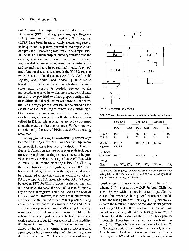
166 Kim, Tront, and Ha
compression technique. Pseudorandom Pattern Generators (PPG) and Signature Analysis Registers (SAR) based on a Linear Feedback Shift Register (LFSR) have been the most widely used among several techniques for test pattern generation and response data compression. The testing resources, for example, PPG and SAR, are usually implemented by transforming the existing registers in a design into multifunctional registers that behave as testing resources in testing mode and normal registers in operational mode. A typical multifunctional testing resource is the BILBO register which has four functional modes: PPG, SAR, shift register, and parallel load modes [1]. In order to transform a normal register into a testing resource, some extra circuitry is needed. Because of the multimodal nature of the testing resources, control logic must also be provided to affect proper configuration of multifunctional registers in each mode. Therefore, the BIST design process can be characterized as the creation of a set of testing resources and control logic. Once testing resources are created, test control logic can be designed using the methods such as are des- cribed in [2]. In this article, we are only concerned about the creation of testing resource. Furthermore, we consider only the use of PPGs and SARs as testing resources.
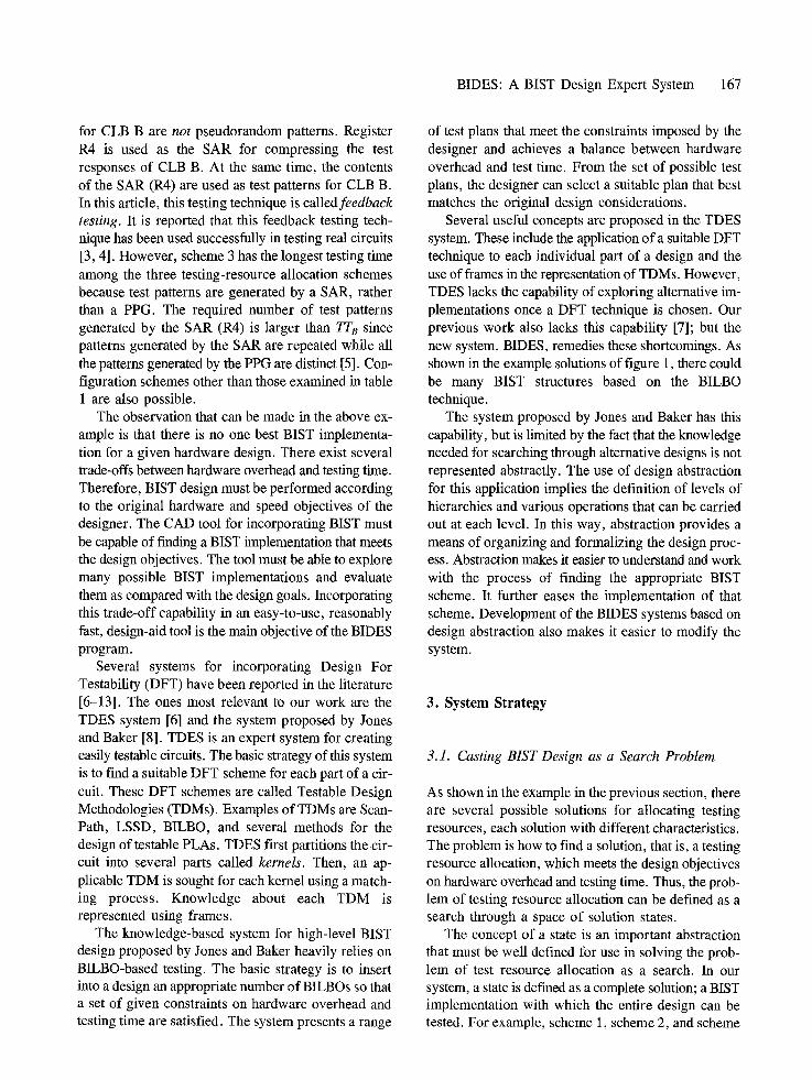
For any given design, there are usually several ways to provide testing resources. Consider the implemen- tation of BIST on a fragment of a design, shown in figure 1. Assuming the use of a scan-path technique for testing registers, testing resources need to be pro- vided to two Combinational Logic Blocks (CLBs), CLB A and CLB B. In implementing a PPG for CLB A, there are two candidate registers, R2 and R3, since transparent paths, that is, paths through which data can be transferred without any change, exist from R2 and R3 to the input CLB A. Similarly, either R3 or R4 could be used as PPG for CLB B. Either of the registers R1, R2, and R4 could act as the SAR of CLB B. Similarly, any of the four registers could be used as the SAR of CLB A. Notice, however, that there are interdependen- cies based on the circuit structure that preclude using certain combinations of the candidate PPGs and SARs.
From among several ways of allocating the testing resources, three schemes are shown in table 1. In scheme 1, all four registers need to be transformed into testing resources, but R3 does not need to be modified if scheme 2 is seleced. Since extra circuitry must be added to transform a normal register into a testing resource, the hardware overhead of scheme 1 is greater than that of scheme 2. However, in terms of testing
( R1
BUS
C R2
CLB A
( R3 ) [
( R4 ~)
CLB B
Fig. 1. A fragment of a design.
Table 1. Three schemes for testing two CLBs in the design in figure 1.
Scheme 1 Scheme 2 Scheme 3
PPG SAR PPG SAR PPG SAR
CLB A R2 R3 R2 R1 R2 R4 CLB B R4 R1 R4 R1 R4 R4
Modified R1, R2 R1, R2, R4 R2, I{4 Registers R3, R4
Hardware Overhead High Medium Low
Testing Time max (TTA, TTB) /T A + TT B TT A + c~ x TT B
7T/ denotes the required number of pseudorandom patterns for testing CLB i. The constant a > 1.0 can be determined by analyz- ing the feedback testing in scheme 3.
speed, scheme 1 has the advantage over scheme 2. In scheme 2, R1 is used as the SAR for both CLBs. As such, the two CLBs cannot be tested in parallel be- cause of the resource sharing conflict centered on R1. Thus, the testing time will be TT A + TTs, where TT/ denotes the required number of pseudorandom patterns for testing CLB i. On the other hand, there is no shar- ing of resources (path and/or testing resource) in scheme 1 and the testing of the two CLBs in parallel is possible. Therefore, the testing time of scheme 1 is max (TTA, TT~), which is less than that of scheme 2.
To further reduce the hardware overhead, scheme 3 can be used. As shown, it is required to modify only two registers, R2 and R4. In scheme 3, test patterns
BIDES: A BIST Design Expert System 167
for CLB B are not pseudorandom patterns. Register R4 is used as the SAR for compressing the test responses of CLB B. At the same time, the contents of the SAR (R4) are used as test patterns for CLB B. In this article, this testing technique is called feedback testing. It is reported that this feedback testing tech- nique has been used successfully in testing real circuits [3, 4]. However, scheme 3 has the longest testing time among the three testing-resource allocation schemes because test patterns are generated by a SAR, rather than a PPG. The required number of test patterns generated by the SAR (R4) is larger than TT~ since patterns generated by the SAR are repeated while all the patterns generated by the PPG are distinct [5]. Con- figuration schemes other than those examined in table 1 are also possible.
The observation that can be made in the above ex- ample is that there is no one best BIST implementa- tion for a given hardware design. There exist several trade-offs between hardware overhead and testing time. Therefore, BIST design must be performed according to the original hardware and speed objectives of the designer. The CAD tool for incorporating BIST must be capable of finding a BIST implementation that meets the design objectives. The tool must be able to explore many possible BIST implementations and evaluate them as compared with the design goals. Incorporating this trade-off capability in an easy-to-use, reasonably fast, design-aid tool is the main objective of the BIDES program.
Several systems for incorporating Design For Testability (DFT) have been reported in the literature [6-13]. The ones most relevant to our work are the TDES system [6] and the system proposed by Jones and Baker [8]. TDES is an expert system for creating easily testable circuits. The basic strategy of this system is to find a suitable DFT scheme for each part of a cir- cuit. These DFT schemes are called Testable Design Methodologies (TDMs). Examples of TDMs are Scan- Path, LSSD, BILBO, and several methods for the design of testable PLAs. TDES first partitions the cir- cuit into several parts called kernels. Then, an ap- plicable TDM is sought for each kernel using a match- ing process. Knowledge about each TDM is represented using frames.
The knowledge-based system for high-level BIST design proposed by Jones and Baker heavily relies on BILBO-based testing. The basic strategy is to insert into a design an appropriate number of BILBOs so that a set of given constraints on hardware overhead and testing time are satisfied. The system presents a range
of test plans that meet the constraints imposed by the designer and achieves a balance between hardware overhead and test time. From the set of possible test plans, the designer can select a suitable plan that best matches the original design considerations.
Several useful concepts are proposed in the TDES system. These include the application of a suitable DFT technique to each individual part of a design and the use of frames in the representation of TDMs. However, TDES lacks the capability of exploring alternative im- plementations once a DFT technique is chosen. Our previous work also lacks this capability [7]; but the new system, BIDES, remedies these shortcomings. As shown in the example solutions of figure 1, there could be many BIST structures based on the BILBO technique.
The system proposed by Jones and Baker has this capability, but is limited by the fact that the knowledge needed for searching through alternative designs is not represented abstractly. The use of design abstraction for this application implies the definition of levels of hierarchies and various operations that can be carried out at each level. In this way, abstraction provides a means of organizing and formalizing the design proc- ess. Abstraction makes it easier to understand and work with the process of finding the appropriate BIST scheme. It further eases the implementation of that scheme. Development of the BIDES systems based on design abstraction also makes it easier to modify the system.
3. System Strategy
3.1. Casting BIST Design as a Search Problem
As shown in the example in the previous section, there are several possible solutions for allocating testing resources, each solution with different characteristics. The problem is how to find a solution, that is, a testing resource allocation, which meets the design objectives on hardware overhead and testing time. Thus, the prob- lem of testing resource allocation can be defined as a search through a space of solution states.
The concept of a state is an important abstraction that must be well defined for use in solving the prob- lem of test resource allocation as a search. In our system, a state is defined as a complete solution; a BIST implementation with which the entire design can be tested. For example, scheme 1, scheme 2, and scheme
168 Kim, Tront, and Ha
3 are all complete solutions for the design in figure 1. Although our system does not subscribe to this defini- tion, a state could be also defined as a partial solution, that is, a BIST implementation for a part of a design. In order to define a state as a partial solution there must be a reliable evaluator with which it can be judged whether a partial solution is a part of satisfactory com- plete solution or not. In test resource allocation, it is very difficult to devise such an evaluator since the overall testing time cannot be evaluated for just a part of a BIST implementation. Therefore, by definition, all states generated during the search process, including an initial state are complete solutions in BIDES.
The general problem-solving strategy for attacking design problems using searching techniques is to repeatedly perform the process of evaluation and regeneration. For a given state, a new state is generated by a transformation of the old state. The new state is evaluated by comparison with the goal-state character- istics. Using this iterative process of evaluation and regeneration, an initial state will be evolved to a goal state eventually. The evaluation and regeneration of various BIST structures requires a high degree of ex- pertise in BIST. This is the primary motivation for employing the expert system approach.
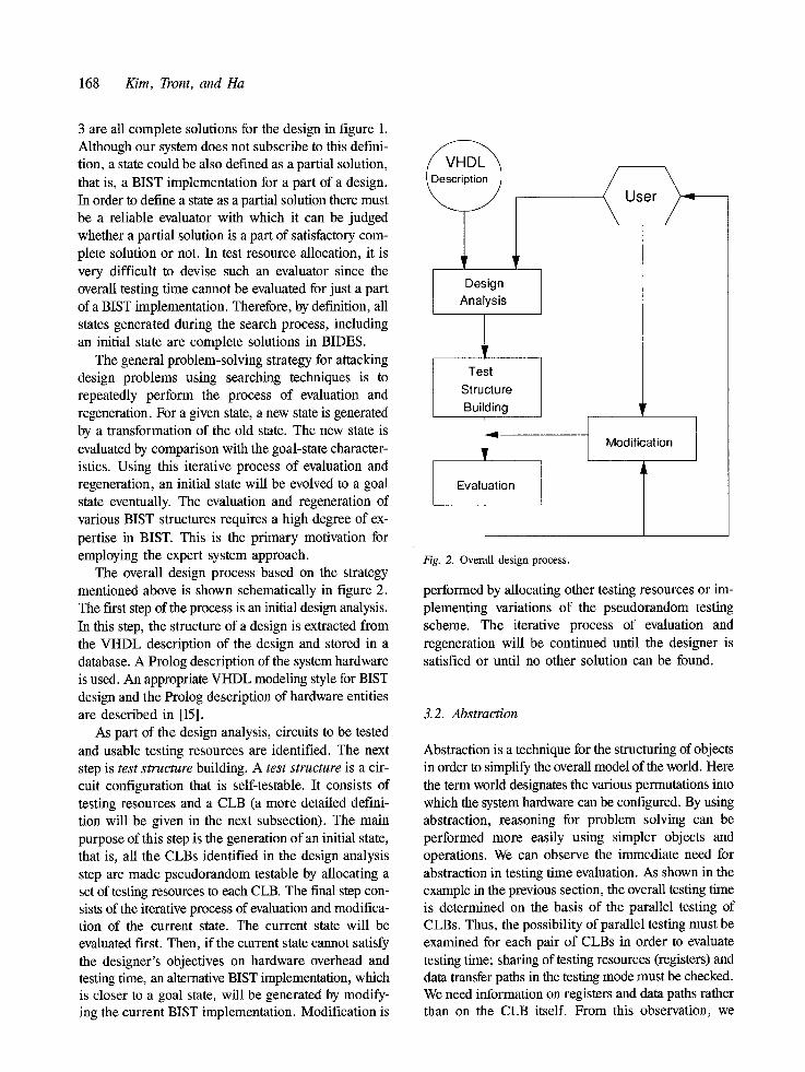
The overall design process based on the strategy mentioned above is shown schematically in figure 2. The first step of the process is an initial design analysis. In this step, the structure of a design is extracted from the VHDL description of the design and stored in a database. A Prolog description of the system hardware is used. An appropriate VHDL modeling style for BIST design and the Prolog description of hardware entities are described in [15].
As part of the design analysis, circuits to be tested and usable testing resources are identified. The next step is test structure building. A test structure is a cir- cuit configuration that is self-testable. It consists of testing resources and a CLB (a more detailed defini- tion will be given in the next subsection). The main purpose of this step is the generation of an initial state, that is, all the CLBs identified in the design analysis step are made pseudorandom testable by allocating a set of testing resources to each CLB. The final step con- sists of the iterative process of evaluation and modifica- tion of the current state. The current state will be evaluated first. Then, if the current state cannot satisfy the designer's objectives on hardware overhead and testing time, an alternative BIST implementation, which is closer to a goal state, will be generated by modify- ing the current BIST implementation. Modification is
Design Analysis
Test Structure Building
I_
Evaluation
User
Modification
Fig. 2. Overall design process.
performed by allocating other testing resources or im- plementing variations of the pseudorandom testing scheme. The iterative process of evaluation and regeneration will be continued until the designer is satisfied or until no other solution can be found.
3.2. Abstraction
Abstraction is a technique for the structuring of objects in order to simplify the overall model of the world. Here the term world designates the various permutations into which the system hardware can be configured. By using abstraction, reasoning for problem solving can be performed more easily using simpler objects and operations. We can observe the immediate need for abstraction in testing time evaluation. As shown in the example in the previous section, the overall testing time is determined on the basis of the parallel testing of CLBs. Thus, the possibility of parallel testing must be examined for each pair of CLBs in order to evaluate testing time; sharing of testing resources (registers) and data transfer paths in the testing mode must be checked. We need information on registers and data paths rather than on the CLB itself. From this observation, we
BIDES: A BIST Design Expert System 169
define an object called "test structure" which consists of a CLB and the testing resources associated with it. Then, parallel testing of two CLBs can be checked by defining an operator "parallel-testing" which examines the resource sharing between two test structures as shown below:
parallel__testing( TSi, TSj)
where TS~ denotes the test structure associated with the CLB k.
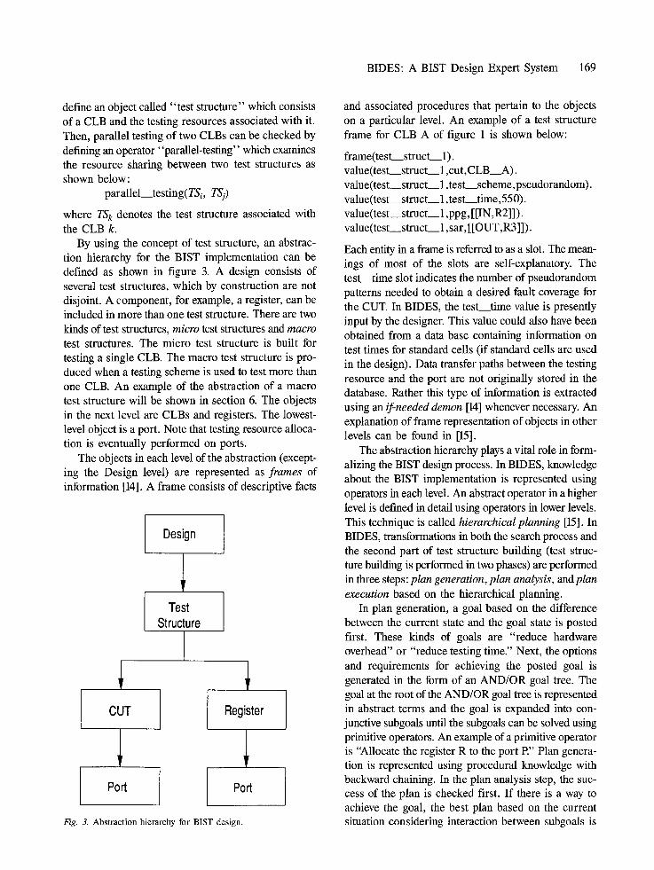
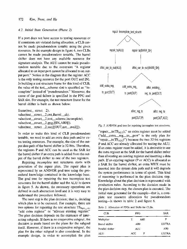
By using the concept of test structure, an abstrac- tion hierarchy for the BIST implementation can be defined as shown in figure 3. A design consists of several test structures, which by construction are not disjoint. A component, for example, a register, can be included in more than one test structure. There are two kinds of test structures, micro test structures and macro test structures. The micro test structure is built for testing a single CLB. The macro test structure is pro- duced when a testing scheme is used to test more than one CLB. An example of the abstraction of a macro test structure will be shown in section 6. The objects in the next level are CLBs and registers. The lowest- level object is a port. Note that testing resource alloca- tion is eventually performed on ports.
The objects in each level of the abstraction (except- ing the Design level) are represented as frames of information [14]. A frame consists of descriptive facts
Design
Test Structure
CUT
Pod
Register
Port
Fig. 3. Abstraction hierarchy for BIST design.
and associated procedures that pertain to the objects on a particular level. An example of a test structure frame for CLB A of figure 1 is shown below:
frame(test__struct~l). value(test__struct__ 1 ,cut,CLB__A). value(test__struct__ 1 ,test__scheme,pseudorandom). value(test~struct__l,test time,550). value(test___struct__l,ppg,[[IN,R2]]). value(test__struct__ 1 ,sar,[[OUT,R3]]).
Each entity in a frame is referred to as a slot. The mean- ings of most of the slots are self-explanatory. The test time slot indicates the number of pseudorandom patterns needed to obtain a desired fault coverage for the CUT. In BIDES, the test time value is presently input by the designer. This value could also have been obtained from a data base containing information on test times for standard cells (if standard cells are used in the design). Data transfer paths between the testing resource and the port are not originally stored in the database. Rather this type of information is extracted using an if-needed demon [14] whenever necessary. An explanation of frame representation of objects in other levels can be found in [15].
The abstraction hierarchy plays a vital role in form- alizing the BIST design process. In BIDES, knowledge about the BIST implementation is represented using operators in each level. An abstract operator in a higher level is defined in detail using operators in lower levels. This technique is called hierarchical planning [15]. In BIDES, transformations in both the search process and the second part of test structure building (test struc- ture building is performed in two phases) are performed in three steps: plan generation, plan analysis, and plan execution based on the hierarchical planning.
In plan generation, a goal based on the difference between the current state and the goal state is posted first. These kinds of goals are "reduce hardware overhead" or "reduce testing time." Next, the options and requirements for achieving the posted goal is generated in the form of an AND/OR goal tree. The goal at the root of the AND/OR goal tree is represented in abstract terms and the goal is expanded into con- junctive subgoals until the subgoals can be solved using primitive operators. An example of a primitive operator is "Allocate the register R to the port E" Plan genera- tion is represented using procedural knowledge with backward chaining. In the plan analysis step, the suc- cess of the plan is checked first. If there is a way to achieve the goal, the best plan based on the current situation considering interaction between subgoals is
170 Kim, Tront, and Ha
chosen using the plan decision knowledge. Otherwise, another plan is generated. Plan decision knowledge is also represented using production rules. A task is finally completed by executing a chosen plan.
4. Test Structure Building
As mentioned earlier, we consider a state in the solu- tion space as a complete test resource allocation. The initial state, as generated by BIDES, must also be a complete test resource allocation, that is, all of the CLBs in a design must have testing resources. Since a goal state will be evolved from an initial state, it is desirable to generate an initial state that requires the least number of modifications. The basic testing strategy adopted in this system is pseudorandom testing. Thus, if all the CLBs are made pseudorandom testable in the initial state, the number of further modifications is expected to be minimized. When BIDES does test
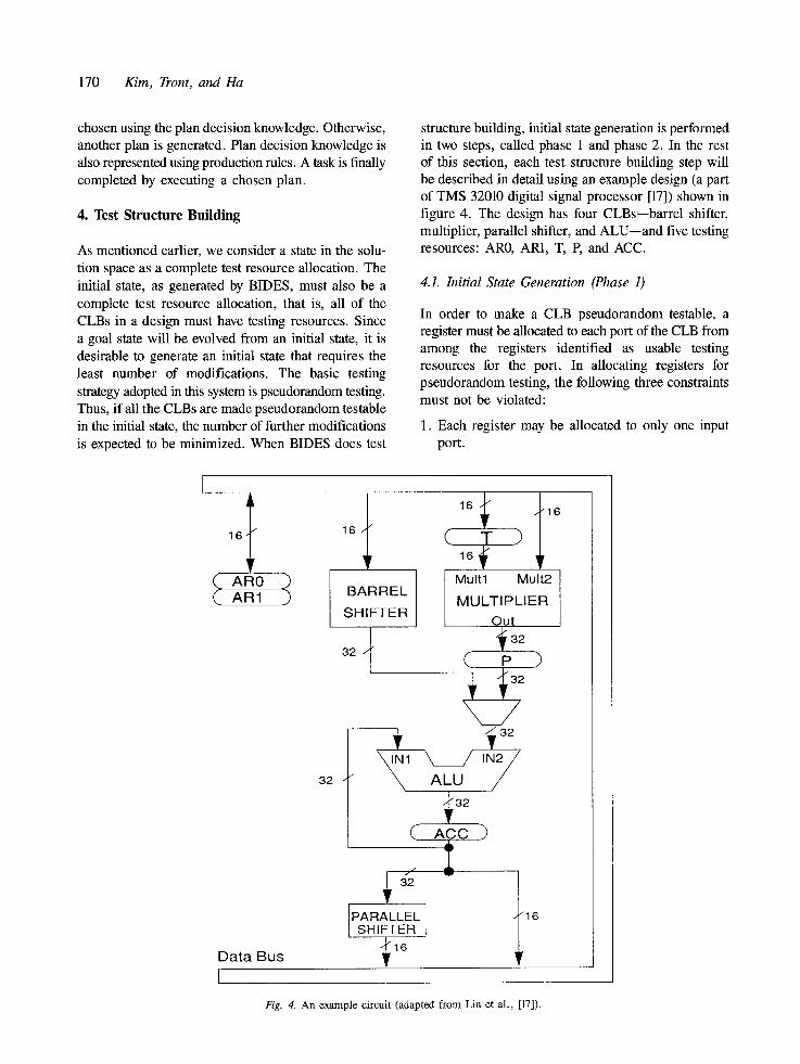
structure building, initial state generation is performed in two steps, called phase 1 and phase 2. In the rest of this section, each test structure building step will be described in detail using an example design (a part of TMS 32010 digital signal processor [17]) shown in figure 4. The design has four CLBs--barrel shifter, multiplier, parallel shifter, and ALU--and five testing resources: AR0, AR1, T, P, and ACC.
4.1. Initial State Generation (Phase I)
In order to make a CLB pseudorandom testable, a register must be allocated to each port of the CLB from among the registers identified as usable testing resources for the port. In allocating registers for pseudorandom testing, the following three constraints must not be violated:
1. Each register may be allocated to only one input port.
16 .~ 16 /~
I AR0 t A R 1 BARREL SHIFTER
32 / /
32 /
16 ~" ~16
( T ) 16~' r
Mult] Mult2
MULTIPLIER
Out
I 3e
( P )
( ACC )
PARALLEL / "16 SHIFTER
Data Bus ~ 16
Fig. 4. An example circuit (adapted from Lin et al., [17]).
BIDES: A BIST Design Expert System 171
2. Registers allocated to the input ports cannot be allocated to the output ports, and vice versa.
3. Data paths, e.g., the bus, cannot be used simul- taneously in test pattern application and response collection.
If the first constraint is violated, the same test patterns will be applied to different input ports of the same CLB. The second constraint prevents the use of the same register as a PPG as well as a SAR for the same CLB. Testing cannot be run in a continuous manner ever a single data path if the third constraint is ob- served. If data path contention occurs, a scheduling algorithm [18] for using the shared data path is needed. These constraints may be relaxed later as test resource scheduling is considered in more detail.
Given these three constraints, the problem of register allocation for pseudorandom testing can be defined as a constraint satisfaction problem. In order to solve this problem an algorithm based on dependency-directed backtracking is devised. The algorithm will be briefly described in the following paragraphs. The details of the algorithm can be found in [15].
Suppose that the algorithm is applied to implement the pseudorandom testing of the multiplier which has two input ports, Multl and Mult2, and one output OUT. The first step is goal expansion. The top-level goal--
make a CUT pseudorandom testable (Multiplier)
will be expanded into the following three conjunctive subgoals on ports:
1. Allocate a register to Multl. 2. Allocate a register to Mult2. 3. Allocate a register to OUT.
These subgoals interact with each other due to the con- straints imposed, and the resulting allocation will be different depending upon the order of subgoal execu- tion. Therefore, we need to decide the order of subgoal execution. A typical strategy "hard to satisfy first" is employed to decide on the order. For each port of a circuit, there could be several candidate registers that can be allocated. If priority is given to a port with the fewest number of candidate registers, the chance of violating the given constraints can be reduced. Accord- ing to this strategy, the three subgoals given above will be executed in the order of OUT, Mult2, and Multl.
The next step is register allocation to be performed according to the order of subgoal execution. Register
allocation for a particular port starts with elimination of unusable registers based on the constraints imposed on the pool of candidate registers. If there is still a usable register after elimination, allocation proceeds, otherwise backtracking is performed. When there is more than one usable register for a given port, a register is selected using a set of built-in heuristics. Heuristics are developed to maximize resource sharing, that is, to minimize the hardware overhead while maintaining a strict pseudorandom testing strategy.
For example, consider the allocation of a register to the port Mult2. Mult2 has three possible resources, AR0, AR1, and ACC. Assuming that the register P is already allocated to the port OUT by the "hard to satisfy strategy" (in fact P is the only usable register for the port OUT), P cannot be used for the port Mult2. However, P is not a usable resource for the port Mult2, thus, the order of subgoal execution constraint does not affect this case. In other words, P is simply eliminated because it is unusable. Other potential resources are handled in a like manner. The next step is register selec- tion. First, two registers, AR0 and AR1, are preferred over ACC because pure pseudorandom patterns can- not be efficiently generated by ACC. Since the size of ACC is 32-bits wide, the patterns generated by ACC can be pseudorandom patterns only for a 32-bit port. Therefore, we need to select one register from among the two registers since both registers can generate pure pseudorandom patterns for the port Mult2. In this case, a register is selected based on global resource sharing. If there is a register already in use to generate inputs for another CLB, then the register will be allocated to this input as well. In that way, resource sharing can be maximized. If none of the candidate registers are already allocated, then a measure for potential resource sharing called Global Degree of Sharing (GDS) is used. For example, the register AR0 can be used as a testing resource for four ports. Therefore, the GDS of AR0 is 4. However, since AR1 has the same GDS, a register will finally be selected arbitrarily. The above heuristics are implemented with if-then production rules.
Whenever the system fails to attain a subgoal, backtracking is performed based on previously speci- fied dependencies. That is, the system backs up to the last subgoal that could have affected the failure and makes a different allocation choice. If backtracking does not resolve the goal failure or there is no available resource in the original design, the cause of the failure is recorded and allocation proceeds. The cause of goal failure will be repaired in phase 2.
172 Kim, Tront, and Ha
4.2. Initial State Generation (Phase 2)
If a port does not have access to testing resources or if constraints are violated during allocation, a CLB can- not be made pseudorandom testable using the given resources. In the example design in figure 4, two CLBs cannot be made pseudorandom testable. The barrel shifter does not have any available resource for signature analysis. The ALU cannot be made pseudo- random testable due to the constraint "A register allocated to an input port cannot be allocated to an out- put port." Notice in the diagram that the register ACC is the only testing resource for the port OUT and IN1. In building a test structure frame for this kind of CLB, the value of the test__scheme slot is specified as "in- complete" instead of "pseudorandom" Moreover, the cause of the goal failure is specified in the PPG and SAR slot. For example, the test structure frame for the barrel shifter is built as shown below:
frame(test__struct__2). value(test___struct__2 ,cut, Barrel sh). value(test__struct___2,test_scheme,incomplete). value(test__struct___2,ppg, [[IN,AR0]]). value(test__struct___2,sar, [lOUT, not avail]]).
In order to make this kind of CLB pseudorandom testable, we need to add an extra data path and/or ex- tra testing resources. For example, the size of the out- put data path of the barrel shifter is 32-bits. Therefore, the registers P and ACC can be used as the SAR for the barrel shifter if an extra path is added from the out- put of the barrel shifter to one of the two registers.
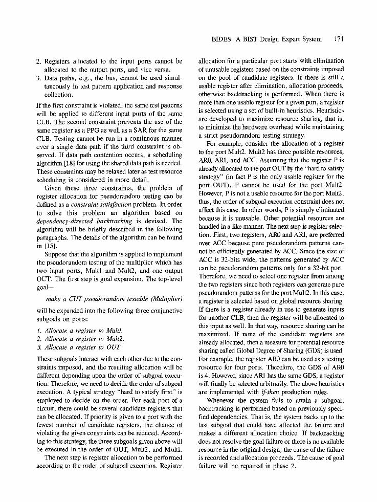
Repairing incomplete test structures starts with generation of the repair plan. The repair plan is represented by an AND/OR goal tree using the pro- cedural knowledge contained in the knowledge base. The goal tree for repairing the two incomplete test structures for the barrel shifter and the ALU is shown in figure 5. As shown, the necessary operations are defined in each abstraction level and it is very easy to understand the procedure followed.
The next step is the plan decision; that is, deciding which plan is to be executed. For example, there are two options for repairing the test structure TSBarr__sh,
"add extra register" or "allocate existing register." The plan decision depends on the existence of inter- acting subgoals. If there is no conjunctive subgoal, the decision is made based on the plans for the subgoal itself. However, if there is a conjunctive subgoal, the plan for the other subgoal is also considered. In the example design, in order to accomplish the plan
repairts(ALU)
alloc sar to_cut(ALU)
add_extra_reg_
toport(OUT)
repair_incomplete test structs
repair_ts(BARR SH)
a[Ioc saLto_cut(BARR_SH)
add_extra_reg_ alloc_existing_
to_port(OUT) reg_to_port(OUT)
arloc_reg_to alloc_reg_to_
port(OUT, P) port(OUT,AGO)
Fig. 5. AND/OR goal tree for repairing incomplete test structures.
"repair ts(TSALu)," an extra register must be added ("add__extra__reg to port" is the only plan for "repair ts(TSALu)") because the two 32-bit registers P and ACC are already allocated for testing the ALU. If an extra register must be added, it is desirable to use the extra register as the SAR for the barrel shifter rather than allocating an existing register and inserting a data path. If an existing register (P or ACC) is allocated as a SAR for the barrel shifter, an extra MUX must be inserted into the system data path and it will degrade the system performance in terms o f speed. This kind of reasoning is performed in the plan decision step. Knowledge about the plan decision is represented with production rules. According to the decision made in the plan decision step, the chosen plan is executed. The initial state generated for the example--that is, a com- plete test resource allocation for pseudorandom testing--is shown in table 2 and figure 6.
Table 2. Allocation of PPGs and SARs for CLBs.
CLB PPG SAR
Multiplier T AR0 P
Barrel shifter AR0 EXTRA
Parallel shifter ACC AR0
ALU ACC P EXTRA
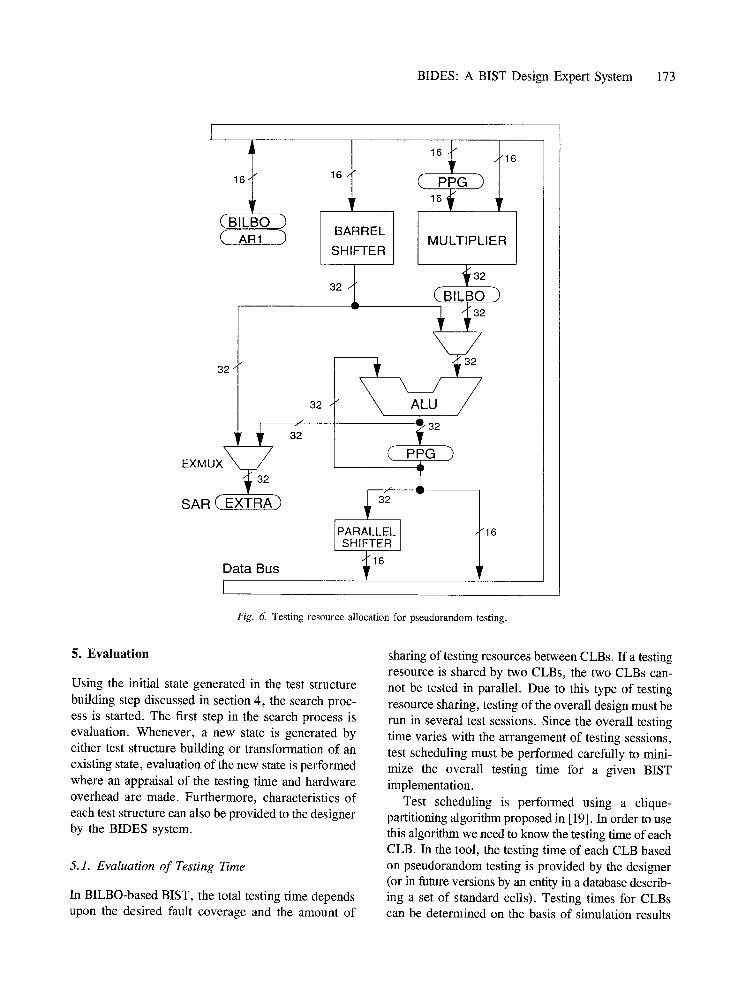
BIDES: A BIST Design Expert System 173
16 ! ( B I L B O ) (. Am 3
32
'6 ! BARREL SHIFTER
( PPG )
MULTIPLIER
EXMUXS ~32
SAR (. EXTRA)
32 z"
J
32
Data Bus
I
32 (BILBO 3 2 @
~" 32 ( PPG )
z"
i PARALLEL 16 SH FTER
Fig. 6. Testing resource allocation for pseudorandom testing. 5. Evaluation
Using the initial state generated in the test structure building step discussed in section 4, the search proc- ess is started. The first step in the search process is evaluation. Whenever, a new state is generated by either test structure building or transformation of an existing state, evaluation of the new state is performed where an appraisal of the testing time and hardware overhead are made. Furthermore, characteristics of each test structure can also be provided to the designer by the BIDES system.
5.1. Evaluation of Testing Time
In BILBO-based BIST, the total testing time depends upon the desired fault coverage and the amount of
sharing of testing resources between CLBs. If a testing resource is shared by two CLBs, the two CLBs can- not be tested in parallel. Due to this type of testing resource sharing, testing of the overall design must be run in several test sessions. Since the overall testing time varies with the arrangement of testing sessions, test scheduling must be performed carefully to mini- mize the overall testing time for a given BIST implementation.
Test scheduling is performed using a clique- partitioning algorithm proposed in [19]. In order to use this algorithm we need to know the testing time of each CLB. In the tool, the testing time of each CLB based on pseudorandom testing is provided by the designer (or in future versions by an entity in a database describ- ing a set of standard cells). Testing times for CLBs can be determined on the basis of simulation results
174 Kim, Tront, and Ha
in conjunction with a knowledge on the desired fault coverage. The values used in the example are arbitrary and only meant to be useful in terms of their relative magnitude. The result of scheduling for the initial state given in figure 6 is shown in table 3. As shown in the table, four CLBs are tested in two testing sessions. Note that parallel testing is possible even though a PPG is shared between two CLBs. Sharing PPGs between CLBs is allowed since two different CLBs can be tested using the same pseudorandom patterns.
Table 3. Result of testing-time evaluation.
Used Registers Scheduled Test Session Tested CLB AR0 P ACC T EXTRA
Session 1 B a ~ s h PPG SAR X PPG SAR Multiplier
Session 2 ALU SAR PPG PPG X SAR Para__sh
Overall testing time = max (TTBarr sh,TTMult ) + max (TTALu,TTpara_~h)
= 2645 + 1857 = 4502 (patterns)
5.2. Hardware Overhead
The major source of hardware overhead in BILBO- based BIST comes from the hardware necessary for im- plementing testing resources, that is, PPGs and SARs along with a scan-path necessary to link the testing hardware. Hardware overhead may also come from the extra data path and extra circuitry such as MUXs necessary for creating the extra data paths. In BIDES, only the hardware overhead for testing resource and extra components is taken into account. The actual silicon area for extra wiring paths should also be con- sidered, but it is very difficult to estimate at the register transfer level without information about the actual floor plan of the design.
In estimating the hardware overhead for the BIST components, the method proposed in [20] is employed. In this method, various BIST components are im- plemented using nMOS and the number of extra tran- sistors needed in each BIST component is counted. In BIDES, the number of extra transistors necessary is counted based on a CMOS implementation rather than nMOS. Hardware overhead for each BIST component is represented using a formula. For example, hardware overhead for the modified n-bit BILBO register is calculated using the formula
number of transistors = (n - 1) x 18 + 58
The constants 18 and 58 come from empirical data generated by configuring example BIST register designs. The CMOS implementation of BIST com- ponents and the corresponding hardware overhead values used in the system can be found in [21]. The hardware overhead for each testing resource and the overall hardware overhead for the initial state for the example of figure 4 are shown in table 4.
Table 4. Result of hardware overhead evaluation.
Hardware overhead Component Function (transistors)
ACC PPG(32) 164
P BILBO(32) 616
AR0 BILBO(16) 328
T PPG(16) 100
EXTRA SAR(32) 734
EXMUX MUX(32) 128
Total hardware overhead 2070
6. Regeneration of BIST Implementation
If the current BIST implementation cannot meet the design objectives, an alternative is sought based on the difference between the current state and a goal state. Since there are two factors in the difference, hardware overhead and testing time, the search needs to be directed in one of the following three directions:
1. Both testing time and hardware overhead need to be reduced.
2. Only testing time needs to be reduced. 3. Only hardware overhead needs to be reduced.
Among the above directions, only two directions-- reducing testing time or reducing hardware overhead-- are considered by the BIDES system, since it is almost impossible to reduce both testing time and hardware overhead simultaneously. As shown in the example in section 2, there exists a trade-off between testing time and hardware overhead.
Based on the result of the evaluation of the current state, the designer decides on the search direction-- either "reduce testing time" or "reduce hardware overhead." A child state of the current state is generated. The new state will be evaluated and the result conveyed to the designer again for approval or further regeneration.
BIDES: A BIST Design Expert System 175
6.1. Reducing Hardware Overhead
Hardware overhead is reduced by reducing the number of testing resources, that is, by eliminating some of the testing resource. There are two kinds of elimina- tion: removal of a register that was added for testing purpose only--for example, EXTRA in figure 6--and restoration of a register that was previously trans- formed into a testing resource. Restoring a register returns it to its original non-BILBO form, which reduces the hardware necessary.
Testing resource elimination starts with the selec- tion of a candidate register to be eliminated. The designer may select a register to be eliminated. Other- wise, a register is selected by the system using prede- fined rules. The prime candidate for elimination is an extra register since it is the source of a significant por- tion of the total hardware overhead. Selection of an extra to be eliminated is based on the difficulty of elimination: that is, it depends upon the number of test structures in which the register is used. In the exam- ple design, the extra register EXTRA is the prime can- didate for elimination since it is used in fewer test struc- tures. The register P will be selected as the next can- didate because the register P is used in just two test structures.
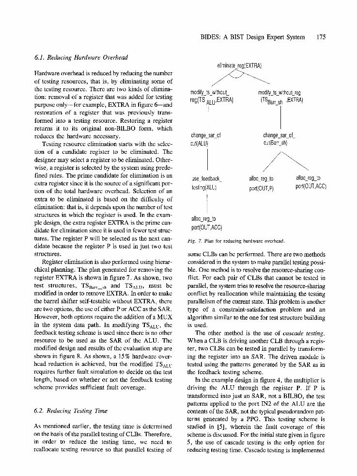
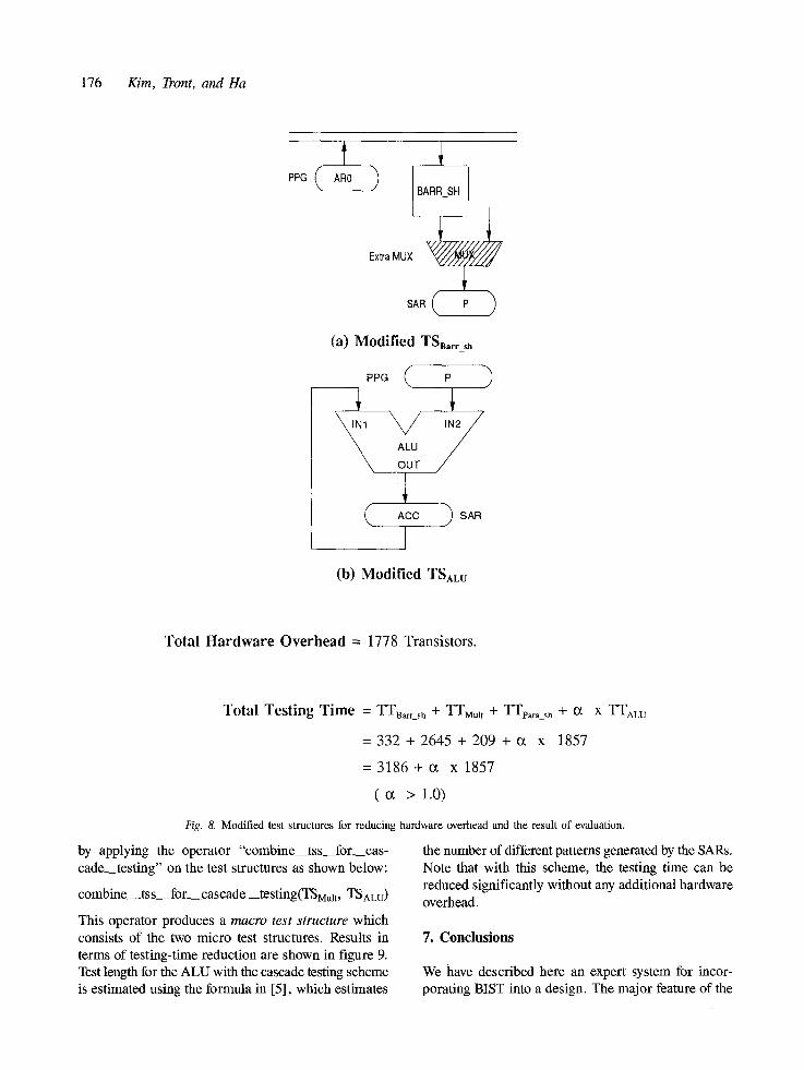
Register elimination is also performed using hierar- chical planning. The plan generated for removing the register EXTRA is shown in figure 7. As shown, two test structures, TSBarr s h and TSaim, must be modified in order to remove EXTRA. In order to make the barrel shifter self-testable without EXTRA, there are two options, the use of either P or ACC as the SAR. However, both options require the addition of a MUX in the system data path. In modifying TSALu, the feedback testing scheme is used since there is no other resource to be used as the SAR of the ALU. The modified design and results of the evaluation step are shown in figure 8. As shown, a 15% hardware over- head reduction is achieved, but the modified TSAL U
requires further fault simulation to decide on the test length, based on whether or not the feedback testing scheme provides sufficient fault coverage.
6.2. Reducing Testing Time
As mentioned earlier, the testing time is determined on the basis of the parallel testing of CLBs. Therefore, in order to reduce the testing time, we need to reallocate testing resource so that parallel testing of
eliminate_reg(EXTRA)
modify_ts_without_ modify_ts_withouLreg reg(TS ALu,EXTRA) (TSBarr sh ,EXTRA)
change sat_of cut(ALU)
use feedback tesling(ALU)
change_sar of cut(Barr_sh)
all0c_reg t0 all0c_reg t0
port(OUT, P) port(OUT,ACC)
alloc_reg_to port(OUT,ACC)
Fig. 7. Plan for reducing hardware overhead.
some CLBs can be performed. There are two methods considered in the system to make parallel testing possi- ble. One method is to resolve the resource-sharing con- flict. For each pair of CLBs that cannot be tested in parallel, the system tries to resolve the resource-sharing conflict by reallocation while maintaining the testing parallelism of the current state. This problem is another type of a constraint-satisfaction problem and an algorithm similar to the one for test structure building is used.
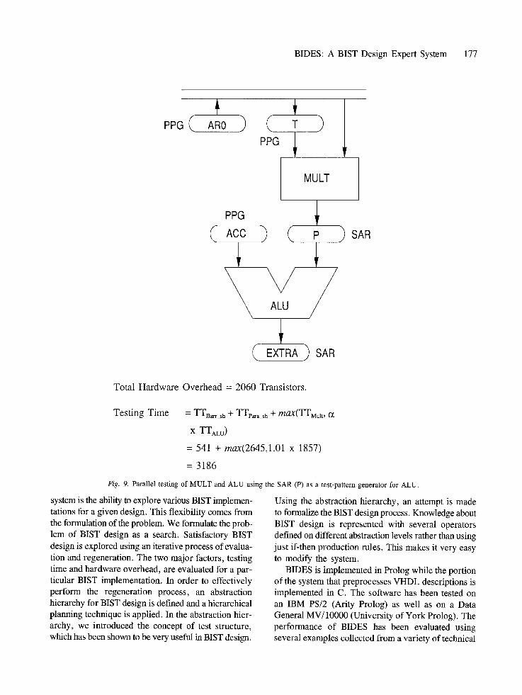
The other method is the use of cascade testing. When a CLB is driving another CLB through a regis- ter, two CLBs can be tested in parallel by transform- ing the register into an SAR. The driven module is tested using the patterns generated by the SAR as in the feedback testing scheme.
In the example design in figure 4, the multiplier is driving the ALU through the register P. If P is transformed into just an SAR, not a BILBO, the test patterns applied to the port IN2 of the ALU are the contents of the SAR, not the typical pseudorandom pat- terns generated by a PPG. This testing scheme is studied in [5], wherein the fault coverage of this scheme is discussed. For the initial state given in figure 5, the use of cascade testing is the only option for reducing testing time. Cascade testing is implemented
176 Kim, Tront, and Ha
PPG ( t
ARO BARR SH
Extra MUX ~ ~
(a) M o d i f i e d TSB . . . . h
_ _ PPG ( P )
IN2
\ OUT /
] (b) Modif ied TSAL U
Tota l H a r d w a r e O v e r h e a d = 1778 Transistors.
Tota l Tes t ing T i m e = TT~r_sh + TTMult + TTpara sh + 0(, X TTALtj
= 3 3 2 + 2 6 4 5 + 2 0 9 + C Z X 1857
= 3 1 8 6 + C ~ X 1857
( o: > 1.0)
Fig. 8. Modified test structures for reducing hardware overhead and the result of evaluation.
by applying the operator "combine tss__for_cas- cade_testing" on the test structures as shown below:
combine tss for___cascade testing(TSMult, TSALu)
This operator produces a macro test structure which consists of the two micro test structures. Results in terms of testing-time reduction are shown in figure 9. Test length for the ALU with the cascade testing scheme is estimated using the formula in [5], which estimates
the number of different patterns generated by the SAILs. Note that with this scheme, the testing time can be reduced significantly without any additional hardware overhead.
7. Conclusions
We have described here an expert system for incor- porating BIST into a design. The major feature of the
BIDES: A BIST Design Expert System 177
PPG ( ARO ) ( PPG
T )
MULT
( cc) ( p ) sAR
Total Hardware Overhead = 2060 Transistors.
Testing Time = TTB~_s~ + TTv . . . . h + max(TrMu]t, 0~
x TTALu)
= 541 + max(2645,1.01 x 1857)
= 3186
Fig. 9. Parallel testing of MULT and ALU using the SAR (P) as a test-pattern generator for ALU.
system is the ability to explore various BIST implemen- tations for a given design. This flexibility comes from the formulation of the problem. We formulate the prob- lem of BIST design as a search. Satisfactory BIST design is explored using an iterative process of evalua- tion and regeneration. The two major factors, testing time and hardware overhead, are evaluated for a par- ticular BIST implementation. In order to effectively perform the regeneration process, an abstraction hierarchy for BIST design is defined and a hierarchical planning technique is applied. In the abstraction hier- archy, we introduced the concept of test structure, which has been shown to be very useful in BIST design.
Using the abstraction hierarchy, an attempt is made to formalize the BIST design process. Knowledge about BIST design is represented with several operators defined on different abstraction levels rather than using just if-then production rules. This makes it very easy to modify the system.
BIDES is implemented in Prolog while the portion of the system that preprocesses VHDL descriptions is implemented in C. The software has been tested on an IBM PS/2 (Arity Prolog) as well as on a Data General MV/10000 (University of York Prolog). The performance of BIDES has been evaluated using several examples collected from a variety of technical
178 Kim, Tront, and Ha
publications. Example circuits consist mainly of data paths generated by a data-path synthesis program. In order to use BIDES, the circuit must consist of Struc- tured/Synchronous Building Blocks (SBB). As men- tioned in [13], an SBB is a circuit structure which con- sists of a CLB followed by a register bank. It is for this reason that data-path circuits are used. Example cir- cuits that have been processed consisted of from two to five CLBs and three to seven registers. BIDES suc- cessfully generated a final state for each test circuit. It took from three to five iterations to reach a final state. Actual processing time for these examples was never longer than 1.5 minutes. During this evaluation proc- ess, one observation seemed to stand out; it is relatively difficult to reduce hardware overhead from that of the initial state. This is due to the concerted effort that BIDES puts into generating a good initial state. On the other hand, it is relatively easy to reduce teting time by using either more testing resources or a cascaded testing scheme. Of particular note is that the cascaded testing scheme is applicable to most of the example cir- cuits. Given that this is the case, it becomes imperative that the testing time and fault coverage of the cascaded testing scheme be more accurately determined.
The major shortcoming of BIDES is that it is only applicable to designs consisting of SBBs. Considering that many designs do not comply with the SBB design style, we are planning to modify the design analysis portion of BIDES so that a design can be partitioned into SBBs and non-SBBs. In this way, the SBB portion can be handled by BIDES and the non-SBB portion can be processed by some other means.
There are several other enhancements planned for the system. These include finding more realistic measures of evaluation, testing of special structures such as PLAs and memory, and post-processing of a modified design. Further, the use of standard cell database will be explored. Finally an investigation into adding test coverage as a parameter to be traded off will be performed. In order to integrate the system with other CAD tools, the modified design will be translated back into VHDL. The structure of the internal database has been set up to facilitate translating the design back to VHDL although the actual translator has not yet been completed.
References
1. B. Koenemarm, J. Mucha, and G. Zwiehoff, "Built-In Logic Block Observation Techniques," Proc. IEEE Intern. Test Conf., pp. 37-41, 1979.
2. J. Kalinowld, A. Albicki, and J. Beausang, "Test Control Signal Distribution in Self-Testing VLSI Circuits" Proc. Intern. Conf. Comput.-Aid. Design, pp. 60-63, 1986.
3. EP. Beucler and M.J. Manner, "HILDO: The Highly Integrated Logic Device Observer;' VLSI Design, pp. 88-96, June 1984.
4. J.W. Gannett, "Self-Testing by Integrated Feedback (STIF)," VLS1 Electronics, N.G. Eisnpruch (Ed.), Academic Press, San Diego, CA, pp. 107-110, 1986.
5. K. Kim, D.S. Ha, and J.G. Tront, "On Using Signature Registers as Pseudorandom Pattern Generators in BIST," IEEE Trans. Com- pur-Aid. Design 7:919-928, August 1988.
6. M.S. Abadir and M.A. Breuer, ' ~ Knowledge-Based System for Designing Testable VLSI Chips" IEEE Design Test Corn- put., 2(4):56-58, 1985.
7. K. Kira, J.G. Tront, and D.S. Ha, '~Automatic Insertion of BIST Hardware Using VHDL," Proc. 25th Design Autorn. Conf., pp. 9-15, 1988.
8. M.A. Jones and K. Baker, ' ~n Intelligent Knowledge-Based System Tool for High-Level BIST Design," Proc. 1EEE Intern. Test Conf. ,, pp. 743-746, 1985.
9. P.W. Horstmarm, "A Knowledge-Based System Using Design for Testability Rules" Proc. 14th Intern. Syrup. Fault-Tolerant Corn- put. pp. 278-284, June 1984.
10. H.S. Fung and S. Hirschhorn, "An Automatic DFT System for the SILC Silicon Compiler," 1EEE Design Test Compur pp. 45-57, February 1986.
11. T.E. Mangir, "EXACT: An Expert System for Testable Design of VLSI" Intern. Symp. VLSI Tech., Systems Applic. , May 1985.
12. A. Kransniewski and A. Albicki, "Automatic Design of Ex- haustively Self-Testing Chips with BILBO Modules" Proc. IEEE Intern. Test Conf, pp. 362-371, 1985.
13. A.P. Ambler et al., "Economically Viable Automatic Insertion of Self-Test Features for Custom VLSI" Proc. IEEE Intern. Test Conf., pp. 232-243, 1986.
14. P.H. Winston, Artificial Intelligence, Addison-Wesley, Reading, MA, 1984.
15. K. Kim, Automatic Design of Self-Testable VLSI Circuits, Ph.D. Thesis, June 1989.
16. P.R. Cohen and E.A. Feigenbaum, The Handbook of Artificial Intelligence, William Kaufmann, Los Altos, CA, 1982.
17. K. Lin et al., "The TMS320 Family of Digital Signal Processor," Proc. IEEE, 75:1143-1159, September 1987.
18. M.S. Abadir and M.A. Breuer, "Test Schedules for VLSI Cir- cuits Having Built-In Test Hardware," 1EEE Trans. Comput. C-35(4):361-367, 1986.
19. C.R. Kime and K.K. Saluja, "Test Scheduling in Testable VLSI Circuits" Proc. 12th Intern. Syrnp. Fault-Tolerant Comput. pp. 406-412, 1982.
20. M.J. Ohletz, T.W. W'dliams, and J.P. Mucha, "Overhead in Scan and Self-Testing Designs" Proc. IEEE Intern. Test Conf., pp. 460-470, 1987.
21. K. Kim, J.G. Tront, and D.S. Ha, "On Hardware Overhead in CMOS BIST Designs," Proc. 1EEE Southeastcon "89, pp. 671-675, April 1989.
Kwanghyun Kim was born in Seoul, Korea. He received the B.S. degree in electronic engineering from Sogang University, Korea in 1978. From 1978 to 1983, he was with the Agency for Defense Develop- ment in Korea where he was involved in the development of airborne navigation systems. Form 1983, he continued his study at Virginia
B I D E S : A B I S T D e s i g n E x p e r t S y s t e m 179
Polytechnic Institute and State University and received the M.S. and Ph.D. degrees, both in Electrical Engineering in 1985 and 1989, respectively.
He joined Samsung Electronics, ASIC Division, as a senior manager in 1989, and is currently working on the development of testable ASICs at Samsung. His research interests include self-testing of VLSI circuits and design automation of testable ASICs.
Joseph G. Tront is an associate professor of Electrical Engineer- ing at Virginia Polytechnic Institute and State University where he teaches both graduate and undergraduate courses in computer engi- neering and electronics. His research interests include VLSI design, fault-tolerant computing, digital circuit modeling and simulation, and microprocessor applications. His work in VLSI has been on the development of CAD tools as well as the development of schemes for implementing fault-tolerant architectures as VLSI circuits. In the CAD tool area, he is presently working on an artificial intelligence tool for automatically inserting built-in self-test circuits into hard- ware description designs. He has participated as a member of the IEEE Design Automation Standards Committee in the development of the VHDL-1076 standard. He has also worked on modeling single- event upset effects in integrated circuits.
Dr. Tront received a B.S.E.E. in 1972 and a M.S.E.E. in 1973 from the University of Dayton. He received the Ph.D. degree from
the State University of New York at Buffalo in 1978. He joined the faculty at Virginia Tech in 1978. He is a senior member of the IEEE and is a member of ACM's SIGDA.
Dong S. Ha was born in Milyang Korea. He received the B.S. degree in electrical engineering from Seoul National University, Korea, in 1974 and the M.S. and Ph.D. degrees in electrical and computer engineering from the University of Iowa, Iowa, in 1984 and 1986, respectively.
Since the fall of 1986 he has been an Assistant Professor in the Department of Electrical Engineering of the Virginia Polytechnic Institute and State University. From 1975 to 1979, he served as a research engineer in the Agency for Defense Development, Korea. During the period, he was involved in various projects, including the development of airborne equipment for communications and naviga- tion and the development of data communication systems. He spent the summer of 1985 at the IBM T.J. Watson Research Center, where he worked on random pattern testing of embedded memory elements. His research interests lie in the area of VLSI testing including design for testability, built-in self-test and test pattern generation.
Dr. Ha is a member of the IEEE Computer Society and the Com- munications Society.