Basic Components Of a Computer System - Učilnica FRI 20/21
28
Patricio Buli´ c Basic Components Of a Computer System A Textbook December 25, 2020 Springer
-
Upload
khangminh22 -
Category
Documents
-
view
0 -
download
0
Transcript of Basic Components Of a Computer System - Učilnica FRI 20/21

Patricio Bulic
Basic Components Of aComputer System
A Textbook
December 25, 2020
Springer


Contents
1 Direct memory access . . . . . . . . . . . . . . . . . . . . . . . . . . . . . . . . . . . . . . . . . . . 11.1 Introduction . . . . . . . . . . . . . . . . . . . . . . . . . . . . . . . . . . . . . . . . . . . . . . . 11.2 Programmed Input/Output . . . . . . . . . . . . . . . . . . . . . . . . . . . . . . . . . . . 11.3 Interrupt-driven I/O . . . . . . . . . . . . . . . . . . . . . . . . . . . . . . . . . . . . . . . . . 41.4 Direct Memory Access . . . . . . . . . . . . . . . . . . . . . . . . . . . . . . . . . . . . . . 51.5 Real-world DMA Controllers . . . . . . . . . . . . . . . . . . . . . . . . . . . . . . . . 10
1.5.1 Intel 8237A DMA controller . . . . . . . . . . . . . . . . . . . . . . . . . . . 101.5.2 STM32Fx series DMA controller . . . . . . . . . . . . . . . . . . . . . . 12
1.6 Bus Mastering DMA . . . . . . . . . . . . . . . . . . . . . . . . . . . . . . . . . . . . . . . . 20
References . . . . . . . . . . . . . . . . . . . . . . . . . . . . . . . . . . . . . . . . . . . . . . . . . . . . . . . . . 23
v


Chapter 1Direct memory access
CHAPTER GOALS
Have you ever wondered how information travels between input-output de-vices and main memory in a computer system? In this chapter, we providea detailed explanation of the Direct Memory access (DMA) I/O techniqueused in modern computer systems, including those using the Intel and ARMfamily of microprocessors. This chapter also aims to demystify the DMAcontroller internals and its programming with various peripherals. Uponcompletion of this chapter, you will be able to:
• Distinguish between programmed IO, interrupt-driven IO, and DMAtransfers.
• Explain the operation of the signals used in direct memory access con-trollers.
• Explain the function of the Intel 8237 DMA controller when used forDMA transfers.
• Explain the function of the DMA controller used in STM Cortex-Mbased systems.
• Explain the function of bus-mastering (also referred to as first-partyDMA).
1.1 Introduction
1.2 Programmed Input/Output
The programmed I/O was the most straightforward type of I/O technique for theexchanges of data between I/O devices and memory. This data transfer method re-quires the least amount of hardware. With programmed I/O, data transfers between
1

2 1 Direct memory access
I/O devices and memory are accomplished by the central processing unit (CPU). Inthe case of programmed I/O, the I/O device does not have direct access to the mainmemory. The I/O devices have memory-mapped registers. This means that the CPUaccesses the I/O device’s registers using LOAD/STORE instructions.
A transfer from an I/O device to the main memory (or vice versa) requires theexecution of several instructions by the CPU. This includes a LOAD instruction totransfer the data from the I/O device’s data register(s) to the CPU and STORE in-struction to transfer the data from CPU to the main memory. Besides, the CPU mustcontinuously sense the I/O device’s status. When the CPU issues a command to theI/O device, it must wait until the I/O operation is complete or new data is available.For example, before reading the data from the I/O device with the LOAD instruc-tion, the CPU must first read the status register (also with a LOAD instruction) ofthe I/O device to check if the I/O device has new data. Similarly, before writing thedata to the I/O device, the CPU must first read the status register (also with a LOADinstruction) of the I/O device to check if the I/O device is prepared to accept newdata. As the CPU is faster than the I/O module, the problem with programmed I/Ois that the CPU has to wait a long time for the I/O device to be ready for eitherreception or transmission of data. The CPU stays in the program loop until the I/Ounit indicates that it is ready for data transfer. This process of waiting and check-ing the status of the I/O device is known as polling or busy waiting. As a result,polling severely degrades the level of the performance of the entire system. Thissituation can be avoided by using an interrupt-driven I/O, which we discuss in thenext section.
CPU
MAIN MEMORY
I/O INTERFACE
I/O D
EVIC
E
DAT
A B
US
AD
DRE
SS B
US
CPU REGISTERS
WE#
DATA REGISTER
STATUS REGISTER
CONTROL REG.
Fig. 1.1: A simplified block diagram of a computer system with programmed I/O.

1.2 Programmed Input/Output 3
Let’s take a look at how programmed I/O would work if you were copying infor-mation from an I/O device to the main memory. Figure 1.1 illustrates a simplifiedblock diagram of a computer system using programmed I/O. The I/O device sharesthe data, address, and control bus with the main memory. Although modern com-puter systems have more buses organized hierarchically, we can still simplify thisdiscussion by assuming that there is only one bus in the system. The I/O devicesin modern computer systems are memory-mapped, meaning that the CPU accessesthese devices through a well-defined I/O interface. The I/O interface of an I/O devicecontains a set of registers, each of them having its unique address from the globaladdress space. The CPU reads and writes to these I/O registers in the same way asit reads or writes to the main memory: using the LOAD and STORE instructions.
The I/O device in Figure 1.1 has three memory-mapped registers: a control reg-ister, a status register, and a data register. The control register is used to programthe I/O device, e.g., set the data rate, parity check, etc. The status register reflectsthe status of the I/O device, e.g., the I/O device is ready to accept new data, or theI/O device has new data, etc. The data register is used to transfer data to/from theI/O device. In programmed I/O mode, the CPU would constantly check the statusregister to see if new data is available. Thus, the CPU would read the status registerwith the LOAD instruction and check a particular bit, which flags that the I/O devicehas new data. The CPU would perform the polling operation inside a program loop.In the case new data is available, the CPU would first transfer data from the dataregister into an internal register with the LOAD instruction. Then, the CPU wouldtransfer data from the internal register into the memory with a STORE instruction.Listing 1.1 illustrates the programmed I/O transfer from the I/O device to the mainmemory:
1
2 ; wait for new data3 busy_wait: lw r1, status_reg;4 beq r1, r0, busy_wait;5
6 ; CPU transfers data7 transfer: lw r2, data_reg8 sw rw, mem_addr9
10
Listing 1.1: Programmed I/O data transfer
While not in use anymore, programmed I/O mode transfers were used in olderhard drives back a few decades ago when so-called DMA transfers didn’t exist. Forexample, programmed I/O was used by the Western Digital WD1003, the hard diskcontroller used by the first PCs. Programmed I/O is still used now in some low-endand embedded computer systems. Also, the Intel 80286, 80386, and 80486 micro-processors used in personal computers were well suited to programmed I0 since theycan move blocks of data with a single String Move instruction. This data move in-struction allowed programmed I/O transfers to reach speeds of about 2.5 Mbytes/s.In an embedded system where the CPU has nothing else to do, busy waiting is rea-

4 1 Direct memory access
sonable. However, in a more sophisticated computer system where the CPU has todo other things, polling is inefficient, and a better I/O transfer method is needed.
1.3 Interrupt-driven I/O
A disadvantage of polling is that the CPU must continuously sense the I/O device’sstatus a loop. The waiting may significantly slow down the system capability of ex-ecuting other instructions and processing other data. The so-called interrupt-drivenI/O could be more efficient. In interrupt-driven I/O, the I/O device, when ready fora new transfer, initiates the data transfer by interrupting the CPU. The CPU thenexecutes the interrupt service program that transfers the data. Similarly, as in pro-grammed I/O, the transfer from an I/O device to the main memory (or vice versa)requires the execution of a LOAD instruction to transfer the data from the I/O de-vice’s data register(s) to the CPU and STORE instruction to transfer the data fromCPU to the main memory. But now, there is no need to wait in a loop and readthe I/O device’s status. The interrupt-driven I/O technique requires more complexhardware but makes far more efficient use of CPU time and capacities.
For the transfer from an I/O device to memory, the device interrupts the CPUwhen new data has arrived and is ready to be retrieved by the system processor.As most of the I/O devices have memory-mapped registers, the interrupt serviceprogram will then read the device’s data register into a CPU register and store thedata from the CPU register to the memory location.
For the transfer from a memory location to an I/O device, the device delivers aninterrupt either when it is ready to accept new data or to acknowledge a successfulprevious data transfer. The interrupt service program will then read the memorylocation into a CPU register and store the data from the CPU register to the device’sdata register.
Hence, in the interrupt-driven I/O, the CPU continuously works on given tasks.When the I/O device is ready for the data transfer, such as when someone types akey on the keyboard or a serial communication interface is ready to transmit a newbyte, it interrupts the CPU from its work to take care of the data transfer. The CPUcan work continuously on a task without checking the input devices, allowing thedevices themselves to interrupt it as necessary.
The interrupt-driven I/O is adequate for simple computer systems, but there aresituations in modern computing that complicate the picture. For example, what ifthe CPU is executing som critical task that should not be interrupted? What if theCPU executes an interrupt service program corresponding to an interrupt with thepriority higher than the priority of the current interrupt request? In such a case, thehandling of the current interrupt request from an I/O device should be deferred.
1.4 Direct Memory Access 5
1.4 Direct Memory Access
We have seen two different methods used to transfer data between I/O devices andthe main memory: polling and interrupt-driven I/O. Both techniques work well withlow-bandwidth devices and some low-end computer systems, and both methods usethe CPU to move data. While moving data, the CPU can not perform any otheroperations, making both methods inappropriate for modern, high-speed computersystems.
An alternative mechanism is to offload the CPU and to have another devicetransfer data directly to or from the main memory - without involving the CPUat all. This mechanism is called direct memory access (DMA). DMA is a featurethat allows systems to access the main memory without any help from the processor.The special device that performs the DMA transfer is a DMA controller. A DMAcontroller offloads the CPU tremendously as it fulfills a memory transfer withoutintervention from the processor. When the transfer is finished, it signals the CPUwith an interrupt.
The DMA controller transfers data between the main memory and an I/O deviceindependent of the CPU. The CPU only initializes the DMA controller. A DMAtransfer is fulfilled in the following steps:
1. The CPU initializes the DMA controller: it provides the source and destinationaddresses of the data to be transferred, the number of bytes to be transferred,and the type of transfer to perform (we will discuss these types later).
2. When data is available, the I/O device requests the DMA transfer from theDMA controller. The DMA controller then requests the bus from the CPU andbecomes the master of the bus and starts the transfer. During the transfer, theDMA controller supplies the memory addresses and the control signals neededto complete the transfer. If the request form the I/O device requires more thanone transfer, the DMA controller will automatically generate the next memoryaddress(es) and will complete the entire DMA transfer of hundreds of thousandsof bytes without involving the CPU. The modern DMA controllers usually con-tain FIFO buffers that help them deal with different timings and delays duringa transfer.
3. When the DMA transfer is complete, the DMA controller interrupts the CPU.The CPU can then decide if more transfers are required and reinitialize theDMA controller for new DMA transfers.
I’m sure you are now wondering how the CPU accesses the main memory dur-ing a DMA transfer. Well, (usually) it does not. But wait, how does the CPU fetchinstructions and data from the main memory if the DMA controller occupies thememory bus? Remember, that CPU never directly access the main memory - it al-ways accesses the L1, L2, and L3 caches first, and only if there is a miss in theL3 cache, the memory controller transfers the cache line to/from the main memory.Thus, again we rely on the temporal and spatial data locality and assume that thereis a very high probability that instructions and operands, needed by the CPU, arealready in the cache(s). So, the DMA transfer usually does not prevent the CPU

6 1 Direct memory access
from fetching instructions and data. By using caches, the CPU leaves most of thememory bandwidth free for use by a DMA controller. In the case of the cache miss,the modern systems rely on multitasking: in that case, the OS would perform a taskswitch another (ready) task.
Summary: Direct Memory Access
Direct memory access (DMA) is a mechanism that allows us to offload theCPU and to have a DMA controller transfer data directly between a periph-eral device and the main memory.
A DMA transfer starts with a peripheral device placing a DMA request tothe DMA controller. The DMA controller then requests the bus from theCPU and starts the transfer. When the DMA transfer is complete, the DMAcontroller interrupts the CPU.
Because of the use of cache and memory hierarchy in modern computer sys-tems, a DMA transfer does not prevent the CPU from fetching instructionsand data.
Let’s take a look at how a DMA controller transfers data between the main mem-ory and an I/O device. Figure 1.2 illustrates a simplified block diagram of a systemwith a DMA controller. The DMA controller is connected to the data, address, andcontrol buses. It also has six control signals: DREQ, DACK, HOLD, HLDA, END,and WE#. Two control signals, DREQ (DMA request) and DACK (DMA acknowl-edge), namely, are used between the DMA controller and an I/O device to requestand acknowledge a DMA transfer. Another two control signals, HOLD (Hold re-quest) and HLDA (Hold acknowledge), are used between the DMA controller andthe CPU to request and acknowledge a DMA transfer. The WE# signal selects be-tween the memory read or memory write operations, and the END signals the CPEthat the DMA transfer is finished and data is ready for further processing. The DMAcontroller has two registers: the address register and the count register. The ad-dress register holds the address of the memory location from/to which the data is tobe transferred. The count register holds the number of data words to be transferred.Both registers are memory-mapped, and the CPU is responsible for their initializa-tion.
Before any data transfer takes place, the CPU should initialize the DMA con-troller’s address and count registers. The CPU writes the address of the memorylocation to/from which the data is to be transferred into the address register, andthe number of data words to be transferred into the count register. During the trans-fer, the DMA controller will decrement the count register after each data word istransferred. It will also increment or decrement the address register, depending onthe mode of operation, and automatically store/read the data to/from consecutivememory locations. When the count register signals that there is no more data to betransferred, the DMA controller will activate the END signal. This signal is usu-

1.4 Direct Memory Access 7
CPU
MAIN MEMORY
DATA REGISTER
STATUS REGISTER
I/O INTERFACE
I/O D
EVIC
E
DAT
A B
US
AD
DRE
SS B
US
CPU REGISTERS
WE#
HOLD
HLDAD
REQ
DAC
K
CONTROL REG.
DMA CONTROLLER
COUNT REGISTER
ADDR. REGISTER
END
Fig. 1.2: A simplified block diagram of a computer system with a DMA controller.
ally connected to a CPU interrupt input and rises an interrupt when a transfer iscompleted.
Let’s suppose the data transfer of one data word from the main memory to theI/O device. Firstly, the CPU writes the address of the memory location that holds thedata into the address register, and the value of 1 into the count register, indicatingthat only one data word is to be transferred. The following steps are then requiredto accomplish the DMA transfer (Figure 1.3):
1. The I/O device is ready to receive data, so it asserts the DREQ signal.2. The DMA controller requests the bus (requests the DMA transfer) from the
CPU by asserting the HOLD signal.3. The CPU relinquishes the control of the main memory. It voluntarily places all
its bus signals at a high-impedance state and asserts the HLDA signal to indicatethe bus is granted.
4. The DMA controller places the memory address from the address register onthe address bus and puts the WE# signal into the high state to indicate the readaccess.
5. The main memory places the requested data onto the data bus.

8 1 Direct memory access
6. The DMA controller asserts the DACK signal. This is to indicate that the I/Odevice can fetch data from the data bus. The DMA controller also decrementsthe count register.
7. The I/O device latches data from the data bus into its data register.8. As the count register now indicates that there is no data left to transfer, the DMA
controller de-asserts the HOLD signal to return the control over the bus to theCPU and activates the END signal to raise a CPU interrupt.
9. The CPU de-asserts the HLDA signal and eventually starts to service the inter-rupt request.
CPU
MAIN MEMORY
DATA REGISTER
STATUS REGISTER
I/O INTERFACE
I/O D
EVIC
E
DAT
A B
US
AD
DRE
SS B
US
CPU REGISTERS
WE#
HOLD
HLDA
DRE
Q
DAC
K
DMA CONTROLLER
CONTROL REG.
1
2
3
4
5
6
7
8
9
ADDR. REGISTER
COUNT REGISTEREND
8
Fig. 1.3: A DMA transfer.
There is usually only one DMA controller in the computer system that is used forDMA transfers to/from several I/O devices. In that case, the DMA controller hasa separate pair of DREQ and DACK signals for each I/O device. This separatepair (DREQ, DACK) is called DMA channel.
The DMA transfer described above is referred to as "Fly-by" DMA. This meansthat the data, which is transferred between an I/O device and memory, does not pass

1.4 Direct Memory Access 9
through the DMA controller. "Fly-by" DMA refers to the DMA transfer betweenan I/O device and memory in which the data flows into/out of the memory usingaddress lines for only one side of the transfer (the memory side). The other side (theI/O device) is "addressed" by the DACK signal, i.e., the DACK signal selects theI/O device involved in the DMA transfer, which should then latch data from the busor place data onto the bus.
The way that the DMA function is implemented varies between computer ar-chitectures, and there is also another type of DMA transfer referred to as "Fly-through" DMA. In "Fly-through" DMA, both source and destination address needto be specified. The data flows through the DMA controller, which now has a FIFObuffer to store the data temporarily. The "Fly-through" DMA controller first placesthe source address onto the address bus, reads the data from the source into its in-ternal FIFO, then places the destination address onto the address bus and writes thedata from its FIFO into the destination.
"Fly-by" DMA is much faster because "Fly-through" DMA results in two bustransfers: one from the source to the internal FIFO and the other from the internalFIFO to the destination. But on the other hand, "Fly-through" DMA enables thememory-to-memory DMA transfers, which are not possible with "Fly-by" DMAcontrollers.
Summary: DMA controllers
Each DMA transfer is driven by at least the DMA controller’s internal tworegisters: the address register and the count register.
A DMA channel is a pair of two control signals between a peripheral deviceand the DMA controller: DMA request (DREQ) and DMA acknowledge(DACK).
In "Fly-by" DMA transfers, the data, which is transferred between an I/Odevice and memory, does not pass through the DMA controller. Only thememory address needs to be specified, while the peripheral device is se-lected by the DACK signal. Only one memory transaction is needed to ac-complish a DMA transfer.
In "Fly-through" DMA, both source and destination address need to be spec-ified. The data flows through the DMA controller, which has a FIFO bufferto store the data temporarily. The "Fly-through" DMA controller first placesthe source address onto the address bus, reads the data from the source intoits internal FIFO, then places the destination address onto the address busand writes the data from its FIFO into the destination. Two memory trans-actions are required to accomplish one DMA transfer.
10 1 Direct memory access
1.5 Real-world DMA Controllers
So far, we have learned that a DMA controller is a special device used to trans-fer data between an I/O device and the main memory without involving the CPU.Modern DMA controllers also support memory-to-memory DMA transfers, thus al-lowing efficient data transfers between two memory regions. For example, on mostmodern computer systems, the C library function memcpy() is implemented usingthe DMA transfer. In this section, we are going to describe two real-world DMAcontrollers and their functionality: the Intel 8237A DMA "fly-by" controller usedin the older Intel PCs, and the "fly-through" DMA controller used in modern ARMCortex-M based systems.
1.5.1 Intel 8237A DMA controller
DRQ0
DACK0
DRQ1
DACK1
DRQ2
DACK2
DRQ3
DACK3
HRQ
HLDA
MEMR#
MEMW#
EOP#
A[7:0]
INTEL8237A
} Channel 0
} Channel 1
} Channel 2
} Channel 3
Fig. 1.4: Intel 8237A DMA controller. The signals used to initialize the DMA con-troller are not shown.
The Intel PC DMA subsystem is based on the Intel 8237A DMA controller. TheIntel 8237A contains four DMA channels that can be programmed independently,and any of the channels may be active at any moment. These channels are numberedas 0, 1, 2, and 3. The Intel 8237A DMA controller moves one byte in each transferand is very similar to the DMA controller described in Figure 1.2.
The Intel 8237A is depicted in Figure 1.4. It has two electrical signals for eachchannel, named DRQ (DMA request) and DACK (DMA acknowledge). There areadditional signals with the names HRQ (Hold Request), HLDA (Hold Acknowl-edge), EOP# (End of Process), and the bus control signals MEMR# (Memory Read),and MEMW# (Memory Write). Table 1.1 provides full 8237A signals description.

1.5 Real-world DMA Controllers 11
Table 1.1: Intel 8237A signals description.
Signal name Signal description
HRQ Hold request is an output used to request the bus.
HLDA Hold acknowladge is an input that signals that the CPU has granted the bus.
DREQ[3:0] DMA request inputs are used to request a DMA transfer foreach of the four DMA channels.
DACK[3:0] DMA acknowledge outputs acknowledge the a channel DMA request andselect the I/O device during the DMA transfer.
A[7:0] These pins are outputs and are used to provide the DMA transfermemory address.
EOP# End-of-process is a bidirectional active-low signal used used as an input toterminate a DMA transfer or as an output to signal the end of a DMA transfer.
MEMR# Memory read is an active-low output used to read data from the selectedmemory location during a DMA transfer
MEMW# Memory write is an active-low output used to write data to the selectedmemory location during a DMA transfer
The Intel 8237A DMA controller is a "fly-by” DMA controller. Subsequently, theDMA can only transfer data between an I/O device and a memory, but not betweentwo I/O devices or two memory locations. Actually, the Intel 8237A controller doesallow two channels to be connected to allow memory-to-memory DMA operations,but nobody in the PC industry used this DMA controller this way since it is fasterto move data between memory locations using the CPU. Each DMA channel is ac-tivated only when an I/O device connected to that DMA channel requests a transferby asserting the DRQ line.
Each channel in The 8237A DMA controller has two internal registers that con-trol the transfer: the count register and the address register. Both registers areprogrammable by the CPU. The count register holds the number of bytes to be trans-ferred, while the address register holds the (initial) memory address. When a byteof data is transferred, the address register is decremented or incremented, depend-ing on how it is programmed. The count register is decremented after each transfer.When the value in the count register goes from zero to 0xFFFF, the EOP# outputsignal is activated.
The 8237A is designed to operate in two major cycles. These are called Idle andActive cycles. When no channel is requesting DMA transfer, the 8237A controllerenters the Idle cycle. In this cycle, the 8237A samples the DREQ lines every clockcycle to determine if any channel is requesting a DMA transfer. When a channelrequests a DMA service by asserting its DREQ signal, the 8237A asserts the HRQsignal to the microprocessor requesting the bus and enters the Active cycle. It is inthe Active cycle that the DMA transfer will take place.
There are three modes of operation: single-mode, block mode, and demandmode. In single-mode, the device is programmed to make one transfer only. Single-

12 1 Direct memory access
mode transfer releases the HOLD signal after each byte is transferred. In this mode,DRQ must be held active until DACK becomes active. If the DRQ is held active, the8237A again requests the bus with the HOLD signal. Upon receipt of a new HLDA,another single transfer will be performed.
Block mode automatically transfers the number of bytes indicated by the countregister. The count register will be decremented, and the address register decre-mented or incremented following each transfer. In block mode, the DMA controlleris activated by DREQ to continue making transfers until the count register goes from0 to FFFFH, or an external EOP# is activated. DREQ need only be held active untilDACK becomes active.
In demand mode, the DMA controller transfers data until an external EOP# isasserted or until DREQ goes inactive. This mode is used when there is a blockof data to be transferred, but the I/O device has not a high data capacity, and thetransfer should be paused until the I/O device is ready again. During the time whenthe transfer is paused, the CPU is allowed to use the bus, and the intermediate valuesof address and word count are preserved. When the I/O is ready to continue thetransfer, the DMA transfer is re-established by activation of the DREQ signal.
Intel 8237A was also used for a DRAM refresh. To refresh one row in DRAM,the 8237A DMA controller reads data from memory onto the data bus. During thisdummy read, sense amplifiers in the memory chips are enabled. This automaticallyleads to the refresh of one memory cell row. But the data is not fetched by an I/Odevice, as no device has issued a DRQ, and the DMA controller does not assert aDACK.
Summary: Intel 8237A DMA Controller
The Intel 8237A controller is a "fly-by" DMA controller. Subsequently, theDMA can only transfer data between an I/O device and a memory. EachDMA transfer requires only one memory transaction. It was used in Intel-based PC systems.
It contains four DMA channels, and any of the channels may be active atany moment. Each channel in The 8237A DMA controller has two internalregisters that control the transfer: the count register and the address register.Both registers are programmable by the CPU.
1.5.2 STM32Fx series DMA controller
This subsection describes the direct memory access (DMA) controller availablein the STM32Fx Arm Cortex-Mx core-based series of systems-on-chips. TheSTM32Fx series DMA controller allows data transfers to take place in the back-ground, without the intervention of the Cortex-Mx processor. During this opera-

1.5 Real-world DMA Controllers 13
tion, the main processor can execute other tasks, and it is only interrupted when awhole data block is transferred and available for processing. The STM32Fx seriesDMA controller is a fly-through DMA controller and supports the transfer of largeamounts of data with no significant impact on system performance. The DMA con-troller can do automated memory to memory data transfers, also do peripheral tomemory and peripheral to peripheral.
REQ_STR0_CH0REQ_STR0_CH1
REQ_STR0_CH7
REQ_STR1_CH0REQ_STR1_CH1
REQ_STR1_CH7
REQ_STR7_CH0REQ_STR7_CH1
REQ_STR7_CH7
REQ_STR0
REQ_STR1
REQ_STR7
ARBITER
FIFO
0
FIFO
1
FIFO
2
FIFO
3
FIFO
4
FIFO
5
FIFO
6
FIFO
7DMA Controller
Control Logic andProgramming
Interface
MEMORY PORT
PERIPHERAL PORT
PROGRAMMING PORT
CH_SEL
STRE
AM
_SEL
STRE
AM
_SEL
STRE
AM
0
STRE
AM
1
STRE
AM
2
STRE
AM
3
STRE
AM
4
STRE
AM
5
STRE
AM
6
STRE
AM
7
STRE
AM
0
STRE
AM
1
STRE
AM
2
STRE
AM
3
STRE
AM
4
STRE
AM
5
STRE
AM
6
STRE
AM
7Memory Address Registers: S0MAR..S7MARPeripheral Address Registers : S0PAR..S7PARNumber of Data Registers: S0NDR..S7NDRCon�guration registers: S0CR..S7CRStatus registers
Fig. 1.5: Simplified block diagram of a STM32Fx series DMA controller.
Figure 1.5 illustrates the simplified block diagram of the STM32Fx series DMAcontroller. The STM32Fx series DMA controller features three ports: a program-ming port for DMA programming and two ports (peripheral and memory ports) thatallow the DMA to initiate data transfers between different I/O devices and memory.A port is a connection to the data, address, and control bus. Thus, one port com-prises data lines, address lines, and control signals, which are not depicted in Figure1.5 due to simplicity.
Each STM32Fx series DMA controller supports up to eight streams. A streamis an active DMA transfer between a peripheral device and memory, two peripheraldevices, or between two memory blocks. Each stream has eight selectable channels(requests). This selection is software-configurable and allows several peripherals toinitiate DMA requests. Each channel is associated with a peripheral device that cantrigger a data transfer request when ready. Thus, the DMA controller can be usedby up to 64 I/O devices (64 channels) and can manage up to eight interleaved DMA

14 1 Direct memory access
transfers (streams). More than one enabled DMA stream must not serve the sameperipheral request.
The DMA controller contains an arbiter for handling the priority between DMAstreams. Stream priority is software-configurable. The arbiter selects the stream withthe highest priority. If two or more DMA streams have the same software prioritylevel, the lowest stream number gets priority. Also, the DMA channels can be as-signed one of four priority levels: very high, high, medium, and low. Channel prior-ity is also software-configurable. And if two same priority channels assert a DMArequest at the same time – the lowest channel number gets priority.
When a peripheral is ready, it sends a DMA request to the DMA controller as-serting a DMA request signal. The DMA controller will then serve the DMA requestdepending on the stream priority. As this is a "fly-through" DMA controller, the dataflows through the DMA controller, which has a FIFO buffer associated with eachstream. The FIFO buffer is used to store the data temporarily and to amortize thedifference in transmission speeds of two peripheral devices. Standard block transferis accomplished by the DMA controller performing a sequence of memory trans-fers. Each transfer involves a load operation from a source address into the FIFO,followed by a store operation from the FIFO to a destination address.
The DMA controller’s control logic and programming interface are accessedthrough the programming port. The programming interface comprises a set of reg-isters per stream. Each stream is characterized by four registers: Memory AddressRegister (SxMAR), Peripheral Address Register (SxPAR), Number of Data Register(SxNDR), and Configuration Register (SxCR). All these registers memory-mappedand will be discussed in the following subsections.
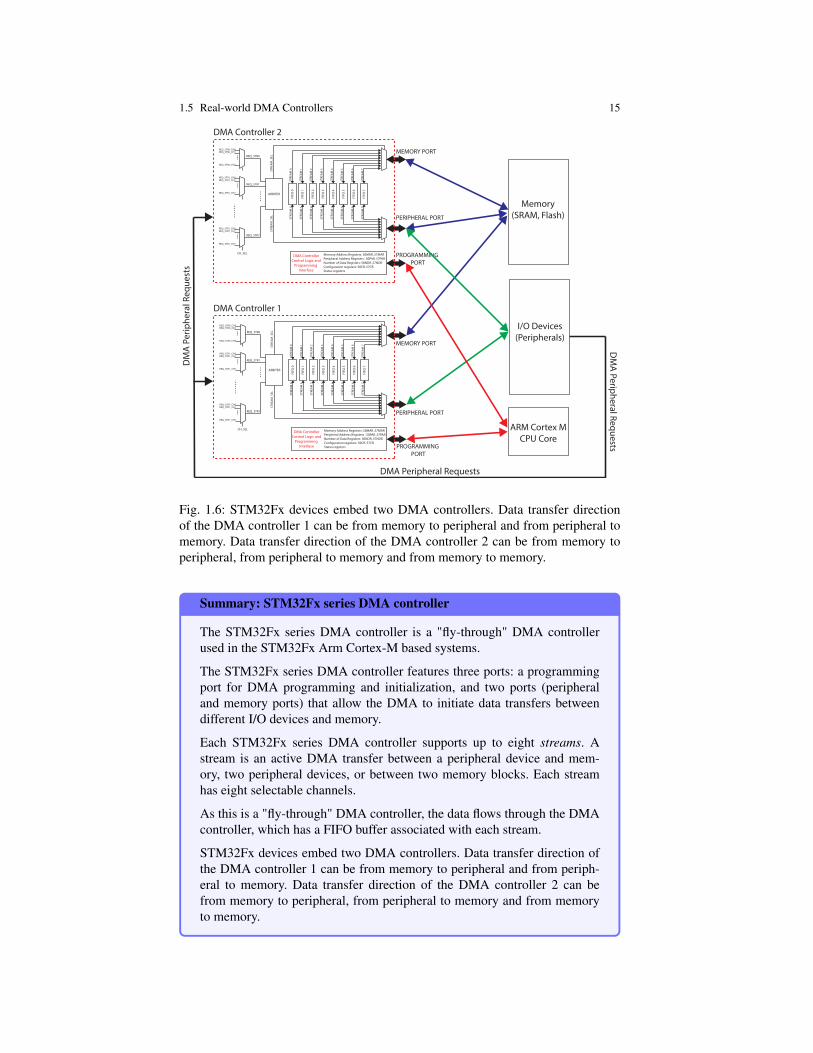
STM32Fx devices embed two DMA controllers (Figure 1.6), offering up to 16streams in total (eight per controller), each dedicated to managing memory accessrequests from one or more peripherals. Data transfer direction of both DMA con-trollers can be from peripheral to memory, from memory to peripheral and frommemory to memory (only the second DMA controller). The peripheral port of thesecond DMA controller can also be connected to memories in order to allow mem-ory to memory transfers. The DMA Contoller 1 peripheral port is not connected tothe bus like DMA controller 2. As a result, only DMA Controller 2 streams are ableto perform memory-to-memory transfers.
1.5 Real-world DMA Controllers 15
REQ_STR0_CH0REQ_STR0_CH1
REQ_STR0_CH7
REQ_STR1_CH0REQ_STR1_CH1
REQ_STR1_CH7
REQ_STR7_CH0REQ_STR7_CH1
REQ_STR7_CH7
REQ_STR0
REQ_STR1
REQ_STR7
ARBITER
FIFO
0
FIFO
1
FIFO
2
FIFO
3
FIFO
4
FIFO
5
FIFO
6
FIFO
7
DMA ControllerControl Logic and
Programming Interface
MEMORY PORT
PERIPHERAL PORT
PROGRAMMING PORT
CH_SEL
STRE
AM
_SEL
STRE
AM
_SEL
STRE
AM
0
STRE
AM
1
STRE
AM
2
STRE
AM
3
STRE
AM
4
STRE
AM
5
STRE
AM
6
STRE
AM
7
STRE
AM
0
STRE
AM
1
STRE
AM
2
STRE
AM
3
STRE
AM
4
STRE
AM
5
STRE
AM
6
STRE
AM
7
Memory Address Registers: S0MAR..S7MARPeripheral Address Registers : S0PAR..S7PARNumber of Data Registers: S0NDR..S7NDRCon�guration registers: S0CR..S7CRStatus registers
ARM Cortex MCPU Core
I/O Devices(Peripherals)
Memory(SRAM, Flash)
DMA Controller 1
DMA Controller 2
DMA Peripheral Requests
DM
A Peripheral Requests
DM
A P
erip
hera
l Req
uest
s
Fig. 1.6: STM32Fx devices embed two DMA controllers. Data transfer directionof the DMA controller 1 can be from memory to peripheral and from peripheral tomemory. Data transfer direction of the DMA controller 2 can be from memory toperipheral, from peripheral to memory and from memory to memory.
Summary: STM32Fx series DMA controller
The STM32Fx series DMA controller is a "fly-through" DMA controllerused in the STM32Fx Arm Cortex-M based systems.
The STM32Fx series DMA controller features three ports: a programmingport for DMA programming and initialization, and two ports (peripheraland memory ports) that allow the DMA to initiate data transfers betweendifferent I/O devices and memory.
Each STM32Fx series DMA controller supports up to eight streams. Astream is an active DMA transfer between a peripheral device and mem-ory, two peripheral devices, or between two memory blocks. Each streamhas eight selectable channels.
As this is a "fly-through" DMA controller, the data flows through the DMAcontroller, which has a FIFO buffer associated with each stream.
STM32Fx devices embed two DMA controllers. Data transfer direction ofthe DMA controller 1 can be from memory to peripheral and from periph-eral to memory. Data transfer direction of the DMA controller 2 can befrom memory to peripheral, from peripheral to memory and from memoryto memory.

16 1 Direct memory access
1.5.2.1 Peripheral and memory addresses
Each DMA transfer is defined by a source address and a destination address. Bothaddresses should be aligned to transfer size. The transfer size value defines the vol-ume of data to be transferred from source to destination. Each stream has a pairof registers to store these addresses: Peripheral Address Register (SxPAR - Streamx Peripheral Address Register) and Memory Address Register (SxMAR - Stream xMemory Address Register). Before each transfer, the CPU should initialize both reg-isters with the valid addresses. It is possible to configure the DMA to automaticallyincrement the source and/or destination address after each data transfer.
1.5.2.2 Transfer size, type and mode
Each DMA transfer is defined by the transfer size and the transfer mode. The trans-fer size is a value that defines the volume of data to be transferred from source todestination. This value is stored in the so-called Number of Data Register (NDR).Each stream has its Number of Data Register, labeled as SxNDTR. Each SxNDTRis a 16-bit register, and the number of data items to be transferred is software pro-grammable from 1 to 65535. After each transfer, the value in SxNDTR is decreasedby the amount of the transferred data; thus, SxNDTR contains the number of datatransfers still to be performed.
The STM32Fx series DMA controller can perform two transfer types: normaltype and circular type. In normal type, once the SxNDTR register reaches zero (thetransfer has completed), the stream is disabled. This means that the CPU shouldreinitialize the DMA controller in order to activate the stream again. In circulartype, the DMA controller can handle circular buffers and continuous data flow. Inthis type, the SxNDTR register is reloaded automatically with the previously pro-grammed value when a transfer has completed.
Each STM32Fx series DMA controller is capable of performing three differenttransfer modes:
1. peripheral to memory,2. memory to peripheral,3. memory to memory (only the second DMA controller is able to do such transfer;
in this mode, the circular type is not allowed).
1.5.2.3 FIFOs and burst transfers
Each stream has a 4x32 bits FIFO that is used to temporarily store data comingfrom the source before transmitting them to the destination. The DMA FIFOs helpto reduce memory access and to do burst transactions which optimize the trans-fer bandwidth. They also allow independent source and destination transfer width(byte, half-word, word): when the data widths of the source and destination are notequal, the DMA automatically packs/unpacks the necessary transfers to optimize

1.5 Real-world DMA Controllers 17
the bandwidth. For example, the data from the source can be transferred into FIFOas bytes or 16-bit half-words and then transferred to the destination from FIFO asbytes, 16-bit half-words, or 32-bit words.
Because of the internal FIFOs, the DMA controller is capable of burst transfersof length 4x, 8x, or 16x data units. A data unit can be a byte, a 16-bit half-word, or a32-bit word. The burst size on the DMA peripheral port must be set according to theperipheral needs/capabilities. The size of the burst is software-configurable, usuallyequal to half the FIFO size of the peripheral.
1.5.2.4 Programming and using the STM32Fx series DMA controller
Programming and using the STM32Fx series DMA controller is relatively easy.Each stream is controlled using four memory-mapped registers: memory addressregister (SxMAR), peripheral address register (SxPAR), number of data register(SxNDTR), and configuration register (SxCR). Once set, the DMA controller takescare of data transfers and memory address increment without disturbing CPU. Toconfigure the DMA controller and a DMA stream, the following procedure shouldbe applied:
1. If the stream is enabled, disable it by resetting stream enable bit in the SxCRregister.
2. Set the peripheral port register address in the SxPAR register. The data willbe moved from/to this address to/from the peripheral port after the peripheralDMA request.
3. Set the memory address in the SxMAR register. The data will be written to orread from this memory after the peripheral DMA request.
4. Configure the total number of data items to be transferred in the SxNDTR reg-ister. After each (burst) transfer, this value is decremented accordingly.
5. Select the DMA channel (request) and configure the stream priority, the datatransfer direction, single or burst transactions, peripheral and memory datawidths, circular/normal type, interrupts in the SxCR register.
6. Activate the stream by setting the stream enable bit in the SxCR register.
As soon as the stream is enabled, it can serve any DMA request from the peripheralconnected to the stream and DMA transactions using the stream can be performed.
1.5.2.5 DMA Transactions
After a peripheral is ready for DMA transfer, the peripheral sends a request signalto the DMA controller. The DMA controller serves the request depending on thechannel priorities. A DMA transaction consists of a sequence of a given number ofdata transfers. The number of data items to be transferred and their width (8-bit,16-bit, or 32-bit) are software programmable. Each DMA transfer consists of threeoperations:
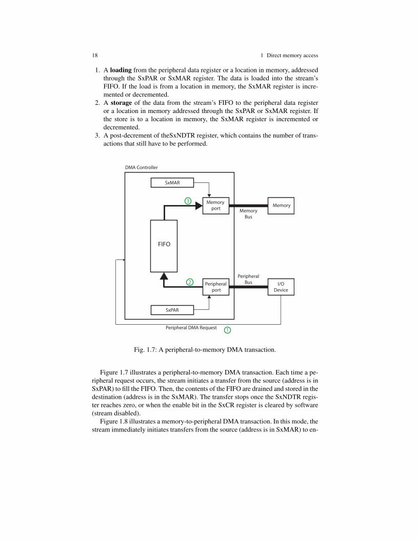
18 1 Direct memory access
1. A loading from the peripheral data register or a location in memory, addressedthrough the SxPAR or SxMAR register. The data is loaded into the stream’sFIFO. If the load is from a location in memory, the SxMAR register is incre-mented or decremented.
2. A storage of the data from the stream’s FIFO to the peripheral data registeror a location in memory addressed through the SxPAR or SxMAR register. Ifthe store is to a location in memory, the SxMAR register is incremented ordecremented.
3. A post-decrement of theSxNDTR register, which contains the number of trans-actions that still have to be performed.
Memory port
Peripheral port
SxMAR
SxPAR
FIFO
Memory
I/ODevice
MemoryBus
PeripheralBus
DMA Controller
Peripheral DMA Request
2
3
1
Fig. 1.7: A peripheral-to-memory DMA transaction.
Figure 1.7 illustrates a peripheral-to-memory DMA transaction. Each time a pe-ripheral request occurs, the stream initiates a transfer from the source (address is inSxPAR) to fill the FIFO. Then, the contents of the FIFO are drained and stored in thedestination (address is in the SxMAR). The transfer stops once the SxNDTR regis-ter reaches zero, or when the enable bit in the SxCR register is cleared by software(stream disabled).
Figure 1.8 illustrates a memory-to-peripheral DMA transaction. In this mode, thestream immediately initiates transfers from the source (address is in SxMAR) to en-

1.5 Real-world DMA Controllers 19
Memory port
Peripheral port
SxMAR
SxPAR
FIFO
Memory
I/ODevice
MemoryBus
PeripheralBus
DMA Controller
Peripheral DMA Request
4
2
3
1
Fig. 1.8: A memory-to-peripheral DMA transaction. In this mode, the stream imme-diately initiates transfers from the memory to entirely fill the FIFO. When a periph-eral request occurs, the contents of the FIFO are stored in the peripheral device.
tirely fill the FIFO, and the SxMAR register is incremented/decremented. The DMAcontroller does not wait for DMA request from a peripheral device to read frommemory. When a peripheral request occurs, the contents of the FIFO are drained andstored in the destination (address is in the SxPAR). The DMA controller then reloadsthe empty internal FIFO again with the next data to be transferred from memory (ad-dress is in SxMAR). The transfer stops once the SxNDTR register reaches zero, orwhen the enable bit in the SxCR register is cleared by software (stream disabled).

20 1 Direct memory access
Summary: STM32Fx series DMA transfers
Each DMA transfer is defined by a source address and a destination address,and each stream has a pair of registers to store these addresses: PeripheralAddress Register (SxPAR -Streamx Peripheral Address Register) and Mem-ory Address Register (SxMAR -Stream x Memory Address Register)
Each DMA transfer is defined by the transfer size and the transfer mode.Each stream has its Number of Data Register (SxNDR), which stores thetransfer size.
The STM32Fx series DMA controller can perform two transfer types: nor-mal type and circular type.
FIFOs allow independent source and destination transfer width and bursttransfers.
Each DMA transfer consists of two transactions on the bus: loading fromthe peripheral data register or a location in memory, and storage of the datato the peripheral data register or a location in memory.
1.6 Bus Mastering DMA
So far, we have learned that we can use a special piece of hardware, a DMA con-troller, namely, to transfer large amounts of data between a peripheral device andmemory. This approach is sometimes referred to as third-party DMA. Third-partyDMA requires an independent DMA controller, which is built into motherboardchipsets, to move data between a peripheral device (referred to as the first party) andsystem RAM (referred to as the second party). Here, the DMA controller is sharedby multiple peripheral devices, which is why it is viewed as the third party DMA.As we have learned previously, each "fly-through" DMA transfer (fly-through is thetype of the DMA used in the majority of today’s computer systems) requires twomemory transactions: one to load the data from the source, and one to store the datato the destination.
The better approach to DMA transfers would be to have only one memory trans-action per DMA transfer, but still avoiding third-party "fly-by" DMA controllers.This is possible with the latest I/O devices built in the modern computer systems,where each I/O device can act as a bus master, i.e., each device can directly ac-cess any other I/O device or memory on the bus. Indeed, each modern I/O devicenow contains its own, integrated, DMA controller, which is not shared by other I/Odevices. This highest performing DMA type is called first-party DMA or Bus Mas-tering DMA. Peripheral devices, which support the Bus Mastering technology, havethe ability to move data to and from system memory without the intervention of theCPU or a third party DMA controller.

1.6 Bus Mastering DMA 21
Bus Mastering allows data to be transferred much faster than third party DMA.This is because half as many bus cycles are needed. The third-party DMA requiresthe DMA controller to alternately read a segment of data from one device (this canbe a peripheral device or system memory) and write it to the other device. Each datasegment requires at least one bus cycle to be read and one bus cycle to be written.Bus mastering devices only require bus cycles when accessing system memory, sohalf as many bus cycles are needed. Because of this, devices that support Bus Mas-tering can move data many times faster than third party DMA. While bus masteringtheoretically allows one peripheral device to directly communicate with another, inpractice almost all peripherals master the bus exclusively to perform peripheral-to-memory and memory-to-peripheral transfers.
PCIe endpoint(e.g. a GPU card)
Intel Core i7
Memory Controler Hub
PCIe Root Complex
MAIN MEMORY
DMA Controller
Bus MasteringDMA
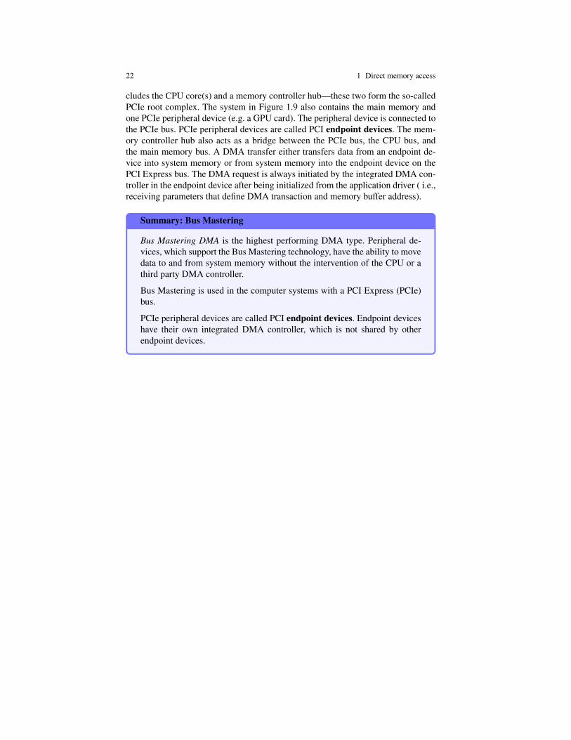
Fig. 1.9: Bus Maserting in an Intel based system. Bus Mastering is the feature in-tegrated into PCIe endpoint devices. A DMA transfer either transfers data from anendpoint device into system memory or from system memory into the endpoint de-vice on the PCI Express bus. The DMA request is always initiated by the integratedDMA controller in the endpoint device after being initialized from the applicationdriver ( i.e., receiving parameters that define DMA transaction and memory bufferaddress).
Bus Mastering is used in the computer systems with a PCI Express (PCIe) bus.A Bus Mastering DMA implementation is by far the most common type of DMAfound in systems based on PCI Express and resides within the peripheral device,which is called Bus Master because it initiates the movement of data to and fromsystem memory. Figure 1.9 shows a typical Intel system architecture. The system in-
22 1 Direct memory access
cludes the CPU core(s) and a memory controller hub—these two form the so-calledPCIe root complex. The system in Figure 1.9 also contains the main memory andone PCIe peripheral device (e.g. a GPU card). The peripheral device is connected tothe PCIe bus. PCIe peripheral devices are called PCI endpoint devices. The mem-ory controller hub also acts as a bridge between the PCIe bus, the CPU bus, andthe main memory bus. A DMA transfer either transfers data from an endpoint de-vice into system memory or from system memory into the endpoint device on thePCI Express bus. The DMA request is always initiated by the integrated DMA con-troller in the endpoint device after being initialized from the application driver ( i.e.,receiving parameters that define DMA transaction and memory buffer address).
Summary: Bus Mastering
Bus Mastering DMA is the highest performing DMA type. Peripheral de-vices, which support the Bus Mastering technology, have the ability to movedata to and from system memory without the intervention of the CPU or athird party DMA controller.
Bus Mastering is used in the computer systems with a PCI Express (PCIe)bus.
PCIe peripheral devices are called PCI endpoint devices. Endpoint deviceshave their own integrated DMA controller, which is not shared by otherendpoint devices.

References
23