b) Arithmetic micro-operation with overflow detection.
9
Computer Architecture: Central Processing Unit BY: Dr. Basim J. & L. Sundos Alazawi. 46 b) Arithmetic micro-operation with overflow detection. 1. Unsigned Binary Addition overflow When the "Binary Addition Algorithm" is used with unsigned binary integer representation: The result is CORRECT only if the CARRY OUT of the high order column is ZERO. Unsigned overflow occurred when carry out =1; For example: 1 1101 0010 210 10 0110 1101 109 10 0011 1111 63 10 The carry bit of 1 indicates overflow. 2. Signed Binary Addition overflow There are many schemes for representing negative integers with patterns of bits. Two's complement is one of many ways to represent negative integers with bit patterns. With two's complement representation the result of addition is correct if the carry into the high order column is the same as the carry out of the high order column. Overflow is detected by comparing these two bits. Here are some more examples: No Overflow No Overflow Overflow Overflow 11111 111 0011 1111 ( 63 10 ) 1101 0101 (-43 10 ) 0001 0100 ( 20 10 ) 00000 011 1100 0001 ( -63 10 ) 0010 1011 ( 43 10 ) 1110 1100 ( -20 10 ) 01111 100 0011 1111 ( 63 10 ) 0110 0100 ( 100 10 ) 1010 0011 ( -93 10 ) 10000 000 1100 0001 ( -63 10 ) 1001 1100 (-100 10 ) 0101 1101 ( 93 10 )
-
Upload
khangminh22 -
Category
Documents
-
view
0 -
download
0
Transcript of b) Arithmetic micro-operation with overflow detection.

Computer Architecture: Central Processing Unit BY: Dr. Basim J. & L. Sundos Alazawi.
46
b) Arithmetic micro-operation with overflow detection.
1. Unsigned Binary Addition overflow
When the "Binary Addition Algorithm" is used with unsigned binary
integer representation: The result is CORRECT only if the CARRY
OUT of the high order column is ZERO. Unsigned overflow occurred
when carry out =1; For example:
1
1101 0010 21010
0110 1101 10910
0011 1111 6310 The carry bit of 1 indicates overflow.
2. Signed Binary Addition overflow
There are many schemes for representing negative integers with patterns of
bits. Two's complement is one of many ways to represent negative integers
with bit patterns. With two's complement representation the result of
addition is correct if the carry into the high order column is the same as
the carry out of the high order column. Overflow is detected by
comparing these two bits. Here are some more examples:
No Overflow No Overflow Overflow Overflow
11111 111
0011 1111 ( 6310)
1101 0101 (-4310)
0001 0100 ( 2010)
00000 011
1100 0001 ( -6310)
0010 1011 ( 4310)
1110 1100 ( -2010)
01111 100
0011 1111 ( 6310)
0110 0100 ( 10010)
1010 0011 ( -9310)
10000 000
1100 0001 ( -6310)
1001 1100 (-10010)
0101 1101 ( 9310)

Computer Architecture: Central Processing Unit BY: Dr. Basim J. & L. Sundos Alazawi.
47
The truth table of tow's sign bits ( Asign and Bsign bit) is shown below:
INPUTS OUTPUTS
Asign Bsign CARRY IN CARRY OUT SUMsign OVERFLOW
0 0 0 0 0 0
0 0 1 0 1 1
0 1 0 0 1 0
0 1 1 1 0 0
1 0 0 0 1 0
1 0 1 1 0 0
1 1 0 1 0 1
1 1 1 1 1 0
From the above truth table:
Notice that overflow occurs only when: CARRYin ≠ CARRYout
or simply: V = Cin XOR Cout ; where V is the overflow signal.
So that, the Arithmetic micro-operation with overflow detection can be design as:
t1X: ER1 R1+R2
t1X: ER1 R1+R2+1

Computer Architecture: Central Processing Unit BY: Dr. Basim J. & L. Sundos Alazawi.
48
Each of the arithmetic micro operations can be implemented in one composite
arithmetic circuit. This circuit comprised of:
Parallel full adders and
Multiplexers are used to choose between the different operations.
The multiplexer controls which data is fed into input of the adder (suppose B, A
represent that inputs). The output of the binary adder is computed from
D = A + B +Cin
The B input can have one of 4 different values: B, ̅ , always “1”, or always “0”
Figure (7); below represent 4-bit arithmetic circuit.
S1 S2 Cin Input B D =A+B+Cin Operation
0 0 0 B A+B ADD
0 0 1 B A+B+1 ADD with carry
0 1 0 ̅ A+ ̅ Sub with borrow (1's comp)
0 1 1 ̅ A+ ̅+1 Sub in 2's comp.
1 0 0 0 A Transfer
1 0 1 0 A+1 Increment
1 1 0 1 A-1 Decrement
1 1 1 1 A Transfer

Computer Architecture: Central Processing Unit BY: Dr. Basim J. & L. Sundos Alazawi.
49
Figure 5 : 4-bit arithmetic circuit
3.3.2.3 Logical Microoperation
Logic micro operation specifies binary operations on the strings of bits in
registers. Logic micro operations are bit-wise operations, i.e., they work on the
individual bits of data. These are useful for bit manipulations on binary data and also
useful for making logical decisions based on the bit value. There are many different

Computer Architecture: Central Processing Unit BY: Dr. Basim J. & L. Sundos Alazawi.
50
logic functions that can be defined over two binary input variables. However, most
systems only implement four of these: AND, OR, XOR, Complement/NOT.
The others can be created from combination of these. The hardware implementation of
logic micro operation requires the insertion of the most important gates like AND,
OR, EXOR, and NOT for each bit or pair of bits in the registers.
Build a logical circuit to generate the four basic logic micro operations required:
four gates (AND, OR, XOR, NOT) and
a multiplexer.
The two selection lines of the multiplexer selects one of the four logic operations
available at one time. The circuit shows one stage for bit “i” but for logic circuit of n
bits the circuit should be repeated n times but with one remark; the selection pins will
be shared with all stages.
Figure 6 Simple Logic circuit
Computer Architecture: Central Processing Unit BY: Dr. Basim J. & L. Sundos Alazawi.
51
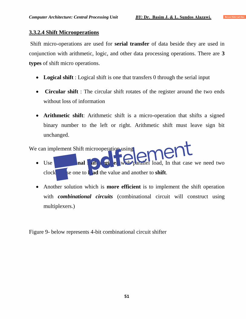
3.3.2.4 Shift Microoperations
Shift micro-operations are used for serial transfer of data beside they are used in
conjunction with arithmetic, logic, and other data processing operations. There are 3
types of shift micro operations.
Logical shift : Logical shift is one that transfers 0 through the serial input
Circular shift : The circular shift rotates of the register around the two ends
without loss of information
Arithmetic shift: Arithmetic shift is a micro-operation that shifts a signed
binary number to the left or right. Arithmetic shift must leave sign bit
unchanged.
We can implement Shift microoperation using:
Use bidirectional shift register with parallel load, In that case we need two
clocks pulse one to load the value and another to shift.
Another solution which is more efficient is to implement the shift operation
with combinational circuits (combinational circuit will construct using
multiplexers.)
Figure 9- below represents 4-bit combinational circuit shifter

Computer Architecture: Central Processing Unit BY: Dr. Basim J. & L. Sundos Alazawi.
52
Figure 7: 4-bit combinational circuit shifter
3.3.3 Arithmetic Logic Shift Unit
Instead of having individual registers performing micro-operations directly, computer
systems employ a number of storage registers connected to a unit called Arithmetic
Logic Unit (ALU). This unit has 2 operands input ports and one output port and a
number of select lines to help in selecting different operations. The ALU is made of
combinational circuit so that the entire register transfer operation from the sources to
the destination is performed in one clock cycle. The arithmetic, logic, and shift

Computer Architecture: Central Processing Unit BY: Dr. Basim J. & L. Sundos Alazawi.
53
circuits (implemented previously) will be combined in one ALU with common
selection inputs. Simple stage (bit) of ALU with its table is shown blow (figure 10).
The arithmetic and logic units will select their operations simultaneously when S0 and
S1 are applied; while S2 and S3 will select one of those unit outputs or a shift left bit
stage or shift right bit stage. The circuit shown provides 8 arithmetic operations, 4
logic operations, and 2 shift operations.
One stage of logic circuit (Fig.9)
Figure 8 simple Arithmetic and logic unit
One stage of
arithmetic circuit (Fig.8)
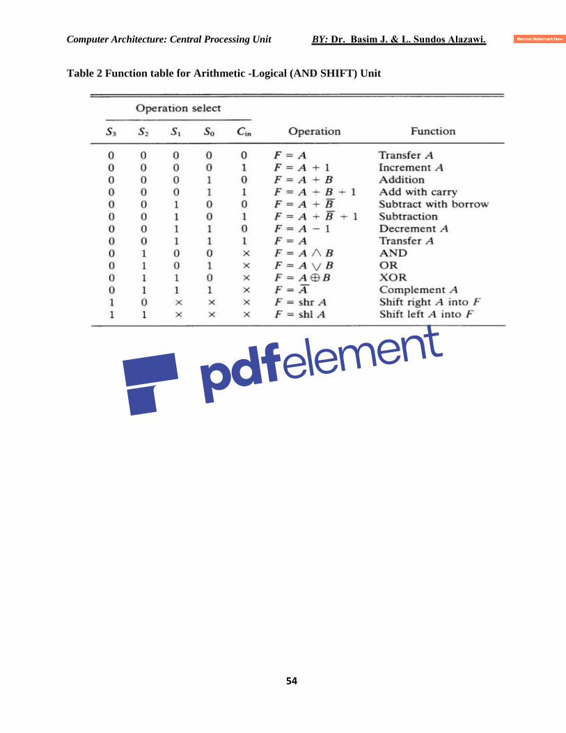
Computer Architecture: Central Processing Unit BY: Dr. Basim J. & L. Sundos Alazawi.
54
Table 2 Function table for Arithmetic -Logical (AND SHIFT) Unit