Prezzi Unitari Dispositivi Medici 1° semestre 2016 - ASST Garda
Upload
khangminh22Category
view
4download
0
1
Asst. Lec. Hussien
Y. Radhi Lecture one:
Counters
Counters
The flip-flops are the main logic element, which are used to build
these circuits since flip-flops have the ability of saving information (the
previous outputs effect on the present output). Flip-flops are connected
to each other in a certain way to obtain the counters. The number of
flip-flops used and the way in which they are connected determine the
number of states (called modulus) and the specific sequence of states
that the counter goes through during each complete cycle. So a binary
mod-8 counter has eight count states, from 0002 to 1112 (e.g. the mod-8
counter actually counts from 0 to 7). Counters are mainly used in
counting applications, where they either measure the time interval
between two unknown time instants or measure the frequency of a
given signal. Counters are divided in to two categories which are
asynchronous and synchronous counters.
1- Asynchronous Counters
Asynchronous counter is a cascaded arrangement of flip-flops where
the output of one flip-flop drives the clock input of the following flip-
flop. The number of flip-flops in the cascaded arrangement depends
upon the number of different logic states that it goes through before it
repeats the sequence, a parameter known as the modulus of the
counter. In an asynchronous, also called a ripple counter or a serial
counter, the clock input is applied only to the first flip-flop in the
cascaded arrangement. The clock input to any subsequent flip-flop
comes from the output of its immediately preceding flip-flop. For
instance, the output of the first flip-flop acts as the clock input to the

2
Asst. Lec. Hussien
Y. Radhi Lecture one:
Counters
second flip-flop, the output of the second flip-flop feeds the clock input
of the third flip-flop and so on. These counters are used to design the
up-counters, down-counters. Asynchronous counters has the following
properties:
1- are also known as ripple counters;
2- are very simple;
3- use the minimum possible hardware (logic gates);
4- employ flip-flops connected serially, with each one triggering
(clocking) the next;
5- have an overall count which 'ripples' through, meaning the overall
operation is relatively slow;
Propagation Delay in Ripple Counters
A major problem with ripple counters arises from the propagation
delay of the flip-flops constituting the counter. An increased propagation
delay puts a limit on the maximum frequency used as clock input to the
counter. We can appreciate that the clock signal time period must be
equal to or greater than the total propagation delay. The maximum clock
frequency therefore corresponds to a time period that equals the total
propagation delay. If tpd is the propagation delay in each flip-flop, then, in
a counter with N flip-flops having a modulus of less than or equal to 2N,
the maximum usable clock frequency is given by fmax = 1/(N × tpd).
Often, two propagation delay times are specified in the case of flip-flops,
one for LOW-to-HIGH transition (tPLH_ and the other for HIGH-to-
LOW transition (tPHL)at the output. In such a case, the larger of the two
should be considered for computing the maximum clock frequency. As

3
Asst. Lec. Hussien
Y. Radhi Lecture one:
Counters
an example, in the case of a ripple counter IC belonging to the low-
power Schottky TTL (LSTTL) family, the propagation delay per flip-flop
typically is of the order of 25 ns. This implies that a four-bit counters and
from this logic family cannot be clocked faster than 10 MHz. The upper
limit on the clock frequency further decreases with increase in the
number of bits to be handled by the counter.
To make these counters do as sequential circuits then the flip-flops mast
be in a toggle case, for example D flip-flop can be in a toggle case as
shown in figure (1):
For T flip-flop, the toggle operation can be achieved easily by entered
logic 1 to the input of T flip-flop as illustrated in figure (2) and for J-K flip-
flop; the same modification can be used as shown in figure (3).
Fig 1 Toggle D flip-flop
1
CLK
D
𝐐
Q
1
Fig 2 Toggle T flip-flop
CLK
T
𝐐
Q
4
Asst. Lec. Hussien
Y. Radhi Lecture one:
Counters
The design steps of sequential counters are:
Number of flip-flops is equal to the largest bits of the required
state.
All flip-flops must be in a toggle case.
For up-counters, the ̅̅̅output of the first flip-flop is used as a
clock pulse for the second flip and so on, when the flip-flops
respond to the positive edge of the clock pulse.
For down-counters, , the output of the first flip-flop is used as a
clock pulse for the second flip and so on, when the flip-flops
respond to the positive edge of the clock pulse.
The third and four steps are opposite, when the flip-flops respond
to the negative edge of the clock pulse.
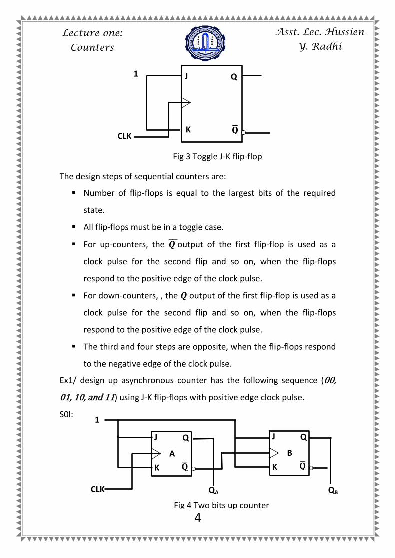
Ex1/ design up asynchronous counter has the following sequence (00,
01, 10, and 11) using J-K flip-flops with positive edge clock pulse.
S0l:
1
K
Fig 3 Toggle J-K flip-flop
CLK
J
𝐐
Q
1
QB CLK
K
J
𝐐
Q
A
QA
K
J
𝐐
Q
B
Fig 4 Two bits up counter

5
Asst. Lec. Hussien
Y. Radhi Lecture one:
Counters
Ex2/for the circuit shown in figure (4), draw the timing diagram and
truth table.
Sol:
HW1: design (3-bits) up counter using J-K flip-flops with negative edge
clock pulse.
Ex3/ design (3-bits) down counter using J-K flip-flops with positive edge
clock pulse.
S0l:
B A Output
0 0 0
0 1 1
1 0 2
1 1 3
QA 0 1 0 1
𝐐 A
1 0 1 0 QB
CLK
Fig 5 Three bits down counter
1
QB QA
K
J
𝐐
Q
B
K
J
𝐐
Q
B
QC CLK
K
J
𝐐
Q
A

6
Asst. Lec. Hussien
Y. Radhi Lecture one:
Counters
Ex4/ draw the timing diagram and truth table of the counter shown in
figure (5).
Sol:
Ex5/ design a (3-bits) down counter using T flip-flops with negative edge
clock pulse, draw the timing diagram and truth table for this counter.
Sol:
C B A Output
1 1 1 7
1 1 0 6
1 0 1 5
1 0 0 4
0 1 1 3
0 1 0 2
0 0 1 1
0 0 0 0
QA
QB
CLK
0
QC
1 0 1 0 1 0 1 0
0 1 1 0 1 0 1
1 0 1 0 1 0 1 0

7
Asst. Lec. Hussien
Y. Radhi Lecture one:
Counters
C B A Output
0 0 0 0
1 1 1 7
1 1 0 6
1 0 1 5
1 0 0 4
0 1 1 3
0 1 0 2
0 0 1 1
0 0 0 0
1 0 1 QA
𝐐B
QC
CLK
0 0 1 0 1
0 0 0 0 1 1 1 1
1 0 1 0 0 0 1 1
Fig 6 (3-bits) T down counter
1
CLK
T
𝐐
Q T
𝐐
Q T
𝐐
Q
QA QB QC

8
Asst. Lec. Hussien
Y. Radhi Lecture one:
Counters
HW2: design a (3-bits) up counter using T flip-flops with negative edge
clock pulse, draw the timing diagram and truth table for this counter.
HW3: design a (4-bits) up counter using D flip-flops with negative edge
clock pulse, draw the timing diagram and truth table for this counter.
HW4: design a (2-bits) down counter using D flip-flops with negative
edge clock pulse, draw the timing diagram and truth table for this
counter.
Important Note: to design up-down counter at the same time, enable
element can be used with the circuit shown in figure (7).
Ex6/ design (4-bits) up-down counter using J-K flip-flops with positive
edge clock pulse.
Sol:
Fig 7 up-down counter enable circuit
Enable o/p
𝐐
Q
Fig 8 Three bits up-down counter
K
J
𝐐
Q
B
1
QB QA
K
J
𝐐
Q
B
QC
Enable
CLK
K
J
𝐐
Q
A

9
Asst. Lec. Hussien
Y. Radhi Lecture one:
Counters
Maximum Count (N)
The maximum count of the counter is related to the number of (flip-
flops) that build the counter which can be expressed as:
N = 2n – 1
For example for four flip-flops, the maximum count is N = 24 – 1 =15
which equivalents to (1111) in binary system.
Modulus Counters
This type of counters is used when the application needs certain
count such as to (1001). These counters are build by controlling the
clear element of the flip-flops thus when reach the required count clear
all flip-flops of the counter.
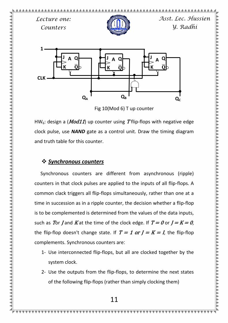
Ex7/ design (Mod 5) up counter using T flip-flops using AND gate as
control element.
Sol:
The truth table of this counter is
C B A COUNT
0 0 0 0
0 0 1 1
0 1 0 2
0 1 1 3
1 0 0 4
0 0 0 0

11
Asst. Lec. Hussien
Y. Radhi Lecture one:
Counters
HW5: design a (Mod8) up counter using D flip-flops with negative edge
clock pulse, use AND gate as a control unit. Draw the timing diagram and
truth table for this counter.
Ex8/ design Mod (6) (JK) up counter using NAND gate as a control
element.
Sol:
the truth table of this counter is
C B A COUNT
0 0 0 0
0 0 1 1
0 1 0 2
0 1 1 3
1 0 0 4
1 0 1 5
0 0 0 0
Fig 9 (Mod 5) T up counter
CLK
1
T
𝐐
Q
QA QB QC
T
𝐐
Q T
𝐐
Q
11
Asst. Lec. Hussien
Y. Radhi Lecture one:
Counters
HW6: design a (Mod11) up counter using T flip-flops with negative edge
clock pulse, use NAND gate as a control unit. Draw the timing diagram
and truth table for this counter.
Synchronous counters
Synchronous counters are different from asynchronous (ripple)
counters in that clock pulses are applied to the inputs of all flip-flops. A
common clack triggers all flip-flops simultaneously, rather than one at a
time in succession as in a ripple counter, the decision whether a flip-flop
is to be complemented is determined from the values of the data inputs,
such as Tor J and K at the time of the clock edge. If T = 0 or J = K = 0,
the flip-flop doesn't change state. If T = 1 or J = K = I, the flip-flop
complements. Synchronous counters are:
1- Use interconnected flip-flops, but all are clocked together by the
system clock.
2- Use the outputs from the flip-flops, to determine the next states
of the following flip-flops (rather than simply clocking them)
J
K
A
𝐐
Q J
K
A
𝐐
Q J
K
A
𝐐
Q
QA QC QB
CLK
1
Fig 10(Mod 6) T up counter

12
Asst. Lec. Hussien
Y. Radhi Lecture one:
Counters
3- Require no settling time due to rippling (as all flip-flops are
clocked synchronously)
4- Need designing, to determine how the present state of the circuit
must be used to determine the next state (i.e. count)
5- Usually need more logic gates for their implementation.
To design the synchronous counters the following steps must be
applied:
Find the number of flip-flops that used in the design of the
counter which can be found from the following equation
N = 2n, where N is the maximum count and n represent the number
of flip-flops.
Draw the excitation table for the flip-flop that used in the
design of this counter.
Find the equations of the flip-flops inputs depending on the
required counts and excitation table using K-Maps.
Draw the state diagram.
Finally draw the logic circuit of the counter.
Ex9/ design (3bits) synchronous up counter using (SR flip-flops)
Sol: the excitation table of SR flip-flop is
Qt Qt+1 S R
0 0 0 X
0 1 1 0
1 0 0 1
1 1 X 0
To find the equations of SR of each flip-flop the following table
must be used.

13
Asst. Lec. Hussien
Y. Radhi Lecture one:
Counters
C B A SA RA SB RB SC RC
0 0 0 1 0 0 X 0 X
0 0 1 0 1 1 0 0 X
0 1 0 1 0 X 0 0 X
0 1 1 0 1 0 1 1 0
1 0 0 1 0 0 X X 0
1 0 1 0 1 1 0 X 0
1 1 0 1 0 X 0 X 0
1 1 1 0 1 0 1 0 1
From the previous table, it is clear that SA = & RA=A. To find
other inputs, K-Maps can be used as follow:
The state diagram of this sequence is
SB = A𝐁
CB �̅�𝐁 �̅�B
A 𝐀
A
0
1
0
0 1 0
X X
𝐂𝐁 C𝐁 CB
�̅�𝐁 �̅�B A 𝐀
A
X
0
X
1 0 1
0 0
𝐂𝐁 C𝐁
RB = A𝐁
CB �̅�𝐁 �̅�B
A 𝐀
A
0
X
X
1 0 0
0 X
𝐂𝐁 C𝐁 CB
�̅�𝐁 �̅�B A 𝐀
A
X
0
0
0 X 1
X 0
𝐂𝐁 C𝐁
SC = A�̅�B RC = AC𝐁

14
Asst. Lec. Hussien
Y. Radhi Lecture one:
Counters
HW7: design a synchronous (4bits) down counter using D flip-flops with
negative edge clock pulse.
HW8: design (2bits) up-down counter using JK flip-flops with positive
edge clock pulse.
HW9: using T flip-flops to design (3bits) down counter with negative
edge clock pulse.
Ex 10 / design (3bits) counter, that counts only even numbers, using T
flip-flops with negative edge clock pulse.
Sol: the excitation table of T flip-flop is
R
S
𝐐
Q A
R
S
𝐐
Q B
R
S
𝐐
Q C
CLK
C B A
000
001
011
010
111
110
100
101
Fig 11 3bits SR synchronous up counter using

15
Asst. Lec. Hussien
Y. Radhi Lecture one:
Counters
Now T inputs of each flip-flop can be found from the following table
From above T.T, TA = 0 & TB = 1
Qt Qt+1 T
0 0 0
0 1 1
1 0 1
1 1 0
C B A TA TB TC
0 0 0 0 1 0
0 1 0 0 1 1
1 0 0 0 1 0
1 1 0 0 1 1
CB �̅�𝐁 �̅�B
A 𝐀
A
0
X
0
X X X
1 1
𝐂𝐁 C𝐁
TC = B
000
0
010
0
110
0
100
0

16
Asst. Lec. Hussien
Y. Radhi Lecture one:
Counters
HW10: design (3bits) counter that counts only odd numbers, using D flip-
flops with positive edge clock pulse.
HW11: design (4bits) counter that counts only primary numbers, using JK
flip-flops with positive edge clock pulse.
Ex11/ design a counter that have the following counts (0, 2, 6, 9, 7, and
3) using D flip-flops with negative edge clock pulse.
Sol: the excitation table of D flip-flop is
Qt Qt+1 D
0 0 0
0 1 1
1 0 0
1 1 1
A B C
T
𝐐
Q T
𝐐
Q T
𝐐
Q
QA QB QC
1 0
CLK
Fig 14 3bits T that counts only even numbers

17
Asst. Lec. Hussien
Y. Radhi Lecture one:
Counters
D C B A DA DB DC DD
0 0 0 0 0 1 0 0
0 0 1 0 0 1 1 0
0 1 1 0 1 0 0 1
1 0 0 1 1 1 1 0
0 1 1 1 1 1 0 0
0 0 1 1 0 0 0 0
DC
DC D�̅�
𝐁 𝐀
𝐁 𝐀
BA
B𝐀
BA
1
X
X
X 1
1
X X
𝐃 �̅�
𝐃 C
0
X
X
0
X
X X
0
DC
DC D�̅�
𝐁 𝐀
𝐁 𝐀
BA
B𝐀
BA
1
X
X
X 0
0
X X
𝐃 �̅�
𝐃 C
0
X
X
0
X
X X
0
DC
DC D�̅�
𝐁 𝐀
𝐁 𝐀
BA
B𝐀
BA
0
X
X
X 1
0
X X
𝐃 �̅�
𝐃 C
0
X
X
1
X
X X
0
DC
DC D�̅�
𝐁 𝐀
𝐁 𝐀
BA
B𝐀
BA
0
X
X
X 1
1
X X
𝐃 �̅�
𝐃 C
1
X
X
1
X
X X
0
DA=D+C DB=D+AC+𝐀 �̅�
DC=D+B𝐀 �̅� DD=𝐀 C
000
00
0010
0
001
1
011
0
011
1
1001

18
Asst. Lec. Hussien
Y. Radhi Lecture one:
Counters
HW12: design a (JK) synchronous counter that has the counts (0, 5, 4, and
7) with positive edge clock pulse.
HW13: design (T) synchronous counter that has the counts (5, 10, 12, 0,
1, and 6).
Shift Register Counters
We have seen that both counters and shift registers are some kinds of
cascade arrangement of flip-flops. A shift register, unlike a counter, has
no specified sequence of states. However, if the serial output of the shift
register is fed back to the serial input, we do get a circuit that exhibits a
specified sequence of states. The resulting circuits are known as shift
register counters. Depending upon the nature of the feedback, we have
two types of shift register counter, namely the ring counter and the shift
counter, also called the Johnson counter. These are briefly described in
the following paragraphs.
C D
𝐐
Q D
D
𝐐
Q A
D
𝐐
Q B
D
𝐐
Q
QD
CLK
QA QB QC
Fig.15 (0, 2, 6, 9, 7, 3 D counter

19
Asst. Lec. Hussien
Y. Radhi Lecture one:
Counters
1- Ring Counter A ring counter is obtained from a shift register by directly feeding
back the true output of the output flip-flop to the data input terminal of
the input flip-flop. If D flip-flops are being used to construct the shift
register, the ring counter, also called a circulating register, can be
constructed by feeding back the Q output of the output flip-flop back to
the D input of the input flip-flop. If JK flip-flops are being used, the Q and
Q outputs of the output flip-flop are respectively fed back to the J and K
inputs of the input flip-flop. Figure 11.45 shows the logic diagram of a
four-bit ring counter. Let us assume that flip-flop FF0 is initially set to
the logic ‘1’ state and all other flip-flops are reset to the logic ‘0’ state.
The counter output is therefore 1000. With the first clock pulse, this ‘1’
gets shifted to the second flip-flop output and the counter output
becomes 0100. Similarly, with the second and third clock pulses, the
counter output will become 0010 and 0001. With the fourth clock pulse,
the counter output will again become 1000. The count cycle repeats in
the subsequent clock pulses. Circulating registers of this type find wide
application in the control section of microprocessor-based systems
where one event should follow the other. The timing waveforms for the
circulating register of Figure (16), as shown in Figure (17), further
illustrate their utility as a control element in a digital system to generate
control pulses that must occur one after the other sequentially.

21
Asst. Lec. Hussien
Y. Radhi Lecture one:
Counters
2- Shift Counter
A shift counter on the other hand is constructed by having an inverse
feedback in a shift register. For instance, if we connect the Q output of
the output flip-flop back to the K input of the input flip-flop and the Q
output of the output flip-flop to the J input of the input flip-flop in a
serial shift register, the result is a shift counter, also called a Johnson
Fig 16 four bits D ring counter
Q0 Q1 Q2 Q3
CLK
D
FF0
D
FF0
D
FF0
D
FF0
Fig 17Timing diagram of four bits D ring counter
Q0
Q1
Q3
CLK
Q2

21
Asst. Lec. Hussien
Y. Radhi Lecture one:
Counters
counter. If the shift register employs D flip-flops, the Q output of the
output flip-flop is fed back to the D input of the input flip-flop. If RS flip-
flops are used, the Q output goes to the R input and the Q output is
connected to the S input. Figure 37 shows the logic diagram of a basic
four-bit shift counter. Let us assume that the counter is initially reset to
all 0s. With the first clock cycle, the outputs will become 1000. With the
second, third and fourth clock cycles, the outputs will respectively be
1100, 1110 and 1111. The fifth clock cycle will change the counter
output to 0111. The sixth, seventh and eighth clock pulses successively
change the outputs to 0011, 0001 and 0000. Thus, one count cycle is
completed in eight cycles. Figure (18) shows the timing waveforms.
Different output waveforms are identical except for the fact that they
are shifted from the immediately preceding one by one clock cycle. Also,
the time period of each of these waveforms is 8 times the period of the
clock waveform. That is, this shift counter behaves as a divide-by-8
circuit. In general, a shift counter comprising n flip-flops acts as a divide-
by-2n circuit. Shift counters can be used very conveniently to construct
counters having a modulus other than the integral power of 2.
Fig18 Four-bit shift counter
K 𝐐 0
J Q0
FF0
K 𝐐 0
J Q0
FF0
K 𝐐 0
J Q0
FF0
K 𝐐 0
J Q0
FF0
CLK

22
Asst. Lec. Hussien
Y. Radhi Lecture one:
Counters
Cascading counters:
This technique is used to obtain higher modulus operation, in this
technique; the last stage output of one counter derives the input of the
next counter.
1- Asynchronous cascading
When two (2bits) asynchronous counters, the overall modulus of the
two cascaded counters is 4*4 = 16 that act as a divided- by-16 counter.
The logic cct. of this cascaded counter with its timing diagram is given in
figure (19).
Mod 4 Mod 4
Q0
K0
J0
𝐐 0
Q1
K1
J1
𝐐 1
1 1
CLK
Q2
K2
J2
𝐐 2
Q3
K3
J3
𝐐 3
Fig 19 Two bits cascaded counter with its timing diagram

23
Asst. Lec. Hussien
Y. Radhi Lecture one:
Counters
2- Synchronous counters
In this type of cascading counters, the output of final stage is called
the terminal count (TC) which entered into next counter, which
represent the count enable input (CTEN). By connecting two mod 10
counters as shown in figure (20) then for every ten cycles of counter
one, counter two goes through one cycle. Thus, counter two will
complete one cycle after one hundred clock pulses. The overall modulus
of these two-cascaded counters is 10*10 =100. Therefore, this
technique is used as frequency divider.
Ex12/ how many-cascaded decade counters that required to divide a
clock frequency by 10000.
Sol: using four mod 10 counters then each one of them divides by 10
then the overall frequency division is (fin/10000).
Note:
Some applications do not require full modulus cascaded counter
instead, it needs truncated sequences. To achieve the truncated
cascaded counters consider the following steps:
Counter 1 Counter 2 1 fin/10
Q0 Q1 Q2 Q3
CTEN
TC
Q0 Q1 Q2 Q3
CTEN
TC
CLK
fin/100
fin
Fig 20 two mod 10 cascaded counters

24
Asst. Lec. Hussien
Y. Radhi Lecture one:
Counters
From the required sequence, find the number of counters for the
cascaded counter.
Subtract the required state from the full modulus states.
Convert the difference state to binary system.
Load these binary numbers equally to each counter to preset
these counters to difference state and count to the full state and
obtain the required state.
Ex13/ design a cascaded counter divided by 3000 using 74HC161 four
bits counter only. Where 74HC161is shown in figure (15).
Sol: Since the required state is 3000, then three 74HC161 4-bits counters
can be used.
Full state = 16 *16*16
= 4096
Difference state = full state – required state
= 4096 – 3000
= (1096)Dec
= (448)Hex
ENP
ENT RCO
D3D2D1D0
Fig 21 74HC161 four bit counter

25
Asst. Lec. Hussien
Y. Radhi Lecture one:
Counters
This means that the first counter is loaded by (1000), the second
counter is loaded by (0100), and the third one is loaded by (0100). The
logic block diagram of such cascaded truncated counter is given in figure
(22).
HW13: use 74HC161 4-bits counters to design a divide-by-1000 counter
(modulus 1000)
Note:
Sometimes the cascaded counters are not working properly, in this
case the following steps are considered:
Calculate the truncated modulus
From the truncated modulus find the correct frequency
Find the modulus of the counter
According to the modulus of the counter, the preset count must
be calculated.
Redesign the counter for the new preset count
Ex14/ determine if the cascaded counter shown in figure (23) is working
properly or not. If not, make it work in correct way.
Sol: from figure (23), it is found that
Fig 22 Cascaded counter divided by 3000 using 74HC161 4-bits counters
Output
ENP
ENT RCO
D3D2D1D0
𝐂𝐋𝐊
1
ENP
ENT RCO
D3D2D1D0
ENP
ENT RCO
D3D2D1D0
0 1 0 0 0 1 0 0 1 0 0 0
4 4 8
𝐋𝐨𝐚𝐝̅̅ ̅̅ ̅̅ ̅

26
Asst. Lec. Hussien
Y. Radhi Lecture one:
Counters
Truncated modulus = full modulus – preset count
= 162-(3D)Hex
= 256 -61 = 195
The correct frequency at final stage is
F2 =
=5128.2Hz
The actual truncated modulus = fin/fout
= 1MHz/10000Hz=100Hz
Truncated modulus = full modulus – preset count
Preset count = full modulus - Truncated modulus
= 256 – 100
=156
=(9C)Hex
Important note:
To obtain the decoding of binary sate (a), take the outputs from each
flip-flop that represents this binary sate and entered it on the AND or
NAND gate, the output of the logic gives the required decoding.
Fig 23 Example of Cascaded counter
Fin =1MHz F2=10000 Hz
Output 𝐂𝐋𝐊
1
ENP
ENT RCO
D3D2D1D0
ENP
ENT RCO
D3D2D1D0
0 1 0 0 0 1 0 0
D 3
𝐋𝐨𝐚𝐝̅̅ ̅̅ ̅̅ ̅
27
Asst. Lec. Hussien
Y. Radhi Lecture one:
Counters
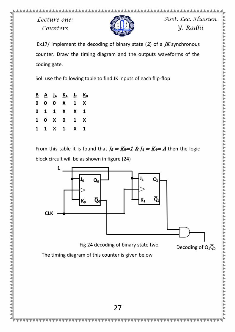
Ex17/ implement the decoding of binary state (2) of a JK synchronous
counter. Draw the timing diagram and the outputs waveforms of the
coding gate.
Sol: use the following table to find JK inputs of each flip-flop
From this table it is found that JB = KB=1 & JA = KA= A then the logic
block circuit will be as shown in figure (24)
The timing diagram of this counter is given below
B A JA KA JB KB
0 0 0 X 1 X
0 1 1 X X 1
1 0 X 0 1 X
1 1 X 1 X 1
J0
K0
Q0
𝐐 0
J1
K1
Q1
𝐐 1
CLK
1
Fig 24 decoding of binary state two Decoding of Q1Q 0

28
Asst. Lec. Hussien
Y. Radhi Lecture one:
Counters
HW14: implement the logic for the decoding states 8 in the (4bits) D
synchronous counter.
Counter applications
The counters are useful in more digital applications and devices, some
of the counters applications are:
1- Digital Clock
The counters can be used as a digital clock system by using the
principle of cascading counters. The input AC voltage with 60 Hz
frequency and the outputs are the seconds, minutes, and hours. This
logic circuit consists of
Wave shaping circuit.
Synchronous counters divided-by-10 & divided-by-6.
An (JK flip-flop).
2- BCD/7-segment.
3- Automobile Parking Control
4- Parallel-to-serial data conversion (multiplexing)
5- Frequency divider
CLK
Q0
Q1
2
Copyright © 2022 FDOKUMEN