Area-power trade-offs for flexible filtering in green radios
9
1 Area-Power Tradeoffs for Flexible Filtering in Green Radios Navin Michael, Christophe Moy, Vinod A Prasad, Jacques Palicot Abstract—The energy efficiency of wireless infrastructure and terminals has been drawing renewed attention of late, due to their significant environmental cost. Emerging green communication paradigms like cognitive radio, are also imposing the additional requirements of flexibility. This dual requirements of energy efficiency and flexibility, poses new design challenges for implementing the radio functional blocks. This paper focuses on the area vs. power tradeoffs for the channel filters that are required in the digital frontend of a flexible, energy efficient radio. In traditional CMOS circuits, increased area was traded for reduced dynamic power consumption. With leakage power emerging as the dominant mode of power consumption in nanoscale CMOS, these tradeoffs have to be revisited. The current work discusses how the increased timing slacks obtained by increasing the parallelism, can be exploited for overall power reduction even in nanoscale circuits. In this context a notion of ‘area efficiency’ and a metric for evaluating it is also introduced. The proposed metric has also been to compare the area efficiencies of different classes of time-shared filters. I. INTRODUCTION HERE is a growing awareness and consensus about the fact that , the issues of energy efficiency and climate change are closely intertwined. Hence tackling the latter problem, cannot be achieved without first resolving the issue of energy efficiency. The Information and Communication Technologies (ICT) infrastructure currently contributes to nearly 3% of the total energy consumption, and the contribution is expected to double in every five years [1]. In the domain of Information and Communication Technologies (ICT), mobile telephony in particular is emerging as one the major areas of focus for reducing the overall energy budget, due to the exponential rate at which the wireless industry has been increasing its customer base. These observations are stimulating an interest in ‘green radios’, which is the nomenclature given to the growing body of ongoing research, targeting the issue of energy efficiency in wireless networks [2]. The operational carbon footprint of the cellular infrastructure has been found to be much higher than the mobile terminals [2,3]. For mobile terminals, the energy efficiency is strongly linked to the usability and battery life. From an environmental perspective, energy efficiency in terminals is also important, due to the serious problem posed by toxic elements in the discarded batteries [4]. The sheer number of mobile terminals can translate to a significant amount of battery pollution. The primary focus in developing the infrastructure has always been on maximizing the spectral efficiency and capacity, and not the energy efficiency. Minimizing the energy consumption of entire wireless network requires concerted efforts at the various levels of the networking hierarchy, right from low power hardware in the infrastructure and terminals, to novel energy aware communication paradigms. Manuscript received September 30, 2009. This work was supported in part by the Merlion PhD Grant (Dossier. No. 9.03.07), France-Singapore Cooperation Platform for Science & Technology. Navin Michael is with the School of Computer Engineering, Nanyang Technological University, Singapore (e-mail: [email protected] ). Christophe Moy is with the SUPELEC/IETR, Cesson Sevigne, France (e- mail: [email protected]). A.P. Vinod is with the School of Computer Engineering, Nanyang Technological University, Singapore ( e-mail: [email protected] ). Jacques Palicot is with the SUPELEC/IETR, Cesson Sevigne, France (e- mail: [email protected]). There exists an insatiable demand for increased bandwidth and value added wireless services. Frequency spectrum is a scarce resource, and the need for increasing spectral efficiency necessitates the use of signal processing algorithms of dramatically increased algorithmic complexity [5]. The increase in algorithmic complexity has been accompanied by an increasing demand for flexibility. New communication paradigms like cognitive radio [6] and symbiotic networks [7] use cooperative spectrum sharing to make more efficient use of available spectrum. They can also be used for jointly targeting both spectrum and energy efficiency [8,9], and hence can be considered within the ambit of green radios. These paradigms require the underlying hardware to operate in a heterogeneous wireless environment which necessitates the hardware to be highly flexible. From the perspective of radio hardware design, there has been an increasing trend to push a significant portion of the radio signal processing load into the digital domain, where one has the advantage of easier reprogrammability and more mature power optimization strategies. All these trends suggests that the energy efficiency (measured in terms of Mops/mW) of the digital baseband is an important target for system level energy optimization of the wireless infrastructure. This paper particularly focuses on the problem of flexible filtering, required for channel selection in the digital front-end of the radios designed for emerging communication paradigms. Flexibility necessitates the use of generic programmable multiply and accumulate (MAC) units, which have a large area overhead. Parallelism, in terms of the T
Transcript of Area-power trade-offs for flexible filtering in green radios

1
Area-Power Tradeoffs for Flexible Filtering in Green Radios
Navin Michael, Christophe Moy, Vinod A Prasad, Jacques Palicot
Abstract—The energy efficiency of wireless infrastructure and
terminals has been drawing renewed attention of late, due to their significant environmental cost. Emerging green communication paradigms like cognitive radio, are also imposing the additional requirements of flexibility. This dual requirements of energy efficiency and flexibility, poses new design challenges for implementing the radio functional blocks. This paper focuses on the area vs. power tradeoffs for the channel filters that are required in the digital frontend of a flexible, energy efficient radio. In traditional CMOS circuits, increased area was traded for reduced dynamic power consumption. With leakage power emerging as the dominant mode of power consumption in nanoscale CMOS, these tradeoffs have to be revisited. The current work discusses how the increased timing slacks obtained by increasing the parallelism, can be exploited for overall power reduction even in nanoscale circuits. In this context a notion of ‘area efficiency’ and a metric for evaluating it is also introduced. The proposed metric has also been to compare the area efficiencies of different classes of time-shared filters.
I. INTRODUCTION HERE is a growing awareness and consensus about the fact that , the issues of energy efficiency and climate
change are closely intertwined. Hence tackling the latter problem, cannot be achieved without first resolving the issue of energy efficiency. The Information and Communication Technologies (ICT) infrastructure currently contributes to nearly 3% of the total energy consumption, and the contribution is expected to double in every five years [1]. In the domain of Information and Communication Technologies (ICT), mobile telephony in particular is emerging as one the major areas of focus for reducing the overall energy budget, due to the exponential rate at which the wireless industry has been increasing its customer base. These observations are stimulating an interest in ‘green radios’, which is the nomenclature given to the growing body of ongoing research,
targeting the issue of energy efficiency in wireless networks [2]. The operational carbon footprint of the cellular infrastructure has been found to be much higher than the mobile terminals [2,3]. For mobile terminals, the energy efficiency is strongly linked to the usability and battery life. From an environmental perspective, energy efficiency in terminals is also important, due to the serious problem posed by toxic elements in the discarded batteries [4]. The sheer number of mobile terminals can translate to a significant amount of battery pollution. The primary focus in developing the infrastructure has always been on maximizing the spectral efficiency and capacity, and not the energy efficiency. Minimizing the energy consumption of entire wireless network requires concerted efforts at the various levels of the networking hierarchy, right from low power hardware in the infrastructure and terminals, to novel energy aware communication paradigms.
Manuscript received September 30, 2009. This work was supported in part
by the Merlion PhD Grant (Dossier. No. 9.03.07), France-Singapore Cooperation Platform for Science & Technology.
Navin Michael is with the School of Computer Engineering, Nanyang Technological University, Singapore (e-mail: [email protected] ).
Christophe Moy is with the SUPELEC/IETR, Cesson Sevigne, France (e-mail: [email protected]).
A.P. Vinod is with the School of Computer Engineering, Nanyang Technological University, Singapore ( e-mail: [email protected] ).
Jacques Palicot is with the SUPELEC/IETR, Cesson Sevigne, France (e-mail: [email protected]).
There exists an insatiable demand for increased bandwidth and value added wireless services. Frequency spectrum is a scarce resource, and the need for increasing spectral efficiency necessitates the use of signal processing algorithms of dramatically increased algorithmic complexity [5]. The increase in algorithmic complexity has been accompanied by an increasing demand for flexibility. New communication paradigms like cognitive radio [6] and symbiotic networks [7] use cooperative spectrum sharing to make more efficient use of available spectrum. They can also be used for jointly targeting both spectrum and energy efficiency [8,9], and hence can be considered within the ambit of green radios. These paradigms require the underlying hardware to operate in a heterogeneous wireless environment which necessitates the hardware to be highly flexible. From the perspective of radio hardware design, there has been an increasing trend to push a significant portion of the radio signal processing load into the digital domain, where one has the advantage of easier reprogrammability and more mature power optimization strategies. All these trends suggests that the energy efficiency (measured in terms of Mops/mW) of the digital baseband is an important target for system level energy optimization of the wireless infrastructure.
This paper particularly focuses on the problem of flexible filtering, required for channel selection in the digital front-end of the radios designed for emerging communication paradigms. Flexibility necessitates the use of generic programmable multiply and accumulate (MAC) units, which have a large area overhead. Parallelism, in terms of the
T

2
number of MAC units has been a traditionally used as a high level architectural transformation, to reduce the dynamic power consumption of filters . Complementary metal oxide semiconductor (CMOS) has been the technology of choice for implementing the integrated circuits in the digital baseband. The power consumption in CMOS technologies was traditionally dominated by dynamic or switching power. However leakage power has started overtaking the dynamic power component. The leakage power consumption is strongly correlated to the total number of leaking transistors [10] and hence the area. This requires the traditional architectural level area-power tradeoffs and the viability of parallelism as a power reduction strategy to be re-examined for smaller geometries. This paper offers some insights, into how the timing slack offered by increased parallelism could be used for reducing the overall power consumption, even in nanoscale technologies. A notion of ‘area efficiency’ is also introduced. It measures the efficiency with which an architecture can trade area for timing slack. The above notion is illustrated with a case study of alternate implementations of Finite Impulse Response (FIR) filters, which are one of the most computational intensive algorithms required in the wireless baseband.
The paper is organized as follows. Section II highlights the need for flexibility in the channel filters of new communication paradigms. Section III gives an overview of the CMOS power consumption components and their dependency on various device level and circuit level parameters. Section IV shows, how trading area for increased timing slack could be used reducing the individual power consumption components. Section V introduces the notion of area efficiency and demonstrates it using different classes of FIR filters
II. FLEXIBLE FILTERING FOR CHANNEL SELECTION IN EMERGING COMMUNICATION PARADIGMS
While spectrum aware communication paradigms like
cognitive radio were originally targeted at increasing the spectral capacity, by making more efficient use of the spectrum, knowledge of the spectrum can also be translated into reduced energy consumption [8,9]. The cognitive radio equipment needs to sense the spectrum over multiple bands, in order to detect the presence of standards with varying channel bandwidth. The radio is required to make use of the vacant bands in the shared spectrum to receive and transmit data. Hence the bandwidth and interference attenuation requirement of the channel selection filters can vary over time. Such a scenario is illustrated in Fig. 1, where P1, P2 and P3 indicate three different sensing periods, with the radio sensing the spectrum for standards of different bandwidths in each of the sensing periods.
Besides opportunistic spectrum sharing, similar requirements of flexibility also exist in paradigms like 4G [11], which require the radio to operate in a heterogeneous, multistandard environment. This in turn imposes the
requirement of flexibility on the channel selection filters and filterbanks. One potential usage scenario of a flexible, spectrum aware radio, could be a vertical handover from UMTS to GSM, when free GSM channels are available, to reduce the energy consumption of the battery.
Channel filters have the task of extracting the channel of interest from the digitized wideband signal from the analog to
P1
P2
Frequency
Frequency
P3
Frequency Fig. 1 Spectrum Sensing in Cognitive Radio
digital converter (ADC). Pushing the fine channel selection load to the digital domain, results in a very coarse band being selected by analog front-end, as shown in Fig 2. The output of the analog to digital converter (ADC) might comprise of unwanted interferers, blockers and quantization noise, which have to be removed by the channel filter, before the signal can be fed to the subsequent baseband blocks. In a multistandard system, the channel bandwidth, the position and power levels of interfering components can vary over time. Channel selection has been traditionally performed by FIR filters due to the relative ease of providing linear phase and stability. FIR channel filters are computationally intensive, due to the large number of multiply and accumulate (MAC) operations that need to be performed for each output sample. Channel filters have to operate on the wideband digitized signal from the analog to digital converter. The sheer number of MAC operations per second places it beyond the computational capabilities of generic DSP processors, instead the function has to be performed using a hardware accelerator. Accelerators use a spatial computation style, as opposed to the temporal style of execution in a processor. The requirement of flexibility also precludes the use of fixed coefficient filter optimizations like common sub expression elimination (CSE) and graph dependency (GD) algorithms, which reduce the arithmetic complexity by reducing the multiply operations to a set of shift and add operations [12,13]. Programmability requires the use of generic programmable MAC units.
Since generic MAC units have a significant area overhead, one important design consideration in the accelerator design is the level of parallelism and total area overhead. On one extreme the filter can be implemented as a full parallel FIR

3
filter where each filter tap is implemented using a dedicated hardware multiplier. On the other hand, it can be implemented as a time-shared filter, where multiple coefficient multiplications are mapped to each of the MAC units [14,15].
Fig. 2 Varying Channel Filtering Requirement
Time-shared filters are more flexible in that they allow multiple filter lengths to be folded onto the same folding set, and the use of a coefficient RAM allows the coefficients to be updated at runtime. The control logic is usually a simple counter, whose control word can be updated for supporting multiple filter lengths.
In any particular mode of operation, the throughput requirements of the channel filter is fixed. In such a scenario, the area overhead due to increased number of MAC units can be traded for reduced frequency of operation and increased timing slack in the critical paths. In higher geometries, this increased slack could be exploited for relaxing the circuit delay by lowering the supply and threshold voltages. This resulted in significant reduction of dynamic power consumption, due to its quadratic dependence on the supply voltage. However, such a scaling strategy has the effect of exponentially increasing the subthreshold leakage power, which is one of the dominant power consumption mechanisms in nanoscale CMOS circuits. Parallelism also results in increased area and increased number of leaking transistors. Hence it needs to be seen, if the relaxed performance requirements of the MAC units with increased parallelism can be translated into lower power consumption in nanoscale CMOS technologies.
III. POWER CONSUMPTION IN NANOSCALE CMOS The evolution of CMOS technologies has more or less
followed the Moore’s law which predicted that the transistor densities would double in every 24 months [16]. This requires the device dimensions to be scaled by a factor of 0.7 in each successive generation. In the constant field scaling regime, the lateral and vertical device dimensions, the supply voltage and the threshold voltage are all scaled by a factor of 0.7, while the doping density is scaled by a factor of 1/0.7. This allows the magnitude of the electric field in the gate oxide and
the MOSFET inversion channel to remain more or less unchanged. The main attraction of technology scaling lies in the fact that both the delay and the capacitance are scaled by a factor of 0.7. Hence the maximum operating frequency of the transistors is increased by about 43% while the scaled capacitance and supply voltage reduce the switching energy by a factor of 0.73 for each generation [17].
For more than three decades, aggressive constant field scaling has allowed increased performance, reduced dynamic power consumption, and more transistors to be packed within the same area. However continued scaling has become unsustainable in the nanoscale era, due to the increased role of leakage power. Leakage had been negligible compared to the
Course band selected by analog frontend
Desired Channel
Interferer Standard-1
dynamic power in higher device geometries, and was an important consideration, only for portable battery powered devices, which spent a significant amount of time in the standby mode. The active power consumption was always dominated by dynamic power. However the leakage power contribution exceeds the dynamic power consumption in the sub 65nm geometries. This can be attributed to two main factors. Firstly, scaling of the supply voltages has required the threshold voltage to be also scaled down, to maintain the gate overdrive. Reducing the threshold voltage, results in an exponential increase in the subthreshold leakage current [18]. Secondly, scaling of the silicon dioxide gate oxide has resulted in the gate and the channel being separated by the thickness of just a few atoms, which has tremendously increased the gate tunneling currents. The cumulative effect of these two currents has resulted in the leakage power overtaking the dynamic power as the dominant source of power consumption in nanoscale CMOS circuits. The relative contribution of the major power consumption components, over the years has been shown in Fig.3 [10].
Fig. 3 Power Consumption Trends [10]
Their contribution in nanoscale CMOS technologies is discussed in more detail below.
A. Subthreshold Leakage Power The subthreshold leakage current, shown in Fig. 4, refers to
Subthreshold Leakage Power
Dynamic Power
Gate Leakage Power (With Si02 gate oxide)
InterfererDesired Channel
Desired Channel
Standard-2
Standard-3
Total Chip Power
2000 2005 1990 1995 2010 2015 2020
Year

4
the drain to source current that flows when the gate to source voltage, Vgs of the transistor is below the threshold voltage. Under the above condition the transistor is said to be in the weak inversion mode. The current in the weak inversion mode is dominated by the diffusion current, rather than the drift current which dominates the drain to source current in the strong inversion mode. This can be attributed to the low concentration of minority carriers and the smaller longitudinal electric fields.
In long channel transistors electrons are attracted to the channel from the highly doped source, under the effect of the positive gate voltage. With increased scaling of the channel length, the drain and source depletion regions are very close to each other. This causes the electrons in the source to be pulled
Fig. 4 Leakage Currents in a MOSFET
into the channel under the effect of the drain electric field. Hence the drain bias VDS influences the channel formation in addition to the gate voltage, in short channel transisitors. The lowering of potential barrier for electrons in the source to enter channel, reduces the threshold voltage and the effect is called drain induced barrier lowering (DIBL) [18].
Another important factor that affects the threshold voltage is the source-body bias. For a metal oxide semiconductor (MOS) transistor to function, both the source-body pn junctions and the drain-body pn junctions have to be reversed biased. Electrons are attracted to the channel from the source, when the channel depletion width is comparable to that of the source-body depletion width. At this point the electrostatic potential of the channel surface is equal to that of the source region. Increasing the magnitude of the reverse biased source to body voltage VSB, results in the widening of the source-body depletion region. Consequently increased gate voltage has to be applied to further increase the channel depletion width. The dependence of the threshold voltage Vth on the body bias VSB can be modeled by (1) [18].
( )
ox
SBBasiBFBth C
VqNVV
+++=
ψεψ
222 (1)
In (1), VSB is the flatband voltage, Na is the doping density, Cox is the gate oxide capacitance per unit area and ψB is the difference between the Fermi potential and substrate intrinsic potential. The cumulative effect of DIBL and body bias can be incorporated into (2) as shown below [18].
( )DS
SBox
SBBasiBFBth V
CVqN
VV ηψε
ψ −+
++=22
2 (3)
η is the DIBL coefficient. Taking the body bias and DIBL into effect, the substrate leakage power can be modeled using (4).
⎟⎟⎠
⎞⎜⎜⎝
⎛−=
−⎟⎟⎠
⎞⎜⎜⎝
⎛ −+
T
DS
T
thGS
vV
mvVV
Teff
oxDDsub eevLWCVP 1
8.12
0μ (4)
Gate Oxide where VDD is the supply voltage, m is the body effect coefficient, vT is the thermal voltage, μ0 is the zero bias mobility, W is the gate width and Leff is the effective gate length. The body effect coefficient m is given by (5)
VG
dm
ox
WT
m3
1+= (5)
where Wdm indicates the maximum depletion layer width, while Tox is the SiO2 gate oxide thickness. The expression (4) indicates an exponential relation between the subthreshold leakage power and the threshold voltage.
B. Gate Leakage Power In a n-channel transistor, the n+ doped polycrystalline
silicon gate is separated from the n type channel by an insulating layer of silicon dioxide (SiO2), which is assumed to have infinite impedance. However aggressive scaling has resulted in a gate oxide approaching a thickness of approximately 1.2 nm or equivalently, 5 silicon atoms. At this thickness the electrons can directly tunnel through extremely narrow potential barrier resulting in gate leakage currents [18,19]. A reverse situation exists in the off state (VGS=0, VDS=VDD), when the electron in the n+ polycrystalline gate tunnel directly into the drain extension regions. Both the mechanisms have been shown in Fig. 4. Similar hole tunneling based gate leakage currents also exist in p-channel transistors. The power consumption due to the direct tunneling gate leakage current can be modeled by (6) [20].
DD
OXG V
T
OX
DDGDDgate e
TVWKVP
α−
⎟⎟⎠
⎞⎜⎜⎝
⎛=
2
(6)
where both KG and αG are experimentally derived constants. The above expression shows that the gate leakage power shows an exponential dependence on the supply voltage and the gate oxide thickness.
C. Dynamic Power Dynamic power consumption occurs due the charging and
discharging of capacitive nodes due to switching activity. The
Source
Gate
Drain
Gate Leakage Current
Gate Leakage Current
Subthreshold Current Channel
Drain Extension
VS VD
VB

5
switching activity comprises of both the useful activity necessary for evaluating a particular output and spurious switching activity a node may experience, before settling into the steady state value. The load capacitances typically consist of parasitic transistor capacitance and interconnect capacitance. In scaled technologies the latter component has started dominating due to the non-scaling of interconnect capacitance. An expression for the dynamic power consumption can be given by (7) [21].
clkDDTfdyn fVCP 2α= (7) where CT stands for the total capacitive load, αf is the fraction of capacitive nodes that are switching and fclk is the clock frequency. The expression (6) reveals a quadratic dependence between the dynamic power consumption and the supply voltage.
IV. TRADING AREA FOR LOWER POWER CONSUMPTION
A. Traditional Architecture Driven VDD/Vth Scaling The delay of a CMOS gate is determined by the time taken
to charge and discharge the capacitive nodes, which depends on the saturation current. The saturation current in turn is strongly dependent on the supply voltage VDD and the gate overdrive voltage ( VDD - Vth ) . The dependence of the gate delay on the above parameters can be given by the alpha power law MOSFET model [22] as shown in (8).
αDDD
pd
VKT
−=
)( thDD VV (8)
where KD is a fitting parameter and α is the velocity saturation term, which is equal to 1.5 in short channel transistors [22]. In higher device geometries, dynamic power consumption was the predominant mode of active power dissipation, and the other components were negligible. The quadratic dependence of supply voltage on dynamic power, made supply voltage scaling an attractive option. The reduction in the gate overdrive could be partly offset by lowering the threshold voltage which allowed the supply voltage to be scaled over a wider range, resulting in greater reductions in the dynamic power. Traditional architecture driven voltage scaling techniques [20] used parallelism to trade off for a lower operating frequency of the datapath operators, in a fixed throughput system. The increased timing slack in the critical paths due to the reduced internal cycle period, increases the room available for VDD/Vth scaling. The linear increase in the physical capacitance term CT in (6), due to increased parallelism, was easily compensated by the quadratic reduction due to lower supply voltage.
B. Exploiting Timing Slack in Nanoscale CMOS This section discusses how the gate oxide thickness, the body
bias and the supply voltage together could be manipulated to reduce total power consumption, while exploiting the timing slacks due to increased parallelism. The traditional architecture driven VDD/Vth scaling model faces some serious bottlenecks in nanoscale technologies. Reduction in the supply voltage results in a quadratic reduction in the dynamic power and an exponential reduction in gate leakage, but lowering the threshold voltage results in an exponential increase in the subthreshold leakage current. Both the gate leakage and subthreshold leakage are also linearly dependent on the gate width. Hence the total leakage power consumption is strongly correlated to the total gate width and area [10].The total physical capacitance term CT in (7) is also strongly correlated to the total area. Hence the power reduction strategy should ensure that the potential gains obtained by increased parallelism are not offset by the area overheads.
The expression (6) indicates that an exponential reduction in gate leakage power could be obtained by either reducing VDD or increasing Tox. The gate oxide capacitance per unit area Cox can be expressed in terms of Tox as follows.
oxoxox TC (9) = ε where εox is the permittivity of the gate oxide. The expression for the threshold voltage in (4), can be reformulated using (10) as shown below.
( )DS
SBox
SBBasioxBFBth V
VqNTVV η
εψε
ψ −+
++=22
2 (10)
It can be seen that increasing Tox, results in an increased threshold voltage, which in turn results in an exponential reduction in subthreshold leakage. Increasing the gate oxide thickness also reduces the gate capacitance, which reduces the dynamic power consumption. The underlying idea of using thicker gate oxides to reduce the leakage currents has been used in a multiple oxide CMOS process [23]. In the above process, the non-critical paths are implemented using low performance high Tox transistors while the critical paths are implemented using transistors with a lower Tox. When the number of critical paths are much lower compared to the non-critical paths, the above technique results in significant reduction of leakage power. However the above strategy suffers from the drawback that it requires a complicated process technology for fabrication. The threshold voltage Vth, increases linearly with Tox as indicated in (10). When supply voltages are also simultaneously scaled down, the room available varying the oxide thickness is limited due to the rapidly increasing gate delay, as is evident from (8).
Note that the expression for the threshold voltage is also a function of the body bias. Traditionally reverse body bias (RBB) ( VSB>0 , for n-channel transistors ) has been used as a standby leakage reduction strategy for fast, leaky transistors. The increased source-body depletion width, results in increased threshold voltage and hence reduced subthreshold

6
current in the standby mode. Removing the RBB allows the circuit to have a high performance in the active mode. However the above strategy provides diminishing returns in scaled technologies. Increasing gate oxide capacitance Cox and lower doping density Na have resulted in a weakened body effect. RBB also results in increasing the drain-body depletion width, aggravating the short channel effects which in turn lower the threshold voltage [24]. RBB also helps to reduce only the subthreshold leakage, and not the gate leakage component, which is significant in aggressively scaled geometries.
Forward body bias (FBB) (VSB < 0, for n-channel transistors) is an alternate leakage reduction strategy where nominally high Vth devices, having low standby leakage power can have their performance improved by applying a FBB in the active mode. FBB has the advantage of scaling well into lower geometries due to its reduction of short channel effects [25]. The threshold voltage is also more sensitive to a forward bias voltage. The application of FBB allows the gate oxide thickness to be increased further, while maintaining a given threshold voltage. However magnitude of the applicable forward bias is limited to around 600mV, due to the drain-body and source-body pn junction currents.
Note that increasing the oxide thickness has the unwanted side-effect of increasing the short channel effects due to a lowering aspect ratio. The aspect ratio is directly proportional to the channel length ‘L’ and inversely proportional to (Tox)1/3
[18]. Hence maintaining a high aspect ratio, requires the channel length to be also increased, along with the gate oxide thickness.
Trading increased parallelism for increased timing slack in the critical paths, relaxes the performance requirement of the whole circuit, allowing it to be implemented using a thicker gate oxide thickness , than would have been permissible in an equivalent circuit with a lower degree of parallelism. Not that the focus here is to use architectural transformations, to allow the whole circuit to be implemented with a thicker gate oxide, and not just the non-critical paths, as done in a multiple oxide process. Hence parallelism offers the possibility to reduce the leakage and dynamic power consumption components without resorting to an advanced CMOS process. The lower performance requirement with increased parallelism, allows the supply voltages to be lowered and the threshold voltage to be increased. Thus the near linear increase in leakage power and dynamic power due to increased area, is compensated by an exponential reduction in subthreshold and gate leakage currents and a quadratic reduction in dynamic power.
The optimum operating conditions, for minimizing the overall power can be derived as follows. Assume that for a given degree of parallelism, the internal cycle period of the datapath operators for maintaining a fixed throughput is TC. Let the propagation delay of the operator for the nominal supply and threshold voltages be TD. The available timing slack for VDD/Vth scaling is given by (TC -TD). Assuming off state conditions for subthreshold leakage (VGS = 0, VDS = VDD, VDD/vT 0), the total power consumption, incorporating the
major power consumption components in nanoscale CMOS can be given using (4),(5),(6) and (7), as shown below.
DD
OXG
T
th
VT
OX
DDGclkDDTf
mvV
oxDDtot e
TVWKfVCe
TAVP
α
α−
−
++= 2
32 (11)
where A is give by (12).
8.120 ev
LWA T
effoxεμ= (12)
Let Vmax be the maximum permissible forward bias voltage (Vsb= -Vmax). Substituting VDS = VDD into (10), the gate oxide thickness Tox can be expressed in terms of the threshold voltage as shown in (13).
( )( )max22
2
VqN
VVVT
Basi
oxDDBFBthox
−
+−−=
ψε
εηψ (13)
Using (5) and (13) the total power consumption Ptot, can now be completely expressed in terms of the two variable parameters - supply voltage VDD and the threshold voltage Vth. Minimizing the total power consumption can now be treated as a constrained optimization problem [26], whose goal is to find the optimum (VDD ,Vth) pair which minimizes the total power, subject to the following constraint.
CCthDD
DDD TTVV
VKΔ−≤
− α)( (13)
where ΔTC is a safety margin introduced, to accommodate threshold voltage variations. Additional constraints can be imposed based on practical and technology imposed limits for the supply and threshold voltage. The optimum (VDD ,Vth) pair can be used to evaluate the gate oxide thickness using (12). The use of the maximum permissible forward bias voltage Vmax ensures that the maximum possible oxide thickness is obtained for a given (VDD,Vth) pair. The above operating conditions are valid for the active mode. The transmission protocols used by the infrastructure might use some built in standby periods, during which some of the accelerator cores may be powered down. This may also happen, if a particular core is not used in the current mode of operation. For these intervals, the power consumption can be further reduced by removing the forward body bias ( VSB=0 ). This results in a lowering of the threshold voltage, and low standby subthreshold and gate leakage currents.
V. AREA EFFICIENCY OF TIME-SHARED FIR FILTERS The last section, proposed a physical design strategy, to
minimize the total power consumption, at a given degree of parallelism and a given timing slack. Trading parallelism for timing slack incurs an area penalty. Finding a suitable structure at the architectural level, that offers more timing

7
slack for unit increase in area, is still an open problem. All the three major power components in nanoscale CMOS, show a near linear dependence on the area. The power reduction strategy, discussed in the previous section, is strongly dependent upon the timing slack can be obtained by increasing the area. Aggressive scaling has brought the supply and threshold voltages closer to each other. In Fig. 5, the normalized delay, VDD/(VDD-Vth
) 3/2 is plotted against the Vth, for VDD =1V and VDD =0.9V. It can be seen that when the Vth approaches VDD the delay curve climbs very steeply. This implies that even a small change in Vth ,will result in a large increase in delay. The use of parallelism in this region, would incur a large area penalty. Hence one important architectural level design parameter, for using parallelism in scaled technologies is the efficiency with which a parallel architecture trades increased area for increased timing slack.
Fig. 5 Normalized delay as a function of threshold voltage
One potential figure of merit that could be used for measuring the area efficiency is the area-frequency (AF) product. The ‘area’ here refers to the total area of the datapath operators, while the ‘frequency’ refers to their internal operating frequency for maintaining a particular throughput. An architecture having a lower area-frequency product has a lower operating frequency and hence increased cycle period, when compared to an architecture having a higher area-frequency product and a comparable area. The increased cycle period contributes to increased timing slack, which in turn allows more room for scaling the supply and threshold voltages. The area efficiency in terms of the area-frequency product, for different classes of time-shared filters are compared below.
A time-shared filter structure can be derived by folding a direct form FIR filer structure or a transpose direct form filter structure onto a limited set of MAC units. An alternate strategy presented by the current authors in [27], would be to use a fast filter algorithm (FFA) structure, as the starting point, for constructing the time-shared filter. FFAs [28,29] work on the principle of algorithmic strength reduction, i.e. reducing the number of expensive MAC operations at the cost of increased add operations. The following analysis shows
how the reduced number of MAC operations in FFA based time-shared filters, can be used for reducing the operating frequency and increasing the available timing slack, when compared to a folded direct form filter with a comparable area.
Assume that the critical path delay of the MAC unit for the nominal supply and threshold voltages is give by TD. Consider a direct form filter of length N, which is folded onto M MAC units (M<<N, N is assumed to be a multiple of M for simplicity). Assuming that the throughput requirement of the filter is fclk, the operating frequency of each MAC can be given by Nfclk/M and the timing slack in the system can be give by (TD - M/Nfclk). Assuming that the area cost of each MAC unit is Am, the area-frequency product of the folded direct form filter can be given by (14).
clkmclk
mdirect NfAM
NfMAAF =×= (14)
FFA structures are a special class of parallel FIR filter
structures. A K-parallel FIR structure, corresponding to a N tap FIR filter, is a block processing structure that processes K inputs in parallel and produces K outputs. The above structure has K2 subfilters, each of length N/K (N is assumed to be a multiple of K for simplicity). When multiple inputs are processed in parallel there exist significant redundancies across the subfilters. This is used by the FFA structures for reducing the number of subfilters. A K-by-K FFA (henceforth referred to as the KxK FFA) has Sk subfilters, where Sk is typically much smaller than K2, and each subfilter is of length N/K. This reduction comes at the expense of Ak pre/post processing adders. The general FFA structure can be illustrated through the example of the simplest FFA, the 2x2 FFA, shown in Fig 6.
TN
Vth
H0
H0+H1
H1
+
Z-2
x(2k)
x(2k+1)
y(2k)
y(2k+1)+ + +
-
-
Fig. 6 2x2 FFA Structure It can be seen that it consist of regular FIR subfilters and a
highly irregular pre-post processing addition network. The subfilters are either a polyphase component of the original filter, or an additive combination of different polyphase components. The time shared filters in [27], are obtained by folding each of the regular subfilters of a base FFA filter, onto a set of L MAC units, while directly mapping the irregular pre/post addition network data flow graph onto hardware. This exploits the regularity of the FIR subfilters for reducing the control overheads, while still benefiting from the algorithmic strength reduction of FFAs. Assuming that the throughput
8
requirement is fclk the input sample rate to each subfilter is fclk/K . Each of the subfilters is of length N/K and is folded onto L MAC units. Hence the operating rate of each MAC unit is Nfclk /K2L. The pre/post processing addition network operates at a rate of fclk/K. The lower bound on the timing slack available in the system, and hence the bottleneck for Vth/VDD scaling is still determined by the time multiplexed MAC units. The total number of MAC units is given by M=SkL. Assuming that the area cost of a word length adder is Ad. The area-frequency product can be given by (15).
( )
⎟⎠
⎞⎜⎝
⎛+⎟⎠
⎞⎜⎝
⎛=
×+=
22
2
KA
LNfA
KS
NfA
LKNf
AALASAF
KclkDKclkm
clkdKmKFFA
(15)
The lower area-frequency product of FFA based time-shared filters arises from the fact that SK/K2<1 and Ad<<Am. The SK, AK, SK/K2 and AK/K2 for different values of K have been tabulated in Table I.
TABLE I –FFA PARAMETERS
K KS KA 2/ KS K
2/ KA K
2 3 4 0.75 1 3 6 10 0.67 1.11 4 9 20 0.56 1.25 5 12 40 0.48 1.60 6 18 42 0.5 1.17 8 27 76 0.42 1.18
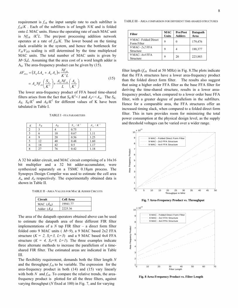
A 32 bit adder circuit, and MAC circuit comprising of a 16x16 bit multiplier and a 32 bit adder-accumulator, were synthesized separately on a TSMC 0.18μm process. The Synopsys Design Compiler was used to estimate the cell area Am and Ad respectively. The experimentally obtained data is shown in Table II.
TABLE II –AREA VALUES FOR MAC & ADDER CIRCUITS
The area of the datapath operators obtained above can be used to estimate the datapath area of three different FIR filter implementations of a N tap FIR filter – a direct form filter folded onto 9 MAC units ( M=9), a 9 MAC based 2x2 FFA structure (K = 2, S2=3, L=3) and a 9 MAC based 4x4 FFA structure (K = 4, S4=9, L=1). The three examples indicate three alternate methods to increase the parallelism of a time-shared FIR filter. The estimated areas are indicated in Table III. The flexibility requirement, demands both the filter length N and the throughput fclk to be variable. The expression for the area-frequency product in both (14) and (15) vary linearly with both N and fclk. To compare the relative trends, the area-frequency product is plotted for all the three filters, against varying throughput (N fixed at 100) in Fig. 7, and for varying
TABLE III – AREA COMPARISON FOR DIFFERENT TIME-SHARED STRUCTURES
filter length (fclk fixed at 50 MHz) in Fig. 8.The plots indicate that the FFA structures have a lower area-frequency product than the folded direct form filter. The results also suggest that using a higher order FFA filter as the base FFA filter for deriving the time-shared structure, results in a lower area-frequency product, when compared to a lower order base FFA filter, with a greater degree of parallelism in the subfilters. Hence for a comparable area, the FFA structures offer an increased timing slack, when compared to a folded direct form filter. This in turn provides room for minimizing the total power consumption at the physical design level, as the supply and threshold voltages can be varied over a wider range.
Fig. 7 Area-Frequency Product vs. Throughput
Fig. 8 Area-Frequency Product vs. Filter Length
Circuit Cell Area MAC (Am) 19941.77 Adder (Ad) 2225.36
Filter MAC Units
Pre/Post Adders
Datapath Area
9 MAC- Folded Direct Form Filter 9 0 179,476
9 MAC- 2x2 FFA Structure 9 4 188,377
9 MAC- 4x4 FFA Structure 9 20 223,883
0 5 10 15 20 25 30 35 40 45 500
1
2
3
4
5
6
7
8
9
10x 1013
Throughput in MHz
Are
a- F
requ
ency
Pro
duct
9 MAC - Folded Direct Form Filter9 MAC - 2x2 FFA Structure9 MAC - 4x4 FFA Structure
0 10 20 30 40 50 60 701
2
3
4
5
6
7
8
9
10x 1013
Filter Length
Are
a- F
requ
ency
Pro
duct
9 MAC - Folded Direct Form Filter9 MAC - 2x2 FFA Structure9 MAC - 4x4 FFA Structure

9
VI. CONCLUSION AND FUTURE WORK The role of parallelism as a power reduction strategy in nanoscale CMOS technologies was analyzed in this paper. The increased contribution of leakage power was highlighted, and it was shown that even though leakage power is strongly correlated to area, there exist opportunities to use the increased timing slack obtained by parallelism for reducing both leakage and dynamic power. A physical design level power reduction strategy was proposed, that uses the performance relaxation obtained by parallelism to minimize the total power consumption, without resorting to an advanced CMOS process. At the architectural level, a notion of area-frequency product was also introduced, to compare with efficiency with which alternate architectures trade area for timing slack. It was shown how this metric could be used to compare different implementations of programmable time-shared FIR filters, which are an essential building block for flexible, energy efficient radios.
While designing in an area frequency (AF) space does give an idea about the timing slack for alternate architectures with comparable area, it does not give any information about the ‘usability’ of the timing slack for reducing power. The degree of possible dynamic and power reduction is strongly coupled to nominal supply and threshold values. The leverage obtained by parallelism can be expected to decrease when scaling results in further lowering of the Vth/VDD ratio. Hence the design of fixed throughput systems in a generalized AFn space will be considered as a part of the future work, where the exponent n, reflects the achievable power reduction, at a specific value of supply and threshold voltage.
REFERENCES [1] A. F. Pele. (2009, June 25). Leti works on green mobile networks, EE
Times Europe. [Online]. Available : http://www.eetimes.eu/218101321
[2] S. Armour, et al. (2009, June 12). Green Radio: Sustainable Wireless Networks,IET. [Online]. Available : http://kn.theiet.org/communications/green-radio-article.cfm ,
[3] M. F. Emmenegger, et al, “Life Cycle Assessment of the Mobile Communication System UMTS: Towards Eco-Efficient Systems,” International Journal of Life Cycle Assessment, 11, 4, (2006): 265 – 276
[4] A. Rayapura, “Wireless Waste. The Challenge of Cell Phone and. Battery Collection”, Inform Report, 2005
[5] J.M. Rabaey, “Silicon Platforms for the Next Generation Wireless Systems – What Role does Reconfigurable Hardware Play?” Field-Programmable Logic and Applications. 10th International Conference, FPL, 2000, Austria, Proceedings Springer-Verlag. 2000, pp.277-85. Berlin , Germany .
[6] S. Haykin, “Cognitive radio: brain-empowered wireless communications,” IEEE J Select. Areas Commun, vol 23, pp. 201-220, Feb 2005
[7] R. Gedge, “Symbiotic networks,” BT Technology Journal, vol.21, pp.67-73, 2003.
[8] A. He, et al, Minimizing Energy Consumption Using Cognitive Radio,” in Proc IEEE Performance,Computing and Communication Conference, pp. 372-377, Dec 2008
[9] J. Palicot, "Cognitive Radio: An Enabling Technology for the Green Radio Communications Concept", in Proc. International Wireless Communications and Mobile Computing Conference, ' pp. 21-24, June 2009
[10] N. S. Kim, et al, "Leakage Current: Moore's Law Meets Static Power," Computer, vol. 36, no. 12, pp. 68-75, Dec. 2003.
[11] J. M. Rabaey, “Wireless beyond the third generation-facing the energy challenge,” Proceedings of the 2001 International Symposium on Low Power Electronics and Design, pp1.-3 Monterey, August 2001.
[12] M. Potkonjak, et al, "Multiple Constant Multiplications: Efficient and Versatile Framework and Algorithms for Exploring Common Subexpression Elimination," IEEE Trans. Comput.-Aided Des. Integr. Circuits Syst., vol. 15, no. 2, 1996, pp. 151-165.
[13] A. G. Dempster and M. D. Macleod, “Use of minimum-adder multiplier blocks in FIR digital filters,” IEEE Trans. Circuits Syst. II, Analog Digit.Signal Process., vol. 42, no. 9, pp. 569–577, Sep. 1995.
[14] C. H. Wang, A. T. Erdogan, and T. Arslan, "High throughput and low power FIR filtering IP cores," in Proceedings of IEEE International SOC Conference, pp. 127-130, Santa Clara, Calif, USA, September 2004.
[15] C. Xu, C.-Y. Wang and K.K. Parhi, "Order-Configurable Programmable Power Efficient FIR Filters", Proc. of Int. Conf. on High Performance Computing , pp. 357-361, December 1996.
[16] M. Lundstorm, "Moore’s Law Forever, Science," Vol. 299. no. 5604, pp. 210 – 211, 2003
[17] B. Nikolic, "Design in the Power-Limited Scaling Regime". IEEE Transactions on Electron Devices, 55(1):71-83, January 2008.
[18] K. Roy, et al, "Leakage current mechanisms and leakage reduction techniques in deep-submicrometer CMOS circuits," Proceedings of the IEEE , vol.91, no.2, pp. 305-327, Feb 2003.
[19] M. Drazdziulis, “A gate leakage reduction strategy for future CMOS circuits,” in Proc.Eur. Solid-State Circuits, Conf., pp.317–320 ,Sep.2003
[20] S.P.Mohanty, et al ,“Analytical Modeling and Reduction of Direct Tunneling Current during Behavioral Synthesis of Nanometer CMOS Circuits,” in Proceedings of the14th ACM/IEEE International Workshop on Logic and Synthesis (IWLS),pp.249–256, 2005
[21] A.P.Chandrakasan and R.W.Brodersen, “Low Power CMOS Digital Design,” Norwell, MA: Kluwer, 1996.
[22] K. A. Bowman, et al, “A physical alpha-power law MOSFET model , in Proceedings of International Symposium on Low Power Electronics and Design, 218 – 222, 1999
[23] N. Sirisantana, et al, "High-Performance Low-Power CMOS Circuits Using Multiple Channel Length and Multiple Oxide Thickness,", in Proceedings IEEE International Conference on Computer Design, pp.227, 2000.
[24] A. Keshavarzi, et al, "Effectiveness of reverse body bias for leakage control in scaled dual Vt CMOS IC," In Proceedings of the international Symposium on Low Power Electronics and Design, 2001.
[25] S. Narendra, et al, "Forward body bias for microprocessors in130nm technology generation and beyond, " IEEE J. Solid-State Circuits,38,696–701,2003.
[26] M. Miyazaki, J. Kao, A. Chandrakasan, "A 175mV Multiply-Accumulate Unit using an Adaptive Supply Voltage and Body Bias Architecture," IEEE Intl. Solid-State Circuits Conf., pp. 58--59, 2002.
[27] N. Michael, et al, “Design of Low Power Multimode Time-shared Filters”, accepted in 7th International Conference on Information, Communications and Signal Processing, Macau, December, 2009.
[28] A. Parker and K.K. Parhi, "Low Area/Power Parallel FIR Digital Filter Implementations", Journal of VLSI Signal Processing, 17(1), pp. 75-92, Sept. 1997.
[29] Z.-J. Mou and P. Duhamel, "Short-length FIR filters and their use in fast nonrecursive filtering, " IEEE Transactions on Signal Processing, Vol. 39, pp. 1322–1332, June 1991