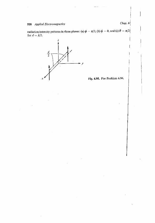
APPLIED ELECTROMAGNETICS
174
6 APPLIED ELECTROMAGNETICS l In Chapter 2 we set our goal to learn how to interpret Maxwell's equations and the associated constitutive relations and to use them to discuss various applications. In the preceding chapters we achieved the first task, namely that of introducing and understanding Maxwell's equations, V • D = p V • B = 0 VxE= -�� VxH=J+ aD at and the various related concepts. We now have the basic electromagnetic theory necessary to venture into the realm of applied electromagnetic theory to which this chapter serves as an introduction. The topics of applied elec- tromagnetic theory are varied, but perhaps the most important among them are concerned with the field basis of circuit theory and with electro- magnetic waves. This is reflected in the topics covered in this chapter. 347
-
Upload
khangminh22 -
Category
Documents
-
view
0 -
download
0
Transcript of APPLIED ELECTROMAGNETICS
6
APPLIED ELECTROMAGNETICS l
In Chapter 2 we set our goal to learn how to interpret Maxwell's equations and the associated constitutive relations and to use them to discuss various applications. In the preceding chapters we achieved the first task, namely that of introducing and understanding Maxwell's equations,
V • D = p
V • B = 0
VxE= -��
VxH=J+ aD
at
and the various related concepts. We now have the basic electromagnetic theory necessary to venture into the realm of applied electromagnetic theory to which this chapter serves as an introduction. The topics of applied electromagnetic theory are varied, but perhaps the most important among them are concerned with the field basis of circuit theory and with electromagnetic waves. This is reflected in the topics covered in this chapter.
347
PART I.
6.1 Poisson's Equation
Statics, Quasistatics, and
Distributed Circuits
Maxwell's equations for the static electric field are given by V • D p
VxE O
(6-1) (6-2)
In view of (6-2), E can be expressed as the gradient of a scalar potential vas we learned in Section 2.12. Thus we have
and E=-VV
D =€E -€VV Substituting (6-4) into (6-1), we obtain
V • €VV -p or
(6-3)
(6-4)
(6-:5) where V2 Vis the Laplacian of V. Equation (6-5) is the differential equati(m for the electrostatic potential Vin a region of volume charge density p. If we assume that 1: is a constant in the region, Vt: is equal to zero so that (6-..5) reduces to
v2v
Equation (6-6) is known as Poisson's equation. If the medium is charge free, then p O and (6-6) reduces to
v2 v o (6-7)
which is known as Laplace's equation. In this section we discuss the appli-cations of Poisson's equation by considering two examples.
EXAMPLE 6-1. Charge is distributed with uniform density p0
C/m3 throughmh a
sphere of radius a centered at the origin. It is desired to find the electros�atic potential and hence the electric field intensity both inside and outside: the sphere by using Poisson's equation for r < a and Laplace's equation 1 for r> a. I
From Poisson's and Laplace's equations, we have
{ Po for r < a v2 v= € 0 \ for r > a
Because of the spherical symmetry of the charge distribution, the pot�ntial is a function of r only. Thus all derivatives of V with respect to 8 and f are348
I
.1
351 Poisson's Equation Sec. 6.1
initial velocity and (b) the number of electrons emitted from the cathode is limited not by the cathode temperature but by the space charge between the cathode and the anode. For steady current flow under these conditions, the electric field at the cathode is zero. If it were some nonzero value and directed towards the cathode, the electrons would be emitted from the cathode with some acceleration and the current would then be temperature limited but not space-charge limited. (In the actual case, the field intensity is slightly nonzero and directed towards the cathode, since no electrons would leave the cathode otherwise.) If the field intensity were some nonzero value and directed towards the anode, there would be no space charge, since the electrons could not leave the cathode. It is desired to find the potential distribution and hence the space charge distribution between the cathode and the anode.
Let V be the potential at a distance x from the cathode, which is considered to be at zero potential. Then the work done by the electric field in moving an electron through a distance x from the cathode is equal to I e I V,where e is the charge of the electron. This work must be equal to the kinetic energy acquired by the electron. Thus, denoting v = v(x)t as the velocity of the electron, we have
JeJ V= !mv2 (6-15) where m is the electronic mass. From (6-15), we get v = ,.j2 J e I V/m so that
v = �21el vi (6-16) m x
If p(x) is the density of the space charge constituted by the electrons, the current density J is given by
J = pv = pJ'!I!?- v1/2jx (6-17)
For steady current flow, (6-18)
where J0
is a constant. Comparing the right sides of (6-17) and (6-18) we obtain
p=J fmv-112
o,y 2fel From Poisson's equation, we now have
d2V = _ _p__ = -[Jo fmJ v-112 = kv- 112 (6-19) dx2
€0 €0'V2fel where k = -(J
0/€
0) ,.jm/J 2e I is a constant. Equation (6-19) is the differential
equation for V in the region between the cathode and the anode. To solve for V, we multiply the left and right sides of (6-19) by 2(dV/dx) dx and 2 dV,
352 Applied Electromagnetics Chap. 6 I I
respectively, to obtain
2 dV a(dV) = 2k v-112 dVdx dx (6-20)
Integrating both sides of (6-20), we get
(�:r = 4kv 112 + Awhere A is the constant of integration to be evaluated from the boundarycondition for dV/dx at the cathode. But dV/dx is the negative of the electricfield intensity. Since the electric field intensity as well as the potential are zero at the cathode, A is equal to zero. Thus
or
dV = 2J7Zv1;4 dx I
v- 114 dV = 2,,/k dx I
(6-21) I
I
Integrating both sides of (6-21), we obtain I I jV314 = 2,,/kx + BI
where B is the constant of integration. To evaluate B, we note that .V = ti for x = 0. Hence B = 0, giving us
I v = Gfl x)4/3 Finally, from the condition that V = V0
for x = d, we have Vo = Gfl d)4/3
so that
I
( X )4/3V= V0 d (6-2;2)
Equation (6-22) is the required solution for the potential between the two plates. The electric field intensity is given by
!
E = -VV = _ av i = _ _±_ Vo (�)ll3iax x 3 d d x
The space charge density is given by aE 4 f V ( x )
-213
p = fo V • E = fo axx = -9 dz
o d
The current density is given by
J = p /2Tef v112i = _ _±_€
/2Tef v�12 i-v � x 9 o,y � az x
I This equation is known as the Child-Langmuir law. The negative sign /for J arises from the fact that the current flow is opposite to the directioq of motion of the electrons.
I
353 Laplace's Equation Sec. 6.2
6.2 Laplace's Equation
A very important class of problems encountered in practice are those for which the charges are confined to the surfaces of conductors. For such problems, either the charge distribution on the surfaces of the conductors, or the potentials of the conductors, or a combination of the two are specified and the problem consists of finding the potential and hence the electric field in the charge-free region bounded by the conductors. Obviously, the potential in the charge-free region satisfies Laplace's equation
v2v= o (6-7)
assuming € to be constant. Hence the solution consists of finding a potential that satisfies Laplace's equation and the specified boundary conditions. Since the right side of Laplace's equation is zero irrespective of the boundary conditions, we can obtain a general solution for the potential that satisfies a particular simplified form of Laplace's equation once and for all. The general solution consists of arbitrary constants of integration, which are evaluated by using the boundary conditions for the specific problem.
Let us consider the cartesian coordinate system. In the general case for which the potential is a function of all three coordinates x, y, and 'z, Laplace's equation is given by
(6-23)
However, if the potential is a function of only one of the coordinates, say x, and independent of the other two, we obtain a simplified version of Laplace's equation as
a2v d2 v
ax2 = dx2
=
0
Integrating (6-24) with respect to x twice, we obtain
V= Ax+ B
(6-24)
(6-25)
where A and B are the arbitrary constants of integration. Equation (6-25) is the general solution for the electrostatic potential in a charge-free region for the case in which the potential is a function of x only. In other words, all problems for which the potential varies with x only but having different boundary conditions must have solutions of the form given by (6-25). Only the values of the arbitrary constants A and B differ from one problem to the other. Thus, having found the general solution once and for all, it is a matter of fitting the given boundary conditions to evaluate the arbitrary constants for obtaining the particular solution to the problem. Let us consider a simple example.
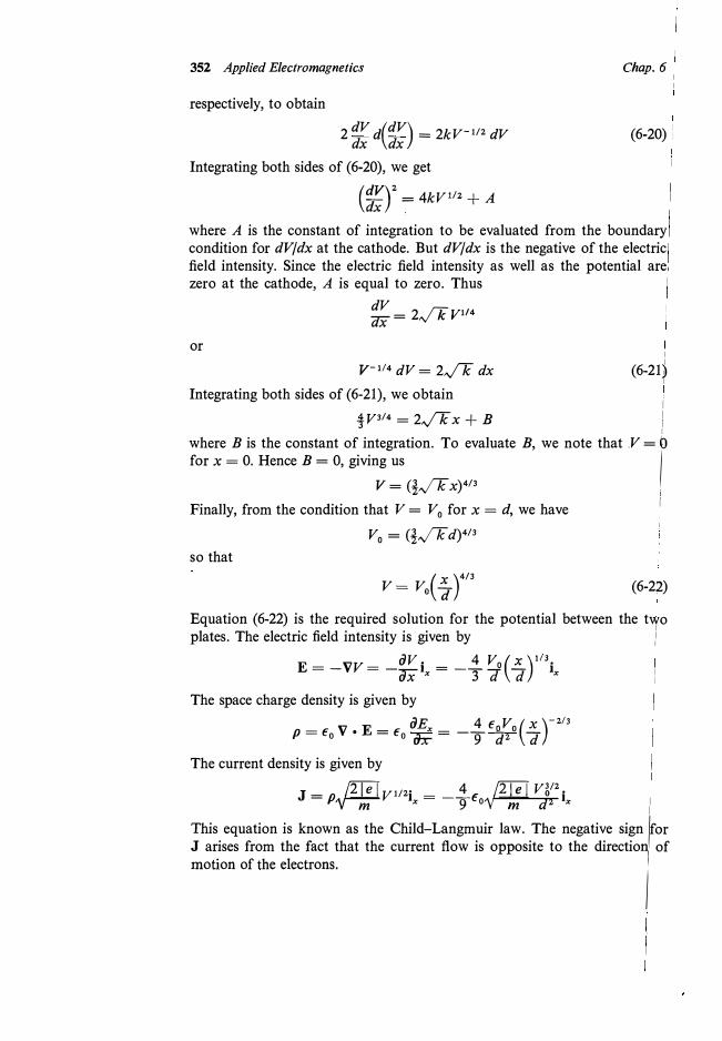
Ex MPLE 6-3. Two parallel conducting plates occupying the planes x = 0 and x = d are kept at potentials V = 0 and V = V0 , respectively, as shown in
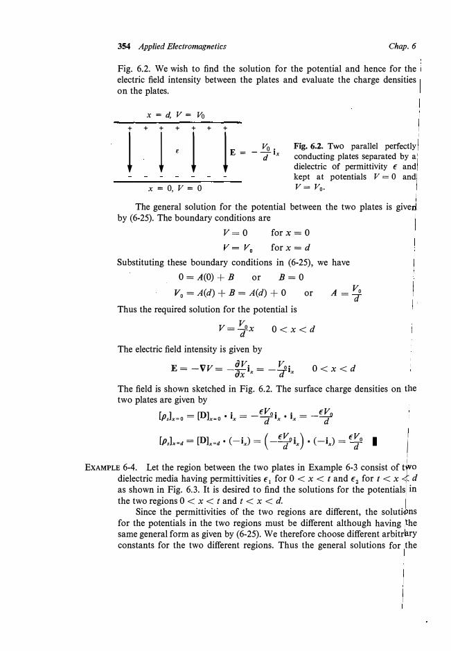
354 Applied Electromagnetics Chap. 6
Fig. 6.2. We wish to find the solution for the potential and hence for the · electric field intensity between the plates and evaluate the charge densities on the plates.
x = d, V = Vo
+ + + + + + +
! ! ' ! !E-x = 0, V = 0
Vo. -dlx
Fig. 6.2. Two parallel perfectly conducting plates separated by a dielectric of permittivity € and kept at potentials V = 0 and V= Vo.
The general solution for the potential between the two plates is give by (6-25). The boundary conditions are
V= 0 for x = 0 for x = d
Substituting these boundary conditions in (6-25), we have 0 = A(O) + B or B = 0
V0 = A(d) + B = A(d) + 0
Thus the required solution for the potential is or
V= �0x O < x < d
A - Vo - d
The electric field intensity is given by
E=-VV=_avi =_voi ax
x d
x O<x<d
The field is shown sketched in Fig. 6.2. The surface charge densities on Hie two plates are given by
[ ] [DJ · €Vo· · €Vo Ps x=O = x=O O 1x = -dlx O Ix = -d
[p.J.-, �[DJ.-,. H.) � (-·�···) . (-i,) � ·�· I II I
EXAMPLE 6-4. Let the region between the two plates in Example 6-3 consist of io dielectric media having permittivities €1 for O < x < t and €2 fort< x � das shown in Fig. 6.3. It is desired to find the solutions for the potentials in the two regions O < x < t and t < x < d. / Since the permittivities of the two regions are different, the soluti nsfor the potentials in the two regions must be different although having he same general form as given by (6-25). We therefore choose different arbitr ry constants for the two different regions. Thus the general solutions for the
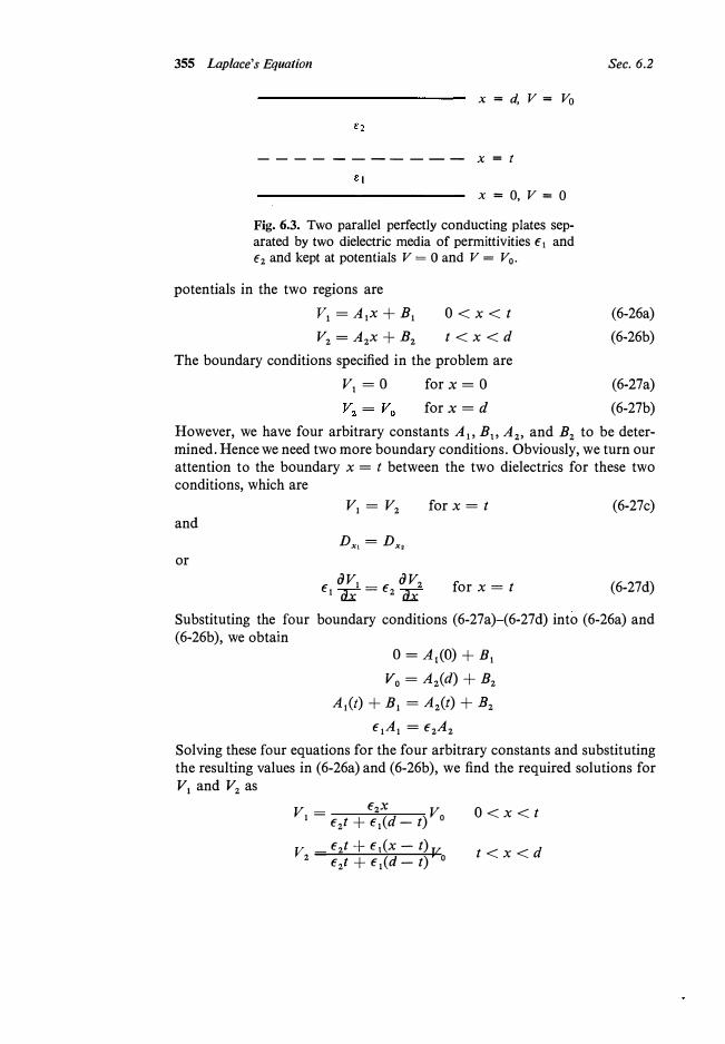
355 Laplace's Equation
x = d, V = Vo
----------- x = t
x = 0, V = 0
Fig. 6.3. Two parallel perfectly conducting plates separated by two dielectric media of permittivities € 1 and €2 and kept at potentials V = 0 and V = V0 •
potentials in the two regions are
v1 = A 1x + B1
V2 = A 2x + B2
O<x<t
t<x<d
The boundary conditions specified in the problem are
V1
= o for x = o
for x = d
Sec. 6.2
(6-26a)
(6-26b)
(6-27a)
(6-27b)
However, we have four arbitrary constants Ai , Bi , A2, and B
2 to be deter
mined. Hence we need two more boundary conditions. Obviously, we turn our attention to the boundary x = t between the two dielectrics for these two conditions, which are
V1 = V2 for x = t (6-27c) and
Dx1 = Dx, or
€ a v1 _ € a vzl ax - 2 ax
for x = t (6-27d)
Substituting the four boundary conditions (6-27a)-(6-27d) into (6-26a) and (6-26b), we obtain
0 = A1(0) + B 1
V0 = Az(d) + B2
Ai(t) + B1 = Az(t) + B2
€1A1 = €2A2Solving these four equations for the four arbitrary constants and substituting the resulting values in (6-26a) and (6-26b), we find the required solutions for V1 and V2
as
V = €zX V I €zf + €1(d -f) 0
v =€2t+€,(x -t)v 2 €zl + €1(d -t) o
O<x<t
t<x<d
356 Applied Electromagnetics Chap. 6
The potential at the interface x = t is
I I
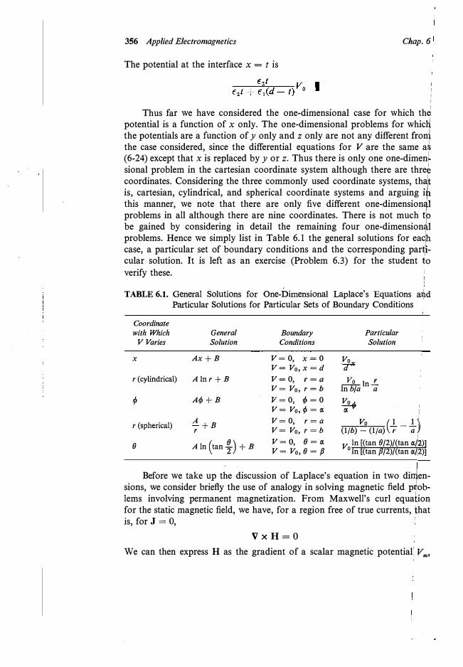
Thus far we have considered the one-dimensional case for which thd potential is a function of x only. The one-dimensional problems for which'. the potentials are a function of y only and z only are not any different froni the case considered, since the differential equations for V are the same a� (6-24) except that xis replaced by y or z. Thus there is only one one-dimen� sional problem in the cartesian coordinate system although there are thre¢ coordinates. Considering the three commonly used coordinate systems, th?-/t is, cartesian, cylindrical, and spherical coordinate systems and arguing iP, this manner, we note that there are only five different one-dimension'! problems in all although there are nine coordinates. There is not much tpbe gained by considering in detail the remaining four one-dimension'!problems. Hence we simply list in Table 6.1 the general solutions for ea9� case, a particular set of boundary conditions and the 'Corresponding partjicular solution. It is left as an exercise (Problem 6.3) for the student to verify these.
TABLE 6.1. General Solutions for One-Dimensional Laplace's Equations amd Particular Solutions for Particular Sets of Boundary Conditions
Coordinate with Which
V Varies
x
r (cylindrical)
r (spherical)
(}
General Solution
Ax+B
Alnr+B
A</>+ B
A +Br
A In (tan f) + B
Boundary Conditions
V= 0, x = 0V= Vo, x = dV= 0, r = a V= Vo, r = bV= 0, </> = 0V = Vo,</>= ocV= 0, r = aV= Vo, r = b V= 0, (} = ocV= Vo,(}= p
Voxd
Particular Solution
---1:'.L In .!..ln b/a a Vo'P():
I
I i Vo (1 1\
(1/b) - (1/a) r - a1I
'
V ln [(tan 0/2)/(tan oc/�)]O ln [(tan P/2)/(tan oc/12)]
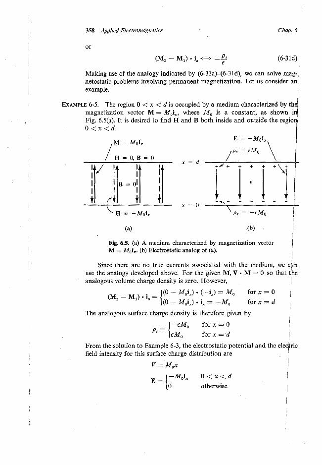
Before we take up the discussion of Laplace's equation in two diniensions, we consider briefly the use of analogy in solving magnetic field pJoblems involving permanent magnetization. From Maxwell's curl equation for the static magnetic field, we have, for a region free of true currents, that is, for J = 0,
VxH=O
We can then express H as the gradient of a scalar magnetic potentiaf Vm,
357 Laplace's Equation Sec. 6.2
that is, (6-28)
Substituting B = µo(H + M) in Maxwell's divergence equation for B, we
have V • B = V • µo
(H + M) = 0or
V • H = -V • M
Substituting (6-28) into (6-29), we obtain V2Vm = V • M,
(6-29)
(6-30) Comparing (6-28) and (6-30) with (6-3) and (6-6), respectively, we observe the following analogy:
H +---->- E Vm -<�V
V • M -<� _.!!_€
(6-31a) (6-3lb) (6-31c)
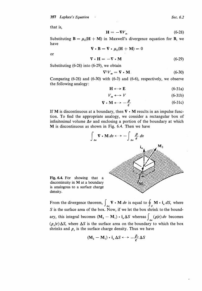
If M is discontinuous at a boundary, then V • M results in an impulse function. To find the appropriate analogy, we consider a rectangular box of infinitesimal volume !iv and enclosing a portion of the boundary at which M is discontinuous as shown in Fig. 6.4. Then we have
f V·Mdv--f .f!_dv Av Av
€
Fig. 6.4. For showing that a discontinuity in M at a boundary is analogous to a surface charge density.
From the divergence theorem, f V • M dv is equal to ,( M • i. dS, where Av Ys
S is the surface area of the box. Now, if we let the box shrink to the bound-ary, this integral bec�mes (M2
- M1) • i. l!:..S whereas f (p/€) dv becomes
Av
(p,/€) l!:..S, where l!:..S is the surface area on the boundary to which the boxshrinks and p, is the surface charge density. Thus we have
(M2 - M1) • i. l!:..S- - �, l!:..S
359 Laplace's Equation Sec. 6.2
The surface charge distribution and the electric field lines are shown inFig. 6.5(b). Now, from (6-31a), the required magnetic field intensity isgiven by
O<x<d
otherwiseThe corresponding magnetic flux density is
B = (H + M) = {µo(-Mot + Mot)µ0
µo(O + 0) =0
These are shown in Fig. 6.5(a). I
O<x<d
otherwiseeverywhere
We now consider the solution of Laplace's equation in two dimensions. If the potential is a function of the two coordinates x and y and independentof z, then it satisfies the equation
a2v a2v o (6-32)ax2 + ay2 =
Equation (6-32) is a partial differential equation in two dimensions x and y.
The technique by means of which it is solved is known as the "separationof variables" technique. It consists of assuming that the solution for thepotential is the product of two functions, one of which is a function of xonly and the second, a function of y only. Denoting these functions to beX and Y, respectively, we have
V(x, y) = X(x) Y(y) (6-33)Substituting this assumed solution into the differential equation, we obtain
d2X d2 Y y dx2 + X dy2 = 0
Dividing both sides of (6-34) by XY and rearranging, we get1 d2X 1 d2YX dx2 = --y dy2
(6-34)
(6-35)
The left side of (6-35) involves x only whereas the right side involves y only.Thus Eq. (6-35) states that a function of x only is equal to a function of yonly. A function of x only other than a constant cannot be equal to a functionof y only other than the same constant for all values of x and y. For example,2x is equal to 4y for only those pairs of values of x and y for which x = 2y.But we are seeking a solution which is good for all pairs of x and y. Thus theonly solution which satisfies (6-35) is that each side of (6-35) must be equalto a constant. Denoting this constant as OG2, we have
!:f = OG2 X (6-36a)
I I
I I
362 Applied Electromagnetics Chap. 6, I
I
I
where A' = 2AD. Next, applying boundary condition (6-39b) to (6-40)\���
O = A' sinh oi:x sin oi:b for O < x < aITo satisfy this equation without obtaining a trivial solution of zero for thr potential, we set
sin oi:b = 0or
oi:b = nn n=l,2,3, ...
n=l,2,3, ... (6-4 )
Since several values of oi: given by (6-41) satisfy the boundary conditio , several solutions are possible for the potential. To take this fact into accou t, we write the solution as the superposition of all these solutions multipli d by different arbitrary constants. In this manner we obtain
� V(x' Y) = " A' s· h nnx . nny
n=l,T,'J, ... n Ill b Sill b for O <y < b
Finally, applying the boundary condition (6-39d) to (6-42), we get
V . ny " A' . h nna . nny "" 0 b (6 43)O Slll b = n�t,T,'J,... n Sill b Sill b 10r < y <
- 1 On the right side of (6-43), we have an infinite series of sine terms in y wherfason its left side, we have only one sine term in y. Equating the coefficients of the sine terms having the same arguments, we obtain
Sill-= A, . h nna {Vo for n = 1
" b O for n -=;t:. Ior
I
A'= � 1 sinh (na/b)
I A:= 0 for n -=;t:. ISubstituting this result in (6-42), we obtain the required solution for Va�
V(x y) = V s!nh (nx/b) sin ny (J-44) ' 0 smh (na/b) b
l Having found the solution, it is always worthwhile to check if it safsfies Laplace's equation and the given boundary conditions to make sure thjt noerror was made in obtaining the solution. The above solution does s tisfy these two criteria. I
If the solution, irrespective of how it is obtained, satisfies Lap ace's equation and the specified boundary conditions, it is the solution acco dingto the uniqueness theorem. To prove this theorem, let us assume t the contrary that two solutions V1 and V2 are possible for the same pro lem.
363 Laplace's Equation Sec. 6.2
Then each of these must satisfy Laplace's equation so that
v2v1 = o (6-45a)
(6-45b) v2 v2 = o
The difference Va = V1 - V
2 must also satisfy Laplace's equation. Thus
v2va = V2CV1 - V2) = v2v1 - v.2v2 = o (6-46)
Also, both V1
and V2 must satisfy the same boundary conditions, so that
Wals = W1 - V2]s = W1Js - W2Js = 0 (6-47)
where S represents the boundary surface. Now, using the vector identity
V •(VA)= VV •A+ VV • A
we have
(6-48)
Integrating both sides of (6-48) throughout the volume enclosed by the boundary S, we have
5 (V • Va VVa) dv = f Wa V2Va) dv + f IVVal2 dv (6-49)
vol vol vol
However, from the divergence theorem and from (6-47),
5 (V • Va VVa) dv = ! Wa VVa) • dS = 0 vol j S
Also, noting that V2Va = 0 in accordance with (6-46), Eq. (6-49) reduces to
5 I VVa 12 dv = 0 (6-50)
vol
Since I VVa 12 is positive everywhere, the only way that (6-50) can be satisfied
is if I VVa 12 is equal to zero throughout the volume of interest. Thus
VVa= 0
or
Va = V1 - V2 = constant (6-51)
However, Va is equal to zero on the boundaries and hence the constant on the right side of (6-51) must be zero, giving us V
1 = V
2 throughout the volume
of interest and thereby proving the uniqueness theorem.
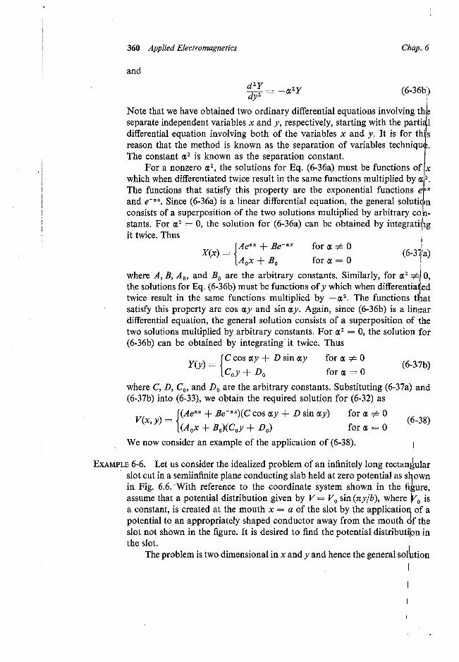
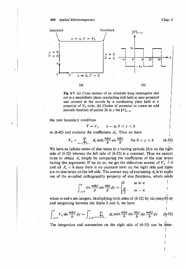
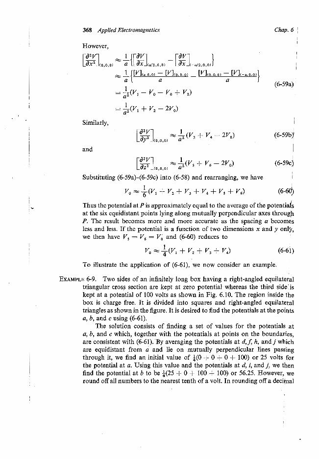
ExAMPLE 6-7. The rectangular slot of Fig. 6.6 is covered at the mouth x = a by a conducting plate which is kept at a potential V = V
0, a constant, making
sure that the edges touching the corners of the slot are insulated as shown by the cross-sectional view in Fig. 6.7(a). We wish to find the potential in the slot for this new boundary condition.
Since the boundary conditions (6-39a)-(6-39c) remain the same, all we have to do to find the required solution for the potential is to substitute
365 Laplace's Equation Sec. 6.2
changed, giving us
fb
=
fb V0
sin mny dy = _ � A� sinh nna sin mny sin nny dyy=O b n-1,2,3,... b y=O b b
or
or
Vab (I - cos mn) = (A' sinh mna)!!_mn m
b 2
{4V
0 1
A�= ;n sinh (mna/b) form odd
form even (6-54)
Substituting this result in (6-42), we obtain the required solution for the potential inside the slot as
V = � 4_V_0
sinh (nnx/b\in-nn_y
n=l,3,s, ..• nn sinh (nna/b) b (6-55)
The above procedure for evaluating the constants A� can also be appreciated by recognizing that the right side of (6-52) is the Fourier series for an odd periodic function in y having the period 2b. We must then have an odd periodic function -0f period 2b on the left side of (6-52). To achieve this, we note that, since the solution is for inside the slot only, it is sufficient if we satisfy the boundary condition for [Vlx=a for the range O < y < b. We are therefore at liberty to choose [Vlx=a for the remainder of y so that an odd periodic function of period 2b is obtained. Obviously, the choice must be as shown in Fig. 6.7(b). The evaluation of A� then consists of finding the coefficients of the Fourier series for this function and comparing these with the coefficients of the series on the right side of (6-52). The steps leading from (6-53) to (6-54) are essentially equivalent to this procedure.
Another class of problems for which Laplace's equation is applicable is those involving the determination of steady current in a conducting slab under the application of potential difference between different surfaces of the slab. For the steady-current condition we have
V •Jc= 0 where Jc is the current density. Replacing Jc by aE, where a is the conductivity of the slab, we have
V • aE = 0 Substituting for E in terms of V, we get
-V•aVV=OIf a is constant, Eq. (6-56) reduces to
V2V=0
(6-56)
366 Applied Electromagnetics Chap. 6
Thus the potential associated with the steady current flow satisfies Laplace's equation. Hence the solution for this potential can be obtained in exactly the same manner as for the charged conductor problems. In fact, the solution for the potential for a particular steady-current problem can be written down by inspection if the solution for the potential for an analogous charged conductor problem is already known and vice versa. Having found the solutio for the potential, the current density can be found by using
Jc= aE = -a VV (6-57)
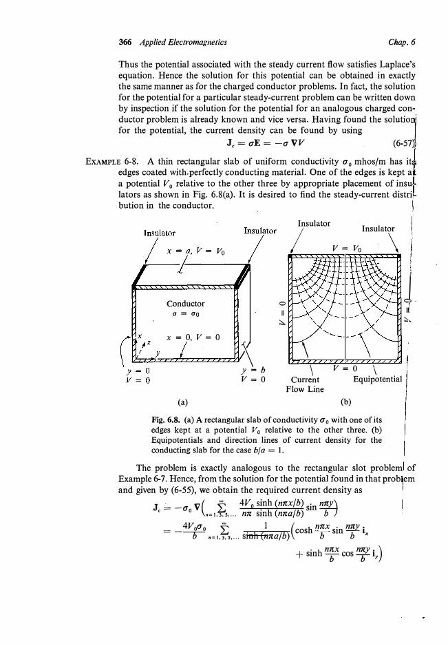
EXAMPLE 6-8. A thin rectangular slab of uniform conductivity a O
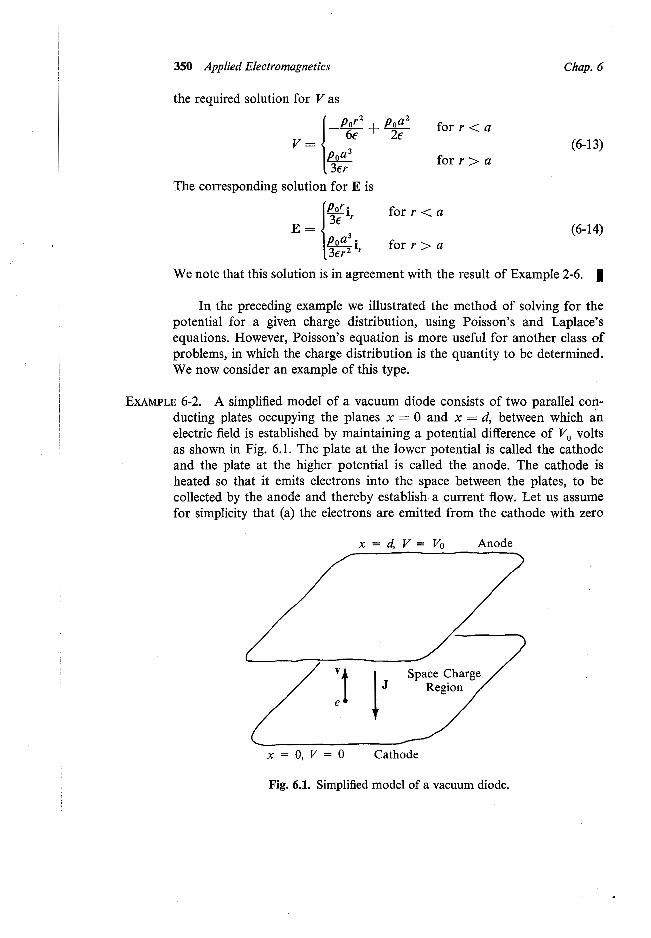
mhos/m has it edges coated with. perfectly conducting material. One of the edges is kept at a potential V0
relative to the other three by appropriate placement of insu -lators as shown in Fig. 6.8(a). It is desired to find the steady-current distribution in the conductor.
Insulator Insulator
I
Conductor a = ao
Vo
x = 0, V = 0
0
II
�
\ y = b
V= Vo \
\ V=O \ \
V=O Current Equipotential Flow Line
(a) (b)
Fig. 6.8. (a) A rectangular slab of conductivity a O with one of itsedges kept at a potential V0 relative to the other three. (b) Equipotentials and direction lines of current density for the conducting slab for the case bf a = 1.
� ::,.
The problem is exactly analogous to the rectangular slot problem of Example 6-7. Hence, from the solution for the potential found in that prob em and given by (6-55), we obtain the required current density as
J = -ao v( f 4V0 sinh (nnx/b) sin nny)c n= ,. 3, s. .. . nn sinh (nna/ b) b
= -4VoO'o f . 1 (cosh nnx sin nny ixb n=l,J,s, ... smh (nna/b) b b
+ sinh nnx cos nny i )b b y
372 Applied Electromagnetics Chap. 6
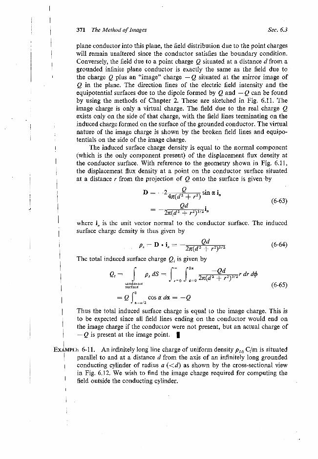
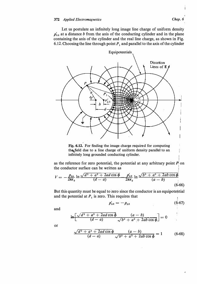
Let us postulate an infinitely long image line charge of uniform density p�0 at a distance b from the axis of the conducting cylinder and in the plane containing the axis of the cylinder and the real line charge, as shown in Fig. 6.12. Choosing the line through pointP
1 and parallel to the axis of the cylinder
Equipotentials
Fig. 6.12. For finding the image charge required for computing thyeld due to a line charge of uniform density parallel to an infinitely long grounded conducting cylinder.
as the reference for zero potential, the potential at any arbitrary point P/ on the conductor surface can be written as
��������I
V = _ PLD In ,jd2 + a2 + 2adcos cf,_ p�0 In ,jb2 + a2 + 2ab cos ct,I2n€0 (d...,... a) 2n€0 (a - b)
1
(6�66) But this quantity must be equal to zero since the conductor is an equipote*tial and the potential at P
1 is zero. This requires that
and
or
P�o = -PLo
In[,jd2 + a2 + 2adcoscf, (a - b) ]- 0 (d- a) ,jb2 + a2 + 2abcoscf, -
,jd2 + a2 + 2adcoscf, (a - b) _ 1 (d- a) ,jb2 + a2 + 2abcoscf,-
I
(6-67) I
(6-68)
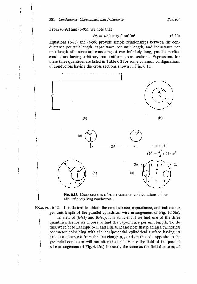
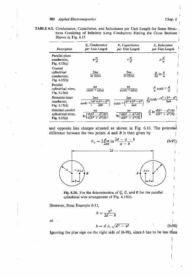
373 Conductance, Capacitance, and Inductance Sec. 6.4
To find the solution for (6-68), let us consider <p = 0. We then have
(d + a)(a - b) = 1d-a a+b or
a2 = bd (6-69)
which satisfies (6-68) for all <p. Thus, an image line charge of uniform density
-p Lo and located at a distance b = a2 / d from the axis of the cylinder satisfiesthe equipotential requirement for the grounded conducting cylinder. Thefield outside the cylinder is therefore exactly the same as the field set up bythe actual line charge of density h
o at distance d from the axis and the
image line charge of density -p Lo at distance a2 / d from the axis. The directionlines of the electric field intensity and the associated equipotential surfacescan be obtained by the methods learned in Chapter 2. These are shownsketched in Fig. 6.12. It is left as an exercise (Problem 6.15) for the studentto show that the total induced surface charge per unit length of the cylinderis equal to the image charge density -PLo
. The field inside the cylinder is, of course, equal to zero since the image charge is only a virtual charge. I
Proceeding in the same manner as in the preceding example, we can obtain the image charge for a point charge near a grounded spherical conductor. If the point charge Q is situated at a distance d from the center of the spherical conductor of radius a, the image charge is a point charge of value
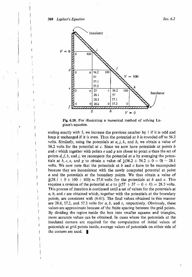
- Qa/ d. It lies at a distance a2 / d from the center of the sphere, along theline joining the center to the charge Q and on the side of Q. We leave thederivation as an exercise (Problem 6.16) for the student. The method ofimages can also be applied for finding fields due to charges in the presence of dielectrics. We will, however, not pursue that topic here.
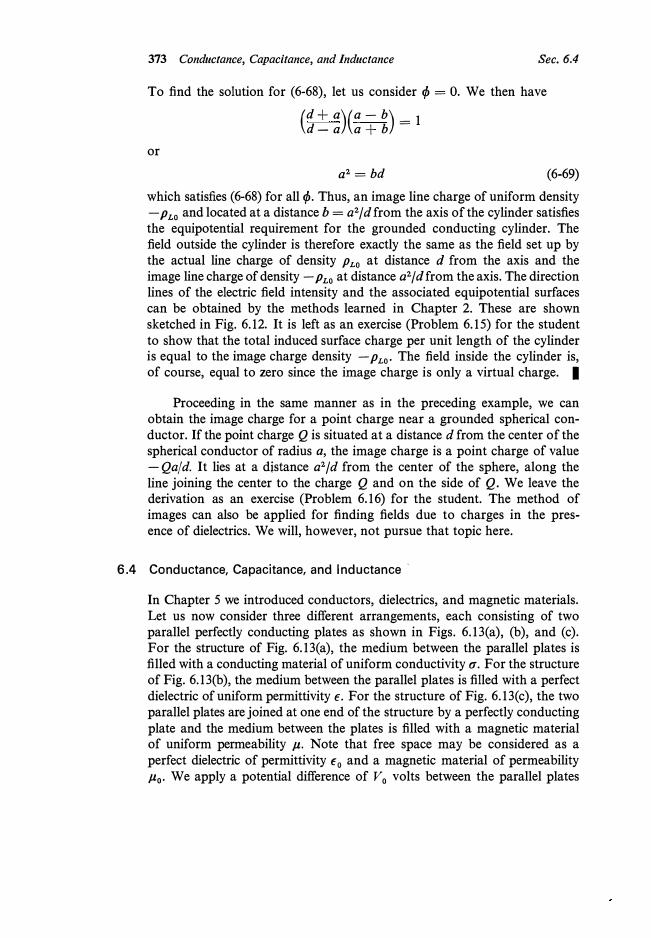
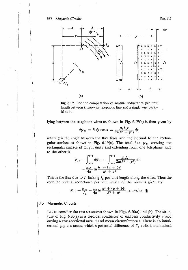
6.4 Conductance, Capacitance, and Inductance ·
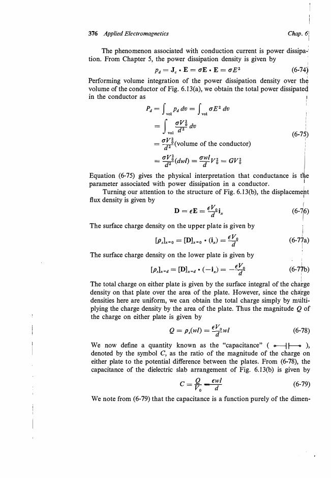
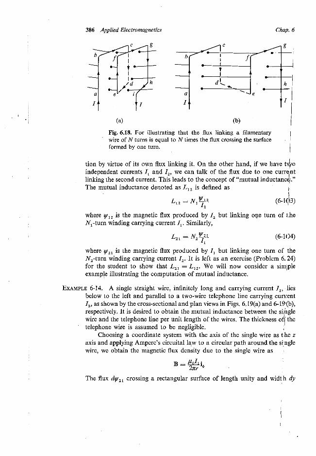
In Chapter 5 we introduced conductors, dielectrics, and magnetic materials. Let us now consider three different arrangements, each consisting of two parallel perfectly conducting plates as shown in Figs. 6.13(a), (b), and (c). For the structure of Fig. 6.13(a), the medium between the parallel plates is filled with a conducting material of uniform conductivity a. For the structure of Fig. 6.13(b), the medium between the parallel plates is filled with a perfect dielectric of uniform permittivity E. For the structure of Fig. 6.13( c ), the two parallel plates are joined at one end of the structure by a perfectly conducting plate and the medium between the plates is filled with a magnetic material of uniform permeability µ. Note that free space may be considered as a perfect dielectric of permittivity €
0 and a magnetic material of permeability
µ0 • We apply a potential difference of V
0 volts between the parallel plates
374 Applied Electromagnetics
e µ
(a) f, (b) f, (c)
V = Vo V = Vo
[HilJ illIDJ x8
x x/0x x
x x x x x
x x/ 0x x x
V=O V=O
Fig. 6.13. Three different structures each consisting of two
parallel perfectly conducting plates. The medium between the
plates is a conductor for structure (a), a dielectric for structure
(b), and a magnetic material for structure (c). The two plates are joined at one end by another perfectly conducting plate for
structure (c).
i
of structures (a) and (b) by connecting appropriate constant voltage sohrces which are not shown in the figure. We pass a z-directed surface cumint /
0
uniformly distributed in the y direction along the upper plate of str�cture (c) and return it in the opposite direction along the lower plate by coriinecting an appropriate constant current source which is not shown in the fitgure.
The medium between the plates of structure (a) is then characteri1kd by
an electric field from the upper to the lower plate and hence by a cond111ction current in the same direction. The medium between the plates of stnJicture (b) is characterized by an electric field only from the upper to the 1Iowerplate and no current. The medium between the plates of structure i (c) ischaracterized by a magnetic field parallel to the plates and towar�s thedirection of advance of a right-hand screw as it is turned in the sense /of thecurrent flow. Since the conduction current cannot leave the conductor� it hasto be tangential to the conductor surface. This forces the electric fidld forstructure (a) to be in the x direction. On the other hand, the electric :$eld atthe surface of a dielectric need not be tangential to it. This results in ftringingof the electric field in the case of structure (b). However, by assumi1g that
375 Conductance, Capacitance, and Inductance Sec. 6.4
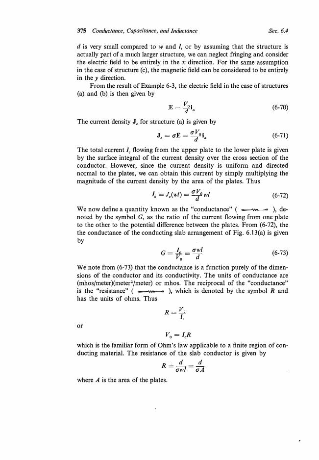
d is very small compared to w and /, or by assuming that the structure is actually part of a much larger structure, we can neglect fringing and consider the electric field to be entirely in the x direction. For the same assumption in the case of structure ( c ), the magnetic field can be considered to be entirely in the y direction.
From the result of Example 6-3, the electric field in the case of structures (a) and (b) is then given by
The current density Jc
for structure (a) is given by
J = aE = a Voj
c d x
(6-70)
(6-71)
The total current Jc
flowing from the upper plate to the lower plate is given by the surface integral of the current density over the cross section of the conductor. However, since the current density is uniform and directed normal to the plates, we can obtain this current by simply multiplying the magnitude of the current density by the area of the plates. Thus
IC= Jc
(wl) = a:0 wl (6-72)
We now define a quantity known as the "conductance" ( o-------'WI,--- ), denoted by the symbol G, as the ratio of the current flowing from one plate to the other to the potential difference between the plates. From (6-72), the the conductance of the conducting slab arrangement of Fig. 6.13(a) is given by
G = b._ = awl (6-73) V0 d We note from (6-73) that the conductance is a function purely of the dimensions of the conductor and its conductivity. The units of conductance are (mhos/meter)(meter2/meter) or mhos. The reciprocal of the "conductance" is the "resistance" ( - ), which is denoted by the symbol R and has the units of ohms. Thus
or V
o= l
cR which is the familiar form of Ohm's law applicable to a finite region of conducting material. The resistance of the slab conductor is given by
d d R =
awl=
aA where A is the area of the plates.
376 Applied Electromagnetics Chap.
The phenomenon associated with conduction current is power dissipation. From Chapter 5, the power dissipation density is given by
Pa= Jc • E = aE • E = aE2 (6-74)
Performing volume integration of the power dissipation density over th� I
volume of the conductor of Fig. 6.13(a), we obtain the total power dissipateq in the conductor as
Pa= f Pa dv = f aE2 dv
vol vol
= J andvvol
d2
aV2
= d2 ° (volume of the conductor)
I I
I
! I I I
(6-7�) I I I I
2 I
_
aV0 (d I)_ awlv2 _ GV2
J
-7 w -7 o- 0
Equation (6-75) gives the physical interpretation that conductance is t, e parameter associated with power dissipation in a conductor.
Turning our attention to the structure of Fig. 6.13(b ), the displacemeht flux density is given by
D = €E = f�ot (6-116)
The surface charge density on the upper plate is given by
[P,lx=o = [DJx=o • (iJ = f�o
The surface charge density on the lower plate is given by
[p,]x=a = [DJx-a • (-iJ = -f�o
I I
(6-77a) I i
i
I (6-77b)
I I
The total charge on either plate is given by the surface integral of the chai"ge density on that plate over the area of the plate. However, since the chalrge densities here are uniform, we can obtain the total charge simply by multiplying the charge density by the area of the plate. Thus the magnitude Q of the charge on either plate is given by
Q = p,(wl ) = €�0 wl (6-78)
We now define a quantity known as the "capacitance" ( o----j 1---- ), denoted by the symbol C, as the ratio of the magnitude of the charge on either plate to the potential difference between the plates. From (6-78), the capacitance of the dielectric slab arrangement of Fig. 6.13(b) is given by
C_ Q_ _fwl-vo - d (6-79)
We note from (6-79) that the capacitance is a function purely of the dimen-
,377 Conductance, Capacitance, and Inductance Sec. 6.4
sions of the dielectric slab and its permittivity. The units of capacitance are (farads/meter)(meter2/meter) or farads.
The phenomenon associated with the electric field in a dielectric medium is energy storage. From Chapter 5, the electric stored energy density is given by
(6-80)
Performing volume integration of the electric stored energy density over the volume of the dielectric of Fig. 6.13(b), we obtain the total electric stored energy in the dielectric as
W = f w dv = J _!__ €E 2 dv e vol e vol
2
= f _!__ EV5dv vol
2. d 2
= � €�� (volume of the dielectric)
- _!__ EV5(d t) = _!__ Ewl v2 = _!__cv2 - 2 d2 w 2 d
O 2 °.
(6-81)
Equation (6-81) gives the physical interpretation that capacitance is the parameter associated with storage of electric energy in a dielectric.
Turning our attention to the structure of Fig. 6.13(c) and neglecting fringing, the magnetic field intensity between the plates is the same as that due to infinite plane current sheets of densities given by
J= llo.-I
w z
lo. --1
w z
for x = 0
for x = d
Hence the magnetic field intensity is uniform between the plates and zero outside the plates, that is,
O<x<d
otherwise From the boundary condition for the tangential magnetic field intensity, the value of H
0 is equal to the surface current density I
0/w since the field is
zero outside the plates. Thus
and
H- Io·--1
w y
for O < x < d
for O < x < d (6-82)
The magnetic flux If/ linking the current I0
is given by the surface integral of
378 Applied Electromagnetics Chap. 6
the magnetic flux density over the area bounded by any contour along which the current flows. This area is simply the cross-sectional area of the magnetic material normal to the magnetic field lines. Since the magnetic field lines are straight, it may seem like they do not link the current. However, straight lines are circles of infinite radii and hence the magnetic field does link th� current. For the structure of Fig. 6.13(c), since the magnetic flux density is:
I
uniform, we can obtain the required magnetic flux If/ by simply multiplying; the magnetic flux density by the cross-sectional area normal to it. Th�: quantity If/ is known as the magnetic flux linkage associated with thJ,! current I
0• Thus f
If/ = B (di) = µIo di y
w
I (6-83/i)
I' 1'
We now define a quantity known as the "inductance" ( � ), denote{d by the symbol L, as the ratio of the magnetic flux linkage associated with th!
,e current I
0 to the current I
0• From (6-83), the inductance of the magnetrc
material slab arrangement of Fig. 6.13(c) is given by
L = !I!... = µdi (6-8jl) � w l
We note from (6-84) that the inductance is a function purely of the dimensio,�s of the magnetic material and its permeability. The units of inductance a1re(henrys/meter)(meter2/meter) or henrys. i The phenomenon associated with magnetic field in a magnetic materi;almedium is energy storage. From Chapter 5, the magnetic stored ener)gy density is given by
(6-85)
Performing volume integration of the magnetic stored energy density over the volume of the magnetic material of Fig. 6.13(c), we obtain the to,tal magnetic stored energy in the magnetic material as
Wm = f Wm dv = f � µH2 dv vol vol
= f .!_µn dvvol
2 W2
(6i86) = � '::2
5 (volume of the magnetic material) !
=_lµn(dwl)=_lµdln=.lLI5 2 w
2 2 W 2 Equation (6-86) gives the physical interpretation that inductance is/ the parameter associated with storage of magnetic energy in a magnetic mat�rial.
To write general expressions for the conductance, capacitance I and inductance in terms of the fields, let us consider the three structures shown
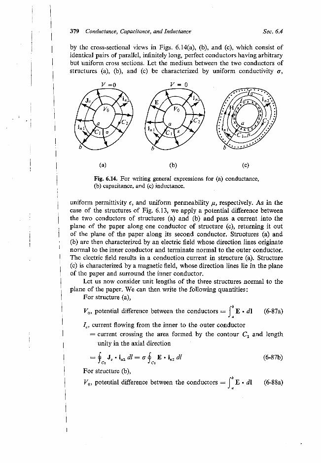
381 Conductance, Capacitance, and Inductance
From (6-92) and (6-95), we note that
£e = µE henry-farad/m2
Sec. 6.4
(6-96)
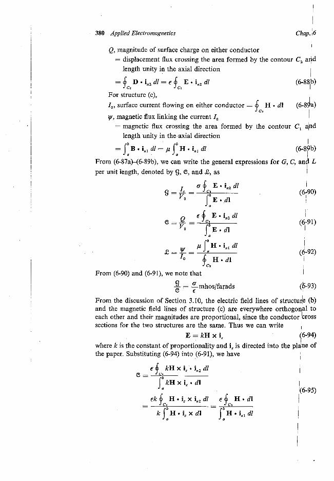
Equations (6-93) and (6-96) provide simple relationships between the conductance per unit length, capacitance per unit length, and inductance per unit length of a structure consisting of two infinitely long, parallel perfect conductors having arbitrary but uniform cross sections. Expressions for these three quantities are listed in Table 6.2 for some common configurations of conductors having the cross sections shown in Fig. 6.15.
1+------w--------+-1
r d
L __ (a) (b)
(c) G) co 2d a << d
(b2 - d 2
)4
>> a2
2a
(d) (e)
Fig. 6.15. Cross sections of some common configurations of parallel infinitely long conductors.
2a
E AMPLE 6-12. It is desired to obtain the conductance, capacitance, and inductance per unit length of the parallel cylindrical wire arrangement of Fig. 6.15(c).
In view of (6-93) and (6-96), it is sufficient if we find one of the three quantities. Hence we choose to find the capacitance per unit length. To do this, we refer to Example 6-11 and Fig. 6.12 and note that placing a cylindrical conductor coinciding with the equipotential cylindrical surface having its axis at a distance b from the line charge PLo
and on the side opposite to the grounded conductor will not alter the field. Hence the field of the parallel wire arrangement of Fig. 6.15(c) is exactly the same as the field due to equal
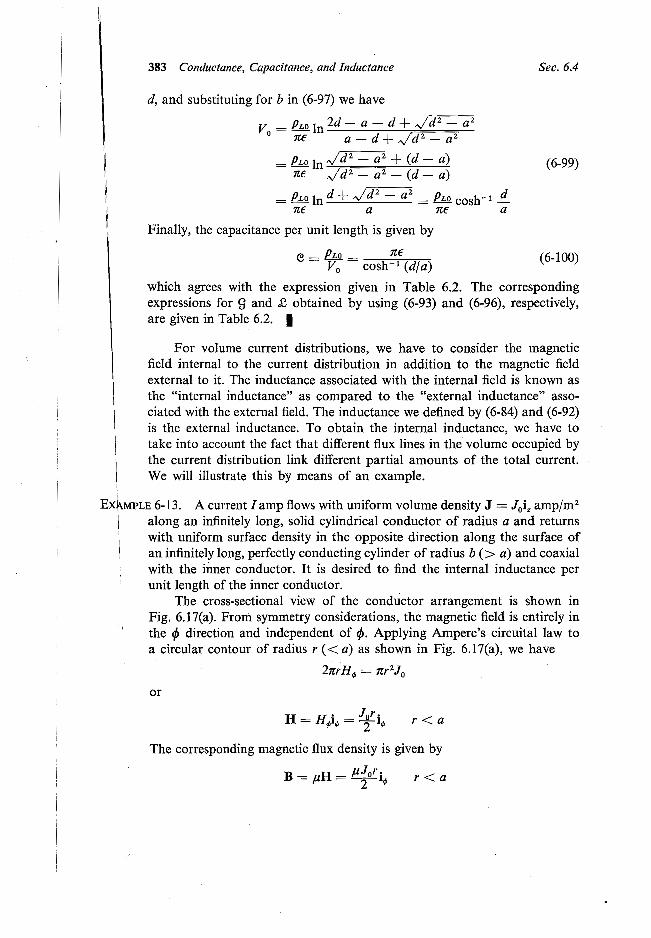
I! ii
385 Conductance, Capacitance, and Inductance Sec. 6.4
Alternatively, we can obtain £1 from energy considerations by making useof the result (6-86) that the magnetic stored energy is equal to 1;Lf2. For £1,
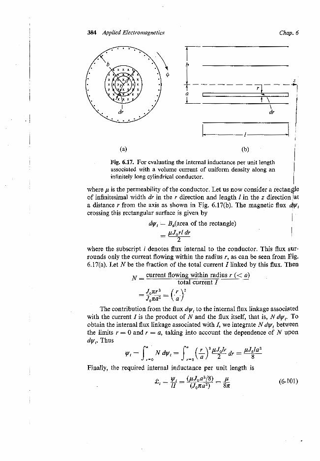
we have to consider the energy stored in the volume internal to the currentdistribution. For unit length of the conductor, this is given by
Wm, = f �µH2 dv vol
= r=o s::o r=o � µ('tr r dr d¢ dz= nµ(Ja4
The internal inductance is then given by
£, _ 2Wm, _ (nµJ5a4/8) _ J!:...
' - --yi:- - (J5n2a4) - 8n which is the same as (6-101). Finally, to find the total inductance per unitlength of the arrangement of Fig. 6. l 7(a), we have to add the external inductance due to the flux in the region a < r < b to the internal inductancegiven by (6-101). This external inductance is given in Table 6.2. I
From the steps involved in the solution of Example 6-13, we observethat the general expression for the internal inductance is
(6-102a)
where S is any surface through which the internal magnetic flux associatedwith I passes. We note that (6-102a) is also good for computing the externalinductance since for external inductance N is independent of di/I, Hence
Lext = � f S
di/I = N j (6-102b)
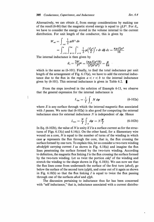
In Eq. (6-102b), the value of N is unity if /is a surface current as for the structures of Figs. 6.13(c) and 6.14(c). On the other hand, for a filamentary wirewound on a core, N is equal to the number of turns of the winding in whichcase 1/1 represents the flux through the core, that is, the flux crossing thesurface formed by one turn. To explain this, let us consider a two-turn windingabcdefghi carrying current I as shown in Fig. 6.18(a) and imagine the fluxlines penetrating the surface formed by the two-turn winding. Accordingto definition, the magnetic flux linking I is the flux crossing the surface formedby the two-turn winding. Let us twist the portion cdef of the winding andstretch the winding to the shape shown in Fig. 6.18(b). We can now see thatthe flux lines come from underneath the surface of the first turn (abed), gobelow the surface of the second turn (efgh), and come out ofit again as shownin Fig. 6.18(b) so that the flux linking I is equal to twice the flux passingthrough one of the surfaces abed and efgh.
The discussion pertaining to inductance thus far has been concernedwith "self inductance," that is, inductance associated with a current distribu-
389 Magnetic Circuits
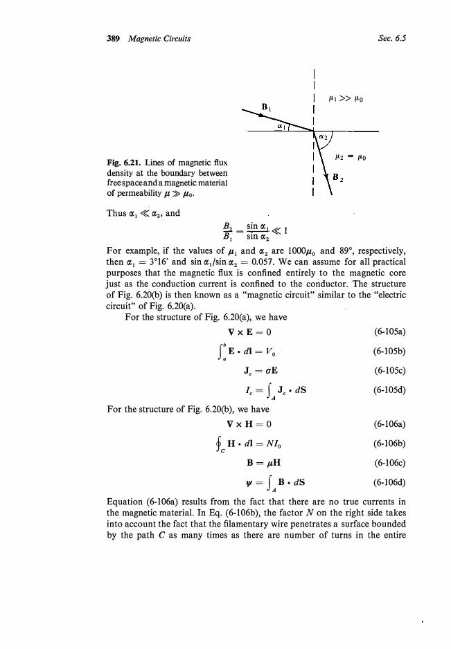
Fig. 6.21. Lines of magnetic flux density at the boundary between free space and a magnetic material of permeability µ )> µ0 •
Thus OG 1 � OG2, and B2 = s�n OG 1 � lB1
sm OG2
Sec. 6.5
/.J,1 >> /J-o
/.J,2 = /.J,O
For example, if the values of µ1
and OG2 are 1000µ0
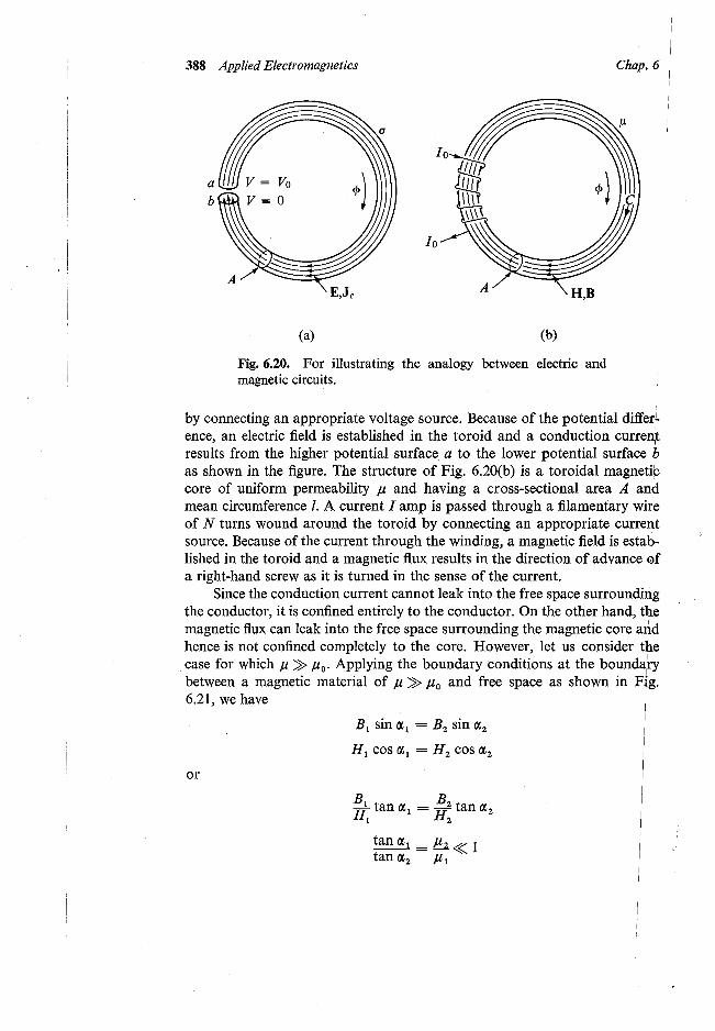
and 89°, respectively, then OG 1 = 3°16' and sin OG1/sin OG2 = 0.057. We can assume for all practical purposes that the magnetic flux is confined entirely to the magnetic core just as the conduction current is confined to the conductor. The structure of Fig. 6.20(b) is then known as a "magnetic circuit" similar to the "electric circuit" of Fig. 6.20(a).
For the structure of Fig. 6.20(a), we have V x E = 0 (6-105a)
s: E • dl = V0
Jc= aE
I = f J • dSc c
For the structure of Fig. 6.20(b), we have VxH=O
(H 0 dl=Nl0
B=µH
If/ = f A
B. dS
(6-105b)
(6-105c)
(6-105d)
(6-106a)
(6-106b)
(6-106c)
(6-106d)
Equation (6-106a) results from the fact that there are no true currents in the magnetic material. In Eq. (6-106b), the factor Non the right side takes into account the fact that the filamentary wire penetrates a surface bounded by the path C as many times as there are number of turns in the entire
391 Magnetic Circuits
6.20(b) is <R = NI
0 = _IIf/ µA
Sec. 6.5
(6-109)
In fact, if we assume that the magnetic field intensity H is uniform over the cross-sectional area and equal to its value at the mean radius of the toroid, we have
IH,t, = NI0
B,t, = µH<I> = µ�Io
If/ = B,t,A = µNf oA
<R = NI0 = _!_If/ µA
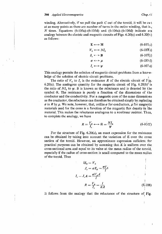
which agrees with (6-109). The equivalent circuit representations of (6-108) and (6-109) are shown in Figs. 6.22(a) and (b).
Vo ± R Nio ±
(a) (b)
Fig. 6.22. Equivalent circuit representations for the structures
of Figs. 6.20(a) and (b).
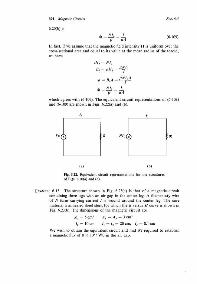
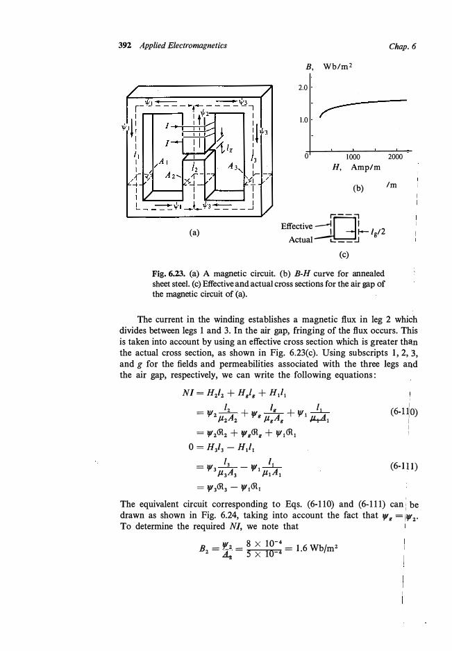
EXAMPLE 6-15. The structure shown in Fig. 6.23(a) is that of a magnetic circuitcontaining three legs with an air gap in the center leg. A filamentary wire of N turns carrying current I is wound around the center leg. The core material is annealed sheet steel, for which the B versus H curve is shown in Fig. 6.23(b). The dimensions of the magnetic circuit are
A2
= 5 cm2 A1
= A3
= 3 cm2
/2 = 10cm /1
= /3
= 20cm, lg
= 0.1 cm We wish to obtain the equivalent circuit and find NI required to establish a magnetic flux of 8 x 10⁻⁴ Wb in the air gap.
392 Applied Electromagnetics Chap. 6
(a)
B, Wb/m2
2.0
1.0
0 1000
H, Amplm
(b)
r.--;i Effective _j_Q :__ l gl2
Actual L: - - �
(c)
Fig. 6.23. (a) A magnetic circuit. (b) B-H curve for annealed sheet steel. (c) Effective and actual cross sections for the air gap of the magnetic circuit of (a).
2000
Im
The current in the winding establishes a magnetic flux in leg 2 which divides between legs 1 and 3. In the air gap, fringing of the flux occurs. This is taken into account by using an effective cross section which is greater than the actual cross section, as shown in Fig. 6.23(c). Using subscripts 1, 2, 3, and g for the fields and permeabilities associated with the three legs and the air gap, respectively, we can write the following equations:
NI= Hzf2 + Hg
lg + H/1
- 12 + lg + 11 - lfl2µ A 'fig µ A lfli
µ A2 2 g g I I
= 1J1/R2 + IJI/Rg + lfl,<R10 = Hi
3 - H1!1
- 13 l, - lf/3 µ A - lf/1
µ A 3 3 I I
= 'fl 3(R3 - 'fl I (RI
I
(6-qo) I I !
(6-111)
The equivalent circuit corresponding to Eqs. (6-110) and (6-111) can:be I
drawn as shown in Fig. 6.24, taking into account the fact that If/ g = /1f12 •
To determine the required NI, we note that
I
B - lf/2-
8 x 10⁻⁴ - 1 6 Wb/ 2
2 - A2 - 5 x 10 4 - • m
II
I I
116.6 I
I
I I I
393 Quasistatics; The Field Basis of Low-Frequency Circuit Theory
¥'3
¥'3
¥'! ¥'3
Fig. 6.24. Equivalent circuit for analyzing the magnetic circuit of Fig. 6.23(a).
Sec. 6.6
From Fig. 6.23(b), the value of H2
is 2200 amp/m. Since legs I and 3 are identical, their reluctances are equal so that the flux If/ 2 divides equally between the two legs. Thus lf/
1 = 1f1
3 = lf/2
/2 = 4 x 10⁻⁴ Wb/m2. Then
B -lf/1 - 4 x 10⁻⁴ - I 333 Wb/ 2
i - A1 - 3 x 10 4 - • m
From Fig. 6.23(b), the value of H1
is 475 amp/m. The effective cross section of the air gap is (,./) + l
g)2 = 2.34 cm 2. The flux density in the
air gap is
B - 'fig - 8 x 10⁻⁴ - I 46 Wb/ 2 g - Ag - 2.342 x 10⁻⁴ -
. m
The magnetic field intensity in the air gap is
H = Bg = Bg = 1.46 = 0.1162 x 10⁷ Wb/m2
g µg
µ0
4n X 10 7
From (6-110), we then have
NI= H2!2
+ Hglg + H
1!1
= 2200 x 0.10 + 0.1162 x 107 x 10-3 + 475 x 0.20
= 1477 amp-turns
We note that a large part of the ampere-turns is due to high reluctance of the air gap. I
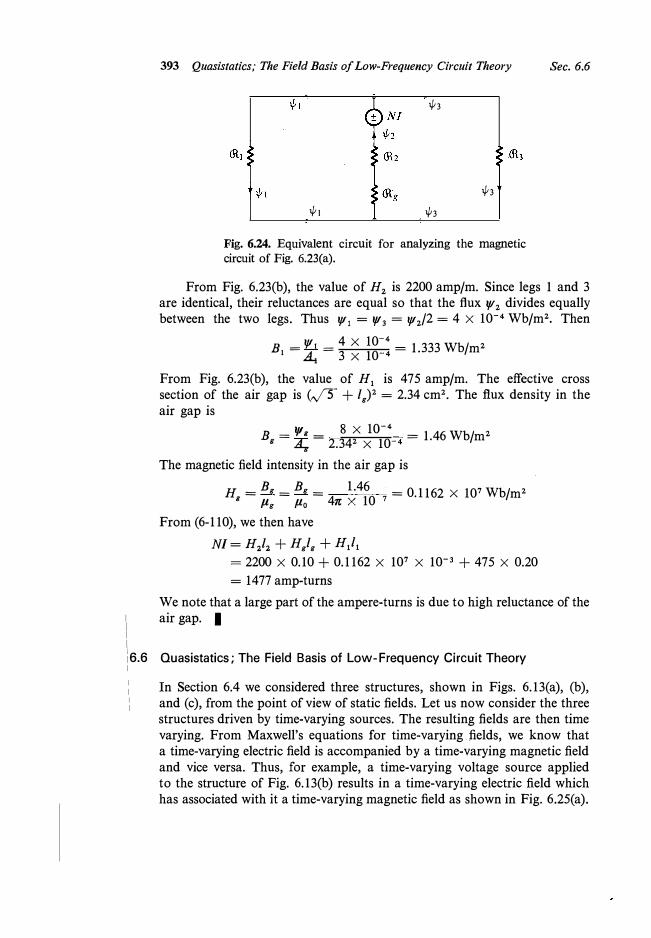
Ouasistatics; The Field Basis of Low-Frequency Circuit Theory
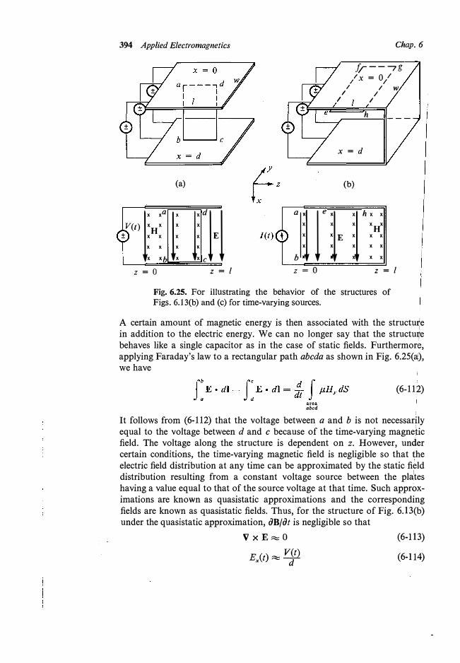
In Section 6.4 we considered three structures, shown in Figs. 6.13(a), (b), and ( c ), from the point of view of static fields. Let us now consider the three structures driven by time-varying sources. The resulting fields are then time varying. From Maxwell's equations for time-varying fields, we know that a time-varying electric field is accompanied by a time-varying magnetic field and vice versa. Thus, for example, a time-varying voltage source applied to the structure of Fig. 6.13(b) results in a time-varying electric field which has associated with it a time-varying magnetic field as shown in Fig. 6.25(a).
394 Applied Electromagnetics
(a)
lx xa
l
x
l
x dl lV(t) XHX x x ± x x x x E
x x x x
X Xb X X C z = 0 z = l
Chap. 6
1r--,g /x = 0
11
/ I W I I
I I
h
x = d
(b)
alle l x
l
hxx x x x x xH x XEX xx
x x x x x
b x x x
z = 0 z = l
Fig. 6.25. For illustrating the behavior of the structures of Figs. 6.13(b) and (c) for time-varying sources.
A certain amount of magnetic energy is then associated with the structu�e in addition to the electric energy. We can no longer say that the structu�e behaves like a single capacitor as in the case of static fields. Furthermore, applying Faraday's law to a rectangular path abcda as shown in Fig. 6.25(a;), we have
area
abed
(6-112)
I
It follows from (6-112) that the voltage between a and b is not necessarily equal to the voltage between d and c because of the time-varying magnetic field. The voltage along the structure is dependent on z. However, under certain conditions, the time-varying magnetic field is negligible so that the electric field distribution at any time can be approximated by the static field distribution resulting from a constant voltage source between the pl�tes having a value equal to that of the source voltage at that time. Such approximations are known as quasistatic approximations and the corresponding fields are known as quasistatic fields. Thus, for the structure of Fig. 6.13(b) under the quasistatic approximation, aB/at is negligible so that
VxE=O
Ex(t) = Vst)
(6-113)
(6-114)
395 Quasistatics; The Field Basis of Low-Frequency Circuit Theory Sec. 6.6
The magnitude of the resulting time-varying charge on either plate is
Q(t) = (lw)f E,/t) = €;! V(t) = CV(t) (6-115)
where C = €wl/d is the same as the capacitance obtained for the directvoltage source. Differentiating both sides of (6-115) with respect to time, we have
dQ = !!_(CV)dt dt (6-116)
But, according to the law of conservation of charge, dQ/dt must be equalto the current I flowing into the plate from the voltage source. Thus Eq. ( 6-116) becomes
d I= -(CV)dt (6-117)
which is the familiar voltage-to-current relationship used in circuit theory for a capacitor. For the sinusoidally time-varying case, Eq. (6-117) reduces to
i = jwCV (6-118)
where i and V are the phasor current and phasor voltage, respectively, and a, is the radian frequency of the voltage source.
Similarly, a time-varying current source applied to the structure of Fig. 6.13(c) results in a time-varying magnetic field which has associated with it a time-varying electric field as shown in Fig. 6.25(b). A certain amount of electric energy is then associated with the structure in addition to the magnetic energy. We can no longer say that the structure behaves like a single inductor as in the case of static.fields. Furthermore, applying the integral form of Maxwell's curl equation for H to a rectangular path ef ghe as shown in Fig. 6.25(b), we have
f: H • di - f: H • di= ft f €Ex dS (6-119)
area
efgh
Since H is zero outside the structure, it follows from ( 6-119) that the current crossing the line ef is not necessarily equal to the current crossing the line hg because of the time-varying electric field. The current flowing along the structure is dependent on z. However, under the quasistatic approximation, an/at is negligible so that the magnetic field distribution at any time can be approximated by the static magnetic field distribution resulting from the flow of a direct current having a value equal to that of the source current at that time. Thus
VxH�o
H (t) � I(t))'
w
(6-120)
(6-121)
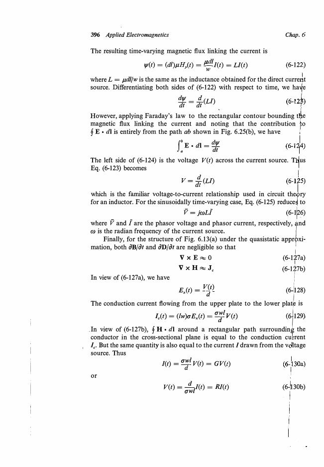
396 Applied Electromagnetics Chap. 6
The resulting time-varying magnetic flux linking the current is
lfl(t) = (dl)µHy(t) = µ:! I(t) = LI(t) (6-122:)
where L = µdl/w is the same as the inductance obtained for the direct curre tsource. Differentiating both sides of (6-122) with respect to time, we ha e
dlfl = !!_(LI)dt dt However, applying Faraday's law to the rectangular contour bounding t emagnetic flux linking the current and noting that the contribution o§ E • dl is entirely from the path ab shown in Fig. 6.25(b), we have
Jb
E • di = dlfla d!
The left side of (6-124) is the voltage V(t) across the current source. T usEq. (6-123) becomes
V = ft (LI)
which is the familiar voltage-to-current relationship used in circuit the ryfor an inductor. For the sinusoidally time-varying case, Eq. (6-125) reduce to
V = jcoLi (6-126) where V and i are the phasor voltage and phasor current, respectively, ndco is the radian frequency of the current source. /
Finally, for the structure of Fig. 6.13(a) under the quasistatic apprcbxi-mation, both aB/at and ao/at are negligible so that
i V x E � 0 (6-127a) V x H � J
c (6-127b) In view of (6-127a), we have !
Ex(t) = VJ!) (6-/128)
The conduction current flowing from the upper plate to the lower platl is
I,(t) - (lw)uE,(t) -u;
l V(t) (61129)
In view of (6-127b), § H • dl around a rectangular path surroundin theconductor in the cross-sectional plane is equal to the conduction cu rentJ
c. But the same quantity is also equal to the current I drawn from the v ltage
source. Thus I(t) = u;l V(t) = GV(t)
or
V(t) = ...!!:__1I(t) = RI(t)(1W
(6-130b)
397 Quasistatics; The Field Basis of Low-Frequency Circuit Theory Sec. 6.6
where G = uwl/d and R = d/uwl are the same as the conductance and resistance, respectively, obtained for the direct voltage source. Equations (6-130a) and (6-130b) are the familiar voltage-to-current relationships used in circuit theory for conductance and resistance, respectively. For the sinusoidally timevarying case, we have
(6-131a) and
(6-131b) where i and V are the phasor current and phasor voltage, respectively.
To summarize what we have learned thus far in this section, the voltageto-current relationships used in circuit theory for a capacitor, inductor, and resistor given by ( 6-117), ( 6-125), and ( 6-130b ), respectively, are valid only under the quasistatic approximation. For the quasistatic approximation to hold, aBjat must be negligible for the case of the capacitor, ao;at must be negligible for the case of the inductor, and both aB/at and ao/at must be negligible for the case of the resistor. To illustrate a method for determining the quantitative condition for the quasistatic approximation to hold in a particular case, we consider the structure of Fig. 6.25(b) in detail for the sinusoidally time-varying case in the following example.
EXAMPLE 6-16. The parallel plate structure of Fig. 6.25(b) is driven by a sinusoidallytime-varying current source. It is desired to. show that the quasistatic approximation holds, that is, that the structure behaves like a single inductor as viewed by the current source for the condition
1 f � 2nl,/µ€
wherefis the frequency of the current source andµ and€ are the permeability and permittivity, respectively, of the medium between the plates.
Under the quasistatic approximation, the time-varying magnetic field distribution at any particular time must be approximately the same as that of the static magnetic field resulting from a direct current equal to the value of the source current at that time. Thus, denoting the phasor corresponding to this magnetic field by ni, we have
(6-132)
where i0 = [Il
z= o is the phasor corresponding to the source current. This time-varying magnetic field induces a time-varying electric field in the xdirection in accordance with Maxwell's curl equation for E, given in phasor form by
v x E = -jcoB
398 Applied Electromagnetics Chap. 6
Denoting the phasor corresponding to this electric field by E�, we have aE� = -jwBq = -jwµffq = -jwµ 10 (6-133)az y y
w
Integrating (6-133) with respect to z, we obtain - jE� = -jwµ ; (z - l) (6-134)
where we have evaluated the arbitrary constant of integration by using the boundary condition that [E�],_ 1
= 0. If ao;at is not negligible, the timevarying electric field corresponding to the phasor E� produces a time-varying magnetic field in they direction in accordance with Maxwell's curl equation for H, given in phasor form by
v xii= jwD Denoting the phasor corresponding to this induced magnetic field by ff�, we have
aff' - - i --a Y = jwD� = jw€E� = w2 µ€ __Q_(z - l)
z w
Integrating (6-135) with respect to z, we obtain
H' = -OJ2µ€ lo [(z - /)2 - !:....]
Y w 2 2
(6-135)
(6-136)
where we have evaluated the arbitrary constant of integration by using th boundary condition that [H�L-o = 0 since the condition that the current a . z = 0, as determined by the tangential magnetic field intensity at z = 0 must be equal to the source current is satisfied by (6-132) alone.
Now, the time-varying magnetic field corresponding to the phasor give by (6-136) induces a time-varying electric field. Denoting the phasor corre sponding to this induced electric field by E�, we have
aE� . ff' _ . 3 2 10 [(z - !)2 12
] az = -.-Jwµ y -
1w µ €w 2 - 2
Integrating (6-137) with respect to z, we obtain
E� = jOJ3 µ
2€ � [(z 6 /)3 - /2(z
2- /)]
(6-137)
(6-138) I
where we have again evaluated the arbitrary constant of integration by using the boundary condition that [E�],_ 1
= 0. Continuing in this manner, we obtain the successively induced magnetic and electric fields as
H" = OJ4
µ2€2 1
0 [(z - /)4 _ l2(z - /)2 + 5/4]
y w 24 4 24 (6-139)
E"' = _ jOJs µ
3€2 lo [(z - /)5 _ l2(z - /)3 + 5l4(z - /)]
x w 120 12 24 (6-1�0)
399 Quasistatics; The Field Basis of Low-Frequency Circuit Theory
ii'" = _ 6 3 3 io [(z - 1)6 _
/2(z - /)4 + 5/4(z - /)2 _ �])' ro µ
€ w 720 48 48 720 E�' = .. .
ii"" - . . .
)' -
The total electric field is given by E = E' + E" + E"' + ...
x x x x
= -jc.oµ io (z _I)+ jro3 µ2€ i0 [(z - 1)3 _ /2 (z - /)]w w 6 2
· s 3 2 io [(z - /)5 /2(z - /)3 + 5/4(z - /)] + - JO) µ € w 120 - 12 24 ...
= -j (µ io (1 + c.o2µ€12 + 5ro4µ2f2/4 + ... )'Y?w 2 24
Sec. 6.6
(6-141)
(6-142)
X [ ro,v'µf(z - I) - (ro,v'µfiz 31
/)3 + (ro,/iif)5(z 51
/)5 - ... J
= -j {µ i0 sin ro,jµf(z - I)
'Y? w cos rov'µf/ The total electric field at z = 0 is given by
[EJ,-o = j (µ io tan rov'µf/-v? w (6-143)
This result could have been obtained simply by adding [E�],_ 0, [E�],_0,
[E�'L-o, and so on. However, Eq. (6-142) was derived to point out that the electric field and hence the voltage along the structure varies sinusoidally with distance. Similarly, if we add iii, ii;, ii�, ii�', and so on, we obtain the total magnetic field as
ii = i0 cos rov'µf(z - I) (6-144) >' w cos rov'µf /
indicating that the magnetic field and hence the current along the structure varies cosinusoidally with distance.
The phasor voltage across the current source is given by
t\ = [V],-0 = s: [Exlz-o di
= j (µ iod tan rov'µf/-v? w
= jc.oµdl j tan rov'µf/w O rov'µf/
= jc.oLio tan�/
(J) µ€
(6-145)
where L = µdl/w is the inductance of the structure computed from static _field considerations. Equation (6-145) represents the voltage-to-current rela-
I I I I
400 Applied Electromagnetics Chap. 6: I
I
tionship at the source end of the structure under the condition for whicli ao;at is not negligible. For ro,/µ€! � 1, tan roJ;if/ � roJ;ifl and Eq.: (6-145) reduces to
V0 = jroLi0
which is the voltage-to-current relationship for a· single inductor. Thus, fo the quasistatic approximation to hold, the condition to be satisfied is
1 f � 2nl,/µ€
As a numerical example, for l = 0.1 m, µ = µ0
, and € = €0, the value f I/2nl,./jii is (1500/n) x 106
• For a value of 1/10 for ro,/µ€1, the frequen y must be less than 150/n MHz for the structure to behave essentially Ii e a single inductor. I
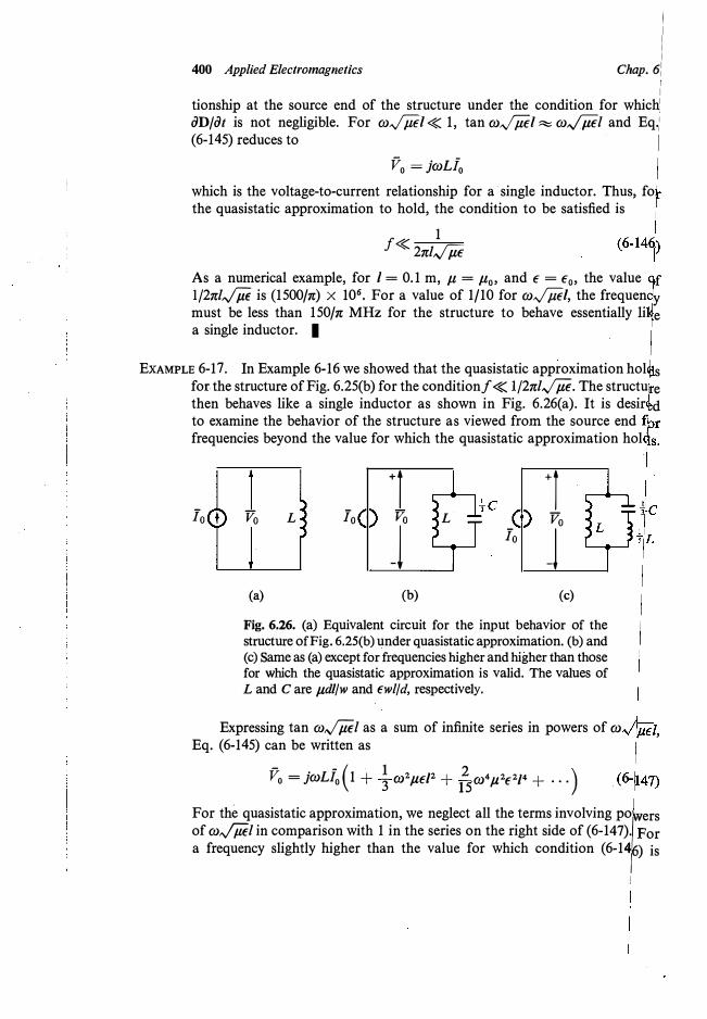
EXAMPLE 6-17. In Example 6-16 we showed that the quasistatic approximation hol s for the structure of Fig. 6.25(b) for the condition!� I/2nl,./jii. The structu e then behaves like a single inductor as shown in Fig. 6.26(a). It is desir d to examine the behavior of the structure as viewed from the source end frequencies beyond the value for which the quasistatic approximation hol
lo L +r +l
lo Vo L Vo
Jlo
-1Vo
(a) (b) (c)
Fig. 6.26. (a) Equivalent circuit for the input behavior of the structure of Pig. 6.25(b) under quasistatic approximation. (b) and (c) Same as (a) except for frequencies higher and higher than thosefor which the quasistatic approximation is valid. The values of L and Care µdl/w and €wl/d, respectively.
Expressing tan ro,./jiil as a sum of infinite series in powers of ro Eq. (6-145) can be written as
V0 = jroLf0 ( 1 + � ro2 µ€12 + 1� ro4 µ2€2/4 + ... )
For the quasistatic approximation, we neglect all the terms involving porersof ro,./jiil in comparison with 1 in the series on the right side of (6-147\Fora frequency slightly higher than the value for which condition (6-14
/ ) is
!
401 Quasistatics; The Field Basis of Low-Frequency Circuit Theory Sec. 6.6
acceptable, we have to include the second term in the series. Thus we have - - ( 1 )V0 = jroL/
0 1 + 3ro2 µ€12
= jroLi0 ( 1 + j ro2 Lc)
(6-148)
where C = Ewl/d is the capacitance computed from static field considerations if the structure were open circuited at z = I. Rearranging (6-148), we get
I- i\ f\ (l 1 2L c) 0 = jroL( l + !ro2 LC) = jroL - 3ro
= V0 (j�L
+ jro �) (6-149)
The voltage-to-current relationship given by (6-149) corresponds to that of an inductor of value Lin parallel with a capacitor of value ! C as shown in Fig. 6.26(b). Thus the same structure which behaves almost like a single inductor at low frequencies governed by (6-146) acts like an inductor in parallel with a capacitor as the frequency is increased. For still higher frequencies, we have to include one more term in the series on the right side of (6-147), giving us
or
io = _Vo (1 + 31 ro2L c + J:....ro4£2 c2)-1
JOJL 15
= j:L ( 1 - +ro2 LC - J5ro4 L2 C2 + higher-order terms)
= _Vo (1 - _!_ro2L c - _!_ro4£2 c 2) JOJL 3 45 _ Vo +
fl ( .roe +
.0)3 LC2)
- jroL O J 3 J 45 t\ t\ = jroL
+ 1/[(jroC/3 )(1 + ro2 LC/15)] - Vo Vo ,..._. jroL
+ (3/jroC)(l - ro2 LC/15)Vo + Vo = jroL (3/jroC) + (jroL/5)
(6-150)
The equivalent circuit corresponding to (6-150) is shown in Fig. 6.26(c). It is now evident that as the frequency is increased, more and more elements are added to the equivalent circuit. For an arbitrarily high frequency, we must
403 Transmission-Line Equations; The Distributed Circuit Concept Sec. 6.7
where £ = µd/w and e = Ew/d are the inductance and capacitance, respectively, per unit length of the structure computed from static fields.
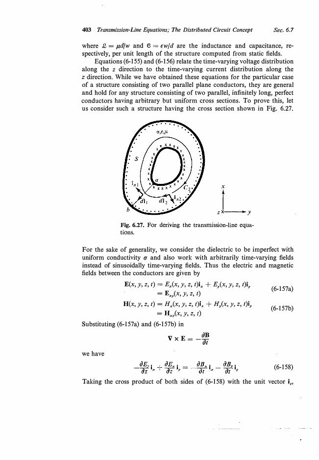
Equations (6-155) and (6-156) relate the time-varying voltage distribution along the z direction to the time-varying current distribution along the z direction. While we have obtained these equations for the particular case of a structure consisting of two parallel plane conductors, they are general and hold for any structure consisting of two parallel, infinitely long, perfect conductors having arbitrary but uniform cross sections. To prove this, let us consider such a structure having the cross section shown in Fig. 6.27.
x
zX---.y
Fig. 6.27. For deriving the transmission-line equations.
For the sake of generality, we consider the dielectric to be imperfect with uniform conductivity u and also work with arbitrarily time-varying fields instead of sinusoidally time-varying fields. Thus the electric and magnetic fields between the conductors are given by
E(x, y, z, t) = Ex(x, y, z, t)ix + E
y(x, y, z, t)iy
= Ex/x, y, z, t)
H(x, y, z, t) = Hx(x, y, z, t)t + H/x, y, z, t)iy
= Hx/x, y, z, t)
Substituting (6-157a) and (6-157b) in
we have
aB V x E = -at
(6-157a)
(6-157b)
(6-158)
Taking the cross product of both sides of (6-158) with the unit vector i,,
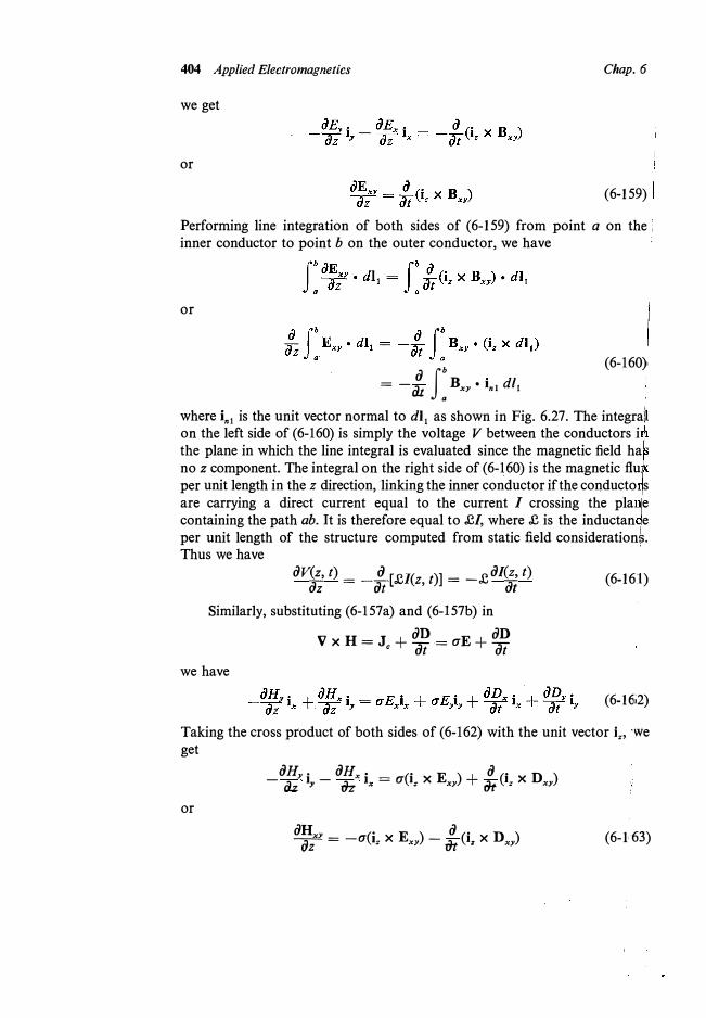
404 Applied Electromagnetics Chap. 6
we get
or
(6-159)
Performing line integration of both sides of (6-159) from point a on the:inner conductor to point b on the outer conductor, we have
or
aJ
b = -ata
Bxy • i.1 d/1 (6-160),
where i.1 is the unit vector normal to dl
1 as shown in Fig. 6.27. The integra11
on the left side of (6-160) is simply the voltage V between the conductors i the plane in which the line integral is evaluated since the magnetic field ha no z component. The integral on the right side of (6-160) is the magnetic flu per unit length in the z direction, linking the inner conductor if the conducto s are carrying a direct current equal to the current I crossing the pla e containing the path ab. It is therefore equal to £/, where J:, is the inductan e per unit length of the structure computed from static field considerationt Thus we have
av�; t) = _ Ji [.CI(z, t)] = -.c a1�;
t)
Similarly, substituting (6-157a) and (6-157b) in
we have
an anV x H = Jc + at = aE + at
(6-161)
(6-16i2)
Taking the cross product of both sides of (6-162) with the unit vector iz, we get
or
aHy. aHX • _ c· E ) a c· 0 )- az ly - az
Ix - a lz X xy + at lz X xy
aHXY c· E ) a c· n ) �=-a lz x xy - at lz x xy (6-l63)
406 Applied Electromagnetics Chap. 6/
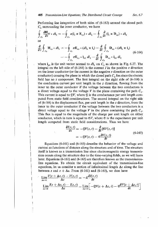
��&-�
IV(z + !:iz, t) - V(z, t) = -£ !:iz aJ(az, t) (6-166a) t I
I(z + !:iz, t) - I(z, t) = -9 !:iz V(z + !:iz, t) - e /:iz av(z ti !:iz, t)I (6-166b)
The circuit theory equivalent of Eqs. (6-166a) and (6-166b) can be drawn a shown in Fig. 6.28 by recognizing that Eq. (6-166a) is Kirchhoff's voltag
I(z,t) c
b
l(z + !:J.z,t)
r£.ilz
·1T
l V(z + Az,t)
_j a
d
Fig. 6.28. Circuit equivalent for an infinitesimal length /:iz of a transmission line.
law written for the loop abcda and that Eq. (6-166b) is Kirchhoff's curr�nt law written for node c. Thus an infinitesimal length /:iz of the structurel is equivalent to the circuit shown in Fig. 6.28 as /:iz - 0. It follows that ihe circuit representation for a portion of length l of the structure consists of infinite number of such sections in cascade as shown in Fig. 6.29. In other
'--------- - - - -- -
00
-----z
Fig. 6.29. Distributed circuit representation of a transmission line.
407 Transmission-Line Equations; The Distributed Circuit Concept Sec. 6.7
words, the structure can no longer be represented by a collection of lumped circuit elements. The conductance, capacitance, and inductance are "distributed" uniformly and overlappingly along the structure, giving rise to the concept of a "distributed circuit." Physically, the electric stored energy, the magnetic stored energy, and the power dissipation due to conduction current flow are distributed uniformly and overlappingly along the line.
Before we conclude this section, we wish to show that the power flow across any cross-sectional plane of the transmission line as computed from surface integration of the Poynting vector is equal to the product of the voltage and current in that plane. To do this, let us again consider the structure of Fig. 6.27. Considering an infinite plane surface (which is a spherical surface of infinite radius and hence a closed surface) in the cross-sectional plane and noting that the fields outside the conductors are zero, the power flow P across any cross-sectional plane is simply the surface integral of the Poynting vector over the cross-sectional surface S between the conductors. Thus
P(z, t) = f s Ex/z, t) X Hx/z, t) • i, dS
= f f (Exy X Hx) • (di! X dl2
) a c,
= ff (Exy
• dl,)(Hxy
• dl2)
a c,
-f ,( (Exy • dl2
)(Hxy • di,)
a jC2
(6-167)
Since we can always choose C2
such that dl2
is everywhere normal to Exy
or, alternatively, since we can al�ays choose the path ab such that dl 1 is everywhere normal to Hx
y, the second integral on the right side of (6-167) is equal to zero. Since f: E
xy • di, is independent of the path on S chosen from
a to b or, alternatively, since £ Hxy • dl2
is independent of the contour C2 Ye,
on S, Eq. (6-167) simplifies to
P(z, t) = u: Exy • di, )(f c,
Hxy • dl2)
= V(z, t) l(z, t)which is the desired result.
(6-168)
409 Uniform Plane Waves and Transmission-Line Waves
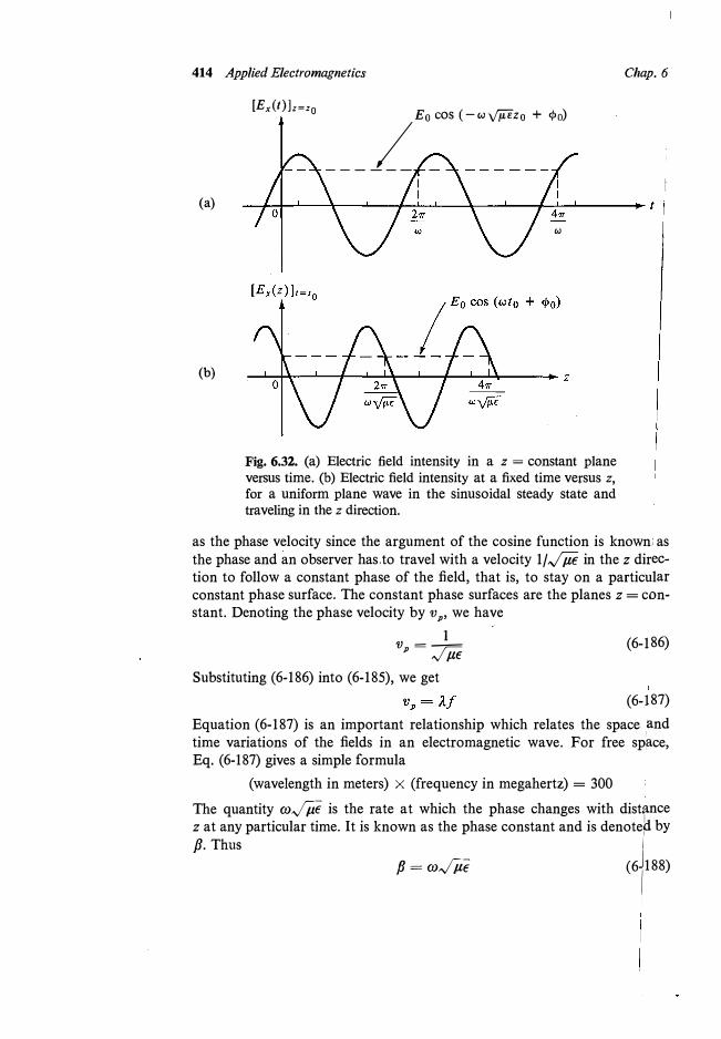
equations. Thus, in cartesian coordinates, we have
v2E = µE a2Exx
ai2
v2E = µE a2Eyy ai2
V2£ = µE a2Ez z ai2
Sec. 6.8
In the most general case, we can have all three components of E and each one of these can be dependent on all three space coordinates x, y, and z and on time. But let us assume for simplicity that EY = Ez = 0. Then we have
(6-174)
We are still faced with a three-dimensional second-order partial differential equation. Our aim at present is to illustrate that time-varying electric and magnetic fields give rise to electromagnetic wave propagation. Hence let us simplify the problem further by assuming that Ex is independent of x and y.
Thus
and Eq. (6-174) simplifies to a2Ex _ € a2Ex az
2 - µ at2
(6-175)
(6-176)
Equation (6-176) is the one-dimensional scalar wave equation. Its solution can be found by using the Laplace transform technique or the separation of variables technique. However, we will here write down the solution and show that it indeed satisfies the equation. Thus let us consider
Ex(z, t) = A f(t - ,Jjiiz) + B g(t + ,Jjiiz) (6-177) where f and g are any functions of the respective arguments and A and B are arbitrary constl:!,nts. Then
a:/ = -A,Jjii f'(t - ,Jjiiz) + B g'(t + ,Jjiiz)
a2E �az/ = Aµ€ f"(t - ,v µEZ) + BµE g"(t + ,Jjiiz) (6-178a)
a:/ = A f'(t - ,Jjiiz) + B g'(t + ,Jjiiz)
a;ix = A f"(t - ,Jjiiz) + B g"(t + ,Jjiiz) (6-178b)
where the primes denote differentiation with respect to the respective arguments. From (6-178a) and (6-178b), we note that (6-177) satisfies (6-176)
1, 410 Applied Electromagnetics Chap. �
and hence is the solution for (6-176). The forms of the functions f and lgdepend upon the particular problem under consideration. Some examplces are cos ro(t - ,Jiifz), e-<,-&zi•, and (t + ,Jiiiz) sin (t + ,Jiiiz). In tf,1.e general case, the solution can be a superposition of several different functio�1s of (t - ,Jiifz) and (t + ,Jiiiz).
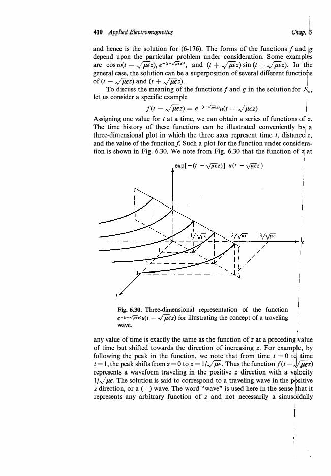
To discuss the meaning of the functions f and g in the solution for x• let us consider a specific example
f(t - ,Jiifz) = e-<t-,/µ,z>u(t - ,Jiiiz)Assigning one value for t at a time, we can obtain a series of functions of z.
The time history of these functions can be illustrated conveniently b a three-dimensional plot in which the three axes represent time t, distance: z,
and the value of the functionf Such a plot for the function under consideration is shown in Fig. 6.30. We note from Fig. 6.30 that the function of� at
exp[-(t -yr,Iez)J u(t -yr,Iez)
3/ffe
/ /
/
Fig. 6.30. Three-dimensional representation of the function e-c,-,iµ,z>u(t - ,./µ€z) for illustrating the concept of a travelingwave.
any value of time is exactly the same as the function of z at a preceding 1value
of time but shifted towards the direction of increasing z. For examplle, by following the peak in the function, we note that from time t = 0 td time t = 1, the peak shifts from z = 0 to z = 1/ ,Jjii. Thus the function f(t- ]�z) represents a waveform traveling in the positive z direction with a ;Jl;ity 1/,Jiif. The solution is said to correspond to a traveling wave in the pbsitive z direction, or a ( +) wave. The word "wave" is used here in the sense khat it represents any arbitrary function of z and not necessarily a sinusJ)idally
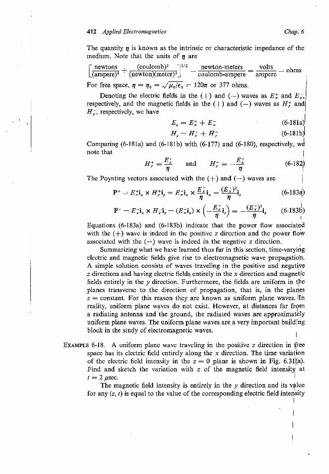
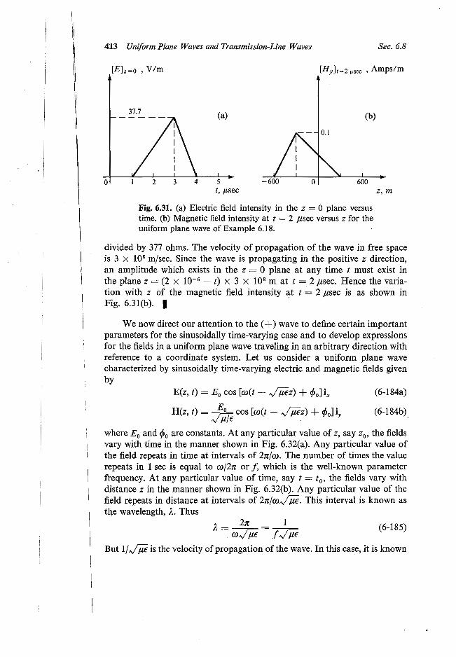
414 Applied Electromagnetics Chap. 6
(a)
(b)
[Ex(t) ]z=zo - - _ _j_Eo oos (-wyµ:i,, + <j>o)
I I
w
Fig. 6.32. (a) Electric field intensity in a z = constant plane versus time. (b) Electric field intensity at a fixed time versus z,
for a uniform plane wave in the sinusoidal steady state and traveling in the z direction.
as the phase velocity since the argument of the cosine function is known, as the phase and an observer has.to travel with a velocity 1/,/iif in the z direction to follow a constant phase of the field, that is, to stay on a particular constant phase surface. The constant phase surfaces are the planes z = constant. Denoting the phase velocity by v
p, we have 1
v - - (6-186) p - ,/µ€
Substituting (6-186) into (6-185), we get (6-187)
Equation (6-187) is an important relationship which relates the space and time variations of the fields in an electromagnetic wave. For free sp�ce, Eq. (6-187) gives a simple formula
(wavelength in meters) x (frequency in megahertz) = 300 The quantity w,/iif is the rate at which the phase changes with distance z at any particular time. It is known as the phase constant and is denote� by ��
JI
p = w,/iif (6 /188)
415 Uniform Plane Waves and Transmission-Line Waves
and
Sec. 6.8
(6-189)
(6-190)
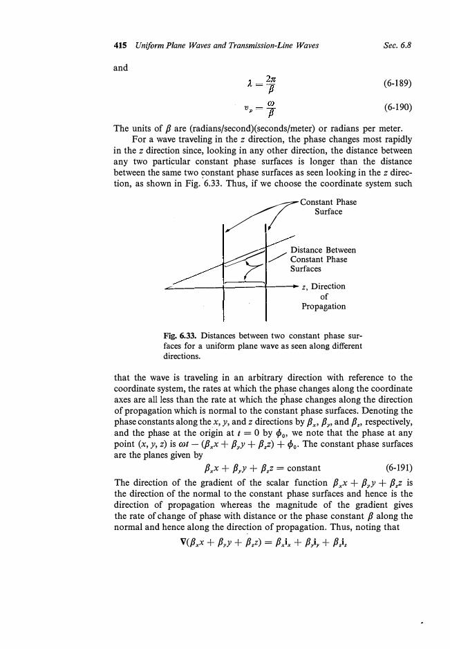
The units of p are (radians/second)(seconds/meter) or radians per meter. For a wave traveling in the z direction, the phase changes most rapidly
in the z direction since, looking in any other direction, the distance between any two particular constant phase surfaces is longer than the distance between the same two �onstant phase surfaces as seen looking in the z direction, as shown in Fig. 6.33. Thus, if we choose the coordinate system such
�Constant Phase/ i/ Surface
� / Distance Between:;::::::----y / Constant Phase
(Surfaces
.c;..-----+-----11--- z, Directionof
Propagation
Fig. 6.33. Distances between two constant phase surfaces for a uniform plane wave as seen along differentdirections.
that the wave is traveling in an arbitrary direction with reference to the coordinate system, the rates at which the phase changes along the coordinate axes are all less than the rate at which the phase changes along the direction of propagation which is normal to the constant phase surfaces. Denoting the phase constants along the x, y, and z directions by fix
, Py, and Pz
, respectively, and the phase at the origin at t = 0 by cp
0, we note that the phase at any
point (x, y, z) is rot - (Pxx + p
yy + fiz
z) + ¢0
• The constant phase surfacesare the planes given by
Pxx + PYY + fiz
z= constant (6-191)
The direction of the gradient of the scalar function Pxx + py
y + fizz is
the direction of the normal to the constant phase surfaces and hence is the direction of propagation whereas the magnitude of the gradient gives the rate of change of phase with distance or the phase constant p along the normal and hence along the direction of propagation. Thus, noting that
V(fixx + PYY + fizz) = P)x + P)y + fiz
iz
• I
416 Applied Electromagnetics Chap. 6
the direction of propagation is along the vector P)x + Pyiy + P,i, and the phase constant along the direction of propagation is
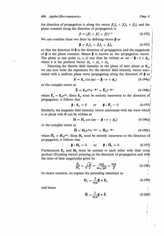
P = (P; + P; + P;>112 (6-192) We can combine these two facts by defining vector p as
P = P)x + P)y + P,i, (6-193) so that the direction of P is the direction of propagation and the magnitude of p is the phase constant. Hence p is known as the propagation vector. The phase at any point (x, y, z) can then be written as wt - p • r + <p0 ,
where r is the position vector xix + yiy + zi,. Denoting the electric field intensity in the plane of zero phase as E
0,
we can now write the expression for the electric field intensity vector associated with a uniform plane wave propagating along the direction of p as
E = E0
cos (rot - P • r + <p0) (6-194a) or the complex vector as
_ E = E0
ehl•e-JP·r = E0e-JP·r (6-194b) I
where E0
= E0eN°. Since E
0 must be entirely transverse to the direction of
propagation, it follows that p • E
0 = 0 or (6-195)
Similarly, the magnetic field intensity vector associated with the wave which is in phase with E can be written as
H = H0
cos (rot - p • r + <p0) (6-196a) or the complex vector as
ii= Hoeloi\oe-lP·r = Hoe-JP·r (6-196bj where ii
0 = H0
ehl•. Since H0
must be entirely transverse to the direction of propagation, it follows that ··
p • H0
= o or p • ii0
= O (6-197rFurthermore E
0 and H
0 must be normal to each other with their cros,s
product (Poynting vector) pointing in the direction of propagation and with the ratio of their magnitudes given by
/ Eo = /µ = wµ = wµ (6-198) H0 'Y € w,Jii; P
In vector notation, we express the preceding statement as
and hence - 1 -H=-PXEwµ
(6-199) I
i
(6-200) I
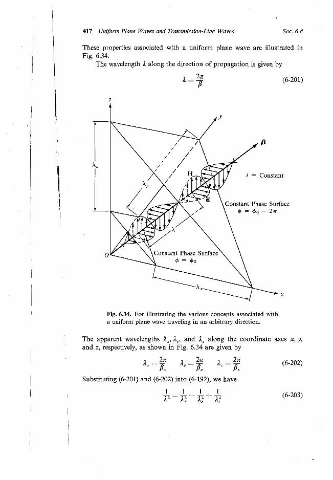
418 Applied Electromagnetics Chap. 6
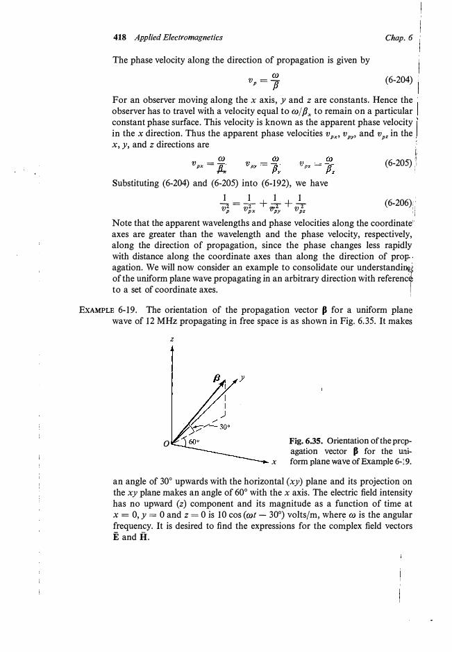
The phase velocity along the direction of propagation is given by w
VP =p (6-204)
For an observer moving along the x axis, y and z are constants. Hence the observer has to travel with a velocity equal tow/ fi
x to remain on a particular
constant phase surface. This velocity is known as the apparent phase velocity in the x direction. Thus the apparent phase velocities vpx, vPY' and vpz in the x, y, and z directions are
i (6-205) ,'1
w vpx =
Px Substituting (6-204) and (6-205) into (6-192), we have
1 1 1 1 2=-2-+--r+2 VP Vpx Vpy Vpz
(6-206)i I
'
Note that the apparent wavelengths and phase velocities along the coordinate' axes are greater than the wavelength and the phase velocity, respectively, along the direction of propagation, since the phase changes less rapidly with distance along the coordinate axes than along the direction of prov-. agation. We will now consider an example to consolidate our understandirl\l;f of the uniform plane wave propagating in an arbitrary direction with referenc�
r to a set of coordinate axes.
EXAMPLE 6-19. The orientation of the propagation vector p for a uniform planewave of 12 MHz propagating in free space is as shown in Fig. 6.35. It makes
z
0 Fig. 6.35. Orientation of the propagation vector P for the uni
x form plane wave of Example 6-19.
an angle of 30° upwards with the horizontal (xy) plane and its projection on the xy plane makes an angle of 60° with the x axis. The electric field intensity has no upward (z) component and its magnitude as a function of time at x = 0, y = 0 and z = 0 is 10 cos (wt - 30°) volts/m, where w is the angular frequency. It is desired to find the expressions for the complex field vectors E and it
419 Uniform Plane Waves and Transmission-Line Waves Sec. 6.8
Since the medium is free space, the phase velocity along the propagation vector is 1/� = 3 x 10⁸ m/sec. From (6-204), we have
P_ ro _ 2nf _ 2n X 12 X 106
_ 0 OS - VP - VP -
3 X J08 - • 'IT,
From the given orientation of the propagation vector, we have
P = 0.08n(cos 30° cos 60° ix + cos 30° sin 60° iy + sin 30° iz) = 0.02n(�ix + 3iy + 2iz)
The solution for Eis of the form E0
e-jp·r. Since E has no z component, we can write
From (6-195), we have
P • Eo = PxExo + PY
EYO = 0
Since Px and PY are both real, E
xo and E
Y0 must be either in phase or in phase opposition for the above equation to be true. Hence let
and
so that
and
or
Exo = -�Eyo
From the given function of time for the electric field intensity magnitude at x = 0, y = 0 and z = 0, that is, r = 0, we have
I Exot + EyOjy I eja. = IOe-j30°
or
and
Substituting Exo = -� Eyo in the above equation, we obtain 4£;0 = 100
or Eyo = 5 and Exo = -5�. Thus
E0 = (-5� e-j"16t + 5e-j"/6iy)
The required expression for E is then given by
it= 5(-�t + iy)e-j,,/6e-jo .02,,<VJx+3y+2z>
The corresponding expression for ii can be obtained by using· (6-200) as
• I
I
420 Applied Electromagnetics
follows: - 1 -H=-PxE
OJµ
t iy
iz - 1 i"T 3 2 e-inl6e-j0.02n(,J3"x+3y+2z)
- 96n ,v ., -� 1 0
= _1_(-i - /""Ti + 2 /""Ti )e-inl6e-j0.02n(,J3"x+3y+2z)
48n x ,v ., Y ,v ., z
Chap. 6:
We can also find the wavelength along the direction of propagation and the apparent wavelengths and velocities of propagation along the x, y, and z axes. Thus
Note that
and
1 2n 2n 11.
= 1f = 0.08n = 25 m
2n 2nl
x = Px = o.o2� n = 57.7 m
1 2n 2n 11.y
= PY = 0.06n = 33.3 m
2n 2n ,l = - = -- = 50 mz Pz o.o4n ro 24n x 106
8
vpx =
Px = 0.02� 1l = 6.928 X 10 m/sec
v = OJ = 24n x 106 = 4 X 10s m/secPY Py
0.06n _ OJ _ 24n x 106
_ s vpz - Pz - 0.04n - 6 X 10 m/sec
1 1 1 1 6.9282 + 42 + 62 = 32
in agreement with (6-203) and (6-206), respectively. I
In Section 4.9 we discussed polarization of vector fields. The fields we found in the preceding example are linearly polarized. We then say !that the wave is linearly polarized. If we combine two linearly polarized uniform plane waves propagating in the same direction and having electric /field vectors equal in magnitude but oriented perpendicular to each other' and differing in phase by n/2, we obtain a circularly polarized uniform f:)lane
421 Uniform Plane Waves and Transmission-Line Waves Sec. 6.8
wave. For example, a uniform plane wave characterized by the electric field intensity vector
E = 2.5(-t _ ,�-J\ + 2,v1Ti,)ei"l3e-jo. 02,,c..r:rx+Jy+2,>
when superimposed with the uniform plane wave of Example 6-19, would result in a circularly polarized uniform plane wave. In general, two linearly polarized uniform plane waves propagating in the same direction result in an elliptically polarized uniform plane wave.
We have introduced the topic of electromagnetic wave propagation by considering uniform plane waves. The uniform plane waves are a special class of waves known as transverse electromagnetic waves, abbreviated TEM waves, so named because the electric and magnetic fields are entirely transverse to the direction of propagation, that is, components of E and H along the direction of propagation are zero. For a general TEM wave, the fields are not uniform but are functions of position in the transverse plane .. The electromagnetic field between the conductors of a transmission line made up of perfect conductors is entirely transverse to the line axis and is in general nonuniform in the cross-sectional plane. In fact, we considered such a field [Eqs. (6-157a) and (6-157b)] in Section 6.7 and, by substituting into Maxwell's curl equations, we obtained the transmission-line equations given by (67161) and (6-165). For a perfect dielectric medium between the conductors, that is, for a = 0, these equations are
and
aV(z, t) = -£aI(z, t)az at
aJ(z, t) _ -eaV(z, t) az - at
where, with reference to Fig. 6.27,
and V(z, t) = J: E(x, y, z, t) • dl 1
J(z, t) = ,i:: H(x, y, z, t) • dl2 :r c,
(6-207)
(6-208)
(6-209a)
(6-209b)
are, respectively, the voltage between the conductors and the current along the conductors for any (z, t).
Eliminating I from (6-207) and (6-208), we obtain a differential equation for V alone as
(6-210)
This equation is completely analogous to Eq. (6-176). It is the wave equation for the TEM wave propagation guided by the conductors of the transmission line except that it is written in terms of the voltage between the conductors instead of the electric field in the medium between the conductors. We can
422 Applied Electromagnetics Chap. 6
write the solution for (6-210) from our experience with the solution of (6-176). The solution is
V(z, t) = v+(t - �z) + v-(t + �z) (6-211) where the subscripts + and - indicate (+)and (-)waves.The corresponding solution for the line current I can be obtained by substituting (6-211) into (6-207) or (6-208). This gives
I(z, t) = If [V+(t - �z) - v-(t + �z)]
Defining
(6-212)
we have
l(z, t) = i [V+(t - �z) - v-(t + �z)] 0
(6-213
The quantity Z O
is the characteristic impedance of the transmission line analo, gous to the intrinsic impedance of the dielectric medium.
f
Thus the general solutions for the voltage and current along a trans} mission line are superpositons of ( +) and ( -) traveling waves along thy line with velocities equal to 1/ � in the respective directions. We will refef to these voltage and current waves as "transmission-line waves." They art completely analogous to the uniform plane waves with the analogy as followsl:
v-Ex
!�>-Hy
£�>-µ
e <->-f
1 1
�<-
>- ,./µ€
fi<->-f?-
i (6-214)
I
I
We should, however, keep in mind that the phenomenon is one of transverse electromagnetic waves guided by the conductors of the transmission liqe. It is not necessary to work with the fields since, because of the transvense electromagnetic nature of the fields, we are able to define uniquely the voltage and current for any transverse plane. In other words, if we consider two points a and b in the same transverse plane on the two conductors, the voltage between these two points is uniquely defined by the electric field/in that plane since a closed path lying in that plane and passing through a a.ind b does not enclose any magnetic flux. Similarly, the current flowing acros� a transverse plane in one direction along the inner conductor and returning in the opposite direction along the outer conductor is uniquely defined by the
!
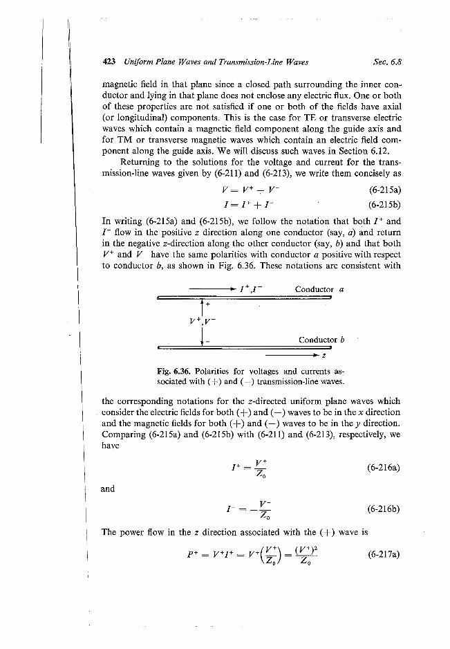
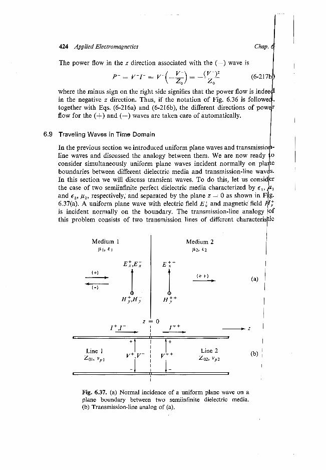
425 Traveling Waves in Time Domain Sec. 6.9
impedances Z01 and Z02 and velocities of propagation v
p 1 and vp2, respec
tively, connected in cascade as shown in Fig. 6.37(b). The specification of Z0
and vp
for a transmission line is equivalent to the specification of£ and e since Z0
= ft1e and v P
= 1/ ,,/JSe. A ( +) wave characterized by voltage v+ and current J+ is incident on the junction z = 0. We are not interested in the time variation of the incident waves at present. We merely wish to determine the transmission and reflection properties at the boundary. Obviously, there is no need to write equations for both the plane wave and transmission line cases because of the analogy. Hence we will simply write the equations in terms of the transmission-line parameters V, I, and Z0
with the understanding that they can be replaced by E
x, Hy, and t/, respectively.
The relationship between v+ and J+ is given by
J+ = � (6-218) Zo1
The incident wave cannot be transmitted into line 2 as it is, since the voltageto-current ratio in line 2 must be equal to Z02 ' Thus, let the transmitted wave voltage and current be v++ and J++, respectively. The incident and transmitted waves alone cannot satisfy the boundary conditions at the junction, which require that the voltages on either side of the junction be equal and the currents on either side of the junction be equal. These conditions are analogous to the boundary conditions for the fields, which state that the tangential electric fields (EJ must be continuous and that the tangential magnetic fields (Hy) must be continuous (in the absence of a surface current) at the boundary between the dielectrics. To satisfy the boundary conditions, there is only one possibility. This is setting up a (-) wave in line 1 which reflects part of the incident power into line 1. Let the voltage and current in this reflected wave be v- and 1-, respectively. The voltage-to-current relationships for the transmitted and reflected waves are
and
V++
]++ = -Zo2
The boundary conditions at z = 0 are v+ + v- = v++
r+r=r+
Substituting (6-218), (6-219), and (6-220) into (6-221b), we have v+ v- v++
Zo1 - Zo1 =
Zo2Solving (6-221a) and (6-222) for v-, we get
v- = v+ Zo2 - Zo1Zo2 + Zo1
(6-219)
(6-220)
(6-22l a) (6-221b)
(6-222)
(6-223)
426 Applied Electromagnetics Chap. 6 I
We now define a quantity r, known as the voltage reflection coefficient as the ratio of the (-) wave or reflected wave voltage to the ( +) wave o incident wave voltage. From (6-223), the voltage reflection coefficient i given by
r - v- - Zo2 - Zo1 - v+ - Zo2 + Zo1
We then note that the current reflection coefficient is 1- -v-;z v-r =
v+ / z
O 1 = - v+ = -r
0 1 We also define a quantity "t'v, known as the voltage transmission coefficien,
1 t,
as the ratio of the ( + +) wave or transmitted wave voltage to the ( +) way
eor incident wave voltage. Thus
I/ v++ v+
+ v- v- 11
"Cv =
v+ =
v+ = l + v+ 1 1
(6-22ri6)
= 1 + r = 2Zo2 I Zo2 + Zo1
The current transmission coefficient "C1 is given by r+
r + 1- 1-
"C1 =y
= r
= I+ r
= 1 - r = 2Zo1
Zo2 + Zo1
(6-2 7)
At this point, we may be surprised to note that the transmitted voltage1 orthe transmitted current can be greater than the incident voltage or the incident current, respectively, depending upon whether r is positive or negative, hat is, Z02 > Z01 or Z02 < Z01 . However, this is not of concern since it is the power balance that must be satisfied. To check this, we note that
p+, incident power = v+ J+
p-, reflected power = v-1-= crv+)(-rJ+) = -r2 v+1+ = -r2P+
where the minus sign signifies that the actual power flow is in the neg tive z direction, and
p++, transmitted power= v++1++ = [(1 + nv+][(l - r)l+] = (1 - P)v+l+ = (1 - P)P+
Thus p++ = p+ + p-, which verifies the power balance at the junction. The fact is that if the transmitted voltage is greater than the incident voltag , the transmitted current is less than the incident current and vice versa so that the transmitted power is less than the incident power. We will now co sider an example to illustrate the application of the formulas for the reflectio and transmission coefficients.
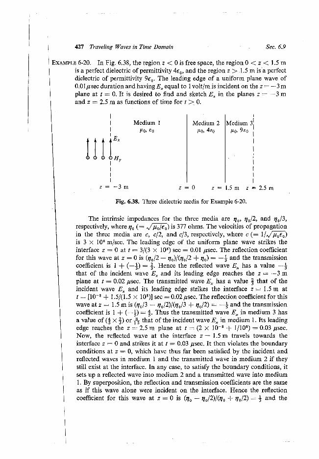
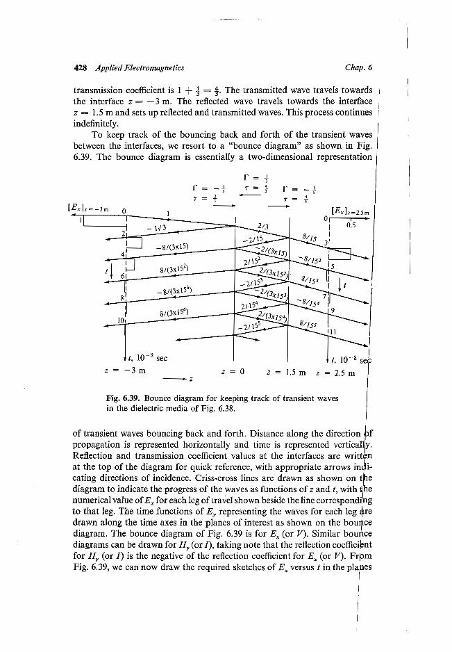
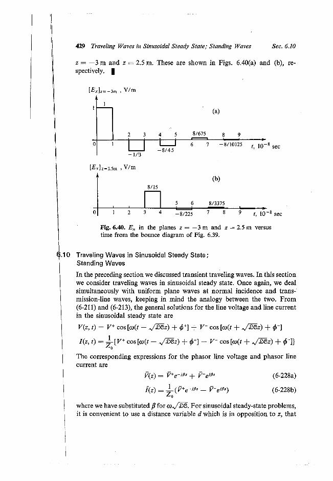
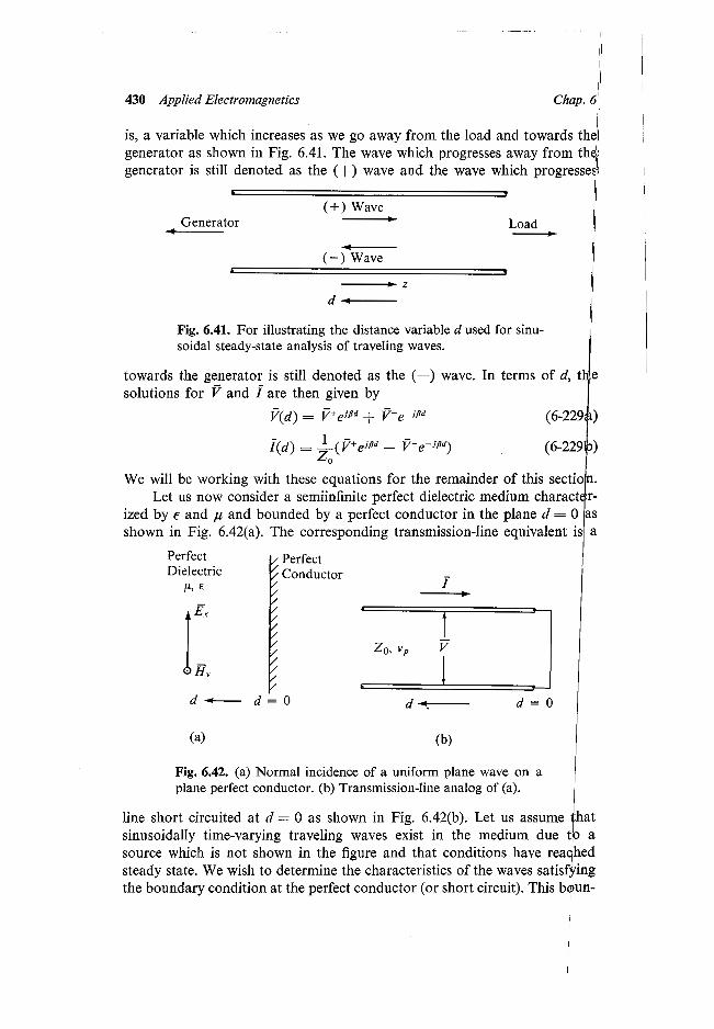
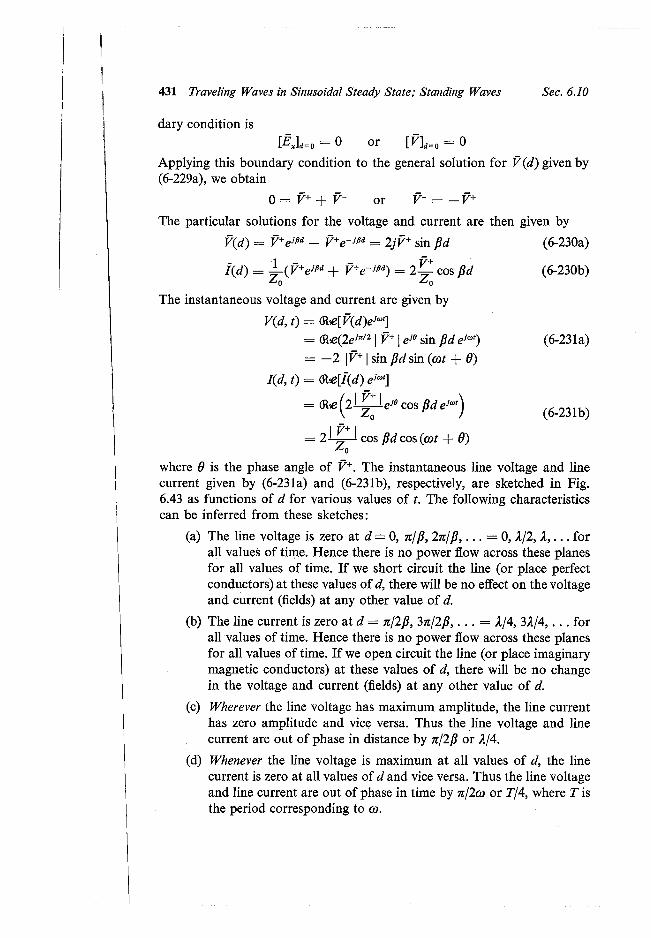
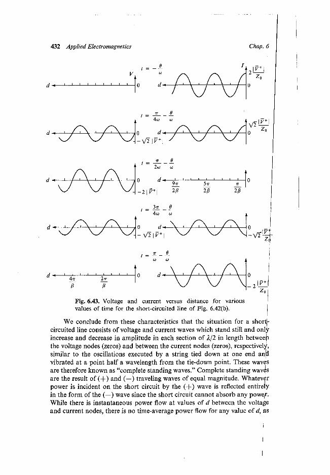
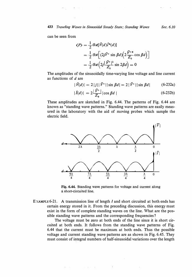
433 Traveling Waves in Sinusoidal Steady State; Standing Waves
can be seen from
<P) = 1 ffi£[V(d)i*(d)]
= 1 <R£[('2jv+ sin Pd)( 2 �* cos pd)]
= 1 ffi£(2} �: 12
sin 2Pd) = 0
Sec. 6.10
The amplitudes of the sinusoidally time-varying line voltage and line current as functions of d are
I V(d) I= 2 ljl Iv+ 11 sin Pdl = 21 v+ 11 sin Pdl - Iv+ I I I(d) I = 2
--:z-I cos pd I
0
(6-232a)
(6-232b)
These amplitudes are sketched in Fig. 6.44. The patterns of Fig. 6.44 are known as "standing wave patterns." Standing wave patterns are easily measured in the laboratory with the aid of moving probes which sample the electric field.
d•� ll'I
2A 3?.. ?.. ?.. O
d•� 1r1
9?.. n 5?.. 3A ?.. O
4 4 4 4 4
Fig. 6.44. Standing wave patterns for voltage and current alonga short-circuited line.
E XAMPLE 6-21. A transmission line of length I and short circuited at both ends hascertain energy stored in it. From the preceding discussion, this energy must exist in the form of complete standing waves on the line. What are the possible standing wave patterns and the corresponding frequencies?
The voltage must be zero at both ends of the line since it is short circuited at both ends. It follows from the standing wave patterns of Fig. 6.44 that the current must be maximum at both ends. Thus the possible voltage and current standing wave patterns are as shown in Fig. 6.45. They must consist of integral numbers of half-sinusoidal variations over the length
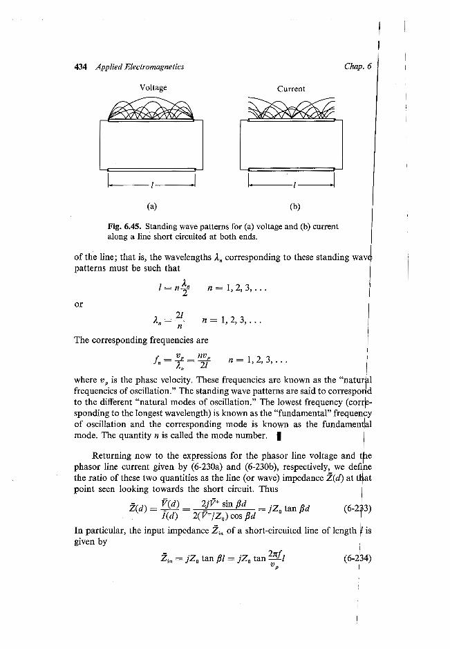
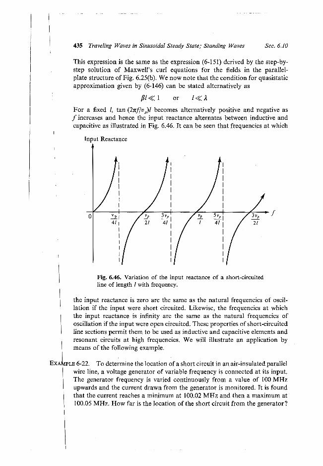
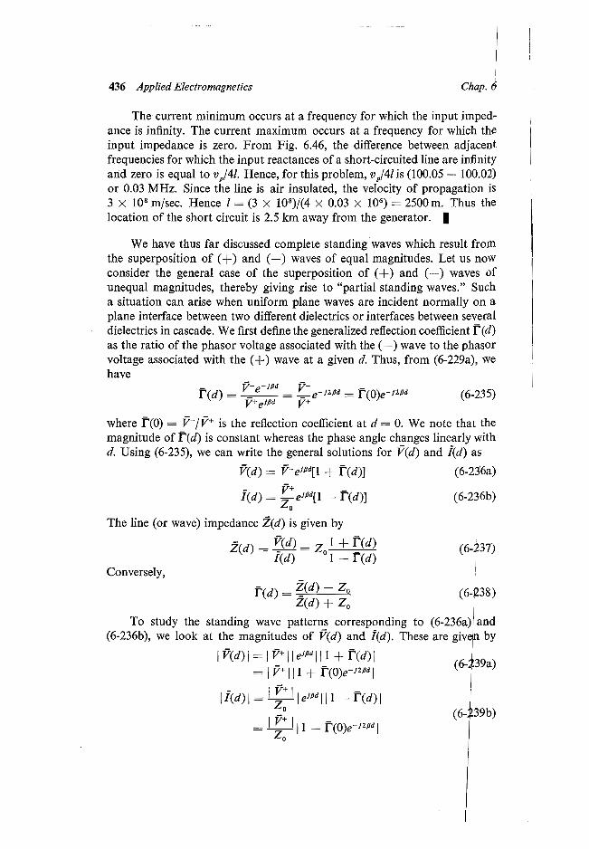
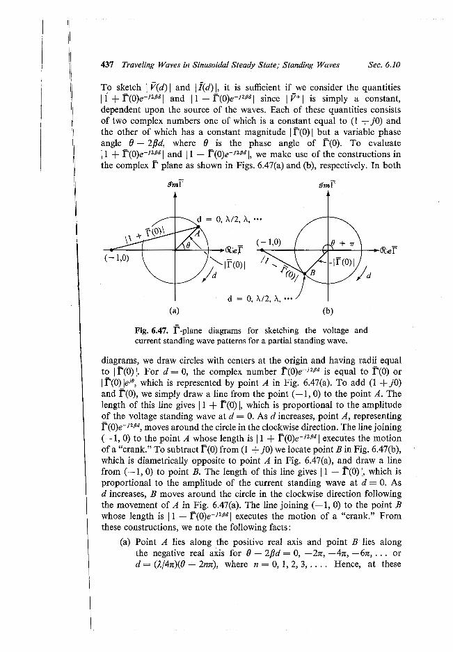
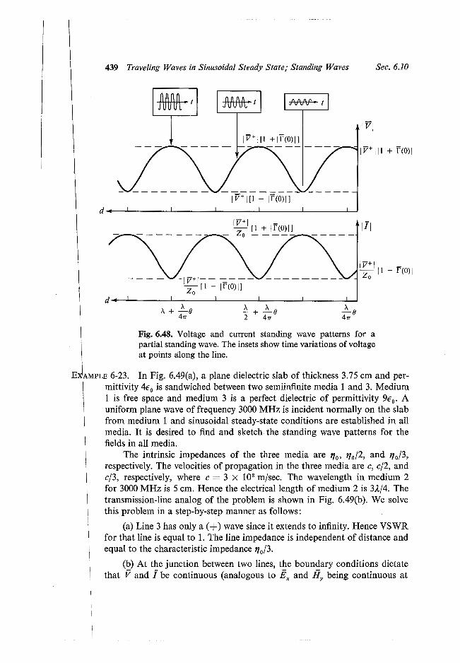
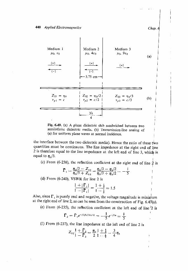
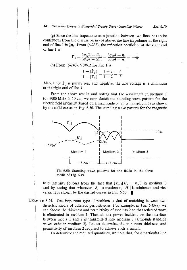
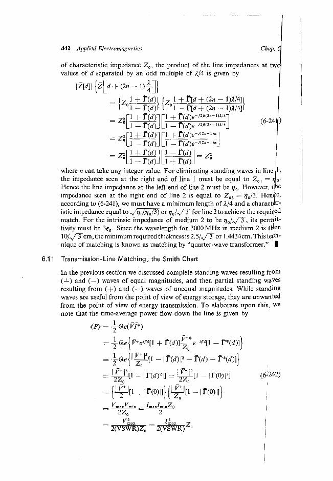
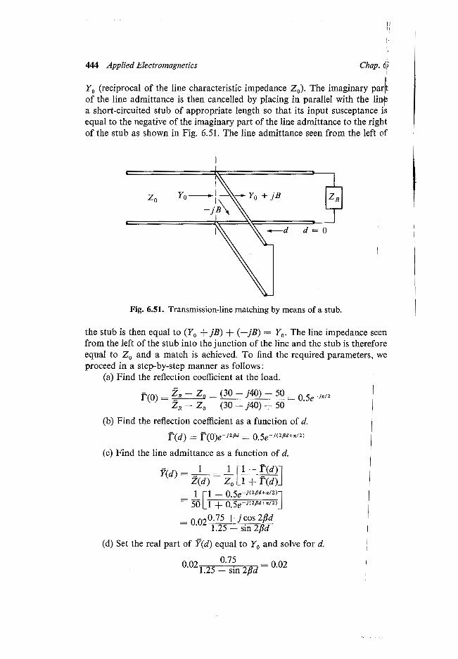
445 Transmission-Line Matching; the Smith Chart
or sin 2Pd = 0.5
2Pd= �
l d= 24
or
or
5n
6
5l
24
Sec. 6.11
Thus the stub must be located at a distance A/24 or 5Af24 from the load. _ (e) To find the length of the stub, we note that the imaginary part of Y(d) is (0.02 cos 2Pd)/(l.25 - sin 2Pd). Its value at the stub location is
B- 10.02 x 1.15 ford= f
4
5l 0.02 x (-1.15) ford= 24(f) The input impedance of a short-circuited line of length l is given by
(6-234). The input admittance is
fin = 1- =. l = -jY
0 cot PlZin JZ
0 tan Pl
Thus the stub length l must be such that
or
1-j0.02 x 1.15
-jY0
cot Pl=j0.02 x 1.15
l ford= 245l ford= 24
l = 1
0.113l
0.387l
l ford= 245l ford= 24 I
The steps involved in the analytical solution of the stub matching problem in the preceding example consist of conversion from line impedance to reflection coefficient, then going along the constant \ f' \ circle in the complex-plane diagram of Fig. 6.47 to find f'(d) and then converting back to impedance. This process of conversion and reconversion from one quantity to the other can be eliminated by constructing a chart which associates with each point in the complex f' plane the corresponding impedance or admittance. One such chart is known as the Smith chart. To discuss the basis of Smith chart construction, we define the normalized line impedance, z(d), as the ratio of the line impedance Z(d) to the characteristic impedance Z
0•
Thus
z(d) = Z(d) = 1 + f'(d)Z
0 1 - r(d) (6-243)
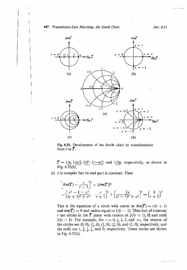
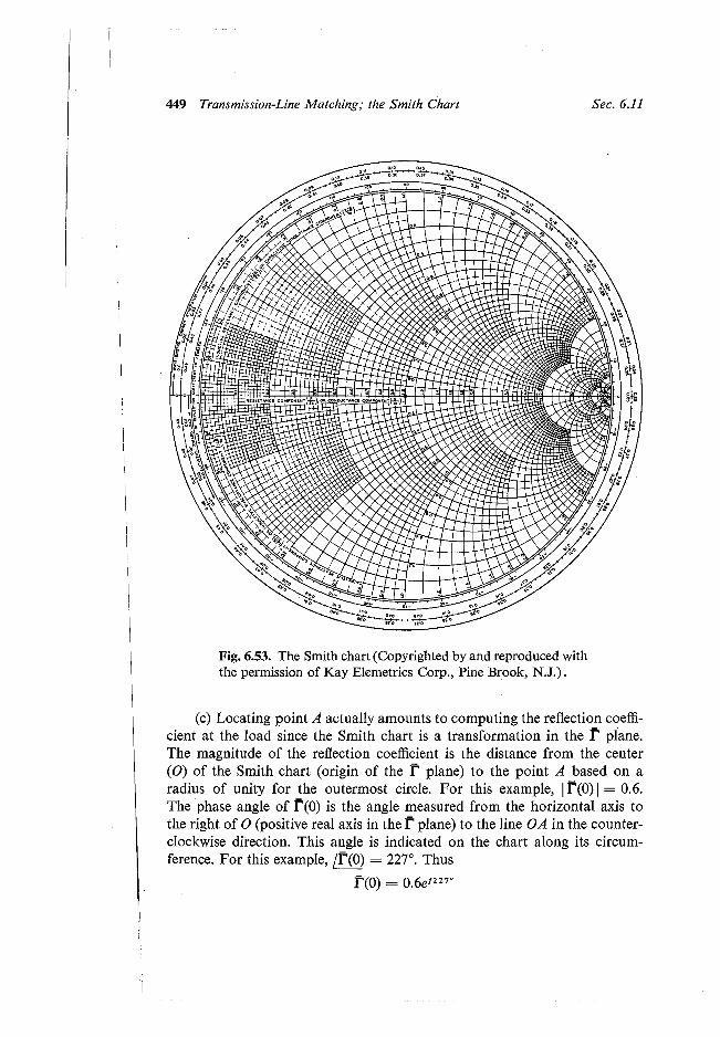
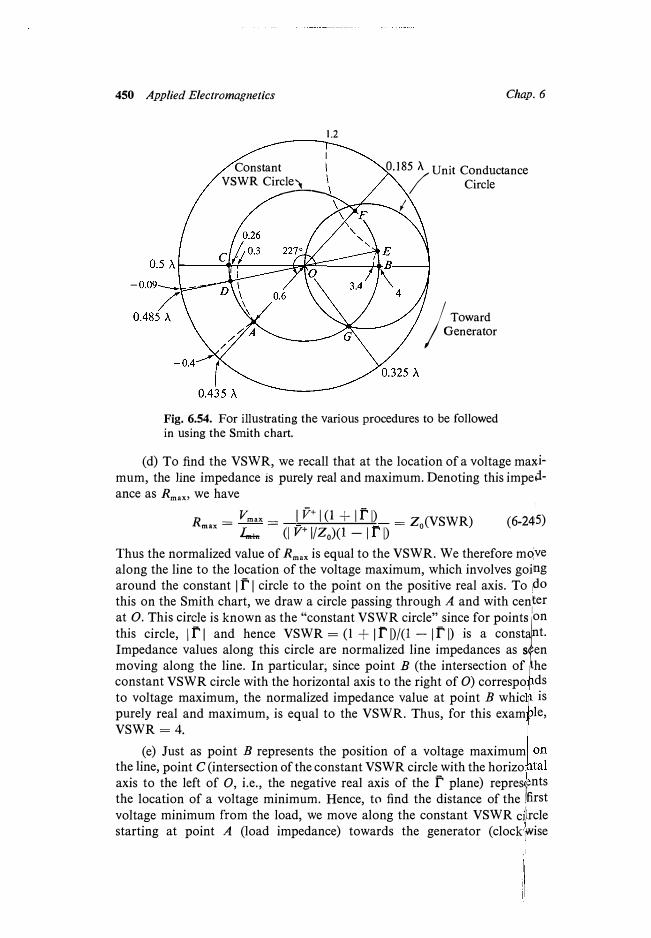
450 Applied Electromagnetics Chap. 6
1.2
Constant VSWR Circle,
O.ISS A Unit Conductance / Circle
---
I
/ Toward Generator
Fig. 6.54. For illustrating the various procedures to be followed in using the Smith chart.
(d) To find the VSWR, we recall that at the location of a voltage maximum, the line impedance is purely real and maximum. Denoting this impe4-ance as Rmax, we have
R _ Vmax _ I y+ I (1 + It I) = z (VSWR)max - I min - (I v+ 1/Zo)(l - Ir I)
0 (6-245)
Thus the normalized value of Rmax is equal to the VSWR. We therefore mqve along the line to the location of the voltage maximum, which involves going around the constant If I circle to the point on the positive real axis. To 1<10
this on the Smith chart, we draw a circle passing through A and with center at 0. This cir�e is known as the "constant VS�R circle"_since for point
�
1on this circle, Ir I and hence VSWR = (1 + Ir 1)/(1 - Ir I) is a const nt. Impedance values along this circle are normalized line impedances as s en moving along the line. In particular; since point B (the intersection of he constant VSWR circle with the horizontal axis to the right of 0) correspo ds to voltage maximum, the normalized impedance value at point B whic is purely real and maximum, is equal to the VSWR. Thus, for this exam le, VSWR=4.
(e) Just as point B represents the position of a voltage maximumthe line, point C (intersection of the constant VSWR circle with the horizo axis to the left of 0, i.e., the negative real axis of the f plane) represrntsthe location of a voltage minimum. Hence, t0 find the distance of the ilfirst voltage minimum from the load, we move along the constant VSWR ci,lrcle starting at point A (load impedance) towards the generator ( clock;wise
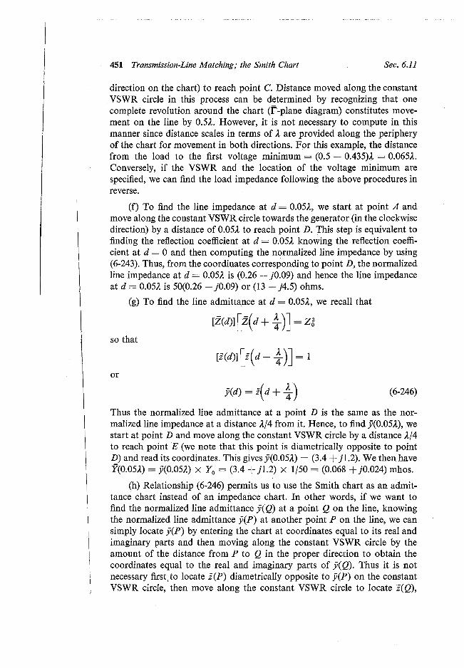
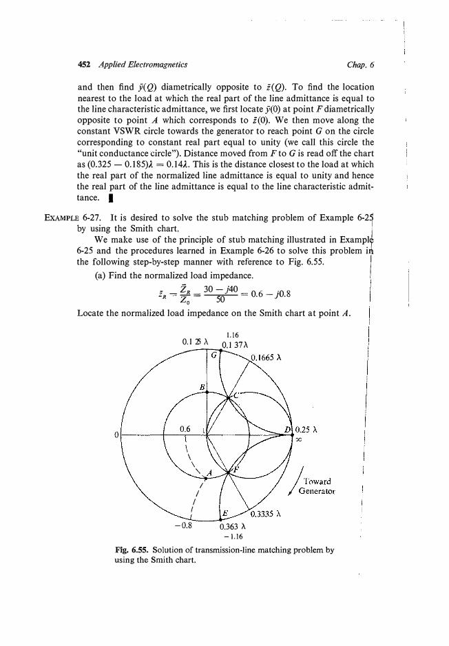
452 Applied Electromagnetics Chap. 6
and then find y(Q) diametrically opposite to i(Q). To find the locationnearest to the load at which the real part of the line admittance is equal to the line characteristic admittance, we first locate y(O) at point F diametrically opposite to point A which corresponds to i(O). We then move along the constant VSWR circle towards the generator to reach point G on the circle corresponding to constant real part equal to unity (we call this circle the "unit conductance circle"). Distance moved from F to G is read off the chart as (0.325 0.185)1 = 0.141. This is the distance closest to the load at which the real part of the normalized line admittance is equal to unity and hence the real part of the line admittance is equal to the line characteristic admittance. I
EXAMPLE 6-27. It is desired to solve the stub matching problem of Example 6-25 by using the Smith chart.
J We make use of the principle of stub matching illustrated in Examply 6-25 and the procedures learned in Example 6-26 to solve this problem irlithe following step-by-step manner with reference to Fig. 6.55. /!
(a) Find the normalized load impedance.
- Z, R
_ 30 - j40 = 0 6 _ ·o 8 ZR Z - 50 • ] • 0
Locate the normalized load impedance on the Smith chart at point A.
0
1.16
o_. _12_s ,."A ___
o.;.:. .. 137 "A
0.6
\ \ \ "
I
I I I
-0.8 0.363 "A
-1.16
X;
Fig. 6.55. Solution of transmission-line matching problem by using the Smith chart.
453 Transmission-Line Matching; the Smith Chart Sec. 6.11
(b) Draw the constant VSWR circle passing through point A. This isthe locus of the normalized line impedance as well as the normalized line admittance. Starting at point A, go around the constant VSWR circle by half a revolution to reach point B diametrically opposite to point A. Point B corresponds to the normalized load admittance.
(c) Starting at point B, go around the constant VSWR circle towardsthe generator until point C on the unit conductance circle is reached. This point corresponds to the normalized line admittance having the real part equal to unity and hence it corresponds to the location of the stub. The distance moved from point B to point C (not from point A to point C) is equal to the distance from the load at which the stub must be located. Thus the location of the stub from the load= (0.1665 - 0.125)l = 0.0415k
(d) Read off the Smith chart the normalized susceptance value corresponding to point C. This value is 1.16 and it is the imaginary part of the normalized line admittance at the location of the stub. The imaginary part of the line admittance is equal to 1.16 x Y0 = (1.16/50) mhos. The input susceptance of the stub must therefore be equal to -(1.16/50) mhos.
(e) This step consists offinding the length of a short-circuited stub havingan input susceptance equal to -(1.16/50) mhos. We can use the Smith chart for this purpose since this simply consists of finding the distance between two points on a line (the stub in this case) at which the admittances (purely imaginary in this case) are known. Thus, since the short circuit corresponds to a susceptance of infinity, we start at point D and move towards the generator along the constant VSWR circle through D (the outermost circle) to reach point E corresponding to -jl.16, which is the input admittance of the stub normalized with respect to its own characteristic admittance. The distance moved from D to Eis the required length of the stub. Thus length of the short-circuited stub= (0.363 - 0.25)l = 0.113l.
(f) The results obtained for the location and the length of the stub agreewith one of the solutions found analytically in Example 6-25. The second solution can be obtained by noting that in step (c) above, we can go around the constant VSWR circle from point B until point Fon the unit conductance circle is reached instead of stopping at point C. The stub location for this solution is (0.3335 - 0.125)l = 0.2085l. The required input susceptance of the stub is (1.16/50) mhos. The length of the stub is the distance from point D to point G in the clockwise direction. This is (0.137 + 0.25)l = 0.387.A.. These values are the same as the second solution obtained in Example 6-25. I
We have illustrated the use of the Smith chart by considering the transmission-line matching problem. However, from the procedures learned in Example 6.26, it can be seen that the Smith chart can be used for all transmission-line and analogous plane-wave problems involving reflection, transmission, and matching. As a further illustration of the applications of
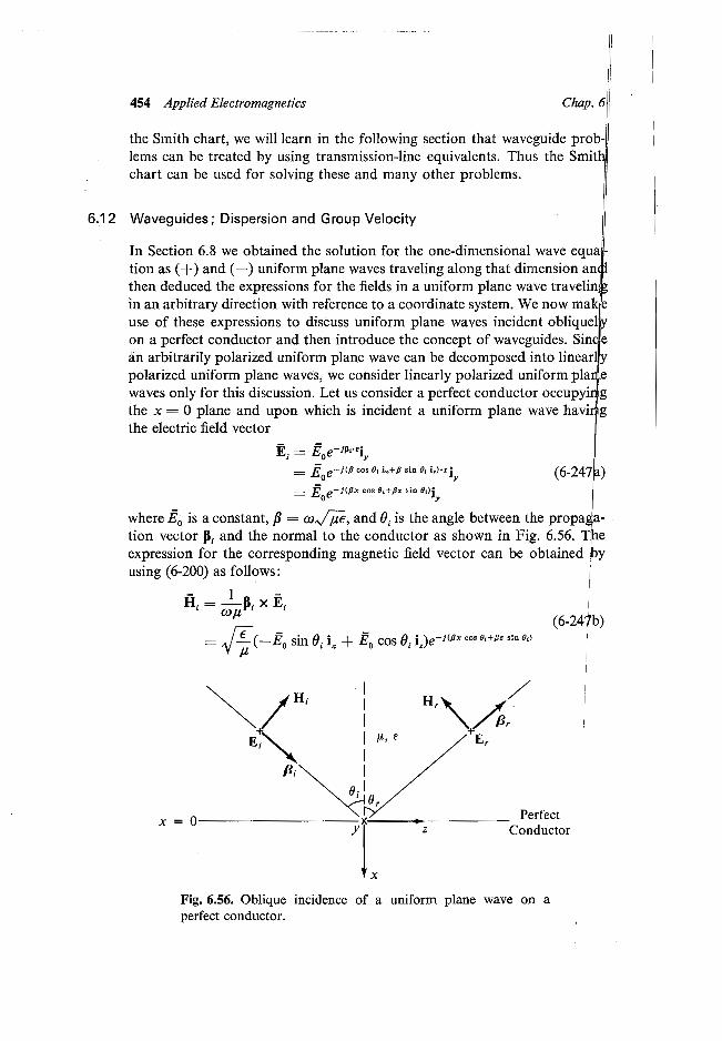
455 Waveguides; Dispersion and Group Velocity Sec. 6.12
Since the boundary condition at a perfect conductor surface dictates that the tangential component of the electric field be zero, a reflected wave must exist which cancels completely the tangential component (which is the only component in this case) of the electric field vector of the incident wave at the surface of the conductor. Such cancellation is possible only if the tangential component of the electric field in the reflected wave at the surface of the conductor is entirely in the y direction, that is, the same as the direction of the tangential component of the electric field vector of the incident wave. Furthermore, since we are dealing with linearly polarized uniform plane waves, the electric field in the reflected wave must everywhere be in the same direction. Hence it must have a y component only everywhere. Thus the electric and magnetic fields of the reflected wave can be written as
E = E' e-iP,·•j r O y
= E�e-i(-p cos (JT i:1:+P sin 8r i::)•rjJ' = E�el(Px cos e,-Pz sin e,)jy
- 1 -H, = -P, x E,wµ
= 1€(-E' sine i - E' cos e i )ei(Px cos e,-Pz sine,) '\/µ 0 rx O rz
(6-248a)
(6-248b)
where E� is a constant, p = w�, and e, is the angle between the propagation vector P, and the normal to the conductor as shown in Fig. 6.56.
Adding the incident and reflected fields, we obtain the components of the total electric and magnetic fields as
Ey = Eoe-j(px cos e,+Pz sin Oil + E�ej(px cos e,-Pz sine,)
ii = /€[-E sine. e-j(px cos e,+Pz sine,) x 'Vµ 0 ,
- E'o sin er ei(Px cos e,-Pz sine,)]
ii = /€ [E cose.e-j(pxcose,+pzsinO,)z 'Vµ 0 ,
- E'o cos e, ei(Px cos e,-Pz sine,)]
(6-249a)
(6-249b)
(6-249c)
Applying the boundary condition at the surface of the conductor, we have
[E] = t e-jpz sine,+ E' e-jpz sine, = 0y x= O O O for all z (6-250) Equation (6-250) can be satisfied only if the exponential factors are equal for all z. Thus we obtain the result
(6-251) that is, the angle of reflection is equal to the angle of incidence, which is the familiar law of reflection in optics. Substituting (6-251) into (6-250), we have
(6-252) Substituting (6-251) and (6-252) into (6-249a)-(6-249c), we obtain the follow-
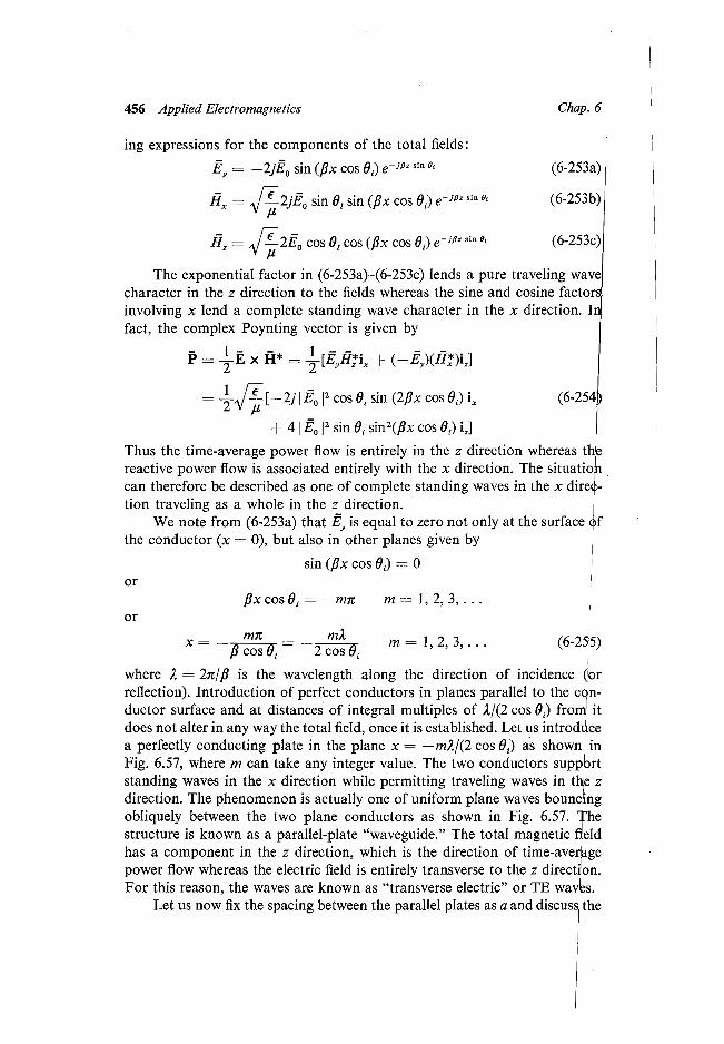
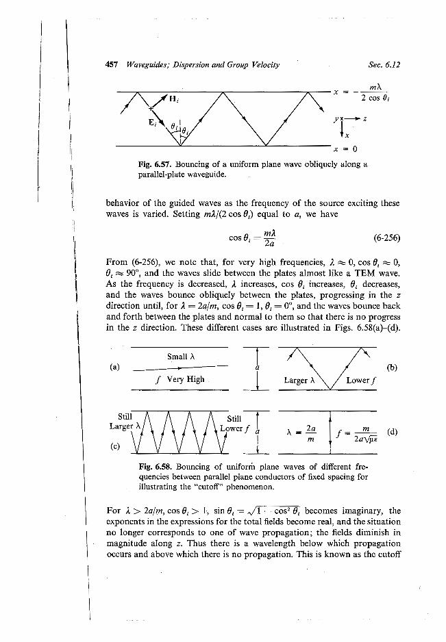
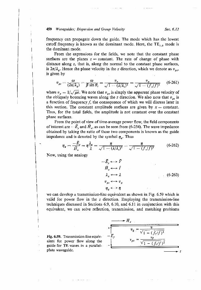
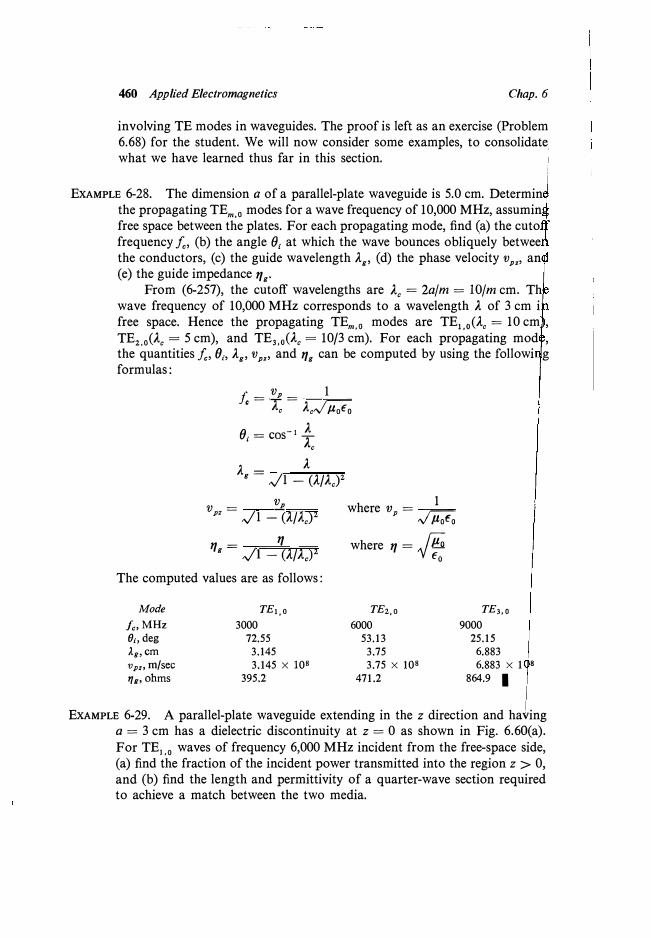
460 Applied Electromagnetics Chap. 6
involving TE modes in waveguides. The proof is left as an exercise (Problem 6.68) for the student. We will now consider some examples, to consolidate. what we have learned thus far in this section.
EXAMPLE 6-28. The dimension a of a parallel-plate waveguide is 5.0 cm. Determinthe propagating TEm,o modes for a wave frequency of 10,000 MHz, assuminfree space between the plates. For each propagating mode, find (a) the cutofrequency fc, (b) the angle O; at which the wave bounces obliquely betweethe conductors, (c) the guide wavelength A
g, (d) the phase velocity v
p,, an
(e) the guide impedance 11g·
i
From (6-257), the cutoff wavelengths are Ac = 2a/m = 10/m cm. Thwave frequency of 10,000 MHz corresponds to a wavelength A of 3 cm i free space. Hence the propagating TEm ,o modes are TE1 ,0(Ac = 10 cm , TE2 ,0(Ac = 5 cm), and TE3 ,0(Ac = 10/3 cm). For each propagating mod , the quantities fc, (),., Ag
, vp,, and 11
g can be computed by using the followi g
formulas:
J, = Vp = I c Ac Ac�
() _ -1 A .--COS T
c
A - A g - ,JI - (A/Ac)2
V = Vp
pz ,JI - (A/Ac)2
11 -11
g - ,JI - (A/AY
The computed values are as follows:
Mode
fc, MHz (};,deg
Ag,Cffi
Vpz, m/sec 17e, ohms
TE1,o
3000
72.55
3.145
3.145 x 10⁸
395.2
1where v p = r;-;-;:--"-' µofo
where 11 = flio'V�
TE2,o
6000
53.13
3.75
3.75 x 10⁸
471.2
TE3,o
9000
25.15
6.883
6.883 x 1 8
864.9 I
EXAMPLE 6-29. A parallel-plate waveguide extending in the z direction and hating a = 3 cm has a dielectric discontinuity at z = 0 as shown in Fig. 6.60(a). For TE1 ,0 waves of frequency 6,000 MHz incident from the free-space side, (a) find the fraction of the incident power transmitted into the region z > 0, and (b) find the length and permittivity of a quarter-wave section required to achieve a match between the two media.
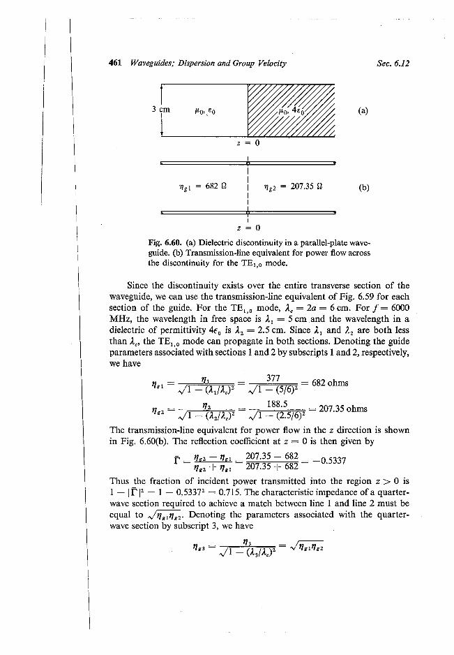
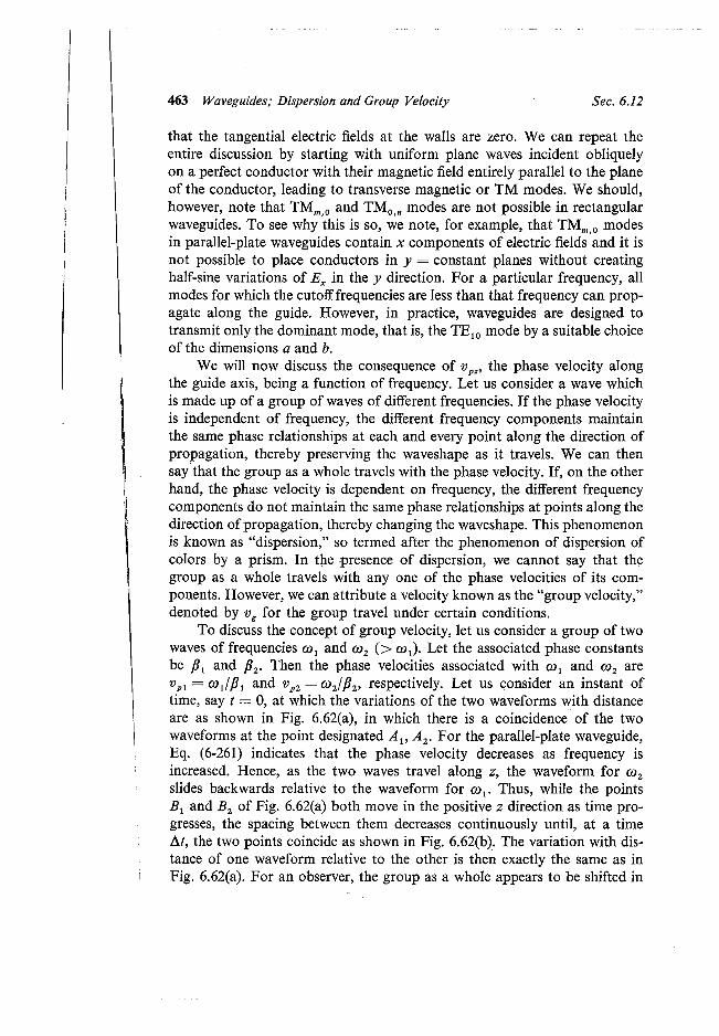
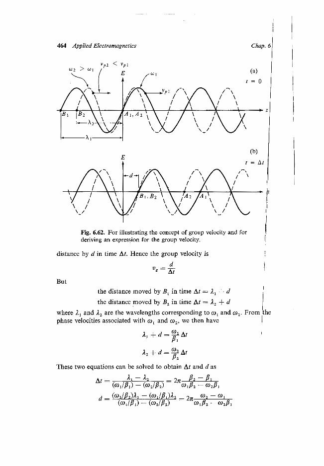
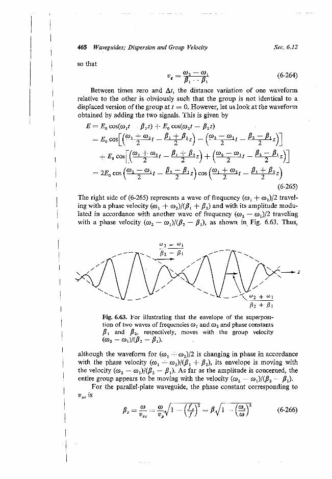
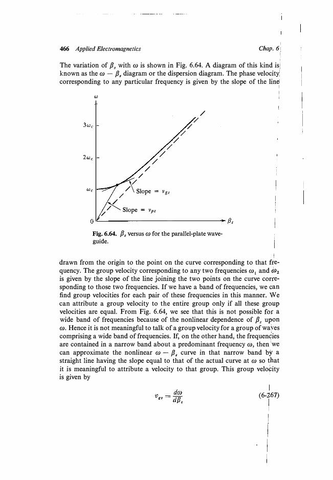
!
466 Applied Electromagnetics Chap. 61 I
!
The variation of Pz with w is shown in Fig. 6.64. A diagram of this kind is!
known as thew - Pz diagram or the dispersion diagram. The phase velocity)
corresponding to any particular frequency is given by the slope of the lin�
w
We
'/
/
/ /
/ /
)(Slope = Vgz //
� Slope = Vpz
/
/
/ /
/
Fig. 6.64. Pz versus w for the parallel-plate waveguide.
I
drawn from the origin to the point on the curve corresponding to that fttequency. The group velocity corresponding to any two frequencies w 1 and m2
is given by the slope of the line joining the two points on the curve corresponding to those two frequencies. If we have a band of frequencies, we canfind group velocities for each pair of these frequencies in this manner. Wecan attribute a group velocity to the entire group only if all these groupvelocities are equal. From Fig. 6.64, we see that this is not possible for awide band of frequencies because of the nonlinear dependence of p z upon
w. Hence it is not meaningful to talk of a group velocity for a group of wavescomprising a wide band of frequencies. If, on the other hand, the frequenciesare contained in a narrow band about a predominant frequency w, then 'wecan approximate the nonlinear w - Pz
curve in that narrow band by astraight line having the slope equal to that of the actual curve at w so tbatit is meaningful to attribute a velocity to that group. This group velo�ityis given by
(6- 67)
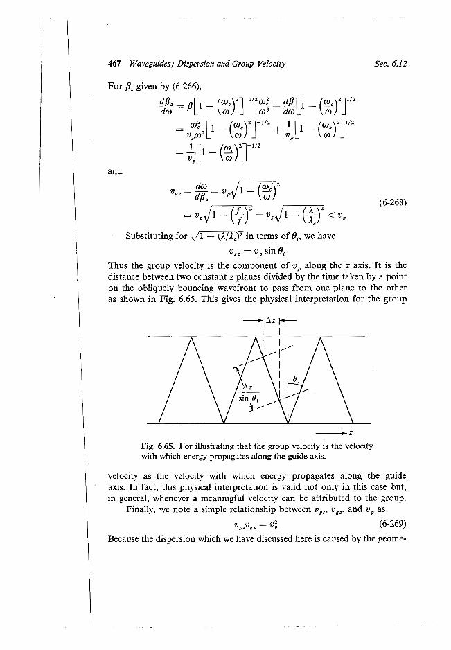
468 Applied Electromagnetics Chap. 6
try associated with the bouncing of the waves between the walls, it is known as "geometric dispersion." There are other types of dispersion as we will learn in later sections. The relationship (6-267) also holds for these other types of dispersion since its derivation is independent of the mechanism causing the dispersion.
6.13 Waves in Imperfect Dielectrics and Conductors; Attenuation and the Skin Effect
Thus far we have been concerned with wave propagation in perfect dielectri media (a = 0). In this section we will discuss wave propagation in los
1 media, especially in good conductors. We restrict our discussion to sinusoid steady state. For a medium characterized by conductivity a, permittivity , and permeability µ, we recall that Maxwell's curl equations are given b.
v x E = -aB = - µ aH /a1 at
ao aE V x H = J + at = aE + € at
For sinusoidally time-varying fields, we have v x E = -jwµii V x ii = aE + jw€E = (a + jw€)E
(6-270�) (6-270�)
Taking the curl of (6-270a) on both sides and using the vector identity :d r V x V x E, we obtain
V(V. E) - V2E = -jwµV xii But from (6-270b), we have
V·E= ). V·Vxii=O O' ]W€
(6-2 1)
(6-2 2)
Substituting (6-272) and (6-270b) into (6-271), we obtain the vector w ve equation for the electric field as
V2E = jwµ(a + jw€)E Defining a complex quantity ji as
we write (6-273) as ji2 = jwµ(a + jw€)
V2E = y2E Assuming that the electric field has only an x component, which is depen ent on the z coordinate only, that is,
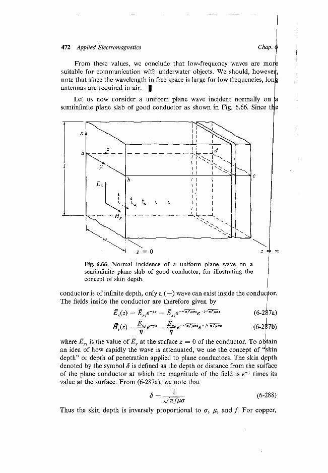
474 Applied Electromagnetics Chap. 6
second term in the integrand can be ignored since a» WE. Hence the integral is simply the conduction current flowing in the conductor. Denoting this by i
x, we have
wH/0) = t or
Substituting (6-292) into (6-290), we get
jj (0) = t
y w
- 1 - I - 2 Pin= 211wllxl
Substituting for fj in (6-293) from (6-286c), we have
pin= 1 (1 +j)� � ltl2
= 1 (I + j) aJw It 12
I I I i 12 + . 1 I I i 12= 2 <10W x }2 <10W x
(6-292)
(6-293)
(6-294)
From (5-206), the real part on the right side of (6-294) is the timeaverage power dissipated in the conductor. It is also exactly the result that would be obtained by computing the time-average power dissipated under quasistatic conditions in a conductor of length I, width w, thickness o, a11d conductivity a if the current t were distributed uniformly over the crass section of the conductor. This gives an alternative significance for the skin depth o. We will denote the resistance 1/aow by the symbol R
s. From (5-206),
the imaginary part on the right side of (6-294) is 2w times the time-avenage magnetic stored energy in the conductor since the time-average electric stored energy is negligible in view of a» WE. In fact, a volume integration of Jµ I H
Y 12 gives exactly the imaginary part of the right side of (6-294)
divided by 2w, that is, I I Ii 124 W<10W x
This energy is the same as the time-average magnetic energy stored under quasistatic conditions in an inductor of value 1/waow if the current It I were flowing in it. This inductance is the internal inductance of the conduc:tor which we denote as L;, Thus the impedance offered by a portion of the conductor of length I and width w to the current flowing in it is given by
Z; = Rs + jwL; = -i-- + j-i-- (6-i95) <1uw auw
i This impedance is known as the "internal impedance." We may empMsize that the formulas for skin depth and internal impedance developed �ere are strictly valid for plane conductors only. However, if the radius pf a cylindrical conductor is very large compared to the skin depth for the mat
/l::rial
of the conductor, these formulas can be used with negligible error. I I
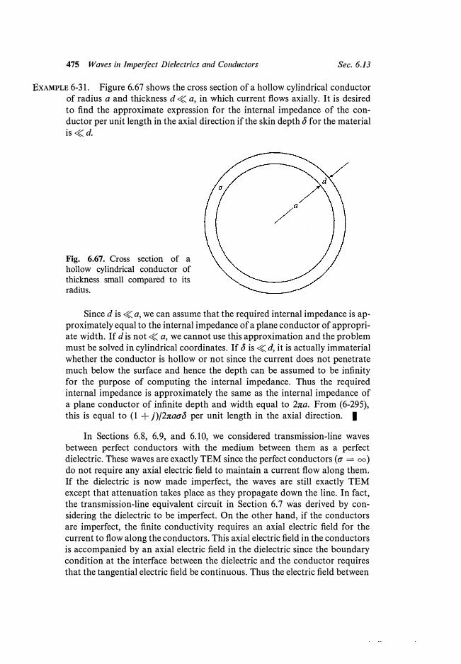
475 Waves in Imperfect Dielectrics and Conductors Sec. 6.13
EXAMPLE 6-31. Figure 6.67 shows the cross section of a hollow cylindrical conductor of radius a and thickness d « a, in which current flows axially. It is desired to find the approximate expression for the internal impedance of the conductor per unit length in the axial direction if the skin depth o for the material is« d.
Fig. 6.67. Cross section of a hollow cylindrical conductor of thickness small compared to its radius.
Since dis« a, we can assume that the required internal impedance is approximately equal to the internal impedance of a plane conductor of appropriate width. If dis not« a, we cannot use this approximation and the problem must be solved in cylindrical coordinates. If o is « d, it is actually immaterial whether the conductor is hollow or not since the current does not penetrate much below the surface and hence the depth can be assumed to be infinity for the purpose of computing the internal impedance. Thus the required internal impedance is approximately the same as the internal impedance of a plane conductor of infinite depth and width equal to 2na. From (6-295), this is equal to (1 + j)/2naao per unit length in the axial direction. I
In Sections 6.8, 6.9, and 6.10, we considered transmission-line waves between perfect conductors with the medium between them as a perfect dielectric. These waves are exactly TEM since the perfect conductors (a = oo) do not require any axial electric field to maintain a current flow along them. If the dielectric is now made imperfect, the waves are still exactly TEM except that attenuation takes place as they propagate down the line. In fact, the transmission-line equivalent circuit in Section 6.7 was derived by considering the dielectric to be imperfect. On the other hand, if the conductors are imperfect, the finite conductivity requires an axial electric field for the current to flow along the conductors. This axial electric field in the conductors is accompanied by an axial electric field in the dielectric since the boundary condition at the interface between the dielectric and the conductor requires that the tangential electric field be continuous. Thus the electric field between
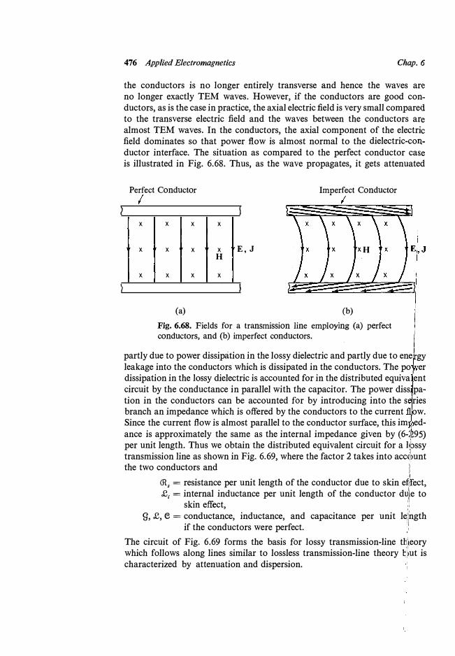
l
)
476 Applied Electromagnetics Chap. 6
the conductors is no longer entirely transverse and hence the waves are no longer exactly TEM waves. However, if the conductors are good conductors, as is the case in practice, the axial electric field is very small compared to the transverse electric field and the waves between the conductors are almost TEM waves. In the conductors, the axial component of the electric field dominates so that power flow is almost normal to the dielectric-conductor interface. The situation as compared to the perfect conductor case is illustrated in Fig. 6.68. Thus, as the wave propagates, it gets attenuated
Perfect Conductor Imperfect Conductor
x
x
x
x x x
x x x H
x x x
(a)
I
E,J
l
x x
x XH
x x
(b)
Fig. 6.68. Fields for a transmission line employing (a) perfect conductors, and (b) imperfect conductors.
partly due to power dissipation in the lossy dielectric and partly due to ene gy leakage into the conductors which is dissipated in the conductors. The po er dissipation in the lossy dielectric is accounted for in the distributed equiva ent circuit by the conductance in parallel with the capacitor. The power diss pation in the conductors can be accounted for by introducing into the s ries branch an impedance which is offered by the conductors to the current ow. Since the current flow is almost parallel to the conductor surface, this im edance is approximately the same as the internal impedance given by (6-��95) per unit length. Thus we obtain the distributed equivalent circuit for a Vbssy transmission line as shown in Fig. 6.69, where the factor 2 takes into acc�i>unt the two conductors and ;:
CR, = resistance per unit length of the conductor due to skin eilrect, £
1 = internal inductance per unit length of the conductor du:le to
k. fli
,1 s me ect, g, £, e = conductance, inductance, and capacitance per unit le;ingth
if the conductors were perfect. The circuit of Fig. 6.69 forms the basis for lossy transmission-line tlJleory which follows along lines similar to lossless transmission-line theory t\ut is characterized by attenuation and dispersion.
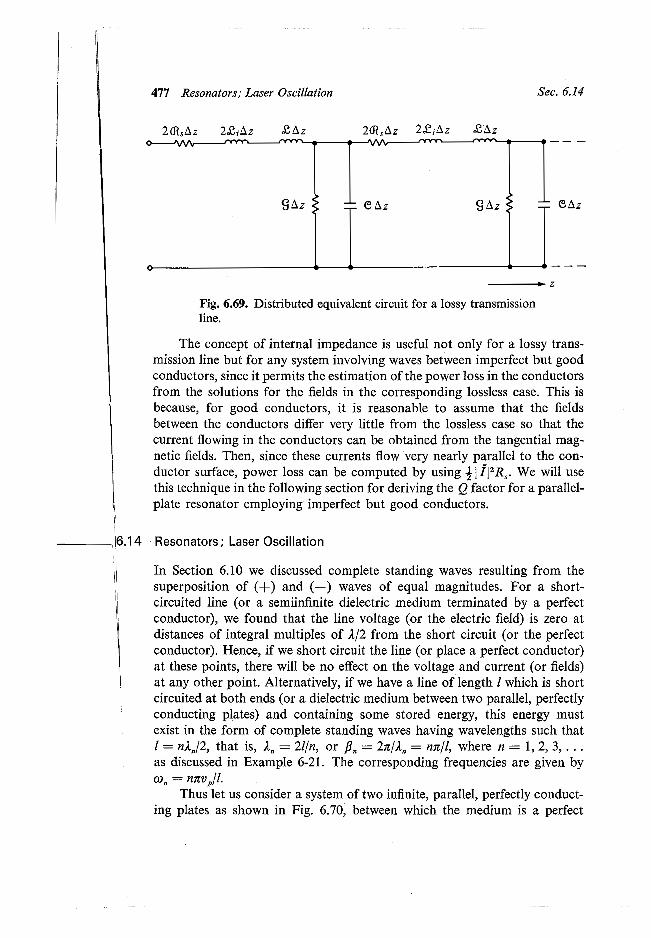
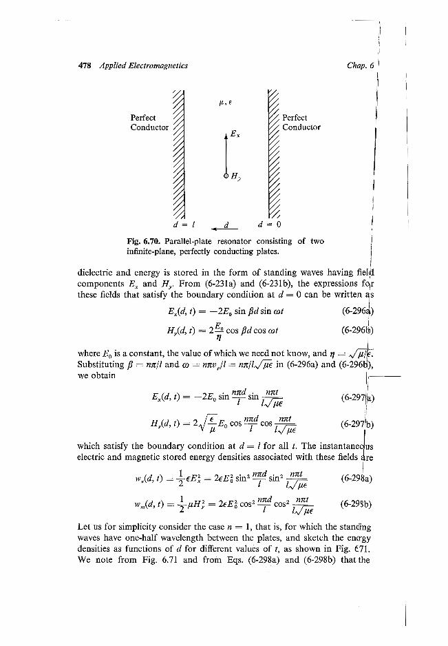
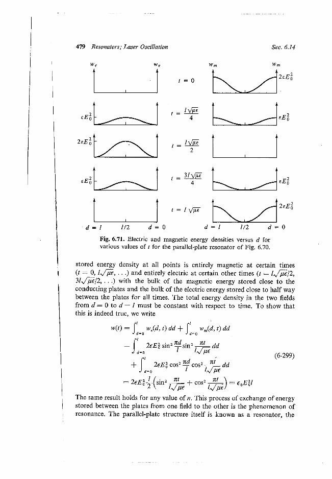
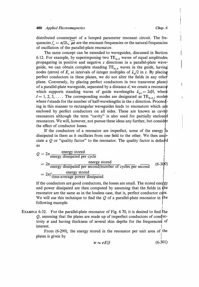
480 Applied Electromagnetics Chap. 6
distributed counterpart of a lumped parameter resonant circuit. The frequencies f. = n/21,,/iit are the resonant frequencies or the natural frequencies of oscillation of the parallel-plate resonator.
The same concept can be extended to waveguides, discussed in Section 6.12. For example, by superimposing two TE
m,o waves of equal amplitude�
propagating in positive and negative z directions in a parallel-plate wave� guide, we can obtain complete standing TE
m,o waves in the guide, having
nodes (zeros) of Ey
at intervals of integer multiples of Ag/2 in z. By placin
i perfect conductors in these planes, we do not alter the fields in any othe plane. Conversely, by placing perfect conductors in two transverse plane of a parallel-plate waveguide, separated by a distance d, we create a resonato which supports standing waves of guide wavelengths ).,
gn = 2d/l, wher
I= I, 2, 3, .... The corresponding modes are designated as TEm,o,i modes
where I stands for the number of half-wavelengths in the z direction. Procee -ing in this manner to rectangular waveguides leads to resonators which a e enclosed by perfect conductors on all sides. These are known as cavi y resonators although the term "cavity" is also used for partially enclosed resonators. We will, however, not pursue these ideas any further, but consid ,r the effect of conductor losses.
If the conductors of a resonator are imperfect, some of the energy is dissipated in them as it oscillates from one field to the oth�r. We then ass ciate a Q or "quality factor" to the resonator. The quality factor is defin d as
Q _ 2 energy stored - n energy dissipated per cycle
_ 2 energy stored - n energy dissipated per second/number of cycles per second
_ 2 f energy stored
- n time-average power dissipatedIf the conductors are good conductors, the losses are small. The stored ene gy and power dissipated are then computed by assuming that the fields in he resonator are the same as in the lossless case, that is, perfect conductor c We will use this technique to find the Q of a parallel-plate resonator in following example.
EXAMPLE 6-32. For the parallel-plate resonator of Fig. 6.70, it is desired to find he Q, assuming that the plates are made up of imperfect conductors of con uctivity a and having thickness of several skin depths for the frequencie of interest.
From (6-299), the energy stored in the resonator per unit area of the plates is given by
w � €E5! (6-�0 1)
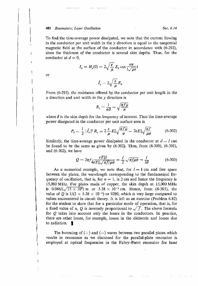
,·
I
483 Waves in Plasma; Ionospheric Propagation
fields in all these waves. Thus it is given by E(z) = Eoe-rz + f' Eoe-2r1erz
+ f'2£ e-2fle-fz + f'3£ e-4flefz0 · 0
+ f'4£oe-4f/e-fz + , , ,
= £0 [e-fz(l + f2e-2r1 + f'4e-4fl + ... )
+ f'erze-2r1(l + f2e-2r1 + ... )]
-e-fz + f e-2flefz
-E ----'-�---- 0
1 - r2e-2f/
Sec. 6.15
(6-304)
From (6-304), we note that the condition for oscillation, that is, for a field to be set up in the medium for zero £
0, is
or (6-305)
Denoting f' = If' I e19 and substituting for ji in terms of 0G and p, we write (6-305) as
or 1r1 e-oo/ = 1
1 -OG = T1n1r1
and
and
n = 0, 1, 2, 3, ...
0- Pl= ±nn
pt= 0 ± nn, n = 0, 1, 2, 3, ... (6-306)
where we choose only those values of n for which pt is greater than zero. While the condition pt= 0 + nn can be satisfied for several frequencies for a given/, the condition OG = (1//) In If' I is satisfied by a particular active medium only for a narrow range of frequencies, so that oscillation occurs only in that narrow range of frequencies. Note that for f' = -1 as is the case for perfectly conducting plates, the condition for oscillation is
1 OG = T In 1 = 0 and pt= nn, n = 1, 2, 3, ...
which agrees with the result for the parallel-plate resonator.
�.15 Waves in Plasma; Ionospheric Propagation
Thus far we have discussed wave propagation in free space and perfect dielectrics and then in lossy dielectrics and good conductors. In free space and perfect dielectrics, the conduction current is zero so that the current is entirely of the displacement type. In lossy dielectrics, we have both conduction and displacement currents but the conduction current is small compared to the displacement current. In good conductors, the displacement current
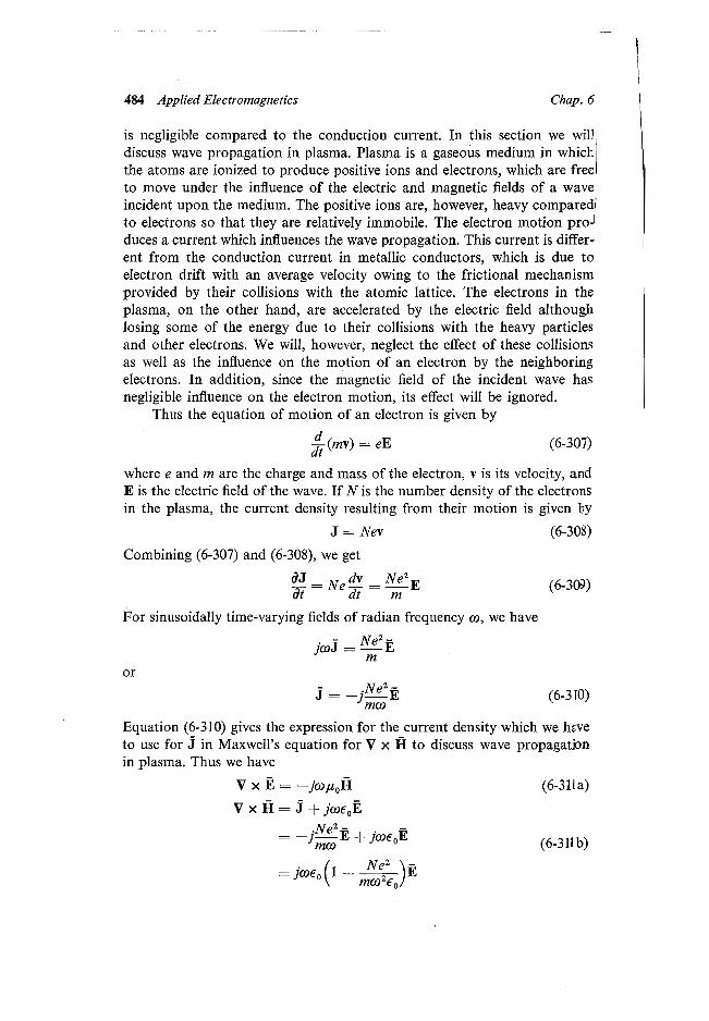
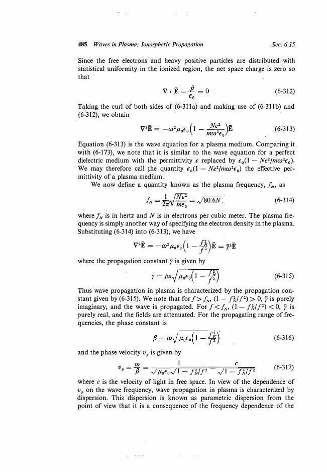
485 Waves in Plasma; Ionospheric Propagation Sec. 6.15
Since the free electrons and heavy positive particles are distributed with statistical uniformity in the ionized region, the net space charge is zero so that
(6-312)
Taking the curl of both sides of (6-311a) and making use of (6-311b) and (6-312), we obtain
-( Ne2 )-
v2E = -ro2µ0€
0 1 - --
2- E mOJ €0
(6-313)
Equation (6-313) is the wave equation for a plasma medium. Comparing it with (6-173), we note that it is similar to the wave equation for a perfect dielectric medium with the permittivity f replaced by fo( l - Ne2/mro2€
0).
We may therefore call the quantity €0(1 - Ne2/mro2
€0
) the effective permittivity of a plasma medium.
We now define a quantity known as the plasma frequency, JN, as
11
Ne2 --
JN = -2 - = ,j80.6Nn m€
0
(6-314)
where f N
is in hertz and N is in electrons per cubic meter. The plasma frequency is simply another way of specifying the electron density in the plasma. Substituting (6-314) into (6-313), we have
V2E = -ro2µ0f
0(1 - :?)E = y2E
where the propagation constant r is given by
- · I (1 11)Y = JOJ,y µofo - J2 (6-315)
Thus wave propagation in plasma is characterized by the propagation constant given by (6-315). We note that for f> fm (I - JU /2) > 0, y is purely imaginary, and the wave is propagated. For f < Im (1 - f U f 2) < 0, y is purely real, and the fields are attenuated. For the propagating range of frequencies, the phase constant is
and the phase velocity v P
is given by
ro 1 c
VP=
7J = ,j µ0€0,/1 - JU/2 = ,/1 - JU/2
(6-316)
(6-317)
where c is the velocity of light in free space. In view of the dependence of v
p on the wave frequency, wave propagation in plasma is characterized by
dispersion. This dispersion is known as parametric dispersion from the point of view that it is a consequence of the frequency dependence of the
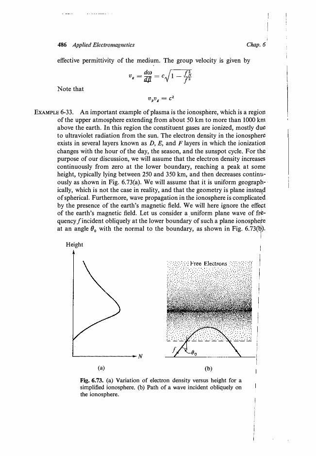
486 Applied Electromagnetics Chap. 6
effective permittivity of the medium. The group velocity is given by
_ dw _ I !tr Vg - dfi - CV 1 - f2
Note that
EXAMPLE 6-33. An important example of plasma is the ionosphere, which is a regionof the upper atmosphere extending from about 50 km to more than 1000 kn:t above the earth. In this region the constituent gases are ionized, mostly due to ultraviolet radiation from the sun. The electron density in the ionosphere exists in several layers known as D, E, and Flayers in which the ionization changes with the hour of the day, the season, and the sunspot cycle. For the purpose of our discussion, we will assume that the electron density increases continuously from zero at the lower boundary, reaching a peak at some height, typically lying between 250 and 350 km, and then decreases continuously as shown in Fig. 6.73(a). We will assume that it is uniform geographically, which is not the case in reality, and that the geometry is plane instea,d of spherical. Furthermore, wave propagation in the ionosphere is complicated by the presence ofthe earth's magnetic field. We will here ignore the effect of the earth's magnetic field. Let us consider a uniform plane wave of frequency f incident obliquely at the lower boundary of such a plane ionosphere at an angle 00
with the normal to the boundary, as shown in Fig. 6.73(�).
Height
......_ _________ N
(a) (b)
Fig. 6.73. (a) Variation of electron density versus height for a simplified ionosphere. (b) Path of a wave incident obliquely on the ionosphere.
487 Waves in Plasma; Ionospheric Propagation Sec. 6.15
We wish to investigate the path of the wave as it propagates in the ionized medium.
We divide the region into several infinitesimal slabs, in each of which the electron density can be considered to be uniform with height. Let us consider the boundary between the free space and the first slab, for which we will denote the plasma frequency as JN, i • From (6-317), the phase velocity along the direction of propagation, that is, normal to the constant phase surfaces in this slab, is given by
c
V p, I = ,v'l - f'fv. ii j2 For the waves in the free space and in the slab to be in step at the boundary, their apparent phase velocities along the boundary must be equal. This is the same as saying that the apparent wavelengths along the boundary must be equal. Since v P, 1 > c, this is possible only if the direction of travel of thewave is bent away from the normal to the boundary as shown in Fig. 6.74.
/N,2
Free Space
Fig. 6.74. For illustrating the bending of the path of a wave as it propagates in the ionosphere.
Thus, denoting the angle between the normal to the boundary and direction of travel in the slab by B
i, we have
or
c · e · e-sin 1 =sm O
Vp,I
491 Radiation of Electromagnetic Waves
equation reduces to
v2v= _.!!....
Sec. 6.16
which is Poisson's equation for the electrostatic potential. Let us consider a point charge Q
0 at the origin. The electrostatic potential due to this point
charge is given by V(r) = Qo
411:ErFor the time-varying case, we know that electromagnetic effects propagate with a finite velocity v which for the homogeneous wave equation corresponding to (6-324) is 1/,../iif. Hence, if the point charge at the origin is varying with time (due to current flowing into and/or away from the origin), its effect is felt at a distance r from the origin after a time delay of r/v. Conversely, the effect felt at a distance r from the origin at time t is due to the value of the charge which existed at the origin at an earlier time t - r/v. Thus, if the point charge at the origin is varying in the manner Q
0 sin wt, we expect the
time-varying electric potential due to it to be
V(r, t) = Qo sin �)(t - r/v) (6-327) 71:Er To verify if our reasoning is correct, we note that
v2v = v2[Qo sin w(t - r/v)]411:Er
= 2;E{[sinw(t- �)Jv2{
+ 2V sin w(t - �) • v{ + { v2 sin w(t - �)}
Q0o(r) sin wt w2Q
0 sin w(t - r/v)
E 4nav2
where we have used the vector identity V2(</>'/I) = </> V2f/l + 2 V<f> • Vf/1 + '/I V2<p
and the relation (see Problem 2-58)
We also note that
v2_!_ = -4nt:5(r) r
w2Q0 sin w(t - r/v)4nErV2
From (6-328a) and (6-328b), we have
v2v _ µi2V = _Q0o(r) sin wtat2
E
(6-328a)
(6-328b)
which agrees with (6-324) for a point charge Q0
sin wt at the origin.
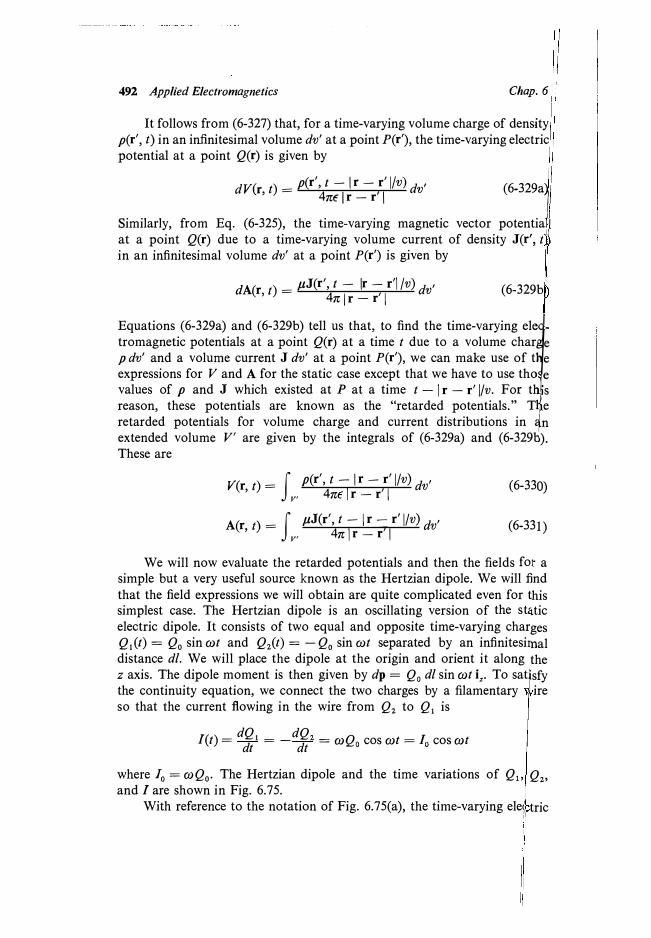
492 Applied Electromagnetics Chap. 6
It follows from (6-327) that, for a time-varying volume charge of density p(r', t) in an infinitesimal volume dv' at a point P(r'), the time-varying electric potential at a point Q(r) is given by
dV(r t) = p(r', t - Ir - r' 1/v) dv' (6-329a) ' 4nf I r - r' I '/
Similarly, from Eq. (6-325), the time-varying magnetic vector potentiaj} at a point Q(r) due to a time-varying volume current of density J(r', tin an infinitesimal volume dv' at a point P(r') is given by
dA(r t) = µJ(r', t - Ir - r'I /v) dv'' 4nlr - r' I
(6-329b
Equations (6-329a) and (6-329b) tell us that, to find the time-varying ele
i
tromagnetic potentials at a point Q(r) at a time t due to a volume char e p dv' and a volume current J dv' at a point P(r'), we can make use of t e expressions for V and A for the static case except that we have to use tho e values of p and J which existed at P at a time t - Ir - r' 1/v. For th's reason, these potentials are known as the "retarded potentials." T�e retarded potentials for volume charge and current distributions in 1n extended volume V' are given by the integrals of (6-329a) and (6-329b). These are
V(r, t) = f p(r', t - Ir - ,r' 1/v)
dv'v' 4n€ Ir - r I (6-330)
A(r, t) = f µJ(r', t - Ir -; r' 1/v) dv'
v' 4n Ir - r I (6-331)
We will now evaluate the retarded potentials and then the fields fot a simple but a very useful source known as the Hertzian dipole. We will find that the field expressions we will obtain are quite complicated even for this simplest case. The Hertzian dipole is an oscillating version of the static electric dipole. It consists of two equal and opposite time-varying charges Q
1 (t) = Q
0 sin cot and Qz(t) = -Q
0 sin cot separated by an infinitesirnal
distance di. We will place the dipole at the origin and orient it along the z axis. The dipole moment is then given by dp = Q
0 di sin cot i,. To satisfy
the continuity equation, we connect the two charges by a filamentary ire so that the current flowing in the wire from Q
2 to Q
1 is
J(t) = dQ1 = _ dQ
2 = coQ0
cos cot= I cos cotdt dt O
where /0 = coQ0
• The Hertzian dipole and the time variations of Qi , Q2,
and I are shown in Fig. 6.75. With reference to the notation of Fig. 6.75(a), the time-varying ele1 tric
,1
495 Radiation of Electromagnetic Waves
E = i0 di sin o( _ _l_ + _1 + jm)e-1"',1" e 4nf mr3 vr2 v2r
= _P211i0 di sin 0[_1_ + _1_ + _l_Je-JPr 4n (jfir)3 (jfir)2 jpr
jj = io di sin () (_!___ + jm) e-Jwr/v if> 4n r2 vr
p2i0 di sin ()[_1_ + 1-Je-JPr4n (jfir)2 jpr
where P = m/v, 11 = � = 1/cv, and i0
= /0
= mQ0 •
Sec. 6.16
(6-337)
(6-338)
We note from (6-335a)-(6-335c) or (6-336)-(6-338) that the field expressions contain terms involving 1 / r3 , 1 / r2
, and 1 / r. Very close to the dipole, the 1/r3 and 1/r2 terms dominate the 1/r terms. Far from the dipole, the 1/r3
and 1/r2 terms are negligible and the fields are determined by the 1/r terms. To see how far from the dipole, let us first consider the Hif> component. The magnitudes of the two terms are equal for r = v/m = 1/P = ),/2n � 0.162. For the Ee component the combined magnitude of the 1/r3 and 1/r2 terms is equal to the 1/r term for
or r4 - (�)\2 - (
2�r = 0
= /1+�.!�02 1 r ,y . 2 21' "'-' • IL
Thus, even in a distance of few wavelengths from the dipole, we can neglect the 1/r3 and 1/r2 terms in comparison with the 1/r terms. The field expressions then reduce to
E, = o
E = jmi0 di sin() e-Jwr/v = jfi11i0
di sin() e-Jpr e 4ncv2r · 4nr jj = jmi
0 di sin() e-Jwr/v = jpi0 di sin() e-JPr
if> 4nvr 4nr
(6-339)
(6-340)
These fields are known as the "radiation fields" because they are the components which contribute to radiation of electromagnetic waves away from the dipole. In fact, we will learn later that the l/r3 and 1/r2 terms do not contribute to the time-average power flow even near the dipole. We note that the ratio of Ee to Hif> given by (6-339) and (6-340) is equal to 11 = ,JiifEas for the case of the fields associated with a uniform plane wave, although the constant phase surfaces are r = constant and the constant amplitude surfaces are (sinO)/r = constant. However, let us consider a spherical surface of large radius and centered at the dipole and divide it into small regions, in each of which sin () may be considered to be constant. Then each small
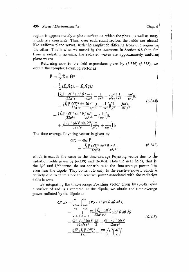
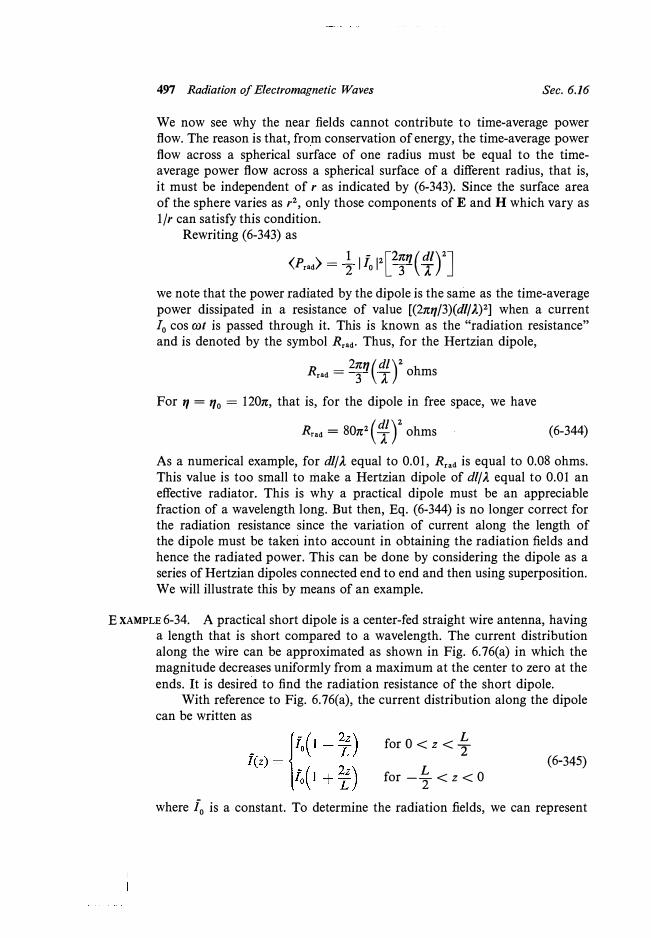
497 Radiation of Electromagnetic Waves Sec. 6.16
We now see why the near fields cannot contribute to time-average power flow. The reason is that, from conservation of energy, the time-average power flow across a spherical surface of one radius must be equal to the timeaverage power flow across a spherical surface of a different radius, that is, it must be independent of r as indicated by (6-343). Since the surface area of the sphere varies as r2, only those components of E and H which vary as l/r can satisfy this condition.
Rewriting (6-343) as
<Prad> = � I fo 12 [2
;11 ( f) 2]
we note that the power radiated by the dipole is the same as the time-average power dissipated in a resistance of value [(2n17/3)(dl/).,)2] when a current !
0 cos rot is passed through it. This is known as the "radiation resistance"
and is denoted by the symbol R,ad· Thus, for the Hertzian dipole,
R,ad = 2;11 (fr ohms
For 11 = 170
= 120n, that is, for the dipole in free space, we have
R,ad = 80n2 (fr ohms (6-344)
As a numerical example, for di/)., equal to 0.01, R,.d is equal to 0.08 ohms. This value is too small to make a Hertzian dipole of di/)., equal to 0.01 an effective radiator. This is why a practical dipole must be an appreciable fraction of a wavelength long. But then, Eq. (6-344) is no longer correct for the radiation resistance since the variation of current along the length of the dipole must be takeri into account in obtaining the radiation fields and hence the radiated power. This can be done by considering the dipole as a series of Hertzian dipoles connected end to end and then using superposition. We will illustrate this by means of an example.
E XAMPLE 6-34. A practical short dipole is a center-fed straight wire antenna, havinga length that is short compared to a wavelength. The current distribution along the wire can be approximated as shown in Fig. 6.76(a) in which the magnitude decreases uniformly from a maximum at the center to zero at the ends. It is desired to find the radiation resistance of the short dipole.
With reference to Fig. 6.76(a), the current distribution along the dipole can be written as
L for O < z < 2L for -2 < z < 0
(6-345)
where i0
is a constant. To determine the radiation fields, we can represent
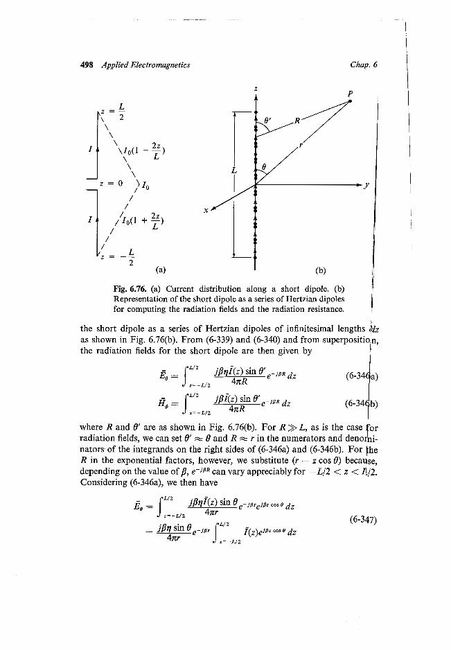
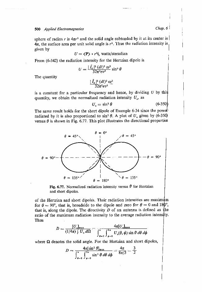
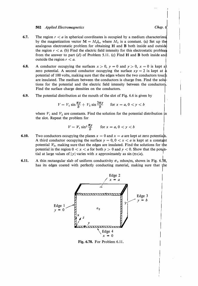
502 Applied Electromagnetics Chap.
6.7. The region r < a in spherical coordinates is occupied by a medium characterizeby the magnetization vector M = M0iz, where M0 is a constant. (a) Set up thanalogous electrostatic problem for obtaining H and B both inside and outsid ,the region r < a. (b) Find the electric field intensity for this electrostatic problefrom the answer to part (d) of Problem 5.11. (c) Find Hand B both inside anoutside the region r < a.
6.8. A conductor occupying the surfaces x > 0, y = 0 and y > 0, x = 0 is kept atzero potential. A second conductor occupying the surface xy = 2 is kept atpotential of 100 volts, making sure that the edges where the two conductors toucare insulated. The medium between the conductors is charge free. Find the soltions for the potential and the electric field intensity between the conductor .Find the surface charge densities on the conductors.
6.9. The potential distribution at the mouth of the slot of Fig. 6.6 is given by
V V . ny V . 3ny = 1 smb+ 2smb for x = a, 0 < y < b
where V1 and V2 are constants. Find the solution for the potential distribution nthe slot. Repeat the problem for
V= Vi sin3 6 for x = a, 0 < y < b
6.10. Two conductors occupying the planes x = 0 and x = a are kept at zero potentia s.A third conductor occupying the surface y = 0, 0 < x < a is kept at a const ntpotential V0 , making sure that the edges are insulated. Find the solutions for thepotential in the region O < x < a for both y > 0 and y < 0. Show that the pot ntial at large values of I y I varies with x approximately as sin (nx/a).
6.11. A thin rectangular slab of uniform conductivity a O mhos/m, shown in Fig. 6. 8,has its edges coated with perfectly conducting material, making sure that he
Edge Iy = 0
Edge 2--�x = a
y
\Edge 4x = 0
Fig. 6.78. For Problem 6.11.
Edge 3�y = b
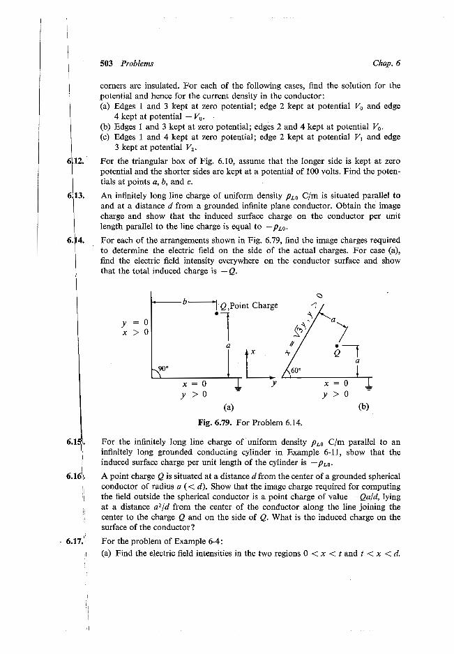
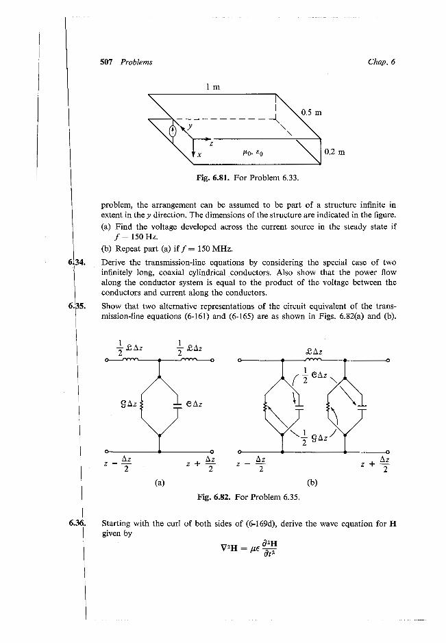
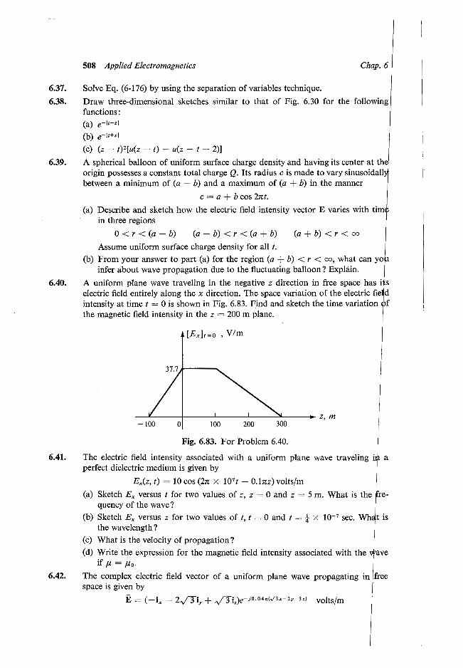
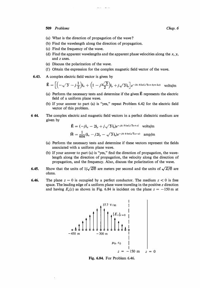
509 Problems
(a) What is the direction of propagation of the wave?(b) Find the wavelength along the direction of propagation.(c) Find the frequency of the wave.
Chap. 6
(d) Find the apparent wavelengths and the apparent phase velocities along the x, y,
and z axes.(e) Discuss the polarization of the wave.(f) Obtain the expression for the complex magnetic field vector of the wave .
6. 43. A complex electric field vector is given by
E = [ ( -,y'3 _ j � )ix + ( 1 _ j�)iy
+ j ,y13i, ]e-jo. 02n(./"3"x+3y+2z> volts/m
(a) Perform the necessary tests and determine if the given E represents the electricfield of a uniform plane wave.
(b) If your answer to part (a) is "yes," repeat Problem 6.42 for the electric fieldvector of this problem.
6 44. The complex electric and magnetic field vectors in a perfect dielectric medium are given by
E = (-jix - 2iy
+ j,v13i,)e-i0· osn<..r3"x+•> vo!ts/m
fl:= 6�n(ix - j2iy - ,y13i,)e-j0.05n(./"3"x+z) amp/m
(a) Perform the necessary tests and determine if these vectors represent the fieldsassociated with a uniform plane wave.
(b) If your answer to part (a) is "yes," find the direction of propagation, the wavelength along the direction of propagation, the velocity along the direction ofpropagation, and the frequency. Also, discuss the polarization of the wave.
6.45. Show that the units of 1/,./JSe are meters per second and the units of� are ohms.
6.46. The plane z = 0 is occupied by a perfect conductor. The medium z < 0 is free space. The leading edge of a uniform plane wave traveling in the positive z direction and having Ex(z) as shown in Fig. 6.84 is incident on the plane z = -150 m at
I37.7 Vim I
.i111Ill.ll1Ii;:l -450 m -300 m I
J..lo, co I I
z = -150 m z = 0 Fig. 6.84. For Problem 6.46.
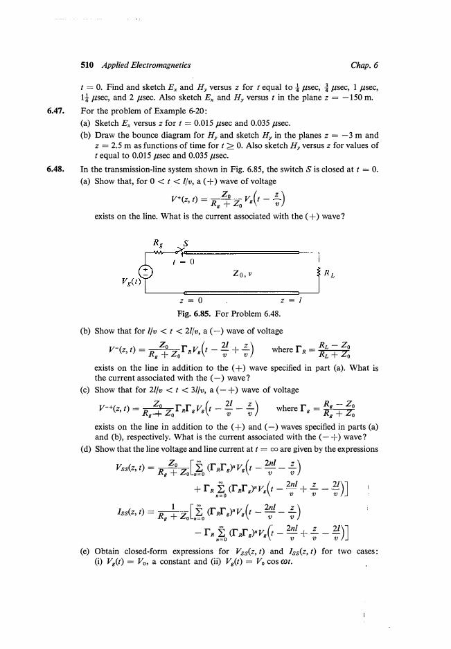
510 Applied Electromagnetics Chap. 6
t = 0. Find and sketch Ex and Hy versus z for t equal to i µsec, i µsec, 1 µsec,1{ µsec, and 2 µsec. Also sketch Ex and Hy versus t in the plane z = -150 m.
6.47. For the problem of Example 6-20:(a) Sketch Ex versus z for t = 0.015 µsec and 0.035 µsec.(b) Draw the bounce diagram for Hy and sketch Hy in the planes z = -3 m and
z = 2.5 m as functions of time for t :::=:: 0. Also sketch Hy versus z for values oft equal to 0.015 µsec and 0.035 µsec.
6.48. In the transmission-line system shown in Fig. 6.85, the switch Sis closed at t = 0.(a) Show that, for O < t < l/v, a ( +) wave of voltage
V+(z, t) = R
g
� Zo Vg(t - : )
exists on the. line. What is the current associated with the ( +) wave?
Zo, v
z = 0 z =Fig. 6.85. For Problem 6.48.
(b) Show that for l/v < t < 21/v, a(-) wave of voltage- � r ( u z)
V (z, t) = Rg
+ Zo R V
g t -
v +
v h r RL -Zow ere R = RL + Zo
exists on the line in addition to the ( +) wave specified in part (a). What isthe current associated with the ( -) wave?
(c) Show that for 21/v < t < 31/v, a ( - +) wave of voltage-+( ) _ Zo r r ( 2/ z )V z, t - Rg + Zo R g
Vg
t -v
-
v R -Zowhere rg = R; + Zo
exists on the line in addition to the ( +) and ( -) waves specified in parts (a)and (b), respectively. What is the current associated with the(-+) wave?
(d) Show that the line voltage and line current at t = oo are given by the expressionsVss(z, t) = R � z [� er Rr
g)" V
g(t - 2n1 - ..!....)
g O n=O V V
+ rR � crRrg)"Vg(t - 2nl + ..!.... - 21)]
n=O V V V
_ 1 [ = r r " ( 2nl z )lss(z, t) - R + z � ( R g) Vg
t - - - -g O n=O V V
= r r (. 2n1 z 21)]- rR � c R g)"V
g 1 - - +- --n=O V V V
(e) Obtain closed-form expressions for V88(z, t) and l88(z, t) for two cases:(i) Vg(t) = V0, a constant and (ii) Vg(t) = V0 cos Wt.
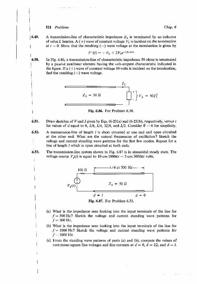
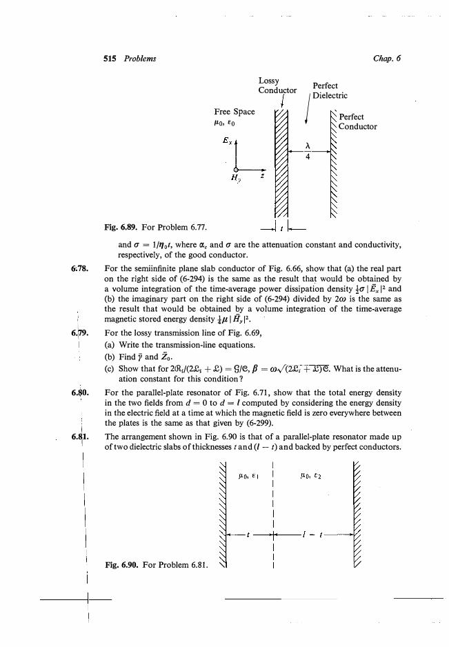
515 Problems
Fig. 6.89. For Problem 6.77.
Free Space µo, ea
Lossy Conductor Chap. 6
Perfect j Dielec,tric
Perfect Conductor t..
4
and a = l/1701, where OCc and a are the attenuation constant and conductivity, respectively, of the good conductor. 6,78. For the semiinfinite plane slab conductor of Fig. 6.66, show that (a) the real part on the right side of (6-294) is the same as the result that would be obtained by a volume integration of the time-average power dissipation density ±a I Ex 12 and (b) the imaginary part on the right side of (6-294) divided by 2co is the same asthe result that would be obtained by a volume integration of the time-average\ magnetic stored energy density {µ I H
y 12.
6.79. For the lossy transmission line of Fig. 6.69,(a) Write the transmission-line equations.(b) Find y and Z0 •
6.�o.
I
! 6.8i1.
I
(c) Show that for 2CR;/(2£1 + £) = g;e, p = co�(2£; + £)e. What is the attenu-ation constant for this condition?For the parallel-plate resonator of Fig. 6.71, show that the total energy density in the two fields from d = 0 to d = l computed by considering the energy density in the electric field at a time at which the magnetic field is zero everywhere between the plates is the same as that given by (6-299).The arrangement shown in Fig. 6.90 is that of a parallel-plate resonator made up of two dielectric slabs of thicknesses t and (l - t) and backed by perfect conductors.
Fig. 6.90. For Problem 6.81. "- '/
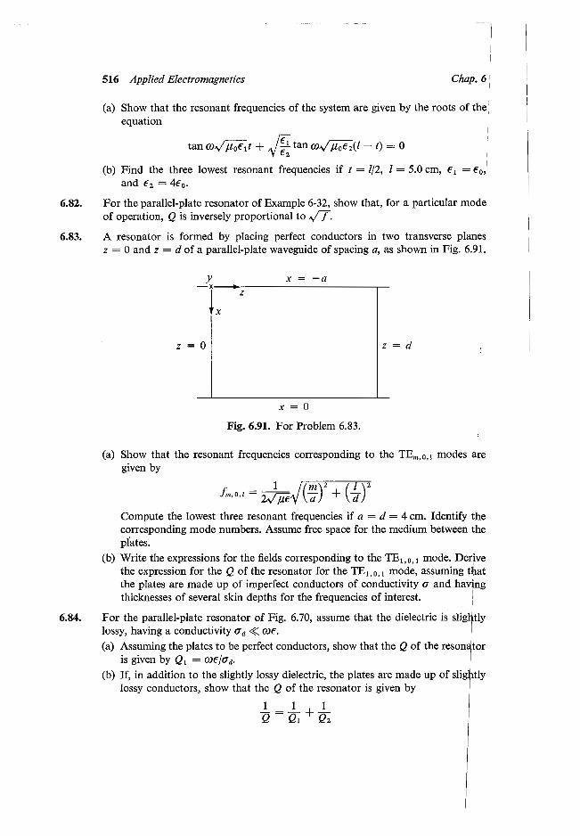
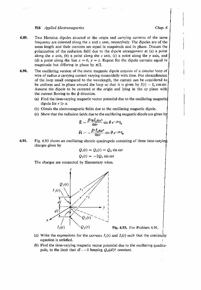
6.92.
6. 93.
519 Problems Chap. 6
(c) Find the electromagnetic fields due to the oscillating quadrupole.(d) Find the radiation fields due to the oscillating quadrupole. Verify by deriving
them directly from the radiation fields due to the oscillating dipole given byEqs. (6-339) and (6-340).
Find the radiation resistance of a straight copper wire of length 1 cm carryingcurrent of frequency 100 MHz. Compare the radiation resistance with the ohmicresistance of the wire (taking into account skin effect) if it has a cylindrical crosssection of radius 1 mm. Repeat for a frequency of 300 MHz .
A half-wave dipole is a center-fed, straight wire antenna having a length equal to half the wavelength. The current distribution along the half-wave dipole is given by
- - nz l(z) = 10 cos L for L L
-T<z<T
as shown in Fig. 6.94.
L
z = 2
z = 0
I
I
Current / Distribution
Fig. 6,94. For Problem 6.93. z =
L
2
(a) Show that the radiation fields of the half-wave dipole are
- _ Mioe-i(n/L)r cos [(n/2) cos 0]Ee
- �---- --��-�
2nr sin O jj = jloe-j(n/L)r COS [(7t/2) COS 0]
"' 2nr sin O
",Jb) Show that the radiation resistance of the half-wave dipole in free space is 73 ohms, given that
Jn/2 cosz [(n/2) cos 0] dO = 0.609 e-o sin O
(c) Sketch the normalized radiation intensity pattern.(d) Show that the directivity of the half-wave dipole is 1.64.
6.94. Two identical short dipoles form an array as shown in Fig. 6.95. Show that theradiation fields due to the array are given by the radiation fields due to one ofthe dipoles multiplied by the factor 2 cos [(ftd sin O cos ¢)/2]. Plot the normalized