Application Note - Four Bit Counter - Dialog Semiconductor
11
Application Note Four Bit Counter AN-FG-001 Abstract This application shows how to build a four-Bit Counter using the SLG47910V FPGA and the FPGA development board. The internal oscillator is used as the clock for the counter. The counter outputs are programmed to GPIOs. This application note comes complete with design files which can be found in the References section.
-
Upload
khangminh22 -
Category
Documents
-
view
0 -
download
0
Transcript of Application Note - Four Bit Counter - Dialog Semiconductor

Application Note
Four Bit Counter
AN-FG-001
Abstract
This application shows how to build a four-Bit Counter using the SLG47910V FPGA and the FPGA development board. The internal oscillator is used as the clock for the counter. The counter outputs are programmed to GPIOs. This application note comes complete with design files which can be found in the References section.

AN-FG-001
Four Bit Counter
Application Note Revision 1.0 10-Dec-2021
CFR0014 2 of 11 © 2022 Dialog Semiconductor
Contents
Abstract ................................................................................................................................................ 1
Contents ............................................................................................................................................... 2
Figures .................................................................................................................................................. 2
1 Terms and Definitions ................................................................................................................... 3
2 References ..................................................................................................................................... 3
3 Introduction .................................................................................................................................... 4
4 Ingredients ..................................................................................................................................... 4
5 Counter Verilog Code ................................................................................................................... 5
6 Floorplan: CLB Utilization ............................................................................................................ 5
7 Design Steps .................................................................................................................................. 6
8 Conclusion ..................................................................................................................................... 9
Revision History ................................................................................................................................ 10
Figures
Figure 1: System Diagram ..................................................................................................................... 4 Figure 2: Four-Bit Counter Schematic ................................................................................................... 4 Figure 3: Counter CLB Utilization .......................................................................................................... 5 Figure 4: ForgeFPGA Tool Bar ............................................................................................................. 6 Figure 5: IO Planner .............................................................................................................................. 7 Figure 6: ForgeFPGA Window .............................................................................................................. 8 Figure 7: Debugging Controls ............................................................................................................... 8
AN-FG-001
Four Bit Counter
Application Note Revision 1.0 10-Dec-2021
CFR0014 3 of 11 © 2022 Dialog Semiconductor
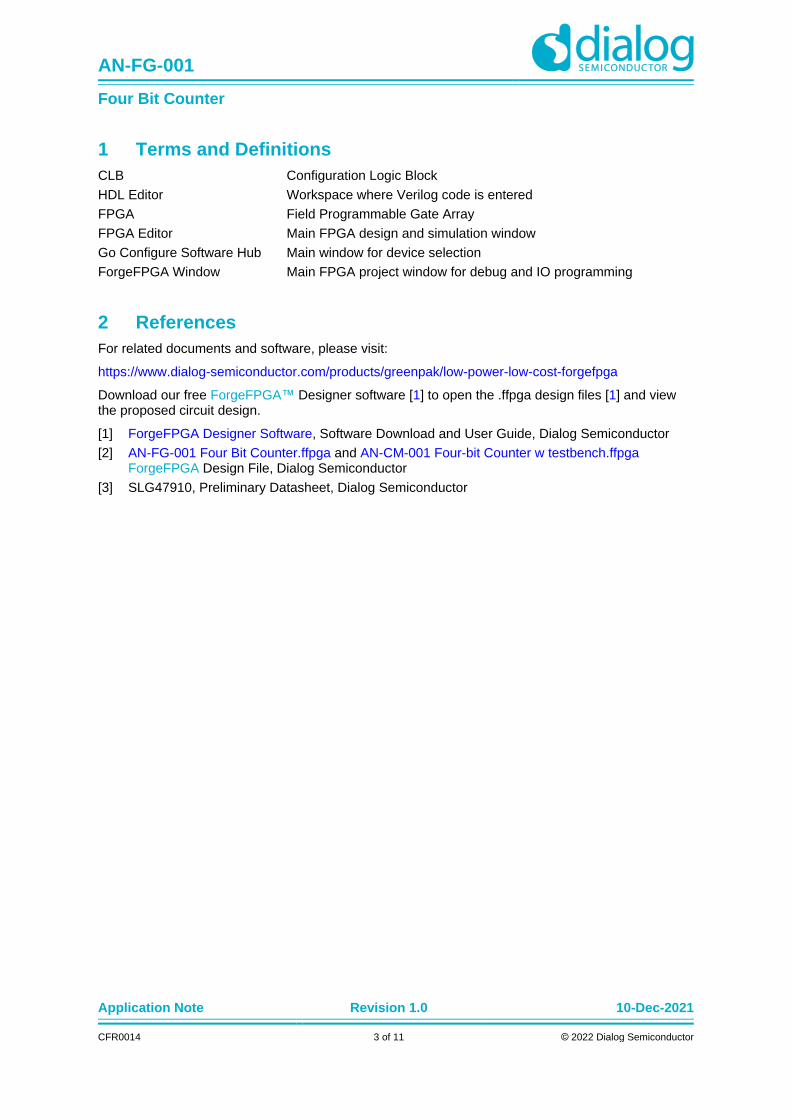
1 Terms and Definitions
CLB Configuration Logic Block
HDL Editor Workspace where Verilog code is entered
FPGA Field Programmable Gate Array
FPGA Editor Main FPGA design and simulation window
Go Configure Software Hub Main window for device selection
ForgeFPGA Window Main FPGA project window for debug and IO programming
2 References
For related documents and software, please visit:
https://www.dialog-semiconductor.com/products/greenpak/low-power-low-cost-forgefpga
Download our free ForgeFPGA™ Designer software [1] to open the .ffpga design files [1] and view the proposed circuit design.
[1] ForgeFPGA Designer Software, Software Download and User Guide, Dialog Semiconductor
[2] AN-FG-001 Four Bit Counter.ffpga and AN-CM-001 Four-bit Counter w testbench.ffpga ForgeFPGA Design File, Dialog Semiconductor
[3] SLG47910, Preliminary Datasheet, Dialog Semiconductor

AN-FG-001
Four Bit Counter
Application Note Revision 1.0 10-Dec-2021
CFR0014 4 of 11 © 2022 Dialog Semiconductor
3 Introduction
This application shows how to build a four-Bit Counter using the SLG47910V FPGA and the FPGA development board. The internal oscillator is used as the clock for the counter. The counter outputs are programmed to GPIOs.
4 Ingredients
■ ForgeFPGA Device SLG47910V
■ FPGAPAK Development Board with USB cable and power supply
■ FPGAPAK Socket Adaptor Board
■ Latest Revision of ForgeFPGA Workshop software
Figure 1: System Diagram
Figure 2: Four-Bit Counter Schematic

AN-FG-001
Four Bit Counter
Application Note Revision 1.0 10-Dec-2021
CFR0014 5 of 11 © 2022 Dialog Semiconductor
5 Counter Verilog Code
* Simple Counter example
*/
(* top *) module Counter(
(* iopad_external_pin, clkbuf_inhibit *) input clk,
(* iopad_external_pin *) input nreset,
(* iopad_external_pin *) input up_down,
(* iopad_external_pin *) output up_down_oe,
(* iopad_external_pin *) output[3:0] counter,
(* iopad_external_pin *) output osc_en,
(* iopad_external_pin *) output osc_lp_mode
);
reg [3:0] counter_up_down;
assign up_down_oe = 1'b1;
assign osc_en = 1'b1;
assign osc_lp_mode =1'b1;
always @(posedge clk or negedge nreset) begin
if (!nreset)
counter_up_down <= 4'h0;
else if (~up_down)
counter_up_down <= counter_up_down + 4'd1;
else
counter_up_down <= counter_up_down - 4'd1;
end
assign counter = counter_up_down;
endmodule
6 Floorplan: CLB Utilization
Figure 3: Counter CLB Utilization
The Floorplan tab in the FPGA Editor shows the placement of the CLBs and FFs (Figure 3). The resource utilization is shown in the top left corner

AN-FG-001
Four Bit Counter
Application Note Revision 1.0 10-Dec-2021
CFR0014 6 of 11 © 2022 Dialog Semiconductor
7 Design Steps
1. Launch the latest version of the Go Configure Software Hub. Select the SLG47910V device and the ForgeFPGA Workshop software will load.
2. From the ForgeFPGA tool bar (Figure 4) select the FPGA Editor tab.
Figure 4: ForgeFPGA Tool Bar
3. Enter the Verilog code into the HDL editor and save the code using the save button on the top left corner of the FPGA Editor.
4. Open the IO planner tab on the FPGA editor. Assign the IOs that are in the Verilog code to GPIO pins on the device (Figure 5) and save.
5. Next select the Synthesize button on the lower left side of the FPGA editor.
6. Select the Generate Bitstream button on the lower left side of the FPGA editor. Check the Logger and Issues tabs to make sure that the bit steam was generated correctly. Now click on the Floorplan tab and see the CLB utilization (Figure 3). Press the Ctrl and the mouse wheel to zoom-in. Confirm that the IOs selected in the IO Planner are shown in the floorplan.

AN-FG-001
Four Bit Counter
Application Note Revision 1.0 10-Dec-2021
CFR0014 7 of 11 © 2022 Dialog Semiconductor
Figure 5: IO Planner
7. Close the FPGA Editor and go to the ForgeFPGA widow (Figure 6). Selecting the Debug tab will enable the debug controls. Double click on the VDD pin and set VDD= 1.2v. Then double click on VDDIO pin and set VDDIO= 1.8v.
8. Double click on EN and PWR and select Force On. This ensures that all blocks are powered up.
9. The IO planner has GPIO4 configured as an input. In the ForgeFPGA window, left click on the blue circle of GPIO4 and select Button. Now the input up_down can be toggled to count-up or count-down.
10. The counter design is now ready to load onto the FPGA using the development board. Connect the development board to adaptor board. Connect the USB and power supply to the development board.

AN-FG-001
Four Bit Counter
Application Note Revision 1.0 10-Dec-2021
CFR0014 8 of 11 © 2022 Dialog Semiconductor
Figure 6: ForgeFPGA Window
11. In the ForgeFPGA Workshop window, select Change platform on the Debugging Controls tab (Figure 7). Choose the ForgeFPGA Development Platform then select Emulation. The Emulation button will toggle the design on and off.
12. Now the counter is loaded onto the FPGA device. GPIO[3:0] will have the outputs of the counter on them. Apply oscilloscope probes to GPIO[3:0] to view the counter outputs.
Figure 7: Debugging Controls

AN-FG-001
Four Bit Counter
Application Note Revision 1.0 10-Dec-2021
CFR0014 9 of 11 © 2022 Dialog Semiconductor
8 Conclusion
The procedure outlined in this application example can be applied to any circuit design that is implemented in Verilog code. This testcase is available for download. If interested, please contact the ForgeFPGA Business Support Team.

AN-FG-001
Four Bit Counter
Application Note Revision 1.0 10-Dec-2021
CFR0014 10 of 11 © 2022 Dialog Semiconductor
Revision History
Revision Date Description
1.0 10-Dec-2021 Initial Version

AN-FG-001
Four Bit Counter
Application Note Revision 1.0 10-Dec-2021
CFR0014 11 of 11 © 2022 Dialog Semiconductor
Status Definitions
Status Definition
DRAFT The content of this document is under review and subject to formal approval, which may result in modifications or
additions.
APPROVED
or unmarked The content of this document has been approved for publication.
Disclaimer
Information in this document is believed to be accurate and reliable. However, Dialog Semiconductor does not give any representations or warranties, expressed or implied, as to the accuracy or completeness of such information. Dialog Semiconductor furthermore takes no responsibility whatsoever for the content in this document if provided by any information source outside of Dialog Semiconductor.
Dialog Semiconductor reserves the right to change without notice the information published in this document, including without limitation the specification and the design of the related semiconductor products, software and applications.
Applications, software, and semiconductor products described in this document are for illustrative purposes only. Dialog Semiconductor makes no representation or warranty that such applications, software and semiconductor products will be suitable for the specified use without further testing or modification. Unless otherwise agreed in writing, such testing or modification is the sole responsibility of the customer and Dialog Semiconductor excludes all liability in this respect.
Customer notes that nothing in this document may be construed as a license for customer to use the Dialog Semiconductor products, software and applications referred to in this document. Such license must be separately sought by customer with Dialog Semiconductor.
All use of Dialog Semiconductor products, software and applications referred to in this document are subject to Dialog Semiconductor’s Standard Terms and Conditions of Sale, available on the company website (www.dialog-semiconductor.com) unless otherwise stated.
Dialog and the Dialog logo are trademarks of Dialog Semiconductor plc or its subsidiaries. All other product or service names are the property of their respective owners.
© 2022 Dialog Semiconductor. All rights reserved.
Contacting Dialog Semiconductor
United Kingdom (Headquarters)
Dialog Semiconductor (UK) LTD
Phone: +44 1793 757700
Germany
Dialog Semiconductor GmbH
Phone: +49 7021 805-0
The Netherlands
Dialog Semiconductor B.V.
Phone: +31 73 640 8822
North America
Dialog Semiconductor Inc.
Phone: +1 408 845 8500
Japan
Dialog Semiconductor K. K.
Phone: +81 3 5769 5100
Taiwan
Dialog Semiconductor Taiwan
Phone: +886 281 786 222
Hong Kong
Dialog Semiconductor Hong Kong
Phone: +852 2607 4271
Korea
Dialog Semiconductor Korea
Phone: +82 2 3469 8200
China (Shenzhen)
Dialog Semiconductor China
Phone: +86 755 2981 3669
China (Shanghai)
Dialog Semiconductor China
Phone: +86 21 5424 9058
Email:
Web site:
www.dialog-semiconductor.com