
Anticoincidence Detector (ACD) Electrical Subsystem - SLAC
99
GLAST LAT Project ACD CDR January 7,8, 2003 1 Section 6 ACD Electrical Subsystem Glenn Unger NASA/GSFC ACD Electrical Subsystem Lead [email protected] http://lhea-glast.gsfc.nasa.gov/acd/electronics Gamma Gamma - - ray Large ray Large Area Space Area Space Telescope Telescope Anticoincidence Detector (ACD) Electrical Subsystem
-
Upload
khangminh22 -
Category
Documents
-
view
3 -
download
0
Transcript of Anticoincidence Detector (ACD) Electrical Subsystem - SLAC

GLAST LAT Project ACD CDR January 7,8, 2003
1Section 6 ACD Electrical Subsystem
Glenn UngerNASA/GSFCACD Electrical Subsystem Lead
[email protected]://lhea-glast.gsfc.nasa.gov/acd/electronics
GammaGamma--ray Large ray Large Area Space Area Space TelescopeTelescope
Anticoincidence Detector (ACD) Electrical Subsystem

GLAST LAT Project ACD CDR January 7,8, 2003
2Section 6 ACD Electrical Subsystem
Outline
• ACD Electrical Subsystem Overview
• Base Electronics Assembly– Photomultiplier Tube
– Resistor Network– PMT Subassembly– Front End Electronics (FREE) Circuit Card
– GLAST ACD Front End (GAFE) ASIC – GLAST ASIC Read-Out Controller (GARC) ASIC– High Voltage Bias Supply

GLAST LAT Project ACD CDR January 7,8, 2003
3Section 6 ACD Electrical Subsystem
ACD Electrical Subsystem Team• Front-End Electronics
– Design – Dave Sheppard– Layout & Fabrication - Phil Goodwin– Population & Assembly – TBD– Testing – Dave Sheppard, Bob Baker
• GLAST ACD Read-out Controller (GARC) ASIC
– Design - Dave Sheppard with SLAC support
– FPGA Simulation/Coding – Bob Baker
• GLAST ACD Front-End (GAFE) ASIC– V1 and V2 design – Satpal Singh, Dave
Sheppard– V1 and V2 testing – Bob Baker, Larry
Olsen– V3 design – Satpal Singh, Dave
Sheppard Oren Milgrone, Dieter Freytag– V3 testing – Chandru Mirchandani, Ken
Rehmann, Masa Hirayama– V4, V5 design – Oren Milgrone, Dieter
Freytag, Dave Sheppard– V4, V5 testing - Chandru Mirchandani,
Ken Rehmann, Masa Hirayama
• High Voltage Bias Supply– Design – Art Ruitberg– Layout & Fabrication – SAIC– Population and Assembly - TBD– Testing – Art Ruitberg
• Photomultiplier Tube Resistor Networks – Design – Art Ruitberg– Layout & Fabrication – SAIC– Population and Assembly – Bill Daniels,
Deneen Ferro– Testing – Art Ruitberg
• Photomultiplier Tube Subassembly– Design – Alex Moiseev, Bob Hartman,
Bill Daniels, Art Ruitberg, Bob Reely, Ken Segal, Brian Grammer
– Assembly – Bill Daniels, Deneen Ferro, Russ Rowles
• Base Electronics Assembly Mechanical Component Design and Packaging
– Bob Reely

GLAST LAT Project ACD CDR January 7,8, 2003
4Section 6 ACD Electrical Subsystem
Electrical Subsystem Architecture
GASU(AEM-A)(AEM-B)
FREE
PMT Rail(up to 18 PMTs)
HVBS
R
HVBS
P
FREE
PMT Rail(up to 18 PMTs)
HVBS
R
HVBS
P
FREE
PMT Rail(up to 18 PMTs)
HVBS
R
HVBS
P
FREE
PMT Rail(up to 18 PMTs)
HVBS
R
HVBS
P
FREE
HVBS
R
PMT Rail(up to 18 PMTs)
HVBS
P
FREE
HVBS
R
PMT Rail(up to 18 PMTs)
HVBS
P
FREE
HVBS
R
PMT Rail(up to 18 PMTs)
HVBS
P
FREE
HVBS
R
PMT Rail(up to 18 PMTs)
HVBS
P
FR
EE
H V B S R
PM
T R
ail
(up
to
18
PM
Ts
)
H V B S P
FR
EE
H V B S R
PM
T R
ail
(up
to
18
PM
Ts
)
H V B S P
FR
EE
HVBSR
PM
T R
ail
(up
to 18
PM
Ts
)
HVBSP
ACDThermistorInterface
FR
EE
HVBSR
HVBSP PM
T R
ail
(up
to 1
8 P
MT
s)
ACD ThermistorInterface
PDU
SIU
PDU
SIU

GLAST LAT Project ACD CDR January 7,8, 2003
5Section 6 ACD Electrical Subsystem
• Requirement to support 194 analog signal channels (reduced from the original 290 channels)
• Requirement to limit number of connections from the ACD to each AEM to 16 (increased from previously required 2)
• Requirement to minimize overall electronics cost (and therefore)the number of Front-end electronics boards
• Requirement to accommodate an asymmetrical routing of fibers to ACD base due to the top tiles and ribbons
• Result of trade study is 12 boards, each with 18 analog channelsand dual cables. (12 x 18 = 216 channels available)
Electrical Subsystem Trade Studies Results

GLAST LAT Project ACD CDR January 7,8, 2003
6Section 6 ACD Electrical Subsystem
Electrical Subsystem Topology
PMT
PMT
LATInterface
(This moduleis LAT
instrumentresponsibility)
Fibers
Particle
Plastic Scintillating Tile
Th
emal
Bla
nke
t &M
icro
met
eoro
id S
hie
ld
89 Tiles (2 PMT/tile)8 Fiber Ribbons (2 PMT/ribbon)
194 Total PMTs
FromanotherPower
DistributionBoard
GLAST ACDFront End
(GAFE)[Analog ASIC]
GL
AS
T A
CD
Re
ado
ut
Co
ntr
olle
r(G
AR
C)
[Dig
ital
AS
IC]
Power Filters3.3V
HV Bias SupplyInterface
High Voltage BiasSupply (HVBS)
FRont End Electronics (FREE) Circuit Card
Veto (18)
Serial Data
Serial Comm.
0 V
to
125
0 V
3.3
V
3.3
V
18 GAFEsper board
Hskping
(2 HVBS per FREE board)
ADC
DAC
Po
we
r D
istr
ibut
ion
Boa
rd
To anotherFREE card
CNO
20 MHz clock
Reset
+28 VoltFilter
+3.3 V
+28 V
Up to18 PMT
perboard
Electronics Chassis

GLAST LAT Project ACD CDR January 7,8, 2003
7Section 6 ACD Electrical Subsystem
Grounding Diagram
Digital Circuits
PMT PMTPMT
Common modechoke
Digital common
Analog common
PMT signal common
HV common
HV
Analog +3.3V
Digital +3.3 V
+28 V HVBS
+28 V HVBSRTN
Harnessshield
+3.3 V FREE
+3.3 V FREERTN
Chassisground
Oscillator
Multiplier
100 ohmsHVBS Circuit Card
~
Commonmodechoke
BEA
HVBS Housing/Faraday shieldgrounded to BEA chassis
FREE Circuit Card
Analog Circuits
Shield placed between Front-end electronics circuit cards

GLAST LAT Project ACD CDR January 7,8, 2003
8Section 6 ACD Electrical Subsystem
Electronics Chassis
CHASSIS
HVBS ASSEMBLY
FREE BOARDS NOT SHOWN IN THIS VIEW
OUTBOARD RAIL
CHASSIS SUPPORT
INBOARD RAIL
PMT HOUSING
RESISTOR NETWORK ENCLOSURE
FREE BOARD MOUNTING HARDWARE
GLAST LAT Project ACD CDR January 7,8, 2003
9Section 6 ACD Electrical Subsystem
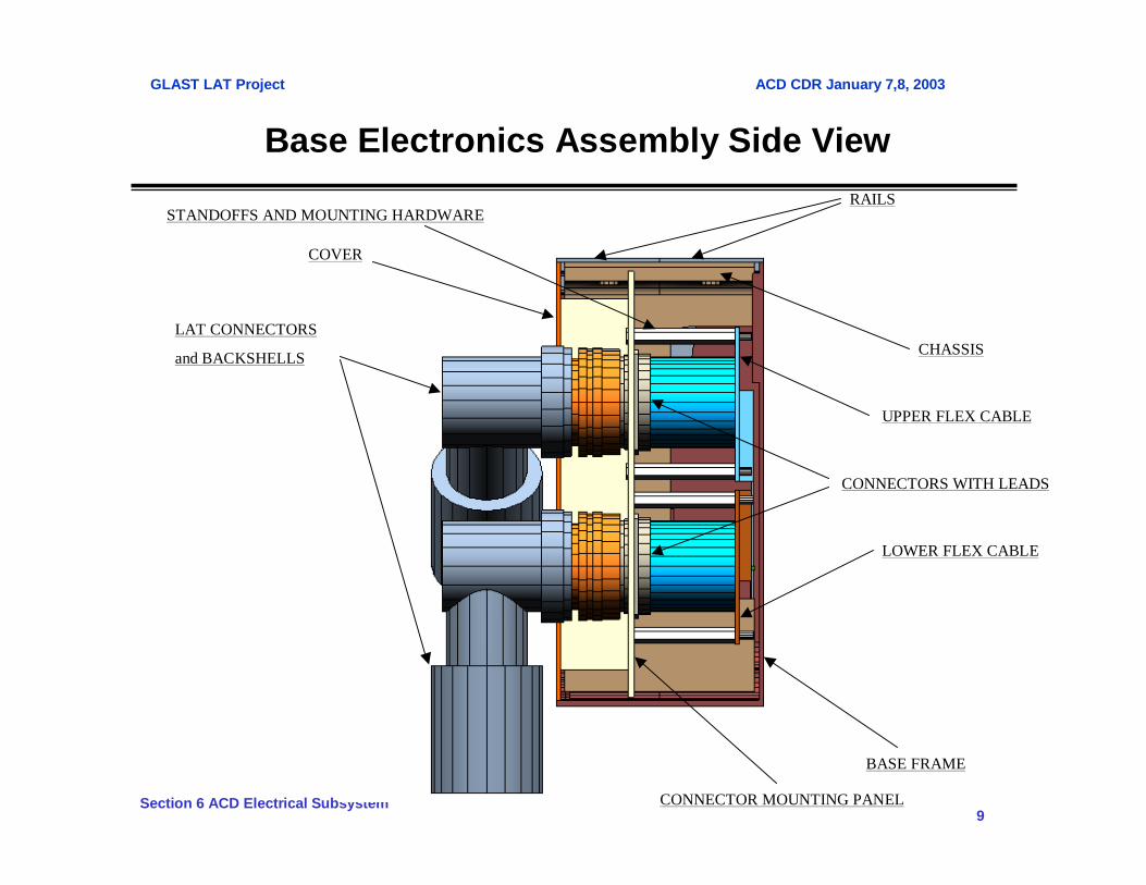
Base Electronics Assembly Side View
LAT CONNECTORS
and BACKSHELLS
COVER
BASE FRAME
CONNECTOR MOUNTING PANEL
RAILS
CHASSIS
UPPER FLEX CABLE
CONNECTORS WITH LEADS
LOWER FLEX CABLE
STANDOFFS AND MOUNTING HARDWARE

GLAST LAT Project ACD CDR January 7,8, 2003
10Section 6 ACD Electrical Subsystem
Electronics Component Design Verification
• ASICs to be tested & screened with a separate bench-top test station at GSFC
• Maxim 145 and Maxim 5121 will be screened at NRL and delivered to GSFC
• Maxim 494 to be screened by GSFC
• Front-end Electronics boards to be performance and environmental tested on the bench prior to integration with ACD
• High Voltage Bias Supplies to be performance and environmental tested at GSFC prior to integration with ACD
• Photomultiplier Tubes will be screened by a flight-approved vendor and tested at GSFC prior to integration with ACD
• Biasing Resistor Networks will be performance and environmental tested at GSFC prior to integration to ACD
– Level IV Requirement 5.12 Radiation Tolerance. The ACD electronics shall remain within specifications after a total ionizing radiation dose of 4.5 kRad(Si).
– Level IV Requirement 5.12.1 Single Event Upset Tolerance. A single event upset (SEU) shall not cause the ACD electronics to transition to an unsafe state.
– Level IV Requirement 5.12.2 Latchup Tolerance.Parts that show any SEE’sat an LET lower than 37 MeV*cm2/mg shall not degrade the mission performance.

GLAST LAT Project ACD CDR January 7,8, 2003
11Section 6 ACD Electrical Subsystem
ACD Electronics Housekeeping
• Digital Housekeeping – GARC will maintain a record of the last command
received and a count of all valid commands and invalid commands received since power-on
– The status of all ACD command registers will be transmitted, by the GARC, to the AEM where it is telemetered at a low rate.
• Analog Housekeeping– The LAT will monitor the ACD voltage rails to an
accuracy of < 10 mV– The LAT will monitor the current used by each of the
ACD low voltage rails to within 10 mA or 5%, whichever is smaller
– The HVBSs associated with each FREE circuit card will produce an analog HV monitor voltage (0 to 2.5 volts), which will be transmitted to the LAT
– The LAT will digitize the HV monitor signals to an accuracy of 0.4% and telemeter the results at a low rate (TBD)
Level IV Requirement 5.9.9: Digital housekeeping. The state of all ACD command registers shall be available for readout via AEM commands. The AEM will scale all ACD VETO and HLD rates and transmit the results in low rate telemetry

GLAST LAT Project ACD CDR January 7,8, 2003
12Section 6 ACD Electrical Subsystem
ACD Electrical Subsystem Power
Number Units Per
Board
Tota l Numbe r
Units (Nom)
Nom. Curre nt pe r unit
3.3V Curre nt (Nom)
28 V Curre nt (Nom)
Nominal Power
Tota l Numbe r
Units (Max)
Max Curre nt pe r unit
3.3V Curre nt (Max)
28 V Curre nt (Max)
Max Power Class Method
Bus Voltage 3.30 28.00 3.60 29.00GAFE 18 216 0.0022 0.475 0.000 1.57 216 0.0022 0.475 0.000 1.57 1 PARAADC MAX145 18 216 0.0012 0.259 0.000 0.86 216 0.0012 0.259 0.000 0.93 3 CALCGARC 1 12 0.0146 0.175 0.000 0.58 12 0.0146 0.175 0.000 0.63 1 PARALVDS Driver 20 240 0.0035 0.840 0.000 2.77 480 0.0035 1.680 0.000 6.05 2 CALCLVDS Rcvr 6 72 0.001 0.072 0.000 0.24 72 0.001 0.072 0.000 0.26 2 CALC
HVBS (PMT Power) 1 12 0.0095 0.000 0.114 3.19 12 0.011 0.000 0.132 3.83 2 MEAS
Cable Loss 2% 0.036 0.002 0.18 0.053 0.003 0.27 NA NA
Power Totals 9.39 13.54
NOMINAL POWER CONFIGURATION MAXIMUM POWER CONFIGURATION
1
2
3
A generational design that follows a previously developed concept and expands complexity of capability within an established design envelope, including new hardware applications to meet a new requirements.
A production level development based on an existing design for which multiple units are planned, and a significant amount of standardization exists.
A new design which is one-of-a-kind or a first generation device.Development Class
PARACALCMEAS
Estimate based on calculated power from detailed design documentationActual power measurements of component
Best estimate based on conceptual design parameters.Method of Power Estimation

GLAST LAT Project ACD CDR January 7,8, 2003
13Section 6 ACD Electrical Subsystem
ACD Electrical Subsystem Mass
Boards & Harnessing
QtyEstimated Mass (Kg)
Calculated Mass (Kg)
Actual Mass (Kg)
Total Mass without Margin
(Kg)
Total Mass with
Margin (Kg) *
FREE Board 12 0.4490 5.3880 5.9268FREE PCB for connectors 24 0.0270 0.6480 0.7128HVBS 24 0.0940 2.2560 2.4816Power Distribution Board 12 0.1440 1.7280 1.9008Bulkhead Connector Mount Bracket 16 0.1397 2.2353 2.4588Bulkhead Connector 26 0.0500 1.3000 1.3000Harnessing 12 0.0240 0.2880 0.2880
Cable Tiedowns 24 0.0010 0.0240 0.0240E Board Mounting Hardware 1 0.5000 0.5000 0.6000
Boards & Harnessing Subtotal 14.3673 15.6928

GLAST LAT Project ACD CDR January 7,8, 2003
14Section 6 ACD Electrical Subsystem
Photomultiplier Tubes (PMT)
PMT
PMT
LATInterface
(This moduleis LAT
instrumentresponsibility)
Fibers
Particle
Plastic Scintillating Tile
Th
emal
Bla
nke
t &M
icro
met
eoro
id S
hie
ld
89 Tiles (2 PMT/tile)8 Fiber Ribbons (2 PMT/ribbon)
194 Total PMTs
FromanotherPower
DistributionBoard
GLAST ACDFront End
(GAFE)[Analog ASIC]
GL
AS
T A
CD
Re
ado
ut
Co
ntr
olle
r(G
AR
C)
[Dig
ital
AS
IC]
Power Filters3.3V
HV Bias SupplyInterface
High Voltage BiasSupply (HVBS)
FRont End Electronics (FREE) Circuit Card
Veto (18)
Serial Data
Serial Comm.
0 V
to
125
0 V
3.3
V
3.3
V
18 GAFEsper board
Hskping
(2 HVBS per FREE board)
ADC
DAC
Po
we
r D
istr
ibut
ion
Boa
rd
To anotherFREE card
CNO
20 MHz clock
Reset
+28 VoltFilter
+3.3 V
+28 V
Up to18 PMT
perboard
Electronics Chassis

GLAST LAT Project ACD CDR January 7,8, 2003
15Section 6 ACD Electrical Subsystem
• Purpose - as events are collected by the scintillating tiles and optical pulses are transmitted to the PMT, the PMT converts the optical pulse to electrical pulses.
• The PMT baseline is the Hamammatsu R4443 (a ruggedized version of the R647)
PMT Characteristics
• Nominal gain of the PMTs is 4 x 10⁵. This will be adjusted as required during the operation of the instrument by variation of the high voltage bias applied to the PMT.
• GAFE interface is a single coax between 10 cm and 18 cm

GLAST LAT Project ACD CDR January 7,8, 2003
16Section 6 ACD Electrical Subsystem
PMT Bonding Process
• Design drivers– Entire PMT, except face, must
be light-tight– No voids around the leads– Demonstrate mechanical
strength after enduring 12-thermal cycles
• Performed by ACD Mechanical team
• Process– Wrap PMT in mu-metal, 0.125
mm thick for magnetic shielding with double-sided tape (3M, Y966)
– Insert the wrapped PMT into PMT housing.
– Place PMT and housing in potting fixture
– Uralane the housing/mu-metal gap under vacuum
GLAST LAT Project ACD CDR January 7,8, 2003
17Section 6 ACD Electrical Subsystem
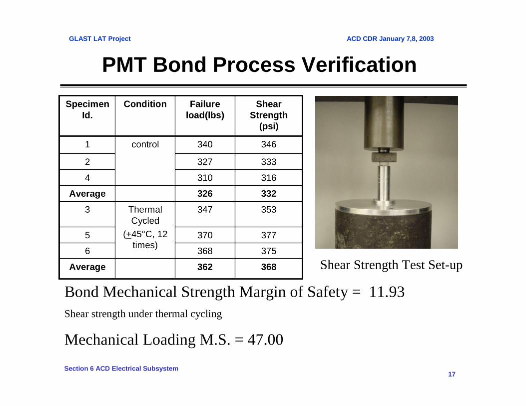
PMT Bond Process Verification
368362Average
3753686
3773705
353347Thermal Cycled
(+45°C, 12 times)
3
332326Average
3163104
3333272
346340control1
Shear Strength
(psi)
Failure load(lbs)
ConditionSpecimenId.
Bond Mechanical Strength Margin of Safety = 11.93Shear strength under thermal cycling
Mechanical Loading M.S. = 47.00
Shear Strength Test Set-up

GLAST LAT Project ACD CDR January 7,8, 2003
18Section 6 ACD Electrical Subsystem
PMT Bonded Assembly
PMT side view
PMT bottom view
GLAST LAT Project ACD CDR January 7,8, 2003
19Section 6 ACD Electrical Subsystem
Resistive Network - Design
• The resistor network receives the high voltage, divides the voltage using a string of resistors, provides the voltages to the PMT, decouples the PMT signal, and transmits the signal to the GAFE.
• Ten-stage resistive divider network where the ∆v of each stage is ~80 V (nominal), ~114 V (maximum).
• The value of R14 effects PMT signal undershoot, hence the ACD efficiency. A mutual decision was made to change it to 10 MΩ. Level IV Requirement 5.11.5 PMT Bias Chain Load Resistor. A load resistor of > 10 kΩ shall be
incorporated into the bias network. Level IV Requirement 5.11.6 PMT Bias Chain Dynode Decoupling. The resistors biasing the last three-
dynode stages shall be bypassed by capacitors to prevent a drop in gain for very large pulses or the maximum expected high rate of pulses (<1% gain change for 3kHz rate).
R1 R2
DY1
R3
DY2
R4
DY3
R5
DY4
R6
DY5
R7
DY6
R8
DY7
R9
DY8
R10
DY9
R11
DY10
HV IN
R12
R13R14
P
SIG OUTto GAFEC4 C6
C5
K
Photomultiplier Tube Interface
Resistor Network

GLAST LAT Project ACD CDR January 7,8, 2003
20Section 6 ACD Electrical Subsystem
Resistive Network - Design
• The resistive divider network has a filter resistor, at the high voltage input, that is ~5% of the total resistance. Level IV Requirement 5.11.2 PMT Bias Chain Filter Resistance. Five percent (nominal)
of the total resistance of the bias chain shall be in a filter resistor(s) at the high voltage input. This PMT bias chain filter resistance protects against a PMT short with a current limiting resistor and filters out HVBS ripple.
• The calculated baseline dynode string biasing current is ~1.50 µA at 1310V (maximum) and ~1.0 µA at 900V. Resistance is 860 MΩ. Level IV Requirement 5.11.1 PMT Bias Chain Total Resistance. The total resistance of
a PMT bias chain shall be such as to result in a nominal current (at the maximum HVBS voltage) of 2 microamps (~100 times the PMT average anode current.)
• 1 MΩ adversely effects the DC operating point. Therefore a 75 MΩ bleed-off resistor will be used. Level IV Requirement 5.11.4. PMT Anode Signal Coupling. The PMT anode signal
shall be coupled into the associated analog electronics via two capacitors of 680 pF in series. A charge leakage bleed-off resistor of at least 1-mega ohms shall be incorporated on the low-voltage side of the capacitor pair.

GLAST LAT Project ACD CDR January 7,8, 2003
21Section 6 ACD Electrical Subsystem
Resistive Network – Assembly
– Three printed circuit boards, each ~22 mm square, stacked ~25 mm high
– Parylene coated– Printed circuit card is
1.56 mm glass epoxy (G-11)
– ~20 components, mostly surface mount resistors and capacitors
– Polycarbonate spacers, vented to prevent corona discharge
Not shown are the high voltage and signal wires which attach on the top board.
GLAST LAT Project ACD CDR January 7,8, 2003
22Section 6 ACD Electrical Subsystem
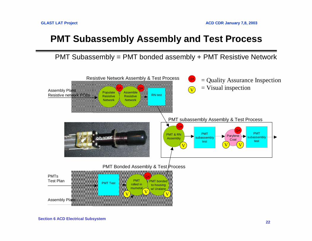
PMT Subassembly Assembly and Test Process
Assembly PlansResistive network PCBs
PopulateResistiveNetwork
QA
RN test
QAAssembleResistiveNetwork
Resistive Network Assembly & Test Process
PMT TestPMT
rolled inmumetal
PMT bondedto housingw/ Uralane
Assembly Plans
QAPMTsTest Plan
V VV
PMT Bonded Assembly & Test Process
PMT & RNAssembly
PMTsubassembly
test
QA
V
ParyleneCoat
QA
V V
PMT subassembly Assembly & Test Process
PMTsubassembly
test
PMT Subassembly = PMT bonded assembly + PMT Resistive Network
= Quality Assurance Inspection= Visual inspectionV
QA

GLAST LAT Project ACD CDR January 7,8, 2003
23Section 6 ACD Electrical Subsystem
PMT Subassembly - Summary
• Status– Development-unit phase is over and beginning the engineering-unit phase.– Design and assembly process was reviewed by the ACD team (materials,
mechanical, electrical and systems) on November 11, 2002 and 29 ways to improve the design and assembly process were identified.
– Met many of the PMT subassembly requirements– Built 6 PMT subassemblies and one failed. Failure Review Board found the
failure could have occurred at a number of places in the assembly process. Suggested performing leak tests, destructive analysis, perform visual inspections more often during assembly and perform various types of inspections. Failure analysis is on-going.
– Performed vibration and thermal test on 4 and all passed• Issues
– PMT light-tightness– Bonding voids– Failed PMT
• Next Steps– Incorporate methods to improve the design and assembly process in the next
PMT subassembly (January ’03 to February ’03)– Test PMT light-tightness using 3 mm of uralane.– Test a new uralane bonding process with longer degassing times and faster
vacuum pump-down– Workmanship will naturally improve as a result of awareness.
GLAST LAT Project ACD CDR January 7,8, 2003
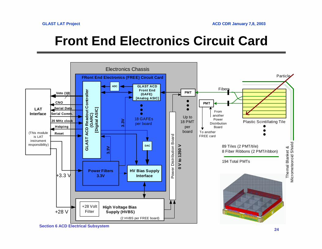
24Section 6 ACD Electrical Subsystem
Front End Electronics Circuit Card
PMT
PMT
LATInterface
(This moduleis LAT
instrumentresponsibility)
Fibers
Particle
Plastic Scintillating Tile
The
mal
Bla
nket
&M
icro
me
teor
oid
Shi
eld
89 Tiles (2 PMT/tile)8 Fiber Ribbons (2 PMT/ribbon)
194 Total PMTs
FromanotherPower
DistributionBoard
GLAST ACDFront End(GAFE)
[Analog ASIC]
GL
AS
T A
CD
Re
ado
ut C
ont
roll
er(G
AR
C)
[Dig
ital
AS
IC]
Power Filters3.3V
HV Bias SupplyInterface
High Voltage BiasSupply (HVBS)
FRont End Electronics (FREE) Circuit Card
Veto (18)
Serial Data
Serial Comm.
0 V
to 1
250
V
3.3
V
3.3V
18 GAFEsper board
Hskping
(2 HVBS per FREE board)
ADC
DAC
Pow
er D
istr
ibut
ion
Boa
rd
To anotherFREE card
CNO
20 MHz clock
Reset
+28 VoltFilter
+3.3 V
+28 V
Up to18 PMT
perboard
Electronics Chassis

GLAST LAT Project ACD CDR January 7,8, 2003
25Section 6 ACD Electrical Subsystem
• The Front-end electronics provides the following: – Interface to the LAT ACD Electronics Module (AEM)– Power filtering– Component protection– HVBS interface– PMT subassembly interface
• The FREE card includes:– Two interface connectors, one AEM Primary, one AEM Secondary
• 79-pin, 62 are used • MIL-DTL-38999 Series II bayonet coupling low profile metal shell connector • Size 22 (high density) contacts• Listed on the NASA Parts Selection List (NPSL)
– 10-layer flexible-rigid cable to rigid connector board– 18 PMT inputs– 18 analog ASICs (GAFE)– 18 analog-to-digital converters (Maxim 145)– 1digital-to-analog converters (Maxim 5121)– 1 digital ASIC (GARC)– 2 parallel HVBS interfaces– Passive components
Front-End Electronics (FREE) - Overview

GLAST LAT Project ACD CDR January 7,8, 2003
26Section 6 ACD Electrical Subsystem
FREE Circuit Card Design - Power Filtering
• Limits the conducted susceptibility • Common-mode and single ended chokes,
ceramic and tantalum capacitors, and series resistors
• Works in conjunction with the FREE grounding topology
• All +3.3V current enters the board via the common mode choke and returns through the same path
• Digital circuits are tied to the digital VDD power plane
• The analog circuits are tied to the VCC analog power plane, which is also isolated via a common mode choke
• All analog current enter and return through the common mode choke
+3.3V
RTN
VDD (DIGITAL)
DGND
CMCHOKE
CMCHOKE
VCC (ANALOG)
AGND

GLAST LAT Project ACD CDR January 7,8, 2003
27Section 6 ACD Electrical Subsystem
FREE Circuit Card Design - Component Protection
• Digital circuits will be bypassed directly between the VDD and DGND planes with surface mounted ceramic capacitors
• The analog parts will be bypassed through a resistor-capacitor network to the VCC and AGND planes
DIGITALCOMPONENT
CERAMIC
DGND
VDD
ANALOGCOMPONENT
AGND
VCC
CERAMIC TANTALUM
DIGITAL BYPASSING ANALOG BYPASSING

GLAST LAT Project ACD CDR January 7,8, 2003
28Section 6 ACD Electrical Subsystem
• Where applicable, parts are selected from the NASA GSFC approved parts list. Parts selected from NPSL have flight heritage and established reliability
• ASIC fabrication process based on calorimeter and tracker experience and qualification. The present baseline is the HP (Agilent) 0.5 µm process.
• Analog-to-digital converter (MAX145), digital-to-analog converter (MAX5121) and the voltage reference amplifier (MAX494) are commercial parts. MAX145 and MAX5121 are identical to that used on calorimeter and tracker. NRL shall provide flight qualified parts to GSFC.
• Printed Circuit Board is fabricated to the IPC-6012 standard. Nominally either 1.6 mm or 2.4 mm thick and to be constructed of either polyimide or FR-4. Assembled and inspected to NASA-STD-8739.3. After setup and functional testing, flight PCBs will be conformal coated and staked with a Uralane 5750/5753 compound
• Total of ~40 types of components. Only the GARC, GAFE, MAX145, MAX5121, MAX494 still being reviewed by Parts Control Board.
FREE Circuit Card Design – Parts

GLAST LAT Project ACD CDR January 7,8, 2003
29Section 6 ACD Electrical Subsystem
FREE Circuit Card – Summary
• Status– Design complete.– Printed Circuit Board layout complete– PCB Fabrication started in December ’02 and expected I early January ‘03– GARC-to-GAFE-to-PMT subassembly communications has been verified– Parts review on-going– Thermal and mechanical analysis near complete
• Issues– None
• Next Steps– Populate and test the FREE circuit card with (development unit) GARCv1
and GAFEv4– Perform electronic chassis (development unit) test with HVBSs and PMTs– Fit check in the electronics chassis (development unit)– Conduct a Peer Review

GLAST LAT Project ACD CDR January 7,8, 2003
30Section 6 ACD Electrical Subsystem
GAFE (Analog ASIC)
PMT
PMT
LATInterface
(This moduleis LAT
instrumentresponsibility)
Fibers
Particle
Plastic Scintillating Tile
Th
emal
Bla
nke
t &M
icro
met
eoro
id S
hie
ld
89 Tiles (2 PMT/tile)8 Fiber Ribbons (2 PMT/ribbon)
194 Total PMTs
FromanotherPower
DistributionBoard
GLAST ACDFront End
(GAFE)[Analog ASIC]
GL
AS
T A
CD
Re
ado
ut
Co
ntr
olle
r(G
AR
C)
[Dig
ital
AS
IC]
Power Filters3.3V
HV Bias SupplyInterface
High Voltage BiasSupply (HVBS)
FRont End Electronics (FREE) Circuit Card
Veto (18)
Serial Data
Serial Comm.
0 V
to
125
0 V
3.3
V
3.3
V
18 GAFEsper board
Hskping
(2 HVBS per FREE board)
ADC
DAC
Po
we
r D
istr
ibut
ion
Boa
rd
To anotherFREE card
CNO
20 MHz clock
Reset
+28 VoltFilter
+3.3 V
+28 V
Up to18 PMT
perboard
Electronics Chassis

GLAST LAT Project ACD CDR January 7,8, 2003
31Section 6 ACD Electrical Subsystem
• Target Technology is Agilent 0.5 um CMOS (as is all other GLAST LAT ASICs)
• GAFEv1 design included shaping amps and discriminators only, no digital core
• GAFEv2 (received 8-02) design included shaping amps and discriminators, digital core, DAC’s, and test charge injection. Analog performance fell short of specs and the design was sensitive to process parameter variations -> yield concerns, analog output can’t drive external ADC
• GAFEv3 (8-02: start of SLAC involvement, new GSFC test team, submitted 9-02, received 12-02). Design goal was to improve most serious performance short-falls within 4 weeks so that a chip is available to enable FREE card testing. Currently under test.
GAFE Evolution

GLAST LAT Project ACD CDR January 7,8, 2003
32Section 6 ACD Electrical Subsystem
GAFE Development Process
SchematicCapture Analog
Section
Generate SPICENetlist
GenerateLayout
Generate SPICENetlist
SimulateCompare
Schematic andLayout Netlists
Are the Schematic andLayout Netlists identical?
Yes
No
Digtial Core iscoded in Verilog
Simulate CodingMap Verilog filesto Tanner Library
Place and RouteCombine Analog
and DigitalLayouts
App software bug in v1 CoreNo Magic supportProblem importing core to Magic ASIC engineer learn TannerSoftware version differencesDesign rules variations
Yes
Digital Core Process
Analog Section Process

GLAST LAT Project ACD CDR January 7,8, 2003
33Section 6 ACD Electrical Subsystem
• All GAFE’s starting from version 3 are pin-compatible• From GAFE4 and up
– Full-chip simulation excluding CORE in PSPICE– Full-chip simulation including CORE in Nanosim (Synopsys)
• GAFEv4 (submitted 11-02, expected 2-03) design which should meet all specifications– E.g. added AC coupling after VETO discriminator amplifier to be insensitive to
process parameter variations (offset voltages)– Reduction of cross-talk within chip– Added high-range calibration
• GAFE5 (est. submission 1-03, expected 3-03)– Most likely candidate for flight– Slight modification of GAFEv4, included on LAT dedicated run so sufficient
(100’s) of IC’s are available• GAFE6 (est. submission 1-03, expected 3-03)
– Design based on LAT calorimeter circuit blocks, included on LAT dedicated run– Keeps PMT input signal within power-rails of GAFE through ability to run PMT’s
at lower gain (factor of 3)– Reduction of external analog input signals into GAFE from 4 to 1 (elimination of
external PMT signal splitting)– Back-up for risk-mitigation
GAFE Evolution (cont.)

GLAST LAT Project ACD CDR January 7,8, 2003
34Section 6 ACD Electrical Subsystem
GAFE Version comparisonIssues GAFE2 to
GAFE3GAFEv4
SimulationGAFEv5
SimulationInverter for Tri State Driver fixed same same
Veto Discriminator Enable fixed same same
HLD Discriminator Enable fixed same same
Shaping Amp Instability fixed same same
Peaking time fixed same same
Drive to ext. ADC (1) fixed same improved
Calibration Circuit same fixed same
Veto insensitivity duration, offset variations (2)
same fixed same
Veto DAC step-size (3) improved fixed improved
INL of low E range,feedthru between channels (3)
improved improved same
BIAS DAC Setting (4) same same fixed
Digital IO freq (5) lower fixed same
Overloading of MODE2 bit n/a overloaded fixed

GLAST LAT Project ACD CDR January 7,8, 2003
35Section 6 ACD Electrical Subsystem
• An AC-coupled input from the PMT anode
• Level IV Requirement 5.3: Adjustable Threshold on VETO Detection of Charged Particles. The threshold for detecting charged particles shall be adjustable from 0.064 to 1.28 pC (0.1 to 2 MIP), with a step size of <0.032 pC (0.05 MIP).
• Level IV Requirement 5.4: False VETO due to Electrical Noise. The total ACD false VETO trigger rate due to noise shall be less than 10 kHz (~46Hz per channel) at 0.096 pC (0.15 MIP) threshold (assuming 1 us VETO pulses).
• Level IV Requirement 5.5 High Threshold Detection. The ACD shall detect pulses due to highly-ionizing particles, carbon-nitrogen-oxygen or heavier nuclei, denoted High-Level Threshold or High-Level Discriminator (HLD), which produce signals from 20 pC to 128 pC (31.2 - 200 MIP with a goal of 1000 MIPs).
• Level IV Requirement 5.6: Adjustable High-Threshold. The High-Level Threshold shall be adjustable for PMT signals from 12.8 to 40.96 pC (20 to 64 MIP) in steps of 0.64 ± 20% pC (1 ± 0.2 MIP ).
• Level IV Requirement 5.8.3: Fast VETO Retriggering. The Fast VETO discriminator shall be capable of retriggering less than 50 ns after the trailing edge of the VETO output signal.
• Level IV Requirement 5.9.8 Test Pulse Injection. For test purposes, the ACD electronics shall incorporate the capability to be artificially stimulated by a test charge, via commands. The test charge injection range shall be 0 - 200 MIP with a goal of 0 - 1000 MIP.
• Level IV Requirement 5.9.5 Integral non-linearity. The integral non-linearity should be kept reasonably low (defined as ~ < 2% over the top 95% of the signal input range), for ease of analysis.
GAFE Requirements

GLAST LAT Project ACD CDR January 7,8, 2003
36Section 6 ACD Electrical Subsystem
GAFE Digital Core Design• Consists of a set of registers accessible via a command-response
protocol.• Registers may be written and read out by serial digital command
• On a single FREE card, each GAFE has a unique address consisting of 5 inputs bits, hardwired to either logic high or logic low.
• There is one 16-bit GAFE Mode register and five six-bit DAC control registers (e.g., DAC1 – DAC5) are available for configuration.
GLAST LAT Project ACD CDR January 7,8, 2003
37Section 6 ACD Electrical Subsystem
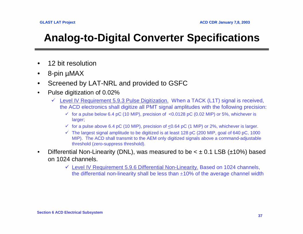
Analog-to-Digital Converter Specifications
• 12 bit resolution
• 8-pin µMAX• Screened by LAT-NRL and provided to GSFC• Pulse digitization of 0.02%
Level IV Requirement 5.9.3 Pulse Digitization. When a TACK (L1T) signal is received, the ACD electronics shall digitize all PMT signal amplitudes with the following precision: for a pulse below 6.4 pC (10 MIP), precision of <0.0128 pC (0.02 MIP) or 5%, whichever is
larger; for a pulse above 6.4 pC (10 MIP), precision of <0.64 pC (1 MIP) or 2%, whichever is larger. The largest signal amplitude to be digitized is at least 128 pC (200 MIP, goal of 640 pC, 1000
MIP). The ACD shall transmit to the AEM only digitized signals above a command-adjustable threshold (zero-suppress threshold).
• Differential Non-Linearity (DNL), was measured to be < ± 0.1 LSB (±10%) based on 1024 channels.
Level IV Requirement 5.9.6 Differential Non-Linearity. Based on 1024 channels, the differential non-linearity shall be less than ±10% of the average channel width
GLAST LAT Project ACD CDR January 7,8, 2003
38Section 6 ACD Electrical Subsystem
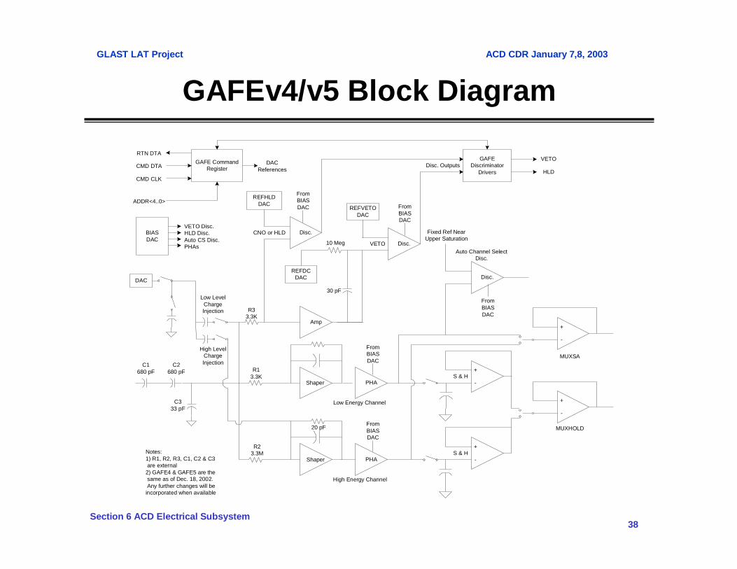
GAFEv4/v5 Block Diagram
DAC
REFHLDDAC
REFVETODAC
Disc.
Amp
PHA
PHA
Disc.
Disc.
GAFEDiscriminator
Drivers
GAFE CommandRegister
REFDCDAC
Shaper
Shaper
Low Energy Channel
High Energy Channel
-
+
-
+
-
+
-
+
CNO or HLD
VETOAuto Channel Select
Disc.
Fixed Ref NearUpper Saturation
MUXSA
MUXHOLD
VETO
HLD
DACReferences
10 Meg
30 pF
20 pF
R13.3K
R23.3M
R33.3K
C2680 pF
C1680 pF
Low LevelChargeInjection
High LevelChargeInjection
C333 pF
RTN DTA
ADDR<4..0>
CMD DTA
CMD CLK
Disc. Outputs
S & H
S & H
BIASDAC
Notes:1) R1, R2, R3, C1, C2 & C3 are external2) GAFE4 & GAFE5 are the same as of Dec. 18, 2002. Any further changes will beincorporated when available
VETO Disc.HLD Disc.Auto CS Disc.PHAs
FromBIASDAC
FromBIASDAC
FromBIASDAC
FromBIASDAC From
BIASDAC

GLAST LAT Project ACD CDR January 7,8, 2003
39Section 6 ACD Electrical Subsystem
GAFEv2/v3 Testing
• GAFE v2 testing (ACD-PROC-000067) and test report (ACD-RPT-000073)are complete.
– Demonstrated GARC-to-GAFE digital core interface– Demonstrated GAFE-to-PMT subassembly interface– Met noise and Integral non-linearity requirements
• Test procedure will be updated for use in GAFEv3 testing.• GAFEv3 testing in progress• Radiation testing planned for GAFEv3/GAFEv4

GLAST LAT Project ACD CDR January 7,8, 2003
40Section 6 ACD Electrical Subsystem
GAFE Summary• Status
– Improved the development process– Strengthened the design and test team– Digital core functioning properly - demonstrated a working interface
between digital core and GARC– Conducted a Peer Review in July, 2002. – All nine issues from the July ’02 Peer Review have been resolved in the
GAFEv4 design– GAFEv4 design and simulations are complete, is being fabricated and is
expected in March ’03. A “bug” was discovered in the configuration register.
– GAFEv5 in design. Same design as GAFEv4 except a “bug” has beencorrected in the configuration register.
• Issues– New test team is coming up the learning curve.– Demonstrate a fully functional and compliant GAFEv4
• Next Steps– Verify GAFEv5 design and prepare for fabrication– Complete GAFEv3 interface and functional testing– Update test procedure
GLAST LAT Project ACD CDR January 7,8, 2003
41Section 6 ACD Electrical Subsystem
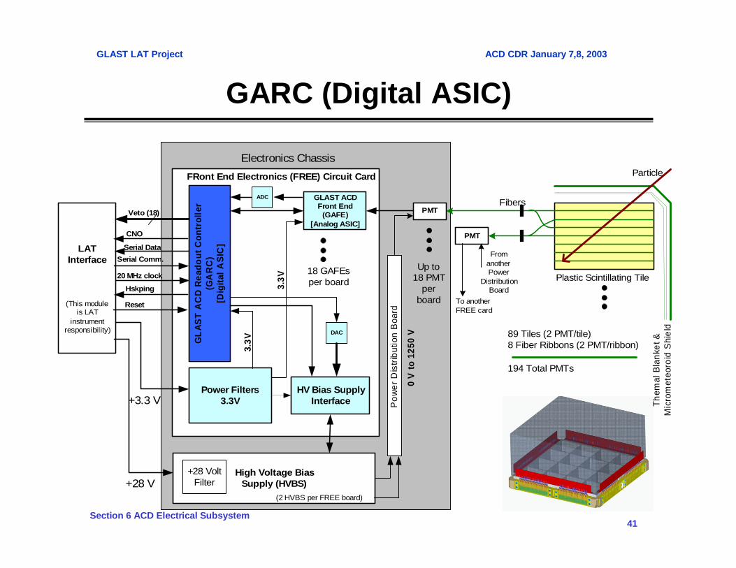
GARC (Digital ASIC)
PMT
PMT
LATInterface
(This moduleis LAT
instrumentresponsibility)
Fibers
Particle
Plastic Scintillating Tile
Th
emal
Bla
nke
t &M
icro
met
eoro
id S
hie
ld
89 Tiles (2 PMT/tile)8 Fiber Ribbons (2 PMT/ribbon)
194 Total PMTs
FromanotherPower
DistributionBoard
GLAST ACDFront End
(GAFE)[Analog ASIC]
GL
AS
T A
CD
Re
ado
ut
Co
ntr
olle
r(G
AR
C)
[Dig
ital
AS
IC]
Power Filters3.3V
HV Bias SupplyInterface
High Voltage BiasSupply (HVBS)
FRont End Electronics (FREE) Circuit Card
Veto (18)
Serial Data
Serial Comm.
0 V
to
125
0 V
3.3
V
3.3
V
18 GAFEsper board
Hskping
(2 HVBS per FREE board)
ADC
DAC
Po
we
r D
istr
ibut
ion
Boa
rd
To anotherFREE card
CNO
20 MHz clock
Reset
+28 VoltFilter
+3.3 V
+28 V
Up to18 PMT
perboard
Electronics Chassis

GLAST LAT Project ACD CDR January 7,8, 2003
42Section 6 ACD Electrical Subsystem
GARC Design Flow
• GARC core logic is coded in Verilog.
• Simulation is performed via Cadence Verilog-XL
• ASIC design is emulated in hardware via retargeting to an AlteraFPGA.
• GARC uses Mentor Graphics Exemplar Leonardo Spectrum synthesis tool to map the input Verilog files to the Agilent 0.5 µm Tanner standard cell library. The output format of the Exemplartool is EDIF.
• The physical layout is performed using the Tanner L-Edit tool. The EDIF output from Exemplar is imported to L-Edit and then automatic cell placement and routing using three metal layers isperformed using the Tanner SPR utility.

GLAST LAT Project ACD CDR January 7,8, 2003
43Section 6 ACD Electrical Subsystem
GARC Clocking
• Continuous 20 MHz• “Look-At-Me” logic selects AEM primary or secondary side to view
(power-on default is Primary) and routes clock from the core to an external clock buffer. Each individual row of Tanner cells is also buffered again.
• 60 rows of logic cells (v1), each buffered by 4 to 12 Tanner clock buffers
• “Look-At-Me” logic clock is buffered by four cells, then 36 cells, then distributed in core where the global clock rail is routed, and buffered by additional 557 cells along the 60 rows. All flip-flops not inside the Look-At-Me logic are clocked via the global CLK signal.
LOOK-AT-MELOGIC
CLK PRIME
DATA PRIME
CLK SEC
DATA SEC
BU
F4
x 4
BU
F4
x 36
CLK
BU
FL
x 557
FANOUT = 4 FANOUT = 9 FANOUT = 15
CLK

GLAST LAT Project ACD CDR January 7,8, 2003
44Section 6 ACD Electrical Subsystem
GARC “Look-At-Me” Circuitry
• Dynamically switches the between AEM primary and secondary interface. Only one can be active
• To switch the GARC to the active AEM side:
– AEM sends a unique look-at-me command– GARC recognizes this command
– GARC performs the multiplexer switch
– GARC provides readback in the GARC Status register
• The power-on default for GARC is the Primary side
GLAST LAT Project ACD CDR January 7,8, 2003
45Section 6 ACD Electrical Subsystem
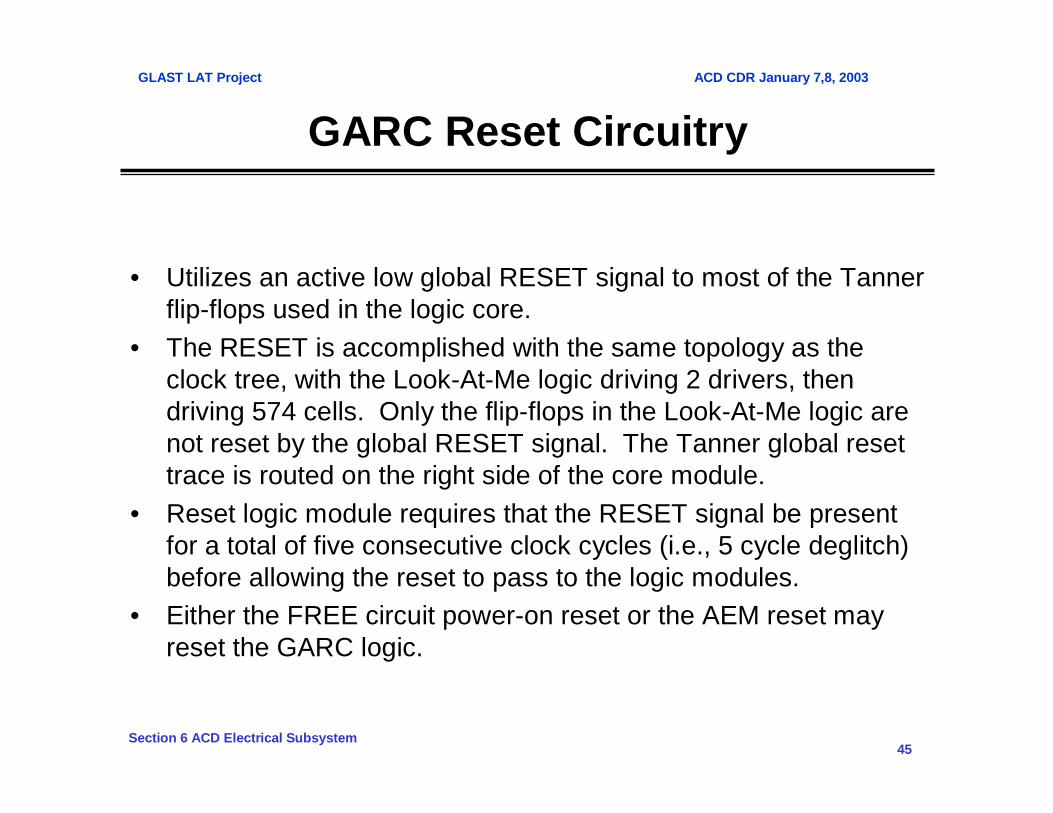
GARC Reset Circuitry
• Utilizes an active low global RESET signal to most of the Tannerflip-flops used in the logic core.
• The RESET is accomplished with the same topology as the clock tree, with the Look-At-Me logic driving 2 drivers, then driving 574 cells. Only the flip-flops in the Look-At-Me logic are not reset by the global RESET signal. The Tanner global reset trace is routed on the right side of the core module.
• Reset logic module requires that the RESET signal be present for a total of five consecutive clock cycles (i.e., 5 cycle deglitch) before allowing the reset to pass to the logic modules.
• Either the FREE circuit power-on reset or the AEM reset may reset the GARC logic.

GLAST LAT Project ACD CDR January 7,8, 2003
46Section 6 ACD Electrical Subsystem
GARC Block Design
INTERFACETO
GAFEASICS
COMMAND &TRIGGER
PROCESSOR
CLOCK A
DISCRIMINATOR ANDHITMAP LOGIC
ADCCONTROL
& ZS LOGIC
EVENT DATAFORMATTER
HLD_OR
VETOs (18)
HLD_WOR_BIAS
GAFE_DTA (+/-)
GAFE_CK (+/-)
STROBE (+/-)
HOLD (+/-)
HOLDDELAY
CIRCUIT
LVDSDRIVERS
LVDSRECEIVER
S
VETO_A (18)
NSDATA A
3.3V RTN
GARC BLOCK DIAGRAM
IRTN (18)
CHIDs (18)
IRTN_HL_DISC
GARCBIASING
CIRCUITRY
BIAS_RCVR
BIAS_DRV_H
BIAS_DRV_L
PHAD (18)
GAFE_RTND
GAFE_RST
3.3VAEM
LOOK-AT-MEAND
RESETLOGIC
CLK
RESET_N
CLOCK B
RESET A
RESET B
CMD A
CMD B
NSDATA B
CNO A
CNO B
VETO_B (18)
MAX145 ADC CONTROL
MAX5121 DAC CONTROL

GLAST LAT Project ACD CDR January 7,8, 2003
47Section 6 ACD Electrical Subsystem
GARCv1
GARC BONDING DIAGRAM
Fully functional and compliant GARCv1

GLAST LAT Project ACD CDR January 7,8, 2003
48Section 6 ACD Electrical Subsystem
GARC-to-AEM Communications: LVDS Drivers and Receivers
• 100 Ω termination resistor• Input voltage levels are 0V
and 3.3V• 40 LVDS drivers
(ACD_NSDATA, ACD_CNO, ACD_VETO)
• 6 LVDS receivers (ACD_CLK, ACD_NSCMD, ACD_NRST)
• The nominal bias setting is controlled externally via bias resistors
• Maximum switch rate is 20 MHz.

GLAST LAT Project ACD CDR January 7,8, 2003
49Section 6 ACD Electrical Subsystem
VETO Signal Characteristics• VETO_AEM
– An active VETO discriminator signal represents a signal in at the PMT
– Signal is deglitched, delayed, and width adjusted by command in GARC
– Digital delay lines will be used to provide delays from 150 ns to 1700 ns with 50 nsec time steps. Width is programmable from 50 ns to 400 ns, in steps of 50 ns
– These signals occur continuously, independent of readout status
• VETO HitMap– Output in the event data as a set of 18 bits (e.g., one per GAFE) as
the result of an ACD Trigger Command.– The VETO HitMap is captured during the event readout. These bits
represent the status of the GAFE discriminators at a previous instant (like pretrigger data on a digital oscilloscope)
– The GAFE discriminator outputs are stretched and delayed by GARC command (no deglitching here). Digital delay lines providedelays from 850 ns to 2400 ns, widths programmable from 150 ns to 900 ns, and an added, 0 - 350 ns, may be added to the trailing edge of the pulse
– The timing of the HitMap capture must be adjusted by command at the LAT level (i.e., the ACD cannot know the LAT trigger latency in advance)
Level IV Requirement 5.2: Charged Particle Detection. The ACD shall produce both fast and slow VETO signals in response to PMT signals resulting from charged particles traversing the ACD tiles and ribbons
Level IV Requirement 5.8.2 Fast VETO Signal Width. The fast VETO output signal shall have a commandable width of 50 nsec to 400 nsec, after ‘de-glitching’ on 2 successive clock pulses. The leading and trailing edges must be synchronous with clock pulses.

GLAST LAT Project ACD CDR January 7,8, 2003
50Section 6 ACD Electrical Subsystem
ACD VETO Characteristics
GAFE DISCRIMINATOROUT
ACD_NVETO
INTERNAL HitMapDELAY LINE
ACTIVEHitMap
STATUS REGISTER
INTERNAL HitMapLATCH SIGNAL
TRIGGER COMMAND

GLAST LAT Project ACD CDR January 7,8, 2003
51Section 6 ACD Electrical Subsystem
Why do the VETOs need Delays and Stretching?
• Alignment of the ACD, Tracker and Calorimeter trigger signals
– Global Trigger (GLT) receives the ACD, Tracker and Calorimeter trigger signals, but can’t align them
– With ACD Electronics module (AEM) commanding, the ACD can delay and stretch the ACDs trigger (VETO) signals,
Tracker
ACD
Calorimeter
Time

GLAST LAT Project ACD CDR January 7,8, 2003
52Section 6 ACD Electrical Subsystem
VETO – Case 1, Case 2 and Case 3
VETO_HM minimum pulse width is programmable from 150 ns to 900 ns. This diagram illustrates a pulse stretched to 500 ns
ComparatorInput
ComparatorOutput
VETO_AEM
Case 2Case 1
ACD_NVETOxxACD_NVETO is the same as VETO_AEM but delayed by a programmable time ranging from 150 ns to 1700 ns. This diagram illustrates a 150 ns delay
VETO_HM
VETO_HMD is the same as VETO_HM but delayed by a programmable time ranging from 850 ns to 2400 ns. This diagram illustrates a 100 ns delay
VETO_HMD
The VETO_AEM signal is synchronized to the clock.
VETO_AEM requires two clock edges to determine if the comparator output exceeds the minimum pulsewidth
Comparator output isasynchronous
Addeddead time
Pulse stretch to minimum
Green circles indicates sample points
Case 3
Addeddead time
Pulse stretch to minimum
Extended pulse begins
Clock
Case 1: A charged particle event occurs where the magnitude of the event produces a comparator output that lasts at least 2 clock edges, but less than the VETO_AEM minimum pulse width.Case 2: A charged particle event occurs where the magnitude of the event produces a comparator output that lasts less than 2 clock edges.Case 3: Two charged particle events occur where each event lasts at least 2 clock edges, but the second event occurs before the VETO_AEM pulse is complete.

GLAST LAT Project ACD CDR January 7,8, 2003
53Section 6 ACD Electrical Subsystem
VETO – Case 4
ComparatorInput
ComparatorOutput
VETO_AEM
Case 4
ACD_NVETOxxACD_NVETO is the same as VETO_AEM but delayed by a programmable time ranging from 150 ns to 1700 ns. This diagram illustrates a 150 ns delay
VETO_HM
VETO_HM minimum pulse width is programmable from 150 ns to 900 ns. This diagram illustrates a pulse equal to the comparator’s actual width and then 150 ns of deadtimeis added. Deadtime is programmable from 0 ns to 350 ns
VETO_HMD is the same as VETO_HM but delayed by a programmable time ranging from 850 ns to 2400 ns. This diagram illustrates a 100 ns delay
VETO_HMD
ACD Timing Analysis: Events and VETOs - Part 2
VETO_AEM is synchronized to the clock. VETO_HITMAP may be synchronized to the clock
VETO_AEM requires two clock edges to determine if the comparator output exceeds the minimum pulsewidth
Addeddeadtime
Case 4: A charged particle event occurs where the magnitude of the event produces a comparator output greater than the VETO_AEM minimum pulse width.

GLAST LAT Project ACD CDR January 7,8, 2003
54Section 6 ACD Electrical Subsystem
GARC-to-GAFE Communication: LVDS Drivers and Receivers
• 64 I/O signals for communication with the 18 GAFE ASICs
– 4 differential control signals (HOLD, STROBE, DATA, CLK)
– 18 channel identification inputs– 19 discriminator inputs (18 VETO + 1 HLD)
– 19 driver current returns (IRTN)
• Custom designed to interface with the corresponding cells in theGAFE
• Utilize an order of magnitude less drive current than the LVDS standard used between the GARC and AEM

GLAST LAT Project ACD CDR January 7,8, 2003
55Section 6 ACD Electrical Subsystem
GAFE/GARC Design – VETO and HLD
• VETO_AEM signal latency was measured to be 170 ns to 220 ns (assumes a zero commandable delay)
Level IV Requirement 5.8.1: Fast VETO (VETO_AEM) Signal Latency. The fast VETO signal latency shall be 100<tlatent<600 nsec from the time of particle passage. The time jitter in the VETO pulses shall be <200 ns relative to particle passage. (‘Deglitch’ circuit raised min latency to 100 nsec from 50 nsec).
• The HLD signal latency is expected to be equal to or less than the fast VETO signal latency since it uses the same type of discriminator as the VETO signal, and no GARC processing is imposed
Level IV Requirement 5.8.6: High-Threshold Signal Latency. A highly-ionizing particle hitting the top or upper side row of tiles of the ACD shall produce a High-Threshold fast signal that will be delivered to the hardware trigger logic with latency of no more than that the latency as defined for the fast VETO in 5.8.1. Command-selected signals out of the eighteen (18) High-Threshold fast signals generated on a single electronics board shall be OR’ed to produce a single signal for transmission to the AEM.
Level IV Requirement 5.5: High Threshold Detection. Each ACD electronics board shall OR up to 18 HLD outputs (selected via command) to generate a single HLD_OR signal for transmission to the AEM.
Level IV Requirement 5.8.7: Discriminator Masking. Each ACD electronics board shall have the capability to disable any combination of the Fast VETO and HLD discriminator outputs. This is to mask unused HLD signals, unpopulated veto channels, and signals due to channel failure.

GLAST LAT Project ACD CDR January 7,8, 2003
56Section 6 ACD Electrical Subsystem
GLAST ACD Readout Controller (GARC) Command Processor
• GARC operates by command response (i.e., in all that it does, it is just “following orders”
• GARC functionality matches the specifications found in the ICD • Three types of commands
– Configuration commands (GARC or GAFE)– Register status readback commands (GARC or GAFE) - data format
returned is configuration command readback.
– Trigger commands (zero-suppressed or non zero-suppressed) - data format returned is ACD event data.
• All registers that can be written may be read via readback command• Some registers are read-only registers (I.e. GARC status, ASIC address, ASIC
version number, etc.)• All registers are initialized to predetermined values upon RESET• Commands are sent serially from the AEM to the digital ASIC via a clock and
data interface.

GLAST LAT Project ACD CDR January 7,8, 2003
57Section 6 ACD Electrical Subsystem
GARC Command Processor (cont.)
Level IV Requirement 5.7: Level 1 Trigger Acknowledge (TACK). The ACD electronics shall accept from the AEM a Level 1 Trigger Acknowledge signal and respond by digitizing and latching data.
Is it a TriggerCommand?
Serial Data In
Start DelayCounter
GARC initiatesanalog-to-digitalconversion with
“start_pha” signal
End of delaycounter, send
“HOLD” signal totransition shapingamplifier T/H to
hold mode
Yes
NoRead 4 bits. Read 28 bits. Is parity
correct?No
Yes
Command isdecoded andimplemented
Command isrejected and errorportion is loaded into GARC register

GLAST LAT Project ACD CDR January 7,8, 2003
58Section 6 ACD Electrical Subsystem
Command & Data Format
Command format
TRIGGER COMMANDZERO-SUPPRESS ENABLED
1 1 0 0
TRIGGER COMMANDZERO-SUPPRESS DISABLED
1 0 1 0
CONFIGURATION COMMAND FORMAT
33 32 31 30 29 28:24 23 22 21:18 17 16:1 0
1 0 0 1 n aaaaa m 1 rrrr p dddd p
Bit 29 - 0 for GARC, 1 for GAFE
Bits 28:24 - Address/Function Select
Bit 23 - 0 for Write, 1 for Read
Bits 21:18 - Register Select
Bit 17 - Odd parity over previous 15 bits
Bit 0 - Odd parity over Command Data
Bits 16:1 - Command Data
CONFIGURATION READBACK FORMAT
Bit 30 - 0 for GARC, 1 for GAFE
Bits 29:25 - Address/Function Select
Bit 24 - Always 1 for Read
Bits 21:18 - Register Select
Bit 18 - Odd parity over previous 12 bits
Bit 1 - Error in parity detected
Bits 17:2 - Data, MSB First
Bit 0 - Odd parity over previous 17 bits
31 30 29:25 24 23 22:19 18 17:2 1
1 S aaaaa m 1 rrrr p dddd e0
p
EVENT DATA FORMAT
Start Bit = 1
Next 18 Bits = HitMap
Next 18 Bits = ZS Map
Next Bit = Cmd/Data Error Bit
Next Bit - Header Parity, odd over previous 37 bits
Next (15 bits * n) - PHA words
MSB Next 18 1 Next 151Next 18 Final 15
1 HitMap e PHApZS Bits PHA...

GLAST LAT Project ACD CDR January 7,8, 2003
59Section 6 ACD Electrical Subsystem
GARC Processing of TACK Command
• The AEM can transmit to any FREE circuit card the trigger command (TACK). Event data occurs in response to an AEM TACK
• The ADCs on the FREE card will be awakened• The VETO HitMap (or the HLD Map in the
appropriate test mode) will be latched, and data will be prepared for transmission to the AEM. HitMap word captures the state of the input discriminators at a preset time in relation to the receipt of the trigger command from the AEM
• The TACK is also time-delayed to match the peaking time of the shaping amplifiers. The time delay shall be imposed by the GARC but the time-delay is preprogrammed via command by the AEM. At the end of the delay a HOLD signal is generated. The pulse height is sampled at a unique point in the readout cycle, the start of the analog-to-digital conversion, ~3.5 microseconds after the event.
Level IV Requirement 5.8.4 Logic VETO (VETO_Hitmap) Signal. A map of VETO signals shall be generated for each TACK (L1T), indicating which ACD PMTs produced signals above their thresholds within ~200 ns of the time of the event causing the TACK. (Note: The ~200 ns window is required because of time jitter in the TACK signal).
Level IV Requirement 5.8.5 Logic VETO Signal Latency.In response to a TACK (L1T), the map of VETO signals shall be latched by the time the ADC conversions are complete.
GLAST LAT Project ACD CDR January 7,8, 2003
60Section 6 ACD Electrical Subsystem
ACD Commands Requirements Level IV Requirement 5.14.1 Detector On/Off Commands. The AEM will
implement commands to allow each group of 18 PMTs to be powered on and off together.
Level IV Requirement 5.14.2 Detector Gain Commands. The ACD shall implement adjustability of the high voltage applied to the group of 18 PMTs associated with a single board.
Level IV Requirement 5.14.3 Electronics On/Off Commands. The AEM will implement commands to allow each ACD electronics board to be separately powered on and off.
Level IV Requirement 5.14.4 VETO Threshold Commands. The ACD shall implement adjustability of the VETO threshold for each PMT.
Level IV Requirement 5.14.5 High-Threshold Commands. The ACD shall implement adjustability of the High-Threshold for each PMT.
Level IV Requirement 5.14.6 ACD Monitoring Commands. The ACD shall implement adjustability of the monitoring functions of the ACD electronics, including the zero suppression for each PMT.
Level IV Requirement 5.14.9 SAA Mode Commands. The ACD photomultiplier bias supplies shall switch into a low-gain mode to protect the phototubes in very high intensity particle conditions (> 10 kHz in an individual tile) such as the South Atlantic Anomaly. (Accomplished by HVBS command from AEM to GARC)

GLAST LAT Project ACD CDR January 7,8, 2003
61Section 6 ACD Electrical Subsystem
Pulse Height Analysis Data
• In response to a TACK, the ACD provides the PHA data to the AEMvia the GARC
• The AEM can send commands that enable or disable each PHA, enable the readout of all PHA channels, and read out just the enabled PHA channels
• There is no requirement for the minimum or maximum number of PHAwords to be read out in Science mode for a science event

GLAST LAT Project ACD CDR January 7,8, 2003
62Section 6 ACD Electrical Subsystem
GARC Testing• GARCv1 fully tested.• Test report details available (ACD-RPT-000073)
. Identified 9 issues. All were straight-forward and simple fixes to a good design
• GARC test procedure is developed and was used to test GARCv1
GARC test board

GLAST LAT Project ACD CDR January 7,8, 2003
63Section 6 ACD Electrical Subsystem
GARC Summary
• Status– Conducted a Peer Review in July, 2002. Attendees were technical people
with ASIC experience from GSFC and JHU-APL. Found eleven issues which have been addressed. Report available. All eleven issues have been resolved in the GARCv2 design
– GARCv1 fully tested (ACD-PROC-000062) and nine issues were identified. All nine issues have been resolved in the GARCv2 design
– GARCv2 fully designed. Fabrication planned in January ‘03. Design is very mature and “flight-like”
• Issues– None
• Next Step– Fabricate GARCv2 and test– Populate and test GARCv1 on the FREE circuit card (development unit)– Radiation test GARCv1

GLAST LAT Project ACD CDR January 7,8, 2003
64Section 6 ACD Electrical Subsystem
High Voltage Bias Supply
PMT
PMT
LATInterface
(This moduleis LAT
instrumentresponsibility)
Fibers
Particle
Plastic Scintillating Tile
Th
emal
Bla
nke
t &M
icro
met
eoro
id S
hie
ld
89 Tiles (2 PMT/tile)8 Fiber Ribbons (2 PMT/ribbon)
194 Total PMTs
FromanotherPower
DistributionBoard
GLAST ACDFront End
(GAFE)[Analog ASIC]
GL
AS
T A
CD
Re
ado
ut
Co
ntr
olle
r(G
AR
C)
[Dig
ital
AS
IC]
Power Filters3.3V
HV Bias SupplyInterface
High Voltage BiasSupply (HVBS)
FRont End Electronics (FREE) Circuit Card
Veto (18)
Serial Data
Serial Comm.
0 V
to
125
0 V
3.3
V
3.3
V
18 GAFEsper board
Hskping
(2 HVBS per FREE board)
ADC
DAC
Po
we
r D
istr
ibut
ion
Boa
rd
To anotherFREE card
CNO
20 MHz clock
Reset
+28 VoltFilter
+3.3 V
+28 V
Up to18 PMT
perboard
Electronics Chassis

GLAST LAT Project ACD CDR January 7,8, 2003
65Section 6 ACD Electrical Subsystem
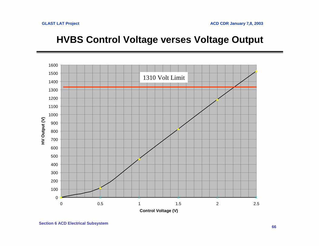
HVBS Design
• Simple, reliable, flight proven circuit approach used.
• Output will be limited should any single point failure
• AEM commandable 0 V to 2.5 V differential DAC input adjusts output level from 0 V to 1310 V. Level IV Requirement 5.10.1 HVBS Voltage Range. The HVBS shall
operate from +400 V to +1310 V. Level IV Requirement 5.10.4 HVBS Voltage Adjustment. The HVBS output
voltage shall be programmable with an analog input. The limiting output current of each HVBS shall be ~80 µA.
• DAC (MAX5121)– 12-bit– < 10 ppm/°C– 0 V to 2.5 V range (differential)
GLAST LAT Project ACD CDR January 7,8, 2003
66Section 6 ACD Electrical Subsystem
HVBS Control Voltage verses Voltage Output
0
100
200
300
400
500
600
700
800
900
1000
1100
1200
1300
1400
1500
1600
0 0.5 1 1.5 2 2.5
Control Voltage (V)
HV
Ou
tpu
t (V
)
1310 Volt Limit
GLAST LAT Project ACD CDR January 7,8, 2003
67Section 6 ACD Electrical Subsystem
HVBS Design (cont.)
• Provides up to 80 microamps of output current at 1250 V. The expected current load for 18 PMTs is 29 microamps. Level IV Requirement 5.10.2 HVBS Output Current. The HVBS shall provide sufficient
current to drive all PMTs (max 18) on each FREE circuit card at the maximum voltage (+1310V).
• Limits output current to 80 microamps at the switching transistor in the oscillator stage. If one PMT shorts, then the output current will approach 60 microamps. Level IV Requirement 5.10.3 HVBS Limiting Output Current. The HVBS output current
shall be limited to protect the ACD from one PMT shorting. At maximum output voltage, each HVBS shall be capable of supplying a total output current of 60 µA. The nominal output current will be 18 µA.
• Operates with an input voltage of 28 V +10/-7 V with a ripple voltage of 100 mV from 50 Hz to 50 MHz and provide an output noise voltage of ±2 mV maximum. Level IV Requirement 5.10.5 HVBS Input power. Each HVBS shall operate from a
supply voltage of 28V 1V, with possible input ripple of 10 mV (frequency range 50 Hz to 50 MHz). The noise shall be less than 100 mV RMS from DC to 1.0 MHz.

GLAST LAT Project ACD CDR January 7,8, 2003
68Section 6 ACD Electrical Subsystem
HVBS Design (cont.)
• Output regulation achieved by controlling conduction of oscillator switching transistor. Regulated to ±0.25% for any combination of input voltage and load current. The temperature stability was measured from +50°C to –25°C and found to be 32 ppm/°C Level IV Requirement 5.10.6 HVBS Line and load Regulation. The HVBS output voltage shall be
regulated to ±0.5% for all combinations of input voltage and load current. (This produces ~5% change in PMT gain).
Level IV Requirement 5.10.10 HVBS Temperature Stability. The HVBS output voltage temperature stability shall be no worse than 500 ppm/C.
• Output voltage ripple is less than ±1 mV p-p over the frequency range from DC to 100 MHz. Level IV Requirement 5.10.7 HVBS Output Ripple. The HVBS output voltage ripple shall be
compatible with the ACD ASIC design. The HVBS output voltage ripple shall not exceed 2 mV p-p over the frequency range 100 Hz to 50 MHz
• Power consumption is less than 295 mW for all conditions. Level IV Requirement 5.10.8 HVBS Power Consumption. The HVBS power dissipation at maximum
output voltage and limiting current shall be <300 mW.
• Ramp-up/down time for loading 18 PMTs is less than 15 seconds. Level IV Requirement 5.10.9 HVBS Ramp Up/Down time. For either application or removal of input
power, the time for the HVBS output voltage to reach its final level (for turn-on, within regulation tolerance) shall be between 5 and 30 seconds. Note: The 5 second requirement is driven by the PMT, the 30 seconds is driven by the maximum tolerable time for HVBS to stabilize when entering/exiting the SAA.

GLAST LAT Project ACD CDR January 7,8, 2003
69Section 6 ACD Electrical Subsystem
HVBS Design (cont.)
• The high voltage is monitored with a unity gain buffered amplifier at the output sensing resistor divider. The monitor scaling factor is 2.5 V if the HVBS is 1500 V and 0 V if the HVBS is 0 V. Level IV Requirement 5.10.11 HVBS Output Voltage Monitoring. The HVBS shall provide a linear
output voltage monitor (for transmission to the AEM) in the range 0.0 to 2.5 V.
Level IV Requirement 5.10.12 HVBS Ground Isolation. The DC impedance between input and output grounds shall be 100 ohms ±20%.
• A 700 kHz Hartley Sine-wave oscillator with a 170 V p-p output is used to minimize EMI Level IV Requirement 5.10.13 HVBS Oscillator Frequency. The HVBS shall utilize an oscillator
frequency >100 kHz (to minimize EMI issues).
• An over-damped LCR low-pass filter attenuates the current pulses of the Hartley oscillator. Level IV Requirement 5.10.14 HVBS EMI and Susceptibility. The HVBS shall neither generate nor be
susceptible to electromagnetic interference exceeding the EMI/EMC test requirement, GSFC-433-RQMT-0005
• PCB design meets IPC-6012 standard, 6-layers, no high-voltage vias, FR-4 material, 0.062”thickness, conformal coated and staked with a Uralane 5750/5753 compound, and assembled and inspected to NASA-STD-8739.3.
GLAST LAT Project ACD CDR January 7,8, 2003
70Section 6 ACD Electrical Subsystem
HVBS Design (cont.)
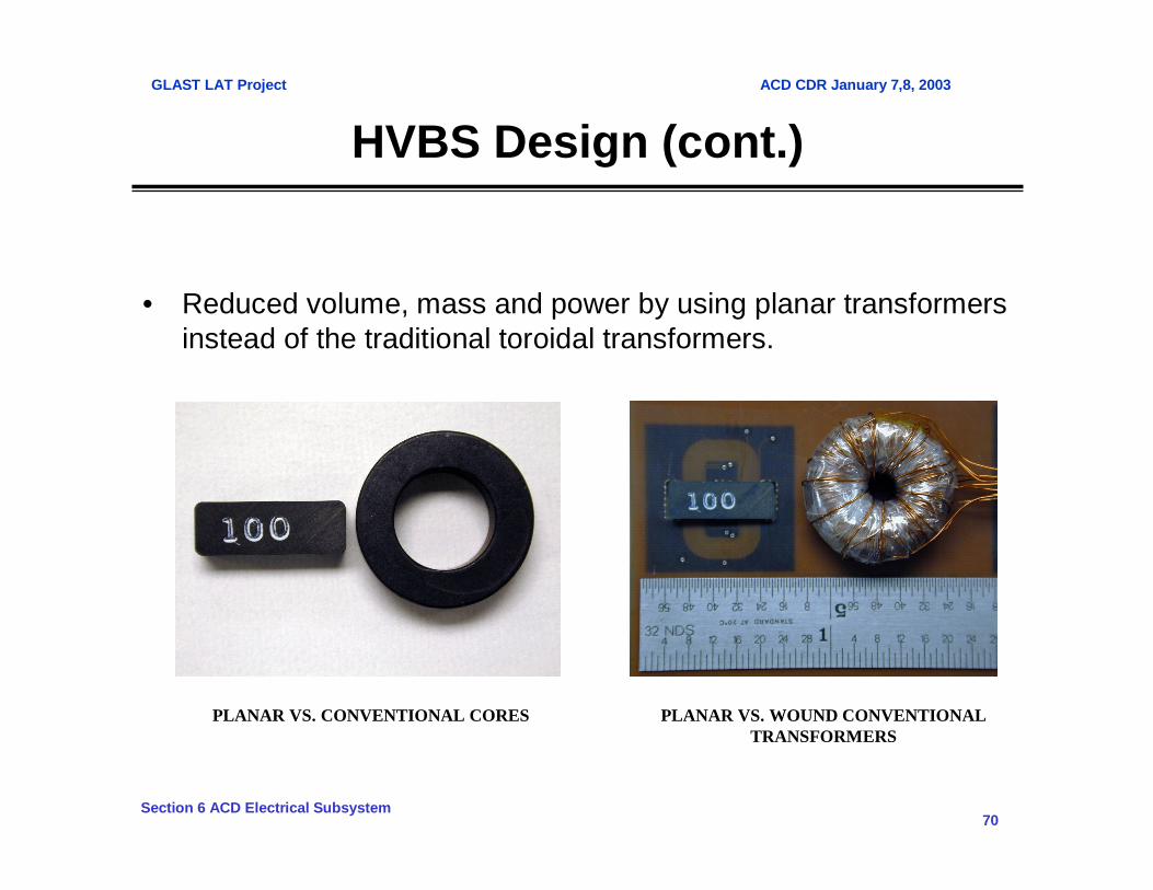
• Reduced volume, mass and power by using planar transformers instead of the traditional toroidal transformers.
PLANAR VS. CONVENTIONAL CORES PLANAR VS. WOUND CONVENTIONAL TRANSFORMERS

GLAST LAT Project ACD CDR January 7,8, 2003
71Section 6 ACD Electrical Subsystem
HVBS – Block Diagram & Interface
Mult
Mult
HVBS, PRIMARY
HVBS, SECONDARY
LAT 200
200
2K
2K
1K
Off: 0.0VOn: 3.3V
FREE CARD
+
+
+
+
-
-
-
-
HV ENABLE, TMRDIFF.HV LEVEL CONTROL
HV RTN.
HV OUTTO PMT DIST.+28V
+28V
+28VRTN
+28VRTN
HVMON
HVMON
MONRTN
MONRTN

GLAST LAT Project ACD CDR January 7,8, 2003
72Section 6 ACD Electrical Subsystem
HVBS Breadboard
Planar transformer and multiplierin the near-flight configuration
Breadboard of the multiplier
Front end of oscillator and control-loop circuitry

GLAST LAT Project ACD CDR January 7,8, 2003
73Section 6 ACD Electrical Subsystem
HVBS Temperature Test Results
HVBS Performance With Planar Trans former at Max Output Vo ltage (Vin=28V, Vref=2.50V)
1.4983 1.4979 1.4996 1.4974 1.5001 1.4998 1.4966
3.1
3.3 3.3 3.33.2
3.33.4
2.22
2.0012.14 2.091
2.166 2.1552.011
0
1
2
3
4
Val
ue
(kV
)
50° 50°C-25°C Ne xt Day, -25°CRoom Temp. Ro om Temp. Ne xt Day, Roo m Te mp.

GLAST LAT Project ACD CDR January 7,8, 2003
74Section 6 ACD Electrical Subsystem
HVBS Power Distribution Board
• Distributes high voltage to up to 18 PMTs• No circuitry• Evolved as a result of electronic chassis
packaging complexity• Constructed of two bus bars, high voltage
and return• Protective cover to keep noise from getting to
the PMT signal
GLAST LAT Project ACD CDR January 7,8, 2003
75Section 6 ACD Electrical Subsystem
HVBS Summary
• Status– Breadboard has been tested and show good results that meet requirements– HVBS design is complete– HVBS (development/engineering unit) layout is getting final touches– Most parts have been approved by Code 300 with the exception of high
voltage capacitors, which are being sample tested by Code 300. The DPA passed.
– Test plan has been developed– Thermal and mechanical analysis near complete
• Issue– None
• Next Steps– Preparing for an breadboard interface test with the GARC– Complete assembly plan development– Development/engineering unit fabricate and test– Fit check development/engineering unit with electronic chassis
GLAST LAT Project ACD CDR January 7,8, 2003
76Section 6 ACD Electrical Subsystem
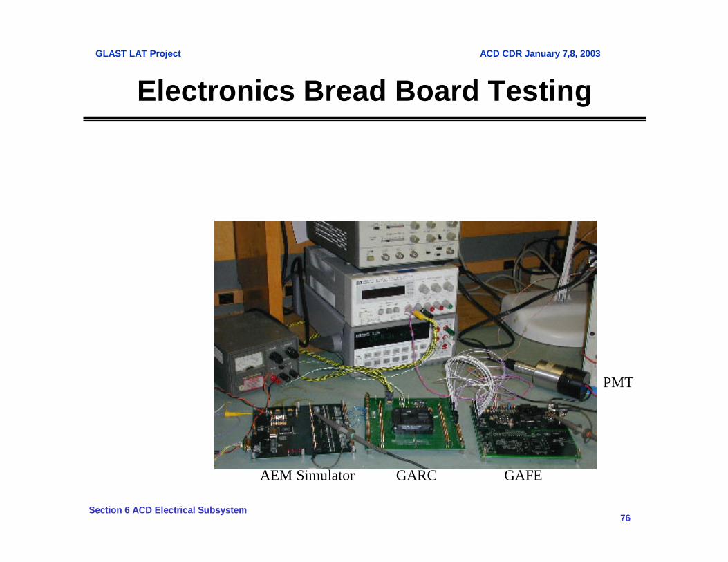
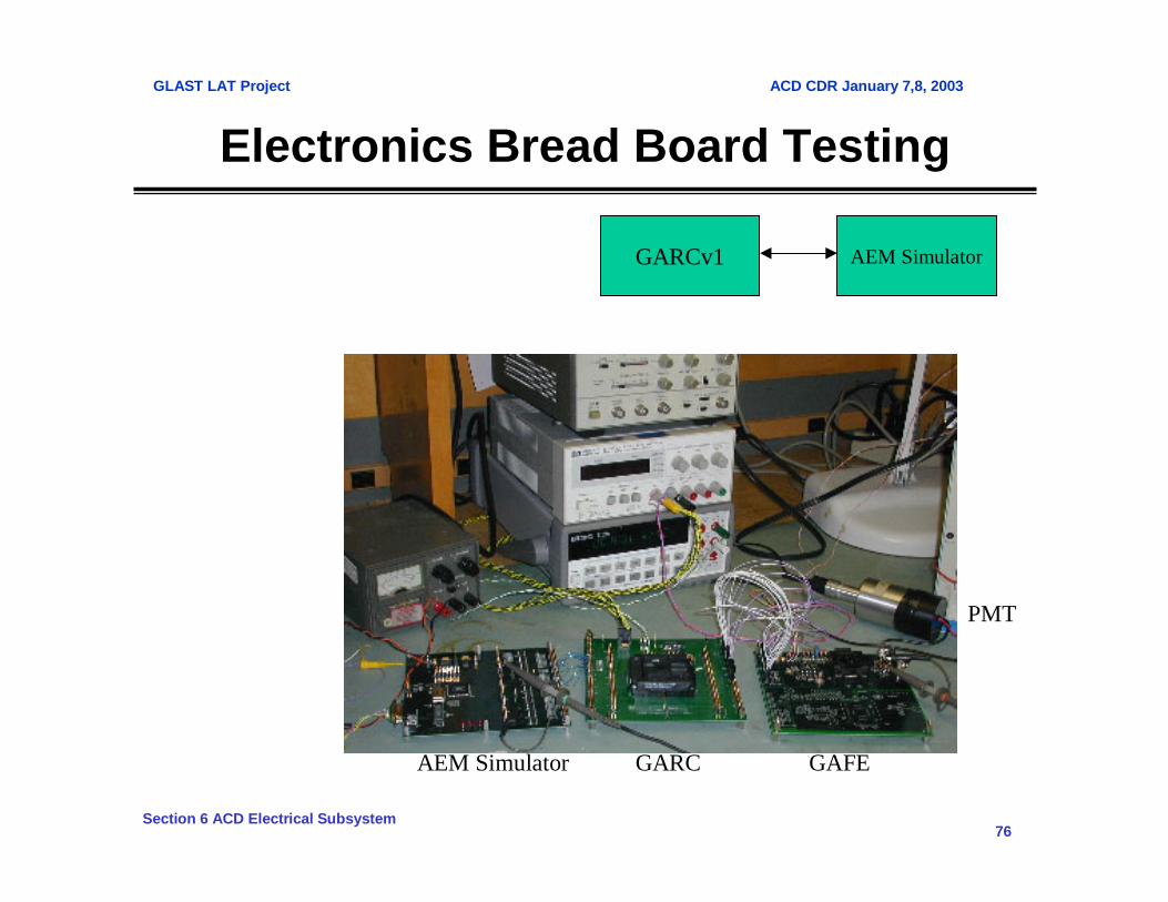
Electronics Bread Board Testing
AEM Simulator GARC GAFE
PMT
GLAST LAT Project ACD CDR January 7,8, 2003
76Section 6 ACD Electrical Subsystem
Electronics Bread Board Testing
AEM Simulator GARC GAFE
PMT
GARCv1 AEM Simulator
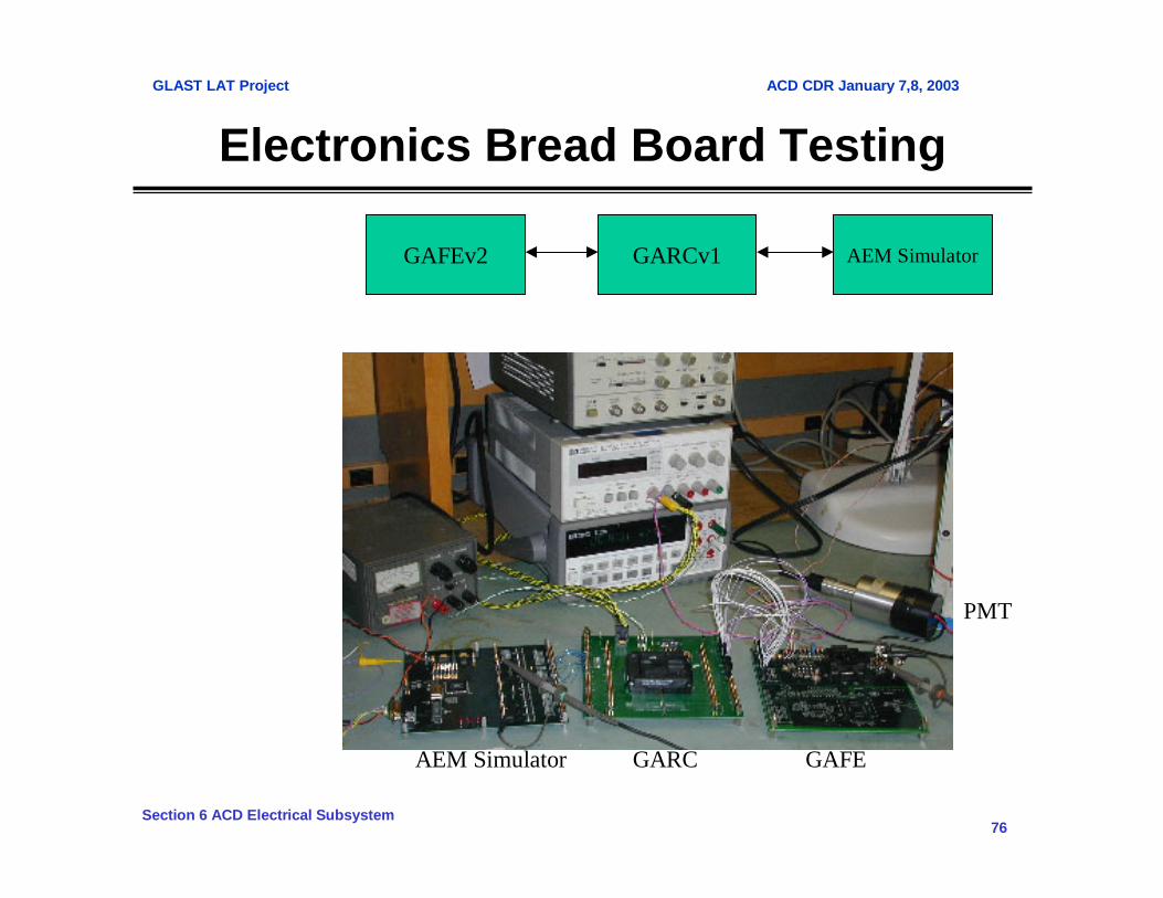
GLAST LAT Project ACD CDR January 7,8, 2003
76Section 6 ACD Electrical Subsystem
Electronics Bread Board Testing
AEM Simulator GARC GAFE
PMT
GARCv1 AEM SimulatorGAFEv2

GLAST LAT Project ACD CDR January 7,8, 2003
76Section 6 ACD Electrical Subsystem
Electronics Bread Board Testing
AEM Simulator GARC GAFE
PMT
GARCv1 AEM SimulatorGAFEv2PMT

GLAST LAT Project ACD CDR January 7,8, 2003
76Section 6 ACD Electrical Subsystem
Electronics Bread Board Testing
AEM Simulator GARC GAFE
PMT
GARCv1 AEM SimulatorGAFEv2PMT
HVBSBreadboard

GLAST LAT Project ACD CDR January 7,8, 2003
77Section 6 ACD Electrical Subsystem
Electronic Bread board Test Results
Sample
& Hold
VETO
Generation
Test with
PMT
• Demonstrated ACD to LAT interface
• Demonstrated GARC to GAFE communication
• Demonstrated PMT signal processing
• Demonstrated VETO and HLD processing

GLAST LAT Project ACD CDR January 7,8, 2003
78Section 6 ACD Electrical Subsystem
Electronic Chassis – Development Unit
• Planned in March/April ’03
• Demonstrate full system functionality
• Demonstrate electro-mechanical interface

GLAST LAT Project ACD CDR January 7,8, 2003
78Section 6 ACD Electrical Subsystem
Electronic Chassis – Development Unit
• Planned in March/April ’03
• Demonstrate full system functionality
• Demonstrate electro-mechanical interface
AEM Test StandFREE Development Unit (5)GARCv1GAFEv4 (18)

GLAST LAT Project ACD CDR January 7,8, 2003
78Section 6 ACD Electrical Subsystem
Electronic Chassis – Development Unit
• Planned in March/April ’03
• Demonstrate full system functionality
• Demonstrate electro-mechanical interface
AEM Test StandFREE Development Unit (5)GARCv1GAFEv4 (18)PMT
Calibration Unit
HVBSDevelopment
Units (3)
Electronic Chassis
PMTCalibration Unit
HVBSDevelopment
Units (3)
FREE Development Unit (5)GARCv1GAFEv4 (18)

GLAST LAT Project ACD CDR January 7,8, 2003
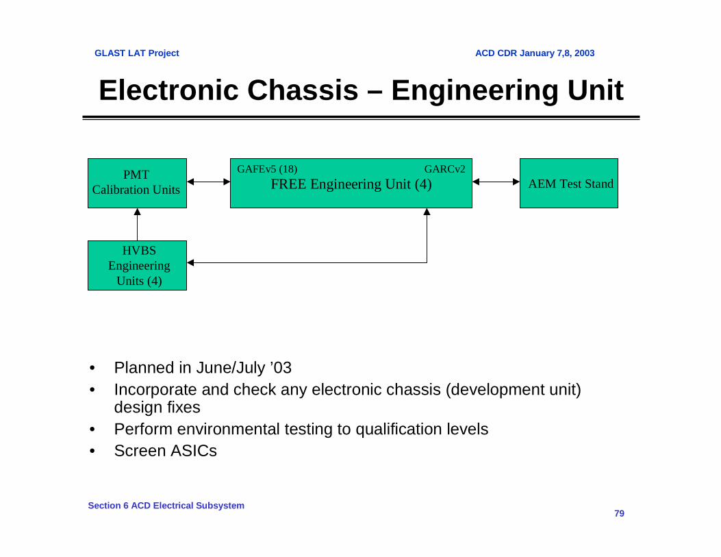
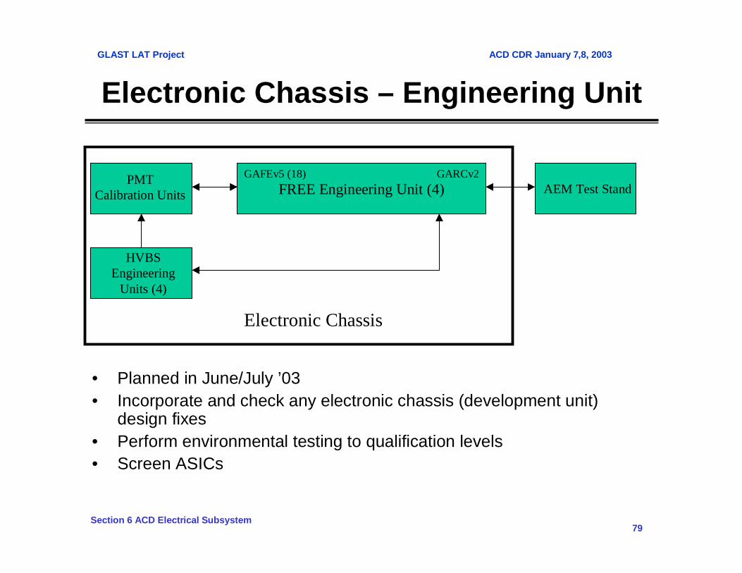
79Section 6 ACD Electrical Subsystem
Electronic Chassis – Engineering Unit
• Planned in June/July ’03• Incorporate and check any electronic chassis (development unit)
design fixes • Perform environmental testing to qualification levels• Screen ASICs
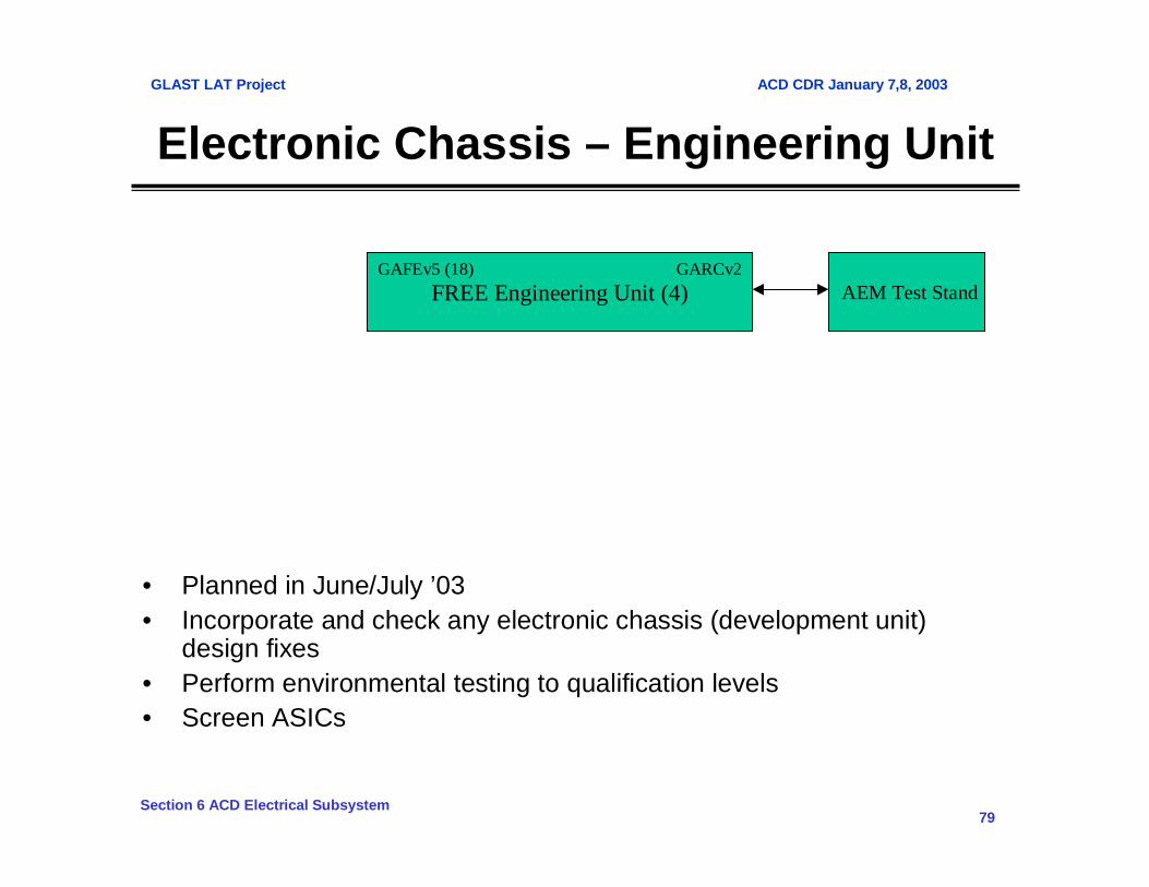
GLAST LAT Project ACD CDR January 7,8, 2003
79Section 6 ACD Electrical Subsystem
Electronic Chassis – Engineering Unit
• Planned in June/July ’03• Incorporate and check any electronic chassis (development unit)
design fixes • Perform environmental testing to qualification levels• Screen ASICs
AEM Test StandFREE Engineering Unit (4)GAFEv5 (18) GARCv2

GLAST LAT Project ACD CDR January 7,8, 2003
79Section 6 ACD Electrical Subsystem
Electronic Chassis – Engineering Unit
• Planned in June/July ’03• Incorporate and check any electronic chassis (development unit)
design fixes • Perform environmental testing to qualification levels• Screen ASICs
AEM Test StandFREE Engineering Unit (4)GAFEv5 (18) GARCv2PMT
Calibration Units
HVBSEngineering
Units (4)
Electronic Chassis
PMTCalibration Units
HVBSEngineering
Units (4)
FREE Engineering Unit (4)GAFEv5 (18) GARCv2

GLAST LAT Project ACD CDR January 7,8, 2003
80Section 6 ACD Electrical Subsystem
Electronic Chassis – Flight Unit
• Planned in November ’03• Perform functional testing• Perform environmental testing to acceptance levels• Deliver to I&T

GLAST LAT Project ACD CDR January 7,8, 2003
80Section 6 ACD Electrical Subsystem
Electronic Chassis – Flight Unit
• Planned in November ’03• Perform functional testing• Perform environmental testing to acceptance levels• Deliver to I&T
AEM Test StandFREE Flight Unit (12)GAFEv5 (18) GARCv2

GLAST LAT Project ACD CDR January 7,8, 2003
80Section 6 ACD Electrical Subsystem
Electronic Chassis – Flight Unit
• Planned in November ’03• Perform functional testing• Perform environmental testing to acceptance levels• Deliver to I&T
AEM Test StandFREE Flight Unit (12)GAFEv5 (18) GARCv2PMT
Flight Units
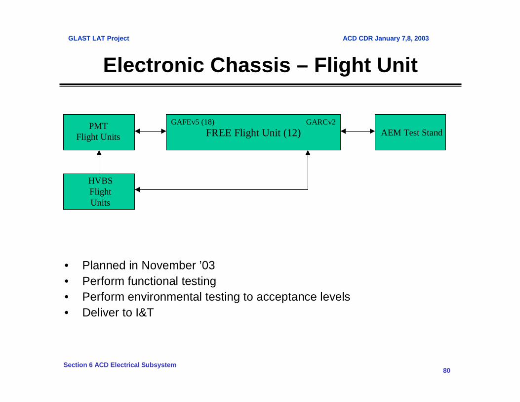
HVBSFlightUnits
Electronic Chassis
PMTFlight Units
HVBSFlightUnits
FREE Flight Unit (12)GAFEv5 (18) GARCv2

GLAST LAT Project ACD CDR January 7,8, 2003
81Section 6 ACD Electrical Subsystem
FREE Assembly Integration and Test Flow
INITIAL INSPECTIONOF FREE PCB
ASSEMBLY
CONNECTORSAVER
VERIFICATION/INSTALLATION
GSE GROUNDING &EQUIPMENT
CHECKS
ELECTRICALCONTINUITY &
ISOLATION TESTS
LVDS TERMINATIONVERIFICATION
IN-RUSH AND DCCURRENT TEST/VERIFICATION
BASIC ALIVENESSTEST
STRAY VOLTAGETEST
VERIFICATION OFOPERATION OVERPOWER SUPPLY
RANGES
FREE REGISTERREAD/WRITE TESTS
POWER ON & DCBIAS POINTS
VERIFICATION
VETO AND HITMAPFUNCTIONALITY
TESTS
GAFE TESTCHARGE INJECTION
TEST
HVBS DACBIAS POINTS
& INTERFACE TEST
FREE BOARDFUNCTIONAL TEST
RANDOM PULSERTEST
PULSE PILE-UPTEST
END-TO-END TESTWITH PHOTOTUBES
DIFFERENTIAL NON-LINEARITY TEST
INTEGRAL NON-LINEARITY TEST

GLAST LAT Project ACD CDR January 7,8, 2003
82Section 6 ACD Electrical Subsystem
Document Status• Electrical Subsystem Specification; ACD-SPEC-000061• FREE Comprehensive Performance Test Procedure; ACD-PROC-000051• FREE Schematics; 2061840 to 2061875 • FREE assembly drawings; 2054522-25 • HVBS Schematics; 2061880 to 2061884 • HVBS assembly drawings; 2054526-29• HVBS Test Procedure; ACD-PROC-000064• PMT Subassembly assembly drawings; 2054545-50,52• Resistor Network Assembly Procedure; document number has been requested• Resistor Network Schematics; 2061885 to 2061889 • Resistor Network Test Procedure; ACD-PROC-000065• PMT Subassembly Test Procedure; ACD-PROC-000066• Resistor Network Assembly Procedure; document number has been requested • PMT Subassembly Assembly Procedure; document number has been requested• GARC Test Procedure; ACD-PROC-000062• GAFE Test Procedure; ACD-PROC-000067• GAFE Schematics; schematics exist, transition to SLAC configuration management

GLAST LAT Project ACD CDR January 7,8, 2003
83Section 6 ACD Electrical Subsystem
ACD Electrical Subsystem Summary
• PMT Subassembly design and assembly process is being finalized. Resistor network design very mature and the layout is being refined. Light-tightness and bonding issues being resolved. Functional and environmental test results show excellent compliance with Level IV requirements
• Front-End Electronics Circuit Card design complete and PCB expected inJanuary ’03. Demonstrated, by design, excellent compliance with Level IV requirements. Demonstrated GARC-to-GAFE interface.
• GAFEv3 is being tested and v4 is expected in January/February ’03. GAFEv5 has been demonstrated, by design and simulation, to have excellent compliance with Level IV requirements. Radiation testing to be performed.
• GARC design is very mature and GARCv2 will go to the foundry in January ’03. GARCv1 test results shows excellent compliance with Level IV requirements. GARC is ready for a flight build after it Upon passing radiation testing, the flight units will be ready to be fabricated.
• HVBS design is very mature. Breadboard testing shows excellent compliance with Level IV requirements.
• Demonstrated very important aspects of the ACD electronics: GARC-to-AEM communications, GARC-to-GAFE communications, VETO and HLD processing.


![[B0700DP.C] Intrinsically Safe I/O Subsystem User's Guide](https://static.fdokumen.com/doc/165x107/6337673477f831aefd0294e9/b0700dpc-intrinsically-safe-io-subsystem-users-guide.jpg)

