Ando et al _ Electronic properties of 2D systems_1982
236
Electronic properties of two-dirI~ensional systerIis Tsuneya Ando Institute ofApplied p'tysies, University of Tsukuba, Sakura, Ibaraki 305, Japan and IBM Thomas J Watson Research Center, Yorktomn Heights, New Fork 10598 Alan B. Fowler and Frank Stern IBM Thomas J. Watson Research Center, Yorktomn Heights, New Fork 10598 The electronic properties of inversion and accumulation layers at semiconductor-insulator interfaces and of other systems that exhibit two-dimensional or quasi-two-dimensional behavior, such as electrons in semiconductor heterojunctions and superlattices and on liquid helium, are reviewed. Energy levels, transport properties, and optical properties are considered in some detail, especially for electrons at the {100)silicon- silicon dioxide interface. Other systems are discussed more briefly. CONTENTS List of Symbols I. Introduction A. Field effect B. Devices C. Space-charge layers D. Capacitance E. Quantum effects F. Magneto conductance G. Localization and impurity bands H. Optical measurements I. Prospectus II. Properties of a Two-Dimensional Electron Gas A. Introduction B. Density of states C. Polarizability and screening D. Plasmons E. Bound states F. Many-body effects 1. Quantum electron fluid 2. Classical electron fluid G. General aspects of transport in twoMimensional systems III. Energy Levels and Vfave Functions A. Subband structure 1. Haxtree approximation for electrons in silicon space-charge layers 2. Self-consistent calculations and results 3. Approximate energies and wave functions a. Triangular potential approximation b. Vaxiational wave function for the lowest subb and c. Higher subbands B. Many-body effects C. Intersubband optical transitions D. Subbands and optical transitions in magnetic fields E. Interface effects Electrons on liquid helium IV. Transport: Extended States A. Measurements B. Experimental results l. Introduction 2. 300 K range 3. 4. 2K range 4. 4.2-90 K 5. Other surfaces — n channel 6. Noise C. Scattering mechanisms at low temperatures 1. Coulomb scattering 2. Surface roughness scattering 3. Multisubband transpoxt *Permanent address. 438 438 439 439 440 441 443 444 444 445 445 446 446 447 447 451 452 454 454 457 458 459 4S9 459 463 466 466 466 468 468 473 481 485 487 488 488 491 491 492 493 497 498 498 499 499 502 506 D. Phonon scattering at high temperatures E. Hot-electron effects V. Activated Transport A. Activated conductance near threshold l. Introduction 2. The Anderson transition 3. "Nonideal" activated conductance 4. Substrate bias 5. Hall effect 6. Other experiments 7. Summary B. Logarithmic conductance at low temperatures C. Two&imensional impurity bands VI. Transport in Strong Magnetic Fields A. Theory of quantum transport in a two-dimensional system 1. Static transport 2. Dynamical conductivity B. Magnetotransport in the silicon inversion layer 1. Case of strong magnetic fields 2. Shubnikov-de Haas oscillation in weak magnetic fields 3. Spin and valley splittings C. Cyclotron resonance 1. Characteristics of the cyclotron resonance 2. Cyclotron effective mass 3. Plasmon and magnetoplasmon absorption D. Electron localization in strong magnetic fields VII. Other Electronic Structure Problems A. Valley splittings — beyond the effective-mass appxoximation 1. Mechanisms of valley splittings a. Ohkawa-Uemura theory — electric breakthrough b. Sham-Nakayama theory — surface scattering c. Kummel s t.heory — spinwrbit interaction 2. Valley splittings on Si(100) a. Many-body effects b. Experimental determination of the valley splitting c. Misorientation effects 3. Minigaps on vicinal planes of Si(100) B. Valley degeneracy and stress effects 1. Valley degeneracy on Si (111)and (110) 2. Stress effects on Si(100) 3. Kelly-Falicov theory 4. Additional developments C. Electron lattice 1. Introduction 2. The two-dimensional electron crystal 3. Electron cxystals in magnetic fields VIII. Systems other than n-channel Si A. Si p-channel layexs 509 513 516 516 516 518 520 521 524 524 525 526 530 535 536 536 542 544 544 550 551 555 555 558 560 562 565 565 565 565 568 571 571 571 573 574 S75 579 579 580 584 587 589 589 590 592 594 594 Reviews of Modern Physics, Vol. 54, No. 2, April 1982 Copyright 'i982 American Physical Society 437
-
Upload
manchester -
Category
Documents
-
view
0 -
download
0
Transcript of Ando et al _ Electronic properties of 2D systems_1982

Electronic properties of two-dirI~ensional systerIisTsuneya Ando
Institute ofApplied p'tysies, University of Tsukuba, Sakura, Ibaraki 305, Japanand IBM Thomas J Watson Research Center, Yorktomn Heights, New Fork 10598
Alan B. Fowler and Frank SternIBM Thomas J. Watson Research Center, Yorktomn Heights, New Fork 10598
The electronic properties of inversion and accumulation layers at semiconductor-insulator interfaces and ofother systems that exhibit two-dimensional or quasi-two-dimensional behavior, such as electrons insemiconductor heterojunctions and superlattices and on liquid helium, are reviewed. Energy levels, transportproperties, and optical properties are considered in some detail, especially for electrons at the {100)silicon-silicon dioxide interface. Other systems are discussed more briefly.
CONTENTS
List of SymbolsI. Introduction
A. Field effectB. DevicesC. Space-charge layersD. CapacitanceE. Quantum effectsF. Magneto conductanceG. Localization and impurity bandsH. Optical measurementsI. Prospectus
II. Properties of a Two-Dimensional Electron GasA. IntroductionB. Density of statesC. Polarizability and screeningD. PlasmonsE. Bound statesF. Many-body effects
1. Quantum electron fluid2. Classical electron fluid
G. General aspects of transport in twoMimensionalsystems
III. Energy Levels and Vfave FunctionsA. Subband structure
1. Haxtree approximation for electrons in siliconspace-charge layers
2. Self-consistent calculations and results3. Approximate energies and wave functions
a. Triangular potential approximationb. Vaxiational wave function for the lowest
subb andc. Higher subbands
B. Many-body effectsC. Intersubband optical transitionsD. Subbands and optical transitions in magnetic fieldsE. Interface effects
Electrons on liquid heliumIV. Transport: Extended States
A. MeasurementsB. Experimental results
l. Introduction2. 300 K range3. 4.2K range4. 4.2-90 K5. Other surfaces —n channel6. Noise
C. Scattering mechanisms at low temperatures1. Coulomb scattering2. Surface roughness scattering3. Multisubband transpoxt
*Permanent address.
438438439439440441443444444445445446446447447451452454454457
4584594S9
459463466466
466468468473481485487488488491491492493497498498499499502506
D. Phonon scattering at high temperaturesE. Hot-electron effects
V. Activated TransportA. Activated conductance near threshold
l. Introduction2. The Anderson transition3. "Nonideal" activated conductance4. Substrate bias5. Hall effect6. Other experiments7. Summary
B. Logarithmic conductance at low temperaturesC. Two&imensional impurity bands
VI. Transport in Strong Magnetic FieldsA. Theory of quantum transport in a two-dimensional
system1. Static transport2. Dynamical conductivity
B. Magnetotransport in the silicon inversion layer1. Case of strong magnetic fields2. Shubnikov-de Haas oscillation in weak
magnetic fields3. Spin and valley splittings
C. Cyclotron resonance1. Characteristics of the cyclotron resonance2. Cyclotron effective mass3. Plasmon and magnetoplasmon absorption
D. Electron localization in strong magnetic fields
VII. Other Electronic Structure ProblemsA. Valley splittings —beyond the effective-mass
appxoximation1. Mechanisms of valley splittings
a. Ohkawa-Uemura theory —electricbreakthrough
b. Sham-Nakayama theory —surface scatteringc. Kummel s t.heory —spinwrbit interaction
2. Valley splittings on Si(100)a. Many-body effectsb. Experimental determination of the valley
splittingc. Misorientation effects
3. Minigaps on vicinal planes of Si(100)B. Valley degeneracy and stress effects
1. Valley degeneracy on Si (111)and (110)2. Stress effects on Si(100)3. Kelly-Falicov theory4. Additional developments
C. Electron lattice1. Introduction2. The two-dimensional electron crystal3. Electron cxystals in magnetic fields
VIII. Systems other than n-channel SiA. Si p-channel layexs
509513516516516518520521524524525526530
535
536536542544544
550551555555558560562565
565565
565568571571571
573574S75579579580584587589589590592594594
Reviews of Modern Physics, Vol. 54, No. 2, April 1982 Copyright 'i982 American Physical Society 437

Ando, Fowler, and Stern: Electronic properties of 2D systems
B. The III-V and related compounds1. Energy-level structure2. InSb3. InAs4. InP5 Hg -xCdx Te
C. Space-charge layers on other materialsl. Ge2. Te3. PbTe4. ZnO
D. Heterojunctions, quantum wells, and superlattices1. Structures2. Energy levels3. Optical properties4. Transport properties5. Magnetotransport
E. Thin filmsI . Layer compounds and intercalated graphiteG. Electron-hole systemH. Electrons on liquid heliumI. Magnetic-field-induced surface states in metals
IX. Outlook
AcknowledgmentsAppendix: Characteristic scale values
1. Quantities related to charge2. Quantities related to distance3. Quantities related to energy4. Quantities related to magnetic field5. Quantities related to mobility
Bibliography
597597600601602603603603604605606607607607609611612613613614614618618618618618619620621621621
Symbol Meaning
Cins
~ins
D(E)
EpEnEN
f(E)
gs
gtHJkgk~I
insulator capacitance per unit areainsulator thicknessdensity of statesmagnitude of electronic chargeenergy; electric fieldFermi energyenergy of bottom of nth subbandenergy of Nth Landau level given by (N+ 2 )~,
field; envelope wave functionFermi distribution functionLande g factorspin degeneracy factorvalley degeneracy factormagnetic fieldcurrent density per unit widthBoltzmann's constantFermi wave vectormean free path; radius of the ground cyclotronorbit [radius of the ¹h cyclotron orbit is given by(2X + 1 )'~2l]
LIST GF SYMBGLS
Two-dimensional vectors are usually indicated by bold-face letters. When three-dimensional vectors appear atthe same time as two-dimensional vectors, the latter aredenoted by lower-case characters and the former byupper-case characters. For example, K= (k, k, ) withk=(k„,k~). Some of the symbols which frequently ap-pear in the text are summarized as follows
mom~
mr
m,m~
N
Ng)
Naep)
Q-ps~ps
Q-RRHTVG
V,„gVTX
~av
Zd
+ins
&sc
r
0-b
effective massfree-electron masslongitudinal effective Inass in the bulktransverse effective mass in the bulkeffective mass perpendicular to the interfacedressed mass (modified by many-body interacions)Landau-level index (starting with 0)concentration of acceptor impurities in the bulk
concentration of donor impurities in the bulkconcentration of fixed space charges in the deple-tion layerdensity of charges per unit area in the oxidethat does not change with VG, assumed to be at theSi-Si02 interfaceconcentration of electrons in inversion oraccumulation layersdensity of fast surface states per unit areacharge per unit areaeN,
„
effective screening parametereN„resistanceHall coef6cienttemperaturegate voltagesubstrate bias voltagethreshold gate voltagex coordinate of center of cyclotron orbitdistance from interfaceaverage position of electrons from interfacethickness of the depletion layeraverage position of electrons in nth subbandfrom interfaceroot-mean-square height of interface roughness;spin-orbit splitting; gap parameterenergy; dielectric function normalized by xenvelope wave function of nth subband formotion normal to the interfacelateral decay length of interface roughnessstatic dielectric constant of insulatorstatic dielectric constant of semiconductorarithmetic average of ~„and ~;„,mobility; chemical potentialBohr magnetoneffective mobilityfield-efFect mobilityHall mobilityresistivity; mass density; charge densityconductivity; spin indexminimum metallic conductivityrelaxation timeelectrostatic potential; phonon field; azimuthal anglesurface potentialsubstrate bias voltageangular frequencycyclotron angular frequencyplasma angular frequency
I. INTRGDUCTIGN
In this article we review the properties of electrons insemiconductor space-charge layers and touch brieQy onother systems which have dynamically two-dimensional
Rev. Mad. Phys. , Vaf. 54, Na. 2, April 1982

Ando, Fowler, and Stern: Electronic properties of 2D systems 439
character. By dynamically two-dimensional we meanthat the electrons or holes have quantized energy levelsfor one spatial dimension, but are &ee to move in twospatial dimensions. Thus the wave vector is a goodquantum number for two dimensions, but not for thethird. These systems are not two-dimensional in a strictsense, both because wave functions have a 6nite spatialextent in the third dimension and because electromagnet-ic fields are not con6ned to a plane but spill out into thethird dimension. Theoretical predictions for idealizedtwo-dimensional systems must therefore be modified be-fore they can be compared with experiment.
We shall generally confine our discussion to systemsfor which parameters can be varied in a given sample,usually by application of an electrical stress. Systems ofthis sort generally occur in what may broadly be calledheterostructures. The best known examples are carriersconfined to the vicinity of junctions between insulatorsand semiconductors, between layers of different semicon-ductors, and between vacuum and liquid helium. Formost of these systems the carrier concentration can bevaried, so that a wealth of information can be obtained&om one sample. They all have at least one well-definedinterface which is usually sharp to a nanometer or less.Several of these systems will be described in Sec. VIII.
Many other experimental systems show two-dimensional character, including layer compounds, inter-calated graphite, and thin 61ms. These systems, whichhave been widely studied, are discussed very brieAy inSec. VIII.
In this chapter we describe some of the basic termsand concepts as an introduction to the more detailed dis-cussion of the following chapters.
A. Field effect
The effects of changes in surface conditions on theconductance of a semiconductor sample have been stu-died for many years. Such measurements are usuallycalled field-effect measurements because a major physicalvariable is the electric field normal to the semiconductorsurface. One important way to change the surface condi-tions, and therefore the surface electric Geld, is throughthe control of gaseous ambients. A famous example isthe Brattain-Bardeen (1953) cycle, in which the surfacepotential of germanium (the difference of potential be-tween the surface and the interior) was varied by expos-ing the sample to dry oxygen, wet oxygen or nitrogen,and dry oxygen again. Gaseous ambients are still usedto control the surface charge of ZnO (see, for example,Many, 1974), and are one basis of a growing class of am-bient sensing devices (see, for instance, Zemel, 1979, andVolume 1 of the new journal Sensors and Actuators) A.disadvantage of the early measurements was that theconductance of the entire sample was measured, and thesurface effects were extracted by taking differences orderivatives as the ambient was changed.
In conjunction with field-eQect measurements, theories
for the dependence of the mobility of carriers near thesurface on the surface conditions were developed and re-fined. Most of the early work was based on thephenomenological notion of diffuse and specular reflec-tion at the surface, as 6rst used by Fuchs (1938) instudying transport in metal films.
The early work on semiconductor surfaces is reviewedin the books by Many, Goldstein, and Grover (1965) andby Frankl (1967), and provides the classical &ameworkon which the quantum models described below have beenbuilt. The classical theory of surface transport has beenreviewed by Greene (1969a, 1969b, 1974).
B. Devices
Most of the discussion in this article will be about aparticular insulator-semiconductor heteroj unction sys-tern —the metal-insulator-semiconductor (MIS) and moreparticularly the metal-oxide-semiconductor (MOS) struc-ture. Most of the work on two-dimensional MIS systemshas been done on a technologically well developed exam-ple, the metal-silicon dioxide-silicon structure, althoughwork on other materials, especially on compound sem-iconductors, has been increasing. The silicon MOSfield-effect transistor was developed in the 1960s and1970s as an amplifying and switching device used in in-tegrated circuits (for reviews see, for example, Grove,1967; Sze, 1969; Nicollian and Brews, 1982). It is themost successful example of a device in which the chargeon the plates of a capacitor is changed by the applicationof a voltage in order to modulate the conductance of oneof the plates, and is now one of the inajor electroniccomponents of memory and logic circuits used in com-puters. The first proposals date from the 1930s(Lilienfeld's and Heil's patents). Shockley and Pearson(1948) studied an MIS structure which was the archetypeof the long series of devices made usually with a slightlyoxidized semiconductor, an organic insulating 61m, and ametallic counter electrode. These structures were used inmost of the numerous studies of interface states and sur-face transport through the 1950s and 1960s.
A related structure, the thin-film transistor (Weimer,1962), used ohmic contacts to a thin 61m of highly resis-tive polycrystalline semiconductor such as CdSe, CdTe,CdS, Se, or Te. Because the properties of these systemswere not as favorable as those of the silicon-silicon diox-ide system, they have not led to widely used devices andhave not proven as amenable to scienti6c investigation.
The metal-oxide-semiconductor field-effect transistor(MOSFET) or insulated-gate field-effect transistor (IG-FET) shown in Fig. 1 uses rectifying contacts to thesemiconductor, usually silicon. For the n-channel deviceshown, no current can Aow between the contacts—usually called the source and the drain —unless an n-typeinversion layer is established near the silicon-silicon diox-ide interface by imposing a positive voltage on the metalelectrode, called the gate. For the analogous p-channeldevices, voltages and majority carriers are reversed in
Rev. Mod. Phys. , VoI. 54, No. 2, Aprii 1982

440 Ando, Fowler, and Stern: Electronic properties of 20 systems
SOURCEELECTRODE
,'n'+3I
I
METAL GATE
SION
L
p TYPE SILICONSUBSTRATE
n+
DRAINELECTRODE
P —— 0 EF
Ey
EFEa
Ey
FIG. 1. A cross section of a silicon n-channel metal-oxide-semiconductor field-effect transistor (MOSFET). The n-typecontacts known as the source and drain are made by diffusionor by ion implantation into the p-type substrate. The currentID between them is controlled by the voltage Vz on the metalelectrode or gate. When a positive voltage is applied to thegate, it can charge the channel region and control the currentbetween source and drain. An ohmic contact can also be madeto the substrate whereby a substrate bias V,„bcan be appliedbetween the substrate and the normally grounded source.
Ec
EEa
y
DEPLETION WIDTH
t-ey,
Ec
-—EFEa
Fy
sign. The MOSFET is a four-terminal device. The elec-trons are drawn from the source, which is usually atground potential. They pass along the surface to thedrain through the n-type channel induced by a positivevoltage on the gate. The fourth terminal, attached to thep-type bulk silicon, is called the substrate contact. Thegate, drain, and substrate voltages (with respect to thegrounded source) are labeled, respectively, VG, VD, and
V,„b.Few carriers enter and fewer are trapped in the ther-
mally grown SiOq because it is a relatively trap-free insu-lator with a high barrier to injection of both electronsand holes. In addition, Si02 has a high electric break-down field (-10 Vcm '), which allows a large chargedensity to be induced at the surface of the silicon. Theinterface between silicon and the thermally grown oxidealso has a relatively low density of interface states if ap-propriately treated, which allows most of the inducedcharge to appear in the semiconductor space-charge layerrather than as charge in interface states. Furthermore,the oxide is quite stable if fast-difIusing species, particu-larly sodium, are avoided during device preparation.The massive efiort in the technology of the silicon-silicondioxide interface that has been carried out duringdevelopment of MOSFET devices has made this systemparticularly well suited to and available for scienti6c in-vestigation.
Vr'ork on materials other than Si has been carried outfor many years, even though the interface properties areusually not as desirable as those of the Si-Si02 interface.For reports on recent work see, for example, Roberts andMorant (1980), Schulz and Pensl (1981), or the Proceed-ings of the Conferences on the Physics of CompoundSemiconductor Interfaces published annually in the Jour-nal of Vacuum Science and Technology.
C. Space-charge layers
The physics of MOS structures begins with a classicalsolution of Poisson s equation in the direction perpendic-ular to the surface or interface. The energy-band dia-gram in the semiconductor is shown in Fig. 2. Here the
FIG. 2. The energy bands at the surface of a p-type semicon-ductor for (a) the flat-band case with no surface fields; (b) accu-mulation of holes at the surface to form an accumulation layer;(c) depletion of the holes or ionization of neutral acceptors nearthe surface to form a depletion layer; and (d) band bendingstrong enough to form an inversion layer of electrons at thesurface. E, and E„are the conduction- and valence-bandedges, respectively, EF is the Fermi energy, and E& is the ac-ceptor energy. The surface potential P, measures the bandbending.
sample is p type. Figure 2(a) shows the case for zeroelectric field, called the flat-band voltage condition. Ap-plication of a negative bias to the gate [Fig. 2(b)] inducesa positive charge in the semiconductor surface, which inthe absence of donor interface states can only occur bythe'induction of excess holes in what is called an accu-mulation layer. If instead a positive bias is placed on thegate, the energy bands bend down at the surface [Fig.2(c)]. Negative charge thus induced in the semiconduc-tor is first formed by removing holes from the valenceband (or from neutral acceptors near the interface whenthey are deionized), forming what is called a depletionlayer. As the positive gate bias is increased, the fixednegative charge of the acceptor ions and the associateddownward band bending increase until the conduction-band edge at the interface approaches the Fermi leveland electrons are induced near the interface. When thesurface electron density equals or exceeds the hole densi-ty in the bulk [Fig. 2(d)], the surface is said to be invert-ed. The layer of electrons at the surface is called the in-version layer, and the region of Gxed negative chargeseparating this layer from the p-type bulk is called thedepletion layer. Another example, with straightforwardchanges of sign, could also be given for a p-type inver-sion layer on an n-type substrate.
A quantitative description of the space-charge layer iseasy to give, following Kingston and Neustadter (1955),if we assume Boltzmann statistics, assume uniform bulkdoping, neglect interface states, and assume all impuritiesto be ionized. Then the charge density p in the one-
Rev. Mod. Phys. , Volt. 54, No. 2, April t 982

t.e$ of 20 $/$terA$d Stern' Electron|& propAndo, Fowl«, an 441
dimensional Poisson equation
d P 4np(z) (1.1)dz Ksc
( ) which is assumed toptic otential P z, w icIk i.e., for large va ues ovanish in the bulk, i.e.,
eP(z) /kgp(z) =e(ND N—g )+epoe
i of bulk donorsthe net charge density oThe 6rst term is eis the density of holes,
b1k d h 1
the second term is e1S
2 h thns with no ——n; po, w'
r concentration appropria e
d d integrate to obtain Q,as follows.
. (1.1) by dgldz an inspace-charge density per unit area
~sc dg4m. dz, 0!
eP /k~T—1)+noksT(e ' —)]"[(N ND)e—g, +poksT(e+ 2~
' 1/2
(1.3)
the a lied gate voltage. The vo glta e dropp gccurs in the insu lator and in t e space-c
be considered toa the capacitor can esaid in another way,iconductor capa-acitance and t e semicbe the insulator capacitance per unitThus the tota capacicitance in series.
area is given by
+1 1 1
c c;„, c„Here
+insills 4
r umt area of the insulator, whoseis the capacitance per unit area othickness 1s dl~s, and
(1.7)+SC
. Ifce er unit area of the semiconductor.is the capacitance pd if the other approx-interface charge caan be neglected an i
are a licable, then C„canbeimations mentioned above are applica e,E . (1.3).obtained directly from q.
LLI
lK
(3 '
D. p
an MOSeasures of the response of anOne of ta lied voltage is its capac'
speci cafi ll its differential capaci an
Ec
EF -E;0+e p,
is o osite to the sign of the surface po- a
-b d it fo 1 toem mb th m rgy-ban pic u tron energy, whose electro static component —e
al ] and negativeom that of the potentiarr hile for negative P,n to the su ace, w
'
h "'dra nt ththe bands bend up and positive c arges asurface.
the s uare bracket in Eq. 1.3 arisesThe 6rst term in t e squarend and third termsar es, while the secon ag
ions of holes and e ec ro1-
are the contribution roith ~&, =0, the rs e
Fo t tbi Qd t and we have sur
ond and third. or nend term domina es
the exponential in thefi d charge and variesp g
gas z,ns will dominate, an aarirted. Figure 3 s owsth surface is inverted. g 3e
-t e, an intrinsic, an a0e
'ed b the difference ofle. The curves have bee
'p edn dis laced y
in the bulk.the Fermi energieslow temperatures,rsion or at very owIn extreme 1nve
te and correctionstistics are not accura e,atE . (1.3). For accumq.
ne lect of the impurilow temperatures, negergy is not valid.
Ca acitance
(1.4)CdV
r charge density per unitthe semiconductor cwhere is
1 because m.ost of theost of this artie e,'We use cgs units in moritten in cgs units.eciall the theory, is veriexis ing
results are given inSome representative resu sI t rnatEonaI (SI) units in the Appendix.InternatEona
!
I
nsit versus su ace otential. Space-charge
i 1 l d th intrinsic Perm'iffer enceergy i ethe surface potentia . und -type semicon u
th b 1k 1 P, sp, , p-y
in creab hdl hme is dominated y eth - h e capaci-ese curves gives eThe derivative of these
tance.
No. 2, April 19S2Rev. Mod. Phys. , Vol. 54, No.

Ando, Fooler, and Stern: Electronic properties of 20 systems
Figure 4 shows the capacitance as a function of gatevoltage for an MOS capacitor on p-type silicon. Thereare three important regimes to note in such a plot. Theyare strong accumulation, strong depletion, and flat bands.The strong-accumulation capacitance and the strong-inversion capacitance both correspond to very thinspace-charge layers, for which the space-charge capaci-tance is usuaHy much larger than the insulator capaci-tance and can either be ignored or corrected for. Thus inthese two limits the measured capacitance is approxi-mately equal to the insulator capacitance. The space-charge capacitance per unit area at flat band is foundfrom Eqs. (1.3) and (1.7) to be
1/2(no+pa)e ~„C„(flatband) =
4m' T (1.8)
C;„,5VG, (1.9)
C4
I I
C3
OO oC3
LJ
O
CLDC3
I I
0 2
GATE VOLTAGE (V)
I- I-----------t
6
FIG. 4. Capacitance of a metal-insulator-semiconductor (MIS)structure as a function of voltage on the metal. The exampleshown is for p-type silicon. Curves are shown for sampleswithout ( —) and with ( ~ ~ ~ -) surface states. The curveswith minima are measured at low frequency. At high frequen-
cy the electrons cannot be generated fast enough to respond,and therefore only the depletion capacitance is measured. Fig-ure courtesy of S. Lai.
More generally, the flat-band capacitance of the space-charge layer is the capacitance of a layer of the semicon-ductor whose thickness is the bulk screening length.
For a real device, the flat-band point is found by com-bining the insulator capacitance, found as describedabove, with the calculated space-charge capacitance.This requires knowing the area of the capacitor, becauseour expressions are all for unit area, as well as anyparasitic capacitances that may be present.
In strong inversion, where the capacitance approachesthe insulator capacitance, the charge induced by a fur-ther increase of the gate voltage goes almost entirely intothe inversion layer. This is especially true at low tem-peratures, where the depletion charge is essentially fixedonce the inversion layer is populated. This leads to thevery useful approximate relation
where iV, is the density of inversion layer electrons perunit area and VG is the gate voltage. A similiar equationapplies to p-type channels.
Capacitance measurements are made by applying asmall ac voltage on the gate electrode in addition to thedc gate bias, or by slowly ramping the gate voltage andmeasuring the current into the capacitor. The minoritycarriers {the electrons in this discussion) must be ther-mally generated and therefore cannot follow the ac vol-
tage at high frequencies. Then the measured capacitancedoes not show a minimum, as illustrated by two of thecurves in Fig. 4. The steady-state capacitance is ob-tained by using low frequencies, a slow ramp, or an PETstructure in which the minority carriers can be suppliedfrom the source and drain contacts. Frequency-dependent efIects associated with the 6nite time requiredto vary the charge in the inversion layer may complicatecapacitance measurements for high-resistance surfacechannels, even if source and drain contacts are present,as found, for example, in capacitance measurements in astrong magnetic field (Kaplit and Zemel, 1968; Vosh-chenkov and Zemel, 1974). At low temperatures longtimes may also be required to develop accumulation anddepletion layers to equilibrium values (Fowler, 1975).
If interface states are present, the previous discussionmust be amended to allow for the charge in those states,which will appear as an additional term in the relationbetween the semiconductor charge Q and the surface po-tential P, . If the interface states can fill and empty atthe measurement frequency, the capacitance will be al-tered as shown by the dotted curves in Fig. 4. If the in-terface charge does not follow the ac voltage, the statesare said to be "slow" as opposed to "fast" states. Thiscan lead to hysteresis if the capacitance curve is tracedby sweeping the dc component of the gate voltage up anddown through the values at which the interface statecharge changes.
The fast states may arise from various sources. Imper-fect matching of the Si02 to the silicon can result in dan-
gling bonds which may be saturated by hydrogen anneal-ing. Ionic charges or dipoles in the oxide near the inter-face can give rise to localized states [see, for example,Goetzberger, Klausmann, and Schulz (1976) and Secs.II.E and V.C below] which appear as bound surfacestates near the band edges in a capacitance measurement.Other interface states may be derived from impurities inthe silicon (Snel, 1981). Probably any microscopic defectwiH appear as a surface state within or without the ener-
gy gap; macroscopic Quctuations in charge may appearas inhomogeneities. It is not always easy to sort outthese effects, as the large literature bears witness.
One of the reasons that MOSFETs are useful techno-logically is the same reason that they are useful for scien-ti6c studies. That is the possibility, with appropriatetreatment, of reducing the number of fast interface statesto values (&10' cm ) that are small compared to therealizable free-carrier concentration ( —10' to —10'cm ). The carriers in these structures have high mobil-ities at low temperatures. This is because the induced
Rev. Mod. Phys. , Vol. 54, No. 2, April 1982

Ando, Fooler, and Stern: Electronic properties of 20 systems
electrons are separated by a large distance from compen-sating positive charge in the gate. The barrier betweenthe silicon conduction band and the silicon-dioxide con-duction band is large (=3.15 eV) so that instabilities dueto electrons tunn. cling into trap states are inhibited andthe samples are stable. They share with other insulated-gate structures the major advantage that it is easily pos-sible by application of a voltage to the gate to change thenumber of induced carriers. Further, in MQSFET struc-tures it is possible to change the electric field seen by agiven density N, of inversion-layer electrons by applyinga substrate bias V,„b between the substrate and thesource. Reverse substrate bias (V,„b&0 for our examplewith a p-type bulk) has the effect of increasing thedepletion-layer charge. Gauss's law requires that the to-tal space charge be proportional to the 6eld at the sur-face, F„which in an MOS configuration is approximate-ly proportional to the gate voltage VG. If the depletioncharge is increased by applying reverse substrate bias, thegate voltage must also be increased if the same numberof electrons is to be maintained. Thus the electron densi-ty N, and the normal surface field F, can be varied in-dependently.
E. Quantum effects
The interest in MOS structures is enhanced becausethey show the electronic properties expected of a two-dimensional electron gas. It was postulated by Schrieffer(1957) that the electrons confined in the narrow potentialwell of an inversion layer would not behave classically.It is clear that if the carrier wavelength is comparable tothe distance from the interface to the classical turningpoint (-k&T/eF, in the simplest approximation) thenthe carrier motion in the direction perpendicular to theinterface cannot be treated classically. Quantization ofthe motion in this direction into discrete levels is expect-ed. When the free-electron behavior along the interfaceis included, the energy levels take the form
fields on a (100) silicon surface at 4.2 K. They postulat-ed that on a (100) surface the degeneracy of the six sil-icon conduction-band energy minima located along the[100] axes in the Brillouin zone (see Fig. 5) is removedby quantization in the surface potential well. The fourvalleys for which the effective mass for motion perpen-dicular to the surface is the light mass m, are expectedto have higher values of the quantum levels E„ofEq.(1.10) than the two valleys whose long axis, correspond-ing to the heavy effective mass mi, is perpendicular tothe surface. They assumed that the decrease in mobilityappeared when the increasing carrier concentration car-ried the Fermi level into the subband associated with thehigher energy levels, making scattering between the twosets of valleys energetically possible. This explanationwas not a correct one for the decrease in mobility but itgave the basis for models of quantization in these sur-faces and its predictions as to the lifting of the degenera-cy of the valleys and of the two-dimensional nature ofthe electrons were soon borne out by magnetoconduc-tance measurements of Fowler, Fang, Howard, and Stiles(1966a, 1966b) and then by many other experiments.Piezoresistance measurements (Dorda, 1973) have alsobeen valuable in demonstrating the quantum effects.
The experiments stimulated theoretical work on energylevels in a surface electric 6eld. Self-consistent one-electron Hartree calculations were carried out for n-typesurface channels in Si by Duke (1967a), Stern and Ho-ward (1967), and Stern (1972b), among others. Calcula-tions for InAs electron accumulation layers by Appel-baum and Baraff (1971b) and Baraff and Appelbaum(1972) were stimulated by the tunneling measurements ofTsui (1970b, 1971b). Pals (1972a, 1972b, 1972c, 1973)carried out self-consistent calculations in connection withhis own capacitance measurements.
(1.10)
where k and k» are the wave-vector components formotion parallel to the surface and the E„arethe electricquantum levels arising from con6nement in the narrowpotential well. Each value of E„is the bottom of a two-dimensional continuum called a subband.
Schrieffer felt that interface scattering would broadenthe energy levels and that discrete quantum levels wouldnot be observed. Nevertheless, many authors, includingHandler and Eisenhour (1964), Murphy (1964), Fang andTriebwasser (1964a, 1964b), Greene (1964), Howard andFang (1965), Kawaji, Huff, and Gatos (1965), Kawaji andKawaguchi (1966), and Fang and Howard (1966),searched for these effects, which were invoked to explainanomalous results of 6eld-effect experiments. In the Castcited paper, Fang and Howard had observed a pro-nounced decrease in the electron mobility at high surface
FICx. S. Schematic constant-energy surfaces for the conductionband of silicon, showing six conduction-band valleys in the(100) direction of momentum space. The band minima, cor-responding to the centers of the ellipsoids, are 8S go of the wayto the Brillouin-zone boundaries. The long axis of an ellipsoidcorresponds to the longitudinal effective mass of electrons insilicon, mI ——0.916mo, while the short axes correspond to thetransverse effective mass, m, =0.190mo.
Rev. Mod. Phys. , Vol. 54, No. 2, April 1982

Ando, Fowler, and Stern.'Electronic properties of 2D systems
F. Magnetoconductance
0 20 40 60GATE YOLTAGE
80 Ioo
A two-dimensional conduction band without spin orvalley degeneracy has a constant density of states equalto m/2m', where m is the effective mass, assumed to beisotropic. If a magnetic field H is perpendicular to thesurface, the two-dimensional &ee-electron motion is con-verted to a set of quantized Landau levels with spacingeHfi/mc The number of electrons per magnetic quan-tum level is equal to the density of states times theLandau-level splitting, or eH/hc, which equals 2.4X 10"cm 2 when H equals 10 T. For a Si(100) inversion layerin the lowest subband (if spin and valley splitting are notresolved) this value must be multiplied by a spin degen-eracy factor 2 and by a valley degeneracy factor 2.
Magnetoconductance oscillations in inversion layersare unique in that the number of electrons can be variedand counted, as described above, by changing the gatevoltage. In the usual Shubnikov —de Haas experiments,oscillatory magnetoconductance is measured by varyingthe magnetic field with a fixed carrier concentration. Inthe inversion layer case, variation of the gate voltage andof the carrier concentration at fixed magnetic field leadsto periodic changes in conductance, as shown in Fig. 6.The constant period was prima facie evidence of two-dimensionality, and the measured number of electronsper oscillation (Fowler et a/. , 1966a, 1966b) gave a valleydegeneracy which agreed within -5%%uo with the value 2predicted by Fang and Howard (1966). Furthermore, theprediction that the mass parallel to the surface should be0.19mo, the transverse mass of electrons in silicon, wasroughly confirmed by analyzing the temperature depen-dence of the oscillation amplitudes to find a value of0.21m 0.
The magnetoconductance experiment made a two-dimensional model a necessity, at least at low tempera-
tures. Many of the screening and scattering propertiesfor such a model were investigated by Stern and Howard(1967). In 1968, Fang and Fowler published an extensiveexperimental study of the transport properties of surfacespace-charge layers, for the first time couched entirely interms of a physical model that recognized the quantumeffects. Some aspects of the large body of work carriedout to understand mobilities and scattering mechanismsboth experimentally and theoretically are discussed inSec. IV.
An important next step was the recognition that tiltingthe magnetic Beld would cause the spin magnetic mo-ment to tilt, while the orbital moment of the Landau lev-els is fixed in relation to the surface and would followonly the normal component of the field. This differencewas used in experiments by Fang and Stiles (1968) tomeasure the Lande: g factor of the electrons, which wasfound to vary with electron concentration, reachingvalues larger than 3 for low electron concentrations.This was a puzzle because the spin-orbit interaction, theusual cause of deviations of the g factor &om its free-electron value 2.0023, is very weak in silicon. Janak(1969) first recognized that many-body effects, i.e.,electron-electron interactions, could account for a largedeviation of the g factor &om its &ee-electron value.Careful measurements of the amplitude of the magneto-conductance oscillations by Smith and Stiles (1972, 1974)showed that the effective mass also increases with de-creasing carrier concentration, in qualitative agreementwith the theory developed by Lee, Ting, and Quinn(1975a, 1975b, 1976), Vinter (1975a, 1976), Ando (1976a,1976b), Ohkawa (1976a), and Quinn (1976). This subjectis discussed more fully in Secs. II.F and VI.B.
The conductance peaks in strong magnetic fields werefound by Ando, Matsumoto, Uemura, Kobayashi, andKomatsubara (1972b) to be approximately given by half-integer multiples of e /kiri, as discussed by Ando andUemura (1974a).
The Hall conductance measured at the resistance peakbetween adjacent Landau levels was found by von Klitz-ing, Dorda, and Pepper (1980) to be an integer multipleof e /h, independent of sample geometry, to such pre-cision that it may help to improve the values of the fun-damental constants and provide a precise, portable secon-dary resistance standard. This rapidly developing fieldhas been reviewed by von Klitzing (1981) and is brieflydiscussed in Sec. VI.B.1.
Reviews of magnetotransport properties have beengiven by Sugano, Hoh, Sakaki, Iizuka, Hirai, Kuroiwa,and Kakemoto (1973) for low magnetic fields and byLandwehr (1975) and Uemura (1974a, 1974b, 1976) forhigher fields.
FIG. 6. Conduction on a (100) surface of an n-channel MOS-FET with a circular plan or Corbino-disk geometry in thepresence of a magnetic field perpendicular to the interface.The oscillations are seen to be uniformly spaced as a functionof gate voltage. In this case the spin and valley splittings arenot resolved. Af'ter Fowler et aI. (1966a).
G. Localization and impurity bands
Early transport measurements (Fang and Fowler,1968) showed that the inversion layer conductivity hadan activated temperature dependence at low carrier den-sities. This was orginally attributed to freeze-out on im-
Rev. Mod. Phys. , Vol. 54, No. 2, April 1982

Ando, Fowler, and Stern: Electronic properties of 2D systems
purity levels, but is now attributed to localization of thestates in band tails. Localized states are also seen in thedensity-of-states minima between magnetic quantum lev-els at large magnetic fields. Localization effects take onspecial interest in inversion layers because the electronconcentration can be easily varied, making possible awider range of experiments than in bulk semiconductors.
Although Coulomb centers can never be completelyexcluded from the vicinity of an electron or hole layer(electrons on liquid helium are a notable exception), thestudy of impurity levels in MOS structures is facilitatedif fixed charges are purposely introduced. Hartstein andFowler (1975b; see also Fowler and Hartstein, 1980b) didthis by diffusing sodium through the oxide to thesilicon-silicon dioxide interface. They showed that a dis-tinct impurity band could be seen in conduction nearthreshold, and studied the activation energy for motionwithin the band and for activation to the conductionband. Here also, the ability to change the electron densi-ty separately from the impurity density makes possible anew class of experiments.
If samples with activated conductivity are taken tolower temperatures, the dependence of conductivity on1/T often appears curved on a semilogarithmic plot, aneffect which is attributed to variable-range hopping, asfirst proposed for two-dimensional systems by Mott(1973). Other early evidence bearing on localization ef-fects is described by Stern (1974b).
More recently, a new effect has been noted in the con-ductance of inversion layers at low temperatures. Sam-ples with seemingly metallic behavior, i.e., a weak in-crease of resistance with increasing temperature at lowtemperatures, show a weak increase of resistance with de-creasing temperature at very low temperatures, as Grstdemonstrated for inversion layers by Bishop, Tsui, andDynes (1980) and Uren, Davies, and Pepper (1980).Such a weak increase, logarithmic in T, has been predict-ed for two-dimensional electron systems on the basis oflocalization arguments by Abrahams, Anderson, Licciar-dello, and Ramakrishnan (1979), who are dubbed the"gang of four, " and on the basis of electron-electron in-teractions by Altshuler, Aronov, and Lee (1980a). Nega-tive magnetoresistance has been found by Kawaguchiand Kawaji (1980b, 1980c) and Wheeler (1981), in goodagreement with predictions by Hikami, Larkin, andNagaoka (1980), Altshuler, Khmel'nitzkii, Larkin, andLee (1980b), and others. These effects are to be dis-tinguished &om the strong localization efFects mentionedabove, which lead to an activated temperature depen-dence. Work on weak localization and related effects isprogressing very rapidly.
Localization and impurity-band effects are consideredin detail in Sec. V.
H. OpticaI measurements
The early work on semiconductor inversion and accu-mulation layers was limited to transport measurementsand was generally consistent with theoretical predictions
of quantum levels. Direct optical measurements ofenergy-level splitting were first made by Kamgar,Kneschaurek, Koch, Dorda, and Beinvogl (Kamgar etal., 1974a, 1974b). It quickly became clear that energy-level splittings could not be explained on the basis ofone-electron models but could be understood if many-body effects were included in the theory, as had alreadybeen found in connection with the effective mass and theg factor. Because many-body effects in two-dimensionalelectron systems are relatively large and because carrierconcentrations can be easily varied, inversion and accu-mulation layers have served as model systems for testingpredictions of many-body theory.
Optical measurements have been reviewed by Koch(1975, 1976a). The many-body theory has been describedby Ando (1976a, 1976b; 1977a, 1977c), Das Sarma andVinter (1981a), Jonson (1976), Kalia, Das Sarma, Nakay-ama, and Quinn (1978, 1979), Nakamura, Ezawa, andWatanabe (1980a), Ohkawa (1976a, 1976b), and Vinter(1976, 1977), among others. Experimental and theoreti-cal results for energy levels and optical transitions areconsidered in Sec. III.
Because of the energy-level broadening produced byscattering, cyclotron resonance measurements in inver-sion and accumulation layers must be carried out atmagnetic fields high enough so that the Landau-levelsplitting is comparable to or greater than the levelbroadening. This pushes the energy range for cyclotronresonance into the far infrared, where it was first detect-ed by Abstreiter, Kneschaurek, Kotthaus, and Koch(1974) and by Allen, Tsui, and Dalton (1974). Many-body effects enter in this experiment in a rather subtleway, as described by Ando (1976a) and Ting, Ying, andQuinn (1976, 1977) and discussed in more detail in Sec.VI.C.
Plasmons in a tmo-dimensional electron gas mere Grstseen for electrons on liquid helium by Cxrimes andAdams (1976a, 1976b) and then in inversion layers byAllen, Tsui, and Logan (1977). The plasma-shifted cy-clotron resonance (magnetoplasmon effect) was con-sidered theoretically by Horing and Yildiz (1973) andLee and Quinn (1975) and was observed by Theis,Kotthaus, and Stiles (1977, 1978a, 1978b). This subjectwas reviewed by Theis (1980) and is discussed in Secs.II.D and VI.C.
I. Prospectus
In the remaining sections the properties of semicon-ductor space-charge layers and of related two-dimensional and quasi-two-dimensional electron systemsare considered in more detail. Section II discusses someproperties of ideal or nearly ideal two-dimensional elec-tron systems. In Sec. III, the energy-level structure isconsidered for realistic models. Section IV discussestransport properties associated with extended states andSec. V discusses transport properties associated with lo-calized states and impurity bands. Section VI dealsmainly with energy levels and transport properties in
Rev. Mod. Phys. , Vol. 54, No. 2, April 1982

Ando, Fowler, and Stern: Electronic properties of 2D systems
strong magnetic Gelds. Section VII considers some ofthe more specialized aspects of two-dimensional electronsystems. The consequences of the multivalleyconduction-band structure of silicon, including valleysplitting and the effects of stress and of surfaces tilted&om (100), are considered in some detail. The two-dimensional electron crystal is treated in general —bothwith and without a magnetic field—and with reference toelectrons on liquid helium, for which the electron crystalwas 6rst observed.
Inversion and accumulation layers at the Si-SiO2 inter-face are the most widely studied two-dimensional elec-tron systems for reasons already discussed above. Mostof the work has been on n-type rather than on p-typechannels, both because electrons have higher mobilityand because the conduction-band structure of siliconmakes electrons easier to treat theoretically than holes.The discussion in Secs. I—VII, therefore, deals primarilywith electrons in silicon, particularly inversion layers onthe (100) surface. In Sec. VIII we consider more brieflya variety of other systems, including holes in silicon andelectrons and holes in other semiconductors. Heterojunc-tions, quantum wells, and superlattices, which have beenreceiving increasing attention in the last few years, arealso covered brieQy. Some related systems with largeliteratures of their own, sometimes predating the workon silicon surface channels, are discussed very briefly.These include thin 61ms, magnetic-fleld-induced surfacestates in metals, layer compounds, and intercalated gra-phite. Section VIII briefly discusses two-dimensionalelectron-hole systems, which have been treated moreoften as theoretical constructs than in the laboratory.Section VIII also describes some of the basic propertiesof electrons on liquid helium and related substrates.This system shares some common features with the othertwo-dimensional electron systems we consider but hasspecial features of its own. The low densities make theelectrons on liquid helium classical (i.e, the kinetic ener-
gy exceeds the interelectron potential energy), and the ab-sence of some scattering mechanisms leads to very highmobilities at low temperatures and to sharper spectrathan for inversion and accumulation layers. This systemwas the first in which an electron lattice was realized(Grimes and Adams, 1979).
The Appendix gives algebraic expressions and numeri-cal values for some commonly used quantities. The Bi-bliography lists papers dealing with the subjects coveredherein. An attempt has been made to cover the literatureof semiconductor inversion and accumulation layers fair-ly completely, and to list representative papers from theother fields discussed in this article. Not all papers inthe bibliography are cited explicitly. We apologize toauthors whose work we have slighted either inadvertentlyor because time and space did not allow coverage of theirwork.
This article was submitted before the Fourth Interna-tional Conference on Electronic Properties of Two-Dimensional Systems, held in New London, NewHampshire in August, 1981. Readers are encouraged to
consult the Proceedings of that conference (published inSurface Science, Vol. 113, 1982; not included in the bib-liography) for recent developments.
II. PRGPERTIES GF A TVVG-DIMENSIGNALELECTRGN GAS
A. Introc}uctjon
The two-dimensional electron systems we consider inthis article constitute only a part of the large class ofdynamically two-dimensional systems that have beenwidely studied in recent years. By dynamically two-dimensional we mean that the components of the systemare free to move in two spatial dimensions but have theirmotion constrained in the third dimension. Our princi-pal subject is the system of electrons in semiconductorinversion and accumulation layers. We also considerbriefly the electrons in semiconductor heterojunctions,quantum wells, and superlattices and electrons on thesurface of liquid helium. Related electron systems men-tioned in Sec. VIII include thin films and layer com-pounds. In addition to these electron systems a numberof other two-dimensional systems have received wide at-tention, including atoms and molecules on graphite andother substrates (Dash, 1975; McTague et al., 1980) andtwo-dimensional magnetic systems (de Jongh and Miede-ma, 1974; Pomerantz, 1978, 1980).
Among the properties of two-dimensional systems thathave attracted active theoretical and experimental in-terest are phase transitions (see, for example, Barber,1980) and long-range order (Imry, 1979). The Proceed-ings of the Conference on Ordering in Two Dimensions(Sinha, 1980) give a useful entry point to the very exten-sive literature of this subject.
Transport and percolation properties of disorderedtwo-dimensional systems have been extensively studied(see, for example, Last and Thouless, 1971; Kirkpatrick,1973, 1979; Stauffer, 1979; Essam, 1980), but percolationtheories as such are not covered in this article. Percola-tion concepts enter briefly in Sec. V.A.3. Transportproperties are covered in Sec. V, and recent work onweak localization and electron-electron interactions intwo-dimensional systems which leads to the predictionthat such systems have vanishing conductivity at abso-lute zero is discussed in Sec. V.B.
The two-dimensional Coulomb gas, a system of elec-trons interacting in a strictly two-dimensional universe inwhich electromagnetic fields are confined to a plane, hasbeen widely studied theoretically (see, for example, Bausand Hansen, 1980). The electrons interact with a loga-rithmic rather than a 1/r potential. While this systemdoes not have an exact physical analog [but see, for ex-ample, Doniach and Huberman (1979), Fisher (1980a),and Hebard and Fiory (1980) in connection with vortex-pair interactions in thin-film superconductors] it is animportant model system for theoretical investigation.
A good overview of many aspects of the physics of
Rev. Mod. Phys. , Vol. 54, No. 2, April 1982

Ando, Fowler, and Stern: Electronic properties of 20 systems 447
two-dimensional systems is given by Kosterlitz andThouless (1978). Many of these aspects are not coveredin the present article. This chapter covers some formalaspects of the physics of ideal two-dimensional systems.
B. Density of States
D(E)=2g„2~k1 kdk(2~)'
(2 1)
where g„is a valley degeneracy factor which gives thenumber of equivalent energy bands and where we haveincluded a factor 2 for spin degeneracy. If the electronexcitation spectrum is given by
kEo
2m(2 2)
Before going on to a detailed discussion of the two-dimensional electron gas let us recall a basic result fortwo-dimensional systems, namely the density of states.Because the density of states in n-dimensional wave-vector space is (2~) ", the two-dimensional density ofelectron states per unit area and unit energy is
C. Polarizability and screening
V.(~V/) = —4np, (2.6)
where p=p,„,+p;„d is the sum of the external chargedensity and the induced charge density, and ~ is thedielectric constant, which can be a function of position.In the long-wavelength limit used here, the inducedcharge density at a point r in the plane z =0 is a func-tion only of the local potential seen by the electrons, asin the three-dimensional Thomas-Fermi model, and wehave
The most important property of a two-dimensionalelectron gas to be considered in this chapter is itsresponse to electromagnetic 6elds. The simplest exampleof this kind is the response of the system to a weak, stat-ic potential that is slowly varying in space. In addition,we first assume that the electron gas is in a sheet of zerothickness at z=0 surrounded by homogeneous mediawith dielectric constants ~;„,for z & 0 and a„for z & 0.
The additional electrostatic potential P produced by anexternal source is related to the charge density p byPoisson's equation
where m is the effective mass, here assumed to be iso-tropic, we obtain
p;„d(r)= —e [N, (P) —N, (0)]5(z), (2.7)
gvmD(E)=, E)Ep
0 E Eo. (2.3)
Note that the density of states rises abruptly at the ener-
gy Eo (in the absence of disorder or level broadening)and is constant for higher energies. There will be addi-tional step increases in the density of states if there aretwo-dimensional bands at higher energies. When onlythe lowest band is occupied, the number of electrons perunit area at absolute zero is
gvm(EF—Eo ), (2.4)
where E~ is the Fermi energy. The Fermi surface for thetwo-dimensional electron system is a curve, also calledthe Fermi line. In the simplest case of isotropic effectivemass it is a circle whose radius is the Fermi wave vector
kF (2m Ng /g„)'—— (2.5)
For elliptical Fermi surfaces with a quadratic depen-dence of E on k the effective mass in Eqs. (2.3) and (2.4)must be replaced by density-of-states effective mass mdwhose value is given in Eq. (3.6). For more complex en-
ergy spectra, such as those that obtain for electrons innonparabolic conduction bands or for holes in warped,nonparabolic valence bands, the density of states mustgenerally be found numerically.
dX,p;.d(r) = —~P(r) „5(z)
dX,= —e'P(r) '5(z) . (2.8)
Then Eq. (2.6) becomes
V (aVP) 2', g(r)5(z) =—4np,„,,— (2.9)
where q, is a screening parameter with dimensions of re-ciprocal length, defined by
2n-e' d&qS dE
(2.10)
with
+sc++ios(2.11)
Contrast Eq. (2.9) with the corresponding equation forlinear screening in a homogeneous three-dimensional sys-tem:
where P=P(r, 0) is the value of the electrostatic potentialat f' averaged over the electron distribution in z, which isa delta function in the present simplified case. Equation(2.7) is the two-dimensional analog of the Thomas-Fermiapproximation.
A potential P changes the energy levels by —eP andthe separation of the Fermi energy EF from the bottomof the conduction band by eP. Because we are assuminga weak potential, we can linearize Eq. (2.7) and find
V P —Q, P= —4mp,„,/~, (2.12)
The free-electron mass is called mo throughout this article. where Q, is the three-dimensional screening parameter,
Rev. Mod. Phys. , Vol. 54, No. 2, April 1982

Ando, Fowler, and Stern: Electronic properties of 2D systems
often called qTF. When the external charge is a pointcharge Ze at the origin, the solution of Eq. (2.12) is thefamiliar exponentially screened Coulomb potential
P = (Ze IVER)exp( Q—,R).To find the screened Coulomb potential for our two-
dimensional example, we use a Fourier-Bessel expansionfor the potential:
p(r, z) = f qAq(z) Jo(qr)dq, (2.13)
where Jo is the Bessel function of order zero and Az(z) isa function of q and z, whose value averaged over thedelta-function electron distribution is Aq =A&(0).
The solution of Eq. (2.9) when the external charge is apoint charge is a point at r =0, z =zp(0 is easily ob-tained. We give here only the value of the Fourier coeffi-cient of the potential in the electron plane as follows:
Ze e"(2.14)
q +qsFor large values of r, where q, r &&0, the asymptoticform of the average potential seen by the electrons is(Stern, 1967):
Ze (1+q,zo)P(r)- (2.15)Kqs r
This inverse-cube dependence of the potential on distanceis much slower than the exponential decay found in thethree-dimensional case, and is one of the principal quali-tative differences between two-dimensional and three-dimensional screening.
The foregoing example assumed that all the electroniccharge was in a plane. I.et us now consider the morerealistic case of nonzero thickness for the electron layer.The simplest approximation for the charge distributionof electrons is the one first made for inversion layers byFang and Howard (1966):
bg(z)= z e2
(2.16)
This is also the appropriate charge density for electronsin the lowest subband for the image potential outsideliquid helium (Cole, 1974) if the thickness of thehelium-vacuum interface is taken to be zero. Expres-sions for the parameter b and a discussion of the validityof this approximate charge distribution are given in thefollowing chapter. With this charge distribution, theprevious considerations are slightly modified: g(z) re-
places 5(z) in Eq. (2.9), and the average potential felt bythe electrons is
P(r) = f g (z)P(r, z)dz, (2.17)
whose Fourier-Bessel transform is again called Aq.Because of the form of Eq. (2.16), it is easy to solve
Eq. (2.9) to find the explicit results for the Fourier-BesselcoefFicients of the average potential seen by the electronsin the inversion layer (Stern and Howard, 1967}:
Ze P«o)+6PoeAq —— zp &0
Ksc q+q P „+q~„Pp
where
(2.18b)
5„=Ksc Kins Ksc Kins
Ksc+ Kj~s 2K(2.19)
2me' dN.qs= (2.20)
Ksc deb3
Pp= (2.21}(b+q)'Sb +9b q+3bq
8(b+q)bP(z)=
3 [e ~'—(ao+aiz+a2z )e '], q~b(b —q)'
2q(3b +q )
(b+q)'4bq (b —q)
(b+q)'
Q2= q(b —q)b+q
(2.23a)
P,„=
P(z)= —,[1+2bz+2b z + , b3z ]—e b~, q =b .
(2.23b)
Kscqs Kqs
2m.e N,(2.24)
where
Note that in the limit of large b the results in Eq. (2.18a)reduce to those for the extreme two-dimensional limitgiven in Eq. (2.14).
Equations (2.18) can be used to calculate the Born-approximation cross section for scattering of electrons inthe lowest subband by charged centers in the oxide andin the semiconductor, as discussed in Sec. II.G and Sec.IV. Recently there have been calculations which treatthe scattering centers in a more sophisticated way bytaking into account the occupation of the bound state inthe presence of a screening charge distribution (Vinter,1978; Takada, 1979). These results will be discussed inthe next section in relation to bound states and in Sec.IV.C in relation to scattering. The results given aboveare the two-dimensional analog of the conventionalBrooks-Herring treatment of ionized impurity scatteringin semiconductors (see, for example, Smith, 1978).
Let us now look more closely at the screening parame-ter q„defined in Eq. (2.20), which gives the screening ef-fects in the long-wavelength, static approximation, andon the related parameter q„defined in Eq. (2.10), whichenters in the extreme two-dimensional limit. We have
gzoZe Ppe
Aq —— zp (0K q +qs Pav +qs ~~PO
(2.18a)(dN, /dE+)
(2.25)
Rev. Mod. Phys. , Vol. 54, No. 2, April 1982

Ando, Fowler, and Stern. Electronic properties of 20 systems
is called the diffusion energy because it enters in the gen-eralized Einstein relation (see, for example, Spenke, 1955)
ED= JMe
(2.26)
1+expB
Eo —EFkBT
ln 1+expkBT
(2.27)
At low temperatures, when Ez Eo ~—& ks T, the dif-fusion energy is Ed -Ez Eo an—d
q, =2g„/a~, a*= &sc(2.28a)
connecting the diffusion coefficient D and the mobility p.For the simple two-dimensional density of states given
by Eq. (2.3), we have (Stern and Howard, 1967)P
electric field acting on the sheet of electrons at z =0 canbe written
P(q, co) =X(q,co)F(q,co)5(z), (2.30)
where X is the polarizability of the layer, given byEhrenreich and Cohen (1959):
fo«i ) —fo«i+q)X(q,co)= ~, limq'L' ~-«g~, —Eg —~—iiria
'
(2.31)
fo is the Fermi-Dirac occupation probability, L is thenormalization area, and the sum is over all one-electronstates of wave vector k and energy Ei,.
For an isotropic two-dimensional electron gas with en-ergy levels Ei, fi k /2——m and Fermi wave vector kF, Eq.(2.31) evaluated at absolute zero gives X=X,+iXz, where(Stern, 1967)
RA'
q, =2g„/a~, a~= (2.28b)
where a* and cT~ are the effective Bohr radii using thesemiconductor dielectric constant and the average of thesemiconductor and insulator dielectric constants, respec-tively. At high temperatures the diffusion energy is
E~-kBT and
2me N, qfAFq'
2k
2 1/2q N2kFcoq
2k.2 1/2
Pl kFQ)q —1fi
(2.32a)
2me2XgKqz =l7gz =
kB T (2.29) me NsX2—— D 1—
A' kFq'
2 1/2mkFcoq
Note, however, that at high temperatures more than onesubband will be populated with carriers, and the expres-sions given here must be generalized. Such generaliza-tions have been given by Stern and Howard (1967) andmore fully by Siggia and Kwok (1970), and have beenapplied to mobility calculations by Stern (1978a) and byMori and Ando (1979). The mobility calculations arediscussed in Sec. IV.
The results given so far in this section have assumedthat the potentials being screened are very slowly varyingin space and static in time. In several kinds of problems,including the calculation of bound states and the scatter-ing of carriers at elevated temperatures or in more thanone subband, this approximation no longer suffices. Thesimplest approximation that gives the response of thesystem to shorter wavelengths and to time-varying poten-tials is the self-consistent or random-phase approxima-tion, in which each electron is assumed to move in theexternal field plus the induced field of all electrons. Thisis the model which leads to the famous Lindhard (1954)dielectric function for a three-dimensional electron gas.It ignores dynamical correlation effects and is known tolead to errors in various quantities such as the paircorrelation function (see, for example, Jonson, 1976), butit is nevertheless widely used because it gives the sim-plest nontrivial result for the linear response of the sys-tem to an external field.
The polarization induced by one component F(q, c0)=Foexp(iq-r icot) of the—total (external plus induced)
' 2 1/2l?lkFQjq
(2.32b)
q nzkFcoqC+ ——sgn +
q plkFcoqD+ =0, +
2kFp 1 (2.32c)
2kF+ & 1 . (2.32d)q vl kFcoq
These results are best understood by looking at anumber of special cases. The simplest is the static,long-wavelength limit considered above. Then we find,for co =0, q -0, that
p;„,= —i'q.P= —q'X(q)y(r)5(z)
X,eP(r)5(z),
EF(2.33)
in agreement with Eq. (2.8). More generally, 5(z) is re-placed by g (z).
The dielectric constant for the physical system we aredealing with will be a nonlocal function in general (Dahland Sham, 1977; Egui1uz and Maradudin, 1978a, 1978b),but can be expressed in a simple form when the inversionlayer is a sheet of charge in the plane z =0 embedded ina homogeneous medium with dielectric constant x. Then
Rev. Mod. Phys. , Vol. 54, No. 2, April 'l982

450 Ando, Fowler, and Stern: Electronic properties of 20 systems
one can define a dielectric constant for longitudinal exci-tation within the plane of electrons to be (Stern, 1967)
potential. The high-temperature limit of the staticdielectric function was found by Fetter (1974b) to be
a(q, co) =~+2~PE(q, co), (2.34)~(q, O) =R 1+
x(q, O) =v 1+-, q (2k~,Qs
q, I
1+—1 — 1—g
2 1/22
g +2k@
where P =q —aco /c . For the corresponding results ina more general case, see Dahl and Sham (1977).
For static fields Eqs. (2.32) and (2.34) give2m%, e.
gi q~eke T
2~2mka T,
q, (q) =
2n'" xg~(x) =
4m'/' (2.38)
(2.35)Here
For small g, this daelectric constant leads to the sameresults that we obtained in a different way above. Forq & 2kF, the screening effects fall off much more rapidly.This removes a conceptual difficulty that arises when thelong-wavelength dielectric constant at absolute zero isconsidered for an ideal two-dimensional electron gas ofvery low density. The screening parameter, given by Eq.(2.28), is independent of carrier concentration, and wewould have the unphysical result that a very low densityof carriers continues to screen as efFectively as a higherdensity. This dif5culty is removed by Eq. (2.35), becausek~ goes to zero as the density goes to zero, so that thescreening affects a smaller and smaller range of q. In areal system, finite temperature and band tailing effectswill also limit the screening at low electron densities.
A more important effect of the cutoff of screening forlarge wave vectors is the change of slope of the dielectricfunction at q =2kF. This change leads to Friedel oscilla-tions in the response of the system to a localized distur-bance, just as in three dimensions. The leading term inthe potential at large distances for a screened Coulombpotential induced by a point charge Ze in the same planeas the sheet of electrons is (Stern, 1967):
N(y)=~ '~ H f dz—ce(2.39)
where P' denotes principal value, is the real part of theplasma dispersion function as defined by Fetter andWalecka (1971, p. 305), whose definition differs by a fac-tor —1 from that of Fried and Conte (1961). Note thatg~(0)=1, and that Eq. (2.38) therefore reduces to (2.29)for small q. At high temperatures for which more thanone subband is occupied Eq. (2.38) can give misleadingresults unless the occupations and spatial extents of thehigher-lying subbands are taken into account. Thewave-vector dependence of the efFective screening param-eter in a single subband at absolute zero and at highertemperatures as calculated by Stern (1980b) is illustratedan Fig. 7.
The screening properties of electrons in coupled layers,as in layer compounds or intercalated graphite, havebeen discussed by Visscher and Falicov (1971), Fetter(1974a), and Pietronero, Strassler, and Zeller (1979).
Zeg 4k) sin(2kzr )
(2kF +q. ) (2kFr)(2.36)
Similar results have been found for three-dimensionalsemiconductors with cylindrical energy bands by Roth,Zeiger, and Kaplan (1966; see also Gabovitch et al.,1978, for metals); for carrier-induced magnetic interac-tions in two-dimensional systems by Fischer and Klein(1975); and, apart &om a phase difFerence, for the in-teraction between adsorbed atoms induced by theresponse of a partially filled band of surface states, byLau and Kohn (1978).
Maldague (1978a) showed how the temperature-dependent static polarizability can be obtained from thevalues at absolute zero. His results can be written
1.0
CL
0.8—)—
0.6—
LLI
u 0.4—CC
V)
0.2—
0.00
2kF
WAVE VECTOR (10 cm j
10
X(q, co; T,p) = f ' ' ', dp',h2 I I
2k~ T
(2.37)
where T is the absolute temperate and p is the chemical
FIG. 7. Wave-vector dependence of the e6ective screeningparameter q, (q, T) normalized to its value q, (0,0) at long wave-lengths and absolute zero, for T=O, 10, 20, 40, and 80 K. Thecurves are calculated for a Si(001) inversion layer with 2&10'electrons per cm, for which the Fermi circle diameter is2k+ 5 01 X 106 cm —i After Stern (19801).
Rev. Mad. Phys. , Vol. 54, No. 2, Apri! 1982

Ando, Fowler, and Stern'. Electronic properties of 20 systems 451
D. Plasmons
We next consider some dynamical consequences of thedielectric constant Eq. (2.32). The simplest of these arethe longitudinal modes of the system, or plasmons,which are solutions of
«(q, co) =0 . (2.40)
For long wavelengths, for which mco » fiqkz, the polari-zability reduces to the &ee-electron value
N,—e /mc0, and the solution of Eq. (2.40) with thedielectric constant (2.34) is
KCO
q 2
2'2
PPl KCO
2m%, e(2.41}
For very long wavelengths, for which q &2m%, e /mc,the right side of Eq. (2.41) becomes negligible andq-tc'~ co/c. A similar result obtains for bulk and sur-face plasmons (Ferrell, 1958). EfFects due to the finiteinsulator thickness, discussed in the next paragraph, gen-erally modify the effective dielectric constant and theplasmon dispersion before these so-called retardation ef-fects become operative.
The efFective dielectric constant given in Eq. (2.34) isvalid when the sheet of carriers is embedded in a homo-geneous medium. In the case of inversion layers, the in-sulating layer. is generally bounded by a metallic gateelectrode and the semiconductor space-charge layer isbounded by the bulk. In the case of electrons on liquidhelium there are usually metal electrodes present. Thepresence of conducting boundaries modifies the plasmondispersion relation. If retardation effects are neglected,the plasma frequency is given by (Dahl and Sham, 1977)
4m%, e qm («~cothqd~+«&»cothqd&»)
(2.42)
4m&, e /Ico& q
Ksc Kins-+dsc dins
(2.43)
At shorter wavelengths the corrections associated with
where d;„,and d are the insulator thickness and the ef-fective thickness of the semiconductor, respectively. Ifthe semiconductor bulk can be considered to be metallicfor co-c0&, as is likely to be the case if there is a substan-tial density of &ee carriers in the bulk, then d„is equalto the depletion layer thickness z~. If the senuconductorbulk is efFectively a dielectric near co&, as is likely to bethe case at low temperatures if the free carriers are&ozen out, then d„becomes the sample thickness ifthere is a metallic substrate electrode or it becomes elec-tively infinite if there is not.
If qz~ & 1, cothqzd —1, Eq. (2.42) reduces to one givenby Chaplik (1972a), Eguiluz, Lee, Quinn, and Chiu(1975), and implicitly by Nakayama (1974a). If qd„&1,qd;„,&1, so that the hyperbolic cotangents can be re-placed by the reciprocals of their arguments, we have
1/2
finite insulator thickness become less important. If theseefFects are neglected and the polarizability is expanded tothe next order in q/co, we find that the plasmon disper-sion deduced &om Eqs. (2.32}, (2.34), and (2.40) is
2~%,e q2
+ q Up. (2.44)NlK 4
The leading term in Eq. (2.44) leads to a square-rootdependence of plasmon energy on wave vector, a resultfirst given for two-dimensional systems by Ritchie (1957)and by Ferrell (1958). Fetter (1973) used the hydro-dynamic approximation, and found a result similar toEq. (2.44) but with the coeKcient of the second term re-placed by —,. Beck and Kumar (1976) calculated theplasmon dispersion taking correlation efFects and the fi-nite spatial extent of the inversion layer into account.They found that the leading term of Eq. (2.44) was notaffected but that the second term was significantlychanged both for degenerate and nondegenerate electrongases. Rajagopal (1977a), in his paper on the longitudi-nal and transverse dielectric functions of the degeneratetwo-dimensional electron gas, pointed out a correction toone term in the original result given by Beck andKumar. The effect of several difFerent model dielectricfunctions on plasmon dispersion has been considered byJonson (1976).
The predicted plasmon dispersion at long wavelengthswas first verified by Grimes and Adams (1976a, 1976b),who measured radio-frequency standing-wave resonancesof electrons on liquid helium in a rectangular cell. Itwas subsequently seen in inversion layers by Allen, Tsui,and Logan (1977) and by Theis, Kotthaus, and Stiles(1978a, 1978b), who measured far-infrared transmission.Plasmon emission has been observed by Tsui, Gornik,and Logan (1980) from inversion layers excited by pass-ing an electric current through the source-drain contacts.In all these experiments the wave vector is selected byplacing a grating of period a close to the electron layer,so that plasm ons with wave-vector componentsq„=2nn/a along the surface can be coupled in or out ofthe system. It has not been possible yet to achieve largeenough values of q to test higher-order terms in theplasrnon dispersion relation, because this requires rathersmall values of the grating period. Such experimentswould be of considerable interest, however, because thehigher-order terms are sensitive to details of the physicalinteractions in the system and because at large wave vec-tors one will reach the regime where plasmon modes andsingle-particle modes overlap.
Another interesting feature of the plasmon dispersionarises if the insulator is bounded by another semiconduc-tor layer or by a semimetal. Opposite charges will be in-duced on opposite sides of the insulator and there wiH betwo coupled plasmon branches. This problem was con-sidered by Eguiluz et al. (1975) and by Caille and Ban-ville (1976). The dispersion relation simplifies if thebounding materials are semiconductors with the samedielectric constant K„,if the effects of finite depletionlayer thickness are ignored, and if qd;„,«1. Then the
Rev. Mad. Phys. , Val. 54, Na. 2, April 1982

452 Ando, Fooler, and Stern: Electronic properties of 2D systems
two branches are given at long wavelengths by
24nNs. e q d&„s 2 2mN, e (m, +mi, )q
(2.45)(me +my )matins me
mbira'sc
where m, and mI, are the electron and hole masses of theinduced carriers on opposite sides of the insulator. Thetwo branches can be called the acoustic and optical cou-pled plasmon modes. They have not yet been observed.Acoustic plasmons can arise within a single space-chargelayer with one type of carrier if more than one subbandis occupied (Takada, 1977). Coupled plasmon modeshave also been considered by Das Sarma and Madhukar(1980a, 1981a). Englert, Tsui, and Logan (1981) mea-sured the plasmon resonance in (001) Si under stress, anddetermined the conditions under which carriers transferto the Eo subband, which has a different optical effectivemass &om that of the lowest subband for motion parallelto the surface. Plasmon-phonon coupling has been treat-ed by Caille, Banville, and Zuckerman (1977), Gersten(1980), Chaplik and Krasheninnikov (1980), and Tannousand Caille (1980).
Plasma oscillations in layered electron gases have beenconsidered by many authors, including Grecu (1973),Fetter (1974a), Apostol (1975), Roberts (1975), andShmelev et al. (1977), and, for layers in a magnetic field,by Kobayashi, Mizuno, and Yokota (1975). For a recentexperimental on intercalated graphite, see Mele andRitsko (1980). Systems in which layers of electrons andholes are present have been widely studied theoretically.They are discussed in Sec. VIII.G.
The effects of magnetic fields on the dielectric proper-ties of a two-dimensional electron gas have been con-sidered theoretically by Chiu and Quinn (1974), Horing,Orman, and Yildiz (1974), Horing and Yildiz (1976),Nakayama (1974b), Lee and Quinn (1975, 1976), Horing,Kamen, and Orman (1981), and Horing, Orman, Kamen,and Glasser (1981), and have been studied experimentallyby Theis, Kotthaus, and Stiles (1977).
Plasmons have been considered as a possible source ofsuperconductivity in inversion layers by Takada andUemura (1976) and Takada (1977, 1978, 1980b). A briefdiscussion of superconductivity in inversion layers isgiven at the end of Sec. II.F.1 in connection with siliconand in Sec. VIII.B.3 in connection with InAs.
A good review of experimental and theoretical workon plasmons and magnetoplasmons in inversion layershas been given by Theis (1980); see also Litovchenko(1978). Additional discussion of plasmon and magneto-plasmon properties appears in Sec. VI.C.3.
E. Bound states
Bound states associated with impurities and defectsstrongly affect the electrical and optical properties ofbulk semiconductors. We shall here explore some of theefFects associated with bound states in two-dimensionalsystems, particularly inversion layer bound states inducedby charged impurities.
The simplest bound states in bulk semiconductors arethose associated with singly charged attractive Coulombcenters in a medium with dielectric constant sc„and anisotropic effective mass m. For a simple, parabolic bandthese states have a hydrogenic spectrum with energy lev-els
2lcsc')i n(2.46)
relative to the adjacent band edge.If an impurity with charge e is placed at the semicon-
ductor surface, or at the boundary between the semicon-ductor and an insulator, then the Coulomb potential en-ergy of an electron is —e /iTR. If there is a large poten-tial barrier which keeps electrons out of the insulator,then as a first approximation we can require that the en-velope wave function of the electron goes to zero at theinterface. If we ignore the image potential and bandbending near the interface, the energy-level spectrum isagain hydrogenic:
Alen
Ry*2~3~ ~ ~ ~
n(2.47)
where Ry* is the efFective rydberg calculated with theaverage dielectric constant. The boundary condition ex-cludes s states, so the level index n begins with n =2.This problem was first considered by Levine (1965).Subsequent authors added polarization effects (Prokop'ev,1966), mass anisotropy (Bell et al., 1967), the image po-tential (Petukhov et al., 1967; Karpushin, 1969), and aweak electric field (Karpushin, 1968). A qualitative dis-cussion of binding to a surface dipole was given by Kar-pushin and Chaplik (1967).
If we include the presence of a surface electric fieldwhich induces electric subbands, and suppose that onlythe lowest subband plays a role, we convert the problemto a two dimensional one. In the extreme two-dimensional limit, in which the Coulomb center is locat-ed in a sheet of electrons at z =0, the energy-level spec-trurn is (Fliigge and Marschall, 1952)
me4] ) Pl 1)2) ~ ~ ~ ~
2' fi (n ——, )(2.48)
This strict two-dimensional limit was considered furtherby Stern and Howard (1967), who calculated the boundstates as the charge moved away from the sheet of elec-trons, and who included screening effects of mobile elec-trons. We do not consider their results here because thestrict two-dimensional limit is too unrealistic, as shownby Martin and Wallis (1978). Also unrealistic is thetreatment by Goetzberger, Heine, and Nicollian (1968),who did not include the requirement that the envelopewave function go to zero in the oxide and therefore tookthe ground state as n = 1 in Eq. (2.47).
A more realistic treatment of bound states in the pres-ence of an interface and an electric field is that of Martinand Wallis (1976, 1978), who used a variational approxi-mation to calculate binding energies associated with a
Rev. Mod. Phys. , Vol. 54, No. 2, April 1982

Ando, Fowler, and Stern: Electronic properties of 2D systems 453
t-~ 0.8
~ 06—4UJ
~~ 0.4—LLI
0.2C9zo 0
2I I
-I 0 I
d(EFFECTIVE UNITS)
FIG. 8. Binding energy of an electron in silicon bound to apositive charge e located a distance d from the Si-Si02 inter-face, for the case of flat bands. The energy unit is the effectiverydberg, Ry~-43 meV, and the distance unit is the effectiveBohr radius, a~-2.2 nm. Note the change of slope as thecharge crosses the interface, which arises from the differentdielectric constants of the Si and the SiG2. After Lipari (1978).
single subband in a Si-Si02 inversion layer as a functionof electric field in the Si. They included the image po-tential and calculated the binding energy of the groundstate and of the first excited state as well as the magni-tude of the matrix element for optical transitions betweenthem. These states become the n =2 and n =3 states,respectively, in Eq. (2.47) when the electric field vanishesand the image potential and mass anisotropy are ignored,and become the n =1 and n =2 states, respectively, inthe two-dimensional limit given in Eq. (2.48) as the elec-tric Geld becomes infinite. The binding energy increasesby an order of magnitude as the electric field increasesfrom very small to very large values.
Lipari (1978) extended these calculations by using amore complete basis set, and by allowing the Coulombcenter to lie in the insulator or in the semiconductor aswell as at the interface. He expanded the wave functionin spherical harmonics —taking full advantage of thesymmetry each of which was multiplied by a radialfunction taken to be a sum of exponentials. Enoughterms were taken in the sums to assure convergence.Lipari studied the influence of the image potential and ofthe mass anisotropy of the lowest conduction-band valleyon the calculated binding energy of the lowest boundstate. His results for silicon give binding energies some-what larger than those of Martin and &allis. Figure 8gives the binding energy as a function of the distance ofthe Coulomb center from the interface as calculated byLipari for the case of flat bands. Vinter (1978) expandedthe wave function of the bound states in a sum of prod-ucts of functions z times functions of r and 8. The func-tions of z were taken from the solution of theSchrodinger equation with no impurity present, and theradial functions were determined numerically. His calcu-lated binding energies are also slightly larger than thoseof Martin and Wallis.
Effects of screening by charges in the inversion layerwere included in the crude calculation by Stern andHoward and in more realistic but still somewhat empiri-
cal calculations by Hipolito and Campos (1979), whofound that screening effects do lower the binding energy.
The experimental system with which these calculationscan be compared is the Si-Si02 system with sodium ionsat or near the interface, as studied by Hartstein, Fowler,Ning, and Albert, which is described in detail in Sec.V.C. The calculated binding energy is related —but prob-ably not equal —to the measured activation energy E&,attributed to activation of electrons from the impurityband to the mobility edge. To minimize the complica-tions of level broadening and of screening, which are notincluded in the calculations, the experimental resultsshould be extrapolated to zero sodium concentration andzero carrier concentration. Experimental and theoreticalresults are compared in Fig. 100.
A more sophisticated calculation of states associatedwith a Coulomb center in the presence of free carrierswas carried out by Vinter (1978), who treated the occu-pation of the bound state and the screening of inversionlayer electrons in a self-consistent way using the Kohn-Sham local density scheme, but without spin or valleypolarization. The levels are quite weakly bound, asfound in previous calculations that included screening ef-fects (Stern and Howard, 1967; Martin and Wallis, 1976),and are found to have fourfold degeneracy even when avalley density formalism is used (Vinter, 1980) to try toremove the degeneracy. The calculations for boundstates in the presence of &ee carriers have so far ignoredlevel broadening effects and effects of overlap of wavefunctions of electrons from adjacent ions, and shouldtherefore be treated with considerable caution, as pointedout by Vinter (1980). Calculations of bound states in thepresence of &ee carriers were also carried out by Takada(1979), who estimated the effect of the occupied boundstates on the mobility. This is discussed in more detai1in Sec. IV.C.
Kramer and Wallis (1979) made the first calculationsof bound states associated with higher subbands. Theyused rather simple variational wave functions and calcu-lated bound states attached to the lowest and the Grsttwo excited subbands of the lowest valleys. They foundthat the transitions between the bound states attached tothe two lowest subbands lie at higher energies than thetransitions between the subbands in the absence of im-purities. This is in qualitative agreement with experi-mental results of McCombe and Cole (1980), who foundthat the presence of sodium ions broadens the intersub-band transitions and shifts them to higher energies.However, the experiments are done in the presence ofsignificant concentrations of free carriers, while the cal-culation of Kramer and challis does not include screen-ing effects. For additional details on the optical mea-surements, see Sec. V.C.
We conclude this section with some general resultsabout bound states in two-dimensional systems. First wenote that an arbitrarily weak attractive potential can sup-port a bound state although the binding energy for a veryweak potential P is likely to be unobservably small (Lan-dau and Lifshitz, 1977, p. 163). In three dimensions, on
Rev. Mod. Phys. , Vol. 54, No. 2, April 1982

Ando, Fooler, and Stern: Electronic properties of 2D systems
pgII ( 8 R dR . (2.49)
Stern and Howard (1967) showed that the model poten-tial for which the Fourier-Bessel coefficients are given inEq. (2.18) is not strong enough to bind states with I &0in an inversion layer if the longwavelength, low-temperature screening approximation is used for allvalues of q. That conclusion would have to be reexam-ined for the more accurate screening given by Eq. (2.35),
the other hand, a potential must have a minimumstrength before it will bind a state (see, for example,Bargmann, 1952). There are conditions on the strengthof the potential needed to bind states with angularmomentum quantum numbers I greater than 0 in two-dimensional systems. Stern and Howard (1967) adapteda result of Bargmann (1952) to show that the number niof bound states with 1 & 0 obeys the inequality
or for the weaker screening present at high temperatures,or in the presence of band tailing.
F. Many-body effects
1. Quantum electron fluidIn a two-dimensional system in which electrons are
con6ned to move within a plane placed in vacuum, theFourier transform V(q) of the electron-electron interac-tion is given by 2m.e /q in contrast to 4vre /q in threedimensions. The extension to a more realistic system isstraightforward. Let us consider the model in which asemiconductor with dielectric constant a« fills the halfspace z &0 and the other z &0 is filled with an insulat-ing medium of dielectric constant x;„,. The electronlayer is placed on the semiconductor side near thesemiconductor-insulator interface. The Coulomb interac-tion between a pair of electrons located at (r,z) and(r',z') is given by
2(+«+ins)eV(r —r';z, z')= [(r—r')'+(z —z') j ' '+ [(r—r') +(z+z') ]
+sc +sc(+«+ +ins)
2e iq. (r—r') —q tz —z't +e
&sA
'"' —.t +'te
+sc++ins(2.50)
This result is obtained from classical electrostatics by solving Poisson s equation. The first term of (2.50) describes thedirect interaction, and the second arises from the interaction with an image of the other electron. The image term isfurther modified when the thickness of the insulator is finite and a metallic plate is placed at z = —d;„,. However, thecondition qd;„,»1 is usually satisfied, and the presence of the metallic electrode is neglected. Therefore, if thenonzero thickness of the electron layer is included, the effective potential becomes V(q)=(2ire /gcq)E(q) withi7=(i~«+a;„,)/2, and
E(q)= —, f dz f dz'g(z)g(z') 1+ e e l' ' I+ 1—0 0 &sc
+ins
&sc
—q tz+z't (2.51)
ins+-&sc
E(q)= 1+-16 sc„ (2.52)
For the density distribution g(z) given by Eq. (2.16) the form factor E(q) is given by the following analytic expression:3 6
8+9 +3 gb b b
1+—b
In the limit of vanishing thickness (b~ ca ) the form fac-tor E(q) becomes unity and the Coulomb potential in thestrict two-dimensional limit is recovered in case of F7=1.
The electron-electron interaction can affect variousproperties of the two-dimensional electron gas. Amongthem the quasiparticle properties such as the effectivemass and the g factor 6rst attracted much attention be-cause they are directly observable experimentally. The gfactor was first obtained by Fang and Stiles (1968) in ann-channel inversion layer on the Si(100) surface andfound to be enhanced from the bulk value close to two.Smith and Stiles (1972) determined the effective mass inihe same system and showed that it was again enhancedand decreased with the electron concentration. See Sec.VI.B for more detailed discussion on various problemsrelated to these experiments.
The most popular way to discuss such quasiparticleproperties is to use Landau s Fermi liquid theory (Lan-
dau, 1956), in which the so-called f function plays a cen-tral role. The object of a microscopic theory is to deter-mine from first principles the values of the f function asa function of the electron concentration. The random-phase approximation is most common and has been fullydiscussed by Rice (1965) in three dimensions. In this ap-proximation the quasiparticle energy E „(k)of an elec-tron with a spin o(+1) and a valley index U is obtainedfrom the total energy by taking a functional derivativewith respect to the Fermi distribution function n~„(k)We have
E,(k)=s(k) —f . g G „(k—q, s(k) —co),2mi
~ E(q~)
(2.53)
where c(k)=iri k /2m,
Rev. Mod. Phys. , Vol. 54, No. 2, April 1 982

Ando, Fowler, and Stern.'Electronic properties of 20 systems 455
n „(k) 1 —n „(k)E —E(k) —iO E —s(k)+iO '
and s(q, co) is the dielectric function, given by
s(q, co)=1+V(q)II(q, co),
with
(2.54)
(2.55)
11(q,co)= —g f . gG'„'(k,E)G'„'(k+q,E+co) .2&l
f u; 'v'(k k') =fo(k k')+& ~'&uUf~(k k') .
Then we get
(2.57)
=1—— gg f d8f „~„(8)cos.8 (2.58)(2m%)'
and
=1+ f d8f (8), (2.59)
where f(8)=f(k, k') with k =k'=kz and k.k'=kF cos8.The effective mass m* and the effective g factor g~ aredefined as usual by
(2.60)
(2.56)
This polarization part is related to the polarizabilityP(q, co) given by Eq. (2.31) through II(q, co)=(q /e )X(q,co). The f function is obtained by furthertaking the functional derivative of Eq. (2.53) with respectto n „(k') Th. e result can be split into two parts:
the g factor, but inappropriate for the effective mass.The g factor is essentially determined by the difFerence ofthe exchange interactions of up- and down-spin electronsin the vicinity of the Fermi line, whereas the effectivemass is determined by virtual excitations of electron-holepairs and plasmons with a wide range of energy. Andoand Uemura (1974b, 1974c) corrected Janak's calculationand also investigated effects of the nonvanishing thick-ness of the inversion layer. The thickness effect wasshown to reduce the bg =g~ —g by about 20% aroundN, -5)&10' cm z. It is Ting, Lee, and Quinn (1975)who really followed the approximation scheme men-tioned above. The effective-mass enhancement wasshown to make the N, dependence of the g factor steeperthan that obtained by Ando and Uemura, who neglectedthe mass shift. Ting et ctl. considered also the Hubbardapproximation (Hubbard, 1957, 1958), which approxi-mately includes effects of short-range correlation, andfound that the g factor increased with the concentrationin contrast to the behavior predicted in the random-phase approximation. A similar behavior was also foundin a three-dimensional system at low concentrations(Ando, 1976b). This strange behavior is thought to be aresult of insufficiencies of the Hubbard approximation.A corresponding calculation for the quasi-two-dimensional system was done by Lee, Ting, and Quinn(1975a). Qhkawa (1976a) employed a similar approxima-tion but included effects of the existence of several sub-bands as well as the nonzero thickness. The eff'ectivemass seems to become slightly larger if one includes in-tersubband mixings.
Equation (2.53) is written as
and
E „(kF)=E(kF)—,g~opsH—
E (k) =s(k)+X(k, e(k) ),instead of the exact Dyson equation
(2.62)
in a weak magnetic field H; where pz is the Bohr mag-neton. Such a scheme was first introduced in the two-dimensional system by Suzuki and Kawamoto (1973) andlater by Ting, Lee and Quinn (1975).
Historically, various people calculated g* and m* indifferent approximation schemes. Janak (1969) is the onewho first noted that the extraordinarily large g factor ob-served experimentally in the n-channel inversion layer onthe Si(100) surface could be due to an exchange enhance-ment. He treated the self-energy shift to the lowest orderin the statically screened Coulomb interaction and calcu-lated g*. His result is similar to Eq. (2.59) except thatm~ is replaced by the bare mass m. As he erroneouslymultiplied the second term of (2.59) by a factor of 2,however, the resulting g value became extremely large.The error in the calculation of Janak was first pointedout by Suzuki and Kawamoto (1973), who showed thatthe g factor was drastically reduced from the result ofJanak. However, there is a problem in their treatment ofthe image effect in the electron-electron interaction.They also calculated the effective mass, neglecting thedynamical screening and replacing s(q, co) by s(q, O) inEq. (2.53). This static approximation is appropriate for
E(k) =e(k)+X(k,E(k)), (2.63)
Instead of the numerical integration of (2.53) over q andco, the second term of (2.64) is replaced by coupling toone effective plasmon as follows:
Im[e(q, co) ' —1]=as(co —coq ) . (2.65)
The energy of the plasmon mq and the coupling constanta are determined by the requirement that the f sum rule
f dco co Iin[E(q, co) —1]= —& 1Tco& (2.66)
and the zero-frequency Kramers-Kronig relation
where the self-energy X(k,E) is evaluated to the lowestorder in the dynamically screened interaction. TheGreen's functions appearing in the self-energy and in thedielectric function are taken to be &ee-particle Green'sfunctions. Vinter (1975a, 1976) used a somewhat dif-ferent approximation scheme. In this approach one usesthe exact Dyson equation (2.63) instead of (2.62). He in-troduced a simplification in evaluating the self-energy.The screened interaction can be separated as
V(q)E(q, co) '= V(q)+ V(q)[e(q, co) ' —1] . (2.64)
Rev. IVlcd. Phys. , Val. 54, Na. 2, April 1982

Ando, Fowler, and Stern.' Electronic properties of 2D systems
1 — =Z 1—mD Ply
(2.68)
where the renormalization constant Z is the value of[1—BX(k,E)/BE) ' on the energy shell at the Fermiline. The subscripts D and R refer to results obtained bythe Dyson equation (2.63) and Rice's approximation(2.62), respectively. Since Z varies &om 0.3 to 0.8 in thedensity range 10"—10' cm in an n-channel inversionlayer on the Si(100) surface, the difFerence between mDand mz is an important one. Lee, Ting, and Quinn(1975b, 1976) argued, following Rice (1965), that Rice'sapproach gives a more accurate result if the self-energy isevaluated only to the lowest order in the effectivescreened interaction. The reason for this is the partialcancellation of higher terms in the self-energy with thecorrection to the approximate equation (2.62) incorporat-ed in the Dyson equation. As a matter of fact Eq. (2.63)does not give a correct high-density expansion, whereas(2.62) does in three dimensions (Rice, 1965). For actualelectron concentrations, however, this cancellation is notcomplete, and it is not easy to tell which procedure givesmore accurate results.
A density-functional formulation has also been used tocalculate the eff'ective mass and the g factor (Ando,1976a, 1976b). Details will be discussed in Sec. III.B.Some of the theoretical results for the effective mass areplotted together with the experimental results of Smithand Stiles (1972) in Fig. 9.
Various properties of a two-dimensional electron gasother than those mentioned above have been studied. Zia(1973) calculated a high-density expansion of the correla-tion energy, evaluating the ring diagrams and thesecond-order exchange diagram. Errors in his resultwere pointed out and corrected by Rajagopal and Kim-ball (1977) and by Isihara and Toyoda (1977a, 1977b).The total energy per electron in rydberg units was ex-pressed as
E(r, )' —0.38—0. 172r, lnr, +O(r, ),1 1.2
S
(2.69)
Im cq~ -11 GqO-1 1 267
CO 2
should be fulfilled, where co& is the plasma &equency, de-Gned by m&
——2m%, e q/Rm. The validity of this plasmonpole approximation for the dielectric function was dis-cussed by Lundqvist (1967a, 1967b) and Overhauser(1971) in three dimensions. Vinter calculated the effec-tive mass using this scheme. The calculated massenhancement showed an %, dependence qualitatively thesame as that calculated by Lee, Ting, and Quinn (1975a)and by others. However, the absolute value turned outto be smaller than those of others.
There has been discussion whether one should use Eq.(2.62) or (2.63) to evaluate the eff'ective mass (Lee et al.,1975b, 1976; Quinn, 1976). By differentiating (2.62) and(2.63) with respect to k and evaluating on the Fermi lineone obtains
where r, is de6ned by N, '=~a~r, and a~ ——R jmoe isthe Bohr radius for &ee space, because we are here treat-ing an ideal two-dimensional electron gas, without con-sidering the effects of the medium via its dielectric con-stant and effective mass. Jonson (1976) compared thecorrelation energies and the pair correlation functionscalculated in the random-phase approximation, the Hub-bard approximation, and the approximation proposed bySingwi, Tosi, Land, and Sjolander (1968). He found thatboth the random-phase and the Hubbard approximationsare less satisfactory in two dimensions than in threedimensions, suggesting the importance of short-rangecorrelations not properly accounted for in these approxi-mations. A similar conclusion was reached by Bose(1976). The comparison was extended to the n-channelinversion layer on Si(100). The finite thickness effect wasshown to iIDprove the validity of the approximationsgreatly, since the 6nite thickness makes the short-rangeinteraction weaker. There have been more investigationson related properties (Isihara and Toyoda, 1976, 1980;Glasser, 1977; Freedman, 1978; Toyoda et aI., 1978;Isihara and Ioriatti, 1980). A similar consideration wasextended to the case in the presence of a magnetic field(Isihara and Toyoda, 1979; Isihara and Kojima, 1979; seealso Isihara, 1980; Glasser, 1980). The diamagnetic andparamagnetic susceptibilities were calculated within therandom-phase approximation in weak and intermediatefields. The weak-field orbital susceptibility was discussedalso by Rajagopal (1977a).
All the theoretical considerations mentioned above as-sume that the ground state is a paramagnetic uniformoccupation of different spin (and also valley, if necessary)states. It is well known that such a uniform distributionbecomes unstable against the formation of the %'ignercrystal at sufficiently low electron concentrations. This
0.26—
I
Smith and StilesFang et al.
0.24—&Lee et at. (za-19.5A)
/
E
0.22—
0.20— ~ ~
Vinter" ".--.-....—.
0.18
N~ (10' cm )FIG. 9. Calculated e6ective masses (Vinter, 1975a, 1976; Leeet al. , 1975a; Ohkawa, 1976a; Ando, 1976a, 19761) and experi-mental results of Smith and Stiles (1972) and of Fang et ah.(1977) in an n-channel inversion layer on a Si(100) surface.
Rev. Mod. Phys. , Vol. 54, No. 2, April 1982

Ando, Fowler, and Stern: Electronic properties of 2D systems
problem will be discussed in Sec. VII.C. Various kindsof instabilities have been proposed in addition to theWigner crystallization. Rajagopal and coworkers (Ra-jagopal, 1977b; Rajagopal et al., 1978a, 1978b) investigat-ed ferromagnetic properties of the two-dimensional sys-tem. They calculated the total energy as a function ofthe spin polarization g=(n, n—, )/(n, +n, ) in therandom-phase approximation, where n, and n, specifythe density of up- and down-spin electrons, respectively.The result shows an abrupt transition to the saturatedferromagnetic state at r, =5.4 in the strict two-dimensional system. In a quasi-two-dimensional systemthe finite layer thickness was found to cause the transi-tion to be gradual and reduce the critical electron con-centration greatly. For Nd, p~ & 7.6 X 10' cm theparamagnetic state is stable above N, -5X 10' cm
In addition to the spin degeneracy, the valleydegeneracy equal to two for the Si(100) surface —mustalso be considered. As long as a weak valley coupling,which will be discussed in Sec. VII.A, is neglected, thereis theoretically no difference between the ferromagneticground state and a single-valley occupancy state inwhich only one valley is occupied by up-spin and down-spin electrons. Other more complicated configurationsare also possible. The possibility of the single-valley oc-cupancy state was studied in a density-functional formu-lation by Bloss, Sham, and Vinter (1979), who predictedan abrupt transition at much larger electron concentra-tion (N, -2.3)& 10" cm for Ãd, »
——1 && 10" cm ).Effects of the different occupation multiplicity on energyseparations between electric subbands were studied (Blosset al., 1980). Ceperly (1978) calculated the ground-stateenergy of a strict two-dimensional system using a MonteCarlo variational method and suggested that the spin-polarized state is stable at densities below r, &13. Thepossibility of a spin-density wave or valley-density wavewas examined by Bergman and Rice (1977). In thesestates, as originally suggested by Overhauser (1962) inthree dimensions, the occupation of the two spin statesor of the difFerent valleys oscillates in space with acharacteristic wave vector Q with
~ Q ~
-2k+, while thetotal electronic charge density remains uniform. Theysuggested that these states could be lower in energy thanthe usual uniform state below N, -8&&10" cm in then-channel layer on the Si(100). Kalia and Quinn (1978)used a density-functional approach for a similar discus-sion. Maldague (1978a, 1978b) calculated the first-orderexchange correction to the static polarizability and founda sharp peak at q =2k~. This behavior differs drasticallyfrom that in three dimensions, where the exchangecorrection does not give a peak structure although itenhances the polarizability near q =2kF. Although thissharp peak becomes smaller if higher-order effects are in-cluded, it suggests a pronounced tendency of the two-dimensional system to instabilities toward a charge-density or spin-density-wave ground state. A density-functional approach has been used also to discuss the on-set of charge-density-wave instability and has givenr, —17 as the critical electron concentration in exact two
dimensions (Sander et al., 1980). Sato and Nagaoka(1978) calculated the static polarizability in the directionnormal to the layer in a two-subband system and sug-gested the possibility of an instability against apolarization-wave state when the Fermi energy is close tothe bottom of the upper subband. In this state a polari-zation wave with wave vector kF is spontaneouslyformed.
The possibility of superconductivity was recently ex-amined in inversion layers. Takada and Uemura (1976)studied various possible mechanisms which can give riseto superconductivity in inversion layers on InAs and sug-gested acoustic plasmons as a candidate for systems inwhich several subbands with different effective masseswere occupied (see also Sec. VIII.B.3). Takada (1978)later showed that the plasmon itself can cause supercon-ductivity in both two- and three-dimensional electrongases. The theory was applied to the n-channel inversionlayer on the Si(100) surface under a uniaxial stress (Taka-da, 1980b). Hanke and Kelly (1980a, 1980b; Kelly andHanke, 198la) included electron-phonon interactions andintersubband excitations in addition to the plasm onmechanism and estimated the transition temperature onthe (111) Si-Si02 surface. In their theory the transitiontemperature rises to a value of order 10 mK as N, in-creases to —10' cm
2. Classical electron fIuid
So far we have considered two-dimensional electrongases at low temperatures. There have been a number oftheoretical investigations of classical two-dimensional
systems in connection with the image-potential-inducedsurface state on liquid helium. In the classical regimethe dimensionless coupling constant which characterizesthe importance of the Coulomb interaction is given byI'=m'~ N,
' e /k&T. The plasma parameter I is de-fined as the ratio of the mean potential energy e (mN, )'to the mean kinetic energy k&T. For a dilute system athigh temperatures I is small (I'&1) and the Coulombinteraction is less important. At intermediate densities(1&I &100) the motion of electrons becomes highlycorrelated or liquidlike. At high densities and low tem-peratures ( I' & 100), the Coulomb potential energypredominates and the electrons are expected to undergo aphase transition to form a periodic crystalline array.This electron solid will be discussed in detail in Sec.VII.C. Here we confine ourselves to the case of relative-ly small I . In the electron system outside liquid heliumI' varies &om 1 to 95 for 10 cm &N, &10 cm at 1K.
We first study some properties of a two-dimensionalclassical plasma in the random-phase approximation,which is equivalent to the Debye-Huckel approximationand is known to be valid for a dilute plasma at high tem-peratures (I &1) in three dimensions. The dielectricfunction in the classical regime becomes
Rev. Mod. Phys. , Vol. 54, No. 2, April 1982

Ando, Fowler, and Stern: Electronic properties of 2D systems
E(qco) =1+ Wq q AT
(2.70)
where q, is the two-dimensional Debye screening con-stant de6ned by q, =2vre N, /k+T, and W(z), the deriva-tive of the plasma dispersion function, is given by
induced charges exceed the background density and onemust introduce a cuto6' distance r, . The result of Fetter(1974b) corresponds to putting r, =A,,h with the thermalwavelength A,,h ——(2M /mk~T)'~. Actually r, is givenby e /k&T, which is roughly the classical distance ofclosest approach of two electrons of energy k&T. Wethen have
1 + xexp( —x /2)dWz= dxx —z —~O
(2.71)=2 — ~ —1 =I ln2I
AT X,AT(2.77)
The pair correlation function is related to S(q) through
g (r) 1= g—[S(q) —1]exp(iq r).1
N,
1 e xdx Jp(x) .
k&T r 0 x+qr (2.73)
The pair correlation function g (r) divergesg(r)- —(1/ksT)(e /r) near the origin. The correlationenergy per electron, e„and the equation of state aregiven with the aid of the virial theorem by
The real part of W(z) is equal to @'(z/V2)/2, where @is given by Eq. (2.39). With the use of the fluctuation-dissipation theorem the static form factor becomes
kg TqS(q) = — f de Im[E(q, co) ' —1]
2 roe'
in the limit of small I . This expression is correct in thedilute limit. An expansion of the equation of state withrespect to I was obtained by Chalupa (1975) and Totsuji(1975, 1976, 1979a). Effects of elytron-electron col-lisions on the damping of the plasma oscillation werestudied and the collisional damping was shown to bemore important than the Landau damping in the domainwhere the plasma oscillation was a well-de6ned collectivemode (Totsuji, 1976; Onuki, 1977).
Recently various attempts have been made to extendthe study to the domain I & 1 (Totsuji, 1979b, 1979c;Totsuji and Kakeya, 1979; Nagano et al., 1980). Numer-ical experiments have also been used to determine ther-modynamic quantities like the equation of state and thepair correlation function (Hockney and Brown, 1975;Totsuji, 1978; Gann eI; a/. , 1979; Itoh et a/. , 1978; Itohand Ichimaru, 1980) and to give dynamic properties suchas the dynamic structure factor and the plasmon disper-sion (Totsuji, 1980; Totsuji and Kakeya, 1980). Thedomain I ~ 100 will be discussed in detail in Sec. VII.C.
2
r g r —12k~ T r
(2.74)
32 qs
q
qs 3exp — — co
2q 2(2.76)
for q «q, .Physically the divergence in Eq. (2.74) appears because
the linear screening approximation in the Debye-Hiickeltreatment is invalid in the vicinity of an electron where
where p is the pressure. Because of the divergence ofg(r) near the origin, the correlation energy diverges loga-rithmically, which is a direct manifestation of the inade-
quacy of the random-phase approximation. In threedimensions, however, the integral of the right-hand sideof (2.74) does not diverge, fortunately, and gives a well-
known result of Debye and Huckel. This strongly sug-gests again the importance of short-range correlations inthe two-dimensional system. From the dielectric func-tion (2.70) one can obtain the plasma frequency co& andthe Landau damping yL as
1/22m%, e q
(2 75)
Q. Qeneral aspects of transport in two-dimensional systems
The basic machinery for discussing the transport prop-erties of electrons in two dimensions, as considered forsilicon inversion and accumulation layers in Sec. IV, isquite similar to that used for three dimensions, but someof the details are different. Thus, for example, the crosssection for elastic scattering can be described by phaseshifts gI for partial waves of angular momentum quan-tum number I, and is given by (Stern and Howard, 1967)
2 '
i (,IH+gI )o'(&) = g e ' sing~k I =—a)(2.78)
S= (k—k'~ =2ksin —.I9
2(2.79)
The phase shifts must satisfy a two-dimensional analogof the Friedel phase-shift sum rule, given at absolute zerofor only one occupied band by (Stern and Howard, 1967)
2g„g gI(E~) =n.Z,I = —oo
(2.80)
where 8 is the scattering angle, the angle between thewave vectors k and k' of the incident and scatteredbeams, given by
Rev. Mod. Phys. , Vol. 54, No. 2, April 1982

Ando, Fowler, and Stern: Electronic properties of 20 systems
to insure that a scattering center of charge Z is fullyscreened at large distances.
The phase-shift analysis can be used to study the accu-racy of the Born approximation
r ~
'"=2k
(2.81)I V(r)Jo(Sr)r dr
G tanhm6
2k sin. 20
2
(2.82)
where G =mZe /Rkfi =Z/a~k. The Born-approxi-mation result is obtained &om Eq. (2.81) using (2.14)with zo ——0 and q, =O, and gives
m(Ze /afiu)
2k sm—. 282
(2.83)
where U =iriklm, for the unscreened Coulomb potential.The corresponding classical cross section is (Kawaji andKawaguchi, 1966)
2K' U sin2- 2~2
(2.84)
The Born approximation is valid for a Coulomb poten-tial when the scattering contribution to the wave func-tion is small, which occurs when Ze /Rr « AU/r (Lan-dau and Lifshitz, 1977, p. 161), i.e., G « 1, and the clas-sical approximation is valid when the electron wave-length (divided by 2~) corresponding to energy E issmall compared to the radius corresponding to potentialenergy of magnitude E, which occurs whenA'/(2mE)'~ &&Ze /VE (Schiff, 1955, p. 120), i.e.,
1
G » —,. The exact result (2.82) goes over to the Born-approximation result (2.83) and to the classical result(2.84) in the appropriate limits.
This example is especially instructive because thecorresponding comparison cannot be made for three-dimensional Coulomb scattering. The Born-approx-
applied to two-dimensional elastic scattering by ascreened Coulomb potential. Stern and Howard (1967)found, for a simple screening model, that the Born ap-proximation underestimates the scattering for an attrac-tive potential and overestimates it for a repulsive poten-tial. When the scattering center is far enough &om theelectron plane the error made by the Born approximationis small. That generally applies for scattering in semi-conductor inversion and accumulation layers because ofthe thickness of the electron layer.
A very instructive example of scattering in two dimen-sions that can be solved exactly is the scattering of elec-trons by an unscreened Coulomb potential energyV(r) = —Ze /Rr produced by a charge Ze located in theelectron plane. The nonrelativistic Schrodinger equationfor this case can be solved (Stern and Howard, 1967) andgives a scattering cross section
imation, classical, and exact cross sections all agree inthat case.
ill. ENERGY LEVELS AND WAVE FUNCTloNS
A. Subband structure
1. Hartree approximation for electrons insilicon space-charge layers
In this section we describe the methods used to calcu-late energy levels and wave functions of electrons insemiconductor inversion and accumulation layers. Thesimple Hartree approximation is described first, to givethe form of the self-consistent one-electron potential andthe Schrodinger equation in the presence of thesemiconductor-insulator interface. Later in the sectionmore realistic approximations are presented and their ef-fect on, energy levels and wave functions are described.
Electrons near semiconductor-insulator interfaces movein a rather complex potential. On one side of the inter-face they see the periodic potential of the semiconductor,on which is superposed the relatively slowly varying elec-tric field induced by the applied voltage, by the work-function difference of the gate and the substrate, and byany fixed charges which may be present. On the otherside they see the potential of the insulator, which is usu-ally amorphous. There is usually a large potential bar-rier which tends to keep electrons out of the insulator.In addition, there may be a transition layer whose prop-erties are difFerent from those of the semiconductor orthe insulator.
A complete treatment of this system is beyond thescope of present theories, although there has been pro-gress on some aspects of the electronic structure of thesemiconductor-insulator interface /see, for example,Laughlin, Joannopoulos, and Chadi (1978, 1980) andHerman, Batra, and Kasowski (1978)]. There is also im-proved understanding of the microscopic structure of theinterface, which will be discussed below.
We shall treat the energy levels in semiconductorspace-charge layers first by making all possible approxi-mations that do not do violence to the underlying physi-cal system and then by examining the effects of these ap-proximations. In particular, we start with the Hartreeapproximation that each electron moves in the averagepotential produced by all electrons, neglecting many-body interactions. We use the effective-mass approxima-tion to smooth out the microscopic structure of thesemiconductor. We also assuIne that the barrier whichkeeps electrons out of the insulator is so large that theelectron envelope wave function can be assumed to van-ish at the semiconductor-insulator interface, taken atz =0. This approximation has been made in most calcu-lations, although it was not made in Duke's (1967a) ori-ginal calculation. It is reasonably good for the silicon-silicon dioxide interface, but is not valid for other inter-faces, such as the GaAs-(oa, A1)As interface or the sur-
Rev. Mod. Phys. , Vol. 54, No. 2, April 1982

Ando, Fowler, and Stern: Electronic properties of 20 systems
face of liquid helium. See Sec. III.E for additional dis-cussion of the boundary condition.
Our treatment is at first limited to electrons because ofthe simpler structure of the conduction band and becauseof the experimental importance of n-channel inversionand accumulation layers in silicon.
One may well question the use of effective-mass ap-proximation for electronic states whose spatial extent is,in cases of confinement by strong surface electric fields,limited to a few atomic layers. This problem has beenaddressed by Schulte (1979, 1980a), and also arises inconnection with valley splitting, discussed in Sec. VII.A,and with heterojunctions and superlattices, discussed inSec. VIII.D. A test with high precision cannot be madewithout more detailed knowledge of the structure of theinterface. We expect, however, that in most cases it isthe lack of knowledge of physical parameters and uncer-tainties in the many-body aspects of the problem, ratherthan the efFective-mass approximation itself, that limitsthe accuracy of the calculations of interest here.
The simplest version of the effective-mass approxima-tion treats the electrons as though they had massescharacteristic of a conduction-band minimum, neglectingnonparabolicity and coupling to other band extrema.The kinetic energy operator can be written
82(3.1)
where the w,j. are the elements of the reciprocaleffective-mass tensor for the particular conduction-bandminimum being considered. Since the potential energy istaken to be a function of z only, the wave function can bewritten as the product of a Bloch function, a z-dependentfactor, and a plane-wave factor representing free motionin the xy plane. A simple transformation to remove thefirst derivative in the Schrodinger equation leaves thewave function in the form (Stern and Howard, 1967)
P(x,y,z) =g;(z)e
Xexp —l i
W33
W23k)+ k2 z u (R},W33
(3.2)
2 +[E;—&(z)]g;(z)=0,2m
(3.3)
where m, =w33', subject to the boundary conditions that
g; go to zero for z=0 and z~ao. [This separation ofvariables in the Schrodinger equation is not generallyvalid if the boundary condition g;(0)=0 is relaxed. ] The
g; are assumed to be normalized:
where u~(R) is the Bloch function for the bottom of theconduction-band valley being considered, including boththe periodic part and the factor exp(ik~ r)w. h,ere k~ isthe wave vector at the energy minimum of the ath valleyand k1 and k2 are wave vectors in the k„-k~ plane mea-sured relative to the projection of k on this plane. Theenvelope function g;(z) satisfies
J gg (z)dz= 1 .
The energy levels are given by
(3.4)
E(k),k2) =E~+2
2
M11 ——— k1W33
W13W23+2 w12- k1k2W33
2W23
k2+ W22-M33
(3.5}
and lead to constant-energy parabolas above the level E;which is the bottom of the ith subband. The principaleffective masses, m„and m~, of these parabolas dependon the orientation of the constant-energy ellipsoids in thebulk with respect to the surface. They are given in TableI for the high-symmetry surfaces of semiconductors withconduction-band minima along the (001) directions, likethose of silicon, and along the (111) directions, likethose of germanium, in terms of the transverse and longi-tudinal effective masses of electrons in the bulk. If thevalues mg =0.19m p and mI =0.916mp are used for sil-icon (Hensel et al., 1965), we obtain the principal effec-tive masses given in Table II.
By analogy with three-dimensional ellipsoidal energybands, we can also introduce two other important massparameters. One is the density-of-states efFective mass
md = (m»my )1/2
the other is the conductivity or optical mass
(3.6)
mop =1+
m~ mz
(3.7)
which enters in transport properties (Smith, 1978).Values of these masses for high-symmetry surfaces of sil-icon are given in Table II.
The energy levels E; for a given value of m, constitutea series of subband minima called a subband ladder. Fordifferent orientations of the bulk constant-energy surfaceswith respect to the surface, there may be different valuesof m„and therefore different ladders. One way to namethese levels is to number the levels of the lowest ladder0,1,2, . . . , those of the second ladder 0', 1',2', . . . , thethird ladder 0",1",2", . . . , and so on. If allconduction-band valleys have the same orientation withrespect to the surface there will be only one ladder. Be-cause of the kinetic energy term in the Schrodinger equa-tion the valleys giving the largest efFective mass m, formotion perpendicular to the surface will have the lowestenergy. Corrections to the simple eftective-mass approxi-mation which take interactions between conduction-bandminima into account lead to changes in this simple pic-ture, as will be discussed below.
The potential energy V(z) which enters in Eq. (3.3}can be written as the sum of three terms as
Rev. Mod. Phys. , Vol. 54, No. 2, April 1982

Ando, Fowler, and Stern.'Electronic properties of 2D systems
TABLE I. Effective masses for three surface orientations, for semiconductors having band structures like those of the conductionband of Si (six I 100 I ellipsoids of revolution) or of Cre (four I 111 j ellipsoids of revolution). The principal effective masses in theellipsoids are m„m„andml. The derived values are m„the effective mass perpendicular to the surface, and m„and m~, theprincipal effective masses of the constant-energy ellipse in the surface. The degeneracy of each set of ellipses is g„.After Stern andHoward (1967).
Si Ge
SurfaceOrientation my gv m„
mtm, (m, +2ml)/3 3mtmr/(m, +2ml) 4
t 110 ) /ml
2m, ml /{mt+ ml )
m,m,mt
(ml +2m, )/3ml
3mtml /(ml +2m, )
mt
m, mt(m, +Sml)/9
ml9m, ml/(m, +Sml )
V(z) = V~(z)+ V, (z)+ V, (z), (3.8)
which represent, respectively, the contributions fromfixed space charges, from induced charges in the space-charge layer, and &om image charges at thesemiconductor-insulator interface. In this section we as-sume that the interface is sharp and that there is an in-finite barrier which keeps electrons out of the insulator.
If the band bending P~ associated with the depletionlayer is not too small, if the bulk is p type, and if the ac-ceptor density Nz is constant throughout the depletionlayer, then a good approximation for the potential energyin the depletion layer is
Zd=2me&g
1 /2
(3.11)
Nd, „~is the number of charges per unit area in the de-pletion layer, whose thickness is z~. If compensatingdonors are present, N~ should be replaced by Nz —XD.As Pd increases, z~ and Nd, ~~ both increase until the in-version layer begins to form, at which point all threequantities tend to saturate, especially at low tempera-tures.
When an inversion layer has formed, the band bendingP~ in (3.11) is given approximately at low temperaturesby
4me Xd,p)2
Vg(z) = z 1—2zd
&depi =Nwzd ~
0&z &zd, (3.9)
(3.10)
(3.12)
the energy difference between bottom of the conductionband in the bulk and the Fermi level. There are several
TABLE II. Numerical values of effective masses for silicon inversion layers. After Stern (19721).
Surface (001) (110)
Valleys
Degeneracy
Normal mass'
Principalmasses
Conductivitymass
Density-of-states massper valley"
m,
my
m ()p
Lower
0.916
0;1900.190
0.190
Higher
0.1900.916
0.417
Lower
0.315
0.1900.553
Higher
0.190
0.1900.916
0.417
0.258
0.1900.674
0.358
'All effective masses are in units of the free-electron mass; they are based on the conduction-bandmasses m, =0.190mo and ml ——0.916mo given by Hensel et al. (1965).b
m~p ——m„my/(m„+my); mg =(m„my)1/2
Rev. Mod. Phys. , Vol. 54, No. 2, April 1982

462 Ando, Fooler, and Stern: Electronic properties of 2D systems
4me'X, z,„
&sc+ep b kgT, — (3.13)
where the second term on the right is the separation ofthe Fermi level &om the bottom of the lowest subband atthe surface, Eu is the energy of the bottom of the lowestsubband relative to the nominal conduction band edge atthe surface, as found from Eq. (3.3), X, is the total con-centration of inversion layer electrons, and z,
„
is theiraverage distance from the semiconductor-insulator inter-face. The fourth term on the right in Eq. (3.13) is the
-(-Ec
EFEp
0
FIG. 10. Schematic band bending near a semiconductor-insulator interface, showing the nominal conduction-band edge(solid) and the corresponding band bending associated with thefixed depletion layer charges only (dashed). The depletionlayer is shown in (b) for a case in which no substrate bias vol-
tage is applied. A negative substrate bias P,„bwould raise theFermi level and the conduction-band edge in the bulk relativeto the values at the surface. An expanded view of the surfaceregion that contains the inversion layer is shown in (b), and i1-
lustrates some of the terms that enter in Eq. (3.jl3) for the bandbending Pq in the depletion layer. In particular,V;=4m%, e z,„/sc„is the contribution of inversion layer elec-trons to the potential energy at z=O.
corrections to this value. The first and most importantof these applies if there is a substrate bias 1I),„bapphedbetween the source or drain contacts at the semiconduc-tor surface and the bulk of the semiconductor. This ex-tra potential generally drops across the high-resistancedepletion layer. If the bulk is at a negative potentialwith respect to the surface, corresponding to negativeP,„b,the depletion layer width increases.
The second correction to Pq takes more careful ac-count of the position of the band edge at the surface inrelation to the Fermi level, which lies at the same energyin the bulk as at the surface in the absence of substratebias. The energies which enter in this correction are il-lustrated in Fig. 10.
The third correction to P~, which takes into accountthe gradual falloff' of the potential at the interface be-tween the depletion layer and the bulk, is kz T/e —[see,for example, Eq. (1.3)] except at very low temperatures,where it is determined by the acceptor level broadening(Stern, 1972b).
When these three corrections are included, the bandbending eP~ which enters in Eq. (3.11) is given by
egg (E, E~——)+(Ep. —Eo)+Eo—
potential drop associated with the inversion-layer charge.Note that P~, which is the quantity that enters in (3.11),is not the same as the surface potential P„asillustratedin Fig. 10.
Finally, the depletion potential mould have to becorrected for any deviation of the acceptor doping fromhomogeneity. Such deviations arise in some cases as theimpurities redistribute themselves during oxidation (see,for example, Margalit et al., 1972, and references citedtherein) but have not usually been taken into account ininversion layer calculations. The effect of nonuniformbu1k doping in the depletion layer can generally beneglected provided that the value of N~ used in Eqs.(3.10) and (3.11) gives the depletion charge obtained froma solution of Poisson's equation for the actual dopingdistribution.
In most cases of interest for silicon, the depletion layeris much wider than the inversion layer, and it is usuallya good approximation to neglect the term quadratic in zin Eq. (3.9). However, for heavily doped substrates, forpositive substrate bias voltages, or for semiconductorswith a small effective mass m, and a correspondinglywide inversion layer, the term quadratic in z can be sig-nificant. In numerical calculations there is no difficultyin keeping both terms, but in some analytic or variation-al treatments it is easier to keep only the linear term.This is the frequently used triangular potential or tri-angular well approximation, so called because the poten-tial well is bounded on one side by the vertical barrierthat keeps electrons out of the insulator and on the otherside by the linearly rising potential given by the firstterm in Eq. (3.9). The triangular approximation is dis-cussed in more detail in Sec. III.A.3.
The preceding discussion applies to the depletion layerpotential when a positive gate voltage is applied to astructure with a p-type substrate. Under a limited rangeof conditions, the same treatment applies also to accumu-lation layers which result when a positive gate voltage isapplied to a structure with an n-type substrate. If thesample is at a low enough temperature so that the elec-tron concentration in the bulk is negligible, then thefixed charges are those of the minority acceptor impuri-ties (Stern, 1974e) and the potential due to fixed chargesis again given by Eqs. (3.9)—(3.11), but eP~ is now of or-der 45 meV, the donor binding energy, rather than of or-der 1.1 eV, the silicon band gap.
At higher temperatures, or at high bulk impurity con-centrations for which the impurity binding energy goesto zero, the model used here does not apply to accumula-tion layers. A treatment that includes the contributionof electrons in the bulk has been given by Appelbaumand Baraff (1971b; see also Baraff and Appelbaum, 1972)for n-type accumulation layers on InAs, and will not beconsidered in detail here.
V, (z), the second term in Eq. (3.8), is the contributionto the potential energy from the charge distribution ofthe electrons in the space-charge layer, and is given bythe solution of Poisson s equation with the charge densi-ty in all subbands as the source term. The result is
Rev. Mod. Phys. , Vol. 54, No. 2, April 1982

Ando, Fowler, and Stern: Electronic properties of 20 systems 463
2 zVg(z) = $N; z+ f (z' —zg'i (z')dz'
Ksc 0
(3.14)ms')s
(3.19)
where N; is the electron concentration in the ith subbandand g;(z) is the corresponding normalized envelope wavefunction. The arbitrary constant of integration has beenchosen to make V, (0)=0. When z~go,
Vg(z)~ 4' 4meg N;zg —— Ngz, y,Ksc Ksc
(3.15)
z, = f "zg,'(z)dz (3.16)
is the average distance &om the semiconductor-insulatorinterface of the electrons in the ith subband and z,
„
isthe corresponding value for all surface electrons.
The last term in the potential energy (3.8) is the imageterm
Ksc Kins e 2
Vr(z) =K$ +KIns 4K$~ 4K$@
(3.17)
which arises because of the different dielectric constantsof the semiconductor and the insulator. The semicon-ductor has the higher dielectric constant in all cases ofinterest here, so that this tenn is repulsive on the semi-conductor side of the interface, where the electrons are.(Note, however, that the sign is different for electrons onliquid helium, considered in Secs. III.E and VIII.H.)
We need to consider whether the appropriate dielectricconstant to be used in Eq. (3.17) is the optical or thestatic dielectric constant. For Si these two values are thesame, but for SiOz they are different, and electrons cou-ple to the electric fields of optical phonons. Such po-laron effects were studied by Sak (1972; see also Mahan,1974) for electrons bound to polar crystals by an imagepotential, and by Pollmann and Biittner (1975, 1977; seealso Kane, 1978) for exciton binding in three dimensions.Interface phonons are discussed in connection with trans-port properties of inversion layers by Bess and Vogl(1979).
There are two characteristic energies in the surface po-laron problem. One is the surface binding energy E;.The other is the surface optical-phonon energy fico„where co, is the solution of ~„(co)+a;„,(co)=0, and isgiven by
KO+ Ksc
+Ksc(3.18)
where K0 and K are the static and optical dielectric con-stants of the insulator and ficoT is the transverse optical-phonon energy at long wavelengths. For materials likeSi02 that have more than one transverse mode, there willbe a corresponding number of surface inodes. It is main-ly the surface optical phonons whose fields couple to theelectrons in the silicon inversion layer.
There are also two characteristic lengths, a polaronlength
and z;, the average distance of the electrons in the ithsubband &om the interface. If we take Rco, -60 meV forSiO&, we find r~i —1 nm. For weakly bound electronicstates, with E; ~%co, and z;&r~~, we expect that Eq.(3.17) will be a good approximation if the static dielectricconstant is used. For more strongly bound states, neitherof these inequalities is expected to hold, and inore de-tailed calculations are needed to find the polaron effects.No simple local image potential expression is likely to beapplicable in that case. There has not been any quantita-tive consideration of these questions for inversion layers.Fortunately, the image potential generally has a rathersmall effect on the electronic structure, as will be dis-cussed below.
2. Self-consistent calculations and results
It is the V, (z) term in the effective one-electron poten-tial of Eq. (3.8) that makes the Schrodinger equation anonlinear eigenvalue problem, because the potentialdepends on the wave functions. Such equations are gen-erally solved iteratively, with an assumed input potentialleading to output wave functions &om which a potentialcan again be derived using Eq. (3.14). The simplestmethod is to use as the input potential for solving theSchrodinger equation in the (n+1)st iteration a linearcombination of the input and output potentials of theprevious iteration:
V;'."+"(z)= V „"'(z)+fX [ V'."„',(z) V,'„"'()] . —(3.20)
The output potential from the nth iteration cannot betaken as the input for the (n+ 1)st iteration, which cor-responds to f=1 in Eq. (3.20), because that process candiverge. There are many methods, both empirical andsystematic, for dealing with this problem. A safe butslow method is to use a small value off and many itera-tions. Methods to achieve faster convergence are dis-cussed in the context of semiconductor space-chargelayers by Stern (1970a) and in the context of the surfaceof the jellium model of metals by Lang and Kohn (1970).The interested reader is referred to those papers and thepapers cited therein for additional information on thisproblem, which will not be discussed further here.
The first self-consistent solutions of Eq. (3.3) werethose of Howard (1966, unpublished), Stern and Howard(1967), Duke (1967a), and Pals (1972b), and there havebeen many others subsequently. We give here some re-sults of numerical self-consistent calculations for specificexamples of inversion layers in (001) silicon, taken &omStern (1972b). His calculations included neither the im-age potential nor many-body effects and therefore haveonly qualitative validity.
Figure 11 shows the energy levels of a Si(100) inver-sion layer at absolute zero as the electron concentrationis increased. Several features should be noted because
Rev. Mod. Phys. , Vol. 54, No. 2, April 1982

Ando, Fowler, and Stern: Electronic properties of 20 systems
50(lOO) Si 0 K
A p IO cm
EO
UJI
LLi
20
lo
E
O
IO
00I 2
Ns +depl (crn )
BxlO 30
&Ndepl (77
I
NA -Np = lO cm
FIG. 11. Energy-level splittings and Fermi energy at 0 K fora (100) inversion layer on p-type silicon with 10' acceptors percm in the bulk. All energies are measured from the bottom ofthe lowest subband. After Stern (1972b).
IO
they enter in the interpretation of many experimentalresults. First, note that the Eo and E& levels are veryclose in energy and cross when X, /Xd, „&
——5.3. Thiscloseness in energy is a consequence of the ratio oftransverse and longitudinal electron effective masses insilicon and the way in which they enter in the energy-level spectrum, and is therefore specific to (100) silicon.The actual ordering of these two levels has notbeen definitively determined. Optical measurements(Kneschaurek and Koch, 1977) suggest that Eo is lower,and analysis (Mori and Ando, 1979) of mobility resultswhen two bands are occupied would suggest that Ej islower than, or at least very close to, Eo. See Sec. III.Cand Sec. IV.C for additional discussion.
The energy-level increase with increasing N, shown inFig. 11 occurs because the average electric field in the in-version layer increases as the total space charge in-creases. Note that Xd,„& is essentially constant at lowtemperatures once the inversion layer is occupied. Athigher temperature, say 300 K %d pJ will continue to in-crease as N, increases until the Fermi level has risenabove the bottom of the lowest subband.
Another important feature of Fig. 11 is the pinning ofthe Fermi level to the bottom of the first excited subbandafter they cross, accompanied by a discontinuity in theirvariation with %,. The pinning is simply a consequenceof the increased density of states after the second sub-band is occupied. The increase in the rate of change ofthe energy of the excited subbands is a consequence oftheI1 much more extended wave functions. The average6eld seen by the electrons in the excited subband is muchmore strongly affected by an increase in population ofthat subband than by the same increase in population ofthe lowest subband, and therefore changes slope when theexcited subband begins to be occupied. Because of theincreased density of states the Fermi 1evel also changesslope and increases less rapidly above the crossing thanbelow with increasing %,. All these changes in slopewill be more gradual when broadening of energy levels is
~Ndepl (77 K )
lI
lOII
I
lo"Ns+ Ndepl (cm-2)
(b)
lOl
considered. They are also more gradual at elevated tem-peratures.
Figure 12 shows the average spatial extent of thecharge distribution from the interface at 2, 77, and 300K for (100) and (111) Si. The decrease of z,„with in-creasing space charge is a reflection of the increasingaverage field seen by the electrons, which pushes themcloser to the surface and overpowers the increase thatmight have been expected when the higher subband isoccupied.
Figure 13 shows the temperature dependence of the en-ergy levels and of z,„ata fixed value of inversion-layercharge. The increase in z,„and in the energy levels oc-curs because electrons are transferred from the lowestsubband to higher subbands as the temperature increasesand N, is held constant. The more extended wave func-tions of the higher subbands lead to the increase in z„,and that in turn increases the effective electric field seenby electrons in the higher subbands, increasing their en-ergy.
Quantum effects play an important role in the proper-ties of the space-charge layer, especially at low tempera-tures and high carrier concentrations. The charge densi-ty, illustrated in Fig. 14, found quantum mechanicallygoes essentially to zero in the oxide because of the highbarrier there, and has its peak well inside the silicon.
FIG. 12. Average spatial extent of the inversion layer elec-trons from the surface, z,„,as a function of the total density ofinversion and depletion charges for (a) (100) and (b) {111)sur-faces on p-type silicon with 10" acceptors per cm in the bulkat 2, 77, and 300 K. After Stern {1972b).
Rev. IVlod. Phys. , Vol. 54, No. 2, April 1982

Andoo Fowler and Sn tern'. Electronicnic properties of 2D systems 465
oELLI
t—o —M~~ LL
UJ W~co
QJ C)gCLcf LL
I20(b)
I.O
0.8
—0.6
O
O
80E
UJ 0.2
I
Ioo 500200
FIG. 13. TeF . . Temperature deependence of (a)ce o inversion 1
a zoandz, thav~ e avei
ively, from th ees h seven lowest sub'es o the sev su
e interfnds, 0 a
poe
eo0
Thehe classical Th omas-Ferm'harge den t
s a peak at th e in-
g pg
o the
ec anically than whenw en c assicall .not er example f
w en calculated 1
,„
for different surfac'
nssu ac orientations h i .
t ff e r e two surfaces. Th
of his the po ula of bb d
e importance of ect
conduction-bsu ands assoc
ects
upie . Thesix vallc s
o e, on the othertemperatures all the
osc cavy n1ass 1so valleys
he (100) surface
actional occue. igure 155 shows that th
ese two valle se subbands asso
oac es the classical valueol which the
r ow electrons o e energy-level splittin
The speci6
e sp 1ttings are
eci c numerical eexamples sho hause the
wn ere are
1ng many-bod1'"1'teda without includ-
th' ' 1'tti 1ng between then t e lowest subband
'0
FIG. 14. Cls(nin}
Classical and quantum-m hi inversion
ec anical ch
cm and awith 10'2 ele
harge densit
ensity. After Stern (1974a).
a dtheh1 igher subbandsportance of
s, and thereforequantum effects.
re enhance the im-
Determination f d' '
y fs cc
e d splittings by far-o subbandec s iscussed in Sec. III.C.
t c ange in the e'
n aas oscillations at lo.......,t,.t...i.r1er 'on 1ncreases and th ebb'"d "d, as iscussed in Sec. III.C.
I.O
u) 0.8OC!
C3~~ 0.6—LLI
U00.4—
CLI 02—
-—- FRACTION IN LOW
FRACTION IN LOWE
OWEST VALLEYS
0IOI I
1
IO(2
Ns+ NdepI (cd )
IO"
FIG. 15.5. Fraction of eled with th 1
o el e owest subbband and in all
1 hace—for a
e lowe
ects are negl' bl . ftigi e. Aftst valleys is-
fter Stern (1972b).
Rev. Mod.d. Phys. , Vol. 54, No. , 2, No. 2, April 1982

Ando, Fowler, and Stern. Electronic properties of 2D systems
3. Approximate energies and wave functions
In this section we describe a number of approximatesolutions that are helpful when full self-consistent solu-tions cannot be conveniently obtained, or when estimatesof properties of inversion layers need to be made. Wefirst describe the triangular potential approximation, forwhich an exact solution can be found. Then we describesimple variational solutions.
by 0 7587, 1.7540, and 2.7575, respectively, for the threelowest solutions. The normalization and some otherproperties of the Airy functions are given in Appendix 8of Stern (1972b). We note here only that the averagevalue of z is z; =2E;/3eI', and that the average value ofz is —,z; for the ith subband.
b. Variational wave funct Ion for the lowest subband
a. Triangular potential approximation
V(z) =eI'z
for z &0, where
4n.(Nd, p)+ fN, )e
(3.21)
(3.22)
If the image potential is excluded, the remaining termsof the potential (3.8) increase linearly at thesemiconductor-insulator interface and then bend over toapproach a constant value. The inversion layer contribu-tion becomes constant after a small multiple of the aver-age inversion-layer penetration z„,and the depletion-layer contribution becomes constant at zd, the edge of thedepletion layer. Because zd is generally much larger thanz„,the curvature of the depletion potential V~(z), givenin Eq. (3.9), can be neglected without substantial error inmany cases, especially when the depletion charge is smallcompared to the inversion charge. However theinversion-layer contribution V, (z) to the potential variessignificantly in the inversion layer and can only beneglected if N, is small compared to %d p1 or if the ad-vantages of an exact solution outweigh the error made inthe potential.
In the triangular well approximation, the potential en-
ergy is given by an infinite barrier for z &0 and by
Simple analytic wave functions make calculations ofproperties of inversion layers much more convenient thanthey would be if numerical self-consistent solutions orcuinbersome analytic solutions like the Airy functionshad to be used. For that reason approximate solutionshave been widely used in inversion layer calculations.The simplest of these, first proposed for inversion layersby Fang and Howard (1966), is
1/2—(1/2)bz (3.25)go(z) =
The average penetration of the charge into the semicon-ductor for this wave function is
3P — ~
b(3.26)
The same wave function also applies to the lowest sub-band of electrons on liquid helium if the barrier forentering the helium is infinite and the solid-vapor inter-face is sharp (Cole, 1974).
The parameter b in Eq. (3.25) is determined by mini-mizing the total energy of the system for given values ofthe inversion- and depletion-layer charges. Because ofthe simplicity of the wave function, it is easy to evaluatethe expectation values of all the terms in the Hamiltoni-an. %'e 6nd
Ksc
is the effective field and f is a numerical coefficientwhich is unrelated to the coefficient in (3.20). Choosingf=1 gives the field at the interface, f=0 gives the de-pletion layer contribution alone, and f= —, gives theaverage Geld in the inversion layer. The Schrodingerequation is solved with the condition that the envelopewave function go to zero at z=0 and at infinity. Thesolutions are Airy functions (Abramowitz and Stegun,1964),
$2&T)=
Sm,212ire Nd, pi
K„b33~e N,
V, 4~„b
( )sc ins e b2
Ksc+ Kins ~Ksc
24me &g2K„b
5~ b
8Ksc
(3.27)
2m, eI E;g2
(3.23)
1/33m.eI' . 3
2m, 2 4l + I 09 I $2$ s ~ ~ ~
where the eigenvalues E; are given asymptotically forlarge i by
E.=&»+(Vd)+«. )+(V, ) . (3.28)
where the terms are the expectation values of the kineticenergy, the potential energy of an electron interactingwith the depletion-layer charges, the potential energy ofan electron interacting with the other electrons in the in-version layer, and the image potential, respectively. Theenergy of the lowest subband is
(3.24)
The exact eigenvalues have i+ s in Eq. (3.24) replacedHowever the total energy per electron, which is thequantity to be minimized, is
Rev. Mod. Phys. , Vol. 54, No. 2, April 1 982

Ando, Fowler, and Stern'. Electronic properties of 2D systems 467
(3.29)1
where the factor —, prevents double counting of electron-electron interactions.
If the image potential and the second term in & &q&
are neglected the value of b that minimizes the total en-
ergy per electron is1/3
48@m,e Nb= (3.30)
500
IOO
30E
LLI
(Ioo) si oKl4
where11+*=+depl+ 3g+s ~ (3.31) E
C:
Q
IO ~ ~ ~ 0 ~ '' —.-- BOTH- "" EXCHANGE
E„=— G' +5„6"4e'kF b b
++sc ' F F(3.32)
a result first given by Stern and Howard (1967). Figure16 shows that the values of Eo and zo calculated for thelowest subband &om the variational wave function (3.25)exceed the values found &om a self-consistent Hartreesolution by less than 7% in the absence of the image po-tential (Stern, 1972b).
If all the terms in Eq. (3.29) are to be retained, theminimization must be done numerically, but is still veryeasy. It is also possible to add the exchange energy(Chaplik, 1971a), whose average value per electron whenthe variational function (3.2S) is used is
IOI I
II I
IO" IO'~
Ns+ Ndgpl {cm )
FIG. 17. Effect of exchange and image potential on the varia-tionally calculated energy and spatial extent of the lowest sub-band. The dashed curve is calculated including the image con-tribution to the energy, the dotted curve included the exchangecontribution, the full curve includes neither, and the chaincurve includes both. After Stern (unpublished).
where kz is the Fermi wave vector, 5„is the coefficientwhich appears in the image potential Eq. (3.17), and 6'and 6" are functions whose values have been calculatedand plotted by Stern (1974d). The expressions for the ex-change contribution to the one-electron energy of thelowest subband have also been given there.
Figure 17 shows how the values of Eo and zo changeas the image and exchange contributions to the energyare included or omitted. The image term, which isrepulsive, tends to expand the wave function, while theexchange term tends to contract it. At high densities itis often better to omit both terms than to include either
term alone. This is an a posteriori justification of theomission of the image term in the Hartree calculationsby Stern and Howard (1967). For low carrier densities,on the other hand, the exchange term is negligible, andthe image term must be included.
The exchange energy is only the simplest term in themany-body energy. A more detailed consideration ofmany-body effects is given in Sec. III.B.
Figure 18 compares the variation al wave functionwithout image or exchange contributions to the corre-sponding self-consistent Hartree wave function and com-
l.08
l.06Df- IOqQ
I.O2
I5—I
E
o IO
CL
I I
(Ioo)si OK
NA =7xlO'4cm-~
Ns=IO cm
Kjrls'3.9
IONAL, IMAGEOMITTED
—""""-"""~ - ~ ~ ~ ~ 3
I.OO I I I I I I
4 5 20 50 80X,red, pl
FIG. 16. Ratios of variational to self-consistent values of theenergy Eo and the average spatial extent from the interface zoof the lowest subband vs the ratio of the density of inversionlayer charges to the density of depletion layer charges. Thevalues are calculated without image or many-body effects.Note the change of scale at X,/Nd, „~——5. After Stern (1972b).
200 5 IO I5
z (nm
FIG. 18. Envelope wave functions calculated self-consistentlywith (dashed curve) and without (full curve) including the im-
age potential, and the Fang-Howard variational wave function(3.25) in which the parameter b is determined by minimizingthe total energy without including the image potential. Ex-change and correlation effects are not included in any of thecurves. After Stern (unpublished).
Rev. Mod. Phys. , Vol. 54, No. 2, April 1982

Ando, Fowler, and Stern: Electronic properties of 20 systems
0.4
F
00 20
sc= 11.7ins = &
I
40 60Ns/ N dipl
(Ioo)si oKQA=7x lo l4
Nd ~=1.01 x 10
80 IGG
derivative of the wave function gives surface roughnessscattering too big by a factor of 9 w'hen the variationalfunction (3.25) is used, because the left side of Eq. (3.33)is three times as large as the right side. For largervalues of N, /Nd, ~) the resulting error will be smaller, butthis example is a dramatic warning that the variationalwave function can lead to serious errors in some cases.
The variational wave function of Eq. (3.25) is by nomeans the only one possible. It has been widely used be-cau.se of its simplicity, but can lead to substantial errors,as we have seen. Another one-parameter wave functionwhich is considerably closer to the self-consistent solu-tion is
FKx. 19. Normalized average of various powers of z, the dis-tance from the surface, evaluated using self-consistent Hartreewave functions calculated with (dashed curves) and without(full curves) including the image potential, are plotted againstthe ratio of the densities of inversion-layer and depletion-layercharges. The horizontal lines are calculated using the varia-tional wave function (3.25}, and show that it is a poorrepresentation of the shape of the more accurate wave func-tions, especially at small values of X,/Xd, ~~. After Stern (un-published).
pares self-consistent wave functions with and without theimage contribution to the potential. The differences areseen to be substantial.
It is useful to have measures of the accuracy of thewave function other than the energy itself, because ratherpoor wave functions can give rather good energies. Fig-ure 19 shows the normalized expectation values of somepowers of z for the variational wave function (3.25), andfor self-consistent Hartree solutions with and without theimage potential as functions of the ratio of inversion-layer charge to depletion-layer charge. Note that theAiry-function solution corresponds to the Hartree solu-
tion without an image term when that ratio equals zero.The variational solution is seen to be very inaccurate atsmall values of N, /Nd, ~~, but to be somewhat better asN, increases.
An even more dramatic example of the errors that canresult from use of the variational wave function (3.25)was pointed out by Matsumoto and Uemura (1974) intheir paper on surface roughness scattering, which is dis-cussed in more detail in Sec. IV.C.2. Prange and Nee(1968) gave the relevant matrix element in terms of thederivative of the wave function at the surface. Matsumo-to and Uemura showed that it can also be written interms of the expectation value of the potential gradient.The two formulations are equivalent, since for the exactwave function one finds, by multiplying the Schrodingerequation (3.3) by dg;/dz and integrating over all z, that
dg; 2~z ~2 d V
g;(z) dz .0 Q2 0 dz
(3.33)
Matsurnoto and Uemura showed that for a triangular po-tential their formulation gives results independent of thewave function used, while the formation in terms of the
g (z) (3
g 3)1/2ze —(1/2)(bz)3/2 (3.34)
which has been proposed by Takada and Uemura (1977).Many-parameter expansions can also be used (Ohkawaand Uemura, 1976, 1977b).
c. Higher subbands
Variational functions have been used to give approxi-mate wave functions and energy levels for higher-lyingsubbands (Takada and Uemura, 1977; Kalia et al., 1978;Ibas Sarma et al., 1979; Kramer and &allis, 1979; Moriand Ando, 1979). They provide an alternative to numer-ical self-consistent calculations. The energy levels canalso be estimated by starting from the values in the de-pletion potential alone, given approxiInately by Eq.(3.24), and adding the effect of the additional inversion-layer potential as a perturbation (Stern, 1972b). This ap-proximation is reasonably good if the higher-lying levelshave wave functions which extend far beyond the regionwhere the inversion layer potential is strongest. Thesemethods are adequate if great accuracy is not essential.
B. Many-body effects
In the preceding section the subband structure was dis-cussed within the Hartree approximation. This approxi-mation is valid when the electron concentration is suffi-ciently high, i.e., when the average kinetic energy of elec-trons is much larger than the average interaction energy.This condition is usually written as r, ~~1, where theparameter r, is defined in three dimensions as the radiusof a sphere containing one electron, in units of the effec-tive Bohr radius a* given by Eq. (2.28a). A correspond-ing result is expected to hold for two-dimensional sys-tems. Therefore, the Hartree approximation is expectedto work quite well for two-dimensional systems in semi-conductors with a small energy gap, like InSb and InAs,because they have a small effective mass and a largedielectric constant. For these materials, typical chargedensities like 10' cm correspond to r, &~1. In thecase of inversion layers on silicon surfaces, however, theeAective mass is larger, and r, then become comparableto or larger than unity for typical values of %,. Many-
Rev. Mad. Phys. , Vol. 64, No. 2, April 1982

Ando, Fowler, and Stern: Electronic properties of 2D systems 469
body effects such as exchange and correlation can thenplay an important role.
The exchange energy was briefly discussed by Chaplik(1971a) and calculated explicitly by Stern (1973, 1974d).Stern has shown that the exchange energy is comparableto or even larger than the energy separations betweensubbands calculated in the Hartree approximation, sug-gesting the importance of the many-body effects. InsufB-ciencies of the Hartree results were pointed out also bycomparison with various experimental results, especiallyinfrared intersubband absorption. In this section we con-sider such many-body effects on the subband structure inthe n-channel layer on the Si(100) surface. We confineourselves to the model of the abrupt interface and to thecase in which only the ground subband is occupied byelectrons, and treat the problem in the effective-mass ap-proximation.
One way to study the many-body effects theoreticallyis to treat the exchange and correlation perturbationallyusing the subband structure calculated in the Hartree ap-proximation as the unperturbed states. The Hamiltonianis given by
m= g [E,+s(k)]a,+„„a,.„„
ikov
1+ 2 X X X V(ij)(lm)(q)ijlm kk'q ~a'vv'
+ +X+ikcrv Ik'cr'v' mk' —qa'v' jk+qnv
(3.35)
where a;k „and a;k „arethe creation and annihilationoperators, respectively, of an electron of the ith subbandwith the wave vector k, the spin a, and the valley u.The electron-electron interaction is given by
G,~j '(k, E)= . (i,j~0)E —e k Ei—+iO(3.39)
with 8(x) being the step function defined by 8(x) =1 forx &0 and 8(x)=0 for x &0. The subband energy isdetermined by
det[G((,. '(k, E) '5i —X;i(k,E)]=0 . (3.40)
One has to introduce some approximations to evaluatethe self-energy explicitly. Vinter (1975b, 1977) neglectedcontributions from scattering processes in which an elec-tron changes subband. The self-energy becomes diagonalin this approximation. He then calculated the self-energyto the lowest order in the dynamically screened Coulombinteraction and exnployed the plasmon pole approxima-tion discussed in Sec. II.F. The self-energy is given by
&oo(k, E)= —f . y q G' '(k+-q, E+co),2m i E(q, o) )
(3.41)
dc' X V(11)(11)(q)27?l
II(q, o) )(»)(oo)
'V(oo)(ii)(q)
e(q, co)
x G)t'(k+q, E+~), (3.42)
where X;z(k, E) is the self-energy matrix, and the unper-turbed Green's function is given by
8(k —k~) 8(kF —k)G(o)(k E) E —s(k) —Eo+i 0 E —E(k) E—o i—0
with
2&8V(ij )(Im) ('q) F(ij )(lm) ('q)
Kq(3.36)
(X) QQ
(ij)(im) (q) g dZ 2Z0 0
l+ 1nse —q ~z —z
Ksc
1—Ksc
e —q ]z+z')
Xk (Z)gi (Z'gj(Z)k (Z') .
G;,(k E)=Gi', '(k E)+ g G' 'ra(k. E)Gi, (k,E),I
(3.38)
(3.37)
The form factor F(q) of Eq. (2.51) corresponds toF(oo)(oo)(q). The existence of the other sets of valleys isneglected in the Hamiltonian for simplicity. The Hartreetreatment of Eq. (3.35) recovers the Hartree result as isexpected. The Green's function becomes a matrix withrespect to the subband indices and satis6es the Dysonequation
Eo(k) =Eo+E(k)+zoo(k, Eo(k) —p ) (3.43)
where the constant shift is taken to be the exchange-correlation part of the chemical potential p„,and ischosen to be
(u =Zoo(kF, Eo+E(kF)) .
Vinter proposed similarly
Ei(k) =Ei+s(k)+Xi)(k, E)(k)—p„,)
(3.44)
(3.45)
for the excited subband. Equations (3.43) and (3.45) weresolved numerically. He showed that E i (k) obtainedfrom (3.45) was quite different &om the result of the ap-proximation in which Ei (k) —p„, was replaced byEi+e(k) in the self-energy of Eq. (3.45). The k depen-
where V(q) = V(oo)(oo)(q), and E(q, co) and II(q, co) aregiven in Eqs. (2.55) and (2.56), respectively. Hedin(1965) proposed an approximate procedure to includehigher-order effects which appear when one uses dressedGreen's functions instead of unperturbed ones in the ex-pression for the self-energy. In this scheme one assumesa constant-energy shift in the Green's functions appear-ing in Eq. (3.41). The Dyson equation becomes
Rev. Mod. Phys. , Yol. 54, No. 2, April 1982

470 Ando, Fowler, and Stern.' Electronic properties of 2D systems
dence of the self-energy shift was small and similar forthe two subbands. An example of the calculated energyshift at k =k~ is shown in Fig. 20 as a function of theelectron concentration for Xd,pl
——1 / IO" cm . Theshift of the ground subband is comparable to the unper-turbed Eo in the Hartree approximation. The same isapplicable to the excited subband. Figure 21 comparesthe calculated subband energy separations averaged overk with the corresponding Hartree result of Stern as afunction of N, for the same Nd, ~~ as in Fig. 20. One seesthat the many-body eAects are considerable and extreme-ly important in the n-channel inversion layer on theSi(100) surface.
Ohkawa (1976a) extended Rice's method discussed inSec. II.F to the many-subband case. The self-energy isdiagonal in this method and the subband energy shift isgiven by
E, (k) =E,+E(k)+X,, (k,E, +e(k)), (3.46)
20
C9CCUJ
LLj
IO
QJ
00N(IOI2 crn 2)
FIG. 20. Self energies at the Fermi wave vector in the groundand the first excited subbands in the n-channel inversion layeron a Si(100) surface. The electron concentration is denoted byX and the self-energies are written as Moo and M~i instead ofXoo and Xii in the text. Xd~i=1X10" cm . After Vinter(1977).
where X;;(k,E) is calculated to the lowest order in thedynamically screened Coulomb interaction. Taking intoaccount subband mixings among the lowest three sub-bands (i =0, 1, and 2), he calculated the self-energy shift.The calculated shift turned out to be very close to that ofVinter for the lowest subband, but 25% smaller than thatof Vinter for the first excited subband. A similar ap-proach was used later by Kalia, Das Sarma, Nakayama,and Quinn (Kalia et al., 1978, 1979; Das Sarma et al.,1979) for the study of temperature and stress efFects.
Since the k dependence of the energy shift is small andunimportant, the energy shift of the ground subband isgiven in Vinter s scheme by Xoo(kF, E(kz)+ED), which isthe same as Eq. (3.46). Therefore the agreement betweenthe results of Vinter and Ohkawa is expected for theground subband. The discrepancy between the energyshifts for the first excited subband mainly originates fromthe difference between Eqs. (3.45) and (3.46). Equation
70
60
50
40
E—30
20
IO
'0 2 3 4 5 6 7 8 9 IO
N(io~~cm ~)
FIG. 21. An example of calculated energy separations fromthe ground subband to the first excited subband for the doublydegenerate set of valleys (E&0) and to the lowest subband of thefourfold-degenerate set (Eoo), calculated by Vinter (1977). Thelower curves show the results in the Hartree approximation,and in the upper curves exchange and correlation are included.The Fermi energy (c+) is measured from the bottom of theground subband. X represents the electron concentration.1Vdzp] 1 X 10" cm . After Vinter ( 1977).
(3.45) seems rather inconsistent and its meaning is notclear. One has introduced p in the energy variable ofthe self-energy because one expects that the self-energywhich appears in Goo(k+ q, E +co ) in place ofGoo'(k+q, E+co) is roughly given by p~ independent ofthe momentum and the energy. If one follows the sameapproximation scheme, one has to introduce someconstant-energy shift of the first excited subband in X»instead of p„„sincethe energy shift is expected to besmaller for the excited subband. Vinter assumed it to bep„„whichseems to be the main origin of the larger en-ergy shift of the first excited subband than that ofQhkawa.
A disadvantage of the perturbation method is that it isnot applicable when the change in the subband structurecaused by the exchange and correlation is considerable,since it is based on the Hartree result. The result is,therefore, expected to be good in the inversion layer withvalues of Xd p] that give large subband energy separa-tions in the Hartree approximation. It is especially notapplicable to accumulation or inversion layers with ex-tremely small Nd, z~ for which subband separations arevery small. As a result of intersubband mixings the elec-tron density distribution becomes narrower than that cal-culated in the Hartree approximation. This is becausethe Hartree approximation overestimates the Coulombrepulsive force of other electrons. As will be shown inthe following, this change in the density distribution isnot negligible even in the inversion layer and can affectthe Hartree energy separation through the change in theself-consistent potential. Vinter tried to take into ac-count this effect using the wave function calculated byneglecting the image potential, under the assumptionthat the change of the density distribution caused by theexchange and correlation cancels that caused by the im-age potential. This cancellation had been demonstrated
Rev. Mod. Phys. , Vol. 54, No. 2, April 1982

Ando, Fowler, and Stern: Electronic properties of 2D systems 471
by Stern (1974d) with the use of a variational wave func-tion in the Hartree-Fock approximation, as has been dis-cussed in Sec. III.A. The cancellation is not complete,however, if one takes into account the correlation effect,as will be shown later. In any case, the fact that thedensity-distribution change due to the many-body effectsis not negligible suggests that the off-diagonal part of theself-energy should give a sizable energy shift. Althougheach off-diagonal matrix eleinent is small (Stern, 1974d),the total contribution from many subbands possibly be-comes appreciable. Takada and Ando (1978) proposed amethod in which the change in the density distributioncan be included within a single-subband approximation.See Sec. VII.B for a more detailed discussion on thismethod.
An alternative way to study the exchange-correlationeffect on the subband structure is to use the density-functional method. Hohenberg, Kohn, and Sham(Hohenberg and Kahn, 1964; Kohn and Sham, 1965)have shown that the density distribution of an interactingelectron gas under an external Geld can be obtained by aone-body Schrodinger-type equation containing an ex-change correlation potential U„, in addition to the usualHartree potential and the external potential. Theexchange-correlation potential is given by a functionalderivative of the exchange-correlation part of theground-state energy E„,[n (R)] with respect to thenumber density n (R) of electrons. The functionalE [n(R)] is not known and is replaced by a productn( R) ~e( n( R)) in the usual local approximation, wheres~(n) is the exchange-correlation energy per electron ofa uniform electron gas with the density n. In this ap-proximation u~ (R) becomes the exchange-correlationpart of the chemical potential p„,of the uniform electrongas. This theory has been used and known to be success-ful in a number of difFerent problems, although thereason for the success has not been fully elucidated yet.The density-functional formulation was first applied tothe space-charge layer by Ando (1976a, 1976b).
There are some problems in the choice of U, in oursystem. The conduction band of Si is anisotropic, andone needs p of anisotropic electron gas. Ando used p,of an electron gas characterized by isotropic mass m pdefined by m»' ——(2m, '+mi )/3. The neglect of theanisotropy seems to be justified (Combescot and No-zieres, 1972; Brinkman and Rice, 1973). Another prob-lem arises because of the image effect caused by the insu-lating layer. Considering the nature of the local approxi-mation, Ando used p„,(n(z);z) of an electron gas wherethe mutual interaction between electrons at (ri,zi) and(r2,z2) is given by
2
V(r, z, —z„z)= ' [2+(z, —z, )']'"&sc
2
[r2+(z z )2+4z2] —1/2(+sc +ins )
+sc(+sc+ +ins)
(3.47)where r=r& —r2.
Strictly speaking, the energy eigenvalue E;(k) obtained&om the Schrodinger-type equation does not necessarilyrepresent the quasiparticle energy. Sham and Kohn(1966) proposed a local energy-dependent exchange-correlation potential for calculating quasiparticle ener-gies. The proposed u (E) is given by hs(K), which isthe quasiparticle energy shift in the uniform electron gas,defined by
i''K'EE(K)+ =E —p+ +p„,,2m p 2m
(3.48)
g* m» " m*(n (z);z)g*(n (z);z)dz-2 m* 2m ~p
X I dz n(z) (3.50)
where g~(n (z);z) is the effective g factor in three dimen-sions. An example of the results calculated in this wayis given in Fig. 9. Actual evaluation of the energy-dependent potential shows, however, that the energydependence is small, and one can regard the eigenvaluesof the Schrodinger-like equation as the subband energiesin a good accuracy. Finally, one has to use a differentexchange-correlation potential for an electron in sub-bands associated with other sets of valleys. Theseexchange-correlation potentials were calculated in theHubbard-like approximation in the case where the valleydegeneracy is two.
Figure 22 compares the electro~ density distributionand the self-consistent potential with those calculated inthe Hartree approximation for the inversion layer(X,= 1 X 10' cm and Xd,~&
——1.55 X 10" cm 2). Ener-gies of the subbands are strongly lowered by theexchange-correlation effect. The change in the densitydistribution is also appreciable and responsible for theshift of the Hartree part of the potential at large z. Thesubband energies and the Fermi energy measured &omthe bottom of the ground subband are shown in Fig. 23.An example for an accumulation layer (N„=1 X 10'cm, which corresponds to an inversion layer withNd, pi=7. 7X10 cm ) is given in Figs. 24 and 25. Theexchange-correlation effect modifies the subband struc-
where K~ is the Fermi wave vector of a uniform three-dimensional electron gas. The potential coincides withu~(n(z);z) for E =p, with p being the chemical poten-tial. Using such a potential, one can calculate varioustwo-dimensional quasiparticle properties. For example,the quasiparticle eFective mass m* is given by
= f dz ' n(z) I dzn(z)m~(n (z);z)
m~p
(3.49)
where m*(n (z);z) is the effective mass of the homogene-ous three-dimensional electron gas. The quasiparticle gfactor is also calculated if one extends the theory to in-clude effects of spin interaction with an external magnet-ic field (Kohn and Sham, 1965). It is given by
Rev. Mod. Phys. , Vol. 54, No. 2, ApriI 1982

Ando Fowler, and Stern: Electronic properties of 2D systems
100
Si (100) n- Inversion
NA-16&10 cm
100
Si {100) n-Accumuiation
N&= 1.0x10 cm
50 50
00 50 100
z {A)
1500
0 50 100
z (A)
150
FKx. 22.Ky. 22. An example of electron density distribution, self-consistent potential, and bottoms of the subbands in the n-channel inversion layer, calculated in the density-functionalform 1ormulation. Corresponding Hartree results are given by bro-ken lines. The difference between V,gz) and V(z) gives theexchange-correlation potential. The electrostatic potential isalso modified if the exchange-correlation effect is included.After Ando (1976a, 1976b).
50
FIG. 24. An example of electron density distribution, self-consistent potential, and bottoms of the subbands for the n-channel accumulation layer on a Si(100) surface, as in Fig. 22.After Ando (1976b).
ture even qualitatively in an accumulation layer. In theHartree approximation, only the ground subband isstrongly localized in the interface region, and all the oth-er subbands are much more extended, quasicontinuumstates. When the exchange-correlation effect is takeninto account, the first excited subband becomes localizedin the surface region. This is consistent with experimen-tal results of intersubband optical absorption by Kamgarand co-workers (Kamgar et al., 1974a, 1974b;Kneschaurek et al., 1976), who observed a narrowlineshape similar to that observed in the inversion layer.The narrow lineshape cannot be explained by the Harireeresult.
CUJ 30—
30
20—
10—
QJ 20
10
00 2 3
N (10" cm~)
FICs. 23. Subbbband energies and the Fermi energy measuredfrom the bottom of the ground subband in the n-channel inver-sion layer on a Si(100) surface. Xd p] 1.55& 10" cm . Thecorresponding results in the Hartree approximation are givenby broken lines. The dotted curve represents the Hartree resultobtained by neglecting the image effect. After Ando (1975b).
01 2 3
Ns (10"2cm )
FIG. 25. An example of subband energies and the Fermi ener-
gy measured from the bottom of the ground subband for then-channel accumulation layer on a Si(100) surface, as in Fig.23. After Ando (1976b).
Rev. Mod. Phys. , Vol. 54, No. 2, April 1982

Ando, Fowler, and Stern: Electronic properties of 20 systems
Kalia, Kawamoto, Quinn, and Ying (1980) have pro-posed a simplified approach for calculating the subbandstructure which in a way gives a connection between theperturbation method and the density-functional ap-proach. They introduce an effective one-body potential,V~(z), similar to the exchange-correlation potential ap-pearing in the density-functional theory, and calculatethe subband structure in the Hartree approximation in-cluding V' (z) as an external potential. Basing theirmethod on the calculated energy levels and wave func-tions, they treat exchange-correlation effects and also—V~(z) perturbationally and calculate the self-energyshifts. The effective potential V„',(z) is determined so asto minimize the self-energy shift of the ground subband.The resulting V~(z) has turned out to be close to theexchange-correlation potential of the density-functionaltheory. Further, the calculated subband energies are inrather good agreement with those of the simple-mindedperturbation theory (Das Sarma et al., 1979) discussedabove.
The temperature dependence of many-body effects hasbeen studied by two groups. Nakamura and co-workers(Nakamura et al., 1978, 1980a) extended the perturbationscheme to the case of high temperatures, where the elec-tron distribution is described by a classical Maxwell-Boltzmann distribution. They considered the seven sub-bands (Eo to E3 and Eo to Ez ) obtained by Stern in theHartree approximation and tried to determine the self-energy shift to the subbands at T =200 and 300 K. Ithas been shown that the imaginary part of the self-energyis very large, even larger than subband energy separa-tions. The real part seems to depend strongly on howthe imaginary part is treated. Further, this short elec-tron lifetime caused by electron-electron collisions makesthe validity of the quasiparticle picture doubtful at hightemperatures. However, there seem to be no observablephenomena in which the large imaginary part of theself-energy plays a vital role. Especially it should be no-ticed that it has no direct effect on the two-dimensionalconductivity and the broadening of intersubband opticaltransitions. On the other hand, Kalia, Das Sarma,Nakayama, and Quinn (Kalia et al., 1978, 1979; Das Sar-ma et al., 1979) considered the three subbands (Eo, E~,and Eo) variationally in the Hartree approximation andcalculated the real part of the self-energy obtained to thelowest order in the dynamically screened Coulomb in-teraction for 0& T &200 K. Changes in the Hartree po-tential caused by exchange and correlation effects werecompletely neglected. The shift of the Eo subband showsa monotonic decrease with temperature, whereas those ofother subbands exhibit a complicated behavior dependingon N, and the separation between the different sets ofvalleys in the bulk, which can be controlled by stress. Ageneral feature found by them is that the subband separa-tion is rather insensitive to the temperature up toT-200 K, in contrast to the prediction in the Hartreeapproximation. In the Hariree approximation the occu-pation of higher subbands having larger spatial extentmakes the density distribution wider. Consequently the
effective potential becomes steeper, which increases thesubband energy separations. These authors claimed thatthe imaginary part of the self-energy is not important, incontrast to the conclusion of Nakamura et al. (1978,1980a). A more elaborate calculation was reported quiterecently by Das Sarma and Vinter (1981), who showedthat the subband energy separation increased with tem-perature.
C. Intersubband optical transitions
In addition to spectroscopic measurements of intersub-band optical transitions, there is another way to get someinformation on the subband energy separations. At-tempts have been made to measure the electron concen-tration at which a higher subband starts to be occupiedby electrons (Tsui and Kaminsky, 1975b; Howard andFang, 1976). In principle one can detect this thresholdconcentration by careful examination of the period of theShubnikov —de Haas oscillation in magnetic Gelds per-pendicular to the interface. Each period corresponds tothe filling of one Landau level in the ground subband.When a higher subband starts to be populated, thisperiod is expected to change. Such a period change hasbeen observed experimentally, but results do not agreewith each other. Howard and Fang (1976) obtained
threshold concentrations for several samples with dif-ferent Nd, ~~. They obtained, for example, N, -7. 6X1 0'
cm for Nd, ~~-3X10" cm . The threshold N, wasfound to decrease with decreasing Nd, ~~ consistent withthe theoretical expectation. These concentrations are,however, substantially larger than the Hartree results butsubstantially smaller than the results obtained by includ-ing the exchange-correlation effect. On the other hand,Tsui and Kaminsky (19751) measured the threshold to be7.4X10' cm for Nd, ~~
—1X10"cm . This result iscloser to the theoretical results but disagrees with that ofHoward and Fang, who estimated it to be 4.7&(10'cm by interpolation for the same Nd, ~~. Tsui and Ka-minsky (1975b) found also that the threshold is loweredwhen stress is applied, and suggested that Ep is lowerthan E~ at the threshold concentration. Since Ep andE& are very close to each other, it is dificult to te11which is actually lower in energy from a purely theoreti-cal point of view. As a matter of fact, both the Hartreeand the density-functional calculation predict Eo &E&near the threshold concentration, whereas Vinter's resultsshow Ep (E~. Various mechanisms that could givevalues of Ep p=Ep —Ep diFerent from the results calcu-lated in the ideal model have been suggested. Stern(1977) considered effects of a thin transition layer at theinterface and showed that Eoo could become smaller, aswill be discussed in Sec. III.E. Sham and Nakayama(1978, 1979; see also Nakayama, 1980) suggested a possi-bility of different effective boundary positions for Eo andE& which can modify their relative energies. This will bediscussed in Sec. VII.A. The possible presence of inter-nal stresses of various origins also affects the relative
Rev. Mod. Phys. , Vol. 54, No. 2, April 1982

474 Ando, Fowler, and Stern: Electronic properties of 20 systems
&se fio ico—2
o (co)=curio
—co —2l c0/r(3.51)
where ficoip=Ei —Ep fip is the oscillator strength and v.
is a phenomenological relaxation time. The intersubbandtransition is induced by an external 6eld E,„,e ' ' ap-plied normal to the slab. The induced current in a unitarea is written as
J,=o (a))E, (3.52)
where the electric field inside the slab E is related to E,„,through
with
E,„,=E (co)E,
e (pi)=1+ o (co) .4~i jL
KS~CO de
(3.53)
Therefore, we have
J,=cr (ro)E,„,,with
(3.55)
o. (co)=cr (p))e (co)
The absorption in a unit area is
—, ReJ,E~ = —, Reo~(rp)E,„,.(3.56)
(3.57)
values of Eo and E&. See Secs. IV.B.3 and VII.B.2 formore discussion of related problems. Some of the experi-ments on the stress effect suggest that Eop can be dif-ferent &om the theoretical result, as will be discussed inSec. VII.B. The relative position of Eo and Ej also af-fects the behavior of the mobility limited by interfaceroughness, which will be discussed in Sec. IV.C.2. Thesituation is further complicated because local strain ef-fects at the Si-Si02 interface are difficult to measure andcontrol in real structures. More elaborate and systematicexperimental investigations are needed in order to clarifythese problems.
The best way to study the subband structure is to ob-serve intersubband optical transitions. As a matter offact, there has been considerable progress in our under-standing through such spectroscopic measurements.However, various additional effects must be considered in
. optical transitions and these can shift the resonance ener-
gy &om the corresponding subband separation. Theseadditional efFects are called the depolarization effect andits local 6eld correction. In the early stages of spectro-scopic study, the importance of these eftects was notrealized, and one assumed implicitly that resonance oc-curred when the energy of infrared light was equal to thesubband separation.
To illustrate the depolarization effect let us consider aslab model introduced by Chen, Chen, and Burstein(1976). In this model we replace the inversion layer byan electron gas confined within a narrow slab of thick-ness d, ir and having a conductivity o~(co) in a unit area,given by
The resonance occurs at a pole of o. (co) which describesthe response of current to the external field. If we substi-tute Eq. (3.51) into (3.54) and (3.56), we have
2&se fio i—pio (pi)=-m ~~o—~ —2i ~/~
(3.58)
~io=~io+~~
where
(3.59)
4m&, e fioQ)p =
KScPtl d eff(3.60)
E,„i——E(z) — j(z),4'KSCCO
(3.62)
where o~(z, z'co) can be constructed from the knownsubband structure in the Hartree approximation. An al-ternative way will be discussed below.
Strictly speaking, one has to derive dispersion relationsof waves propagating near the interface in various exter-nal configurations used experimentally. Chen, Chen, andBurstein (1976) have shown that poles of o. (rp) can beobserved in an attenuated total reQection experiment inwhich the Si is used as its own attenuated total reflectionprism. Nakayama (1977a) has calculated the dispersionof a wave propagating along a strip transmission lineused in absorption experiments and has shown that thechange in the transmission is essentially given byReer (co) under usual experimental conditions.
Physically the depolarization effect arises because eachelectron feels a field which is different &om the externalfield by the mean Hartree field of other electrons polar-ized by the external field. As has frequently been men-tioned, however, the Hartree approximation overesti-mates the Coulomb repulsive force of other electrons,and the exchange-correlation effect greatly reduces the ef-fective repulsive potential. Therefore we expect that theexchange-correlation effect on the depolarization effectgreatly reduces the shift of the resonance energy. Dia-grams for o (co) are shown in Fig. 26. In the random-phase approximation o (co) is given by the sum of an in-Gnite series of bubbles, each of which corresponds too.~(co) calculated in the Hartree approximation. Whenone inserts the dressed Cxreen's functions in the bubblesone must take into account corresponding vertex correc-tions, as is also shown in Fig. 26. In this sense the localGeld correction to the depolarization dFect is often called
The resonance energy is shifted from the subband energyseparation by an amount related to the efFective plasma0frequency co&. For d,a-50 A alld fip 0.5 the plasmafrequency is usually not small, and the depolarization ef-fect is appreciable. In actual systems one can calculateo~(pi) &om the following two equations (Nakayama,1977a, 1977b; Dahl and Sham, 1977):
j(z)= I dz'cr (z,z';co)E(z') (3.61)
and
Rev. Mad. Phys. , Vol. 54, No. 2, April 1982

Ando, Fowler, and Stern: Electronic properties of 20 systems
the excitonlike effect or the final-state interaction.The proper inclusion of the exchange-correlation effect
on the optical transition is not a simple matter. Greatcare must be taken in going beyond the random-phaseapproximation (equivalent to the Hartree approximation)in including the self-energy and the vertex correction.Ando (1977a, 1977c) made a rather drastic assumptionthat the same exchange-correlation potential u (n(z);z)introduced in Sec. III.B can be used in the presence of adynamical external field. This cannot be justified on arigorous theoretical basis as in the case of a static field(Hohenberg and Kohn, 1964), but has been expected togive a reasonable magnitude for the local field efFect. Interms of diagrams this approximation corresponds to us-ing the same proper vertex part, denoted by y in Fig. 26,for the dynamical response as that for the static response.The neglect of the hequency dependence is consistentwith the small energy dependence of the exchange-correlation potential, as has been mentioned in Sec. III.B.
I.et hn(z)e ' ' be the change in the density distribu-tion in the presence of an external electric field E,„,eThe e6'ective perturbation becomes
A 'e '~'=[eE,„,z +b.V, (z) +AV~(z)]e '"', (3.63)
where the change in the Hartree potential is
and the desired conductivity becomes
o (co)=E,„t' dz j(z) .0
(3.68}
From Eqs. (3.63) and (3.66) one gets the self-consistencyequation,
g [A„—(%co) 5„]ur
2pp2 g
fifm„o ZnO &
(3.69)
with
z„=f dz g„(z)zg (z),
A. =(~.o)'5. —~.o(~. —P. )~ o,and
(3.70)
(3.71)
1/2'
2Nlg&. =(«erat) ' ~.o
where g„(z)is chosen to be real, fuu„o E——„p E——„E—p,and only the ground subband is assumed to be occupiedby electrons initially. The induced current can be ob-tained &om Eq. (3.66) by the equation of continuity as
j(z}=—f dz'( —e)( i—co)hn (z'), (3.67)
b. V, (z) = — f dz' f dz "b.n (z"),sc
(3.64)X n ~~'~0 (3.72)
dv„,(n (z);z)b.V„,(z) = b,n (z) .
dn z(3.65)
and the change in the exchange-correlation potential isWe have defined
24me 1 1
an =2 XSn&sc n0 mO
' 1/2
(3.73)
In Eq. (3.63), KV, (z) describes the depolarization e6ectand hV (z) its local field correction. By the use of per-turbation theory one gets 1 1
nm s8 = —2X1/2
b,n (z) = —2 g g„(z)gp(z)n~X,",(~ ~m'~0),
(fun„o) —(%co)
(bf o„=
(3.66)
002
Bu (n (z);z)X f dzg„(zg' (zg'p(z)
0 Qn (z)(3.74)
where the length tensor S„m introduced by Allen, Tsui,and Vinter (1976) is defined by
I
S„= f dz g„(z)g(z) f dz' f dz"g (z")g (z")
1 1 A2
~nO ~m 0 2ml
X f dz [g (z)gp(z) —g& (z)go(z)]
X [g (z)go(z) —g (z)go(z)] . (3.75)
FICx. 26. Diagrammatic representation of the dynamical con-ductivity o. {co) which gives the intersubband optical absorp-tion. (a) The Hartree approximation. (b) Exchange and corre-lation are included. The shaded part represents an appropriatevertex correction which should be consistent with an approxi-mation for the dressed Careen's function.
When we introduce a matrix U in such a way thatA =U AU is d1agonal, we get
N, e ( iso) — f„po~(co) = g 2, (3.76)
~l „~oco+ p—co —2l co I'r
Rev. Mod. Phys. , Vol. 54, No. 2, Aprii 1982
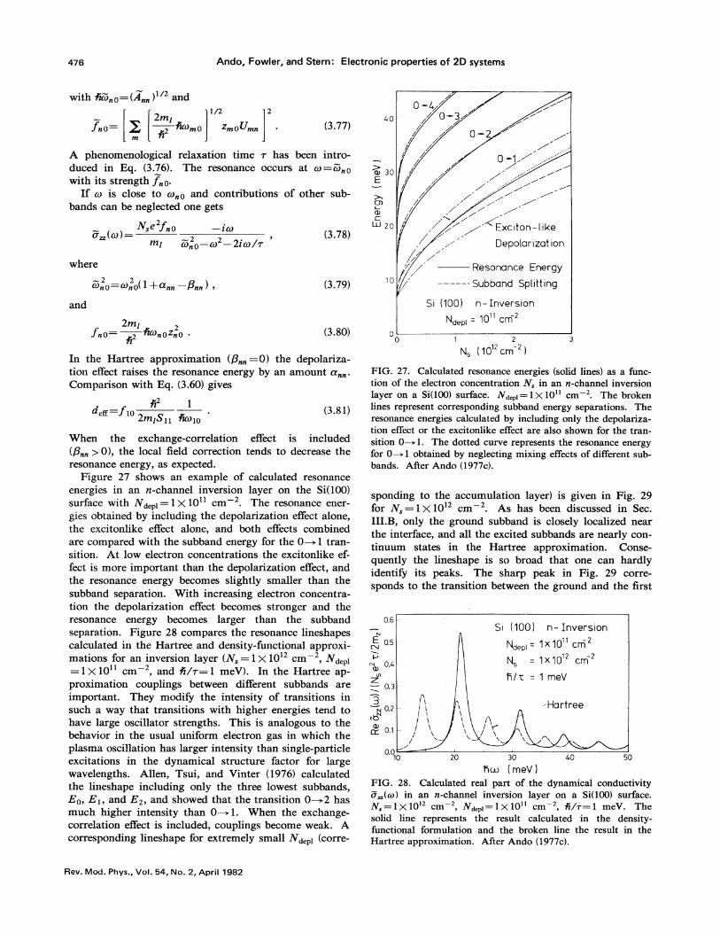
Ando, Fowler, and Stern: Electronic properties of 2D systems
with iriconp ——(Ann)'~ and
2' gf„o ——g fico p &m 0Umn (3.77)
A phenomenological relaxation time ~ has been intro-duced in Eq. (3.76). The resonance occurs at co=cenowith its strength fnp.
If co is close to ceno and contributions of other sub-bands can be neglected one gets
2+se fno —ECO(co)=-
ml COn p—CO —21ci) /1
(3.78)
C:LLj 20
oino=rono(1+ixnn Pnn ) ~ (3.79) 10
2%iIfno= ~nozno .
A2(3.80)
In the Hartree approximation (Pnn——0) the depolariza-
tion eQect raises the resonance energy by an amount a„„.Comparison with Eq. (3.60) gives
1dea=fio
2 S (3.81)
When the exchange-correlation e6ect is included
(P„n&0), the local field correction tends to decrease theresonance energy, as expected.
Figure 27 shows an example of calculated resonanceenergies in an n-channel inversion layer on the Si(100)surface wi th +d p] 1 Q 10" cm . The resonance ener-gies obtained by including the depolarization effect alone,the excitonlike effect alone, and both effects combinedare compared with the subband energy for the 0~1 tran-sition. At low electron concentrations the excitonlike ef-fect is more important than the depolarization effect, andthe resonance energy becomes slightly smaller than thesubband separation. %'ith increasing electron concentra-tion the depolarization effect becomes stronger and theresonance energy becomes larger than the subbandseparation. Figure 28 compares the resonance lineshapescalculated in the Hartree and density-functional approxi-mations for an inversion layer (N, = I X 10' cm, Nd, ~i=1X10"cm, and A/v= 1 meV). In the Hartree ap-proximation couplings between diferent subbands areimportant. They modify the intensity of transitions insuch a way that transitions with higher energies tend tohave large oscillator strengths. This is analogous to thebehavior in the usual uniform electron gas in which theplasma oscillation has larger intensity than single-particleexcitations in the dynamical structure factor for largewavelengths. Allen, Tsui, and Vinter (1976) calculatedthe lineshape including only the three lowest subbands,Eo, E~, and E2, and showed that the transition 0~2 hasmuch higher intensity than 0~1. When the exchange-correlation effect is included, couplings become weak. Acorresponding lineshape for extremely small %d,~&
(corre-
00
Si (')00) n- Inversion
N„„=&O" Cm2
1 2
N, (10 cm )
FICx. 27. Calculated resonance energies (solid lines) as a func-tion of the electron concentration %, in an n-channel inversionlayer on a Si(100) surface. Xd,» ——1& 10" cm . The brokenlines represent corresponding subband energy separations. Theresonance energies calculated by including only the depolariza-tion effect or the excitonlike effect are also shown for the tran-sition 0—+1. The dotted curve represents the resonance energyfor 0~1 obtained by neglecting mixing effects of different sub-bands. After Ando (1977c).
sponding to the accumulation layer) is given in Fig. 29for %,=1&10' cm . As has been discussed in Sec.III.B, only the ground subband is closely localized nearthe interface, and all the excited subbands are nearly con-tinuum states in the Hartree approximation. Conse-quently the lineshape is so broad that one can hardlyidentify its peaks. The sharp peak in Fig. 29 corre-sponds to the transition between the ground and the Grst
N
0.5
04
0.3-
3
0.1—
Si (100) n- Inversion
0.010 40 5020 30
Fico ( meV )
FIG. 28. Calculated real part of the dynamical conductivityo. (~) in an n-channel inversion layer on a Si(100) surface.%,=1&10' cm, Xd,»
——1)&10" cm, A/~=1 meV. Thesolid line represents the result calculated in the density-functional formulation and the broken line the result in theHartree approximation. AAer Ando (1977c).
Rev. Mod. Phys. , Vol. 54, No. 2, April 1982

Ando, Fowler, and Stern: Electronic properties of 2D systems 477
0.4
Si (100) n - Accumulation—5x)Q cm
40
E0.3
VCV
(D
0.23
CL
eV
g) 30E
Q)
LLI 20
0.010 20
hm (mev)30
0'ep
1 2
N, (10' cm )
FIG. 29. Calculated real part of the dynamical conductivitycr (co) in an n-channel accumulation layer on a Si(100) surfacefor fi/v=1, 2, and 3 meV. N, =l&10' cm . After Ando(1977c).
FIG. 30. Calculated resonance energy for the transition 0~1as a function of the electron concentration N, in n-channel
layers on a Si(100) surface. The curve for the smallest Nd, ~~
corresponds to the accumulation case. Experimental results
(Kaxngar et al. , 1974a, 19741; Kneschaurek et al. , 1976) arealso shown. After Ando (1977c).
excited subband which becomes a "bound state" due tothe exchange-correlation effect. The broad absorption atthe higher energy side corresponds to transitions tohigher quasicontinuum states. Figure 30 shows the reso-nance energy for the 0—+1 transition for different valuesof Nz, „~.The curve for the smallest Nd, ~~ actually corre-sponds to the accumulation layer. Results of infrared ab-sorption measurements (Kamgar et aI. , 1974a, 1974b;Kneschaurek et al. , 1976) are also shown. The agree-rnent between theory and experiment is excellent. Theexperimental results and also the theoretical results showthat the effect of Nd, ~~ is relatively small at low concen-trations and becomes more important with increasingconcentration. This is one of the direct manifestations ofthe importance of the additional corrections in opticaltransitions. The effect of Nd, z~ on the subband energyseparation is more important at low electron concentra-tions and becomes less important at high concentrationswhere the self-consistent potential is mainly determinedby the potential of electrons themselves.
Vinter (1977; see also Vinter and Stern, 1976) calculat-ed the resonance energy for the transition 0~1 neglect-ing the vertex correction. His result is essentially givenby Eq. (3.59), with %co&0 being the energy separation cal-culated by including the exchange-correlation effect inhis approximation as discussed in Sec. GI.B. This ap-proximation is, however, inconsistent with the impor-
tance of the exchange-correlation effect in the subbandstructure. He then tried to calculate the excitonlike ef-
fect to the lowest order in the statically screenedCoulomb interaction. The binding energy is found tovary &om 0.9 to 1.8 meV for the electron concentrationbetween 10' and 3)& 10' cm . Without calculating theintensity of the transitions, he speculated that the transi-tions to both the "bound exciton" state and the &ee statewere allowed and gave rise to the two-peak structure ob-served by the early photoconductivity experiments ofWheeler and Goldberg (1975). However, the above dis-cussion shows that the transition to the exciton "boundstate" is allowed and others are essentially forbidden (seealso Ando, 1977c; Bloss and Sham, 1979). As will bediscussed below, the two-peak structure has turned out toresult &om completely different origins.
Broadening of intersubband optical transitions causedby elastic scatterers has been studied theoretically (Ando,1976c, 1978c). The dynamical conductivity for co-co&0 iswritten as
e f&0 mg Xr.,(E)Reo (ap) = ' f(E)dE
~tnt 2M (~ Ace)0)2+—F' „(E)~
(3.82)
with
Rev. Mod. Phys. , Vol. 54, No. 2, April 1982

478 Ando, Fowler, and Stern: Electronic properties of 2D systems
1 A' fi2 ro(E) ri(E) bio(E) (3.83)
= ~X & I«k'I ~i
Iok) —(lk'I ~i
Ilk) I'&&««) —«k')) IE=.(k)+E,
k'
+~& &I(ok'
I ~iIlk)
I'&&««) —«k')+&io)
I E=.(k)+E,gt
(3.84)
where A&
represents potentials of scatterers and &. .
means an average over all configurations of scatterers.The broadening is not determined by the simple arith-metic average of the broadenings iii/ro and iiilr~ of thetwo subbands, but contains a correction term —A/~jo.The broadening vanishes when the efFective potentials ofthe scatterers are the same for both subbands and there isno intersubband mixing. In the case of a model withshort-range surface roughness scattering (see Sec. IV.C),for example, Ando (1976c) obtained
3 1
8 ~, — "-2~, ' (3.85)
which shows that the broadening is less than that deter-mined by the mobility. However, Eq. (3.84) shows thatthe relation between the mobility and the broadening ofthe intersubband transitions is not simple for realisticscatterers. Effects of Na+ ions near the interface on thebroadening have been studied experimentally. McCombeand Cole (1980) have demonstrated clearly that broaden-ing increases with increasing Na+ ion concentration butis less than the width estimated from the correspondingeffective electron mobility. This is in qualitative agree-ment with the theoretical prediction of the simple modeldiscussed above. On the other hand, Chang et al. (1980)obtained a peculiar result for low concentrations of Na+ions: The subband linewidth was independent of the ionconcentration, while the mobility changed substantially.
Effects of electron-electron collisions on the broaden-ing of optical transitions have been investigated by Tingand Cranguly (1979). They included the imaginary partof the self-energy of the first excited subband in additionto the real part, and calculated the resonance lineshape.The imaginary part was shown to have little e6ect on theposition of the resonance except at low electron concen-trations, but to contribute to broadening. Broadening ofintersubband transitions caused by electron-electron in-teractions seems to be a dii5cult problem, however. Ifone employs the same approximation as for the calcula-tion of the cyclotron resonance lineshape one gets thewrong result that electron-electron interactions causebroadening, contrary to Kohn's theorem that they do notaffect the cyclotron resonance lineshape in translationallyinvariant systems (Kohn, 1961). Further, if a similar ap-proximation is applied to subband transitions in an elec-tron system outside of liquid He, one has an extremelylarge broadening of the resonance which has never beenobserved (Ando, unpublished). Experimental results inthe inversion layer seem to show that the broadening
comes from the same mechanisms as those limiting theusual mobility (Neppl et al. , 1977; McCombe and Cole,1980), and electron-electron collisions seem to have littleinfluence.
Three different methods have been employed to ob-serve intersubband optical transitions: in&ared absorp-tion, emission, and photoconductivity. Figure 31 gives aschematic drawing of the experimental arrangement usedin absorption experiments (Kamgar et al. , 1974a, 1974b;Kamgar and Kneschaurek, 1976; Kneschaurek et aI. ,1976; Koch, 1975, 1976a, 1976b). A molecular gas laseris used as the source of far-infrared radiation. Theseparation of the transmission-line plates is the samplethickness, which ranges between 0.2 and 0.35 mm. Sincethe efFective spacing is of the order of 10 wavelengths,many modes propagate in the sample instead of a pureTEM mode. However, the presence of the thick con-ducting plate close to the space-charge layer causes the rfelectric Geld to be predominantly perpendicular to theSi-SiO2 interface. The samples lack the source-draincontacts of a regular MOSFET, and visible radiationfrom a light-emitting diode is used to generate electronsnear the interface. In the course of such experiments ithas been found that at low temperatures the inversionlayer and the bulk behave as two nearly isolated electri-cal systems because of the thick depletion layer, andtheir quasi-Fermi levels are not necessarily the same.Consequently the thickness of the depletion layer and thevalue of Nd, „ican be smaller than the equilibrium values.These values have been determined from observed capaci-tance versus gate voltage curves. The absorption of thelaser radiation at fixed energy fico is measured as a func-tion of the gate voltage VG. An example is shown inFig. 32. Positive and negative gate voltages correspondto electron inversion and hole accumulation, respectively.
St 02Al- G te
~ ) ~I//////A')V////////////T/l
Si QPv+//////////////////////////////&
Vg
Transrniss ion- Line Arrangement
FIG. 31. Sample and transmission-line assembly used for ab-sorption experiments. After Kneschaurek et al. (1976).
Rev. Mod. Phys. , Vol. 54, No. 2, April 1982

Ando, Fowler, and Stern: Electronic properties of 20 systems
Si (100) p-TypedP/dVg
Sample W 10-1hm =10.45 meV
T 4. 2 K
LEo = 004, mA
1'/o"
I I I I I II
I I I
-5 0 3 Vg (V)
FIG. 32. Intersubband resonance signals observed as a powerabsorption derivative dP jdVG and in differential absorptionwith on-off modulation of VG. P is given in terms of percentof transmitted power at N, =O and for dimensions of the sam-
ple and transmission line as shown in Fig. 31. Positive andnegative gate voltages correspond to electron inversion andhole accumulation, respectively. After Kneschaurek et al.(1976).
SI (100j n- Typeccumul ot)on
=10.45 meV
mple ASn-1
A sharp single resonance is observed for the inversionlayer. Figure 33 gives examples for the accumulationlayer. The sharp peak at higher gate voltages is the tran-sition 0~1, and a weak and broad absorption at lowergate voltages is considered to be due to transitions tohigher excited subbands which are extremely close toeach other in energy. The observed resonance energiesfor the 0~1 transition are summarized in Fig. 30. Ef-fects of negative substrate bias, i.e., the depletion fieldproportional to Nd, ~~, have also been studied.Kneschaurek, Kamgar, and Koch (1976) find a lineardependence of the resonance energy on Xd,„ifor N,values between 4.6&(10" and 6~ 10" cm
Resonant photoconductivity has also been used to ob-serve intersubband transitions (Wheeler and Ralston,1971; Wheeler and Goldberg, 1975). Wheeler and Gold-berg (1975) observed negative photoconductivities in thepresence of far-in&ared laser radiation. An exainple ofan observed change in the conductivity is given in Fig.34. Both the sharp peak and the broad structure atlower gate voltage move to higher X, with increase ofthe laser energy and are identified as intersubband opticaltransitions. However, the resonance energies obtainedare in disagreement with those of the absorption experi-ments discussed above. The electron densities X, atwhich the resonances occur are about 30% higher thanthe corresponding X, values of Kneschaurek, Kamgar,and Koch (1976), although the depletion charge Nd, ~i, ifestimated from the doping of the samples, is almost thesame. The position of the sharp peak is rather close tothat of the absorption in the accumulation layer. Fur-thermore, the photoconductive effect exhibits a complete-ly difYerent lineshape. On the other hand, Gornik andTsui (1976) detected hot-electron-induced infrared emis-sion caused by intersubband transitions. They populatedthe excited subbands by heating up the electron distribu-tion with an electric field along the surface. The energyseparations obtained were in agreement with the photo-conductivity data of Wheeler and Goldberg (1975) and indisagreement with the absorption results. The three ex-
pie ASn-2
pie S rl-3
C/lI
Z
COCL'
GE/l
—Yg (V)
10I ~ t i i I
FIG. 33. Electron accumulation signals observed in samplesfrom different batches. After Kneschaurek et aI. (1976).
0 1 2 3 4 5 6 7V9
FIG. 34. Photo-induced response as a function of the gate vo1-
tage VG for the two wavelengths 118 p,m (Ace=10.45 meV) and78 pm (15.81 meV). After Wheeler and Cioldberg (1975).
Rev. Mod. Phys. , Vol. 54, No. 2, April 1982

Ando, Fowler, and Stern: Electronic properties of 20 systems
periments were performed on difFerent types of samplesfabricated in different laboratories. The discrepancy wasat Grst believed to arise from real eFects such as inhomo-geneity of the doping or the structure of the Si-Si02 tran-sition layer. However, more recent observation of ab-sorption and photoconductivity on the same samples hasrevealed that both experiments give identical resonancepositions and similar lineshape (Neppl et al. , 1977; Kam-gar et a/. , 1977, 1978; Hu et al. , 1978). Kamgar, Tsui,and Sturge (1977; see also Kamgar et al. , 1978) per-formed time-resolved experiments and demonstrated thatthe resonance position depends on the degree to whichelectrostatic equilibrium is established in the Si substrate.Actually, difficulties in achieving real electrostatic equi-librium had long been anticipated (see, for example,Fowler, 1975 and references therein). The absence of adepletion layer in the experiments of Wheeler and Gold-berg (1975) and of Gornik and Tsui (1976) was found tobe the main cause of the discrepancy, and all the laterexperiments have con6rmed the results of the absorptionexperiments.
The mechanism of the intersubband resonant pho-toresponse is not yet understood. Wheeler and Goldberg(1975) and Hu, Pearse, Cham, and Wheeler (1978) re-
ported that the response time of the photoconductivity isvery long (of the order of 10 s) and that the signal am-
plitude is almost independent of temperature between 4.2and 1.6 K. Neppl, Kotthaus, Koch, and Shiraki (1977),on the other hand, observed a strong temperature depen-dence. As the mechanism of the negative photoresponse,Wheeler and Goldberg (1975) proposed that electronsphotoexcited to an upper level have lower mobilities,which cause the decrease in surface conductivity. This isthe same as the model suggested earlier by Katayama,Kotera, and Komatsubara (1970, 1971) for explaining anegative photoconductivity observed on InSb surfaces.Dohler (1976a, 1976b) suggested a model in which theexistence of the Eo subband plays an important role.Electrons excited into E& are scattered into Eo by inter-valley impurity scattering and stay there for a while. Al-
though this model seems to explain the long responsetime, it cannot explain a strong temperature dependence.Existence of a long-lived surface trap level has also been
proposed. Neppl, Kotthaus, and Koch (1979) proposedthat the increase of electron temperature relative to lat-tice temperature caused by absorption is the main originof the photoresponse. They could not substantiate thelong response time observed previously, and showed thatthe response time is shorter than 10 s. By applying amagnetic field perpendicular to the surface they convinc-ingly demonstrated that the photoresponse and Bo./BTdepend in the same way on magnetic field. However,they have shown also that the heating mechanism cannotexplain all the diff'erent experimental results observed indifferent kinds of samples.
Kneschaurek and Koch (1977) studied the temperaturedependence of intersubband optical transitions between4.2 and 130 K. An example of the observed lineshapes isgiven in Fig. 35. With rising temperature, the lines
Si I100) n Inversionsarnpt e p —K1%m=15.81 rneV
Nd, =1.1~10 cm
dP/dVg
A(T)/A (0j1 --4,
I
0 I I s I I a I s I / 4 ~ L
0 50 100 T fK]
T=11 K
T =28K
T=37K
=70K
T =130 K
4I I I
6 8 Vg V)
FIG. 35. Intersubband resonance at diferent temperatures forfun=15. 81 meV. The inset shows the variation of the reso-nance amplitude for the 0~1 transition with temperature.Along with the decay of the 0~1 amplitude a new resonanceassociated with the thermally populated 0' level is observed.AAer Kneschaurek and Koch (1977).
originating from the Eo subband shift and diminish inamplitude, as is shown in the inset of the Ggure. At thesame time a small extra peak appears at a low electronconcentration and grows in amplitude. The new peak isconsidered to represent transitions from the thermally oc-cupied lowest subband level of the fourfold-degeneratevalleys with light mass normal to the surface. The reso-nance position seems to be consistent with E& —Eo es-timated theoretically. One has to assume, however, avalue of Eo —Eo, which is much smaller than thetheoretical prediction, to explain the observed tempera-ture dependence of the relative amplitudes of the absorp-tions. This problem will be discussed also in Sec. VII.Bin connection with stress eff'ects. Temperature depen-dence was also studied on the (111) and (110) surfaces ofSi (Kamgar, 1979). The width of the resonance line athigh temperatures presents a problem. The experimentsshow that the increase in width is not appreciable, whilethe mobility decreases and the broadening of the cylotronresonance increases considerably with rising temperature(see Secs. IV.C and VI.B). Therefore, the experiments
Rev. Mod. Phys. , Vol. 54, No. 2, April 1982

Ando, Fowler, and Stern: Electronic properties of 2D systems 481
show, somewhat surprisingly, that neither phononscattering nor electron colhsions are e6ective in deter-mining the broadening of intersubband optical transi-tions. Quite recently experiments were extended even toroom temperature (Scha6ler and Koch, 1981; Changet al. , 1980). The resonance energy was found to in-crease considerably, rather in agreement with a predic-tion given in the Hartree approximation discussed in Sec.III.A.
All the experiments mentioned above have been car-ried out at discrete frequencies while sweeping the gatevoltage to tune the subband transitions into coincidence.This approach possesses some inherent disadvantages.Since N, and the self-consistent potential both changeduring the gate voltage sweep, it is difficult to determinethe lineshape and the relative intensities of the varioustransitions. Only in the last few years has Fouriertransform spectroscopy been applied to this system(McCombe and Schafer, 1979; McCombe et al. , 1979;McCombe and Cole, 1980). McCombe, Holm, andSchafer (1979) showed that the observed relative intensi-ties of 0~1, 0~2, and 0~3 transitions cannot be ex-plained by the Hartree result and are fully consistentwith the result of the density-functional calculation. Ashas been discussed above, the Hartree calculationpredicts a large depolarization effect, which drasticallymodifies the relative strengths of resonance intensities insuch a way that transitions to higher excited subbandshave larger intensities. On the other hand, the reductionof the depolarization e6'ect due to exchange and correla-tion makes the 0~1 transition the strongest, in agree-ment with the experiments. McCombe, and co-workershave carried out quite extensive and detailed subbandspectroscopy and have shown that there is excellentagreement with calculations over a much wider range of
p] and frequency than is shown in Fig. 30. The studyhas been extended to (110) and (111) surfaces (McCombeand Cole, 1980; Cole and McCombe, 1980), where inter-subband spectroscopy can provide information on valleydegeneracy and on the nature of the ground state. Thiswill be discussed in Sec. VII.B. Effects of Na+ ions nearthe interface have also been studied using this technique,as has already been mentioned above. They have alsoobserved transitions associated with bound states of Na+ions. This was already mentioned in Sec. II.E and willbe more fully discussed in Sec. V.C.
Different methods have been employed to observe in-tersubband transitions in space-charge layers on semicon-ductors other than Si. A simple transmission con6gura-tion in which light is incident normal to the surface canexcite subband transitions in narrow-gap semiconductorsbecause of the nonparabolic dispersion of the bulk bandstructure (see Sec. VIII.B). Resonant light scattering canalso be used in III-V semiconductors. For example,quite recent observations of spin-flip and non-spin-fiipexcitations in GaAs-A1GaAs heterostructures have deter-mined the subband energy separation and correspondingresonance energy independently, as will be discussedbrieQy in Sec. VIII.D.
D. Subbands and optical transitions in magnetic fields
'2
p, +—'H, x + p,'+ V(z), (3.86)2m' c 2mI
where we have chosen the gauge A=(H»z, H,x,O). Tolowest order in H„one immediately gets an effectiveHamiltonian for the electron motion parallel to the sur-face in the nth subband (Stern and Howard, 1967),
1 8 1 e~n px + Hyznn + py + Hzx2m, c 2m, C
+&.+,[(z')..—(z„„)'],2m, h„'
(3.87)
where I» ch/eH» ——The las.t term of Eq. (3.87)represents a diamagnetic energy shift. This shift wasfirst observed by a tunneling experiment in an accumula-tion layer on InAs by Tsui (1971a). In the case of apurely parallel magnetic field (H, =O) the dispersion isgiven by a parabola with its minimum position shifted by—z„„/l»in the k„direction. In the case of nonzero H„Eq. (3.87) gives the Landau level,
&,~ =~,(&+—,)+ [(z')„„—(z„„)']+Emt y
- with m, =eH, /m, c which is determined by the perpen-dicular component. The corresponding wave function isgiven by
1 i' z„„(x—X)4Nx(r z) expI. I2 I2
XX~(x —~)g„(z), (3.89)
Additional details of the subband structure and of thedepolarization e6ect and its local field correction appear-ing in optical transitions can be obtained by studying ef-fects of magnetic fields. When a magnetic field is ap-plied in the y direction parallel to the surface, electronsmoving in the positive and negative x directions are af-fected by different Lorentz forces and the subband struc-ture is modified. Usually in the inversion layer the ra-
0dius of the cyclotron motion (typically, 81 A in 100 kOe)is much larger than the thickness of the inversion layer,and the magnetic field is treated as a small perturbation.When the magnetic field is tilted, the perpendicular com-ponent of the field quantizes the electron motion parallelto the surface into discrete Landau levels. Although aparallel magnetic field usually has little effect on two-dimensional properties, it can strongly affect the spec-trum of intersubband optical transitions.
Let us assume that a magnetic field (O,H», H, ) is ap-plied along the yz plane in the n-channel inversion layeron the Si(001) surface. In the Hartree approximation thesubband dispersion is determined by the Hamiltonian
2
p~ +—Hyz1 e
Rev. Mod. Phys. , Vol. 54, No. 2, April 1982

482 Ando, Fowler, and Stern'. Electronic properties of 2D systems
where l, =cd/eH, and X~(x) is the usual Landau-levelwave function. The factor exp[ —iz«(x —X)/l~] arisesbecause of the shiA of the center of cyclotron motion ink space.
The above results are valid to first order in Hz. Tosecond order in Hz one should add to Eq. (3.87) a termgiven by (Stern, 1968)
2 2 Z2
(3.90)m, pyg, I4 ~„E„—E
This term gives rise to an increase of the effective massin the x direction for the ground subband:
(3.91)
This amounts to an increase of only a few percent in theeffective mass for N, =1X10' cm and Xd,~i
——1X10"cm in H„=100kO'e. Qne sees, therefore, that thelowest-order expressions (3.88) and (3.89) are usuallyvalid except in extremely strong magnetic IIIelds. Thefact that the Landau level structure is determined onlyby the perpendicular component has been utilized experi-mentally for many purposes. Uemura and Matsumoto(1971; see also Uemura, 1974b) discussed the effect of H~using a variational wave function of the form given byEq. (3.25). They ascribed an anomalous magnetoresis-tance observed by Tansal, Fowler, and Cotellessa (1969)to the effect of deformed wave functions in a parallelmagnetic field. See Sec. IV.B for a more detailed discus-sion of the experiments. Such a perturbation treatmentis not valid for higher subbands, especially in case of ac-cumulation layers, since the spread of the wave functionscan be comparable to or larger than the radius of the cy-clotron motion. A self-consistent calculation has beenperformed in the Hartree approximation in strong paral-lel magnetic fields (Ando, 1975b). The ground subbandwas shown still to be described by the lowest-order per-turbation, but excited subbands becoine magnetic surfacestates perturbed by a weak surface potential, since theyare quite extended and nearly continuum states in the ab-sence of Hz. The corresponding calculation, includingexchange and correlation effects, has also been made in adensity-functional formulation (Ando, 1978a, 1978b). Anexample of the results is given in Fig. 36. The subbandstructure becomes a mixture of the electric subband andthe magnetic surface states.
Since the optical transition occurs vertically (k conser-vation), the relative shift in k space of the energy minimaand the diamagnetic energy shift cause broadening andshifting of intersubband absorption spectra in a parallelmagnetic field. In the simplest case, where one canneglect couplings between different subbands and wherethe inagnetic field is sufficiently weak, one has
Ncr (co)= 2 L„(co)[1+y„„r.„(ro)]
mI ~no
(3.92)
where y«(=a« —P«) represents the strength of thedepolarization e6ects and its local Geld correction,~no=En —EO arid
RUSS 1 n0
occupied t ~no(kx )(3.93)
with Ace 0(k&)=E„(k) Eo(k—). In the case of y« ——0,this gives a semielliptic spectrum aroundfico„()(k = —zoo/ly) with the width A' k~(z„„—zp())milyproportional to H„. It should be noted that the reso-nance peak is not given by %co„o(k,,= —zoo/Iz)X(l+y«)' in the presence of the depolari-zation effect, but its shift is enhanced because of the de-formed lineshape (Ando, 1977b). The broadening andthe shifts of the resonance have been observed experimen-tally (Kamgar et al. , 1974a; Beinvogl et al. , 1976). Anexample of the experimental results for the accumulationlayer on the Si(100) surface is plotted in Fig. 37. Thesignal shifts to lower and lower gate voltages and thelinewidth shows an increase with increasing magneticfield. The shift of the resonance peak is found to belarger for high electron concentrations. This fact is adirect consequence of the depolarization effect, and can-not be explained by the diamagnetic shifts alone. If weneglect the depolarization effect, the effect of the magnet-ic field should be smaller with increasing electron con-centration because the electrons become more closelybound near the surface. Actually, however, both thedepolarization effect and the deformation of the lineshapebecome stronger with N, and consequently the shift ofthe peak increases with X,. Experiments have been ex-tended to the inversion layer (Beinvogl et a/. , 1976), but
100
kx /kF0
90
CAL
Vo
60
50 -5 0
k„(10cm' )
FIG. 36. An example of the calculated subband dispersion re-lation E vs k„in an n-channel accumulation layer on a Si(100)surface in a magnetic field applied parallel to the surface (the ydirection). N, =2 ~ 10' cm . H = 100 kOe. After Ando(19781).
Rev. IVlod. Phys. , Vol. 64, No. 2, April t 982

Ando, Fowler, and Stern: Electronic properties of 2D systems 483
Si {100)n-accurnuIati onhu =15.81 rneV
dPdVg
12 Ns(10 cm
FICx. 37. InQuence of a parallel magnetic Geld on the positionand line shape of the intersubband resonance in the accumula-tion layer. After Beinvogl et al. (1976).
the magnetic field effect has turned out to be very small.Figure 38 gives examples of absorption spectra for theaccumulation case calculated in a density-functional for-mulation (Ando, 1978b) and shows the broadening andshifting of the spectra. The overall asymmetry of thelineshape is consistent with the experimental results.Beinvogl et al. (1976) obtained the peak shift of BR-2.8meV near N, -0.6X10' cm and EE-3.9 meV nearN, —1 X 10' cm at Hy ——100 kOe. The correspondingtheoretical results are given by hE -2.3 meV atN, =Q.6&10' cm and AE-3.5 meV at %,=1X10'cm . The theoretical shifts are slightly smaller, but canbe said to be in good agreement with the experimentalresults.
Figure 39 gives a schematic illustration of the subbandand Landau-level structure in a magnetic field tiltedfrom the z direction. Because of shifts of the center ofthe Landau orbit in k& ky space, combinedintersubband-cyclotron transitions become allowed in ad-dition to the main transition. Such combined resonance
was first observed in a system of electrons trapped out-side of liquid helium by the image potential (Zipfelet al. , 1976a). A pair of satellite peaks, displacedsymmetrically by about the Landau-level separation fromthe main intersubband transition, was observed. In in-version and accumulation layers the existence of thedepolarization effect makes the spectrum much morecomplicated, but the observation of the combined reso-nances has been shown to provide important informationon the strength of the depolarization effect (Ando,1977b).
Let us Grst consider the simplest case discussed abovefor the case of a parallel magnetic field. The dynamicalconductivity in a tilted magnetic field is given by Eq.(3.92} with
yyf «ON)ll —f«.N ))2m' N,
& ~.o~xx (~.0)X «.x Eow } —(~—)
where
l,=—2(z„„—z~~ ),Iy
(3.94)
(3.9S}
A /
and J»(x} is the overlap integral of the Landau-levelwave functions whose centers are displaced by an amount(z„„—zoo)/l» in k„-k» space, given by
0,2
E)
0.1
200 kQe0.0
I I
//
/0~
10 20 30
~~ (meVj
FIG. 38. Calculated real part of the dynamical conductivitycr (ru) at %,=-1X10' cm for H=O, 50, 100, 150, and 200kOe in an n-channel accumulation layer on Si(100). R/&=1meV. After Ando (1978b).
FICi. 39. Schematic illustration of the subband and Landau-level structure in an inversion layer in a tilted magnetic field.The magnetic field is in the y-z plane, and the z direction hasbeen chosen in the direction normal to the surface. The twoparabolas represent the dispersion relation in the absence ofH, . Because of shifts of the center of the Landau orbit in k„-k~ space, combined intersubband-cyclotron transitions becoxneallowed in addition to the main transition. After Ando(1979c).
Rev. Mod. Phys. , Vol. 64, No. 2, April 1982

484 Ando, Fowler, and Stern: Electronic properties of 20 systems
L~ ( —,x )exp( ——,x ),Si (100) n-Accumulation
H, =35 koe
(3.96)
with Lz(x) being the associated Laguerre polynomial.The intensity of the transition ON~nX' is determinedby J~~(h„o),which is easily understood from Fig. 39.%%en 6„0~&1,we get
l, (z„„—zoo )=1 (N—+ —, )14
(3.97)
and
2 2lg (z„„—zoo)
&Nw+t~~no) =2 (&+ 2
+2 ) (3.98)
Since the diamagnetic energy shift is usually not impor-tant, the position of the combined resonances ~+0 isgiven by E„o+EN1%co&when the amplitude is suf6cientlysmall, while the main resonance is determined byE„=o(1+@«)'E„o,which is the resonance energy inthe absence of a magnetic field. Thus we can determinethe strength of the depolarization effect &om the relativeshift of the combined and main resonances in such acase. In the opposite limit H~ &~H„onthe other hand,the lineshape can be shown to approach that in theparallel magnetic field except for the appearance of aquantum structure caused by the nonzero H, .
The combined resonance was observed in the accumu-lation layer by Beinvogl and Koch (1978; see also Koch,1981), although a first attempt failed (Beinvogl et al. ,1976). An example of the experimental results is shownin Fig. 40, where the absorption derivative dP/dN, isplotted as a function of N, for fun=15. 8 meV. Themain transition is at X,—1.2&10' cm in the absenceof H~ and is shifted to higher N, with H~. We can seeat X,—1.05 X 10' cm a combined resonance for6%=+1, which splits into two peaks above Hz-50kOe, and at N, —1.7)&10' cm a weak combined reso-nance for b,N = —1. The relative shift of the main reso-nance from the center of the combined resonances showsclearly the existence of the depolarization effect (positivey~~). Figure 41 gives experimental positions of the mainand combined resonances in H, =35 and 50 kOe for suf-ficiently small H„,together with E~o, E~o+fuo„and E~o,where E~o and E~o are the subband energy separationand the resonance energy calculated in the density-functional formulation. The theoretical results for theresonance energy in the absence of a magnetic field areabout 10% higher than the experiments. This slightdifference in the absolute values is within the accuracy ofthe approximations employed in the theoretical calcula-tion. A possible error might also exist on the experirnen-tal side because of uncertainties in determining exactvalues of N, . The agreement on positions of the corn-
0.5 1.0 1.5
N, {10' cm )
2.0
FIG. 40. Experimental results of absorption in an n-channelaccumulation layer on Si(100) in tilted magnetic fields observedby Beinvogl and Koch (1978). The absorption derivativedI'/dN, is plotted as a function of X, for fico=15.81 meV.The main transition is at %,-1.2)&10' cm . %e can see atN, -1.05)& 10' cm a combined resonance for 5 jV= + 1which splits into two above H„-50kGe, and at X,—1.7)&10'cm a weak combined resonance for hN= —1. After Ando(1979c).
10
E10
E10 hu)~
H, =35 kOe
H, =50 kQe
00 0.5
vogl —Koch
0 kOe
H, -35kOeH, =50 kOe
1.0
N, {10' cm )
2.0
FIG. 41. Comparison of the theoretical and experimental posi-tions of the main and the combined transitions (AN=+1) inn-channel accumulation layers on Si(100) in tilted magneticfields. H, =35 and 50 kOe. The solid line represents the cal-culated resonance energy and the dotted line the subband ener-
gy separation for the transition from the ground to the first ex-cited subband in the absence of a magnetic field. Expected po-sitions of combined resonances are given by dashed and dot-dashed lines. After Ando (1979c).
Rev. Mod. Phys. , Vol. 54, No. 2, April 1982

Ando, Fowler, and Stern'. Electronic properties of 2D systems 485
bined resonances relative to the main resonances is suffi-cient to allow us to conclude that the calculated strengthof the depolarization effect agrees with the experiments.
A self-consistent calculation in a density-functional ap-proximation has been carried out by Ando (1979a, 1979c,1980b) for inversion and accumulation layers in tiltedmagnetic fields. Figure 42 shows an example of calculat-ed optical spectra in an n-channel accumulation layer onSi(100) for N, =1)&10' cm . A weak but distinct peakat Ace-12.7 meV is the combined resonance hN = —1.Around Ace-17 meV combined resonances hX =+1can be seen. For small H», the positions of these com-bined resonances are given by E~o+Aco, and that of themain resonance is at E~o, as expected. Although thetheoretical results explain general features of the experi-ments, especially the splitting of the combined resonance6%=+1 above H„-50kOe, there are some disagree-ments, especially concerning the strength of the com-bined resonances relative to that of the main resonance.Experimentally the combined resonances become strongerat a smaller H„,which seems to suggest that the actualfirst excited subband is more loosely bound than theoreti-cally predicted. This seems, however, to be inconsistentwith the absence of a diamagnetic energy shift in the ex-periments. Perhaps one must include a change in theexchange-correlation effect in the presence of a magneticfield to explain such details of the subband structure.
E. Interface effects
» most calculations for inversion and accumulationlayers, it has been assumed that the semiconductor-
Si (100) n-AccumulationN —1 x)0 crn
C:O
Otl)
C3
15 20
h~ (rneV)
FIG. 42. Calculated optical spectra for different values of Hyin an n-channel accumulation layer on a Si(100) surface.1V, =1&10' cd and H, =35 kOe. The numbers appearingin the figure represent values of Hy. After Ando (1979c).
insulator interface is sharp and that there is an infinitebarrier which keeps electrons out of the insulator. Butthe barrier from the bottom of the conduction band in Sito the bottom of the conduction band in Si02 is knownto be 3.1 to 3.2 eV (Williams, 1977), which will permit asmall amount of penetration of the wave function intothe insulator. In addition, the notion of a sharp barriermust break down on an atomic scale. The proper way todeal with this problem is to use the correct microscopicstructure of the interface to solve the problem withoutuse of the efFective-mass approximation. Such an ap-proach is not possible now because the interface structureis not known precisely. It would be dificult in any casebecause the interface between a crystal (the semiconduc-tor) and an amorphous material (the insulator) can onlybe dealt with approximately.
Within the spirit of the effective-mass approximation,we can deal with this problem by modeling the interfaceregion in such a way that the atomic structure issmoothed out, and by using appropriate efkctive massesfor the insulator. In this section we describe such an ap-proach for the Si-Si02 interface and for the surface ofliquid helium. For interfaces with smaller barrierheights, like those that enter in semiconductor hetero-structures, the interface becomes a central part of theproblem of determining energy levels. That case is dis-cussed brieQy in Sec. VIII.D.2.
Once electron penetration into the insulator is allowed,a sharp interface can no longer be used because thesingularity in the image potential, Eq. (3.17), cannot behandled where the wave function is nonzero. Fortunate-ly, a smoothly graded interface removes the singularityin the image potential.
Experimental evidence regarding the Si-SiO2 interfaceappears to be converging toward a model in which the Siand the Si02 are separated by only one or two atomiclayers of intermediate stoichiometry. Earlier studies us-ing Auger spectroscopy and argon ion sputtering (see, forexample, Johannessen et al. , 1976) had indicated a tran-sition region 2 to 3.5 nm wide, but other measurementsusing photoemission (DiStefano, 1976; Raider andFlitsch, 1976, 1978; Bauer et al. , 1978, 1979; Ishizakaet al. , 1979; Ishizaka and Iwata, 1980), nuclear back-scattering (Sigmon et al. , 1974; Feldman et al. , 1978a,1978b; Jackman et al. , 1980), and high-resolution elec-tron microscopy (Krivanek et al. , 1978a, 1978b;Krivanek and Mazur, 1980) have reduced this value andsuggest an interface only one or two atomic layers thick.
There are several possible ways to define the interfacethickness, as pointed out by Pantelides and Long (1978)and by Stern (1978b). One of these looks at the atomicstructure of the interface, and could lead to a zero nomi-nal interface width for the structure in Fig. 43, in w»cha plane separates the two materials. A second de6nitionconsiders the local environment of each atom, and de-Gnes the transition layer as the region in which these en-vironments differ from those in the bulk. For the caseshown in Fig. 43, the transition layer would be at leasttwo atomic layers wide. Finally, one could consider
Rev. Mod. Phys. , Vol. 54, No. 2, April 1982

486 Ando, Fowler, and Stern: Electronic properties of 20 systems
0 b c
Q a Q ~ Q I Q &i {)
0 ~ 0 ~ 0 ~ 0 &~ ()
0 ~ 0 ~ ()
0 ~ 0 ~ 0 ~ 0 ~~ ()
properties that depend on excited states of the system,such as energy gaps and dielectric properties. In thatcase the transition layer could be wider than the onegiven by the second de6nition, because the excited statescan be expected to spread out beyond the range of thepotential that is varying. It is the last of these defini-tions that enters in our case, because the barrier height,the effective mass, and the dielectric function all involveconduction-band states.
We proceed by constructing a model for the transitionlayer, calculating the image potential for this model, andsolving the Schrodinger equation for the envelope wavefunction. The parameters that vary across the transitionlayer are the eff'ective mass m„the barrier height Ez,and the dielectric constant. All of these quantities areassumed to change with the same grading function S(z).Thus we assume:
a(z) =x;„s+(ls„—ls;„,)S(z),
mz( )™zins+(mz sc mz ins)S(z) ~
Vg(z) =Eg EgS(z), —(3.99)
where S =0 on the insulator side and S =1 on the sem-iconductor side of the interface.
The simplest grading function is a linear dependencethrough the transition layer. Such a dependence hasbeen found (Stern, 1978b) to lead to unphysical loga-rithmic singularities in the image potential. To removethese singularities, Stern used a linear grading withrounded corners. The image potential is found by solv-ing Poisson's equatio~
V.a(z) VP = —4m Q5(r)5(z —z'), (3.100)
taking the potential at the position of the point charge Qminus the potential
a(z')[(z z') +r ]'~—that the same charge would give in a homogeneous medi-
a b c
FIG. 43. Schematic picture of a transition from a crystallineelement 2 to a crystalline compound AB3. The line bb is thenominal interface, but A atoms on this line have differentbonding than do A atoms on either side. The transition layercan be considered to be bounded by the lines aa and cc, andtherefore has a finite width even though the crystallographicinterface is sharp.
V(z)= Vd(z)+ V (z)+ VI(z)+ Vg(z), (3.101)
where V, (z) must be determined from a solution ofPoisson s equation with a spatially varying dielectric con-stant, and can therefore no longer be found from Eq.(3.14).
The spatially varying effective mass changes the formof the Schrodinger equation, which must now be written
A' d + [V(z) —E;]g;(z)=0 (3.102)
to conserve probability current through the transitionlayer (Harrison, 1961; BenDaniel and Duke, 1966).
For the (001) Si-Si02 interface there are two ladders ofsubbands, the twofold-degenerate lowest ladder withm, =0.916m in silicon, and the fourfold upper ladderwith m, =0.19m in silicon. The corresponding masses inSi02 are not universally agreed upon, even for energiesnear the bottom of the conduction band, which isthought to lie at k =0. Tunneling measurements havegiven values of 0.42m (Lenzlinger and Snow, 1969),0.48m (Weinberg et al. , 1976), 0.65m (Kovchavtsev,1979), and 0.85m (Maserjian, 1974; see also Lewicki andMaserjian, 1975), among others. The situation is evenmore dif5cult for the fourfold valleys, which lie awayfrom k =0 and therefore connect to points away fromthe bottom of the conduction band in the Si02. Calcula-tions for the conduction bands of crystalline Si02 (Cala-brese and Fowler, 1978; Schneider and Fowler, 1978; Ba-tra, 1978) suggest that the barrier height is -5 eV forthe energy levels connected with the fourfold valleys, i.e.,-2 eV higher than for electrons from the twofold val-leys, but tunneling measurements of Weinberg (1977) forthe (100), (110), and (111) surfaces do not appear to sup-port such a large di6erence.
Stern (1977) originally used a graded interface modelas a possible alternative to interface roughness scattering.He assumed that the penetration of the wave functioninto the transition layer reduced the mobility in propor-tion to the fraction of the total inversion-layer chargedensity that was in the transition layer. He obtainedrough agreement with experimental results. A subse-quent attempt (Stern, unpublished) to derive this mobilityreduction using the Born approximation led to a reduc-tion proportional to the square of the charge penetration
um whose dielectric constant has the local value Is(z'),and multiplying by a factor —, to take into account thefact that the image potential is a self-energy. The imagepotential energy is obtained by multiplying the potentialby Q, and is independent of the sign of Q. It is a con-tinuous function through the interface and becomes theconventional image potential for distances more than afew transition layer widths away. Note that the conven-tional image potential is attractive on the low-dielectric-constant side of the interface and repulsive on the high-dielectric-constant side.
The potential energy in the Schrodinger equation canbe written
Rev. Mod. Phys. , Vol. 64, No. 2, April 1982

Ando, Fowler, and Stern: Electronic properties of 2D systems
into the transition layer, with much too small a magni-tude. There is now increasing evidence &om work ofKrivanek and co w-orkers (Krivanek et al. , 1978a, 1978b;Krivanek and Mazur, 1980; Sugano, Chen, and Hamano,1980; Hahn and Henzler, 1981) and others for interfaceroughness of approximately the required magnitude, sothis alternative mechanism is neither needed nor theoreti-cally well founded. We should add that the values of en-ergy shifts calculated by Stern (1977) used an even moreprimitive model than the one described here and aretherefore unreliable. He found that the presence of atransition layer decreased the splitting Ep p, whereasNakayaina (1980) finds an increase using a more detailedmodel. Experimental evidence relating to this splitting isdiscussed in Secs. III.C and IV.C.
Because of all the uncertainties in the model, and moreparticularly because many of the material constants thatenter the model are not well known for the Si-Si02 inter-face, we do not show any quantitative results for energy-level shifts attributed to the interface transition layer.Laughlin et al. (1978, 1980), Herman et al. (1978, 1980),Schulte (1979), and Nakayama (1980) have all undertak-en calculations which treat the interface microscopically.Aside from the difficulty of characterizing the amor-phous oxide, first-principles calculations like those ofLaughlin et al. and Herman et aI. face the difficulty thatthey must give the subband energies with a precision oforder 1 meV if they are to reproduce subband splittingscorrectly, not an easy task when the subband splittingsare compared to energy gaps of order 1 eV or larger.
A guide to the behavior to be expected from a transi-tion layer can be obtained by assuming that the layerleads to a boundary condition on the logarithmic deriva-tive of the envelope function at the interface. If we alsoassume a simple triangular potential, we can use resultsfor the solution of the Airy equation (see, for example,Stern, 1972b) to learn that for small enough values ofg(0)/g'(0) all the subbands of a given ladder will movedown in energy by about the same amount with respectto the values obtained with the boundary conditiong(0)=0, as shown in Fig. 44. Numerical solutions ofEq. (3.102) bear this out. However, different subbandladders shift by different amounts because differentvalues of m, and E~ obtain for each ladder.
v+ I 4 z+= Vp, z&0 (3.103)
also gives a good fit to experiment with P=0. 108 nm(Zipfel and Simons, 1976, unpublished) or 0.101 nm(Hipolito et al. , 1978). Sanders and Weinreich (1976)give analytic expressions for the level shifts for a numberof cases. Calculations with more realistic microscopicsurface models should be carried out for comparison withthe spectroscopic data.
7I
Ep
Ep
LLJ
UJEI
the kind of analysis described above, without some of theuncertainties that limit its application to the Si-SiO2 in-terface. Stern (1978b) used the same approach as above,with one arbitrary parameter in the interface gradingfunction S(z). He used a barrier height Ez ——1 eV andan effective mass m, =l. lm (Springett et al. , 1967) forelectrons in liquid helium, and obtained a good fit to theenergy splitting of the first two excited subbands fromthe lowest subband (Grimes et al. , 1976). The interfacewidth (10% to 90%) deduced &om the fit is 0.57 nm,which is within the range of previous estimates. Thesame parameters also give a good fit to the recent resultsof Lambert and Richards (1981), who extended the mea-surements to higher electric fields. Calculated and mea-sured results are shown in Sec. VIII.H.
The model Stern used for the helium surface gives agood fit to experiment, but it is by no means unique.For example, the model potential
Electrons on liquid heliumEp
For electrons on the surface of liquid helium (see Sec.VIII.H for a brief review of this two-dimensional electronsystem) there are both theoretical reasons (Lekner andHenderson, 1978; Mackie and Vfoo, 1978; see also theearlier papers cited in Stern, 1978b) and reasons based onanalysis of experiments on reflection of He atoms &omliquid He (Echenique and Pendry, 1976a, 1976b; Ed-wards and Saam, 1978; Edwards and Fatouros, 1978) tobelieve that there is a gradually varying density at thesurface. Estimated interface widths are of order 0.3 to0.8 nm. Thus this system should be a good candidate for
Oo 4 5 6ala (dgldz) ),o.
FIG. 44. Effect of boundary condition at the semiconductor-insulator interface on the energies of a ladder of levels in a tri-angular potential well. The abscissa is the scaled ratio of theenvelope wave function at the interface to its derivative there.The scaling distance a is (A' /2m, eF)', where F is the electricfield in the semiconductor, and the scaling energy is E~ =eFa.The energies for vanishing derivative of the envelope wavefunction at the interface are marked at the right. AAer Stern(1972b).
Rev. Mod. Phys. , Vol. 54, No. 2, April 1982

488 Ando, Fowler, and Stern: Electronic properties of 20 systems
IV. TRANSPORT: EXTENDED STATES
A. Measuremeots
The purpose of this section is to give the reader someidea about the nature of the transport measurements cit-ed and some feeling for their accuracy. Low-&equencytransport measurements would seem to be amongst thesimplest. As in the case of solid semiconductor samples,the accurate extraction of relevant information is moredifIicult. The problem is to derive the fundamentalproperties —free-carrier concentration, mobility, trap dis-tributions, densities of states, etc.—&om the measuredquantities=onductance, Hall effect, field-e6ect mobility,magnetoresistance, capacitance, etc.
The simplest measurable quantity is the sheet conduc-tivity,
pefr=fP ~ (4.3)
where f is the fraction of the induced electrons that are&ee (i.e., not trapped or in depletion charge).
determined by the straight-line extrapolation to zero con-ductance of the turn-on region measured as a function ofgate voltage [see Fig. 45(a)]. Both thermal broadeningand trapping tend to obscure these definitions. Anoverestimate of Vz. results in low values for X, and highvalues for p, ir as compared to p. The e6ective mobilitycan also differ from the mobility p in the presence oftrapping at the interface. A simple model gives
o =eN, p =gDL /W, (4.1)
where e is the electronic charge, X, the areal free chargedensity, p the mobility, gD the source-drain conductance,L the length of a MOSFET structure as shown in Fig. 1,and 8'its width. Even this measurement can be trouble-some because of nonohmic effects (source-drain fieldsmust be kept to less than 1 Vcm ' and sometimes 10Vcm ' at low temperatures), contact resistances com-parable to the channel resistance, leakage currents, orpoorly defined channel lengths. Four-probe measure-ments can be used to eliminate contact eKects. If theconductivity can be unambiguously measured, the prob-lem is then to determine X, and p independently. Forsome three-dimensional semiconductors at low carrierconcentration this has been achieved to reasonable accu-racy by a combination of conductivity, Hall effect, driftmobility, cyclotron resonance, and other measurementsas a function of temperature, which have been carefullymatched and iterated with theory (see Smith, 1978, forinstance). Probably only for germanium and silicon arethe detailed properties accurately known, and then onlyfor the lower carrier densities.
For inversion layers a drift mobility measurement can-not be made, but there is additional information availableas compared to solids: the number of carriers can be es-timated from the gate voltage dependence of the capaci-tance and the conductance.
Several mobilities are used to characterize MOSFETs.The effective mobility
0C,„(VG —VT) 0
VT
4 6VG {volts)
{o)
IO
where cr is the small signal conductivity, C,„
is the ca-pacitance per unit area across the oxide, V& is the gatevoltage, and VT is the threshold gate voltage, depends onthe somewhat arbitrary de6nition of the threshold vol-tage or the turn-on voltage. VT is often defined as thevoltage where the Fermi level is as close to the conduc-tion (or valence) band at the surface as to the valence (orconduction) band in the bulk. Experimentally it is often
VG {volts)
{b)FIG. 45. Typical plot of (a) conductance gD and (b) transcon-ductance g as a function of gate voltage. Because of the tailsat low gate voltage, the threshold voltage VT is taken from astraight-line extrapolation of one or the other curve, but usual-
ly from g . When looked at carefully even the transconduc-tance curves show a tail near threshold, which is broadened byincreasing temperature or by interface states.
Rev. Mod. Phys. , Vol. 54, No. 2, April 1982

Ando, Fowler, and Stern: Electronic properties of 2D systems
The field-effect mobility is derived from the transcon-ductance
g~ =dIDldVGI vD (4.4)
where ID is the drain current and VD the drain voltage,and g~ is normalized for geometric factors. Then (Fangand Fowler, 1968)
VFE= C V=fl +(VG VT—) S dV +fdV
ox D
(4.5)
which illustrates the hazards of extracting information&om the field-effect mobility. All voltages are referredto the source. Because g goes to zero at threshold itcan be used to de6ne Vr, but again, because of broaden-ing effects, only somewhat better than conductance can[see Fig. 45(b)]. Many of the effective mobility data atlow temperatures discussed below were extracted by anextrapolation of the transconductance at 77 K and by use
of the Vz thus derived with the conductance data. Forconductance and transconductance measurements, closed(typically circular) structures can be made to avoid leak-
age at the edges. If the drain voltages are kept low in actransconductance experiments, capacitive feedthrough&om the gate can add to the drain current signi6cantlyand cause severe errors, particularly for W &l..
The Hall mobility p~ also need not equal the mobility
p. We can write
pH =rp =R~c(7 ~ (4.6)
where r is the Hall ratio and RH is the Hall constant.The Hall ratio is discussed in Smith (1978), for instance,and need not equal unity. It is expected to be unity forcircular Fermi surfaces at low temperatures. Hall-effcx:tmeasurements without an adequate theory of scatteringcannot unambiguously give either the mobility or thecarrier density. Thus the effects of trapping cannot beseparated &om the effects of scattering on the Hall ratiowithout a great deal of circular reasoning (Fowler et al. ,1964; Fang and Fowler, 1968; Sakaki et al. , 1970). Nocalculations of the Hall ratio except for some based onrather simple assumptions (Sugano et al. , 1973) havebeen made, even at low temperatures where only one sub-band is occupied, although Sakaki et al. (1970) inferred avalue of about 0.85 at 300 K. At higher temperatures(greater than about 40 K) a multiple-band theory is need-ed. In the absence of trapping the measured carrier con-centration,
1&a=eRH C
(4.7)
can reasonably be used to de6ne a threshold by extrapo-lation to zero carrier concentration. However Hall-effectmeasurements are more dificult than conductance mea-surements, and the samples are more complex and larger,and without special precautions, open at the edges. As isusual with Hall measurements, geometric effects must be
accounted for properly. Contact resistance effects whichcan be a problem in conductance geometry samples areavoided, at least by open-circuit Hall voltage measure-ments. The larger size increases the chances that thesample may be macroscopically inhomogeneous (Fangand Fowler, 1968; Thompson, 1978b). The open struc-tures increase the chance that leakage currents aroundthe periphery can obscure results at low K„although itis possible to make samples with guard electrodes.
At higher temperatures leakage currents through thesource diode into the substrate can result in errors whichare especially important at low carrier densities and espe-cially when a substrate bias is applied.
The C-V curves "apacitance measured as a functionof gate voltage "an be used to measure free-carrier, de-pletion, and surface trapped carrier densities near thresh-old, at least above the temperature for &eeze-out of thebulk. Sze (1969) has presented an excellent overview.Although there are many techniques for interpreting theC-V data, they are far from trivial and not uncontrover-sial. With few exceptions (Sakaki et al. 1970) carefulcapacitance studies have not been combined with trans-port measurements. Nicollian and Brews (1982) will ex-tensively review these measurements.
The capacitance can be used to characterize the sur-face because the charge is not induced within a fewangstroms of the silicon-insulator interface as it would bein a metal-insulator interface. Fast interface states areusually considered to be at the interface and are fast be-cause they empty and 611 faster than the measurementfrequency. Inversion-layer electrons are induced &omseveral to several hundred angstrom units away from thesurface, depending on field. The depletion charge can beinduced many thousands of angstroms from the surface.In general one can write an expression (Kingston andNeustadter, 1955) for the classically induced charge,
Ksce kTQ =+ ' &~4"+so2& e
—eP,exp
kT e0,+no exp
e
' 1t2
—1 +Q;, (P, ),
V.ppi =Eo.do. +4's (4.9)
and Czauss's law at the interface is applied, an expressionrelating the induced charge and the apphed voltage is ob-tained which can be differentiated to obtain the capaci-tance. Many hundreds of papers have been published on
(4.8)
where Q is the total induced charge and is positive whenP„the surface potential measured between the bulk andthe surface, is negative. Nz is the acceptor density andpo and no are the bulk hole and electron densities,respectively. Some of these points have been addressedin Sec. I. Q (P, ) is the interface state charge densityand depends on whether the states are acceptors ordonors and on the position of the states in the gap.When this expression is combined with
Rev. Mod. Phys. , Vol. 64, No. 2, April 1982

Ando, Fowler, and Stern: Electronic properties ot 2D systems
this subject. Much of the literature is reviewed in Sze(1969) and by Goetzberger, Klausmann, and Schulz(1976), Schulz (1980), and Nicollian and Brews (1982).The last esperially consider the effects of inhomo-geneities.
This classical model results in capacitance curves asshown in Fig. 4, where the e6ects of interface states areshown. VFB, the voltage for which the space charge iszero, is determined if the substrate doping is known.Work-function differences between the silicon and gatemetal and charge in the oxide or interface states canresult in displacement of VFB from zero—a built-in vol-tage. For both accumulation and inversion, charge is in-duced near the surface, and at least in thick (& 500 A)oxides the capacitance equals approximately the oxidecapacitance. In depletion the capacitance decreases asthe charge is induced farther into the silicon. Near theminimum, inversion electrons are just beginning to be in-duced with increased surface Geld.
The eFect of reduring the temperature is to sharpenthe turn-on and also to change VF& because the Fermilevel in the bulk moves closer to the valence band, whichincreases the work-function differences between the gateand the silicon and therefore changes the built-in voltagedue to differences in the silicon and gate work functions.
The results must be modi6ed to account for quantumeffects, which tend to result in the electrons being ex-tended farther into the silicon and are important whenthe oxide thickness is small (Pals, 1972b; Stern, 1972b,1974a). The classical expressions derived in Sze (1969)are not valid for oxide thicknesses less than 300 A, butno complete set of curves based on a self-consistent quan-tum theory has been published.
Another technique for counting the number of freeelectrons as a function of gate voltage is to measure theShubnikov —de Haas oscillations in the magnetoresis-tance at moderate fields as a function of VG and magnet-ic 6eld. Each oscillation contains the number of elec-trons in a Landau level which fortunately is independentof the inass (Fowler et al. , 1966). Extrapolation of a fandiagram of the location of the levels as a function of fieldand gate voltage to zero magnetic 6eld gives the e6ectivethreshold, at least where band tailing effects are unim-portant. This is illustrated in Fig. 46, where the posi-tions of the peaks in the transconductance are shown.Some spread in the extrapolated threshold determinationfor difFerent Landau levels can occur if there is a strongdependence of mobility on carrier concentration. If theaverage conductance increases rapidly at low voltagesand decreases at high voltages there is a displacement ofthe peaks which can account for this spread. Usuallytransconductance rather than conductance is used be-cause the oscillations are more pronounced, so that mea-surements can be made at the lowest magnetic fields toreduce the extrapolation range. The sparing of the Lan-dau levels gives a very accurate measurement of C,„.For thin oxides the spacing should measure the variationin zgy e
If trapping, band tailing, or depletion charge are im-
loo
I I ~ ~
80—
6o-I
UJ4C31- 4o—
x
89lOIIl2
0—p.o 40 60
GATE VOLTAGElOO
FIG. 46. A fan diagram of the peaks in the transconductanceresulting from magnetoconductance oscillations. The thresholdvoltage VT is determined by extrapolation of the peaks for thevarious Landau levels. The oxide capacitance C„canalso bedetermined to high RccuiRcy from such diagranls bccRusc whenthe nth Landau level is filled, nkcg, D{E}=X,=C „(V~—V~).After Fowler et al. (19661).
portant (as they are near threshold) no single experimentcan unambiguously give the mobility and carrier concen-trations. Most techniques are accurate to 5% or betterfor carrier concentrations above 10' /cm . An exceptionwould be in samples with many interface states whenmeasured near and above room temperature (Sakakiet al. , 1970; Fang and Fowler, 1968). The interpretationof the measurements is increasingly unreliable at carrierconcentrations below 10' cm (Fowler and Hartstein,1980a). A combination of Hall-effect, conductance,Shubnikov —de Haas, and C-V Ineasurements is reallyneeded (Sakaki et a/. , 1970). Capacitance, however, isdif6cult to measure near threshold at 4.2 K and requireslarge samples which may su6er from inhomogeneity(Thompson, 1978b; Brews, 1972a, 1972b, 1975a, 1975b;Ning and Sah, 1974) and is therefore useful on only rela-tively ideal samples. Capacitance measurements are dif-ficult to interpret at 4.2 K because the minority chargemust Aow in along a distributed-resistance-capacitor net-work from the source and drain (Voschchenkov andZemel, 1974), and because depletion charge is not readilyestablished when the majority carriers are frozen out.Use of infrared light to supply mobile charge introducesvarious photovoltages such as the surface photovoltageand Dember e6ects. However, at higher temperatures acombination of complex conductance measurements hasallowed accurate determination of mobility and carrierconcentration as low as 10 cm (Shiue and Sah, 1979;Chen and Muller, 1974).
The measurement of threshold voltage or the Aat-bandvoltage VFB is important to determine oxide charge. Italso measures the charge in fast states for flat bands, Q„
Rev. Mod. Phys. , Vol. 54, No. 2, April 1 982

Ando, Fowler, and Stern.'Electronic properties of 20 systems
(acceptor states below the Fermi level and donor statesabove). The oxide charge is taken conventionally as anequivalent oxide charge residing at the silicon-silicondioxide interface,
deeN,„=Q,„= en,„(z)dz,
dox(4.10)
where N„
is the equivalent charge density at the inter-face, d,
„
is the oxide thickness, z is the distance &om thegate to the point in the oxide where the charge concen-tration is n,„(z)measured away &om the interface. Mea-surement of the distribution of charge, which is neededto calculate scattering, is dif%cult (DiMaria, 1978).
In general the fiat-band voltage depends on the oxidecharge, the work function of the metal, and the workfunction of the silicon (and therefore on the doping of thesilicon and the temperature) so that
[(X„+E~E„) X—]-~FS = Q..
C„where X„andX~ are, respectively, the energy differencesbetween the valence band of the silicon and the Fermilevel of the metal and the conduction band of the silicondioxide, and E~ E„is the —Fermi energy of the siliconmeasured &om the valence band. X„is 4.2+0. 1 eV forsilicon and X is about 3.2—3.5 eV for an aluminumgate, depending on processing (Solomon and DiMaria,1981). Hickmott (1980) has summarized his results andthose of others and has concluded that X —X„canvaryup to 0.1S V, depending on postmetallixation annealing.The values for other metals range from 2.2 to 4.2 eV andhave been determined by internal photoemission (see, forinstance, Goodman and O' Neill, 1966).
The threshold voltage is approximately given by
Qdepl~T VFB+ +ADC„ (4.12)
where Qd, ~i (a„eX„Q~——/2n)', P~ is the potentialacross the depletion layer at the threshold for inversion(see also Sec. III.A. 1) and X„is the acceptor density inthe silicon. At low temperatures and for all but patho-logically compensated doping, Pd is approximately equalto the energy gap (1.15 V) when the source is groundedto the substrate at low temperature. However, Qd, ~i canbe varied by using a substrate bias, V,„b.
If there are interface states that are filled as the surfaceis depleted, their effect Q~/C, „must be added. If thefast states are normally neutral when filled (donors) thenVFB will be shifted but Vz. will not be, unless there arestates above the Fermi level at the surface at threshold.As can be seen, the extraction of information about thetransport properties is easier in the absence of fast stateswhich by proper processing can be reduced below 10'cm . In general, the various techniques used for extra-polation of thresholds —Hall measurements, Shub-nikov —de Haas fan diagrams, capacitance and extrapola-tion of nitrogen temperature transconductance —are ingood agreement for samples with low fast-interface-state
density ( —10' cm ) and oxides that are relatively thick(&500 A). They are not for samples with high fast-interface-state densities, as when sodium is introduced, sothat errors can be larger (10"carriers/cm ) in such cases(Fowler and Hartstein, 1980a).
B. Experimental results
1. Introduction
There is a large and confusing mass of data on trans-port in inversion layers. Only a few papers have at-tempted to survey the whole field: Fang and Fowler(1968), Komatsubara, Narita, Katayama, Kotera, andKobayashi (1974), and a series of papers by Cheng (1971,1972, 1973a, 1973b, 1974), Cheng and Sullivan (1973a,1973b, 1973c, 1974), and Sah and associates (Sah et al. ,1972b; Shiue and Sah, 1976, 1979, 1980). Most papershave attacked limited ranges of temperature or samplecharacteristics, with the result that a coherent picture isnot obvious. Here we shall attempt to give some coher-ence to the experimental results by examining primarilyconduction of electrons in the unactivated regime mainlyon the (100) silicon surface. (We ignore weak localiza-tion here; it will be discussed in Sec. V.B) The (100) sur-face has been studied most because it has the highest mo-bility and the most nearly perfect oxides of any of the sil-icon surfaces. It also leads to a simpler theory because itis orthogonal or parallel to all the principal axes of theconduction-band minima. Hole conduction has beenstudied in far less detail and is discussed briefly in Sec.VIII.A.
In general at room temperature the electron mobilityin the surface is less than in the bulk because of in-creased scattering. However, at low temperatures it ishigher, partly because the electrons are in the lowest sub-band so that the effective mass parallel to the surface islight and partly because they are separated &om theircompensating positive charge in the gate, so thatCoulomb scattering is reduced.
The general characteristics are illustrated in Fig. 47,where Hall-mobility data are shown as a function ofN,:(ecRH) ' —for two samples, both with 2-ohm-cm @-
type substrates for V,„b——0. The high-mobility samplehad a 990 A oxide and was annealed at 1000 C in N2after oxidation; the low-mobility sample had a 500 A ox-ide and was not annealed in N2 at high temperature.The first had an oxide charge of (6+2)X10' cm andthe latter (13.4+4) )& 10' cm
The di6erences between these samples are most strik-ing at 4.2 K, although the samples show the same gen-eral variation of mobility with X, and T. At 4.2 K thereis a smooth rise in mobility as X, increases, followed bya decrease. At low X, the maximum mobility is 18000cm V ' s ' for the low-oxide-charge samples. Thehigher-oxide-charge sample had a maximum mobility ofonly 4000 occuring at higher W, . At high values of X,the mobilities approach the same values and decrease as
Rev. Mod. Phys. , Vol. 54, No. 2, April 1982

4g2 Ando, Fowler, and Stern: Electronic properties of 2D systems
lo4-
IO43777I3OOHM cm(Ioo)IIOOA OXIDE
'oOP
l03—E
IO3OJECP
IO4
l02lOlo lOII
I I
lol2
(ec RH) I-cm 2lol'
KlO
& lo2—C34JU
UJ
IO3
FIG. 47. Hall mobility as a function of 1/ecR~ ——NH for twosamples. The solid curves are for a sample where
X,„=(6+2)~ 10' cm . The dashed curves are for a samplewith N,„=(13.4+4) &10' cm . Data are shown for 300,77.3, 28, and 4.2 K. The overlap of the 77.3 K data for lowoxide charge and the 4.2 K data for high oxide charge over alarge part of the range is coincidental. All low-temperaturecurves approximately coincide at high values of X,. AAerFowler (unpublished).
I
IOI
IOOI02
IOOO
FIG. 48. Typical temperature dependence of the effective mo-bility p,g for an n-channel device. The carrier density X, inunits of cm is given by 2&(10" Vg, and the value ofV~ =(VG —Vz) in volts is indicated for each curve. The oxidecharge X,„wasabout 2&10" cm . The upper and lower setsof data are displaced. After Fang and Fowler (1968).
about N, to a value of about 1000 at N, =10'3 cmGenerally, this behavior can be ascribed to oxide chargescattering, which decreases as N, increases, and surfaceroughness scattering, which increases with K„althoughother mechanisms may affect the mobility to a lesser ex-tent, especially near threshold.
The mobility is seen to decrease between 4.2 and 77 Kat low X, but is relatively temperature independent athigh N, . At low carrier concentrations depending onX,
„
the temperature dependence can reverse sign. The77 K data also show some structure that will be dis-cussed below.
At 300 K the mobility is lower than at lower tempera-tures over most of the range of N, and is much lessdependent on N, or N „.This is a range where oxidecharge scattering should be weak, the conduction-bandelectrons are not degenerate, many subbands contributeto the conduction, and phonon scattering should bestrong.
Representative plots of the temperature dependence asa function of N, are shown for samples with high N,
„
(-2X 10 ' cm ) in Fig. 48, taken &om Fang andFowler (1968). Similar extensive data may be found in-that paper —all for low-m os hty samples —and rnKomatsubara et al. (1974). Generally there is a strongincrease in p,~ with increasing temperature forN, &2—10&&10" cm which can be activated (Fangand Fowler, 1968). Above this N, range the mobilityvaries weakly in high N,„samples in complex fashionuntil it decreases at high temperatures as about TIn high-mobility samples the temperature dependence ofresistance can be stronger and has been reported as highas T (Kawaguchi and Kawaji, 1980a) below 10 K.
Below we shall discuss in more detail these and otherdata, dividing the data generally into the ranges around300 K, near 4.2 K, and 4.2 —90 K for electrons on (100)silicon samples. In Sec. IV.B.5 some other cases will bediscussed briefly.
2. 300 K range
As may be seen in Fig. 47, the mobility is nearly con-stant or decreases slowly over the entire range of X, atroom temperature. This result differs &om early resultsof Fang and Fowler (1968), where an initial increase wasobserved as shown in Fig. 49. The samples showing a
700HII36 A 95o~ ll20 A Iso
600 —X I I46 F 6o' II27 A I o
t& 500-
C4
E", 400-
~ 300-
200—
IOO—
0I 0'
I I I
IPIO IPI I I012
SURFACE ELECTRON CONCENTRATION -cmIOI5
FIG. 49. Hall mobility pH for a sample with large oxidecharge (2X10" cm ) as a function of (ecRH) '=X, at 300 C.Note the decrease in pa at low X,. After Fang and Fowler(1968).
Rev. Mod. Phys. , Vol. 54, No. 2, April 1982

Ando, Fowler, and Stern'. Electronic properties of 2D systems 493
l200 ~
I IOO-
IOOO —iC3
SURFACE CHANNEL
(I I I) (I IO) 032670(I I 0) (I IO) 0 I I 970
~ (IOO) (I IO) 03 I I70&DCO
I
O
AlE
C3
900—gO
800—
700—
NA=2. 2 x IOI4 crn ~
T=25 G
500 i 1 i l s I ) I I &I t I
0 2 4 6 8 IO l2
0+ OT QSS/q ( 0 / re
FIG. 50. Effective mobility at 298 K at low carrier density asa function of total oxide charge. Note that the samples made
on the (100), (110), and (111) surface lie on the same curve.Af'ter Sah et al. (1972b).
decrease of p,g at low N, are characterized by oxidechanges of 2X 10" cm or greater.
Brews (1972a, 1972b, 1975a, 1975b) has considered theeffect of spatial fluctuations in N, resulting from fluctua-tions in N,„and has concluded that p-(1 ——,(o, )),where (o., ) is the variance of the surface potential. Heconcludes that for N,
„
less than 3)&10I cm no de-crease in mobility with decreasing N, should be seen, atleast down to N, =3&10 cm, whereas a maximumshould occur at N, =10" cm for N,„=3&&10"cmThis is consistent with Fig. 49, where there are about2)&10" cm oxide charges, and Fig. 47, where the ox-ide charge is low. Comparison with data of Chen and
Muller (1974) and with Shiue and Sah (1979) also bearsout his conclusion, although the latter have a somewhatdifferent explanation. The latter have carried out mea-surements to values of N, as low as 10 cm and do ob-serve a small decrease in mobility below 10 cm insamples with N» —1.4 & 10" cm . However, theirsamples with No„——1.17& 10' cm show only a slight-ly greater decrease, even though pm»-600 cm V 'sas comparIxl to 1000 for the better samples.
In the now more generally studied samples with
N,„&10"cm the mobility is quite flat versus N, for10' &N» ~ 2& 10" cm with mobilities over 1000cm V 's ' for the best samples. Figure 47 demon-strates thai the oxide charge contributes to the scatteringeven at 300 K and that an oxide charge difference ofabout 7.50(10' cm has reduced the maximum 300 Kmobility by about 30%%uo. This is clearly shown in Fig.50, taken from Sah et al. (1972b), where a mobilitydependence on N,„wasmeasured. The mobility did notdepend on crystal orientation. As N, increases, the mo-bility decrease is initially weak but grows stronger as N,approaches the range where surface roughness scatteringmay become important. No simple power 1aw in N,
describes the variation. For 10' ~ N, & 5 ~ 10' cmagain no power law seems to obtain in N„but the depen-dence is roughly as (N, +Nd, ~I)
'~ . Calculation of thescattering in this range is very difficult because manysubbands are occupied and because inter- and intra-subband scattering and optical- and acoustic-phononscattering are involved, as is surface roughness scatteringat high N, . Probably the best comparison with phononscattering theory could be made at N, =2 —5 & 10'cm in the cleanest samples.
In the 300 K range the mobility varies as about T(Leistiko et al. , 1965; Fang and Fowler, 1968; Komatsu-bara et al. , 1974) although acoustic-phonon scattering forone subband (which is not realized at high temperature)should follow a T ' law (Kawaji, 1969). Sah et al.(1972b) found somewhat weaker temperature dependence.Phonon scattering is discussed theoretically in Sec. IV.D.
It should be noted that in this temperature range theFermi level is usually below the conduction-band edge,so that interface states can change occupancy with sur-face field and temperature as discussed by Fang andFowler (1968), Sakaki, Hoh, and Sugano (1970), and Sahet al. (1972b). The surface state contribution to thescattering can vary, depending on temperature and onwhether the states are donors or acceptors.
3. 4.2 K range
At 4.2 K the electrons are generally in the quantum
limit, in that only the lowest-energy Eo subbands are oc-cupied in a perfect unstrained sample. Gn the (100) sur-
face these have spin and twofold valley degeneracy.
Furthermore, as is well known, Matthiessen's rule may
be applied with confidence at 4.2 K to separate the vari-
ous scattering mechanisms. As noted above, there is a
large body of experimental data for samples with dif-ferent N~„. However, as noted in Sec. IV.A, the estimateof N,
„
is difficult for small values and for thin oxides.Furthermore, the location of the charge in the oxide isnot usually known. The data are usually compared totheory for the different scattering mechanisms added ap-propriately. Another approach to the problem ofseparating the contributions of the diff'erent scatteringmechanisms is to vary the oxide charge methodically.Even though the absolute value of N,„may not beknown, the change may be determined accurately. Theoxide charge can be varied by annealing as in Sah et al.(1972b) and Tsui and Allen (1975). The position of thisoxide charge is not known precisely. Oxides can begrown with known densities of neutral electron and/orhole traps that can be filled by charge injection(DiMaria, 1978). Even though the positions and densi-
ties of these charges have been measured, an experimentusing trapping in the oxide has not been done. Double-insulator structures such as MNQS (metal-nitride-oxide-silicon) devices may be used (Pepper, 1974a), but thecharge distribution again is not accurately known.Another approach is to drift sodium ions from the metal
Rev. Mod. Phys. , Vol. 54, No. 2, April 1982

494 Ando, Fowler, and Stern: Flectronic properties of 2D systems
10 I I I I I I I I
C30)
10
EO
0.831.63.86.5
8.3
1 ~
1 I
10O 14.5
20.2
10I I I I I I I I
to the silicon interface (Harstein and Fowler, 1976, 1978,1980b). The Na+ ions have been shown to reside verynear one or the other interface (DiMaria, Aitken, andYoung, 1976; DiMaria, 1978). Besides introducing 6xedoxide charge, the sodium also introduces acceptor surface
2.0
1.5
CARRIER DENSITY (cm )
FIG. 51. Some of the extensive measurements on a set of sam-ples in which N,„,the oxide charge density, was varied bydrifting Na ions through the Si02. The effective mobility p ffis plotted as a function of the carrier density N, . The mea-surements were made at 4.2 K. After Hartstein et aI. (1980).
states (Fowler and Hartstein, 1980a) which are neutral-ized before the inversion electrons are induced. Tkis ap-proach was used methodically to vary the mobility withN„Nd,„i,and N,„.The mobility varied as a function of%, and %, at V,„qequal to zero, as shown in Fig. 51.At constant N, the data were fitted to
p,g' ——c +a%,„+bN„. (4.13)
The first term represents scattering that is not a functionof N,„and to first order was assumed to be primarilyp&z', the reciprocal of the surface roughness scattering.This amounts to an assumption that there is no interac-tion between surface roughness scattering and oxidecharge scattering. Values of the intercept are shown inFig. 52 plotted versus (Nd, ~i+N, ) for different substratebiases. This plot most nearly rectified the curve and wasfar better than a plot versus (Nd, „i+N,/2) . Compar-ison of these data with theory is made in Sec. IV.C.Sugano et ar. (1980) have reported significantly increasedsurface roughness scattering on severely roughened sur-faces. Earlier, Cheng and Sullivan (1973c) and more re-cently Kohl et al. (1981) observed increased surfaceroughness scattering as a result of treatments whichroughened the surface, although the latter ascribed theeffect in their treatment to an increase in neutral defects.It should be noted that the failure of the curve in Fig. 52to intersect the axis at 0 is an indication of an additionalscattering mechanism.
The reciprocal of the linear coef5cient a in Eq. (4.13)is shown in Fig. 53. As may be seen, this part of thescattering decreases with N, . These results are comparedwith theory in Sec. IV.C. The quadratic term presum-ably arises from multiple scattering events. It is onlystrong for low values of N, where kF is long as com-pared to the (N,„)'~. It is shown for N, =2X10'
1.0I I I I I I
0.5x —80K
—4.2 K
0.00 50 100
2I+ N izv)
150 200
X
x oX g
~ ~
FIG. S2. The intercept of p,g', the reciprocal of mobility,when extrapolated to N,„=Ofrom a plot against N„,is plot-ted versus (Nd, » + N, ) . The mobility is in units of 10cm V 's '. Nd~~, the number of charges per unit area in thedepletion layer, and N, (called Nqwv in the figure), the numberof electrons per unit area in the inversion layer, are in units of10' cm . %'hile it is assumed that the scattering for N,„=Ois primarily due to surface roughness scattering, the failure ofthe curve to intercept the origin indicates an additional scatter-ing mechanism. Data are for various values of substrate biasvoltage V,„l„i.e., for different values of Nd, ~~ as well as N, .After Hartstein et al. (1980).
10I 1 I I I i I
10
CARRIER DENSITY (cm )
FIG. S3. The reciprocal of the linear coeNcient a, taken fromfitting p,~' ——c+ aN,„+bN „,as a function of N, at 4.2 and80 K. The data were taken from Fig. S1. After Hartsteinet al. (1980).
Rev. Mod. Phys. , Vol. 54, No. 2, April 1982

Ando, Fowler, and Stern: Electronic properties of 2D systems 496
cin in Fig. 54 as a function of temperature for differentsubstrate biases. As may be seen, it decreases rapidlywith increasing temperature. It is only measured at lowN, . On the other hand, the temperature dependence ofthe linear term a is much weaker and depends on N„asmay be seen in Fig. 55. At low carrier concentrations, aincreases with temperature. Unless this increase is takeninto account in analyzing the weak temperature depen-dence of p &om phonon scattering, for instance, errorswill result. Oxide charge scattering is compared totheory in Sec. IV.C.1.
Other scattering may obtain at 4.2 K that may modifythe simple picture above. Below 30 K a negative magne-toresistance has been reported (Eisele and Dorda, 1974a;Kawaguchi et al., 1978a, 1978b; Kawaguchi and Kawaji,1980b, 1980c) that was at first attributed to the decreaseof some scattering mechanism in a magnetic field. Itvaries as N, '. It depends only on the normal com-ponent of magnetic field, in contrast to an effect in InAs(Kawaji and Kawaguchi, 1966). Similar effects havebeen seen on n-channel (111) samples and on p-channeldevices. The effect is quadratic at low fields and satu-rates at about 1 —1.5 T. The saturation value of themagnetoconductivity change has a maximum value of4% at 4.2 K, decreases with increasing temperature, andvanishes at about 30 K. The quadratic dependence ofthe magnetoconductivity on magnetic field follows aCurie-Weiss law. Dorda found that the effect decreasedwith large surface state density. Attempts to explainthese effects on the basis of spin-spin scattering seem fu-tile because of the dependence on the direction of mag-netic field. Recently this effect has been related to locali-zation effects (Kawaguchi and Kawaji, 1980b; Hikamiet al. , 1980) discussed in Sec. V.B.
Inability to fit experimental results, especially at lowN„itwh theories of the major scattering processes hasled to the postulate of an additional short-range scatter-ing mechanism (Matsumoto and Uemura, 1974; Takada,
1979) sometimes called neutral impurity scattering.Neutral impurities are difIicult to detect except possiblyby trapping (DiMaria, 1978) or by electron spin reso-nance; so are charge dipoles (Hess and Sah, 1975). Thenature of these scatterers is elusive but Yagi and Kawaji(1978, 1979) associated them with growth parameters, ashave Kohl et al. (1981). They found that the maximummobility decreased &om 10 to 7.5X10 cm V 's ' asthe oxide thickness was reduced &om 2700 to 910 A.However, samples with different processing can showmobilities of 2)&10 cm V 's ' for a thickness of 990A (Fig. 47). These results may be related to surfaceroughening results reported by Sugano et al. (1980) andto the final oxidation rate and the oxygen defect gradientat the silicon interface.
The temperature dependence of the mobility near 4.2K has been the subject of extensive study and of somecontroversy. As may be seen in Fig. 48, there is a signi-ficant temperature dependence for high values of gatevoltage or carrier density above the activated regime. Inhigh-mobility (or low-oxide-charge) samples the mobilityshows a somewhat smaller decrease with increasing T,but as in the low-mobility samples illustrated by Fig. 48the effcx:t decreases as N, increases. These effects havebeen studied by Cham and Wheeler (1980b) as a functionof the maximum mobility, which is a measure of the ox-ide charge scattering in the sample, by Kawaguchi andKawaji (1980a), and by Kawaguchi, Suzuki, and Kawaji(1980). Earher papers such as Fang and Fowler (1968)or Komatsubara et al. (1974) contain some of the samedata, although they have not reduced the data in thesame way, nor gathered data with such care when thevariations with temperature were small. The more recentpapers have presented the data by extrapolating the re-ciprocal mobility data to T =0 and subtracting the extra-polated value of I/r from the value at any given tem-perature. The difference is labeled I/rT. It is not clear
O0)M
C4
EO
D
l~ I I I I
~ —15 V~ —3Vx OV
.5V O0)M
I
LA
C)
5 I I I I 1 I
131.2 X 10
7X10X
3X10
X X
~ ~
0 I I I I I 1 I
10
X
100
0 I I I I I I I
10
TEMPERATURE (K)
100
TEMPERATURE (K)
FIG. 54. The coef5cient b of the quadratic term, for the samefit described in Fig. 53. These data are for N, =2&& 10' cmAfter Hartstein et al. {1980).
FIG. 55. The temperature dependence of 1/a, the reciprocal ofthe linear coefficient, as described in Fig. 53, for three valuesof X,. After Hartstein et aI. (1980).
Rev. Mod. Phys. , Vol. 54, No. 2, April 1982

496 Ando, Fowler, and Stern.'Electronic properties of 20 systems
that this procedure has any simple physical meaning. Itmay lead to erroneous conclusions if more than onescattering mechanism is involved but, especially whenthe temperature variations are small, it is convenient.Some of the raw data of Kawaguchi and Kawaji (1980a)are shown in Fig. 56. Kawaguchi and Kawaji (1980a)have, in addition, corrected for the negative magne-toresistance efFect, although it is not clear what the justi-fication for so doing is or at least how it should be doneproperly. The extrapolation to T =0 is also dangerous,especially when the logarithmic effects arising from weaklocalization are important (see Sec. V.B).
Kawaguchi and Kawaji (1980a), using these pro-cedures, found a very strong dependence of 1/rT on tem-perature, which they ascribed to phonon scattering al-though they remarked that theory predicted a muchweaker magnitude of phonon scattering. Cham andWheeler (1980b) and Kawaguchi et al. (1981) foundmuch weaker temperature dependence (about T' ).The former concluded that the effects arise primarily&om the temperature dependence of other mechanismssuch as oxide charge scattering and surface roughnessscattering. The temperature variation for these processesarises primarily from the temperature dependence of thescreening and has been calculated in a simple approxima-tion by Stern (1980b). Stern's calculations for the tem-perature dependence of impurity scattering have alsobeen compared with the results of Hartstein and Fowler(1980) (see Fig. 55), and good agreement was found forN, =3X10" cm . All of the experiments discussedabove require extreme care in measurement because oftenthe changes with temperature are small. The extractionof the data in terms of 1/rr is not straightforward, andthe interpretation involves at least oxide charge, surfaceroughness, and phonon scattering and possibly otherscattering mechanisms, so that this problem remainssomewhat unresolved. This has a bearing on the weak
localization effects discussed in Sec. V.BPiezoresistance effects have proven a valuable tool for
the study of transport at 4.2 K. These have been studiedby applying stresses in various ways —most extensivelyand controllably by bending bar samples (Colman et al. ,1968; Dorda, 1971a; Dorda and Eisele, 1973; Dordaet al. , 1972a; Eisele et a/. , 1976a; Eisele, 1978; Geschet al. , 1978), by studying silicon on sapphire (Kawajiet al. , 1976), and by using epoxy cements (Fang, 1980).The effects arise primarily because of the displacement ofthe valleys lying along axes with diFerent orientations tothe stress. For the (100) surface a compressive stressalong the [010] direction lowers the valleys in that direc-tion relative to the (100) and (001) valleys. Enoughstress can lower the (010) and/or (001) valleys which arethe subbands with light mass perpendicular to thesurface —the primed subbands —below the (100) orunprimed subbands, especially if the surface quantumsplittings, Eo Eo, are—small (N, and Nd, ~~ small). An-isotropy results &om such stresses and has been studiedby Dorda (1973). Typical results are shown in Fig. 57.The mobility decreases as the electrons transfer to theprimed valleys. Dorda and Eisele (1973) have concludedthat there may be an intrinsic stress of 80 Nmm; onthe basis of other arguments (Eisele, 1978) they estimatean average stress of 10—50 Nmm . Nicholas et al.(1976) have estimated a stress of 30 Nmm using an op-tical technique. These estimates are for the average mac-roscopic stress. Local stresses may be higher. The localand macroscopic stresses may vary depending on samplesize, oxide thickness, and on whether the sample is free-standing or bonded to a metal or ceramic header. Thereader should refer to Sec. VII.B for further relevantcomments.
Electron transfer e6ects are demonstrated if the field-
500-0E0
400—)CA
CAQJ~ 300-
I I
NS= I. I x IOI2cm-2
:MOS (IOO)N5-IO
~ 3.3
5.34.2
, i 40- &inv(10 m )
50
50, 300P(Nmm )
200 I
IO 20 30 40 50TEIVIPERATURE (K) compression tensiori
FIG. 56. The temperature dependence of the resistivity of a(100) silicon inversion layer. The parameters are the electrondensities N, . After Kawaguchi and Kawaji (1980a).
FIG. 57. Relative change of conductivity Ao. /o. o for a (100)surface with current and strain in the [010t direction at 6.4 K.After Dorda and Eisele (1973).
Rev. IVIod. Phys. , Vol. 54, No. 2, April 1982

497~ ) 2D sy$tefAyoperties o~ E)egtronic p«ller, and $tern:Ando Fo
e.as a nfu ction of N, wp(Eisele, 197;
the case wherers
g.
k under stressfrom the (00
t'
n-Pt ess sphttmg.f the electron
the stress
&o hall o e
f subbands.axima arise
in le set o sue mea-
ptmp as' effects o
s butemphasizmg the e
the right shape oful in giving t e ha ewere bad y1 offmm ' e.
ed further in Sec.cuss
4. 4.2-90 K
of the comple'
ylexityand 48 demonstra aie some o
or low N, cmre range.the con u
and1 reparatio
hFowleI',
incrscattering may r
I24
2CIA
Vs
h r temperat res ofde charg'th»gh ",bband'
980) ha"his range ', Fowler, an
d pendence o972b) . Ha&
h temperat. Na+ ions
t,emp ted to resh sms by d
d applyingscatte g
scatte gb )0 K.
severa
Matthiessen s1' ht increase w
t ring attemper "",
dependenc o.h eciproca
The fempe rature . I e rFig. SS.nd deere
c~&cient is shownnear] y atincreases
e mo
scattering
feature of thhigh Ns.
0 shows an .the moblli y
interesting . ;t versusFi ure 47 a
inflectio»"7 & This is
42 K a»,nsat77
bility abov10~ cm elec
obicurve
in the 6ei~ b~ Fang a
abouteffect mo
nobser"ed
e as reportd on
most ea ' y1 tion charg
erature»low deP e 1
on tempPles with
h dependencesd Fig 60, resp
Fowler (19h wn in F g.
threshold a
68). T.
59 ant 77eak may be
bias are s oseen near
temperature is re-
~
ly A sha~, .d]y as the t
k is striking'78) in Fig 5
. This peak
PEjsele (19prressure by
to ma e Eo'&mena Simheno
stress . Fi S9 m aase &om p(1975b) andQrews
1n e data in gggested by
~ ome elec-, effects a' '"to the stress
Dorda {1978).Gesc E1sele, a
20—I500—
l250—
I
C4E
!000—I—
Kl
750—LLJ444J
500—UJU
297 K
250—
I-2
Cfll
0—I I
4 5I I
2 30
x)0 -12
under
~ inv
Easact mobility p~E nc6 -lcornmpressive stress a . K.
i.LJ
0I
20 50GATE VOLTAGE
l0 50 60400-lo
s res on as temperatuai variousct mobihty'
sAft F(100) surface.
h s., Vol. 54, No. 2, Ap ril 1982Rev. Mod. Phys. , Vol.

Ando, Fowter, and Stern: Electronic properties of 2D systems
trons can occupy the fourfold subbands even if they arenot lower than the twofold. Gesch et a/. were able to af-fect this structure at 77 K under stress. The peaks couldbe enhanced if there were intrinsic strains in the surface.The common appearance of two and sometimes morepeaks might arise from an inhomogeneous strain or fromsplitting of the (010) and (001) subbands. These peaksare suppressed with substrate bias or as the doping is in-creased because both increase Nd, p&
and thereforeEo Eo. —Komatsubara et al. (1974) have seen morecomplex behavior that depends on the samples. They at-tributed some of the structure to interface bound states.This was later also suggested by Tidey and Stradling(1974). As shown in Fang and Fowler (1968),d(R~ ')/d VG increases slowly and smoothly through thisrange in samples where this structure appears, but theHall mobility shows the same structure as the eFectivemobility. Trapped electrons would not give the highmobility observed in the first peak. On the other hand,these data could be consistent with a two-band model ofthe Hall eRect.
When these peaks are observed an anomalous magne-toresistance is also seen (Tansal et al. , 1969; Sakaki andSugano, 1969) when the magnetic field lies in the siliconsurface. It follows the law bg/g =aHX I+PH .Uemura and Matsumoto (1971) have ascribed the qua-dratic efFect to a diamagnetic shift in the ground-statewave functions, but have not calculated the change inEQ' EQ The direction of the Lorentz-force term is in adirection to increase this splitting and so to transfer elec-trons to the low-mass valleys.
Clearly the behavior of the transport properties in thisrange is complex. For a simple comparison with theoryit is probably best to work with a maximum subbandsplitting, which corresponds to large Xd,„~.
5. Other surfaces —n channel
We have concentrated on the (100) surface becauseeven with its complexity it is the simplest and the moststudied. This does not mean that the other primarysurfaces —(110) and (111)—have not received attentionand do not have many interesting phenomena associatedwith them. Indeed, the apparent anomalies in valley de-generacy have been of very great interest. In general, themobilities on surfaces other than the (100) are lower and,except for the (111), are anisotropic. Sato et al. (1972),Sah et al. (1972b), and Arnold and Abowitz (1966) haveshown that there is a strong correlation with the oxidecharge. The Geld-effect mobility dependence is shown inFig. 61. Results for planes vicinal to the (100) planegenerally show a peak in the field-e6'ect mobility at lowN, at 77 K, but those for the (111) and (110) planes donot. The temperature dependence of pFE for all planes issimilar to that of the (100) surfaces above 77 K. The an-isotropies increase as the temperature is reduced (Satoet al. , 1971; Sah et al. , 1969; Sakaki and Sugano, 1972a).
6. Noise
The subject of noise in metal-insulator-semiconductordevices has a substantial literature that is only partiallyrepresented in the bibliography (Abowitz et al. , 1967;Aoki et al. , 1977; Berz, 1970a, 1975a; Berz and Prior,1970; Broux et a/. , 1975; Das and Moore, 1974; Flinnet al. , 1967; Fu and Sah, 1972; Jindal and van der Ziel,1978; Katto et al. , 1977; Klaassen, 1971; Nougier et al. ,1978; Park et al. , 1981; Sato et al. , 1969; Vandamme,1980; Voss, 1977, 1978). Many authors find a correla-tion between the amount of I/f noise and the density ofsurface states, but there is no general agreement as to de-tails of mechanisms. Noise is not discussed in any detail
2000— 5000~OO)zon" == (Oli) zone
0Cl
I
EEJ
LallL.
I OOO—+I Y~0
-2—5-IO-20-30
2000
1
~ IOOO
~ 500
0.5 I
F~ (IO V~cm)
l
(OOl)(Ol 5)(025)(O l I ) (l l I) (522) (3ll) (all) ( lOO)(2l l ) (4ll)
SURFACE OR)ENTATION
FIG. 60. Field-effect mobility as a function of X, for varyingsubstrate bias at 77 K for different values of surface electricfield I', (proportional to N, + Kd,PI). After Fang and Fowler(1968).
FIG. 61. Dependence of field-effect mobility on surface andcurrent direction at 77, 208, and 298 K for X,=3X10' cmThe mobility is highest on the (001) surface, for which the ox-ide charge is lowest. AAer Sato et al. (1971a).
Rev. Mod. Phys. , Vol. 54, No. 2, April 1982

Ando, Fowler, and Stern.'Electronic properties of 20 systems 499
in this article. For a recent review, see Hooge et al.(1981).
vanishing q. The screening effect can be included withinthe linear approximation by dividing vz"'(z; ) by thedielectric constant s(q) with
C. Scattering rnechanisrns at low temperatures
1. Coulomb scattering
(p) Z e(p)V, (r,z)= [(r—r;) +(z —z;) ]2 2 —&l2
K
for z; & 0, and
Z(~'e'Vty, )( )
~ [(r r )2+(z )2]—1/2
(4.14)
The scattering &om charged centers in the electricquantum limit has been formulated by Stern and Howard(1967). We briefly review the theory in this section. Weconfine ourselves to the n-channel inversion layer on theSi(100) surface where the Fermi line is isotropic. Let usfirst calculate the potential of a charged center located at(r;,z;). This problem has been treated in Sec. II.C withinthe Thomas-Fermi approximation. Here we shall discussit in a diferent way which allows the treatment to bereadily extended to many-subband cases. Using the usu-al image method, we have
s(q) =1+ F(q)II(q), (4.21)
where II(q) is the static polarization part defined by Eq.(2.56) and F(q) is the form factor for electron-electroninteractions given by Eq. (2.51).
In the Born approximation the transport relaxationtime is given by
1
r(e(k)) g g f N "'(z)dz~
u j',"'g (z)~
2
k' p
X (1—cosO~ )5(s(k) —e(k') ),
(4.22)
where N"'(z)d xdydz is the concentration of the pthkind of charged center within the volume dx dydz, 9~is the angle between the vectors k and k', ands(k)=Pi k /2m, . We have assumed that the chargedcenters are distributed completely at random in the planeparallel to the surface. The mobility is given by
[(r—r;) +(z+z;)']IC~~( K~ +K;~s )
(4.15)
p=m,
with
(4.23)
with
u "'(r)= g u~"'(z;)exp[iq. (r—r;)],q
(4.17)
for z; &0. Here, 17=(v„+v;„,)/2 and Z'"' is the chargeof the pth kind of charge center. The efFective potentialfor electrons in the inversion layer in the electric quan-turn limit is given by
ug'"'(r)= f dz~gp(z)
~
V"'(r,z) . (4.16)
This can be expressed in a more elegant form in terms ofthe following two-dimensional Fourier transform. Wehave
g s(k)r(s(k))
g s(k)
as(k)
Bs(k)
(4.24)
( gp(z)~
'=Biz) .
Vfe have
(4.25)
where f(e(k)) is the Fermi distribution function. At suf-
ficiently low temperatures we have (r) =r(E~), with EFbeing the Fermi energy.
There are two cases where we can get explicit expres-sions of the form factors. The simplest case is the two-dimensional limit, defined by
2~Z(~~e'u~"'(z;) = F(q,z;),
Kg
where for z; & 0
F(q,z;)=e ' f dze ~'~ gp(z)~
(4.18)
(4.19)
F(q,z;) =e
corresponding to
Z(p)e2v'"'(r)= [(r—r ) +z ]
(4.26)
(4.27)
and for z; &0
F(q,z;)= —, f dzi gp(z) i
Kins —q ~z —z; ~1+ eKsc F(q,z;) =Ppe (4.28)
If we use the usual variational wave function (3.25), wecan express the form factor for z; &0 as
Kins1—Ksc
—q(z+z;)e and for z; ~0 as
(4.20)The form factor F(q,z;) becomes unity in the limit of
0
F(q,z;) =—1+ P(z;)+ — 1 — PpeKsc &, Ksc
(4.29)
Rev. Mod. Phys. , Vol. 54, No. 2, April 1982

Ando, Fooler, and Stern: Electronic properties of 20 systems
where I'0 and I'(z) are given by Eqs. (2.21) and (2.23),respectively.
The important length in the scattering is 1 /k~. As isclear &om Eqs. (4.19) and (4.20), charged centers whichcontribute to scattering are limited by the condition~z; ~
&1/kF. (If (z) & 1/kF for z; &0, the thickness ofthe inversion layer (z) determines the region of z; in-stead of 1/kF. Usually, however, (z ) & 1/kF. ) Thevalue of 1/kF is typically 100 A around N, =10I~ cmMany charged centers can contribute to scattering at lowelectron concentrations, but only a small number ofcenters, especially ones which are located near the inter-face, contribute to it at high electron concentrations.Usually the charged acceptors in the bulk silicon play lit-tle role as scatterers except at extremely small electronconcentrations. For bulk doping of 10' cm, for exam-ple, there are only —10' cm acceptors within 100 Afrom the interface. This density is very small and thereare many more oxide charges at or near the interface inmost samples.
In the random-phase approximation we have (Stern,1967)
r
2g, m,II(q) = 1 —8(q —2kF ) 1—
2~2
t 2 1/22 p'
(4.30)
where 8(x) is the usual step function [8(x)=1 for x ~0and 8(x)=0 for x &0] and g„is the valley degeneracyfactor. Thus the efFective potential becomes
2~Z'~~e'Uq'"'(z;)= I'(q, z;),
x(q +q,F(q) )(4.31)
where q, is the Thomas-Fermi screening constant givenby q, =2Ire II(0)/2 =2g„me /KR We see. that 1/q, isof the order of 5 A and much smaller than 1/kF. There-fore the screening dominates the strength of scattering,and the ratio of the form factors F(q,z; )/F(q) determinesthe dependence of the mobility limited by the Coulombscattering on the electron concentration. Since I' (q, z; )
decreases much more rapidly than E(q) with increasing qfor z; &0, the net efFective mobility increases with the in-crease of the electron concentration at low temperatures.Further, the actual mobility is sensitive to the distance ofthe charged centers from the interface and decreasesrather rapidly with increasing distances. A possible dis-tribution of charged centers in the z direction causes anadditional dependence.
As has been discussed in Sec. IV.B, Hartstein, Ning,and Fowler (1976) and Hartstein, Fowler, and Albert(1980) extensively studied the mobility limited by theCoulomb scattering. They varied oxide charges controll-ably by drifting sodium ions through the oxide to the in-terface. The numbers of ions which were believed to beJust Rt tllc Interface (wltllln R fcw Rllgstlollls fl'OI11 the 111-
terface) were counted by measuring the shift of the con-duction threshold. Hartstein et al. determined the mo-bility which depended on the concentration of the ions.
)04 I
Si (IQQ) n-Inversion
]Q3
)012
X, (cm')
FIG. 62. Mobilities limited by charges at the Si-Si02 interface(X „=1&10'cm ) calculated in the linear screening approxi-mation. The solid lines represent the results calculated withexchange-correlation effects included, the dashed lines thosecalculated in the random-phase (Hartree) approximation, andthe dotted curve that of Stern (1978a), who took into accounteffects of interface grading. Experimental results of Hartstein,Ning, and Fowler (1976) are also shown.
An example of their results is shown in Fig. 62, togetherwith theoretical results for two difFerent values of Nd, ~I.The theoretical result has been obtained in the electricquantum limit, i.e., by assuming that only the groundelectric subband is occupied by electrons. An examplecalculated by Stern (1978R) is also shown. He consideredgraded interface effects, which tend to shift the electronsto the oxide more than in the case of a sharp interfaceand give larger effects of scattering at high electron con-centrations. The agreement is reasonable except for somedifFerences at low and extremely high electron concentra-tions.
In spite of such good agreement there are several prob-lems with the theory of the mobility mentioned above.We have used the Born approximation for the calculationof the scattering strength. Stern and Howard (1967) stu-died higher-order effects in the simplest two-dimensionallimit, using the phase-shift method. Roughly speaking,higher-order effects tend to increase the scattering in caseof attractive scatterers, since the wave function tends tohave a large amplitude around the position of chargedcenters. EQects are opposite for repulsive scatterers.There has been no such investigation for more realisticpotentials, but we expect that the Born approximationworks quite well actually because the effective scatteringpotential becomes much smaller in actual inversionlayers than that in the two-dimensional limit.
The effects of exchange and correlation on the screen-ing pose a problem. As has been shown in Sec. III.B,the exchange-correlation effec is important in determin-ing the subband structure. The same is expected to holdfor the screening efFect. Maldague (1978R) studied theexchange efFect on the dielectric function and found an
Rev. Mod. Phys. , Vol. 54, No. 2, April ') 982

Ando, Fowler, and Stern: Electronic properties of 2D systems 501
increase of the polarization part with q, in contrast to theconstant value in the random-phase approximation, andsharp structure at q =2kF. Such a sharp structure disap-pears in actual systems because of the broadening effectand higher-order correlation eKects, but the increasingpolarization part and consequently the increasing dielec-tric function remains valid. If we go beyond therandom-phase approximation, however, the simple re-placement of the impurity potential by a screened poten-tial is not sufFicient, and we have to take into accountthe so-called vertex correction. An example of mobilitiescalculated in the density-functional formulation (Ando,unpublished) is also shown in Fig. 62. If account is tak-en of the exchange and the correlation, electrons do notexperience so much repulsive force due to other electronsand consequently feel impurity potentials more strongly.Thus the mobility decreases. The agreement seems tobecome better.
There is a more serious question on the linear screen-ing approximation. It is known that any attractive po-tential has a bound state in two dimensions, in contrastto three dimensions (see Sec. II.E). Thus the potential ofcharged centers can have a bound state after beingscreened by free electrons. In this case the linear screen-ing might no longer be valid, and we have to calculatethe total potential self-consistently, although the differ-ence in the effective potential and consequently in thevalue of the mobility might be expected to be not solarge if the binding is weak. Takada (1979) calculatedthe binding energy and effective potential assuming avariational wave function of a bound electron and takinginto account the effect of other free electrons in the linearscreening approximation. This method is too crude andtends to overestimate effects of screening, since orthogo-nalization of the wave functions of extended states tothose of the localized states is completely neglected.Therefore, it gives too large values of the mobility.Vinter (1978, 1980) studied this problem in a density-functional formulation. He calculated the energy forcases of different numbers of bound electrons and showedthat the case in which four electrons are bound in a sin-gle level is the only self-consistent solution. The bindingenergy he obtained is less than 1 meV and slightly in-creases with increasing electron concentration. The re-sulting mobility has turned out to be very close to thecorresponding result of the linear screening approxima-tion shown in Fig. 62. A plausible reason for the four-fold occupancy of a single bound state is as follows: Be-cause of the strong screening by free electrons, the poten-tial due to a point charge near the interface has a short-range attractive part and an additional oscillatory part atlarge distances. The binding energy is small and thewave function of the bound state is much extended. Sup-pose that a single electron is bound in this bound state.The bound charge gives only a slowly-varying repulsivepotential that can easily be screened out by other freeelectrons. Therefore, the resulting potential has a largeshort-range attractive part which can bind another elec-tron of different spin or different valley. This continues
until the bound state can contain no more electrons be-cause of the Pauli exclusion principle.
At lower electron concentrations like 1V, —10' cmthe broadening g/r is rather comparable to the Fermienergy; the simple Boltzmann transport equation is nolonger valid, and multiple-scattering effects become im-portant. The experimental analysis by Hartstein et al.(1976) assumed that the change in the inverse of the mo-bility due to N,
„
is linear in X,„.Subsequent more care-ful analysis by Hartstein et al. (1980) seems to show thatthe results deviate from the linear relationship at lowelectron concentrations, where 1/kF becomes comparableto distances between charged centers. At still lower con-centrations the conductivity becomes activated and elec-tronic states are believed to be localized. Therefore thedeviation from the above simple theory is not surprising.At extremely high electron concentrations like %, & 10'cm, higher electric subbands are occupied by electrons,and we have to consider the problem of multisubbandtransport. This problem will be discussed in Sec. IV.C.3.
There have been various investigations of the behaviorof the mobility with the increase of temperature. Theremight be two different regions of temperature, where themobility shows different temperature dependence. AtsuKciently high temperatures, around room temperature,the screening effect is already very small, and the mobili-ty ~ould be expected to increase roughly in proportion tok&T (in the absence of phonon scattering) because of theq-dependence of the Coulomb scattering matrix element.There might also be additional temperature dependencewhich arises &om the form factor and distribution ofcharges in the oxide. At lower temperatures, around ni-trogen temperature, the screening effect is still appreci-able and the dependence becomes complicated. The in-crease of the kinetic energy of electrons tends to reducethe scattering but at the same time reduces the screeningeffect. Therefore the actual temperature dependence isdetermined by the relative importance of these two ef-fects. The original experiments of Fang and Fowler(1968) showed that the mobility, except at low electronconcentrations, decreased with increasing temperature.At low concentrations the ~obility showed an increasewith temperature, but this was considered to be due tothermal excitation of electrons from localized to extendedstates. Sah, Ning, and Tschopp (1972b) argued that theincrease of the mobility observed by them at low electronconcentrations could be explained by the decrease inCoulomb scattering with temperature. However, theyneglected the screening effect and the possibility of elec-tron localization. Experiments of Komatsubara et al.(1974) showed the decrease of the mobility except for avery peculiar temperature dependence at extremely lowelectron concentrations. More recently the temperaturedependence of the mobility at relatively low temperatureshas attracted much attention. Kawaguchi and Kawaji(1980a; see also Kawaguchi et al. , 1980) ascribed a partof the observed resistivity dependence on temperature toacoustic-phonon scattering (see Sec. IV.D for more dis-cussion). Hartstein et al. (1980) separated contributions
Rev. IVlod. Phys. , Vol. 54, No. 2, April 1982

502 Ando, Fowler, and Stern: Electronic properties of 20 systems
from controllable Na+ ions and showed that the mobilityassociated with scattering from the ions decreases withincreasing temperature at relatively low electron concen-trations. Cham and Wheeler (1980a) also reported a de-crease of the mobility. Stern (1978a) calculated the mo-bility limited by the Coulomb scattering at 4.2 and 77 Kand demonstrated that the decrease of the screening ef-fect is much more important and reduces the mobilitybetween these temperatures. A later more systematiccalculation (Stern, 1980b) showed that the reciprocal ofthe mobility has a term roughly linear in T below 80 K.This agrees with extensive measurements by Cham andWheeler (1980b) for samples containing a large numberof interface charges. The large change in the mobilitywith temperature thus obtained roughly accounts formost of the temperature dependence observed byKawaguchi and Kawaji (1980a) and by Hartstein et al.(1980), although there remain disagreements concerningdetailed dependence on the temperature. Stern hasdemonstrated further that a strong energy dependence ofthe relaxation time makes simple separation of the resis-tivity into di6erent contributions no longer valid atelevated temperatures (Fig. 63), as in three dimensions.
2. Surface roughness scattering
Surface asperities at the Si-Si02 interface are con-sidered to be inherent to space-charge layers and are ex-pected to constitute a major cause of scattering, especial-ly at high electron concentrations. Since their exact na-ture is not yet known, this surface roughnessscattering —also called interface roughness scattering or
fi(u, ) =pf i( —v, ), (4.32)
where fi is the nonequilibrium part of the electron dis-tribution function and u, is the velocity component per-pendicular to the surface (see, for example, review papersby Greene, 1969a, 1969b, 1974, 1975). We do not gointo the discussion of this classical case but confine our-selves to the case of the inversion layer at low tempera-tures, where the electron motion is quantized. Thescattering of electrons from such roughness in quantizedsubbands was first theoretically studied by Prange andNee (1968) for magnetic surface states in metals, and bymany people for thin Glms. Later many authors tried toapply this model to the inversion layer problem (Cheng,1971, 1972, 1973b, 1974; Cheng and Sullivan,1973a—1973c; Matsumoto and Uemura, 1974), but amore complete theory has appeared relatively recently,
simply roughness scattering —has been studied theoreti-cally within a simple model. This model assumes an in-ffnite barrier at the interface, whose position z =b,(r)may have a small and slowly varying displacement.Classically when quantization of the electron motion inthe z direction is not important, scattering due to thesurface has customarily been treated by a boundary con-dition on the electron distribution function, following theinitial work of Schrieffer (1957). He assumed diffusescattering at the surface. More generally, the so-calledFuchs (1938) parameter p phenomenologically describesintermediate cases between diffuse scattering (p =0) andspecular reflection (p =1). This is defined by the boun-dary condition for the electron distribution function atz =0, through
Si (OOI)
I.5 — sN = 2 x IO'~ cm ~Si (OOI)
Ns=2xIO'~ cm ~
I.O ~ ~——-I + -I
+ox +sr
~is~,~ggl 45$
-I ++ox +sr
IX--—X
I
20
0 5X X=X—oQ 0 -G=
LLjfK I
40T(K)
I
60I
20I
40T(K)
FIG. 63. Temperature dependence of reciprocal mobility for a silicon inversion layer, with all electrons assumed to be in thelowest subband, with (a) the long-wavelength limit for the temperature-dependent screening parameter and (b) the full wave-vectordependence. Results are shown for oxide charge scattering alone (p „),surface roughness scattering alone (p„),and for the sum ofthe two mechanisms (p). The difference between the upper full curve and the dashed curve shows the departure fromMatthiessen s rule. The mobility limited by surface roughness has been calculated without 5 V(r~) (see Sec. IV.C.2). After Stern(1980b).
Rev. Mod. Phys. , Vol. 54, No. 2, April 1982

Ando, Fooler, and Stern: Electronic properties of 20 systems 503
even within such a simple inodel (Ando, 1977d). In thefollowing a brief review of the theory is given. We againrestrict ourselves to the n-channel inversion layer on theSi(100) surface.
When energy separations between difFerent subbandsI
are suKciently large and the change in the form of thewave function can be neglected, the efFect of surfaceroughness is calculated to lowest order &om the matrixelement as follows:
V„z„i,——f dz f drL ' e '"'Ig„(z b(r—))[MO+bV(rz)]g„(z—h(r)) —g„'(z)~0/„(z)JL ' e'"'
= f dz f drL ' e '"' b, lr) Pg —g' P b,(r) +b(r) g'g +g*(z)EV(r z)g (z) L ' e'
(4.33)
where ~o is the Hamiltonian in the absence of surfaceroughness and EV(r,z) describes the change in the poten-tial energy due to surface roughness. For a matrix ele-ment between states with the same energy, we have
(Matsumoto, unpublished)
VSR(1) fP ~ "go2mI dz
(4.38)
where
sRnkn'k'
2 k—k'
+ f dz f dre '" ""g„(z)hV(r,z)g„(z),
(4.34)
g f dz( g (z)~
T
4me —%, +Xd,p)&sc
(a.„—~;„,)e ) )2
4K,~(Kz~+ K;«) z
(4.39)
(4.40)
(4.3S)b,(r) = g hqe'~',
and we have used the identity:
, av dpi= f dz g„' g„F.„—Bz dz2P72I dZ dZ o
(4.36)
which can easily be proved by taking a matrix element ofthe commutator:
r av(z)z~ 0 i az
(4.37)n [z —b.(r)] n(z) = ——h(r) an(z)
O'Z(4.41)
The first term of Eq. (4.34) is the result of Prange andNee (1968). In the electric quantum limit we have gives the potential at (r,z) (z & 0),
Equations (4.38) and (4.39) are completely equivalent ifwe use an exact self-consistent wave function. In thecase of variational wave functions, however, we shoulduse Eq. (4.39) rather than (4.38), since it gives the exactresult (4.40), while (4.38) does not. For example, if weuse the variational wave function (3.25) in Eq. (4.38), theinadequate value of the derivative at z =0 gives a wrongdependence on X, and Xd,~~, as shown by Matsumotoand Uemura (1974).
Next we consider the potential EV(r,z). We first as-sume that h(r', z)) 0 to calculate b, V(r, z). The othercase can be treated in a similar manner. The change inthe electron density distribution,
f dr' f dz'[(r —r') +(z —z')2] '~23, (r')2
f dr f dz[(r —r') +(z+z')']' '&(r')c}z'
iqr ~ i —q ~z —z'( Pl Z&qe dZ e
sc lns g iq.r q ( + ) n Z~qe dz e az'
The deformed Si-Si02 interface gives an effective dipole moment at z =0,
(4.42)
p, (r') =—I ins
(N, +Nd, ~~ )b, ( r')d r',4m
(4.43)
which gives the potential
Rev. Mod. Phys. , Vol. 54, No. 2, April 1982

504 Ando, Fowler, and Stern: Electronic properties of 2D systems
1 (1— )p, (r')z[(r —r') +z ]+sc++ins
(4.44)
Thus we have the potential modiIIication
4m.e (K„—K;„,)K$c( K$c +K;ns
(4.45)
The image potential is also modi6ed. An electron existing at (r,z) (z &0) causes an extra polarization at the deformedinterface. The extra dipole moment is given by
sc+ ins [(r r') +z ](4.46)
The dipole in the z direction, p, (r ), is obtained by replacing r —r by z in (446). This dipole moment gives rise to thepotential at (r,z)
p.(r —r')+p, z 1 K„—K;„, p. (r—r') —p,zKsc [(r r') —+Z ] Ksc sc(Ksc+ ins) [(i I') +Z ]
(4.47)
Thus we have the modification of the potential energy,
(K„—«;„,)e, ~ Ki (qz)b,qe'q'q 1 +sc +ins
Xo(qz)+sc++ins
(4.48)iit
where Ko and Xi are the modi6ed Bessel functions and we have multiplied by a factor of —, in Eq. (4.48) because theimage potential is a self-energy. The final EV(r,z) can be obtained by adding all these terms. In the electric quantumlimit, we have
with
&u =I'oi,oi, =~i —kl (I&—&
I) (4.49)
1(q)=y(q)+y; „,(q),where
2ire (K„—K;„,)2 2
y(q)= ( —,~, +&d.,i)+ &, 1 — f dz ~g. ~2e-"Ksc(Ksc+ K;ns)
4vre (K„«;„,)— OO
(~, +&d.,i) 1 —fKsc Ksc+Kins
(4.50)
(4.51)
Xi(qz)y;, ,(q)= " '"'q f dz
igo(z) iK„(K„+K;„,) QZ (qz)
1 +sc +insKp(qz)
+sc++ins(4.52)
%'e have
4n.ey(q) =- ( , N, +Ad, pi
)— (4.53)
for q~O and
4mey(q) = ( —,&, +&d.pi)
&sc(4.54)
for sufficiently large q. The factor —, of the term includ-ing X, in Eqs. (4.53) and (4.54), first derived byMatsumoto and Uemura (1974), has a simple physicalmeaning. This term describes the effective electric fieldwhich arises from X, positive charges at the gate elec-trode and —N, negative charges of electrons in the in-version layer. The average value of the 6eld due to elec-
rsR(E(k) )2wy([g[2)&(&&)
k, e(k —k')
2
X (1—coseiu, )5(e(k) —E(k') ), (4.5S)
trons themselves vanishes because electron-electron in-teractions are an internal force. Only the field due topositive charges at the gate electrode contribute to thefield, which gives the difference of the factor —, from theterm proportional Nd, ~]. The image term vanishes forsmall q, since a uniform displacement of the interfacedoes not give rise to the change in the image potentialwhich an electron feels.
The relaxation time is given by
Rev. Mod. Phys. , Vol. 54, No. 2, April 1982

Ando, Fowler, and Stern: Electronic properties of 20 systems 505
where we have included the screening effect in the linearapproximation. The mobility decreases in proportion to
at high electron concentrations, which explains theusual behavior of experimental mobilities. Althoughthere is no definite physical ground, we usually assume aGaussian form of the correlation of the surface rough-ness:
I 2{b(r)h(r') }=b, exp
A(4.56)
where b, is the average displacement of the interface andA is of the order of the range of its spatial variation inthe direction parallel to the surface. Then we have
r
A{~
b,q ~
'}=nb.'Azexp (4.57)
I
h, =4.3 A
01 2
( N, +IVd~, ) (10 cm )
FICx. 64. Calculated mobility limited by surface roughnessscattering and examples of experimental results (Hartsteinet aL, 1976) for two different values of depletion charges. Thelateral decay length (A in the text) is denoted as d in the fig-ure. After Ando (1977d).
For values of parameters usually used, this Gaussianform of the correlation is not important as long as A isnot so large, and the product Ah is an important param-eter which determines the value of the mobility. Sincethe image effect is small, the dependence of rsR' on N,and Nd, ~i is determined by (N, +2Nd, ~i) and the formfactor Ii(q) of the screening function s(q). Since theform factor becomes larger with increasing Nd, ~i, the ef-fect of Nd, i becomes smaller than that given by(N, +2Nd, „i)if we take into account the screening effect.An example of the calculated mobility limited by thesurface roughness scattering is shown in Fig. 64 togetherwith experimental results of Hartstein et al. (1976). Toexplain the experimental results we need roughness of theorder of h-4. 3 A and A-15 A. We cannot chooselarger values of A, because the scattering effect becomesineffective at high electron concentrations and the calcu-lated N, dependence of the mobility deviates &om experi-mental N, dependence if A becomes comparable to 1/kz.The existence of surface roughness of such magnitude isconsidered to be reasonable. Hartstein et al. (1976) ex-
perimentally subtracted the contribution of scatteringfrom charged centers and showed that the dependence ofthe mobility on N, and Nd, „iwas given by (N, +Nd, ~i)rather than (N, +2Nd, „~). Because of the screening ef-fect the theoretical result shows weaker dependence on
pJ but seems to deviate from the experimental resultsat very high electron concentrations above X,—7&10'cm . At higher electron concentrations, however,higher subbands are occupied by electrons, and the abovesimple result cannot directly be applicable. This problemwill be discussed in Sec. IV.C.3.
Although the simple theoretical model described aboveseems to explain the experimental results reasonably well,there are several problems on the theoretical side. Thevalidity of the expansion in terms of 6 is one of themand has not been fully elucidated yet. The first term ofEq. (4.34) can also be obtained more simply by treatingmodification of the interface barrier as a perturbation(Ando, 1977d). We assume a 6nite interface barrierVOO( —z+h(r)} and the same effective mass mi also forz & 0 for simplicity. The perturbation is given byVOO{ —z + b,(r) }—VOO( —z) = Vob, (r)5(z). For sufficient-ly large Vo the wave function near z =0 is given by
iy2 &' ' 1/2
g„(z)= g„'(0)exp — z2mI Vo
(4.58)
which is the saine as the first term of Eq. (4.34). If wecalculate higher-order terms we see that the expansionparameter in this formalism is given by (2m' Vo/A )'Therefore Eq. (4.59) is valid only if (2m' Vo/fP)' b, « 1.Actually, however, 6 is comparable to or larger than(fi /2m' Vo)'~ . Although this derivation is differentfrom the previous one and the relationship between thetwo derivations is not yet clear, this fact casts somedoubt on the expansion in terms of the surface rough-ness. The parameters of the surface roughness obtainedabove might have only a qualitative meaning. Moretheoretical investigation is necessary to clarify the prob-lem of the surface roughness scattering even within thesimple model.
All the above expressions have been obtained underthe assumption of slowly varying surface roughness, i.e.,6 «A. Actually, however, there can be roughness withshorter ranges or of atomic scales. These might becomemore and more important at high electron concentra-tions. Such short-range roughness might be related tothe interface grading studied by Stern (1977). Sternshowed that the experimental behavior of the mobility athigh electron concentrations could also be explained byassuming that the scattering due to the grading or toscatterers in the oxide was proportional to the part of the
where g„'(0)is the derivative of the wave function in thecase of in6nite Vo. Therefore we get
d vari 0n~nkn'k' =
~ & ~k —&' ~
2mI dZ dZ
Rev. Mod. Phys. , Vol. 54, No. 2, April 1982

506 Ando, Fowler, and Stern: Electronic properties of 2D systems
ioOExp. 4-2 K
EO
I—
QDC3 3X]Q—
Ac'.
L
~ ill I i I I s a s $ I
1011 10N. v{cm )
FIG. 65. Calculated mobility vs electron concentration ¹„,.Curve A is obtained by combining oxide charge scattering andsurface roughness scattering. Curve 8 is obtained by adding athird relaxation process, independent of the electron concentra-tion. The circles show experiments of Kawaji (unpublished).The lateral decay length of the surface roughness is denotedhere as L. After Matsumoto and Uemura {1974).
density distribution of electrons within the transitionlayer and the oxide. Microscopic formulation of this pic-ture has not been successful.
As has been discussed in Sec. III.E., there have beenvarious experimental investigations on the structure ofthe Si-Si02 interface. From these measurements one cannow obtain preliminary information on the nature of theinterface roughness. For example, Krivanek, Tsui,Sheng, and Kamgar (Krivanek et al. , 1978a, 1978b) stu-died the interface using high-resolution (-3 A) cross-sectional transmission electron microscopy. They foundthat the interface is quite smooth, although it has along-range modulation of a height -4 A with a wave-length of 200—500 A. This is not inconsistent with themodel discussed above, since cross-sectional transmissionelectron micrographs give the envelope of the asperitiesprojected to the plane normal to the interface, andshort-range roughness contributing to the electron mobil-ity is averaged out. Sugano and associates (Suganoer al., 1980; see also Sugano, 1980) used normaltransmission microscopy. They obtained values for thecorrelation length and the root mean square of the inter-face roughness which are consistent with the model dis-cussed above.
If we include the two scattering mechanisms, chargedcenters in the oxide and surface roughness, we can ex-plain the overall behavior of experimental mobilities atlow temperatures. The mobility increases first, takes amaximum value around %,—10' cm, and then de-creases with increase of the electron concentration.Quantitatively, however, the two mechanisms alone can-not reproduce the experimental behavior, as first notedby Matsumoto and Uemura (1974). An example of cal-culated mobilities and unpublished experimental resultsof Kawaji is given in Fig. 65. Matsumoto and Uemura
assumed a uniform distribution of charged centers in theoxide and neglecting b, V(r,z) for the surface roughnessscattering. The two mechanisms explain the behavior atboth low and high electron concentrations, but are insuf-ficient near the electron concentration where the mobilityhas a maximum. If we assume that charged centers arelocated only at the interface, the agreement becomesworse. The situation does not change even if the correc-tion term b, V(r, z) is included. The curve B was obtainedby adding a phenomenological relaxation time indepen-dent of X,. The figure shows that there are otherscattering mechanisms which are important, especiallyaround %, =10' cm . These are expected to be ofshort range (see also the discussion in Sec. VI.B}.
Many people have proposed other scattering mechan-isms in connection with various experimental results (seealso Sec. IV.B). Neumark (1968, 1969, 1970) has pro-posed that misfit dislocations may form a network alongthe interface and may contribute to scattering. Sakakiand Sugano (1972a) argued that defects of gigantic crosssection (like cavities in Swiss cheese) could be important.This model was originally suggested by Fang and Fowler(1968). Hess and Sah (1975) and Pepper (1977a) arguedthe existence of dipoles (positive and negative charges lo-cated close to each other) in the oxide (see also Kar-pushin and Chaplik, 1967), which would result in ascattering with short range. Eisele and Dorda (1974b)discussed scattering through surface states above theconduction-band edge. This is in addition to scatteringby charges in surface states arising from dangling bonds(Arnold and Abowitz, 1966). Two-electron localizedcenters were proposed by Ngai and Reinecke (1976; seealso Ngai and White, 1978, 1980; White and Ngai,1978a, 1978b}. Takada (1979) argued that neutralcenters consisting of a charge near the interface and abound electron in the inversion layer could be possiblescatterers. Yagi and Nakai (1980) tried to explain thestrong %, dependence of observed mobilities below themobility maximum by assuming a reduced screening ofthe Coulomb scattering due to smearing of the density ofstates at low energies. Qne must assume extremely largevalues of the level broadening to account for the experi-mental %, dependence, however.
3. Multisubband transport
So far we have mainly been concerned with the trans-port problem in the electric quantum limit, where onlythe ground electric subband is occupied by electrons. Athigh electron concentrations or at nonzero temperatures,higher subbands can be populated, and we have to dealwith the problem of the multisubband transport even inn-channel inversion layers on the Si surfaces. This isalso true in the presence of appropriate uniaxial stresses,where subbands associated with other valleys can havethe same or lower energies and electrons are transferred&om the usual two valleys to other valleys in the nchannel layers on the Si surfaces. In this section we
Rev. Mad. Phys. , Vel. 54, No. 2, April 1982

Ando, Fowler, and Stern: Electronic properties of 2I3 systems 607
briefly review the work on this multisubband transport inthe n-channel inversion layer on the Si(100} surface atsuf5ciently low temperatures. The problem is also relat-ed to the subband structure; the results of such investiga-tion are expected to give further information on the sub-band structure and scattering mechanisms in this system.
Gccupation of higher subbands leads to several effects.The transport now includes contributions &om severalsubbands, and we must also take into account intersub-band scattering processes. Further, the screening effectbecomes larger, since all the subbands contribute to thescreening of scattering potentials. The polarizationcaused by virtual intersubband transitions might also beimportant.
The formal extension of the previous theory to the caseI
of more than one occupied subband is straightforwardand has been done by Siggia and Kwok (1970). Howev-er, actual calculations are very tedious and have beenperformed only relatively recently. In general, the densi-ty matrix has off-diagonal elements between differentsubbands in the presence of intersubband scatteringprocesses. When the broadening of levels due to inter-subband scattering is suKciently small in comparisonwith subband energy separations, we can neglect suchoff-diagonal parts and use the usual Boltzinann transportequation, which becomes a set of coupled equations fordistribution functions associated with each subband inthe presence of intersubband scattering processes. I et usconsider the case when the two-dimensional Fermi line isisotropic. Then
a.(k) =,.—'@,.H ' = y ( ((ik(~, (
jk) ('&5(E, +e(k) —E —e(k'))[f (k') —f (k)],J J I (4.60)
where E is an electri fiel, f;(k) is the distribution function of the ith subband, m is the effective mass for the motionparallel to the surface (m =m, for the subbands Eo, E„.. .), A i describes potentials of scatterers, and ( }meansaverage over scatterers. At low temperature inte~alley scattering is exp~t~ to be sumciently weak and can be
neglect&. In this case electrons in the different valleys can be regard~ as independent cument carriers and there isno coupling between their distribution functions. The coupled Boitzmann equations can be so»ed exactly by 'n«oducing energy-dependent relaxation times associated with each subband. We have
af(E, +.(k) }f;(k)=f(E;+e(k)) v;(E—~+a(k)} Rk 8 (4.61)
where f(E) is the Fermi-Dirac distribution function. The Boltzmann equation then leads to a system of linear simul-taneous equations for ~;(E) as follows:
E E; = QI(ij(E—)~~(E), (4.62)
where
2 A' dk dk'Xi(E)= 2 f z f 5(j g (
~
(ik~
A ) ~
lk')~
)5(Eg+E(k) —E)5(Ei+s(k') —E)km, (2n. ) (2n. )
—(~(ik
~
A i ~
jk')~
)5(E;+s(k)—E)5(E~.+E(k') —E}k.k'I
(4.63)
The current can be calculated asE(ij)(i'j')(9) 5ij5i'j'+
2&8+'j((I)+('j)('j')(&) (4.67)
J=( —e)2g„gf f;(k),(2~)~ m
(4.64)
p; =(elm)r;(Ep),
The effective mobility is given by
(4.65)
where g„is the valley degeneracy. The mobility of theith subband at zero temperature is given by
where the form factor is defined by Eq. (3.37) and thepolarization part is given by
f(E, +s(k)) —f(E,+s(k+q))Ilj(q)=2g„
E; +e( k) Ej —s(k+ q)—(4.68)
The effective potential becomes(4.66)
(Vq );=
g(&q'")(jan«(I)
'f(ij)(j) (4.69)
where %; is the electron concentration in the ith sub-band.
The screening e6ect can, in the random-phase approxi-mation, be included in terms of a matrix dielectric func-tion,
where ( Vq'"'),j is the two-dimensional Fourier transformof the matrix element of the bare scattering potential ande(q) ' is the inverse of the matrix dielectric function.
So far we have assumed that there is only a single set
Rev. Mod. Phys. , Vol. 54, No. 2, April 1982

Ando, Fowler, and Stern: Eiectronic properties of 2D systems
of subbands associated with equivalent valleys. The ex-tension of the above formalism to the case in which dif-ferent sets of subbands are occupied by electrons isstraightforward. In this case the total current is a sumof contributions of subbands of different valleys, since atlow temperatures intervalley scattering processes are ex-pected to be sufficiently weak. As for the case of thescreening effect, we have a coupling of contributions ofdifferent valleys, as has been discussed by Stern (1978a).The polarization part is diagonal with respect to valleyindices but can be dependent on them. The same thingapplies to the form factor. There do not exist termswhich correspond to intervalley scattering, but we haveto take into account mutual interactions of electrons indifferent valleys. Therefore the dielectric function alsohas a matrix form.
The first actual calculation of the mobility in the mul-
tisubband system was done by Nelson and Brown (1974).They assumed short-range scatterers which were distri-buted near the interface to simulate the surface roughnessscattering and also uniformly throughout the bulk Si tosimulate bulk phonons. They used the triangular poten-tial for the surface electric field and calculated mobilitiesat room temperature. In spite of these ad hoc assump-tions they demonstrated the importance of the intersub-band scattering effects. Ezawa (1976) calculatedphonon-limited mobilities using Stern s Hartree results.
At low temperatures under usual conditions there aretwo possible ways the excited subbands can be occupiedwhen the electron concentration increases. The Hartreecalculation of Stern predicts that Eo &Ei at suf5cientlyhigh electron concentrations, and consequently the firstexcited subband of the usual two valleys becomes occu-pied by electrons first. Many-body effects such as ex-
change and correlation modify the subband structure, ashas been discussed in Sec. III.B. A density-functionalcalculation of Ando (1976a, 1976b) predicts a qualitative-
ly similar result to the Hartree calculation, while a per-turbation calculation of Vinter (1977) showed that Eo islower. Stern (1977) studied effects of the grading of theSi-Si02 interface and showed that the grading reduces
Eo, as has been discussed in Sec. III.E. Sham andNakayama (Sham and Nakayama, 1978, 1979; Nakaya-ma, 1980) have suggested possible differences of efFectiveinterface positions for different sets of valleys, which canalso affect the relative positions of Eo and Ei subbands.This theory will be discussed in Sec. VII.A. Therefore,the occupation of higher subbands includes rather a sub-tle problem, and we have to consider the two casesseparately.
Stern (1978a} studied the case in which the subbands 0and 0' were occupied by electrons, neglecting the aniso-tropy of the Fermi line of the 0' subband. In this caseintersubband scattering is absent and the problem isslightly simpler. He employed a formulation which is anextension of that described in Sec. II.C for the screeningeffect and took into account the graded interface. Aslong as the thickness of the graded region is sufBciently
0small (-5 A), qualitative behavior of the results is the
same as for the results obtained by the above formula-tion. An example of his results for charged centers isshown in Fig. 66. The charged centers were assumed tobe located on the semiconductor side of the graded re-gion. This might be unreasonable if we consider the factthat the potential for positive Na+ ions has a very deepminimum on the insulator side, as has later been shownby Stern (1978b). Roughly speaking, the change in theposition of charged centers makes the absolute value ofthe mobility larger or smaller but does not modify thequalitative behavior. The mobility increases dramaticallywhen the subband 0' becomes occupied. %%en the excit-ed subband is occupied, electrons in the subband havevery high mobility values because effective potentials forthe electrons in the excited subband become very weak.Further, the screening effect itself also becomes stronger,since electrons in both subbands contribute to the screen-ing of scattering potentials. These two effects cause theabrupt increase of the mobility when the subband 0' be-comes occupied. Note that the position of the occupa-tion of the excited subband occurs at higher electron con-centrations than predicted in the Hartree approximationbecause Stern has included an increase of the subbandseparation due to many-body effects by phenomenologi-cally adding an energy which is proportional to(X,+Ad, ~i)' . He obtained similar behavior for the mo-bility limited by the surface roughness scattering, al-though he did not take into account various correctionsdiscussed in Sec. IV.C.2.
Mori and Ando (1979) studied the case in which sub-bands 0 and 1 are occupied by electrons. In this case wehave to treat the intersubband scattering properly. Anexample of results for surface roughness scattering isshown in Fig. 67 together with the experimenta1 results
I I I I I I
10
N; {cm2)
FIG. 66. Measured and calculated mobilities resulting fromscattering by 10' charges per cm at the semiconductor edgeof the transition layer between Si and SiO2 vs the concentrationof inversion layer electrons (X;). The measured values arefrom Harstein eI; al. (1976). The smooth curve is the calculat-ed mobility with only the lowest subband occupied. The upperbranch is the calculated mobility with subbands Eo and Ep' oc-cupied. After Stern (1978a).
Rev. Mod. Phys. , Vol. 54, No. 2, April 1982

Ando, Fowler, and Stern: Electronic properties of 2D systems 509
3
E
'O2
00 1
2(N +Ndp)
2
( 1Q crn )26
FIG. 67. Calculated and experimental mobilities limited bysurface roughness scattering for two different values of Xd p&.
The solid lines are obtained with the two subbands, Eo and E&,included. The dotted line is the case in which only the lowestsubband is assumed to be occupied for Xd,pi
——3.6&10" cmThe dashed line is obtained if intersubband scattering is
neglected. Experimental results are from Hartstein et al.(1976). The lateral decay length of the surface roughness isdenoted as d in the figure. After Mori and Ando (1979).
of Hartstein et al. (1976) for Nd, ~~——3.6 X 10" and
1.9~10' cm . For %d,„)——3.6)&10" cm the E)subband becomes occupied around (N, +Nd, ~~ )
=0.6& 10 cm . The mobility decreases discontinu-ously at this concentration and becomes smaller thanthat obtained by neglecting the occupation of the excitedsubband. This is because the intersubband scattering iscrucial and reduces the mobility, especially of the excitedsubband, considerably. The occupation of the excitedsubband tends to make the mobility a function of(N, +Nd, ~~) . The mobility limited by charged centersshows the same behavior, as is shown in Fig. 67.
As we have seen, the mobility behaves quite di8erent-ly, depending on which subband is occupied by electronsfirst. Comparison with experimental results seems toshow that subband 1 is usually lower than the 0' subbandat high electron concentrations (in the absence ofstresses). This supports the result of the Hartree and thedensity-functional calculations.
The sharp drop or increase of the effective mobilitywhen higher subbands become occupied by electrons isvery sensitive to the level broadening effect, which hasnot been included in the above formulation. Mori andAndo (1979) studied this effect within a simple model ofsurface roughness scattering for the case in which sub-bands 0 and 1 are occupied by electrons. They haveshown that the density of states of subband 1 has a rela-tively large low-energy tail and that the sharp drop ofthe mobility can easily be smeared out. Therefore, it isnot possible to observe such a structure experimentally.The existence of the low-energy tail of the density of
states is more serious when the 0' subband becomes oc-cupied. Electronic states in the tail region are highlylikely to be localized, and results might be quite di6erentfrom the above, even qualitatively, when the Fermi levellies in this tail region. Those problems have not beenworked out yet.
By applying an appropriate uniaxial stress we canbring energies of the bottoms of different valleys downand transfer electrons from the usual two valleys to othersets of valleys. There have been a number of experimentson the effects of uniaxial stress on various properties. Ahumplike structure of the mobility has been observed byKawaji, Hatanaka, Nakamura, and Onga (1976) in an nchannel inversion layer on (100) surface of Si on sap-phire, where a large difference in the thermal expansioncoefficient of silicon and sapphire gives a large compres-sive stress along the interface. Similar structure has alsobeen observed by Cxesch, Eisele, and Dorda (1978; seealso Fang, 1980) on the Si(100) surface under applieduniaxial stress. Those structures are believed to appearwhen the Fermi level comes close to the bottom of sub-band 0, which is higher in energy than the 0' subband atlow electron concentrations under sufficiently largestresses. So far experimental results seem to show thatthe valley degeneracy remains two in spite of the electrontransfer effect. More detailed discussion of this problemwill be given in Sec. VII.B.
Takada (1979) calculated the mobility in an n-channelinversion layer on the Si(100) surface under stress. Heused the formulation described above and calculated themobility assuming two scattering mechanisms, chargedcenters in the oxide, and surface roughness scattering.He showed that the mobility increases by more than oneorder of magnitude when the subbands of the differentvalleys are occupied by electrons at the same time. Thisis completely analogous to the result of Stern (1978a).Experimentally such an anomalous increase of the mobil-ity has not been observed, which seems to suggest theimportance of other kinds of scattering mechanisms atrelatively low electron concentrations where the mobilityhas a maximum. Takada showed that neutral impurities,which consist of positive charges near the interface onthe insulator side and a bound electron in the inversionlayer, could be a candidate for an additional scatteringmechanism. Vinter (1978, 1980) studied screening of apositive charge in a density-functional formulation. Heinvestigated various possible confIgurations of numbersof electrons in bound states and also calculated mobili-ties. The self-consistent configuration of electrons seemsto be different from that assumed by Takada, as has beendiscussed in Sec. IV.C.1.
D. Phonon scattering at high temperatures
Lattice vibrations are an inevitable source of scatteringand can dominate the scattering near room temperature.In the range of electron concentrations X,=0.5—5& 10'cm and around room temperature, the mobility p is
Rev. Mod. Phys. , Vol. 54, No. 2, April 'l 982

510 Ando, Fowler, and Stern.'Electronic properties of 20 systems
laaaalg kg T I ~) $/3 T,& pcr'(z) 2vrR'
(4.70)
known to behave like p~X, " ' 'T " ' ' and tohave the magnitude 200—1000 cm V 's ' dependingon the crystallographic orientation of the surface. Thisbehavior of the mobility has been discussed in Sec. IV.Band is generally believed to be determined by phononscattering. In this section we shall review the theory ofphonon scattering in the inversion layer.
Scattering by lattice vibrations can be expected tocause three different types of electronic transitions, i.e.,transitions between states within a single valley viaacoustic phonons (called intra valley acoustic-phono nscattering) and optical phonons (called intr av alleyoptical-phonon scattering), and transitions between dif-ferent valleys (called intervalley scattering). The intra-valley acoustic-phonon scattering involves phonons withlow energies and is almost an elastic process. The intra-valley optical-phonon scattering is induced by opticalphonons of low momentum and high energy and is con-sidered to be negligible in silicon. The interv alleyscattering can be induced by the emission and absorptionof high-momentum, high-energy phonons, which can beof either acoustic- or optical-mode nature. Intervalleyscattering can therefore be important only for tempera-tures high enough that an appreciable number of suitablephonons is excited or for hot electrons which can emithigh-energy phonons. Hot-electron effects are discussedin the following section.
Kawaji (1969) proposed a model of two-dimensionalphonons and calculated the electron mobility limited byacoustic phonons. His argument was essentially adimensional analysis based on the Bardeen-Shockleytheory in the bulk (Bardeen and Shockley, 1950), and ledto an expression:
where p is the mass density, cI is the longitudinal soundvelocity, "„is the deformation potential, mII is an effec-tive mass parallel to the surface, and (z) -z,
„
is the ef-fective thickness of the inversion layer. This expressionexplains the qualitative behavior of the mobility observedexperimentally at high temperatures. Acoustic-phononscattering was later studied extensively by Ezawa,Kawaji, Nakamura, and co-workers (Ezawa et al., 1971a,1971b; Ezawa, Kuroda, and Nakamura, 1971; Kawaji etal., 1972; Ezawa et al., 1974; Ezawa, 1976). In the fol-lowing we first derive the above formula based on a morerigorous formulation.
Let us restrict ourselves to the ground subband in ann-channel layer on the Si(100) surface. We usually re-place the silicon by an isotropic elastic continuum, whichis known to be a good approximation in the bulk in deal-ing with acoustic-phonon scattering. Define U=(u, u, )as the displacement of the elastic medium. We have
H„p„——=„P(r,z),
P(r, z) =DV.(r,z)+ u, (r,z),aaz '
(4.71)
(4.72)
where D =:-d/:-„is the ratio between deformation po-tentials in the two di6erent directions. It is known that:-„=9eV and D = —0.67. Silicon is, however, anisotro-pic, and one must modify these numbers so as to be con-sistent with the isotropic phonon model. Ezawa et aL(1974) chose "„=12eV and D = —0.67. At sufficientlyhigh temperatures, around room temperature, a typicalPhonon energy, given by crq with q-(2m, kiiT/iri )' orq —I/(z), is much smaller than a typical electron ener-
gy of the order of ksT, and can be neglected. Thismeans that the scattering can be treated as an elasticprocess. The transport relaxation time becomes
1 2m :-„g(1—cos8~ )5(s(k) —e(k') )r(e(k) ) A'
x I, dz I, «'1k'(z)l'100(z') I'D(zz', Ik —k'I» (4.73)
where D (z,z';q) is the phonon correlation function, deffned by
D(r,z;r', z') = g exp[iq. (r—r')]D(z, z', q)
Tr exp( —PA ~h)P(r, z)P(r', z')
TI'exp —A ph
U(r, z)= ggg2pcog
where A ~h is the Hamiltonian for phonons and p= 1/kri T.For simplicity we neglect the existence of the Si-Si02 interface and use the bulk phonon spectrum. We have
' ]/2e~'[b~' exp(iQ r+iq, z)+.H c ], . .
(4.74)
(4.75)
where A, denotes phonon modes (A, =1,2 for transverse modes and A, =3 for the longitudinal mode), Q=(q, q, ), ~' isthe polarization vector, co~
' ——cg with c =c, for A. = I and 2 and c =cr for A, =3, b&' is the phonon destruction opera-tor, and H.c. denotes Hermitian conjugate. At sufBciently high temperatures we can use
Rev. Mod. Phys. , Vol. 54, No. 2, April 1982

Ando, Fowler, and Stern: Electronic properties of 2D systems 511
(bg +by ) =5@@522(bg +by ) —=5@@522()+ (~') (~)+ (~) BT
Q
and get
(4.76)
D(z,z', q)= 2 g D2+2 iq (z —z')Z (4.77)
Therefore we have
r(e(k) )
~d8 + (z)dq,= f (1—cos8) f f dz~go(z)
~
e
2 4 2 2
2qz D qs cr qz
g2 g4 2 2 g4q =2k sin(8/2)
(4.78)
If we use the variational expression (3.25), it is easy toperform the integration over q, . Since the right-handside of (4.78) is a slowly varying function of e(k) and N„the main dependence of the mobility on the temperatureand the electron concentration is given by that of re,thus confirming Kawaji s simple-minded result. Becauseof the two-dimensional energy-independent density ofstates, no additional T dependence appears in the mobili-ty, in contrast to the usual result for three-dimensionalsystems. As is clear &om the above derivation, the Tbehavior of the mobility reflects the number of phononsexcited at T. The phonon system is essentailly three-dimensional, while the electron system is two-dimensional. Momentum conservation gives a severe re-striction only on the components of the phonon momen-turn q in the direction parallel to the surface, and pho-nons which have q, with
~ q, ~(1/(z ) contribute equal-
ly to the scattering. This gives the factor (z) ~N, ' inthe expression for the mobility.
The existence of the interface affects the phononmodes near the interface. The oxide is softer than siliconand has lower sound velocities. Thus the phonon am-plitudes near the interface become larger than in thebulk, and the electron-phonon scattering is expected tobe stronger. To investigate this eKect, Ezawa, Kawaji,Nakamura, and co-workers (Ezawa et a/ 1971a; Ezawa,Kuroda, and Nakamura, 1971; Ezawa et al., 1974;Kawaji et al., 1972) studied an extreme case by assumingthat the oxide was infinitely soft, i.e., the interface couldbe replaced by a stress-&ee boundary. Ezawa (1971) ob-tained a complete orthonormal set of eigenmodes of pho-nons in an isotropic elastic continuum occupying a half-space. Those modes are called surfons. The Rayleigh
McSkimin {1953)measured the velocity in both Si and SiO2at room temperature. According to him, for example,ci ——9.13X 10 cm/s, c«,To&
——4.67 X 10 cm/s, andc«00~&=5.84X10' cm/s for waves propagating in the (110)direction in Si. For amorphous Si02 he obtainedcI=5 97X10 cm/s and c, =4.76X10 cm/s.
I
wave which is localized near the surface is one of thesurfons. We do not go into the problem of finding thesurfon modes, and those who are interested should referto Ezawa's paper. Ezawa et al. (1974) calculated thephonon correlation function (4.74) and mobilities in n-channel layers on three major surfaces, (100), (110), and(111). Their work is equivalent to a corresponding onefor the bulk by Herring and Vogt (1956). It is clear thatthe temperature and electron concentration dependenceof the mobility is essentially given by that for the bulkphonon scattering, and that only the absolute value canbe modified by the interface eKect. Their results wererather disappointing, however. The calculated mobilitywas only 10—20% smaller than that for the bulk pho-non scattering, which indicates that the interface effect isnot important in determining the strength of scattering.Further, the oxide is actually not infinitely soft, and thesituation is rather closer to the bulk phonon case than tothe case of the stress-free boundary. We can conclude,therefore, that the existence of the interface does not playan important role in electron-phonon scattering in actualinversion layers, except that the electron motion is two-dimensional.
Ezawa and co-workers calculated the mobility andfound that it was quite sensitive to D Their assu. medvalue D = —0.67 roughly corresponded to a maximumvalue of mobility. In general theoretical results haveturned out to be much larger than experimental ones.For example, the calculated mobility on the (100) surfaceis given by p=3500 cm V 's ' at X, =1&10' cmand T=300 K, and becomes larger roughly in propor-tion to X, ' with decreasing electron concentration. Incontrast typical experimental values of the mobility atroom temperatures are between 300 and 400 cm V ' sat X,—10' cm, one order of magnitude smaller thanthe calculated values. There is, however, a possibilitythat some other scattering mechanisms still contribute tothe mobility even at room temperatures for such highelectron concentrations.
So far we have assumed the electric quantum limit,where only the ground subband is occupied by electrons.
Rev. Mod. Phys. , Vol. 54, No. 2, April 1982

512 Ando, Fowler, and Stern: Electronic properties of 2D systems
Actually this assumption may not be valid at room tem-perature. Stern's self-consistent calculation (Stern,1972b) shows that only 20% of the electrons are in theground subband on the (100) surface at X, =1X10'cm . This occupation ratio increases with X„but40%of the electrons are still in excited subbands even atX,= 1 &( 10' cm . The situation becomes slightlybetter on other surfaces like (110) and (111),but the elec-tric quantum limit does not apply to the room-temperature case. When excited subbands are occupied,intersubband scattering becomes very important andshould be taken into account properly. Ezawa (1976)studied this effect on the (100) surface using Stern's self-consistent wave functions. Occupation of excited sub-bands associated with the two valleys which are locatedin the [100] and [100] directions and which give theground subband reduces the mobility because of impor-tant intersubband scattering. This is completely analo-gous to the case at low temperatures discussed previous-ly. The mobility of electrons occupying subbands associ-ated with the other four valleys becomes smaller thanthat of electrons in the two valleys, because the decreaseof scattering caused by a larger (z) is cancelled by themass increase in the direction parallel to the surface.Consequently the mobility decreases if we take into ac-count the higher subband occupation. Ezawa showedthat the efFect was substantial and reduced the mobilityto as low as half of the value in the electric quantumlimit at X, =1&10' cm . It is easy to understand thatthe temperature dependence becomes steeper than theT ' dependence found for the electric quantum limit.However, the agreement becomes worse for thedependence. With decreasing N, population of electronsin higher subbands, and consequently ihe reduction ofthe mobility, becomes more and more substantial. Thusthe electron concentration dependence becomes smaller.As a matter of fact Ezawa's numerical calculation gavemobilities which were almost independent of X„in con-trast to the X, dependence in the electric quantumlimit.
The theory of phonon scattering is, therefore, at an un-satisfactory stage. The calculated mobility limited byacoustic-phonon scattering is not only much larger thanexperiments, but does not reproduce p o:X, ' behavior.The discrepancy in the absolute value is easily reduced ifwe assume a larger value of the deformation potential:-„near the interface. If we consider the fact that electronsare far from the interface on an atomic scale, however, itis highly unlikely that the value is di6erent from that inthe bulk. The electron concentration dependence of themobility might become steeper if many-body effects onthe subband structure are included. Exchange and corre-lation increase energy separations between subbands andpopulation of electrons in the ground subband. Furtherthe eAect becomes larger at lower electron concentra-tions. Calculations have shown that the exchange andcorrelation are still substantial, even at room temperature(Nakamura et a1., 1978, 1980a; Kalia et al. , 1978, 1979;Das Sarma and Vinter, 1981). This means that the elec-
tric quantum limit might still be a good approximationand reduces the role of intersubband scattering. There-fore the dependence of the mobility on the electron con-centration becomes steeper, although its absolute valuebecomes close to that for the electric quantum limit.The calculation of Nakamura et al. , (1978, 1980a)showed that the quasiparticle energy of electrons had alarge imaginary part caused by electron-electron scatter-ing at high temperatures. A preliminary investigation ofthe effects of such short lifetimes by Nakamura et al.(1980b) suggested an increase of the mobility of electronsin the ground subband. This is because the large ima-ginary part of the self-energy gives rise to a low-energytail of the density of states and consequently reduces thestrength of scattering through the reduction of the final-state density of state.
Intervalley phonon scattering is known to be necessaryto account for mobilities in the bulk at room tempera-ture. As a matter of fact intervalley scattering reducesthe Inobility as much as a factor of 3 from the calculatedonly for acoustic-phonon scattering in the bulk atT =300 K (Long, 1960). This mechanism is also impor-tant in the inversion layer and will reduce the discrepan-cy between the theory and experiments discussed above.There have been some investigations of intervalley pho-non scattering eff'ects on the mobility (Sah et al. , 1972b;Ezawa et al. , 1974; Ferry, 1976a; Roychoudhury andBasu, 1980), but they are still qualitative. This is be-cause of the need to know the subband structure, espe-cially the relative energies of subbands associated withthe different valleys.
Electrons in the inversion layer are coupled to polaroptical phonons of SiO2 across the interface by the mac-roscopic electrostatic fringe fields of these modes, as hasbeen discussed in Sec. III.A. This remote polar phononhas been suggested to be an efFective scattering mechan-ism, especially for energy loss of electrons in thenonohmic (hot-electron) regime (Hess and Vogl, 1979).However, since energies of optimal phonons in SiOz arevery large ( &670 K), this scattering mechanism is inef-fective in determining the mobility at room temperaturein the ohmic regime (Moore and Ferry, 1980b, 1980c).
Experiments to study phonon scattering at lower tem-peratures have also been carried out. Kawaguchi andKawaji (1980a; see also Kawaguchi et al. , 1980) mea-sured the mobility for temperatures between 4.2 and 50K. The total resistivity p was assumed to consist ofthree terms, p=pph+p, +p„where p, is residual resis-tivity, assumed to be independent of temperature, and p,is an "anomalous" term dependent on the temperaturelog arithmically. By applying a weak magnetic GeldKawaguchi and Kawaji suppressed the anomalous termand determined the temperature-dependent resistivity pph,which was ascribed to acoustic-phonon scattering. Al-though the resulting temperature dependence of pphseemed to agree with the calculation by Shinba andNakamura (1981), its absolute value has turned out to bemuch larger. Hartstein, Fowler, and Albert (1980) madesimilar but more extensive experiments for varying con-
Rev. Mod. Phys. , Vol. 54, No. 2, April 1982

Ando, Fowler, and Stern'. Electronic properties of 2D systems
centrations of Na ions near the Si-Si02 interface. Apart of the resistivity independent of the concentration ofthe charges was ascribed to acoustic-phonon scatteringand temperature-independent surface roughness scatter-ing. The temperature dependence of the mobility wasalso studied by Cham and Wheeler (1980a, 1980b), as hasbeen discussed in Secs. IV.B. and IV.C.1. Stern (1980b)took into account the temperature dependence of thescreening effect and calculated the mobility limited bycharged centers and surface roughness. He demonstratedthat the charge and roughness scattering alone can ap-proximately account for most of the observed tempera-ture dependence. Further, Matthiessen's rule is invalidat elevated temperatures, which cast doubt on the separa-tion of various scattering contributions at such high tem-peratures.
~I.83 x lO'22.26 lO'2
IOl2 l y42 x l0 l2
3000—
2600 ~loxlol2
2200O
I 800
l400
1000
600
7@5x Iol'
6.7 x lo"5.SS x IO'l
5.0 x loll
Ns=5.76 x lO'/cm
3800 &
lr
ls l ~
li
la
3400~
E. Hot-electron effects 2000 I i I . I a I )
8 l 2 l6 20 24 28 32 36It was observed very early (Fowler et al. , 1966a; Fang
and Fowler, 1968) that especially at low temperatures theconductance of electrons depended on the source-drainfield FD. This result of electron heating can be viewedeither as an annoyance or as an opportunity. Experi-mentally, it adds to the difficulty of making conductivityor mobility measurements. At very low temperatureselaborate techniques are sometimes required to extractthe conductivities because fields as low as 10 Vcmmay be required to avoid significant electron heating(see, for instance, Bishop et al. , 1980). Generally, howev-
er, fields of the order of 0.1 Vcm ' are low enough toavoid heating effects. Hot-electron effects represent anopportunity in that they allow a study of phonon scatter-ing in greater detail, especially at low texnperatureswhere elastic scattering dominates at low I'D. At veryhigh fields, even at 300 K, most of the electron energy istransferred to the lattice through optical phonons; even-
tually the electron velocity saturates as in the bulk (Fangand Fowler, 1970; Coen and Muller, 1980). This haspractical implications for device design (Das, 1969) andalso allows further study of intervalley and intersubband
!200
IOOO
T(K)FIG. 69. Temperature dependence of the zero-field mobilityfor the same samples and electron densities as in Fig. 68.These data can be used with those in Fig. 68 to infer the elec-
tron temperatures as a function of drain field. After Fang and
Fowler (1970).
scattering. Reviews have been written by Hess (1978a)and by Ferry (1978a).
Hot-electron studies evolve naturally into tworegimes —low and high field. To understand the hot-electron effects it is necessary to understand all of thevarious scattering mechanisms oxide charge, surfaceroughness, and optical and acoustic phonon —for the in-trasubband, intersubband-intravalley, and interv alleycases. As discussed in Secs. IV. C and IV. D, the firsttwo cases are reasonably well understood, but the phononscattering is much less well understood and the fits todata are largely empirical.
There are two primary ways of observing electronheating. If the mobility is temperature dependent, thenit is relatively simple to measure a change of conduc-tance with FD and relate it to a change of electron tem-perature as illustrated in Figs. 68, 69, and 70. However,
IO
Bt2
o 800I
) 600
400
2002.I x lO"
0 —i i l I I I l
0 I 2 3 4 5 6 7 8
0.2
A"+X ~g X
X ~~'
X
g$=5.55 x lo~ XS=4.2 x lo'l
X =S.oxlo"SI e s ~ 8 E I I I
IOF (volt/crn)
lcm 2-
cm
crn 2
F (volt/crn)
FIG. 68. Field dependence of the electron mobility at 4.2 Kfor different electron densities. After Fang and Fowler (1970).
FIG. 70. Electron temperature rise as a function of drain field,deduced from the data in the two previous figures showingET=0.3I'D . In the range of these measurements, the conduc-tivity is activated. After Fang and Fowler (1970).
Rev. Mod. Phys. , Vol. 54, No. 2, April 1982

Ando, Fowler, and Stern: Electronic properties of 2D systems
if the temperature dependence of the mobility is weak, asit is at 4.2 K for N, & IO' cm, then measurements aredifficult. Then it is possible to use the temperaturedependence of the magneto-oscillations as a thermometerin measuring the electron temperature as FD increased.Results of such measurements are shown in Fig. 71 fromFang and Fowler (1970).
When the conductance is measured as a function of VD
at a constant lattice temprature, T, the data can be fittedat low values of ID with
(z) that enters in the areal density is not very well de-fined, but is approximately equal to z,„(seealso Sec.IV. D). For the warm-electron case at low temperature,where only acoustic and elastic scattering are important,Hess and Sah (1974a) show that the distribution is ap-proximately Maxwellian. At higher values of F~, when
the electron temperature is such that many electronshave energies greater than fuuz, there is a departure froma Maxwellian distribution at E=ficoz. The mean energydeviation 6 from kT is
(4.79) I =(E—kit)=7E( ),dE(4.82)
To first order the field dependence can be fitted to anelectron temperature by comparison with the temperaturedependence of the low field mobility at the same electronconcentration. The electron temperature must be a validconcept as FD approaches zero. Hess and Sah (1974a)have argued that a Maxwellian distribution is more near-ly valid for a two-dimensional than for a three-dimensional gas when the electron distribution is per-turbed by a 6eld.
While there are di6erent degrees of sophistication pos-sible in discussing hot-electron effects (see Conwell, 1967;Ferry, 1976c, 1978a, 1978b), we shall follow Hess andSah (1974a) by using a Boltzmann-equation approach.First, the simplest expression for the acoustical- andoptical-mode phonon scattering is assumed to hold:
~„'=:-„k~T(m,m, )'~3' 'p 'ci (z)(mImi) =ittrioIit1/2 2
r..=X [(Ng + 1 )$(x —x~ )+N~ ],R 2 ipCR
(4.80)
(4.81)
where = is the deformation potential for the appropriatemode, p is an areal mass density in a layer of effectivethickness (z ), c is the appropriate sound velocity,X=+~kBT, XR =~R/kBT, 0" ls a step filllctloll, COR al'ethe appropriate phonon &equencies, and Kz is thenumber of phonons per mode. The effective thickness
I.OO—
y OO. I—
I I ~ I I I II0o~
o 82798To= 3 K g~~' 2I kOe
o,+
Q
/
o ~
o qNs=«~O~zto
o, Ns-2X IOI2
Ogo~/g TO=2. .4 K
= I.O
lg0/ , I, . lO.OI
O. I
—O. l
IOI.O
F (volt/cm)FIG. 71. Electron temperature rise as a function of electricfield, deduced from the dependence of magneto-oscillation am-plitude on temperature and drain field. The ambient tempera-tures were 2.4 and 3.0 K. The electron densities were not inan activated range. ET-FD . After Fang and Fowler (1970).
where v.E is the energy relaxation time and
=epED ' ep (4.83)
The change in mobility is fitted by Eq. (4.79) above.Then approximately
p=e(dpfdb, )rE . (4.84)
This should hold in the limit as ID approaches zero.From these arguments Hess and Sah (1974a) find that foracoustic-mode scattering
( )„= I (k~r kpT, ) . —2(m, mi )'~:"zdt $3p
(4.85)
Thus T, —T should be expected to vary as I'D in the lim-it of small drain fields. For the optical modes
dE 1/2 2 2
2trtpc~2
PicotsX Ng (NR + 1)exp—
k~T,
(4.86)
They find that for the Maxwellian case on the (110) sur-face p should decrease from a value of about 10cm V at 50 K to 10 at 230 K. When optical-modescattering is important p is nearly constant at 10cm V
Fang and Fowler (1970) have found results that seemto be in contradiction to the above. At 4.2 K and lowvalues of N, ( &10' cm ) they found that P=10cm V . However, these data are in a range where lo-calization phenomena (see Sec. V.A) occur, so that theabove arguments are not expected to be relevant. Fur-ther, they found at all values of N, studied that (T, —T)is proportional to FD (Figs. 70 and 71). Clearly, moreexperimental and theoretical work is required.
Assuming p not to be a function of Vg, Hess and Sah(1974a) found experimentally that p on (110) surfaceswas proportional to the mobility p, as expected from Eq.(4.84). They found at 77 K that p&,oo&=(5+2)&&10cm V and P&iio&=(2+0.6)X10 cm V, while
p( ioo) =4000 cm V ' s and p| goo) =2800cm V ' sec '. This is in reasonable agreement with thepredictions above. As they pointed out, repopulation of
Rev. Mod. Phys. , Vol. 54, No. 2, April 1982

Ando, Fowler, and Stern. Electronic properties of 20 systems 515
the higher subbands was not taken into account. Tohave done so would have been a nontrival undertakingbecause it would have had to be done self-consistentlyand because the energy distribution would have been seri-ously perturbed. They made a rough estimate of the ef-fects of repopulation and concluded that in this case theywere small. Inherent in this approximation is aknowledge of the Debye temperature O~ =—Acoz. For f-type scattering (two valleys not on the same axes) Hessand Sah used O~ ——670 K and Oq ——190 K (Norton et al. ,1973). They used:-~ ——17.6 eV and:-q ——7.4 eV. Thereis some uncertainty in these constants.
Fang and Fowler (1970) also measured the electronvelocities to very high fields (up to about 5 X 10Vcm '). They used thick oxide films and relativelysmall source-drain lengths to minimize the variation ofcarrier density along the channel. Coen and Muller(1980) used a resistive gate with the voltage drop along itproperly adjusted for the same purpose (but could not el-iminate the effects of varying Nd, ~~). Their results andthose of others are quite similar [Sugano et al. , 1973;Sato et al. , 1971b (for holes)] and show saturation at thehighest fields to a velocity U», . Typical results of Fowlerand Fang (1969) are shown in Fig. 72. These experi-ments averaged the conductance over all directions onthe (100) surface. However there are quantitative differ-ences between experiments. Recent results of Cooper andNelson (1981) give higher values of the saturation veloci-ty. See also Muller and Eisele (1980). The differenceshave not been resolved.
Hess and Sah (1974a) used the Eo and Eo. subbands,only f phonons, and the arguments above to fit thehigh-field data of Fang and Fowler (1969) with reason-able success, as shown in Fig. 73. Ferry (1976a) used theEp Eo and E~ subbands and six phonons. Nakamura(1976) carried out a somewhat more elaborate calculationand compared it to unpublished data of Namiki andKawaji (Fig. 74). Basu made a Monte Carlo calculation(1978a). Theory and experiment are compared in Fig.75. Experiment is somewhat lower than theory. Ferry
l 1 1 I I I I l l I I Oil
expb O6tt(ob
O.4-n-C(lao)SURFACE
a ~ ~ a ~ ~ a al ~ I I I I l~lo4 IO~
E (volt/cm)
0IO~
attained the closest fit to the data.The saturation velocity (-6X 10 cm s ') for the (100)
surface at 300 K is somewhat lower than the bulk valueof about 10 cms ' (Canali et al., 1975). At first glance,this may seem surprising because at the high electrontemperatures ( —1000 K) near saturation the electronsmight be expected to look almost bulklike, and theywould be so far &om the surface that surface effects
1 Q
1=77K
N =10 cm12
S
o
0. 1
o Namiki and Kawaji
i i & I I
1Q
l I I i I I I
10'E(V/cm)
FICx. 73. Comparison of theoretical predictions of Bess andSah (1974) for electron velocity saturation for two directions inthe (001) surface with experiment. The ordinate is o./o. o orp/po. The data were taken from Fang and Fowler (1970).After Bess and Sah (1974a, 1974b).
IO4
I'
I'
I
IO7- NS=66 x IOI2r. ~~IOO Ohrn-em
(IOO) SURFACF ~
T =300 K
~ CORRECTED FOR
THE DRAIN
DEPLETIONI I I I I
IO2 Io~ IO4 IO6
F {volt/cm)FIG. 72. Typical drift velocity variation as a function of fieldfor electrons in the (100) surface at 300 K. The sample had achannel length of 10 pm and a gate oxide thickness of 1 pm.The two sets of data shown at high drain field are uncorrectedand approximately corrected for the slight decrease of carrierconcentration near the drain at high drain voltage. After Fangand Fowler (1970).
1.0
C.
T=-300K
N =10 cm12 -2
S
oo
o Namiki and Kawaji
0. 1
sisal
10
ilail
104
E(V/cm)
FIG. 74. Comparison of theoretical predictions of Nakamura(1976) with unpublished data of Namiki and Kawaji for elec-trons in the (100) surface. The dashed lines are for the one-subband approximation; the solid lines take account of highersubbands. After Nakamura (1976).
Rev. Mad. Phys. , Vol. 54, No. 2, April 1982

Ando, Fowler, and Stern: Electronic properties of 20 systems
n — channel300 K
HS
MC
FF
)s
10 104
FIELD V/ cm
FIG. 75. Drift velocity vs drain 6eld for electrons in n-typeinversion layers. The calculated curves are from Bess and Sah(HS) (1974a, 1974b) and the Monte Carlo calculations of Basu(MC) (1978a). Experimental results are from Sato (S) et al.(1971b) for two gate voltages, and from Fang and Fooler (FF)(1970). After Basu (1978a).
transfer are of the order of 10—50 ns. If the electrontransfer mechanism obtained, one would expect thesetimes to be much shorter of the order 10 ps or less.This intuition is supported by the calculations of Daset al. (1978) and Moore and Das (1979). Sugano et al.(1973), after an extensive series of measurements, con-cluded that the relaxation was due to lattice heating.Microwave measurements of hot-electron effects predict-ed by Ferry and Das (1977) might show the transfer ef-fects, but so far have not.
An interesting application of hot-electron sects hasbeen due to Gornik and Tsui (Gornik and Tsui, 1976,1978a; Tsui 1978b; Gornik and Miiller 1979; Tsui andGornik, 1978; Gornik et al. , 1980a, 1980b). They ob-served light emission due to transitions of electrons heat-ed to higher subbands or higher Landau levels, or by ex-citing plasmons. Because the emission is weak, it is dif-6cult to measure the spectra with high resolution, butthey correspond roughly to the expected transitions.
Thus hot-electron eGects are approximately describedby simple theory. They offer the hope of better under-standing of phonon scattering.
V. ACTIVATED TRANSPORT
E
~ 88Ld~ 6.6CL
2.2C5
4.z K, s [iso] —5,PULSE
VG
2OV-I7.5V—
I5VI2.5V-
IOV7.5V5V
IO 20 30DRAIN VOLTAGE (V)
4.2KK a-IIO. O'Io-2 VG8- ~20 V
IO
Oo
=~5. o,
IO 20 30 40V,&V)
FIG. 76. The drain current ID vs the drain voltage V~ at 4.2K on (100) Si sampled at 70 ns from the pulse front. AfterSugano et al. {1973).
should be minimal. Nonetheless, because of the varyingpotential perpendicular to the surface, the electron energydistribution averages perpendicular to the surface mightbe expected to be different than it would be in a constantpotential.
There is a fascinating possibility that negative differen-tial resistance similar to that seen in bulk GaAs could beobserved if the heated electrons in the Eo subband weretransferred to the Eo subband, which has greater massand lower mobility. Qbservations of such an effect were6rst reported by Katayama et al. (1972) and were furtherstudied by Sugano et al. (1973), Hess et al. (1975), andNeugebauer et al. (1978). Experiments were carried outby pulsing the drain voltage and observing the draincurrent at a given time for different VD as shown in Fig.76, as an example. It is remarkable that for these dataand all others reported the relaxation times attributed to
A. Activated conductance near threshold
intr odoct loll
In three-dimensional systems, the effects of disorder,band tails, and metal-insulator transitions have long beenof interest. See Mott and Davis (1979) and Mott (1974b)for reviews. Here we review evidence of similar effects atthe band edges in inversion layers. Again the ability tovary Ez and W, is used to advantage.
There are known to be charges in the oxide either nearto the Si-SiQ2 interface or spread throughout the oxide.Such charges can cause discrete bound states (Stern andHoward, 1967; Fang and Fowler, 1968; Goetzbergeret a/. , 1968) (see Sec. II.E and Sec. V.C below) or ran-dom surface potential fluctuations, as shown graphicallyin Fig. 77. If the potential fluctuations are mainly longrange it is possible for k to be a good quantum numberfor the electrons within a potential minimum. Then itmight be expected that the electron will behave accord-ing to a classical percolation theory if the voltage is suchthat there are isolated "lakes" or networks of electrons.If short-range fluctuations dominate, the lowest-energyelectrons can be localized in the potential wells unless theelectron density is such that the Ioffe-Regel criterion (seeMott, 1974a) that kzl &1/2m, where l is the mean freepath, is exceeded. In the latter case, the electronic wavefunctions are extended. In either case, the density ofstates averaged over the surface no longer abruptly in-creases to its constant value for two dimensions ofg„m/m6, where g„is the valley degeneracy. Instead, asshown graphically in Fig. 78, there is a band tail. Mott(1966) has proposed that below some energy E„called
Rev. Mod. Phys. , Vol. 54, No. 2, April 1982

Ando, Fowler, and Stern: Etectronic properties of 2D systems 517
EcEF
(b)
FICr. 77. Fluctuations in the conduction- and valence-bandedges. (a) shows long-range Auctuations, whereas (b) showsshort-range Auctuations. The Fermi level is shown for a casewhere the electrons might be expected to be localized.
the mobility edge, the electrons are localized; above theyare free or at least in extended states.
In this section, experimental evidence for strong locali-zation mill be reviewed. Here the conductivity is ther-mally activated. The logarithmic regime of weak locali-zation is discussed in Sec. V.B. It should be noted thatthere are still many open questions both for weak (loga-rithmic) and strong (activated) localization.
Mott (1973) and Stern (1974b, 1974c) had speculatedthat the activated conductance reported by Fang andFowler (1968) was evidence of Anderson localization.Several reviews of this subject have been written (Mottet al. , 1975; Pepper et aI., 1975; Pepper, 1977a, 1978g;Adkins, 1978a). There remains a lot of experimentalwork to be done. Samples differ markedly, and no simi-lar set of samples exists for which all of the various ex-periments have been performed. Therefore it is not al-ways possible to argue about the interrelationship of ex-perimental results with confidence.
The conductance data are generally of two types, bothassumed to arise from fluctuations of the oxide chargenear the Si-Si02 interface. Both show thermally activat-
ed currents for N, less than about 10' cm in the tem-perature range from 2 —4 K to 50 K, with the activationenergy decreasing as N, increases. The first case (some-times referred to as "ideal" below) generally seems to fitthe Mott model for transport for an Anderson transitionas modified by Pepper (Pepper et al. , 1974c, 197S; Mottet al. , 1975) for two dimensions in the thermally activat-ed range. They find
—$V/k~ T(5.1)O =O'mine
O. I e~/4b
where o. ;„is approximately the minimum metallic con-ductivity predicted for two dimensions O. l e /iri—8'decreases with increasing X, but o.m;„is constant. In in-version layers o. ;„appears never to be much smallerthan 0.1 e /iii but is often larger. This idealized behavioris shown in Fig. 79(a). In the second case, shown in Fig.79(b) (sometimes referred to as the "nonideal" case inthat it does not fit the Mott-Pepper model), the prefactoro.o increases with X, and 8 decreases as in the othercase. This behavior has been ascribed to long-range fluc-tuations in the oxide charge (Arnold, 1974, 1976), inwhich conductance corresponds to classical percolationeither through metallic one- or two-dimensional pathsand/or by thermal activation over barriers.
Below we shall discuss the evidence from conductance
LL3
C)
Ec
(a)c
Ec
FKx. 78. The density of states D(E) for (a) an unperturbedand (b) a perturbed band in two dimensions. The mobilityedge is shown at E,.
(b)FIG. 79. A graphic illustration of the two types of activatedconductivity. (a) demonstrates the "ideal*' Anderson localiza-tion, with the curves converging at o;„=0.1e /A. (b) is the"nonideal" case, with cro increasing with X,. The intercepts
: are normally at values greater than 0.1e /4.
Rev. Mod. Phys. , Vol. 54, No. 2, April 1982

518 Ando, Fowler, and Stern: Electronic properties of 2D systems
data for the short- and long-range fluctuation or alter-nately the "ideal" and "nonideal" models, followed bydiscussions of the effect of substrate bias, the Hall effect,and miscellany. Very recently, Gold and Gotze (1981)have analyzed the effects of long- and short-range fluc-tuations. In general, their theory supports the idea thatthe ideality is reduced as the range of the disorder in-creases.
2. The Anderson transition
where z is the number of nearest neighbors. Thouless(1974) found that Vo/8 at the mobility edge was —, sothat cr;„is about 0.07 e /fi or 1.8&(10 S in this rela-tively crude model. Computer models of Licciardelloand Thouless (1975a, 1975b, 1976a) predict thato;„=0.12e /A' or 2.9&&10 S.
Mott (1968) predicts that Eq. (5.1) holds at intermedi-ate temperatures below the mobility edge. This isn't ob-vious if one approaches the problem by assuming thatthe electrons have some fixed mobility at and near themobility edge and a density of states N(E, ). Then
o =ep, ;„kzTN (E, ) exp[(EF —E, ) jks Tj . (5.3)
The derivation of cr;„assumes a diffusive process at themobility edge, and it is then argued that the diffusionconstant k~Tp is constant in analogy with metals, sothat o. ;„is not temperature dependent. This impliesthat when (EF E, ) &0 the numb—er of carriers above themobility edge is activated and that the mobility decreasesas T . We shall return to this in a discussion of theHall effect. Experiments are not accurate enough todetermine any temperature dependence in o. ;„.
Figure 80 (Pollitt, 1976) shows one of the many exam-ples of such behavior in the literature. Similar resultshave been reported in n- and p-type inversion layers and
In 1958 Anderson argued that if fluctuations of+Vo/2 were introduced in a tight binding model withbandwidth 8, all of the electrons would be localized ifVo/8 exceeded some critical value. Mott (1966, 1967)argued that even if all of the electrons in the band werenot localized, those near the edges would be. He intro-duced the idea of the mobility edge at E„anenergymarking the boundary between localized electrons withwave functions decaying as exp( ar) —and electrons inextended states with short mean free paths. Just aboveE, the electrons diffuse, but below they can only move
by thermally activated tunneling to another site (Millerand Abrahams, 1960) or by being thermally excited tostates above the mobility edge. Mott has proposed thatthe conductivity decreases to zero discontinuously as EFpasses through E, at T =0. A so-called metal-insulatortransition takes place.
For two dimensions Pepper (Mott et al. , 1975) modi-fied Mott s derivation of the minimum metallic conduc-tivity o. ;„,the conductivity at the mobility edge, to 6nd
' —1
~e' ~0(5.2)
4zA'
-«o o o o o oo.o o 1.2o 0—0
(p+~o()iso o oo~ &+o oo o o ow=030
0 0 0 oo h o 0c3 -7 0 ~o 0 0-~o
Q 00 0l6.0 b~.97 0.8cn 8 0 0
0 0 00.5 0.6
0-90.70
0 0.2 04 0.8
FIG. 80. Logarithm of the conductance vs 1/T. The carrierconcentration X, (proportional to VG —VT) ranges from about10 to 10 cm . The activation energies W(=E, —EF) inmeV are indicated. After Pollitt (1976).
o I
E~ 2-
LUI
LU
6-
EOl
E
O
QJ 2
4f0
0I I I I I I
0.5 I.O l.5 0 I 2N(E)rlo' m- r eV-~ (Ec -EF)/rnev
(~) (b)
FIG. 81. (a) Density of localized states N(E) plotted againstE,—EF calculated from Fig. 80. (b) Logarithm of X(E) vsE,—EF, the difference of energy between the mobility edge andthe Fermi level. After Pollitt (1976).
in simple MOS structures and MNOS memory devices.The values of o. ;„measured range &om 1.5 to 5X10S. This is certainly close to the expected value, althougho. ;„doesnot appear to be quite a universal constant.
Because the MOS structure is a capacitor, the numberof electrons is directly related to the gate voltage, so thatX, can be measured approximately and the change in N,can be determined quite accurately. Therefore, if thedensity of states and E, do not change as N, changes,the density of states D(E, ) in the tail of the conductionband can be inferred &om a measurement of the activa-tion energy (E, Ez) as a function—of N, . This was firstreported by Adkins, Pollitt, and Pepper (1976) and hasbeen applied by Pollitt (1976) to data for a device with
1.8 ~ 10" cm localized electrons and o. ;„=2&(10 S.
Rev. Mod. Phys. , Vol. 54, No. 2, April 1982

Ando, Fowler, and Stern: Electronic properties of 20 systems 519
The results are shown in Fig. 81. The density of statesdecreases exponentially in the band tail as expected (Zit-tartz and Langer, 1966; Thouless and Elzain, 1978).D(EF) does not exceed the density of states in the unper-turbed conduction band (1.6X 10" cm meV '). Thisanalysis may be too simple. D(E) may vary either be-cause of correlation effects (Tsui and Allen, 1974) or insamples with low Nd, „~because increasing N, decreasesz,„and could change the potential fluctuations. In somecases D(E) varies signi6cantly over AT, although theexperiments discussed were carried out below 10 K. Themaximum measured value of D(E) seems to lie between0.5 and 0.75 of 1.6X10" cm meV ' so long as thenumber of apparent localized states is less than about3X10" cm (Pepper et al. , 1976; Adkins et a/. , 1976).In samples with a higher number of localized states,however, the deduced D(E) can rise to values well above1.6&&10" cm meV ' (Tsui and Allen, 1975; Adkinset al. , 1976) by as much as a factor of 20. Correlationeffects have been invoked by Tsui and Allen (1975) butno model exists. Mott et al. (1975) have suggested thatelectrons trapped on sites increase disorder —that is, theincrease in random potential due to the localized elec-trons must dominate over the screening of the potentialfluctuations. It is not clear why this should happen. IfXd,~&
is small, increasing N, should increase the depth ofthe localized states just as reverse substrate bias does(Pepper, 1977a and discussion below in Sec. V.A.4) be-cause, for low Xd,~&, changes in X, strongly affect z,„.No correlation of this effect to Xd,~~ has been made.
There are several arguments about the density of statesD(E, ) where the transition occurs. Early arguments(Mott et a/. , 1975} suggested that D(E, ) was about —,
the unperturbed band value. Thouless and Elzain (1978),using a white-noise model, have estimated that the ratiois nearer —,, which is certainly more nearly consistentwith the measurements where the maximum ratio ob-served in well behaved samples with a small number oflocalized electrons was 0.7 (Adkins et al. , 1976).
At both higher and lower temperatures there is adeparture &om a simply activated dependence. Athigher temperatures other subbands may be involved (seeSec. IV.B.4). At low temperatures, conduction is be-lieved to proceed by variable-range hopping (Pepperet al. , 1974c; Tsui and Allen, 1974). The theory (Mott,1968; Ambegaokar et al. , 1971) for this process isdeveloped from the theory of Miller and Abrahams(1960) for nearest-neighbor hopping within a band. Mill-er and Abrahams found that nearest-neighbor hopping isa simple activated process with an activation energycomparable to the bandwidth. In the band tail, thebandwidth has to be of the order of (E, EF) so that ac-—tivation to the mobility edge would always be expectedto dominate nearest-neighbor hopping. However, at lowenough temperatures, longer hops with lower activationenergy become favored and the expected dependence is amodi6cation of Mott's theory for three dimensions(Mott, 1968), as made by Pollack (1972) and Hamilton(1972). They found
a~(E, Ep}'.— (5.5)
Early experiments on (111) surfaces well below the mo-bility edge, where an overshoot of D (E) was st,showed s =0.73+0.07 (Pepper et a/. , 1974b). This wasclose to a prediction of Abram (1973) that s-0.75 for atwo-dimensional system. However, more extensive mea-surements on better behaved samples with fewer localizedelectrons (Pollitt, 1976} showed that s was not constantwith (E, E~) an—d increased &om values of 0.6 deep inthe band tail to about one near the mobility edge. Thisof course means that a is not described by a power-lawdependence in the energy difference. Mott (1976) has ar-gued that s =1 for two dimensions as E~ approaches E,because values of s less than one are inconsistent with adiscontinuous change in o at T=O—a metal-insulatortransition. Licciardello and Thouless (1975b) found evenhigher values. At least some of Mott's arguments havebeen disputed by Licciardello and Thouless (1977). Atlarge values of (E, E~) one might exp—ect that s —+0.5(Adkins et al. , 1976).
8 ~
QJC) KV =-4.3
~ 9cx -lO—
O~
I I s a I
I.Q l.2(K / 7}I/3
FICx. 82. Logarithm of conductivity vs T ' . The data arefor two values of VG. After Mott et al. (1975).
ln(o'/op)= —3a [nD(E~)kgb (5.4)1
where o'p= &D(Ep)[77tzD(EF)AT] v~ and D(E~) isassumed to be constant over a few ktt T, a is the localiza-tion factor in P-exp( —ar), and vz is a &equency factorthat depends on the electron-phonon interaction. Thecondition that D(E) varies slowly as compared to k&Tdoes not appear unreasonably violated in Fig. 81 (Mottet al., 1975). Pollitt (1976; see also, Mott et al. , 1975)tested this relationship carefully for several samples andfound that lno was proportional to —(1/T)Typical data are shown in Fig. 82. No account was ap-parently taken in these Sts of any temperature depen-dence in the prefactor.
From these data a can be calculated using the valuesof D(E) as derived above &om the activated regime. Ithas been predicted that
Rev. Mod. Phys. , Vol. 54, No. 2, April 1982

520 Ando, Fowler, and Stern: Electronic properties of 20 systems
Many of the apparent anomalies in these "ideally" lo-calized samples, such as the Hall effect and substrate biaseffects, are discussed below. It is not clear that othersupposedly anomalous effects, such as the observation ofmagneto-oscillations or cyclotron resonance below themobility edge, have ever been studied in "ideal" samples.
3. "Nonideal" activated conductance
As discussed in the introduction to this section, manysamples are not as "ideal" as those discussed above anddo not seem to conform to the Mott-Pepper model oftransport in a two-dimensional system experiencing An-derson localization. Some data of this sort taken &omAllen, Tsui, and DeRosa (1975) are shown in Fig. 83;they are similar to data &om many sources (Fang andFowler, 1968; Fowler, 1975; Hartstein and Fowler, 1975;Arnold, 1976; Cole, Sjostrand, and Stiles, 1976; Tsuiet al. , 1974). As will be discussed below, application ofreverse substrate bias, resulting in a decrease in z,„,cansometimes change samples from nonideal to nearly ideal(Pepper, 1977a).
It can be seen in Fig. 83 that the prefactor of the ex-ponential temperature dependence of conductivity in-creases with 1V', . For the nonideal case it is much moredifficult to define a "o. ;„"experimentally because oovaries with X,. An approximate value is taken at thelowest nonactivated conductivity. Values below 10 Sup to close to 10 S have been reported. Furthermore,there is usually strong curvature in these data, sometimesapproximating the law expected for variable-range hop-ping at temperatures where variable-range hopping is notlikely to dominate (Hartstein and Fowler, 1975a). It isin such samples that many of the apparently anomalouseffects have been observed and used as evidence againstan Anderson transition. Another mechanism may be atwork.
Arnold (1976) has attributed such "nonideal" results to
=gi(EF), V(E~ (5.6)
where V is the energy of the local band edge. In the in-sulating regions he finds a conductivity
2k'T' kgT, ~2o. v 2kT
(5.7)
where o. is the standard deviation of the potential and eis the fraction of space occupied by the noninsulating re-gions. He then uses the percolation theory of Kirkpa-trick (1973) to determine the conductivity as a functionof temperature. At finite temperatures he finds that
1
g = —,(2p —1)(o-,—o, )
(5.8)
longer-range or macroscopic Auctuations in the oxidecharge and the surface potential. He has attempted toexplain his results in terms of a semiclassical percolationtheory, necessarily with many approximations and as-sumptions. He assumes that near (or even below) currentthreshold, pools or lakes of carriers form that are at Grstnot simply connected. They are below the percolationthreshold at 0 K, and conduction can only proceed bytunneling through or by thermal excitation over the in-tervening barriers. [He has suggested that resonant tun-neling may give rise to the structure in the field-effectmobility observed by Howard and Fang (1965), Pals andvan Heck (1973), Tidey et al. , (1974), Voland and Pagnia(1975), and Voss (1977, 1978).j Even for higher values ofthe average X„where there are percolation paths atT =0, thermal excitation over the barriers could providecurrent paths at finite temperatures. Arnold (1974, 1976)supposes, as do Brews (1972a, 1972b, 1975a, 1975b) andStern (1974b, 1974c) that the oxide charges have a Pois-son distribution across the surface which leads to poolsof the order of several hundred angstroms or more. Thisassumption is questionable, but calculation of the con-ductivity is mathematically tractable. Arnold finds thatif g, (EF) is the average conductance in the metallic re-gions,
g (E~, V) =g i (Ep) exp( [E~—V ]lkii T), V) EF
lQ-4-
lO-5
lQ-6.—
lQ 7 I I I I
Q OP Q4 Q6 Qe
FIG. 83. Logarithm of conductivity vs T ' for a nonidealsample. After Allen et al. (1975).
where p(EF) is the fraction of the surface occupied bymetallic regions, which reduces to a constant at T=0.He has 6tted these expressions to experiment as shown inFig. 84 for a sample where the oxide charge was 6X10"cm, apparently assuming a single constant mobility inthe conducting regions. It should be noted that he ob-tained a reasonable fit and that there is a curvature inthe plots over the entire range, with decreasing activationenergy at lower temperatures. Sjostrand and Stiles (1975)and Sjostrand et al. (1976) had observed a saturation(below about 1 K), with the saturation conductance de-creasing with X„ofthe conductance at a low tempera-ture. This may represent the situation where conductionby thermal excitation over the barriers is no longer im-
Rev. Mod. Phys. , Vol. 54, No. 2, April 1982

Ando, Fowler, and Stern: Electronic properties of 20 systems 521
10'tends to increase with X,„.Hartstein and Fowler(1975a) found that it was proportional to N,„.4. Substrate bias
—100
10'— -50
10
)-10
V
-5
100
I
0.2I I
0.4—"(K ")T
—0.5
FIG. 84. Logarithm of effective mobility p,~ divided bypo ——400 cm V 's ', the value at %,=1.6&(10' cm . Theparameter is N, . The solid curves are a Gt from Arnold'seffective-medium theory. After Arnold (1976).
portant. This would imply that the percolation thresh-old occurs for N, well below the value reached at the ap-parent minimum metallic conductivity. However, it isnot yet clear that this saturation of the conductance isnot an experimental artifact due to electron heating bynoise. An experimentally observed variable-range hop-ping law is not predicted by Arnold's theory, but he re-marks that the fit may be fortuitous.
Arnold's model would seem to be reasonably successfulin fitting the conductance data for the nonideal samples.However, there are serious problems in fitting the modelto other experiments, as discussed below. Practically, theminimum metaBic conductivity, a term which is onlybroadly appropriate to this sort of sample, is not too welldefined even experimentally because there is no commonintercept for ino as a function of T ' and because k&Tis much larger than the activation energy near the "mo-bility edge. " This lack of precision in definition seems tobe reflected when the reported "minimum metallic con-ductivities" are compared (Adkins, 1978a) for differentsamples &om different laboratories, as shown in Fig. 85.Hartstein and Fowler (1975) had concluded &om theirdata that o;„-N,„butAdkins (1978a) fe'lt that theexponent was closer to —0.85. Adkins also concludedthat for many samples cr&-N,' Pepper (1977.a) foundthat this result only obtained when the localized chargeexceeded the oxide charge. In general, increasing the ox-ide charge for this type of sample decreases the depen-dence of the intercept, oo, on N, . That is, the samplesbecome more nearly ideal and cpm;„approaches 0.1 e /A.The number of states that are localized, i.e., N, at o
W
CO
)0—cE
b
gqoXp
I
IO
M„(IO cm )
IOO
FICx. 85. Apparent minimum metallic conductivity oagainst the net number of positive charges in the oxide N „.The gradient in the curve is —0.85. Data from Hartstein andFooler (1975), Tsui and Allen (1975), Pepper et al. (1974), andAdkins (1978a). After Adkins (1978a).
Substrate bias can be applied so as to change the fieldat the Si-SiOz interface, and therefore z,„,independentlyof N, because the field is a function of both Nd, ~i and
Therefore, the electrons can be moved nearer or far-ther from the oxide charge that causes the potential fluc-tuations in the surface. Fowler (1975) and Lakhani andStiles (1976a) used substrate bias to study its effects inthe activated conductivity regime. Fowler found, unex-pectedly, that the conductance increased rather than de-creased as the electrons were forced closer to the surface.As discussed in Sec. IV, the effect of forcing the elec-trons closer to the surface is to increase all of the scatter-ing mechanisms that are normally important whenEF & E,. These effects have received more study by Cole,Sjostrand, and Stiles (1976) and especially by Pepper(1977a, 1978h). In the nonideal samples, Fowler foundthat the conductance increased with reverse substratebias before saturating, except at low N, (&10" cm ).Furthermore, the activation energies for constant N, de-creased with increasing reverse substrate bias. Theseresults are shown in Fig. 86. Cole, Sjostrand, and Stiles(1976) observed similar results for electrons, but slightlydifferent results for holes in nonideal samples. Fowler(1975) has suggested that this effect might be due toband tails from the higher subbands that are split awayby reverse substrate bias.
Pepper (1977a) found that some samples that werenonideal behaved very much like ideal samples when thecarriers were forced close to the interface, or alternatelyideal samples could become nonideal under the influenceof forward substrate bias which pulls the carriers away&om the interface, as shown for holes in Fig. 87 and forelectrons in Fig. 88. In the latter case, as the electronsare pulled away &om the surface, the apparent number oflocalized electrons seems to increase. For Xd,~~-0 theactivated curves once again converge but at a value wellabove 0.1 e /fi. Pepper (1977a) has found the effect of
Rev. Mod. Phys. , Vol. 54, No. 2, April 1982

522 Ando, Fowler, and Stern.'Electronic properties of 2D systems
3000—
IOOO—
E 3OO—
KlC) IOO—
pP =-a.
0v/p~~ tox o~& I Q
o') ~F'x o«
P/ o'g ~ 0NOD ~ ~
A'/ '~ 656- 10
~t ~
30—e
IO 1 ! I
IOl2
CARRIER CONCENTRATION, Ns, c
Iol' 1OI5
FIG. 86. Electron effective mobility as a function of inversion
layer electron concentration at 4.2 K. The bulk doping level is
N& ——1.36&(10' cm and the density of oxide charges is
N,„=9.1&10' cm . The curves, starting with the lowest,
are for substrate bias voltages V,„b——1, 0, —1, —2, —4, —8,—16, and —32 V. At high densities the curves coincide.After Fowler {1975).
substrate bias is strongest in samples that are not radia-tion hard (Pepper, 1977e, 1978h). Samples that are notradiation hard have large numbers of neutral traps nearthe interface that trap positive charge when the samplesare exposed to radiation. Similar neutral traps have beenobserved for electrons by Young (1980). They occurafter the same annealing treatment as in samples that arenot radiation hard. The electron and hole traps may bethe same, although no experiments have been done toconnect them. Furthermore, there is evidence of a neu-tral short-range scatterer in the studies of metallic con-ductance (Sec. IV). Pepper (1977a) supposes that thesecenters are dipoles, probably short-range in potential.They can easily exceed by an order of magnitude the netnumber of positive charges in the oxide. He suggeststhat when the electrons are far from the interface, thefluctuations arise primarily &om the longer-range mono-poles, but that when the electrons are pushed close theinterface the dip oles dominate. Such an explanationwould predict long-range fluctuations and nonidealbehavior for moderate %,„,that changes to ideal
behavior either when the N,„
is much larger than thenumber of neutral centers or when N,
„
is smaller but
Nd, ~&is such that the dipoles contribute most of the fluc-
tuations. For very low doping ig the substrate this tran-s1tlon could occur as X increases because Xd pJ is small.It is possible to trap either holes or electrons in theseneutral centers (DiMaria, 1978), and it would be interest-
ing to study the effect on transport in this range. Onee6'ect of hole trapping is an observed increase of the ap-
Q ex lOIG0
4 x IQ'03.5
Ns=2rlO /crn~
%=8.5 rneV1 I
0.2 0.5 0.2
6r IO3.3
I
0.5
(/T (K )
FIG. 87. The effects of substrate bias on a p-channel MQSFET. %,„=10"cm . The logarithm of conductance is shown for (a)
V,„b——+ 20 V and (b) V,„b———0.6 V. The curves are labeled with the values of X,[cm 2]=2&&10"VG[V] and the activation ener-
gy 8'. After Pepper (1977a).
Rev. Mod. Phys. , Vol. 54, No. 2, April 1982

Ando, Fowler, and Stern: Electronic properties of 2D systems 523
I
(o) Vsub=0
4 N(=67,4.0,M,27,2.0,1.7,1.5,I.O rneV
~ ~
~ ~
Vaqb + 0'4(b)
~~+- ~ ~ ~ o~ oo 5.0 x10'kcis~-
20 &&.0I.2
NS=0.9,I.I,I.B,I.5f I 8f2 5/2.7,3.4 x 10"/crn~
%=6.8,4.5,5.8,2.5,2.I,I.8,I.4,1.05 rneV
CO
bO
(c) I
Vsub= +0 84'=5.7,3.6,2.2,2.I rneV
Ns
10"/crn~
Vaub + I. I(d)
Ns
o +oo ~o +o 4.8xIO'r/crn
2.0 2.8
!.6I.7 9=6.7,5,5,2.I, I.7, I.I rneV
O. I
O. e
0.2 0.5 Q. I
I
0.2I
0.5
I/T (K I)
FIG. 88. Progressive effects of forward substrate bias in an n-channel MOSFET. V,„b——0, +0.4, +0.8, and + 1.1 V.1V,„=1.7X10" cm . Xz ——2)&10'~ cm 3. N, [cm ~]=7.S)&10'OVG[V]. Values of X, and 8'are given. After Pepper {1977a).
parent density of surface states.Pepper (1978h) has found also that if samples are
prepared so as to reduce the number of neutral states orhole traps or dipoles at the interface, the usualanomalous substrate bias effects are not seen. The con-ductance decreases slightly as the electrons are forcedcloser to the interface. He has not reported on the effecton activation energies, density of states, or localizationconstant.
The depletion charge itself is subject to fluctuationthat statistically might be expected to be fairly longrange. According to Keyes (1975a, 1975b), the rangemight be expected to increase as Nd p] increases, whichdoes not seem to be consistent with Pepper's results.
Keyes takes as his length scale the depletion depth. Ifz,„were more appropriate this conclusion would be dif-ferent.
Thus it appears that the substrate bias experiments arenot necessarily inconsistent with the discussion above ofthe two general types of samples with long- and short-range fluctuations. Arnold's theory (1976) has not beenmodi6ed to consider the effects of substrate bias. The re-cent calculations of Gold and Gotze (1981), in which ac-count has been taken of the range of fluctuations to 6tvarious "ideal" and "nonideal" data, have not yet beenextended to the substrate bias data. It would be interest-ing to see if the fluctuation parameter does in fact de-crease with negative substrate bias.
Rev. Mod. Phys. , Vol. 54, No. 2, Aprii 't 982

524 Ando, Fowler, and Stern: Electronic properties of 20 systems
400—
200
CP4)
IOOAl
E80
60iSC)X
25 IOI
n * 1.6 X 10 l ~ Cm ~
l.5
11E
O-100
C0
g 8
U 7Z
T= 1.7K
+~+
+++++
~+H '+
+A++ +g +++ +++ ++
I+
+
+ yg++I r+ p+
+$+ 4 ++ /+
p+ + ++ +
207 8 9 10 11
TotaI hole concentration (10""cm )
12
l00 O. I 0.2 05 OA
I
0.5I
0.6 0.7
FIG. 90. NH ——(ecR~) ', the value of N, from Hall measure-ments, as a function of N, from C,„(VG—VT). A&er Arnoldand Shannon (1976).
FIG. 89. Hall mobility vs T ' for a p-channel sample demon-strating the activated Hall mobility in this nonideal sample.Each curve is labeled with the value of electron density N,(here called n) and the activation energy O'. After Arnold(1974).
5. Hall effect
The Hall effect in the activated regime has been re-garded as anomalous since Arnold (1974) reported thatthe Hall mobility rather than the carrier concentrationderived from the Hall effect—(ecRH) '—was thermallyactivated as shown in Fig. 89. Arnold and Shannon(1976) further found that there was an anomalous rise in(ecRH )
' with decreasing N, somewhere close to the me-tallic transition in these nonideal samples, as shown inFig. 90. In this range the Hall mobility goes to zero butthe conductance remains finite. A similar but weakerstructure was reported by Pollitt et al. (1976) for sup-posedly ideal samples. Similar effects have been seen byPepper (1978f, 1978g} in samples where N,„,due in thiscase to Na+ ions, is relatively high (7X10" cm ). Hefound, as may be seen in Fig. 91, that this rise disap-peared as the electrons were forced by substrate biascloser to the surface and the samples became more nearlyideal. Furthermore, with reverse substrate bias thebehavior that is intuitively expected for excitation to themobility edge was found. That is, (ecRH) ' was lessthan N, for a &a;„but equal for the metallic regimeFurther, the strong temperature dependence of the mobil-ity decreased, so that most of the temperature depen-dence in the activated regime was presumably in the car-.rier concentration. Thus these preliminary substrate biasexperiments would seem to eliminate the Hall-efFect
6. Other experiments
It has been observed (Tsui and Allen, 1974) thatmagneto-oscillations persist into the activated regime. Itshould be remembered that these experiments were made
Or
E
O 0cQ
' o~P
Ns(IO cm }
FIG. 91. (ecR~) ' vs N, for two substrate biases at 4.2 K. (a)V,„b——0. (b) V,„b———15 V. The arrow marks a conductivity of3X10 S (0.12e /A). After Pepper (1978fl.
anomaly in ideal samples, but more data are needed to beconfident.
The case for long-range fluctuations would still seemto be anomalous. At 0 K, (ecRH) ' should take on thevalue for the metallic regions (Juretschke et al. , 1956).We believe that there is no theory of the Hall effect atelevated temperatures where conductance is dominatedby excitation over barriers and especially none that yieldssomething like the experimental results.
It should be noted that Adkins (1978a, 1978b) hascome to very different conclusions.
Rev. Mod. Phys. , Vol. 54, No. 2, April 1982

Ando, Fowler, and Stern'. Electronic properties of 20 systems 525
on nonideal samples. If they correspond to Arnold'slong-range fluctuation model then it would not besurprising that cyclotron orbits could exist in the poolsof metallic electrons. However, it might be expected thatoscillations would be considerably smeared because itwould be almost unbelievable if X, were the same ineach pool. We have found no reference to measurementof magneto-oscillations below o;„for ideal samples.
The situation is similar for cyclotron resonance experi-ments. It is not apparent that cyclotron resonance oc-curs anomalously in ideal samples. Some workers havenot measured the temperature dependence of the conduc-tance but have assumed an activated behavior. Further,there are still differences in results between difFerentgroups (Kennedy et al. , 1977; Kotthaus et al. , 1974b;Abstreiter et al. , 1976b; %'agner, 1976a, 1976b; Wagnerand Tsui, 1979, 1980; Wagner et al. 1980). Both of theabove experiments might be clarified with substrate bias.
Allen et al. (1975) carried out some very instructiveand dif6cult experiments on 25 Qcm samples for whichthe conductance data are shown in Fig. 83. The conduc-tance was measured from 0 to about 10' Hz and isshown in Fig. 92. At high X, the data fit the Drude re-lationship,
X,e ro(~)=
m(1+re) 2)(5.9)
The scattering time ~ can be determined at co=0, andthe curves are fit for this value of r. When the conduc-tance is activated in these nonideal samples v. is deter-mined from the intercept from Fig. 83 (for T '=0 andco=0). Apart &om understandable scatter, the Drudecurves seem to fit the data at frequencies somewhatabove those corresponding to the relevant activation en-
ergies from the dc data. At lower frequencies they dropprecipitously to the dc value. Allen et ol. (1975) believethat these data cannot be explained in terms of a macro-scopic fluctuation model because they believe the barrierswould be shorted out at the intermediate &equencies orthat the inhomogeneities would have to be unreasonablylarge as compared to those in other smaller samplesshowing similar conductance behavior. Thus this experi-ment may contradict all of the arguments about non-ideal samples above. Gne possibility is that these sam-
ples are well above the percolation threshold at T =0, asthe samples of Sjostrand er al. (1974, 1976) may havebeen. In that case, most of the samples would be con-ducting, and large pools of metallic electrons might exist.This seems to be the only experiment of this sort report-ed, so that it is important that more be done taking ad-vantage of newer insights gained since it was done.
Hoshino (1976) developed a theory of &equency-dependent conductance for a microscopic localizationmodel that results in curves similar to those in to Fig.92. One of his parameters is the power s by which thelocalization factor a varies [see Eq. (5.5)]. He found thebest Gt for s =0.75 in agreement with the early theory ofAbram (1973) and experiments of Pepper, Pollitt, and
1 .201— (o)
1.00& g =(l5.3+- 0.2) x l0ll/crn~S0.80— l.2 K
0.60 — c) + T=4.8xl0 ~~sec
0.40—0.20—
0 D
l (b)
0.50 —Q Ns=(8.5+ 0.2) xIOI~icrnZ
0.40— l. 2K
050 + r = 4.5 x10 secCP
0.20—O. I 0—0„
0.24—0-20~~ o Ns=(3.6+ 0.2) x lO /crn
1.2 K
O. I 2 ~ T =4 xtO ' sec008— d ~ o
~gW~o(&)
I
0.10—g NS=(l.8+ 0.2) x lO'l/cm~
0.08— l.2 K
0.06 0 v =2.2 x l0-i~sec
O~'
0 & 10 20 30 40FREQUENCY crn
F&G. 9p. Conductivity (S) at 1.2 K vs frequency in cm
These curves correspond to the same conditions as in Fig. 83
with the dc data (5) taken from that figure. The open circles
are data taken using an infrared spectrometer; the closed cir-
cles are from microwave measurements. The solid lines are the
Drude behavior predicted from the dc conductivity, extrapolat-ed to T '=0, at the indicated value of N, . After Allen et al.(1975).
Adkins (1974b) but not with the later data of Pollitt(1976).
It should be noted that nonohmic behavior can set inat very low source-drain fields (as low as 10 Vcm ' inthe activated regimes). Experimentally it must be avoid-ed and/or studied. Pepper (1978g) has reviewed this sub-ject.
7. Summary
With the exception of the &equency-dependent experi-ments of Allen et al. (1975) there seems to be some orderto these disordered systems. The samples seem to fallinto two classes which have been labeled ideal ornonideal, or alternatively microscopically or macroscopi-cally disordered, or simply I or II.
I. o = o;„exp[—(E~ —E, )Ikey T ], where o=0.1e /A—the ideal Anderson-localization case in twodimensions, with short-range fluctuations.
Rev. Mod. Phys. , Vol. 54, No. 2, April l 982

Ando, Fooler, and Stern: Electronic properties of 2D systems
II. o =o 0 exp( —W/kii T), where o.o increases withX,—the nonideal, macroscopic case of classical percola-tion, with long-range fluctuations.
However, as remarked at the beginning of this section,the existing data are not much more than a framework.Much experimental work has to be done, especially onthe Hall effect and on cr(co). It would be interesting ifthe theoretical work of Gold and Gotze (1981) could beapplied to Hall effect, substrate bias, and cr(co)
Further, it has been long recognized (Allen and Tsui,1974) that the correlation energies are comparable to thesize of the band tails and to the binding energies of elec-trons to ions in the oxide, and evidence certainly existsfor strongly correlated states (Adkins, 1978a, 1978b; Wil-son et al. 1980a, 1980b). These effects are discussedbelow;
In all of the above discussions it has been assumedthat only one set of subbands is involved for electrons on(100) surfaces. At higher temperatures ( ~ 30 K) thismay not be true, and if Nd, ~i is low or there are signifi-cant strains it may not be so at. low %„even at 0 K.Peculiar activated and Hall-e6ect behavior might be ex-pected if two sets of valleys were close together. No ex-periments have been reported varying the stress in theactivated regime.
Note added in proof. Recently Kastalsky and Fang(1982) have reported experimental results not inconsistentwith the suggestion (Fowler, 1975) that higher band tailsmay play a role in activated processes.
Pepper (1978c) has observed a transition &om three- totwo-dimensional minimum metallic conductance in animpurity band in GaAs when the thickness was reducedto several hundred angstroms. This case is more nearlysimilar to that studied by Knotek, Pollak, Donovan, andKurtzman (1973) in thin amorphous Ge films than forinversion layers. The value of o;„observed in the pres-ence of a magnetic field was 2&&10 S, or about » of0.1 e /fi, in rough agreement with the suggestion ofAoki and Kamimura (1977) that if E, is in a Landaulevel cr;„is decreased. With no magnetic field cr;„wasnear 0.1 e /iii.
B. Logarithmic conductance at low temperatures
The experimental results on temperature dependence ofconductance generally allow an empirical division intocases with activated conduction, as discussed in thepreceding section, and cases with nonactivated conduc-tion, as discussed in Sec. IV. Vhthin the last few yearsthere has been growing evidence, both experimental andtheoretical, that there is an increase in resistance at verylow temperatures for samples previously thought to benonactivated or quasimetallic. Because the resistancechanges are rather small of order 10%—and because alarge body of theory attributes them to two-dimensionallocalization in the limit of weak disorder, these effectsare sometimes called weak localization sects. In this
section we briefly discuss the theoretical and experimen-tal work that has led to this new state of afFairs. No at-tempt is made to give a definitive assessment of this rap-idly developing field or to describe the theory in detail
Localization effects are most pronounced in one-dimensional systems [see, for example, Mott and Twose(1961); Landauer (1970); Thouless and Kirkpatrick(1981)],but determination of the dimensionality of a realsample requires a careful analysis of the characteristicscale lengths, as discussed by Adkins (1977), Thouless(1977), and many later authors. A review of the status oflocalization in thin wires is given by Giordano (1980).Chaudhari et al. (1980) point out that the magnitudes ofthe inelastic scattering times required to account for thetemperature dependence of the resistance of metallicwires at low temperatures are one or two orders of mag-nitude smaller than theoretically estimated. They find,however, that experiments which deduce the inelasticscattering times from an analysis of the current-voltagecharacteristics of superconducting wires in terms ofphase-slip centers give values in approximate agreementwith those deduced &om the scaling theory, and there-fore do not allow a definitive choice to be made betweenthe scaling theory and the electron-electron interactiontheory. Although the one-dimensional systems are ofgreat interest, we shall not pursue them here. Most ofthe remaining discussion in this section will be limited totwo-dimensional systems.
%'ork on weak localization received a major impetusfrom the paper of Abrahams, Anderson, Licciardello,and Ramakrishnan (1979), who gave a general discussionof localization e6ects for systems in one, two, and threedimensions. Their model includes the conventionalstrong, exponential localization, independent of dimen-sionality, for systems with strong disorder and proposesthat two-dimensional systems will have a weak, loga-rithmic decrease of conductance with increasing samplelength, even for weak disorder. This implies that there isno insulator-metal transition in an infinite two-dimensional sample. In contrast, three-dimensional sys-tems exhibit a transition from activated conductivity tometallic conductivity as the degree of disorder decreases.
Indications that two-dimensional systems of nonin-teracting electrons have zero dc conductivity at absolutezero had also been obtained in the theoretical work byWegner (1979) and Gotze, Prelovsek, and Wolfle (1979).Vollhardt and Wolfie (1980a, 1980b) calculated thedynamical conductivity Reo(co)-co for co~0 using adiagrammatic self-consistent perturbation scheme for thedielectric constant. A similar self-consistent scheme hasbeen used by Kawabata (1981a). Various numerical ex-periments have been performed to study the validity ofthe one-parameter scaling theory, but will not be dis-cussed here.
VA.ether there is any connection between these resultsand the result, mentioned in Sec. II.E, that an arbitrarilyweak attractive potential has a bound state in twodimensions, is not clear. Allen (1980) has drawn ananalogy between localization and random walks for sys-
Rev. IVlod. Phys. , Vol. 54, No. 2, April 1982

Ando, Fooler, and Stern: Electronic properties of 20 systems 627
tems of one, two, and three dimensions.The scaling theory of Abrahams et al. (1979) predicts
a logarithmic dependence of conductance on samplelength in two dimensions but does not explicitly discussthe temperature dependence of the conductance. Suchdiscussions were given by Thouless (1977) and Anderson,Abrahams, and Ramakrishnan (1979), who related thecharacteristic length that appears in the scaling theory toan inelastic scattering length. Related discussions havealso been given by Imry (1981). For two dimensions, theacoustic-phonon scattering rate varies as T~, where thevalue of p varies between 2 and 4 depending on thedimensionality of the phonons that dominate the scatter-ing and on the ratio of the thermal phonon wavelengthto the elastic mean free path l (Thouless, 1977; Andersonet al. , 1979). If electron-electron scattering is the dom-inant inelastic process then p =2, but this value can bemodified if effects of disorder are taken into account inthe electron-electron collision process. The logarithmicdependence of conductance on sample length in the scal-ing theory is therefore converted to a logarithmic de-crease of conductance with decreasing teinperature, pro-vided the sample length is larger than the distance awave packet diffuses between inelastic scattering events(Thouless, 1977). This distance is of the order of thegeometric mean of the elastic and inelastic mean freepaths (Anderson et al. , 1979).
An alternative to the scaling theory which alsopredicts a logarithmic decrease of conductance with de-creasing temperature at low temperatures was given byAltshuler, Aronov, and Lee (1980a) and by Fukuyama(1980b, 1981), who considered combined effects ofelectron-electron interactions and disorder. Related workhas also been done by Maldague (1981). For a recent ex-periment on a three-dimensional system (doped bulk Si)which gives results that tend to support the prediction ofthe electron-electron interaction theory that there shouldbe a conductance increase proportional to T' at low
temperatures, see Rosenbaum, Andres, Thomas, and Lee(1981).
The predicted conductivity o for a two-dimensionalelectron gas in the quasimetallic, nonactivated range hasthe form
surfaces depends on the relative magnitudes of the vari-ous intervalley scattering rates. The electron-electron in-teraction theory (Altshuler et al. , 1980a) gives
C = —,(1 I')—, (5.12)
—7000
I IOO—
where I' depends on the ratio of the Fermi wavelength tothe screening length. I" approaches 1 for strong screen-ing and 0 for weak screening. Fukuyama (1980b, 1981)gives a slightly different coefiicient because he includesadditional processes which were ignored by Altshuleret al. In their theory, To Rl——k~r, where ~, the electronscattering time, is generally dominated at low tempera-tures by elastic scattering.
Experimental evidence in support of these theories wasfirst found for thin metal films. Dolan and Osheroff(1979) found a logarithmic resistance increase with de-creasing temperature in thin films of a gold-palladium al-loy. The total resistance change in the logarithmic rangewas —10%. Corresponding results for silicon inversionlayers were reported by Bishop, Tsui, and Dynes (1980),as shown in Fig. 93, and by Uren, Davies, and Pepper(1980).
The experimental values of the coef6cient C vary sig-nificantly. Dolan and Osheroff (1979) found values be-tween 0.36 and 0.84 for AuPd films with thicknesses of2 —4 nm and resistances of 1 —5 kQ. Van den drieset al. (1981) found values of order one for clean Cu filmswith resistivities of 10—20 0, and values (0.5 for filmswith resistivities above 100 Q. Markiewicz and Harris(1981) measured thin, clean Pt films with thicknessesfrom 0.1 to 10 nm deposited on clean Si substrates.They found C=0.75+0.15, with the logarithmic tem-perature dependence continuing up to room temperaturein the thinnest films, which were one monolayer thick.For silicon inversion layers, Bishop et al. (1980) reportedC =0.52+0.05. Finally, for In2O3 films, Ovadyahu andImry (1981) found C in the range 0.75 to 1. The cluster-ing of these results within a factor -3 for so many dif-ferent systems, with electron densities and resistivities
Ceo =o'o+ ln(T/To) .
fi
For the scaling theory,
C =g„ap/2,
(5.10)
(5.11)
IO80-Cy
K
I060—
—6500
—6000
with a=1 for spin-independent scattering and a= —, forstrong spin-flip scattering (Anderson et al. , 1979; see alsoHikami et al. , 1980); g„is the valley degeneracy, whichequals 2 for (100) silicon inversion layers. Fukuyama(1980d) showed that if the intervalley scattering in such asystem exceeds the inelastic scattering rate, as is likely atlow enough temperatures in a silicon inversion layer,then there is an additional factor —, which cancels thefactor g, =2 for a (100) surface. The situation for other
—5500
l040 I
O.IOI
I.O lo.o
FIG. 93. Resistance of silicon inversion layers, extrapolated tozero source-drain voltage, vs absolute temperature on a loga-rithmic scale. The electron density is 2.03&&10' cm for theupper curve and 5.64&(10' cm for the lower curve. AfterBishop, Tsui, and Dynes (1980).
Rev. Mod. Phys. , Vol. 54, No. 2, April 1982

Ando, Fowler, and Stern: Electronic properties of 20 systems
varying over several orders of magnitude, gives supportto the theories that lead to Eq. (5.10), but does not clear-ly distinguish between the localization theory and theelectron-electron interaction theory.
The comparison of theory and experiment is somewhatambiguous when one tries to convert &om conductanceto resistance if the value of To is not known. Severalanalyses appear to include an implicit assumption thatthe To which enters in Eq. (5.10) is close to the range ofthe measurements. The theories presumably contain acutoff above which the logarithmic dependence no longerholds, but this has not been spelled out clearly in relationto experimental result's.
The conductance of two-diinensional quasimetallic sys-tems is also found to have a term logarithmic in electricGeld I' at low Gelds and low temperatures. Andersonet al. (1979) propose that the effect is caused by simpleJoule heating of the electrons. Then the analog to Eq.(5.10) in which the temperature T is replaced by the elec-tric Geld E has a coefficient C'=2C/(p'+2), where p' isthe exponent in the temperature dependence of the rateof electron energy loss to the lattice, which is not neces-sarily the same as the inelastic scattering rate. Wherethe terms logarithmic in temperature and in electric fieldhave both been measured, the comparison generally givesphysically reasonable values of Ji', although there are ex-ceptions (Uren et al. , 1980).
Negative magnetoresistance at low temperatures whichdepends only on the normal component of the magneticfield and which has an approxiinately logarithmic tem-perature dependence was observed in Si(111) inversionlayers by Kawaguchi, Kitahara, and Kawaji (1978a,1978b) before recent ideas on weak localization haddeveloped. They attributed the effect to s-d scattering(Kondo effect). The first measurements showing negativemagnetoresistance in inversion layers at low temperatureswere those of Eisele and Dorda (1974a) and Dorda andEisele (1974), who attributed it to interface effects (seealso Sec. IV.B.3).
More recently, detailed measurements of magnetocon-ductance of electrons in Si inversion layers at low tem-peratures and low magnetic fields have been carried outby Kawaguchi and Kawaji (1980b, 1980c), as illustratedin Fig. 94, and Wheeler (1981). They compared theirresults with the theory of Hikami, Larkin, and Nagaoka(1980) for weak localization, which predicts under somesimplifying but approximately valid conditions that
4aeH (5.14)
(5.13)
where 1(r is the digamma function (Abramowitz andStegun, 1964, p. 258), with @(z)-lnz —(2z) ' —- forlarge z, ~ and ~;„arethe elastic and inelastic scatteringtimes, respectively,
D is the diffusion constant, and era e——DD(E~), wherethe last factor is the density of states at the Fermi ener-gy. If the elastic scattering rate is much larger than theinelastic scattering rate, as is likely at low enough tem-peratures, and if ra «1, then Eq. (5.13) leads to
a (H) —o.(0)=— Inae2 1 1 1
r;„a 2 r;„a
C3
EctO
b
l I 1 I I l I I I
Ns= 1.9 x IO crn «~~em»~~~~gSIIO
ggggOg8~S
~ggggggSS+~aa&~~ 4 $
IO.O ~ ~gal%
I ~8glP8 ~8
~gggP+ S~ggO
0g~ggO
~w) QQ 5.3
gl
gggO+»8 ~ 74
8as&~8 ggS
~S9.5 ~
5ek
IO.4g»8++ggggSS»gggOgOO
~ a~ Si-IVIOS {IOO) 55-8ggO
g les I I I I I I I I I l' 0 5 lO
H {kOe)
FICr. 94. Magnetic 6eld dependence of the conductance of aSi(100) inversion layer with 1.9&10' electrons per cm at tem-peratures from 1.9 to 10.4 K. The experimental points havebeen 6tted to the expression of Hikami et cI. (1980) given in
Eq. (5.15). After Kawaguchi and Kawaji (1980c).
(5.15)
at constant temperature. Hikami et al. (1980) also con-sidered magnetic scattering and spin-orbit interaction,but we shall not consider those aspects of the problemhere.
Kawaguchi and Kawaji (1980b) Gnd that the coeffi-cient a in Eq. (5.13) is between 0.5 and 0.7 and that theinelastic scattering rate is approximately given byr;„'=2X 10 " s ' (T/4 K)' for a sample withN, =5X10' cm . Their second paper (1980c) showsthat the temperature dependence weakens to about the1.3 power for N, =8 X 10" cm, that the inelasticscattering time increases with increasing %„asshown inFig. 95, and that the coef5cient a decreases from 1 forN, —10' cm to about 0.6 for N, =6X10' cmsmaller than the expected value one. The inelasticscattering rate deduced by Wheeler (1981) &om his datavaries approximately linearly with temperature, and de-creases with increasing values of N„reaching aminimum near 1V, -6&10' cm, where the next sub-band begins to be occupied. Wheeler finds that a= 1 inEq. (5.13) is consistent with his measurements.
There has been no quantitative analysis yet of themechanisms that lead to the temperature dependencesand magnitudes of the inelastic scattering rates in inver-
Rev. Mod. Phys. , Vol. 54, No. 2, April 1982

Ando, Fowler, and Stern: Electronic properties of 2D systems 529
I l I I I I I
Sl-MOS(lOO) S5-8
i O-I I
00
O
0 Ns = O.8 x IO clO' —~ i9
FIG. 95. Temperature dependence of the inelastic scatteringtime obtained from fitting experimental magnetoconductanceresults to the theory of Hikami et al. (1980). After Kawaguchiand Kawaji (1980c).
sion layers deduced &om analysis of the weak localiza-tion effects. The inelastic scattering rate I /~;„is expect-ed in clean samples to vary with temperature as T ifbulk phonon scattering is the dominant mechanism and
. as T if electron-electron scattering is the dominantmechanism. However, strong elastic scattering canmodify these results, as shown, for example, by Schmid(1974) for bulk systems. Abrahams, Anderson, Lee, andRamakrishnan (1981) and Uren et al. (1981) have shownthat under these circumstances the electron-electronscattering rate at low temperatures is linear in T. If theresulting value p =1 is used in Eq. (5.11) with the indi-cated value (Fukuyama, 1980b) g„a= 1, then C ——,,which is well within the range of experimental values re-ferred to above.
Hall-effect results have been published by Uren, Davies
CC
a +
lI~ Q
4R (kQ)
FIG. 96. Hall-coe%cient change divided by conductancechange vs resistance per square for silicon inversion layers.The triangles are for a magnetic field of 0.4 T and for electronconcentrations of about 3& 10" cm and the squares are for amagnetic field of 1.3 T and for electron concentrations from0.8 to 2&10' cm . The solid symbols give changes withvariation of source-drain Geld, and the open symbols givechanges with variation of temperature. After Uren et al.(1980).
and Pepper (1980), as illustrated in Fig. 96, and byBishop, Tsui, and Dynes (1981). The ratio s of the frac-tional change of the Hall coefficient to the &actionalchange of the resistivity as the temperature is changed isfound to depend on the magnitude of the resistivity,varying from a value near two at resistivities of order 1
kQ to a value approaching 0 at higher resistivities.Fukuyama (1980c, 1980e) showed that this ratio shouldbe zero in the localization theory, for which the loga-rithmic corrections arise in the mobility rather than inthe carrier concentration. Altshuler, Khmel nitzkii, Lar-kin, and Lee (1980b) showed that the ratio is two in theelectron-electron interaction model. Thus there is evi-dence in the Hall-effect data for the presence of bothmechanisms. Kaveh and Mott (1981b) agree with thefinding of Uren et al. (1980) that their experimental re-sults can be understood if the localization effects arequenched at large enough magnetic fields, where theelectron-electron effects then dominate. This quenchingis implicit in the theory of Hikami et al.
Whether a magnetic 6eld destroys the weak localiza-tion or not is an interesting theoretical problem that hasnot yet been fully understood. Yoshioka, Ono, andFukuyama (1981; see also Ono et al. , 1981) extended theself-consistent diagrammatic theory of Vollhardt andWolfle (1980a, 1980b) and studied this problem. Theyshowed that the magnetic field does not destroy the lo-calization, although it tends to increase the spatial extentof localized wave functions. It is known that all thestates cannot. be localized in strong magnetic fields (seeSec. VI.D).
The experiments are quite difficult because of thesmall signal levels required, and consequently the experi-mental error bars are quite large. The best data are ob-tained from electron heating effects, in which thesource-drain field rather than the ambient temperature isvaried, because these are considerably less troublesome tocarry out with precision. The determination of the de-tailed dependence of the Hall-effect ratio s on sampleparameters and on magnetic 6eld requires additionalmeasurements.
The relation between localization and superconductivi-ty is intriguing. Deutscher et al. (1980) found that su-perconductivity appears in granular aluminum filmswhose conductivity is in the weak localization regime,where the resistance has a logarithmic temperaturedependence, but not in films whose conductivity is ac-tivated at low temperatures. [For a review of granularfilms, see Abeles et al. (1975).] Whether these resultshave any bearing on silicon inversion layers, for whichsuperconductivity has been predicted (see Sec. II.D) butnot yet observed, is not clear.
This sketchy account gives only a hint of the great in-terest in these new developments in the low-temperatureconductance of quasimetallic two-dimensional systems.Apart &om resolution of some of the experimental prob-lems that have been alluded to above, the principal needis the development of a theory that includes both locali-zation effects and electron-electron interaction. One ap-
Rev. Mod. Phys. , Vol. 54, No. 2, April 1982

530 Ando, Fowler, and Stern: Electronic properties of 20 systems
proach, based on additivity of the two effects, has recent-ly been describmi by Kaveh and Mott (1981b). The sub-ject is likely to see considerable progress in the near fu-ture.
Note added in proof. AAer this manuscript was sub-mitted, other theoretical treatments that include both lo-calization sects and electron-electron interaction havebeen published. See, for example, Fukuyama (1982) for amore recent review.
C. Two-dimensional impurity bands
Silicon inversion layers afford a unique opportunity forthe study of impurity levels and impurity bands becauseof the ease with which almost all of the relevant parame-ters can be varied. The theory of bound states arising&om charges near the Si-SiQz interface was discussed inSec. II.E. The impurity bands may be created by drift-
ing sodium ions to the proximity of the silicon-silicondioxide interface where they give rise to bound states inthe silicon. At high enough concentrations the boundstates overlap and result in impurity bands (Hartsteinand Fowler, 1975b). In practice the sodium concentra-tion that gives rise to such states may be varied betweenabout 10" and 2)c 10' cm . The electron concentra-tion may be varied simply by changing the voltage onthe gate electrode of a metal-oxide-silicon (MGS) device.The potential binding the electrons to the ions may bevaried independently of the electron concentration bychanging the potential well due to the depletion charge(Fowler, 1975) using a substrate bias between the surfacecontacts and the bulk of the silicon.
The existence of bound states due to ions in the SiOznear the Si-Si02 interface was suggested by Stern andHoward (1967) to explain the peaks in p„Eobserved byFang and Fowler (1968) discussed in Sec. IV.B. Many ofthe groups who have studied these peaks since then(Kotera et a/. , 1972b; Komatsubara et al. , 1974; Tideyand Stradling, 1974) have also suggested this explanation.The last cited paper suggested that the ions were "fielddeionized" as N, and the binding energy increased, giv-ing rise to the minimum in pFE. Whether these peaksare due to impurity states or to higher subbands (see Sec.IV.B) may still be an open question. Here we shall leavethis question to discuss a more fully characterized andidentified structure that is believed to arise from impuri-
ty bands resulting &om electrons bound to sodium ionsnear the Si-Si02 interface.
Sodium ions have long been known to be mobile in theSiG2 films on MOS structures. (See, for instance, out ofa large literature, Hickmott, 1975; Boudry and Stagg,1979; Verwey, 1979). These tend to be located near oneor the other interface (DiMaria 1977, 1981; DiMariaet al. , 1976) and are easily drifted back and forth at orabove room temperature in an electric field across theoxide, but are effectively &ozen in position somewherebelow 300 K. These positive sodium ions can give riseto fast states, a variety of traps in the oxide (DiMaria,1981), macroscopic inhomogeneities giving rise to bandtails (Hartstein and Fowler, 1975a), and gross inhomo-
geneities at least at high concentrations of about 10'cm (DiStefano, 1971; Williams and Woods, 1973; Bot-toms and Cxuterman, 1974; DiStefano and Lewis, 1974).Evidence due to Fowler and Hartstein (1980a) impliesthat at least at lower densities most of the sodium at theSi-Si02 interface contributes fast interface donor stateswell below the conduction-band edge. If these stateswere acceptors they would dominate the scattering (Hart-stein et al. , 1980). If they were within about 40 meV ofthe conduction-band edge the structure (as a function ofVo) discussed below would shift with temperature. Inaddition, there are bound states 15—30 meV below theconduction-band edge resulting from electrons in the sil-icon bound to Na ions in the Si02 quite close to the in-terface. These ions cannot be neutralized by transfer ofelectrons from the silicon presumably because they areenergetically inaccessible. In a sense, they are neutral-ized, or at least screened when electrons are bound tothem but the SiQ2 barrier keeps most of the electronicwave function in the silicon.
If the wave functions of such states overlap, tunnelingis possible between them. Thermal excitation to the mo-bility edge is also possible at higher temperatures. Thebound states may be random in position along the sur-face, and because of background surface potential fluc-tuations or because of variation of the distance of theions from the interface may be random in energy. Thewells are shown in Fig. 97(a) with the wave functions de-
(b)FIG. 97. (a) The potentials due to the Na ions at the Si-Si02interface are shown by the upper curves with wells. The over-lapping wave functions which fall off' as exp( —ar) are alsoshown. (b) Density. .of states averaged over the surface. Theimpurity band is shown with a half width at half maximum ofI . The mobility edge E, is shown in the band tail.
Rev. Mod. Phys. , Vol. 54, No. 2, April 1982

Ando, Fowler, and Stern: Electronic properties of 2D systems
caying as exp( a—r). Below, in Fig. 97(b), the expecteddensity of electron states averaged across the surface isshown with a band tail due to other fluctuations and animpurity band.
The sodium-derived impurity bands have been ob-served primarily by the study of conductance in the (100)surface of MOSFET devices (Hartstein and Fowler,1975b, 1976; Hartstein et al. , 1978a, 1978b; Fowler andHartstein, 1980b). Typical conductance curves as a func-tion of gate voltage are shown in Fig. 98. The conduc-tance peak has been reported only in the sodium-dopedsamples and is believed to be due to an impurity band.As may be seen, the impurity band peaks precede the on-set of conduction in the first quasi-two-dimensional sub-band as the gate voltage is increased and negative chargeis induced. At high enough Na+ concentrations thepeak is washed out. Reverse substrate bias sharpens thepeak but decreases its amplitude.
The number of sodium ions has been determined indifferent ways which give difFerent results. Their numberand the carrier concentration ren1ain the greatest uncer-tainty in these measurements. It is now believed that thebest measure of their number is from the shift of thresh-old (onset of inversion) determined from an extrapolationof the magnetoconductance oscillations in the meta11icconduction region to zero magnetic field (Fang andFowler, 1968; Fowler and Hartstein, 1980a). This pro-cedure results in lower values of sodium concentrationsthan those reported earlier for some of the same data.
Nox = ~.5 xlO crn
V, =0V
There could still be an error in N,„ofabout 0.5)&10"cn1
The temperature dependence of the conductance hasbeen observed to exhibit three ranges; the two higherranges are thermally activated and are believed to corre-spond to activation to the mobility edge (Ei ) andnearest-neighbor hopping (E3), and the lowest appears tobe variable-range hopping (Mott, 1973). Early papers(Hartstein and Fowler, 1976, 1978) gave approximatevalues for Ei and E3. A recent paper (Fowler and Hart-stein, 1980b) reports values &om least-squares fits to
0 =0 ) exp +03 exp8
(5.16)
In Fig. 99 representative data are shown for the tempera-ture dependence for a sample where the surface field, andtherefore the binding potential, has been increased by in-creasing the negative substrate bias ( V,„b).In these mea-surements the carrier concentrations have been fixed atthe conductance maxima, which presumably correspondto the maxima of the density of states and to half-filledimpurity bands. The activation energies &om thesecurves have been widely compared (Martin and Wallis,1976, 1978; Lipari, 1978; Vinter, 1978) with calculationsof the binding energies, even though E& is thought tocorrespond to activation to the mobility edge, which doesnot necessarily correspond to the unperturbedconduction-band edge. These calculations are reviewedin Sec. II.E. As expected, a higher surface field forcesthe electrons closer to the ions in the oxide and increasesboth E) and E3. In Fig. 100 these data are comparedwith the theories of Martin and Wallis and of Lipari.(Note that in both of these papers the determination ofthe experiinental values of electric field in electrostaticunits is wrong by an order of magnitude. ) These theories
that of Vinter, which agrees approximately withLipari, differ in the degree of sophistication of the trial
O
t-iir4JK
C3I
V~
0-3-I5
El(meV}~Ell 8.520.625.5
e CÃe
o ~ ~ Ep0
0Z', e -3V-IO
E,(~eV)—3.34.56.5
l I
0.4 0.6 0.8 l .0 l.2 l.4Vg (Volts)
FICx. 98. Typical conductance curves near current threshold attwo temperatures. The impurity-band maximum is assumed tooccur at the conductance maximum. Note that the position ofthe maximum conductance is temperature independent. AfterFowler and Hartstein (19801).
~l I l
0.05 O. IO O.I5 0.20 0.25TEMPERaTURE (K )
FICx. 99. Temperature dependence of the conductance at theconductance maxima for different values of substrate bias andfor a substrate doping X~ ——8.9)&10' cm . The values of Eiand E3 given here are not from least-squares fits. AfterFowler and Hartstein (1980b).
Rev. Mod. Phys. , Vol. 54, No. 2, April 1982

532 Ando, Fowler, and Stern: Electronic properties of 2D systems
[ I I I I 1 I 11
50
0PQ
w 30w
C3
20—Q3 N; „=ZN
= 3.5xlo cm
Na =8.9x )0)5crrl 3
0 I
)04I I j I t I I I
)06105
FIEL.D (V/crn)
FIG. 100. Comparison of the values of E& from Fig. 99 withthe theories of Martin and Wallis (1978) and Lipari (1978).The binding energies from theory and E~ from experiment arecompared for different values of surface field corresponding todi6erent values of V,„b.After Fowler and Hartstein (1980b).
wave functions. None take screening into account. Theearlier theory of Stern and Howard {1967)did, in a sim-ple way, for strictly two-dimensional electrons. Hipolitoand Campos (1979) calculated the effect of screening, butfits to the data of Fig. 100 could not distinguish betweenscreening and displacement of the ion from the surface.All of these theories give results that are higher than theexperimental results for E~.
If screening is important, then an extrapolation of themeasured values of E& to zero sodium concentration, andtherefore N, =O, should be expected to be more nearlycomparable to the theory. Such data are shown in TableIII and plotted in Fig. 101 for the depletion charge
p] 3.63 &( 10" cm . It may be seen that the least-squares fit to a linear curve gives a value of E~ of24. 1+0.3 meV. An error in N,„probably would not af-fect this value by more than 1 meV. The calculatedvalues for the binding energy for this case are 28. 1 meV(Martin and Wallis, 1976, 1978), 29.3 me V (Vinter,1978), and 29.8 meV (Lipari, 1978), where all theories as-sume the ion is at the interface. According to Lipari, the
binding would be about 24 meV if the ions were dis-placed about 4 A into the oxide {see Fig. 8). Vinter's(1978) scattering theory puts the electrons at the interfacebut would not be changed much by a displacement of 4A. A dangerous extrapolation of E& in Fig. 101 to highsodium concentration would result in E~ ——0 atN,„=1.7& 10' cm . At this concentration the impuri-ty band is observed to be merged with the band fail.
The extrapolation of the conductance in this range foractivation to a mobility edge to infinite temperatureshould give the minimum metallic conductivity cr;„ifthe fluctuations are mostly microscopic and if the valuesgiven in Table III for the various sodium concentrationsare accurate. There is no strong dependence on N,„,andthe average value is (2.0+O. l)X10 S. This is highcompared to 0.12e /A or 3&(10 S. It is consistentwith the minimum temperature-independent conductivityobserved in the conduction band tail, which is not neces-sarily a minimum metallic conductivity (see Sec. V.A).
Table III and Fig. 101 also show E3, which is relatedto the bandwidth (Miller and Abrahams, 1960), as afunction of N,„.The bandwidth is strongly reduced asthe oxide charge is increased. It should be rememberedthat these data are for half-filled bands, so that both thedensity of states and the electron concentration increasewith N,„.One would expect that the effects of screeningshould increase with N,„and that the effects of the fluc-tuations should be reduced by screening. The only esti-mates of screening effects are due to Stern (1976) and toHipolito and Campos (1979). Stern assumed that therandom potential arises &om the sodium ions giving riseto the bound states and that the screening is proportionalto the density of states and is equal to that of a two-dimensional electron gas [2m.e D(E)/K] [see Eq. (2.24)].His iterated results do not give rise to an impurity bandfor the values of N,„where one has been observed, sothat his treatment would seem to overestimate the levelbroadening. The assumed screening which is possiblyappropriate for &ee electrons is probably not right.one has calculated the polarizability of the bound elec-trons for the two-dimensional case appropriate here, sothat no better screening theory exists. Vinter (1978) hasa more nearly appropriate theory but has applied it onlyto scattering in the metallic regime. The extrapolation ofE3 from Fig. 101 to zero N „gives a value of about 5meV. This may represent the intrinsic potential fiuctua-
TABLE III. Constants for activated conductivity as a function of N,„.Here, N„
is the oxidecharge and E&, cubi, E3, and o.3 are from a least-squares 6t to Eq. (5.16).
N,„
(10" cm (meV)O&
(10 S} (xneV)
2.1
2.94.24.96.6
21.819.917.116.615.4
1.72.41.81.92.1
4.03.51.91.61.1
2.2~ 10-'1.6~ 10-'4.4~ 10-'4.8~10 '1.3~10 '
Rev. Mod. Phys. , Vol. 54, No. 2, April 'l 982

Ando, Fowler, and Stern'. Electronic properties of 20 systems 533
24
20 E =24.)—),4 xlo N
0 I
hopping, variable-range hopping is observed. The bestdata for this range are shown in Fig. 103. While thesedata are not extensive, they reasonably fit the expectedvariable-range hopping law [Eq. (5A)], where
)E l2—
4J
0
E&=5.1-7.5xlo Npx 0
I I
2 4
Nox ( I0 CPA )
0
—4E
2 4J
FIG. 101. The activation energies for excitation to the mobili-
ty edge, E&, and for nearest-neighbor hopping, E3, as functionsof N,„.Only the data (0) were used in the fit of the solidlines. The two sets of data are for diAerent samples. AfterFowler and Hartstein {1980b).
tions in the absence of both screening and sodium, or itmay represent fluctuations in the displacement of thesodium ions from the interface.
The data for nearest-neighbor hopping can be com-pared to the two-dimensional hopping theory of Haydenand Butcher (1979). They predict that
(73—o.o eXp—2.39a~ 1/2
OX
83k' T (5.17)
E
-IIIO
where
ciao
is proportional to N,'„,a appears inf=gpexp( ar), the w—ave function of the bound statesparallel to the surface, and 8' is the bandwidth for aband with a constant density of states. The extrapolationof o 3 to T= 00, cr„,should be proportional toN,„exp(—2.39aN,„).Figure 102 shows these datain linearized form. A least-squares fit yields a '=69+2A, a much larger value than previously estimated (Hart-stein and Fowler, 1978). It should be remembered thatthis procedure assumes that a is not a function of N,
„
even though E~ is.Below the temperature regime for nearest-neighbor
Tp=27a /~kgD(EF) (5.18)
o. 0
Tp= 4.4 x 10 K
I/3 ie~=we ' o
and where D(EF) is the density of states at the Fermilevel. D(EF) was taken as N,„/E3in the past (Hartsteinand Fowler, 1978). More recently Hartstein et al. (1979)and Fowler and Hartstein (1980b) assumed that for aGaussian distribution of the form D (E)=D,
„
X exp( —E /2I ) one would have E3 ——2I /3. This waschosen in analogy with a result by Hayden and Butcher(1979) that for a constant density of states with width 8',one has E3——W/3. More recently Al-Sadee, Butcher,and Hayden (1981) have found that E3 ——1.2I for aGaussian. The maximum density of states is related tothe total number of states by Dm, „=Nto,/I &2', and itwas assumed that N„,=N,„.If E3 ——21 /3 was substi-tutei in Eq. (5.18), it was found for the data discussedabove that a '=42 A. If the relation between E3 and Igiven by Al-Sadee et al. was used, then a '=56 A. Nomeasurements of variable-range hopping have been madeas a function of substrate bias or N,„,so that the effectsof changing the surface field or N,„arenot known, un-like the situation for EI and E3.
Some measurements have been made of EI and E3 asfunctions of N, (Hartstein et al. , 1979; Fowler and Hart-stein, 1980b). The dependence of EI and E3 on N, isshown in Fig. 104 for different values of N,„.The varia-tion of EI with N, was fitted with a Gaussian withparameters N„,and I. The values of I, of the max-imum density of states D,„,and of the integratednumber of states in the Gaussian were calculated and areshown in Table IV. This procedure assumed that thebandwidth, binding energy, and mobility edge do not
OJ&xb8
)0"-
-l3I
I.o ).2l 1 l l
).4 l.6 I.B 2.0 2.2 2.4
No-„"x)o' (cm)
)o to~ I
0.6I I I I I
0.7 0.8(TEMPERATURE) (K)
FIG. 102. Logarithm of the conductance o.„
from the extra-polation of the nearest-neighbor hopping as (1/P goes to 0, di-vided by N,'„,as a function of N,„'. A straight line ispredicted by Hayden and Butcher (1979). After Fowler andHartstein (1980b).
FIG. 103. Logarithm of current at the lowest temperatures vsT ' . Here N,„=3.5)&10" cm and, at somewhat highertemperatures, E3——3.3 me V. After Fowler and Hartstein(1980b).
Rev. Mod. Phys. , Vol. 54, No. 2, April 1982

Ando, Fowler, and Stern'. Electronic properties of 20 systems
)E 15—
LLJ
IO—
'o
00
ooocx8~
0
03.6 6
5+3[(5'/W')']12
(5.19)
the Fermi level is held constant. When the Fermi levelis above or below the center of the band there is a differ-ence in the number of initial and final states, which leadsto an increase in the apparent activation energy as ob-served. Hayden (1980) found that for a constant densityof states (finite rectangular band) of width W,
T
5'jI.
28', +—8' 8"&5' (5.20)
00
3.6oI 0
0o-o 6oo ~o
~-o o-~~
where 6'='6/k&T and &'= &/2k&T and 5 is the dis-placement of the Fermi level from the center of the band.Using these formulas and properly relating 5 to X„hewas able to get a reasonable 6t to the data of Fig. 104both for Ej and E3. There may in addition be a realchange in the bandwidth because the screening might beexpected to change as the electron density and the densi-ty of states changes. There is no explicit dependence ofo-, the infinite temperature extrapolation of the nearest-neighbor hopping process, on electron concentration inthe theory of Hayden and Butcher (1979). This mayresult from the constant density of states assumed. Whatwas observed experimentally was a monotonic increase of
Il -P,hNs (10 cm )
FIG. 104. Ei and E3 for different values of N,„asfunctionsof N, . More accurate determination of the oxide charges givesN,„=2.1, 3.4, and 4.5 & 10" cm for the three samplesshown. The data for Ei have been fitted using a Gaussian byHartstein et al. (1979) and using a constant density of states byHayden (1980). After Hartstein et al. (1979).
depend on the number of electrons in the band. The «-fects of motion of the Fermi level were not considered.The least-squares fit was relatively insensitive to theparameters. In the table, I is compared to 3E3/2 atthe conductance maximum. Comparison with E3/1.2would be consistent with Al-Sadee et al. (1981). Thedata do not allow a clear choice between the two.
The dip in Ei in the data of Fig. 104 could arise fromtwo causes. It may arise, as has been suggested (Hart-stein et al. , 1979), and as Hayden (1980) has confirmedfor his model, &om the statistics of the hopping process.In the experiments the carrier concentration rather than
o as electron density increased, as shown in Fig. 105.This is not in agreement with intuition, which would bet»t o -&,(&„—~, ). A decrease of a with increasingX, and decreasing E& might explain the results.
Attempts have been made to observe a second conduc-tance peak that might correspond to a second Hubbardband, with no success. The sodium concentration hasbeen increased to a level where one might have expectedto observe metallic conduction at the maximum in theimpurity band, again with negative results. An attemptto observe impurity-band conductance anisotropy in a(110) sample was inconclusive (Fowler and Hartstein,1980b). Measurements in a magnetic field (Fowler andHartstein, 1980b) showed the expected reduction in con-ductivity, but not enough measurements were made todetermine the changes in the activated processes. Voss(1977, 1978) has measured the noise in these impuritybands. Good Hall-effect measurements are probablyneeded for really accurate determination of X,„andN, .Pepper (1978b) has made preliminary measurements, buthas reported no results except when the peaks were
TABLE IV. Density of states in impurity bands. D(E),„
is the maximum of the density ofstates with a distribution exp( —E /2I ) and Nt„ is the integrated value. I and D(E),„weredetermined by fitting to E&(N, ) in Fig. 104. The values of the activation energy E3 used in thelast column are the minimum values from Fig. 104.
(10"cm )
a(E) .„
(10' cm eV ') (10"cm-')r
(meV)3E3/2(meV)
2.1
3.54.5
2.1
3.42.1
2.61.52.3
4.81.82.1
5.24.33.3
Rev. Mod. Phys. , Vol. 54, No. 2, April 1982

Ando, Fowler, and Stern: Electronic properties of 20 systems
IO
«0
O4—
be
l l
I 2
&~s (lO cm )
FIG. 105. o. , the extrapolation of the nearest-neighbor hop-
ping conductivity to 1/T=0, as a function of X,. AfterFowler and Hartstein (1980b).
smeared out. No evidence of these impurity bands hasbeen seen in the capacitance (Fowler and Hartstein,1980a).
Even at this preliminary stage of investigation theNa+-MOS structure has generally shown many proper-ties expected of impurity bands. The impurity bands aresomewhat different &om those in compensated three-dimensional systems in that the fluctuations are notcaused by the compensating ions, but rather by variationin the location of the Na+ ions parallel and perpendicu-lar to the surface. This system seems to offer a uniqueopportunity to study impurity-band phenomena. It ap-pears that in the range of temperatures studied ( & 1 K)there has been no need to invoke a Coulomb gap orcooperative hopping processes (Pollak, 1980).
The ac conductivity of these samples has not beenmeasured using the techniques of Allen et al. (1975).However, McCombe and Schafer (1979) and McCombeand Cole (1980) have made measurements studying theeffects of sodium ions on the far-infrared absorptionspectra with the field perpendicular to the surface.While their data are somewhat scanty, there is evidenceof a shifted absorption peak as compared to the intersub-band absorption (EO~E~ ). See Fig. 106. Because the
bound state for the higher subband is expected to be lesstightly bound than the bound state for the lowest sub-band, the shift in transition energy is expected to be posi-tive, and a positive shift of about 5 meV was observed.Kramer and Wallis (1979) have calculated a shift ofabout 10 meV. A comparison has been made in Fig.107. This measurement does not depend on the mobilityedge location as do the determinations of E~ &om con-ductance as a function of temperature. It may depend onthe sodium and electron concentrations. One interestingresult is that the impurity-band transition was observedwhen the Fermi level was below the conduction band,but merged with the intersubband transition when theFermi level was in the conduction band. As can be seenin Fig. 107, the difference between the shifted and un-shifted lines effectively disappears for N, =2N,
„
forN,„=7.4)&10" cm . This may mean that the impuritybands merge with the conduction band in the presence oflarge numbers of &ee electrons.
If measurements on the band tails, discussed in Sec.V.A, are scanty, measurements on the impurity bandsare more so. As should be obvious, more data are need-ed, especially relating to variable-range hopping as func-tions of N,„,N„and V,„bor Nd, ~~. Better data onE~ (&»NI, Nd, „~) and E3(N,„,N„Nd,~~) are needed.Hall-effect data are needed. Additionally, surfaces understrain where Eo and Eo are interchanged have not beenstudied. It is clear that the opportunities afforded by animpurity-band system where so many variables may bechanged relatively easily have only begun to be explored.
VI. TRANSPORT IN STRONG MAGNETIC FIELDS
VAen a strong magnetic field is applied normal to theinversion layer, the energy spectrum becomes discrete be-cause the quantization of the orbital motion converts theconstant density of states connected with motion parallelto the surface into a series of Landau levels. This systemprovides an ideal tool for the study of quantum transportphenomena, whose characteristics are not so clear in the
l .75
N =6.2 x lo" cm-~S
0I . 50—
o 0UJ
lis
I .25—
CI:
I I I
IOO l50 200 l50 200 250FREQUENCY {cm ')
FIG. 106. Spectra for differential transmission through MOS-FET samples for two values of N, and three values of X,„:
(1.6)( 10" cm 2); ——- (7.4)& 10" cm ); ——~ —-(16.1)& 10" cm ). After McCombe and Schafer (1979).
I
i4I
l2 i6I .00
4 6 8 lO
g, (iO" crn ')FIG. 107. Ratio of impurity-shifted transition to continuumtransition as a function of N, compared to the theoretical pre-diction of Kramer and %'allis (1979). The experimental resultscompare transition energies for samples with X,„=7 && 10"cm and % „—10' cm . The calculations are for isolatedions with no screening. After McCombe and Cole (1980).
Rev. Mod. Phys. , Vol. 54, No. 2, April 1982

536 Ando, Fowler, and Stern: Electronic properties of 2D systems
usual three-dimensional systems because of the existenceof the &ee motion in the direction parallel to magneticfields. There have been a number of theoretical and ex-perimental investigations on phenomena such as magne-totransport, cyclotron resonance, and magnetoplasmoneffect. Effects of electron-electron interactions whichplay important roles in determining the subband struc-ture and screening effects manifest themselves in variousproperties brause of the singular nature of the density ofstates. The discrete density of states can also modify thelocalization strongly. In this section we describe variousinvestigations related to the quantum transport phenome-na mainly in the n-channel inversion layer on the silicon(100) surface.
We briefly summarize theoretical results on thebroadening of Landau levels, the conductivity tensor, anddynamical properties in Sec. VI.A. Transport propertiesof actual inversion layers and their interpretations aregiven in Sec. VI.B Section VI.C is devoted to the discus-sion of cyclotron resonance and related dynamical prop-erties. A rough sketch of various investigations on elec-tron localization is given in Sec. VI.D.
with
P'p —— P+ —A1 e2Hz c
(6.2)
P', =$g u'~'(r —r;,z;), (6.3)
p~x(r)= exp i i —X~(x —X),1 . xy .XyL 2l l
(6.4)
withr T
2
X~(x)=(2 N!~n. l) ' exp — H~l
L
(6.5)
where H~(y) is Hermite's polynomial and L is the areaof the system. The Hamiltonian is rewritten as
where u'&'(r —r;,z;) is the effective two-dimensional po-tential of the pth kind of scatterer located at (r;,z;). Wechoose the symmetric gauge A=( Hy—/2, Hx/2). Aneigenfunction of A p is given by
A. Theory of quantum transport in a two-dimensional system ~p=+ENaxxaxx ~
+NX
(6.6)
1. Static transport
—col p +cgl (6.1)
Let us consider an isoiropic two-dimensional systemcharacterized by an effective mass m. In the absence ofscatterers the density of states has a 5-function peak atthe position of each Landau level E =EN, whereEz (N+1/2)%co„——co, =eH/mc, and H is the strengthof a magnetic field applied normal to the system. Thedegeneracy of each level is given by 1/2n. l in a unitarea, where l is the radius of the ground cyclotron orbit,given by / =cd/eH. For H =100 koe, for example,
01=81 A and the degeneracy is 2.5&10" cm . In thepresence of scatterers each Landau level is broadened.So far many different approximations have been proposedfor the calculation of such level broadening and transportproperties. Among them the so-called self-consistentBorn approximation is known to be most established andthe simplest one free from various difficulties of diver-gence caused by the singular nature of the density ofstates. In the self-consistent Born approximation, effectsof scattering from each scatterer are taken into accountin the lowest Born approximation, while those of the lev-el broadening are considered in a self-consistent waywithin a framework of the Green's-function formalism.This becomes equivalent to the Boltzmann transporttheory in the absence of a magnetic field in the weakscattering limit, and is sufBcient to demonstrate charac-teristics of the quantum transport in this system. In thefollowing we briefly review the theory and summarizevarious characteristic results (Ando et al. , 1972a, 1972b;Ando and Uemura, 1974a; Ando, 1974a—1974c; Andoet al. , 1975).
The Hamiltonian is given by
where aN+x and aNx are the creation and destructionoperator, respectively. We introduce the Green's func-tion
G~«)4w&xx =&(OIa~x« —~) 'aux IO)&(6.&)
whereI0) represents the vacuum state and ( . )
means an average over all configurations of scatterers.The Careen's function is diagonal with respect toLandau-level index N and center coordinate X and in-dependent of X. The density of states D(E) is given by
D (E)= ——g ImG~(E + i 0)1
NX
g ImGN(E+i0) .1 1
2~l(6.9)
The Green's function is calculated perturbationally, usingiteratively
(E —A ) '=(E —~)+(E—A p) 'A i(E —A ) (6.10)
and is usually written in terms of the self-energy X&(E)as
GN (E)=G~ '(E)+ G~ '(E)&~(E)G~(E), (6.1 1)
with G~ '(E) =(E E~)—The self-consistent Born approximation includes con-
tributions of the diagram shown in Fig. 108 and gives
A ( ——g gg g (NXI
u'"'(r r;,z;)—IN'X')a~~a~x,i p NX N'X'
(6.7)
Rev. Mod. Phys. , Vol. 54, No. 2, April 1982

Ando, Fowler, and Stern: Electronic properties of 20 systems
Xx«)=g g X ((NXI
u'"' IN'X'}(N'X'I
u'"'I N»p i N'X'
where
g g g ((NXI
u'&'IN'X')(N'X'
I
u'&'I NX))
i p X'
=$ f dzN~"'(z) f dr; f dr f dr'$gzx(r)u'"'(r r;,—z;)fzx(r))~X(r')u'"'(r' r;,—z;)PNX(r')X'
(6.12)
=2nlg. f dz N~"'(z) f f u'"'(r, z)u'"'(r', z)JN~Ir—r'I
(6.13)
Here we have used
g y„x(r)y„'z(r')=,J„„X 2n.lz
Ir —r'I .~Xr'exp i
2l(6.14)
with' 1/2
Pf Il'N —N'
2
~N'2
expJivN (&)=( 1)—
with
2
where L~(x) is the associated Laguerre polynomial. In suKciently strong magnetic fields one can neglect couplingsbetween different Landau levels. When E-E~, one gets
&x«)= .I ~Gx«) *— (6.16)
I &——4X2nl g f dzN"'(z) f f u'"'(r, z)u'"'(r', z)J&N
2m.lz 2m.l~(6.17)
The density of states becomes
D(E)=q g 1—
2ml2 N
2 1/2
(6.18)
The density of states for each Landau level has a semielliptic form with the width I &.The nature of the level broadening I'~ depends strongly on the range of scattering potentials. In the case of short-
range scatterers (d &1/(2N +1)'~ where d is of the order of the range), one can replace u'"'(r, z) by V'"'(z)5(r) and get
IN ——I with
(6.19)
where ry is the relaxation time for H =0 obtained by assuming the same scatterers. The level broadening is essentiallythe hfetime broadening and independent of the Landau level. However, it depends on the strength of the magneticfield. In the case of long-range scatterers, on the other hand, one gets
IN =4X2nl g f dzN, '"'(z}f zu'I"(r, z} f z J»2m 1 2@i
Ir—r'Il
=4+ f dz N "'(z) f dr u'&'(r, z) =4(( V(r) —( V(r) ) ) ), (6.20)
where V(r) is the local potential energy. Therefore, the level broadening is of the so-called inhomogeneous type and isdetermined by the fluctuation of the local potential energy. If the range is comparable to the wavelength of electronsgiven by I/(2N+1)'~, the width depends on N in a complicated manner. Figure 109 gives an example of the rangedependence of I N for scatterers with a Gaussian potential,
r
V'~'(z) r'u'"'(r, z) = exp
%d d(6.21)
The width is independent of N for both short- and long-range limits and becomes smaller with increasing N for inter-
Rev. Mod. Phys. , Vol. 54, No. 2, April 3 982

538 Ando, Fowler, and Stern: Electronic properties of 20 systems
mediate ranges. The eFect of the range is more important for large X because the electron wavelength becomes small-er.
The transverse conductivities o~ and oz~ ( =cr~ ) are most easily calculated with the center-migration theory (Kuboet al. , 1965). One has
1Im E —A +i0 (6.22)
where f(E) is the Fermi distribution function and
1 1 Bu'"'(r —r;,z; )[X,A ]=—ggg g NX l X'X'
p i NX N'x' Bp+~XX&r'X' (6.23)
The conductivity can also be calculated perturbationally. One has to sum contributions of diagrams which are con-sistent with those taken into account in the self-energy diagram. In the self-consistent Born approximation one shouldinclude the diagram shown in Fig. 108, and one gets, in suf5ciently strong magnetic fields,
XX '2e df ~N E E'NI dE — 1— (6.24)
fi N
where X should be chosen in such a way that E& is closest to E and
(I )=4X2 l Qrd N"'() —I I I ' l ' J2~l' 2~1' y 3'
(6.25)
In the case of short-range scatterers one can expandJ~N(x) with respect to x and obtain
(I ~ ) =(N+ —,)I
The peak value of o.~ at zero temperature is given by
the limit of long-range scatterers. Figure 110 showspeak values of cr for scatterers with the Gaussian po-tential (6.21). The peak value decreases rapidly with in-
creasing range in proportion to (I/d) .The Hall conductivity o„~( = —o») can be calculated
similarly (Ando et a/. , 1975) and is given by
(o )~ k= (&+—,),iii
(6.27) X,eco~y +Leko'~y
H(6.29)
which depends only on the Landau-level index X and thenatural constants and is independent of the magneticBeld and the strength of scatterers. In the case of long-
range scatterers one has 1.0
(I )'=((&V&(r))'), (6.28)
which is just the fluctuation of the gradient of the localpotential energy. The transverse conductivity vanishes in
PE/
/+ / 0.5
QZ
FIG. 108. A diagrammatic representation of the self-
consistent Born approximation. The crosses denotes scatterersand the dotted lines represent interactions edith them. TheGrst term in the self-energy causes a trivial shift of the energyorigin and can be omitted. The terms other than the first in
the bottom figure do not contribute to the conductivity in
strong magnetic fields.
Range Dependence of Level VVidth
l 1 l I I
1.0 2.0 3.0
FICi. 109. The level broadening ratio I N/I 0 as a function ofthe range a=i/1 of the Cxaussian potential. After Ando andUemura (1974a).
Rev. Mod. Phys. , Vol. 54„No.2, April 3 982

Ando, Fowler, and Stern:em: Electronic properties of 20 systems 539
1.0
Thus the instein relation gives
(6.36)
+0.5
This agrees with Eq. (6.27) within a nq. . t o.ui ive erivation of the eak v
transverse conductivit he pea value of the
relevant quantities hc ivi y s ows that its inde pendence of
consequence of a c
'ies suc as the level wi'dth and H is a
o a cancellation of the two effccprobability of jumps of thtional to the scattering t Wh
ps o t e center coordinate is rpropor-gng rate. When the scatt
e evel broadenin becomtl th e pump probability decreises
the decrease of th d'
es. Ao e ensity of final states. Agument is applic bl 1ica e a so to the case of slo
es. A similar ar-
scatterers (Ando and Uo slowly varying
coordinate moves acco do an emura, 1974a}. Since the
accor ing toe center
0.0 1.0 2.0 3.0X l BV( )
By(6.37)
dllFIG. 110. The peak valuee pea value of the eonductivit (I /I
function of the range a=d/I of th
tential. After
o t e Gaussian po-
ia . fter Ando and Uemura (1974a).
the diffusion canconstant is proportional to theof the gradient of th 1 gy.e ocal potential ener . E
logical expressions of cr de as t at which the classical hes o cr and cr~ satisfy, i.e.,
with
afp3
2 3/2
~N
2se gf COc
xy = I 1+(~ r~)I
In thehe case of short-range scatterers one gets
(I N") =(&+—,)I
(6.30)
(6.31)
COc
%see+ xx
COc Vf
I+(co~1y}
(6.38)
Thus we have a relation:
I .k.y i.k= (O )I .k.c
(6.32)
In ththe case of long-range scatterers one has
(I g)"=«~+ —,')&(l~I (.))'&', )
which vanishes'
es in the long-range limit.The abo.above results can physicall bey u de stood i
'mp e i sion picture as hUemura (1974a 1 . maa, 1974b). In stron maconduction takes la
g magnetic fields thea es p ace because of jumps of the
coordinates of a cyclot b scthe case of short-
yc o ron or it caused b scy scattering. In
jump is of the ds o -range scatterers the distance of eache or er o the radius of the c clotron
and the diffusion const t D~ f'n con «center of the orbit isn constant D~ of the
(2N + 1)l(6.34)
D(Ep)-F (6.35)
where ~ is a lifetime of th b' .ty relation gives th d
'y
e or it. Further thnear the center ofe ensity of states
This also ho has a simple meaning: Whenng: en an electric fieldin t e y direction, the center of tho e cyclo-
e x irection with a drift veloci-
y p w ic gives rise to theo the Hall conductivit
frictional force actincan e regarded as a
gac ing on each electronz ———rrIUz/'ry ——eE /co 'r . T e current in the
ue o t is orce is given by
(6.39)J„=a —= g(
= — cTzz y=EcTzyEy
Ill nlagllctlc field of arbitrary stl'c11In r 1 rary strength, the problemcu t ecause scatterin rocg poau eve s become important.
sis clif, 0m Rpplox1111Rtloll lt is very dif-o get explicit expressions of the
sor, and so far onl the conductivity ten-
r on y t e case of short-ranbeen studied in d t 1 Ae ai ndo, 1974c). It has
- ange scatterers has
that the peak value of a dcreases rather slowl 't
ue o a'~ decreases and that of o~y in-w y wit ecreasin ma n
fn tl 1y arger than unit . Ti y o states for arbitra va
have been calculatedu a numerically. When co ~than unity the os ll thas
ci a ion becomes sinusoidal and one
Rev. Mod. Ph s. Vys. , Vol. 54, No. 2, April 1982

5ao Ando, Fowler, and Stern: Electronic properties of 2D systems
Nge vg2
xx =Pl
11 —2
1 + (co&7/ )
(a),r/) 2' k~T 2n kqT2 csch
I + (co,w/) %co,
27Tpcos expC
+CO&V'y
(6.40)
where simple parabolic bands and evenly spaced Landaulevels are assumed and the chemical potential p is as-sumed to be sufBciently larger than Rco, . This equationenables us to extract the efFective mass and the zero-fieldrelaxation time ~/ &om experimental data of the tem-perature dependence and magnetic field dependence ofthe oscillation amplitude. This will be discussed in detailin Sec. VI.B. It should be noticed that the oscillatorypart of the conductivity does not contain (fico, /p)'~, incontrast to the result in a three-dimensional system. In athree-dimensional system the nonoscillatory part of thedensity of states increases as E'~ with increasing E be-cause of the overlapping of the density of states of lowerLandau levels corresponding to large momenta in thedirection of a magnetic field, which gives rise to the fac-tor (flu, /p )
'~ . In the two-dimensional system thenonoscillatory part of the density of states is essentiallyindependent of E and such a factor does not exist.Nevertheless many people have used a simple formula forthree dimensions containing this factor in analyzing ex-perimental results (Niederer, 1974; Eisele et al. , 1976a,1976b; Fang et al. , 1977). This factor does not influencethe effective-mass determination, which is usually basedon the temperature dependence alone.
To examine the validity of the self-consistent Born ap-proximation, the Born series has been summed up to in-finite order (the so-called single-site approximation)(Ando, 1974a). The results approach those in the self-consistent Born approximation for high concentrations ofweak scatterers, i.e., when an electron feels potentials ofmany scatterers at the same time. In other cases wehave to use the higher-order approximation. Especiallywhen the strength of scatterers is weak enough to neglectcoupling with different Landau levels and their concen-tration is small, the density of states associated with eachLandau level has structure because of the appearance ofso-called impurity bands. Such impurity bands can ap-pear both at the low- and high-energy edges of the Lan-dau level, depending on whether the potential is attrac-tive or repulsive. )Vhen the potential is attractive andstrong, the impurity band can appear only below the bot-tom of the ground Landau level. The Hall conductivityhas also been calculated in higher-order approximations(Ando et al. , 1975). It has been noted that when eachLandau level is Glled at zero temperature o.„ztakes itsclassical value N, ec/H, even in—the presence of local-ized impurity states in the strong-Geld limit. This prob-lem has attracted considerable attention, as will be dis-cussed in Sec. VI.B. An early discussion of the levelbroadening and transverse conductivities in a kind ofsingle-site approximation was given by Ohta (197 la,1971b). The important self-consistency requirement wasneglected in this work, however.
The self-consistent Born approximation is not sufB-
cient in the energy region close to the spectral edges,which is clear if we consider the unphysical sharp cutoffof the density of states. The results obtained in this ap-proximation, especially in strong magnetic fields wherethe density of states vanishes between adjacent Landaulevels, are therefore not suitable for a detailed analysis ofthe line shape of the conductivity tensor. To get reason-able results near the spectral edges, one has to take intoaccount effects of multiple scattering. This is dif6cult,however, since the simple multiple-scattering correctiondoes not give physically reasonable results because of theanalyticity problem (Ando, 1974b). In the case of highconcentrations of weak short-range scatterers, infiniteseries can be summed up to infinite order in an approxi-mate manner. One replaces terms by a common expres-sion for each order of the perturbation expansion andsums up the resulting asymptotic expansion. The profileof the resulting density of states is a kind of average ofthe elliptic form and a Gaussian form, as is shown inFig. 111. %'ith increasing Landau-level index N the pro-
~ ~ ~ ~ ~ 0 ~ ~ ~
I ~ '4t
——-[=00
q =1.25
y =1.0 ( Gaussian)
q =0.0 (SCBA)~ ~~ ~
~ ~
0
LU
0.5—I
0.0-2
FIG. 111. The density-of-states profile of the ground Landaulevel calculated by approximately summing up infinite series ofa perturbation expansion (the solid line). The broken line andthe dotted line give the elliptic and Gaussian form, respective-ly. After Ando (1974b).
Rev. Mod. Phys. , Vol. 54, No. 2, April 1982

Ando, Fooler, and Stern: Electronic properties of 20 systems 541
with
X(t)=(exp — A—t ) . (6.42)
In the interaction representation one gets
)'t(t) )t'e(t)(Texp ——I dept t(r) ), (6.43)
with T being a time-ordering operator,
I
¹3UJ
ClL
CV
and
l lA i(t) =exp Ao—t A i exp — Aot—
K (t) =exp — PPot—
(6.44)
(6.45)
I
~o.o1 2'
A cumulant expansion of the time-ordered exponential inEq. (6.43) gives
FIG. 112. The density-of-states pro61e of Landau levels ealeu-lated by approximately summing up infinite series of a pertur-bation expansion. It approaches a semielliptie form with in-creasing Landau-level index ¹ After Ando (1974b).
t ao
T exp —— wA I w =exp —,C„L
(6.46)
(6.41)I
file approaches the result of the self-consistent Born ap-proximation, although the density of states has low- andhigh-energy tails, as is shown in Fig. 112. This depen-dence on N is consistent with the fact that the Born ap-proximation becomes sufficient for large kinetic energy.A similar calculation for the conductivity is difficult andhas not yet been carried out.
Gerhardts (1975a, 1975b, 1976) used a method of cu-mulant expansion (or path-integral method) in calculat-ing the density of states. The Green's function is writtenas
GN(E) =f dt exp( —iEt)(0I aNXK(t)aNx I
0),
The first-order term,
(6.47)
If the lowest nontrivial term is retained one has
(6.48)
is trivial and can be neglected. The second-order term isnontrivial and is given by
2
T f dr f dr'[(A i(r}~,(r') ) —(~, )2] .
KN ( t}=«I aNX« t )aNx I
o)r
d d '=exp — ENt exp ——g f dzN"'(z)2nl g f 2 f zfi 2m.l 2m.l
)& v'"'(r, z)v'("'(r', z)JNNIr —r'I Ir —r'I EN EN—
(6.49)
with
(6.50)
7
X(co,t) =f dr f dr'exp[ iso(r r')]— —1+ z [1—exp( itot)] . —
ECO
(E EN)—exp —2
IN
(6.52)
I
Thus, the density of states takes on a Gaussian form,' —1/2
D(E)=, g —r„'N 2
KN ( t )=exp — EN t expI t
8irt
In a sufficiently strong magnetic field, one gets
(6.51}
which is shown by the dotted line in Fig. 111. This ap-proximation, called the lowest-order cumulant approxi-mation, can take into account higher-order effects par-tially and does not cause the unphysical sharp cutoff of
Rev. IVlod. Phys. , Vol. 54, No. 2, April 1982

Ando, Fowler, and Stern.' Electronic properties of 20 systems
the density of states. It gives, therefore, a theoreticalbasis, together with the calculation of Ando, for usingthe Gaussian form of the density of states in qualitativeline-shape analysis. Figure 112 shows that the line shapecalculated by Ando in higher approximation resemblesthe elliptic form more closely than the Gaussian forhigher Landau levels. Such a result can be obtained inthe present approximation only if higher-order terms inthe cumulant expansion are included. It is rather diAi-
cult to calculate the transport coeKcients in a consistentapproximation with this method, and Gerhardts intro-duced a simplified approximation. The peak value ob-tained for the transverse conductivity is a factor m/2 aslarge as Eq. (6.27). The transverse conductivity remainsGnite in the limit of long-range scatterers. This result isunphysical, since the potentials are ineffective in this lim-
it, and might originate from the inconsistency of the ap-proximation for the Green's function and that for theconductivity.
The theory mentioned above can easily be extended toan anisotropic case with ihe electron dispersion given bytwo different efFective masses, especially in strong mag-netic fields (Ando, 1976d). The density of states and theconductivities are given by expressions similar to Eqs.(6.18), (6.24), (6.29), and (6.30), where x and y directionsare chosen in the symmetry directions. The nature ofthe level broadening is essentially the same as in the iso-tropic system, as is expected. In the case of short-rangescatterers the transverse conductivity is most anisotropic,and one gets
IXX
fPly
where m„and m~ are the efFective masses in the x and ydirection, respectively, m=(m„m~)'~, and o» is theconductivity in the isotropic system characterized by themass m and the same scatterers. VAth an increase of therange the anisotropy decreases and the conductivity be-comes isotropic in the case of long-range scatterers. Fig-ure 113 shows an example of the calculated range depen-dence of the anisotropy for scatterers with a Gaussianpotential. %'e can see the range dependence clearly. Onecan also calculate the Hall conductivity in the aniso-tropic system. However, the anisotropy does not a6ectthe Hall conductivity strongly. %"hen a magnetic Geldbecomes weaker and mixing between difII'erent Landaulevels is important, the problem becomes considerablymore difficul, except in case of short-range scatterers.In the case of short-range scatterers Eq. (6.53) is valid inmagnetic fields of arbitrary strength. In the case ofscatterers with finite ranges, however, we cannot give anydeGnite answers. Even the Boltzmann equation in theabsence of a magnetic field can be solved only with tedi-ous numerical calculation or only approximately.
1,5
i4CU
+1 0
b
b o5
"o.o 0.5 1.0
light incident normal to the surface. Emission can alsobe used (Gornik and Tsui, 1978a, 1978b; Gornik et al. ,1980a). Usually the wavelength of the light is muchlarger than the thickness of the inversion layer. Theresponse of the system to an external electric field can becalculated by regarding the inversion layer as a conduct-ing sheet having a two-dimensional conductivity tensorcr„(co),defined by
Jp5(z) exp(
idiot)—
o.„„(co)E„(z)5(z) exp( —icot), (6.54)v=x, y
where E (z) exp(
idiot)
—is the electric field, and the sheetis assumed to be at z=0. Using this equation we cancalculate the transmission coefficient easily (An do,1975a; von Ortenberg, 1975; Abstreiter et al. , 1976b;Chiu et al. , 1976; Kennedy et al. , 1976a). When theconductivity is not too large we can easily show that thechange of the transmission of light linearly polarized inthe x direction is proportional to the real part of cr»(co).Thus the problem is reduced to the study of the dynami-cal conductivity o (co). Note that Fabry-Perot —typemultiple refiection effects due to finite layer thicknessshould be avoided in experiments. Otherwise variouslineshape distortions can appear in the transmission (vonOrtenberg; 1975; Abstreiter eI; al. , 1976b; Chiu et al. ,1976; Kennedy et al. , 1976a). Note also that the conduc-tivity can become large and the line shape of thetransmission can deviate &om that of the real part ofcr»(co), especially at high electron concentrations. A fulltransmission coef5cient should be used in analyzing theline shape in such cases.
The theory discussed in the previous section can be ex-tended to the calculation of the dynamical conductivitya (co) (Ando and Uemura, 1974d; Ando, 1975a). Herewe present only some of the results obtained. In the case
2. 0ynamical conductivity
Dynamical properties of the inversion layer are usuallystudied by measuring the transmission of far-infrared
FIG. 113. An example of the range dependence of thetransverse conductivity in an n-channel inversion layer on aSi(110) surface. Scatterers with a Gaussian potential are as-sumed. After Ando (1976d).
Rev. Mod. Phys. , Val. 54, No. 2, April 1982

Ando, Fowler, and Stern.'Electronic properties of 2D systems 543
of short-range scatterers optical transitions between allstates in adjacent Landau levels become allowed, sincethe level broadening is essentially the lifetime broaden-ing. Consequently the resonance width is determined bythe level width itself. In the case of long-range scatterersonly the transition between states with nearly the samerelative energy measured &om the center of eachbroadened Landau level is allowed, since those states cor-respond to those with nearly the same position of thecenter of the cyclotron motion in the case of inhomo-geneous broadening. The width of the resonance I cR is
l
db(Ace) =2rrl g f dzX;(p)(z) f 2 f z JN~
2g I2
determined by the fluctuation of the gradient of the localpotential V(r), i.e.,
(6.55)
It is rather difficult to give an explicit expression of thewidth of the cyclotron resonance in general cases. Ando(1975a) has obtained the second inoment of the spectrum,5(Ace), when the Fermi level lies midway between adja-cent Landau levels in strong magnetic Gelds:
/r —r'/+JN+1%+ j
u'"'(r, z)u'"'(r', z)
=g f dz N, i'(z) g vq" (z) [J~~(lq) J~+i~—+i(lq)] (6.56)
with
v'"'(r, z) =g u~"'(z) exp(iq r) . . (6.57)
We have h(fico) =I /2 in the case of short-rangescatterers. There is a possibility, however, that the actu-al width can be smaller than the second moment in thecase of long-range scatterers. As a matter of fact Eq.(6.56) gives
b, (irido) —((1 V V(r)) &, (6.58)
which is shown to be larger than I CR with the aid ofSchwarz's inequality. Examples of o~(co) calculated inthe self-consistent Born approximation for scatterers witha Gaussian potential are given in Fig. 114. With increas-ing range the linewidth becomes narrower than the levelwidth. A part of this effect is the same as the differencebetween the usual lifetime of states and the velocity re-
laxation time in the absence of a magnetic field. Theline shape is strongly dependent on the position of theFermi energy, especially in the case of short-rangescatterers. This is a result of the Pauli exclusion princi-ple and the discrete nature of the density of statescharacteristic of the two-dimensional system. Thus it israther difficult to deffne the exact width of the transitionin this system at low temperatures. This strong depen-dence of the dynamical conductivity on the position ofthe Fermi level causes the appearance of quantum oscil-lation of the cyclotron resonance line shape at low tem-peratures. Usually the cyclotron resonance is observed
by sweeping H at a constant %co. With the change of Hthe Fermi level passes through many different Landaulevels successively, and an oscillatory behavior appears inthe cyclotron resonance line shape. The dynamical con-ductivity o~(co) has a dip when co, is smaller than co
and a peak when ~, is larger than co, when the Fermilevel lies midway between adjacent Landau levels. The
I
period of this quantum oscillation is determined only bythe electron concentration X„as for the usualShubnikov —de Haas oscillation of the static conductivi-ty. Examples of the results of numerical calculation foran n-channel inversion layer on the Si(100) surface areshown in Fig. 11S. Short-range scatterers are assumed.We can clearly see the strong quantum oscillation below10 K. The asymmetry of the line shape is a consequenceof the fact that the level width is proportional to H'The structure around H =30 kOe and 20 kOe is asubharmonic structure, which is again a direct conse-quence of the discrete density of states of our system.Because of a coupling of different Landau levels due toscatterers, the profile of the density of states of each Lan-dau level has a small peak at the position of other Lan-dau levels. This structure of the density of states gives
1 1
rise to the subharmonic structure at co, /co= —,, —,, . . . inthe two-dimensional system. In three-dimensional sys-tems such structure might exist in the density profile, butis not strong enough to cause the subharmonic structurein the line shape since the singularity of the density ofstates is much weaker than in the two-dimensional sys-tem. Those are the main characteristics of the cyclotronresonance line shape in the two-dimensional system.
Prasad and Fujita (1977a—1977c, 1978; see also Fujitaand Prasad, 1977; Prasad, 1978, 1980) calculated thewidth of the resonance using a more simplified approxi-mation scheme. In their formalism one starts from theself-consistent Born approximation and introduces a fur-ther approximation to get an explicit expression of thedynamical conductivity. It cannot describe the detailedstructure of the resonance line shape, such as the quan-tum oscillation and the subharmonic structure, althoughit is quite useful for qualitative discussion of thebroadening. They obtained an expression for the widthwhich is the same as the second moment (6.56). A dif-ferent approach was used by Gotze and Hajdu (1979) and
Rev. Mod. Phys. , Vol. 54, No. 2, April 19S2

544 Ando, Fowler, and Stern: Electronic properties of 20 systems
l0-pl
10 ~ =0.0=0.5
e= ].0cL= f5
5
—p(&-~) I r„
00
HALF-FILLED LANDAU LEVEL
—&0
— 5(
1
LL
L
I
I:::
10
N=O
—5(~-~)/ I N
Oy, ]i'
0
)V
oy JJ
0FILLED LANDAU LEVEL0 l
FIG. 114. Dynamical conductivity in the case of scatterer with the Gaussian potential at zero temperature I. is the level width
of the Nth Landau level and a=d/'&. (a) The Fermi level lies just at the middle of the gap between the Nth and (N+1)th leve s.(b) It lies at the center o t e t eve. o e a ef h N h 1 1 N t that the peak is shifted to the higher-energy side for the half-filled case (b), especia yin the case of short-range scatterers. This causes the quantum oscillation of the cyclotron resonance line shape. A er An o(1975a).
gave similar results for the broadening. Effects of pho-non scattering at higher temperatures have been con-sidered (Prasad et a/. , 1977; Prasad, 1979). Electron-phonon interactions were also discussed by Horovitz andMadhukar (1979). Various theories have been proposedin connection with effects of electron-electron interac-tions. Those will be discussed in Sec. VI.C.
B. Magnetotransport in the silicon inversion layer
1. Case of strong magnetic fields
As we have seen in Sec. IV.C, the screening of scatter-ing potentials by free carriers in the inversion layer playsan important role in determining the conductivity and
Rev. Mod. Phys. , Vol. 54, No. 2, April 1982

Ando, Fowler, and Stern: Eiectronic properties of 2D systems
0.5
h~ = 3.68 meV
~/ Q)1.0 1.5
N~ =1.101 cm2
p = 5,000cm2/'I/s
h~ = 3.68 meV
~a- ~ /Q)1.0
N~ =1 10 cm
p. = 11,000cm /Vs
0.5
hm = 3.68 meV
1.0—~(w
I
1.5
Nnv =410' ~g = 5.500cm /Vs
E
z3
0.0
0050 —H (kOe)
50 100—H (jtoe) 50 = H(koe}
FIG. 115. Dynamical conductivity as a function of applied magnetic field in an n-channel inversion layer on a Si(100) surfaceShort-range scatterers are assumed. The broken lines are obtained by the classical formula in which the Lorentzian line shape witha single relaxation time ~f is assumed. In the calculation use has been made of m=0. 195mo and g~=2, and the valley splitting isignored. %co=3.68 meV. After Ando (1975a).
the mobility. Since the Thomas-Fermi screening con-stant is given by the density of states at the Fermi energyat zero temperature, the discrete density of states instrong magnetic fields makes the screening quite differentfrom that in the absence of a magnetic field. Thus theapplication of the theory discussed in the previous sec-tion is not a simple problem in realistic inversion layers.The dielectric function in magnetic fields depends strong-ly on the broadening of Landau levels, which is deter-mined by the strength of scatterers, i.e., by the screening.We have to determine the broadening and the screeningin a self-consistent manner. Such a calculation has beenperformed only for the case in which the strong magneticfield limit is applicable, i.e., when interactions betweendifferent Landau levels can be treated perturbationally(Arido, 1977d). The assumed scatterers are chargedcenters, which have been assumed to be distributed al-most uniformly in the oxide, and surface roughness. Anexample of the results for H =100 kOe is shown in Figs.116 and 117. In Fig. 116 are shown the calculated mo-bility in the absence of a magnetic field, the width ob-tained &om Eq. (6.19), the width I z of the Landau levelN where the Fermi level lies, and the second moment ofcyclotron resonance. Two different moments are given,corresponding to the fact that we have two transitions,&om N to N+1 and &om N —1 to N. The actual widthis expected to be given by an average of the two mo-ments and might be smaller in the case of long-range
4—
0)E 3izo f
'I
A/2 )Lz
LL
0
H 100 k08 Nj 3X 10 CfYl
6, =3A, d= 25A
N N+1
2 3
N, (10' crn j
RN-1 N
Mobility
0'2 cv
OX
FIG. 116. Various kinds of widths calculated in the self-consistent Born approximation in an n-channel inversion layeron Si(100) for H= 100 kOe. Charged centers in the oxide andsurface roughness are assumed as dominant scatterers. Themobility at H=O and the corresponding I are shown by thedotted lines. The level broadening I ~ depends strongly on theposition of the Fermi level, whereas the broadening of the cy-clotron resonance (I ~ ~+i, I ~ i N) does not vary so much.After Ando (1977d).
scatterers. The width I z depends on the position of theFermi energy E~ and becomes very large when E~ lies atthe tail region of each Landau level. The moments ofthe cyclotron resonance do not vary so much with N, .
Rev. Mod. Phys. , Vol. 54, No. 2, April 1982

ectronic properties og 2D systemsAndo, Fowler, and tern.'
I
3777 T
I
QZ
QZ
I 03 4 5
02
-20
(&O"cm- j
va in units of e /m. A inFKjl. 117. Peak va invalues of o~ aIld 0~@ in
6ersion layer on a
kOe. The corresponding results or s ob the dotted lines.scatterers are shown y
otentials become long ra gIan c bccausc ofThe scattering poten rae screening effect w en
tails. Excep t for these cases, ot I"& an eT is is rather R surprisingare given rath
4
her well by I". T is is ra1 c range of parametersresult, but is rutrue of a relatively wi e range
f the mobility. In Fig.which gives re t e mreasonable values o t e m117 the peak values of cr and o.„zare
for short-range scatterers, w ic cwith the results or s ospond to the samsame value of the mo i ity in
The eak va ues ec1 become very smalla magnetic Geld. p ec1' the tail region, since e pwhen Ez ies in
'e
n e. In other cases, owecome long rang .f r short-range scatterers.11 ivcn by the results or s o -r
1
again we gih short-range scatterer mode
fi t mngc of scatterersr ma netic fields the s o -ran
becomes slightly woworse and t e ni e raIn any case,im ortant, especially at low, . nbecomes impo an, . n
one sees tha t the model o s ort-ran ef its simplicity, workshas frequent y1 been used because o i s
11 in discussing various qua i a'
However, there are some cases in w icmodel is not appropriate.
Fan, Howar, anIn 1966 Fowler, g,ed the Shubnikov —e aas1966b) first observed e
' — asin an n-channel inversi yion laer on t e i
served results are given in ig.Some of the observe11 does not look assha e of the oscillation oesthough the line shape 11 oes
e uently observed or eideal as that subseq y e'
e char e or higher Ino i i y, iwith lower oxide c a ghaviors which wi e ithe characteristic beha
'
d X of therom the constant perio inin this section. From endcncc of its Rmpli-
'n and the temperature depen ence ooscillation an e n ence o
tude, Fow . ed t aler et al. confirmed t a' electron system c aratwo-dimensiona. elec
d tion-band massa.ss which is close to the con uc ion-fective ma. ss w ic is c1'ttin s were also observed
m' . as been discussed in Sec.
s in and valley sp ittings wma netic fields. As as een
version ayh 100 and [100] directions.two va ylie s located in the anhin the effective-mass approxi-These are degenerate within t e e ec
20 40 60 80 I 00GATE VGLTAGE
ma netoconductivity for varying magneticg gs from the interIne ia e- iefields as one crosses r
F Howard, andhigh-field region, observed byb Fowler, ang,Stiles (1966a,6 1966b). After Stiles (1974b).
e li ed. This problemb t the degeneracy can be li e .will bc discussed 111 detail 111 Scc.
s stematic measurement o o. orA detailed and sys ed b Kobayashiin hi h mobility was ma e ysamples having ig
and Komatsubararetical rediction (Ando andet al. , 1974) after the theoretical prediction n
Uemura, 1974a) of the pe eak value of o~; see Eq.F' 119. Thexam le of their results is shown in ig.
the eak into two, observed in = asplitting of e pbe s in-Zeeman splitting,Landau levels, is considered to be spin-
QOSILITY g~I10-
I
l
II
I
g. I
I'
I
l00 150Gate Voltage ( V )
~ ~exam le of the oscillation of the conductivityb (A d I 1972oba ashi and Komatsubara n
er, a.,' - h l inversion layer on aer, al. , 1974) in an n-c anne
i =95 kO . h ff tive mobility and the=95 kOe. The e ec iveA ~l idth I are also shown. A er ncorresponding leve wi
Uemura {1974a).
ril 1982Rev. Mod. Phys. , Vol. 54, No. 2, Ap'

Ando, Fooler, and Stern: Electronic properties of 20 systems 547
l40 .
l 20Q
~ loo-CQCL
80-
60
C3
C) 40-O
20-
50k0e6080g5.5
fJI) f
/'
I
I r'fl
Ili]
l,
l
Il)I
0 40 60 80 I OO l20
GATE VOLTAGE V, tV)
FIG. 120. Magnetoconductivity oscillations for different fieldsobserved by Kobayashi and Komatsubara (Ando et al. , 1972a;Komatsubara et al. , 1974). After Ando et al. (1972a).
20
and the additional splitting observed in X=O and 1 isconsidered to be valley splitting. In Fig. 120, o.~ isshown for various strengths of H. It shows clearly thatthe peak values are almost independent of H, which isexplained by dominant short-range scatterers. The ex-perimental peak values are plotted as a function of N inFig. 121. If one takes into account the degree of thesplittings observed experimentally, one can conclude thatthe theoretical peak values for short-range scatterers arein semiquantitative agreement with the experiments.
Lakhani and Stiles (1976b) also made a systematicstudy of the peak values of cr~ for a wider range of Hand for diFerent values of substrate bias. Their peakvalues tend to decrease rather more rapidly with decreas-ing H than the theoretical prediction for very short-rangescatterers. This can qualitatively be explained by theresult of the calculation for realistic scatterers discussedabove. Quantitatively, however, the calculated Hdepen-'dence of the peak values is too large in comparison withthe experiments. This suggests the existence of addition-al and unknown scatterers in actual inversion layers. La-khani and Stiles suggested that interv alley scatteringwhich couples different valleys might be important (seeSec. IV.C for more detailed discussion of scatteringmechanisms). Peak values of cr~ have also been studiedas functions of the source-drain electric field (Kawaji andWakabayashi, 1976; Kawaji, 1978).
As has been shown in Sec. VI.A, we can determine thebroadening of levels &om the Hall conductivity o„~.Ameasurement of the Hall conductivity o„~was Grst madeby Igarashi, Wakabayashi, and Kawaji (1975) in strongmagnetic 6elds. They used a wide rectangular sample(length-to-width ratio —,) and deduced o and o.„zfromthe measured source-drain current and Hall voltage.Figure 122 gives an example of their results. The experi-
a- (e.s.U.)2 lP
0S—
C3
00
1
i
i
/ P
ii q
) Cr&
0
LLIV)E, 3.LLj
V)2- r q'v
rw gQ
,vg
I 2 3 4 5
LANDAU LEVEL INDEXFIG. 121. The peak values ot the transverse conductivity
L d l el indices. Three broken lines representtheoretical values of the peak heights of fourfold, twofold, an
ite and black circles arede eneracy cases, respectively.experimen a resut l results for two different samples akOe and at 1.4 K. After Ando et al. (1972a).
ments are qualitatively explained by the theory. For ex-ample, the theory shows that the effective width of b.o„~as a function of the Fermi energy is narrower than thatof o~. This explains the experimental result that thespin splitting is resolved in ho~ but not in o forN =3. Kawaji, Igarashi, and Wakabayashi (1975) madea line-shape analysis of their results using a Gaussianform of the density of states. The spin splitting and itsenhancement due to the exchange effect (see Sec. VI.B.3)was taken into account, but the valley splitting was notin the analysis. The calculated line shape is given by the
p7iAE
&g 6.
5.e"
6"
0 10 20 30 40 50 60 70 80VG (~)
FICx. 122. The conductivities o. and o„~ measured byIgarashi, %akabayashi, and Kawaji (1975) together with atheoretical prediction based on a line-shape analysis {Kawaji,Igarashi, and Wakabayashi, 1975). After Kawaji, Igarashi,and Wakabayashi (1975).
Rev. IVlod. Phys. , Vol. 54, No. 2, April 1982

548 Ando, Fooler, and Stern. Electronic properties of 2D systems
solid lines. The agreement is satisfactory for o~ but notso good for Acr„~, for which the absolute value is muchlarger than the theoretical one. Various possible correc-tions for b.o.
„„
in higher-order approximations havetheoretically been considered, but are too small to ex-plain this large disagreement (Ando et aI , 1.975). Waka-bayashi and Kawaji (1978; see also Kawaji, 1978) haveshown that the observed o.~ and o.„~depend strongly onthe sample geometry and that the simple procedure fordetermining cr and o„zfrom measured quantities doesnot give correct values for the conductivity tensor. Forwide samples, the value obtained for o is close to thatobserved in circular samples (the Corbino geometry) andis reasonable, but the Hall conductivity turns out to beunreasonable. For long samples, on the other hand, thetransverse conductivity becomes completely diFerent&om that of circular samples. It has been suggested thata large electric field distortion near the edges of the sam-ples is responsible. Because of these problems a directcomparison between theory and experiment was not pos-sible for the Hall conductivity. o„~has been successfullyobtained by measuring the Hall current instead of theconventional Hall voltage for wide samples (Wakabayashiand Kawaji, 1980a, 1980b). The electric field distortionis not so serious in this method. Figure 123 shows anexample of the results obtained. A solid line in o.„zisthe result calculated from the measured o. withAcr„z-Io. /duo„where I is obtained from the mea-sured mobility through Eq. (6.19). One sees that thetheory explains the experimental results on the absolutevalue of b,o„~quite satisfactorily.
The theory discussed in Sec. VI.A predicts thatcr„~= N—,ec/H=¹ /2M when the Fermi level liesmidway between adjacent Landau levels X and %+1 insufficiently strong magnetic ffelds. In 1980 von Klitzing,Dorda, and Pepper (1980), Braun, Staben, and von Klitz-ing (1980), and Kawaji and Wakabayashi (1981) mea-sured o.~ on the Si(100) surface and showed that o.
„„
isindependent of N, in the range where o.~ is extremelysmall in comparison with its peak value. An example ofthe experimental results is given in Fig. 124. Von Klitz-ing, Dorda, and Pepper (1980) showed that the value ofu„~ in the Qat region is given by an integer multiple ofe /2rrh to high accuracy (within a relative error of—1.5)& 10 ). They suggested further that it is possibleto determine the fundamental constant e /fi more accu-rately. This application, as well as the use of the quan-tum Hall effect as a possible secondary resistance stand-ard, has attracted considerable attention and is being ac-tively pursued in ihe standards laboratories of severalcountries (Taylor and Phillips, 1982). A review has beengiven by von Klitzing (1981). The quantum Hall effecthas also been found in GaAs-(AI, Ga)As heterojunctions(Tsui and Gossard, 1981; Narita et a/. , 1981a; Baraff andTsui, 1981). These interesting developments have raiseda fundamental problem on the validity of the theoreticalprediction obtained in the previous section within rathersimple approximations (Aoki and Ando, 1981; Prange,1981; Laughlin, 1981).
The Hall conductivity o.„„
is given by Eq. (6.29). Thecorrection 4o.„zarising from the presence of scatterers is
p-SUBSTRATE
ALL PROBE
Q —DRaw
20- 2.0-
) E~ I5-~ i.5-
CL
n+
GATE
POTENTIAL PROBEHANNEL
IO — I.O—
5 — 0.5—
0— '0oiI
5n=O
,'IO l5 i 20 25I( n=l I n=2
Vg/VO0 1 2 3, 4
Ns (10 crn )FIG. 123. The conductivities o. and cr y (dotted curves) ob-served by Wakabayashi and Kawaji (1980a, 1980b) in Hall-current measurement. The solid line for the transverse conduc-tivity represents that observed in the Corbino geometry (circu-lar samples) giving purely u . The solid line for the Hall con-ductivity is calculated through 6o.xy
——(I /fur, )~~ by using ameasured mobility in the absence of a magnetic field. AfterWakabayashi and Kawaji (1980b).
FIG. 124. Recordings of the Hall voltage, U~, and the voltagedrop between the potential probes, Upp as a function of thegate voltage at T=1.5 K. The magnetic field is 18 T. Theoscillation up to the Landau level n =2 is shown. The Hallvoltage and Up„are proportional to p„y and p, respectively,whe e pxx =~xx/ (~xx + ~xy) an pxy = —oxy/ (~xx+~xy).inset shows a top view of the device with a length of L =400pm, a width of 8'=50 pm and a distance between the poten-tial probes of Lp„=130pm. After von Klitzing, Dorda, andPepper (1980).
Rev. Mod. Phys. , Vol. 54, No. 2, April 1982

Ando, Fowler, and Stern: Electronic properties of 20 syste~s
written as (Kubo et al. , 1965)
e'r f«)Ao."-;i &(E. E,+,O)
X[(a)X(P)(P( &(~)
(6.59)
where~
a) describes eigenstates and E correspondingenergy. When the state
~u) is localizedw, e have
(a ~X~
P)= . (n [ [X,A ) ~f3)
1(Ep E)(a—iX iP) .
sA(6.60)
where V(r) is the local potential energy and~
a') is theeigenstate in the presence of E„.In the strong-field limitwe have
0 (r)=y exxon(r) (6.62)
a' a'BVBy
(6.63)
where ( . . ) means the spatial average and use hasbeen made of the orthogonality of cgx and Eq. (6.14).Therefore, we have Ao„„=Owhen each Landau level iscompletely filled with electrons. In localized states wavefunctions deform infinitesimally in the electric field insuch a way that the efFective field of scatterers(a'~BV/By ~a') exactly cancels the external field Ez.Gn the other hand, wave functions of some extended
With the aid of [X,Yj =i/, we immediately see that thecontribution in ho„~ of the state
~
a) is given by ec/H,which exactly cancels the corresponding term in the firstterm of (6.29). This means that o.„„becomesfiat as afunction of N, as long as the Fermi level lies in the ener-
gy region of localized states. This agrees with an intui-tive picture that localized states carry no current and ex-p1ains the experimental results. It can immediately beshown from Eq. (6.59) that o„~vanishes when a Landaulevel is completely occupied by electrons in a strong-Geldlimit where mixing between different Landau levels is notimportant. Therefore, cr„„is given by the same value (aninteger multiple of e /2vrA) as in the absence of scatter-ers, even in the case when some of the states are local-ized. This has a simple physical meaning: The inducedcurrent lil the x direction ln an lnfinlteslmal electric field
E~ in the y direction is written as
j„=—elf (E ~ )(a'~ X)a')
a'
states deform in the opposite way because their wavefunctions are orthogonal to localized wave functions, andelectrons move faster than eE—~/H by an amount givenby the effective field due to scatterers. This extra Hallcurrent compensates for that not carried by the localizedelectrons.
Under actual experimental conditions, mixing betweendifFerent Landau levels cannot be neglected completelyand might give rise to corrections to the value of o&y.This interesting problem has not been fully studied yet,although there is some indication that higher-order mix-ing effects are not important (Prange, 1981; Ando, un-published). Laughlin (1981) has presented an argumentwhich shows that the Hall conductivity should be exactlyan integer multiple of e /h in arbitrary magnetic fieldsas long as the Fermi level lies in localized states and agap exists in the density of extended states. The problemhas also been studied by Thouless (1981).
There have been attempts to obtain the width of theLandau levels by measuring the temperature dependenceof the minimum values of o when the Fermi level liesmidway between two adjacent levels (Nicholas et al. ,1977, 1978; Englert and von Klitzing, 1978). If there isno overlap of the density of states of adjacent levels, o.~is determined by thermal excitation of electrons to theLandau levels and is expected to be given by
AE —2I(a'xx )min ~ exp
2k~ 7 (6.64)
where b,E is the separation of the levels and I is theirwidth. Nelgecting valley splitting, Nicholas et al. andEnglert and von Klitzing determined I from their exper-imental results. The I s obtained in this way are consid-erably smaller than the width obtained from zero-fieldmobilities and have no simple relationship with them.This is not surprising. As has been discussed above,scattering when the Fermi level lies near the tail of Lan-dau levels can be quite different from scattering in theabsence of a magnetic field, due to the difference of thescreening effect. Further, this determination of the widthis closely rdated to the localization in strong magneticfields (see Sec. VI.D).
Warm-electron effects in strong magnetic fields werestudied theoretically by Uchimura and Uemura (1979a,1979b). They solved an energy-balance equation for thegain from the applied electric field and the loss to thephonon system and calculated the increase of the tem-perature of the electron system. In spite of the discretedensity of states the temperature increase does not showsingular behavior as a function of the electron concentra-tion. This is due to a cancellation of the density-of-statesfunction appearing in the expressions for the energy lossand gain terms. The results were compared with experi-mental results (Kawaji and Wakabayashi, unpublished),which were estimated from comparison between the con-ductivities for high fields at low temperatures and forlow fields at elevated temperatures The calcu. lated tem-perature rise has turned out to be slightly smaller thanthe experiments.
Rev. Mod. Phys. , Vof. 54, No. 2, April $982

Ando, Fowler, and Stern: Electronic properties of 20 systems
2. Shubnikov-de Haas oscillation in weak magnetic fields
%'hen the magnetic 6eld becomes weaker, the conduc-tivity exhibits a sinusoidal oscillation. In general we canwrite it as
dEcr~(E) .Bf (6.65)
In sufFiciently weak magnetic fields we have
~ (E)=r"'(E)—cos r"'(E), (6.66)
where p is the chemical potential. Therefore we candetermine co, or the effective mass m defined byco, =eH /me from the temperature dependence of the os-cillation amplitude of o. if F' ' and F'" are indepen-dent of temperature. Very early (Fowler et al , 1966.b)the mass was found to be (0.21+0.01)mo at low X, .Smith and Stiles (1972, 1974; see also Stiles, 1974a,1974b) made a systematic study of such temperaturedependence and determined the effective mass as afunction of N, . It is about 15% enhanced from theconduction-band mass I,=0.191m0 aroundX,= 1 & 10' cm and decreases with increasingThis X, dependence is in the opposite direction to thatexpected &om nonparabolicity and is considered to be aresult of electron-electron interactions. It has provoked alot of theoretical investigations. As has been discussed inSec. II.F, the theoretical calculation of the mass enhance-ment due to electron-electron interactions explains theexperimental results reasonably well. Furthermore, theenhancement has turned out to be in agreement with thatestimated from the so-called subharmonic structure ofthe cyclotron resonance line shape (Kotthaus et al. ,1974a; Abstreiter et al. , 1976b). The position of thesubharmonic structure has been shown by Ando (1976e)to be determined by the effective mass enhanced by themany-body effect. This will be discussed in more detailin Sec. VI.C.1.
Many later experiments, however, cast some doubt onthe accuracy of the effective masses determined in thisway. Stiles (1974b) made similar experiments in tiltedmagnetic fields, and obtained mass values stronglydependent on the spin splitting, although the general ten-dency of the mass to be enhanced, and decrease with X„was the same as that determined by Smith and Stiles.Lakhani, Lee, and Quinn (1976) studied efFects of thesubstrate bias and found that the mass increased whenelectrons were brought close to the surface. However,the mass obtained in the absence of the substrate biasshowed a completely opposite behavior tq that observedby Smith and Stiles, i.e., the mass increased with X, .
where E' '(E) and F"'(E) are slowly varying functions ofE. Thus we have at low temperatures
2m krrTcsch —cos F"'(p),
Rcu, Ace,
(6.67)
Fang, Fowler, and Hartstein (1977, 1978) made a moresystematic study of the temperature dependence of theShubnikov —de Haas oscillation. They determined themass for diAerent values of H, substrate bias, bulk dop-ing, and concentrations of charges in the oxide. Theirconclusion is rather disappointing. According to themthe masses obtained from such an analysis do not behavein a consistent way as a function of the doping and thesubstrate bias. If the enhancement were caused by an in-trinsic eAect, such as electron-electron interactions, themass values obtained for the same %d,„& shou1d be thesame. Their results suggest that the masses derived froman analysis of Shubnikov —de Haas oscillations dependon the detailed nature of scatterers in the system. Thisfact has been demonstrated by changing the concentra-tion of charges in the oxide. For low concentrations ofthe oxide charges the masses obtained show behaviorsimilar to that found by Smith and Stiles, but they showopposite X, dependence when scattering due to the oxidechaI ges becomes important.
There might be several possible reasons for such astrange behavior of the temperature dependence of theShubnikov —de Haas oscillations. As has been shown inSec. IV.C, the screening of scattering potentials by freecarriers in the inversion layer plays an important role indetermining the mobility. Thus the oscillatory behaviorof the screening e6ect can cause additional temperaturedependence of the term I" ' and F'" when the oscillationamplitude is not suf5ciently small. As a matter of fact,the Thomas-Fermi screening constant (q —&0) is given by
2 e f dE — D(E) .BE (6.68)
Q cos exp2&p
C
(6.69)
where use has been made of a result (Ando, 1974c):
NZ 2'D (E)= 1 —2 cos exp2M', Ace,(6.70)
The spin and valley degeneracies have been neglected, forsimplicity. There have been some theoretical investiga-tions on the screening in magnetic fields (Lee and Quinn,1976; Horing et al., 1974; Horing and Yildiz, 1976).However, explicit expressions for the dielectric constantcannot easily be obtained for nonzero values of q, espe-cially in the presence of leve1 broadening due to scatter-ers. Further, so far there has not been any re1iabletheory of the Shubnikov —de Haas oscillation for realisticscatterers, and we can not rule out the possibility thatsuch a change in the screening is responsible for thestrange behavior of the effective mass. A possible tem-
In the case of short-range scatterers we have the oscilla-tion of q, in weak magnetic fields, given by
2m kgT 2m kgT9's =
21 —2 csch-
7r 2mB C
Rev. Mod. Phys. , Vol. 54, No. 2, April 1982

Ando, Fowler, and Stern: Electronic properties of 20 systems 551
perature dependence of the spin and valley splittings dueto the change in the many-body effect (see Sec. VI.B.3)also affects the temperature dependence of the oscillationamplitude. Another possibility is a strong perturbationof the energy spectrum due to the existence of scatterers.In the presence of impurity-bound states, energy levels oflow-lying extended states are pushed up due toquantum-mechanical interactions. Consequently theseparation between adjacent Landau levels becomessmaller, causing an increase of the effective inass(Overhauser, 1978). This model predicts that the effec-tive mass increases with impurity concentrations, whichis, however, opposite to the behavior obtained by Fang,Fowler, and Hartstein (1977, 1978). An effective-massmodification caused by impurity scattering has been pro-posed also by Sernelius and Berggren (1980). There is nodoubt that a large part of the mass enhancement and itsstrong dependence on the electron concentration inhigh-mobility samples is due to electron-electron interac-tions discussed in Sec. II.F. At present, however, it ishard to separate experimentally the exact contribution ofthe electron-electron interaction &om other kinds of ef-fects.
As is clear from Eq. (6.40), the oscillation amplitudedecreases exponentially with decreasing H. This so-called Dingle factor was used to determine the relaxationtime in this system. Fowler (1969, unpublished) obtainedrelaxation times which were in reasonable agreementwith the values deduced from the mobility at high N,but which were much larger at low N, . Niederer (1974)made similar measurements and obtained results whichwere in good agreement with the mobility around theelectron concentration where the mobility had a peak,but became smaller at high X,. Lakhani, Lee, andQuinn (1976) used this method to show that the relaxa-tion time decreased with increasing negative substratebias. Experiments of Fang, Fowler, and Hartstein (Fanget al. , 1977, 1978; Hartstein and Fang, 1978) gave resultsin good agreement with the mobility. Although therestill remain some disagreements between the experimen-tal results, one can conclude that the relaxation timedetermined from the oscillation amplitude is roughlyequal to the relaxation time which determines the mobili-ty in the absence of a magnetic Geld. This fact is rathersurprising because there is no a priori reason that thetwo kinds of relaxation times should be the same for ar-bitrary scatterers. It might be related to the fact that theshort-range scatterer model works quite well in strongmagnetic fields. Hartstein and Fang (1978) investigatedthe Dingle temperature (kiiTD fi/2m'~) for diffe——rentconcentrations of charged centers in the oxide. Theyhave found that the oxide charge dependence of the Din-gle temperature agrees quite well with the theoreticalprediction.
3. Spin and valley splittings
We have seen in the previous section that the observedvalues of a. are explained by the theory quite well.
There remains the problem of explaining the line shapeof cr, especially the observed degree of splitting for dif-ferent Landau levels. The measured mobility and thelevel width calculated froin Eq. (6.19) are shown in Fig.119. If one assumes a g factor of two, the spin-Zeemanenergy gp&H (typically, 1.16 meV at H =100 kOe) issmaller than the level width I, and one cannot expect tosee either the spin splitting or the valley splitting, whichis even smaller than the spin splitting for low-lying Lan-dau levels (see Sec. VII.A for a detailed discussion on thevalley splitting). Further, the width is a relatively slowlyvarying function of N„and one cannot expect a largechange of the degree of the splitting with increasing Lan-dau levels observed experimentally.
In 1968 Fang and Stiles (1968) performed a celebratedexperiment. In the electric quantum limit the Landau-level structure is determined by the component of a mag-netic field normal to the surface, and the spin splitting isgiven by the total magnetic Geld, when the magneticfield is tilted from the normal direction (see Sec. III.D).Thus the separation of Landau levels and that of dif-ferent spin states can be controlled independently. Anexample of observed oscillation of the transconductanceda IdN, in tilted magnetic fields is given in Fig. 125.From the characteristic change of the line shape, Fangand Stiles determined the tilt angle where the energyseparations between adjacent levels (N, t ) and(N, t ), (N, l ) and (N + 1, t), are equal to each other.From such a tilt angle one gets a relation between the gfactor (gs) when the Fermi level lies midway betweenthe (N, &) and (N, l) levels and the g factor (gL ) when itlies between the (N, g) and (N + 1, t) levels,
62O
1 1
( II
/+57. S
IQ53
I I I I I I I
0 I 2 5 4 5 6 7NS (lOl2 cm-2 ~
FICr. 125. Transconductance oscillations with the surface-electron concentrations at 90 kOe for different tilt angles 0.The arrows identify the surface-electron concentration at whichthe energy separations are equal. After Fang and Stiles (1968).
Rev. Mod. Phys. , Vol. 54, No. 2, April 1982

Ando, Fowler, and Stern: Electronic properties of 2D systems
AeHggpgH = cosO —gl pgH
mc(6.71)
Putting gL, ——g~ and using m =I,=0.191mo they deter-mined the g factor for various values of N, . The g factoris strongly enhanced &om the bulk value (-2) and in-creases drastically with decreasing electron concentration.Note, however, that the absolute value derived in thisway can be somewhat in error if the mass is diQerent&om the bulk value.
The g-factor enhancement has been explained by theexchange effect among electrons in the Landau level. Letus assume that the number of electrons with t spin islarger than that of electrons with i spin because of thespin-Zeeman splitting. Electrons with 4 spin feel morerepulsive force than those with t spin, since electronswith the same spin cannot be close to each other due tothe Pauli exclusion principle and electrons feel strongerrepulsive force from electrons with different spins. Theoriginal splitting is therefore enhanced by electron-electron interactions. Such enhancement of the g factorhas been calculated by a number of authors in the weakmagnetic field limit, as has been discussed in Sec. II.F.The actual experiments were performed in strong mag-netic fields, where the quantization into Landau levels isappreciable. Thus the assumption that gl* ——g~ is actual-ly not so good, since the difference of the numbers ofelectrons with t and J, spins is different for the two casescorresponding to gL and gz. In strong magnetic fieldsthe density of states becomes discrete and the differencein numbers of electrons with g and l spins, to which theenhancement is proportional, depends strongly on the po-sition of the Fermi level. When the Fermi level lies atthe middle of the gap between (N, t ) and (N, t) levels, the
difference becomes maximum and the g factor has a cer-tain maximum value larger than 2. When it lies midwaybetween the (N, t) and (N+1, t) levels, the difference be-comes minimum and the g factor has a minimum valueclose to 2. Therefore the g factor oscillates with thechange of X,.
This oscillatory g factor has been calculated in the so-called screened Hartree-Fock approximation (Ando andUemura, 1974b, 1974c; see also Uemura, 1974a, 1974b).The effective g factor is defined by
g pbH =gpgH +g~q —&~) .
Here, we have
X~,—Xiv, ——g J~~(lq) (n~, n~, —),V(q)E(q, O)
(6.72)
(6.73)
where n~ is the filling factor of the Landau level (N, o.),which equals one when the level is filled by electrons,V(q) is the Fourier transform of the effective two-dimensional electron-electron interaction given byV(q)=(2melxq)I'(. q) with E(q) being the form factorgiven by Eq. (2.51), and e(q, O) is the static dielectricfunction. The dielectric function is calculated within therandom-phase approximation in strong magnetic fields.Since the difFerence of the occupations, n~, —n», andthe dielectric function depend on the energy separation ofthe g and l spin levels, one has to determine the splittingself-consistently. An example of the results is shown inFig. 126. The g factor oscillates with N„and peakvalues increase with increasing magnetic fields. Figure127 shows the ratio g*p&H/I & when the Fermi levellies midway between & and & spin levels. The pointsconnected by the dashed lines are the values obtained by
5 ~I
I
2
80 kOe
5
~ 60kOe
2 3
N (1Q cm )
FIG. 126. Calculated oscillatory g factor as a function of the electron concentration in magnetic fields. The solid and broken linesrepresent the g factor for the level width I ~ ——I and 0.8I", respectively. After Ando and Uemura (1974b).
Rev. Mod. Phys. , Vol. 54, No. 2, April 1982

Ando, Fowler, and Stern: Electronic properties of 2D systems 553
2.0l scaA
—I = 08f scBa
I.5 Htgt~&— 95 kop
l.0 bara
0 I
i I i
2
N;„„(xlol2 cnr2)
i I
5 6
Hg
FKx. 127. The ratio of g*p&H, when the Fermi level lies atthe middle point between g and 4 levels, to the level width I ~.The points connected by broken lines are the values obtained
by neglecting the enhancement of the g factor (g =2). Thoseconnected by solid lines are obtained by the values forI ~ ——0.SI in Fig. 126. After Ando and Uemura (1974b,1974c).
neglecting the enhancement of the g factor. The pointsconnected by the solid lines are obtained by the enhanced
g factor (g~). When this ratio is larger than a certaincritical value, (g p&H/I z)„the spin splitting can beresolved in the line shape of cr . Although the criticalvalue depends on the actual form of the energy depen-dence of o~, it is reasonable to assume that(g*p~H/I N), —1. Therefore the theory predicts thatthe spin splitting should be seen in levels with X &2 inaccordance with the experimental results.
Because of such oscillatory behavior of g*, we cannotdetermine the value of g~ from Eq. (6.71) even if we
know the tilt angle 49. Kobayashi and Komatsubara(1974) performed a tilted magnetic field experiment simi-lar to that of Fang and Stiles (1968), and obtained theupper and lower bounds of the actual values of g*. Since
g~ ~gL we can get g,„byputting gI* ——2 and g;„byputting gI' ——g&. Their values are given in Fig. 128 to-gether with the results of Fang and Stiles. Calculatedvalues of g~ for the tilted magnetic fields experimentallyfound are also shown. The calculated gq lies between
g;„andg,„except for low Landau levels N =0 and 1,where the sharp cutoff of the density of states calculatedin the self-consistent Born approximation causes singularresults. One can conclude that the experiments are ex-plained by the enhancement of the g factor rather well.
By further tilting magnetic fields one can bring abouta situation in which the levels of (N, t) and (N+1, T)
coincide with each other and can obtain the g factor.From the above discussion it is clear that the g factor ob-tained by this coincidence method can give differentvalues of the g factor &om that of Fang and Stiles (1968).Kobayashi and Komatsubara (1973; see also Komatsu-bara et al. , 1974) obtained a g factor which was very
2 ' ——
0 2
N, (10cm )
FIG. 128. Oscillatory g factor under tilted magnetic fieldsversus electron concentration N;„„.H„„~is 95 kOe. Hq (com-ponent perpendicular to the surface) is shown in the figure.The solid and broken lines represent the g factor for I"&——Iand I ~ ——0.SI, respectively. The upper (g,„)and lowerbounds (g;„)obtained by Kobayashi and Komatsubara (1974)and the value obtained by Fang and Stiles (1968) are alsoshown.
close to the bulk value of 2. There seemed to be a prob-lem, however, concerning the determination of the tiltangle where the coincidence occurred. Landwehr,Bangert, and von Klitzing (1975) made similar experi-ments more carefully and showed that the g factor ob-tained in this coincidence method was also enhanced.The same result was obtained recently by Englert (1981).Theoretical calculation for such a large tilt angle has notyet been done, however.
Lakhani and Stiles (1973) proposed a method to mea-sure gs by considering the minimum value of o~ be-tween adjacent levels. They assumed that all the quanti-ties except the level separations remain unchanged withthe change of H and that the minimum values of o.
„„
depended only on the energy separation of the two adja-cent levels. At a constant total magnetic field theydetermined the tilt angle ~here the average of theminimum values for the cases when the Fermi level liesat the midpoint between (N, J, ) and (N, T) levels and themidpoint between (N, &) and (N+1, T) levels become thesame as the minimum value of o.~ for the case when theFermi level lies midway between (N, T) and (N, t) in themagnetic field perpendicular to the surface. They ob-tained experimental values of gz using Eq. (6.72) assum-ing gL ——2. Although this seemed to be an excellent ideato determine gs, the peak value of the oscillatory g fac-tor, the basic assumption was not correct since the levelbroadening depends on the normal component of the ap-plied magnetic 6eld and changes with the tilt angle.
Englert and von Klitzing (1978) proposed an ingenious
Rev. Mod. Phys. , Vol. 54, No. 2, April 1982

Ado, Fowler, qnd Stern. rontc Pr~p~~tI~~ o~ 20 sys
for the case when the Fermi 1e, t ) and (N + 1, l) levels. Thrmi evel lies midway between
or =1 and 2. For the case when the Fermilevel lies midway between (N t) dan (N, l) we expect
gsPa&2k~ T
(6.75)(oxx )min ~ exp
They obtained gs -2.6 for X=1. TThus they have showna e en ancement is really caused by the exchan e ef-
fect and demonstrated for the firthe
e or t e rst time the oscillation ofe g factor as a function of N Th e actual values of
obtained are not accurate enou h hgs
e enoug, however, because thever appmg of the densities of states of the tw
spin levels is still a reciaes o t e two adjacent
wi be necessa to o11
is s i appreciable. Stronger magnetic 6 ld'c e sry obtain more accurate values.
At the early stages there waswhether the
g ere was some controversy as tow et er the observed enhancement of the s in s 1'
a real one or an a arento e spin splitting is
t e ract that the ate vh r"
r an apparent enhancement originatin fng IOHl
ga e voltage is proportional to the elec-
way to determine g' andn gs indePendently. They mcasured minimum values of o. foro. or diFerent values of H aa xe H cosL9. In such a mse all the uan
ties of states of ad aremain unc anged except the spin splitting. If the dc ensi-
a jacent levels do not overla thductivit mn
ap, c con-
y an become nonzero due to th 1o erma excitation
dce ectrons into adjacent levels. Th h
ependence of the minimum val f h ~ 'y
es. us t e magnetic fieldva ue o t e o.~ is given by
(oxx) ' expgI.PaII
Zk~ T
tron concentration rather than the Fet a/. , 1973. N
an t e Fermi energy (Naritaarita and Komatsubara ~974; K.omatsu-
iederer, 1974). There stillere sti seem to ex-
dthe coinci
e spin splitting. Kohlerhave raised thee question whether the vae valley splitting scri-
0
e experimental results on thn e spin split-
I980 1 E 1 rt 1981itzing, Nicholas, and
C CX1StenCe Ofe comp etely disregarded thing, w ich plays an im po oe in
e actual line shape of o-o.„.As will be, the calculated valle
roughly proportional to X ia ey splitting is
tal. ...1 ..h;.h ... dna o
„
in contrast to the ex
~ ~
seem to indicate that ia seem t 'd at it decreases with
e valley splittin isg is enhanced in theas e spin splitting by the exch g
much more import hb), and the enh ancement is
0po ant than for the s in
hkawa and Uemura (1976e spin splitting.
this enhancement i th76, 1977c) took into account
in t e screened Hartre-mation, usin the
'g e value of the bare valle
rtree-Pock approxi-
lated by them. Theva ey splitting calcu-
ey assumed short-ran e sgo t e density of states an
e o o. . An exam le of thA. p of the results is givenaracteristics of the de ree ofegree o the splitting
erimenta y are qualitativel re rodh 1 htl 1
Eq. (6.19) withig y smaller than1 those obtained from
wit the experimental mobilities. Ali i ies. lthoughs ort-range scatterers for the full N,
range is not realistic, one mn conclude that thexperiments quite well. A complete line-
12—
)q 10—
I
x
H=140 k0el/2mL = 1.35&&IQ cmNA-ND= 2&10 urn I = 0.69 t gcap
~=0.78 I scBA
=0-87 I scBA
FICx. 129.9. Calculated transverse ma netoconvalley and s in
rse rnagnetoconductivity for several levpin splittings are resolved in the lo
evel widths as a function of ele
respon to I and ~ ~ ~
usps can be seen'
o e ectron concentration (% ) Th
d, respectively, in the text. After Ohn in the Landau level X =4. I and I'
inv ~
e ex . er Ohkawa and Uemura (1976, 1977c).and I scgA in
Rev. Mod. Ph ys. , Vol. 54, No. 2, April t 982

Ando, Fooler, and Stern'. Electronic properties of 20 systems 555
shape analysis requires the self-consistent determinationof the broadening and screening and proper treatment ofthe localization effect, in addition to the enhancement ofthe spin and valley splittings. Such analysis is extremelydificult, even if we know the precise nature of scatterersin this system. A more detailed discussion of the valleysplitting is given in Sec. VII.A.
I I I l
S (~0m i»' 'P f-8906Hz
C. Cyclotron resonance
A brief discussion of the theory of the dynamical con-ductivity of a two-dimensional electron-impurity systemin strong magnetic fields has been given in Sec. VI.A.2.This section deals with various problems related to cy-clotron resonance in actual inversion layers.
't. Characteristics of the cyclotron resonance
Cyclotron resonance was observed for the 6rst time inan n-channel inversion layer on the silicon (100) surfaceby Abstreiter, Kneschaurek,
'Kotthaus, and Koch (1974)
and by Allen, Tsui, and Dalton (1974) independently.The quantum oscillation predicted theoretically (Andoand Uemura, 1974d; Ando, 1975a) was first observed byAbstreiter, Kotthaus, Koch, and Dorda (1976b). An ex-ample of their results is shown in Fig. 130. The magnet-ic fields where the Fermi level lies just at the midpointbetween adjacent Landau levels are denoted by black tri-angles. One sees clearly that the absorption has a dip atthe low magnetic field side, i.e., below M-60 kOe, and apeak at the high magnetic field side, in agreement withthe theoretical prediction. An example of correspondingtheoretical line shapes is also shown. One sees the posi-tion of the quantum oscillation is in excellent agreementwith the theory, although the theoretical line shapeshows slightly larger amplitude. This disagreement con-cerning the amplitude of the quantum oscillation cannotbe explained by a possible difference of the real part ofo (co) and the transmission coefficient, which was men-tioned in Sec. VI.A.2. There are many possible reasonsfor the disagreement. The self-consistent Born approxi-mation used in the theoretical calculation is the simplestapproximation. If one considers higher-order effects, thedensity of states has low- and high-energy tails, wherethe broadening is expected to be inhomogeneous. There-fore the energy region where our simple approximationholds becomes effectively narrower, and consequently theamplitude of the quantum oscillation becomes smaller.Further, the short-range scatterer model is not strictlyapplicable, and the quantum oscillation decreases withincreasing range of scattering potentials. Sample inho-mogeneity, if present, could make the amplitude smaller.In any case one can conclude that the agreement is satis-factory.
Abstreiter, Kotthaus, Koch, and Dorda (1976b) ob-tained the width of the cyclotron resonance by fittingtheir results to a classical Lorentzian line shape andcompared it with the relaxation time at H =0. Theresult is shown in Fig. 131. The width of the cyclotron
FIG. 130. Examples of cylotron resonances observed in an n-channel inversion layer on a Si(100) surface. fico=3.68 meV.T=5 K. The magnetic fields where the Fermi level lies at thecenter of each Landau level are denoted by downward pointingarrows with corresponding Landau-level indices. The dottedline represents a theoretical prediction by Ando (1975a). Theelectron concentration is proportional to the gate voltage and isgiven approximately by 0.9X 10' cm at 10 V. AfterAbstreiter et al. (1976b).
{b)
2-(UCA
Cd
C)
1
2
N (IO cm )
FIG. 131. Comparison of the zero-field scattering rate 1/v. o
with the scattering rate at resonance 1/~, . The dashed line in{a) {-0.65) is the value predicted for short-range scatterers inthe self-consistent Born approximation. Here, ~0 correspondsto r~ in the text. After Abstreiter et al. (1976b).
Rev. Mod. Phys. , Vol. 54, No. 2, April 1982

Ando, Fowler, and Stern: Electronic properties of 20 systems
resonance is larger than the level broadening Pilaf atH =0, which is consistent with the theoretical predic-tion. In the upper part of the figure the ratio of the cy-clotron width to the square root of Pilaf is plotted.Theoretically this ratio should be constant and is givenby the broken line if scatterers are of short range and thesame both at nonzero H and H =0. At high concentra-tions (N, & 1.5X 10' cm ) the agreement is satisfactory.Near the electron concentration where the relaxationtime has a peak, the actual width becomes smaller thanthe result for short-range scatterers. This suggests thatactual scatterers are different &om complete short-rangescatterers. At very low concentrations (N, &0.5X10'cm ) the cyclotron width becomes very large because ofthe inhomogeneous broadening. Abstreiter, Koch, Goy,and Couder (1976a) studied the &equency dependence ofthe cyclotron resonance line shape. At high X, the ex-perimental results were consistent with the H' depen-dence predicted theoretically, but they found a significantdeviation from the H' dependence at low N„i.e., thewidth became almost independent of H. Wagner, Ken-nedy, McCombe, and Tsui (1980; see also Kennedy et al. ,1975a) performed a much more extensive study of thefrequency dependence of the cyclotron resonance lineshape for wider ranges of external frequencies. The H'dependence was found for high densities (X, & 1X10'cm ) and high fields, in agreement with the theoreticalprediction. Again very little dependence on magneticfield was found at low electron concentrations. In orderto explain those detailed results we need accurateknowledge of the nature of scatterers and theoretical cal-culation of the actual line shape for realistic scatterers.This is a very difBcult task, however. Experiments withcontrolled concentrations of scatterers like Na+ ions,performed quite recently (Chang and Koch, 1981), cangive important information on the broadening.
Another interesting feature of the cyclotron resonanceline shape in the two-dimensional system predictedtheoretically (Ando, 1975a) is the appearance of thesubharmonic structure. The subharmonic structure wasexperimentally observed by Kotthaus, Abstreiter, andKoch (1974a; see also Abstreiter et al. , 1976b). An ex-ample of their results is shown in Fig. 132, where the ab-sorption derivative is plotted against H. The existence ofsuch structure can be seen in Fig. 131, although thestructure is very small. The actual position of thesubharmonics is, however, shifted to the higher magneticfield side. This shift has been explained by the massenhancement effect due to electron-electron interactions(Ando, 1976e).
Kohn (1961) has proved that the position of the cyclo-tron resonance is not a6ected by electron-electron in-teractions in homogeneous systems (Kohn's theorem).Although Kohn's proof is restricted only to short-rangemutual interactions, the theorem is a consequence of thefact that electron-electron interactions are an internalforce. In inversion layers, the presence of scatterersviolates the translational invariance of the system andthe theorem is actually not applicable. It suggests, how-
ever, that one should make a careful and consistent ap-proximation in calculating dynamical conductivitieswhich include effects of electron-electron interactions. Incalculating the dynamical conductivity, one must consid-er an important correction called the vertex correction,which cancels the mass enhancement effect completely ifapplied to a homogeneous system. Landau's Fermi-liquid theory is an example of such methods, but is notadequate for the discussion of the subharmonic structure,which is a direct consequence of the complete quantiza-tion of the orbital motion.
Ando (1976e) considered a model two-dimensional sys-tern in which electrons are interacting with each othervia a weak short-range potential. Within the simplestapproximation (essentially Hartree-Fock) we can calcu-late the mass enhancement and the dynamical conduc-tivity consistently. The resulting dynamical conductivityis given by
o+(co) =o+(co) 1+ice m2 o+(co)
X,e'
p-Si {100j A1
f =890 7GH
Q3
aCL"a
2 3H (tesla)
FIG. 132. Subharmonic structure in the absorption derivativefor diQerent gate voltages. Pm=3. 68 meV. The electron con-centration is roughly proportional to the gate voltage and is1)& 10' cm at 10 V. The position of the subharmonic struc-ture is shifted to the higher magnetic Geld side correspondingto the increase of the mass with decreasing electron concentra-tion. After Abstreiter et aI. (1976b).
(6.76)
where m and m* are the bare and dressed masses, respec-tively, + ( —) denotes the left (right) circularly polarizedwave, and o.+ is the conductivity of a noninteracting sys-tem characterized by the dressed mass m*. If we substi-tute a simple classical Lorentzian line shape in the aboveexpression we immediately see that the resonance posi-tion is determined by the bare mass m. If the line shapeis quite different from the Lorentzian, however, the peak
Rev. Mod. Phys. , Vol. 54, No. 2, April 1982

Ando, Fowler, and Stern: Electronic properties of 2D systems 557
position can be shifted. At the tails of the cyclotron res-onance o+(co) is small and can be neglected in thedenominator of (6.76). Therefore the subharmonic struc-ture is determined by that of o.+(co), i.e., by the conditionthat co n—co,
' (n is an integer larger than 2), whereco,
*=eH/m ~c. This model of electron-electron interac-tions is too simple and not directly applicable to actualinversion layers. However, the fact that the subharmonicstructure is essentially determined by the dressed massm* is true of actual systems. Since the vertex correctionis not important at tails, the position of the subharmonicstructure is given by the difference of the quasiparticleenergies of adjacent Landau levels, i.e., by m~. Figure133 shows an example of the line shape calculated in thismodel together with an experimental result of Abstreiter,Kotthaus, Koch, and Dorda (1976b). The peaks denotedby arrows correspond to the subharmonics. If we assume8%%uo enhancement of the mass, the position is shifted tothe higher magnetic field side and agrees with the experi-ment. Enhancement of this order is theoretically quitereasonable. Figure 134 gives the comparison of three dif-ferent experimental masses. The mass determined fromthe main peak is essentially independent of N, except forthe strange behavior at low N„while the masses deter-mined from the temperature dependence of the amplitudeof the Shubnikov-de Haas oscillation of static conductivi-ties and from the subharmonics are enhanced and showthe same N, dependence. Thus we can say that the massenhancement due to electron-electron interactions ex-plains the shift of the subharmonic structure quite well.
Ting, Ying, and Quinn (1976) suggested a similarmechanism of the shift of the subharmonic structure
------- Experiment (A1, Vs=25V, T-l, 5K)Theory (Ns--2.60x10 crn 2)
--—— I IassicaI Lineshape
based on a different formalism. We can generally expressthe dynamical conductivity as
iK,e /mo+(co) =
co+co~+M(ci))(6.77)
where M(co) is called the memory function (Gotze andWolfle, 1972). If we expand M(co) in terms of thestrength of scattering we have, to the lowest order in thestrength of impurity scattering,
M (co)= g f dz Ni'"'(z)%,corn
Xg~
u~"'(z)~
'q„'[s(q,co)q
—s(q, 0) '] .
(6.78)
If such an expansion to the lowest order in the impurityconcentration is meaningful, this is the exact expressionto this order. In our system, however, the validity ofsuch an expansion is highly doubtful because a self-consistent treatment is essential, as has been discussed inSec. VI.A. One might be able to use this expression onlyfor looking at the qualitative behavior of the conductivi-ty. It is easy to see that the imaginary part of M(co) hasa peak near neo,
* due to magnetoplasmon modes (Chiuand Quinn, 1974; see also Horing and Yildiz, 1973, 1976;Horing et al. , 1974). Because of the dispersion of mag-netoplasmon modes the actual subharmonic structure canbe shifted and broadened, depending on what wave vec-tors q are important in scattering. In the case of short-range scatterers a wide range of q contributes to thestructure, and the position of the subharmonic structureis expected to be close to n~,*. A later numerical calcu-lation of the line shape based on this method, however,
p =7000crn~/Vsec.
f7' = 0.197&0i
O.24—
0.23—
~ Subharmonics of CR~ SdH (Smith-Stiles)o Main Peak of CR
E O.22-E
0.21—
0.20—
20 30 40 50 60 70 80 90 100
Magnetic Field (kQe}
FIG. 133. An example of theoretical and experimental cyclo-tron resonance line shapes in an n-channel inversion layer on aSi(100) surface. The energy of the incident light is 3.68 meV.The magnetic Gelds given by ~=2', and ~=3m,* are shownby the arrows. After Ando (1976e).
0.192 3
N, (10 cm )
FIG. 134. A comparison of various masses in an n-channel in-version layer on a Si(100) surface. The mass obtained by put-ting co equal to 2',* from the position of the subharmonicstructure of the cyclotron resonance (Abstreiter et al. , 1976b),the mass measured by Smith and Stiles (1972) under 25.9 kOe,and the mass deduced from the main peak position of the cy-clotron resonance (Abstreiter et aI., 1976b) are shown. AfterAndo (1976e).
Rev. Mod. Phys. , Vol. 54, No. 2, April 1982

558 Ando, Fowler, and Stern: Electronic properties of 2D systems
failed to give a definite subharmonic structure (Tinget al. , 1977).
Many-body effects on the cyclotron resonance havealso been studied at high temperatures in high magnetic6elds (Fukuyama, Kuranioto, and Platzman, 1978;Fukuyama, Platzman, and Anderson, 1978).
2. Cyclotron effective mass
& =890.7 6HzK
C3)(
(lOO)
pIes:
A1
D3
Ds
W7
—i0.103-0 O.s 1 O
N {IO cm 2)
FIG. 135. Resonance magnetic 6eld and cyclotron effectivemass versus electron density (n, ) for different samples at rela-tively low electron concentrations. @co=3.68 meV. AfterAbstreiter et al. (1976b).
The problem of the cyclotron mass m„de6ned by theposition of the main cyclotron resonance, is in muchcontroversy. Kotthaus, Abstreiter, Koch, and Ranvaud(1974b; see also Kotthaus, 1978, 1979, 1980; Abstreiteret al. , 1976b) observed an increase of m, with decreasingN, at low N, (N, &0.8X10' cm ) for the laser fre-
quency Ace=3. 68 meV as is shown in Fig. 135. At stilllower N, (N, &0.4X10' cm ) m, decreases very rapid-ly, depending on the samples. At higher X, the mass al-most has a constant value close to m, =0.198mo. Thismass value is slightly larger than the bulk conduction-band mass of m, =0.191mo, but has been shown to beconsistent with the bulk mass for the same laser frequen-
cy (Abstreiter et al. , 1976b). Abstreiter et al. (1976a)studied the frequency dependence of m, and found nosystematic variation outside experimental error for X,above 0.4& 10' cm
The reason for the increasing m, with decreasing X,below X, &0.8X10' cm is totally unknown. The de-crease of m, at even lower X, was attributed byKotthaus et al. (1974b) to perturbed cyclotron resonancedue to potential fluctuations. When a slowly varying po-
tential fluctuation V(r) exists, the change of the frequen-cy of the cyclotron motion is given by the curvature ofthe local potential, i.e., by
&(~, ) —= 2 (IV)'&(r) . (6.79)
0.26—0.24—
o0'22 bulkE O pO —mass
E Oi8-O.I6-O.I4-O.I2 —
gg
O, IO—
le—16—
l2—~ lO—
8—6—
2—8 lOII
kJk, »
r~
~
I l.2cm l
a 25Acm l
5212cm '
6l,lcm l
I I I I I I III2 4 6 8 lOl2ns {Cm ~)
FIG. 136. The density (n, ) dependence of the cyclotron eA'ec-
tive mass and scattering time v at four far-infrared radiationfrequencies. The lines connecting the mass data at a particularfrequency are drawn as aids to the eye. A dc scattering timederived from the 4.5 K effective mobility and the band massm=0. 19mo is shown as a solid line. AAer Kennedy et al.(1977).
When electrons occupy the ground Landau leve1 com-pletely, this shift vanishes because the curvature of thepotential becomes zero on the average. At low concen-trations electrons are considered to be in local potentialminima where 6(Aco, ) &0, and the effective cyclotron en-ergy becomes larger or m, decreases. Such a shift shouldbecome appreciable roughly below the electron concen-tration where only the ground Landau level is occupiedby electrons. This simple consideration explains thevalue of X, where the rapid decrease of m, occurs. Asimilar shift of the peak can appear even for short-rangescatterers (Ando, 1975a). Mikeska and Schmidt (1975)examined this effect theoretically by assuming an artifi-cial potential fluctuation and showed that the abrupt de-crease of m, observed experimentally could be explainedby such a mechanism. A later temperature dependencestudy gave results consistent with such a model(Kiiblbeck and Kotthaus, 1975; Kotthaus and Kiiblbeck,1976).
Similar experiments at low electron concentrationswere also performed by Kennedy, Wagner, McCombe,and Tsui (1977; see also Wagner et al. , 1976a, 1976b,1980; Wagner and Tsui, 1979, 1980). An example oftheir results is shown in Fig. 136. They found a charac-
Rev. IVlod. Phys. , Vol. 54, No. 2, April 1982

Ando, Fowler, and Stern: Electronic properties of 2D systems 559
0.0208=7.69 Tns=8.05 x lO' /cm~
O.OI 5 — ~ -04gT
—IO
0.0 I 0—CO—5
0.005-
0 —00 15 50 su~ 45 60
WAVENUMBER {crn ')
FICs. 137. Cyclotron resonance in the extreme quantum limit.The solid lines represent raw data; the structure is residualnoise. The expected classical line shape is shown as a dashline. The dotted line is a theoretical calculation of the frequen-
cy response of a pinned charge-density wave with m=0.21rnoand a pinning frequency y=20.2 cm ', following Fukuyamaand Lee (1978). The filling factor is 0.43. After %'ilson et al.(1980).
teristic N, dependence similar to that of Kotthaus et al.(1974b), but their m, depended on the photon energy ofthe laser light, in contrast to the results of Abstreiteret aI. (1976a). As is seen in the figure, the linewidth be-comes narrower with decreasing N, at fuu=7. 6 meV, incontrast to the opposite behavior for lower magneticfields. They argued that this was inconsistent with theperturbed cyclotron resonance and tried to attribute it tosome phase change of the two-dimensional electron gas.Wilson, Allen, and Tsui (1980) measured the cyclotronresonance at low concentrations with the use of a far-in&ared spectrometer. This technique enabled a directobservation of the &equency dependence of the conduc-tivity at a fixed magnetic field and electron concentra-tion, when the usual magnetic field sweep at constant&equency is not adequate for investigation of phenomenastrongly dependent on the field. Figure 137 gives an ex-ample of observed resonances for v=0.43, with v beingthe 61ling factor of the ground Landau level defined byv=2ml X,. The broken line shows the expected classicalline shape. The peak is shifted to the higher-frequencyside and the line shape is narrower than expected fromthe zero-field mobility. They also showed that the lineshape exhibits a peculiar change as a function of thefilling factor. As a possible explanation they proposed ahighly correlated or crystalline ground state. As amatter of fact, a pinned charge-density-wave model(Fukuyama and Lee, 1978) gives the dotted line, whichexplains the observed line shape. However, it is notcompletely certain that the existence of a crystallineground state is the only explanation for the behavior inthe absence of any reliable theory of localization effectsfor realistic scatterers and that of electron solids instrong magnetic fields. The electron solid will be dis-cussed in Sec. VII.C. A similar narrowing has also been
observed under compressional stress (Stallhoffer et al. ,1976; Kotthaus, 1978, 1979).
Kennedy, Wagner, McCombe, and Tsui (1975b, 1976b;see also Wagner et al. , 1980) measured the frequencydependence and observed that m, increased with decreas-ing frequency except at low concentrations. Theyshowed that m, was a function of co~ and proposed thatthis was caused by a reintroduction of electron-electroninteractions caused by the presence of strong scattering.To explain this anomalous frequency dependence, Tzoar,Platzman, and Simons (1976) calculated a high-&equencyconductivity neglecting the presence of magnetic Gelds,using the formula (6.77). They defined the mass shift bycomparing a high-frequency expansion of the phe-nomenological expression:
iN, eo.(co)= m~(co+i/r)
(6.80)
and that of Eq. (6.77). Naturally the calculated mass de-
creases with increasing frequency because such a correc-tion should vanish in the limit of infinite co. A similarcalculation was also made by Cxanguly and Ting (1977).It is not clear, however, that this enhanced mass is relat-ed to the actual resonance position. Actually what we
need is the dynamical conductivity at co-co„which cor-
responds to ~=0 in the absence of a magnetic Geld in
Eq. (6.77) and has nothing to do with the calculatedmass shift in the high-frequency limit. Ting, Ying, and
Quinn (1977) calculated the dynamical conductivity, sub-
stituting E(q,co) calculated in the random-phase approxi-mation in the presence of magnetic fields. Because thelowest-order expression has a difficulty with divergence,as has been mentioned before, they calculated E(q, co) in
an approximation similar to the self-consistent Born ap-proximation. Figure 138 gives an example of the com-parison between observed and calculated line shapes.They obtained a slight enhancement of m, (around 2%)which is almost independent of the &equency. So far thetheories cannot give any definite conclusion on the effectsof electron-electron interactions on the cyclotron reso-nance in this system. This is a very difficult theoreticalproblem, and further study is needed. More experimen-tal work is also necessary in order to clarify importantparameters which cause such differences of experimentalresults.
Ngai and Reinecke (1976) proposed a new model of lo-
calization effects based on localized two-electron stateswhich have been proposed to exist in amorphous Si02.Using a very simplified model Hamiltonian, they claimedthat the increase of m, with decreasing N, below0.8)&10' cm could be explained by such a model.This and related models were further investigated (Ngaiand White, 1978, 1980; White and Ngai, 1978a, 1978b).
Theis (1978, unpublished) has carefully measured thecyclotron resonance at high N, and observed an increaseof m, with increasing N, . This behavior is consistentwith the effect of the nonparabolicity of the silicon con-duction band. Falicov (1976) calculated the nonparaboli-
Rev. Mod. Phys. , Vol. 54, No. 2, April 1982

560 Ando, Fowler, and Stern.' Electronic properties of 20 systems
Oba
N= I 5 ~ IO cm, m 25.4cmEXPERIMENT 0 ~ ~ ~ 4 ~ ~
CLAS SI CA L LINE SHA PE —————THEORY (T~, = 2.5r)
~ ~
Ins
Grating
Thin Gate
Insulator
Inversion Layer
Semiconductor
be
FIG. 139. A schematic illustration of the grating structure forobservation of the two-dimensional plasmon in the inversionlayer.
C3
00
I5 25I i I i i i I i ) i I
55 45 55 65 75 85 95
MAGNET I C FIELD (gQ)
FIG. 138. Calculated and measured cyclotron resonance line
shapes for electron concentration (X) of 1.S&10' cm and atAce=3. 15 meV. The dotted curve is from Kennedy, Wagner,McCombe, and Tsui {unpublished). After Ting et al. (1977).
3. Plasmon and magnetoplasmon absorption
So far we have discussed a response of the system tohomogeneous external fields (q =0, where q is the two-dimensional wave vector in the direction parallel to thesurface). A response to an external field with nonzero q's
is also observable. Allen, Tsui, and Logan (1977; seealso Tsui, Allen, Logan, Kamgar, and Coppersmith,
city e6ect in an approximation similar to that employedby Falicov and Garcia (1975) in calculating the effectivemass in p channels of silicon. He calculated the bulkFermi surface and then cut it at k, corresponding to theconduction-band minimum. Although the qualitativebehavior of the calculated X, dependence of m, seems toagree with the experiments, this method is known to beinadequate in p channels (see Sec. VIII.A). More work isnecessary concerning such a nonparabolicity eFect.
Kiiblbeck and Kotthaus (1975; see also Kotthaus andKiiblbeck, 1976) measured the cyclotron resonance as afunction of temperature. They found a surprising resultthat m, increased considerably with temperature. Ken-nedy, Mccombe, Tsui and Wagner (1978) found no suchanomalous behavior. Stallhoffer, Kotthaus, and Koch(1976) investigated the cyclotron resonance under uniaxi-al stress and found an increase of I, similar to the tem-perature eS'ect. These strange behaviors are related tothe existence of another set of subbands associated withvalleys located in di6erect directions in the silicon Bril-louin zone and will be discussed in Sec. VII.B togetherwith more recent experimental results.
1978) observed the two-dimensional plasmon in the in-version layer. The two-dimensional plasmon was 6rstobserved by Grimes and Adams (1976a, 1976b; see alsoGrimes, 1978a) in the system of electrons trapped by theimage potential on the liquid-helium surface. Allen,Tsui, and Logan made a grating structure on top of asemitransparent gate electrode, as is shown in Fig. 139.When far-in&ared light is incident normal to the surfacewith a polarization parallel to the grating periodicity(say, x direction), the light is longitudinally modulatedwith the wave vectors q„=2mnla (n =1,2, . . . ),
E„(x,z) = g E„(q„,z) exp(iq„x i cot),—n=0
(6.81)
J&(q)6(z) exp(iq r i cot) = g—o~ (q, co)5(z)E,(q,z)v=x,y
X exp(iq. r —i cot),
(6.82)
where the sheet is assumed to be at z =O. Usually thecapacitive reactance of the grid is small compared to theaverage resistive admittance of the metallization, and wecan calculate the response of the inversion layer to suchelectric 6elds assuming the conductivity of the gate is in-finite. Neglecting the retardation efYect (infinite lightvelocity) and solving Poisson's equation by the imagemethod, we can calculate the induced electric field corre-sponding to the induced current in the inversion layer.We have for q=(q, 0)
where a is the period of the grating. The strength ofeach component of the electric field can easily be calcu-lated. Roughly speaking, fields with high n become rela-tively larger with decreasing width t of the semitrans-parent region of the gate, since the field is concentratedacross this part while being essentially zero over thehighly conductive part. Such modulation of the field isappreciable within a distance of the order of the gratingperiod a from the gate electrode.
Usually the wavelength of such modulated far-infraredradiation is much larger than the thickness of the inver-sion layer, and we can still regard the layer as a conduct-ing sheet having the two-dimensional conductivity tensortr& (q, co), defined by
Rev. Mod. Phys. , Vol. 54, No. 2, April 1982

Ando, Fowler, and Stern: Bectronic properties of 20 systems 561
E„'"(q,z)=—co Kgg +Icj~g cotll( qd j~s )
Xexp( —q ~z~)J„(q), (6.83)
J„(q)exp(iqx ice—t)5(z) = cr~(q, co)E„(q,z)5(z)
)& exp(iqx i co—t),where
(6.84)
with
o (q, co)=a (q, co)s(q, co) (6.85)
where d;„, is the thickness of the insulator (SiQz).Therefore we have
The plasmon has also been observed in emission experi-ments (Gornik et al. , 1980a).
In the presence of a magnetic field perpendicular tothe surface, the plasmon resonance turns into the so-called plasma-shifted cyclotron resonance or magneto-plasmon. If we substitute o~(co)=iN, e colm(co —co, )into Eqs. (6.85) and (6.86) we have a resonance atco =co, +co&. Theis, Kotthaus, and Stiles (1977; see alsoTheis, 1980) observed such a resonance. An example oftheir results is given in Fig. 141. A plasma-shifted cy-clotron resonance can be seen at the lower magnetic fieldside of the usual cyclotron resonance, and its position isshifted to lower H with increasing N, . They found that
s(q~~) =1+ o~(q, co) .4mi qco a„+i~;„,coth(qd;„,)
Therefore the absorption is given by
P = —, Reo.,ii(co)~E„(q=O,z =0)
~
with
(6.86)
(6.87)
0.03—
0.02—
0.0 I—
0
ns=0.36 x IOI~ crn. ~
m"=0.3I/~ =0.4e x IOI2 sec-I
cr,g(a)) = g o (q„,co)5„, (6.88)
where
~E„(q„,z =0)
~
=5„~E„(q=O,z =0)~
(6.89)
2 4m&, eCOp =
7?l x„+a;„,coth(qd;„,)(6.90)
with q =q„.See Sec. II.D for some more discussion onthe plasmon.
An example of absorption observed by Alleri et al.(1977) is shown in Fig. 140. We can see the clear ab-sorption due to the excitation of the plasmon (n =1) su-perposed on the Drude background, corresponding to ab-sorption of the spatially unmodulated (n =0) componentof the radiation field. They analyzed their data using thesimple Drude formula of the conductivity (6.80) anddetermined the mass. They obtained a value close to0.2mo almost independent of N, at high N„but foundan increase of the mass with decreasing X, at low N„aresult similar to that observed in the cyclotron resonance(Kotthaus et al. , 1974b; Kennedy et al. , 1977). Theis,Kotthaus, and Stiles (1978a, 1978b; see also Theis, 1980;Kotthaus, 1980) observed resonances associated withhigher n for various energies of far-in&ared light. Theyanalyzed their data using a mass value close to 0.2mo in-dependent of N, and concluded that the theoreticaldispersion relation (6.90) explains their results quite well.
Under the experimental conditions the period of thegrating is much larger than the length scale, and we canreplace o. (q, co) by o (co). Further, if we substitute theDrude expression cr (co) =iN, e /mao into (6.85) and(6.86) we have the resonance absorption at the position ofthe two-dimensional plasmon
0.07—&I 0.06—I
0.05—O 0.04-I 003—u) 0.02-
0.0 I—0
0.07—0.06—
o0.04—
O 0.03—0.02—o0.0 I—
0
0.07—0.06—0.05—0.04—0.03—
~ ~
ns=075 x IO' crn
rn"=0.2I/~=0. 58 xlo' sec-
ns=l. 55 x IO crn
rn~ = 0.2I/v=0. 74 xlO sec I
~ ~ ~ ~O~ 0 ~ y=+~pe--e~1
ns=2. 5I x IOl~ cw 2
rn" =0.2I /7 = I. I x IO'2 sec
O.OI—0
0l I I l
IO 20 50 40 50 60FREQUENCY (crn ')
FIG. 140. Fractional change in transmission caused by inver-sion layer electrons at 1.2 K. Resolution is 1 cm '. Solidcurves are theoretical results with indicated mass and relaxa-tion time. The lower curve is the Drude part and the uppercurve contains the plasmon absorption. After Allen et al.(1977).
Rev. Mod. Phys. , Vol. 54, No. 2, April 1982

Ando, Fooler, and Stern. Electronic properties of 20 systems
0.20
O. I 5
0.7
0.6—E
0.5
0.4
I 1
N =3.0x10 crn
O. I 0
0.05
g,hI I
4 6} I
8
MAGNETIC INDUCTION {TESLA)
FIG. 141. Absorption as a function of magnetic field for dif-ferent electron concentrations in an n-channel inversion layeron a Si{100)surface. fico=3.68 meV. The numbers in the 6rstrow at the bottom represent electron concentration X, (calledn, in the figure) in units of 10' cm . The inverted trianglesindicate the expected magnetoplasmon position. The dashedcurves have been generated with the use of a classical Lorent-zian line shape of the cyclotron resonance. A coupling of themagnetoplasmon with the subharmonic structure can be seenaround H-35 kQe for %,=2.42~10' cm. After Theis et al.(1977).
the position of the plasma-shifted cyclotron resonanceagreed reasonably well with the theoretical predictionbased on the simple Drude conductivity. However, theyobserved additional effects, i.e., a coupling of theplasma-shifted cyclotron resonance with the subharmonicstructure when their positions were close to each other,i.e., for X, =1.95, 2.42, and 2.90)&10' cm in Fig. 141.
A corresponding theoretical calculation of the magne-toplasmon resonance line shape was performed by Ando(1978d). An example of the results corresponding to theexperimental conditions is given in Fig. 142. The posi-tion of the plasma-shifted cyclotron resonance is denotedby downward-pointing arrows and the position of thesubharmonic structure by upward-pointing arrows.%'hen the two positions are close to each other as shownin the figure, they repel each other, and the two peaksappear in the plasma-shifted cyclotron resonanceo~(qi, co) and also in the total absorption. If we takeaccount of the nonzero value of q (nonlocal efFect), thedynamical conductivity o.~(q, co) has a resonance struc-ture at neo, (n ~ 1) because of the existence of the mag-netoplasmon modes (Chiu and Quinn, 1974). The cou-pling with such modes has been shown to be negligible
') 0.3
0.2C:C&~ 0.1
100 120
under experimental conditions.The technique of using a grating structure for the gate
electrode has made it possible to observe the two-dimensional plasmon and magnetoplasmon. So far, how-ever, we have not been able to get much new informationfrom such observations. As is clear from the above dis-cussion, what we need to explain the experimental obser-vations is a precise knowledge of the local two-dimensional conductivity o (q=0, co), which might aswell be obtained from the more usual transmission-typeexperiments without a grating structure. Therefore atechnique to get much larger wave vectors is highlydesirable. At large wave vectors comparable to the Fer-mi wave vectors or the inverse of the thickness of the in-version layers, a variety of interesting physical effectsshould become accessible, such as observation of variousmagnetoplasmon modes (Chiu and Quinn, 1974), effectsof exchange and correlation on the plasmon dispersion(Rajagopal, 1977a; Beck and Kumar, 1976), and mixingof plasm on and intersubband resonances (Dahl andSham, 1977; Eguiluz and Mar adudin, 1978a, 1978b).Attempts in this direction have been made already(Theis, 1980), and we may expect to see much morework on inversion layer plasmons in the next few years.
D. Electron localization in strong magnetic fields
It has long been known that states are localized nearthe edges of low-lying Landau levels in strong magnetic6elds. This fact can clearly be seen even in the 6rst ex-periments of Fowler, Fang, Howard, and Stiles (1966a,1966b), where the conductance is very small for a consid-erable range of gate voltages between the peaks for dif-
20 40 60 80
H (kOe}FIG. 142. Calculated dynamical conductivities for%,=3)&10' cm in an n-channel inversion layer on a Si(100)surface as a function of the magnetic field normal to the sur-face. Ace=3.68 meV. The solid lines represent the result ofthe self-consistent Born approximation and the dotted lines theclassical. o. gives the usual cyclotron resonance, o. theplasma-shifted cyclotron resonance, and o.,p the total absorp-tion. The positions of the plasma-shifted cyclotron resonanceand the subharmonic structure are denoted by the downwardand upward pointing arrows, respectively. The other struc-tures denoted by triangles are the quantum oscillation. AfterAndo (1978d).
Rev. Mod. Phys. , Vol. 54, No. 2, April 1982

Ando, Fowler, and Stern: Electronic properties of 20 systems 563
E
o2
I
EE~l
00 50H ( kOe)
100 t50
FIG. 143. Concentration of immobile electrons vs magneticfield for different Landau-level indices N observed by Kawajiand Wakabayashi (1976). The straight lines give[2~l'(2% + 1)]
—'.
ferent spin- and valley-split levels. This problem was leftuntouched for a long while and then received consider-able theoretical and experimental attention. Various ex-perimental results and corresponding theoretical models(sometimes rather speculative) have been reported.
Kawaji and Wakabayashi (1976; see also Kawaji, 1978)made a careful study of the transverse conductivity o~in strong magnetic fields and observed the vanishing ofo in several finite regions of N„ indicating theexistence of localized electrons at the edges of Landaulevels. They have shown that the concentration of local-ized electrons associated with the tail of the Nth Landaulevels is approximately given by [(2K+ i)2irl ] ', as isshown in Fig. 143. This roughly means that the electronwave functions become extended when the cyclotron or-bit covers the whole space. They suggested as a possibleexplanation a two-dimensional Wigner crystal pinned byrandom potential fluctuations. In this model, only elec-trons in the Landau level where the Fermi level lies aresupposed to form an electron crystal, and it becomes un-stable when the condition [(2%+1)2' ] ' —1 is satis-fied. This interesting experimental result has provokedvarious theoretical investigations.
The possibility of two-dimensional signer crystalliza-tion, with and without strong magnetic fields, has beenstudied theoretically by a number of authors. Tsukada(1976a, 1977a, 1977b) investigated the properties of theelectron crystal in strong magnetic fields, extending thetheory of Platzman and Fukuyama (1974) in the absenceof a magnetic Geld. He showed that the X dependenceand 0 dependence of the concentration of localized elec-trons could be similar to that obtained in the experi-ments of Kawaji and Wakabayashi (1976) discussedabove. To explain the actual experimental values he hadto assume large potential Quctuations, which he did onlyto stablize the Wigner crystal. In the presence of largepotential fluctuations we must consider sects of the An-derson localization, however, There have been varioustheoretical estimates of critical concentrations in the casewhen electrons occupy only the ground Landau level, aswill be discussed in Sec. VII.C. The results show essen-
tially that the critical electron concentration increaseswith the strength of a magentic field roughly in propor-tion to II. However, if we consider the fact that Platz-man and Fukuyama's (1974) criterion for classical elec-trons in the absence of a magnetic field is different by afactor of about 50 from the results of various more recentnumerical experiments, those considerations can predictonly qualitative behaviors. The possibility of a charge-density wave ground state originating from the mutualCoulomb interaction has been discussed also (Fukuyama,Platzman, and Anderson, 1978, 1979; Fukuyama, 1979;Kuramoto, 1978a, 1978b; Kawabata, 1978; Yoshioka andFukuyama, 1979, 1980, 1981a, 1981b). A more detaileddiscussion on the electron solid in the two-dimensionalsystem is given in Sec. VII.C.
Another possible explanation of the observed localiza-tion is the Anderson localization due to large potentialfluctuations analogous to that in the absence of a mag-netic field. Tsukada (1976b) assumed slowly varying po-tential fluctuations and calculated the density of states inthe tail region of Landau levels. In the case of slowlyvarying potentials the center of the cyclotron motionmoves according to Eq. (6.37), and the percolation ofsuch loop orbitals around potential minima determinesthe delocalization of electrons. Assuming simplified cir-cular orbits, Tsukada obtained a condition for the locali-zation which was very close to the experimental resultsfor the ground Landau level. For higher Landau levelssuch a calculation does not predict the observed Xdependence, however. In actual inversion layers it is notcertain whether the slowly varying limit is applicable ornot, because different kinds of scatterers can contributeto scattering and because the short-range scatterer modelworks relatively well, as has been discussed in previoussections.
Aoki and Kamimura (1977) proposed a condition forthe localization by a heuristic argument corresponding tothe Ioffe —Regel condition kzl-1 where I is the meanfree path (see, for example, Mott and Davis, 1979).Their argument is not so convincing, but leads to the ex-istence of a minimum metallic conductivity independentof the Landau-level index. Assuming a value for theminimum metallic conductivity and using the result ofcr in the self-consistent Born approximation, theyderived an expression for the concentration of localizedelectrons similar to the experimental results. Aoki (1977,1978b) made a numerical study of localization in strongmagnetic fields. He considered a finite system with ran-dom short-range scatterers, and calculated the density ofstates and electron wave functions for the ground Landaulevel. The results demonstrated the localization of elec-tronic states at the tail region in agreement with a simpleintuitive picture. He calculated the dynamical conduc-tivity and showed that the conductivity became muchsmaller than the result of the single-site approximationwhen the Fermi level was in the tail region (Aoki,1978b). The calculation was extended to the N =1 Lan-dau level and showed that the region of the energy corre-sponding to localized states became narrower than for
Rev. Mod. Phys. , Vol. 54, No. 2, April 1982
Ando, Fooler, and Stern: Electronic properties of 20 systems
xx =min expk~T
(6.91)
where W is the energy separation between the mobilityedge and the Fermi level (see, for example, Mott andDavis, 1979). They suggested that the temperaturedependence might be explained by a quantum diffusionof Schottky defects in the Wigner crystal. Kawaji, Wak-abayashi, Namiki, and Kusuda (1978) found that thetemperature dependence was strongly sample-dependent.They showed that in samples with low mobilities, Eq.(6.91) was consistent with their results, and they obtaineda minimum metallic conductivity which slightly depend-ed on the strength of the magnetic fie1d.
Nicholas, Stradling, and Tidey (1977) measured thetemperature dependence of minimum values of o.
„
fordiferent H. They showed that the existence of the mo-bility edge and the minimum metallic conductivity ex™plained the behavior at sufficiently low temperatures.They obtained values of minimum metallic conductivitywhich are about the same as the minimum metallic con-ductivity in the absence of a magnetic field for theground Landau level, but are one order of magnitudesmaller for higher Landau levels. Similar experimentswere extended to stronger magnetic fields and difkrenisamples, and values of minimum metallic conductivitystrongly dependent on the samples were obtained (Nicho-
%=0. However the calculation was not accurate enoughto conclude whether this was consistent with theminimum metallic conductivity independent of X, as hadbeen proposed by Aoki and Kamimura (1977).
Wigner crystallization and Anderson localization cor-respond to the two extreme limiting cases of strongelectron-electron interactions and large potential Quctua-tions, respectively. In actual inversion layers we expectthat both random potential Quctuations and electron-electron interactions are important. The interplay of thetwo mechanisms is one of the most diflicult theoreticalproblems. Aoki (1978a, 1979) tried to study this prob-lem numerically. He considered a Gnite system con6nedwithin a square, and calculated electronic states in theHartree-Fock approximation in the presence of bothelectron-electron interactions and short-range scatterers.His calculation demonstrated the change of the electronicstates from the Wigner crystal to the Anderson localiza-tion with the change of their relative strengths. In theintermediate cases the system can be regarded as aWigner glass. Although the results look very beautiful,we could hardly say that we understand this difIicultproblem, since the system size is too small and we cannot neglect important edge eAects.
Kawaji and Wakabayashi (1977; see also Kawaji, 1978)measured the activation-type temperature dependence ofthe transverse conductivity when the Fermi level lies inthe low-energy part of the lowest Landau level. Thetemperature dependence was shown to be given by a sumof two activated conductivities and to be difFerent fromthe characteristic behavior of the Anderson localization:
las et al. , 1978; see also, Nicholas, 1979). The existenceof sample dependence of the minimum metallic conduc-tivity is analogous to that in the absence of a magnetic6eld (see Sec. V.A), and its origin is not well understood.Nicholas et al. suggested that the electron concentrationcorresponding to the mobility edge was rather indepen-dent of the strength of the magnetic 6eld, in contrast tothe result of Kawaji and Wakabayashi (1976). This is in-consistent with the Wigner crystal and possibly favorsAnderson localization. Work has been extended to lowertemperatures (Nicholas et al. , 1979; Nicholas, Kress-Rogers, Kuchar, Pepper, Portal, and Stradling, 1980).At extremely low temperatures the dependence of o.~ onthe temperature is shown to deviate from Eq. (6.91) andobey
8o~ 0'o expT
(6.92)
This suggests that so-called variable-range hopping (see,for example, Mott and Davis, 1979) is a dominant con-duction process.
Similar experiinents were performed by Pepper (1978b)for the ground Landau level. He obtained results whichwere similar to those obtained by him in the absence of amagnetic field. Some samples show the beautiful charac-teristic behavior (6.91) for the constant minimum metal-lic conductivity and others do not. He could controlsuch behavior by either applying substrate bias or chang-ing the surface conditions. The resulting value of theIninimum metallic conductivity for the ground Landaulevel was close to those found in other work.
Tsui (1977) extended magnetoconductivity measure-ments up to 220 kOe and found new fine structures re-sulting from localized electrons at the high-energy side ofeach Landau level. Those structures were very sensitiveto applied source-drain electric field and disappeared forlarge fields.
At low concentrations, especially where only thelowest Landau level is occupied by electrons, the cyclo-tron resonance has been known to exhibit a peculiarbehavior, as has been discussed in Sec. VI.C. The linenarrowing and shifts of the peak have been linked to theexistence of a highly correlated or crystalline groundstate.
We have given a rough sketch of recent investigationson localization in strong magnetic fields. The presentunderstanding of the problem is very poor, especiallytheoretically, and much more work is necessary in orderto clarify the situation. As discussed in Sec. VI.B, theHall conductivity has been shown experimentally to beindependent of X, in the region where o. vanishes andgiven by an integer multiple of e /2'. This experimen-tal result and subsequent theoretical study (Aoki andAndo, 1981) have shown that all the states in a Landaulevel cannot be localized in the strong-6eld limit. Thisshows that the theory of Abrahams, Anderson, Licciar-dello, and Ramakrishnan (1979; see V.B above) does notapply to two-dimensional systems in strong magneticfields.
Rev. Mod. Phys. , Vol. 54, Na. 2, April 1982

Ando, Fowler, and Stern: Electronic properties of 2D systems 565
Vll. OTHER ELECTRONIC STRUCTURE PROBLEMS
A. Valley splittings —beyond the effective-massapproximation
As has frequently been mentioned, the ground subbandin an n-channel inversion layer on the Si(100) surface isformed from states associated with two conduction val-leys located near X points in opposite (100) directionsin the Brillouin zone. It has long been known that thisvalley degeneracy predicted in the effective-mass approxi-mation is lifted in actual inversion layers, as observed inthe experiments of Fowler, Fang, Howard, and Stiles(1966a, 1966b). Usually the valley splitting is observedin the Shubnikov —de Haas oscillation in strong magnet-ic fields and at relatively low electron concentrations, ashas been discussed in Sec. VI.B. Only relatively recentlyhave extensive investigations been performed on these in-teresting old phenomena. A valley splitting has been ob-served also on the (111) surface (Englert, Tsui, andLandwehr, 1980; see also Landwehr, 1980). The valleysplitting attracted further attention in connection withobservation of minigaps in the electron dispersion rela-tion in inversion layers on Si surfaces slightly tilted fromthe (100). The minigaps on tilted surfaces are consideredto arise from the valley splitting. However, their actualmagnitudes are much larger than those predicted bystraightforward extension of the mechanisms of the split-ting on the exact (100) surface and remain to be under-stood in the future. In this section we discuss the valleysplitting and related phenomena. Various mechanismsproposed theoretically and their mutual relations arebriefly discussed first, and experimental attempts todetermine values of the valley splitting are summarizedand results are compared with theoretical predictions.Minigaps on tilted surfaces and related topics are dis-cussed also.
1. Mechanisms of valley splittings
a. Ohkawa-Uemura theory —electric breakthrough
The problem of valley splittings in donor states ofsemiconductors with multivalley structure like Si and Gewas left controversial and unsolved after the formulationof the effective-mass theory (Luttinger and Kohn, 1955)and its success in explaining their excited states (Kohnand Luttinger, 1955). Many attempts have been made toexplain the binding energy of the split levels originallydegenerate in the effective-mass theory. However, noneof them has been conclusive. Especially the so-calledmultivalley effective-mass theory formulated by Twose(see Appendix of Fritzsche, 1962) and its analogs havebeen widely used and seemed to give values of valleysplittings in reasonable agreement with experiments ondonors in Si and Cxe. The multivalley effective-masstheory was criticized and shown to be inconsistent by anumber of authors independently (see, e.g., Ohkawa,1979a; Pantelides, 1979, and references therein). The
multivalley effective-mass equation, if treated correctly,should give identical vanishing of the splitting, and vari-ous nonzero values of the valley splittings calculatedbased on it are incorrect. The first theoretical attempt toobtain the valley splitting in the inversion layer wasmade by Narita and Yamada (1974). Their method con-tains an inconsistency similar to that appearing in themultivalley effective-mass theory and gives an expressionwhich depends on the choice of the energy origin. Theyobtained a relatively large value of the splitting which isproportional to an applied electric field. However, thisresult seems to originate from an artificially chosen ex-tremely large value of the potential energy at the Si-Si02interface.
Ohkawa and Uemura (1976, 1977a, 1977b) calculatedthe valley splitting on the Si(100) based on a naive gen-eralization of the efFective-mass formulation of Luttingerand Kohn. They constructed a k.p effective Hamiltoni-an which describes the lowest conduction band forkp —k3 0, where k2 and k3 are [010] and [001] com-ponents of the wave vector. Cardona and Pollak (1966)obtained the energy bands across the entire zone by di-agonalizing a 15&15 k.p Hamiltonian. The 15 statesused correspond to free-electron states having wave vec-tors (000), (111),and (200) in a unit of 2n/a, with. abeing the lattice constant given by 5.43 A. The calculat-ed energy bands of silicon in the (111)and (100) direc-tions are shown in Fig. 144. Three bands of b,
&sym-
metry, which include the lowest conduction band 6]', areobtained from the 3X 3 matrix,
E(I"))+ k)2mp
Tk)2mp
f2Tk)
2mp
f2E(l )5)+ k)
2mp
f2T'k )
2mp
T'k]2mp
E(r', )+ "2mp
(7.1)
Xg
Lp
Lg
Ll5.5Lg
I
Ap
AI ~i5
OO l.20eVOeV
Xg
L)Lp' 4 W
pLl
Xl
K=2m/a(l/2 I/2 I/2) k=(OOO} k=2~/0(looj
FKr. 144. Energy bands of silicon in the [111] and [100]directions of k space calculated in the k p method by Cardonaand Pollak 4,'1966).
Rev. Mod. Phys. , Vol. 54, No. 2, April 1982

Ando, Fowler, and Stern. Electronic properties of 20 systems
A (ki)=E(1 &)+
2PPz p
"Tk2' p
"Tk,
2tPl p
Q2E(I „)+ (1+S)k i
2%i p
(7.2)
with
where mo is the free-electron mass, k& is the [100] com-ponent, and E(I ~5), E(I &), and E(I'I) are the energies ofthe corresponding bands at the I point. Ohkawa andUemura have reduced (7.1) to the following 2X2 matrixby treating j."1 perturbationally:
48mmI e 211
(&a+ —„&delhi» (7.8)
and L„(x)is the associated I.aguerre polynomial. Theterm n=0 is the same as the usual variational wavefunction (3.25). Instead of determining V(z) self-consistently they used the Hartree potential correspond-ing to the electron density distribution given by Eq.(3.25). The valley splitting was calculated variationallyby a numerical diagonalization of a large matrix given bytruncating the sum over n in Eq. (7.7) at n =9. Theresulting valley splitting is shown in Fig. 145 and is ex-pressed approximately by
A T' IS=2mo E(1 )5)—E(I ))
(7.3)
32N, +—„Xd,p1
AE, -0.15&(2 meV .12 cm
(7.9)
=eA(k, )A(k, ), (7.4)
where A(k, ) is a two-component envelope wave functionV(k, —k,') is the Fourier transform of the external
potential V(z). The above is approximately transformedinto a usual effective-mass equation in real space,
If we use E(1 &)—E(I »)=0.268 Ry, T =1.080 atomicunits (a.u.), and S =0.041, the two conduction-bandminima are at k&
——+ko with ko ——0.84(2n/a), which isvery close to the known value of ko ——0.85(2m'/a). Theeffective mass at the minima is given by mI = 1.035mo incontrast to the known value of 0.9II6mp. These minorinsuf5ciencies cause no serious errors. The bands do nothave zero slope at an X point on the Brillouin-zoneboundary. This degeneracy is called "sticking together"and is characteristic of the diamond structure. Becauseof this fact one can partly include effects of the b.2 bandjust above the lowest conduction band by extending (7.2)to the second Brillouin zone, i.e., one uses (7.2) also for—4m/a &k& &4n./a. In the presence of an external po-tential the effective-mass equation is shown to be givenby
A (k, )A(k, )+ f dk,' V(k, —k,' )A(k,' )
I.(+ ) sink+F —= ~- g(z)exp(+ikoz) . (7.10)
The usual variational procedure in which (+~
A + V~+)
is minimized gives A, + and g(z). One has
d22 g(z)+ V(z)g(z) =ED'(z),
2m' dz2 (7.11)
where m, -0.98m' is shghtly different from the experi-mental value ml ——0.916mp. Since the overlap integral(+
~ +) is extremely small, the valley splitting is obtainedfrom the off- idgaon laelement (+
~
A + V—so —Eo~
—),
& 5 k„~„0
Since the above expression is essentially proportional tothe effective electric Geld an electron feels, this mechan-ism has been called the electric breakthrough by Ohkawaand Uemura.
An analytic expression for the valley splitting has beenobtained in a more simplified treatment of Eq. (7.5)(Ando, 1979b). Assume a trial wave function
with
F(z)+ V(z)F(z)=sF(z),Ii Bz
F(z)= I dk, A(k, )e
(7.5)
(7.6)
1.0c3
CL
~O.SlX
fQLAR POT.
asOhkawa and Uemura expanded the envelope function
~c(+)F(z)=
n=p + n
1/2Q3
(& +1)(~ +2)
XzL„(bz)exp( ——,bz+ ikoz ), (7.7)
5 6 7 8 9 &0
N»(10 cm )
FIG. 145. The valley splitting calculated by Qhkawa andUemura {1976, 1977b) as a function of the inversion layer elec-tron concentration. The broken line is calculated assuming atriangular potential. The solid lines are calculated assumingnearly self-consistent potentials for two different dopings.After Ohkawa and Uemura {19771).
Rev. Mod. Phys. , Vol. 54, No. 2, April t 982

Ando, Fowler, and Stern: Electronic properties of 2D systems 567
where eo is the energy of the bottom of the conductionband. The resulting expression, in the limit that kp ismuch smaller than the scale of the variation of g(z), isgiven by
In the limit of large ko, the overlapping integral is deter-mined by a region of z where g(z) spatially varies moststrongly, i.e., near z =0 where the wave function itself iscontinuous but its derivative changes discontinuouslyacross z =0. We have
b,E„= 3 er Ig'(0)
I
4ko'(7.12)
f dze Ig(z) I
= hm f dze ' zIg'(0)
I
(7.18)2)ko 3
BVzaz
(7.13) Thus we obtain
with
where P is a quantity close to unity, er ——E(I ~ ) —E(I ~5),and g'(0) is the derivative of the wave function at z =0.Using an identity (3.33) it is written as
2m, I 0a= —PEr -0.25 A . (7.14)&r
I P0)I',
4kp(7.19)
Since the potential is determined self-consistently, wehave in the electric quantum limit, where only theground subband is occupied,
BV z 4me
z Ksc
2(v„—v;„,je4«„(«„—«;„,) zz
(7.15)
A (k, )-(k, —ko) +so
2~p
fi(k, +kp) +Ep
2mp
(7.16)
The Hamiltonian gives two independent subbands when
c& is zero. The valley splitting is given to lowest orderin Ep by
b,E, -sr f dze 'Igo(z)
I(7.17)
The last term represents a contribution from a classicalimage force and has a relatively large contribution, aswill be discussed below. The factor —, in the term pro-portional to X, has an important meaning, as has beendiscussed in Sec. IV.C.2, and is a result of the exact self-consistency of g(z) and V(z). This result (7.13}is severalpercent smaller than the numerical result (7.9) ofOhkawa and Uemura. This difference partly originates&om the difference of II=1.035mo and m, =0.98moand the neglect of the self-consistency by Ohkawa andUemura. However, such a discrepancy is certainlywithin the accuracy of the present approximate treatmentof the conduction band.
The essential part of Eq. (7.13) is reproduced by asimpler argument. When we neglect small S in Eq. (7.2)and change the representation, we can write (7.2) tolowest order in c.j- as
which is close to (7.12). Equation (7.19) means that theoverlapping integral, and consequently the valley-valleyinteraction, is given by a portion of the electron densitydistribution within a distance from the interface of theorder of the lattice constant (-2m/ko). Ohkawa andUemura used the variational wave function (3.25) inevaluating the overlapping integral (7.18) and obtainedvalues almost three times as large as those given by Eq.(7.9}. Their elaborate numerical calculation was actuallynecessary only to get accurate values of the derivative ofthe wave function at z =0.
There are various insufBciencies in the Ohkawa-Uemura theory. They treated the I
~ band perturbation-ally in Eq. (7.2). This approximation is valid near the Ipoint, but might break down near the conduction-bandminima. As a matter of fact, the energy separation be-tween hi and 6&' has become smaller than that betweenh~' and hi' around the X point. The analytic treatmentof the 2&(2 matrix Hamiltonian can easily be extended tothe original 3 X3 matrix Hamiltonian (7.1), which isshown to give about 20%%uo larger splitting than Eqs.(7.13) and (7.14) (Ando, unpublished). As is clear fromthe above discussion, the interaction of the two 5&' bandsat the I point and the resulting gap c.~ are the main ori-gin of the valley splitting obtained by Ohkawa andUemura. Figure 144 shows that A2 bands which havebeen included in the extended zone scheme should haveinteractions at the I point (or at k~ ——+4m/a in the ex-tended zone scheme). The valley-valley coupling causedby these interactions is completely neglected, but mightalso give a significant contribution to the splitting be-cause the distance from the band minimumk~ ——0.85(2m. /a) to the second edge k~ ——4m/a is compar-able to that to the I point (k& ——0). There can be a prob-lem concerning the boundary condition at the interface.The barrier height at the Si-SiG2 interface is believed tobe about 3 eV, while the gap between A~' and A~' at theconduction-band minima is of the order of 13 eV.Therefore, the condition that the envelope functions forboth of these bands should vanish at z =0 may be un-reasonable, and more realistic conditions should be em-ployed. Ohkawa (1979a} later extended his theory to a
Rev. Mod. Phys. , Vol. 54, No. 2, April 1982

568 Ando, Fowler, and Stern: Electronic properties of 20 systems
case of finite barrier heights and showed within the two-band model that the absolute value of the splitting is in-dependent of the barrier height as long as it is muchlarger than the subband energy Ep. However, it is not
I
certain that this result is applicable to many-band cases.Effects of nonzero values of wave vectors in the direc-
tion parallel to the interface have also been studied usingthe k.p Hamiltonian near the X point,
A (ki, kp, k3)=
fi(k) —ko) + (kp+k3)
2ml 2
@2Lk2k3+l, "„e23
2mp
g2Lk2k3 ~ e23
2mp
(k, +k;)'+ (k', +k3)2ml 2m
(7.20}
obtained by Hensel, Hasegawa, and Nakayama (1965), where k& is measured &om the X point, ko =0.15(2m/a), :-„'isa deformation potential constant, and ez3 is a shear strain. Ghkawa and Uemura (1977b) treated the off-diagonal partof Eq. (7.20) perturbationally and claimed that the valley splitting for a Landau-level X was given by
1/2
32 1
N, +—„Nd,p) ~ (X + —, )fuu,LE„=0.1SX
10'2 cm 2 8 10 meV
2
=u exy+ 10 meV(7.21)
(in meV in strong magnetic fields. Here y, proportionalto L, is a dimensionless quantity larger than unity.Qhkawa (1978b) found later that the second term in thecurly bracket of (7.21) does not exist actually and thatthe valley splitting should be almost independent of theLandau level.
5. $'ham-Nakayama theory —surface scattering
1 —2ia, ~ (7.23)
where a, is called the scattering length. In the interiorof the semiconductor where the evanescent waves havedied down, the asymptotic wave functions become
the conduction-band edge, the S matrix for sui5cientlysmall v is given by
1 —2ia v —n a'
Sham and Nakayama (1978, 1979) have presented amore elegant theory of the valley splitting which includesthe Ohkawa-Uemura theory as a special case. In thistheory we first solve a problem of the band structure in ahalf-space and then construct an effective-mass equationwhich includes the slowly varying potential V(z) butdoes not contain the potential of the abrupt interface.Let us consider the vicinity of the conduction-band mini-ma k~ ——+ko. In the presence of the interface the wavefunction for the states with energy so+A a /2ml is writ-ten as
p,„=e'"'pko S„e'"'pko—Sp, e'"'pko—QTk)Xk,—
(7.22a)
02a e P—ko S12e 4O S22e P —ko g TA,2+k ~
A,
-2 simc(z —a, )gk i axcos—~(z —. a, )g
1
q'~~ 4z~+ pa &4—'i~
(7.24a)
-2 sine(z —a, )g k +i a*~cosz(z —a, )pk, .
(7.24b)
The effective position of the boundary for the asymptoticwave functions is given by the scattering length a, .These V~„and %q„for positive values of ~ form the basisset in treating bound states due to an external potential.
Since electrons in the inversion layer exist in the inte-rior, and the external potential V(z) is sufficiently slowlyvarying, the wave function can be expanded as
(7.22b) q = y f "" ~„(z)q„„
.2m
(7.25)
where p+k is the Bloch wave function at k~ ——+ko and0
k 2 —k 3 —0, sc is the wave vector measured from +k p,is an evanescent wave corresponding to the given energy,and ml ——0.916mp. The first term of the right-hand sideof Eq. (7.22a) represents an incoming wave with wavevector ko —a. propagating toward the interface, and thesecond and third terms are scattered waves with kp+aand —kp+~, respectively. The quantity S,& is called theS matrix. If there is no intrinsic interface state around
('P,„~V~ql„„)= V(x —x') —V(~+~'),
V(~)= I dz V( iz i)e
(7.26)
(7.27)
We choose the origin of z at z =a„for simplicity. Thematrix elements of V(z} are evaluated in the approxima-tion of the slowly varying potential and by neglecting in-tervalley terms such as (pk
~
V~ g k ). The diagonal
element becomes
Rev. Mod. Phys. , Vol. 54, No. 2, April 1982

Ando, Fowler, and Stern: EIectronic properties of 20 systems
( )a* BV(z)2l clz
and W( —z) = W(z). If we define
(7.29)
A„(z)=f simczA„(v), (7.30)
we have the coupled equations
fi d2 + V(z)Bz
2m1 dz2
i BV(z)2 Bz
i, BV(z)2 Bz A i(z)
d A2(z), +V(z)
2mI
The off-diagonal element becomes
(~pi„i
Vi ipse„)= W(a —x') —W(a+a'),
where W(~) is the Fourier transform of W(z), defined by
scattering mechanism.Sham and Nakayama evaluated a for k„=kz——0 em-
ploying the k-p band structure model of Cardona andPollack (1966). They used a model for the interface ofan infinite barrier in a plane at a distance zo from a (100)atomic plane and calculated a as a function of zo. For agiven energy just above the conduction-band edge, the3)& 3 matrix associated with the b, i symmetry (7.1) yieldsfour Bloch states +ko+~ close to the minima. The 5&5b,2 matrix yields four evanescent waves with wave vec-tors +0 09.5i a.u. and +0.835i a.u. , neglecting terms ofO(~ ). Evanescent waves of symmetry other than b i andA2 are ignored since they are incompatible with the I"1symmetry in the plane parallel to the interface (Jones,1966). We expand these Bloch and evanescent waves interms of the plane waves of symmetry I i at z =zo.
g'i(r) =1,IA i(z)
A2(z) (7.31) 2m 2m 2mjz(r) =2 cos x cos y cos zoa a a
with the boundary condition that A i(0}=A 2(0) =0.When only the diagonal part is retained, the usualsingle-valley effective-mass equation is recovered,
2' . 2m . 277+sin x sin y sin zoa a a(7.35)
fi dz g(z)+ V(zg'(z) =ED'(z),
2m I dz 2(7.32)
2& 2' . 2'$3(r) =2 cos x cos y sin zoa a a
(7.33)
Therefore, the problem has been reduced to that of ob-taining the quantity a, i.e., the off-diagonal element ofthe S matrix. This has been called the surface scatteringmechanism.
There have been controversies as to whether the elec-tric breakthrough mechanism of Qhkawa and Uemuraand the surface scattering of Sham and Nakayama areessentially equivalent or completely independent(Ohkawa, 1978a, 1979a; Nakayama and Sham, 1978).As can easily be understood &om the derivation of (7.19),the presence of the abrupt interface plays an importantrole even in the electric breakthrough formalism. Fur-ther, Eq. (7.33) is quite similar to (7.13). The similarityof the expressions obtained in both theories suggests thatthey are not independent of each other. Nakayama andSham (1978) have calculated a in the two-band model(S =0) considered by Ohkawa and Uemura as
2mpEI o=0.23 A,kofi T (7.34)
which agrees with Eq. (7.14) except for some minordi6erences arising from terms with higher order in2moer/R T . Thus one can conclude that the Sham-Nakayama theory contains the Ohkawa-Uemura theoryas a special case and that the electric breakthroughmechanism is essentially equivalent to the surface
with A, (z) =A2(z) =g(z}. The lowest-order perturbation
gives the valley splitting,
2m . 2m 2m—sin x sin y cos zoa a a
4m 4m.$4,(r) =cos x +cos y .
The Bloch waves pk of b, i symmetry are expanded atz=zo as
(7.36)
and the evanescent waves p~ of h2 symmetry are givenby
Xi(r,z=zo)= gb;ig;(r), (7.37)
c;(ko «) Si i c;(ko+x')—S2—i c;(—ko+a )—2—g Tgibii =0,
A, =1
C& ( —k 0 —K ) Si zc; ( ko +~ ) —S»c;( —k 0 +~—)2—g T,b,,=o,
A, =1
(7.38a)
(7.38b)
for i =1-4. These constitute a set of eight equations
where the coef5cients c;(k) and b;i can be determined bythe original k.p Hamiltonian and its basis plane waves.In particular, one has c&(k) =0. The S matrix can be ob-tained by substituting Eqs. (7.36) and (7.37) into theright-hand side of (7.22) and imposing the condition thatthe left-hand side should vanish. One gets
Rev. Mod. Phys. , Vol. 64, No. 2, April t 982

570 Ando, Fowler, and Stern: Electronic properties of 2D systems
which determine eight unknown S,J and T~z. In Fig.146, the resulting ~a I
is plotted as a function ofzo. Wehave
~
a~
=0.43 A except in the extreme neighborhoodof zo ——0.047a, where the energy of an interface statepresent in the model crosses the conduction-band minimaand a diverges due to a resonance scattering. We candiscard the possibility of such resonances in Si-SiOq sys-tems, since it would be impossible to form an inversionlayer if there were intrinsic interface states near theconduction-band edge. Sham and Nakayama have
0chosen
~
a~
=0.43 A. This value of a is almost twice aslarge as that calculated in the two-band model ofOhkawa and Uemura. This large enhancement is partlydue to the inclusion of additional couplings of the twovalleys neglected in the two-band model, as has been dis-cussed previously, and due to intervalley interactionsthrough intrinsic interface states.
Schulte (1979, 1980a) calculated directly the energylevels of the system described by the k.p Hamiltonian ofCardona and Pollak within the model of a constantexternal electric field (the triangular potential approxima-tion) and the abrupt interface, which is the same as usedby Sham and Nakayama. He replaced the constant fieldby a staircase potential and expanded the wave functionfor each small interval of z in terms of four Bloch wavesand four evanescent waves obtained by Sham and Nakay-ama. Those functions are joined smoothly at each stepedge. The resulting valley splitting or the value of
~
a~
is almost the same as that of Sham and Nakayama,which confirms the validity of the effective-mass approx-imation for the external potential V(z). The k„and k»dependence of a was studied within the same model andshown to give very small distortion of the Fermi line(Schulte, 1980b).
Within the model of the infinite potential at the inter-face, the Sham-Nakayama theory is certainly more com-plete and gives a more accurate value of the valley split-ting. However, the validity of the model is highly doubt-ful in actual inversion layers, especially if it is literally
II
I
I
extended to many-band Hamiltonians. The Si-SiO2 in-terface is not yet understood in detail, although variousexperiments have already been started to investigate itsmicroscopic structure (see, for example, Pantelides,1978b, and Sec. III.E). The interface is expected to besharp, but SiO2 is known to be amorphous, and a thintransition layer of several angstroms of SiO, where x isbetween 0 and 2, is thought to exist at the interface.This has been discussed in Sec. III.E. The wave functionin the vicinity of the interface, which determines the in-tervalley couplings, is actually very sensitive to such mi-croscopic structures. It is hardly possible to conclude,therefore, that the value of o. obtained by Sham andNakayama is more appropriate in actual inversion layersthan that of Ohkawa and Uemura. At present one candiscuss only the order of magnitude of the valley split-ting. Further, there may well be a problem of m.isorien-tation eAects in actual systems, as will be discussedbelow.
Nakayama (1980) has presented a calculation of abased on an LCAO (linear combination of atomic orbi-tals) version of the Sham-Nakayama theory For. bulksilicon he has used a semiempirical LCAO model ofPandey and Phillips (1976), which consists of 3s and 3patomic orbitals whose interaction parameters are deter-mined so as to fit to known band energies. A very sim-ple model is taken for the oxide and interface region: Aninfinitely large diagonal atomic energy is assumed in theoxide and a diagonal shift b. is assumed for all atomicorbitals for Si atoms in the interface layer. The values of
~
a~
and a, are calculated as functions of A. Both~
a~
and a, are shown to vary strongly and exhibit resonancebehavior as 6 varies. Furthermore, the absolute valuesof
~
a~
and a, are quite sensitive to the choice of theLCAO parameters. Although this model is much toosimplified, and its relation to the actual Si-SiO2 system isnot clear, the results suggest that the valley splitting isextremely sensitive to models of the interface, and its ac-curate value could be obtained theoretically only if thedetailed structure of the interface were well understood.
There are some problems in estimation ofF, a(BV(z)/Bz) in addition to that of ~a ~. As amatter of fact, I',g is quite sensitive to treatment of theimage potential. Sham and Nakayama (1979) evaluatedI',g assuming the image potential,
2(+sc +ins)
VI(z) =4a„(a„+x;„,)(z +5) (7.39)
0 I I 1 l I 1
-O. I -0.047 0 0.047 O. I
Zp/0
FIG. 146. The coefficient~
a~
of thematrix for the conduction-band edge onfunction of the interface position, from ato midway between two crystal planes,Sham and Nakayama {1979).
intervalley scatteringa Si{100)surface as acrystal plane at zp ——0at zo ——+a/8. After
where 5 is a cutoff distance of the order of the latticeconstant. They used the more accurate variational wavefunction (3.34). Figure 147 shows the resulting N,~,which is defined by F,tr 2me N,a/~„, as a——function of
for' Xd pJ 0. The modification of the image potentialby a finite 5 of the order of the lattice constant a affectsthe energy levels rather weakly but changes I',g drasti-cally. This fact can be another source of uncertainty inthe exact theoretical estimation of the valley splitting.
As has been shown in Eq. (7.24), the effective interface
Rev. Mod. Phys. , Vol. 64, No. 2, April 1982

Ando, Fowler, and Stern: Electronic properties of 20 systems 571
EobJ0
5E
4OJ
1
S=o/28=a/4
c. Kummel's theory —spin-orbit interaction
dk,%(r,z) =I F(k, )@k (r,z), (7.42)
Kummel (1975) proposed a mechanism for the valleysplitting which is completely different &om the two men-tioned above, namely spin-orbit coupling. Gne maywrite the wave function in the presence of an externalpotential as
l
0 I 2 3 4 5 6 & 8 9 IO
N(IOI2 cr -2)
where E(k, ) is the envelope function and gk (r,z) is theBloch function of the conduction band for k~=kz ——0.In the presence of the potential V(z) =eFz, the envelopefunction satisfiesFIG. 147. The effective electron concentration N, —2N;, de-
fined by F,g——2me (N, —2N; )/K„, as a function of the elec-tron concentration N, (called N in the figure) when Nd, p~
——0for various values of the distance parameter 5 which modifiesthe denominator of the image potential. In the case of infinite5 {no image force), one gets N; =0. After Sham and Nakaya-ma {1979).
for the envelope function should be placed at the scatter-ing length z =a„which can depend on the interfaceboundary conditions. In the presence of a perturbing po-tential V(z) the effective-mass approximation gives anenergy shift of the subband by an amount
av(z)AE =a,BZ
(7.40)
with respect to that obtained under the condition thatthe envelope function vanishes at z=0. This does notaffect the energy separations of the subbands associatedwith the two valleys which we have considered andwhich are assumed to be occupied by electrons. Howev-er, this effect can shift the relative energies of the sub-bands for different sets of valleys. We have
BV(z)b,Eee ——(ag —a, ) pt
BZ(7.41)
where a,' is the scattering length for the four valleyswhich present a lighter normal effective mass and(i3V(z)/Bz)o' is the average of the field for the 0' sub-band. Shain and Nakayama (1979) have shown that a,'
is rather sensitive to the position of the interface zo intheir k.p infinite-barrier model. Nakayama (1980) ob-tained an interface-induced increase of Ep'o of the orderof meV in his LCAO model. This behavior is oppositeto the result of Stern (1977), who found that effects of in-terface grading make Eoo smaller than in the case of anabrupt interface, as has been discussed in Sec. III.E. Thepossible existence of internal strains in the vicinity of theinterface a6ects the relative positions of Eo and Eo sub-bands. In any case, the energy di6erence Epp is quitesensitive to the actual interface condition. Since SiG2 isamorphous, the scattering length a, can vary spatially.This Quctuating a, can be another source of electronscattering. The effect is similar to that of the interfaceroughness considered in Sec. IV.C.
e(k, )E(k, )+eE —. „+X(k,) E(k, )=sF(k, ),1 8Bk,
X(k, )=—f„dRuk (R) uk (R), (7.44)2
where 0 is the volume of a unit cell and uk (R) is theg
periodic part of the Bloch function. Assuming thatE(k, ) has nonzero values only around the minima +ko,Kummel has obtained two series of subbands whose ener-gies are shifted by eFX(+ke) from the energy levels cal-culated in the usual efFective-mass equation. In the ab-sence of a spin-orbit interaction uk can be chosen as real
z
and X(+ke) can be set zero. In its presence, however,X(+ke) can be nonzero aild X(+kp) = —X( —ke). Thusthe spin-orbit coupling may give rise to a valley splitting
EE„=2~X(+kp)
~
eF
=2iX(+ko)i( ). (7.45)
This is the spin-orbit mechanism proposed by Kurnmel.Since the spin-orbit interaction is not important in theconduction-band edge of silicon, it is not certain whethersuch a mechanism really contributes a sizable amount tothe valley splitting in actual inversion layers. Estimationof X(+ke) requires understanding of the detailed bandstructure and has not been done yet. Kummel claimsthat
~X(+ke)
Itakes a nonzero value which is one order
of magnitude smaller than the lattice constant. Therehave been arguments as to whether a nonzero value of
~X(+ko)
~
can give the splitting given by (7.45) tolowest order (Campo et al. , 1978; Ando, unpublished).
2. Valley splittings on Si(100)
a. Many-body effects
A typical example of the Shubnikov —de Haas oscilla-tion of the transverse conductivity in strong magnetic
(7.43)
where the F before the bracket is the electric field, E(k) isthe dispersion of the conduction band, and
Rev. Mod. Phys. , Vol. 54, No. 2, April 1982

572 Ando, Fowler, and Stern. Electronic properties of 2D systems
6elds (Kawaji, Wakabayashi, and Kusuda, unpublished)is given in Fig. 148. A similar Ggure has also been givenin Sec. VI.B. The lowest two Landau levels (% =0 and1) show splitting of the peak into four. The larger split-ting is the spin-Zeeman splitting and the additional oneis considered to be the valley splitting. The Landau levelX=2 exhibits a small valley splitting. For X=3, onlythe spin splitting is resolved in magnetic 6elds below 150kOe, and a characteristic structure called a cusp byQhkawa and Uemura (1976, 1977c) appears aboveH-150 kOe, as is denoted by an arrow. For higherLandau levels no splittings are resolved. Therefore, thevalley splittings disappear at high concentrations. Onthe other hand, calculated valley splittings, as discussedin Sec. VII.A. 1, are extremely small at low X, and in-crease roughly in proportion to X,. Such characteristicbehavior of the line shape is closely related to the prob-lem of the level broadening eFect. As has been discussedin Sec. VI.B estimated level widths of Landau levels aretypically 1.5-2 meV in H-100 kOe and much largerthan the valley splitting predicted theoretically. Further,the width does not increase so rapidly with X, as to ex-plain the rapid change of the line shape of theShubnikov —de Haas oscillation. It is clear, therefore,that simple inclusion of the bare valley splitting cannotaccount for the experimental results and that the addi-tional enhancement of the splitting, which is the same asthat of the spin splitting as discussed in detail in Sec.VI.B, is crucial.
A schematic illustration of the relative motions ofLandau levels with different spins and valleys is given inFig. 149, where the spin orientations are denoted by &
and & and the valleys by + and —.The occupied levelssuffer a self-energy shift roughly proportional to their oc-cupation and inversely proportional to the screening ofthe system. Therefore, the enhancement oscillates as afunction of the electron occupation of the levels.Qhkawa and Uemura (1976, 1977c) calculated the self-energy shift in the screened Hartree-Pock approximationused by Ando and Uemura (1974b, 1974c) for the ex-
ta) Metal
(b) Insulator
Meta l
planation of the spin splitting, using their value of thebare valley splitting and taking a Gaussian form as thedensity of states of each level. A.n example of calculatedline shapes of the Shubnikov —de Haas oscillation hasbeen given in Fig. 129, which explains the characteristicfeature of the experimental results. Although thereremain various problems in such a line-shape analysissuch as electron localization eff'ects discussed in Sec.VI.D, they clearly demonstrated the importance of theexchange enhancement eFect in explaining the experi-mental results.
Rauh and Kummel (1980a—1980c) extended the cal-culation of Ohkawa and Uemura to nonzero tempera-tures and calculated the maximum enhanced valley split-ting when the position of the chemical potential is mid-
way between the valley energy levels (the cases A and Fin Fig. 149). They have demonstrated that with the in-crease of temperature and enhanced splitting stays ap-proximately constant at its zero temperature value andthen drastically drops down around a certain tempera-ture of the order of the bare valley splitting. At highertemperatures the valley splitting is not resolved. This ra-pid decrease occurs due to a twofold positive feedbackmechanism: With increasing temperature the diAerencein occupation numbers of the two valleys decreases andthe screening increases simultaneously.
0E
2
UCO
lA
Or ]lACQ
Si {001) n-1nversion
Insulator
Metal
Insulator
Metal
3 4
N, {30"cm ')FIG. 148. Examples of transverse conductivity observed byKawaji, %'akabayashi, and Kusuda (unpublished) in an n-
channel inversion layer on a Si(100) surface. The arrows indi-cate positions of %=3 Landau levels. After Ando (1980a).
FIG. 149. A schematic sketch of the enhancement of the spinand valley splittings. The occupied level sufFers s self-energyshift proportional to its occupation and inversely proportionalto the screening of the system. The enhancement is large in aninsulating situation, and small in a metallic situation. AfterOhkawa and Uemura (1977c).
Rev. Mod. Phys. , Vol. 54, No. 2, April 1982

Ando, Fowler, and Stern: Electronic properties of 2D systems 573
b. Experimental determination of the valley splitting
The line shape of the Shubnikov —de Haas oscillationcalculated by Ohkawa and Uemura does not necessarilymean that their value of the bare valley splitting agreeswith experiments. This is because the actual splitting,according to their calculation, is dominated by many-body enhancement, especially at low electron concentra-tions. It should be noticed that the enhancement due tothe exchange effect is still appreciable and cannot beneglected even at higher electron concentrations wherethe valley splitting is not resolved in the Shubnikov —deHaas oscillations. This makes experimental determina-tion of the valley splitting quite dif6cult and ambiguous,although one can get some information on the splittingfrom the experimental results.
Let us 6rst focus our attention on the characteristicdifference of the line shape of the peak for N =3 (denot-ed by arrows) in Fig. 148. At H =110 kOe the peakshows only the spin splitting, which means that the ener-
gy separation of the levels X =(3, l, +) and (3, T, —)when the Fermi level lies midway between them is largerthan that of the levels (3, t, —) and (3, t, +) when theFermi level lies at the corresponding middle point. Al-though this relation holds for the level separations modi-Ged by the strong many-body enhancement, one can safe-ly assume that the same is applicable to the energy levelsin the absence of the enhancement effect. Therefore, onecan conclude that the valley splitting is smaller than halfof the spin splitting around the peak electron concentra-tion, i.e., EE„&p&H,with p~ being the Bohr magneton.The line shape at H =150 kOe, on the other hand, showsthat the valley splitting is slightly larger than half of thespin splitting. In this way one can obtain such upperand lower bounds (sometimes the exact values) of thebare valley splitting from line-shape analysis in differentmagnetic Gelds. One can be more precise in the case oftilted magnetic 6elds because the spin splitting is deter-mined by the total magnetic Geld. Figure 150 gives anexample of results of the line-shape analysis done byKawaji, Wakabayashi, and Kusuda (unpublished), togeth-er with the theoretical results of Ohkawa and Uemura(1976, 1977b) and of Sham and Nakayama (1978, 1979),in the case of no cutoff of the image potential. Boththeoretical results become about 10%%uo larger than thoseshown in the figure if one chooses 5-a/4 in Eq. (7.39).The bare valley splitting for N =3 seems to lie betweenthe two theoretical curves. Note, however, that thetheoretical results are shown in the figure only for visualaid and are not meant to be compared with the experi-mental results because of various uncertainties originat-ing from the model of the interface.
The most naive determination of the valley splittingshould be possible in lower magnetic Gelds where theLandau-level separation Ace, is comparable to the valleysplitting (Stiles, 1979; see also Ando, 1979b). An exam-ple of the Landau-level structure for H =25 kOe isshown in Fig. 151 together with a schematic illustrationof the Shubnikov —de Haas oscillation of the conductivi-
ty. The result of Sham and Nakayama (1979) for 5=0 isassumed, and the many-body enhancement is completelyneglected for simplicity. Although the valley splitting issmall and not resolved, the Shubnikov —de Haas oscilla-tion should show a characteristic phase change of m atthe electron concentration where the valley splitting ishalf of the Landau-level separation (around N, =3.8X10' cm in Fig. 151). Such a phase change did not at-tract much attention until quite recently, and the experi-mental situation is still unclear. This is mainly becauseof its strong sample dependence. Some samples seem toexhibit such a phase change at high electron concentra-tions but others do not. Stiles (1979) reexamined earlierexperimental results of weak-field Shubnikov —de Haasoscillations of various samples systematically. The phasechange does not happen in all samples, but the behavioris nearly the same for all samples from a given wafer.He has found also that such a phase change even occurstwice or more in some samples for a certain range of ap-plied magnetic Gelds, suggesting an oscillatory behaviorof the valley splitting as a function of N, . Figure 150contains a single experimental result obtained by Kawaji,Wakabayashi and Kusuda (unpublished). The valleysplitting is much smaller than those in strong magneticfields. Note that the splitting determined in this waycontains the exchange enhancement, which cannot beneglected even at small magnetic fields, and that the bare
1.0
0.8—
)E 06-C:
CLcA
0.4--
0
0.2—
0.00
FICr. 150. Upper and lower bounds (black dots with a down-ward and upward pointing arrow, respectively) obtained from aline-shape analysis of magnetoconductance oscillations instrong magnetic fields by Kawaji, Wakabayashi, and Kusuda(unpublished). Theoretical predictions by Ohkawa and Uemu-ra (1977b) and by Sham and Nakayama (1979) for 5=0 arealso shown. A phase change of the Shubnikov —de Haas oscil-lation in weak magnetic fields gives the data point shown by asmall circle. After Ando (1980).
Rev. Mod. Phys. , Vol. 54, No. 2, April i982

574 Ando, Fowler, and Stern: Electronic properties of 2D systems
30
PCDt
LLI 2p
Landau Levels Si (001 j n-Inversion
Bonding—————Ant ibonding
a theoretical prediction. In all these works, however, theimportant many-body effect has not been considered ex-plicitly. Therefore, the values of the valley splitting can-not be compared directly with the theoretical values, al-though their qualitative behavior is expected to becorrect. We do not give a deiailed account of these ex-periments here, since they require quite complicated ar-guments on the level structure and the line shape of theconductivity.
c. Misorientation effects
1p
l I
t
I
I
/ I
~Fermi Energy
3 4
N (10' cm )
Ando (1979a) has suggested that crystallographicmisorientations of the surface can affect the valley split-ting. Since the valley splitting is a result of coupling ofthe two valleys located near the opposite ends of theBrillouin zone, a slight tilt of the interface from the (100)direction can give rise to a large change in the splitting.Suppose that the interface is tilted by 0. The Fermi linesassociated with the two valleys projected to the interfaceplane (k, =O) are separated by an amount of 2kosin8 inthe k„-k~ plane. Therefore, if we neglect coupling of dif-ferent Landau levels of the two valleys, we get
FIG. 151. Schematic illustration of the Landau-level energyand the Shubnikov —de Haas oscillation of the conductivity asa function of electron concentration X, in H=25 kOe. Thethin solid lines and broken lines represent the bonding and an-
tibonding levels, respectively, and the dot-dot-dashed line theposition of the Fermi energy in the absence of magnetic field.The vertical dot-dashed line at 3.8X 10' cm shows the elec-tron concentration where the valley splitting is one-half of theLandau-level separation. The oscillation changes its phase atthis electron concentration. After Ando (1979b).
splitting is even smaller. One sees, therefore, that thevalley splitting depends on magnetic field rather strongly.
Actually there have been many other attempts todetermine the value of the valley splitting. Kohler andco-workers (Kohler et al. , 1978; Kohler and Roos, 1979a,1979b; Kohler, 1980) tried to determine the valley split-ting using a slightly different argument of the phasechange of the Shubnikov —de Haas oscillation in tiltedmagnetic fields. Von Klitzing (1980) analyzed theFermi-energy dependence of the transverse conductivityby tilting a magnetic field and keeping its normal com-ponent fixed. He has obtained maximum allowed values(upper bounds) of the valley splitting from such ananalysis. Oscillations in strong magnetic fields as a func-tion of the substrate bias were studied by Nicholas et al.(1980a), who demonstrated a strong sample dependenceof the absolute value of the splitting and an increase ofthe splitting with increasing Xd,p~. More recently Nicho-las, von Klitzing, and Englert (1980) performed a line-shape analysis of the conductivity in strong magneticGelds in a way similar to that discussed above by varyingXd pi and the tilt angle of the magnetic field. Theyshowed, for the first time, that the valley splitting in-creases linearly as a function of Nd, „i,in agreement with
Ev ~EUlJNN(2kol Sli18)
l(7.46)
—Jo[2koR, sin8], (7.47)
where Jo(x) is the Bessel function of the zeroth order0
and R, is the classical cyclotron radius. Since ko —1 A0
and l —100 A typically, very small values of 8 (of the or-der of 0.5') are sufficient to modify the splitting drasti-cally. Further, the effect is larger for high Landau levelsand weak magnetic fields. Examples of results of numer-ical calculations in which couplings between differentLandau levels are also included are given in Fig. 152,where the valley splitting of the Landau level where theFermi level lies is plotted against N, for M =25 and 1SOkOe. EAects are enormous, especially in weak magneticfields, and even give rise to an oscillatory behavior whichcan be understood from Eq. (7.47). This can be a candi-date to explain the experimental results of Stiles (1979)mentioned above. Additional valley-valley interactionsthrough an X point are present for nonzero values of kand k„and can become important in the case of largemisorientations.
There can be various sources of nonzero values of 0 inactual inversion layers. Since experimental accuracy ofthe determination of the crystallographic orientation isusually limited to -0.5, usual MOSFETs are believedto have misorientations of the same order. Actual sam-ples have the so-called interface roughness, whose exactnature is not well known (see Secs. IV.B and IV.C) andwhich can give rise to a large-scale (slowly varying) de-
where bE, is the valley splitting for 8=0, J&z(x) is theoverlapping integral of the Landau levels, and I =cd/eHis the radius of the ground cyclotron orbit. For suffi-ciently large X,
J~~(2kol sin8) —Jo[(2%+1)' 2kol sin8]
Rev. Mod. Phys. , Vol. 54, No. 2, April 1982

Ando, Fowler, and Stern'. Electronic properties of 2D systems 575
1.5 1.5
)E 10 1.0
CO
21QlL
0)
g 05 0.5
C3~Z
C)
O
4 6
()0 cm j
10 0 4 6
N, (10' cm )
FIG. 152. Calculated valley splittings of the Landau levelwhere the Fermi level lies at zero temperature as a function ofthe electron concentration N, for different values of the tilt an-
gle 0 in (a) H=25 kOe and (b) 150 kOe. Nd, ~~——0.1&(10'
cm . After Ando (1979b).
00 I 2 5 4 5
Ns (10'~ cm ~)
FIG. 153. Observed conductivity on various tilted surfaces asa function of the electron concentration n, . Curve A, a~'S 9 JTP 9
curve B, o. in n channel on a Si(811) surface at low tempera-ture; curve C, cr~ on a Si(811) surface at high temperature (77K); curve D, p channel on a Si(811) surface. After Cole et al.(1977).
formation of the interface similar to misorientations.These are almost uncontrollable experimentally and cancause valley splittings which are strongly sample depen-dent, especially in lower magnetic fields. Therefore, themisorientation effect can explain various strangebehaviors of the splitting which are observed experimen-tall . Thlly. ere are some problems, however, in applyingthe above simple-minded theory to actual systems. Thetilt angle of 0.5 corresponds to a distance of several hun-dred angstroms along the surface for each lattice con-stant step, which might cast some doubt on the meaningof such a small tilt angle. The interface might locally beflatter than expected and directed in the exact (100)direction, which weakens the misorientation effect, espe-cially in strong magnetic fields where the cyclotron ra-dius is suf5ciently small. Thus the effective tilt anglecan depend on the strength of the field through the ra-dius of the cyclotron orbit.
tron concentration N, . An oscillation with large arnpli-tude appears above N, -3.2)&10' cm in weak mag-netic fields. This oscillation has longer period in N, thanthe usual one which can be seen at smaller concentra-tions (N, &2.5X10' cm ). From the period and thetemperature dependence of the oscillation amplitude Coleet al. have obtained the concentration of electrons parti-cipating in the oscillation and their effective mass. Theresults are given in Fig. 155. One sees that the electrondispersion relation for high concentrations is highly non-parabolic. Such anomalous behavior was explained byassuming a minigap in the two-dimensional dispersionrelation caused by the existence of a one-dimensional su-perlattice potential. A minigap which is about 4 rneV at&, =3&10 cm and increases linearly with &, seemsto explain all the characteristics of the observed results.
3. Minigaps on vicinal planes of Si('IOO)
Cole, Lakhani, and Stiles (1977; see also Stiles et al. ,1977) have observed an anomalous structure in the elec-tron concentration dependence of the conductivity in ann-channel inversion layer on the Si(811) surface. The(811) surface was tilted only 10 from the exact (100) sur-face and both the subband structure and transport prop-erties were expected to be almost the same as those on100. Examples of observed conductivities are given
'en in
ig. 153. Let us choose in the following the x and ydirections in [288] and [Oll], respectively, and the zdirection in [811]. The conductivities in the principaldirections, cr~ and cruz, exhibit a double-dip (or W-
shape) and single-peak structure, respectively. Suchstructures disappear at high temperatures and do notseem to exist in p-channel layers. Figure 154 shows ob-served Shubnikov —de Haas oscillations of the y corn-ponent conductivity (Ocr~~/BN, ) as a function of the elec-
KlCL
0E
I I l
2 4 5 6
N, (ial' cm-')
FIG. 154. Transconductance do.~/dn, on Si(811) at 1.5 K fordifferent magnetic fields. Curve A, H=O; curve 8, H=3 kOe;curve C, H=8 kOe. AAer Cole et al. (1977).
Rev. Mod. Phys. , Voi. 54, No. 2, Aprii 1982

576 Ando, Fowler, and Stern: Electronic properties of 2D systems
e "X .. ~
~~~~ «T» +~+ +++
(3LLI
LL- O. lLLI
Z',O
OC3
C3
Xp&%
~ g~ g +
ooI I
4
Ns (IOI2 cm ~)
FIG. 155. Measured effective masses as a function of the elec-tron concentration on a Si(811) surface. The solid curve is themeasured number of carrier in the lens orbit. The dashedcurves are the expected values for the one-dimensional super-lattice model. After Cole et al. (1977).
The structures of the conductivities are caused by thechange in the density of states and electron velocitiesnear the minigap. Electrons in the upper lens orbit causethe Shubnikov —de Haas oscillation with a longer period
and a larger amplitude. From the electron concentrationcorresponding to the anomalous peak of o.„„,one candetermine the period of the superlattice potential to be104 A. This is different from the expected step period31.4 A at the Si-Si02 interface. The origin of the as-sumed superlattice potential has remained unknown.Other surfaces have also been studied (Lakhani et al. ,1978). The (511) surface (tilted 16) has been shown toexhibit a similar expected behavior, whereas a strikingdifference occurs on the (23 22) surface (tilted -7 ).
Sham, Allen, Kamgar, and Tsui (1978) have proposedan alternative model in which minigaps result from theremoval, by valley-valley interactions, of the valley de-generacies at crossings of the surface subbands obtainedby projecting the bulk dispersion to the plane parallel tothe interface (k, =0). This so-called valley projectionmodel predicts that the minigap occurs at the electronconcentration where the Fermi wave number measuredfrom the bottom reaches 0.15(2m/a)sin8, where 8 is thesurface tilt angle. This electron concentration explainsthe position of the gap observed on the (811) and (911)surfaces. Tsui, Sturge, Kamgar, and Allen (1978) latermade a systematic study of the tilt-angle dependence andcon6rmed the valley projection model.
Although the position of the minigap can be explained,the size of the observed minigaps is much larger than thevalley splitting on the exact (100) surface and is not un-derstood yet. For tilt angles like O-10' valley-valley in-teractions through the X point are expected to be impor-tant. One can estimate the value of the minigap fromEq. (7.20) in a manner similar to that discussed previous-ly (Sham, 1979a; Ohkawa, 1978b, 1979b, 1980). One ob-tains
—sinO 0 cosO kx
k3
k2 —— cos8cosg —sing sin8cosg k»
cos8 sing cosP sin8 cosP(7.48)
where P is the azimuthal angle of the surface direction with respect to the [010] direction and the x direction has beenchosen in the direction of the tilt. In the absence of shear strains e23 the minigap at k =k~ =0 is given to the lowestorder in I. and O as
b,E„—i I.J dz go(z)e —,k, sin8sin(2$)gp(z)e sin 8~
sln2$~
fg2 ~ ~ —ik'~ &—«+ I. ~t . 2 . BV(z)
2mo o 4ko mo Bz(7.49)
where (BV(z)/Bz) is given by Eq. (7.15). This valuedepends strongly on 8 and P. For the (911) surface, forexample, it gives 0.6 meV at X, -3&10' cm by put-ting 8-10 and P=m/4. This number is much smallerthan that observed by Cole et al. (1977). One can calcu-late the gap for nonvanishing k and k~, which showsthat the gap depends rather strongly on k~ and k~.
Various experiments have been performed to obtainthe value of the minigap. Sham, Allen, Kamgar, andTsui (1978) observed far-infrared optical absorptionacross the minigap on the (811) surface. Figure 156
I
shows an example of observed dynamical conductivities,a (co) and o~z(co), when the Fermi level lies at thecenter of the minigap. The y component of conductivityis close to the Drude conductivity given by the observedmobility, while the x component exhibits a clear inter-band transition. Since the largest valley-valley couplingoccurs at k =0 where the two valleys are degenerate, thepredominant contribution to the optical transition comesfrom regions of k -k~ space close to the points where thetwo Fermi circles in the absence of a minigap cross eachother. One can expect, therefore, that such optical mea-
Rev. Mod. Phys. , Vol. 54, No. 2, April 1982

Ando, Fowler, and Stern: Electronic properties of 2D systems 577
3xlO ~
C3
EO
ns = 2.79 x lOI2/c(T}2
rn" = 0,2083 x lO-12
b
T = l.2 K
0EO
~'
b
I
I
r}s=2.79 x lOl2/crn2
L =
lloyd
l0 20 30 40FREQUENCY (crnl)
50
FIG. 156. Optical conductivity vs frequency on a Si(911) sur-face observed by Sham, Allen, Kamgar, and Tsui (1978). (a)o.~, (b) o. . The solid and dashed curves in (b) representtheoretical predictions based on the superlattice model and thevalley projection model, respectively.
surements give the minigap at these points, while thestructure of the static conductivities gives the minigap atk„=kz——0. Far-infrared absorption has also been ob-served by other workers (Tsui, Allen, Logan, Kamgar,and Coppersmith, 1978; Cole et al. , 1978; Sesselmannet al. , 1979; see also Kotthaus, 1980) and has been inves-tigated extensively on various surfaces with difFerent tiltangles by Sesselmann and Kotthaus (1979) and by Kam-gar, Sturge, and Tsui (1980). The results show that theminigap increases with the tilt angle and X„in qualita-tive agreement with the theoretical prediction based onEq. (7.20). However, the absolute value is much largerthan the theoretical one. Far-infrared emission resultingfrom radiative decay of electronic excitations across theminigap has also been observed (Tsui and Gornik, 1978;Tsui, Gornik, and Muller, 1979; Ciomik and Tsui, 1978a,1978b; Gornik et al. , 1980a) and used for the investiga-tion of the N, and 0 dependence of the gap. The condi-tion of the onset of the magnetic breakthrough in theShubnikov —de Haas oscillation (see, for example, Pip-pard, 1962}, bE, -(fico,EF}'~, has explicitly been em-
ployed by Kusuda and Kawajii (unpublished} and byOkamoto, Muro, Narita, and Kawaji (1980). Roughlyspeaking, the minigap obtained in this way is expected tobe the same as the optical minigap. Although thismethod cannot determine the absolute value, it candescribe the qualitative behavior such as the %, and 0dependence. E6ects of substrate bias have not been fullystudied yet. Cole, Lakhani, and Stiles (1977) have shownthat the minigap increases with increasing depletion 6eldproportional to Nd, p~, consistent with the theoretical pre-diction given in Eq. (7 49). Gornik, Schawarz, Lin-demann, and Tsui (1980a) have suggested from experi-
ments on far-infrared emission that the minigap is afunction of (N, +Nd, ~i), in disagreement with Eq. (7.49).
All the experiments mentioned above indicate ex-istence of a large 0-independent term in the expression ofthe minigap. One possible candidate for this large termis existence of large strains which might originate fromthe tilting of the interface. In the presence of a strainthe off-diagonal term i:-„'e23of Eq. (7.20) gives rise to a0-independent valley splitting. Since the overlapping in-tegral of the wave functions of the two valleys is dom-inated by the region of z close to the interface, strains ex-tremely localized in the vicinity of the interface are suffi-cient. In this case, however, such localized strains can-not be described by Eq. (7.20). The amount of strain candepend on the tilt angle, which might cause additional 0dependence of the minigap. A possible appearance of in-terface states near the conduction-band edge on tiltedsurfaces and resulting resonance interactions of the twovalleys, as demonstrated by Sham and Nakayama on theexact (100) surface within a k.p infinite barrier model, isanother candidate. One needs experimental study of theminigap on samples made by different preparation tech-niques to give an answer.
Equation (7.49) suggests that the valley splitting canstrongly depend on the azimuthal angle P. Such adependence has been studied by several groups, but isstill in controversy. Sesselmann and co-workers (Sessel-mann et al. , 1979; Sesselmann and Kotthaus, 1979) havesuggested from measurements of optical absorptions andstatic conductivities that the minigap on (n 10) surfaces(/=0) is much smaller than on the (n 11), consistentwith the sin2$ dependence of Eq. (7.49). Stiles (1979)obtained a minigap on (n 10) surfaces similar to those onthe (n11) although the structure of the conductivity ismuch weaker. Kusuda and Kawaji (unpublished) ob-tained, from the condition for magnetic breakthrough,minigaps on (n10) which are about half of the corre-sponding gaps on (n11) with the same tilt angle. It isnot certain at present whether such contradictory resultsoriginate from a large k„and kz dependence of the mini-
gap or are inherent in its strong dependence on interfaceconditions.
The valley projection model predicts a possibility ofappearance of many other higher minigaps (Tsui, Sturge,Kamgar, and Allen, 1978; Tsui, Kamgar, and Sturge,1979). Figure 157 shows the E vs k„relation of inver-sion layer electrons on surfaces tilted by 8 from (100). Inthe extended zone scheme and if minigaps are neglected,it consists of two parabolas centered at k„=+ko,withko ——0.85(2m/a), one from each of the two (100) valleys.The model assumes that projection of the reciprocal lat-tice vector, (4n./a, 0,0), onto the surface gives a surfacereciprocal lattice vector Q=(Q, O) with Q =(4m/ci)sin9in the tilting direction. Consequently minigaps in thesurface bands can appear whenever these bands crosseach other in the periodic zone scheme, as is illustratedin Fig. 157. The minigaps occurring at k„=O, +Q/2,+2Q/2, . . . arise from valley-valley interactions, whilethe interaction of degenerate states &om the same valley
Rev. IVlod. Phys. , Vol. 54, No. 2, April 1982

Ando, Fowler, and Stern: Electronic properties of 2D systems
0(a)
E{K„)
Q ~Q2 k)t 2
0(b)
Q 2Q2 ~x 2
FKJ. 157. E vs k„relation of inversion layer electrons on sur-faces tilted by an angle 8 from (100): (a) in the extended-zonescheme in the absence of valley-valley interactions and (b) inthe periodic-zone scheme with degeneracies at band crossingsremoved. Q ={4~/a)sin8. After Tsui, Sturge, Kamgar, andAllen (1978).
will result in the minigaps at k„=+(2m/a —ko)sin8.Therefore one can expect minigaps to appear with in-creasing electron concentration N, at k~ ——(2m /a —ko)sin8, kosin8, (2'/a)sin8, (4n/a —ko) sin8, . . .where kF (mX, ) ~. Ts——ui, .Sturge, Kamgar, and Allen(1978) observed at expected positions anomalies in thesecond derivatives of conductivities with respect to K,associated with those additional higher minigaps[kz ——0.85(2n./a)sin8, (2n/a)sin8, and 1.15(2'/a)sin8jon (n ll) surfaces with large n Optical . absorption wasobserved across the second minigap 0.85(2m. /a)sin8 andgave a gap which is similar in magnitude to the 6rstminigap corresponding to the same X, and tilt angle(Tsui, Sturge, Kamgar, and Allen, 1978; Kamgar et al. ,1980). Far-in&ared emission also gives some of thesehigher minigaps (Gornik et al. , 1980a).
When electrons are confined within an extremely nar-row region close to the interface plane, and the momen-tum haik, in the direction perpendicular to the interfacespreads out in the whole momentum space, the two-dimensional reciprocal lattice vectors Cx can be obtainedby projecting the corresponding reciprocal lattice vectorsin three dimension onto the interface plane (Volkov andSandomirskii, 1978, 1979; Sham, 1979a). This projectioncan give reciprocal lattice points in two dimensionswhich are different from those obtained in the simplevalley projection model discussed above. One can showthat on the (n 11) surface G„=m(2m/a) sin8 for even nand G» =m (4n/a)sin8 for odd n, where m is an integer.The two-dimensional Brillouin zone becomes a half ofthat obtained previously in the k„direction for even n.
Although this does not affect the electron concentrationcorresponding to the lowest minigap, it can give rise toadditional higher gaps on (n 11) surfaces with even nThose new minigaps have not yet been observed, howev-er. In the case of the (2322) surface, the same argumentgives G„=m(m'/a)sin8, and even k~ or the electron con-centration corresponding to the lowest minigap can bediferent from that predicted in the simple valley projec-tion model (Volkov and Sandomirskii, 1978). It is notcertain whether this new gap explains the observedanomalous behavior on the (23 2 2) surface (Lakhaniet g/. , 1978). Such new minigaps can certainly exist inprinciple. However, if we consider that couplings be-tween bands which are quite far apart in momentumspace are needed, there might be some doubt as towhether they have values big enough to be observable ex-perimentally.
Although there is no doubt about the existence of aminigap on tilted surfaces, there remains a problem as towhether the minigap due to the valley splitting explainsdetails of the anomalous behavior of the transport ob-served experimentally. Actually the inversion layer onthe tilted surfaces provides an ideal system where onecan study effects of nonparabolicity and band gaps in thedispersion relatio~ on transport phenomena. Transportproperties of such a system have been investigatedtheoretically (Ando, 1979d; see also Ando, 1980a). Themodel assumes a gap independent of k„and kz todescribe the dispersion around the lowest minigap on til-ted surfaces and short-range scatterers as a mainmechanism which limits the electron mobility. Themodel of short-range scatterers has been shown to ex-plain various characteristics of the quantum transport inthe inversion layer, as has been discussed in Sec. VI.The transport coef5cients o~(co) and o~~(co) have beencalculated within the model both in the presence and inthe absence of a magnetic field and both for co=0 andfor co+0. Figure 158 shows an example of calculateddensity of states and static conductivities as a function ofthe Fermi energy. The energy is measured from the bot-tom of the subbands in the absence of their coupling andis normalized by the Fermi energy corresponding to thecrossing of the two subbands. The scattering strength isparametrized by the level broadening in the absence of aminigap I o, which is given for the present example by0.15. The minigap lies between 0.7 and 1.3. The densityof states shows structure near the bottom and the top ofthe gap, reflecting a logarithmic divergence and a step-function —like increase, respectively. This sharp struc-ture has been smoothed by the level broadening e6ect.Both cr and o„zexhibit a small peak when the Fermilevel crosses the minigap, and o. has a larger peak.This is quite difFerent from the characteristic feature ofthe experiments shown in Fig. 153. Experimentally o~has a peak, while o.~ has a 8'-shaped structure. Similardisagreements have been shown to exist also in theShubnikov —de Haas oscillation and the dynamical con-ductivities describing the minigap absorption. The vari-ous anomalies in the transport coefficients associated
Rev. Mod. Phys. , Vel. 54, No. 2, April 1982

Ando, Fowler, and Stern'. Electronic properties of 20 systems 579
3.0
tll
—2.5
Do 2.0
= 0.3lo = 0.15
such scatterers are inherent in interface conditions on til-ted surfaces or common to all the different surfaces. De-tailed experimental investigations of Shubnikov —de Haasoscillations in this system have been carried out byMatheson and Higgins (1982).
UC0u 1-5
F)1.00
(A
~ 0.5C)
0.00.0 0.5 1.0
Energy
I
1.5(
2.0
FIG. 158. An example of the density of states D(E) and con-ductivities u and o.~ calculated in a model system. Theminigap lies between 0.7 and 1.3. AAer Ando (1979d).
3.0
th::2.5'5
= 0.3p = Q. 15
l d = Q. 75l p&n = 0.25l p
o1.5
a1.0
c 05C3
0.00.0 0.5 1.0
Energy1.5 2.0 2.5
FIG. 159. An example of the density of states and conductivi-ties calculated in a model system. A weak intervalley scatter-ing has been included. After Ando (1979d).
with the existence of the minigap are very sensitive tothe presence of intervalley scattering, which has beencompletely ignored. Figure 159 gives an example in thepresence of intervalley scattering, i.e., in the case when25% of the mobility is determined by intervalley scatter-ing. The y component is not affected, but o~ now exhi-bits a 8'-shaped structure in agreement with experi-ments. Both the Shubnikov —de Haas oscillations andthe dynamical conductivities are strongly modified bysuch intervalley scattering and now explain the experi-mental features. We see, therefore, that the existence ofminigaps explains various characteristics of transportonly if we assume the presence of a sizable amount of in-tervalley scattering at low temperatures. This suggeststhe existence of scatterers with short ranges of atomicscales in the inversion layer. It is not certain whether
B. Valley degeneracy and stress effects
1. Valley degeneracy on Si(111)end (110)
As has been discussed in Sec. III, the multivalleystructure of the conduction band of Si can give variousvalley degeneracy factors g, on different surfaces.Constant-energy ellipsoids of the conduction band of Siare schematically illustrated in Fig. 5. The six valleyswill be denoted by a, b, c, d, e, and f, following the nota-tion of Kelly and Falicov (1977a). Sometimes we willcall the valleys a and d 1 valleys and the valleys b and f2 valleys. For the Si(100) geometry, valleys a and d (the1 valleys) present their major axes and a high effectivemass normal to the surface, while the other four havetheir major axes in the plane of the surface and present alower normal e6ective mass. Consequently the groundsubband consists of the 1 valleys on the (100) surface,giving g, =2. All the experimental results have con-firmed this expectation except for the existence of a smallvalley splitting arising from the deviation from the sim-ple efFective-mass approximation. A similar considera-tion gives g„=4and g„=6for the ground subband onthe (110) and (111) surface, respectively. Until quite re-cently, however, all the experiments failed to observe anyvalley degeneracy factor other than g„=2on these sur-faces. The puzzling problem of the valley degeneracyhas excited much controversy.
Although experimental study on the Si (110) and (111)surfaces began simultaneously with that on the (100) sur-face, the low electron mobility has long prevented de-tailed investigation on those surfaces. TheShubnikov —de Haas effect was first reported by Lakhaniand Stiles (1975a) and Neugebauer, von Klitzing,Landwehr, and Dorda (1975, 1976). These two groupsfound that g„=2on both surfaces. The degeneracy fac-tor g„was determined unambiguously from theShubnikov —de Haas period by using the electron con-centration which is proportional to an applied gate vol-tage and by the orbital degeneracy of the Landau level,1/2n. l with I =cd/eH. Qccupation of higher subbandswas not observed for a wide range of electron concentra-tion. The latter authors obtained the effective mass andthe effective g factor by extending the usual method em-ployed on the (100) surface. These quantities wereshown to be enhanced and to decrease with increasingelectron concentration. This behavior is essentially thesame as on the (100) surface.
The relative energies of the valleys can be shifted inthe presence of stresses, as is well known in the case ofbulk samples. There can be built-in stress fields in anMOS structure. As a result of thermally grown SiO2 on
Rev. Mod. Phys. , Vol. 54, No. 2, April 1982

580 Ando, Fowler, and Stern: Electronic properties of 20 systems
Si, for example, stresses develop on cooling to room orlower temperature because of the di6erent thermal ex-pansion coefficients of Si and Si02 (and also of metallicgate electrode). However, such stresses caused by thethermal mismatch are known to be less than 10dyncm (Jaccodine and Schlegel, 1966; Whelam et al. ,1967; Conru, 1976; Jacobs and Dorda, 1978) and are toosmall to account for the observed lifting of the valley de-generacy. Further, any stress Gelds along the plane ofthe interface cannot remove the degeneracy g„=4on the(110) surface. Therefore, such a macroscopic uniformstress mechanism can be ruled out for removal of thevalley degeneracy.
Effects of uniaxial stresses applied externally were laterstudied on the (111) surface (Tsui and Kaminsky, 1976b;Dorda et al. , 1976). Occupation of other subbands wasnot observed even for stresses up to 2)&10 dyncmThe mobility, which was isotropic in spite of g„=2,be-mme anisotropic in the presence of a stress. This aniso-tropy roughly corresponds to that estimated from theeffective-mass anisotropy for the occupation of a singleset of valleys.
Tsui and Kaminsky (1976b) proposed the existence ofinhomogeneous stresses at the interface arising frommismatch between the Si—Si bonds in Si and Si—0—Sibonds in Si02. The interface is assumed to be dividedinto small domains of uniaxial stresses, and within eachdomain the uniaxial stress lowers two of the sixfold-degenerate subbands in energy. In this model thedomains are supposed to be randomly oriented, and themobility is isotropic in the absence of external stresses.%'hen a uniaxial stress is applied to the sample, thedomains with favorable stress directions gmw, whichcauses mobility anisotropy.
Kelly and Falicov (1976, 1977a; see also Falicov, 1979)proposed that a large intervalley electron-electron in-teraction mediated by phonons could give rise to abroken-symmetry ground state with a valley degeneracylo~er than the usual paramagnetic occupation of the six-fold and fourfold valley degeneracy on the (111) and(110) surface, respectively. This theory will be discussedin detail in a subsequent section. It was claimed that theso-called charge-density wave (CDWtt) state, in which thetwo "right-angle" valleys are coupled, giving two degen-erate subbands (g„=2),is realized on the (111) surface.Since there are three possible ways of coupling, thisCOWL state would lead to domain structure.
Extensive investigations were made on the problem ofvalley degeneracy by Dorda and co-workers (Dordaet al. , 1976, 1978, 1980; Eisele, 1978). They measuredthe mobility anisotropy and Shubnikov —de Haas oscilla-tions carefully in the presence of various different uniaxi-al stresses. The valley degeneracy was always 2throughout their investigations. However, the anisotro-pic mobility behaved just as expected from the usualelectron transfer from the six valleys to an appropriateset of valleys with the increase of stress. It was conclud-ed that the stress mechanism was unlikely bemuse thevalley degeneracy of 2 required local stresses much larger
than the applied stress, whereas the behavior of the mo-bility suggested that local inhomogeneous stresses wereof the same order as the applied stress. They also mea-sured the temperature dependence of the anisotropic mo-bility and found a kinklike structure around T-272 Kfor X, =5.4X10' cm on the (111) surface. They ar-gued that this temperature corresponded to a criticaltemperature at which the first-order phase transition oc-cured &om the charge-density wave state to the usualparamagnetic state. This temperature was, however, al-most independent of the strength of applied stresses, andmuch larger than a predicted critical temperature whichis of the order of the Fermi energy.
Some information on the nature of the ground statecan be obtained from intersubband optical absorptions.On the (111) and (110) surfaces the electron motionsparallel and perpendicular to the surface are coupledwith each other because of the anisotropic and tilted con-6guration of the valleys. Consequently intersubbandtransitions can be induced by an electric Geld parallel tothe surface. In such a simple transmission geometry, thedepolarization effect and exciton effect can be diFerentfrom those in the usual transmission line geometry.Ando, Eda, and Nakayama (1977) have shown that thedepolarization effect and a part of the exciton effectdisappear when the state has a full symmetry, i.e., g„=6on the (111) surface and g„=4on the (110) surface.When electrons occupy only two opposite valleys undersufficiently strong stresses, on the other hand, the spec-trum has been shown to be the same as that for thetransmission line geometry. Nakayama (1978) examinedresonance spectra of both geometries for possible modelsof the ground state on the (111) surface, i.e., the normalstate (g„=6),stress-induced states (g„=2),and charge-density wave state with and without domain structure.A characteristic feature of the spectra was shown todepend on the symmetry of the ground state and the sizeof the domain in a complicated way. A comparison ofthe resonance line shapes in the different geometries canbe used for distinguishing a possible ground state amongthose so far proposed. There has been some progress onthis direction experimentally (Kamgar, unpublished;McCombe and Cole, 1980; Cole and McCombe, 1980).However, the results are still preliminary and no definiteconclusion has been deduced so far.
2. Stress effects on Si(100)
%'hen a compressional stress is applied, for example,along the [010] direction, the 2 valleys located in thesame direction are lowered in energy with respect to the1 valleys. Consequently the separation between Eo andFo becomes smaller. Tsui and Kaminsky (1975b, 1976a)found a change in the oscillation period at high electronconcentrations in an unstressed sample and suggested oc-cupation of higher subbands. In the presence of uniaxialcompressional stresses such a period change was shownto occur at lower electron concentrations, which suggest-
Rev. Mod. Phys. , Vol. 54, No. 2, April i 982

Ando, Fowter, and Stern. Electronic properties of 2D systems
ed the simultaneous occupation of Eo and Eo subbandsbecause of the decrease of their energy separation causedby stresses.
The electron transfer under stress provides an interest-ing theoretical problem, since electron-electron interac-tions are known to be important in our system. Takadaand Ando (1978) studied this problem in the case when acompressional stress was applied in the [010] direction.They assumed variational wave functions of the typegiven by Eq. (3.34), with parameters b& for the 1 valleysand b2 for the 2 valleys. The total energy E at a concen-tration X, and under a given stress characterized by theenergy splitting of the 1 and 2 valleys in the bulk wascalculated as a function of b» bz, N&, and N2, where N~and N2 are concentrations for the corresponding valleys(N&+Nq ——N2). The parameters b~ and b2 were deter-mined so as to minimize E(b&,b2, N&, N2) at a given N~,and the resulting energy was then minimized withrespect to %&. This procedure is a natu. ral extension ofthe method described in Sec. III.A, where only a singlesubband is considered. Kawaji, Hatanaka, Nakamura,and Onga (1976) discussed the subband structure of sil-icon on sapphire in the Hartree approximation using thismethod and assuming the wave functions of the typegiven by Eq. (3.25). Takada and Ando extended thismethod to higher approximations such as the Hartree-Fock and random-phase approximation. This approachhas the merit of being able to describe the change in theelectron density distribution caused by exchange andcorrelation effects, which could be included in the pertur-bation method considered by Vinter (1975a, 1976) and byOhkawa (1976a, 1976b) only if intersubband mixings aretaken into account. As a matter of fact, it gives a densi-ty distribution of electrons in good agreement with theresults of the density-functional calculation (And o,1976a, 1976b) in the single-subband case.
An example of the calculated "phase diagram" isshown in Fig. 160, where the stresses at which the elec-tron transfer begins or ends are plotted against the elec-tron concentration. The Hartree approximation (the dot-ted lines) always predicts a continuous electron transferand also a large range of the stress where electrons occu-py both the 1 and 2 valleys. This is related to theFermi-level "pinning" which occurs when a higher sub-band having a large spatial extent begins to be occupied,as has been discussed in Sec. III.A. The Hartree-Fockapproximation gives an abrupt first-order transfer be-tween the two sets of valleys up to %,—1&10' cmEven above N, —10' cm there are jumps in X& andN2 at the beginning and the end of the transfer. Whenthe correlation is included in the random-phase approxi-mation, the region of the abrupt transfer is reduced tobelow W, -2& 10" cm since the correlation greatlyreduces the exchange effect.
Vinter (1979b) studied the same problem in thedensity-functional formulation. He extended the approxi-mation scheme used by Ando (1976a, 1976b) to the casewhen electrons occupy both the 1 and 2 valleys. Theexchange-correlation potentials for the 1 and 2 valleys
40Si (100) under uniaxiai
30
E
V)
20
1 -valleys
ns ( 10 crn )
FIG. 160. A phase diagram in an n-channel inversion layer ona Si(100) surface under uniaxial compressional stresses in theHartree, Hartree-Fock, and random-phase approximations.The mixed state shows the coexistent region of the two kindsof valleys. After Takada and Ando (1978).
can differ from each other and were chosen to be theexchange-correlation part of the chemical potential ofthose electrons in a uniform electron gas with the localelectron densities n &(z) and n2(z). This procedure issimilar to the spin-density-functional formalism for aspin-polarized system (von Barth and Hedin, 1972; Cxun-narson and Lundqvist, 1976). The results were shown tobe in reasonable agreement with those calculated by Ta-kada and Ando with a different method. Tews (1978)has presented a calculation of the subband structurewithin a quite simplified approximation.
Experimental piezoresistance study started quite early(Dorda, 1970, 1971a, 1971b; Dorda et al. , 1972a, 1972b;Dorda, Friedrich, and Preuss, 1972; Dorda and Eisele,1973; see also Dorda, 1973). Following this pioneeringwork, the study of stress e6ects was continued by Dordaand co-workers. They employed two methods in apply-ing stresses to MOS transistors: Narrow slabs containingone row of devices were mounted on one side, whereasthe other free end was bent upwards or downwards, giv-ing rise to uniaxial compression or tension at the surface.This method could produce stresses up to
~
I'~
-3.2X10 dyncm in the [010] direction. Largermechanical pressure was achieved by direct compression(
~
I'~
-5X10 dyncm ). Using bulk deformation con-stants, values of 4/I'-8. 4X10 meVdyncm wereobtained where 6 is the difference of the bottoms of the1 and 2 valleys.
The effective mass was determined from the usual tem-perature dependence of the amplitude of theShubnikov —de Haas oscillation and found to increase
Rev. Mod. Phys. , Vol. 54, No. 2, April 1982

582 Ando, Fowler, and Stern.'Electronic properties of 2D systems
considerably with applied compressional stresses in the[010] direction (Eisele et al. , 1976a, 1976b). A latermore systematic investigation revealed that it variedfrom 0.2mo to 0.45mo sharply with stress at sufFicientlylow electron concentrations like N, &10' cm (Eiseleet al. , 1977). The latter 0.45mo is close to theoreticallypredicted 0.42mo of the 2 valleys. This seemed to sug-gest that the complete electron transfer really takes placeunder stresses. No clear indication of simultaneous occu-pation of the four valleys was observed, although the os-cillation amplitude became extremely small around thecrossover stresses.
The Shubnikov —de Haas eAect was also studied byEnglert et al. (1978). The valley degeneracy was againfound to remain 2 for stresses up toP-3.3X10 dyncm, although some disturbance of thephase was observed for moderate stresses and electronconcentrations. They could not observe change in theperiod even at high concentrations similar to that found
by Tsui and Kaminsky (1975b). Instead, the conductivi-
ty exhibited a phase shift of the oscillation by an amountof m in comparison with the phase in the absence ofstress. This was attributed to a result of the mass in-crease from 0.2mo to 0.45mo mentioned above, whichmakes the spin splitting larger than half of the Landau-level separation and can cause the phase change, as hasbeen discussed in Sec. VI.B in connection with eIIects oftilted magnetic Relds.
Relaxation times and mobilities in the presence ofstresses have also been studied (Eisele et al. , 1976c; Dor-da et al. , 1978; Gesch et a/. , 1978). Details will not bediscussed, as they are contained in the review by Eisele(1978). Here, we note the result of Gesch, Eisele, andDorda (1978), who measured the 6eld-effect mobility de-
6ned by pFz Ocr le dN,——as a function of uniaxialcompressional stress in the [010] direction. Usually @zan
increases rapidly and then decreases slowly with X, inthe absence of stresses. With increasing stresses the peakX, was found to be shifted to higher electron concentra-tions and then pzz had a double-peak structure as afunction of the electron concentration. This behaviorwas related to the electron transfer eRect. Assuming thatEo-Eo around the dip position Gesch et al. estimated
Eoo in the absence of a stress. They showed that the es-timated values coincided with the corresponding theoreti-cal result of Ando (1976b).
Takada (1979) studied the mobility under stresstheoretically, assuming simultaneous occupation of theEo and Eo subbands. It was shown that the mobility ofelectrons in the Eo subbands limited by surface rough-ness and charged centers in the oxide increased consider-ably (more than a factor 10) when electrons occupiedboth the subbands. He suggested the importance of oth-er kinds of scatterers, and especially neutral impurities,as a candidate. The results qualitatively explain the ob-served behavior. See also Sec. IV.C.3 for more discus-sion on related problems.
The calculations by Takada and Ando (1978) and byVinter (1979b) show that as soon as both subbands con-
tain electrons, the Fermi energy is almost pinned to theEo subband, and for all practical purposes the number ofelectrons in the Eo stays constant, especially at relativelylow concentrations. Thus only the electrons that go intothe Eo subband show up in the Shubnikov —de Haas os-cillations in a "gate voltage sweep. " This could explainwhy only a single period is seen in the X, sweep, why achange of phase upon increasing the electron concentra-tion at higher stresses was observed by Englert et al.(1978), and why only the mass corresponding to the Eosubband or the one corresponding to the Eo can be deter-mined from the temperature dependence of the oscilla-tion amplitude. In a magnetic sweep at a constant N„however, one usually expects that two periods in I/Hshould show up, or at least the period observed corre-sponding to one of the systems should change with pres-sure because of the change in the population of that sub-band system. No evidence of this mas seen experimental-ly (Eisele et al. , 1976b; Eisele, 1978).
Large compressional stresses can also be produced onMOSFETs made by silicon grown on sapphire films. Alarge difference in thermal expansion coef5cients causes alarge lateral (anisotropic) stress in the Si 61ms on coolingfrom the deposition temperature. Various properties,such as anisotropies in the electron mobility, elastoresis-tance, and Inagnetoresistance, mere studied and explainedby the anisotropic two-dimensional dispersion relationcorresponding to the two valleys with the density-of-states eR'ective mass md -0.42mo which were lowered inenergy due to the stress.
Kawaji, Hatanaka, Nakamura, and Onga (1976) ob-served a hump in the electron mobility versus gate vol-tage curves in n-channel layers on silicon on (1012)A1203 The hump was attributed to electron populationof the usual Eo subband with increasing N, . TheShubnikov —de Haas effect was also studied (Hatanakaet al. , 1978; see also Kawaji, 1978). Considering that%co, -2p@H, they assumed that each peak did not have aspin degeneracy and concluded that the ground subbandconsisted of the fourfold-degenerate 2 and 3 valleys.Later experiments in tilted magnetic fields (von Klitzinget a/, 1977; Hatanaka et al. , 1978; Englert, Landwehr,Pontcharra, and Dorda, 1980) revealed, however, thateach peak consisted of two Landau levels of electronswith difFerent spins (i.e., g„=2).This was considered tobe due to the enhancement of the g factor caused by theexchange effect. An enhancement of the g factor similarto that in the absence of a stress gives g*p&H-%co„which predicts that each peak consists of the (N, l) and(%+1,&) levels, and that the total degeneracy of theground Landau level should be a half of that of higherLandau levds. A careful examination of the oscillationperiod by Wakabayashi, Hatanaka, and Kawaji (1979)showed, however, that the ground Landau level had thesame degeneracy as others, which let them choose a dif-ferent model in which g'piiH-2%co, . This model gavean extremely large value of the g factor. The oscillationamplitude became extremely small near ihe electron con-centration corresponding to the mobility hump. Again,
Rev. Mod. Phys. , Vol. 54, No. 2, April 1982

Ando, Fowler, and Stern: Electronic properties of 2D systems 583
no clear change in the oscillation period was observed.More information can be obtained &om cyclotron reso-
nance experiments. Before going into a discussion ofstress effects, let us consider the cyclotron resonance athigh temperatures in the absence of a stress, since the in-crease of the temperature causes electron occupation ofthe Eo subband and is expected to give rise to effectssimilar to those of compressional stresses. Kiiblbeck andKotthaus (1975; sm also Kotthaus and Kiiblbeck, 1976)obtained a surprising result on the temperature depen-dence of the cyclotron resonance in the absence of exter-nal stresses. An example of their results is shown in Fig.161. The cyclotron mass deduced from the peak positionand the broadening increased drastically with increasingtemperature. The temperature effect was shown to beenormous at low electron concentrations and to becomesmaller with increasing concentration. AroundN, —10' cm, for example, the effective mass increasedby as much as 30% between 4.2 and 65 K. In intersub-band optical transitions under similar conditions,Kneschaurek and Koch (1977) found a new transition,suggesting the population of the Eo subband. Naivelythis would lead to two cyclotron resonances correspond-ing to m, -0.2mo and 0.42mo. However, the cyclotronresonance experiment showed only a single peak whichshifted to the high magnetic field side with increasingtemperature.
Cyclotron resonance under stress was investigated byStallhofer, Kotthaus, and Koch (1976). They failed tosee two peaks, even under their largest compressional
II ~oEL
I
0 5 10 H(Tes (a j
FIG. 161. Cyclotron resonance in an n-channel inversion layeron a Si(100) surface at diAerent temperatures for X,-S)&10"cm . The dots are fits of the classical expression to the lineshape. Values for m, /mo of 0.210, 0.217, 0.232, 0.252, and0.272, and for co~, of 6, 3.2, 2.S, 2, and 1.8 were obtained fortemperatures of 7.8, 25.5, 41.5, S6, and 65 K, respectively.The corresponding values of the resonance magnetic field aremarked by arrows. After Kublbeck and Kotthaus (1975).
stresses, but observed only a single peak which exhibitedan increase of the cyclotron mass with decreasing elec-tron concentration, as at high temperatures. The massbecame as large as 0.42mo, the efFective mass of the Eosubband, at sufhciently low concentrations. They alsofound a peculiar behavior of the line narrowing at lowconcentrations under the influence of stresses.
In systems consisting of two kinds of electrons withdi6erent masses, Kohn's theorem is no longer valid andelectron-electron interactions can directly modify the cy-clotron resonance positions. Takada and Ando (1978)calculated the dynamical conductivity o.~(co) inLandau's Fermi-liquid theory and studied such effects.Effects of electron-electron scat terings on relaxationtimes were neglected. They found that the resonancepeaks for corresponding electrons were both shifted tothe higher inagnetic field side (mass enhancement). Fur-ther, the peak shiA for electrons with a lower mass wasshown to be much larger than that for electrons with ahigher mass, and the resonance intensity was found to beinodified by interactions in such a way that the intensityfor electrons with a small mass was enhanced consider-ably. In the limit of strong interactions, there remainsessentially a single peak which lies around a certain aver-age of the positions of the original two peaks. This is aresult of the fact that both kinds of electrons move in acorrelated way when interactions are strong enough.With the use of the Fermi-liquid parameters calculatedby the use of the subband structure discussed previously,they calculated the resonance line shape under stress.They demonstrated that the line shape could behave as ifit had a single peak which shifted from the positoin cor-responding to the 2 valleys to that corresponding to the1 valleys with increasing X, at a fixed stress when theline broadening was large enough (d'or-2). This qualita-tively explains the observed behavior of the cyclotron res-onance under stress, but quantitatively stronger electron-electron interactions were shown to be needed to fully ac-count for the experiments.
Appel and Overhauser (1978) proposed an alternativeeffect of electron-electron scattering on the cyclotron res-onance. They calculated the dynamical conductivity us-ing kinetic equations for the total currents J~ and J2 ofelectrons of the 1 and 2 valleys, respectively. In additionto the ordinary scattering term —J;/v (i =1,2) describ-ing effects of impurity scattering, they added a termcharacterized by an electron-electron collision time ~, .This new scattering term, which makes each carrier relaxto a common velocity, was Grst proposed by Kukkonenand Maldague (1976) and arises because scatteringamong electrons with different masses does not preservethe total velocity. This ~, was shown to make the reso-nance peaks for the two kinds of electrons come closertogether, and to merge into a single peak in the limit ofshort ~„because the scattering reduces the relative velo-cities of their cyclotron motions. The collision rate 1/r,is proportional to (kii T) +(fico/2m) at low temperaturesand for a small frequency, ~, of an external Geld becauseof the presence of the sharp Fermi surfaces. This effect
Rev. Mod. Phys. , Vol. 54, No. 2, April 1982

584 Ando, Fowler, and Stern: Electronic properties of 20 systems
is, therfore, independent of that studied by Takada andAndo (1978), which does not vanish in the limit of smallT and co. Appel and Gverhauser made a rough estimateof z, using an expression for a three-dimensional systemand claimed that both the temperature efFect of Kublbeckand Kotthaus (1975) and the stress effect at low tempera-tures could be explained by the similar electron occupa-tion of the 1 and 2 valleys.
Takada (1980a) incorporated the two effects within a&amework of the Fermi-liquid theory and investigatedthe relative importance of the above-mentioned two ef-fects. He showed that 1/r„if calculated more accurate-ly, is one order of magnitude smaller than that estimatedby Appel and Overhauser and is not important at lowtemperatures like T &10 K. It could become importantat high temperatures like T-77 K. As is well known,the Fermi-liquid theory is valid only when Aeo «EF andkgT«EF, where EF is a typical Fermi energy. How-ever, these conditions were often not satisfied experimen-tally. Ting (1980) extended a memory-functional methodused by Ganguly and Ting (1977) to the two-carrier sys-tem and calculated the dynamical conductivity to thelowest order in the Coulomb interaction between elec-trons of different valleys. Although the validity of suchan approximation is not clear, he obtained essentially thesame conclusion as that of Takada. Tzoar and Platzman(1979) calculated the high-frequency limit of the conduc-tivity in the absence of a magnetic field and showed thateffects of electron collisions could be represented by afrequency-dependent relaxation time. Then, they extend-ed the results to a lower-frequency side by a phenomeno-logical argument. The resulting expression was similarto that of Ting (1980), in which a magnetic field was setequal to zero. All the above-mentioned investigationstreat a magnetic field semiclassically or neglect it com-pletely, and the quantization of the orbital motion iscompletely neglected. Perhaps strong magnetic field ef-fects might be most crucial under actual experimentalconditions, since the cyclotron energy is comparable tothe typical Fermi energy.
3. Kelly-Faltcov theory
To explain the observed reduction of the valley degen-eracy factor g, on the Si(111) and (110) surfaces dis-cussed previously, Kelly and Falicov (1976, 1977a) pro-posed a charge-density wave (CDW) ground state result-ing from a large phonon-mediated intervalley electron ex-change interaction. As an illustrated example let us con-sider a model Hamiltonian for a two-valley system(Paulus, 1978):
A = g [E,(k)ak+~k +eh(k)bk bk ]
with
—V* g «k bk~+bk+uk~)+2~'V'ko
(7.51)
b, = g(b~+~k ), (7.52)
where V" = V —2U, and we have neglected unimportantterms which contain the usual (ak ak ) or (bk bk )and assumed that 6 is real. Further, we assume that
e, (k)=Eb(k)= k =E(k),2fPl
(7.53)
for simplicity. The term "charge-density wave" stemsfrom the fact that the state with a nonvanishing 6 givesrise to an electron density which varies spatially with awave vector given by the di6erence of the positions ofthe two valleys in the two-dimensional k space. In termsof the bonding and antibonding combinations,
(ak +bk ) (ak —bk )+ka ~ ~ Pkn (7.54)
A = g [e(k)—b, V"]ak+ak
+ g [e(k)+b, V']pk+ pk +26,'V*, (7.55)
with~= —, X [&~k+.~k. &
—&Pk.Pk. &] . (7.56)k
Introduce the Fermi energy EF in the case of vanish-ing b, , i.e., N, =2(2m/2vrR )E~ Then the total . energybecomes
EF 1 — b, V" (b—, V" (EF),2+%2 m V*
Here, al+, and b~+ are the creation operators for electronsin valleys a and b, respectively, and the wave vector k ismeasured &om each valley minimum. The second termproportional to V represents the usual Coulomb repul-sion, and the last term describes an intervalley interac-tion introduced by Kelly and Falicov. Usually this termis extremely small for the Coulomb interaction, since itincludes a large momentum transfer. Kelly and Falicovassumed that U arose &om a phonon-mediated interac-tion, as discussed by Cohen (1964), and took a large neg-ative value.
Let us consider the stability of a charge-density wavestate in the unrestricted Hartree Fock approximation.The charge-density wave state is characterized by thenonvanishing expectation value of the product aj+, bi,and biz . In the Hartree Fock approximation
A = g [e,(k)ak+~k +eh(k)bk bk
+ —, V g «~uk-q +bk+bk q )kk'qatar'
+ (a k'o'a k'+quar' +b k'o'b k'+quar' )+ +
+U g ak bk+q bk~ak q~ . (7.50)
kk'qo. o'
mV"2M'
2m% ~ m V"
m V" 2vrR2(hV*)Ep) .
(7.57)
Rev. Mod. Phys. , Vol. 54, No. 2, April 1982

Ando, Fowler, and Stern. Electronic properties of 20 systems
1+exp[(E V'+@ )/k~ T]5=—k~Tln2 1+exp[( —XV*+@)/kgT]
(7.58)
where p is the chemical potential. This critical tempera-ture T, is given by the condition that (7.58) does nothave a solution except 6=0, and becomes
1kg T, = —EF/ln 1 ——
5(7.59)
This shows that the critical temperature is always of theorder of the Fermi energy except in the vicinity of 5= 1.
In actual inversion layers on the (111) surface theproblem is slightly more complicated. The model Ham-iltonian is given by
This gives b, =0 for 5 & 1 and 6 =(m/2M )Ez for 5 & 1,where 5=mV" /2M is a dimensionless coupling con-stant. One sees, therefore, that the first-order transition&om the usual paramagnetic ground state to the charge-density wave state occurs at 5=(m/2m% )(V —2U)=l.In the charge-density wave state only the bonding state(a) is occupied by electrons, since the 2b. V is largerthan 2EF, which means the reduction of the valley de-generacy. At finite temperatures, on the other hand, thetransition is of the second order. The gap equation (7.56)becomes
b,.d = g (ak+~k ), A = g (ak+~k ), etc.k k
~bf t
+~hfdf
~ceg +~ceg ~
B =C =E =I' =X,/8 . (7.62)
Examples of the phase diagrams as a function of U~ andV are shown in Fig. 162 for several different values ofU /Up. The phase diagrams depend strongly on the ra-tio U~/Up. According to Cohen (1964), the phonon-mediated electron-electron interaction U varies as(co~k), where soak is the appropriate phonon frequencyof the wave vector equal to the intervalley k vector. Byusing both the selection rules of Lax and Hop6eld (1961)and the phonon spectrum of Martin (1969), Kelly and
Ui--2xl0
Ferro m
(7.61)
The valley degeneracy factor becomes unity. The CDWpstate couples four valleys into two pairs, pushing twobelow the Fermi level while the remaining two valleysare uncoupled and unoccupied. It has the occupationmultiplicity of 2 and is characterized by
A = g[a, (k)ak+~k + . . ]kcr
~ ~ . +,—, V[akrQk qn+ ][ak'aak+qcr'+ l
qkk'acr'U [akAk+q dk ak-, + 1
+, +,
Up[ak bk+q~bk~k q~ + ' ' ' ], (7.60)
U)--2x$0
qkk'acr'
where the 6rst term is the kinetic energy of electrons ofthe 6 valleys (a, b, c, d, e, and p, the second termrepresents the usual intravalley term dominated by theCoulomb repulsion, the third the intervalley exchange be-tween the valleys along the same axis, and the last be-tween the valleys at right angles to each other. The lasttwo terms are assumed to be attractive phonon-mediatedinteractions ( U, Up ~ 0). In the above Hamiltonianfour-valley terms such as a+bd+e, etc., which are con-sidered to have the same order of magnitude as a+bb+a,are neglected.
Kelly and Falicov examined the total energy of variousless exotic states of the above Hamiltonian in the unre-stricted Hartree-Pock approximation (both for positiveand negative U's for completeness). It was shown thatthere were two types of charge-density wave states,driven by U and Up. The CDW solution couples twoopposite valleys, pushing one below the Fermi level,while the other four valleys remain uncoupled and unoc-cupied. It is characterized by a nonvanishing correlation5 d, ——+A,d, ——X, /4 and the occupation number
=D =N, /4, where
)
-10I
10
FIG. 162. Phase diagram for Si(100) inversion layer groundstate. U~, U2, and U2p correspond to V, U, and U&, respec-tively, in the text. U~, U2, and U2p are given in a unit of10 ' eVcm . SDW means spin-density wave states. AfterKelly and Falicov (1977a).
Rev. Mod. Phys. , Vol. 54, No. 2, April t982

Ando, Fowler, and Stern: Electronic properties of 20 systems
Falicov estimated U /Up to be somewhat less than uni-ty. Keeping the observed g„=2in mind, they suggestedthat the sample was in the CD' regime for the actualexperimentally accessible range of X, .
In the CDW~ phase, the C3, symmetry of the (111)surface is reduced to mirror symmetry, and domains ofdifferent CDW~ solutions, each with just one of the threepossible q vectors, should appear. Consequently thetransport properties will be isotropic for random distri-bution of such domains, and the anisotropy will appearunder uniaxial stress as just one density-wave domain ispreferentially driven. Therefore the existence of theCD%'p state can explain the main features of the experi-mental findings on the (111)surface.
The CDW~ causes various other effects. Since the twovalleys with different efFective masses are coupled, theFermi line is distorted and the density-of-states efFectivemass at the Fermi level is enhanced. Further, this dis-tortion allows optical transitions from the bonding to an-tibonding states in an electric field parallel to the surface(Kelly and Falicov, 1977b). Drew (1978) suggested theappearance of harmonics in the cyclotron resonance atco=(2n + 1)co„with n being an integer.
On the Si(110) surface the two-dimensional effective-mass tensors for the four heavy-normal-mass valleys areidentical, and the possible density-wave solutions, whilethey alter the occupied valley degeneracy, do not affectthe effective masses. The nonvanishing intervalley corre-lations, h, b for example, merely split the bands rigidlyapart. The simple model considered above is applicableto this surface. The phase of the paramagnetic occupa-tion of two valleys (g, =2) becomes stable for values ofU and U~ corresponding to the CD' phase on the(111) surface, thus explaining the observed g, =2 on the(110) surface. A similar model was also applied to vari-ous surfaces of Ge and CxaP where the conduction-bandminima possess difFerent symmetries (Kelly and Falicov,1977c).
On the Si(100) surface a similar consideration predictsthe usual ground state with g„=2(Kelly and Falicov,1976, 1977a). When the energies of the 1 and 2 valleysare close to each other under a uniaxial compressionalstress in the [010] direction, two valleys, a and b for ex-ample, can be coupled into bonding and antibondingcombinations, and it becomes favorable to establish acharge-density wave ground state if the intervalley in-teraction Up is sufficiently strong. This stress-inducedCDW was proposed by Kelly and Falicov (1977d, 1977e,1978) to account for various anomalous behaviors of theexperiments mentioned earlier. The application of theprevious theory is straightforward. The only difFerence isthat one is now dealing with the coupling of two valleyshaving diFerent normal e6ective masses and has to con-sider the change in the wave functions for electronmotion in the z direction normal to the surface. Kellyand Falicov assumed the same envelope function of theform given by Eq. (3.25) for both kinds of valleys andminimized the total energy calculated in the unrestrictedHartree-Pock approximation with respect to the varia™
tional parameter.Kelly and Falicov assumed extremely large values of V
(V- 54 & 10' cm meV), for which a discontinuousfirst-order transition always takes place between the 1
valleys and 2 valleys, even for vanishing U's. Their re-sults show as a function of the stress a first-order transi-tion from paramagnetic occupation of the 1 valleys to acharge-density wave state and a second-order transitionfrom the charge-density wave state to paramagnetic oc-cupation of the 2 valleys for sufficiently large values ofU and Up (comparable to V). Correspondingly the ef-fective mass changed discontinously from -0.2mo to in-termediate values and then continuously to the high ef-fective mass -0.42mo. If we look at the eff'ective massas a function of the electron concentration under stress,the effective mass remains -0.42mo till some electronconcentration which depends on stress, decreases con-tinuously, and then drops discontinuously to -0.2mo.Throughout these transitions the occupied valley degen-eracy remains 2. Similar phase changes were shown tooccur as a function of temperature (Kelly and Falicov,1977e, 1978). With increasing temperature at a constantstress and electron concentration, electrons occupied the2 valleys as well, even if they were only in the 1 valleysat zero temperature. At sufficiently high temperaturesthe number of electrons in the 2 valleys could becomemuch larger than that of electrons in the 1 valleys be-cause of the difFerence in their efFective masses. It wasdemonstrated that for certain values of stress and theelectron concentration successive transitions similar to-those which occur as a function of stress could take placeas a function of temperature. These results seem to ex-plain at least qualitatively the experimental results of thetemperature and stress dependence of the cyclotron reso-nance (Kiiblbeck and Kotthaus, 1975; Stallhofer et al. ,1976). Effects of strong magnetic ffelds were studied andshown to modify the phase boundary slightly (Kelly andFalicov, 1977f).
Some additional work was subsequently done on theproperties of charge-density wave states. Nakayama(1978) suggested the so-called triple charge-density waveas a possible ground state on the Si(111) surface. Thisstate is characterized by nonvanishing correlations,draco. =~ceo ~eao nd ~bdo ~dfo ~fbobriefly treated by Kelly and Falicov (1977a) and claimedto be unstable with respect to the CDW and/or CD'states. Actually, however, the state can be lower in ener-
gy than the other states. It also has g„=2. Since thetrigonal symmetry of the surface is retained, one neednot assume the existence of a domain structure to explainthe observed isotropic conductivities. Gn the other hand,Kelly (1978a) argued that the triple CDW state couldeasily be taken over by the CD' state in the presenceof a small built-in stress. Effects of four-valley termsneglected in the Hamiltonian (7.60) were studied byQuinn and Kawamoto (1978) and by Kelly (1978a).Especially the former paper showed that the CD'and/or triple CDW states were more stabilized againstthe CDW state by their inclusion. Qno and Paulus
Rev. Mod. Phys. , Vol. 54, No. 2, April 1982

Ando, Fowler, and Stern: Electronic properties of 2D systems 587
(1979) calculated low-lying collective excitations in thecharge-density wave state within the simple two-valleymodel and found acoustic-phonon —like modes related tothe phase oscillation of the charge-density wave and fluc-tuation of the population difference between the two val-
leys.As we have seen, the Kelly-Falicov theory seems to
explain qualitatively various anomalous and unexplainedfeatures of experimental results on the (111) and (110)surfaces and on the (100) surface under stresses. In spiteof such a success the magnitude of the assumed parame-ters of the model Hamiltonian poses a serious problem.Kelly and Falicov (1976, 1977a) tried to estimate V as-suming a three-dimensional screened Coulomb potentialand leaving the screening constant as an adjustableparameter. This procedure is certainly not appropriate.There might be several different ways to estimate V &ommore elaborate treatment of the electron-electronCoulomb interaction discussed in Sec. II.F. One way isto note that the effective g factor calculated in theHartree-Fock approximation &om the Hamiltonian (7.50)for U=O is given by
g =2 1 — V2
(7.63)
A comparison of the above with the result of Sec II..F.leads to the conclusion that mV/2iriri lies between 0.3and 0.4 for the electron concentration1 X 10' cm & N, & 5 X 10' cm on the Si(100) sur-face. This gives 5& V&8X10' cm meV, which is oneorder of magnitude smaller than that assumed by Kellyand Falicov (1977d, 1977e) to explain the stress effect onthe (100) surface. For nonvanishing U~ the g factor isgiven by
g*=2 1 — (V+U )2M2
(7.64)
on the (100) surface in the absence of stress. Therefore,the enhancement of the g factor is reduced if U~ is nega-tive. If we consider the fact that the observed g factor isactually enhanced and is well explained by the conven-tional theory', we inust place
~
U~
as being much lessthan 5 X 10' cm meV. Kelly (1978b) estimated thephonon-mediated intervalley interactions U~ and U~ inthe bulk within a tight-binding formulation. The resultsare given by U~ ——0.11)&10' cm meV and Up——0.25&10' cm meV, which are nearly two orders ofmagnitude smaller than the values necessary for thecharge-density wave ground state. He suggested, howev-er, that near the Si-SiO2 interface phonon selection rulesmight be relaxed and the phonon-mediated interactionscould be enhanced from the bulk values. Recently Kellyand Hanke (19811) carried out a detailed calculation ofthe phonon-mediated electron-electron interaction and itsenhancement near the Si-SiQ2 interface. They found theeffect to be too weak to lead by itself to the density-waveeffects predicted by Kelly and Falicov.
Beni and Rice (1979) argumi that in Si all intervalley
exchange interactions are negligible in comparison withthe direct Coulomb interactions, on the ground that cal-culations of the electron-hole-liquid binding energy inbulk Si can be fully explained by neglecting intervalleyexchange interactions. They compared the energy of thestates with g„=6and 2 on the Si(111) surface andshowed that the state with g„=6is lower in energy forusually accessible electron concentrations.
Although the smallness of the parameters makes theproposed charge-density wave ground state highly unlike-
ly, a definite conclusion can be obtained only experimen-tally. The best way to check the existence of such abroken-symmetry ground state is to observe characteris-tic phenomena which appear only in the charge-densitywave phase and not in the usual phase. The optical tran-sitions between the bonding and antibonding states andthe harmonics of the cyclotron resonances might be agood candidate.
4. Additional developments
In the last few years various experimental results haveappeared which apparently contradict previous ones andare unfavorable to the Kelly-Falicov theory. Tsui andKaminsky (1979, 1980) studied the Shubnikov —de Haasoscillations in a large number of MOSFETs on the Si(111)surface prepared under various experimental conditions.They observed the expected sixfold valley degeneracy insome devices fabricated in a way difFerent from that forsamples which showed g, =2. The influence of uniaxialstress was also studied and the expected change in thevalley degeneracy was observed. It was suggested thatthe previously observed g„=2was not an intrinsic effectcaused by electron-electron interactions but more likelywas related to the condition of the interface of the device.However, it is still unclear what the changes are at theSi-SiQ2 interface for different oxidation procedures andhow such changes are related to the valley degeneracy ofthe electronic state of the inversion layer. The expectedfourfold degeneracy has also been observed on the (110)surface (Stiles, 1980). Roos and Kohler (1980) arguedthat g„=2could not explain Shubnikov —de Haas oscil-lations observed on the (110) and (111) surfaces in tiltedmagnetic fields.
An attempt has been made to apply external biaxialstress on the (100) surface so that the four valleys of theheavy-mass band should be equally lowered and the ex-pected fourfold degeneracy and mixed sixfold bands maybe observed under favorable conditions (Fang, 1980).The desired isotropic biaxial stress was created by thedifferential expansion coefficient of the Si and a suitableepoxy. The situation is quite similar to that of silicon onsapphire except that the lateral stress on sapphire is an-isotropic. Unfortunately, Fang failed to observe the four-fold degeneracy, possibly because of slight anisotropy ofstress. However, he could study the heavy-mass band indetail in the highly compressed sample. A phase reversalof the Shubnikov —de Haas oscillation was observed atan electron concentration depending on temperature.
Rev. Mod. Phys. , Vol. 54, No. 2, April 1982

588 Ando, Fowler, and Stern: Electronic properties of 2D systems
This was attributed to the X, and temperature depen-dence of the exchange-enhanced g factor. As has alreadybeen discussed above in connection with the experimentalresults of Englert, Landwehr, von Klitzing, Dorda, andGesch (1978), the spin splitting is larger than half of theLandau-level separation at low concentrations. At highelectron concentrations the situation becomes just the op-posite because of the decrease of the effective g factor. Ina sample under moderate stress the Shubnikov —de Haasoscillation suggests occurrence of transitions at two dif-ferent electron concentrations. The transition at lowerconcentration (N, —1.9X 10' cm ) is accompanied by asmall phase shift. The period remains unchanged by thetransitions. The transition at higher concentration(N, -4X10' cm ) is accompanied by a small phaseshift and the period is increased by about 15% after thetransition. The latter transition is similar to the one pre-viously observed by Tsui and Kaminsky (1975) and theformer resembles that reported by Eisele et al. (1977).Both the phase and period change do not support thecharge-density wave ground state.
Cyclotron resonance at elevated temperatures was alsostudied by Kennedy, %'agner, McCombe, and Tsui(1977). No appreciable temperature dependence of thecyclotron effective mass was observed, in contrast to theexperiments of Kiiblbeck and Kotthaus (1975). Thedependence of the cyclotron mass at high temperatureson the depletion charge was studied by Stallhofer, Mios-ga, and Kotthaus (1978). In the original experiments onthe temperature dependence by Kiiblbeck and Kotthausand on the stress dependence by Stallhofer, Kotthaus,and Koch (1976), the samples were continuously il-luminated with band-gap radiation, and the local Fermilevel at the interface was much higher than that in thebulk (the quasiaccumulation layer). It was demonstratedthat the temperature dependence of the resonance posi-tion became smaller with increasing Xd,~~ and disap-peared in the large Nd, ~~ limit. These experimentsstrongly suggest that the change in the cyclotro~ efkc-tive mass with temperature is related to the occupationof the heavy-mass subband EQ Although the abovementioned experiments are not inconsistent with thecharge™density wave ground state, the experimentally ob-served temperature dependence of the intersubband opti-cal absorption spectrum cannot readily be interpretedwithin the framework of the Kelly-Falicov theory.Kneschaurek and Koch (1977) observed that with risingtemperature a new peak grows and the resonance linesoriginating from the Eo subband shift and diminish inamplitude. This behavior was attributed to the electronoccupation of the EQ subband. The existence of two dis-tinct resonance lines indicated at least the presence oftwo distinct types of electrons at high temperatures, con-trary to the prediction of Kelly and Falicov.
The stress effect on the cyclotron resonance on Si(100)has been reexamined. Stallhofer, Kotthaus, andAbstreiter (1979) and Abstreiter, Stallhofer, andKotthaus (1980) observed for the first time two distinctcyclotron resonance peaks under stress except at low car-
rier concentrations and high temperatures. The compres-sion quoted by the earlier work (Stallhofer et al., 1976)was found to be overestimated by a factor of 3. The cy-clotron effective masses deduced &om the resonancepeaks agree well with the expected value for the Ep sub-band but are more than 10% higher than predicted forthe EQ subband. The dependence on the depletioncharge was also studied and shown to be consistent withthe expectation that EQ increased with Xdcp& From thestress dependence of the relative population they extract-ed Eo' —Ep in the absence of a stress as -6 meV rough-ly independent of N, . This number is smaller thantheoretically predicted for an accumulation layer (Ando,1976b), which is, however, consistent with the intersub-band optical absorption spectrum at high temperatures(Kneschaurek and Koch, 1977). The electron concentra-tion in a given subband can also be extracted from theperiod of the quantum oscillation of the cyclotron reso-nance, as has been discussed in Sec. VI.A. With increas-ing stress the quantum oscillation of the cyclotron reso-nance for the Eo subband was found to increase in period(decrease in electron concentration). This change in thepopulation of the EQ subband agreed with the one ob-tained from the relative strength of the two peaks. Thequantum oscillation was, however, observed to disappearunder high stresses, possibly due to the existence of someinhomogeneities in the stress, and such comparison wasnot possible for a wide range of the stress.
These new observations can be well understood withinthe conventional theory, and completely contradict theKelly-Falicov theory. The relative occupation of the 1
and 2 valleys extracted from the experiments is explainedby the theoretical results of Takada and Ando (1978) andof Vinter (1979b), although one has to assume smallerEpp for a given strength of stress. The shifts of thepeaks when both kinds of valleys are occupied can be ex-plained by the usual electron-electron interaction (Takadaand Ando, 1978; Takada, 1980), and the behavior at hightemperatures is consistent with the prediction of Appeland Overhauser (1978). Therefore, the cyclotron reso-nance under stress seems to be perfectly explainablewithout introducing the charge-density wave groundstate. However, the problem of the valley degeneracystill remains unexplained. Gesch, Dorda, Stallhoffer, andKotthaus (1979) measured the Shubnikov —de Hans os-cillation on the same sample used for the cyclotron reso-nance under identical conditions and found that the os-cillation period always gave a valley degeneracy of two.In order to reconcile the two contradicting experimentalresults, they suggested a domain model where thedomain sizes were large enough for cyclotron orbits toexist, and in each domain only one of the subbands wasoccupied. Such a model is, however, highly doubtful ifwe consider the fact that the various characteristics ofthe cyclotron resonance are explained as has been men-tioned above. Vinter and Overhauser (1980) suggestedthe possibility of explaining this valley degeneracy para-dox in terms of the discreteness of the density of states intwo dimensions. When the energy level is completely
Rev. Mod. Phys. , Vol. 54, No. 2, April 1982

Ando, Fowler, and Stern: Electronic properties of 20 systems
discrete, the Fermi level is always pinned to some Lan-dau levels, and the oscillation of the density of states isdetermined only by the degeneracy of Landau levels withthe same energy. Therefore, slight lifting of the degen-eracy of Landau levels associated with different sets ofvalleys can give rise to the valley degeneracy of 2 insteadof 6 on Si(111). The argument is not convincing, howev-er, since they must assume extremely narrow Landau-level width to explain the experimental results. Theproblem of the stress eff'ect and the valley degeneracyremains open at present.
C. Electron lattice
1.0
0.8
0.6
0.4
0.2
00 O. I 0.2 0.5T/Tc
LIQUID
.2
I I
0.4 0.5 0.6
1. introduction
As first pointed out by Wigner (1934, 1938), the elec-tron system will adopt a configuration of the lowest po-tential energy and crystallize into a lattice when the po-tential energy dominates the kinetic energy. In theWigner lattice (or crystal, solid, etc.) each electron be-comes localized about a lattice site. For a two-dimensional electron gas with a density per unit areaN, =(mro) ', the mean potential energy per electron be-comes
2
( v) = ' =e'~'"x,'" .ro
(7.65)
~, =(r k, T/~'"e')', (7.67)
and at zero temperature the melting occurs at N, =N,with
4me 4 1
vrA I ma I(7.68)
where a~ —fi /me . If we introduce r—,=ro/az as usual,we have r, =(m./4)'~ I ~ at the melting point.
At zero temperature (called the quantum regime) the ki-netic energy becomes (K) =mX, fi /2m. Therefore crys-tallization will occur at sufficiently low concentrations.At sufficiently high temperatures (called the classical re-gime) the kinetic energy is given by k&T and crystalliza-tion will occur at high concentrations. Usually the in-version layer at sufficiently low electron concentrationscorresponds to the quantum regime, and the classical re-gime is hardly realizable. On the other hand, the elec-tron system on liquid helium is in the classical regime.
We can get a qualitative picture of the shape and na-ture of the phase diagram by setting
r=—(I&K (7.66)
the ratio of the average potential energy to the averagekinetic energy, equal to a constant I along the meltingcurve. Figure 163 shows a phase diagram obtained byPlatzman and Fukuyama (1974) in this way. At hightemperatures, where (K) =k&T, the melting curve be-comes
FIG. 163. Parametrized phase diagram of the two-dimensionalsystem. The shaded region corresponds to the crystal phase.n, =4/ma~I . k~T, =2e m/A I . After Platzman andFukuyama (1974).
In the three-dimensional system the Wigner crystal isbelieved to have a body-centered cubic lattice (Fuchs,1935), since it has the lowest static lattice energy amongseveral possible lattice structures. There have been anumber of different estimates of the critical r, denoted byr„atwhich the "Wigner transition" is expected to occurat zero temperature. These estimates have varied over awide range, say from 5 to 700. [See also a review paperby Care and March (1975) for more detailed discussionin three dimensions. ] Wigner ascribed to each electron afixed potential energy e2/ro and—a zero-point energy3fico/2, with co =e /mro and compared their sum withthe energy of the liquid phase calculated in the lowest or-der. He obtained 6 & r„&10. Carr (1961) calculated theenergy of the lattice state and obtained r„-5from thebehavior of the lowest-order anharmonic contribution.Mott (1961), on the other hand, used as the zero-pointenergy that of a particle in a spherical cavity of radius roand obtained r„-20.The most common method of es-timating r„is by using the Lindemann melting criterion,which states that melting will occur when the root-mean-square electron displacement (u ),„
is some frac-tion 5 of the square of the intersite separation ra.Nozieres and Pines (1958) calculated (u ),„onthe as-sumption that only longitudinal vibrations at frequencyco& with co& 4mne /m contr——ibuted, and obtained r„-20for the known empirical value 5= —,. However, thismethod is very dependent on the choice of 5, as waspointed out by Coldwell-Horsfall and Maradudin (1960).As a matter of fact, we have r„=5 /12 in theNozieres-Pines theory, which gives r„-20for 5- —, and
1r„—1 for 5-—,. Further, the result also depends strong-ly on the way in which (u ),„
is determined. If we usethe harmonic frequencies of Carr (1961), one hasr„=65,which gives r„—1S36 for 5- 4 and r„-96
Ifor 5- 2. Kugler (1969) obtained r,~-21.9, calculatingthe &equency of transverse phonons in the renormalizedharmonic approximation (or self-consistent harmonic ap-proximation). This approximation has been widely usedin the calculation of the phonon spectra of rare gas solids
Rev. Mod. Phys. , Vol. 54, No. 2, April 1982
590 Ando, Fowler, and Stern.'Electronic properties of 2D systems
(see, for example, Koehler, 1966, 1968; Werthamer,1969). Kugler then attempted to estimate the effects ofanharmonicity not contained in the self-consistent har-monic approximation and found that deviations from theharmonic result could become important at much highervalues of r„i.e., around r, -700. De Wette (1964) es-timated that r„lay between 47 and 100 by a criterion forthe appearance of bound states for an electron in asingle-particle potential well. This criterion was laterreexamined by Van Horn (1967) to give r„-27.Isihara(1972) obtained r„=14.4 by the Pade approximant inter-polation of the ground-state energy. More recentlyShore, Zaremba, Rose, and Sander (1979) used adensity-functional theory and obtained r„-26from thecondition that a nonuniform electron distribution in aSigner-Seitz sphere becomes stable. Such a wide varia-tion of predicted critical r, reflects the difficulty of theproblein, and the whole subject of the transition densityremains rather open.
In the two-dimensional system the problem becomesmore dificult since the meaning of the two-dimensionalcrystal is not well understood yet. Peierls (1935) hasshown that thermal motion of long-wavelength phononswill destroy the long-range crystalline order of a two-dimensional solid in the sense that the mean-square devi-ation of an atom from its equilibrium position increaseslogarithmically with the size of the system, and Braggpeaks of the diffraction pattern are broad instead ofsharp. The absence of long-range order of the conven-tional form has been proved by Mermin (1968) with theuse of rigorous Bogoliubov s inequalities. He has sug-gested, however, that the thermal motion does not neces-sarily destroy the correlation in orientation of crystalaxes at large distances.
Kosterlitz and Thouless (1973) proposed that the melt-ing is associated with a transition from an elastic to afluid response to small external shear strains, i.e., thesolid phase supports a long-wavelength transverse pho-non, but the fluid phase does not. As a criterion forsuch a solid-liquid phase transition, they proposed achange in the sign of the free energy of a dislocation. Inthe solid state there are no &ee dislocations in equilibri-um, and above the melting temperature there is someconcentration of dislocations which can move freelyunder the influence of an arbitrarily small shear stress.
Nelson and Halperin (Halperin and Nelson, 1978; Nel-son and Halperin, 1979; Nelson, 1978; Halperin, 1979,1980) extended the theory of dislocation-mediated melt-ing and found that melting should occur in two stageswith increasing temperature. The state just above themelting temperature does not have ihe properties of anisotropic liquid, but is a new type of liquid-crystal phasetermed the hexatic phase, in which there is quasi-long-range order of the orientation of nearest-neighbor bonds.With increasing temperature the hexatic phase becomesunstable to the formation of free disclinations and a tran-sition occurs to an isotropic phase.
It is not obvious that the above-mentioned generaltheory of the two-dimensional solid-liquid transition is
directly applicable to the electron solid which is deter-mined by the long-range Coulomb force. As a matter offact, the Coulomb potential does not satisfy a conditionassumed by Mermin (1968).
A review of various aspects of the electron crystal intwo dimensions has been given by Fukuyama (1979).
2. The two-dimensional electron crystal
Crandall and Williams (1971) first suggested that anordered state might minimize the potential energy ofelectrons on the liquid helium surface by forming a two-dimensional electron crystal. Independently Chaplik(1972a) discussed the possibility of crystallization ofcharge carriers in low-density inversion layers. Severalpeople investigated properties of the two-dimensionalWigner crystal assuming its presence.
There seems to be little doubt about the fact that thetwo-dimensional Wigner solid forms a hexagonal lattice.Meissner, Namaizawa, and Voss (1976) calculated theground-state static potential energy Eo, defined by
e210 0 (7.69)
gp + —, g g iI p(ij)u; u p,i ij a,p=x,y
(7.70)
where u;=r —r; is the displacement vector relative tothe lattice site r;, and @~p(ij ) is the force-constant ten-sor, defined by
+ p(ij)= — v(r)m ~a BrP
i+jr=I0
EJ
1 ~ 8 8( )
k+l ~a ~~P I'= I'.k0
(7.71)
with v(r)=e /r, and r;J =r; —rJ. The two eigenvaluesof the Fourier transform
&0 p(k)= g@ p(ij)exP( ik r,j)—J
give the squared vibrational &equencies
(7.72)
where N is the number of electrons and r; is the equili-brium position of the ith electron. They obtainedEo —2.21/r, Ry——for the hexagonal lattice. Bonsall andMaradudin (1976, 1977) performed calculation of Eo forthe five two-dimensional Bravais lattices and showedthat the hexagonal lattice has the lowest energy. Strictlyspeaking, one has to add the zero-point energy of the lat-tice vibration and compare the total energy. This can beespecially important for the comparison of the hexagonaland square lattices, which have static energies very closeto each other. As will be discussed bdow, however, thesquare lattice is unstable for long-wavelength shearwaves.
In a harmonic approximation the spectrum of latticevibrations is determined by the Hamiltonian
Rev. Mod. Phys. , Vof. 54, No. 2, April 1982

Ando, Fowler, and Stern: Electronic properties of 2D systems
~i', + = —, I C'~(»+~'yy«)
+[[@~(k)—C)yy(k)] +4@~(k) ]'
(7.73)
where the upper and lower branches become the longitu-dinal and transverse phonon &equencies, respectively, inthe long-wavelength limit. In terms of the polarizationvector e(kA, ), which satisfies
N p(k)ep(kA, ) =coi„(k)e (kA, ),P=x,y
the above can be written as
(7.74)
co&(k)= — g ge (kA)eti(kA)[1 —exp(ik. rz)]i &ja,P
X U(~)a a
Br Br~(7.75)
To see the long-wavelength limit we can use an expan-sion in reciprocal lattice space,
2mN, e k kp (k+G) (k+G)ti@ gk)=
m k a~ /k+Cx/
GaGp(7.76)
For long wavelengths the frequency of the longitudinalphonon is determined by the first term of Eq. (7.76) and
2m&, eerat (k)= k . (7.77)
This is independent of the lattice structure and is thesame as the plasma frequency of the two-dimensionalelectron gas (or liquid). For the transverse phonon, onthe other hand, the term including summations overnonzero reciprocal lattice vectors becomes important andthe dispersion becomes linear, i.e., coi,(k) =c~hk.
Crandall (1973) calculated the phonon spectrum of thesquare lattice, but his calculation seems to contain errors.Platzman and Fukuyama (1974) made a crude estimatefor the hexagonal lattice. More accurate calculationswere later performed by Meissner et al. (1976) and byBonsall and Maradudin (1976, 1977). It was found thatthe transverse branch in the (10) direction is imaginaryin the square lattice, which implies that the square lat-tice is unstable against shear forces in this direction. Asimilar instability has also been found for the honeycomblattice (Meissner and Flammang, 1976). In the hexago-nal lattice, on the other hand, the &equency is positiveeverywhere in the Brillouin zone and the transverse modebecomes isotropic in the long-wavelength 1imit, as is ex-pected. Meissner et al. (1976) and Bonsall and Maradu-din (1976, 1977) also calculated the zero-point vibrationalenergy in the hexagonal lattice.
There have been several attempts to determine the crit-
ical temperature or electron concentration at which thetwo-dimensional Wigner solid melts. Platzman andFukuyama (1974) applied the self-consistent harmonicapproximation proposed by Kugler (1969) in a three-dimensiona1 system. In this approximation the normalmode &equencies are given by
co&(k)2= g g [1—exp(ik rz. )]i& aJ,P
)(v ()vk)eV()v). )( — v( )v)V,2ria ~rip
(7.78)
where ( . . ) means the average over the phonon distri-bution at temperature T and r;j =r; —rj. This consti-tutes an equation which self-consistently determinescoi(k). It was solved by assuming a longitudinalplasmon mode given by Eq. (7.77) and an isotropictransverse mode having a velocity c~h, i.e., co, (k)=c~hk,and by determining c~h in a self-consistent manner. Themelting of the crystal is related to the vanishing of aself-consistent solution. One of the remarkable featuresof their results is that the phonon frequency increaseswith the fluctuation, suggesting that the solid becomesharder in the presence of fluctuations. The transversephonon velocity in the vicinity of the melting tempera-ture is even higher than that at zero temperature (thevalue calculated in the harmonic approximation). This isbecause in two dimensions interaction between broadenedcharge distributions is larger than between point chargesif the broadening is small enough. Platzman andFukuyama found I =2.8 at high temperatures (theclassical regime) and r, =4.5 (I -3) at zero tempera-ture. These va1ues are extremely small, and it is hard tobelieve that the system really crystallizes under theseconditions.
Thouless (1978) used the Kosterlitz-Thouless (1973)theory of dislocation-mediated melting to discuss me1tingof the two-dimensional electron crystal. In this theory,there are supposed to be no isolated dislocations at lowtemperatures, and melting takes place when the &ee ener-
gy of a dislocation changes sign. The energy of an iso-lated dislocation with Burgers vector of magnitude b (thelattice constant) is given by
2b 2
4~ g2 (7.79)
where c~h is the velocity of the transverse phonon, p isthe mass per unit area, and L is the area of the system.Since there are approximately L /b possible positionsfor the dislocation, the entropy is given by
L 2
S=kglnb2 (7.80)
Therefore, the melting temperature Tm is
k~T cphp b(7.81)
4~Using the value of c~h calculated by Bonsall and Mara-dudin (1977) at zero temperature, Thouless obtainedI m =79 in the classical regime. This number is much
Rev. Mod. Phys. , Vol. 54, No. 2, April 1982

Ando, Fowler, and Stern'. Electronic properties of 20 systems
larger than that of Platzman and Fukuyama. The actualvalue of I has been expected to be larger than theabove, since as the melting temperature is approachedfrom below, bound dislocation pairs appear, and thesereduce the rigidity modulus below its zero-temperaturevalue [opposite to the behavior found by Platzman andFukuyama (1974) in the self-consistent harmonic approx-imation].
Morf (1979) employed a molecular dynamic simulationto calculate the temperature dependence of the rigiditymodulus and found that the low-frequency shearmodulus decreases slowly with increasing T untilT-0.9T~, and drops rapidly as T approaches T~ due tononlinear phonon interactions. A melting temperaturewas calculated by solving the renormalization groupequations of Halperin and Nelson with the use of this ri-gidity modulus and the dislocation core energy (Fisheret al. , 1979a) and gave I ~ = 128.
Hockney and Brown (1975) carried out a computer ex-periment using a molecular-dynamic method for a sys-tem of 10 classical point charges confined to move in aplane. They discussed a lambdalike anomaly in the elec-tronic specific heat at I =95, which they took to be atransition between a fluid and a polycrystalline phase.All other calculated properties (internal energy, paircorrelation function, and structure factor) varied smooth-ly through the phase transition. More recent numericalexperiments have failed to confirm the anomaly in thespecific heat and have found the phase transition atlarger values of I . It has been suggested that the systemwas not allowed sufficient time to reach thermal equili-brium in the Hockney-Brown simulation (Gann et al. ,1979; Morf, 1979). A Monte Carlo calculation by Gann,Chakravarty, and Chester (1979) places the melting tran-sition in the range 110&1 (140. The experimental ob-servation of coupled plasmon-ripplon resonances on theliquid helium surface by Grimes and Adams (1979, 1980)gives I ~ 135.
The dislocation theory of the melting of the two-dimensional electron solid seems to work quite well inthe classical regime. The value of I ~ estimated in theself-consistent harmonic approximation (Platzman andFukuyama, 1974) is, on the other hand, almost two or-ders of magnitude smaller than the actual value. Sincethe self-consistent harmonic approximation for phononsassumes that the lattice vibrations are nearly harmoniC, ,it cannot take proper account of effects of local disorderslike dislocations which play important roles in the melt-ing of the lattice. The dislocation theory is not applica-ble to the quantum regime, since it is essentially classi-cal. There have been some attempts to includequantum-mechanical effects (Fukuyama, 1980a; Fukuya-ma and Yoshioka, 1980a). So far there is no reliabletheory in the quantum regime.
3. Electron crystals in magnetic fields
There have been various investigations on magneticfield effects on the two-dimensional electron crystal. Let
us 6rst consider the vibrational spectrum in the harmon-ic approximation. Effects of a magnetic field appliedperpendicular to the plane can be taken into accountquasiclassically by replacing p; in Eq. (7.70) byp;+eA(r;)/c, where A(r) is the vector potential. Then
[p; +—A(r; )] + g @„„(ij)u;„u.„.2m, . ' e ' 2
(7.82)
When we introduce the phonon Green's function definedby
P 4
D„„(ij;iso„)=—,f dec " (T,u;&(r)uz ), (7.83)
where P=1/k&T, co„=2m.nk&T, T, is a time-orderingoperator, and n is an integer, we have
oi„D~„(ij)+co„co,E„~q„(ij)
+ g g Np (il)D~„(lj) = 6;J5p1
I a=ay(7.84)
The eigenfrequencies of phonons, co+(k), are determinedby detD(k) '=0 as
+[(co( +co, +co, ) 4coico, ]'~ J—, (7.86)
where cur and co, are frequencies of longitudinal andtransverse phonons in the absence of a magnetic Geld andco, =eH/mc. The above expression was first derived byChaplik (1972a).
In the long-wavelength limit we have
co+~~c ~
' 1/22m.&,e
c k'~2Cph
(7.87)
(7.88)
We see that the cyclotron frequency, which is co+(k =0),is unchanged even in the crystalline state, in agreementwith Kohn's (1961) theorem. Because of interactionswith the cyclotron motion the transverse phonon be-comes softened and is proportional to k ~ .
With the use of the above spectrum the orbital mag-netization was calculated by Chaplik (1972a) and lateralso be Fukuyama and McClure (1975). Fukuyama(1976a) studied the qualitative behavior of dynamicalconductivities and efFects of impurity pinning. The pho-non spectrum in a magnetic field has also been discussedby Meissner (1976, 1978).
There have been various discussions as to whether amagnetic field tends to stabilize the electron crystal. Lo-zovik and Yudson (1975a) suggested that the solid phasebecame more stable in the presence of a magnetic field.
with c„~=1,c~„=—1, and c& ——0, otherwise. In termsof the Fourier transform, one has
cg„+@ (k) co„cii,+@„y(k)—co„co,+@Y„(k) co„+@yy (k)
(7.85)
Rev. Mod. Phys. , Vol. 54, No. 2, April 1982

Ando, Fowler, and Stern'. Electronic properties of 20 systems
They used a simple Einstein model of phonons with a&equency coo-co&(k-ir/b) in the absence of a field andargued that the amplitude (u )„=Pi/mco of the zero-point oscillations decreased and consequently the crystalwas more favored, since co is given by (coo+co, )'~ in amagnetic field. This discussion, however, does not takeinto account the ~ mode, which is proportional to kin the long-wavelength limit. If one uses the usual ex-pression of the mean displacement in the absence of amagnetic field,
(u'),„= g g (ni, i, + —,),mN q ~ cogk
(7.89)
one might expect the melting temperature to becomesmaller in a magnetic field because of the softening of theco mode. In Eq. (7.89) N is the total number of elec-trons and nii, is the Bose occupation number of phononswith a frequency coi(k). As a matter of fact, there havebeen several arguments based on the above that the elec-tron crystal would melt in a strong magnetic field(Fukuyama, 1975; Chaplik, 1977a, 1977b).
In a magnetic field, however, Eq. (7.89) is not valid.A correct expression is
COI l(ni, + —,), (7.91)
which means that the magnetic field works rather to sta-bilize the solid phase. Fukuyama (1976b) calculated(u ),„atzero temperature, where it does not diverge,and showed that application of magnetic 6elds enhancedthe localization of electrons in spite of the fact that thephonon was softened by the field. A similar conclusionwas reached by Lozovik, Musin, and Yudson (1979).
Jonson and Srinivasan (1977) extended the Platzman-Fukuyama calculation in the self-consistent harmonic ap-proximation to the case in a magnetic Geld. Theyshowed that the magnetic field tends to crystallize elec-trons and increases the melting temperature monotonical-ly. This was also suggested &om comparison of the freeenergy of the liquid and solid phases. Lerner and Lozo-vik (1978c) also discussed magnetic Geld efFects.
So far, the magnetic field has been treated quasiclassi-cally, and the quantization of the orbital motion and thediscrete energy spectrum in the two-dimensional systemhave not been considered explicitly. Actually, it is possi-ble that electrons belonging to each Landau level form akind of crystal when their concentrations are sufBcientlysmall, although all the electrons can not form a Wigner
(u 2),„=kiiT g —g [D~(k)+Dye(k)]n k
2 2 22co+ —coI —cog
(ni, ++ —, )mN I co+(co+ —co )
2 2 22' —coI —cog 1+ 2 2 (ni, + —, ) . (7.90)
co (co —co+ )
In the long-wavelength limit (k —&0) the second term inthe large parentheses becomes
c,(q) =1+ II(q) .q
(7.92)
If we consider only the lowest (N =0) Landau level, wehave
II(q) =—exp—q l2 2
2
(7.93)in the Hartree (random-phase) approximation, wheref(E) is the Fermi distribution function. At sufficientlyhigh temperatures the above is reduced to
r
II(q) =exp (7.94)
In the Hartree-Fock approximation exchange can be tak-en into account by replacing II(q) by II(q)/
solid. Such a possibility was studied theoretically byTsukada (1976a, 1977a, 1977b). When one neglects in-teractions between different Landau levels, the Hamil-tonian is expressed in terms of center coordinates of thecyclotron orbit. Assuming that the center coordinatesform a hexagonal lattice, Tsukada determined vibrationalfrequencies in the self-consistent harmonic approximationand showed that the electrons could form a lattice whenthe occupation ratio of each Landau level, v=2m. l X,with / =cd/eH, was sufficiently small (v-0.3 and 0.17for the ground and first excited Landau level, respective-ly) for the n-channel inversion layer on Si(100). Thesenumbers are too small to explain experimental results ob-served in the Si inversion layer by Kawaji and Waka-bayashi (1976). Tsukada also considered efFects of im-purities, assuming that they would tend to stabilize thecrystal.
In magnetic fields the x and y components of thecenter coordinates of a cyclotron orbit, X and Y, do notcommute with each other, i.e., [X,FJ=XY—YX=il,which makes the system difFerent from a simple classicalsystem. In the strong-field linut where v«1 is satis-fied, this incommutability is unimportant and the systembecomes classical. The melting temperature of the elec-tron lattice is, therefore, given by Eq. (7.81) in theKosterlitz- Thouless theory. Fukuyama and Yoshioka(1980b) estimated quantum effects, i.e., effects of non-commuting X and F, on the shear modulus within a har-monic approximation. It has been shown that the quan-tum eIFects cannot be neglected and reduce the meltingtemperature already around v-0. 1. Electron crystals instrong fields have been discussed also by Canel (1978)and by Doman (1979).
Fukuyama, Platzman, and Anderson (1978, 1979) cal-culated the &ee energy within the Hartree-Fock approxi-mation and suggested that the usual phase with a uni-form electron density distribution becomes unstableagainst the formation of charge-density waves at tem-peratures well above the melting temperature of the elec-tron lattice. This instability may be obtained as follows.The dielectric function describing response of the systemis written as
Rev. Mod. Phys. , Vol. 54, No. 2, April 'l982

594 Ando, Fowler, and Stern: Eiectronic properties of 2D systems
[1—2m.l (e /l)I(q)II(q)], where
1/2
I (q) = — exp2
q 2(2 q 2(2
4'
4(7.95)
Vill. SYSTEMS OTHER THAN n-CHANNEL Si
A. Si p-channel layers
The investigation of p-channel silicon inversion layersbegan in earnest even before that of n channels. Espe-cially in the mid-1960's the literature on p-channel de-vices exceeded that on n channels because many sem-
with Io(x) being the modified Bessel function. Thedielectric function vanishes at T = T, [—=0.557v(1—v)e /I] around q=qo (—= 1.568/l), corresponding tothe instability toward charge-density wave formation.The wavelength of the charge-density wave is indepen-dent of the electron concentration and determined by theexchange matrix element I(q). It has been expected thatas the temperature is lowered, the period and harmoniccontent of the charge-density wave change, evolving to-wards an anharmonic electron solid.
Electronic properties of the charge-density waveground state have been investigated within the Hartree-Fock approximation (Kuramoto, 1978a, 1978b; Kawaba-ta, 1978; Yoshioka and Fukuyama, 1979, 1980, 198lb).Kuramoto and Kawabata concluded that the charge-density wave state was a kind of zero-gap semiconductor,i.e., there was not an energy gap at the Fermi level, forv= —, (half-filled Landau level). However, a later calcu-lation (Yoshioka and Fukuyama, 1979, 1980, 1981a) hasshown that the charge-density wave state is essentially anelectron lattice and has a large gap at the Fermi level.Dynamical properties of the impurity pinning of phasonsof the charge-density wave have been studied (Fukuyamaand Lee, 1978). Kawabata (1980) discussed effects ofcharge-density wave Quctuations on the conductivity.
All discussion of the charge-density wave instabilityhas been made within the mean-Geld-type Hartree-Pockapproximation. It is not so certain, therefore, that theresults can describe real features of actual two-dimensional systems. Especially the instability at hightemperatures as T, -0.557v(1 —v)e // may criticallydepend on the nature of the approximation. As can easi-ly be seen, the charge-density wave formation with q-qoat T, originates purely from the exchange interaction,which is known to be overestimated in the Hartree-Fockapproximation. Fukuyam a, Platzman, and Anderson(1979) suggested that T, does not represent the actualmelting temperature of the charge-density wave, butrather a kind of transition temperature between an essen-tially gaslike phase and a phase with charge-densitywaves but no long-range order. Wilson, Allen, and Tsui(1980) have tried to explain recent experiments on cyclo-tron resonance at low electron concentrations in a Si in-version layer by the existence of such short-range orderof charge-density waves. See Sec. VI.C for more detailson the cyclotron resonance.
iconductor companies concentrated their efForts on them.Some information may be found in the papers by Mur-phy (1964), Leistiko, Clove, and Sah (1965), Colman,Bate, and Mize (1968), Sato, Takeishi, and Hara (1969),Murphy, Berz, and Flinn (1969), Cheng (1974), Hess, En-glert, Neugebauer, Landwehr, and Dorda (1977), andGuzev, Cxurtov, Rzhanov, and Frantsuzov (1979), amongothers. The two-dimensional properties of p-channel de-vices are more dif5cult to observe than those of nchannel devices primarily because the efFective massesare higher and the mobilities are lower. Furthermore,the theory is more dificult because of the complex na-ture of the warped valence bands.
The powerful experimental methods like theShubnikov —de Haas efFect or infrared spectroscopy,which can give direct information about electric sub-bands, were applied more recently. Surface quantum os-cillations in p-channel inversion layers have been studiedon the (110), (111), and (100) surfaces by von Klitzing,Landwehr, and Dorda (1974a—1974c) and on the (111)and (100) surfaces by Lakhani, Stiles, and Cheng (1974).From the temperature dependence of the amplitude ofthe Shubnikov —de Haas oscillations both groups deter-mined the effective mass as a function of the hole con-centration. They showed that the effective mass in-creased considerably with X,. There is a large discrepan-cy between these two experimental results. Mass valuesobtained by Lakhani et al. (1974) are about twice aslarge as those of von Klitzing et al. As will be discussedbelow, difFerent theories appeared which agreed with ei-ther set of experimental results. This caused quite a con-troversy. Qn the (110) surface von Klitzing et al.(1974a) observed a second set of oscillations associatedwith the occupation of the first excited subband aboveX,=3.2& 10' cm
Hole cyclotron resonance was observed by Kotthausand Ranvaud (1977) on the (100), (110), and (111) sur-faces. By fitting a classical line shape to experimentaldata they determined the efFective mass. The masses ob-tained from the cyclotron resonance turned out to agreewith those determined from Shubnikov —de Haas oscilla-tions by von Klitzing et ak. The reasons why Lakhaniet al. obtained mass values about a factor of two largerthan the actual ones are not understood yet and mightoriginate from bad quality of their samples.
Intersubband optical transitions were studied in inver-sion and accumulation layers on the (100) surface byKneschaurek, Kamgar, and Koch (1976) and on the(110) and (111) surfaces by Kamgar (1977). Resonanceline shapes were broader than corresponding ones in n-channel layers. The line shape turned out to be extreme-ly broad in accumulation layers. The temperature depen-dence was also studied briefly (Kamgar, 1977).
The band structure of the valence band in the vicinityof the I point is known to be described by the 6&6 ma-trix Hamiltonian (Luttinger and Kohn, 1955),
A ]I,.p 0Ao ——
0 ~ +A (8.1)k-p
Rev. Mod. Phys. , Vol. 54, No. 2, April 'l982

Ando, Fowler, and Stern: Electronic properties of 20 systems 595
where A Q.p given by
fi K +Lki+M(k2+k3)2Ptl p
Xk, k2
Xk, k,
Nk ik2
fi K'+Lk,'+M(k', +k f )2&i p
Xk2k3
Xk, k,
Nk2k3
Q2 K'+Lk', +M(k', +k', )277l p
(8.2)
and
1 i 0 0 0 —1
1 0 0 0 i0
H, =——0
0 1 1 —i 00 1 1 —t 00 i i 1 0
(8.3)
and for the spin-splitoff level:
E(K)= —b, +AK',
where
1
A = —,(L+2M}+-2mo
8 = —,(L —M),
C = —,[N —(L —M) ] .
(8.S)
(8.6)
The band parameters I., M, X, and 5 have been deter-mined by microwave cyclotron resonances and effects ofuniaxial stresses (Dresselhaus, Kip, and Kittel, 1955;Dexter, Zeiger, and Lax, 1956; Hensel and Feher, 1963).Because of the degeneracy at k~ ——k2 ——k3 ——0, the disper-sion cannot be expressed in terms of the usual effective-mass tensor for the heavy and light holes. One sees thatthe band is highly nonparabolic and anisotropic. Be-cause of the existence of inversion symmetry each bandhas Kramers degeneracy.
In principle the extension of the subband structure cal-culation in n channels to that in p channels is straight-forward. As usual we choose the z direction normal tothe surface. The subband structure can be obtained bysolving the coupled effective-mass equation
k„,k», — +V(z) —e "g;k k (z)
1 a I'k„X+iky
i Bz
(8.7)
—1 —i 0 0 0 1
where K=(ki, kz, k3) and K=~
K ~. This Hamiltonianhas been obtained by the k p perturbation for p-like wavefunctions at the I point. In the approximation that thespin-orbit splitting of the p3/2, pi/z levels is sufficientlylarge, one has approximate expressions of the dispersionrelation for the heavy and light holes:
E(K) AK2+[g2K2+( 2(k2k2+k2k2+k2k2)]1/2
(8 4)
with the boundary condition that g;» k (z =0)Z g
=g;k k (z = oo)=0. The potential V(z) should be deter-Z
mined self-consistently in the Hartree approximation.The actual numerical procedure is, however, very tedi-ous, and several simplincations have been tried.
The simplest procedure proposed by several authors(Colman et al. , 1968; Sato et al. , 1969) is to cut thethree-dimensional energy contour E(k„,k», k, ) of theheavy hole in the bulk at k, =+kp withko ——(2m
~Eo
~
/fi )'/, where m is an appropriate effec-tive mass and Eo is the energy of the bottom of theground subband calculated in a triangular potential ap-proximation. This gives a two-dimensional E vs k rela-tion. Such a simple estimation has been used for a roughexplanation of the anisotropy of mobility at room tem-perature.
Falicov and Garcia (197S) slightly improved the aboveapproximation. Instead of putting k, =+ko in the bulkdispersion of the heavy hole, they determined the E(k)relation by minimizing the expression
E,(k„,k„)=f E(k„,k„k,)f "d . "'~g( ) ~'
+f dz V(z)i g(z) i
(8.8)
where g(z) is a variational wave function of the usualform (3.25). From the area A(E) in the k„k» space-given by E =E(k), they calculated a classical cyclotronmass
fi BA (E)2m BE EE (8.9)
The calculated effective mass was coincident with experi-mental results of Lakhani et al. (1974) on the (111) and(100) surfaces, but turned out to be about twice as largeas more exact experimental results of von Klitzing et al.(1974a—1974c) and of Kotthaus and Ranvaud (1977).
One sees that such simplified treatment is not ap-propriate in p channels. This originates &om the degen-eracy at the I point and large ofF-diagonal elements ofthe matrix Hamiltonian (8.1). In the theories mentionedabove, k, appearing in the off-diagonal elements has beenreplaced by some effective kp and the matrix has thenbeen diagonalized. When an inversion layer is formed,however, terms linear in k, become much smaller, as hasbeen suggested by Landwehr, Bangert, von Klitzing, En-glert, and Dorda (1976). This can easily be seen if one
Rev. Mod. Phys. , Vol. 54, No. 2, April 1982

Ando, Fowler, end Stern: Electronic properties of 2D systems
considers the fact that (k, ) =0 for a bound state. Con-sequently, such theories overestimate effects of the off-diagonal elements and give too large an effective mass.
Garcia and Falicov (1975a, 1975b) and Garcia (1976)made attempts to calculate the subband structure using asingle-band effective-mass equation by assuming an ap-propriate isotropic eRective mass determined in the sim-plified theory. The accuracy of their calculated results ishighly doubtful, however, for the reasons mentionedabove.
More rigorous calculations of the subband structurewere performed independently by 8angert and co-workers (Bangert et a/. , 1974; Bangert and Landwehr,1976; see also Landwehr, 1975) and by Ohkawa andUemura (1975; see also Uemura, 1976). Both groupssolved the 6X6 matrix effective-mass equation (8.7) atzero temperature in the absence of a magnetic Geld. Theformer authors expanded g;k k into a linear combination'xyof six Airy functions and diagonalized a matrix Hamil-tonian for different sets of points in the k„-k» plane.Self-consistency was established iteratively using the cal-culated electron density as the initial distribution for thenext step. The eRective mass was calculated by (8.9)semiclassically. Ohkawa and Uemura used a similarmethod except that they used a more complicated set oftrial functions.
The calculations revealed that the ground subbandcould be approximately regarded as the heavy hole, theerst excited subband as the light hole, and the second ex-cited subband as the excited state of the heavy hole. Fig-ure 164 shows an example of Fermi lines of the groundsubband for the three major surfaces calculated byOhkawa and Uemura (1975). The dispersion is highlynonparabolic. Further, the spin degeneracy is lifted ex-cept at k~ =ky =0~ cvcn ln thc abscncc of a magnetic6eld. This lifting is considered to arise from the spin-orbit interaction and breaking of the inversion symmetry,and is larger for excited subbands. Such splittings havenever been observed experimentally, however.
For the (110) surface, the calculation of Bangert et al.(1974) predicts that the Brst excited subband becomes po-pulated at N, -4X10' cm for Nd, „&
——1.3X10" cmwhile that of Ohkawa and Uemura (1975) predicts&,=2.8)&10' cm . Both calculations neglect the im-age potential. This difference arises partly because ofslight differences of values of band parameters used inthe two calculations. Insuf5ciencies of the number ofbasis wave functions might be another possible reason.The experimental value found by von Klitzing et al.(1974a) is N, =3.2X 10' cm
Calculated effective masses on the three major sur-faces, i.e., (100), (110), and (111), are compared with ex-perimental results determined by Shubnikov —de Haasoscillations (von Klitzing et al. , 1974a—1974c) and cy-clotron resonances (Kotthaus and Ranvaud, 1977) in Fig.165. Experimental results of Lakhani, Stiles, and Cheng(1974) and theoretical results of Falicov and Garcia(1975) are also shown. Although there exist slight differ-ences between the results of Bangcrt et al. and of
ky
(1OO)ND- ~A=&0 cm
1O cm
5&0"cm'
25 10 cm
0' cm
(001)
'y III
I
II
4
I
1'
I
2 3
/II
,kx
0
(110)ND- NA=10 cm
10~10 cm
710 cm12
5.1O cm
3.10 cm12
1 "10 cm
( I I QPl l l
2 3 4 5 6 710 cm
ky (111)ND -Ng=10 cm (c)
-5x10 cm12 -2
l2-3x10 cm
2x10 cm12 -2
1&10 cm
Ohkawa and Uemura and between the experimental re-sults of von Klitzing et aI. and of Kotthaus and Ran-vaud, they are in reasonable agreement.
The eRect of exchange and correlation on the subbandstructure was studied by Ohkawa (1976b) in a crude ap-proximation. He neglected the nonparabolicity and cal-culated the self-energy shift of the subbands associatedwith the heavy hole using a parabolic dispersion on the
I I
3 4 5 610'cm'
FIG. 164. The Fermi line of the ground subband in p-channelinversion layers on Si: (a) (100); (b) (110); (c) (ill). The solidand dashed curves are for two spin-split levels. The electronconcentration for each curve is given in the figure. AfterOhkawa and Uemura (1975).
Rev. Mod. Phys. , Vol. 54, No. 2, April l982

Ando, Fowler, and Stern: Electronic properties of 2D systems 597
1.0
0.8-
rnc
rT)0
0.4
Ii~,Q i
.Igt
Pl/
'r
CR eSdH Z,o
00
I I I I I I
2 4 6
n, (10' crn )
1.0
0.8-
0.6-
mcfYl0
0.4
1 I I ' I I 1
,oo S) (100) (o )
(100) surface. As had been expected, the many-bodycorrection to the subband energy level was shown to beas important as in n-channel layers, while the correctionto the e6ective mass was small. Although calculationshave never been made for the light-hole subband, theshift of that subband is also expected to be appreciable.Thus the coincidence between theory and experimentconcerning the concentration at which the first excitedsubband becomes occupied by holes on the (110) surfacemust be accidental.
Intersubband optical transitions from the ground tothe second excited subband (heavy-hole subbands) havethe largest oscillator strength. Transitions to the first ex-cited subband are not strictly forbidden but have beenshown to be small (Qhkawa, 1976b). The energy differ-ence between the ground and the second excited subbandcalculated by Ohkawa, crudely including the many-bodyshift, seems to coincide with the resonance energy mea-sured by Kneschaurek et al. (1976) on the (100) surface.However, additional corrections like the depolarizationeffect and its local field effect, which appear in the opti-cal absorption, are expected to be as important as in n-channel layers. Reliable theoretical estimation of thesecorrections seems very difficult, and we do not knowwhether the coincidence is accidental or not.
0.2SdH ~
B. The III-V and related compounds
1.0
0,8-
I I . I I
Sj (111)O
0 I I I I I I
0 2 4 6n (10'cm ) Investigations of space-charge layers on narrow-gap
III-V semiconductors also started in the mid-1960s(Kawaji et al. , 1965; Chang and Howard, 1965; Kawajiand Kawaguchi, 1966; Kawaji and Gatos, 1967a, 1967b).However, the difficulty of obtaining samples with goodquality has long prevented progress in this system. Wefirst summarize results of theoretical investigations of theenergy-level structure and then discuss experimentalresults for the more widely studied materials.
0.4-
02 ~
CR ~
SdH a,o 1. Energy-level structure
00
I I I I I
2 4 6n, (10'cm )
FIG. 165. Cyclotron effective mass m, vs electron concentra-tion n, for p-channel inversion layers on (a) (100), (b) (110), and(c) (111) surfaces of Si. Acu=3.68 meV. T-10 K. Typicalabsolute errors are indicated by the error bars for m,* (blackdots) determined by the cyclotron resonance (Kotthaus and'
Ranvaud, 1977). Shubnikov —de Haas experiments give theopen circles (Lakhani et al. , 1974) and the triangles (vonKlitzing et al. , 1974a—1974c). Theoretical results arerepresented by solid lines (Ohkavva and Uemura, 1975), dashedlines (Bangert et al. , 1974), and dotted lines (Falicov and Gar-cia, 1975). After Kotthaus and Ranvaud (1977).
In narrow-gap III-V semiconductors with the zinc-blende structure, the bottom of the conduction band andthe top of the valence band are located at the I point inthe Brillouin zone. A schematic illustration of the bandstructure is shown in Fig. 166. The band structure nearthe I point is well described by a simpli6ed version(Bowers and Yafet, 1959) of a k p Hamiltonian obtained
by Kane (1957) from one s-like and three p-like basiswave functions:
(8.10)
with
Rev. Mod. Phys. , Vol. 54, No. 2, April i S82

598 Ando, Fowler, and Stern: Electronic properties of 2D systems
fi K /2mo Pk~/~2Pk+/v 2 —sg+A K /2mp
+Pk+ /~6 0+Pk+ /~3 0
+Pk /v60
0
+Pk /-~3
0
—6—c6+fi E /2mo
(8.11)
O O &2/3Pk, —Pk, /~S0 0 0
V2/3 Pk3 0 0 0Pk,—/v 3 0 0
(8.12)
and
P= (is Ip, Iz&,PRO
where k+ ——k ~+~k2 and E =k
& +k 2+k 3. The bandparameters are
and
2-'~'I(x—il )1&,
—6-'"I(x+ 1')~&+(—,)-'"Izt&,
—3-'"I(x+ir) & &
—3-'"Iz & &
4m Oc Bx BP(8.14)
where V is the periodic crystal potential. In the aboveexpression, the bases are
Iist&,2-'"
I(x+ir) t &,
6 '"I(x—il')»+( —,)'" I»&
IzIist&,
in that order. Actually, the expression shown above isthe Hamiltonian for the diamond structure, and the lackof inversion symmetry in the zinc-blende structure givesrise to additional terms. However, such corrections areusually small and are neglected. For discussion of thevalence-band structure additional terms, second-order ink.p, should be included as in the case of p channels ofsilicon. The above Hamiltonian is considered to be suffi-cient for the conduction band. In the presence of a mag-netic field we add the spin-Zeeman energy and replacek; —+k;+eA;/c with H=VXA. The usual eliminationof off-diagonal elements leads to the effective-mass ex-pression
with
AKe(K) = ——gpsHo,2'
2 P (3sg+25)+m mo 3 fg2sg(qg ++)
moAPg=2 ——3 fi Eg(kg+6)
(8.15)
(8.16)
(8.17)
FIG. 166. A schematic illustration of the band structure inIII-V semiconductors near the I point. I 6 is the conductionband, I 8 gives the heavy and light holes, and I 7 is called thespin-splitoff band.
For InSb, for example, we have sg ——238 meV, b, =900meV, I =0.013mo, and g = —51.
In contrast to p channels of Si where the band struc-ture is also described by a complicated matrix Hamil-tonian, there is no well-established method of calculatingthe subband structure for semiconductors with a narrowgap. Effects of the interface or the surface on the bandstructure are not understood, and it is not yet clear whatkinds of boundary conditions should be used for envelopewave functions at the interface. The change in thecharge-density distribution when the inversion layer isformed is not necessarily determined by excess electronsin the inversion layer alone. Deformed wave functions ofvalence bands, whose effects are usually included interms of the dielectric constant sc„in case of wide-gapmaterials, might play an important role. In addition to
Rev. Mod. Phys. , Vol. 54, No. 2, April 1982

Ando, Fowler, and Stern: Electronic properties of 2D systems 599
=eg;(k, z)exp(ik r), (8.18)
for a given surface potential V(z). They neglected thekinetic energy corresponding to the &ee electron and el-iminated the components of the wave function exceptthose associated with the I 6 conduction band, i.e., gi and
The resulting equation for g& and gs is given by
such fundamental problems there is also a practical diffi-culty in actual calculations. The usual variational princi-ple, which works in the case of p channels of Si, is notapplicable in this system because the energy spectrum ex-tends &om minus infinity to plus infinity. In spite ofthese difBculties there have been various attempts to cal-culate the subband structure.
Ohkawa and Ueinura (1974a, 1974b) tried to solve theeffective-mass equation
g [Pt',z+ V(z)5tj. ](J.(k,z)exp(ik r).
near the interface is very small, the expectation value ofthe derivative of the potential remains nonzero and can-cels the term associated with the electric field for z ~0.Thus one must put (BV/Bz) =0 in the above expression.Otherwise electrons are accelerated in the negative zdirection and can not stay in the inversion layer. Onesees, therefore, that the spin splitting does not appear inthe lowest order but in the third order with respect tothe last term of (8.21). This argument does not seem tobe valid if the barrier height is larger than the band gap.However, one can easily show that the requirement ofthe boundary condition, gi(0)=$5(0)=0, leads to thesame conclusion. In deriving Eq. (8.19) one must take aderivative of the potential to eliminate other componentsof the wave function. One should be very careful in es-timating such derivatives since the singular interface bar-rier potential can be crucial.
Arai (unpublished) expanded g;(k, z) as
kg —&+(k,z) P+(z) =0,I (8.19)g, (k,z) =g a,"(k)g,"'(z),
1=0where gt (z) satisfies
(8.23)
with
P+(k,z) = ( —Eg+ V —e) g&+ $5 . (8.20)1 k
2 k
d + V(z) g' '(z)=E' 'gt (z),2m dz2
(8.24)
iri (BV/Bz)4m ( —eg+ V —E)
(8.21)
They solved the above equation using the WKB method:1/2
J dz A+(kz)0 g2
=(n +—,)m. , n =0, 1,... (8.22)
where zo is a turning point of A, +(k,z). The results wereused to analyze experimental results of Hgp 79Cdp 2]Te byAntcliffe, Bate, and Reynolds (1971).
An important conclusion deduced from (8.21) byOhkawa and Uemura was that the spin splitting arising&om the lack of inversion symmetry of the applied elec-tric field was given by kP (BV/Bz)/Eg (Ohkawa andUemura, 1974a, 1974b; Uemura, 1974a). When one uses(BV/Bz)-F, tt, where F,tt is an appropriate average ofthe efFective electric Geld acting on electrons, the split-ting is large and could cause a reversal of ordering ofLandau levels in Hg& „Cd„Te.However, this result waslater criticized by Ando (Darr et al. , 1976). The sim-plest argument is as follows: The potential V(z) appear-ing in Eq. (8.21) contains also the potential of the inter-face barrier. Although the amplitude of wave functions
For simplicity they treated the case of h~oo and ob-tained
A.+(k,z) =e — —V(z)—fi k (V(z) —e)2m EG
3iri (3V/R')Sm ( —eg+ V —e)
iri (8 V/Bz )+4m ( —eg+ V —s)
e(K) = eg (8.2S)
with the boundary condition gt '(0)=pi (ao )=0. Here,m' is an appropriately estimated effective mass at a givenelectron concentration. He used I =0, . . . , 6 as thebasis. Therefore one has to diagonalize a 56&56 matrixfor different values of k. Arai assumed that 14 levelswith the "highest" energies corresponded to the conduc-tion band and calculated the electron density and the po-tential V(z) self-consistently. The subband structure inan n-channe1 inversion layer on InSb determined in thisway turned out to be in excellent agreement with experi-ments on the subband structure, such as subband energyseparations and the effective mass. Arai also estimatedtunneling from an inversion layer state to the bulkvalence-band state and showed that it was negligible forInSb. The spin splitting turned out to be extremelysmall in comparison with the prediction of Ohkawa andUemura, as had been expected. There remain severalproblems even in such an elaborate calculation. There isno a prion reason to choose the 14 highest levels out of56 resulting levels because the usual variational principledoes not exist. The assumed basis wave functions areconsidered to be reasonable for the conduction band butcannot describe state corresponding to the valence band.Therefore it is highly doubtful that the calculation con-tains effects of the change in interband interactionscaused by the surface potential, which was crucial in pchannels of Si.
Takada and Uemura (1977) used a simplified approxi-mation similar to that employed by Falicov and Garcia(1975) in p channels of Si. The bulk dispersion relationwas approximated by
' 1/2
Rev. Mod. Phys. , Vol. 54, No. 2, April 1982

600 Ando, Fowler, and Stern.' Electronic properties of 20 systems
and the subband structure was determined variationallywith the use of Eq. (3.34) for the ground subband and anorthogonal trial function for the first excited subband.EAects of higher subbands were included in a very crudeway. In spite of the crudeness of the approximation theresults turned out to be in reasonable agreement withthose of Arai in InSb, especially for low electron concen-trations where occupation of higher excited subbands wasnot appreciable. It is not yet clear why the simpli6ca-tion works well for the conduction band in narrow-gapsemiconductors but does not for the valence band of Si.Qne possible reason is that, in p channels of Si, wavefunctions of heavy and light holes overlap each other andmixing between them caused by the surface potential isvery important, while in n-channel layers of narrow-gapsemiconductors the states associated with the conductionband and the valence band are spatially separated andmutual mixing is not important as long as tunneling ef-fects are negligible. Takada and Uemura also investigat-ed the possibility of occupation of subbands associatedwith conduction-band valleys having a heavy e6ectivemass. The lowest such valleys are believed to exist at theL point in InAs, InSb, and GaAs (see, for example, Phil-lips, 1973; Aspnes, 1976). They showed that a subbandassociated with heavy-mass valleys could be populated atsufficiently high concentrations because its kinetic energycorresponding to the motion in the z direction does notincrease so much due to the large effective mass. This issimilar to the situation in an n-channel layer on Si(100)under high uniaxial stresses. This approximation schemehas been refined significantly by Takada, Arai, Uchimu-ra, and Uemura (1980a, 1980b), who obtained a subbandstructure in good agreement with experiments and calcu-lated also optical spectra for both parallel and perpendic-ular polarization of the electric field.
2. InSb
Extensive investigations of n-channel space-chargelayers on InSb have been performed. The conductionband of InSb is characterized by a small effective massand is highly nonparabolic, as has been discussed in aprevious section. Preliminary work on the low-temperature conduction was started in the 1960s (Kawajiet al. , 1965; Chang and Howard, 1965; Kawaji and Cxa-
tos, 1967a; Komatsubara et al. , 1969). Kotera, Kataya-ma, and Komatsubara (1972a) succeeded in observingShubnikov —de Haas oscillations in elaborately preparedMOSFET samples with Si02-insulated gates. The com-plicated oscillations showed occupation of more than twosubbands and were analyzed in terms of two subband lev-els in a triangular potential well. The intricacies of thesubband structure in narrow-gap materials were not ap-preciated at that stage, however.
A thorough investigation of the quantum oscillationswas later made by Darr and co-workers (Darr andKotthaus, 1978; Darr et al. , 1978). They observed beau-tiful Shubnikov —de Haas oscillations and determinedsubband occupations which are shown in Fig. 167 to-
'10-N, ;
10"cm 2)8-
—- — Theory I B=Q)Arai R Uernura
rO
O
r
Or
r O
or
r ro
8 (a) 00th
subband
2
O
~ 000r
or
r4r0
0 0-0-0--0-0- -~
0- -0 2nd——0- 0 -0 ——0- -0- ——
0 - —0- —0-I I I I
8 N„(IQ"crn ~
O. OS
0.04—
In Sb
Alp
0 03—
0.02—
Np
l3 -3NA-ND —— lp c
I I
2 3
As (- lp col )l2 -2
FIT+. 167. Subband occupation X„(a)and cyclotron effectivemass m„(b)of the ith subband in an n-channel inversion layeron InSb vs electron density. The theoretical values (dashedlines) are taken from Arai (unpublished) for the subband occu-pation and from Takada et al. (1980b) for the effective mass.After Darr and Kotthaus (1978) and Takada et al. (1980b).
gether with the theoretical prediction of Arai. For densi-ties up to N, —10' cm three subbands are partiallyfilled. The good agreeement between the theory and theexperiments seems to suggest that interband e6ects arestill unimportant up to this electron concentration.
The cyclotron resonance has also been observed (Darret al. , 1975, 1978), although not yet fully published.The resonance contains separate lines from each subbandbecause the strong nonparabolicity makes the effectivemass subband dependent. The cyclotron masses deducedfrom the resonance fields seem to be in reasonable agree-ment with the theoretical result, especially in low mag-netic fields. Further, the resonance amplitudes have beenshown to be related reasonably well to the occupancydetermined from the Shubnikov —de Haas oscillations.
A weak but distinct peak was observed on the high-
Rev. Mad. Phys. , Vol. 54, No. 2, April 1982

Ando, Fowler, and Stern: Electronic properties of 20 systems
field tail of the cyclotron resonance when the magneticfield was tilted from the normal to the surface (Darret al. , 1976). This resonance was attributed to a spinresonance since its position was essentially determined bythe total Inagnetic field when the field was tilted and wasclose to that expected from the bulk g value. The inten-sity seemed to depend strongly on the tilt angle anddisappeared when the magnetic field was exactly perpen-dicular to the surface. However, its mechanism and thetilt angle dependence have not been fully understood yet.In a narrow-gap semiconductor with strong spin-orbit in-teraction and nonparabolicity, spin resonances can be in-duced by usual electric-dipole transitions. This so-calledelectric-dipole-induced electron spin resonance was firstobserved in bulk Hgi „Cd„Teby Bell (1962) and in bulkInSb by McCombe and Wagner (1971). Its matrix ele-ment was calculated for the bulk by Sheka (1964) and isgiven by
V =U —lUX
2~6+~ f IIk,
m, EG(sG +6, ) m, c(8.26)
where m, =2m /~
g*~
and the magnetic field H is in thez direction. It is clear that the matrix element given by(8.26) vanishes in the inversion layer because (k, ) =0.The k-linear term discussed in the previous section couldgive rise to a large spin resonance matrix element, evenfor the magnetic field normal to the surface, if (BV/Bz)were set equal to I',~. The experimental results alsoshow that one must put (BV/Bz) =—0 and that such alarge k-linear splitting of the spin degeneracy does notexist. In tilted magnetic fields where mixing betweendifferent subbands and Landau levels is appreciable, thespin resonance seems to become strong, but the mechan-ism is not yet established because of the difficulty of theproblem.
Direct intersubband optical absorptions were observedby Beinvogl and Koch (1977) in the configuration whereincident infrared light was chosen to be normal to thesurface. Because of the nonparabolicity, the electronmotion parallel to the surface couples with the perpen-dicular motion, which can give rise to intersubband tran-sitions even in this configuration (Beinvogl et al. , 1978).There is no net polarization of electrons in the directionnormal to the surface, and the resonance is not affectedby the depolarization efFect which is important in Si in-version layers, as has been discussed in Sec. III.C. Theobserved resonance energies, E~o, E20, and E2~, seemedat first to agree well with the theoretical result. Experi-ments by Wiesinger, Beinvogl, and Koch (1979) have re-vealed, however, that the resonance lines are actually ob-served as doublets. The temperature dependence of theresonance has also been investigated. The resonance po-sitions have been shown to shift to the lower-energy sidein contrast to the prediction in the simple Hartree ap-proxiination for Si inversion layers, as discussed in Sec.III.A. Induced free electrons and holes might be respon-sible for such anomalous temperature dependence. Theseproblems remain to be explained in the future.
3. InAs
It has been known from anomalous behavior of theHall coefficient that surfaces of p-type InAs crystals canbe inverted and natural n-channel inversion layers can beformed. The study of inversion layers on InAs beganquite early. Kawaji and co-workers (Kawaji andKawaguchi, 1966; Kawaji and Gatos, 1967b) studied theconductivity of an inversion layer on etched surfacesboth in the presence and in the absence of a magneticfield. The electron concentration was controlled by amylar-foil-insulated gate. The mobility was found to in-crease with carrier density, consistent with ionized im-purity scattering in the quantized surface channel. Thesurface magnetoresistance exhibited oscillatory variationswhich were most likely quantum oscillations.
Work was later extended to surfaces cleaved in air,where charges at the surface muse a strong band bendingand an inversion layer with an extremely high electronconcentration N, —10' cm (Kawaji, 1968; Kawaji andKawaguchi, 1968). Anomalous changes of the resistivityand magnetoresistance were observed below 4 K. Theresistivity was found to drop rapidly around 3 K and tobecome extremely small below 2 K. This resistivitychange disappeared in the presence of a magnetic Geld.This anomaly was primarily analyzed in terins of scatter-ing by localized spins, but was considered to be causedby fluctuation effects in two-dimensional superconductors(Kawaji, Miki, and Kinoshita, 1975). The transitiontemperature was estimated as 2.7 K. The superconduc-tivity has not been observed by other groups, however.
Takada and Uemura (1976) investigated various possi-ble mechanisms which could give rise to superconduc-tivity in the inversion layer. Because of the small densityof states near the Fermi energy, phonons alone are notsufficient to support superconductivity. Takada andUemura suggested as the most probable mechanismacoustic plasmons existing in multicarrier systems likespace-charge layers on III-V compound semiconductors.It was suggested that acoustic plasmons play a similarrole for the superconductivity of carriers in the subbandwith high electron concentrations to that played by theacoustic phonons in metals. Takada and Uemura es-timated the coupling constant from an integral kernel ofa gap equation and showed that superconductivity waspossible at high electron concentrations if the acoustic-plasmon mechanism was combined with phononmechanisms. Properties of acoustic plasmons were laterstudied by Takada in various cases (Takada, 1977).More recently Takada (1978, 1980b) numerically solvedthe gap equation including electron-electron interactionsin the random-phase approximation and found that theplasmon itself could cause the superconductivity whenthe electron concentration was not too high and not toolow. He suggested that the experimentally observed high
T, could be explained if a heavy eff'ective mass and asmall dielectric constant were assumed. The proble~ isstill open because the calculation includes various ap-proximations and unknown parameters concerning the
Rev. Mod. Phys. , Vol. 54, No. 2, April 1982

Ando, Fowler, and Stern: Electronic properties of 20 systems
t
4
a
0
-200I
-looI
0 IOO
BIAS (mV)
I
200 300
FKx. 168. Normalized conductance vs bias on an n-typeInAs-oxide-Pb tunnel junction observed by Tsui (1971b). Thebulk carrier concentration is 2.2&10' cm . The conductanceshows structures when the Fermi level of Pb crosses the bot-toms of the subbands (Eo at —180 meV and E~ at -50 MeV).The structure around 20 meV corresponds to crossing theconduction-band edge of the bulk InAs.
subband structure at high concentrations like 10' cmIt is not certain whether the plasmon alone can give riseto the superconductivity in principle. (See Sec. II.F.1 forreferences to related theoretical work by Hanke and Kel-ly on superconductivity in silicon).
Tsui (1970a —1970c, 1971b, 1972, 1973, 1975a, 1975b)extensively studied n-channel accumulation layers on de-generate InAs (2.2 X 10' cm & Ãn Ng—& 1.6 X 1o'cm ), where bound charge states coexist with freecharge in the surface region. He employed tunneling ofelectrons through an interface barrier to determine thebound-state energies. The derivative of the tunnelingconductance with respect to the applied bias voltageshowed a dip when the bottom of a subband coincidedwith the Fermi energy of the metal gate. Energies oftwo bound states were determined at low bulk carrierdensities, while only a single level was found at high den-sities. An example of observed conductance is given inFig. 168. For magnetic fields perpendicular to the inter-face the conductance showed quantum oscillations asso-ciated with Landau levels of the bound state, whichcould directly determine the cyclotron mass of subbandcarriers. The cyclotron masses were found to increasewith the applied magnetic field, reflecting the nonpara-bolicity of the conduction band. The diamagnetic energyshift caused by a magnetic field parallel to the surfacediscussed in Sec. III.D was observed first in these tun-neling experiments (Tsui, 1971a).
The screening of an external electric field by free bulkcarriers in the vicinity of the surface of degenerate sem-iconductors was theoretically investigated in different ap-proximations by Appelbaum and Baraff (1971a—1971c;see also Baraff and Appelbaum, 1972) in considerable de-tail. By a self-consistent Hartree-type calculation theyshowed that bound surface states could exist even in theabsence of external electric field when the electron con-
centration was sufBciently large. This bound state is aresult of a deficiency of negative charges arising from theexistence of the large barrier potential at the surface.Their self-consistent calculation gave results at least inqualitative agreement with the experiments of Tsui. Aquantitative comparison is not possible because of theimportance of the nonparabolicity on actual InAs accu-mulation layers. Effects of a magnetic field perpendicu-lar to the surface on the bound-state energy were alsostudied. Landau quantization of surface carriers, ratherthan quantization of bulk carriers, was shown to be amain cause of the quantum oscillation of the bound-stateenergy. This was confirmed by the experiments of Tsui(1972).
InAs has again become a subject of active experimen-tal investigations. A space-charge layer with tunable X,has been created on n-type epitaxial layers grown onGaAs substrate material (Wagner et al. , 1978; Washburnand Sites, 1978; Washburn et al. , 1979). In these experi-ments the bulk doping is much smaller(&D —Xz -2X10' cm ) than in the samples used byTsui, and the existence of free carriers is not so impor-tant. Subband occupations have been determined &omquantum oscillations of surface conductivity, and threesubbands have been shown to be occupied by electronsup to N, -2.5& 10' cm . Resonant Raman scatteringhas been reported, and LQ phonons coupled to intersub-band excitations have been observed (Ching et al. , 1980).Intersubband transitions have also been observed by ab-sorption and reflection experiments (Reisinger and Koch,1981). Clear evidence of the presence of mixed electricand magnetic subbands (see also Sec. III.D) has been ob-served in a magnetic field parallel to the surface (Doeze-ma et al., 1980). Comparison of experimental mobilityresults (Kawaji and Kawaguchi, 1966; Baglee et al. ,1980) for electrons in InAs inversion layers with theoreti-cal estiinates by Moore and Ferry (1980c) shows surfaceroughness scattering to be important over the entirerange of N, values covered, from —10" to 2X10' cm(Baglee et al. , 1981).
There have been attempts to make high-quality MISstructures on GaAs, which have been motivated by thehope of applying such devices to the fabrication oflarge-scale integrated circuits operating at multigigabitdata rates. They have been unsuccessful, however, be-cause of large surface-state densities which are observedon this semiconductor. In contrast with GaAs, the III-Vcompound InP has turned out to have lower surface-statedensities, and an inversion layer has been produced onp-type materials. Its transport properties have been stu-died at room temperature, generally in the context ofmetal-insulator-semiconductor device characterization(see, for example, Roberts et al. , 1977, 1978; Lile et al. ,1978, Kawakami and Okamura, 1979; Meiners et al. ,1979; and Baglee et al. , 1980). For a review of materialsaspects of work on field-effect transistors using com-
Rev. Mod. Phys. , Vol. 54, No. 2, April 1982

Ando, Fowler, and Stern: Electronic properties of 2D systems 603
pound semiconductors, see Wieder (1980, 1981).Low-temperature experiments are beginning to be car-
ried out. Several preliminary results have been reported,such as Shubnikov —de Haas oscillations (von Klitzinget al. , 1980a, 1980b) and cyclotron resonance (Cheng andKoch, 1981).
5. Hg& Cd Te
Both HgTe and CdTe have the zinc-blende structure,and the edges of both the conduction and valence bandsare located at the I point. In HgTe the deep potentialwell of the heavy Hg ion pulls down the energy of the s-like state, which has a large electron density distributionaround the ion core. Consequently HgTe has the so-called inverted ordering of the bands, i.e., the s-like I 6band lies below the p-like I q band. The band gap isabout 0.28 eV at low temperatures. On the other hand,CdTe has a structure similar to that of InSb and InAs.The band gap is about 1.6 eV. Therefore band crossingoccurs in the Hg~ „Cd„Tealloys, near x =0.146 at lowtemperatures. For x &0.146 the alloys can be regardedas narrow-gap semiconductors„while for x &0.146 theyare semimetals. These materials are ideal for studyingband mixing efFects.
AntclifFe, Bate, and Reynolds (1971) observed oscilla-tory magnetoresistance in naturally inverted surfaces ofp-type Hgl „Cd„Te(x =0.21) with the band gap CG ——68meV and the band-edge mass m =0.06mo at 4.2 K.Several sets of oscillations were rccordni, and the elec-tron concentrations were determined from the oscillationperiods. Various samples were found to have di6erentsurface electron densities between 1 and 7X10" cmThe effective mass was obtained from the temperaturedependence of the oscillation alnplitudes and was foundto vary from sample to sample according to the electronconcentration. The results were analyzed with the use ofthe subband structure calculated in the %'KB approxima-tion for a triangular potential and the simplified bulkdispersion relation A K /2m =e(l+e/CG). The analysisshowed that only the ground subband was occupied,which led AntclifFe et aI. to conclude that di6erent setsof quantum oscillations observed in a single sample wereassociated with di6erent regions of the surface havingdifFerent electron concentrations. A later more elaborateanalysis of Qhkawa and Uemura (1974a, 1974b) suggest-ed that at least two subbands could be occupied by elec-trons. Qhkawa and Uemura calculated the effectivemass with the use of an appropriately parametrized po-tential and obtained reasonable agreement with the ex-periments.
Narita, Kuroda, and co-workers (Kuroda and Narita,1976; Narita and Kuroda, 1977; Narita et a/. , 1979) con-structed an MIS structure of Hgl „Cd„Te(x =0.165,0.180, and 0.185) using a thin mylar foil as an insulator.They could vary the surface charge concentration be-tween 0 and SX10" cm . Surface cyclotron resonancewas observed from electrons in various subbands.Shubnikov —de Haas oscillations of the surface conduc-
tivity were also obtained, using nonresonant microwaveabsorptions. They could determine the cyclotron massesand the electron occupation ratios of various subbands.The results were compared with a calculation of Takadaand Uemura (unpublished), who extended their method(Takada and Uemura, 1977) for III-V semiconductors toHgl „Cd„Te.The experimental results were in disagree-ment with the calculation and seemed to be explained ifone assumed that the actual surface charge density for agiven gate voltage was about half of that determined ex-perimentally.
Thuillier and Bazenet (1979) made capacitance mea-surements in a magnetic field and obtained electron con-centrations of various subbands. The results turned outto be explained by the calculation of Takada and Uemu-ra. The origin of such disagreement between di6erentexperiments is not known.
C. Space-charge layers on other materials
A superb natural insulating oxide and a good-qualityinterface have made Si the obvious choice for MQSFETs,and a great deal of physical research has been done ontllc quantized clcctlolllc states 011 Sl surfaces. Surfaceand interface transport properties of germanium havealso been the concern of physical research. However, thenatural oxide of Ge is unstable, and Cire has been knownto have high density of interface states, which has madesophisticated research like that on Si surfaces very di6i-cult. In spite of the di61culties, various experiments havebeen carried out on Ge surfaces.
Germanium has four very anisotropic conduction-bandminima at the Brillouin-zone edge in the (111) direc-tions, which are characterized by longitudinal andtransverse efFective masses mI ——1.6mo and m, =0.08mo,respectively. The valley which has its longitudinal massperpendicular to the surface gives rise to one ladder ofsubbands denoted by 0, 1,2, . . . , whereas the other threevalleys give rise to another, higher-lying ladder of sub-bands, 0', 1',2', . . . . Although the situation is quitesimilar to that on Si(100), there are two features signifi-cantly different from Si(100). First, the e6ective massnormal to the surface of the unprimed subbands is largerthan that in Si, while the density of states is much small-er because of the small transverse mass and the lack ofvalley degeneracy. This means that the Fermi energy in-creases much faster with the electron concentration, sothat several excited subbands are readily 6lled by elec-trons. Second, the large-mass anisotropy and thereby asmall normal effective mass for the 0' subband push it upin energy drastically. As a matter of fact, a density-functional calculation of Vinter (1979a) predicts that Elstarts to be occupied below N, =3&10" cm and E2below 1)&10' cm and that Eo is very close to E3 Incontrast, Eo. is close to El on the Si(100) surface.
Weber, Abstreiter, and Koch (1976) prepared a metal-
Rev. IVlod. Phys. , Vol. 54, No. 2, April 1982

An«. Fow~e~, and Stern.. E~ectronjc propert/es o$ 2D
e
msulator-semiconductor (MIS)face of p-type Ge usin 1
structure on the (111y sul-
cause the samples la king my ar oil as an insulaator. Be-
ac source-drain contacts miabsorption was used to m
c s, m1crowave,e o measure the surface cond t
They observed distinct Shubnikov —deUc ivlty.
-d ...1o ron resonances originatin from' gu an s. A single period of uo quantum oscil-
up to %,-6.2&(10' cm in1'"'""'~ bb dsu an and gave the subb
of only -20%%u' fo o the charge X. Thg ubband occupancy
about 80% f h ag, . They proposed that
states.g occupied bound surface
Binder, Germanova, Huber, and Ku er, and Koch (Binder et al. ,a, prepared better sam les b
faces w th d 1
p es by coating Cxe sur-i R ie ectric lacquer la er. Th
ditional Shubnikov —dey . They observed ad-
u ni ov —de aas oscillations, suupposed torons in t e ground subband. Fi urerons in t . igure 169
of (111)6c, wh. clc 50 Rnd S RI'c scf1o e magneto-oscillation spectrum
ed with h0 1
RI'c scf1cs of peaks Rssoclat-wi t e ground and the first exci
respectivel . 0 1 Srs excited subbands,
n y i was obscrvcde in t e previous ex eri
is is probably because the smaller binthe ground subband
sma er bmding length ofn su and results in stron er scatte
Figure 170 shows the bban impe ections and a oor mp r mobility.
electrons determ d fws e subband occu ationine rom the oscillation eriods tine r p o s, ogeth-
tion of 5 certa' 1
a e y inter (197o9a). The observa-
o ce ain y explains the main arttl ons missin h
n pa of the elec-ng in the earlier ex eri
there still rperiment. However,
s i remain some electrons h h ds w ic onot showu p
Sample A
-2rn j
in the Shubnikov —de H llaas osci ations. Furtin th — aas' . rt er, the
en e t eoretical and ex Crim
suits is not perfect. It has bperimental re-
su and is for some reason possibly much lower inan e ermi levd is stron 1 ing y pinned
optical absorptions have 1
arge ensity of states. Interersubband
t e resultin resons Rvc also been obscrvcd 1Q G
'g resonance energies for the 0~1
C, Rn
transitions are in Iee ~ and 0~2
in Ieasonable agreement with theestimations (Scholz d K h,z an och, 1980).
Tellurium is another 1er onductor oner e cmental semiconsu an s have been exa
The Tec 1
examined extensively.e crysta is characterized b itse c y i s istinctive chain
wi arge anisotro andwi'
py d no center of inver-ot the valence-band maxima an
conduction-band minimaxima an the
inima are nown to be in thof a corner (called the M oint
the vicinity
generate, with hole concentratia are p-type de-
een impossible to synthesizesamples. Con sequentl th
esize n-type
been the ob'ect of 'y e valence-ce- and structure has
e o ject of interest and has been st d dun t at the valence ban
e - i e orm owing to a large k-linearc - 1 c orm gc - 1ncR1 tcIT11 ori-e ac o inversion symmet . The ry. ere has
c wor on the conduction band becausees. erefore the inver-
cr is especially important, since it rovicr is cs e ', ' cc i provides an ex-
band.e stu y of electronf ons in the conduction
Investigations of surface pro ertiesInve ce properties began rather early.
was deduced that usuall ae -e ect experiments (Silbermann et aI. 197
usua y an accumulation layer is
C4 2EO
C3
a
2 3N jpv (10 CfTI )
a I ~ a ~ ~ I ~ ~ ~ ~
FIG. 169.69. Magnetoconductivity of an n-cha69. 'i y o an n-channel inversion
e su ace. So and Sciated with the
l are sexes of peaks asso-wi t e ground and the next-hi her-1
After Binder et al. (1979a).1g er- ylng subband.
FIG. 170. Com ariomparison between calculated (Vinter
o a energy density in an n-chann-channel inversion layersu ace. X;„„corresponds to N in th
W; represents the op 1 t, 1n e text and
opu at~on o the ith subline represents 1
b and. The brokens ear e'er experimental results Ws
'esu s (Weber et al. , 1976).
Rev. Mod. Ph s.~ ys. , Vol. 54, No. 2, Aprit 1982

Ando, Fowler, and Stern: Electronic properties of 2D systems 605
present at the surface of pure Te single crystals. This ac-cumulation could be so much enhanced by chemicaltreatment that surface carriers confined in surface sub-bands could show up in quantum oscillations of bulksample resistance in magnetic fields (von Klitzing andLandwehr, 1971). Extensive investigations were laterperformed in both accum. ulation and inversion layers onthe (0001) and (1100) surfaces (Silbermann et al. , 1974;Silbermann and Landwehr, 1975, 1976). The work em-ployed a metal-insulator-semiconductor (MIS) structurein which insulating mylar foils were loosely mounted onchemically polished surfaces. This technique made itpossible to vary surface hole concentration over a widerange and also generate electron inversion layers. On the(0001) surface up to four periods for holes were identifiedin surface quantum oscillations. The distribution ofholes in each subband was determined from the period.The effective masses were also obtained from the tem-perature dependence of the oscillation amplitude. How-ever, electron signals were observed only with dif5culty.Gn the (1100) surface many periods were observed forboth electrons and holes. They gave g,g, =2 for bothcases, where g„and g, are the spin and the valley degen-eracy factor, respectively. However, the total chargedensity deduced from the assignments revealed thatabout 10% of the total charge calculated from the ap-plied voltage was missing. Additional work has beenperformed for inversion layers on both surfaces (Bouatand Thuillier, 1974, 1977, 1978a, 1978b), and twoperiods have been identified in the quantum oscillations.
A self-consistent calculation of surface subbands hasbeen done within a simplified treatment for the accumu-lation layer on the (0001) surface (Kaczmarek andBangert, 1977). The calculation predicts that six electricsubbands are occupied for experimentally available holeconcentrations. It has been suggested that two subbandsare very close to the Fermi energy and do not contributeto Shubnikov —de Haas oscillations. Calculated chargedistributions among the remaining four subbands are inexcellent agreement with experimental results. However,the enhancement of the efFective masses from the bulkvalue cannot be fully accounted for by the calculation.Kaczmarek and Bangert (1980) also performed calcula-tions for inversion layers on the (0001) and (1100) sur-faces in magnetic fields normal to the surface. A largek-linear term has been shown to remove the spin degen-eracy. Calculated subband occupations and effectivemasses roughly explain the experimental results ofShubnikov —de Haas oscillations and cyclotron reso-nances.
Cyclotron resonance has been observed in both accu-mulation and inversion layers (von Grtenberg and Silber-mann, 1975, 1976). Figure 171 shows an example of thecyclotron resonance spectra of electrons and holes on the(0001) surface for two different wavelengths. The reso-nance line shape has a common pseudosplitting due tobulk hole absorptions, which makes the line-shapeanalysis rather complicated. The cyclotron mass in-creases considerably with the hole concentration in the
OCACA
CA
)—CA
LiJ ~I—
~ KUJ N
LLJC3
U, =(-555+ sin ~t)(V)2I I I
20 40 60IVIAGNETIC FIELD, B(k- gauss)
I
80
FKs. 171. Cyclotron resonance spectra of electrons (upperpanel) and holes (lower panel) on a Te(0001) surface for radia-tion of two different wavelenghts (A, =311 and 337 pm). Sharpdips, which cause the common pseudosplitting of the lineshape, are due to bulk hole cyclotron resonances. After vonOrtenberg and Silbermann (1976).
accumulation case, while it is almost independent of theelectron concentration in the inversion case. Investiga-tion of the frequency dependence of the cyclotron reso-nance has revealed an anomalous increase of the effectivemass at low frequencies in both accumulation and inver-sion layers on the (0001) and (1100) surface (von Grten-berg et al. , 1979; von Grtenberg, 1980). The reason forthis anomalous behavior cannot be explained by nonpara-bolicity and remains unresolved.
3. PbTe
The IV-VI compound PbTe has the NaC1 crystalstructure, and its conduction band has multiple minimaat the I. points of the Brillouin zone of the fcc lattice.Because of the small direct energy gap at I. (eG ——0.19 eVat 4.2 K), the conduction band is highly nonparabolic.Extrinsic carriers are generated by deviations ofstoichiometry, and no freeze-out of these carriers hasbeen detected at any temperature. The electron Fermisurface consists of four elongated ellipsoids with theirmajor axes oriented along the (111) directions. Thetransverse mass m, and the longitudinal mass mI at theband minima are mg 0.02M p and MI 0.2mp. Thestatic dielectric constant is extremely large, sc„-1000,re-flecting the unusual lattice properties of the lead salts,which makes the system quite different from othernarrow-gap semiconductors like InSb and HgCdTe.
The accumulation layer on the (100) surface of n-typePbTe has been studied in electron tunneling throughPbTe-oxide-Pb junctions (Tsui et al. , 1974; Tsui, 1975b).A natural accumulation layer with a 6xed electron con-centration of about 2&&10' cm is observed on PbTewith bulk electron concentration of 1.2X 10' cm . Ex-istence of three quantized levels is suggested from dips inthe tunneling currents. The depth of the surface poten-
Rev. Mod. Phys. , Vol. 54, No. 2, April t982

606 Ando, Fowler, and Stern: Electronic properties of 20 systems
tial well is also obtained. A perpendicular magnetic Geldgives rise to oscillations in the tunneling current, whichgive the Landau-level structure in the accumulationlayer. It has been demonstrated that Landau levels ofdifferent subbands interact strongly with each other, pos-sibly because of strong nonparabolicity. Ion-bombardedsurfaces have been studied (Tsui, Kaminsky, andSchmidt, 1978), and four occupied electron subbandswere observed for both PbTe-oxide-Pb and PbTe-oxide-Sn junctions. Tunneling through PbTe-Au Schottky bar-riers was also observed.
The nonparabolicity effect was considered in a two-band k-p model by Lin-Chung (1979), who assumed aparametrized surface potential and calculated the sub-band energies in the WKB approximation. The schemewas essentially the same as that for III-V compoundsproposed earlier by Ohkawa and Uemura (1974a, 1974b).Comparison with experiments requires a full self-consistent calculation, however.
An inversion layer has been created on (111) surfacesof epitaxially grown p-type materials with bulk hole con-centration 7 X 10' cm (Schaber et QI , 1977.). The sur-face electron density is tuned using a mylar-foil-insulatedgate electrode. Distinct Shubnikov —de Haas oscillationshave been observed. However, the number of carriers ata given gate voltage which contribute to the oscillationshas been found to be only about 5% of the total numberexpected. Cyclotron resonance was later observed in thissystem (Schaber et al. , 1978; Schaber and Doezema,1979). The reflectivity was measured, since the frequen-
cy of the radiation used was within the restrahlen bandof PbTe. Further, circularly polarized radiation wasused to distinguish the surface electron contribution frombulk hole resonances. Figure 172 shows an example ofobserved spectra for the electron active mode. Thedifference of the reflectivities for VG ——VT andVG ——VG(X, ) is plotted against applied magnetic field.The large dip around W-23 kOe corresponds to cyclo-
x
FIG. 172. DifFerential magnetoreAectivity of an n-channel in-version layer on a PbTe(111) surface. A large dip around 2.3T is due to cyclotron resonance of electrons in the a valley. Aweak b-valley cyclotron resonance around H=5 T splits intothree dips with tilting magnetic Geld. This suggests the three-dimensional nature of the system.
tron resonances of electrons in the a valley whichpresents the major axis in the direction normal to thesurface, and a weak structure around 50 kOe correspondsto those of electrons in three b valleys whose major axesform an angle of 70.S3 with the surface normal. Aline-shape analysis suggests electron occupation ofseveral subbands associated with the a valley and a fewassociated with the b valleys. This fact has been shownto be consistent with a calculation in a triangular poten-tial approximation. The effective masses deduced fromthe resonance positions are close to the bulk cyclotronmass rather than the predicted two-dimensional one.Further, the b-valley resonances split with tilting of themagnetic field, as shown in the figure. This suggeststhat the surface IIield is so weak —because of the largestatic dielectric constant —that the binding length islarger than the cyclotron radius and the electron motionis three-dimensional. The occupation of the b valleys ex-plains the absence of electrons mentioned previously.
4. ZnO
ZnO is the only example of the class II-VI materialsfor which surface transport has been seriously examined.Various methods have been proposed to create n-channelaccumulation layers on ZnO crystals (for reviews see, forexample, Many, 1974; Gopel and Lampe, 1980). Theconductivities and Hall conductivities of the polar Znand O surfaces and the prism surface have been mea-sured for vacuum-cleaved surfaces with annealing treat-ments in atomic hydrogen and oxygen atmospheres (Hei-land and Kunstmann, 1969; Kohl and Heiland, 1977;Kohl et al. , 1978). Very strong accumulation layers(X,—10' cm ) have been obtained with voltage pulsesapplied in an electrolyte, and the density of inducedcharge has been measured as a function of the surfacebarrier height (Eger et al. , 1975, 1976; Eger and Gold-stein, 1979). Corresponding theoretical calculation of thesubband structure gives results in reasonable agreementwith the experiments. Extremely strong accumulationlayers were produced also by illuminating ZnO crystalsin vacuum with band-gap light and by exposure to ther-malized He+ ions. The Hall and field-e6ect mobilitieshave been measured as a function of the electron concen-tration. Papers by the Aachen group (Kohl and Heiland,1977; Kohl et al. , 1978; Moormann et aI., 1980; VeuhoFand Kohl, 1981) have reported that at low carrier con-centrations the mobility oscillates as X, varies, forreasons which are not well understood. At higher elec-tron concentrations they and the group at Jerusalem(Goldstein et al. , 1977; Grinshpan et al. , 1979; Nitzanet al. , 1979) 6nd smoother variations. Mobilities are oforder 100 cm V 's ' at room temperature, less thanhalf of a calculated value based on polar phonon scatter-ing (Roy et al. , 1980). At temperatures below 100 K themobilities exceed 1000 cm V ' s '. At the highestvalues of W„oforder 10' cm and above, interfaceroughness is thought to dominate and the mobilities fallbelow 100 cm V 's
Rev. Mod. Phys. , Vol. 54, No. 2, April 1982

Ando, Fowler, and Stern: Electronic properties of 2D systems 607
A large negative magnetoresistance has been observed(Goldstein and Grinshpan, 1977; Goldstein et al., 1979)which varies as (B/T) over a considerable range ofmagnetic fields and temperatures and reaches values over2% for B/T-0. 1 TK '. It has been suggested thatpositive surface charges which conglomerate into largeclusters with large magnetic moments may be the mainscatterers in such systems. The energy-loss spectrum oflow-energy electrons has been observed and analyzed interms of two-dimensional plasmons (Goldstein et al. ,1980; Many et al. , 1981).
300 200I
100 100 200 300
Egp
D. Heterojunctions, quantum wells, and superlattices
1. StructuresEg
A superlattice arises when a periodic spatial modula-tion is imposed and lowers the effective dimensionality ofa system. The simplest example relevant to the presentdiscussion is the superposition of a periodic potential, asproduced by a sound wave (Keldysh, 1962), a composi-tion variation (Esaki and Tsu, 1970), or an impurity con-centration modulation (Dohler, 1972a, 1972b) on an oth-erwise homogeneous three-dimensional system. Superlat-tices have also been proposed in two-dimensional systems(Bate, 1977; Ginzburg and Monarkha, 1978; Petrov,1978; Stiles, 1978; Ferry, 1981).
The development of crystal growth techniques such asmolecular-beam epitaxy (Cho and Arthur, 1976; Esakiand Chang, 1976) and metalorganic chemical vapordeposition (Dupuis and Dapkus, 1979) has made possiblethe growth of semiconductors with controlled changes ofcomposition and doping on a very fine scale. The firstman-made semiconductor superlattice was reported byBlakeslee and Aliotta (1970), who used chemical vapordeposition to make GaAsl „P„structures. Heterostruc-tures which exhibit two-dimensional electron effects havealso been made using liquid-phase epitaxy (Tsui and Lo-gan, 1979). In this section we shall briefly discuss someof the structures that have been made in the past ten orso years and shall consider some of their properties, withparticular reference to two-dimensional behavior andquantum effects. The role of the many people involved
in the preparation of improved materials and structures,cited only peripherally in this article, has been a key fac-tor in the advances that have been made in the electronicproperties and the device applications of these systems.
Figure 173 shows the energy-band diagram of aGaAs-Ga~ „AlAs heterojunction, with the band-gapdiscontinuity that arises in the presence of an abruptcomposition change. The quasitriangular potential wellcan confine electrons (see, for example, van Ruyven, Blu-yssen, and Williams, 1979) and can lead to quantum ef-fects similar to those seen in inversion layers. Twoheterojunctions can be combined to give a quantum well,for example a thin layer of GaAs surrounded by layers ofGa~ „Al„As.Such structures, with central layers toothick to show quantum effects, have been used for manyyears in double-heterostructure lasers (Kressel and
FIG. 173. Schematic drawing of the conduction-band edge ata GaAs-A1046ao6As heterojunction with an abrupt composi-tion change or a transition layer graded over 10 or 20 nrn.The position of the lowest quantum level is indicated by thehorizontal line for each of the three cases. After van Ruyvenet al. (1979).
Butler, 1977; Casey and Panish, 1978) to confine bothcarriers and light. As the thickness of the central layerbecomes comparable to the Fermi wavelength 2m/k~,quantum effects become important and modify theenergy-level structure of the system. If many such wellswith adjoining barriers are combined in a regular array,a superlattice is formed.
The combinations of materials &om whichheterojunctions —and therefore quantum wells andsuperlattices "an be made is limited by material con-straints such as reasonable matching of lattice parame-ters and absence of large densities of interface states.The possibility of using more than two materials hasbeen considered by Esaki, Chang, and Mendez (1981).Reviews of superlattices have been given by Shik (1974),Dingle (1975a, 1975b), Sai-Halasz (1979, 1980), Changand Esaki (1980), and Dohler (1981).
A superlattice that does not involve heterojunctionswas considered by Dohler (1972a, 1972b, 1979, 1981). Itis called a "nipi" structure and is made by alternatingdonor and acceptor doping. Because the band bendingarises from space-charge effects, the spatial period ofsuch structures is generally larger than for heterojunctionsuperlattices and the barriers are generally less sharp.These structures are now beginning to be realized andtheir possibilities are being explored (Ploog et al. , 1981a,1981b; Kunzel et al. , 1981; Dohler et al. , 1981). One in-teresting feature is that one can contact the n-type layersand the p-type layers separately and apply a voltagedi6erence to modulate the potential variations and the ef-fective energy gap for optical transitions.
2. Energy levels
Energy levels can be calculated most easily for a quan-tum well —or for a thin film —if one assumes an abrupt
Rev. Mod. Phys. , Vol. 54, No. 2, April 1982

Ando, Fowler, and Stern: Electronic properties of 20 systems
interface and an inifinite barrier height. Then ine6ective-mass approximation the energy levels are givenby
fi m 2 fi kE1 +
2ppz~ d 2m(8.27)
0.9;77 K
0.6—=dd
where d is the well width, m, is the efFective mass formotion perpendicular to the walls, and k and m are thewave vector and effective mass for motion parallel to thewalls. This spectrum shows increasing level spacingwith increasing quantum number n, which is opposite tothe behavior in a triangular well. See Eq. (3.24).
If the barrier height is finite and if the carriers insidethe barrier have properties not too diferent from those inthe well, e.g., they arise from the same band extremum,then the simple effective-mass approximation can still beused to calculate an envelope wave function provided theproper boundary conditions (Harrison, 1961; see alsoPrice, 1962) are used to match the envelope functions atthe barrier plane. More complex cases are mentionedbriefly in Sec. III.E.
The energy-level structure of a quantum well has beencon6rmed in a number of experiments, including opticalexperiments mentioned below and tunneling measure-ments, for example those of Chang, Esaki, and Tsu(1974b) shown in Fig. 174.
If many quantum wells are arranged periodically the
energy levels for motion in the z direction will interact asthe wave functions of adjacent wells begin to overlap in-side the barrier. The superlattice periodicity creates anew, smaller Brillouin zone in the k, direction. Thediscrete quantum levels of widely spaced wells are re-placed by a series of energy bands called minibands.Their energy bandwidth increases as the barrier heightand width decrease. An example of the dependence ofsuperlattice energy-band structure on layer width isshown in Fig. 17S, where the motion parallel to thelayers has not been included.
If the materials &om which a quantum well or a su-perlattice is formed have such difFerent properties thatcarriers at a given energy have wave functions attachedto di6'erent band extrema, then the simple envelope-function approach considered above no longer applies.The wave functions must include contributions &ommore than one Bloch function, and the matching of wavefunctions at the heterojunction must be done microscopi-cally. This situation applies for example, to the InAs-CraSb system, 6rst discussed by Sai-Halasz, Tsu, andEsaki (1977), for which the energy gaps of the two con-stituents are so poorly aligned that valence-band levels inone constituent can be at a higher energy thanconduction-band levels in the other constituent (see Fig.176). This system is expected to be semimetallic whenthe superlattice layers are thick, and to be semiconduct-ing for thin layers, in which quantum sects move thelevels apart. This expectation has been confirmed byChang et al. (1979). Properties of the InAs-CxaSb systemhave been reviewed by Chang and Esaki (1980) andDohler (1980).
Bastard (1981b) and White and Sham (1981) haveshown how the e6ective-mass approximation can be gen-eralized to treat band overlap problems like those of the
0.3—O
EI
E3
LLIo 0—
Cl
~ -0.3—
—O. I
—-O. l
E
zLLJCCCC
(3
1 I I I I I I I I
~Ec{GaAl As)
0.2—
El
Ep(C)
El(B
El(C)
(b)
-0.6— —-0.2
-0.9—l.2
I
-0.6I
0volts
I
0.6—0.3
l.2
FIG. 174. Conductance versus voltage perpendicular to thelayers for the GaAs-Gap 3A1Q 7As double-barrier structureshown in the inset. The structures at —0. 11 and 0.19 V areattributed to a drop of about 0.08 V across each Gap 3A1Q7AS
barrier, making the band edge in the adjoining bulk n-GaAsresonant with the first quantum level in the central GaAs well.The structures at —0.53 and 0.79 V are similarly attributed toresonance with the second quantum level. After Chang et al.(1974b).
C 0—0 I I I I I I I I I
0 2 4 6 8 IOOdl=dg {nm)
El(D)I I I
0.2 OA 0.6 0.8 I.O
"zj "z (max)
FIG. 175. (a) Calculated band edges of the lowest and first ex-cited minibands in a superlattice with GaAs and Gap 8Alp 2Aslayers each having the indicated thickness. The barrier heightis taken to be 0.21 eV, and the electron effective mass in bothlayers is taken to be 0.07mp. {b) Dispersion of the energy ofthe bottom of the lowest miniband versus normalized wavevector in the direction of the superlattice axis. Cases A, 8, C,and D correspond to d& ——dz ——3, 5, 7, and 9 nm, respectively.The dashed curves give the dispersion of the bottom of the firstexcited miniband for cases C and D. Unpublished resultscourtesy of L. L. Chang.
Rev. Mod. Phys. , VoI. 54, No. 2, April 1982

Ando, Fowler, and Stern: Flectronic properties of 20 systems 60g
8Pn
gggX
Lti5
Epll
l(El
HH2 l LHI
MHHs LHz
FIG. 176. Schematic energy diagram of an In& „Ga„As-GaSb~ yAsy superlattice. The shaded regions are the energygaps of the respective layers. The calculated energies of elec-tron and hole minibands are indicated on the right for parame-ters corresponding to a semiconducting state. After Sai-Halaszet al. (1978a).
InAs-GaSb system. Calculations of energy levels that gobeyond the effective mas-s approximation have been car-ried out by a number of authors, including Mukherji andNag (1975), Caruthers and Lin-Chung (1978), Sai-Halasz,Esaki, and Harrison (1978b), Ihm, Lam, and Cohen(1979), Madhukar and Nucho (1979), Schulman andMcGill (1977, 1979a, 1979b), Schulte (1979, 1980a), andIvanov and Pollman (1980). When charged impurities,and therefore band curvature, are present the energy lev-
els must be calculated self-consistently, as has been done,for example, by Ando and Mori (1979; see also Mori andAndo, 1980a).
3. Optical properties
The energy levels expected in heterojunctions, quan-tum wells, and superlattices are most directly verified byoptical measurements. The transmission measurementsof Dingle, Wiegmann, and Henry (1974) for a GaAs-Ga~ „Al„Assystem, shown in Fig. 177, displayed majorstructure identified with electron quantum levels, withsome additional splitting attributed to hole quantum lev-els. Peaks out to electron quantum number 7 have beenfitted to a model (Dingle, 1975b), although the analysisof hole levels, which has not been published in detail„may require additional work in view of complexvalence-band structure.
Because GaAs-(A1, Ga)As quantum wells and superlat-tices confine both electrons and holes in the same layer,exciton effects are expected to be significant —probablyeven more significant than in a three-dimensional systembecause the hydrogenic levels in two dimensions aredeeper than those in three dimensions (see Sec. II.E).The excitonic effects were recognized in the paper ofDingle etal. (1974), and have been more quantitativelyconsidered by Keldysh (1979b). Weaker excitonic effectsare expected in superlattices of the InAs-GaSb type thatconfine electrons and holes in adjoining layers. Optical
—L, =4OOOA
~ CA
LLI
~ lK
f- I-CL g)lK ~0 gV) ~Co
n=4
Lg =210 A
=140A
1.515 1.550 1.600ENERGY (eV)
1,650 1.700
FIG. 177. Optical absorption of GaAs layers 14, 21, and 400 nm thick betweeil Alp 2Gao 8As confining layers, showing peaks asso-ciated with electron quantum levels. The splitting of the lowest peak for the thinnest layer is attributed to light- and heavy-holequantum levels in the valence band. After Dingle et al. (1974).
.Rev. Mod. Phys. , Vol. 54, No. 2, April 1982

Ando, Fowler, and Stern'. Electronic properties of 20 systems
absorption in such structures has been reported byChang, Sai-Halasz, Esaki, and Aggarwal (1981). Effectsof confinement in quantum wells or superlattices onbound states associated with charged impurities havebeen considered by a number of authors, including Kel-dysh (1979a), Arutyunyan and Nerkararyan (1981), andBastard (1981a).
Quantization effects in narrow potential wells can sig-nificantly affect lasing properties (see, for example, vander Ziel et a/. , 1975; Holonyak et a/. , 1980a). It has beensuggested that the two-dimensionality of the energy spec-trum in a quantum well leads to a slower increase ofthreshold current density with temperature than in laserswith thicker active layers (Chin et a/. , 1980; Hess et a/. ,1980). Lasing at a phonon sideband of the electronictransition in a GaAs-based quantum well heterostructurehas been reported by Holonyak et a/. (1980b), but con-trary evidence has been reported by Weisbuch et al.(1981b). The possible role of clustering in ternary alloys,its effect on energy levels and optical transitions in quan-tum wells and heterostructures, and its dependence ongrowth conditions are also under active discussion (Holo-nyak et al. , 1980c, 1981a, 1981b; Miller and Tsang, 1981;Miller, Weisbuch, and Cxossard, 1981). Luminescenceand lasing are being actively explored to characterize theelectronic states of quantum wells (see, for example,Holonyak et al. , 1980a; Miller et aI. , 1981a—1981c; Vo-jak et al. , 1980; Weisbuch et a/. , 1980, 1981a; Voisinet a/. , 1981) but will not be discussed further here. Someof the underlying theoretical questions have been exam-ined by Satpathy and Altarelli (1981).
The first measurements of Raman scattering by a su-perlattice were made by Manuel et a/. (1976). They re-lated the energy dependence of the resonant Raman crosssection for longitudinal-optical (LO) phonon scattering tothe electronic energy-level structure of the superlattice.Sai-Halasz, Pinczuk, Yu, and Esaki (1978c, 1978d) attri-buted a Raman scattering peak near the GaAs LO pho-non energy in a GaAs-Gao 75A10 25As superlattice to um-klapp processes associated with the smaller Brillouinzone of the superlattice. The efYect of zone folding onthe phonons is not thought to play a role in their sam-ples, which had periods of 12 and 20 nm. Merlin et a).(1980a, 1980b) attribute the extra peak seen by Sai-Halasz etal. to phonon anisotropy that gives diferentenergies for longitudinal phonons moving parallel andperpendicular to the layers. Breaking of selection rulesby defects is required if this explanation is to account forthe observed results. Additional work is required to testthe two alternative explanations. The 6ne structure thatMerz, Barker, and Cxossard (Merz eta/. , 1977; Barkeret a/. , 1978) had seen is attributed by Merlin et a/. to ef-fects of Raman scattering in air near the surface of thesample and is absent when the measurements are madeln vacuum.
The most pronounced eQects in the previous experi-ments occur for Raman scattering near the LO phononenergies of the constituent materials of the superlattice,i.e., between 280 and 400 cm ' for systems based on
GaAs and AlAs. In addition, Colvard, Merlin, Klein,and Gossard (1980) find two sharp peaks at 63 and 67cm ' in a superlattice whose unit cell has 1.36 nm ofGaAs and 1.14 nm of AlAs. These peaks are attributedto e6ects of Brillouin-zone folding. Superlattices havebeen found to give selective absorption for phononswhose wavelength is twice the superlattice period(Narayanamurti et a/. , 1979).
Resonant electronic Raman scattering is a powerfultechnique that has been used to study quantum levels inheterojunctions, shown in Fig. 178 (Abstreiter and Ploog,1979), in quantum wells, shown in Fig. 179 (Pinczuket a/. , 1980b), and in doping superlattices (Dohler et a/. ,1981). The configuration with parallel polarization ofthe incident and backscattered beams is sensitive to col-lective excitation modes, while the perpendicular polari-zation configuration is sensitive to single-particle spin-Qip excitations. Theoretical considerations regarding res-onance enhancements and spin-flip versus non-spin-fliptransitions were discussed by Burstein, Pinczuk, andBuchner (1979) and Burstein, Pinczuk, and Mills (1980).One interesting aspect of the Raman scattering measure-
LOL ~2z{yy)z
0V
J0 200 400
FREQUENCY SHIFT (crn ")FIG. 178. Resonant Raman scattering from a GaAs-A102GaosAs heterostructure at 2 K excited by 1.92 eV pho-tons. The upper curve shows backscattered light in the paral-lel polarization configuration. The peaks correspond to pho-nons in the doped GaAs adjoining the heterojunction (L+ andL ), in the GaAs Schottky barrier at the surface (LO), and inthe undoped A1GaAs substrate (LOi and LO2). The lowerseries of curves, for the perpendicular polarization configura-tion, shows a free-electron Raman peak with an upper cutoff ata value of qU~ given by the product of the backscattering wavevector times the indicated Fermi velocity of the GaAs layer, asharp GaAs LO phonon peak associated with the Schottkybarrier, and a peak attributed to subband excitation of the elec-trons at the heterojunction. The curves are for a series of in-creasing reverse voltages applied across the Schottky barrier.Increasing values of V increase the barrier thickness and de-crease the carrier concentrations, first in the GaAs layer andthen in the interfacial accumulation layer. After Abstreiterand Ploog (1979).
Rev. Mod. Phys. , Vol. 54, No. 2, April 1982

Ando, Fowler, and Stern: Electronic properties of 2D systems
I II I
I I
(-) -1y 45. E
01 EF(+) -0~ 20
GoAs-Ago &8Goo 82As
ps= 4.2 x10 cm T=2K
E =2T6
EOg = 21.7
("IIIII II"
III(III III
i
I I I I I
10 15 20 25 30 35 40 45 50ENERGY SHIFT {meV)
FIG. 179. Resonant Raman scattering for a modulation-dopedsuperlattice with GaAs and Alo jsGao82As layers, each 20 nmthick. The upper curve, for parallel polarization of the in-cident and backscattered light (incident photon energy=1. 935eV) shows two peaks, with subscripts + and —,attributed tocoupled collective modes of the charge-density intersubbandtransition 0~1 and a GaAs LO phonon, as well as the LOphonon peaks of the GaAs and (Al, Ga)As layers. The lowerpeak, for perpendicular polarization, is attributed to a spin-Aip0—+1 single-particle transition. The inset shows the calculatedenergies of the lowest subbands and the band bending. All theenergies are in meV. AAer Pinczuk et al. (1980b).
ments is that the depolarizing fields which enter into op-tical absorption, as discussed in Sec. III.C, are presentfor the parallel polarization configuration but are absentfor the perpendicular polarization con6guration, whichallows their effects to be experimentally determined. Foradditional details on these points and on the coupling ofplasmon modes and intersubband excitations, see Pinc-zuk er al. (1980b, 1980c, 1981a) and Abstreiter et al.(1981).
Miller, Tsang, and Nordland (1980) showed that elec-trons in GaAs-(AI, Ga)As quantum wells excited by cir-cularly polarized light achieve greater values of spin po-larization than in bulk GaAs. The increase arises fromthe splitting of the degeneracy at the top of the valenceband by the quantum well potential. These authors stu-died spin-dependent recombination as well as spin polari-zation, but were unable to explain all of the observedresults quantitatively. Alvarado, Cicacci, and Campagna(1981) recently showed that spin-polarized electrons canbe obtained by combining a superlattice with a surfacehaving negative electron af6nity.
4. Transport properties
The first paper on superlattices (Esaki and Tsu, 19'70)
proposed that carriers moving across the layers of a su-
perlattice would constitute a realization of a Bloch oscil-lator, a system in which a carrier moving in a periodicpotential with spatial period d under the influence of anelectric 6eld I' traverses the Brillouin zone (or, in thepresent case, minizone) periodically with &equencyvii ed——I'lh (see, for example, Wannier, 1959; the Bloch&equency appears to have been 6rst written down expli-citly by Zener, 1934). The realization of such periodicmotion requires that v~r&1, where w is the scatteringtime. Esaki and Tsu (1970) and Lebwohl and Tsu (1970)showed that such a system exhibits negative differentialconductivity (see also Tsu and Dohler, 1975). Price(1973) found that this efFect is obliterated (i.e., the dif-ferential mobility is positive, and in fact approaches apositive peak) near the Bloch &equency. Esaki, Chang,Howard, Rideout, Ludeke, and Schul (Esaki et al. , 1972;Chang eral. , 1973) reported a weak negative differentialconductance in a GaAs-(Al, Ga)As superlattice, but thisis not evidence for the Bloch oscillator, which remains atantalizing concept. Some related theoretical conceptsare cited by Churchill and Holmstrom (1981).
Transport properties of carriers in superlattices arecontrolled in part by the same mechanisms that limit themobility of electrons in silicon inversion layers. One im-portant difference arises &om the polar nature of mostsuperlattice materials, which enhances phonon scattering.Calculations of scattering mechanisms in superlatticesand related two-dimensional electronic systems have beencarried out by Ferry (1978c, 1979), Hess (1979), Moriand Ando (1980a, 1980b), Price (1981a, 1981c), and Basuand Nag (1980, 1981). Although the formal expressionsfor the lattice scattering mobility are different &om thosefor three-dimensionless systems, the numerical values ofthe mobility and of its temperature dependence for aGaAs-based superlattice or heterojunction near 100 Kare comparable to those in bulk GaAs for typical layerparameters if the carrier concentration is low enoughthat screening effects can be neglected (Price, unpub-lished).
Coulomb scattering by impurities can be reduced insuperlattices if the impurities are placed in the layerswith the higher energy gap and the carriers are confinedin the layers with the lower energy gap. This technique,called modulation doping, allows the carriers and the im-purities to be spatially separated and results in highermobilities than would obtain for uniform doping. It wassuggested in an unpublished 1969 report by Esaki andTsu and was first published and applied to GaAs-basedsuperlattices by Dingle, Stormer, Gossard and Wiegmann(1978). Still higher mobilities can be obtained byseparating the carriers from the ions by an undopedspacer layer. Low-temperature mobilities considerablyhigher than those obtained for Si inversion layers havebeen obtained in this way, as illustrated in Fig. 180.Part of the increase can be attributed to the smaller massof electrons in GaAs (0.07mo) than in (001) Si inversionlayers (0.19mo).
The prospects of improved device performance (see, forexample, Mimura et al. , 1980, 1981; Mimura and Fuku-
Rev. Mod. Phys. , Vol. 54, No. 2, April 3982

Ando, Fowler, and Stern. Electronic properties of 20 systems
I I I I I I I1!
300 000—
200 000—
100000—
0)th
co~
50 000—E
ClOX
20 000—
10 000—
$000 —) 1 I I 1 IIII I I I I
2 5 10 20 50 100 200 400T~~P~~~TuR~ (K)
FIG. 180. Electron mobility in a modulation-doped GaAs-Alo 3)Gao 69As heterostructure. A 10 nm undoped layerseparates the doped (Al, Ga)As from the electrons in the un-
doped GaAs. The lower curve is for the sample in the dark,with 3.6)& 10" electrons per cm in the channel. The increasedelectron concentration in the upper curve is a result of long-lived carriers induced by light. After Stormer et al. C,'1981b).
ta, 1980) have stimulated active programs to grow GaAsheterostructures and measure their transport properties.Among the groups that have reported transport measure-ments are those at Bell Laboratories (Dingle et a/. , 1978;Stormer et al. , 1979a—1979c, 1981a—1981c; Stormer,1980; Tsui et a/. , 1981), Cornell University (Wang er g/. ,1981; Judaprawira et a/. , 1981), the University of Illinois(Drummond et a/. , 1981a—1981e; Witkowski et a/. ,1981a, 1981b), and Rockwell (Coleman et a/. , 1981b) inthe United States, as well as groups in France (Delage-beaudeuf et a/. , 1980; Delescluse et a/. , 1981), and Japan(Hiyamizu et a/. , 1980, 1981a, 1981b; Narita et a/. ,1981a, 1981b). This long list, by no means complete,shows the intense interest —and competition —in thisGeld. As data accumulate, comparisons of the experi-ments with theories for the scattering in these systemscan become more detailed and systematic. Some com-parisons, especially on the role of modulation doping andthe use of undoped spacer layers, have already been made(see, for example, Drummond et a/. , 1981e) and show
that phonon scattering is the limiting mechanism in thehighest-mobility structures down to below 77 K, withCoulomb scattering dominant near liquid helium tem-peratures. The advantages of very high mobilities at lowtemperatures are reduced in device applications by thestrong decrease of mobility in modest source-drain 6eldsat these temperatures (see, for example, Drummondet a/ , 19. 81a; Morkoq, 1981).
Most transport measurements in superlattices, hetero-junctions, and quantum wells have been for electrons, butStormer and Tsang (1980) have reported measurementson holes at a GaAs-(Al, Ga)As heterojunction interface.
5. Magnetotransport
A magnetic field perpendicular to a layer of a two-dimensional system quantizes the motion along the layerand leads to the characteristic Shubnikov —de Haas os-cillations in magnetoconductance. Such experimentshave been widely used to probe the two-dimensionality ofcarriers in superlattices. Note, however, that a gate vol-tage cannot be used to control carrier concentration aseasily in a superlattice as in an inversion or accumulationlayer. Thus oscillatory magnetotransport measurementshave been made by varying the magnetic Geld ratherthan the carrier concentration. One of the key tests oftwo-dimensional character is the behavior of the oscilla-tions as the field is tilted from the normal to the layers.A strictly two-dimensional system will have oscillationsthat follow the normal component of the field. Magneto-conductance experiments along these lines have been car-ried out (Chang et a/. , 1977; Dingle, 1978; Sakaki et a/. ,1978). An exainple is shown in Fig. 181. There is evi-dence that magnetic breakdown can cause transitions be-tween diferent subbands under appropriate conditions(Chang et a/. , 1977).
The magnetophonon efFect, which arises when the LOphonon energy is a multiple or a submultiple of the Lan-dau energy Ace„has been observed in the second deriva-tive of resistance with respect to magnetic field (with 8in the range 5 to 18 T) in GaAs-(AI, Ga)As interfaces andsuperlattices by Tsui, Englert, Cho, and Gossard (1980).Two-dimensional magnetophonon effects have been con-sidered theoretically by Korovin, Pavlov, and Eshpulatov(1980) and by Das Sarma and Madhukar (1980b).
A striking efFect induced by magnetic fields is thetransition of the InAs-GaSb superlattice from a semime-tallic state to a semiconducting state as Landau levelscross the Fermi level (Kawai et a/. , 1980).
Cyclotron resonance of electrons has been observed inGaAs-(AI, Ga)As heterojunction by Stormer et a/. (1979b)and in an InAs-GaSb superlattice by Bluyssen et ah.(1979). The mass values in both cases are within 10% ofthe values expected from a simple model. Magnetoab-sorption measurements on InAs-GaSb superlattices(Guldner et a/. , 1980; Maan et a/. , 1981) show both cy-clotron resonance and osciHatory interband magnetoab-sorption, and allow experimental determination ofparameters of the electronic band structure which are in
Rev. Mod. Phys. , Vol. 54, No. 2, April 1982

Ando, Fowler, and Stern: Electronic properties of 20 systems 613
l ti
l$
fi t I
l0
t~
Ep-
5
60—403050-20o7QOl0QO
(~ )~80
H—90
0 3 6 9 (2 i5 IBB(T)
PO.I2—
I-
00.08—
I I
EI
f I
)f
O. I 02J'
=90—
I.O—og)
09—CQ
0.8—I~ 0.7-
I [k I I t I I
II
kz
~ +sin ]0 0
(b)
4 6 50 60 90
FIG. 181. Magnetoresistance oscillations at 4.2 K for elec-trons in a superlattice with InAs and GaSb layers each 9 nmthick. The upper figure shows the relative resistance change vsmagnetic field 8 for fields inclined at various angles It) to thelayers. The lower left figure shows the fan diagram for the os-cillation extrema, and its inset shows the approximate densityof states, in units of 10' cm meV ' vs energy in eV. Thelower right figure shows the angular dependence of the incre-ment of 1/8, confirming the sing behavior expected for a two-dimensional electron gas. Its inset shows the approximate Fer-mi surface in the k~~
—k, plane. After Sakaki et aI. (1978).
E. Thin films
Quantum effects in thin 61ms have been known for along time, both in connection with magnetic quantization(see, for example, Erukhimov and Tavger, 1967) whicharises when the sample thickness is comparable to the di-ameter of a Landau orbit, and in connection with "elec-
good agreement with those expected theoretically.Speculations about electron crystallization and
charge-density waves in two-dimensional systems haveinfluenced work on superlattices. Tsui, Stormer, Cxos-
sard, and Wiegmann (1980) observed conductancebehavior at high 6elds and low temperatures which couldnot be explained by one-electron models, and which theyattributed to a correlated state. The evidence, as in thecase of inversion layers, is still inconclusive.
Work on heterojunctions, quantum wells, and superlat-tices is developing rapidly, and much of the work report-ed here may be superseded soon. Part of the intereststems from the possibility of device applications and partfrom the rapid development of molecular-beam epitaxyand other methods of device fabrication.
trical" quantization, which arises when the sample thick-ness is comparable to a typical electron wavelength. Theenergy-level structure in the latter case is given in lowestapproximation by Eq. (8.27). It will be modified by in-terface effects and by the detailed energy-band structureof the material. The theory of size quantization in thinfilms has been studied extensively by Bezak (1966a,1966b), Cottey (1970, 1972, 1973, 1975, 1976, 1978,1980), Volkov and Pinsker (1976, 1977, 1979), Zafuzny(1978, 1979a, 1979b, 1981a—1981c; Zaruzny and Pilat,1979), and by many other authors. For a review of earlyexperimental work, see, for example, Lutskii (1970).
Quantum size efFects have been observed in the opticalproperties of a number of materials, including InSb (Fila-tov and Karpovich, 1969a, 1969b) and PbTe (Salashchen-ko etal. , 1975). Quantum size effects are also seen intunneling spectra, for example in Bi thin 6lms (Korneevet al. , 1970).
Transport properties of films are also sensitive toquantum size effects. In thick 61ms, surface scatteringperturbs the electron motion, as has been well reviewedby Cxreene (1969a, 1969b). In thin films, where themotion perpendicular to the film is quantized, the formaltreatment is rather difFerent, and is closer to the treat-ment required for inversion layers. Work on thin-filmtransport properties, which in part predates the corre-sponding results for inversion layers, has been discussedby Demikhovskii and Tavger (1964), Chaplik and Entin(1968), and Baskin and Entin (1969), among others, andhas been reviewed by Tavger and Demikhovskii (1968).
Bi8Te7S5 is a striking thin-film material which cleavesin units of five atomic layers. Its electrical and opticalproperties have been extensively studied by Soonpaa andco-workers. See Soonpaa (1976a, 1976b, 1978a) for anaccount of this work and for references to earlier papers.The system shows indications of minimum metallic con-ductivity (Soonpaa, 1978b), discussed for inversion layersin Sec. V. Magnetotransport properties (Undem et al.,1977; Soonpaa, 1979) and localization effects (Soonpaa,1980) have also been investigated.
F. Layer compounds and intercalated graphite
In this section we allude briefly to two importantclasses of materials that also show aspects of two-dimensional electronic structure. The first class consistsof the layer compounds, of which there are many exam-ples, including CiaSe and related materials and TaSe2 andrelated materials. Many properties of the layer com-pounds have been reviewed in the series of books editedby Mooser (1976), including the volumes edited by Levy(1976) and by Lee (1976); see also the conferenceproceedings edited by van Bruggen, Haas, and Myron(1980, part A) and by Nishina, Tanuma, and Myron(1981). Charge-density waves in layer compounds(DiSalvo, 1976; Williams, 1976) are easier to verify thanin inversion layers or superlattices because they producemeasurable lattice displacement.
graphite and intercalated graphite constitute another
Rev. Mod. Phys. , Val. 54, No. 2, April 1982

Ando, Fowler, and Stern: Electronic properties of 2D systems
large family of materials with quasi-two-dimensionalelectronic properties. Intercalation efkcts are also widelystudied in the layer compounds. For collections of pa-pers dealing with these subjects, see, for example, Vogeland Herold (1977), van Bruggen et al. (1980, part B), andNishina etal. (1981). The subject has been reviewed byDresselhaus and Dresselhaus (1981).
The two kinds of materials briefly noted in this sectionboth have large bodies of literature, and have developedlargely independently of the two-dimensional systemsdescribed in this review. One major difFerence is that thelayer compounds and intercalated graphite both haveelectron densities of order 10' cm per layer, muchlarger than the densities in inversion layers, superlattices,or on liquid helium. Thus the energy scales, and the ap-proximations that are useful, are considerably differentfor the two classes of systems.
Plasma oscillations in superlattices and in layer com-pounds and intercalated graphite can be strongly affectedby coupling of the electromagnetic field from layer tolayer. Theoretical treatments of this problem were brief-ly mentioned in Sec. II.D. An experiment on plasmondispersion in a layered system was carried out by Meleand Ritsko (1980) on intercalated graphite.
G. Electron-hole system
For some time, a system consisting of spatiallyseparated two-dimensional electrons and holes has been asubject of theoretical study. Such a structure can, for ex-
ample, be realized in a sandwich structure of a p-typesemiconductor, a thin insulator, and an n-type semicon-ductor. Semiconductor heterostructures grown by themolecular-beam epitaxy technique may be another candi-date (see Sec. VIII. D). Although experimental observa-tion has not been reported, the theoretical investigationhas been motivated by a new mechanism of superconduc-tivity. In this section a brief description of various inves-tigations related to such two-dimensional electron-holesystems is given.
As has been well known, a pairing interaction betweenelectrons and holes in an electron-hole system can giverise to a transition to the so-called "excitonic phase" (see,e.g., Halperin and Rice, 1968). In the case of a usualsemimetal or a semiconductor with a narrow gap, thepairing leads only to a rearrangement of the bandscheme, i.e., to a transition to an excitonic insulator. Infact, superconductivity is impossible in an excitonic insu-lator by virtue of the local electrical neutrality. More-over, the presence of interband transitions of the pairingquasiparticles lifts the degeneracy of the system withrespect to the phase of the order parameter, which makessuperfluidity impossible. If the pairing is produced be-tween spatially separated electrons and holes, however,tunneling processes between the paired quasiparticles canbe negligibly weak and the system can go over the exci-tonic superfluid state. The superfluid motion of pairs ofspatially separated electrons and holes corresponds to un-damped currents Qowing through different regions of the
system in opposite directions. This is the new mechan-ism of superconductivity proposed first by Lozovik andYudson (1975b, 1976a, 1976b) and later independently byShevchenko (1976).
Electronic properties of the excitonic phase have beeninvestigated in the Hartree-Fock approximation for spa-tially separated electron-hole systems with circular Fermilines (Lozovik and Yudson, 1975b, 1976a—1976c, 1977a,Shevchenko, 1976, 1977). It has been shown that thesystem possesses a majority of the properties of a super-conductor, but not the Meissner effect. The transitiontemperature, which is of the order of ihe gap 6 at theFermi level, has been shown to be as large as —100 Kfor an optimum choice of the values of the parameterssuch as the insulator thickness, the dielectric constants,and the eAective masses. Lozovik and Yudson suggestedthat possible consequences of electron-hole superconduc-tivity that could be observed experimentally are the ex-istence of an an energy gap 26 in the two-dimensionaldynamical conductivity and antiparallel superconductingcurrents in noncontacting coaxial cylindrical films.
There have been many other investigations on this andrelated systems. They include, for example, effects ofweak electron-hole tunneling processes (Lozovik andYudson, 1977b; Klyuchnik and Lozovik, 1978b, 1979;Lozovik and Klyuchnik, 1980), extension to periodic lay-ered structures with spatially separated electrons andholes (Shevchenko and Kulik, 1976; Shevchenko, 1977;Kulik and Shevchenko, 1977), and effects of high mag-netic fields perpendicular to the layer (Kuramoto andHorie, 1978). The possibility of a dipole-solid phase inwhich dipoles consisting of paired electrons and holesform a hexagonal lattice has also been suggested in boththe presence and the absence of magnetic fields (Yoshio-ka and Fukuyama, 1978).
Two-dimensional electron-hole systems can also beproduced, for example, in size-quantized semimetal filmsand quantized semiconductor films or layered semicon-ductors with nonequilibrium electrons and holes. Al-though superAuidity is impossible in these systems, vari-ous kinds of phase transitions can occur as in three-dimensional electron-hole systems. Investigations havebeen directed to, for example, the ground-state energy ofan electron-hole liquid (Kuramoto and Kamimura, 1974;Andryushin and Silin, 1976b; Andryushin, 1976), an ex-citonic transition (Lozovik and Yudson, 1976b; Klyu-chnik and Lozovik, 1978a; Andryushin and Sihn, 1979),and e6'ects of strong magnetic fields (Lerner and Lozo-vik, 1977, 1978a, 1978d, 1979a, 1979b, 1980a, 1980b).
H. Electrons on liquid helium
Electrons on liquid helium constitute a special kind ofquasi-two-dimensional space-charge layer that sharessome general features with the other electronic systemswe have discussed, but differs from them in other ways.As we shall see, this system is scaled down in manyrespects —most notably the energy separations and theattainable electron densities. But small is beautiful, be-

Ando, Fowler, and Stern: Electronic properties of 20 systems
K—1 e 2
V(z) =-K+1 4z
(8.28)
when the dielectric occupies the half-space z &0. In theparticular case of liquid helium, whose dielectric con-stant is 1.0572 at 1 K (Chan etal. , 1977), this gives avery weak force. There is also a potential step of order 1
eV (Schoepe and Rayfield, 1973; Broomall and Onn,1975) which keeps electrons out of the liquid helium. Inmany experiments the image potential is supplementedby applying an electric field F, sometimes called thepressing field or holding field, across two planar elec-trodes located above and below the surface. If we as-sume, as in the usual approximation for inversion layers,that the barrier can be taken to be inifinite and that theinterface is abrupt, then the Schrodinger equation
+ [V(z)+eFz]itj„(z)=E„g„(8.29)2m dz
can be solved with the boundary conditionsP(0)=g(oo)=0 to find the bound states. The subbandsare given by adding the free-electron kinetic energyfi k /2m to the eigenvalues E„.
With the image potential of Eq. (8.28), the Schrodingerequation (8.29) when F=O is the same as for the hydro-gen atom, and the bound states are given by
cause mobilities are very high, allowing spectroscopy tobe carried out with greater precision than for space-charge layers in semiconductors.
We shall give only a brief discussion of the propertiesof electrons on liquid helium to emphasize the relation-ship of this system to the semiconductor space-chargelayers that are our principal concern. Fortunately the in-terested reader can consult several good reviews, includ-ing those of Cole (1974), Shikin and Monarkha (1975),Crandall (1976), Grimes (1978a), Shikin (1978a),Williams (1980), and Edel'man (1980).
The most notable development in this field has beenthe observation of crystallization of electrons on the sur-face of liquid helium at low temperatures by Grimes andAdams (1979). This result is discussed in the more gen-eral context of electron crystals in Sec. VII. C, and somedetails are also given below. In this section we give abrief description of some of the basic properties of theelectrons on liquid helium and related substrates and ofsome of the experimental and theoretical approaches thathave been used to study them.
An electron outside a dielectric medium with dielectricconstant x feels an attractive image potential energy
Grimes and Brown (1974), and are illustrated in Fig.182, taken &om Zipfel, Brown, and Grimes (1976a). Theenergy-level differences for zero electric field are about5% larger than those predicted by Eq. (8.30). Thediscrepancy is attributed to interface effects, which havebeen discussed in Sec. III.E. Several model calculationsthat give a good fit to the results of Grimes etal. arebrieQy discussed in that section.
Lambert and Richards (1981) recently reported resultsof microwave measurements extending to higher pressingfields. They compared their measured splittings, extra-polated to zero surface charge, with Stern's (1978b andunpublished) calculations and found agreement within 1
CxHz. These results are illustrated in Figs. 183 and 184.Lambert and Richards (1980, 1981) also pointed out thatcorrelations between the electrons in the layer influencethe measured splittings, and determined one moment
K =0.70656%, I g (r)r dr (8.31)
of the radial distribution function g(r) to be approxi-mately 10%%uo bigger than the value for a hexagonal lat-tice. This result is consistent with theoretical estimatesfor the electron density range covered by their measure-ments. Correlations also a6ect the rate of electron es-cape from the surface, as discussed by Iye, Kono, Kajita,and Sasaki (1980).
Plasmons in a two-dimensional system were first ob-served for electrons on liquid helium (Grimes andAdams, 1976a, 1976b). The dependence of the plasmafrequency on the wave vector follows the expecteddispersion, including the boundary effects from the cavitywalls. Plasmon dispersion is discussed more generally inSecs. II.D and VI.C.3.
Cyclotron resonance of electrons on liquid helium is arich subject that has been actively studied both experi-mentally and theoretically. Both the cyclotron linewidthand its position are influenced by the interaction of the
f=220.0 GHz
~~sr ttttD
K —1
K+1
'2me4
n =1,2, 3, . . . .324 n
(8.30)
Solutions of the Schrodinger equation including the elec-tric field term have been obtained variationally (Grimeset al. , 1976) and analytically (Hipolito et al. , 1978).Some mathematical aspects of the solutions have beenconsidered by Rau (1977) and O' Connell (1978). Transi-tions between these energy levels lie at microwave fre-quencies for electrons on helium. They were first seen by
I
IOI I I I I
20 30 40 50 60POTENTIAL DIFFERENCE
ACROSS CELL (volts)
FIG. 182. Derivative of the microwave power vs the potentialdifference across a cell with a layer of electrons on the surfaceof liquid helium. The cell height is 0.32 cm and the bath tem-perature is 1.2 K. After Zipfel et al. (1976a).
Rev. Mod. Phys. , Vol. 54, No. 2, April 1982

Ando, Fowler, and Stern.' Electronic properties of 20 systems
1000
C9
4J
Py 500IJJQtL
0 0 1000E LE C TR I C F I EL D (V/CM)
2000
FIG. 183. Measured energy-level splittings of electrons onliquid helium vs the pressing electric field (squares) and split-tings calculated assuming an abrupt helium surface with an in-finite barrier height (lines). After Lambert and Richards{1981).
p4 1 1
10—
w 9—tX:
LL 8Cl
6CC
1-3
1 -2&1 -3a1 -4
LL I I
0 500 1000 1500ELECTRIC FIELD (V/CIVI)
FIG. 184. Difference between the measured and calculatedsplittings of Fig. 183 {points) and difFerences calculated byStern (1978b and unpublished) using a graded interface model(lines). After Lambert and Richards (1981).
2000
electrons with each other and with the helium surface.Comprehensive experimental results have been publishedby Edel'man (1979). The work is well reviewed byMonarkha and Shikin (1980) and is not covered here.Dykman (1980) has discussed the effect of electron order-ing on cyclotron resonance.
The mobility of electrons on liquid helium has beenmeasured directly (see, for example, Bridges and McGill,1977) and has been deduced from the linewidth of cyclo-tron resonance (Brown and Grimes, 1972) and of theplasmon modes (Grimes and Adams, 1976a, 1976b). Athigh vapor density the mobility is limited by scatteringfrom helium atoms in the vapor, and at lower densities itis limited by scattering from ripplons, which are hydro-
0'6I
v +$~ + ++
Al CP~E o ~op~" so~—
Clo 105—X
N (atoms/ urn&)
)p20
$04 I i i I i i I i I I I li ll I lllliill I I I l I I I I I I I I
0.5 0.6 0.7 0.8 1.0 $.5
FIG. 185. Electron mobility parallel to the He surface versustemperature and He vapor density. The solid line is calculatedfor vapor-atom scattering only (Brown and Grimes, 1972).The dashed line is calculated for both ripplon and vapor-atomscattering (Saitoh, 1977). The experimental data points arefrom: full circles, Somrner and Tanner (1971); open squares,Brown and Grimes (1972); plus signs, Grimes and Adams(1976b); open circles, Rybalko et al. (1975). After Grimes{1978a).
dynamic modes of the helium surface. At temperaturesbelow about 0.7 K the latter mechanism dominates.Mobilities up to 10 cm V 's ' have been observed, asshown in Fig. 185.
The density of electrons on liquid helium is limited tovalues below -2)& 10 cm by an instability (Gor'kovand Chernikova, 1973; see also Williams and Crandall,1971) which leads to discharge of the electrons to thebottom electrode or out the sides of the film (see, for ex-ample, Volodin etal. , 1977; Khaikin, 1978b) at higherdensities. The available density range includes the rangein which electron crystallization can be expected on thebasis of the theoretical considerations described in Sec.VII. C.
Electrons on a thin 61m of liquid helium are attractednot only by the image potential of the helium but also bythe stronger image potential of the substrate. The result-ing binding energies can be much larger than for bulkliquid helium, but the electrons can tunnel to the sub-strate if the film is thin enough. This system has beendiscussed theoretically by Cole (1971), Sander (1975),Shikin and Monarkha (1975), and Jackson and Platzman(1981). Volodin, Khaikin, and Edel'man (1976) foundthat the maximum attainable electron density is higherin such a system than for electrons on bulk liquid heli-um.
Experimental evidence for an electron crystal wasfound by Grimes and Adams (1979), who observedresonant frequencies predicted by Fisher, Halperin, andPlatzman (1979b) for a hexagonal lattice (sometimesloosely called a triangular lattice) of electrons coupled tothe surface modes of the liquid helium. These oscilla-tions disappear above a transition temperature whichdepends on density and corresponds to I =137+15,where I is the ratio of potential energy to kinetic energygiven in Eq. (7.66). Fisher (1980b) quotes a value
Rev. Mod. Phys. , Vol. 54, No. 2, April 1982

Ando, Fowler, and Stern: Electronic properties of 20 systems
I ~ = 131+7 &om more recent work of Grimes andAdams. He has also briefly discussed the order of thetransition. Kalia, Vashishta, and de Leeuw (1981) find afirst-order transition from a molecular dynamics calcula-tion. A large first-order transition appears to be ruledout experimentally. The experimental results of Grimesand Adams are illustrated in Fig. 186. Mehrotra andDahm (1979) have predicted that the linewidth of pho-non resonances in this system drops upon crystallizationand then increases again to a peak as the temperature islowered below the crystallization temperature.
Confirming evidence of crystallization has been ob-tained by Deville et al. (1980; see also Marty et a/. , 1980)&om observation of optical modes of electrons coupled tosurface deformations of the liquid helium. They find atransition for N, -T' +, as op—posed to the T depen-dence of Eq. (7.67) which is confirmed by Grimes andAdams. If the results of Deville etal. are fitted to a Tdependence, they give I" =118+10.
(a)0.46 K
0.
z 0
1
IOI
20
F (MHz)
I
50I
40
(b)
C4
ECJ
2—C)
CO
SOLID
LIQUID
I
0.I
I
0.2 0.3 0.4I
0.51
0.6 0.7
FICi. 186. (a) Experimental traces displaying the sudden ap-pearance with decreasing temperature of coupled plasmon-ripplon resonances associated with a hexagonal electron latticeon the surface of liquid helium. The letters identify modes ofthe system as described by Fisher et al. (1979b). (b) Portion ofthe solid-liquid phase boundary for a classical, two-dimensionalsheet of electrons. The data points denote the melting tem-peratures measured at various values of the electron densityN, . The line is for I =137, where I is the ratio of potentialenergy to kinetic energy. After Cxrimes and Adams (1979).
Hot-electron effects have been widely discussed forelectrons on liquid helium. Good introductions to theexperimental and theoretical work are the theoretical pa-pers of Monarkha and Sokolov (1979) and of Saitoh andAoki (1978b). One consequence of electron heating is theappearance of abrupt changes for small increases in ap-plied power, as seen, for example, in cyclotron resonance(Edel'man, 1977a) and in plasmon standing-wave reso-nance (Grimes, 1978a). These effects are attributed toexcitation of electrons to higher subbands, where theyhave different spatial distributions and scattering ratesthan in the lowest subband. Another prediction of hot-electron calculations (Monarkha, 1979b) is a differentdependence of mobility on the pressing field when theelectrons are in the fluid phase and when they are in theordered phase. Such a change has been observed byRybalko, Esel'son, and Kovdrya (1979) and is in fairagreement with the crystallization parameters found byGrimes and Adams.
Most of the work on liquid helium has been on He.There has been some work on electrons bound to the sur-face of liquid He (Edel'man, 1977b, 1979), whose dielec-tric constant is only 1.0425 at 1 K (Kierstead, 1976),leading to a weaker image potential and shallower, moreextended energy levels which are more easily deformedby an external field. Volodin and Edel'man (1979) havemeasured the energy-level splittings between the lowestsubband and the first two excited subbands. They finddeviations of order 3—4% from the hydrogenic spec-trum [Eq. (8.30)] and conclude that the deviations can beaccounted for by a liquid-vapor interface similar to orslightly wider than that of He. Iye (1980) has measuredthe temperature dependence of mobility for electrons onHe, and finds the inobility to be limited by gas atom
scattering down to 0.5 K. Electron binding has alsobeen reported on the surface of liquid hydrogen and crys-talline neon and hydrogen by Troyanovskii, Volodin, andKhaikin (1979a, 1979b).
The interaction between electrons and the surface ofliquid helium admits of a state in which electrons clustertogether and form a dimple on the helium surface(Williams and Crandall, 1971). Application of a pressingfield can lead to softening of coupled electron-ripplonmodes and to an instability which causes the electrons toform a hexagonal dimple lattice, in which each dimpleholds about 10 electrons (Leiderer and Wanner, 1979;Ikezi, 1979; Shikin and Leiderer, 1980; Melnikov andMeshkov, 1981). Ebner and Leiderer (1980) have studiedthe development of the dimple instability on a time scaleof seconds for a range of electron densities. Other typesof nonlinear deformations of the surface have recentlybeen described by Giannetta and Ikezi (1981). Modesoftening and dimple crystals also occur for ions trappedat the boundary between liquid He and He (Leidereret al. , 1978; Wanner and Leiderer, 1979; Leiderer, 1979).Another system of massive particles is formed by elec-trons and their surrounding bubbles inside the liquidhelium, which must be held to the surface by a pressingfield (see, for example, Cole, 1974; Williams and
Rev. Mod. Phys. , Vol. 64, No. 2, April 1982

Ando, Fowler, and Stern: Electronic properties of 20 systems
Theobald, 1980). Electrons can also line the surface of abubble in liquid helium (Shikin, 1978b).
I. Magnetic-field-induced surface states in metals
Surface Landau levels can be induced in metals in thepresence of a magnetic field parallel to the surface, andmanifest themselves as oscillations in the microwave im-pedance of the sample versus magnetic field. The surfacecomponent of the Fermi velocity of electrons within theskin depth induces an effective force perpendicular to thesurface, which in turn induces quantum levels much likethose in inversion layers. Because of the small value ofthe equivalent electric field, the level spacings correspondto frequencies of order 10" Hz for magnetic fields of or-der 100 G, and vary as H . This subject was pursuedin the late 1960s and early 1970s (Khaikin, 1968; Neeeta/. , 1968; Azbel, 1969, Sec. 13; Doezema and Koch,1972), and there has been some more recent work (see,for example, Silin and Tolkachev, 1979). The scatteringof electrons in magnetic surface states in metals (Prangeand Nee, 1968; Prange, 1969; Koch and Murray, 1969;Mertsching and Fischbeck, 1970) is controlled bymechanisms which in part are similar to those thatoperate in inversion and accumulation layers in semicon-ductors.
Levels similar to those described here for normal met-als are also found at the surface of type-I superconduc-tors (see, for example, Koch and Pincus, 1967; Maldona-do and Koch, 1970).
IX. OUTLOOK
The scope of this review and of the bibliography showsthat the study of electronic properties of two-dimensionalsystems has flourished in the past ten years. The versa-tility that follows from easily varied carrier concentra-tions and other system parameters has been widely ex-ploited, and the importance of many-body effects hasbeen clearly established. Electrons near the Si-SiOz in-terface, on the surface of liquid helium, and in the morerecently explored heterojunction systems provide nearlyideal physical realizations of a two-dimensional electrongas. However, except for electrons on helium, factorslike impurites, strains, interface roughness, and othersources of inhomogeneities complicate theunderstanding —and in some cases the reproducibility-of some observed phenomena. Many of the subjectscovered in our review cannot be considered to be fullyunderstood and await new approaches or morecomprehensive study.
Many new propects are opening. The advent ofheterostructures with electrons of very high mobility andtherefore very long mean free paths, as well as the in-creased ability to make very small structures, allows thereduction of dimensionality in some physical sense fromtwo to one. Increased sophistication and increasing entryof new workers into the 6eld has led to continuing inno-
vation both experimentally and theoretically. There isstill opportunity for discovering new phenomena, newtechniques, new structures, and new applications. Weexpect that this field will continue to be fruitful for someyears.
ACKNOWLEDGMENTS
We are grateful to the many colleagues who have as-sisted us during the preparation of this review throughdiscussions and correspondence and by providing pre-prints and figures. To those who may have deferredplans to write review articles of their own we apologizefor the long time it has taken to complete thismanuscript. We thank L. L. Chang, M. Inoue, S. Lai, B.D. McCombe, M. Pepper, P. J. Price, and P. J. Stiles forhelpful contributions to this article, and Maryann Pulicefor typing parts of Secs. I, IV, and V.
APPENI3I X: CHARACTE R ISTIC SCALE VALUES
sc„=staticdielectric constant of silicon=11. 5,~;„,=static dielectric constant of oxide=3. 9,m =efFective mass for motion parallel to the
interface =0.19m o,m, =effective mass for motion perpendicular to the
interface =0.916m 0.
The mass values are from Hensel, Hasegawa, and Nakay-ama (1965), the silicon dielectric constant is &om Bethin,Castner, and Lee (1974), and the oxide dielectric constantis &om Grove (1967; p. 103). Slightly di6'erent valuesmay have been used elsewhere in the text and in the pa-pers cited.
1. Quantities related to charge
C;„„insulator capri tanee.
+inslI1S (cgs),
In this section we give numerical values for some ofthe characteristic lengths, energies, and other quantitiesthat arise in discussing the electronic properties of sem-iconductor space-charge layers. Although equations inthe remainder of the text are in cgs units, we shall givethem here both in cgs and in Systeme International (SI)units. To convert from SI units to cgs units, replace coby 1/4' See th.e list of symbols at the beginning of thisarticle for definitions of symbols not defined below.
The expressions given here are often valid only undercertain conditions. Refer to the relevant places in thetext for a more complete discussion.
Most numerical values in this section are normalizedto the values for electrons in silicon (100) inversion layersat low temperatures with only the lowest subband occu-pied. The material parameters used are:
Rev. Mod. Phys. , Vol. 54, No. 2, April 1982

Ando, Fowler, and Stern: Electronic properties of 2I3 systems
Cins = (SI) &
dins
C;„,[pF/cm ]=34.53dins
Kins
3.9
N„space cha-rge layer carrier density, -C~„,( Vo —VT)/e.
N, [cm ]=2.155X10"i Vo —VT
i [V]
zd, dep/etion layer thickness./21
trad(g
2me (Ng ND—
1/2
(cgs),Zd=
2&scsokd
e (Ng —ND )(SI),
2. Quantities related to distance
100 nmX
dins
Kins
3.9) ' 15 3 1/2
zg[ij,m] =1.127(/A[V])'A D
Xd p1 depletion layer charges per unit area.
' 1/2z„pd(Ng ND )—
&d.p1= (cgs),
2&e
&d.p1=
1/22Epa„pd(Ng ND )—(SI),
Ndpp][cm 2] 1' 127X 10 (Pd[V])'
&~ —&DX 10' cm
' 1/2Ksc
11.5
' 1/2
where Pd is the band bending in the depletion layer, in-cluding the substrate voltage P,„b, if any. See Eqs.(3.9)—(3.13).
F~„„electricfield in insulator
where Vz and VT are the gate voltage and the thresholdvoltage, respectively. This relation is an approximateone, and applies to strongly inverted or accumulatedspace-charge layers.
zp —=zpp average distance of electrons from the interfacetoith only the lowest subband occupied.
1/39K„fi16m.mme X* (cgs),
1/39KscEO~ (sI),
4m, e X*1/3
10' cmzp[nm] =2.283
Ksc
11.5
1/3 ' 1/30.916m p
11where N*=Nd, z~+»N, . Typical values of zp rangefrom 1 to 10 nm or more. See also Fig. 12.
where Pd is the band bending in the depletion layer, in-cluding the substrate voltage P,„b, if any. See Eqs.(3.9)—(3.13). Typical values of zd range Rom 0.1 to 10LMm.
4me (N, +Nd, p))(cg»
Kins
iF;„,i = (SI),e (N, +Nd, p) )
0 ins
i F;„,i [V/cm] =4.640X 10 10"cm —' 3.9Kins
kz [cm ']= 1.772 X 10 10"cm-'
Az 2~/kz, Fermi——wavelength.
1012 —2
Ap. [nm] =35.452
kF (2mN, /g„)'~——, Fermi wave vector1/2 - 1/2
2
1/2
if there is no charge in the insulator or at thesemiconductor-insulator interface. Because Si02 has amaximum dielectric breakdown field of about 10 V/cm,the value of N, + Nd, p1 in Si cannot exceed about2X 10' cm
F„electricfield just inside the semiconductor
4me (Ng +Nd, pt )iF, i
= (cgs),Ksc
i' i= (SI),
e(N, +N~, p, )
OKsc
iF, i
[V/cm] = 1.574 X 10 10"cm —'
vF A'kF /m, Fermi ——velocity.
vF [cm/s] = 1.080X 101/2
S
10"cm'T
0.19m oX
gv m
a*, effective Bohr radius using semiconductor dielectricconstant.
2K„Aa~ = (cgs),me
4m'. O K„Aa*= (SI),me
Rev. Mod. Phys. , Vol. 54, No. 2, April 1982

Ando, Fooler, and Stern.'Electronic properties of 2D systems
a*[nm] =3.20311.5
0.19m pE;, quantum levels in a constant electric field F, Isee Eq.(3.24)J.
a*, effective Bohr radius using average dielectric constantof semiconductor and insulator.
f2
2mz
1/33& - 3eFg(i+ —, )
2/3
—g22 (cgs),
me
4&E,@K'a*=me
E;[meV]-61.15(i+ ~ ) ~3
10' cm
0.916mpX
Ksc mz
' 2/3
a~[urn] =2.145K
77,0.19mo
q, =2g„ja~,screening wave vector (long wave-length, lowtemperature limit; one subband occupied) using semiconductor dielectri. c constant fsee Eqs. (2.24) and (2.28)J.
where we used I', =end p]/K Ep. The three lowest levelsare Ep ——50.9 meV, E1——88.9 meV, and E2 ——120.1 meV,all multiplied by the last three factors above.
Ry*, effective rydberg using semiconductor dielectric constant.
q, [cm ']=1.249&C 10Ksc 0.19m p
4Ry*=
2 (cgs),2K„A
q, =2g„ja~,screening wave vector (Long wav-elength, lowtemperature limit; one subband occupied) using averagedielectric constant of semiconductor and insulator fseeEqs. (2.24) and (2.28)g:
Ry*=2 2 ~ (SI),
32m coK„R
Ry*[meV) = 19.550. 19mp Ksc
q, [cm ']= 1.865 X 10K
r, =(mN, ) ', signer Seitz -radius.
1/210' cmr, [nm] =5.642
= 1.761a+
=2.631a
1/210' cm 11.5
1/210' cm 7 7
m
0. 19m p
0.19mp
3. Quantities related to energy
The dimensionless ratio r, /a* or r, /a~ is often calledsimply r, . It varies from about 1 to 10 or more for theusual range of carrier concentrations in silicon inversionlayers.
Ry*= (SI),32lT' EpK fl
Ry*[meV] =43.600.19m o
7.7
fico&, two dimensio-nal plasmon energy for wave vector q inthick insulator lim-it Isee Eq. (2.42)J.
1/22m&, e q
(cgs),Km
1/2X,e q (SI),
Ry*, effective rydberg using average dielectric constant ofsemiconductor and insulator.
me'Ry* = (cgs),
2
D(E)=g, m/rrA, density of states in the Lowest subband.fico~ [meV] =6 865. 1/2 1/2
S
10 cm 10"cm-'
D (E)[cm eV ']= 1.587)& 10'2
,0 19mo
0.19m oX
1/2 - . 1/27.7
where a spin degeneracy g, =2 has been assumed. COp
[cm ']=55.3710 cm
' 1/2 1/2S
10' cm
Ez[meV ]=6.30010' cm gu
0 19mp
EF N, /D(E), Fermi ——energy at absolute zero, one subband occupied.
,0.19mp
X '
m
1/27.7
fuu~, two dimensional pla-smon energy for wave vector q in
Rev. Mod. Phys. , Vol. 54, No. 2, April 1982

Ando, Fowler, and Stern'. Electronic properties of 2D systems
thin in-sulator limit /see &q. (2.43)J.
AN, e d;„, 1/2
(cgs),
5. Quantities related to mobility
a=mp/e, scattering time.
Kj11Sm
2N, e dj„sco& ——q
+inspm
1/2
(SI),
r[ps] = 1.0800.19m p
p10 cm V 's
1 =UFO' Ak——rp /e, low tem-perature mean free path.
ficoq[meV] =4.314
X10
10' cm-'
1/2jIIS
10 nm
1/2 1/2 - ~ 1/20.19mp
+jns
l [nm] = 116.7 p10 cm V 's
I,=fi/2v. , leUel broadening.
l[nm] =65.8210 cmV 's
kF10' cm-'
' 1/2S
10"cm-'
COp[cm ']=34.79
27TC 10 crn
~111S
10 nm
1/2
0.19mpI,[meV] =0.304710 cmV 's
N,X 10"cm-'
' 1/2 0.19m p1/2
3.9+jns
kFl, I'ermi wave Uector times mean free path =Ez/I,
co,r=p [m V ' s ']B[T]=10 p [cm V ' s ']H [Oe] .The depletion layer is assumed to be much thicker thanthe oxide.
4. Quantities related to magnetic field
Nz, bulk acceptor concentration, Uersus room-temperaturebulk resistiuity p, for nominally uncompensated p-type silicon (after Sze, 1969).
%co„Iandau-level separation.
eHfimc
(SI),
p [0 cm]
0.1
1
10100
[cm 3]
5~10"1.5X «0"1.4X10"1.4X10'4
0.19m pfico, [meV] =0.6093B[T] Bl BLIOG RAPH Y
1 T=10 Cs.
gp &B, spin sp/itting.
gpeB [meV] =0.1158B[T]—,2 '
where pii (cgs)=eA/2moc, pii (SI)=eiri/2mo.
[cm ]=2.418&&10' B[T] .h
'l, size of lowest cyclotron orbit.
1/2
I = (cgs),Ac
eH1/2
eB(SI),
l [nm] =25.66(B[T])
eB/h, carriers per magnetic quantum leuel, spin and val-
ley sp/ittings resolved.
This bibliography attempts to give fairly complete cov-erage of the electronic properties of inversion and accu-mulation layers at semiconductor-insulator interfaces andof recent work on the properties of electrons on the sur-face of liquid helium. Some papers dealing with relatedfields, such as thin films, heterojunctions, quantum wellstructures, and superlattices, and with some general as-pects of two-dimensional systems have also been includ-ed. We have excluded most papers dealing with devices,radiation effects, and interface states. Not all papers inthe bibliography are referred to in the text.
Abeles, B., P. Sheng, M. D. Coutts, and Y. Arie, 1975, "Struc-ture and electrical properties of granular metal films, " Adv.Phys. 24, 407 —461.
Abessonova, L. N. , V. N. Dobrovol'skii, and Yu. S. Zharkikh,1975, "Scattering of holes appearing near cleaved germaniumsurfaces under energy quantizing conditions, " Fiz. Tekh. Po-luprovodn. 9, 957-960 [Sov. Phys. —Semicond. 9, 626—627(1975)].
Abessonova, L. N. , V. N. Dobrovol'skii, Yu. S. Zharkikh, Cx.
Rev. tVlod. Phys. , Vol. 54, No. 2, April 1982

Ando, Fowler, and Stern: Electronic properties of 20 systems
K. Ninidze, and O. S. Frolov, 1976, "Anomalous behavior ofthe carrier mobility in inversion channels on the surface ofoxidized silicon, " Fiz. Tekh. Poluprovodn. 10, 665 —668[Sov. Phys. —Semicond. 10, 397—399 (1976)].
Abowitz, G., E. Arnold, and E. A. Leventhal, 1967, "Surfacestates and I/f noise in MOS transistors, " IEEE Trans. Elec-tron Devices ED-14, 775 —777.
Abrahams, E., P. W. Anderson, P. A. Lee, and T. V. Ramak-rishnan, 1981, "Quasiparticle lifetime in disordered two-dimensional metals, " Phys. Rev. B 24, 6783—6789.
Abrahams, E., P, W. Anderson, D. C. Licciardello, and T. V.Ramakrishnan, 1979, "Scaling theory of localizations: Ab-sence of quantum difFusion in two dimensions, " Phys. Rev.Lett. 42, 673—676.
Abrahams, E., P. W. Anderson, and T. V. Ramakrishnan,1980, "Non-Ohmic effects of Anderson localization, " Philos.Mag. B 42, 827 —833.
Abram, R. A., 1973, "Localized states in inverted silicon-silicon dioxide interfaces, "J. Phys. C 6, L379—L381.
Abramowitz, M., and I. A. Stegun, eds. , 1964, Handbook ofMathematical Functions (National Bureau of Standards Ap-plied Mathematics Series, No. 55) (U.S. Government PrintingOAice, Washington)
Abstreiter, G., 1980, "Electronic properties of the two-dimensional system at GaAs/Al„Ga] As interfaces, " Surf.Sci. 98, 117—125.
Abstreiter, G., P. Kneschaurek, J. P. Kotthaus, and J. F.Koch, 1974, "Cyclotron resonance of electrons in an inversionlayer on Si," Phys. Rev. Lett. 32, 104—107.
Abstreiter, G., J. F. Koch, P. Goy, and Y. Couder, 1976a,"Frequency dependence of surface cyclotron resonance in Si,"Phys. Rev. B 14, 2494 —2497.
Abstreiter, G., J. P. Kotthaus, J. F. Koch, and G. Dorda,1976b, "Cyclotron resonance of electrons in surface space-charge layers on silicon, "Phys. Rev. B 14, 2480 —2493.
Abstreiter, G., and K. Ploog, 1979, "Inelastic light scatteringfrom a quasi-two-dimensional electron system inGaAs —Al Ga] As heterojunctions, " Phys. Rev. Lett. 42,1308—1311.
Abstreiter, G., P. Stallhofer, and J. P. Kotthaus, 1980, Effectsof uniaxial stress on the cyclotron resonance in inversionlayers on Si(100)," Surf. Sci. 98, 413—415.
Abstreiter, G., Ch. Zeller, and K. Ploog, 1981, "Study ofGaAs —Al„Ga~ „Asmultilayer systems by resonant inelasticlight scattering techniques, " in Gallium Arsenide and RelatedCompounds, 1980, edited by H. W. Thim (Institute of Phy-sics, Bristol), pp. 741 —749.
Adachi, T., and C. R. Helms, 1979, "Electron energy lossspectroscopy studies of the Si-SiO2 interface, " Appl. Phys.Lett. 35, 199—201.
Adkins, C. J., 1977, "Maximum metallic resistance, " Philos.Mag. 36, 1285—1289.
Adkins, C. J., 1978a, "Threshold conduction in inversionlayers, "J. Phys. C 11, 851—883.
Adkins, C. J. 1978b, '"The Hall efFect in inversion layers, " Phi-los. Mag. B 38, 535—548.
Adkins, C. J., 1979a, Effective medium theory of conductivityand Hall effect in two dimensions, " J. Phys. C 12,3389—3393.
Adkins, C. J., 1979b, "Application of effective medium theoryto inversion layers, "J. Phys. C 12, 3395—3400.
Adkins, C. J., S. Pollitt, and M. Pepper, 1976, "The Andersontransition in silicon inversion layers, " J. Phys. (Paris) 37, Col-loques, C4-343 —C4-347.
Agarwal, G. K., J. S. Thakur, and K. N. Pathak, 1981, "Sumrules for the current correlation functions of a two-dimensional classical electron liquid, " Phys. Lett. A 84,213—215.
Agranovich, [V.] M., and B. P. Antonyuk, 1974, "Excitons andinstability of the dielectric state in quasi-one-dimensional andquasi-two-dimensional structures, " Zh. Eksp. Teor. Fiz. 67,2352 —2356 [Sov. Phys. —JETP 40, 1167—1169 (1975)].
Agranovich, V. . M., B. P. Antonyuk, and A. G. Mal'shukov,1976, "New mechanism of exciton self-localization in quasi-one-dimensional and quasi-two-dimensional semiconductors, "Zh. Eksp. Tear. Fiz. Pis'ma Red. 23, 492 —495 [JETP Lett.23, 448 —450 (1976)].
Agranovich, V. M., B. P. Antonyuk, E. P. Ivanova, and A. G.Mal'shukov, 1977, "Self-localization of excitons in quasi-one-dimensional and quasi-two-dimensional semiconductors, " Zh.Eksp. Teor. Fiz. 72, 614—624 [Sov. Phys. —JETP 45,322 —327 (1977)].Alferieff, M. E. and C. B. Duke, 1968, "Energy and lifetime of
space-charge-induced localized states, " Phys. Rev. 168,832—842.
Alig, R. C., 1976, "Optical properties of a dense two-dimensional electron gas, "RCA Rev. 37, 206 —219.
Allen, P. B., 1980, "Electron localisation in a random poten-tial: A random walk analogue, "J. Phys. C 13, L667 —L669.
Allen, S. J., Jr., D. C. Tsui, and J. V. Dalton, 1974, "Far in-frared cyclotron resonance in the inversion layer of Si," Phys.Rev. Lett. 32, 107—110.
Allen, S. J., Jr., D. C. Tsui, and F. DeRosa, 1975, "Frequencydependence of the electron conductivity in the silicon inver-sion layer in the metallic and localized regimes, " Phys. Rev.Lett. 35, 1359—1362.
Allen, S. J., Jr., D. C. Tsui, and B. Vinter, 1976, "On the ab-sorption of infrared radiation by electrons in semiconductorinversion layers, " Solid State Commun. 20, 425 —428.
Allen, S. J., Jr., D. C. Tsui, and R. A. Logan, 1977, "Observa-tion of the two-dimensional plasmon in silicon inversionlayers, " Phys. Rev. Lett. 38, 980—983.
Allgaier, R. S., and J. B. Restore, 1979, "Improved weak-fieldmagnetoresistance analysis for (001)-oriented thin films andsurface layers with cubic or tetragonal symmetry, " J. ApplPhys. 50, 402 —405.
Allgaier, R. S., J. B. RestorE, and 8. Houston, 1979a, "Unifiedweak-field magnetoresistance phenomenology for cubic andnoncubic [ 001 I-and [ 111 I-oriented epitaxial films and sur-face layers, " Appl. Phys. Lett. 34, 158—159.
Allgaier, R. S., J. B. RestorIIF, and B. Houston, 1979b, "Unifiedweak-field magnetoresistance phenomenology for (111)-o6.ented thin films and surface layers with cubic, trigonal, andhexagonal symmetries, " Phys. Rev. B 19, 6155—6163.
Al Sadee, S. R., P. N. Butcher, and K. J. Hayden, 1981,"Dependence of the hopping conductivity exponent on bandshape for two-dimensional impurity bands, " Philos. Mag. B43, 173—175.
Altshuler, B. L., and A. G. Aronov, 1978, "Influence ofelectron-electron correlation on the resistivity of dirty met-als, " Zh. Eksp. Teor. Fiz. Pis'ma Red. 27, 700—702 [JETPLett. 27, 662 —664 (1978)1.
Altshuler, B. L., and A. G. Aronov, 1981, "Electron density ofstates and energy relaxation time in magnetic field, " SolidState Commun. 38, 11—15.
Altshuler, B. L., A. G. Aronov, and P. A. Lee, 1980a, "In-teraction effects in disordered Fermi systems in two dimen-sions, " Phys. Rev. Lett. 44, 1288—1291.

Ando, Fowler, and Stern'. Electronic properties of 20 systems
Altshuler, B. L., D. Khmel'nitzkii, A. I. Larkin, and P. A.Lee, 1980b, "Magnetoresistance and Hall effect in a disor-dered two-dimensional electron gas,
" Phys. Rev. B 22,5142—5153.
Altwein, M. , and H. Finkenrath, 1975, "Quantum size efFect inSnTe observed by tunnel experiments, " Phys. Status Solidi 872, 413—419.
Alvarado, S. F., F. Ciccacci, and M. Campagna, 1981,"GaAs —Al„Gai „As superlattices as sources of polarizedphotoelectrons, "Appl. Phys. Lett. 39, 615—617.
Ambegaokar, V., B. I. Halperin, and J. S. Langer, 1971, "Hop-ping conductivity in disordered systems, " Phys. Rev. B 4,2612—2620.
Anderson, P. W., 1958, "Absence of difFusion in certain ran-dom lattices, "Phys. Rev. 109, 1492—1505.
Anderson, P. W., 1981, "New method for scaling theory of lo-calization. II. Multichannel theory of a 'wire' and possibleextension to higher dimensionality, " Phys. Rev. B 23,4828 —4836.
Anderson, P. W. , E. Abrahams, and T. V. Ramakrishnan,1979, "Possible explanation of nonlinear conductivity in thin-film metal wires, " Phys. Rev. Lett. 43, 718—720.
Ando, T., 1974a, "Theory of quantum transport in a two-dimensional electron system under magnetic fields. II.Single-site approximation under strong fields, " J. Phys. Soc.Japan 36, 1521—1529.
Ando, T., 1974b, "Theory of quantum transport in a two-dimensional electron system under magnetic fields. III.Many-site approximation, "J. Phys. Soc. Japan 37, 622 —630.
Ando, T., 1974c, "Theory of quantum transport in a two-dimensional electron system under magnetic fields. IV. Gs-ciHatory conductivity, "J. Phys. Soc. Japan 37, 1233—1237.
Ando, T., 1975a, "Theory of cyclotron resonance lineshape in atwo-dimensional electron system, " J. Phys. Soc. Japan 38989—997.
Ando, T., 1975b, "Subband structure of an accumulation layerunder strong magnetic fields, " J. Phys. Soc. Japan 39,411—417.
Ando, T., 1976a, "Density-functional calculation of subbandstructure on semiconductor surfaces, "Surf. Sci. 58, 128—134.
Ando, T., 1976b, "Density-functional calculation of sub-bandstructure in accumulation and inversion layers, " Phys. Rev. 813, 3468 —3477.
Ando, T., 1976c, "Lineshape of inter-subband optical transi-tions in space charge layers, "Z. Phys. B 24, 33—39.
Ando, T., 1976d, "Quantum transport in an anisotropic two-dimensional system under strong magnetic fields, " Z. Phys. 824, 219—226.
Ando, T., 1976e, "Mass enhancement and subharmonic struc-ture of cyclotron resonance in an interacting two-dimensionalelectron gas, " Phys. Rev. Lett. 36, 1383—1385.
Ando, T., 1977a, "Inter-subband optical transitions in a surfacespace-charge layer, " Solid State Commun. 21, 133—136.
Ando, T., 1977b, "Inter-subband optical absorption in an in-version layer on a semiconductor surface in magnetic fields, "Solid State Commun. 21, 801 —804.
Ando, T., 1977c, "Inter-subband optical absorption in space-charge layers on semiconductor surfaces, " Z. Phys. B 26,263 —272.
Ando, T., 1977d, "Screening efFect and quantum transport in asilicon inversion layer in strong magnetic fields, " J. Phys. Soc.Japan 43, 1616—1626.
Ando, T., 1978a, "Electron-electron interaction and electronicproperties of space charge layers on semiconductor surfaces, "
Surf. Sci. 73, 1 —18.Ando, T., 1978b, "Subband structure and inter-subband ab-
sorption in an accumulation layer in strong magnetic fields, "J. Phys. Soc. Japan 44, 475 —481.
Ando, T., 1978c, "Broadening of inter-subband transitions inimage-potential-induced surface states outside liquid helium, "J. Phys. Soc. Japan 44, 765 —773.
Ando, T., 1978d, "Theory of magnetoplasmon resonancelineshape in the silicon inversion layer, " Solid State Commun.27, 895—899.
Ando, T., 1979a, "Theory of intersubband-cyclotron combinedresonance in the silicon accumulation layer, " in Physics ofSemiconductors, 1978, edited by B. L. H. Wilson (Institute ofPhysics, Bristol), pp. 1219—1222.
Ando, T., 1979b, "Valley splitting in the silicon inversionlayer: Misorientation eA'ect, " Phys. Rev. B 19, 3089—3095.
Ando, T., 1979c, "Theory of intersubband cyclotron combinedresonances in the silicon space-charge layer, " Phys. Rev. B19, 2106—2116.
Ando, T., 1979d, "Minigap and transport in a two-dimensionalelectron system, "J. Phys. Soc. Japan 47, 1595—1605.
Ando, T., 1980a, "Valley splitting and related phenomena in Siinversion layers, " Surf. Sci. 98, 327—349.
Ando, T., 1980b, "Many-body effects in the space chargelayers, " in Proceedings of the 15th International Conferenceon the Physics of Semiconductors, Kyoto [J. Phys. Soc. Japan49, Suppl. A, 929—936 (1980)].
Ando, T., 1981a, "Magnetic quantization and transport in asemiconductor superlattice, " in Physics in High MagneticFields, edited by S. Chikazumi and M. Miura (Springer, Ber-lin), pp. 301—304.
Ando, T., 1981b, "Electronic properties of a semiconductor su-perlattice, III. Energy levels and transport in magneticfields, " J. Phys. Soc. Japan 50, 2978 —2984.
Ando, T., T. Eda, and M. Nakayama, 1977, "Optical absorp-tion in surface space-charge layers of anisotropic and tiltedvalley systems, " Solid State Commun. 23, 751 —754.
Ando, T., Y. Matsumoto, and Y. Uemura, 1972a, "Theory ofquantum galvanomagnetic efFects in the inversion layer ofsemiconductors, " in Proceedings of the 11th InternationalConference on the Physics of Semiconductors, Warsaw(PWN —Polish Scientific, Warsaw), Vol. 1, pp. 294—305.
Ando, T., Y. Matsumoto, Y. Uemura, Mineo Kobayashi, andK. F. Komatsubara, 1972b, "Transverse magneto-conductivity of a two-dimensional electron gas, " J. Phys. Soc.Japan 32, 859.
Ando, T., Y. Matsumoto, and Y. Uemura, 1975, "Theory ofHall efFect in a two-dimensional electron system, " J. Phys.Soc. Japan 39, 279—288.
Ando, T., and S. Mori, 1979 "Electronic properties of a sem-iconductor superlattice. I. Self-consistent calculation of sub-band structure and optical spectra, " J. Phys. Soc. Japan 47,1518—1527.
Ando, T., and Y. Uemura, 1974a, "Theory of quantum trans-port in a two-dimensional electron system under magneticfields. I. Characteristics of level broadening and transportunder strong fields, " J. Phys. Soc. Japan 36, 959—967.
Ando, T., and Y. Uemura, 1974b, "Theory of oscillatory g fac-tor in an MOS inversion layer under strong magnetic fields, "J. Phys. Soc. Japan 37, 1044—1052.
Ando, T., and Y. Uemura, 1974c, "Oscillation of effective gfactor in MOS inversion layers under strong magnetic 6elds, "in Proceedings of the Second International Conference on
Solid Surfaces, Kyoto [Jpn. J. Appl. Phys. , Suppl. 2, Pt. 2,

Ando, Fooler, and Stern. Electronic properties of 2I3 systems
329—332 (1974)].Ando, T., and Y. Uemura, 1974d, "Theory of cyclotron reso-
nance line shape in MOS inversion layers, " in Proceedings ofthe 12th International Conference on the Physics of Semiconductors, Stuttgart, edited by M. H. Pilkuhn (Teubner,Stuttgart), pp. 724—728.
Andreev, A. F., 1971, "Interaction of conduction electronswith a metal surface, " Usp. Fiz. Nauk 105, 113—124 [Sov.Phys. —Usp. 14, 609—615 {1972)].
Andryushin, E. A., 1976, "Ground-state energy of a layeredelectron-hole liquid, " Fiz. Tverd. Tela (Leningrad) 18,2493 —2498 [Sov. Phys. —Solid State 18, 1457—1460 (1976)].
Andryushin, E. A. , L. V. Keldysh, A. A. Sanina, and A. P. Si-lin, 1980, "Electron-hole liquid in thin semiconductor films, "Zh. Eksp. Teor. Fiz. 79, 1509—1517 [Sov. Phys. —JETP 52,761—765 (1980)].
Andryushin, E. A., and A. P. Silin, 1976a, "On the theory ofthe collective phenomena in quasi-two-dimensional sernicon-ductors, "Solid State Commun. 20, 453 —456.
Andryushin, E. A. , and A. P. Silin, 1976b, "Two-dimensionalelectron-hole liquid, " Fiz. Tv erd. Tela (Leningrad) 18,2130—2132 [Sov. Phys. —Solid State 18, 1243—1244 {1976)].
Andryushin, E. A. , and A. P. Silin, 1979, "Phase diagram of atwo-dimensional electron-hole system, " Fiz. Tverd. Tela (Len-ingrad) 21, 219—222 [Sov. Phys. —Solid State 21, 129—130(1979)].
Andryushin, E. A., and A. P. Silin, 1980, "Excitons in thinsemiconductor films, " Fiz. Tverd. Tela (Leningrad) 22,2676—2680 [Sov. Phys. —Solid State 22, 1562—1564 (1980)].
Antcliffe, G. A., R. T. Bate, and R. A. Reynolds, 1971, "Oscil-latory rnagnetoresistance from an n-type inversion layer withnonparabolic bands, " in The Physics of Semimetals and Varrom Gap Semiconductors, edited by D. L. Carter and R. T.Bate (Pergamon, Oxford); J. Phys. Chem. Solids 32, Suppl. I,499—510.
Aoki, H. , 1977 "Computer simulation of two-dimensionaldisordered electron systems in strong magnetic fields, " J.Phys. C 10, 2583 —2593.
Aoki, H. , 1978a, "Numerical study of two-dimensional %igne»glass in strong magnetic fields, " Surf. Sci. 73, 281 —290.
Aoki, H. , 1978b, "Transport properties of two-dimensionaldisordered electron systems in strong magnetic fields, " J.Phys. C 11, 3823—3834.
Aoki, H. , 1979, "Effect of coexistence of random potential andelectron-electron interaction in two-dimensional systems:signer glass, "J. Phys. C 12, 633—645.
Aoki, H. , and T. Ando, 1981, "Effect of localization on theHall conductivity in the two-dimensional system in strongmagnetic fields, " Solid State Commun. 38, 1079—1082.
Aoki, H. , and H. Kamimura, 1977, "Anderson localization ina two-dimensional electron system under strong magneticfields, " Solid State Commun. 21, 45 —47.
Aoki, M. , H. Katto, and E. Yamada, 1977, "Low-frequency1/f noise in MOSFET's at low current levels, "J. Appl. Phy, ". .48, 5135—5140.
Aoki, T., and M. Saitoh, 1979, "Theory of hot electrons on theliquid He surface II,"J. Phys. Soc. Japan 46, 423 —431.
Aoki, T., and M. Saitoh, 1980, "Theory of cyclotron resonanceof hot electrons on the liquid 4He, " J. Phys. Soc. Japan 48,1929—1936.
Apostol, M., 1975, "Plasma frequency of the electron gas inlayered structures, "Z. Phys. B 22, 13—19.
Appel, J., and A. %'. Overhauser 1978, "Cyclotron resonancein two interacting electron systems with application to Si ir»-
version layers, "Phys. Rev. B 18, 758'—767.Appelbaum, J. A. , and G. A. Bara8; 1971a, Effect of magnet-
ic field on the energy of surface bound states, " Phys. Rev. B4, 1235—1245.
Appelbaum, J. A. , and G. A. BaraA; 1971b, "Parametric ap-proach to surface screening of a weak external electric field, "Phys. Rev. B 4, 1246—1250.
Appelbaum, J. A. , and G. A. Bara8', 1971c, "Self-induced defi-ciency state in degenerate semiconductors, " Phys. Rev. Lett.26, 1432—1435.
Arnold, E., 1974, "Disorder-induced carrier localization in sil-icon surface inversion layers, " Appl. Phys. Lett. 25,705 —707.
Arnold, E., 1976, "Conduction mechanism in bandtails at theSi-Si02 interface, " Surf. Sci. 58, 60—70.
Arnold, E., 1978, "Comment on the frequency dependence ofelectron conductivity in the silicon inversion layer in the me-tallic and localized regimes, "Phys. Rev. B 17, 4111—4113.
Arnold, E., and G. A. Abowitz, 1966, Effect of surface stateson electron mobility in Si surface inversion layers, " Appl.Phys. Lett. 9, 344—346.
Arnold, E., and H. Schauer, 1978, "Measurement of interfacestate density in MNOS structures, " Appl. Phys. Lett. 32,333—335.
Arnold, E., and J. M. Shannon, 1976, "Anomalous Hall effectand carrier transport in bandtails at the Si-SiO2 interface, "Solid State Commun. 18, 1153—1156.
Arora, V. K., and F. Cx. Awad, 1981, "Quantum size effect insemiconductor transport, " Phys. Rev. B 23, 5570—5575.
Arutyunyan, G. M. , and Kh. V. Nerkararyan, 1981, "Specialfeatures of the Coulomb interaction in periodic semiconductorstructures, " Fiz. Tverd. Tela (Leningrad) 23, 225 —228 [Sov.Phys. —Solid State 23, 127—129 (1981)].
Asche, M., and O. G. Sarbei, 1981, '-'Electron-phonon interac-tion in n-Si," Phys. Status Solidi B 103, 11—50.
Aspnes, D. E., 1976, "GaAs lower conduction-band minima:Ordering and properties, " Phys. Rev. B 14, 5331—5343.
Aspnes, D. E., and J. B. Theeten, 1979, "Optical properties ofthe interface between Si and its thermally grown oxide, "Phys. Rev. Lett. 43, 1046—1050.
Aymeloglu, S., and J. N. Zemel, 1976a, "Field effect studies onn-channel (100) MOSFET's at 4.2 to 77 K," Surf. Sci. 58,98—103.
Aymeloglu, S., and J. N. Zernel, 1976b, "Freeze-out effects onn-channel MOS PET's, " IEEE Trans. Electron DevicesED-23, 466—470.
Azbel, M. Ya., 1969, "Problems of the electron theory of met-als. IV. Thermodynamic and kinetic properties of metals in amagnetic field, " Usp. Fiz. Nauk 98, 601 —651 [Sov. Phys. —Usp. 12, 507—533 (1970)].
Azbel, M. Ya., 1981, "Localization in thin wires, " Phys. Rev.Lett. 46, 675 —678.
8abichenko, V. S., L. V. Keldysh, and A. P. Silin, 1980,"Coulomb interaction in thin semiconductor and semimetal fi-laments, " Fiz. Tverd. Tela (Leningrad) 22, 1238—1240 [Sov.Phys. —Solid State 22, 723 —724 (1980)].
Baccarani, G., A. M. Mazzone, and C. Morandi, 1974, "Thediffuse scattering model of effective mobility in the stronglyinverted layer of MOS transistors, " Solid-State Electron. 17,785 —789.
Baccarani, G., and A. M. Mazzone, 1975, "The influence of anenergy-dependent relaxation time on the specular and diffusescattering models of surface conduction in MOS structures, "Solid-State Electron. 18, 718—720.
Rev. Mod. Phys. , Vol. 54, No. 2, April 1982

Ando, Fowler, and Stern: Electronic properties of 20 systems
Ha glee, D. A. , D. K. Ferry, C. W. Wilmsen, and H. H.Wieder, 1980, "Inversion layer transport and properties of ox-ides on InAs, " J. Vac. Sci. Technol. 17, 1032—1036.
Haglee, D. A. , D. H. Laughlin, 8 T. Moore, B. L. Eastep, D.K. Ferry, and C. W. Wilmsen, 1981, "Inversion layer trans-port and insulator properties of the indium-based III-V's, " inGallium Arsenide and Related Compounds, 1980, edited by H.W. Thim (Institute of Physics, Bristol), pp. 259—265.
Bangert, E., K. von Klitzing, and G. Landwehr, 1974, "Selfconsistent calculations of electric subbands in p-type siliconinversion layers, " in Proceedings of the 12th InternationalConference on the Physics of Semiconductors, Stuttgart, editedby M. H. Pilkuhn (Teubner, Stuttgart), pp. 714—718.
8angert, E., and G. Landwehr, 1976, "Self-consistent calcula-tions of electric subbands in p-type silicon inversion layers, "Surf. Sci. 58, 138—140.
Banville, M., A. Caille, and M. J. Zuckerman, 1980, "Interac-tion of interface plasmons and longitudinal optical phonons inmultilayer structures in the presence of transverse conductivi-ty, " Phys. Rev. 8 21, 355—363.
BaraA; G. A., and J. A. Appelbaum, 1972, Effect of electricand magnetic fields on the self-consistent potential at the sur-face of a degenerate semiconductor, " Phys. Rev. 8 5,475 —497.
BaraA; G. A., and D. C. Tsui, 1981, "Explanation ofquantized-Hall-resistance plateaus in heterojunction inversionlayers, " Phys. Rev. 8 24, 2274 —2277.
Barber, M. N. , 1980, "Phase transitions in two dimensions, "Phys. Rep. 59, 375—409.
Bardeen, J., and %. Shockley, 1950, "Deformation potentialsand mobilities in non-polar crystals, " Phys. Rev. 80, 72—80.
Bargmann, V., 1952, "On the number of bound states in a cen-tral field of force,"Proc. Natl. Acad. Sci. (U.S.) 38, 961—966.
Barker, A. S., J. L. Merz, and A. C. Gossard, 1978, "Study ofzone-folding effects on phonons in alternating monolayers ofGaAs-AlAs, " Phys. Rev. 8 17, 3181—3196.
8artelink, D. J., 1980, "Surface depletion and inversion in sem-iconductors with arbitrary dopant profiles, "Appl. Phys. Lett.37, 220 —223.
Bartkowski, M. , M. JaIochowski, Z. Korczak, M. Subotowicz,and M. Zaluzny, 1979, "Quantum size effect in PbTe, " inPhysics of Semiconductors, 1978, edited by B. L. H. Wilson(Institute of Physics, Bristol), pp. 745 —748.
Baru, V. G., and E. V. Grekov, 1980, "Gas-liquid phase tran-sition in quasi-two-dimensional electron gas in magnetic sem-iconductors, " Fiz. Tverd. Tela (Leningrad) 22, 802 —806[Sov. Phys. —Solid State 22, 467 —470 (1980)].
Baru, V. G., and E. V. Grekov, 1981, "Van der Waals theoryof the phase transition of quasi-two-dimensional electron gasin magnetic semiconductors, " Phys. Status Solidi 8 105,369—376.
Baskin, E. M., A. V. Chaplik, and M. V. Entin, 1972, "Local-ized electron states in thin layers due to geometric defects ofthe surface, " Zh. Eksp. Teor. Fiz. 63, 1077—1082 [Sov.Phys. —JETP 36, 566—569 (1973)].
Baskin, E. M., and M. V. Entin, 1969, "Electron scatteringand the conductivity of a film with surface defects, " Zh.Eksp. Teor. Fiz. 57, 460—468 [Sov. Phys. —JETP 30,252 —256 (1970)].
Baskin, E. M., and M. V. Entin, 1974, "Transport effects inthe vicinity of a semiconductor surface under strong band-bending conditions, " Fiz. Tekh. Poluprovodn. 8, 64 —73 [Sov.Phys. —Semicond. 8, 37—42 (1974)].
Baskin, E. M., L. N. Magarill, and M. V. Entin, 1978, "Two-
dimensional electron-impurity system in a strong magneticfield, " Zh. Eksp. Teor. Fiz. 75, 723 —734 [Sov. Phys. —JETP48, 365—370].
Bass, F. G., V. V. Zorchenko, and V. I. Shashora, 1980,"Stark-cyclotron resonance in semiconductors with a superlat-tice," Zh. Eksp. Teor. Fiz. Pis'ma Red. 31, 345 —347 [JETPLett. 31, 314—317 (1980)].
Bastard, G., 1981a, "Hydrogenic impurity states in a quantummell: A simple model. " Phys. Rev. 8 24, 4714—4722.
Bastard, G., 1981b, "Superlattice band structure in theenvelope-function approximation, " Phys. Rev. 8 24,5693—5697.
Basu, P. K., 1976, "On the validity of Matthiessen's Rule inthe calculation of surface carrier mobility, " Indian J. PureAppl. Phys. 14, 767—768.
Basu, P. K., 1977, "High-Geld drift velocity of silicon inversionlayers —A Monte Carlo calculation, " J. Appl. Phys. 48,350—353.
Basu, P. K. 1978a, "Monte Carlo calculation of the drift velo-city of electrons and holes in high electric fields in siliconMOSFETs, " Surf. Sci. 73, 156—159.
Basu, P. K., 1978b, "Monte Carlo calculation of hot electrondrift velocity in silicon (100)-inversion layer by including threesubbands, " Solid State Commun. 27, 657 —660.
Basu, P. K., 1979, "Correct form of energy-balance equationfor intervalley and intersubband scattering in semiconduc-tors, " Phys. Rev. 8 19, 4100—4106.
Basu, P. K., and B. R. Nag, 1980, "Lattice scattering mobilityof a two-dimensional electron gas in GaAs, " Phys. Rev. 8 22,4849 —4852.
Basu, P. K., and B. R. Nag, 1981, "Piezoelectric scattering inquantized surface layers in semiconductors, " J. Phys. C 14,1519—1522.
Bate, R. T., 1977, "Electrically controllable superlattice, " Bull.Am. Phys. Soc. 22, 407.
Batra, I. P., 1978, "Electronic structure investigations of twoallotropic forms of SiQz. a-quartz and P-cristobalite, " in ThePhysics of Si02 and its Interfaces, edited by S. T. Pantehdes(Pergamon, New York), pp. 65 —69.
Bauer, R. S., J. C. McMenamin, R. Z. Bachrach, A. Bianconi,L. Johansson, and H. Petersen, 1979, "Bonding at theSi(111)-SiO2 interface: Stoichiometry and kinetics probed withsynchrotron radiation photoemission spectroscopies, " in Phy-sics of Semiconductors, 1978, edited by B. L. H. Wilson (Insti-tute of Physics, Bristol), pp. 797—800.
Bauer, R. S., J. C. McMenamin, H. Petersen, and A. Bianconi,1978, "Initial stages of SiOq formation on Si(111)," in ThePhysics of SiOi and its Interfaces, edited by S. T. Pantelides(Pergamon, New York), pp. 401 —406.
Baus, M. , 1978, "Collective modes and dynamic structure fac-tor of a two-dimensional electron solid, " J. Stat. Phys. 19,163—176.
Baus, M. , 1980a, "Absence of long-range order with long-rangepotentials, "J. Stat. Phys. 22, 111—119.
Baus, M., 1980b, "Theoretical evidence for the existence of theself-diffusion constant of two-dimensional electron liquids, " J.Phys. C I3, L41 —L43.
Baus, M., and J. Bosse, 1980, "Comments on self-difFusion intwo-dimensional electron liquids, " Phys. Rev. A 22,2284 —2285.
Baus, M., and J.-P. Hansen, 1980, "Statistical mechanics ofsimple Coulomb systems, "Phys. Rep. 59, 1—94.
Beck, D. E., and P. Kumar, 1976, "Plasma oscillation of acharge layer at an insulator surface, " Phys. Rev. 8 13,
Rev. Mod. Phys. , Val. 54, No. 2, April 1982

Ando, Fooler, end Stern.'Electronic properties of 2l3 systems
2859—2864; 14, 5127(E).Beinvogl, W., H. D. Drew, and F. Koch, 1978, "On theresonant excitation of electron subbands on the surface ofInSb, " in Physics of 1Varrow Gap Semiconductors, edited by J.Raut'uszkiewicz, M. Gorska, and E. Kaczmarek(PWN —Polish Scientific, Warsaw), pp. 411—416.
Beinvogl, W., A. Kamgar, and J. F. Koch, 1976, "Influence ofa magnetic field on electron subbands in a surface space-charge layer, "Phys. Rev. 8 14, 4274 —4280.
Beinvogl, W. , and J. F. Koch, 1977, "Spectroscopy of electronsubband levels in an inversion layer on InSb, " Solid StateCommun. 24, 687—690; Surf. Sci. 73, 547 —548 (extendedabstract) (1978).
Beinvogl, W. , and J. F. Koch, 1978, "Intersubband-cyclotroncombined resonance in a surface space charge layer, " Phys.Rev. Lett. 40, 1736—1739.
Bell, R. J., W. T. Bousman, Jr., G. M. Goldman, and D. G.Rathbun, 1967, "Surface and bulk impurity eigenvalues in theshallow donor impurity theory, " Surf. Sci. 7, 293 —301.
Bell, R. L., 1962, "Electric dipole spin transition in InSb, "Phys. Rev. Lett. 9, 52—54.
Belyavskii, V. I., 1978, "Optical absorption by impurities in asemiconductor with a superlattice, " Fiz. Tverd. Tela (Len-ingrad) 20, 2821 —2822 [So v. Phys. —Solid State 20,1630—1631 (1978)].
BenDaniel, D. J., and C. B. Duke, 1966, "Space-charge effectson electron tunneling, " Phys. Rev. 152, 683—692.
Bendow, B., 1971, "Theory of the effect of finite crystal size onthe frequencies and intensities of impurity absorption lines insemiconductors, " Phys. Rev. 8 3, 1999—2003.
Beni, G., and T. M. Rice, 1979, "Stability of the six-valleystate of the Si(111) n-type inversion layer, " Phys. Rev. 8 20„5390—5393.
Berezinskii, V. L., 1970, "Destruction of long-range order inone-dimensional and two-dimensional systems having a con-tinuous symmetry group. I. Classical systems, " Zh. Eksp.Teor. Fiz. 59, 907—920 [Sov. Phys. —JETP 32, 493 —500(1971)].
Berezinskii, V. L., 1971, "Destruction of long-range order aa~
one-dimensional and two-dimensional systems possessingcontinuous symmetry group. II. Quantum systems, " Zh.Eksp. Teor. Fiz. 61, 1144—1156 [Sov. Phys. —JETP 34,610—616 (1972)].
Bergman, D. J., and T. M. Rice, 1977, "Possibility of a spin—density-wave or a valley-density-wave in the ground state oI' atwo-dimensional electron Quid, " Solid State Commun. 23,59—62.
Bergman, D. J., T. M. Rice, and P. A. Lee, 1977,. "Fluctua-tions, Coulomb effects, and long-range order in incommensu-rate charge-density-wave structures, " Phys. Rev. 8 15„-1706—1718.
Hers, A., J. H. Cafarella, and 8. E. Burke, 1973, "Surface mo-bility measurement using acoustic surface waves„" App&.Phys. Lett. 22, 399—401.
Berz, F., 1970a, "Theory of low frequency noise in SiMOST's, " Solid-State Electron, 13, 631—647.
Berz, F., 1970b, "Ionized impurity scattering in silicon surfacechannels, " Solid-State Electron, 13, 903—906.
Berz, F., 1975a, Comment on "Measurements and interpreta-tion of low frequency noise in FET's," IEEE Trans. ElectronDevices ED-22, 293—294.
Berz, F., 197Sb, "The surface space charge layer, " in SurfacePhysics of Phosphors and Semiconductors, edited by C. C3.
Scott and C. E. Reed (Academic, New York), pp. 143—220.
Berz, F., and C. G. Prior, 1970, "Test of McWhorter's modelof low-frequency noise in Si M.O.S.T.s," Electron. Lett. 6,595 —597.
Bethin, J., T. G. Castner, and N. K. Lee, 1974, "Polarizabili-ties of shallow donors in silicon, '* Solid State Commun. 14,1321—1324.
Bezak, V., 1966a, "The degenerate semiconductor thin films.I—The Fermi energy, "J. Phys. Chem. Solids 27, 815—820.
Bezak, V., 1966b, "The degenerate semiconductor thin films.II—The longitudinal electric conductivity, " J. Phys. Chem.Solids 27, 821 —834.
Binder, J., K. Germanova, A. Huber, and F. Koch, 1979a,"Space-charge layers on Ge surfaces. I. dc Conductivity andShubnikov —de Haas effect, "Phys. Rev. 8 20, 2382 —2390.
Binder, J., A. Huber, K. Germanova, and F. Koch, 1979b, .
"Space-charge layers on Ge surfaces. II. High-frequencyconductivity and cyclotron resonance, " Phys. Rev. 8 20,2391 —2394.
Bishop, D. J., D. C. Tsui, and R. C. Dynes, 1980, "Nonmetal-lic conduction in electron inversion layers at low tempera-tures, "Phys. Rev. Lett. 44, 1153—1156.
Bishop, D. J., D. C. Tsui, and R. C. Dynes, 1981, "Observa-tion of a non-Ohmic Hall resistivity at low temperatures in atwo-dimensional electron gas, "Phys. Rev. Lett. 46, 360—363.
Blakeslee, A. E. and C. F. Aliotta, 1970, "Man-made superlat-tice crystals, " IBM J. Res. Dev. 14, 686—688.
Blanc, J., C. J. Buiocchi, M. S. Abrahams, and W. E. Ham,1977, "The Si/SiO2 interface examined by cross-sectionaltransmission electron microscopy, " Appl. Phys. Lett. 30,120- 122.
Blanc, J., 1978, "A revised model for the oxidation of Si by ox-ygen,
"Appl. Phys. Lett. 33, 424 —426.Bliek, L. M. , 1974, "The inQuence of Landau level broadening
on the Shubnikov —de Haas effect in two-dimensional conduc-tors, " in Proceedings of the 12th International Conference onthe Physics of Semiconductors, Stuttgart, edited by M. H. Pil-kuhn (Teubner, Stuttgart), pp. 729—733.
Bloss, W. L., and L. J. Sham, 1979, "Exciton effect in siliconinversion layer, "Bull. Am. Phys. Soc. 24, 437.
Bloss, W. L., L. J. Sham, and B. Vinter, 1979, "Interaction-induced transition at low densities in silicon inversion layer, "Phys. Rev. Lett. 43, 1529—1532; Surf. Sci. 98, 250—255(1980).
Bloss, W. L., S. C. Ying, and J. J. Quinn, 1981, "Exchange-correlation effects in silicon (111) inversion layers: Strain-enhanced valley-occupancy phase transitions, " Phys. Rev. 823, 1839—1842.
Bloss, W. L., S. C. Ying, J. J. Quinn, T. Cole, and B. D.McCombe, 1980, "Exchange-correlation effects in silicon in-version layers: Valley occupancy phase transitions, " inProceedings of the 15th International Conference on the Physics of Semiconductors, ICyoto [J. Phys. Soc. Japan 49, Suppl.A, 963—966 (1980)].
Bluyssen, H. , J. C. Maan, P. Wyder, L. L. Chang, and L.Esaki, 1979, "Cyclotron resonance in an InAs-GaSb superlat-tice," Solid State Commun. 31, 35—38.
Bonsall, L., and A. A. Maradudin, 1976, "Some dynamicalproperties of a two-dimensional Wigner crystal, " Surf. Sci. 58,312—319.
Bonsall, L., and A. A. Maradudin, 1977, "Some static anddynamical properties of a two-dimensional %'igner crystal, "Phys. Rev. 8 15, 1959—1973.
Bose, S. M., 1976, "Electron correlations in a two-dimensionalelectron gas, " Phys. Rev. 8 13, 4192—4195.
Rev. Mod. Phys. , Vol. 54, No. 2, April 1982

Ando, Fowler, and Stern: Electronic properties of 20 systems
Bottka, N. , and M. E. Hills, 1978, "Internal electroabsorptionin inverted heterostructures: An optical method for probingepitaxial layers, "Appl. Phys. Lett. 33, 765 —767.
Bottoms, W. R., and D. Guterman, 1974, "Electron beamprobe studies of semiconductor-insulator interfaces, " J. Vac.Sci. Technol. 11, 965—971.
Bouat, J., and J. C. Thuillier, 1974, "Surface quantum trans-port in MOS structure on tellurium, " in Proceedings of the5th Conference on Solid State Deuices, Tokyo, 1973 [J. JapanSoc. Appl. Phys. 43, Suppl. , 327—331].
Bouat, J., and J. C. Thuillier, 1977, "Surface quantum oscilla-tions in tellurium inversion layers, " Phys. Lett. A 62,523 —525.
Bouat, J., and J. C. Thuillier, 1978a, "Surface quantum trans-port in tellurium inversion layers, " Surf. Sci. 73, 528 —536.
Bouat, J., and J. C. Thuillier, 1978b, "Calculation of surfacequantum levels in tellurium inversion layers, " J. Phys. (Paris)39, 1193—1197.
Boudry, M. R., and J. P. Stagg, 1979, "The kinetic behavior ofmobile ions in the Al-Si02-Si system, " J. Appl. Phys. 50„942 —950.
Bowers, R., and Y. Yafet, 19S9, "Magnetic susceptibility ofInSb, "Phys Rev. 115, 1165—1172.
Brattain, W. H. , and J. Bardeen, 1953, "Surface properties ofgermanium, "Bell Syst. Tech. J. 32, 1 —41.
Braun, E., E. Staben, and K. von Klitzing, 1980, "Experimen-tal determination of h/e by the quantized Hall resistance inMOSFETs, "PTB-Mitteilungen 90, 350—351.
Brews, J. R., 1972a, "Surface potential fluctuations generatedby interface charge inhomogeneities in MOS devices, " J.Appl. Phys. 43, 2306—2313.
Brews, J. R., 1972b, "Admittance of an MOS device with in-terface charge inhomogeneities, " J. Appl. Phys. 43,3451 —3455.
Brews, J. R., 1973a, "Limitations on photoinjection studies ofcharge distributions close to interfaces in MOS capacitors, " J.Appl. Phys. 44, 379—384.
Brews, J. R., 1973b, "Correcting interface-state errors in MOSdoping profile determinations, " J. Appl. Phys. 44,3228 —3231.
Brews, J. R., 197Sa, "Theory of the carrier-density fluctuationsin an IGFET near threshold, "J. Appl. Phys. 46, 2181—2192.
Brews, J. R., 1975b, "Carrier density fluctuations and the IG-FET mobility near threshold, "J. Appl. Phys. 46, 2193—2203.
Brews, J. R., 1977, Comments on "A new approach to thetheory and modeling of IGFET's" IEEE Trans. Electron De-vices ED-24, 1369—1370.
Brews, J. R., 1978, "A charge-sheet model of the MOSFET, "Solid-State Electron. 21, 345 —355.
Brews, J. R., 1981, "Physics of the MOS transistor, " in SiliconIntegrated Circuits, edited by D. Kahng (Suppl. 2 of AppliedSolid State Science, edited by R. Wolfe) (Academic, NewYork), Part A, pp. 1 —120.
Brews, J. R., and A. D. Lopez, 1973, "A test for lateralnonuniformities in MOS devices using only capacitancecurves, " Solid-State Electron. 16, 1267—1277.
Bridges, F., and J. F. McGill, 1977, "Mobility of electrons onthe surface of liquid helium, " Phys. Rev. B 15, 1324—1339.
Brinkman, W. F., and T. M. Rice, 1973, "Electron-hole liquidsin semiconductors, " Phys. Rev. B 7, 1508—1S23.
Broomall, J. R., and D. G. Qnn, 1975, "Surface electron bar-riers for helium-3 and helium-4: Experimental study of densi-ty dependence, " in Proceedings of the 14th InternationalConference on I.ow Temperature Physics, edited by M.
Krusius and M. Vuorio (North-Holland, Amsterdam), Vol. 1,pp. 439—442.
Broux, G., R. Van Overstraeten, and G. Declerck, 1975, "Ex-perimental results on fast surface states and 1/f noise inM.Q.S. transistors, "Electron. Lett. 11, 97—98.
Brown, E., 1969, "Effect of a tangential magnetic field on sur-face inversion layer states, " IBM Research Report RC 2629(unpublished).
Brown, T. R., and C. C. Grimes, 1972, "Observation of cyclo-tron resonance in surface-bound electrons on liquid helium, "Phys. Rev. Lett. 29, 1233—1236.
Bmwn, T. R., and R. W. Hockney, 1976, "A phase transitionin a classical electron film, "Surf. Sci. 58, 295—296.
Burstein, E., A. Pinczuk, and S. Buchner, 1979, "Resonanceinelastic light scattering by charge carriers at semiconductorsurfaces, " in Physics of Semiconductors, 1978, edited by B. L.H. Wilson (Institute of Physics, Bristol), pp. 1231—1234.
Burstein, E., A. Pinczuk, and D. L. Mills, 1980, "Inelasticlight scattering by charge carrier excitations in two-dimensional plasmas: Theoretical considerations, " Surf. Sci.98, 451 —468.
Butcher, P. N. , 1980, "Calculation of hopping transport coef6-cients, " Philos. Mag. B 42, 799—824.
Butcher, P. N. , and K. J. Hayden, 1977, "Analytical formulaefor d.c. hopping conductivity. Degenerate hopping in widebands, " Philos. Mag. 36, 657—676.
Butcher, P. N. , K. J. Hayden, and J. A. McInnes, 1977,"Analytical formulae for d.c. hopping conductivity, " Philos.Mag. 36, 19—32.
Caille, A., and M. Banville, 1976, "The interaction of the two-dimensional plasmon with the surface plasmons in an MOSstructure, "Solid State Commun. 19, 951—954.
Caille, A., M. Banville, and M. J. Zuckermann, 1977, "Interac-tion of interface plasmons and longitudinal optical phonons ina multilayer structure, " Solid State Commun. 24, 805 —808.
Calabrese, E., and W. B. Fowler, 1978, "Electronic energy-band structure of a quartz, "Phys. Rev. B 18, 2888 —2896.
Calinon, R., Ph. Choquard, E. Jamin, and M. Navet, 1980,"On the equation of state of the 2-D Wigner model, " in Or-dering in Tao Dimensions, edited by S. K. Sinha(Elsevier —North-Holland, New York), pp. 317—320.
Campo, A., and R. Kummel, 1981, "Valley splitting in (001),(011) and (111) Si MOSFETs, " Solid State Commun. 37,433—435.
Campo, A., R. Kummel, and H. Rauh, - 1978, "Spin-orbit in-teraction and many-body effects in surface states of siliconMOSFETs, " Surf. Sci. 73, 342 —349.
Canali, C., G. Manni, R. Minder, and G. Ottaviani, 197S,"Electron and hole drift velocity measurements in silicon andtheir empirical relation to electric field and temperature, "IEEE .Trans. Electron Devices ED-22 1045—1047.
Canel, E., 1978, "On the two-dimensional [email protected] lattice in amagnetic field, " Surf. Sci. 73, 350—3S6.
Canel, E., M. P. Matthews, and R. K. P. Zia, 1972, "Screeningin very thin films, " Phys. Kondens. Materie 1S, 191—200.
Caplan, P. J., E. H. Poindexter, B. E. Deal, and R. R. Razouk,1980, "EPR defects and interface states on oxidized (111)and(100) silicon, " in The Physics of MOS Insulators, edited by CiLucovsky, S. T. Pantelides, and F. L. Galeener (Pergamon,New York), pp. 306—310.
Cardona, M. , and F. H. Pollak, 1966, "Energy-band structureof germanium and silicon: The k.p method, " Phys. R|.*v. 142,530—S43.
Care, C. M. , and N. H. March, 1975, "Electron crystalliza-

Anno, Fooler, and Stern. Electronic properties of 2D systems
tion, "Adv. Phys. 24, 101—116.Carr, W. J., Jr., 1961, "Energy, speciGc heat, and magneticproperties of the low-density electron gas, " Phys. Rev. 122,1437—1446.
Caruthers, E., and P. J. Lin-Chung, 1978, "Pseudopotentialcalculations for ultrathin layer heterostructures, " J. Vac. Sci.Technol. 15, 1459—1464.
Casey, H. C., Jr, , and M. B. Panish, 1978, HeterostructureLasers (Academic, New York).
Castner, T. G., N. K. Lee, G. S. Cieloszyk, and G. L. Salinger,1975, "Dielectric anomaly and the metal-insulator transitionin n-type Si,"Phys. Rev. Lett. 34, 1627—1630.
Ceperley, D., 1978, "Ground state of the fermion one-component plasma: A Monte Carlo study in two and threedimensions, " Phys. Rev. 8 18, 3126—3138.
Chakravarti, A. N. , A. K. Chowdhury, K. P. Ghatak, and D.R. Choudhury, 1980, "On the modification of the Einstein re-lation for inversion layers on narrow gap semiconductors in astrong electric Geld, " Phys. Status Solidi A 59, K211—K215.
Chakravarty, S., and C. Dasgupta, 1980, "Absence of crystal-line order in two dimensions, "Phys. Rev. 8 22, 369—372.
Chalupa, J., 1975, "Equation of state of a classical electronlayer, " Phys. Rev. 8 12, 4—9.
Cham, K. M., and R. G. Wheeler, 1980a, "Electron-phononinteractions in n-type silicon inversion layers at low tempera-tures, " Surf. Sci. 98, 210 (abstract).
Cham, K. M. , and R. G. Wheeler, 1980b, "Temperature-dependent resistivities in silicon inversion layers at low tem-peratures, " Phys. Rev. Lett. 44, 1472—1475.
Chan, M. , M. Ryschkewitsch, and H. Meyer, 1977, "Thedielectric constant in liquid and solid He, " J. Low Temp.Phys. 26, 211—228.
Chang, C.-A., A. Segmuller, L. L. Chang, and L. Esaki, 1981,"Ge-GaAs superlattices by molecular beam epitaxy, " Appl.Phys. Lett. 38, 912—914.
Chang, H. R., and F. Koch, 1981, "Cyclotron resonance atNa+-doped Si-Si02 interfaces, " Solid State Commun. 38,1189—1192.
Chang, H. R., H. Reisinger, F. Scha6ler, J. Scholz, K. Wies-inger, and F. Koch, 1980, "Developments in subband spec-troscopy, " iu Proceedings of the 15th International Conferenceon the Physics of Semiconductors, Kyoto [J. Phys. Soc. Japan49, Suppl. A, 955—958].
Chang, L. L., 1978, "Sub-band dimensionality in semiconduc-tor superlattices, " Surf. Sci. 73, 226 —228.
Chang, L. L., 1980, "Semiconductor-semimetal transitions inInAs-CsaSb superlattices, " in Proceedings of the I5th Internationai Conference on the Physics of Semiconductors, kyoto,
"[J. Phys. Soc. Japan 49, Suppl. A, 997—1004].
Chang, L. L., and L. Esaki, 1980, "Electronic properties ofInAs-GaSb superlattices, " Surf. Sci. 98, 70—89.
Chang, L. L., L. Esaki, W. E. Howard, R. Ludeke, and G.Schul, 1973, "Structures grown by molecular beam epitaxy, "J. Vac. Sci. Technol. 10, 655 —662.
Chang, L. L., L. Esaki, A. Segmiiller, and R. Tsu, 1974a,"Resonant electron tunneling in semiconductor barrier struc-tures, " iu Proceedings of the 12th International Conference onthe Physics of Semiconductors, Stuttgart, edited by M. H. Pil-kuhn (Teubner, Stuttgart), pp. 688—692.
Chang, L. L., L. Esaki, and R. Tsu, 1974b, "Resonant tunnel-ing in semiconductor double barriers, " Appl. Phys. Lett. 24,593—595.
Chang, L. L., and W. E. Howard, 1965, "Surface inversionand accumulation of anodized InSb, " Appl. Phys. Lett. 7„
210—212.Chang, L. L., N. Kawai, G. A. Sai-Halasz, R. Ludeke, and L.Esaki, 1979, "Observation of semiconductor-semimetal transi-tions in In As-GaSb superlattices, " Appl. Phys. Lett. 35,939—942.
Chang, I.. I ., N. J. Kawai, E. E. Mendez, C.-A. Chang, andL. Esaki, 1981, "Semimetallic InAs-GaSb superlattices to theheterojunction limit, "Appl. Phys. Lett. 38, 30—32.
Chang„L. I, and R. Ludeke, 1975, "Molecular-beam epi-taxy, " in Epitaxial Growth, Part A, edited by J. W. Matthews(Academic, New York), pp. 37—72.
Chang, L. L., G. A. Sai-Halasz, L. Esaki, and R. L. Aggarwal,1981, "Spatial separation of carriers in InAs-GaSb superlat-tices, "J. Vac. Sci. Technol. 19, 589—591.
Chang, L. L., H. Sakaki, C. A. Chang, and L. Esaki, 1977,"Shubnikov —de Haas oscillations in a semiconductor super-lattice, "Phys. Rev. Lett. 38, 1489—1493.
Chaplik, A. V., 1970, "Impurity scattering of electrons in thinfilms, " Zh. Eksp. Teor. Fiz. 59, 2110—2115 [Sov. Phys. —JETP 32, 1143—1145 (1971)).
Chaplik, A. V., 1971a, "Energy spectrum and electron scatter-ing processes in inversion layers, " Zh. Eksp. Teor. Fiz. 60,1845 —1852 [Sov. Phys. —JETP 33, 997—1000 (1971)].
Chaplik, A. V., 1971b, "Some features of the temperaturedependence of the conductivity of thin Glms, " Fiz. Tekh. Po-luprovodu. 5, 1900—1903 [Sov. Phys. —Semicond. 5,1651—1653 (1972)].
Chaplik, A. V., 1972a, "Possible crystallization of charge car-riers in low-density inversion layers, "Zh. Eksp. Teor. Fiz. 62,746 —753 [Sov. Phys. —JETP 35, 395—398 (1972)].
Chaplik, A. V., 1972b, "Magnetic surface levels in semiconduc-tors, " Fiz. Tekh. Poluprovodn. 6, 1760—1764 [Sov. Phys. —Semicoud. 6, 1516—1519 (1973)].
Chaplik, A. V., 1977a, "Phase diagram of a two-dimensionalWigner crystal in a magnetic field, " Zh. Eksp. Teor. Fiz. 72,1946—1952 [Sov. Phys. —JETP 45, 1023—1026 (1977)].
Chaplik, A. V., 1977b, "Phase diagram of the two-dimensional(TD) electron crystal iu a magnetic field, " iu Proceedings ofthe Seuenth Internat&ona/ Vacuum Congress and the Third In-ternational Conference on Solid Surfaces, Vienna, edited by R.Dobrozemsky, F. Rudenauer, F. P. Viehbock, and A. Breth(Berger, Horn, Austria), Vol. I, pp. 399—401.
Chaplik, A. V., 1978, "Two-dimensional plasmons on the sur-face of piezocrystal, " Solid State Commun. 27, 1297—1300.
Chaplik, A. V., 1980, "Amplification of two-dimensional plas-ma waves in superlattices, " Zh. Eksp. Teor. Fiz. Pis'ma Red.32, 529—532 [JETP Lett. 32, 509—512].
Chaplik, A. V., and M. V. Entin, 1968, "Energy spectrum andelectron mobility in a thin film with non-ideal boundary, " Zh.Eksp. Tear. Fiz. 55, 990—998 [Sov. Phys. —JETP 28,514—517 (1969)].
Chaplik, A. V., and M. V. Entin, 1970, "Absorption of lightby free carriers in a thin film with non-ideal surface, " Zh.Fksp. Teor. Fiz. 59, 857—864 [Sov. Phys. —JETP 32,468 —471 (1971)].
Chaplik, A. V., and M. V. Entin, 1971, "Charged impurities invery thin layers, " Zh. Eksp. Teor. Fiz. 61, 2496 —2503 [Sov.Phys. —JETP 34, 1335—1339 (1972)].
Chaplik, A. V., and M. V. Krasheninnikov, 1980, "Two-dimensional plasmons (2DP) and acoustic waves in crystals, "Surf. Sci. 98, 533—552.
Chaplik, A. V., and L. D. Shvartsman, 1979, "Magnetic sur-face levels in Schottky barriers, " Fiz. Tekh. Poluprovodn. 13,169—170 [Sov. Phys. —Semicoud. 13, 96—97 (1979)].
Rev. IVlod. Phys. , Vol. 54, No. 2, April i982

Ando, Fowler, and Stern'. Electronic properties ot 2D systems
Chaudhari, P., A. N. Broers, C. C. Chi, R. Laibowitz, E. Spill-er, and J. Viggiano, 1980, "Phase-slip and localization dif-fusion lengths in amorphous W-Re alloys, " Phys. Rev. Lett.45, 930—932.
Chaudhari, P., and H.-U. Habermeier, 1980a, "Quantum local-ization in amorphous W-Re alloys, " Phys. Rev. Lett. 44,40—43.
Chaudhari, P., and H.-U. Habermeier, 1980b, "One-dimensional quantum localization in amorphous W-Re films, "Solid State Commun. 34, 687—689.
Chen, J. T. C., and R. S. Muller, 1974, "Carrier mobilities atweakly inverted Si surfaces, "J. Appl. Phys. 45, 828 —834.
Chen, W. P., Y. J. Chen, and E. Burstein, 1976, "The interfaceEM modes of a 'surface quantized' plasma layer on a sem-iconductor surface, " Surf. Sci. 58, 263 —265.
Cheng, A. , and P. M. Platzman, 1978, "Shift in cyclotron reso-nance of electrons on liquid helium surfaces, " Solid StateCommun. 25, 813—815.
Cheng, H. C., and F. Koch, 1981, "Magnetoconductance stud-ies on InP surfaces, " Solid State Commun. 37, 911—913.
Cheng, Y. C., 1969, "On the temperature dependence of MOSthreshold, "Phys. Lett. A 29, 444 —445.
Cheng, Y. C., 1971, "On the scattering of electrons in magnet-ic and electric surface states by surface roughness, " Surf. Sci.27, 663—666.
Cheng, Y. C., 1972, "Electron mobility in an MOS inversionlayer, " in Proceedings of the 3rd Conference on Solid StateDeuices, Tokyo, 1971 [J. Japan Soc. Appl. Phys. 41, Suppl. ,173—180].
Cheng, Y. C., 1973a, "Effect of charge inhomogeneities on sil-icon surface mobility, "J. Appl. Phys. 44, 2425 —2427.
Cheng, Y. C., 1973b, "A proposed experiment to measure sur-face roughness in Si/Si02 system, " Surf. Sci. 40, 433—438.
Cheng, Y. C., 1974, "The influence of surface on hole mobilityin metal-oxide-silicon structure, " in Proceedings of the SecondInternational Conference on Solid Surfaces, Kyoto [Jpn. J.Appl. Phys. Suppl. 2, Pt. 2, 363—366].
Cheng, Y. C., 1977, "Electronic states at the silicon-silicondioxide interface, "Prog. Surf. Sci. 8, 181—218.
Cheng, Y. C., and E. A. Sullivan, 1973a, "Scattering of chargecarriers in Si surface layers, " J. Appl. Phys. 44, 923—925.
Cheng, Y. C., and E. A. Sullivan, 1973b, "Relative importanceof phonon scattering to carrier mobility in Si surface layer atroom temperature, " J. Appl. Phys. 44, 3619—3625.
Cheng, Y. C., and E. A. Sullivan, 1973c, "On the role ofscattering by surface roughness in silicon inversion layers, "Surf. Sci. 34, 717—731.
Cheng, Y. C., and E. A. Sullivan, 1974, "Effect of Coulombscattering on silicon surface mobility, " J. Appl. Phys. 45,187—192.
Chernikova, D. M. , 1976, "Charged helium surface in a capa-citor, " Fiz. Nizk. Temp. 2, 1374—1378 [Sov. J. Low Temp.Phys. 2, 669—671 (1976)].
Cheung, N. W., L. C. Feldman, P. J. Silverman, and I.Stensgaard, 1979, "Studies of the Si-Si02 interface by MeVion channeling, "Appl. Phys. Lett. 35, 859—861.
Chin, R., N. Holonyak, Jr., B. A. Vojak, K. Hess, R. D. Du-puis, and P. D. Dapkus, 1980, "Temperature dependence ofthreshold current for quantum-well Al„Ga& As-GaAsheterostructure laser diodes, "Appl. Phys. Lett. 36, 19—21.
Ching, L. Y., E. Burstein, S. Buchner, and H. H. Wieder,1980, "Resonant Raman scattering at InAs surfaces in MOSjunctions, " in Proceedings of the 15th International Conference on the Physics of Semiconductors, Kyoto [J. Phys. Soc.
Japan 49, Suppl. A, 951—954].Chiu, K. W. , T. K. Lee, and J. J. Quinn, 1976, "Infrared
magneto-transmittance of a two-dimensional electron gas, "Surf. Sci. 58, 182—184.
Chiu, K. W. , and J. J. Quinn, 1974, "Plasma oscillations of atwo-dimensional electron gas in a strong magnetic field, "Phys. Rev. B 9, 4724 —4732.
Cho, A. Y., and J. R. Arthur, 1976, "Molecular beam epi-taxy, " in Progress in Solid State Chemistry, edited by J. O.McCaldin and G. Somorjai (Pergamon, Oxford), Vol. 10, pp.157—191.
Choudhuri, D. Ray, and D. Chattopadhyay, 1979, "First orderintervalley scattering in silicon inversion layers, " So1id StateCommun. 32, 1053—1054.
Choudhury, D. R., P. K. Basu, and A. N. Chakravarti, 1976a,'"Effect of the surface electric field on the specific heat ofsemiconductor inversion layers, " Phys. Status Solidi A 36,K65 —K69.
Choudhury, D. R., P. K. Basu, and A. N. Chakravarti, 1976b,"On the modification of the Einstein relation for semiconduc-tor inversion layers, " Phys. Status Solidi A 38, K85 —K88.
Choudhury, D. R., A. K. Choudhury, and A. N. Chakravarti,1980, Effect of a quantizing magnetic field on the capaci-tance of MOS structures of small-gap semiconductors, " Appl.Phys. 22, 145—148.
Chroboczek, J., D. I. Aladashvili, and L. Sosnowski, 1974,"Magnetically controlled surface conduction in p-type InSb atliquid helium temperatures, " in Proceedings of the 12th International Conference on the Physics of Semiconductors,Stuttgart, edited by M. H. Pilkuhn (Teubner, Stuttgart), pp.698—702.
Churchill, J. N. , and F. E. Holmstrom, 1981, "Comments onthe existence of Bloch oscillations, " Phys. Lett. A 85,453—456.
Clark, T. D., 1974, "Quantum size effect in the electrical con-ductivity of BisTe7S5,"J. Phys. Chem. Solids 35, 9—13.
Coen, R. W. , and R. S. Muller, 1980, "Velocity of surface car-riers in inversion layers on silicon, " Solid-State Electron. 23,35—40.
Cohen, M. L., 1964, "Superconductivity in many-valley sem-iconductors and in semimetals, " Phys. Rev. 134,A511 —A521.
Coldwell-Horsfall, R. A. , and A. A. Maradudin, 1960, "Zero-point energy of an electron lattice, " J. Math. Phys. 1,395—404.
Cole, M. W., 1971, "Electronic surface states of a dielectricfilm on a metal substrate, "Phys. Rev. B 3, 4418—4422.
Cole, M. W., 1974, "Electronic surface states of liquid heli-um, " Rev. Mod. Phys. 46, 451 —464.
Cole, T., J. P. Kotthaus, T. N. Theis, and P. J. Stiles, 1978,"High frequency conductivity of two-dimensiona1 electrons ina superlattice, " Surf. Sci. 73, 238 —239.
Cole, T., A. A. Lakhani, and P. J. Stiles, 1976, "Fine structurein the field effect mobility of MOS transistors, " Surf. Sci. 58,56—59.
Cole, T., A. A. Lakhani, and P. J. Stiles, 1977, "Influence of aone-dimensional superlattice on a two-dimensional electrongas, " Phys. Rev. Lett. 38, 722 —725.
Cole, T., A. A. Lakhani, and P. J. Stiles, 1981, "Effect of re-verse substrate bias on the minigap in Si inversion layers, "Sohd State Commun. 39, 127—132.
Cole, T., and B. D. McCombe, 1980, "Valley degeneracy andintersubband spectroscopy in (111) and (110) Si inversionlayers, " in Proceedings of the 15th International Conference
Rev. Mod. Phys. , Vol. 54, Mo. 2, April 1982

630 Ando, Fowler, and Stern: Electronic properties of 20 systems
on the Physics of Semiconductors, Kyoto [J. Phys. Soc. Japan49, Suppl. A, 959—962].
Cole, T., B. D. McCombe, J. J. Quinn, and R. K. Kalia, 1981,"Evidence for a valley-occupancy transition in Si inversionlayers at low electron densities, " Phys. Rev. Lett.1096—1099.
Cole, T., M. E. Sjostrand, and P. J. Stiles, 1976, "Activatedchannel conductivity in silicon inversion layers at high tern-peratures, " Surf. Sci. 58, 91—97.
Coleman, J. J., P. D. Dapkus, %'. D. Laidig, 8. A. Vojak, andN. Holonyak, Jr., 1981a, "High-barrier cluster-freeAl„Gai „As-A1As-GaAs quantum-well heterostructurelaser, "Appl. Phys. Lett. 38, 63—65.
Coleman, J. J., P. D. Dapkus, and J. J. J. Yang, 198lb,"Single-interface enhanced mobility structures by metalorgan-ic chemical vapour deposition, " Electron. Lett. 17, 606—608.
Colman, D., R. T. Bate, and J. P. Mixe, 1968, "Mobility aniso-tropy and piezoresistance in silicon p-type inversion layers, " J.Appl. Phys. 39, 1923—1931.
Colvard, C., R. Merlin, M. V. Klein, and A. C. Gossard, 1980,"Observation of folded acoustic phonons in a semiconductorsuperlattice, " Phys. Rev. Lett. 45, 298 —301.
Combescot, M. , and C. Benoit a la Guillaume, 1981, "Two-dimensional electrons-holes droplets in superlattices, " SolidState Commun. 39, 651 —654.
Cornbescot, M., and P. Nozieres, 1972, "Condensation of exci-tons in germanium and silicon, " J. Phys. C 5, 2369—2392.
Conru, H. 'W. , 1976, "Measuring small-area Si/SiO& interfacestress with SEM,"J. Appl. Phys. 47, 2079—2081.
Conwell, E. M., 1967, High Field Transport in Semiconductors(Academic, New York).
Cooper, J. A., Jr., and D. F. Nelson, 1981, "Measurement of'
the high-Geld drift velocity of electrons in inversion layers onsilicon, " IEEE Electron Device Lett. EDL-2, 171—173.
Cottey, A. A. 1970, "Intraband transitions in the quantum sizeeffect, " J. Phys. C 3, L167—L169.
Cottey, A. A., 1972, "Band theory of quantum size effect, " J.Phys. C 5, 2591 —2598.
Cottey, A. A., 1973, "Quantum size effect with arbitrary sur-face potential, " J. Phys. C 6, 2446 —2458.
Cottey, A. A. , 197S, "Theory of infrared spectrum of size-quantized films, " J. Phys. C 8, 4135—4146.
Cottey, A. A., 1976, "Intraband dipole matrix elements of asized-quantized film, " J. Phys. C 9, 2365 —2373.
Cottey, A. A., 1978, "Band theory of size-quantized electronstates in thin crystalline films, " Phys. Status Solidi 8 88,207 —219.
Cottey, A. A. , 1980, "Theory of tunneling into size-quantizedfilms with application to lead, " Phys. Status Solidi 8 102,577—S83.
Cranda11, R. S., 1973, "Collective modes of a two-dimensiona1Wigner crystal, " Phys. Rev. A 8, 2136—2142.
Crandall, R. S., 1974a, "Lifetime of surface state electrons onliquid He. I. Free electron, " Phys. Rev. A 9, 1297—1304.
Crandall, R. S., 1974b, "Lifetime of surface state electrons onliquid He. II. Electron lattice, " Phys. Rev. A 10,1370—1379.
Crandall, R. S., 1975, "Hot electrons on liquid helium, " Phys.Rev. 8 12, 119—124.
Crandall, R. S., 1976, "Properties of surface state electrons on1iquid helium, " Surf. Sci. 58, 266—282.
Crandall, R. S., and R. 'Williams, 1971, "Crystallization ofelectrons on the surface of liquid helium, " Phys. Lett. A 34,404 —405.
Dahl, D. A. , and L. J. Sham, 1977, "Electrodynamics ofquasi-two-dimensional electrons, " Phys. Rev. 8 16, 651—661.
Dandekar, N. V., A. Madhukar, and D. N. Lowy, 1980,"Study of the electronic structure of model (110}surfaces andinterfaces of semi-infinite III-V compound semiconductors:The GaSb-InAs system, "Phys. Rev. 8 21, 5687—S705.
Parr, A. , A. Huber, and J. P. Kotthaus, 1978, *'Magnetocon-ductivity and cyclotron resonance in inversion layers on p-InSb, " in Physics of Narrow Gap Semiconductors, edited by J.Raufuszkiewicz, M. Gorska, and E. Kaczmarek(PWN —Polish Scientific, Warsaw), pp. 417—422.
Darr, A., and J. P. Kotthaus, 1978, "Magnetotransport in aninversion layer on p-InSb, "Surf. Sci. 73, 549—552.
Parr, A., J. P. Kotthaus, and T. Ando, 1976, "Electron spinresonance in an inversion layer on InSb, " in Proceedings ofthe 13th International Conference on the Physics of Semiconductors, Rome, edited by F. G. Fumi (North-Holland, Am-sterdam), pp. 774—777.
Darr, A., J. P. Kotthaus, and J. F. Koch, 197S, "Surface cy-clotron resonance in InSb, " Solid State Commun. 17,455 —458.
Das, M. B., 1969, "Physical limitations of MOS structures, "Solid-State Electron. 12, 305—336.
Pas, M. B., and J. M. Moore, 1974, Measurements and inter-pretation of low-frequency noise in FET's," IEEE Trans.Electron Devices ED-21, 247 —257.
Oas, P., D. K. Ferry, and A. H. Barr, 1978, "The transientresponse of quasi-two-dimensional semiconductors under hotelectron conditions, " Surf. Sci. 73, 147—155.
Dasgupta, B. 8., 1980, Effects of a perpendicular electric fieldon a quasi-two-dimensional system: Hydrogenic model, " J.Phys. Chem. Solids 41, 89—93.
Dasgupta, B. B., and R. S. Sorbello, 1980, "Electromigrationin a quasi-two-dimensional electron gas: Theory of drivingforce, "Phys. Rev. 8 21, 4196—4201.
Dash, J. Cx. , 1975, Films on Solid Surfaces (Academic, NewYork}.
Das Sarma, S., 1980, "Self-consistent theory of screening in atwo-dimensional electron gas under strong magnetic field, "Solid State Commun. 36, 357—360.
Das Sarma, S., 1981, "Two-dimensional level broadening in theextreme quantum limit, "Phys. Rev. 8 23, 4592 —4596.
Das Sarma, S., R. K. Kalia, M. Nakayama, and J. J. Quinn,1979, "Stress and temperature dependence of subband struc-ture in silicon inversion layers, " Phys. Rev. 8 19,6397—6406.
Das Sarma, S., and A. Madhukar, 1980a, "Formation of ananomalous acoustic plasmon in spatially separated plasmas, "Surf. Sci. 98, 563—570.
Das Sarma, S., and A. Madhukar, 1980b, "Study of electron-phonon interaction and magneto-optical anomalies in two-dimensionally confined systems, " Phys. Rev. 8 22,2823 —2836.
Das Sarma, S., and A. Madhukar, 1981a, "Collective modes ofspatially separated, two-component, two-dimensional plasmain solids, " Phys. Rev. 8 23, 805 —815.
Pas Sarma, S., and A. Madhukar, 1981b, "Ideal vacancy in-duced band gap levels in lattice matched thin superlattices:The GaAs-A1As(100) and GaSb-InAs(100) systems, " J. Vac.Sci. Technol. 19, 447 —452.
Das Sarma, S., and B. Vinter, 1981a, "Temperature-dependentmany-body e6ects on the electronic properties of space-chargelayers, " Phys. Rev. 8 23, 6832—6835.
Das Sarma, S., and B. Vinter, 1981b, "EA'ect of impurity
Rev. IVlod. Phys. , Vol. 54, No. 2, April 1982

Ando, Fowler, and Stern: Electronic properties of 20 systems
scattering on the distribution function in two-dimensional
Fermi systems, "Phys. Rev. B 24, 549—553.Davies, R. A., M. J. Uren, and M. Pepper, 1981, "Magneticseparation of localisation and interaction effects in a two-dimensional electron gas at low temperatures, " J. Phys. C 14,LS31—LS37.
Declerck, G., R. Van Overstraeten, and G. Broux, 1974, "Dis-cussion of the surface-potential fluctuations caused by oxidecharge fluctuations, "J. Appl. Phys. 45, 2593—2595.
de Jongh, L. J., and A. R. Miedema, 1974, "Experiments onsimple magnetic model systems, " Adv. Phys. 23, 1 —260.
Delagebeaudeuf, D., P. Delescluse, P. Etienne, M. Laviron, J.Chaplart, and N. T. Linh, 1980, "Two-dimensional electrongas M.E.S.F.E.T. structure, " Electron. Lett. 16, 667—668.
Delescluse, P., M. Laviron, J. Chaplart, D. Delagebeaudeuf,and N. T. Linh, 1981, "Transport properties in GaAs-Al„Ga~ „As heterostructures and MESFET application, "Electron. Lett. 17, -342 —344.
Demikhovskii, V. Ya., and B. A. Tavger, 1964, "Electronscattering by acoustic vibrations in thin semiconductor films, "Fiz. Tverd. Tela (Leningrad) 6, 960—962 [Sov. Phys. —SolidState 6, 743 —744 (1964)].
Deutscher, G., B. Bandyopadhyay, T. Chui, P. Lindenfeld, W.L. McLean, and T. Worthington, 1980, "Transition to locali-zation in granular aluminum films, " Phys. Rev. Lett. 44,1150—1153.
Deville, G., F. Gallet, D. Marty. J. Poitrenaud, A. Valdes, andF. I. B. Williams, 1980, "Detection of ordering of electrons onliquid helium, " in Ordering in Two Dimensions, edited by S.K. Sinha (Elsevier —North-Holland, New York), pp.309—312.
de Wette, F. W. , 1964, "Note on the electron lattice, " Phys.Rev. 135, A287 —A294.
Dexter, R. N. , H. J. Zeiger, and B. Lax, 1956, "Cyclotron res-onance experiments in silicon and germanium, " Phys. Rev.104, 637—644.
DiMaria, D. J., 1977, "Room-temperature conductivity and lo-cation of mobile sodium ions in the thermal silicon dioxidelayer of a metal-silicon dioxide-silicon structure, " J. Appl.Phys. 48, 5149—5151.
DiMaria, D. J., 1978, "The properties of electron and holetraps in thermal silicon dioxide layers grown on silicon, " inThe Physics of Si02 and its Interfaces, edited by S. T. Pan-telides (Pergamon, New York), pp. 160—178.
DiMaria, D. J., 1981, "Capture and release of electrons onNa -related trapping sites in the SiO& layer of metal-oxide-semiconductor structures at temperature between 77 K and296 K,"J. Appl. Phys. 52, 7251 —7260.
DiMaria, D. J., J. M. Aitken, and D. R. Young, 1976, "Cap-ture of electrons into Na -related trapping sites in the SiO&layer of MOS structures at 77 K," J. Appl. Phys. 47,2740 —2743.
Dingle, R., 1975a, "Optical and electronic properties of thinAl„Ga& „As/GaAs heterostructures, " Crit. Rev. Solid StateSci. 5, 585 —590.
Dingle, R., 1975b, "Confined carrier quantum states in ul-trathin semiconductor heterostructures, " in Festkor-perprobleme (Aduances in Solid State Physics), edited by H. J.Queisser (Pergamon-Vieweg, Braunschweig), Vol. XV, pp.21 —48.
Dingle, R., 1978, "Magnetic Geld induced carrier dimensionali-ty change in a semiconductor superlattice, " Surf. Sci. 73,229 —231.
Dingle, R., A. C. Gossard, and W. Wiegmann, 1975, "Direct
observation of superlattice formation in a semiconductorheterostructure, "Phys. Rev. Lett. 34, 1327—1330.
Dingle, R., H. L. Stormer, A. C. Gossard, and W. Wiegmann,1978, "Electron mobilities in modulation-doped semiconduc-tor heterojunction superlattices, " Appl. Phys. Lett. 33,665 —667.
Dingle, R., H. L. Stormer, A. C. Gossard, and W. Wiegmann,1980, "Electronic properties of the GaAs-A1GaAs interfacewith applications to multi-interface heterojunction superlat-tices," Surf. Sci. 98, 90—100.
Dingle, R., W. Wiegmann, and C. H. Henry, 1974, "Quantumstates of confined carriers in very thin Al„Ga~ „As-GaAs-Al„Ga& „As heterostructures, " Phys. Rev. Lett. 33,827 —830.
DiSalvo, F. J., 1976, "Charge density waves in layered com-pounds, " Surf. Sci. 58, 297—311.
DiStefano, T. H. , 1971, "Barrier inhomogeneities on a Si-Si02interface by scanning internal photoemission, " Appl. Phys.Lett. 19, 280—282.
DiStefano, T. H. , 1976, "Field dependent internal photoemis-sion probe of the electronic structure of the Si-Si02 interface, "J. Vac. Sci. Technol. 13, 856—859.
DeStefano, T. H. , and J. E. Lewis, 1974, "The influence ofsodium on the Si-SiO2 interface, " J. Vac. Sci. Technol. 11,1020—1027.
Djurik, Z., Z. Spasojevic, and D. Tjapkin, 1976, "Electronground state in the semiconductor inversion layer and low fre-quency MIS capacitance, " Solid-State Electron. 19, 931—934.
Dobrovol'skii, V. N. , and Yu. S. Zharkikh, 1970, "Scatteringof holes of a two-dimensional gas near cleaved germaniumsurface, " Phys. Status Solidi 42, K33—K35.
Dobrovol'skii, V. N. , and Yu. S. Zharkikh, 1971, "Scatteringof holes of a two-dimensional gas near germanium surfacescleaved in liquid nitrogen, " Phys. Status Sohdi A 6,655 —663.
Dobrovol'skii, V. N. , Yu. S. Zharkikh, and L. N. Abessonova,1971, "Scattering of carriers in inversion channels in metal-oxide-silicon structures, " Fiz. Tekh. Poluprovodn. 5,723 —729 [Sov. Phys. —Semicond. 5, 633—638 (1971)].
Doezema, R. E., and J. F. Koch, 1972, "Magnetic surface lev-els in Cu—.-Observation and analysis of microwave resonancesand determination of Fermi velocities, " Phys. Rev. B 5,3866—3882.
Doezema, R. E., M. Nealon, and S. Whitmore, 1980, "Hybridquantum oscillations in a surface space-charge layer, " Phys.Rev. Lett. 45, 1593—1596.
Dohler, G. H. , 1972a, "Electron states in crystals with 'nipi-superstructure', " Phys. Status Solidi B 52, 79—92.ohler, G. H. , 1972b, "Electrical and optical properties of
crystals with 'nipi-superstructure', " Phys. Status Solidi B 52,533—545.
Dohler, G. H. , 1976a, "Influence of intervalley transitions onthe photoconductivity in n type Si (100-) inversion layers, "Solid State Commun. 18, 633—636.
Dohler, G. H. , 1976b, "Interv alley transitions in inversionlayers, " J. Vac. Sci. Technol. 13, 903—907.
Dohler, G. H. , 1978, "Ultrathin doping layers as a model for2D systems, " Surf. Sci. 73, 97—105.
Dohler, G. H. , 1979, "Doping superlattices, " J. Vac. Sci. Tech-nol. 16, 851 —856.
Dohler, G. H. , 1980, "Electron-hole subbands at the GaSb-InAs interface, " Surf. Sci. 98, 108—116.
Dohler, G. H. , 1981, "Semiconductor superlattices —A newmaterial for research and applications, " Physica Scripta 24,
Rev. Mod. Phys. , Vol. 54, No. 2, April 1982
Ando, Fowler, and Stern.'Electronic properties of 20 systems
430—439.Dohler, G. H. , H. Kunzel, D. Olego, K. Ploog, P. Ruden, H.J. Stolz, and G. Abstreiter, 1981, "Observation of tunableband gap and two-dimensional subbands in a novel GaAs su-perlattice, " Phys. Rev. Lett. 47, 864 —867.
Dohler, G. H. , R. Tsu, and L. Esaki, 1975, "A new mechan-ism for negative differential conductivity in superlattices, "Solid State Commun. 17, 317—320.
Dolan, G. J., and D. D. Osheroff, 1979, "Nonmetallic conduc-tion in thin metal films at low temperatures, " Phys. Rev.Lett. 43, 721 —724; 43, 1690(E).
Doman, B. G. S., 1979, "The two-dimensional Wigner crystalin a magnetic field, "J. Phys. C 12, 3757—3760.
Domany, E., and S. Sarker, 1979, "Renormalization-groupstudy of Anderson localization, " Phys. Rev. B 20,4726 —4729.
Don, K. Z. , I. G. Neizvestnyi, V. N. Ovsyuk, and Yu. A.Rzhanov, 1979, "The anomalous Hall factor in electron inver-sion channels in germanium, " Zh. Eksp. Teor. Fiz. Pis'maRed. 30, 189—192 [JETP Lett. 30, 174—176 (1979)].
Doniach, S., and B. A. Huberman, 1979, "Topological excita-tions in two-dimensional superconductors, " Phys. Rev. Lett.42, 1169—1172.
Dorda, G., 1970, Effective mass change of electrons in siliconinversion layers observed by piezoresistance, " Appl. Phys.Lett. 17, 406—408.
Dorda, G., 1971a, "Piezoresistance in quantized conductionbands in silicon inversion layers, " J. Appl. Phys. 42,2053 —2060.
Dorda, G., 1971b, "The band splitting in silicon inversionlayers, *' in Proceedings of the International Conference on thePhysics and Chemistry of Semiconductor IIeterojunctions andI.ayer Structures, edited by G. Szigeti, Z. Bodo, G. Gergely,G. Pataki, J. Pocza, J. Schanda, I. Szep, and Mrs. A. Valko(Akademiai Kiado, Budapest), Vol. V, pp. 83—90.
Dorda, G., 1973, "Surface quantization in semiconductors, " inFestkorperprobleme (Advances in Solid State Physics), editedby H. J. Queisser (Pergamon-Vieweg, Braunschweig), Vol.XIII, pp. 215—239.
Dorda, G., 1974, "Transport properties of semiconductor sur-face layers, "Electron. Fisc. Apli. 17, 203 —208.
Dorda, G., and I. Eisele, 1973, "Piezoresistance in n-type sil-icon inversion layers at low temperatures, " Phys. Status SolidiA 20, 263 —273.
Dorda, G., and I. Eisele, 1974, "Negative and positive magne-toresistance related to surface states in silicon inversionlayers, " in Proceedings of the 12th International Conferenceon the Physics of Semiconductors, Stuttgart, edited by M. H.Pilkuhn (Teubner, Stuttgart), pp. 704 —708.
Dorda, G., I. Eisele, and H. Gesch, 1978, "Many-valley in-teractions in silicon inversion layers, " Phys. Rev. B 17,1785—1798.
Dorda, G., I. Eisele, and E. Preuss, 1972a, "Energy leveldifferences in surface quantization measured by piezoresis-tance eKect, " Solid State Commun. 11, 1625—1628.
Dorda, G., I. Eisele, and E. Preuss, 1972b, "Surface quantiza-tion observed by piezoresistance and Hall effect measurementsin p-type silicon inversion layers, " in Proceedings of the 11thInternational Conference on the Physics of Semiconductors,8'arsaw (PWN —Polish Scientific, Warsaw), Vol. 2, pp.1468—1473.
Dorda, G., I. Eisele, E. Soutschek, E. Vass, and K. Hess, 1977,"Electron transport at the Si-SiO2 interface, " in Proceedingsof the Seventh International Vacuum Congress and the Third
International Conference on Solid Surfaces, Vienna, edited byR. Dobrozemsky, F. Riidenauer, F. P. Viehbock, and A.Breth (Berger, Horn, Austria), Vol. I, pp. 563—565.
Dorda, G., H. Friedrich, and E. Preuss, 1972, "Band structureinvestigation on p-type silicon inversion layers by piezoresis-tance and mobility measurements, " J. Vac. Sci. Technol. 9,759—761.
Dorda, G., H. Gesch, and I. Eisele, 1976, "Valley degeneracyand mobility anisotropy under mechanical stress on (111) sil-icon inversion layers, " Solid State Commun. 20, 429—432.
Dorda, G., H. Gesch, and I. Eisele, 1980, "Anomalousbehaviour of the electron transport on (110) and (111) siliconsurfaces, " Surf. Sci. 98, 407—412.
Dresselhaus, G., A. F. Kip, and C. Kittel, 1955, "Cyclotronresonance of electrons and holes in silicon and germaniumcrystals, " Phys. Rev. 98, 368—384.
Dresselhaus, M. S., and G. Dresselhaus, 1981, "Intercalationcompounds of graphite, "Adv. Phys. 30, 139—326.
Drew, H. D., 1978, "Charge-density wave induced cyclotronresonance harmonics on Si(111) inversion layers, " Surf. Sci.73, 498 —499.
Drummond, T. J., M. Keever, W. Kopp, H. Morkoy, K. Hess,B. G. Streetman, and A. Y. Cho, 1981a, "Field dependence ofmobility in A102Ga08As/GaAs heterojunctions at very lowfields, " Electron. Lett. 17, 545 —547.
Drummond, T. J., W. Kopp, and H. Morkoc, 1981b, "Threeperiod (Al, Ga)As/GaAs heterostructures with extremely highmobilities, " Electron. Lett. 17, 442 —444.
Drummond, T. J., W. Kopp, H. Morkoq, K. Hess, A. Y. Cho,and B. G. Streetman, 1981c, Effect of background doping onthe electron mobility of (Al, Ga)As/GaAs heterostructures, " J.Appl. Phys. 52, 5689—5690.
Drummond, T. J., H. Morkoy, and A. Y. Cho, 1981d, "Depen-dence of electron mobility on spatial separation of electronsand donors in Al„Gai „As/GaAs heterostructures, " J. Appl.Phys. 52, 1380—1386.
Drummond, T. J., H. Morkoy, K. Hess, and A. Y. Cho, 1981e,"Experimental and theoretical electron mobility of modulationdoped Al„Ga& „As/GaAs heterostructures grown by molecu-lar beam epitaxy, "J. Appl. Phys. 52, 5231—5234.
Duke, C. B., 1967a, "Optical absorption due to space-charge-induced localized states, " Phys. Rev. 159, 632—644; 164,1214(E) (1967); 177, 1394(E) (1969).
Duke, C. B., 1967b, "Continuously-variable infrared line ab-sorption due to narrow space-charge channels, " Phys. Lett. A24, 461 —463.
Duke, C. B., 1968, "Quantum theory of transport in narrowchannels, "Phys. Rev. 168, 816—831.
Duke, C. B., and C. E. Swenberg, 1968, "Quantum effects innarrow channels at semiconductor surfaces, " in Proceedings ofthe ¹inth International Conference on the Physics of Semiconductors, Moscow (Nauka, Leningrad), Vol. 2, pp. 745 —749.
Dupuis, R. D., and P. D. Dapkus, 1979, "Preparation andproperties of Gai „Al„As-GaAsheterostructure lasers grownby metalorganic chemical vapor deposition, " IEEE J. Quant.Electron. ' QE-15, 128—135.
D'yakonova, M. I., and A. ~V. Khaetskii, 1981, "Surface statesin a gapless semiconductor, " Zh. Eksp. Teor. Fiz. Pis'maRed. 33, 115—118 [JETP Lett. 33, 110—113 (1981)].
Dykman, M. I., 1976, "Theory of nondegenerate two-dimensional electrons interacting with phonons in quantizingmagnetic fields, " Phys. Status Solidi B 74, 547 —559.
Dykman, M. I., 1978, "Theory of cyclotron resonance of two-dimensional electrons interacting with surface and volume

Ando, FowIer, and Stern: FIectronic properties of 20 systems
phonons, "Phys. Status Solidi 8 88, 463 —47S.Dykman, M. I., 1980a, "Toward the theory of cyclotron reso-
nance of two-dimensional electrons on a liquid helium sur-face," Fiz. Nizk. Temp. 6, 560—566 [Sov. J. Low Temp.Phys. 6, 268 —271 (1980)].
Dykman, M. I., 1980b, "Cyclotron resonance of two-dimensional electrons forming %'igner crystal, " Solid StateCommun. 35, 753—757.
Dynes, R. C., J. P. Garno, and J. M. Rowell, 1978, "Two-dimensional electrical conductivity in quench-condensed metalfilms, "Phys. Rev. Lett. 40, 479—482.
Eagles, D. M. , 1967, "Predicted transition temperature of verythin films and whiskers of superconducting semiconductors—Application to SrTiG3,"Phys. Rev. 164, 489—497.
Eagles, D. M., 1969, "Possible pairing without superconduc-tivity at low carrier concentrations in bulk and thin-film su-perconducting semiconductors, "Phys. Rev. 186, 456—463.
Eagles, D. M., 1971, "Tunneling results on In-SrTiO3 barriersinterpreted as con6rmation of the theory of transitions fromlarge to nearly small polarons, " Phys. Status Solidi 8 48,407 —417.
Eaves, L., R. A. Hoult, R. A. Stradling, R. J. Tidey, J. C. Por-tal, and S. Askenazy, 1975, "Fourier analysis of magnetopho-non and two-dimensional Shubnikov —de Haas magnetoresis-tance structure, *' J. Phys. C 8, 1034—10S3.
Ebner, W., and P. Leiderer, 1980, "Development of the dimpleinstability on liquid He, "Phys. Lett. A 80, 277 —280.
Echenique, P. M., and J. B. Pendry, 1976a, "Scattering of Heatoms from the surface of liquid He at 30 mK, " J. Phys. C9, 3183—3191.
Echenique, P. M. , and J. B. Pendry, 1976b, "ReQectivity ofliquid He surfaces to "He atoms, " Phys. Rev. Lett. 37,561—563.
Edel'man, V. S., 1976, "Effective mass of electrons localizedover the surface of liquid helium, " Zh. Eksp. Teor. Fiz.Pis'ma Red. 24, 510—513 [JETP Lett. 24, 468 —471 (1976)].
Edel'man, V. S., 1977a, "Nonlinear cyclotron resonance ofelectrons localized over the surface of liquid helium, " Zh.Eksp. Teor. Fiz. Pis'ma Red. 25, 422 —425 [JETP Lett. 25,394—397 (1977)].
Edel'man, V. S., 1977b, "Observation of electrons localizedover the surface of liquid He, " Zh. Eksp. Teor. Fiz. Pis'maRed. 26, 647 —650 [JETP Lett. 26, 493—495 (1977)].
Edel'man, V. S., 1979, "Investigation of the resonance proper-ties of electrons localized above liquid He and He, " Zh.Eksp. Teor. Fiz. 77, 673 —691 [Sov. Phys. —JETP 50,338—348 (1979)].
Edel'man, V. S., 1980, "Levitated electrons, " Usp. Fiz. Nauk.130, 675 —706 [Sov. Phys. —Usp. 23, 227 —244 (1980)].
Edel'shtein, V. M., 1980, "Conductivity of a two-dimensionalelectron gas, " Zh. Eksp. Teor. Fiz. Pis'ma Red. 31, 60—62[JETP Lett. 31, 55 —58 (1980)].
Edwards, D. O., and P. P. Fatouros, 1978, "Theory of atomicscattering at the free surface of liquid He," Phys. Rev. 8 17,2147—2159.
Edwards, D. O., and W. F. Saam, 1978, "The free surface ofliquid helium, " in Progress in Lou Temperature Physics, edit-ed by D. F. Brewer {North-Holland, Amsterdam}, Vol. VIIA,pp. 283 —369.
Edwards, J. T., and D. J. Thouless, 1972, "Numerical studiesof localization in disordered systems, " J. Phys. C 5,807—820.
Edwards, S. F., M. B. Green, and G. Srinivasan, 1977, "Thedensity [of] states of electrons in a disordered material, " Phi-
los. Mag. 35, 1421—1424.Eger, D., and Y. Cioldstein, 1979, "Quantization effects in
ZnO accumulation layers in contact with an electrolyte, "Phys. Rev. B 19, 1089—1097.
Eger, D., A. Many, and Y. Goldstein, 1975, "Very strong ac-cumulation layers on ZnO surfaces, " Phys. Lett. A 55,197—198.
Eger, D., A. Many, and Y. Goldstein, 1976, "Quantum proper-ties of strong accumulation layers on ZnO surfaces, " Surf.Sci. 58 18—24.
Eguiluz, A. , T. K. Lee, J. J. Quinn, and K. W. Chiu, 1975,"Interface excitations in metal-insulator-semiconductor struc-tures, " Phys. Rev. 8 11, 4989—4993.
Eguiluz, A., and A. A. Maradudin, 1978a, "Electromagneticmodes of an inversion layer, " Surf. Sci. 73, 437 —445.
Eguiluz, A., and A. A. Maradudin, 1978b, "Electromagneticmodes of an inversion layer on a semiconductor surface, "Ann. Phys. {N.Y.) 113, 29—78.
Eguiluz, A. G., A. A. Maradudin, and R. J. Elliott, 1981, "Vi-bration modes of a two-dimensional %'igner lattice coupled toripplons on a liquid-helium surface, " Phys. Rev. B 24,197—217.
Fhrenreich, H. , and M. H. Cohen, 1959, "Self-consistent fieldapproach to the many-electron problem, " Phys. Rev. 115,786—790.
Eisele, I., 1978, "Stress and intersubband correlation in the sil-icon inversion layer, " Surf. Sci. 73, 315—337.
Eisele, I., and G. Dorda, 1974a, "Negative magnetoresistancein n-channel (100) silicon inversion layers, " Phys. Rev. Lett.32, 1360—1363.
Eisele, I., and G. Dorda, 1974b, "Surface states in the conduc-tion band region of Si," Solid State Commun. 15,1391—1394.
Eisele, I., H. Gesch, and G. Dorda, 1976a, "Mechanical stressinfluence on effective masses in Si inversion layers, " Surf. Sci.58, 169—177.
Eisele, I., H. Gesch, and G. Dorda, 1976b, "Surface quantumoscillations in {100) inversion layers under uniaxial stress, "Solid State Commun. 18, 743 —746.
Eisele, I., H. Gesch, and G. Dorda, 1976c, "Evidence for mo-bility domains in (100) silicon inversion layers, " Solid StateCommun. 20, 677 —680.
Eisele, I., H. Gesch, and G. Dorda, 1977, "Effective masses in(100) silicon inversion layers, " Solid State Commun. 22,185—188.
Englert, Th. , 1981, "Electron transport in silicon inversionlayers at high magnetic fields, " in Physics in II&gh MagneticFields, edited by S. Chikazumi and M. Miura (Springer, Ber-lin), pp. 274—283.
Englert, Th. , G. Abstreiter, and J. Pontcharra, 1980, "Deter-mination of existing stress in silicon 61ms on sapphire sub-strate using Raman spectroscopy, " Solid-State Electron. 23,31—33.
Englert, Th. , and G. Landwehr, 1976, "Magneto-transportproperties of silicon inversion layers at low carrier densities, "Surf. Sci. S8, 217—226.
Englert, Th. , G. Landwehr, J. Pontcharra, and G. Dorda,1980, "Inversion layers in silicon on insulating substrates, "Surf. Sci. 98, 427 —436.
Englert, Th. , G. Landwehr, K. von Klitzing, G. Dorda, andH. Gesch, 1978, "Surface quantum oscillations in silicon (100)inversion layers under uniaxial pressure, " Phys. Rev. 8 18,794—802; Surf. Sci. 73, 338—339.
Englert, Th. , D. C. Tsui, and G. Landwehr, 1980, "Gbserva-
Rev. Mod. Phys. , Vol. 54, No. 2, April 1982

Ande, Fowler, and Stern: Bectronic properties of 2D systems
tion of valley splitting in (111) n-type silicon inversionlayers, " Solid State Commun. 33, 1167—1169.
Englert, Th. , D. C. Tsui, and R. A. Logan, 1981, "A plasmaresonance study of valley transfer in (001) Si inversionlayers, "Solid State Commun. 39, 483—486.
Englert, Th. , and K. von Klitzing, 1978, "Analysis of pminima in surface quantum oscillations on (100) n-type siliconinversion layers, " Surf. Sci. 73, 70—80.
Englert, Th. , K. von Klitzing, R. J. Nicholas, G. Landwehr,G. Dorda, and M. Pepper, 1980, "On the electronic g-factor1Q Pl-type s111con 1Qvers1on layers, Phys. Status Sol1di B 99237—242.
Engstroin, L., and K.-F. Berggren, 1980, "Quantisation of elec-tron states in a two-dimensional GaAs impurity band at lowcarrier concentrations, "J. Phys. C 13, 6477 —6481.
Entin, M. V., 1969, "Surface mobility of electrons with quan-tizing band bending, " Fiz. Tverd. Tela (Leningrad) 11,958—961 fSov. Phys. —Solid State 11, 781—783 (1969)].
Epshtein, E. M., 1979, "Plasma oscillations in a superlatticesubjected to a strong electric field, " Fiz. Tverd. Tela (Len-ingrad) 21, 1719—1722 [Sov. Phys. —Solid State 21, 986—987(1979)].
Erukhimov, M. Sh. , and B. A. Tavger, 1967, "Quantum longi-tudinal galvanomagnetic phenomena in thin semiconductorand semimetal films, " Zh. Eksp. Teor. Fiz. 53, 926—935[Sov. Phys. —JETP 26, 560—565 (1968)].
Esaki, L. and L. L. Chang, 1974, "New transport phenomenonin a semiconductor 'superlattice', " Phys. Rev. Lett. 33,495 —498.
Esaki, L., and L. L. Chang, 1976, "Semiconductor superfinestructures by computer-controlled molecular beam epitaxy, "Thin Solid Films 36, 285 —298.
Esaki, L. and L. L. Chang, 1979, "Semiconductor superlatticesin high magnetic fields, " J. Magn. Magn. Mater. 11,208 —215.
Esaki, L., L. L. Chang, W. E. Howard, and V. L. Rideout,1972, "Transport properties of GaAs-GaAlAs superlattice, "in Proceedings of the 11th International Conference on thePhysics of Semiconductors, Warsaw (PWN —Polish Scientific, ,
Warsaw), Vol. 1, pp. 431—437.Esaki, L., L. L. Chang, and E. E. Mendez, 1981, "Polytype su-
perlattices and multi-heterojunptions, " Jpn. J. Appl. Phys. 20,L529 —L532.
Esaki, L., and R. Tsu, 1970, "Superlattice and negative dif-ferential conductivity in semiconductors, " IBM J. Res. Dev.14, 61 —65.
Esel'son, B. N. , A. S. Rybalko, and Yu. Z. Kovdrya, 1979,"Investigation of the mobility and current-voltage characteris-tics of surface electrons in helium, " Fiz. Nizk. Temp. 5,1354—1358 [Sov. J. Low Temp. Phys. 5, 641 —643 (1980)].
Esel'son, B. N. , A. S. Rybalko, and S. S. Sokolov, 1980a, "In-vestigation of the surface electron mobility in liquid He andweak solutions of He in He, " Fiz. Nizk. Temp. 6,1120—1129 [Sov. J. Low Temp. Phys. 6, 544 —548 (1980)].
Esel'son, B. N. , A. S. Rybalko, and S. S. Sokolov, 1980b, "IQ-vestigation of the liquid crystal phase transition in a systemof electrons localized on the surface of liquid helium, " Fiz.Nizk. Temp. 6, 1130—1136 [Sov. J. Low Temp. Phys. 6,549 —551 (1980)].
Essam, J. W. , 1980, "Percolation theory, "Rep. Prog. Phys. 43,833—912.
Evans, E., and D. L. Mills, 1973, "Interaction of slow electronswith the surface of a model dielectric: Theory of surface po-larons, " Phys. Rev. B 8, 4004 —4018.
Ezawa, H. , 1971, "Phonons in a half space, " Ann. Phys.(N.Y.) 67, 438—460.
Ezawa, H. , 1976, "Inversion layer mobility with intersubbandscattering, " Surf. Sci. S8, 25 —32.
Ezawa, H. , S. Kawaji, T. Kuroda, and K. Nakamura, 1971a,"Electron mobility in a semiconductor inversion layer: Possi-ble contribution from bulk phonons, " Surf. Sci. 24, 659—662.
Ezawa, H. , S. Kawaji, and K. Nakamura, 1971b, "Surfons andthe electron mobility in a semiconductor inversion layer, "Surf. Sci. 27, 218—220.
Ezawa, H. , S. Kawaji, and K. Nakamura, 1974, "Surfons andthe electron mobility in silicon inversion layers, " Jpn. J. Appl.Phys. 13, 126—155; 14, 921—922(E) (1975).
Ezawa, H. , T. Kuroda, and K. Nakamura, 1971, "Electronsand 'surfons' in a semiconductor inversion layer, " Surf. Sci.24, 654—658.
Falicov, L. M., and N. Garcia, 1975, "Hole cyclotron massesin silicon MOS devices, " Solid State Commun. 17, 473 —476.
Falicov, L. M., 1976, "Non-parabolicity and transverse mass ofelectron carriers in silicon, " Solid State Commun. 18,669—671.
Falicov, L. M., 1979, "Density waves in one, two and threedimensions, " in Physics of Semiconductors, 1978, edited by B.I . H. Wilson {Institute of Physics, Bristol), pp. 53 —62.
Fang, F. F., 1980, "EfFect of biaxial stress on Si(100) inversionlayers, '* Surf. Sci. 98, 416—426.
Fang, F. F., and A. B. Fowler, 1968, "Transport properties ofelectrons in inverted silicon surface, " Phys. Rev. 169,619—631.
Fang, F. F., and A. B. Fowler, 1970, "Hot electron effects andsaturation velocities in silicon inversion layers, " J. Appl.Phys. 41, 1825—1831.
Fang, F. F., A. B. Fowler, and A. Hartstein, 1977, "Effectivemass and collision time of (100) Si surface electrons, " Phys.Rev. B 16, 4446 —4454.
i ang, F. F., A. B. Fowler, and A. Hartstein, 1978, "On the ef-fective mass and collision time of (100) Si surface electrons, "Surf. Sci. 73, 269 —271.
Pang, F. F., and W. E. Howard, 1966, "Negative f][eld-effectmobility on (100) Si surfaces, " Phys. Rev. Lett. 16, 797—799.
Fang, F. F., and P. J. Stiles, 1968, "Effects of a tilted magneticfield on a two-dimensional electron gas, " Phys. Rev. 174,823 —828.
Fang, F. F., and S. Triebwasser, 1964a, "Carrier surfacescattering in silicon inversion layers, " Appl. Phys. Lett. 4,145—147.
Fang, F. F., and S. Triebwasser, 1964b, "Carrier surfacescattering in silicon inversion layers, " IBM J. Res. Dev. 8,410—415.
Feldman, L. C., P. J. Silverman, J. S. Williams, T. E. Jack-man, and I. Stensgaard, 1978a, "Use of thin Si crystals inbackscattering —Channeling studies of the Si-Si02 interface, "Phys. Rev. Lett. 41, 1396—1399.
Feldman, L. C., I. Stensgaard, P. J. Silverman, and T. E. Jack-man, 1978b, "Studies of the Si-SiOp interface by MeV ionscattering, " in The Physics of SiOz and its Interfaces, editedby S. T. Pantelides (Pergamon, New York), pp. 344—350.
Fell, B., J. T. Chen, J. Hardy, M. Prasad, and S. Fujita, 1978,"Theory of the mobility of electrons limited by charged im-purities in two dimensions, " J. Phys. Chem. Solids 39,221 —224.
Ferrell, R. A. , 1958, "Predicted radiation of plasma oscillationsin metal films, " Phys. Rev. 111, 1214—1222.
Ferry, D. K., 1976a, "Optical and intervalley scattering in

Ando, Fooler, and Stern: Electronic properties of 2D systems
quantized inversion layers in semiconductors, " Surf. Sci. 57,218—228.
Ferry, D. K., 1976b, "First-order optical and intervalleyscattering in semiconductors, " Phys. Rev. 8 14, 1605—1609.
Ferry, D. K., 1976c, "Hot-electron effects in silicon quantizedinversion layers, "Phys. Rev. 8 14, 5364—5371.
Ferry, D. K., 1976d, "Electron transport in silicon inversionlayers, " in Proceedings of the 13th International Conferenceon the Physics of Semiconductors, Rome, edited by F. G.Fumi (North-Holland, Amsterdam), pp. 758—761.
Ferry, D. K., 1977a, "Energy relaxation to acoustic phonons inquasi-two-dimensional semiconductors, " Solid State Commun.22, 127—128.
Ferry, D. K., 1977b, "Critical concentration of hot carriers ina quasi-two-dimensional semiconductor, " Phys. Lett. A 60,243 —244.
Ferry, D. K., 1978a, "Transport of hot carriers in semiconduc-tor quantized inversion layers, " Solid-State Electron. 21,115—121.
Perry, D. K., 1978b, "Warm electrons in degenerate quasi-two-dimensional semiconductors, " Surf. Sci. 73, 136—146.
Perry, D. K., 1978c, "Scattering by polar-optical phonons in aquasi-two-dimensional semiconductor, "Surf. Sci. 75, 86—91.
Ferry, D. K. 1979, "The transport of electrons in quantized in-version and accumulation layers in III-V compounds, " ThinSolid Films 56, 243 —252.
Perry, D. K., 1981, "Charge instabilities in lateral super-lattices under conditions of population inversion, " Phys.Status Solidi 8 106, 63—71.
Ferry, D. K., and P. Das, 1977, "Microwave hot electron ef-fects in semiconductor quantized inversion layers, " Solid-StateElectron. 20, 355—359.
Petter, A. L., 1973, "Electrodynamics of a layered electron gas.I. Single layer, "Ann. Phys. (N.Y.) 81, 367—393.
Petter, A. L., 1974a, "Electrodynamics of a layered electrongas. II. Periodic array, "Ann. Phys. (N.Y.) 88, 1 —25.
Fetter, A. L., 1974b, "Electrodynamics and thermodynamics ofa classical electron surface layer, " Phys. Rev. B 10,3739—3745.
Fetter, A. L., and J. D. Walecka, 1971, Quantum Theory ofMany-Particle Systems (McGraw-Hill, New York).
Pilatov, O. N. , and I. A. Karpovich, 1969a, "Dependence ofthe width of the forbidden band of indium antimonide filmson the thickness, " Fiz. Tverd. Tela (Leningrad) 11, 805 —806[Sov. Phys. —Solid State 11, 655 —656 (1969)].
Filatov, G. N. , and I. A. Karpovich, 1969b, "Structure of theabsorption band edge of thin indium antimonide films, " Fiz.Tverd. Tela (Leningrad) 11, 1637—1640 [Sov. Phys. —SolidState 11, 1328—1330 (1969)].
Fischer, B., and M. W. Klein, 1975, "Magnetic and nonmag-netic impurities in two-dimensional metals, "Phys. Rev. 8 11,2025 —2029.
Fischer, G., and H. Hoffmann, 1980, "Gscillations of the elec-trical conductivity with film thickness in very thin platinum6lms, " Solid State Commun. 35, 793—796.
Fischer, W., E. P. Jacobs, I. Eisele, and G. Dorda, 1978,"Electron mobility in Si-MOSFETs with an additional im-planted channel, " Chem. Eng. Science 33, 689—692; Solid-State Electron. 22, 225 —228 (1979).
Fisher, D. S., 1980a, "Flux-lattice melting in thin-film super-conductors, " Phys. Rev. 8 22, 1190—1199.
Fisher, D. S., 1980b, "Two dimensional Wigner crystallizationand electrons on helium, " in Ordering in Two Dimensions,edited by S. K. Sinha (North-Holland, New York), pp.
189—192.Fisher, D. S., B. I. Halperin, and R. Morf, 1979a, "Defects inthe two-dimensional electron solid and implications for melt-ing, " Phys. Rev. 8 20, 4692—4712.
Fisher, D. S., B. I. Halperin, and P. M. Platzman, 1979b,"Phonon-ripplon coupling and the two-dimensional electronsolid on a liquid-helium surface, " Phys. Rev. Lett. 42,798—801.
Fisher, D. S., and V. B. Shikin, 1980, Spectrum of electron-ripplon system on the surface of liquid helium in the presenceof a magnetic field normal to this surface, " Zh. Eksp. Teor.Fiz. Pis'ma Red. 31, 228 —230 [JETP Lett. 31, 208 —210(1980)].
Fleishman, L., and P. W. Anderson, 1980„"Interactions andthe Anderson transition, " Phys. Rev. 8 21, 2366—2377.
Pleishman, L., D. C. Licciardello, and P. W. Anderson, 1978,"Elementary excitations in the Fermi glass, " Phys. Rev. Lett.40, 1340—1343.
Flinn, I., Cx. Bew, and F. Berz, 1967, "Low frequency noise inMGS field effect transistors, " Solid-State Electron. 10,833—845.
Plug ge, S., and H. Marschall, 1952, Rechenmethoden derQuantentheorie, 2nd ed. (Springer, Berlin), Problem 24.
Fomin, N. V., 1967, "Quantum theory of space charge capaci-tance, " Fiz. Tv erd. Tela (Leningrad) 9, 616—623 [So v.Phys. —Solid State 9, 474 —479 (1967)].
Ponash, S. J., 1973, "Effects of stress on metal-oxide-semiconductor structures, " J. Appl. Phys. 44, 4607 —4615.
Powler, A. B., 1975, "Substrate bias effects on electron mobili-ty in silicon inversion layers at low temperatures, " Phys. Rev.Lett. 34, 15—17.
Fowler, A. B., 1982, "Transport in inversion layers, " in BandTheory and Transport Properties, edited by William Paul (Vol.1 of Handbook on Semiconductors, edited by T. S. Moss)
(North-Holland, Amsterdam), pp. 599—616.Fowler, A. B., F. F. Fang, and F. Hochberg, 1964, "Hall mea-
surements on silicon field effect transistor structures, " IBM J.Res. Dev. 8, 427 —429.
Fowler, A. B., F. F. Fang, W. E. Howard, and P. J. Stiles,1966a, "Magneto-oscillatory conductance in silicon surfaces, "Phys. Rev. Lett. 16, 901—903.
Powler, A. B., F. F. Fang, W. E. Howard, and P. J. Stiles,1966b, "Oscillatory magneto-conductance in Si surfaces, " inProceedings of the International Conference on the Physics ofSemiconductors, Kyoto [J. Phys. Soc. Japan 21, Suppl. ,331—335].
Fowler, A. 8., and A. Hartstein, 1980a, "Techniques for deter-mining threshold, " Surf. Sci. 98, 169—172.
Powler, A. 8., and A. Hartstein, 1980b, "Impurity bands in in-version layers, " Philos. Mag. 8 42, 949—959.
Powler, W. B., P. M. Schn eider, and E. Calabrese, 1978,"Band structures and electronic properties of Si02," in ThePhysics of Si02 and its Interfaces, edited by S. T. Pantelides(Pergamon, New York), pp. 70—74.
Frankl, D. R., 1967, Electrical Properties of SemiconductorSurfaces (Pergamon, New York).
Frankl, D. R., 1974, "Surface states, " Crit. Rev. Solid StateSci. 4, 455 —475.
Freedman, R., 1978, "Some properties of a charged two-dimensional Fermi liquid, " Phys. Rev. 8 18„2482—2483.
Frenzel, H. , and P. Balk, 1980, "Interface width and structureof the Si-SiO2 layer on oxidized Si," in The Physics of MOSInsulators, edited by G. Lucovsky, S. T. Pantelides, and F. L.Galeener (Pergamon, New York), pp. 246 —249.

Ando, Fowler, and Stern: Electronic properties of 20 systems
Fried, 8. D., and S. D. Conte, 1961, The Plasma DispersionFunction {Academic, New York).
Friedman, L., 1978, "The Hall eQect in ordered and disorderedsystems, " Philos. Mag. 8 38, 467 —476.
Friedman, L., and M. Pollak, 1978, "Hall mobility due tohopping-type conduction in disordered systems, " Philos. Mag.8 38, 173—189.
Friedrich, H. , and J. Stillger, 1970, "Die Beweglichkeit vonLadungstragern in Stromkanal von MOS- Transistoren, "Solid-State Electron, 13, 1049—1053.
Friend, R. H. , and D. Jerome, 1979, "Periodic lattice distor-tions and charge density waves in one- and two-dimensionalmetals, " J. Phys. C 12, 1441—1477.
Fritzsche, D., 1980, "Interface studies on InP MIS inversionFET's with Si02 gate insulation, " in Insulating Films onSemiconductors, 1979, edited by G. G. Roberts and M. J.Morant {Institute of Physics, Bristol), pp. 258 —265.
Fritzsche, H. , 1962, "EQect of stress on the donor wave func-tions in germanium, " Phys. Rev. 125, 1560—1567.
Fu, H.-S., and C. T. Sah, 1972, "Theory and experiments onsurface 1/f noise, " IEEE Trans. Electron Devices ED-19,273 —285.
Fuchs, K., 1935, "A quantum mechanical investigation of thecohesive forces of metallic copper, " Proc. R. Soc. London151, 585 —602.
Fuchs, K., 1938, "The conductivity of thin metallic films ac-cording to the electron theory of metals, " Proc. CambridgePhil. Soc. 34, 100—108.
Fujita, S., and M. Prasad, 1977, "Theory of cyclotron reso-nance lineshape for an electron-impurity system in twodimensions, "J. Phys. Chem. Solids 38, 1351—1353.
Fukuyama, H. , 1975, "Two-dimensional Wigner crystal undermagnetic field, " Solid State Commun. 17, 1323—1326.
Fukuyama, . H. , 1976a, "Two-dimensional Wigner crystal inmagnetic fields, " Surf. Sci. 58, 320—324.
Fukuyama, H. , 1976b, "Two-dimensional Wigner crystall]tza-tion caused by magnetic field, " Solid State Commun. 19,551—554.
Fukuyama, H. , 1979, "Wigner solid in two-dimension, " inPhysics of I.ow Dimensiono-l Systems (Proceedings of KyotoSummer Institute, I979), edited by Y. Nagaoka and S. Hi-kami (Publication OQice, Progress of Theoretical Physics,Kyoto), pp. 145—175.
Fukuyama, H. , 1980a, "Quantum effects on melting tempera-ture of two-dimensional Wigner solid, " J. Phys. Soc. Japan48, 1841—1852.
Fukuyama, H. , 1980b, "EQects of interactions on non-metallicbehaviors in two-dimensional disordered systems,
" J. Phys.Soc. Japan 48, 2169—2170.
Fukuyama, H. , 1980c, "Hall eQect in two-dimensional disor-dered systems, "J. Phys. Soc. Japan 49, 644—648.
Fukuyama, H. , 1980d, "Effects of intervalley impurity scatter-ing on the non-metallic behavior in two-dimensional sys-tems, "J. Phys. Soc. Japan 49, 649—651.
Fukuyama, H. , 1980e, "Conductivity and Hall effect in two-dimensional disordered systems, " in Proceedings of the I5thInternational Conference on the Physics of Semiconductors,Kyoto [J. Phys. Soc. Japan 49, Suppl. A, 987—990].
Fukuyama, H. , 1980f, "Non-metallic behaviors of two-dimensional metals and effect of intervalley impurity scatter-ing, "Prog. Theor. Phys. Suppl. 69, 220—231.
Fukuyama, H. , 1981, "EQects of mutual interactions in weaklylocabzed regime of disordered two-dimensional systems. I.Magnetoresistance and spin-susceptibility, " J. Phys. Soc.
Japan 50, 3407—3414.Fukuyama, H. , 1982, "Theory of weakly localized regime of
the Anderson localization in two dimensions, " Surf. Sci. 113,489—504.
Fukuyama, H. , Y. Kurarnoto, and P. M. Platzman, 1978,"Coulomb interaction effects on cyclotron resonance in 2Dsystems, " Surf. Sci. 73, 491 —493.
Fukuy am a, H. , Y. Kurarnoto, and P. M. Platzman, 1979,"Many-body eQect on level broadening and cyclotron reso-nance in two-dimensional systems under strong magneticfield, " Phys. Rev. B 19, 4980—4985.
Fukuyama, H. , and P. A. Lee, 1978, "Pinning and conductivi-ty of two-dimensional charge-density waves in magneticfields, " Phys. Rev. 8 18, 6245 —6252.
Fukuyama, H. , and J. W. McClure, 1975, "Orbital magneticmoment of two-dimensional Wigner crystal, " Solid StateCommun. 17, 1327—1330.
Fukuyama, H. , P. M. Platzman, and P. W. Anderson, 1978,"The two-dimensional electron gas in a strong magneticfield, "Surf. Sci. 73, 374—378.
Fukuyama, H. , P. M. Platzman, and P. W. Anderson, 1979,"Two-dimensional electron gas in a strong magnetic field, "Phys. Rev. B. 19, 5211—5217.
Fukuyama, H. , and D. Yoshioka, 1980a, "Quantum effects onmelting temperature of two-dimensional Wigner solid, " Surf.Sci. 98, 11—16.
Fukuyama, H., and D. Yoshioka, 1980b, "Quantum effects onmelting temperature of two-dimensional Wigner solid instrong magnetic fields, " J. Phys. Soc. Japan 48, 1853—1860.
Gabovich, A. M. , L. G. Il'chenko, E. A. Pashitskii, and Yu. A.Romanov, 1978, "Screening of charges and Friedel oscilla-tions of the electron density in metals having diQerentlyshaped Fermi surfaces, " Zh. Eksp. Teor. Fiz. 75, 249 —264[Sov. Phys. —JETP 48, 124—131 (1978)].
Ganguly, A. K., and C. S. Ting, 1977, "Temperature depen-dence of dynamic conductivity of electrons in the surface in-version layer of semiconducting silicon, " Phys. Rev. 8 16,3541—3545.
0ann, R. C., S. Chakravarty, and G. V. Chester, 1979,"Monte Carlo simulation of the classical two-dimensionalone-component plasma, "Phys. Rev. 8 20, 326—344.
Garcia, N. , 1976, "Self-consistent numerical solution of p-typeinversion layers in silicon MOS devices, " Solid State Com-mun. 18, 1021—1024.
Garcia, N. , and L. M. Falicov, 1975a, "Localized states of @-type inversion layers in semiconductor field-eQect transistors, "Phys. Rev. 8 11, 728 —731.
Garcia, N. , and L. M. Falicov, 1975b, "Variation with Fermilevel of the hole cyclotron masses in silicon and germanium, "Solid State Commun. 16, 891—894.
Garner, C. M., I. Lindau, C. Y. Su, P. Pianetta, and W. E.Spicer, 1979, "Electron-spectroscopic studies of the earlystages of the oxidation of Si," Phys. Rev. 8 19, 3944—3956.
Gaydon, B. G., 1973, "The low temperature strain sensitivityof MOS transistors, "Solid-State Electron. 16, 147—154.
Gergel', V. A. , and R. A. Suris, 1978, "Fluctuation of the sur-face potential in metal-insulator-conductor structures, " Zh.Eksp. Teor. Fiz. 75, 191—203 [Sov. Phys. —JETP 48,95—101 (1978)].
Gerhardts, R. R., 1975a, "Path-integral approach to the two-dimensi. onal magneto-conductivity problem. I. General for-mulation of the approach, "Z. Phys. 8 21, 275 —283.
Gerhardts, R. R., 1975b, "Path-integral approach to the two-dimensional magneto-conductivity problem. II. Application

Ando, Fowler, and Stern: Electronic properties of 20 systems 637
to n-type (100)-surface inversion layers of p-silicon, " Z. Phys.B 21, 285 —294.
Gerhardts, R. R., 1976, "Cumulant approach to the two-dimensional magneto-conductivity problem, " Surf. Sci. SS,227 —234.
Gerhardts, R. R., 198la, "Transition to an anharmoniccharge-density wave of a two-dimensional electron gas in astrong magnetic field, "Phys. Rev. B 24, 1339—1349.
Gerhardts, R. R., 1981b, "Wigner transition temperature of atwo-dimensional electron gas in a strong magnetic field, "Phys. Rev. B 24, 4068 —4071.
Gersten, J. I., 1980a, "Theory of surface plasmarons, " Surf.Sci. 92, 579—592.
Gersten, J. I., 1980b, "Theory of surface plasmarons. II. Theeffect of a finite thickness of the accumulation layer, " Surf.Sci. 97, 206 —218.
Gesch, H. , G. Dorda, P. Stallhofer, and J. P. Kotthaus, 1979,"Comparison of Shubnikov —de Haas effect and cyclotronresonance on Si(100) MOS transistors under uniaxial stress, "Solid State Commun. 32, 543 —546.
Gesch, H. , I. Eisele, and G. Dorda, 1977, "p-Type inversionlayers under mechanical stress, " in Proceedings of the SeventhInternational Vacuum Congress and the Third InternationalConference on Solid Surfaces, Vienna, edited by R.Dobrozemsky, F. Rudenauer, F. P. Viehbock, and A. Breth(Berger, Horn, Austria), Vol. I, pp. 559—562.
Gesch, H. , I. Eisele, and G. Dorda, 1978, "Pressure depen-dence of structure in the mobility of (100) silicon inversionlayers, "Surf. Sci. 73, 81 —89.
Giannetta, R. W., and H. Ikezi, 1981, "Nonlinear deformationof the electron-charged surface of liquid He, " Phys. Rev.Lett. 47, 849 —852.
Ginzburg, Vl. L., and Yu. P. Monarkha, 1978, "Surface elec-trons in helium over macroscopic periodic structures, " Fiz.Nizk. Temp. 4, 1236—1239 [Sov. J. Low Temp. Phys. 4,580—582 (1978)].
Giordano, N. , 1980, "Experimental study of localization inthin wires, " Phys. Rev. B 22, 5635—5654.
Giordano, N. , W. Gilson, and D. E. Prober, 1979, "Experi-mental study of Anderson localization in thin wires, " Phys.Rev. Lett. 43, 725 —728.
Glasser, M. L., 1977, "Pair correlation function for a two-dimensional electron gas, "J. Phys. C 10, L121—L123.
Glasser, M. L., 1980, "Two-dimensional electron gas in a mag-netic field: Polarizability, " Phys. Rev. B 22, 472 —473.
Glasser, M. L., 1981, "Specific heat of electron gas of arbitrarydimensionality,
" Phys. Lett. A S1, 295 —296.Glew, R. W., and M. Halberstadt, 1981, "Modulation dopedGaAs-GaA1As multilayer structures, " in Gallium Arsenideand Related Compounds, 1980, edited by H. W. Thim (Insti-tute of Physics, Bristol), pp. 731—740.
Cinadinger, A. P., and H. E. Talley, 1970, "Quantum mechani-
cal calculation of the carrier distribution and the thickness ofthe inversion layer of a MOS field-effect transistor, " Solid-State Electron. 13, 1301—1309.
Goetzberger, A. , 1967, "Behavior of MOS inversion layers atlow temperature, " IEEE Trans. Electron Devices ED-14,787—789.
Goetzberger, A. , V. Heine, and E. H. Nicollian, 1968, "Surfacestates in silicon from charges in the oxide coating, " Appl.Phys. Lett. 12, 95—97.
Goetzberger, A., E. Klausmann, and M. J. Schulz, 1976, "In-terface states on semiconductor/insulator surfaces, " Crit. Rev.Solid State Sci. 6, 1 —43.
Goetzberger, A. , and M. Schulz, 1973, "Fundamentals of MOStechnology, " in Festkorperprobleme (Advances in Solid StatePhysics), edited by H. J. Queisser (Pergamon-Vieweg, Braun-schweig), Vol. XIII, pp. 309—336.
Goetzber ger, A. , and S. M. Sze, 1969, "Metal-insulator-semiconductor (MIS) physics, " in Applied Solid State Science,edited by R. Wolfe and L. J. Kriessman (Academic, NewYork), Vol. 1, pp. 153—238.
Gold, A., and W. Gotze, 1981, "The conductivity of stronglydisordered two-dimensional systems, " J. Phys. C 14,4049 —4066.
Goldstein, Y., and Y. Grinshpan, 1977, "Negative magne-toresistance in very strong accumulation layers on ZnO sur-faces, " Phys. Rev. Lett. 39, 953—956.
Goldstein, Y., Y. Grinshpan, and A. Many, 1979, "Negativemagnetoresistance in quantized accumulation layers on ZnOsurfaces, " Phys. Rev. B 19, 2256 —2265.
Goldstein, Y., A. Many, D. Eger, Y. Grinshpan, G. Yaron,and M. Nitzan, 1977, "Extreme accumulation layers on ZnOsurfaces due to He+ ions, " Phys. Lett. A 62, 57—58.
Goldstein, Y., A. Many, I. Wagner, and J. Gersten, 1980,"ELS studies of quantized accumulation layers on ZnO sur-faces, " Surf. Sci. 98, 599—612.
Goodman, A. M. , and J. J. O' Neill, Jr., 1966, "Photoemissionof electrons from metals into silicon dioxide, " J. Appl. Phys.37, 3580—3583.
Goodman, B., and W. M. Polansky, 1976, "Local mass of (110)Ge surface inversion layer electrons, " Bull. Am. Phys. Soc.21, 342.
Gopel, W., and U. Lampe, 1980, "InQuence of defects on theelectronic structure of zinc oxide surfaces, " Phys. Rev. B 22,6447 —6462.
Gor'kov, L. P., and D. M. Chernikova, 1973, "Concerning thestructure of a charged surface of liquid helium, " Zh. Eksp.Teor. Fiz. Pis'ma Red. 18, 119—122 [JETP Lett. 18, 68—70(1973)].
Gor'kov, L. P., and D. M. Chernikova, 1976, "Mode of stabili-ty loss of charged helium surface, " Dokl. Akad. Nauk SSSR228, 829 —832 [Sov. Phys. —Dokl. 21, 328—330 (1976)].
Gor'kov, L. P., A. I. Larkin, and D. E. Khmel'nitskii, 1979,"Particle conductivity in a two-dimensional random poten-tial, " Zh. Eksp. Teor. Fiz. Pis'ma Red. 30, 248 —252 [JETPLett. 30, 228 —232 (1979)].
Gornik, E., R. Schawarz, G. Lindernann, and D. C. Tsui,1980a, "Emission spectroscopy on two-dimensional systems, "Surf. Sci. 98, 493—504.
Gornik, E., R. Schawarz, D. C. Tsui, A. C. Gossard, and W.Wiegmann, 1980b, "Far infrared emission from 2D.electronsat the GaAs-Al„Ga~ „As interface, " Solid State Commun.38, 541 —545; in Proceedings of the 15th International Conference on the Physics of Semiconductors, Kyoto [J. Phys. Soc.Japan 49, Suppl. A, 1029—1032].
Gornik, E., and D. C. Tsui, 1976, "Voltage-tunable far-infrared emission from Si inversion layers, " Phys. Rev. Lett.37, 1425—1428.
Gornik, E., and D. C. Tsui, 1978a, "Far infrared emissionfrom hot electrons in Si-inversion layers, " Solid-State Elec-tron. 21, 139—142.
Gornik, E., and D. C. Tsui, 1978b, "Cyclotron and subbandemission from Si inversion layers, " Surf. Sci. 73, 217—221.
Gotze, W., and J. Hajdu, 1979, "On the theory of thetransverse dynamic magneto-conductivity in two-dimensionalelectron-impurity systems, " Solid State Commun. 29, 89—92.
Gotze, W., P. Prelovsek, and P. WoMe, 1979, "Localization of
Rev. Mod. Phys. , Vol. 54, No. 2, April 1982

Ando, Fooler, and Stern: Bectronic properties of 2D systems
particles in a two-dimensional random potential, " Solid StateCommun. 30, 369—373.
Gotze, W., and P. Wolfle, 1972, "Homogeneous dynamicalconductivity of simple metals, "Phys. Rev. B 6, 1226—1238.
Grebenshchikov, Yu. B., and V. V. Korneev, 1977, "Mott Ex-citon spectrum in a thin semiconductor in a magnetic field, "Fiz. Tverd. Tela (Leningrad) 19, 2143—2149 [Sov. Phys. —Solid State 19, 1255—1258 (1977)].
Grecu, D., 1973, "Plasma frequency of the electron gas in lay-ered structures, "Phys. Rev. B 8, 1958—1961.
Greene, R. F., 1964, "Surface transport, " Surf. Sci. 2,101—113.
Greene, R. F., 1969a, "Electron transport and scattering nearcrystal surfaces, " in Molecular Processes on Solid Surfaces,edited by E. Drauglis, R. D. Gretz and R. J. Jaffee(McGraw-Hill, New York), pp. 239—263.
Greene, R. F., 1969b, "Transport and scattering near crystalsurfaces, " in Solid State Surface Science, edited by M. Green{M. Dekker, New York), Vol. I, pp. 87—132.
Greene, R. F., 1972, "The connection between the thermo-dynamics of chemisorption on semiconductor surfaces andsurface scattering of carriers, "Thin Solid Films 13, 179—183.
Greene, R. F., 1974, "Surface electron transport, " Crit. Rev.Solid State Sci. 4, 477 —497.
Greene, R. F., 1975, "Carrier scattering at elemental and com-pound semiconductor interfaces, " Crit. Rev. Solid State Sci.5, 34S—351.
Greene, R. F., D. Bixler, and R. N. Lee, 1971, "Semiconductorsurface electrostatics, " J. Vac. Sci. Technol. 8, 75 —79.
Greene, R. F., and J. Malamas, 1973, "Scattering of carriers insemiconductors by screened surface charges, " Phys. Rev. 8 7,1384—1392.
Greene, R. F., and R. W. O'Donnell, 1966, "Scattering of con-duction electrons by localized surface charges, " Phys. Rev.147, 599—602.
Grimes, C. C., 1978a, "Electrons in surface states on liquidhelium, " Surf. Sci. 73, 379—395.
Grimes, C. C., 1978b, "Structure of the electron gas at the sur-face of liquid helium, " J. Phys. (Paris) 39, Colloques, C6-1352—C6-1357.
Grimes, C. C., 1979, "Cyclotron resonance in a two-dimensional electron gas on helium surfaces, " J. Magn. Magn.Mater. 11, 32—38.
Grimes, C. C., and G. Adams, 1976a, "Plasmons in a sheet ofelectrons on liquid helium, " Surf. Sci. 58, 292 —294.
Grimes, C. C., and G. Adams, 1976b, "Observation of two-dimensional plasmons and electron-ripplon scattering in asheet of electrons on liquid helium, " Phys. Rev. Lett. 36,145—148.
Grimes, C. C., and G. Adams, 1979, "Evidence for a liquid-to-crystal phase transition in a classical, two-dimensionalsheet of electrons, " Phys. Rev. Lett. 42, 795—798.
Grimes, C. C., and G. Adams, 1980, "Crystallization of elec-trons on the surface of liquid helium, " Surf. Sci. 98, 1 —7.
Grimes, C. C., and T. R. Brown, 1974, "Direct spectroscopicobservation of electrons in image-potential states outsideliquid helium, " Phys. Rev. Lett. 32, 280—283.
Grimes, C. C., T. R. Brown, M. L. Burns, and C. L. Zipfel,1976, "Spectroscopy of electrons in image-potential-inducedsurface states outside liquid helium, " Phys. Rev. 8 13,140—147.
Grinshpan, Y., M. Nitzan, and Y. Goldstein, 1979, "Hall mo-bility of electrons in quantized accumulation layers on ZnOsurfaces, " Phys. Rev. B 19, 1098—1107.
Grosvalet, J., 1968, "Phenomenes de transport en surface dansles semi-conducteurs, " J. Phys. (Paris) 29, Colloques, C2-59—C2-64.
Grosvalet, J., C. Jund, C. Motsch, and R. Poirier, 1966, "Ex-perimental study of semiconductor surface conductivity, "Surf. Sci. 5, 49—80.
Grove, A. S., 1967, Physics and Technology of SemiconductorDevices (Wiley, New York).
Grunthaner, F. J., P. J. Grunthaner, R. P. Vasquez, B. F.Lewis, J. Maserjian, and A. Madhukar, 1979, "High-resolution x-ray photoelectron spectroscopy as a probe of localatomic structure: Application to amorphous Si02 and the Si-SiO& interface, "Phys. Rev. Lett. 43, 1683—1686.
Grunthaner, F. J., and J. Maserjian, 1978, "Chemical structureof the transitional region of the Si02/Si interface, " in ThePhysics of Si02 and its Interfaces, edited by S. T. Pantelides(Pergamon, New York), pp. 389—395.
Gryukanov, M. F., and V. V. Korneev, 1978, "Plasma surfacestates of electrons in a semiconductor subjected to a quantiz-ing magnetic field, " Fiz. Tekh. Poluprovodn. 12, 861—865[Sov. Phys. —Semicond. 12, 508 —510 (1978)].
Guldner, Y., J. P. Vieren, P. Voisin, M. Voos, L. L. Chang,and L. Esaki, 1980, "Cyclotron resonance and far-infraredmagneto-absorption experiments in semimetallic InAs-GaSbsuperlattices, "Phys. Rev. Lett. 45, 1719—1722.
Gulyaev, Yu. V., and R. A. Gusparian, 1980, "Acoustoelec-tronic phenomena in the systems with quantum size effects, "Surf. Sci. 98, 5S3—562.
Gunnarson, O., and B. I. Lundqvist, 1976, "Exchange andcorrelation in atoms, molecules, and solids by the spin-densityfunctional formalism, " Phys. Rev. B 13, 4274 —4298.
Guzev, A. A. , V. A. Gurtov, A. V. Rzhanov, and A. A.Frantsuzov, 1979, "Hole mobility in inversion layers of MOSstructures with superthin gate dielectric, " Phys. Status SolidiA 56, 61 —73.
Guzev, A. A. , G. L. Kuryshev, and S. P. Sinitsa, 1970a, "Mo-bility of holes in silicon inversion layers in metal-dielectric-semiconductor structures, " Fiz. Tverd. Tela (Leningrad) 4,2043 —2047 [Sov. Phys. —Semicond. 4, 1755—1759 (1971)].
Guzev, A. A., G. L. Kuryshev, and S. P. Sinitsa, 1970b,"Scattering mechanisms in inversion channels of MIS struc-tures on silicon, " Phys. Status Solidi A 14, 41 —50.
Hahn, P. O., and M. Henzler, 1981, "Influence of oxidationparameters on atomic roughness at the Si-Si02 interface, " J.Appl. Phys. 52, 4122—4127.
Halperin, B. I., 1979, "Superfluidity, melting, and liquid-crystal phases in two dimensions, " in Physics of LowDimensional Systems (Proceedings of Kyoto Summer Institute,I979), edited by Y. Nagaoka and S. Hikami (Publication Of-fice, Progress of Theoretical Physics, Kyoto), pp. 53—124.
Halperin, B. I., 1980, "Theory of melting in two dimensions, "Surf. Sci. 98, 8 —10.
Halperin, B. I., and T. M. Rice, 1968, "The excitonic state atthe semiconductor-semimetal transition, " Solid State Phys.21, 115—192.
Halperin, B. I., and D. R. Nelson, 1978, "Theory of two-dimensional melting, " Phys. Rev. Lett. 41, 121—124; 519(E).
Hamilton, E. M. , 1972, "Variable range hopping in a non-uniform density of states, " Philos. Mag. 26, 1043—1045.
Handler, P., and S. Eisenhour, 1964, "Transport properties oflight and heavy holes in the space charge region of a cleanand water covered (111) germanium surface, " Surf. Sci. 2,64 —74.
Hanke, W. , and M. J. Kelly, 1980a, "Surface superconductivity

Ando, Fowler, and Stern.'Electrooic properties of 20 systems
and the metal-oxide-semiconductor system, " Phys. Rev. Lett.45, 1203—1206.
Hanke, W., and M. J. Kelly, 1980b, "Mechanisms of supercon-ductivity at semiconductor interfaces, " in Proceedings of the15th International Conference on the Physics of Semiconductars, Eyoto [J. Phys. Soc. Japan 49, Suppl. A, 991—994].
Hanni, R. S., and J. M. J. Madey, 1978, "Shielding by an elec-tron surface layer, " Phys. Rev. B 17, 1976—1983.
Hansen, J. P., D. Levesque, and J. J. Weis, 1979, "Self-diFusion in the two-dimensional classical electron gas, " Phys.Rev. Lett. 43, 979—982.
Harrison, W. A., 1961, "Tunneling from an independent-particle point of view, "Phys. Rev. 123, 85 —89.
Hartstein, A. , and F. F. Fang, 1978, "Variation of theShubnikov —de Haas amplitudes with ionic scattering in sil-icon inversion layers, " Phys. Rev. B 18, 5502 —5505.
Hartstein, A., and A. B. Fowler, 1975a, "High temperature'variable range hopping' conductivity in silicon inversionlayers, "J. Phys. C 8, L249 —L253.
Hartstein, A. , and A. B. Fowler, 1975b, "Oxide-charge-inducedimpurity level in silicon inversion layers, " Phys. Rev. Lett.34, 1435—1437.
Hartstein, A., and A. B. Fowler, 1976, "Conductivity in atwo-dimensional impurity band, " in Proceedings of the 13thInternational Conference on the Physics of Semiconductors,Rome, edited by F. G. Fumi (North-Holland, Amsterdam),pp. 741 —745.
Hartstein, A. , and A. B. Fowler, 1978, "Impurity bands in in-
version layers, " Surf. Sci. 73, 19—30.Hartstein, A. , A. B. Fowler, and M. Albert, 1979, "Variationof the conductivity in a 2-D impurity band with Fermi level
position, " in Physics of Semiconductors, 1978, edited by B. L.H. Wilson (Institute of Physics, Bristol), pp. 1001—1004.
Hartstein, A., A. B. Fowler, and M. Albert, 1980, "Tempera-ture dependence of scattering in the inversion layer, " Surf.Sci. 98, 181—190.
Hartstein, A., T. H. Ning, and A. B. Fowler, 1976, "Electronscattering in silicon inversion layers by oxide [cltarge] andsurface roughness, " Surf. Sci. 58, 178—181.
Hasegawa, H. , and T. Sawada, 1980, "On the distribution andproperties of interface states at compound semi-conductor —insulator interfaces, " Surf. Sci. 98, 597—598.
Hatanaka, K., S. Onga, Y. Yasuda, and S. Kawaji, 1978,"Magnetoconductivity oscillations and inversion layer sub-bands in silicon on sapphire, " Surf. Sci. 73, 170—178.
Hattori, T., and T. Nishina, 1978, "Studies of Si/Si02 inter-faces and Si02 by XPS," in The Physics of Si02 and its Interfaces, edited by S. T. Pantelides (Pergamon, New York), pp.379—383.
Hayden, K. J., 1980, "Carrier-density dependence of the ac-tivation energies associated with hopping in two-dimensionalimpurity bands, "Philos. Mag. B 41, 619—624.
Hayden, K. J., and P. N. Butcher, 1979, "Analysis of hoppingconduction in impurity bands in inversion layers, " Philos.Mag. B 38, 603—617.
Haydock, R., 1981, "The electronic structure of weak, random,two- and three-dimensional potentials, " Philos. Mag. B 43203—218.
Hebard, A. F., and A. T. Fiory, 1980, "Recent experimentalresults on vortex processes in thin-film superconductors, " inOrdering in Two Dimensions, edited by S. K. Sinha(Elsevier —North-Holland, New York), pp. 181—187.
Hedin, L., 1965, "New method for calculating the one-particleGreen's function with application to the electron-gas prob-
lem, " Phys. Rev. 139, A796 —A823.Heiland, G., E. Mollwo, and F. Stockmann, 1959, "Electronic
processes in zinc oxide, " Solid State Phys. 8, 191—323.Heiland, G., and P. Kunstmann, 1969, "Polar surfaces of zinc
oxide crystals, " Surf. Sci. 13, 72—84.Hcinrichs, J., 1978 Density-of-states tails, QuctuatloIl states,
and mobility edges in systems with randomly distributed im-purities, " Phys. Rev. B 17, 3051—3062.
Helms, C. R., 1979, "Morphology and electronic structure ofSi-Si02 interfaces and Si surfaces, " J. Vac. Sci. Technol. 16,608 —614.
Helms, C. R., N. M. Johnson, S. A. Schwarz, and W. E.Spicer, 1978a, "Auger sputter profiling studies of the Si-SiO2interface, " in The Physics of Si02 and its Interfaces, edited byS. T. Pantelides (Pergamon, New York), pp. 366—372.
Helms, C. R., Y. E. Strausser, and W. E. Spicer, 1978b, "Ob-servation of an interInediate chemical state of silicon in theSi/Si02 interface by Auger sputter profiling, " Appl. Phys.Lett. 33, 767—769.
Hensel, J. C., and G. Feher, 1963, "Cyclotron resonance exper-iments in uniaxially stressed silicon: Valence band inversemass parameters and deformation potentials, " Phys. Rev.129, 1041—1062.
Hensel, J. C., H. Hasegawa, and M. Nakayama, 1965, "Cyclo-tron resonance in uniaxially stressed silicon. II. Nature ofthe covalent bond, " Phys. Rev. 138, A225 —A238.
Henzlcr, M., 1975, "Electronic transport at surfaces, " in Sur-face Physics of Materials, edited by J. M. Blakely (Academic,New York), Vol. I, pp. 241 —278.
Henzler, M., 1978, "Quantitative evaluation of random distri-buted steps at interfaces and surfaces, " Surf. Sci. 73,240 —251.
Henzler, M., and F. W. Wulfcrt, 1976, "Determination ofatomic steps at the interface Si-Sioux,
" in Proceedings of the13th International Conference on the Physics of Semiconductors, Rome, edited by F. G. Fumi (North-Holland, Amster-dam), pp. 669—672.
Herman, F., I. P. Batra, and R. V. Kasowski, 1978, "Electron-ic structure of a model Si-Sio2 interface, " in The Physics ofSiOz and its Interfaces, edited by S. T. Pantelides (Pergamon,New York), pp. 333—338.
Herman, F., D. J. Henderson, and R. V. Kasowski, 1980,"Electronic structure of vacancies and interstitials in SiO2," inThe Physics of MOS Insulators, edited by Ci. Lucovsky, S. T.Pantelidcs, and F. L. Galeener (Pergamon, New York), pp.107—110.
Herring, C., and E. Vogt, 1956, "Transport and deformation-potential theory for many-valley semiconductors with aniso-tropic scattering, " Phys. Rev. 101, 944—961.
Hess, K., 1975, "Anisotropic impurity scattering in electricallyquantized inversion layers, " Solid State Commun. 17,157—159.
Hcss, K., 1976, "Magnetoresistance of n-silicon inversionlayers in the Ohmic and in the hot-electron range, " Surf. Sci.58, 235 —237.
Hcss, K., 1978a, "Review of experimental aspects of hot elec-tron transport in MOS structures, " Solid-State Electron. 21,123—132.
Hcss, K., 1978b, "Energy relaxation to acoustic phonons insurface inversion layers, " Solid State Commun. 25, 191—192.
Hess, K., 1979, "Impurity and phonon scattering in layeredstructures, "Appl. Phys. Lett. 35, 484 —486.
Hess, K., G. Dorda, and C. T. Sah, 1976a, "The current-voltage characteristics of field-effect transistors with short
Rev. Mod. Phys. , Vol. 54, Na. 2, April 1982

Ando, Fowler, and Stern: EIectronic properties of 2D systems
channels, " Solid State Commun. 19, 471 —473.Hess, K., Th. Englert, T. Neugebauer, G. Landwehr, and G.
Dorda, 1976b, "Non-Ohmic effects in p-type silicon inversionlayers, " in Proceedings of the 13th International Conferenceon the Physics of Semiconductors, Rome, edited by F. Cx.
Fumi (North-Holland, Amsterdam), pp. 746 —749.Hess, K., T. Englert, T. Neugebauer, G. Landwehr, and G.
Dorda, 1977, "Hot-carrier effects in high magnetic fields insilicon inversion layers at low temperatures: p-channel, "Phys. Rev. B 16, 3652—3659.
Hess, K., A. Neugroschel, C. C. Shiue, and C. T. Sah, 1975,"Non-Ohmic electron conduction in silicon surface inversionlayers at low temperatures, " J. Appl. Phys. 46, 1721—1727.
Hess, K., and C. T. Sah, 1974a, "Warm and hot carriers in sil-icon surface-inversion layers, " Phys. Rev. B 10, 3375—3386.
Hess, K., and C. T. Sah, 1974b, "Hot carriers in silicon surfaceinversion layers, " J. Appl. Phys. 45, 1254—1257.
Hess, K., and C. T. Sah, 197S, "Dipole scattering at the Si-SiO2 interface, " Surf. Sci. 47, 650—654.
Hess, K., and P. Vogl, 1979, "Remote polar phonon scatteringin silicon inversion layers, " Solid State Commun. 30,807 —809.
Hess, K., B. A. Vojak, N. Holonyak, Jr., R. Chin, and P. D.Dapkus, 1980, "Temperature dependence of threshold currentfor a quantum-well heterostructure laser, " Solid-State Elec-tron. 23, 585 —S89.
Hickmott, T. W., 197S, "Thermally stimulated ionic conduc-tivity of sodium in thermal Si02," J. Appl. Phys. 46,2583 —2598 '
Hickmott, T. W. , 1980, "Dipole layers at the metal-SiO2 inter-face," J. Appl. Phys. 51, 4269 —4281.
Hikami, S., A. I. Larkin, and Y. Nagaoka, 1980, "Spin-orbitinteraction and magnetoresistance in the two dimensional ran-dom system, " Prog. Theor. Phys. 63, 707 —710.
Hines, D. F., and N. E. Frankel, 1979, "Charged Bose gas intwo dimensions. Zero magnetic field, " Phys. Rev. B 20,972—983.
Hipolito, O., 1979, "Ground-state energy of strongly boundcharged particles on surfaces, "J. Phys. C 12, 4667 —4672.
Hipohto, O., and V. B. Campos, 1979, "Screening effects in n-
type Si inversion layers, " Phys. Rev. B 19, 3083—3088.Hipolito, O., J. R. D. de Felicio, and G. A. Farias, 1978,
"Electron bound states on liquid helium, " Solid State Com-mun. 28, 365—368.
Hiyamizu, S., T. Mimura, T. Fujii, and K. Nanbu, 1980,"High mobility of two-dimensional electrons at the GaAs/n-A1GaAs heterojunction interface, " Appl. Phys. Lett. 37,805—807.
Hiyamizu, S., T. Mimura, T. Fujii, K. Nanbu, and H. Hashi-moto, 1981a, "Extremely high mobilities of two-dimensionalelectron gas in selectively doped GaAs/X-AlGaAs heterojunc-tion structures grown by MBE," Jpn. J. Appl. Phys. 20,L245 —L248.
Hiyamizu, S., K. Nanbu, T. Mimura, T. Fujii, and H. Hashi-moto, 1981b, "Room-temperature Inobility of two-dimensionalelectron gas in selectively doped GaAs/1V-A1GaAs heterojunc-tion structures, " Jpn. J. Appl. Phys. 20, L378—L380.
Hockney, R. W., and T. R. Brown, 1975, "A lambda transitionin a classical electron film, " J. Phys. C 8, 1813—1822.
Hohenberg, P., and W. Kohn, 1964, "Inhomogeneous electrongas, " Phys. Rev. 136, B864—B871.
Holm-Kennedy, J. W., 1974, "New eAect in insulated-gatefield-e6'ect transistors: Transverse voltage anisotropy at theinverted silicon surface, " Phys. Rev. Lett. 32, 111—114.
Holonyak, N. , Jr., R. M. Kolbas, W. D. Laidig, M. Altarelli,R. D. Dupuis, and P. D. Dapkus, 1979, "Phonon-sidebandMO-CVD quantum-well Al„Ga~ „As-GaAs heterostructurelaser, " Appl. Phys. Lett. 34, 502 —505.
Holonyak, N. , Jr., R. M. Kolbas, R. D. Dupuis, and P. D.Dapkus, 1980a, "Quantum-well heterostructure lasers, " IEEEJ. Quant. Electron. QE-16, 170—185.
Holonyak, N. , Jr., R. M. Kolbas, W. D. Laidig, B. A. Vojak,K. Hess, R. D. Dupuis, and P. D. Dapkus, 1980b, "Phonon-assisted recombination and stimulated emission in quantum-well Al„Ga& „As-GaAs heterostructures, " J. Appl. Phys. 51,1328—1337.
Holonyak, N. , Jr., W. D. Laidig, B. A. Vojak, K. Hess, J. J.Coleman, P. D. Dapkus, and J. Bardeen, 1980c, "Alloy clus-tering in Al„Ga~ „As-GaAs quantum-well heterostructures, "Phys. Rev. Lett. 45, 1703—1706.
Holonyak, N. , Jr. , W. D. Laidig, M. D. Camras, H. Morkoq,T. J. Drummond, and K. Hess, 1981a, "Clustering and pho-non effects in Al„Ga~ „As-GaAs quantum-well heterostruc-ture lasers grown by molecular beam epitaxy, " Solid StateCommun. 40, 71—74.
Holonyak, N. , Jr., W. D. Laidig, K. Hess, J. J. Coleman, andP. D. Dapkus, 1981b, "Alloy clustering in Al„Ga~ „As,"Phys. Rev. Lett. 46, 1043.
Holyavko, V. N. , V. P. Dragunov, B. V. Morozov, E. M.Skok, and N. B. Velchev, 1976, "Study of the size quantiza-tion in p-type silicon inversion layers by means of magne-toresistance, " Phys. Status Solidi B 75, 423 —432.
Holz, A. , 1980a, "Dislocation formalism in crystals with long-range interactions, " Phys. Rev. B 22, 3678—3691.
Holz, A. , 1980b, "Defect states and phase transition in thetwo-dimensional Wigner crystal, " Phys. Rev. B 22,3692—3705; and in Ordering in Two Dimensions, edited by S.K. Sinha (Elsevier —North-Holland, New York), pp.313—316.
Holz, A. , and J. T. N. Medeiros, 1978, "Melting transition oftwo-dimensional crystals, " Phys. Rev. B 17, 1161—1174.
Honlein, W., K. von Khtzing, and G. Landwehr, 1980, "InAu-ence of the MQS surface channel on a channel-to-source con-tact diode characteristic, " Surf. Sci. 98, 167—168; and in In-sulating Films on Semiconductors, 7979, edited by G. G.Roberts and M. J. Morant (Institute of Physics, Bristol), pp.133—139.
Hooge, F. N. , T. G. M. Kleinpenning, and L. K. J. Van-damme, 1981, "Experimental studies on 1/f noise, " Rep.Prog. Phys. 44, 479 —532.
Horing, N. J. M., E. Kamen, and M. Qrman, 1981, "2D plas-ma layer conductivity tensor in high magnetic field, " Physica1058, 115—119.
Horing, N. J. M., and J. J. LaBonney, 1979, "DHVA oscilla-tions in the correlation energy of a two-dimensional quantumplasma, " J. Magn. Magn. Mater. 11, 73—75.
Horing, N. J. M., M. Qrman, E. Kamen, and M. L. Glasser,1981, "Analysis of the two-dimensional quantum plasma con-ductivity tensor, " Phys. Lett. A 85, 378—382.
Horing, N. J. M., M. Orman, and M. Yildiz, 1974, "Magneto-conductivity tensor of a two-dimensional plasma in a quantiz-ing magnetic field, "Phys. Lett. A 48, 7—8.
Horing, N. J. M. , and M. Yildiz, 1973, "Magnetic field effectson slab surface plasmons in the local limit, " Phys. Lett. A 44,386—388.
Haring, N. J. M. , and M. Yildiz, 1976, "Quantum theory oflongitudinal dielectric response properties of a two dimension-al plasma in a magnetic field, " Ann. Phys. (N.Y.) 97,

Ando, Fowler, and Stern: Electronic properties of 2D systems
216—241.Horovitz, B., and A. Madhukar, 1979, "Electron-phonon in-teraction and cyclotron resonance in two-dimensional electrongas, " Solid State Commun. 32, 695—698.
Hoshino, K., 1976, "Optical conductivity of two-dimensionaldisordered system, "J. Phys. Soc. Japan 41, 1453—1458.
Hoshino, K., and M. Watabe, 1976, "Density of states andconductivity for two-dimensional Anderson model, " SolidState Commun. 18, 1111—1113.
Houghton, A., A. Jevicki, R. D. Kenway, and A. M. M.Pruisken, 1980, "Noncompact o. models and the existence of amobility edge in disordered electronic systems near twodimensions, " Phys. Rev. Lett. 45, 394—397.
Howard, W. E., and F. F. Fang, 1965, "Low temperature ef-fects in Si FETs," Solid-State Electron. 8, 82 —83.
Howard, W. E., and F. F. Fang, 1976, "The effects of highersub-band occupation in (100) Si inversion layers, " Phys. Rev.8 13, 2519—2523.
Hsing, C. J., D. P. Kennedy, A. D. Sutherland, and K. M. vanVliet, 1979, "Quantum mechanical determination of the po-tential and carrier distributions in the inversion layer ofmetal-oxide-semiconductor devices, " Phys. Status Solidi A 56,129—141.
Hsing, C. J., D. P. Kennedy, K. M. van Vliet, and A. D. Suth-erland, 1980, "Inversion layer carrier mobility in metal-oxide-semiconductor devices, " Phys. Status Solidi A 57,683—690.
Hu, C. C., J. Pearse, K. M. Cham, and R. G. Wheeler, 1978,"Photoconductivity measurements related to intersubbandtransitions in silicon MOSFET structures, " Surf. Sci. 73,207 —216.
Hu, G., and W. C. Johnson, 1980, "Relationship betweentrapped holes and interface states in MOS capacitors, " Appl.Phys. Lett. 36, S90—S92.
Huang, H.-M. , Y. M. Shih, and C.-W. Woo, 1974, "Electronicsurface states on liquid helium, " J. Low Temp. Phys. 14,413—418.
Huang, W. , J. Rudnick and A. J. Dahm, 1977, "Sound modesof a two-dimensional electron gas bound to a helium film, " J.Low Temp. Phys. 28, 21 —27.
Hubbard, J., 19S7, "The description of collective motions interms of many-body perturbation theory, " Proc. R. Soc. Lon-don Ser. A 240, 539—560.
Hubbard, J., 1958, "The description of collective motions interms of many-body perturbation theory II. The correlationenergy of a free-electron gas, " Proc. R. Soc. London Ser. A243, 336—352.
Huybrechts, W. J., 1978, "Ground-state energy and effectivemass of a polaron in a two-dimensional surface layer, " SolidState Commun. 28, 95—97.
Igarashi, T., J. Wakabayashi, and S. Kawaji, 1975, "Hall effectin silicon inversion layers under strong magnetic fields, " J.Phys. Soc. Japan 38, 1S49.
Ignatov, A. A., 1980, "Dielectric nature of high-frequencyproperties of thin semiconductor films, " Fiz. Tekh. Polupro-vodn. 14, 1582—1586 [Sov. Phys. —Semicond. 14, 937—939l1980)].
Ihm, J., P. K. Lam, and M. L. Cohen, 1979, "Electronic struc-ture of the [001] InAs-GaSb superlattice, " Phys. Rev. B 20,4120—4125.
Ikezi, H. , 1979, "Macroscopic electron lattice on the surface ofliquid helium, "Phys. Rev. Lett. 42, 1688—1690; 43, 238(E).
Ikezi, H. , and P. M. Platzman, 1981, "Stability of helium filmscharged with electrons, "Phys. Rev. B 23, 1145—1148.
Imry, Y., 1979, "Long range order in two dimensions, " Crit.Rev. Solid State Mater. Sci. 8, 157—174.
Imry, Y., 1981, Comments on the scaling theory of localiza-tion and conduction in disordered systems, " Phys. Rev. B 24,1107—1110.
Imry, Y., and L. Gunther, 1971, "Fluctuations and physicalproperties of the two-dimensional crystal lattice, " Phys. Rev.B 3, 3939—3945.
Inkson, J. C., and K. B. Ma, 1979, "Effect of electron-electronscattering on electrical conduction in inversion layers, " J.Phys. C 12, 3941—3949.
Ioriatti, L., and A. Isihara, 1980, "A logarithmic singularity inthe specific heat of a two-dimensional electron gas, " Phys.Status Solidi B 97, K65 —K69.
Ipri, A. C., 1973, "Accumulation- and inversion-layer Hallmobilities in silicon films on sapphire, " Appl. Phys. Lett. 22,16—18.
Ishibashi, T., Y. Suzuki, and H. Okamoto, 1981, "Photo-luminescence of an AIAs/GaAs superlattice grown by MBEin the 0.7—0.8 pm wavelength region, " Jpn. J. Appl. Phys.20, L623 —L626.
Ishizaka, A. , S. Iwata, and Y. Kamigaki, 1979, "Si-SiO2 inter-face characterization by ESCA," Surf. Sci. 84, 355—374.
Ishizaka, A. , and S. Iwata, 1980, "Si-SiO2 interface characteri-zation from angular dependence of x-ray photoelectron spec-tra, "Appl. Phys. Lett. 36, 71—73.
Isihara, A. , 1972, "Crystallization of an electron gas, " Phys.Kondens. Mater. 15, 225 —229.
Isihara, A. , 1980, "Thermal and magnetic properties of two-dimensional electrons, " Surf. Sci. 98, 31—40.
Isihara, A., and L. Ioriatti, 1980a, "Exact evaluation of thesecond-order exchange energy of two-dimensional electronfluid, " Phys. Rev. B 22, 214—219.
Isihara, A. , and L. C. Ioriatti, Jr., 1980b, "Application of adielectric function to the exchange energy and specifc heat ofa two-dimensional electron gas, "Physica 103A, 621 —629.
Isihara, A., and D. Y. Kojima, 1979, "Study of two-dimensional electrons in a magnetic field. II. Intermediatefield, " Phys. Rev. B 19, 846 —855.
Isihara, A., and M. Mukai, 1981, "Cyclotron resonance of Si(001) inversion layers, "Phys. Rev. B 24, 7408 —7411.
lsihara, A., and T. Toyoda, 1976, "Spatial correlations of atwo-dimensional electron gas, "Z. Phys. B 23, 389—394.
Isihara, A., and T. Toyoda, 1977a, "Correlation energy of 2-Delectrons, " Ann. Phys. (N.Y.) 106, 394—406; 114, 497{E)(1978).
'
Isihara, A., and T. Toyoda, 1977b, "The ground state energyof a 2-D electron gas (Addendum), " Z. Phys. B 26, 216; 29,70(E) (1978).
Isihara, A., and T. Toyoda, 1979, "Study of a two-dimensionalelectron gas in a magnetic field. I. Weak field, " Phys. Rev.B 19, 831—845.
Isihara, A., and T. Toyoda, 1980, "Two-dimensional electrongas at finite temperature, " Phys. Rev. B 21, 3358—3365.
Ito, R., 1972, "Quantum-limit piezoresistance of n-type inver-sion layers of silicon and germanium, " J. Appl. Phys. 43,735—737.
Itoh, N. , and S. Ichimaru, 1980, "Harmonic lattice model forthe internal energy of the classical two-dimensional, one-component plasma fluid, "Phys. Rev. B 22, 1459—1460.
Itoh, N. , S. Ichimaru, and S. Nagano, 1978, "Lattice model forthe two-dimensional electron liquid, " Phys. Rev. B 17,2862 —2865.
Ivanov, I., and J. Pollmann, 1980, "Microscopic approach to
Rev. Mod. Phys. , Vol. 54, No. 2, April 1982

Ando, Fowler, and Stern: Electronic properties of 20 systems
the quantum size effect in superlattices, " Solid State Com-mun. 32, 869—872.
Iye, Y., 1980, "Mobility of electrons in the surface state ofliquid helium, " J. Low Temp. Phys. 40, 441 —451.
Iye, Y., K. Kono, K. Kajita, and W. Sasaki, 1979, "Escaperate of two-dimensional electrons on a liquid helium surfacearound 1 K,"J. Low Temp. Phys. 34, 539—550.
Iye„Y., K. Kono, K. Kajita, and W. Sasaki, 1980, "Electronescape from the image-potential-induced surface states onliquid helium, "J. Low Temp. Phys. 38, 293—310.
Jaccodine, R. J., and W. A. Schlegel, 1966, "Measurement ofstrains at Si-SiO2 interface, "J. Appl. Phys. 37, 2429 —2434.
Jackman, T. E., J. R. MacDonald, L. C. Feldman, P. J. Silver-man, and I. Stensgaard, 1980, "(100) and (110) Si-SiO2 inter-face studies by MeV ion backscattering, " Surf. Sci. 100,35—42.
Jackson, S. A., and P. M. Platzman, 1981, "Polaronic aspectsof two-dimensional electrons on films of liquid He, " Phys.Rev. B 24, 499—502.
Jacoboni, C., C. Canali, G. Ottaviani, and A. Alberigi Quaran-ta, 1977, "A review of some charge transport properties of sil-icon, " Solid-State Electron. 26, 77—89.
Jacobs, E. P., and G. Dorda, 1978, "Mechanical stress at the(111)Si surface covered by SiO2 and Al-SiO2 layers, " Surf. Sci.73, 357—364.
Jaklevic, R. C., and J. I.ambe, 1975, "Experimental study ofquantum size effects in thin metal films by electron tunnel-ing, " Phys. Rev. B 12, 4146—4160.
Janak, J. F., 1969, "g Factor of the two-dimensional interact-ing electron gas, " Phys. Rev. 178, 1416—1418.
Jindal, R. P., and A. van der Ziel, 1978, "Carrier Quctuationnoise in a MOSFET channel due to traps in the oxide, "Solid-State Electron. 21, 901—903.
Joannopoulos, J. D., and R. B. Laughlin, 1977, "Interface pho-non states in amorphous Si-SiO2," in Amorphous and I.iquidSemiconductors, edited by W. E. Spear (Centre for IndustrialConsultancy and Liaison, University of Edinburgh), pp.487—489.
Johannessen, J. S., and T. A. Fjeldly, 1977, "The effect of as-grown oxide thickness and oxidation temperature on the elec-tronic properties of Si-Si02 structures, " in Proceedings of theSeuenth Internationa/ Vaccum Congress and the Third Inter-national Conference on Solid Surfaces, Vienna, edited by R.Dobrozemsky, F. Rudenauer, F. P. Viehbock, and A. Breth(Berger, Horn, Austria), Vol. I, pp. 579—582.
Johannessen, J. S., %. E. Spicer, and Y. E. Strausser, 1976,"An Auger analysis of the Si-SiO2 interface, " J. Appl. Phys.47, 3028—3037.
Johnson, N. M. , D. J. Bartelink, and J. P. McVittie, 1979,"Measurement of interface defect states at oxidized siliconsurfaces by constant capacitance DLTS," J. Vac. Sci. Tech-nol. 16, 1407—1411.
Johnson, N. M. , D. K. Biegelsen„and M. D. Moyer, 1980,"Characteristic defects at the Si-SiO& interface, " in The I'hy-sics of MOS Insulators, edited by G. Lucovsky, S. T. Pan-telides, and F. L. Galeener (Perg amon, New York), pp.311—315.
Johnson, P. N. , and H. H. Soonpaa, 1971, "Contact potentialchange accompanying size effect semimetal to semiconductortransition, " in The Physics of Semimetals and Narrow GapSemiconductors, edited by D. L. Carter and R. T. Bate (Per-gamon, Oxford); J. Phys. Chem. Solids 32, Suppl. 1,121—123.
Jones, R. O., 1966, "Surface representations and complex band
structure of a diamond-type semiconductor, " Proc. Phys. Soc.London 89, 443 —451.
Jonson, M. , 1976, "Electron correlations in inversion layers, " J.Phys. C 9, 3055—3071.
Jonson, M., and G. Srinivasan, 1977, "Magnetic field inducedWigner transition in inversion layers, " Solid State Commun.24, 61—64.
Jonson, M., and G. Srinivasan, 1978, "The MOSFET inversionlayer: The conductivity of a localized highly correlatedphase, " Phys. Scr. 18, 476—480.
Judaprawira, S., W. I. Wang, P. C. Chao, C. E. C. Wood, D.W. Woodard, and L. F. Eastman, 1981, "Modulation-dopedMBE GaAs/n-Al„Ga~ „AsMESFETs," IEEE Electron De-vice Lett. EDL-2, 14—15.
Juretschke, H. S., R. Landauer, and J. A. Swanson, 1956,"Hall effect and conductivity in porous media, " J. Appl.Phys. 27, 838—839.
Kaczmarek, E., and E. Bangert, 1977, "Calculation of surfacestates in accumulation layer of tellurium, " Solid State Com-mun. 22, 165—168.
Kaczmarek, E., and E. Bangert, 1980, "Inversion layers of tel-lurium in magnetic fields, "J. Phys. C 13, 695—704.
Kajita, K., Y. Iye, K. Kono„and W. Sasaki, 1978, "Escaperate of two-dimensional electrons on liquid helium surface, "Solid State Commun. 27, 1379—1383.
Kaha, R. K., S. Das Sarma, M. Nakayama, and J. J. Quinn,1978, "Temperature dependence of many-body effects in in-version layers, " Phys. Rev. B 18, 5564—5566.
Kalia, R. K., S. Das Sarma, M. Nakayama, and J. J. Quinn,1978, "Temperature dependence of the subband energies insemiconducting surface inversion layers: Exchange and corre-lation eKects, " in Physics of Semiconductors, l978, edited byB. L. H. Wilson (Institute of Physics, Bristol), pp.1247—1250.
Kalia, R. K., G. Kawamoto, J. J. Quinn, and S. C. Ying, 1980,"A simplified treatment of exchange and correlation in semi-conducting surface inversion layers, " Solid State Commun.34, 423 —426.
Kalia, R. K., and J. J. Quinn, 1978, "Exchange instabilities inan n-type silicon inversion layer, " Phys. Rev. B 17,1383—1387.
Kalia, R. K., P. Vashishta, and S. W. de Leeuw, 1981, "Melt-ing of a two-dimensional electron lattice, " Phys. Rev. B 23,4794—4797.
Kamgar, A., 1977, "Inter-subband spectroscopy in hole spacecharge layers on (110) and (111) Si surfaces, " Solid StateCommun. 21, 823 —826.
Kamgar, A., 1979, "Temperature dependence of many-body ef-fects in Si accumulation layers: An experimental observa-tion, " Solid State Commun. 29, 719—722.
Kamgar, A., and P. Kneschaurek, 1976, "Spectroscopy of sur-face charge layers on p-type Si," Surf. Sci. 58, 135—137.
Kamgar, A., P. Kneschaurek, W. Beinvogl, and J. F. Koch,1974a, "Spectroscopy of space charge layers on n-type Si," inProceedings of the 12th International Conference on the Physics of Semiconductors, Stuttgart, edited by M. H. Pilkuhn(Teubner, Stuttgart), pp. 709—713.
Kamgar, A. , P. Kneschaurek, G. Dorda, and J. F. Koch,1974b, "Resonance spectroscopy of electron levels in a surfaceaccumulation layer, *' Phys. Rev. Lett. 32, 1251—1254.
Kamgar, A., M. D. Sturge, and D. C. Tsui, 1978, "Photocon-ductivity and absorption measurements on (100) and (911) SiMOSFETs, " Surf. Sci. 73, 166—169.
Kamgar, A., M. D. Sturge, and D. C. Tsui, 1980, "Optical
Rev. Mod. Phys. , Vol. 54, Na. 2, April 1982

Ando, Fowler, and Stern: Electronic properties of 2O systems
measurements of the minigaps in electron inversion layers onvicinal planes of Si(001)," Phys. Rev. B 22, 841 —847.
Kamgar, A., D. C. Tsui, and M. D. Sturge, 1977, "On thediscrepancies between absorption and photoconductivity mea-surements in silicon inversion layers, " Solid State Commun.24, 47 —50.
Kamieniecki, E., 1979, "Ion-electron (configurational) interfacestates in MOS structures, "Appl. Phys. Lett. 35, 807—809.
Kamins, T. I., and N. C. MacDonald, 1968, "Measurements ofthe scattering of conduction electrons by surface charges, "Phys. Rev. 167, 754—758.
Kane, E. O., 1957, "Band structure of indium antimonide, " J.Phys. Chem. Solids 1, 249 —261.
Kane, E. O., 1978, "Pollmann-Biittner variational method forexcitonic polarons, " Phys. Rev. 8 18, 6849—6855.
Kaplan, J. I., and M. L. Glasser, 1969, "g Factors for an in-teracting electron gas, " Phys. Rev. 186, 958.
Kaplan, R., 1979, "Periodic stepped structure on vicinal planesof (100) silicon, " in Physics of Semiconductors, 1978, edited byB. L. H. Wilson (Institute of Physics, Bristol), pp.1351—1354.
Kaplan, R., 1980, "LEED study of the stepped surface of vici-nal Si(100)," Surf. Sci. 93, 145—158.
Kaplit, M., and J. N. Zemel, 1968, "Capacitance observationsof Landau levels in surface quantization, " Phys. Rev. Lett.21, 212—215.
Karpushin, A. A., 1968, "Theory of shallow surface states, "Fiz. Tverd. Tela (Leningrad) 10, 3515—3518 [Sov. Phys. —Solid State 10, 2793—2795 (1969)].
Karpushin, A. A., 1969, "Theory of surface donor states in sil-icon and germanium, " Fiz. Tverd. Tela (Leningrad) 11,2163—2166 [Sov. Phys. —Solid State 11, 1748—1750 (1970)].
Karpushin, A. A. , and A. V. Chaplik, 1967, "Interaction ofcarriers with surface defects having a dipole moment, " Fiz.Tekh. Poluprovodu. 1, 1043—1046 [Sov. Phys. —Semicoud. 1,870—872 (1968)].
Kassabov, J., N. Velchev, and V. Gancheva, 1974, "On the ef-fect of gate oxide thickness upon the Hall mobility and othermagneto-electrical characteristics in MOST structures, "Solid-State Electron. 17, 41 —45.
Kastalsky, A., and F. F. Fang, 1982, Effect of subband split-ting on Si inversion layers, " Surf. Sci. 113, 153—160.
Katayama, Y., N. Kotera, and K. F. Komatsubara, 1970, "Os-cillatory magnetoconductance and negative photoconductivityof quantized electrons in surface inversion layer of InSb, " inProceedings of the Tenth International Conference on the Physics of Semiconductors, Cambridge, Massachusetts, edited byS. P. Keller, J. C. Hensel, and F. Stern (U. S. Atomic EnergyCommission, Oak Ridge, Tennessee), pp. 464 —468.
Katayama, Y., N. Kotera, and K. F. Komatsubara, 1971,"Tunable infrared detector using photoconductivity of thequantized surface inversion layer of MOS transistor, " inProceedings of the 2nd Conference on Solid State Devices,Tokyo, 1970 [J. Japan Soc. Appl. Phys. 40, Suppl. , 214—218].
Katayama, Y., K. Narita, Y. Shiraki, M. Aoki, and K. F.Komatsubara, 1977, "Conductance anomalies and electronicstates in silicon inversion layers near threshold at low tem-peratures, "J. Phys. Soc. Japan 42, 1632—1639.
Katayama, Y., K. Narita, Y. Shiraki, T. Shimada, and K. F.Komatsubara, 1976, "Conductance enhancement of inversionlayer electrons near threshold at low temperatures, " inProceedings of the 13th International Conference on the Physics of Semiconductors, Rome, edited by F. CJ. Fumi (North-Holland, Amsterdam), pp. 750 —753.
Katayama, Y., I. Yoshida, N. Kotera, and K. F. Komatsu-bara, 1972, "Differential negative resistance of n-type inver-sion layer in silicon MOS field-eAect transistor, " Appl. Phys.Lett. 20, 31—33.
Katto, H. , M. Aoki, and E. Yamada, 1977, "Low-frequencynoise in MOSFET's at low current levels, " in Proceedings ofthe Symposium on 1/f Fluctuations, Tokyo (Enstitute of Elec-trical Engineers of Japan, Tokyo), pp. 148—155.
Kaveh, M., and N. F. Mott, 1981a, "DifTosion and logarithmiccorrections to the conductivity of a disordered non-interacting2D electron gas: Power law localisation, " J. Phys. C 14,L177—L182.
Kaveh, M., and N. F. Mott, 1981b, "Electron correlations andlogarithmic singularities in density of states and conductivityof disordered two-dimensional systems, " J. Phys. C 14,L183—L190.
Kaveh, M., M. J. Uren, R. A. Davies, and M. Pepper, 1981,"Localization in disordered two dimensional systems and theuniversal dependence on diffusion length, " J. Phys. C 14,413—419.
Kawabata, A., 1978, "Hartree-Fock solution of CDW of two-dimensional electron gas in magnetic field, " Solid State Com-mun. 28, 547 —550.
Kawabata, A. , 1980, "Many-body effects on the transverseconductivity of two-dimensional electron systems in strongmagnetic fields, " Surf. Sci. 98, 276 —282.
Kawabata, A., 1981a, "A self-consistent treatment of Andersonlocalization, " Solid State Commun. 38, 823 —825.
Kawabata, A. , 1981b, "Positive magnetoresistance induced byZeeman splitting in two-dimensional systems, " J. Phys. Soc.Japan 50, 2461 —2462.
Kawaguchi, Y., H. Kato, and S. Qawaji, 1974, "Electricalproperties of Cs covered real Si surfaces, " in Proceedings ofthe Second International Conference on Solid Surfaces, Kyoto, " [Jpu. J. Appl. Phys. , Suppl. 2, Pt. 2, 429 —432].
Kawaguchi, Y., and S. Kawaji, 1976, "Impurity band conduc-tion in cesium adsorbed n-channel Si inversion layers, " Surf.Sci. 58, 33—41.
Kawaguchi, Y., and S. Kawaji, 1980a, "Lattice scattering mo-bility of n-inversion layers in Si(100) at low temperatures, "Surf. Sci. 98, 211—217.
Kawaguchi, Y., and S. Kawaji, 1980b, "Negative magne-toresistance in silicon (100) MOS inversion layers, " J. Phys.Soc. Japan 48, 699—700.
Kawaguchi, Y., and S. Kawaji, 1980c, "Negative magnetoresis-tance in a two-dimensional random system of Si-MOS inver-sion layers, " iu Proceedings of the 15th International Conference on the Physics of Semiconductors, Kyoto [J. Phys. Soc.Japan 49, Suppl. A, 983—986].
Kawaguchi, Y., H. Kitahara, and S. Kawaji, 1978a, "Negativemagnetoresistance in a two-dimensional impurity band incesiated p-Si(111) surface inversion layers, " Surf. Sci. 73,520—527.
Kawaguchi, Y., H. Kitahara, and S. Kawaji, 1978b, "Angulardependent negative magnetoresistance in Si-MOS (111) inver-sion layers, " Solid State Commun. 26, 701 —703.
Kawaguchi, Y., T. Suzuki, and S. Kawaji, 1980, "Carrier con-centration dependence and temperature dependence of mobili-ty in silicon (100) n-channel inversion layers at low tempera-tures, " Solid State Commun. 36, 257 —259.
Kawai, N. J., L. L. Chang, G. A. Sai-Halasz, C.-A. Chang,and L. Esaki, 1980, "Magnetic field-induced semimetal-to-semiconductor transition in InAs-GaSb superlattice, " Appl.Phys. Lett. 36, 369—371.

Anno, Fowler, and Stern: Electronic properties of 2D systems
Kawaji, S., 1968, "Anomalous resistance and magneto-resistance in two dimensional transport in InAs, " in Proceed-ings of the ninth International Conference on the Physics ofSemiconductors, Moscow (Nauka, Leningrad), Vol. 2, pp.730—734.
Kawaji, S., 1969, "The two-dimensional lattice scattering mo-bility in a semiconductor inversion layer, " J. Phys. Soc. Japan27, 906—908.
Kawaji, S., 1978, "Quantum galvanomagnetic experiments insilicon inversion layers under strong magnetic fields, " Surf.Sci. 73, 46—69.
Kawaji, S., H. Ezawa, and K. Nakamura, 1972, "Semiconduc-tor inversion layers and phonons in half-space, " J. Vac. Sci.Technol. 9, 762 —768.
Kawaji, S., and H. C. Gatos, 1967a, "The role of surface treat-ment in the field effect anomaly of n-type InSb at high mag-netic fields, " Surf. Sci. 6, 362—368.
Kawaji, S., and H. C. Gatos, 1967b, "Electric field effect onthe magnetoresistance of indium arsenide surfaces in highmagnetic fields, " Surf. Sci. 7, 215—228.
Kawaji, S., K. Hatanaka, K. Nakamura, and S. Onga, 1976,"Mobility hump and inversion layer subbands in Si on sap-phire, " J. Phys. Soc. Japan 41, 1073—1074.
Kawaji, S., H. Huff, and H. C. Gatos, 1965, "Field e6'ect onmagnetoresistance in n-type indium antimonide, " Surf. Sci. 3,234 —242.
Kawaji, S., T. Igarashi, and J. Wakabayashi, 1975, "Quantumgalvanomagnetic effect in n-channel silicon inversion layersunder strong magnetic fields, " Prog. Theor. Phys. Suppl. 57,176—186.
Kawaji, S., and Y. Kawaguchi, 1966, "Galvanomagnetic prop-erties of surface layers in indium arsenide, " in Proceedings ofthe International Conference on the Physics of Semiconductors, Kyoto [J. Phys. Soc. Japan 21, Suppl. , 336—340].
Kawaji, S., and Y. Kawaguchi, 1968, "A new type ofanomalous magnetoresistance in two dimensional transport inInAs, "J. Phys. Soc. Japan 24, 963.
Kawaji, S., S. Miki, and T. Kinoshita, 1975, "Superconduc-tivity in InAs surfaces, "J. Phys. Soc. Japan 39, 1631—1632.
Kawaji, S., M. Namiki, and N. Hoshi, 1980, "Anderson locali-zation in silicon MOS inversion layers at low densities, " J.Phys. Soc. Japan 49, 1637—1638.
Kawaji, S., and J. Wakabayashi, 1976, "Quantum galvanomag-netic properties of n-type inversion layers on Si (100) MOS-FET," Surf. Sci. 58, 238—245.
Kawaji, S., and J. Wakabayashi, 1977, "Temperature depen-dence of the magnetoconductivity in the ground Landau levelin silicon inversion layers, " Solid State Commun. 22, 87 —91.
Kawaji, S., and J. Wakabayashi, 1981, "Temperature depen-dence of transverse and Hall conductivities of silicon MOS in-version layers under strong magnetic fields, " in Physics inHigh Magnetic Fields, edited by S. Chikazumi and M. Miura(Springer, Berlin), pp. 284—287.
Kawaji, S., J. Wakabayashi, M. Namiki, and K. Kusuda, 1978,"Electron localization in silicon inversion layers under strongmagnetic fields, " Surf. Sci. 73, 121—128.
Kawakami, T., and M. Okamura, 1979, "InP/A12O3 n-channelinversion-mode M.I.S.F.E.T.s using sulphur-disused sourceand drain, "Electron. Lett. 15, 502 —504.
Kawamoto, Cr. , R. Kalia, and J. J. Quinn, 1980, "Effect of theelectron-phonon interaction on the subband structure of inver-sion layers in compound semiconductors, " Surf. Sci. 98,589—596.
Kawamoto, Cx. H. , J. J. Quinn, and W. L. Bloss, 1981, "Sub-
band structure of n-channel inversion layers on polar sem-iconductors, " Phys. Rev. B 23, 1875—1886.
Kazarinov, R. F., and Yu. V. Shmartsev, 1971, "Opticalphenomena due to the carriers in a semiconductor with a su-perlattice, " Fiz. Tekh. Poluprovodn. 5, 800—802 [Sov.Phys. —Semicond. 5, 710—711 (1971)].
Kazarinov, R. F., and R. A. Suris, 1971, "Possibility of theamplification of electromagnetic waves in a semiconductorwith a superlattice, " Fiz. Tekh. Poluprovodn. 5, 797—800[Sov. Phys. —Semicond. 5, 707—709 {1971)].
Kazarinov, R. F., and R. A. Suris, 1972, "Electric and elec-tromagnetic properties of semiconductors with a superlattice, "Fiz. Tekh. Poluprovodn. 6, 148 —162 [So v. Phys. —Semicond. 6, 120—131 (1972)].
Keldysh, L. V., 1962, "Effect of ultrasonics on the electronspectrum of crystals, " Fiz. Tverd. Tela (Leningrad) 4,2265 —2267 [Sov. Phys. —Solid State 4, 1658—1659 (1962)).
Keldysh, L. V., 1979a, "Coulomb interaction in thin semicon-ductor and semimetal films, " Zh. Eksp. Teor. Fiz. Pis'maRed. 29, 716—719 [JETP Lett. 29, 658 —661 (1979)].
Keldysh, L. V., 1979b, "Polaritons in thin semiconductingfilms, " Zh. Eksp. Teor. Fiz. Pis'ma Red. 30, 244 —249 [JETPLett. 30, 224 —227 {1979)].
Kelly, M. J., 1978a, "Broken symmetry states in n-type siliconinversion layers, " J. Phys. C 11, 4239—4250.
Kelly, M. J., 1978b, "The phonon-mediated interv alleyelectron-electron interaction in silicon, " Solid State Commun.27, 717—719.
Ke11y, M. J., and L. M. Falicov, 1976, "Electronic structure ofinversion layers in many-valley semiconductors, " Phys. Rev.Lett. 37, 1021—1024.
Kelly, M. J., and L. M. Falicov, 1977a, "Electronic groundstate of inversion layers in many-valley semiconductors, "Phys. Rev. B 15, 1974—1982.
Kelly, M. J., and L. M. Falicov, 1977b, "Optical properties ofcharge-density-wave ground states for inversion layers inmany-valley semiconductors, " Phys. Rev. B 15, 1983—1987.
Kelly, M. J., and L. M. Falicov, 1977c, "Broken-symmetryground states in n-type inversion layers of Ge and GaP, " J.Phys. C 10, 1203—1209.
Kelly, M. J., and L. M. Falicov, 1977d, "Applied stresses, cy-clotron masses and charge-density waves in silicon inversion1ayers, " Solid State Commun. 22, 447 —450.
Kelly, M. J., and L. M. Falicov, 1977e, "Stress and tempera-ture dependence of the electronic properties of n-type siliconinversion layers, "J. Phys. C 10, 4735 —4752.
Kelly, M. J., and L. M. Falicov, 1977f, "Magnetic fields andthe stability of charge-density-wave ground-states in siliconinversion layers, " Solid State Commun. 24, 535—537.
Kelly, M. J., and L. M. Falicov, 1978, "The dependence of theelectronic ground state of n-type silicon inversion layers onstress, temperature, magnetic field and gate voltage, " Surf.Sci. 73, 303—314.
Kelly, M. J., and W. Hanke, 1981a, "Surface superconductivityand the MOS system, "Phys. Rev. B 23, 112—123.
Kelly, M. J., and W. Hanke, 1981b, "Electron-phonon interac-tion at a silicon surface, "Phys. Rev. B 23, 924—927.
Kennedy, T. A., B. D. McCombe, D. C. Tsui, and R. J.Wagner, 1978, "Temperature and band-gap-light dependenceof far IR resonant magnetotransmission in Si inversionlayers, " Surf. Sci. 73, 500—502.
Kennedy, T. A., R. J. Wagner, B. D. McCombe, and D. C.Tsui, 1975a, "Frequency dependence of cyclotron resonance inSi inversion layers, " Crit. Rev. Solid State Sci. 5, 391—395.
Rev. Mod. Phys. , Vol. 54, No. 2, April 1982

Ando, Fowler, and Stern: Electronic properties of 2D systems 645
Kennedy, T. A., R. J. Wagner, B. D. McCombe, and D. C.Tsui, 1975b, "Frequency-dependent cyclotron effective massesin Si inversion layers, " Phys. Rev. Lett. 35, 1031—1034.
Kennedy, T. A. , R. J. Wagner, B. D. McCombe, and J. J.Quinn, 1976a, "Lineshape distortions in FIR cyclotron reso-nance of MOS structures, " Solid State Commun. 18,275 —278.
Kennedy, T. A. , R. J. Wagner, B. D. McCombe, and D. C.Tsui, 1976b, "Frequency dependent effective masses in Si in-version layers at metallic densities, " Surf. Sci. 58, 185—186.
Kennedy, T. A. , R. J. Wagner, B. D. McCombe, and D. C.Tsui, 1977, "Far infrared resonant magnetoabsorption in lowdensity Si inversion layers, " Solid State Commun. 22,459—462.
Keyes, R. W., 1975a, "Effect of randomness in the distributionof impurity ions on FET thresholds in integrated electronics, "IEEE J. Solid-State Circuits SC-10, 245 —257.
Keyes, R. W. , 1975b, "The effect of randomness in the distri-bution of impurity ions on FET thresholds, " Appl. Phys. 8,251 —259.
Keyes, R. W., 1976, "Accumulation and inversion layers onsemiconductor surfaces, " Comments Solid State Phys. 7,53—58.
Khaikin, M. S., 1968, "Magnetic surface levels, " Usp. Fiz.Nauk. 96, 409—440 [Sov. Phys. —Usp. 11, 785 —801 (1968)];Adv. Phys. 18, 1 —40 (1969).
Khaikin, M. S., 1978a, "Stationary levels of the electron in thefield of a polarized neutral particle, " Zh. Eksp. Teor. Fiz.Pis'ma Red. 27, 706—709 [JETP Lett. 27, 668 —670 {1978)].
Khaikin, M. S., 1978b, Cinematographic investigation of bub-blons in superfluid helium, " J. Phys. (Paris) 39, Colloques,C6-1295—C6-1297.
Khaikin, M. S., A. M. Trojanovsky, and A. P. Volodin, 1980,"Levels of charges at surface of dielectrics, " Surf. Sci. 98,66—67.
Khor, K. E., and P. V. Smith, 1971, "Localization of electronstates in two-dimensional disordered potential arrays, " J.Phys. C 4, 2029 —2040.
Kierstead, H. A. , 1976, "Dielectric constant and molar volumeof saturated liquid He and He, " J. Low Temp. Phys. 23,791—805.
Kingston, R. H. , and S. F. Neustadter, 1955, "Calculation ofthe space charge, electric field, and free carrier concentrationat the surface of a semiconductor, " J. Appl. Phys. 26,718—720.
Kirkpatrick, S., 1973, "Percolation and conduction, " Rev.Mod. Phys. 45, 574—588.
Kirkpatrick, S., 1979, "Models of disordered materials, " in IllCondensed Matter, edited by R. Balian, R. Maynard, and G.Toulouse (North-Holland, Amsterdam), pp. 323—403.
Klaassen, F. M., 1971, "Characterization of low I/f noise inMOS transistors, " IEEE Trans. Electron Devices ED-18,887—891.
Kleppmann, W. G., 1976, Influence of electron-electron in-teractions on the localization of surface states, " J. Phys. C 9,L207 —L210.
Kleppmann, W. G., and R. J. Elliott, 1975, "The Wigner tran-sition in a magnetic field, "J. Phys. C 8, 2729 —2736.
Klyuchnik, A. V., and Yu. E. Lozovik, 1978a, "Two-dimensional dielectric electron-hole liquid, " Fiz. Tverd. Tela(Leningrad) 20, 625 —627 [Sov. Phys. —Solid State 20, 364(1978)].
Klyuchnik, A. V., and Yu. E. Lozovik, 1978b, "Interbandtransitions and currents in systems with e-h pairing, "J. Phys.
C 11, L483 —L487.Klyuchnik, A. V., and Yu. E. Lozovik, 1979, "Effect of inter-band transitions on the current states in systems withelectron-hole pairing, " Zh. Eksp. Teor. Fiz. 76, 670—686[Sov. Phys. —JETP 49, 335—343 {1979)].
Kneschaurek, P., A. Kamgar, and J. F. Koch, 1976, "Electron-ic levels in surface space charge layers on Si(100)," Phys. Rev.B 14, 1610—1622.
Kneschaurek, P., and J. F. Koch, 1977, "Temperature depen-dence of the electron intersubband resonance on (100) Si sur-faces, " Phys. Rev. B 16, 1590—1S96.
Knotek, M. L., 1975, Temperature and thickness dependenceof low temperature transport in amorphous silicon films: Acomparison to amorphous germanium, " Solid State Commun.17, 1431—1433.
Kobayashi, Michisuke, J. Mizuno, and I. Yokota, 1975, "Mag-netoplasma oscillation of a layered electron gas, " J. Phys. Soc.Japan 39, 18—21.
Kobayashi, Mineo, and K. F. Komatsubara, 1973, "Deter-mination of g-factor of electrons in n-type Si surface inversionlayers, " Solid State Commun. 13, 293—296.
Kobayashi, Mineo, and K. F. Komatsubara, 1974, "On the ex-perimental g factor of conduction electrons in n-type inversionlayer on silicon (100) surface, " in Proceedings of the SecondInternational Conference on Solid Surfaces, Kyoto [Jpn. J.Appl. Phys. Suppl. 2, Pt. 2, 343—346].
Kobayashi, S., F. Komori, Y. Ootuka, and W. Sasaki, 1980,"lnT dependence of resistivity in two-dimensionally coupledfine particles of Cu, "J. Phys. Soc. Japan 49, 1635—1636.
Koch, J. F., 1975, "The dynamics of conduction electrons insurface space charge layers, " in Festkorperprobleme (Aduancesin Solid State Physics), edited by H. J. Queisser (Pergamon-Vieweg, Braunschweig), Vol. XV, pp. 79—112.
Koch, J. F., 1976a, "Spectroscopy of surface space chargelayers, " Surf. Sci. 58, 104—127.
Koch, J. F., 1976b, "Spectroscopy of surface space chargelayers, "J. Vac. Sci. Technol. 13, 897—898.
Koch, F., 1979, "Electronic properties of insulator-semiconductor interfaces, " Surf. Sci. 80, 110—124.
Koch, F., 1980, "Those other space-charge layers, " Surf. Sci.98, S71—588.
Koch, F., 1981, "Electric subbands in a magnetic field, " inPhysics in High Magnetic Fields, edited by S. Chikazumi andM. Miura (Springer, Berlin), pp. 262 —273.
Koch, J. F., and T. E. Murray, 1969, "Electron scattering at arough surface, " Phys. Rev. 186, 722 —727.
Koch, J. F., and P. A. Pincus, 1967, "Microwave absorptionby magnetic-field-induced surface states in superconductors, "Phys. Rev. Lett. 19, 1044—1046.
Koehler, T. R., 1966, "Exact matrix elements of a crystalHamiltonian between harmonic-oscillator wave functions, "Phys. Rev. 144, 789—798.
Koehler, T. R., 1968, "New theory of lattice dynamics at0 K," Phys. Rev. 165, 942 —950.
Kogan, V. G., and V. Z. Kresin, 1969, "Light absorption in athin film in the presence of a quantum size effect, " Fiz.Tverd. Tela (Leningrad) 11, 3230—3235 [Sov. Phys. —SolidState 11, 2618—2622 (1969)].
Kohl, D., C. Becker, G. Heiland, U. Niggebrugge, and P. Balk,1981, "Hall measurements on MOSFET devices prepared byTCE oxidation, "J. Phys. C 14, 553—558.
Kohl, D., and G. Heiland, 1977, "Anomalous behaviour ofelectron mobility in space charge layers, " Surf. Sci. 63,96—103.
Rev. Mad. Phys. , Vol. 54, No. 2, Aprii 1982

646 Ando, Fowler, and Stern: Electronic properties of 20 systems
Kohl, D., H. Moorman, and G. Heiland, 1978, "Correlatedbehavior of Hall mobility and work function in the case of ac-cumulation layers on ZnO crystals, " Surf. Sci. 73, 160—162.
Kohler, H. , 1980, "Valley splitting in n-type inverted siliconMOSFET surfaces, " Surf. Sci. 98, 378—389.
Kohler, H., and M. Roos, 1979a, "Quantitative determinationof the valley splitting in n-type inverted silicon (100) MOS-FET surfaces, "Phys. Status Solidi B 91 233—241.
Kohler, H. , and M. Roos, 1979b, "The influence of the valleysplitting and lineshape in the density of states on the quan-tum oscillations of n-type (100) inverted silicon MOSFET sur-faces, " Phys. Status Solidi B 92, 489—494.
Kohler, H. , and M. Roos, 1979c, "Evidence for a Lande-factor
g =2 in n-type inverted silicon MOSFET surfaces, " Phys.Status Solidi B 95, 107—115.
Kohler, H. , M. Roos, and G. Landwehr, 1978, "Magnetic fielddependence of the valley splitting in n-type inverted siliconMOSFET surfaces, " Solid State Commun. 27, 955—959.
Kohn, W., 1961, "Cyclotron resonance and de Haas —van Al-phen oscillations of an interacting electron gas, " Phys. Rev.123, 1242—1244.
Kohn, W., and J. M. Luttinger, 1955, "Theory of donor statesin silicon, " Phys. Rev. 98, 915—922.
Kohn, W., and L. J. Sham, 196S, "Self-consistent equations in-
cluding exchange and correlation effects, " Phys. Rev. 140,A1133—A1138.
Komatsubara, K. F., H. Kamioka, and Y. Katayama, 1969,"Electrical conductivity in an n-type surface inversion layer ofInSb at low temperature,
"J. Appl. Phys. 40, 2940—2944. '
Komatsubara, K. F., K. Narita, Y. Katayama, N. Kotera, andMineo Kobayashi, 1974, "Transport properties of conductionelectrons in n-type inversion layers in (100) surfaces of sil-icon, " J. Phys. Chem. Solids 35, 723 —740.
Komiyama, S., H. Eyferth, and J. P. Kotthaus, 1980,"Phonon-induced intersubband resonance in an inversionlayer, " in Proceedings of the 15th International Conference onthe Physics of Semiconductors, Kyoto [J. Phys. Soc. Japan 49,Suppl. A, 687—690].
Komori, F., S. Kobayashi, Y. Ootuka, and W. Sasaki, 1981,"Experimental study of electron localization in a two-dimensional metal, " J. Phys. Soc. Japan 50, 1051—1052.
Kono, K., Y. Iye, K. Kajita, S. Kobayashi, and W. Sasaki,1980, "Electron escape from the image-potential-induced sur-face states on liquid helium, " Surf. Sci. 98, 17—21.
Konstantinov, O. V., and A. Ya. Shik, 1970, "Plasma surfacestates in semiconductors, " Zh. Eksp. Teor. Fiz. 58,1662—1674 [Sov. Phys. —JETP 31, 891—897 (1970)].
Korneev, O. N. , V. N. Lutskii, and M. I. Elinson, 1970, "In-vestigation of the electron energy spectrum in bismuth filmsusing the tunnel effect, " Fiz. Tverd. Tela (Leningrad) 12,1333—1335 [Sov. Phys. —Solid State 12, 1049—1050 (1970)].
Korneev, V. V., 1977, "Transverse conductivity of thin sem-iconductor films due to the scattering by acoustic phonons inquantizing magnetic fields, " Fiz. Tverd. Tela (Leningrad) 19,357—363 [Sov. Phys. —Solid State 19, 205 —209 (1977)].
Korneev, V. V., 1978, "Thermomagnetic coeAicients in a size-quantized semiconducting film, " Zh. Eksp. Teor. Fiz. 74,1477 —1482 [Sov. Phys. —JETP 47, 773 —776 (1978)].
Korneev, V. V., F. R. Ulinich, and N. A. Usov, 1978, "Screen-ing of an electric field and of the Coulomb interaction inquantized films located in strong magnetic fields, " Fiz. Tverd.Tela (Leningrad) 20, 2448 —2452 [Sov. Phys. —Solid State 20,1413—1415 (1978)].
Korotkikh, V. L., A. L. Musatov, and V. D. Shadrin, 1978,
"Influence of size-effect quantization of energy levels in sem-iconductors on the photoelectric emission, " Zh. Eksp. Teor.Fiz. Pis'ma Red. 27, 652 —655 [JETP Lett. 27, 616—619(1978)].
Korovin, L. I., S. T. Pavlov, and B. E. Eshpulatov, 1980, "Ef-fect of optical phonons on magnetooptic absorption by a two-dimensional electron gas, " Fiz. Tverd. Tela (Leningrad) 22,130—134 [Sov. Phys. —Solid State 22, 74—77 (1980)].
Koshkin, V. M. , and K. A. Katrunov, 1979, "Superlattice andquantum-size efFect (QSE) in the intercalated crystals, " Zh.Eksp. Teor. Fiz. Pis'ma Red. 29, 205 —209 [JETP Lett. 29,183—186 (1979)].
Kosterlitz, J. M., and D. J. Thouless, 1973, "Ordering, metas-tability and phase transitions in two-dimensional systems, " J.Phys. C 6, 1181—1203.
Kosterlitz, J. M. , and D. J. Thouless, 1978, "Two-dimensionalphysics, " in Progress in Lou Temperature Physics (North-Holland, Amsterdam), Vol. VIIB, pp. 371—433.
Kotera, N. , Y. Katayama, and K. F. Komatsubara, 1972a,"Magnetoconductance oscillations of n-type inversion layersin InSb surfaces, " Phys. Rev. B 5, 3065—3078.
Kotera, N. , Y. Katayama, I. Yoshida, and K. F. Komatsu-bara, 1972b, "Two-dimensional impurity states in an n-typeinversion layer of silicon, " J. Vac. Sci. Technol. 9, 754 —757.
Kotthaus, J. P., 1978, "High frequency magnetoconductivity inspace charge layers on semiconductors, " Surf. Sci. 73,472 —490.
Kotthaus, J. P., 1979, "Spectroscopy of semiconductor inver-sion layers in high magnetic fields, " J. Magn. Magn. Mater.11, 20—25.
Kotthaus, J. P., 1980, "Spectroscopy of quasi-two-dimensionalspace charge layers, " in Proceedings of the I5th InternationalConference on the Physics of Semiconductors, Kyoto [J. Phys.Soc. Japan 49, Suppl. A, 937—945].
Kotthaus, J. P., G. Abstreiter, and J. F. Koch, 1974a,"Subharmonic structure of cyclotron resonance in an inver-sion layer on Si," Solid State Commun. 15, 517—519.
Kotthaus, J. P., G. Abstreiter, J. F. Koch, and R. Ranvaud,1974b, "Cyclotron resonance of localized electrons on a Sisurface, "Phys. Rev. Lett. 34, 151—154.
Kotthaus, J. P., and H. Kublbeck, 1976, "Temperature depen-dence of the cyclotron resonance in electron inversion layerson Si," Surf. Sci. 58, 199—201.
Kotthaus, J. P., and R. Ranvaud, 1977, "Cyclotron resonanceof holes in surface space charge layers on Si," Phys. Rev. B15, 5758 —S762.
Kovchavtsev, A. P., 1979, "Tunnel currents in the Au-Si02-Sisystem with the oxide film 16—36 A thick, " Fiz. Tverd. Tela(Leningrad) 21, 3055 —3060 [Sov. Phys. —Solid State 21,1758—1762 (1979)].
Krafcsik, I., and D. Marton, 1979, "Experimental study of thecharge model of interface states, " Phys. Lett. A 71, 24S —248.
Kramer, B., A. MacKinnon, and D. Weaire, 1981, "Numericalstudy of conductivity for the Anderson model in two andthree dimensions, " Phys. Rev. B 23, 6357—6370.
Kramer, G. M., and R. F. Wallis, 1979, "Theory of impurity-shifted intersubband transitions in n-type inversion layers on(100) silicon, " in Physics of Semiconductors, 1978, edited byB. L. H. Wilson (Institute of Physics, Bristol), pp.1243—1246.
Krasheninnikov, M. V., and A. V. Chaplik, 1978, "Plasma-acoustic waves on the surface of a piezoelectric crystal, " Zh.Eksp. Teor. Fiz. 75, 1907—1918 [Sov. Phys. —JETP 48,960—966 (1978)].
Rev. Mod. Phys. , Vol. 54, No. 2, April 1982

Ando, Fowler, and Stern: Electronic properties of 2D systems
Krasheninnikov, M. V., and A. V. Chaplik, 1979, "Resonanceexcitation of hypersound by two-dimensional plasmons, " Zh.Eksp. Teor. Fiz. 76, 1812—1815 [Sov. Phys. —JETP 49,921—923 (1979)].
Krasheninnikov, M. V., and A. V. Chaplik, 1980, "Instabilitiesof two-dimensional plasma waves, " Zh. Eksp. Teor. Fiz. 79,555 —560 [Sov. Phys. —JETP 52, 279—282 (1980)].
Krasheninnikov, M. V., and A. V. Chaplik, 1981, "Two-dimensional plasma waves in superlattices, " Fiz. Tekh. Polu-provodn. 15, 32—39 [Sov. Phys. —Semicond. 15, 19—23(1981)].
Krasheninnikov, M. V., M. B. Sultanov, and A. V. Chaplik,1979, "Interaction between two-dimensional plasmons andacoustic waves caused by the deformation potential, " Zh.Eksp. Teor. Fiz. 77, 1636—1642 [Sov. Phys. —JETP 50,821 —824 (1979)].
Kressel, H. , and J. K. Butler, 1977, Semiconductor Lasers andHeterojunction LEDs (Academic, New York).
Kress-Rogers, E., R. J. Nicholas, Th. Englert, and M. Pepper,1981, "Two-dimensional conductivity in the contact regions ofsilicon MOSFETs, " J. Phys. C 13, L619—L622.
Krivanek, O. L. and J. H. Mazur, 1980, "The structure of ul-trathin oxide on silicon, "Appl. Phys. Lett. 37, 392—394.
Krivanek, O. L., T. T. Sheng, and D. C. Tsui, 1978a, "Ahigh-resolution electron microscopy study of the Si-Si02 inter-face,"Appl. Phys. Lett. 32, 437—439.
Krivanek, O. L., D. C. Tsui, T. T. Sheng, and A. Kamgar,1978b, "A high-resolution electron microscopy study of theSi-Si02 interface, " in The Physics of Si02 and its Interfaces,edited by S. T. Pantelides (Pergamon, New York), pp.356—361.
Krowne, C. M., and J. W. Holm-Kennedy, 1974a, "Energy re-laxation of electrons in the (100) n-channel of a Si-MOSFET.I. Bulk phonon treatment, " Surf. Sci. 46, 197—231.
Krowne, C. M. , and J. W. Holm-Kennedy, 1974b, "Energy re-laxation of electrons in the (100) n-channel of a Si-MOSFET.II. Surface phonon treatment, " Surf. Sci. 46, 232 —250.
Kublbeck, H., and J. P. Kotthaus, 1975, Temperature-dependent cyclotron mass of inversion-layer electrons in Si,"Phys. Rev. Lett. 35, 1019—1022.
Kubo, R., S. J. Miyake, and N. Hashitsume, 1965, "Quantumtheory of galvanomagnetic efFect at extremely strong magneticfields, " Solid State Phys. 17, 269—364.
Kugler, A. A., 1969, "Anharmonic contributions to vibrationalproperties of the Wigner electron lattice, " Ann. Phys. (N.Y.)53, 133—173.
Kukkonnen, C. A., and P. M. Maldague, 1976, "Electron-holescattering and the electrical resistivity of the semimetal TiS2,"Phys. Rev. Lett. 37, 782—785.
Kukushkin, L. S., 1980, "Optical analogy in the problem ofgalvanornagnetic properties of a quasi-two-dimensional con-ductor, " Zh. Eksp. Teor. Fiz. 78, 1020—1029 [Sov. Phys. —JETP 51, 515—519 (1980)].
Kulik, I. O., and S. I. Shevchenko, 1977, "Excitonic 'super-fluidity' in low-dimensional crystals, " Solid State Commun.21, 409—411.
Kurnmel, R., 1975, "Theory of valley-splitting in surface quan-tum states of silicon MOSFETs, " Z. Phys. B 22, 223 —230.
Kunzel, H. , G. H. Dohler, A. Fischer, and K. Ploog, 1981,"Modulation of two-dimensional conductivity in a molecularbeam epitaxially grown GaAs bulk space-charge system, "Appl. Phys. Lett. 38, 171—174.
Kuramoto, Y., 1978a, "Charge density waves of two-dimensiona1 electrons in strong magnetic fields, " J. Phys. Soc.
Japan 44, 1035—1036.Kuramoto, Y., 1978b, "Classical and quantum two-
dimensional Wigner crystal in strong magnetic fields, " J.Phys. Soc. Japan 45, 390—396.
Kuramoto, Y., and C. Horie, 1978, "Two-dimensional exciton-ic phase in strong magnetic fields, " Solid State Commun. 25,713—716.
Kuramoto, Y., and H. Kamimura, 1974, "Theory of two-dimensional electron-hole liquids —Application to layer-typesemiconductors, "J. Phys. Soc. Japan 37, 716—723.
Kuroda, T., and S. Narita, 1976, "Cyclotron resonance in ann-type inversion layer on Hgi „Cd„Tealloy, " J. Phys. Soc.Japan 41„709—710.
Kurosawa, T., and S. Nagahashi, 1978, "On Gunn instabilityin two-dimensional semiconductors, " J. Phys. Soc. Japan 45,707—708.
Kvon, Z. D., I. G. Neizvestnyi, V. N. Ovsyuk, and G. A.Yagunova, 1980, "Charge-carrier transport anisotropy in theinversion channels on high-index silicon surfaces, " Zh. Eksp.Teor. Fiz. Pis'ma Red. 32, 370—373 [JETP Lett. 32,346—348 (1980)].
LaBonney, J. J., Jr., and N. J. M. Horing, 1977, "Exchange en-ergy of a two dimensional quantum plasma in a magneticfield, "Surf. Sci. 64, 437—456.
Lado, F., 1978, "Hypernetted-chain solutions for the two-dimensional classical electron gas,
" Phys. Rev. B 17,2827 —2832.
Lai, W. Y., L. Y. Liou, and C. S. Ting, 1981, "Effect of inter-valley electron-electron interaction on the resistivity of elec-trons in Si surface inversion layers, " Phys. Rev. B 24,935—942.
Laidig, W. D., N. Holonyak, Jr., M. D. Camras, B. A. Vojak,K. Hess, J. J. Coleman, and P. D. Dapkus, 1981, "Quenchingof stimulated phonon emission in Al Ga~ „As-GaAsquantum-well heterostructures, " Solid State Commun. 38,301—304.
Lakhani, A. A. , T. Cole, and P. J. Stiles, 1978, "Superlatticeand a two-dimensiona1 electron gas, " Surf. Sci. 73, 223 —225.
Lakhani, A. A. , T. Cole, and P. J. Stiles, 1981, "Substrate biasefFects on subband separation and interband scattering in Si{110) p-channel MOSFETs, " Solid State Commun. 39,569—572.
Lakhani, A. A. , T. K. Lee, and J. J. Quinn, 1976, "Depen-dence on substrate bias of the effective mass and Dingle tem-perature of electrons in the surface inversion layer of silicon, "Surf. Sci. 58, 213—216.
Lakhani, A. A. , and P. J. Stiles, 1973, "Experimental study ofoscillatory values of g* of a two-dimensional electron gas, "Phys. Rev. Lett. 31, 25 —28.
Lakhani, A. A., and P. J. Stiles, 1975a, "Shubnikov —de Haasoscillations in n-type inversion layers on (110) and (111) sur-faces of Si," Phys. Lett. A 51, 117—118.
Lakhani, A. A., and P. J. Stiles, 1975b, "Modification of themagnetoconductance of a two-dimensional electron gas byaltering the boundary conditions in the third dimension, "Solid State Commun. 16, 993—996.
Lakhani, A. A. , and P. J. Stiles, 1976a, EfFect of substratebias on the mobility and scattering time of electrons in Si in-version layers, " Surf. Sci. 58, 193—198.
Lakhani, A. A., and P. J. Stiles, 1976b, "Critical tests of thetheory of magnetoconductance in two dimensions, " Phys.Rev. B 13, 5386—5391.
Lakhani, A. A., P. J. Stiles, and Y. C. Cheng, 1974, "Oscilla-tory magnetoconductance of p-type inversion layers in Si sur-
Rev. Mod. Phys. , Vol. 54, No. 2, April 1982

Ando, Fowler, and Stern.' Electronic properties of 20 systems
faces, " Phys. Rev. Lett. 32, 1003—1006.Lambert, D. K., and P. L. Richards, 1980, "Measurement of
local disorder in a two-dimensional electron fluid, " Phys. Rev.Lett. 44, 1427—1429.
Lambert, D. K., and P. L. Richards, 1981, "Far-infrared andcapacitance measurements of electrons on liquid helium, "Phys. Rev. 8 23, 3282 —3290.
Landau, L. D., 1956, "The theory of a Fermi liquid, " Zh.Eksp. Teor. Fiz. 30, 1058—1064 [So v. Phys. —JETP 3,920—925 (1957)].
Landau, L. D., and E. M. Lifshitz, 1977, Quantum Mechanics3rd ed. (Pergamon, Oxford).
Landauer, R., 1970, "Electrical resistance of disordered one-dimensional lattices, " Philos. Mag. 21, 863 —867.
Landwehr, Cx., 1975, "Quantum transport in silicon inversionlayers, " in Festkorperprobleme (Aduances in Solid State Physics), edited by H. J. Queisser (Pergamon-Vieweg, Braun-schweig), Vol. XV, pp. 49—77.
Landwehr, G., 1977, "Semiconductor cyclotron resonance:Transport and surface phenomena, " J. Opt. Soc. Am. 67,922 —928.
Landwehr, G., 1980, "Recent results of high magnetic field ex-periments on MOSFETs in Grenoble, " Surf. Sci. 98,321 —326.
Landwehr, G., E. Bangert, and K. von Klitzing, 1975, "Sur-face quantum oscillations in silicon, " in Physique sousChamps Magnetiques Intenses, Grenoble, 1974 (Colloques In-
'/
ternationaux No. 242, Editions du Centre National de la Re-cherche Scientifique, Paris), pp. 177—185.
Landwehr, G., E. Bangert, K. von Klitzing, Th. Englert, andG. Dorda, 1976, "Comments on the hole mass in silicon in-version layers, " Solid State Commun. 19, 1031—1035.
Lang, N. D., and W. Kohn, 1970, "Theory of metal surfaces:Charge density and surface energy, " Phys. Rev. 8 1,4555 —4568.
Larkin, A. I., 1980, "Reluctance of two-dimensional systems, "Zh. Eksp. Teor. Fiz. Pis'ma Red. 31, 239—243 [JETP Lett.31, 219—223 (1980)].
Last, B. J., and D. J. Thouless, 1971, "Percolation theory andelectrical conductivity, " Phys. Rev. Lett. 27, 1719—1721.
Lau, K. H. , and W. Kohn, 1978, "Indirect long-range oscilla-tory interaction between adsorbed atoms, " Surf. Sci. 75,69—85.
Laughlin, R. B., 1981, "Quantized Hall conductivity in twodimensions, "Phys. Rev. 8 23, 5632—5633.
Laughlin, R. B., J. D. Joannopoulos, and D. J. Chadi, 1978,"Electronic states of Si-SiOz interfaces, " in The Physics ofSi02 and its Interfaces, edited by S. T. Pantelides, (Pergamon,New York), pp. 321 —327.
Laughlin, R. B., J. D. Joannopoulos, and D. J. Chadi, 1980,"Theory of the electronic structure of the Si-Si02 interface, "Phys. Rev. 8 21, 5733—5744.
Laur, J., and T. S. Jayadevaiah, 1973, "Carrier concentrationin the inversion layer of an MOS field effect transistor, "Solid-State Electron. 16, 644 —646.
Lax, M., and J. J. Hopfield, 1961, "Selection rules connectingdifferent points in the 8rillouin zone, " Phys. Rev. 124,115—123.
Lebwohl, P. A., and R. Tsu, 1970, "Electrical transport prop-erties in a superlattice, "J. Appl. Phys. 41, 2664 —2667.
Lee, P. A. (editor), 1976, Optical and Electrical Properties (Vol.4 of Physics and Chemistry of Materials with Layered Structures, edited by E. Mooser) (Reidel, Dordrecht).
Lee, P. A., 1979, "Real-space scaling studies of localization, "
Phys. Rev. Lett. 42, 1492—1494.Lee, P. A. , 1980, "Scaling studies of localization, " J. Non-
cryst. Solids 35—36, 21 —28.Lee, P. A. , and D. S. Fisher, 1981, ". Anderson localization in
two dimensions, " Phys. Rev. Lett. 47, 882 —885.Lee, P. A., and T. M. Rice, 1979, "Electric field depinning ofcharge density waves, " Phys. Rev. 8 19, 3970—3980.
Lee, T. K., and J. J. Quinn, 1975, "Fermi liquid theory of twodimensional electron liquid: Magnetoplasma waves, " Phys.Rev. 8 11, 2144—2147.
Lee, T. K., and J. J. Quinn, 1976, "Quantum oscillations inscreening in a two-dimensional electron gas, " Surf. Sci. 58,148—152.
Lee, T. K., C. S. Ting, and J. J. Quinn, 1975a, "Electron-electron interactions in the surface inversion layer of a sem-iconductor, " Solid State Commun. 16, 1309—1312.
Lee, T. K., C. S. Ting, and J. J. Quinn, 1975b, "Landau in-teraction function for electrons in the surface inversion layerof a semiconductor: A test of many-body theory, " Phys. Rev.Lett. 35, 1048—1050.
Lee, T. K., C. S. Ting, and J. J. Quinn, 1976, "Microscopiccalculation of the Fermi liquid interaction constants for elec-trons in the surface inversion layer of a semiconductor, " Surf.Sci. 58, 246 —251.
Leiderer, P., 1979, "Charged interface of He- He mixtures.Softening of interfacial waves, " Phys. Rev. 8 20, 4511—4517.
Leiderer, P., and M. Wanner, 1979, "Structure of the dimplelattice on liquid He, "Phys. Lett. A 73, 189—192.
Leiderer, P., M. Wanner, and W. Schoepe, 1978, "Ions at thecritical interface of 'He- He mixtures, " J. Phys. (Paris) 39,C6-1328—C6-1333.
Leistiko, O., Jr., A. S. Grove, and C. T. Sah, 1965, "Electronand hole mobilities in inversion layers on thermally oxidizedsilicon surfaces, " IEEE Trans. Electron Devices ED-12,248 —254.
Lekner, J., and J. R. Henderson, 1978, "The surface of liquidHe, based on the idea that II; &Jf (rj. ) describes a droplet, " J.
Low Temp. Phys. 31, 763 —. 784.Lenzlinger, M. and E. H. Snow, 1969, "Fowler-Nordheim tun-
neling into thermally grown Si02," J. Appl. Phys. 40,278 —283.
Lerner, I. V., and Yu. E. Lozovik, 1977, "Two-dimensionalelectron-hole liquid in the strong magnetic field, " Solid StateCommun. 23, 453—458.
Lerner, I. V., and Yu. E. Lozovik, 1978a, "Quasi two-dimensional electron-hole liquid in strong magnetic fields, "Zh. Eksp. Teor. Fiz. 74, 274 —287 [Sov. Phys. —JETP 47,140—147 (1978)].
Lerner, I. V., and Yu. E. Lozovik, 1978b, "Interaction ofquasiparticles near the interface of two media, " Fiz. Tverd.Tela (Leningrad) 20, 2241 —2245 [Sov. Phys. —Solid State 20,1293—1295 (1978)).
Lerner, I. V., and Yu. E. Lozovik, 1978c, "On the crystalliza-tion of two™dimensional electron system in strong magneticfield, " Solid State Commun. 25, 205 —208.
Lerner, I. V., and Yu. E. Lozovik, 1978d, "Phase diagram ofquasi-zero-dimensional electron-hole system, "Zh. Eksp. Teor.Fiz. Pis'ma Red. 27, 497—499 [JETP Lett. 27, 467—470(1978)].
Lerner, I. V., and Yu. E. Lozovik, 1979a, "Thermodynamics ofelectrons in a quantized semimetal film in high magneticfield, " Zh. Eksp. Teor. Fiz. 76, 1136—1150 [Sov. Phys. —JETP 49, 576—583 (1979)].
Lerner, I. V., and Yu. E. Lozovik, 1979b, "Electron-hole rear-
Rev. Mod. Phys. , Vol. 54, No. 2, April t982

Ando, Fowler, and Stern: Electronic properties of 2D systems 649
rangements in two-dimensional semimetals in high magneticfields, " J. Phys. C 12, L501 —L505.
Lerner, I. V., and Yu. E. Lozovik, 1980a, "Phase transitions intwo-dimensional electron-hole systems in high magneticfields, "J. Low Temp. Phys. 38, 333—352.
Lerner, I. V., and Yu. E. Lozovik, 1980b, "Mott exciton in aquasi-two-dimensional semiconductor in a strong magneticfield, " Zh. Eksp. Teor. Fiz. 78, 1167—1175 [Sov. Phys. —JETP 51, 588 —592 (1980)].
Lerner, I. V., and Yu. E. Lozovik, 1980c, "Correlation energyand excitation spectra of two-dimensional electron-hole sys-tems in high magnetic fields, " Solid State Commun. 36,7—13.
Lerner, I. V., Yu. E. Lozovik, and D. R. Musin, 1981, "Spa-tially separated electron-hole system in high magnetic fields, "J. Phys. C 14, L311—L315.
Levine, J. D., 1965, "Nodal hydrogenic wave functions ofdonors on semiconductor surfaces, " Phys. Rev. 140,A586 —A589.
Levy, F. (editor), 1976, Crystallography and Crystal Chemistryof Materials with Layered Structures (Vol. 2 of Physics andChemistry oI Materials with Layered Structures, edited by E.Mooser) (Reidel, Dordrecht).
Lewicki, G., and J. Maserjian, 1975, "Oscillations in MOS tun-neling, "J. Appl. Phys. 46, 3032—3039.
Licari, J. J., 1979, "Polaron self-energy in a dielectric slab, "Solid State Commun. 29, 625 —628.
Licciardello, D. C., 1977, "Is 30,000 ohms the maximum two-dimensional resistance?" Comments Solid State Phys. 8,61—66.
Licciardello, D. C., and H. H. Soonpaa, 1980, "Variable rangehopping in a thin crystal, " Surf. Sci. 98, 225 —226.
Licciardello, D. C., and D. J. Thouless, 1975a, "Constancy ofminimum metallic conductivity in two dimensions, " Phys.Rev. Lett. 35, 1475—1478.
Licciardello, D. C., and D. J. Tbouless, 1975b, "Conductivityand mobility edges for two-dimensional disordered systems, "J. Phys. C 8, 4157—4170.
Licciardello, D. C., and D. J. Thouless, 1976a, "Universalityand transport in two-dimensional disordered systems, " Surf.Sci. 58, 89—90.
Licciardello, D. C., and D. J. Thouless, 1976b, "On the extentof the localized wavefunction, "J. Phys. C 9, L417—L419.
Licciardello, D. C., and D. J. Thouless, 1977, "Fluctuations ofthe localized wave function, "Commun. Phys. 2, 7—8.
Licciardello, D. C. and D. J. Thouless, 1978, "Conductivityand mobility edges in disordered systems II. Further calcula-tions for the square and diamond lattices, " J. Phys. C 11,925 —936.
Lieneweg, U. , 1980, "Frequency response of charge transfer inMOS inversion layers, " Solid-State Electron. 23, 577—583.
Lile, D. L., D. A. Collins, L. G. Meiners, and L. Messik, 1978,"n-channel inversion-mode InP M.I.S.F.E.T.," Electron. Lett.14, 657 —659.
Lin-Chung, P. J., 1979, "Quantized surface states in an accu-mulation layer of n-PbTe, " in Physics of Semiconductors,7978, edited by B. L. H. Wilson (Institute of Physics, Bristol),pp. 1223—1226.
Lindemann, G., E. Gornik, R. Schawarz, and D. C. Tsui,1981, "Cyclotron emission from GaAs and InP, " in GalliumArsenide and Related Compounds, 1980, edited by H. W.Thim (Institute of Physics, Bristol), pp. 631—638.
Lindhard, J., 1954, "On the properties of a gas of charge parti-cles,"K. Dan. Vidensk. Selsk. Mat. -Fys. Medd. 28 {8), 1 —57.
Lipari, N. O., 1978, "Electronic states of impurities localizedat or near semiconductor-insulator- interfaces, " J. Vac. Sci.Technol. 15, 1412—1416.
Litovchenko, V. G., 1978, "Characteristics of quasi-two-dimensional excitons and plasm ons at various concentra-tions, " Surf. Sci. 73, 446 —471.
Long, D., 1960, "Scattering of conduction electrons by latticevibrations in silicon, " Phys. Rev. 120, 2024 —2032.
Lozovik, Yu. E., S. M. Apenko, and A. V. Klyuchnik, 1980,"Two-dimensional electron crystal in magnetic field. Topo-logical phase transitions and stability region, " Solid StateCommun. 36, 485 —492.
Lozovik, Yu. E., and A. V. Klyuchnik, 1980, "Current statesand domains in systems with electron-hole pairing, " J. LowTemp. Phys. 38, 761—775.
Lozovik, Yu. E., D. R. Musin, and V. I. Yudson, 1979,"Range of existence of a two-dimensional electron crystal in astrong magnetic field, " Fiz. Tverd. Tela (Leningrad) 21,1974—1977 [Sov. Phys. —Solid State 21, 1132—1134 (1979)].
Lozovik, Yu. E., and V. N. Nishanov, 1976, "Wannier-Mottexcitons in layer structures and near an interface of twomedia, " Fiz. Tverd. Tela (Leningrad) 18, 3267 —3272 [Sov.Phys. —Solid State 18, 1905—1908 (1976)].
Lozovik, Yu. E., and V. I. Yudson, 1975a, "Crystallization oftwo-dimensional electron gas in a magnetic field, " Zh. Eksp.Teor. Fiz. Pis'ma Red. 22, 26—28 [JETP Lett. 22, 11—12(1975)].
Lozovik, Yu. E., and V. I. Yudson, 1975b, "Feasibility of su-perfluidity of paired spatially separated electrons and holes; anew superconductivity mechanism, " Zh. Eksp. Teor. Fiz.Pis'ma Red. 22, 556—559 [JETP Lett. 22, 274 —276 (1975)].
Lozovik, Yu. E., and V. I. Yudson, 1976a, "Superconductivityat dielectric pairing of spatially separated quasiparticles, "Solid State Commun. 19, 391—393.
Lozovik, Yu. E., and V. I. Yudson, 1976b, "A new mechanismfor superconductivity: Pairing between spatially separatedelectrons and holes, " Zh. Eksp. Teor. Fiz. 71, 738—753 [Sov.Phys. —JETP 44, 389—397 (1976)].
Lozovik, Yu. E., and V. I. Yudson, 1976c, "Electron-hole su-perconductor in electromagnetic fields, " Fiz. Tverd. Tela(Leningrad) 18, 1962—1966 [Sov. Phys. —Solid State 18,1142—1144 (1976)].
Lozovik, Yu. E., and V. I. Yudson, 1976d, "Excitonic insulatortransition in thin films, "Phys. Lett. A 56, 393—394.
Lozovik, Yu. E., and V. I. Yudson, 1977a, "Electron-hole su-perconductivity. InAuence of structure defects, " Solid StateCommun. 21, 211—215.
Lozovik, Yu. E., and V. I. Yudson, 1977b, "The phase fixationin the systems with e-h pairing; Collective modes and currentstates, " Solid State Commun. 22, 117—122.
Lucovsky, G., and D. J. Chadi, 1980, "A microscopic modelfor the Q, defect at the Si/SiO2 interface, " in The Physics ofMOS Insulators, edited by G. Lucovsky, S. T. Pantelides, andF. L. Galeener (Pergamon, New York), pp. 301—305.
Lucovsky, G., S. T. Pantelides, and F. L. Galeener, eds. , 1980,The Physics of MOS Insulators (Pergamon, New York).
Lundqvist, B. I., 1967a, "Single-particle spectrum of the degen-erate electron gas I. The structure of the spectral weightfunction, " Phys. Kondens. Mater. 6, 193—205.
Lundqvist, B. I., 1967b, "Single-particle spectrum of the degen-erate electron gas II. Numerical results for electrons coupledto plasmons, "Phys. Kondens. Mater. 6, 206—217.
Lutskii, V. N. , 1970, "Quantum size e8'ect—Present state andperspectives of experimental investigations, " Phys. Status
Rev. Mod. Phys. , Vol. 54, No. 2, April 1982

Ando, Fowler, and Stern: Electronic properties ot 2D systems
Solidi A 1, 199—220.Lutskii, V. N. , and E. P. Fesenko, 1968, "Some possibilities forinvestigating the structure of electronic spectra using thequantum-size effect, " Fiz. Tverd. Tela (Leningrad) 10,3661 —3663 [Sov. Phys. —Solid State 10, 2902 —2904 (1968)].
Lutskii, V. N. , and T. N. Pinsker, 1980, "Quantum size eA'ect
in films and new method for investigating the band structureof solids, "Thin Solid Films 66, 55 —69.
Luttinger, J. M., and W. Kohn, 1955, "Motion of electrons andholes in perturbed periodic fields, " Phys. Rev. 97, 869—883.
Ma, K. B., and J. C. Inkson, 1978, "Possible-re-evaporation oftwo-dimensional Wigner crystals at extremely low densities, "J. Phys. C 11, L411—L415.
Ma, T. P., and R. C. Barker, 1974, "Surface-state spectra fromthick-oxide MQS tunnel junctions, " Solid-State Electron. 17,913—929.
Maan, J. C., Y. Guldner, J. P. Vieren, P. Voisin, M. Voos, L.L. Chang, and L. Esaki, 1981, "Three dimensional characterof semimetallic InAs-GaSb superlattices, " Solid State Corn-mun. 39, 683—686.
Mackie, F. D., and C.-W. Woo, 1978, "Surface structure ofliquid He, "Phys. Rev. 8 18, 529 —535.
Madhukar, A. , 1977, "Coupled electron-phonon system in twodimensions and its implications for inversion layers, " SolidState Commun. 24, 11—14.
Madhukar, A. , N. V. Dandekar, and R. N. Nucho, 1979,"Two-dimensional effects and effective masses in InAs/GaSb(100) superlattices, "J. Vac. Sci. Technol. 16, 1507—1511.
Madhukar, A., and S. Das Sarma, 1980, "Electron-phononcoupling and resonant magneto-phonon effect in opticalbehavior of two-dimensionally confined charge carriers, " Surf.Sci. 98, 135—142.
Madhukar, A., and R. N. Nucho, 1979, "The electronic struc-ture of InAs/GaSb (001) superlattices —two dimensional ef-fects, " Solid State Commun. 32, 331—336.
Maeda, H. , 1970, "Negative mass effect and the energy disper-sion of carriers in MOS inversion layers: Possibility of a nov-el solid state oscillator, " in Proceedings of the Ist Conferenceon Solid State Devices, Tokyo, I969 [J. Japan Soc. Appl.Phys. 39 Suppl. , 185—191].
Maeda, H. , 1972, "Electron conductivity-mass anisotropy insilicon MQS inversion layers, " J. Phys. Soc. Japan 32, 575.
Maekawa, S., and H. Fukuyama, 1981, "Magnetoresistance intwo-dimensional disordered systems: Effects of Zeeman split-ting and spin-orbit scattering, " J. Phys. Soc. Japan 50,2516—2524.
Mahan, G. D., 1974, "Electron interaction with surfacemodes, " in Elementary Excitations in Solids, Molecules, andAtoms, edited by J. T. Devreese, A. B. Kunz, and T. C. Col-lins (Plenum, London), Part 8, pp. 93—130.
Maldague, P. F., 1978a, "Many-body corrections to the polari-zability of the two-dimensional electron gas, " Surf. Sci. 73,296—302.
Maldague, P. F., 1978b, "Effect of exchange on charge densitywaves in layered compounds, " Solid State Commun. 26,133—135.
Maldague, P. F., and D. M. Nicholson, l. 980, "A variationalapproach to the ground state of the two-dimensional electrongas, " Physica 998, 250—254.
Maldague, P. F., 1981, "Quantum diffusion and divergent Quc-tuations in disordered metals, " Phys. Rev. 8 23, 1719—1728.
Maldonado, J. R., and J. F. Koch, 1970, "Surface states in su-perconducting indium, " Phys. Rev. 8 1, 1031—1039.
Manuel, P., G. A. Sai-Halasz, L. L. Chang, C.-A. Chang, and
L. Esaki, 1976, "Resonant Raman scattering in a semicon-ductor superlattice, "Phys. Rev. Lett. 37, 1701—1704.
Many, A., 1974, "Relation between physical and chemicalprocesses on semiconductor surfaces, " Crit. Rev. Solid StateSci. 4, 515—539.
Many, A., Y. Goldstein, and N. B. Grover, 1965, Semiconduc-tor Surfaces (North-Holland, Amsterdam).
Many, A., I. Wagner, A. Rosenthal, J. I. Gersten, and Y.Goldstein, 1981, "Plasmas on quantized accumulation layerson ZnO surfaces, "Phys. Rev. Lett. 46, 1648—1651.
Marchand, A. , and N. Lumbroso, 1960, "Magnetic susceptibih-ty of a two-dimensional electron gas with an energy propor-tional to k"," in Proceedings of the Fourth Conference on Carbon, (Pergamon, Oxford), pp. 189—195.
Margalit, S., A. Neugroschel, and A. Bar-Lev, 1972, "Redistri-bution of boron and phosphorous in silicon af'ter two oxida-tion steps used in MOST fabrication, " IEEE Trans. ElectronDevices ED-19, 861 —868.
Margoninsky, Y., and D. Eger, 1979, "The influence of ionbombardment and annealing on the conductivity of the polarZnO (0001) surface, " Surf. Sci. 80, 579—585.
Markiewicz, R. S., and L. A. Harris, 1981, "Two-dimensionalresistivity of ultrathin metal films, " Phys. Rev. Lett. 46,1149—1153.
Martin, 8. G., and R. F. Wallis, 1976, "Theory of bound statesassociated with n-type inversion layers on sihcon (001) sur-faces, " in Proceedings of the 13th International Conference onthe Physics of Semiconductors, Rome, edited by F. CJ. Fumi(North-Holland, Amsterdam), pp. 792—795.
Martin, 8. G., and R. F. Wa11is, 1978, "Theory of bound statesassociated with n-type inversion layers on silicon, " Phys. Rev.8 18, 5644—5648.
Martin, R. M., 1969, "Dielectric screening model for lattice vi-brations of diamond-structure crystals, " Phys. Rev. 186,871 —884.
Marty, D., J. Poitrenaud, and F. I. B. Williams, 1980, "Obser-vation of liquid-to-crystal transition in a two-dimensionalelectronic system, "J. Phys. (Paris) Lett. 41, L311—L314.
Maschke, K., H. Overhof, and P. Thomas, 1974, "Qn variablerange hopping near the Fermi energy. Two-dimensional sys-tems, " Phys. Status Sohdi 8 62, 113—122.
Maserjian, J., 1974, "Tunneling in thin MQS structures, " J.Vac. Sci. Technol. 11, 996—1003.
Matheson, T. G., and R. J. Higgins, 1980, "Magnetic break-down in the tipped Si 'superlattice', " in Proceedings of theI5th International Conference on the Physics of Semiconductors Kyoto [J. Phys. Soc. Japan 49, Suppl. A, 967—970].
Matheson, T. G., and R. J. Higgins, 1982, "Tunneling in tiltedSi inversion layers, " Phys. Rev. 8 25, 2633—2644.
Matsurnoto, Y., and Y. Uemura, 1974, "Scattering mechanismand low temperature mobihty of MQS inversion layers, " inProceedings of the Second International Conference on SolidSurfaces, Kyoto [Jpn. J. Appl. Phys. Suppl. 2, Pt. 2,367—370].
McCombe, B. D., and T. Cole, 1980, "Intersubband spectros-copy of inversion layers in the principal surfaces of silicon:Many-body and 'impurity' effects, " Surf. Sci. 98, 469—480.
McCombe, B. D., R. T. Holm, and D. E. Schafer, 1979, "Fre-quency domain studies of intersubband optica1 transitions inSi inversion layers, " Solid State Commun. 32, 603—608.McCombe, B. D., and D. E. Schafer, 1979, Effects of Na+
ions on far IR optical spectroscopy of Si inversion layers, " inPhysics of Semiconductors, I978, edited by B. L. H. Wilson(Institute of Physics, Bristol), pp. 1227—1230.

Ando, Fowler, and Stern: Electronic properties of 2D systems
McCombe, B. D., and R. J. Wagner, 1971, "Electric-dipole ex-cited electron spin resonance in InSb, " Phys. Rev. B 4,1285—1288.
McNutt, M. J., and C. T. Sah, 1974a, "High frequency spacecharge layer capacitance of strongly inverted semiconductorsurfaces, " Solid-State Electron. 17, 377—385.
McNutt, M. J., and C. T. Sah, 1974b, "Effects of spatiallyinhomogeneous oxide charge distribution on the MOScapacitance-voltage characteristics, " J. Appl. Phys. 45,3916—3921.
McNutt, M. J., and C. T. Sah, 1975, "Experimental observa-tions of the effects of oxide charge inhomogeneity on fast sur-face state density from high-frequency MOS capacitance-voltage characteristics, "Appl. Phys. Lett. 26, 378—380.
McNutt, M. J., and C. T. Sah, 1976, "Exact capacitance of alossless MOS capacitor, " Solid-State Electron. 19, 255 —257.
McNutt, M. J., and C. T. Sah, 1978, "Experimental MOS C-Vdata in strong inversion, " IEEE Trans. Electron Devices ED-25, 847 —848.
McSkimin, H. J., 1953, "Measurement of elastic constants atlow temperatures by means of ultrasonic waves —Data forsilicon and germanium single crystals, and for fused silica, " J.Appl. Phys. 24, 988—997.
McTague, J. P., M. Nielsen, and L. Passell, 1980, "Structureand phase transitions in physisorbed monolayers, " in Order-ing in Strongly Fluctuating Condensed Matter Systems, editedby T. Riste (Plenum, New York), pp. 195—220.
Mehrotra, R., and A. J. Dahm, 1979, "Linewidths of reso-nances in a two-dimensional Wigner lattice on a liquid-heliumsurface, " Phys. Rev. Lett. 43, 467 —470.
Meiners, L. G., D. L. Lile, and D. A. Collins, 1979, "Inversionlayers on InP, "J. Vac. Sci. Technol. 16, 1458—1461.
Meissner, G., 1970, Crystallization instabilities in highlyanharmonic crystals, " Phys. Rev. B 1, 1822—1830.
Meissner, G., 1976, "Magnetic field dependence of vibrationalexcitations in a two-dimensional triangular Wigner crystal, "Z. Phys. B 23, 173—176.
Meissner, G., 1978, "Collective excitations and electrodynamicbehavior of electrons in a three-layer structure, " Surf. Sci. 73,411—418.
Meissner, G., and A. Flammang, 1976, "Dynamical instabilityof two-dimensional honeycomb Wigner crystal, " Phys. Lett.A 57, 277 —278.
Meissner, G., H. Namaizawa, and M. Voss, 1976, "Stabilityand image-potential-induced screening of electron vibrationalexcitations in a three-layer structure, " Phys. Rev. B 13,1370—1376.
Mele, E. J., and J. J. Ritsko, 1980, "Dielectric response and in-traband plasmon dispersion in stage-1 FeC13 intercalated gra-phite, " Solid State Commun. 33, 937—940.
Mel'nikov, V. I., and S. V. Meshkov, 1981, "Instability of acharged surface of liquid helium, " Zh. Eksp. Teor. Fiz.Pis'ma Red. 33, 222 —226 [JETP Lett. 33, 211—214 119811].
Mendez, E. E., C.-A. Chang, L. L. Chang, L. Esaki, and F. H.Pollak, 1980, "ElectroreAectance study of semiconductor su-perlattices, " in Proceedings of the 15th International Conference on the Physics of Semiconductors, Kyoto [J. Phys. Soc.Japan 49, Suppl. A, 1009—1012].
Mendez, E. E., L. L. Chang, G. Landgren, R. Ludeke, L.Esaki, and F. H. Pollak, 1981, "Observation of superlatticeeffects on the electronic bands of multilayer heterostructures, "Phys. Rev. Lett. 46, 1230—1234.
Merlin, R., C. Colvard, M. V. Klein, H. Morkoc, A. Y. Cho,and A. C. Gossard, 1980a, "Raman scattering in superlat-
tices: Anisotropy of polar phonons, " Appl. Phys. Lett. 36,43—45.
Merlin, R., C. Colvard, M. V. Klein, H. Morkoq, A. C. Cxos-sard, and A. Y. Cho, 1980b, "Phonon folding and anisotropyin GaAs-A1As superlattices, " in Proceedings of the 15th International Conference on the Physics of Semiconductors, Kyoto[J. Phys. Soc. Japan 49, Suppl. A, 1021—1023].
Mermin, N. D., 1968, "Crystalline order in two dimensions, "Phys. Rev. 176, 250—254; Phys. Rev. B 20, 4762(E) (1979).
Mertsching, J., and H. J. Fischbeck, 1970, "Surface scatteringof electrons in magnetic surface states, " Phys. Status Solidi41, 45 —56.
Merz, J. L., A. S. Barker, Jr., and A. C. Gossard, 1977, "Ra-man scattering and zone-folding effects for alternating mono-layers of GaAs-AlAs, "Appl. Phys. Lett. 31, 117—119.
Mikeska, H. J., and H. Schmidt, 1975, "Cyclotron resonance ofelectrons in localized surface states, " Z. Phys. B 20, 43 —48.
Millea, M. F., and A. H. Silver, 1978, "Influence of the freesurface on the electrical behavior of metal contacts to p-InAs, "J. Vac. Sci. Technol. 15, 1362—1369.
Miller, A., and E. Abrahams, 1960, "Impurity conduction atlow concentrations, "Phys. Rev. 120, 745 —755.
Miller, R. C., R. Dingle, A. C. Gossard, R. A. Logan, W. A.Nordland, Jr., and W. Wiegrnann, 1976, "Laser oscillationwith optically pumped very thin GaAs-Al~Gai „As mul-tilayer structures and conventional double heterostructures, "J. Appl. Phys. 47, 4509—4517.
Miller, R. C., D. A. Kleinman, and A. C. Gossard, 1979,"Electron spin orientation in optically pumped GaAs-Al„Cra~ „As multilayer structures, " in Physics of Semiconductors, 1978, edited by B. L. H. Wilson (Institute of Physics,Bristol), pp. 1043—1046.
Miller, R. C., D. A. Kleinrnan, O. Munteanu, and W. T.Tsang, 1981a, "New transitions in the photolurninescence ofGaAs quantum wells, "Appl. Phys. Lett. 39, 1 —3.
Miller, R. C., D. A. Kleinman, W. A. Nordland, Jr., and A. C.Gossard, 1981b, "Luminescence studies of optically pumpedquantum wells in GaAs-Al Gai As multilayer structures, "Phys. Rev. B 22, 863—871.
Miller, R. C., D. A. Kleinman, W. T. Tsang, and A. C. Gos-sard, 1981c, "Observation of the excited level of excitons inGaAs quantum wells, " Phys. Rev. B 24, 1134—1136.
Miller, R. C., and W. T. Tsang, 1981, "Al-Ga disorder inAl„Gai „Asalloys grown by molecular beam epitaxy, " Appl.Phys. Lett. 39, 334—335.
Miller, R. C., W. T. Tsang, and W. A. Nordland, Jr., 1980,"Spin-dependent recombination in GaAs, " Phys. Rev. 8 21,1569—1575.
Miller, R. C., C. Weisbuch, and A. C. Gossard, 1981, "Alloyclustering in Al„Ga& „As," Phys. Rev. Lett. 46, 1042 (Com-rnent).
Mima, K., and H. Ikezi, 1978, "Propagation of nonlinearwaves on an electron-charged surface of liquid helium, " Phys.Rev. B 17, 3567—3575.
Mimura, T., and M. Fukuta, 1980, "Status of the GaAsmetal-oxide-semiconductor technology, " IEEE Trans. Elec-tron Devices ED-27, 1147—1155.
Mimura, T., S. Hiyamizu, T. Fujii, and K. Nanbu, 1980,"A new field-efFect transistor with selectively dopedGaAs/n-Al„Ga& As heterojunctions, " Jpn. J. Appl. Phys.19, L225 —L227.
Mimura, T., K. Joshin, S. Hiyamizu, K. Hikosaka, and M.Abe, 1981, "High electron mobihty transistor logic, " Jpn. J.Appl. Phys. 20, L598—L600.
Rev. Mod. Phys. , Vol. 54, No. 2, April 1982

Ando, Fowler, and Stern', Electronic properties of 2D systems
Missman, R., and P. Handler, 1959, "Hall mobility of acleaned germanium surface, " J. Phys. Chem. Solids 8,109—111.
Miyazaki, T., I. Yoshida, Y. Katayama, and N. Kotera, 1971,"Surface electron mobility of silicon with various gate insula-tor structures, " in Proceedings of the 2nd Conference on SolidState Deuices, Tokyo, 1970 [J. Japan Soc. &ppl. Phys. 40Suppl. , 199—204].
Mochan, L., and R. G. Barrera, 1981, "Optical properties ofquasi-two-dimensional systems: Nonlocal effects, " Phys. Rev.B 23, 5707—5718.
Mon, . K. K., K. Hess, and J. D. Dow, 1981, "Deformation po-tentials of superlattices and interfaces, " J. Vac. Sci. Technol.19, 564—566.
Monarkha, Yu. P., 1978, "InAuence of shortwave surface exci-tations of liquid helium on damping effects in a two-dimensional electron gas, " Fiz. Nizk. Temp. 4, 1093—1104[Sov. J. Low Temp. Phys. 4, 515—520 (1978)].
Monarkha, Yu. P., 1979a, "Conductivity of a two-dimensionalWigner crystal of surface electrons in helium in a rapidly al-ternating electrical field, "Fiz. Nizk. Temp. 5, 950—952 [Sov.J. Low Temp. Phys. 5, 451 —452 (1979)].
Monarkha, Yu. P., 1979b, "The possibility of studying thespectrum of short-wave surface excitations of liquid heliumusing nonlinear current-voltage characteristics of the two-dimensional electron gas, " Fiz. Nizk. Temp. 5, 994—1004[Sov. J. Low Temp. Phys. 5, 470—474 (1979)].
Monarkha, Yu. P., 1980a, "On the theory of electron-ripplonresonances in a two-dimensional Wigner crystal on a liquid-helium surface, " Fiz. Nizk. Temp. 6, 685 —697 [Sov. J. LowTemp. Phys. 6, 331—337 (1980)].
Monarkha, Yu. P., 1980b, "Dynamic properties of a two-dimensional electronic crystal on a helium surface in a strongmagnetic field, " Fiz. Nizk. Temp. 6, 852 —857 [Sov. J. LowTemp. Phys. 6, 413—415 (1980)].
Monarkha, Yu. P., 1980c, "Couphng of the phonons of a two-dimensional Wigner crystal with the second surface sound inhelium and surface waves of a solid substrate, " Fiz. Nizk.Temp. 6, 949—952 [Sov. J. Low Temp. Phys. 6, 462 —463(1980)].
Monarkha, Yu. P., 1980d, "Influence of a magnetic Geld onthe stability of the charged surface of a liquid dielectric, " Fiz.Nizk. Temp. 6, 1352—1355 [Sov. J. Low Temp. Phys. 6,660—661 (1980)].
Monarkha, Yu. P., and V. B. Shikin, 1975, "Theory of a two-dimensional Wigner crystal of surface electrons in helium, "Zh. Eksp. Teor. Fiz. 68, 1423—1433 [Sov. Phys. —JETP 41,710—714 (1975)].
Monarkha, Yu. P., and V. B. Shikin, 1980, "Cyclotron reso-nance for electrons in surface states on liquid helium, " Surf.Sci. 98, 41 —60.
Monarkha, Yu. P., and S. S. Sokolov, 1979, "A theory ofcurrent instabilities of a charged liquid helium surface, " Fiz.Nizk. Temp. 5, 1283—1291 [Sov. J. Low Temp. Phys. 5,605—609 (1979)].
Monarkha, Yu. P., S. S. Sokolov, and V. B. Shikin, 1981, "Ef-fective mass of surface electrons in helium under non-equilibrium conditions, " Solid State Commun. 38, 611—614.
Moore, B. T., and D. K. Ferry, 1980a, "Hall measurements ontrap states in n-channel Si MOSFETs at 77 K," Solid StateCommun. 33, 509—511.
Moore, B. T., and D. K. Ferry, 1980b, "Remote polar phononscattering in Si inversion layers, " J. Appl. Phys. 51,2603 —2605.
Moore, B. T., and D. K. Ferry, 1980c, "Scattering of inversionlayer electrons by oxide polar mode generated interface pho-nons, "J. Vac. Sci. Technol. 17, 1037—1040.
Moore, J. S., and P. Das, 1979, "The transient response of hotelectrons in quasi-two-dimensional semiconductors, " J. Appl.Phys. 50, 8082—8086.
Moormann, H. , D. Kohl, and G. Heiland, 1980, "Variations ofwork functions and surface conductivity on clean cleaved zincoxide surfaces by annealing and by hydrogen adsorption, "Surf. Sci. 100, 302—314.
Mooser, E. (managing editor), 1976-, Physics and Chemistry ofMaterials with Layered Structures (Reidel, Dordrecht) (seealso Lee, 1976; Levy, 1976).
More, R. M. , 1975, "Surface roughness scattering of electronsin semiconductors and semimetals, "- J. Phys. C 8,3810—3816.
Morf, R. H. , 1979, "Temperature dependence of the shearmodulus and melting of the two-dimensional electron solid, "Phys. Rev. Lett. 43, 931—935.
Mori, S., and T. Ando, 1979, "Intersubband scattering effecton the mobility of a Si (100) inversion layer at low tempera-tures, " Phys. Rev. B 19, 6433—6441.
Mori, S., and T. Ando, 1980a, "Electronic properties of aheavily-doped n-type GaAs-Ga[ „Al„Assuperlattice, " Surf.Sci. 98, 101—107.
Mori, S., and T. Ando, 1980b, "Electronic properties of asemiconductor superlattice II. Low temperature mobility per-pendicular to the superlattice, " J. Phys. Soc. Japan 48,865 —873.
Morkoq, H. , 1981, "Current transport in modulation doped(Al, Ga)As/GaAs heterostructures. Applications to highspeed FETs," IEEE Electron Device Lett. EDL—2,260—262.
Mott, N. F., 1961, "The transition to.the metallic state, " Phi-los. Mag. 6, 287 —309.
Mott, N. F., 1966, "The electrical properties of liquid mercu-ry, " Philos. Mag. 13, 989—1014.
Mott, N. F., 1967, "Electrons in disordered structures, " Adv.Phys. 16, 49—144.
Mott, N. F., 1968, "Conduction in glasses containing transitionmetal ions, "J. Non-cryst. Solids 1, 1 —17.
Mott, N. F., 1973, "Conduction in amorphous materials, "Electronics 8r, Power 19, 321 —324.
Mott, N. F., 1974a, Metal-Insulator Transitions (Taylor andFrancis, London).
Mott, N. F., 1974b, "Conduction in non-crystalline systems X.Mobility and percolation edges, " Philos. Mag. 29, 613—639.
Mott, N. F., 1975, "Coulomb gap and low-temperature con-ductivity of disordered systems, "J. Phys. C 8, L239—L240.
Mott, N. F., 1976a, "The metal-insulator transition in an im-
purity band, "J. Phys. (Paris) 37, Colloques, C4-301 —C4-306.Mott, N. F., 1976b, "Some properties of the mobility edge in
disordered systems, " Commun. Phys. 1, 203 —206.Mott, N. F., 1978, "Some comments and suggestions on the
Hall effect in non-crystalline systems, " Philos. Mag. 8 38,549—553.
Mott, N. F., and E. A. Davis, 1979, Electronic Processes inWon-Crystalline Materials, 2nd ed. (Clarendon, Oxford).
Mott, N. F., and M. Kaveh, 1981, "The conductivity of dis-ordered systems and the scaling theory, " J. Phys. C 14,L659—L664.
Mott, N. F., M. Pepper, S. Pollitt, R. H. Wallis, and C. J. Ad-kins, 1975, "The Anderson transition, " Proc. R. Soc. LondonSer. A 345, 169—205.

Ando, Fowler, and Stern: Electronic properties of 20 systems 653
Mott, N. F., and W. D. Twose, 1961, "The theory of impurityconduction, " Adv. Phys. 10, 107—163.
Mukherji, D., and B. R. Nag, 1975, "Miniband parametersof semiconductor superlattices, " Solid-State Electron. 181107—1109.
Mukherji, D., and B. R. Nag, 1980, "Transverse electron effec-tive mass in a semiconductor superlattice, " Phys. Rev. B 21,5857 —5859.
Muller, W., and I. Eisele, 1980, "Velocity saturation -in shortchannel field effect transistors, " Solid State Commun. 34,447 —449.
Muls, P. A., G. J. Declerck, and R. J. Van Overstraeten, 1978,"Characteristics of the MOSFET operating in weak inver-sion, " in Advances in Electronics and Electron Physics, editedby L. Marton (Academic, New York), Vol. 47, pp. 197—266.
Murayama, Y., Y. Kamigaki, and E. Yamada, 1972, "Dif-ferential negative resistance (DNR) in n-channel MOSFETs ofsilicon, " in Proceedings of the 3rd Conference on Solid StateDeuices, Tokyo, I971 [J. Japan Soc. Appl. Phys. 41 Suppl. ,133—140].
Murphy, N. St. J., 1964, "Surface mobility of holes in thermal-ly oxidized silicon measured by the field effect and the Halleffect, " Surf. Sci. 2, 86—92.
Murphy, N. St. J., F. Berz, and I. Flinn, 1969, "Carrier mobil-ity in silicon MOST's, " Solid-State Electron. 12, 775 —786.
Nagai, T., and A. Onuki, 1978, "Melting of the two-dimensional electron solid, " J. Phys. C 11, L681 —L684.
Nagano, S., S. Ichimaru, and N. Itoh, 1980, "Correlationalproperties of two-dimensional electron systems in the surfacestates on liquid helium, " Surf. Sci. 98, 22 —29.
Nagano, S., S. Ichimaru, H. Totsuji, and N. Itoh, 1979, "Life-time of surface-state electrons on liquid helium: Relation withthe chemical potential of the electron liquid, " Phys. Rev. 819, 2449 —2456.
Nakamura, K., 1976, "Hot electrons in Si inversion layer, "Surf. Sci. 58, 48 —55.
Nakamura, K., H. Ezawa, and K. Watanabe, 1980a, "Many-body effects in the Si metal-oxide-semiconductor inversionlayer: Subband structure, " Phys. Rev. B 22 1892—1904.
Nakamura, K., K. Watanabe, and H. Ezawa, 1978, "Many-body effects in the subband structure of Si-MOS inversionlayer, "Surf Sci. 73, 258 —265.
Nakamura, K., K. Watanabe, and H. Ezawa, 1980b, "Many-body effects and the electron mobility in Si inversion layers atroom temperature, " Surf. Sci. 98, 202 —209.
Nakao, K., 1979, "Electronic band structure of superlattices inmagnetic fields, "J. Phys. Soc. Japan 46, 1669—1670.
Nakayama, M. , 1974a, "Theory of surface waves coupled tosurface carriers, " J. Phys. Soc. Japan 36, 393—398.
Nakayama, M. , 1974b, "Theory of magnetoplasma surfacewaves coupled to surface carriers, " in Proceedings of theSecond International Conference on Solid Surfaces, Kyoto[Jpn. J. Appl. Phys. , Suppl. 2, Pt. 2, 901—904].
Nakayama, M., 1975, "Theory of electromagnetic response ofsolid surfaces, "J. Phys. Soc. Japan 39, 265 —274.
Nakayama, M., 1977a, "On the strip transmission line spec-troscopy of the inter-subband transition of MOS chargelayer, " Solid State Commun. 21, 587—589.
Nakayama, M. , 1977b, "Electromagnetic response of surfacestates, " in Proceedings of the Seuenth International VacuumCongress and the Third International Conference on SolidSurfaces, Vienna, edited by R. Dobrozemsky, F. Riidenauer,F. P. Viehbock, and A. Breth (Berger, Horn, Austria), Vol. I,pp. 395—398.
Nakayama, M., 1978, "Optical spectrum of inter-subband tran-sition in n-Si (111) MOS charge layer, " Surf. Sci. 73,510—517.
Nakayama, M., 1980, Effect of the interface on electronicstructure of n-Si MOS charge layer, " Surf. Sci. 9S, 358—365.
Nakayama, M., and L. J. Sham, 1978, "Surface-induced valleysplitting in n-channel (001) silicon-MOS charge layer, " SolidState Commun. 28, 393—396.
Namaizawa, H. , 1980, "Self-consistent Debye-Wailer factors ofthe electron solid on liquid helium, " Solid State Commun. 34,607—610.
Narayanamurti, V., H. L. Stormer, M. A. Chin, A. C. Gos-sard, and W. Wiegmann, 1979, "Selective transmission ofhigh-frequency phonons by a superlattice: The 'dielectric'phonon filter, " Phys. Rev. Lett. 43, 2012—2016.
Narita, K., and K. F. Komatsubara, 1974, "On the g factor forelectrons in n-type silicon surface inversion layers, " inProceedings of the Second International Conference on SolidSurfaces, Kyoto [Jpn. J. Appl. Phys. Suppl. 2, Pt. 2,347 —350].
Narita, K., S. Takaoka, and K. F. Komatsubara, 1973, "Onthe g-factor for electrons in n-type Si surface inversionlayers, " Solid State Commun. 12, 1221 —1224.
Narita, K., and E. Yamada, 1974, "Valley-orbit splitting of thestates in surface inversion layers, " in Proceedings of the 12thInternational Conference on the Physics of Semiconductors,Stuttgart, edited by M. H. Pilkuhn (Teubner, Stuttgart), pp.719—723.
Narita, S., and T. Kuroda, 1977, "Far-infra-red cyclotron reso-nance in the inversion layer on p-Hg& „Cd„Te," NuovoCimento B 39, 834—839.
Narita, S., T. Kuroda, and Y. Nisida, 1979, "Study of n-surface inversion layers of Hgi „Cd„Tealloys, " in Physics ofSemiconductors, 1978, edited by B. L. H. Wilson (Institute ofPhysics, Bristol), pp. 1235—1238.
Narita, S., S. Takeyarna, W. B. Luo, S. Hiyamizu, K. Nanbu,and H. Hashimoto, 1981a, "Galvanomagnetic study of 2-dimensional electron gas in Al„Ga] „As/GaAs heterojunc-tion FET," Jpn. J. Appl. Phys. 20, L443-L446.
Narita, S., S. Takeyama, W. B. Luo, S. Hiyamizu, K. Nanbu,and H. Hashimoto, 1981b, "Magnetoconductance investiga-tions of Al„Ga] „As/GaAs heterojunction FET in strongmagnetic fields, " Jpn. J. Appl. Phys. 20, L447 —L450.
Nash, J. G., and J. W. Holm-Kennedy, 1974, "Determinationof intervalley electron-phonon deformation potential constantsin n-silicon by analysis of high electric field transport proper-ties, " Appl. Phys. Lett. 25, 507—509.
Nedorezov, S. S., 1966, "Oscillations of the electronic thermo-dynamic characteristics of a metal film at high pressures, "Zh. Eksp. Teor. Fiz. 51, 1575—1586 [Sov. Phys. —JETP24, 1061—1067 (1967)].
Nedorezov, S. S., 1970, "Space quantization in semiconductorfilms, " Fiz. Tverd. Tela (Leningrad) 12, 2269 —2276 [Sov.Phys. —Solid State 12, 1814—1819 (1970)].
Nee, T. W., J. F. Koch, and R. E. Prange, 1968, "Surfacequantum states and impedance oscillations in a weak magnet-ic field —Numerical aspects, "Phys. Rev. 174, 758 —766.
Nelson, A. R., 1974, "Anisotropic relaxation time in quantized(110) silicon inversion layers, "J. Appl. Phys. 45, 2935—2937.
Nelson, A. R., and E. Brown, 1974, "Conduction in quantizedsilicon inversion layers with many occupied subbands, " Phys.Rev. B 9, 1664—1668.
Nelson, D. R., 1978, "Study of melting in two dimensions, "Phys. Rev. B 18, 2318—2338.
Rev. Mod. Phys. , Vol. 54, No. 2, April 3982

Ando, Fowler, and Stern.' Electronic properties of 20 systems
Nelson, D. R., and B. I. Halperin, 1979, "Dislocation-mediatedmelting in two dimensions, "Phys. Rev. 8 19, 2457 —2484.
Neppl, F., J. P. Kotthaus, J. F. Koch, and Y. Shiraki, 1977,"Intersubband spectroscopy by photoconductivity and absorp-tion in inversion layers on p-Si(100)," Phys. Rev. 8 16,1519—1524.
Neppl, F., J. P. Kotthaus, and J. F. Koch, 1979, "Mechanismof intersubband resonant photoresponse, " Phys. Rev. 8 19,5240 —5250.
Nerou, J. P., A. Filion, and P.-E. Girard, 1976, "Low tempera-ture surface conductivity of GaSb, "J. Phys. C 9, 479—489.
Neugebauer, T., K. von Klitzing, G. Landwehr, and G. Dorda,1975, "Surface quantum oscillations in (110) and (111) n-typesilicon inversion layers, " Solid State Commun. 17, 295 —300.
Neugebauer, T., K. von Klitzing, G. Landwehr, and G. Dorda,1976, "Quantum oscillations in (110) aud (111) n-channelMOSFETs, " Surf. Sci. SS, 261 —262.
Neugebauer, T., and G. Landwehr, 1980, "Determination ofthe phonon modes involved in the carrier-phonon interactionin silicon inversion layers at low temperatures by nonohmictransport measurements, " Phys. Rev. 8 21, 702 —708.
Neugebauer, T., G. Landwehr, and K. Hess, 1978, "Negativedi6erential resistance in (100) n-channel silicon inversionlayers, " Solid-State Electron. 21, 143—146; Surf. Sci. 73,163—165 (extended abstract).
Neumark, G. F., 1968, "New model for interface charge-carrier mobility: The role of misfit dislocations, " Phys. Rev.Lett. 21, 1252—1256.
Neumark, G. F., 1969, "Misfit dislocations and interface mo-bility, " iu International Conference on Properties and use ofM.I.S. Structures, Grenoble, edited by J. Borel (Centred'Etudes Nucleaires, Grenoble), pp. 337—350.
Neumark, G. F., 1970, "Theory of the influence of misfit dislo-cations on interfacial mobility and Hall effect, " Phys. Rev. 81, 2613—2622.
Ngai, K. L., and T. L. Reinecke, 1976, "Contributions to local-ization in the silicon inversion layer from states in the gap inSiO„," Phys. Rev. Lett. 37, 1418—1422.
Ngai, K. L., and C. T. White, 1978, "Critical comparisons be-tween experiment and the predictions of the random pair at-tractive interaction model of carrier localization in Si inver-sion layers, "Surf. Sci. 73, 31—39.
Ngai, K. L., and C. T. White, 1981, "A model of interfacestates and charges at the Si-SiO2 interface: Its predictionsand comparisons with experiments, " J. Appl. Phys. 52,320—337.
Nicholas, R. J., 1979, "Shubnikov-de Haas oscillations in n-channel silicon (100) MOSFETs in magnetic fields up to35 T," Solid State Commun. 31, 437 —441.
Nicholas, R. J., E. Kress-Rogers, F. Kuchar, M. Pepper, J. C.Portal, and R. A. Stradling, 1980, "Electron transport in sil-icon inversion layers at high magnetic fields and the influenceof substrate bias, " Surf. Sci. 98, 283 —298.
Nicholas, R. J., and R. A. Stradling, 1976, "A time-dependentanomalous threshold in silicon MOS devices fabricated onhigh-resistivity subtrates, " J. Phys. D 9, L109—L113.
Nicholas, R. J., R. A. Stradling, S. Askenazy, P. Perrier, andJ. C. Portal, 1978, "The analysis of thermal activation oftwo-dimensiona1 Shubnikov —de Haas conductivity minimaand maxima, "Surf. Sci. 73, 106—115.
Nicholas, R. J., R. A. Stradling, and R. J. Tidey, 1977, "Evi-dence for Anderson localisation in Landau leve1 tails from theanalysis of two-dimensional Shubnikov —de Haas conductivityminima, " Solid State Commun. 23, 341 —345.
Nicholas, R. J., K. von Klitzing, and Th. Englert, 1980, "Aninvestigation of the valley-splitting in n-channel silicon (100)inversion layers, " Solid State Commun. 34, 51—55.
Nicholas, R. J., K. von Klitzing, and R. A. Stradling, 1976,"An observation by photoconductivity of strain splitting ofshallow bulk donors located near to the surface in siliconMOS devices, " Solid State Commun. 20, 77—80.
Nicollian, E. H. , and J. R. Brews, 1982, MOS Physics andTechnology (Wiley, New York).
Niederer, H. H. J. M., 1974, "Magneto oscillatory conductanceiu n-type inverted silicon surfaces, " iu Proceedings of theSecond International Conference on Solid Surfaces, Kyoto[Jpn. J. Appl. Phys. Suppl. 2, Pt. 2, 339—342].
Niederer, H. H. , J. M., A. P. M. Matthey, and M. J. Sparnaay,1981a, "Temperature dependent metallic conductance abovethe mobility edge of a silicon inversion layer, " J. Phys. C 14,4167—4175.
Niederer, H. H. J. M., A. P. M. Matthey, and M. J. Sparnaay,1981b, "Thermally activated conductance of a silicon inver-sion layer by electrons excited above the mobility edge, " J.Phys. C 14, 4177—4184.
Nimtz, G., B. Schlicht, E. Tyssen, R. Dornhaus, and L. D.Haas, 1979, "A magneto-transport anomaly in semiconduc-tors at low carrier densities, a Wigner condensation?" SolidState Commun. 32, 669—671.
Ning, T. H. , and C. T. Sah, 1972, "Theory of scattering ofelectrons in a nondegenerate-semiconductor-surface inversionlayer by surface-oxide charges, " Phys. Rev. 8 6, 4605 —4613.
Ning, T. H. , and C. T. Sah, 1974, "Effects of imhomogeneitiesof surface-oxide charges on the electron energy levels in asemiconductor surface-inversion layer, " Phys. Rev. 8 9,527 —535.
Nishi, Y., and H. Hara, 1978, "Physics and device technologyof silicon ou sapphire, " in Proceedings of the 9th Conferenceon Solid State Devices, Tokyo, 1977 [Jpn. J. Appl. Phys. 17,Suppl. 17-1, 27 —35].
Nishina, Y., S. Tanuma, and H. W. Myron, eds. , 1981,Proceedings of the Yamada Conference IV on Physics andChemistry of Layered Materials, Sendai, 1980 [Physica 105B,1 —-503].
Nitzan, M. , Y. Grinshpan, and Y. Goldstein, 1979, "Field-effect mobility in quantized accumulation layers on ZnO sur-faces, " Phys. Rev. 8 19, 4107—4115.
Niu, H. , and M. Takai, 1978, "Lateral photovoltaic effect inMOS structures, Jpn. J. Appl. Phys. 17, 1873—1874.
Nkoma, J. S., 1981, "Effect of impurities on the two-dimensional electron gas polarisability, " J. Phys. C 14,1685—1691.
Norton, P., T. Braggins, and H. Levinstein, 1973, "Impurityand lattice scattering parameters as determined from Halland mobility analysis in n-type silicon, " Phys. Rev. 8 8,5632 —5653.
Noti, G., 1972 "Normalization of wave functions in an MISstructure, " Solid-State Electron. 15, 723 —725.
Nougier, J. P., D. Sodini, M. Rolland, D. Gasquet, and G.Lecoy, 1978, "Noise of hot carriers in the channel of n siliconjunction gate field effect transistors, " Solid-State Electron. 21,133—138.
Nozieres, P., and D. Pines, 1958, "Correlation energy of a freeelectron gas, " Phys. Rev. 111,442 —454.
Oakley, R. E., and M. Pepper, 1972, "The inQuence of dielec-tric charge on the hole field-effect mobility in silicon inversionlayers, " Phys. Lett. A 41, 87—88.
O' Connell, R. F., 1977, "One-dimensional hydrogenic atom in
Rev. Mod. Phys. , Vol. 54, No. 2, April 1982

Ando, Fowler, and Stern. Electronic properties of 20 systems
an electric field with solid-state applications, " Phys. Lett. A60, 481 —482.
O' Connell, R. F., 1978, "Rydberg states in strong electric andmagnetic fields, "Phys. Rev. A 17, 1984—1987.
O' Connell, R. F., 1981, "Intersubband-cyclotron combined res-onance in a surface space-charge layer, " Physica 103B,348 —350.
O' Connell, R. F., and G. L. Wallace, 1981a, "Null Faradayrotation —A clean method for determination of relaxationtimes and efFective masses in MIS and other systems, " SolidState Commun. 38, 429 —432.
O' Connell, R. F., and G. L. Wallace, 1981b, "Faraday rotationin the Appel-Overhauser model for inversion-layer electronsin Si,"Phys. Rev. B 24, 2267 —2269.
Ohkawa, F. J., 1976a, "Quasi-particle properties in surfacequantized states of silicon, " Surf. Sci. 58, 326—332.
Ohkawa, F. J., 1976b, "The electronic structure of p-channelinversion layers of silicon {100)M.O.S.: Many-body efFects onthe subbands, "J. Phys. Soc. Japan 41, 122—129.
Qhkawa, F. J., 1978a, "Electric breakthrough in an inversionlayer: Exactly solvable model, " Solid State Commun. 26,69—71.
Qhkawa, F. J., 1978b, "Electric break through in n-channel Siinversion layer tilted from (100) surface, " J. Phys. Soc. Japan45, 1427—1428.
Qhkawa, F. J., 1979a, "Multi-valley effective mass theory, " J.Phys. Soc. Japan 46, 736—743.
Qhkawa, F. J., 1979b, "Interference efFects of I and Xelectric-break-throughs in inversion layers of Si," J. Phys.Soc. Japan 46, 855 —860.
Qhkawa, F. J., 1980, "Electric break-throughs in vicinal planesof (001) Si inversion layers, " Surf. Sci. 98, 350—357.
Ohkawa, F. J., and Y. Uemura, 1974a, "Quantized surfacestates of a narrow gap semiconductor, " in Proceedings of theSecond International Conference on Solid Surfaces, Kyoto[Jpn. J. Appl. Phys. Suppl. 2, Pt. 2, 355—358].
Ohkawa, F. J., and Y. Uemura, 1974b, "Quantized surfacestates of a narrow-gap semiconductor, " J. Phys. Soc. Japan37, 1325—1333.
Qhkawa, F. J., and Y. Uemura, 1975, "Hartree approximationfor the electronic structure of a p-channel inversion layer ofsilicon M.O.S.," Frog. Theor. Phys. Suppl. 57, 164—175.
Ohkawa, F. J., and Y. Uemura, 1976, "Valley splitting in ann-channel (100) inversion layer on p-type silicon, " Surf. Sci.58, 254 —260.
Qhkawa, F. J., and Y. Uemura, 1977a, "Theory of valley split-ting in an n-channel (100) inversion layer of Si. I. Formula-tion by extended zone efFective mass theory, " J. Phys. Soc.Japan 43, 907—916.
Ohkawa, F. J., and Y. Uemura, 1977b, "Theory of valley split-ting in an n-channel (100) inversion layer of Si. II. Electricbreak through, "J. Phys. Soc. Japan 43, 917—924.
Ohkawa, F. J., and Y. Uemura, 1977c, "Theory of valley split-ting in an n-channel (100) inversion layer of Si. III.Enhancement of splittings by many-body efFects, " J. Phys.Soc. Japan 43, 925 —932.
Qhmura, Y., 1979, "Galvanomagnetic effect for holes and thevalence band in (001) silicon on sapphire, " J. Phys. Soc. Japan47, 145—152.
Qhta, K., 1971a, "Broadening of Landau levels in two-dimensional electron gas: Its efFect on surface capacitance, "Jpn. J. Appl. Phys. 10, 850—863.
Qhta, K., 1971b, "Broadening of Landau levels in two-dimensional electron gas. II. Transverse magnetoconduc-
tance, "J. Phys. Soc. Japan 31, 1627—1638.Ohwada, A., H. Maeda, and K. Tanaka, 1969, "EfFect of thecrystal orientation upon electron mobility at the Si-Si02 inter-face," Jpn. J. Appl. Phys. 8, 629—630.
Okamoto, H. , K. Muro, S. Narita, and S. Kawaji, 1980, "Far-infrared investigation of high index surfaces on silicon, " Surf.Sci. 98, 505 —512.
Ql'shanetskii, B. Z., and A. V. Rzhanov, 19SO, "One-dimen-sional periodic structure on high-index silicon surfaces, " Zh.Eksp. Teor. Fiz. Pis'ma Red. 32, 337—340 [JETP Lett. 32,313—315 (1980)].
Qnga, S., K. Hatanaka, S. Kawaji, Y. Nishi, and Y. Yasuda,1978, Effect of residual stress on hole mobility of SOS MOSdevices, " Jpn. J. Appl. Phys. 17, 15S7—1592.
Qnga, S., K. Hatanaka, S. Kawaji, and Y. Yasuda, 1977, "In-fluence of crystalline defects and residual stress on the electri-cal characteristics of SOS MOS devices, " Jpn. J. Appl. Phys.17, 413—422.
Qnga, S., W. H. Ko, K. Hatanaka, and S. Kawaji, 1980,"Electrical characteristics of depletion-type SOS MOS de-vices, " Jpn. J. Appl. Phys. 19, 1675—1682.
Qnga, S., T. Yoshii, K. Hatanaka, and Y. Yasuda, 1976, "Ef-fect of cystalline defects on electrical properties in siliconfilms on sapphire, " in Proceedings of the 7th Conference onSolid State Deuices, Tokyo, I975 [Jpn. J. Appl. Phys. 15,Suppl. 15-1, 225 —231].
Qno, Y., and U. Paulus, 1979, "Low-lying collective modes inthe charge density wave state in n-type inversion layers ofsemiconductors, " Z. Phys. B 34, 11—15.
Qno, Y., D. Yoshioka, and H. Fukuyama, 1981, "Magne-toresistance of two-dimensional Anderson localized system inself-consistent treatment, " J. Phys. Soc. Japan 50,2143—2144.
Onuki, A. , 1977, "Collective modes of a two-dimensional elec-tron Quid, "J. Phys. Soc. Japan 43, 396—405.
Qppermann, R., and F. Wegner, 1979, "Disordered systemswith n orbitals per site: 1/n expansion, " Z. Phys. B 34,327—348.
Qrlov, L. K., and Yu. A. Romanov, 1976, "Two-photon ab-sorption in semiconductors with a superlattice, " Fiz. Tekh.Poluprovodn. 10, 1052—1057 [Sov. Phys. —Semicond. 10,625 —628 (1976)].
Orman, M. , and N. J. M. Horing, 1974, "Inversion layer plas-ma waves in quantizing magnetic field, " Solid State Com-mun. 15, 1381—1385.
Orman, M., N. J. M. Horing, and M. L. Glasser, 1977, "Twodimensional magnetoplasma waves for adjoining media of dif-ferent dielectric properties, " in Proceedings of the Seuenth International Vacuum Congress and the Third InternationalConference on Solid Surfaces, Vienna, edited by R.Dobrozemsky, F. Rudenauer, F. P. Viehbock, and A. Breth{Berger, Horn, Austria), Vol. I, pp. 545 —548.
Osaka, Y., 1977, "Interface states induced by amorphous SiO2in MQS structures, "J. Phys. Soc. Japan 42, 533—541.
Osaka, Y., 1980, "Effects of long range components of randompotentials on conductivity in two dimensions, " Surf. Sci. 98,244 —249.
Qsbourn, G. C., 1980, "Tunneling transmission coeAicients forelectrons through (100) GaAs-Ga] „Al„As-GaAsheterostruc-tures, "J. Vac. Sci. Technol. 17, 1104—1107.
Qsbourn, G. C., 1981, "Electron transmission probabilitiesthrough GaAs/strained GaAsP/GaAs(100) heterostructures, "J. Vac. Sci. Technol. 19, 592—595.
Osipov, E. B., 1978, "Changes in the electron spectrum of a
Rev. Mod. Phys. , Vol. 54, No. 2, April 1982

656 Ando, Fowler, and Stern: Electronic properties of 2D systems
semiconductor film in a quantizing magnetic field due to theinteraction with optical phonons, " Fiz. Tekh. Poluprovodn.12, 2060—2062 [Sov. Phys. —Semicond. 12, 1228 (1978)].
Otto, A., 1967, "Theory of plasmon excitation in thin films byelectrons of non-normal incidence, " Phys. Status Solidi 22,401 —406.
Ovadyahu, Z., and Y. Imry, 1981, "Magnetoconductive effectsin an electively two-dimensional system. Weak Anderson lo-calization, " Phys. Rev. 8 24, 7439—7442.
Overhauser, A. W. , 1962, "Spin density waves in an electrongas, "Phys. Rev. 128, 1437—1452.
Overhauser, A. W. , 1971, "Simplified theory of electron corre-lations in metals, " Phys. Rev. 8 3, 1888—1898.
Overhauser, A. W., 1978, "Effective-mass variation in siliconinversion layers, " Phys. Rev. 8 18, 2884 —2887.
Ovsyuk, N. N. , and M. P. Sinyukov, 1980, Effect of quantiza-tion on electrical reAection spectra in the surface region of asemiconductor, " Zh. Eksp. Teor. Fiz. Pis'ma Red. 32,366—370 [JETP Lett. 32, 342 —345 (1980)].
Pals, J. A. , 1972a, "A general solution of the quantization in asemiconductor surface inversion layer in the electric quantumlimit, " Phys. Lett. A 39, 101—102.
Pals, J. A., 1972b, "Experimental verification of the surfacequantization of an n-type inversion layer of silicon at 300 and77 K," Phys. Rev. 8 5, 4208 —4210.
Pals, J. A., 1972c, "Quantization eiYects in semiconductor in-version and accumulation layers, " Philips Research ReportsSuppl. 7, pp. 1 —84.
Pals, J. A. , 1973, "Measurements of the surface quantization insilicon n- and p-type inversion layers at temperatures above25 K," Phys. Rev. 8 7, 754—760.
Pals, J. A. , and W. J. J. A. van Heck, 1973, "Peaked structurein field-effect mobility of silicon MOS transistors at very lowtemperatures, "Appl. Phys. Lett. 23, 550—552.
Pandey, K. C., and J. C. Phillips, 1976, "Atomic densities ofstates near Si (111)surfaces, " Phys. Rev. 8 13, 750—760.
Pantelides, S. T., 1977, "Recent advances in the theory of elec-tronic structure of SiO&," Comments Solid State Phys. 8,55 —60.
Pantelides, S. T., 1978a, "The electronic structure of impuritiesand other point defects in semiconductors, " Rev. Mod. Phys.50, 797—858.
Pantelides, S. T., ed. , 1978b, The Physics of Si02 and its Interfaces (Pergamon, New York).
Pantelides, S. T., 1979, "Multiband and multivalley efkctive-mass theory for impurities in semiconductors, " Solid StateCommun. 30, 65 —70.
Pantelides, S. T., and M. Long, 1978, "Continuous-random-network models for the Si-Si02 interface, " in The Physics ofSi02 and its Interfaces edited by S. T. Pantelides (Pergamon,New York), pp. 339—343.
Park, H. S., A, van der Ziel, R. J. J. Zijlstra, and S. T. Liu,1981, -"Discrimination between two noise models in metal-oxide-semiconductor Geld-effect transistors, " J. Appl. Phys.52, 296—299.
Parrinello, M., and N. H. March, 1976, "Thermodynamics ofWigner crystallization, "J. Phys. C 9, L147—L150.
Paulus, U., 1978, "Two-valley model for studying the low tem-perature phases in n-type inversion layers of semiconductors, "Z. Phys. 8 30, 165—166.
Peierls, R. E., 1935, "Quelques proprietes typiques des corpssolides, "Ann. Inst. Henri Poincare 5, 177—222.
Pepper, M., 1977a, "The Anderson transition in silicon inver-sion layers: The origin of the random field and the effect of
substrate bias, "Proc. R. Soc. London Ser. A 353, 225 —246.Pepper, M., 1977b, "An introduction to silicon inversion
layers, " Contemp. Phys. 18, 423 —454.Pepper, M., 1977c, "A metal-insulator transition in the impuri-
ty band of n-type GaAs induced by loss of dimension, " J.Phys. C 10, L173—L177.
Pepper, M. , 1977d, "Electron and hole localization at the Si-SiO2 interface, " in Amorphous and Liquid Semiconductors,edited by W. E. Spear (Centre for Industrial Consultancy andLiaison, University of Edinburgh), pp. 477—486.
Pepper, M. , 1977e, "The radiation hardness of the Si-Si02 in-terface and carrier localization in the inversion layer, " J.Phys. C 10, L445 —L450.
Pepper, M. , 1978a, "Some aspects of localization in two-dimensional systems, " Surf. Sci. 73, 40—45.
Pepper, M. , 1978b, "Magnetic localization in silicon inversionlayers, " Philos. Mag. 8 37, 83—95;
Pepper, M., 1978c, "The metal-insulator transition in the im-purity band of n-type GaAs induced by a magnetic field andloss of dimension, " Philos. Mag. 8 37, 187—198.
Pepper, M. , 1978d, "Inversion layer transport and the radia-tion hardness of the Si-Si02 interface, " IEEE Trans. Nucl.Sci. NS-25, 1283—1287.
Pepper, M. , 1978e, "The Si-Si02 interface and localization inthe inversion layer, " in The Physics of SiOz and its Interfaces,edited by S. T. Pantelides (Pergamon, New York), pp.407 —411.
Pepper, M., 1978f, "The Hall eAect in impurity bands and in-version layers, " Philos. Mag. 8 38, 515—526.
Pepper, M. , 1978g, "The metal non-metal transition in two-dimensional systems, " in The Metal Non-metal Transition inDisordered Systems, edited by L. R. Friedman and D. P. Tun-stall (Scottish Universities Summer School in Physics, Edin-burgh), pp. 285 —311.
Pepper, M. , 1979a, "Two dimensional impurity bands in Si andCJaAs, " in Physics of Semiconductors, I978, edited by B. L.H. Wilson (Institute of Physics, Bristol), pp. 997—1000.
Pepper, M. , 1979b, "Metal-insulator transitions induced by amagnetic field, "J. Non-Cryst. Solids 32, 161—185.
Pepper, M. , 1979c, "Conductance oscillations in a two-dimensional impurity band, " J. Phys. C 12, L617—L625.
Pepper, M., 1980a, "Conductance oscillations in two-dimensional transport, "Surf. Sci. 98, 218—219.
Pepper, M. , 1980b, "Ballistic injection of electrons in metal-semieonductor junctions: III. Phonon and sub-band spectros-copy of silicon inversion layers, " J. Phys. C 13, L721 —L723.
Pepper, M. , and N. F. Mott, 1976, "The Si-Si02 interface andAnderson localization in the inversion layer, " in Proceedingsof the 13th International Conference on the Physics of Semiconductors, Rome, edited by F. G. Fumi (North-Holland,Amsterdam), pp. 762 —765.
Pepper, M., S. Pollitt, and C. J. Adkins, 1974a, "Anderson lo-calisation of holes in a Si inversion layer, " Phys. Lett. A 48,113—114.
Pepper, M., S. Pollitt, and C. J. Adkins, 1974b, "The spatialextent of localized state wavefunctions in silicon inversionlayers, " J. Phys. C 7, L273 —L277.
Pepper, M. , S. Pollitt, C. J. Adkins, and R. E. Oakley, 1974c,"Variable-range hopping in a silicon inversion layer, " Phys.Lett. A 47, 71—72.
Pepper, M., S. Pollitt, C. J. Adkins, and R. A. Stradling, 1975,"Anderson localization in silicon inversion layers, " Crit. Rev.Solid State Sci. 5, 375—384.
Pepper, M., M. J. Uren, and R. E. Oakley, 1979, "Conduc-
Rev. Mod. Phys. , Vol. 54, No. 2, April 1982

Ando, Fowler, and Stern: Electronic properties of 2D systems 657
tance oscillations and source-drain-limited conduction in SiMOSFET's, " J. Phys. C 12, L897—L900.
Petrov, V. A. , 1978, "Possibility of formation of one- and two-dimensional 'periodic superstructures in thin films and onsemiconductor surfaces, " Fiz. Tekh. Poluprovodn. 12,380—382 [Sov. Phys. —Semicond. 12, 219—220 (1978)].
Petukhov, B. V., V. L. Pokrovskii, and A. V. Chaplik, 1967,"States of electrons localized at surface charges, " Fiz. Tverd.Tela (Leningrad) 9, 70—74 [Sov. Phys. —Solid State 9,51—54 (1967)].
Philipp, H. R., 1979, "The infrared optical properties of Si02and Si02 layers on silicon, " J. Appl. Phys. 50, 1053—1057.
Phillips, J. C., 1973, Bonds and Bands &n Semiconductors(Academic, New York).
Pichard, J. L., and G. Sarma, 1981a, "Finite size scalingapproach to Anderson localisation, " J. Phys. C 14,L127—L132.
Pichard, J. L., and G. Sarma, 1981b, "Finite size scaling ap-proach to Anderson localisation: II. Quantitative analysisand new results, "J. Phys. C 14, L617—L625.
Pierret, R. F., and C. T. Sah, 1968, "An MOS-oriented investi-gation of effective mobility theory, " Solid-State Electron. 11,279—290.
Pietronero, L., and S. Strassler, 1981, "Mechanism of electron-phonon scattering and resistivity in graphite intercalationcompounds, " Phys. Rev. 8 23, 6793—6796.
Pietronero, L., S. Strassler, and H. R. Zeller, 1979, "Nonlinearscreening in layered semimetals, " Solid State Commun. 30,399—401.
Piller, H. , 1979, "Far infrared Faraday rotation in a two-dimensional electron gas, " J. Vac. Sci. Technol. 16,2096—2100.
Pinczuk, A., H. L. Stormer, R. Dingle, J. M. Worlock, W.Wiegmann, and A. C. Gossard, 1979, "Observation of inter-subband excitations in a multilayer two dimensional electrongas, "Solid State Commun. 32, 1001—1003.
Pinczuk, A., J. M. Worlock, H. L. Stormer, R. Dingle, W.Wiegmann, and A. C. Gossard, 1980a, "Inelastic lightscattering spectroscopy of a multilayer two dimensional elec-tron gas, " Surf. Sci. 98, 126—133.
Pinczuk, A., J. M. Worlock, H. L. Stormer, R. Dingle, W.Wiegmann, and A. C. Gossard, 1980b, "Intersubband spec-troscopy of two-dimensional electron gases: Coulomb interac-tions, " Solid State Commun. 36, 43—46.
Pinczuk, A. , J. M. Worlock, H. L. Stormer, R. Dingle, W.Wiegmann, and A. C. Gossard, 1980c, "Light scattering spec-troscopy of two dimensional electron gas in semiconductors, "Proceedings of the 15th International Conference on the Physics of Semiconductors, Kyoto [J. Phys. Soc. Japan 49, Suppl.A, 1025 —1028].
Pinczuk, A. , J. Shah, A. C. Gossard, and W. Wiegmann,1981a, "Light scattering by photoexcited two-dimensionalelectron plasma in GaAs-(A1Ga)As heterostructures, " Phys,Rev. Lett. 46, 1341—1344.
Pinczuk, A., J. M. Worlock, H. L. Stormer, A. C. Gossard,and W. Wiegmann, 1981b, "Light scattering spectroscopyof electrons in GaAs-{AlGa)As heterostructures: Correlationwith transport properties, " J. Vac. Sci. Technol. 19,561—563.
Pippard, A. B., 1962, "Quantization of coupled orbits in met-als, "Proc. R. Soc. London Ser. A 270, 1 —13.
Platzman, P. M. , and G. Beni, 1976, "Comment on plasmonlinewidth experiments for electrons on a helium surface, "Phys. Rev. Lett. 36, 626—628; 1350(E).
Platzman, P. M. , and H. Fukuyama, 1974, "Phase diagram ofthe two-dimensional electron liquid, " Phys. Rev. 8 10,3150—3158.
Platzman, P. M. , and B. I. Halperin, 1978, "The effect ofparallel magnetic field on interband transitions in two-dimensional systems, "Phys. Rev. 8 18, 226 —232.
Platzman, P. M. , A. L. Simons, and N. Tzoar, 1977, "High-frequency conductivity of electrons on a helium surface, "Phys. Rev. 8 16, 2023 —2026.
Platzman, P. M. , and N. Tzoar, 1976a, "Many-body effects inthe absorption spectrum of electrons in two-dimensional sys-tems, " Surf. Sci. 58, 289—291.
Platzman, P. M., and N. Tzoar, 1976b, "Oscillations of a two-dimensional classical plasma, " Phys. Rev. B 13, 3197—3199.
Ploog, K., A. Fischer, G. H. Dohler, and H. Kunzel, 1981a,"Novel periodic doping structures in GaAs grown by molecu-lar beam epitaxy, " in Gallium Arsenide and Related Com-pounds, 1980, edited by H. W. Thim (Institute of Physics,Bristol), pp. 721—730.
Ploog, K., H. Kunzel, J. Knecht, A. Fischer, and G. H.Dohler, 1981b, "Simultaneous modulation of electron andhole conductivity in a new periodic GaAs doping multilayerstructure, "Appl. Phys. Lett. 38, 870—872.
Pogrebinskii, M. B., 1977, "Mutual drag of carriers in asemiconductor-insulator-semiconductor system, " Fiz. Tekh.Poluprovodn. 11, 637—644 [Sov. Phys. —Semicond. 11,372—376 (1977)].
Poindexter, E. H. , P. J. Caplan, B.E. Deal, and R. R. Razouk,1981, "Interface states and electron spin resonance centers inthermally oxidized (111) and (100) sihcon wafers, " J. Appl.Phys. 52, 879—884.
Poirier, R., 1966, "Mobilite electronique dans une couched'inversion a la surface d'un semi-conducteur, " C. R. Acad.Sci. Ser. 8 262, 281 —284.
Poirier, R., 1968, "Magnetoresistance dans une coucheelectronique d'inversion sur une surface (100) d'un cristal desilicium a 77'K," J. Phys. (Paris) 29, Colloques, C2-65 —C2-68.
Pollak, M. , 1972, "A percolation treatment of dc hopping con-duction, "J. Non-Cryst. Solids 11, 1 —24.
Pollak, M. , 1980, "Effect of electron-electron interactions onhopping and on delocalization, "Philos. Mag. 8 42, 781—798.
Pollitt, S., 1976, "Further investigations of the spatial extent oflocalized-state wave functions, "Commun. Phys. 1, 207—212.
Pollitt, S., M. Pepper, and C. J. Adkins, 1976, "The Andersontransition in silicon inversion layers, " Surf. Sci. 58, 79—88.
Pollmann, J., and H. Buttner, 1975, "Upper bounds for theground-state energy of the exciton-phonon system, " SolidState Commun. 17, 1171—1174.
Pollmann, J., and H. Buttner, 1977, "Effective Hamiltoniansand binding energies of Wannier excitons in polar semicon-ductors, "Phys. Rev. 8 16, 4480 —4490.
Polyanovskii, V. M., 1980a, "Quantum oscillations in semicon-ductors with a superlattice in magnetic fields, " Fiz. Tverd.Tela (Leningrad) 22, 1529—1531 [Sov. Phys. —Solid State22, 894—895 (1980)].
Polyanovskii, V. M., 1980b, "Quantum theory of galvanomag-netic effects in superlattice semiconductors, " Fiz. Tverd. Tela(Leningrad) 22, 1975—1979 [Sov. Phys. —Solid State 22,1151—1154 (1980)].
Pomerantz, M., 1978, "Experimental evidence for magnetic or-dering in a literally two-dimensional magnet, " Solid StateCommun. 27, 1413—1416.
Pomerantz, M., 1980, "Studies of literally two-dimensional
Rev. Mod. Phys. , Vol. 54, No. 2, April 1982

Ando, Fowler, and Stern: Electronic properties of 20 systems
magnets of manganese stearate, " in Phase Transitions in Sur-face Films, edited by J. G. Dash and J. Ruvalds (Plenum,New York), pp. 317—346.
Portal, J. C., R. J. Nicholas, E. Kress-Roger, A. Chevy, J. Bes-son, J. Galibert, and P. Perrier, 1980, "Two-dimensionalbehaviour of electrons in bulk InSe from Shubnikov —de Haasoscillations and cyclotron resonance, " in Proceedings of the15th International Conference on the Physics of Semiconductors, Kyoto [J. Phys. Soc. Japan 49, Suppl. A, 879—882].
Prange, R. E., 1969, "Electron-Rayleigh-wave interaction, "Phys. Rev. 187, 804—808.
Prange, R. E., 1981, "Quantized Hall resistance and the mea-surement of the fine-structure constant, " Phys. Rev. 8 23,4802 —4805.
Prange, R. E., and T. -W. Nee, 1968, "Quantum spectroscopyof the low-field oscillations in the surface impedance, " Phys.Rev. 168, 779—786.
Prasad, M., 1978, "Gn the magnetic field dependence of reso-nance line width in the inversion layer, " Solid State' Commun.26, 85 —86.
Prasad, M. , 1979, "Quantum theory of the cyclotron resonancelineshape for a two-dimensional electron-phonon system, "Phys. Lett. A 70, 127—130.
Prasad, M. , 1980, "Generalized transport method and applica-tions, " J. Phys. C 13, 3239—3251.
Prasad, M. , and S. Fujita, 1977a, "Gn the cyclotron resonancewidth of an electron impurity system in two dimensions, "Solid State Commun. 2I, 1105—1106.
Prasad, M. , and S. Fujita, 1977b, "Comparison between thetwo theories of cyclotron resonance lineshape for a two-dimensional electron-impurity system, " Solid State Commun.23, 551—553.
Prasad, M., and S. Fujita, 1977c, "Matthiessen's rule and itsvariation for cyclotron resonance width in two and threedimensions, " Phys. Lett. A 63, 147—148.
Prasad, M. , and S. Fujita, 1978, "Quantum theory of cyclotronresonance lineshape for an electron-impurity system in twodimensions, " Physica 91A, 1 —16.
Prasad, M. , T. K. Srinivas, and S. Fujita, 1977, "Gn the tem-perature dependent cyclotron resonance lineshape of inversionlayer electrons in Si," Solid State Commun. 24, 439—441;Surf. Sci. 73, 505 —508 (1978).
Prelovsek, P., 1978a, "Numerical study of the conductivityin the vicinity of mobility edges, " Phys. Rev. Lett. 40,1596—1599.
Prelovsek, P., 1978b, Diffusion in the Anderson model of adisordered system: A numerical study, " Phys. Rev. 8 18,3657 —3664.
Prelovsek, P., 1981, "Conductor-insulator transition in the An-derson model of a disordered solid, " Phys. Rev. 8 23,1304—1319.
Preuss, E., 1971, "Field-effect of indium antimonide in a mag-netic field, " Surf. Sci. 24, 515—534.
Price, P. J., 1962, "Transmission of Bloch waves through crys-tal interfaces, " in Proceedings of the 6th International Conference on the Physics of Semiconductors, Exeter (Institute ofPhysics, London), pp. 99—103.
Price, P. J., 1973, "Transport properties of the semiconductorsuperlattice, " IBM J. Res. Dev. 17, 39—46.
Price, P. J., 1980, "Dielectric function of superlattice materi-als, " in Basic Optical Properties of Materials, Summaries ofPapers, edited by A. Feldman (U.S. Government Printing Of-fice, Washington), NBS Special Publication 574, pp.164—166.
Price, P. J., 1981a, "Two-dimensional electron transport insemiconductor layers. I. Phonon scattering, " Ann. Phys.(N.Y.) 133, 217—239.
Price, P. J., 1981b, "Mesostructure electronics, " IEEE Trans.Electron Devices ED-28, 911—914.
Price, P. J., 1981c, "Two-dimensional electron transport insemiconductor layers. II. Screening, " J. Vac. Sci. Technol.19, 599—603.
Prokop'ev, E. P., 1966, "Localized electron states on anonideal surface of a semiconductor, " Fiz. Tverd. Tela(Leningrad) 8, 2770 —2772 [Sov. Phys. —Solid State 8,2209 —2210 (1967)].
Quinn, J. J., 1976, "Transport studies in inversion layers, " inProceedings of the 13th International Conference on the Physics of Semiconductors, Rome, edited by F. G. Fumi (North-Holland, Amsterdam), pp. 733—740.
Quinn, J. J., and G. Kawamoto, 1978, "Charge density wavesin silicon inversion layers: Effect of four valley interactionterms, " Solid State Commun. 28, 797—801.
Quinn, J. J., G. Kawamoto, and B. D. McCombe, 1978, "Sub-band spectroscopy by surface channel tunneling, " Surf. Sci.73, 190—196.
Rahman, T. S., and A. A. Maradudin, 1980, "Effect of surfaceroughness on the image potential, " Phys. Rev. B 21,504—521.
Rahman, T. S., and D. L. Mills, 1980, "Electron-phononcoupling in image-potential bound states, " Phys. Rev. 8 21,1432—1444.
Rahman, T. S., D. L. Mills, and P. S. Riseborough, 1981,"Electron-phonon interactions and electron inversion layerson polar semiconductors, " Phys. Rev. 8 23, 4081 —4088.
Raider, S. I., and R. Flitsch, 1976, "Stoichiometry of SiG2/Siinterfacial regions. I. Ultrathin oxide films, " J. Vac. Sci.Technol. 13, 58 (abstract).
Raider, S. I., and R. Flitsch, 1978, "X-ray photoelectron spec-troscopy of Si02-Si interfacial regions, " in The Physics of Si02and its Interfaces, edited by S. T. Pantelides (Pergamon, NewYork), pp. 384—388.
Rajagopal, A. K., 1977a, "Longitudinal and transverse dielec-tric functions of a two-dimensional electron system: Inclusionof exchange correlations, " Phys. Rev. 8 15, 4264 —4269.
Rajagopal, A. K., 1977b, "Itinerant electron ferromagnetism ofa two-dimensional system, " Solid State Commun. 21,483 —486.
Rajagopal, A. K., and J. C. Kimball, 1977, "Correlations ina two-dimensional electron system, " Phys. Rev. 8 15,2819—2825.
Rajagopal, A. K., S. P. Singhal, M. Banerjee, and J. C. Kim-ball, 1978a, "Ferromganetism of two-dimensional electronsystems, " Surf. Sci. 73, 365—373.
Rajagopal, A. K., S. P. Singhal, M. Banerjee, and J. C. Kim-ball, 1978b, "Correlations in two-dimensional electron sys-tems. Magnetic properties, " Phys. Rev. 8 17, 2262 —2268.
Rakhmanov, S. Ya., 1979, "The Wigner crystal in a semicon-ductor film in a high magnetic field, " Solid State Commun.30, 779—782.
Rau, A. R. P., 1977, "Phenomena exhibiting strong field mix-ing, " Phys. Rev. A I6, 613—617.
Rau, A. R. P., 1979, "Rydberg states in electric and magneticfields: Near-zero-energy resonances, " J. Phys. 8 12,L193—L198.
Rau, A. R. P., 1980, "Two-dimensional electron layers: A sys-tern for studying strong field mixing effects, " Surf. Sci. 98,513—514.
Rev. Mod. Phys. , Vol. 54, No. 2, April 1982

Ando, Foweer, and Stern: EIectronie properties of 2D systems
Rauh, H. , and R. Kiimmel, 1980a, "Theory of the temperaturedependence of the enhanced valley splitting in surface statesof silicon MOSFETs, " Surf. Sci. 98, 370—377.
Rauh, H. , and R. Kiimmel, 1980b, "Critical temperatures forthe observation of valley-splitting in Si-MOSFETs, " SolidState Commun. 35, 731—733.
Rauh, H. , and R. Kummel, 1980c, "Many-body enhancementof the valley splitting in Si-MGSFETs at finite temperatures:Reexamination of the 2-dimensionality of the system and crit-ical temperatures for the valley splitting, " in Proceedings ofthe I5th International Conference on the Physics of Semiconductors, Kyoto [J. Phys. Soc. Japan 49, Suppl. A, 971—974].
Rauh, H. , and R. Kiimmel, 1980d, "On the two-dimensionalityof many-body effects in surface quantum states of Si-MOSFETs, "Z. Phys. B 39, 219—226.
Redin, R. D., H. A. Undem, and H. H. Soonpaa, 1977, "Ef-fects of adsorption on the electrical conductivity of thin crys-tals of bismuth tellurium sulfide, " Surf. Sci. 69, 702—707.
Reisinger, H. , and F. Koch, 1981, "Spectroscopy of InAs sub-bands, " Solid State Commun. 37, 429 —431.
Rendell, R. W., and S. M. Girvin, 1981, "Hall voltage depen-dence on inversion-layer geometry in the quantum Hall-efFectregime, " Phys. Rev. B 23, 6610—6614.
Ribeiro, C. A., and J. C. Pfister, 1972, "Hall effect measure-ments of hole mobility in an inversion layer of a MOS struc-ture at low temperatures, " So';id State Commun. 10, 63—69.
Rice, T. M. , 1965, "The effects of electron-electron interactionon the properties of metals, "Ann. Phys. (N.Y.) 31, 100—129.
Ritchie, R. H. , 1957, "Plasma losses by fast electrons in thinfilms, "Phys. Rev. 106, 874—881.
Roberts, G. G., and M. J. Morant, eds. , 1980, Insulating Filmson Semiconductors, 1979 (Institute of Physics, Bristol).
Roberts, G. G., K. P. Pande, and W. A. Barlow, 1977, "InP-Langmuir-film M.I.S. structures, " Electron. Lett. 13,581 —583.
Roberts, G. G., K. P. Pande, and W. A. Barlow, 1978,"InP/Langmuir-film M.I.S.F.E.T.," IEE J. Solid State Elec-tron Devices 2, 169—175.
Roberts, O. D., 1975, "ReQectance of an array of charge con-ducting layers, "Z. Phys. B 22, 21 —30.
Romanov, G. V., V. Ya. Uritskii, and B. F. Gruzinov, 1969,"Carrier mobility in the inversion layers on the surface of sil-icon, " Fiz. Tekh. Poluprovodn. 3, 1414—1416 [Sov. Phys. —Semicond. 3, 1183—1184 (1970)].
Roinanov, O. V., V. Ya. Uritskii, and A. M. Yafyasov, 1976,"InfIuence of ion implantation on surface transport of carriersin silicon, " Fiz. Tekh. Poluprovodn. 10, 332—337 [Sov. Phys.—Semicond. 10, 198—201 (1976)].
Romanov, O. V., A. M. Yafyasov, and V. Ya. Uritskii, 1979,"InAuence of various factors on surface charge transport inthe valence band of silicon, " Fiz. Tekh. Poluprovodn. 13,2100—2105 [Sov. Phys. —Semicond. 13, 1228—1231].
Romanov, Yu. A., 1979, "Plasma oscillations in a superlatticesubjected to a strong high-frequency electric field, " Fiz.Tverd. Tela (Leningrad) 21, 877 —882 [Sov. Phys. —SolidState 21, 513—516 (1979)].
Romanov, Yu. A. , and E. V. Demidov, 1980, "Nonlinear con-ductivity of thin semiconductor films, " Fiz. Tekh. Polupro-vodn. 14, 1526—1531 [Sov. Phys. —Semicond. 14, 906—908(1980)].
Rona, M., and A. Erqelebi, 1979, "Polaron model for localiza-tion in Si inversion layers, " in Physics of Semiconductors,1978, edited by B. L. H. Wilson (Institute of Physics, Bristol),pp. 1239—1242.
Roos, M., and H. Kohler, 1979, "Investigation of the reprodu-cibility of electronic properties in n-type inverted siliconMGSFET surfaces, "Phys. Status Solidi 8 94, 469—475.
Roos, M. , and H. Kohler, 1980, "Valley splitting and valleydegeneracy factor in n-type silicon (110) and (111) inversionlayers, " in Proceedings of the I5th International Conferenceon the Physics of Semiconductors, Kyoto [J. Phys. Soc. Japan49, Suppl. A, 975—978].
Roos, M. , and G. Landwehr, 1978, "Shubnikov —de Haas os-cillations caused by a two-dimensional leakage channel on sil-icon MGSFETs induced by electron irradiation, " IEEETrans. Nucl. Sci. NS-25, 1246—1250.
Rosenbaum, T. F., K. Andres, G. A. Thomas, and P. A. Lee,1981, "Conductivity cusp in a disordered metal, " Phys. Rev.Lett. 46, 568 —571.
Rosthal, R. A., and R. E. Prange, 1976, "Effects of finitethickness on the interacting electron gas in a surface inversionlayer, " Surf. Sci. 58, 325 (abstract).
Roth, L. M., H. J. Zeiger, and T. A. Kaplan, 1966, "Generali-zation of the Ruderman-Kittel-Kasuya-Yosida interaction fornonspherical Fermi surfaces, "Phys. Rev. 149, 519—525.
Roy, J. B., P. K. Basu, and B. R. Nag, 1980, "Mobility of elec-trons in a quantized accumulation layer on ZnO limited byphonon scattering, "Phys. Status Solidi B 102, K125—K128.
Roychoudhury, D., and P. K. Basu, 1977, "Density-of-statesmass for quantized accumulation layers measured from C-Vcharacteristics, "Solid-State Electron. 20, 1023—1024.
Roychoudhury, D., and P. K. Basu, 1980, "Mobility of elec-trons in a quantized silicon inversion layer due to phononscattering, "Phys. Rev. 8 22, 6325 —6329.
Rozhkov, S. S., and P. M. Tomchuk, 1977, "Current fluctua-tions in semiconductors in the presence of a quantizing elec-tric field, " Zh. Eksp. Teor. Fiz. 72, 248 —256 [Sov. Phys. —JETP 45, 130—134 (1977)].
Rundgren, J., and G. Malmstrom, 1977, "Transmission and re-flection of low-energy electrons at the surface barrier of ametal, "J. Phys. C 10, 4671 —4687.
Rutledge, J. L., and W. E. Armstrong, 1972, Effective surfacemobility theory, " Solid-State Electron. 15, 215—219.
Rybalko, A. S., 1980, "Interaction of helium surface electronswith electromagnetic radiation, " Fiz. Nizk. Temp. 6,141—146 [Sov. J. Low Temp. Phys. 6, 67 —69 (1980)].
Rybalko, A. S., B. N. Esel'son, and Yu. Z. Kovdrya, 1979,"Liquid-crystal phase transition in a system of surface elec-trons at temperatures below 0.3 K," Fiz. Nizk. Temp. 5,947—949 [Sov. J. Low Temp. Phys. 5, 450—451].
Rybalko, A. S., Yu. Z. Kovdrya, and B. N. Esel'son, 1975,"Electron mobility near the surface of liquid helium at tem-peratures down to 0.5 K," Zh. Eksp. Teor. Fiz. Pis'ma Red.22, 569—572 [JETP Lett. 22, 280—281 (1976)].
Rytova, N. S., 1966, "Resonance absorption of electromagneticwaves in a thin film„" Fiz. Tverd. Tela (Leningrad) 8,2672 —2678 [Sov. Phys. —Solid State 8, 2136—2140 (1967)].
Ryzhii, V. I., 1968, "Quantum oscillations of electrical conduc-tivity of thin films in a magnetic field, " Fiz. Tverd. Tela(Leningrad) 10, 2887 —2889 [Sov. Phys. —Solid State 10,2286 —2287 (1969)].
Ryzhii, V. I., 1969, "Quantum theory of the electrical conduc-tivity of thin semiconducting films in a strong magneticfield, " Fiz. Tekh. Poluprovodn. 3, 1704—1706 [Sov. Phys. —Semicond. 3, 1432—1433 (1970)].
Ryzhii, V. I., 1971, "New type of conductivity oscillation in asemiconductor surface layer in a transverse quantizing mag-netic field, " Fiz. Tverd. Tela (Leningrad) 13, 3139—3141
Rev. Mod. Phys. , Vol. 54, No. 2, April 1982

Ando, Fowler, and Stern: Electronic properties of 20 systems
[Sov. Phys. —Solid State 13, 2644 —2645 (1972)].Sabnis, A. G., and J. T. Clemens, 1979, "Characterization of
the electron mobility in the inverted (100) Si surface, " in7979 International Electron Devices Meeting Technical Digest(IEEE, Piscataway, N.J.), pp. 18—21.
Sah, C. T., 1976a, "Bulk and interface imperfections insemiconductors, "Solid-State Electron. 19, 975—990.
Sah, C. T., 1976b, "The origin of interface states and interfacecharges generated by ionizing radiation, " IEEE Trans. Nucl.Sci. NS-23, 1563—1568.
Sah, C. T., J. R. Edwards, and T. H. Ning, 1972a, "Observa-tion of mobility anisotropy of electrons on (110) siliconsurfaces at low temperatures, " Phys. Status Solidi A 10,153—160.
Sah, C. T., T. H. Ning, and L. L. Tschopp, 1972b, "Thescattering of electrons by surface oxide charges and by latticevibrations at the silicon-silicon dioxide interface, Surf. Sci.32, 561 —575.
Sai-Halasz, G. A., 1979, "Semiconductor superlattices, " inPhysics of Semiconductors, 1978, edited by B. L. H. Wilson(Institute of Physics, Bristol), pp. 21 —30.
Sai-Halasz, G. A., 1980, "Man-made semiconductor superlat-tices, " in ¹m Developments in Semiconductor Physics, editedby F. Beleznay, G. Ferenczi, and J. Giber (Lecture Notes inPhysics, Vol. 122; Springer, Berlin), pp. 215—225.
Sai-Halasz, G. A. , L. L. Chang, J.-M. Welter, C.-A. Chang,and L. Esaki, 1978a, "Optical absorption of In~ „Ga„As-GaSb& yAsy superlattices, " Solid State Commun. 27,935—937.
Sai Halasz, G. A. , L. Esaki, and W. A. Harrison, 1978b,"InAs-GaSb superlattice energy structure and its semi-conductor-semimetal transition, " Phys. Rev. 8 18,2812—2818.
Sai-Halasz, G. A., A. Pinczuk, P. Y. Yu, and L. Esaki, 1978c,"Superlattice umklapp processes in resonant Raman scatter-ing, " Surf. Sci. 73, 232 —237.
Sai Halasz, G. A., A. Pinczuk, P. Y. Yu, and L. Esaki,1978d, "Resonance enhanced umklapp Raman processes inGaAs-Ga~ „Al„Assuperlattices, " Solid State Commun. 25,381—384.
Sai-Halasz, G. A. , R. Tsu, and L. Esaki, 1977, "A new sem-
iconductor superlattice, "Appl. Phys. Lett. 30, 651—653.Saitoh, M., 1977, "Warm electrons on the liquid He surface, "J. Phys. Soc. Japan 42, 201 —209.
Saitoh, M., and T. Aoki, 1978a, "Theory of hot electrons onthe surface of He,"Surf. Sci. 73, 291—295.
Saitoh, M., and T. Aoki, 1978b, "Theory of hot electrons onthe liquid He surface, "J. Phys. Soc. Japan 44, 71—79.
Saitoh, M., and T. Aoki, 1980, "Cyclotron resonance of hotelectrons on the surface of He," Surf. Sci. 98, 61—65.
Sak, J., 1972, "Theory of surface polarons, " Phys. Rev. B 6,3981—3986.
Sakaki, H., 1980, "Scattering suppression and high-mobility ef-fect of size-quantized electrons in ultrafine semiconductorwire structures, " Jpn. J. Appl. Phys. 19, L735—L738.
Sakaki, H. , L. L. Chang, G. A. Sai-Halasz, C. A. Chang,and L. Esaki, 1978, "Two-dimensional electronic structure inEnAs-GaSb superlattices, " Solid State Commun. 26,589—592.
Sakaki, H. , L. L. Chang, and L. Esaki, 1979, "Subband-structure related anisotropy in negative magnetoresistivity ofsemiconductor superlattices, " in Physics of Semiconductors,1978, edited by B. L. H. Wilson (Institute of Physics, Bristol),pp. 737—740.
Sakaki, H. , K. Hoh, and T. Sugano, 1970, "Determination of' interface-state density and mobility ratio in silicon surface in-
version layers, " IEEE Trans. Electron Devices ED-17,892—896.
Sakaki, H. , and T. Sugano, 1971, "Galvanomagnetic effects insilicon surface inversion layers, " Jpn. J. Appl. Phys. 10,1016—1027.
Sakaki, H. , and Sugano, T., 1972a, "Anisotropic channel con-ductivity of a MOS transistor on the (110) surface of silicon, "in Proceedings of the 3rd Conference on Solid State Devices,Tokyo, 1971 [J. Japan Soc. Appl. Phys. 41 Suppl. , 141—149].
Sakaki, H. , and Sugano, T., 1972b, "Nonlinear transport andnegative differential mobility of hot electrons in silicon surfaceinversion layers, " Ann. Rep. Eng. Res. Inst. Univ. Tokyo 31,121—125.
Sakaki, H. , and T. Sugano, 1974, "Negative diQ'erential resis-tance and thermal effect in silicon MOS field-effect transis-tors, " in Proceedings of the 5th Conference on Solid State Devices, Tokyo, 1973 [J. Japan Soc. Appl. Phys. 43 Suppl. ,314—322].
Sakaki, H. , K. Wagatsuma, J. Hamasaki, and S. Saito, 1976,"Velocity-field characteristics of size-quantized electrons inthin semiconductor films having corrugated surfaces, "Seisan-Kenkyu 28, 78 —80.
Sakurai, T., and T. Sugano, 1980, "Gap states of crystallinesilicon and amorphous Si02 system, " in The Physics of MOSInsulators, edited by G. Lucovsky, S. T. Pantelides, and F. L.Galeener (Pergamon, New York), pp. 241 —245.
Salashchenko, V. N. , B. N. Zvonkov, O. N. Filatov, and I. A.Karpovich, 1975, "Quantum size effect in thin films of leadtelluride, " Fiz. Tverd. Tela (Leningrad) 17, 3641—3643 [Sov.Phys. —Solid State 17, 2367—2368 (1975)].
Sander, L. M., 1975, "Electron localization at a liquid heliumsurface, " Phys. Rev. B 11, 4350—4354.
Sander, L. M., J. H. Rose, and H. B. Shore, 1980, "Chargedensity waves in two- and three-dimensional jelhum, " Phys.Rev. B 21, 2739—2744.
Sanders, T. M., Jr., and G. Weinreich, 1976, "Energies ofexternal electron surface states on liquid helium, " Phys. Rev.8 13, 4810—4814.
Sandomirskii, V. B., 1967, "Quantum size effect in a semimet-al film, " Zh. Eksp. Teor. Fiz. 52, 158—166 [Sov. Phys. —JETP 25, 101—106 (1967)].
Sardaryan, V. S., and M. M. Arakelyan, 1978, "Bound statesof electrons and optical phonons under conditions of one-dimensional quantizing, "Phys. Status Solidi B 85, 459—463.
Saris, F. W., W. K. Chu, C.-A. Chang, R. Ludeke, and L.Esaki, 1980, "Ion backscattering and channeling study ofInAs-GaSb superlattices, "Appl. Phys. Lett. 37, 931—933.
Sarker, S., and E. Domany, 1981, "Scaling theory of Andersonlocalization: A renormalization-group approach, " Phys. Rev.8 23, 6018—6036.
Sato, K., and Y. Nagaoka, 1978, "Polarization-wave instabilityin quasi-two-dimensional system of electrons, " Solid StateCommun. 26, 299—301.
Sato, T., Y. Takeishi, and H. Hara, 1969, "Effects of crystallo-graphic orientation on mobility, surface state density, andnoise in p-type inversion layers on oxidized silicon surfaces, "Jpn. J. Appl. Phys. 8, 588—598.
Sato T. Y. Takeishi H. Hara and Y. Okamoto 1971a "Mo-bility anisotropy of electrons in inversion layers on oxidizedsilicon surfaces, " Phys. Rev. 8 4, 1950—1960.
Sato, T., Y. Takeishi, H. Tango, H. Ohnuma, and Y. Okamo-to, 1971b, "Drift-velocity saturation of holes in Si inversion
Rev. Mod. Phys. , Vol. 54, No. 2, April 'l982

Ando, Fowler, and Stern: Electronic properties of 2D systems 661
layers, " J. Phys. Soc. Japan 31, 1846.Satpathy, S., and M. Altarelli, 1981, "Model calculation of theoptical properties of semiconductor quantum wells, " Phys.Rev. B 23, 2977—2982.
Schaber, H. , and R. E. Doezema, 1979, "Magnetoreflectivity ofthe inversion layer on p-PbTe in the far infrared, " Phys. Rev.B 20, 5257 —5266.
Schaber, H. , R. E. Doezema, J. F. Koch, and A. Lopez-Otero,1978, "Magnetoreflectance of surface space charge layers onPbTe, " Solid State Commun. 26, 7—10; Surf. Sci. 73,503—S04 (extended abstract).
Schaber, H. , R. E. Doezema, P. J. Stiles, and A. Lopez-Otero,1977, "Quantum oscillations in an inversion layer on p-PbTe, " Solid State Commun. 23, 405 —408.
SchaAler, F. and F. Koch, 1981, "Subband spectroscopy atroom temperature, " Solid State Commun. 37, 365—368.
Schiff, L. I., 1955, Quantum Mechanics, 2nd ed. (McGraw-Hill, New York), p. 120.
Schmid, A., 1974, "On the dynamics of electrons in an impuremetal, "Z. Phys. 271, 251 —256.
Schneider, P. M. , and W. B. Fowler, 1978, "One-electron ener-
gy bands of silicon dioxide in the ideal P-cristobalite struc-ture, "Phys. Rev. B 18, 7122—7133.
Schoepe, W., and G. W. Rayfield, 1973, "Tunneling from elec-tronic bubble states in liquid helium through the liquid-vaporinterface, "Phys. Rev. A 7, 2111—2121.
Scholz, J., and F. Koch, 1980, "Spectroscopy of electron sub-bands on Ge-(111),'* Solid State Commun. 34, 249 —251.
Schrieffer, J. R., 1957, "Mobility in inversion layers: Theoryand experiment, " in Semiconductor Surface Physics, edited byR. H. Kingston (University of Pennsylvania Press, Philadel-phia), pp. 55 —69.
Schulman, J. N. , and T. C. McGill, 1977, "Band structure ofAlAs-GaAs(100) superlattices, " Phys. Rev. Lett. 39,1680—1683; 40, 483(E) (1978).
Schulman, J. N. , and T. C. McGill, 1979a, "Electronic proper-ties of A1As-GaAs (001) interface and superlattice, " Phys.Rev. B 19, 6341 —6349.
Schulman, J. N. , and T. C. McGill, 1979b, "Ideal CdTe/HgTesuperlattices, "J. Vac. Sci. Technol. 16, 1513—1516.
Schulman, J. N. , and T. C. McGill, 1981, "Complex bandstructure and superlattice electronic states, " Phys. Rev. B 23,4149—4155.
Schulte, F. K., 1977, "Energies and Fermi levels of electrons insize-quantized metal films, " Phys. Status Solidi B 79,149—153.
Schulte, F. K., 1979, "Theory of valley-splitting withouteffective-mass approximation, " Solid State Commun. 32,483 —485.
Schulte, F. K., 1980a, "Electron energies in n-inversion layersof Si/Si02 calculated without efFective-mass approximation, "Surf. Sci. 98, 366—369.
Schulte, F. K., 1980b, "E'~~-dependence of subband energies forSi(001) n-inversion layers, " Solid State Commun. 35, 65 —67.
Schulz, M. , 1980, "MOS interface states, " in Insulating Eilmson Semiconductors, 1979, edited by G. G. Roberts and M. J.Morant (Institute of Physics, Bristol), pp. 87—96.
Schulz, M., and N. M. Johnson, 1978, "Evidence for multipho-non emission from interface states in MOS structures, " SolidState Commun. 25, 481 —484.
Schulz, M., E. Klausmann, and A. Hurrle, 1975, "Correlationof surface states with impurities, " Crit. Rev. Solid State Sci.5, 319—325.
Schulz, M., and G. Pensl, eds. , 1981, Insulating Eilms on Sem-
iconductors (Springer, Berlin).Sernelius, B. E., and K.-F. Berggren, 1980, "Variation of theelectron effective mass with ionic scattering in silicon inver-sion layers, "Surf. Sci. 98, 191—196.
Sesselmann, W. , T. Cole, J. P. Kotthaus, R. Kellerer, H.Gesch, I. Eisele, G. Dorda, and P. Goy, 1979, "Investigationof the band structure in inversion layers on vicinal planes of(100)-Si," in Physics of Semiconductors, I978, edited by B. L.H. Wilson (Institute of Physics, Bristol), pp. 1343—1346.
Sesselmann, W. , and J. P. Kotthaus, 1979, "Spectroscopicdetermination of the energy gaps in the inversion layerbandstructure on vicinal planes of Si(001)," Solid State Com-mun. 31, 193—196.
Severson, K. E., and H. H. Soonpaa, 1977, "Peaked structurein a single-crystal film, "Thin Solid Films 42, 61—67.
Sham, L. J., 1979a, "Theory of inversion layers on high-indexsurface of silicon, " in Physics of Semiconductors, I978, editedby B. L. H. Wilson (Institute of Physics, Bristol), pp.1339—1342.
Sham, L. J., 1979b, "Quasi-two dimensional electron system atthe semiconductor interface, " in Physics of Loto Dimens-ionalSystems (Proceedings of Kyoto Summer Institute, I979), edit-ed by Y. Nagaoka and S. Hikami (Publication ONce, Pro-gress of Theoretical Physics, Kyoto), pp. 195—230.
Sham, L. J., S. J. Allen, Jr., A. Kamgar, and D. C. Tsui, 1978,"Valley-valley splitting in inversion layers on a high indexsurface of silicon, "Phys. Rev. Lett. 40, 472 —47S.
Sham, L. J., and W. Kohn, 1966, "One-particle properties ofan inhomogeneous interacting electron gas, " Phys. Rev. 145,561 —567.
Sham, L. J., and M. Nakayama, 1978, Effect of interface onthe effective mass approximation, " Surf. Sci. 73, 272 —280.
Sham, L. J., and M. Nakayama, 1979, "Effective-mass approx-imation in the presence of an interface, " Phys. Rev. B 20„734—747.
Sheka, V. I., 1964, "Electron combination resonance intensityin semiconductors with a narrow forbidden band, " Fiz.Tverd. Tela (Leningrad) 6, 3099—3106 [Sov. Phys. —SolidState 6, 2470—2475 (1965)].
Sherman, A. V., 1981, "Dependence of the polaron binding en-ergy and effective mass in a crystal layer on its thickness, "Solid State Commun. 39, 273 —277.
Shevchenko, S. I., 1976, "Theory of superconductivity of sys-tems with pairing of spatially separated electrons and holes, "Fiz. Nizk. Temp. 2, 505 —516 [Sov. J. Low Temp. Phys. 2,251 —257 (1976)].
Shevchenko, S. I., 1977, "Ginzburg-Landau equations andquantum coherent phenomena in systems with electron-holepairing, " Fiz. Nizk. Temp. 3, 605 —622 [Sov. J. Low Temp.Phys. 3, 293—302 (1977)].
Shevchenko, S. I., and I. O. Kulik, 1976, "Electrodynamics ofelectron pairing in low-dimensionality crystals without inver-sion centers, "Zh. Eksp. Teor. Fiz. Pis'ma Red. 23, 171—173[JETP Lett. 23, 150—153 (1976)].
Shik, A. Ya., 1974, "Superlattices —periodic semiconductorstructures (review), " Fiz. Tekh. Poluprovodn. S, 1841—1864[Sov. Phys. —Semicond. g, 1195—1209 (1974)].
Shik, A. Ya., 1976, "Conductivity of inhomogeneous surfacechannels, " Zh. Eksp Teor. Fiz.. 70, 2211—2217 [Sov. Phys.—JETP 43, 1154—1157 (1976)].
Shikin, V. B., 1974, Excitation of capillary waves in heliumby a Wigner lattice of surface electrons, "Zh. Eksp. Teor. Fiz.Pis'ma Red. 19, 647 —650 [JETP Lett. 19, 335—336 (1974)].
Shikin, V. B., 1975, "Collective modes of a system of electrons
Rev. Mod. Phys. , Vol. 54, Nc. 2, April 1982

Ando, Fowler, and Stern: Electronic properties of 20 systems
on a helium surface, " Zh. Eksp. Teor. Fiz. Pis'ma Red. 22,328 —331 [JETP Lett. 22, 154—155 (1975)].
Shikin, V. B., 1977a, "The collective-excitation spectrum of theWig ner electron crystal on a liquid-hehum surface, " Zh.Eksp. Teor. Fiz. 72, 1619—1629 [Sov. Phys. —JETP 45,850—856 {1977)].
Shikin, V. B., 1977b, "Cyclotron resonance with surface elec-trons in liquid helium, " Zh. Eksp. Teor. Fiz. Pis'ma Red. 25,425 —428 [JETP Lett. 25, 397—400 (1977)].
Shikin, V. B., 1978a, "Theory of localized electron states onthe liquid helium surface, " Surf. Sci. 73, 396—410.
Shikin, V. B., 1978b, "Multielectron bubbles in liquid helium, "Zh. Eksp. Teor. Fiz. Pis'ma Red. 27, 44 —47 [JETP Lett. 27,39—41 (1978)].
Shikin, V. B., 1978c, "Parametric excitation of electrons at theliquid helium surface in a magnetic field, " J. Phys. (Paris) 39,Colloques, C6-336—C6-337.
Shikin, V. 8., 1979a, "Parametric excitation of electrons on thesurface of liquid helium in a magnetic field, " Zh. Eksp. Teor.Fiz. 76, 199—211 [Sov. Phys. —JETP 49, 102—108 (1979)].
Shikin, V. B., 1979b, "The cyclotron frequency shift for elec-trons localized at the surface of liquid helium, " Zh. Eksp.Teor. Fiz. 77, 717—732 [Sov. Phys. —JETP 50, 361—369(1979)].
Shikin, V. B., 1979c, "Some properties of two-dimensionalWigner crystal on the liquid helium surface, " in Physics ofLoto Dimensi-onal Systems (Proceedings of Kyoto Summer Institute, 1979), edited by Y. Nagaoka and S. Hikami (Publica-tion OAice, Progress of Theoretical Physics, Kyoto), pp.177—193.
Shikin, V. B., and P. Leiderer, 1980, "Many-electron holes onthe surface of liquid helium, " Zh. Eksp. Teor. Fiz. Pis'maRed. 32, 439—442 [JETP Lett. 32, 416—418 (1980)].
Shikin, V. B., and Yu. P. Monarkha, 1973, "Free electrons onthe surface of liquid helium in the presence of external fields, "Zh. Eksp. Teor. Fiz. 65, 751 —761 [Sov. Phys. —JETP 38,373—377 (1974)].
Shikin, V. B., and Yu. P. Monarkha, 1974, "On the interactionof surface electrons in liquid helium with oscillations of thevapor-liquid interface, "J. Low Temp. Phys. 16, 193—208.
Shikin, V. B., and Yu. P. Monarkha, 1975, "Surface charges inhelium (a survey), " Fiz. Nizk. Temp. 1, 957—983 [Sov. J.Low Temp. Phys. 1, 459—472 (1975)].
Shikin, V. B., and F. I. B. Williams, 1981, "Electrons on adielectric liquid-vapor interface. Stability in presence of nor-mal magnetic field, " J. Low Temp. Phys. 43, 1 —15.
Shinba, Y., and K. Nakamura, 1981, "Phonon-limited electronmobility in Si(100) inversion layer at low temperatures, " J.Phys. Soc. Japan 50, 114—120.
Shiraki, Y., 1977, "Photoconductivity of silicon inversionlayers, "J. Phys. C I0, 4539—4544.
Shiue, C. C., and C. T. Sah, 1976, "Studies of electron screen-ing effects on the electron mobility in silicon surface inversionlayers, " Surf. Sci. 58, 153—161.
Shiue, C. C., and C. T. Sah, 1979, "New mobility-measurement technique on inverted semiconductor surfacesnear the conduction threshold, " Phys. Rev. 8 19, 2149—2162.
Shiue, C. C., and C. T. Sah, 1980, "Theory and experiment ofelectron mobility on silicon surface in weak inversion, " Surf.Sci. 98, 173.
Shklovskii, B. I., 1977, "Critical behavior of the Hall coeffi-cient near the percolation threshold, "Zh. Eksp. Teor. Fix. 72,288 —295 [Sov. Phys. —JETP 45, 152—156 {1977)].
Shmelev, G. M. , I. A. Chaikovskii, V. V. Pavlovich, and E. M.
/
Epshtein, 1977a, "Electron-phonon interaction in a superlat-tice," Phys. Status Sohdi B 80, 697—710.
Shmelev, G. M. , I. A. Chaikovskii, V. V. Pavlovich, and E. M.Epshtein, 1977b, "Plasma oscillations in a superlattice, " Phys.Status Solidi 8 82, 391—395.
Shockley, %'., and G. L. Pearson, 1948, "Modulation of con-ductance of thin films of semi-conductors by surface charges, "Phys. Rev. 74, 232 —233.
Shore, H. B., E. Zaremba, J. H. Rose, and L. Sander, 1979,"Density-functional theory of signer crystallization, " Phys.Rev. 8 18, 6506—6509.
Siggia, E. D., and P. C. Kwok, 1970, "Properties of electronsin semiconductor inversion layers with many occupied electricsubbands. I. Screening and impurity scattering, " Phys. Rev.8 2, 1024—1036.
Sigmon, T. W. , W. K. Chu, E. Lugujjo, and J. W. Mayer,1974, "Stoichiometry of thin silicon oxide layers on silicon, "Appl. Phys. Lett. 24, 105—107.
Silbermann, R., and G. Landwehr, 1975, "Surface quantum os-cillations in accumulation and inversion layers on tellurium, "Solid State Commun. 16, 1055—1058.
Silbermann, R., and G. Landwehr, 1976, "Quantized electronsand holes in tellurium surfaces, " Surf. Sci. 58, 252 —253.
Silberrnann, R., G. Landwehr, and H. Kohler, 1971, "Field ef-fect in tellurium, " Solid State Commun. 9, 949—951.
Silbermann, R., G. Landwehr, J. C. Thuillier, and J. Bouat,1974, "Influence of external electric fields on surface quantumoscillations in tellurium, " in Proceedings of the Second International Conference on Solid Surfaces, Kyoto [Jpn. J. Appl.Phys. Suppl. 2, Pt. 2, 359—362].
Silin, V. P., and O. M. Tolkachev, 1979, "Cyclotron resonanceof skipping electrons and determination of the electron-electron interaction in bismuth, " Fiz. Tverd. Tela (Leningrad)21, 1300—1306 [Sov. Phys. —Solid State 21, 753—757(1979)].
Silversmith, D. J., 1972, "Nonuniform lateral ionic impuritydistributions at Si-Si02 interfaces, " J. Electrochem. Soc. 119,1589—1593.
Singh, J., and A. Madhukar, 1981, "The origin and nature ofsilicon band-gap states at the Si/Si02 interface, " Appl. Phys.Lett. 38, 884—886.
Singwi, K. S., M. P. Tosi, R. H. Land, and A. Sjolander, 1968,"Electron correlations at metallic densities, " Phys. Rev. 176,589—599.
Sinha, S. K., ed. , 1980, Ordering in Two Dimensions(Elsevier —North-Holland, New York}.
Sjogren, L., 1980, "Collective properties of a two-dimensionalclassical electron liquid, " J. Phys. C 13, L841 —L846.
Sjostrand, M. E., T. Cole, and P. J. Stiles, 1976, "Low tern-perature saturation of the channel conductivity in silicon in-version layers, " Surf. Sci. 58, 72—78.
Sjostrand, M. E., and P. J. Stiles, 1975, "The channel conduc-tivity in n-type Si inversion layers at very low electron densi-ties, " Solid State Commun. 16, 903—907.
Smith, J. L., and P. J. Stiles, 1972, "Electron-electron interac-tions continuously variable in the range 2.1&r, &0.9," Phys.Rev. I ett. 29, 102—104.
Smith, J. L., and P. J. Stiles, 1974, "The dependence of theelectron-electron enhancement of the effective mass on mag-netic field, " in Low Temperature I'hysics-I T 13, edited by K.D. Timmerhaus, W. J. O' Sullivan, and E. F. Hammel (Ple-num, New York), Vol. 4, pp. 32—36.
Smith, R.. A., 1978, Semiconductors, 2nd ed. (CambridgeUniversity Press, London).
Rev. Mod. Phys. , V@I. 54, No. 2, April 1982

Ando, Fowler, and Stern: Electronic properties of 2D systems
Snel, J., 1981, "The doped Si/Si02 interface, " Solid-State Elec-tron. 24, 135—139.
Solomon, P. M. , 1977, "On the establishment of an inversionlayer in p- and n-type silicon substrates under conditions ofhigh oxide fields, " Appl. Phys. Lett. 30, 597—598.
Solomon, P. M., and D. J. DiMaria, 1981, "Effect of forminggas anneal on Al-Si02 internal photoemission characteristics, "J. Appl. Phys. 52, 5867 —S869.
Sommer, W. T., and D. J. Tanner, 1971, "Mobility of electronson the surface of liquid He, " Phys. Rev. Lett. 27,1345—1349.
Soonpaa, H. H. , 1975, "An unusual C-V eAect, " Crit. Rev.Solid State Sci. 5, 341—343.
Soonpaa, H. H. , 1976a, "Electrical conductivity in a conductor5 atoms thick, " Surf. Sci. 58, 42 —47.
Soonpaa, H. H. , 1976b, "A size effect semiconductor, " inProceedings of the 13th International Conference on the Physics of Semiconductors, Rome, edited by F. G. Fumi (North-Holland, Amsterdam), pp. 364—367.
Soonpaa, H. H. , 1978a, "Thin crystal as a 2D system, " Surf.Sci. 73, 90—95.
Soonpaa, H. H. , 1978b, "Minimum metallic conductivity in athin crystal, " Solid State Commun. 27, 877—879.
Soonpaa, H. H. , 1979, "Low field magnetoconductivity in thincrystals, " Solid State Commun. 31, 493—496.
Soonpaa, H. H. , 1980, "Experimental observations on thincrystals of Bi&(Tei „S„)3in the localization region, " Surf. Sci.98, 220 —224.
Soukoulis, C. M., and E. N. Economou, 1980, "Localization indisordered two-dimensional systems, " Phys. Rev. Lett. 45,1590—1S93.
Spasojevic, Z., V. Milanovic, and D. Tjapkin, 1980, "The cal-culation of the carrier concentration in a symmetrical MISIMstructure inversion layer, " Solid State Commun. 34,489—492.
Spenke, E., 1955, Ehektronisehe Hahbleiter (Springer, Berlin), p.282.
Springett, B. E., M. H. Cohen, and J. Jortner, 1967, "Proper-ties of an excess electron in liquid helium: The effect of pres-sure on the properties of the negative ion, '* Phys. Rev. 159,183—190.
Srinivasari, G., and M. Jonson, 1975, "Dielectric screening ininversion layers, " J. Phys. C 8, L37—L40.
Stallhofer, P., J. P. Kotthaus, and G. Abstreiter, 1979, "Effectsof uniaxial stress on the cyclotron resonance in inversionlayers on Si(100)," Solid State Commun. 32, 655 —658.
Stallhofer, P., J. P. Kotthaus, and J. F. Koch, 1976, "Surfacecyclotron resonance in Si under uniaxial stress, " Solid StateCommun. 20, 519—522.
Stallhofer, P., H. Miosga, and J. P. Kotthaus, 1978, "The ef-fect of temperature and stress on the surface cyclotron reso-nance in (100)Si," Surf. Sci. 73, 340—341.
Stannard, J. E., T. A. Kennedy, and B. D. McCombe, 1976,"Properties of surface carriers at GaAs-native oxide inter-faces, " J. Vac. Sci. Technol. 13, 869—872.
Stark, D., and P. Zwicknagl, 1980, "Experimental study ofquantum size effects in very thin metal films, " Appl. Phys.21, 397—406.
Stauf'er, D., 1979, "Scaling theory of percolation clusters, "Phys. Rep. 54, I —74.
Stein, J., and U. Krey, 1979, "Numerical studies on the Ander-son localization problem. I. Localization edges and criticalexponents, "Z. Phys. B 34, 287 —296.
Stein, J., and U. Krey, 1980a, "Numerical studies on the An-
derson localization problem. II. Conductivity, " Z. Phys. 837, 13—22.
Stein, J., and U. Krey, 1980b, "On the size-dependence of theelectrical conductivity for strongly disordered two-dimensionalsystems, " Solid State Commun. 36, 951—955.
Stern, F., 1967, "Polarizability of a two-dimensional electrongas, " Phys. Rev. Lett. 18, 546 —548.
Stern, F., 1968, "Transverse Hall effect in the electric quantumlimit, " Phys. Rev. Lett. 21, 1687—1690.
Stern, F., 1970a, "Iteration methods for calculating self-consistent fields in semiconductor inversion layers, " J. Corn-put. Phys. 6, 56—67.
Stern, F., 1970b, "Quantum and continuum results for inver-sion layers, " in Proceedings of the Tenth International Conference on the Physics of Semiconductors, Cambridge, Massachusetts, edited by S. P. Keller, J. C. Hensel, and F. Stern(U. S. Atomic Energy Commission, Oak Ridge, Tennessee),pp. 451 —458.
Stern F., 1972a, "Surface quantization and surface transport insemiconductor inversion and accumulation layers, " J. Vac.Sci. Technol. 9, 752 —753.
Stern, F., 1972b, "Self-consistent results for n-type Si inversionlayers, " Phys. Rev. B 5, 4891—4899.
Stern, F., 1973, "Electron exchange energy in Si inversionlayers, " Phys. Rev. Lett. 30, 278 —280.
Stern, F., 1974a, "Quantum properties of surface space-chargelayers, "Crit. Rev. Solid State Sci. 4, 499—514.
Stern, F., 1974b, "Evidence for a mobility edge in inversionlayers, " Phys. Rev. B 9, 2762 —2765.
Stern, F., 1974c, "Evidence for a mobility edge in inversionlayers. II,"J. Vac. Sci. Technol. 11, 962 —964.
Stern, F., 1974d, "Exchange energy in inversion layers: Thick-ness effects, " in Proceedings of the Second InternationalConference on Solid Surfaces, Kyoto [Jpn. J. Appl. Phys.Suppl. 2, Pt. 2, 323 —328].
Stern, F., 1974e, "Calculated energy levels and optical absorp-tion in n-type Si accumulation layers at low temperature, "Phys. Rev. Lett. 33, 960—963.
Stern, F., 1976a, "Screening and level broadening in inversionlayers with random fixed charges, " Surf. Sci. 58, 162—168.
Stern, F., 1976b, "Recent progress in electronic properties ofquasi-two-dimensional systems, " Surf. Sci. 58, 333—340.
Stern, F., 1976c, "Image and exchange eAects on inversionlayer wave functions, " Bull. Am. Phys. Soc. 21, 343.
Stern, F., 1977, "EAect of a thin transition layer at a Si-SiO2interface on electron mobility and energy levels, " Solid StateCommun. 21, 163—166.
Stern, F., 1978a, "Two-subband screening and transport in
(001) silicon inversion layers, " Surf. Sci. 73, 197—206.Stern, F., 1978b, "Image potential near a gradual interface be-
tween two dielectrics, " Phys. Rev. B 17, 5009—5015.Stern, F., 1980a, "Conference Summary [Yamada ConferenceII on Electronic Properties of Two-Dimensional Systems(Third International Conference)], " Surf. Sci. 98, 613—616.
Stern, F., 1980b, "Calculated temperature dependence of mo-bility in silicon inversion layers, " Phys. Rev. Lett. 44,1469—1472.
Stern, F., and W. E. Howard, 1967, "Properties of semicon-ductor surface inversion layers in the electric quantum limit, "Phys. Rev. 163, 816—835.
Stiles, P. J., 1974a, "Properties of carriers at the Si-SiO2 inter-face in MOSFET structures, " J. Vac. Sci. Technol. 11,958—961.
Stiles, P. J., 1974b, "Electronic properties of interface carriers
Rev. Mod. Phys. , Vol. 54, No. 2, April 1982

Ando, Fowler, and Stern.' Electronic properties of 20 systems
at low temperatures, " in Proceedings of the Second International Conference on Solid Surfaces, Kyoto [Jpn. J. Appl.Phys. Suppl. 2, Pt. 2, 333—338].
Stiles, P. J., 1978, "The artificial superlat tice in a two-dimensional system, " Surf. Sci. 73, 252 —257.
Stiles, P. J., 1979, "Transport in quasi-two-dimensional spacecharge layers, " in Physics of Semiconductors, 1978, edited byB. L. H. Wilson (Institute of Physics, Bristol), pp. 41 —52.
Stiles, P. J., 1980, "Quasi-two-dimensional electron systems insemiconductor space charge layers, " Surf. Sci. 98, 143—144.
Stiles, P. J., T. Cole, and A. A. Lakhani, 1977, "Evidence for asuperlattice at Si-SiO„ interface, " J. Vac. Sci. Technol. 14,969—971.
Stormer, H. L., 1980, "Modulation doping of semiconductorsuperlattices and interfaces, " in Proceedings of the 15th International Conference on the Physics of Semiconductors, Kyoto'[J. Phys. Soc. Japan 49, Suppl. A, 1013—1020].
Stormer, H. L., R. Dingle, A. C. Gossard, W. Wiegmann, andR. A. Logan, 1979a, "Electronic properties of modulation-doped CxaAs-Al Cxa& As superlattices, " in Physics of Semiconductors, 1978, edited by B. L. H. Wilson (Institute ofPhysics, Bristol), pp. 557—560.
Stormer, H. L., R. Dingle, A. C. Gossard, W. Wiegmann, andM. D. Sturge, 1979b, "Two-dimensional electron gas at asemiconductor-semiconductor interface, " Solid State Com-mun. 29, 705 —709.
Stormer, H. L., R. Dingle, A. C. Gossard, W. Wiegmann, andM. D. Sturge, 1979c, "Two-dimensional electron gas at dif-ferentially doped GaAs-Al Gai „As heterojunction inter-face,"J. Vac. Sci. Technol. 16, 1517—1519.
Stormer, H. L., A. C. Gossard, and W. Wiegmann, 1981a,"Backside-gated modulation-doped GaAs-(Aloa)As hetero-junction interface, "Appl. Phys. Lett. 39, 493—495.
Stormer, H. L., A. C. Gossard, W. Wiegmann, and K.Baldwin, 198lb, "Dependence of electron mobility inmodulation-doped GaAs-(AlGa)As heterojunction interfaceson electron density and Al concentration, " Appl. Phys. Lett.39, 912—914.
Stormer, H. L., A. Pinczuk, A. C. Gossard, and W. Wieg-mann, 1981c, "InQuence of undoped (AlGa)As spacer on mo-bility enhancement in GaAs-(A1Ga)As superlattices, " Appl.Phys. Lett. 38, 691—693.
Stormer, H. L., and W. -T. Tsang, 1980, "Two-dimensionalhole gas at a semiconductor heterojunction interface, " Appl.Phys. Lett. 35, 685 —687.
Stradling, R. A., 1980, "The physics of space charge layers, "in Insulating Films on Semiconductors, 1979, edited by G. G.Roberts and M. J. Morant (Institute of Physics, Bristol), pp.1 —11.
Stradling, R. A., and R. J. Tidey, 1975, "Peaked structure ap-pearing in the field effect mobility of silicon MOS devices attemperatures above 20 K," Crit. Rev. Solid State Sci. 5,359—368.
Studart, N. , and O. Hipolito, 1979, "Correlations and plasmaoscillations of a two-dimensional classical electron system, "Phys. Rev. A 19, 1790—1795.
Studart, N. , and O. Hipolito, 1980, "Electrodynamical proper-ties of two-dimensional classical electron systems, "Phys. Rev.A 22, 2860—2865.
Sturge, M. D., A. Kamgar, and D. C. Tsui, 1978, "Time-resolved photoconductivity measurements in Si MOSFETs, "Bull. Am. Phys. Soc. 23, 326.
Sugano, T., 1974, "Electron transport in silicon surface inver-sion layer, " in Proceedings of the 5th Conference on Solid
State Deuices, Tokyo, 1973 [J. Japan Soc. Appl. Phys. 43Suppl. , 309—313].
Sugano, T., 1980, "Physical and chemical properties of Si-SiO2transition regions, " Surf. Sci. 98, 145—153.
Sugano, T., J. J. Chen, and T. Hamano, 1980, "Morphology ofSi-Si02 interface, " Surf. Sci. 98, 154—166.
Sugano, T., K. Hob, H. Sakaki, T. Iizuka, K. Hirai, K.Kuroiwa, and K. Kakemoto, 1973, "Quantum state and elec-tron transport of silicon-silicon dioxide interface and MIS de-vice technology, " J. Faculty Engineering, Univ. Tokyo (B)XXXII, 155—371.
Sugano, T., H. Sakaki, and K. Hoh, 1968, "Hall mobility ofelectrons in silicon surface inversion layers, " Jpn. J. Appl.Phys. 7, 1131.
Sugano, T., H. Sakaki, and K. Hoh, 1970, Effect of heattreatment on interface mobility of carriers in MOS struc-tures, " in Proceedings of the 1st Conference on Solid State Deuices, Tokyo, 1969 [J. Japan Soc. Appl. Phys. 39 Suppl. ,192—202].
Suh, Y. B., 1978, "Surface magnetic properties of Bloch elec-tron gas in opposing electric and magnetic fields at T =0 K,"Phys. Lett. A 66, 337—340.
Suzuki, K., and Y. Kawamoto, 1973, "The g-factors ofitinerant electrons in silicon inversion layers, " J. Phys. Soc.Japan 35, 1456—1459.
Svensson, C. M. , 1978, "The defect structure of the Si-SO2 in-terface, a model based on trivalent silicon and its hydrogen'compounds', " in The Physics of Si02 and its Interfaces, edit-ed by S. T. Pantelides (Pergamon, New York), pp. 328 —332.
Sze, S. M. , 1969, Physics of Semiconductor Devices (Wiley,New York) (or 2nd ed. , 1981).
Takada, Y., 1977, "Acoustic plasmons in MOS inversion
layers, " J. Phys. Soc. Japan 43, 1627—1636.Takada, Y., 1978, "Plasmon mechanism of superconductivity
in two- and three-dimensional electron systems, " J. Phys. Soc.Japan 45, 786—794.
Takada, Y., 1979, Effects of screening and neutral impurityon mobility in silicon inversion layers under uniaxial stress, "J. Phys. Soc. Japan 46, 114—122.
Takada, Y., 1980a, "Theory of cyclotron resonance in Si(100)inversion layers under [001] uniaxial stress, " Surf. Sci. 9$,442 —450.
Takada, Y., 1980b, "First-principle calculation of superconduc-tivity transition temperature of MOS inversion layers, " J.Phys. Soc. Japan 49, 1713—1721.
Takada, Y., and T. Ando, 1978, "Stress effects on electronicproperties of silicon inversion layers, " J. Phys. Soc. Japan 44,905 —913.
Takada, Y., K. Arai, N. Uchimura, and Y. Uemura, 1980a,"Theory of the electronic properties of n-channe1 inversionlayers on narrow-gap semiconductors. I. Subband structureof InSb, "J. Phys. Soc. Japan 49, 1851—1858.
Takada, Y., K. Arai, N. Uchimura, and Y. Uemura, 1980b,"Theory of the electronic properties of n-channel inversionlayers on narrow-gap semiconductors, " in Proceedings of the15th International Conference on the Physics of Semiconductors, Kyoto [J. Phys. Soc. Japan 49, Suppl. A, 947 —950].
Takada, Y., and Y. Uemura, 1976, "Acoustic plasmon andpossibility of superconductivity in MOS structures, " inProceedings of the 13th International Conference on the Physics of Semiconductors, Rome, edited by F. G. Fumi (North-Holland, Amsterdam), pp. 754—757.
Takada, Y., and Y. Uemura, 1977, "Subband structures of n-channel inversion layers on III-V compounds —A possibility
Rev. Mod. Phys. , Vol. 54, No. 2, April 1982

Ando, Fowler, and Stern: Electronic properties of 20 systems
of the gate controlled Gunn effect, " J. Phys. Soc. Japan 43,139—150.
Takahashi, T., 1972, "The quantization of elastic waves in Si-SiO2 system, " M. S. thesis, Department of Physics, Faculty ofScience, Gakushuin University, Tokyo (unpublished).
Takeishi, Y., T. Sato, H. Maeda, and K. Hirabayashi, 1972,"Effects of surface orientation on transport properties of elec-trons and holes on oxidized silicon surfaces, " J. Vac. Sci ~
Technol. 9, 769 (abstract).Tangena, A. G., N. F. de Rooij, and J. Middelhoek, 1978,"Sensitivity of MOS structures for contamination with H+,Na+, and K+ ions, "J. Appl. Phys. 49, 5576—5583.
Tannous, C., and A. Caille, 1980, "Two-dimensional plasrnon-surface phonon interaction for ionic semiconductors, " Phys.Status Solidi B 97, K77 —K80.
Tansal, S., A. B. Fowler, and R. F. Cotellessa, 1969,"Anomalous magnetoconductance in silicon surfaces, " Phys.Rev. 178, 1326—1327.
Tasch, A. F., Jr., D. D. Buss, R. T. Bate, and B. H. Breazeale,1970, "Landau levels in the inversion layer on p-typeHg~ „Cd„Te," in Proceedings of the Tenth InternationalConference on the Physics of Semiconductors, Cambridge,Massachusetts, edited by S. P. Keller, J. C. Hensel, and F.Stern (U. S. Atomic Energy Commission, Oak Ridge, Tennes-see), pp. 458 —463.
Tatarskii, V. V., and V. B. Shikin, 1980, "Cyclotron resonancelinewidth of electrons above the surface of liquid helium, "*
Fiz. Nizk. Temp. 6, 1365—1370 [Sov. J. Low Temp. Phys. 6,665 —667 (1980)j.
Tavger, B. A., and Demikhovskii, V. Ya., 1968, "Quantumsize effects in semiconducting and semimetallic films, " Usp.Fiz. Nauk 96, 61 —86 [Sov. Phys. —Usp. 11, 644 —658(1969)].
Taylor, B. N. , and W. D. Phillips, eds. , 1982, Proceedings ofthe Second International Conference on Precision Measurement and tundamental Constants, Gaithersburg, 1981 (SpecialPublication 617, National Bureau of Standards, Washington).
Tews, H. , 1978, "Hartree calculations for n-inversion layers onstressed silicon surfaces, "Solid State Commun. 26, 349—352.
Theis, T. N. , 1980, "Plasmons in inversion layers, " Surf. Sci.98, 515—532.
Theis, T. N. , J. P. Kotthaus, and P. J. Stiles, 1977, "Two-dimensional magnetoplasmon in the silicon inversion layer, "Solid State Commun. 24, 273 —277.
Theis, T. N. , J. P. Kotthaus and P. J. Stiles, 1978a, "Genera-tion of 2D plasmon resonances at multiple wave-vectors; atest of the dispersion relation, " Surf. Sci. 73, 434—436.
Theis, T. N. , J. P. Kotthaus, and P. J. Stiles, 1978b,"Wavevector dependence of the two-dimensional plasm ondispersion relationship in the (100) silicon inversion layer, "Solid State Commun. 26, 603—606.
Thompson, J. P., 1978a, "Hall effect measurements on siliconinversion layers, "Phys. Lett. A 66, 65—66.
Thompson, J. P., 1978b, "Is the Hall effect in silicon inversionlayers consistent with macroscopic inhomogeneities'7" Philos.Mag. B 38, 527 —533.
Thorstensen, B., T. A. Fjeldly, and J. S. Johannessen, 1977,"Field effect in Si-Si02 structures induced by adsorption ofpolar gas molecules, " in Proceedings of the Seuenth International Vacuum Congress and the Third International Conference on Solid Surfaces, Vienna, edited by R. Dobrozemsky, F.Riidenauer, F. P. Viehbock, and A. Breth (Berger, Horn, Aus-tria), Vol. I, pp. 575 —578.
Thouless, D. J., 1974, "Electrons in disordered systems and the
theory of localization, "Phys. Rep. 13, 93—142.Thouless, D. J., 1976, "Localization by correlation and by dis-
order, "J. Phys. (Paris) 37, Colloques, C4-349 —C4-352.Thouless, D. J., 1977, "Maximum metallic resistance in thinwires„"Phys. Rev. Lett. 39, 1167—1169.
Thouless, D. J., 1978, "Melting of the two-dimensional Wignerlattice, " J. Phys. C 11, L189—L190.
Thouless, D. J., 1979, "Percolation and localization, " in Ill-Condensed Matter, edited by R. Balian, R. Maynard, and G.Toulouse (North-Holland, Amsterdam), pp. 1 —62.
Thouless, D. J., 1980, "The effect of inelastic electron scatter-ing on the conductivity of very thin wires, " Solid State Com-mun. 34, 683—685.
Thouless, D. J., 1981, "Localisation and the two-dimensionalHall effect, " J. Phys. C 14, 3475 —3480.
Thouless, D. J., and M. E. Elzain, 1978, "The two-dimensionalwhite noise problem and localisation in an inversion layer, " J.Phys. C 11, 342S —3438.
Thouless, D. J., and S. Kirkpatrick, 1981, "Conductivity of thedisordered linear chain, " J. Phys. C 14, 235 —245.
Thuillier, J. C., 1975, "Surface quantization in tellurium, " inPhysique sous Champs Magnetiques Intenses, Grenoble, 1974(Colloques Internationaux No. 242, Editions du Centre Na-tional de la Recherche Scientifique, Paris), pp. 189—193.
Thuillier, J. C., and F. Bazenet, 1979, "Properties of oxide-Hg ~ „Cd„Teinterfaces, " J. Vac. Sci. Technol. 16, 1417(abstract) ~
Tidey, R. J., and R. A. Stradling, 1974, "Peaked structure ap-pearing in the field effect mobility of silicon MOS devices attemperatures above 20 K,"J. Phys. C 7, L3S6—L361.
Tidey, R. J., R. A. Stradling, and M. Pepper, 1974, "Peakedstructure appearing in the field effect mobility of silicon MOSdevices at liquid helium temperatures, " J. Phys. C 7,L3S3—L355.
Ting, C. S., 1980, "Effect of intervalley electron-electron coup-ling on the cyclotron resonance line shape for electrons in theSi surface inversion layers, " Surf. Sci. 98, 437—441.
Ting, C. S., and A. K. Ganguly, 1979, "EAect of the Auger-like transition on the intersubband optical absorption in Sisurface inversion layers, *' Phys. Rev. 8 20, 4244 —4250.
Ting, C. S., A. K. Ganguly, and W. Y. Lai, 1981, "Theory ofcyclotron resonance for electrons in a Si surface inversionlayer under a uniaxial stress, " Phys. Rev. B 24, 3371—3379.
Ting, C. S., T. K. Lee, and J. J. Quinn, 1975, "Effective massand g factor of interacting electrons in the surface inversionlayer of silicon, " Phys. Rev. Lett. 34, 870—874.
Ting, C. S., S. C. Ying, and J. J. Quinn, 1976, "Infrared cyclo-tron resonance in semiconducting surface inversion layers, "Phys. Rev. Lett. 37, 215—218.
Ting, C. S., S. C. Ying, and J. J. Quinn, 1977, "Theory of cy-clotron resonance of interacting electrons in a semiconductingsurface inversion layer, "Phys. Rev. 8 16, S394—5404.
Tjapkin, D., V. Milanovic, and Z. Spasojevic, 1981, "The Ein-stein relation for two-dimensional strongly inverted layers, "Phys. Status Solidi A 63, 737—742.
Tobey, M. C., Jr., and N. Gordon, 1974, "Concerning the on-set of heavy inversion in MIS devices, " IEEE Trans. ElectronDevices ED-21, 649 —650.
Toda, M., 1969, "Propagation of surface charge waves in n-InSb MOS structure in a magnetic field, " J. Phys. Soc. Japan27, 428 —436.
Toda, M., 1970, "Nonlinear effects of surface charge waves ina n-InSb MOS structure in a transverse magnetic field, " Jpn.J. Appl. Phys. 9, 49—57.
Rev. Mod. Phys. , Vol. 54, No. 2, April 1982

Ando, Fowler, and Stern: Electronic properties of 20 systems
Tokuda, A. R., and P. O. Lauritzen, 1974, "MOSFET thresh-olds at 4.2 K induced by cooling bias, " IEEE Trans. ElectronDevices ED-21, 606—607.
Toscano-Rico, A., and J. C. Pfister, 1971, "Hall effect mea-surements of hole mobility in an inversion layer at the Si-SiO2interface, " Phys. Status Solidi A 5, 209 —218.
Totsuji, H. , 1975, "Thermodynamic properties of surface layerof classical electrons, "J. Phys. Soc. Japan 39, 253 —254.
Totsuji, H. , 1976, "Theory of two-dimensional classical elec-tron plasma, " J. Phys. Soc. Japan 40, 857—862.
Totsuji, H. , 1978, "Numerical experiment on two-dimensionalelectron liquids. Thermodynamic properties and onset ofshort-range order, "Phys. Rev. A 17, 399—406.
Totsuji, H., 1979a, "Cluster expansion for two-dimensionalliquids, " Phys. Rev. A 19, 889—893.
Totsuji, H. , 1979b, "Lower bounds for thermodynamic quanti-ties of two- and three-dimensional one-component plasmas, "Phys. Rev. A 19, 1712—1716.
Totsuji, H. , 1979c, "Lower bounds for thermodynamic quanti-ties of d-dimensional classical one-component plasmas withd-dimensional Coulomb interactions (d =1, 2, and 3 ),
" Phys.Rev. A 19, 2433 —2439.
Totsuji, H. , 1980, "EAect of electron correlation on the high-frequency conductivity of electron liquids on a liquid heliumsurface, " Phys. Rev. 8 22, 187—190.
Totsuji, H. , and H. Kakeya, 1979, "Longitudinal properties oftwo-dimensional classical electron liquids, " Phys. Lett. A 73,23 —25.
Totsuji, H. , and H. Kakeya, 1980, "Dynamical properties oftwo-dimensional classical electron liquids, " Phys. Rev. A 22,1220—1228.
Toyoda, T., D. Y. Kojima, and A. Isihara, 1978, "Correlationsin a 2D electron gas, " Surf. Sci. 73, 266—268.
Tremblay, A.-M. , and V. Ambegaokar, 1979, "Eigenmodes ofthe coupled two-dimensional Wigner-crystal —liquid-surfacesystem and instability of a charged liquid surface, " Phys.Rev. 8 20„2190—2195.
Troyanovskii, A. M. , A. P. Volodin, and M. S. Khaikin,1979a, "Electron localization over a liquid hydrogen surface, "Zh. Eksp. Teor. Fiz. Pis'ma Red. 29, 65 —68 [JETP Lett. 29,59—62 (1979)].
Troyanovskii, A. M. , A. P. Volodin, and M. S. Khaikin,1979b, '*Electron localization over the surface of crystallinehydrogen and neon, " Zh. Eksp. Teor. Fiz. Pis'ma Red. 29,421 —425 [JETP Lett. 29, 382—385 (1979)].
Trylski, J., 1976, "Theoretical re-examination of the effectivemasses as obtained from Shubnikov —de Haas oscillations, " inProceedings of the 13th International Conference on the Physics of Semiconductors, Rome, edited by F. Cx. Fumi (North-Holland, Amsterdam), p. 1153 (abstract).
Tsu, R., and G. Dohler, 1975, "Hopping conductivity in a 'su-perlattice', "Phys. Rev. 8 12, 680—686.
Tsu, R., and L. Esaki, 1973, "Tunneling in a finite superlat-tice,"Appl. Phys. Lett. 22, 562 —564.
Tsu, R., and J. Janak, 1974, "Magnetic quantization in a su-perlattice, " Phys. Rev. 8 9, 404 —408.
Tsu, R., A. Koma, and L. Esaki, 1975, "Optical properties ofsemiconductor superlattice, "J. Appl. Phys. 46, 842 —845.
Tsui, D. C., 1970a, "Observation of Landau levels in InAs byelectron tunneling, " Solid State Commun. 8, 113—116.
Tsui, D. C., 1970b„"Observation of surface bound state andtwo-dimensional energy band by electron tunneling, " Phys.Rev. Lett. 24, 303—306.
Tsui, D. C., 1970c, "Some recent developments in semiconduc-
tor tunneling, " in Proceedings of the Tenth InternationalConference on the Physics of Semiconductors, Cambridge,Massachusetts, edited by S. P. Keller, J. C. Hensel, and F.Stern (U. S. Atomic Energy Commission, Oak Ridge, Tennes-see), pp. 468 —477.
Tsui, D. C., 1971a, "Efkct of a parallel magnetic field on sur-face quantization, " Solid State Commun. 9, 1789—1792.
Tsui, D. C., 1971b, "Electron-tunneling studies of a quantizedsurface accumulation layer, "Phys. Rev. 8 4, 4438 —~~";9.
Tsui, D. C., 1972, "Quantum effects in a semiconductor sur-face layer, " in Proceedings of the 11th International Conference on the Physics of Semiconductors, Warsaw(PWN —Polish Scientific, Warsaw), Vol. 1, pp. 109—125.
Tsui, D. C., 1973, "Electron tunneling and capacitance studiesof a quantized surface accumulation layer, " Phys. Rev. 8 8,2657 —2669.
Tsui, D. C., 1975a, "Landau-level spectra of conduction elec-trons at an InAs surface, " Phys. Rev. 8 12, 5739—5748.
Tsui, D. C., 1975b, "Tunneling and some electronic propertiesof compound semiconductors, " Crit. Rev. Solid State Sci. 5,353—357.
Tsui, D. C., 1977, "High field magnetoconductivity of Si inver-sion layers, " Solid State Commun. 21, 675 —678.
Tsui, D. C., 1978, "Conference summary [Second InternationalConference on the Electronic Properties of Two-DimensionalSystems, Berchtesgaden, 1977],"Surf. Sci. 73, 560—S64.
Tsui, D. C., and S. J. Allen, Jr., 1974, "Mott-Anderson locali-zation in the two-dimensional band tail of Si inversionlayers, " Phys. Rev. Lett. 32, 1200—1203.
Tsui, D. C., and S. J. Allen, Jr., 1975, "Localization and theminimum metallic conductivity in Si inversion layers, " Phys.Rev. Lett. 34, 1293—1295.
Tsui, D. C., and S. J. Allen, Jr., 1981, "Locahzation and thequantized Hall resistance in the two-dimensional electrongas, " Phys. Rev. 8 24, 4082.
Tsui, D. C., S. J. Allen, Jr., R. A. Logan, A. Kamgar, and S.N. Coppersmith, 1978, "High frequency conductivity in sil-icon inversion layers: Drude relaxation, 2D plasmons andminigaps in a surface superlattice, " Surf. Sci. 73, 419—433.
Tsui, D. C., Th. Englert, A. Y. Cho, and A. C. Gossard, 1980,"Observation of magnetophonon resonances in a two-dimensional electronic system, " Phys. Rev. Lett. 44,341 —344.
Tsui, D. C., and E. Gornik, 1978, "Far infrared emission fromSi MOSFETs on high index surfaces, " Appl. Phys. Lett. 32,365—367.
Tsui, D. C., E. Gornik, and R. A. Logan, 1980, "Far infraredemission from plasma oscillations of Si inversion layers, "Solid State Commun. 35, 875 —877.
Tsui, D. C., E. Gornik, and W. Muller, 1979, "Voltage tunableemission from Si-inversion layers, " in Physics of Semiconductors, 1978, edited by B. L. H. Wilson (Institute of Physics,Bristol), pp. 1347—1350.
Tsui, D. C., and A. C. Gossard, 1981, "Resistance standardusing quantization of the Hall resistance of GaAs-Al„GaI „As heterostructures, " Appl. Phys. Lett. 38,550—552.
Tsui, D. C., A. C. Gossard, G. Kaminsky, and W. Wiegmann,1981, "Transport properties of GaAs-Al„GaI „Asheterojunc-tion field-effect transistors, " Appl. Phys. Lett. 39, 712—714.
Tsui, D. C., A. Kamgar, and M. D. Sturge, 1979, "New mini-gaps in electron inversion layers on vicinal planes of (100) Si,"in Physics of Semiconductors, 1978, edited by B. L. H. Wilson(Institute of Physics, Bristol), pp. 1335—1338.
Rev. Mod. Phys. , Vol. 54, No. 2, April 1982

Ando, Fowler, and Stern. Electronic properties of 20 systems
Tsui, D. C. and G. Kaminsky, 1975a, "Seebeck effect in Si in-version layers, "Bull. Am. Phys. Soc. 20, 555.
Tsui, D. C., and G. Kaminsky, 1975b, "Observation of highersub-band in n-type (100) Si inversion layers, " Phys. Rev. Lett.35, 1468—1471.
Tsui, D. C., and G. Kaminsky, 1976a, "Influence of uniaxialstress on quantum effects in Si inversion layers, " Surf. Sci.58, 187—192.
Tsui, D. C., and G. Kaminsky, 1976b, "Valley degeneracy ofelectrons in accumulation and inversion layers on Si (111)sur-faces, " Solid State Commun. 20, 93—95.
Tsui, D. C., and G. Kaminsky, 1979, "Observation of sixfoldvalley degeneracy in electron inversion layers on Si (111),"Phys. Rev. Lett. 42, 595—597.
Tsui, D. C., and G. Kaminsky, 1980, "Si inversion layers witha six-fold valley degeneracy, " Surf. Sci. 98, 400—406.
Tsui, D. C., G. Kaminsky, and P. H. Schmidt, 1974, "Tunnel-ing study of surface quantization in n-PbTe, " Phys. Rev. B 9,3524—3531.
Tsui, D. C., G. Kaminsky, and P. H. Schmidt, 1978, "Tunnel-ing spectroscopy of PbTe surfaces, " in Physics of Narrotv GapSemiconductors, edited by J. Raufuszkiewicz, M. Gorska, andE. Kaczmarek (PWN —Polish Scientific, Warsaw), pp.405 —410.
Tsui, D. C., and R. A. Logan, 1979, "Observation of two-dimensional electrons in LPE-grown GaAs-Al„Gai „Asheterojunctions, "Appl. Phys. Lett. 35, 99—101.
Tsui, D. C., H. L. Stormer, A. C. Gossard, and W. Wieg-mann, 1980, "Two-dimensional electrical transport in GaAs-Al Ga& „Asmultilayers at high magnetic fields, " Phys. Rev.B 21, 1589—1595.
Tsui, D. C., M. D. Sturge, A. Kamgar, and S. J. Allen, Jr.,1978, "Surface band structure of electron inversion layers onvicinal planes of Si (100),"Phys. Rev. Lett. 40, 1667—1670.
Tsukada, M. , 1976a, "Wigner lattice in MOS inversion layersunder strong magnetic field, " J. Phys. Soc. Japan 40,1515—1517.
Tsukada, M., 1976b, "On the tail states of the Landau sub-bands in MOS structures under strong magnetic field, " J.Phys. Soc. Japan 41, 1466—1472.
Tsukada, M., 1977a, "Two-dimensional crystallization of theelectrons in MOS structures induced by strong magneticfield, "J. Phys. Soc. Japan 42, 391—398.
Tsukada, M., 1977b, "Two-dimensional Wigner crystal inMOS structures under strong magnetic fields, " in Proceedingsof the Seventh International Vacuum Congress and the ThirdInternational Conference on Solid Surfaces, Vienna, edited byR. Dobrozem sky, F. Rudenauer, F. P. Viehbock, and A.Breth (Berger, Horn, Austria), Vol. I, pp. 403—406.
Tsuzuki, T., 1981, "Electric field dependence of non-metallicconduction in a two-dimensional random system, " Solid StateCommun. 38, 915—917.
Tzoar, N. , 1979a, "High-frequency conductivity of a two-dimensional electron gas interacting with optical phonons, "Phys. Rev. B 20, 1306—1309.
Tzoar, N. , 1979b, "The interaction of polar-optical phononswith a two-dimensional electron gas, " Surf. Sci. 84, 440 —448.
Tzoar, N. , and P. M. Platzman, 1979, "High-frequency con-ductivity of a two-dimensional two-component electron gas, "Phys. Rev. B 20, 4189—4193.
Tzoar, N. , P. M. Platzman, and A. Simons, 1976, "High-frequency conductivity of electrons in two-dimensional inver-sion layers, "Phys. Rev. Lett. 36, 1200—1203.
Uchimura, N. , and Y. Uemura, 1979a, "Hot electron effects in
Landau levels of MOS inversion layers, " in Physics of Semiconductors, 1978, edited by B. L. H. Wilson (Institute ofPhysics, Bristol), pp. 331—334.
Uchimura, N. , and Y. Uemura, 1979b, "Hot electron effects inLandau levels of MOS inversion layers, " J. Phys. Soc. Japan47, 1417—1425.
Uemura, Y., 1974a, "Landau levels and electronic properties ofsemiconductor interface, " in Proceedings of'the Second International Conference on Solid Surfaces, Kyoto [Jpn. J. Appl.Phys. , Suppl. 2, Pt. 2, 17—24].
Uemura, Y., 1974b, "Quantum galvano-magnetic phenomenain M.O.S. inversion layers, " in Proceedings of the 12th International Conference on the Physics of Semiconductors,Stuttgart, edited by M. H. Pilkuhn (Teubner, Stuttgart), pp.665 —674.
Uemura, Y., 1976, "Theoretical considerations on quantizationfor carriers in MOS structures, " Surf. Sci. 58, 1 —16.
Uemura, Y., and Y. Matsumoto, 1971, "An analysis foranomalous galvano-magnetic effects in surface inversion layerof semiconductors, " in Proceedings of the 2nd Conference onSolid State Devices, Tokyo, 1970 [J. Japan Soc. Appl. Phys.40, Suppl. , 205 —213].
Ulinich, F. R., and N. A. Usov, 1979, "Phase diagram of atwo-dimensional Wigner crystal in a magnetic field, " Zh.Eksp. Teor. Fiz. 76, 288 —294 [Sov. Phys. —JETP 49,147—150 (1979)].
Undem, H. A., K. E. Severson, and H. H. Soonpaa, 1977, "I-Vand Inagnetoconductivity measurements on a quasi-two-dimensional crystal, " Solid State Commun. 23, 695—697.
Uren, M. J., R. A. Davies, and M. Pepper, 1980, "The obser-vation of interaction and localisation effects in a two-dimensional electron gas at low temperatures, " J. Phys. C 13,L985—L993.
Uren, M. J., R. A. Davies, M. Kaveh, and M. Pepper, 1981,"Magnetic delocalisation of a two dimensional electron gasand the quantum law of electron-electron scattering, "J. Phys.C 14, L395—L402.
Ury, I., and J. W. Holm-Kennedy, 1978, "Two-dimensionalsubbanding in junction field effect structures, " Surf. Sci. 73,179—189.
van Bruggen, C. F., C. Haas, and H. W. Myron, eds. , 1980,Proceedings of the International Conference on Layered Materials and Intercalates, Nij megen, 1979 [Physica 998,1 —550].
Vandamme, L. K. J., 1980, "Model for 1/f noise in MOStransistors biased in the linear region, " Solid-State Electron.23, 317—323.
Van den dries, L., C. Van Haesendonck, Y. Bruynseraede, andG. Deutscher, 1981, "Two-dimensional localization in thincopper films, " Phys. Rev. Lett. 46, 565 —568.
van der Ziel, J. P., R. Dingle, R. C. Miller, W. Wiegmann,and W. A. Nordland, Jr., 1975, "Laser oscillation from quan-tum states in very thin GaAs-AloqGaosAs multilayer struc-tures, "Appl. Phys. Lett. 26, 463 —465.
Van Horn, H. M., 1967, "Instability and melting of the elec-tron solid, " Phys. Rev. 157, 342 —349.
Van Overstraeten, R. J., G. Declerck, and G. L. Broux, 1973,"The inQuence of surface potential Quctuations on the opera-tion of the MOS transistor in weak inversion, " IEEE Trans.Electron Devices ED-20, 1154—1158.
van Ruyven, L. J., H. J. A. Bluyssen, and F. Williams, 1979,"Effective band edges at a heterojunction interface due toquantum and grading effects, " in Physics of Semiconductors,1978, edited by B. L. H. Wilson (Institute of Physics, Bristol),
Rev. Mod. Phys. , Vol. 54, No. 2, April 1982

Ando, FowIer, Gnd Stern: Electronic properties oII' 20 systems
pp. 769—772.Varley, R. L., and J. E. Tigner, 1979, "Velocity autocorrelation
function in a strongly coupled, magnetized pure electron plas-ma, " Phys. Rev. Lett. 43, 1113—1116.
Vas'ko, F. T., 1979, "Spin splitting in the spectrum of two-
dimensional electrons due to the surface potential, " Zh. Eksp.Teor. Fiz. Pis'ma Red. 30, 574—577 [JETP Lett. 30,S41 —S44 (1979)].
Vas'ko, F. T., and N. A. Prima, 1979, "Spin splitting of thespectrum of two-dimensional electrons, " Fiz. Tverd. Tela{Leningrad) 21, 1734—1738 [Sov. Phys. —Solid State 21,994—996 (1979)].
Vass, E., and K. Hess, 1976, "Energy loss of warm and hotcarriers in surface inversion layers of polar semiconductors, "Z. Phys. 8 25, 323 —325.
Velchev, N. B., V. N. Holiavko, 8. V. Morozov, and E. M.Skok, 1976, "Galvanomagnetic properties of p diffusion, accu-mulation and inversion layers at the Si-SiO2 interface in thelow temperature range, "Thin Solid Films 35, 305—319.
Velchev, N. B., and I. S. Nachev, 1980, "Self-consistent resultsfor n-channel silicon MOST at high magnetic fields, " Surf.Sci. 98, 308—320.
Verwey, J. F., 1980, "Mobility and trapping of ions in SiO2,"in Insulating Eilms on Semiconductors, 1979, edited by G. G.Roberts and M. J. Morant (Institute of Physics, Bristol), pp.62—74.
Veuho6; E., and D. Kohl, 1981, "Hall eAect measurements onZnQ accumulation layers, "J. Phys. C 14, 2395—2407.
Vincett, P. S., and G. G. Roberts, 1980, "Electrical and pho-toelectric transport properties of Langmuir-Blodgett films anda discussion of possible device applications, " Thin Solid Films68, 135—171.
Vinter, 8., 1975a, "Correlation energy and eAective mass ofelectrons in an inversion layer, " Phys. Rev. Lett. 35,1044—1047.
Vinter, B., 1975b, "Efkct of the electron-electron interactionon the excitation energies of an n-inversion layer on Si,"Phys. Rev. Lett. 35, 598—601.
Vinter, 8., 1976, "Many-body effects in n-type Si inversionlayers. I. Effects in the lowest subband, " Phys. Rev. 8 13,4447 —4456.
Vinter, B., 1977, "Many-body effects in n-type Si inversionlayers. II. Excitations to higher subbands, " Phys. Rev. 8 15,3947—3958.
Vinter, B., 1978, "Self-consistent calculation of impurityscattering in inversion layers, " Solid State Commun. 28,861—863.
Vinter, 8., 1979a, "Subband energies in n-channel inversionlayers on (111)-Ge," Phys. Rev. 8 20, 2395—2397.
Vinter, B., 1979b, "Density-functional calculation of subbandstructure of Si inversion layers under stress, " Solid StateCommun. 32, 651—653.
Vinter, 8., 1980, "Impurity scattering in inversion layers indensity functional formalisms, "Surf. Sci. 98, 197—201.
Vinter, B., and A. W. Qverhauser, 1980, "Resolution ofShubnikov —de Haas paradoxes in Si inversion layers, " Phys.Rev. Lett. 44, 47—50.
Vinter, B., and F. Stern, 1976, "Many-body effects in the firstexcited subband of the n-inversion layer of .Si," Surf. Sci. 58,141—145.
Viscor, P., 1979, "Comment on two-dimensional variable-rangehopping conduction in group IV amorphous elemental sem-iconductors, " Solid State Commun. 32, 281 —284.
Visscher, P. 8., and L. M. Falicov, 1971, "Dielectric screening
in a layered electron gas, " Phys. Rev. 8 3, 2541 —2547.Vlasenko, E. V., R. A. Suris, and B. I. Fuks, 1977, "Possibilityof determination of the surface mobility in a charge-transferMIS structure, " Fiz. Tekh. Poluprovodn. I 1, 1112—1117[Sov. Phys. —Semicond. 11, 657 —660 {1977)].
Vlasenko, E. V., R. A. Suris, A. M. Filachev, and 8. I. Fuks,1980, "Surface mobility of carriers in indium antimonide, "Zh. Eksp. Teor. Fiz. Pis'ma Red. 31, 49 —52 [JETP Lett. 31,44 —47 (1980)].
Vogel, F. L., and A. Herold, eds. , 1977, Proceedings of theFranco American Conference on Intercalation Compounds ofGraphite, I.a Xapoule [Mater. Sci. Engin. 31, 1 —355].
Voisin, P., Pi. Bastard, C. E. T. Goncalves da Silva, M. Voos,L. L. Chang, and L. Esaki, 1981, "Luminescence from InAs-GaSb superlattices, " Solid State Commun. 39, 79—82.
Voisin, P., Y. Guldner, J. P. Vieren, M. Voos, C. Benoit a laGuillaume, N. J. Kawai, L. L. Chang, and L. Esaki, 1980,"Optical studies of InAs-GaSb superlattices, " in Proceedingsof the 15th International Conference on the Physics of Semiconductors, Kyoto [J. Phys. Soc. Japan 49, Suppl. A,1005—1008].
Vojak, B. A. , N. Holonyak, Jr., W. D. Laidig, K. Hess, J. J.Coleman, and P. D. Dapkus, 1980, "The exitonic recombina-tion in Al„Ga] „As-G-aAs quantum-well heterostructures, "Solid State Commun. 35, 477 —481.
Voland, G., and H. Paginia, 1975, "Steps and fine structure inthe drain current of MISFETs after x-irradiation under bias, "Appl. Phys. 8, 211—215.
Volkov, V. A., and T. N. Pinsker, 1976, "Size quantizationand the surface states in semiconductors, " Zh. Eksp. Teor.Fiz. 70, 2268 —2278 [Sov. Phys. —JETP 43, 1183—1189(1976)].
Volkov, V. A., and T. N. Pinsker, 1977, "Electron dispersionlaw in a bounded crystal, " Zh. Eksp. Teor. Fiz. 72,1087—1096 [Sov. Phys. —JETP 45, 568 —573 (1977)].
Volkov, V. A., and T. N. Pinsker, 1979, "Boundary conditions,energy spectrum, and optical transitions of electrons inbounded narrow gap crystals, " Surf. Sci. 81, 181—192.
Volkov, V. A., and V. 8. Sandomirskii, 1978, "InAuence of anatural superlattice from a surface with high indices on thespectrum of 2D electrons in a multivalley semiconductor, "Zh. Eksp. Teor. Fiz. Pis'ma Red. 27, 688 —692 [JETP Lett.27, 651—654 {1978)].
Volkov, V. A., and V. B. Sandomirskii, 1979, "On the theoryof a natural (orientational) superlattice in a two-dimensionalelectron gas, "Phys. Status Solidi 8 94, 349—352.
Vollhardt, D., and P. WolAe, 1980a, "Anderson localization ind &2 dimensions: A self-consistent diagrammatic theory, "Phys. Rev. Lett. 45, 842 —846; 1370(E).
Vollhardt, D., and P. Wolfle, 1980b, "Diagrammatic self-consistent treatment of the Anderson localization in d &2dimensions, " Phys. Rev. 8 22, 4666—4679.
Volodin, A. P., and V. S. Edelman, 1979, "Spectrum of elec-trons localized above liquid He, "Zh. Eksp. Teor. Fiz. Pis'maRed. 30, 668 —671 [JETP Lett. 30, 633—636 (1979)].
Volodin, A. P., M. S. Khaikin, and V. S. Edelman, 1976, "Sur-face electronic states above a helium film, " Zh. Eksp. Teor.Fiz. Pis'ma Red. 23, 524 —527 [JETP Lett. 23, 478 —481(1976)].
Volodin, A. P., M. S. Khaikin, and V. S. Edel'man, 1977,"Development of instability and bubblon production on acharged surface of liquid helium, " Zh. Eksp. Teor. Fiz.Pis'ma Red. 26, 707 —711 [JETP Lett. 26, 543 —546 (1977)].
von Barth, U., and L. Hedin, 1972, "A local exchange-
Rev. Mod. Phys. , Vol. 54, No. 2, April 1982

Ando, Fowler, and Stern.'Electronic properties of 20 systems
correlation potential for the spin polarized case: I," J. Phys.C 5, 1629—1642.
von Klitzing, K., 1980, "Lineshape analysis of Shubnikov —deHaas oscillations in (100) n-type silicon inversion layers, "Surf. Sci. 98, 390—399.
von Klitzing, K., 1981, "The fine structure constant a. A con-tribution of semiconductor physics to the determination of a,"in Festkorperprobleme/Advances in Solid State Physics, editedby J. Treusch (Vieweg, Braunschweig), Vol. XXI, pp. 1 —23.
von Klitzing, K., G. Dorda, and M. Pepper, 1980, "Realiza-tion of a resistance standard based on fundamental con-stants, " Phys. Rev. Lett. 45, 494—497.
von Klitzing, K., Th. Englert, E. Bangert, and D. Fritzsche,1980a, "Transport properties of a two-dimensional electrongas at the surface of InP—Field effect transistors, " inProceedings of the 15th International Conference on the Physics of Semiconductors, Kyoto [J. Phys. Soc. Japan 49, Suppl.A, 979—982].
von Klitzing, K., Th. Englert, and D. Fritzsche, 1980b,"Transport measurements on InP inversion metal-oxide-semiconductor transistors, " J. Appl. Phys. 51, 5893—5897.
von Klitzing, K., Th. Englert, G. Landwehr, and G. Dorda,1977, "Surface quantum oscillations in n-type (100) silicon in-version layers on sapphire, " Solid State Commun. 24,703—706.
von Klitzing, K., and G. Landwehr, 1971, "Surface quantumstates in tellurium, " Solid State Commun. 9, 2201 —2205.
von Klitzing, K., G. Landwehr, and G. Dorda, 1974a,"Shubnikov —de Haas oscillations in p-type inversion layerson n-type silicon, " Solid State Commun. 14, 387—393.
von Klitzing, K., Cx. Landwehr, and Cr. Dorda, 1974b, "Quan-tum oscillations in p-type inversion layers of (111) and (100)silicon field effect transistors, " Solid State Commun. 15,489—493.
von Klitzing, K., G. Landwehr, and G. Dorda, 1974c, "Sur-face quantum oscillations in p-type channels on n-type sil-icon, " in Proceedings of the Second International Conferenceon Solid Surfaces, Kyoto [Jpn. J. Appl. Phys. , Suppl. 2, Pt. 2,351—354].
von Klitzing, K., R. J. Nicholas, and R. A. Stradling, 1976,"An observation by photoconductivity of strain splitting ofshallow bulk donors located near to the surface in siliconMOS devices, " in Proceedings of the 13th InternationalConference on the Physics of Semiconductors, Rome, edited byF. G. Fumi {North-Holland, Amsterdam), pp. 784—787.
von Ortenberg, M., 1975, "Substrate effects on the cyclotronresonance in surface layers of silicon, " Solid State Commun.17, 1335—1338.
von Ortenberg, M. , 1980, "Optical properties of the quasi two-dimensional systems on tellurium surfaces, " Surf. Sci. 98,481 —492.
von Ortenberg, M. , S. Merz, and A. Schlachetzki, 1976,"Magneto-spectroscopy of electrons in accumulation layers ongallium arsenide surfaces, " in Proceedings of the 13th International Conference on the Physics of Semiconductors, Rome,edited by F. G. Fumi (North-Holland, Amsterdam), pp.766—769.
von Ortenberg, M., and R. Silbermann, 1975, "Cyclotron reso-nance of electrons and holes in electric surface subbands oftellurium, " Solid State Commun. 17, 617—620.
von Ortenberg, M. , and R. Silbermann, 1976, "Surface cyclo-tron resonance of accumulation and inversion layers in telluri-um, " Surf. Sci. 58, 202 —206.
von Ortenberg, M. , and U. Steigenberger, 1977, "Submillimeter
cyclotron resonance of electrons in accumulation layers on in-dium antimonide surfaces, "J. Opt. Soc. Am. 67, 928 —931.
von Ortenberg, M. , J. Tuchendler, R. Silbermann, and J. C.Thuillier, 1979, "Frequency dependence of the surface cyclo-tron resonance of tellurium, " Phys. Rev. B 19, 2276 —2282.
von Wienskowski, J., and W. Monch, 1974, "Surface states atclean and cesiated Ge (111) surfaces, " in Proceedings of the12th International Conference on the Physics of Semiconductors, Stuttgart, edited by M. H. Pilkuhn (Teubner, Stuttgart),pp. 734—738.
Voos, M. , and L. Esaki, 1981, "InAs-GaSb superlattices inhigh magnetic fields, " in Physics in High Magnetic Fields,edited by S. Chikazumi and M. Miura (Springer, Berlin), pp.292 —300.
Voshchenkov, A. M., and J. N. Zemel, 1974, "Admittancestudies of surface quantization in (100)-oriented Si metal-oxide-semiconductor field-eAect transistors, " Phys. Rev. B 9,4410—4421; 12, 815(E) (1975).
Voss, R. F., 1977, "1/f noise in Si inversion layers: The effectof oxide charge and conduction mechanism, " in Proceedingsof the Symposium on 1/f Fluctuations, Tokyo (Institute ofElectrical Engineers of Japan, Tokyo), pp. 132—139.
Voss, R. F., 1978, "1/f noise and percolation in impuritybands in inversion layers, " J. Phys. C 11, L923—L926.
Vul, B. M., and E. I. Zavaritskaya, 1978, "Shubnikov —deHaas oscillations in the cleavage plane of a germanium bi-crystal, " Zh. Eksp. Teor. Fiz. Pis'ma Red. 27, 580—583[JETP Lett. 27, 547—550 (1978)].
Vul, B. M., and E. I. Zavaritskaya, 1979a, "Two-dimensionalelectronic phenomena in germanium, " in Physics of Semiconductors, 1978, edited by B. L. H. Wilson (Institute of Physics,Bristol), pp. 421 —424.
Vul, B. M. , and E. I. Zavaritskaya, 1979b, "Two-dimensionalelectronic phenomena in bicrystals of germanium at heliumtemperatures, " Zh. Eksp. Teor. Fiz. 76, 1089—1099 [Sov.Phys. —JETP 49, 551 —557 (1979)].
Vul, B. M., E. I. Zavaritskaya, Yu. A. Bashkirov, and V. M.Vinogradova, 1977, "Minimum of metallic conductivity in atwo-dimensional system, " Zh. Eksp. Teor. Fiz. Pis'ma Red.25, 204 —207 [Sov. Phys. —JETP 25, 187—189 (1977)].
Wagner, R. J., T. A. Kennedy, B. D. McCombe, and D. C.Tsui, 1976a, "Frequency dependence of cyclotron resonance inSi inversion layers in the region of activated conductivity, "Surf. Sci. 58, 207 —211.
Wagner, R. J., T. A. Kennedy, B. D. McCombe, and D. C.Tsui, 1976b, "Magnetooptical studies of low-density inversionlayers in Si MOSFETs, " in Proceedings of the 13th International Conference on the Physics of Semiconductors, Rome,edited by F. G. Fumi (North-Holland, Amsterdam), pp.770—773.
Wagner, R. J., T. A. Kennedy, B. D. McCombe, and D. C.Tsui, 1980, "Cyclotron resonance of electron inversion layersin Si (001) metal-oxide-semiconductor field-effect transistors(MOSFET's), " Phys. Rev. B 22, 945 —958.
Wagner, R. J., T. A. Kennedy, and H. H. Wieder, 1978,"Magneto-transconductance study of surface accumulationlayers in InAs, " in Physics of Narrow Gap Semiconductors,edited by J. Rauluszkiewicz, M. Gorska, and E. Kaczmarek{PWN—Polish Scientific, Warsaw), pp. 427 —432; Surf. Sci.73, 545 —546 (extended abstract).
Wagner, R. J., and D. C. Tsui, 1979, "Submillimeter cyclotronresonance studies of inversion layers at low electron density, "J. Magn. Magn. Mater 11, 26—31.
Wagner, R. J., and D. C. Tsui, 1980, "Submillimeter laser cy-

670 Ando, Fowler, and Stern.'Electronic properties of 20 systems
clotron resonance of inversion layers at low electron densi-ties, " Surf. Sci. 98, 256—261.
Wakabayashi, J., K. Hatanaka, and S. Kawaji, 1979, "Magne-toconductance oscillations in inversion layers in silicon onsapphire (SOS)," in Physics of Semiconductors, I978, editedby B. L. H. Wilson (Institute of Physics, Bristol), pp.1251—1254.
Wakabayashi, J., and S. Kawaji, 1978, "Hall effect in siliconMOS inversion layers under strong magnetic fields, " J. Phys.Soc. Japan 44, 1839—1849.
Wakabayashi, J., and S. Kawaji, 1980a, "Hall conductivity inn-type silicon inversion layers under strong magnetic fields, "Surf. Sci. 98, 299—307.
Wakabayashi, J., and S. Kawaji, 1980b, "Hall current mea-surernent under strong magnetic fields for silicon MOS inver-sion layers, " J. Phys. Soc. Japan 48, 333—334.
Wang, %. I., C. E. C. Wood, and L. F. Eastman, 1981, "Ex-tremely high electron mobilities in modulation doped GaAs-Al„Gai „Asheterojunction superlattices, " Electron. Lett. 17,36—37.
Wanner, M. , and P. Leiderer, 1979, "Charge-induced rigplonsoftening and dimple crystallization at the interface of He-He mixtures, " Phys. Rev. Lett. 42, 315—317.
Wannier, Cx. H. , 1959, Elements of Solid State Theory (Cam-bridge University Press), pp. 191—193.
Washburn, H. A., and J. R. Sites, 1978, "Oscillatory transportcoe6icients in InAs surface layers, " Surf. Sci. 73, 537—544.
Washburn, H. A., J. R. Sites, and H. H. Wieder, 1979, "Elec-tronic profile of n-InAs on semi-insulating GaAs, " J. Appl.Phys. 50, 4872 —4878.
Weaire, D., and B. Kramer, 1979, "Numerical methods in thestudy of the Anderson transition, " J. Non-Cryst. Solids 32,131—140.
Weaire, D., and B. Kramer, 1980, "Numerical methods forelectronic properties of disordered solids, " J. Non-Cryst.Solids 35/36, 9—14.
Weaire, D., and V. Srivastava, 1977, "The Anderson localisa-tion problem II. Some detailed numerical results, " J. Phys. C10, 4309—4318.
Weaire, D., and A. R. %'illiarns, 1977, "The Anderson locali-zation problem: I. A new numerical approach, " J. Phys. C10, 1239—1245.
Weber, W. , G. Abstreiter, and J. F. Koch, 1976, "Electrons ina surface space charge layer on germanium —Shubnikov —deHaas oscillations and cyclotron resonance, " Solid State Com-mun. 18, 1397—1399.
Wegner, F., 1979, "The mobility edge problem: Continuoussymmetry and a conjecture, " Z. Phys. 8 35, 207—210.
Weimer, P. K., 1962, "The TFT—A new thin-film transistor, "Proc. IRE 50, 1462—1469.
%einberg, Z. A. , 1977, "Tunneling of electrons from Si intothermally grown SiO~," Solid-State Electron. 20, 11—18.
Weinberg, Z. A., W. C. Johnson, and M. A. Lampert, 1976,"High field transport in SiO2 on silicon induced by coronacharging of the unmetallized surface, " J. Appl. Phys. 47,248 —255.
%eisbuch, C., R. Dingle, A. C. Gossard, and W. Wiegmann,1980, "Optical properties and interface disorder of GaAs-Al„Gai „Asmulti-quantum well structures, " in Gallium Ar-senide and Related Compounds, 1980, edited by H. W. Thim(Institute of Physics, Bristol), pp. 711—720; see also J. Vac.Sci. Technol. 17, 1128—1129 (summary abstract).
Weisbuch, C., R. Dingle, A. C. Gossard, and W. Wiegmann,1981a, "Optical characterization of interface disorder in
GaAs-Al„Gai „As multi-quantum well structures, " SolidState Commun. 38, 709—712.
Weisbuch, C., R. C. Miller, R. Dingle, A. C. Gossard, and W.Wiegmann, 1981b, "Intrinsic radiative recombination fromquantum states in GaAs-Al„Gai „As multiquantum wellstructures, " Solid State Commun. 37, 219—222.
Weissman, Y., 1976, "Quantum spatial distribution of a nonde-generate free charge carrier gas in semiconductors subject tohigh external electric fields at low temperatures, " J. Phys. C9, 2353—2363.
Weisz, J. F., J. B. Sokolo6; and J. E. Sacco, 1979, "Impuritypinning in one, two, and three dimensions in incommensuratemodulated lattices, " Phys. Rev. B 20, 4713—4720.
Werthamer, N. R., 1969, "Theory of quantum crystals, " Am. .
J. Phys. 37, 763—782.Wheeler, R. G., 1976, "Far infrared photoresistive response insilicon inversion layers and electric subband spectra, " Surf.Sci. 58, 146 (abstract).
Wheeler, R. G., 1981, "Magnetoconductance and weak locali-zation in silicon inversion layers, " Phys. Rev. B 24,4645 —4651.
%'heeler, R. G., and H. S. Goldberg, 1975, "A novel voltagetuneable infrared spectrometer-detector, " IEEE Trans. Elec-tron Devices ED-22, 1001—1009.
Wheeler, R. G., and R. W. Ralston, 1971, "Continuouslyvoltage-tunable line absorption in surface quantization, " Phys.Rev. Letters 27, 925 —928.
Whelam, M. V., A. H. Goemans, and L. M. C. Goosens, 1967,"Residual stresses at an oxide-silicon interface, " Appl. Phys.Lett. j.0, 262 —264.
%hite, C. T., and K. L. Ngai, 1978a, "Random attractiveelectron-electron interactions in two-dimensional systems, "Surf. Sci. 73, 116—120.
White, C. T., and K. L. Ngai, 1978b, "Metastabilities at theSi-SiO„ interface, " in The Physics of Si02 and its Interfaces,edited by S. T. Pantelides {Pergamon, New York), pp.412—416.
%'hite, C. T., and K. L. Ngai, 1979, "Reconstructing states atthe Si-SiO2 interface, " J. Vac. Sci. Technol. 16, 1412—1416.
White, C. T., and K. L. Ngai, 1980, "Polaron and bipolaronstates in Si-inversion layers: Possible origins and effects, "Surf. Sci. 98, 227 —242.
%hite, S. R., and L. J. Sham, 1981, "Electronic properties offlat-band semiconductor heterostructures, " Phys. Rev. Lett.47, 879—882.
Wieder, H. H. , 1980, "The problems and prospects of com-pound semiconductor field-effect transistors, " J. Vac. Sci.Technol. 17, 1009—1018.
Wieder, H. H. , 1981, "Materials options for field-effect transis-tors, "J. Vac. Sci. Technol. 18, 827 —837.
Wiesinger, K., W. Beinvogl, and J. F. Koch, 1979, "IR spec-troscopy of subband levels on InSb surfaces, " in Physics ofSemiconductors, 1978, edited by B. L. H. Wilson (Institute ofPhysics, Bristol), pp. 1215—1218.
Wigner, E., 1934, "On the interaction of electrons in metals, "Phys. Rev. 46, 1002—1011.
%igner, E., 1938, "Effects of the electron interaction on theenergy levels of electrons in metals, " Trans. Faraday Soc. 34,678 —685.
Williams, F. I. B., 1980, "Two dimensional adsorbed charges, "J. Phys. (Paris) 41, Colloques, C3-249 —C3-262.
Williams, G. A. , and J. Theobald, 1980, "Localized ions underthe surface of liquid helium, " Phys. Lett. A 77, 255 —257.
Williams, P. M. , 1976, "Phase transitions and charge density
Rev. Mod. Phys. , Vol. 54, No. 2, April 1982

Ando, Fowler, and Stern.' Electronic properties of 20 systems 67't
waves in the layered transition metal dichalcogenides, " inCrystallography and Crystal Chemistry of Materials with Lay-ered Structures, edited by F. Levy (Reidel, Dordrecht), pp.51—92.
Williams, R., 1974, "Image force interactions at the interfacebetween an insulator and a semiconductor, " J. Appl. Phys.45, 1239—1242.
Williams, R., 1977, "Properties of the silicon-SiO2 interface, "J. Vac. Sci. Technol. 14, 1106—1111.
Williams, R., and R. S. Crandall, 1971, "Deformation of thesurface of liquid helium by electrons, " Phys. Lett. A 36,35—36.
Williams, R., and M. H. Woods, 1973, "Image forces and thebehavior of mobile positive ions in silicon dioxide, " Appl.Phys. Lett. 22, 458 —459.
'Wilson, B. A., S. J. Allen, Jr., and D. C. Tsui, 1980, "Evi-dence for a collective ground state in Si inversion layers in theextreme quantum limit, " Surf. Sci. 98, 262 —271; Phys. Rev.Lett. 44, 479—482.
Witkowski, L. C., T. J. Drummond, S. A. Barnett, H. Morkoq,A. Y. Cho, and J. E. Greene, 1981a, "High mobility GaAs-Al„Ga& „As single period modulation-doped heterojunc-tions, "Electron. Lett. 17, 126—128.
Witkowski, L. C., T. J. Drummond, C. M. Stanchak, and H.Morkoq, 198lb, "High mobilities in Al Ga~ „As-CxaAsheterojunctions, "Appl. Phys. Lett. 37, 1033—1035.
Wu, C.-Y., and G. Thomas, 1972, "Theory of the electron mo-bility in inversion layers on oxidized silicon surface at roomtemperature, "Phys. Rev. B 6, 4581 —4587.
Wu, C.-Y., and G. Thomas, 1974, "Two-dimensional electron-lattice scattering in thermally oxidized silicon surface inver-sion layers, "Phys. Rev. B 9, 1724—1732.
Yagi, A. , and S. Kawaji, 1978, "Oxide thickness effects onelectron scatterings at a thermally grown Si-SiO2 interface, "Appl. Phys. Lett. 33, 349—350.
Yagi, A., and S. Kawaji, 1979, "Eftects of nitrogen annealingon electron scatterings in Si-SiQ2 interface, " Solid-State Elec-tron. 22, 261—263.
Yagi, A. , and S. Kawaji, 1981, "Effects of tailing of density ofstate on the mobility of Si-MOSFETs at low temperatures —Aproposal for the characterization of Si-Si02 interfaces, " Jpn.J. Appl. Phys. 20, 909—915.
Yagi, A. , and M. Nakai, 1980, "Coulomb scattering in theband tail of n-channel silicon MOSFETs, " Surf. Sci. 98,174—180.
Yagi, A., M. Namiki, K. Kusuda, and S. Kawaji, 1978, "Char-acterization of Si-SiO2 interface with Cl ions by low tem-perature electron conduction measurements, " Surf. Sci. 73,129-134.
Yamada, E., 1974, "Theory of hot electrons and saturationvelocities in silicon inversion layers, " in Proceedings of the 5thConference on Solid State Devices, Tokyo, 1973 [J. Japan Soc.Appl. Phys. 43 Suppl. , 323—326].
Yoshino, S., and M. Okazaki, 1976, "Numerical study of local-ization in Anderson model for disordered systems,
" SolidState Commun. 20, 81 —83.
Yoshino, S., and M. Okazaki, 1977, "Numerical study of elec-tron localization in Anderson model for disordered systems:Spatial extension of wavefunction, " J. Phys. Soc. Japan 43,415—423.
Yoshino, S., and M. Okazaki, 1978, "Chain like localization inthe two dimensional disordered system, " Solid State Com-mun. 27, 557 —560.
Yoshioka, D., and H. Fukuyarna, 1978, "Existence of dipole-
density-wave (DDW) state in electron-hole junction systems, "J. Phys. Soc. Japan 45, 137—147; 47, 327(E) (1979).
Yoshioka, D., and H. Fukuyama, 1979, "Charge density wavestate of two-dimensional electrons in strong magnetic fields, "J. Phys. Soc. Japan 47, 394—402.
Yoshioka, D., and H. Fukuyama, 1980, "Charge density wavestate of two-dimensional electrons in strong magnetic fields, "Surf. Sci. 98, 272 —275.
Yoshioka, D., and H. Fukuyama, 1981a, "Two-dimensionalcharge density wave state in a strong magnetic field, " in I'hy-sics in Hsgh Magnetic Fields, edited by S. Chikazumi and M.Miura (Springer, Berlin), pp. 288 —291.
Yoshioka, D., and H. Fukuyama, 1981b, '*EAects of higherLandau levels and valley degeneracy on charge density waveinstability of two-dimensional electrons in strong magneticfields, " J. Phys. Soc. Japan 50, 1560—1569.
Yoshioka, D., Y. Ono, and H. Fukuyama, 1981, "Self-consistent treatment of two-dimensional Anderson localizationin magnetic fields, " J. Phys. Soc. Japan 50, 3419—3426; 51,340(E) (1982).
Young, D. R., 1980, "Electron trapping in SiQ2," in InsulatingFilms on Semiconductors, 1979, edited by G. G. Roberts andM. J. Morant (Institute of Physics, Bristol), pp. 28 —39.
ZaLzny, M. , 1978, "Two-photon interband absorption in size-quantized semiconductor films, " Thin Solid Films 55,243 —252.
Zafuiny, M., 1979a, "Light absorption in size-quantized filmof a many valley semiconductor, " Acta Phys. Polon. A 55,819—826.
ZaIuzny, M., 1979b, "On the optical orientation of free carriersin size quantized Pb& „SnTe filrns, " Phys. Status Solidi B96, K51—K55.
ZaLzny, M. , 1981a, "On the optical transitions in size quan-tized films, " Surf. Sci. 104, L222 —L224.
Zat'uzny, M., 1981b, "Intersubband dipole matrix elements ofnarrow-gap semiconductor films, " Thin Solid Films 76,307—312.
Zaluiny, M., 1981c, "Interband absorption in size-quantizedInSb films, "Thin Solid Films 81, 161—167.
Zafuzny, M., and M. Pilat, 1979, "Two-photon absorption insize-quantized films with tilted valleys, " Thin Solid Films 61,99—103.
Zernel, A. , and J. R. Sites, 1977, "Electronic transport near thesurface of indium antimonide 6hns, " Thin Solids Films 41,297—305.
Zemel, J. N. , 1979, "Chemically sensitive devices, " Surf. Sci.86, 322 —334.
Zemel, J. N. , and M. Kaplit, 1969, "Degeneracy effects onsemiconductor surfaces, " Surf. Sci. 13, 17—29.
Zener, C., 1934, "A theory of the electrical breakdown of soliddieleetrics, " Proc. R. Soc. London Ser. A 145, 523 —529.
Zia, R. K. P., 1973, "Electron correlation in a high density gasconfined to very thin films, "J. Phys. C 6, 3121—3129.
Ziegler, K., and E. Klausmann, 1976, "Properties of the inter-face charge inhomogeneities in the thermally grown Si-Si02structure, " Appl. Phys. Lett. 28, 678 —681.
Zimmermann, J., R. Fauquembergue, M. Charef, and E. Con-stant, 1980, "Electron dynamics in p-Si MOSFET inversionchannels, " Electron. Lett. 16, 664 —666.
Zipfel, C. L., T. R. Brown, and C. C. Grimes, 1976a, "Spec-troscopic studies of electron surface states on liquid helium, "Surf. Sci. 58, 283 —288.
Zipfel, C. L., T. R. Brown, and C. C. Grimes, 1976b, "Mea-surement of the velocity autoeorrelation time in a two-
Rev. Mod. Phys. , Vol. 54, No. 2, April 1982

Ando, Fowler, and Stern: Electronic properties of 2D systems
dimensional electron liquid, " Phys. Rev. Lett. 37,1760—1763.
Zittartz, J., and J. S. Langer, 1966, "Theory of bound states ina random potential, " Phys. Rev. 148, 741 —747.
Zvonkov, B. N. , N. N. Salashchenko, and O. N. Filatov, 1979,"Size quantization of the Eo and E& absorption edges inInSb, " Fiz. Tverd. Tela (Leningrad) 21, 1344—1348 [Sov.Phys. —Solid State 21, 777—779 (1979)].
Rev. Mod. Phys. , Vol. 54, No. 2, April 1982