Analysis of the USRP2 Firmware: system architecture overview
15
Analysis of the USRP2 Firmware: system architecture overview J. Johansen, S. Enevoldsen, V. Pucci, O. Tonelli, A.F. Cattoni, Y. Le Moullec – Aalborg University, Denmark
Transcript of Analysis of the USRP2 Firmware: system architecture overview

Analysis of the USRP2 Firmware: system architecture overview
J. Johansen, S. Enevoldsen, V. Pucci, O. Tonelli, A.F. Cattoni, Y. Le Moullec – Aalborg University, Denmark
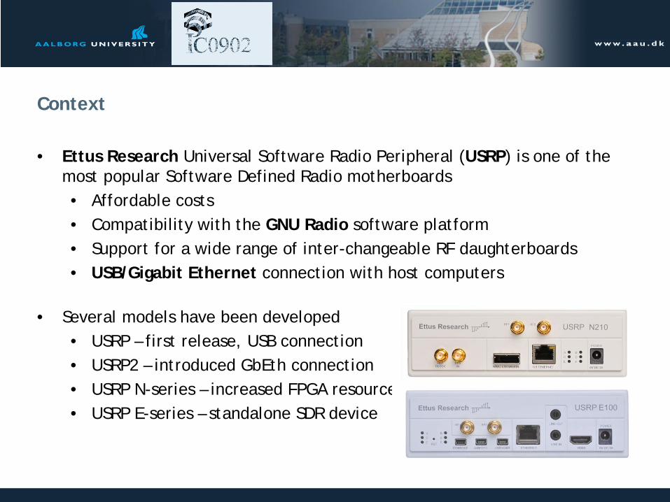
Context
• Ettus Research Universal Software Radio Peripheral (USRP) is one of the most popular Software Defined Radio motherboards • Affordable costs • Compatibility with the GNU Radio software platform • Support for a wide range of inter-changeable RF daughterboards • USB/Gigabit Ethernet connection with host computers
• Several models have been developed
• USRP – first release, USB connection • USRP2 – introduced GbEth connection • USRP N-series – increased FPGA resources • USRP E-series – standalone SDR device

Motivation
• The USRPs in their factory configuration feature a firmware which enables basic capabilities on the hardware • Up/down-sampling of the RF signal • Filtering • Management of data timestamp • Management of UDP packets on the GbE connection to the host
• Considerable hardware resources (especially on the new N-series) are left unused
• Implementation of processing features on the FPGA may be a valuable improvement to specific SDR systems
• An hardware implementation compatible with the provided firmware is preferable
• Lack of documentation about the USRP firmware architecture

Contribution
• Analysis of the existing USRP2 firmware • Architecture overview and schemes • Analysis of Verilog components
Notes: Firmware analysis relates to the release 3 Same architecture applies to USRP2 and N-series

General architecture

Main firmware components
• GMII – Gigabit Media Independent Interface • GE-MAC – Gigabit Ethernet Media Access Controller • Softcore Processor: 32-bit GPP ZPU
Host PC
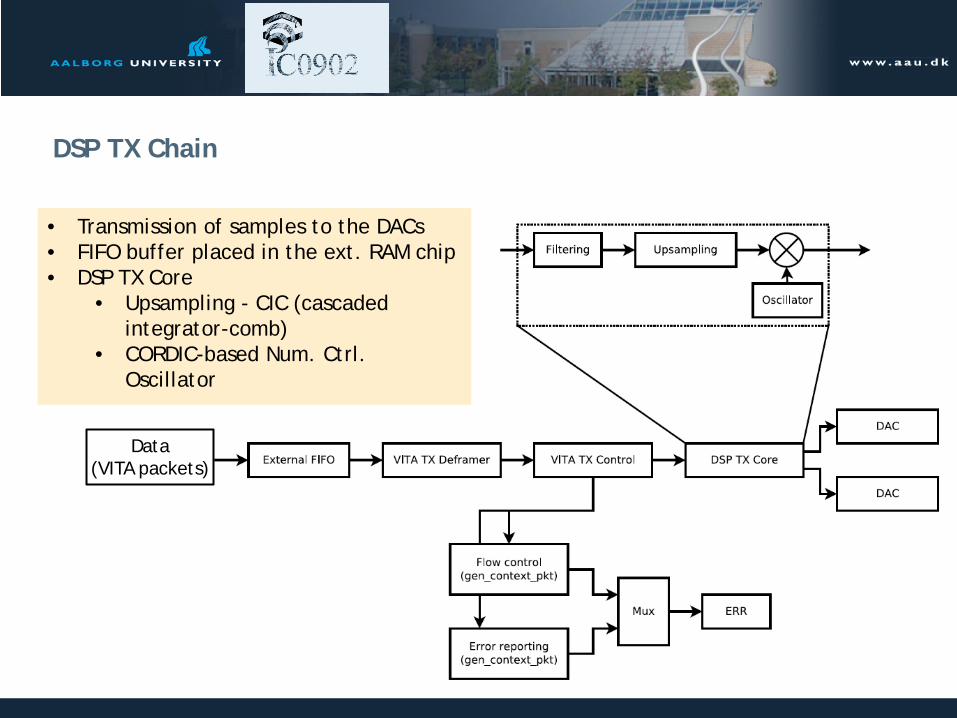
DSP TX Chain
• Transmission of samples to the DACs • FIFO buffer placed in the ext. RAM chip • DSP TX Core
• Upsampling - CIC (cascaded integrator-comb)
• CORDIC-based Num. Ctrl. Oscillator
Data (VITA packets)

DSP RX Chain
Data (VITA packets)
• Dual operations of the DSP TX Chain • VITA RX Control block adds timing
information • Adds control flag if rx samples are
delayed

CPU/ZPU
• The on-board CPU controls the functioning of the DSP chains, packet routing and other peripherals
• It has access to the board devices through 𝐼2𝐶 and SPI buses but it does not have direct access to the DSP chain datapath
• The CPU communicates to the host through UDP packets. • The CPU can directly access 512 bytes of packet space in the CPU
FIFO

Packet Router RX
• The RX packet router inspects packets coming from the Ethernet connection • Ensures that only packet that match the IP address of the board, will be
processed • Sends UDP packets to the ZPU and VITA packets to the DSP TX chain
HO
ST P
C

Packet Router RX
• The RX packet router inspects packets coming from the Ethernet connection • Ensures that only packet that match the IP address of the board, will be
processed • Sends UDP packets to the ZPU and VITA packets to the DSP TX chain
HO
ST P
C
Conclusions and future work
• Deeper understanding of the USRP2 firmware architecture • The firmware modularity allows to implement additional features
• Create new blocks in Verilog • Manage input/output connections of existing blocks
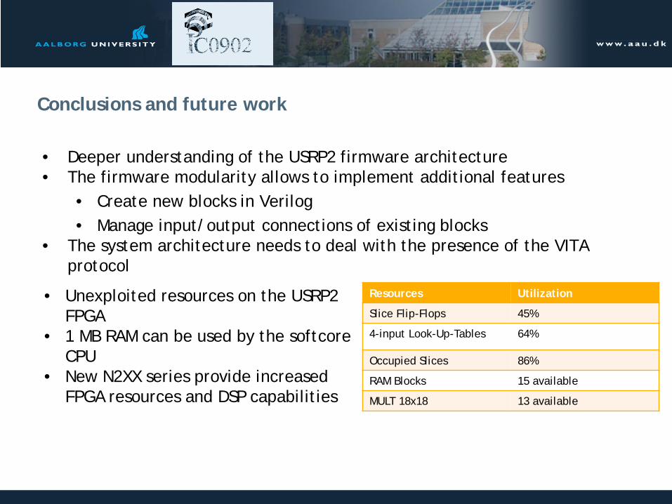
• The system architecture needs to deal with the presence of the VITA protocol Resources Utilization
Slice Flip-Flops 45%
4-input Look-Up-Tables 64%
Occupied Slices 86%
RAM Blocks 15 available
MULT 18x18 13 available
• Unexploited resources on the USRP2 FPGA
• 1 MB RAM can be used by the softcore CPU
• New N2XX series provide increased FPGA resources and DSP capabilities

Reference
J.Johansen, S. Enevoldsen, V.Pucci, “Analysis and Architectural Mapping of an FFT Algorithm into an Already Existing FPGA Firmware of a Low-cost COTS SDR Peripheral”, 2nd Semester Master Project, Spring 2011, Aalborg University, Denmark.

Boot-up process
• Configuration data for the FPGA is typically loaded either from an onboard ROM chip or a FLASH ROM
• In the USRP2 the boot-up process is controlled by a CPLD (Complex Programmable Logic Device) that performs the initialization process of the SPI interface for a SD card
• Bits from address 0 on the card are loaded into the FPGA configuration interface† • The following bits are the firmware image for the softcore processor if enabled on
the FPGA.
†fpga/usrp2/boot_cpld/boot_cpld.v
VITA Radio Transport Protocol
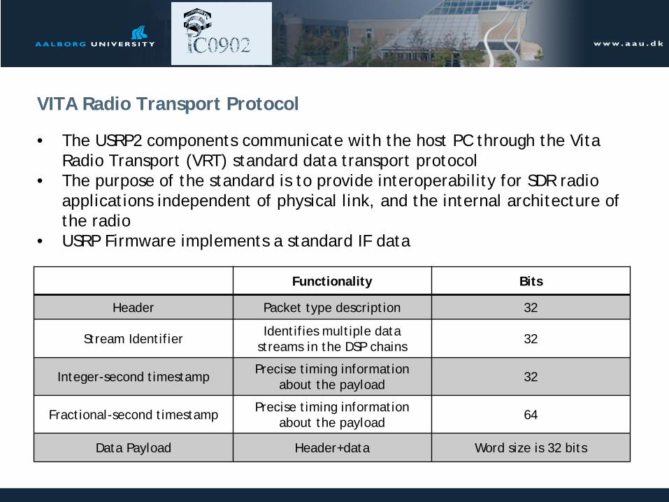
• The USRP2 components communicate with the host PC through the Vita Radio Transport (VRT) standard data transport protocol
• The purpose of the standard is to provide interoperability for SDR radio applications independent of physical link, and the internal architecture of the radio
• USRP Firmware implements a standard IF data
Functionality Bits
Header Packet type description 32
Stream Identifier Identifies multiple data streams in the DSP chains 32
Integer-second timestamp Precise timing information about the payload 32
Fractional-second timestamp Precise timing information about the payload 64
Data Payload Header+data Word size is 32 bits