DISCO: a coherent diffeomorphic framework for brain registration under exhaustive sulcal constraints
Upload
khangminh22Category
view
4download
0
Introduction
This document describes the functionalities of the STSW-ST25DV002 firmware, developed to take full advantage of theST25DV64KC-DISCO board functionalities, working with any dynamic tag of the ST25DV-I2C Series.In this document, the dynamic tag series from STMicroelecronics is referred to as ST25DV-I2C tags.The ST25DV-I2C tags are integrated circuits (IC) for contactless applications that communicate with a microcontroller throughan I2C interface; this makes this device a dynamic tag. On the RF side, the reader (for instance a smart phone) retrieves andupdates the content of the tag when close by.The reader communicates with the ST25DV64KC-DISCO board using the ISO 15693 protocol, while the STM32L476xxmicrocontroller device communicates with the ST25DV-I2C tag through an I2C bus.With this discovery kit, the ST25DV-I2C tag is ready to receive any content, following the NFC Forum standard. This means thata smart phone is able to natively read it, without having previously installed any specific application.A specific Fast transfer mode allows the user to transfer data directly to the microcontroller, without using the embeddedEEPROM.
STSW-ST25DV002 firmware for the ST25DV64KC-DISCO board
UM2949
User manual
UM2949 - Rev 1 - February 2022For further information contact your local STMicroelectronics sales office.
www.st.com

1 General information
This document applies to the STM32L476xx Arm®-based microcontroller devices.
Note: Arm is a registered trademark of Arm Limited (or its subsidiaries) in the US and/or elsewhere.
UM2949General information
UM2949 - Rev 1 page 2/60

2 List of acronyms and notational conventions
2.1 List of acronyms
Table 1. Acronyms
Acronym Definition
APB Advanced peripheral bus
AAR Android™ application record
BLE Bluetooth® Low Energy
CAN Controller area network
GPS Global positioning system
GPO General purpose output
H2R Host to reader
IEC International electrotechnical commission
ISO International standards organization
MCU Micro controller unit (microcontroller)
NFC Near field communication
OOB Out of band
R2H Reader to host
RF Radio frequency
RFID Radio frequency identification
RISC Reduced instruction set computer
SPI Serial peripheral interface
URI Uniform resource identifier
URL Uniform resource locator
USB Universal serial bus
2.2 Number convention and notationThe following conventions and notations apply in this document unless otherwise stated:• Binary numbers are represented by strings of 0 and 1 digits starting with the most significant bit (MSB) on
the left followed by the least significant bit (LSB) on the right, and "0b" added at the beginning. Example:0b11110101.
• Hexadecimal numbers are represented by using numbers 0 to 9 and characters A to F, and adding "0x" atthe beginning. The MSB is shown on the left and the LSB on the right. Example: 0xF5.
• Decimal numbers are represented without any leading character. Example: 245.
UM2949List of acronyms and notational conventions
UM2949 - Rev 1 page 3/60

3 Overview
3.1 ST25DV-I2C tagThe ST25DV-I2C tag is a dynamic tag IC for contactless applications (ISO 15693). It manages the RFcommunication with a reader. It also includes frame coding, RF modulation and manages the anti-collisionprocess.The ST25DV-I2C tag works as an NFC Forum Type 5 tag, supporting: detection, read and write operations. Asshown in Figure 1, this device communicates with a reader without any external controller.
Figure 1. Communication scheme
MCU ST25DV-I2C RFI2C
3.2 STM32L476xx microcontroller devicesThe STM32L476xx microcontroller devices are ultra-low-power microcontrollers based on the high-performanceArm® 32-bit RISC core operating at a frequency of up to 80 MHz. The Arm® Cortex®-M4 core features afloating point unit (FPU) single precision, which supports all Arm® single-precision data-processing instructionsand data types. It also implements a full set of DSP instructions and a memory protection unit (MPU) to enhanceapplication security.The STM32L476xx microcontroller devices embed high-speed memories (up to 1 Mbytes of Flash memory,up to 128 Kbytes of SRAM), a flexible external memory controller (FSMC) for static memories (for deviceswith packages of 100 pins and more), a Quad-SPI Flash memory interface (available on all packages) and anextensive range of enhanced I/Os and peripherals connected to two APB buses, two AHB buses and a 32-bitmulti-AHB bus matrix.The STM32L476xx microcontroller devices embed several protection mechanisms for embedded Flash memoryand SRAM: readout protection, write protection, proprietary code readout protection and firewall.These devices offer up to three fast 12-bit ADCs (5 Msps), two comparators, two operational amplifiers, twoDAC channels, an internal voltage reference buffer, a low-power RTC, two general-purpose 32-bit timers, two16-bit PWM timers dedicated to motor control, seven general-purpose 16-bit timers, and two 16-bit low-powertimers. The STM32L476xx microcontroller devices support four digital filters for external sigma delta modulators(DFSDM).In addition, up to 24 capacitive sensing channels are available. The devices also embed an integrated LCD driver8x40 or 4x44, with internal step-up converter.They also feature standard and advanced communication interfaces:• Three I²Cs• Three SPIs• Three USARTs, two UARTs and one Low-power UART.• Two SAIs (serial audio interfaces)• One SDMMC• One CAN• One USB OTG full-speed• One SWPMI (single wire protocol master interface)For full details of the STM32L476xx microcontroller device specifications, refer to www.st.com.
UM2949Overview
UM2949 - Rev 1 page 4/60

3.3 ST25DV64KC-DISCO boardsThe ST25DV64KC-DISCO is an evaluation kit, which allows the user to evaluate the performance of the ST25DV-I2C tag dynamic tag. The kit is composed of two boards, namely a motherboard (see Figure 2) and the ST25DV-I2C tag daughter board (see Figure 3).
3.3.1 ST25DV64KC-DISCO motherboardThe ST25DV64KC-DISCO (illustrated in Figure 2) is powered through the USB bus (micro and mini connectors)and no external power supply is required.This motherboard embeds the STM32L476VG microcontroller and different peripherals:• LCD display and touchscreen to interface with the user• USB connectors to connect to a PC (mini-USB for the ST-Link debugger and micro-USB available for the
user application)• Optional modules: Wi‑Fi® and BLE to connect with a smart phoneThe connectors on the right side of the board are dedicated to the daughter boards that embed the NFC tags.
Figure 2. ST25DV64KC-DISCO motherboard MB1396
UM2949ST25DV64KC-DISCO boards
UM2949 - Rev 1 page 5/60

3.3.2 ST25DV-I2C tag daughter boardThe ST25DVKC Discovery ANT C3 board (illustrated in Figure 3) embeds the ST25DV64KC device and a 40 mmx 23 mm, 13.56 MHz double layer inductive etched antenna (no need for any tuning components).The ST25DV64KC communicates with the STM32L476VG 32-bit MCU via the I²C bus.
Figure 3. ST25DVKC Discovery ANT C3 board
UM2949ST25DV64KC-DISCO boards
UM2949 - Rev 1 page 6/60

4 Firmware description
4.1 PrerequisiteThe ST25DV-I2C tag is a dynamic tag, whose content and configuration is driven by both a microcontroller(through I²C) and a reader through RF.To benefit from the ST25DV64KC-DISCO demonstration kit, the user must have one of the following:• A smart phone with the NFC enabled, combined with the ST25 NFC App installed on it. Refer to ST25
Android™ NFC tap application (UM2131), available on www.st.com for more information.• An NFC reader, such as the CR95HF distributed with the M24LR discovery kit (M24LR-DISCOVERY). To
take full advantage of the ST25DV-I2C tag features, use CR95HF transceiver board firmware version 3.7.0or higher, combined with the ST25PC-NFC software. Refer to Software toolbox for NFC tags user manual(UM2444), available on www.st.com.
The ST25DV-I2C tag is fully compliant with the NFC Forum Type 5 standard. As this standard is recentlyintroduced, some features may not be fully supported by older smart phones.
4.2 Main menuThe main menu (Figure 4) is composed of three icons, used to access sub-menus.
Figure 4. ST25DV64KC-DISCO main menu display
Each item allows the user to enter a sub-menu containing a set of use cases as outlined. The sub-menus aresummarized in Table 2:
Table 2. Main menu item definition
Discover ST25DV-I2C tag Fast transfer mode demonstration NFC NDEF demonstrations
Note: If the Wi‑Fi® and/or the Bluetooth® Low Energy modules have been added to the board, the corresponding iconsare available to access the Wi‑Fi® and Bluetooth® pairing demonstrations.
UM2949Firmware description
UM2949 - Rev 1 page 7/60
To select a category, touch the icon on the screen. To start a demonstration, touch the desired demonstrationicon on the screen (see description below). A long touch on an icon displays the description of the correspondingdemonstration(s) in the top line.As the purpose of this document is to illustrate the firmware behavior, the descriptions are detailed from themicrocontroller point of view.
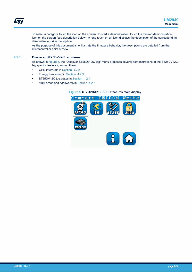
4.2.1 Discover ST25DV-I2C tag menuAs shown in Figure 5, the "Discover ST25DV-I2C tag" menu proposes several demonstrations of the ST25DV-I2Ctag specific features, among them:• GPO interrupts in Section 4.2.2 • Energy harvesting in Section 4.2.3 • ST25DV-I2C tag states in Section 4.2.4 • Multi-areas and passwords in Section 4.2.5
Figure 5. ST25DV64KC-DISCO features main display
UM2949Main menu
UM2949 - Rev 1 page 8/60

4.2.2 RF GPO interrupt demonstrationThe ST25DV-I2C tag has a GPO that is used to send interrupts to the microcontroller.Several kinds of event on the RF side may be configured to trigger the GPO interrupt. In this demonstrationall possible interrupt sources are enabled, except for the "RF activity", which occurs too often for reasonablereadability when using a smart phone as a reader.To start the demonstration, select the "GPO control demo" menu, this displays the instructions until it detects aGPO interrupt.As soon as the first GPO interrupt is received, the LCD displays the list of sources of received interrupt, and thenumber of each interrupt occurrences (see Figure 6).
Figure 6. ST25DV64KC-DISCO interrupt generation display
The event types and the way to generate them are listed below:• Field on: place a reader near the ST25DV-I2C tag• Field off: move a reader away from the ST25DV-I2C tag• EEPROM written: modify the content of the ST25DV-I2C tag• RF interrupt: requires the use of a specific reader instruction, that is sent either by a smart phone running
the ST25 NFC app, or by a reader (see the instructions in Smart phone GPO management and Generatingthe RF and RF user interrupts using the ST25PC-NFC software with the CR95HF sections, respectively, forAndroid™ ST25 NFC application and for the CR95HF reader used with the ST25PC-NFC software)
• RF user: requires the use of a specific reader command, that is sent either by a smart phone running theST25 NFC app or by a reader (see the instructions in Smart phone GPO management and Generating theRF and RF user interrupts using the ST25PC-NFC software with the CR95HF sections, respectively, for theAndroid™ ST25 NFC application and for the CR95HF reader used with the ST25PC-NFC software)
To start the Android ST25 NFC application, read the ST25DV-I2C tag with a smart phone (after entering the GPOdemonstration), which automatically opens the required application (or propose the installation of the application).The automatic application selection is done using an NDEF with an AAR.
Note: The mailbox events are also used to trigger the GPO interrupts. They are not mentioned here, as they wouldrequire placing the ST25DV-I2C tag in the Mailbox mode.
Smart phone GPO management
The ST25 NFC application handles the RF interrupt and the RF user interrupt using register fields information(see Figure 7). Do not forget to present the configuration password before any register change.
UM2949Main menu
UM2949 - Rev 1 page 9/60

Figure 7. Smart phone GPO register configuration
The ST25 NFC application generates the RF interrupt and the RF user interrupt using features located in theTools fragment in association with the RF GPO interrupt demonstration.
Generating the RF and RF user interrupts using the ST25PC-NFC software with the CR95HF
These interrupts are generated by any RF reader or Android™ smart phone.Using the CR95HF IC and ST25PC-NFC software, the user is able to send interrupts or drive the GPO (seeFigure 8 and Figure 9)• Select the ST25DV-I2C tag product• Select "ENERGY HARVESTING" and GPO tab• Click on "Send Interrupt Generated by GPO" to send an interrupt on GPO line• Click on GPO set or GPO reset to be able to drive the GPO line.For additional information about CR95HF PC software refer to the CR95HF development software user manual(UM1084), available on www.st.com.
UM2949Main menu
UM2949 - Rev 1 page 10/60

Figure 8. ST25DV-I2C tag contextual menu
Figure 9. PC software ST25DV-I2C tag special commands interface
UM2949Main menu
UM2949 - Rev 1 page 11/60

4.2.3 ST25DV-I2C tag energy harvesting demonstrationThe ST25DV-I2C is able to harvest the energy provided by the RF to power other devices.This demonstration displays the voltage, current and power provided by the ST25DV-I2C (see Figure 10).
Figure 10. ST25DV64KC-DISCO energy harvesting measurement display
A LED is also turned on to simulate the effect of the energy harvesting when the RF field is approaching or whenit leaves.The energy harvesting pin is connected to a load with which is used to measure the current delivered by the tag.This load is configurable (shown in Figure 10) from 540 Ω to 4320 Ω. The objective is to simulate the currentconsumed by additional external circuitry.
UM2949Main menu
UM2949 - Rev 1 page 12/60

4.2.4 ST25DV-I2C tag states demonstrationThis menu illustrates the possibility to change the ST25DV-I2C tag state, for example the power savedemonstration. This demonstration proposes three different modes:1. RF disabled mode: RF commands are interpreted but not executed. The ST25DV-I2C tag responds with the
error code 0x0F.2. Sleep mode: all RF communications are disabled, the RF interface does not interpret the commands, but
minimizes consumption of RF interface.3. Low-power down: the ST25DV-I2C tag is fully inactive from Host - I2C side, but the memory content is
accessible on the RF side.For all above cases, the demonstration consists in writing an NDEF with the ST25 URL, and changing theST25DV-I2C tag state. A message is displayed that invites the user to try to read the content of the ST25DV-I2Ctag, and check that it is not possible.The content of the ST25DV-I2C tag can be read again as soon as the demonstration screen is passed.
Note: For the Low-power mode, the ST25DXSPARE jumper must be present on the ST25DV64KC-DISCO board'sMCU pin, and a 12-pin package must be used for the ST25DV-I2C tag.
4.2.5 ST25DV-I2C tag multi area and password demonstrationThe ST25DV-I2C tag defines up to four different areas in memory. Each area may have a custom security level,requiring one of the three passwords to be provided in order to read and/or write the memory.This demonstration sets two different areas:1. "Area 1" contains an NDEF with a vCard. This area is readable by anyone, but can only be written after
presenting "password 1".2. "Area 2" contains an NDEF with a different vCard. This area cannot be read without the "password 1", and
cannot be written even after the password presentation.By default, all the passwords are set to 0000 0000 0000 0000. These values are only updated from the RF side.To execute the demonstration, the user must first read the ST25DV-I2C tag without any specific application. Thephone displays the vCard stored in "Area 1".Then the user opens the ST25 NFC application, and taps the tag again, the application detects two areas, anddisplays the "Area "1 vCard.The user may try to write a different NDEF to the "Area 1", and check that the write fails unless "password 1" ispresented.If the user selects the "Area 2" NDEF, the application requests "password 1" before displaying the "Area 2" vCard.The user may try to write a different NDEF in "Area 2", this does not work even after presenting "password 1".This is expected, as the security level of "Area 2" prevents any write access to the memory.
Smart phone and multi areas
When the tag is configured in multi areas, the ST25 NFC application then handles the areas and presents areasand content to the user. The user then chooses the desired area by selecting the corresponding menu in theapplication drawer. This is illustrated in Figure 11.In case special protection is needed, the application displays security status information. On click, a popup isused to present the area password needed to access area content.
UM2949Main menu
UM2949 - Rev 1 page 13/60

Figure 11. Smart phone and area display
ST25PC-NFC software and multi areas
The ST25PC-NFC software is used to create up to four areas on the ST25DV-I2C tag EEPROM:1. From the Inventory side panel, right-click on the ST25DV-I2C tag tag (see Figure 8).2. In the contextual menu, select the "Multi Area Editor" item.3. Move the sliders for each area until the desired value is reached (see Figure 12 for an example of an
EEPROM cut into four equal areas of 2048 bytes segments).4. The start address, size of the area and ENDA register values are updated in real time inside the bottom
table.
UM2949Main menu
UM2949 - Rev 1 page 14/60

Figure 12. ST25DV-I2C tag multi area configuration interface of the ST25PC-NFC software
Access rights for each area of the tag are set from the "Area configuration" screen (see Figure 13):1. From the table, select the area to protect (up to four areas).2. In the "Area protection" column, set one of four options for read and write operations (only three are
available for "Area 1").3. Additionally, the password number can be set for each area.
Figure 13. Area configuration interface of the ST25PC-NFC software
UM2949Main menu
UM2949 - Rev 1 page 15/60

4.2.6 ST25DV-I2C tag compare EEPROM writeThis menu shows the difference between writing to the 4-byte ST25DVxxK EEPROM page and to the 16-byteST25DVxxKC EEPROM page. When entering this menu the following screens show the difference by emulatingan ST25DVxxKC EEPROM page write and performing the actual write on the ST25DVxxKC EEPROM.
Figure 14. ST25DVxxK emulated EEPROM write screen
Figure 15. ST25DVxxK emulated EEPROM write results
UM2949Main menu
UM2949 - Rev 1 page 16/60

Figure 16. ST25DVxxKC EEPROM write screen
Figure 17. ST25DVxxKC EEPROM write results
UM2949Main menu
UM2949 - Rev 1 page 17/60

4.2.7 NFC NDEF demonstration menuThe NFC NDEF demonstrations menu (see Figure 18) proposes several demonstrations concerning NDEFmessages:• URI NDEF message (URL and phone number)• SMS NDEF message• Email NDEF message• vCard NDEF message• Geo-location NDEF message• Custom (MyApp) NDEF message• Multi record NDEF message• Bluetooth® Low Energy OOB NDEF message (requires an additional Bluetooth® Low Energy module)• Wi‑Fi® OOB NDEF message (requires an additional Wi‑Fi® module).
Figure 18. ST25DV64KC-DISCO NFC NDEF demonstrations menu display
URI demonstration
This menu (see Figure 19) shows how to manage URI content in the ST25DV-I2C tag.With the MCU, the user:• Stores an NDEF message containing a URL or a phone number (it is then be read with an NFC reader or a
smart phone).• Reads any URI that is stored in the ST25DV-I2C tag. The display shows the content of the URI.
UM2949Main menu
UM2949 - Rev 1 page 18/60

Figure 19. ST25DV64KC-DISCO read URI display
Note: If the MCU reads the ST25DV-I2C tag memory, it does not contain a URI, an error message is displayed.
Smart phone and URI NDEF
Refer to Reading and writing NDEF on a smart phone with the Android ST25 application section.
SMS demonstration
This menu indicates how to manage SMS content in the ST25DV-I2C tag.With the MCU, the user:• Stores an NDEF message containing an SMS (it is then be read with an NFC reader or with a smart phone)• Reads any SMS that is stored in the ST25DV-I2C tag memory (the SMS is displayed on the screen).
Figure 20. ST25DV64KC-DISCO read SMS content display
Note: If the MCU reads the ST25DV-I2C tag memory, it does not contain an SMS, an error message is displayed.
Smart phone and SMS NDEF
Refer to Reading and writing NDEF on a smart phone with the Android ST25 application section.
Email demonstration
The menu illustrated in Figure 21 indicates how to manage e-mail content in the ST25DV-I2C tag.With the MCU, the user:• Stores an NDEF message containing an e-mail (it is then be read with an NFC reader or with a smart
phone).• Reads any e-mail that is stored in the ST25DV-I2C tag memory. The content of the e-mail is displayed on
the screen.
UM2949Main menu
UM2949 - Rev 1 page 19/60

Figure 21. ST25DV64KC-DISCO read Email content display
Note: If the MCU reads the ST25DV-I2C tag memory, it does not contain an e-mail, an error message is displayed.
Smart phone and e-mail NDEF
Refer to Reading and writing NDEF on a smart phone with the Android ST25 application section.
vCard demonstration
The menu illustrated in Figure 22 indicates how to manage vCard content in the ST25DV-I2C tag.With the MCU, the user:• Stores an NDEF message containing a vCard. Depending on the size of the ST25DV-I2C tag, this vCard
may or may not embed a picture• Reads the ST25DV-I2C tag content.If the vCard was previously stored, the following information is displayed on the board screen: name, title,organization, cell phone number, work address and work e-mail.
Note: The vCard with an embedded picture needs around 3 Kbytes of memory and cannot be stored in the ST25DV-I2C tag devices with smaller memory sizes, the ST25DV64 (with 64 kbits) must be used.If the MCU reads the ST25DV-I2C tag memory, it does not contain a vCard, an error message is displayed.Only vCard 2.1 is implemented in this firmware version. If the user stores a vCard 3.0 in the ST25DV-I2C tag,the firmware issues an error message.
UM2949Main menu
UM2949 - Rev 1 page 20/60

Figure 22. ST25DV64KC-DISCO read vCard content display
Smart phone and vCard NDEF
Refer to Reading and writing NDEF on a smart phone with the Android ST25 application section.
Geolocation demonstration
The menu illustrated in Figure 23 indicates how to manage the geolocation content in the ST25DV-I2C tag.With the MCU, the user:• Stores an NDEF message containing a geolocation (it is then read with an NFC reader or with a smart
phone)• Reads any geolocation that is stored in the ST25DV-I2C tag memory, the content is displayed on the screen.
Figure 23. ST25DV64KC-DISCO read geolocation display
Note: If the MCU reads the ST25DV-I2C tag memory, it does not contain a geolocation, an error message is displayed.
UM2949Main menu
UM2949 - Rev 1 page 21/60

MyApp record demonstration
This demonstration illustrated by Figure 24 shows how to use a proprietary NDEF record to control an applicationrunning on the host MCU. As the format of the message follows the NFC Forum NDEF standard, it is written orread by any device supporting this format.The MCU waits until a "Proprietary configuration" record is written to the tag, then it updates the LCD display andcontrols a LED as described in the record.This demonstration uses the ST25DV-I2C tag GPO to detect that the ST25DV-I2C tag is written to. In the ST25NFC App, the user must enter the "compose NDEF" menu, and then select the "Proprietary configuration" record.From there, the user:• Selects whether the LED1 must blink and configure the blinking period.• Enters the text to be displayed by the MCU.
Note: The "Proprietary configuration" record allows the user to control up to four LEDs. As the ST25DV64KC-DISCOboard has only one LED, configuring LED2, LED3 or LED4 has no effect.After changing the setting in the compose "Proprietary configuration" record menu, the user must click on "Writeto tag" and tap the ST25DV-I2C tag. As soon as a new message is written in the ST25DV-I2C tag memory,the MCU reads it and if it finds the expected message, it configures the LED and the LCD as specified in themessage.If the data written to the ST25DV-I2C tag is not a valid "Proprietary configuration" record, the MCU displays anerror message and continues waiting for a valid "Proprietary configuration" record to be written.
Figure 24. ST25DV64KC-DISCO MyApp demonstration screen
Multi record demonstration
This menu indicates how to manage a multi record NDEF in the ST25DV-I2C tag.With the MCU, the user:• Stores an NDEF message containing the ST25 URI (it is then be read with an NFC reader or a smart
phone).• Adds the "ST25 Android™ Application Record" (ST25 AAR) to the existing NDEF message.For this demonstration, the user is requested to read the URI with a smart phone, and check that its preferredbrowser is open with the ST25 URL (this is the default behavior when URI is natively supported by the smartphone).Then, after adding the ST25 AAR, when the ST25DV-I2C tag is read with a smart phone, the browser is no longeropen, while the ST25 application is. The URI appears as the first record in the application.
Smart phone and multi records NDEF
This section provides dedicated indications how to build multi records NDEFs (see Figure 25).How to build each record:1. From "Ndef Editor" menu, click on the '+' at the bottom right corner to add a record. A popup appears
allowing the user to choose the record type.2. Fill the record and click on the floppy icon, in the top right corner, to save the record to the tag.3. Proceed in the same way to add more records.
UM2949Main menu
UM2949 - Rev 1 page 22/60

Figure 25. Smart phone and multi records editor display
Bluetooth® Low Energy pairing demonstration (requires an additional Bluetooth® Low Energy module)
This menu indicates how to manage a Bluetooth® Low Energy pairing content in the ST25DV-I2C tag. By default,the ST25DV64KC-DISCO board does not feature the Bluetooth® Low Energy functionality, and is added using theST BlueNRG module.For this demonstration, the user reads the ST25DV-I2C tag content with a smart phone having the Bluetooth®
Low Energy OOB support (e.g. Android™ 6.0).With the MCU, the user:
• Stores an NDEF message containing the Bluetooth® Low Energy Out-Of-Band (OOB)• Reads a Bluetooth® or Bluetooth® Low Energy OOB previously stored in the ST25DV-I2C tag memory.
When the user reads the ST25DV-I2C tag with a smart phone having Bluetooth® Low Energy support, thesmart phone automatically asks confirmation and connects to the BlueNRG module present on the demonstrationboard. The MAC address provided by the smart phone is displayed on the screen of the demonstration board assoon as the pairing is completed.The BlueNRG is configured to act as a human interface device (HID); it is displayed on the smart phone with thisname: HID.The HID protocol is natively supported by Android™ 6.0 smart phones, and this demonstration allows the user tocontrol a pointer on the paired phone, by touching the screen of the ST25DV64KC-DISCO board. The screen actsas a touch-pad, the user button as a select button.Touch the bottom line of the LCD to exit this demonstration.The user selects the "Change BLE Address" command to prevent spurious connections from previously pairedsmart phones.This changes the Bluetooth® Low Energy module device address, and is seen by smart phones as a differentdevice (however the device name - HID - is left unchanged).
Note: Some smart phones require a specific action from the user to enable the HID control (this setting may be locatedin the smart phone's Bluetooth® menu).
Smart phone and Bluetooth® Low Energy
Refer to Reading and writing NDEF on a smart phone with the Android ST25 application section.
Wi‑Fi® pairing demonstration (requires an additional Wi‑Fi® module)
This menu indicates how to manage a Wi‑Fi® pairing content in the ST25DV-I2C tag. By default, theST25DV64KC-DISCO board does not feature the Wi‑Fi® module. To access this feature add the ST SPWF01module which acts as a mini Wi‑Fi® access point.For this demonstration, the ST25DV-I2C tag content is read with a smart phone using Wi‑Fi®.With the MCU, the user:
UM2949Main menu
UM2949 - Rev 1 page 23/60

• Stores an NDEF message containing a Wi‑Fi® protected setup (WPS) OOB descriptor.• Reads a WPS OOB previously stored in the ST25DV-I2C tag memory.
When the user reads the ST25DV-I2C tag with a smart phone having the Wi‑Fi® support, the smart phoneautomatically asks a confirmation and connects to the SWPF_AS01 Wi‑Fi® network. The MAC address providedby the smart phone is displayed on the screen of the demonstration board as soon as the connection iscompleted.
Note: For the demonstration no Internet access is provided by the board mini access point.
Note: If, when the MCU reads the ST25DV-I2C tag memory, it does not contain a WPS OOB, an error message isdisplayed.
Smart phone and Wi‑Fi® pairing
Refer to Reading and writing NDEF on a smart phone with the Android ST25 application section.
Reading and writing NDEF on a smart phone with the Android™ ST25 application
The ST25 NFC App enables to read or write NDEF messages.• Read: tap the tag, if a managed NDEF is discovered, content is accessible from the NDEF tab or NDEF
editor (refer to the Android™ application user manual for more details), see Figure 26.• Write an NDEF: select "NDEF editor" and choose the NDEF type has to be written. An editor according to
the selected type is displayed (see Figure 27).
Figure 26. Smart phone and NDEF discover display
UM2949Main menu
UM2949 - Rev 1 page 24/60

Figure 27. Smart phone and URL NDEF write menu display
Reading and writing NDEF with the ST25PC-NFC software
To access the NDEF editor screen, start by right-clicking on a ST25DV-I2C tag tag in the "Inventory Pane" (seeFigure 8), then select the "NDEF Editor" option in the menu. The NDEF interface is illustrated in Figure 28.The first list on the left of the NDEF Editor screen displays the content of the tag. Click on the "Read from selectedtag" button to refresh the list content.The right-most list helps the user compose an NDEF message. The current tag content is then copied by clickingon the "Edit" arrow located between the two lists. Add a new record by clicking on the "Add new record" button atthe bottom right side of the screen. To remove a record from the composition list, click on the "X" icon.To write the NDEF message to the tag, click on the "Write" icon located between the two lists.
UM2949Main menu
UM2949 - Rev 1 page 25/60

Figure 28. ST25PC-NFC software NDEF interface
Clearing the EEPROM
This menu allows the user to clear the EEPROM content. The three choices are:1. Write an empty NDEF2. Erase the CC file (replace the first four bytes of memory with 0xFF)3. Clear EEPROM (fill the whole memory with 0xFF).
4.2.8 Fast transfer mode demonstration menuThis demonstration is intended to show how the ST25DV-I2C tag improves the data exchange between thereader and the MCU using a proprietary protocol based on the ISO15693 standard as opposed to exchangingdata through the EEPROM. To perform the data exchange the ST25DV-I2C tag shares a 256-byte RAM bufferavailable for the reader and the MCU (also called mailbox).Data exchange is only carried out in one direction at a time (half duplex). The mailbox contains indicators givingthe reader status and generates pulses on a GPO, which must be connected to an external interrupt (GPIO input)of the microcontroller. For more details on the mailbox feature, refer to the ST25DV-I2C tag datasheet.When the user selects the Fast transfer mode icon (see Figure 4), a message displays "Starting Demo". Duringthis time, the firmware is initialized, enabling the mailbox functionality and erasing the Flash memory on theMCU (to store data downloaded through NFC, dedicated demonstration Flash memory area). Then, when thedemonstration has finished its initialization, the message "Ready to start demo ! !" is displayed, as shown inFigure 29.
Note: When the Mailbox feature is enabled, the EEPROM is in read only mode. To modify the EEPROM disable the"Mailbox" feature.
UM2949Main menu
UM2949 - Rev 1 page 26/60

Figure 29. ST25DV64KC-DISCO Fast transfer mode display
The picture and note icons in Figure 29, on the bottom left of the screen, point to a sub-menu that allows the userto choose a picture or a random data buffer, which is to be transferred to a reader (see Host to reader imageupload and Host to Reader data transfer sections).The home icon (bottom right) allows the user to go back to the main menu (see Figure 4).At this step, the firmware is waiting for an action from the reader or from the user to start. These actions aredescribed in the following sections.
Smart phone and Fast transfer mode use cases
Available actions can be accessed after tag has been taped, and are available in the ST25DV-I2C tag features ordemonstrations menus within the application "Drawer".The available use cases are:• Mailbox management, enable/disable the mailbox and display mailbox register fields status• Data transfer, to demonstrate basics transfers• Firmware upgrade, to demonstrate the firmware upgrade use case• Picture transfer, to demonstrate how to upload or download pictures• Stopwatch synchronization, to demonstrate fast transfer with a smart phone.The display is illustrated in Figure 30.
UM2949Main menu
UM2949 - Rev 1 page 27/60

Figure 30. Smart phone and Fast transfer mode use cases display
PC software and Fast transfer mode use cases
As with Android™ phones, all the Fast transfer mode demonstrations are played using the ST25PC-NFC software.The CR95HF is used as a RF reader, for more information refer to Software toolbox for NFC tags user manual(UM2444), available on www.st.com.To access the Fast transfer mode screen, start by right-clicking on a ST25DV-I2C tag tag in the "Inventory"pane (see Figure 31), then select the "Fast Transfer Mode" option in the menu. Two tabs appear below thetag selection box "Read Message" (by default) and "Write Message". Click on the "Write Message" tab (seeFigure 31).The message area allows the user to write up to 256 bytes of data. A "Fill with" button fills up the whole bufferwith the specified byte value. After the message is written it is sent to the tag mailbox by clicking on the "WriteMessage" button.Click on "Read Register" to the right of the screen to read the values of the tag dynamic registers.
UM2949Main menu
UM2949 - Rev 1 page 28/60

Figure 31. ST25PC-NFC software - ST25DV-I2C tag FTM interface Write tab
Once the tag mailbox is filled , switch to the "Read message" tab (see Figure 32).
Figure 32. ST25PC-NFC software - ST25DV-I2C tag FTM interface Read tab
Click on the "Read Message Length" button to get the size in bytes of the mailbox content, and on the "ReadMessage" button to display the current content of the mailbox.In the ST25PC-NFC software, the full FTM set of demonstrations are accessible from the menu. Figure 33illustrates how to access them.Available demonstrations are:• "Reader-to-Host" and "Host-to-Reader" R2H data transfer: transfer of binary file to/from PC software (using
the CR95HF board) to and from the ST25DV64KC-DISCO board.
UM2949Main menu
UM2949 - Rev 1 page 29/60

• Reader-to-Host" firmware upgrade: transfer of binary file containing a new STM32 firmware from PCsoftware (using CR95HF board) to ST25DV64KC-DISCO board, the ST25DV64KC-DISCO firmware isupgraded.
• "Reader-to-Host" and "Host-to-Reader" image transfer: transfer of JPG image to/from PC software (usingCR95HF board) to and from the ST25DV64KC-DISCO board, the image is displayed on ST25DV64KC-DISCO LCD.
Figure 33. ST25PC-NFC software - Access to ST25V-I2C FTM demonstrations
Smart phone and FTM data transfers
Several menus accessible by the drawer menu are dealing with the Fast transfer mode data transfers:• Mailbox management. Radio buttons give the current status of the mailbox, and this menu permits to enable/
disable the mailbox feature• FTM demonstrations:
– Send or receive data– Firmware update– Send or receive pictures.
• Stopwatch transfers: This demonstration shows a chronometer synchronized between the smart phone andthe tag using the mailbox. It shows the low latency.
UM2949Main menu
UM2949 - Rev 1 page 30/60

Figure 34. ST25DV drawer menu (Mailbox management, FTM demonstration, Stopwatch demonstration)
As prerequisite to any data transfer, the mailbox has to be enabled, without any pending message. The correctstatus is shown in Figure 35.
UM2949Main menu
UM2949 - Rev 1 page 31/60

Figure 35. Mailbox status
UM2949Main menu
UM2949 - Rev 1 page 32/60

Figure 36. Data transfers from reader to tag of a random buffer
Note: According to data size selected, the corresponding payload data is initialized with random values on which aCRC is computed to be sure that the host computes the same data after each transfer.
Note: For every transfers done with the Android™ application, the user can choose between two modes:• Error recovery enabled. With this mode, the protocol is able to detect transmission errors and to recover
(by retransmitting the faulty packets). This is the default (and recommended) mode.• Error recovery disabled. Data transfer is done at max throughput. There is no recovery in case of
transmission error.
PC software and FTM data transfers
In the ST25DV-I2C tag/ST25DV-DISCOVERY "Demos" menu (see Figure 33), select the "FTM – Data Transfer"item which leads to the "Data. Transfer Demo" in Figure 37.To execute a R2H data transfer, select the "Send a file" item from the command list. A window pops-up askingthe user to select a file to transfer to the ST25DV64KC-DISCO board. CRC computation is done when loading thefile.Then click on the "Start" button to start transferring data to the board.
UM2949Main menu
UM2949 - Rev 1 page 33/60

Figure 37. Software R2H data transfer display
A progress bar and a timer display the transfer progress.At the end of the transfer, the CRC calculated by the ST25DV64KC-DISCO board is compared with the CRCcalculated by the PC software. Demonstration duration is displayed too.
Reader to host firmware upgrade
This function allows the user to send data (that is manipulated as binary) from the reader to the STM32L476xxmicrocontroller device. The data is stored in the Flash memory and at the end of the transfer, the followinginstruction code jumps to the new firmware location, demonstrating the capability to transfer large mounts ofbinary data. For this example, the new firmware is stored in a secondary area in the Flash memory and it is notintended to be used for new demonstrations. To come back to the initial firmware, press the reset button and itreboots the reader with the with this firmware.To prepare the ST25DV64KC-DISCO for the firmware upgrade demonstration, power up the board, then touch theFTM icon to start the fast transfer mode demonstration (Figure 29).The kit is now waiting for a reader action (see Smart phone and firmware upgrade and PC software andfirmware upgrade sections) to continue the demonstration. The dedicated firmware is located in: ST25DV-DISCOVERY\Demonstrations\ST25DVDemo_FwUpgd\Binary folderTo execute the firmware download, the user first has to send (from the reader) a correct password (for thisdemonstration the password is 0x12345678). During the password check, the Flash memory area where thefirmware is to be stored is erased (Figure 38).
UM2949Main menu
UM2949 - Rev 1 page 34/60

Figure 38. ST25DV64KC-DISCO firmware upgrade: password check
If the password is correct, the user is authorized to start the transfer (Figure 39), if not, the user has to enter anew password to continue (Figure 40).
Figure 39. ST25DV64KC-DISCO firmware upgrade: password OK
Figure 40. ST25DV64KC-DISCO firmware upgrade: wrong password
During the transfer the full length of data transmitted is displayed, and a bar indicates the progress (seeFigure 41).
UM2949Main menu
UM2949 - Rev 1 page 35/60

Figure 41. Software end transfer status display
When the transfer is successfully completed, the computed CRC and the transfer time are displayed (seeFigure 42). In case of failure the display shows an error message.
Figure 42. ST25DV64KC-DISCO firmware upgrade: transfer done
To start the new firmware, simply tap the screen.
Smart phone and firmware upgrade
Features:• Upgrade a new firmware to the ST25DV64KC-DISCO board.Demonstration steps, see the screen illustration in Figure 43:1. Check the mailbox status (Must be enable, withtout any pending messages in the mailbox).2. Select the “Firmware demos” in the drawer menu and click on “Firmware update button”.3. Select the file to be downloaded.4. A pop up asks for a password. By default, and for demonstration purpose the password is 12345678.5. Start download = Start transfer button.6. Smart phone and firmware download.
UM2949Main menu
UM2949 - Rev 1 page 36/60

Figure 43. Smart phone and firmware upgrade display
PC software and firmware upgrade
In the ST25DV-I2C tag/ST25DV-DISCOVERY "Demos" menu (see Figure 33), select the "FTM – FirmwareUpgrade" item.To execute a R2H firmware upgrade, first select a binary file to send with the "Select File" button (see Figure 44).CRC computation is done when loading the file, and is displayed on the screen.To start the firmware upgrade, click on the "Send to RF" button. Status of the transfer is updated in real timeillustrated by the "Transfer rate" progress bar.
UM2949Main menu
UM2949 - Rev 1 page 37/60

Figure 44. PC software R2H successful firmware upgrade
Reader to host image download
This function sends data from the reader to the STM32L476xx microcontroller device. In this demonstration, datais composed of jpeg images, stored in the Flash memory and displayed when the transfer is successful.To prepare the ST25DV64KC-DISCO for the R2H picture transfer demonstration, power on the board, then touchthe FTM icon to start the fast transfer mode demonstration (see Figure 29).It is now waiting for a reader action to continue the demonstration, as illustrated in the Smart phone and picturetransfers and Smart phone and picture download transfer sections.During the transfer, the full length of data transmitted is displayed and a progress bar indicates the progression.When the transfer is successfully done, the computed CRC and transfer duration are displayed on screen. Todisplay the downloaded picture touch the screen. To return to the Fast transfer mode demonstration simply touchthe screen.
Smart phone and picture transfers
Features:• Send a picture to the tag.• Receive a picture from the tag.Picture upload steps:1. Check the mailbox status (c.f. drawer menus).2. Select “FTM demos” in drawer menu.
UM2949Main menu
UM2949 - Rev 1 page 38/60

3. Click on “Send picture to tag” Select a picture in phone memory.The upload display screens are illustrated in Figure 45 and .
Figure 45. Transfer from smart phone to tag
UM2949Main menu
UM2949 - Rev 1 page 39/60

Figure 46. Image transfer demonstration: send a picture
PC software and image transfer
In the ST25DV-I2C tag/ST25DV-DISCOVERY "Demos" menu (see Figure 33), select the"FTM – Picture Transfer" item.To run a R2H transfer (from CR95HF reader to Host board), first select the "Pick a picture to upload" item from thecommand list (see Figure 47). Choose a file from the window that pops up, then click on the "Start" button.
UM2949Main menu
UM2949 - Rev 1 page 40/60

Figure 47. PC software R2H image transfer display
Host to reader image upload
This function sends data from the STM32L476xx microcontroller device to the reader (H2R).In this demonstration, the data is composed of jpeg images, it is written to the mailbox each time it is free, and theGPO returns the information to the MCU when the reader reads the mailbox message.To start this demonstration the user must perform an action on the firmware side.The picture icon at bottom left allows the user to enter a new menu (see Figure 48), which lets the user choosethe pictures to send to the reader. By touching the screen on the left or right border the user scrolls between thedifferent pictures available for transfer, simply touch the image on screen to select it. To come back and cancel theaction, touch the arrow at the bottom of the screen.
UM2949Main menu
UM2949 - Rev 1 page 41/60

Figure 48. ST25DV64KC-DISCO select picture to upload
After selecting the picture to transfer, the firmware writes the first chunk in the mailbox and waits for the messageto be read. During the transfer, a file size and a progress bar are displayed, as shown in Figure 49.
Figure 49. ST25DV64KC-DISCO image upload start
The kit is now waiting for the reader to read the message in the mailbox (see Smart phone and picture transfersand PC software and picture upload transfer sections) to continue the demonstration.When the transfer is successfully completed, the computed CRC and transfer time are displayed on the screen(Figure 50). In case of failure, the display shows an error message.
Figure 50. ST25DV64KC-DISCO image upload successful
UM2949Main menu
UM2949 - Rev 1 page 42/60

To return to the Fast transfer mode demonstration simply touch the screen.
Smart phone and picture download transfer
Features: same as Smart phone and picture transfers.Picture download steps:1. Check MB registers2. Select “FTM demos” in the drawer menu3. Received picture from tag button. Select a picture on the ST25 discovery kit. The transfer starts.
Smart phone and picture upload transfers display
Figure 51. Smart phone and picture upload transfers display
PC software and picture upload transfer
In the ST25DV-I2C tag/ST25DV-DISCOVERY "Demos" menu (see Figure 33), select the "FTM – Picture Transfer"item. The H2R image transfer display is illustrated in Figure 52. PC software H2R image transfer display.
UM2949Main menu
UM2949 - Rev 1 page 43/60

To initiate the transfer, choose a picture from the ST25DV64KC-DISCO board. Then click on the "Start" button tostart the transfer from the board to the reader. CRC computation is done when all data is transferred, then it issent to the tag.The demonstration ends when the PC software receives the acknowledgment and displays the image .
Figure 52. PC software H2R image transfer display
Host to Reader data transfer
This function allows the user to send data from the STM32L476xx microcontroller device to the reader. In thisdemonstration, the data takes random binary values. Each time the mailbox is free the MCU writes data, and theGPO informs it when the reader consumes the mailbox message.To start this demonstration the user needs to perform an action on firmware side. The data icon at bottom leftallows the user to enter a new menu; the size of the data transfer (from the MCU to a reader) is selected from 1 to999 kB, using the keyboard shown in Figure 53. The inputs are corrected by using the arrow on the bottom left. Tocancel and return to the Fast transfer mode menu touch the arrow at the bottom of the screen. After entering thecorrect size, touch the "Ok" icon.
UM2949Main menu
UM2949 - Rev 1 page 44/60

Figure 53. ST25DV64KC-DISCO select H2R data size to transfer display
The kit is now waiting for a reader to read the message on the mailbox (see Smart phone and H2R data transfersection) to continue the demonstration.When transfer is successfully completed, the display shows the computed CRC and transfer time (see Figure 50).In case of failure, the display shows an error message.To return to the Fast transfer mode demonstration simply touch the screen.
Smart phone and H2R data transfer
To start the demonstration after prerequisites setting checked, go to “FTM demos” menu.After having selected the buffer size to send from ST25DV64KC-DISCO board, user can click on “Receive datafrom tag” button to start the transfer.
UM2949Main menu
UM2949 - Rev 1 page 45/60

Figure 54. Smart phone and data transfers H2R with selected size
PC software and H2R data transfer
In the ST25DV-I2C tag/ST25DV-DISCOVERY "Demos" menu (see Figure 33), select the "FTM – Picture Transfer"item.To send data from the ST25DV64KC-DISCO board to the HF reader, select "Receive a buffer in a file" in thecommand menu.Select the buffer size to be sent from the ST25DV64KC-DISCO board and click on the "Start" button to start thetransfer of data from the board. CRC computation is done when all data is transferred, then it is sent to the tag.
UM2949Main menu
UM2949 - Rev 1 page 46/60

Figure 55. PC software H2R data transfer display
The demonstration ends when the PC software receives acknowledgment and saves the data in a file. A windowpops up at the end of the transfer to select the file location.
Stopwatch demonstration
This demonstration shows how fast a smart phone updates the mailbox.The smart phone sends, as fast as possible, stopwatch values (8-byte frames) to the MCU using the mailbox. TheMCU displays these values on the LCD screen and computes the duration between two consecutive updates. Theaverage and maximum inter-frame durations are refreshed and displayed after the reception of 20 frames.To run the demonstration1. On the ST25DV64KC-DISCO board, enter the Fast transfer mode menu.2. On the smart phone: open the ST25 NFC App, tap the ST25DV-I2C tag and go to the "Stopwatch Transfers"
menu and click on Start button.
UM2949Main menu
UM2949 - Rev 1 page 47/60

Figure 56. ST25DV64KC-DISCO stopwatch start
Smart phone and stopwatch transfers
In this demonstration the smart phone sends, as fast as possible, stopwatch values (8-byte frames) to the MCUusing the mailbox. The main features are• Configuration of the “Mail Box” register [Enable / Disable MB, Watchdog)
– Selection of static or dynamic registers– Read Cfg to retrieve MB status
• Start: Starts the stopwatch, the display is updated accordingly, and frames are sent to the host if a tag is inthe field. The display is updated, starting from 00:00:00 (minutes:seconds:milliseconds)
• Stop: Stops the stopwatch. When restarted, the stopwatch restarts from 00:00:00.• Pause: Pauses the stopwatch• Resume: resumes the stopwatch after a pauseOn the smart phone open the ST25 NFC application, tap the ST25DV and go to the “Stopwatch Transfers” menuand click on Start button. Pause and Resume buttons can then be used.
UM2949Main menu
UM2949 - Rev 1 page 48/60

Figure 57. Smart phone and stopwatch transfers
PC software and stopwatch demonstration
In the ST25DV-I2C tag/ST25DV-DISCOVERY "Demos" menu (see Figure 33), select the "FTM – Picture Transfer"item.Click on the "Start" button to begin sending time data to the board.Click on "Pause" to temporarily stop the timer. The "Resume" button starts the timer where it left off.Click on "Stop" to definitely stop the timer.
UM2949Main menu
UM2949 - Rev 1 page 49/60

Figure 58. ST25PC-NFC software and Stopwatch demonstration
UM2949Main menu
UM2949 - Rev 1 page 50/60

Appendix A FTM protocol details
A.1 IntroductionThe new FTM protocol has been introduced to bring the following benefits:
• Protocol is integrated into the ST25SDK so that every application, whether on Android™, iOS™, or PC, canuse it. The previous protocol was fully managed by the applications.
• Simplify the use of the Fast transfer mode: a single API function takes care of the transmission, whatever thedata size. The users do not need to split the data and neither do they need to acknowledge it anymore.
• Short overhead in order to optimize the data rate.• Robust in case of errors or if the tag is moved out and back in the RF field. The transmission is be able to
restart and to complete without error.The NFC reader (for example a smart phone) is always the initiator of all communications.The new protocol is available on MB1286 “ST25DV-Discovery board” and on MB1396 “ST25DV64KC-DISCOboard”.
A.2 Operating modesThe protocol is able to operate in two modes:• A mode with error recovery: This mode is robust in case of transmission error or packet lost.• A mode without error recovery. This mode gives the priority to the transfer speed but is not able to recover in
case of error.For both modes, the data to transfer must be split to fit in the ST25DV-I2C Mailbox (which can contain up to 256bytes). «Packet» is called the amount of data that fits into the ST25DV mailbox.Depending of the size of the data to send, there are one or more «packets» to transmit.When sending big data files (like images or firmware data), it is interesting to detect transmission errors early andto be able to resent only the failing packets. The user could use a CRC for the whole file but in case of error,the user has to resend the whole file. The user could use a CRC to acknowledge each packet but this has a bigimpact on performance. Instead a CRC can be used to acknowledge a group of packets. This group of packets iscalled a “segment”.A CRC is computed on all the data of the segment. If the CRC is correct, all the packets of the segment areconsidered as valid. Otherwise, an error is sent to the transmitter and all the packets of the current segment haveto be resent.Depending of the use case, the application has the possibility to change the number of packets per segment. Inthe ST25SDK, the default setting is 20 packets per segment (= 4900 Bytes per segment).Example of transmission with three packets per segment:
Figure 59. Example of transmission with three packets per segment
MS54572V1
Packet1 Packet2 Packet3 Packet4 Packet5 Packet6 Packet7
Segment1(a CRC is computedfor those 3 packets)
Segment2(a CRC is computedfor those 3 packets)
Segment3(containing a single packet
it also contains CRC)
Data to send
UM2949FTM protocol details
UM2949 - Rev 1 page 51/60

A.3 Low-level protocolA low-level protocol has been defined to:• Split the data to be sent into packets (a small header is added to indicate the content of the packet)• Ensure their transmission• Possibly: check the validity of the data received and acknowledge itThis protocol allows user to send data of any size, both ways.Each packet starts with a “Control Byte” or a “Status Byte”:1. A “Control Byte” is used to indicate the bytes present in the packet (packet data length, total, data length,
CRC presence and so on).
Figure 60. Structure of a packet
MS54573V1
C L TL DATA CRC Unused Bytes
Max mailbox size: 256 Byte
CTR
L By
teon
1 b
yte
Packet
Pack
et d
ata
leng
th
on 1
byt
e (o
ptio
nal)
Tota
l len
gth
on 4
by
te (o
ptio
nal)
CR
C o
n 4
byte
(o
ptio
nal)
2. A “Status Byte” is a single Byte sent in response to one or more received packets to indicate if thetransmission was successful or not.
Figure 61. Structure of a status packet
MS54574V1
S Unused Bytes
Status Byte(1 byte)
The following table describes the content structure of the control byte.
Table 3. Control byte structure definition
Bit number Description
Bit 7 This bit must be set to 0 for a control byte (it is used to distinguish control bytes and status bytes).
Bit 6Bit indicating if a packet data length field (on one byte) is present. It indicates the length of the data present inthis packet (including the CRC bytes, if any). If no packet data length field is present, the receiver considers thatthe packet has the max possible size.
Bit 5 Segment End. When this bit is set, a CRC is present in this packet. The CRC is calculated on all the datapresent between “Segment Start” and “Segment End”. An acknowledge must be sent by the receiver.
Bit 4 Segment Start
UM2949Low-level protocol
UM2949 - Rev 1 page 52/60

Bit number Description
Bit 3 - 2
• Bits used to indicate data split on several packets. They have the following meaning:– b00: Data fitting in a single packet.– b01: First packet of a serie of packets. In that case, a total length field (on 4 bytes) is present. It
indicates the length of the data that has been split on several packets.– b10: Middle packet (there can be more than one).– b11: End packet finishing the transfer of the data.
Bit 1 Parity bit toggling for every new segment. It allows to detect the re-transmission of the same segment
Bit 0 Bit indicating if the packet belongs to a segment
The following table describes the content structure of the status byte.
Table 4. Status byte structure
Bit number Description
Bit 7 This bit must be set to 1 for a status byte (to avoid confusion with control bytes)
Bit 6 - 4 Reserved
Bit 3 - 0Status of the last packet(s) received:• 00: SEGMENT_OK• 01: SEGMENT_ERROR (Ex: CRC error, packet lost…etc)
So a status byte with the value 0x80 corresponds to SEGMENT_OK and 0x81 corresponds toSEGMENT_ERROR.
A.4 ST Light ProtocolOn top of previous low level protocol, a light protocol is used to indicate the content of the sent data. This lightprotocol is used to send commands that can be understood by the receiver.It is not mandatory to use this light protocol. Users can use their own protocol if they prefer.In this protocol, the data sent are called “Commands”.A command starts with a byte called “cmdId” and can be followed by some data:
Figure 62. Structure of a command
MS54575V1
Cmd Id DATA
Command Byte
0
Warning: The most significant bit of the command_id must be set to 0.
Response format:• The response must start with a response byte that is (0x80 | cmdId). It allows the user to check that the
response really matches the command sent. The most significant bit is set to 1 to indicate that it is aresponse and not a command.
UM2949ST Light Protocol
UM2949 - Rev 1 page 53/60

• Then there is a command status:– CMD_OK (=0x81) in case of success– CMD_ERROR (=0x82) in case of error– CMD_INTERNAL_ERROR (=0x83) in case of internal error (not due to the protocol).– CMD_UNKNOWN (= 0x84)– CMD_NOT_ALLOWED (= 0x85): Command not allowed
• Then there might be some “Response data”
Figure 63. Structure of a command response
MS54576V1
Cmd Id Response data
Response Byte
Cmd status1
Note: Beware of the possible confusion between "status bytes" used for acknowledging (SEGMENT_OK = 0x80,SEGMENT_ERROR = 0x81) and Command Status (CMD_OK = 0x81, CMD_ERROR = 0x82).The following commands are currently used:
Table 5. FTM commands list
Cmd Id Command name Data Response data
0x00 FTM_GET_BOARD_INFO Data must contain 2 bytes (0x00, 0x00)The response data contains 4 bytes:one indicating the board name and 3indicating the firmware version
0x01 FTM_SEND_PICTURE Data must contain the picture Null
0x02 FTM_READ_PICTURE Null The response data contains the pictureread
0x03 FTM_STOPWATCH Data must contain the stopwatch data Null
0x04 FTM_FW_UPGRADE Data must contain the firmware to send Null
0x05 FTM_SEND_DATA Data must contain the data to send Null
0x06 FTM_READ_DATA Null The response data contains the dataread
0x07 FTM_SEND_PASSWORD Data must contain the password to sendto grant the Firmware upgrade Null
0x0FECHO
(used only for debug)
The first byte indicates if the STM32must send a response with or withouterror recovery (0x00 = without errorrecovery, 0x01 = with error recovery).
The other bytes can be chosen by theissuer
The response data contains the samebytes has in the command data
UM2949ST Light Protocol
UM2949 - Rev 1 page 54/60

Revision history
Table 6. Document revision history
Date Revision Description of changes
03-Fev-22 1 Initial release.
UM2949
UM2949 - Rev 1 page 55/60

Contents
1 General information . . . . . . . . . . . . . . . . . . . . . . . . . . . . . . . . . . . . . . . . . . . . . . . . . . . . . . . . . . . . . . .22 List of acronyms and notational conventions . . . . . . . . . . . . . . . . . . . . . . . . . . . . . . . . . . . . . .3
2.1 List of acronyms . . . . . . . . . . . . . . . . . . . . . . . . . . . . . . . . . . . . . . . . . . . . . . . . . . . . . . . . . . . . . . . 3
2.2 Number convention and notation . . . . . . . . . . . . . . . . . . . . . . . . . . . . . . . . . . . . . . . . . . . . . . . . . 3
3 Overview . . . . . . . . . . . . . . . . . . . . . . . . . . . . . . . . . . . . . . . . . . . . . . . . . . . . . . . . . . . . . . . . . . . . . . . . . .43.1 ST25DV-I2C tag . . . . . . . . . . . . . . . . . . . . . . . . . . . . . . . . . . . . . . . . . . . . . . . . . . . . . . . . . . . . . . . 4
3.2 STM32L476xx microcontroller devices. . . . . . . . . . . . . . . . . . . . . . . . . . . . . . . . . . . . . . . . . . . . . 4
3.3 ST25DV64KC-DISCO boards . . . . . . . . . . . . . . . . . . . . . . . . . . . . . . . . . . . . . . . . . . . . . . . . . . . . 53.3.1 ST25DV64KC-DISCO motherboard . . . . . . . . . . . . . . . . . . . . . . . . . . . . . . . . . . . . . . . . . . 5
3.3.2 ST25DV-I2C tag daughter board. . . . . . . . . . . . . . . . . . . . . . . . . . . . . . . . . . . . . . . . . . . . . 6
4 Firmware description . . . . . . . . . . . . . . . . . . . . . . . . . . . . . . . . . . . . . . . . . . . . . . . . . . . . . . . . . . . . . .74.1 Prerequisite . . . . . . . . . . . . . . . . . . . . . . . . . . . . . . . . . . . . . . . . . . . . . . . . . . . . . . . . . . . . . . . . . . . 7
4.2 Main menu . . . . . . . . . . . . . . . . . . . . . . . . . . . . . . . . . . . . . . . . . . . . . . . . . . . . . . . . . . . . . . . . . . . . 74.2.1 Discover ST25DV-I2C tag menu . . . . . . . . . . . . . . . . . . . . . . . . . . . . . . . . . . . . . . . . . . . . . 8
4.2.2 RF GPO interrupt demonstration. . . . . . . . . . . . . . . . . . . . . . . . . . . . . . . . . . . . . . . . . . . . . 9
4.2.3 ST25DV-I2C tag energy harvesting demonstration . . . . . . . . . . . . . . . . . . . . . . . . . . . . . . 12
4.2.4 ST25DV-I2C tag states demonstration . . . . . . . . . . . . . . . . . . . . . . . . . . . . . . . . . . . . . . . 13
4.2.5 ST25DV-I2C tag multi area and password demonstration . . . . . . . . . . . . . . . . . . . . . . . . . 13
4.2.6 ST25DV-I2C tag compare EEPROM write . . . . . . . . . . . . . . . . . . . . . . . . . . . . . . . . . . . . 16
4.2.7 NFC NDEF demonstration menu. . . . . . . . . . . . . . . . . . . . . . . . . . . . . . . . . . . . . . . . . . . . 18
4.2.8 Fast transfer mode demonstration menu. . . . . . . . . . . . . . . . . . . . . . . . . . . . . . . . . . . . . . 26
Appendix A FTM protocol details . . . . . . . . . . . . . . . . . . . . . . . . . . . . . . . . . . . . . . . . . . . . . . . . . . . . .51A.1 Introduction . . . . . . . . . . . . . . . . . . . . . . . . . . . . . . . . . . . . . . . . . . . . . . . . . . . . . . . . . . . . . . . . . . 51
A.2 Operating modes. . . . . . . . . . . . . . . . . . . . . . . . . . . . . . . . . . . . . . . . . . . . . . . . . . . . . . . . . . . . . . 51
A.3 Low-level protocol . . . . . . . . . . . . . . . . . . . . . . . . . . . . . . . . . . . . . . . . . . . . . . . . . . . . . . . . . . . . . 52
A.4 ST Light Protocol. . . . . . . . . . . . . . . . . . . . . . . . . . . . . . . . . . . . . . . . . . . . . . . . . . . . . . . . . . . . . . 53
Revision history . . . . . . . . . . . . . . . . . . . . . . . . . . . . . . . . . . . . . . . . . . . . . . . . . . . . . . . . . . . . . . . . . . . . . . .55
UM2949Contents
UM2949 - Rev 1 page 56/60

List of tablesTable 1. Acronyms . . . . . . . . . . . . . . . . . . . . . . . . . . . . . . . . . . . . . . . . . . . . . . . . . . . . . . . . . . . . . . . . . . . . . . . . . 3Table 2. Main menu item definition . . . . . . . . . . . . . . . . . . . . . . . . . . . . . . . . . . . . . . . . . . . . . . . . . . . . . . . . . . . . . . 7Table 3. Control byte structure definition . . . . . . . . . . . . . . . . . . . . . . . . . . . . . . . . . . . . . . . . . . . . . . . . . . . . . . . . . 52Table 4. Status byte structure . . . . . . . . . . . . . . . . . . . . . . . . . . . . . . . . . . . . . . . . . . . . . . . . . . . . . . . . . . . . . . . . 53Table 5. FTM commands list . . . . . . . . . . . . . . . . . . . . . . . . . . . . . . . . . . . . . . . . . . . . . . . . . . . . . . . . . . . . . . . . . 54Table 6. Document revision history . . . . . . . . . . . . . . . . . . . . . . . . . . . . . . . . . . . . . . . . . . . . . . . . . . . . . . . . . . . . . 55
UM2949List of tables
UM2949 - Rev 1 page 57/60

List of figuresFigure 1. Communication scheme . . . . . . . . . . . . . . . . . . . . . . . . . . . . . . . . . . . . . . . . . . . . . . . . . . . . . . . . . . . . . 4Figure 2. ST25DV64KC-DISCO motherboard MB1396 . . . . . . . . . . . . . . . . . . . . . . . . . . . . . . . . . . . . . . . . . . . . . . . 5Figure 3. ST25DVKC Discovery ANT C3 board . . . . . . . . . . . . . . . . . . . . . . . . . . . . . . . . . . . . . . . . . . . . . . . . . . . . 6Figure 4. ST25DV64KC-DISCO main menu display . . . . . . . . . . . . . . . . . . . . . . . . . . . . . . . . . . . . . . . . . . . . . . . . . 7Figure 5. ST25DV64KC-DISCO features main display. . . . . . . . . . . . . . . . . . . . . . . . . . . . . . . . . . . . . . . . . . . . . . . . 8Figure 6. ST25DV64KC-DISCO interrupt generation display . . . . . . . . . . . . . . . . . . . . . . . . . . . . . . . . . . . . . . . . . . . 9Figure 7. Smart phone GPO register configuration . . . . . . . . . . . . . . . . . . . . . . . . . . . . . . . . . . . . . . . . . . . . . . . . . 10Figure 8. ST25DV-I2C tag contextual menu . . . . . . . . . . . . . . . . . . . . . . . . . . . . . . . . . . . . . . . . . . . . . . . . . . . . . . 11Figure 9. PC software ST25DV-I2C tag special commands interface . . . . . . . . . . . . . . . . . . . . . . . . . . . . . . . . . . . . . 11Figure 10. ST25DV64KC-DISCO energy harvesting measurement display . . . . . . . . . . . . . . . . . . . . . . . . . . . . . . . . . 12Figure 11. Smart phone and area display . . . . . . . . . . . . . . . . . . . . . . . . . . . . . . . . . . . . . . . . . . . . . . . . . . . . . . . . 14Figure 12. ST25DV-I2C tag multi area configuration interface of the ST25PC-NFC software . . . . . . . . . . . . . . . . . . . . . 15Figure 13. Area configuration interface of the ST25PC-NFC software . . . . . . . . . . . . . . . . . . . . . . . . . . . . . . . . . . . . . 15Figure 14. ST25DVxxK emulated EEPROM write screen. . . . . . . . . . . . . . . . . . . . . . . . . . . . . . . . . . . . . . . . . . . . . . 16Figure 15. ST25DVxxK emulated EEPROM write results. . . . . . . . . . . . . . . . . . . . . . . . . . . . . . . . . . . . . . . . . . . . . . 16Figure 16. ST25DVxxKC EEPROM write screen . . . . . . . . . . . . . . . . . . . . . . . . . . . . . . . . . . . . . . . . . . . . . . . . . . . 17Figure 17. ST25DVxxKC EEPROM write results . . . . . . . . . . . . . . . . . . . . . . . . . . . . . . . . . . . . . . . . . . . . . . . . . . . 17Figure 18. ST25DV64KC-DISCO NFC NDEF demonstrations menu display . . . . . . . . . . . . . . . . . . . . . . . . . . . . . . . . 18Figure 19. ST25DV64KC-DISCO read URI display . . . . . . . . . . . . . . . . . . . . . . . . . . . . . . . . . . . . . . . . . . . . . . . . . . 19Figure 20. ST25DV64KC-DISCO read SMS content display . . . . . . . . . . . . . . . . . . . . . . . . . . . . . . . . . . . . . . . . . . . 19Figure 21. ST25DV64KC-DISCO read Email content display . . . . . . . . . . . . . . . . . . . . . . . . . . . . . . . . . . . . . . . . . . . 20Figure 22. ST25DV64KC-DISCO read vCard content display. . . . . . . . . . . . . . . . . . . . . . . . . . . . . . . . . . . . . . . . . . . 21Figure 23. ST25DV64KC-DISCO read geolocation display . . . . . . . . . . . . . . . . . . . . . . . . . . . . . . . . . . . . . . . . . . . . 21Figure 24. ST25DV64KC-DISCO MyApp demonstration screen . . . . . . . . . . . . . . . . . . . . . . . . . . . . . . . . . . . . . . . . . 22Figure 25. Smart phone and multi records editor display . . . . . . . . . . . . . . . . . . . . . . . . . . . . . . . . . . . . . . . . . . . . . . 23Figure 26. Smart phone and NDEF discover display . . . . . . . . . . . . . . . . . . . . . . . . . . . . . . . . . . . . . . . . . . . . . . . . . 24Figure 27. Smart phone and URL NDEF write menu display . . . . . . . . . . . . . . . . . . . . . . . . . . . . . . . . . . . . . . . . . . . 25Figure 28. ST25PC-NFC software NDEF interface . . . . . . . . . . . . . . . . . . . . . . . . . . . . . . . . . . . . . . . . . . . . . . . . . . 26Figure 29. ST25DV64KC-DISCO Fast transfer mode display . . . . . . . . . . . . . . . . . . . . . . . . . . . . . . . . . . . . . . . . . . . 27Figure 30. Smart phone and Fast transfer mode use cases display. . . . . . . . . . . . . . . . . . . . . . . . . . . . . . . . . . . . . . . 28Figure 31. ST25PC-NFC software - ST25DV-I2C tag FTM interface Write tab . . . . . . . . . . . . . . . . . . . . . . . . . . . . . . . 29Figure 32. ST25PC-NFC software - ST25DV-I2C tag FTM interface Read tab . . . . . . . . . . . . . . . . . . . . . . . . . . . . . . . 29Figure 33. ST25PC-NFC software - Access to ST25V-I2C FTM demonstrations . . . . . . . . . . . . . . . . . . . . . . . . . . . . . . 30Figure 34. ST25DV drawer menu (Mailbox management, FTM demonstration, Stopwatch demonstration) . . . . . . . . . . . . 31Figure 35. Mailbox status . . . . . . . . . . . . . . . . . . . . . . . . . . . . . . . . . . . . . . . . . . . . . . . . . . . . . . . . . . . . . . . . . . . 32Figure 36. Data transfers from reader to tag of a random buffer . . . . . . . . . . . . . . . . . . . . . . . . . . . . . . . . . . . . . . . . . 33Figure 37. Software R2H data transfer display . . . . . . . . . . . . . . . . . . . . . . . . . . . . . . . . . . . . . . . . . . . . . . . . . . . . . 34Figure 38. ST25DV64KC-DISCO firmware upgrade: password check . . . . . . . . . . . . . . . . . . . . . . . . . . . . . . . . . . . . . 35Figure 39. ST25DV64KC-DISCO firmware upgrade: password OK . . . . . . . . . . . . . . . . . . . . . . . . . . . . . . . . . . . . . . . 35Figure 40. ST25DV64KC-DISCO firmware upgrade: wrong password . . . . . . . . . . . . . . . . . . . . . . . . . . . . . . . . . . . . . 35Figure 41. Software end transfer status display . . . . . . . . . . . . . . . . . . . . . . . . . . . . . . . . . . . . . . . . . . . . . . . . . . . . 36Figure 42. ST25DV64KC-DISCO firmware upgrade: transfer done . . . . . . . . . . . . . . . . . . . . . . . . . . . . . . . . . . . . . . . 36Figure 43. Smart phone and firmware upgrade display . . . . . . . . . . . . . . . . . . . . . . . . . . . . . . . . . . . . . . . . . . . . . . . 37Figure 44. PC software R2H successful firmware upgrade. . . . . . . . . . . . . . . . . . . . . . . . . . . . . . . . . . . . . . . . . . . . . 38Figure 45. Transfer from smart phone to tag . . . . . . . . . . . . . . . . . . . . . . . . . . . . . . . . . . . . . . . . . . . . . . . . . . . . . . 39Figure 46. Image transfer demonstration: send a picture . . . . . . . . . . . . . . . . . . . . . . . . . . . . . . . . . . . . . . . . . . . . . . 40Figure 47. PC software R2H image transfer display . . . . . . . . . . . . . . . . . . . . . . . . . . . . . . . . . . . . . . . . . . . . . . . . . 41Figure 48. ST25DV64KC-DISCO select picture to upload . . . . . . . . . . . . . . . . . . . . . . . . . . . . . . . . . . . . . . . . . . . . . 42Figure 49. ST25DV64KC-DISCO image upload start . . . . . . . . . . . . . . . . . . . . . . . . . . . . . . . . . . . . . . . . . . . . . . . . 42Figure 50. ST25DV64KC-DISCO image upload successful . . . . . . . . . . . . . . . . . . . . . . . . . . . . . . . . . . . . . . . . . . . . 42Figure 51. Smart phone and picture upload transfers display . . . . . . . . . . . . . . . . . . . . . . . . . . . . . . . . . . . . . . . . . . . 43Figure 52. PC software H2R image transfer display . . . . . . . . . . . . . . . . . . . . . . . . . . . . . . . . . . . . . . . . . . . . . . . . . 44Figure 53. ST25DV64KC-DISCO select H2R data size to transfer display . . . . . . . . . . . . . . . . . . . . . . . . . . . . . . . . . . 45
UM2949List of figures
UM2949 - Rev 1 page 58/60

Figure 54. Smart phone and data transfers H2R with selected size. . . . . . . . . . . . . . . . . . . . . . . . . . . . . . . . . . . . . . . 46Figure 55. PC software H2R data transfer display. . . . . . . . . . . . . . . . . . . . . . . . . . . . . . . . . . . . . . . . . . . . . . . . . . . 47Figure 56. ST25DV64KC-DISCO stopwatch start . . . . . . . . . . . . . . . . . . . . . . . . . . . . . . . . . . . . . . . . . . . . . . . . . . . 48Figure 57. Smart phone and stopwatch transfers . . . . . . . . . . . . . . . . . . . . . . . . . . . . . . . . . . . . . . . . . . . . . . . . . . . 49Figure 58. ST25PC-NFC software and Stopwatch demonstration . . . . . . . . . . . . . . . . . . . . . . . . . . . . . . . . . . . . . . . . 50Figure 59. Example of transmission with three packets per segment . . . . . . . . . . . . . . . . . . . . . . . . . . . . . . . . . . . . . . 51Figure 60. Structure of a packet . . . . . . . . . . . . . . . . . . . . . . . . . . . . . . . . . . . . . . . . . . . . . . . . . . . . . . . . . . . . . . . 52Figure 61. Structure of a status packet . . . . . . . . . . . . . . . . . . . . . . . . . . . . . . . . . . . . . . . . . . . . . . . . . . . . . . . . . . 52Figure 62. Structure of a command. . . . . . . . . . . . . . . . . . . . . . . . . . . . . . . . . . . . . . . . . . . . . . . . . . . . . . . . . . . . . 53Figure 63. Structure of a command response. . . . . . . . . . . . . . . . . . . . . . . . . . . . . . . . . . . . . . . . . . . . . . . . . . . . . . 54
UM2949List of figures
UM2949 - Rev 1 page 59/60

IMPORTANT NOTICE – PLEASE READ CAREFULLY
STMicroelectronics NV and its subsidiaries (“ST”) reserve the right to make changes, corrections, enhancements, modifications, and improvements to STproducts and/or to this document at any time without notice. Purchasers should obtain the latest relevant information on ST products before placing orders. STproducts are sold pursuant to ST’s terms and conditions of sale in place at the time of order acknowledgement.
Purchasers are solely responsible for the choice, selection, and use of ST products and ST assumes no liability for application assistance or the design ofPurchasers’ products.
No license, express or implied, to any intellectual property right is granted by ST herein.
Resale of ST products with provisions different from the information set forth herein shall void any warranty granted by ST for such product.
ST and the ST logo are trademarks of ST. For additional information about ST trademarks, please refer to www.st.com/trademarks. All other product or servicenames are the property of their respective owners.
Information in this document supersedes and replaces information previously supplied in any prior versions of this document.
© 2022 STMicroelectronics – All rights reserved
UM2949
UM2949 - Rev 1 page 60/60
Copyright © 2022 FDOKUMEN