Analysis of double-gate CMOS for double-pole four-throw RF switch design at 45-nm technology
12
J Comput Electron (2011) 10:229–240 DOI 10.1007/s10825-011-0359-6 Analysis of double-gate CMOS for double-pole four-throw RF switch design at 45-nm technology Viranjay M. Srivastava · K.S. Yadav · G. Singh Published online: 19 April 2011 © Springer Science+Business Media LLC 2011 Abstract In this paper, we have analyzed a 45-nm RF CMOS switch design technology with the double-pole four- throw circuit by using independently controlled double-gate MOSFET. The proposed switch reduces the number of tran- sistors and increases the logic density per unit area as com- pare to the conventional CMOS switch. With the unique in- dependent double-gate properties, we have demonstrated the potential advantages in terms of the drain current, threshold voltage, attenuation with ON resistance, flat-band capaci- tances, charge density and power dissipation of the proposed switch, which provides a switch with a significant drive cir- cuit that is free from the signal propagation delay and addi- tional voltage power supply. Moreover, the main emphasis is to provide a plurality of such switches arranged in a densely configured switch array, which provides a lesser attenuation, and better isolation with fast switching speed. Keywords 45-nm technology · Double-gate MOSFET · DP4T switch · Radio frequency · RF switch · Attenuation · CMOS switch · VLSI 1 Introduction In the antenna selection system, signals from a subset of the antennas are processed at any time by the limited bandwidth V.M. Srivastava ( ) · G. Singh Department of Electronics and Communication Engineering, Jaypee University of Information Technology, Solan 173234, India e-mail: [email protected] K.S. Yadav VLSI Design Group, Central Electronics Engineering Research Institute (CEERI), Pilani 333031, India of radio frequency (RF), which is available for the receiver. Hence, the transmitter needs to send pilots multiple times to enable the receiver to estimate the channel state of all the an- tennas and select the best subset. In the RF transceiver sys- tem, multiple antenna system circuitries are used to substi- tute conventional single antenna circuitry, which improves the transmission capability and reliability of the communi- cation systems. With the multiple antennas, data transfer rate is increased by the same factor, as the number of antenna are used, for example, we have three antennas used in the transceiver, then the data transfer rate will increased by a factor of ‘3’. Antenna selection system and switching mech- anism is essential to circumvent the uses of several RF chain associated with the various antennas [1, 2]. The transistor scaling necessitates the integration of new device structures. The double-gate (DG) MOSFETs are ex- ample of this, which are capable for nanoscale integrated cir- cuits due to their enhanced scalability compared to bulk or Si-CMOS [3, 4]. When we are using a switch with multiple- gates, the behavior of these switches depends on the number of gates, which controls the operational process of the de- vice. So the additional logic functions can be implemented into a single chip transistor. The transistors which use inde- pendently controlled gates are not limited to only two gates, but for the geometrical reasons of the transistor and the con- nectivity of the transistor terminals, it is suitable to use only two gates. Independent double-gate transistors can be used to implement the universal logic functionality within a sin- gle transistor [5]. Recently, Gidon [6] has investigated the two-dimension DG MOSFET and combat the high aspect ratio of the transistor (thin channel compared to its length) by introducing an anisotropy scale factor in its geometry. Lu and Taur [7] have presented an analytic potential model for long channel symmetric and asymmetric DG MOSFETs. The model is derived rigorously from the exact solution
Transcript of Analysis of double-gate CMOS for double-pole four-throw RF switch design at 45-nm technology
J Comput Electron (2011) 10:229–240DOI 10.1007/s10825-011-0359-6
Analysis of double-gate CMOS for double-pole four-throw RFswitch design at 45-nm technology
Viranjay M. Srivastava · K.S. Yadav · G. Singh
Published online: 19 April 2011© Springer Science+Business Media LLC 2011
Abstract In this paper, we have analyzed a 45-nm RFCMOS switch design technology with the double-pole four-throw circuit by using independently controlled double-gateMOSFET. The proposed switch reduces the number of tran-sistors and increases the logic density per unit area as com-pare to the conventional CMOS switch. With the unique in-dependent double-gate properties, we have demonstrated thepotential advantages in terms of the drain current, thresholdvoltage, attenuation with ON resistance, flat-band capaci-tances, charge density and power dissipation of the proposedswitch, which provides a switch with a significant drive cir-cuit that is free from the signal propagation delay and addi-tional voltage power supply. Moreover, the main emphasis isto provide a plurality of such switches arranged in a denselyconfigured switch array, which provides a lesser attenuation,and better isolation with fast switching speed.
Keywords 45-nm technology · Double-gate MOSFET ·DP4T switch · Radio frequency · RF switch · Attenuation ·CMOS switch · VLSI
1 Introduction
In the antenna selection system, signals from a subset of theantennas are processed at any time by the limited bandwidth
V.M. Srivastava (�) · G. SinghDepartment of Electronics and Communication Engineering,Jaypee University of Information Technology, Solan 173234,Indiae-mail: [email protected]
K.S. YadavVLSI Design Group, Central Electronics Engineering ResearchInstitute (CEERI), Pilani 333031, India
of radio frequency (RF), which is available for the receiver.Hence, the transmitter needs to send pilots multiple times toenable the receiver to estimate the channel state of all the an-tennas and select the best subset. In the RF transceiver sys-tem, multiple antenna system circuitries are used to substi-tute conventional single antenna circuitry, which improvesthe transmission capability and reliability of the communi-cation systems. With the multiple antennas, data transfer rateis increased by the same factor, as the number of antennaare used, for example, we have three antennas used in thetransceiver, then the data transfer rate will increased by afactor of ‘3’. Antenna selection system and switching mech-anism is essential to circumvent the uses of several RF chainassociated with the various antennas [1, 2].
The transistor scaling necessitates the integration of newdevice structures. The double-gate (DG) MOSFETs are ex-ample of this, which are capable for nanoscale integrated cir-cuits due to their enhanced scalability compared to bulk orSi-CMOS [3, 4]. When we are using a switch with multiple-gates, the behavior of these switches depends on the numberof gates, which controls the operational process of the de-vice. So the additional logic functions can be implementedinto a single chip transistor. The transistors which use inde-pendently controlled gates are not limited to only two gates,but for the geometrical reasons of the transistor and the con-nectivity of the transistor terminals, it is suitable to use onlytwo gates. Independent double-gate transistors can be usedto implement the universal logic functionality within a sin-gle transistor [5]. Recently, Gidon [6] has investigated thetwo-dimension DG MOSFET and combat the high aspectratio of the transistor (thin channel compared to its length)by introducing an anisotropy scale factor in its geometry.Lu and Taur [7] have presented an analytic potential modelfor long channel symmetric and asymmetric DG MOSFETs.The model is derived rigorously from the exact solution
230 J Comput Electron (2011) 10:229–240
to the Poisson’s continuity equation and current continuityequation without the charge-sheet approximation. To pre-serving the proper physics, volume inversion in the sub-threshold region is well accounted for the model. For theseanalytical expressions of the drain current, terminal chargesand capacitances for the long channel DG MOSFETs arefound continuous in all operation regions, such as linear, sat-uration, and sub-threshold. The drain current model, chargemodel, trans-conductance model and capacitive model forsymmetrical and asymmetrical DG MOSFETs is also devel-oped in [7].
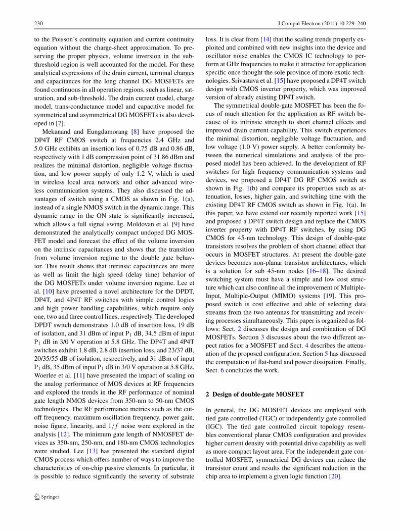
Mekanand and Eungdamorang [8] have proposed theDP4T RF CMOS switch at frequencies 2.4 GHz and5.0 GHz exhibits an insertion loss of 0.75 dB and 0.86 dB,respectively with 1 dB compression point of 31.86 dBm andrealizes the minimal distortion, negligible voltage fluctua-tion, and low power supply of only 1.2 V, which is usedin wireless local area network and other advanced wire-less communication systems. They also discussed the ad-vantages of switch using a CMOS as shown in Fig. 1(a),instead of a single NMOS switch in the dynamic range. Thisdynamic range in the ON state is significantly increased,which allows a full signal swing. Moldovan et al. [9] havedemonstrated the analytically compact undoped DG MOS-FET model and forecast the effect of the volume inversionon the intrinsic capacitances and shows that the transitionfrom volume inversion regime to the double gate behav-ior. This result shows that intrinsic capacitances are moreas well as limit the high speed (delay time) behavior ofthe DG MOSFETs under volume inversion regime. Lee etal. [10] have presented a novel architecture for the DPDT,DP4T, and 4P4T RF switches with simple control logicsand high power handling capabilities, which require onlyone, two and three control lines, respectively. The developedDPDT switch demonstrates 1.0 dB of insertion loss, 19 dBof isolation, and 31 dBm of input P1 dB, 34.5 dBm of inputP1 dB in 3/0 V operation at 5.8 GHz. The DP4T and 4P4Tswitches exhibit 1.8 dB, 2.8 dB insertion loss, and 23/37 dB,20/35/55 dB of isolation, respectively, and 31 dBm of inputP1 dB, 35 dBm of input P1 dB in 3/0 V operation at 5.8 GHz.Woerlee et al. [11] have presented the impact of scaling onthe analog performance of MOS devices at RF frequenciesand explored the trends in the RF performance of nominalgate length NMOS devices from 350-nm to 50-nm CMOStechnologies. The RF performance metrics such as the cut-off frequency, maximum oscillation frequency, power gain,noise figure, linearity, and 1/f noise were explored in theanalysis [12]. The minimum gate length of NMOSFET de-vices as 350-nm, 250-nm, and 180-nm CMOS technologieswere studied. Lee [13] has presented the standard digitalCMOS process which offers number of ways to improve thecharacteristics of on-chip passive elements. In particular, itis possible to reduce significantly the severity of substrate
loss. It is clear from [14] that the scaling trends properly ex-ploited and combined with new insights into the device andoscillator noise enables the CMOS IC technology to per-form at GHz frequencies to make it attractive for applicationspecific once thought the sole province of more exotic tech-nologies. Srivastava et al. [15] have proposed a DP4T switchdesign with CMOS inverter property, which was improvedversion of already existing DP4T switch.
The symmetrical double-gate MOSFET has been the fo-cus of much attention for the application as RF switch be-cause of its intrinsic strength to short channel effects andimproved drain current capability. This switch experiencesthe minimal distortion, negligible voltage fluctuation, andlow voltage (1.0 V) power supply. A better conformity be-tween the numerical simulations and analysis of the pro-posed model has been achieved. In the development of RFswitches for high frequency communication systems anddevices, we proposed a DP4T DG RF CMOS switch asshown in Fig. 1(b) and compare its properties such as at-tenuation, losses, higher gain, and switching time with theexisting DP4T RF CMOS switch as shown in Fig. 1(a). Inthis paper, we have extend our recently reported work [15]and proposed a DP4T switch design and replace the CMOSinverter property with DP4T RF switches, by using DGCMOS for 45-nm technology. This design of double-gatetransistors resolves the problem of short channel effect thatoccurs in MOSFET structures. At present the double-gatedevices becomes non-planar transistor architectures, whichis a solution for sub 45-nm nodes [16–18]. The desiredswitching system must have a simple and low cost struc-ture which can also confine all the improvement of Multiple-Input, Multiple-Output (MIMO) systems [19]. This pro-posed switch is cost effective and able of selecting datastreams from the two antennas for transmitting and receiv-ing processes simultaneously. This paper is organized as fol-lows: Sect. 2 discusses the design and combination of DGMOSFETs. Section 3 discusses about the two different as-pect ratios for a MOSFET and Sect. 4 describes the attenu-ation of the proposed configuration. Section 5 has discussedthe computation of flat-band and power dissipation. Finally,Sect. 6 concludes the work.
2 Design of double-gate MOSFET
In general, the DG MOSFET devices are employed withtied gate controlled (TGC) or independently gate controlled(IGC). The tied gate controlled circuit topology resem-bles conventional planar CMOS configuration and provideshigher current density with potential drive capability as wellas more compact layout area. For the independent gate con-trolled MOSFET, symmetrical DG devices can reduce thetransistor count and results the significant reduction in thechip area to implement a given logic function [20].
J Comput Electron (2011) 10:229–240 231
Fig. 1 Schematic circuitdiagram of the (a) conventionalDP4T CMOS transceiver switch[8] and, (b) proposed DP4T DGRF CMOS transceiver switchfor advanced communicationsystems
Independent control of both gates (front and back gate) ofthe DG MOSFET in the double-gate can be used to improvethe performance and reduces the power loss in the circuits.It can also be used to merge parallel transistors in the non-critical paths. This results the reduction in effective switch-ing capacitance and hence power dissipation [21]. Since thebehavior of a switch depends on the number of controllinggates and additional logic circuit can be implemented into asingle transistor. Independent double-gate transistors can beapplied to implement universal logic functionality within asingle transistor. These features make Si-CMOS significantfor use in applications that require mixed RF and digital sys-tems [22–24].
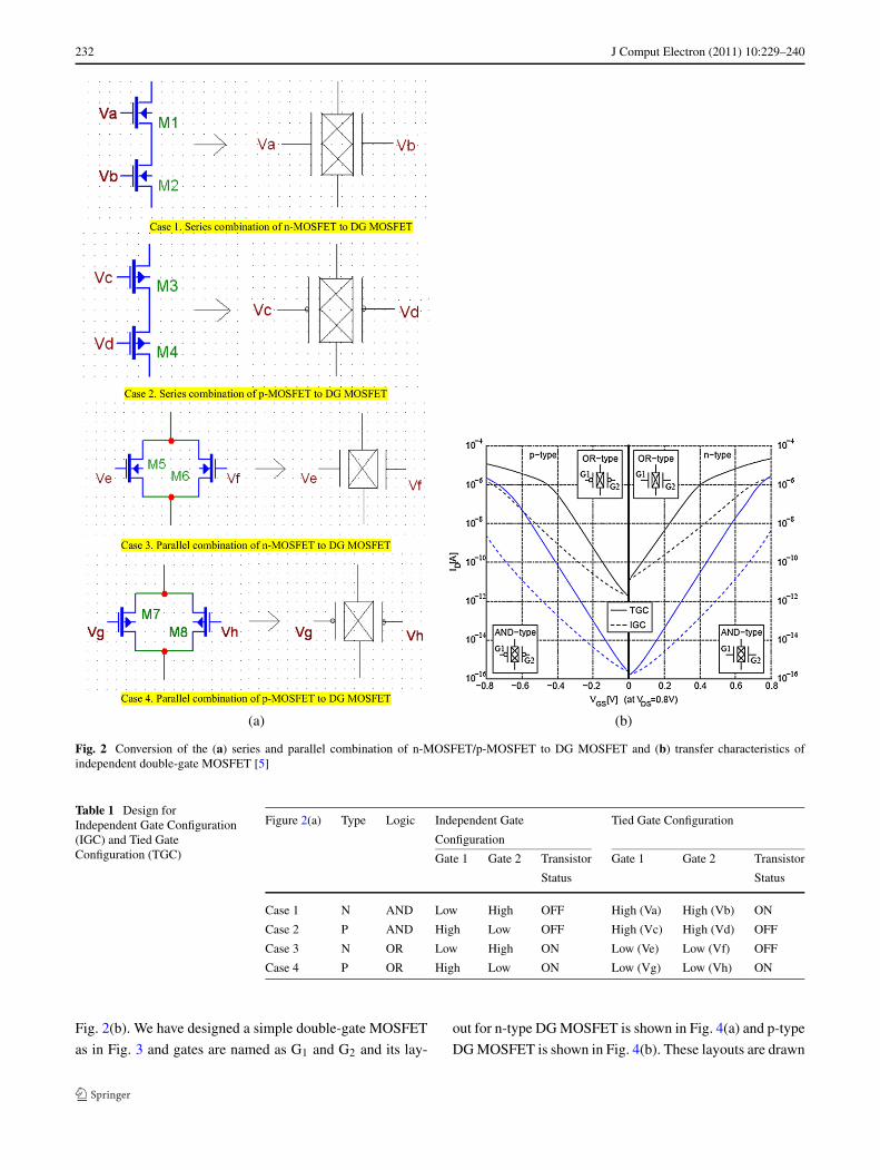
Independently controlled gate transistors reduces thenumber of transistors from circuit design perception, as twotransistors connected in series or parallel combination canbe compounded into the one transistor as shown in Fig. 2.
This procedure reduces the transistors stack height as wellas chip area and power consumption. Also ‘OR’ and ‘AND’type devices directed to higher gate delay and leakage, re-spectively for IGC. So during the circuit is inactive, the inputpatterns should be applied in a way that both gates are at thesame potential to reduce the leakage to a minimum. Nu-merous devices can be used in between the paths to balancethe lower drive current in the IGC. However, in some casesthe TGC is a better choice as a substitute for using multi-ple IGC. For this reason a trade-off between area reduction,gate delay and leakage has to be selected, when using tran-sistors with independently controlled gates. Table 1 showsthe transistor status for IGC and TGC with logic design.
The use of IGC is better for gates with small fan outand short capacitive wire loads. The circuit of Fig. 2(a)uses independently controlled gates which are investigatedby simulated in [25–28] and their characteristic is shown in
232 J Comput Electron (2011) 10:229–240
(a) (b)
Fig. 2 Conversion of the (a) series and parallel combination of n-MOSFET/p-MOSFET to DG MOSFET and (b) transfer characteristics ofindependent double-gate MOSFET [5]
Table 1 Design forIndependent Gate Configuration(IGC) and Tied GateConfiguration (TGC)
Figure 2(a) Type Logic Independent Gate Tied Gate Configuration
Configuration
Gate 1 Gate 2 Transistor Gate 1 Gate 2 Transistor
Status Status
Case 1 N AND Low High OFF High (Va) High (Vb) ON
Case 2 P AND High Low OFF High (Vc) High (Vd) OFF
Case 3 N OR Low High ON Low (Ve) Low (Vf) OFF
Case 4 P OR High Low ON Low (Vg) Low (Vh) ON
Fig. 2(b). We have designed a simple double-gate MOSFET
as in Fig. 3 and gates are named as G1 and G2 and its lay-
out for n-type DG MOSFET is shown in Fig. 4(a) and p-type
DG MOSFET is shown in Fig. 4(b). These layouts are drawn
J Comput Electron (2011) 10:229–240 233
Fig. 3 Schematic of the basic double-gate n-MOSFET
Table 2 An effective aspect ratio for different combination of transis-tors as shown in Fig. 2
Figure 2(a) Effective aspect ratio
Case 1 0.5(W/L)
Case 2 2.0(W/L)
Case 3 0.5(W/L)
Case 4 2.0(W/L)
with Microwind 3.1 version. The scalable CMOS rules sup-port both n-well and p-well processes. Here we use MO-SIS recognized n-well process based technology codes thatspecify the well type of the process selected. In Fig. 4(b) thegreen boundary shows the well for the designing of p-typeDG MOSFET and also an extra drain voltage (Vdd ) is ap-plied to support that well. With this double-gate MOSFET,we can design all the connection of Fig. 2 with the aspectratio (W/L) as shown in Table 2.
3 Aspect ratio for 45-nm DG MOSFET
The smaller MOSFETs with a lower aspect ratio (W/L) aredesirable for several reasons. The main reason is to makehigher transistors density on a chip area. This results in achip with the same functionality in a smaller area or morefunctionality in the same area. Since fabrication costs for asemiconductor wafer are relatively fixed, the cost per inte-grated circuits is mainly related to the number of chips thatcan be produced per wafer. Hence, the smaller ICs allowmore chips per wafer, reducing the price per chip. In fact,over the past 30 years the number of transistors per chip hasbeen doubled every 2–3 years once a new technology node isintroduced. Also, the smaller transistors switches are faster.For example, one approach to size reduction is a scaling ofthe MOSFET that requires all device dimensions to reduceproportionally. The main device dimensions are the transis-tor length, width, and the oxide thickness, each (used to)scale with a factor of 0.3 per node. This way, the transistorchannel resistance does not change with scaling, while gatecapacitance is cut by a factor of 0.3. Hence, the RC delay ofthe transistor scales with a factor of 0.3 means it decreases.
Fig. 4 Layout of the (a) n-type DG MOSFET, and (b) p-type DGMOSFET
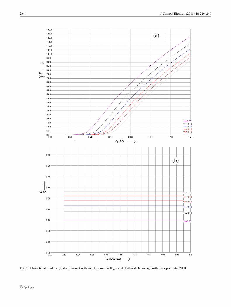
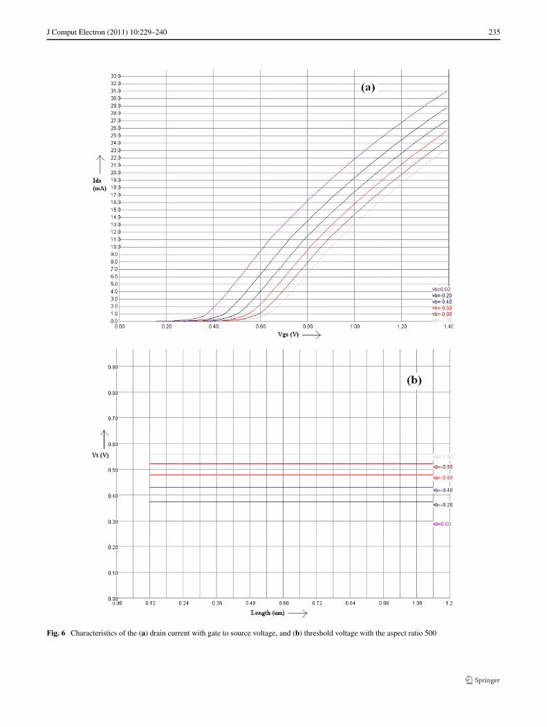
For the purpose of 45-nm technology, we selected twoaspect ratios. First, the channel length L = 0.045 µm andchannel width W = 22.5 µm (aspect ratio is 500), and sec-ond the channel length L = 0.045 µm and channel widthW = 90 µm (aspect ration is 2000). With the help of Mi-crowind 3.1 version, the simulated results for aspect ratio2000 are shown in Fig. 5(a). For the DP4T DG RF CMOSswitch design, we consider the control voltage of 1.0 V. Atthis voltage, the drain to source current (Ids ) decrease withrespect to bulk voltage. So for higher Ids as of 85 mA, low-est bulk voltage (Vb = 0 V) is needed. Also for aspect ratioof 500, Fig. 6(a) shows 22 mA of current Ids at control volt-age of 1.0 V with lowest bulk voltage (Vb = 0 V). Since indouble-gate MOSFET bulk voltage is zero, so we can obtainthe highest current easily using this proposed switch.
Figures 5(b) and 6(b), shows the threshold voltage forthe n-MOSFET of aspect ratio 2000, with channel length
234 J Comput Electron (2011) 10:229–240
Fig. 5 Characteristics of the (a) drain current with gate to source voltage, and (b) threshold voltage with the aspect ratio 2000
J Comput Electron (2011) 10:229–240 235
Fig. 6 Characteristics of the (a) drain current with gate to source voltage, and (b) threshold voltage with the aspect ratio 500
236 J Comput Electron (2011) 10:229–240
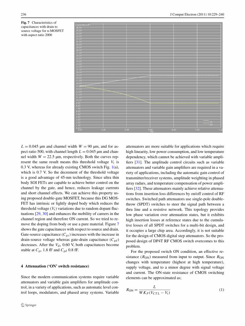
Fig. 7 Characteristics ofcapacitances with drain tosource voltage for n-MOSFETwith aspect ratio 2000
L = 0.045 µm and channel width W = 90 µm, and for as-pect ratio 500, with channel length L = 0.045 µm and chan-nel width W = 22.5 µm, respectively. Both the curves rep-resent the same result means this threshold voltage Vt is0.3 V, whereas for already existing CMOS switch Fig. 1(a),which is 0.7 V. So the decrement of the threshold voltageis a good advantage of 45-nm technology. Since ultra thinbody SOI FETs are capable to achieve better control on thechannel by the gate, and hence, reduces leakage currentsand short channel effects. We can achieve this property us-ing proposed double-gate MOSFET, because this DG MOS-FET has intrinsic or lightly doped body which reduces thethreshold voltage (Vt ) variations due to random dopant fluc-tuations [29, 30] and enhances the mobility of careers in thechannel region and therefore ON current. So we tried to re-move the doping from body or use a pure material. Figure 7shows the gate capacitances with respect to source and drain.Gate-source capacitance (Cgs ) increases with the increase indrain-source voltage whereas gate-drain capacitance (Cgd )decreases. After the Vds 0.60 V, both capacitances becomestable at Cgs 1.8 fF and Cgd 0.8 fF.
4 Attenuation (‘ON’ switch resistance)
Since the modern communication systems require variableattenuators and variable gain amplifiers for amplitude con-trol, in a variety of applications, such as automatic level con-trol loops, modulators, and phased array systems. Variable
attenuators are more suitable for applications which requirehigh linearity, low power consumption, and low temperaturedependency, which cannot be achieved with variable ampli-fiers [31]. The amplitude control circuits such as variableattenuators and variable gain amplifiers are required in a va-riety of applications, including the automatic gain control oftransmitter/receiver systems, amplitude weighting in phasedarray radars, and temperature compensation of power ampli-fiers [32]. These attenuators mainly achieve relative attenua-tions from insertion loss differences by on/off control of RFswitches. Switched path attenuators use single-pole double-throw (SPDT) switches to steer the signal path between athru line and a resistive network. This topology provideslow phase variation over attenuation states, but it exhibitshigh insertion losses at reference states due to the cumula-tive losses of all SPDT switches for a multi-bit design, andit occupies a large chip area. Accordingly, it is not suitablefor the design of CMOS digital step attenuators. So the pro-posed design of DP4T RF CMOS switch overcomes to thisproblem.
For the proposed switch ON condition, an effective re-sistance (RON) measured from input to output. Since RON
changes with temperature (highest at high temperature),supply voltage, and to a minor degree with signal voltageand current. The ON-state resistance of CMOS switchingelements can be approximated as;
RON = L
WKP (VCT L − Vt )(1)
J Comput Electron (2011) 10:229–240 237
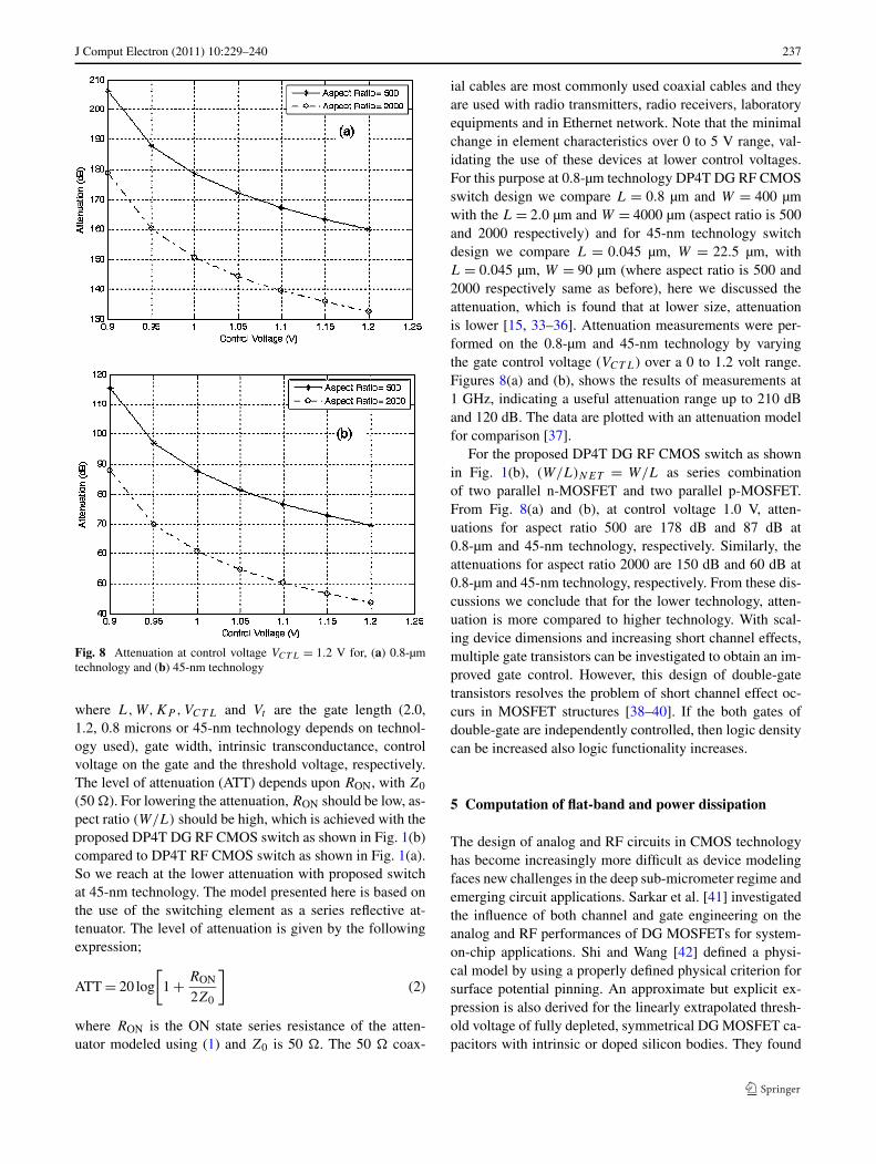
Fig. 8 Attenuation at control voltage VCT L = 1.2 V for, (a) 0.8-µmtechnology and (b) 45-nm technology
where L,W,KP ,VCT L and Vt are the gate length (2.0,1.2, 0.8 microns or 45-nm technology depends on technol-ogy used), gate width, intrinsic transconductance, controlvoltage on the gate and the threshold voltage, respectively.The level of attenuation (ATT) depends upon RON, with Z0
(50 �). For lowering the attenuation, RON should be low, as-pect ratio (W/L) should be high, which is achieved with theproposed DP4T DG RF CMOS switch as shown in Fig. 1(b)compared to DP4T RF CMOS switch as shown in Fig. 1(a).So we reach at the lower attenuation with proposed switchat 45-nm technology. The model presented here is based onthe use of the switching element as a series reflective at-tenuator. The level of attenuation is given by the followingexpression;
ATT = 20 log
[1 + RON
2Z0
](2)
where RON is the ON state series resistance of the atten-uator modeled using (1) and Z0 is 50 �. The 50 � coax-
ial cables are most commonly used coaxial cables and theyare used with radio transmitters, radio receivers, laboratoryequipments and in Ethernet network. Note that the minimalchange in element characteristics over 0 to 5 V range, val-idating the use of these devices at lower control voltages.For this purpose at 0.8-µm technology DP4T DG RF CMOSswitch design we compare L = 0.8 µm and W = 400 µmwith the L = 2.0 µm and W = 4000 µm (aspect ratio is 500and 2000 respectively) and for 45-nm technology switchdesign we compare L = 0.045 µm, W = 22.5 µm, withL = 0.045 µm, W = 90 µm (where aspect ratio is 500 and2000 respectively same as before), here we discussed theattenuation, which is found that at lower size, attenuationis lower [15, 33–36]. Attenuation measurements were per-formed on the 0.8-µm and 45-nm technology by varyingthe gate control voltage (VCT L) over a 0 to 1.2 volt range.Figures 8(a) and (b), shows the results of measurements at1 GHz, indicating a useful attenuation range up to 210 dBand 120 dB. The data are plotted with an attenuation modelfor comparison [37].
For the proposed DP4T DG RF CMOS switch as shownin Fig. 1(b), (W/L)NET = W/L as series combinationof two parallel n-MOSFET and two parallel p-MOSFET.From Fig. 8(a) and (b), at control voltage 1.0 V, atten-uations for aspect ratio 500 are 178 dB and 87 dB at0.8-µm and 45-nm technology, respectively. Similarly, theattenuations for aspect ratio 2000 are 150 dB and 60 dB at0.8-µm and 45-nm technology, respectively. From these dis-cussions we conclude that for the lower technology, atten-uation is more compared to higher technology. With scal-ing device dimensions and increasing short channel effects,multiple gate transistors can be investigated to obtain an im-proved gate control. However, this design of double-gatetransistors resolves the problem of short channel effect oc-curs in MOSFET structures [38–40]. If the both gates ofdouble-gate are independently controlled, then logic densitycan be increased also logic functionality increases.
5 Computation of flat-band and power dissipation
The design of analog and RF circuits in CMOS technologyhas become increasingly more difficult as device modelingfaces new challenges in the deep sub-micrometer regime andemerging circuit applications. Sarkar et al. [41] investigatedthe influence of both channel and gate engineering on theanalog and RF performances of DG MOSFETs for system-on-chip applications. Shi and Wang [42] defined a physi-cal model by using a properly defined physical criterion forsurface potential pinning. An approximate but explicit ex-pression is also derived for the linearly extrapolated thresh-old voltage of fully depleted, symmetrical DG MOSFET ca-pacitors with intrinsic or doped silicon bodies. They found
238 J Comput Electron (2011) 10:229–240
a better result between the values of threshold-voltage cal-culated using this expression and those extracted from thenumerically simulated current-voltage characteristics of DGMOSFET. Instead of increasing monotonically with the gateoxide thickness, the linearly extrapolated threshold voltageof a DG MOSFET device with a doped silicon body is foundto exhibit a global minimum. The dependence of this min-imum threshold-voltage on body doping concentration isevaluated.
In general, the physical oxide thickness is determinedby ellipsometer, but its accuracy cannot be guaranteed forthose of very thin oxides. Another approach is using highresolution transmission electron microscopy analysis. Thismethod is more accurate, but still suffers from high costand low throughput. In addition, the thickness measuredwith these methods is physical thickness. It cannot be em-ployed to determine the equivalent oxide thickness of thehigh dielectric constant (high-K) materials, proposed for fu-ture ULSI CMOS application, because dielectric constantsof these materials are different to that of oxide. Furthermore,the thickness of thick oxide can also be derived from theelectrical capacitance–voltage (C–V ) data in inversion re-gion or strong accumulation region [43, 44]. However, thismethod cannot be applied directly for thin oxide, becausethe thickness measured from C–V curve consists of poly-gate depletion width, oxide thickness, and inversion chargethickness for the inversion state. Both oxide thickness andaccumulation charge thickness are included for strong accu-mulation state. Therefore, Chain et al. [45] have proposed anovel and simple method to determine ultrathin oxide thick-ness, based on the measuring of MOS flat-band capacitance.At flat-band condition, the surface band bending and thesemiconductor charge are both small and can be neglected.Here the classical MOS theory can be safely applied withoutconsidering partial differential equation and quantum mech-anism, thus simplifying the extracting of thickness proce-dure [46].
The presented model of a DP4T DG RF CMOS switchpredicts that the flat-band capacitance equals the oxide ca-pacitance. This is due to ignoring any charge variation in thesemiconductor, as in double-gate MOSFET this is intrinsicor lightly doped [47]. So we derive the exact flat-band capac-itance (CFB ) and find out the flat-band voltage (VFB ), by theuse of flat-band capacitance method. In this method an idealvalue of the CFB has been calculated using (3). Once thevalue of CFB is known, the value of VFB can be obtainedfrom the C–V curve, by interpolating the closest gate-to-substrate (VGS ) values [43, 48]. For flat-band condition theflat-band capacitance is as;
CFB = COX · εSA/λD
COX + εSA/λD
(3)
where λD is the extrinsic Debye length, oxide capacitance,COX is 5.202 pF, permittivity of the substrate material, εS is
11.7×8.85×10−14 F cm−1 and A is the gate area (cm2), sowe found the value of λD 1.279 × 10⁻⁵ cm as well as CFB
3.167 pF. For the proposed DP4T DG RF CMOS switch asshown in Fig. 1(b), CFB is series combination of two p-MOS. So CFB will be 1.59 pF. Similarly, the value will besame for n-MOSFET, if both MOSFET are designed withsame parameters.
For CMOS circuits where no DC current flows, averagedynamic power is given by Pavg = CL × V 2
DD × f , whereCL, VDD and f represents the total load capacitance, powersupply and frequency of the signal transition respectivelyfor combinational CMOS logic, applies only to dynamic(capacitive) power. For this purpose dc power and/or short-circuit power must be computed separately [49, 50]. For theproposed DP4T DG RF CMOS Switch, CL becomes halfof the general CMOS switch as well as power supply alsodecreases, so average dynamic power become less for thisproposed switch, which is an improved results compared toalready existing switches.
6 Conclusion
In this paper, we conclude that the threshold voltage (Vt )of the double-pole four-throw double-gate switch is 0.3 V,whereas for already existing CMOS switch it is 0.7 V. In theDG MOSFET, the bulk voltage is zero, so we can achieve thehighest drain current easily by using this proposed switch.At higher technology, attenuation is lower, as in this paper,we reported 60 dB to 87 dB for 45-nm technology comparedto 150 dB to 187 dB for 0.8-µm technology. Off-isolationand switching speed are significantly improved in the pro-posed DP4T DG RF CMOS switch over the already ex-isting CMOS switch. Moreover, the flat-band capacitanceand power dissipation becomes half and threshold voltageas well as flat-band voltages is reduced as flat-band capaci-tance becomes half for the proposed DP4T DG RF CMOSswitch. The half power dissipation has been discussed forthe proposed DP4T DG RF CMOS switch and compared theresults with the already existing CMOS switches. Ultra thinbody SOI FETs employ very thin silicon body to achievebetter control of the channel by the gate and hence, reducedthe leakage and short channel effects. By use of the intrin-sic or lightly doped body, in the DG MOSFET, reduces thethreshold voltage variations due to random dopant fluctua-tions and enhances the mobility of the careers in the channelregion and therefore increment in ‘ON’ current occurs. Sowe can get a better result by using this DG MOSFET 45-nmtechnology as it has intrinsic or lightly doped body for theapplication of DP4T DG RF CMOS switch.
Acknowledgements Authors are sincerely thankful to the potentialreviewers for their decisive time to review this article, and critical com-ments and suggestions to improve the quality of the manuscript.
J Comput Electron (2011) 10:229–240 239
References
1. Wang, B.H., Hui, H.T.: Investigation on the FFT-based antennaselection for compact uniform circular arrays in correlated MIMOchannels. IEEE Trans. Signal Process. 59(2), 739–746 (2011)
2. Kristem, V., Mehta, N.B., Molisch, A.F.: A novel, balanced, andenergy-efficient training method for receive antenna selection.IEEE Trans. Wirel. Commun. 9(9), 2742–2753 (2010)
3. Srivastava, V.M., Yadav, K.S., Singh, G.: Design and performanceanalysis of double-gate MOSFET over single-gate MOSFET forRF switch. Microelectron. J. 42(3), 527–534 (2011)
4. Sjoblom, P., Sjoland, H.: Measured CMOS switched high-qualitycapacitors in a reconfigurable matching network. IEEE Trans. Cir-cuits Syst. 54(10), 858–862 (2007)
5. Srivastava, V.M., Yadav, K.S., Singh, G.: Double-pole four-throwCMOS switch design with double-gate transistor. In: 2010 AnnualIEEE India Conference, 17–19 December, India, pp. 1–4 (2010
6. Gidon, S.: Double gate MOSFET modeling. In: Proceedings of theCOMSOL Multiphysics User’s Conference, Paris, pp. 1–4 (2005)
7. Lu, H., Taur, Y.: An analytic potential model for symmetric andasymmetric DG MOSFETs. IEEE Trans. Electron Devices 53(5),1161–1168 (2006)
8. Mekanand, P., Eungdamorang, D.: DP4T CMOS switch in atransceiver of MIMO system. In: Proc. of 11th IEEE Int. Confer-ence of Advanced Communication Technology, Korea, pp. 472–474 (2009)
9. Moldovan, O., Chaves, F. et al.: Accurate prediction of the volumeinversion impact on undoped Double Gate MOSFET capacitances.Int. J. Numer. Model. 23(6), 447–456 (2010)
10. Lee, C., Banerjee, B., Laskar, J.: Novel T/R switch architecturesfor MIMO applications. IEEE MTT-S Int. Microw. Symp. Dig. 4,1137–1140 (2004)
11. Woerlee, P.H., Knitel, M.J., Scholten, A.J.: RF CMOS perfor-mance trends. IEEE Trans. Electron Devices 48(8), 1776–1782(2001)
12. Ashraf, N., Vasileska, D.: 1/f noise: threshold voltage and ON-current fluctuations in 45-nm device technology due to chargedrandom traps. J. Comput. Electron., 9(3–4), 128–134 (2010)
13. Lee, T.H.: CMOS RF no longer an oxymoron. In: Proc. of the 19thGallium Arsenide Integrated Circuit Symposium, USA, pp. 244–247 (1997)
14. Ahmed, S., Ringhofer, C., Vasileska, D.: An effective potential ap-proach to modeling 25 nm MOSFET devices. J. Comput. Electron.9(3–4), 197–200 (2010)
15. Srivastava, V.M., Yadav, K.S., Singh, G.: Double pole four throwswitch design with CMOS inverter. In: Proc. of 5th IEEE Con-ference on Wireless Communication and Sensor Networks, India,15–19 December, pp. 1–4 (2009)
16. Sverdlov, V.: Scaling, power consumption, and mobility enhance-ment techniques. In: Selberherr, S. (ed.) Strain Induced Effects inAdvanced MOSFET, Computational Microelectronics, pp. 5–22(2011)
17. Cheng, Y., Matloubian, M.: Parameter extraction of accurate andscaleable substrate resistance components in RF MOSFETs. IEEEElectron Device Lett. 23(4), 221–223 (2002)
18. Lin, Y.S., Lu, S.S., Lee, T.S., Liang, H.B.: Characterization andmodeling of small signal substrate resistance effect in RF CMOS.In: Proc. of IEEE MTT-S Digest, Seattle, WA, June, pp. 161–164(2002)
19. Luo, Z., Steegen, A., Eller, M., Mann, R., Baiocco, C., Nguyen,P., Kim, L., Hoinkis, M., Ku, V., Wann, C.: High performance andlow power transistors integrated in 65 nm bulk CMOS technology.In: Proc. of Int. Electron Device Meeting, CA, April, pp. 661–664(2004)
20. Kuang, J.B., Kim, K., Chuang, C.T., Ngo, H.C., Gebara, F.H.,Nowka, K.J.: Circuit techniques utilizing independent gate control
in double-gate technologies. IEEE Trans. Very Large Scale Integr.16(12), 1657–1665 (2008)
21. Kaushik, R., Mahmoodi, H., Mukhopadhyay, S.: Double-gate SOIdevices for low-power and high-performance applications. In:Proc. of 19th Int. Conference on VLSI Design, USA, pp. 445–452(2006)
22. Weis, M., Emling, R., Schmitt, D.: Circuit design with indepen-dent double-gate transistors. Adv. Radio Sci. 7, 231–236 (2009)
23. Weis, M., Pfitzner, A., Kasprowicz, D., Emling, R., Maly, W.,Landsiedel, D.: Adder circuits with transistors using indepen-dently controlled gates. In: Proc. of IEEE Int. Symp. on Circuitsand Systems, Taipei, 24–27 May, pp. 449–452 (2009)
24. Claeys, C.: ULSI Process Integration III. Electrochemical Society,January 2003
25. Chiang, M.H., Kim, K., Tretz, C.: High-density reduced-Stacklogic circuit techniques using independent-gate controlled double-gate devices. IEEE Trans. Electron Devices 53(9), 2370–2377(2006)
26. Mukhopadhyay, S., Mahmoodi, H., Roy, K.: Design of high per-formance sense amplifier using independent gate control in sub-50 nm double-gate MOSFET. In: Proc. of 6th Int. Symposium onQuality of Electronic Design, USA, 21–23 March 2005, pp. 490–495 (2005)
27. Weste, N., Harris, D.: CMOS VLSI Design: A Circuits and Sys-tems Perspective, 3rd edn. Pearson Addison Wesley, Reading(2005)
28. Weis, M.: Low power SRAM cell using vertical slit field effecttransistor. In: Proc. of European Solid-State Circuits Conference,Edinburgh, 15–19 September (2008)
29. Shin, C., Sun, X., Liu, K.: Study of random-dopant-fluctuation ef-fects for the tri-gate bulk MOSFET. IEEE Trans. Electron Devices56(7), 1538–1542 (2009)
30. Litwin, A.: Overlooked interfacial silicide-polysilicon gate resis-tance in MOS transistors. IEEE Trans. Electron Devices 48(9),2179–2181 (2001)
31. Min, B.W., Rebeiz, G.M.: A 10–50-GHz CMOS distributed stepattenuator with low loss and low phase imbalance. IEEE J. Solid-State Circuits 42(11), 2547–2554 (2007)
32. Ku, B.H., Hong, S.: 6-bit CMOS digital attenuators with low phasevariations for X-band phased-array systems. IEEE Trans. Microw.Theory Tech. 58(7), 1651–1663 (2010)
33. Gogineni, U., Li, H., Alamo, J., Wang, J., Jagannathan, B.: Effectof substrate contact shape and placement on RF characteristics of45-nm low-power CMOS devices. In: Proc. of Radio FrequencyIntegrated Circuits Symposium, USA, pp. 163–166 (2009)
34. Gogineni, U., Li, H., Alamo, J., Wang, J., Jagannathan, B.: Ef-fect of substrate contact shape and placement on RF characteristicsof 45-nm low-power CMOS devices. IEEE J. Solid-State Circuits45(5), 998–1006 (2010)
35. Lee, S.H., Kim, C.S., Yu, H.K.: A small signal RF model and itsparameter extraction for Substrate Effects in RF MOSFETs. IEEETrans. Electron Devices 48(7), 1374–1379 (2001)
36. Srivastava, V.M., Yadav, K.S., Singh, G.: Attenuation with doublepole four throw CMOS switch design. In: 2010 IEEE In. Conf. onSemiconductor Electronics, Malaysia, 28–30 June 2010, pp. 173–175 (2010)
37. Carmo, J.P., Mendes, P.M., Correia, J.H.: A 2.4-GHz RF CMOStransceiver for wireless sensor applications. In: Proc. of Int. Con-ference on Electrical Engineering, Coimbra, pp. 902–905 (2005)
38. Raczkowski, K., Thijs, S., De Raedt, W., Nauwelaers, B.,Wambacq, P.: 50 to 67 GHz ESD-protected power amplifiers indigital 45-nm LP CMOS. In: Proc. of Int. Solid State Circuits Con-ference, CA, pp. 382–384 (2009)
39. Valdes Garcia, A., Reynolds, S., Plouchart, J.O.: 60 GHz trans-mitter circuits in 65 nm CMOS. In: Proc. of Radio FrequencyIntegrated Circuits Symposium, Atlanta, June 2008, pp. 641–644(2008)
240 J Comput Electron (2011) 10:229–240
40. Srivastava, V.M., Yadav, K.S., Singh, G.: Performance of double-pole four-throw double-gate RF CMOS Switch in 45 nm technol-ogy. Wirel. Eng. Technol. 1(2), 47–54 (2010)
41. Kumar, N.M., Syamal, B., Sarkar, C.K.: Influence of channel andgate engineering on the analog and RF performance of DG MOS-FETs. IEEE Trans. Electron Devices 57(4), 820–826 (2010)
42. Shi, X., Wong, M.: Effects of substrate doping on the linearlyextrapolated threshold voltage of symmetrical DG MOS devices.IEEE Trans. Electron Devices 52(7), 1616–1621 (2005)
43. Srivastava, V.M.: C-V Measurement using VEE Pro Software af-ter Fabrication of MOS Capacitance, 1st edn. VDM, Beau-Bassin(2010)
44. Srivastava, V.M., Yadav, K.S., Singh, G.: Application of VEE Prosoftware for measurement of MOS device parameters using C-Vcurve. Int. J. Comput. Appl. 1(7), 43–46 (2010)
45. Chen, C.H., Fang, Y.K., Yang, C.W., Ting, S.F., Tsair, Y.S., Wang,M.F., Yao, L.G., Chen, S.C., Yu, C.H., Liang, M.S.: Determinationof deep ultrathin equivalent oxide thickness from measuring flat-band curve. IEEE Trans. Electron Devices 49(4), 695–698 (2002)
46. Cox, P., Yang, P., Mahant, S., Chatterjee, P.: Statistical modelingfor efficient parametric yield estimation of MOS VLSI Circuits.IEEE J. Solid-State Circuits 20(1), 391–398 (2003)
47. Chen, C.H., Fang, Y.K., Yang, C.W., Ting, S.F., Liang, M.S.: De-termination of deep ultrathin equivalent oxide thickness from mea-suring flat-band C-V curve. IEEE Trans. Electron Devices 49(4),695–698 (2002)
48. Gate Dielectric C-V Characterization Using the Model 4200Semiconductor Characterization System: Application Note, Num-ber 2239, Keithley Instruments, Ohio
49. Li, Z., Quintal, R.: A dual-band CMOS front-end with two gainmodes for wireless LAN applications. IEEE J. Solid-State Circuits39(11), 2069–2073 (2004)
50. Cheng, Y., Matloubian, M.: Frequency dependent resistive andcapacitive components in RF MOSFETs. IEEE Electron DeviceLett. 22(7), 333–335 (2001)