
Analog Micropipeline Rings for High Precision Timing
10
Analog Micropipeline Rings for High Precision Timing Scott Fairbanks Cambridge University [email protected] Simon Moore Cambridge University [email protected] Abstract I use asynchronous FIFO stages that are connected in rings to generate and deliver highly precise timing signals. I introduce a Micropipeline FIFO control stage that oscil- lates at frequencies greater to that found in a ring of three unloaded inverters. Tokens spread evenly through FIFO rings built from this control under certain conditions. The tokens are ‘locked’ into an equally separated pattern by a classical feedback control where the actuator is the FIFO control stage. The actuating variable is the stage latency which varies according to the temporal separation of its in- puts. When the tokens in the FIFO ring are equally spaced, the relative phases of the nodes in the system assume pre- dictable values. This technique allows the division of a better than three gate delay cycle time into an arbitrarily large number of phases whose precision is limited only by the limits of the fabrication process and noise. Applications that need a pre- cise time reference can benefit from this technique. A/D con- version, clock recovery, and multi-phase clocking solutions are briefly sketched. 1. Introduction This paper advances work from two papers presented at previous meetings of this conference. Ebergen et al [4] explored how data tokens distribute themselves throughout a free running FIFO. An accurate characterization of the FIFO was performed using a delay characterization for an asynchronous control stage that took into account the temporal proximity of its inputs. With this characterization and the response times of the source and sink to the FIFO, they predicted how tokens could be expected to distribute themselves over a section of free running FIFO. They confirmed the predictions us- ing HSPICE simulations. Winstanley et al [10] continues this investigation by clos- ing the section of FIFO into a ring and explaining why the tokens in the ring sometimes gather into a bunch and some- times do not. They were able to force the tokens to bunch in the ring and were also able to force them to spread apart evenly throughout the ring by use of a novel state holder or ‘keeper’ circuit at the output of the C-element. This current paper again looks at rings of asynchronous FIFO control. However the focus is to amplify and ex- ploit the effect whereby tokens evenly distribute themselves around the ring. I refer to this state as locked. 2. Theory 2.1. Tokens and Phases A token in a FIFO usually represents the presence of data. In a Micropipeline [9] its presence is signaled when the binary output of adjacent stages are complements. Data movements in Micropipeline FIFO stages are of- ten viewed as atomic. The data is there or it is not. In this paper, a token can be smeared across a number of stages. When the tokens in the ring are locked, the outputs of ad- jacent FIFO stages have a fixed phase relationship with re- spect to each other. A token experiences 180° of phase shift when it moves between two stages within a ring built from asynchronous FIFO stages that communicate using Micropipeline signal- ing. If tokens are confined to a ring and spread evenly through the ring, then the phase shift at the output of each stage must be: φ = tokens stages * 180° (1) ‘Fractional number of tokens per stage’ and ‘phase offset per stage’ are then equivalent descriptions. The total number of phases available, assuming differen- tial signaling, is twice the number of stages. 2.2. The FIFO Stage The FIFO stage I use is shown in Figure 1. This stage implements the C-element function. Complementary values are held on the output by the cross coupled inverters that I refer to as a keeper. When the
-
Upload
independent -
Category
Documents
-
view
3 -
download
0
Transcript of Analog Micropipeline Rings for High Precision Timing
Analog Micropipeline Rings for High Precision Timing
Scott FairbanksCambridge University
Simon MooreCambridge University
Abstract
I use asynchronous FIFO stages that are connected inrings to generate and deliver highly precise timing signals.I introduce a Micropipeline FIFO control stage that oscil-lates at frequencies greater to that found in a ring of threeunloaded inverters. Tokens spread evenly through FIFOrings built from this control under certain conditions. Thetokens are ‘locked’ into an equally separated pattern by aclassical feedback control where the actuator is the FIFOcontrol stage. The actuating variable is the stage latencywhich varies according to the temporal separation of its in-puts. When the tokens in the FIFO ring are equally spaced,the relative phases of the nodes in the system assume pre-dictable values.
This technique allows the division of a better than threegate delay cycle time into an arbitrarily large number ofphases whose precision is limited only by the limits of thefabrication process and noise. Applications that need a pre-cise time reference can benefit from this technique. A/D con-version, clock recovery, and multi-phase clocking solutionsare briefly sketched.
1. Introduction
This paper advances work from two papers presented atprevious meetings of this conference.
Ebergen et al [4] explored how data tokens distributethemselves throughout a free running FIFO.
An accurate characterization of the FIFO was performedusing a delay characterization for an asynchronous controlstage that took into account the temporal proximity of itsinputs. With this characterization and the response times ofthe source and sink to the FIFO, they predicted how tokenscould be expected to distribute themselves over a sectionof free running FIFO. They confirmed the predictions us-ing HSPICE simulations.
Winstanley et al [10] continues this investigation by clos-ing the section of FIFO into a ring and explaining why thetokens in the ring sometimes gather into a bunch and some-
times do not. They were able to force the tokens to bunchin the ring and were also able to force them to spread apartevenly throughout the ring by use of a novel state holder or‘keeper’ circuit at the output of the C-element.
This current paper again looks at rings of asynchronousFIFO control. However the focus is to amplify and ex-ploit the effect whereby tokens evenly distribute themselvesaround the ring. I refer to this state aslocked.
2. Theory
2.1. Tokens and Phases
A token in a FIFO usually represents the presence ofdata. In a Micropipeline [9] its presence is signaled whenthe binary output of adjacent stages are complements.
Data movements in Micropipeline FIFO stages are of-ten viewed as atomic. The data is there or it is not. In thispaper, a token can be smeared across a number of stages.When the tokens in the ring are locked, the outputs of ad-jacent FIFO stages have a fixed phase relationship with re-spect to each other.
A token experiences180° of phase shift when it movesbetween two stages within a ring built from asynchronousFIFO stages that communicate using Micropipeline signal-ing. If tokens are confined to a ring and spread evenlythrough the ring, then the phase shift at the output of eachstage must be:
φ =tokensstages
∗ 180° (1)
‘Fractional number of tokens per stage’ and ‘phase offsetper stage’ are then equivalent descriptions.
The total number of phases available, assuming differen-tial signaling, is twice the number of stages.
2.2. The FIFO Stage
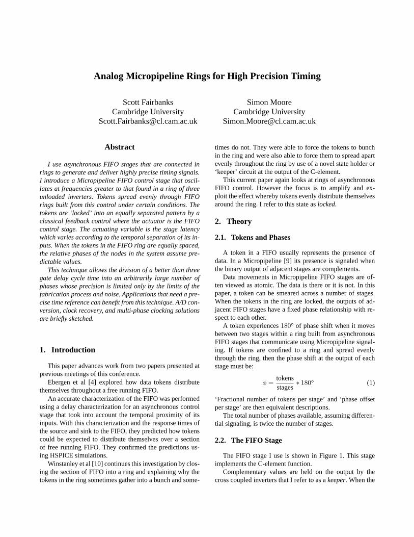
The FIFO stage I use is shown in Figure 1. This stageimplements the C-element function.
Complementary values are held on the output by thecross coupled inverters that I refer to as akeeper. When the
keeperinverters
inputinverters
A
B
A'
B'
CC'
keeperinverters
inputinverters
A
B
A'
B'
CC'
A B
C
C
icon
Figure 1. Analog C-element
inputs agree, the state of the output is set to the same valueas the inputs. When the inputs disagree the binary state ofthe output is the value of the inputs when they last agreed.The actual potential at the output of this gate is removedfrom the supply or ground by an amount determined by thevoltage divider formed by the inverter connected to the as-serted input against the keeper and the inverter connectedto the unasserted input. I call this an Analog C-element be-cause its output voltage is expected to take on a range ofvalues and its inputs sense this same range of values.
Some things to note about the Analog C-element are:
Symmetry It is completely symmetric. I don’t know ofany other electrically symmetric C-elements. This C-element alone is used as the FIFO stage in this paper.The shortest path back to any node through adjacentstages is three gate delays, ensuring robust oscillationsif all inverters are of the same size.
Economy It uses 12 transistors. None of the transistors arein series. A layout made for this stage in a 180nmprocess using2µm wide PMOS transistors and1µmwide NMOS transistors was6 × 6µ2 . The drains ofthe inverters connected to the inputs should be sharedto reduce the drain capacitance for a stage by a third.The square layout lends itself to simple placement andabutment of cells. The short distance between cells re-sults in insignificant wire loads.
Static Current If the inputs disagree then static current isdrawn. This is a problem if this FIFO stage were usedin an asynchronous environment where it might waitan unbounded period of time for its inputs to agree.
When used in a ring FIFO with locked tokens, the in-puts are always transitioning.
Performance When the inputs are in phase, the input in-verters work together and are hardly impeded by thekeeper inverter, which is mostly disabled because theinputs to the keepers inverters are switching as they tryto resist the voltage change.
When the inputs are out of phase, the output set-tles at a voltage removed from the rail. This resultsin shorter gate delays when the final input arrives be-cause the output potential must then be charged over asmaller voltage range.
Predictability There are no internal nodes between therails and the output. Internal nodes store charge thatcould be dumped onto the output and cause unexpectedphase shifts.
keeperinverters
inputinverters
A
B
A'
B'
CC'
CC CCC C
Request
Acknowledge Request
AcknowledgeFour Stage Micropipeline
Figure 2. Four Stage Micropipeline
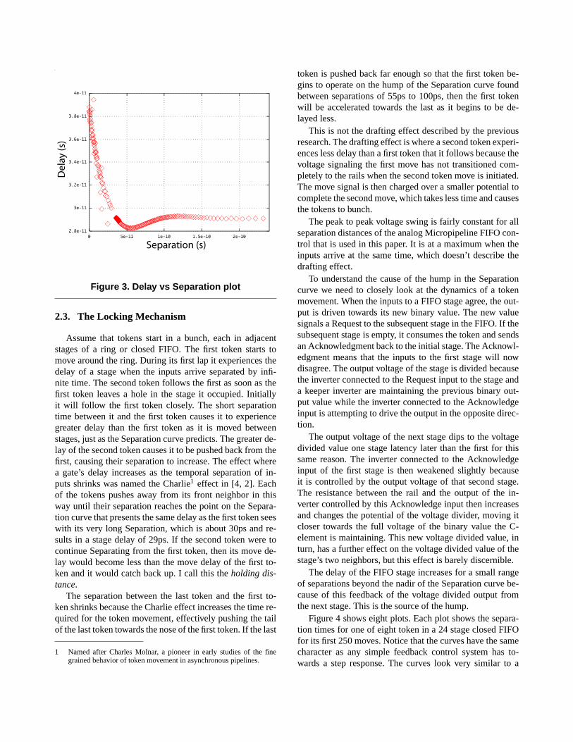
Figure 3 shows the closed loop FIFO stage delay vs tem-poral separation of the inputs. I refer to this plot as aSepa-ration curve. Both papers [4, 10] characterize a FIFO stagewith an open loop delay versus temporal input separationcharacterizations to predict their FIFO’s behavior. The openloop characteristics of the analog Micropipeline FIFO stagediffers significantly from its closed loop behavior. The Sep-aration plot shows that the delay of the stage is at a max-imum when its inputs arrive simultaneously. The delay ta-pers to a nadir near 50ps. There is a small hump from 55psto 100ps. The delay then tapers out to a constant value forlarge input separation times. The open loop characteriza-tion of the analog Micropipeline did not have the hump thatstarts at 55ps. Instead the delay monotonically tapered to aconstant delay value of 18ps at around a 200ps separation.
Separation (s)
Del
ay (s
)
Figure 3. Delay vs Separation plot
2.3. The Locking Mechanism
Assume that tokens start in a bunch, each in adjacentstages of a ring or closed FIFO. The first token starts tomove around the ring. During its first lap it experiences thedelay of a stage when the inputs arrive separated by infi-nite time. The second token follows the first as soon as thefirst token leaves a hole in the stage it occupied. Initiallyit will follow the first token closely. The short separationtime between it and the first token causes it to experiencegreater delay than the first token as it is moved betweenstages, just as the Separation curve predicts. The greater de-lay of the second token causes it to be pushed back from thefirst, causing their separation to increase. The effect wherea gate’s delay increases as the temporal separation of in-puts shrinks was named the Charlie1 effect in [4, 2]. Eachof the tokens pushes away from its front neighbor in thisway until their separation reaches the point on the Separa-tion curve that presents the same delay as the first token seeswith its very long Separation, which is about 30ps and re-sults in a stage delay of 29ps. If the second token were tocontinue Separating from the first token, then its move de-lay would become less than the move delay of the first to-ken and it would catch back up. I call this theholding dis-tance.
The separation between the last token and the first to-ken shrinks because the Charlie effect increases the time re-quired for the token movement, effectively pushing the tailof the last token towards the nose of the first token. If the last
1 Named after Charles Molnar, a pioneer in early studies of the finegrained behavior of token movement in asynchronous pipelines.
token is pushed back far enough so that the first token be-gins to operate on the hump of the Separation curve foundbetween separations of 55ps to 100ps, then the first tokenwill be accelerated towards the last as it begins to be de-layed less.
This is not the drafting effect described by the previousresearch. The drafting effect is where a second token experi-ences less delay than a first token that it follows because thevoltage signaling the first move has not transitioned com-pletely to the rails when the second token move is initiated.The move signal is then charged over a smaller potential tocomplete the second move, which takes less time and causesthe tokens to bunch.
The peak to peak voltage swing is fairly constant for allseparation distances of the analog Micropipeline FIFO con-trol that is used in this paper. It is at a maximum when theinputs arrive at the same time, which doesn’t describe thedrafting effect.
To understand the cause of the hump in the Separationcurve we need to closely look at the dynamics of a tokenmovement. When the inputs to a FIFO stage agree, the out-put is driven towards its new binary value. The new valuesignals a Request to the subsequent stage in the FIFO. If thesubsequent stage is empty, it consumes the token and sendsan Acknowledgment back to the initial stage. The Acknowl-edgment means that the inputs to the first stage will nowdisagree. The output voltage of the stage is divided becausethe inverter connected to the Request input to the stage anda keeper inverter are maintaining the previous binary out-put value while the inverter connected to the Acknowledgeinput is attempting to drive the output in the opposite direc-tion.
The output voltage of the next stage dips to the voltagedivided value one stage latency later than the first for thissame reason. The inverter connected to the Acknowledgeinput of the first stage is then weakened slightly becauseit is controlled by the output voltage of that second stage.The resistance between the rail and the output of the in-verter controlled by this Acknowledge input then increasesand changes the potential of the voltage divider, moving itcloser towards the full voltage of the binary value the C-element is maintaining. This new voltage divided value, inturn, has a further effect on the voltage divided value of thestage’s two neighbors, but this effect is barely discernible.
The delay of the FIFO stage increases for a small rangeof separations beyond the nadir of the Separation curve be-cause of this feedback of the voltage divided output fromthe next stage. This is the source of the hump.
Figure 4 shows eight plots. Each plot shows the separa-tion times for one of eight token in a 24 stage closed FIFOfor its first 250 moves. Notice that the curves have the samecharacter as any simple feedback control system has to-wards a step response. The curves look very similar to a
plot of the temperature near the heat source of a house dur-ing winter after the thermostat is turned on. Initially the tar-get is overshot by a large amount and then there is a largeamount of ringing about the target while the controlled vari-able converges.
The effect of the electronic force between two like-charged particles is similar to the interaction between to-kens in a ring. Intuition about how charged particles inter-act can be applied with tokens in a ring. Equally spacedcharges confined to the same closed path, such as electronsorbiting at the same energy level around a nucleus, arrangethemselves into the lowest energy state which is equidis-tant. The main difference in the charged particle system andthe tokens in a ring is that the tokens have a limited sep-aration over which they affect each other. This illustrationmight be helpful.
In the simulations used to draw Figures 4 and 5, one hun-dred moves required about 7.5ns to 10ns.
Move
Sep
arat
ion
(s)
Figure 4. Separation between a token and itspredecessor versus number of Moves for theeight tokens in a 24 stage closed FIFO
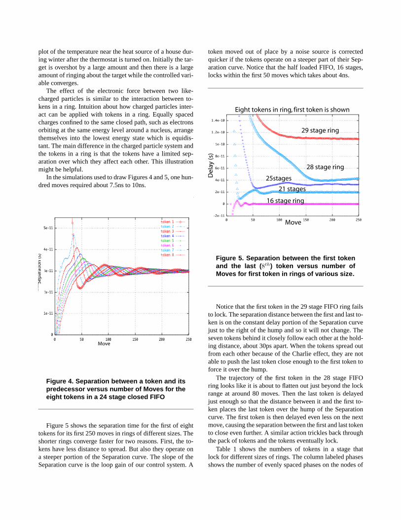
Figure 5 shows the separation time for the first of eighttokens for its first 250 moves in rings of different sizes. Theshorter rings converge faster for two reasons. First, the to-kens have less distance to spread. But also they operate ona steeper portion of the Separation curve. The slope of theSeparation curve is the loop gain of our control system. A
token moved out of place by a noise source is correctedquicker if the tokens operate on a steeper part of their Sep-aration curve. Notice that the half loaded FIFO, 16 stages,locks within the first 50 moves which takes about 4ns.
16 stage ring
21 stages
25stages
28 stage ring
29 stage ring
Move
Eight tokens in ring, first token is shown
Del
ay (s
)
Figure 5. Separation between the first tokenand the last ( 8th) token versus number ofMoves for first token in rings of various size.
Notice that the first token in the 29 stage FIFO ring failsto lock. The separation distance between the first and last to-ken is on the constant delay portion of the Separation curvejust to the right of the hump and so it will not change. Theseven tokens behind it closely follow each other at the hold-ing distance, about 30ps apart. When the tokens spread outfrom each other because of the Charlie effect, they are notable to push the last token close enough to the first token toforce it over the hump.
The trajectory of the first token in the 28 stage FIFOring looks like it is about to flatten out just beyond the lockrange at around 80 moves. Then the last token is delayedjust enough so that the distance between it and the first to-ken places the last token over the hump of the Separationcurve. The first token is then delayed even less on the nextmove, causing the separation between the first and last tokento close even further. A similar action trickles back throughthe pack of tokens and the tokens eventually lock.
Table 1 shows the numbers of tokens in a stage thatlock for different sizes of rings. The column labeled phasesshows the number of evenly spaced phases on the nodes of
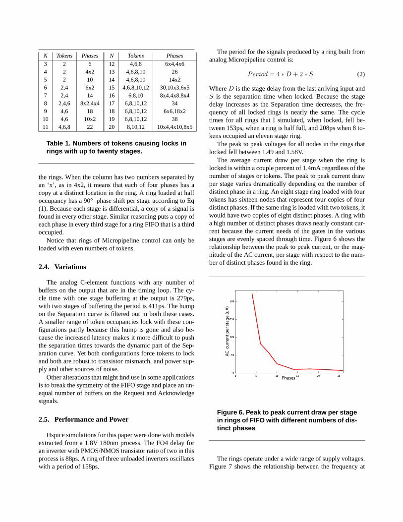
N Tokens Phases N Tokens Phases
3 2 6 12 4,6,8 6x4,4x64 2 4x2 13 4,6,8,10 265 2 10 14 4,6,8,10 14x26 2,4 6x2 15 4,6,8,10,12 30,10x3,6x57 2,4 14 16 6,8,10 8x4,4x8,8x48 2,4,6 8x2,4x4 17 6,8,10,12 349 4,6 18 18 6,8,10,12 6x6,18x210 4,6 10x2 19 6,8,10,12 3811 4,6,8 22 20 8,10,12 10x4,4x10,8x5
Table 1. Numbers of tokens causing locks inrings with up to twenty stages.
the rings. When the column has two numbers separated byan ‘x’, as in 4x2, it means that each of four phases has acopy at a distinct location in the ring. A ring loaded at halfoccupancy has a 90° phase shift per stage according to Eq(1). Because each stage is differential, a copy of a signal isfound in every other stage. Similar reasoning puts a copy ofeach phase in every third stage for a ring FIFO that is a thirdoccupied.
Notice that rings of Micropipeline control can only beloaded with even numbers of tokens.
2.4. Variations
The analog C-element functions with any number ofbuffers on the output that are in the timing loop. The cy-cle time with one stage buffering at the output is 279ps,with two stages of buffering the period is 411ps. The humpon the Separation curve is filtered out in both these cases.A smaller range of token occupancies lock with these con-figurations partly because this hump is gone and also be-cause the increased latency makes it more difficult to pushthe separation times towards the dynamic part of the Sep-aration curve. Yet both configurations force tokens to lockand both are robust to transistor mismatch, and power sup-ply and other sources of noise.
Other alterations that might find use in some applicationsis to break the symmetry of the FIFO stage and place an un-equal number of buffers on the Request and Acknowledgesignals.
2.5. Performance and Power
Hspice simulations for this paper were done with modelsextracted from a 1.8V 180nm process. The FO4 delay foran inverter with PMOS/NMOS transistor ratio of two in thisprocess is 88ps. A ring of three unloaded inverters oscillateswith a period of 158ps.
The period for the signals produced by a ring built fromanalog Micropipeline control is:
Period = 4 ∗D + 2 ∗ S (2)
WhereD is the stage delay from the last arriving input andS is the separation time when locked. Because the stagedelay increases as the Separation time decreases, the fre-quency of all locked rings is nearly the same. The cycletimes for all rings that I simulated, when locked, fell be-tween 153ps, when a ring is half full, and 208ps when 8 to-kens occupied an eleven stage ring.
The peak to peak voltages for all nodes in the rings thatlocked fell between 1.49 and 1.58V.
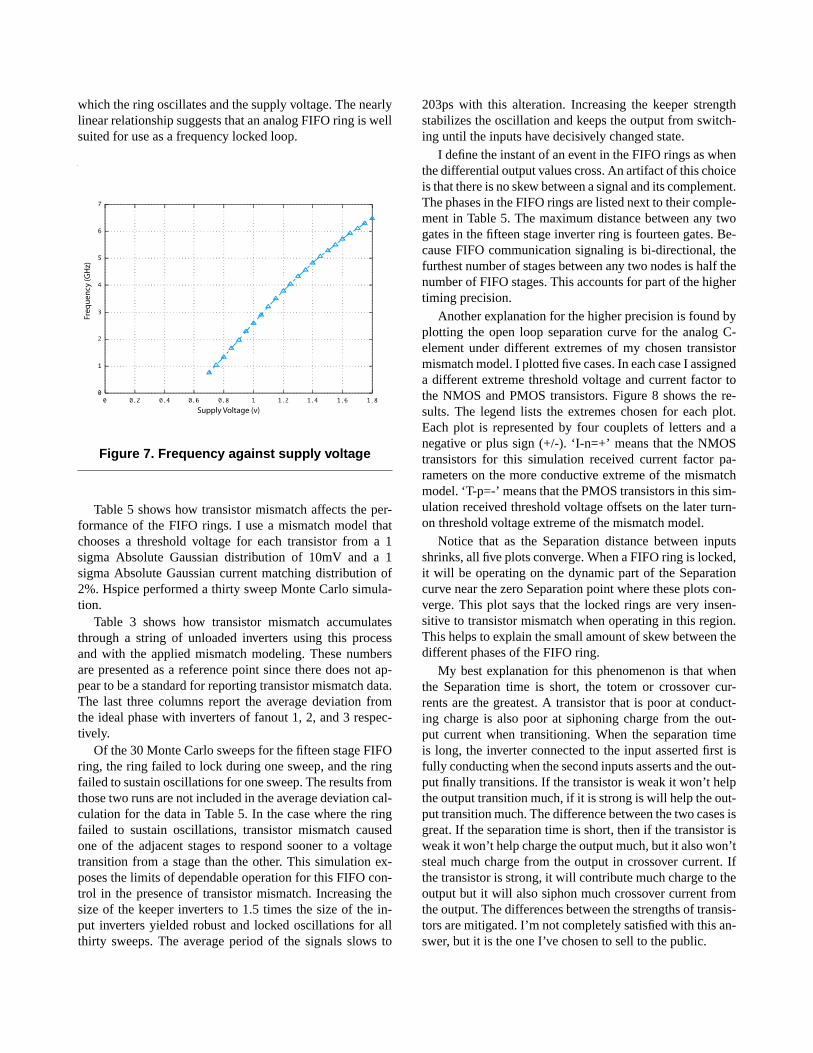
The average current draw per stage when the ring islocked is within a couple percent of 1.4mA regardless of thenumber of stages or tokens. The peak to peak current drawper stage varies dramatically depending on the number ofdistinct phase in a ring. An eight stage ring loaded with fourtokens has sixteen nodes that represent four copies of fourdistinct phases. If the same ring is loaded with two tokens, itwould have two copies of eight distinct phases. A ring witha high number of distinct phases draws nearly constant cur-rent because the current needs of the gates in the variousstages are evenly spaced through time. Figure 6 shows therelationship between the peak to peak current, or the mag-nitude of the AC current, per stage with respect to the num-ber of distinct phases found in the ring.
Phases
AC
cu
rren
t p
er s
tag
e (u
A)
Figure 6. Peak to peak current draw per stagein rings of FIFO with different numbers of dis-tinct phases
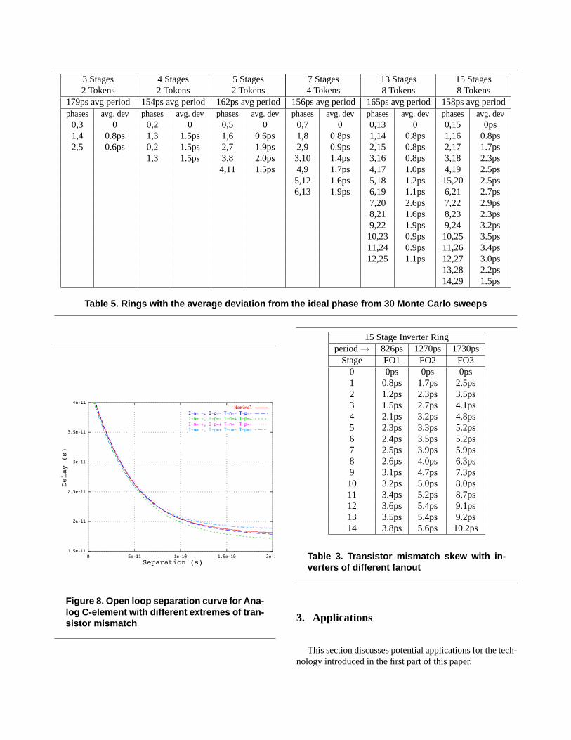
The rings operate under a wide range of supply voltages.Figure 7 shows the relationship between the frequency at
which the ring oscillates and the supply voltage. The nearlylinear relationship suggests that an analog FIFO ring is wellsuited for use as a frequency locked loop.
Supply Voltage (v)
Freq
uen
cy (G
Hz)
Figure 7. Frequency against supply voltage
Table 5 shows how transistor mismatch affects the per-formance of the FIFO rings. I use a mismatch model thatchooses a threshold voltage for each transistor from a 1sigma Absolute Gaussian distribution of 10mV and a 1sigma Absolute Gaussian current matching distribution of2%. Hspice performed a thirty sweep Monte Carlo simula-tion.
Table 3 shows how transistor mismatch accumulatesthrough a string of unloaded inverters using this processand with the applied mismatch modeling. These numbersare presented as a reference point since there does not ap-pear to be a standard for reporting transistor mismatch data.The last three columns report the average deviation fromthe ideal phase with inverters of fanout 1, 2, and 3 respec-tively.
Of the 30 Monte Carlo sweeps for the fifteen stage FIFOring, the ring failed to lock during one sweep, and the ringfailed to sustain oscillations for one sweep. The results fromthose two runs are not included in the average deviation cal-culation for the data in Table 5. In the case where the ringfailed to sustain oscillations, transistor mismatch causedone of the adjacent stages to respond sooner to a voltagetransition from a stage than the other. This simulation ex-poses the limits of dependable operation for this FIFO con-trol in the presence of transistor mismatch. Increasing thesize of the keeper inverters to 1.5 times the size of the in-put inverters yielded robust and locked oscillations for allthirty sweeps. The average period of the signals slows to
203ps with this alteration. Increasing the keeper strengthstabilizes the oscillation and keeps the output from switch-ing until the inputs have decisively changed state.
I define the instant of an event in the FIFO rings as whenthe differential output values cross. An artifact of this choiceis that there is no skew between a signal and its complement.The phases in the FIFO rings are listed next to their comple-ment in Table 5. The maximum distance between any twogates in the fifteen stage inverter ring is fourteen gates. Be-cause FIFO communication signaling is bi-directional, thefurthest number of stages between any two nodes is half thenumber of FIFO stages. This accounts for part of the highertiming precision.
Another explanation for the higher precision is found byplotting the open loop separation curve for the analog C-element under different extremes of my chosen transistormismatch model. I plotted five cases. In each case I assigneda different extreme threshold voltage and current factor tothe NMOS and PMOS transistors. Figure 8 shows the re-sults. The legend lists the extremes chosen for each plot.Each plot is represented by four couplets of letters and anegative or plus sign (+/-). ‘I-n=+’ means that the NMOStransistors for this simulation received current factor pa-rameters on the more conductive extreme of the mismatchmodel. ‘T-p=-’ means that the PMOS transistors in this sim-ulation received threshold voltage offsets on the later turn-on threshold voltage extreme of the mismatch model.
Notice that as the Separation distance between inputsshrinks, all five plots converge. When a FIFO ring is locked,it will be operating on the dynamic part of the Separationcurve near the zero Separation point where these plots con-verge. This plot says that the locked rings are very insen-sitive to transistor mismatch when operating in this region.This helps to explain the small amount of skew between thedifferent phases of the FIFO ring.
My best explanation for this phenomenon is that whenthe Separation time is short, the totem or crossover cur-rents are the greatest. A transistor that is poor at conduct-ing charge is also poor at siphoning charge from the out-put current when transitioning. When the separation timeis long, the inverter connected to the input asserted first isfully conducting when the second inputs asserts and the out-put finally transitions. If the transistor is weak it won’t helpthe output transition much, if it is strong is will help the out-put transition much. The difference between the two cases isgreat. If the separation time is short, then if the transistor isweak it won’t help charge the output much, but it also won’tsteal much charge from the output in crossover current. Ifthe transistor is strong, it will contribute much charge to theoutput but it will also siphon much crossover current fromthe output. The differences between the strengths of transis-tors are mitigated. I’m not completely satisfied with this an-swer, but it is the one I’ve chosen to sell to the public.
3 Stages 4 Stages 5 Stages 7 Stages 13 Stages 15 Stages2 Tokens 2 Tokens 2 Tokens 4 Tokens 8 Tokens 8 Tokens
179ps avg period 154ps avg period 162ps avg period 156ps avg period 165ps avg period 158ps avg periodphases avg. dev phases avg. dev phases avg. dev phases avg. dev phases avg. dev phases avg. dev
0,3 0 0,2 0 0,5 0 0,7 0 0,13 0 0,15 0ps1,4 0.8ps 1,3 1.5ps 1,6 0.6ps 1,8 0.8ps 1,14 0.8ps 1,16 0.8ps2,5 0.6ps 0,2 1.5ps 2,7 1.9ps 2,9 0.9ps 2,15 0.8ps 2,17 1.7ps
1,3 1.5ps 3,8 2.0ps 3,10 1.4ps 3,16 0.8ps 3,18 2.3ps4,11 1.5ps 4,9 1.7ps 4,17 1.0ps 4,19 2.5ps
5,12 1.6ps 5,18 1.2ps 15,20 2.5ps6,13 1.9ps 6,19 1.1ps 6,21 2.7ps
7,20 2.6ps 7,22 2.9ps8,21 1.6ps 8,23 2.3ps9,22 1.9ps 9,24 3.2ps10,23 0.9ps 10,25 3.5ps11,24 0.9ps 11,26 3.4ps12,25 1.1ps 12,27 3.0ps
13,28 2.2ps14,29 1.5ps
Table 5. Rings with the average deviation from the ideal phase from 30 Monte Carlo sweeps
Separation (s)
Delay (s)
Figure 8. Open loop separation curve for Ana-log C-element with different extremes of tran-sistor mismatch
15 Stage Inverter Ringperiod→ 826ps 1270ps 1730ps
Stage FO1 FO2 FO30 0ps 0ps 0ps1 0.8ps 1.7ps 2.5ps2 1.2ps 2.3ps 3.5ps3 1.5ps 2.7ps 4.1ps4 2.1ps 3.2ps 4.8ps5 2.3ps 3.3ps 5.2ps6 2.4ps 3.5ps 5.2ps7 2.5ps 3.9ps 5.9ps8 2.6ps 4.0ps 6.3ps9 3.1ps 4.7ps 7.3ps10 3.2ps 5.0ps 8.0ps11 3.4ps 5.2ps 8.7ps12 3.6ps 5.4ps 9.1ps13 3.5ps 5.4ps 9.2ps14 3.8ps 5.6ps 10.2ps
Table 3. Transistor mismatch skew with in-verters of different fanout
3. Applications
This section discusses potential applications for the tech-nology introduced in the first part of this paper.
3.1. Analog Digital Conversion
As the frequency at which we modulate data increases,so will the sampling frequencies needed to convert that sig-nal to the digital domain. High frequency signals turn sim-ple interconnect into transmission lines and excite reactiveparasitics that would otherwise remain unobservable. Be-cause the rings of asynchronous control that I have pre-sented are able to precisely demarcate time in quantitiesmuch smaller than the cycle time, they can be used to sam-ple analog signals at relatively low frequencies while stillfulfilling the Nyquist rate criteria.
The Nyquist criteria says that to reconstruct an analogsignal from a digital data, the analog signal must be sam-pled at a frequency that is twice that of the highest fre-quency component of the analog signal. Rather than sam-ple with a high frequency signal equal to or greater thanthe Nyquist rate, a relatively low frequency ring that gen-erates multiple evenly spaced phases can be used. For ex-ample, an 18Ghz analog signal would need to be sampledat 36GHz to satisfy the Nyquist criteria. Alternatively, onecould use the precisely demarcated phases generated by athree stage FIFO ring with six phases that operates at 6Ghz.Each phase could be used to sample the analog signal. Thisscheme achieves the necessary 36Ghz sampling rate.
3.2. Clock Recovery
Clock Recovery circuits are used between communicat-ing synchronous modules that don’t share the same clock.Based on the frequency and phase of the sent data, a localclock is ‘recovered’ by the receiver.
A clock recovery solution is sketched in Figure 9. Sevensamples of the data line are used to resolve the phase dif-ference between the sending data and a clock signal gener-ated by a FIFO ring. Each phase and its complement oper-ate a passgate latch. Each latch samples the input data line.Each of the latches are pulsed by an adjacent phase of thecontrol ring. XOR-ing the outputs of adjacent latches re-veals the relative phase of the sending and receiving clock.The latches controlled by signals advanced in phase rela-tive to the sending clock will all successfully latch the data,and the XORs will not assert. The latches controlled by sig-nals retarded in phase relative to the sending clock will allfail to latch the data and the XOR connected to these latcheswill not assert. The latch controlled by a signal in phase withthe sending clock will just barely latch the data. The XORwith inputs from the output of that latch and its predeces-sor latch will assert because only it’s two inputs differ.
Depending on the relative phase of the received data,the supply is momentarily throttled or reduced to a differ-ent level, temporarily changing the frequency and adding orsubtracting phase from the loop. The more phases that the
receiever uses to locate the relative phase of the receiveddata, the more likely a latch will go metastable and fail todetect the transition. But then the next latch will certainlydetect the edge and trigger the later XOR. The more phasesthat are used to detect the clock edge, the better the accu-racy and the more likely that the metastability will occur.The only adverse effect is that the receiver’s clock will beadvanced or retarded perhaps a bit too much. This is thequantitization noise of the system.
Oversampling clock recovery circuits have beenproposed[11]. Their effectiveness is limited because of thetradeoff in the number of sampling phases against the fre-quency of the local clock. More phases requires more stagesin the local oscillator. More gate delays mean slower fre-quencies. Phase interpolators [8] can be used to mul-tiply the number of phases without compromising fre-quency but multiple oscillators are needed and the jitteron the derived edges limits the effectiveness of this solu-tion.
3.3. Clock Generation and Distribution
The number of gate delays per pipeline stage is steadilyreducing with each new generation of high performanceprocessor. Minor sources of skew on the order of fractionsof a gate delay were once negligible, but are now signifi-cant.
• Generating complementary signals by running a sig-nal through short uneven chains of inverters resultsin uncertainties that must be modeled as skew. Halfa gate delay of skew is significant when logic pathsare dipping below ten gate delays [1]. The ideas pre-sented above yield low-skewfully complementary sig-nals. This frees valuable pico-seconds to perform com-putations and allows clock frequencies to continue in-creasing.
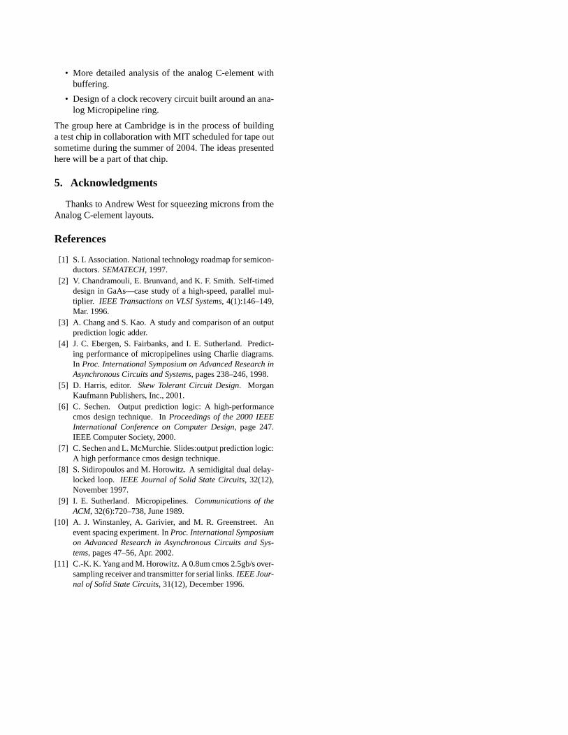
• Harris [5] derives the following equation to relate themaximum tolerable clock skew for Domino logic as afunction of the number of clock phases (N ) used.
tmax−skew =N−1
N ∗ Tc − thold − tprecharge
2(3)
Using this equation he presents the following table ofvalues for maximum clock-skew and necessary pre-chargetime for different values ofN assuming a sixteen gate de-lay clock period.
Notice that as the number of clock phases increases, themaximum skew tolerated also increases. Unfortunately theextra clock skew gained by using more phases is not avail-able at higher frequencies where it is most needed using thecurrent solutions detailed in Harris’ book. FIFO rings re-move this limit.
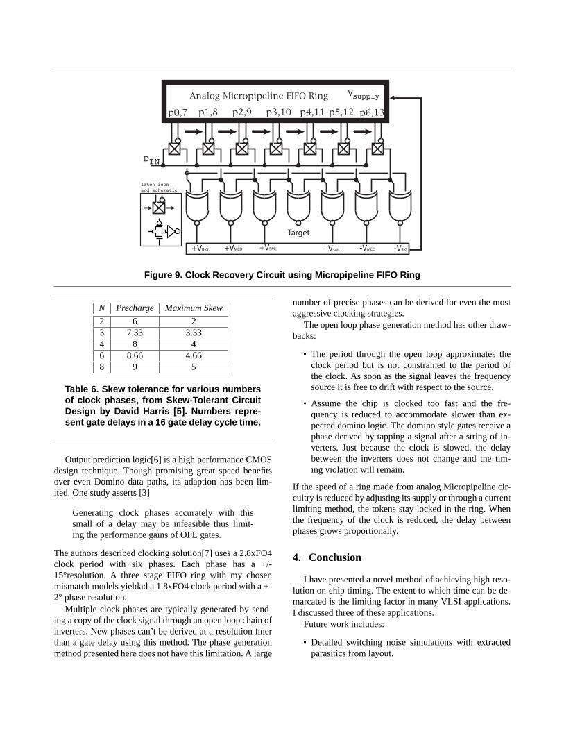
+VBIG +VMED +VSML -VBIG-VMED-VSML
Target
Vsupply
DIN
p0,7 p1,8 p2,9 p3,10 p4,11 p5,12 p6,13
Analog Micropipeline FIFO Ring
latch icon and schematic
Figure 9. Clock Recovery Circuit using Micropipeline FIFO Ring
N Precharge Maximum Skew
2 6 23 7.33 3.334 8 46 8.66 4.668 9 5
Table 6. Skew tolerance for various numbersof clock phases, from Skew-Tolerant CircuitDesign by David Harris [5]. Numbers repre-sent gate delays in a 16 gate delay cycle time.
Output prediction logic[6] is a high performance CMOSdesign technique. Though promising great speed benefitsover even Domino data paths, its adaption has been lim-ited. One study asserts [3]
Generating clock phases accurately with thissmall of a delay may be infeasible thus limit-ing the performance gains of OPL gates.
The authors described clocking solution[7] uses a 2.8xFO4clock period with six phases. Each phase has a +/-15°resolution. A three stage FIFO ring with my chosenmismatch models yieldad a 1.8xFO4 clock period with a +-2° phase resolution.
Multiple clock phases are typically generated by send-ing a copy of the clock signal through an open loop chain ofinverters. New phases can’t be derived at a resolution finerthan a gate delay using this method. The phase generationmethod presented here does not have this limitation. A large
number of precise phases can be derived for even the mostaggressive clocking strategies.
The open loop phase generation method has other draw-backs:
• The period through the open loop approximates theclock period but is not constrained to the period ofthe clock. As soon as the signal leaves the frequencysource it is free to drift with respect to the source.
• Assume the chip is clocked too fast and the fre-quency is reduced to accommodate slower than ex-pected domino logic. The domino style gates receive aphase derived by tapping a signal after a string of in-verters. Just because the clock is slowed, the delaybetween the inverters does not change and the tim-ing violation will remain.
If the speed of a ring made from analog Micropipeline cir-cuitry is reduced by adjusting its supply or through a currentlimiting method, the tokens stay locked in the ring. Whenthe frequency of the clock is reduced, the delay betweenphases grows proportionally.
4. Conclusion
I have presented a novel method of achieving high reso-lution on chip timing. The extent to which time can be de-marcated is the limiting factor in many VLSI applications.I discussed three of these applications.
Future work includes:
• Detailed switching noise simulations with extractedparasitics from layout.
• More detailed analysis of the analog C-element withbuffering.
• Design of a clock recovery circuit built around an ana-log Micropipeline ring.
The group here at Cambridge is in the process of buildinga test chip in collaboration with MIT scheduled for tape outsometime during the summer of 2004. The ideas presentedhere will be a part of that chip.
5. Acknowledgments
Thanks to Andrew West for squeezing microns from theAnalog C-element layouts.
References
[1] S. I. Association. National technology roadmap for semicon-ductors.SEMATECH, 1997.
[2] V. Chandramouli, E. Brunvand, and K. F. Smith. Self-timeddesign in GaAs—case study of a high-speed, parallel mul-tiplier. IEEE Transactions on VLSI Systems, 4(1):146–149,Mar. 1996.
[3] A. Chang and S. Kao. A study and comparison of an outputprediction logic adder.
[4] J. C. Ebergen, S. Fairbanks, and I. E. Sutherland. Predict-ing performance of micropipelines using Charlie diagrams.In Proc. International Symposium on Advanced Research inAsynchronous Circuits and Systems, pages 238–246, 1998.
[5] D. Harris, editor. Skew Tolerant Circuit Design. MorganKaufmann Publishers, Inc., 2001.
[6] C. Sechen. Output prediction logic: A high-performancecmos design technique. InProceedings of the 2000 IEEEInternational Conference on Computer Design, page 247.IEEE Computer Society, 2000.
[7] C. Sechen and L. McMurchie. Slides:output prediction logic:A high performance cmos design technique.
[8] S. Sidiropoulos and M. Horowitz. A semidigital dual delay-locked loop. IEEE Journal of Solid State Circuits, 32(12),November 1997.
[9] I. E. Sutherland. Micropipelines.Communications of theACM, 32(6):720–738, June 1989.
[10] A. J. Winstanley, A. Garivier, and M. R. Greenstreet. Anevent spacing experiment. InProc. International Symposiumon Advanced Research in Asynchronous Circuits and Sys-tems, pages 47–56, Apr. 2002.
[11] C.-K. K. Yang and M. Horowitz. A 0.8um cmos 2.5gb/s over-sampling receiver and transmitter for serial links.IEEE Jour-nal of Solid State Circuits, 31(12), December 1996.