
anàlisi, disseny i implementació de circuits basats en efectes ...
224
TREBALL FI DE GRAU Grau en Enginyeria Electrònica Industrial i Automàtica ANÀLISI, DISSENY I IMPLEMENTACIÓ DE CIRCUITS BASATS EN EFECTES D’ÀUDIO ANNEXOS Autor: Albert Dalmases Mendoza Director: Manuel Andrés Manzanares Brotons Convocatòria: Gener 2021
-
Upload
khangminh22 -
Category
Documents
-
view
6 -
download
0
Transcript of anàlisi, disseny i implementació de circuits basats en efectes ...
TREBALL FI DE GRAU
Grau en Enginyeria Electrònica Industrial i Automàtica
ANÀLISI, DISSENY I IMPLEMENTACIÓ DE CIRCUITS BASATS EN EFECTES D’ÀUDIO
ANNEXOS Autor: Albert Dalmases Mendoza Director: Manuel Andrés Manzanares Brotons Convocatòria: Gener 2021

Índex del contingut d’Annexos
ESQUEMÀTICS FINALS DE LTspice:
DISTORSIÓ .................................................................................................................................................. 5
EQUALITZADOR .......................................................................................................................................... 6
OCTAVADOR ............................................................................................................................................... 7
COMPRESSOR ............................................................................................................................................. 8
Altres documents consultats:
SERIES DE VALORS ESTÀNDARD PER DÈCADA DE RESISTORS I CAPACITORS. .............................................. 9
TAULA COMPARATIVA DE RESISTÈNCIES .................................................................................................. 10
TAULA COMPARATIVA DE CAPACITORS .................................................................................................... 11
Fulls de fabricant (Datasheet):
TL07XX LOW-NOISE FET-INPUT OPERATIONAL AMPLIFIERS ...................................................................... 12
RC4558 DUAL GENERAL-PURPOSE OPERATIONAL AMPLIFIER ................................................................... 71
LM13700 DUAL OPERATIONAL TRANSCONDUCTANCE AMPLIFIERS .......................................................... 95
LM317 3-TERMINAL ADJUSTABLE REGULATOR ....................................................................................... 132
BC546 / BC547 / BC548 / BC549 / BC550 ................................................................................................ 164
NPN EPITAXIAL SILICON TRANSISTOR ..................................................................................................... 164
3/8" SQUARE MULTI-TURN CERMET TRIMMER – T93 ............................................................................. 176
AXIAL-LEAD GLASS PASSIVATED STANDARD RECOVERY RECTIFIERS ......................................................... 190
1N91X, 1N4X48, FDLL914, FDLL4X48 ....................................................................................................... 197
1N5817, 1N5818, 1N5819 ....................................................................................................................... 205

ADJ
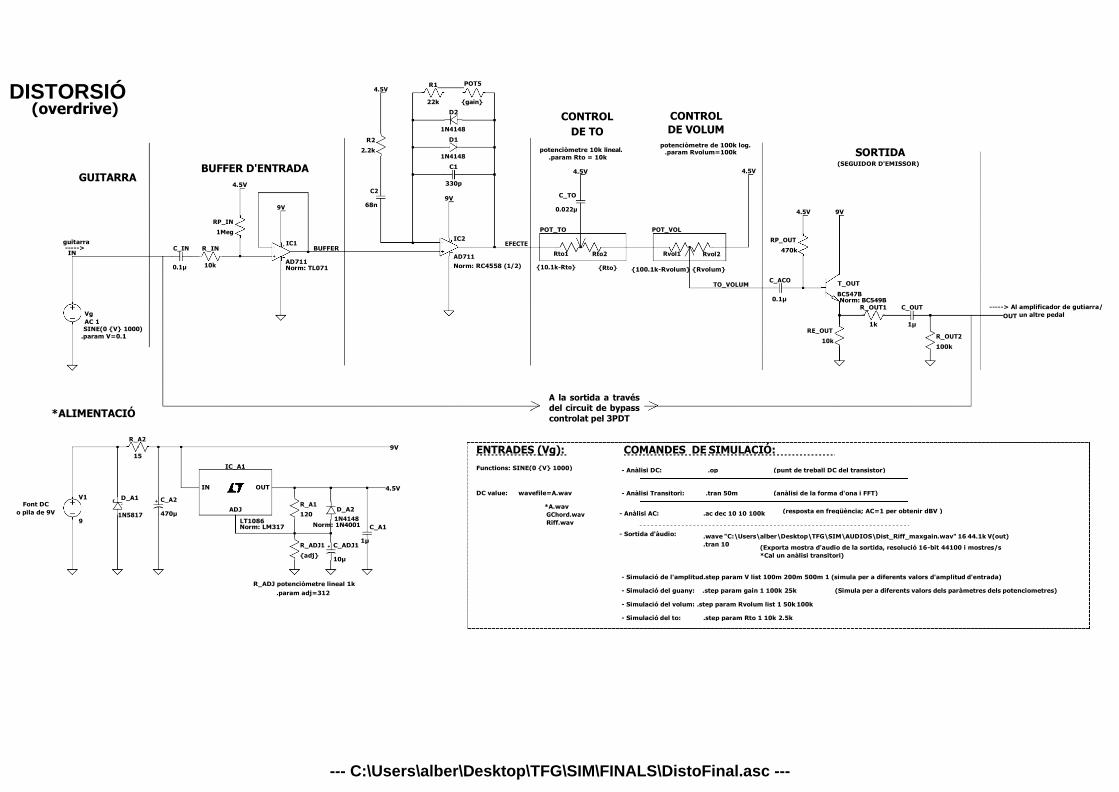
DISTORSIÓ (overdrive)
4.5V
R1 POT5
22k gain
D2
CONTROL
CONTROL
GUITARRA
BUFFER D'ENTRADA
4.5V
9V
R2
2.2k
C2
68n
1N4148
D1
1N4148
C1
330p
9V
DE TO
potenciòmetre 10k lineal.
.param Rto = 10k
4.5V
C_TO
0.022µ
DE VOLUM
potenciòmetre de 100k log. .param Rvolum=100k
4.5V
4.5V
SORTIDA
(SEGUIDOR D'EMISSOR)
9V
guitarra -----> IN
C_IN
RP_IN
1Meg
R_IN
IC1
BUFFER
IC2
AD711
EFECTE
POT_TO
Rto1
Rto2
POT_VOL
Rvol1
Rvol2
RP_OUT
470k
Vg
AC 1 SINE(0 V 1000)
.param V=0.1
0.1µ 10k AD711 Norm: TL071 Norm: RC4558 (1/2) 10.1k-Rto Rto 100.1k-Rvolum Rvolum
TO_VOLUM
C_ACO
0.1µ
RE_OUT
10k
T_OUT
BC547B Norm: BC549B
R_OUT1
1k
C_OUT
1µ
R_OUT2
100k
-----> Al amplificador de gutiarra/
OUT un altre pedal
*ALIMENTACIÓ
A la sortida a través del circuit de bypass
controlat pel 3PDT
V1
Font DC
o pila de 9V
R_A2
15
D_A1
1N5817
C_A2
470µ
IC_A1
R_A1
120
D_A2
1N4148
9V
4.5V
9 LT1086 Norm: LM317 Norm: 1N4001 C_A1
R_ADJ1
adj
C_ADJ1 1µ
10µ
R_ADJ potenciòmetre lineal 1k
.param adj=312
--- C:\Users\alber\Desktop\TFG\SIM\FINALS\DistoFinal.asc ---
OUT IN
- Simulació de l'amplitud.step param V list 100m 200m 500m 1 (simula per a diferents valors d'amplitud d'entrada)
- Simulació del guany: .step param gain 1 100k 25k (Simula per a diferents valors dels paràmetres dels potenciometres)
- Simulació del volum: .step param Rvolum list 1 50k 100k
- Simulació del to: .step param Rto 1 10k 2.5k
(Exporta mostra d'audio de la sortida, resolució 16-bit 44100 i mostres/s
*Cal un anàlisi transitori)
.tran 10
.wave "C:\Users\alber\Desktop\TFG\SIM\AUDIOS\Dist_Riff_maxgain.wav" 16 44.1k V(out)
- Sortida d'àudio:
(resposta en freqüència; AC=1 per obtenir dBV ) .ac dec 10 10 100k - Anàlisi AC:
(anàlisi de la forma d'ona i FFT) .tran 50m - Anàlisi Transitori: DC value: wavefile=A.wav
*A.wav
GChord.wav
Riff.wav
(punt de treball DC del transistor) .op - Anàlisi DC:
COMANDES DE SIMULACIÓ: ENTRADES (Vg):
Functions: SINE(0 V 1000)
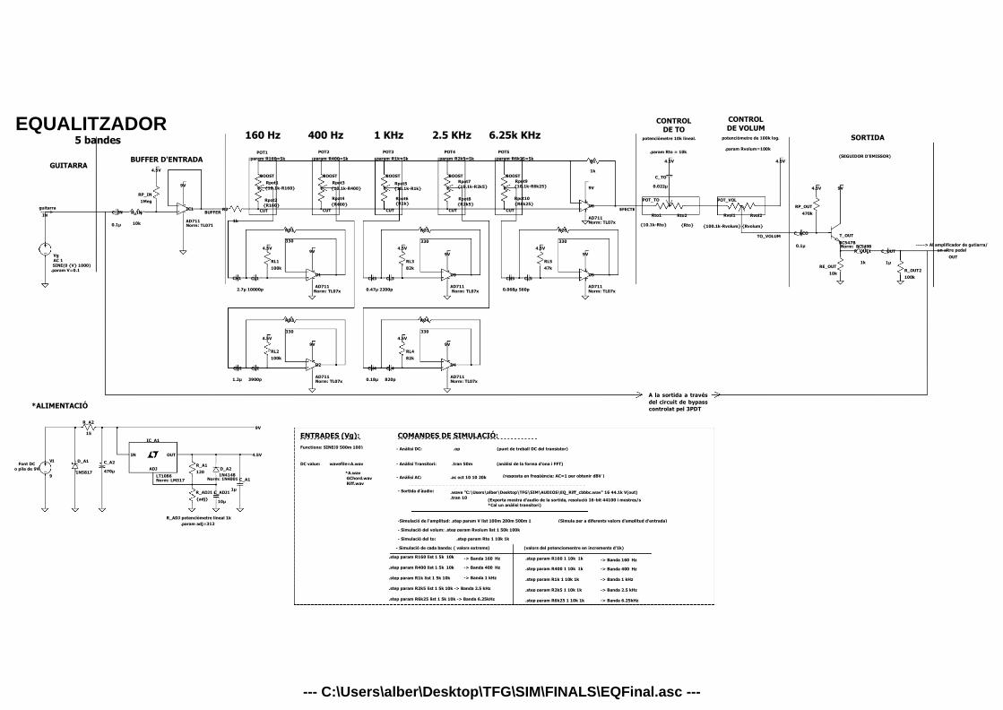
EQUALITZADOR
5 bandes
160 Hz
400 Hz
1 KHz
2.5 KHz
6.25k KHz
CONTROL
DE TO potenciòmetre 10k lineal.
CONTROL
DE VOLUM
potenciòmetre de 100k log.
SORTIDA
GUITARRA
BUFFER D'ENTRADA
4.5V
POT1 POT2 POT3 POT4 POT5
.param R160=5k .param R400=5k .param R1k=5k .param R2k5=5k .param R6k25=5k
.param Rto = 10k
R1 4.5V
1k
.param Rvolum=100k
4.5V
(SEGUIDOR D'EMISSOR)
guitarra -----> IN
C_IN
RP_IN
1Meg
R_IN
9V
IC1
BUFFER
R2
BOOST
Rpot1
10.1k-R160
Rpot2
R160
CUT
BOOST
Rpot3
10.1k-R400
Rpot4
R400
CUT
BOOST
Rpot5 10.1k-R1k
Rpot6 R1k
CUT
BOOST
Rpot7
10.1k-R2k5
Rpot8
R2k5
CUT
BOOST
Rpot9 10.1k-R6k25
Rpot10
R6k25
CUT
9V
U6
AD711
EFECTE
C_TO
0.022µ
POT_TO
Rto1
Rto2
POT_VOL
Rvol1
Rvol2
4.5V 9V
RP_OUT
470k
Vg AC 1 SINE(0 V 1000)
.param V=0.1
0.1µ 10k AD711 Norm: TL071
1k
CN1
CL1
4.5V
RL1
100k
RO1
330
9V
U1
CN3
CL3
4.5V
RL3
82k
RO3
330
9V
U3
CN5
CL5
4.5V
RL5
47k
RO5
330
Norm: TL07x
9V
U5
10.1k-Rto Rto 100.1k-Rvolum Rvolum
TO_VOLUM
C_ACO
0.1µ
RE_OUT
10k
T_OUT
BC547B Norm: BC549B
R_OUT1
1k
C_OUT
1µ
-----> Al amplificador de gutiarra/
un altre pedal
OUT
R_OUT2
100k
2.7µ 10000p
AD711 Norm: TL07x
0.47µ 2200p
AD711 Norm: TL07x
0.068µ 560p
AD711 Norm: TL07x
RO2 RO4
CN2
1.2µ
CL2
3900p
4.5V
RL2
100k
330
9V
U2
AD711 Norm: TL07x
CN4
0.18µ
CL4
820p
4.5V
RL4
82k
330
9V
U4
AD711 Norm: TL07x
*ALIMENTACIÓ
A la sortida a través
del circuit de bypass
controlat pel 3PDT
R_A2
15
9V
IC_A1
Font DC V1
o pila de 9V
D_A1
1N5817
C_A2
470µ
IN
ADJ
OUT
R_A1
120
D_A2
4.5V
9 LT1086 Norm: LM317
1N4148 Norm: 1N4001 C_A1
R_ADJ1 C_ADJ1 1µ
adj 10µ
R_ADJ potenciòmetre lineal 1k
.param adj=312
--- C:\Users\alber\Desktop\TFG\SIM\FINALS\EQFinal.asc ---
ENTRADES (Vg):
Functions: SINE(0 500m 100)
COMANDES DE SIMULACIÓ:
- Anàlisi DC: .op (punt de treball DC del transistor)
DC value: wavefile=A.wav
*A.wav
GChord.wav
Riff.wav
- Anàlisi Transitori: .tran 50m (anàlisi de la forma d'ona i FFT)
- Anàlisi AC: .ac oct 10 10 20k (resposta en freqüència; AC=1 per obtenir dBV )
- Sortida d'àudio: .wave "C:\Users\alber\Desktop\TFG\SIM\AUDIOS\EQ_Riff_cbbbc.wav" 16 44.1k V(out)
.tran 10 (Exporta mostra d'audio de la sortida, resolució 16-bit 44100 i mostres/s
*Cal un anàlisi transitori)
-Simulació de l'amplitud: .step param V list 100m 200m 500m 1
- Simulació del volum: .step param Rvolum list 1 50k 100k
(Simula per a diferents valors d'amplitud d'entrada)
- Simulació del to: .step param Rto 1 10k 1k
- Simulació de cada banda: ( valors extrems) (valors del potenciomentre en increments d'1k)
.step param R160 list 1 5k 10k
.step param R400 list 1 5k 10k
.step param R1k list 1 5k 10k
-> Banda 160 Hz
-> Banda 400 Hz
-> Banda 1 kHz
.step param R160 1 10k 1k
.step param R400 1 10k 1k
-> Banda 160 Hz
-> Banda 400 Hz
.step param R1k 1 10k 1k -> Banda 1 kHz
.step param R2k5 list 1 5k 10k -> Banda 2.5 kHz .step param R2k5 1 10k 1k -> Banda 2.5 kHz
.step param R6k25 list 1 5k 10k -> Banda 6.25kHz .step param R6k25 1 10k 1k -> Banda 6.25kHz
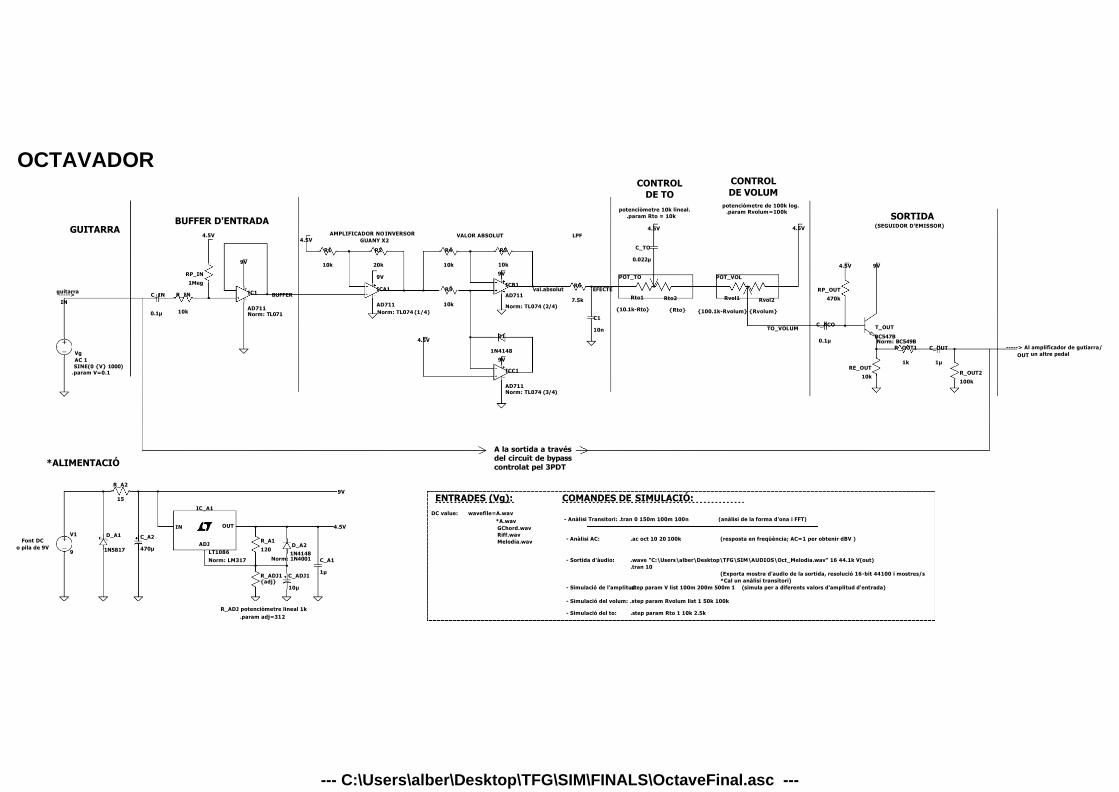
OCTAVADOR
BUFFER D'ENTRADA
GUITARRA 4.5V
4.5V
AMPLIFICADOR NO INVERSOR
GUANY X2
VALOR ABSOLUT
LPF
CONTROL
DE TO
potenciòmetre 10k lineal.
.param Rto = 10k
4.5V
CONTROL
DE VOLUM
potenciòmetre de 100k log. .param Rvolum=100k
4.5V
SORTIDA
(SEGUIDOR D'EMISSOR)
guitarra ----->
C_IN
RP_IN
1Meg
R_IN
9V
IC1
BUFFER
R1
10k
R2
20k
9V
ICA1
R4
10k
R3
R5
10k
9V
ICB1
AD711
val.absolut
R6
7.5k
EFECTE
C_TO
0.022µ
POT_TO
POT_VOL
4.5V 9V
RP_OUT
470k IN
Vg
AC 1 SINE(0 V 1000)
.param V=0.1
0.1µ 10k AD711 Norm: TL071
AD711
Norm: TL074 (1/4)
4.5V
10k Norm: TL074 (2/4)
D1
1N4148
9V
ICC1
AD711 Norm: TL074 (3/4)
C1
10n
10.1k-Rto Rto 100.1k-Rvolum Rvolum
TO_VOLUM
C_ACO
0.1µ
RE_OUT
10k
T_OUT
BC547B Norm: BC549B
R_OUT1
1k
C_OUT
1µ
R_OUT2
100k
-----> Al amplificador de gutiarra/
OUT un altre pedal
*ALIMENTACIÓ
A la sortida a través
del circuit de bypass
controlat pel 3PDT
R_A2
15
9V
IC_A1
V1 Font DC
o pila de 9V 9
D_A1
1N5817
C_A2
470µ
LT1086
R_A1
120
D_A2
1N4148
4.5V
Norm: LM317 Norm: 1N4001
R_ADJ1 C_ADJ1 adj
C_A1
1µ
10µ
R_ADJ potenciòmetre lineal 1k
.param adj=312
--- C:\Users\alber\Desktop\TFG\SIM\FINALS\OctaveFinal.asc ---
ADJ
OUT
Rvol1 Rto2 Rto1
- Sortida d'àudio: .wave "C:\Users\alber\Desktop\TFG\SIM\AUDIOS\Oct_Melodia.wav" 16 44.1k V(out)
.tran 10
(Exporta mostra d'audio de la sortida, resolució 16-bit 44100 i mostres/s
*Cal un anàlisi transitori)
- Simulació de l'amplitu.sdtep param V list 100m 200m 500m 1 (simula per a diferents valors d'amplitud d'entrada)
- Simulació del volum: .step param Rvolum list 1 50k 100k
- Simulació del to: .step param Rto 1 10k 2.5k
(resposta en freqüència; AC=1 per obtenir dBV )
- Anàlisi AC: .ac oct 10 20 100k
(anàlisi de la forma d'ona i FFT) - Anàlisi Transitori: .tran 0 150m 100m 100n
COMANDES DE SIMULACIÓ: ENTRADES (Vg):
DC value: wavefile=A.wav
*A.wav
GChord.wav
Riff.wav
Melodia.wav
IN
Rvol2
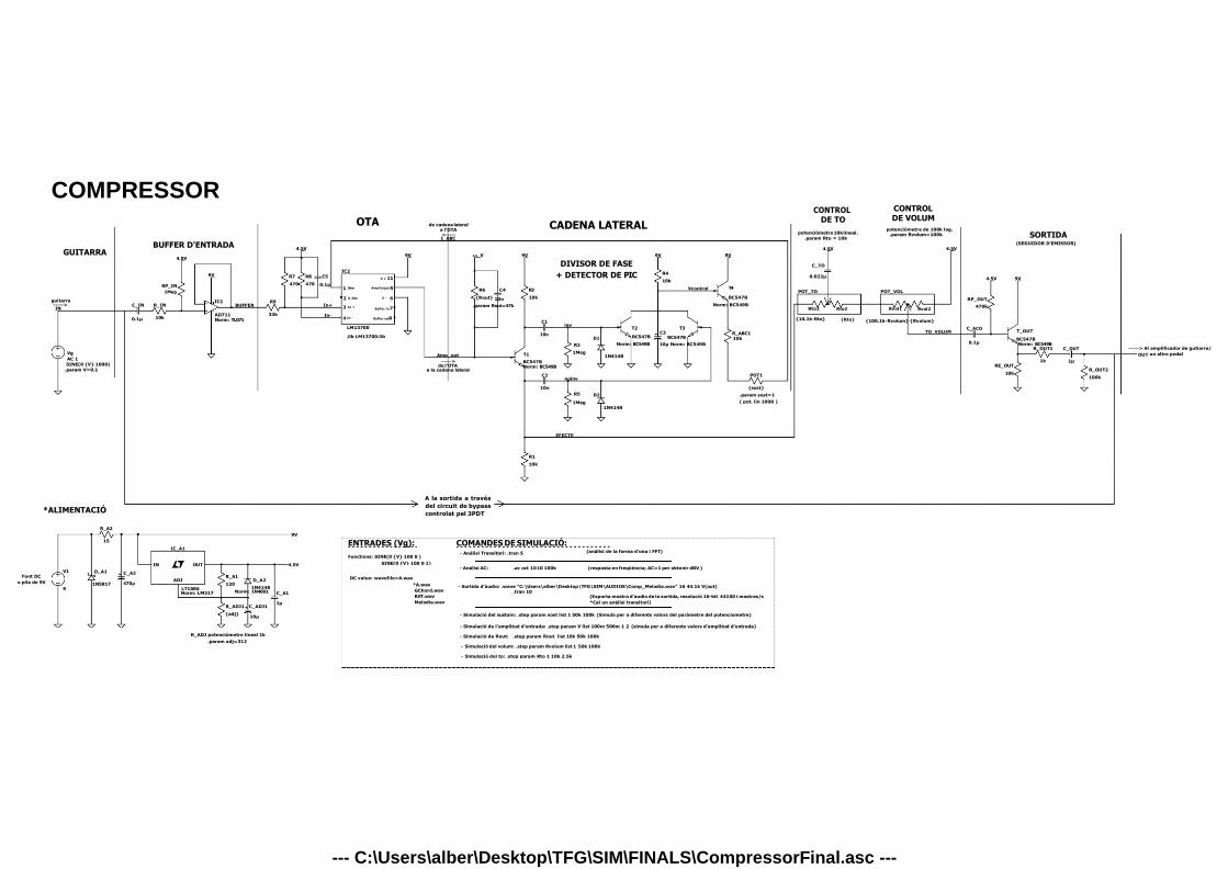
COMPRESSOR
BUFFER D'ENTRADA
GUITARRA 4.5V
4.5V
OTA
de cadena lateral a l'OTA <----- I_ABC
9V
4.5 V
CADENA LATERAL
9V 9V 9V
DIVISOR DE FASE
CONTROL
DE TO
potenciòmetre 10k lineal.
.param Rto = 10k
4.5V
C_TO
CONTROL DE VOLUM
potenciòmetre de 100k log. .param Rvolum=100k
4.5V
SORTIDA (SEGUIDOR D'EMISSOR)
RP_IN
1Meg
9V R7 R8 C5
470 470 0.1µ
IC2
1 Ibias
V + 11
Amp Output5
R6 C4 R3
+ DETECTOR DE PIC R4
10k
Vcontrol T4
0.022µ
POT_TO
POT_VOL
4.5V 9V
guitarra -----> IN
C_IN
R_IN
IC1 BUFFER
R9
In+
2 D_bias
3 In +
V - 6
Buffer In 7
Rout 10n
.param Rout=47k
10k BC547B
Norm: BC549B
Rto1
Rto2
Rvol1
Rvol2
RP_OUT
470k
0.1µ 10k AD711 Norm: TL071
33k In- 4 In - Buffer out8
LM13700
.lib LM13700.lib
C1
10n
inv
D1
T2
BC547B
T3
C3 BC547B
R_ABC1 10k
10.1k-Rto
Rto
100.1k-Rvolum Rvolum
TO_VOLUM
C_ACO
0.1µ
T_OUT
BC547B
Vg
AC 1
SINE(0 V 1000)
.param V=0.1
Amp_out
-----> de l'OTA
a la cadena lateral
T1
BC547B Norm: BC549B
C2
10n
R2
1Meg
noinv
R5
1Meg
Norm: BC549B
1N4148
D2
1N4148
10µ Norm: BC549B
POT1
sost
.param sost=1
( pot. lin 100K )
RE_OUT
10k
Norm: BC549B R_OUT1
1k
C_OUT
1µ
R_OUT2
100k
-----> Al amplificador de gutiarra/
OUT un altre pedal
EFECTE
R1
10k
*ALIMENTACIÓ
A la sortida a través
del circuit de bypass
controlat pel 3PDT
V1
Font DC
o pila de 9V
R_A2
15
D_A1
1N5817
C_A2
470µ
IC_A1
IN
ADJ
OUT
R_A1
120
D_A2
1N4148
9V
4.5V
9 LT1086 Norm: LM317 Norm: 1N4001
R_ADJ1 C_ADJ1
C_A1
1µ
adj 10µ
R_ADJ potenciòmetre lineal 1k
.param adj=312
--- C:\Users\alber\Desktop\TFG\SIM\FINALS\CompressorFinal.asc ---
ENTRADES (Vg):
Functions: SINE(0 V 100 0 )
SINE(0 V 100 0 1)
COMANDES DE SIMULACIÓ: - Anàlisi Transitori: .tran 5 (anàlisi de la forma d'ona i FFT)
- Anàlisi AC: .ac oct 10 10 100k (resposta en freqüència; AC=1 per obtenir dBV )
DC value: wavefile=A.wav
*A.wav
GChord.wav
Riff.wav
Melodia.wav
- Sortida d'àudio: .wave "C:\Users\alber\Desktop\TFG\SIM\AUDIOS\Comp_Melodia.wav" 16 44.1k V(out) .tran 10
(Exporta mostra d'audio de la sortida, resolució 16-bit 44100 i mostres/s
*Cal un anàlisi transitori)
- Simulació del sustain: .step param sost list 1 50k 100k (Simula per a diferents valors del paràmetre del potenciometre)
- Simulació de l'amplitud d'entrada: .step param V list 100m 500m 1 2 (simula per a diferents valors d'amplitud d'entrada)
- Simulació de Rout: .step param Rout list 10k 50k 100k
- Simulació del volum: .step param Rvolum list 1 50k 100k
- Simulació del to: .step param Rto 1 10k 2.5k
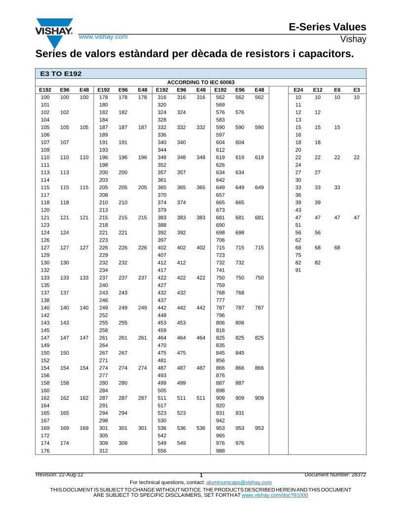
E-Series Values www.vishay.com Vishay
Series de valors estàndard per dècada de resistors i capacitors.
E3 TO E192
ACCORDING TO IEC 60063
E192 E96 E48 E192 E96 E48 E192 E96 E48 E192 E96 E48 E24 E12 E6 E3
100 100 100 178 178 178 316 316 316 562 562 562 10 10 10 10
101 180 320 569 11
102 102 182 182 324 324 576 576 12 12
104 184 328 583 13
105 105 105 187 187 187 332 332 332 590 590 590 15 15 15
106 189 336 597 16
107 107 191 191 340 340 604 604 18 18
109 193 344 612 20
110 110 110 196 196 196 348 348 348 619 619 619 22 22 22 22
111 198 352 626 24
113 113 200 200 357 357 634 634 27 27
114 203 361 642 30
115 115 115 205 205 205 365 365 365 649 649 649 33 33 33
117 208 370 657 36
118 118 210 210 374 374 665 665 39 39
120 213 379 673 43
121 121 121 215 215 215 383 383 383 681 681 681 47 47 47 47
123 218 388 690 51
124 124 221 221 392 392 698 698 56 56
126 223 397 706 62
127 127 127 226 226 226 402 402 402 715 715 715 68 68 68
129 229 407 723 75
130 130 232 232 412 412 732 732 82 82
132 234 417 741 91
133 133 133 237 237 237 422 422 422 750 750 750
135 240 427 759
137 137 243 243 432 432 768 768
138 246 437 777
140 140 140 249 249 249 442 442 442 787 787 787
142 252 448 796
143 143 255 255 453 453 806 806
145 258 459 816
147 147 147 261 261 261 464 464 464 825 825 825
149 264 470 835
150 150 267 267 475 475 845 845
152 271 481 856
154 154 154 274 274 274 487 487 487 866 866 866
156 277 493 876
158 158 280 280 499 499 887 887
160 284 505 898
162 162 162 287 287 287 511 511 511 909 909 909
164 291 517 920
165 165 294 294 523 523 931 931
167 298 530 942
169 169 169 301 301 301 536 536 536 953 953 953
172 305 542 965
174 174 309 309 549 549 976 976
176 312 556 988
Revision: 22-Aug-12 1 Document Number: 28372
For technical questions, contact: [email protected]
THIS DOCUMENT IS SUBJECT TO CHANGE WITHOUT NOTICE. THE PRODUCTS DESCRIBED HEREIN AND THIS DOCUMENT ARE SUBJECT TO SPECIFIC DISCLAIMERS, SET FORTH AT www.vishay.com/doc?91000
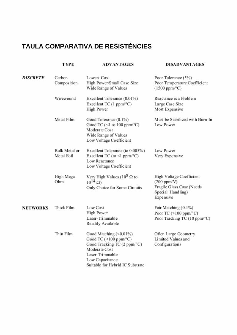
TAULA COMPARATIVA DE RESISTÈNCIES
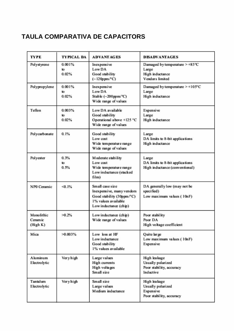
TAULA COMPARATIVA DE CAPACITORS
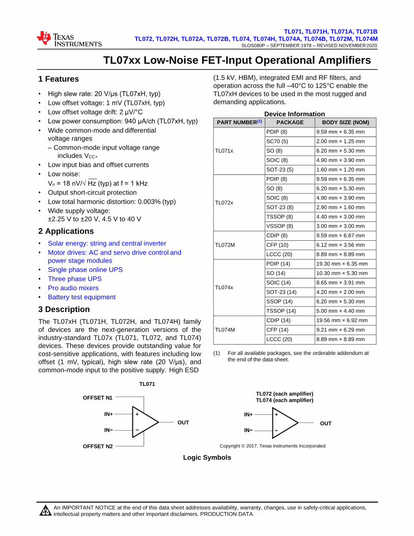
TL071, TL071H, TL071A, TL071B
TL072, TL072H, TL072A, TL072B, TL074, TL074H, TL074A, TL074B, TL072M, TL074M www.ti.com SLOS080P – SEPTEMBER 1978 – REVISED NOVEMBER 2020
Copyright © 2020 Texas Instruments Incorporated Submit Document Feedback 1
Product Folder Links: TL071 TL071H TL071A TL071B TL072 TL072H TL072A TL072B TL074 TL074H TL074A
TL074B TL072M TL074M
+
−
TL071, TL071H, TL071A, TL071B
TL072, TL072H, TL072A, TL072B, TL074, TL074H, TL074A, TL074B, TL072M, TL074M SLOS080P – SEPTEMBER 1978 – REVISED NOVEMBER 2020
1 Features
TL07xx Low-Noise FET-Input Operational Amplifiers
(1.5 kV, HBM), integrated EMI and RF filters, and
operation across the full –40°C to 125°C enable the
• High slew rate: 20 V/μs (TL07xH, typ)
• Low offset voltage: 1 mV (TL07xH, typ)
• Low offset voltage drift: 2 μV/°C
• Low power consumption: 940 μA/ch (TL07xH, typ)
• Wide common-mode and differential
voltage ranges
– Common-mode input voltage range
includes VCC+
• Low input bias and offset currents
• Low noise:
Vn = 18 nV/√ Hz (typ) at f = 1 kHz
• Output short-circuit protection
• Low total harmonic distortion: 0.003% (typ)
• Wide supply voltage:
±2.25 V to ±20 V, 4.5 V to 40 V
2 Applications
• Solar energy: string and central inverter
• Motor drives: AC and servo drive control and
power stage modules
• Single phase online UPS
• Three phase UPS
• Pro audio mixers
• Battery test equipment
3 Description
The TL07xH (TL071H, TL072H, and TL074H) family
of devices are the next-generation versions of the
industry-standard TL07x (TL071, TL072, and TL074)
devices. These devices provide outstanding value for
cost-sensitive applications, with features including low
offset (1 mV, typical), high slew rate (20 V/μs), and
common-mode input to the positive supply. High ESD
TL07xH devices to be used in the most rugged and
demanding applications.
Device Information PART NUMBER(1) PACKAGE BODY SIZE (NOM)
TL071x
PDIP (8) 9.59 mm × 6.35 mm
SC70 (5) 2.00 mm × 1.25 mm
SO (8) 6.20 mm × 5.30 mm
SOIC (8) 4.90 mm × 3.90 mm
SOT-23 (5) 1.60 mm × 1.20 mm
TL072x
PDIP (8) 9.59 mm × 6.35 mm
SO (8) 6.20 mm × 5.30 mm
SOIC (8) 4.90 mm × 3.90 mm
SOT-23 (8) 2.90 mm × 1.60 mm
TSSOP (8) 4.40 mm × 3.00 mm
VSSOP (8) 3.00 mm × 3.00 mm
TL072M
CDIP (8) 9.59 mm × 6.67 mm
CFP (10) 6.12 mm × 3.56 mm
LCCC (20) 8.89 mm × 8.89 mm
TL074x
PDIP (14) 19.30 mm × 6.35 mm
SO (14) 10.30 mm × 5.30 mm
SOIC (14) 8.65 mm × 3.91 mm
SOT-23 (14) 4.20 mm × 2.00 mm
SSOP (14) 6.20 mm × 5.30 mm
TSSOP (14) 5.00 mm × 4.40 mm
TL074M
CDIP (14) 19.56 mm × 6.92 mm
CFP (14) 9.21 mm × 6.29 mm
LCCC (20) 8.89 mm × 8.89 mm
(1) For all available packages, see the orderable addendum at
the end of the data sheet.
OFFSET N1
TL071
TL072 (each amplifier)
TL074 (each amplifier)
IN+
IN−
OUT
IN+
IN−
OUT
OFFSET N2 Copyright © 2017, Texas Instruments Incorporated
Logic Symbols
+
−
An IMPORTANT NOTICE at the end of this data sheet addresses availability, warranty, changes, use in safety-critical applications,
intellectual property matters and other important disclaimers. PRODUCTION DATA.
TL071, TL071H, TL071A, TL071B
TL072, TL072H, TL072A, TL072B, TL074, TL074H, TL074A, TL074B, TL072M, TL074M SLOS080P – SEPTEMBER 1978 – REVISED NOVEMBER 2020 www.ti.com
Copyright © 2020 Texas Instruments Incorporated Submit Document Feedback 13
Product Folder Links: TL071 TL071H TL071A TL071B TL072 TL072H TL072A TL072B TL074 TL074H TL074A
TL074B TL072M TL074M
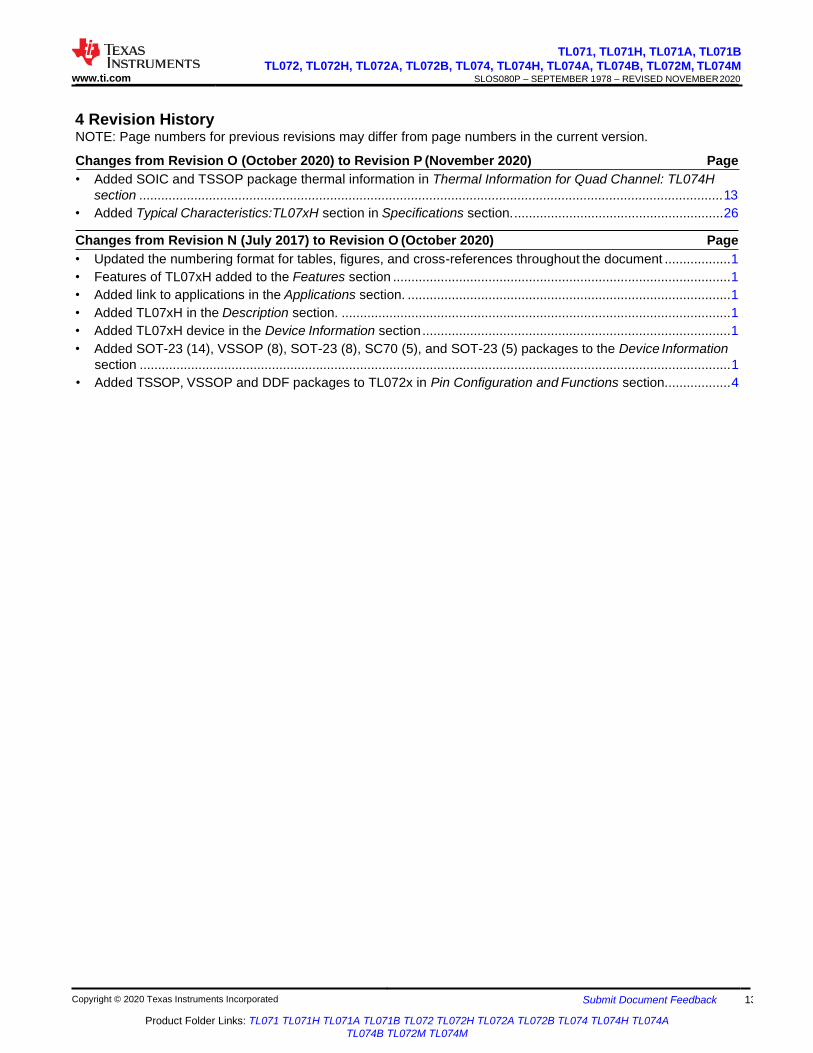
4 Revision History NOTE: Page numbers for previous revisions may differ from page numbers in the current version.
Changes from Revision O (October 2020) to Revision P (November 2020) Page
• Added SOIC and TSSOP package thermal information in Thermal Information for Quad Channel: TL074H
section ............................................................................................................................................................... 13
• Added Typical Characteristics:TL07xH section in Specifications section. ......................................................... 26
Changes from Revision N (July 2017) to Revision O (October 2020) Page
• Updated the numbering format for tables, figures, and cross-references throughout the document .................. 1
• Features of TL07xH added to the Features section ............................................................................................ 1
• Added link to applications in the Applications section. ........................................................................................ 1
• Added TL07xH in the Description section. .......................................................................................................... 1
• Added TL07xH device in the Device Information section .................................................................................... 1
• Added SOT-23 (14), VSSOP (8), SOT-23 (8), SC70 (5), and SOT-23 (5) packages to the Device Information
section ................................................................................................................................................................. 1
• Added TSSOP, VSSOP and DDF packages to TL072x in Pin Configuration and Functions section.................. 4
TL071, TL071H, TL071A, TL071B
TL072, TL072H, TL072A, TL072B, TL074, TL074H, TL074A, TL074B, TL072M, TL074M SLOS080P – SEPTEMBER 1978 – REVISED NOVEMBER 2020 www.ti.com
14 Submit Document Feedback Copyright © 2020 Texas Instruments Incorporated
Product Folder Links: TL071 TL071H TL071A TL071B TL072 TL072H TL072A TL072B TL074 TL074H TL074A
TL074B TL072M TL074M
• Added DYY package to TL074x in Pin Configuration and Functions section ..................................................... 4
• Removed Table of Graphs from the Typical Characteistics section. ................................................................. 33
• Deleted reference to obsolete documentation in Layout Guidelines section. ................................................... 43
• Removed Related Documentation section ........................................................................................................ 45
Changes from Revision M (February 2014) to Revision N (July 2017) Page
• Updated data sheet text to latest documentation and translation standards ....................................................... 1
• Added TL072M and TL074M devices to data sheet ............................................................................................ 1
• Rewrote text in Description section ..................................................................................................................... 1
• Changed TL07x 8-pin PDIP package to 8-pin CDIP package in Device Information table ................................. 1
• Deleted 20-pin LCCC package from Device Information table ............................................................................ 1
• Added 2017 copyright statement to front page schematic .................................................................................. 1
• Deleted TL071x FK (LCCC) pinout drawing and pinout table in Pin Configurations and Functions section ....... 4
• Updated pinout diagrams and pinout tables in Pin Configurations and Functions section .................................. 4
• Deleted differential input voltage parameter from Absolute Maximum Ratings table ........................................ 10
• Deleted table notes from Absolute Maximum Ratings table .............................................................................. 10
• Added new table note to Absolute Maximum Ratings table .............................................................................. 10
• Changed minimum supply voltage value from –18 V to –0.3 V in Absolute Maximum Ratings table ............... 10
• Changed maximum supply voltage from 18 V to 36 V in Absolute Maximum Ratings table ............................. 10
• Changed minimum input voltage value from –15 V to VCC– – 0.3 V in Absolute Maximum Ratings table. ........ 10
• Changed maximum input voltage from 15 V to VCC– + 36 V in Absolute Maximum Ratings table. .................... 10
• Added input clamp current parameter to Absolute Maximum Ratings table ..................................................... 10
• Changed common-mode voltage maximum value from VCC+ – 4 V to VCC+ in the Recommended Operating
Conditions table. ................................................................................................................................................ 11
• Changed devices in Recommended Operating Conditions table from TL07xA and TL07xB to TL07xAC and
TL07xBC ............................................................................................................................................................ 11
• Added TL07xI operating free-air temperature minimum value of –40°C to Recommended Operating
Conditions table ................................................................................................................................................. 11
• Added U (CFP) package thermal values to Thermal Information: TL072x (cont.) table. .................................. 13
• Added W (CFP) package thermal values to Thermal Information: TL074x (cont.) table................................... 14
• Added Figure 6-59 to Typical Characteristics section ....................................................................................... 33
• Added second Typical Application section application curves .......................................................................... 41
• Reformatted document references in Layout Guidelines section ...................................................................... 43
Changes from Revision L (February 2014) to Revision M (February 2014) Page
• Added Device Information table, Pin Configuration and Functions section, ESD Ratings table, Feature
Description section, Device Functional Modes, Application and Implementation section, Power Supply
Recommendations section, Layout section. ........................................................................................................ 1
Changes from Revision K (January 2014) to Revision L (February 2014) Page
• Moved Tstg to Handling Ratings table ................................................................................................................. 11
Changes from Revision J (March 2005) to Revision K (January 2014) Page
• Updated document to new TI datasheet format - no specification changes. ....................................................... 1
TL071, TL071H, TL071A, TL071B
TL072, TL072H, TL072A, TL072B, TL074, TL074H, TL074A, TL074B, TL072M, TL074M SLOS080P – SEPTEMBER 1978 – REVISED NOVEMBER 2020 www.ti.com
Copyright © 2020 Texas Instruments Incorporated Submit Document Feedback 15
Product Folder Links: TL071 TL071H TL071A TL071B TL072 TL072H TL072A TL072B TL074 TL074H TL074A
TL074B TL072M TL074M
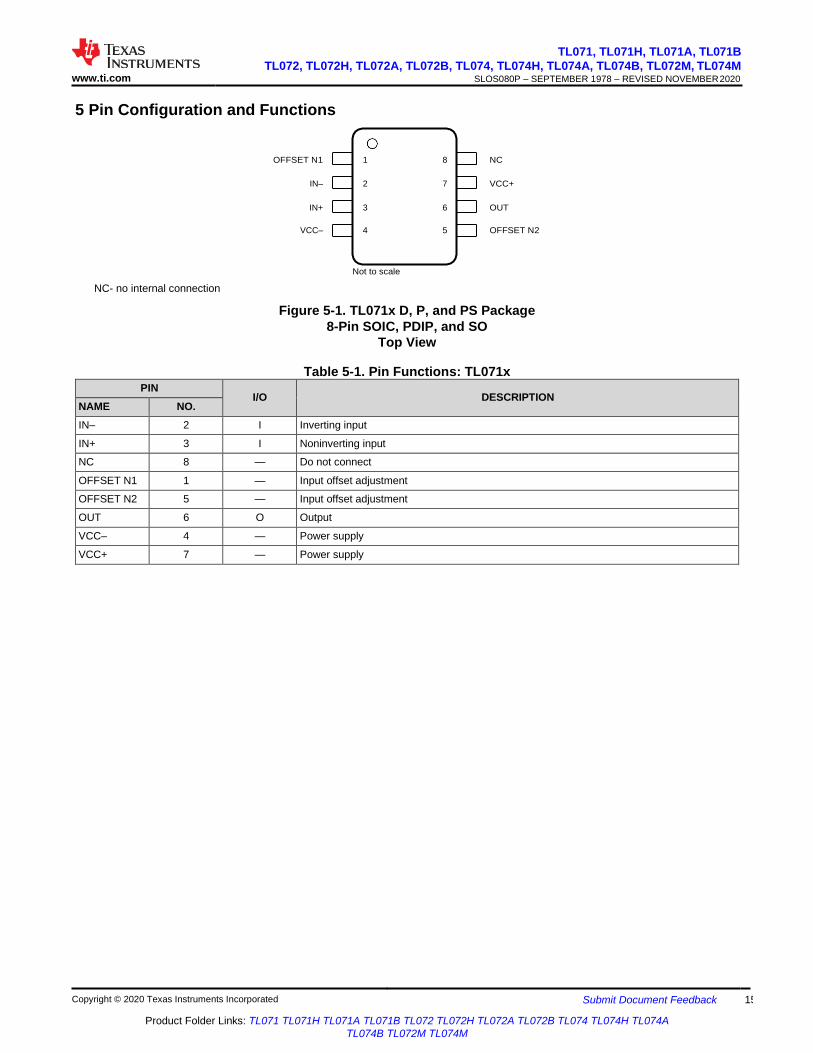
5 Pin Configuration and Functions
OFFSET N1 1 8 NC
IN– 2 7 VCC+
IN+ 3 6 OUT
VCC– 4 5 OFFSET N2
NC- no internal connection
Not to scale
Figure 5-1. TL071x D, P, and PS Package
8-Pin SOIC, PDIP, and SO
Top View
Table 5-1. Pin Functions: TL071x PIN
I/O
DESCRIPTION NAME NO.
IN– 2 I Inverting input
IN+ 3 I Noninverting input
NC 8 — Do not connect
OFFSET N1 1 — Input offset adjustment
OFFSET N2 5 — Input offset adjustment
OUT 6 O Output
VCC– 4 — Power supply
VCC+ 7 — Power supply
TL071, TL071H, TL071A, TL071B
TL072, TL072H, TL072A, TL072B, TL074, TL074H, TL074A, TL074B, TL072M, TL074M SLOS080P – SEPTEMBER 1978 – REVISED NOVEMBER 2020 www.ti.com
16 Submit Document Feedback Copyright © 2020 Texas Instruments Incorporated
Product Folder Links: TL071 TL071H TL071A TL071B TL072 TL072H TL072A TL072B TL074 TL074H TL074A
TL074B TL072M TL074M
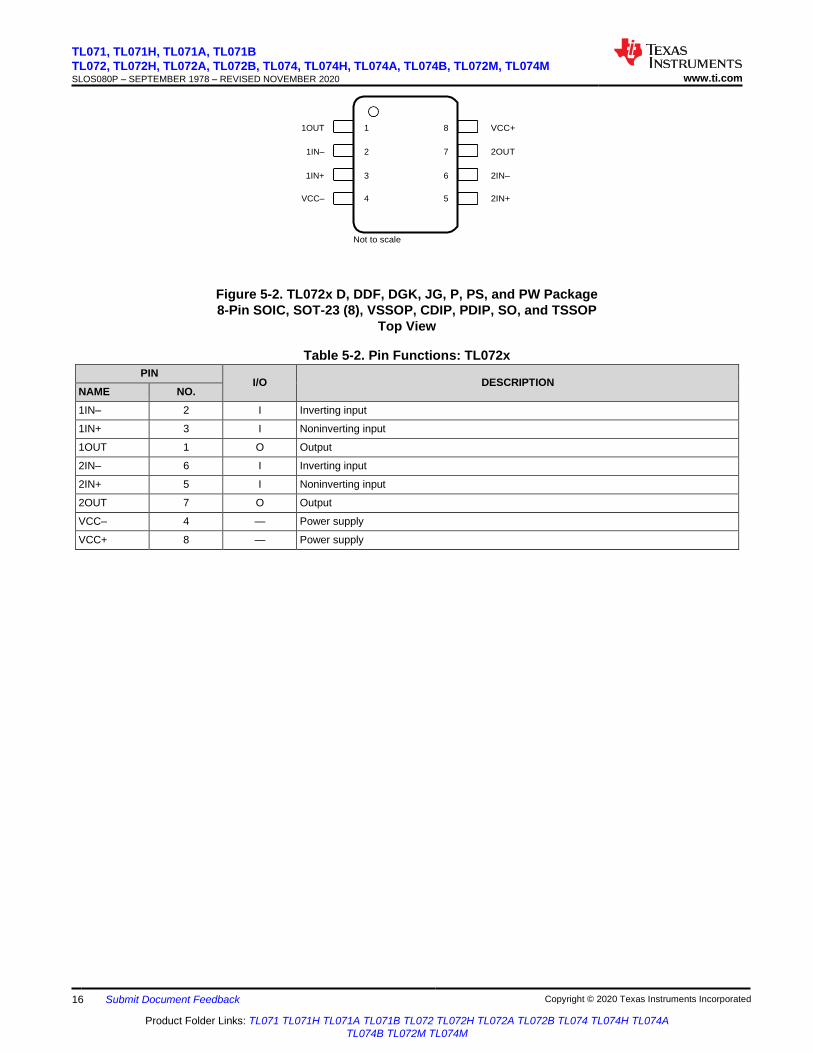
1OUT 1 8 VCC+
1IN– 2 7 2OUT
1IN+ 3 6 2IN–
VCC– 4 5 2IN+
Not to scale
Figure 5-2. TL072x D, DDF, DGK, JG, P, PS, and PW Package
8-Pin SOIC, SOT-23 (8), VSSOP, CDIP, PDIP, SO, and TSSOP
Top View
Table 5-2. Pin Functions: TL072x
PIN
I/O
DESCRIPTION NAME NO.
1IN– 2 I Inverting input
1IN+ 3 I Noninverting input
1OUT 1 O Output
2IN– 6 I Inverting input
2IN+ 5 I Noninverting input
2OUT 7 O Output
VCC– 4 — Power supply
VCC+ 8 — Power supply
TL071, TL071H, TL071A, TL071B
TL072, TL072H, TL072A, TL072B, TL074, TL074H, TL074A, TL074B, TL072M, TL074M SLOS080P – SEPTEMBER 1978 – REVISED NOVEMBER 2020 www.ti.com
Copyright © 2020 Texas Instruments Incorporated Submit Document Feedback 17
Product Folder Links: TL071 TL071H TL071A TL071B TL072 TL072H TL072A TL072B TL074 TL074H TL074A
TL074B TL072M TL074M
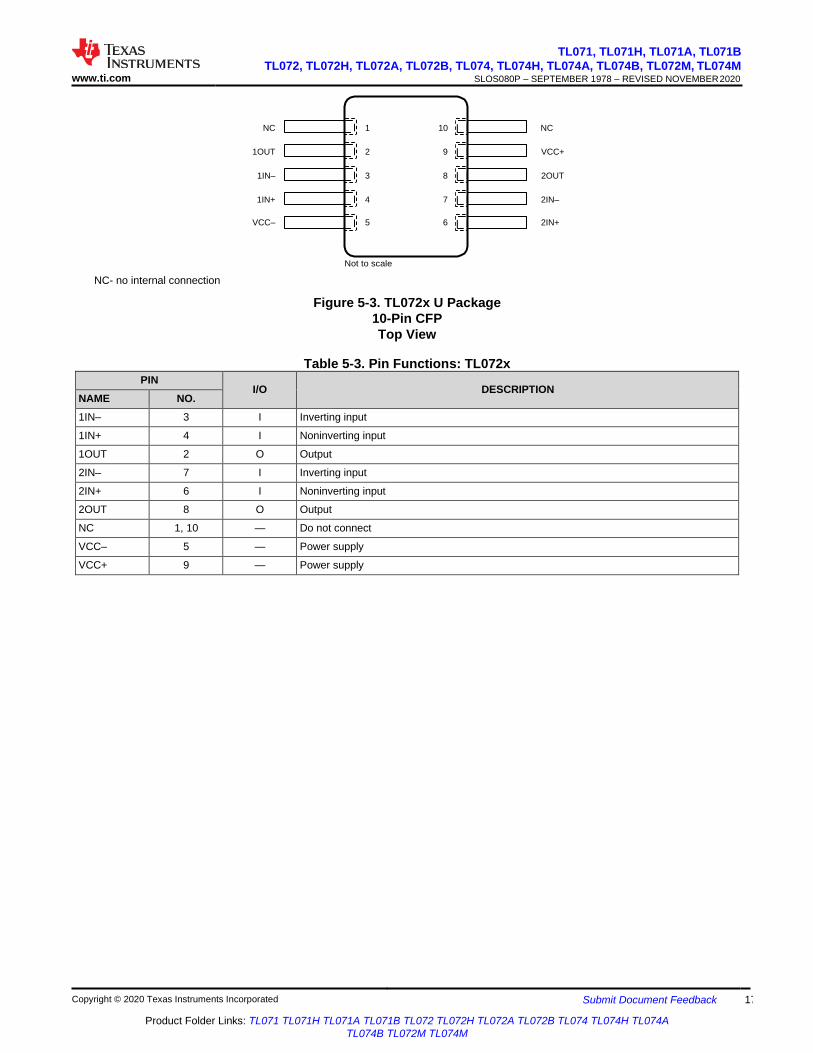
NC 1 10 NC
1OUT 2 9 VCC+
1IN– 3 8 2OUT
1IN+ 4 7 2IN–
VCC– 5 6 2IN+
NC- no internal connection
Not to scale
Figure 5-3. TL072x U Package
10-Pin CFP
Top View
Table 5-3. Pin Functions: TL072x PIN
I/O
DESCRIPTION NAME NO.
1IN– 3 I Inverting input
1IN+ 4 I Noninverting input
1OUT 2 O Output
2IN– 7 I Inverting input
2IN+ 6 I Noninverting input
2OUT 8 O Output
NC 1, 10 — Do not connect
VCC– 5 — Power supply
VCC+ 9 — Power supply
TL071, TL071H, TL071A, TL071B
TL072, TL072H, TL072A, TL072B, TL074, TL074H, TL074A, TL074B, TL072M, TL074M SLOS080P – SEPTEMBER 1978 – REVISED NOVEMBER 2020 www.ti.com
18 Submit Document Feedback Copyright © 2020 Texas Instruments Incorporated
Product Folder Links: TL071 TL071H TL071A TL071B TL072 TL072H TL072A TL072B TL074 TL074H TL074A
TL074B TL072M TL074M
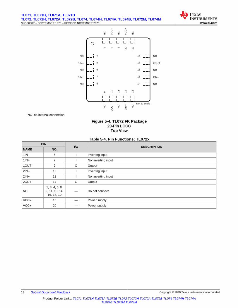
4 18
5 17
6 16
7 15
8 14
NC NC
1IN–
2OUT
NC NC
1IN+ 2IN–
NC NC
Not to scale
NC- no internal connection
Figure 5-4. TL072 FK Package
20-Pin LCCC
Top View
Table 5-4. Pin Functions: TL072x PIN
I/O
DESCRIPTION NAME NO.
1IN– 5 I Inverting input
1IN+ 7 I Noninverting input
1OUT 2 O Output
2IN– 15 I Inverting input
2IN+ 12 I Noninverting input
2OUT 17 O Output
NC
1, 3, 4, 6, 8,
9, 11, 13, 14,
16, 18, 19
—
Do not connect
VCC– 10 — Power supply
VCC+ 20 — Power supply
NC
9
3
N
C
VC
C–
10
2
1O
UT
NC
11
1
N
C
2IN
+
12
20
V
CC
+
NC
13
19
N
C
TL071, TL071H, TL071A, TL071B
TL072, TL072H, TL072A, TL072B, TL074, TL074H, TL074A, TL074B, TL072M, TL074M SLOS080P – SEPTEMBER 1978 – REVISED NOVEMBER 2020 www.ti.com
Copyright © 2020 Texas Instruments Incorporated Submit Document Feedback 19
Product Folder Links: TL071 TL071H TL071A TL071B TL072 TL072H TL072A TL072B TL074 TL074H TL074A
TL074B TL072M TL074M
1OUT 1 14 4OUT
1IN– 2 13 4IN–
1IN+ 3 12 4IN+
VCC+ 4 11 VCC–
2IN+ 5 10 3IN+
2IN– 6 9 3IN–
2OUT 7 8 3OUT
Not to scale
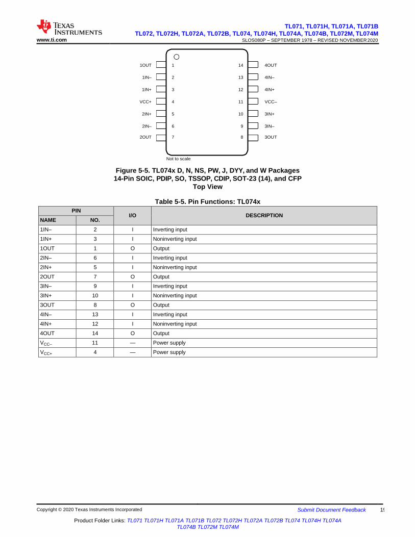
Figure 5-5. TL074x D, N, NS, PW, J, DYY, and W Packages
14-Pin SOIC, PDIP, SO, TSSOP, CDIP, SOT-23 (14), and CFP
Top View
Table 5-5. Pin Functions: TL074x
PIN
I/O
DESCRIPTION NAME NO.
1IN– 2 I Inverting input
1IN+ 3 I Noninverting input
1OUT 1 O Output
2IN– 6 I Inverting input
2IN+ 5 I Noninverting input
2OUT 7 O Output
3IN– 9 I Inverting input
3IN+ 10 I Noninverting input
3OUT 8 O Output
4IN– 13 I Inverting input
4IN+ 12 I Noninverting input
4OUT 14 O Output
VCC– 11 — Power supply
VCC+ 4 — Power supply
TL071, TL071H, TL071A, TL071B
TL072, TL072H, TL072A, TL072B, TL074, TL074H, TL074A, TL074B, TL072M, TL074M SLOS080P – SEPTEMBER 1978 – REVISED NOVEMBER 2020 www.ti.com
20 Submit Document Feedback Copyright © 2020 Texas Instruments Incorporated
Product Folder Links: TL071 TL071H TL071A TL071B TL072 TL072H TL072A TL072B TL074 TL074H TL074A
TL074B TL072M TL074M
4 18
5 17
6 16
7 15
8 14
1IN+ 4IN+
NC NC
VCC+ VCC–
NC NC
2IN+ 3IN+
Not to scale
NC- no internal connection
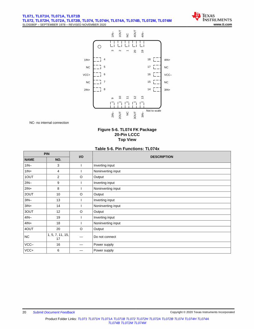
Figure 5-6. TL074 FK Package
20-Pin LCCC
Top View
Table 5-6. Pin Functions: TL074x PIN
I/O
DESCRIPTION NAME NO.
1IN– 3 I Inverting input
1IN+ 4 I Noninverting input
1OUT 2 O Output
2IN– 9 I Inverting input
2IN+ 8 I Noninverting input
2OUT 10 O Output
3IN– 13 I Inverting input
3IN+ 14 I Noninverting input
3OUT 12 O Output
4IN– 19 I Inverting input
4IN+ 18 I Noninverting input
4OUT 20 O Output
NC 1, 5, 7, 11, 15,
17 — Do not connect
VCC– 16 — Power supply
VCC+ 6 — Power supply
2IN
–
9
3
1IN
–
2O
UT
10
2
1O
UT
NC
11
1
N
C
3O
UT
12
20
4O
UT
3IN
–
13
19
4IN
–
TL071, TL071H, TL071A, TL071B
TL072, TL072H, TL072A, TL072B, TL074, TL074H, TL074A, TL074B, TL072M, TL074M SLOS080P – SEPTEMBER 1978 – REVISED NOVEMBER 2020 www.ti.com
Copyright © 2020 Texas Instruments Incorporated Submit Document Feedback 21
Product Folder Links: TL071 TL071H TL071A TL071B TL072 TL072H TL072A TL072B TL074 TL074H TL074A
TL074B TL072M TL074M
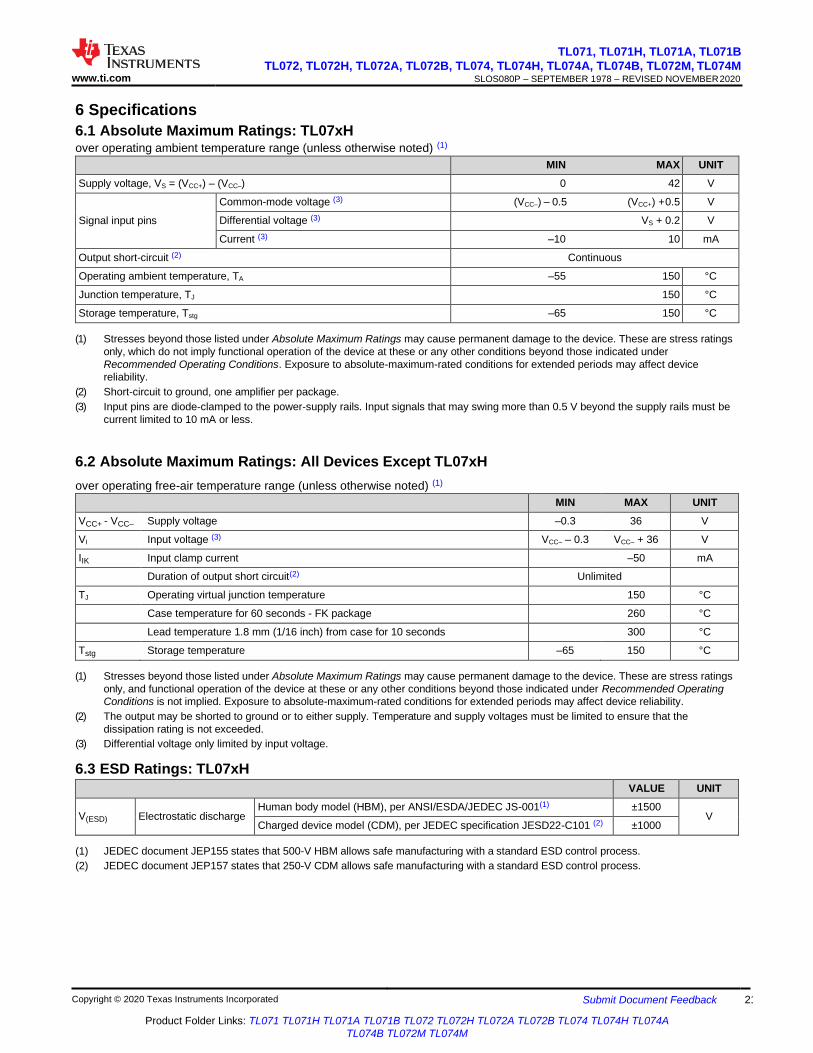
6 Specifications
6.1 Absolute Maximum Ratings: TL07xH over operating ambient temperature range (unless otherwise noted) (1)
MIN MAX UNIT
Supply voltage, VS = (VCC+) – (VCC–) 0 42 V
Signal input pins
Common-mode voltage (3) (VCC–) – 0.5 (VCC+) + 0.5 V
Differential voltage (3) VS + 0.2 V
Current (3) –10 10 mA
Output short-circuit (2) Continuous
Operating ambient temperature, TA –55 150 °C
Junction temperature, TJ 150 °C
Storage temperature, Tstg –65 150 °C
(1) Stresses beyond those listed under Absolute Maximum Ratings may cause permanent damage to the device. These are stress ratings
only, which do not imply functional operation of the device at these or any other conditions beyond those indicated under
Recommended Operating Conditions. Exposure to absolute-maximum-rated conditions for extended periods may affect device
reliability.
(2) Short-circuit to ground, one amplifier per package.
(3) Input pins are diode-clamped to the power-supply rails. Input signals that may swing more than 0.5 V beyond the supply rails must be
current limited to 10 mA or less.
6.2 Absolute Maximum Ratings: All Devices Except TL07xH
over operating free-air temperature range (unless otherwise noted) (1)
MIN MAX UNIT
VCC+ - VCC– Supply voltage –0.3 36 V
VI Input voltage (3) VCC– – 0.3 VCC– + 36 V
IIK Input clamp current –50 mA
Duration of output short circuit(2) Unlimited
TJ Operating virtual junction temperature 150 °C
Case temperature for 60 seconds - FK package 260 °C
Lead temperature 1.8 mm (1/16 inch) from case for 10 seconds 300 °C
Tstg Storage temperature –65 150 °C
(1) Stresses beyond those listed under Absolute Maximum Ratings may cause permanent damage to the device. These are stress ratings
only, and functional operation of the device at these or any other conditions beyond those indicated under Recommended Operating
Conditions is not implied. Exposure to absolute-maximum-rated conditions for extended periods may affect device reliability.
(2) The output may be shorted to ground or to either supply. Temperature and supply voltages must be limited to ensure that the
dissipation rating is not exceeded.
(3) Differential voltage only limited by input voltage.
6.3 ESD Ratings: TL07xH VALUE UNIT
V(ESD)
Electrostatic discharge Human body model (HBM), per ANSI/ESDA/JEDEC JS-001(1) ±1500
V Charged device model (CDM), per JEDEC specification JESD22-C101 (2) ±1000
(1) JEDEC document JEP155 states that 500-V HBM allows safe manufacturing with a standard ESD control process.
(2) JEDEC document JEP157 states that 250-V CDM allows safe manufacturing with a standard ESD control process.


TL071, TL071H, TL071A, TL071B
TL072, TL072H, TL072A, TL072B, TL074, TL074H, TL074A, TL074B, TL072M, TL074M SLOS080P – SEPTEMBER 1978 – REVISED NOVEMBER 2020 www.ti.com
Copyright © 2020 Texas Instruments Incorporated Submit Document Feedback 11
Product Folder Links: TL071 TL071H TL071A TL071B TL072 TL072H TL072A TL072B TL074 TL074H TL074A
TL074B TL072M TL074M
6.4 ESD Ratings: All Devices Except TL07xH
VALUE UNIT
V(ESD) Electrostatic discharge
Human body model (HBM), per ANSI/ESDA/JEDEC JS-001(1) ±2000 V Charged-device model (CDM), per JEDEC specification JESD22-
C101(2) ±1000
(1) JEDEC document JEP155 states that 500-V HBM allows safe manufacturing with a standard ESD control process.
(2) JEDEC document JEP157 states that 250-V CDM allows safe manufacturing with a standard ESD control process.
6.5 Recommended Operating Conditions: TL07xH over operating ambient temperature range (unless otherwise noted)
MIN MAX UNIT
VS Supply voltage, (VCC+) – (VCC–) 4.5 40 V
VI Input voltage range (VCC–) + 2 (VCC+) + 0.1 V
TA Specified temperature –40 125 °C
6.6 Recommended Operating Conditions: All Devices Except TL07xH
over operating free-air temperature range (unless otherwise noted)
MIN MAX UNIT
VCC+ Supply voltage (1) 5 15 V
VCC– Supply voltage (1) –5 –15 V
VCM Common-mode voltage VCC– + 4 VCC+ V
TA
Operating free-air temperature
TL07xM –55 125
°C
TL08xQ –40 125
TL07xI –40 85
TL07xAC, TL07xBC, TL07xC 0 70
(1) VCC+ and VCC– are not required to be of equal magnitude, provided that the total VCC (VCC+ – VCC–) is between 10 V and 30 V.
6.7 Thermal Information for Single Channel: TL071H
THERMAL METRIC (1)
TL071H
UNIT D (2)
(SOIC)
DBV (2)
(SOT-23)
8 PINS 5 PINS
RθJA Junction-to-ambient thermal resistance TBD TBD °C/W
RθJC(top) Junction-to-case (top) thermal resistance TBD TBD °C/W
RθJB Junction-to-board thermal resistance TBD TBD °C/W
ψJT Junction-to-top characterization parameter TBD TBD °C/W
ψJB Junction-to-board characterization parameter TBD TBD °C/W
RθJC(bot) Junction-to-case (bottom) thermal resistance TBD TBD °C/W
(1) For more information about traditional and new thermal metrics, see the Semiconductor and IC Package Thermal Metrics application
report, SPRA953.
(2) This package option is preview for TL071H.
TL071, TL071H, TL071A, TL071B
TL072, TL072H, TL072A, TL072B, TL074, TL074H, TL074A, TL074B, TL072M, TL074M SLOS080P – SEPTEMBER 1978 – REVISED NOVEMBER 2020 www.ti.com
12 Submit Document Feedback Copyright © 2020 Texas Instruments Incorporated
Product Folder Links: TL071 TL071H TL071A TL071B TL072 TL072H TL072A TL072B TL074 TL074H TL074A
TL074B TL072M TL074M
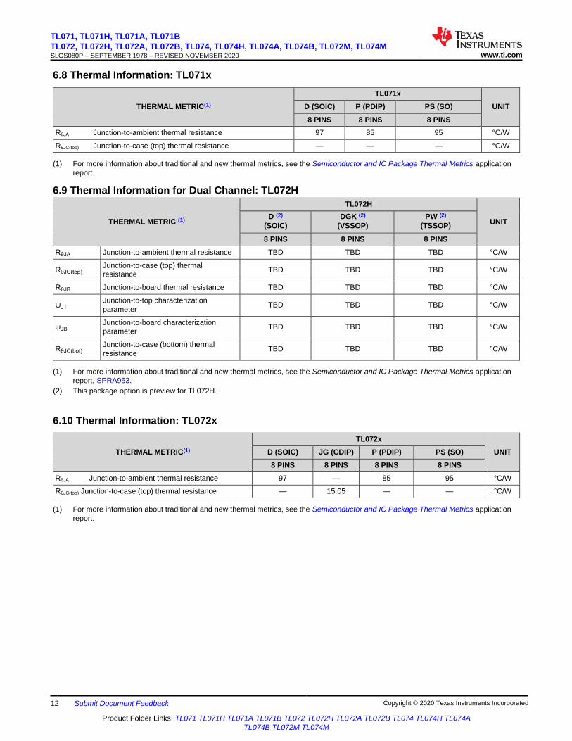
6.8 Thermal Information: TL071x
THERMAL METRIC(1)
TL071x UNIT D (SOIC) P (PDIP) PS (SO)
8 PINS 8 PINS 8 PINS
RθJA Junction-to-ambient thermal resistance 97 85 95 °C/W
RθJC(top) Junction-to-case (top) thermal resistance — — — °C/W
(1) For more information about traditional and new thermal metrics, see the Semiconductor and IC Package Thermal Metrics application
report.
6.9 Thermal Information for Dual Channel: TL072H
THERMAL METRIC (1)
TL072H
UNIT D (2)
(SOIC)
DGK (2)
(VSSOP)
PW (2)
(TSSOP)
8 PINS 8 PINS 8 PINS
RθJA Junction-to-ambient thermal resistance TBD TBD TBD °C/W
RθJC(top) Junction-to-case (top) thermal
resistance TBD TBD TBD °C/W
RθJB Junction-to-board thermal resistance TBD TBD TBD °C/W
ψJT Junction-to-top characterization
parameter TBD TBD TBD °C/W
ψJB Junction-to-board characterization
parameter TBD TBD TBD °C/W
RθJC(bot) Junction-to-case (bottom) thermal
resistance TBD TBD TBD °C/W
(1) For more information about traditional and new thermal metrics, see the Semiconductor and IC Package Thermal Metrics application
report, SPRA953.
(2) This package option is preview for TL072H.
6.10 Thermal Information: TL072x
THERMAL METRIC(1)
TL072x UNIT D (SOIC) JG (CDIP) P (PDIP) PS (SO)
8 PINS 8 PINS 8 PINS 8 PINS
RθJA Junction-to-ambient thermal resistance 97 — 85 95 °C/W
RθJC(top) Junction-to-case (top) thermal resistance — 15.05 — — °C/W
(1) For more information about traditional and new thermal metrics, see the Semiconductor and IC Package Thermal Metrics application
report.
TL071, TL071H, TL071A, TL071B
TL072, TL072H, TL072A, TL072B, TL074, TL074H, TL074A, TL074B, TL072M, TL074M SLOS080P – SEPTEMBER 1978 – REVISED NOVEMBER 2020 www.ti.com
Copyright © 2020 Texas Instruments Incorporated Submit Document Feedback 13
Product Folder Links: TL071 TL071H TL071A TL071B TL072 TL072H TL072A TL072B TL074 TL074H TL074A
TL074B TL072M TL074M
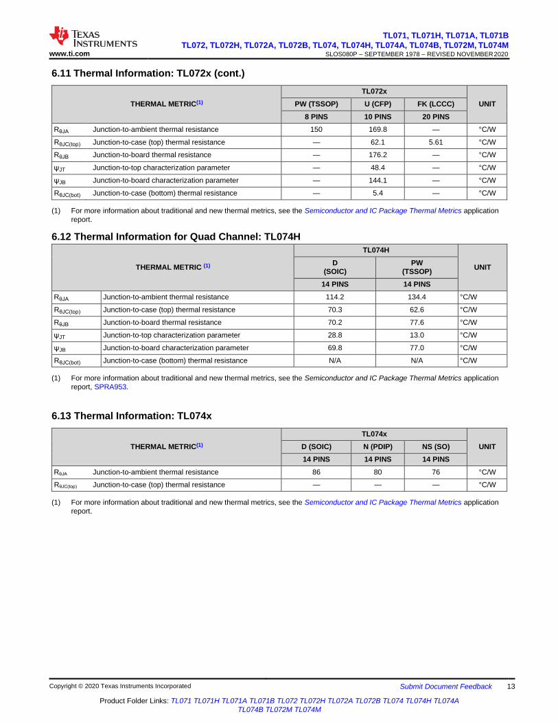
6.11 Thermal Information: TL072x (cont.)
THERMAL METRIC(1)
TL072x UNIT PW (TSSOP) U (CFP) FK (LCCC)
8 PINS 10 PINS 20 PINS
RθJA Junction-to-ambient thermal resistance 150 169.8 — °C/W
RθJC(top) Junction-to-case (top) thermal resistance — 62.1 5.61 °C/W
RθJB Junction-to-board thermal resistance — 176.2 — °C/W
ψJT Junction-to-top characterization parameter — 48.4 — °C/W
ψJB Junction-to-board characterization parameter — 144.1 — °C/W
RθJC(bot) Junction-to-case (bottom) thermal resistance — 5.4 — °C/W
(1) For more information about traditional and new thermal metrics, see the Semiconductor and IC Package Thermal Metrics application
report.
6.12 Thermal Information for Quad Channel: TL074H
THERMAL METRIC (1)
TL074H
UNIT D
(SOIC)
PW
(TSSOP)
14 PINS 14 PINS
RθJA Junction-to-ambient thermal resistance 114.2 134.4 °C/W
RθJC(top) Junction-to-case (top) thermal resistance 70.3 62.6 °C/W
RθJB Junction-to-board thermal resistance 70.2 77.6 °C/W
ψJT Junction-to-top characterization parameter 28.8 13.0 °C/W
ψJB Junction-to-board characterization parameter 69.8 77.0 °C/W
RθJC(bot) Junction-to-case (bottom) thermal resistance N/A N/A °C/W
(1) For more information about traditional and new thermal metrics, see the Semiconductor and IC Package Thermal Metrics application
report, SPRA953.
6.13 Thermal Information: TL074x
THERMAL METRIC(1)
TL074x UNIT D (SOIC) N (PDIP) NS (SO)
14 PINS 14 PINS 14 PINS
RθJA Junction-to-ambient thermal resistance 86 80 76 °C/W
RθJC(top) Junction-to-case (top) thermal resistance — — — °C/W
(1) For more information about traditional and new thermal metrics, see the Semiconductor and IC Package Thermal Metrics application
report.
TL071, TL071H, TL071A, TL071B
TL072, TL072H, TL072A, TL072B, TL074, TL074H, TL074A, TL074B, TL072M, TL074M SLOS080P – SEPTEMBER 1978 – REVISED NOVEMBER 2020 www.ti.com
14 Submit Document Feedback Copyright © 2020 Texas Instruments Incorporated
Product Folder Links: TL071 TL071H TL071A TL071B TL072 TL072H TL072A TL072B TL074 TL074H TL074A
TL074B TL072M TL074M
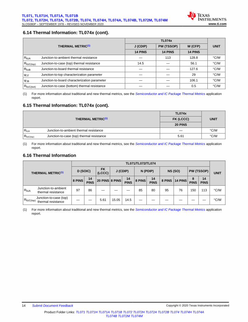
6.14 Thermal Information: TL074x (cont).
THERMAL METRIC(1)
TL074x UNIT J (CDIP) PW (TSSOP) W (CFP)
14 PINS 14 PINS 14 PINS
RθJA Junction-to-ambient thermal resistance — 113 128.8 °C/W
RθJC(top) Junction-to-case (top) thermal resistance 14.5 — 56.1 °C/W
RθJB Junction-to-board thermal resistance — — 127.6 °C/W
ψJT Junction-to-top characterization parameter — — 29 °C/W
ψJB Junction-to-board characterization parameter — — 106.1 °C/W
RθJC(bot) Junction-to-case (bottom) thermal resistance — — 0.5 °C/W
(1) For more information about traditional and new thermal metrics, see the Semiconductor and IC Package Thermal Metrics application
report.
6.15 Thermal Information: TL074x (cont).
THERMAL METRIC(1)
TL074x UNIT FK (LCCC)
20 PINS
RθJA Junction-to-ambient thermal resistance — °C/W
RθJC(top) Junction-to-case (top) thermal resistance 5.61 °C/W
(1) For more information about traditional and new thermal metrics, see the Semiconductor and IC Package Thermal Metrics application
report.
6.16 Thermal Information
THERMAL METRIC(1)
TL071/TL072/TL074
UNIT
D (SOIC) FK
(LCCC) J (CDIP) N (PDIP) NS (SO) PW (TSSOP)
8 PINS 14
PINS 20 PINS 8 PINS
14
PINS 8 PINS
14
PINS 8 PINS 14 PINS
8
PINS
14
PINS
RθJA Junction-to-ambient
thermal resistance 97 86 — — — 85 80 95 76 150 113 °C/W
RθJC(top) Junction-to-case (top)
thermal resistance — — 5.61 15.05 14.5 — — — — — — °C/W
(1) For more information about traditional and new thermal metrics, see the Semiconductor and IC Package Thermal Metrics application
report.
TL071, TL071H, TL071A, TL071B
TL072, TL072H, TL072A, TL072B, TL074, TL074H, TL074A, TL074B, TL072M, TL074M SLOS080P – SEPTEMBER 1978 – REVISED NOVEMBER 2020 www.ti.com
Copyright © 2020 Texas Instruments Incorporated Submit Document Feedback 15
Product Folder Links: TL071 TL071H TL071A TL071B TL072 TL072H TL072A TL072B TL074 TL074H TL074A
TL074B TL072M TL074M
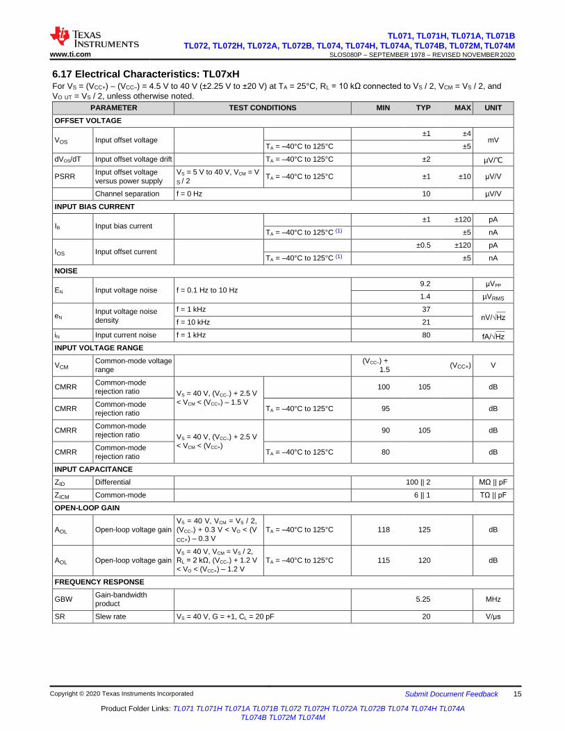
6.17 Electrical Characteristics: TL07xH For VS = (VCC+) – (VCC–) = 4.5 V to 40 V (±2.25 V to ±20 V) at TA = 25°C, RL = 10 kΩ connected to VS / 2, VCM = VS / 2, and
VO UT = VS / 2, unless otherwise noted.
PARAMETER TEST CONDITIONS MIN TYP MAX UNIT
OFFSET VOLTAGE
VOS
Input offset voltage ±1 ±4
mV TA = –40°C to 125°C ±5
dVOS/dT Input offset voltage drift TA = –40°C to 125°C ±2 µV/
PSRR Input offset voltage
versus power supply
VS = 5 V to 40 V, VCM = V
S / 2 TA = –40°C to 125°C
±1 ±10 μV/V
Channel separation f = 0 Hz 10 µV/V
INPUT BIAS CURRENT
IB
Input bias current ±1 ±120 pA
TA = –40°C to 125°C (1) ±5 nA
IOS
Input offset current ±0.5 ±120 pA
TA = –40°C to 125°C (1) ±5 nA
NOISE
EN
Input voltage noise
f = 0.1 Hz to 10 Hz 9.2 μVPP
1.4 µVRMS
eN Input voltage noise
density
f = 1 kHz 37
nV/√Hz f = 10 kHz 21
iN Input current noise f = 1 kHz 80
fA/√Hz
INPUT VOLTAGE RANGE
VCM Common-mode voltage
range
(VCC–) +
1.5
(VCC+) V
CMRR Common-mode
rejection ratio VS = 40 V, (VCC–) + 2.5 V
< VCM < (VCC+) – 1.5 V
100 105
dB
CMRR Common-mode
rejection ratio TA = –40°C to 125°C 95 dB
CMRR Common-mode
rejection ratio VS = 40 V, (VCC–) + 2.5 V
< VCM < (VCC+)
90 105
dB
CMRR Common-mode
rejection ratio TA = –40°C to 125°C 80 dB
INPUT CAPACITANCE
ZID Differential 100 || 2 MΩ || pF
ZICM Common-mode 6 || 1 TΩ || pF
OPEN-LOOP GAIN
AOL
Open-loop voltage gain
VS = 40 V, VCM = VS / 2,
(VCC–) + 0.3 V < VO < (V
CC+) – 0.3 V
TA = –40°C to 125°C
118
125
dB
AOL
Open-loop voltage gain
VS = 40 V, VCM = VS / 2,
RL = 2 kΩ, (VCC–) + 1.2 V
< VO < (VCC+) – 1.2 V
TA = –40°C to 125°C
115
120
dB
FREQUENCY RESPONSE
GBW Gain-bandwidth
product
5.25 MHz
SR Slew rate VS = 40 V, G = +1, CL = 20 pF 20 V/μs
TL071, TL071H, TL071A, TL071B
TL072, TL072H, TL072A, TL072B, TL074, TL074H, TL074A, TL074B, TL072M, TL074M SLOS080P – SEPTEMBER 1978 – REVISED NOVEMBER 2020 www.ti.com
16 Submit Document Feedback Copyright © 2020 Texas Instruments Incorporated
Product Folder Links: TL071 TL071H TL071A TL071B TL072 TL072H TL072A TL072B TL074 TL074H TL074A
TL074B TL072M TL074M
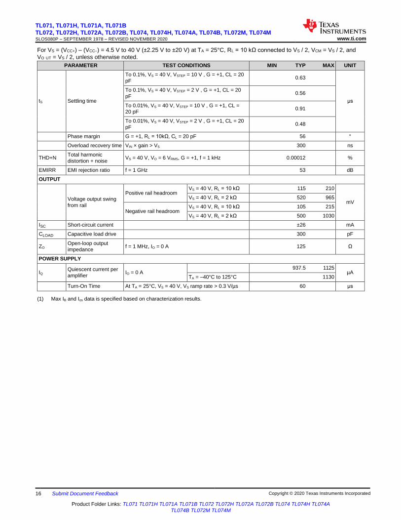
For VS = (VCC+) – (VCC–) = 4.5 V to 40 V (±2.25 V to ±20 V) at TA = 25°C, RL = 10 kΩ connected to VS / 2, VCM = VS / 2, and
VO UT = VS / 2, unless otherwise noted.
PARAMETER TEST CONDITIONS MIN TYP MAX UNIT
tS
Settling time
To 0.1%, VS = 40 V, VSTEP = 10 V , G = +1, CL = 20
pF 0.63
μs
To 0.1%, VS = 40 V, VSTEP = 2 V , G = +1, CL = 20
pF 0.56
To 0.01%, VS = 40 V, VSTEP = 10 V , G = +1, CL =
20 pF 0.91
To 0.01%, VS = 40 V, VSTEP = 2 V , G = +1, CL = 20
pF 0.48
Phase margin G = +1, RL = 10kΩ, CL = 20 pF 56 °
Overload recovery time VIN × gain > VS 300 ns
THD+N Total harmonic
distortion + noise VS = 40 V, VO = 6 VRMS, G = +1, f = 1 kHz 0.00012 %
EMIRR EMI rejection ratio f = 1 GHz 53 dB
OUTPUT
Voltage output swing
from rail
Positive rail headroom VS = 40 V, RL = 10 kΩ 115 210
mV
VS = 40 V, RL = 2 kΩ 520 965
Negative rail headroom VS = 40 V, RL = 10 kΩ 105 215
VS = 40 V, RL = 2 kΩ 500 1030
ISC Short-circuit current ±26 mA
CLOAD Capacitive load drive 300 pF
ZO Open-loop output
impedance f = 1 MHz, IO = 0 A 125 Ω
POWER SUPPLY
IQ Quiescent current per
amplifier IO = 0 A
937.5 1125 µA
TA = –40°C to 125°C 1130
Turn-On Time At TA = 25°C, VS = 40 V, VS ramp rate > 0.3 V/µs 60 μs
(1) Max IB and Ios data is specified based on characterization results.
TL071, TL071H, TL071A, TL071B
TL072, TL072H, TL072A, TL072B, TL074, TL074H, TL074A, TL074B, TL072M, TL074M SLOS080P – SEPTEMBER 1978 – REVISED NOVEMBER 2020 www.ti.com
Copyright © 2020 Texas Instruments Incorporated Submit Document Feedback 17
Product Folder Links: TL071 TL071H TL071A TL071B TL072 TL072H TL072A TL072B TL074 TL074H TL074A
TL074B TL072M TL074M
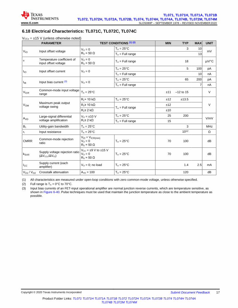
6.18 Electrical Characteristics: TL071C, TL072C, TL074C
VCC± = ±15 V (unless otherwise noted)
PARAMETER TEST CONDITIONS (1) (2) MIN TYP MAX UNIT
VIO
Input offset voltage VO = 0
RS = 50 Ω
TA = 25°C 3 10 mV
TA = Full range 13
α Temperature coefficient of
input offset voltage
VO = 0
RS = 50 Ω TA = Full range 18 µV/°C
IIO
Input offset current VO = 0 TA = 25°C 5 100 pA
TA = Full range 10 nA
IIB Input bias current (3) VO = 0 TA = 25°C 65 200 pA
TA = Full range 7 nA
VICR Common-mode input voltage
range TA = 25°C ±11 –12 to 15
V
VOM
Maximum peak output
voltage swing
RL= 10 kΩ TA = 25°C ±12 ±13.5 V RL≥ 10 kΩ
TA = Full range ±12
RL≥ 2 kΩ ±10
AVD Large-signal differential
voltage amplification
VO = ±10 V
RL≥ 2 kΩ
TA = 25°C 25 200
V/mV TA = Full range 15
B1 Utility-gain bandwidth TA = 25°C 3 MHz
rI Input resistance TA = 25°C 1012 Ω
CMRR
Common-mode rejection
ratio
VIC = VICR(min)
VO = 0
RS = 50 Ω
TA = 25°C
70
100
dB
kSVR
Supply voltage rejection ratio
(ΔVCC±/ΔVIO)
VCC = ±9 V to ±15 V
VO = 0
RS = 50 Ω
TA = 25°C
70
100
dB
ICC Supply current (each
amplifier) VO = 0; no load TA = 25°C
1.4 2.5 mA
VO1 / VO2 Crosstalk attenuation AVD = 100 TA = 25°C 120 dB
(1) All characteristics are measured under open-loop conditions with zero common-mode voltage, unless otherwise specified.
(2) Full range is TA = 0°C to 70°C.
(3) Input bias currents of an FET-input operational amplifier are normal junction reverse currents, which are temperature sensitive, as
shown in Figure 6-40. Pulse techniques must be used that maintain the junction temperature as close to the ambient temperature as
possible.
TL071, TL071H, TL071A, TL071B
TL072, TL072H, TL072A, TL072B, TL074, TL074H, TL074A, TL074B, TL072M, TL074M SLOS080P – SEPTEMBER 1978 – REVISED NOVEMBER 2020 www.ti.com
18 Submit Document Feedback Copyright © 2020 Texas Instruments Incorporated
Product Folder Links: TL071 TL071H TL071A TL071B TL072 TL072H TL072A TL072B TL074 TL074H TL074A
TL074B TL072M TL074M
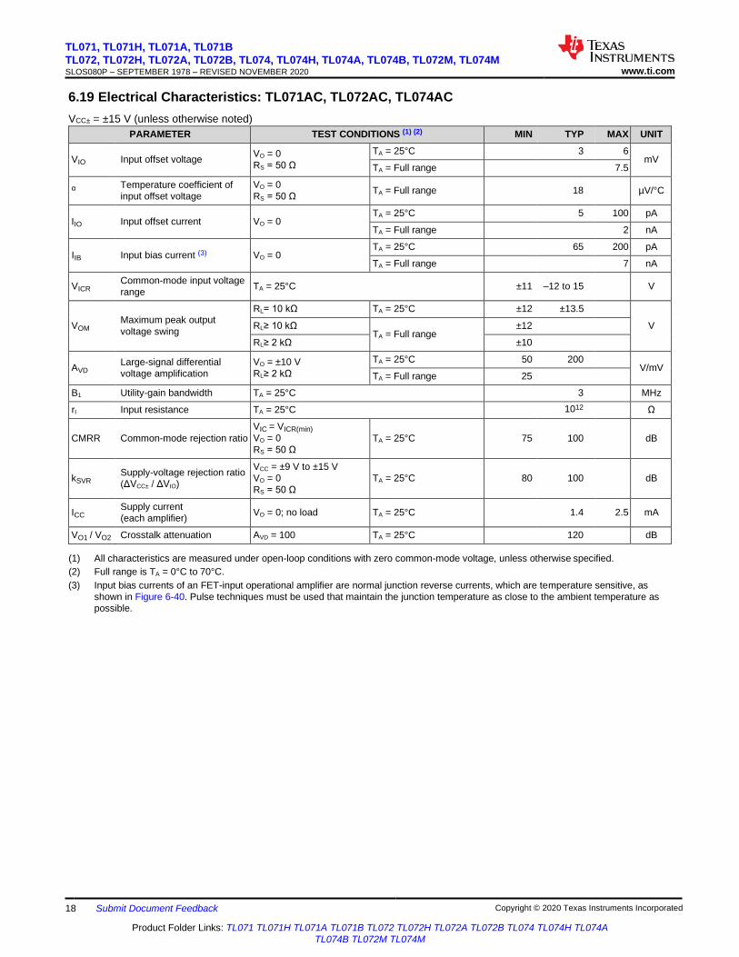
6.19 Electrical Characteristics: TL071AC, TL072AC, TL074AC
VCC± = ±15 V (unless otherwise noted)
PARAMETER TEST CONDITIONS (1) (2) MIN TYP MAX UNIT
VIO
Input offset voltage VO = 0
RS = 50 Ω
TA = 25°C 3 6 mV
TA = Full range 7.5
α Temperature coefficient of
input offset voltage
VO = 0
RS = 50 Ω TA = Full range 18 µV/°C
IIO
Input offset current VO = 0 TA = 25°C 5 100 pA
TA = Full range 2 nA
IIB Input bias current (3) VO = 0 TA = 25°C 65 200 pA
TA = Full range 7 nA
VICR Common-mode input voltage
range TA = 25°C ±11 –12 to 15
V
VOM
Maximum peak output
voltage swing
RL= 10 kΩ TA = 25°C ±12 ±13.5 V RL≥ 10 kΩ
TA = Full range ±12
RL≥ 2 kΩ ±10
AVD Large-signal differential
voltage amplification
VO = ±10 V
RL≥ 2 kΩ
TA = 25°C 50 200
V/mV TA = Full range 25
B1 Utility-gain bandwidth TA = 25°C 3 MHz
rI Input resistance TA = 25°C 1012 Ω
CMRR
Common-mode rejection ratio
VIC = VICR(min)
VO = 0
RS = 50 Ω
TA = 25°C
75
100
dB
kSVR
Supply-voltage rejection ratio
(ΔVCC± / ΔVIO)
VCC = ±9 V to ±15 V
VO = 0
RS = 50 Ω
TA = 25°C
80
100
dB
ICC Supply current
(each amplifier) VO = 0; no load TA = 25°C
1.4 2.5 mA
VO1 / VO2 Crosstalk attenuation AVD = 100 TA = 25°C 120 dB
(1) All characteristics are measured under open-loop conditions with zero common-mode voltage, unless otherwise specified.
(2) Full range is TA = 0°C to 70°C.
(3) Input bias currents of an FET-input operational amplifier are normal junction reverse currents, which are temperature sensitive, as
shown in Figure 6-40. Pulse techniques must be used that maintain the junction temperature as close to the ambient temperature as
possible.

TL071, TL071H, TL071A, TL071B
TL072, TL072H, TL072A, TL072B, TL074, TL074H, TL074A, TL074B, TL072M, TL074M SLOS080P – SEPTEMBER 1978 – REVISED NOVEMBER 2020 www.ti.com
Copyright © 2020 Texas Instruments Incorporated Submit Document Feedback 19
Product Folder Links: TL071 TL071H TL071A TL071B TL072 TL072H TL072A TL072B TL074 TL074H TL074A
TL074B TL072M TL074M
6.20 Electrical Characteristics: TL071BC, TL072BC, TL074BC
VCC± = ±15 V (unless otherwise noted)
PARAMETER TEST CONDITIONS (1) (2) MIN TYP MAX UNIT
VIO
Input offset voltage VO = 0
RS = 50 Ω
TA = 25°C 2 3 mV
TA = Full range 5
α Temperature coefficient of
input offset voltage
VO = 0
RS = 50 Ω TA = Full range 18 µV/°C
IIO
Input offset current VO = 0 TA = 25°C 5 100 pA
TA = Full range 2 nA
IIB Input bias current (3) VO = 0 TA = 25°C 65 200 pA
TA = Full range 7 nA
VICR Common-mode input
voltage range TA = 25°C ±11 –12 to 15
V
VOM
Maximum peak output
voltage swing
RL= 10 kΩ TA = 25°C ±12 ±13.5 V RL≥ 10 kΩ
TA = Full range ±12
RL≥ 2 kΩ ±10
AVD Large-signal differential
voltage amplification
VO = ±10 V
RL ≥ 2 kΩ
TA = 25°C 50 200
V/mV TA = Full range 25
B1 Utility-gain bandwidth TA = 25°C 3 MHz
rI Input resistance TA = 25°C 1012 Ω
CMRR
Common-mode rejection
ratio
VIC = VICR(min)
VO = 0
RS = 50 Ω
TA = 25°C
75
100
dB
kSVR
Supply-voltage rejection
ratio (ΔVCC±/ΔVIO)
VCC = ±9 V to ±15 V
VO = 0
RS = 50 Ω
TA = 25°C
80
100
dB
ICC Supply current (each
amplifier) VO = 0; no load TA = 25°C
1.4 2.5 mA
VO1 / VO2 Crosstalk attenuation AVD = 100 TA = 25°C 120 dB
(1) All characteristics are measured under open-loop conditions with zero common-mode voltage, unless otherwise specified.
(2) Full range is TA = 0°C to 70°C.
(3) Input bias currents of an FET-input operational amplifier are normal junction reverse currents, which are temperature sensitive, as
shown in Figure 6-40. Pulse techniques must be used that maintain the junction temperature as close to the ambient temperature as
possible.
TL071, TL071H, TL071A, TL071B
TL072, TL072H, TL072A, TL072B, TL074, TL074H, TL074A, TL074B, TL072M, TL074M SLOS080P – SEPTEMBER 1978 – REVISED NOVEMBER 2020 www.ti.com
20 Submit Document Feedback Copyright © 2020 Texas Instruments Incorporated
Product Folder Links: TL071 TL071H TL071A TL071B TL072 TL072H TL072A TL072B TL074 TL074H TL074A
TL074B TL072M TL074M
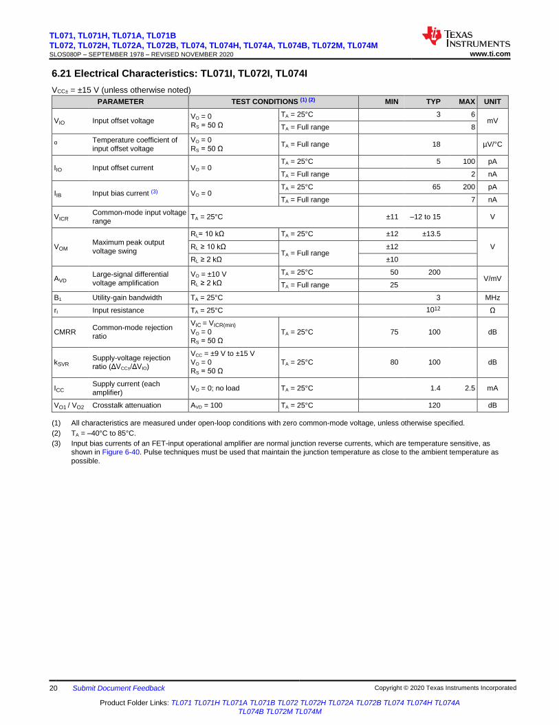
6.21 Electrical Characteristics: TL071I, TL072I, TL074I
VCC± = ±15 V (unless otherwise noted)
PARAMETER TEST CONDITIONS (1) (2) MIN TYP MAX UNIT
VIO
Input offset voltage VO = 0
RS = 50 Ω
TA = 25°C 3 6 mV
TA = Full range 8
α Temperature coefficient of
input offset voltage
VO = 0
RS = 50 Ω TA = Full range 18 µV/°C
IIO
Input offset current VO = 0 TA = 25°C 5 100 pA
TA = Full range 2 nA
IIB Input bias current (3) VO = 0 TA = 25°C 65 200 pA
TA = Full range 7 nA
VICR Common-mode input voltage
range TA = 25°C ±11 –12 to 15
V
VOM
Maximum peak output
voltage swing
RL= 10 kΩ TA = 25°C ±12 ±13.5 V RL ≥ 10 kΩ
TA = Full range ±12
RL ≥ 2 kΩ ±10
AVD Large-signal differential
voltage amplification
VO = ±10 V
RL ≥ 2 kΩ
TA = 25°C 50 200
V/mV TA = Full range 25
B1 Utility-gain bandwidth TA = 25°C 3 MHz
rI Input resistance TA = 25°C 1012 Ω
CMRR
Common-mode rejection
ratio
VIC = VICR(min)
VO = 0
RS = 50 Ω
TA = 25°C
75
100
dB
kSVR
Supply-voltage rejection
ratio (ΔVCC±/ΔVIO)
VCC = ±9 V to ±15 V
VO = 0
RS = 50 Ω
TA = 25°C
80
100
dB
ICC Supply current (each
amplifier) VO = 0; no load TA = 25°C
1.4 2.5 mA
VO1 / VO2 Crosstalk attenuation AVD = 100 TA = 25°C 120 dB
(1) All characteristics are measured under open-loop conditions with zero common-mode voltage, unless otherwise specified.
(2) TA = –40°C to 85°C.
(3) Input bias currents of an FET-input operational amplifier are normal junction reverse currents, which are temperature sensitive, as
shown in Figure 6-40. Pulse techniques must be used that maintain the junction temperature as close to the ambient temperature as
possible.
TL071, TL071H, TL071A, TL071B
TL072, TL072H, TL072A, TL072B, TL074, TL074H, TL074A, TL074B, TL072M, TL074M SLOS080P – SEPTEMBER 1978 – REVISED NOVEMBER 2020 www.ti.com
Copyright © 2020 Texas Instruments Incorporated Submit Document Feedback 21
Product Folder Links: TL071 TL071H TL071A TL071B TL072 TL072H TL072A TL072B TL074 TL074H TL074A
TL074B TL072M TL074M
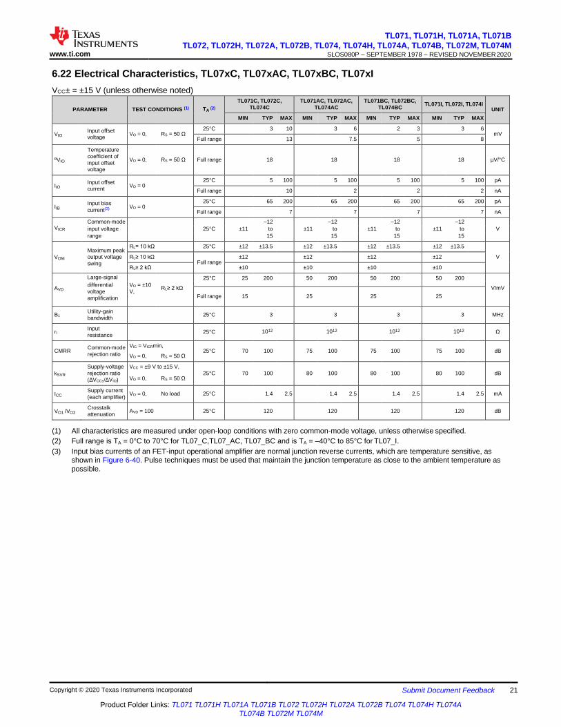
6.22 Electrical Characteristics, TL07xC, TL07xAC, TL07xBC, TL07xI
VCC± = ±15 V (unless otherwise noted)
PARAMETER
TEST CONDITIONS (1)
TA
(2)
TL071C, TL072C,
TL074C
TL071AC, TL072AC,
TL074AC
TL071BC, TL072BC,
TL074BC TL071I, TL072I, TL074I
UNIT
MIN TYP MAX MIN TYP MAX MIN TYP MAX MIN TYP MAX
VIO
Input offset
voltage
VO = 0,
RS = 50 Ω
25°C 3 10 3 6 2 3 3 6 mV
Full range 13 7.5 5 8
αVIO
Temperature
coefficient of
input offset
voltage
VO = 0,
RS = 50 Ω
Full range
18
18
18
18
µV/°C
IIO
Input offset
current
VO = 0
25°C 5 100 5 100 5 100 5 100 pA
Full range 10 2 2 2 nA
IIB
Input bias
current(3)
VO = 0
25°C 65 200 65 200 65 200 65 200 pA
Full range 7 7 7 7 nA
Common-mode –12 –12 –12 –12
VICR input voltage 25°C ±11 to ±11 to ±11 to ±11 to V
range 15 15 15 15
VOM
Maximum peak
output voltage
swing
RL= 10 kΩ 25°C ±12 ±13.5 ±12 ±13.5 ±12 ±13.5 ±12 ±13.5
V RL≥ 10 kΩ Full range
±12 ±12 ±12 ±12
RL≥ 2 kΩ ±10 ±10 ±10 ±10
Large-signal 25°C 25 200 50 200 50 200 50 200
AVD differential
voltage
amplification
VO = ±10
V, RL≥ 2 kΩ V/mV
Full range
15
25
25
25
B1 Utility-gain
bandwidth
25°C 3 3 3 3 MHz
rI Input
resistance
25°C 1012 1012 1012 1012 Ω
CMRR
Common-mode
rejection ratio
VIC = VICRmin,
VO = 0, RS = 50 Ω
25°C
70
100
75
100
75
100
75
100
dB
kSVR
Supply-voltage
rejection ratio
(ΔVCC±/ΔVIO)
VCC = ±9 V to ±15 V,
VO = 0, RS = 50 Ω
25°C
70
100
80
100
80
100
80
100
dB
ICC Supply current
(each amplifier) VO = 0, No load 25°C
1.4 2.5
1.4 2.5
1.4 2.5
1.4 2.5 mA
VO1 /VO2 Crosstalk
attenuation AVD = 100 25°C 120 120 120 120 dB
(1) All characteristics are measured under open-loop conditions with zero common-mode voltage, unless otherwise specified.
(2) Full range is TA = 0°C to 70°C for TL07_C,TL07_AC, TL07_BC and is TA = –40°C to 85°C for TL07_I.
(3) Input bias currents of an FET-input operational amplifier are normal junction reverse currents, which are temperature sensitive, as
shown in Figure 6-40. Pulse techniques must be used that maintain the junction temperature as close to the ambient temperature as
possible.
TL071, TL071H, TL071A, TL071B
TL072, TL072H, TL072A, TL072B, TL074, TL074H, TL074A, TL074B, TL072M, TL074M SLOS080P – SEPTEMBER 1978 – REVISED NOVEMBER 2020 www.ti.com
22 Submit Document Feedback Copyright © 2020 Texas Instruments Incorporated
Product Folder Links: TL071 TL071H TL071A TL071B TL072 TL072H TL072A TL072B TL074 TL074H TL074A
TL074B TL072M TL074M
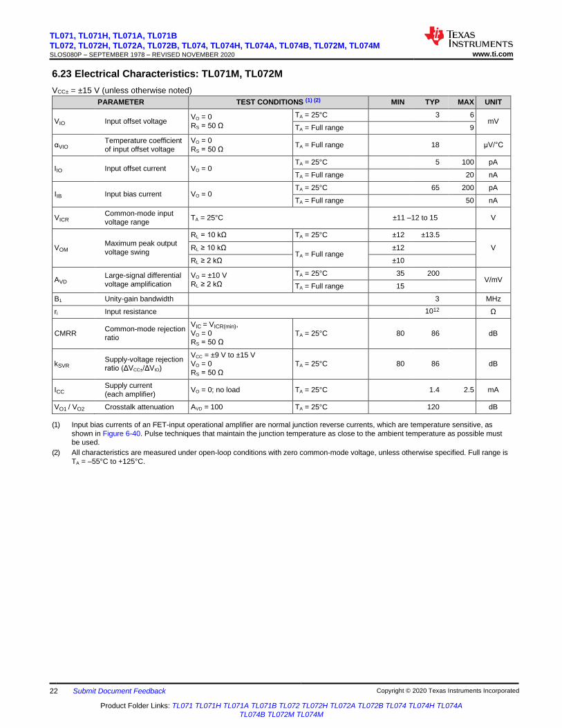
6.23 Electrical Characteristics: TL071M, TL072M
VCC± = ±15 V (unless otherwise noted)
PARAMETER TEST CONDITIONS (1) (2) MIN TYP MAX UNIT
VIO
Input offset voltage VO = 0
RS = 50 Ω
TA = 25°C 3 6 mV
TA = Full range 9
αVIO Temperature coefficient
of input offset voltage
VO = 0
RS = 50 Ω TA = Full range 18 μV/°C
IIO
Input offset current VO = 0 TA = 25°C 5 100 pA
TA = Full range 20 nA
IIB
Input bias current VO = 0 TA = 25°C 65 200 pA
TA = Full range 50 nA
VICR Common-mode input
voltage range TA = 25°C ±11 –12 to 15 V
VOM
Maximum peak output
voltage swing
RL = 10 kΩ TA = 25°C ±12 ±13.5
V RL ≥ 10 kΩ TA = Full range
±12
RL ≥ 2 kΩ ±10
AVD Large-signal differential
voltage amplification
VO = ±10 V
RL ≥ 2 kΩ
TA = 25°C 35 200
V/mV TA = Full range 15
B1 Unity-gain bandwidth 3 MHz
ri Input resistance 1012 Ω
CMRR
Common-mode rejection
ratio
VIC = VICR(min),
VO = 0
RS = 50 Ω
TA = 25°C
80
86
dB
kSVR
Supply-voltage rejection
ratio (ΔVCC±/ΔVIO)
VCC = ±9 V to ±15 V
VO = 0
RS = 50 Ω
TA = 25°C
80
86
dB
ICC Supply current
(each amplifier) VO = 0; no load TA = 25°C
1.4 2.5 mA
VO1 / VO2 Crosstalk attenuation AVD = 100 TA = 25°C 120 dB
(1) Input bias currents of an FET-input operational amplifier are normal junction reverse currents, which are temperature sensitive, as
shown in Figure 6-40. Pulse techniques that maintain the junction temperature as close to the ambient temperature as possible must
be used.
(2) All characteristics are measured under open-loop conditions with zero common-mode voltage, unless otherwise specified. Full range is
TA = –55°C to +125°C.
TL071, TL071H, TL071A, TL071B
TL072, TL072H, TL072A, TL072B, TL074, TL074H, TL074A, TL074B, TL072M, TL074M SLOS080P – SEPTEMBER 1978 – REVISED NOVEMBER 2020 www.ti.com
Copyright © 2020 Texas Instruments Incorporated Submit Document Feedback 23
Product Folder Links: TL071 TL071H TL071A TL071B TL072 TL072H TL072A TL072B TL074 TL074H TL074A
TL074B TL072M TL074M
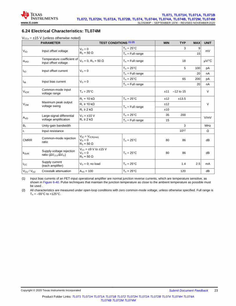
6.24 Electrical Characteristics: TL074M
VCC± = ±15 V (unless otherwise noted)
PARAMETER TEST CONDITIONS (1) (2) MIN TYP MAX UNIT
VIO
Input offset voltage VO = 0
RS = 50 Ω
TA = 25°C 3 9 mV
TA = Full range 15
αVIO Temperature coefficient of
input offset voltage VO = 0, RS = 50 Ω TA = Full range 18 μV/°C
IIO
Input offset current VO = 0 TA = 25°C 5 100 pA
TA = Full range 20 nA
IIB
Input bias current VO = 0 TA = 25°C 65 200 pA
TA = Full range 20 nA
VICR Common-mode input
voltage range TA = 25°C ±11 –12 to 15
V
VOM
Maximum peak output
voltage swing
RL = 10 kΩ TA = 25°C ±12 ±13.5
V RL ≥ 10 kΩ TA = Full range
±12
RL ≥ 2 kΩ ±10
AVD Large-signal differential
voltage amplification
VO = ±10 V
RL ≥ 2 kΩ
TA = 25°C 35 200
V/mV TA = Full range 15
B1 Unity-gain bandwidth 3 MHz
ri Input resistance 1012 Ω
CMRR
Common-mode rejection
ratio
VIC = VICR(min)
VO = 0
RS = 50 Ω
TA = 25°C
80
86
dB
kSVR
Supply-voltage rejection
ratio (ΔVCC±/ΔVIO)
VCC = ±9 V to ±15 V
VO = 0
RS = 50 Ω
TA = 25°C
80
86
dB
ICC Supply current
(each amplifier) VO = 0; no load TA = 25°C
1.4 2.5 mA
VO1 / VO2 Crosstalk attenuation AVD = 100 TA = 25°C 120 dB
(1) Input bias currents of an FET-input operational amplifier are normal junction reverse currents, which are temperature sensitive, as
shown in Figure 6-40. Pulse techniques that maintain the junction temperature as close to the ambient temperature as possible must
be used .
(2) All characteristics are measured under open-loop conditions with zero common-mode voltage, unless otherwise specified. Full range is
TA = –55°C to +125°C.
TL071, TL071H, TL071A, TL071B
TL072, TL072H, TL072A, TL072B, TL074, TL074H, TL074A, TL074B, TL072M, TL074M SLOS080P – SEPTEMBER 1978 – REVISED NOVEMBER 2020 www.ti.com
24 Submit Document Feedback Copyright © 2020 Texas Instruments Incorporated
Product Folder Links: TL071 TL071H TL071A TL071B TL072 TL072H TL072A TL072B TL074 TL074H TL074A
TL074B TL072M TL074M
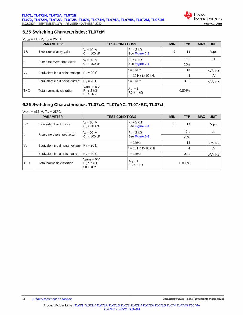
6.25 Switching Characteristics: TL07xM
VCC± = ±15 V, TA = 25°C
PARAMETER TEST CONDITIONS MIN TYP MAX UNIT
SR Slew rate at unity gain VI = 10 V
CL = 100 pF
RL = 2 kΩ
See Figure 7-1 5 13 V/μs
tr
Rise-time overshoot factor VI = 20 V
CL = 100 pF
RL = 2 kΩ
See Figure 7-1
0.1 μs
20%
Vn
Equivalent input noise voltage RS = 20 Ω f = 1 kHz 18
nV/√ Hz
f = 10 Hz to 10 kHz 4 μV
In Equivalent input noise current RS = 20 Ω f = 1 kHz 0.01
pA/√ Hz
THD
Total harmonic distortion
VIrms = 6 V
RL ≥ 2 kΩ
f = 1 kHz
AVD = 1
RS ≤ 1 kΩ
0.003%
6.26 Switching Characteristics: TL07xC, TL07xAC, TL07xBC, TL07xI
VCC± = ±15 V, TA = 25°C
PARAMETER TEST CONDITIONS MIN TYP MAX UNIT
SR Slew rate at unity gain VI = 10 V
CL = 100 pF
RL = 2 kΩ
See Figure 7-1 8 13 V/μs
tr
Rise-time overshoot factor VI = 20 V
CL = 100 pF
RL = 2 kΩ
See Figure 7-1
0.1 μs
20%
Vn
Equivalent input noise voltage RS = 20 Ω f = 1 kHz 18
nV/√ Hz
f = 10 Hz to 10 kHz 4 μV
In Equivalent input noise current RS = 20 Ω f = 1 kHz 0.01
pA/√ Hz
THD
Total harmonic distortion
VIrms = 6 V
RL ≥ 2 kΩ
f = 1 kHz
AVD = 1
RS ≤ 1 kΩ
0.003%
TL071, TL071H, TL071A, TL071B
TL072, TL072H, TL072A, TL072B, TL074, TL074H, TL074A, TL074B, TL072M, TL074M SLOS080P – SEPTEMBER 1978 – REVISED NOVEMBER 2020 www.ti.com
Copyright © 2020 Texas Instruments Incorporated Submit Document Feedback 25
Product Folder Links: TL071 TL071H TL071A TL071B TL072 TL072H TL072A TL072B TL074 TL074H TL074A
TL074B TL072M TL074M
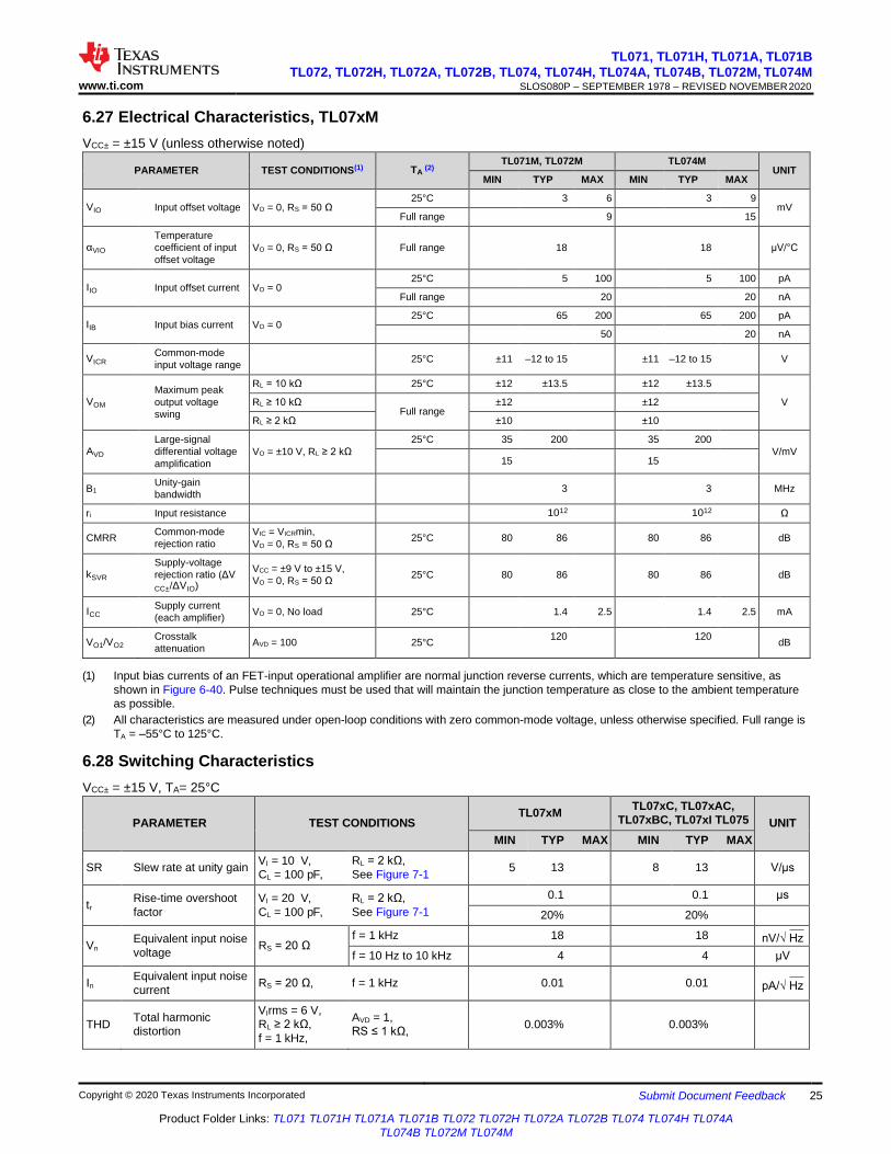
6.27 Electrical Characteristics, TL07xM
VCC± = ±15 V (unless otherwise noted)
PARAMETER
TEST CONDITIONS(1) TA
(2) TL071M, TL072M TL074M
UNIT MIN TYP MAX MIN TYP MAX
VIO
Input offset voltage VO = 0, RS = 50 Ω 25°C 3 6 3 9
mV Full range 9 15
αVIO
Temperature
coefficient of input
offset voltage
VO = 0, RS = 50 Ω
Full range
18
18
μV/°C
IIO
Input offset current VO = 0 25°C 5 100 5 100 pA
Full range 20 20 nA
IIB
Input bias current VO = 0 25°C 65 200 65 200 pA
50 20 nA
VICR Common-mode
input voltage range
25°C ±11 –12 to 15
±11 –12 to 15
V
VOM
Maximum peak
output voltage
swing
RL = 10 kΩ 25°C ±12 ±13.5 ±12 ±13.5
V RL ≥ 10 kΩ
Full range ±12 ±12
RL ≥ 2 kΩ ±10 ±10
AVD
Large-signal
differential voltage
amplification
VO = ±10 V, RL ≥ 2 kΩ
25°C 35 200 35 200 V/mV
15 15
B1 Unity-gain
bandwidth
3 3 MHz
ri Input resistance 1012 1012 Ω
CMRR Common-mode
rejection ratio
VIC = VICRmin,
VO = 0, RS = 50 Ω 25°C 80 86
80 86
dB
kSVR
Supply-voltage
rejection ratio (ΔV
CC±/ΔVIO)
VCC = ±9 V to ±15 V,
VO = 0, RS = 50 Ω
25°C
80
86
80
86
dB
ICC Supply current
(each amplifier) VO = 0, No load 25°C
1.4 2.5
1.4 2.5 mA
VO1/VO2 Crosstalk
attenuation AVD = 100 25°C
120 120 dB
(1) Input bias currents of an FET-input operational amplifier are normal junction reverse currents, which are temperature sensitive, as
shown in Figure 6-40. Pulse techniques must be used that will maintain the junction temperature as close to the ambient temperature
as possible.
(2) All characteristics are measured under open-loop conditions with zero common-mode voltage, unless otherwise specified. Full range is
TA = –55°C to 125°C.
6.28 Switching Characteristics
VCC± = ±15 V, TA= 25°C
PARAMETER
TEST CONDITIONS
TL07xM TL07xC, TL07xAC,
TL07xBC, TL07xI TL075
UNIT
MIN TYP MAX MIN TYP MAX
SR Slew rate at unity gain VI = 10 V,
CL = 100 pF,
RL = 2 kΩ,
See Figure 7-1 5 13 8 13 V/μs
tr Rise-time overshoot
factor
VI = 20 V,
CL = 100 pF,
RL = 2 kΩ,
See Figure 7-1
0.1 0.1 μs
20% 20%
Vn Equivalent input noise
voltage RS = 20 Ω
f = 1 kHz 18 18
nV/√ Hz
f = 10 Hz to 10 kHz 4 4 μV
In Equivalent input noise
current RS = 20 Ω, f = 1 kHz 0.01 0.01
pA/√ Hz
THD
Total harmonic
distortion
VIrms = 6 V,
RL ≥ 2 kΩ,
f = 1 kHz,
AVD = 1,
RS ≤ 1 kΩ,
0.003%
0.003%
TL071, TL071H, TL071A, TL071B
TL072, TL072H, TL072A, TL072B, TL074, TL074H, TL074A, TL074B, TL072M, TL074M SLOS080P – SEPTEMBER 1978 – REVISED NOVEMBER 2020 www.ti.com
26 Submit Document Feedback Copyright © 2020 Texas Instruments Incorporated
Product Folder Links: TL071 TL071H TL071A TL071B TL072 TL072H TL072A TL072B TL074 TL074H TL074A
TL074B TL072M TL074M
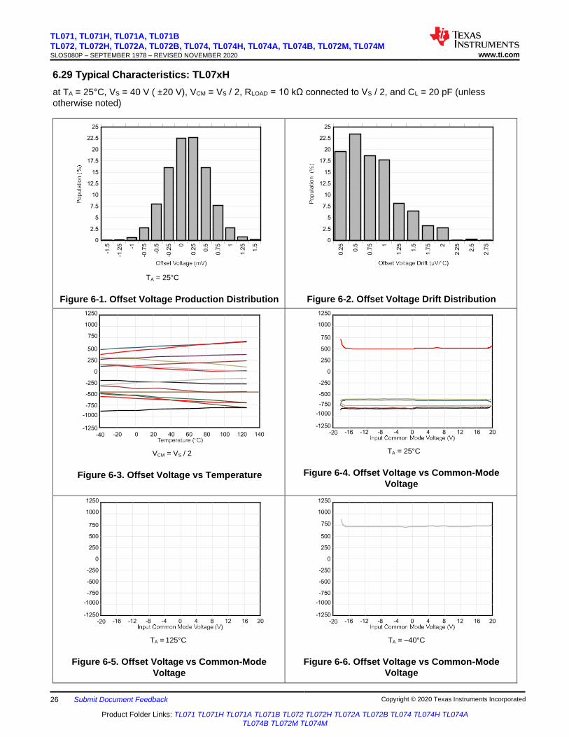
6.29 Typical Characteristics: TL07xH
at TA = 25°C, VS = 40 V ( ±20 V), VCM = VS / 2, RLOAD = 10 kΩ connected to VS / 2, and CL = 20 pF (unless
otherwise noted)
TA = 25°C
Figure 6-1. Offset Voltage Production Distribution
Figure 6-2. Offset Voltage Drift Distribution
VCM = VS / 2
Figure 6-3. Offset Voltage vs Temperature
TA = 25°C
Figure 6-4. Offset Voltage vs Common-Mode
Voltage
TA = 125°C
Figure 6-5. Offset Voltage vs Common-Mode
Voltage
TA = –40°C
Figure 6-6. Offset Voltage vs Common-Mode
Voltage
TL071, TL071H, TL071A, TL071B
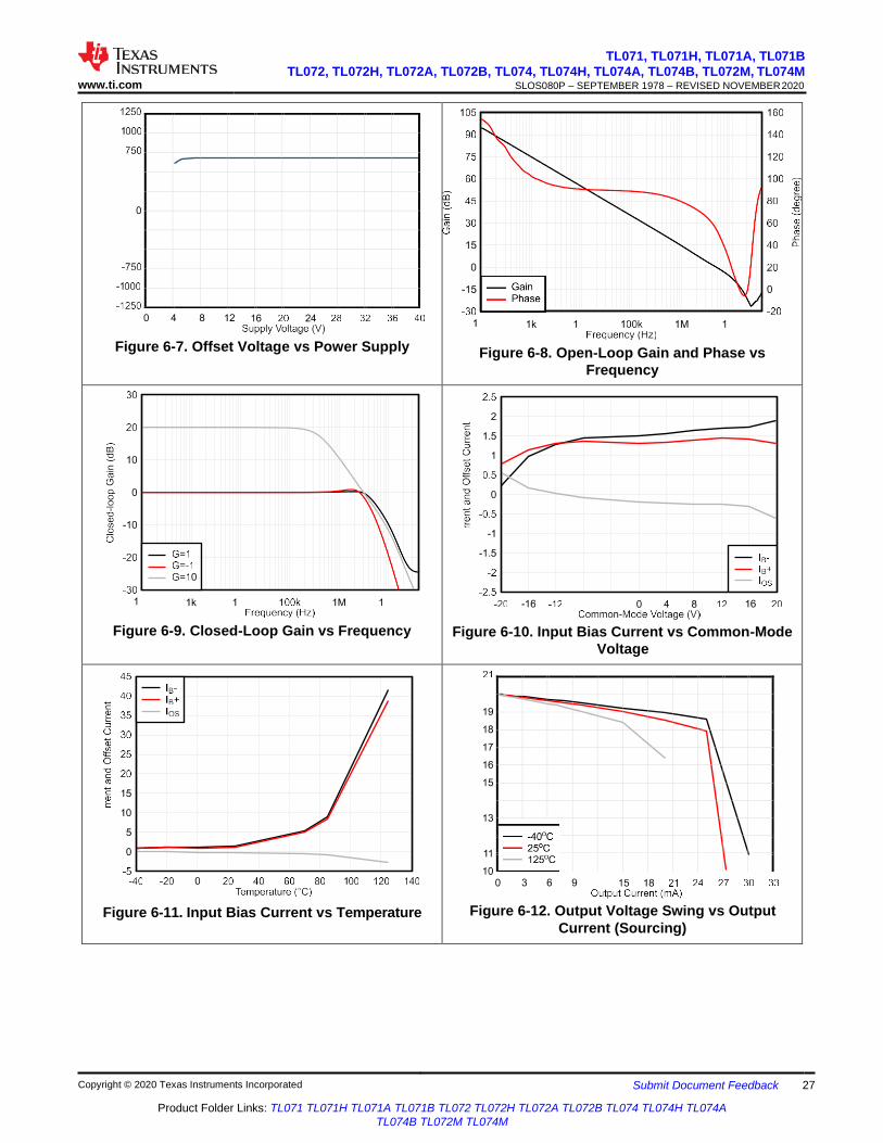
TL072, TL072H, TL072A, TL072B, TL074, TL074H, TL074A, TL074B, TL072M, TL074M SLOS080P – SEPTEMBER 1978 – REVISED NOVEMBER 2020 www.ti.com
Copyright © 2020 Texas Instruments Incorporated Submit Document Feedback 27
Product Folder Links: TL071 TL071H TL071A TL071B TL072 TL072H TL072A TL072B TL074 TL074H TL074A
TL074B TL072M TL074M
Figure 6-7. Offset Voltage vs Power Supply
Figure 6-8. Open-Loop Gain and Phase vs
Frequency
Figure 6-9. Closed-Loop Gain vs Frequency
Figure 6-10. Input Bias Current vs Common-Mode
Voltage
Figure 6-11. Input Bias Current vs Temperature
Figure 6-12. Output Voltage Swing vs Output
Current (Sourcing)
TL071, TL071H, TL071A, TL071B
TL072, TL072H, TL072A, TL072B, TL074, TL074H, TL074A, TL074B, TL072M, TL074M SLOS080P – SEPTEMBER 1978 – REVISED NOVEMBER 2020 www.ti.com
28 Submit Document Feedback Copyright © 2020 Texas Instruments Incorporated
Product Folder Links: TL071 TL071H TL071A TL071B TL072 TL072H TL072A TL072B TL074 TL074H TL074A
TL074B TL072M TL074M
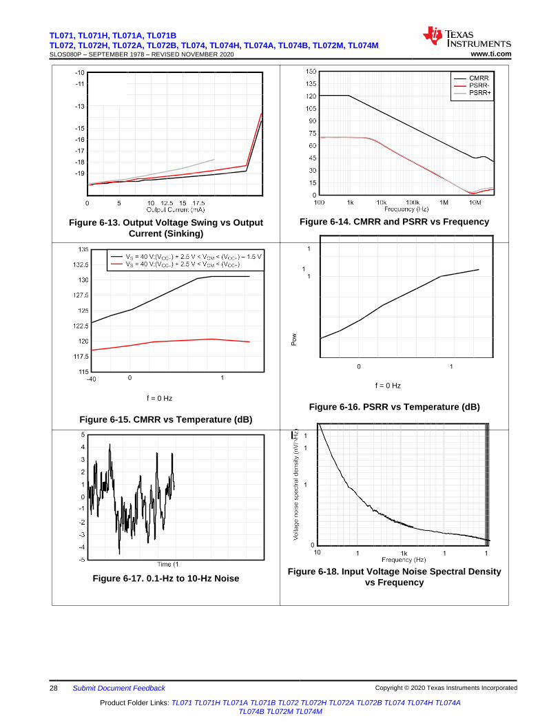
Figure 6-13. Output Voltage Swing vs Output
Current (Sinking)
f = 0 Hz
Figure 6-15. CMRR vs Temperature (dB)
Figure 6-17. 0.1-Hz to 10-Hz Noise
Figure 6-14. CMRR and PSRR vs Frequency
f = 0 Hz
Figure 6-16. PSRR vs Temperature (dB)
Figure 6-18. Input Voltage Noise Spectral Density
vs Frequency
TL071, TL071H, TL071A, TL071B
TL072, TL072H, TL072A, TL072B, TL074, TL074H, TL074A, TL074B, TL072M, TL074M SLOS080P – SEPTEMBER 1978 – REVISED NOVEMBER 2020 www.ti.com
Copyright © 2020 Texas Instruments Incorporated Submit Document Feedback 29
Product Folder Links: TL071 TL071H TL071A TL071B TL072 TL072H TL072A TL072B TL074 TL074H TL074A
TL074B TL072M TL074M
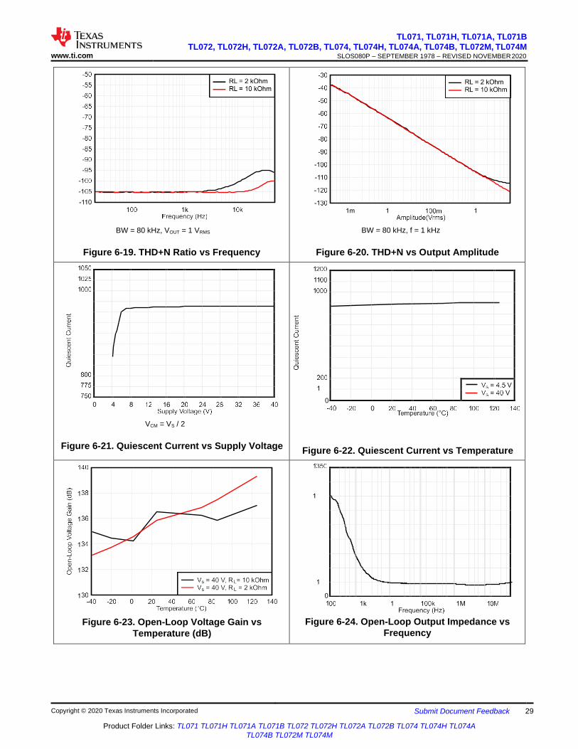
BW = 80 kHz, VOUT = 1 VRMS
Figure 6-19. THD+N Ratio vs Frequency
BW = 80 kHz, f = 1 kHz
Figure 6-20. THD+N vs Output Amplitude
VCM = VS / 2
Figure 6-21. Quiescent Current vs Supply Voltage
Figure 6-22. Quiescent Current vs Temperature
Figure 6-23. Open-Loop Voltage Gain vs
Temperature (dB)
Figure 6-24. Open-Loop Output Impedance vs
Frequency
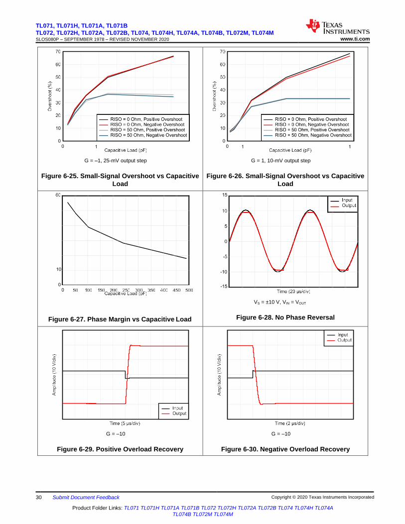
TL071, TL071H, TL071A, TL071B
TL072, TL072H, TL072A, TL072B, TL074, TL074H, TL074A, TL074B, TL072M, TL074M SLOS080P – SEPTEMBER 1978 – REVISED NOVEMBER 2020 www.ti.com
30 Submit Document Feedback Copyright © 2020 Texas Instruments Incorporated
Product Folder Links: TL071 TL071H TL071A TL071B TL072 TL072H TL072A TL072B TL074 TL074H TL074A
TL074B TL072M TL074M
G = –1, 25-mV output step
Figure 6-25. Small-Signal Overshoot vs Capacitive
Load
G = 1, 10-mV output step
Figure 6-26. Small-Signal Overshoot vs Capacitive
Load
Figure 6-27. Phase Margin vs Capacitive Load
VS = ±10 V, VIN = VOUT
Figure 6-28. No Phase Reversal
G = –10
Figure 6-29. Positive Overload Recovery
G = –10
Figure 6-30. Negative Overload Recovery
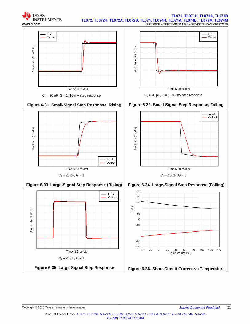
TL071, TL071H, TL071A, TL071B
TL072, TL072H, TL072A, TL072B, TL074, TL074H, TL074A, TL074B, TL072M, TL074M SLOS080P – SEPTEMBER 1978 – REVISED NOVEMBER 2020 www.ti.com
Copyright © 2020 Texas Instruments Incorporated Submit Document Feedback 31
Product Folder Links: TL071 TL071H TL071A TL071B TL072 TL072H TL072A TL072B TL074 TL074H TL074A
TL074B TL072M TL074M
CL = 20 pF, G = 1, 10-mV step response
Figure 6-31. Small-Signal Step Response, Rising
CL = 20 pF, G = 1, 10-mV step response
Figure 6-32. Small-Signal Step Response, Falling
CL = 20 pF, G = 1
Figure 6-33. Large-Signal Step Response (Rising)
CL = 20 pF, G = 1
Figure 6-34. Large-Signal Step Response (Falling)
CL = 20 pF, G = 1
Figure 6-35. Large-Signal Step Response
Figure 6-36. Short-Circuit Current vs Temperature

TL071, TL071H, TL071A, TL071B
TL072, TL072H, TL072A, TL072B, TL074, TL074H, TL074A, TL074B, TL072M, TL074M SLOS080P – SEPTEMBER 1978 – REVISED NOVEMBER 2020 www.ti.com
32 Submit Document Feedback Copyright © 2020 Texas Instruments Incorporated
Product Folder Links: TL071 TL071H TL071A TL071B TL072 TL072H TL072A TL072B TL074 TL074H TL074A
TL074B TL072M TL074M
Figure 6-38. Channel Separation vs Frequency
Figure 6-37. Maximum Output Voltage vs
Frequency
Figure 6-39. EMIRR (Electromagnetic Interference Rejection Ratio) vs Frequency
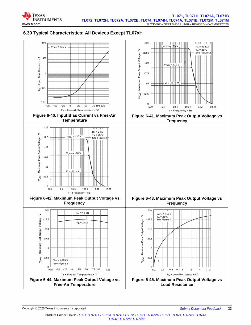
TL071, TL071H, TL071A, TL071B
TL072, TL072H, TL072A, TL072B, TL074, TL074H, TL074A, TL074B, TL072M, TL074M SLOS080P – SEPTEMBER 1978 – REVISED NOVEMBER 2020 www.ti.com
Copyright © 2020 Texas Instruments Incorporated Submit Document Feedback 33
Product Folder Links: TL071 TL071H TL071A TL071B TL072 TL072H TL072A TL072B TL074 TL074H TL074A
TL074B TL072M TL074M
B I I
M O V
M O V
M O V
M O V
VCC± = ±15 V VCC± = ±15 V RL = 10 kΩ
TA = 25°C
See Figure 2
VCC± = ±10 V
VCC± = ±5 V
V = ±15 V CC±
RL = 2 kΩ
TA = 25°C
See Figure 2
VCC± = ±10 V
VCC± = ±5 V
8
RL = 2 kΩ
VO
M −
Ma
xim
um
Pe
ak
Ou
tpu
t V
oltag
e −
V
8
6.30 Typical Characteristics: All Devices Except TL07xH
100 ±15
±12.5
10
±10
1 ±7.5
±5
0.1
±2.5
0.01
−75 −50 −25 0 25 50 75 100 125
0
100
1 k 10 k
100 k 1 M
10 M
TA − Free-Air Temperature − °C
Figure 6-40. Input Bias Current vs Free-Air
Temperature
f − Frequency − Hz
Figure 6-41. Maximum Peak Output Voltage vs
Frequency
±15
±12.5
±10
±7.5
±5
±2.5
0 100
1 k 10 k
100 k
1 M 10 M
f − Frequency − Hz
Figure 6-42. Maximum Peak Output Voltage vs
Frequency
±15
RL = 10 kΩ
±12.5
±10
±7.5
±5
Figure 6-43. Maximum Peak Output Voltage vs
Frequency
±15
±12.5
±10
±7.5
±5
±2.5
0 −75
VCC± = ±15 V
See Figure 2
−50 −25 0 25 50 75 100
125
±2.5
0
0.1
0.2
0.4
0.7 1 2
4 7 10
TA − Free-Air Temperature − °C
Figure 6-44. Maximum Peak Output Voltage vs
Free-Air Temperature
RL − Load Resistance − kΩ
Figure 6-45. Maximum Peak Output Voltage vs
Load Resistance
I IB
− In
pu
t B
ias
Cu
rre
nt
− n
A
VO
M −
Ma
xim
um
Pe
ak
Ou
tpu
t V
oltag
e −
V
VO
M −
Ma
xim
um
Pe
ak
Ou
tpu
t V
olt
ag
e −
V
VO
M −
Ma
xim
um
Pe
ak
Ou
tpu
t V
oltag
e −
V
VCC± = ±15 V
TA = 25°C See Figure 2
8
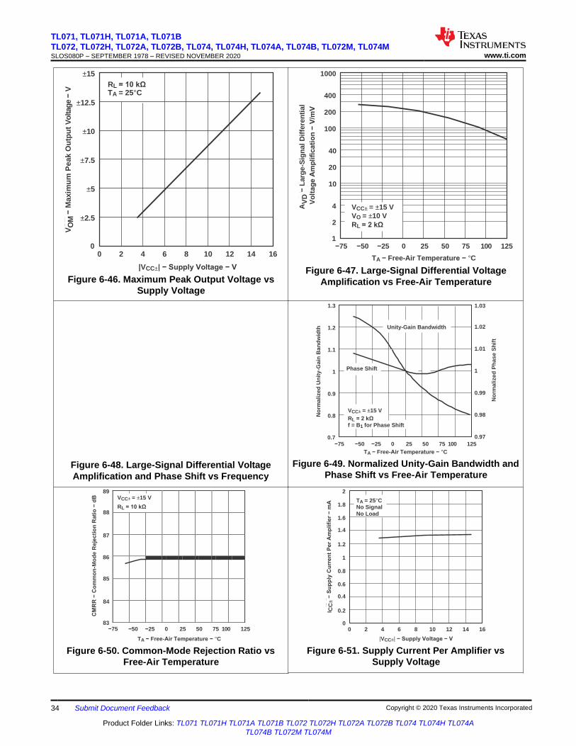
TL071, TL071H, TL071A, TL071B
TL072, TL072H, TL072A, TL072B, TL074, TL074H, TL074A, TL074B, TL072M, TL074M SLOS080P – SEPTEMBER 1978 – REVISED NOVEMBER 2020 www.ti.com
34 Submit Document Feedback Copyright © 2020 Texas Instruments Incorporated
Product Folder Links: TL071 TL071H TL071A TL071B TL072 TL072H TL072A TL072B TL074 TL074H TL074A
TL074B TL072M TL074M
M O V
D V A
C C I
RL = 10 kΩ TA = 25°C
VCC± = ±15 V
VO = ±10 V
RL = 2 kΩ
Unity-Gain Bandwidth
Phase Shift
VCC± = ±15 V
RL = 2 kΩ
f = B1 for Phase Shift
TA = 25°C No Signal
No Load
I CC
± −
Su
pp
ly C
urr
en
t P
er
Am
pli
fie
r −
mA
±15
±12.5
±10
1000
400
200
100
±7.5
±5
±2.5
0 0
2 4 6 8 10 12 14 16
40
20
10
4
2
1 −75
−50 −25 0 25 50 75 100
TA − Free-Air Temperature − °C
125
|VCC±| − Supply Voltage − V
Figure 6-46. Maximum Peak Output Voltage vs
Supply Voltage
Figure 6-47. Large-Signal Differential Voltage
Amplification vs Free-Air Temperature
1.3
1.2
1.1
1
0.9
0.8
0.7
−75
−50 −25 0 25 50 75 100
TA − Free-Air Temperature − °C
1.03
1.02
1.01
1
0.99
0.98
0.97
125
Figure 6-48. Large-Signal Differential Voltage
Amplification and Phase Shift vs Frequency
Figure 6-49. Normalized Unity-Gain Bandwidth and
Phase Shift vs Free-Air Temperature
89 2
1.8
88 1.6
1.4
87
1.2
86 1
0.8
85 0.6
0.4
84
0.2
83 −75
−50 −25 0 25 50 75 100
TA − Free-Air Temperature − °C
125
0
0 2 4 6 8 10 12 14 16
|VCC±| − Supply Voltage − V
Figure 6-50. Common-Mode Rejection Ratio vs
Free-Air Temperature
Figure 6-51. Supply Current Per Amplifier vs
Supply Voltage
VO
M −
Ma
xim
um
Peak O
utp
ut
Vo
ltag
e −
V
CM
RR
− C
om
mo
n-M
od
e R
eje
cti
on
Rati
o −
dB
AV
D −
Larg
e-S
ign
al D
iffe
ren
tia
l
Vo
lta
ge A
mp
lifi
ca
tio
n −
V/m
V
No
rma
lize
d U
nit
y-G
ain
Ba
nd
wid
th
No
rma
lize
d P
ha
se
Sh
ift
VCC± = ±15 V
RL = 10 kΩ
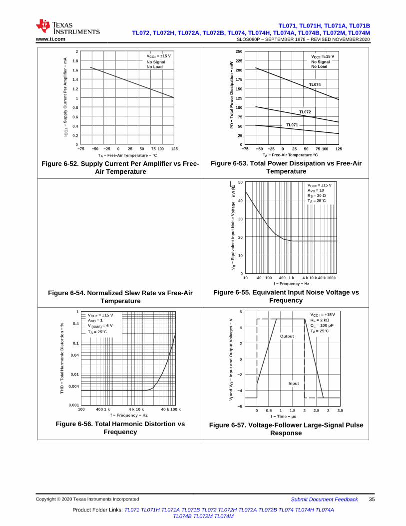
TL071, TL071H, TL071A, TL071B
TL072, TL072H, TL072A, TL072B, TL074, TL074H, TL074A, TL074B, TL072M, TL074M SLOS080P – SEPTEMBER 1978 – REVISED NOVEMBER 2020 www.ti.com
Copyright © 2020 Texas Instruments Incorporated Submit Document Feedback 35
Product Folder Links: TL071 TL071H TL071A TL071B TL072 TL072H TL072A TL072B TL074 TL074H TL074A
TL074B TL072M TL074M
C C I
z H / V n
VCC± =±15 V
No Signal No Load
TL071
TL072
TL074
VCC± = ±15 V
AVD = 10
RS = 20 Ω
TA = 25°C
VCC± = ±15 V
AVD = 1
VI(RMS) = 6 V
TA = 25°C
VCC± = ±15 V
RL = 2 kΩ
CL = 100 pF
TA = 25°C
Output
Input
VI a
nd
VO
− I
np
ut
an
d O
utp
ut
Vo
ltag
es −
V
2
1.8
1.6
1.4
1.2
1
0.8
0.6
0.4
0.2
250
225
200
175
150
125
100
75
50
25
0 −75
−50 −25 0 25 50 75 100
TA − Free-Air Temperature − °C
125
0 −75
−50 −25 0 25 50 75 100
TA − Free-Air Temperature −°C
125
Figure 6-52. Supply Current Per Amplifier vs Free-
Air Temperature
Figure 6-53. Total Power Dissipation vs Free-Air
Temperature
50
40
30
20
10
0
10 40 100 400 1 k 4 k 10 k 40 k 100 k
f − Frequency − Hz
Figure 6-54. Normalized Slew Rate vs Free-Air
Temperature
Figure 6-55. Equivalent Input Noise Voltage vs
Frequency
1 6
0.4 4
0.1 2
0.04 0
0.01 −2
0.004 −4
0.001 100
400 1 k
4 k 10 k
40 k 100 k
−6 0 0.5 1 1.5 2 2.5 3
3.5
f − Frequency − Hz
Figure 6-56. Total Harmonic Distortion vs
Frequency
t − Time − µs
Figure 6-57. Voltage-Follower Large-Signal Pulse
Response
TH
D −
To
tal H
arm
on
ic D
isto
rtio
n −
%
I CC
± −
Su
pp
ly C
urr
en
t P
er
Am
pli
fie
r −
mA
PD
− T
ota
l P
ow
er
Dis
sip
ati
on
− m
W
Vn
− E
qu
iva
len
t In
pu
t N
ois
e V
olt
ag
e −
nV
/ H
z
VCC± = ±15 V
No Signal
No Load
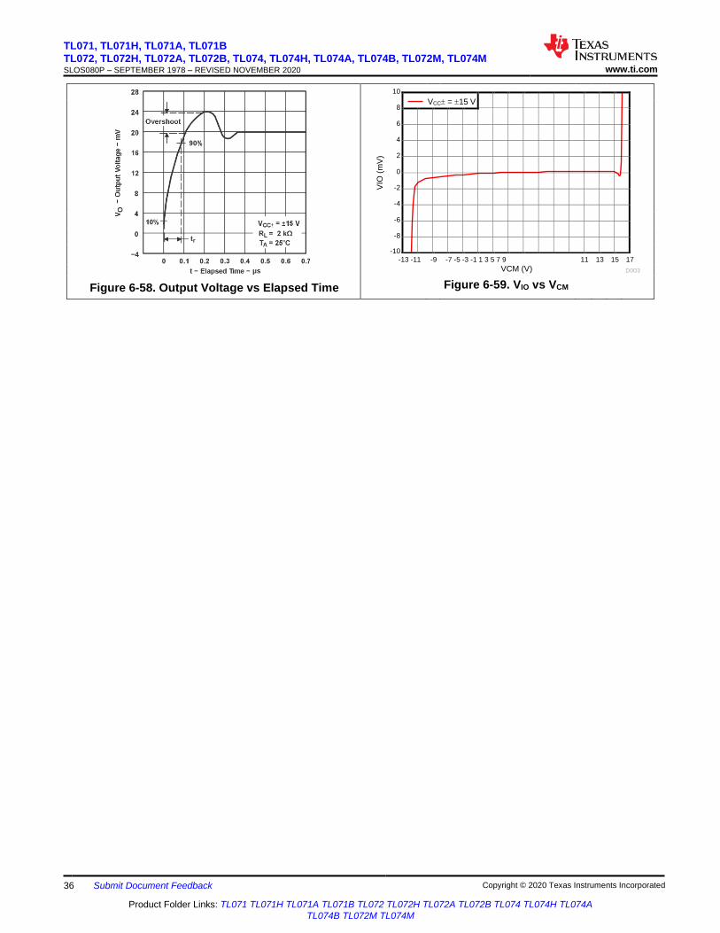
TL071, TL071H, TL071A, TL071B
TL072, TL072H, TL072A, TL072B, TL074, TL074H, TL074A, TL074B, TL072M, TL074M SLOS080P – SEPTEMBER 1978 – REVISED NOVEMBER 2020 www.ti.com
36 Submit Document Feedback Copyright © 2020 Texas Instruments Incorporated
Product Folder Links: TL071 TL071H TL071A TL071B TL072 TL072H TL072A TL072B TL074 TL074H TL074A
TL074B TL072M TL074M
VIO
(m
V)
10
8
6
4
2
0
-2
-4
-6
-8
-10 -13 -11 -9 -7 -5 -3 -1 1 3 5 7 9 11 13 15 17
VCM (V) D003
Figure 6-58. Output Voltage vs Elapsed Time Figure 6-59. VIO vs VCM
VCC = 15 V
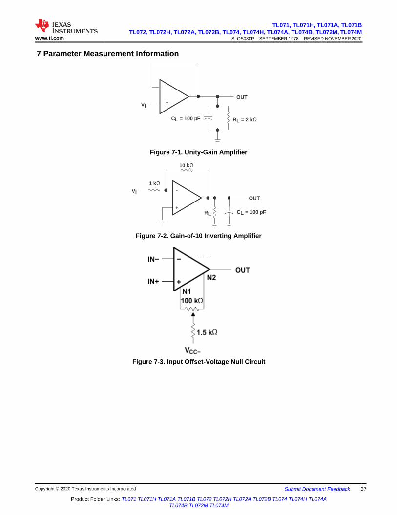
TL071, TL071H, TL071A, TL071B
TL072, TL072H, TL072A, TL072B, TL074, TL074H, TL074A, TL074B, TL072M, TL074M SLOS080P – SEPTEMBER 1978 – REVISED NOVEMBER 2020 www.ti.com
Copyright © 2020 Texas Instruments Incorporated Submit Document Feedback 37
Product Folder Links: TL071 TL071H TL071A TL071B TL072 TL072H TL072A TL072B TL074 TL074H TL074A
TL074B TL072M TL074M
7 Parameter Measurement Information
VI
+
CL = 100 pF
OUT
RL = 2 kΩ
Figure 7-1. Unity-Gain Amplifier
10 kΩ
1 kΩ
VI
OUT
RL CL = 100 pF
Figure 7-2. Gain-of-10 Inverting Amplifier
Figure 7-3. Input Offset-Voltage Null Circuit
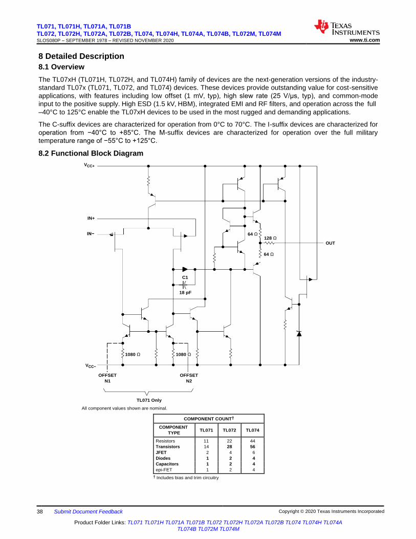
TL071, TL071H, TL071A, TL071B
TL072, TL072H, TL072A, TL072B, TL074, TL074H, TL074A, TL074B, TL072M, TL074M SLOS080P – SEPTEMBER 1978 – REVISED NOVEMBER 2020 www.ti.com
38 Submit Document Feedback Copyright © 2020 Texas Instruments Incorporated
Product Folder Links: TL071 TL071H TL071A TL071B TL072 TL072H TL072A TL072B TL074 TL074H TL074A
TL074B TL072M TL074M
8 Detailed Description
8.1 Overview
The TL07xH (TL071H, TL072H, and TL074H) family of devices are the next-generation versions of the industry-
standard TL07x (TL071, TL072, and TL074) devices. These devices provide outstanding value for cost-sensitive
applications, with features including low offset (1 mV, typ), high slew rate (25 V/μs, typ), and common-mode
input to the positive supply. High ESD (1.5 kV, HBM), integrated EMI and RF filters, and operation across the full
–40°C to 125°C enable the TL07xH devices to be used in the most rugged and demanding applications.
The C-suffix devices are characterized for operation from 0°C to 70°C. The I-suffix devices are characterized for
operation from −40°C to +85°C. The M-suffix devices are characterized for operation over the full military
temperature range of −55°C to +125°C.
8.2 Functional Block Diagram
VCC+
IN+
IN−
OUT
VCC−
OFFSET
N1
OFFSET
N2
TL071 Only
All component values shown are nominal.
COMPONENT COUNT†
COMPONENT
TYPE TL071 TL072 TL074
Resistors 11 22 44
Transistors 14 28 56
JFET 2 4 6
Diodes 1 2 4
Capacitors 1 2 4
epi-FET 1 2 4
† Includes bias and trim circuitry
64 Ω 128 Ω
64 Ω
C1
18 pF
1080 Ω 1080 Ω
TL071, TL071H, TL071A, TL071B
TL072, TL072H, TL072A, TL072B, TL074, TL074H, TL074A, TL074B, TL072M, TL074M SLOS080P – SEPTEMBER 1978 – REVISED NOVEMBER 2020 www.ti.com
Copyright © 2020 Texas Instruments Incorporated Submit Document Feedback 39
Product Folder Links: TL071 TL071H TL071A TL071B TL072 TL072H TL072A TL072B TL074 TL074H TL074A
TL074B TL072M TL074M
8.3 Feature Description
The TL07xH family of devices improve many specifications as compared to the industry-standard TL07x family.
Several comparisons of key specifications between these families are included below to show the advantages of
the TL07xH family.
8.3.1 Total Harmonic Distortion
Harmonic distortions to an audio signal are created by electronic components in a circuit. Total harmonic
distortion (THD) is a measure of harmonic distortions accumulated by a signal in an audio system. These
devices have a very low THD of 0.003% meaning that the TL07x device adds little harmonic distortion when
used in audio signal applications.
8.3.2 Slew Rate
The slew rate is the rate at which an operational amplifier can change the output when there is a change on the
input. These devices have a 13-V/μs slew rate.
8.4 Device Functional Modes
These devices are powered on when the supply is connected. These devices can be operated as a single-
supply operational amplifier or dual-supply amplifier depending on the application.
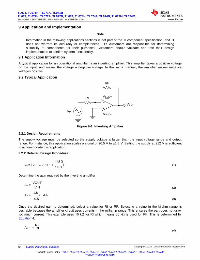
TL071, TL071H, TL071A, TL071B
TL072, TL072H, TL072A, TL072B, TL074, TL074H, TL074A, TL074B, TL072M, TL074M SLOS080P – SEPTEMBER 1978 – REVISED NOVEMBER 2020 www.ti.com
40 Submit Document Feedback Copyright © 2020 Texas Instruments Incorporated
Product Folder Links: TL071 TL071H TL071A TL071B TL072 TL072H TL072A TL072B TL074 TL074H TL074A
TL074B TL072M TL074M
9 Application and Implementation
Note
Information in the following applications sections is not part of the TI component specification, and TI
does not warrant its accuracy or completeness. TI’s customers are responsible for determining
suitability of components for their purposes. Customers should validate and test their design
implementation to confirm system functionality.
9.1 Application Information
A typical application for an operational amplifier is an inverting amplifier. This amplifier takes a positive voltage
on the input, and makes the voltage a negative voltage. In the same manner, the amplifier makes negative
voltages positive.
9.2 Typical Application
RF
VOUT
VIN
Figure 9-1. Inverting Amplifier
9.2.1 Design Requirements
The supply voltage must be selected so the supply voltage is larger than the input voltage range and output
range. For instance, this application scales a signal of ±0.5 V to ±1.8 V. Setting the supply at ±12 V is sufficient
to accommodate this application.
9.2.2 Detailed Design Procedure
1 M Ω Vo = ( Vi + Vi o ) * ( 1 +
1 k Ω ) (1)
Determine the gain required by the inverting amplifier:
AV =
AV =
VOUT
VIN (2)
1.8 = −3.6
−0.5 (3)
Once the desired gain is determined, select a value for RI or RF. Selecting a value in the kilohm range is
desirable because the amplifier circuit uses currents in the milliamp range. This ensures the part does not draw
too much current. This example uses 10 kΩ for RI which means 36 kΩ is used for RF. This is determined by
Equation 4.
AV =
− RF RI
(4)
RI Vsup+
+
Vsup-
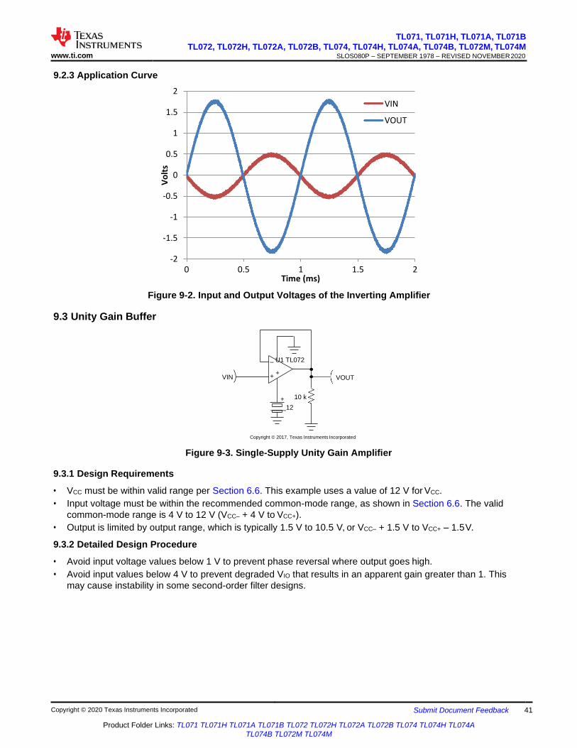
TL071, TL071H, TL071A, TL071B
TL072, TL072H, TL072A, TL072B, TL074, TL074H, TL074A, TL074B, TL072M, TL074M SLOS080P – SEPTEMBER 1978 – REVISED NOVEMBER 2020 www.ti.com
Copyright © 2020 Texas Instruments Incorporated Submit Document Feedback 41
Product Folder Links: TL071 TL071H TL071A TL071B TL072 TL072H TL072A TL072B TL074 TL074H TL074A
TL074B TL072M TL074M
– U1 TL072
+ +
+
12
10 k
9.2.3 Application Curve
2
1.5
1
0.5
0
-0.5
-1
-1.5
-2 0 0.5 1 1.5 2
Time (ms)
Figure 9-2. Input and Output Voltages of the Inverting Amplifier
9.3 Unity Gain Buffer
VIN VOUT
Copyright © 2017, Texas Instruments Incorporated
Figure 9-3. Single-Supply Unity Gain Amplifier
9.3.1 Design Requirements
• VCC must be within valid range per Section 6.6. This example uses a value of 12 V for VCC.
• Input voltage must be within the recommended common-mode range, as shown in Section 6.6. The valid
common-mode range is 4 V to 12 V (VCC– + 4 V to VCC+).
• Output is limited by output range, which is typically 1.5 V to 10.5 V, or VCC– + 1.5 V to VCC+ – 1.5 V.
9.3.2 Detailed Design Procedure
• Avoid input voltage values below 1 V to prevent phase reversal where output goes high.
• Avoid input values below 4 V to prevent degraded VIO that results in an apparent gain greater than 1. This
may cause instability in some second-order filter designs.
VIN
VOUT
Vo
lts
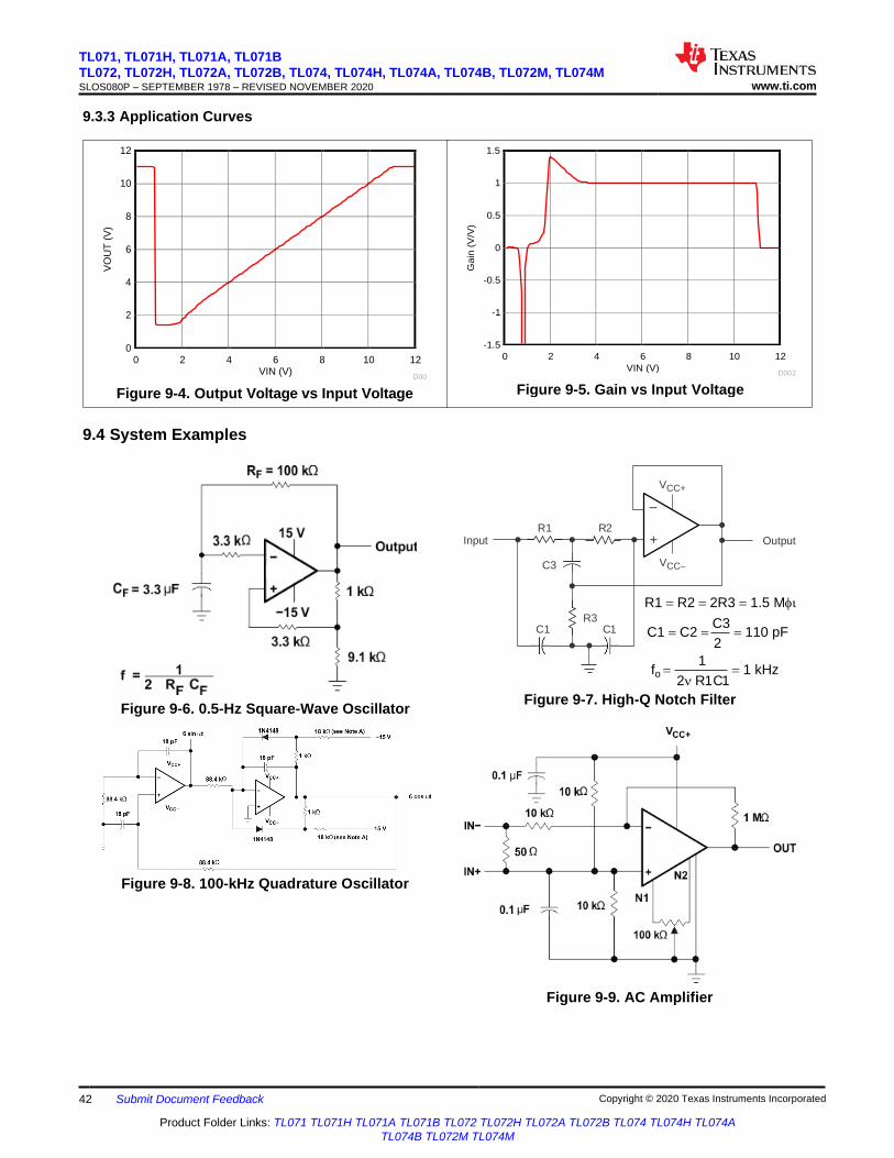
TL071, TL071H, TL071A, TL071B
TL072, TL072H, TL072A, TL072B, TL074, TL074H, TL074A, TL074B, TL072M, TL074M SLOS080P – SEPTEMBER 1978 – REVISED NOVEMBER 2020 www.ti.com
42 Submit Document Feedback Copyright © 2020 Texas Instruments Incorporated
Product Folder Links: TL071 TL071H TL071A TL071B TL072 TL072H TL072A TL072B TL074 TL074H TL074A
TL074B TL072M TL074M
Figure 9-5. Gain vs Input Voltage
12
D002
10 8 6
VIN (V)
4 2 0
1.5
1
0.5
0
-0.5
-1
-1.5
Figure 9-4. Output Voltage vs Input Voltage
12
D00
10 8 6 VIN (V)
4 2 0
12
10
8
6
4
2
0
9.3.3 Application Curves
9.4 System Examples
Input
R1 R2
C3
VCC+
–
+
VCC–
Output
R3
C1 C1
R1 = R2 = 2R3 = 1.5 M
C1 = C2 = C3
= 110 pF 2
fo = 1
2 R1 C1 = 1 kHz
Figure 9-6. 0.5-Hz Square-Wave Oscillator Figure 9-7. High-Q Notch Filter
Figure 9-8. 100-kHz Quadrature Oscillator
Figure 9-9. AC Amplifier
VO
UT
(V
)
Ga
in (
V/V
)
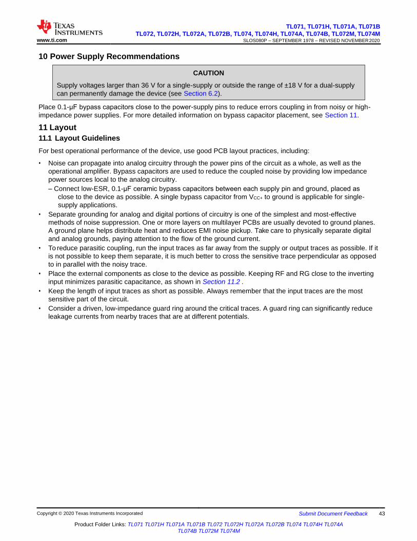
TL071, TL071H, TL071A, TL071B
TL072, TL072H, TL072A, TL072B, TL074, TL074H, TL074A, TL074B, TL072M, TL074M SLOS080P – SEPTEMBER 1978 – REVISED NOVEMBER 2020 www.ti.com
Copyright © 2020 Texas Instruments Incorporated Submit Document Feedback 43
Product Folder Links: TL071 TL071H TL071A TL071B TL072 TL072H TL072A TL072B TL074 TL074H TL074A
TL074B TL072M TL074M
CAUTION
Supply voltages larger than 36 V for a single-supply or outside the range of ±18 V for a dual-supply
can permanently damage the device (see Section 6.2).
10 Power Supply Recommendations
Place 0.1-μF bypass capacitors close to the power-supply pins to reduce errors coupling in from noisy or high-
impedance power supplies. For more detailed information on bypass capacitor placement, see Section 11.
11 Layout
11.1 Layout Guidelines
For best operational performance of the device, use good PCB layout practices, including:
• Noise can propagate into analog circuitry through the power pins of the circuit as a whole, as well as the
operational amplifier. Bypass capacitors are used to reduce the coupled noise by providing low impedance
power sources local to the analog circuitry.
– Connect low-ESR, 0.1-μF ceramic bypass capacitors between each supply pin and ground, placed as
close to the device as possible. A single bypass capacitor from VCC+ to ground is applicable for single-
supply applications.
• Separate grounding for analog and digital portions of circuitry is one of the simplest and most-effective
methods of noise suppression. One or more layers on multilayer PCBs are usually devoted to ground planes.
A ground plane helps distribute heat and reduces EMI noise pickup. Take care to physically separate digital
and analog grounds, paying attention to the flow of the ground current.
• To reduce parasitic coupling, run the input traces as far away from the supply or output traces as possible. If it
is not possible to keep them separate, it is much better to cross the sensitive trace perpendicular as opposed
to in parallel with the noisy trace.
• Place the external components as close to the device as possible. Keeping RF and RG close to the inverting
input minimizes parasitic capacitance, as shown in Section 11.2 .
• Keep the length of input traces as short as possible. Always remember that the input traces are the most
sensitive part of the circuit.
• Consider a driven, low-impedance guard ring around the critical traces. A guard ring can significantly reduce
leakage currents from nearby traces that are at different potentials.
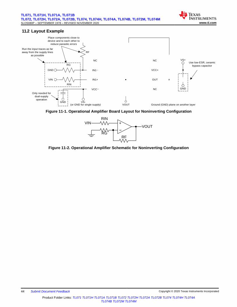
TL071, TL071H, TL071A, TL071B
TL072, TL072H, TL072A, TL072B, TL074, TL074H, TL074A, TL074B, TL072M, TL074M SLOS080P – SEPTEMBER 1978 – REVISED NOVEMBER 2020 www.ti.com
44 Submit Document Feedback Copyright © 2020 Texas Instruments Incorporated
Product Folder Links: TL071 TL071H TL071A TL071B TL072 TL072H TL072A TL072B TL074 TL074H TL074A
TL074B TL072M TL074M
11.2 Layout Example
Place components close to
device and to each other to
reduce parasitic errors
Run the input traces as far
away from the supply lines
as possible
RG
GND
RF
NC
IN1−
NC
VCC+
VS+
Use low-ESR, ceramic
bypass capacitor
VIN
Only needed for
dual-supply
operation
GND
RIN
VS-
IN1+
VCC−
OUT
NC
GND
(or GND for single supply) VOUT Ground (GND) plane on another layer
Figure 11-1. Operational Amplifier Board Layout for Noninverting Configuration
RIN VIN +
RG
RF
VOUT
Figure 11-2. Operational Amplifier Schematic for Noninverting Configuration
TL071, TL071H, TL071A, TL071B
TL072, TL072H, TL072A, TL072B, TL074, TL074H, TL074A, TL074B, TL072M, TL074M SLOS080P – SEPTEMBER 1978 – REVISED NOVEMBER 2020 www.ti.com
Copyright © 2020 Texas Instruments Incorporated Submit Document Feedback 45
Product Folder Links: TL071 TL071H TL071A TL071B TL072 TL072H TL072A TL072B TL074 TL074H TL074A
TL074B TL072M TL074M
12 Device and Documentation Support
12.1 Related Links
The table below lists quick access links. Categories include technical documents, support and community
resources, tools and software, and quick access to sample or buy.
Table 12-1. Related Links
PARTS PRODUCT FOLDER ORDER NOW TECHNICAL
DOCUMENTS
TOOLS &
SOFTWARE
SUPPORT &
COMMUNITY
TL071 Click here Click here Click here Click here Click here
TL071A Click here Click here Click here Click here Click here
TL071B Click here Click here Click here Click here Click here
TL072 Click here Click here Click here Click here Click here
TL072A Click here Click here Click here Click here Click here
TL072B Click here Click here Click here Click here Click here
TL072M Click here Click here Click here Click here Click here
TL074 Click here Click here Click here Click here Click here
TL074A Click here Click here Click here Click here Click here
TL074B Click here Click here Click here Click here Click here
TL074M Click here Click here Click here Click here Click here
12.2 Receiving Notification of Documentation Updates
To receive notification of documentation updates, navigate to the device product folder on ti.com. Click on
Subscribe to updates to register and receive a weekly digest of any product information that has changed. For
change details, review the revision history included in any revised document.
12.3 Support Resources
TI E2E™ support forums are an engineer's go-to source for fast, verified answers and design help — straight
from the experts. Search existing answers or ask your own question to get the quick design help you need.
Linked content is provided "AS IS" by the respective contributors. They do not constitute TI specifications and do
not necessarily reflect TI's views; see TI's Terms of Use.
12.4 Trademarks
TI E2E™ is a trademark of Texas Instruments.
All trademarks are the property of their respective owners.
12.5 Electrostatic Discharge Caution
This integrated circuit can be damaged by ESD. Texas Instruments recommends that all integrated circuits be handled
with appropriate precautions. Failure to observe proper handling and installation procedures can cause damage.
ESD damage can range from subtle performance degradation to complete device failure. Precision integrated circuits may be more susceptible to damage because very small parametric changes could cause the device not to meet its published
specifications.
12.6 Glossary
TI Glossary This glossary lists and explains terms, acronyms, and definitions.
13 Mechanical, Packaging, and Orderable Information
The following pages include mechanical packaging and orderable information. This information is the most
current data available for the designated devices. This data is subject to change without notice and revision of
this document. For browser based versions of this data sheet, refer to the left hand navigation.
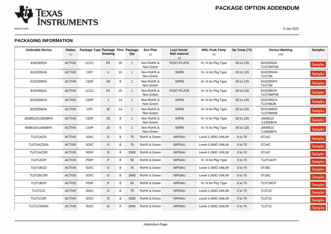
PACKAGE OPTION ADDENDUM
www.ti.com 5-Jan-2021
Addendum-Page 46
PACKAGING INFORMATION
Orderable Device Status Package Type Package
(1) Drawing
Pins Package
Qty
Eco Plan
(2)
Lead finish/
Ball material
(6)
MSL Peak Temp
(3)
Op Temp (°C) Device Marking
(4/5)
Samples
81023052A ACTIVE LCCC FK 20 1 Non-RoHS &
Non-Green
POST-PLATE N / A for Pkg Type -55 to 125 81023052A
TL072MFKB
8102305HA ACTIVE CFP U 10 1 Non-RoHS &
Non-Green
SNPB N / A for Pkg Type -55 to 125 8102305HA
TL072M
8102305PA ACTIVE CDIP JG 8 1 Non-RoHS &
Non-Green
SNPB N / A for Pkg Type -55 to 125 8102305PA
TL072M
81023062A ACTIVE LCCC FK 20 1 Non-RoHS &
Non-Green
POST-PLATE N / A for Pkg Type -55 to 125 81023062A
TL074MFKB
8102306CA ACTIVE CDIP J 14 1 Non-RoHS &
Non-Green
SNPB N / A for Pkg Type -55 to 125 8102306CA
TL074MJB
8102306DA ACTIVE CFP W 14 1 Non-RoHS &
Non-Green
SNPB N / A for Pkg Type -55 to 125 8102306DA
TL074MWB
JM38510/11905BPA ACTIVE CDIP JG 8 1 Non-RoHS &
Non-Green
SNPB N / A for Pkg Type -55 to 125 JM38510
/11905BPA
M38510/11905BPA ACTIVE CDIP JG 8 1 Non-RoHS &
Non-Green
SNPB N / A for Pkg Type -55 to 125 JM38510
/11905BPA
TL071ACD ACTIVE SOIC D 8 75 RoHS & Green NIPDAU Level-1-260C-UNLIM 0 to 70 071AC
TL071ACDG4 ACTIVE SOIC D 8 75 RoHS & Green NIPDAU Level-1-260C-UNLIM 0 to 70 071AC
TL071ACDR ACTIVE SOIC D 8 2500 RoHS & Green NIPDAU Level-1-260C-UNLIM 0 to 70 071AC
TL071ACP ACTIVE PDIP P 8 50 RoHS & Green NIPDAU N / A for Pkg Type 0 to 70 TL071ACP
TL071BCD ACTIVE SOIC D 8 75 RoHS & Green NIPDAU Level-1-260C-UNLIM 0 to 70 071BC
TL071BCDR ACTIVE SOIC D 8 2500 RoHS & Green NIPDAU Level-1-260C-UNLIM 0 to 70 071BC
TL071BCP ACTIVE PDIP P 8 50 RoHS & Green NIPDAU N / A for Pkg Type 0 to 70 TL071BCP
TL071CD ACTIVE SOIC D 8 75 RoHS & Green NIPDAU Level-1-260C-UNLIM 0 to 70 TL071C
TL071CDR ACTIVE SOIC D 8 2500 RoHS & Green NIPDAU Level-1-260C-UNLIM 0 to 70 TL071C
TL071CDRE4 ACTIVE SOIC D 8 2500 RoHS & Green NIPDAU Level-1-260C-UNLIM 0 to 70 TL071C
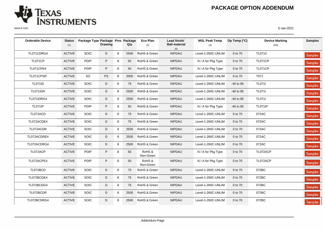
PACKAGE OPTION ADDENDUM
www.ti.com 5-Jan-2021
Addendum-Page 47
Orderable Device Status Package Type Package
(1) Drawing
Pins Package
Qty
Eco Plan
(2)
Lead finish/
Ball material
(6)
MSL Peak Temp
(3)
Op Temp (°C) Device Marking
(4/5)
Samples
TL071CDRG4 ACTIVE SOIC D 8 2500 RoHS & Green NIPDAU Level-1-260C-UNLIM 0 to 70 TL071C
TL071CP ACTIVE PDIP P 8 50 RoHS & Green NIPDAU N / A for Pkg Type 0 to 70 TL071CP
TL071CPE4 ACTIVE PDIP P 8 50 RoHS & Green NIPDAU N / A for Pkg Type 0 to 70 TL071CP
TL071CPSR ACTIVE SO PS 8 2000 RoHS & Green NIPDAU Level-1-260C-UNLIM 0 to 70 T071
TL071ID ACTIVE SOIC D 8 75 RoHS & Green NIPDAU Level-1-260C-UNLIM -40 to 85 TL071I
TL071IDR ACTIVE SOIC D 8 2500 RoHS & Green NIPDAU Level-1-260C-UNLIM -40 to 85 TL071I
TL071IDRG4 ACTIVE SOIC D 8 2500 RoHS & Green NIPDAU Level-1-260C-UNLIM -40 to 85 TL071I
TL071IP ACTIVE PDIP P 8 50 RoHS & Green NIPDAU N / A for Pkg Type -40 to 85 TL071IP
TL072ACD ACTIVE SOIC D 8 75 RoHS & Green NIPDAU Level-1-260C-UNLIM 0 to 70 072AC
TL072ACDE4 ACTIVE SOIC D 8 75 RoHS & Green NIPDAU Level-1-260C-UNLIM 0 to 70 072AC
TL072ACDR ACTIVE SOIC D 8 2500 RoHS & Green NIPDAU Level-1-260C-UNLIM 0 to 70 072AC
TL072ACDRE4 ACTIVE SOIC D 8 2500 RoHS & Green NIPDAU Level-1-260C-UNLIM 0 to 70 072AC
TL072ACDRG4 ACTIVE SOIC D 8 2500 RoHS & Green NIPDAU Level-1-260C-UNLIM 0 to 70 072AC
TL072ACP ACTIVE PDIP P 8 50 RoHS &
Non-Green
NIPDAU N / A for Pkg Type 0 to 70 TL072ACP
TL072ACPE4 ACTIVE PDIP P 8 50 RoHS &
Non-Green
NIPDAU N / A for Pkg Type 0 to 70 TL072ACP
TL072BCD ACTIVE SOIC D 8 75 RoHS & Green NIPDAU Level-1-260C-UNLIM 0 to 70 072BC
TL072BCDE4 ACTIVE SOIC D 8 75 RoHS & Green NIPDAU Level-1-260C-UNLIM 0 to 70 072BC
TL072BCDG4 ACTIVE SOIC D 8 75 RoHS & Green NIPDAU Level-1-260C-UNLIM 0 to 70 072BC
TL072BCDR ACTIVE SOIC D 8 2500 RoHS & Green NIPDAU Level-1-260C-UNLIM 0 to 70 072BC
TL072BCDRG4 ACTIVE SOIC D 8 2500 RoHS & Green NIPDAU Level-1-260C-UNLIM 0 to 70 072BC
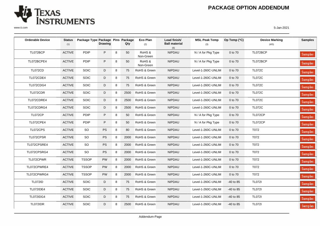
PACKAGE OPTION ADDENDUM
www.ti.com 5-Jan-2021
Addendum-Page 48
Orderable Device Status Package Type Package
(1) Drawing
Pins Package
Qty
Eco Plan
(2)
Lead finish/
Ball material
(6)
MSL Peak Temp
(3)
Op Temp (°C) Device Marking
(4/5)
Samples
TL072BCP ACTIVE PDIP P 8 50 RoHS &
Non-Green
NIPDAU N / A for Pkg Type 0 to 70 TL072BCP
TL072BCPE4 ACTIVE PDIP P 8 50 RoHS &
Non-Green
NIPDAU N / A for Pkg Type 0 to 70 TL072BCP
TL072CD ACTIVE SOIC D 8 75 RoHS & Green NIPDAU Level-1-260C-UNLIM 0 to 70 TL072C
TL072CDE4 ACTIVE SOIC D 8 75 RoHS & Green NIPDAU Level-1-260C-UNLIM 0 to 70 TL072C
TL072CDG4 ACTIVE SOIC D 8 75 RoHS & Green NIPDAU Level-1-260C-UNLIM 0 to 70 TL072C
TL072CDR ACTIVE SOIC D 8 2500 RoHS & Green NIPDAU Level-1-260C-UNLIM 0 to 70 TL072C
TL072CDRE4 ACTIVE SOIC D 8 2500 RoHS & Green NIPDAU Level-1-260C-UNLIM 0 to 70 TL072C
TL072CDRG4 ACTIVE SOIC D 8 2500 RoHS & Green NIPDAU Level-1-260C-UNLIM 0 to 70 TL072C
TL072CP ACTIVE PDIP P 8 50 RoHS & Green NIPDAU N / A for Pkg Type 0 to 70 TL072CP
TL072CPE4 ACTIVE PDIP P 8 50 RoHS & Green NIPDAU N / A for Pkg Type 0 to 70 TL072CP
TL072CPS ACTIVE SO PS 8 80 RoHS & Green NIPDAU Level-1-260C-UNLIM 0 to 70 T072
TL072CPSR ACTIVE SO PS 8 2000 RoHS & Green NIPDAU Level-1-260C-UNLIM 0 to 70 T072
TL072CPSRE4 ACTIVE SO PS 8 2000 RoHS & Green NIPDAU Level-1-260C-UNLIM 0 to 70 T072
TL072CPSRG4 ACTIVE SO PS 8 2000 RoHS & Green NIPDAU Level-1-260C-UNLIM 0 to 70 T072
TL072CPWR ACTIVE TSSOP PW 8 2000 RoHS & Green NIPDAU Level-1-260C-UNLIM 0 to 70 T072
TL072CPWRE4 ACTIVE TSSOP PW 8 2000 RoHS & Green NIPDAU Level-1-260C-UNLIM 0 to 70 T072
TL072CPWRG4 ACTIVE TSSOP PW 8 2000 RoHS & Green NIPDAU Level-1-260C-UNLIM 0 to 70 T072
TL072ID ACTIVE SOIC D 8 75 RoHS & Green NIPDAU Level-1-260C-UNLIM -40 to 85 TL072I
TL072IDE4 ACTIVE SOIC D 8 75 RoHS & Green NIPDAU Level-1-260C-UNLIM -40 to 85 TL072I
TL072IDG4 ACTIVE SOIC D 8 75 RoHS & Green NIPDAU Level-1-260C-UNLIM -40 to 85 TL072I
TL072IDR ACTIVE SOIC D 8 2500 RoHS & Green NIPDAU Level-1-260C-UNLIM -40 to 85 TL072I
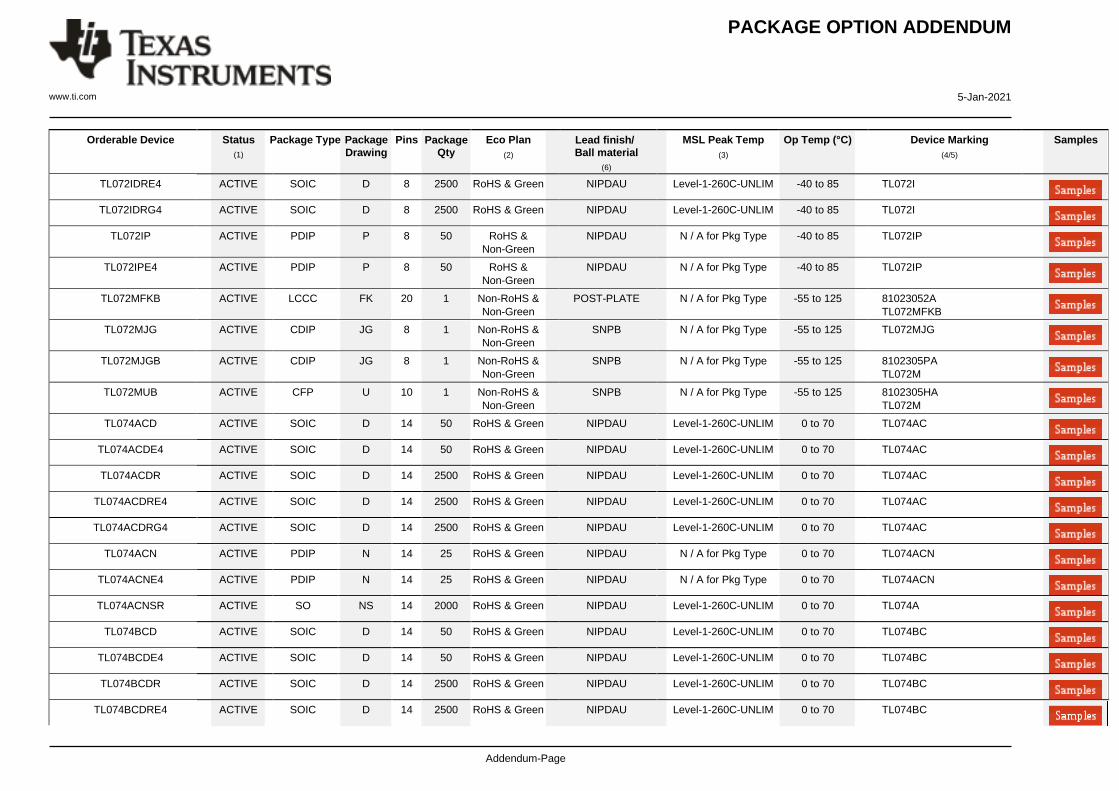
PACKAGE OPTION ADDENDUM
www.ti.com 5-Jan-2021
Addendum-Page 49
Orderable Device Status Package Type Package
(1) Drawing
Pins Package
Qty
Eco Plan
(2)
Lead finish/
Ball material
(6)
MSL Peak Temp
(3)
Op Temp (°C) Device Marking
(4/5)
Samples
TL072IDRE4 ACTIVE SOIC D 8 2500 RoHS & Green NIPDAU Level-1-260C-UNLIM -40 to 85 TL072I
TL072IDRG4 ACTIVE SOIC D 8 2500 RoHS & Green NIPDAU Level-1-260C-UNLIM -40 to 85 TL072I
TL072IP ACTIVE PDIP P 8 50 RoHS &
Non-Green
NIPDAU N / A for Pkg Type -40 to 85 TL072IP
TL072IPE4 ACTIVE PDIP P 8 50 RoHS &
Non-Green
NIPDAU N / A for Pkg Type -40 to 85 TL072IP
TL072MFKB ACTIVE LCCC FK 20 1 Non-RoHS &
Non-Green
POST-PLATE N / A for Pkg Type -55 to 125 81023052A
TL072MFKB
TL072MJG ACTIVE CDIP JG 8 1 Non-RoHS &
Non-Green
SNPB N / A for Pkg Type -55 to 125 TL072MJG
TL072MJGB ACTIVE CDIP JG 8 1 Non-RoHS &
Non-Green
SNPB N / A for Pkg Type -55 to 125 8102305PA
TL072M
TL072MUB ACTIVE CFP U 10 1 Non-RoHS &
Non-Green
SNPB N / A for Pkg Type -55 to 125 8102305HA
TL072M
TL074ACD ACTIVE SOIC D 14 50 RoHS & Green NIPDAU Level-1-260C-UNLIM 0 to 70 TL074AC
TL074ACDE4 ACTIVE SOIC D 14 50 RoHS & Green NIPDAU Level-1-260C-UNLIM 0 to 70 TL074AC
TL074ACDR ACTIVE SOIC D 14 2500 RoHS & Green NIPDAU Level-1-260C-UNLIM 0 to 70 TL074AC
TL074ACDRE4 ACTIVE SOIC D 14 2500 RoHS & Green NIPDAU Level-1-260C-UNLIM 0 to 70 TL074AC
TL074ACDRG4 ACTIVE SOIC D 14 2500 RoHS & Green NIPDAU Level-1-260C-UNLIM 0 to 70 TL074AC
TL074ACN ACTIVE PDIP N 14 25 RoHS & Green NIPDAU N / A for Pkg Type 0 to 70 TL074ACN
TL074ACNE4 ACTIVE PDIP N 14 25 RoHS & Green NIPDAU N / A for Pkg Type 0 to 70 TL074ACN
TL074ACNSR ACTIVE SO NS 14 2000 RoHS & Green NIPDAU Level-1-260C-UNLIM 0 to 70 TL074A
TL074BCD ACTIVE SOIC D 14 50 RoHS & Green NIPDAU Level-1-260C-UNLIM 0 to 70 TL074BC
TL074BCDE4 ACTIVE SOIC D 14 50 RoHS & Green NIPDAU Level-1-260C-UNLIM 0 to 70 TL074BC
TL074BCDR ACTIVE SOIC D 14 2500 RoHS & Green NIPDAU Level-1-260C-UNLIM 0 to 70 TL074BC
TL074BCDRE4 ACTIVE SOIC D 14 2500 RoHS & Green NIPDAU Level-1-260C-UNLIM 0 to 70 TL074BC
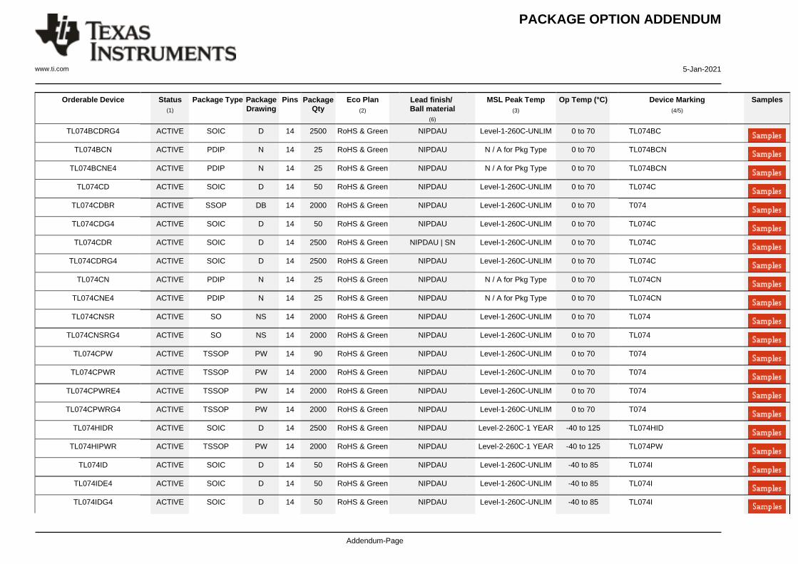
PACKAGE OPTION ADDENDUM
www.ti.com 5-Jan-2021
Addendum-Page 50
Orderable Device Status Package Type Package
(1) Drawing
Pins Package
Qty
Eco Plan
(2)
Lead finish/
Ball material
(6)
MSL Peak Temp
(3)
Op Temp (°C) Device Marking
(4/5)
Samples
TL074BCDRG4 ACTIVE SOIC D 14 2500 RoHS & Green NIPDAU Level-1-260C-UNLIM 0 to 70 TL074BC
TL074BCN ACTIVE PDIP N 14 25 RoHS & Green NIPDAU N / A for Pkg Type 0 to 70 TL074BCN
TL074BCNE4 ACTIVE PDIP N 14 25 RoHS & Green NIPDAU N / A for Pkg Type 0 to 70 TL074BCN
TL074CD ACTIVE SOIC D 14 50 RoHS & Green NIPDAU Level-1-260C-UNLIM 0 to 70 TL074C
TL074CDBR ACTIVE SSOP DB 14 2000 RoHS & Green NIPDAU Level-1-260C-UNLIM 0 to 70 T074
TL074CDG4 ACTIVE SOIC D 14 50 RoHS & Green NIPDAU Level-1-260C-UNLIM 0 to 70 TL074C
TL074CDR ACTIVE SOIC D 14 2500 RoHS & Green NIPDAU | SN Level-1-260C-UNLIM 0 to 70 TL074C
TL074CDRG4 ACTIVE SOIC D 14 2500 RoHS & Green NIPDAU Level-1-260C-UNLIM 0 to 70 TL074C
TL074CN ACTIVE PDIP N 14 25 RoHS & Green NIPDAU N / A for Pkg Type 0 to 70 TL074CN
TL074CNE4 ACTIVE PDIP N 14 25 RoHS & Green NIPDAU N / A for Pkg Type 0 to 70 TL074CN
TL074CNSR ACTIVE SO NS 14 2000 RoHS & Green NIPDAU Level-1-260C-UNLIM 0 to 70 TL074
TL074CNSRG4 ACTIVE SO NS 14 2000 RoHS & Green NIPDAU Level-1-260C-UNLIM 0 to 70 TL074
TL074CPW ACTIVE TSSOP PW 14 90 RoHS & Green NIPDAU Level-1-260C-UNLIM 0 to 70 T074
TL074CPWR ACTIVE TSSOP PW 14 2000 RoHS & Green NIPDAU Level-1-260C-UNLIM 0 to 70 T074
TL074CPWRE4 ACTIVE TSSOP PW 14 2000 RoHS & Green NIPDAU Level-1-260C-UNLIM 0 to 70 T074
TL074CPWRG4 ACTIVE TSSOP PW 14 2000 RoHS & Green NIPDAU Level-1-260C-UNLIM 0 to 70 T074
TL074HIDR ACTIVE SOIC D 14 2500 RoHS & Green NIPDAU Level-2-260C-1 YEAR -40 to 125 TL074HID
TL074HIPWR ACTIVE TSSOP PW 14 2000 RoHS & Green NIPDAU Level-2-260C-1 YEAR -40 to 125 TL074PW
TL074ID ACTIVE SOIC D 14 50 RoHS & Green NIPDAU Level-1-260C-UNLIM -40 to 85 TL074I
TL074IDE4 ACTIVE SOIC D 14 50 RoHS & Green NIPDAU Level-1-260C-UNLIM -40 to 85 TL074I
TL074IDG4 ACTIVE SOIC D 14 50 RoHS & Green NIPDAU Level-1-260C-UNLIM -40 to 85 TL074I
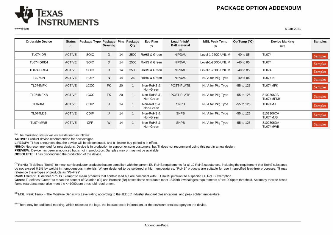
PACKAGE OPTION ADDENDUM
www.ti.com 5-Jan-2021
Addendum-Page 51
Orderable Device Status
(1)
Package Type Package
Drawing
Pins Package
Qty
Eco Plan
(2)
Lead finish/
Ball material
(6)
MSL Peak Temp
(3)
Op Temp (°C) Device Marking
(4/5)
Samples
TL074IDR ACTIVE SOIC D 14 2500 RoHS & Green NIPDAU Level-1-260C-UNLIM -40 to 85 TL074I
TL074IDRE4 ACTIVE SOIC D 14 2500 RoHS & Green NIPDAU Level-1-260C-UNLIM -40 to 85 TL074I
TL074IDRG4 ACTIVE SOIC D 14 2500 RoHS & Green NIPDAU Level-1-260C-UNLIM -40 to 85 TL074I
TL074IN ACTIVE PDIP N 14 25 RoHS & Green NIPDAU N / A for Pkg Type -40 to 85 TL074IN
TL074MFK ACTIVE LCCC FK 20 1 Non-RoHS &
Non-Green
POST-PLATE N / A for Pkg Type -55 to 125 TL074MFK
TL074MFKB ACTIVE LCCC FK 20 1 Non-RoHS &
Non-Green
POST-PLATE N / A for Pkg Type -55 to 125 81023062A
TL074MFKB
TL074MJ ACTIVE CDIP J 14 1 Non-RoHS &
Non-Green
SNPB N / A for Pkg Type -55 to 125 TL074MJ
TL074MJB ACTIVE CDIP J 14 1 Non-RoHS &
Non-Green
SNPB N / A for Pkg Type -55 to 125 8102306CA
TL074MJB
TL074MWB ACTIVE CFP W 14 1 Non-RoHS &
Non-Green
SNPB N / A for Pkg Type -55 to 125 8102306DA
TL074MWB
(1) The marketing status values are defined as follows:
ACTIVE: Product device recommended for new designs.
LIFEBUY: TI has announced that the device will be discontinued, and a lifetime-buy period is in effect.
NRND: Not recommended for new designs. Device is in production to support existing customers, but TI does not recommend using this part in a new design.
PREVIEW: Device has been announced but is not in production. Samples may or may not be available.
OBSOLETE: TI has discontinued the production of the device.
(2)
RoHS: TI defines "RoHS" to mean semiconductor products that are compliant with the current EU RoHS requirements for all 10 RoHS substances, including the requirement that RoHS substance
do not exceed 0.1% by weight in homogeneous materials. Where designed to be soldered at high temperatures, "RoHS" products are suitable for use in specified lead-free processes. TI may
reference these types of products as "Pb-Free".
RoHS Exempt: TI defines "RoHS Exempt" to mean products that contain lead but are compliant with EU RoHS pursuant to a specific EU RoHS exemption.
Green: TI defines "Green" to mean the content of Chlorine (Cl) and Bromine (Br) based flame retardants meet JS709B low halogen requirements of <=1000ppm threshold. Antimony trioxide based
flame retardants must also meet the <=1000ppm threshold requirement.
(3)
MSL, Peak Temp. - The Moisture Sensitivity Level rating according to the JEDEC industry standard classifications, and peak solder temperature.
(4)
There may be additional marking, which relates to the logo, the lot trace code information, or the environmental category on the device.
PACKAGE OPTION ADDENDUM
www.ti.com 5-Jan-2021
Addendum-Page 52
(5)
Multiple Device Markings will be inside parentheses. Only one Device Marking contained in parentheses and separated by a "~" will appear on a device. If a line is indented then it is a continuation
of the previous line and the two combined represent the entire Device Marking for that device.
(6)
Lead finish/Ball material - Orderable Devices may have multiple material finish options. Finish options are separated by a vertical ruled line. Lead finish/Ball material values may wrap to two
lines if the finish value exceeds the maximum column width.
Important Information and Disclaimer:The information provided on this page represents TI's knowledge and belief as of the date that it is provided. TI bases its knowledge and belief on information
provided by third parties, and makes no representation or warranty as to the accuracy of such information. Efforts are underway to better integrate information from third parties. TI has taken and
continues to take reasonable steps to provide representative and accurate information but may not have conducted destructive testing or chemical analysis on incoming materials and chemicals.
TI and TI suppliers consider certain information to be proprietary, and thus CAS numbers and other limited information may not be available for release.
In no event shall TI's liability arising out of such information exceed the total purchase price of the TI part(s) at issue in this document sold by TI to Customer on an annual basis.
OTHER QUALIFIED VERSIONS OF TL072, TL072M, TL074, TL074M :
• Catalog: TL072, TL074
• Enhanced Product: TL072-EP, TL072-EP, TL074-EP, TL074-EP
• Military: TL072M, TL074M
NOTE: Qualified Version Definitions:
• Catalog - TI's standard catalog product
• Enhanced Product - Supports Defense, Aerospace and Medical Applications
• Military - QML certified for Military and Defense Applications
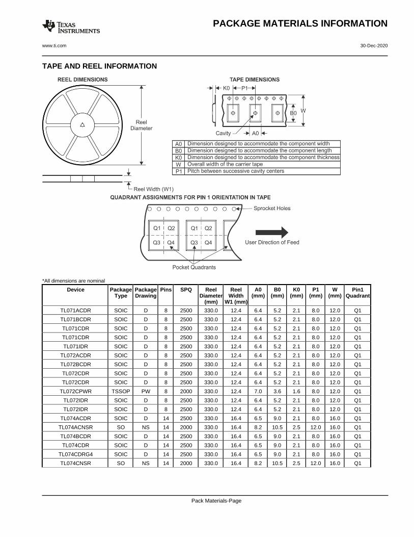
PACKAGE MATERIALS INFORMATION
www.ti.com 30-Dec-2020
Pack Materials-Page 53
TAPE AND REEL INFORMATION
*All dimensions are nominal
Device Package Type
Package Drawing
Pins SPQ Reel Diameter
(mm)
Reel Width
W1 (mm)
A0 (mm)
B0 (mm)
K0 (mm)
P1 (mm)
W (mm)
Pin1 Quadrant
TL071ACDR SOIC D 8 2500 330.0 12.4 6.4 5.2 2.1 8.0 12.0 Q1
TL071BCDR SOIC D 8 2500 330.0 12.4 6.4 5.2 2.1 8.0 12.0 Q1
TL071CDR SOIC D 8 2500 330.0 12.4 6.4 5.2 2.1 8.0 12.0 Q1
TL071CDR SOIC D 8 2500 330.0 12.4 6.4 5.2 2.1 8.0 12.0 Q1
TL071IDR SOIC D 8 2500 330.0 12.4 6.4 5.2 2.1 8.0 12.0 Q1
TL072ACDR SOIC D 8 2500 330.0 12.4 6.4 5.2 2.1 8.0 12.0 Q1
TL072BCDR SOIC D 8 2500 330.0 12.4 6.4 5.2 2.1 8.0 12.0 Q1
TL072CDR SOIC D 8 2500 330.0 12.4 6.4 5.2 2.1 8.0 12.0 Q1
TL072CDR SOIC D 8 2500 330.0 12.4 6.4 5.2 2.1 8.0 12.0 Q1
TL072CPWR TSSOP PW 8 2000 330.0 12.4 7.0 3.6 1.6 8.0 12.0 Q1
TL072IDR SOIC D 8 2500 330.0 12.4 6.4 5.2 2.1 8.0 12.0 Q1
TL072IDR SOIC D 8 2500 330.0 12.4 6.4 5.2 2.1 8.0 12.0 Q1
TL074ACDR SOIC D 14 2500 330.0 16.4 6.5 9.0 2.1 8.0 16.0 Q1
TL074ACNSR SO NS 14 2000 330.0 16.4 8.2 10.5 2.5 12.0 16.0 Q1
TL074BCDR SOIC D 14 2500 330.0 16.4 6.5 9.0 2.1 8.0 16.0 Q1
TL074CDR SOIC D 14 2500 330.0 16.4 6.5 9.0 2.1 8.0 16.0 Q1
TL074CDRG4 SOIC D 14 2500 330.0 16.4 6.5 9.0 2.1 8.0 16.0 Q1
TL074CNSR SO NS 14 2000 330.0 16.4 8.2 10.5 2.5 12.0 16.0 Q1
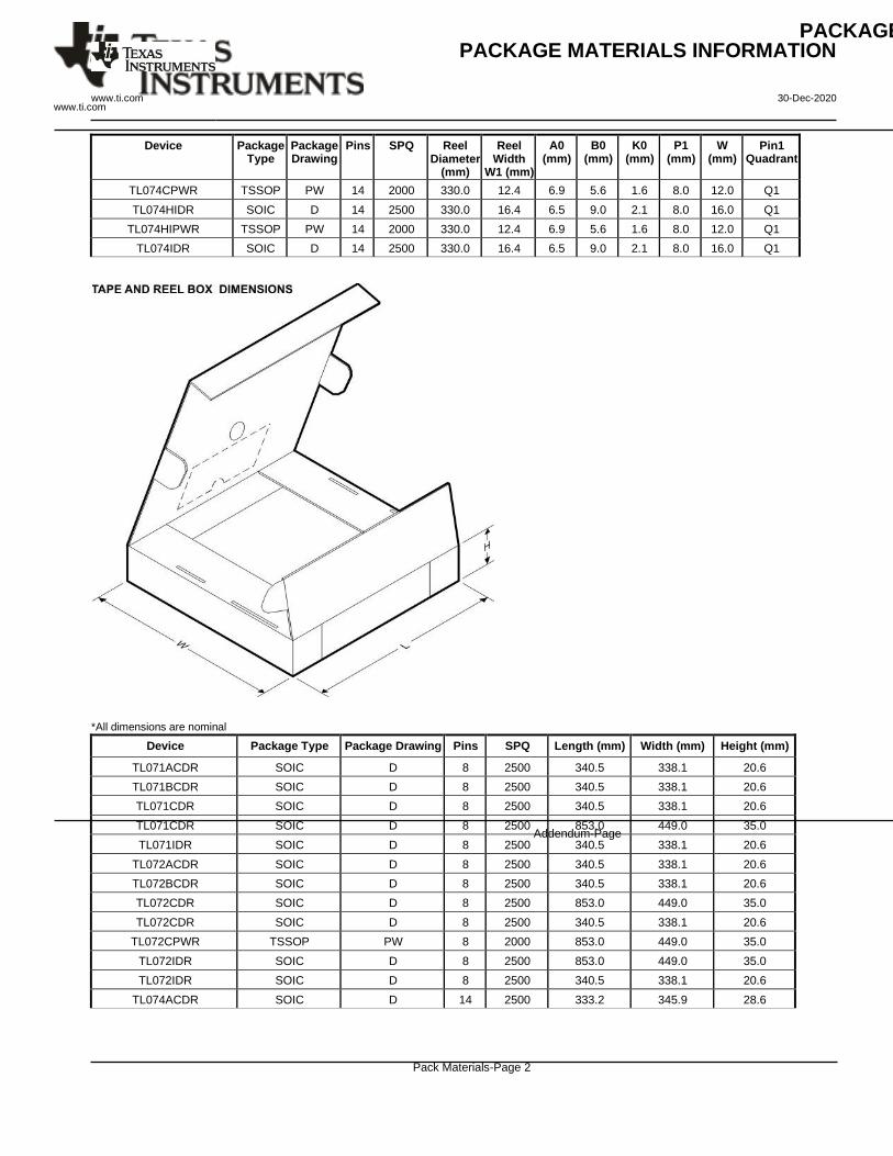
PACKAGE OPTION ADDENDUM
www.ti.com
Addendum-Page 54
PACKAGE MATERIALS INFORMATION
www.ti.com 30-Dec-2020
Device Package Type
Package Drawing
Pins SPQ Reel Diameter
(mm)
Reel Width
W1 (mm)
A0 (mm)
B0 (mm)
K0 (mm)
P1 (mm)
W (mm)
Pin1 Quadrant
TL074CPWR TSSOP PW 14 2000 330.0 12.4 6.9 5.6 1.6 8.0 12.0 Q1
TL074HIDR SOIC D 14 2500 330.0 16.4 6.5 9.0 2.1 8.0 16.0 Q1
TL074HIPWR TSSOP PW 14 2000 330.0 12.4 6.9 5.6 1.6 8.0 12.0 Q1
TL074IDR SOIC D 14 2500 330.0 16.4 6.5 9.0 2.1 8.0 16.0 Q1
*All dimensions are nominal
Device Package Type Package Drawing Pins SPQ Length (mm) Width (mm) Height (mm)
TL071ACDR SOIC D 8 2500 340.5 338.1 20.6
TL071BCDR SOIC D 8 2500 340.5 338.1 20.6
TL071CDR SOIC D 8 2500 340.5 338.1 20.6
TL071CDR SOIC D 8 2500 853.0 449.0 35.0
TL071IDR SOIC D 8 2500 340.5 338.1 20.6
TL072ACDR SOIC D 8 2500 340.5 338.1 20.6
TL072BCDR SOIC D 8 2500 340.5 338.1 20.6
TL072CDR SOIC D 8 2500 853.0 449.0 35.0
TL072CDR SOIC D 8 2500 340.5 338.1 20.6
TL072CPWR TSSOP PW 8 2000 853.0 449.0 35.0
TL072IDR SOIC D 8 2500 853.0 449.0 35.0
TL072IDR SOIC D 8 2500 340.5 338.1 20.6
TL074ACDR SOIC D 14 2500 333.2 345.9 28.6
Pack Materials-Page 2
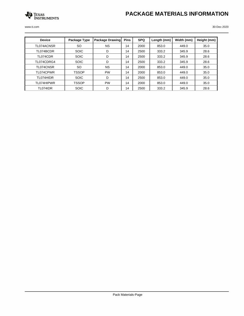
PACKAGE MATERIALS INFORMATION
www.ti.com 30-Dec-2020
Pack Materials-Page 55
Device Package Type Package Drawing Pins SPQ Length (mm) Width (mm) Height (mm)
TL074ACNSR SO NS 14 2000 853.0 449.0 35.0
TL074BCDR SOIC D 14 2500 333.2 345.9 28.6
TL074CDR SOIC D 14 2500 333.2 345.9 28.6
TL074CDRG4 SOIC D 14 2500 333.2 345.9 28.6
TL074CNSR SO NS 14 2000 853.0 449.0 35.0
TL074CPWR TSSOP PW 14 2000 853.0 449.0 35.0
TL074HIDR SOIC D 14 2500 853.0 449.0 35.0
TL074HIPWR TSSOP PW 14 2000 853.0 449.0 35.0
TL074IDR SOIC D 14 2500 333.2 345.9 28.6
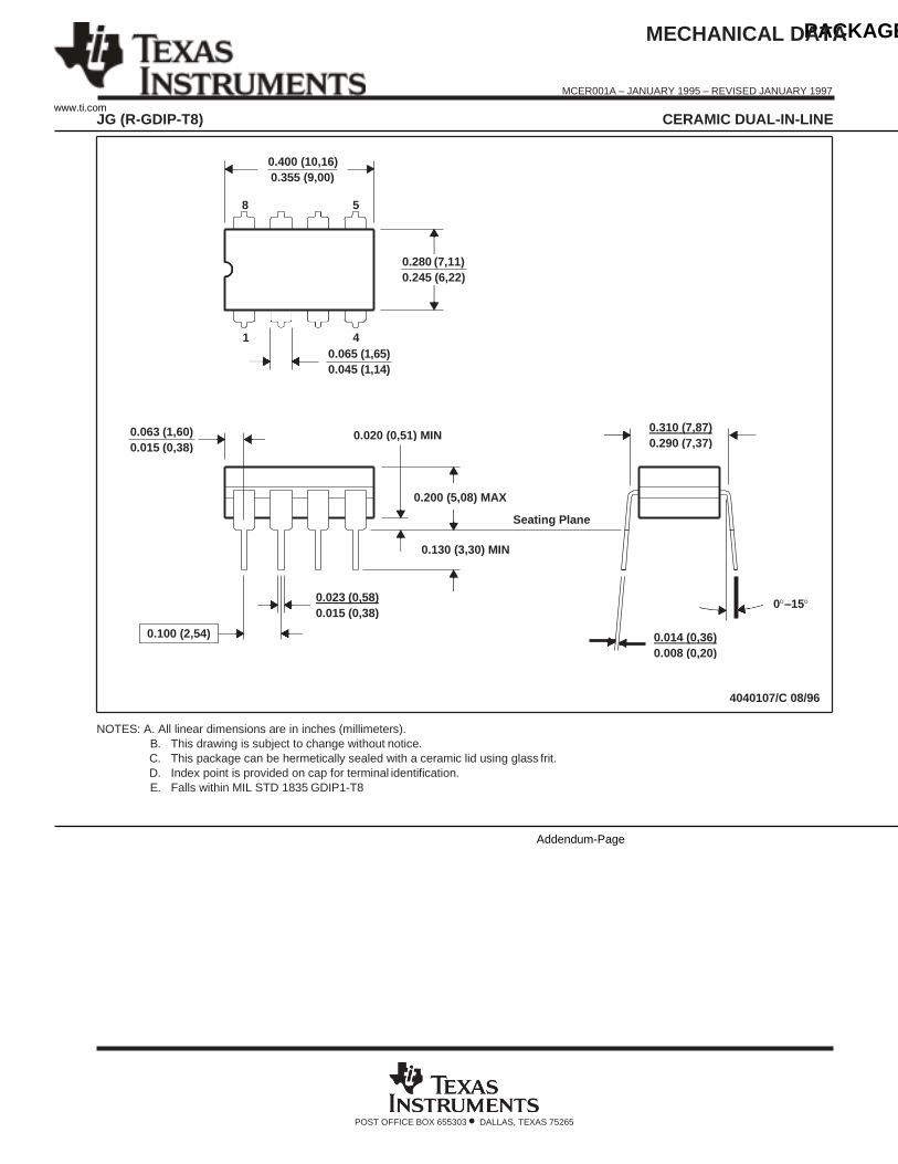
PACKAGE OPTION ADDENDUM
www.ti.com
Addendum-Page 56
4040107/C 08/96
0.014 (0,36)
0.008 (0,20)
0.100 (2,54)
0–15 0.023 (0,58)
0.015 (0,38)
0.130 (3,30) MIN
Seating Plane
0.200 (5,08) MAX
0.310 (7,87)
0.290 (7,37) 0.020 (0,51) MIN 0.063 (1,60)
0.015 (0,38)
4
0.065 (1,65)
0.045 (1,14)
1
0.280 (7,11)
0.245 (6,22)
5 8
0.400 (10,16)
0.355 (9,00)
MECHANICAL DATA
MCER001A – JANUARY 1995 – REVISED JANUARY 1997
JG (R-GDIP-T8) CERAMIC DUAL-IN-LINE
NOTES: A. All linear dimensions are in inches (millimeters).
B. This drawing is subject to change without notice.
C. This package can be hermetically sealed with a ceramic lid using glass frit.
D. Index point is provided on cap for terminal identification.
E. Falls within MIL STD 1835 GDIP1-T8
POST OFFICE BOX 655303 • DALLAS, TEXAS 75265
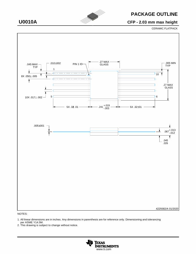
U0010A
PACKAGE OUTLINE
CFP - 2.03 mm max height
SCALE 1. 400
CERAMIC FLATPACK
.045 MAX
TYP
8X .050 .005
.010 .002
1
PIN 1 ID
.27 MAX GLASS
.005 MIN TYP
10
.27 MAX GLASS
10X .017 .002 5 6
5X .32 .01 +.019 -.003
5X .32 .01
.005 .001
+.013 -.012
.045
.026
4225582/A 01/2020
NOTES:
1. All linear dimensions are in inches. Any dimensions in parenthesis are for reference only. Dimensioning and tolerancing per ASME Y14.5M.
2. This drawing is subject to change without notice.
www.ti.com
.241
.067

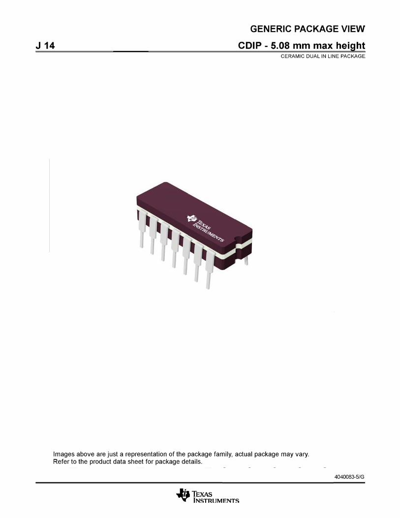
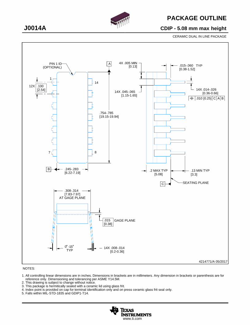
J0014A
PACKAGE OUTLINE
CDIP - 5.08 mm max height
S C A L E 0. 9 0 0
CERAMIC DUAL IN LINE PACKAGE
12X
PIN 1 ID (OPTIONAL)
1
A 4X .005 MIN [0.13]
14
14X .045-.065
[1.15-1.65]
.015-.060 [0.38-1.52]
TYP
14X .014-.026 [0.36-0.66]
.754-.785 [19.15-19.94]
7 8
B .245-.283
[6.22-7.19]
.308-.314 [7.83-7.97]
AT GAGE PLANE
.2 MAX TYP [5.08]
C
.13 MIN TYP [3.3]
SEATING PLANE
GAGE PLANE
0 -15 TYP
14X .008-.014 [0.2-0.36]
4214771/A 05/2017
NOTES:
1. All controlling linear dimensions are in inches. Dimensions in brackets are in millimeters. Any dimension in brackets or parenthesis are for reference only. Dimensioning and tolerancing per ASME Y14.5M.
2. This drawing is subject to change without notice. 3. This package is hermitically sealed with a ceramic lid using glass frit. 4. Index point is provided on cap for terminal identification only and on press ceramic glass frit seal only. 5. Falls within MIL-STD-1835 and GDIP1-T14.
www.ti.com
.100 [2.54]
.015 [0.38]
.010 [0.25] C A B
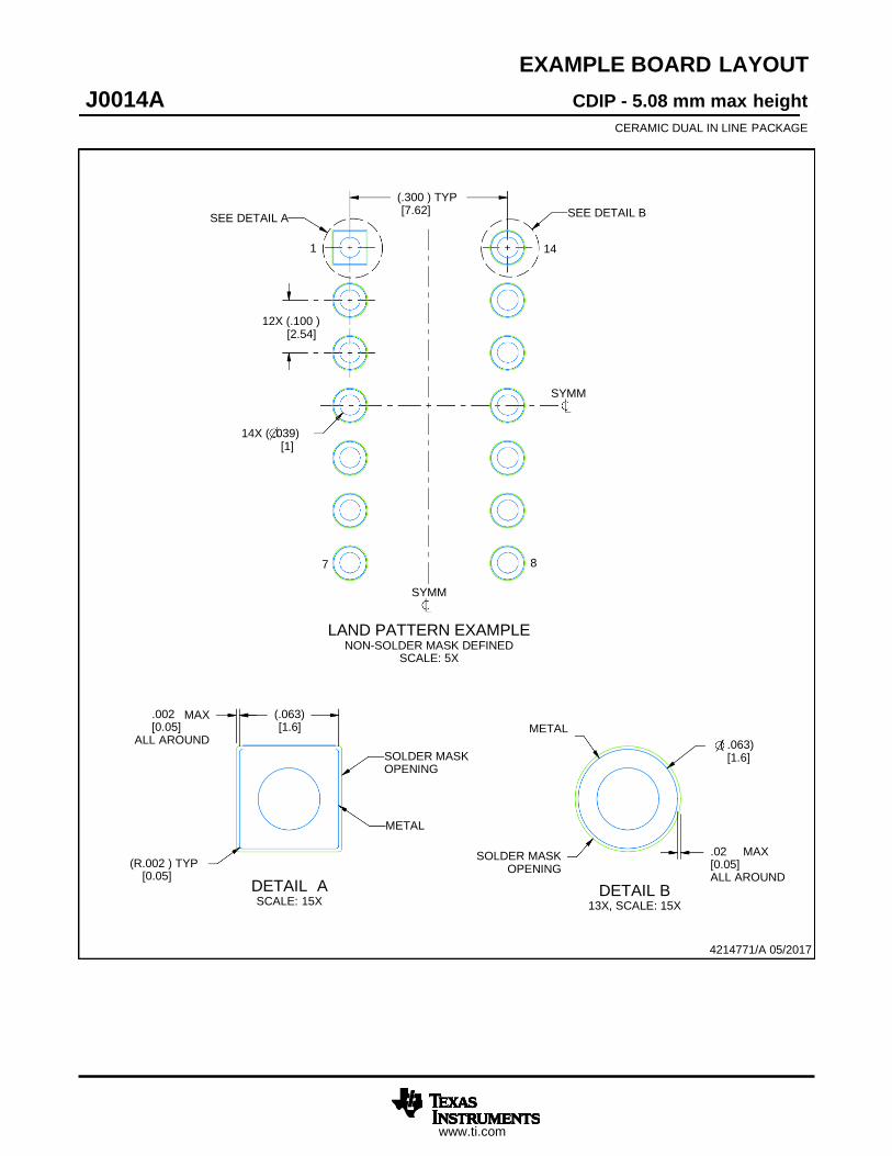
J0014A
EXAMPLE BOARD LAYOUT
CDIP - 5.08 mm max height
CERAMIC DUAL IN LINE PACKAGE
SEE DETAIL A
(.300 ) TYP [7.62]
SEE DETAIL B
1 14
12X (.100 ) [2.54]
SYMM
14X ( .039) [1]
7 8
SYMM
LAND PATTERN EXAMPLE NON-SOLDER MASK DEFINED
SCALE: 5X
.002 [0.05]
MAX (.063) [1.6]
METAL ALL AROUND
SOLDER MASK OPENING
( .063) [1.6]
(R.002 ) TYP [0.05]
DETAIL A SCALE: 15X
METAL
SOLDER MASK OPENING
DETAIL B
13X, SCALE: 15X
.02 MAX [0.05] ALL AROUND
4214771/A 05/2017
www.ti.com

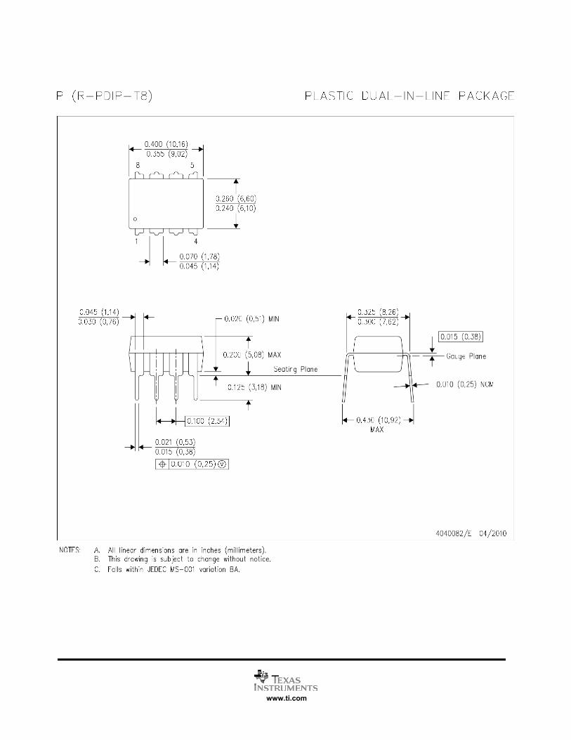
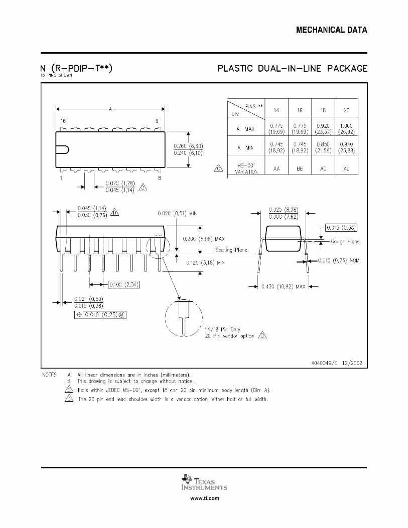
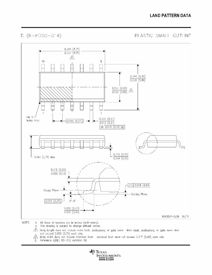
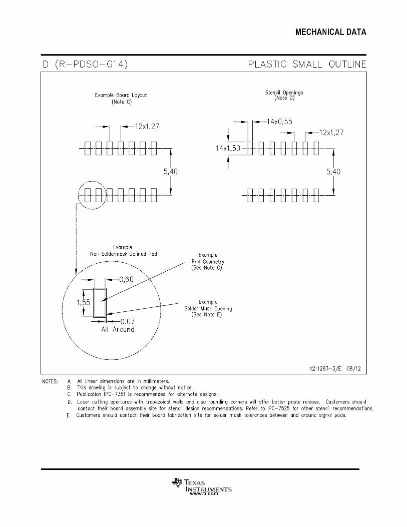
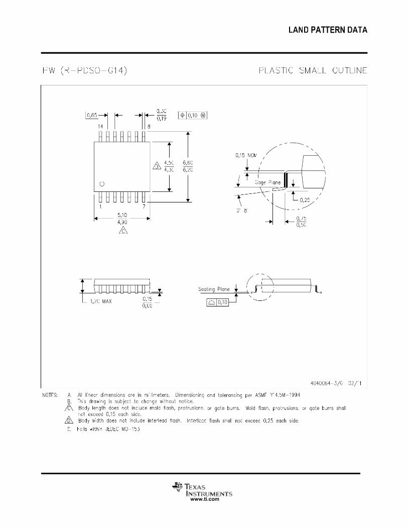
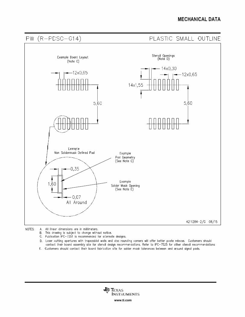
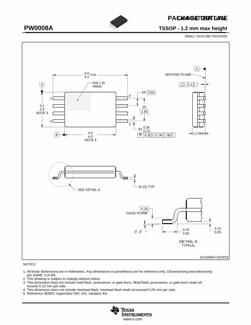
www.ti.com
PW0008A
PACKAGE OUTLINE
TSSOP - 1.2 mm max height
SC AL E 2.8 00
SMALL OUTLINE PACKAGE
6.6 6.2
C
SEATING PLANE
A
1
3.1 2.9
NOTE 3
PIN 1 ID AREA
6X 8
2X
1.95
0.1 C
4
4.5 4.3
NOTE 4
5
0.30 0.19
1.2 MAX
SEE DETAIL A
(0.15) TYP
GAGE PLANE
0 - 8 0.75 0.50
DETAIL A TYPICAL
0.15 0.05
4221848/A 02/2015
NOTES:
1. All linear dimensions are in millimeters. Any dimensions in parenthesis are for reference only. Dimensioning and tolerancing per ASME Y14.5M.
2. This drawing is subject to change without notice. 3. This dimension does not include mold flash, protrusions, or gate burrs. Mold flash, protrusions, or gate burrs shall not
exceed 0.15 mm per side. 4. This dimension does not include interlead flash. Interlead flash shall not exceed 0.25 mm per side. 5. Reference JEDEC registration MO-153, variation AA.
0.25
0.65
TYP
8X
B 0.1 C A B
IMPORTANT NOTICE AND DISCLAIMER TI PROVIDES TECHNICAL AND RELIABILITY DATA (INCLUDING DATASHEETS), DESIGN RESOURCES (INCLUDING REFERENCE
DESIGNS), APPLICATION OR OTHER DESIGN ADVICE, WEB TOOLS, SAFETY INFORMATION, AND OTHER RESOURCES “AS IS”
AND WITH ALL FAULTS, AND DISCLAIMS ALL WARRANTIES, EXPRESS AND IMPLIED, INCLUDING WITHOUT LIMITATION ANY
IMPLIED WARRANTIES OF MERCHANTABILITY, FITNESS FOR A PARTICULAR PURPOSE OR NON-INFRINGEMENT OF THIRD
PARTY INTELLECTUAL PROPERTY RIGHTS.
These resources are intended for skilled developers designing with TI products. You are solely responsible for (1) selecting the appropriate
TI products for your application, (2) designing, validating and testing your application, and (3) ensuring your application meets applicable
standards, and any other safety, security, or other requirements. These resources are subject to change without notice. TI grants you
permission to use these resources only for development of an application that uses the TI products described in the resource. Other
reproduction and display of these resources is prohibited. No license is granted to any other TI intellectual property right or to any third party
intellectual property right. TI disclaims responsibility for, and you will fully indemnify TI and its representatives against, any claims, damages,
costs, losses, and liabilities arising out of your use of these resources.
TI’s products are provided subject to TI’s Terms of Sale (https:www.ti.com/legal/termsofsale.html) or other applicable terms available either
on ti.com or provided in conjunction with such TI products. TI’s provision of these resources does not expand or otherwise alter TI’s
applicable warranties or warranty disclaimers for TI products.
Mailing Address: Texas Instruments, Post Office Box 655303, Dallas, Texas 75265
Copyright © 2021, Texas Instruments Incorporated
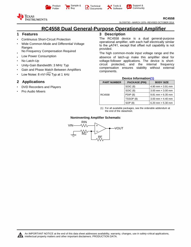
Product Folder
Sample & Buy
Technical Documents
Tools & Software
Support & Community
RC4558
SLOS073G – MARCH 1976 – REVISED OCTOBER 2014
RC4558 Dual General-Purpose Operational Amplifier 1 Features 3 Description
• Continuous Short-Circuit Protection
• Wide Common-Mode and Differential Voltage
Ranges
The RC4558 device is a dual general-purpose operational amplifier, with each half electrically similar to the μA741, except that offset null capability is not provided.
• No Frequency Compensation Required
The high common-mode input voltage range and the
• Low Power Consumption absence of latch-up make this amplifier ideal for • No Latch-Up voltage-follower applications. The device is short-
• Unity-Gain Bandwidth: 3 MHz Typ
• Gain and Phase Match Between Amplifiers
• Low Noise: 8 nV/√Hz Typ at 1 kHz
circuit protected, and the internal frequency compensation ensures stability without external components.
2 Applications
• DVD Recorders and Players
• Pro Audio Mixers
Device Information(1)
PART NUMBER PACKAGE (PIN) BODY SIZE
RC4558
SOIC (8) 4.90 mm × 3.91 mm
SOIC (8) 3.00 mm × 3.00 mm
PDIP (8) 9.81 mm × 6.35 mm
TSSOP (8) 3.00 mm × 4.40 mm
SOP (8) 6.20 mm × 5.30 mm
(1) For all available packages, see the orderable addendum at the end of the datasheet.
Noninverting Amplifier Schematic
RIN VIN +
RG
RF
VOUT
An IMPORTANT NOTICE at the end of this data sheet addresses availability, warranty, changes, use in safety-critical applications, intellectual property matters and other important disclaimers. PRODUCTION DATA.
RC4558
SLOS073G – MARCH 1976 – REVISED OCTOBER 2014 www.ti.com
72 Submit Documentation Feedback Copyright © 1976–2014, Texas Instruments Incorporated
Product Folder Links: RC4558
Table of Contents
1 Features .................................................................. 1
2 Applications............................................................ 1
3 Description ............................................................. 1
4 Revision History ..................................................... 2
5 Pin Configuration and Functions .......................... 3
6 Specifications ......................................................... 4
6.1 Absolute Maximum Ratings...................................... 4
6.2 Handling Ratings...................................................... 4
6.3 Recommended Operating Conditions ....................... 4
6.4 Thermal Information ................................................. 4
6.5 Electrical Characteristics .......................................... 5
6.6 Operating Characteristics ......................................... 5
6.7 Typical Characteristics ............................................. 6
7 Detailed Description .............................................. 9
7.1 Overview 9
4 Revision History
7.2 Functional Block Diagram ......................................... 9
7.3 Feature Description .................................................. 9
7.4 Device Functional Modes ......................................... 9
8 Application and Implementation ......................... 10
8.1 Typical Application ................................................. 10
9 Power Supply Recommendations ...................... 13
10 Layout................................................................... 14
10.1 Layout Guidelines .................................................14
10.2 Layout Example ....................................................14
11 Device and Documentation Support .................. 15
11.1 Trademarks...........................................................15
11.2 Electrostatic Discharge Caution ............................15
11.3 Glossary ...............................................................15
12 Mechanical, Packaging, and Orderable Information ........................................................... 15
Changes from Revision F (September 2010) to Revision G Page
• Added Applications, Device Information table, Handling Ratings table, Feature Description section, Device
Functional Modes, Application and Implementation section, Power Supply Recommendations section, Layout
section, Device and Documentation Support section, and Mechanical, Packaging, and Orderable Information section. ...... 1
• Removed Ordering Information table. .................................................................................................................................... 1
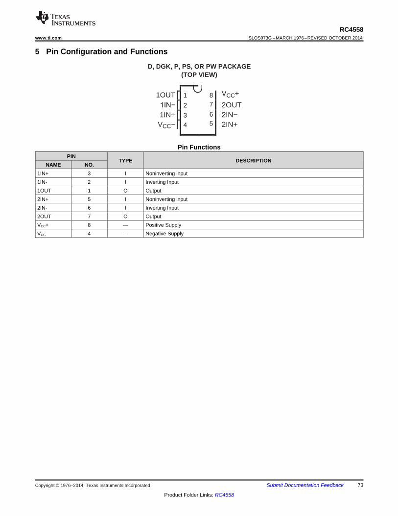
RC4558
SLOS073G – MARCH 1976 – REVISED OCTOBER 2014 www.ti.com
Submit Documentation Feedback 73 Copyright © 1976–2014, Texas Instruments Incorporated
Product Folder Links: RC4558
5 Pin Configuration and Functions
D, DGK, P, PS, OR PW PACKAGE
(TOP VIEW)
1OUT 1 8 VCC+
1IN− 2 7 2OUT
1IN+ 3 6 2IN−
VCC− 4 5 2IN+
Pin Functions
PIN
TYPE
DESCRIPTION NAME NO.
1IN+ 3 I Noninverting input
1IN- 2 I Inverting Input
1OUT 1 O Output
2IN+ 5 I Noninverting input
2IN- 6 I Inverting Input
2OUT 7 O Output
VCC+ 8 — Positive Supply
VCC- 4 — Negative Supply
RC4558
SLOS073G – MARCH 1976 – REVISED OCTOBER 2014 www.ti.com
74 Submit Documentation Feedback Copyright © 1976–2014, Texas Instruments Incorporated
Product Folder Links: RC4558
6 Specifications
6.1 Absolute Maximum Ratings
over operating free-air temperature range (unless otherwise noted)(1)
MIN MAX UNIT
VCC+ Supply voltage(2)
18 V
VCC– –18
VID Differential input voltage(3) ±30 V
VI Input voltage (any input)(2)(4) ±15 V
Duration of output short circuit to ground, one amplifier at a time (5) Unlimited
TJ Operating virtual junction temperature 150 °C
(1) Stresses beyond those listed under Absolute Maximum Ratings may cause permanent damage to the device. These are stress ratings only, and functional operation of the device at these or any other conditions beyond those indicated under Recommended Operating Conditions is not implied. Exposure to absolute-maximum-rated conditions for extended periods may affect device reliability.
(2) All voltage values, unless otherwise noted, are with respect to the midpoint between VCC+ and VCC–. (3) Differential voltages are at IN+ with respect to IN–. (4) The magnitude of the input voltage must never exceed the magnitude of the supply voltage or 15 V, whichever is less. (5) Temperature and/or supply voltages must be limited to ensure that the dissipation rating is not exceeded.
6.2 Handling Ratings MIN MAX UNIT
Tstg Storage temperature range -65 150 °C
V(ESD)
Electrostatic discharge Human body model (HBM), per AEC Q100-002 (1) 0 500
V Charged device model (CDM), per AEC Q100-011 (2) 0 1000
(1) JEDEC document JEP155 states that 500-V HBM allows safe manufacturing with a standard ESD control process. (2) JEDEC document JEP157 states that 250-V CDM allows safe manufacturing with a standard ESD control process.
6.3 Recommended Operating Conditions MIN MAX UNIT
VCC+
Supply voltage 5 15
V VCC– –5 –15
TA Operating free-air temperature RC4558 0 70
°C RC4558I –40 85
6.4 Thermal Information
THERMAL METRIC(1)
RC4558 UNIT D DGK P PS PW
8 PINS
RθJA Junction-to-ambient thermal resistance 97 172 85 95 149 °C/W
(1) For more information about traditional and new thermal metrics, see the IC Package Thermal Metrics application report, SPRA953.
RC4558
SLOS073G – MARCH 1976 – REVISED OCTOBER 2014 www.ti.com
Submit Documentation Feedback 75 Copyright © 1976–2014, Texas Instruments Incorporated
Product Folder Links: RC4558
6.5 Electrical Characteristics
at specified free-air temperature, VCC+ = 15 V, VCC– = –15 V
PARAMETER TEST
CONDITIONS(1) TA
(2) MIN TYP MAX UNIT
VIO
Input offset voltage VO = 0 25°C 0.5 6
mV Full range 7.5
IIO
Input offset current VO = 0 25°C 5 200
nA Full range 300
IIB
Input bias current VO = 0 25°C 150 500
nA Full range 800
VICR Common-mode input voltage range 25°C ±12 ±14 V
VOM
Maximum output voltage swing
RL = 10 kΩ 25°C ±12 ±14 V
RL = 2 kΩ 25°C ±10 ±13
Full range ±10
AVD
Large-signal differential voltage amplification RL ≥ 2 kΩ, VO = ±10 V
25°C 20 300
V/mV Full range 15
B1 Unity-gain bandwidth 25°C 3 MHz
ri Input resistance 25°C 0.3 5 MΩ
CMRR Common-mode rejection ratio 25°C 70 90 dB
kSVS Supply-voltage sensitivity (ΔVIO/ΔVCC) VCC = ±15 V to ±9 V
25°C
30 150 μV/V
Vn
Equivalent input noise voltage (closed loop)
AVD = 100, RS = 100 Ω, f = 1 kHz, BW = 1 Hz
25°C
8
nV/√Hz
ICC
Supply current (both amplifiers)
VO = 0, No load
25°C 2.5 5.6 mA TA min 3 6.6
TA max 2.3 5
PD
Total power dissipation (both amplifiers)
VO = 0, No load
25°C 75 170 mW TA min 90 200
TA max 70 150
VO1/VO2
Crosstalk attenuation Open loop RS = 1 kΩ,
f = 10 kHz
25°C 85
dB AVD = 100 105
(1) All characteristics are measured under open-loop conditions with zero common-mode input voltage, unless otherwise specified. (2) Full range is 0°C to 70°C for RC4558 and –40°C to 85°C for RC4558I.
6.6 Operating Characteristics
VCC+ = 15 V, VCC– = –15 V, TA = 25°C
PARAMETER TEST CONDITIONS MIN TYP MAX UNIT
tr Rise time VI = 20 mV, RL = 2 kΩ, CL = 100 pF 0.13 ns
Overshoot VI = 20 mV, RL = 2 kΩ, CL = 100 pF 5%
SR Slew rate at unity gain VI = 10 V, RL = 2 kΩ, CL = 100 pF 1.1 1.7 V/μs
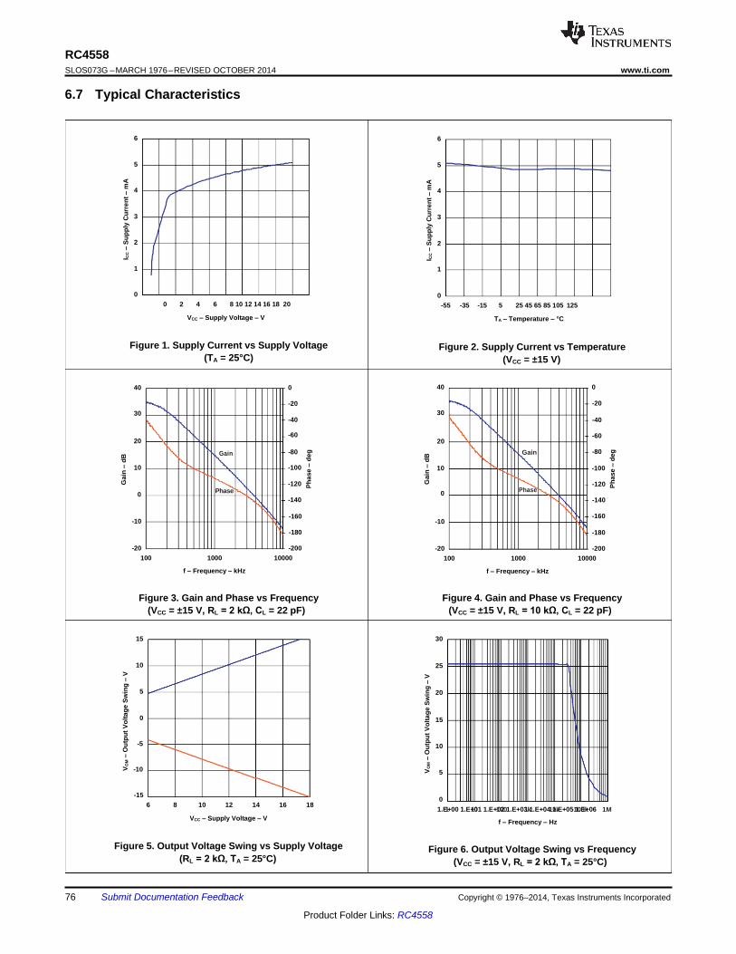
RC4558
SLOS073G – MARCH 1976 – REVISED OCTOBER 2014 www.ti.com
76 Submit Documentation Feedback Copyright © 1976–2014, Texas Instruments Incorporated
Product Folder Links: RC4558
1.E+00 1.E+01 1.E+02 1.E+03 1.E+04 1.E+05 1.E+06
Phase
Gain
Ph
ase
– d
eg
VO
M –
Ou
tpu
t V
olt
ag
e S
win
g –
V
Ga
in –
dB
I C
C –
Su
pp
ly C
urr
en
t –
mA
6.7 Typical Characteristics
6 6
5 5
4 4
3 3
2 2
1 1
0
0 2 4 6 8 10 12 14 16 18 20
VCC – Supply Voltage – V
0
-55 -35 -15 5 25 45 65 85 105 125
TA – Temperature – °C
Figure 1. Supply Current vs Supply Voltage
(TA = 25°C) Figure 2. Supply Current vs Temperature
(VCC = ±15 V)
40 0 40 0
-20
30 30 -40
-20
-40
20
Gain
-60
20
-80
-60
-80
10 -100 10 -100
0
Phase
-120
0 -140
-120
-140
-10
-160
-180
-10
-160
-180
-20
-200
-20
-200
100 1000 10000
f – Frequency – kHz
100 1000 10000
f – Frequency – kHz
Figure 3. Gain and Phase vs Frequency
(VCC = ±15 V, RL = 2 kΩ, CL = 22 pF)
Figure 4. Gain and Phase vs Frequency
(VCC = ±15 V, RL = 10 kΩ, CL = 22 pF)
15 30
10 25
5 20
0 15
-5 10
-10 5
-15
6 8 10 12 14 16 18
0
1 10
100 1k
10k
100k 1M
VCC – Supply Voltage – V f – Frequency – Hz
Figure 5. Output Voltage Swing vs Supply Voltage
(RL = 2 kΩ, TA = 25°C) Figure 6. Output Voltage Swing vs Frequency
(VCC = ±15 V, RL = 2 kΩ, TA = 25°C)
Ga
in –
dB
V
OM –
Ou
tpu
t V
olt
ag
e S
win
g –
V
I CC –
Su
pp
ly C
urr
en
t –
mA
Ph
ase
– d
eg
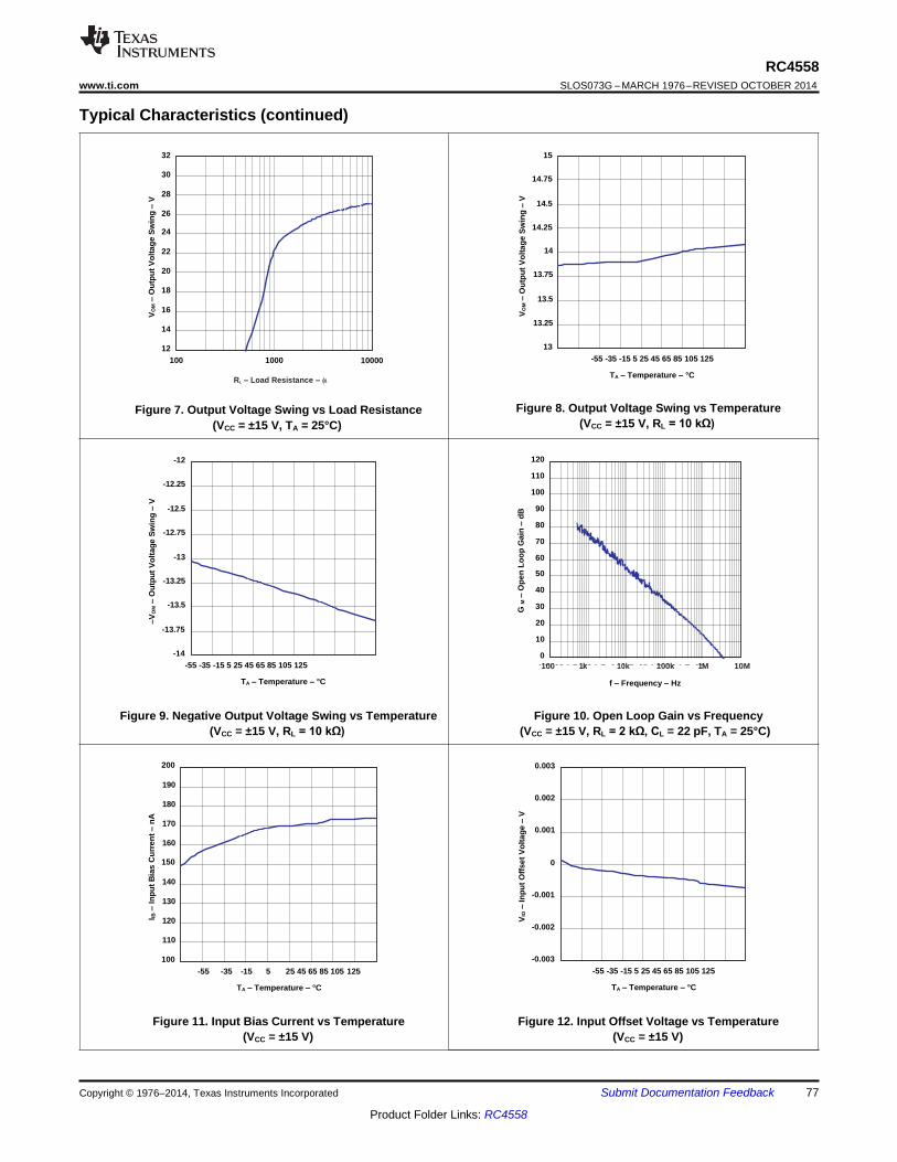
RC4558
SLOS073G – MARCH 1976 – REVISED OCTOBER 2014 www.ti.com
Submit Documentation Feedback 77 Copyright © 1976–2014, Texas Instruments Incorporated
Product Folder Links: RC4558
1.E+02 1.E+03 1.E+04 1.E+05 1.E+06 1.E+07
Rload – Load Resistance –
VIO
– I
np
ut
Off
se
t V
olt
ag
e –
V
VO
M –
Ou
tpu
t V
olt
ag
e S
win
g –
V
Typical Characteristics (continued)
32 15
30
14.75
28
14.5
26
24 14.25
22
20
18
16
14
12
100
1000
RL – Load Resistance –
10000
14
13.75
13.5
13.25
13
-55 -35 -15 5 25 45 65 85 105 125
TA – Temperature – °C
Figure 7. Output Voltage Swing vs Load Resistance
(VCC = ±15 V, TA = 25°C)
Figure 8. Output Voltage Swing vs Temperature
(VCC = ±15 V, RL = 10 kΩ)
-12
-12.25
-12.5
-12.75
-13
-13.25
-13.5
120
110
100
90
80
70
60
50
40
30
-13.75
-14
-55 -35 -15 5 25 45 65 85 105 125
20
10
0
100 1k
10k
100k 1M
10M
TA – Temperature – °C
f – Frequency – Hz
Figure 9. Negative Output Voltage Swing vs Temperature
(VCC = ±15 V, RL = 10 kΩ)
Figure 10. Open Loop Gain vs Frequency
(VCC = ±15 V, RL = 2 kΩ, CL = 22 pF, TA = 25°C)
200 0.003
190
180
0.002
170
160
0.001
150 0
140
130
-0.001
120
110
-0.002
100
-55 -35 -15 5 25 45 65 85 105 125
TA – Temperature – °C
-0.003
-55 -35 -15 5 25 45 65 85 105 125
TA – Temperature – °C
Figure 11. Input Bias Current vs Temperature
(VCC = ±15 V)
Figure 12. Input Offset Voltage vs Temperature
(VCC = ±15 V)
I IB –
In
pu
t B
ias
Cu
rre
nt
– n
A
–V
OM –
Ou
tpu
t V
olt
ag
e S
win
g –
V
VO
M –
Ou
tpu
t V
olt
ag
e S
win
g –
V
G M
– O
pe
n L
oo
p G
ain
– d
B
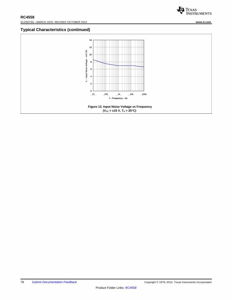
RC4558
SLOS073G – MARCH 1976 – REVISED OCTOBER 2014 www.ti.com
78 Submit Documentation Feedback Copyright © 1976–2014, Texas Instruments Incorporated
Product Folder Links: RC4558
1.E+01 1.E+02 1.E+03 1.E+04 1.E+05
) z H ( t r / V n – e g a t l o V e s i o N t u p n I –
n V
Typical Characteristics (continued)
f – Frequency – Hz
Figure 13. Input Noise Voltage vs Frequency
(VCC = ±15 V, TA = 25°C)
100k 10k 1k 100 10
14
12
10
8
6
4
2
0
Vn
– I
np
ut
No
ise V
olt
ag
e –
nV
/H
z
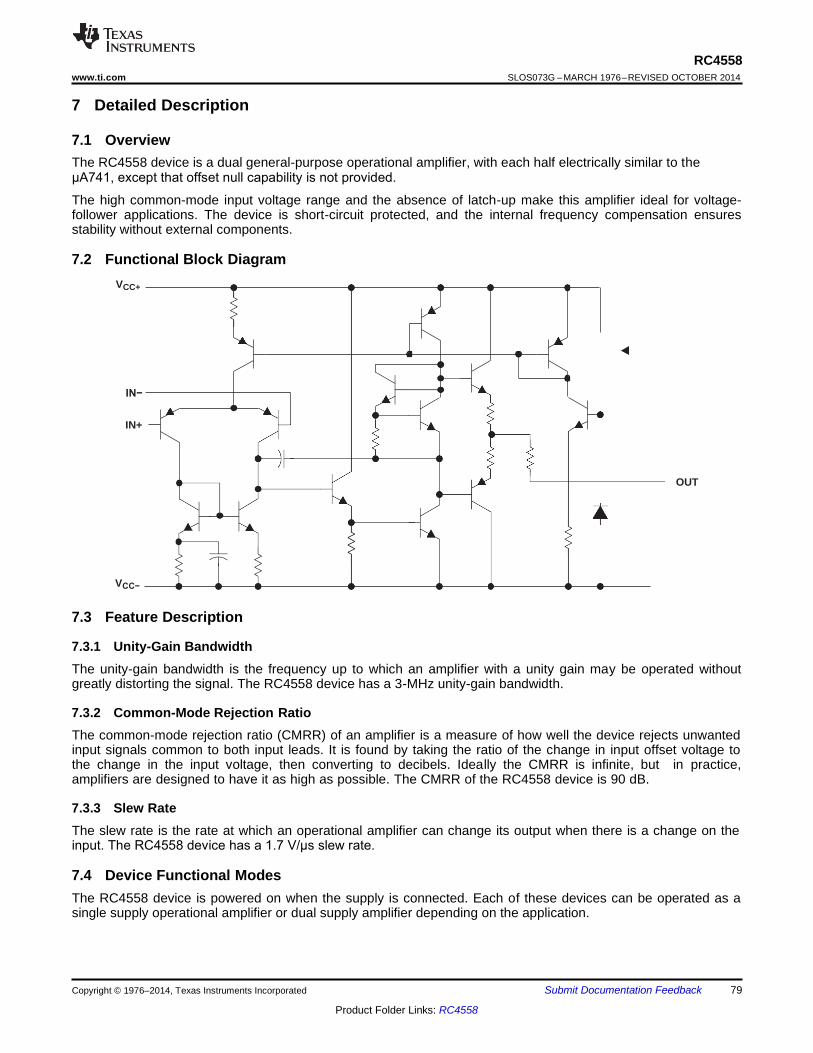
RC4558
SLOS073G – MARCH 1976 – REVISED OCTOBER 2014 www.ti.com
Submit Documentation Feedback 79 Copyright © 1976–2014, Texas Instruments Incorporated
Product Folder Links: RC4558
7 Detailed Description
7.1 Overview
The RC4558 device is a dual general-purpose operational amplifier, with each half electrically similar to the μA741, except that offset null capability is not provided.
The high common-mode input voltage range and the absence of latch-up make this amplifier ideal for voltage- follower applications. The device is short-circuit protected, and the internal frequency compensation ensures stability without external components.
7.2 Functional Block Diagram
VCC+
IN−
IN+
OUT
VCC−
7.3 Feature Description
7.3.1 Unity-Gain Bandwidth
The unity-gain bandwidth is the frequency up to which an amplifier with a unity gain may be operated without greatly distorting the signal. The RC4558 device has a 3-MHz unity-gain bandwidth.
7.3.2 Common-Mode Rejection Ratio
The common-mode rejection ratio (CMRR) of an amplifier is a measure of how well the device rejects unwanted input signals common to both input leads. It is found by taking the ratio of the change in input offset voltage to the change in the input voltage, then converting to decibels. Ideally the CMRR is infinite, but in practice, amplifiers are designed to have it as high as possible. The CMRR of the RC4558 device is 90 dB.
7.3.3 Slew Rate
The slew rate is the rate at which an operational amplifier can change its output when there is a change on the input. The RC4558 device has a 1.7 V/μs slew rate.
7.4 Device Functional Modes
The RC4558 device is powered on when the supply is connected. Each of these devices can be operated as a single supply operational amplifier or dual supply amplifier depending on the application.
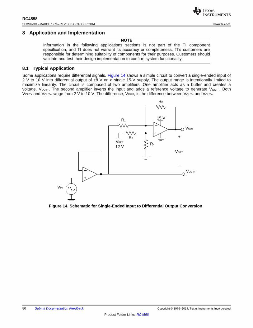
RC4558
SLOS073G – MARCH 1976 – REVISED OCTOBER 2014 www.ti.com
80 Submit Documentation Feedback Copyright © 1976–2014, Texas Instruments Incorporated
Product Folder Links: RC4558
R1 15 V
+ R3 +
VREF R4
12 V
VDIFF
–
+
8 Application and Implementation
NOTE Information in the following applications sections is not part of the TI component specification, and TI does not warrant its accuracy or completeness. TI’s customers are responsible for determining suitability of components for their purposes. Customers should validate and test their design implementation to confirm system functionality.
8.1 Typical Application
Some applications require differential signals. Figure 14 shows a simple circuit to convert a single-ended input of 2 V to 10 V into differential output of ±8 V on a single 15-V supply. The output range is intentionally limited to maximize linearity. The circuit is composed of two amplifiers. One amplifier acts as a buffer and creates a voltage, VOUT+. The second amplifier inverts the input and adds a reference voltage to generate VOUT–. Both VOUT+ and VOUT– range from 2 V to 10 V. The difference, VDIFF, is the difference between VOUT+ and VOUT–.
R2
VOUT-
VOUT+
VIN
Figure 14. Schematic for Single-Ended Input to Differential Output Conversion
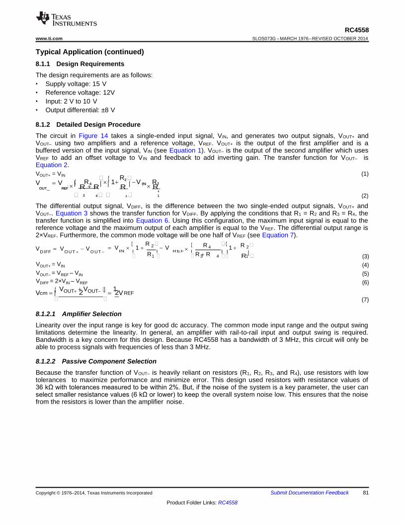
RC4558
SLOS073G – MARCH 1976 – REVISED OCTOBER 2014 www.ti.com
Submit Documentation Feedback 81 Copyright © 1976–2014, Texas Instruments Incorporated
Product Folder Links: RC4558
out
ref 4
3+ 4
2
1 in
2
1
Typical Application (continued)
8.1.1 Design Requirements
The design requirements are as follows:
• Supply voltage: 15 V
• Reference voltage: 12V
• Input: 2 V to 10 V
• Output differential: ±8 V
8.1.2 Detailed Design Procedure
The circuit in Figure 14 takes a single-ended input signal, VIN, and generates two output signals, VOUT+ and VOUT– using two amplifiers and a reference voltage, VREF. VOUT+ is the output of the first amplifier and is a buffered version of the input signal, VIN (see Equation 1). VOUT– is the output of the second amplifier which uses VREF to add an offset voltage to VIN and feedback to add inverting gain. The transfer function for VOUT– is Equation 2.
VOUT+ = VIN (1)
V = V
R 4
1+
R2 − V
R2
OUT REF
R + R
R IN
R
3 4 1 1 (2)
The differential output signal, VDIFF, is the difference between the two single-ended output signals, VOUT+ and VOUT–. Equation 3 shows the transfer function for VDIFF. By applying the conditions that R1 = R2 and R3 = R4, the transfer function is simplified into Equation 6. Using this configuration, the maximum input signal is equal to the reference voltage and the maximum output of each amplifier is equal to the VREF. The differential output range is 2×VREF. Furthermore, the common mode voltage will be one half of VREF (see Equation 7).
V = V − V = V
1 + R 2
− V R 4
1 + R 2
1 3 4 1
V = VOUT+ + VOUT−
= 1
V cm 2
2 REF
8.1.2.1 Amplifier Selection
(7)
Linearity over the input range is key for good dc accuracy. The common mode input range and the output swing limitations determine the linearity. In general, an amplifier with rail-to-rail input and output swing is required. Bandwidth is a key concern for this design. Because RC4558 has a bandwidth of 3 MHz, this circuit will only be able to process signals with frequencies of less than 3 MHz.
8.1.2.2 Passive Component Selection
Because the transfer function of VOUT– is heavily reliant on resistors (R1, R2, R3, and R4), use resistors with low tolerances to maximize performance and minimize error. This design used resistors with resistance values of 36 kΩ with tolerances measured to be within 2%. But, if the noise of the system is a key parameter, the user can select smaller resistance values (6 kΩ or lower) to keep the overall system noise low. This ensures that the noise from the resistors is lower than the amplifier noise.
D IFF O U T + O U T − IN R
R E F R + R
R
(3)
VOUT+ = VIN (4)
VOUT– = VREF – VIN (5)
VDIFF = 2×VIN – VREF (6)
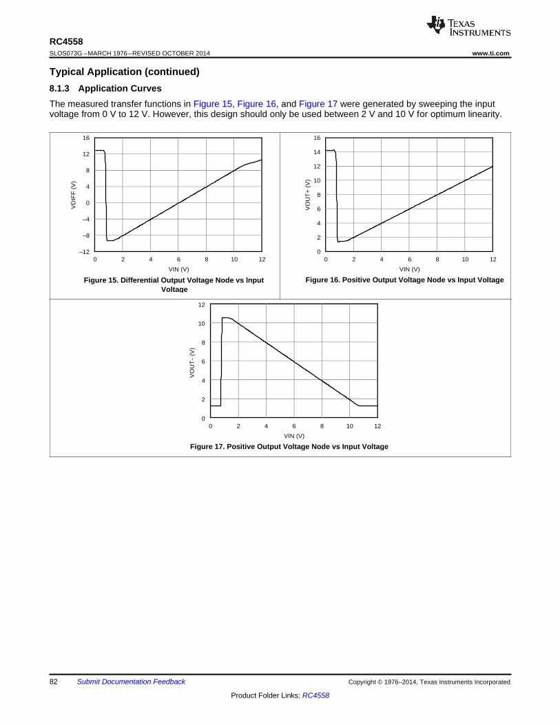
RC4558
SLOS073G – MARCH 1976 – REVISED OCTOBER 2014 www.ti.com
82 Submit Documentation Feedback Copyright © 1976–2014, Texas Instruments Incorporated
Product Folder Links: RC4558
Figure 17. Positive Output Voltage Node vs Input Voltage
10 12
C002
8 6
VIN (V)
4 2 0
12
10
8
6
4
2
0
Figure 16. Positive Output Voltage Node vs Input Voltage
10 12
C001
8 6
VIN (V)
4 2 0
16
14
12
10
8
6
4
2
0
Figure 15. Differential Output Voltage Node vs Input
Voltage
10 12
C003
8 6
VIN (V)
4 2 0
16
12
8
4
0
–4
–8
–12
Typical Application (continued)
8.1.3 Application Curves
The measured transfer functions in Figure 15, Figure 16, and Figure 17 were generated by sweeping the input voltage from 0 V to 12 V. However, this design should only be used between 2 V and 10 V for optimum linearity.
VD
IFF
(V
)
VO
UT
− (
V)
VO
UT
+ (
V)
RC4558
SLOS073G – MARCH 1976 – REVISED OCTOBER 2014 www.ti.com
Submit Documentation Feedback 83 Copyright © 1976–2014, Texas Instruments Incorporated
Product Folder Links: RC4558
CAUTION
Supply voltages outside of the ±18-V range can permanently damage the device (see the Absolute Maximum Ratings ).
9 Power Supply Recommendations
The RC4558 device is specified for operation from ±5 V to ±15 V; many specifications apply from –0°C to 70°C. The Typical Characteristics section presents parameters that can exhibit significant variance with regard to operating voltage or temperature.
Place 0.1-μF bypass capacitors close to the power-supply pins to reduce errors coupling in from noisy or high impedance power supplies. For more detailed information on bypass capacitor placement, refer to the Layout Guidelines.
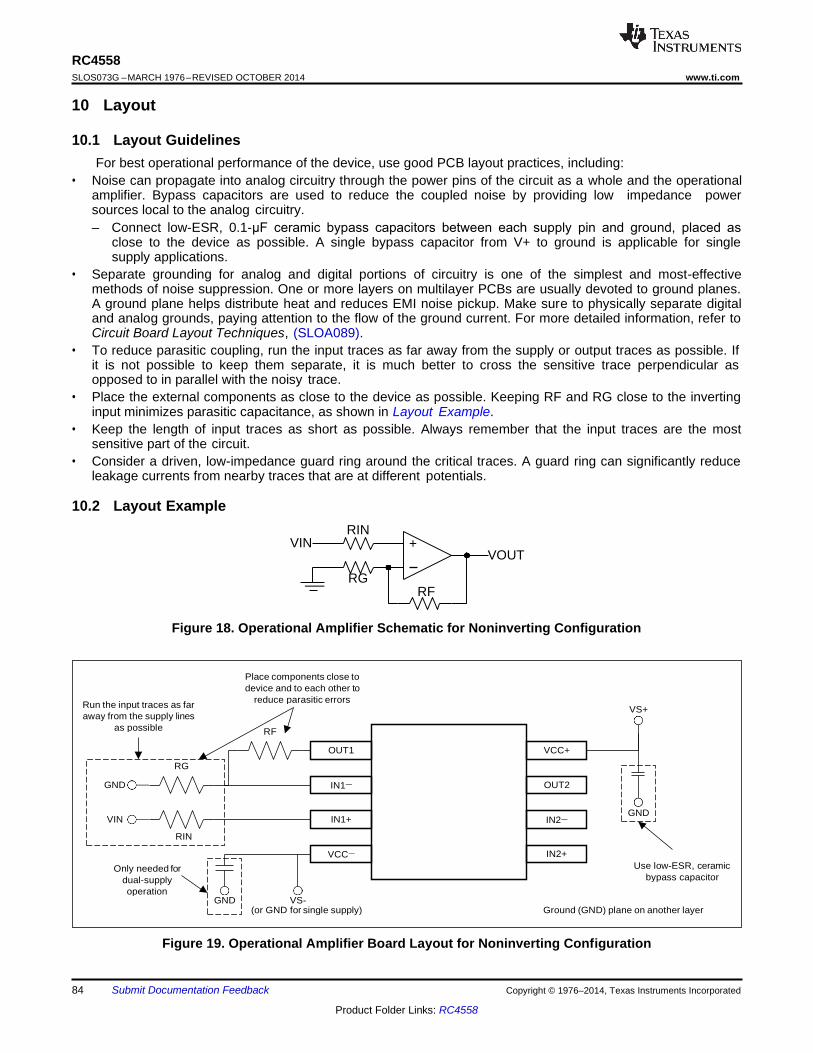
RC4558
SLOS073G – MARCH 1976 – REVISED OCTOBER 2014 www.ti.com
84 Submit Documentation Feedback Copyright © 1976–2014, Texas Instruments Incorporated
Product Folder Links: RC4558
GND VS- (or GND for single supply) Ground (GND) plane on another layer
Use low-ESR, ceramic
bypass capacitor Only needed for
dual-supply
operation
IN2+ VCC−
RIN
GND IN2− IN1+ VIN
OUT2 IN1− GND
RG
VCC+ OUT1
RF
VS+
Place components close to
device and to each other to
reduce parasitic errors Run the input traces as far
away from the supply lines
as possible
10 Layout
10.1 Layout Guidelines
For best operational performance of the device, use good PCB layout practices, including:
• Noise can propagate into analog circuitry through the power pins of the circuit as a whole and the operational amplifier. Bypass capacitors are used to reduce the coupled noise by providing low impedance power sources local to the analog circuitry.
– Connect low-ESR, 0.1-μF ceramic bypass capacitors between each supply pin and ground, placed as close to the device as possible. A single bypass capacitor from V+ to ground is applicable for single supply applications.
• Separate grounding for analog and digital portions of circuitry is one of the simplest and most-effective methods of noise suppression. One or more layers on multilayer PCBs are usually devoted to ground planes. A ground plane helps distribute heat and reduces EMI noise pickup. Make sure to physically separate digital and analog grounds, paying attention to the flow of the ground current. For more detailed information, refer to Circuit Board Layout Techniques, (SLOA089).
• To reduce parasitic coupling, run the input traces as far away from the supply or output traces as possible. If it is not possible to keep them separate, it is much better to cross the sensitive trace perpendicular as opposed to in parallel with the noisy trace.
• Place the external components as close to the device as possible. Keeping RF and RG close to the inverting input minimizes parasitic capacitance, as shown in Layout Example.
• Keep the length of input traces as short as possible. Always remember that the input traces are the most sensitive part of the circuit.
• Consider a driven, low-impedance guard ring around the critical traces. A guard ring can significantly reduce leakage currents from nearby traces that are at different potentials.
10.2 Layout Example
VIN
RIN +
RG
RF
VOUT
Figure 18. Operational Amplifier Schematic for Noninverting Configuration
Figure 19. Operational Amplifier Board Layout for Noninverting Configuration
RC4558
SLOS073G – MARCH 1976 – REVISED OCTOBER 2014 www.ti.com
Submit Documentation Feedback 85 Copyright © 1976–2014, Texas Instruments Incorporated
Product Folder Links: RC4558
11 Device and Documentation Support
11.1 Trademarks
All trademarks are the property of their respective owners.
11.2 Electrostatic Discharge Caution
This integrated circuit can be damaged by ESD. Texas Instruments recommends that all integrated circuits be handled with appropriate precautions. Failure to observe proper handling and installation procedures can cause damage.
ESD damage can range from subtle performance degradation to complete device failure. Precision integrated circuits may be more susceptible to damage because very small parametric changes could cause the device not to meet its published specifications.
11.3 Glossary
SLYZ022 — TI Glossary.
This glossary lists and explains terms, acronyms and definitions.
12 Mechanical, Packaging, and Orderable Information
The following pages include mechanical packaging and orderable information. This information is the most current data available for the designated devices. This data is subject to change without notice and revision of this document. For browser based versions of this data sheet, refer to the left hand navigation.
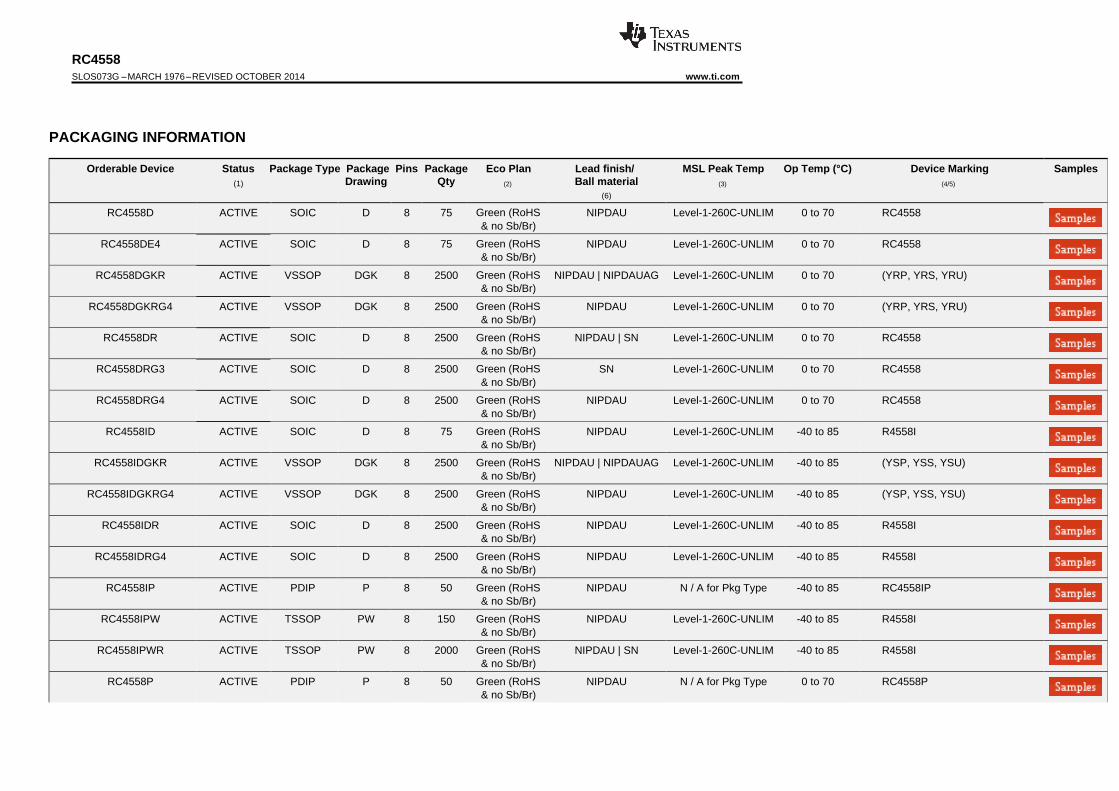
RC4558
SLOS073G – MARCH 1976 – REVISED OCTOBER 2014 www.ti.com
PACKAGING INFORMATION
Orderable Device Status Package Type Package Pins Package Eco Plan Lead finish/ MSL Peak Temp Op Temp (°C) Device Marking
(1) Drawing Qty (2) Ball material (3) (4/5)
(6)
Samples
RC4558D ACTIVE SOIC D 8 75 Green (RoHS
& no Sb/Br)
NIPDAU Level-1-260C-UNLIM 0 to 70 RC4558
RC4558DE4 ACTIVE SOIC D 8 75 Green (RoHS
& no Sb/Br)
NIPDAU Level-1-260C-UNLIM 0 to 70 RC4558
RC4558DGKR ACTIVE VSSOP DGK 8 2500 Green (RoHS
& no Sb/Br)
NIPDAU | NIPDAUAG Level-1-260C-UNLIM 0 to 70 (YRP, YRS, YRU)
RC4558DGKRG4 ACTIVE VSSOP DGK 8 2500 Green (RoHS
& no Sb/Br)
NIPDAU Level-1-260C-UNLIM 0 to 70 (YRP, YRS, YRU)
RC4558DR ACTIVE SOIC D 8 2500 Green (RoHS
& no Sb/Br)
NIPDAU | SN Level-1-260C-UNLIM 0 to 70 RC4558
RC4558DRG3 ACTIVE SOIC D 8 2500 Green (RoHS
& no Sb/Br)
SN Level-1-260C-UNLIM 0 to 70 RC4558
RC4558DRG4 ACTIVE SOIC D 8 2500 Green (RoHS
& no Sb/Br)
NIPDAU Level-1-260C-UNLIM 0 to 70 RC4558
RC4558ID ACTIVE SOIC D 8 75 Green (RoHS
& no Sb/Br)
NIPDAU Level-1-260C-UNLIM -40 to 85 R4558I
RC4558IDGKR ACTIVE VSSOP DGK 8 2500 Green (RoHS
& no Sb/Br)
NIPDAU | NIPDAUAG Level-1-260C-UNLIM -40 to 85 (YSP, YSS, YSU)
RC4558IDGKRG4 ACTIVE VSSOP DGK 8 2500 Green (RoHS
& no Sb/Br)
NIPDAU Level-1-260C-UNLIM -40 to 85 (YSP, YSS, YSU)
RC4558IDR ACTIVE SOIC D 8 2500 Green (RoHS
& no Sb/Br)
NIPDAU Level-1-260C-UNLIM -40 to 85 R4558I
RC4558IDRG4 ACTIVE SOIC D 8 2500 Green (RoHS
& no Sb/Br)
NIPDAU Level-1-260C-UNLIM -40 to 85 R4558I
RC4558IP ACTIVE PDIP P 8 50 Green (RoHS
& no Sb/Br)
NIPDAU N / A for Pkg Type -40 to 85 RC4558IP
RC4558IPW ACTIVE TSSOP PW 8 150 Green (RoHS
& no Sb/Br)
NIPDAU Level-1-260C-UNLIM -40 to 85 R4558I
RC4558IPWR ACTIVE TSSOP PW 8 2000 Green (RoHS
& no Sb/Br)
NIPDAU | SN Level-1-260C-UNLIM -40 to 85 R4558I
RC4558P ACTIVE PDIP P 8 50 Green (RoHS
& no Sb/Br)
NIPDAU N / A for Pkg Type 0 to 70 RC4558P

PACKAGE OPTION ADDENDUM
www.ti.com 17-Jul-2020
Orderable Device Status
(1)
Package Type Package
Drawing
Pins Package
Qty
Eco Plan
(2)
Lead finish/
Ball material
(6)
MSL Peak Temp
(3)
Op Temp (°C) Device Marking
(4/5)
Samples
RC4558PE4 ACTIVE PDIP P 8 50 Green (RoHS
& no Sb/Br)
NIPDAU N / A for Pkg Type 0 to 70 RC4558P
RC4558PSR ACTIVE SO PS 8 2000 Green (RoHS
& no Sb/Br)
NIPDAU Level-1-260C-UNLIM 0 to 70 R4558
RC4558PSRG4 ACTIVE SO PS 8 2000 Green (RoHS
& no Sb/Br)
NIPDAU Level-1-260C-UNLIM 0 to 70 R4558
RC4558PW ACTIVE TSSOP PW 8 150 Green (RoHS
& no Sb/Br)
NIPDAU Level-1-260C-UNLIM 0 to 70 R4558
RC4558PWR ACTIVE TSSOP PW 8 2000 Green (RoHS
& no Sb/Br)
NIPDAU | SN Level-1-260C-UNLIM 0 to 70 R4558
(1) The marketing status values are defined as follows:
ACTIVE: Product device recommended for new designs.
LIFEBUY: TI has announced that the device will be discontinued, and a lifetime-buy period is in effect.
NRND: Not recommended for new designs. Device is in production to support existing customers, but TI does not recommend using this part in a new design.
PREVIEW: Device has been announced but is not in production. Samples may or may not be available.
OBSOLETE: TI has discontinued the production of the device.
(2)
RoHS: TI defines "RoHS" to mean semiconductor products that are compliant with the current EU RoHS requirements for all 10 RoHS substances, including the requirement that RoHS substance
do not exceed 0.1% by weight in homogeneous materials. Where designed to be soldered at high temperatures, "RoHS" products are suitable for use in specified lead-free processes. TI may
reference these types of products as "Pb-Free".
RoHS Exempt: TI defines "RoHS Exempt" to mean products that contain lead but are compliant with EU RoHS pursuant to a specific EU RoHS exemption.
Green: TI defines "Green" to mean the content of Chlorine (Cl) and Bromine (Br) based flame retardants meet JS709B low halogen requirements of <=1000ppm threshold. Antimony trioxide based
flame retardants must also meet the <=1000ppm threshold requirement.
(3)
MSL, Peak Temp. - The Moisture Sensitivity Level rating according to the JEDEC industry standard classifications, and peak solder temperature.
(4)
There may be additional marking, which relates to the logo, the lot trace code information, or the environmental category on the device.
(5)
Multiple Device Markings will be inside parentheses. Only one Device Marking contained in parentheses and separated by a "~" will appear on a device. If a line is indented then it is a continuation
of the previous line and the two combined represent the entire Device Marking for that device.
(6)
Lead finish/Ball material - Orderable Devices may have multiple material finish options. Finish options are separated by a vertical ruled line. Lead finish/Ball material values may wrap to two
lines if the finish value exceeds the maximum column width.
Addendum-Page 2
RC4558
SLOS073G – MARCH 1976 – REVISED OCTOBER 2014 www.ti.com
Important Information and Disclaimer:The information provided on this page represents TI's knowledge and belief as of the date that it is provided. TI bases its knowledge and belief on information
provided by third parties, and makes no representation or warranty as to the accuracy of such information. Efforts are underway to better integrate information from third parties. TI has taken and
continues to take reasonable steps to provide representative and accurate information but may not have conducted destructive testing or chemical analysis on incoming materials and chemicals.
TI and TI suppliers consider certain information to be proprietary, and thus CAS numbers and other limited information may not be available for release.
In no event shall TI's liability arising out of such information exceed the total purchase price of the TI part(s) at issue in this document sold by TI to Customer on an annual basis.
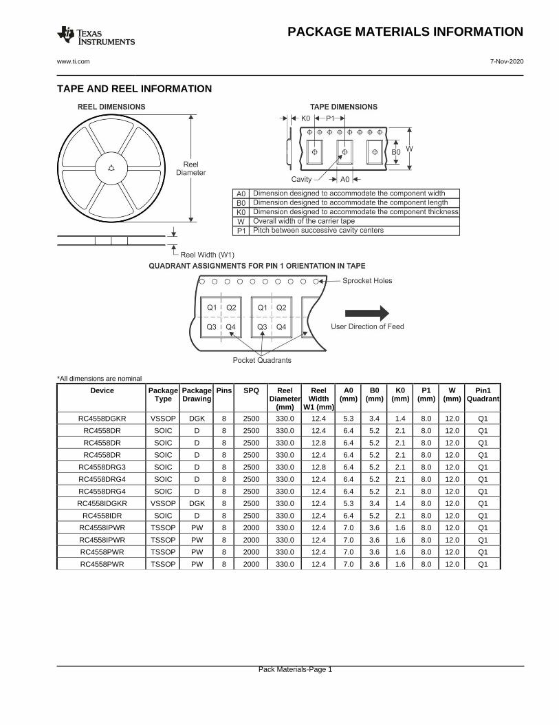
PACKAGE MATERIALS INFORMATION
www.ti.com 7-Nov-2020
TAPE AND REEL INFORMATION
*All dimensions are nominal
Device Package Type
Package Drawing
Pins SPQ Reel Diameter
(mm)
Reel Width
W1 (mm)
A0 (mm)
B0 (mm)
K0 (mm)
P1 (mm)
W (mm)
Pin1 Quadrant
RC4558DGKR VSSOP DGK 8 2500 330.0 12.4 5.3 3.4 1.4 8.0 12.0 Q1
RC4558DR SOIC D 8 2500 330.0 12.4 6.4 5.2 2.1 8.0 12.0 Q1
RC4558DR SOIC D 8 2500 330.0 12.8 6.4 5.2 2.1 8.0 12.0 Q1
RC4558DR SOIC D 8 2500 330.0 12.4 6.4 5.2 2.1 8.0 12.0 Q1
RC4558DRG3 SOIC D 8 2500 330.0 12.8 6.4 5.2 2.1 8.0 12.0 Q1
RC4558DRG4 SOIC D 8 2500 330.0 12.4 6.4 5.2 2.1 8.0 12.0 Q1
RC4558DRG4 SOIC D 8 2500 330.0 12.4 6.4 5.2 2.1 8.0 12.0 Q1
RC4558IDGKR VSSOP DGK 8 2500 330.0 12.4 5.3 3.4 1.4 8.0 12.0 Q1
RC4558IDR SOIC D 8 2500 330.0 12.4 6.4 5.2 2.1 8.0 12.0 Q1
RC4558IPWR TSSOP PW 8 2000 330.0 12.4 7.0 3.6 1.6 8.0 12.0 Q1
RC4558IPWR TSSOP PW 8 2000 330.0 12.4 7.0 3.6 1.6 8.0 12.0 Q1
RC4558PWR TSSOP PW 8 2000 330.0 12.4 7.0 3.6 1.6 8.0 12.0 Q1
RC4558PWR TSSOP PW 8 2000 330.0 12.4 7.0 3.6 1.6 8.0 12.0 Q1
Pack Materials-Page 1
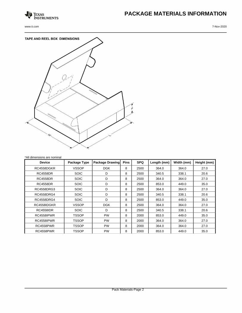
PACKAGE MATERIALS INFORMATION
www.ti.com 7-Nov-2020
*All dimensions are nominal
Device Package Type Package Drawing Pins SPQ Length (mm) Width (mm) Height (mm)
RC4558DGKR VSSOP DGK 8 2500 364.0 364.0 27.0
RC4558DR SOIC D 8 2500 340.5 338.1 20.6
RC4558DR SOIC D 8 2500 364.0 364.0 27.0
RC4558DR SOIC D 8 2500 853.0 449.0 35.0
RC4558DRG3 SOIC D 8 2500 364.0 364.0 27.0
RC4558DRG4 SOIC D 8 2500 340.5 338.1 20.6
RC4558DRG4 SOIC D 8 2500 853.0 449.0 35.0
RC4558IDGKR VSSOP DGK 8 2500 364.0 364.0 27.0
RC4558IDR SOIC D 8 2500 340.5 338.1 20.6
RC4558IPWR TSSOP PW 8 2000 853.0 449.0 35.0
RC4558IPWR TSSOP PW 8 2000 364.0 364.0 27.0
RC4558PWR TSSOP PW 8 2000 364.0 364.0 27.0
RC4558PWR TSSOP PW 8 2000 853.0 449.0 35.0
Pack Materials-Page 2
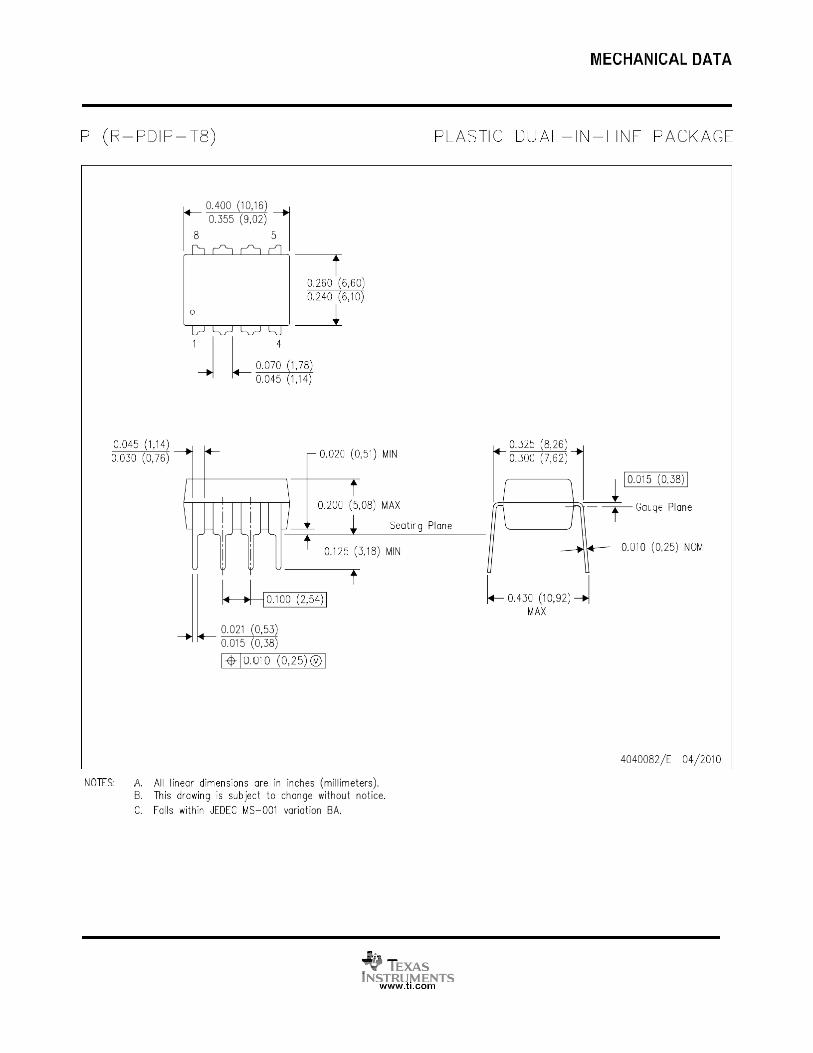
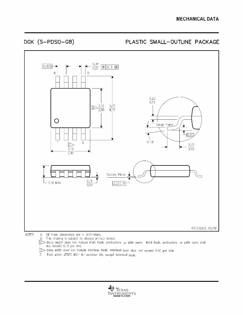


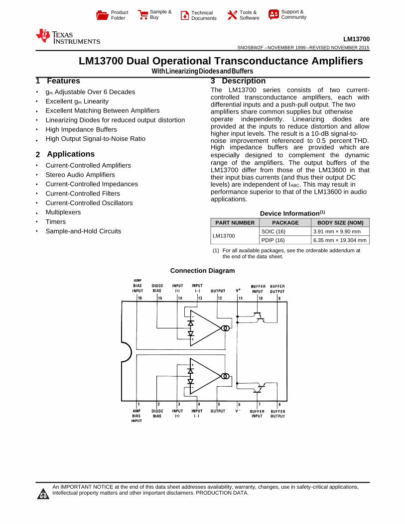
Product Folder
Sample & Buy
Technical Documents
Tools & Software
Support & Community
LM13700
SNOSBW2F – NOVEMBER 1999 – REVISED NOVEMBER 2015
LM13700 Dual Operational Transconductance Amplifiers With Linearizing Diodes and Buffers
1 Features 3 Description
• gm Adjustable Over 6 Decades
• Excellent gm Linearity
The LM13700 series consists of two current- controlled transconductance amplifiers, each with differential inputs and a push-pull output. The two
• Excellent Matching Between Amplifiers amplifiers share common supplies but otherwise
• Linearizing Diodes for reduced output distortion
• High Impedance Buffers
operate independently. Linearizing diodes are provided at the inputs to reduce distortion and allow higher input levels. The result is a 10-dB signal-to-
• High Output Signal-to-Noise Ratio noise improvement referenced to 0.5 percent THD. High impedance buffers are provided which are
2 Applications especially designed to complement the dynamic
• Current-Controlled Amplifiers
• Stereo Audio Amplifiers
range of the amplifiers. The output buffers of the LM13700 differ from those of the LM13600 in that their input bias currents (and thus their output DC
• Current-Controlled Impedances levels) are independent of IABC. This may result in
• Current-Controlled Filters
• Current-Controlled Oscillators
performance superior to that of the LM13600 in audio applications.
• Multiplexers Device Information(1)
• Timers
• Sample-and-Hold Circuits
(1) For all available packages, see the orderable addendum at the end of the data sheet.
Connection Diagram
An IMPORTANT NOTICE at the end of this data sheet addresses availability, warranty, changes, use in safety-critical applications, intellectual property matters and other important disclaimers. PRODUCTION DATA.
PART NUMBER PACKAGE BODY SIZE (NOM)
LM13700 SOIC (16) 3.91 mm × 9.90 mm
PDIP (16) 6.35 mm × 19.304 mm
LM13700
SNOSBW2F – NOVEMBER 1999 – REVISED NOVEMBER 2015 www.ti.com
96 Submit Documentation Feedback Copyright © 1999–2015, Texas Instruments Incorporated
Product Folder Links: LM13700
Table of Contents
1 Features .................................................................. 1
2 Applications............................................................ 1
3 Description ............................................................. 1
4 Revision History ..................................................... 2
5 Pin Configuration and Functions .......................... 3
6 Specifications ......................................................... 4
6.1 Absolute Maximum Ratings...................................... 4
6.2 Recommended Operating Conditions ....................... 4
6.3 Thermal Information ................................................. 4
6.4 Electrical Characteristics .......................................... 5
6.5 Typical Characteristics ............................................. 6
7 Detailed Description .............................................. 9
7.1 Overview 9
7.2 Functional Block Diagram ........................................ 9
7.3 Feature Description .................................................. 9
7.4 Device Functional Modes ....................................... 10
8 Application and Implementation ......................... 11
8.1 Application Information ........................................... 11
8.2 Typical Application ................................................. 11
8.3 System Examples ................................................... 12
9 Power Supply Recommendations ...................... 29
10 Layout ................................................................... 29
10.1 Layout Guidelines ................................................ 29
10.2 Layout Example ................................................... 29
11 Device and Documentation Support .................. 30
11.1 Community Resources ......................................... 30
11.2 Trademarks .......................................................... 30
11.3 Electrostatic Discharge Caution............................ 30
11.4 Glossary 30
12 Mechanical, Packaging, and Orderable Information ........................................................... 30
4 Revision History NOTE: Page numbers for previous revisions may differ from page numbers in the current version.
Changes from Revision E (March 2013) to Revision F Page
• Added ESD Ratings table, Feature Description section, Device Functional Modes, Application and Implementation
section, Power Supply Recommendations section, Layout section, Device and Documentation Support section, and
Mechanical, Packaging, and Orderable Information section. ................................................................................................. 1
• Removed soldering information in Absolute Maximum Ratings table ..................................................................................... 4
Changes from Revision D (March 2013) to Revision E Page
• Changed layout of National Data Sheet to TI format ............................................................................................................ 27
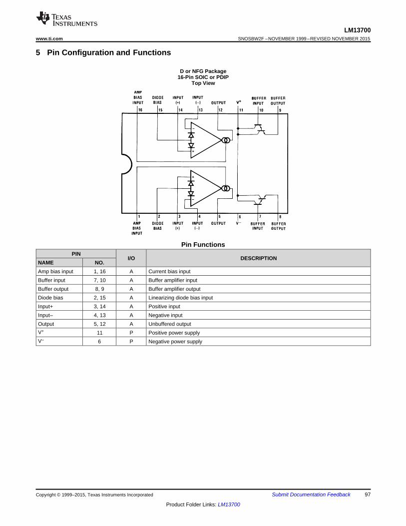
LM13700
SNOSBW2F – NOVEMBER 1999 – REVISED NOVEMBER 2015 www.ti.com
Submit Documentation Feedback 97 Copyright © 1999–2015, Texas Instruments Incorporated
Product Folder Links: LM13700
5 Pin Configuration and Functions
D or NFG Package 16-Pin SOIC or PDIP
Top View
Pin Functions
PIN
I/O
DESCRIPTION NAME NO.
Amp bias input 1, 16 A Current bias input
Buffer input 7, 10 A Buffer amplifier input
Buffer output 8, 9 A Buffer amplifier output
Diode bias 2, 15 A Linearizing diode bias input
Input+ 3, 14 A Positive input
Input– 4, 13 A Negative input
Output 5, 12 A Unbuffered output
V+ 11 P Positive power supply
V– 6 P Negative power supply
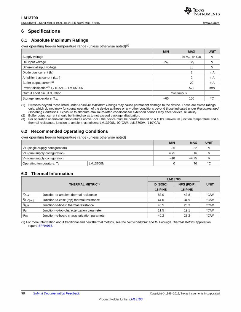
LM13700
SNOSBW2F – NOVEMBER 1999 – REVISED NOVEMBER 2015 www.ti.com
98 Submit Documentation Feedback Copyright © 1999–2015, Texas Instruments Incorporated
Product Folder Links: LM13700
6 Specifications
6.1 Absolute Maximum Ratings
over operating free-air temperature range (unless otherwise noted)(1)
MIN MAX UNIT
Supply voltage 36 VDC or ±18 V
DC input voltage +VS −VS V
Differential input voltage ±5 V
Diode bias current (ID) 2 mA
Amplifier bias current (IABC) 2 mA
Buffer output current(2) 20 mA
Power dissipation(3) TA = 25°C – LM13700N 570 mW
Output short circuit duration Continuous
Storage temperature, Tstg −65 150 °C
(1) Stresses beyond those listed under Absolute Maximum Ratings may cause permanent damage to the device. These are stress ratings only, which do not imply functional operation of the device at these or any other conditions beyond those indicated under Recommended Operating Conditions. Exposure to absolute-maximum-rated conditions for extended periods may affect device reliability.
(2) Buffer output current should be limited so as to not exceed package dissipation. (3) For operation at ambient temperatures above 25°C, the device must be derated based on a 150°C maximum junction temperature and a
thermal resistance, junction to ambient, as follows: LM13700N, 90°C/W; LM13700M, 110°C/W.
6.2 Recommended Operating Conditions
over operating free-air temperature range (unless otherwise noted)
MIN MAX UNIT
V+ (single-supply configuration) 9.5 32 V
V+ (dual-supply configuration) 4.75 16 V
V– (dual-supply configuration) –16 –4.75 V
Operating temperature, TA LM13700N 0 70 °C
6.3 Thermal Information
THERMAL METRIC(1)
LM13700 UNIT D (SOIC) NFG (PDIP)
16 PINS 16 PINS
RθJA Junction-to-ambient thermal resistance 83.0 43.8 °C/W
RθJC(top) Junction-to-case (top) thermal resistance 44.0 34.9 °C/W
RθJB Junction-to-board thermal resistance 40.5 28.3 °C/W
ψJT Junction-to-top characterization parameter 11.5 19.1 °C/W
ψJB Junction-to-board characterization parameter 40.2 28.2 °C/W
(1) For more information about traditional and new thermal metrics, see the Semiconductor and IC Package Thermal Metrics application report, SPRA953.

LM13700
SNOSBW2F – NOVEMBER 1999 – REVISED NOVEMBER 2015 www.ti.com
Submit Documentation Feedback 99 Copyright © 1999–2015, Texas Instruments Incorporated
Product Folder Links: LM13700
6.4 Electrical Characteristics
These specifications apply for VS = ±15 V, TA = 25°C, amplifier bias current (IABC) = 500 μA, pins 2 and 15 open unless
otherwise specified. The inputs to the buffers are grounded and outputs are open.
PARAMETER TEST CONDITIONS MIN TYP MAX UNIT
Input offset voltage (VOS) Over specified temperature range 0.4 4
mV IABC = 5 μA 0.3 4
VOS including diodes Diode bias current (ID) = 500 μA 0.5 5 mV
Input offset change 5 μA ≤ IABC ≤ 500 μA 0.1 3 mV
Input offset current 0.1 0.6 μA
Input bias current 0.4 5
μA Over specified temperature range 1 8
Forward transconductance (gm) 6700 9600 13000
μS Over specified temperature range 5400
gm tracking 0.3 dB
Peak output current
RL = 0, IABC = 5 μA 5 μA RL = 0, IABC = 500 μA 350 500 650
RL = 0, Over Specified Temp Range 300
Supply current IABC = 500 μA, both channels 2.6 mA
CMRR 80 110 dB
Common-mode range ±12 ±13.5 V
Crosstalk Referred to input(1) 20 Hz < f < 20 kHz
100 dB
Differential input current IABC = 0, input = ±4 V 0.02 100 nA
Leakage current IABC = 0 (refer to test circuit) 0.2 100 nA
Input resistance 10 26 kΩ
Open-loop bandwidth 2 MHz
Slew rate Unity gain compensated 50 V/μs
Buffer input current See (1) 0.5 2 μA
Peak buffer output voltage See (1) 10 V
PEAK OUTPUT VOLTAGE
Positive RL = ∞, 5 μA ≤ IABC ≤ 500 μA 12 14.2 V
Negative RL = ∞, 5 μA ≤ IABC ≤ 500 μA −12 −14.4 V
VOS SENSITIVITY
Positive ΔVOS/ΔV+ 20 150 μV/V
Negative ΔVOS/ΔV− 20 150 μV/V
(1) These specifications apply for VS = ±15 V, IABC = 500 μA, ROUT = 5-kΩ connected from the buffer output to −VS and the input of the buffer is connected to the transconductance amplifier output.

LM13700
SNOSBW2F – NOVEMBER 1999 – REVISED NOVEMBER 2015 www.ti.com
100 Submit Documentation Feedback Copyright © 1999–2015, Texas Instruments Incorporated
Product Folder Links: LM13700
6.5 Typical Characteristics
Figure 1. Input Offset Voltage
Figure 2. Input Offset Current
Figure 3. Input Bias Current
Figure 4. Peak Output Current
Figure 5. Peak Output Voltage and Common Mode Range
Figure 6. Leakage Current

LM13700
SNOSBW2F – NOVEMBER 1999 – REVISED NOVEMBER 2015 www.ti.com
Submit Documentation Feedback 101 Copyright © 1999–2015, Texas Instruments Incorporated
Product Folder Links: LM13700
Typical Characteristics (continued)
Figure 7. Input Leakage
Figure 8. Transconductance
Figure 9. Input Resistance
Figure 10. Amplifier Bias Voltage vs. Amplifier Bias Current
Figure 11. Input and Output Capacitance
Figure 12. Output Resistance

LM13700
SNOSBW2F – NOVEMBER 1999 – REVISED NOVEMBER 2015 www.ti.com
102 Submit Documentation Feedback Copyright © 1999–2015, Texas Instruments Incorporated
Product Folder Links: LM13700
Typical Characteristics (continued)
Figure 13. Distortion vs. Differential Input Voltage
Figure 14. Voltage vs. Amplifier Bias Current
Figure 15. Output Noise vs Frequency
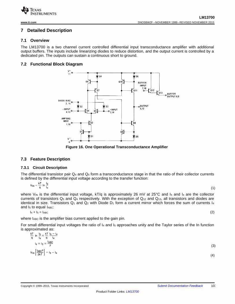
LM13700
SNOSBW2F – NOVEMBER 1999 – REVISED NOVEMBER 2015 www.ti.com
Submit Documentation Feedback 103 Copyright © 1999–2015, Texas Instruments Incorporated
Product Folder Links: LM13700
7 Detailed Description 7.1 Overview
The LM13700 is a two channel current controlled differential input transconductance amplifier with additional output buffers. The inputs include linearizing diodes to reduce distortion, and the output current is controlled by a dedicated pin. The outputs can sustain a continuous short to ground.
7.2 Functional Block Diagram
Figure 16. One Operational Transconductance Amplifier
7.3 Feature Description
7.3.1 Circuit Description
The differential transistor pair Q4 and Q5 form a transconductance stage in that the ratio of their collector currents is defined by the differential input voltage according to the transfer function:
(1)
where VIN is the differential input voltage, kT/q is approximately 26 mV at 25°C and I5 and I4 are the collector currents of transistors Q5 and Q4 respectively. With the exception of Q12 and Q13, all transistors and diodes are identical in size. Transistors Q1 and Q2 with Diode D1 form a current mirror which forces the sum of currents I4 and I5 to equal IABC:
I4 + I5 = IABC (2)
where IABC is the amplifier bias current applied to the gain pin.
For small differential input voltages the ratio of I4 and I5 approaches unity and the Taylor series of the In function is approximated as:
(3)
(4)
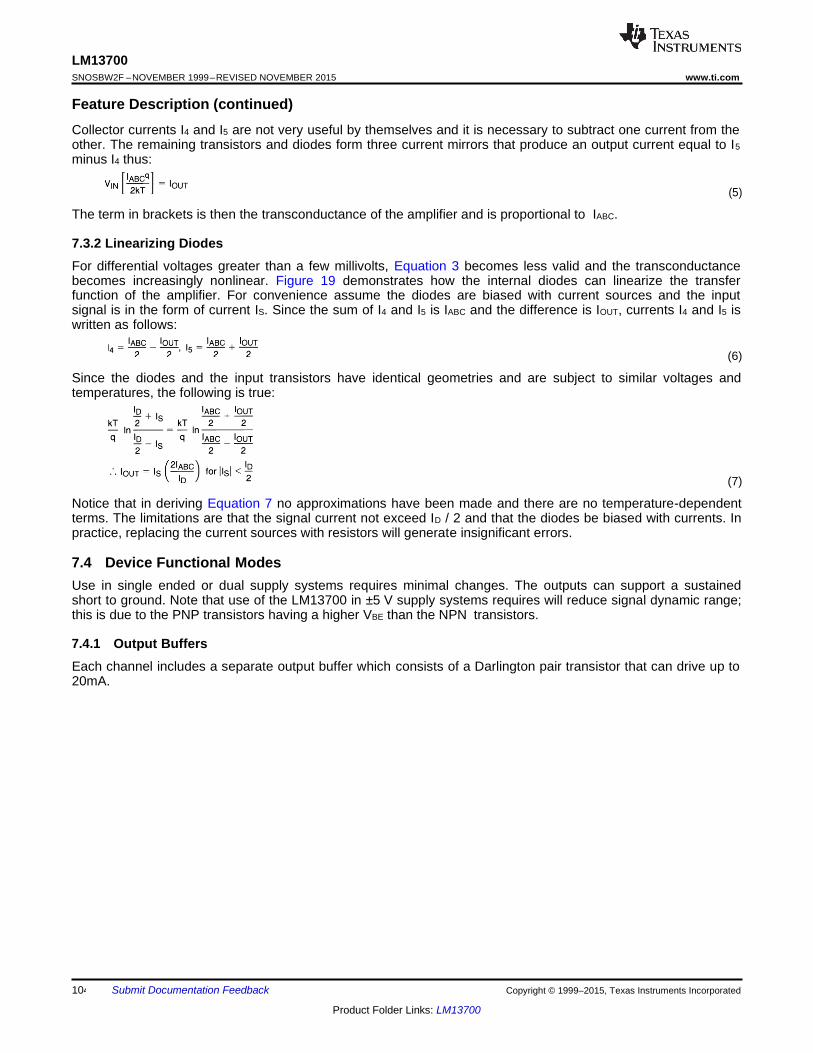
LM13700
SNOSBW2F – NOVEMBER 1999 – REVISED NOVEMBER 2015 www.ti.com
104 Submit Documentation Feedback Copyright © 1999–2015, Texas Instruments Incorporated
Product Folder Links: LM13700
Feature Description (continued)
Collector currents I4 and I5 are not very useful by themselves and it is necessary to subtract one current from the other. The remaining transistors and diodes form three current mirrors that produce an output current equal to I5 minus I4 thus:
(5)
The term in brackets is then the transconductance of the amplifier and is proportional to IABC.
7.3.2 Linearizing Diodes
For differential voltages greater than a few millivolts, Equation 3 becomes less valid and the transconductance becomes increasingly nonlinear. Figure 19 demonstrates how the internal diodes can linearize the transfer function of the amplifier. For convenience assume the diodes are biased with current sources and the input signal is in the form of current IS. Since the sum of I4 and I5 is IABC and the difference is IOUT, currents I4 and I5 is written as follows:
(6)
Since the diodes and the input transistors have identical geometries and are subject to similar voltages and temperatures, the following is true:
(7)
Notice that in deriving Equation 7 no approximations have been made and there are no temperature-dependent terms. The limitations are that the signal current not exceed ID / 2 and that the diodes be biased with currents. In practice, replacing the current sources with resistors will generate insignificant errors.
7.4 Device Functional Modes
Use in single ended or dual supply systems requires minimal changes. The outputs can support a sustained short to ground. Note that use of the LM13700 in ±5 V supply systems requires will reduce signal dynamic range; this is due to the PNP transistors having a higher VBE than the NPN transistors.
7.4.1 Output Buffers
Each channel includes a separate output buffer which consists of a Darlington pair transistor that can drive up to 20mA.
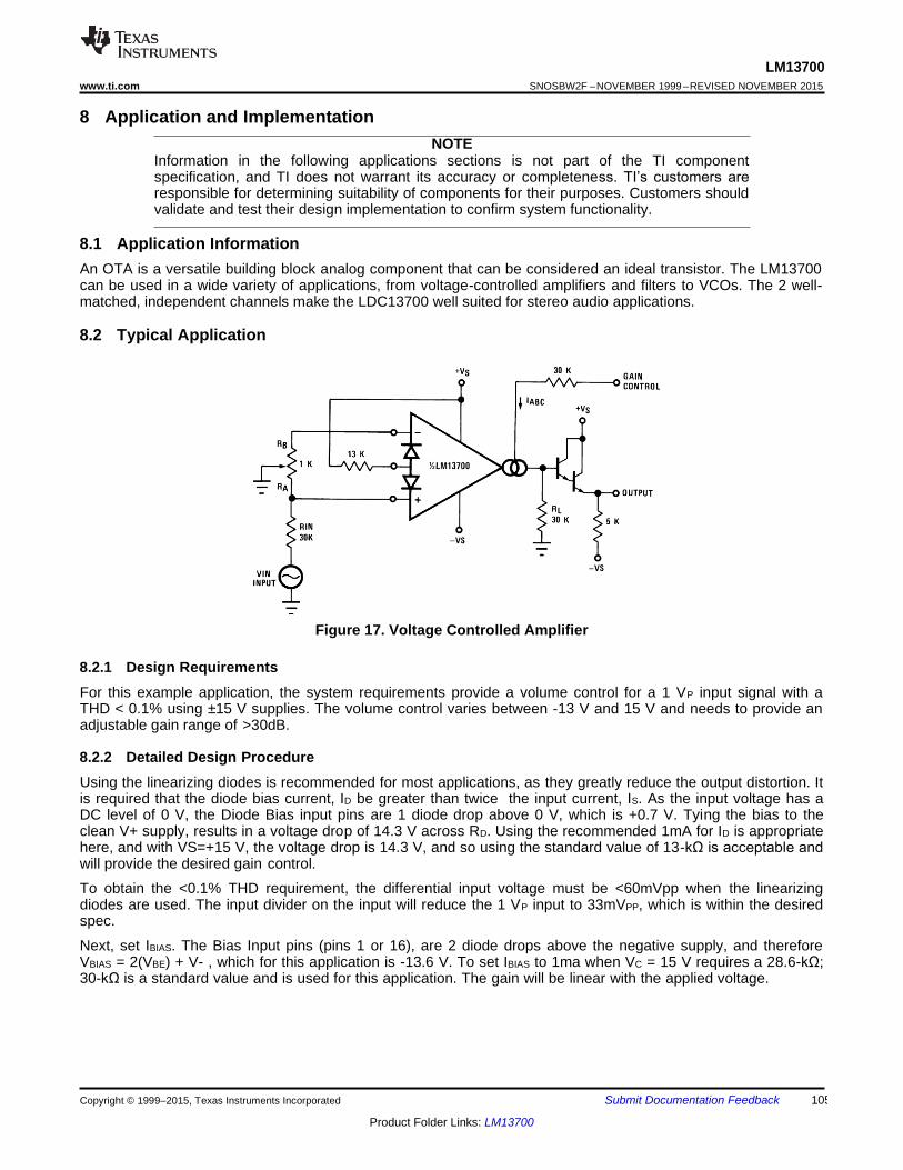
LM13700
SNOSBW2F – NOVEMBER 1999 – REVISED NOVEMBER 2015 www.ti.com
Submit Documentation Feedback 105 Copyright © 1999–2015, Texas Instruments Incorporated
Product Folder Links: LM13700
8 Application and Implementation
NOTE Information in the following applications sections is not part of the TI component specification, and TI does not warrant its accuracy or completeness. TI’s customers are responsible for determining suitability of components for their purposes. Customers should validate and test their design implementation to confirm system functionality.
8.1 Application Information
An OTA is a versatile building block analog component that can be considered an ideal transistor. The LM13700 can be used in a wide variety of applications, from voltage-controlled amplifiers and filters to VCOs. The 2 well- matched, independent channels make the LDC13700 well suited for stereo audio applications.
8.2 Typical Application
Figure 17. Voltage Controlled Amplifier
8.2.1 Design Requirements
For this example application, the system requirements provide a volume control for a 1 VP input signal with a THD < 0.1% using ±15 V supplies. The volume control varies between -13 V and 15 V and needs to provide an adjustable gain range of >30dB.
8.2.2 Detailed Design Procedure
Using the linearizing diodes is recommended for most applications, as they greatly reduce the output distortion. It is required that the diode bias current, ID be greater than twice the input current, IS. As the input voltage has a DC level of 0 V, the Diode Bias input pins are 1 diode drop above 0 V, which is +0.7 V. Tying the bias to the clean V+ supply, results in a voltage drop of 14.3 V across RD. Using the recommended 1mA for ID is appropriate here, and with VS=+15 V, the voltage drop is 14.3 V, and so using the standard value of 13-kΩ is acceptable and will provide the desired gain control.
To obtain the <0.1% THD requirement, the differential input voltage must be <60mVpp when the linearizing diodes are used. The input divider on the input will reduce the 1 VP input to 33mVPP, which is within the desired spec.
Next, set IBIAS. The Bias Input pins (pins 1 or 16), are 2 diode drops above the negative supply, and therefore VBIAS = 2(VBE) + V- , which for this application is -13.6 V. To set IBIAS to 1ma when VC = 15 V requires a 28.6-kΩ; 30-kΩ is a standard value and is used for this application. The gain will be linear with the applied voltage.

LM13700
SNOSBW2F – NOVEMBER 1999 – REVISED NOVEMBER 2015 www.ti.com
106 Submit Documentation Feedback Copyright © 1999–2015, Texas Instruments Incorporated
Product Folder Links: LM13700
Typical Application (continued)
8.2.3 Application Curve
0
-5
-10
-15
-20
-25
-30
-35
-15 -10 -5 0 5 10 15 Control Voltage (V)
D001
Figure 18. Signal Amplitude vs Control Voltage
8.3 System Examples
8.3.1 Voltage-Controlled Amplifiers
Figure 20 shows how the linearizing diodes is used in a voltage-controlled amplifier. To understand the input biasing, it is best to consider the 13-kΩ resistor as a current source and use a Thevenin equivalent circuit as shown in Figure 21. This circuit is similar to Figure 19 and operates the same. The potentiometer in Figure 20 is adjusted to minimize the effects of the control signal at the output.
Figure 19. Linearizing Diodes
For optimum signal-to-noise performance, IABC should be as large as possible as shown by the Output Voltage vs Amplifier Bias Current graph. Larger amplitudes of input signal also improve the S/N ratio. The linearizing diodes help here by allowing larger input signals for the same output distortion as shown by the Distortion vs. Differential Input Voltage graph. S/N may be optimized by adjusting the magnitude of the input signal via R IN (Figure 20) until the output distortion is below the desired level. The output voltage swing can then be set at any level by selecting RL.
Although the noise contribution of the linearizing diodes is negligible relative to the contribution of the amplifier's internal transistors, ID should be as large as possible. This minimizes the dynamic junction resistance of the diodes (re) and maximizes their linearizing action when balanced against RIN. A value of 1 mA is recommended for ID unless the specific application demands otherwise.
Sig
nal A
mplit
ud
e (
dB
)
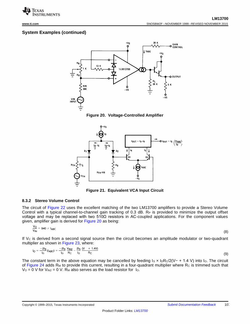
Submit Documentation Feedback 107 Copyright © 1999–2015, Texas Instruments Incorporated
Product Folder Links: LM13700
LM13700
SNOSBW2F – NOVEMBER 1999 – REVISED NOVEMBER 2015 www.ti.com
System Examples (continued)
Figure 20. Voltage-Controlled Amplifier
Figure 21. Equivalent VCA Input Circuit
8.3.2 Stereo Volume Control
The circuit of Figure 22 uses the excellent matching of the two LM13700 amplifiers to provide a Stereo Volume Control with a typical channel-to-channel gain tracking of 0.3 dB. RP is provided to minimize the output offset voltage and may be replaced with two 510Ω resistors in AC-coupled applications. For the component values given, amplifier gain is derived for Figure 20 as being:
(8)
If VC is derived from a second signal source then the circuit becomes an amplitude modulator or two-quadrant multiplier as shown in Figure 23, where:
(9)
The constant term in the above equation may be cancelled by feeding IS × IDRC/2(V− + 1.4 V) into IO. The circuit of Figure 24 adds RM to provide this current, resulting in a four-quadrant multiplier where RC is trimmed such that VO = 0 V for VIN2 = 0 V. RM also serves as the load resistor for IO.
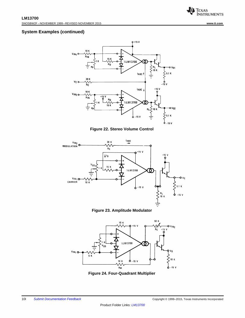
108 Submit Documentation Feedback Copyright © 1999–2015, Texas Instruments Incorporated
Product Folder Links: LM13700
LM13700
SNOSBW2F – NOVEMBER 1999 – REVISED NOVEMBER 2015 www.ti.com
System Examples (continued)
Figure 22. Stereo Volume Control
Figure 23. Amplitude Modulator
Figure 24. Four-Quadrant Multiplier
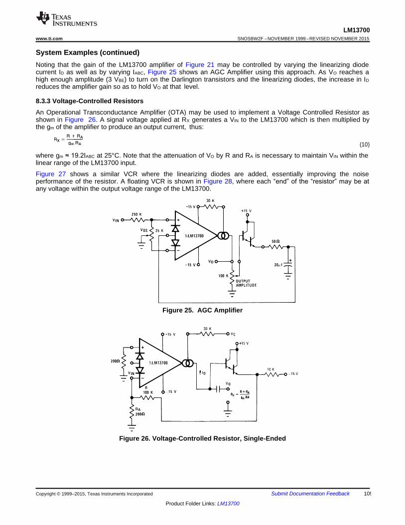
Submit Documentation Feedback 109 Copyright © 1999–2015, Texas Instruments Incorporated
Product Folder Links: LM13700
LM13700
SNOSBW2F – NOVEMBER 1999 – REVISED NOVEMBER 2015 www.ti.com
System Examples (continued)
Noting that the gain of the LM13700 amplifier of Figure 21 may be controlled by varying the linearizing diode current ID as well as by varying IABC, Figure 25 shows an AGC Amplifier using this approach. As VO reaches a high enough amplitude (3 VBE) to turn on the Darlington transistors and the linearizing diodes, the increase in ID reduces the amplifier gain so as to hold VO at that level.
8.3.3 Voltage-Controlled Resistors
An Operational Transconductance Amplifier (OTA) may be used to implement a Voltage Controlled Resistor as shown in Figure 26. A signal voltage applied at RX generates a VIN to the LM13700 which is then multiplied by the gm of the amplifier to produce an output current, thus:
(10)
where gm ≈ 19.2IABC at 25°C. Note that the attenuation of VO by R and RA is necessary to maintain VIN within the linear range of the LM13700 input.
Figure 27 shows a similar VCR where the linearizing diodes are added, essentially improving the noise performance of the resistor. A floating VCR is shown in Figure 28, where each “end” of the “resistor” may be at any voltage within the output voltage range of the LM13700.
Figure 25. AGC Amplifier
Figure 26. Voltage-Controlled Resistor, Single-Ended
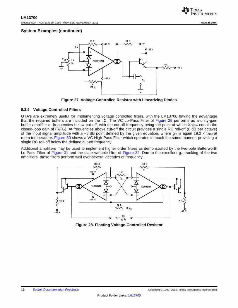
110 Submit Documentation Feedback Copyright © 1999–2015, Texas Instruments Incorporated
Product Folder Links: LM13700
LM13700
SNOSBW2F – NOVEMBER 1999 – REVISED NOVEMBER 2015 www.ti.com
System Examples (continued)
Figure 27. Voltage-Controlled Resistor with Linearizing Diodes
8.3.4 Voltage-Controlled Filters
OTA's are extremely useful for implementing voltage controlled filters, with the LM13700 having the advantage that the required buffers are included on the I.C. The VC Lo-Pass Filter of Figure 29 performs as a unity-gain buffer amplifier at frequencies below cut-off, with the cut-off frequency being the point at which XC/gm equals the closed-loop gain of (R/RA). At frequencies above cut-off the circuit provides a single RC roll-off (6 dB per octave) of the input signal amplitude with a −3 dB point defined by the given equation, where gm is again 19.2 × IABC at room temperature. Figure 30 shows a VC High-Pass Filter which operates in much the same manner, providing a single RC roll-off below the defined cut-off frequency.
Additional amplifiers may be used to implement higher order filters as demonstrated by the two-pole Butterworth Lo-Pass Filter of Figure 31 and the state variable filter of Figure 32. Due to the excellent gm tracking of the two amplifiers, these filters perform well over several decades of frequency.
Figure 28. Floating Voltage-Controlled Resistor
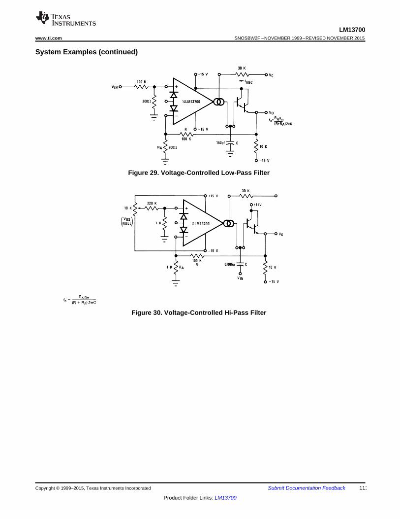
Submit Documentation Feedback 111 Copyright © 1999–2015, Texas Instruments Incorporated
Product Folder Links: LM13700
LM13700
SNOSBW2F – NOVEMBER 1999 – REVISED NOVEMBER 2015 www.ti.com
System Examples (continued)
Figure 29. Voltage-Controlled Low-Pass Filter
Figure 30. Voltage-Controlled Hi-Pass Filter
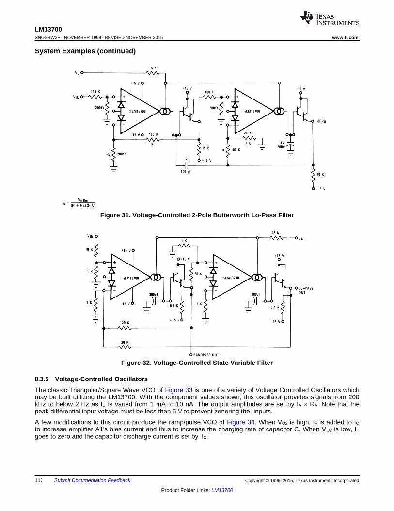
112 Submit Documentation Feedback Copyright © 1999–2015, Texas Instruments Incorporated
Product Folder Links: LM13700
LM13700
SNOSBW2F – NOVEMBER 1999 – REVISED NOVEMBER 2015 www.ti.com
System Examples (continued)
Figure 31. Voltage-Controlled 2-Pole Butterworth Lo-Pass Filter
Figure 32. Voltage-Controlled State Variable Filter
8.3.5 Voltage-Controlled Oscillators
The classic Triangular/Square Wave VCO of Figure 33 is one of a variety of Voltage Controlled Oscillators which may be built utilizing the LM13700. With the component values shown, this oscillator provides signals from 200 kHz to below 2 Hz as IC is varied from 1 mA to 10 nA. The output amplitudes are set by IA × RA. Note that the peak differential input voltage must be less than 5 V to prevent zenering the inputs.
A few modifications to this circuit produce the ramp/pulse VCO of Figure 34. When VO2 is high, IF is added to IC to increase amplifier A1's bias current and thus to increase the charging rate of capacitor C. When VO2 is low, IF goes to zero and the capacitor discharge current is set by IC.
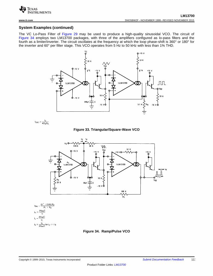
Submit Documentation Feedback 113 Copyright © 1999–2015, Texas Instruments Incorporated
Product Folder Links: LM13700
LM13700
SNOSBW2F – NOVEMBER 1999 – REVISED NOVEMBER 2015 www.ti.com
System Examples (continued)
The VC Lo-Pass Filter of Figure 29 may be used to produce a high-quality sinusoidal VCO. The circuit of Figure 34 employs two LM13700 packages, with three of the amplifiers configured as lo-pass filters and the fourth as a limiter/inverter. The circuit oscillates at the frequency at which the loop phase-shift is 360° or 180° for the inverter and 60° per filter stage. This VCO operates from 5 Hz to 50 kHz with less than 1% THD.
Figure 33. Triangular/Square-Wave VCO
Figure 34. Ramp/Pulse VCO
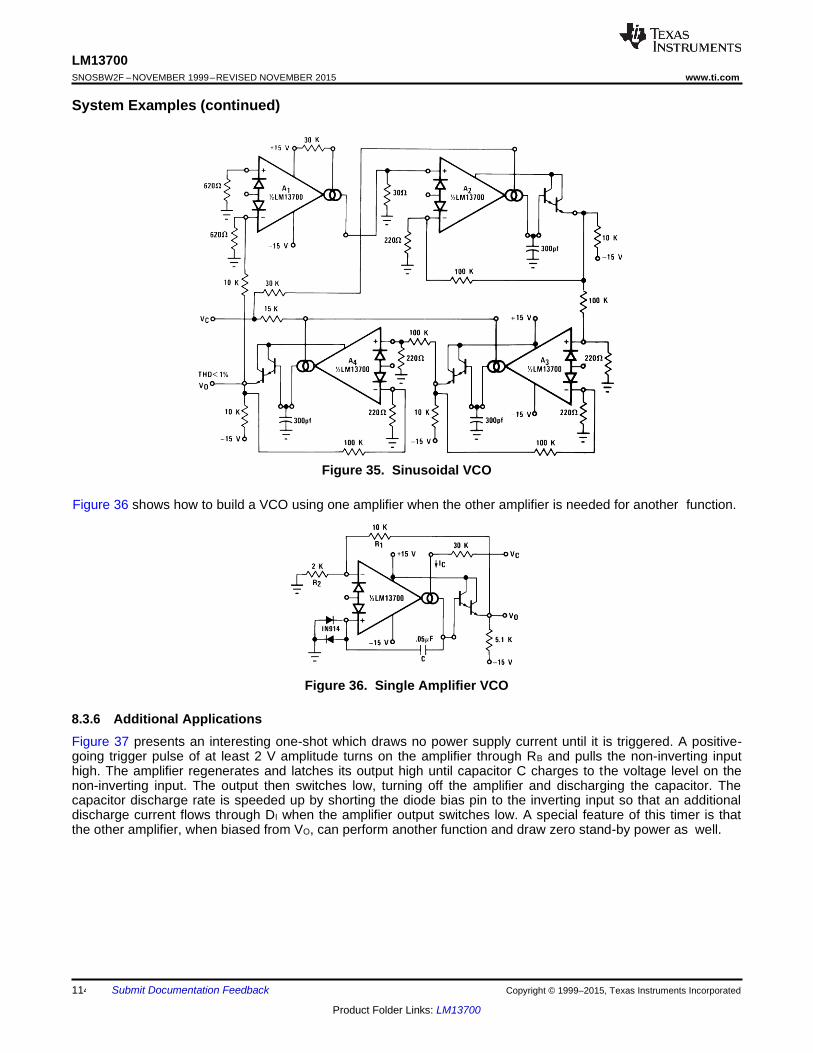
114 Submit Documentation Feedback Copyright © 1999–2015, Texas Instruments Incorporated
Product Folder Links: LM13700
LM13700
SNOSBW2F – NOVEMBER 1999 – REVISED NOVEMBER 2015 www.ti.com
System Examples (continued)
Figure 35. Sinusoidal VCO
Figure 36 shows how to build a VCO using one amplifier when the other amplifier is needed for another function.
Figure 36. Single Amplifier VCO
8.3.6 Additional Applications
Figure 37 presents an interesting one-shot which draws no power supply current until it is triggered. A positive- going trigger pulse of at least 2 V amplitude turns on the amplifier through RB and pulls the non-inverting input high. The amplifier regenerates and latches its output high until capacitor C charges to the voltage level on the non-inverting input. The output then switches low, turning off the amplifier and discharging the capacitor. The capacitor discharge rate is speeded up by shorting the diode bias pin to the inverting input so that an additional discharge current flows through DI when the amplifier output switches low. A special feature of this timer is that the other amplifier, when biased from VO, can perform another function and draw zero stand-by power as well.
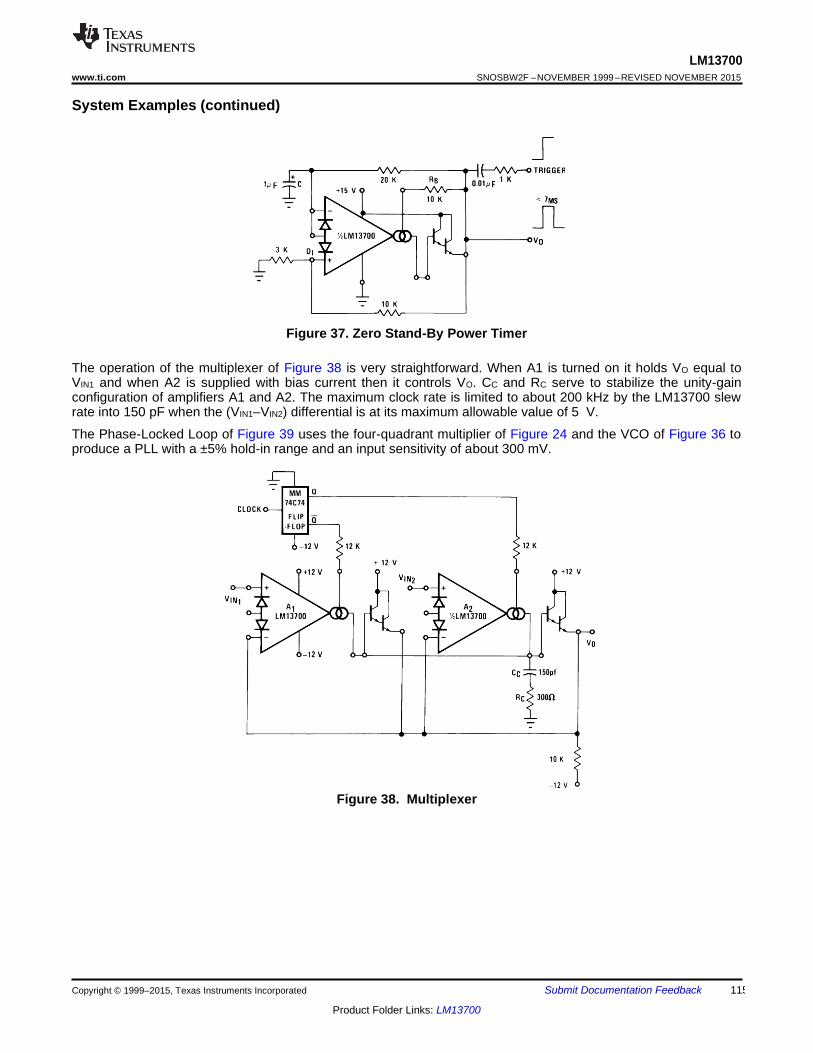
Submit Documentation Feedback 115 Copyright © 1999–2015, Texas Instruments Incorporated
Product Folder Links: LM13700
LM13700
SNOSBW2F – NOVEMBER 1999 – REVISED NOVEMBER 2015 www.ti.com
System Examples (continued)
Figure 37. Zero Stand-By Power Timer
The operation of the multiplexer of Figure 38 is very straightforward. When A1 is turned on it holds VO equal to VIN1 and when A2 is supplied with bias current then it controls VO. CC and RC serve to stabilize the unity-gain configuration of amplifiers A1 and A2. The maximum clock rate is limited to about 200 kHz by the LM13700 slew rate into 150 pF when the (VIN1–VIN2) differential is at its maximum allowable value of 5 V.
The Phase-Locked Loop of Figure 39 uses the four-quadrant multiplier of Figure 24 and the VCO of Figure 36 to produce a PLL with a ±5% hold-in range and an input sensitivity of about 300 mV.
Figure 38. Multiplexer
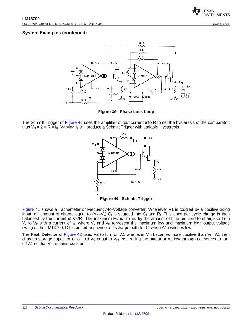
116 Submit Documentation Feedback Copyright © 1999–2015, Texas Instruments Incorporated
Product Folder Links: LM13700
LM13700
SNOSBW2F – NOVEMBER 1999 – REVISED NOVEMBER 2015 www.ti.com
System Examples (continued)
Figure 39. Phase Lock Loop
The Schmitt Trigger of Figure 40 uses the amplifier output current into R to set the hysteresis of the comparator; thus VH = 2 × R × IB. Varying IB will produce a Schmitt Trigger with variable hysteresis.
Figure 40. Schmitt Trigger
Figure 41 shows a Tachometer or Frequency-to-Voltage converter. Whenever A1 is toggled by a positive-going input, an amount of charge equal to (VH–VL) Ct is sourced into Cf and Rt. This once per cycle charge is then balanced by the current of VO/Rt. The maximum FIN is limited by the amount of time required to charge Ct from VL to VH with a current of IB, where VL and VH represent the maximum low and maximum high output voltage swing of the LM13700. D1 is added to provide a discharge path for Ct when A1 switches low.
The Peak Detector of Figure 42 uses A2 to turn on A1 whenever VIN becomes more positive than VO. A1 then charges storage capacitor C to hold VO equal to VIN PK. Pulling the output of A2 low through D1 serves to turn off A1 so that VO remains constant.
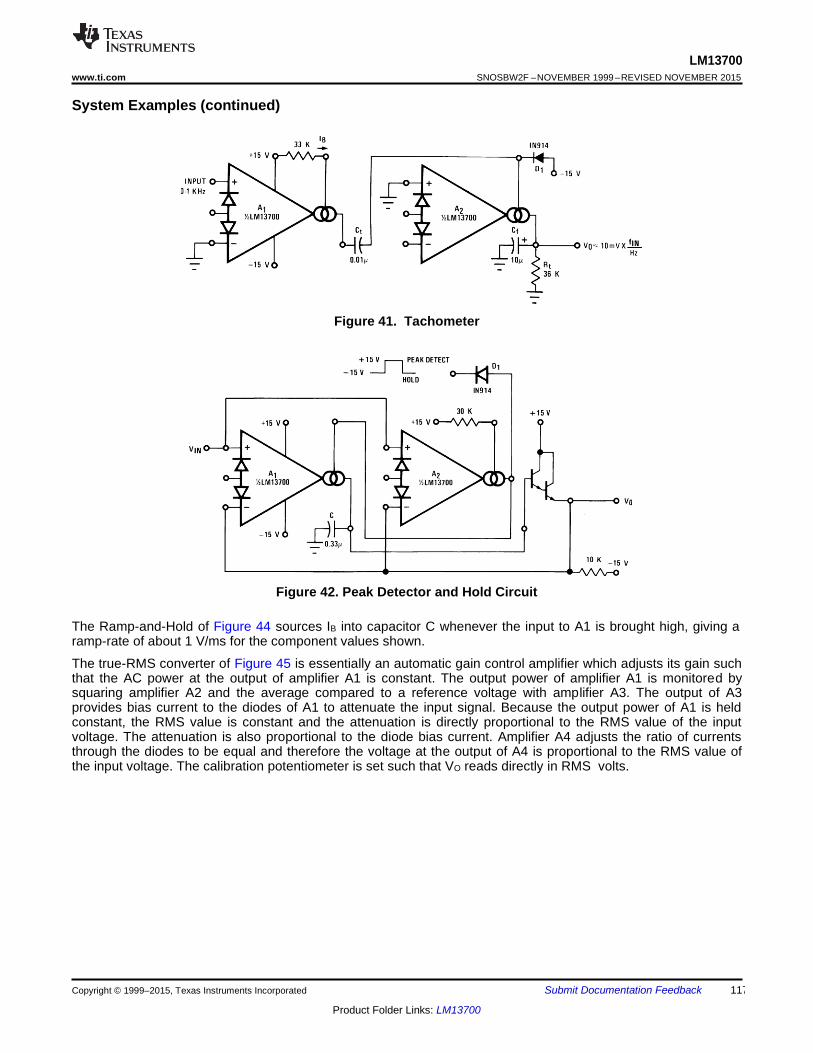
Submit Documentation Feedback 117 Copyright © 1999–2015, Texas Instruments Incorporated
Product Folder Links: LM13700
LM13700
SNOSBW2F – NOVEMBER 1999 – REVISED NOVEMBER 2015 www.ti.com
System Examples (continued)
Figure 41. Tachometer
Figure 42. Peak Detector and Hold Circuit
The Ramp-and-Hold of Figure 44 sources IB into capacitor C whenever the input to A1 is brought high, giving a ramp-rate of about 1 V/ms for the component values shown.
The true-RMS converter of Figure 45 is essentially an automatic gain control amplifier which adjusts its gain such that the AC power at the output of amplifier A1 is constant. The output power of amplifier A1 is monitored by squaring amplifier A2 and the average compared to a reference voltage with amplifier A3. The output of A3 provides bias current to the diodes of A1 to attenuate the input signal. Because the output power of A1 is held constant, the RMS value is constant and the attenuation is directly proportional to the RMS value of the input voltage. The attenuation is also proportional to the diode bias current. Amplifier A4 adjusts the ratio of currents through the diodes to be equal and therefore the voltage at the output of A4 is proportional to the RMS value of the input voltage. The calibration potentiometer is set such that VO reads directly in RMS volts.
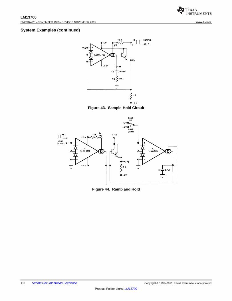
118 Submit Documentation Feedback Copyright © 1999–2015, Texas Instruments Incorporated
Product Folder Links: LM13700
LM13700
SNOSBW2F – NOVEMBER 1999 – REVISED NOVEMBER 2015 www.ti.com
System Examples (continued)
Figure 43. Sample-Hold Circuit
Figure 44. Ramp and Hold
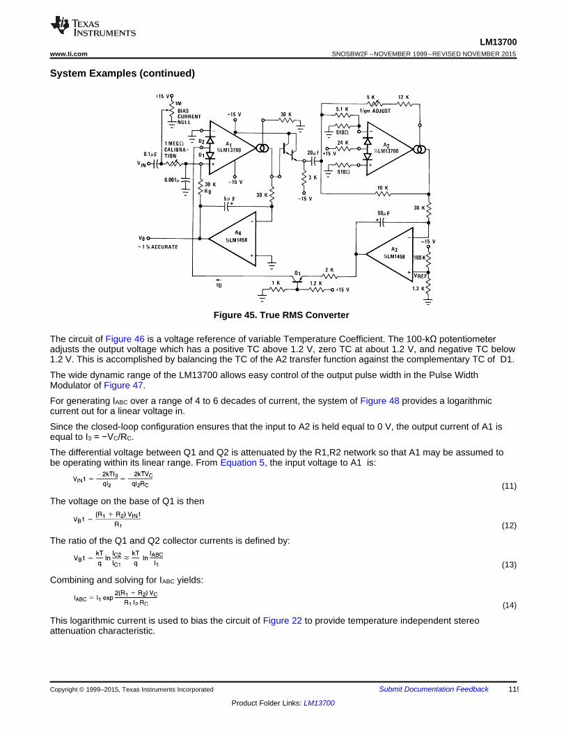
Submit Documentation Feedback 119 Copyright © 1999–2015, Texas Instruments Incorporated
Product Folder Links: LM13700
LM13700
SNOSBW2F – NOVEMBER 1999 – REVISED NOVEMBER 2015 www.ti.com
System Examples (continued)
Figure 45. True RMS Converter
The circuit of Figure 46 is a voltage reference of variable Temperature Coefficient. The 100-kΩ potentiometer adjusts the output voltage which has a positive TC above 1.2 V, zero TC at about 1.2 V, and negative TC below 1.2 V. This is accomplished by balancing the TC of the A2 transfer function against the complementary TC of D1.
The wide dynamic range of the LM13700 allows easy control of the output pulse width in the Pulse Width Modulator of Figure 47.
For generating IABC over a range of 4 to 6 decades of current, the system of Figure 48 provides a logarithmic current out for a linear voltage in.
Since the closed-loop configuration ensures that the input to A2 is held equal to 0 V, the output current of A1 is equal to I3 = −VC/RC.
The differential voltage between Q1 and Q2 is attenuated by the R1,R2 network so that A1 may be assumed to be operating within its linear range. From Equation 5, the input voltage to A1 is:
The voltage on the base of Q1 is then
The ratio of the Q1 and Q2 collector currents is defined by:
Combining and solving for IABC yields:
(11)
(12)
(13)
(14)
This logarithmic current is used to bias the circuit of Figure 22 to provide temperature independent stereo attenuation characteristic.
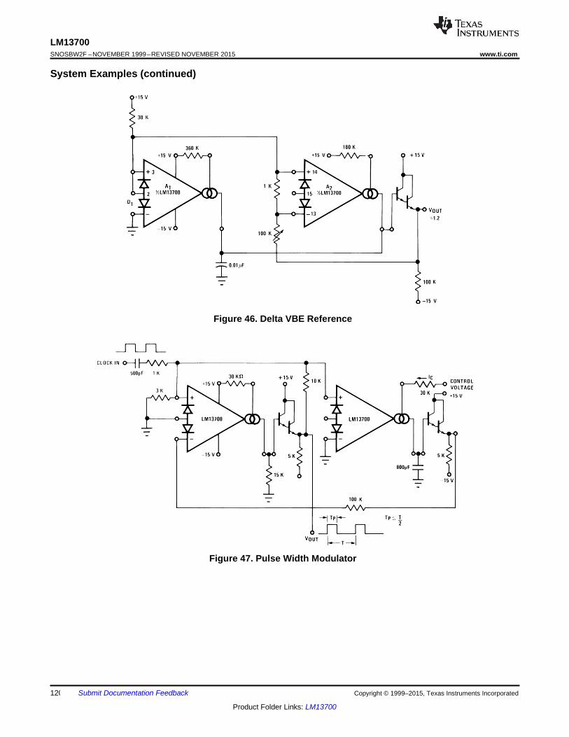
120 Submit Documentation Feedback Copyright © 1999–2015, Texas Instruments Incorporated
Product Folder Links: LM13700
LM13700
SNOSBW2F – NOVEMBER 1999 – REVISED NOVEMBER 2015 www.ti.com
System Examples (continued)
Figure 46. Delta VBE Reference
Figure 47. Pulse Width Modulator
Submit Documentation Feedback 121 Copyright © 1999–2015, Texas Instruments Incorporated
Product Folder Links: LM13700
LM13700
SNOSBW2F – NOVEMBER 1999 – REVISED NOVEMBER 2015 www.ti.com
System Examples (continued)
Figure 48. Logarithmic Current Source
Figure 49. Unity Gain Follower
Figure 50. Leakage Current Test Circuit
122 Submit Documentation Feedback Copyright © 1999–2015, Texas Instruments Incorporated
Product Folder Links: LM13700
LM13700
SNOSBW2F – NOVEMBER 1999 – REVISED NOVEMBER 2015 www.ti.com
System Examples (continued)
Figure 51. Differential Input Current Test Circuit
Submit Documentation Feedback 123 Copyright © 1999–2015, Texas Instruments Incorporated
Product Folder Links: LM13700
LM13700
SNOSBW2F – NOVEMBER 1999 – REVISED NOVEMBER 2015 www.ti.com
9 Power Supply Recommendations
The LM13700 can operate with either a single-ended supply or a dual supplies. The supplies should be low impedance sources with sufficient bypassing. Use of low-ESR sufficiently rated voltage ceramic capacitors is recommended. When bypassing dual supply configurations, the supply bypass capacitors should couple to ground.
10 Layout
10.1 Layout Guidelines
Place supply bypass capacitors as close to the appropriate supply pins as possible. When multiple bypass capacitors are used, the smallest value capacitor should be closest to the supply pin.
Use of a ground plane to minimize ground impedance and provide constant signal impedance is recommended. Avoid routing signal traces over any gaps in the ground plane.
Feedback components and passives should be placed close to the device pins to minimize parasitic impedances. When using capacitors to limit bandwidth, the capacitor should be closer to the device pin than any ballasting or gain resistors.
10.2 Layout Example
Figure 52. Layout Recommendation
1 2 V+ IBIAS1
2 1 ILIN2 V+
2 1 V+ IBIAS1
1 2 IBIAS2 V+
1 IBIAS1 16 IBIAS2
1 2 VIN1 VIN1+
2 1 VIN2+ VIN2
2 ILIN1 15 ILIN2
GND GND
2 1 GND VIN1+ 3 VIN1+
1 2 14 VIN2+ VIN2 VIN2+ GND GND GND
2 1 GND VIN1– 4VIN1– 13 VIN2–
1 2 VIN2– GND
1 GND
2 VIN1–
1 GND
2 DARL1
2 1 5 DARL1 12 DARL2 DARL2DARL2 GND
1 VIN2–
1 GND
2 1 VOUT1
VOUT1 VOUT1
1 GND
2 V–
v– 6 V– 11 V+ v+ 2 1 V+ GND VOUT2
VOUT2 VOUT2
1 2
GND V– v+ 7 DARL1 10 DARL2
v+ GND
V– V+
VOUT1 8 VOUT1 9 VOUT2
DA
RL
1
ILIN
1
ILIN
2
DA
RL
2
124 Submit Documentation Feedback Copyright © 1999–2015, Texas Instruments Incorporated
Product Folder Links: LM13700
LM13700
SNOSBW2F – NOVEMBER 1999 – REVISED NOVEMBER 2015 www.ti.com
11 Device and Documentation Support 11.1 Community Resources
The following links connect to TI community resources. Linked contents are provided "AS IS" by the respective contributors. They do not constitute TI specifications and do not necessarily reflect TI's views; see TI's Terms of Use.
TI E2E™ Online Community TI's Engineer-to-Engineer (E2E) Community. Created to foster collaboration among engineers. At e2e.ti.com, you can ask questions, share knowledge, explore ideas and help solve problems with fellow engineers.
Design Support TI's Design Support Quickly find helpful E2E forums along with design support tools and contact information for technical support.
11.2 Trademarks
E2E is a trademark of Texas Instruments. All other trademarks are the property of their respective owners.
11.3 Electrostatic Discharge Caution
These devices have limited built-in ESD protection. The leads should be shorted together or the device placed in conductive foam during storage or handling to prevent electrostatic damage to the MOS gates.
11.4 Glossary
SLYZ022 — TI Glossary.
This glossary lists and explains terms, acronyms, and definitions.
12 Mechanical, Packaging, and Orderable Information
The following pages include mechanical, packaging, and orderable information. This information is the most current data available for the designated devices. This data is subject to change without notice and revision of this document. For browser-based versions of this data sheet, refer to the left-hand navigation.
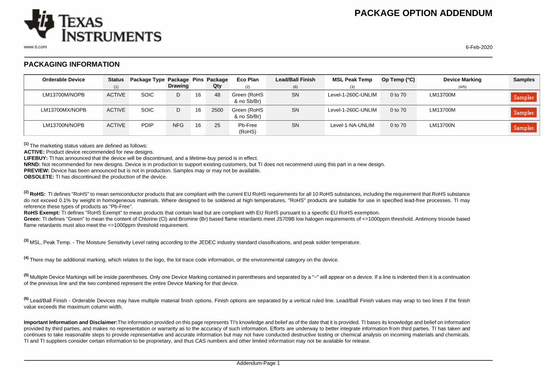
PACKAGE OPTION ADDENDUM
www.ti.com 6-Feb-2020
PACKAGING INFORMATION
Orderable Device Status
(1)
Package Type Package
Drawing
Pins Package
Qty
Eco Plan
(2)
Lead/Ball Finish
(6)
MSL Peak Temp
(3)
Op Temp (°C) Device Marking
(4/5)
Samples
LM13700M/NOPB ACTIVE SOIC D 16 48 Green (RoHS
& no Sb/Br)
SN Level-1-260C-UNLIM 0 to 70 LM13700M
LM13700MX/NOPB ACTIVE SOIC D 16 2500 Green (RoHS
& no Sb/Br)
SN Level-1-260C-UNLIM 0 to 70 LM13700M
LM13700N/NOPB ACTIVE PDIP NFG 16 25 Pb-Free
(RoHS)
SN Level-1-NA-UNLIM 0 to 70 LM13700N
(1) The marketing status values are defined as follows:
ACTIVE: Product device recommended for new designs.
LIFEBUY: TI has announced that the device will be discontinued, and a lifetime-buy period is in effect.
NRND: Not recommended for new designs. Device is in production to support existing customers, but TI does not recommend using this part in a new design.
PREVIEW: Device has been announced but is not in production. Samples may or may not be available.
OBSOLETE: TI has discontinued the production of the device.
(2)
RoHS: TI defines "RoHS" to mean semiconductor products that are compliant with the current EU RoHS requirements for all 10 RoHS substances, including the requirement that RoHS substance
do not exceed 0.1% by weight in homogeneous materials. Where designed to be soldered at high temperatures, "RoHS" products are suitable for use in specified lead-free processes. TI may
reference these types of products as "Pb-Free".
RoHS Exempt: TI defines "RoHS Exempt" to mean products that contain lead but are compliant with EU RoHS pursuant to a specific EU RoHS exemption.
Green: TI defines "Green" to mean the content of Chlorine (Cl) and Bromine (Br) based flame retardants meet JS709B low halogen requirements of <=1000ppm threshold. Antimony trioxide based
flame retardants must also meet the <=1000ppm threshold requirement.
(3)
MSL, Peak Temp. - The Moisture Sensitivity Level rating according to the JEDEC industry standard classifications, and peak solder temperature.
(4)
There may be additional marking, which relates to the logo, the lot trace code information, or the environmental category on the device.
(5)
Multiple Device Markings will be inside parentheses. Only one Device Marking contained in parentheses and separated by a "~" will appear on a device. If a line is indented then it is a continuation
of the previous line and the two combined represent the entire Device Marking for that device.
(6)
Lead/Ball Finish - Orderable Devices may have multiple material finish options. Finish options are separated by a vertical ruled line. Lead/Ball Finish values may wrap to two lines if the finish
value exceeds the maximum column width.
Important Information and Disclaimer:The information provided on this page represents TI's knowledge and belief as of the date that it is provided. TI bases its knowledge and belief on information
provided by third parties, and makes no representation or warranty as to the accuracy of such information. Efforts are underway to better integrate information from third parties. TI has taken and
continues to take reasonable steps to provide representative and accurate information but may not have conducted destructive testing or chemical analysis on incoming materials and chemicals.
TI and TI suppliers consider certain information to be proprietary, and thus CAS numbers and other limited information may not be available for release.
Addendum-Page 1
PACKAGE OPTION ADDENDUM
www.ti.com 6-Feb-2020
In no event shall TI's liability arising out of such information exceed the total purchase price of the TI part(s) at issue in this document sold by TI to Customer on an annual basis.
Addendum-Page 2
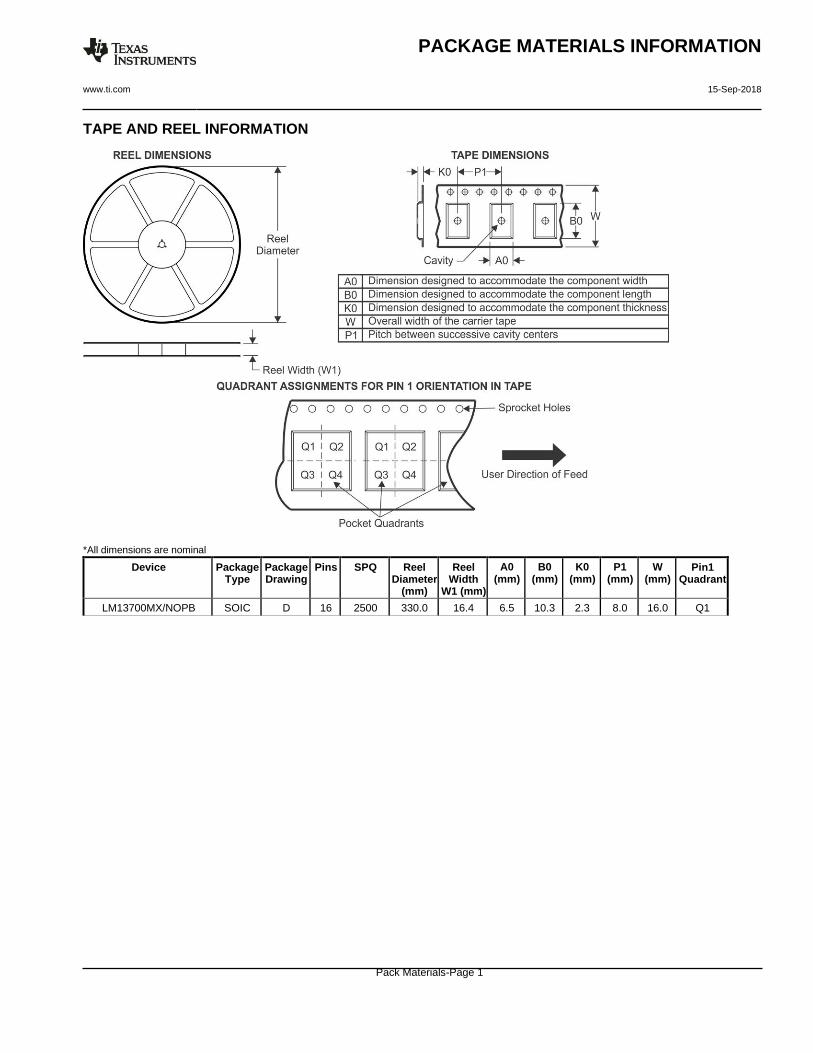
PACKAGE MATERIALS INFORMATION
www.ti.com 15-Sep-2018
TAPE AND REEL INFORMATION
*All dimensions are nominal
Device Package Type
Package Drawing
Pins SPQ Reel Diameter
(mm)
Reel Width
W1 (mm)
A0 (mm)
B0 (mm)
K0 (mm)
P1 (mm)
W (mm)
Pin1 Quadrant
LM13700MX/NOPB SOIC D 16 2500 330.0 16.4 6.5 10.3 2.3 8.0 16.0 Q1
Pack Materials-Page 1
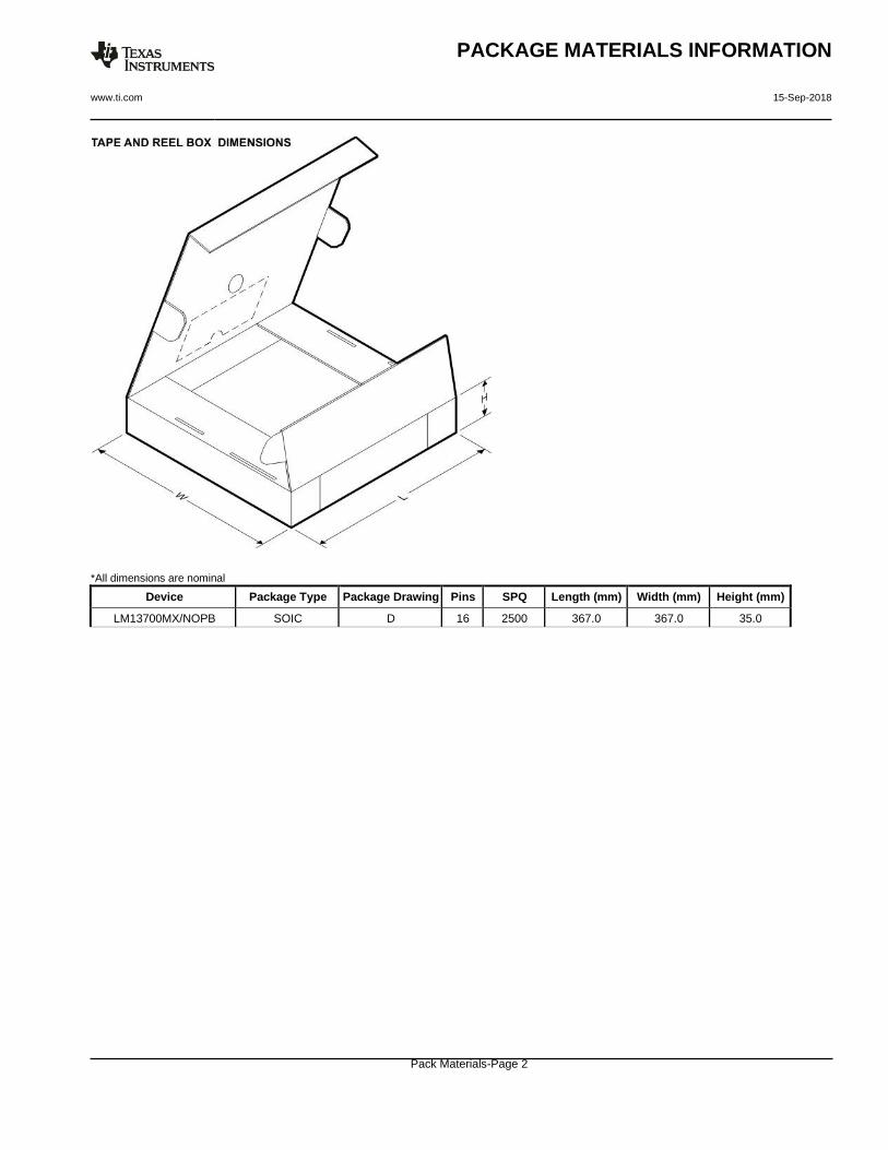
PACKAGE MATERIALS INFORMATION
www.ti.com 15-Sep-2018
*All dimensions are nominal
Device Package Type Package Drawing Pins SPQ Length (mm) Width (mm) Height (mm)
LM13700MX/NOPB SOIC D 16 2500 367.0 367.0 35.0
Pack Materials-Page 2
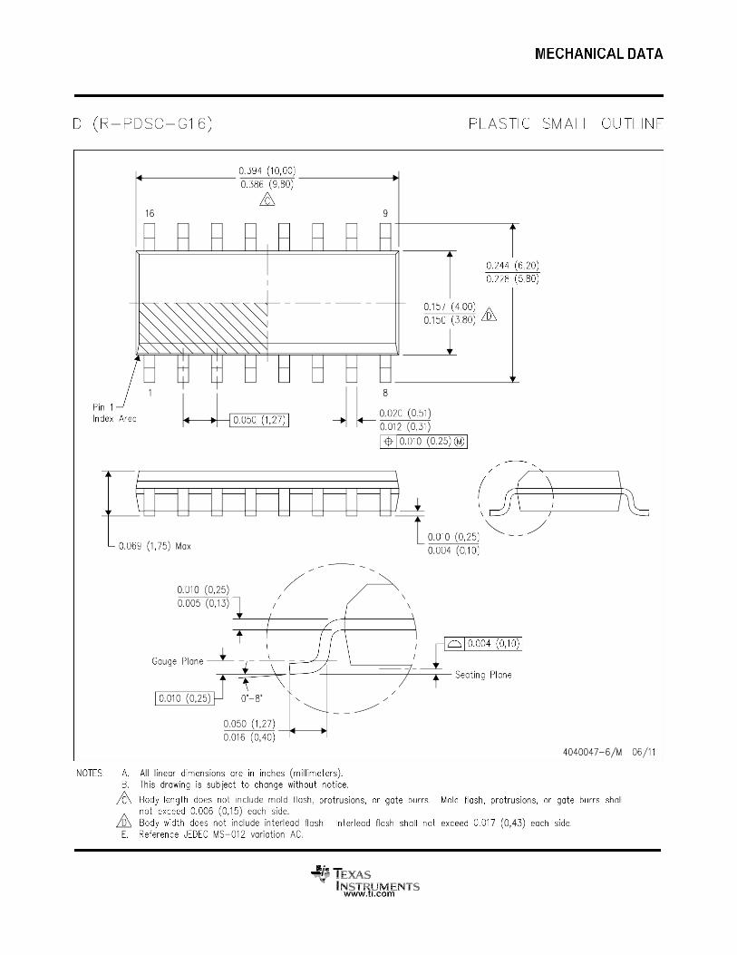

IMPORTANT NOTICE AND DISCLAIMER
TI PROVIDES TECHNICAL AND RELIABILITY DATA (INCLUDING DATASHEETS), DESIGN RESOURCES (INCLUDING REFERENCE DESIGNS), APPLICATION OR OTHER DESIGN ADVICE, WEB TOOLS, SAFETY INFORMATION, AND OTHER RESOURCES “AS IS” AND WITH ALL FAULTS, AND DISCLAIMS ALL WARRANTIES, EXPRESS AND IMPLIED, INCLUDING WITHOUT LIMITATION ANY IMPLIED WARRANTIES OF MERCHANTABILITY, FITNESS FOR A PARTICULAR PURPOSE OR NON-INFRINGEMENT OF THIRD PARTY INTELLECTUAL PROPERTY RIGHTS.
These resources are intended for skilled developers designing with TI products. You are solely responsible for (1) selecting the appropriate TI products for your application, (2) designing, validating and testing your application, and (3) ensuring your application meets applicable standards, and any other safety, security, or other requirements. These resources are subject to change without notice. TI grants you permission to use these resources only for development of an application that uses the TI products described in the resource. Other reproduction and display of these resources is prohibited. No license is granted to any other TI intellectual property right or to any third party intellectual property right. TI disclaims responsibility for, and you will fully indemnify TI and its representatives against, any claims, damages, costs, losses, and liabilities arising out of your use of these resources.
TI’s products are provided subject to TI’s Terms of Sale (www.ti.com/legal/termsofsale.html) or other applicable terms available either on ti.com or provided in conjunction with such TI products. TI’s provision of these resources does not expand or otherwise alter TI’s applicable warranties or warranty disclaimers for TI products.
Mailing Address: Texas Instruments, Post Office Box 655303, Dallas, Texas 75265
Copyright © 2020, Texas Instruments Incorporated
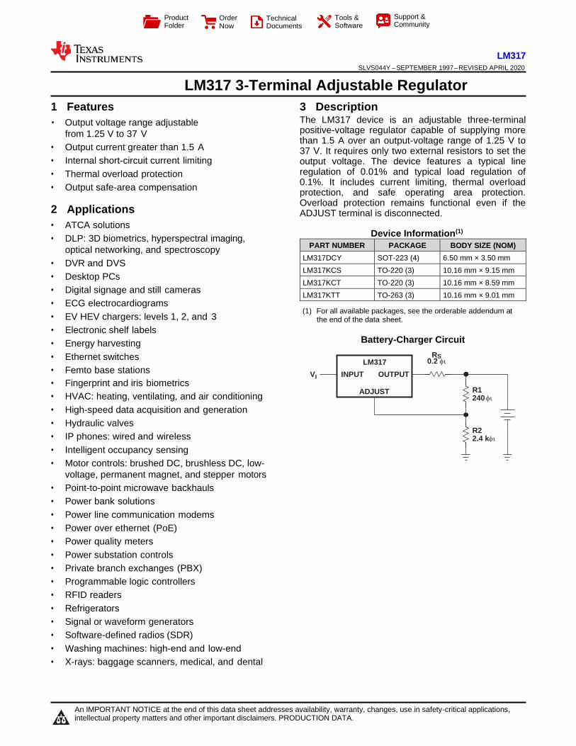
R1 240
R2 2.4 k
LM317
INPUT OUTPUT
ADJUST
Product Folder
Order Now
Technical Documents
Tools & Software
Support & Community
1 Features
LM317
SLVS044Y – SEPTEMBER 1997 – REVISED APRIL 2020
LM317 3-Terminal Adjustable Regulator
3 Description
• Output voltage range adjustable
from 1.25 V to 37 V
• Output current greater than 1.5 A
• Internal short-circuit current limiting
• Thermal overload protection
• Output safe-area compensation
2 Applications
• ATCA solutions
• DLP: 3D biometrics, hyperspectral imaging,
optical networking, and spectroscopy
• DVR and DVS
• Desktop PCs
• Digital signage and still cameras
• ECG electrocardiograms
• EV HEV chargers: levels 1, 2, and 3
• Electronic shelf labels
• Energy harvesting
• Ethernet switches
The LM317 device is an adjustable three-terminal positive-voltage regulator capable of supplying more than 1.5 A over an output-voltage range of 1.25 V to 37 V. It requires only two external resistors to set the output voltage. The device features a typical line regulation of 0.01% and typical load regulation of 0.1%. It includes current limiting, thermal overload protection, and safe operating area protection. Overload protection remains functional even if the ADJUST terminal is disconnected.
Device Information(1)
PART NUMBER PACKAGE BODY SIZE (NOM)
LM317DCY SOT-223 (4) 6.50 mm × 3.50 mm
LM317KCS TO-220 (3) 10.16 mm × 9.15 mm
LM317KCT TO-220 (3) 10.16 mm × 8.59 mm
LM317KTT TO-263 (3) 10.16 mm × 9.01 mm
(1) For all available packages, see the orderable addendum at the end of the data sheet.
Battery-Charger Circuit
RS 0.2
• Femto base stations VI
• Fingerprint and iris biometrics
• HVAC: heating, ventilating, and air conditioning
• High-speed data acquisition and generation
• Hydraulic valves
• IP phones: wired and wireless
• Intelligent occupancy sensing
• Motor controls: brushed DC, brushless DC, low-
voltage, permanent magnet, and stepper motors
• Point-to-point microwave backhauls
• Power bank solutions
• Power line communication modems
• Power over ethernet (PoE)
• Power quality meters
• Power substation controls
• Private branch exchanges (PBX)
• Programmable logic controllers
• RFID readers
• Refrigerators
• Signal or waveform generators
• Software-defined radios (SDR)
• Washing machines: high-end and low-end
• X-rays: baggage scanners, medical, and dental
An IMPORTANT NOTICE at the end of this data sheet addresses availability, warranty, changes, use in safety-critical applications, intellectual property matters and other important disclaimers. PRODUCTION DATA.
LM317
SLVS044Y – SEPTEMBER 1997 – REVISED APRIL 2020 www.ti.com
Submit Documentation Feedback 133 Copyright © 1997–2020, Texas Instruments Incorporated
Product Folder Links: LM317
Table of Contents
1 Features .................................................................. 1
2 Applications ........................................................... 1
3 Description ............................................................. 1
4 Revision History ..................................................... 2
5 Device Comparison Table ..................................... 3
6 Pin Configuration and Functions.......................... 4
7 Specifications ......................................................... 5
7.1 Absolute Maximum Ratings ..................................... 5
7.2 ESD Ratings ............................................................ 5
7.3 Recommended Operating Conditions ....................... 5
7.4 Thermal Information ................................................. 5
7.5 Electrical Characteristics .......................................... 6
7.6 Typical Characteristics ............................................. 7
8 Detailed Description .............................................. 9
8.1 Overview 9
8.2 Functional Block Diagram ........................................ 9
8.3 Feature Description .................................................. 9
8.4 Device Functional Modes ....................................... 10
9 Application and Implementation ......................... 11
9.1 Application Information ........................................... 11
9.2 Typical Application ................................................. 11
9.3 System Examples ................................................... 12
10 Power Supply Recommendations ...................... 18
11 Layout................................................................... 18
11.1 Layout Guidelines ................................................ 18
11.2 Layout Example ................................................... 18
12 Device and Documentation Support .................. 19
12.1 Receiving Notification of Documentation Updates 19
12.2 Support Resources ............................................... 19
12.3 Trademarks .......................................................... 19
12.4 Electrostatic Discharge Caution ........................... 19
12.5 Glossary 19
13 Mechanical, Packaging, and Orderable Information ........................................................... 19
4 Revision History
Changes from Revision X (September 2016) to Revision Y Page
• Added Device Comparison Table ........................................................................................................................................... 3
• Changed VIN to IOUT in Load Transient Response figures....................................................................................................... 7
• Added missing caption to second y-axis in second Load Transient Response figure ............................................................ 7
• Changed VOUT and output impedance equations in Battery-Charger Circuit section ............................................................ 14
Changes from Revision W (January 2015) to Revision X Page
• Changed body size dimensions for KCS TO-220 Package on Device information table ....................................................... 1
• Changed body size dimensions for KTT TO-263 Package on Device information table ........................................................ 1
• Changed VO Output Voltage max value from 7 to 37 on Recommended Operating Conditions table ................................... 5
• Added min value to IO Output Current in Recommended Operating Conditions table ............................................................ 5
• Changed values in the Thermal Information table to align with JEDEC standards ................................................................ 5
• Added KCT package data to Thermal Information table ......................................................................................................... 5
• Deleted Section 9.3.6 "Adjusting Multiple On-Card Regulators with a Single Control" ......................................................... 14
• Updated Adjustsable 4-A Regulator Circuit graphic ............................................................................................................. 16
• Added Receiving Notification of Documentation Updates section and Community Resources section ............................... 19
Changes from Revision V (February 2013) to Revision W Page
• Added Applications, Device Information table, Pin Functions table, ESD Ratings table, Thermal Information table,
Feature Description section, Device Functional Modes, Application and Implementation section, Power Supply
Recommendations section, Layout section, Device and Documentation Support section, and Mechanical,
Packaging, and Orderable Information section. ..................................................................................................................... 1
• Deleted Ordering Information table. ....................................................................................................................................... 1
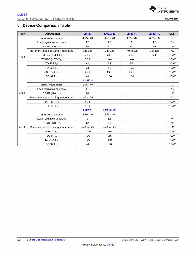
LM317
SLVS044Y – SEPTEMBER 1997 – REVISED APRIL 2020 www.ti.com
134 Submit Documentation Feedback Copyright © 1997–2020, Texas Instruments Incorporated
Product Folder Links: LM317
5 Device Comparison Table
IOUT PARAMETER LM317 LM317-N LM317A LM317HV UNIT
1.5 A
Input voltage range 4.25 - 40 4.25 - 40 4.25 - 40 4.25 - 60 V
Load regulation accuracy 1.5 1.5 1 1.5 %
PSRR (120 Hz) 64 80 80 65 dB
Recommended operating temperature 0 to 125 0 to 125 –40 to 125 0 to 125 °C
TO-220 (NDE) TJA 23.5 23.2 23.3 23 °C/W
TO-200 (KCT) TJA 37.9 N/A N/A °C/W
TO-252 TJA N/A 54 54 °C/W
TO-263 TJA 38 41 N/A °C/W
SOT-223 TJA 66.8 59.6 59.6 °C/W
TO-92 TJA N/A 186 186 °C/W
0.5 A
LM317M
Input voltage range 3.75 - 40 V
Load regulation accuracy 1.5 %
PSRR (120 Hz) 80 dB
Recommended operating temperature -40 - 125 °C
SOT-223 TJA 60.2 °C/W
TO-252 TJA 56.9 °C/W
0.1 A
LM317L LM317L-N
Input voltage range 3.75 - 40 4.25 - 40 V
Load regulation accuracy 1 1.5 %
PSRR (120 Hz) 62 80 dB
Recommended operating temperature –40 to 125 –40 to 125 °C
SOT-23 TJA 167.8 N/A °C/W
SO-8 TJA N/A 165 °C/W
DSBGA TJA N/A 290 °C/W
TO-92 TJA N/A 180 °C/W
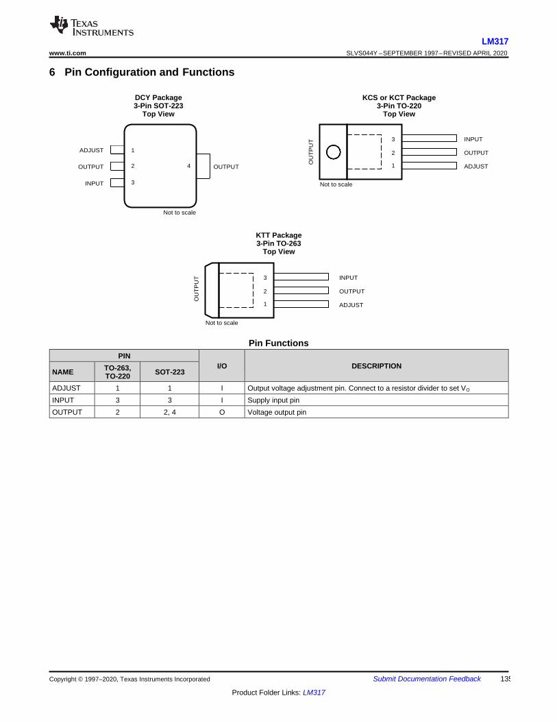
LM317
SLVS044Y – SEPTEMBER 1997 – REVISED APRIL 2020 www.ti.com
Submit Documentation Feedback 135 Copyright © 1997–2020, Texas Instruments Incorporated
Product Folder Links: LM317
1
2 4
3
6 Pin Configuration and Functions
DCY Package 3-Pin SOT-223
Top View
KCS or KCT Package 3-Pin TO-220
Top View
ADJUST
INPUT
OUTPUT
OUTPUT OUTPUT ADJUST
INPUT Not to scale
Not to scale
KTT Package 3-Pin TO-263
Top View
INPUT
OUTPUT
ADJUST
Not to scale
Pin Functions
PIN I/O
DESCRIPTION
NAME TO-263, TO-220
SOT-223
ADJUST 1 1 I Output voltage adjustment pin. Connect to a resistor divider to set VO
INPUT 3 3 I Supply input pin
OUTPUT 2 2, 4 O Voltage output pin
3 2 1
3 2 1
OU
TP
UT
OU
TP
UT
LM317
SLVS044Y – SEPTEMBER 1997 – REVISED APRIL 2020 www.ti.com
136 Submit Documentation Feedback Copyright © 1997–2020, Texas Instruments Incorporated
Product Folder Links: LM317
7 Specifications
7.1 Absolute Maximum Ratings
over virtual junction temperature range (unless otherwise noted)(1)
MIN MAX UNIT
VI – VO Input-to-output differential voltage 40 V
TJ Operating virtual junction temperature 150 °C
Lead temperature 1,6 mm (1/16 in) from case for 10 s 260 °C
Tstg Storage temperature –65 150 °C
(1) Stresses beyond those listed under Absolute Maximum Ratings may cause permanent damage to the device. These are stress ratings only, and functional operation of the device at these or any other conditions beyond those indicated under Recommended Operating Conditions is not implied. Exposure to absolute-maximum-rated conditions for extended periods may affect device reliability.
7.2 ESD Ratings MAX UNIT
V(ESD)
Electrostatic discharge Human body model (HBM), per ANSI/ESDA/JEDEC JS-001(1) 2500
V Charged device model (CDM), per JEDEC specification JESD22-C101(2) 1000
(1) JEDEC document JEP155 states that 500-V HBM allows safe manufacturing with a standard ESD control process. (2) JEDEC document JEP157 states that 250-V CDM allows safe manufacturing with a standard ESD control process.
7.3 Recommended Operating Conditions MIN MAX UNIT
VO Output voltage 1.25 37 V
VI – VO Input-to-output differential voltage 3 40 V
IO Output current 0.01 1.5 A
TJ Operating virtual junction temperature 0 125 °C
7.4 Thermal Information
THERMAL METRIC(1)
LM317
UNIT DCY
(SOT-223) KCS
(TO-220) KCT
(TO-220) KTT
(TO-263)
4 PINS 3 PINS 3 PINS 3 PINS
Rθ(JA) Junction-to-ambient thermal resistance 66.8 23.5 37.9 38.0 °C/W
RθJC(top) Junction-to-case (top) thermal resistance 43.2 15.9 51.1 36.5 °C/W
RθJB Junction-to-board thermal resistance 16.9 7.9 23.2 18.9 °C/W
ψJT Junction-to-top characterization parameter 3.6 3.0 13.0 6.9 °C/W
ψJB Junction-to-board characterization parameter 16.8 7.8 22.8 17.9 °C/W
RθJC(bot) Junction-to-case (bottom) thermal resistance NA 0.1 4.2 1.1 °C/W
(1) For more information about traditional and new thermal metrics, see the Semiconductor and IC package thermal metrics application report.
LM317
SLVS044Y – SEPTEMBER 1997 – REVISED APRIL 2020 www.ti.com
Submit Documentation Feedback 137 Copyright © 1997–2020, Texas Instruments Incorporated
Product Folder Links: LM317
7.5 Electrical Characteristics
over recommended ranges of operating virtual junction temperature (unless otherwise noted)
PARAMETER TEST CONDITIONS(1) MIN TYP MAX UNIT
Line regulation(2) VI – VO = 3 V to 40 V TJ = 25°C 0.01 0.04
%/V TJ = 0°C to 125°C 0.02 0.07
Load regulation
IO = 10 mA to 1500 mA
CADJ (3) = 10 μF,
TJ = 25°C
VO ≤ 5 V 25 mV
VO ≥ 5 V 0.1 0.5 %VO
TJ = 0°C to 125°C VO ≤ 5 V 20 70 mV
VO ≥ 5 V 0.3 1.5 %VO
Thermal regulation 20-ms pulse, TJ = 25°C 0.03 0.07 %VO/W
ADJUST terminal current 50 100 μA
Change in ADJUST terminal current
VI – VO = 2.5 V to 40 V, PD ≤ 20 W, IO = 10 mA to 1500 mA 0.2 5 μA
Reference voltage VI – VO = 3 V to 40 V, PD ≤ 20 W, IO = 10 mA to 1500 mA 1.2 1.25 1.3 V
Output-voltage temperature stability
TJ = 0°C to 125°C 0.7 %VO
Minimum load current to maintain regulation
VI – VO = 40 V
3.5 10 mA
Maximum output current VI – VO ≤ 15 V, PD < PMAX
(4)
1.5 2.2
A VI – VO ≤ 40 V, PD < PMAX
(4), TJ = 25°C 0.15 0.4
RMS output noise voltage (% of VO)
f = 10 Hz to 10 kHz, TJ = 25°C
0.003 %VO
Ripple rejection VO = 10 V,
f = 120 Hz CADJ = 0 μF(3)
57
dB CADJ = 10 μF(3) 62 64
Long-term stability TJ = 25°C 0.3 1 %/1k hr
(1) Unless otherwise noted, the following test conditions apply: |VI – VO| = 5 V and IOMAX = 1.5 A, TJ = 0°C to 125°C. Pulse testing techniques are used to maintain the junction temperature as close to the ambient temperature as possible.
(2) Line regulation is expressed here as the percentage change in output voltage per 1-V change at the input. (3) CADJ is connected between the ADJUST terminal and GND. (4) Maximum power dissipation is a function of TJ(max), θJA, and TA. The maximum allowable power dissipation at any allowable ambient
temperature is PD = (TJ(max) – TA) / θJA. Operating at the absolute maximum TJ of 150°C can affect reliability.
LM317
SLVS044Y – SEPTEMBER 1997 – REVISED APRIL 2020 www.ti.com
138 Submit Documentation Feedback Copyright © 1997–2020, Texas Instruments Incorporated
Product Folder Links: LM317
°C A
A
A
A
A
A
A
A
OUT
A
V = V
7.6 Typical Characteristics
10.01
10.005
T = 25°C
T = –40°C
1.4
1.2
1
T = –40°C
10
9.995
9.99
T = 125°C
0.8
0.6
0.4
0.2
T = 25°C
T = 125°C
9.985
9.98
V = 10 V Nom
0
-0.2
-0.4
OUT REF
IOUT – A IOUT – A
Figure 1. Load Regulation Figure 2. Load Regulation
0
-0.5
-1
-1.5
-2
-2.5
-3
-3.5
-4
-4.5
-5
11
10.8
10.6
10.4
10.2
10
9.8
9.6
9.4
9.2
9
0
-0.5
-1
-1.5
-2
-2.5
-3
-3.5
-4
-4.5
-5
11
10.8
10.6
10.4
10.2
10
9.8
9.6
9.4
9.2
9
Time – µs Time – µs
Figure 3. Load Transient Response Figure 4. Load Transient Response
1.285
1.28
1.275
1.27
1.265
1.26
-68
-66
-64
-62
-60
-58
1.255
1.25
1.245
1.24
T = 12
-56
-54
-52
-50
VIN = 15 V
VOUT = 10 V
f = 120 Hz
TA = 25°C
VIN – V IOUT – A
Figure 5. Line Regulation Figure 6. Ripple Rejection
vs Output Current
T = 25
T =
5°C
–40°C
CADJ = 10 µF
VOUT
IOUT
VO
UT –
V
VO
UT
– V
L
oa
d C
urr
en
t –
A
0
-30
-20
-10
0
10
20
30
40
50
60
70
0
0.1
0.2
0.3
0.4
0.5
0.6
0.7
0.8
0.9
1
1.1
1.2
1.3
1.4
1.5
5
10
15
20
25
30
35
VO
UT D
ev
iati
on
– V
4
0
VO
UT –
V
Lo
ad
Cu
rre
nt
– A
R
ipp
le R
eje
cti
on
– d
B
0
0.2
0.4
0.6
0.8
1
1.2
1.4
1.6
1.8
2
2.2
2.4
2.6
2.8
3
3.2
3.4
0
0.1
0.2
0.3
0.4
0.5
0.6
0.7
0.8
0.9
1
1.1
1.2
1.3
1.4
1.5
-30
-20
-10
0
10
20
30
40
50
60
70
VO
UT
D
ev
iati
on
V
IOUT
VOUT
CADJ = 0 µF
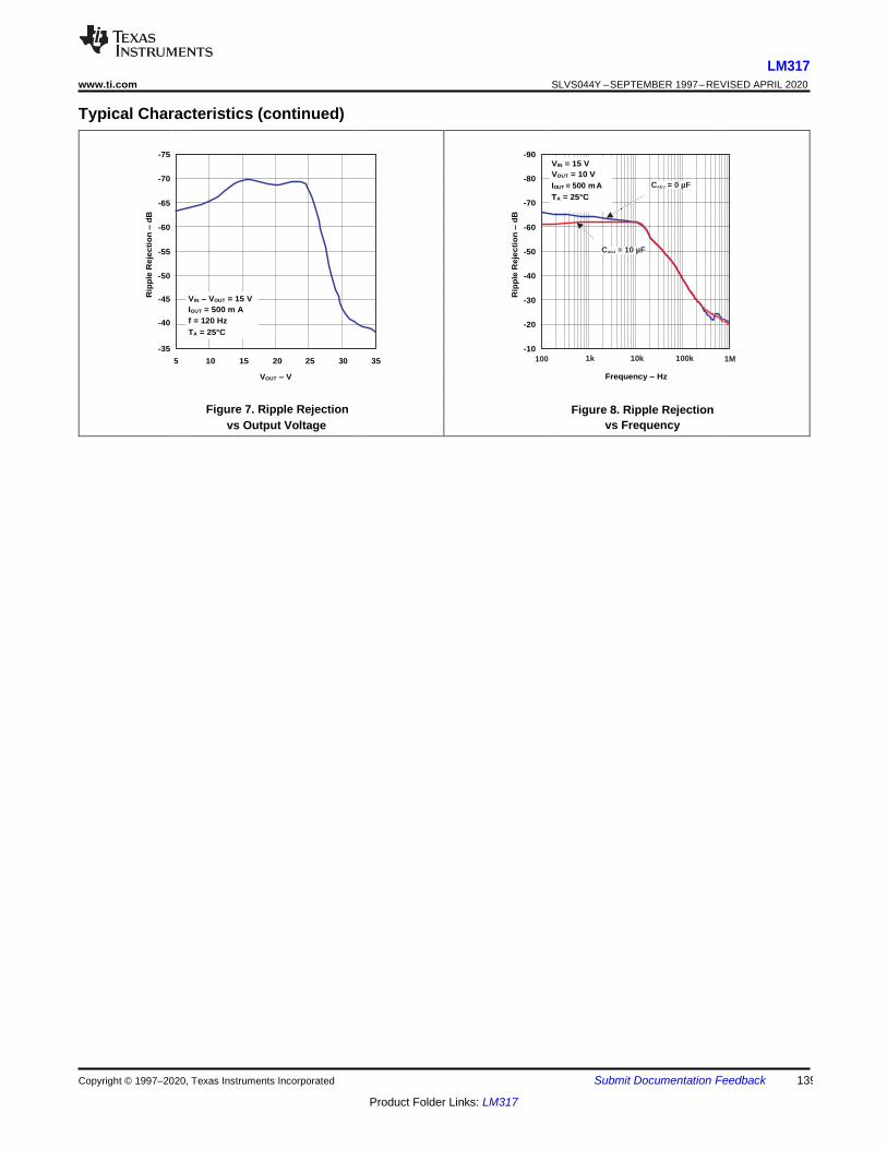
LM317
SLVS044Y – SEPTEMBER 1997 – REVISED APRIL 2020 www.ti.com
Submit Documentation Feedback 139 Copyright © 1997–2020, Texas Instruments Incorporated
Product Folder Links: LM317
100 1000 10000 100000 1000000
Rip
ple
Re
jec
tio
n –
dB
Rip
ple
Re
jec
tio
n –
dB
Typical Characteristics (continued)
-75
-90
-80
-70
-60
-50
-40
-30
-20
-10
100
VIN = 15 V
VOUT = 10 V
IOUT = 500 m A CADJ = 0 µF
TA = 25°C
CADJ = 10 µF
1k 10k 100k
Frequency – Hz
Figure 8. Ripple Rejection
vs Frequency
1M
-70
-65
-60
-55
-50
-45
VIN – VOUT = 15 V
IOUT = 500 m A
-40 f = 120 Hz
TA = 25°C
-35
5 10 15 20 25 30 35
VOUT – V
Figure 7. Ripple Rejection
vs Output Voltage
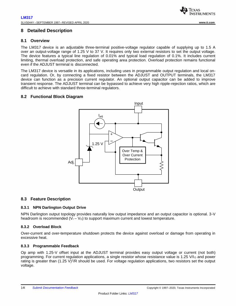
LM317
SLVS044Y – SEPTEMBER 1997 – REVISED APRIL 2020 www.ti.com
140 Submit Documentation Feedback Copyright © 1997–2020, Texas Instruments Incorporated
Product Folder Links: LM317
8 Detailed Description
8.1 Overview
The LM317 device is an adjustable three-terminal positive-voltage regulator capable of supplying up to 1.5 A over an output-voltage range of 1.25 V to 37 V. It requires only two external resistors to set the output voltage. The device features a typical line regulation of 0.01% and typical load regulation of 0.1%. It includes current limiting, thermal overload protection, and safe operating area protection. Overload protection remains functional even if the ADJUST terminal is disconnected.
The LM317 device is versatile in its applications, including uses in programmable output regulation and local on- card regulation. Or, by connecting a fixed resistor between the ADJUST and OUTPUT terminals, the LM317 device can function as a precision current regulator. An optional output capacitor can be added to improve transient response. The ADJUST terminal can be bypassed to achieve very high ripple-rejection ratios, which are difficult to achieve with standard three-terminal regulators.
8.2 Functional Block Diagram
Input
Adj.
Output
8.3 Feature Description
8.3.1 NPN Darlington Output Drive
NPN Darlington output topology provides naturally low output impedance and an output capacitor is optional. 3-V headroom is recommended (VI – VO) to support maximum current and lowest temperature.
8.3.2 Overload Block
Over-current and over-temperature shutdown protects the device against overload or damage from operating in excessive heat.
8.3.3 Programmable Feedback
Op amp with 1.25-V offset input at the ADJUST terminal provides easy output voltage or current (not both) programming. For current regulation applications, a single resistor whose resistance value is 1.25 V/IO and power rating is greater than (1.25 V)2/R should be used. For voltage regulation applications, two resistors set the output voltage.
Iadj
+
1.25 V
Over Temp &
Over Current
Protection
LM317
SLVS044Y – SEPTEMBER 1997 – REVISED APRIL 2020 www.ti.com
Submit Documentation Feedback 141 Copyright © 1997–2020, Texas Instruments Incorporated
Product Folder Links: LM317
8.4 Device Functional Modes
8.4.1 Normal Operation
The device OUTPUT pin will source current necessary to make OUTPUT pin 1.25 V greater than ADJUST terminal to provide output regulation.
8.4.2 Operation With Low Input Voltage
The device requires up to 3-V headroom (VI – VO) to operate in regulation. The device may drop out and OUTPUT voltage will be INPUT voltage minus drop out voltage with less headroom.
8.4.3 Operation at Light Loads
The device passes its bias current to the OUTPUT pin. The load or feedback must consume this minimum current for regulation or the output may be too high. See the Electrical Characteristics table for the minimum load current needed to maintain regulation.
8.4.4 Operation In Self Protection
When an overload occurs the device shuts down Darlington NPN output stage or reduces the output current to prevent device damage. The device will automatically reset from the overload. The output may be reduced or alternate between on and off until the overload is removed.
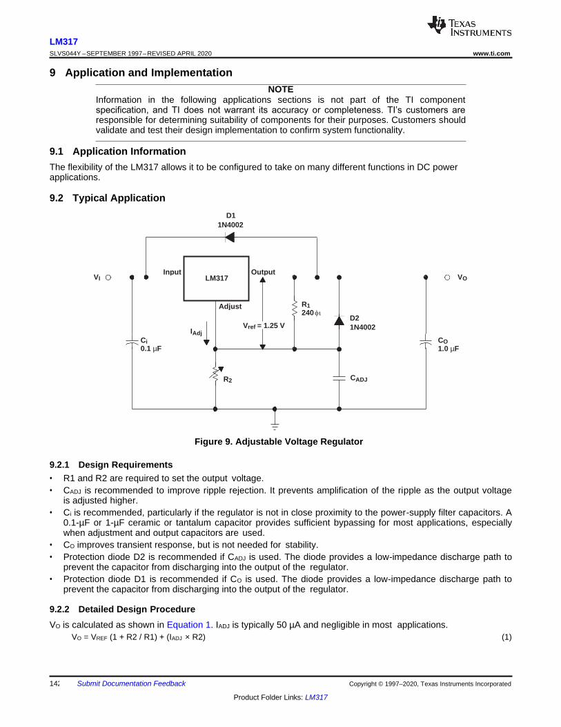
LM317
SLVS044Y – SEPTEMBER 1997 – REVISED APRIL 2020 www.ti.com
142 Submit Documentation Feedback Copyright © 1997–2020, Texas Instruments Incorporated
Product Folder Links: LM317
Input Output LM317
Adjust R1
240
Vref = 1.25 V IAdj
D2
1N4002
Ci
0.1 µF CO
1.0 µF
R2 CADJ
9 Application and Implementation
NOTE Information in the following applications sections is not part of the TI component specification, and TI does not warrant its accuracy or completeness. TI’s customers are responsible for determining suitability of components for their purposes. Customers should validate and test their design implementation to confirm system functionality.
9.1 Application Information
The flexibility of the LM317 allows it to be configured to take on many different functions in DC power applications.
9.2 Typical Application
D1
1N4002
VI VO
Figure 9. Adjustable Voltage Regulator
9.2.1 Design Requirements
• R1 and R2 are required to set the output voltage.
• CADJ is recommended to improve ripple rejection. It prevents amplification of the ripple as the output voltage is adjusted higher.
• Ci is recommended, particularly if the regulator is not in close proximity to the power-supply filter capacitors. A 0.1-µF or 1-µF ceramic or tantalum capacitor provides sufficient bypassing for most applications, especially when adjustment and output capacitors are used.
• CO improves transient response, but is not needed for stability.
• Protection diode D2 is recommended if CADJ is used. The diode provides a low-impedance discharge path to prevent the capacitor from discharging into the output of the regulator.
• Protection diode D1 is recommended if CO is used. The diode provides a low-impedance discharge path to prevent the capacitor from discharging into the output of the regulator.
9.2.2 Detailed Design Procedure
VO is calculated as shown in Equation 1. IADJ is typically 50 µA and negligible in most applications.
VO = VREF (1 + R2 / R1) + (IADJ × R2) (1)
LM317
SLVS044Y – SEPTEMBER 1997 – REVISED APRIL 2020 www.ti.com
Submit Documentation Feedback 143 Copyright © 1997–2020, Texas Instruments Incorporated
Product Folder Links: LM317
R1 120
−10 V
C1
0.1 µF R3 680
R2 3 k
LM317
INPUT OUTPUT
ADJUST
Typical Application (continued)
9.2.3 Application Curves
9.3 System Examples
9.3.1 0-V to 30-V Regulator Circuit
V = V
1 +
R2 +R3 − 10 V
Here, the voltage is determined by OUT REF
R1
+35 V VO
Figure 12. 0-V to 30-V Regulator Circuit
Figure 11. Line-Transient Response
Time – µs
9.98 14
10.00 15
10.02 16
10.04 V
IN
17
10.06
18 10.08
VOUT
10.10 19
CADJ = 10 µF
10.12 20
Figure 10. Line-Transient Response
Time – µs
9.98 14
10.00 15
10.02 16
VIN
10.04 17
10.06 18
10.08 VOUT 19
CADJ = 0 µF
10.10 20
VIN
Ch
an
ge –
V
-25
-15
-5
5
15
25
35
45
55
65
VO
UT –
V
VIN
Ch
an
ge –
V
-25
-15
-5
5
15
25
35
45
55
65
VO
UT –
V
LM317
SLVS044Y – SEPTEMBER 1997 – REVISED APRIL 2020 www.ti.com
144 Submit Documentation Feedback Copyright © 1997–2020, Texas Instruments Incorporated
Product Folder Links: LM317
R1
240 Ω
V
R3
C1
0.1 µF
120 Ω
C2
1 µF Output R4
Adjust 1 kΩ
LM317
INPUT OUTPUT
ADJUST
ADJUST
INPUT OUTPUT
LM317
R1
LM317
INPUT OUTPUT
ADJUST
R1 240
D1 1N4002
C1
0.1 µF
C3
1 µF
R2 5 k
C2
10 µF
LM317
INPUT OUTPUT
ADJUST
System Examples (continued)
9.3.2 Adjustable Regulator Circuit With Improved Ripple Rejection
C2 helps to stabilize the voltage at the adjustment pin, which helps reject noise. Diode D1 exists to discharge C2 in case the output is shorted to ground.
VI VO
Figure 13. Adjustable Regulator Circuit with Improved Ripple Rejection
9.3.3 Precision Current-Limiter Circuit
This application limits the output current to the ILIMIT in the diagram.
VI I
limit 1.2 R1
Figure 14. Precision Current-Limiter Circuit
9.3.4 Tracking Preregulator Circuit
This application keeps a constant voltage across the second LM317 in the circuit.
R2
720 Ω
VI
O
Figure 15. Tracking Preregulator Circuit
LM317
SLVS044Y – SEPTEMBER 1997 – REVISED APRIL 2020 www.ti.com
Submit Documentation Feedback 145 Copyright © 1997–2020, Texas Instruments Incorporated
Product Folder Links: LM317
R1 240
R2 2.4 k
LM317
INPUT OUTPUT
ADJUST
System Examples (continued)
9.3.5 1.25-V to 20-V Regulator Circuit With Minimum Program Current
Because the value of VREF is constant, the value of R1 determines the amount of current that flows through R1 and R2. The size of R2 determines the IR drop from ADJUSTMENT to GND. Higher values of R2 translate to higher VOUT.
R +R V = V 1 + 2 3 − 10 V OUT REF
R1 (2)
(R1+ R2)min = VoIreg(min) (3)
VI
Figure 16. 1.25-V to 20-V Regulator Circuit With Minimum Program Current
9.3.6 Battery-Charger Circuit
The series resistor limits the current output of the LM317, minimizing damage to the battery cell.
V = 1.25 V 1 +
R2 OUT R1
IOUT(short) = 1.25V
RS
Output Impedance =RS 1 +
R2
(4)
(5)
R1
RS
0.2
VI
(6)
Figure 17. Battery-Charger Circuit
VO
R1 1.2 kΩ
R2 20 kΩ
LM317
INPUT OUTPUT
ADJUST
LM317
SLVS044Y – SEPTEMBER 1997 – REVISED APRIL 2020 www.ti.com
146 Submit Documentation Feedback Copyright © 1997–2020, Texas Instruments Incorporated
Product Folder Links: LM317
LM317
INPUT OUTPUT VO =
ADJUST R1
240 Ω
D1 1N4002
R3
50 kΩ R2
2.7 kΩ
2N2905 C1
25 µF
LM317
INPUT OUTPUT
ADJUST
System Examples (continued)
9.3.7 50-mA Constant-Current Battery-Charger Circuit
The current limit operation mode can be used to trickle charge a battery at a fixed current. ICHG = 1.25 V ÷ 24 Ω. VI should be greater than VBAT + 4.25 V. (1.25 V [VREF] + 3 V [headroom])
24 Ω
VI
Figure 18. 50-mA Constant-Current Battery-Charger Circuit
9.3.8 Slow Turn-On 15-V Regulator Circuit
The capacitor C1, in combination with the PNP transistor, helps the circuit to slowly start supplying voltage. In the beginning, the capacitor is not charged. Therefore output voltage starts at VC1+ VBE + 1.25 V = 0 V + 0.65 V + 1.25 V = 1.9 V. As the capacitor voltage rises, VOUT rises at the same rate. When the output voltage reaches the value determined by R1 and R2, the PNP will be turned off.
VI 15 V
Figure 19. Slow Turn-On 15-V Regulator Circuit
9.3.9 AC Voltage-Regulator Circuit
These two LM317s can regulate both the positive and negative swings of a sinusoidal AC input.
VI
120 Ω
12 VI(PP)
120 Ω 480 Ω
6 VO(PP)
2 W (TYP)
VI
Figure 20. AC Voltage-Regulator Circuit
ADJUST
INPUT OUTPUT
LM317
480 Ω
LM317
INPUT OUTPUT
ADJUST
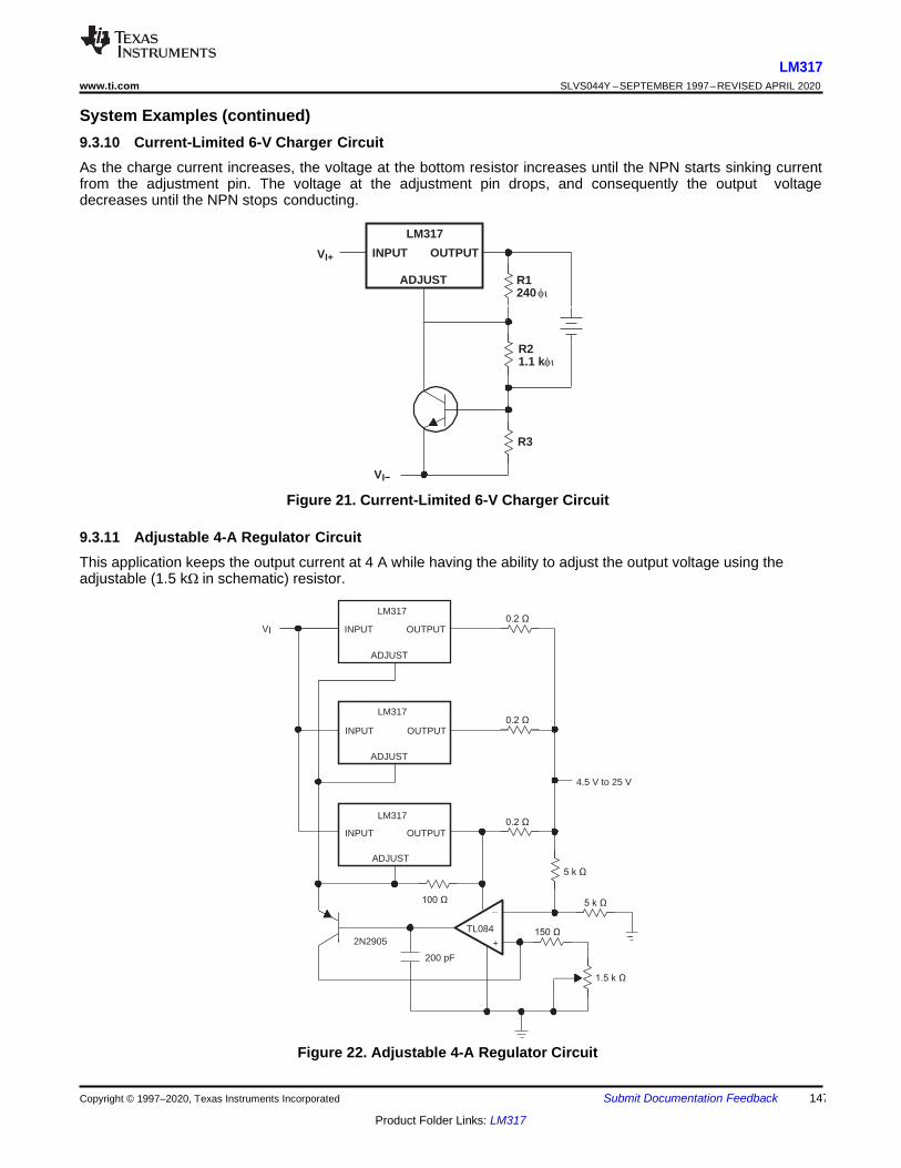
LM317
SLVS044Y – SEPTEMBER 1997 – REVISED APRIL 2020 www.ti.com
Submit Documentation Feedback 147 Copyright © 1997–2020, Texas Instruments Incorporated
Product Folder Links: LM317
0.2 Ω
0.2 Ω
4.5 V to 25 V
0.2 Ω
5 k Ω
100 Ω _
5 k Ω
TL084
+ 150 Ω
2N2905
200 pF
1.5 k Ω
LM317
INPUT OUTPUT
ADJUST
LM317
INPUT OUTPUT
ADJUST
ADJUST
OUTPUT INPUT
LM317
R1 240
R2 1.1 k
R3
LM317
INPUT OUTPUT
ADJUST
System Examples (continued)
9.3.10 Current-Limited 6-V Charger Circuit
As the charge current increases, the voltage at the bottom resistor increases until the NPN starts sinking current from the adjustment pin. The voltage at the adjustment pin drops, and consequently the output voltage decreases until the NPN stops conducting.
VI+
VI−
Figure 21. Current-Limited 6-V Charger Circuit
9.3.11 Adjustable 4-A Regulator Circuit
This application keeps the output current at 4 A while having the ability to adjust the output voltage using the adjustable (1.5 kΩ in schematic) resistor.
VI
Figure 22. Adjustable 4-A Regulator Circuit
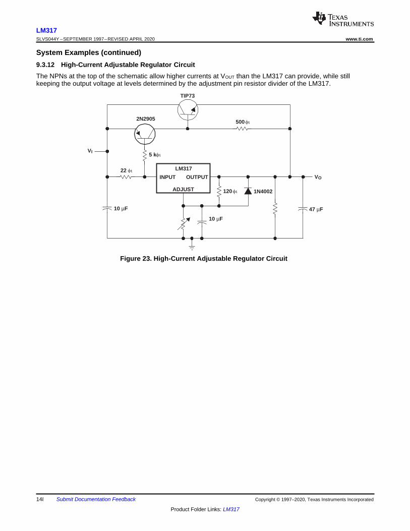
LM317
SLVS044Y – SEPTEMBER 1997 – REVISED APRIL 2020 www.ti.com
148 Submit Documentation Feedback Copyright © 1997–2020, Texas Instruments Incorporated
Product Folder Links: LM317
System Examples (continued)
9.3.12 High-Current Adjustable Regulator Circuit
The NPNs at the top of the schematic allow higher currents at VOUT than the LM317 can provide, while still keeping the output voltage at levels determined by the adjustment pin resistor divider of the LM317.
TIP73
VI
Figure 23. High-Current Adjustable Regulator Circuit
2N2905 500
5 k
22
VO
120 1N4002
10 µF 47 µF
10 µF
LM317
INPUT OUTPUT
ADJUST
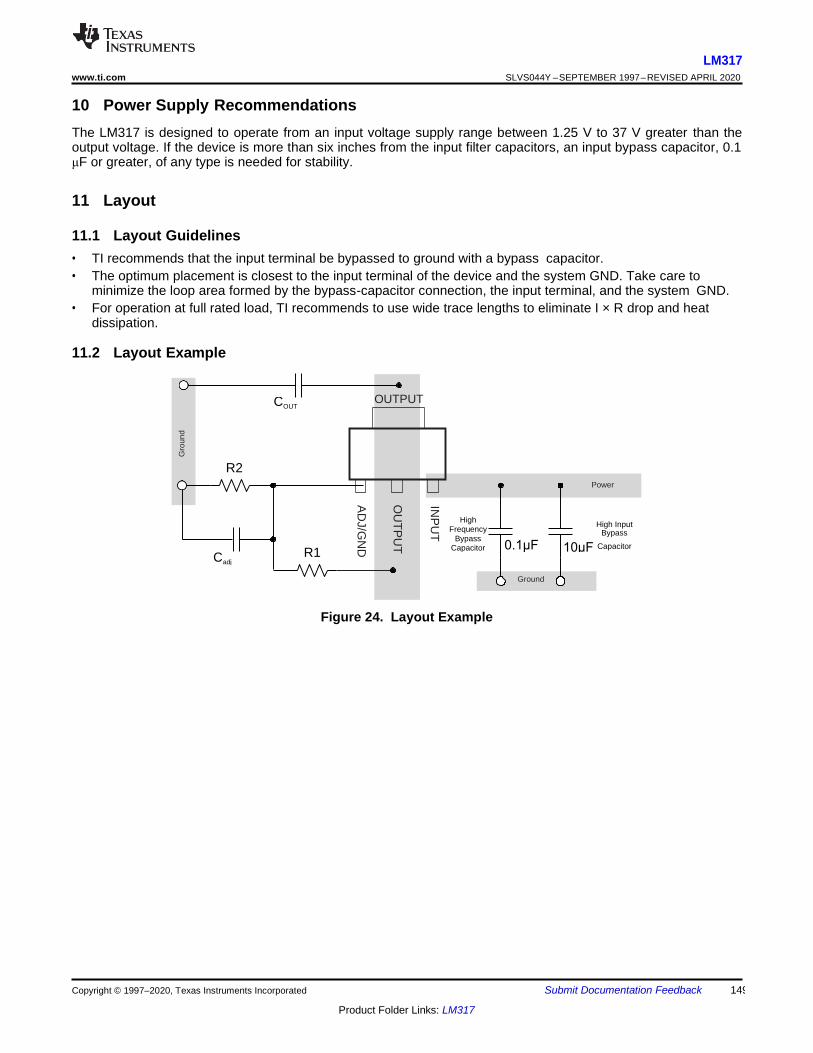
LM317
SLVS044Y – SEPTEMBER 1997 – REVISED APRIL 2020 www.ti.com
Submit Documentation Feedback 149 Copyright © 1997–2020, Texas Instruments Incorporated
Product Folder Links: LM317
10 Power Supply Recommendations
The LM317 is designed to operate from an input voltage supply range between 1.25 V to 37 V greater than the output voltage. If the device is more than six inches from the input filter capacitors, an input bypass capacitor, 0.1 μF or greater, of any type is needed for stability.
11 Layout
11.1 Layout Guidelines
• TI recommends that the input terminal be bypassed to ground with a bypass capacitor.
• The optimum placement is closest to the input terminal of the device and the system GND. Take care to minimize the loop area formed by the bypass-capacitor connection, the input terminal, and the system GND.
• For operation at full rated load, TI recommends to use wide trace lengths to eliminate I × R drop and heat dissipation.
11.2 Layout Example
Figure 24. Layout Example
COUT OUTPUT
R2 Power
High Frequency
Bypass Capacitor
High Input Bypass
10μF Capacitor
C R1 adj
Ground
0.1μF
INP
UT
OU
TP
UT
AD
J/G
ND
Gro
un
d
LM317
SLVS044Y – SEPTEMBER 1997 – REVISED APRIL 2020 www.ti.com
150 Submit Documentation Feedback Copyright © 1997–2020, Texas Instruments Incorporated
Product Folder Links: LM317
12 Device and Documentation Support
12.1 Receiving Notification of Documentation Updates
To receive notification of documentation updates, navigate to the device product folder on ti.com. In the upper right corner, click on Alert me to register and receive a weekly digest of any product information that has changed. For change details, review the revision history included in any revised document.
12.2 Support Resources
TI E2E™ support forums are an engineer's go-to source for fast, verified answers and design help — straight from the experts. Search existing answers or ask your own question to get the quick design help you need.
Linked content is provided "AS IS" by the respective contributors. They do not constitute TI specifications and do not necessarily reflect TI's views; see TI's Terms of Use.
12.3 Trademarks
E2E is a trademark of Texas Instruments. All other trademarks are the property of their respective owners.
12.4 Electrostatic Discharge Caution This integrated circuit can be damaged by ESD. Texas Instruments recommends that all integrated circuits be handled with appropriate precautions. Failure to observe proper handling and installation procedures can cause damage.
ESD damage can range from subtle performance degradation to complete device failure. Precision integrated circuits may be more susceptible to damage because very small parametric changes could cause the device not to meet its published specifications.
12.5 Glossary
SLYZ022 — TI Glossary.
This glossary lists and explains terms, acronyms, and definitions.
13 Mechanical, Packaging, and Orderable Information
The following pages include mechanical, packaging, and orderable information. This information is the most current data available for the designated devices. This data is subject to change without notice and revision of this document. For browser-based versions of this data sheet, refer to the left-hand navigation.
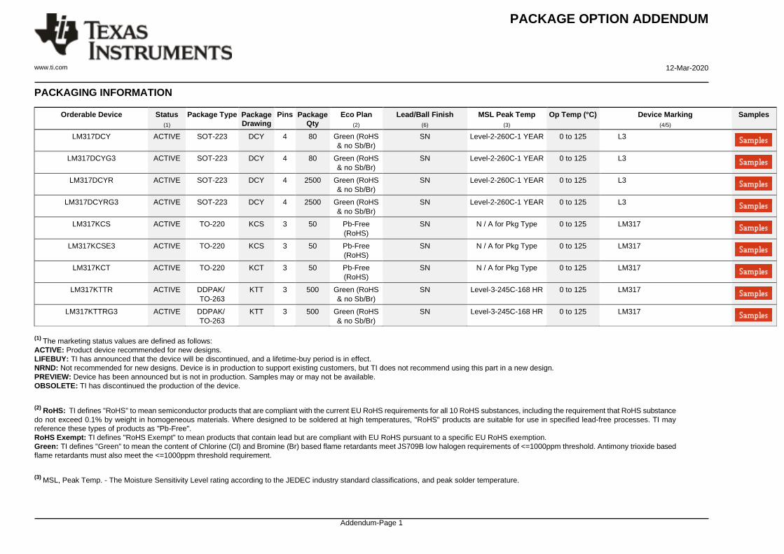
PACKAGE OPTION ADDENDUM
www.ti.com 12-Mar-2020
PACKAGING INFORMATION
Orderable Device Status
(1)
Package Type Package
Drawing
Pins Package
Qty
Eco Plan
(2)
Lead/Ball Finish
(6)
MSL Peak Temp
(3)
Op Temp (°C) Device Marking
(4/5)
Samples
LM317DCY ACTIVE SOT-223 DCY 4 80 Green (RoHS
& no Sb/Br)
SN Level-2-260C-1 YEAR 0 to 125 L3
LM317DCYG3 ACTIVE SOT-223 DCY 4 80 Green (RoHS
& no Sb/Br)
SN Level-2-260C-1 YEAR 0 to 125 L3
LM317DCYR ACTIVE SOT-223 DCY 4 2500 Green (RoHS
& no Sb/Br)
SN Level-2-260C-1 YEAR 0 to 125 L3
LM317DCYRG3 ACTIVE SOT-223 DCY 4 2500 Green (RoHS
& no Sb/Br)
SN Level-2-260C-1 YEAR 0 to 125 L3
LM317KCS ACTIVE TO-220 KCS 3 50 Pb-Free
(RoHS)
SN N / A for Pkg Type 0 to 125 LM317
LM317KCSE3 ACTIVE TO-220 KCS 3 50 Pb-Free
(RoHS)
SN N / A for Pkg Type 0 to 125 LM317
LM317KCT ACTIVE TO-220 KCT 3 50 Pb-Free
(RoHS)
SN N / A for Pkg Type 0 to 125 LM317
LM317KTTR ACTIVE DDPAK/
TO-263
KTT 3 500 Green (RoHS
& no Sb/Br)
SN Level-3-245C-168 HR 0 to 125 LM317
LM317KTTRG3 ACTIVE DDPAK/
TO-263
KTT 3 500 Green (RoHS
& no Sb/Br)
SN Level-3-245C-168 HR 0 to 125 LM317
(1) The marketing status values are defined as follows:
ACTIVE: Product device recommended for new designs.
LIFEBUY: TI has announced that the device will be discontinued, and a lifetime-buy period is in effect.
NRND: Not recommended for new designs. Device is in production to support existing customers, but TI does not recommend using this part in a new design.
PREVIEW: Device has been announced but is not in production. Samples may or may not be available.
OBSOLETE: TI has discontinued the production of the device.
(2)
RoHS: TI defines "RoHS" to mean semiconductor products that are compliant with the current EU RoHS requirements for all 10 RoHS substances, including the requirement that RoHS substance
do not exceed 0.1% by weight in homogeneous materials. Where designed to be soldered at high temperatures, "RoHS" products are suitable for use in specified lead-free processes. TI may
reference these types of products as "Pb-Free".
RoHS Exempt: TI defines "RoHS Exempt" to mean products that contain lead but are compliant with EU RoHS pursuant to a specific EU RoHS exemption.
Green: TI defines "Green" to mean the content of Chlorine (Cl) and Bromine (Br) based flame retardants meet JS709B low halogen requirements of <=1000ppm threshold. Antimony trioxide based
flame retardants must also meet the <=1000ppm threshold requirement.
(3)
MSL, Peak Temp. - The Moisture Sensitivity Level rating according to the JEDEC industry standard classifications, and peak solder temperature.
Addendum-Page 1
PACKAGE OPTION ADDENDUM
www.ti.com 12-Mar-2020
(4) There may be additional marking, which relates to the logo, the lot trace code information, or the environmental category on the device.
(5)
Multiple Device Markings will be inside parentheses. Only one Device Marking contained in parentheses and separated by a "~" will appear on a device. If a line is indented then it is a continuation
of the previous line and the two combined represent the entire Device Marking for that device.
(6)
Lead/Ball Finish - Orderable Devices may have multiple material finish options. Finish options are separated by a vertical ruled line. Lead/Ball Finish values may wrap to two lines if the finish
value exceeds the maximum column width.
Important Information and Disclaimer:The information provided on this page represents TI's knowledge and belief as of the date that it is provided. TI bases its knowledge and belief on information
provided by third parties, and makes no representation or warranty as to the accuracy of such information. Efforts are underway to better integrate information from third parties. TI has taken and
continues to take reasonable steps to provide representative and accurate information but may not have conducted destructive testing or chemical analysis on incoming materials and chemicals.
TI and TI suppliers consider certain information to be proprietary, and thus CAS numbers and other limited information may not be available for release.
In no event shall TI's liability arising out of such information exceed the total purchase price of the TI part(s) at issue in this document sold by TI to Customer on an annual basis.
Addendum-Page 2
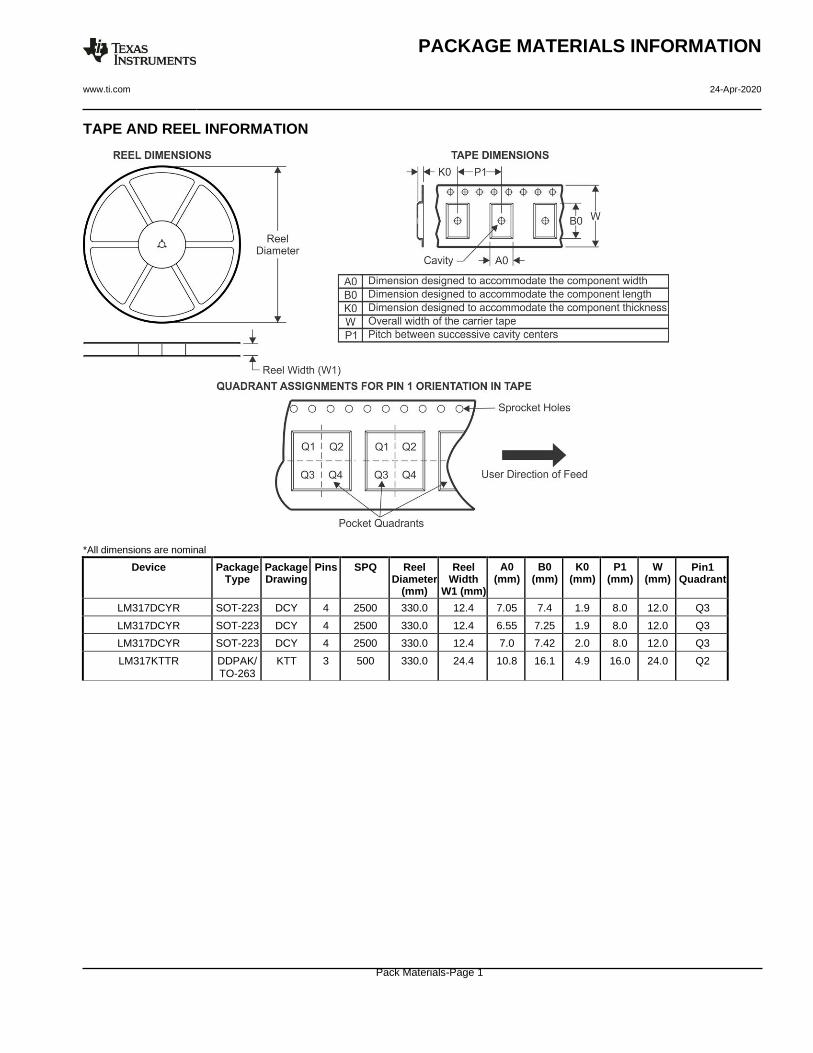
PACKAGE MATERIALS INFORMATION
www.ti.com 24-Apr-2020
TAPE AND REEL INFORMATION
*All dimensions are nominal
Device Package Type
Package Drawing
Pins SPQ Reel Diameter
(mm)
Reel Width
W1 (mm)
A0 (mm)
B0 (mm)
K0 (mm)
P1 (mm)
W (mm)
Pin1 Quadrant
LM317DCYR SOT-223 DCY 4 2500 330.0 12.4 7.05 7.4 1.9 8.0 12.0 Q3
LM317DCYR SOT-223 DCY 4 2500 330.0 12.4 6.55 7.25 1.9 8.0 12.0 Q3
LM317DCYR SOT-223 DCY 4 2500 330.0 12.4 7.0 7.42 2.0 8.0 12.0 Q3
LM317KTTR DDPAK/
TO-263
KTT 3 500 330.0 24.4 10.8 16.1 4.9 16.0 24.0 Q2
Pack Materials-Page 1
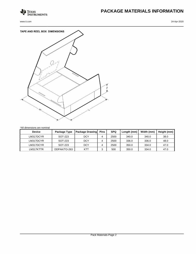
PACKAGE MATERIALS INFORMATION
www.ti.com 24-Apr-2020
*All dimensions are nominal
Device Package Type Package Drawing Pins SPQ Length (mm) Width (mm) Height (mm)
LM317DCYR SOT-223 DCY 4 2500 340.0 340.0 38.0
LM317DCYR SOT-223 DCY 4 2500 336.0 336.0 48.0
LM317DCYR SOT-223 DCY 4 2500 350.0 334.0 47.0
LM317KTTR DDPAK/TO-263 KTT 3 500 350.0 334.0 47.0
Pack Materials-Page 2
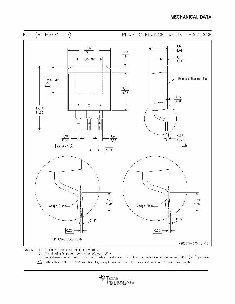
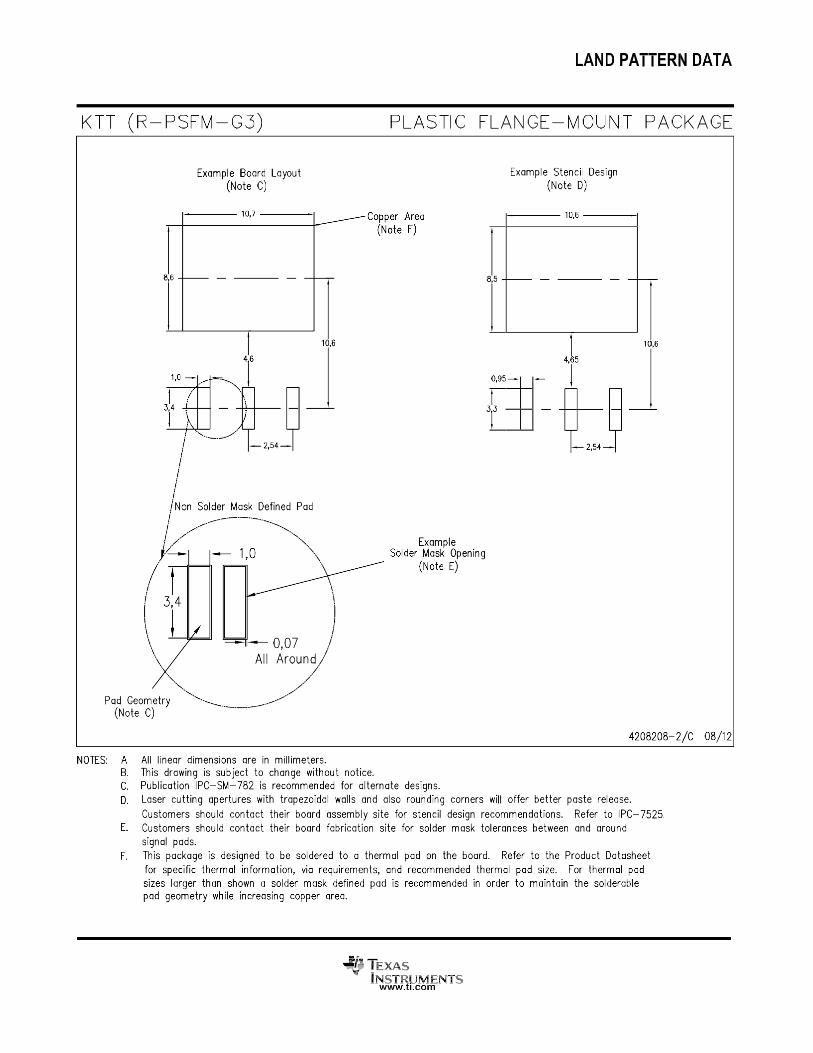
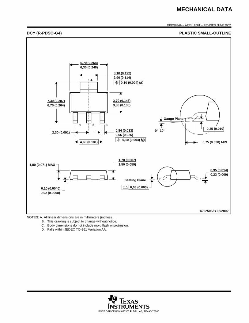
4202506/B 06/2002
0,08 (0.003) 0,10 (0.0040)
0,02 (0.0008)
Seating Plane
0,35 (0.014)
0,23 (0.009)
1,70 (0.067)
1,50 (0.059)
0,75 (0.030) MIN
1,80 (0.071) MAX
0,25 (0.010) 0–10
3
0,84 (0.033)
0,66 (0.026)
0,10 (0.004) M
2,30 (0.091)
2 1
Gauge Plane
3,70 (0.146)
3,30 (0.130)
7,30 (0.287)
6,70 (0.264)
3,10 (0.122)
2,90 (0.114)
0,10 (0.004) M 4
6,70 (0.264)
6,30 (0.248)
4,60 (0.181)
MECHANICAL DATA
MPDS094A – APRIL 2001 – REVISED JUNE 2002
DCY (R-PDSO-G4) PLASTIC SMALL-OUTLINE
NOTES: A. All linear dimensions are in millimeters (inches).
B. This drawing is subject to change without notice.
C. Body dimensions do not include mold flash or protrusion.
D. Falls within JEDEC TO-261 Variation AA.
POST OFFICE BOX 655303 • DALLAS, TEXAS 75265
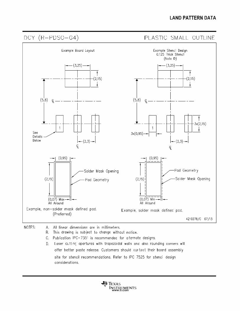
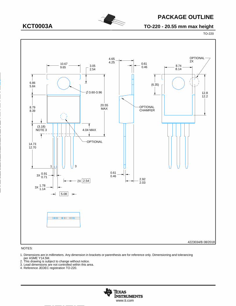
PACKAGE OUTLINE
www.ti.com
KCT0003A TO-220 - 20.55 mm max height
SCALE 0.850
TO-220
10.67 9.65
3.05 2.54
4.65 4.25 0.61
0.46
8.74
OPTIONAL 2X
6.86 5.84
3.60-3.96
(6.35)
12.8 12.2
8.79 8.39
20.55 MAX
OPTIONAL CHAMFER
(3.18)
NOTE 3
4.04 MAX
14.73 12.70
OPTIONAL
1 3
0.91 0.71
2X
1.78 1.14
0.61 0.46
2.92 2.03
4223034/B 08/2018
NOTES:
1. Dimensions are in millimeters. Any dimension in brackets or parenthesis are for reference only. Dimensioning and tolerancing per ASME Y14.5M.
2. This drawing is subject to change without notice. 3. Lead dimensions are not controlled within this area. 4. Reference JEDEC registration TO-220.
5.08
2.54
8.14
3X
3X
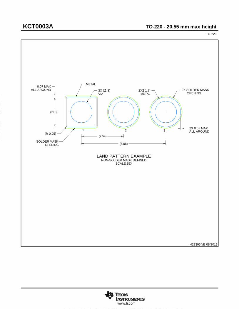
www.ti.com
KCT0003A TO-220 - 20.55 mm max height
TO-220
0.07 MAX
ALL AROUND
METAL
3X ( 1.3) VIA
2X ( 1.8)
METAL
2X SOLDER MASK OPENING
( 1.8)
(R 0.05)
SOLDER MASK OPENING
1
(2.54)
2 3
(5.08)
2X 0.07 MAX ALL AROUND
LAND PATTERN EXAMPLE NON-SOLDER MASK DEFINED
SCALE:15X
4223034/B 08/2018
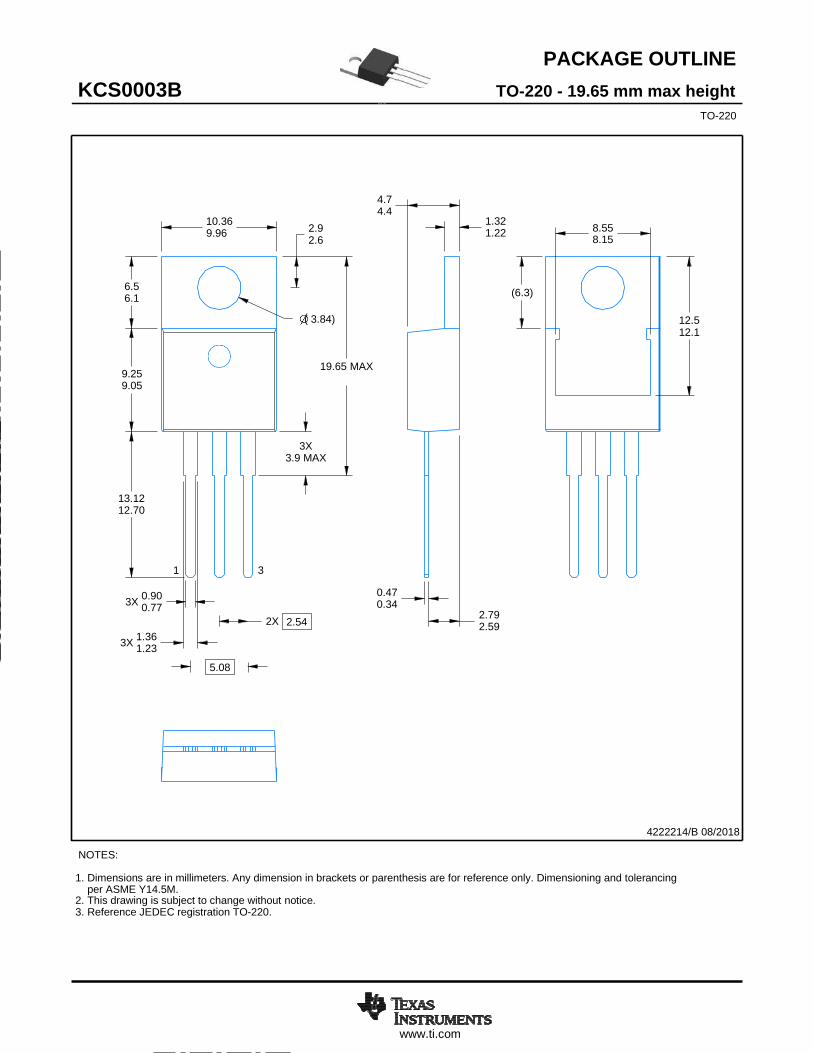
PACKAGE OUTLINE
www.ti.com
KCS0003B TO-220 - 19.65 mm max height
SCALE 0.850
TO-220
10.36 9.96
2.9 2.6
4.7 4.4
1.32 1.22
8.55
6.5 6.1
( 3.84)
(6.3)
12.5 12.1
9.25 9.05
19.65 MAX
3X
3.9 MAX
13.12 12.70
1 3
0.90 0.77
2X
1.36 1.23
0.47 0.34
2.79 2.59
4222214/B 08/2018
NOTES:
1. Dimensions are in millimeters. Any dimension in brackets or parenthesis are for reference only. Dimensioning and tolerancing per ASME Y14.5M.
2. This drawing is subject to change without notice. 3. Reference JEDEC registration TO-220.
5.08
2.54
8.15
3X
3X
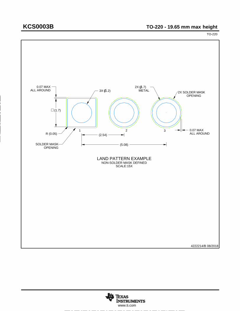
www.ti.com
KCS0003B TO-220 - 19.65 mm max height
TO-220
0.07 MAX
ALL AROUND
3X (1.2)
2X (1.7) METAL
2X SOLDER MASK OPENING
(1.7)
R (0.05)
1 2 3
(2.54)
0.07 MAX ALL AROUND
SOLDER MASK OPENING
(5.08)
LAND PATTERN EXAMPLE NON-SOLDER MASK DEFINED
SCALE:15X
4222214/B 08/2018
IMPORTANT NOTICE AND DISCLAIMER
TI PROVIDES TECHNICAL AND RELIABILITY DATA (INCLUDING DATASHEETS), DESIGN RESOURCES (INCLUDING REFERENCE DESIGNS), APPLICATION OR OTHER DESIGN ADVICE, WEB TOOLS, SAFETY INFORMATION, AND OTHER RESOURCES “AS IS” AND WITH ALL FAULTS, AND DISCLAIMS ALL WARRANTIES, EXPRESS AND IMPLIED, INCLUDING WITHOUT LIMITATION ANY IMPLIED WARRANTIES OF MERCHANTABILITY, FITNESS FOR A PARTICULAR PURPOSE OR NON-INFRINGEMENT OF THIRD PARTY INTELLECTUAL PROPERTY RIGHTS.
These resources are intended for skilled developers designing with TI products. You are solely responsible for (1) selecting the appropriate TI products for your application, (2) designing, validating and testing your application, and (3) ensuring your application meets applicable standards, and any other safety, security, or other requirements. These resources are subject to change without notice. TI grants you permission to use these resources only for development of an application that uses the TI products described in the resource. Other reproduction and display of these resources is prohibited. No license is granted to any other TI intellectual property right or to any third party intellectual property right. TI disclaims responsibility for, and you will fully indemnify TI and its representatives against, any claims, damages, costs, losses, and liabilities arising out of your use of these resources.
TI’s products are provided subject to TI’s Terms of Sale (www.ti.com/legal/termsofsale.html) or other applicable terms available either on ti.com or provided in conjunction with such TI products. TI’s provision of these resources does not expand or otherwise alter TI’s applicable warranties or warranty disclaimers for TI products.
Mailing Address: Texas Instruments, Post Office Box 655303, Dallas, Texas 75265
Copyright © 2020, Texas Instruments Incorporated
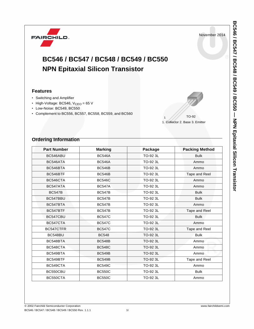
© 2002 Fairchild Semiconductor Corporation
BC546 / BC547 / BC548 / BC549 / BC550 Rev. 1.1.1
www.fairchildsemi.com
164
November 2014
BC546 / BC547 / BC548 / BC549 / BC550
NPN Epitaxial Silicon Transistor
Features
• Switching and Amplifier
• High-Voltage: BC546, VCEO = 65 V
• Low-Noise: BC549, BC550
• Complement to BC556, BC557, BC558, BC559, and BC560
1 TO-92
1. Collector 2. Base 3. Emitter
Ordering Information
Part Number Marking Package Packing Method
BC546ABU BC546A TO-92 3L Bulk
BC546ATA BC546A TO-92 3L Ammo
BC546BTA BC546B TO-92 3L Ammo
BC546BTF BC546B TO-92 3L Tape and Reel
BC546CTA BC546C TO-92 3L Ammo
BC547ATA BC547A TO-92 3L Ammo
BC547B BC547B TO-92 3L Bulk
BC547BBU BC547B TO-92 3L Bulk
BC547BTA BC547B TO-92 3L Ammo
BC547BTF BC547B TO-92 3L Tape and Reel
BC547CBU BC547C TO-92 3L Bulk
BC547CTA BC547C TO-92 3L Ammo
BC547CTFR BC547C TO-92 3L Tape and Reel
BC548BU BC548 TO-92 3L Bulk
BC548BTA BC548B TO-92 3L Ammo
BC548CTA BC548C TO-92 3L Ammo
BC549BTA BC549B TO-92 3L Ammo
BC549BTF BC549B TO-92 3L Tape and Reel
BC549CTA BC549C TO-92 3L Ammo
BC550CBU BC550C TO-92 3L Bulk
BC550CTA BC550C TO-92 3L Ammo
BC
546 / B
C54
7 / B
C548 / B
C549 / B
C550 —
NP
N E
pita
xia
l Silic
on
Tra
nsis
tor
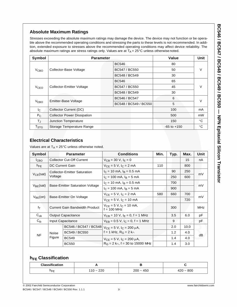
© 2002 Fairchild Semiconductor Corporation
BC546 / BC547 / BC548 / BC549 / BC550 Rev. 1.1.1
www.fairchildsemi.com
165
Absolute Maximum Ratings
Stresses exceeding the absolute maximum ratings may damage the device. The device may not function or be opera-
ble above the recommended operating conditions and stressing the parts to these levels is not recommended. In addi-
tion, extended exposure to stresses above the recommended operating conditions may affect device reliability. The
absolute maximum ratings are stress ratings only. Values are at TA = 25°C unless otherwise noted.
Symbol Parameter Value Unit
VCBO
Collector-Base Voltage
BC546 80 V BC547 / BC550 50
BC548 / BC549 30
VCEO
Collector-Emitter Voltage
BC546 65 V BC547 / BC550 45
BC548 / BC549 30
VEBO Emitter-Base Voltage BC546 / BC547 6
V BC548 / BC549 / BC550 5
IC Collector Current (DC) 100 mA
PC Collector Power Dissipation 500 mW
TJ Junction Temperature 150 C
TSTG Storage Temperature Range -65 to +150 C
Electrical Characteristics
Values are at TA = 25°C unless otherwise noted.
Symbol Parameter Conditions Min. Typ. Max. Unit
ICBO Collector Cut-Off Current VCB = 30 V, IE = 0 15 nA
hFE DC Current Gain VCE = 5 V, IC = 2 mA 110 800
VCE(sat) Collector-Emitter Saturation
Voltage
IC = 10 mA, IB = 0.5 mA 90 250 mV
IC = 100 mA, IB = 5 mA 250 600
VBE(sat) Base-Emitter Saturation Voltage IC = 10 mA, IB = 0.5 mA 700
mV IC = 100 mA, IB = 5 mA 900
VBE(on) Base-Emitter On Voltage VCE = 5 V, IC = 2 mA 580 660 700
mV VCE = 5 V, IC = 10 mA 720
fT Current Gain Bandwidth Product VCE = 5 V, IC = 10 mA,
f = 100 MHz
300
MHz
Cob Output Capacitance VCB = 10 V, IE = 0, f = 1 MHz 3.5 6.0 pF
Cib Input Capacitance VEB = 0.5 V, IC = 0, f = 1 MHz 9 pF
NF
Noise
Figure
BC546 / BC547 / BC548 VCE = 5 V, IC = 200 A,
f = 1 kHz, RG = 2 k
2.0 10.0
dB
BC549 / BC550 1.2 4.0
BC549 VCE = 5 V, IC = 200 A,
RG = 2 k f = 30 to 15000 MHz
1.4 4.0
BC550 1.4 3.0
hFE Classification
Classification A B C
hFE 110 ~ 220 200 ~ 450 420 ~ 800
BC
546 / B
C54
7 / B
C54
8 / B
C549 / B
C550 —
NP
N E
pita
xia
l Silic
on
Tra
nsis
tor
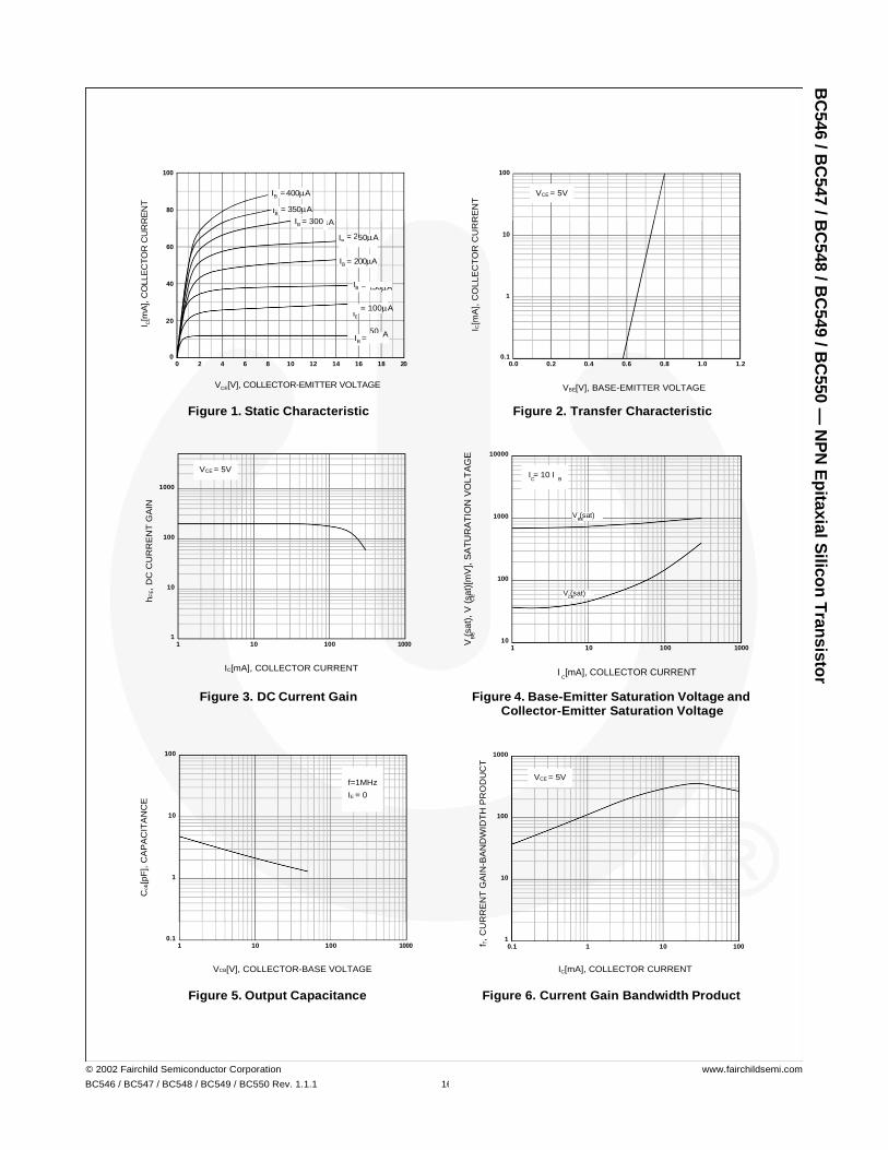
© 2002 Fairchild Semiconductor Corporation
BC546 / BC547 / BC548 / BC549 / BC550 Rev. 1.1.1
www.fairchildsemi.com
166
f T,
CU
RR
EN
T G
AIN
-BA
ND
WID
TH
PR
OD
UC
T
C B
C
A
100
80
60
40
IB = 400A
= 350A
IB = 300
IB = 200A
B
100
10
1
VCE = 5V
= 100A
20
IB =
0
0 2 4 6 8 10 12 14 16 18 20
0.1
0.0
0.2
0.4
0.6
0.8
1.0
1.2
VCE[V], COLLECTOR-EMITTER VOLTAGE
VBE[V], BASE-EMITTER VOLTAGE
Figure 1. Static Characteristic Figure 2. Transfer Characteristic
1000
VCE = 5V
10000
I = 10 I
1000 V (sat)
100
100
10
V (sat)
1
1 10 100 1000
IC[mA], COLLECTOR CURRENT
10 1 10 100 1000
I [mA], COLLECTOR CURRENT
Figure 3. DC Current Gain Figure 4. Base-Emitter Saturation Voltage and Collector-Emitter Saturation Voltage
100
f=1MHz
IE = 0
1000
VCE = 5V
10 100
1 10
0.1
1 10 100 1000
1 0.1 1
10 100
VCB[V], COLLECTOR-BASE VOLTAGE IC[mA], COLLECTOR CURRENT
Figure 5. Output Capacitance Figure 6. Current Gain Bandwidth Product
= 2 IB
A
50
IB
A 150 = I
50A
IB
BC
546 / B
C54
7 / B
C548 / B
C549 / B
C550 —
NP
N E
pita
xia
l Silic
on
Tra
nsis
tor
Co
b[p
F],
CA
PA
CIT
AN
CE
I C
[mA
], C
OLLE
CT
OR
CU
RR
EN
T
hF
E,
DC
CU
RR
EN
T G
AIN
V (
sat)
, V
(sat)
[mV
], S
AT
UR
AT
ION
VO
LT
AG
E
BE
C
E
I C[m
A],
CO
LLE
CT
OR
CU
RR
EN
T
BE
CE
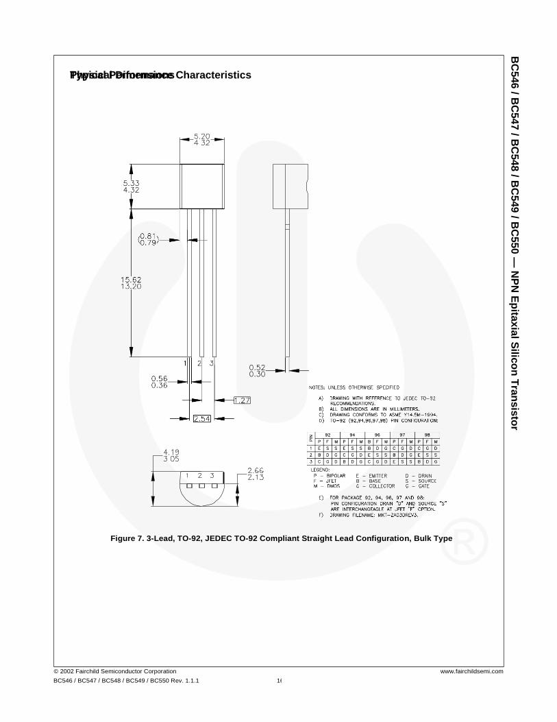
Typical Performance Characteristics
© 2002 Fairchild Semiconductor Corporation
BC546 / BC547 / BC548 / BC549 / BC550 Rev. 1.1.1
www.fairchildsemi.com
167
Physical Dimensions
D
Figure 7. 3-Lead, TO-92, JEDEC TO-92 Compliant Straight Lead Configuration, Bulk Type
BC
546 / B
C54
7 / B
C548 / B
C549 / B
C550 —
NP
N E
pita
xia
l Silic
on
Tra
nsis
tor
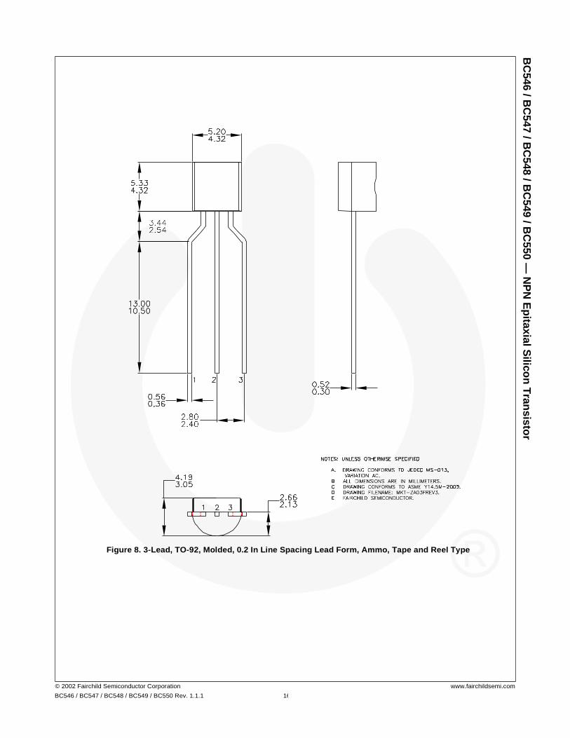
© 2002 Fairchild Semiconductor Corporation
BC546 / BC547 / BC548 / BC549 / BC550 Rev. 1.1.1
www.fairchildsemi.com
168
Figure 8. 3-Lead, TO-92, Molded, 0.2 In Line Spacing Lead Form, Ammo, Tape and Reel Type
BC
546 / B
C54
7 / B
C548 / B
C549 / B
C550 —
NP
N E
pita
xia
l Silic
on
Tra
nsis
tor
Physical Dimensions (Continued)
© 2002 Fairchild Semiconductor Corporation
BC546 / BC547 / BC548 / BC549 / BC550 Rev. 1.1.1
www.fairchildsemi.com
169
TRADEMARKS
The following includes registered and unregistered trademarks and service marks, owned by Fairchild Semiconductor and/or its global subsidiaries, and is not
intended to be an exhaustive list of all such trademarks.
AccuPower¥
Awinda®
AX-CAP®*
BitSiC¥
Build it Now¥
CorePLUS¥
CorePOWER¥
CROSSVOLT¥
CTL¥
Current Transfer Logic¥
DEUXPEED®
Dual Cool™
EcoSPARK®
EfficientMax¥
ESBC¥ ®
Fairchild®
Fairchild Semiconductor®
FACT Quiet Series¥
FACT®
FAST®
FastvCore¥
FETBench¥
FPS¥
F-P FS¥
FRFET®
Global Power ResourceSM
GreenBridge¥
Green FPS¥
Green FPS¥ e-Series¥
Gmax¥
GTO¥
IntelliMAX¥
ISOPLANAR¥
Making Small Speakers Sound Louder
and Better™
MegaBuck¥
MICROCOUPLER¥
MicroFET¥
MicroPak¥
MicroPak2¥
MillerDrive¥
MotionMax¥ ®
mWSaver®
OptoHiT¥ ®
OPTOPLANAR®
®
PowerTrench®
PowerXS™
Programmable Active Droop¥
QFET®
QS¥
Quiet Series¥
RapidConfigure¥
¥
Saving our world, 1mW/W/kW at a time™
SignalWise¥
SmartMax¥
SMART START¥
Solutions for Your Success¥
SPM®
STEALTH¥
SuperFET®
SuperSOT¥-3
SuperSOT¥-6
SuperSOT¥-8
SupreMOS®
SyncFET¥
Sync-Lock™
®*
TinyBoost®
TinyBuck®
TinyCalc¥
TinyLogic®
TINYOPTO¥
TinyPower¥
TinyPWM¥
TinyWire¥
TranSiC¥
TriFault Detect¥
TRUECURRENT®*
SerDes¥
UHC®
Ultra FRFET¥
UniFET¥
VCX¥
VisualMax¥
VoltagePlus¥
XS™
Xsens™ ❺™
OPTOLOGIC
* Trademarks of System General Corporation, used under license by Fairchild Semiconductor.
DISCLAIMER
FAIRCHILD SEMICONDUCTOR RESERVES THE RIGHT TO MAKE CHANGES WITHOUT FURTHER NOTICE TO ANY PRODUCTS HEREIN TO IMPROVE
RELIABILITY, FUNCTION, OR DESIGN. TO OBTAIN THE LATEST, MOST UP-TO-DATE DATASHEET AND PRODUCT INFORMATION, VISIT OUR WEBSITE
AT HTTP://WWW.FAIRCHILDSEMI.COM. FAIRCHILD DOES NOT ASSUME ANY LIABILITY ARISING OUT OF THE APPLICATION OR USE OF ANY
PRODUCT OR CIRCUIT DESCRIBED HEREIN; NEITHER DOES IT CONVEY ANY LICENSE UNDER ITS PATENT RIGHTS, NOR THE RIGHTS OF OTHERS.
THESE SPECIFICATIONS DO NOT EXPAND THE TERMS OF FAIRCHILD’S WORLDWIDE TERMS AND CONDITIONS, SPECIFICALLY THE WARRANTY
THEREIN, WHICH COVERS THESE PRODUCTS.
LIFE SUPPORT POLICY
FAIRCHILD’S PRODUCTS ARE NOT AUTHORIZED FOR USE AS CRITICAL COMPONENTS IN LIFE SUPPORT DEVICES OR SYSTEMS WITHOUT THE
EXPRESS WRITTEN APPROVAL OF FAIRCHILD SEMICONDUCTOR CORPORATION.
As used herein:
1. Life support devices or systems are devices or systems which, (a) are
intended for surgical implant into the body or (b) support or sustain
life, and (c) whose failure to perform when properly used in
accordance with instructions for use provided in the labeling, can be
reasonably expected to result in a significant injury of the user.
ANTI-COUNTERFEITING POLICY
2. A critical component in any component of a life support, device, or
system whose failure to perform can be reasonably expected to
cause the failure of the life support device or system, or to affect its
safety or effectiveness.
Fairchild Semiconductor Corporation's Anti-Counterfeiting Policy. Fairchild's Anti-Counterfeiting Policy is also stated on our external website, www.fairchildsemi.com,
under Sales Support.
Counterfeiting of semiconductor parts is a growing problem in the industry. All manufacturers of semiconductor products are experiencing counterfeiting of their
parts. Customers who inadvertently purchase counterfeit parts experience many problems such as loss of brand reputation, substandard performance, failed
applications, and increased cost of production and manufacturing delays. Fairchild is taking strong measures to protect ourselves and our customers from the
proliferation of counterfeit parts. Fairchild strongly encourages customers to purchase Fairchild parts either directly from Fairchild or from Authorized Fairchild
Distributors who are listed by country on our web page cited above. Products customers buy either from Fairchild directly or from Authorized Fairchild Distributors
are genuine parts, have full traceability, meet Fairchild's quality standards for handling and storage and provide access to Fairchild's full range of up-to-date technical
and product information. Fairchild and our Authorized Distributors will stand behind all warranties and will appropriately address any warranty issues that may arise.
Fairchild will not provide any warranty coverage or other assistance for parts bought from Unauthorized Sources. Fairchild is committed to combat this global
problem and encourage our customers to do their part in stopping this practice by buying direct or from authorized distributors.
PRODUCT STATUS DEFINITIONS
Definition of Terms
Datasheet Identification Product Status Definition
Advance Information Formative / In Design Datasheet contains the design specifications for product development. Specifications may change in any manner without notice.
Preliminary First Production Datasheet contains preliminary data; supplementary data will be published at a later date. Fairchild Semiconductor reserves the right to make changes at any time without notice to improve design.
No Identification Needed Full Production Datasheet contains final specifications. Fairchild Semiconductor reserves the right to make changes at any time without notice to improve the design.
Obsolete Not In Production Datasheet contains specifications on a product that is discontinued by Fairchild Semiconductor. The datasheet is for reference information only.
Rev. I72
© Fairchild Semiconductor Corporation www.fairchildsemi.com
MTi®
MTx®
MVN®
MotionGrid
www.onsemi.com 1
PUBLICATION ORDERING INFORMATION
LITERATURE FULFILLMENT:
Literature Distribution Center for ON Semiconductor
19521 E. 32nd Pkwy, Aurora, Colorado 80011 USA Phone: 303−675−2175 or 800−344−3860 Toll Free USA/Canada
Fax: 303−675−2176 or 800−344−3867 Toll Free USA/Canada
Email: [email protected]
Semiconductor Components Industries, LLC
N. American Technical Support: 800−282−9855 Toll Free
USA/Canada
Europe, Middle East and Africa Technical Support:
Phone: 421 33 790 2910
Japan Customer Focus Center
Phone: 81−3−5817−1050
ON Semiconductor Website: www.onsemi.com
Order Literature: http://www.onsemi.com/orderlit
For additional information, please contact your local
Sales Representative
www.onsemi.com
ON Semiconductor and are trademarks of Semiconductor Components Industries, LLC dba ON Semiconductor or its subsidiaries in the United States and/or other countries. ON Semiconductor owns the rights to a number of patents, trademarks, copyrights, trade secrets, and other intellectual property. A listing of ON Semiconductor’s product/patent coverage may be accessed at www.onsemi.com/site/pdf/Patent−Marking.pdf. ON Semiconductor reserves the right to make changes without further notice to any products herein.
ON Semiconductor makes no warranty, representation or guarantee regarding the suitability of its products for any particular purpose, nor does ON Semiconductor assume any liability arising out of the application or use of any product or circuit, and specifically disclaims any and all liability, including without limitation special, consequential or incidental damages. Buyer is responsible for its products and applications using ON Semiconductor products, including compliance with all laws, regulations and safety requirements or standards, regardless of any support or applications information provided by ON Semiconductor. “Typical” parameters which may be provided in ON Semiconductor data sheets and/or specifications can and do vary in different applications and actual performance may vary over time. All operating parameters, including “Typicals” must be validated for each customer application by customer’s technical experts. ON Semiconductor does not convey any license under its patent rights nor the rights of others. ON Semiconductor products are not designed, intended, or authorized for use as a critical component in life support systems or any FDA Class 3 medical devices or medical devices with a same or similar classification in a foreign jurisdiction or any devices intended for implantation in the human body. Should Buyer purchase or use ON Semiconductor products for any such unintended or unauthorized application, Buyer shall indemnify and hold ON Semiconductor and its officers, employees, subsidiaries, affiliates, and distributors harmless against all claims, costs, damages, and expenses, and reasonable attorney fees arising out of, directly or indirectly, any claim of personal injury or death associated with such unintended or unauthorized use, even if such claim alleges that ON Semiconductor was negligent regarding the design or manufacture of the part. ON Semiconductor is an Equal Opportunity/Affirmative Action Employer. This literature is subject to all applicable copyright laws and is not for resale in any manner.
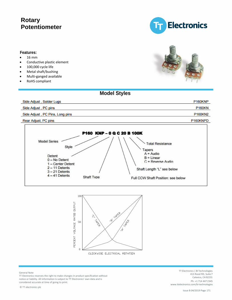
Rotary Potentiometer
P160 Series
TT Electronics | BI Technologies 413 Rood RD, Suite 7
Calexico, CA 92231
Ph: +1 714 447 2345 www.ttelectronics.com/bi-technologies
General Note TT Electronics reserves the right to make changes in product specification without notice or liability. All information is subject to TT Electronics’ own data and is considered accurate at time of going to print.
© TT electronics plc
Issue B 04/2019 Page 171
Features: • 16 mm
• Conductive plastic element
• 100,000 cycle life
• Metal shaft/bushing
• Multi-ganged available
• RoHS compliant
Model Styles
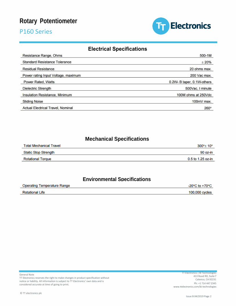
Rotary Potentiometer
P160 Series
© TT electronics plc Issue B 04/2019 Page 2
Electrical Specifications
Mechanical Specifications
Environmental Specifications
General Note TT Electronics reserves the right to make changes in product specification without notice or liability. All information is subject to TT Electronics’ own data and is considered accurate at time of going to print.
TT Electronics | BI Technologies 413 Rood RD, Suite 7
Calexico, CA 92231
Ph: +1 714 447 2345 www.ttelectronics.com/bi-technologies
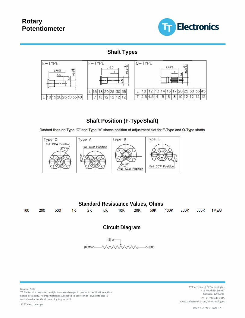
Rotary Potentiometer
P160 Series
TT Electronics | BI Technologies 413 Rood RD, Suite 7
Calexico, CA 92231
Ph: +1 714 447 2345 www.ttelectronics.com/bi-technologies
General Note TT Electronics reserves the right to make changes in product specification without notice or liability. All information is subject to TT Electronics’ own data and is considered accurate at time of going to print.
© TT electronics plc
Issue B 04/2019 Page 173
Shaft Types
Shaft Position (F-Type Shaft)
Standard Resistance Values, Ohms
Circuit Diagram
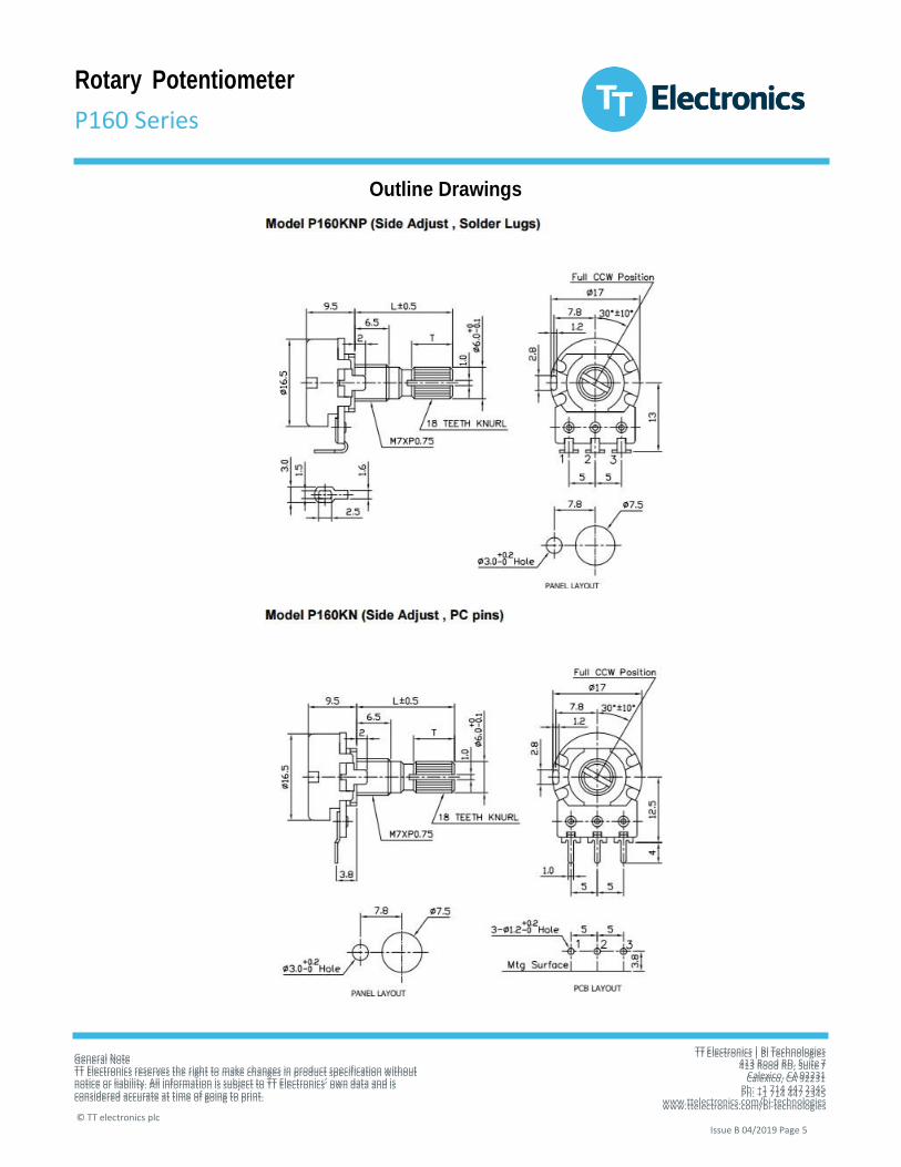
Rotary Potentiometer
P160 Series
TT Electronics | BI Technologies 413 Rood RD, Suite 7
Calexico, CA 92231
Ph: +1 714 447 2345 www.ttelectronics.com/bi-technologies
General Note TT Electronics reserves the right to make changes in product specification without notice or liability. All information is subject to TT Electronics’ own data and is considered accurate at time of going to print.
© TT electronics plc Issue B 04/2019 Page 5
Outline Drawings
General Note TT Electronics reserves the right to make changes in product specification without notice or liability. All information is subject to TT Electronics’ own data and is considered accurate at time of going to print.
TT Electronics | BI Technologies 413 Rood RD, Suite 7
Calexico, CA 92231
Ph: +1 714 447 2345 www.ttelectronics.com/bi-technologies
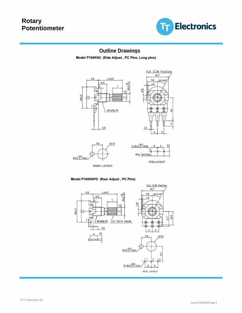
Rotary Potentiometer
P160 Series
© TT electronics plc Issue B 04/2019 Page 4
Outline Drawings
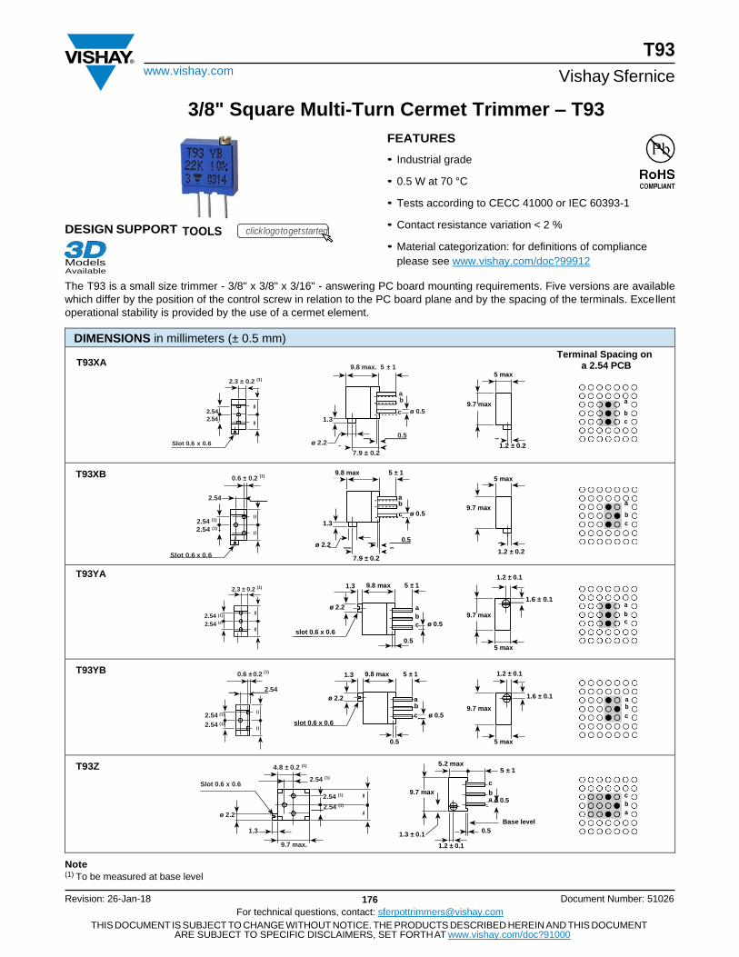
T93
Vishay Sfernice www.vishay.com
Revision: 26-Jan-18 176
For technical questions, contact: [email protected]
Document Number: 51026
THIS DOCUMENT IS SUBJECT TO CHANGE WITHOUT NOTICE. THE PRODUCTS DESCRIBED HEREIN AND THIS DOCUMENT ARE SUBJECT TO SPECIFIC DISCLAIMERS, SET FORTH AT www.vishay.com/doc?91000
DESIGN SUPPORT
Models Available
3/8" Square Multi-Turn Cermet Trimmer – T93
FEATURES
• Industrial grade
• 0.5 W at 70 °C
• Tests according to CECC 41000 or IEC 60393-1
• Contact resistance variation < 2 %
• Material categorization: for definitions of compliance
please see www.vishay.com/doc?99912
The T93 is a small size trimmer - 3/8" x 3/8" x 3/16" - answering PC board mounting requirements. Five versions are available
which differ by the position of the control screw in relation to the PC board plane and by the spacing of the terminals. Excellent
operational stability is provided by the use of a cermet element.
DIMENSIONS in millimeters (± 0.5 mm)
Terminal Spacing on T93XA
9.8 max. 5 ± 1 a 2.54 PCB 5 max
2.3 ± 0.2 (1)
a b
9.7 max a 2.54 c ø 0.5 b 2.54 1.3 c
0.5
Slot 0.6 x 0.6 ø 2.2 1.2 ± 0.2
7.9 ± 0.2
T93XB 0.6 ± 0.2 (1) 9.8 max 5 ± 1
5 max
2.54 a b
9.7 max a
c ø 0.5 b 2.54 (1)
1.3 c
2.54 (1)
0.5 ø 2.2
Slot 0.6 x 0.6 7.9 ± 0.2 1.2 ± 0.2
T93YA 1.2 ± 0.1
2.3 ± 0.2 (1) 1.3 9.8 max 5 ± 1
1.6 ± 0.1
ø 2.2 a a
2.54 (1) b 9.7 max b
2.54 (1) c ø 0.5 c slot 0.6 x 0.6
0.5 5 max
T93YB 0.6 ± 0.2 (1) 1.3 9.8 max 5 ± 1 1.2 ± 0.1
2.54
ø 2.2 a 1.6 ± 0.1 a
b 9.7 max b 2.54 (1) c ø 0.5 c
2.54 (1) slot 0.6 x 0.6
0.5 5 max
T93Z 4.8 ± 0.2 (1) 5.2 max 5 ± 1
Slot 0.6 x 0.6 2.54 (1)
c
9.7 max b c 2.54 (1)
a ø 0.5 2.54 (1) b
ø 2.2 a Base level
1.3 1.3 ± 0.1
0.5
9.7 max. 1.2 ± 0.1
Note (1) To be measured at base level
TOOLS click logo to get started
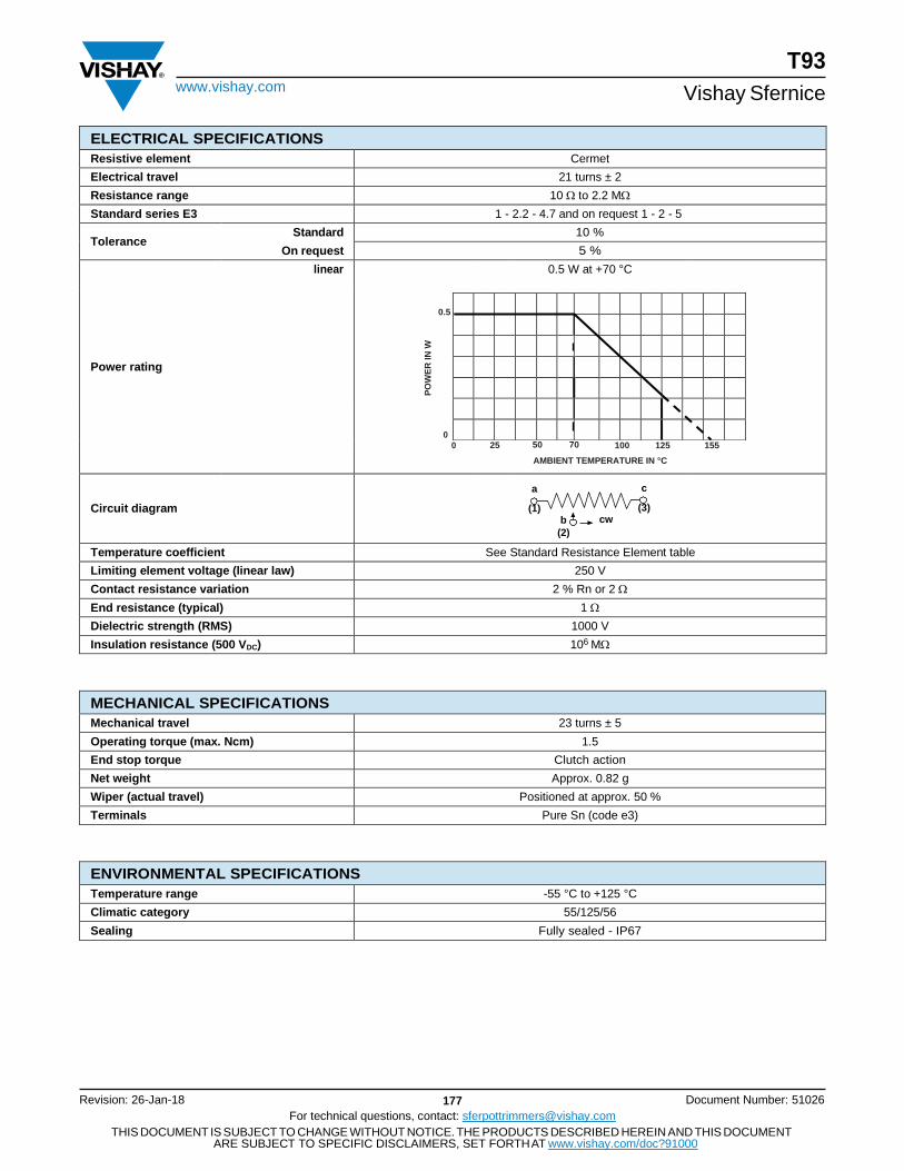
T93
Vishay Sfernice www.vishay.com
Revision: 26-Jan-18 177
For technical questions, contact: [email protected]
Document Number: 51026
THIS DOCUMENT IS SUBJECT TO CHANGE WITHOUT NOTICE. THE PRODUCTS DESCRIBED HEREIN AND THIS DOCUMENT ARE SUBJECT TO SPECIFIC DISCLAIMERS, SET FORTH AT www.vishay.com/doc?91000
PO
WE
R I
N W
ELECTRICAL SPECIFICATIONS
Resistive element Cermet
Electrical travel 21 turns ± 2
Resistance range 10 to 2.2 M
Standard series E3 1 - 2.2 - 4.7 and on request 1 - 2 - 5
Tolerance Standard
On request
10 %
5 %
linear 0.5 W at +70 °C
0.5
Power rating
0
0 25 50 70 100 125 155
AMBIENT TEMPERATURE IN °C
Circuit diagram
a c
(1) (3) b cw
(2)
Temperature coefficient See Standard Resistance Element table
Limiting element voltage (linear law) 250 V
Contact resistance variation 2 % Rn or 2
End resistance (typical) 1
Dielectric strength (RMS) 1000 V
Insulation resistance (500 VDC) 106 M
MECHANICAL SPECIFICATIONS
Mechanical travel 23 turns ± 5
Operating torque (max. Ncm) 1.5
End stop torque Clutch action
Net weight Approx. 0.82 g
Wiper (actual travel) Positioned at approx. 50 %
Terminals Pure Sn (code e3)
ENVIRONMENTAL SPECIFICATIONS
Temperature range -55 °C to +125 °C
Climatic category 55/125/56
Sealing Fully sealed - IP67
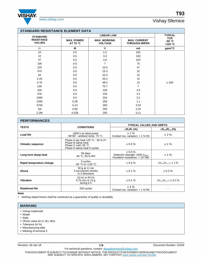
T93
Vishay Sfernice www.vishay.com
Revision: 26-Jan-18 178
For technical questions, contact: [email protected]
Document Number: 51026
THIS DOCUMENT IS SUBJECT TO CHANGE WITHOUT NOTICE. THE PRODUCTS DESCRIBED HEREIN AND THIS DOCUMENT ARE SUBJECT TO SPECIFIC DISCLAIMERS, SET FORTH AT www.vishay.com/doc?91000
• Vishay trademark
• Model
• Style
• Ohmic value (in , k, M)
• Tolerance (in %)
• Manufacturing date
• Marking of terminal 3
STANDARD RESISTANCE ELEMENT DATA
STANDARD RESISTANCE
VALUES
LINEAR LAW TYPICAL TCR
-55 °C +125 °C
MAX. POWER AT 70 °C
MAX. WORKING VOLTAGE
MAX. CURRENT THROUGH WIPER
W V mA ppm/°C
10 0.5 2.2 224
22 0.5 3.3 150
47 0.5 4.8 103
100 0.5 7 70
220 0.5 10.5 47
470 0.5 15.3 32
1K 0.5 22.4 22
2.2K 0.5 33.2 15
4.7K 0.5 48.5 10 ± 100
10K 0.5 70.7 7
22K 0.5 105 4.8
47K 0.5 153 3.2
100K 0.5 224 2.2
220K 0.28 250 1.1
470K 0.13 250 0.53
1M 0.06 250 0.25
2.2M 0.028 250 0.11
PERFORMANCES
TESTS CONDITIONS TYPICAL VALUES AND DRIFTS
RT/RT (%) R1-2/R1-2 (%)
Load life 1000 h at rated power
90'/30' - ambient temp. 70 °C ± 1 %
Contact res. variation: < 1 % Rn ± 2 %
Climatic sequence
Phase A dry heat 125 °C - 30 % Pr Phase B damp heat Phase C cold -55 °C Phase D damp heat 5 cycles
± 0.5 %
± 1 %
Long term damp heat 56 days
40 °C, 93 % RH
± 0.5 % Dielectric strength: 1000 VRMS
Insulation resistance: > 104 M
± 1 %
Rapid temperature change 5 cycles
-55 °C to +125 °C ± 0.5 % V1-2/V1-3 ± 1 %
Shock
50 g at 11 ms 3 successive shocks
in 3 directions
± 0.1 %
± 0.2 %
Vibration
10 Hz to 55 Hz 0.75 mm or 10 g
during 6 h
± 0.1 %
V1-2/V1-3 ± 0.2 %
Rotational life 200 cycles ± 4 %
Contact res. variation: < 1 % Rn -
Note
• Nothing stated herein shall be construed as a guarantee of quality or durability
MARKING
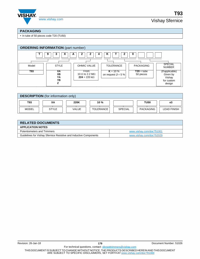
T93
Vishay Sfernice www.vishay.com
Revision: 26-Jan-18 179
For technical questions, contact: [email protected]
Document Number: 51026
THIS DOCUMENT IS SUBJECT TO CHANGE WITHOUT NOTICE. THE PRODUCTS DESCRIBED HEREIN AND THIS DOCUMENT ARE SUBJECT TO SPECIFIC DISCLAIMERS, SET FORTH AT www.vishay.com/doc?91000
• In tube of 50 pieces code T20 (TU50)
ORDERING INFORMATION (part number)
T 9 3 X A 2 2 4 K T 2 0
Model
STYLE
OHMIC VALUE
TOLERANCE
PACKAGING
SPECIAL NUMBER
T93 XA XB YA YB Z
From 10 to 2.2 M
224 = 220 k
K = 10 %
on request J = 5 %
T20 = tube 50 pieces
(If applicable)
Given by
Vishay for custom
design
DESCRIPTION (for information only)
T93
MODEL
XA
STYLE
220K
VALUE
10 %
TOLERANCE
SPECIAL
TU50
PACKAGING
e3
LEAD FINISH
RELATED DOCUMENTS
APPLICATION NOTES
Potentiometers and Trimmers www.vishay.com/doc?51001
Guidelines for Vishay Sfernice Resistive and Inductive Components www.vishay.com/doc?52029
PACKAGING
T93
Vishay Sfernice www.vishay.com
Revision: 26-Jan-18 180
For technical questions, contact: [email protected]
Document Number: 51026
THIS DOCUMENT IS SUBJECT TO CHANGE WITHOUT NOTICE. THE PRODUCTS DESCRIBED HEREIN AND THIS DOCUMENT ARE SUBJECT TO SPECIFIC DISCLAIMERS, SET FORTH AT www.vishay.com/doc?91000
Legal Disclaimer Notice www.vishay.com Vishay
Disclaimer
ALL PRODUCT, PRODUCT SPECIFICATIONS AND DATA ARE SUBJECT TO CHANGE WITHOUT NOTICE TO IMPROVE
RELIABILITY, FUNCTION OR DESIGN OR OTHERWISE.
Vishay Intertechnology, Inc., its affiliates, agents, and employees, and all persons acting on its or their behalf (collectively,
“Vishay”), disclaim any and all liability for any errors, inaccuracies or incompleteness contained in any datasheet or in any other
disclosure relating to any product.
Vishay makes no warranty, representation or guarantee regarding the suitability of the products for any particular purpose or
the continuing production of any product. To the maximum extent permitted by applicable law, Vishay disclaims (i) any and all
liability arising out of the application or use of any product, (ii) any and all liability, including without limitation special,
consequential or incidental damages, and (iii) any and all implied warranties, including warranties of fitness for particular
purpose, non-infringement and merchantability.
Statements regarding the suitability of products for certain types of applications are based on Vishay’s knowledge of
typical requirements that are often placed on Vishay products in generic applications. Such statements are not binding
statements about the suitability of products for a particular application. It is the customer’s responsibility to validate that a
particular product with the properties described in the product specification is suitable for use in a particular application.
Parameters provided in datasheets and / or specifications may vary in different applications and performance may vary over
time. All operating parameters, including typical parameters, must be validated for each customer application by the customer’s
technical experts. Product specifications do not expand or otherwise modify Vishay’s terms and conditions of purchase,
including but not limited to the warranty expressed therein.
Except as expressly indicated in writing, Vishay products are not designed for use in medical, life-saving, or life-sustaining
applications or for any other application in which the failure of the Vishay product could result in personal injury or death.
Customers using or selling Vishay products not expressly indicated for use in such applications do so at their own risk.
Please contact authorized Vishay personnel to obtain written terms and conditions regarding products designed for
such applications.
No license, express or implied, by estoppel or otherwise, to any intellectual property rights is granted by this document
or by any conduct of Vishay. Product names and markings noted herein may be trademarks of their respective owners.
© 2021 VISHAY INTERTECHNOLOGY, INC. ALL RIGHTS RESERVED
Revision: 01-Jan-2021 1 Document Number: 91000
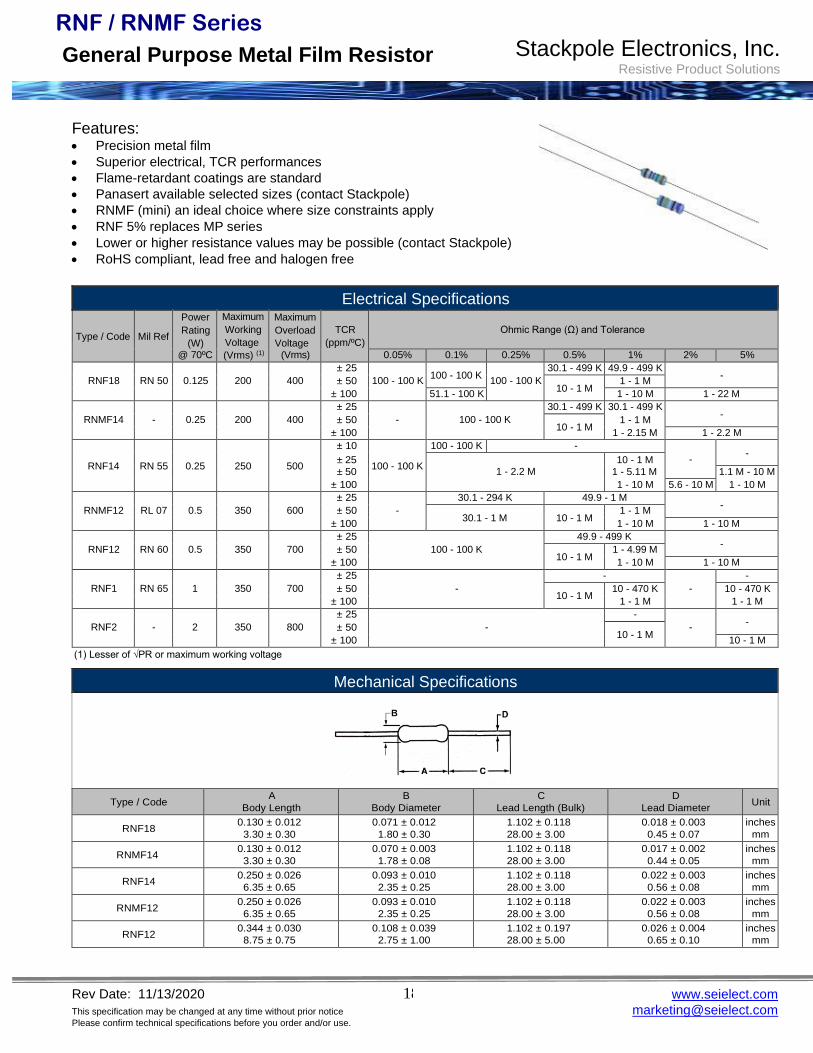
RNF / RNMF Series
General Purpose Metal Film Resistor Stackpole Electronics, Inc. Resistive Product Solutions
181 Rev Date: 11/13/2020
This specification may be changed at any time without prior notice
Please confirm technical specifications before you order and/or use.
www.seielect.com
Features: • Precision metal film
• Superior electrical, TCR performances
• Flame-retardant coatings are standard
• Panasert available selected sizes (contact Stackpole)
• RNMF (mini) an ideal choice where size constraints apply
• RNF 5% replaces MP series
• Lower or higher resistance values may be possible (contact Stackpole)
• RoHS compliant, lead free and halogen free
Electrical Specifications
Type / Code
Mil Ref
Power
Rating
(W) @ 70ºC
Maximum
Working
Voltage
(Vrms) (1)
Maximum
Overload
Voltage (Vrms)
TCR
(ppm/ºC)
Ohmic Range (Ω) and Tolerance
0.05% 0.1% 0.25% 0.5% 1% 2% 5% ± 25
100 - 100 K 30.1 - 499 K 49.9 - 499 K
- RNF18 RN 50 0.125 200 400 ± 50 100 - 100 K 100 - 100 K
10 - 1 M 1 - 1 M
± 100 51.1 - 100 K 1 - 10 M 1 - 22 M ± 25 30.1 - 499 K 30.1 - 499 K
- RNMF14 - 0.25 200 400 ± 50 - 100 - 100 K
10 - 1 M 1 - 1 M
± 100 1 - 2.15 M 1 - 2.2 M ± 10 100 - 100 K -
-
RNF14 RN 55 0.25 250 500 ± 25
± 50 100 - 100 K
1 - 2.2 M
10 - 1 M
1 - 5.11 M
-
1.1 M - 10 M ± 100 1 - 10 M 5.6 - 10 M 1 - 10 M ± 25 30.1 - 294 K 49.9 - 1 M
- RNMF12 RL 07 0.5 350 600 ± 50 -
30.1 - 1 M 10 - 1 M 1 - 1 M
± 100 1 - 10 M 1 - 10 M ± 25 49.9 - 499 K
- RNF12 RN 60 0.5 350 700 ± 50 100 - 100 K
10 - 1 M 1 - 4.99 M
± 100 1 - 10 M 1 - 10 M ± 25 - -
RNF1 RN 65 1 350 700 ± 50 - 10 - 1 M
10 - 470 K - 10 - 470 K ± 100 1 - 1 M 1 - 1 M ± 25 -
- RNF2 - 2 350 800 ± 50 -
10 - 1 M -
± 100 10 - 1 M
(1) Lesser of √PR or maximum working voltage
Mechanical Specifications
Type / Code A
Body Length
B
Body Diameter
C
Lead Length (Bulk)
D
Lead Diameter Unit
RNF18 0.130 ± 0.012
3.30 ± 0.30
0.071 ± 0.012
1.80 ± 0.30
1.102 ± 0.118
28.00 ± 3.00
0.018 ± 0.003
0.45 ± 0.07
inches
mm
RNMF14 0.130 ± 0.012
3.30 ± 0.30
0.070 ± 0.003
1.78 ± 0.08
1.102 ± 0.118
28.00 ± 3.00
0.017 ± 0.002
0.44 ± 0.05
inches
mm
RNF14 0.250 ± 0.026
6.35 ± 0.65
0.093 ± 0.010
2.35 ± 0.25
1.102 ± 0.118
28.00 ± 3.00
0.022 ± 0.003
0.56 ± 0.08
inches
mm
RNMF12 0.250 ± 0.026
6.35 ± 0.65
0.093 ± 0.010
2.35 ± 0.25
1.102 ± 0.118
28.00 ± 3.00
0.022 ± 0.003
0.56 ± 0.08
inches
mm
RNF12 0.344 ± 0.030
8.75 ± 0.75
0.108 ± 0.039
2.75 ± 1.00
1.102 ± 0.197
28.00 ± 5.00
0.026 ± 0.004
0.65 ± 0.10
inches
mm
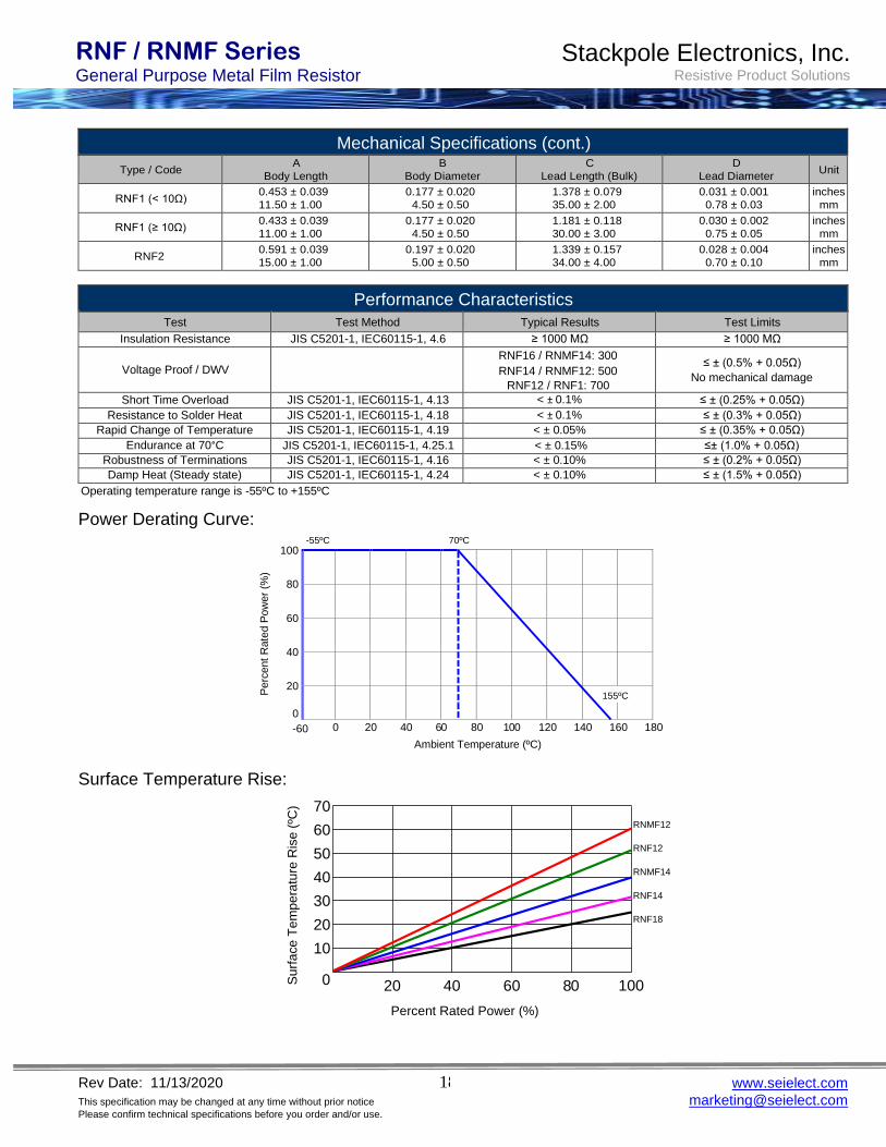
RNF / RNMF Series General Purpose Metal Film Resistor
Stackpole Electronics, Inc. Resistive Product Solutions
182 Rev Date: 11/13/2020
This specification may be changed at any time without prior notice
Please confirm technical specifications before you order and/or use.
www.seielect.com
Mechanical Specifications (cont.)
Type / Code A
Body Length
B
Body Diameter
C
Lead Length (Bulk)
D
Lead Diameter Unit
RNF1 (< 10Ω) 0.453 ± 0.039
11.50 ± 1.00
0.177 ± 0.020
4.50 ± 0.50
1.378 ± 0.079
35.00 ± 2.00
0.031 ± 0.001
0.78 ± 0.03
inches
mm
RNF1 (≥ 10Ω) 0.433 ± 0.039
11.00 ± 1.00
0.177 ± 0.020
4.50 ± 0.50
1.181 ± 0.118
30.00 ± 3.00
0.030 ± 0.002
0.75 ± 0.05
inches
mm
RNF2 0.591 ± 0.039
15.00 ± 1.00
0.197 ± 0.020
5.00 ± 0.50
1.339 ± 0.157
34.00 ± 4.00
0.028 ± 0.004
0.70 ± 0.10
inches
mm
Performance Characteristics
Test Test Method Typical Results Test Limits
Insulation Resistance JIS C5201-1, IEC60115-1, 4.6 ≥ 1000 MΩ ≥ 1000 MΩ
Voltage Proof / DWV
RNF16 / RNMF14: 300
RNF14 / RNMF12: 500
RNF12 / RNF1: 700
≤ ± (0.5% + 0.05Ω)
No mechanical damage
Short Time Overload JIS C5201-1, IEC60115-1, 4.13 < ± 0.1% ≤ ± (0.25% + 0.05Ω)
Resistance to Solder Heat JIS C5201-1, IEC60115-1, 4.18 < ± 0.1% ≤ ± (0.3% + 0.05Ω)
Rapid Change of Temperature JIS C5201-1, IEC60115-1, 4.19 < ± 0.05% ≤ ± (0.35% + 0.05Ω)
Endurance at 70°C JIS C5201-1, IEC60115-1, 4.25.1 < ± 0.15% ≤± (1.0% + 0.05Ω)
Robustness of Terminations JIS C5201-1, IEC60115-1, 4.16 < ± 0.10% ≤ ± (0.2% + 0.05Ω)
Damp Heat (Steady state) JIS C5201-1, IEC60115-1, 4.24 < ± 0.10% ≤ ± (1.5% + 0.05Ω)
Operating temperature range is -55ºC to +155ºC
Power Derating Curve: -55ºC 70ºC
100
80
60
40
20
0
-60 0 20 40 60
80 100
120 140 160 180
Surface Temperature Rise:
70
60
50
40
30
20
10
0
Ambient Temperature (ºC)
20 40 60 80
Percent Rated Power (%)
RNMF12
RNF12
RNMF14
RNF14
RNF18
100
Pe
rce
nt
Rate
d P
ow
er
(%)
Su
rfa
ce
Te
mp
era
ture
Ris
e (
ºC)
155ºC
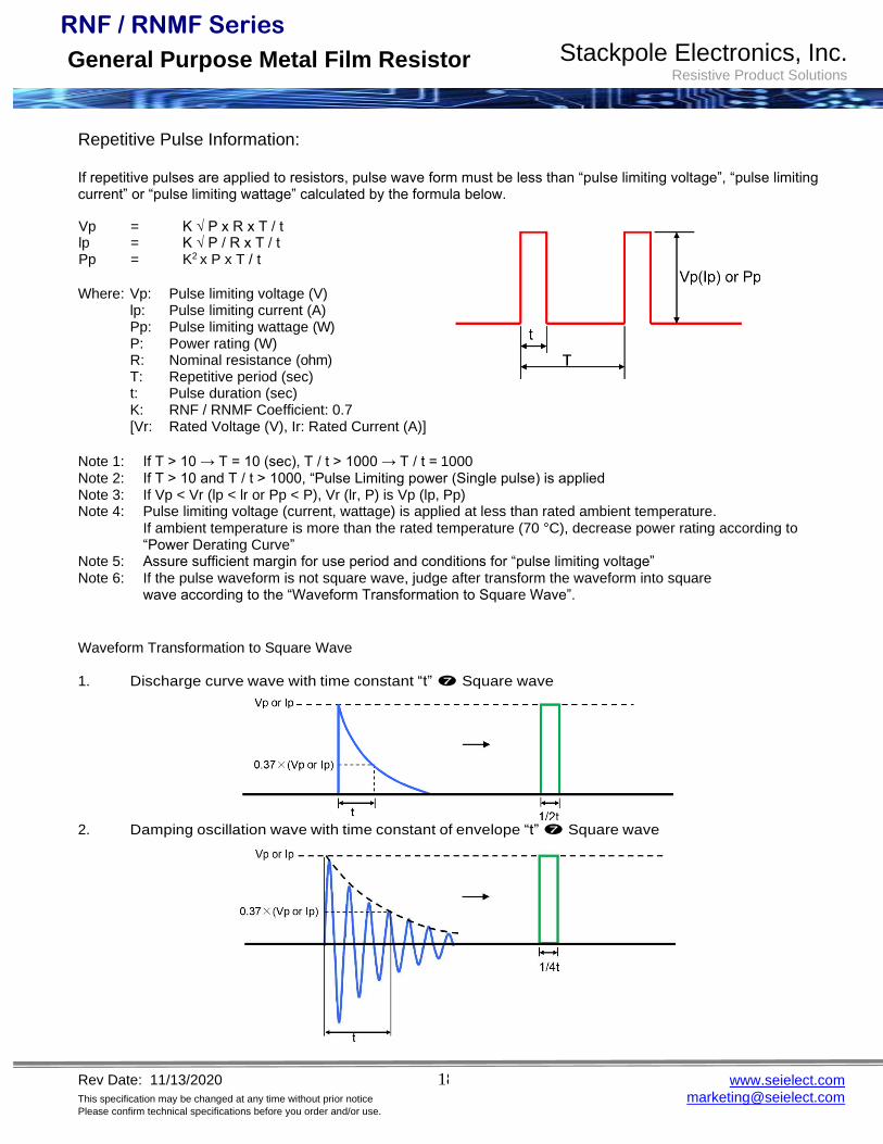
RNF / RNMF Series
General Purpose Metal Film Resistor Stackpole Electronics, Inc. Resistive Product Solutions
183 Rev Date: 11/13/2020
This specification may be changed at any time without prior notice
Please confirm technical specifications before you order and/or use.
www.seielect.com
Repetitive Pulse Information:
If repetitive pulses are applied to resistors, pulse wave form must be less than “pulse limiting voltage”, “pulse limiting current” or “pulse limiting wattage” calculated by the formula below.
Vp = K √ P x R x T / t lp = K √ P / R x T / t Pp = K2 x P x T / t
Where: Vp: Pulse limiting voltage (V) lp: Pulse limiting current (A) Pp: Pulse limiting wattage (W) P: Power rating (W) R: Nominal resistance (ohm) T: Repetitive period (sec) t: Pulse duration (sec) K: RNF / RNMF Coefficient: 0.7 [Vr: Rated Voltage (V), Ir: Rated Current (A)]
Note 1: If T > 10 → T = 10 (sec), T / t > 1000 → T / t = 1000 Note 2: If T > 10 and T / t > 1000, “Pulse Limiting power (Single pulse) is applied Note 3: If Vp < Vr (lp < lr or Pp < P), Vr (lr, P) is Vp (lp, Pp) Note 4: Pulse limiting voltage (current, wattage) is applied at less than rated ambient temperature.
If ambient temperature is more than the rated temperature (70 °C), decrease power rating according to “Power Derating Curve”
Note 5: Assure sufficient margin for use period and conditions for “pulse limiting voltage” Note 6: If the pulse waveform is not square wave, judge after transform the waveform into square
wave according to the “Waveform Transformation to Square Wave”.
Waveform Transformation to Square Wave
1. Discharge curve wave with time constant “t” Square wave
2. Damping oscillation wave with time constant of envelope “t” Square wave
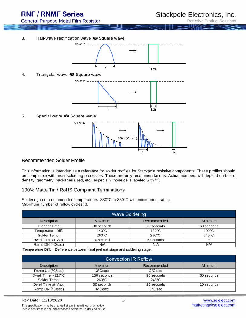
RNF / RNMF Series General Purpose Metal Film Resistor
Stackpole Electronics, Inc. Resistive Product Solutions
184 Rev Date: 11/13/2020
This specification may be changed at any time without prior notice
Please confirm technical specifications before you order and/or use.
www.seielect.com
3. Half-wave rectification wave Square wave
4. Triangular wave Square wave
5. Special wave Square wave
Recommended Solder Profile
This information is intended as a reference for solder profiles for Stackpole resistive components. These profiles should be compatible with most soldering processes. These are only recommendations. Actual numbers will depend on board density, geometry, packages used, etc., especially those cells labeled with “*”.
100% Matte Tin / RoHS Compliant Terminations
Soldering iron recommended temperatures: 330°C to 350°C with minimum duration. Maximum number of reflow cycles: 3.
Wave Soldering
Description Maximum Recommended Minimum
Preheat Time 80 seconds 70 seconds 60 seconds
Temperature Diff. 140°C 120°C 100°C
Solder Temp. 260°C 250°C 240°C
Dwell Time at Max. 10 seconds 5 seconds *
Ramp DN (°C/sec) N/A N/A N/A
Temperature Diff. = Defference between final preheat stage and soldering stage.
Convection IR Reflow
Description Maximum Recommended Minimum
Ramp Up (°C/sec) 3°C/sec 2°C/sec *
Dwell Time > 217°C 150 seconds 90 seconds 60 seconds
Solder Temp. 260°C 245°C *
Dwell Time at Max. 30 seconds 15 seconds 10 seconds
Ramp DN (°C/sec) 6°C/sec 3°C/sec *
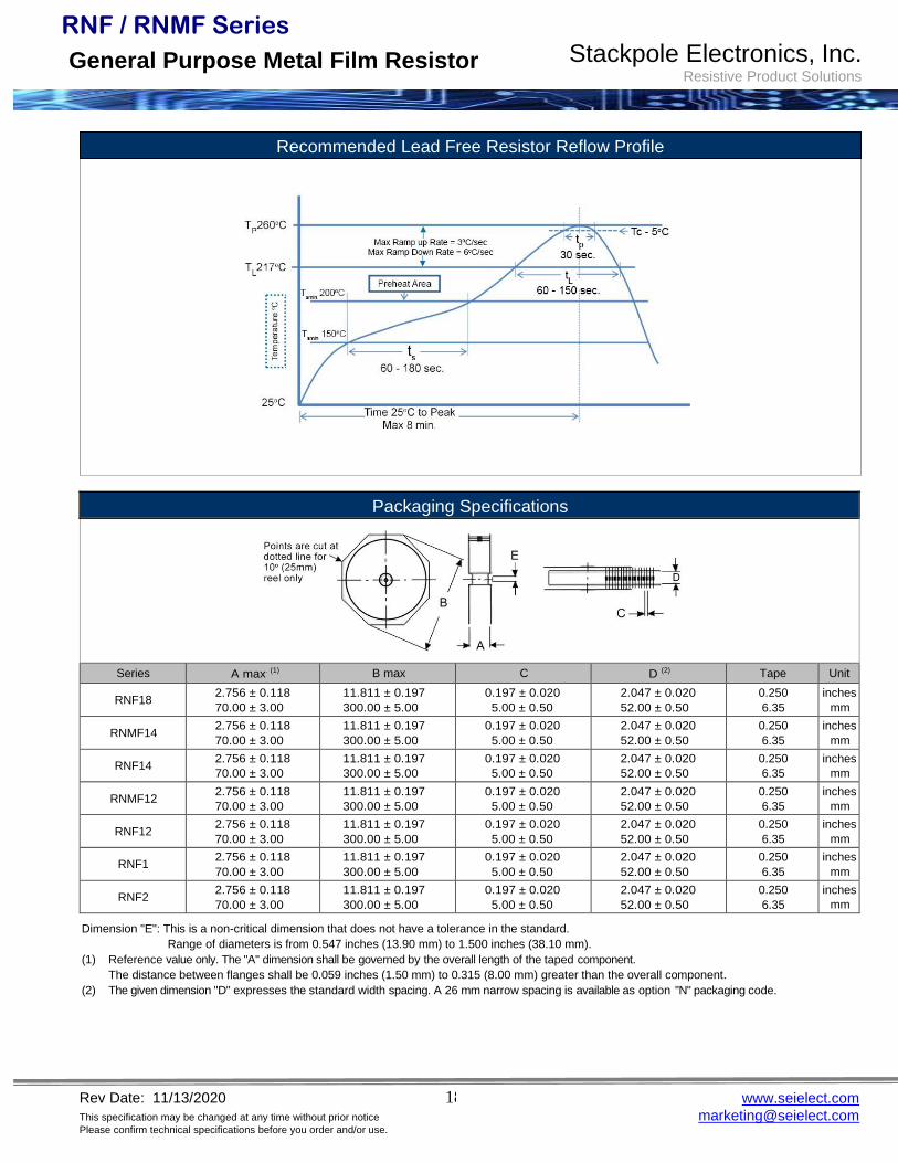
RNF / RNMF Series
General Purpose Metal Film Resistor Stackpole Electronics, Inc. Resistive Product Solutions
185 Rev Date: 11/13/2020
This specification may be changed at any time without prior notice
Please confirm technical specifications before you order and/or use.
www.seielect.com
Packaging Specifications
Series A max. (1) B max C D (2) Tape Unit
RNF18 2.756 ± 0.118
70.00 ± 3.00
11.811 ± 0.197
300.00 ± 5.00
0.197 ± 0.020
5.00 ± 0.50
2.047 ± 0.020
52.00 ± 0.50
0.250
6.35
inches
mm
RNMF14 2.756 ± 0.118
70.00 ± 3.00
11.811 ± 0.197
300.00 ± 5.00
0.197 ± 0.020
5.00 ± 0.50
2.047 ± 0.020
52.00 ± 0.50
0.250
6.35
inches
mm
RNF14 2.756 ± 0.118
70.00 ± 3.00
11.811 ± 0.197
300.00 ± 5.00
0.197 ± 0.020
5.00 ± 0.50
2.047 ± 0.020
52.00 ± 0.50
0.250
6.35
inches
mm
RNMF12 2.756 ± 0.118
70.00 ± 3.00
11.811 ± 0.197
300.00 ± 5.00
0.197 ± 0.020
5.00 ± 0.50
2.047 ± 0.020
52.00 ± 0.50
0.250
6.35
inches
mm
RNF12 2.756 ± 0.118
70.00 ± 3.00
11.811 ± 0.197
300.00 ± 5.00
0.197 ± 0.020
5.00 ± 0.50
2.047 ± 0.020
52.00 ± 0.50
0.250
6.35
inches
mm
RNF1 2.756 ± 0.118
70.00 ± 3.00
11.811 ± 0.197
300.00 ± 5.00
0.197 ± 0.020
5.00 ± 0.50
2.047 ± 0.020
52.00 ± 0.50
0.250
6.35
inches
mm
RNF2 2.756 ± 0.118
70.00 ± 3.00
11.811 ± 0.197
300.00 ± 5.00
0.197 ± 0.020
5.00 ± 0.50
2.047 ± 0.020
52.00 ± 0.50
0.250
6.35
inches
mm
Dimension "E": This is a non-critical dimension that does not have a tolerance in the standard.
Range of diameters is from 0.547 inches (13.90 mm) to 1.500 inches (38.10 mm).
(1) Reference value only. The "A" dimension shall be governed by the overall length of the taped component.
The distance between flanges shall be 0.059 inches (1.50 mm) to 0.315 (8.00 mm) greater than the overall component.
(2) The given dimension "D" expresses the standard width spacing. A 26 mm narrow spacing is available as option "N" packaging code.
Recommended Lead Free Resistor Reflow Profile
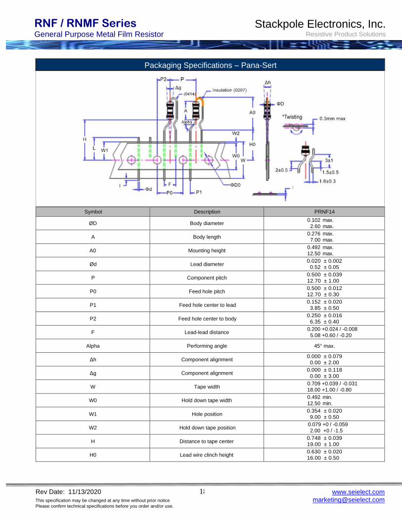
RNF / RNMF Series General Purpose Metal Film Resistor
Stackpole Electronics, Inc. Resistive Product Solutions
186 Rev Date: 11/13/2020
This specification may be changed at any time without prior notice
Please confirm technical specifications before you order and/or use.
www.seielect.com
Packaging Specifications – Pana-Sert
Symbol Description PRNF14
ØD Body diameter 0.102 max.
2.60 max.
A Body length 0.276 max.
7.00 max.
A0 Mounting height 0.492 max.
12.50 max.
Ød Lead diameter 0.020 ± 0.002
0.52 ± 0.05
P Component pitch 0.500 ± 0.039
12.70 ± 1.00
P0 Feed hole pitch 0.500 ± 0.012
12.70 ± 0.30
P1 Feed hole center to lead 0.152 ± 0.020
3.85 ± 0.50
P2 Feed hole center to body 0.250 ± 0.016
6.35 ± 0.40
F Lead-lead distance 0.200 +0.024 / -0.008
5.08 +0.60 / -0.20
Alpha Performing angle 45° max.
Δh Component alignment 0.000 ± 0.079
0.00 ± 2.00
Δg Component alignment 0.000 ± 0.118
0.00 ± 3.00
W Tape width 0.709 +0.039 / -0.031
18.00 +1.00 / -0.80
W0 Hold down tape width 0.492 min.
12.50 min.
W1 Hole position 0.354 ± 0.020
9.00 ± 0.50
W2 Hold down tape position 0.079 +0 / -0.059
2.00 +0 / -1.5
H Distance to tape center 0.748 ± 0.039
19.00 ± 1.00
H0 Lead wire clinch height 0.630 ± 0.020
16.00 ± 0.50
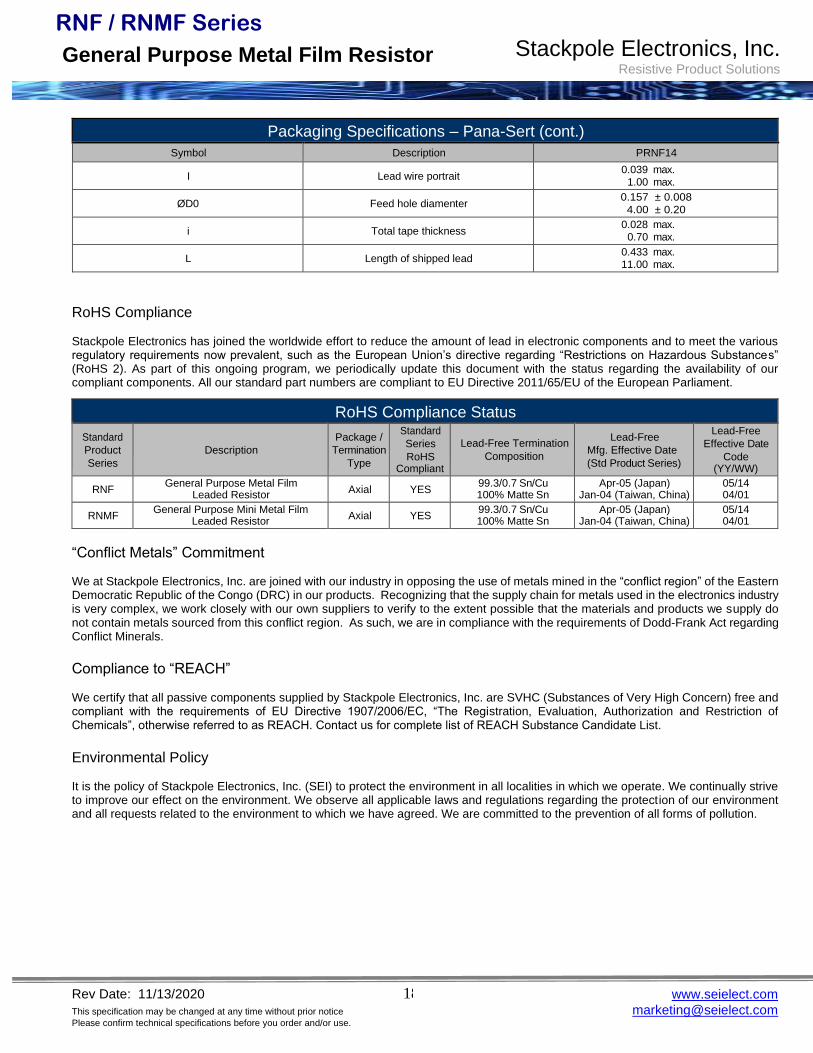
RNF / RNMF Series
General Purpose Metal Film Resistor Stackpole Electronics, Inc. Resistive Product Solutions
187 Rev Date: 11/13/2020
This specification may be changed at any time without prior notice
Please confirm technical specifications before you order and/or use.
www.seielect.com
Packaging Specifications – Pana-Sert (cont.)
Symbol Description PRNF14
I Lead wire portrait 0.039 max.
1.00 max.
ØD0 Feed hole diamenter 0.157 ± 0.008
4.00 ± 0.20
i Total tape thickness 0.028 max.
0.70 max.
L Length of shipped lead 0.433 max. 11.00 max.
RoHS Compliance
Stackpole Electronics has joined the worldwide effort to reduce the amount of lead in electronic components and to meet the various regulatory requirements now prevalent, such as the European Union’s directive regarding “Restrictions on Hazardous Substances” (RoHS 2). As part of this ongoing program, we periodically update this document with the status regarding the availability of our compliant components. All our standard part numbers are compliant to EU Directive 2011/65/EU of the European Parliament.
RoHS Compliance Status
Standard
Product
Series
Description
Package /
Termination
Type
Standard
Series
RoHS Compliant
Lead-Free Termination
Composition
Lead-Free
Mfg. Effective Date
(Std Product Series)
Lead-Free
Effective Date
Code (YY/WW)
RNF General Purpose Metal Film
Leaded Resistor Axial YES
99.3/0.7 Sn/Cu 100% Matte Sn
Apr-05 (Japan) Jan-04 (Taiwan, China)
05/14 04/01
RNMF General Purpose Mini Metal Film
Leaded Resistor Axial YES
99.3/0.7 Sn/Cu 100% Matte Sn
Apr-05 (Japan) Jan-04 (Taiwan, China)
05/14 04/01
“Conflict Metals” Commitment
We at Stackpole Electronics, Inc. are joined with our industry in opposing the use of metals mined in the “conflict region” of the Eastern Democratic Republic of the Congo (DRC) in our products. Recognizing that the supply chain for metals used in the electronics industry is very complex, we work closely with our own suppliers to verify to the extent possible that the materials and products we supply do not contain metals sourced from this conflict region. As such, we are in compliance with the requirements of Dodd-Frank Act regarding Conflict Minerals.
Compliance to “REACH”
We certify that all passive components supplied by Stackpole Electronics, Inc. are SVHC (Substances of Very High Concern) free and compliant with the requirements of EU Directive 1907/2006/EC, “The Registration, Evaluation, Authorization and Restriction of Chemicals”, otherwise referred to as REACH. Contact us for complete list of REACH Substance Candidate List.
Environmental Policy
It is the policy of Stackpole Electronics, Inc. (SEI) to protect the environment in all localities in which we operate. We continually strive to improve our effect on the environment. We observe all applicable laws and regulations regarding the protection of our environment and all requests related to the environment to which we have agreed. We are committed to the prevention of all forms of pollution.
RNF / RNMF Series General Purpose Metal Film Resistor
Stackpole Electronics, Inc. Resistive Product Solutions
188 Rev Date: 11/13/2020
This specification may be changed at any time without prior notice
Please confirm technical specifications before you order and/or use.
www.seielect.com
Product Series
Code Description
Power Rating Tolerance
Code W Code Tol Value Code Description
PRNF Panasert 12 0.5
RoHS 1 1
2 2
C
D
F
G
0.25%
0.5%
1%
2%
E96
E24
T Tape and Reel
E24 A Ammo
Packaging
Size
RNF18, RNF14
RNMF14, RNMF12
RNF12, RNF1
RNF2
RNF18, RNF14
RNMF14, RNMF12
Quantity
5000
2500
1000
5000 (*)
TCR
Code ppm
T
E
C
D
10
25
50
100
Resistance Value
Four characters with
the multiplier used
as the decimal
holder.
10 ohm = 10R0
10.2 K ohm = 10K2
1 M ohm = 1M00
1 2 3 4 5 6 7 8 9 10 11 12
R
N
F
1
4
F
T
D
4
K
7
5
RNF Standard 18 0.125 A 0.05%
RNMF Mini 14 0.25 B 0.1%
J 5% RNF12 2000
RNF1, RNF2 1000
B
Bulk
RNF18, RNF14,
RNF12, RNF1, RNF2,
1000 RNMF12, RNMF14
(*) Precision metal film resistors with tolerances <1% may be available in smaller quantities. Contact Stackpole for more details.
How to Order

189 Rev Date: 11/13/2020
This specification may be changed at any time without prior notice
Please confirm technical specifications before you order and/or use.
www.seielect.com
Axial-Lead Glass Passivated Standard Recovery Rectifiers
1N4001, 1N4002, 1N4003, 1N4004, 1N4005, 1N4006, 1N4007 This data sheet provides information on subminiature size, axial
lead mounted rectifiers for general−purpose low−power
applications.
Features
• Shipped in Plastic Bags, 1000 per bag
• Available Tape and Reeled, 5000 per reel, by adding a “RL” suffix to
the part number
• Available in Fan−Fold Packaging, 3000 per box, by adding a “FF”
suffix to the part number
• Pb−Free Packages are Available
Mechanical Characteristics
• Case: Epoxy, Molded
• Weight: 0.4 gram (approximately)
• Finish: All External Surfaces Corrosion Resistant and Terminal
Leads are Readily Solderable
• Lead and Mounting Surface Temperature for Soldering Purposes:
260C Max. for 10 Seconds, 1/16 in. from case
• Polarity: Cathode Indicated by Polarity Band
www.onsemi.com
LEAD MOUNTED RECTIFIERS
50−1000 VOLTS
DIFFUSED JUNCTION
CASE 59−10
AXIAL LEAD
PLASTIC
MARKING DIAGRAM
*For additional information on our Pb−Free strategy and soldering details, please
download the ON Semiconductor Soldering and Mounting Techniques Reference Manual, SOLDERRM/D.
A
1N400x
YYW
W
A = Assembly Location
1N400x = Device Number
x = 1, 2, 3, 4, 5, 6 or 7
YY = Year
W
W = Work Week
= Pb−Free Package (Note: Microdot may be in either location)
ORDERING INFORMATION
See detailed ordering and shipping information on page 5 of
this data sheet.
Semiconductor Components Industries, LLC, 2012
October, 2020 − Rev. 15 1 Publication Order Number:
1N4001/D
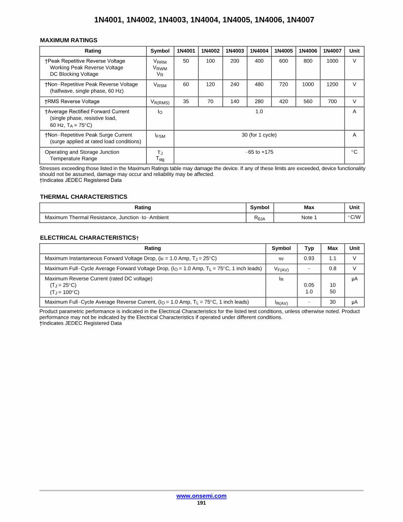
1N4001, 1N4002, 1N4003, 1N4004, 1N4005, 1N4006, 1N4007
www.onsemi.com 191
MAXIMUM RATINGS
Rating Symbol 1N4001 1N4002 1N4003 1N4004 1N4005 1N4006 1N4007 Unit
†Peak Repetitive Reverse Voltage
Working Peak Reverse Voltage
DC Blocking Voltage
VRRM
VRWM
VR
50 100 200 400 600 800 1000 V
†Non−Repetitive Peak Reverse Voltage
(halfwave, single phase, 60 Hz)
VRSM 60 120 240 480 720 1000 1200 V
†RMS Reverse Voltage VR(RMS) 35 70 140 280 420 560 700 V
†Average Rectified Forward Current
(single phase, resistive load,
60 Hz, TA = 75C)
IO 1.0 A
†Non−Repetitive Peak Surge Current
(surge applied at rated load conditions)
IFSM 30 (for 1 cycle) A
Operating and Storage Junction
Temperature Range TJ
Tstg
−65 to +175 C
Stresses exceeding those listed in the Maximum Ratings table may damage the device. If any of these limits are exceeded, device functionality should not be assumed, damage may occur and reliability may be affected. †Indicates JEDEC Registered Data
THERMAL CHARACTERISTICS
Rating Symbol Max Unit
Maximum Thermal Resistance, Junction−to−Ambient R0JA Note 1 C/W
ELECTRICAL CHARACTERISTICS†
Rating Symbol Typ Max Unit
Maximum Instantaneous Forward Voltage Drop, (iF = 1.0 Amp, TJ = 25C) vF 0.93 1.1 V
Maximum Full−Cycle Average Forward Voltage Drop, (IO = 1.0 Amp, TL = 75C, 1 inch leads) VF(AV) − 0.8 V
Maximum Reverse Current (rated DC voltage)
(TJ = 25C)
IR 0.05
10
µA
(TJ = 100C) 1.0 50
Maximum Full−Cycle Average Reverse Current, (IO = 1.0 Amp, TL = 75C, 1 inch leads) IR(AV) − 30 µA
Product parametric performance is indicated in the Electrical Characteristics for the listed test conditions, unless otherwise noted. Product performance may not be indicated by the Electrical Characteristics if operated under different conditions. †Indicates JEDEC Registered Data
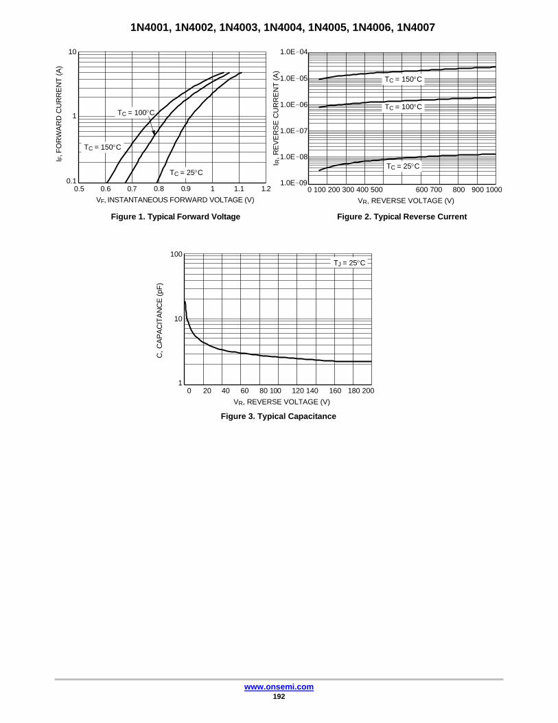
1N4001, 1N4002, 1N4003, 1N4004, 1N4005, 1N4006, 1N4007
www.onsemi.com 192
TC = 100C
TC = 150C
TC = 25C
I R,
RE
VE
RS
E C
UR
RE
NT
(A
)
10 1.0E−04
1.0E−05
1.0E−06
1
1.0E−07
1.0E−08
0.1 0.5 0.6 0.7
0.8 0.9
1 1.1 1.2
1.0E−09 0 100 200 300 400 500
600 700
800
900 1000
VF, INSTANTANEOUS FORWARD VOLTAGE (V) VR, REVERSE VOLTAGE (V)
Figure 1. Typical Forward Voltage Figure 2. Typical Reverse Current
100
10
1 0 20 40 60 80 100
120 140
160
180 200
VR, REVERSE VOLTAGE (V)
Figure 3. Typical Capacitance
TC = 150C
TC = 100C
TC = 25C
TJ = 25C
I F, F
OR
WA
RD
CU
RR
EN
T (
A)
C,
CA
PA
CIT
AN
CE
(pF
)
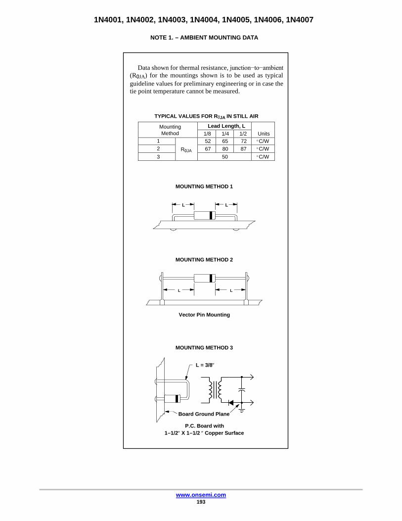
1N4001, 1N4002, 1N4003, 1N4004, 1N4005, 1N4006, 1N4007
www.onsemi.com 193
Data shown for thermal resistance, junction−to−ambient
(R0JA) for the mountings shown is to be used as typical
guideline values for preliminary engineering or in case the
tie point temperature cannot be measured.
TYPICAL VALUES FOR R0JA IN STILL AIR
MOUNTING METHOD 1
L L
MOUNTING METHOD 2
L L
Vector Pin Mounting
MOUNTING METHOD 3
L = 3/8
Board Ground Plane
P.C. Board with
1−1/2 X 1−1/2 Copper Surface
NOTE 1. − AMBIENT MOUNTING DATA
Mounting
Method
Lead Length, L Units 1/8 1/4 1/2
1 R0JA
52 65 72 C/W
2 67 80 87 C/W
3 50 C/W
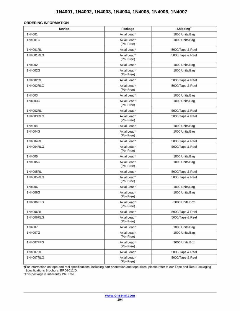
1N4001, 1N4002, 1N4003, 1N4004, 1N4005, 1N4006, 1N4007
www.onsemi.com 194
ORDERING INFORMATION
Device Package Shipping†
1N4001 Axial Lead* 1000 Units/Bag
1N4001G Axial Lead*
(Pb−Free)
1000 Units/Bag
1N4001RL Axial Lead* 5000/Tape & Reel
1N4001RLG Axial Lead*
(Pb−Free)
5000/Tape & Reel
1N4002 Axial Lead* 1000 Units/Bag
1N4002G Axial Lead*
(Pb−Free)
1000 Units/Bag
1N4002RL Axial Lead* 5000/Tape & Reel
1N4002RLG Axial Lead*
(Pb−Free)
5000/Tape & Reel
1N4003 Axial Lead* 1000 Units/Bag
1N4003G Axial Lead*
(Pb−Free)
1000 Units/Bag
1N4003RL Axial Lead* 5000/Tape & Reel
1N4003RLG Axial Lead*
(Pb−Free)
5000/Tape & Reel
1N4004 Axial Lead* 1000 Units/Bag
1N4004G Axial Lead*
(Pb−Free)
1000 Units/Bag
1N4004RL Axial Lead* 5000/Tape & Reel
1N4004RLG Axial Lead*
(Pb−Free)
5000/Tape & Reel
1N4005 Axial Lead* 1000 Units/Bag
1N4005G Axial Lead*
(Pb−Free)
1000 Units/Bag
1N4005RL Axial Lead* 5000/Tape & Reel
1N4005RLG Axial Lead*
(Pb−Free)
5000/Tape & Reel
1N4006 Axial Lead* 1000 Units/Bag
1N4006G Axial Lead*
(Pb−Free)
1000 Units/Bag
1N4006FFG Axial Lead*
(Pb−Free)
3000 Units/Box
1N4006RL Axial Lead* 5000/Tape & Reel
1N4006RLG Axial Lead*
(Pb−Free)
5000/Tape & Reel
1N4007 Axial Lead* 1000 Units/Bag
1N4007G Axial Lead*
(Pb−Free)
1000 Units/Bag
1N4007FFG Axial Lead*
(Pb−Free)
3000 Units/Box
1N4007RL Axial Lead* 5000/Tape & Reel
1N4007RLG Axial Lead*
(Pb−Free)
5000/Tape & Reel
†For information on tape and reel specifications, including part orientation and tape sizes, please refer to our Tape and Reel Packaging Specifications Brochure, BRD8011/D.
*This package is inherently Pb−Free.
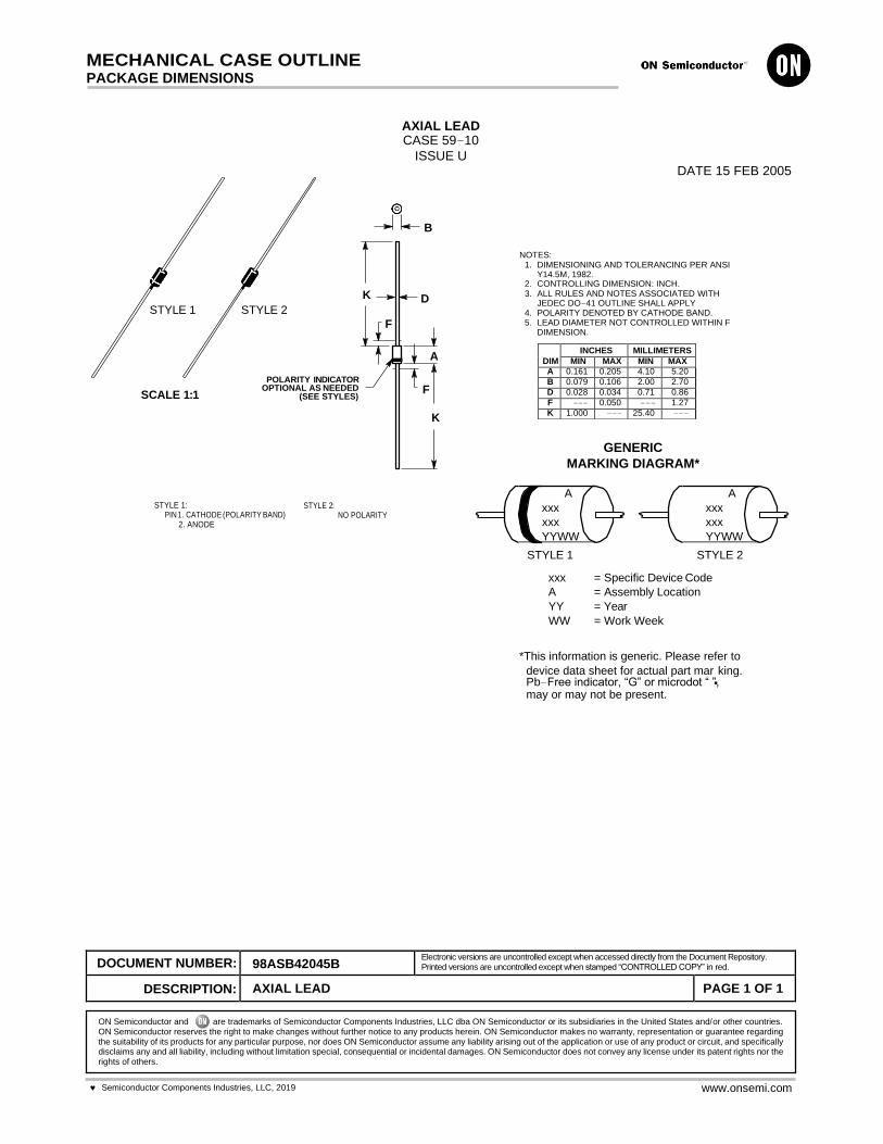
ON Semiconductor reserves the right to make changes without further notice to any products herein. ON Semiconductor makes no warranty, representation or guarantee regarding the suitability of its products for any particular purpose, nor does ON Semiconductor assume any liability arising out of the application or use of any product or circuit, and specifically disclaims any and all liability, including without limitation special, consequential or incidental damages. ON Semiconductor does not convey any license under its patent rights nor the rights of others.
are trademarks of Semiconductor Components Industries, LLC dba ON Semiconductor or its subsidiaries in the United States and/or other countries. ON Semiconductor and
MECHANICAL CASE OUTLINE PACKAGE DIMENSIONS
AXIAL LEAD CASE 59−10
ISSUE U DATE 15 FEB 2005
B
STYLE 1 STYLE 2
NOTES: 1. DIMENSIONING AND TOLERANCING PER ANSI
Y14.5M, 1982. 2. CONTROLLING DIMENSION: INCH. 3. ALL RULES AND NOTES ASSOCIATED WITH
JEDEC DO−41 OUTLINE SHALL APPLY 4. POLARITY DENOTED BY CATHODE BAND. 5. LEAD DIAMETER NOT CONTROLLED WITHIN F
DIMENSION.
SCALE 1:1
POLARITY INDICATOR OPTIONAL AS NEEDED
(SEE STYLES)
GENERIC
MARKING DIAGRAM*
STYLE 1:
PIN 1. CATHODE (POLARITY BAND) 2. ANODE
STYLE 2:
NO POLARITY
A
xxx
xxx
A
xxx
xxx
YYWW YYWW
STYLE 1 STYLE 2
xxx = Specific Device Code
A = Assembly Location
YY = Year
WW = Work Week
*This information is generic. Please refer to
device data sheet for actual part marking.
Pb−Free indicator, “G” or microdot “ ”, may or may not be present.
DOCUMENT NUMBER: 98ASB42045B Electronic versions are uncontrolled except when accessed directly from the Document Repository. Printed versions are uncontrolled except when stamped “CONTROLLED COPY” in red.
DESCRIPTION: AXIAL LEAD PAGE 1 OF 1
Semiconductor Components Industries, LLC, 2019 www.onsemi.com
K D
F
A
F
K
DIM
INCHES MILLIMETERS
MIN MAX MIN MAX
A 0.161 0.205 4.10 5.20
B 0.079 0.106 2.00 2.70
D 0.028 0.034 0.71 0.86
F −−− 0.050 −−− 1.27
K 1.000 −−− 25.40 −−−
PUBLICATION ORDERING INFORMATION
LITERATURE FULFILLMENT:
Email Requests to: [email protected]
ON Semiconductor Website: www.onsemi.com
TECHNICAL SUPPORT
North American Technical Support:
Voice Mail: 1 800−282−9855 Toll Free USA/Canada
Phone: 011 421 33 790 2910
Europe, Middle East and Africa Technical Support:
Phone: 00421 33 790 2910
For additional information, please contact your local Sales Representative
ON Semiconductor and are trademarks of Semiconductor Components Industries, LLC dba ON Semiconductor or its subsidiaries in the United States and/or other countries. ON Semiconductor owns the rights to a number of patents, trademarks, copyrights, trade secrets, and other intellectual property. A listing of ON Semiconductor’s product/patent coverage may be accessed at www.onsemi.com/site/pdf/Patent−Marking.pdf. ON Semiconductor reserves the right to make changes without further notice to any products herein.
ON Semiconductor makes no warranty, representation or guarantee regarding the suitability of its products for any particular purpose, nor does ON Semiconductor assume any liability arising out of the application or use of any product or circuit, and specifically disclaims any and all liability, including without limitation special, consequential or incidental damages. Buyer is responsible for its products and applications using ON Semiconductor products, including compliance with all laws, regulations and safety requirements or standards, regardless of any support or applications information provided by ON Semiconductor. “Typical” parameters which may be provided in ON Semiconductor data sheets and/or specifications can and do vary in different applications and actual performance may vary over time. All operating parameters, including “Typicals” must be validated for each customer application by customer’s technical experts. ON Semiconductor does not convey any license under its patent rights nor the rights of others. ON Semiconductor products are not designed, intended, or authorized for use as a critical component in life support systems or any FDA Class 3 medical devices or medical devices with a same or similar classification in a foreign jurisdiction or any devices intended for implantation in the human body. Should Buyer purchase or use ON Semiconductor products for any such unintended or unauthorized application, Buyer shall indemnify and hold ON Semiconductor and its officers, employees, subsidiaries, affiliates, and distributors harmless against all claims, costs, damages, and expenses, and reasonable attorney fees arising out of, directly or indirectly, any claim of personal injury or death associated with such unintended or unauthorized use, even if such claim alleges that ON Semiconductor was negligent regarding the design or manufacture of the part. ON Semiconductor is an Equal Opportunity/Affirmative Action Employer. This literature is subject to all applicable copyright laws and is not for resale in any manner.
SOD80
Cathode Band
SOD−80 COLOR BAND MARKING
DEVICE 1ST BAND
FDLL914 BLACK FDLL914A BLACK FDLL914B BLACK FDLL4148 BLACK FDLL4448 BLACK
-1st band denotes cathode terminal and has wider width
1N91x, 1N4x48, FDLL914, FDLL4x48
Small Signal Diode
ORDERING INFORMATION
www.onsemi.com
DO−35 Cathode is denoted with a black band
LL−34 THE PLACEMENT OF THE EXPANSION GAP HAS NO RELATIONSHIP TO THE LOCATION OF THE CATHODE TERMINAL
Semiconductor Components Industries, LLC, 2002
October, 2017 − Rev. 4 1 Publication Order Number:
1N914/D
Part Number Marking Package Packing Method
1N914 914 DO−204AH (DO−35) Bulk
1N914−T50A 914 DO−204AH (DO−35) Ammo
1N914TR 914 DO−204AH (DO−35) Tape and Reel
1N914ATR 914A DO−204AH (DO−35) Tape and Reel
1N914B 914B DO−204AH (DO−35) Bulk
1N914BTR 914B DO−204AH (DO−35) Tape and Reel
1N916 916 DO−204AH (DO−35) Bulk
1N916A 916A DO−204AH (DO−35) Bulk
1N916B 916B DO−204AH (DO−35) Bulk
1N4148 4148 DO−204AH (DO−35) Bulk
1N4148TA 4148 DO−204AH (DO−35) Ammo
1N4148−T26A 4148 DO−204AH (DO−35) Ammo
1N4148−T50A 4148 DO−204AH (DO−35) Ammo
1N4148TR 4148 DO−204AH (DO−35) Tape and Reel
1N4148−T50R 4148 DO−204AH (DO−35) Tape and Reel
1N4448 4448 DO−204AH (DO−35) Bulk
1N4448TR 4448 DO−204AH (DO−35) Tape and Reel
FDLL914 Black SOD−80 Tape and Reel
FDLL914A Black SOD−80 Tape and Reel
FDLL914B Black SOD−80 Tape and Reel
FDLL4148 Black SOD−80 Tape and Reel
FDLL4148−D87Z Black SOD−80 Tape and Reel
FDLL4448 Black SOD−80 Tape and Reel
FDLL4448−D87Z Black SOD−80 Tape and Reel
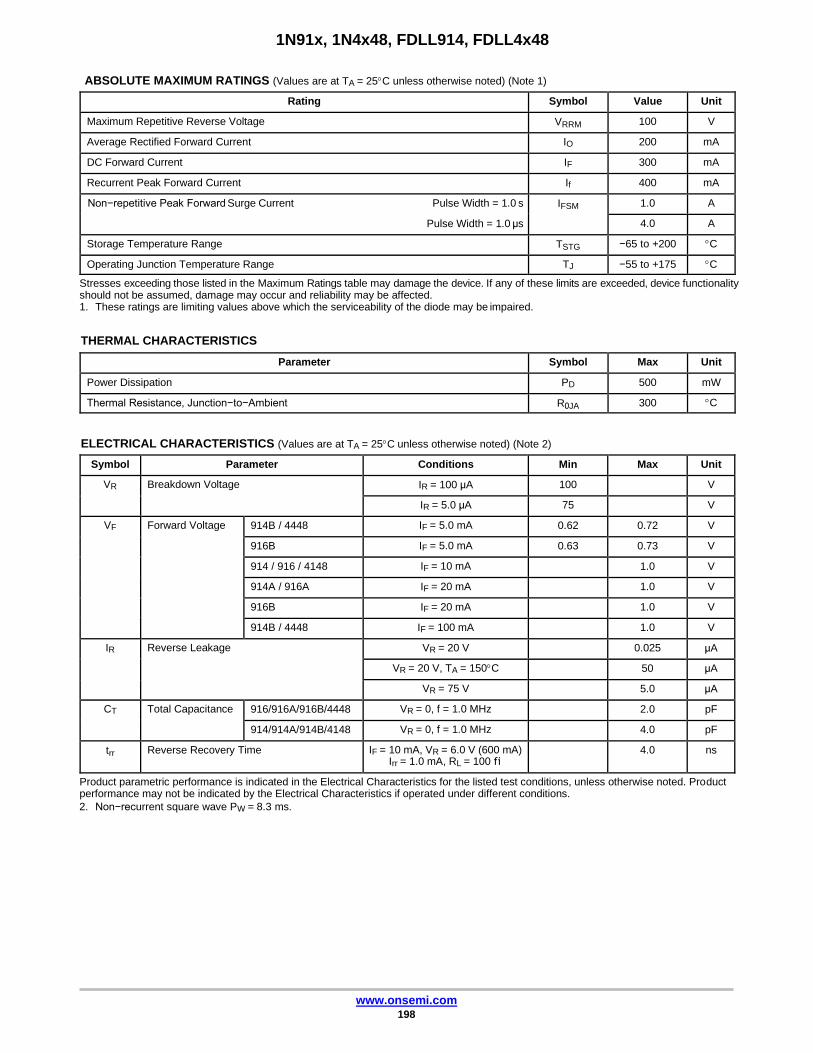
1N91x, 1N4x48, FDLL914, FDLL4x48
www.onsemi.com 198
ABSOLUTE MAXIMUM RATINGS (Values are at TA = 25C unless otherwise noted) (Note 1)
Rating Symbol Value Unit
Maximum Repetitive Reverse Voltage VRRM 100 V
Average Rectified Forward Current IO 200 mA
DC Forward Current IF 300 mA
Recurrent Peak Forward Current If 400 mA
Non−repetitive Peak Forward Surge Current Pulse Width = 1.0 s
Pulse Width = 1.0 µs
IFSM 1.0 A
4.0 A
Storage Temperature Range TSTG −65 to +200 C
Operating Junction Temperature Range TJ −55 to +175 C
Stresses exceeding those listed in the Maximum Ratings table may damage the device. If any of these limits are exceeded, device functionality should not be assumed, damage may occur and reliability may be affected. 1. These ratings are limiting values above which the serviceability of the diode may be impaired.
THERMAL CHARACTERISTICS
Parameter Symbol Max Unit
Power Dissipation PD 500 mW
Thermal Resistance, Junction−to−Ambient R0JA 300 C
ELECTRICAL CHARACTERISTICS (Values are at TA = 25C unless otherwise noted) (Note 2)
Symbol Parameter Conditions Min Max Unit
VR Breakdown Voltage IR = 100 µA 100 V
IR = 5.0 µA 75 V
VF Forward Voltage 914B / 4448 IF = 5.0 mA 0.62 0.72 V
916B IF = 5.0 mA 0.63 0.73 V
914 / 916 / 4148 IF = 10 mA 1.0 V
914A / 916A IF = 20 mA 1.0 V
916B IF = 20 mA 1.0 V
914B / 4448 IF = 100 mA 1.0 V
IR Reverse Leakage VR = 20 V 0.025 µA
VR = 20 V, TA = 150C 50 µA
VR = 75 V 5.0 µA
CT Total Capacitance 916/916A/916B/4448 VR = 0, f = 1.0 MHz 2.0 pF
914/914A/914B/4148 VR = 0, f = 1.0 MHz 4.0 pF
trr Reverse Recovery Time IF = 10 mA, VR = 6.0 V (600 mA) Irr = 1.0 mA, RL = 100 fi
4.0 ns
Product parametric performance is indicated in the Electrical Characteristics for the listed test conditions, unless otherwise noted. Product performance may not be indicated by the Electrical Characteristics if operated under different conditions.
2. Non−recurrent square wave PW = 8.3 ms.
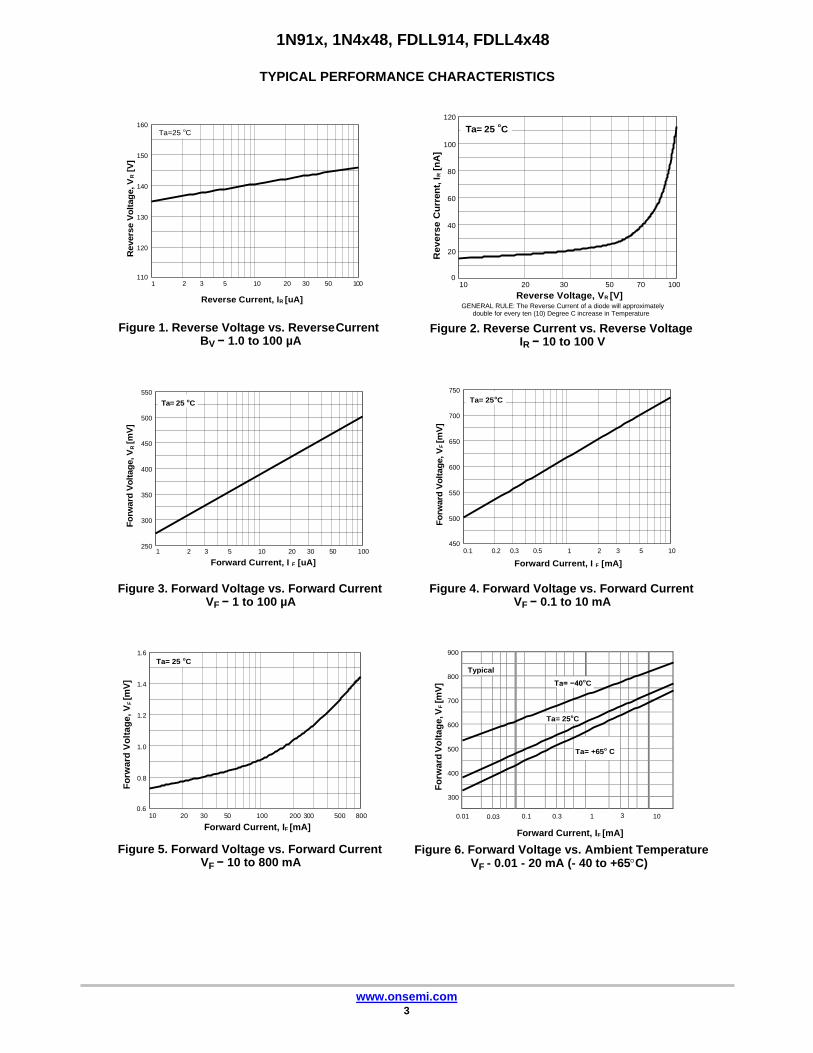
Ta=25 oC
Re
ve
rse C
urr
en
t, I
R [n
A]
1N91x, 1N4x48, FDLL914, FDLL4x48
TYPICAL PERFORMANCE CHARACTERISTICS
120 160
100
150
80
140
60
130
40
120 20
110 1
2 3 5 10 20 30 50 100
Reverse Current, IR [uA]
0 10 20 30 50 70 100
Reverse Voltage, VR [V] GENERAL RULE: The Reverse Current of a diode will approximately
double for every ten (10) Degree C increase in Temperature
Figure 1. Reverse Voltage vs. Reverse Current BV − 1.0 to 100 µA
Figure 2. Reverse Current vs. Reverse Voltage IR − 10 to 100 V
550
750
500
700
450
650
400
600
350
550
300
500
250
450 0.1
Figure 3. Forward Voltage vs. Forward Current VF − 1 to 100 µA
Figure 4. Forward Voltage vs. Forward Current VF − 0.1 to 10 mA
1.6
1.4
1.2
1.0
0.8
900
800
700
600
500
400
0.6 10
20 30 50
100 200 300
500
800
300
0.01
0.03
0.1
0.3 1 3 10
Forward Current, IF [mA]
Figure 5. Forward Voltage vs. Forward Current VF − 10 to 800 mA
Forward Current, IF [mA]
Figure 6. Forward Voltage vs. Ambient Temperature VF - 0.01 - 20 mA (- 40 to +65C)
www.onsemi.com 3
Ta= 25 oC
Ta= 25 oC Ta= 25 oC
Ta= 25 oC
Fo
rward
Vo
lta
ge, V
F [m
V]
Fo
rward
Vo
ltag
e, V
R [m
V]
Revers
e V
olt
ag
e, V
R [V
]
Fo
rward
Vo
lta
ge, V
F [m
V]
Fo
rward
Vo
ltag
e, V
F [m
V]
Typical
Ta= −40oC
Ta= 25oC
Ta= +65o C
1 2 3 5 10 20 30 50 100 0.2 0.3 0.5 1 2 3 5 10
Forward Current, I F [uA] Forward Current, I F [mA]
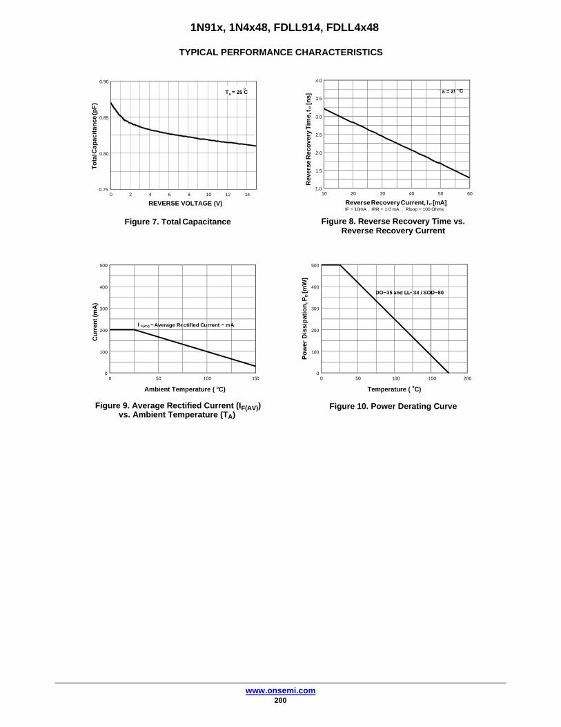
1N91x, 1N4x48, FDLL914, FDLL4x48
www.onsemi.com 200
o
TA = 25 C
Po
wer
Dis
sip
ati
on
, PD
[mW
] R
evers
e R
eco
very
Tim
e, t
rr [n
s]
TYPICAL PERFORMANCE CHARACTERISTICS
0.90 4.0
3.5
0.85 3.0
2.5
0.80 2.0
1.5
0.75 0 2
4 6 8
10 12 14
1.0 10 20 30 40 50 60
REVERSE VOLTAGE (V)
Figure 7. Total Capacitance
Reverse Recovery Current, I rr [mA] IF = 10mA , IRR = 1.0 mA , Rloop = 100 Ohms
Figure 8. Reverse Recovery Time vs. Reverse Recovery Current
500 500
400 400
300 300
200 200
100 100
0
0 50 100 150
Ambient Temperature ( oC)
0 0 50 100
Temperature ( oC)
150
200
Figure 9. Average Rectified Current (IF(AV)) vs. Ambient Temperature (TA)
Figure 10. Power Derating Curve
Cu
rren
t (m
A)
To
tal C
ap
acit
an
ce
(pF
)
T a = 25 oC
I F(AV) − A verage Re ctified Cu rrent − m A
DO−35 and LL− 34 / SO D−80
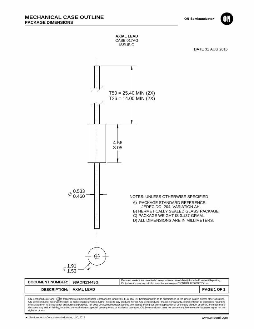
ON Semiconductor and are trademarks of Semiconductor Components Industries, LLC dba ON Semiconductor or its subsidiaries in the United States and/or other countries. ON Semiconductor reserves the right to make changes without further notice to any products herein. ON Semiconductor makes no warranty, representation or guarantee regarding the suitability of its products for any particular purpose, nor does ON Semiconductor assume any liability arising out of the application or use of any product or circuit, and specifically disclaims any and all liability, including without limitation special, consequential or incidental damages. ON Semiconductor does not convey any license under its patent rights nor the rights of others.
MECHANICAL CASE OUTLINE PACKAGE DIMENSIONS
AXIAL LEAD CASE 017AG
ISSUE O
DATE 31 AUG 2016
T50 = 25.40 MIN (2X) T26 = 14.00 MIN (2X)
4.56 3.05
0.533 0.460
NOTES: UNLESS OTHERWISE SPECIFIED
A) PACKAGE STANDARD REFERENCE: JEDEC DO−204, VARIATION AH.
B) HERMETICALLY SEALED GLASS PACKAGE. C) PACKAGE WEIGHT IS 0.137 GRAM.
D) ALL DIMENSIONS ARE IN MILLIMETERS.
1.91 1.53
DOCUMENT NUMBER: 98AON13443G Electronic versions are uncontrolled except when accessed directly from the Document Repository. Printed versions are uncontrolled except when stamped “CONTROLLED COPY” in red.
DESCRIPTION: AXIAL LEAD PAGE 1 OF 1
Semiconductor Components Industries, LLC, 2019 www.onsemi.com
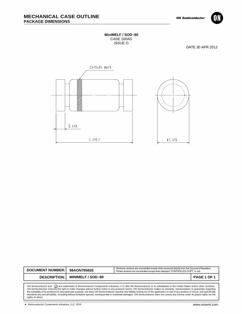
ON Semiconductor reserves the right to make changes without further notice to any products herein. ON Semiconductor makes no warranty, representation or guarantee regarding the suitability of its products for any particular purpose, nor does ON Semiconductor assume any liability arising out of the application or use of any product or circuit, and specifically disclaims any and all liability, including without limitation special, consequential or incidental damages. ON Semiconductor does not convey any license under its patent rights nor the rights of others.
are trademarks of Semiconductor Components Industries, LLC dba ON Semiconductor or its subsidiaries in the United States and/or other countries. ON Semiconductor and
MECHANICAL CASE OUTLINE PACKAGE DIMENSIONS
MiniMELF / SOD−80
CASE 100AD ISSUE O
DATE 30 APR 2012
DOCUMENT NUMBER: 98AON79582E Electronic versions are uncontrolled except when accessed directly from the Document Repository. Printed versions are uncontrolled except when stamped “CONTROLLED COPY” in red.
DESCRIPTION: MINIMELF / SOD−80 PAGE 1 OF 1
Semiconductor Components Industries, LLC, 2019 www.onsemi.com
www.onsemi.com
PUBLICATION ORDERING INFORMATION
LITERATURE FULFILLMENT:
Email Requests to: [email protected]
ON Semiconductor Website: www.onsemi.com
TECHNICAL SUPPORT
North American Technical Support:
Voice Mail: 1 800−282−9855 Toll Free USA/Canada
Phone: 011 421 33 790 2910
Europe, Middle East and Africa Technical Support:
Phone: 00421 33 790 2910
For additional information, please contact your local Sales Representative
ON Semiconductor and are trademarks of Semiconductor Components Industries, LLC dba ON Semiconductor or its subsidiaries in the United States and/or other countries. ON Semiconductor owns the rights to a number of patents, trademarks, copyrights, trade secrets, and other intellectual property. A listing of ON Semiconductor’s product/patent coverage may be accessed at www.onsemi.com/site/pdf/Patent−Marking.pdf. ON Semiconductor reserves the right to make changes without further notice to any products herein.
ON Semiconductor makes no warranty, representation or guarantee regarding the suitability of its products for any particular purpose, nor does ON Semiconductor assume any liability arising out of the application or use of any product or circuit, and specifically disclaims any and all liability, including without limitation special, consequential or incidental damages. Buyer is responsible for its products and applications using ON Semiconductor products, including compliance with all laws, regulations and safety requirements or standards, regardless of any support or applications information provided by ON Semiconductor. “Typical” parameters which may be provided in ON Semiconductor data sheets and/or specifications can and do vary in different applications and actual performance may vary over time. All operating parameters, including “Typicals” must be validated for each customer application by customer’s technical experts. ON Semiconductor does not convey any license under its patent rights nor the rights of others. ON Semiconductor products are not designed, intended, or authorized for use as a critical component in life support systems or any FDA Class 3 medical devices or medical devices with a same or similar classification in a foreign jurisdiction or any devices intended for implantation in the human body. Should Buyer purchase or use ON Semiconductor products for any such unintended or unauthorized application, Buyer shall indemnify and hold ON Semiconductor and its officers, employees, subsidiaries, affiliates, and distributors harmless against all claims, costs, damages, and expenses, and reasonable attorney fees arising out of, directly or indirectly, any claim of personal injury or death associated with such unintended or unauthorized use, even if such claim alleges that ON Semiconductor was negligent regarding the design or manufacture of the part. ON Semiconductor is an Equal Opportunity/Affirmative Action Employer. This literature is subject to all applicable copyright laws and is not for resale in any manner.

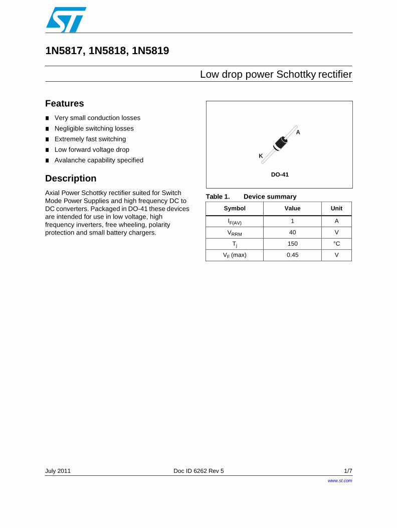
1N5817, 1N5818, 1N5819
Low drop power Schottky rectifier
Features
Very small conduction losses
Negligible switching losses
Extremely fast switching
Low forward voltage drop
Avalanche capability specified
Description
Axial Power Schottky rectifier suited for Switch
Mode Power Supplies and high frequency DC to
DC converters. Packaged in DO-41 these devices
are intended for use in low voltage, high
frequency inverters, free wheeling, polarity
protection and small battery chargers.
Table 1. Device summary
July 2011 Doc ID 6262 Rev 5 1/7
www.st.com
A
K
DO-41
Symbol Value Unit
IF(AV) 1 A
VRRM 40 V
Tj 150 °C
VF (max) 0.45 V
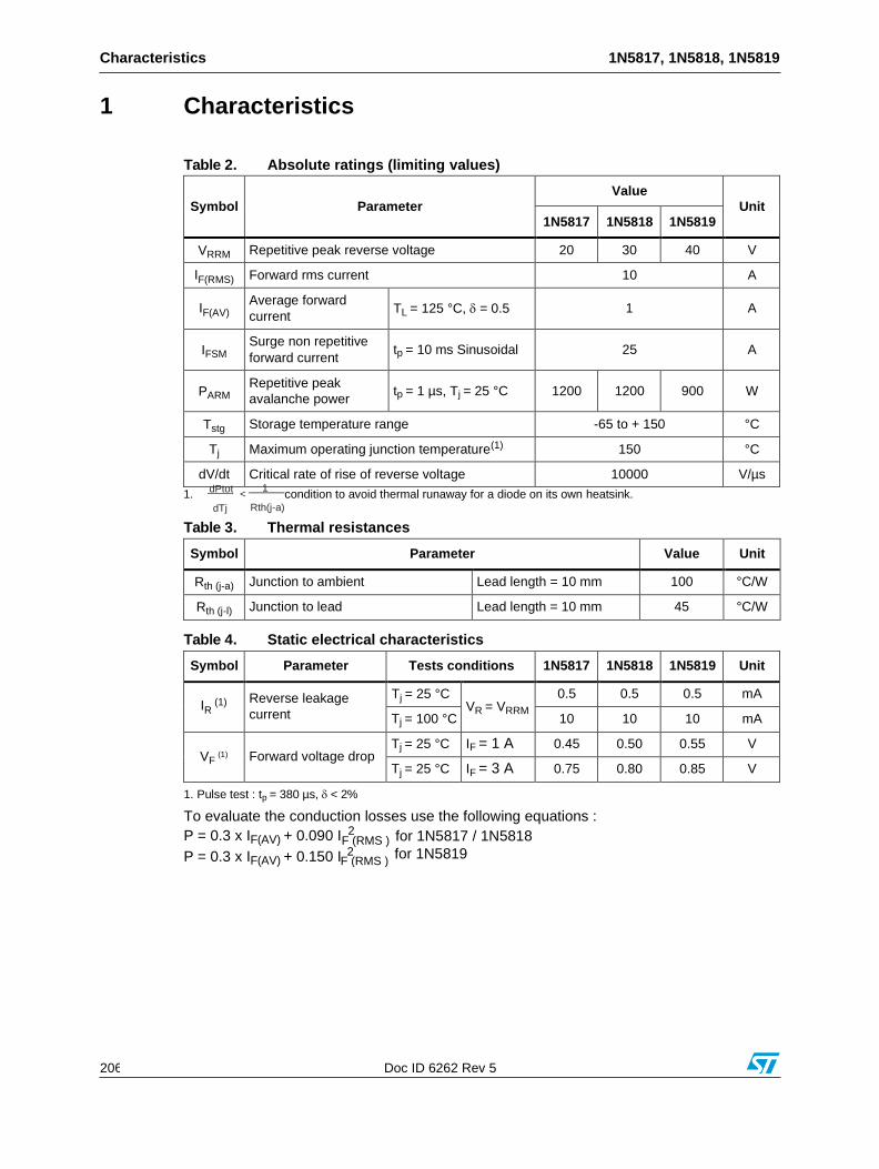
Characteristics 1N5817, 1N5818, 1N5819
206/7
Doc ID 6262 Rev 5
F (RMS )
F (RMS )
1 Characteristics
Table 2. Absolute ratings (limiting values)
Symbol
Parameter
Value Unit
1N5817 1N5818 1N5819
VRRM Repetitive peak reverse voltage 20 30 40 V
IF(RMS) Forward rms current 10 A
IF(AV) Average forward
current TL = 125 °C, = 0.5 1 A
IFSM Surge non repetitive
forward current tp = 10 ms Sinusoidal 25 A
PARM Repetitive peak
avalanche power tp = 1 µs, Tj = 25 °C 1200 1200 900 W
Tstg Storage temperature range -65 to + 150 °C
Tj Maximum operating junction temperature(1) 150 °C
dV/dt Critical rate of rise of reverse voltage 10000 V/µs
1. dPtot
< 1
condition to avoid thermal runaway for a diode on its own heatsink. dTj Rth(j-a)
Table 3. Thermal resistances
Symbol Parameter Value Unit
Rth (j-a) Junction to ambient Lead length = 10 mm 100 °C/W
Rth (j-l) Junction to lead Lead length = 10 mm 45 °C/W
Table 4. Static electrical characteristics
Symbol Parameter Tests conditions 1N5817 1N5818 1N5819 Unit
IR (1) Reverse leakage
current
Tj = 25 °C VR = VRRM
0.5 0.5 0.5 mA
Tj = 100 °C 10 10 10 mA
VF
(1)
Forward voltage drop
Tj = 25 °C IF = 1 A 0.45 0.50 0.55 V
Tj = 25 °C IF = 3 A 0.75 0.80 0.85 V
1. Pulse test : tp = 380 µs, < 2%
To evaluate the conduction losses use the following equations :
P = 0.3 x IF(AV) + 0.090 I 2
P = 0.3 x IF(AV) + 0.150 I 2
for 1N5817 / 1N5818
for 1N5819
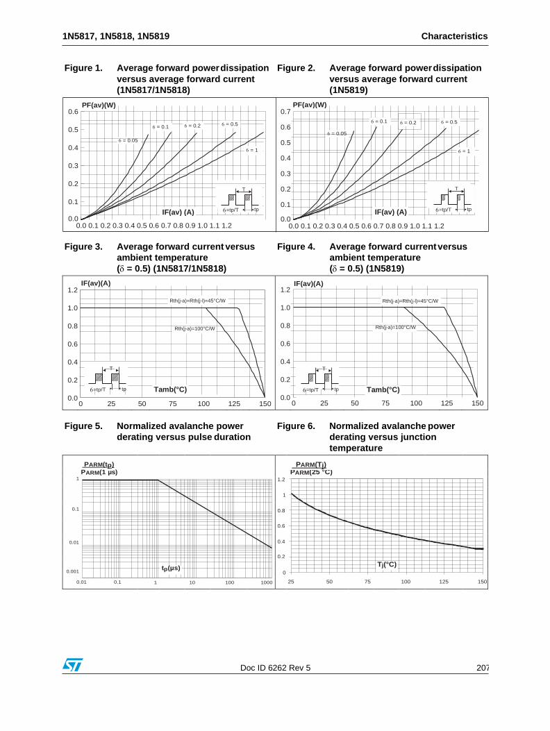
1N5817, 1N5818, 1N5819 Characteristics
Doc ID 6262 Rev 5 207/7
Figure 1. Average forward power dissipation
versus average forward current
(1N5817/1N5818)
Figure 2. Average forward power dissipation
versus average forward current
(1N5819)
Figure 3. Average forward current versus
ambient temperature
( = 0.5) (1N5817/1N5818)
Figure 4. Average forward current versus
ambient temperature
( = 0.5) (1N5819)
1.2
1.0
0.8
0.6
0.4
0.2
0.0
IF(av)(A)
T
=tp/T
0 25
tp
50
Rth(j-a)=Rth(j-l)=45°C/W
Rth(j-a)=100°C/W
Tamb(°C)
75 100
125
150
1.2
1.0
0.8
0.6
0.4
0.2
0.0
IF(av)(A)
T
=tp/T
0 25
tp
50
Rth(j-a)=Rth(j-l)=45°C/W
Rth(j-a)=100°C/W
Tamb(°C)
75 100
125
150
Figure 5. Normalized avalanche power
derating versus pulse duration
Figure 6. Normalized avalanche power
derating versus junction
temperature
PARM(tp)
PARM(1 µs) 1
0.1
0.01
0.001
0.01 0.1
1
tp(µs)
10
100
1000
PARM(Tj)
PARM(25 °C)
1.2
1
0.8
0.6
0.4
0.2
Tj(°C)
0
25 50 75 100 125 150
0.0 0.0 0.1 0.2 0.3 0.4 0.5 0.6 0.7 0.8 0.9 1.0 1.1 1.2
=tp/T tp IF(av) (A)
0.2
0.1
= 1
0.5
0.4
0.3
= 0.05
= 0.5 0.6
= 0.1
0.7 PF(av)(W)
0.0 0.0 0.1 0.2 0.3 0.4 0.5 0.6 0.7 0.8 0.9 1.0 1.1 1.2
=tp/T tp IF(av) (A)
0.1
T
0.3
0.2
= 1 0.4 = 0.05
= 0.5 = 0.2 = 0.1
0.6
0.5
PF(av)(W)
T
= 0.2
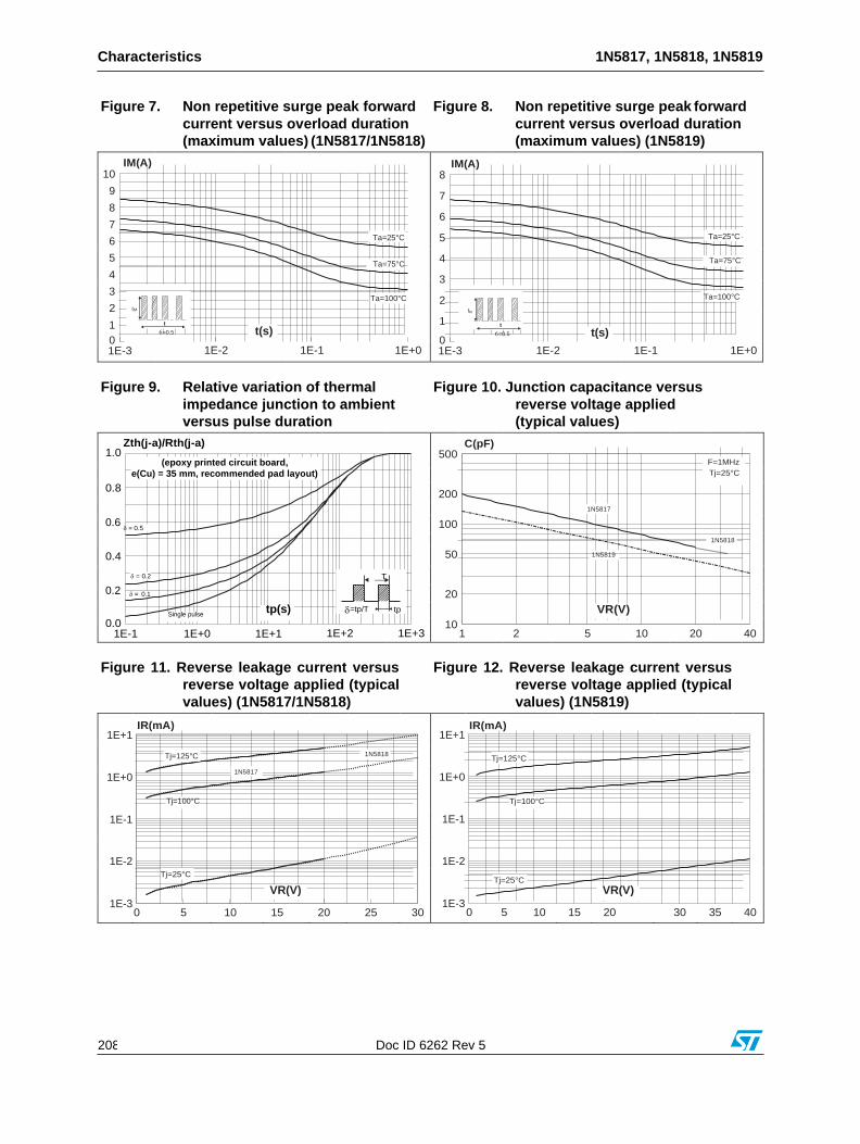
Characteristics 1N5817, 1N5818, 1N5819
208/7
Doc ID 6262 Rev 5
Figure 7. Non repetitive surge peak forward
current versus overload duration
(maximum values) (1N5817/1N5818)
Figure 8. Non repetitive surge peak forward
current versus overload duration
(maximum values) (1N5819)
IM(A) 10
9
8
7
6
5
4
3
2 IM
1
0 1E-3
Ta=25°C
IM(A) 8
7
6
5
4
3
2 IM
1
0 1E-3
Ta=25°C
Ta=75°C
Ta=75°C
Ta=100°C
Ta=100°C
t
=0.5
t(s)
t
=0.5
t(s)
1E-2 1E-1 1E+0 1E-2 1E-1 1E+0
Figure 9. Relative variation of thermal
impedance junction to ambient
versus pulse duration
Figure 10. Junction capacitance versus
reverse voltage applied
(typical values)
Zth(j-a)/Rth(j-a) 1.0
(epoxy printed circuit board,
e(Cu) = 35 mm, recommended pad layout)
0.8
0.6
= 0.5
0.4
= 0.2
0.2 = 0.1
Single pulse tp(s)
0.0 1E-1 1E+0 1E+1
500
C(pF)
F=1MHz
Tj=25°C
200
1N5817
100
1N5818
50 1N5819
T
20
=tp/T tp VR(V)
1E+2 1E+3 10
1 2 5 10 20
40
Figure 11. Reverse leakage current versus
reverse voltage applied (typical
values) (1N5817/1N5818)
Figure 12. Reverse leakage current versus
reverse voltage applied (typical
values) (1N5819)
1E+1
IR(mA) 1E+1
IR(mA)
Tj=125°C 1N5818
Tj=125°C
1E+0 1N5817 1E+0
Tj=100°C Tj=100°C
1E-1 1E-1
1E-2
1E-2
Tj=25°C VR(V)
Tj=25°C VR(V)
1E-3 0 5 10 15 20 25 30
1E-3 0 5 10 15 20 30 35 40
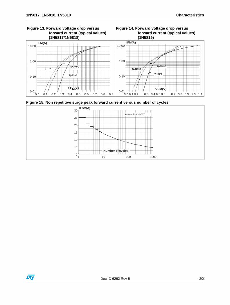
1N5817, 1N5818, 1N5819 Characteristics
Doc ID 6262 Rev 5 209/7
Number of cycles
F=50Hz Tj initial=25°C
Figure 13. Forward voltage drop versus
forward current (typical values)
(1N5817/1N5818)
Figure 14. Forward voltage drop versus
forward current (typical values)
(1N5819)
IFM(A) 10.00
1.00
0.10
0.01 0.0 0.1
IFM(A)
10.00
1.00
Tj=100°C
Tj=125°C
0.10
Tj=25°C
0.2
0.3
M
0.4
0.5
0.6
0.7
0.8
0.9
0.01 0.0 0.1 0.2
0.3
VFM(V)
0.4 0.5 0.6
0.7
0.8
0.9
1.0
1.1
Figure 15. Non repetitive surge peak forward current versus number of cycles
1000 100 10 1
0
25
20
15
10
5
IFSM(A) 30
Tj=100°C
Tj=125°C
Tj=25°C
V F (V )
210/7
Doc ID 6262 Rev 5
Package Information 1N5817, 1N5818, 1N5819
2 Package Information
Epoxy meets UL94, V0
Band indicates cathode
In order to meet environmental requirements, ST offers these devices in different grades of
ECOPACK® packages, depending on their level of environmental compliance. ECOPACK®
specifications, grade definitions and product status are available at: www.st.com. ECOPACK® is an ST trademark.
Table 5. DO-41 (Plastic) dimensions
ØD ØB
C A C
Ref.
Dimensions
Millimeters Inches
Min. Max. Min. Max.
A 4.07 5.20 0.160 0.205
B 2.04 2.71 0.080 0.107
C 25.4 1
D 0.71 0.86 0.028 0.034
3 Ordering information
Table 6. Ordering information
Order code Marking Package Weight Base qty Delivery mode
1N581x Part number
cathode ring DO-41 0.34 g 2000 Ammopack
1N581xRL Part number
cathode ring DO-41 0.34 g 5000 Tape and reel
4 Revision history
Table 7. Document revision history
Date Revision Changes
Jul-2003 4A Last update.
04-Jul-2011 5 Updated Table 5.: DO-41 (Plastic) dimensions.
1N5817, 1N5818, 1N5819 Characteristics
Doc ID 6262 Rev 5 211/7
1N5817, 1N5818, 1N5819
Please Read Carefully:
Information in this document is provided solely in connection with ST products. STMicroelectronics NV and its subsidiaries (“ST”) reserve the
right to make changes, corrections, modifications or improvements, to this document, and the products and services described herein at any
time, without notice.
All ST products are sold pursuant to ST’s terms and conditions of sale.
Purchasers are solely responsible for the choice, selection and use of the ST products and services described herein, and ST assumes no
liability whatsoever relating to the choice, selection or use of the ST products and services described herein.
No license, express or implied, by estoppel or otherwise, to any intellectual property rights is granted under this document. If any part of this
document refers to any third party products or services it shall not be deemed a license grant by ST for the use of such third party products
or services, or any intellectual property contained therein or considered as a warranty covering the use in any manner whatsoever of such
third party products or services or any intellectual property contained therein.
UNLESS OTHERWISE SET FORTH IN ST’S TERMS AND CONDITIONS OF SALE ST DISCLAIMS ANY EXPRESS OR IMPLIED
WARRANTY WITH RESPECT TO THE USE AND/OR SALE OF ST PRODUCTS INCLUDING WITHOUT LIMITATION IMPLIED
WARRANTIES OF MERCHANTABILITY, FITNESS FOR A PARTICULAR PURPOSE (AND THEIR EQUIVALENTS UNDER THE LAWS
OF ANY JURISDICTION), OR INFRINGEMENT OF ANY PATENT, COPYRIGHT OR OTHER INTELLECTUAL PROPERTY RIGHT.
UNLESS EXPRESSLY APPROVED IN WRITING BY AN AUTHORIZED ST REPRESENTATIVE, ST PRODUCTS ARE NOT
RECOMMENDED, AUTHORIZED OR WARRANTED FOR USE IN MILITARY, AIR CRAFT, SPACE, LIFE SAVING, OR LIFE SUSTAINING
APPLICATIONS, NOR IN PRODUCTS OR SYSTEMS WHERE FAILURE OR MALFUNCTION MAY RESULT IN PERSONAL INJURY,
DEATH, OR SEVERE PROPERTY OR ENVIRONMENTAL DAMAGE. ST PRODUCTS WHICH ARE NOT SPECIFIED AS "AUTOMOTIVE
GRADE" MAY ONLY BE USED IN AUTOMOTIVE APPLICATIONS AT USER’S OWN RISK.
Resale of ST products with provisions different from the statements and/or technical features set forth in this document shall immediately void
any warranty granted by ST for the ST product or service described herein and shall not create or extend in any manner whatsoever, any
liability of ST.
ST and the ST logo are trademarks or registered trademarks of ST in various countries.
Information in this document supersedes and replaces all information previously supplied.
The ST logo is a registered trademark of STMicroelectronics. All other names are the property of their respective owners.
© 2011 STMicroelectronics - All rights reserved
STMicroelectronics group of companies
Australia - Belgium - Brazil - Canada - China - Czech Republic - Finland - France - Germany - Hong Kong - India - Israel - Italy - Japan -
Malaysia - Malta - Morocco - Philippines - Singapore - Spain - Sweden - Switzerland - United Kingdom - United States of America
www.st.com