AN225948 - AIROC™ CYW20819/CYW20820 Bluetooth ...
15
Application Note Please read the Important Notice and Warnings at the end of this document 002-25948 Rev. *C www.infineon.com page 1 of 15 2022-04-10 AN225948 AIROC™ CYW20819/CYW20820 Bluetooth® & Bluetooth® LE system on chip hardware design guidelines About this document Scope and purpose This document provides hardware guidance on how to design with CYW208xx (CYW20819 and CYW20820). Intended audience This document is intended for hardware engineers creating PCB layout designs with CYW208xx. Table of contents About this document ....................................................................................................................... 1 Table of contents ............................................................................................................................ 1 1 Introduction .......................................................................................................................... 2 2 Basic layout guidelines ........................................................................................................... 3 3 Component placement ........................................................................................................... 4 3.1 PAVDD supply for CYW20819 and CYW20820.......................................................................................... 4 3.2 Bypass capacitor placement ................................................................................................................... 4 3.3 Antenna placement ................................................................................................................................. 5 3.4 Bandpass filter......................................................................................................................................... 6 3.5 Power inductor placement ..................................................................................................................... 7 3.6 Crystal placement ................................................................................................................................... 7 4 PCB layers and routing............................................................................................................ 9 4.1 Ground vias .............................................................................................................................................. 9 4.2 Layer 1: Components, signal fanout, and RF trace ................................................................................ 9 4.3 Layer 2: Solid ground plane .................................................................................................................... 9 4.4 Layer 3: Power traces ............................................................................................................................ 10 4.5 Layer 4: Power traces and non-critical signals ..................................................................................... 11 4.6 Unavoidable power trace crossing on adjacent layers ........................................................................ 12 References .................................................................................................................................... 13 Revision history............................................................................................................................. 14
-
Upload
khangminh22 -
Category
Documents
-
view
2 -
download
0
Transcript of AN225948 - AIROC™ CYW20819/CYW20820 Bluetooth ...
Application Note Please read the Important Notice and Warnings at the end of this document 002-25948 Rev. *C
www.infineon.com page 1 of 15 2022-04-10
AN225948
AIROC™ CYW20819/CYW20820 Bluetooth® &
Bluetooth® LE system on chip hardware design
guidelines
About this document
Scope and purpose
This document provides hardware guidance on how to design with CYW208xx (CYW20819 and CYW20820).
Intended audience
This document is intended for hardware engineers creating PCB layout designs with CYW208xx.
Table of contents
About this document ....................................................................................................................... 1
Table of contents ............................................................................................................................ 1
1 Introduction .......................................................................................................................... 2
2 Basic layout guidelines ........................................................................................................... 3
3 Component placement ........................................................................................................... 4
3.1 PAVDD supply for CYW20819 and CYW20820.......................................................................................... 4
3.2 Bypass capacitor placement ................................................................................................................... 4 3.3 Antenna placement ................................................................................................................................. 5
3.4 Bandpass filter ......................................................................................................................................... 6
3.5 Power inductor placement ..................................................................................................................... 7
3.6 Crystal placement ................................................................................................................................... 7
4 PCB layers and routing ............................................................................................................ 9 4.1 Ground vias .............................................................................................................................................. 9
4.2 Layer 1: Components, signal fanout, and RF trace ................................................................................ 9
4.3 Layer 2: Solid ground plane .................................................................................................................... 9 4.4 Layer 3: Power traces ............................................................................................................................ 10
4.5 Layer 4: Power traces and non-critical signals ..................................................................................... 11 4.6 Unavoidable power trace crossing on adjacent layers ........................................................................ 12
References .................................................................................................................................... 13
Revision history............................................................................................................................. 14

Application Note 2 of 15 002-25948 Rev. *C
2022-04-10
AIROC™ CYW20819/CYW20820 Bluetooth® & Bluetooth® LE system on
chip hardware design guidelines Introduction
1 Introduction
This document provides basic guidelines on the layout for the CYW208xx. This document is divided into the
following sections.
• Basic layout guidelines which include the board stackup and the impedance control requirements
• Component placements and recommended parts for the critical components
• Routing guidelines and the recommended trace width for various power traces
Application Note 3 of 15 002-25948 Rev. *C
2022-04-10
AIROC™ CYW20819/CYW20820 Bluetooth® & Bluetooth® LE system on
chip hardware design guidelines Basic layout guidelines
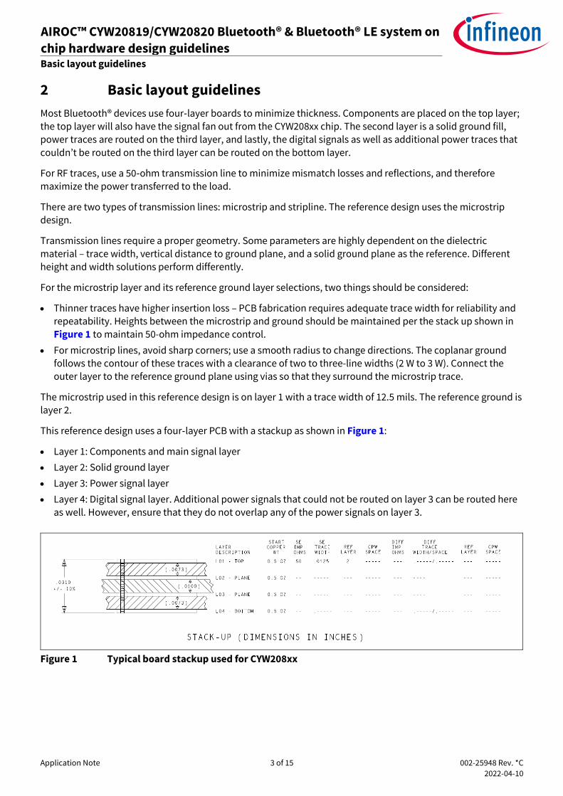
2 Basic layout guidelines
Most Bluetooth® devices use four‐layer boards to minimize thickness. Components are placed on the top layer; the top layer will also have the signal fan out from the CYW208xx chip. The second layer is a solid ground fill, power traces are routed on the third layer, and lastly, the digital signals as well as additional power traces that
couldn’t be routed on the third layer can be routed on the bottom layer.
For RF traces, use a 50‐ohm transmission line to minimize mismatch losses and reflections, and therefore maximize the power transferred to the load.
There are two types of transmission lines: microstrip and stripline. The reference design uses the microstrip design.
Transmission lines require a proper geometry. Some parameters are highly dependent on the dielectric
material – trace width, vertical distance to ground plane, and a solid ground plane as the reference. Different
height and width solutions perform differently.
For the microstrip layer and its reference ground layer selections, two things should be considered:
• Thinner traces have higher insertion loss – PCB fabrication requires adequate trace width for reliability and repeatability. Heights between the microstrip and ground should be maintained per the stack up shown in Figure 1 to maintain 50-ohm impedance control.
• For microstrip lines, avoid sharp corners; use a smooth radius to change directions. The coplanar ground follows the contour of these traces with a clearance of two to three-line widths (2 W to 3 W). Connect the
outer layer to the reference ground plane using vias so that they surround the microstrip trace.
The microstrip used in this reference design is on layer 1 with a trace width of 12.5 mils. The reference ground is layer 2.
This reference design uses a four‐layer PCB with a stackup as shown in Figure 1:
• Layer 1: Components and main signal layer
• Layer 2: Solid ground layer
• Layer 3: Power signal layer
• Layer 4: Digital signal layer. Additional power signals that could not be routed on layer 3 can be routed here as well. However, ensure that they do not overlap any of the power signals on layer 3.
Figure 1 Typical board stackup used for CYW208xx
Application Note 4 of 15 002-25948 Rev. *C
2022-04-10
AIROC™ CYW20819/CYW20820 Bluetooth® & Bluetooth® LE system on
chip hardware design guidelines Component placement
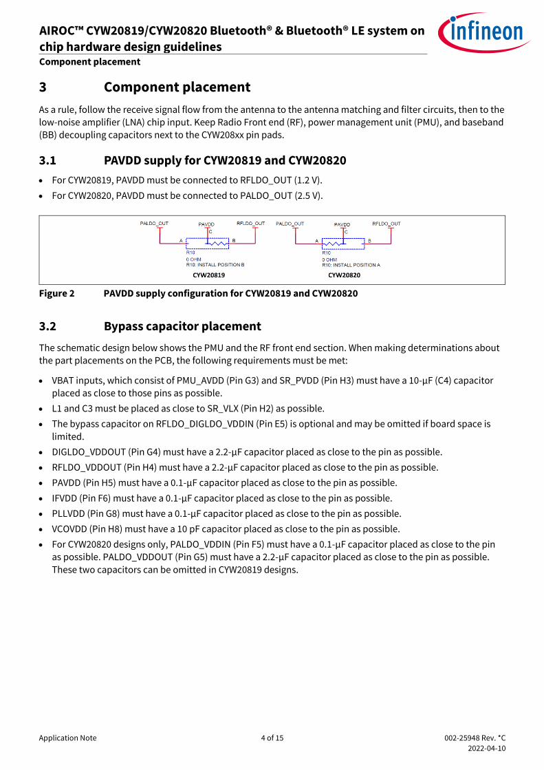
3 Component placement
As a rule, follow the receive signal flow from the antenna to the antenna matching and filter circuits, then to the low-noise amplifier (LNA) chip input. Keep Radio Front end (RF), power management unit (PMU), and baseband (BB) decoupling capacitors next to the CYW208xx pin pads.
3.1 PAVDD supply for CYW20819 and CYW20820
• For CYW20819, PAVDD must be connected to RFLDO_OUT (1.2 V).
• For CYW20820, PAVDD must be connected to PALDO_OUT (2.5 V).
Figure 2 PAVDD supply configuration for CYW20819 and CYW20820
3.2 Bypass capacitor placement
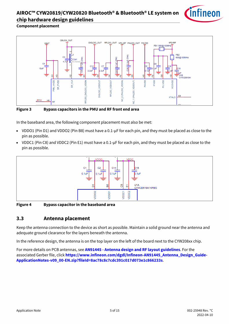
The schematic design below shows the PMU and the RF front end section. When making determinations about the part placements on the PCB, the following requirements must be met:
• VBAT inputs, which consist of PMU_AVDD (Pin G3) and SR_PVDD (Pin H3) must have a 10-µF (C4) capacitor placed as close to those pins as possible.
• L1 and C3 must be placed as close to SR_VLX (Pin H2) as possible.
• The bypass capacitor on RFLDO_DIGLDO_VDDIN (Pin E5) is optional and may be omitted if board space is
limited.
• DIGLDO_VDDOUT (Pin G4) must have a 2.2-µF capacitor placed as close to the pin as possible.
• RFLDO_VDDOUT (Pin H4) must have a 2.2-µF capacitor placed as close to the pin as possible.
• PAVDD (Pin H5) must have a 0.1-µF capacitor placed as close to the pin as possible.
• IFVDD (Pin F6) must have a 0.1-µF capacitor placed as close to the pin as possible.
• PLLVDD (Pin G8) must have a 0.1-µF capacitor placed as close to the pin as possible.
• VCOVDD (Pin H8) must have a 10 pF capacitor placed as close to the pin as possible.
• For CYW20820 designs only, PALDO_VDDIN (Pin F5) must have a 0.1-µF capacitor placed as close to the pin as possible. PALDO_VDDOUT (Pin G5) must have a 2.2-µF capacitor placed as close to the pin as possible.
These two capacitors can be omitted in CYW20819 designs.
Application Note 5 of 15 002-25948 Rev. *C
2022-04-10
AIROC™ CYW20819/CYW20820 Bluetooth® & Bluetooth® LE system on
chip hardware design guidelines Component placement
Figure 3 Bypass capacitors in the PMU and RF front end area
In the baseband area, the following component placement must also be met:
• VDDO1 (Pin D1) and VDDO2 (Pin B8) must have a 0.1-µF for each pin, and they must be placed as close to the pin as possible.
• VDDC1 (Pin C8) and VDDC2 (Pin E1) must have a 0.1-µF for each pin, and they must be placed as close to the pin as possible.
Figure 4 Bypass capacitor in the baseband area
3.3 Antenna placement
Keep the antenna connection to the device as short as possible. Maintain a solid ground near the antenna and adequate ground clearance for the layers beneath the antenna.
In the reference design, the antenna is on the top layer on the left of the board next to the CYW208xx chip.
For more details on PCB antennas, see AN91445 - Antenna design and RF layout guidelines. For the
associated Gerber file, click https://www.infineon.com/dgdl/Infineon-AN91445_Antenna_Design_Guide-
ApplicationNotes-v09_00-EN.zip?fileId=8ac78c8c7cdc391c017d073e1c866233s.
Application Note 6 of 15 002-25948 Rev. *C
2022-04-10
AIROC™ CYW20819/CYW20820 Bluetooth® & Bluetooth® LE system on
chip hardware design guidelines Component placement
Figure 5 Antenna placement and microstrip clearance
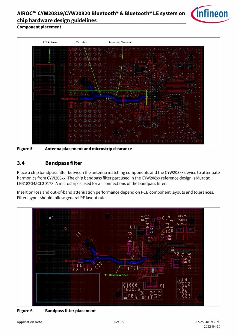
3.4 Bandpass filter
Place a chip bandpass filter between the antenna matching components and the CYW208xx device to attenuate
harmonics from CYW208xx. The chip bandpass filter part used in the CYW208xx reference design is Murata; LFB182G45CL3D178. A microstrip is used for all connections of the bandpass filter.
Insertion loss and out-of-band attenuation performance depend on PCB component layouts and tolerances.
Filter layout should follow general RF layout rules.
Figure 6 Bandpass filter placement

Application Note 7 of 15 002-25948 Rev. *C
2022-04-10
AIROC™ CYW20819/CYW20820 Bluetooth® & Bluetooth® LE system on
chip hardware design guidelines Component placement
3.5 Power inductor placement
The power inductor must have good isolation; this is done by surrounding it with as much ground as possible. The power inductor should also be placed as close to CBUCK_OUT pins (SR_VLX, Pin H2) as possible. The
inductor should be placed adjacent with the output capacitor (C3 in this design). The copper on the PCB top layer under this inductor should be cut out. See the “Recommended Component” section in the CYW208xx datasheet, and reference design files for the recommended component.
Figure 7 Power inductor isolation and placement
3.6 Crystal placement
Protect the crystal and related traces from noise sources and use a solid ground to separate the crystal from RF traces. The crystal ground plane should have direct vias to the reference ground plane.
The load capacitors placement as shown in Figure 8 is recommended, because this placement uses the least amount of PCB trace to connect the CYW208xx chip, the Crystals and the crystal load capacitors together which
will minimize the parasitic capacitance.
Crystal specifications and requirements can be found in the CYW208xx datasheet. See References.
For the crystal parts, TXC 8Y24070015 is recommended for the 24-MHz main crystal, and TXC 9H03270073 for
the 32.768-kHz crystal.

Application Note 8 of 15 002-25948 Rev. *C
2022-04-10
AIROC™ CYW20819/CYW20820 Bluetooth® & Bluetooth® LE system on
chip hardware design guidelines Component placement
Figure 8 24-MHz and 32.768-kHz crystal placements

Application Note 9 of 15 002-25948 Rev. *C
2022-04-10
AIROC™ CYW20819/CYW20820 Bluetooth® & Bluetooth® LE system on
chip hardware design guidelines PCB layers and routing
4 PCB layers and routing
4.1 Ground vias
Do not use long thin traces to connect components to ground vias; doing so adds inductance that can significantly alter circuit performance. Instead, place the vias directly on the ground pads of the components. Do not use through hole vias on the pins of the CYW208xx chips; instead, use 1:2 laser vias to connect the ground pads directly to the main ground. Only use through hole vias in the open area to stitch the ground plane
on all layers together. Make sure there are enough ground pins near the ground pad of the CBUCK output capacitor (C3 in this design).
4.2 Layer 1: Components, signal fanout, and RF trace
All the passive components for the chip can be placed on the top layer. Signal fanout from the CYW208xx chip will also be done on the top layer.
The RF trace, shown as blue, must be well isolated and have a solid ground plane along both sides of the trace.
Figure 9 Layout 1, components and signal fanout
4.3 Layer 2: Solid ground plane
Fill the layer immediately below the layer where CYW208xx is located with the solid ground plane for the optimal ground return path.

Application Note 10 of 15 002-25948 Rev. *C
2022-04-10
AIROC™ CYW20819/CYW20820 Bluetooth® & Bluetooth® LE system on
chip hardware design guidelines PCB layers and routing
Figure 10 Layer 2, solid ground fill
4.4 Layer 3: Power traces
• Route the main DC power supply line up the middle of the board like a spine, branching off left and right as
needed.
• Avoid routing DC power in a loop.
• Consider the current flow when routing the power traces to the chip. For input power pins, make sure the power trace goes through the decoupling capacitors before going into the power pin. For output power pins,
make sure that the power trace goes to the decoupling capacitors immediately before going to the load.
• Protect the RF power supply from main power, noisy signals, and digital power by separating with ground fill.
• Ensure that adequate power trace width and vias are available (or present) to minimize parasitic
impedance.
• Crossing or overlapping power traces on adjacent layers is not recommended. In the case where power traces crossing cannot be avoided, have them cross in a perpendicular manner to minimize the overlapping
area of the power traces. (Refer to the example shown in Section 4.6)
• Recommended Trace width for the power signals are as follows:
− CBUCK_OUT → Minimum 10 mils trace width
− CBUCK_OUT to RFLDO_DIGLDO_VDDIN (Pin E5) → Minimum 10 mils trace width
− VDDIO → Minimum 10 mils trace width
− VDDIO to VDDO (Pin B8 and D1) → Minimum 8 mils trace width
− DIGLDO_OUT (Pin G4) to VDDC (Pin C8 and E1) → Minimum 8 mils trace width
− VBAT to PMU_AVDD (Pin G3)/SR_PVDD (Pin H3) → Minimum 10 mils trace width
− RFLDO_VDDOUT (Pin H4) to 1P2VRF → Minimum 8 mils trace width
− VPA_BT to PALDO_VDDIN (Pin F5) → Minimum 10 mils trace width
− PALDO_VDDOUT (Pin G5) to PAVDD (Pin H5) → Minimum 8 mils trace width
− 1P2VRF → Minimum 8 mils trace width
Application Note 11 of 15 002-25948 Rev. *C
2022-04-10
AIROC™ CYW20819/CYW20820 Bluetooth® & Bluetooth® LE system on
chip hardware design guidelines PCB layers and routing
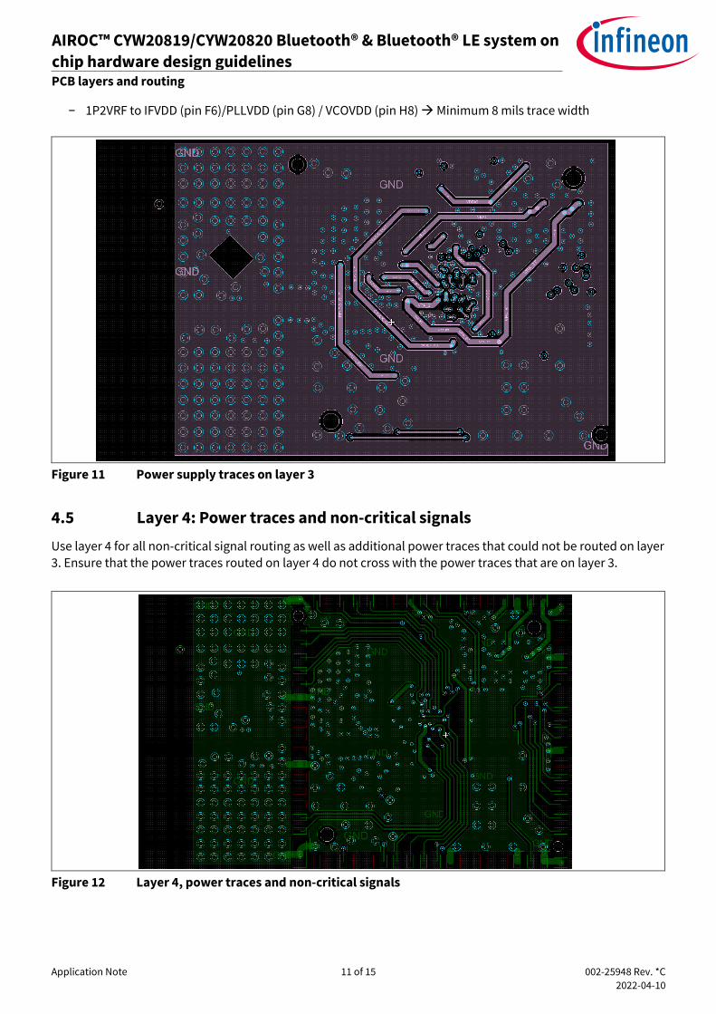
− 1P2VRF to IFVDD (pin F6)/PLLVDD (pin G8) / VCOVDD (pin H8) → Minimum 8 mils trace width
Figure 11 Power supply traces on layer 3
4.5 Layer 4: Power traces and non-critical signals
Use layer 4 for all non-critical signal routing as well as additional power traces that could not be routed on layer 3. Ensure that the power traces routed on layer 4 do not cross with the power traces that are on layer 3.
Figure 12 Layer 4, power traces and non-critical signals
Application Note 12 of 15 002-25948 Rev. *C
2022-04-10
AIROC™ CYW20819/CYW20820 Bluetooth® & Bluetooth® LE system on
chip hardware design guidelines PCB layers and routing
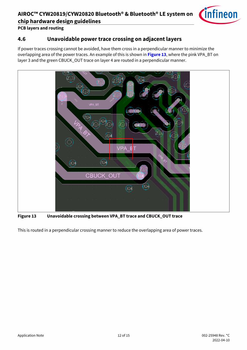
4.6 Unavoidable power trace crossing on adjacent layers
If power traces crossing cannot be avoided, have them cross in a perpendicular manner to minimize the overlapping area of the power traces. An example of this is shown in Figure 13, where the pink VPA_BT on
layer 3 and the green CBUCK_OUT trace on layer 4 are routed in a perpendicular manner.
Figure 13 Unavoidable crossing between VPA_BT trace and CBUCK_OUT trace
This is routed in a perpendicular crossing manner to reduce the overlapping area of power traces.
Application Note 13 of 15 002-25948 Rev. *C
2022-04-10
AIROC™ CYW20819/CYW20820 Bluetooth® & Bluetooth® LE system on
chip hardware design guidelines References
References
A wealth of data is available at www.infineon.com to help you to select the right device, and quickly and effectively integrate the device into your design.
[1] Datasheets
− CYW20819
− CYW20820
[2] Application note
− Antenna design and RF layout guidelines
Application Note 14 of 15 002-25948 Rev. *C
2022-04-10
AIROC™ CYW20819/CYW20820 Bluetooth® & Bluetooth® LE system on
chip hardware design guidelines Revision history
Revision history
Document
version
Date of release Description of changes
** 2018-12-18 Initial release
*A 2019-06-21 Added PAVDD Supply for CYW20719 and CYW20720
*B 2021-03-16 Updated to Infineon template
*C 2022-04-10 Corrected section 3.1 heading
Updated document title

Edition 2022-04-10
Published by
Infineon Technologies AG
81726 Munich, Germany
© 2022 Infineon Technologies AG. All Rights Reserved.
Do you have a question about this
document?
Go to www.infineon.com/support
Document reference
002-25948 Rev. *C
IMPORTANT NOTICE The information contained in this application note is given as a hint for the implementation of the product only and shall in no event be regarded as a description or warranty of a certain functionality, condition or quality of the product. Before implementation of the product, the recipient of this application note must verify any function and other technical information given herein in the real application. Infineon Technologies hereby disclaims any and all warranties and liabilities of any kind (including without limitation warranties of non-infringement of intellectual property rights of any third party) with respect to any and all information given in this application note. The data contained in this document is exclusively intended for technically trained staff. It is the responsibility of customer’s technical departments to evaluate the suitability of the product for the intended application and the completeness of the product information given in this document with respect to such application.
For further information on the product, technology, delivery terms and conditions and prices please contact your nearest Infineon Technologies office (www.infineon.com).
WARNINGS Due to technical requirements products may contain dangerous substances. For information on the types in question please contact your nearest Infineon Technologies office. Except as otherwise explicitly approved by Infineon Technologies in a written document signed by authorized representatives of Infineon Technologies, Infineon Technologies’ products may not be used in any applications where a failure of the product or any consequences of the use thereof can reasonably be expected to result in personal injury.
Trademarks All referenced product or service names and trademarks are the property of their respective owners.