IS2008S-IS2010S-IS2013S-IS2015S-Bluetooth-Mono-Audio ...
63
IS2008S/IS2010S/IS2013S/ IS2015S Bluetooth ® Mono Audio SOC Introduction The IS20xxS Mono Audio chip is a compact, highly integrated, CMOS single-chip RF and baseband Integrated Chip (IC) with Enhanced Data Rate (EDR) for 2.4 GHz applications. The IS20xxS Mono Audio chip is compliant with Bluetooth ® 4.1 specifications and completely backward-compatible with Bluetooth 3.0, 2.0 or 1.2 systems. The IS20xxS Mono Audio chip incorporates Bluetooth 1/2/3 Mbps RF, single-cycle 8-bit MCU, TX/RX modem, 5-port memory controller, task/hopping controller, UART interface and Microchip’s Bluetooth software stack to achieve the required Bluetooth 4.1 specifications with EDR functions. For voice and audio applications, the IS20xxS Mono Audio chip also integrates a Digital Signal Processor (DSP) co-processor, a PLL and a dedicated Codec to provide superior audio and voice quality. For the enhanced audio applications, SBC (Sub-band Coding)/AAC_LC (Advanced Audio Coding) decoding functions are also carried out by the DSP to satisfy the Bluetooth A2DP (Advanced Audio Distribution Profile) requirements. For voice applications, basic Continuous Variable Slope Data (CVSD) encoding and decoding with enhanced noise reduction and echo cancellation are implemented by the built-in DSP to achieve better quality in both the sending and receiving sides. Additionally, to minimize the external components required for portable devices, a battery voltage sensor, battery charger, a switching regulator and Low Dropout (LDO) are integrated to reduce system Bill of Materials (BOM) cost for various Bluetooth applications. A Mono 1-channel 2.3W Class-D Amplifier (CDA), which provides up to 100 dB Signal-to-noise Ratio (SNR), is also built-in to reduce the BOM cost and PCB area. The IS20xxS Mono Audio chip series includes: • IS2008S • IS2010S • IS2013S • IS2015S Features • Compliant with Bluetooth specification 4.1 • Supports the following Bluetooth audio profiles: – HFP 1.6 – HSP 1.1 – A2DP 1.2 – AVRCP 1.5 – SPP 1.0 – PBAP 1.0 Baseband Features • 16 MHz main clock input • Built-in internal ROM for program memory • Connects simultaneously to two hosts (phones, tablets) over HFP/A2DP profiles • Adaptive Frequency Hopping (AFH) avoids occupied RF channels © 2021 Microchip Technology Inc. and its subsidiaries Datasheet DS70005472A-page 1
-
Upload
khangminh22 -
Category
Documents
-
view
0 -
download
0
Transcript of IS2008S-IS2010S-IS2013S-IS2015S-Bluetooth-Mono-Audio ...

IS2008SIS2010SIS2013SIS2015S
Bluetoothreg Mono Audio SOC
IntroductionThe IS20xxS Mono Audio chip is a compact highly integrated CMOS single-chip RF and baseband Integrated Chip(IC) with Enhanced Data Rate (EDR) for 24 GHz applications The IS20xxS Mono Audio chip is compliant withBluetoothreg 41 specifications and completely backward-compatible with Bluetooth 30 20 or 12 systems
The IS20xxS Mono Audio chip incorporates Bluetooth 123 Mbps RF single-cycle 8-bit MCU TXRX modem 5-portmemory controller taskhopping controller UART interface and Microchiprsquos Bluetooth software stack to achieve therequired Bluetooth 41 specifications with EDR functions
For voice and audio applications the IS20xxS Mono Audio chip also integrates a Digital Signal Processor (DSP)co-processor a PLL and a dedicated Codec to provide superior audio and voice quality For the enhanced audioapplications SBC (Sub-band Coding)AAC_LC (Advanced Audio Coding) decoding functions are also carried out bythe DSP to satisfy the Bluetooth A2DP (Advanced Audio Distribution Profile) requirements
For voice applications basic Continuous Variable Slope Data (CVSD) encoding and decoding with enhanced noisereduction and echo cancellation are implemented by the built-in DSP to achieve better quality in both the sending andreceiving sides
Additionally to minimize the external components required for portable devices a battery voltage sensor batterycharger a switching regulator and Low Dropout (LDO) are integrated to reduce system Bill of Materials (BOM) costfor various Bluetooth applications A Mono 1-channel 23W Class-D Amplifier (CDA) which provides up to 100 dBSignal-to-noise Ratio (SNR) is also built-in to reduce the BOM cost and PCB area
The IS20xxS Mono Audio chip series includesbull IS2008Sbull IS2010Sbull IS2013Sbull IS2015S
Featuresbull Compliant with Bluetooth specification 41bull Supports the following Bluetooth audio profiles
ndash HFP 16ndash HSP 11ndash A2DP 12ndash AVRCP 15ndash SPP 10ndash PBAP 10
Baseband Featuresbull 16 MHz main clock inputbull Built-in internal ROM for program memorybull Connects simultaneously to two hosts (phones tablets) over HFPA2DP profilesbull Adaptive Frequency Hopping (AFH) avoids occupied RF channels
copy 2021 Microchip Technology Incand its subsidiaries
Datasheet DS70005472A-page 1
bull Supports a fast connection
Audio Codecbull 20-bit Digital-to-Analog Converter (DAC) and 16-bit Analog-to-Digital Converter (ADC) codecbull 98 dB SNR DAC playbackbull Built-in 1-channel 23W Class D amplifier for a 4Ω speaker (for IS201315S only)
RF Featuresbull Compatible with Bluetooth 41 (EDR) system in 24 GHz ISM bandbull Combined TXRX RF terminal simplifies external matching and reduces external antenna switchesbull Maximum TX output power control is +4 dBm with 20 dB level control from register controlbull Built-in TR switch for Class 23 applicationbull To avoid temperature variation temperature sensor with temperature calibration is utilized into bias current and
gain controlbull Integrated synthesizer requires no external Voltage-Controlled Oscillator (VCO) varactor diode resonator and
loop filterbull Crystal oscillation with built-in digital trimming for temperature or process variations
DSP Audio Processingbull Supports 64 Kbps A-Law or μ-Law PCM format or CVSD (Continuous Variable Slope Delta Modulation) for
SCO channel operationbull Supports noise suppressionbull Supports echo suppressionbull SBC and optional AAC decodingbull Packet Loss Concealment (PLC)bull Built-in voice prompts for four languages (ChineseEnglishSpanishFrench) and 20 events for each one
Note Configure this functionality in the IS20XXS_UI toolbull Supports Serial Copy Management System (SCMS-T) content protection
Peripheralsbull Built-in lithium-ion battery charger (up to 350 mA)bull Integrated 18V and 3V configurable switching regulator and LDObull Built-in ADC for battery monitor and voltage sensorbull A line-in port for external audio inputbull Two LED drivers
Flexible HCI Interfacebull High speed HCI-UART interface (supports up to 921600 bps)
Package DetailsTable 1 Package Details
Parameter IS2008S IS2010S IS2013S IS2015S
Package type QFN QFN
Pin count 48 56
Package size(1) 6x6x09 7x7x09
Note 1 All dimensions are in millimeters (mm) unless specified
IS2008SIS2010SIS2013SIS2015S
copy 2021 Microchip Technology Incand its subsidiaries
Datasheet DS70005472A-page 2
Applicationsbull Mono headsets with A2DPbull Mono speaker phones
IS2008SIS2010SIS2013SIS2015S
copy 2021 Microchip Technology Incand its subsidiaries
Datasheet DS70005472A-page 3
Table of Contents
Introduction1
Features 1
1 Quick References6
11 Reference Documentation612 Acronyms and Abbreviation 6
2 Device Overview 8
21 Key Features822 Pin Details 10
3 Audio 17
31 Digital Signal Processor 1732 Codec1833 Auxiliary Port 1834 Class D Audio Amplifier18
4 Transceiver19
41 Transmitter 1942 Receiver 1943 Synthesizer1944 Modem 1945 Adaptive Frequency Hopping (AFH) 19
5 Microcontroller20
51 Memory 2052 External Reset2053 Reference Clock20
6 Power Management Unit (PMU) 22
61 Charging a Battery 2262 Voltage Monitoring2263 Low Dropout Regulator 2264 Switching Regulator 2365 LED Driver23
7 Application Information24
71 Power Supply 2472 Host MCU Interface2473 Timing Sequence of UART Application 2574 General Purpose IO pins28
8 Antenna Placement Rule 30
9 Electrical Characteristics31
10 Packaging Information 37
101 Chip Identification System37
IS2008SIS2010SIS2013SIS2015S
copy 2021 Microchip Technology Incand its subsidiaries
Datasheet DS70005472A-page 4
102 Package Marking Information37103 Package Details 38
11 Reflow Profile and Storage Condition 43
111 Stencil of SMT Assembly Suggestion 43112 Reflow Profile 44113 Storage Condition44
12 Reference Circuit 46
13 Document Revision History59
The Microchip Website60
Product Change Notification Service60
Customer Support 60
Microchip Devices Code Protection Feature 60
Legal Notice 61
Trademarks 61
Quality Management System 62
Worldwide Sales and Service63
IS2008SIS2010SIS2013SIS2015S
copy 2021 Microchip Technology Incand its subsidiaries
Datasheet DS70005472A-page 5
1 Quick References
11 Reference DocumentationFor further details refer to the following
bull IS20xxBM1xBM2x DSP Application Notebull IS200xIS201xIS202x UART Command SOP
12 Acronyms and AbbreviationTable 1-1 Acronyms and Abbreviations
Acronyms and Abbreviations Description
AAC_LC Advanced Audio Coding ndash Low Complexity
A2DP Advanced Audio Distribution Profile
ADC Analog-to-Digital Converter
AFH Adaptive Frequency Hopping
BDR Basic Data Rate
BOM Bill of Materials
BPF Band Pass Filter
CVSD Continuous Variable Slope Data
DAC Digital-to-Analog Converter
DSP Digital Signal Processor
EDR Enhanced Data Rate
GFSK Gaussian Frequency Shift Keying
IC Integrated Chip
LDO Low Dropout
LNA Low Noise Amplifier
NFC Near-field Communication
PA Power Amplifier
PLC Packet Loss Concealment
PMU Power Management Unit
POR Power-on Reset
RF Radio Frequency
RSSI Received Signal Strength Indicator
SBC Sub-band Coding
SCMS-T Supports Serial Copy Management System
SNR Signal-to-Noise Ratio
IS2008SIS2010SIS2013SIS2015SQuick References
copy 2021 Microchip Technology Incand its subsidiaries
Datasheet DS70005472A-page 6
continuedAcronyms and Abbreviations Description
UART Universal Asynchronous Receiver Transmitter
VCO Voltage-Controlled Oscillator
WDT Watchdog Timer
IS2008SIS2010SIS2013SIS2015SQuick References
copy 2021 Microchip Technology Incand its subsidiaries
Datasheet DS70005472A-page 7
2 Device OverviewThe IS20xxS SoC integrates
bull Bluetooth 41 radio transceiverbull Power Management Unit (PMU)bull Digital Signal Processor (DSP)bull 1-channel Class-D Amplifier (CDA)
The following figure illustrates the block diagram of the IS20xxS SoC
Figure 2-1 Block Diagram of IS20xxS
8051
16 KB patch RAM
448 KB ROM
44 KB RAM
24-bit DSP Core
MCU
158 KB ROM
88 KB RAM
DSP
IS20xx
Classic RF
MACMODEM
Bluetooth + EDRTransceiver
RF Controller
Antenna
16 MHz Crystal
EEPROM
Power Switch
LED
BAT Charger
18 V BUCK
30 V LDO2
LED Driver2
PMULi-IonBAT
2-Channel DAC
Digital Core
2-Channel ADC
Audio Codec
(For IS20082010 only)
Speaker2W
Stereo Class-D AMP
MIC1
MIC2
Speaker
AUX_IN(analog signal) I2C
GPIOs or HWIO Port 0~3
21 Key FeaturesThe following table provides the key features of the IS20xxS family
Table 2-1 Key Features
Feature IS2008S IS2010S IS2013S IS2015S
Application Headset Headset Speaker Speaker
IS2008SIS2010SIS2013SIS2015SDevice Overview
copy 2021 Microchip Technology Incand its subsidiaries
Datasheet DS70005472A-page 8
continuedFeature IS2008S IS2010S IS2013S IS2015S
StereoMono Mono Mono Mono Mono
Package QFN QFN QFN QFN
Pin count 48 48 56 56
Dimensions (mm) 6x6 6x6 7x7 7x7
Audio DAC output 1-channel 1-channel 1-channel 1-channel
DAC (single-ended) SNR at28V (dB) -98 -98 -98 -98
DAC (capless) SNR at 28V(dB) -96 -96 -96 -96
ADC SNR at 28V (dB) -90 -90 -90 -90
I2S digital output No No No No
Analog Auxiliary-Input No No Yes Yes
Mono microphone 2 2 1 1
External audio amplifierinterface No No Yes Yes
Built-in CDA No No 1-channel 1-channel
UART Yes Yes Yes Yes
LED driver 2 2 2 2
Integrated DC-DC step-down regulator Yes Yes Yes Yes
DC 5V adapter input Yes Yes Yes Yes
Battery charger (350 mAmaximum) Yes Yes Yes Yes
GPIO 6 6 9 9
Button Support 6 6 6 6
NFC Yes Yes Yes Yes
Voice prompt Yes Yes Yes Yes
Multi-tone Yes Yes Yes Yes
DSP sound effect No No Yes Yes
Bluetooth Profiles
A2DP 12 12 12 12
AVRCP 15 15 15 15
HFP 16 16 16 16
HSP 11 11 11 11
PBAP 10 10 10 10
SPP No 10 No 10
IS2008SIS2010SIS2013SIS2015SDevice Overview
copy 2021 Microchip Technology Incand its subsidiaries
Datasheet DS70005472A-page 9
22 Pin DetailsThe following figure illustrates the pin diagram of the IS2008S and IS2010S
Figure 2-2 IS2008S and IS2010S Pin Diagram
The following table provides the pin description of the IS2008S and IS2010S
Table 2-2 Pin Description
IS2008S andIS2010S Pin No Pin Type(1) Pin Name Description
1 P VCOM Internal biasing voltage for codec
2 I MICN2 Mic2 mono differential analog negative input
3 I MICP2 Mic2 mono differential analog positive input
4 I MICN1 Mic1 mono differential analog negative input
5 I MICP1 Mic1 mono differential analog positive input
6 P MICBIAS Electric microphone biasing voltage
7 P VDD_CORE Core 12V power input connect to CLDO_O pin
8 O P1_2 IO pin default pull-high input EEPROM clock SCL
IS2008SIS2010SIS2013SIS2015SDevice Overview
copy 2021 Microchip Technology Incand its subsidiaries
Datasheet DS70005472A-page 10
continuedIS2008S and
IS2010S Pin No Pin Type(1) Pin Name Description
9 IO P1_3 IO pin default pull-high input EEPROM data SDA
10 I RST_N System Reset pin active when rising edge
11 P VDD_IO IO power supply input (27-33V) connect to LDO31_VOpin
12 IO P0_1
IO pin default pull-high input(2)
bull FWD key when class 2 RF (default) active-lowbull Class 1 TX control signal of external RF TR switch
active high
13 IO P1_5
IO pin default pull high input(2)
bull NFC detection pin active-lowbull Out_Ind_0bull Slide switch detector active-lowbull Buzzer signal output
14 I HCI_RXD HCI UART data input
15 O HCI_TXD HCI UART data output
16 P CODEC_VO 31V LDO output for codec power
17 P LDO31_VIN 31V LDO input connect to SYS_PWR pin
18 P LDO31_VO 31V LDO output
19 P ADAP_IN 5V power adapter input
20 P BAT_IN 33-42V Li-ion battery input
21 - NC No Connection
22 P SAR_VDD SAR 18V input connect to BK_O pin
23 P SYS_PWR Power output which comes from BAT_IN or ADAP_IN
24 P BK_VDD 18V buck VDD Power Input connect to SYS_PWR pin
25 P BK_LX 18V buck pin for switch
26 P BK_O 18V buck feedback input
27 I PWR Multi function push button and power-on key
28 I LED2 LED Driver 2
29 I LED1 LED Driver 1
30 IO P0_3
IO pin default pull-high input(2)
bull REV key (default) active-lowbull Buzzer signal outputbull Out_Ind_1bull Class 1 RX control signal of external RF TR switch
active high
31 P CLDO_O 12V core LDO output
32 P PMIC_IN PMU blocks power input connect to BK_O pin
IS2008SIS2010SIS2013SIS2015SDevice Overview
copy 2021 Microchip Technology Incand its subsidiaries
Datasheet DS70005472A-page 11
continuedIS2008S and
IS2010S Pin No Pin Type(1) Pin Name Description
33 P RFLDO_O 128V RF LDO output
34 P VBG Bandgap output reference for decoupling interference
35 P ULPC_VSUS ULPC 12V output power
36 I XO_N 16 MHz crystal input negative
37 I XO_P 16 MHz crystal input positive
38 P VCC_RF RF power input (128V) for both synthesizer and TXRXblock connect to RFLDO_O pin
39 IO RTX RF path (transmitreceive)
40 I P0_2IO pin default pull-high input(2)
PlayPause key (default) active-low
41 I P2_0IO pin default pull-high input system configuration
H Application L Baseband (IBDK mode)
42 I P2_7IO pin default pull high input(2)
Volume up key (default) active-low
43 I P0_5IO pin default pull high input(2)
Volume down (default) active-low
44 P VDD_IO IO power supply input (27-33V) connect to LDO31_VOpin
45 P VDD_AOPositive power supply dedicated to codec outputamplifiers connect to CODEC_VO pin
46 O AOHPM Headphone common mode outputsense input
47 O AOHPL Left channel analog headphone output
48 P VDDA Positive power supplyreference voltage for codecconnect to CODEC_VO pin
49 P EP Exposed pads used as ground (GND) pins
Notes 1 The conventions used in the table are indicated as follows
ndash I = Input pinndash O = Output pinndash IO = InputOutput pinndash P = Power pin
2 All IO pins are configured using the IS20XXS_UI tool a Windowsreg-based utility
The following figure illustrates the pin diagram of the IS2013S and IS2015S
IS2008SIS2010SIS2013SIS2015SDevice Overview
copy 2021 Microchip Technology Incand its subsidiaries
Datasheet DS70005472A-page 12
Figure 2-3 IS2013S and IS2015S Pin Diagram
The following table provides the pin description of the IS2013SIS2015S
Table 2-3 Pin Description
IS2013S andIS2015S Pin No Pin Type(1) Pin Name Description
1 P VDDAO Positive power supply dedicated to codec output amplifiersConnect to CODEC_VO pin
2 O AOHPM Headphone common mode outputsense input
3 O AOHPL Left channel analog headphone output
4 P VDDA Positive power supplyreference voltage for codec connect toCODEC_VO pin
5 P VCOM Internal biasing voltage for codec
6 I MICN1 Mic1 mono differential analog negative input
7 I MICP1 Mic1 mono differential analog positive input
8 P MICBIAS Electric microphone biasing voltage
9 I AIL Left channel single-ended analog inputs
IS2008SIS2010SIS2013SIS2015SDevice Overview
copy 2021 Microchip Technology Incand its subsidiaries
Datasheet DS70005472A-page 13
continuedIS2013S and
IS2015S Pin No Pin Type(1) Pin Name Description
10 P VDD_CORE Core 12V power input connect to CLDO_O pin
11 O P1_2 IO pin default pull high input EEPROM clock SCL
12 IO P1_3 IO pin default pull high input EEPROM data SDA
13 I RST_N System Reset pin active when rising edge
14 P VDD_IO IO power supply input (27-33V) connect to LDO31_VO pin
15 IO P0_1
IO pin default pull-high input(2)
bull FWD key when class 2 RF (default) active-lowbull Class 1 TX Control signal of external RF TR switch
active high
16 I P2_4IO pin default pull high input system configuration
L Boot mode with P2_0 low combination
17 IO P0_4IO pin default pull high input(2)
bull NFC detection pin active-lowbull Out_Ind_0
18 IO P1_5
IO pin default pull high input(2)
bull NFC detection pin active-lowbull Out_Ind_0bull Slide switch detector active-lowbull Buzzer signal output
19 I HCI_RXD HCI UART input data
20 O HCI_TXD HCI UART output data
21 P CODEC_VO 31V LDO output for codec power
22 P LDO31_VIN 31V LDO input connect to SYS_PWR pin
23 P LDO31_VO 31V LDO output
24 P ADAP_IN 5V power adapter input
25 P BAT_IN 33 to 42V Li-ion battery input
26 P SAR_VDD SAR 18V input connect to BK_O pin
27 P SYS_PWR Power output which come from BAT_IN or ADAP_IN
28 P LDO18_VDD 18V LDO VDD Power Input connect to SYS_PWR pin
29 P LDO18_O 18V LDO output
30 I PWR Multi-Function Push button and power on key
31 - NC No Connection
32 I LED2 LED Driver 2
33 I LED1 LED Driver 1
IS2008SIS2010SIS2013SIS2015SDevice Overview
copy 2021 Microchip Technology Incand its subsidiaries
Datasheet DS70005472A-page 14
continuedIS2013S and
IS2015S Pin No Pin Type(1) Pin Name Description
34 IO P0_0IO pin default pull-high input(2)
bull Slide switch detector active-lowbull UARTTX_IND active-low
35 IO P0_3
IO pin default pull-high input(2)
bull REV key (default) active-lowbull Buzzer signal outputbull Out_Ind_1bull Class 1 RX control signal of external RF TR switch
active high
36 I EANEmbedded ROMExternal Flash enable
H Embedded L External Flash
37 P CLDO_O 12V core LDO output
38 P PMIC_IN PMU blocks power input connect to BK_O pin
39 P RFLDO_O 128V RF LDO output
40 P VBG Bandgap output reference for decoupling interference
41 P ULPC_VSUS ULPC 12V output power
42 I XO_N 16 MHz crystal input negative
43 I XO_P 16 MHz crystal input positive
44 P VCC_RFRF power input (128V) for both synthesizer and TXRXblock connect to RFLDO_O pin
45 IO RTX RF path (transmitreceive)
46 I P0_2IO pin default pull-high input(2)
PlayPause key (default) active-low
47 I P2_0IO pin default pull-high input system configuration
H Application L Baseband (IBDK mode)
48 I P2_7IO pin default pull-high input(2)
Volume up key (default) active-low
49 I P3_0IO pin default pull-high input(2)
Line-in detector (default) active-low
50 I P0_5IO pin default pull-high input(2)
Volume down (default) active-low
51 P VDD_IO IO power supply input (27-33V) connect to LDO31_VO pin
52 P AVDD_CDA Supply voltage of audio amplifier
53 P VBP_CDA Reference voltage output
54 O HPON_CDA Negative BTL output of channel-1
55 O HPOP_CDA Positive BTL output of channel-1
IS2008SIS2010SIS2013SIS2015SDevice Overview
copy 2021 Microchip Technology Incand its subsidiaries
Datasheet DS70005472A-page 15
continuedIS2013S and
IS2015S Pin No Pin Type(1) Pin Name Description
56 P PVDD_CDA Supply voltage of power stage ch-1
57 P EP Exposed pads used as ground (GND) pins
Notes 1 The conventions used in the table are indicated as follows
ndash I = Input pinndash O = Output pinndash IO = InputOutput pinndash P = Power pin
2 All IO pins are configured using the UI tool a Windows-based utility
IS2008SIS2010SIS2013SIS2015SDevice Overview
copy 2021 Microchip Technology Incand its subsidiaries
Datasheet DS70005472A-page 16
3 AudioThe input and output audio signals have different stages and each stage is programmed to vary the gain responsecharacteristics For microphones both single-ended inputs and differential inputs are supported To maintain ahigh-quality signal provide a stable bias voltage source to the condenser microphonersquos FET Use the DC-blockingcapacitors at both positive and negative sides of the input Internally this analog signal is converted to 16-bit 8 kHzlinear PCM data
31 Digital Signal ProcessorA Digital Signal Processor (DSP) is used to perform speech and audio processing The advanced speech featuressuch as acoustic echo cancellation and noise reduction are built in To reduce nonlinear distortion and to help echocancellation an outgoing signal level to the speaker is monitored and adjusted to avoid saturation of the speakeroutput or microphone input Adaptive filtering is also applied to track the echo path impulse in response to provide anecho-free and full-duplex user experience
The embedded noise reduction algorithm helps to extract clean speech signals from the noisy inputs capturedby microphones and improves mutual understanding in communication The advanced audio features such asmulti-band dynamic range control parametric multi-band equalizer audio widening and virtual bass are built in Theaudio effect algorithms improve the userrsquos audio listening experience in terms of better quality audio after audiosignal processing
The following figures illustrate the processing flow of speakerphone applications for speech and audio signalprocessing
Figure 3-1 Speech Processing
Figure 3-2 Audio Processing
The DSP parameters such as EQ Speaker Gain Mic Gain Sound Effect and more are configured using the DSPtool For additional information on the DSP tool refer to the IS20xxBM1xBM2x DSP Application Note
IS2008SIS2010SIS2013SIS2015SAudio
copy 2021 Microchip Technology Incand its subsidiaries
Datasheet DS70005472A-page 17
Note The DSP tool and IS20xxBM1xBM2x DSP Application Note are available for download at the Microchipwebsite
32 CodecThe built-in codec has a high SNR performance and it consists of an ADC a DAC and additional analog circuitry
33 Auxiliary PortThe SoC supports one analog (line-in) signal from the external audio source The analog signal is processed bythe DSP to generate different sound effects (multi-band dynamic range compression and audio widening) which areconfigured using the DSP tool
34 Class D Audio AmplifierThe Class D amplifier has a significant advantage in many applications due to its lower power dissipation whichproduces less heat The IS2013S and IS2015S SoC have a built-in Class D amplifier that reduces circuit board spaceand system cost The efficiency of the amplifier extends the battery life in portable systems
The Class D amplifier is implemented by using a full-bridge output stage A full bridge uses two half-bridge stages todrive the load differentially The Class D amplifier provides a good SNR and enough drive capability for a 4Ω speakerdriver
IS2008SIS2010SIS2013SIS2015SAudio
copy 2021 Microchip Technology Incand its subsidiaries
Datasheet DS70005472A-page 18
4 TransceiverThe SoC is designed and optimized for Bluetooth 24 GHz systems It contains a complete radio frequencytransmitterreceiver section An internal synthesizer generates a stable clock to synchronize with another device
41 TransmitterThe internal Power Amplifier (PA) has a maximum output power of +4 dBm with 20 dB power level control Applythis to Class 2 or Class 3 radios without an external RF PA The transmitter directly performs the IQ conversionto minimize the frequency drift and it can access the 20 dB power range with the temperature compensationmechanism
42 ReceiverThe Low-Noise Amplifier (LNA) operates with TR-combined mode for the single port application It saves the pin onthe package without having an external TXRX switch
The ADC is used to sample the input analog signal and convert it into a digital signal for demodulator analysisA channel filter is integrated into a receiver channel before the ADC to reduce the external component count andincrease the anti-interference capability
The image rejection filter is used to reject the image frequency for the low-IF architecture and it is also intended toreduce the external Band Pass Filter (BPF) component for a super heterodyne architecture
The Received Signal Strength Indicator (RSSI) signal feedback to the processor is used to control the RF outputpower to make a good trade-off for effective distance and current consumption
43 SynthesizerA synthesizer generates a clock for radio transceiver operation The VCO inside with a tunable internal LC tankcan reduce any variation for components A crystal oscillator with an internal digital trimming circuit provides a stableclock for the synthesizer
44 ModemFor Bluetooth 12 specifications and below 1 Mbps is the standard data rate based on the Gaussian Frequency ShiftKeying (GFSK) modulation scheme This basic rate modem meets BDR requirements of Bluetooth 20 with EDRspecifications
For Bluetooth 20 and above specifications EDR is introduced to provide the data rates of 123 Mbps Thisenhanced data rate modem meets EDR requirements of Bluetooth 20 with EDR specifications For the basebandboth BDR and EDR utilize the same 1 MHz symbol rate and 16 kHz slot rate For BDR 1 symbol represents 1-bitHowever each symbol in the payload part of the EDR packets represents 2-bit or 3-bit This is achieved by using twodifferent modulations π4 DQPSK and 8 DPSK
45 Adaptive Frequency Hopping (AFH)The SoC has an AFH function to avoid RF interference It has an algorithm to check the nearby interference and tochoose the clear channel for the transceiver Bluetooth signal
IS2008SIS2010SIS2013SIS2015STransceiver
copy 2021 Microchip Technology Incand its subsidiaries
Datasheet DS70005472A-page 19
5 MicrocontrollerA single-cycle 8-bit microcontroller is built into the SoC to execute the Bluetooth protocols It operates from 16 MHzto higher frequencies where the firmware dynamically adjusts the trade-off between the computing power and thepower consumption In the ROM version the MCU firmware is hard-wired to minimize power consumption for thefirmware execution and to save the external Flash cost
51 MemoryThere are sufficient ROM and RAM to fulfill the processor requirements in which a synchronous single port RAMinterface is used The register bank dedicated single port memory and Flash memory are connected to theprocessor bus The processor coordinates with all link control procedures and the data movement happens using aset of pointer registers
52 External ResetThe IS20xxS SoC provides a Watchdog Timer (WDT) to reset the SoC It has an integrated Power-on Reset (POR)circuit that resets all circuits to a known Power-on state This action is also driven by an external Reset signal whichis used to control the device externally by forcing it into a POR state The RST_N signal input is active-low and noconnection is required in most of the applications
53 Reference ClockThe IS20xxS SoC is composed of an integrated crystal oscillation function that uses a 16 MHz external crystal andtwo specified loading capacitors to provide a high quality system reference timer source Use this feature to removethe initial tolerance frequency errors which are associated with the crystal and its equivalent loading capacitance inthe mass production Achieve the frequency trim by adjusting the crystal loading capacitance through the on-chip trimcapacitors (Ctrim)
The value of the trimming capacitance is 200 fF (200x10-15 F) per LSB at the 5-bit word and the overall adjustableclock frequency is plusmn40 kHz The following figure illustrates the crystal connection of the IS20xxS SoC with twocapacitors
Figure 5-1 Crystal Connection
IS20XXS
XO_N
CL1
XO_P
CL2
IS2008SIS2010SIS2013SIS2015SMicrocontroller
copy 2021 Microchip Technology Incand its subsidiaries
Datasheet DS70005472A-page 20
Notes 1 Ctrim = 200 fF (1 to 31) Cint = 3 pF2 CL = [(CL1 x CL2) (CL1 + CL2)] + (Ctrim 2) + Cint (set trim value as 16 Ctrim = 32 pF)3 For a 16 MHz crystal where CL = 9 pF the CL1 = CL2 = 91 pF)4 For the CL selection refer to the data sheet of the crystal
IS2008SIS2010SIS2013SIS2015SMicrocontroller
copy 2021 Microchip Technology Incand its subsidiaries
Datasheet DS70005472A-page 21
6 Power Management Unit (PMU)The IS20xxS SoC has an integrated PMU The main features of the PMU are a lithium-ion battery charger and avoltage regulator A power switch is used to switch over the power source between a battery and an adapter Alsothe PMU provides current to the LED drivers
61 Charging a BatteryThe IS20xxS SoC has a built-in battery charger which is optimized for lithium-polymer batteries The battery chargerincludes a current sensor for a charging control user programmable current regulator and high accuracy voltageregulator
The charging current parameters are configured by using the UI (IS20XXS_UI) tool Whenever the adapter isplugged-in the charging circuit will be activated Reviving pre-charging constant current mode constant voltagemode and re-charging functions are implemented The maximum charging current is 350 mA The following figureillustrates the charging curve of a battery
Figure 6-1 Battery Charging Curve
62 Voltage MonitoringA 10-bit successive approximation register ADC (SAR ADC) provides a dedicated channel for battery voltage leveldetection The warning level is programmed by using the UI tool The ADC provides a granular resolution to enablethe MCU to take control over the charging process
63 Low Dropout RegulatorA built-in LDO Regulator is used to convert the battery or adapter power for the power supply It also integratesthe hardware architecture to control the power-onoff procedure The built-in programmable LDOs provide power forcodec and digital IO pads Also it is used to buffer the high input voltage from the battery or adapter This LDOrequires a 1 μF bypass capacitor
IS2008SIS2010SIS2013SIS2015SPower Management Unit (PMU)
copy 2021 Microchip Technology Incand its subsidiaries
Datasheet DS70005472A-page 22
64 Switching RegulatorThe built-in programmable output voltage regulator converts the battery voltage to RF and base band core powersupply This converter has a high conversion efficiency and a fast transient response
65 LED DriverThe IS20xxS SoC consists of two LED drivers to control the LEDs The LED drivers provide enough sink current(16-step control and 035 mA for each step) and the LED is connected directly to the IS20xxS SoC
Note Configure the LED settings using the IS20XXS_UI tool
The following figure illustrates the LED driver in the IS20xxS SoC
Figure 6-2 LED DRIVER
IS20xxS
LED2
SYS_PWR
LED1
IS2008SIS2010SIS2013SIS2015SPower Management Unit (PMU)
copy 2021 Microchip Technology Incand its subsidiaries
Datasheet DS70005472A-page 23
7 Application InformationThis section describes the power supply connection host MCU UART interface and various modes in detail
71 Power SupplyThe following figure illustrates the connection from the BAT_IN pin to various other voltage supply pins of theIS20xxS SoC
The BAT_IN input pin powers the IS20xxS SoC To charge the battery connect the external 5V power adapter toADAP_IN
Figure 7-1 Power Tree Diagram
VDDA VDDAO
VDD_IO
3V LDO
18V Buck
SAR_VDD
LDO31_VIN
CODEC_VO
LDO31_VO
BK_VDD
BK_LX
BK_O
VDD_CORE
VCC_RF
12V LDOPMIC_IN
CLDO_O
RFLDO_O
PVDD_CDA
Li-Io
n BA
T BAT_IN
ADAP_IN
SYS_PWRPower Switch
5V Adapter
(42~30V)
(45~55V)(42~30V)
(30~27V)
(33 ~27V)
(18V)
(12V)
(128V)
72 Host MCU InterfaceAn external MCU controls the IS20xxS SoC using the UART command set The following figure illustrates the UARTinterface between the IS20xxS SoC and an external MCU
Figure 7-2 Host MCU Interface Over UART
IS20xxSHCI_TXD
HCI_RXD
PWR
P0_0
MCUUART_TX
UART_RX
MCU_WAKEUP
BT_WAKEUP
UART Interface
UART Interface
The MCU controls the IS20xxS SoC over the UART interface and wakes up the SoC using the PWR pin The MCUfunction wakes up by connecting to the P0_0 pin of the IS20xxS
Refer to the IS200xIS201xIS202x UART Command SOP document for a list of functions that the IS20xxS SoCsupports and how to use the IS20XXS_UI tool to set up the system using the UART command
Note The IS200xIS201xIS202x UART Command SOP document is available for download from the Microchipwebsite at IS200xIS201xIS202x UART Command SOP
IS2008SIS2010SIS2013SIS2015SApplication Information
copy 2021 Microchip Technology Incand its subsidiaries
Datasheet DS70005472A-page 24
73 Timing Sequence of UART ApplicationThe following figures illustrate the various UART control signal timing sequences
Figure 7-3 Power-OnOff Sequence
BAT_IN
SYS_PWR
1 ms
Power- oninitial idle Power-on Power-on Power-off idle
MCU state
MFB (PWR)
BK_OLDO31_VO
400 ms
RST_N
MCU sends UART command (UART_RX)
UART Command
MCU sends power-off UART Command
Power-on ACK ACK ACKIS20xxS response UART state
(UART_TX)
Set ldquoPower-on Directlyrdquo boot
any
10 ms
20 msKeep all IS20xxSand MCU connection to low level
2s
(See Figure 7-4) (See Figure 7-5)
IS20xxS disconnect and auto power-off
gt 1s
Figure 7-4 Timing Sequence of RX Indication after Power-On
Resume 32 kHz mode
MFB (PWR)MCU sends UART command
MFB pulse must be longer than the UART command slot time
150 ms
2 ms 2 ms
Enter 32 kHz mode
1 ms
UART Command
IS2008SIS2010SIS2013SIS2015SApplication Information
copy 2021 Microchip Technology Incand its subsidiaries
Datasheet DS70005472A-page 25
Figure 7-5 Timing Sequence of Power-Off
BAT_IN +4V
MFB
MCU Sends RST_N
BK_OUT
LDO31_VO
UART Bus
2s 1s
IS20xxS Sends Power-off ACK
Notes 1 EEPROM clock = 100 kHz2 For a byte wire 001 ms x 32 clock x 2 = 640 μs3 It is recommended that ramp-down time be more than 640 μs during the power-off sequence to ensure safe
operation of the device
IS2008SIS2010SIS2013SIS2015SApplication Information
copy 2021 Microchip Technology Incand its subsidiaries
Datasheet DS70005472A-page 26
Figu
re 7
-6
Tim
ing
Sequ
ence
of P
ower
-On
(NA
CK
)
BAT
_IN
SYS_
PWR
1 m
s Pow
er-
onin
itial
idle
Pow
er-o
nM
CU
sta
te
MFB
(PW
R)
BK_O
LD
O31
_VO
400
ms
RST
_N
MC
U s
ends
UAR
T co
mm
and
(UAR
T_R
X)
UAR
T C
omm
and
NAC
KPo
wer
-on
ACK
ACK
IS20
xxS
resp
onse
UAR
T st
ate
(UAR
T_TX
)
Set ldquo
Pow
er-o
n D
irect
lyrdquo b
oot
10 m
s
20 m
s
Ret
ry i
f AC
K is
not
rece
ived
200
ms
any
Wai
t
Max
imum
5 ti
mes
(1s)
IS2008SIS2010SIS2013SIS2015SApplication Information
copy 2021 Microchip Technology Incand its subsidiaries
Datasheet DS70005472A-page 27
Figure 7-7 Reset Timing Sequence in Case of No Response from SoC to Host MCU
MFB (PWR)
MCU sends UART command UART
Command
UART Command
IS20xxS UART
If no response
RST_N
1ms
X ms1ms
1ms
1ms
Note The MCU sends the UART command again when the SoC is not responding to its first UART command Ifthe SoC is not responding to the second UART command within X ms the MCU forces the system to reset
Figure 7-8 Timing Sequence of Power Drop Protection
BAT_IN +4V
RST_N from Reset IC
Power
SYS_PWR
IS20xxS
Reset OUT VDDGND
MCU Reset
Reset IC
29V
1 It is recommended that the battery be connected on a BAT_IN pin of the SoC for the power supply2 If an external power source or a power adapter is used to provide the power to the SoC (ADAP_IN) use a
voltage supervisor IC3 The RESET IC output pin must be open drain with delay time of le 10 ms and the recommended part is
TCM809SVNB713
74 General Purpose IO pinsThe following table provides the details of various functions that are mapped to the IO pins of the IS20xxS SoCand these IOs are configured by using the IS20XXS_UI tool The first button (Button 0) must be configured as thepower-onoff key and can be set using the PWR pin The remaining pins are configured for any one of the defaultfunctions (short press long press double press and combinations)
IS2008SIS2010SIS2013SIS2015SApplication Information
copy 2021 Microchip Technology Incand its subsidiaries
Datasheet DS70005472A-page 28
Table 7-1 IO Pin Configuration
Sl No Pin Name Buttons Default Functions(1)
1 PowerMFB Button 0 PWR
2 P0_2 Button 1 PlayPause
3 P2_7 Button 2 Volume Up
4 P0_5 Button 3 Volume Down
5 P0_1 Button 4 FWD
6 P0_3 Button 5 REV
Note 1 These functions can be configured using the IS20XXS_UI tool
Few signals are generated to indicate or control outside devices The most popular applications are NFC for easypairing external audio amplifier for louder speaker and buzzer for indication
Table 7-2 IO Pins for Added Functions
Functions(1) IO Configurable Features
Slide switch P0_0P1_5
Buzzer P0_3
NFC detect P0_4P1_5
External amplifier enable P1_5
Note 1 These functions can be configured using the IS20XXS_UI tool
IS2008SIS2010SIS2013SIS2015SApplication Information
copy 2021 Microchip Technology Incand its subsidiaries
Datasheet DS70005472A-page 29
8 Antenna Placement RuleFor Bluetooth-enabled products the antenna placement affects the overall performance The antenna requires freespace to radiate RF signals and it must not be surrounded by the GND plane
The following figure illustrates a typical example of the good and poor antenna placement on the main applicationboard with the GND plane
Figure 8-1 Antenna Placement Examples
The following figure illustrates the keep-out area recommended for the PCB antenna
Figure 8-2 Keep-Out Area Recommended for PCB Antenna
Note For additional information on the antenna placement refer to the antenna-specific data sheet from theantenna manufacturer
IS2008SIS2010SIS2013SIS2015SAntenna Placement Rule
copy 2021 Microchip Technology Incand its subsidiaries
Datasheet DS70005472A-page 30
9 Electrical CharacteristicsThis section provides an overview of the IS20xxS SoC electrical characteristics
Table 9-1 Absolute Maximum Ratings
Parameter Symbol Minimum Maximum Unit
Digital core supply voltage VDD_CORE 0 135 V
RF supply voltage VCC_RF 0 135 V
SAR ADC supply voltage SAR_VDD 0 21 V
Codec supply voltage VDDAVDDAO 0 33 V
IO supply voltage VDD_IO 0 36 V
Buck supply voltage BK_VDD 0 43 V
Supply voltage LDO31_VIN 0 43 V
Battery input voltage BAT_IN 0 43 V
Adapter input voltage ADAP_IN 0 70 V
Storage temperature TSTORE -65 +150
Operation temperature TOPERATION -20 +70
Note Stresses listed on the preceding table cause permanent damage to the device This is a stress rating onlyThe functional operation of the device at those or any other conditions and those indicated in the operation listingsof this specification are not implied Exposure to maximum rating conditions for extended periods affects devicereliability
The following tables provide the recommended operating conditions and the electrical specifications of the IS20xxSSoC
Table 9-2 Recommended Operating Condition
Parameter Symbol Minimum Typical Maximum Unit
Digital core supply voltage VDD_CORE 114 12 126 V
RF supply voltage VCC_RF 122 128 134 V
SAR ADC supply voltage SAR_VDD 162 18 198 V
Codec supply voltage VDDAVDDAO 27 28 30 V
IO supply voltage VDD_IO 27 30 33 V
Buck supply voltage BK_VDD 3 37 425 V
Supply voltage LDO31_VIN 3 37 425 V
Battery input voltage BAT_IN 3 37 425 V
Adapter input voltage ADAP_IN 45 5 55 V
Operation temperature TOPERATION -20 +25 +70
Note All these supply voltages are programmed through the EEPROM parameters
IS2008SIS2010SIS2013SIS2015SElectrical Characteristics
copy 2021 Microchip Technology Incand its subsidiaries
Datasheet DS70005472A-page 31
Table 9-3 Buck Switching Regulator
Parameter Minimum Typical Maximum Unit
Input voltage 30 37 425 V
Output voltage (Iload = 70 mA andVin = 4V) 17 18 205 V
Output voltage accuracy mdash plusmn5 mdash
Output voltage adjustable step mdash 50 mdash mVStep
Output adjustment range -01 mdash +025 V
Average load current (ILOAD) 120 mdash mdash mA
Conversion efficiency (BAT = 38Vand Iload = 50 mA) mdash 88(1) mdash
Quiescent current (PFM) mdash mdash 40 μA
Output current (peak) 200 mdash mdash mA
Shutdown current mdash mdash lt1 μA
Notes 1 Test condition SAR_VDD = 18V and temperature = +252 These parameters are characterized but not tested in manufacturing
Table 9-4 Low-dropout Regulator
Parameter Minimum Typical Maximum Unit
Input Voltage 30 37 425 V
Output VoltageCODEC_VO mdash 28 mdash
VIO_VO mdash 28 mdash
Output Accuracy (VIN = 37V ILOAD = 100 mA and +27) mdash plusmn5 mdash
Output current (average) mdash mdash 100 mA
Drop-out voltage
(Iload = maximum output current)mdash mdash 300 mV
Quiescent current (excluding load and Iload lt 1 mA) mdash 45 mdash μA
Shutdown current mdash mdash lt1 μA
Notes 1 Test condition SAR_VDD = 18V and temperature = +252 These parameters are characterized but not tested in manufacturing
Table 9-5 Battery Charger
Parameter Minimum Typical Maximum Unit
Input voltage (ADAP_IN) 45 50 55 V
Supply current to charger only mdash 3 45 mA
IS2008SIS2010SIS2013SIS2015SElectrical Characteristics
copy 2021 Microchip Technology Incand its subsidiaries
Datasheet DS70005472A-page 32
continuedParameter Minimum Typical Maximum Unit
Maximum batteryfast chargecurrent (ENX2 =0)
Headroom gt 07V (ADAP_IN = 5V) 170 200 240 mA
Headroom = 03V (ADAP_IN = 45V) 160 180 240 mA
Maximum batteryfast chargecurrent (ENX2 =1)
Headroom gt 07V (ADAP_IN = 5V) 300 350 420 mA
Headroom = 03V (ADAP_IN = 45V) 180 220 270 mA
Trickle charge voltage threshold mdash 3 mdash V
Battery charge termination current ( of fast charge current) mdash 10 mdash
Notes 1 Headroom = VADAP_IN ndash VBAT2 ENX2 is not allowed to be enabled when VADAP_IN ndash VBAT gt 2V3 These parameters are characterized but not tested in manufacturing
Table 9-6 LED Diver
Parameter Minimum Typical Maximum Unit
Open-drain voltage mdash mdash 36 V
Programmable current range 0 mdash 525 mA
Intensity control mdash 16 mdash step
Current step mdash 035 mdash mA
Power-down open-draincurrent mdash mdash 1 μA
Shutdown current mdash mdash 1 μA
Notes 1 Test condition SAR_VDD = 18V and temperature = +252 These parameters are characterized but not tested in manufacturing
Table 9-7 Audio Codec Digital-to-Analog Converter
Parameter (Condition)(1) Minimum Typical Maximum Unit
Over-sampling rate mdash 128 mdash fs
Resolution 16 mdash 20 Bits
Output sample rate 8 mdash 48 kHz
Signal-to-noise Ratio (2) (SNR at capless mode) for 48 kHz mdash 96 mdash dB
Signal-to-noise Ratio (2)
(SNR at single-ended mode) for 48 kHzmdash 98 mdash dB
Digital gain -54 mdash 485 dB
Digital gain resolution mdash 2 to 6 mdash dB
Analog gain -28 mdash 3 dB
Analog gain resolution mdash 1 mdash dB
IS2008SIS2010SIS2013SIS2015SElectrical Characteristics
copy 2021 Microchip Technology Incand its subsidiaries
Datasheet DS70005472A-page 33
continuedParameter (Condition)(1) Minimum Typical Maximum Unit
Output voltage full-scale swing (AVDD = 28V) 495 7425 mdash mV rms
Maximum output power (16Ω load) mdash 345 mdash mW
Maximum output power (32Ω load) mdash 172 mdash mW
Allowed loadResistive 8 16 OC Ω
Capacitive mdash mdash 500 pF
THD+N (16Ω load) mdash mdash 005
Signal-to-noise Ratio (SNR at 16Ω load) mdash mdash mdash 96 dB
Notes 1 T = +25 VDD = 30V 1 kHz sine wave input and Bandwidth = 20 Hz ndash 20 kHz2 fin = 1 kHz Bandwidth = 20 Hz ndash 20 kHz A-weighted THD + N lt 001 0 dBFS signal and Load = 100 kΩ3 These parameters are characterized but not tested in manufacturing
Table 9-8 Audio Codec Analog-to-Digital Converter
Parameter (Condition)(1) Minimum Typical Maximum Unit
Resolution mdash mdash 16 Bit
Output sample rate 8 mdash 48 kHz
Signal-to-noise Ratio (2) (SNR at MIC or Line-in mode) mdash 90 mdash dB
Digital gain -54 mdash 485 dB
Digital gain resolution mdash 2 to 6 mdash dB
MIC boost gain mdash 20 mdash dB
Analog gain mdash mdash 60 dB
Analog gain resolution mdash 20 mdash dB
Input full scale at maximum gain (differential) mdash 4 mdash mVrms
Input full scale at minimum gain (differential) mdash 800 mdash mVrms
3 dB bandwidth mdash 20 mdash kHz
Microphone mode (input impedance) mdash 24 mdash kΩ
THD+N (microphone input) at 30 mVrms input mdash 002 mdash
Notes 1 T = +25 VDD = 30V 1 kHz sine wave input and Bandwidth = 20 Hz ndash 20 kHz2 fin = 1 kHz Bandwidth = 20 Hz ndash 20 kHz A-weighted and THD + N lt 1 150 mVpp input3 These parameters are characterized but not tested in manufacturing
Table 9-9 Single-Channel ClassndashD Amplifier
Parameter (Condition) Minimum Typical Maximum Unit
Standalone SNR (A-weighting) mdash 100 mdash dB
Gain mdash 12 mdash dB
PSRR (217 Hz 200 mV on PVDD) mdash 70 mdash dB
IS2008SIS2010SIS2013SIS2015SElectrical Characteristics
copy 2021 Microchip Technology Incand its subsidiaries
Datasheet DS70005472A-page 34
continuedParameter (Condition) Minimum Typical Maximum Unit
Efficiency4Ω 80 mdash 85
8Ω 85 mdash 90
Supply voltage 30 37 45 V
Load mdash 40 mdash Ω
Quiescent current (1 channel) mdash 20 mdash mA
Sample frequency mdash 250 mdash kHz
Over current limits mdash 23 mdash A
Shutdown current mdash 10 mdash μA
Notes 1 Test condition PVDD_CDA = 42V and temperature = 252 These parameters are characterized but not tested in manufacturing
Table 9-10 Transmitter Section for BDR and EDR
Parameter Minimum Typical Maximum BluetoothSpecification Unit
Maximum RF transmit power mdash 30 40 -6 to 4 dBm
Relative transmit power -4 -12 1 -4 to 1 dB
Notes 1 The RF Transmit power is calibrated during production using the MP tool software and MT8852 Bluetooth test
equipment2 Test condition VCC_RF = 128V and temperature = +25
Table 9-11 Receiver Section for BDR and EDR
Parameter Packet Type Minimum Typical Maximum BluetoothSpecification Unit
Sensitivity at 01 BER GFSK mdash -90 mdash le-70 dBm
Sensitivity at 001 BERπ4 DQPSK mdash -91 mdash le-70 dBm
8 DPSK mdash -82 mdash le-70 dBm
Notes 1 Test condition VCC_RF = 128V and temperature = +252 These parameters are characterized but not tested in manufacturing
Table 9-12 System Current Consumption
System Status Typical Maximum Unit
System Off mode 2 5 μA
Standby mode 08 mdash mA
Link mode 04 mdash mA
SCO Link 78 mdash mA
A2DP Link (Vp-p = 200 mV 1k tone signal) 107 mdash mA
IS2008SIS2010SIS2013SIS2015SElectrical Characteristics
copy 2021 Microchip Technology Incand its subsidiaries
Datasheet DS70005472A-page 35
Notes 1 Consider the current consumption values with the IS2010 EVB as a test platform2 Test condition BAT_IN = 38V link with the HTC EYE smartphone The distance between the smartphone and
EVB is 30 cm
IS2008SIS2010SIS2013SIS2015SElectrical Characteristics
copy 2021 Microchip Technology Incand its subsidiaries
Datasheet DS70005472A-page 36
10 Packaging InformationThis section provides information on package marking package details and footprint dimensions of the IS20xxS SoC
101 Chip Identification SystemPart No X -Y
(Chip Name) (Package Type) (Version)
Legendbull Chip Name
ndash IS2008Sndash IS2010Sndash IS2013Sndash IS2015S
bull Package Typendash S = QFN (Saw Type) Package
bull Versionndash ldquo-203rdquo represents the chip version is 203
For examplebull IS2015S-002 002 version ROM code IS2015 chip in QFN type packagebull IS2010S-203 203 version ROM code IS2010 chip in QFN type package
102 Package Marking InformationThe following figure illustrates the package marking information of the IS20xxS
IS2008SIS2010SIS2013SIS2015SPackaging Information
copy 2021 Microchip Technology Incand its subsidiaries
Datasheet DS70005472A-page 37
Figure 10-1 Package Marking Information
Page 36
Page 36
48 Lead QFN (6x6x09 mm) 56 Lead QFN (7x7x09 mm)
Pin 1 Index
Pin 1 Index Pin 1 Index
Legend
XXX Chip serial number version and e3 Pb-free JEDEC designator for Matte Tin (Sn)
YY Year code (last 2 digits of calendar year)
WW Week code (week of January 1 is week ldquo1rdquo)
NNN Alphanumeric traceability code
103 Package DetailsThe following figures illustrate the footprint dimensions and the chip outline details of the IS2008S and IS2010S SoC
IS2008SIS2010SIS2013SIS2015SPackaging Information
copy 2021 Microchip Technology Incand its subsidiaries
Datasheet DS70005472A-page 38
Figure 10-2 IS2008S and IS2010S Chip Outline Details
IS2008SIS2010SIS2013SIS2015SPackaging Information
copy 2021 Microchip Technology Incand its subsidiaries
Datasheet DS70005472A-page 39
Figure 10-3 IS2008S and IS2010S Footprint Dimensions
PAD LENGTHPAD WIDTH
PAD PITCHPAD COUNT
Note For the most current package drawings refer to the Microchip Packaging Specification available at httpwwwmicrochipcompackaging
The following figures illustrate the footprint dimensions and the chip outline details of the IS2013S and IS2015S SoC
IS2008SIS2010SIS2013SIS2015SPackaging Information
copy 2021 Microchip Technology Incand its subsidiaries
Datasheet DS70005472A-page 40
Figure 10-4 IS2013S and IS2015S Chip Outline Details
IS2008SIS2010SIS2013SIS2015SPackaging Information
copy 2021 Microchip Technology Incand its subsidiaries
Datasheet DS70005472A-page 41
Figure 10-5 IS2013S and IS2015S Footprint Dimensions
Note For the most current package drawings refer to the Microchip Packaging Specification available at httpwwwmicrochipcompackaging
IS2008SIS2010SIS2013SIS2015SPackaging Information
copy 2021 Microchip Technology Incand its subsidiaries
Datasheet DS70005472A-page 42
11 Reflow Profile and Storage ConditionThis chapter describes reflow profiles and stencil information of the IS20xxS SoC
111 Stencil of SMT Assembly SuggestionThe stencil of the SMT assembly suggestion contains the following sections
1111 Stencil Type and Thicknessbull Laser cuttingbull Stainless steelbull Thickness 05 mm pitch thickness less than 015 mm
1112 Aperture Size and Shape for Terminal Padbull Aspect ratio (widththickness) is more than 15bull Aperture shape
ndash The stencil aperture is designed to match the pad size on the PCBndash Oval-shaped opening is used to get the optimum paste releasendash Rounded corners to minimize cloggingndash Positive taper walls (5deg tapering) with the bottom opening larger than the top opening
1113 Aperture Design for Thermal Padbull Small multiple openings are used instead of one big opening as shown in the following figure
Figure 11-1 IS20xxS SoC Reflow Profile Aperture Design
bull 60 to 80 solder paste coveragebull Rounded corners to minimize cloggingbull Positive taper walls (5deg tapering) with the bottom opening is larger than the top opening as shown in the
following figureFigure 11-2 IS20xxS SoC Stencil Type
IS2008SIS2010SIS2013SIS2015SReflow Profile and Storage Condition
copy 2021 Microchip Technology Incand its subsidiaries
Datasheet DS70005472A-page 43
112 Reflow ProfileThe following figure illustrates the reflow profile and its specific features are
bull Standard Condition IPCJEDEC J-STD-020bull Preheat 150 to 200 for 60 to180 secondsbull Average ramp-up rate (217 to peak) 1 to 2sec maxbull Temperature maintained above 217 60 to 150 secondsbull Time within 5 of actual peak temperature 20 to 40 secondsbull Peak temperature 260 with +5-0 tolerancebull Ramp-down rate (peak to 217) 3sec maxbull Time within 25 to peak temperature 8 minutes maxbull Cycle interval 5 minutes
Figure 11-3 Reflow Profile
+150degC
+200degC
+217degC
+255degCRamp-up rate1~2degCsec max+217degC to peak
Peak +260degC (+50degC tolerance)
Ramp-down rate+3degCsec maxpeak to +217degC
20 to 40 sec
Time (sec)
60 to 180 sec 60 to 150 sec
113 Storage ConditionUsers must follow these specific storage conditions for the IS20xxS SoC
bull Calculated shelf life in the sealed bag 24 months at lt40 and lt90 Relative Humidity (RH)bull Once the bag is opened devices that are subjected to reflow solder or other high temperature process must be
mounted within 168 hours of factory conditions that is lt3060 RH
The following figure illustrates the IS20xxS SoC bag label details
IS2008SIS2010SIS2013SIS2015SReflow Profile and Storage Condition
copy 2021 Microchip Technology Incand its subsidiaries
Datasheet DS70005472A-page 44
Figure 11-4 Storage Conditions
IS2008SIS2010SIS2013SIS2015SReflow Profile and Storage Condition
copy 2021 Microchip Technology Incand its subsidiaries
Datasheet DS70005472A-page 45
12 Reference CircuitThis section provides the reference schematics of IS2008S IS2010S IS2013S and IS2015SFigure 12-1 IS2008SIS2010S Reference Circuit (Main Circuit)
(Peak Current 400 mA)
(1uF X5R or 47uF Y5V)
P0_3
VBGULPC_VSUS
MFB
VBG
ULPC_VSUS
LED1LED2
P0_1
ADAP
_IN
P1_5
P0_2
P0_5
P2_7
P2_0
MIC_P2MIC_N2
MIC_P1MIC_N1
P1_2P1_3RST_N
AOH
PLAO
HPM
HC
I_TX
DH
CI_
RXD
RFLDO_O1V8
1V2
1V8
CODEC_VO
2V8
1V8SYS_PWR
BAT_IN
CODEC_VO
2V8
SYS_PWR
SYS_PWR
RFLDO_O
MIC_BIAS
2V8
1V2
ADAP_IN
MIC_N2MIC_P2MIC_N1MIC_P1
RST_N
HC
I_R
XDH
CI_
TXD
LED2LED1
AOH
PMAO
HPL
P0_1
P1_5
P0_3
P0_5
P2_7
P2_0
P0_2
MFB
C791u16V
ANT1
ANT-MP8
1
C321u16V
C291u16V
C7710u16V
C871u16V
X1X4P-16MHZ
4 13 2
C251u16V
C402p50V
C311u16V
C219p50V
C281u16V
R681K1
12
C261u16V
C191u16V
C361u16V
L10L10uH-2
C831u16V
C841u16V
IS2008SIS2010S
U6
IS2010S_MH+2MIC
MICN22
AO
HP
L47
VD
DA
48
VCOM1
MICN14
MICP15
MICBIAS6
VDD_CORE7
VDD_IO11 RST_N10
P128
P139
P05
43
HC
I_TX
D15
HC
I_R
XD
14
XO
_P37
XO_N36
ULPC_VSUS35
P27
42
VBG34
RFLDO_O33
PMIC_IN32
CLDO_O31
NC
21
SY
S_P
WR
23
P20
41
P15
13
P02
40
P0112
VD
D_I
O44
RTX
39
VC
C_R
F38
EP
49
VD
DA
O45
AO
HP
M46
MICP23
P0330
CO
DE
C_V
O16
LDO
31_V
IN17
LDO
31_V
O18
AD
AP
_IN
19
BA
T_IN
20
SA
R_V
DD
22
BK
_VD
D24
BK_LX25BK_O26PWR27
LED129
LED228
C801u16V
C8210u16V
TP9RF-TP1
C861u16V
L227nH
R691K
12
C8110u16V
C411u16V
C249p50V
C3NP-0402
C271u16V
C341u16V
L368p50V
C231u16V
C781u16V
IS2008SIS2010SIS2013SIS2015SReference Circuit
copy 2021 Microchip Technology Incand its subsidiaries
Datasheet DS70005472A-page 46
Figure 12-2 IS2008SIS2010S EEPROM (Main Circuit)
EEPROM
P1_2P1_3
2V8
U7ACE24C64
A01
A12
A23
GND4
SDA5SCL6WP7VCC8
C3801u16V
C391u16V
R18NP-0603
R174K7
12
IS2008SIS2010SIS2013SIS2015SReference Circuit
copy 2021 Microchip Technology Incand its subsidiaries
Datasheet DS70005472A-page 47
Figure 12-3 IS2008SIS2010S Audio Interface (Optional Circuit)
AOHPMS
AOHPL
MIC1
MIC2
MIC2+
MIC1+
MIC1-
MIC2-
AOHPM
AOHPL
MIC_P1
MIC_N1
MIC1+
MIC1-
MIC_P2
MIC_N2
MIC2+
MIC2-
MIC_BIAS
MIC_BIAS
MIC_P1
MIC_N1
MIC_P2
MIC_N2
AOHPM
AOHPL
C42220p50V
D14SPE0572
21
TP51
C4647u10V
C440047u25V
D16SPE0572
21
TP131
R91K
1 2
TP61
TP111
R112K
1 2
C11 10p50V
R61K
1 2
TP71
C15 10p50V
C350047u25V
C2047u10V
D12SPE0572
21
C37220p50V
TP81
C2247u10V
D13SPE0572
21
C1239p50V
C430047u25V
D10SPE0572
21
C1739p50V
R71K
1 2
R102K
1 2
R81K
1 2
C400047u25V
D11SPE0572
21
C4547u10V
IS2008SIS2010SIS2013SIS2015SReference Circuit
copy 2021 Microchip Technology Incand its subsidiaries
Datasheet DS70005472A-page 48
Figure 12-4 IS2008SIS2010S Audio Options (Optional Circuit)
FWD
VOL_UP
PLAYPAUSE
REV
VOL_DN P2_7
P0_2
P0_3
P0_5
P0_1
MFB
SYS_PWR
MFB
P0_2
P0_3 P0_1
P0_5 P2_7
C6415p50V
SW9SW-TACT
12
34SW4
SW-TACT
12
34
C6615p50V
C6515p50V
SW5
SW-TACT
12
34SW6
SW-TACT
12
34
C6815p50V
C6715p50V
SW8
SW-TACT
12
34SW7
SW-TACT
12
34
Figure 12-5 IS2008SIS2010S LED (Optional Circuit)
LED1
LED2 SYS_PWR
LED1
LED2LED2LED-HR12
LED1LED-B12
IS2008SIS2010SIS2013SIS2015SReference Circuit
copy 2021 Microchip Technology Incand its subsidiaries
Datasheet DS70005472A-page 49
Figure 12-6 IS2008SIS2010S NFC (Optional Circuit)
P1_5
MFB
SYS_PWR
P1_5
D22CDSU400B1 2
R291201
1 2
R252701
1 2
R13NP-0805
Q7
STS2306
312
R301K1
12
G D
S
Q9STS2301
13
2
TP291
R231M
12
TP301
D21CDSU400B
1 2
D20
21
Figure 12-7 IS2008SIS2010S Reset (Optional Circuit)
RST_N
ADAP_IN
RST_N
R282K
12
Q3
MMBT3904
321
C701u16V
IS2008SIS2010SIS2013SIS2015SReference Circuit
copy 2021 Microchip Technology Incand its subsidiaries
Datasheet DS70005472A-page 50
Figure 12-8 IS2008SIS2010S Slide Switch (Optional Circuit)
P1_5MFB
SYS_PWR
2V8
Q8
STS2306
312
GD
SQ14STS2301
13
2 R5010K
12
R141K
12
C13610u16V
R129
100K
1 2
R52
100K1
2
ONSW10
SW-1BIT
1 2
Figure 12-9 IS2008SIS2010S Test Point (Optional Circuit)
CORE_LDO
RF_LDO
BK_OUT
BAT-
ADAPGNDHCI_TXD
RESET
HCI_RXD
CODEC_VDD
BAT+P2_0
VDD_IO
RST_N
HCI_RXD
HCI_TXD
P2_0
1V2
RFLDO_O
ADAP_IN
1V8
BAT_IN
CODEC_VO
2V8
HCI_TXD
HCI_RXD
RST_N
P2_0
TP281
TP251
TP261
TP151
TP271
TP171
TP161
TP191
TP211
TP351
TP221
TP201
TP241
IS2008SIS2010SIS2013SIS2015SReference Circuit
copy 2021 Microchip Technology Incand its subsidiaries
Datasheet DS70005472A-page 51
Figure 12-10 IS2013SIS2015S Reference Circuit (Main Circuit)
(Peak Current 400 mA)
(1uF X5R or 47uF Y5V)
(Peak current 1A )
(C88 should closeto IC)
AOHPLAOHPM
AIL
MFB
MIC_P1MIC_N1
VBG
ULPC_VSUS
P1_2P1_3RST_N
VBGULPC_VSUS
HC
I_TX
DH
CI_
RXD
P0_0P0_3
P2_4
P0_1
P0_4
LED1LED2
P0_2
P0_5
P2_7
P2_0
P3_0
P3_0
HPO
PH
PON
CODEC_VO
1V8
MIC_BIAS
2V8
ADAP_IN
RFLDO_O1V8
1V2
1V8SYS_PWR
BAT_IN
CODEC_VO
2V8SYS_PWR
SYS_PWR
2V8
RFLDO_O
1V2
CDA_PWR
PVDD_CDA_IN
AOHPLAOHPM
MIC_N1MIC_P1
AIL
RST_N
HC
I_R
XDH
CI_
TXD
P0_1
P0_4
P2_4
LED2LED1P0_0
MFB
P0_3
P2_7
P2_0
P0_2
P0_5
P3_0
HPO
PH
PON
C8210u16V
R681K1
12
C341u16V
IS2013SIS2015S
U6
AOHPL3
VDDA4
VCOM5
MICN16
MICP17
MICBIAS8
VDD_IO14 RST_N13
P1211
P1312
VDD_CORE10
P24
16
EP
57
VDDAO1
AOHPM2
PV
DD
_CD
A56
HP
OP
_CD
A55
HP
ON
_CD
A54
VB
P_C
DA
53
AV
DD
_CD
A52
XO_N42
ULPC_VSUS41
AIL9
VBG40
RFLDO_O39
PMIC_IN38
CLDO_O37
EAN36
P27
48
P04
17
LED133
LED232
PWR30
LDO18_O29
P0034
P20
47P
3049
P02
46
P01
15
VD
D_I
O51
RTX
45
VC
C_R
F44
XO
_P43
P05
50H
CI_
RX
D19
HC
I_TX
D20
P0335
P15
18
CO
DE
C_V
O21
LDO
31_V
IN22
LDO
31_V
O23
AD
AP
_IN
24
BA
T_IN
25
SA
R_V
DD
26
SY
S_P
WR
27
LDO
18_V
DD
28
NC31
C402p50V
C161u16V
TP9RF-TP1
C231u16V
C3NP-0402
C191u16V
C801u16V
ANT1
ANT-MP8
1
C411u16V
X1X4P-16MHZ
4 13 2
C311u16V
C871u16V
C841u16V
C810u16V
C361u16V
FB9GSMA201209
12
C791u16V
C831u16V
C281u16V
C271u16V
C181u16V
C291u16V
C781u16V
C261u16V
C7710u16V
R691K1
12
C861u16V
C8810u16V
C321u16V
C251u16V
C249p50V
L368p50V
C8110u16V
C219p50V
L227nH
+C117100u16V
12
IS2008SIS2010SIS2013SIS2015SReference Circuit
copy 2021 Microchip Technology Incand its subsidiaries
Datasheet DS70005472A-page 52
Figure 12-11 IS2013SIS2015S EEPROM (Main Circuit)
EEPROM
P1_2P1_3
2V8
R174K7
12
C3801u16V
U7ACE24C64
A01
A12
A23
GND4
SDA5SCL6WP7VCC8
R18NP-0603
C391u16V
IS2008SIS2010SIS2013SIS2015SReference Circuit
copy 2021 Microchip Technology Incand its subsidiaries
Datasheet DS70005472A-page 53
Figure 12-12 IS2013SIS2015S Audio Interface (Optional Circuit)
LINEINPUT
AOHPMS
AOHPL
MIC1
MIC_P1
MIC_N1
AIRR
AILL AIL
AOHPM
AOHPL
MIC1+
MIC1+
MIC1-MIC1-
AIRR
AILL
MIC_BIAS
MIC_P1
MIC_N1
AIL
AOHPM
AOHPL
P3_0
D14SPE0572
21
D13SPE0572
21
C1739p50V
R7 1K1 2
TP131
C350047u25V
C15 10p50V
R61300
1 2
C1239p50V
C401u16V
C420047u25V
C11 10p50V
R6 1K1 2
TP111
R63NP-0603
D16SPE0572
21
TP61
D18SPE0572
21
R62NP-0603
C2247u10V
D19SPE0572
21
P3TSH-3865D
4
3
210
1
C37220p50V
C3001u16V
R60300
1 2
D10SPE0572
21
R102K
1 2
TP51
C2047u10V
IS2008SIS2010SIS2013SIS2015SReference Circuit
copy 2021 Microchip Technology Incand its subsidiaries
Datasheet DS70005472A-page 54
Figure 12-13 IS2013SIS2015S Audio Options (Optional Circuit)
FWD
VOL_UP
PLAYPAUSE
REV
VOL_DN
P0_2
P0_5 P2_7
P0_1P0_3
MFB
SYS_PWR
MFB
P0_2
P0_3 P0_1
P0_5 P2_7SW8
SW-TACT
12
34 C6815p50V
SW6
SW-TACT
12
34 C6615p50V
SW5
SW-TACT
12
34 C6515p50V
SW9SW-TACT
12
34C6415p50V
SW4
SW-TACT
12
34
SW7
SW-TACT
12
34 C6715p50V
Figure 12-14 IS2013SIS2015S CDA (Optional Circuit)
(Close to IC)
HPON_OHPOP_OHPOP_O
HPON_OHPOP
HPONTP32 1
FB6GSMA201209
12
D24SPE0572
21
TP31 1
D23SPE0572
21
C50220p50V
C43220p50V
FB5GSMA201209
12
IS2008SIS2010SIS2013SIS2015SReference Circuit
copy 2021 Microchip Technology Incand its subsidiaries
Datasheet DS70005472A-page 55
Figure 12-15 IS2013SIS2015S External Power Switch (Optional Circuit)
(Vo=(1+ R24R16)125)
Warning 45V max
OPTIONAL 45V Booster CircuitIf no boost add R26 0-ohm
Optional if ADAP_INgt5V
ADAP_IN
BAT_IN
5VCDA_PWR
CODEC_VO
2V8
U3SM4839N
S1
S2
S3
G4
D8
D7
D6
D5
+C60
100u16V
12
R91K1
12
L1L10uH-3
D11N5822
21
D21N4002
21
R1620
12 R11
20K
12
C331u16V
R22 NP-0603
R21 01 2
U2 RT9266E
CE1
EXT2
GND3
LX4
VDD5
FB6
R241M
1 2
C710u16V
U1APL1117-VC
ADJ
GND
1O
UT2
IN3C6
10u16V
R26NP-0805
R16390K
1 2
+C61
100u16V
12
C501u16V
R20NP-0603
G D
S
Q4STS2301
13
2
R21K81
12
Figure 12-16 IS2013SIS2015S LED (Optional Circuit)
LED2
LED1
SYS_PWR
LED1
LED2
LED1LED-B12
LED2LED-HR12
Figure 12-17 IS2013SIS2015S NFC (Optional Circuit)
P0_4
MFB
SYS_PWR
P0_4
D20
21
Q7
STS2306
312
G D
S
Q9STS2301
13
2R301K1
12
R252701
1 2
TP301
D21CDSU400B
1 2
D22CDSU400B1 2
R231M
12
R291201
1 2
R13NP-0805
TP291
Note Only for NFC tag with rectifier circuit
IS2008SIS2010SIS2013SIS2015SReference Circuit
copy 2021 Microchip Technology Incand its subsidiaries
Datasheet DS70005472A-page 56
Figure 12-18 IS2013SIS2015S Reset (Optional Circuit)
RST_N
ADAP_IN
RST_N
C701u16V
Q3
MMBT3904
321
R282K
12
Figure 12-19 IS2013SIS2015S Slide Switch (Optional Circuit)
P0_0MFB
SYS_PWR
2V8
P0_0
R5010K
12
SW10
SW-1BIT
1 2
R141K
12
R129
100K
1 2GD
SQ14STS2301
13
2
C13610u16V
R52
100K
12
Q8
STS2306
312
IS2008SIS2010SIS2013SIS2015SReference Circuit
copy 2021 Microchip Technology Incand its subsidiaries
Datasheet DS70005472A-page 57
Figure 12-20 IS2013SIS2015S Test Point (Optional Circuit)
CORE_LDO
RF_LDO
GNDADAP
BAT-
LDO18_OUT
HCI_RXD
RESET
HCI_TXD
CODEC_VDD
P2_0 BAT+
VDD_IO
P2_4
RST_N
P2_0
P2_4
HCI_TXD
HCI_RXD
ADAP_IN
1V2
RFLDO_O
1V8
BAT_IN
CODEC_VO
2V8
HCI_TXD
HCI_RXD
P2_0
P2_4
TP201
TP271
TP211
TP221
TP241
TP151
TP191
TP251
TP231
TP261
TP171
TP351
TP281
TP161
IS2008SIS2010SIS2013SIS2015SReference Circuit
copy 2021 Microchip Technology Incand its subsidiaries
Datasheet DS70005472A-page 58
13 Document Revision HistoryRevision Date Section Description
A 062021 Documentbull Updated from ISSC to Microchip templatebull Assigned a new Microchip document numberbull ISBN number added
IS2008SIS2010SIS2013SIS2015SDocument Revision History
copy 2021 Microchip Technology Incand its subsidiaries
Datasheet DS70005472A-page 59
The Microchip Website
Microchip provides online support via our website at wwwmicrochipcom This website is used to make files andinformation easily available to customers Some of the content available includes
bull Product Support ndash Data sheets and errata application notes and sample programs design resources userrsquosguides and hardware support documents latest software releases and archived software
bull General Technical Support ndash Frequently Asked Questions (FAQs) technical support requests onlinediscussion groups Microchip design partner program member listing
bull Business of Microchip ndash Product selector and ordering guides latest Microchip press releases listing ofseminars and events listings of Microchip sales offices distributors and factory representatives
Product Change Notification Service
Microchiprsquos product change notification service helps keep customers current on Microchip products Subscribers willreceive email notification whenever there are changes updates revisions or errata related to a specified productfamily or development tool of interest
To register go to wwwmicrochipcompcn and follow the registration instructions
Customer Support
Users of Microchip products can receive assistance through several channels
bull Distributor or Representativebull Local Sales Officebull Embedded Solutions Engineer (ESE)bull Technical Support
Customers should contact their distributor representative or ESE for support Local sales offices are also available tohelp customers A listing of sales offices and locations is included in this document
Technical support is available through the website at wwwmicrochipcomsupport
Microchip Devices Code Protection Feature
Note the following details of the code protection feature on Microchip devices
bull Microchip products meet the specifications contained in their particular Microchip Data Sheetbull Microchip believes that its family of products is secure when used in the intended manner and under normal
conditionsbull There are dishonest and possibly illegal methods being used in attempts to breach the code protection features
of the Microchip devices We believe that these methods require using the Microchip products in a manneroutside the operating specifications contained in Microchiprsquos Data Sheets Attempts to breach these codeprotection features most likely cannot be accomplished without violating Microchiprsquos intellectual property rights
bull Microchip is willing to work with any customer who is concerned about the integrity of its codebull Neither Microchip nor any other semiconductor manufacturer can guarantee the security of its code Code
protection does not mean that we are guaranteeing the product is ldquounbreakablerdquo Code protection is constantlyevolving We at Microchip are committed to continuously improving the code protection features of our productsAttempts to break Microchiprsquos code protection feature may be a violation of the Digital Millennium Copyright ActIf such acts allow unauthorized access to your software or other copyrighted work you may have a right to suefor relief under that Act
IS2008SIS2010SIS2013SIS2015S
copy 2021 Microchip Technology Incand its subsidiaries
Datasheet DS70005472A-page 60
Legal Notice
Information contained in this publication is provided for the sole purpose of designing with and using Microchipproducts Information regarding device applications and the like is provided only for your convenience and may besuperseded by updates It is your responsibility to ensure that your application meets with your specifications
THIS INFORMATION IS PROVIDED BY MICROCHIP ldquoAS ISrdquo MICROCHIP MAKES NO REPRESENTATIONSOR WARRANTIES OF ANY KIND WHETHER EXPRESS OR IMPLIED WRITTEN OR ORAL STATUTORYOR OTHERWISE RELATED TO THE INFORMATION INCLUDING BUT NOT LIMITED TO ANY IMPLIEDWARRANTIES OF NON-INFRINGEMENT MERCHANTABILITY AND FITNESS FOR A PARTICULAR PURPOSEOR WARRANTIES RELATED TO ITS CONDITION QUALITY OR PERFORMANCE
IN NO EVENT WILL MICROCHIP BE LIABLE FOR ANY INDIRECT SPECIAL PUNITIVE INCIDENTAL ORCONSEQUENTIAL LOSS DAMAGE COST OR EXPENSE OF ANY KIND WHATSOEVER RELATED TO THEINFORMATION OR ITS USE HOWEVER CAUSED EVEN IF MICROCHIP HAS BEEN ADVISED OF THEPOSSIBILITY OR THE DAMAGES ARE FORESEEABLE TO THE FULLEST EXTENT ALLOWED BY LAWMICROCHIPS TOTAL LIABILITY ON ALL CLAIMS IN ANY WAY RELATED TO THE INFORMATION OR ITS USEWILL NOT EXCEED THE AMOUNT OF FEES IF ANY THAT YOU HAVE PAID DIRECTLY TO MICROCHIP FORTHE INFORMATION Use of Microchip devices in life support andor safety applications is entirely at the buyerrsquos riskand the buyer agrees to defend indemnify and hold harmless Microchip from any and all damages claims suits orexpenses resulting from such use No licenses are conveyed implicitly or otherwise under any Microchip intellectualproperty rights unless otherwise stated
Trademarks
The Microchip name and logo the Microchip logo Adaptec AnyRate AVR AVR logo AVR Freaks BesTimeBitCloud chipKIT chipKIT logo CryptoMemory CryptoRF dsPIC FlashFlex flexPWR HELDO IGLOO JukeBloxKeeLoq Kleer LANCheck LinkMD maXStylus maXTouch MediaLB megaAVR Microsemi Microsemi logoMOST MOST logo MPLAB OptoLyzer PackeTime PIC picoPower PICSTART PIC32 logo PolarFire ProchipDesigner QTouch SAM-BA SenGenuity SpyNIC SST SST Logo SuperFlash Symmetricom SyncServerTachyon TimeSource tinyAVR UNIO Vectron and XMEGA are registered trademarks of Microchip TechnologyIncorporated in the USA and other countries
AgileSwitch APT ClockWorks The Embedded Control Solutions Company EtherSynch FlashTec Hyper SpeedControl HyperLight Load IntelliMOS Libero motorBench mTouch Powermite 3 Precision Edge ProASICProASIC Plus ProASIC Plus logo Quiet-Wire SmartFusion SyncWorld Temux TimeCesium TimeHub TimePictraTimeProvider WinPath and ZL are registered trademarks of Microchip Technology Incorporated in the USA
Adjacent Key Suppression AKS Analog-for-the-Digital Age Any Capacitor AnyIn AnyOut Augmented SwitchingBlueSky BodyCom CodeGuard CryptoAuthentication CryptoAutomotive CryptoCompanion CryptoControllerdsPICDEM dsPICDEMnet Dynamic Average Matching DAM ECAN Espresso T1S EtherGREEN IdealBridgeIn-Circuit Serial Programming ICSP INICnet Intelligent Paralleling Inter-Chip Connectivity JitterBlocker maxCryptomaxView memBrain Mindi MiWi MPASM MPF MPLAB Certified logo MPLIB MPLINK MultiTRAK NetDetachOmniscient Code Generation PICDEM PICDEMnet PICkit PICtail PowerSmart PureSilicon QMatrix REAL ICERipple Blocker RTAX RTG4 SAM-ICE Serial Quad IO simpleMAP SimpliPHY SmartBuffer SMART-IS storCladSQI SuperSwitcher SuperSwitcher II Switchtec SynchroPHY Total Endurance TSHARC USBCheck VariSenseVectorBlox VeriPHY ViewSpan WiperLock XpressConnect and ZENA are trademarks of Microchip TechnologyIncorporated in the USA and other countries
SQTP is a service mark of Microchip Technology Incorporated in the USA
The Adaptec logo Frequency on Demand Silicon Storage Technology and Symmcom are registered trademarks ofMicrochip Technology Inc in other countries
GestIC is a registered trademark of Microchip Technology Germany II GmbH amp Co KG a subsidiary of MicrochipTechnology Inc in other countries
All other trademarks mentioned herein are property of their respective companiescopy 2021 Microchip Technology Incorporated Printed in the USA All Rights Reserved
ISBN 978-1-5224-8375-5
IS2008SIS2010SIS2013SIS2015S
copy 2021 Microchip Technology Incand its subsidiaries
Datasheet DS70005472A-page 61
Quality Management SystemFor information regarding Microchiprsquos Quality Management Systems please visit wwwmicrochipcomquality
IS2008SIS2010SIS2013SIS2015S
copy 2021 Microchip Technology Incand its subsidiaries
Datasheet DS70005472A-page 62
AMERICAS ASIAPACIFIC ASIAPACIFIC EUROPECorporate Office2355 West Chandler BlvdChandler AZ 85224-6199Tel 480-792-7200Fax 480-792-7277Technical SupportwwwmicrochipcomsupportWeb AddresswwwmicrochipcomAtlantaDuluth GATel 678-957-9614Fax 678-957-1455Austin TXTel 512-257-3370BostonWestborough MATel 774-760-0087Fax 774-760-0088ChicagoItasca ILTel 630-285-0071Fax 630-285-0075DallasAddison TXTel 972-818-7423Fax 972-818-2924DetroitNovi MITel 248-848-4000Houston TXTel 281-894-5983IndianapolisNoblesville INTel 317-773-8323Fax 317-773-5453Tel 317-536-2380Los AngelesMission Viejo CATel 949-462-9523Fax 949-462-9608Tel 951-273-7800Raleigh NCTel 919-844-7510New York NYTel 631-435-6000San Jose CATel 408-735-9110Tel 408-436-4270Canada - TorontoTel 905-695-1980Fax 905-695-2078
Australia - SydneyTel 61-2-9868-6733China - BeijingTel 86-10-8569-7000China - ChengduTel 86-28-8665-5511China - ChongqingTel 86-23-8980-9588China - DongguanTel 86-769-8702-9880China - GuangzhouTel 86-20-8755-8029China - HangzhouTel 86-571-8792-8115China - Hong Kong SARTel 852-2943-5100China - NanjingTel 86-25-8473-2460China - QingdaoTel 86-532-8502-7355China - ShanghaiTel 86-21-3326-8000China - ShenyangTel 86-24-2334-2829China - ShenzhenTel 86-755-8864-2200China - SuzhouTel 86-186-6233-1526China - WuhanTel 86-27-5980-5300China - XianTel 86-29-8833-7252China - XiamenTel 86-592-2388138China - ZhuhaiTel 86-756-3210040
India - BangaloreTel 91-80-3090-4444India - New DelhiTel 91-11-4160-8631India - PuneTel 91-20-4121-0141Japan - OsakaTel 81-6-6152-7160Japan - TokyoTel 81-3-6880- 3770Korea - DaeguTel 82-53-744-4301Korea - SeoulTel 82-2-554-7200Malaysia - Kuala LumpurTel 60-3-7651-7906Malaysia - PenangTel 60-4-227-8870Philippines - ManilaTel 63-2-634-9065SingaporeTel 65-6334-8870Taiwan - Hsin ChuTel 886-3-577-8366Taiwan - KaohsiungTel 886-7-213-7830Taiwan - TaipeiTel 886-2-2508-8600Thailand - BangkokTel 66-2-694-1351Vietnam - Ho Chi MinhTel 84-28-5448-2100
Austria - WelsTel 43-7242-2244-39Fax 43-7242-2244-393Denmark - CopenhagenTel 45-4485-5910Fax 45-4485-2829Finland - EspooTel 358-9-4520-820France - ParisTel 33-1-69-53-63-20Fax 33-1-69-30-90-79Germany - GarchingTel 49-8931-9700Germany - HaanTel 49-2129-3766400Germany - HeilbronnTel 49-7131-72400Germany - KarlsruheTel 49-721-625370Germany - MunichTel 49-89-627-144-0Fax 49-89-627-144-44Germany - RosenheimTel 49-8031-354-560Israel - RarsquoananaTel 972-9-744-7705Italy - MilanTel 39-0331-742611Fax 39-0331-466781Italy - PadovaTel 39-049-7625286Netherlands - DrunenTel 31-416-690399Fax 31-416-690340Norway - TrondheimTel 47-72884388Poland - WarsawTel 48-22-3325737Romania - BucharestTel 40-21-407-87-50Spain - MadridTel 34-91-708-08-90Fax 34-91-708-08-91Sweden - GothenbergTel 46-31-704-60-40Sweden - StockholmTel 46-8-5090-4654UK - WokinghamTel 44-118-921-5800Fax 44-118-921-5820
Worldwide Sales and Service
copy 2021 Microchip Technology Incand its subsidiaries
Datasheet DS70005472A-page 63
- Introduction
- Features
- Table of Contents
- 1 Quick References
-
- 11 Reference Documentation
- 12 Acronyms and Abbreviation
-
- 2 Device Overview
-
- 21 Key Features
- 22 Pin Details
-
- 3 Audio
-
- 31 Digital Signal Processor
- 32 Codec
- 33 Auxiliary Port
- 34 Class D Audio Amplifier
-
- 4 Transceiver
-
- 41 Transmitter
- 42 Receiver
- 43 Synthesizer
- 44 Modem
- 45 Adaptive Frequency Hopping (AFH)
-
- 5 Microcontroller
-
- 51 Memory
- 52 External Reset
- 53 Reference Clock
-
- 6 Power Management Unit (PMU)
-
- 61 Charging a Battery
- 62 Voltage Monitoring
- 63 Low Dropout Regulator
- 64 Switching Regulator
- 65 LED Driver
-
- 7 Application Information
-
- 71 Power Supply
- 72 Host MCU Interface
- 73 Timing Sequence of UART Application
- 74 General Purpose IO pins
-
- 8 Antenna Placement Rule
- 9 Electrical Characteristics
- 10 Packaging Information
-
- 101 Chip Identification System
- 102 Package Marking Information
- 103 Package Details
-
- 11 Reflow Profile and Storage Condition
-
- 111 Stencil of SMT Assembly Suggestion
-
- 1111 Stencil Type and Thickness
- 1112 Aperture Size and Shape for Terminal Pad
- 1113 Aperture Design for Thermal Pad
-
- 112 Reflow Profile
- 113 Storage Condition
-
- 12 Reference Circuit
- 13 Document Revision History
- The Microchip Website
- Product Change Notification Service
- Customer Support
- Microchip Devices Code Protection Feature
- Legal Notice
- Trademarks
- Quality Management System
- Worldwide Sales and Service
-
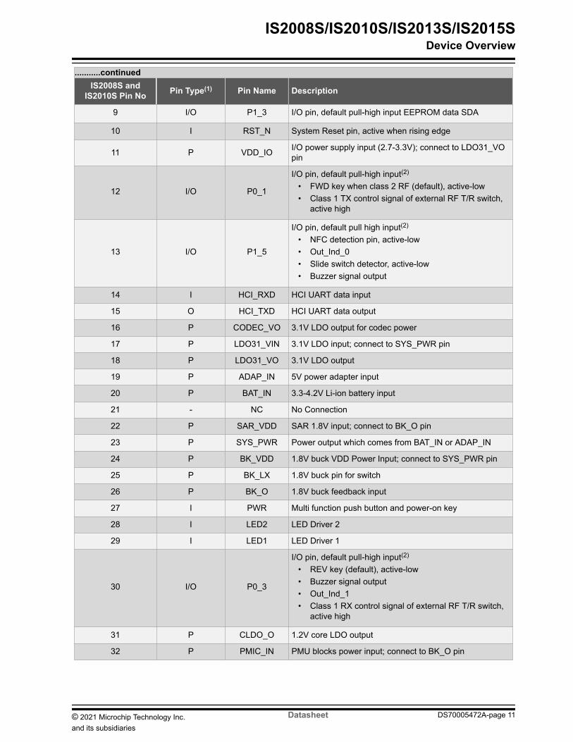
continuedIS2008S and
IS2010S Pin No Pin Type(1) Pin Name Description
33 P RFLDO_O 128V RF LDO output
34 P VBG Bandgap output reference for decoupling interference
35 P ULPC_VSUS ULPC 12V output power
36 I XO_N 16 MHz crystal input negative
37 I XO_P 16 MHz crystal input positive
38 P VCC_RF RF power input (128V) for both synthesizer and TXRXblock connect to RFLDO_O pin
39 IO RTX RF path (transmitreceive)
40 I P0_2IO pin default pull-high input(2)
PlayPause key (default) active-low
41 I P2_0IO pin default pull-high input system configuration
H Application L Baseband (IBDK mode)
42 I P2_7IO pin default pull high input(2)
Volume up key (default) active-low
43 I P0_5IO pin default pull high input(2)
Volume down (default) active-low
44 P VDD_IO IO power supply input (27-33V) connect to LDO31_VOpin
45 P VDD_AOPositive power supply dedicated to codec outputamplifiers connect to CODEC_VO pin
46 O AOHPM Headphone common mode outputsense input
47 O AOHPL Left channel analog headphone output
48 P VDDA Positive power supplyreference voltage for codecconnect to CODEC_VO pin
49 P EP Exposed pads used as ground (GND) pins
Notes 1 The conventions used in the table are indicated as follows
ndash I = Input pinndash O = Output pinndash IO = InputOutput pinndash P = Power pin
2 All IO pins are configured using the IS20XXS_UI tool a Windowsreg-based utility
The following figure illustrates the pin diagram of the IS2013S and IS2015S
IS2008SIS2010SIS2013SIS2015SDevice Overview
copy 2021 Microchip Technology Incand its subsidiaries
Datasheet DS70005472A-page 12
Figure 2-3 IS2013S and IS2015S Pin Diagram
The following table provides the pin description of the IS2013SIS2015S
Table 2-3 Pin Description
IS2013S andIS2015S Pin No Pin Type(1) Pin Name Description
1 P VDDAO Positive power supply dedicated to codec output amplifiersConnect to CODEC_VO pin
2 O AOHPM Headphone common mode outputsense input
3 O AOHPL Left channel analog headphone output
4 P VDDA Positive power supplyreference voltage for codec connect toCODEC_VO pin
5 P VCOM Internal biasing voltage for codec
6 I MICN1 Mic1 mono differential analog negative input
7 I MICP1 Mic1 mono differential analog positive input
8 P MICBIAS Electric microphone biasing voltage
9 I AIL Left channel single-ended analog inputs
IS2008SIS2010SIS2013SIS2015SDevice Overview
copy 2021 Microchip Technology Incand its subsidiaries
Datasheet DS70005472A-page 13
continuedIS2013S and
IS2015S Pin No Pin Type(1) Pin Name Description
10 P VDD_CORE Core 12V power input connect to CLDO_O pin
11 O P1_2 IO pin default pull high input EEPROM clock SCL
12 IO P1_3 IO pin default pull high input EEPROM data SDA
13 I RST_N System Reset pin active when rising edge
14 P VDD_IO IO power supply input (27-33V) connect to LDO31_VO pin
15 IO P0_1
IO pin default pull-high input(2)
bull FWD key when class 2 RF (default) active-lowbull Class 1 TX Control signal of external RF TR switch
active high
16 I P2_4IO pin default pull high input system configuration
L Boot mode with P2_0 low combination
17 IO P0_4IO pin default pull high input(2)
bull NFC detection pin active-lowbull Out_Ind_0
18 IO P1_5
IO pin default pull high input(2)
bull NFC detection pin active-lowbull Out_Ind_0bull Slide switch detector active-lowbull Buzzer signal output
19 I HCI_RXD HCI UART input data
20 O HCI_TXD HCI UART output data
21 P CODEC_VO 31V LDO output for codec power
22 P LDO31_VIN 31V LDO input connect to SYS_PWR pin
23 P LDO31_VO 31V LDO output
24 P ADAP_IN 5V power adapter input
25 P BAT_IN 33 to 42V Li-ion battery input
26 P SAR_VDD SAR 18V input connect to BK_O pin
27 P SYS_PWR Power output which come from BAT_IN or ADAP_IN
28 P LDO18_VDD 18V LDO VDD Power Input connect to SYS_PWR pin
29 P LDO18_O 18V LDO output
30 I PWR Multi-Function Push button and power on key
31 - NC No Connection
32 I LED2 LED Driver 2
33 I LED1 LED Driver 1
IS2008SIS2010SIS2013SIS2015SDevice Overview
copy 2021 Microchip Technology Incand its subsidiaries
Datasheet DS70005472A-page 14
continuedIS2013S and
IS2015S Pin No Pin Type(1) Pin Name Description
34 IO P0_0IO pin default pull-high input(2)
bull Slide switch detector active-lowbull UARTTX_IND active-low
35 IO P0_3
IO pin default pull-high input(2)
bull REV key (default) active-lowbull Buzzer signal outputbull Out_Ind_1bull Class 1 RX control signal of external RF TR switch
active high
36 I EANEmbedded ROMExternal Flash enable
H Embedded L External Flash
37 P CLDO_O 12V core LDO output
38 P PMIC_IN PMU blocks power input connect to BK_O pin
39 P RFLDO_O 128V RF LDO output
40 P VBG Bandgap output reference for decoupling interference
41 P ULPC_VSUS ULPC 12V output power
42 I XO_N 16 MHz crystal input negative
43 I XO_P 16 MHz crystal input positive
44 P VCC_RFRF power input (128V) for both synthesizer and TXRXblock connect to RFLDO_O pin
45 IO RTX RF path (transmitreceive)
46 I P0_2IO pin default pull-high input(2)
PlayPause key (default) active-low
47 I P2_0IO pin default pull-high input system configuration
H Application L Baseband (IBDK mode)
48 I P2_7IO pin default pull-high input(2)
Volume up key (default) active-low
49 I P3_0IO pin default pull-high input(2)
Line-in detector (default) active-low
50 I P0_5IO pin default pull-high input(2)
Volume down (default) active-low
51 P VDD_IO IO power supply input (27-33V) connect to LDO31_VO pin
52 P AVDD_CDA Supply voltage of audio amplifier
53 P VBP_CDA Reference voltage output
54 O HPON_CDA Negative BTL output of channel-1
55 O HPOP_CDA Positive BTL output of channel-1
IS2008SIS2010SIS2013SIS2015SDevice Overview
copy 2021 Microchip Technology Incand its subsidiaries
Datasheet DS70005472A-page 15
continuedIS2013S and
IS2015S Pin No Pin Type(1) Pin Name Description
56 P PVDD_CDA Supply voltage of power stage ch-1
57 P EP Exposed pads used as ground (GND) pins
Notes 1 The conventions used in the table are indicated as follows
ndash I = Input pinndash O = Output pinndash IO = InputOutput pinndash P = Power pin
2 All IO pins are configured using the UI tool a Windows-based utility
IS2008SIS2010SIS2013SIS2015SDevice Overview
copy 2021 Microchip Technology Incand its subsidiaries
Datasheet DS70005472A-page 16
3 AudioThe input and output audio signals have different stages and each stage is programmed to vary the gain responsecharacteristics For microphones both single-ended inputs and differential inputs are supported To maintain ahigh-quality signal provide a stable bias voltage source to the condenser microphonersquos FET Use the DC-blockingcapacitors at both positive and negative sides of the input Internally this analog signal is converted to 16-bit 8 kHzlinear PCM data
31 Digital Signal ProcessorA Digital Signal Processor (DSP) is used to perform speech and audio processing The advanced speech featuressuch as acoustic echo cancellation and noise reduction are built in To reduce nonlinear distortion and to help echocancellation an outgoing signal level to the speaker is monitored and adjusted to avoid saturation of the speakeroutput or microphone input Adaptive filtering is also applied to track the echo path impulse in response to provide anecho-free and full-duplex user experience
The embedded noise reduction algorithm helps to extract clean speech signals from the noisy inputs capturedby microphones and improves mutual understanding in communication The advanced audio features such asmulti-band dynamic range control parametric multi-band equalizer audio widening and virtual bass are built in Theaudio effect algorithms improve the userrsquos audio listening experience in terms of better quality audio after audiosignal processing
The following figures illustrate the processing flow of speakerphone applications for speech and audio signalprocessing
Figure 3-1 Speech Processing
Figure 3-2 Audio Processing
The DSP parameters such as EQ Speaker Gain Mic Gain Sound Effect and more are configured using the DSPtool For additional information on the DSP tool refer to the IS20xxBM1xBM2x DSP Application Note
IS2008SIS2010SIS2013SIS2015SAudio
copy 2021 Microchip Technology Incand its subsidiaries
Datasheet DS70005472A-page 17
Note The DSP tool and IS20xxBM1xBM2x DSP Application Note are available for download at the Microchipwebsite
32 CodecThe built-in codec has a high SNR performance and it consists of an ADC a DAC and additional analog circuitry
33 Auxiliary PortThe SoC supports one analog (line-in) signal from the external audio source The analog signal is processed bythe DSP to generate different sound effects (multi-band dynamic range compression and audio widening) which areconfigured using the DSP tool
34 Class D Audio AmplifierThe Class D amplifier has a significant advantage in many applications due to its lower power dissipation whichproduces less heat The IS2013S and IS2015S SoC have a built-in Class D amplifier that reduces circuit board spaceand system cost The efficiency of the amplifier extends the battery life in portable systems
The Class D amplifier is implemented by using a full-bridge output stage A full bridge uses two half-bridge stages todrive the load differentially The Class D amplifier provides a good SNR and enough drive capability for a 4Ω speakerdriver
IS2008SIS2010SIS2013SIS2015SAudio
copy 2021 Microchip Technology Incand its subsidiaries
Datasheet DS70005472A-page 18
4 TransceiverThe SoC is designed and optimized for Bluetooth 24 GHz systems It contains a complete radio frequencytransmitterreceiver section An internal synthesizer generates a stable clock to synchronize with another device
41 TransmitterThe internal Power Amplifier (PA) has a maximum output power of +4 dBm with 20 dB power level control Applythis to Class 2 or Class 3 radios without an external RF PA The transmitter directly performs the IQ conversionto minimize the frequency drift and it can access the 20 dB power range with the temperature compensationmechanism
42 ReceiverThe Low-Noise Amplifier (LNA) operates with TR-combined mode for the single port application It saves the pin onthe package without having an external TXRX switch
The ADC is used to sample the input analog signal and convert it into a digital signal for demodulator analysisA channel filter is integrated into a receiver channel before the ADC to reduce the external component count andincrease the anti-interference capability
The image rejection filter is used to reject the image frequency for the low-IF architecture and it is also intended toreduce the external Band Pass Filter (BPF) component for a super heterodyne architecture
The Received Signal Strength Indicator (RSSI) signal feedback to the processor is used to control the RF outputpower to make a good trade-off for effective distance and current consumption
43 SynthesizerA synthesizer generates a clock for radio transceiver operation The VCO inside with a tunable internal LC tankcan reduce any variation for components A crystal oscillator with an internal digital trimming circuit provides a stableclock for the synthesizer
44 ModemFor Bluetooth 12 specifications and below 1 Mbps is the standard data rate based on the Gaussian Frequency ShiftKeying (GFSK) modulation scheme This basic rate modem meets BDR requirements of Bluetooth 20 with EDRspecifications
For Bluetooth 20 and above specifications EDR is introduced to provide the data rates of 123 Mbps Thisenhanced data rate modem meets EDR requirements of Bluetooth 20 with EDR specifications For the basebandboth BDR and EDR utilize the same 1 MHz symbol rate and 16 kHz slot rate For BDR 1 symbol represents 1-bitHowever each symbol in the payload part of the EDR packets represents 2-bit or 3-bit This is achieved by using twodifferent modulations π4 DQPSK and 8 DPSK
45 Adaptive Frequency Hopping (AFH)The SoC has an AFH function to avoid RF interference It has an algorithm to check the nearby interference and tochoose the clear channel for the transceiver Bluetooth signal
IS2008SIS2010SIS2013SIS2015STransceiver
copy 2021 Microchip Technology Incand its subsidiaries
Datasheet DS70005472A-page 19
5 MicrocontrollerA single-cycle 8-bit microcontroller is built into the SoC to execute the Bluetooth protocols It operates from 16 MHzto higher frequencies where the firmware dynamically adjusts the trade-off between the computing power and thepower consumption In the ROM version the MCU firmware is hard-wired to minimize power consumption for thefirmware execution and to save the external Flash cost
51 MemoryThere are sufficient ROM and RAM to fulfill the processor requirements in which a synchronous single port RAMinterface is used The register bank dedicated single port memory and Flash memory are connected to theprocessor bus The processor coordinates with all link control procedures and the data movement happens using aset of pointer registers
52 External ResetThe IS20xxS SoC provides a Watchdog Timer (WDT) to reset the SoC It has an integrated Power-on Reset (POR)circuit that resets all circuits to a known Power-on state This action is also driven by an external Reset signal whichis used to control the device externally by forcing it into a POR state The RST_N signal input is active-low and noconnection is required in most of the applications
53 Reference ClockThe IS20xxS SoC is composed of an integrated crystal oscillation function that uses a 16 MHz external crystal andtwo specified loading capacitors to provide a high quality system reference timer source Use this feature to removethe initial tolerance frequency errors which are associated with the crystal and its equivalent loading capacitance inthe mass production Achieve the frequency trim by adjusting the crystal loading capacitance through the on-chip trimcapacitors (Ctrim)
The value of the trimming capacitance is 200 fF (200x10-15 F) per LSB at the 5-bit word and the overall adjustableclock frequency is plusmn40 kHz The following figure illustrates the crystal connection of the IS20xxS SoC with twocapacitors
Figure 5-1 Crystal Connection
IS20XXS
XO_N
CL1
XO_P
CL2
IS2008SIS2010SIS2013SIS2015SMicrocontroller
copy 2021 Microchip Technology Incand its subsidiaries
Datasheet DS70005472A-page 20
Notes 1 Ctrim = 200 fF (1 to 31) Cint = 3 pF2 CL = [(CL1 x CL2) (CL1 + CL2)] + (Ctrim 2) + Cint (set trim value as 16 Ctrim = 32 pF)3 For a 16 MHz crystal where CL = 9 pF the CL1 = CL2 = 91 pF)4 For the CL selection refer to the data sheet of the crystal
IS2008SIS2010SIS2013SIS2015SMicrocontroller
copy 2021 Microchip Technology Incand its subsidiaries
Datasheet DS70005472A-page 21
6 Power Management Unit (PMU)The IS20xxS SoC has an integrated PMU The main features of the PMU are a lithium-ion battery charger and avoltage regulator A power switch is used to switch over the power source between a battery and an adapter Alsothe PMU provides current to the LED drivers
61 Charging a BatteryThe IS20xxS SoC has a built-in battery charger which is optimized for lithium-polymer batteries The battery chargerincludes a current sensor for a charging control user programmable current regulator and high accuracy voltageregulator
The charging current parameters are configured by using the UI (IS20XXS_UI) tool Whenever the adapter isplugged-in the charging circuit will be activated Reviving pre-charging constant current mode constant voltagemode and re-charging functions are implemented The maximum charging current is 350 mA The following figureillustrates the charging curve of a battery
Figure 6-1 Battery Charging Curve
62 Voltage MonitoringA 10-bit successive approximation register ADC (SAR ADC) provides a dedicated channel for battery voltage leveldetection The warning level is programmed by using the UI tool The ADC provides a granular resolution to enablethe MCU to take control over the charging process
63 Low Dropout RegulatorA built-in LDO Regulator is used to convert the battery or adapter power for the power supply It also integratesthe hardware architecture to control the power-onoff procedure The built-in programmable LDOs provide power forcodec and digital IO pads Also it is used to buffer the high input voltage from the battery or adapter This LDOrequires a 1 μF bypass capacitor
IS2008SIS2010SIS2013SIS2015SPower Management Unit (PMU)
copy 2021 Microchip Technology Incand its subsidiaries
Datasheet DS70005472A-page 22
64 Switching RegulatorThe built-in programmable output voltage regulator converts the battery voltage to RF and base band core powersupply This converter has a high conversion efficiency and a fast transient response
65 LED DriverThe IS20xxS SoC consists of two LED drivers to control the LEDs The LED drivers provide enough sink current(16-step control and 035 mA for each step) and the LED is connected directly to the IS20xxS SoC
Note Configure the LED settings using the IS20XXS_UI tool
The following figure illustrates the LED driver in the IS20xxS SoC
Figure 6-2 LED DRIVER
IS20xxS
LED2
SYS_PWR
LED1
IS2008SIS2010SIS2013SIS2015SPower Management Unit (PMU)
copy 2021 Microchip Technology Incand its subsidiaries
Datasheet DS70005472A-page 23
7 Application InformationThis section describes the power supply connection host MCU UART interface and various modes in detail
71 Power SupplyThe following figure illustrates the connection from the BAT_IN pin to various other voltage supply pins of theIS20xxS SoC
The BAT_IN input pin powers the IS20xxS SoC To charge the battery connect the external 5V power adapter toADAP_IN
Figure 7-1 Power Tree Diagram
VDDA VDDAO
VDD_IO
3V LDO
18V Buck
SAR_VDD
LDO31_VIN
CODEC_VO
LDO31_VO
BK_VDD
BK_LX
BK_O
VDD_CORE
VCC_RF
12V LDOPMIC_IN
CLDO_O
RFLDO_O
PVDD_CDA
Li-Io
n BA
T BAT_IN
ADAP_IN
SYS_PWRPower Switch
5V Adapter
(42~30V)
(45~55V)(42~30V)
(30~27V)
(33 ~27V)
(18V)
(12V)
(128V)
72 Host MCU InterfaceAn external MCU controls the IS20xxS SoC using the UART command set The following figure illustrates the UARTinterface between the IS20xxS SoC and an external MCU
Figure 7-2 Host MCU Interface Over UART
IS20xxSHCI_TXD
HCI_RXD
PWR
P0_0
MCUUART_TX
UART_RX
MCU_WAKEUP
BT_WAKEUP
UART Interface
UART Interface
The MCU controls the IS20xxS SoC over the UART interface and wakes up the SoC using the PWR pin The MCUfunction wakes up by connecting to the P0_0 pin of the IS20xxS
Refer to the IS200xIS201xIS202x UART Command SOP document for a list of functions that the IS20xxS SoCsupports and how to use the IS20XXS_UI tool to set up the system using the UART command
Note The IS200xIS201xIS202x UART Command SOP document is available for download from the Microchipwebsite at IS200xIS201xIS202x UART Command SOP
IS2008SIS2010SIS2013SIS2015SApplication Information
copy 2021 Microchip Technology Incand its subsidiaries
Datasheet DS70005472A-page 24
73 Timing Sequence of UART ApplicationThe following figures illustrate the various UART control signal timing sequences
Figure 7-3 Power-OnOff Sequence
BAT_IN
SYS_PWR
1 ms
Power- oninitial idle Power-on Power-on Power-off idle
MCU state
MFB (PWR)
BK_OLDO31_VO
400 ms
RST_N
MCU sends UART command (UART_RX)
UART Command
MCU sends power-off UART Command
Power-on ACK ACK ACKIS20xxS response UART state
(UART_TX)
Set ldquoPower-on Directlyrdquo boot
any
10 ms
20 msKeep all IS20xxSand MCU connection to low level
2s
(See Figure 7-4) (See Figure 7-5)
IS20xxS disconnect and auto power-off
gt 1s
Figure 7-4 Timing Sequence of RX Indication after Power-On
Resume 32 kHz mode
MFB (PWR)MCU sends UART command
MFB pulse must be longer than the UART command slot time
150 ms
2 ms 2 ms
Enter 32 kHz mode
1 ms
UART Command
IS2008SIS2010SIS2013SIS2015SApplication Information
copy 2021 Microchip Technology Incand its subsidiaries
Datasheet DS70005472A-page 25
Figure 7-5 Timing Sequence of Power-Off
BAT_IN +4V
MFB
MCU Sends RST_N
BK_OUT
LDO31_VO
UART Bus
2s 1s
IS20xxS Sends Power-off ACK
Notes 1 EEPROM clock = 100 kHz2 For a byte wire 001 ms x 32 clock x 2 = 640 μs3 It is recommended that ramp-down time be more than 640 μs during the power-off sequence to ensure safe
operation of the device
IS2008SIS2010SIS2013SIS2015SApplication Information
copy 2021 Microchip Technology Incand its subsidiaries
Datasheet DS70005472A-page 26
Figu
re 7
-6
Tim
ing
Sequ
ence
of P
ower
-On
(NA
CK
)
BAT
_IN
SYS_
PWR
1 m
s Pow
er-
onin
itial
idle
Pow
er-o
nM
CU
sta
te
MFB
(PW
R)
BK_O
LD
O31
_VO
400
ms
RST
_N
MC
U s
ends
UAR
T co
mm
and
(UAR
T_R
X)
UAR
T C
omm
and
NAC
KPo
wer
-on
ACK
ACK
IS20
xxS
resp
onse
UAR
T st
ate
(UAR
T_TX
)
Set ldquo
Pow
er-o
n D
irect
lyrdquo b
oot
10 m
s
20 m
s
Ret
ry i
f AC
K is
not
rece
ived
200
ms
any
Wai
t
Max
imum
5 ti
mes
(1s)
IS2008SIS2010SIS2013SIS2015SApplication Information
copy 2021 Microchip Technology Incand its subsidiaries
Datasheet DS70005472A-page 27
Figure 7-7 Reset Timing Sequence in Case of No Response from SoC to Host MCU
MFB (PWR)
MCU sends UART command UART
Command
UART Command
IS20xxS UART
If no response
RST_N
1ms
X ms1ms
1ms
1ms
Note The MCU sends the UART command again when the SoC is not responding to its first UART command Ifthe SoC is not responding to the second UART command within X ms the MCU forces the system to reset
Figure 7-8 Timing Sequence of Power Drop Protection
BAT_IN +4V
RST_N from Reset IC
Power
SYS_PWR
IS20xxS
Reset OUT VDDGND
MCU Reset
Reset IC
29V
1 It is recommended that the battery be connected on a BAT_IN pin of the SoC for the power supply2 If an external power source or a power adapter is used to provide the power to the SoC (ADAP_IN) use a
voltage supervisor IC3 The RESET IC output pin must be open drain with delay time of le 10 ms and the recommended part is
TCM809SVNB713
74 General Purpose IO pinsThe following table provides the details of various functions that are mapped to the IO pins of the IS20xxS SoCand these IOs are configured by using the IS20XXS_UI tool The first button (Button 0) must be configured as thepower-onoff key and can be set using the PWR pin The remaining pins are configured for any one of the defaultfunctions (short press long press double press and combinations)
IS2008SIS2010SIS2013SIS2015SApplication Information
copy 2021 Microchip Technology Incand its subsidiaries
Datasheet DS70005472A-page 28
Table 7-1 IO Pin Configuration
Sl No Pin Name Buttons Default Functions(1)
1 PowerMFB Button 0 PWR
2 P0_2 Button 1 PlayPause
3 P2_7 Button 2 Volume Up
4 P0_5 Button 3 Volume Down
5 P0_1 Button 4 FWD
6 P0_3 Button 5 REV
Note 1 These functions can be configured using the IS20XXS_UI tool
Few signals are generated to indicate or control outside devices The most popular applications are NFC for easypairing external audio amplifier for louder speaker and buzzer for indication
Table 7-2 IO Pins for Added Functions
Functions(1) IO Configurable Features
Slide switch P0_0P1_5
Buzzer P0_3
NFC detect P0_4P1_5
External amplifier enable P1_5
Note 1 These functions can be configured using the IS20XXS_UI tool
IS2008SIS2010SIS2013SIS2015SApplication Information
copy 2021 Microchip Technology Incand its subsidiaries
Datasheet DS70005472A-page 29
8 Antenna Placement RuleFor Bluetooth-enabled products the antenna placement affects the overall performance The antenna requires freespace to radiate RF signals and it must not be surrounded by the GND plane
The following figure illustrates a typical example of the good and poor antenna placement on the main applicationboard with the GND plane
Figure 8-1 Antenna Placement Examples
The following figure illustrates the keep-out area recommended for the PCB antenna
Figure 8-2 Keep-Out Area Recommended for PCB Antenna
Note For additional information on the antenna placement refer to the antenna-specific data sheet from theantenna manufacturer
IS2008SIS2010SIS2013SIS2015SAntenna Placement Rule
copy 2021 Microchip Technology Incand its subsidiaries
Datasheet DS70005472A-page 30
9 Electrical CharacteristicsThis section provides an overview of the IS20xxS SoC electrical characteristics
Table 9-1 Absolute Maximum Ratings
Parameter Symbol Minimum Maximum Unit
Digital core supply voltage VDD_CORE 0 135 V
RF supply voltage VCC_RF 0 135 V
SAR ADC supply voltage SAR_VDD 0 21 V
Codec supply voltage VDDAVDDAO 0 33 V
IO supply voltage VDD_IO 0 36 V
Buck supply voltage BK_VDD 0 43 V
Supply voltage LDO31_VIN 0 43 V
Battery input voltage BAT_IN 0 43 V
Adapter input voltage ADAP_IN 0 70 V
Storage temperature TSTORE -65 +150
Operation temperature TOPERATION -20 +70
Note Stresses listed on the preceding table cause permanent damage to the device This is a stress rating onlyThe functional operation of the device at those or any other conditions and those indicated in the operation listingsof this specification are not implied Exposure to maximum rating conditions for extended periods affects devicereliability
The following tables provide the recommended operating conditions and the electrical specifications of the IS20xxSSoC
Table 9-2 Recommended Operating Condition
Parameter Symbol Minimum Typical Maximum Unit
Digital core supply voltage VDD_CORE 114 12 126 V
RF supply voltage VCC_RF 122 128 134 V
SAR ADC supply voltage SAR_VDD 162 18 198 V
Codec supply voltage VDDAVDDAO 27 28 30 V
IO supply voltage VDD_IO 27 30 33 V
Buck supply voltage BK_VDD 3 37 425 V
Supply voltage LDO31_VIN 3 37 425 V
Battery input voltage BAT_IN 3 37 425 V
Adapter input voltage ADAP_IN 45 5 55 V
Operation temperature TOPERATION -20 +25 +70
Note All these supply voltages are programmed through the EEPROM parameters
IS2008SIS2010SIS2013SIS2015SElectrical Characteristics
copy 2021 Microchip Technology Incand its subsidiaries
Datasheet DS70005472A-page 31
Table 9-3 Buck Switching Regulator
Parameter Minimum Typical Maximum Unit
Input voltage 30 37 425 V
Output voltage (Iload = 70 mA andVin = 4V) 17 18 205 V
Output voltage accuracy mdash plusmn5 mdash
Output voltage adjustable step mdash 50 mdash mVStep
Output adjustment range -01 mdash +025 V
Average load current (ILOAD) 120 mdash mdash mA
Conversion efficiency (BAT = 38Vand Iload = 50 mA) mdash 88(1) mdash
Quiescent current (PFM) mdash mdash 40 μA
Output current (peak) 200 mdash mdash mA
Shutdown current mdash mdash lt1 μA
Notes 1 Test condition SAR_VDD = 18V and temperature = +252 These parameters are characterized but not tested in manufacturing
Table 9-4 Low-dropout Regulator
Parameter Minimum Typical Maximum Unit
Input Voltage 30 37 425 V
Output VoltageCODEC_VO mdash 28 mdash
VIO_VO mdash 28 mdash
Output Accuracy (VIN = 37V ILOAD = 100 mA and +27) mdash plusmn5 mdash
Output current (average) mdash mdash 100 mA
Drop-out voltage
(Iload = maximum output current)mdash mdash 300 mV
Quiescent current (excluding load and Iload lt 1 mA) mdash 45 mdash μA
Shutdown current mdash mdash lt1 μA
Notes 1 Test condition SAR_VDD = 18V and temperature = +252 These parameters are characterized but not tested in manufacturing
Table 9-5 Battery Charger
Parameter Minimum Typical Maximum Unit
Input voltage (ADAP_IN) 45 50 55 V
Supply current to charger only mdash 3 45 mA
IS2008SIS2010SIS2013SIS2015SElectrical Characteristics
copy 2021 Microchip Technology Incand its subsidiaries
Datasheet DS70005472A-page 32
continuedParameter Minimum Typical Maximum Unit
Maximum batteryfast chargecurrent (ENX2 =0)
Headroom gt 07V (ADAP_IN = 5V) 170 200 240 mA
Headroom = 03V (ADAP_IN = 45V) 160 180 240 mA
Maximum batteryfast chargecurrent (ENX2 =1)
Headroom gt 07V (ADAP_IN = 5V) 300 350 420 mA
Headroom = 03V (ADAP_IN = 45V) 180 220 270 mA
Trickle charge voltage threshold mdash 3 mdash V
Battery charge termination current ( of fast charge current) mdash 10 mdash
Notes 1 Headroom = VADAP_IN ndash VBAT2 ENX2 is not allowed to be enabled when VADAP_IN ndash VBAT gt 2V3 These parameters are characterized but not tested in manufacturing
Table 9-6 LED Diver
Parameter Minimum Typical Maximum Unit
Open-drain voltage mdash mdash 36 V
Programmable current range 0 mdash 525 mA
Intensity control mdash 16 mdash step
Current step mdash 035 mdash mA
Power-down open-draincurrent mdash mdash 1 μA
Shutdown current mdash mdash 1 μA
Notes 1 Test condition SAR_VDD = 18V and temperature = +252 These parameters are characterized but not tested in manufacturing
Table 9-7 Audio Codec Digital-to-Analog Converter
Parameter (Condition)(1) Minimum Typical Maximum Unit
Over-sampling rate mdash 128 mdash fs
Resolution 16 mdash 20 Bits
Output sample rate 8 mdash 48 kHz
Signal-to-noise Ratio (2) (SNR at capless mode) for 48 kHz mdash 96 mdash dB
Signal-to-noise Ratio (2)
(SNR at single-ended mode) for 48 kHzmdash 98 mdash dB
Digital gain -54 mdash 485 dB
Digital gain resolution mdash 2 to 6 mdash dB
Analog gain -28 mdash 3 dB
Analog gain resolution mdash 1 mdash dB
IS2008SIS2010SIS2013SIS2015SElectrical Characteristics
copy 2021 Microchip Technology Incand its subsidiaries
Datasheet DS70005472A-page 33
continuedParameter (Condition)(1) Minimum Typical Maximum Unit
Output voltage full-scale swing (AVDD = 28V) 495 7425 mdash mV rms
Maximum output power (16Ω load) mdash 345 mdash mW
Maximum output power (32Ω load) mdash 172 mdash mW
Allowed loadResistive 8 16 OC Ω
Capacitive mdash mdash 500 pF
THD+N (16Ω load) mdash mdash 005
Signal-to-noise Ratio (SNR at 16Ω load) mdash mdash mdash 96 dB
Notes 1 T = +25 VDD = 30V 1 kHz sine wave input and Bandwidth = 20 Hz ndash 20 kHz2 fin = 1 kHz Bandwidth = 20 Hz ndash 20 kHz A-weighted THD + N lt 001 0 dBFS signal and Load = 100 kΩ3 These parameters are characterized but not tested in manufacturing
Table 9-8 Audio Codec Analog-to-Digital Converter
Parameter (Condition)(1) Minimum Typical Maximum Unit
Resolution mdash mdash 16 Bit
Output sample rate 8 mdash 48 kHz
Signal-to-noise Ratio (2) (SNR at MIC or Line-in mode) mdash 90 mdash dB
Digital gain -54 mdash 485 dB
Digital gain resolution mdash 2 to 6 mdash dB
MIC boost gain mdash 20 mdash dB
Analog gain mdash mdash 60 dB
Analog gain resolution mdash 20 mdash dB
Input full scale at maximum gain (differential) mdash 4 mdash mVrms
Input full scale at minimum gain (differential) mdash 800 mdash mVrms
3 dB bandwidth mdash 20 mdash kHz
Microphone mode (input impedance) mdash 24 mdash kΩ
THD+N (microphone input) at 30 mVrms input mdash 002 mdash
Notes 1 T = +25 VDD = 30V 1 kHz sine wave input and Bandwidth = 20 Hz ndash 20 kHz2 fin = 1 kHz Bandwidth = 20 Hz ndash 20 kHz A-weighted and THD + N lt 1 150 mVpp input3 These parameters are characterized but not tested in manufacturing
Table 9-9 Single-Channel ClassndashD Amplifier
Parameter (Condition) Minimum Typical Maximum Unit
Standalone SNR (A-weighting) mdash 100 mdash dB
Gain mdash 12 mdash dB
PSRR (217 Hz 200 mV on PVDD) mdash 70 mdash dB
IS2008SIS2010SIS2013SIS2015SElectrical Characteristics
copy 2021 Microchip Technology Incand its subsidiaries
Datasheet DS70005472A-page 34
continuedParameter (Condition) Minimum Typical Maximum Unit
Efficiency4Ω 80 mdash 85
8Ω 85 mdash 90
Supply voltage 30 37 45 V
Load mdash 40 mdash Ω
Quiescent current (1 channel) mdash 20 mdash mA
Sample frequency mdash 250 mdash kHz
Over current limits mdash 23 mdash A
Shutdown current mdash 10 mdash μA
Notes 1 Test condition PVDD_CDA = 42V and temperature = 252 These parameters are characterized but not tested in manufacturing
Table 9-10 Transmitter Section for BDR and EDR
Parameter Minimum Typical Maximum BluetoothSpecification Unit
Maximum RF transmit power mdash 30 40 -6 to 4 dBm
Relative transmit power -4 -12 1 -4 to 1 dB
Notes 1 The RF Transmit power is calibrated during production using the MP tool software and MT8852 Bluetooth test
equipment2 Test condition VCC_RF = 128V and temperature = +25
Table 9-11 Receiver Section for BDR and EDR
Parameter Packet Type Minimum Typical Maximum BluetoothSpecification Unit
Sensitivity at 01 BER GFSK mdash -90 mdash le-70 dBm
Sensitivity at 001 BERπ4 DQPSK mdash -91 mdash le-70 dBm
8 DPSK mdash -82 mdash le-70 dBm
Notes 1 Test condition VCC_RF = 128V and temperature = +252 These parameters are characterized but not tested in manufacturing
Table 9-12 System Current Consumption
System Status Typical Maximum Unit
System Off mode 2 5 μA
Standby mode 08 mdash mA
Link mode 04 mdash mA
SCO Link 78 mdash mA
A2DP Link (Vp-p = 200 mV 1k tone signal) 107 mdash mA
IS2008SIS2010SIS2013SIS2015SElectrical Characteristics
copy 2021 Microchip Technology Incand its subsidiaries
Datasheet DS70005472A-page 35
Notes 1 Consider the current consumption values with the IS2010 EVB as a test platform2 Test condition BAT_IN = 38V link with the HTC EYE smartphone The distance between the smartphone and
EVB is 30 cm
IS2008SIS2010SIS2013SIS2015SElectrical Characteristics
copy 2021 Microchip Technology Incand its subsidiaries
Datasheet DS70005472A-page 36
10 Packaging InformationThis section provides information on package marking package details and footprint dimensions of the IS20xxS SoC
101 Chip Identification SystemPart No X -Y
(Chip Name) (Package Type) (Version)
Legendbull Chip Name
ndash IS2008Sndash IS2010Sndash IS2013Sndash IS2015S
bull Package Typendash S = QFN (Saw Type) Package
bull Versionndash ldquo-203rdquo represents the chip version is 203
For examplebull IS2015S-002 002 version ROM code IS2015 chip in QFN type packagebull IS2010S-203 203 version ROM code IS2010 chip in QFN type package
102 Package Marking InformationThe following figure illustrates the package marking information of the IS20xxS
IS2008SIS2010SIS2013SIS2015SPackaging Information
copy 2021 Microchip Technology Incand its subsidiaries
Datasheet DS70005472A-page 37
Figure 10-1 Package Marking Information
Page 36
Page 36
48 Lead QFN (6x6x09 mm) 56 Lead QFN (7x7x09 mm)
Pin 1 Index
Pin 1 Index Pin 1 Index
Legend
XXX Chip serial number version and e3 Pb-free JEDEC designator for Matte Tin (Sn)
YY Year code (last 2 digits of calendar year)
WW Week code (week of January 1 is week ldquo1rdquo)
NNN Alphanumeric traceability code
103 Package DetailsThe following figures illustrate the footprint dimensions and the chip outline details of the IS2008S and IS2010S SoC
IS2008SIS2010SIS2013SIS2015SPackaging Information
copy 2021 Microchip Technology Incand its subsidiaries
Datasheet DS70005472A-page 38
Figure 10-2 IS2008S and IS2010S Chip Outline Details
IS2008SIS2010SIS2013SIS2015SPackaging Information
copy 2021 Microchip Technology Incand its subsidiaries
Datasheet DS70005472A-page 39
Figure 10-3 IS2008S and IS2010S Footprint Dimensions
PAD LENGTHPAD WIDTH
PAD PITCHPAD COUNT
Note For the most current package drawings refer to the Microchip Packaging Specification available at httpwwwmicrochipcompackaging
The following figures illustrate the footprint dimensions and the chip outline details of the IS2013S and IS2015S SoC
IS2008SIS2010SIS2013SIS2015SPackaging Information
copy 2021 Microchip Technology Incand its subsidiaries
Datasheet DS70005472A-page 40
Figure 10-4 IS2013S and IS2015S Chip Outline Details
IS2008SIS2010SIS2013SIS2015SPackaging Information
copy 2021 Microchip Technology Incand its subsidiaries
Datasheet DS70005472A-page 41
Figure 10-5 IS2013S and IS2015S Footprint Dimensions
Note For the most current package drawings refer to the Microchip Packaging Specification available at httpwwwmicrochipcompackaging
IS2008SIS2010SIS2013SIS2015SPackaging Information
copy 2021 Microchip Technology Incand its subsidiaries
Datasheet DS70005472A-page 42
11 Reflow Profile and Storage ConditionThis chapter describes reflow profiles and stencil information of the IS20xxS SoC
111 Stencil of SMT Assembly SuggestionThe stencil of the SMT assembly suggestion contains the following sections
1111 Stencil Type and Thicknessbull Laser cuttingbull Stainless steelbull Thickness 05 mm pitch thickness less than 015 mm
1112 Aperture Size and Shape for Terminal Padbull Aspect ratio (widththickness) is more than 15bull Aperture shape
ndash The stencil aperture is designed to match the pad size on the PCBndash Oval-shaped opening is used to get the optimum paste releasendash Rounded corners to minimize cloggingndash Positive taper walls (5deg tapering) with the bottom opening larger than the top opening
1113 Aperture Design for Thermal Padbull Small multiple openings are used instead of one big opening as shown in the following figure
Figure 11-1 IS20xxS SoC Reflow Profile Aperture Design
bull 60 to 80 solder paste coveragebull Rounded corners to minimize cloggingbull Positive taper walls (5deg tapering) with the bottom opening is larger than the top opening as shown in the
following figureFigure 11-2 IS20xxS SoC Stencil Type
IS2008SIS2010SIS2013SIS2015SReflow Profile and Storage Condition
copy 2021 Microchip Technology Incand its subsidiaries
Datasheet DS70005472A-page 43
112 Reflow ProfileThe following figure illustrates the reflow profile and its specific features are
bull Standard Condition IPCJEDEC J-STD-020bull Preheat 150 to 200 for 60 to180 secondsbull Average ramp-up rate (217 to peak) 1 to 2sec maxbull Temperature maintained above 217 60 to 150 secondsbull Time within 5 of actual peak temperature 20 to 40 secondsbull Peak temperature 260 with +5-0 tolerancebull Ramp-down rate (peak to 217) 3sec maxbull Time within 25 to peak temperature 8 minutes maxbull Cycle interval 5 minutes
Figure 11-3 Reflow Profile
+150degC
+200degC
+217degC
+255degCRamp-up rate1~2degCsec max+217degC to peak
Peak +260degC (+50degC tolerance)
Ramp-down rate+3degCsec maxpeak to +217degC
20 to 40 sec
Time (sec)
60 to 180 sec 60 to 150 sec
113 Storage ConditionUsers must follow these specific storage conditions for the IS20xxS SoC
bull Calculated shelf life in the sealed bag 24 months at lt40 and lt90 Relative Humidity (RH)bull Once the bag is opened devices that are subjected to reflow solder or other high temperature process must be
mounted within 168 hours of factory conditions that is lt3060 RH
The following figure illustrates the IS20xxS SoC bag label details
IS2008SIS2010SIS2013SIS2015SReflow Profile and Storage Condition
copy 2021 Microchip Technology Incand its subsidiaries
Datasheet DS70005472A-page 44
Figure 11-4 Storage Conditions
IS2008SIS2010SIS2013SIS2015SReflow Profile and Storage Condition
copy 2021 Microchip Technology Incand its subsidiaries
Datasheet DS70005472A-page 45
12 Reference CircuitThis section provides the reference schematics of IS2008S IS2010S IS2013S and IS2015SFigure 12-1 IS2008SIS2010S Reference Circuit (Main Circuit)
(Peak Current 400 mA)
(1uF X5R or 47uF Y5V)
P0_3
VBGULPC_VSUS
MFB
VBG
ULPC_VSUS
LED1LED2
P0_1
ADAP
_IN
P1_5
P0_2
P0_5
P2_7
P2_0
MIC_P2MIC_N2
MIC_P1MIC_N1
P1_2P1_3RST_N
AOH
PLAO
HPM
HC
I_TX
DH
CI_
RXD
RFLDO_O1V8
1V2
1V8
CODEC_VO
2V8
1V8SYS_PWR
BAT_IN
CODEC_VO
2V8
SYS_PWR
SYS_PWR
RFLDO_O
MIC_BIAS
2V8
1V2
ADAP_IN
MIC_N2MIC_P2MIC_N1MIC_P1
RST_N
HC
I_R
XDH
CI_
TXD
LED2LED1
AOH
PMAO
HPL
P0_1
P1_5
P0_3
P0_5
P2_7
P2_0
P0_2
MFB
C791u16V
ANT1
ANT-MP8
1
C321u16V
C291u16V
C7710u16V
C871u16V
X1X4P-16MHZ
4 13 2
C251u16V
C402p50V
C311u16V
C219p50V
C281u16V
R681K1
12
C261u16V
C191u16V
C361u16V
L10L10uH-2
C831u16V
C841u16V
IS2008SIS2010S
U6
IS2010S_MH+2MIC
MICN22
AO
HP
L47
VD
DA
48
VCOM1
MICN14
MICP15
MICBIAS6
VDD_CORE7
VDD_IO11 RST_N10
P128
P139
P05
43
HC
I_TX
D15
HC
I_R
XD
14
XO
_P37
XO_N36
ULPC_VSUS35
P27
42
VBG34
RFLDO_O33
PMIC_IN32
CLDO_O31
NC
21
SY
S_P
WR
23
P20
41
P15
13
P02
40
P0112
VD
D_I
O44
RTX
39
VC
C_R
F38
EP
49
VD
DA
O45
AO
HP
M46
MICP23
P0330
CO
DE
C_V
O16
LDO
31_V
IN17
LDO
31_V
O18
AD
AP
_IN
19
BA
T_IN
20
SA
R_V
DD
22
BK
_VD
D24
BK_LX25BK_O26PWR27
LED129
LED228
C801u16V
C8210u16V
TP9RF-TP1
C861u16V
L227nH
R691K
12
C8110u16V
C411u16V
C249p50V
C3NP-0402
C271u16V
C341u16V
L368p50V
C231u16V
C781u16V
IS2008SIS2010SIS2013SIS2015SReference Circuit
copy 2021 Microchip Technology Incand its subsidiaries
Datasheet DS70005472A-page 46
Figure 12-2 IS2008SIS2010S EEPROM (Main Circuit)
EEPROM
P1_2P1_3
2V8
U7ACE24C64
A01
A12
A23
GND4
SDA5SCL6WP7VCC8
C3801u16V
C391u16V
R18NP-0603
R174K7
12
IS2008SIS2010SIS2013SIS2015SReference Circuit
copy 2021 Microchip Technology Incand its subsidiaries
Datasheet DS70005472A-page 47
Figure 12-3 IS2008SIS2010S Audio Interface (Optional Circuit)
AOHPMS
AOHPL
MIC1
MIC2
MIC2+
MIC1+
MIC1-
MIC2-
AOHPM
AOHPL
MIC_P1
MIC_N1
MIC1+
MIC1-
MIC_P2
MIC_N2
MIC2+
MIC2-
MIC_BIAS
MIC_BIAS
MIC_P1
MIC_N1
MIC_P2
MIC_N2
AOHPM
AOHPL
C42220p50V
D14SPE0572
21
TP51
C4647u10V
C440047u25V
D16SPE0572
21
TP131
R91K
1 2
TP61
TP111
R112K
1 2
C11 10p50V
R61K
1 2
TP71
C15 10p50V
C350047u25V
C2047u10V
D12SPE0572
21
C37220p50V
TP81
C2247u10V
D13SPE0572
21
C1239p50V
C430047u25V
D10SPE0572
21
C1739p50V
R71K
1 2
R102K
1 2
R81K
1 2
C400047u25V
D11SPE0572
21
C4547u10V
IS2008SIS2010SIS2013SIS2015SReference Circuit
copy 2021 Microchip Technology Incand its subsidiaries
Datasheet DS70005472A-page 48
Figure 12-4 IS2008SIS2010S Audio Options (Optional Circuit)
FWD
VOL_UP
PLAYPAUSE
REV
VOL_DN P2_7
P0_2
P0_3
P0_5
P0_1
MFB
SYS_PWR
MFB
P0_2
P0_3 P0_1
P0_5 P2_7
C6415p50V
SW9SW-TACT
12
34SW4
SW-TACT
12
34
C6615p50V
C6515p50V
SW5
SW-TACT
12
34SW6
SW-TACT
12
34
C6815p50V
C6715p50V
SW8
SW-TACT
12
34SW7
SW-TACT
12
34
Figure 12-5 IS2008SIS2010S LED (Optional Circuit)
LED1
LED2 SYS_PWR
LED1
LED2LED2LED-HR12
LED1LED-B12
IS2008SIS2010SIS2013SIS2015SReference Circuit
copy 2021 Microchip Technology Incand its subsidiaries
Datasheet DS70005472A-page 49
Figure 12-6 IS2008SIS2010S NFC (Optional Circuit)
P1_5
MFB
SYS_PWR
P1_5
D22CDSU400B1 2
R291201
1 2
R252701
1 2
R13NP-0805
Q7
STS2306
312
R301K1
12
G D
S
Q9STS2301
13
2
TP291
R231M
12
TP301
D21CDSU400B
1 2
D20
21
Figure 12-7 IS2008SIS2010S Reset (Optional Circuit)
RST_N
ADAP_IN
RST_N
R282K
12
Q3
MMBT3904
321
C701u16V
IS2008SIS2010SIS2013SIS2015SReference Circuit
copy 2021 Microchip Technology Incand its subsidiaries
Datasheet DS70005472A-page 50
Figure 12-8 IS2008SIS2010S Slide Switch (Optional Circuit)
P1_5MFB
SYS_PWR
2V8
Q8
STS2306
312
GD
SQ14STS2301
13
2 R5010K
12
R141K
12
C13610u16V
R129
100K
1 2
R52
100K1
2
ONSW10
SW-1BIT
1 2
Figure 12-9 IS2008SIS2010S Test Point (Optional Circuit)
CORE_LDO
RF_LDO
BK_OUT
BAT-
ADAPGNDHCI_TXD
RESET
HCI_RXD
CODEC_VDD
BAT+P2_0
VDD_IO
RST_N
HCI_RXD
HCI_TXD
P2_0
1V2
RFLDO_O
ADAP_IN
1V8
BAT_IN
CODEC_VO
2V8
HCI_TXD
HCI_RXD
RST_N
P2_0
TP281
TP251
TP261
TP151
TP271
TP171
TP161
TP191
TP211
TP351
TP221
TP201
TP241
IS2008SIS2010SIS2013SIS2015SReference Circuit
copy 2021 Microchip Technology Incand its subsidiaries
Datasheet DS70005472A-page 51
Figure 12-10 IS2013SIS2015S Reference Circuit (Main Circuit)
(Peak Current 400 mA)
(1uF X5R or 47uF Y5V)
(Peak current 1A )
(C88 should closeto IC)
AOHPLAOHPM
AIL
MFB
MIC_P1MIC_N1
VBG
ULPC_VSUS
P1_2P1_3RST_N
VBGULPC_VSUS
HC
I_TX
DH
CI_
RXD
P0_0P0_3
P2_4
P0_1
P0_4
LED1LED2
P0_2
P0_5
P2_7
P2_0
P3_0
P3_0
HPO
PH
PON
CODEC_VO
1V8
MIC_BIAS
2V8
ADAP_IN
RFLDO_O1V8
1V2
1V8SYS_PWR
BAT_IN
CODEC_VO
2V8SYS_PWR
SYS_PWR
2V8
RFLDO_O
1V2
CDA_PWR
PVDD_CDA_IN
AOHPLAOHPM
MIC_N1MIC_P1
AIL
RST_N
HC
I_R
XDH
CI_
TXD
P0_1
P0_4
P2_4
LED2LED1P0_0
MFB
P0_3
P2_7
P2_0
P0_2
P0_5
P3_0
HPO
PH
PON
C8210u16V
R681K1
12
C341u16V
IS2013SIS2015S
U6
AOHPL3
VDDA4
VCOM5
MICN16
MICP17
MICBIAS8
VDD_IO14 RST_N13
P1211
P1312
VDD_CORE10
P24
16
EP
57
VDDAO1
AOHPM2
PV
DD
_CD
A56
HP
OP
_CD
A55
HP
ON
_CD
A54
VB
P_C
DA
53
AV
DD
_CD
A52
XO_N42
ULPC_VSUS41
AIL9
VBG40
RFLDO_O39
PMIC_IN38
CLDO_O37
EAN36
P27
48
P04
17
LED133
LED232
PWR30
LDO18_O29
P0034
P20
47P
3049
P02
46
P01
15
VD
D_I
O51
RTX
45
VC
C_R
F44
XO
_P43
P05
50H
CI_
RX
D19
HC
I_TX
D20
P0335
P15
18
CO
DE
C_V
O21
LDO
31_V
IN22
LDO
31_V
O23
AD
AP
_IN
24
BA
T_IN
25
SA
R_V
DD
26
SY
S_P
WR
27
LDO
18_V
DD
28
NC31
C402p50V
C161u16V
TP9RF-TP1
C231u16V
C3NP-0402
C191u16V
C801u16V
ANT1
ANT-MP8
1
C411u16V
X1X4P-16MHZ
4 13 2
C311u16V
C871u16V
C841u16V
C810u16V
C361u16V
FB9GSMA201209
12
C791u16V
C831u16V
C281u16V
C271u16V
C181u16V
C291u16V
C781u16V
C261u16V
C7710u16V
R691K1
12
C861u16V
C8810u16V
C321u16V
C251u16V
C249p50V
L368p50V
C8110u16V
C219p50V
L227nH
+C117100u16V
12
IS2008SIS2010SIS2013SIS2015SReference Circuit
copy 2021 Microchip Technology Incand its subsidiaries
Datasheet DS70005472A-page 52
Figure 12-11 IS2013SIS2015S EEPROM (Main Circuit)
EEPROM
P1_2P1_3
2V8
R174K7
12
C3801u16V
U7ACE24C64
A01
A12
A23
GND4
SDA5SCL6WP7VCC8
R18NP-0603
C391u16V
IS2008SIS2010SIS2013SIS2015SReference Circuit
copy 2021 Microchip Technology Incand its subsidiaries
Datasheet DS70005472A-page 53
Figure 12-12 IS2013SIS2015S Audio Interface (Optional Circuit)
LINEINPUT
AOHPMS
AOHPL
MIC1
MIC_P1
MIC_N1
AIRR
AILL AIL
AOHPM
AOHPL
MIC1+
MIC1+
MIC1-MIC1-
AIRR
AILL
MIC_BIAS
MIC_P1
MIC_N1
AIL
AOHPM
AOHPL
P3_0
D14SPE0572
21
D13SPE0572
21
C1739p50V
R7 1K1 2
TP131
C350047u25V
C15 10p50V
R61300
1 2
C1239p50V
C401u16V
C420047u25V
C11 10p50V
R6 1K1 2
TP111
R63NP-0603
D16SPE0572
21
TP61
D18SPE0572
21
R62NP-0603
C2247u10V
D19SPE0572
21
P3TSH-3865D
4
3
210
1
C37220p50V
C3001u16V
R60300
1 2
D10SPE0572
21
R102K
1 2
TP51
C2047u10V
IS2008SIS2010SIS2013SIS2015SReference Circuit
copy 2021 Microchip Technology Incand its subsidiaries
Datasheet DS70005472A-page 54
Figure 12-13 IS2013SIS2015S Audio Options (Optional Circuit)
FWD
VOL_UP
PLAYPAUSE
REV
VOL_DN
P0_2
P0_5 P2_7
P0_1P0_3
MFB
SYS_PWR
MFB
P0_2
P0_3 P0_1
P0_5 P2_7SW8
SW-TACT
12
34 C6815p50V
SW6
SW-TACT
12
34 C6615p50V
SW5
SW-TACT
12
34 C6515p50V
SW9SW-TACT
12
34C6415p50V
SW4
SW-TACT
12
34
SW7
SW-TACT
12
34 C6715p50V
Figure 12-14 IS2013SIS2015S CDA (Optional Circuit)
(Close to IC)
HPON_OHPOP_OHPOP_O
HPON_OHPOP
HPONTP32 1
FB6GSMA201209
12
D24SPE0572
21
TP31 1
D23SPE0572
21
C50220p50V
C43220p50V
FB5GSMA201209
12
IS2008SIS2010SIS2013SIS2015SReference Circuit
copy 2021 Microchip Technology Incand its subsidiaries
Datasheet DS70005472A-page 55
Figure 12-15 IS2013SIS2015S External Power Switch (Optional Circuit)
(Vo=(1+ R24R16)125)
Warning 45V max
OPTIONAL 45V Booster CircuitIf no boost add R26 0-ohm
Optional if ADAP_INgt5V
ADAP_IN
BAT_IN
5VCDA_PWR
CODEC_VO
2V8
U3SM4839N
S1
S2
S3
G4
D8
D7
D6
D5
+C60
100u16V
12
R91K1
12
L1L10uH-3
D11N5822
21
D21N4002
21
R1620
12 R11
20K
12
C331u16V
R22 NP-0603
R21 01 2
U2 RT9266E
CE1
EXT2
GND3
LX4
VDD5
FB6
R241M
1 2
C710u16V
U1APL1117-VC
ADJ
GND
1O
UT2
IN3C6
10u16V
R26NP-0805
R16390K
1 2
+C61
100u16V
12
C501u16V
R20NP-0603
G D
S
Q4STS2301
13
2
R21K81
12
Figure 12-16 IS2013SIS2015S LED (Optional Circuit)
LED2
LED1
SYS_PWR
LED1
LED2
LED1LED-B12
LED2LED-HR12
Figure 12-17 IS2013SIS2015S NFC (Optional Circuit)
P0_4
MFB
SYS_PWR
P0_4
D20
21
Q7
STS2306
312
G D
S
Q9STS2301
13
2R301K1
12
R252701
1 2
TP301
D21CDSU400B
1 2
D22CDSU400B1 2
R231M
12
R291201
1 2
R13NP-0805
TP291
Note Only for NFC tag with rectifier circuit
IS2008SIS2010SIS2013SIS2015SReference Circuit
copy 2021 Microchip Technology Incand its subsidiaries
Datasheet DS70005472A-page 56
Figure 12-18 IS2013SIS2015S Reset (Optional Circuit)
RST_N
ADAP_IN
RST_N
C701u16V
Q3
MMBT3904
321
R282K
12
Figure 12-19 IS2013SIS2015S Slide Switch (Optional Circuit)
P0_0MFB
SYS_PWR
2V8
P0_0
R5010K
12
SW10
SW-1BIT
1 2
R141K
12
R129
100K
1 2GD
SQ14STS2301
13
2
C13610u16V
R52
100K
12
Q8
STS2306
312
IS2008SIS2010SIS2013SIS2015SReference Circuit
copy 2021 Microchip Technology Incand its subsidiaries
Datasheet DS70005472A-page 57
Figure 12-20 IS2013SIS2015S Test Point (Optional Circuit)
CORE_LDO
RF_LDO
GNDADAP
BAT-
LDO18_OUT
HCI_RXD
RESET
HCI_TXD
CODEC_VDD
P2_0 BAT+
VDD_IO
P2_4
RST_N
P2_0
P2_4
HCI_TXD
HCI_RXD
ADAP_IN
1V2
RFLDO_O
1V8
BAT_IN
CODEC_VO
2V8
HCI_TXD
HCI_RXD
P2_0
P2_4
TP201
TP271
TP211
TP221
TP241
TP151
TP191
TP251
TP231
TP261
TP171
TP351
TP281
TP161
IS2008SIS2010SIS2013SIS2015SReference Circuit
copy 2021 Microchip Technology Incand its subsidiaries
Datasheet DS70005472A-page 58
13 Document Revision HistoryRevision Date Section Description
A 062021 Documentbull Updated from ISSC to Microchip templatebull Assigned a new Microchip document numberbull ISBN number added
IS2008SIS2010SIS2013SIS2015SDocument Revision History
copy 2021 Microchip Technology Incand its subsidiaries
Datasheet DS70005472A-page 59
The Microchip Website
Microchip provides online support via our website at wwwmicrochipcom This website is used to make files andinformation easily available to customers Some of the content available includes
bull Product Support ndash Data sheets and errata application notes and sample programs design resources userrsquosguides and hardware support documents latest software releases and archived software
bull General Technical Support ndash Frequently Asked Questions (FAQs) technical support requests onlinediscussion groups Microchip design partner program member listing
bull Business of Microchip ndash Product selector and ordering guides latest Microchip press releases listing ofseminars and events listings of Microchip sales offices distributors and factory representatives
Product Change Notification Service
Microchiprsquos product change notification service helps keep customers current on Microchip products Subscribers willreceive email notification whenever there are changes updates revisions or errata related to a specified productfamily or development tool of interest
To register go to wwwmicrochipcompcn and follow the registration instructions
Customer Support
Users of Microchip products can receive assistance through several channels
bull Distributor or Representativebull Local Sales Officebull Embedded Solutions Engineer (ESE)bull Technical Support
Customers should contact their distributor representative or ESE for support Local sales offices are also available tohelp customers A listing of sales offices and locations is included in this document
Technical support is available through the website at wwwmicrochipcomsupport
Microchip Devices Code Protection Feature
Note the following details of the code protection feature on Microchip devices
bull Microchip products meet the specifications contained in their particular Microchip Data Sheetbull Microchip believes that its family of products is secure when used in the intended manner and under normal
conditionsbull There are dishonest and possibly illegal methods being used in attempts to breach the code protection features
of the Microchip devices We believe that these methods require using the Microchip products in a manneroutside the operating specifications contained in Microchiprsquos Data Sheets Attempts to breach these codeprotection features most likely cannot be accomplished without violating Microchiprsquos intellectual property rights
bull Microchip is willing to work with any customer who is concerned about the integrity of its codebull Neither Microchip nor any other semiconductor manufacturer can guarantee the security of its code Code
protection does not mean that we are guaranteeing the product is ldquounbreakablerdquo Code protection is constantlyevolving We at Microchip are committed to continuously improving the code protection features of our productsAttempts to break Microchiprsquos code protection feature may be a violation of the Digital Millennium Copyright ActIf such acts allow unauthorized access to your software or other copyrighted work you may have a right to suefor relief under that Act
IS2008SIS2010SIS2013SIS2015S
copy 2021 Microchip Technology Incand its subsidiaries
Datasheet DS70005472A-page 60
Legal Notice
Information contained in this publication is provided for the sole purpose of designing with and using Microchipproducts Information regarding device applications and the like is provided only for your convenience and may besuperseded by updates It is your responsibility to ensure that your application meets with your specifications
THIS INFORMATION IS PROVIDED BY MICROCHIP ldquoAS ISrdquo MICROCHIP MAKES NO REPRESENTATIONSOR WARRANTIES OF ANY KIND WHETHER EXPRESS OR IMPLIED WRITTEN OR ORAL STATUTORYOR OTHERWISE RELATED TO THE INFORMATION INCLUDING BUT NOT LIMITED TO ANY IMPLIEDWARRANTIES OF NON-INFRINGEMENT MERCHANTABILITY AND FITNESS FOR A PARTICULAR PURPOSEOR WARRANTIES RELATED TO ITS CONDITION QUALITY OR PERFORMANCE
IN NO EVENT WILL MICROCHIP BE LIABLE FOR ANY INDIRECT SPECIAL PUNITIVE INCIDENTAL ORCONSEQUENTIAL LOSS DAMAGE COST OR EXPENSE OF ANY KIND WHATSOEVER RELATED TO THEINFORMATION OR ITS USE HOWEVER CAUSED EVEN IF MICROCHIP HAS BEEN ADVISED OF THEPOSSIBILITY OR THE DAMAGES ARE FORESEEABLE TO THE FULLEST EXTENT ALLOWED BY LAWMICROCHIPS TOTAL LIABILITY ON ALL CLAIMS IN ANY WAY RELATED TO THE INFORMATION OR ITS USEWILL NOT EXCEED THE AMOUNT OF FEES IF ANY THAT YOU HAVE PAID DIRECTLY TO MICROCHIP FORTHE INFORMATION Use of Microchip devices in life support andor safety applications is entirely at the buyerrsquos riskand the buyer agrees to defend indemnify and hold harmless Microchip from any and all damages claims suits orexpenses resulting from such use No licenses are conveyed implicitly or otherwise under any Microchip intellectualproperty rights unless otherwise stated
Trademarks
The Microchip name and logo the Microchip logo Adaptec AnyRate AVR AVR logo AVR Freaks BesTimeBitCloud chipKIT chipKIT logo CryptoMemory CryptoRF dsPIC FlashFlex flexPWR HELDO IGLOO JukeBloxKeeLoq Kleer LANCheck LinkMD maXStylus maXTouch MediaLB megaAVR Microsemi Microsemi logoMOST MOST logo MPLAB OptoLyzer PackeTime PIC picoPower PICSTART PIC32 logo PolarFire ProchipDesigner QTouch SAM-BA SenGenuity SpyNIC SST SST Logo SuperFlash Symmetricom SyncServerTachyon TimeSource tinyAVR UNIO Vectron and XMEGA are registered trademarks of Microchip TechnologyIncorporated in the USA and other countries
AgileSwitch APT ClockWorks The Embedded Control Solutions Company EtherSynch FlashTec Hyper SpeedControl HyperLight Load IntelliMOS Libero motorBench mTouch Powermite 3 Precision Edge ProASICProASIC Plus ProASIC Plus logo Quiet-Wire SmartFusion SyncWorld Temux TimeCesium TimeHub TimePictraTimeProvider WinPath and ZL are registered trademarks of Microchip Technology Incorporated in the USA
Adjacent Key Suppression AKS Analog-for-the-Digital Age Any Capacitor AnyIn AnyOut Augmented SwitchingBlueSky BodyCom CodeGuard CryptoAuthentication CryptoAutomotive CryptoCompanion CryptoControllerdsPICDEM dsPICDEMnet Dynamic Average Matching DAM ECAN Espresso T1S EtherGREEN IdealBridgeIn-Circuit Serial Programming ICSP INICnet Intelligent Paralleling Inter-Chip Connectivity JitterBlocker maxCryptomaxView memBrain Mindi MiWi MPASM MPF MPLAB Certified logo MPLIB MPLINK MultiTRAK NetDetachOmniscient Code Generation PICDEM PICDEMnet PICkit PICtail PowerSmart PureSilicon QMatrix REAL ICERipple Blocker RTAX RTG4 SAM-ICE Serial Quad IO simpleMAP SimpliPHY SmartBuffer SMART-IS storCladSQI SuperSwitcher SuperSwitcher II Switchtec SynchroPHY Total Endurance TSHARC USBCheck VariSenseVectorBlox VeriPHY ViewSpan WiperLock XpressConnect and ZENA are trademarks of Microchip TechnologyIncorporated in the USA and other countries
SQTP is a service mark of Microchip Technology Incorporated in the USA
The Adaptec logo Frequency on Demand Silicon Storage Technology and Symmcom are registered trademarks ofMicrochip Technology Inc in other countries
GestIC is a registered trademark of Microchip Technology Germany II GmbH amp Co KG a subsidiary of MicrochipTechnology Inc in other countries
All other trademarks mentioned herein are property of their respective companiescopy 2021 Microchip Technology Incorporated Printed in the USA All Rights Reserved
ISBN 978-1-5224-8375-5
IS2008SIS2010SIS2013SIS2015S
copy 2021 Microchip Technology Incand its subsidiaries
Datasheet DS70005472A-page 61
Quality Management SystemFor information regarding Microchiprsquos Quality Management Systems please visit wwwmicrochipcomquality
IS2008SIS2010SIS2013SIS2015S
copy 2021 Microchip Technology Incand its subsidiaries
Datasheet DS70005472A-page 62
AMERICAS ASIAPACIFIC ASIAPACIFIC EUROPECorporate Office2355 West Chandler BlvdChandler AZ 85224-6199Tel 480-792-7200Fax 480-792-7277Technical SupportwwwmicrochipcomsupportWeb AddresswwwmicrochipcomAtlantaDuluth GATel 678-957-9614Fax 678-957-1455Austin TXTel 512-257-3370BostonWestborough MATel 774-760-0087Fax 774-760-0088ChicagoItasca ILTel 630-285-0071Fax 630-285-0075DallasAddison TXTel 972-818-7423Fax 972-818-2924DetroitNovi MITel 248-848-4000Houston TXTel 281-894-5983IndianapolisNoblesville INTel 317-773-8323Fax 317-773-5453Tel 317-536-2380Los AngelesMission Viejo CATel 949-462-9523Fax 949-462-9608Tel 951-273-7800Raleigh NCTel 919-844-7510New York NYTel 631-435-6000San Jose CATel 408-735-9110Tel 408-436-4270Canada - TorontoTel 905-695-1980Fax 905-695-2078
Australia - SydneyTel 61-2-9868-6733China - BeijingTel 86-10-8569-7000China - ChengduTel 86-28-8665-5511China - ChongqingTel 86-23-8980-9588China - DongguanTel 86-769-8702-9880China - GuangzhouTel 86-20-8755-8029China - HangzhouTel 86-571-8792-8115China - Hong Kong SARTel 852-2943-5100China - NanjingTel 86-25-8473-2460China - QingdaoTel 86-532-8502-7355China - ShanghaiTel 86-21-3326-8000China - ShenyangTel 86-24-2334-2829China - ShenzhenTel 86-755-8864-2200China - SuzhouTel 86-186-6233-1526China - WuhanTel 86-27-5980-5300China - XianTel 86-29-8833-7252China - XiamenTel 86-592-2388138China - ZhuhaiTel 86-756-3210040
India - BangaloreTel 91-80-3090-4444India - New DelhiTel 91-11-4160-8631India - PuneTel 91-20-4121-0141Japan - OsakaTel 81-6-6152-7160Japan - TokyoTel 81-3-6880- 3770Korea - DaeguTel 82-53-744-4301Korea - SeoulTel 82-2-554-7200Malaysia - Kuala LumpurTel 60-3-7651-7906Malaysia - PenangTel 60-4-227-8870Philippines - ManilaTel 63-2-634-9065SingaporeTel 65-6334-8870Taiwan - Hsin ChuTel 886-3-577-8366Taiwan - KaohsiungTel 886-7-213-7830Taiwan - TaipeiTel 886-2-2508-8600Thailand - BangkokTel 66-2-694-1351Vietnam - Ho Chi MinhTel 84-28-5448-2100
Austria - WelsTel 43-7242-2244-39Fax 43-7242-2244-393Denmark - CopenhagenTel 45-4485-5910Fax 45-4485-2829Finland - EspooTel 358-9-4520-820France - ParisTel 33-1-69-53-63-20Fax 33-1-69-30-90-79Germany - GarchingTel 49-8931-9700Germany - HaanTel 49-2129-3766400Germany - HeilbronnTel 49-7131-72400Germany - KarlsruheTel 49-721-625370Germany - MunichTel 49-89-627-144-0Fax 49-89-627-144-44Germany - RosenheimTel 49-8031-354-560Israel - RarsquoananaTel 972-9-744-7705Italy - MilanTel 39-0331-742611Fax 39-0331-466781Italy - PadovaTel 39-049-7625286Netherlands - DrunenTel 31-416-690399Fax 31-416-690340Norway - TrondheimTel 47-72884388Poland - WarsawTel 48-22-3325737Romania - BucharestTel 40-21-407-87-50Spain - MadridTel 34-91-708-08-90Fax 34-91-708-08-91Sweden - GothenbergTel 46-31-704-60-40Sweden - StockholmTel 46-8-5090-4654UK - WokinghamTel 44-118-921-5800Fax 44-118-921-5820
Worldwide Sales and Service
copy 2021 Microchip Technology Incand its subsidiaries
Datasheet DS70005472A-page 63
- Introduction
- Features
- Table of Contents
- 1 Quick References
-
- 11 Reference Documentation
- 12 Acronyms and Abbreviation
-
- 2 Device Overview
-
- 21 Key Features
- 22 Pin Details
-
- 3 Audio
-
- 31 Digital Signal Processor
- 32 Codec
- 33 Auxiliary Port
- 34 Class D Audio Amplifier
-
- 4 Transceiver
-
- 41 Transmitter
- 42 Receiver
- 43 Synthesizer
- 44 Modem
- 45 Adaptive Frequency Hopping (AFH)
-
- 5 Microcontroller
-
- 51 Memory
- 52 External Reset
- 53 Reference Clock
-
- 6 Power Management Unit (PMU)
-
- 61 Charging a Battery
- 62 Voltage Monitoring
- 63 Low Dropout Regulator
- 64 Switching Regulator
- 65 LED Driver
-
- 7 Application Information
-
- 71 Power Supply
- 72 Host MCU Interface
- 73 Timing Sequence of UART Application
- 74 General Purpose IO pins
-
- 8 Antenna Placement Rule
- 9 Electrical Characteristics
- 10 Packaging Information
-
- 101 Chip Identification System
- 102 Package Marking Information
- 103 Package Details
-
- 11 Reflow Profile and Storage Condition
-
- 111 Stencil of SMT Assembly Suggestion
-
- 1111 Stencil Type and Thickness
- 1112 Aperture Size and Shape for Terminal Pad
- 1113 Aperture Design for Thermal Pad
-
- 112 Reflow Profile
- 113 Storage Condition
-
- 12 Reference Circuit
- 13 Document Revision History
- The Microchip Website
- Product Change Notification Service
- Customer Support
- Microchip Devices Code Protection Feature
- Legal Notice
- Trademarks
- Quality Management System
- Worldwide Sales and Service
-
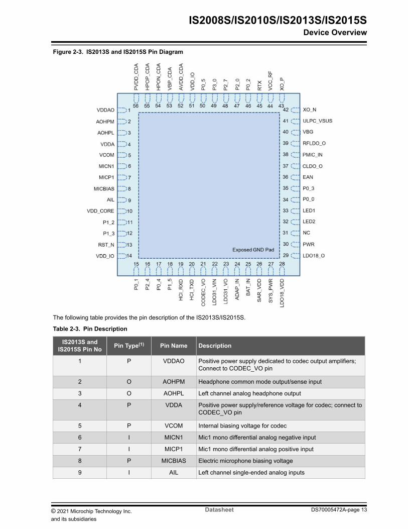

continuedIS2013S and
IS2015S Pin No Pin Type(1) Pin Name Description
34 IO P0_0IO pin default pull-high input(2)
bull Slide switch detector active-lowbull UARTTX_IND active-low
35 IO P0_3
IO pin default pull-high input(2)
bull REV key (default) active-lowbull Buzzer signal outputbull Out_Ind_1bull Class 1 RX control signal of external RF TR switch
active high
36 I EANEmbedded ROMExternal Flash enable
H Embedded L External Flash
37 P CLDO_O 12V core LDO output
38 P PMIC_IN PMU blocks power input connect to BK_O pin
39 P RFLDO_O 128V RF LDO output
40 P VBG Bandgap output reference for decoupling interference
41 P ULPC_VSUS ULPC 12V output power
42 I XO_N 16 MHz crystal input negative
43 I XO_P 16 MHz crystal input positive
44 P VCC_RFRF power input (128V) for both synthesizer and TXRXblock connect to RFLDO_O pin
45 IO RTX RF path (transmitreceive)
46 I P0_2IO pin default pull-high input(2)
PlayPause key (default) active-low
47 I P2_0IO pin default pull-high input system configuration
H Application L Baseband (IBDK mode)
48 I P2_7IO pin default pull-high input(2)
Volume up key (default) active-low
49 I P3_0IO pin default pull-high input(2)
Line-in detector (default) active-low
50 I P0_5IO pin default pull-high input(2)
Volume down (default) active-low
51 P VDD_IO IO power supply input (27-33V) connect to LDO31_VO pin
52 P AVDD_CDA Supply voltage of audio amplifier
53 P VBP_CDA Reference voltage output
54 O HPON_CDA Negative BTL output of channel-1
55 O HPOP_CDA Positive BTL output of channel-1
IS2008SIS2010SIS2013SIS2015SDevice Overview
copy 2021 Microchip Technology Incand its subsidiaries
Datasheet DS70005472A-page 15
continuedIS2013S and
IS2015S Pin No Pin Type(1) Pin Name Description
56 P PVDD_CDA Supply voltage of power stage ch-1
57 P EP Exposed pads used as ground (GND) pins
Notes 1 The conventions used in the table are indicated as follows
ndash I = Input pinndash O = Output pinndash IO = InputOutput pinndash P = Power pin
2 All IO pins are configured using the UI tool a Windows-based utility
IS2008SIS2010SIS2013SIS2015SDevice Overview
copy 2021 Microchip Technology Incand its subsidiaries
Datasheet DS70005472A-page 16
3 AudioThe input and output audio signals have different stages and each stage is programmed to vary the gain responsecharacteristics For microphones both single-ended inputs and differential inputs are supported To maintain ahigh-quality signal provide a stable bias voltage source to the condenser microphonersquos FET Use the DC-blockingcapacitors at both positive and negative sides of the input Internally this analog signal is converted to 16-bit 8 kHzlinear PCM data
31 Digital Signal ProcessorA Digital Signal Processor (DSP) is used to perform speech and audio processing The advanced speech featuressuch as acoustic echo cancellation and noise reduction are built in To reduce nonlinear distortion and to help echocancellation an outgoing signal level to the speaker is monitored and adjusted to avoid saturation of the speakeroutput or microphone input Adaptive filtering is also applied to track the echo path impulse in response to provide anecho-free and full-duplex user experience
The embedded noise reduction algorithm helps to extract clean speech signals from the noisy inputs capturedby microphones and improves mutual understanding in communication The advanced audio features such asmulti-band dynamic range control parametric multi-band equalizer audio widening and virtual bass are built in Theaudio effect algorithms improve the userrsquos audio listening experience in terms of better quality audio after audiosignal processing
The following figures illustrate the processing flow of speakerphone applications for speech and audio signalprocessing
Figure 3-1 Speech Processing
Figure 3-2 Audio Processing
The DSP parameters such as EQ Speaker Gain Mic Gain Sound Effect and more are configured using the DSPtool For additional information on the DSP tool refer to the IS20xxBM1xBM2x DSP Application Note
IS2008SIS2010SIS2013SIS2015SAudio
copy 2021 Microchip Technology Incand its subsidiaries
Datasheet DS70005472A-page 17
Note The DSP tool and IS20xxBM1xBM2x DSP Application Note are available for download at the Microchipwebsite
32 CodecThe built-in codec has a high SNR performance and it consists of an ADC a DAC and additional analog circuitry
33 Auxiliary PortThe SoC supports one analog (line-in) signal from the external audio source The analog signal is processed bythe DSP to generate different sound effects (multi-band dynamic range compression and audio widening) which areconfigured using the DSP tool
34 Class D Audio AmplifierThe Class D amplifier has a significant advantage in many applications due to its lower power dissipation whichproduces less heat The IS2013S and IS2015S SoC have a built-in Class D amplifier that reduces circuit board spaceand system cost The efficiency of the amplifier extends the battery life in portable systems
The Class D amplifier is implemented by using a full-bridge output stage A full bridge uses two half-bridge stages todrive the load differentially The Class D amplifier provides a good SNR and enough drive capability for a 4Ω speakerdriver
IS2008SIS2010SIS2013SIS2015SAudio
copy 2021 Microchip Technology Incand its subsidiaries
Datasheet DS70005472A-page 18
4 TransceiverThe SoC is designed and optimized for Bluetooth 24 GHz systems It contains a complete radio frequencytransmitterreceiver section An internal synthesizer generates a stable clock to synchronize with another device
41 TransmitterThe internal Power Amplifier (PA) has a maximum output power of +4 dBm with 20 dB power level control Applythis to Class 2 or Class 3 radios without an external RF PA The transmitter directly performs the IQ conversionto minimize the frequency drift and it can access the 20 dB power range with the temperature compensationmechanism
42 ReceiverThe Low-Noise Amplifier (LNA) operates with TR-combined mode for the single port application It saves the pin onthe package without having an external TXRX switch
The ADC is used to sample the input analog signal and convert it into a digital signal for demodulator analysisA channel filter is integrated into a receiver channel before the ADC to reduce the external component count andincrease the anti-interference capability
The image rejection filter is used to reject the image frequency for the low-IF architecture and it is also intended toreduce the external Band Pass Filter (BPF) component for a super heterodyne architecture
The Received Signal Strength Indicator (RSSI) signal feedback to the processor is used to control the RF outputpower to make a good trade-off for effective distance and current consumption
43 SynthesizerA synthesizer generates a clock for radio transceiver operation The VCO inside with a tunable internal LC tankcan reduce any variation for components A crystal oscillator with an internal digital trimming circuit provides a stableclock for the synthesizer
44 ModemFor Bluetooth 12 specifications and below 1 Mbps is the standard data rate based on the Gaussian Frequency ShiftKeying (GFSK) modulation scheme This basic rate modem meets BDR requirements of Bluetooth 20 with EDRspecifications
For Bluetooth 20 and above specifications EDR is introduced to provide the data rates of 123 Mbps Thisenhanced data rate modem meets EDR requirements of Bluetooth 20 with EDR specifications For the basebandboth BDR and EDR utilize the same 1 MHz symbol rate and 16 kHz slot rate For BDR 1 symbol represents 1-bitHowever each symbol in the payload part of the EDR packets represents 2-bit or 3-bit This is achieved by using twodifferent modulations π4 DQPSK and 8 DPSK
45 Adaptive Frequency Hopping (AFH)The SoC has an AFH function to avoid RF interference It has an algorithm to check the nearby interference and tochoose the clear channel for the transceiver Bluetooth signal
IS2008SIS2010SIS2013SIS2015STransceiver
copy 2021 Microchip Technology Incand its subsidiaries
Datasheet DS70005472A-page 19
5 MicrocontrollerA single-cycle 8-bit microcontroller is built into the SoC to execute the Bluetooth protocols It operates from 16 MHzto higher frequencies where the firmware dynamically adjusts the trade-off between the computing power and thepower consumption In the ROM version the MCU firmware is hard-wired to minimize power consumption for thefirmware execution and to save the external Flash cost
51 MemoryThere are sufficient ROM and RAM to fulfill the processor requirements in which a synchronous single port RAMinterface is used The register bank dedicated single port memory and Flash memory are connected to theprocessor bus The processor coordinates with all link control procedures and the data movement happens using aset of pointer registers
52 External ResetThe IS20xxS SoC provides a Watchdog Timer (WDT) to reset the SoC It has an integrated Power-on Reset (POR)circuit that resets all circuits to a known Power-on state This action is also driven by an external Reset signal whichis used to control the device externally by forcing it into a POR state The RST_N signal input is active-low and noconnection is required in most of the applications
53 Reference ClockThe IS20xxS SoC is composed of an integrated crystal oscillation function that uses a 16 MHz external crystal andtwo specified loading capacitors to provide a high quality system reference timer source Use this feature to removethe initial tolerance frequency errors which are associated with the crystal and its equivalent loading capacitance inthe mass production Achieve the frequency trim by adjusting the crystal loading capacitance through the on-chip trimcapacitors (Ctrim)
The value of the trimming capacitance is 200 fF (200x10-15 F) per LSB at the 5-bit word and the overall adjustableclock frequency is plusmn40 kHz The following figure illustrates the crystal connection of the IS20xxS SoC with twocapacitors
Figure 5-1 Crystal Connection
IS20XXS
XO_N
CL1
XO_P
CL2
IS2008SIS2010SIS2013SIS2015SMicrocontroller
copy 2021 Microchip Technology Incand its subsidiaries
Datasheet DS70005472A-page 20
Notes 1 Ctrim = 200 fF (1 to 31) Cint = 3 pF2 CL = [(CL1 x CL2) (CL1 + CL2)] + (Ctrim 2) + Cint (set trim value as 16 Ctrim = 32 pF)3 For a 16 MHz crystal where CL = 9 pF the CL1 = CL2 = 91 pF)4 For the CL selection refer to the data sheet of the crystal
IS2008SIS2010SIS2013SIS2015SMicrocontroller
copy 2021 Microchip Technology Incand its subsidiaries
Datasheet DS70005472A-page 21
6 Power Management Unit (PMU)The IS20xxS SoC has an integrated PMU The main features of the PMU are a lithium-ion battery charger and avoltage regulator A power switch is used to switch over the power source between a battery and an adapter Alsothe PMU provides current to the LED drivers
61 Charging a BatteryThe IS20xxS SoC has a built-in battery charger which is optimized for lithium-polymer batteries The battery chargerincludes a current sensor for a charging control user programmable current regulator and high accuracy voltageregulator
The charging current parameters are configured by using the UI (IS20XXS_UI) tool Whenever the adapter isplugged-in the charging circuit will be activated Reviving pre-charging constant current mode constant voltagemode and re-charging functions are implemented The maximum charging current is 350 mA The following figureillustrates the charging curve of a battery
Figure 6-1 Battery Charging Curve
62 Voltage MonitoringA 10-bit successive approximation register ADC (SAR ADC) provides a dedicated channel for battery voltage leveldetection The warning level is programmed by using the UI tool The ADC provides a granular resolution to enablethe MCU to take control over the charging process
63 Low Dropout RegulatorA built-in LDO Regulator is used to convert the battery or adapter power for the power supply It also integratesthe hardware architecture to control the power-onoff procedure The built-in programmable LDOs provide power forcodec and digital IO pads Also it is used to buffer the high input voltage from the battery or adapter This LDOrequires a 1 μF bypass capacitor
IS2008SIS2010SIS2013SIS2015SPower Management Unit (PMU)
copy 2021 Microchip Technology Incand its subsidiaries
Datasheet DS70005472A-page 22
64 Switching RegulatorThe built-in programmable output voltage regulator converts the battery voltage to RF and base band core powersupply This converter has a high conversion efficiency and a fast transient response
65 LED DriverThe IS20xxS SoC consists of two LED drivers to control the LEDs The LED drivers provide enough sink current(16-step control and 035 mA for each step) and the LED is connected directly to the IS20xxS SoC
Note Configure the LED settings using the IS20XXS_UI tool
The following figure illustrates the LED driver in the IS20xxS SoC
Figure 6-2 LED DRIVER
IS20xxS
LED2
SYS_PWR
LED1
IS2008SIS2010SIS2013SIS2015SPower Management Unit (PMU)
copy 2021 Microchip Technology Incand its subsidiaries
Datasheet DS70005472A-page 23
7 Application InformationThis section describes the power supply connection host MCU UART interface and various modes in detail
71 Power SupplyThe following figure illustrates the connection from the BAT_IN pin to various other voltage supply pins of theIS20xxS SoC
The BAT_IN input pin powers the IS20xxS SoC To charge the battery connect the external 5V power adapter toADAP_IN
Figure 7-1 Power Tree Diagram
VDDA VDDAO
VDD_IO
3V LDO
18V Buck
SAR_VDD
LDO31_VIN
CODEC_VO
LDO31_VO
BK_VDD
BK_LX
BK_O
VDD_CORE
VCC_RF
12V LDOPMIC_IN
CLDO_O
RFLDO_O
PVDD_CDA
Li-Io
n BA
T BAT_IN
ADAP_IN
SYS_PWRPower Switch
5V Adapter
(42~30V)
(45~55V)(42~30V)
(30~27V)
(33 ~27V)
(18V)
(12V)
(128V)
72 Host MCU InterfaceAn external MCU controls the IS20xxS SoC using the UART command set The following figure illustrates the UARTinterface between the IS20xxS SoC and an external MCU
Figure 7-2 Host MCU Interface Over UART
IS20xxSHCI_TXD
HCI_RXD
PWR
P0_0
MCUUART_TX
UART_RX
MCU_WAKEUP
BT_WAKEUP
UART Interface
UART Interface
The MCU controls the IS20xxS SoC over the UART interface and wakes up the SoC using the PWR pin The MCUfunction wakes up by connecting to the P0_0 pin of the IS20xxS
Refer to the IS200xIS201xIS202x UART Command SOP document for a list of functions that the IS20xxS SoCsupports and how to use the IS20XXS_UI tool to set up the system using the UART command
Note The IS200xIS201xIS202x UART Command SOP document is available for download from the Microchipwebsite at IS200xIS201xIS202x UART Command SOP
IS2008SIS2010SIS2013SIS2015SApplication Information
copy 2021 Microchip Technology Incand its subsidiaries
Datasheet DS70005472A-page 24
73 Timing Sequence of UART ApplicationThe following figures illustrate the various UART control signal timing sequences
Figure 7-3 Power-OnOff Sequence
BAT_IN
SYS_PWR
1 ms
Power- oninitial idle Power-on Power-on Power-off idle
MCU state
MFB (PWR)
BK_OLDO31_VO
400 ms
RST_N
MCU sends UART command (UART_RX)
UART Command
MCU sends power-off UART Command
Power-on ACK ACK ACKIS20xxS response UART state
(UART_TX)
Set ldquoPower-on Directlyrdquo boot
any
10 ms
20 msKeep all IS20xxSand MCU connection to low level
2s
(See Figure 7-4) (See Figure 7-5)
IS20xxS disconnect and auto power-off
gt 1s
Figure 7-4 Timing Sequence of RX Indication after Power-On
Resume 32 kHz mode
MFB (PWR)MCU sends UART command
MFB pulse must be longer than the UART command slot time
150 ms
2 ms 2 ms
Enter 32 kHz mode
1 ms
UART Command
IS2008SIS2010SIS2013SIS2015SApplication Information
copy 2021 Microchip Technology Incand its subsidiaries
Datasheet DS70005472A-page 25
Figure 7-5 Timing Sequence of Power-Off
BAT_IN +4V
MFB
MCU Sends RST_N
BK_OUT
LDO31_VO
UART Bus
2s 1s
IS20xxS Sends Power-off ACK
Notes 1 EEPROM clock = 100 kHz2 For a byte wire 001 ms x 32 clock x 2 = 640 μs3 It is recommended that ramp-down time be more than 640 μs during the power-off sequence to ensure safe
operation of the device
IS2008SIS2010SIS2013SIS2015SApplication Information
copy 2021 Microchip Technology Incand its subsidiaries
Datasheet DS70005472A-page 26
Figu
re 7
-6
Tim
ing
Sequ
ence
of P
ower
-On
(NA
CK
)
BAT
_IN
SYS_
PWR
1 m
s Pow
er-
onin
itial
idle
Pow
er-o
nM
CU
sta
te
MFB
(PW
R)
BK_O
LD
O31
_VO
400
ms
RST
_N
MC
U s
ends
UAR
T co
mm
and
(UAR
T_R
X)
UAR
T C
omm
and
NAC
KPo
wer
-on
ACK
ACK
IS20
xxS
resp
onse
UAR
T st
ate
(UAR
T_TX
)
Set ldquo
Pow
er-o
n D
irect
lyrdquo b
oot
10 m
s
20 m
s
Ret
ry i
f AC
K is
not
rece
ived
200
ms
any
Wai
t
Max
imum
5 ti
mes
(1s)
IS2008SIS2010SIS2013SIS2015SApplication Information
copy 2021 Microchip Technology Incand its subsidiaries
Datasheet DS70005472A-page 27
Figure 7-7 Reset Timing Sequence in Case of No Response from SoC to Host MCU
MFB (PWR)
MCU sends UART command UART
Command
UART Command
IS20xxS UART
If no response
RST_N
1ms
X ms1ms
1ms
1ms
Note The MCU sends the UART command again when the SoC is not responding to its first UART command Ifthe SoC is not responding to the second UART command within X ms the MCU forces the system to reset
Figure 7-8 Timing Sequence of Power Drop Protection
BAT_IN +4V
RST_N from Reset IC
Power
SYS_PWR
IS20xxS
Reset OUT VDDGND
MCU Reset
Reset IC
29V
1 It is recommended that the battery be connected on a BAT_IN pin of the SoC for the power supply2 If an external power source or a power adapter is used to provide the power to the SoC (ADAP_IN) use a
voltage supervisor IC3 The RESET IC output pin must be open drain with delay time of le 10 ms and the recommended part is
TCM809SVNB713
74 General Purpose IO pinsThe following table provides the details of various functions that are mapped to the IO pins of the IS20xxS SoCand these IOs are configured by using the IS20XXS_UI tool The first button (Button 0) must be configured as thepower-onoff key and can be set using the PWR pin The remaining pins are configured for any one of the defaultfunctions (short press long press double press and combinations)
IS2008SIS2010SIS2013SIS2015SApplication Information
copy 2021 Microchip Technology Incand its subsidiaries
Datasheet DS70005472A-page 28
Table 7-1 IO Pin Configuration
Sl No Pin Name Buttons Default Functions(1)
1 PowerMFB Button 0 PWR
2 P0_2 Button 1 PlayPause
3 P2_7 Button 2 Volume Up
4 P0_5 Button 3 Volume Down
5 P0_1 Button 4 FWD
6 P0_3 Button 5 REV
Note 1 These functions can be configured using the IS20XXS_UI tool
Few signals are generated to indicate or control outside devices The most popular applications are NFC for easypairing external audio amplifier for louder speaker and buzzer for indication
Table 7-2 IO Pins for Added Functions
Functions(1) IO Configurable Features
Slide switch P0_0P1_5
Buzzer P0_3
NFC detect P0_4P1_5
External amplifier enable P1_5
Note 1 These functions can be configured using the IS20XXS_UI tool
IS2008SIS2010SIS2013SIS2015SApplication Information
copy 2021 Microchip Technology Incand its subsidiaries
Datasheet DS70005472A-page 29
8 Antenna Placement RuleFor Bluetooth-enabled products the antenna placement affects the overall performance The antenna requires freespace to radiate RF signals and it must not be surrounded by the GND plane
The following figure illustrates a typical example of the good and poor antenna placement on the main applicationboard with the GND plane
Figure 8-1 Antenna Placement Examples
The following figure illustrates the keep-out area recommended for the PCB antenna
Figure 8-2 Keep-Out Area Recommended for PCB Antenna
Note For additional information on the antenna placement refer to the antenna-specific data sheet from theantenna manufacturer
IS2008SIS2010SIS2013SIS2015SAntenna Placement Rule
copy 2021 Microchip Technology Incand its subsidiaries
Datasheet DS70005472A-page 30
9 Electrical CharacteristicsThis section provides an overview of the IS20xxS SoC electrical characteristics
Table 9-1 Absolute Maximum Ratings
Parameter Symbol Minimum Maximum Unit
Digital core supply voltage VDD_CORE 0 135 V
RF supply voltage VCC_RF 0 135 V
SAR ADC supply voltage SAR_VDD 0 21 V
Codec supply voltage VDDAVDDAO 0 33 V
IO supply voltage VDD_IO 0 36 V
Buck supply voltage BK_VDD 0 43 V
Supply voltage LDO31_VIN 0 43 V
Battery input voltage BAT_IN 0 43 V
Adapter input voltage ADAP_IN 0 70 V
Storage temperature TSTORE -65 +150
Operation temperature TOPERATION -20 +70
Note Stresses listed on the preceding table cause permanent damage to the device This is a stress rating onlyThe functional operation of the device at those or any other conditions and those indicated in the operation listingsof this specification are not implied Exposure to maximum rating conditions for extended periods affects devicereliability
The following tables provide the recommended operating conditions and the electrical specifications of the IS20xxSSoC
Table 9-2 Recommended Operating Condition
Parameter Symbol Minimum Typical Maximum Unit
Digital core supply voltage VDD_CORE 114 12 126 V
RF supply voltage VCC_RF 122 128 134 V
SAR ADC supply voltage SAR_VDD 162 18 198 V
Codec supply voltage VDDAVDDAO 27 28 30 V
IO supply voltage VDD_IO 27 30 33 V
Buck supply voltage BK_VDD 3 37 425 V
Supply voltage LDO31_VIN 3 37 425 V
Battery input voltage BAT_IN 3 37 425 V
Adapter input voltage ADAP_IN 45 5 55 V
Operation temperature TOPERATION -20 +25 +70
Note All these supply voltages are programmed through the EEPROM parameters
IS2008SIS2010SIS2013SIS2015SElectrical Characteristics
copy 2021 Microchip Technology Incand its subsidiaries
Datasheet DS70005472A-page 31
Table 9-3 Buck Switching Regulator
Parameter Minimum Typical Maximum Unit
Input voltage 30 37 425 V
Output voltage (Iload = 70 mA andVin = 4V) 17 18 205 V
Output voltage accuracy mdash plusmn5 mdash
Output voltage adjustable step mdash 50 mdash mVStep
Output adjustment range -01 mdash +025 V
Average load current (ILOAD) 120 mdash mdash mA
Conversion efficiency (BAT = 38Vand Iload = 50 mA) mdash 88(1) mdash
Quiescent current (PFM) mdash mdash 40 μA
Output current (peak) 200 mdash mdash mA
Shutdown current mdash mdash lt1 μA
Notes 1 Test condition SAR_VDD = 18V and temperature = +252 These parameters are characterized but not tested in manufacturing
Table 9-4 Low-dropout Regulator
Parameter Minimum Typical Maximum Unit
Input Voltage 30 37 425 V
Output VoltageCODEC_VO mdash 28 mdash
VIO_VO mdash 28 mdash
Output Accuracy (VIN = 37V ILOAD = 100 mA and +27) mdash plusmn5 mdash
Output current (average) mdash mdash 100 mA
Drop-out voltage
(Iload = maximum output current)mdash mdash 300 mV
Quiescent current (excluding load and Iload lt 1 mA) mdash 45 mdash μA
Shutdown current mdash mdash lt1 μA
Notes 1 Test condition SAR_VDD = 18V and temperature = +252 These parameters are characterized but not tested in manufacturing
Table 9-5 Battery Charger
Parameter Minimum Typical Maximum Unit
Input voltage (ADAP_IN) 45 50 55 V
Supply current to charger only mdash 3 45 mA
IS2008SIS2010SIS2013SIS2015SElectrical Characteristics
copy 2021 Microchip Technology Incand its subsidiaries
Datasheet DS70005472A-page 32
continuedParameter Minimum Typical Maximum Unit
Maximum batteryfast chargecurrent (ENX2 =0)
Headroom gt 07V (ADAP_IN = 5V) 170 200 240 mA
Headroom = 03V (ADAP_IN = 45V) 160 180 240 mA
Maximum batteryfast chargecurrent (ENX2 =1)
Headroom gt 07V (ADAP_IN = 5V) 300 350 420 mA
Headroom = 03V (ADAP_IN = 45V) 180 220 270 mA
Trickle charge voltage threshold mdash 3 mdash V
Battery charge termination current ( of fast charge current) mdash 10 mdash
Notes 1 Headroom = VADAP_IN ndash VBAT2 ENX2 is not allowed to be enabled when VADAP_IN ndash VBAT gt 2V3 These parameters are characterized but not tested in manufacturing
Table 9-6 LED Diver
Parameter Minimum Typical Maximum Unit
Open-drain voltage mdash mdash 36 V
Programmable current range 0 mdash 525 mA
Intensity control mdash 16 mdash step
Current step mdash 035 mdash mA
Power-down open-draincurrent mdash mdash 1 μA
Shutdown current mdash mdash 1 μA
Notes 1 Test condition SAR_VDD = 18V and temperature = +252 These parameters are characterized but not tested in manufacturing
Table 9-7 Audio Codec Digital-to-Analog Converter
Parameter (Condition)(1) Minimum Typical Maximum Unit
Over-sampling rate mdash 128 mdash fs
Resolution 16 mdash 20 Bits
Output sample rate 8 mdash 48 kHz
Signal-to-noise Ratio (2) (SNR at capless mode) for 48 kHz mdash 96 mdash dB
Signal-to-noise Ratio (2)
(SNR at single-ended mode) for 48 kHzmdash 98 mdash dB
Digital gain -54 mdash 485 dB
Digital gain resolution mdash 2 to 6 mdash dB
Analog gain -28 mdash 3 dB
Analog gain resolution mdash 1 mdash dB
IS2008SIS2010SIS2013SIS2015SElectrical Characteristics
copy 2021 Microchip Technology Incand its subsidiaries
Datasheet DS70005472A-page 33
continuedParameter (Condition)(1) Minimum Typical Maximum Unit
Output voltage full-scale swing (AVDD = 28V) 495 7425 mdash mV rms
Maximum output power (16Ω load) mdash 345 mdash mW
Maximum output power (32Ω load) mdash 172 mdash mW
Allowed loadResistive 8 16 OC Ω
Capacitive mdash mdash 500 pF
THD+N (16Ω load) mdash mdash 005
Signal-to-noise Ratio (SNR at 16Ω load) mdash mdash mdash 96 dB
Notes 1 T = +25 VDD = 30V 1 kHz sine wave input and Bandwidth = 20 Hz ndash 20 kHz2 fin = 1 kHz Bandwidth = 20 Hz ndash 20 kHz A-weighted THD + N lt 001 0 dBFS signal and Load = 100 kΩ3 These parameters are characterized but not tested in manufacturing
Table 9-8 Audio Codec Analog-to-Digital Converter
Parameter (Condition)(1) Minimum Typical Maximum Unit
Resolution mdash mdash 16 Bit
Output sample rate 8 mdash 48 kHz
Signal-to-noise Ratio (2) (SNR at MIC or Line-in mode) mdash 90 mdash dB
Digital gain -54 mdash 485 dB
Digital gain resolution mdash 2 to 6 mdash dB
MIC boost gain mdash 20 mdash dB
Analog gain mdash mdash 60 dB
Analog gain resolution mdash 20 mdash dB
Input full scale at maximum gain (differential) mdash 4 mdash mVrms
Input full scale at minimum gain (differential) mdash 800 mdash mVrms
3 dB bandwidth mdash 20 mdash kHz
Microphone mode (input impedance) mdash 24 mdash kΩ
THD+N (microphone input) at 30 mVrms input mdash 002 mdash
Notes 1 T = +25 VDD = 30V 1 kHz sine wave input and Bandwidth = 20 Hz ndash 20 kHz2 fin = 1 kHz Bandwidth = 20 Hz ndash 20 kHz A-weighted and THD + N lt 1 150 mVpp input3 These parameters are characterized but not tested in manufacturing
Table 9-9 Single-Channel ClassndashD Amplifier
Parameter (Condition) Minimum Typical Maximum Unit
Standalone SNR (A-weighting) mdash 100 mdash dB
Gain mdash 12 mdash dB
PSRR (217 Hz 200 mV on PVDD) mdash 70 mdash dB
IS2008SIS2010SIS2013SIS2015SElectrical Characteristics
copy 2021 Microchip Technology Incand its subsidiaries
Datasheet DS70005472A-page 34
continuedParameter (Condition) Minimum Typical Maximum Unit
Efficiency4Ω 80 mdash 85
8Ω 85 mdash 90
Supply voltage 30 37 45 V
Load mdash 40 mdash Ω
Quiescent current (1 channel) mdash 20 mdash mA
Sample frequency mdash 250 mdash kHz
Over current limits mdash 23 mdash A
Shutdown current mdash 10 mdash μA
Notes 1 Test condition PVDD_CDA = 42V and temperature = 252 These parameters are characterized but not tested in manufacturing
Table 9-10 Transmitter Section for BDR and EDR
Parameter Minimum Typical Maximum BluetoothSpecification Unit
Maximum RF transmit power mdash 30 40 -6 to 4 dBm
Relative transmit power -4 -12 1 -4 to 1 dB
Notes 1 The RF Transmit power is calibrated during production using the MP tool software and MT8852 Bluetooth test
equipment2 Test condition VCC_RF = 128V and temperature = +25
Table 9-11 Receiver Section for BDR and EDR
Parameter Packet Type Minimum Typical Maximum BluetoothSpecification Unit
Sensitivity at 01 BER GFSK mdash -90 mdash le-70 dBm
Sensitivity at 001 BERπ4 DQPSK mdash -91 mdash le-70 dBm
8 DPSK mdash -82 mdash le-70 dBm
Notes 1 Test condition VCC_RF = 128V and temperature = +252 These parameters are characterized but not tested in manufacturing
Table 9-12 System Current Consumption
System Status Typical Maximum Unit
System Off mode 2 5 μA
Standby mode 08 mdash mA
Link mode 04 mdash mA
SCO Link 78 mdash mA
A2DP Link (Vp-p = 200 mV 1k tone signal) 107 mdash mA
IS2008SIS2010SIS2013SIS2015SElectrical Characteristics
copy 2021 Microchip Technology Incand its subsidiaries
Datasheet DS70005472A-page 35
Notes 1 Consider the current consumption values with the IS2010 EVB as a test platform2 Test condition BAT_IN = 38V link with the HTC EYE smartphone The distance between the smartphone and
EVB is 30 cm
IS2008SIS2010SIS2013SIS2015SElectrical Characteristics
copy 2021 Microchip Technology Incand its subsidiaries
Datasheet DS70005472A-page 36
10 Packaging InformationThis section provides information on package marking package details and footprint dimensions of the IS20xxS SoC
101 Chip Identification SystemPart No X -Y
(Chip Name) (Package Type) (Version)
Legendbull Chip Name
ndash IS2008Sndash IS2010Sndash IS2013Sndash IS2015S
bull Package Typendash S = QFN (Saw Type) Package
bull Versionndash ldquo-203rdquo represents the chip version is 203
For examplebull IS2015S-002 002 version ROM code IS2015 chip in QFN type packagebull IS2010S-203 203 version ROM code IS2010 chip in QFN type package
102 Package Marking InformationThe following figure illustrates the package marking information of the IS20xxS
IS2008SIS2010SIS2013SIS2015SPackaging Information
copy 2021 Microchip Technology Incand its subsidiaries
Datasheet DS70005472A-page 37
Figure 10-1 Package Marking Information
Page 36
Page 36
48 Lead QFN (6x6x09 mm) 56 Lead QFN (7x7x09 mm)
Pin 1 Index
Pin 1 Index Pin 1 Index
Legend
XXX Chip serial number version and e3 Pb-free JEDEC designator for Matte Tin (Sn)
YY Year code (last 2 digits of calendar year)
WW Week code (week of January 1 is week ldquo1rdquo)
NNN Alphanumeric traceability code
103 Package DetailsThe following figures illustrate the footprint dimensions and the chip outline details of the IS2008S and IS2010S SoC
IS2008SIS2010SIS2013SIS2015SPackaging Information
copy 2021 Microchip Technology Incand its subsidiaries
Datasheet DS70005472A-page 38
Figure 10-2 IS2008S and IS2010S Chip Outline Details
IS2008SIS2010SIS2013SIS2015SPackaging Information
copy 2021 Microchip Technology Incand its subsidiaries
Datasheet DS70005472A-page 39
Figure 10-3 IS2008S and IS2010S Footprint Dimensions
PAD LENGTHPAD WIDTH
PAD PITCHPAD COUNT
Note For the most current package drawings refer to the Microchip Packaging Specification available at httpwwwmicrochipcompackaging
The following figures illustrate the footprint dimensions and the chip outline details of the IS2013S and IS2015S SoC
IS2008SIS2010SIS2013SIS2015SPackaging Information
copy 2021 Microchip Technology Incand its subsidiaries
Datasheet DS70005472A-page 40
Figure 10-4 IS2013S and IS2015S Chip Outline Details
IS2008SIS2010SIS2013SIS2015SPackaging Information
copy 2021 Microchip Technology Incand its subsidiaries
Datasheet DS70005472A-page 41
Figure 10-5 IS2013S and IS2015S Footprint Dimensions
Note For the most current package drawings refer to the Microchip Packaging Specification available at httpwwwmicrochipcompackaging
IS2008SIS2010SIS2013SIS2015SPackaging Information
copy 2021 Microchip Technology Incand its subsidiaries
Datasheet DS70005472A-page 42
11 Reflow Profile and Storage ConditionThis chapter describes reflow profiles and stencil information of the IS20xxS SoC
111 Stencil of SMT Assembly SuggestionThe stencil of the SMT assembly suggestion contains the following sections
1111 Stencil Type and Thicknessbull Laser cuttingbull Stainless steelbull Thickness 05 mm pitch thickness less than 015 mm
1112 Aperture Size and Shape for Terminal Padbull Aspect ratio (widththickness) is more than 15bull Aperture shape
ndash The stencil aperture is designed to match the pad size on the PCBndash Oval-shaped opening is used to get the optimum paste releasendash Rounded corners to minimize cloggingndash Positive taper walls (5deg tapering) with the bottom opening larger than the top opening
1113 Aperture Design for Thermal Padbull Small multiple openings are used instead of one big opening as shown in the following figure
Figure 11-1 IS20xxS SoC Reflow Profile Aperture Design
bull 60 to 80 solder paste coveragebull Rounded corners to minimize cloggingbull Positive taper walls (5deg tapering) with the bottom opening is larger than the top opening as shown in the
following figureFigure 11-2 IS20xxS SoC Stencil Type
IS2008SIS2010SIS2013SIS2015SReflow Profile and Storage Condition
copy 2021 Microchip Technology Incand its subsidiaries
Datasheet DS70005472A-page 43
112 Reflow ProfileThe following figure illustrates the reflow profile and its specific features are
bull Standard Condition IPCJEDEC J-STD-020bull Preheat 150 to 200 for 60 to180 secondsbull Average ramp-up rate (217 to peak) 1 to 2sec maxbull Temperature maintained above 217 60 to 150 secondsbull Time within 5 of actual peak temperature 20 to 40 secondsbull Peak temperature 260 with +5-0 tolerancebull Ramp-down rate (peak to 217) 3sec maxbull Time within 25 to peak temperature 8 minutes maxbull Cycle interval 5 minutes
Figure 11-3 Reflow Profile
+150degC
+200degC
+217degC
+255degCRamp-up rate1~2degCsec max+217degC to peak
Peak +260degC (+50degC tolerance)
Ramp-down rate+3degCsec maxpeak to +217degC
20 to 40 sec
Time (sec)
60 to 180 sec 60 to 150 sec
113 Storage ConditionUsers must follow these specific storage conditions for the IS20xxS SoC
bull Calculated shelf life in the sealed bag 24 months at lt40 and lt90 Relative Humidity (RH)bull Once the bag is opened devices that are subjected to reflow solder or other high temperature process must be
mounted within 168 hours of factory conditions that is lt3060 RH
The following figure illustrates the IS20xxS SoC bag label details
IS2008SIS2010SIS2013SIS2015SReflow Profile and Storage Condition
copy 2021 Microchip Technology Incand its subsidiaries
Datasheet DS70005472A-page 44
Figure 11-4 Storage Conditions
IS2008SIS2010SIS2013SIS2015SReflow Profile and Storage Condition
copy 2021 Microchip Technology Incand its subsidiaries
Datasheet DS70005472A-page 45
12 Reference CircuitThis section provides the reference schematics of IS2008S IS2010S IS2013S and IS2015SFigure 12-1 IS2008SIS2010S Reference Circuit (Main Circuit)
(Peak Current 400 mA)
(1uF X5R or 47uF Y5V)
P0_3
VBGULPC_VSUS
MFB
VBG
ULPC_VSUS
LED1LED2
P0_1
ADAP
_IN
P1_5
P0_2
P0_5
P2_7
P2_0
MIC_P2MIC_N2
MIC_P1MIC_N1
P1_2P1_3RST_N
AOH
PLAO
HPM
HC
I_TX
DH
CI_
RXD
RFLDO_O1V8
1V2
1V8
CODEC_VO
2V8
1V8SYS_PWR
BAT_IN
CODEC_VO
2V8
SYS_PWR
SYS_PWR
RFLDO_O
MIC_BIAS
2V8
1V2
ADAP_IN
MIC_N2MIC_P2MIC_N1MIC_P1
RST_N
HC
I_R
XDH
CI_
TXD
LED2LED1
AOH
PMAO
HPL
P0_1
P1_5
P0_3
P0_5
P2_7
P2_0
P0_2
MFB
C791u16V
ANT1
ANT-MP8
1
C321u16V
C291u16V
C7710u16V
C871u16V
X1X4P-16MHZ
4 13 2
C251u16V
C402p50V
C311u16V
C219p50V
C281u16V
R681K1
12
C261u16V
C191u16V
C361u16V
L10L10uH-2
C831u16V
C841u16V
IS2008SIS2010S
U6
IS2010S_MH+2MIC
MICN22
AO
HP
L47
VD
DA
48
VCOM1
MICN14
MICP15
MICBIAS6
VDD_CORE7
VDD_IO11 RST_N10
P128
P139
P05
43
HC
I_TX
D15
HC
I_R
XD
14
XO
_P37
XO_N36
ULPC_VSUS35
P27
42
VBG34
RFLDO_O33
PMIC_IN32
CLDO_O31
NC
21
SY
S_P
WR
23
P20
41
P15
13
P02
40
P0112
VD
D_I
O44
RTX
39
VC
C_R
F38
EP
49
VD
DA
O45
AO
HP
M46
MICP23
P0330
CO
DE
C_V
O16
LDO
31_V
IN17
LDO
31_V
O18
AD
AP
_IN
19
BA
T_IN
20
SA
R_V
DD
22
BK
_VD
D24
BK_LX25BK_O26PWR27
LED129
LED228
C801u16V
C8210u16V
TP9RF-TP1
C861u16V
L227nH
R691K
12
C8110u16V
C411u16V
C249p50V
C3NP-0402
C271u16V
C341u16V
L368p50V
C231u16V
C781u16V
IS2008SIS2010SIS2013SIS2015SReference Circuit
copy 2021 Microchip Technology Incand its subsidiaries
Datasheet DS70005472A-page 46
Figure 12-2 IS2008SIS2010S EEPROM (Main Circuit)
EEPROM
P1_2P1_3
2V8
U7ACE24C64
A01
A12
A23
GND4
SDA5SCL6WP7VCC8
C3801u16V
C391u16V
R18NP-0603
R174K7
12
IS2008SIS2010SIS2013SIS2015SReference Circuit
copy 2021 Microchip Technology Incand its subsidiaries
Datasheet DS70005472A-page 47
Figure 12-3 IS2008SIS2010S Audio Interface (Optional Circuit)
AOHPMS
AOHPL
MIC1
MIC2
MIC2+
MIC1+
MIC1-
MIC2-
AOHPM
AOHPL
MIC_P1
MIC_N1
MIC1+
MIC1-
MIC_P2
MIC_N2
MIC2+
MIC2-
MIC_BIAS
MIC_BIAS
MIC_P1
MIC_N1
MIC_P2
MIC_N2
AOHPM
AOHPL
C42220p50V
D14SPE0572
21
TP51
C4647u10V
C440047u25V
D16SPE0572
21
TP131
R91K
1 2
TP61
TP111
R112K
1 2
C11 10p50V
R61K
1 2
TP71
C15 10p50V
C350047u25V
C2047u10V
D12SPE0572
21
C37220p50V
TP81
C2247u10V
D13SPE0572
21
C1239p50V
C430047u25V
D10SPE0572
21
C1739p50V
R71K
1 2
R102K
1 2
R81K
1 2
C400047u25V
D11SPE0572
21
C4547u10V
IS2008SIS2010SIS2013SIS2015SReference Circuit
copy 2021 Microchip Technology Incand its subsidiaries
Datasheet DS70005472A-page 48
Figure 12-4 IS2008SIS2010S Audio Options (Optional Circuit)
FWD
VOL_UP
PLAYPAUSE
REV
VOL_DN P2_7
P0_2
P0_3
P0_5
P0_1
MFB
SYS_PWR
MFB
P0_2
P0_3 P0_1
P0_5 P2_7
C6415p50V
SW9SW-TACT
12
34SW4
SW-TACT
12
34
C6615p50V
C6515p50V
SW5
SW-TACT
12
34SW6
SW-TACT
12
34
C6815p50V
C6715p50V
SW8
SW-TACT
12
34SW7
SW-TACT
12
34
Figure 12-5 IS2008SIS2010S LED (Optional Circuit)
LED1
LED2 SYS_PWR
LED1
LED2LED2LED-HR12
LED1LED-B12
IS2008SIS2010SIS2013SIS2015SReference Circuit
copy 2021 Microchip Technology Incand its subsidiaries
Datasheet DS70005472A-page 49
Figure 12-6 IS2008SIS2010S NFC (Optional Circuit)
P1_5
MFB
SYS_PWR
P1_5
D22CDSU400B1 2
R291201
1 2
R252701
1 2
R13NP-0805
Q7
STS2306
312
R301K1
12
G D
S
Q9STS2301
13
2
TP291
R231M
12
TP301
D21CDSU400B
1 2
D20
21
Figure 12-7 IS2008SIS2010S Reset (Optional Circuit)
RST_N
ADAP_IN
RST_N
R282K
12
Q3
MMBT3904
321
C701u16V
IS2008SIS2010SIS2013SIS2015SReference Circuit
copy 2021 Microchip Technology Incand its subsidiaries
Datasheet DS70005472A-page 50
Figure 12-8 IS2008SIS2010S Slide Switch (Optional Circuit)
P1_5MFB
SYS_PWR
2V8
Q8
STS2306
312
GD
SQ14STS2301
13
2 R5010K
12
R141K
12
C13610u16V
R129
100K
1 2
R52
100K1
2
ONSW10
SW-1BIT
1 2
Figure 12-9 IS2008SIS2010S Test Point (Optional Circuit)
CORE_LDO
RF_LDO
BK_OUT
BAT-
ADAPGNDHCI_TXD
RESET
HCI_RXD
CODEC_VDD
BAT+P2_0
VDD_IO
RST_N
HCI_RXD
HCI_TXD
P2_0
1V2
RFLDO_O
ADAP_IN
1V8
BAT_IN
CODEC_VO
2V8
HCI_TXD
HCI_RXD
RST_N
P2_0
TP281
TP251
TP261
TP151
TP271
TP171
TP161
TP191
TP211
TP351
TP221
TP201
TP241
IS2008SIS2010SIS2013SIS2015SReference Circuit
copy 2021 Microchip Technology Incand its subsidiaries
Datasheet DS70005472A-page 51
Figure 12-10 IS2013SIS2015S Reference Circuit (Main Circuit)
(Peak Current 400 mA)
(1uF X5R or 47uF Y5V)
(Peak current 1A )
(C88 should closeto IC)
AOHPLAOHPM
AIL
MFB
MIC_P1MIC_N1
VBG
ULPC_VSUS
P1_2P1_3RST_N
VBGULPC_VSUS
HC
I_TX
DH
CI_
RXD
P0_0P0_3
P2_4
P0_1
P0_4
LED1LED2
P0_2
P0_5
P2_7
P2_0
P3_0
P3_0
HPO
PH
PON
CODEC_VO
1V8
MIC_BIAS
2V8
ADAP_IN
RFLDO_O1V8
1V2
1V8SYS_PWR
BAT_IN
CODEC_VO
2V8SYS_PWR
SYS_PWR
2V8
RFLDO_O
1V2
CDA_PWR
PVDD_CDA_IN
AOHPLAOHPM
MIC_N1MIC_P1
AIL
RST_N
HC
I_R
XDH
CI_
TXD
P0_1
P0_4
P2_4
LED2LED1P0_0
MFB
P0_3
P2_7
P2_0
P0_2
P0_5
P3_0
HPO
PH
PON
C8210u16V
R681K1
12
C341u16V
IS2013SIS2015S
U6
AOHPL3
VDDA4
VCOM5
MICN16
MICP17
MICBIAS8
VDD_IO14 RST_N13
P1211
P1312
VDD_CORE10
P24
16
EP
57
VDDAO1
AOHPM2
PV
DD
_CD
A56
HP
OP
_CD
A55
HP
ON
_CD
A54
VB
P_C
DA
53
AV
DD
_CD
A52
XO_N42
ULPC_VSUS41
AIL9
VBG40
RFLDO_O39
PMIC_IN38
CLDO_O37
EAN36
P27
48
P04
17
LED133
LED232
PWR30
LDO18_O29
P0034
P20
47P
3049
P02
46
P01
15
VD
D_I
O51
RTX
45
VC
C_R
F44
XO
_P43
P05
50H
CI_
RX
D19
HC
I_TX
D20
P0335
P15
18
CO
DE
C_V
O21
LDO
31_V
IN22
LDO
31_V
O23
AD
AP
_IN
24
BA
T_IN
25
SA
R_V
DD
26
SY
S_P
WR
27
LDO
18_V
DD
28
NC31
C402p50V
C161u16V
TP9RF-TP1
C231u16V
C3NP-0402
C191u16V
C801u16V
ANT1
ANT-MP8
1
C411u16V
X1X4P-16MHZ
4 13 2
C311u16V
C871u16V
C841u16V
C810u16V
C361u16V
FB9GSMA201209
12
C791u16V
C831u16V
C281u16V
C271u16V
C181u16V
C291u16V
C781u16V
C261u16V
C7710u16V
R691K1
12
C861u16V
C8810u16V
C321u16V
C251u16V
C249p50V
L368p50V
C8110u16V
C219p50V
L227nH
+C117100u16V
12
IS2008SIS2010SIS2013SIS2015SReference Circuit
copy 2021 Microchip Technology Incand its subsidiaries
Datasheet DS70005472A-page 52
Figure 12-11 IS2013SIS2015S EEPROM (Main Circuit)
EEPROM
P1_2P1_3
2V8
R174K7
12
C3801u16V
U7ACE24C64
A01
A12
A23
GND4
SDA5SCL6WP7VCC8
R18NP-0603
C391u16V
IS2008SIS2010SIS2013SIS2015SReference Circuit
copy 2021 Microchip Technology Incand its subsidiaries
Datasheet DS70005472A-page 53
Figure 12-12 IS2013SIS2015S Audio Interface (Optional Circuit)
LINEINPUT
AOHPMS
AOHPL
MIC1
MIC_P1
MIC_N1
AIRR
AILL AIL
AOHPM
AOHPL
MIC1+
MIC1+
MIC1-MIC1-
AIRR
AILL
MIC_BIAS
MIC_P1
MIC_N1
AIL
AOHPM
AOHPL
P3_0
D14SPE0572
21
D13SPE0572
21
C1739p50V
R7 1K1 2
TP131
C350047u25V
C15 10p50V
R61300
1 2
C1239p50V
C401u16V
C420047u25V
C11 10p50V
R6 1K1 2
TP111
R63NP-0603
D16SPE0572
21
TP61
D18SPE0572
21
R62NP-0603
C2247u10V
D19SPE0572
21
P3TSH-3865D
4
3
210
1
C37220p50V
C3001u16V
R60300
1 2
D10SPE0572
21
R102K
1 2
TP51
C2047u10V
IS2008SIS2010SIS2013SIS2015SReference Circuit
copy 2021 Microchip Technology Incand its subsidiaries
Datasheet DS70005472A-page 54
Figure 12-13 IS2013SIS2015S Audio Options (Optional Circuit)
FWD
VOL_UP
PLAYPAUSE
REV
VOL_DN
P0_2
P0_5 P2_7
P0_1P0_3
MFB
SYS_PWR
MFB
P0_2
P0_3 P0_1
P0_5 P2_7SW8
SW-TACT
12
34 C6815p50V
SW6
SW-TACT
12
34 C6615p50V
SW5
SW-TACT
12
34 C6515p50V
SW9SW-TACT
12
34C6415p50V
SW4
SW-TACT
12
34
SW7
SW-TACT
12
34 C6715p50V
Figure 12-14 IS2013SIS2015S CDA (Optional Circuit)
(Close to IC)
HPON_OHPOP_OHPOP_O
HPON_OHPOP
HPONTP32 1
FB6GSMA201209
12
D24SPE0572
21
TP31 1
D23SPE0572
21
C50220p50V
C43220p50V
FB5GSMA201209
12
IS2008SIS2010SIS2013SIS2015SReference Circuit
copy 2021 Microchip Technology Incand its subsidiaries
Datasheet DS70005472A-page 55
Figure 12-15 IS2013SIS2015S External Power Switch (Optional Circuit)
(Vo=(1+ R24R16)125)
Warning 45V max
OPTIONAL 45V Booster CircuitIf no boost add R26 0-ohm
Optional if ADAP_INgt5V
ADAP_IN
BAT_IN
5VCDA_PWR
CODEC_VO
2V8
U3SM4839N
S1
S2
S3
G4
D8
D7
D6
D5
+C60
100u16V
12
R91K1
12
L1L10uH-3
D11N5822
21
D21N4002
21
R1620
12 R11
20K
12
C331u16V
R22 NP-0603
R21 01 2
U2 RT9266E
CE1
EXT2
GND3
LX4
VDD5
FB6
R241M
1 2
C710u16V
U1APL1117-VC
ADJ
GND
1O
UT2
IN3C6
10u16V
R26NP-0805
R16390K
1 2
+C61
100u16V
12
C501u16V
R20NP-0603
G D
S
Q4STS2301
13
2
R21K81
12
Figure 12-16 IS2013SIS2015S LED (Optional Circuit)
LED2
LED1
SYS_PWR
LED1
LED2
LED1LED-B12
LED2LED-HR12
Figure 12-17 IS2013SIS2015S NFC (Optional Circuit)
P0_4
MFB
SYS_PWR
P0_4
D20
21
Q7
STS2306
312
G D
S
Q9STS2301
13
2R301K1
12
R252701
1 2
TP301
D21CDSU400B
1 2
D22CDSU400B1 2
R231M
12
R291201
1 2
R13NP-0805
TP291
Note Only for NFC tag with rectifier circuit
IS2008SIS2010SIS2013SIS2015SReference Circuit
copy 2021 Microchip Technology Incand its subsidiaries
Datasheet DS70005472A-page 56
Figure 12-18 IS2013SIS2015S Reset (Optional Circuit)
RST_N
ADAP_IN
RST_N
C701u16V
Q3
MMBT3904
321
R282K
12
Figure 12-19 IS2013SIS2015S Slide Switch (Optional Circuit)
P0_0MFB
SYS_PWR
2V8
P0_0
R5010K
12
SW10
SW-1BIT
1 2
R141K
12
R129
100K
1 2GD
SQ14STS2301
13
2
C13610u16V
R52
100K
12
Q8
STS2306
312
IS2008SIS2010SIS2013SIS2015SReference Circuit
copy 2021 Microchip Technology Incand its subsidiaries
Datasheet DS70005472A-page 57
Figure 12-20 IS2013SIS2015S Test Point (Optional Circuit)
CORE_LDO
RF_LDO
GNDADAP
BAT-
LDO18_OUT
HCI_RXD
RESET
HCI_TXD
CODEC_VDD
P2_0 BAT+
VDD_IO
P2_4
RST_N
P2_0
P2_4
HCI_TXD
HCI_RXD
ADAP_IN
1V2
RFLDO_O
1V8
BAT_IN
CODEC_VO
2V8
HCI_TXD
HCI_RXD
P2_0
P2_4
TP201
TP271
TP211
TP221
TP241
TP151
TP191
TP251
TP231
TP261
TP171
TP351
TP281
TP161
IS2008SIS2010SIS2013SIS2015SReference Circuit
copy 2021 Microchip Technology Incand its subsidiaries
Datasheet DS70005472A-page 58
13 Document Revision HistoryRevision Date Section Description
A 062021 Documentbull Updated from ISSC to Microchip templatebull Assigned a new Microchip document numberbull ISBN number added
IS2008SIS2010SIS2013SIS2015SDocument Revision History
copy 2021 Microchip Technology Incand its subsidiaries
Datasheet DS70005472A-page 59
The Microchip Website
Microchip provides online support via our website at wwwmicrochipcom This website is used to make files andinformation easily available to customers Some of the content available includes
bull Product Support ndash Data sheets and errata application notes and sample programs design resources userrsquosguides and hardware support documents latest software releases and archived software
bull General Technical Support ndash Frequently Asked Questions (FAQs) technical support requests onlinediscussion groups Microchip design partner program member listing
bull Business of Microchip ndash Product selector and ordering guides latest Microchip press releases listing ofseminars and events listings of Microchip sales offices distributors and factory representatives
Product Change Notification Service
Microchiprsquos product change notification service helps keep customers current on Microchip products Subscribers willreceive email notification whenever there are changes updates revisions or errata related to a specified productfamily or development tool of interest
To register go to wwwmicrochipcompcn and follow the registration instructions
Customer Support
Users of Microchip products can receive assistance through several channels
bull Distributor or Representativebull Local Sales Officebull Embedded Solutions Engineer (ESE)bull Technical Support
Customers should contact their distributor representative or ESE for support Local sales offices are also available tohelp customers A listing of sales offices and locations is included in this document
Technical support is available through the website at wwwmicrochipcomsupport
Microchip Devices Code Protection Feature
Note the following details of the code protection feature on Microchip devices
bull Microchip products meet the specifications contained in their particular Microchip Data Sheetbull Microchip believes that its family of products is secure when used in the intended manner and under normal
conditionsbull There are dishonest and possibly illegal methods being used in attempts to breach the code protection features
of the Microchip devices We believe that these methods require using the Microchip products in a manneroutside the operating specifications contained in Microchiprsquos Data Sheets Attempts to breach these codeprotection features most likely cannot be accomplished without violating Microchiprsquos intellectual property rights
bull Microchip is willing to work with any customer who is concerned about the integrity of its codebull Neither Microchip nor any other semiconductor manufacturer can guarantee the security of its code Code
protection does not mean that we are guaranteeing the product is ldquounbreakablerdquo Code protection is constantlyevolving We at Microchip are committed to continuously improving the code protection features of our productsAttempts to break Microchiprsquos code protection feature may be a violation of the Digital Millennium Copyright ActIf such acts allow unauthorized access to your software or other copyrighted work you may have a right to suefor relief under that Act
IS2008SIS2010SIS2013SIS2015S
copy 2021 Microchip Technology Incand its subsidiaries
Datasheet DS70005472A-page 60
Legal Notice
Information contained in this publication is provided for the sole purpose of designing with and using Microchipproducts Information regarding device applications and the like is provided only for your convenience and may besuperseded by updates It is your responsibility to ensure that your application meets with your specifications
THIS INFORMATION IS PROVIDED BY MICROCHIP ldquoAS ISrdquo MICROCHIP MAKES NO REPRESENTATIONSOR WARRANTIES OF ANY KIND WHETHER EXPRESS OR IMPLIED WRITTEN OR ORAL STATUTORYOR OTHERWISE RELATED TO THE INFORMATION INCLUDING BUT NOT LIMITED TO ANY IMPLIEDWARRANTIES OF NON-INFRINGEMENT MERCHANTABILITY AND FITNESS FOR A PARTICULAR PURPOSEOR WARRANTIES RELATED TO ITS CONDITION QUALITY OR PERFORMANCE
IN NO EVENT WILL MICROCHIP BE LIABLE FOR ANY INDIRECT SPECIAL PUNITIVE INCIDENTAL ORCONSEQUENTIAL LOSS DAMAGE COST OR EXPENSE OF ANY KIND WHATSOEVER RELATED TO THEINFORMATION OR ITS USE HOWEVER CAUSED EVEN IF MICROCHIP HAS BEEN ADVISED OF THEPOSSIBILITY OR THE DAMAGES ARE FORESEEABLE TO THE FULLEST EXTENT ALLOWED BY LAWMICROCHIPS TOTAL LIABILITY ON ALL CLAIMS IN ANY WAY RELATED TO THE INFORMATION OR ITS USEWILL NOT EXCEED THE AMOUNT OF FEES IF ANY THAT YOU HAVE PAID DIRECTLY TO MICROCHIP FORTHE INFORMATION Use of Microchip devices in life support andor safety applications is entirely at the buyerrsquos riskand the buyer agrees to defend indemnify and hold harmless Microchip from any and all damages claims suits orexpenses resulting from such use No licenses are conveyed implicitly or otherwise under any Microchip intellectualproperty rights unless otherwise stated
Trademarks
The Microchip name and logo the Microchip logo Adaptec AnyRate AVR AVR logo AVR Freaks BesTimeBitCloud chipKIT chipKIT logo CryptoMemory CryptoRF dsPIC FlashFlex flexPWR HELDO IGLOO JukeBloxKeeLoq Kleer LANCheck LinkMD maXStylus maXTouch MediaLB megaAVR Microsemi Microsemi logoMOST MOST logo MPLAB OptoLyzer PackeTime PIC picoPower PICSTART PIC32 logo PolarFire ProchipDesigner QTouch SAM-BA SenGenuity SpyNIC SST SST Logo SuperFlash Symmetricom SyncServerTachyon TimeSource tinyAVR UNIO Vectron and XMEGA are registered trademarks of Microchip TechnologyIncorporated in the USA and other countries
AgileSwitch APT ClockWorks The Embedded Control Solutions Company EtherSynch FlashTec Hyper SpeedControl HyperLight Load IntelliMOS Libero motorBench mTouch Powermite 3 Precision Edge ProASICProASIC Plus ProASIC Plus logo Quiet-Wire SmartFusion SyncWorld Temux TimeCesium TimeHub TimePictraTimeProvider WinPath and ZL are registered trademarks of Microchip Technology Incorporated in the USA
Adjacent Key Suppression AKS Analog-for-the-Digital Age Any Capacitor AnyIn AnyOut Augmented SwitchingBlueSky BodyCom CodeGuard CryptoAuthentication CryptoAutomotive CryptoCompanion CryptoControllerdsPICDEM dsPICDEMnet Dynamic Average Matching DAM ECAN Espresso T1S EtherGREEN IdealBridgeIn-Circuit Serial Programming ICSP INICnet Intelligent Paralleling Inter-Chip Connectivity JitterBlocker maxCryptomaxView memBrain Mindi MiWi MPASM MPF MPLAB Certified logo MPLIB MPLINK MultiTRAK NetDetachOmniscient Code Generation PICDEM PICDEMnet PICkit PICtail PowerSmart PureSilicon QMatrix REAL ICERipple Blocker RTAX RTG4 SAM-ICE Serial Quad IO simpleMAP SimpliPHY SmartBuffer SMART-IS storCladSQI SuperSwitcher SuperSwitcher II Switchtec SynchroPHY Total Endurance TSHARC USBCheck VariSenseVectorBlox VeriPHY ViewSpan WiperLock XpressConnect and ZENA are trademarks of Microchip TechnologyIncorporated in the USA and other countries
SQTP is a service mark of Microchip Technology Incorporated in the USA
The Adaptec logo Frequency on Demand Silicon Storage Technology and Symmcom are registered trademarks ofMicrochip Technology Inc in other countries
GestIC is a registered trademark of Microchip Technology Germany II GmbH amp Co KG a subsidiary of MicrochipTechnology Inc in other countries
All other trademarks mentioned herein are property of their respective companiescopy 2021 Microchip Technology Incorporated Printed in the USA All Rights Reserved
ISBN 978-1-5224-8375-5
IS2008SIS2010SIS2013SIS2015S
copy 2021 Microchip Technology Incand its subsidiaries
Datasheet DS70005472A-page 61
Quality Management SystemFor information regarding Microchiprsquos Quality Management Systems please visit wwwmicrochipcomquality
IS2008SIS2010SIS2013SIS2015S
copy 2021 Microchip Technology Incand its subsidiaries
Datasheet DS70005472A-page 62
AMERICAS ASIAPACIFIC ASIAPACIFIC EUROPECorporate Office2355 West Chandler BlvdChandler AZ 85224-6199Tel 480-792-7200Fax 480-792-7277Technical SupportwwwmicrochipcomsupportWeb AddresswwwmicrochipcomAtlantaDuluth GATel 678-957-9614Fax 678-957-1455Austin TXTel 512-257-3370BostonWestborough MATel 774-760-0087Fax 774-760-0088ChicagoItasca ILTel 630-285-0071Fax 630-285-0075DallasAddison TXTel 972-818-7423Fax 972-818-2924DetroitNovi MITel 248-848-4000Houston TXTel 281-894-5983IndianapolisNoblesville INTel 317-773-8323Fax 317-773-5453Tel 317-536-2380Los AngelesMission Viejo CATel 949-462-9523Fax 949-462-9608Tel 951-273-7800Raleigh NCTel 919-844-7510New York NYTel 631-435-6000San Jose CATel 408-735-9110Tel 408-436-4270Canada - TorontoTel 905-695-1980Fax 905-695-2078
Australia - SydneyTel 61-2-9868-6733China - BeijingTel 86-10-8569-7000China - ChengduTel 86-28-8665-5511China - ChongqingTel 86-23-8980-9588China - DongguanTel 86-769-8702-9880China - GuangzhouTel 86-20-8755-8029China - HangzhouTel 86-571-8792-8115China - Hong Kong SARTel 852-2943-5100China - NanjingTel 86-25-8473-2460China - QingdaoTel 86-532-8502-7355China - ShanghaiTel 86-21-3326-8000China - ShenyangTel 86-24-2334-2829China - ShenzhenTel 86-755-8864-2200China - SuzhouTel 86-186-6233-1526China - WuhanTel 86-27-5980-5300China - XianTel 86-29-8833-7252China - XiamenTel 86-592-2388138China - ZhuhaiTel 86-756-3210040
India - BangaloreTel 91-80-3090-4444India - New DelhiTel 91-11-4160-8631India - PuneTel 91-20-4121-0141Japan - OsakaTel 81-6-6152-7160Japan - TokyoTel 81-3-6880- 3770Korea - DaeguTel 82-53-744-4301Korea - SeoulTel 82-2-554-7200Malaysia - Kuala LumpurTel 60-3-7651-7906Malaysia - PenangTel 60-4-227-8870Philippines - ManilaTel 63-2-634-9065SingaporeTel 65-6334-8870Taiwan - Hsin ChuTel 886-3-577-8366Taiwan - KaohsiungTel 886-7-213-7830Taiwan - TaipeiTel 886-2-2508-8600Thailand - BangkokTel 66-2-694-1351Vietnam - Ho Chi MinhTel 84-28-5448-2100
Austria - WelsTel 43-7242-2244-39Fax 43-7242-2244-393Denmark - CopenhagenTel 45-4485-5910Fax 45-4485-2829Finland - EspooTel 358-9-4520-820France - ParisTel 33-1-69-53-63-20Fax 33-1-69-30-90-79Germany - GarchingTel 49-8931-9700Germany - HaanTel 49-2129-3766400Germany - HeilbronnTel 49-7131-72400Germany - KarlsruheTel 49-721-625370Germany - MunichTel 49-89-627-144-0Fax 49-89-627-144-44Germany - RosenheimTel 49-8031-354-560Israel - RarsquoananaTel 972-9-744-7705Italy - MilanTel 39-0331-742611Fax 39-0331-466781Italy - PadovaTel 39-049-7625286Netherlands - DrunenTel 31-416-690399Fax 31-416-690340Norway - TrondheimTel 47-72884388Poland - WarsawTel 48-22-3325737Romania - BucharestTel 40-21-407-87-50Spain - MadridTel 34-91-708-08-90Fax 34-91-708-08-91Sweden - GothenbergTel 46-31-704-60-40Sweden - StockholmTel 46-8-5090-4654UK - WokinghamTel 44-118-921-5800Fax 44-118-921-5820
Worldwide Sales and Service
copy 2021 Microchip Technology Incand its subsidiaries
Datasheet DS70005472A-page 63
- Introduction
- Features
- Table of Contents
- 1 Quick References
-
- 11 Reference Documentation
- 12 Acronyms and Abbreviation
-
- 2 Device Overview
-
- 21 Key Features
- 22 Pin Details
-
- 3 Audio
-
- 31 Digital Signal Processor
- 32 Codec
- 33 Auxiliary Port
- 34 Class D Audio Amplifier
-
- 4 Transceiver
-
- 41 Transmitter
- 42 Receiver
- 43 Synthesizer
- 44 Modem
- 45 Adaptive Frequency Hopping (AFH)
-
- 5 Microcontroller
-
- 51 Memory
- 52 External Reset
- 53 Reference Clock
-
- 6 Power Management Unit (PMU)
-
- 61 Charging a Battery
- 62 Voltage Monitoring
- 63 Low Dropout Regulator
- 64 Switching Regulator
- 65 LED Driver
-
- 7 Application Information
-
- 71 Power Supply
- 72 Host MCU Interface
- 73 Timing Sequence of UART Application
- 74 General Purpose IO pins
-
- 8 Antenna Placement Rule
- 9 Electrical Characteristics
- 10 Packaging Information
-
- 101 Chip Identification System
- 102 Package Marking Information
- 103 Package Details
-
- 11 Reflow Profile and Storage Condition
-
- 111 Stencil of SMT Assembly Suggestion
-
- 1111 Stencil Type and Thickness
- 1112 Aperture Size and Shape for Terminal Pad
- 1113 Aperture Design for Thermal Pad
-
- 112 Reflow Profile
- 113 Storage Condition
-
- 12 Reference Circuit
- 13 Document Revision History
- The Microchip Website
- Product Change Notification Service
- Customer Support
- Microchip Devices Code Protection Feature
- Legal Notice
- Trademarks
- Quality Management System
- Worldwide Sales and Service
-
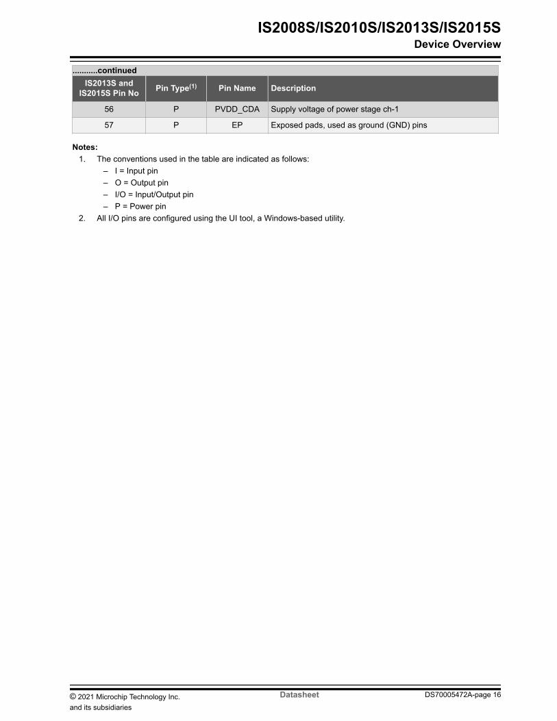
continuedIS2013S and
IS2015S Pin No Pin Type(1) Pin Name Description
56 P PVDD_CDA Supply voltage of power stage ch-1
57 P EP Exposed pads used as ground (GND) pins
Notes 1 The conventions used in the table are indicated as follows
ndash I = Input pinndash O = Output pinndash IO = InputOutput pinndash P = Power pin
2 All IO pins are configured using the UI tool a Windows-based utility
IS2008SIS2010SIS2013SIS2015SDevice Overview
copy 2021 Microchip Technology Incand its subsidiaries
Datasheet DS70005472A-page 16
3 AudioThe input and output audio signals have different stages and each stage is programmed to vary the gain responsecharacteristics For microphones both single-ended inputs and differential inputs are supported To maintain ahigh-quality signal provide a stable bias voltage source to the condenser microphonersquos FET Use the DC-blockingcapacitors at both positive and negative sides of the input Internally this analog signal is converted to 16-bit 8 kHzlinear PCM data
31 Digital Signal ProcessorA Digital Signal Processor (DSP) is used to perform speech and audio processing The advanced speech featuressuch as acoustic echo cancellation and noise reduction are built in To reduce nonlinear distortion and to help echocancellation an outgoing signal level to the speaker is monitored and adjusted to avoid saturation of the speakeroutput or microphone input Adaptive filtering is also applied to track the echo path impulse in response to provide anecho-free and full-duplex user experience
The embedded noise reduction algorithm helps to extract clean speech signals from the noisy inputs capturedby microphones and improves mutual understanding in communication The advanced audio features such asmulti-band dynamic range control parametric multi-band equalizer audio widening and virtual bass are built in Theaudio effect algorithms improve the userrsquos audio listening experience in terms of better quality audio after audiosignal processing
The following figures illustrate the processing flow of speakerphone applications for speech and audio signalprocessing
Figure 3-1 Speech Processing
Figure 3-2 Audio Processing
The DSP parameters such as EQ Speaker Gain Mic Gain Sound Effect and more are configured using the DSPtool For additional information on the DSP tool refer to the IS20xxBM1xBM2x DSP Application Note
IS2008SIS2010SIS2013SIS2015SAudio
copy 2021 Microchip Technology Incand its subsidiaries
Datasheet DS70005472A-page 17
Note The DSP tool and IS20xxBM1xBM2x DSP Application Note are available for download at the Microchipwebsite
32 CodecThe built-in codec has a high SNR performance and it consists of an ADC a DAC and additional analog circuitry
33 Auxiliary PortThe SoC supports one analog (line-in) signal from the external audio source The analog signal is processed bythe DSP to generate different sound effects (multi-band dynamic range compression and audio widening) which areconfigured using the DSP tool
34 Class D Audio AmplifierThe Class D amplifier has a significant advantage in many applications due to its lower power dissipation whichproduces less heat The IS2013S and IS2015S SoC have a built-in Class D amplifier that reduces circuit board spaceand system cost The efficiency of the amplifier extends the battery life in portable systems
The Class D amplifier is implemented by using a full-bridge output stage A full bridge uses two half-bridge stages todrive the load differentially The Class D amplifier provides a good SNR and enough drive capability for a 4Ω speakerdriver
IS2008SIS2010SIS2013SIS2015SAudio
copy 2021 Microchip Technology Incand its subsidiaries
Datasheet DS70005472A-page 18
4 TransceiverThe SoC is designed and optimized for Bluetooth 24 GHz systems It contains a complete radio frequencytransmitterreceiver section An internal synthesizer generates a stable clock to synchronize with another device
41 TransmitterThe internal Power Amplifier (PA) has a maximum output power of +4 dBm with 20 dB power level control Applythis to Class 2 or Class 3 radios without an external RF PA The transmitter directly performs the IQ conversionto minimize the frequency drift and it can access the 20 dB power range with the temperature compensationmechanism
42 ReceiverThe Low-Noise Amplifier (LNA) operates with TR-combined mode for the single port application It saves the pin onthe package without having an external TXRX switch
The ADC is used to sample the input analog signal and convert it into a digital signal for demodulator analysisA channel filter is integrated into a receiver channel before the ADC to reduce the external component count andincrease the anti-interference capability
The image rejection filter is used to reject the image frequency for the low-IF architecture and it is also intended toreduce the external Band Pass Filter (BPF) component for a super heterodyne architecture
The Received Signal Strength Indicator (RSSI) signal feedback to the processor is used to control the RF outputpower to make a good trade-off for effective distance and current consumption
43 SynthesizerA synthesizer generates a clock for radio transceiver operation The VCO inside with a tunable internal LC tankcan reduce any variation for components A crystal oscillator with an internal digital trimming circuit provides a stableclock for the synthesizer
44 ModemFor Bluetooth 12 specifications and below 1 Mbps is the standard data rate based on the Gaussian Frequency ShiftKeying (GFSK) modulation scheme This basic rate modem meets BDR requirements of Bluetooth 20 with EDRspecifications
For Bluetooth 20 and above specifications EDR is introduced to provide the data rates of 123 Mbps Thisenhanced data rate modem meets EDR requirements of Bluetooth 20 with EDR specifications For the basebandboth BDR and EDR utilize the same 1 MHz symbol rate and 16 kHz slot rate For BDR 1 symbol represents 1-bitHowever each symbol in the payload part of the EDR packets represents 2-bit or 3-bit This is achieved by using twodifferent modulations π4 DQPSK and 8 DPSK
45 Adaptive Frequency Hopping (AFH)The SoC has an AFH function to avoid RF interference It has an algorithm to check the nearby interference and tochoose the clear channel for the transceiver Bluetooth signal
IS2008SIS2010SIS2013SIS2015STransceiver
copy 2021 Microchip Technology Incand its subsidiaries
Datasheet DS70005472A-page 19
5 MicrocontrollerA single-cycle 8-bit microcontroller is built into the SoC to execute the Bluetooth protocols It operates from 16 MHzto higher frequencies where the firmware dynamically adjusts the trade-off between the computing power and thepower consumption In the ROM version the MCU firmware is hard-wired to minimize power consumption for thefirmware execution and to save the external Flash cost
51 MemoryThere are sufficient ROM and RAM to fulfill the processor requirements in which a synchronous single port RAMinterface is used The register bank dedicated single port memory and Flash memory are connected to theprocessor bus The processor coordinates with all link control procedures and the data movement happens using aset of pointer registers
52 External ResetThe IS20xxS SoC provides a Watchdog Timer (WDT) to reset the SoC It has an integrated Power-on Reset (POR)circuit that resets all circuits to a known Power-on state This action is also driven by an external Reset signal whichis used to control the device externally by forcing it into a POR state The RST_N signal input is active-low and noconnection is required in most of the applications
53 Reference ClockThe IS20xxS SoC is composed of an integrated crystal oscillation function that uses a 16 MHz external crystal andtwo specified loading capacitors to provide a high quality system reference timer source Use this feature to removethe initial tolerance frequency errors which are associated with the crystal and its equivalent loading capacitance inthe mass production Achieve the frequency trim by adjusting the crystal loading capacitance through the on-chip trimcapacitors (Ctrim)
The value of the trimming capacitance is 200 fF (200x10-15 F) per LSB at the 5-bit word and the overall adjustableclock frequency is plusmn40 kHz The following figure illustrates the crystal connection of the IS20xxS SoC with twocapacitors
Figure 5-1 Crystal Connection
IS20XXS
XO_N
CL1
XO_P
CL2
IS2008SIS2010SIS2013SIS2015SMicrocontroller
copy 2021 Microchip Technology Incand its subsidiaries
Datasheet DS70005472A-page 20
Notes 1 Ctrim = 200 fF (1 to 31) Cint = 3 pF2 CL = [(CL1 x CL2) (CL1 + CL2)] + (Ctrim 2) + Cint (set trim value as 16 Ctrim = 32 pF)3 For a 16 MHz crystal where CL = 9 pF the CL1 = CL2 = 91 pF)4 For the CL selection refer to the data sheet of the crystal
IS2008SIS2010SIS2013SIS2015SMicrocontroller
copy 2021 Microchip Technology Incand its subsidiaries
Datasheet DS70005472A-page 21
6 Power Management Unit (PMU)The IS20xxS SoC has an integrated PMU The main features of the PMU are a lithium-ion battery charger and avoltage regulator A power switch is used to switch over the power source between a battery and an adapter Alsothe PMU provides current to the LED drivers
61 Charging a BatteryThe IS20xxS SoC has a built-in battery charger which is optimized for lithium-polymer batteries The battery chargerincludes a current sensor for a charging control user programmable current regulator and high accuracy voltageregulator
The charging current parameters are configured by using the UI (IS20XXS_UI) tool Whenever the adapter isplugged-in the charging circuit will be activated Reviving pre-charging constant current mode constant voltagemode and re-charging functions are implemented The maximum charging current is 350 mA The following figureillustrates the charging curve of a battery
Figure 6-1 Battery Charging Curve
62 Voltage MonitoringA 10-bit successive approximation register ADC (SAR ADC) provides a dedicated channel for battery voltage leveldetection The warning level is programmed by using the UI tool The ADC provides a granular resolution to enablethe MCU to take control over the charging process
63 Low Dropout RegulatorA built-in LDO Regulator is used to convert the battery or adapter power for the power supply It also integratesthe hardware architecture to control the power-onoff procedure The built-in programmable LDOs provide power forcodec and digital IO pads Also it is used to buffer the high input voltage from the battery or adapter This LDOrequires a 1 μF bypass capacitor
IS2008SIS2010SIS2013SIS2015SPower Management Unit (PMU)
copy 2021 Microchip Technology Incand its subsidiaries
Datasheet DS70005472A-page 22
64 Switching RegulatorThe built-in programmable output voltage regulator converts the battery voltage to RF and base band core powersupply This converter has a high conversion efficiency and a fast transient response
65 LED DriverThe IS20xxS SoC consists of two LED drivers to control the LEDs The LED drivers provide enough sink current(16-step control and 035 mA for each step) and the LED is connected directly to the IS20xxS SoC
Note Configure the LED settings using the IS20XXS_UI tool
The following figure illustrates the LED driver in the IS20xxS SoC
Figure 6-2 LED DRIVER
IS20xxS
LED2
SYS_PWR
LED1
IS2008SIS2010SIS2013SIS2015SPower Management Unit (PMU)
copy 2021 Microchip Technology Incand its subsidiaries
Datasheet DS70005472A-page 23
7 Application InformationThis section describes the power supply connection host MCU UART interface and various modes in detail
71 Power SupplyThe following figure illustrates the connection from the BAT_IN pin to various other voltage supply pins of theIS20xxS SoC
The BAT_IN input pin powers the IS20xxS SoC To charge the battery connect the external 5V power adapter toADAP_IN
Figure 7-1 Power Tree Diagram
VDDA VDDAO
VDD_IO
3V LDO
18V Buck
SAR_VDD
LDO31_VIN
CODEC_VO
LDO31_VO
BK_VDD
BK_LX
BK_O
VDD_CORE
VCC_RF
12V LDOPMIC_IN
CLDO_O
RFLDO_O
PVDD_CDA
Li-Io
n BA
T BAT_IN
ADAP_IN
SYS_PWRPower Switch
5V Adapter
(42~30V)
(45~55V)(42~30V)
(30~27V)
(33 ~27V)
(18V)
(12V)
(128V)
72 Host MCU InterfaceAn external MCU controls the IS20xxS SoC using the UART command set The following figure illustrates the UARTinterface between the IS20xxS SoC and an external MCU
Figure 7-2 Host MCU Interface Over UART
IS20xxSHCI_TXD
HCI_RXD
PWR
P0_0
MCUUART_TX
UART_RX
MCU_WAKEUP
BT_WAKEUP
UART Interface
UART Interface
The MCU controls the IS20xxS SoC over the UART interface and wakes up the SoC using the PWR pin The MCUfunction wakes up by connecting to the P0_0 pin of the IS20xxS
Refer to the IS200xIS201xIS202x UART Command SOP document for a list of functions that the IS20xxS SoCsupports and how to use the IS20XXS_UI tool to set up the system using the UART command
Note The IS200xIS201xIS202x UART Command SOP document is available for download from the Microchipwebsite at IS200xIS201xIS202x UART Command SOP
IS2008SIS2010SIS2013SIS2015SApplication Information
copy 2021 Microchip Technology Incand its subsidiaries
Datasheet DS70005472A-page 24
73 Timing Sequence of UART ApplicationThe following figures illustrate the various UART control signal timing sequences
Figure 7-3 Power-OnOff Sequence
BAT_IN
SYS_PWR
1 ms
Power- oninitial idle Power-on Power-on Power-off idle
MCU state
MFB (PWR)
BK_OLDO31_VO
400 ms
RST_N
MCU sends UART command (UART_RX)
UART Command
MCU sends power-off UART Command
Power-on ACK ACK ACKIS20xxS response UART state
(UART_TX)
Set ldquoPower-on Directlyrdquo boot
any
10 ms
20 msKeep all IS20xxSand MCU connection to low level
2s
(See Figure 7-4) (See Figure 7-5)
IS20xxS disconnect and auto power-off
gt 1s
Figure 7-4 Timing Sequence of RX Indication after Power-On
Resume 32 kHz mode
MFB (PWR)MCU sends UART command
MFB pulse must be longer than the UART command slot time
150 ms
2 ms 2 ms
Enter 32 kHz mode
1 ms
UART Command
IS2008SIS2010SIS2013SIS2015SApplication Information
copy 2021 Microchip Technology Incand its subsidiaries
Datasheet DS70005472A-page 25
Figure 7-5 Timing Sequence of Power-Off
BAT_IN +4V
MFB
MCU Sends RST_N
BK_OUT
LDO31_VO
UART Bus
2s 1s
IS20xxS Sends Power-off ACK
Notes 1 EEPROM clock = 100 kHz2 For a byte wire 001 ms x 32 clock x 2 = 640 μs3 It is recommended that ramp-down time be more than 640 μs during the power-off sequence to ensure safe
operation of the device
IS2008SIS2010SIS2013SIS2015SApplication Information
copy 2021 Microchip Technology Incand its subsidiaries
Datasheet DS70005472A-page 26
Figu
re 7
-6
Tim
ing
Sequ
ence
of P
ower
-On
(NA
CK
)
BAT
_IN
SYS_
PWR
1 m
s Pow
er-
onin
itial
idle
Pow
er-o
nM
CU
sta
te
MFB
(PW
R)
BK_O
LD
O31
_VO
400
ms
RST
_N
MC
U s
ends
UAR
T co
mm
and
(UAR
T_R
X)
UAR
T C
omm
and
NAC
KPo
wer
-on
ACK
ACK
IS20
xxS
resp
onse
UAR
T st
ate
(UAR
T_TX
)
Set ldquo
Pow
er-o
n D
irect
lyrdquo b
oot
10 m
s
20 m
s
Ret
ry i
f AC
K is
not
rece
ived
200
ms
any
Wai
t
Max
imum
5 ti
mes
(1s)
IS2008SIS2010SIS2013SIS2015SApplication Information
copy 2021 Microchip Technology Incand its subsidiaries
Datasheet DS70005472A-page 27
Figure 7-7 Reset Timing Sequence in Case of No Response from SoC to Host MCU
MFB (PWR)
MCU sends UART command UART
Command
UART Command
IS20xxS UART
If no response
RST_N
1ms
X ms1ms
1ms
1ms
Note The MCU sends the UART command again when the SoC is not responding to its first UART command Ifthe SoC is not responding to the second UART command within X ms the MCU forces the system to reset
Figure 7-8 Timing Sequence of Power Drop Protection
BAT_IN +4V
RST_N from Reset IC
Power
SYS_PWR
IS20xxS
Reset OUT VDDGND
MCU Reset
Reset IC
29V
1 It is recommended that the battery be connected on a BAT_IN pin of the SoC for the power supply2 If an external power source or a power adapter is used to provide the power to the SoC (ADAP_IN) use a
voltage supervisor IC3 The RESET IC output pin must be open drain with delay time of le 10 ms and the recommended part is
TCM809SVNB713
74 General Purpose IO pinsThe following table provides the details of various functions that are mapped to the IO pins of the IS20xxS SoCand these IOs are configured by using the IS20XXS_UI tool The first button (Button 0) must be configured as thepower-onoff key and can be set using the PWR pin The remaining pins are configured for any one of the defaultfunctions (short press long press double press and combinations)
IS2008SIS2010SIS2013SIS2015SApplication Information
copy 2021 Microchip Technology Incand its subsidiaries
Datasheet DS70005472A-page 28
Table 7-1 IO Pin Configuration
Sl No Pin Name Buttons Default Functions(1)
1 PowerMFB Button 0 PWR
2 P0_2 Button 1 PlayPause
3 P2_7 Button 2 Volume Up
4 P0_5 Button 3 Volume Down
5 P0_1 Button 4 FWD
6 P0_3 Button 5 REV
Note 1 These functions can be configured using the IS20XXS_UI tool
Few signals are generated to indicate or control outside devices The most popular applications are NFC for easypairing external audio amplifier for louder speaker and buzzer for indication
Table 7-2 IO Pins for Added Functions
Functions(1) IO Configurable Features
Slide switch P0_0P1_5
Buzzer P0_3
NFC detect P0_4P1_5
External amplifier enable P1_5
Note 1 These functions can be configured using the IS20XXS_UI tool
IS2008SIS2010SIS2013SIS2015SApplication Information
copy 2021 Microchip Technology Incand its subsidiaries
Datasheet DS70005472A-page 29
8 Antenna Placement RuleFor Bluetooth-enabled products the antenna placement affects the overall performance The antenna requires freespace to radiate RF signals and it must not be surrounded by the GND plane
The following figure illustrates a typical example of the good and poor antenna placement on the main applicationboard with the GND plane
Figure 8-1 Antenna Placement Examples
The following figure illustrates the keep-out area recommended for the PCB antenna
Figure 8-2 Keep-Out Area Recommended for PCB Antenna
Note For additional information on the antenna placement refer to the antenna-specific data sheet from theantenna manufacturer
IS2008SIS2010SIS2013SIS2015SAntenna Placement Rule
copy 2021 Microchip Technology Incand its subsidiaries
Datasheet DS70005472A-page 30
9 Electrical CharacteristicsThis section provides an overview of the IS20xxS SoC electrical characteristics
Table 9-1 Absolute Maximum Ratings
Parameter Symbol Minimum Maximum Unit
Digital core supply voltage VDD_CORE 0 135 V
RF supply voltage VCC_RF 0 135 V
SAR ADC supply voltage SAR_VDD 0 21 V
Codec supply voltage VDDAVDDAO 0 33 V
IO supply voltage VDD_IO 0 36 V
Buck supply voltage BK_VDD 0 43 V
Supply voltage LDO31_VIN 0 43 V
Battery input voltage BAT_IN 0 43 V
Adapter input voltage ADAP_IN 0 70 V
Storage temperature TSTORE -65 +150
Operation temperature TOPERATION -20 +70
Note Stresses listed on the preceding table cause permanent damage to the device This is a stress rating onlyThe functional operation of the device at those or any other conditions and those indicated in the operation listingsof this specification are not implied Exposure to maximum rating conditions for extended periods affects devicereliability
The following tables provide the recommended operating conditions and the electrical specifications of the IS20xxSSoC
Table 9-2 Recommended Operating Condition
Parameter Symbol Minimum Typical Maximum Unit
Digital core supply voltage VDD_CORE 114 12 126 V
RF supply voltage VCC_RF 122 128 134 V
SAR ADC supply voltage SAR_VDD 162 18 198 V
Codec supply voltage VDDAVDDAO 27 28 30 V
IO supply voltage VDD_IO 27 30 33 V
Buck supply voltage BK_VDD 3 37 425 V
Supply voltage LDO31_VIN 3 37 425 V
Battery input voltage BAT_IN 3 37 425 V
Adapter input voltage ADAP_IN 45 5 55 V
Operation temperature TOPERATION -20 +25 +70
Note All these supply voltages are programmed through the EEPROM parameters
IS2008SIS2010SIS2013SIS2015SElectrical Characteristics
copy 2021 Microchip Technology Incand its subsidiaries
Datasheet DS70005472A-page 31
Table 9-3 Buck Switching Regulator
Parameter Minimum Typical Maximum Unit
Input voltage 30 37 425 V
Output voltage (Iload = 70 mA andVin = 4V) 17 18 205 V
Output voltage accuracy mdash plusmn5 mdash
Output voltage adjustable step mdash 50 mdash mVStep
Output adjustment range -01 mdash +025 V
Average load current (ILOAD) 120 mdash mdash mA
Conversion efficiency (BAT = 38Vand Iload = 50 mA) mdash 88(1) mdash
Quiescent current (PFM) mdash mdash 40 μA
Output current (peak) 200 mdash mdash mA
Shutdown current mdash mdash lt1 μA
Notes 1 Test condition SAR_VDD = 18V and temperature = +252 These parameters are characterized but not tested in manufacturing
Table 9-4 Low-dropout Regulator
Parameter Minimum Typical Maximum Unit
Input Voltage 30 37 425 V
Output VoltageCODEC_VO mdash 28 mdash
VIO_VO mdash 28 mdash
Output Accuracy (VIN = 37V ILOAD = 100 mA and +27) mdash plusmn5 mdash
Output current (average) mdash mdash 100 mA
Drop-out voltage
(Iload = maximum output current)mdash mdash 300 mV
Quiescent current (excluding load and Iload lt 1 mA) mdash 45 mdash μA
Shutdown current mdash mdash lt1 μA
Notes 1 Test condition SAR_VDD = 18V and temperature = +252 These parameters are characterized but not tested in manufacturing
Table 9-5 Battery Charger
Parameter Minimum Typical Maximum Unit
Input voltage (ADAP_IN) 45 50 55 V
Supply current to charger only mdash 3 45 mA
IS2008SIS2010SIS2013SIS2015SElectrical Characteristics
copy 2021 Microchip Technology Incand its subsidiaries
Datasheet DS70005472A-page 32
continuedParameter Minimum Typical Maximum Unit
Maximum batteryfast chargecurrent (ENX2 =0)
Headroom gt 07V (ADAP_IN = 5V) 170 200 240 mA
Headroom = 03V (ADAP_IN = 45V) 160 180 240 mA
Maximum batteryfast chargecurrent (ENX2 =1)
Headroom gt 07V (ADAP_IN = 5V) 300 350 420 mA
Headroom = 03V (ADAP_IN = 45V) 180 220 270 mA
Trickle charge voltage threshold mdash 3 mdash V
Battery charge termination current ( of fast charge current) mdash 10 mdash
Notes 1 Headroom = VADAP_IN ndash VBAT2 ENX2 is not allowed to be enabled when VADAP_IN ndash VBAT gt 2V3 These parameters are characterized but not tested in manufacturing
Table 9-6 LED Diver
Parameter Minimum Typical Maximum Unit
Open-drain voltage mdash mdash 36 V
Programmable current range 0 mdash 525 mA
Intensity control mdash 16 mdash step
Current step mdash 035 mdash mA
Power-down open-draincurrent mdash mdash 1 μA
Shutdown current mdash mdash 1 μA
Notes 1 Test condition SAR_VDD = 18V and temperature = +252 These parameters are characterized but not tested in manufacturing
Table 9-7 Audio Codec Digital-to-Analog Converter
Parameter (Condition)(1) Minimum Typical Maximum Unit
Over-sampling rate mdash 128 mdash fs
Resolution 16 mdash 20 Bits
Output sample rate 8 mdash 48 kHz
Signal-to-noise Ratio (2) (SNR at capless mode) for 48 kHz mdash 96 mdash dB
Signal-to-noise Ratio (2)
(SNR at single-ended mode) for 48 kHzmdash 98 mdash dB
Digital gain -54 mdash 485 dB
Digital gain resolution mdash 2 to 6 mdash dB
Analog gain -28 mdash 3 dB
Analog gain resolution mdash 1 mdash dB
IS2008SIS2010SIS2013SIS2015SElectrical Characteristics
copy 2021 Microchip Technology Incand its subsidiaries
Datasheet DS70005472A-page 33
continuedParameter (Condition)(1) Minimum Typical Maximum Unit
Output voltage full-scale swing (AVDD = 28V) 495 7425 mdash mV rms
Maximum output power (16Ω load) mdash 345 mdash mW
Maximum output power (32Ω load) mdash 172 mdash mW
Allowed loadResistive 8 16 OC Ω
Capacitive mdash mdash 500 pF
THD+N (16Ω load) mdash mdash 005
Signal-to-noise Ratio (SNR at 16Ω load) mdash mdash mdash 96 dB
Notes 1 T = +25 VDD = 30V 1 kHz sine wave input and Bandwidth = 20 Hz ndash 20 kHz2 fin = 1 kHz Bandwidth = 20 Hz ndash 20 kHz A-weighted THD + N lt 001 0 dBFS signal and Load = 100 kΩ3 These parameters are characterized but not tested in manufacturing
Table 9-8 Audio Codec Analog-to-Digital Converter
Parameter (Condition)(1) Minimum Typical Maximum Unit
Resolution mdash mdash 16 Bit
Output sample rate 8 mdash 48 kHz
Signal-to-noise Ratio (2) (SNR at MIC or Line-in mode) mdash 90 mdash dB
Digital gain -54 mdash 485 dB
Digital gain resolution mdash 2 to 6 mdash dB
MIC boost gain mdash 20 mdash dB
Analog gain mdash mdash 60 dB
Analog gain resolution mdash 20 mdash dB
Input full scale at maximum gain (differential) mdash 4 mdash mVrms
Input full scale at minimum gain (differential) mdash 800 mdash mVrms
3 dB bandwidth mdash 20 mdash kHz
Microphone mode (input impedance) mdash 24 mdash kΩ
THD+N (microphone input) at 30 mVrms input mdash 002 mdash
Notes 1 T = +25 VDD = 30V 1 kHz sine wave input and Bandwidth = 20 Hz ndash 20 kHz2 fin = 1 kHz Bandwidth = 20 Hz ndash 20 kHz A-weighted and THD + N lt 1 150 mVpp input3 These parameters are characterized but not tested in manufacturing
Table 9-9 Single-Channel ClassndashD Amplifier
Parameter (Condition) Minimum Typical Maximum Unit
Standalone SNR (A-weighting) mdash 100 mdash dB
Gain mdash 12 mdash dB
PSRR (217 Hz 200 mV on PVDD) mdash 70 mdash dB
IS2008SIS2010SIS2013SIS2015SElectrical Characteristics
copy 2021 Microchip Technology Incand its subsidiaries
Datasheet DS70005472A-page 34
continuedParameter (Condition) Minimum Typical Maximum Unit
Efficiency4Ω 80 mdash 85
8Ω 85 mdash 90
Supply voltage 30 37 45 V
Load mdash 40 mdash Ω
Quiescent current (1 channel) mdash 20 mdash mA
Sample frequency mdash 250 mdash kHz
Over current limits mdash 23 mdash A
Shutdown current mdash 10 mdash μA
Notes 1 Test condition PVDD_CDA = 42V and temperature = 252 These parameters are characterized but not tested in manufacturing
Table 9-10 Transmitter Section for BDR and EDR
Parameter Minimum Typical Maximum BluetoothSpecification Unit
Maximum RF transmit power mdash 30 40 -6 to 4 dBm
Relative transmit power -4 -12 1 -4 to 1 dB
Notes 1 The RF Transmit power is calibrated during production using the MP tool software and MT8852 Bluetooth test
equipment2 Test condition VCC_RF = 128V and temperature = +25
Table 9-11 Receiver Section for BDR and EDR
Parameter Packet Type Minimum Typical Maximum BluetoothSpecification Unit
Sensitivity at 01 BER GFSK mdash -90 mdash le-70 dBm
Sensitivity at 001 BERπ4 DQPSK mdash -91 mdash le-70 dBm
8 DPSK mdash -82 mdash le-70 dBm
Notes 1 Test condition VCC_RF = 128V and temperature = +252 These parameters are characterized but not tested in manufacturing
Table 9-12 System Current Consumption
System Status Typical Maximum Unit
System Off mode 2 5 μA
Standby mode 08 mdash mA
Link mode 04 mdash mA
SCO Link 78 mdash mA
A2DP Link (Vp-p = 200 mV 1k tone signal) 107 mdash mA
IS2008SIS2010SIS2013SIS2015SElectrical Characteristics
copy 2021 Microchip Technology Incand its subsidiaries
Datasheet DS70005472A-page 35
Notes 1 Consider the current consumption values with the IS2010 EVB as a test platform2 Test condition BAT_IN = 38V link with the HTC EYE smartphone The distance between the smartphone and
EVB is 30 cm
IS2008SIS2010SIS2013SIS2015SElectrical Characteristics
copy 2021 Microchip Technology Incand its subsidiaries
Datasheet DS70005472A-page 36
10 Packaging InformationThis section provides information on package marking package details and footprint dimensions of the IS20xxS SoC
101 Chip Identification SystemPart No X -Y
(Chip Name) (Package Type) (Version)
Legendbull Chip Name
ndash IS2008Sndash IS2010Sndash IS2013Sndash IS2015S
bull Package Typendash S = QFN (Saw Type) Package
bull Versionndash ldquo-203rdquo represents the chip version is 203
For examplebull IS2015S-002 002 version ROM code IS2015 chip in QFN type packagebull IS2010S-203 203 version ROM code IS2010 chip in QFN type package
102 Package Marking InformationThe following figure illustrates the package marking information of the IS20xxS
IS2008SIS2010SIS2013SIS2015SPackaging Information
copy 2021 Microchip Technology Incand its subsidiaries
Datasheet DS70005472A-page 37
Figure 10-1 Package Marking Information
Page 36
Page 36
48 Lead QFN (6x6x09 mm) 56 Lead QFN (7x7x09 mm)
Pin 1 Index
Pin 1 Index Pin 1 Index
Legend
XXX Chip serial number version and e3 Pb-free JEDEC designator for Matte Tin (Sn)
YY Year code (last 2 digits of calendar year)
WW Week code (week of January 1 is week ldquo1rdquo)
NNN Alphanumeric traceability code
103 Package DetailsThe following figures illustrate the footprint dimensions and the chip outline details of the IS2008S and IS2010S SoC
IS2008SIS2010SIS2013SIS2015SPackaging Information
copy 2021 Microchip Technology Incand its subsidiaries
Datasheet DS70005472A-page 38
Figure 10-2 IS2008S and IS2010S Chip Outline Details
IS2008SIS2010SIS2013SIS2015SPackaging Information
copy 2021 Microchip Technology Incand its subsidiaries
Datasheet DS70005472A-page 39
Figure 10-3 IS2008S and IS2010S Footprint Dimensions
PAD LENGTHPAD WIDTH
PAD PITCHPAD COUNT
Note For the most current package drawings refer to the Microchip Packaging Specification available at httpwwwmicrochipcompackaging
The following figures illustrate the footprint dimensions and the chip outline details of the IS2013S and IS2015S SoC
IS2008SIS2010SIS2013SIS2015SPackaging Information
copy 2021 Microchip Technology Incand its subsidiaries
Datasheet DS70005472A-page 40
Figure 10-4 IS2013S and IS2015S Chip Outline Details
IS2008SIS2010SIS2013SIS2015SPackaging Information
copy 2021 Microchip Technology Incand its subsidiaries
Datasheet DS70005472A-page 41
Figure 10-5 IS2013S and IS2015S Footprint Dimensions
Note For the most current package drawings refer to the Microchip Packaging Specification available at httpwwwmicrochipcompackaging
IS2008SIS2010SIS2013SIS2015SPackaging Information
copy 2021 Microchip Technology Incand its subsidiaries
Datasheet DS70005472A-page 42
11 Reflow Profile and Storage ConditionThis chapter describes reflow profiles and stencil information of the IS20xxS SoC
111 Stencil of SMT Assembly SuggestionThe stencil of the SMT assembly suggestion contains the following sections
1111 Stencil Type and Thicknessbull Laser cuttingbull Stainless steelbull Thickness 05 mm pitch thickness less than 015 mm
1112 Aperture Size and Shape for Terminal Padbull Aspect ratio (widththickness) is more than 15bull Aperture shape
ndash The stencil aperture is designed to match the pad size on the PCBndash Oval-shaped opening is used to get the optimum paste releasendash Rounded corners to minimize cloggingndash Positive taper walls (5deg tapering) with the bottom opening larger than the top opening
1113 Aperture Design for Thermal Padbull Small multiple openings are used instead of one big opening as shown in the following figure
Figure 11-1 IS20xxS SoC Reflow Profile Aperture Design
bull 60 to 80 solder paste coveragebull Rounded corners to minimize cloggingbull Positive taper walls (5deg tapering) with the bottom opening is larger than the top opening as shown in the
following figureFigure 11-2 IS20xxS SoC Stencil Type
IS2008SIS2010SIS2013SIS2015SReflow Profile and Storage Condition
copy 2021 Microchip Technology Incand its subsidiaries
Datasheet DS70005472A-page 43
112 Reflow ProfileThe following figure illustrates the reflow profile and its specific features are
bull Standard Condition IPCJEDEC J-STD-020bull Preheat 150 to 200 for 60 to180 secondsbull Average ramp-up rate (217 to peak) 1 to 2sec maxbull Temperature maintained above 217 60 to 150 secondsbull Time within 5 of actual peak temperature 20 to 40 secondsbull Peak temperature 260 with +5-0 tolerancebull Ramp-down rate (peak to 217) 3sec maxbull Time within 25 to peak temperature 8 minutes maxbull Cycle interval 5 minutes
Figure 11-3 Reflow Profile
+150degC
+200degC
+217degC
+255degCRamp-up rate1~2degCsec max+217degC to peak
Peak +260degC (+50degC tolerance)
Ramp-down rate+3degCsec maxpeak to +217degC
20 to 40 sec
Time (sec)
60 to 180 sec 60 to 150 sec
113 Storage ConditionUsers must follow these specific storage conditions for the IS20xxS SoC
bull Calculated shelf life in the sealed bag 24 months at lt40 and lt90 Relative Humidity (RH)bull Once the bag is opened devices that are subjected to reflow solder or other high temperature process must be
mounted within 168 hours of factory conditions that is lt3060 RH
The following figure illustrates the IS20xxS SoC bag label details
IS2008SIS2010SIS2013SIS2015SReflow Profile and Storage Condition
copy 2021 Microchip Technology Incand its subsidiaries
Datasheet DS70005472A-page 44
Figure 11-4 Storage Conditions
IS2008SIS2010SIS2013SIS2015SReflow Profile and Storage Condition
copy 2021 Microchip Technology Incand its subsidiaries
Datasheet DS70005472A-page 45
12 Reference CircuitThis section provides the reference schematics of IS2008S IS2010S IS2013S and IS2015SFigure 12-1 IS2008SIS2010S Reference Circuit (Main Circuit)
(Peak Current 400 mA)
(1uF X5R or 47uF Y5V)
P0_3
VBGULPC_VSUS
MFB
VBG
ULPC_VSUS
LED1LED2
P0_1
ADAP
_IN
P1_5
P0_2
P0_5
P2_7
P2_0
MIC_P2MIC_N2
MIC_P1MIC_N1
P1_2P1_3RST_N
AOH
PLAO
HPM
HC
I_TX
DH
CI_
RXD
RFLDO_O1V8
1V2
1V8
CODEC_VO
2V8
1V8SYS_PWR
BAT_IN
CODEC_VO
2V8
SYS_PWR
SYS_PWR
RFLDO_O
MIC_BIAS
2V8
1V2
ADAP_IN
MIC_N2MIC_P2MIC_N1MIC_P1
RST_N
HC
I_R
XDH
CI_
TXD
LED2LED1
AOH
PMAO
HPL
P0_1
P1_5
P0_3
P0_5
P2_7
P2_0
P0_2
MFB
C791u16V
ANT1
ANT-MP8
1
C321u16V
C291u16V
C7710u16V
C871u16V
X1X4P-16MHZ
4 13 2
C251u16V
C402p50V
C311u16V
C219p50V
C281u16V
R681K1
12
C261u16V
C191u16V
C361u16V
L10L10uH-2
C831u16V
C841u16V
IS2008SIS2010S
U6
IS2010S_MH+2MIC
MICN22
AO
HP
L47
VD
DA
48
VCOM1
MICN14
MICP15
MICBIAS6
VDD_CORE7
VDD_IO11 RST_N10
P128
P139
P05
43
HC
I_TX
D15
HC
I_R
XD
14
XO
_P37
XO_N36
ULPC_VSUS35
P27
42
VBG34
RFLDO_O33
PMIC_IN32
CLDO_O31
NC
21
SY
S_P
WR
23
P20
41
P15
13
P02
40
P0112
VD
D_I
O44
RTX
39
VC
C_R
F38
EP
49
VD
DA
O45
AO
HP
M46
MICP23
P0330
CO
DE
C_V
O16
LDO
31_V
IN17
LDO
31_V
O18
AD
AP
_IN
19
BA
T_IN
20
SA
R_V
DD
22
BK
_VD
D24
BK_LX25BK_O26PWR27
LED129
LED228
C801u16V
C8210u16V
TP9RF-TP1
C861u16V
L227nH
R691K
12
C8110u16V
C411u16V
C249p50V
C3NP-0402
C271u16V
C341u16V
L368p50V
C231u16V
C781u16V
IS2008SIS2010SIS2013SIS2015SReference Circuit
copy 2021 Microchip Technology Incand its subsidiaries
Datasheet DS70005472A-page 46
Figure 12-2 IS2008SIS2010S EEPROM (Main Circuit)
EEPROM
P1_2P1_3
2V8
U7ACE24C64
A01
A12
A23
GND4
SDA5SCL6WP7VCC8
C3801u16V
C391u16V
R18NP-0603
R174K7
12
IS2008SIS2010SIS2013SIS2015SReference Circuit
copy 2021 Microchip Technology Incand its subsidiaries
Datasheet DS70005472A-page 47
Figure 12-3 IS2008SIS2010S Audio Interface (Optional Circuit)
AOHPMS
AOHPL
MIC1
MIC2
MIC2+
MIC1+
MIC1-
MIC2-
AOHPM
AOHPL
MIC_P1
MIC_N1
MIC1+
MIC1-
MIC_P2
MIC_N2
MIC2+
MIC2-
MIC_BIAS
MIC_BIAS
MIC_P1
MIC_N1
MIC_P2
MIC_N2
AOHPM
AOHPL
C42220p50V
D14SPE0572
21
TP51
C4647u10V
C440047u25V
D16SPE0572
21
TP131
R91K
1 2
TP61
TP111
R112K
1 2
C11 10p50V
R61K
1 2
TP71
C15 10p50V
C350047u25V
C2047u10V
D12SPE0572
21
C37220p50V
TP81
C2247u10V
D13SPE0572
21
C1239p50V
C430047u25V
D10SPE0572
21
C1739p50V
R71K
1 2
R102K
1 2
R81K
1 2
C400047u25V
D11SPE0572
21
C4547u10V
IS2008SIS2010SIS2013SIS2015SReference Circuit
copy 2021 Microchip Technology Incand its subsidiaries
Datasheet DS70005472A-page 48
Figure 12-4 IS2008SIS2010S Audio Options (Optional Circuit)
FWD
VOL_UP
PLAYPAUSE
REV
VOL_DN P2_7
P0_2
P0_3
P0_5
P0_1
MFB
SYS_PWR
MFB
P0_2
P0_3 P0_1
P0_5 P2_7
C6415p50V
SW9SW-TACT
12
34SW4
SW-TACT
12
34
C6615p50V
C6515p50V
SW5
SW-TACT
12
34SW6
SW-TACT
12
34
C6815p50V
C6715p50V
SW8
SW-TACT
12
34SW7
SW-TACT
12
34
Figure 12-5 IS2008SIS2010S LED (Optional Circuit)
LED1
LED2 SYS_PWR
LED1
LED2LED2LED-HR12
LED1LED-B12
IS2008SIS2010SIS2013SIS2015SReference Circuit
copy 2021 Microchip Technology Incand its subsidiaries
Datasheet DS70005472A-page 49
Figure 12-6 IS2008SIS2010S NFC (Optional Circuit)
P1_5
MFB
SYS_PWR
P1_5
D22CDSU400B1 2
R291201
1 2
R252701
1 2
R13NP-0805
Q7
STS2306
312
R301K1
12
G D
S
Q9STS2301
13
2
TP291
R231M
12
TP301
D21CDSU400B
1 2
D20
21
Figure 12-7 IS2008SIS2010S Reset (Optional Circuit)
RST_N
ADAP_IN
RST_N
R282K
12
Q3
MMBT3904
321
C701u16V
IS2008SIS2010SIS2013SIS2015SReference Circuit
copy 2021 Microchip Technology Incand its subsidiaries
Datasheet DS70005472A-page 50
Figure 12-8 IS2008SIS2010S Slide Switch (Optional Circuit)
P1_5MFB
SYS_PWR
2V8
Q8
STS2306
312
GD
SQ14STS2301
13
2 R5010K
12
R141K
12
C13610u16V
R129
100K
1 2
R52
100K1
2
ONSW10
SW-1BIT
1 2
Figure 12-9 IS2008SIS2010S Test Point (Optional Circuit)
CORE_LDO
RF_LDO
BK_OUT
BAT-
ADAPGNDHCI_TXD
RESET
HCI_RXD
CODEC_VDD
BAT+P2_0
VDD_IO
RST_N
HCI_RXD
HCI_TXD
P2_0
1V2
RFLDO_O
ADAP_IN
1V8
BAT_IN
CODEC_VO
2V8
HCI_TXD
HCI_RXD
RST_N
P2_0
TP281
TP251
TP261
TP151
TP271
TP171
TP161
TP191
TP211
TP351
TP221
TP201
TP241
IS2008SIS2010SIS2013SIS2015SReference Circuit
copy 2021 Microchip Technology Incand its subsidiaries
Datasheet DS70005472A-page 51
Figure 12-10 IS2013SIS2015S Reference Circuit (Main Circuit)
(Peak Current 400 mA)
(1uF X5R or 47uF Y5V)
(Peak current 1A )
(C88 should closeto IC)
AOHPLAOHPM
AIL
MFB
MIC_P1MIC_N1
VBG
ULPC_VSUS
P1_2P1_3RST_N
VBGULPC_VSUS
HC
I_TX
DH
CI_
RXD
P0_0P0_3
P2_4
P0_1
P0_4
LED1LED2
P0_2
P0_5
P2_7
P2_0
P3_0
P3_0
HPO
PH
PON
CODEC_VO
1V8
MIC_BIAS
2V8
ADAP_IN
RFLDO_O1V8
1V2
1V8SYS_PWR
BAT_IN
CODEC_VO
2V8SYS_PWR
SYS_PWR
2V8
RFLDO_O
1V2
CDA_PWR
PVDD_CDA_IN
AOHPLAOHPM
MIC_N1MIC_P1
AIL
RST_N
HC
I_R
XDH
CI_
TXD
P0_1
P0_4
P2_4
LED2LED1P0_0
MFB
P0_3
P2_7
P2_0
P0_2
P0_5
P3_0
HPO
PH
PON
C8210u16V
R681K1
12
C341u16V
IS2013SIS2015S
U6
AOHPL3
VDDA4
VCOM5
MICN16
MICP17
MICBIAS8
VDD_IO14 RST_N13
P1211
P1312
VDD_CORE10
P24
16
EP
57
VDDAO1
AOHPM2
PV
DD
_CD
A56
HP
OP
_CD
A55
HP
ON
_CD
A54
VB
P_C
DA
53
AV
DD
_CD
A52
XO_N42
ULPC_VSUS41
AIL9
VBG40
RFLDO_O39
PMIC_IN38
CLDO_O37
EAN36
P27
48
P04
17
LED133
LED232
PWR30
LDO18_O29
P0034
P20
47P
3049
P02
46
P01
15
VD
D_I
O51
RTX
45
VC
C_R
F44
XO
_P43
P05
50H
CI_
RX
D19
HC
I_TX
D20
P0335
P15
18
CO
DE
C_V
O21
LDO
31_V
IN22
LDO
31_V
O23
AD
AP
_IN
24
BA
T_IN
25
SA
R_V
DD
26
SY
S_P
WR
27
LDO
18_V
DD
28
NC31
C402p50V
C161u16V
TP9RF-TP1
C231u16V
C3NP-0402
C191u16V
C801u16V
ANT1
ANT-MP8
1
C411u16V
X1X4P-16MHZ
4 13 2
C311u16V
C871u16V
C841u16V
C810u16V
C361u16V
FB9GSMA201209
12
C791u16V
C831u16V
C281u16V
C271u16V
C181u16V
C291u16V
C781u16V
C261u16V
C7710u16V
R691K1
12
C861u16V
C8810u16V
C321u16V
C251u16V
C249p50V
L368p50V
C8110u16V
C219p50V
L227nH
+C117100u16V
12
IS2008SIS2010SIS2013SIS2015SReference Circuit
copy 2021 Microchip Technology Incand its subsidiaries
Datasheet DS70005472A-page 52
Figure 12-11 IS2013SIS2015S EEPROM (Main Circuit)
EEPROM
P1_2P1_3
2V8
R174K7
12
C3801u16V
U7ACE24C64
A01
A12
A23
GND4
SDA5SCL6WP7VCC8
R18NP-0603
C391u16V
IS2008SIS2010SIS2013SIS2015SReference Circuit
copy 2021 Microchip Technology Incand its subsidiaries
Datasheet DS70005472A-page 53
Figure 12-12 IS2013SIS2015S Audio Interface (Optional Circuit)
LINEINPUT
AOHPMS
AOHPL
MIC1
MIC_P1
MIC_N1
AIRR
AILL AIL
AOHPM
AOHPL
MIC1+
MIC1+
MIC1-MIC1-
AIRR
AILL
MIC_BIAS
MIC_P1
MIC_N1
AIL
AOHPM
AOHPL
P3_0
D14SPE0572
21
D13SPE0572
21
C1739p50V
R7 1K1 2
TP131
C350047u25V
C15 10p50V
R61300
1 2
C1239p50V
C401u16V
C420047u25V
C11 10p50V
R6 1K1 2
TP111
R63NP-0603
D16SPE0572
21
TP61
D18SPE0572
21
R62NP-0603
C2247u10V
D19SPE0572
21
P3TSH-3865D
4
3
210
1
C37220p50V
C3001u16V
R60300
1 2
D10SPE0572
21
R102K
1 2
TP51
C2047u10V
IS2008SIS2010SIS2013SIS2015SReference Circuit
copy 2021 Microchip Technology Incand its subsidiaries
Datasheet DS70005472A-page 54
Figure 12-13 IS2013SIS2015S Audio Options (Optional Circuit)
FWD
VOL_UP
PLAYPAUSE
REV
VOL_DN
P0_2
P0_5 P2_7
P0_1P0_3
MFB
SYS_PWR
MFB
P0_2
P0_3 P0_1
P0_5 P2_7SW8
SW-TACT
12
34 C6815p50V
SW6
SW-TACT
12
34 C6615p50V
SW5
SW-TACT
12
34 C6515p50V
SW9SW-TACT
12
34C6415p50V
SW4
SW-TACT
12
34
SW7
SW-TACT
12
34 C6715p50V
Figure 12-14 IS2013SIS2015S CDA (Optional Circuit)
(Close to IC)
HPON_OHPOP_OHPOP_O
HPON_OHPOP
HPONTP32 1
FB6GSMA201209
12
D24SPE0572
21
TP31 1
D23SPE0572
21
C50220p50V
C43220p50V
FB5GSMA201209
12
IS2008SIS2010SIS2013SIS2015SReference Circuit
copy 2021 Microchip Technology Incand its subsidiaries
Datasheet DS70005472A-page 55
Figure 12-15 IS2013SIS2015S External Power Switch (Optional Circuit)
(Vo=(1+ R24R16)125)
Warning 45V max
OPTIONAL 45V Booster CircuitIf no boost add R26 0-ohm
Optional if ADAP_INgt5V
ADAP_IN
BAT_IN
5VCDA_PWR
CODEC_VO
2V8
U3SM4839N
S1
S2
S3
G4
D8
D7
D6
D5
+C60
100u16V
12
R91K1
12
L1L10uH-3
D11N5822
21
D21N4002
21
R1620
12 R11
20K
12
C331u16V
R22 NP-0603
R21 01 2
U2 RT9266E
CE1
EXT2
GND3
LX4
VDD5
FB6
R241M
1 2
C710u16V
U1APL1117-VC
ADJ
GND
1O
UT2
IN3C6
10u16V
R26NP-0805
R16390K
1 2
+C61
100u16V
12
C501u16V
R20NP-0603
G D
S
Q4STS2301
13
2
R21K81
12
Figure 12-16 IS2013SIS2015S LED (Optional Circuit)
LED2
LED1
SYS_PWR
LED1
LED2
LED1LED-B12
LED2LED-HR12
Figure 12-17 IS2013SIS2015S NFC (Optional Circuit)
P0_4
MFB
SYS_PWR
P0_4
D20
21
Q7
STS2306
312
G D
S
Q9STS2301
13
2R301K1
12
R252701
1 2
TP301
D21CDSU400B
1 2
D22CDSU400B1 2
R231M
12
R291201
1 2
R13NP-0805
TP291
Note Only for NFC tag with rectifier circuit
IS2008SIS2010SIS2013SIS2015SReference Circuit
copy 2021 Microchip Technology Incand its subsidiaries
Datasheet DS70005472A-page 56
Figure 12-18 IS2013SIS2015S Reset (Optional Circuit)
RST_N
ADAP_IN
RST_N
C701u16V
Q3
MMBT3904
321
R282K
12
Figure 12-19 IS2013SIS2015S Slide Switch (Optional Circuit)
P0_0MFB
SYS_PWR
2V8
P0_0
R5010K
12
SW10
SW-1BIT
1 2
R141K
12
R129
100K
1 2GD
SQ14STS2301
13
2
C13610u16V
R52
100K
12
Q8
STS2306
312
IS2008SIS2010SIS2013SIS2015SReference Circuit
copy 2021 Microchip Technology Incand its subsidiaries
Datasheet DS70005472A-page 57
Figure 12-20 IS2013SIS2015S Test Point (Optional Circuit)
CORE_LDO
RF_LDO
GNDADAP
BAT-
LDO18_OUT
HCI_RXD
RESET
HCI_TXD
CODEC_VDD
P2_0 BAT+
VDD_IO
P2_4
RST_N
P2_0
P2_4
HCI_TXD
HCI_RXD
ADAP_IN
1V2
RFLDO_O
1V8
BAT_IN
CODEC_VO
2V8
HCI_TXD
HCI_RXD
P2_0
P2_4
TP201
TP271
TP211
TP221
TP241
TP151
TP191
TP251
TP231
TP261
TP171
TP351
TP281
TP161
IS2008SIS2010SIS2013SIS2015SReference Circuit
copy 2021 Microchip Technology Incand its subsidiaries
Datasheet DS70005472A-page 58
13 Document Revision HistoryRevision Date Section Description
A 062021 Documentbull Updated from ISSC to Microchip templatebull Assigned a new Microchip document numberbull ISBN number added
IS2008SIS2010SIS2013SIS2015SDocument Revision History
copy 2021 Microchip Technology Incand its subsidiaries
Datasheet DS70005472A-page 59
The Microchip Website
Microchip provides online support via our website at wwwmicrochipcom This website is used to make files andinformation easily available to customers Some of the content available includes
bull Product Support ndash Data sheets and errata application notes and sample programs design resources userrsquosguides and hardware support documents latest software releases and archived software
bull General Technical Support ndash Frequently Asked Questions (FAQs) technical support requests onlinediscussion groups Microchip design partner program member listing
bull Business of Microchip ndash Product selector and ordering guides latest Microchip press releases listing ofseminars and events listings of Microchip sales offices distributors and factory representatives
Product Change Notification Service
Microchiprsquos product change notification service helps keep customers current on Microchip products Subscribers willreceive email notification whenever there are changes updates revisions or errata related to a specified productfamily or development tool of interest
To register go to wwwmicrochipcompcn and follow the registration instructions
Customer Support
Users of Microchip products can receive assistance through several channels
bull Distributor or Representativebull Local Sales Officebull Embedded Solutions Engineer (ESE)bull Technical Support
Customers should contact their distributor representative or ESE for support Local sales offices are also available tohelp customers A listing of sales offices and locations is included in this document
Technical support is available through the website at wwwmicrochipcomsupport
Microchip Devices Code Protection Feature
Note the following details of the code protection feature on Microchip devices
bull Microchip products meet the specifications contained in their particular Microchip Data Sheetbull Microchip believes that its family of products is secure when used in the intended manner and under normal
conditionsbull There are dishonest and possibly illegal methods being used in attempts to breach the code protection features
of the Microchip devices We believe that these methods require using the Microchip products in a manneroutside the operating specifications contained in Microchiprsquos Data Sheets Attempts to breach these codeprotection features most likely cannot be accomplished without violating Microchiprsquos intellectual property rights
bull Microchip is willing to work with any customer who is concerned about the integrity of its codebull Neither Microchip nor any other semiconductor manufacturer can guarantee the security of its code Code
protection does not mean that we are guaranteeing the product is ldquounbreakablerdquo Code protection is constantlyevolving We at Microchip are committed to continuously improving the code protection features of our productsAttempts to break Microchiprsquos code protection feature may be a violation of the Digital Millennium Copyright ActIf such acts allow unauthorized access to your software or other copyrighted work you may have a right to suefor relief under that Act
IS2008SIS2010SIS2013SIS2015S
copy 2021 Microchip Technology Incand its subsidiaries
Datasheet DS70005472A-page 60
Legal Notice
Information contained in this publication is provided for the sole purpose of designing with and using Microchipproducts Information regarding device applications and the like is provided only for your convenience and may besuperseded by updates It is your responsibility to ensure that your application meets with your specifications
THIS INFORMATION IS PROVIDED BY MICROCHIP ldquoAS ISrdquo MICROCHIP MAKES NO REPRESENTATIONSOR WARRANTIES OF ANY KIND WHETHER EXPRESS OR IMPLIED WRITTEN OR ORAL STATUTORYOR OTHERWISE RELATED TO THE INFORMATION INCLUDING BUT NOT LIMITED TO ANY IMPLIEDWARRANTIES OF NON-INFRINGEMENT MERCHANTABILITY AND FITNESS FOR A PARTICULAR PURPOSEOR WARRANTIES RELATED TO ITS CONDITION QUALITY OR PERFORMANCE
IN NO EVENT WILL MICROCHIP BE LIABLE FOR ANY INDIRECT SPECIAL PUNITIVE INCIDENTAL ORCONSEQUENTIAL LOSS DAMAGE COST OR EXPENSE OF ANY KIND WHATSOEVER RELATED TO THEINFORMATION OR ITS USE HOWEVER CAUSED EVEN IF MICROCHIP HAS BEEN ADVISED OF THEPOSSIBILITY OR THE DAMAGES ARE FORESEEABLE TO THE FULLEST EXTENT ALLOWED BY LAWMICROCHIPS TOTAL LIABILITY ON ALL CLAIMS IN ANY WAY RELATED TO THE INFORMATION OR ITS USEWILL NOT EXCEED THE AMOUNT OF FEES IF ANY THAT YOU HAVE PAID DIRECTLY TO MICROCHIP FORTHE INFORMATION Use of Microchip devices in life support andor safety applications is entirely at the buyerrsquos riskand the buyer agrees to defend indemnify and hold harmless Microchip from any and all damages claims suits orexpenses resulting from such use No licenses are conveyed implicitly or otherwise under any Microchip intellectualproperty rights unless otherwise stated
Trademarks
The Microchip name and logo the Microchip logo Adaptec AnyRate AVR AVR logo AVR Freaks BesTimeBitCloud chipKIT chipKIT logo CryptoMemory CryptoRF dsPIC FlashFlex flexPWR HELDO IGLOO JukeBloxKeeLoq Kleer LANCheck LinkMD maXStylus maXTouch MediaLB megaAVR Microsemi Microsemi logoMOST MOST logo MPLAB OptoLyzer PackeTime PIC picoPower PICSTART PIC32 logo PolarFire ProchipDesigner QTouch SAM-BA SenGenuity SpyNIC SST SST Logo SuperFlash Symmetricom SyncServerTachyon TimeSource tinyAVR UNIO Vectron and XMEGA are registered trademarks of Microchip TechnologyIncorporated in the USA and other countries
AgileSwitch APT ClockWorks The Embedded Control Solutions Company EtherSynch FlashTec Hyper SpeedControl HyperLight Load IntelliMOS Libero motorBench mTouch Powermite 3 Precision Edge ProASICProASIC Plus ProASIC Plus logo Quiet-Wire SmartFusion SyncWorld Temux TimeCesium TimeHub TimePictraTimeProvider WinPath and ZL are registered trademarks of Microchip Technology Incorporated in the USA
Adjacent Key Suppression AKS Analog-for-the-Digital Age Any Capacitor AnyIn AnyOut Augmented SwitchingBlueSky BodyCom CodeGuard CryptoAuthentication CryptoAutomotive CryptoCompanion CryptoControllerdsPICDEM dsPICDEMnet Dynamic Average Matching DAM ECAN Espresso T1S EtherGREEN IdealBridgeIn-Circuit Serial Programming ICSP INICnet Intelligent Paralleling Inter-Chip Connectivity JitterBlocker maxCryptomaxView memBrain Mindi MiWi MPASM MPF MPLAB Certified logo MPLIB MPLINK MultiTRAK NetDetachOmniscient Code Generation PICDEM PICDEMnet PICkit PICtail PowerSmart PureSilicon QMatrix REAL ICERipple Blocker RTAX RTG4 SAM-ICE Serial Quad IO simpleMAP SimpliPHY SmartBuffer SMART-IS storCladSQI SuperSwitcher SuperSwitcher II Switchtec SynchroPHY Total Endurance TSHARC USBCheck VariSenseVectorBlox VeriPHY ViewSpan WiperLock XpressConnect and ZENA are trademarks of Microchip TechnologyIncorporated in the USA and other countries
SQTP is a service mark of Microchip Technology Incorporated in the USA
The Adaptec logo Frequency on Demand Silicon Storage Technology and Symmcom are registered trademarks ofMicrochip Technology Inc in other countries
GestIC is a registered trademark of Microchip Technology Germany II GmbH amp Co KG a subsidiary of MicrochipTechnology Inc in other countries
All other trademarks mentioned herein are property of their respective companiescopy 2021 Microchip Technology Incorporated Printed in the USA All Rights Reserved
ISBN 978-1-5224-8375-5
IS2008SIS2010SIS2013SIS2015S
copy 2021 Microchip Technology Incand its subsidiaries
Datasheet DS70005472A-page 61
Quality Management SystemFor information regarding Microchiprsquos Quality Management Systems please visit wwwmicrochipcomquality
IS2008SIS2010SIS2013SIS2015S
copy 2021 Microchip Technology Incand its subsidiaries
Datasheet DS70005472A-page 62
AMERICAS ASIAPACIFIC ASIAPACIFIC EUROPECorporate Office2355 West Chandler BlvdChandler AZ 85224-6199Tel 480-792-7200Fax 480-792-7277Technical SupportwwwmicrochipcomsupportWeb AddresswwwmicrochipcomAtlantaDuluth GATel 678-957-9614Fax 678-957-1455Austin TXTel 512-257-3370BostonWestborough MATel 774-760-0087Fax 774-760-0088ChicagoItasca ILTel 630-285-0071Fax 630-285-0075DallasAddison TXTel 972-818-7423Fax 972-818-2924DetroitNovi MITel 248-848-4000Houston TXTel 281-894-5983IndianapolisNoblesville INTel 317-773-8323Fax 317-773-5453Tel 317-536-2380Los AngelesMission Viejo CATel 949-462-9523Fax 949-462-9608Tel 951-273-7800Raleigh NCTel 919-844-7510New York NYTel 631-435-6000San Jose CATel 408-735-9110Tel 408-436-4270Canada - TorontoTel 905-695-1980Fax 905-695-2078
Australia - SydneyTel 61-2-9868-6733China - BeijingTel 86-10-8569-7000China - ChengduTel 86-28-8665-5511China - ChongqingTel 86-23-8980-9588China - DongguanTel 86-769-8702-9880China - GuangzhouTel 86-20-8755-8029China - HangzhouTel 86-571-8792-8115China - Hong Kong SARTel 852-2943-5100China - NanjingTel 86-25-8473-2460China - QingdaoTel 86-532-8502-7355China - ShanghaiTel 86-21-3326-8000China - ShenyangTel 86-24-2334-2829China - ShenzhenTel 86-755-8864-2200China - SuzhouTel 86-186-6233-1526China - WuhanTel 86-27-5980-5300China - XianTel 86-29-8833-7252China - XiamenTel 86-592-2388138China - ZhuhaiTel 86-756-3210040
India - BangaloreTel 91-80-3090-4444India - New DelhiTel 91-11-4160-8631India - PuneTel 91-20-4121-0141Japan - OsakaTel 81-6-6152-7160Japan - TokyoTel 81-3-6880- 3770Korea - DaeguTel 82-53-744-4301Korea - SeoulTel 82-2-554-7200Malaysia - Kuala LumpurTel 60-3-7651-7906Malaysia - PenangTel 60-4-227-8870Philippines - ManilaTel 63-2-634-9065SingaporeTel 65-6334-8870Taiwan - Hsin ChuTel 886-3-577-8366Taiwan - KaohsiungTel 886-7-213-7830Taiwan - TaipeiTel 886-2-2508-8600Thailand - BangkokTel 66-2-694-1351Vietnam - Ho Chi MinhTel 84-28-5448-2100
Austria - WelsTel 43-7242-2244-39Fax 43-7242-2244-393Denmark - CopenhagenTel 45-4485-5910Fax 45-4485-2829Finland - EspooTel 358-9-4520-820France - ParisTel 33-1-69-53-63-20Fax 33-1-69-30-90-79Germany - GarchingTel 49-8931-9700Germany - HaanTel 49-2129-3766400Germany - HeilbronnTel 49-7131-72400Germany - KarlsruheTel 49-721-625370Germany - MunichTel 49-89-627-144-0Fax 49-89-627-144-44Germany - RosenheimTel 49-8031-354-560Israel - RarsquoananaTel 972-9-744-7705Italy - MilanTel 39-0331-742611Fax 39-0331-466781Italy - PadovaTel 39-049-7625286Netherlands - DrunenTel 31-416-690399Fax 31-416-690340Norway - TrondheimTel 47-72884388Poland - WarsawTel 48-22-3325737Romania - BucharestTel 40-21-407-87-50Spain - MadridTel 34-91-708-08-90Fax 34-91-708-08-91Sweden - GothenbergTel 46-31-704-60-40Sweden - StockholmTel 46-8-5090-4654UK - WokinghamTel 44-118-921-5800Fax 44-118-921-5820
Worldwide Sales and Service
copy 2021 Microchip Technology Incand its subsidiaries
Datasheet DS70005472A-page 63
- Introduction
- Features
- Table of Contents
- 1 Quick References
-
- 11 Reference Documentation
- 12 Acronyms and Abbreviation
-
- 2 Device Overview
-
- 21 Key Features
- 22 Pin Details
-
- 3 Audio
-
- 31 Digital Signal Processor
- 32 Codec
- 33 Auxiliary Port
- 34 Class D Audio Amplifier
-
- 4 Transceiver
-
- 41 Transmitter
- 42 Receiver
- 43 Synthesizer
- 44 Modem
- 45 Adaptive Frequency Hopping (AFH)
-
- 5 Microcontroller
-
- 51 Memory
- 52 External Reset
- 53 Reference Clock
-
- 6 Power Management Unit (PMU)
-
- 61 Charging a Battery
- 62 Voltage Monitoring
- 63 Low Dropout Regulator
- 64 Switching Regulator
- 65 LED Driver
-
- 7 Application Information
-
- 71 Power Supply
- 72 Host MCU Interface
- 73 Timing Sequence of UART Application
- 74 General Purpose IO pins
-
- 8 Antenna Placement Rule
- 9 Electrical Characteristics
- 10 Packaging Information
-
- 101 Chip Identification System
- 102 Package Marking Information
- 103 Package Details
-
- 11 Reflow Profile and Storage Condition
-
- 111 Stencil of SMT Assembly Suggestion
-
- 1111 Stencil Type and Thickness
- 1112 Aperture Size and Shape for Terminal Pad
- 1113 Aperture Design for Thermal Pad
-
- 112 Reflow Profile
- 113 Storage Condition
-
- 12 Reference Circuit
- 13 Document Revision History
- The Microchip Website
- Product Change Notification Service
- Customer Support
- Microchip Devices Code Protection Feature
- Legal Notice
- Trademarks
- Quality Management System
- Worldwide Sales and Service
-
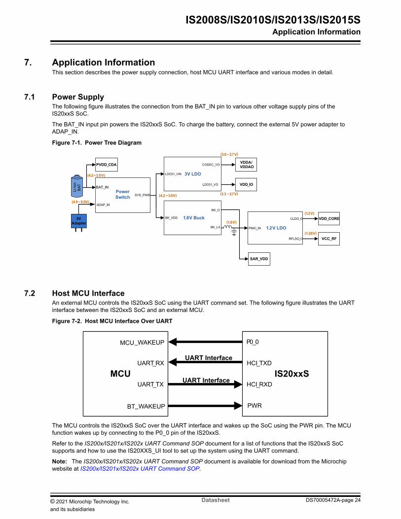
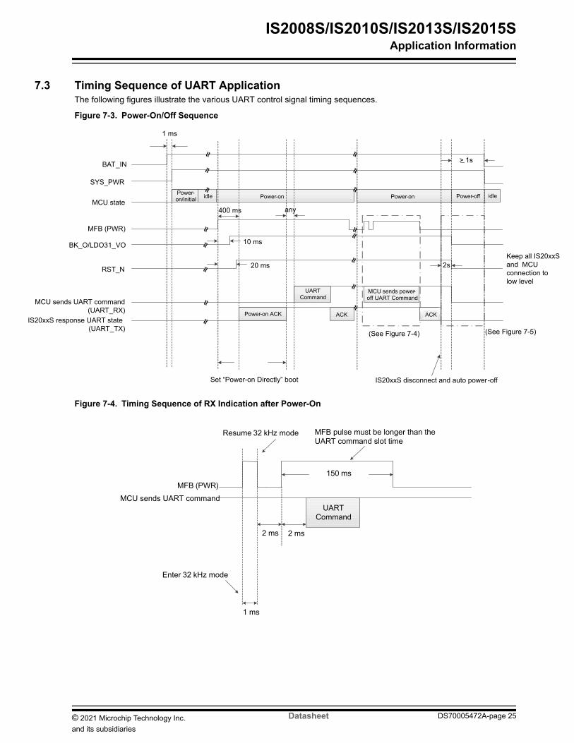
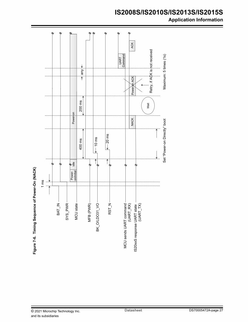
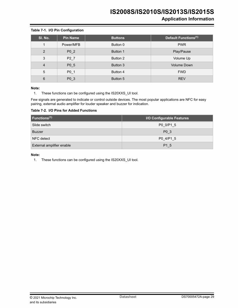
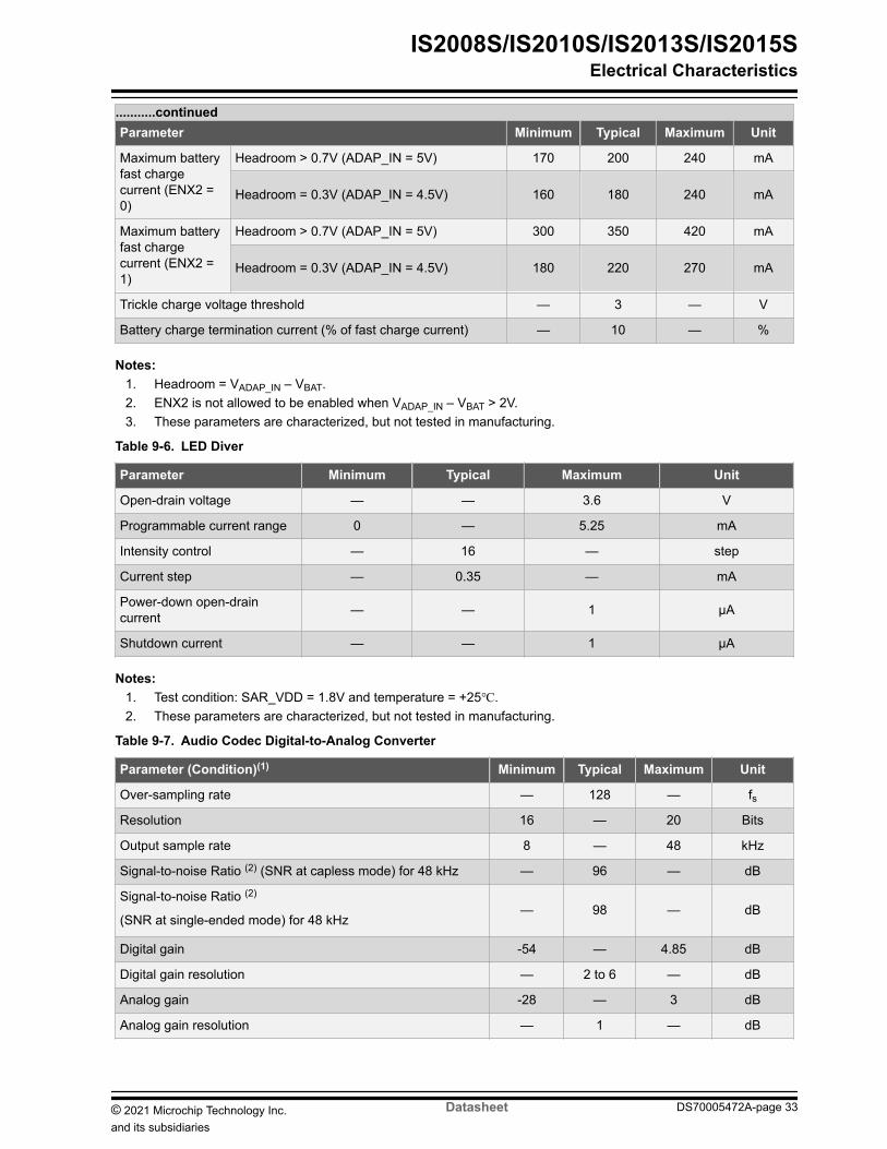
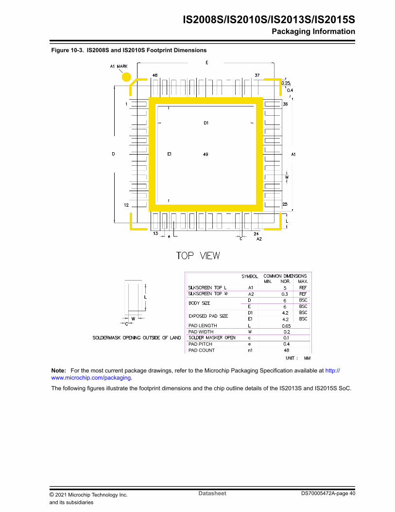
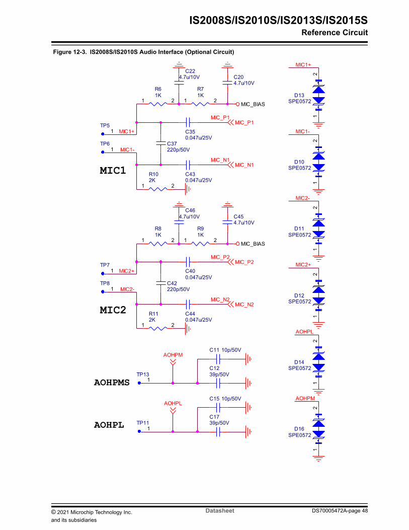
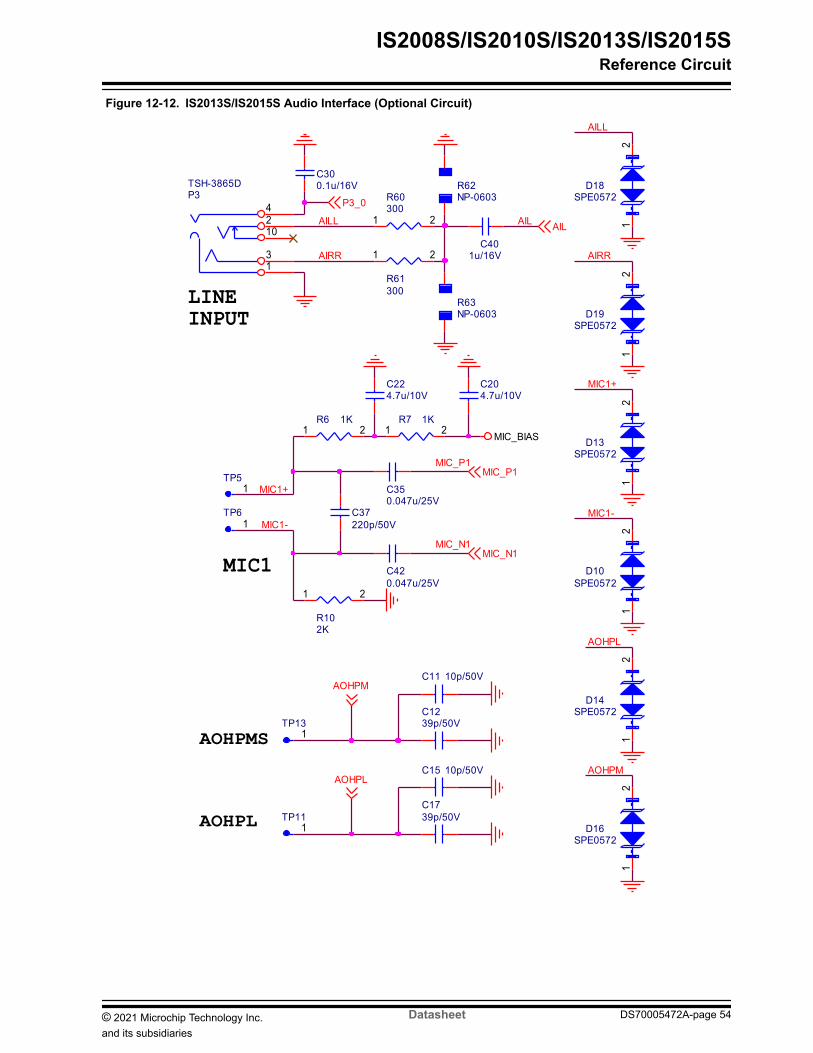