AlphaServer GS80/160/320 - iStorage Networks
564
Compaq Computer Corporation AlphaServer GS80/160/320 Service Manual Order Number: EK–GS320–SV. D01 This manual is for service providers who maintain Compaq AlphaServer GS80/160/320 systems.
-
Upload
khangminh22 -
Category
Documents
-
view
2 -
download
0
Transcript of AlphaServer GS80/160/320 - iStorage Networks

Compaq Computer Corporation
AlphaServer GS80/160/320 Service Manual
Order Number: EK–GS320–SV. D01
This manual is for service providers who maintain Compaq AlphaServer GS80/160/320 systems.

Revised February, 2001
© 2001 Compaq Computer Corporation.
Compaq, the Compaq logo, and AlphaServer registered in U.S. Patent and Trademark Office. OpenVMS and Tru64 are trademarks of Compaq Information Technologies Group, L.P. in the United States and other countries.
Portions of the software are © copyright Cimetrics Technology. Linux is a registered trademark of Linus Torvalds in several countries. UNIX is a trademark of The Open Group in the United States and other countries. KEA! is a registered trademark of Attachmate Corporation. All other product names mentioned herein may be trademarks of their respective companies.
Compaq shall not be liable for technical or editorial errors or omissions contained herein. The information in this document is provided “as is” without warranty of any kind and is subject to change without notice. The warranties for Compaq products are set forth in the express limited warranty statements accompanying such products. Nothing herein should be construed as constituting an additional warranty.
FCC Notice
This equipment generates, uses, and may emit radio frequency energy. The equipment has been type tested and found to comply with the limits for a Class A digital device pursuant to Part 15 of FCC rules, which are designed to provide reasonable protection against such radio frequency interference.
Operation of this equipment in a residential area may cause interference in which case the user at his own expense will be required to take whatever measures may be required to correct the interference.
Any modifications to this device—unless expressly approved by the manufacturer—can void the user’s authority to operate this equipment under part 15 of the FCC rules.
Modifications
The FCC requires the user to be notified that any changes or modifications made to this device that are not expressly approved by Compaq Computer Corporation may void the user's authority to operate the equipment.
Cables
Connections to this device must be made with shielded cables with metallic RFI/EMI connector hoods in order to maintain compliance with FCC Rules and Regulations.
Taiwanese Notice

Japanese Notice
Canadian Notice
This Class A digital apparatus meets all requirements of the Canadian Interference-Causing Equipment Regulations.
Avis Canadien
Cet appareil numérique de la classe A respecte toutes les exigences du Règlement sur le matériel brouilleur du Canada.
European Union Notice
Products with the CE Marking comply with both the EMC Directive (89/336/EEC) and the Low Voltage Directive (73/23/EEC) issued by the Commission of the European Community.
Compliance with these directives implies conformity to the following European Norms (in brackets are the equivalent international standards):
EN55022 (CISPR 22) - Electromagnetic Interference
EN50082-1 (IEC801-2, IEC801-3, IEC801-4) - Electromagnetic Immunity
EN60950 (IEC950) - Product Safety
Warning!
This is a Class A product. In a domestic environment this product may cause radio interference in which case the user may be required to take adequate measures.
Achtung!
Dieses ist ein Gerät der Funkstörgrenzwertklasse A. In Wohnbereichen können bei Betrieb dieses Gerätes Rundfunkstörungen auftreten, in welchen Fällen der Benutzer für entsprechende Gegenmaßnahmen verantwortlich ist.
Attention!
Ceci est un produit de Classe A. Dans un environnement domestique, ce produit risque de créer des interférences radioélectriques, il appartiendra alors à l'utilisateur de prendre les mesures spécifiques appropriées.


v
Contents
Preface ......................................................................................................................xix
Chapter 1 System Overview
1.1 GS160/320 System Cabinets ................................................................. 1-2 1.2 GS160/320 System Building Block........................................................ 1-4 1.3 GS160/320 System Box ......................................................................... 1-6 1.4 GS80 Rack Cabinet ............................................................................... 1-8 1.5 GS80 System Drawer.......................................................................... 1-10 1.6 Operator Control Panel....................................................................... 1-12 1.7 Hierarchical System Architecture....................................................... 1-14 1.7.1 The Primary Switch and the Quad Building Block ...................... 1-14 1.7.2 The Secondary Switch................................................................... 1-16 1.7.3 The Hierarchical Switch ............................................................... 1-18 1.7.4 Addressing .................................................................................... 1-20 1.8 System Management Architecture...................................................... 1-22 1.8.1 Console Serial Bus ........................................................................ 1-22 1.8.2 System Management Console....................................................... 1-24 1.8.3 System Control Manager (SCM)................................................... 1-26 1.8.4 Power System Manager (PSM) ..................................................... 1-28 1.8.5 PCI Backplane Manager (PBM).................................................... 1-30 1.8.6 Hierarchical Switch Power Manager (HPM) ................................ 1-32 1.9 System Partitioning ............................................................................ 1-34 1.9.1 Hard Partitions............................................................................. 1-34 1.9.2 Soft Partitions............................................................................... 1-36 1.9.3 Mixture of Hard and Soft Partitions............................................. 1-38 1.9.4 Servicing Partitions ...................................................................... 1-40 1.10 CPU Module ........................................................................................ 1-42 1.10.1 CPU Processor .............................................................................. 1-44 1.11 Memory Module .................................................................................. 1-46 1.12 Power System Manager Module.......................................................... 1-48 1.13 Clock Generation Modules .................................................................. 1-50

vi
1.13.1 H-switch Clock Module ................................................................. 1-50 1.13.2 Dual-Output Clock Module........................................................... 1-52 1.13.3 Clock Splitter Module ................................................................... 1-54 1.13.4 Master Phase Lock Loop............................................................... 1-56 1.14 Local I/O Riser Modules...................................................................... 1-58 1.14.1 System Box Local I/O Riser Module ............................................. 1-58 1.14.2 System Drawer Local I/O Riser Module ....................................... 1-60 1.15 Power Modules .................................................................................... 1-62 1.15.1 Main Power Module ...................................................................... 1-62 1.15.2 Auxiliary Power Module ............................................................... 1-64 1.15.3 Hierarchical Switch Power Module .............................................. 1-66 1.15.4 Short-Circuit Protection Module................................................... 1-68 1.16 Directory Module................................................................................. 1-70 1.17 Global Port Module ............................................................................. 1-72 1.18 Global Port Distribution Board........................................................... 1-74 1.19 Hierarchical Switch............................................................................. 1-76 1.20 H-switch Power Manager Module....................................................... 1-78 1.21 PCI Subsystem.................................................................................... 1-80 1.21.1 PCI I/O Subsystem Interconnect .................................................. 1-80 1.21.2 PCI Backplane .............................................................................. 1-82 1.21.3 PCI Box Configuration.................................................................. 1-84 1.21.4 Standard I/O Module .................................................................... 1-86 1.21.5 PCI Remote I/O Riser Module....................................................... 1-88 1.21.6 Console Serial Bus Node ID Module............................................. 1-90 1.21.7 Standard I/O Cable Interface........................................................ 1-92 1.22 GS160/320 System Power ................................................................... 1-94 1.22.1 AC Input Box (Three Phase)......................................................... 1-96 1.22.2 48V Power Supply......................................................................... 1-98 1.22.3 Power Subrack............................................................................ 1-100 1.22.4 Power Distribution Panel and Power Cabinet Bulkhead ........... 1-102 1.23 GS80 System Power .......................................................................... 1-104 1.23.1 AC Input Box (Single Phase) ...................................................... 1-106 1.23.2 48V Power Supplies .................................................................... 1-108 1.23.3 GS80 Power Subrack .................................................................. 1-110 1.24 PCI Power Supply ............................................................................. 1-112

vii
Chapter 2 Power-Up
2.1 Operator Control Panel......................................................................... 2-2 2.1.1 Control Panel Assembly.................................................................. 2-2 2.1.2 Fluorescent Display Messages........................................................ 2-4 2.2 Power-Up Test Flow – Init. and Phase 0 .............................................. 2-6 2.3 Power-Up Test Flow – Phase 1 ........................................................... 2-12 2.4 Power-Up Test Flow – Phases 2, 3, and 4........................................... 2-16 2.5 Power Applied – Vaux Present............................................................ 2-18 2.6 System Turned On .............................................................................. 2-22 2.7 SROM/XSROM Error Reports............................................................. 2-34
Chapter 3 Troubleshooting
3.1 Troubleshooting During Power-Up ....................................................... 3-2 3.2 System Management Console Problems ............................................... 3-5 3.3 Power-Up Display and Troubleshooting ............................................... 3-6 3.4 Using the SCM Monitor ...................................................................... 3-10 3.4.1 SCM Commands ........................................................................... 3-10 3.4.2 Controlling Power ......................................................................... 3-12 3.4.3 Displaying and Setting Up the System Environment .................. 3-14 3.4.4 Displaying Configuration Information ......................................... 3-16 3.4.5 Dealing with EEPROMs ............................................................... 3-22 3.5 Running Diagnostics Using the SCM Monitor.................................... 3-24 3.6 Using the SRM Console ...................................................................... 3-30 3.6.1 Displaying and Setting Up the System Environment .................. 3-30 3.6.2 Controlling Power with the SRM.................................................. 3-31 3.6.3 Displaying Configuration Information (SRM) .............................. 3-33 3.7 Running Diagnostics from the SRM Console...................................... 3-46 3.7.1 Setting Up the Test Environment ................................................ 3-46 3.7.2 Background Testing and Display.................................................. 3-48 3.7.3 Testing and Exercising the System .............................................. 3-52 3.7.4 Running SRM Loadable Diagnostics ............................................ 3-62 3.7.5 Crashing the System..................................................................... 3-70 3.8 Troubleshooting with LEDs ................................................................ 3-72 3.9 Dealing with a Hung System .............................................................. 3-76 3.9.1 Troubleshooting a Diagnostic Hang.............................................. 3-78 3.9.2 Troubleshooting a Diagnostic Fault.............................................. 3-82 3.10 Dealing with Corrupt Firmware ......................................................... 3-84 3.11 Error Detection ................................................................................... 3-86 3.12 Compaq Analyze.................................................................................. 3-88

viii
3.12.1 Compaq Analyze Using a Web Browser........................................ 3-88 3.12.2 Problem Found Report.................................................................. 3-90 3.12.3 Description of the Error (660)....................................................... 3-94
Chapter 4 GS160/320 Component Removal and Replacement 4.1 System Safety........................................................................................ 4-2 4.2 FRU List................................................................................................ 4-4 4.3 FRU Power States Defined ................................................................. 4-10 4.3.1 Hot-Swapping a FRU.................................................................... 4-12 4.3.2 Warm-Swapping a FRU................................................................ 4-13 4.3.3 Cold-Swapping a FRU .................................................................. 4-14 4.3.4 Getting a FRU into the AC Off State.................................................. 4-15 4.4 System Box Module Location and Identification ................................ 4-16 4.4.1 Power Color Codes ........................................................................ 4-18 4.4.2 Module Color Codes ...................................................................... 4-20 4.5 System Box Module Access ................................................................. 4-22 4.5.1 Memory, Directory, Main Power, or Auxiliary Power Module
Removal and Replacement............................................................ 4-24 4.5.2 CPU Removal and Replacement................................................... 4-26 4.5.3 Power System Manager Removal and Replacement .................... 4-28 4.5.4 Clock Splitter Module Removal and Replacement ....................... 4-30 4.5.5 Local I/O Riser Removal and Replacement................................... 4-32 4.5.6 Global Port Module Removal and Replacement ........................... 4-34 4.5.7 Memory or Directory DIMM Removal and Replacement.............. 4-36 4.5.8 System Box Removal and Replacement........................................ 4-38 4.6 GS160 Distribution Board Assembly Modules.................................... 4-40 4.6.1 Distribution Board Removal and Replacement ............................ 4-40 4.6.2 Dual-Output Clock Module Removal and Replacement ............... 4-42 4.6.3 Console Serial Bus Module Removal and Replacement ............... 4-44 4.7 Hierarchical Switch Assembly Modules.............................................. 4-46 4.7.1 H-switch Removal and Replacement ............................................ 4-46 4.7.2 H-switch Power Supply Removal and Replacement..................... 4-48 4.7.3 H-switch Clock Module Removal and Replacement ..................... 4-50 4.7.4 H-switch Power Manager Removal and Replacement.................. 4-52 4.7.5 Console Serial Bus Module Removal and Replacement ............... 4-54 4.8 System Cabinet Blower Removal and Replacement ........................... 4-56

ix
Chapter 5 Power Cabinet Component Removal and Replacement 5.1 PCI Modules.......................................................................................... 5-2 5.1.1 Standard I/O Module Removal and Replacement........................... 5-4 5.1.2 Console Serial Bus Node ID Module Removal and Replacement ... 5-6 5.1.3 Remote I/O Riser Removal and Replacement................................. 5-8 5.1.4 PCI Option Removal and Replacement ........................................ 5-10 5.1.5 PCI Backplane Removal and Replacement................................... 5-12 5.1.6 PCI Fan Removal and Replacement ............................................. 5-14 5.1.7 DVD/CD-ROM Player Removal and Replacement ....................... 5-16 5.1.8 SCSI (FIS) Disk Removal and Replacement................................. 5-18 5.1.9 Standard I/O Cable Interface Removal and Replacement............ 5-20 5.1.10 PCI Power Supply Removal and Replacement ............................. 5-22 5.1.11 Standard I/O Battery Removal and Replacement ........................ 5-24 5.2 Operator Control Panel Removal and Replacement ........................... 5-26 5.3 Terminal Server Removal and Replacement ...................................... 5-28 5.4 48V Power Supply Removal and Replacement ................................... 5-30 5.5 Power Subrack Removal and Replacement......................................... 5-32 5.6 AC Input Box Removal and Replacement........................................... 5-34
Chapter 6 GS80 Component Removal and Replacement 6.1 Drawer Modules.................................................................................... 6-2 6.1.1 Accessing a Single or Top Drawer in a GS80 System..................... 6-4 6.1.2 Accessing a Bottom Drawer in a GS80 System .............................. 6-6 6.2 Memory, Directory, Main Power, or Auxiliary Power Module Removal
and Replacement................................................................................... 6-8 6.3 CPU Removal and Replacement ......................................................... 6-10 6.4 Power System Manager Removal and Replacement........................... 6-12 6.5 Clock Splitter Module Removal and Replacement.............................. 6-14 6.6 I/O Riser Removal and Replacement .................................................. 6-16 6.7 I/O Transition Module Removal and Replacement............................. 6-18 6.8 Drawer Backplane Removal and Replacement................................... 6-20 6.9 Dual-Output Clock Removal and Replacement .................................. 6-22 6.10 Distribution Board Removal and Replacement .................................. 6-24 6.11 Console Serial Bus Removal and Replacement................................... 6-26 6.12 Drawer Blower Removal and Replacement ........................................ 6-28 6.13 Operator Control Panel Removal and Replacement ........................... 6-30 6.14 Power Supply Removal and Replacement........................................... 6-32 6.15 Power Subrack Removal and Replacement......................................... 6-34

x
6.16 AC Input Box Removal and Replacement........................................... 6-36
Appendix A Power Distribution Rules
A.1 GS160/320 Power Cabinet Configuration and Cabling.........................A-2 A.2 Expander Cabinet Configuration and Cabling .....................................A-8 A.3 GS80 Power Cabling ...........................................................................A-16
Appendix B Cache Coherency
B.1 Terminology ..........................................................................................B-2 B.2 Cache States..........................................................................................B-3 B.3 Cache Commands..................................................................................B-4 B.3.1 Memory Space Commands..............................................................B-4 B.3.2 System Probe Commands ...............................................................B-6 B.4 Cache State Transition Diagram ..........................................................B-7 B.5 Commands and Cache State Interaction ..............................................B-7 B.6 Virtual Channels...................................................................................B-9 B.7 Virtual Channels and Coherency Flow ...............................................B-10 B.7.1 Memory Space Transactions.........................................................B-10 B.7.2 I/O Space Reads ............................................................................B-12 B.7.3 I/O Space Writes ...........................................................................B-14 B.8 Virtual Channel Ordering Rules.........................................................B-15 B.9 Coherency Data Storage......................................................................B-18 B.9.1 CPU Primary Tag Store (PTag) ....................................................B-18 B.9.2 IOP Tag Store ...............................................................................B-19 B.9.3 QBB Duplicate Tag Store (DTag) .................................................B-20 B.9.4 QBB Directory...............................................................................B-21 B.9.5 TTT Storage ..................................................................................B-21 B.9.6 Access to Coherency State ............................................................B-22 B.10 Coherency Storage and Coherency Flow.............................................B-24 B.10.1 Local Read Transactions...............................................................B-24 B.10.2 Local Read Modify Transactions...................................................B-26 B.10.3 Local Change-to-Dirty, Inval-to-Dirty and Full Block
Transactions .................................................................................B-28 B.10.4 Global (Remote) Read Transactions..............................................B-30 B.10.5 Global (Remote) Read Modify Transactions..................................B-32 B.10.6 Global (Remote) Change-to-Dirty Transactions ...........................B-34 B.10.7 Global (Remote) Inval-to-Dirty and Full Block Write
Transactions .................................................................................B-36

xi
Appendix C Power-Up Diagnostic Error Table
Appendix D Firmware Updates
D.1 System Firmware That May Require Updates .................................... D-2 D.2 Preparations for Firmware Updates.................................................... D-4 D.2.1 Partitions ....................................................................................... D-4 D.2.2 Hardware Connections .................................................................. D-6 D.2.3 Laptop Operating System Preparation.......................................... D-8 D.2.4 Terminal Emulator Settings........................................................ D-10 D.3 Firmware Updates ............................................................................. D-13 D.3.1 Using LFU ................................................................................... D-13 D.3.2 Using the SCM Update Command............................................... D-19 D.4 Dealing with a COM1 Port Jam......................................................... D-23 Glossary
Index

xii
Examples 1–1 Shutting Down a Partition...................................................................... 1-40 2–1 System Control Manager Power-Up Display.......................................... 2-18 2–2 SCM Power-Up Display (OCP On).......................................................... 2-22 2–3 Examples of the SCM Error Display....................................................... 2-34 3–1 Console Power-Up Error Messages........................................................... 3-6 3–2 Show nvram ............................................................................................ 3-14 3–3 Set Environment Variables..................................................................... 3-15 3–4 Show csb.................................................................................................. 3-16 3–5 Show system ........................................................................................... 3-17 3–6 Show status............................................................................................. 3-18 3–7 Show fru.................................................................................................. 3-20 3–8 Clear error............................................................................................... 3-22 3–9 Build fru.................................................................................................. 3-23 3–10 Build eeprom......................................................................................... 3-23 3–12 Setting Up the Diagnostic Environment and Testing........................... 3-24 3–13 Various Test Commands....................................................................... 3-28 3–14 Set Environment Variables................................................................... 3-30 3–15 Show Environment Variables ............................................................... 3-30 3–16 Clear Environment Variables ............................................................... 3-30 3–17 Power Off (partiton/qbb) ....................................................................... 3-31 3–18 Power off cpu <n> Command.................................................................. 3-32 3–19 Power on cpu <n> Command .................................................................. 3-32 3–20 Show configuration ............................................................................... 3-33 3–21 Show fru................................................................................................ 3-38 3–22 Set sys_serial_number .......................................................................... 3-41 3–23 Csr <csr_espression> ............................................................................ 3-42 3–24 Csr <csr_expression> <data>................................................................ 3-43 3–25 Wf show cpu .......................................................................................... 3-44 3–26 Info ........................................................................................................ 3-44 3–27 Setting Up the Diagnostic Environment............................................... 3-46 3–28 Running sys_exer in the Background ................................................... 3-48 3–29 Show_status .......................................................................................... 3-49 3–30 Kill_diags .............................................................................................. 3-49 3–31 Kill <process id>.................................................................................... 3-50 3–32 Ps........................................................................................................... 3-51 3–33 Test ....................................................................................................... 3-52 3–34 Sys_exer ................................................................................................ 3-53 3–35 Exer....................................................................................................... 3-54 3–36 Memexer................................................................................................ 3-58

xiii
3–37 Fptest .................................................................................................... 3-59 3–38 Fakedisk................................................................................................ 3-60 3–39 Nettest................................................................................................... 3-61 3–40 Booting the Firmware CD-ROM ........................................................... 3-62 3–41 Acer_bridge_diag................................................................................... 3-64 3–42 Acer_io_diag .......................................................................................... 3-65 3–43 Acer_8042_diag ..................................................................................... 3-66 3–44 Isp1020_diag ......................................................................................... 3-67 3–45 Bq4285_diag.......................................................................................... 3-68 3–46 Isa_misc_diag........................................................................................ 3-69 3–47 Crash..................................................................................................... 3-70 3–48 Diagnostic Hang.................................................................................... 3-78 3–49 A Sample Diagnostic Fault ................................................................... 3-82 3–50 Problem Found (660)............................................................................. 3-90 3–51 Compaq Analyze Error Report.............................................................. 3-94 3–52 Problem Found (680)........................................................................... 3-100 3–53 620 Error Report ................................................................................. 3-105 3–54 630 Error Report ................................................................................. 3-109 4–1 Warm-Swap State (assumes the system is partitioned) ......................... 4-13 D–1 Removing Partitions................................................................................ D-4 D–2 COM1 Port Settings for Windows NT 4.0 ............................................... D-8 D–3 COM1 Port Settings for Windows 2000 .................................................. D-9 D–4 COM1 Port Settings for Windows 95 ...................................................... D-9 D–5 KEAterm V5.1 Session for PC or Laptop COM1 Port........................... D-10 D–6 PowerTerm 525 Settings....................................................................... D-12 D–7 Running LFU ........................................................................................ D-13 D–8 Using the Update Command................................................................. D-19 D–9 Clearing a COM1 Port Jam................................................................... D-23
Figures 1–1 GS320 System Cabinets............................................................................ 1-2 1–2 Quad Building Block Backplane............................................................... 1-4 1–3 System Box (rear view) ............................................................................. 1-6 1–4 GS80 Rack Cabinet ................................................................................... 1-8 1–5 GS80 System Drawer Backplane............................................................ 1-10 1–6 Control Panel Assembly.......................................................................... 1-12 1–7 Quad Building Block Block Diagram...................................................... 1-14 1–8 An Eight-Processor System Block Diagram............................................ 1-16 1–9 Architecture Block Diagram ................................................................... 1-18 1–10 Console Serial Bus Block Diagram ....................................................... 1-22

xiv
1–11 SMC Connections.................................................................................. 1-24 1–12 System Control Manager Block Diagram ............................................. 1-26 1–13 Power System Manager Software Block Diagram................................ 1-28 1–14 PCI Backplane Manager Block Diagram.............................................. 1-30 1–15 HPM Block Diagram............................................................................. 1-32 1–16 CPU Module.......................................................................................... 1-42 1–17 Alpha Chip Block Diagram ................................................................... 1-44 1–18 Memory Module .................................................................................... 1-46 1–19 Power System Manager Module Block Diagram .................................. 1-48 1–20 PSM Module LEDs and Jumpers.......................................................... 1-49 1–21 H-switch Clock Module ......................................................................... 1-50 1–22 Dual-Output Clock Module ................................................................... 1-52 1–23 Clock Splitter Module Block Diagram .................................................. 1-54 1–24 Master Phase Lock Loop Block Diagram.............................................. 1-56 1–25 System Box Local I/O Riser Module Block Diagram............................. 1-58 1–26 System Drawer Local I/O Riser Module Block Diagram....................... 1-60 1–27 Main Power Module Block Diagram ..................................................... 1-62 1–28 Auxiliary Power Module Block Diagram .............................................. 1-64 1–29 H-switch Power Module Block Diagram............................................... 1-66 1–30 Short-Circuit Protection Block Diagram and Interconnect .................. 1-68 1–31 Directory Module Block Diagram ......................................................... 1-70 1–32 Global Port Modules.............................................................................. 1-72 1–33 Distribution Board Block Diagram and Physical Layout ..................... 1-74 1–34 Hierarchical Switch .............................................................................. 1-76 1–35 H-switch Power Module ........................................................................ 1-78 1–36 I/O Subsystem Module and Cable Interconnect.................................... 1-80 1–37 PCI Backplane Layout .......................................................................... 1-82 1–38 PCI Slot Locations................................................................................. 1-84 1–39 Standard I/O Module ............................................................................ 1-86 1–40 PCI I/O Riser Block Diagram................................................................ 1-88 1–41 Console Serial Bus Node ID Module..................................................... 1-90 1–42 Standard I/O Cable Interface Module................................................... 1-92 1–43 Power Block Diagram of GS320 System ............................................... 1-94 1–44 AC Input Box (Three Phase) ................................................................. 1-96 1–45 48V Power Supply (GS160/320) ............................................................ 1-98 1–46 Power Subrack and Power Supply Installation Order........................ 1-100 1–47 Power Cabinet Cabling and Distribution Panel ................................. 1-102 1–48 GS80 Power Distribution Block Diagram........................................... 1-104 1–49 AC Input Box (Single Phase) .............................................................. 1-106 1–50 DC Power Supply (GS80) .................................................................... 1-108 1–51 GS80 Power Subrack .......................................................................... 1-110 1–52 PCI Power Supply ............................................................................... 1-112
xv
2–1 Control Panel ............................................................................................ 2-2 2–2 Power-Up Flowchart – Init. and Phase 0.................................................. 2-6 2–3 Power-Up Flowchart - Phase 1 ............................................................... 2-12 2–4 Power-Up Flowchart - Phase 2, 3, and 4................................................. 2-16 3–1 System LEDs........................................................................................... 3-72 3–2 Core System Error Detectors.................................................................. 3-86 3–3 Compaq Analyze Using a Web Browser.................................................. 3-88 4–1 System Box Module Locations (rear) ...................................................... 4-16 4–2 System Box Module Location (front)....................................................... 4-17 4–3 System Box/Power Color Codes .............................................................. 4-18 4–4 Slot Color Codes...................................................................................... 4-20 4–5 Accessing System Boxes.......................................................................... 4-22 4–6 Generic System Box Module Removal .................................................... 4-24 4–7 Removing a CPU..................................................................................... 4-26 4–8 Power Manager Removal ........................................................................ 4-28 4–9 Clock Splitter Removal ........................................................................... 4-30 4–10 I/O Riser Removal ................................................................................. 4-32 4–11 Global Port Removal ............................................................................. 4-34 4–12 DIMM Removal..................................................................................... 4-36 4–13 System Box Removal............................................................................. 4-38 4–14 Distribution Board Removal ................................................................. 4-40 4–15 Dual-Output Clock Module Removal .................................................... 4-42 4–16 Console Serial Bus Module Removal .................................................... 4-44 4–17 H-switch Removal ................................................................................. 4-46 4–18 H-switch Power Supply Removal.......................................................... 4-48 4–19 H-switch Clock Module Removal .......................................................... 4-50 4–20 H-switch Power Manager Module Removal.......................................... 4-52 4–21 Console Serial Bus Module Removal .................................................... 4-54 4–22 System Cabinet Blower Removal.......................................................... 4-56 5–1 Accessing the PCI ..................................................................................... 5-2 5–2 Standard I/O Module Removal.................................................................. 5-4 5–3 CSB Node ID Module Removal ................................................................. 5-6 5–4 Remote I/O Riser Removal........................................................................ 5-8 5–5 PCI Option Removal ............................................................................... 5-10 5–6 PCI Backplane Removal ......................................................................... 5-12 5–7 PCI Fan Removal.................................................................................... 5-14 5–8 DVD/CD-ROM Removal.......................................................................... 5-16 5–10 SCSI Disk Removal............................................................................... 5-18 5–11 Standard I/O Interface Module Removal .............................................. 5-20 5–12 PCI Power Supply Removal .................................................................. 5-22 5–13 Standard I/O Battery Removal ............................................................. 5-24 5–14 OCP Removal ........................................................................................ 5-26

xvi
5–15 Terminal Server Removal ..................................................................... 5-28 5–16 Power Supply Removal ......................................................................... 5-30 5–17 Power Subrack Removal ....................................................................... 5-32 5–18 AC Input Box Removal.......................................................................... 5-34 6–1 Drawer Modules Location......................................................................... 6-2 6–2 Accessing a Top or Single Drawer System................................................ 6-4 6–3 Accessing a Dual Drawer System ............................................................. 6-6 6–4 Generic Drawer Module Replacement ...................................................... 6-8 6–5 Removing a CPU..................................................................................... 6-10 6–6 Power Manager Removal ........................................................................ 6-12 6–7 Clock Splitter Removal ........................................................................... 6-14 6–8 Local I/O Riser Removal ......................................................................... 6-16 6–9 I/O Riser Transition Module Removal .................................................... 6-18 6–10 Drawer Backplane Removal.................................................................. 6-20 6–11 Dual-Output Clock Module Removal .................................................... 6-22 6–12 Distribution Board Removal ................................................................. 6-24 6–13 Console Serial Bus Removal ................................................................. 6-26 6–14 Drawer Blower Removal ....................................................................... 6-28 6–15 OCP Removal ........................................................................................ 6-30 6–16 Power Supply Removal ......................................................................... 6-32 6–17 Power Subrack Removal ....................................................................... 6-34 6–18 AC Input Box Removal.......................................................................... 6-36 A–1 Power Cabinet Configurations .................................................................A-2 A–2 GS160/320 Power Cabinet Components...................................................A-4 A–3 GS160/320 Power Cabinet Cabling ..........................................................A-6 A–4 Expander Cabinet Configuration .............................................................A-8 A–5 Expander Cabinet Cable Connector Locations.......................................A-10 A–6 Expander Cabinet H9A20-AA Variant Cabling .....................................A-12 A–7 Expander Cabinet H9A20-AB, -AC Variants Cabling............................A-14 A–8 GS/80 Power Cabling -CA Cabinet.........................................................A-16 A–9 GS/80 Power Cabling -CB, -CC Cabinet.................................................A-18 B–1 Cache State Tranition Diagram...............................................................B-7 B–2 Memory Space Transation Flow Diagram..............................................B-10 B–3 I/O Space Read Transaction Flow Diagram...........................................B-12 B–4 I/O Space Write Transaction Flow Diagram ..........................................B-14 B–5 Cache Coherency Storage Access ...........................................................B-22 B–6 Local Read Coherency Store Flow..........................................................B-24 B–7 Local Read/Modify Transaction..............................................................B-26 B–8 Local Change-to-Change Coherency Store Flow ....................................B-28 B–9 Global (Remote) Read Transaction Storage Flow ..................................B-30 B–10 Read Mod Coherency Store Flow..........................................................B-32 B–11 Change-to-Dirty Coherency Store Flow................................................B-34

xvii
B–12 Inval-to-Dirty, Full Block Write Coherency Store Flows .....................B-36 D–1 Connecting a Laptop to the Local Terminal Port.................................... D-6
Tables 1 Compaq AlphaServer GS80/160/320 Documentation ................................ xx 1–1 Address Ranges Seen at the CPU........................................................... 1-20 1–2 Address Ranges Seen in the System....................................................... 1-20 1–3 I2C Bus Device Identification on PSM/QBB............................................ 1-29 1–4 Rules Affecting Hard Partitions ............................................................. 1-34 1–5 Possible 32-P Hard Partitioned System.................................................. 1-35 1–6 Rules Affecting Soft Partitions ............................................................... 1-36 1–7 Possible Soft Partition ............................................................................ 1-36 1–8 Possible 32-P Partitioned System........................................................... 1-38 1–9 CPU Variants.......................................................................................... 1-43 1–10 Memory Configurations ........................................................................ 1-47 1–11 Directory Array DIMM Types............................................................... 1-71 1–12 PCI Slots and Logical Hoses ................................................................. 1-85 1–13 Circuit Breaker Line Protection (Three Phase) .................................... 1-97 1–14 Circuit Breaker Line Protection (Single Phase) ................................. 1-107 2–1 Display Messages...................................................................................... 2-4 2–2 SROM Tests .............................................................................................. 2-9 2–3 XSROM Test s Run in Phase 0 ................................................................ 2-10 2–4 XSROM Tests Run in Phase 1 ................................................................ 2-14 2–5 XSROM Tests Run in Phases 2, 3, and 4................................................ 2-17 3–1 Power Problems ........................................................................................ 3-2 3–2 Console Problems...................................................................................... 3-5 3–3 Fluorescent Display Messages.................................................................. 3-8 3–4 SCM Commands ..................................................................................... 3-10 3–5 Power On/Off........................................................................................... 3-12 3–6 Modem Initialization Strings.................................................................. 3-18 3–7 Show Status Entries ............................................................................... 3-19 3–8 Show fru Command Field Descriptions .................................................. 3-21 3–9 Additional SRM Show FRU Codes.......................................................... 3-41 3–10 Diagnostic Environment Variables....................................................... 3-46 3–11 Exer Options ......................................................................................... 3-56 3–12 Hung System Suggestions .................................................................... 3-76 3–13 Fail-Safe Loader Jumpers..................................................................... 3-84 4–1 Hazards and Safety Features ................................................................... 4-2 4–2 Field-Replaceable Unit Part Numbers...................................................... 4-4

xviii
4–3 FRU Cables............................................................................................... 4-7 4–4 Power States ........................................................................................... 4-10 4–5 FRU Power Swap States........................................................................ 4-11 4–6 Power Color Coding................................................................................. 4-19 4–7 Module Color Codes ................................................................................ 4-20 6–1 Module Color Codes (GS80) ...................................................................... 6-3 B–1 Basic Cache Coherency Terminology .......................................................B-2 B–2 AlphaServer GS Series Cache States.......................................................B-3 B–3 Memory Space Commands .......................................................................B-5 B–4 System Probe Commands.........................................................................B-6 B–5 Memory Command and Cache State Interaction .....................................B-8 B–6 CPU PTag Cache Coherency Storage.....................................................B-18 B–7 IOP Tag Cache Coherency Storage ........................................................B-19 B–8 DTag Cache Coherency Storage .............................................................B-20 B–9 Directory Cache Coherency Storage.......................................................B-21 B–10 QSA Interface to the Cache Coherency Storage...................................B-23 C–1 Test Number / Error Number...................................................................C-4 D–1 Firmware Update Files and What They Update..................................... D-2

xix
Preface
Intended Audience This manual is for service providers who maintain Compaq AlphaServer GS80/160/320 systems.
Document Structure This manual uses a structured documentation design. Topics are organized into small sections, usually consisting of two facing pages. Most topics begin with an abstract that provides an overview of the section, followed by an illustration or example. The facing page contains descriptions, procedures, and definitions.
This manual has six chapters, four appendixes, and a glossary.
• Chapter 1, System Overview, introduces the three systems covered by this manual. It describes both the system and management architecture, and each component in the system.
• Chapter 2, Power-Up, describes system power-up.
• Chapter 3, Troubleshooting, describes troubleshooting techniques.
• Chapter 4, GS160/320 Component Removal and Replacement, describes removal and replacement procedures of field-replaceable units.
• Chapter 5, Power Cabinet Component Removal and Replacement, describes removal and replacement procedures of field-replaceable units that reside in the power cabinet.
• Chapter 6, GS80 Component Removal and Replacement, describes removal and replacement procedures of field-replaceable units with the exception of PCI box units in the GS80 cabinet.
• Appendix A, Power Distribution Rules, describes how power is distributed in various system configurations.
• Appendix B, Cache Coherency, describes how the system keeps cache coherent.

xx
• Appendix C, Power-Up Diagnostic Error Table, lists test numbers, errors, and the likely FRU if an SROM or XSROM diagnostic fails.
• Appendix D, Firmware Updates, describes methods for updating firmware and unjamming the communications link.
Documentation Titles
Table 1 Compaq AlphaServer GS80/160/320 Documentation
Order Number Title
QA–6GAAA–G8 AlphaServer GS80/160/320 Documentation Kit
EK–GS320–UG AlphaServer GS80/160/320 User’s Guide
EK–GS320–RM AlphaServer GS80/160/320 Firmware Reference Manual
EK–GSPAR–RM AlphaServer GS80/160/320 Getting Started with Partitions
EK–GS320–IN AlphaServer GS160/320 Installation Guide
EK–GSR80–IN AlphaServer GS80 Installation Guide
AG–RKSW*–BE AlphaServer GS80/160/320 User Information CD
QA–6GAAB–G8 AlphaServer GS80/160/320 Service Documentation Kit
EK–GS320–SV AlphaServer GS80/160/320 Service Manual
EK–GS320–RM AlphaServer GS80/160/320 Firmware Reference Manual
AG–RKSZ*–BE AlphaServer GS80/160/320 Service Information CD
EK–GSCON–IN AlphaServer GS80/160/320 System Management Console Installation and User’s Guide
EK–GS320–UP AlphaServer GS160/320 Upgrade Manual
EK–GSR80–UP AlphaServer GS80 Upgrade Manual
EK–GS320–SP AlphaServer GS80/160/320 Site Preparation
EK–GS320–PR AlphaServer GS80/160/320 System Programmer’s Manual
WF Diagnostic Firmware Functional Specification

xxi
Information on the Internet Visit the following Web sites for service tools and more information about the AlphaServer GS80/160/320 systems:
AlphaServer site www.compaq.com/alphaserver/site_index.html
General Support http://www.compaq.com/services Console Firmware http://ftp.digital.com/pub/Digital/Alpha/firmware/readme.html Supported Options List http://www.compaq.com/alphaserver/products/options.html Operating System Patches http://www.support.compaq.com/patches/index.html WEBES/Compaq Analyze http://www.support.compaq.com/svctools/


System Overview 1-1
Chapter 1 System Overview
The AlphaServer GS80/160/320 systems have two different design centers: one with a small footprint and up to 8 CPUs, the other with a larger footprint that expands to 32 CPUs. This chapter describes both types of systems, their components, and their system enclosures. Most of the components between the two are interchangeable.
Topics covered in this chapter are:
• GS160/320 System Cabinets
• GS160/320 System Building Block
• GS160/320 System Box
• GS80 Rack Cabinet
• GS80 System Drawer
• Operator Control Panel
• Hierarchical System Architecture
• System Management Architecture
• System Partitioning
• CPU Module
• Memory Module
• Power System Manager Module
• Clock Generation Modules
• Local I/O Riser Modules
• Power Modules
• Directory Module
• Global Port Module
• Global Port Distribution Board
• Hierarchical Switch
• H-switch Power Manager Module
• PCI Subsystem
• GS160/320 System Power
• GS80 System Power
• PCI Power Supply

1-2 AlphaServer GS80/160/320 Service Manual
1.1 GS160/320 System Cabinets
Two cabinets are required for a GS160 system; three are required for a GS320 system.
Figure 1–1 GS320 System Cabinets
PK1522
System Cabinet 2
System Cabinet 1
Power Cabinet

System Overview 1-3
Figure 1–1 shows the front view of the GS320 system cabinets. Systems from 1 to 32 CPUs, from 4 Gbytes to 256 Gbytes of memory, and from 13 to 27 PCI slots for I/O options can be built in these cabinets. Expander cabinets containing additional storage and/or PCI I/O capacity are optional and can bring the total number of PCI slots to 224. For storage configuration rules, see Appendix A and the AlphaServer GS80/160/320 User’s Guide.
The power cabinet contains:
• Two AC input boxes
• up to four power subracks, one for each system box, with two to three AC to 48 VDC power supplies in each subrack (two power supplies are required)
• the operator control panel
• one required master PCI box plus optionally another PCI box and storage device or two storage devices
• one terminal server
System cabinet 1 contains:
• up to two system boxes
• a console serial bus module
• a dual-output clock module in systems with one or two QBBs
• a distribution board in systems with only two QBBs
• an H-switch clock module for systems with more than two QBBs
• an hierarchical switch in systems with more than two QBBs
• a blower
System cabinet 2 contains:
• up to two system boxes
• a blower
Expander cabinet contains:
• up to four PCI boxes
• from two to ten disk storage shelves

1-4 AlphaServer GS80/160/320 Service Manual
1.2 GS160/320 System Building Block
The basic system building block for these systems is the quad building block or QBB. A QBB consists of a backplane, up to four CPUs, up to four memory modules, a directory module, up to two I/O riser modules, a global port, two power modules, a power system manager module, and a clock splitter module. The maximum number of QBBs in a GS160 is four and in the GS320 is eight. Each QBB has an ID number from 0 to 7.
Figure 1– 2 Quad Building Block Backplane
PK1505-99
2 3 4 5 4 5 6
110 5 4 5 4 11 12 13
1 7
19
8

System Overview 1-5
Figure 1–2 shows a QBB backplane and its connectors. Module locations are identified by callouts.
� 48V/Vaux power connector (present only on even numbered QBBs in the rear of the system)
� Global port module connector (note there are two backplanes: the one for the front QBB has the global port connector on its back facing the rear of the cabinet and the one for the back QBB has the global port connector on its front also facing the rear of the cabinet.)
� Directory module connector (necessary if a system has more than one QBB)
� CPU module connectors (up to four)
� Memory module connectors (up to four)
� Local I/O riser module connectors (up to two with two ports each)
� 48V/Vaux power input connectors
Cutout in backplane
¡ Short-circuit protection module (will be designed into the backplane later)
¢ Clock splitter module connector
11 Power system manager module connector
12 Main power module connector
13 Auxiliary power module connector
QBBs are placed such that their global ports are as close to each other as is possible. Global ports are the second-level switches through which CPUs in one QBB communicate with CPUs and memories in other QBBs. In fact, global ports have to be physically close to each other to enable fast second-level switching. This requires that QBB backplanes be flipped when placed in a system box. Therefore, the orientation of the backplane is important and determines the location of modules. See Section 4.4 for QBB and module orientations.
Figure 1–2 shows the orientation of the backplanes in QBBs 5 and 7.

1-6 AlphaServer GS80/160/320 Service Manual
1.3 GS160/320 System Box
A system box contains two QBBs back to back.
Figure 1– 3 System Box (rear view)
PK1506
PowerConnectors
I/O Risers
Memory 0
CPU 1
Memory 2
CPU 3
Directory
Global Port - Odd(Connected to front QBB)
AuxiliaryPower
MainPower
PSM CPU 0Memory 1
CPU 2
Memory 3
Clock Splitter
Global Port - Even(Connected to rear QBB)

System Overview 1-7
Figure 1–3 shows the rear view of a system box. Each CPU and each memory module is assigned a physical ID associated with the slot in the QBB backplane in which it resides. A GS320 system can have up to four system boxes each with two QBBs. When all QBBs contain the maximum of four CPUs, a system containing 32 processors is created.
Global ports must be physically close to each other and to the hierarchical switch and therefore are connected either to the front of a QBB backplane or to the back. The global port module attached to the front backplane is plugged into its back. And the global port module attached to the back backplane is plugged into its front. The global port module attached to the front backplane extends to the rear of the system box though the cutout in the rear backplane.
The two backplanes in the system box are oriented so that the global port connector on the front backplane is opposite the cutout in the rear backplane. See Figure 1–2.

1-8 AlphaServer GS80/160/320 Service Manual
1.4 GS80 Rack Cabinet
The AlphaServer GS80 system is in a single rack cabinet.
Figure 1– 4 GS80 Rack Cabinet
PK2237

System Overview 1-9
Figure 1–4 shows the front view of the GS80 rack system. A GS80 can have from one to eight CPUs, from 1 Gbyte to 64 Gbytes of memory, and from 13 to 41 PCI slots. Configurations depend upon options chosen for given base systems.
A cabinet with a single drawer contains:
• one system drawer
• one AC input box
• one power subrack with two or three AC to 48 VDC power supplies
• the operator control panel
• one required master PCI box with up to a combination of three PCI boxes and/or storage shelves
A cabinet with two system drawers contains:
• two system drawers
• a distribution module
• two AC input boxes
• two power subracks with two or three AC to 48 VDC power supplies in each
• the operator control panel
• one required master PCI box with an optional PCI box or storage shelves
For storage configuration rules, see Appendix A or the AlphaServer GS80/160/320 User’s Guide.

1-10 AlphaServer GS80/160/320 Service Manual
1.5 GS80 System Drawer
The system drawer QBB is the building block for the smaller system. The drawer contains a backplane, CPU(s), memory(s), I/O riser(s), power modules, a power system manager, a clock splitter, and a directory, if there are two system drawers in the cabinet.
Figure 1– 5 GS80 System Drawer Backplane
PK1534
1
GPD0
GPA
GPD1
QSD0
QSA
QSD1
QSD2
QSD3
WFJ
IOD0
IOA
IOD1
MCMDtag 0-3
MCMDtag 4-7
72 3 2 3 4 5 6
8 3 2 3 2 9 10 11

System Overview 1-11
Figure 1–5 shows a system drawer backplane and the location of module and cable connectors.
� Connectors for global port cables
� CPU module connectors
� Memory module connectors
� Power system manager (PSM) module connector
� Console serial bus (CSB) connector
� Clock splitter module connector
� Local I/O riser module connectors
Directory module connector
¡ Main power module connector
¢ Auxiliary power module connector
11 48V power cable connector
The major difference between the system box design and the drawer design is that the global port is on the drawer backplane whereas in the system box global ports are distinct modules. See Section 1.17 for information on the system box global port.
Another difference is the orientation of the I/O riser ports. In the drawer the port is perpendicular to the backplane whereas in the system box the port is parallel to the backplane. See Sections 1.14.1 and 1.14.2 for descriptions of I/O riser modules for the system box and the drawer-based systems.

1-12 AlphaServer GS80/160/320 Service Manual
1.6 Operator Control Panel
The control panel is located in the front door of the power cabinet. It has a three position On/Off switch, three pushbuttons, three status LEDs, and an ASCII/graphical vacuum fluorescent display.
Figure 1– 6 Control Panel Assembly
PK0621
21 3 4
9 108
65 7
Users control the basic state of the system by use of pushbuttons and a keyswitch on the operator control panel (OCP). LEDs and a fluorescent display provide visual evidence of the system state.
Only the system control manager (SCM) in the master PCI box1 is connected to the OCP. If the user changes the system state by pushing a button or turning the switch, the SCM communicates those changes to the system through shared memory on the standard I/O module and the system responds accordingly.
1 An optional, redundant SCM in a second master PCI box may also be connected to the OCP.

System Overview 1-13
The callouts in Figure 1–6 point to these components on the control panel.
� Secure LED – When lit, indicates that the keyswitch is in the Secure position and system is powered on. All pushbuttons and SCM functions are disabled, including remote access to the system.
� Power OK LED – When lit, indicates that the system is powered on and remote console operations are enabled. (Keyswitch in On position.)
� Halt LED – When lit with the Power LED, indicates the system is powered on, remote console operations are enabled, and the Halt pushbutton is pressed. A HALT IN command issued at the remote console does not cause this LED to light.
When lit with both Power LED and Secure LED, indicates a powered on system, disabled remote console operations, and Halt pushbutton is pressed in.
� ASCII/graphical vacuum fluorescent display that displays a maximum of four 20-character rows of ASCI text or a small 120 x 32 dot graphic. See Section 2.1.2 for a list of messages.
� Off switch position – System is powered off and cannot be powered on remotely. No LEDs are lit.
� On switch position – System is powered on and can be remotely powered on or powered off. (The power LED should be lit.)
� Secure switch position – System is powered on and cannot be remotely powered on or off. All pushbuttons and SCM functions are disabled. (The secure LED should be lit.)
Halt pushbutton – Pressing this pushbutton causes the operating system to perform a halt, and prevents the console from booting the operating system. The halt stays in effect until the Halt pushbutton is pressed again. Pushing the Halt button affects the entire system and all partitions in it.
¡ Fault pushbutton – Pressing this pushbutton causes a system fault without clearing captured error information in control and status registers. All partitions are reset. After a fault is generated, the system will automatically reset if AUTO_FAULT_RESET is enabled.
¢ Reset pushbutton – Pressing this pushbutton causes a system reset that clears captured error information.

1-14 AlphaServer GS80/160/320 Service Manual
1.7 Hierarchical System Architecture
AlphaServer GS80/160/320 systems are distributed shared-memory multiprocessor systems with up to eight 4-processor QBBs inter-connected by an 8x8 hierarchical switch (H-switch). The system provides a single address space shared by all processors, though memory is physically distributed over all nodes (QBBs) in the system.
1.7.1 The Primary Switch and the Quad Building Block
From an architectural point of view, the quad building block contains the primary (local) switch connecting up to four CPUs, four memory modules, and local I/O ports. If the system contains more than one QBB, a secondary switch and further system support is required.
Figure 1– 7 Quad Building Block Block Diagram

System Overview 1-15
Figure 1–7 shows a single QBB. CPUs access memory and I/O through the local 11-port switch. In a four-processor (4-P) system, no communication off the QBB backplane, other than I/O and system management, is necessary. Therefore, neither the global port nor the directory modules are needed. Not shown in the diagram is the console serial bus used for system management. See Section 1.8.1 for information on the console serial bus.
The local switch consists of quad switch address chips and quad switch data chips. Four bidirectional ports are dedicated to memory, four bidirectional ports are dedicated to processors, one bidirectional port is connected to the IOP, and two unidirectional ports, one for transmit and the other for receive, are connected to the global port. (Note that in GS80 systems the global port is built into the drawer backplane.)
The duplicate tag store (DTag) maintains a copy of the state of each processor’s B-cache tags so that the system can access the state of a given piece of data at a particular address. As one can imagine, keeping track of ownership and state of memory locations in a system in which memory is physically located in one or more QBBs is a major system task. The DTag performs its part in that effort by tracking the ownership and state of data locally.
For a full description of coherency, see Appendix B.
1-16 AlphaServer GS80/160/320 Service Manual
1.7.2 The Secondary Switch
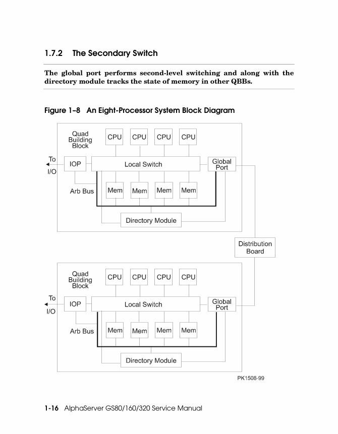
The global port performs second-level switching and along with the directory module tracks the state of memory in other QBBs.
Figure 1– 8 An Eight-Processor System Block Diagram

System Overview 1-17
Figure 1–8 shows an 8-processor, two QBB system. Such a system can be built using a rack cabinet and two drawers (a GS80 system) or a system and power cabinet and a loaded system box (an 8-P GS160 system). This configuration is the maximum for the rack GS80 system.
The directory contains state information on each 64-byte (cache-block-size) chunk of main memory in the system. Like memory, the directory is distributed across system nodes such that if a memory address is located on a particular node the directory module on that node knows its state, ownership, and current location of the most up to date copy of the block. The directory makes the primary memory coherence decisions.
The global port performs two major functions: first to pass command/address and data between the nodes and second to keep track of transactions that are not complete. This second function is important in keeping memory coherent. Since DTag and directory data are typically updated once a transaction is complete, the Transaction Tracking Table (TTT), a CAM (content addressable memory) located on the global port, keeps track of incomplete transactions (in flight transactions) at a given node. Thus, cache blocks accessed by more than one CPU at the same time can be correctly tracked and updated. For a full description of coherency, see Appendix B.
In a two QBB system, a global port in QBB0 communicates with a global port in QBB1 through a distribution board.
In addition to the system functions just described, the console serial bus (CSB) routes through the global port.
For a description of the global port module, see Section 1.17.

1-18 AlphaServer GS80/160/320 Service Manual
1.7.3 The Hierarchical Switch
The hierarchical switch is an 8-port switch that connects up to 8 QBBs.
Figure 1– 9 Architecture Block Diagram

System Overview 1-19
Figure 1–9 is a block diagram of a 16-processor GS160 system. It consists of two full system boxes with two QBBs in each. In this case, only four of the eight ports in the hierarchical switch (H-switch) are used to pass command/address and data between nodes.
Since these systems use distributed memory, the hierarchical switch is required to help maintain systemwide coherency. First, it supports multicasting. Whenever a processor attempts to gain ownership of a memory block, “ invalidates” may need to be broadcast to the other quad processor switches. Therefore, certain packets transmitted by a global port will have multiple destinations. When the H-switch sees multiple destinations, it will “multicast” the packet to all target ports. The second coherency requirement is that the hierarchical switch must maintain certain ordering for packets received from and transmitted to the global ports. For a full description of coherency, see Appendix B.
Paths in the H-switch are all unidirectional – either transmit or receive – so it is possible to have 16 transactions passing through the switch simultaneously. Each of the 8 ports connected to QBB global ports can be transmitting and receiving data at the same time. It should be noted that transactions are buffered in many locations throughout the system, in memory, global ports, directories, CPUs, I/O subsystems, etc., such that a large system could be keeping track of over 300 transactions at any given time.
When transactions cross QBB boundaries in systems with more than two QBBs, command/address and data pass through the local global port, through the H-switch, and through the remote global port to their ultimate destination.

1-20 AlphaServer GS80/160/320 Service Manual
1.7.4 Addressing
The CPU chip and the rest of the system have slightly different formats.
Table 1– 1 Address Ranges Seen at the CPU
Home QBB Memory Space Address I/O Space Address
0 000.0000.0000 - 00f.ffff.ffff ff0.0000.0000 - fff.ffff.ffff
1 010.0000.0000 - 01f.ffff.ffff fe0.0000.0000 - fef.ffff.ffff
2 020.0000.0000 - 02f.ffff.ffff fd0.0000.0000 - fdf.ffff.ffff
3 030.0000.0000 - 03f.ffff.ffff fc0.0000.0000 - fcf.ffff.ffff
4 040.0000.0000 - 04f.ffff.ffff fb0.0000.0000 - fbf.ffff.ffff
5 050.0000.0000 - 05f.ffff.ffff fa0.0000.0000 - faf.ffff.ffff
6 060.0000.0000 - 06f.ffff.ffff f90.0000.0000 - f9f.ffff.ffff
7 070.0000.0000 - 07f.ffff.ffff f80.0000.0000 - f8f.ffff.ffff
Table 1– 2 Address Ranges Seen in the System
Home QBB Memory Space Address I/O Space Address
0 000.0000.0000 - 00f.ffff.ffff 800.0000.0000 - 80f.ffff.ffff
1 010.0000.0000 - 01f.ffff.ffff 810.0000.0000 - 81f.ffff.ffff
2 020.0000.0000 - 02f.ffff.ffff 820.0000.0000 - 82f.ffff.ffff
3 030.0000.0000 - 03f.ffff.ffff 830.0000.0000 - 83f.ffff.ffff
4 040.0000.0000 - 04f.ffff.ffff 840.0000.0000 - 84f.ffff.ffff
5 050.0000.0000 - 05f.ffff.ffff 850.0000.0000 - 85f.ffff.ffff
6 060.0000.0000 - 06f.ffff.ffff 860.0000.0000 - 86f.ffff.ffff
7 070.0000.0000 - 07f.ffff.ffff 870.0000.0000 - 87f.ffff.ffff

System Overview 1-21
The memory system functions as a single, distributed, tightly-coupled shared memory. The system’s memory address space and I/O address space are distributed in segments across a system’s QBBs. Each memory address maps to one and only one memory module, on one and only one QBB. Each I/O address maps to one and only one I/O device, on one and only one QBB. The QBB onto which a memory or I/O address maps is referred to as that address’ “Home” QBB.
The 43-bit physical addresses upon which the Alpha chip operates map to a slightly modified 43-bit physical address format upon which the rest of the system hardware operates.
Table 1–1 shows the home QBB address ranges as defined by the 43-bit address range upon which the Alpha chip operates. Note that in memory space, address bits <38-36> directly decode the home QBB of a memory space address, where the inverse of address bits <38-36> decode the home QBB of an I/O space address.
Table 1–2 shows the home QBB address ranges as defined by the 43-bit address range, after the Alpha chip’s 43-bit addresses have been changed to the address format used by the rest of the system hardware. Note that in this format, address bits <38-36> directly decode the home QBB of both memory space and I/O space references.
The processors in a distributed, tightly-coupled, shared memory system function as a symmetric multiprocessing (SMP) system. Each processor can operate on memory data whose home is in the same QBB as the processor or on data whose home is in a different QBB. When a processor issues a request to an address whose home is in the same QBB as the processor, the request is referred to as a “ local” request. When a processor issues a request to an address whose home is in a different QBB, the request is referred to as a “remote” or “global” request.
For a complete discussion of system addressing, see the AlphaServer GS80/160/320 System Programmer’s Manual.

1-22 AlphaServer GS80/160/320 Service Manual
1.8 System Management Architecture
AlphaServer GS80/160/320 systems use an independent multi-drop serial bus, powered by auxiliary voltage (Vaux), to configure, monitor, and control the system and its partitions either locally or remotely.
1.8.1 Console Serial Bus
The console serial bus (CSB) is controlled by the system control manager microprocessor (SCM) on the standard I/O module in the required master PCI box. Each QBB, PCI, standard I/O module with its SCM, and hierarchical switch, if present, is connected to the CSB.
Figure 1– 10 Console Serial Bus Block Diagram
Figure 1–10 is a block diagram of the console serial bus. Vaux, present whenever AC is applied, powers this bus and its nodes; it functions while the system is off (DC not present). The master system control manager (SCM) controls the console serial bus. The OCP can connect to two SCMs on two standard I/O modules providing redundancy.

System Overview 1-23
The system management console (SMC) is a front end PC that serves as the local console for the system. See Section 1.8.2.
A modem for remote control connects directly to the SMC PC through the modem port. Another modem connected to the standard I/O is used for system-initiated service calls.
The CSB uses a polled master/slave protocol where a single master controls the network. The master, in this case the SCM, sends commands to slaves to which they respond.
Nodes on the CSB are:
• One or up to eight SCMs (two for the GS80), one of which is the active master of the bus (CSB master SCM) while all others are slave nodes. One other slave SCM may be used as a redundant CSB master. It must have its environment variable scm_csb_master_eligible set and be connected to the OCP.
• Up to 8 power system managers (PSMs), one in each QBB in the system.
• Up to 16 PCI backplane managers (PBMs), one on each PCI backplane.
• One H-switch power manager (HPM), if an H-switch is present.
With the exception of the SCM, each node is a microprocessor programmed to monitor the subsystem it is in. The SCM’s microprocessor is programmed as the system console. It continually polls each node to retrieve monitoring information from each slave.
By default the SCM with the lowest CSB node ID number connected to the OCP becomes the bus master. (The node ID switch determines the node number for the SCM. Each CSB node ID number must be unique. See Section 1.21.6.)
SCM Failover
Assuming SCM redundancy, four conditions will cause failover:
• If the default master fails self-test.
• If the default master loses connection with the OCP.
• If a new node with an eligible master SCM is added to the CSB and it has a lower node number than the current master, then the current master relinquishes control of the CSB and the new SCM becomes master.
• If the slave SCM node that is an eligible master does not see the master SCM continually assert CSB MASTER ENABLE, it becomes the master.
NOTE: Should failover occur, the SCM monitor function physically moves from one standard I/O module to another. Note also that a powered off QBB may power back on should failover occur or if a remote user initiates the power-on. Putting the PSM switch in the Service position prevents this.

1-24 AlphaServer GS80/160/320 Service Manual
1.8.2 System Management Console
The system management console (SMC) is a front end PC running terminal emulator(s) and connected either directly to the master SCM or to a terminal server connected to all SCMs including the master.
Figure 1– 11 SMC Connections

System Overview 1-25
Figure 1–11 shows the connections made to the system management console and connections made from it to the terminal server located above the AC input boxes in the power cabinet of a GS160/320 system.
By running as many terminal emulation sessions as SCM/SRM consoles, the SMC has control of each SCM/SRM/partition in the system. (Each partition hard or soft requires a console. See Section 1.9 for information on partitions.) Since each hard or soft partition requires a console and a GS320 can have as many as eight partitions, eight consoles are required. By using the SMC PC running terminal emulation software, only one console device is needed to control all partitions.
As can be seen from Figure 1–11, remote access to the console of any partition is possible through a corporate LAN or through a modem connection from a remote service site. A modem connected to the modem port on the standard I/O module allows system-initiated calls when a system event is detected that requires service.
A Special Case
A customer who decides not to partition his system does not receive the terminal server unless they configure their system with a redundant SCM.
See the AlphaServer GS80/160/320 System Management Console Installation and User’s Guide for information on using the SMC.

1-26 AlphaServer GS80/160/320 Service Manual
1.8.3 System Control Manager (SCM)
The system control manager (SCM) is primarily responsible for two tasks: remote management and master of the console serial bus (CSB). The SCM is on the standard I/O module in a master PCI box.
Figure 1– 12 System Control Manager Block Diagram

System Overview 1-27
The system control manager (SCM) uses the console serial bus to:
• Control system power-up
• Configure the system
• Monitor the system
• Update firmware
• Power on and power off the system, locally or remotely
• Halt and reset the system
Through a microprocessor and its associated resources, the SCM receives and initiates secure remote connections. It is powered by the Vaux output of the PCI power supply that is on whenever AC is applied to the PCI box.
Figure 1–12 shows the hardware interfaces to the SCM:
• COM1 port or Super I/O (DVD/CD-ROM, mouse, keyboard, SCSI disk, etc.) COM1 is an internal port to the ISA bus and is not brought outside the master PCI box.
• Modem port
• Local terminal port
• Operator control panel (OCP) switch, display, and LEDs
• Console serial bus (CSB)
• Shared RAM (shared between the SCM and SRM console/OS through the standard I/O ISA bus) for storage of systemwide configuration and status, and for buffering console data
The SCM has access to the following resources:
• 128 Kbytes of operating RAM
• 256 Kbytes of sector-erasable-flash EPROM for instruction storage
• 8 Kbytes of EEPROM for storage of configuration, error information, and user-definable console settings
• 128 Kbytes of shared RAM
The SCM can operate in different modes allowing local or remote control. For a complete description of the features available in the SCM, see the AlphaServer GS80/160/320 User’s Guide or the AlphaServer GS80/160/320 Firmware Reference Manual.
See Section 1.21.4 for a description of the standard I/O module where the SCM monitor resides.

1-28 AlphaServer GS80/160/320 Service Manual
1.8.4 Power System Manager (PSM)
In addition to configuring and monitoring the QBB, the power system manager (PSM) performs tasks at the request of the system control manager. The PSM is a microprocessor controlled subsystem responsible for power management, environmental monitoring, system reset, and initialization. The PSM is a required module in all QBBs.
Figure 1– 13 Power System Manager Software Block Diagram

System Overview 1-29
Figure 1–13 shows the software block diagram for the power system manager. The PSM is responsible for power on/off, environmental system management, system initialization, system reset, and system communication in a QBB. Three I2C bus controllers control three I2C buses that route throughout the QBB. The PSM also controls the serial lines to the CPUs used to communicate with SROM/XSROM code during power-up. Like all other nodes on the CSB it is powered by Vaux. For a description of the module itself, see Section 1.12.
Table 1– 3 I2C Bus Device Identification on PSM/QBB
I2C Bus Devices on the Bus
I2C1 One hardware monitor on the PSM, up to eight 8-bit expanders, one on each CPU and each memory, and up to eight 256-byte EEPROMs, one on each CPU and each memory.
I2C2 One hardware monitor on the PSM, three 8-bit expanders (one on the directory module, one on the main power module, and one on the auxiliary power module), and up to eight 256-byte EEPROMs (one on each IOP, and one on each of the following: global port, directory module, main power module, and auxiliary power module).
I2C3 Three 8-bit expanders on the QBB backplane, one hardware monitor on the PSM, and two EEPROMs (one on the PSM and the other on the QBB backplane).
The PSM is controlled by instructions provided by the SCM. When instructed, the PSM initiates QBB power-up. See Chapter 2.
PSM firmware resides in flash EPROM that can be updated by the SCM update command or by LFU. See Section 1.12 for a PSM block diagram and module description.
Note that when an operator issues the SCM show csb command, CPUs and IOPs are given CSB node addresses though they are not on the CSB. The PSM in each QBB senses the presence of CPUs and IOPs and knows whether they are on or off. These CSB node addresses allow operators to target CPUs and IOPs when using SCM commands. It is the PSM on the CSB that can power on or off an entire QBB or power on or off CPUs and IOPs individually.

1-30 AlphaServer GS80/160/320 Service Manual
1.8.5 PCI Backplane Manager (PBM)
In addition to configuring and monitoring the PCI I/O subsystem, the PCI backplane manager (PBM) performs tasks at the request of the system control manager (SCM). The PBM is a microprocessor controlled subsystem responsible for PCI environmental monitoring, notifying the system of unsafe conditions, PCI test, reset, and initialization. The PBM is on the PCI backplane.
Figure 1– 14 PCI Backplane Manager Block Diagram

System Overview 1-31
Figure 1–14 is a block diagram of the PCI backplane manager (PBM). It is primarily responsible for monitoring environmental sensors on the backplane and reporting unsafe conditions. The shaded part of the block diagram is powered by Vaux and is available for use whenever AC is applied.
The PBM microprocessor controls the x86 bus upon which are various control and status registers, an interface to the PCA ASIC (Section 1.21.5), and an interface to the I2C bus on the PCI backplane. As seen in the block diagram, the microprocessor connects to the CSB and is directed by the system control manager (SCM). In normal operation the PBM monitors the environment and reports status to the SCM when polled.
Devices on the I2C bus are:
• Two monitors, one monitoring voltages, the other monitoring temperatures, fan speed, and voltages.
• Four 256x8 byte EEPROMs, one on the PCI backplane, one on the standard I/O module, and one on each of the two remote I/O riser modules. The EEPROMs contain service information.
The PBM microprocessor also controls 128 Kbytes of operating RAM, 256 Kbytes of sector-erasable flash EPROM for instruction storage, and the PCI backplane LEDs visible on the console serial bus ID module at the rear of the PCI box. See Section 1.21.6.
PBM firmware resides in flash EPROM that can be updated by the SCM update command or by LFU.
When power is applied to the PCI backplane (Vaux present), the PBM runs through its self-test. Areas tested are:
• Flash ROM (checksum)
• RAM
• I2C bus controller
• I2C FRU EEPROM
• LM80 monitor circuits
• Miscellaneous CSRs
• Note that self-test will fail if an error is found in the EEPROM.
See Section 1.21.2 for a description of the PCI backplane where the PBM resides.

1-32 AlphaServer GS80/160/320 Service Manual
1.8.6 Hierarchical Switch Power Manager (HPM)
The hierarchical switch power manager (HPM) is a microprocessor controlled subsystem responsible for power management, environmental monitoring, asynchronous reset & initialize, I2C bus management, and console serial bus communication for the H-switch.
Figure 1– 15 HPM Block Diagram

System Overview 1-33
Figure 1–15 is a block diagram of the hierarchical switch power manager (HPM) module. The HPM is responsible for monitoring environmental sensors on the H-switch and reporting unsafe conditions. The HPM is powered by Vaux which is converted to +5V and +3.3V on the module.
The HPM monitors two clock signals and several power supply signals that must be good and remain good during power-on and normal operation. If any fail, the H-switch is turned off.
The HPM performs a reset, initialize, and functional self-test for the H-switch. If these functions pass, the HPM enters a stand-by state; if they fail, the HPM remains in the initialize state, the reset/initialize LED remains on, and the CSB remains operational so that failure data can be reported to the SCM.
The microprocessor operation is controlled by firmware stored in flash memory on the HPM, and receives commands from the SCM through the console serial bus (CSB) interface. The flash memory contains the HPM firmware code and a sector with a fail-safe loader (FSL). Updating of the flash program image is done by LFU or by downloading the data over the CSB using the SCM update command.
The HPM has one I 2C bus and is shared between devices mounted on the H-switch, and on the HPM module itself. The HPM module also contains a 256x8-bit EEPROM, and one LM80 device for monitoring DC voltages and temper-ature on the H-switch.
For a description of the HPM module, see Section 1.20.

1-34 AlphaServer GS80/160/320 Service Manual
1.9 System Partitioning
Partitions allow large systems to appear as several smaller ones either from a hardware and/or software point of view.
NOTE: When considering partitions, it is helpful to separate two functions resident on the standard I/O module: the SCM function and the SRM function. Although all STD I/Os contain SCM code, only one is master of the CSB and only one other may be eligible to become master. A major reason for having more than two standard I/O modules in a system is to fulfill the requirement that each partition, hard or soft, have an SRM console.
1.9.1 Hard Partitions
GS80/160/320 systems may be hard partitioned on QBB boundaries. The number of QBBs in a system dictates the maximum number of hard partitions. Each hard partition requires at least one QBB that has CPU(s), memory, and an I/O subsystem with a standard I/O module.
Table 1– 4 Rules Affecting Hard Partitions
Rule Rule Description
1 A hard partition requires one or more QBBs with CPUs, memory, and an attached I/O subsystem(s) with at least one standard I/O module.
2 Hard partitions are set up on QBB boundaries.
3 The maximum number of standard I/O modules on the console serial bus is eight.
4 Hard partitions may have redundant consoles but are limited by rule 3.
5 Hard partitions are defined at the SCM firmware level.
For a full discussion of hardware partitions and how to create them, see AlphaServer GS80/160/320 Getting Started with Partitions.

System Overview 1-35
Applying the rules in Table 1–4 to a GS320 with eight QBBs, a customer might set up a system as shown in Table 1–5. Such a system has three hard partitions each with the required resources to run an operating system. The configuration shows that hard partitions are confined to QBB boundaries and that no resources are shared across partitions.
Table 1– 5 Possible 32-P Hard Partitioned System
Partition 0 Partition 1 Partition 2
QBB0 & 1 (CPUs 0-7)
QBB2 & 3 (CPUs 8-15)
QBB4 – QBB7 (CPUs 16-31)
4 PCI boxes -2 with STD I/Os
4 PCI boxes -2 with STD I/Os
8 PCI boxes - 2 with STD I/Os
Memory in QBB0 & 1
Memory in QBB2 & 3
Memory in QBB4 - 7
Results of Hard Partitioning
1. A hard partition is a subset of system resources capable of running an operating system.
2. Partitions are isolated from each other and know nothing about another’s existence.
3. Errors: See Section 3.11.
• All errors that are faults crash all partitions.
• Uncorrectable errors that are not faults affect only the hard partition experiencing the error.
• Correctable errors affect only the hard partition experiencing the error.
4. From an SRM console/operating system point of view, partitions look alike – QBBs, CPUs, memory, and IOPs are numbered starting with 0.
NOTE: Result 4 can lead to confusion. Say two partitions with two QBBs in each have been created in a system with four QBBs (0-3). If you issue the command $ stop/cpu/poweroff 7 in one partition, the command may target CPU3 in QBB1. If you issue the same command in the other partition, the command may target CPU3 in QBB3. To minimize this effect, create a hardware drawing of the partitions to help translate software IDs to physical locations.
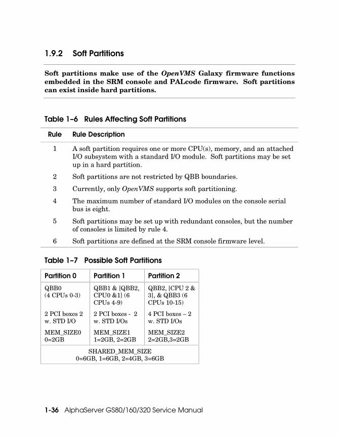
1-36 AlphaServer GS80/160/320 Service Manual
1.9.2 Soft Partitions
Soft partitions make use of the OpenVMS Galaxy firmware functions embedded in the SRM console and PALcode firmware. Soft partitions can exist inside hard partitions.
Table 1– 6 Rules Affecting Soft Partitions
Rule Rule Description
1 A soft partition requires one or more CPU(s), memory, and an attached I/O subsystem with a standard I/O module. Soft partitions may be set up in a hard partition.
2 Soft partitions are not restricted by QBB boundaries.
3 Currently, only OpenVMS supports soft partitioning.
4 The maximum number of standard I/O modules on the console serial bus is eight.
5 Soft partitions may be set up with redundant consoles, but the number of consoles is limited by rule 4.
6 Soft partitions are defined at the SRM console firmware level.
Table 1– 7 Possible Soft Partitions
Partition 0 Partition 1 Partition 2
QBB0 (4 CPUs 0-3)
QBB1 & [QBB2, CPU0 &1] (6 CPUs 4-9)
QBB2, [CPU 2 & 3], & QBB3 (6 CPUs 10-15)
2 PCI boxes 2 w. STD I/O
2 PCI boxes - 2 w. STD I/Os
4 PCI boxes – 2 w. STD I/Os
MEM_SIZE0 0=2GB
MEM_SIZE1 1=2GB, 2=2GB
MEM_SIZE2 2=2GB,3=2GB
SHARED_MEM_SIZE 0=6GB, 1=6GB, 2=4GB, 3=6GB

System Overview 1-37
For a full discussion of soft partitions and how to create them, see the AlphaServer GS80/160/320 Getting Started with Partitions.
Applying the rules in Table 1–6 to a GS160 with four QBBs, a customer might set up a system as shown in Table 1–7. This system has three soft partitions each with the required resources to run an instance of an operating system. Currently, only OpenVMS supports soft partitions. The configuration shows that soft partitions are not confined to QBB boundaries and through shared memory and the Galaxy console functions, the instances of the operating systems running in each partition know about each other.
Results of Soft Partitioning
1. A soft partition is a subset of system resources capable of running an operating system.
2. Partitions know about each other’s existence and can share resources. (System faults will crash all partitions though.)
3. Errors: See Section 3.11.
• All errors that are faults crash all partitions.
• Uncorrectable errors that are not faults affect only the soft partition experiencing the error.
• Correctable errors affect only the hard partition experiencing the error.
4. From a console/operating system point of view, partitions look alike – QBBs, CPUs, and IOPs are numbered starting with 0 in each partition.
NOTE: Result 4 can lead to confusion. Say two partitions with two QBBs in each have been created in a system with four QBBs (0-3). If you issue the command $ stop/cpu/poweroff 7 in one partition, the command may target CPU3 in QBB1. If you issue the same command in the other partition, the command may target CPU3 in QBB3. To minimize this effect, create a hardware drawing of the partitions to help translate software IDs to physical locations.

1-38 AlphaServer GS80/160/320 Service Manual
1.9.3 Mixture of Hard and Soft Partitions
Hard and soft partitions can exist in a single system.
Table 1– 8 Possible 32-P Partitioned System
Hard Partition 0
Hard Partition 1
Hard Partition 2 Soft Partition 0 Soft Partition 1 Soft Partition 2
QBB0 & 1 (4 CPUs 0-7)
QBB2 & 3 (8 CPUs 8-15)
QBB4 (4 CPUs 16-19)
QBB5 &[QBB6, CPU0 &1] (6 CPUs 20-25)
[QBB6, CPU 2 & 3], & QBB7 (6 CPUs 26-31)
4 PCI boxes -2 with STD I/Os
4 PCI boxes -1 with STD I/O
2 PCI boxes 1 with STD I/O
2 PCI boxes - 2 with STD I/Os
4 PCI boxes – 2 with STD I/Os
Memory in QBB0 & 1
Memory in QBB2 & 3
MEM_SIZE0 4=2GB
MEM_SIZE1 5=2GB, 6=2GB
MEM_SIZE2 6=2GB,7=2GB
SHARED_MEM_SIZE 4=6GB, 5=6GB, 6=4GB, 7=6GB

System Overview 1-39
For a full discussion of both hard and soft partitions and how to create them, see AlphaServer GS80/160/320 Getting Started with Partitions.
Table 1–8 describes a fully loaded 32-P system with the maximum number of CPUs (32), maximum number of PCIs (16), and the maximum number of standard I/O modules (8). Were each slot in each PCI filled, this system could have as many as 216 options in addition to those that are part of PCI boxes with standard I/O modules ((8 PCIs with STD I/Os X 13 available PCI sots = 104 PCI options) + (8 PCIs without STD I/Os X 14 available PCI sots = 112 PCI options) = 216 PCI options). These facts, coupled with the possibility of various power states and error propagation, (see Sections 4.3) indicate why you need a good map of hardware and firmware.

1-40 AlphaServer GS80/160/320 Service Manual
1.9.4 Servicing Partitions
Partitions allow parts of a system to remain up and running while other parts of the system are powered off for service.
Example 1– 1 Shutting Down a Partition
…[..Shut down the operating system in a given partition ..]� P00>>> power off � Powering off Hard_partition_2 consisting of: � QBB2 QBB3 QBB-2 Powering OFF QBB-3 Powering OFF ~I~ QBB2/PSM32 SysEvent: QBB_POWER_OFF Reg0:7CBC Reg1:F1FF ~I~ QBB3/PSM33 SysEvent: QBB_POWER_OFF Reg0:7CBC Reg1:33FF ~I~ HSW8/HPM40 SysEvent: LINK2_OFF Reg0:3C3C Reg1:D5E1 ~I~ HSW8/HPM40 SysEvent: LINK3_OFF Reg0:383C Reg1:D5E1 SCM_EF> show csb � . . C6 IOR2 ON C7 IOR3 ON 32 PSM V05.4 (04.13/11:20) V4.0 (07.06) VAUX � SrvSw:.SERVICE 32 XSROM V05.5 (04.13/11:41) C8 CPU0/SROM V5.0-7 OFF C8 IOR0 OFF C9 IOR1 OFF CA IOR2 OFF CB IOR3 OFF 33 PSM V05.4 (04.13/11:20) V4.0 (07.06) VAUX � SrvSw: SERVICE 33 XSROM V05.5 (04.13/11:41) CC CPU0/SROM V5.0-7 OFF CD CPU1/SROM V5.0-7 OFF CC IOR0 OFF CD IOR1 OFF 34 PSM V05.4 (04.12/02:07) V4.0 (07.06) ON SrvSw: NORMAL 34 XSROM V05.5 (04.13/11:41) D0 CPU0/SROM V5.0-7 ON D1 CPU1/SROM V5.0-7 ON

System Overview 1-41
Service can be performed on one or more partitions while other partitions remain operational. Once the operating system running in a given partition is shut down, power can be removed from the partition without removing power from other partitions. And once a QBB is in an Off state, any module in that QBB can be replaced or added without further disruption of the system.
Rules for Servicing Partitions
1. Only hard partitions can be powered off.
2. If a hard partition or system is soft partitioned, each instance of the operating system in each soft partition must be shut down before the hart partition or system is powered off.
3. Once the partition is powered off, put the service switch on the PSM(s) in the QBB(s) that define the partition in the Service position. This prevents both a remote user from powering on the QBB/partition while it is being serviced and a partition power-on should a master SCM failover to a backup, master-eligible SCM.
Example 1–1 shows how a partition can be shut down. The general procedure consists of the following:
� Shut down the operating system in the partition.
� At the SRM console prompt, enter the power off command. This command causes all activity throughout the QBB/partition to cease and then power off to occur. Using the SCM power of –par x command takes power away from the QBB/partition with out cleanly stopping the partition’s activity.
� The hard partition and its configuration is identified and power down starts.
� The SCM command show csb is issued here to show the result of the SRM power off command.
� The SCM command show csb shows that the service switch on the PSMs in the QBBs powered off has been switched to Service. See Section 1.8.4 for a functional description and Section 1.12 for a physical description of the PSM.

1-42 AlphaServer GS80/160/320 Service Manual
1.10 CPU Module
The CPU module uses the Alpha processor chip.
Figure 1– 16 CPU Module

System Overview 1-43
A single Alpha processor chip is on the CPU module.
Some features of the CPU module are:
• QBB system interface
• PSM interface, both I2C and serial I/O
• Backup cache of 4 Mbytes
• Master phase lock loop (MPLL) clock (reference supplied by the QBB backplane)
• On-board DC-DC converter (48V to a voltage specific to the CPU chip) (other than the power modules this is the only module in a QBB to have a 48V input)
• Short-circuit protection
• On-board SROM for diagnostics
• Module hot-swap (PSM control for power-on and power-off)
• Two LEDs:
Hot Swap OK – Yellow – normally off Run – Green – normally on
• I2C bus 8-bit expander register for module status
• I2C bus EEPROM containing module serial number, B-cache size, QSA parameter bit, and FRU error information relevant to the module
Table 1– 9 CPU Variants
Module Variant Cache Size Base CPU
B4125-Ax 4 Mbytes EV67

1-44 AlphaServer GS80/160/320 Service Manual
1.10.1 CPU Processor
The Alpha processor used in these systems is the third generation of the chip. It contains 15.2 million transistors.
Figure 1– 17 Alpha Chip Block Diagram

System Overview 1-45
Figure 1–17 is a block diagram of the 21264 Alpha processor chip. The chip’s architectural features are:
• Four integer execution units (E-box): two are used for address calculations for load and store instructions and two are used for normal integer calculations
• Two floating-point execution units (F-box) for add, divide, multiply, and square root
• One instruction fetch, issue, and retire unit (I-box)
• A memory reference unit
• A 64-Kbyte instruction cache (I-cache)
• A 64-Kbyte data cache (D-cache)
• An external cache and system interface unit (C-box)
• Two external interfaces: one backup cache data port with a 16-byte bus and one system port with an 8-byte data bus
The chip contains 15.2 million transistors and is packaged in a 587-pin grid array carrier. Four instructions can be issued per clock cycle. The design supports out-of-order instruction execution, branch prediction, and high-speed access to backup cache and memory. In addition to normal Alpha RISC instructions, the 21264 processor includes special motion video instructions.

1-46 AlphaServer GS80/160/320 Service Manual
1.11 Memory Module
The memory module uses SDRAM storage elements and CMOS application specific integrated circuits (ASICs) for interface and control logic. Each memory module holds two four DIMM memory arrays.
Figure 1– 18 Memory Module
DIMMs
PLLs
MPD
MPA
MPD
PK0603
Memory module features include:
• Two memory arrays consisting of four DIMMs each.
• Read error detection of single-bit errors and the most prevalent 2-bit, 3-bit, and 4-bit errors in SDRAM arrays. (Single-bit error correction can be enabled.)
• Write data detection of single-bit errors written to memory.
• Write victim buffers allow write transactions to be in a “pre-directory lookup” state freeing the write transaction commander to continue processing without waiting for write confirmation. The command and data are placed in queues for later execution.

System Overview 1-47
• Memory interleaving is used to improve memory bandwidth by “staggering” transactions on the memory arbitration bus. See memory interleaving guidelines in the AlphaServer GS80/160/320 User’s Guide.
• Read data wrapping is used to reduce apparent memory latency by allowing quadword (8 bytes) access in a prescribed order.
• A microcontroller initiates memory built-in self-test and communicates DIMM EEPROM data to the PSM.
• Short-circuit protection.
Table 1– 10 Memory Configurations
DIMM
Module Min. Max.
QBB Max.
GS80 Max.
GS320 Max.
SDRAM
256 MB 1 GB 2 GB 8 GB 16 GB 64 GB 64-Mbit
512 MB 2 GB 4 GB 16 GB 32 GB 128 GB 64/256-Mbit
1 GB 4 GB 8 GB 32 GB 64 GB 256 GB 256-Mbit
Configuration Guidelines
• Minimum configuration: 1 Gbyte.
• Memory arrays on a memory module may be of different sizes but no mixed DIMM sizes are allowed in a memory array.
• If your system has two memory arrays, for better bandwidth, have two single arrays (4 DIMMs) on two memory modules rather than two memory arrays on a single memory module.
For more information, see the AlphaServer GS80/160/320 User’s Guide.

1-48 AlphaServer GS80/160/320 Service Manual
1.12 Power System Manager Module
The PSM is the microprocessor controller for the power subsystem.
Figure 1– 19 Power System Manager Module Block Diagram

System Overview 1-49
Figure 1–19 is a block diagram of the power system manager module. For a functional description of the power system manager, see Section 1.8.4.
Figure 1– 20 PSM Module LEDs and Jumpers
Figure 1–20 shows the service switch, the PSM module LEDs, and jumpers.
Service Switch
When in the Normal position, the switch allows the PSM normal operational control of the QBB. When set to the Service position, 48V does not get converted to logic voltages but may still be present on the backplane. Placing the switch in the Service position prevents a remote operator from turning the QBB back on.
LEDs
QBB DC Good (Green)
On (normal) Off
All DC voltages in the QBB are good System/QBB off or DC voltage(s) not good
Reset/Initialize (yellow)
On Off (normal )
The PSM is in the reset/initialize state Self-test passed and PSM configuration done
Hot Swap DC OK (green)
On (normal) Off
On-board hot-swap regulator is good On-board hot-swap regulator is not good
PSM DC OK (green)
On (normal) Off
DC voltages on the PSM are good DC voltages on the PSM are not good
Vaux OK (green)
On (normal) Off
Vaux present at the module Vaux not present
Jumpers
J6 When installed, the most significant bit of the CSB address field is set to 1.
J7 When installed, the hardware cannot write the PSM’s flash memory.
J9 When installed, the micro will remain in fail-safe loader mode after a PSM reset.
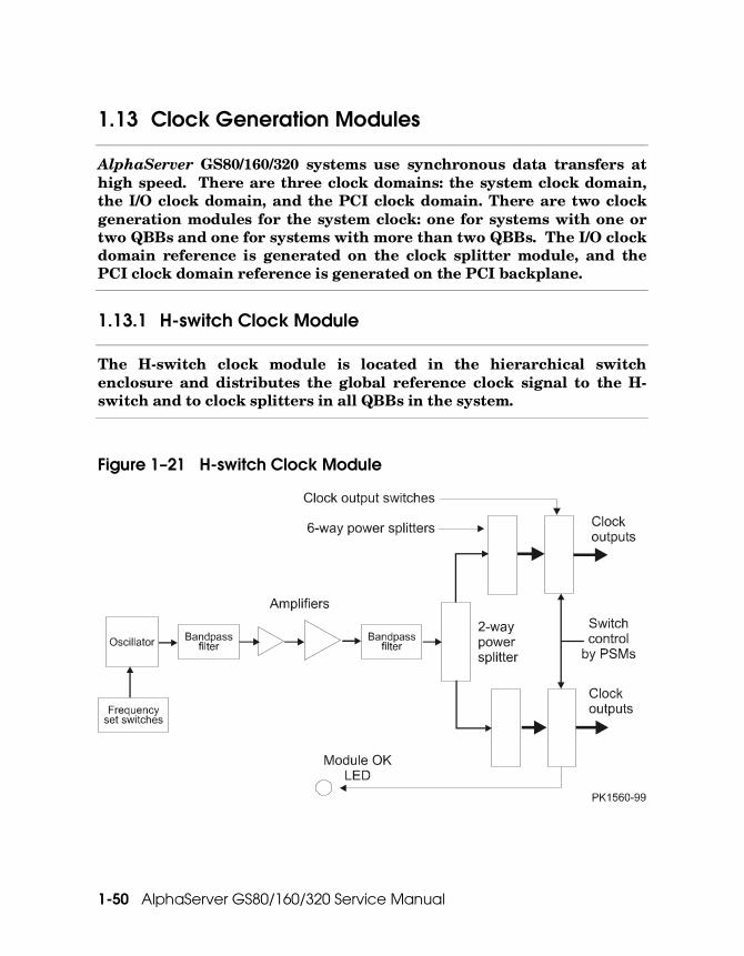
1-50 AlphaServer GS80/160/320 Service Manual
1.13 Clock Generation Modules
AlphaServer GS80/160/320 systems use synchronous data transfers at high speed. There are three clock domains: the system clock domain, the I/O clock domain, and the PCI clock domain. There are two clock generation modules for the system clock: one for systems with one or two QBBs and one for systems with more than two QBBs. The I/O clock domain reference is generated on the clock splitter module, and the PCI clock domain reference is generated on the PCI backplane.
1.13.1 H-switch Clock Module
The H-switch clock module is located in the hierarchical switch enclosure and distributes the global reference clock signal to the H-switch and to clock splitters in all QBBs in the system.
Figure 1– 21 H-switch Clock Module
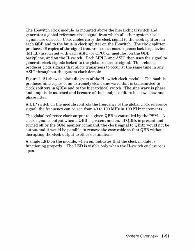
System Overview 1-51
The H-switch clock module is mounted above the hierarchical switch and generates a global reference clock signal from which all other system clock signals are derived. Coax cables carry the clock signal to the clock splitters in each QBB and to the built-in clock splitter on the H-switch. The clock splitter produces 48 copies of the signal that are sent to master phase lock loop devices (MPLL) associated with each ASIC (or CPU) on modules, on the QBB backplane, and on the H-switch. Each MPLL and ASIC then uses the signal to generate clock signals locked to the global reference signal. This scheme produces clock signals that allow transitions to occur at the same time in any ASIC throughout the system clock domain.
Figure 1–21 shows a block diagram of the H-switch clock module. The module produces nine copies of an extremely clean sine wave that is transmitted to clock splitters in QBBs and to the hierarchical switch. The sine wave is phase and amplitude matched and because of the bandpass filters has low skew and phase jitter.
A DIP switch on the module controls the frequency of the global clock reference signal; the frequency can be set from 40 to 100 MHz in 100 KHz increments.
The global reference clock output to a given QBB is controlled by the PSM. A clock signal is output when a QBB is present and on. If QBBx is present and turned off by the SCM monitor command, the clock signal to QBBx would not be output and it would be possible to remove the coax cable to that QBB without disrupting the clock output to other destinations.
A single LED on the module, when on, indicates that the clock module is functioning properly. The LED is visible only when the H-switch enclosure is open.
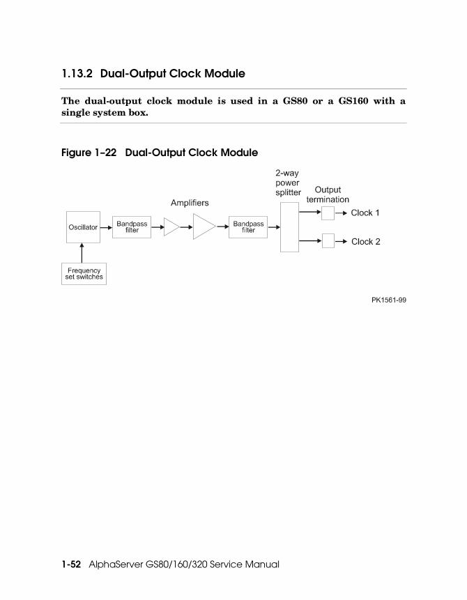
1-52 AlphaServer GS80/160/320 Service Manual
1.13.2 Dual-Output Clock Module
The dual-output clock module is used in a GS80 or a GS160 with a single system box.
Figure 1– 22 Dual-Output Clock Module

System Overview 1-53
The dual-output clock module is used in 4 or 8P systems only. The module is mounted on the rear left side wall of the top drawer in GS80 systems and in the distribution board housing in GS160/320 systems. It generates a global reference clock signal from which all other system clock signals are derived. Equal length coax cables carry the clock signal to the clock splitters in each QBB. The clock splitter produces 48 copies of the signal that are sent to master phase lock loop (MPLL) devices associated with each ASIC (or CPU) on modules and on the QBB backplanes. Each MPLL and ASIC then uses the signal to generate clock signals locked to the global reference signal. This scheme produces clock signals that allow transitions to occur at the same time throughout the system clock domain.
Figure 1–22 shows a block diagram of the dual-output clock module. The module produces two copies of an extremely clean sine wave that is transmitted to the clock splitter module.
A DIP switch on the module controls the frequency of the global clock reference signal; the frequency can be set from 40 to 100 MHz in 100 KHz increments.
The dual-output clock output to a given QBB is controlled by the PSM. A clock signal is output when a QBB is present and on. If QBBx is present and turned off by the SCM monitor command, the clock signal to QBBx would not be output and you can remove the coax cable to that QBB without disrupting the clock output to other QBBs.

1-54 AlphaServer GS80/160/320 Service Manual
1.13.3 Clock Splitter Module
The clock splitter module converts the global reference sine wave from either clock module to 48 identical copies of a positive ECL (PECL) signal that is distributed to master phase lock loops (MPLL) associated with ASICs on the system backplane and on modules in the QBB. It also generates independent clock signals for the I/O domain.
Figure 1– 23 Clock Splitter Module Block Diagram

System Overview 1-55
Figure 1–23 shows a functional block diagram of the clock splitter. A clock splitter module is required in each QBB.
The clock splitter receives the clock sine wave from either the H-switch clock module or the dual-output clock module and converts it into 48 copies of a positive ECL clock signal. This PECL clock signal is transmitted to master phase lock loop (MPLL) modules associated with each ASIC and CPU in the system clock domain. Each MPLL and ASIC then uses the signal to generate clock signals locked to the global reference signal. This scheme produces clock signals that allow transitions to occur at the same time throughout the system clock domain.
Outputs are switched and controlled by the presence or absence of a module. If CPU 0 and 1 are present in a QBB and CPU 2 and 3 are absent, then the clock signals to CPU 0 and 1 are on and the clock signals to CPU 2 and 3 are off.
The clock splitter module is laser trimmed for module to module matching. Clocks throughout the system clock domain are kept precise by matching etch lengths and using precision-made modules in generating the clock signals.
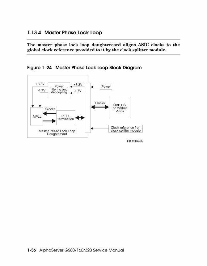
1-56 AlphaServer GS80/160/320 Service Manual
1.13.4 Master Phase Lock Loop
The master phase lock loop daughtercard aligns ASIC clocks to the global clock reference provided to it by the clock splitter module.
Figure 1– 24 Master Phase Lock Loop Block Diagram

System Overview 1-57
Figure 1–24 shows a functional block diagram of the master phase lock loop daughtercard (MPLL). Each ASIC in the system has an associated MPLL. To keep tight clock tolerances, the MPLLs are all deskewed so that all have the same performance.
To synchronize all ASICs in the system, the global reference clock is supplied to each MPLL in the system; the MPLLs supply the clock to the ASIC that it is associated with, tests the ASIC’s delay, and then aligns the internal ASIC clock to the global reference clock. This design keeps all clocks running to within 200 picoseconds of each other.

1-58 AlphaServer GS80/160/320 Service Manual
1.14 Local I/O Riser Modules
There are two local I/O riser modules: one for the GS160/320 QBBs and another for the GS80 QBBs.
1.14.1 System Box Local I/O Riser Module
The system box local I/O riser module provides two I/O port interfaces to the QBB and two connections for I/O cables connected to the PCI I/O subsystem through remote I/O riser modules in PCI boxes. The module may be removed while other parts of the system remain operational. There may be up to two optional local I/O risers in each QBB.
Figure 1– 25 System Box Local I/O Riser Module Block Diagram

System Overview 1-59
The system box local I/O riser module provides two I/O port interfaces to the QBB I/O port (IOP). Since there is a similar I/O riser in the PCI box, it is helpful to name the riser connected to the QBB the local riser and the one connected to the PCI the remote riser.
Figure 1–25 shows a block diagram of the system box local riser. There are two minilink application-specific integrated circuits (MLK ASIC) on the module, one for each port. The function of the minilink is to control the flow of data between the QBB and the I/O subsystem. The module can be hot swapped if there is appropriate operating system support.
The MLK ASICs are synchronized to the QBB using a phase locked loop device that receives its reference clock from the QBB.
The Port In and Port Out signals provide a full duplex link between the MLK ASIC and the IOP on the QBB. The Port signals include 16 address lines, 16 data lines, and various control lines.
The Cable In and Cable Out signals provide a full duplex link between near end (Local) and far end (Remote) MLK ASICs through the I/O Hose cable. The cable signals include 16 multiplexed address/data lines and various control lines.
A 256x8-bit I2C EEPROM present on the module sits on I2C bus 2 controlled by the PSM. The contents of this EEPROM can be read using the show fru SCM command.
LEDs
Power On LED (Green)
On (normal) Off
Power is applied to the module Power not applied to the module
Swap OK LED (Yellow)
On Off (normal)
Module safe to hot swap (green LED Off) Module not safe to hot swap
A short-circuit protection (SCP) daughtercard is provided to monitor the +1.5V, +3.3V, and +3.3V PLL supply rails; it shuts the power down quickly if a short is detected on the module.

1-60 AlphaServer GS80/160/320 Service Manual
1.14.2 System Drawer Local I/O Riser Module
The GS80 drawer local I/O riser module provides two I/O port interfaces to the QBB and two connections for I/O cables connected to the PCI I/O subsystem through remote I/O riser modules. The module cannot be removed while other parts of the system remain operational.
Figure 1– 26 System Drawer Local I/O Riser Module Block Diagram

System Overview 1-61
Figure 1–26 is a block diagram of the drawer local I/O riser modules. Together the two modules, the B4172-Ax and the B4173-Ax, are functionally identical to the system box local I/O riser module; only the mechanics of the module are different. In the GS80, the I/O cables must be brought out at a right angle to the I/O riser. The two-module design makes this possible.
The B4172-Ax plugs into the drawer backplane and the B4173-Ax plugs into the B4172-Ax module such that the I/O ports exit the back of the drawer.
See the previous section for a description of this module.

1-62 AlphaServer GS80/160/320 Service Manual
1.15 Power Modules
Each QBB has two power modules; the H-switch has one power module.
1.15.1 Main Power Module
The main power module converts 48 VDC power supplied by the power supplies to DC voltages required by the clocks and devices on the QBB.
Figure 1– 27 Main Power Module Block Diagram

System Overview 1-63
The power module converts 48 VDC to the following required outputs.
• - 1.7VP at 24 amps
• +1.7V at 45 amps
• +3.3VP at 45 amps
• +3.3V at 90 amps
Separate converters on the module put out each voltage. The VP voltages are routed to the phase lock loop clocks thoughout the QBB. Other voltages power the rest of the QBB including the modules that plug into it. Figure 1–27 shows the block diagram of the main power module and its daughtercard that contains the control logic for the converters.
LEDs
CONV3 Overtemp (yellow)
On Off (normal)
If overtemp condition for converter 3 If temp OK at converter 3 in location E12
CONV2 Overtemp (yellow)
On Off (normal)
If overtemp condition for converter 2 If temp OK at converter 2 in location E6
CONV1 Overtemp (yellow)
On Off (normal)
If overtemp condition for converter 1 If temp OK at converter 1 in location E2
CONV0 Overtemp (yellow)
On Off (normal)
If overtemp condition for converter 0 If temp OK at converter 0 in location E1
Vaux Present (green)
On (normal) Off
Vaux present at the module Vaux not present
Swap OK (yellow)
On Off (normal)
Ok to swap out the module (Vaux Present LED may be on also) The module is not ready to swap out
Module OK (green)
On (normal) Off
All voltages on the module are within tolerances At least one voltage is out of tolerance

1-64 AlphaServer GS80/160/320 Service Manual
1.15.2 Auxiliary Power Module
Like the main power module, the auxiliary power module converts 48 VDC supplied by the power supplies to DC voltages necessary for devices other than clocks on the QBB.
Figure 1– 28 Auxiliary Power Module Block Diagram

System Overview 1-65
The power module converts 48 VDC to the following required outputs:
• +3.3V at 135 amps
• +2.5V at 45 amps
The 2.5V is used by SRAMs that make up CPU backup cache and will be used when such DIMMs are placed in the directory and memory modules.
The 3.3V is current-shared with the 3.3V output from the main power module. Separate converters, some in parallel, on the module put out each voltage.
Figure 1–28 shows the block diagram of the auxiliary power module and its daughtercard that contains the logic for the converters.
LEDs
CONV3 Overtemp (yellow)
On Off (normal)
If overtemp condition for converter 3 If temp OK at converter 3 in location E1
CONV2 Overtemp (yellow)
On Off (normal)
If overtemp condition for converter 2 If temp OK at converter 2 in location E6
CONV1 Overtemp (yellow)
On Off (normal)
If overtemp condition for converter 1 If temp OK at converter 1 in location E13
CONV0 Overtemp (yellow)
On Off (normal)
If overtemp condition for converter 0 If temp OK at converter 0 in location E12
Vaux Present (green)
On (normal) Off
Vaux present at the module Vaux not present
Swap OK (yellow) On Off (normal)
OK to swap out the module (Vaux OK LED may be on also) The module is not ready to swap out
Module OK (green)
On (normal) Off
All voltages on the module are within tolerances At least one voltage is out of tolerance

1-66 AlphaServer GS80/160/320 Service Manual
1.15.3 Hierarchical Switch Power Module
The hierarchical switch power module converts 48 VDC power to the voltages necessary for the H-switch.
Figure 1– 29 H-switch Power Module Block Diagram

System Overview 1-67
Figure 1–29 shows the block diagram of the hierarchical switch power supply. The module converts 48 VDC to the following required outputs:
• -1.7VP at 2.5 amps
• +1.7V at 14 amps
• +2.5V at 7.5 amps
• +3.3VP at 5 amps
• +3.3V at 5.5 amps
• +5.0V at 0.15 amps
• +15V at 0.5 amps
Only one power module is required for the H-switch; the second is redundant and either module is hot swappable. Other features include the ability to enable the module remotely, sense the outputs at the delivery point, and assert DC OK signals. The module also is attached to the I2C bus for module history and revision EEPROM support.
Components on the H-switch are protected from overcurrent and voltage changes outside set window limits.
LEDs
Vaux Present (green)
On (normal) Off
Indicates Vaux present at the module Vaux not present
+3.3VP OK (green)
On (normal) Off
Voltage is within tolerance window Voltage is outside the tolerance window
+3.3V OK (green)
On (normal) Off
Voltage is within tolerance window Voltage is outside the tolerance window
-1.7VP OK (green)
On (normal) Off
Voltage is within tolerance window Voltage is outside the tolerance window
Internal +5V OK (green)
On (normal) Off
Voltage is within tolerance window Voltage is outside the tolerance window
+1.7V OK (green)
On (normal) Off
Voltage is within tolerance window Voltage is outside the tolerance window
Swap OK (yellow)
On Off (normal)
OK to swap out the module (Vaux LED may be on also) The module is not ready to swap out
Module OK (green)
On (normal) Off
All voltages are within tolerances At least one voltage is out of tolerance
+2.5V OK (green)
On (normal) Off
Voltage is within tolerance window Voltage is outside the tolerance window

1-68 AlphaServer GS80/160/320 Service Manual
1.15.4 Short-Circuit Protection Module
The short-circuit protection module is a small daughtercard that protects against short circuits on modules and backplanes throughout the system. In some cases, the protection circuit has been designed into the module so the daughtercard is not used. There are two parts: one for remote I/O risers and one for other modules and backplanes.
Figure 1– 30 Short-Circuit Protection Block Diagram and Interconnect

System Overview 1-69
Figure 1–30 shows both a block diagram of the short-circuit protection module and its interconnect in the QBB and drawer. Similar interconnects exist in the PCI where the SCP is installed on the PCI backplane, the two remote I/O risers, and the standard I/O module.
At present (August 2000), the functions performed by the SCP are designed into the CPU module, the H-switch, the global port, and the GS80 backplane. If the GS160/320 backplane or other modules are redesigned, the protection circuit will become part of the modules and the use of the SCP daughtercard will be eliminated.
The SCP (54-30058-01) is currently used on the memory, directory, local I/O riser, QBB backplane, and the standard I/O module.
The SCP (54-30394-01) is currently used only on the remote I/O riser.
The first voltage available to the SCP is the +3.3VP for the clocks; the other voltages are available later in the power-up process and are provided to other op-amp comparitors as power-up progresses.
The following circuits are monitored:
• 3.3PLL
• 3.3V logic
• 2.5V logic
• 1.5V
• 5V PCI
• 3.3V PCI
Depending upon the location of a short circuit, the SCP latches the main and auxiliary power modules off in the QBB, or latches the two PCI power supplies off in the PCI box, or latches the H-switch power supplies off in the H-switch. Notification of a short-circuit failure is given to the PSM, PBM, or the HPM. In systems with more than one QBB only the QBB with the short-circuit is powered off.
To restore power to a QBB after a short-circuit protection fault, either the system must be power cycled by the OCP switch or the SCM monitor command power on – csb x (where x is the csb address of the PSM in the target QBB) must be executed.
If an SCP is not installed, the system will not power up.

1-70 AlphaServer GS80/160/320 Service Manual
1.16 Directory Module
The directory module uses DIMMs populated with SDRAMs to track ownership and state of memory addresses local to a QBB. A directory module is necessary in each QBB in systems with more than one.
Figure 1– 31 Directory Module Block Diagram
DIMMClock
Micro
DIMM 0
DIMM 7
DMDDMA
bus_sel<3:0>
bus_valid
test_mode<1:0>, test_sel
unc_errcor_err
csr_bus<16:0>
EDC_sub
same_bank_vic
row_par
col_par
rctc_suc<3:0> owner_id<5:0> test_mas<7:0> unc_err lctd_succsr_data
ArbBus
D_status<1:0>
PK1514-99

System Overview 1-71
The directory module is associated with the local memory contained within a QBB. In systems with more than one QBB, a directory module is required in each.
The directory functions as the focal point for memory coherency. It is used to store the processor ID of the current owner and node masks or presence bits of the nodes that have acquired shared copies of a cache block belonging to memory in the local QBB. The directory module is accessed for every local memory reference issued by a local processor, remote processor, or I/O device to determine if the memory contains a valid copy of the requested block or if the block is dirty elsewhere in a remote processor’s cache. If the requested block on the local QBB is not the most current, the directory module forwards the request to the CPU in the system that has it. The directory module also sends an invalidate command to nodes that may have a shared copy of the requested block when the requester of the block intends to modify it. See Appendix B for a description of cache coherency.
As shown in Figure 1–31, the directory module contains two ASICs, the directory address controller (DMA) and directory data controller (DMD) as well as eight custom DIMM modules. The DIMMs have two independent arrays, one with 20 data bits and the second with 21 address and control bits.
The directory module detects single-bit, double-bit, and some greater-than-double-bit errors and performs error correction for single-bit errors. The DMD ASIC provides a data path, error detection/correction, directory response, and directory state updates based on the incoming command and the current state. The DMA ASIC provides address and control for the SDRAM, diagnostic/self-test functions, and interfaces to the incoming commands from the QSA and to the directory’s microprocessor.
DIMM types used on directory modules must be large enough to hold data for each block of data in all memories on a QBB. Table 1–11 shows the directory DIMM type and part number associated with a given array size.
Table 1– 11 Directory Array DIMM Types
Dir DIMM Type Memory Array Size Dir DIMM Part Number
0 256 MB 54-25019-Ax
1 1 GB 54-25023-Ax
2 2 GB 54-25023-Bx
3 2 GB 54-25023-Cx
4 4 GB 54-25023-Dx

1-72 AlphaServer GS80/160/320 Service Manual
1.17 Global Port Module
There are two global port modules, one for QBBs in the front of the system box and one for QBBs in the rear of the system box.
Figure 1– 32 Global Port Modules
GPD
GPD
GPA
PK0608
GPD
GPD
GPA
(Rear QBB)
(Front QBB)

System Overview 1-73
Figure 1–32 shows the two global port modules used in the system box. One, the B4180-Bx, is used for the QBB in the front of the system box. The other, the B4181-Bx, is for the QBB in the back of the system box. There is no global port module for drawer systems; since the function of the global port is built into the drawer backplane. For a functional description of the global port, see Section 1.7.2.
The rear global port plugs into the front of the rear QBB’s backplane. The front global port is longer and plugs into the rear of the front QBB’s backplane. The result is that when a system box has two QBBs in it, the global ports are in the rear of the machine close to the H-switch or distribution module to which they are cabled.
The front and rear global port modules are identical except for their handles. The handle for the rear module is flush with the edge of the module while the handle for the front module is offset from the edge to compensate for the fact that it is plugged into the back of the front QBB’s backplane. When installing cables to the front global port, the cables pass between the handle and the edge of the module to reach the cable connectors on the module.
Note that the console serial bus is routed through the global port module.

1-74 AlphaServer GS80/160/320 Service Manual
1.18 Global Port Distribution Board
There are two QBB distribution boards, one for GS160/320 systems and one for GS80 systems. The distribution module connects the transmit signals from each of two global ports to the receivers on the other.
Figure 1– 33 Distribution Board Block Diagram and Physical Layout

System Overview 1-75
Figure 1–33 shows a simple block diagram of the B4186-Ax distribution board and the layout for both distribution boards. These boards are used in systems that have two QBBs. In systems with more than two QBBs, the hierarchical switch actively performs this switching function.
The B4186-Ax module, used with the system box, is an active module because of the CSB connection. The B4185-Ax, used in GS80 systems, does not have a CSB connection and is completely passive.
There are five connectors on the B4186-Ax module, one is for the CSB bus cable, two are for cables connected to the global port in QBB0, and two are for cables connected to the global port in QBB1. There are four connectors on the B4185-AA module, two are for cables connected to the global port in QBB0, and two are for cables connected to the global port in QBB1.
The B4186-Ax is located in a distribution box housing at the rear of the system. The B4185-Ax, located at the rear of a two-drawer system, is enclosed in its own EMI enclosure that is to the right of the fans in both drawers. When the B4185-Ax is used, the two drawers are physically connected to each other.

1-76 AlphaServer GS80/160/320 Service Manual
1.19 Hierarchical Switch
The hierarchical switch allows up to eight QBBs to communicate with each other simultaneously.
Figure 1– 34 Hierarchical Switch
A2B2B3A3
A6B6B7A7
A4B4B5A5
A0B0B1A1
SystemBox 2
SystemBox 4
SystemBox 3
SystemBox 1
PK1516
HSD
HSD
HSA
HSA
HSD
HSD
WFJ
Clock
PLLs
PLLs

System Overview 1-77
Figure 1–34 shows the hierarchical switch. For a functional description of the H-switch, see Section 1.7.3.
The hierarchical switch has eight ports. Each port consists of two unidirectional buses, one in and one out, each with a 2-Gbyte/second raw bandwidth.
The functions of the hierarchical switch are implemented in six ASICs, two HSAs for addresses and four HSDs for data. Data arrives at the switch, is buffered, its destination(s) determined, its commands linked and ordered, and then passed on at the appropriate time to its destination(s).

1-78 AlphaServer GS80/160/320 Service Manual
1.20 H-switch Power Manager Module
The h-switch power module (HPM) is a microprocessor controlled sub-system responsible for H-switch power management, environmental monitoring, asynchronous reset and initialize, I2C bus management, and CSB communication.
Figure 1– 35 H-switch Power Manager Module
H-Switch PowerManager Module
PK1266

System Overview 1-79
Figure 1–35 is a drawing of the location of the H-switch power manager (HPM). For a functional description of the HPM, see Section 1.8.6. In GS80 and GS160 systems with only one system box the HPM is not present. In all other system configurations that require the hierarchical switch an HPM is present. The module jumpers and LEDs are as follows.
Jumpers
The module has three two-position jumpers, none of which are normally installed.
J2 Flash_Write_Inhibit - When installed, prevents the hardware from writing to the flash memory.
J3 Force_FSL - When installed, causes the firmware to remain in the fail-safe-loader (FSL) code after HPM reset.
J4 HS_CSB_ID0 - When installed, sets ID0 of the microprocessor’s CSB address field to a 1.
LEDs
The module has two LEDs:
DC OK LED (green)
On (normal) Off
Indicates on-board +3.3V and +5V are good On-board voltages not good
Reset/Initialize LED (yellow)
On Off (normal)
HPM is in the initialize or reset state HPM configured, tested, and ready for operation
LEDs are visible only when the H-switch EMI cover over it is removed.

1-80 AlphaServer GS80/160/320 Service Manual
1.21 PCI Subsystem
The I/O subsystem consists of the local and remote I/O risers and the PCI box to which they are attached. There are two types of PCI boxes: a master PCI box and an expansion PCI box. The master PCI box has the devices necessary to test and boot the system; the expansion PCI box does not.
1.21.1 PCI I/O Subsystem Interconnect
The PCI I/O subsystem is connected to QBBs through local and remote I/O riser modules and their cables.
Figure 1– 36 I/O Subsystem Module and Cable Interconnect
PCIBackplane
StandardI/O Module
CSB NodeID Module
Standard I/OCable Interconnect
Module
Remote I/ORiser Module
Local I/ORiser Module
QBBBackplane
Remote I/ORiser Module
PK1267

System Overview 1-81
Figure 1–36 shows all the major I/O subsystem components. The QBB backplane contains the IOP ASICs and two local I/O riser slots. The local I/O riser provides two I/O ports that are cabled to the remote I/O riser modules connected to the PCI backplane. The PCI backplane contains 14 PCI slots spread over four logical 64-bit PCI buses. Two of those buses contain four PCI slots and two contain three PCI slots.
An expansion PCI box contains the remote I/O risers, the CSB node ID module, PCI power supplies, and fans.
In addition to the components found in an expansion PCI box, a master PCI box contains a standard I/O module, a SCSI FIS disk, a standard I/O cable interface module, and a CD-ROM or DVD player.
For information on the local I/O riser module, see Section 1.14.1.
For information on the remote I/O riser module, see Section 1.21.5.
For information on the standard I/O module, see Section 1.21.4.
For information on the CSB node ID module, see Section 1.21.6.
For information on the standard I/O cable interface module, see Section 1.21.7.

1-82 AlphaServer GS80/160/320 Service Manual
1.21.2 PCI Backplane
The PCI backplane contains the connectors for the remote I/O risers, PCI devices, and the standard I/O module. Much of the logic on the PCI backplane is dedicated to communicating with devices on the PCI buses and controlling the interface with the PCA ASICs on the remote I/O risers. The PCI backplane also contains the PBM microprocessor connected to the CSB.
Figure 1– 37 PCI Backplane Layout

System Overview 1-83
Figure 1–37 shows the layout of the PCI backplane. All the PCI slots and riser slots are labeled.
Note that the slot at the far right of the drawing is labeled 0-0/1. In a master PCI box the slot is occupied by the standard I/O module and PCI slot 0-0 is not available. In an expansion PCI box, which does not have a standard I/O module, PCI slot 0-1 is available.
The PCI backplane manager (PBM), resides on the PCI backplane and is powered by Vaux. See Section 1.8.5 for a block diagram and functional description of the PBM.
The PCI backplane has two jumpers, neither of which is normally installed:
J60 If the flash ROM is corrupt, installing this jumper will force the PBM into fail-safe loader mode. The jumper station is three pronged and the installed position is indicated by a silkscreen connection.
J62 For future use.

1-84 AlphaServer GS80/160/320 Service Manual
1.21.3 PCI Box Configuration
Each QBB can have two I/O risers supporting up to two PCI boxes. A cable connects a local I/O riser (in the QBB) to a remote I/O riser (in the PCI box). Each PCI box can have up to two remote I/O risers creating two three-slot and two four-slot 64-bit PCI buses. Cable connectors for the two remote I/O risers are shown as Riser 0 and Riser 1 in Figure 1–38. PCI slots and logical hoses are listed in Table 1– 12.
Figure 1– 38 PCI Slot Locations
PK-0643-99
67 5 4 3 2 1
1
56 47 13 2Slot
Riser Riser 0
PCI Slot Configuration Guidelines
• I/O riser 0 must be installed.
• The standard I/O module is always installed in riser 0-slot 1.
• Install high-powered modules in slots with one inch module pitch (all slots except riser 0-slot 5, riser 0-slot 6, riser 1-slot 5, and riser 1-slot 6).
• Install high-performance adapters across multiple bus/hose segments to get maximum performance.
• VGA graphics options must be installed in riser 0-slot 2 or riser 0-slot 3.

System Overview 1-85
CAUTION: Installing a full-length module next to the standard I/O module requires extra care due to cabling on the standard I/O module.
Logical Hoses
You can have a maximum of four logical hoses per PCI box. Logical hose numbers are assigned by the firmware. Logical hoses are numbered from 0 to 63 and are assigned in blocks of eight to each QBB. QBB0 is assigned hoses 0 – 7, QBB1 hoses 8 – 15, … QBB7 hoses 56 – 63.
Table 1– 12 PCI Slots and Logical Hoses
Remote I/O Riser 0 Remote I/O Riser 1
Logical Hose 0 Logical Hose 1 Logical Hose 2 Logical Hose 3
Riser 0-Slot 1 Riser 0-Slot 4 Riser 1-Slot 1 Riser 1-Slot 4
Riser 0-Slot 2 Riser 0-Slot 5 Riser 1-Slot 2 Riser 1-Slot 5
Riser 0-Slot 3 Riser 0-Slot 6 Riser 1-Slot 3 Riser 1-Slot 6
--- Riser 0-Slot 7 --- Riser 1-Slot 7
PCI Option Power Dissipations
The SCM console show system command shows PCI adapters as dissipating L, M, or H power, where L=low=7.5W, M=medium=15W, and H=high=25W.

1-86 AlphaServer GS80/160/320 Service Manual
1.21.4 Standard I/O Module
The standard I/O module is central to the system management architecture. It provides basic I/O devices necessary for testing and configuring the system and is the location of the system control manager (SCM) and the system console (SRM). It is located in the master PCI box in the power cabinet. At least one is required though there may be up to eight to support partitions. When the SCM is in pass through mode, it becomes the local console.
Figure 1– 39 Standard I/O Module

System Overview 1-87
The standard I/O module provides basic I/O device interfaces to allow the system to be tested, configured, and booted. These devices include:
• Keyboard and mouse support
• Asynchronous communication ports (local terminal port, COM1 (internal to the module), COM2, modem port, USB ports)
• A multimode parallel port
• An internal SCSI UltraWide controller with an UltraWide disk and optional fast-narrow CD-ROM/DVD
• An IDE controller for connection to CD-ROM or other ATAPI/IDE devices
In addition, the system control manager (SCM) microprocessor is located on the standard I/O module. There are two interfaces to the SCM: the operator control panel (OCP) interface and the console serial bus (CSB) interface.
Jumpers
J12 When installed, forces the SRM console defaults.
J13 When installed, forces COM1 bypass.
J18 When installed, forces the SCM defaults.
J17 When installed, forces the SCM to remain in fail-safe loader mode upon reset.
The jumper station is three pronged and the installed position is indicated by a silkscreen connection.
Functions of the SCM are described in Section 1.8.
The SRM console code also resides on the standard I/O module. After power-up is complete and the SRM console code is running, the standard I/O module becomes the local console port if so configured.
In partitioned systems, each partition requires, among other things, a standard I/O module so that each partition has a console. See Section 1.9 for information on partitioning.

1-88 AlphaServer GS80/160/320 Service Manual
1.21.5 PCI Remote I/O Riser Module
The PCI remote I/O riser module resides in the PCI box and provides an interface between a single I/O cable and two PCI buses. The PCA ASIC is the PCI bus controller.
Figure 1– 40 PCI I/O Riser Block Diagram

System Overview 1-89
The remote I/O riser module provides an interface between a single I/O cable and two PCI buses.
Figure 1–40 is a block diagram of the remote I/O riser module installed in the PCI I/O subsystem. The data path passes through the MLK ASIC to the PCA ASIC that controls the two PCI buses.
Both the MLK ASIC and the PCA ASIC are synchronized to the PCI using a phase locked loop device that receives its reference clock from the PCI.
The Port In and Port Out signals provide a full duplex link between the MLK ASIC and the PCA ASIC. The Port signals include 16 address lines, 16 data lines, and various control lines.
The Cable In and Cable Out signals provide a full duplex link between near end (local) and far end (remote) MLK ASICs through the I/O cable. The I/O cable signals include 16 multiplexed address/data lines and various control lines.
A 256x8-bit I2C EEPROM present on the module sits on the I2C bus controlled by the PBM on the PCI backplane. The contents of this EEPROM can be read using the show fru SCM command.
A short-circuit protection (SCP) daughtercard is provided to monitor the +1.5V, +3.3V, and +3.3V PLL supply rails; it shuts the power down quickly if a short is detected on the module.

1-90 AlphaServer GS80/160/320 Service Manual
1.21.6 Console Serial Bus Node ID Module
The console serial bus node ID module is mounted at the rear of the PCI box and contains the bulkhead connector for the CSB cable, the PCI box status LEDs, and the PCI box CSB node ID switch. This module is present in all PCI boxes in the system and is cabled to the PCI backplane and to the CSB. The CSB node ID number must be unique for each PCI box.
Figure 1– 41 Console Serial Bus Node ID Module

System Overview 1-91
The PCI box console serial bus node ID module is a small board mounted at the right rear of the PCI box that provides the bulkhead interface for the CSB cable, PCI box CSB node ID switch, and PCI box status LEDs. Figure 1–41 is a drawing of the module.
PCI Box ID
A small switch on the CSB ID module is used to set the PCI box node ID. The ID becomes part of the CSB node address for the box. All PCI boxes on the CSB must have a unique address; therefore, the ID switch setting must be unique for each PCI box in the system. The switch has 16 positions and displays the setting as 0 to 15.
PCI Box LEDs
The LEDs are vertically aligned on the bulkhead and are listed from top to bottom.
SCM Master (green)
On Off
Lit when the SCM in this PCI box is the CSB master No standard I/O module, or SCM in this PCI box is not the CSB master.
PBM BIST (yellow)
On Off (normal)
Lit by Vaux power on reset Cleared by the PBM when it passes BIST
SCM BIST (yellow)
On Off (normal)
Lit by Vaux power on reset Cleared by the SCM when it passes BIST
DC Power OK (green)
On (normal) Off
Power supply outputs within regulation Power supply off or outputs out of regulation
Vaux OK (green)
On (normal) Off
Vaux is on and within regulation Vaux is not on or is out of regulation

1-92 AlphaServer GS80/160/320 Service Manual
1.21.7 Standard I/O Cable Interface
The standard I/O cable interface module is located in the front top right corner of master PCI boxes.
Figure 1– 42 Standard I/O Cable Interface Module

System Overview 1-93
Figure 1–42 shows the standard I/O cable interface module. It is located in the front top right corner of the PCI box. A cable inside the master PCI box connects it to the standard I/O module.
The module contains the following:
• Mouse connector
• Keyboard connector
• COM2 port
• Parallel port
• OCP cable connector

1-94 AlphaServer GS80/160/320 Service Manual
1.22 GS160/320 System Power
Several components make up the power system for the AlphaServer GS160 and GS320 systems: the AC input box, the system 48V power supplies, the power subrack, the cabinet bulkhead, the power modules in the system box, the power supplies in PCI boxes, the power supplies in the H-switch, and the power managers in the system box, H-switch, and on the PCI.
Figure 1– 43 Power Block Diagram of GS320 System

System Overview 1-95
Major power components are described in the following sections except for the power modules in the QBB and the power managers. For the main power module, see Section 1.15.1, for the auxiliary power module, see Section 1.15.2, for the H-switch, see Section 1.15.3, for the PSM, see Section 1.8.4 and Section 1.12, for the HPM, see Section 1.8.6 and Section 1.12, and for the PBM, see Section 1.8.5.
Figure 1–43 is a block diagram of power distribution in a GS320 system. It shows most of the major components that make up the power distribution system. Power distribution from one component to the next is color-coded. Cables used between subracks and system boxes maintain the color code as well.
Color Codes
Color AC Input Box # Subrack # System Box #
Blue 1 (J1 – J3) 1 1
Green 1 (J4 – J6) 2 2
Orange 2 (J1 – J3) 3 3
Brown 2 (J4 – J6) 4 4
Note that diodes on the H-switch are used to “or” Vaux power so that whenever any of the H7505 subracks receive AC power, the CSB and H-switch power supplies receive Vaux.
Diodes for the OCP
Diodes on the subracks are used to “or” 48V so that whenever subracks �, �, �, or � are on, the OCP is powered.
Diodes for the H-switch
Diodes on the H-switch are also used to “or” 48V so that whenever any of the subracks are on, the H-switch is powered.
Diodes for the Cabinet Blowers
Diodes on the subracks are used to “or” 48V so that whenever subracks � or � are on, the blower in system cabinet 1 (�) is powered. The same is true for subracks � or � except that the blower in system cabinet 2 (�) is powered.

1-96 AlphaServer GS80/160/320 Service Manual
1.22.1 AC Input Box (Three Phase)
There are two variants of AC input boxes for system box based systems.
Figure 1– 44 AC Input Box (Three Phase)

System Overview 1-97
Figure 1–44 shows both the front and rear of the AC input box used in GS160/320 systems. Three phase AC input power is used in these systems. There are two variants:
• The 30-48848-01 used in North America/Japan provides 3 phase 30 amp. 120/208V power.
• The 30-48848-02 used in Europe provides 3 phase 30 amp. 380-415V power.
There is no visual difference between the two variants except the power cord plug. The box has a main circuit breaker that protects all power to the system and branch circuit breakers that protect power to the 48V power supplies and to PCIs and storage devices. Loads must be distributed across the three phases to avoid nuisance tripping of circuit breakers. See the power distribution rules in Appendix A.
Two AC input boxes are required.
The LEDs, marked L1, L2, L3, when lit indicate the presence of each phase of the 3-phase AC input.
Table 1–13 shows which outlet each circuit breaker protects.
Table 1– 13 Circuit Breaker Line Protection (Three Phase)
Circuit Breaker Rating (amps) Outlets Protected
CB1 30 All
CB2 15 J1
CB3 15 J2
CB4 15 J3
CB5 15 J4
CB6 15 J5
CB7 15 J6
CB8 15 J7 – J10
CB9 15 J11 – J14
CB10 15 J15 – J18
CB11 15 J19 – J22

1-98 AlphaServer GS80/160/320 Service Manual
1.22.2 48V Power Supply
The 1600 watt power supply converts AC to 48 VDC and to Vaux (8.75 VDC) from a single phase provided by the three-phase AC input box.
Figure 1– 45 48V Power Supply (GS160/320)

System Overview 1-99
Figure 1–45 shows the 1600 watt 48V power supply. The power supply plugs into the power subrack. To differentiate it and the 1000 watt 48V power supply used in drawer systems, note the back plug receptacle shapes are different (� in Figure 1–45 and � in Figure 1–50).
Features of the power supply are:
• 48 VDC and Vaux outputs. Vaux is always on when AC power is applied. 48 VDC output is controlled by an enable signal provided by the PSMs in the system.
• Power factor correction on AC input
• May be placed in parallel
• May be hot swapped
• Dual speed fan – low speed when only Vaux is output, high speed when both voltages are output
• Output is automatically adjusted to 48V by sensing voltages at the load and changing power supply output accordingly
• Fault protection for:
− Overcurrent
− Overvoltage
− Overtemperature
• Status signals
− VAUX_OK_L
− 48V_OK_L
− PS_PRESENT_L
• LEDs
− Vaux is always on when AC is applied and within regulation
− 48V is on when the power supply is enabled and within regulation

1-100 AlphaServer GS80/160/320 Service Manual
1.22.3 Power Subrack
The power subrack holds three power supplies that power a system box containing two QBBs. Since more than one may be necessary to power either a GS160 or GS320, they are color coded to match the colors assigned to system boxes.
Figure 1– 46 Power Subrack and Power Supply Installation Order
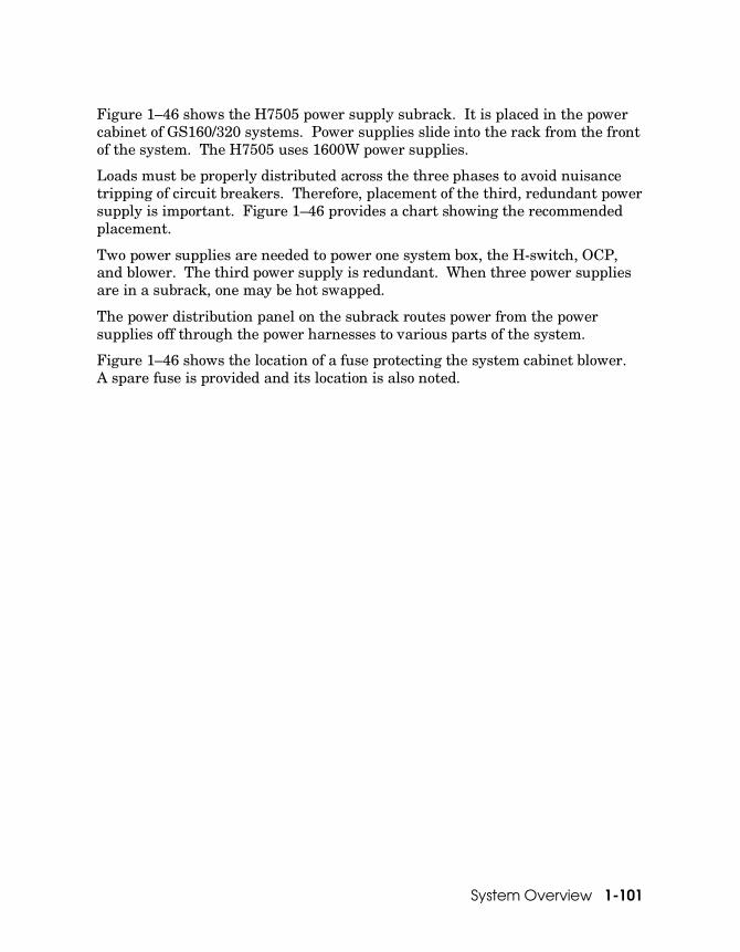
System Overview 1-101
Figure 1–46 shows the H7505 power supply subrack. It is placed in the power cabinet of GS160/320 systems. Power supplies slide into the rack from the front of the system. The H7505 uses 1600W power supplies.
Loads must be properly distributed across the three phases to avoid nuisance tripping of circuit breakers. Therefore, placement of the third, redundant power supply is important. Figure 1–46 provides a chart showing the recommended placement.
Two power supplies are needed to power one system box, the H-switch, OCP, and blower. The third power supply is redundant. When three power supplies are in a subrack, one may be hot swapped.
The power distribution panel on the subrack routes power from the power supplies off through the power harnesses to various parts of the system.
Figure 1–46 shows the location of a fuse protecting the system cabinet blower. A spare fuse is provided and its location is also noted.

1-102 AlphaServer GS80/160/320 Service Manual
1.22.4 Power Distribution Panel and Power Cabinet Bulkhead
The power distribution panel is located on the rear of the power subrack. The power cabinet bulkhead is located between the power cabinet and system cabinet 1. There are two power cabinet bulkheads, one for cables running from the subracks to system cabinet 1 and another for cables running from the subracks to system boxes in system cabinet 2.
Figure 1– 47 Power Cabinet Cabling and Distribution Panel
1
1
2
3
3
4
5
PK1533

System Overview 1-103
Figure 1–47 shows the location and use of the power distribution panel which is part of the power subrack. The power distribution panel performs the “oring functions” described in Section 1.22.
Figure 1–47 also shows power cabling in a power cabinet.
� Marks the connections made by the cable connecting the AC input box and the power distribution panel on the subrack.
� Shows the cable connections made by power and signal cables from the power distribution panel and the power cabinet bulkhead.
� Shows the cable connections made by the power cable connecting the subrack(s) and the OCP.
� The power distribution panel on the power subrack is where much of the logic controlling power resides.
� The power cabinet bulkhead is a piece of sheet metal with cutouts through which power and signal cables from the power distribution panel mate with cables that carry power and signals to the system boxes, H-switch, and blowers.

1-104 AlphaServer GS80/160/320 Service Manual
1.23 GS80 System Power
Six major components make up the power system for the AlphaServer GS80 systems: the AC input box, the 48V power supplies, the power modules in the drawer, the power managers, the PCI power supplies, and the storage power supplies.
Figure 1– 48 GS80 Power Distribution Block Diagram

System Overview 1-105
Major power components are described in the following sections except for the power modules in the drawer and the power managers. For the main power module see Section 1.15.1, for the auxiliary power module see Section 1.15.2, for the PSM see Section 1.8.4 and Section 1.12, and for the PBM see Section 1.8.5.
Figure 1–48 is a block diagram of power distribution in a GS80 system. It shows most of the major components that make up the power distribution system.
Note that diodes on the subracks and within the drawer are used to “or” 48V so that whenever either H7504 subrack is on, the OCP and clock are powered.

1-106 AlphaServer GS80/160/320 Service Manual
1.23.1 AC Input Box (Single Phase)
There are three variants of AC input boxes for GS80 systems. Only one AC input box is required when the inlet voltage is high (200+ V) and two are required when the voltage is low (120 V).
Figure 1– 49 AC Input Box (Single Phase)

System Overview 1-107
Figure 1–49 shows both the front and rear of the AC input box used for GS80 systems. Single-phase AC input power is used in these systems. There are three variants:
• The 30-48847-01 used in North America accommodates single phase 30 amp. 120V power
• The 30-48205-04 used in Europe phase 30 amp. 220-240V power
• The 30-48205-03 used in North America and Japan accommodates single phase 30 amp 200-240V power
There is no visual difference between the variants except the power cord plugs. The box has a main circuit breaker that protects all power to the system and branch circuit breakers that protect power to the 48V power supplies and to PCIs and storage devices. See the power distribution rules in Appendix A.
Two AC input boxes are needed in the largest of configurations.
A single LED, when lit, indicates the presence of AC input.
Table 1–14 shows which outlets each circuit breaker protects.
Table 1– 14 Circuit Breaker Line Protection (Single Phase)
Circuit Breaker Rating (amps)
North America Europe Japan
CB1 30 All All All
CB2 20 J1, J2 J1 – J8 J1-J8
CB3 20 J3 – J5 J9 – J16 J9 – J16

1-108 AlphaServer GS80/160/320 Service Manual
1.23.2 48V Power Supplies
The 1000 watt power supply converts AC from the drawer based system AC input box to 48 VDC and to Vaux (8.75 V DC).
Figure 1– 50 DC Power Supply (GS80)

System Overview 1-109
Figure 1–50 shows the 1000 watt 48V power supply. The power supply plugs into the power subrack. To differentiate it and the 1600 watt power supply used in system box based systems, note the back plug receptacle shapes are different (� in Figure 1–45 and � in Figure 1–50).
Features of the power supply are:
• 48 VDC and Vaux outputs. Vaux is always on when AC power is applied. 48 VDC output is controlled by an enable signal provided by the PSM in the system.
• Power factor correction on AC input
• May be placed in parallel
• May be hot swapped
• Dual speed fan – low speed when only Vaux is output, high speed when both voltages are output
• Output is automatically adjusted to 48V by sensing the voltage at the load and changing power supply output accordingly
• Fault protection for:
− Overcurrent
− Overvoltage
− Overtemperature
• Status signals
− VAUX_OK_L
− 48V_OK_L
− PS_PRESENT_L
• LEDs
− Vaux is always on when AC is applied and within regulation.
− 48V is on when the power supply is enabled and within regulation.
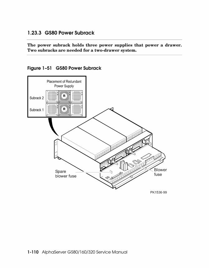
1-110 AlphaServer GS80/160/320 Service Manual
1.23.3 GS80 Power Subrack
The power subrack holds three power supplies that power a drawer. Two subracks are needed for a two-drawer system.
Figure 1– 51 GS80 Power Subrack

System Overview 1-111
Figure 1–51 shows the H7504 power supply subrack. It is placed between the drawers and the AC input boxes. Power supplies slide into the rack from the front of the system. The H7504 power subrack accepts 1000 watt power supplies.
Two power supplies are needed to power one drawer, the OCP, and clock. The third power supply is redundant. When there are three power supplies in a subrack, one may be hot swapped.
There is an electrical difference between the GS80 power subrack and the GS160/320 subrack.
Figure 1–51 shows the location of a fuse protecting the system cabinet blower. A spare fuse is provided and its location is also noted.
There are also two variants:
H7504-BA IEC power cord for North America (120V input)
H7504-DA NEMA power cord for Europe/Japan (200-240V inputs)

1-112 AlphaServer GS80/160/320 Service Manual
1.24 PCI Power Supply
The PCI power supply converts AC input to DC voltages required by the PCI I/O subsystem. One power supply is required; the second is redundant.
Figure 1– 52 PCI Power Supply
PK1247

System Overview 1-113
Figure 1–52 shows the PCI power supply, which receives AC power from the AC input box. The supply plugs into the front of the PCI box. One power supply is required for a PCI box; the second is redundant.
The power module converts single phase AC input to the following required outputs:
• +3.3V at 57A
• +5.0V at 50A
• +12V at 7A
• -12V at 1.5A
• Vaux (+5.0V) at 2A (Vaux - always on when AC applied)
Features of the power supply are:
• Power factor correction on AC input
• May be placed in parallel
• May be hot swapped
• Output is automatically adjusted by sensing the voltage at the load and changing power supply output accordingly
• Fault protection for:
− Overcurrent
− Overvoltage
− Overtemperature
− Magnetic interlock switch
• Status signals
− POK_L
− VAUX_OK_L
− OVERTEMP_L
− PRESENT_L
• LEDs
− Power OK
− Vaux OK
− Swap OK


Power-Up 2-1
Chapter 2 Power-Up
This chapter describes power-up testing and explains the power-up displays. The following topics are covered:
• Operator Control Panel
• Power-Up Test Flow – Init. and Phase 0
• Power-Up Test Flow – Phase 1
• Power-Up Test Flow – Phases 2, 3, and 4
• Power Applied – Vaux Present
• System Turned On
• SROM/XSROM Error Reports

2-2 AlphaServer GS80/160/320 Service Manual
2.1 Operator Control Panel
The control panel is located at the top of the power cabinet.
2.1.1 Control Panel Assembly
The control panel assembly has a three position On/Off switch, three pushbuttons, three status LEDs, and an ASCII/graphical vacuum fluorescent display.
Figure 2–1 Control Panel
PK0621
21 3 4
9 108
65 7
Users control the basic state of the system by use of pushbuttons and a keyswitch on the operator control panel (OCP). LEDs and a fluorescent display provide visual evidence of the system state.
Only the system control manager (SCM) in the system has access to the OCP. If the user changes the system state by pushing a button or turning the switch, the SCM communicates those changes to the system over the console serial bus (CSB) and through shared RAM on the standard I/O module to notify the SRM console and the operating system. The system responds accordingly.

Power-Up 2-3
The callouts in Figure 2–1 point to these components of the control panel.
� Secure LED – When lit, indicates that the keyswitch is in the Secure position and system is powered on. All OCP pushbutton and SCM functions are disabled including remote access to the system.
� Power LED – When lit, indicates that at least one QBB is powered on and that remote console operations are enabled. (Keyswitch in On position)
� Halt LED – When lit with the Power LED, indicates the system is powered on, remote console operations are enabled, and the Halt pushbutton is pressed. A HALT IN command issued at the remote console does not cause this LED to light.
When lit with both Power LED and Secure LED, indicates a powered on system, disabled remote console operations, and Halt pushbutton is pressed in.
� ASCII/graphical vacuum fluorescent display that displays a maximum of four 20-character rows of ASCII text or a small 120 x 32 dot graphic.
� Off switch position – System is powered off and cannot be powered on remotely. No LEDs are lit.
� On switch position – System is powered on and can be remotely powered on or off. (The power LED should be lit.)
� Secure switch position – System is powered on and cannot be remotely powered on or off. All OCP pushbutton and SCM functions are disabled. (The secure LED should be lit.)
Halt pushbutton – pressing this pushbutton causes the operating system to perform a halt, and prevents the console from booting the operating system. The halt stays in effect until the Halt pushbutton is pressed again. Pushing the halt button affects the entire system and all partitions in it.
¡ Fault pushbutton – pressing this pushbutton causes a system fault without clearing captured error information in control and status registers. If AUTO_FAULT_RESET is enabled, the system will automatically reset after a fault is generated.
¢ Reset pushbutton – pressing this pushbutton causes a system reset that clears captured error information.

2-4 AlphaServer GS80/160/320 Service Manual
2.1.2 Fluorescent Display Messages
The vacuum fluorescent display is used to communicate the state and or condition of the machine. Four 20-character lines are available.
Table 2– 1 Display Messages
Message Description
AlphaServer GS-xxx Identifies the AlphaServer as a GS-80, GS-160, or a GS-320. If the OCP_TEXT environment variable is empty, this line appears; otherwise the value of the OCP_TEXT environment variable is displayed.
Cpu- Mem- Pci- Indicates the number of good CPUs, memory arrays, and PCI buses attached to the system.
Keyswitch-ON/OFF/“ON/SECURE”
Indicates the state of the keyswitch.
Faulty Keyswitch Indicates that the keyswitch is not working or is not connected to the SCM.
Power ON The system is on.
ON - Failure The system failed during power-up. See the console display to determine why.
Powering/pwr OFF partition- x
The system is powering on or off a particular partition.
PwrOn Phase x Step y On a partition by partition basis, this line lists the power-up diagnostics currently running.
“Marks” Indicates that power-up flow is in progress.
Power Transition OFF/Failed
Indicates that the system is in the process of going from an On state to an Off state, or has failed in the process of going from an Off state to an On state.
QBB Power On/Off CPUx A particular CPU is powering on or off.
QBB Power On/Off IOR x A particular local I/O riser is powering on or off.

Power-Up 2-5
Message Description
ALERT: NO Valid MEM NO Valid CPU NO CPI & MEM NO Stdio
Alerts provide information about system configurations that cause the system or a partition not to operate. Those conditions are no valid CPUs or memory, or standard I/O module.
CLI HALT IN/OUT An SCM halt in or halt out command was issued.
HALT Asserted/Deasserted
The Halt button is in and the halt signal is asserted. The Halt button is out and the halt signal is not asserted.
CLI SYSTEM FAULT An SCM fault command was issued.
FAULT asserted The Fault button was pushed.
CLI RESET An SCM reset command was issued.
RESET The Reset button was pushed.
Master SCM Node If SCM failover occurs, or the micros reset while power is on, this line indicates that control of the CSB is restored to an SCM connected to this OCP.
Control Restored Should SCM failover occur, or the micros reset while power is on, this line indicates that control of the CSB is restored to an SCM CSB bus master.
SLAVE SCM NODE Indicates that this particular redundant OCP is connected to a slave (redundant) SCM.
Keyswitch - INACTIVE Indicates that this particular redundant OCP is connected to a slave SCM node and its keyswitch is inactive.
Messages shown in Table 2–1 appear on the OCP’s fluorescent display. Four lines can be displayed at any one time. Under normal operating conditions, messages underlined in Table 2–1 are displayed. Other messages appear when the system or a partition is powering up or is in transition. Still others appear when a control panel button is pushed or an SCM command is issued.

2-6 AlphaServer GS80/160/320 Service Manual
2.2 Power-Up Test Flow – Init. and Phase 0
After the initial setup, phase 0 tests the “local” QBBs.
Figure 2– 2 Power-Up Flowchart – Init. and Phase 0

Power-Up 2-7
Power-up consists of an initialization phase followed by five test phases. The system control manager (SCM) firmware, run by the microprocessor on the standard I/O module, controls power-up. The SCM, master of the console serial bus (CSB), sends power-up control test packets over the CSB to the PSMs in each QBB. The PSMs in turn pass power-up control test packets to the CPUs in the QBBs over the PSM to CPU serial lines.
Each microprocessor on the CSB (SCM, PSM, PBM, and HPM) has both an application image and a fail-safe loader (FSL) image in flash ROM.
When power is applied (or a reset is initiated), each microprocessor runs its FSL image that performs a checksum on the application image. If the checksum is bad, the microprocessor remains in FSL mode and the particular resource it controls will not be configured into the system. If the SCM fails the checksum, the system will not power up. Appropriate messages appear at the console. See Section 3.10 for more on the FSL.
A phase is executed during the time between communication points established between the SCM and PSMs. Steps within phases are tests executed between communication points between the PSM and SROM/XSROM code running on the CPU(s).
During the initialization phase, SROM code is loaded into I-cache of each CPU in the system and communication between the PSM and CPU is established over the serial lines. No tests are conducted.
During phase 0, “ local” testing of each QBB in the system is conducted. No testing is conducted between QBBs if more than one is present. At the end of phase 0, in addition to knowing the location of standard I/O module(s), the following is known about each QBB:
• Whether self-test passed or failed on CPUs, PSMs, DTags, DIRs, IOPs, and memory
• Whether the QBB switch, the global port, and the I/O path to the PCAs work
• The state and size of directory memory if it is working
• The state and size of the DTag if it is working
• Nothing about QBBs without CPUs other than the fact that they exist
Table 2–2 and Table 2–3 list the SROM tests and XSROM tests run during phase 0.

2-8 AlphaServer GS80/160/320 Service Manual
Figure 2– 2 Power-Up Flowchart – Init. and Phase 0 (Continued)

Power-Up 2-9
Table 2–2 lists the SROM tests run in phase 0.
Table 2– 2 SROM Tests
Test # Hex.
Test Name
Phase 0 Step 0 tests
1 Alpha CPU chip BIST check test (BIST = built-in self-test)
2 Alpha CPU D-cache test
3 B-cache initialization test
4 B-cache data line test
5 B-cache march test
6 B-cache address test
7 Alpha CPU chip D-cache and CPU Module B-cache error test
8 B-cache ECC data line test
9 B-cache data ECC march test
A B-cache data line and C-box read chain verify test
B B-cache data RAM and C-box read chain verify test

2-10 AlphaServer GS80/160/320 Service Manual
Table 2–3 lists the XSROM tests run in phase 0.
Table 2– 3 XSROM Tests Run in Phase 0
Test # Hex
Test Name
Phase 0 Step 1 tests
10 Local QSD WHAMI (QSD Who Am I register) test
11 Local QSD revision register test
12 Local QSA scratch register test
13 Local QSD CPU0… 3 scratch (QSDx scratch register) tests
14 Local non-device interrupt test
15 Local I/O device interrupt test
16 Local interval timer interrupt test
17 Local inter-processor interrupt test
18 Placeholder
Phase 0 Step 2 tests
19 Local IOP address path scratch CSR test
1a Local IOP data path scratch CSR test
1b Local I/O Hose 0 configuration and path verification test
1c Local I/O Hose 1 configuration and path verification test
1d Local I/O Hose 2 configuration and path verification test
1e Local I/O Hose 3 configuration and path verification test
1f Placeholder
Phase 0 Step 3 tests
20 Local GPA scratch register test
21 Local GPD scratch register test
22 Local global port-link to HS-link loopback test
23 Local global port performance monitor test

Power-Up 2-11
Table 2– 3 XSROM Tests Run in Phase 0 (Continued)
Test # Hex
Test Name
Phase 0 Step 3 tests continued
24 Local IOP error test
25 Local MEM0 scratch/BIST/error tests
26 Local MEM1 scratch/BIST/error tests
27 Local MEM2 scratch/BIST/error tests
28 Local MEM3 scratch/BIST/error tests
29 Local DTag scratch and BIST check test
2a Local directory scratch and BIST check test
Phase 0 Step 4 tests
2b Local IOP BIST check test
2c Local QSA error line test
2d Local hose error line test
2e Local GP error line test
2f Placeholder
30 Local DIRectory error line test
Phase 0 Step 5 tests
31 Local QSD error line (Fault) test
32 Local DTag error line (Fault) test

2-12 AlphaServer GS80/160/320 Service Manual
2.3 Power-Up Test Flow – Phase 1
Remote testing of QBBs is done in phase 1.
Figure 2– 3 Power-Up Flowchart - Phase 1

Power-Up 2-13
During phase 1, “remote” testing of each QBB in the system is conducted if there is more than one QBB in the system. Remote means testing of hardware by a system primary CPU, selected by the SCM from data collected in phase 0, across secondary (global ports) and the hierarchical switch if present.
Initial soft QBB IDs are assigned in this phase. (Soft QBB IDs may change during power-up if something fails.) Soft QBB IDs are necessary to make sure that good memory exists at address 000.0000.0000, a requirement of Tru64 UNIX. Since it is possible that hard QBB 0 may not have good memory, soft QBB ID 0, which will contain memory space address 000.0000.0000 by definition, is assigned to a QBB that has good functioning memory. As a result software uses a soft address that points to a hard address that may be different.
At the end of phase 1, the following is known:
• The soft and hard QBB IDs of all functioning QBBs in the system
• Whether there were self-test errors on CPUs, PSMs, DTags, DIRs, IOPs, and memory
• Whether the QBB switch, the global port, the I/O path to the PCAs, and the hierarchical switch work
• The configuration of all QBBs
• The location of any standard I/O modules (SIO)

2-14 AlphaServer GS80/160/320 Service Manual
Table 2–4 lists the XSROM tests executed during phase 1.
Table 2– 4 XSROM Tests Run in Phase 1
Test # Hex
Test Name
Phase 1 Step 6 tests
33 Placeholder
34 Local QBB soft ID configuration (system primary’s QBB only)
Phase 1 Step 7 Tests (start loop)
35 Remote GPA scratch register test
36 Remote GPD scratch register test
37 Remote QBB soft ID configuration
38 Remote global port performance monitor test
Phase 1 Step 8 tests
39 Remote IOP Address Path (IOA scratch CSR) test
3a Remote IOP Data Path (IOD scratch CSR) test
3b Remote I/O Hose 0 configuration and path verification test
3c Remote I/O Hose 1 configuration and path verification test
3d Remote I/O Hose 2 configuration and path verification test
3e Remote I/O Hose 3 configuration and path verification test
Phase 1 Step 9 tests
3f Remote QSA scratch register test
40 Remote QSD scratch register test
41 Remote IOP error line test

Power-Up 2-15
Table 2– 4 XSROM Tests Run in Phase 1 (Continued)
Test # Hex
Test Name
Phase 1 Step 9 tests continued
42 Remote MEM0 scratch/BIST/error line testing
43 Remote MEM1 scratch/BIST/error line testing
44 Remote MEM2 scratch/BIST/error line testing
45 Remote MEM3 scratch/BIST/error line testing
46 Remote DTag BIST check
47 Remote DIR BIST check
48 Remote IOP BIST check
49 Remote QSA error line test
4a Remote Hose error line test
4b Remote GP error line test
4c Placeholder
4d Remote directory error line test
Phase 1 Step A tests
4e Remote QSD error line (FAULT) test
4f Remote DTag error line (FAULT) test
Phase 1 Step B tests
50 Placeholder
51 Placeholder
52 Memory and directory configuration

2-16 AlphaServer GS80/160/320 Service Manual
2.4 Power-Up Test Flow – Phases 2, 3, and 4
During the final three phases, XSROM code assures cache coherency, assures that all CPUs can access all memory, and leaves all CPUs running the SRM console.
Figure 2– 4 Power-Up Flowchart - Phase 2, 3, and 4

Power-Up 2-17
The phase 2 test “victimizes” all cache blocks of all secondary CPUs. (The SP CPU “victimized” all its cache blocks at the end of phase 1.) A victimized cache block is one that the CPU has modified and wishes to write back to memory. Writing data back to memory assures that the contents of B-cache, DTags, and memory are coherent.
The phase 3 tests assure that each CPU interacts correctly with its own B-cache and the QBB’s DTag and can access each memory array in the entire system. In an eight QBB system each with four fully loaded memory carriers produces a maximum of 64 memory arrays to test by each CPU in the system. The memory access test operates on only one cache block in each array.
During phase 4, the SP CPU unloads the PAL/console code from the flash ROM on the standard I/O module into memory. It then places the starting address of the code in memory in its QSD CPUx scratch register. The secondary CPUs read that register waiting for the address and when it arrives, jump to the address and start running console code. All CPUs now run PAL/console code.
The SRM console conducts the rest of power-up.
Table 2–5 lists the XSROM tests run during phases 2, 3, and 4.
Table 2– 5 XSROM Tests Run in Phases 2, 3, and 4
Test # Test Name
Phase 2 Step C test
53 Secondary cache victimization test
Phase 3 Step D tests
54 B-cache TAG data line testing (run by all CPUs)
55 Memory access test (run by all CPUs)
56 Low memory mailbox access test (run by all CPUs)
57 Memory thrashing test (run by all CPUs)
Phase 4 Step E tests
58 Console flash ROM checksum and unload test (CSB)
59 Console (alternate) flash ROM checksum and unload test (CSB)
Phase 4 Step F tests
5a – 5c Placeholder
5d CPU hot-swap cache victimization/jump to console test
5e – 5f Placeholder

2-18 AlphaServer GS80/160/320 Service Manual
2.5 Power Applied – Vaux Present
When power is applied, the microprocessors on the CSB execute their built-in self-test (BIST) and the system control manager takes control of the system. Micros on the CSB are SCMs, PSMs, HPM, and PBMs.
Example 2– 1 System Control Manager Power-Up Display Master SCM | Testing SCM EEPROM – Passed | � Initializing Evs | SCM Selftest Passed | Polling CSB............................ � OCP will be inactive for first 12 seconds after micro reset � SCM_E0> Querying the modem port...no device detected � SCM_E0> | ~I~ CSB Node 10 connection added | SCM_E0> | ~I~ CSB Node 11 connection added | SCM_E0> PS1 in PBP0 added | PS2 in PBP0 added | � Remote IOR0 added to PBP0 | SCM_E0> | ~I~ CSB Node 40 connection added | � SCM_E0> PS1 in PBP1 added | PS2 in PBP1 added | � Remote IOR0 added to PBP1 | SCM_E0> PS2 in HS0 added | GP0 Cable Present | GP1 Cable Present | � GP2 Cable Present | GP3 Cable Present | SCM_E0> | ~I~ CSB Node 30 connection added | SCM_E0> | ~I~ CSB Node 31 connection added | � SCM_E0> | ~I~ CSB Node 32 connection added | SCM_E0> | ~I~ CSB Node 33 connection added |

Power-Up 2-19
Example 2–1 shows the SCM monitor display for a four QBB system with eight CPUs. Auxiliary power is applied to the system when the AC circuit breakers are put in the On position.
Refer to Example 2–1.
� When power is applied, an eligible SCM with the lowest csb node ID number connected to the OCP and running from its application image becomes master of the CSB. It checks its EEPROM and self-test, restores environment variables (EVs), and sets up data structures and CSB communication channels.
� The SCM polls all addresses on the CSB.
� The state of the OCP is ignored until after the SCM maps the system. The time that the SCM ignores the OCP has a default of 12 seconds.
� The modem port is polled. Had there been a modem attached, data describing its configuration would have been displayed. See the AlphaServer GS80/160/320 User’s Guide or Firmware Reference Manual.
� Two PCIs are found, one at CSB node 10 (PBP0), and the other at node 11 (PBP1). Both have two power supplies PS1 and PS2 and both have a single remote I/O riser (IOR0).
� Node 40, the hierarchical switch, is added to the CSB and cables connecting it to global ports 0, 1, 2, and 3 are found. In this example only one of the two possible H-switch power supplies is present.
� Information messages connecting nodes 30, 31, 32, and 33 to the CSB are displayed indicating the presence of four QBBs.
Continued on next page
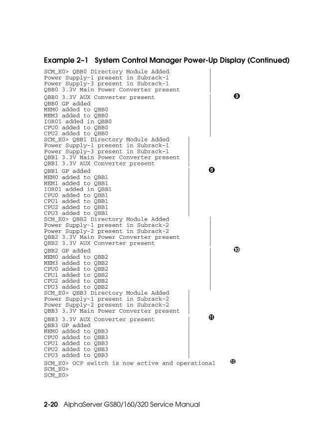
2-20 AlphaServer GS80/160/320 Service Manual
Example 2– 1 System Control Manager Power-Up Display (Continued) SCM_E0> QBB0 Directory Module Added | Power Supply-1 present in Subrack-1 | Power Supply-3 present in Subrack-1 | QBB0 3.3V Main Power Converter present | QBB0 3.3V AUX Converter present | QBB0 GP added | MEM0 added to QBB0 | MEM3 added to QBB0 | IOR01 added in QBB0 | CPU0 added to QBB0 | CPU2 added to QBB0 | SCM_E0> QBB1 Directory Module Added | Power Supply-1 present in Subrack-1 | Power Supply-3 present in Subrack-1 | QBB1 3.3V Main Power Converter present | QBB1 3.3V AUX Converter present | QBB1 GP added | ¡ MEM0 added to QBB1 | MEM1 added to QBB1 | IOR01 added in QBB1 | CPU0 added to QBB1 | CPU1 added to QBB1 | CPU2 added to QBB1 | CPU3 added to QBB1 | SCM_E0> QBB2 Directory Module Added | Power Supply-1 present in Subrack-2 | Power Supply-2 present in Subrack-2 | QBB2 3.3V Main Power Converter present | QBB2 3.3V AUX Converter present | QBB2 GP added | ¢ MEM0 added to QBB2 | MEM3 added to QBB2 | CPU0 added to QBB2 | CPU1 added to QBB2 | CPU2 added to QBB2 | CPU3 added to QBB2 | SCM_E0> QBB3 Directory Module Added | Power Supply-1 present in Subrack-2 | Power Supply-2 present in Subrack-2 | QBB3 3.3V Main Power Converter present |
QBB3 3.3V AUX Converter present | 11 QBB3 GP added | MEM0 added to QBB3 | CPU0 added to QBB3 | CPU1 added to QBB3 | CPU2 added to QBB3 | CPU3 added to QBB3 | SCM_E0> OCP switch is now active and operational 12 SCM_E0> SCM_E0>

Power-Up 2-21
The continuation of Example 2–1 shows the description of each QBB. In this particular system only QBBs 0 and 1 have local I/O risers. QBB1 has two CPUs while the rest have four. Other similarities and differences between the QBBs can be seen by further examination.
QBB0 is described.
¡ QBB1 is described.
¢ QBB2 is described.
11 QBB3 is described.
12 The SCM can now begin to monitor the state of the OCP switch.
Once the SCM has configured the CSB, it begins to monitor the state of the OCP switch. Assuming the switch is in the Off position, the SCM monitor display remains at the SCM prompt. If the OCP keyswitch is in the On position, the SCM will automatically continue with power-up.

2-22 AlphaServer GS80/160/320 Service Manual
2.6 System Turned On
Once the OCP switch is attended by the SCM firmware, the system can be turned on by the switch.
Example 2– 2 SCM Power-Up Display (OCP On) SCM_E0> OCP switch is now active and operational SCM_E0> SCM_E0> Powering on PCI Box 0 | � Powering on PCI Box 1 | ~I~ Testing OCP Switch- passed QBB-0 Powering ON | Power ON Phase INIT | QBB-1 Powering ON | � QBB-2 Powering ON | QBB-3 Powering ON | SCM_E0> QBB2 now Testing Step-0 | QBB3 now Testing Step-0 | � QBB0 now Testing Step-0 | QBB1 now Testing Step-0 | ~I~ SCMe1 non-csb member while it tests & initializes its Shared RAM � SCM_E0> . ~I~ QBB0/PSM30 SysEvnt: QBB_INIT_CD1 Reg0:7AB3 Reg1:35FF (test-0) | (fmask/fts:8f) | | ~I~ QBB2/PSM32 SysEvent: QBB_INIT_CD1 Reg0:768F Reg1:0FFF (test-0) | (fmask/fts:8f) |
| � ~I~ QBB1/PSM31 SysEvent: QBB_INIT_CD1 Reg0:7AB3 Reg1:3FFF (test-0) | (fmask/fts:8f) | | ~I~ QBB3/PSM33 SysEvent: QBB_INIT_CD1 Reg0:768F Reg1:0FFF (test-0) | (fmask/fts:8f) | Testing SIO Shared RAM(please wait) | | � Initializing shared ram | Shared RAM Initialized | Powering ON H-Switch | SCM_E0> | � ~I~ HSW4/HPM40 SysEvent: HS_INIT_CD1 Reg0:000F Reg1:D581 |

Power-Up 2-23
Example 2–2 shows a continuation of the SCM console display after the OCP switch has been put in the On position.
Refer to Example 2–2.
� PCIs and QBBs are powered on.
� The QBBs are powered on and the Init. Phase is started.
� The SROM code (step 0) is run on each CPU in each QBB.
� The master SCM is SCM_E0 and, in this case, the slave SCM is SCMe1. The message displayed here indicates that while the slave SCM is testing its shared RAM, the master SCM recognizes that fact. The standard I/O shared RAM is tested and initialized. The SCM, SRM console, and operating systems use this RAM to pass information to each other.
� The PSM in each QBB is told to establish the relationship between transmit and receive time between each element (CPU, memory, global port, and directory) attached to the local quad switch. In other words, the local switch is started and synchronized.
� The standard I/O shared RAM is tested and initialized. The SCM, SRM console, and operating systems use this RAM to pass information to each other.
� HPM is told to establish the relationship between transmit and receive time between each element (global ports) attached to the hierarchical switch. In other words, the hierarchical switch is started and synchronized.

2-24 AlphaServer GS80/160/320 Service Manual
Example 2– 2 SCM Power-Up Display (OCP On) (Continuation 1)
Phase 0 �
~I~ Enable HS Links: 0f � ~I~ QbbConf(gp/io/c/m)=0000bbff Assign=0f SQbb0=00 PQbb=00 SoftQbbId=0000ba98 |
~I~ SysConfig: 00 00 00 00 00 00 00 00 07 1f 07 9f 37 3f 37 95 | � SCM_E0>
~I~ HSW4/HPM40 SysEvent: LINK0_ON Reg0:000F Reg1:D581 |� SCM_E0> | ~I~ HSW4/HPM40 SysEvent: LINK1_ON Reg0:010F Reg1:D581 | SCM_E0> | ~I~ HSW4/HPM40 SysEvent: LINK2_ON Reg0:030F Reg1:D581 | SCM_E0> | ~I~ HSW4/HPM40 SysEvent: LINK3_ON Reg0:070F Reg1:D581 | SCM_E0> ........... QBB2 now Testing Step-1 | QBB3 now Testing Step-1. | QBB1 now Testing Step-1.. | QBB0 now Testing Step-1................................... | QBB0 now Testing Step-2. | QBB0 now Testing Step-3. | � QBB0 now Testing Step-4. | QBB0 Step(s)-4 5 Tested.. | QBB3 now Testing Step-2. | QBB3 now Testing Step-3. | QBB3 now Testing Step-4. | QBB3 Step(s)-4 5 Tested............... | QBB1 now Testing Step-2. | QBB2 now Testing Step-2. | QBB1 now Testing Step-3 | QBB2 now Testing Step-3. | QBB1 now Testing Step-5 | QBB2 now Testing Step-5 | Phase 1 QBB0 IO_MAP0: 0000A0C001333333 | QBB1 IO_MAP1: 0000A1C101333333 | � QBB2 IO_MAP2: 0000000000000003 | QBB3 IO_MAP3: 0000000000000003 | | ~I~ QbbConf(gp/io/c/m)=0000bbff Assign=0f SQbb0=00 PQbb=00 SoftQbbId=0000ba98 | ~I~ SysConfig: 00 00 00 00 00 00 00 00 07 1f 07 9f 37 3f 37 95 | SCM_E0> QBB2 now Testing Step-6 | QBB3 now Testing Step-6. | QBB0 now Testing Step-6. | � QBB1 Step(s)-5 6 Tested | QBB2 Step(s)-6 Tested | QBB3 Step(s)-6 Tested | QBB0 now Testing Step-7. | QBB0 now Testing Step-8. |

Power-Up 2-25
QBB0 now Testing Step-9. | QBB0 now Testing Step-A. | QBB0 now Testing Step-7. | � QBB0 now Testing Step-8. | QBB0 now Testing Step-9.. | QBB0 now Testing Step-A. | QBB0 now Testing Step-7. | QBB0 now Testing Step-8.. | QBB0 now Testing Step-9. | QBB0 now Testing Step-A. | QBB0 now Testing Step-B. | Refer to continuation 1 of Example 2–2.
� Phase 0, local QBB testing begins. See Section 2.2 for information on testing done in phase 0.
� The SCM sends the H-switch a mask of links between the global ports and the H-switch to enable the links.
� The configuration data from the initialization phase is displayed.
� The links between the H-switch and the global ports in each QBB are on. This is the result of the command sent in �.
� Phase 0 steps 1 through 5 are run on each QBB. Had any test failed, an error message would have printed in the display. Phase 0 ends.
� If errors had occurred in phase 0, error messages would have appeared here. Had there been any errors, the configuration described here might be different from the configuration described in �. See Section 2.7 for information on interpreting SROM/XSROM error messages. Note that when diagnostics fail, they may call out several different FRUs. The SCM monitor may drop from the configuration those resources that the diagnostic identifies as being the most likely failing unit (FRU1). It will not drop those resources identified by the diagnostic as FRU2 – FRU4.
� Each step of phase 1 is performed on each QBB. In phase 1 a system primary CPU is chosen and it tests each QBB over a path out its global port through the hierarchical switch and in to the QBB under test through its global port. For a list of tests run in phase 1, see Table 2–4.

2-26 AlphaServer GS80/160/320 Service Manual
Example 2– 2 SCM Power-Up Display (OCP On) (Continuation 2)
Phase 2 �
QBB0 IO_MAP0: 0000A0C001333333 | � QBB1 IO_MAP1: 0000A1C101333333 | QBB2 IO_MAP2: 0000000000000003 | QBB3 IO_MAP3: 0000000000000003 | | ~I~ QbbConf(gp/io/c/m)=0000bbff Assign=0f SQbb0=00 PQbb=00 SoftQbbId=0000ba98 ~I~ SysConfig: 00 00 00 00 00 00 00 00 07 1f 07 9f 37 3f 37 95 | SCM_E0> QBB1 now Testing Step-C | � QBB2 now Testing Step-C | QBB3 now Testing Step-C. | QBB0 now Testing Step-C. | Phase 3 ~I~ QbbConf=0000bbff Assign=0f SQbb0=00 PQbb=00 SoftQbbId=0000ba98 | � ~I~ SysConfig: 00 00 00 00 00 00 00 00 07 1f 07 9f 37 3f 37 95 | SCM_E0> . QBB0 now Testing Step-D | � QBB1 now Testing Step-D | QBB2 now Testing Step-D | QBB3 now Testing Step-D...... | QBB0 IO_MAP0: 0000A0C001333333 | � QBB1 IO_MAP1: 0000A1C101333333 | QBB2 IO_MAP2: 0000000000000003 | QBB3 IO_MAP3: 0000000000000003 | Phase 4 ~I~ QbbConf(gp/io/c/m)=0000bbff Assign=0f SQbb0=00 PQbb=00 SoftQbbId=0000ba98
~I~ SysConfig: 00 00 00 00 00 00 00 00 07 1f 07 9f 37 3f 37 95 | � QBB0 unloading console across port0 from PCI Box-0 | � Console COM1 from master PCI Box-0 | Retrieving FRU information for Shared RAM...(please wait) | SCM_E0> . QBB0 now Testing Step-E | QBB1 now Testing Step-E | QBB2 now Testing Step-E | QBB3 now Testing Step-E. | Power On Complete | ¡ Returning to system COM1 port |

Power-Up 2-27
Refer to continuation 3 of Example 2–2.
� Phase 2 begins.
� The pass/fail results of phase 1 are passed back to the SCM indicated by the ~I~ line. An I/O map built by the PSM, now the result of remote testing, is passed to the SCM monitor.
� Phase 2 testing is done on each QBB. Phase 2 consists of a single test. The caches of each secondary CPU are victimized – that is, written back into memory with the result that memory and caches are now coherent. For detailed information on cache coherency, see Appendix B.
� Again the system map is displayed.
� Phase 3 testing is done on each QBB. Phase 3 tests that each CPU can access each memory in each QBB in the system. See Table 2–5 for a list of these tests.
� A final system map is displayed.
� The system primary CPU, in this case CPU0, unloads the console code from the master PCI box over an identified path.
The secondary CPUs in each QBB start running the console code.
¡ After phase 4 step E (console unload), power-on is complete and control of the system is passed to COM1. The SCM monitor relinquishes control of the system and turns control over to the SRM console if the environment variable AUTO_QUIT_SCM is enabled.

2-28 AlphaServer GS80/160/320 Service Manual
Example 2– 2 SCM Power-Up Display (OCP On) (Continuation 3)
System Primary QBB0 : 0 |� System Primary CPU : 0 on QBB0 \ . | Par hrd/csb CPU Mem IOR3 IOR2 IOR1 IOR0 GP QBB Dir PS Temp | QBB# 3210 3210 (pci_box.rio) Mod BP Mod 321 (ºC) | | (-) 0/30 -P-P P--P --.- --.- P0.1 P0.0 P P P P-P 28.0 | (-) 1/31 PPPP --PP --.- --.- P1.1 P1.0 P P P P-P 31.0 | (-) 2/32 PPPP P--P --.- --.- --.- --.- P P P -PP 28.5 | (-) 3/33 PPPP ---P --.- --.- --.- --.- P P P -PP 30.5 | | | HSwitch Type Cables 7 6 5 4 3 2 1 0 Temp(ºC) | HPM40 4-port - - - - P P P P 30.0 | | PCI Rise1-1 Rise1-0 Rise0-1 Rise0-0 RIO PS Temp | Cab 7 6 5 4 3 2 1 7 6 5 4 3 2 1 1 0 21 (ºC) | | 10 - - L - - - - - - - - L - S * * PP 33.5 | 11 - - - - - - - - - - - - - S * * PP 32.0 | OpenVMS PALcode V1.78-2, Tru64 UNIX PALcode V1.71-1 � system = QBB 0 1 2 3 + HS |� QBB 0 = CPU 0 2 + Mem 0 3 + Dir + IOP + PCA 0 1 + GP (Hrd QBB 0)| QBB 1 = CPU 0 1 2 3 + Mem 0 1 + Dir + IOP + PCA 0 1 + GP (Hrd QBB 1)| QBB 2 = CPU 0 1 2 3 + Mem 0 3 + Dir + IOP + PCA + GP (Hrd QBB 2)| QBB 3 = CPU 0 1 2 3 + Mem 0 + Dir + IOP + PCA + GP (Hrd QBB 3)| shared RAM version is 1.4 hose 0 has a standard I/O module � starting console on CPU 0 | � initialized idle PCB | initializing semaphores | initializing heap | initial heap 2c0c0 | memory low limit = 1f4000 | heap = 2c0c0, 1ffc0 | initializing driver structures | initializing idle process PID | initializing file system | initializing timer data structures | lowering IPL | CPU 0 speed is 731 MHz | � create dead_eater | create poll | create timer | create powerup | access NVRAM | QBB 0 memory, 4 GB |

Power-Up 2-29
QBB 1 memory, 3 GB | QBB 2 memory, 3 GB | QBB 3 memory, 1 GB | total memory, 11 GB | copying PALcode to 10bffe8000 | � copying PALcode to 20bffe8000 | copying PALcode to 303ffe8000 |
Refer to continuation 3 of Example 2–2.
� An expanded system map is displayed.
� PALcode is loaded and started.
� The system configuration is displayed from the SRM console point of view.
� The location of the standard I/O module with both the SCM monitor code and the SRM console code is determined.
� The console is started on the system primary CPU. In this case CPU0 in QBB0.
� The CPU’s speed is identified, various firmware variables are created, and distributed memory is sized and mapped.
� The PALcode is copied into memory locations in each QBB making local references possible.

2-30 AlphaServer GS80/160/320 Service Manual
Example 2– 2 SCM Power-Up Display (OCP On) (Continuation 4)
probe I/O subsystem | � probing hose 0, PCI | probing PCI-to-ISA bridge, bus 1 | bus 0, slot 1 -- pka -- QLogic ISP10x0 | bus 0, slot 3 -- ewa -- DE500-BA Network Controller | bus 0, slot 15 -- dqa -- Acer Labs M1543C IDE | bus 0, slot 15 -- dqb -- Acer Labs M1543C IDE | probing hose 1, PCI | probing hose 2, PCI | probing hose 3, PCI | bus 0, slot 5 -- pkb -- QLogic ISP10x0 | probing hose 8, PCI | probing PCI-to-ISA bridge, bus 1 | bus 0, slot 1 -- pkc -- QLogic ISP10x0 | bus 0, slot 15 -- dqc -- Acer Labs M1543C IDE | bus 0, slot 15 -- dqd -- Acer Labs M1543C IDE | probing hose 9, PCI | probing hose 10, PCI | probing hose 11, PCI | starting drivers | entering idle loop starting console on CPU 2 | � initialized idle PCB | initializing idle process PID | lowering IPL | CPU 2 speed is 731 MHz | create powerup | entering idle loop | starting console on CPU 4 | initialized idle PCB | initializing idle process PID | lowering IPL | CPU 4 speed is 731 MHz | create powerup | starting console on CPU 5 | initialized idle PCB | initializing idle process PID | lowering IPL | CPU 5 speed is 731 MHz | create powerup | entering idle loop | starting console on CPU 6 | initialized idle PCB | initializing idle process PID | lowering IPL | CPU 6 speed is 731 MHz | create powerup |

Power-Up 2-31
Refer to continuation 4 of Example 2–2.
� The I/O subsystem is mapped.
� Each CPU in the system is identified, started, and initialized.

2-32 AlphaServer GS80/160/320 Service Manual
Example 2– 2 SCM Power-Up Display (OCP On) (Continuation 5)
starting console on CPU 7 | � initialized idle PCB | initializing idle process PID | lowering IPL | CPU 7 speed is 731 MHz | create powerup | starting console on CPU 8 | initialized idle PCB | initializing idle process PID | Repeated for each lowering IPL | CPU in the system. CPU 8 speed is 731 MHz | create powerup | . . . starting console on CPU 14 | initialized idle PCB | initializing idle process PID | lowering IPL | CPU 14 speed is 731 MHz | create powerup | initializing pka pkb pkc ewa dqa dqb dqc dqd � environment variable mopv3_boot created version V5.8-126 Mar 1 2000 01:44:48 initializing GCT/FRU at 1f4000 � AlphaServer Console V5.8-126, built on Mar 1 2000 at 01:44:48 � P00>>>

Power-Up 2-33
Refer to continuation 5 of Example 2–2.
� Each secondary CPU starts the console, is initialized and ready to join the multiprocessor environment.
� The I/O subsystem is initialized.
� GCT/FRU is the system configuration tree/FRU table and its location in memory is 1f4000. The configuration tree/FRU table is the data structure containing information about hard and soft partitions. Note that the location in memory of the configuration tree is a fixed address in these systems. (GCT stands for Galaxy Configuration Tree.)
� The SRM console is up and running on all CPUs in the system.

2-34 AlphaServer GS80/160/320 Service Manual
2.7 SROM/XSROM Error Reports
SROM and XSROM errors are reported to the PSM, which passes the error information on to the SCM at the end of each phase. The SCM formats the information and displays it to the console. For a full description of running SROM/XSROM tests, see Section 3.5.
Example 2– 3 Examples of the SCM Error Display Example 1 SCM_E0> test &pc0 13 Testing. Please wait... � � �/� �/� *** Error Format: 1 Severity: Hard QBB/CPU: 00/00 Type: XSROM selftest Test: 13h Error: 0002 � Rvsn: V4.0-0 FRU1: QBB0 QSD3 | FRU2: QBB0.CPU0 | � FRU3: | FRU4: | P1: 5755555555555555 (Exp) | P2: 5555555555555555 (Rcvd) | � P3: 00000f8fff940800 (Addr) | P4: 0000000000000080 |
Example 2
SCM_E0> test &pc0 25 Testing. Please wait...0 *** Error Format: 2 Severity: Hard QBB/CPU: 00/00 Type: XSROM selftest Test: 25h Error: 100f Rvsn: V4.9-0 FRU1: QBB0.MEM0.DIMM J2, J3, J4 FRU2: FRU3: FRU4: P1: 00000000000e0000 P2: 0000000000000005 P3: 000000000c0f0c00 P4: 00000f8fffd9d000
Continued on page 2-36

Power-Up 2-35
The SCM formats and prints SROM and XSROM errors found during power-up or when executing the diagnostics in user mode. Example 2–3 shows examples of two formats for SROM/XSROM failures.
� The error format is identified: 1 = expected/received 2 = parameters 3 = unexpected exception
� Severity: possible results are: hard, soft, machine check, fault, or unexpected interrupt
� QBB in which the error occurred
� CPU that was executing code at the time the error occurred
� Type of Error = SROM or XSROM Test # = hex number of the test running at the time of the error Error # = the specific error identifying the diagnostic subtest (see Appendix C)
� Possible FRU(s) and the possible component on that FRU ordered from most likely to least likely
� Values of specific parameters the diagnostic test uses (see Appendix C for definitions of parameters related to the specific test and sub-test)
Example 1 shows a QSD CPUx_SCRATCH CSR Read/Write Test failure. A bit in the data path is not correct. The parameters in this format are: expected data, received data, and the address where the error occurred. In this case the error points to the QSD3 ASIC on QBB0. Diagnostic error FRU1 callouts are the ones used by the SCM to determine what resource to drop from the system as it is powering up. In this case QBB0 would be dropped from the system.
Example 2 shows a local memory BIST check test failure on MEM0. Appendix C shows error number 100f of test 25 to be a multi-bit error on MEM0. The callout of DIMMs is J2, J3, and J4. The parameters are also defined in Appendix C. Diagnostic error FRU1 callouts are the ones used by the SCM to determine what resource to drop from the system as it is powering up. In this case the memory array with the failing DIMM would be mapped out of the system.

2-36 AlphaServer GS80/160/320 Service Manual
Example 2– 3 Examples of the SCM Error Display (Continued) Example 3 SCM_E0> test &pc0 52 Testing. Please wait... *** Error Format: 2 Severity: Hard QBB/CPU: 00/00 Type: XSROM selftest Test: 52h Error: 0108 Rvsn: V4.1-0 FRU1: QBB0.MEM1 ARR0, CFG FRU2: FRU3: FRU4: P1: 0000000000000108 P2: 0000000000000000 P3: 0000000000000000 P4: 0000000000000000 SCM_E0>
Example 3 shows a memory/directory configuration test failure. A careful reading of Appendix C error 108 of test 52 shows that array 0 in MEM1 on QBB0 is not fully populated. The array would be mapped out of the system.

Troubleshooting 3-1
Chapter 3 Troubleshooting
This chapter describes various troubleshooting techniques including power-up testing and explains the power-up displays. The following topics are covered:
• Troubleshooting During Power-Up
• System Management Console Problems
• Power-Up Display and Troubleshooting
• Using the SCM Monitor
• Running Diagnostics Using the SCM Monitor
• Using the SRM Console
• Running Diagnostics from the SRM Console
• Troubleshooting with LEDs
• Dealing with a Hung System
• Dealing with Corrupt Firmware
• Error Detection
• Compaq Analyze

3-2 AlphaServer GS80/160/320 Service Manual
3.1 Troubleshooting During Power-Up
Power problems may occur when powering up the system.
Table 3–1 Power Problems
Symptom Possible Cause Indicators
System does not power up and/or main blowers off and/or nothing on console
Vaux problems (affects the entire system) - AC at site not available
- AC input box not plugged in/power cord faulty (AC input box LEDs not lit)
- AC input box circuit breakers tripped
- AC input box broken
- Power cords from AC input box to power supplies (48V or PCI) not plugged in or faulty
- Power supplies broken (both PCI and/or all 48V) (Vaux LEDs off)
- Broken power subrack distribution panel
- Power not getting from subrack distribution panel to PSMs in QBBs (PSM Vaux LED off)
- Power not getting from QBB backplane to CSB board in H-switch housing or drawer
- Power not getting to console serial bus node ID module in PCI box
- Short-circuit protection module tripped, loose, or fallen off
AC LEDs off
AC LEDs off
AC LEDs off
Power supply LEDs off
Power supply LEDs off
None
Vaux LEDs off on QBB mods
None
Vaux LED off on ID mod
Message on console – MPLL_DCOK_Timeout

Troubleshooting 3-3
Table 3– 1 Power Problems (Continued)
Symptom Possible Cause Indicators
System does not power up/main blowers off
CSB bus problems - Cable broken/disconnected along path from STD I/O ¬ CSB ID module ¬ CSB module
- Vaux problem
Message on console regarding lost connections
See above
System does not power up/main blowers off
OCP problems - OCP present signal not seen by SCM (signal cable path from STD I/O ¬ STD I/O cable interface ¬ OCP) (SCM thinks it’s a slave on the CSB and cannot issue power-up cmds.)
- 48V problem
SCM states it’s a slave on the console
OCP LEDs off
System or part of system does not power up and/or main blowers off
48V power problems (may affect part or entire system) - Any Vaux problem will cause 48V problems
- Any CSB problem
- Any OCP problem
- Signal from PSM to power distribution panel on subrack not good (cable connections)
- PSM failure
- PSM service switch in Service position
See above
See above
See above
Power supply LEDs off
Same
Switch ¬ serv./ PSM qbb_dc_good LED off/console message
Continued on next page

3-4 AlphaServer GS80/160/320 Service Manual
Table 3– 1 Power Problems (Continued)
Symptom Possible Cause Indicators
System or part of system does not power up
Logic voltage problems - PSM faiure
- Main power module failure
- Auxiliary power module failure
PSM/main/aux LEDs not normal
PSM qbb_dc_good LED off/ main power LEDs not normal
PSM qbb_dc_good LED off/ aux power LEDs not normal

Troubleshooting 3-5
3.2 System Management Console Problems
If the system management console connected to the local terminal port on a standard I/O module does not operate, the problem could range from broken hardware to unequal baud rates on the serial line.
Table 3– 2 Console Problems
Symptom Possible Cause Indicator
Power-up display not seen on the system management console
- System management console not plugged in
- Path from the master standard I/O module to the system console problem
- Baud rate of console device and COM1 not the same
- Console environment variable not set to serial
- Mouse or keyboard connections poor
- Mouse or keyboard broken
- Terminal emulator software not set up properly (See Appendix D.)
CPU run LED off
No display
None or strange characters seen
No display
Console device does not respond
Console device does not respond
No display
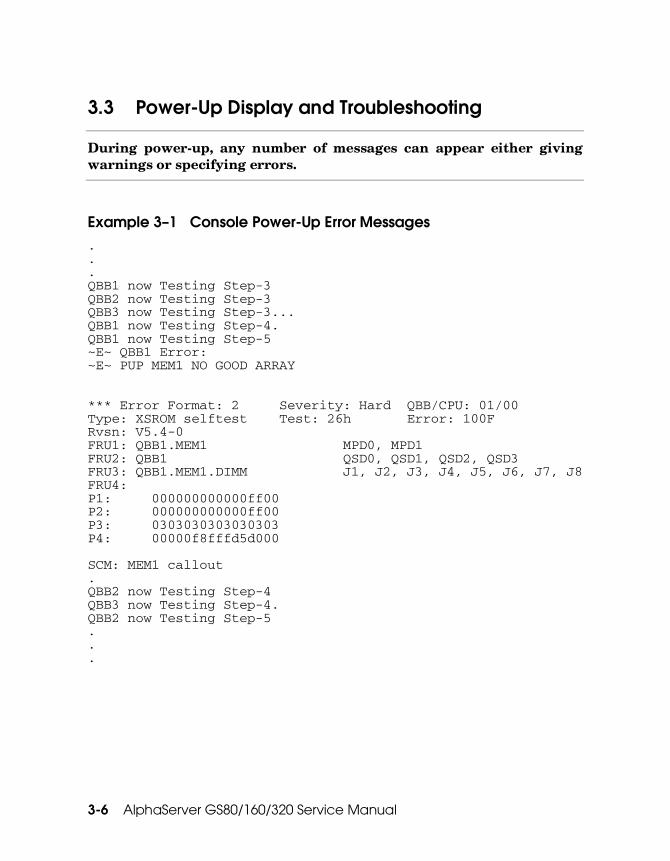
3-6 AlphaServer GS80/160/320 Service Manual
3.3 Power-Up Display and Troubleshooting
During power-up, any number of messages can appear either giving warnings or specifying errors.
Example 3– 1 Console Power-Up Error Messages . . . QBB1 now Testing Step-3 QBB2 now Testing Step-3 QBB3 now Testing Step-3... QBB1 now Testing Step-4. QBB1 now Testing Step-5 ~E~ QBB1 Error: ~E~ PUP MEM1 NO GOOD ARRAY *** Error Format: 2 Severity: Hard QBB/CPU: 01/00 Type: XSROM selftest Test: 26h Error: 100F Rvsn: V5.4-0 FRU1: QBB1.MEM1 MPD0, MPD1 FRU2: QBB1 QSD0, QSD1, QSD2, QSD3 FRU3: QBB1.MEM1.DIMM J1, J2, J3, J4, J5, J6, J7, J8 FRU4: P1: 000000000000ff00 P2: 000000000000ff00 P3: 0303030303030303 P4: 00000f8fffd5d000 SCM: MEM1 callout . QBB2 now Testing Step-4 QBB3 now Testing Step-4. QBB2 now Testing Step-5 . . .

Troubleshooting 3-7
Example 3–1 shows a memory error report in the middle of power-up. In this case memory failed self-test and the report shows that the most likely FRU is memory 1 in QBB1.
The SROM/XSROM diagnostic reports errors using error and warning formats:
*** Designates a diagnostic error format. Depending on the type of error and the configuration, the machine will most likely power up. At a minimum the resource is dropped from the system.
### Designates a diagnostic warning format. The machine will power up and the resource will most likely be available.
The SCM reports the following:
~E~ Designates an error detected by the scm/psm/hpm/pbm. Depending upon the type of error and system configuration, the machine will most likely power up but the resource is dropped. If you see ***, you'll also see ~E~.
~W~ Designates a warning and is much like ~E~ except it is not as severe. The machine will most likely power up but the resource is questionable. An example would be the failure of a redundant power supply in the PCI; the machine powers up and the PCI resources are available.
~I~ Designates an information message about power-up progress or configuration.
Table 3–3 lists the messages sent to the OCP’s fluorescent display during power-up and when a number of system events occur. It is another source of information that may be useful when troubleshooting or configuring the machine.

3-8 AlphaServer GS80/160/320 Service Manual
Table 3– 3 Fluorescent Display Messages
Display Message Description
AlphaServer GS-xxx Identifies the AlphaServer as a GS-80, GS-160, or a GS-320. If the OCP_TEXT environment variable is empty, this line appears, otherwise the value of the OCP_TEXT environment variable is displayed.
Cpu- Mem- Pci- Indicates the number of good CPUs, memory arrays, and PCI buses attached to the system.
Keyswitch-ON/OFF/“ON/SECURE”
Indicates the state of the keyswitch.
Faulty Keyswitch Indicates that the keyswitch is not working or is not connected to the SCM.
Power ON The system is on.
ON - Failure The system failed during power-up. See the console display to determine why.
Powering/pwr OFF partition- x
The system is powering on or off a particular partition.
PwrOn Phase x Step y On a partition by partition basis, this line describes what power-up diagnostics are presently running.
“Marks” Indicates that power-up flow is in progress.
Power Transition OFF/Failed
Indicates that the system is in the process of going from an On state to an Off state, or has failed in the process of going from an Off state to an On state.
QBB Power On/Off CPUx A particular CPU is powering on or off.
QBB Power On/Off IOR x A particular local I/O riser is powering on or off.

Troubleshooting 3-9
Display Message Description
ALERT: NO Valid MEM NO Valid CPU NO CPI & MEM NO Stdio
Alerts provide information about system configurations that cause the system or a partition not to operate. Those conditions are no valid CPUs or memory, or standard I/O module.
CLI HALT IN/OUT An SCM halt in or halt out command was issued.
HALT Asserted/Deasserted
The halt button is in and the halt signal is asserted. The halt button is out and the halt signal is not asserted.
CLI SYSTEM FAULT An SCM fault command was issued.
FAULT asserted The fault button was pushed.
CLI RESET An SCM reset command was issued.
RESET The reset button was pushed.
Master SCM Node If SCM fail-over occurs, or the micros reset while power is on, this line indicates that control of the CSB is restored to a SCM connected to this OCP.
Control Restored Should SCM fail-over occur, or the micros reset while power is on, this line indicates that control of the CSB is restored to a SCM CSB bus master.
SLAVE SCM NODE Indicates that this particular redundant OCP is connected to a slave (redundant) SCM.
Keyswitch - INACTIVE Indicates that this particular redundant OCP is connected to a slave SCM node and its keyswitch is inactive.
Messages shown in Table 3–3appear on the OCP’s fluorescent display. Four lines can be displayed at any one time. Under normal operating conditions, messages underlined in Table 3–3 are displayed. Other messages appear when the system or a partition is powering up or is in transition. Still others appear when a control panel button is pushed or an SCM command is issued.

3-10 AlphaServer GS80/160/320 Service Manual
3.4 Using the SCM Monitor
There are several SCM commands that set the system environment, display configuration information, and help diagnose the system.
3.4.1 SCM Commands
The system control manager sets and controls the system environment through a set of commands.
Table 3– 4 SCM Commands
Command Description
build <fru> <pn> <sn> <mod> <ali> Build FRU data (pn= part number in 2-5-2.4 format, sn=serial number in xxyzzabcde format, mod= module, and ali=alias).
build EEPROM Restore the EEPROM (nvram) to the SMC default values.
clear {alert , port} Clear alert state or the COM1 port
deposit [-ipr, -spr, (-iic,-offset), &mn, &p<csb_adr>, -next <n>, -q, -l, -w, -b]
Write data to a memory location or CSR/ IPR
disable {alert, remote, test <n> } Disable remote dial-in, alert dial-out, or selective tests
el Types out the event log
enable {alert, remote, test} Enable remote dial-in, alert dial-out, selective tests
erase Erase the screen
examine [-ipr, -spr, (-iic,-offset), &mn, &p<csb_adr>, -next <n>, -q, -l, -w, -b]
Read a memory location or CSR/IPR
fault [-all, -partition <n>] Create a systemwide FAULT condition
halt {in, out}<-partition <n>,-all> Halt a partition or the entire system (virtual OCP halt button)
hangup Terminate a remote session

Troubleshooting 3-11
Table 3– 4 SCM Commands (Continued)
Command Description
help or ? Display the list of SCM commands
init modem Initialize the modem (See Table 3–6)
master <cli cmd> Slave SCM command to master SCM – allows a slave SCM to pass an SCM command to the master for the master to issue
power {off, on} [-all, -partition <n>] On/off power a partition or the entire system to system/QBB/H-switch
quit Switch from SCM-CLI mode COM1 port
reset [-all, -partition <n>] Reset the system or a particular partition
set flow {com1, local, modem} {hard, soft, both, none}
Set a port's flow control characteristic
set baud {com1, local, modem} <value> Set a port's baud rate
set com1_mode {through, snoop, soft_bypass, firm_bypass, local}
Set COM1 operating mode
show{csb, system, status, fru, nvr} Show various system information
test {alert, &pc<n> test_num} Force the sending of an alert message
update {-csb node_address,…} Update micro flash on CSB node(s)
For details on SCM commands, see the AlphaServer GS80/160/320 Firmware Reference Manual.

3-12 AlphaServer GS80/160/320 Service Manual
3.4.2 Controlling Power
The SCM commands, power on and power off behave differently depending upon whether the system is partitioned or not.
Table 3– 5 Power On/Off
Command
Non Partitioned System
Partitioned System
Power on Powers on the entire system.
If QBB to I/O hose mapping already exists as indicated by the show system command, the partition owning the particular PCI box from which the command is issued will power-up. Other partitions will not. If the system has not already been mapped, the system will not power-up.
Power off Powers off the entire system.
The partition owning the particular PCI box from which the command is issued will power down. No other partitions will power down and all PCI boxes remain powered on.
Power on –all Powers on the entire system.
Powers on the entire system starting with partition 0 through partition n.
Power off –all Powers off the entire system.
Powers off the entire system starting with partition 0 through partition n.
Power on –par n Gives an error message.
Powers on the QBBs and PCIs in the partition specified by n, where n is the partition number AND all other PCIs.
Power off –par n Gives an error message.
Powers off the QBBs in the partition specified by n, where n is the partition number. All PCIs remain powered.

Troubleshooting 3-13
Table 3–5 describes the behavior of the power on/power off commands as they relate to whether the system is partitioned or not. If the system is not partitioned, the hp_count1 environment variable is zero and either power on or power off commands will power the entire system on or off including the I/O.
If the system is partitioned, however, the behavior of the power commands vary as described in the table.
The important thing to remember here is what happens when you use power on– par n and power off – par n commands. Power on – par n will power on all PCI boxes and power off-par n will never power off any PCI boxes. If you have to work on the PCI boxes connected to partitions you need to power down the partition and pull the plug on the target PCI box.
NOTE: The proper method of powering down a partition is to use the SRM power off command. Using the SRM command instead of the SCM command allows completion of work in progress and puts the QBBs and H-switch in a known state so that errors are not seen when the partition is later powered up.
1 The hp_cont environment variable specifies the number of hard partitions in the system.

3-14 AlphaServer GS80/160/320 Service Manual
3.4.3 Displaying and Setting Up the System Environment
Two SCM commands are used to display and set system environment variables stored in EEPROM on the standard I/O module.
Example 3– 2 Show nvram SCM_E0> show nvram ! SCM command COM1_PRINT_EN 1 !prevents SCM printing when SRM controls COM1 HP_COUNT 3 !Number of hard partitions HP_QBB_MASK0 3 !mask of QBBs in hard partition 0 HP_QBB_MASK1 4 !mask of QBBs in hard partition 1 HP_QBB_MASK2 8 !mask of QBBs in hard partition 2 HP_QBB_MASK3 0 !mask of QBBs in hard partition 3 HP_QBB_MASK4 0 !mask of QBBs in hard partition 4 HP_QBB_MASK5 0 !mask of QBBs in hard partition 5 HP_QBB_MASK6 0 !mask of QBBs in hard partition 6 HP_QBB_MASK7 0 !mask of QBBs in hard partition 7 SROM_MASK ff f !mask of SROM power-up tests XSROM_MASK ff ff ff ff ff ff ff ff ff 1 0 0 !Mask XSROM p-up tests PRIMARY_CPU ff !system primary CPU PRIMARY_QBB0 ff !QBB of the system primary CPU AUTO_QUIT_SCM 1 !on power-up, system reverts to SRM FAULT_TO_SYS 0 !if set, faults become less severe sys events DIMM_READ_DIS 1 !prevents FRU data retrieval at power-up SCM_CSB_MASTER_ELIGIBLE 1 !This scm is eligible to become CSB master PERF_MON 20 !sets up the performance monitor register SCM_FORCE_FSL 0 !if set, the SCM stays in fail-safe loader mode OCP_TEXT Uninitialized !data sent to OCP graphics display AUTO_FAULT_RESTART !if set, system starts after a fault SCM_SIZING_TIME c !time allotted to poll CSB and ignore OCP SCM_E0>

Troubleshooting 3-15
Example 3– 3 Set Environment Variables SCM_E0> set hp_count 3 !setting up 3 partitions SCM_E0> set hp_qbb_mask0 03 !partition 0 two QBBs 0 and 1 SCM_E0> set hp_qbb_mask1 04 !partition 1 with one QBB, 2 SCM_E0> set hp_qbb_mask2 08 !partition 2 with one QBB, 3 SCM_E0> Any of these environment variables can be set using the SCM set command. In Example 3–3 the set command is used to define 3 partitions. The hard partition count (hp_count) is set to 3 and each partition is set up on QBB boundaries by the hard partition masks (hp_qbb_maskx). The results of these particular set commands can be seen in Example 3–2.
For details on system environment variables, see the AlphaServer GS80/160/320 Firmware Reference Manual.

3-16 AlphaServer GS80/160/320 Service Manual
3.4.4 Displaying Configuration Information
Several show commands provide system information.
Example 3– 4 Show csb SCM_E0> show csb CSB Type Firmware Revision FSL Revision Power State 10 PBM T04.6 (11.03/01:09) T4.2 (09.08) ON 11 PBM T04.6 (11.03/01:09) T4.2 (09.08) ON 12 PBM T04.6 (11.03/01:09) T4.2 (09.08) ON 13 PBM T04.6 (11.03/01:09) T4.2 (09.08) ON 30 PSM T04.6 (11.03/01:07) T4.2 (09.08) ON SrvSw: NORMAL 30 XSROM T04.6 (11.03/02:19) c0 CPU0/SROM T4.2-7 ON c1 CPU1/SROM T4.2-7 ON c2 CPU2/SROM T4.2-7 ON c3 CPU3/SROM T4.2-7 ON c0 IOR0 ON c1 IOR1 ON 31 PSM T04.6 (11.03/01:07) T4.2 (09.08) ON SrvSw: NORMAL 31 XSROM T04.6 (11.03/02:19) c4 CPU0/SROM T4.2-7 ON c5 CPU1/SROM T4.2-7 ON c6 CPU2/SROM T4.2-7 ON c7 CPU3/SROM T4.2-7 ON c4 IOR0 ON c5 IOR1 ON 32 PSM T04.6 (11.03/01:07) T4.2 (09.08) ON SrvSw: NORMAL 32 XSROM T04.6 (11.03/02:19) c8 CPU0/SROM T4.2-7 ON c9 CPU1/SROM T4.2-7 ON c8 IOR0 ON c9 IOR1 ON 33 PSM T04.6 (11.03/01:07) T4.0 (07.06) ON SrvSw: NORMAL 33 XSROM T04.6 (11.03/02:19) ca CPU0/SROM T4.2-7 ON cb CPU1/SROM T4.2-7 ON cc IOR0 ON cd IOR1 ON 40 HPM T04.6 (11.03/01:11) T4.2 (09.08) ON e0 SCM MASTER T04.6 (11.03/01:13) T4.2 (09.08) ON e1 SCM SLAVE T04.6 (11.03/01:13) T4.2 (09.08) ON Ineligible e2 SCM SLAVE T04.6 (11.03/01:13) T4.2 (09.08) ON Ineligible e6 SCM SLAVE T04.6 (11.03/01:13) T4.2 (09.08) ON Ineligible SCM_E0>
Example 3–4 shows the results of the show csb command. Each node on the console serial bus is given a node address used to target PBMs, PSMs, CPUs, IORs, and slave SCMs when using some SCM commands. For a detailed explanation of each column, see the AlphaServer GS80/160/320 User’s Guide or the AlphaServer GS80/160/320 Firmware Reference Manual.
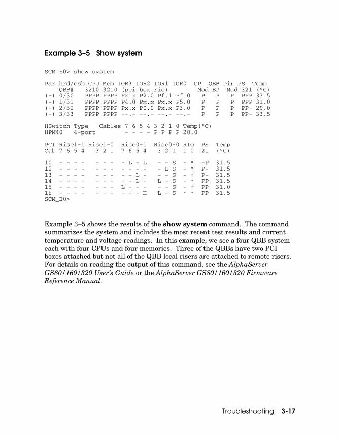
Troubleshooting 3-17
Example 3– 5 Show system SCM_E0> show system Par hrd/csb CPU Mem IOR3 IOR2 IOR1 IOR0 GP QBB Dir PS Temp QBB# 3210 3210 (pci_box.rio) Mod BP Mod 321 (ºC) (-) 0/30 PPPP PPPP Px.x P2.0 Pf.1 Pf.0 P P P PPP 33.5 (-) 1/31 PPPP PPPP P4.0 Px.x Px.x P5.0 P P P PPP 31.0 (-) 2/32 PPPP PPPP Px.x P0.0 Px.x P3.0 P P P PP- 29.0 (-) 3/33 PPPP PPPP --.- --.- --.- --.- P P P PP- 33.5 HSwitch Type Cables 7 6 5 4 3 2 1 0 Temp(ºC) HPM40 4-port - - - - P P P P 28.0 PCI Rise1-1 Rise1-0 Rise0-1 Rise0-0 RIO PS Temp Cab 7 6 5 4 3 2 1 7 6 5 4 3 2 1 1 0 21 (ºC) 10 - - - - - - - - L - L - - S - * -P 31.5 12 - - - - - - - - - - - - L S - * P- 31.5 13 - - - - - - - - - L - - - S - * P- 31.5 14 - - - - - - - - - L - L - S - * PP 31.5 15 - - - - - - - L - - - - - S - * PP 31.0 1f - - - - - - - - - - H L - S * * PP 31.5 SCM_E0>
Example 3–5 shows the results of the show system command. The command summarizes the system and includes the most recent test results and current temperature and voltage readings. In this example, we see a four QBB system each with four CPUs and four memories. Three of the QBBs have two PCI boxes attached but not all of the QBB local risers are attached to remote risers. For details on reading the output of this command, see the AlphaServer GS80/160/320 User’s Guide or the AlphaServer GS80/160/320 Firmware Reference Manual.

3-18 AlphaServer GS80/160/320 Service Manual
Example 3– 6 Show status SCM_E0> show status AlphaServer GS320 RMC escape sequence : [esc][esc]scm or ^[^[scm Local Baud/flow control : 57600/soft COM1 Baud/flow control : 57600/hard Modem Baud/flow control : 57600/hard COM1 mode : Pass-through OCP power switch : On OCP halt : Deasserted OCP secure : Non-Secure Remote access : Disabled Remote user : Not Connected Alerts : Disabled Modem password : Modem init string : atz&c1s0=1 Modem dial string : atdt915085551212 Modem alert string : ,,,,,,50885551212# Alert pending : YES Most recent alert : system fan failure
Table 3– 6 Modem Initialization Strings
Modem Initialization String
AT&T Dataport 14.4 ate0v0&c1s0=2
Hayes Accura 336/56k ate0v0&c1&k3s0=2 Compaq Microcom 510 ate0v0&c1s0=2 3Com USR Courier V. Everything ate0v0&c1s0=2 3Com USR 56K* (5676) (Japanese) ate0v0&c1s0=2 MultiTech MT5600ZDX ate0v0&c1s0=2 Aiwa PV-BW5610 (Japanese) ate0v0&c1s0=2 Omrom ME5614D (Japanese) ate0v0&c1s0=2
Table 3–6 lists common modems and their initialization strings.

Troubleshooting 3-19
Example 3–6 shows the results of the show status command, and Table 3–7 defines the entries. Show status reads the EEPROM on the standard I/O module and the state of the OCP (buttons and switch). The variables are set using various SCM commands controlling remote access to the system. See the AlphaServer GS80/160/320 User’s Guide for more information.
Table 3– 7 Show Status Entries
Name Description
RMC escape sequence Current escape sequence to access the SCM.
Local Baud/flow control Baud rate of the local port.
COM1 Baud/flow control Baud rate of COM1.
Modem Baud/flow control Baud rate of modem port.
COM1 mode Inputs accepted through COM1.
OCP power switch State of the OCP switch: Off, On, Secure.
OCP halt Current state of the Halt pushbutton: asserted/deasserted.
OCP secure Non-Secure = modem for remote access is enabled. Secure = modem for remote access is disabled.
Remote access Enabled = remote access allowed. Disabled = remote access not allowed.
Remote user A remote user is currently connected/not connected.
Alerts Enabled = dial-out enabled for sending alerts. Disabled = dial-out disabled.
Modem password Set = password set for modem access. Not set = no password set for modem access.
Modem init string Initialization string set for the modem.
Modem dial string Pager string to be dialed when an alert occurs.
Modem alert string Identifies the system that triggered the alert – usually the phone number of the monitored system.
Alert pending Yes = an alert has been triggered. No = no alert has been triggered.
Most recent alert Type of alert (for example, a power supply failure).

3-20 AlphaServer GS80/160/320 Service Manual
Example 3– 7 Show fru SCM_E0> show fru FRUname E Part# Serial# Model/Other Alias/Misc PBP0 00 54-25027-01.E01 NI92960262 WF08LTA111 WFFW_LAB_PSM_DEV PBP0.SIO 00 B4190-BA.B02 NI92660342 WF08LTA111 WFFW_LAB_PSM_DEV PBP0.RIO0 00 B4171-AA.E02 NI93871237 PBP0.RIO1 00 B4171-AA.E02 NI93871402 PBP1 00 54-25027-01.E02 NI93670860 WF08LTA111 WFFW_LAB_PSM_DEV PBP1.SIO 00 B4190-BA.B02 NI93371331 WF08LTA111 WFFW_LAB_PSM_DEV PBP1.RIO0 00 B4171-AA.E02 NI94270090 PBP1.RIO1 00 B4171-AA.E02 NI94270267 QBB0 00 54-25045-01.A01 NI93900000 WF08LTA111 WFFW_LAB_PSM_DEV QBB0.PSM 00 B12345-AA.H02 NI12312312 QBB0.PWR 00 54-25017-01.D01 NI90665954 WF08LTA111 WFFW_LAB_PSM_DEV QBB0.AUX 00 54-25123-01.D03 NI93060135 WF08LTA111 WFFW_LAB_PSM_DEV QBB0.CPU0 00 B4125-AA. E02 NI94170333 .......... ................ QBB0.CPU1 00 B4125-AA.E02 NI94170122 .......... ................ QBB0.CPU2 00 B4125-AA.E02 NI94170187 .......... ................ QBB0.CPU3 00 B4125-AA. E02 NI94170146 .......... ................ QBB0.MEM0 00 B4150-AA.D01 NI92460128 .......... ................ QBB0.MEM0.DIM0 00 54-24941-EA.C03 AY923HU .......... ................ QBB0.MEM0.DIM1 00 54-24941-EA.C03 AY9234S .......... ................ QBB0.MEM0.DIM2 00 54-24941-EA.C03 AY9233S .......... ................ QBB0.MEM0.DIM3 00 54-24941-EA.C03 AY923DU .......... ................ QBB0.MEM3 00 B4150-AA.D02 NI94070620 QBB0.MEM3.DIM0 00 54-24941-FA.C03 AY92902896 .......... ................ QBB0.MEM3.DIM1 00 54-24941-FA.C03 AY92902743 .......... ................ QBB0.MEM3.DIM2 00 54-24941-FA.C03 AY92716697 .......... ................ QBB0.MEM3.DIM3 00 54-24941-FA.C03 AY92716824 .......... ................ QBB0.DIR 00 -B4140-AA.D01 NI93870621 WF08LTA111 WFFW_LAB_PSM_DEV QBB0.DIR0.DIM1 00 .................. ??000 .......... ................ QBB0.DIR0.DIM2 00 54-25023-BA.A01 NI92961537 .......... ................ QBB0.DIR0.DIM4 00 54-25023-BA.A01 NI94061203 .......... ................ QBB0.DIR0.DIM5 00 54-25023-BA.A01 NI94061205 .......... ................ QBB0.IO01 00 -B4170-AA.E01 NI94173724 WF08LTA111 WFFW_LAB_PSM_DEV QBB0.GP 00 -B4180-BA.A03 NI94270815 WF08LTA111 WFFW_LAB_PSM_DEV QBB1 00 54-25045-01.A01 NI93900000 WF08LTA111 WFFW_LAB_PSM_DEV QBB1.PSM 00 54-25074-01.H02 NI93971109 QBB1.PWR 00 54-25017-01.E03 NI93060261 WF08LTA111 WFFW_LAB_PSM_DEV QBB1.AUX 00 54-25123-01.D03 NI93060086 WF08LTA111 WFFW_LAB_PSM_DEV QBB1.CPU0 00 B4125-AA.E02 NI94371010 .......... ................ QBB1.CPU1 00 B4125-AA.E02 NI94370702 .......... ................ QBB1.MEM0 00 -B4150-AA.D02 NI93671665 WF08LTA111 WFFW_LAB_PSM_DEV QBB1.MEM0.DIM0 00 54-24941-FA.C03 AY92617777 .......... ................ QBB1.MEM0.DIM1 00 54-24941-FA.C03 AY92617723 .......... ................ QBB1.MEM0.DIM2 00 54-24941-FA.C03 AY92617726 .......... ................ QBB1.MEM0.DIM3 00 54-24941-FA.C03 AY92617776 .......... ................ QBB1.MEM1 00 -B4150-AA.D04 NI94172049 WF08LTA111 WFFW_LAB_PSM_DEV QBB1.MEM1.DIM0 00 54-24941-EA.C03 AY923H!! .......... ................ QBB1.MEM1.DIM1 00 54-24941-EA.C03 AY923A"! .......... ................ QBB1.MEM1.DIM2 00 54-24941-EA.C03 AY923%$! .......... ................ QBB1.MEM1.DIM3 00 54-24941-EA.C03 AY923/$! .......... ................ QBB1.DIR 00 -B4140-AA.D01 NI93870652 WF08LTA111 WFFW_LAB_PSM_DEV QBB1.DIR0.DIM1 00 .................. ??000 .......... ................ QBB1.DIR0.DIM2 00 54-25023-BA.A01 NI93260343 .......... ................ QBB1.DIR0.DIM3 00 54-25023-BA.A01 NI94060375 .......... ................ QBB1.DIR0.DIM4 00 54-25023-BA.A01 NI94060764 .......... ................ QBB1.DIR0.DIM5 00 54-25023-BA.A01 NI94060750 .......... ................ QBB1.DIR0.DIM6 00 54-25023-BA.A01 NI94060229 .......... ................ QBB1.DIR0.DIM7 00 54-25023-BA.A01 NI94060204 .......... ................ QBB1.IO01 00 -B4170-AA.E01 NI94173767 WF08LTA111 WFFW_LAB_PSM_DEV

Troubleshooting 3-21
QBB1.GP 00 -B4181-BA.A02 NI93470534 WF08LTA111 WFFW_LAB_PSM_DEV HSW8 00 B4187-AA.B01 NI93870439 HSW8.HPM0 02 54-25115-01.B04 NI92660628 HSW8.PWR2 00 54-30194-01.D01 NI94271542 .......... ................
Table 3– 8 Show fru Command Field Descriptions
Field Description
FRU The field-replaceable unit name and location in the hierarchy of the system.
QBB Quad building block PSM Power system manager
CPU CPU module PWR Main power module
MEM Memory module AUX Auxiliary power module
DIMM DIMM module IOxx Local I/O riser (xx=ports)
DIR Directory module GP Global port
HSW8 8-port H-switch HPM H-switch power manager
PBP PCI backplane SIO Standard I/O module
RIO Remote I/O riser module
E Error field. Indicates errors logged against the FRU. Codes are as follows:
01 Failure 10 Checksum error on bytes 0-62
02 Test detected error logged 20 Checksum error on bytes 64-126
04 At least one error logged 40 Checksum error on bytes 128-254
08 reserved 80 FRUs system serial #s inconsistent
Part # The Compaq or vendor part number of the FRU in ASCII.
Serial #
The FRU serial number. For Compaq parts the serial number format is: XXYWWNNNNN, where XX = manufacturing location, YWW = year and week, and NNNNN = sequence number in hexadecimal.
Model/Other
Optional model information about the module. For example, for FRU PBPx the field might read PCI_BACKPN.
Alias Optional name for the FRU.
The show fru command, Example 3–7, reads the EEPROM on each FRU. Table 3–8 describes each field. The SCM clear error <fru> command clears the error field of the target FRU (see Example 3–8).

3-22 AlphaServer GS80/160/320 Service Manual
3.4.5 Dealing With EEPROMs
EEPROMs throughout the system record FRU identification and error information and store system environment and firmware information.
Example 3– 8 Clear error SCM_E0> show fru . . . QBB1.DIR0.DIM7 00 ...S...S...S@..... ??404?6T$$ v....".... .G...H......_ ’. QBB1.GP 00 B4181-BA. B01 NI93061440 .......... ................ QBB2 00 54-25043-01.D03 NI94470368 QBB2.PSM 40 54-25074-01.J01 NI94570274 WF96LTA113 WF_FIRMWARE_LAB QBB2.PWR 00 54-25017-01.F01 NI94171317 QBB2.AUX 00 54-25123-01.E01 NI94170839 . . . scm-E0> clear error qbb2.psm scm_E0> show fru . . . QBB1.DIR0.DIM7 00 ...S...S...S@..... ??404?6T$$ v....".... .G...H......_ ’. QBB1.GP 00 B4181-BA. B01 NI93061440 .......... ................ QBB2 00 54-25043-01.D03 NI94470368 QBB2.PSM 00 54-25074-01.J01 NI94570274 WF96LTA113 WF_FIRMWARE_LAB QBB2.PWR 00 54-25017-01.F01 NI94171317 QBB2.AUX 00 54-25123-01.E01 NI94170839
Example 3–8 is an example of the clear error command. In this case, the command clears the error logged against the PSM module in QBB2.

Troubleshooting 3-23
Example 3– 9 Build fru SCM_E0> build qbb2.psm 54-25074-01.J01 NI94570274 WF96LTA113 WF_FIRMWARE_LAB Example 3–9 is an example of the build <fru> command. The command places manufacturing information (part number and serial number) and optional information (module name and an alias) in the designated FRU’s EEPROM. The command also clears any errors logged against the module. If a field is left blank in the command, it is left blank in the EEPROM as well.
Example 3– 10 Build eeprom SCM_E0> build eeprom Restoring EEPROM Defaults Maintaining local baud at 57600 Maintaining local flow at soft !software flow control protocol Maintaining modem baud at 57600 Maintaining modem flow at hard !hardware flow control protocol Maintaining COM1 baud at 57600 Maintaining COM1 flow at hard !hardware flow control protocol SCM_E0>
Example 3–10 is an example of the build eeprom command. The command sets default environment variables in the nvram but maintains some locally set variables that affect communications to the local terminal port, COM1, and the modem port. The user is informed of which variables are not being restored. To restore all the defaults, insert the “ force console defaults” jumper on the standard I/O module (see Section 1.21.4) and cycle power to the PCI box.

3-24 AlphaServer GS80/160/320 Service Manual
3.5 Running Diagnostics Using the SCM Monitor
If the SRM console gets loaded, the SROM/XSROM diagnostic tests cannot be run under the console. To run SROM/XSROM diagnostics in SCM user mode they must be loaded and remain in the CPU’s I-cache or B-cache. And once XSROM tests are loaded into a CPU’s B-cache, SROM tests may not be run on it unless the SROM is once again loaded. SCM examines and deposits require SROM or XSROM code running.
Example 3– 12 Setting Up the Diagnostic Environment and Testing
SCM_E0> show nvram � COM1_PRINT_EN HP_COUNT 0 . . . SROM_MASK ff f � XSROM_MASK ff ff ff ff ff ff ff ff ff 1 0 0 . � . . AUTO_FAULT_RESTART 1 SCM_SIZING_TIME c SCM_E0> test &pc0 5 � Testing. Please wait..CPU Connect Error node 30(response=2e)� SCM_E0> set xsrom_mask none � SCM_E0> sho nvram ALERT Uninitialized BAUD 57600 . . . SROM_MASK fe f XSROM_MASK 0 0 0 0 0 0 0 0 0 0 0 0 � . . . SCM_CSB_MASTER_ELIGIBLE 1 PERF_MON 0

Troubleshooting 3-25
Example 3–12 shows a diagnostic session. Test masks stored in the NVRAM on the standard I/O module control power-up diagnostic testing. The SCM reads the test masks and executes the tests designated by the mask. The first quadword masks the SROM tests and XSROM tests 10 through 3a, and the second quadword masks the remainder of the XSROM tests. By default all tests are run during power-up including XSROM test 58 which loads the console into memory and all CPUs jump to that code and start. If the console is loaded and all CPUs are running console, no diagnostics can be run in SCM user mode.
The following shows the bits set in the SROM/XSROM masks controlling diagnostic tests during power-up. All bits in the mask are set including those that correspond to placeholders.
First quadword mask:
|--------- XSROM tests 10 through 3a ----------------------------|-SROM tests 0¤f -| F F F F F F F F F F F F F F F F 1111 1111 1111 1111 1111 1111 1111 1111 1111 1111 1111 1111 1111 1111 1111 1111 3333 3333 3333 3333 2222 2222 2222 2222 1111 1111 1111 1111 fedc ba98 7654 3210 fedc ba98 7654 3210 fedc ba98 7654 3210 fedc ba98 7654 3210
Second quadword mask:
|--------XSROM tests 40 through 5f ----------| 0 0 1 F F F F F F (hex) 0000 0000 0001 1111 1111 1111 1111 1111 1111 (bits set) 5555 5555 5555 5555 4444 4444 4444 4444 (hex test number) fedc ba98 7654 3210 fedc ba98 7654 3210
� The show nvram command reads the contents of the NVRAM.
� The default SROM mask tells the SRM to run all SROM tests. Note that the NVRAM is read in bytes and leading zero nibbles are suppressed.
� The default XSROM mask tells the SRM to run all the XSROM tests. The bit that is set above the � controls test 58(h) which unloads the console.
� test &pc0 5 tells the SCM to run SROM test 5 on CPU0. Note that the CSB address c0 is used to designate the target CPU. See Example 3–12.
� The test fails because the SRM console code, not the SROM code, is running in the CPU.
� Use the SCM command set xsrom_mask none to instruct the SCM not to execute any XSROM tests and not unload the console code.
� The show nvram shows that no bits are set in the XSROM_MASK.

3-26 AlphaServer GS80/160/320 Service Manual
Example 3– 12 Setting Up the Diagnostic Environment (Continued)
SCM_E0> reset � Powering ON on QBB-0 SCM_E0> QBB0 now Testing Step-0 PSM30 SysEvent: QBB_PULSE_RESET SysEvent Reg0: 468f SysEvent Reg1: 33ff Phase 0............................ PSM30 SysEvent: QBB_INIT_CD1 SysEvent Reg0: 468f SysEvent Reg1: 33ff QBB0 Step-1 Tested | QBB0 Step-2 Tested | QBB0 Step-3 Tested | QBB0 Step-4 Tested | QBB0 Step-5 Tested | Phase 1 | QBB0 Step-6 Tested | QBB0 Step-7 Tested | QBB0 Step-8 Tested | � QBB0 Step-9 Tested | QBB0 Step-a Tested | QBB0 Step-b Tested | Phase 2 | QBB0 Step-c Tested | Phase 3 | QBB0 Step-d Tested | Phase 4 | QBB0 now Testing Step-e... | Power On Complete SCM_E0> test &pc0 5 � Testing. Please wait...Test(s) passed. SCM_E0> test &pc1 7 � Testing. Please wait...Test(s) passed. SCM_E0> test &pc0 10 � Testing. Please wait...Test(s) passed. SCM_E0> test &pc0 5 � Testing. Please wait...XSROM already unloaded Error node 30 (response=29) SCM_E0> test &pc1 5 � Testing. Please wait...Test(s) passed. SCM_E0>

Troubleshooting 3-27
As Example 3–12 continues, the callouts explain the progress of the diagnostic session.
� The reset command is executed.
� Even though no XSROM tests are executed, the SCM runs through its normal power-up routine. (xsrom_mask = none)
� The test &pc0 5 command now passes. SROM test 5, the B-cache march test, is run on CPU0.
� The test &pc1 7 command passes. SROM test 7, the EVx D-cache and B-cache error tests, run on CPU1.
� The test &pc0 10 command passes. XSROM test 10, the local QSD who am I register test, is run on CPU0.
� The test &pc0 5 command now fails, though it passed in �, on CPU0 because the XSROM was loaded when test 10 was executed in �.
� The SROM test still passes on CPU1 though.

3-28 AlphaServer GS80/160/320 Service Manual
Example 3– 13 Various Test Commands SCM_E0> test &pc1 5 � Testing. Please wait…Test(s) passed. SCM_E0> test &pc1 80 10 0 � Testing. Please wait…Test(s) passed. SCM_E0> test &pc1 80 ff 0 � Testing. Please wait…Test(s) passed. SCM_E0> test &pc1 80 ffe 0 20 � SCM_E0> Test(s) passed. SCM_E0> test &pc0 80 ff0000 0 � Testing. Please wait…Test(s) passed. SCM_E0>

Troubleshooting 3-29
� Test &pc1 5 is an example of using a test number to run a single test. The
SCM command-line interface does not accept a list of tests using this format; however, it does accept masks and continuous or multiple passes.
� test &pc1 80 10 0 is an example of the format used to pass a mask. “80” indicates to the SCM that a diagnostic mask will follow. In this case, 10 is the first quadword of the mask and 0 is the second. The 5th bit is set in the first quadword, so test 5 is executed on CPU1. The command in � is equivalent to the command in �.
� test &pc1 80 ff 0 is an example of the format used to request the execution of several tests in sequence. In this case, the first quadword mask has bits 0 through 7 set so those tests are executed.
� test &pc1 80 ffe 0 20 is an example of a format used to request 20 passes of tests 0 through b – all the SROM test.
� Test &pc0 80 ff0000 0 is an example of using the mask format to run XSROM tests. In this case tests 10 through 1b are executed.
A few other restrictions apply to running diagnostics as follows:
• XSROM test ^x10->^x33 (the local QBB tests) can be executed before but not after either test ^x34 ( Soft QBB ID Config) or test ^x37 (Remote Soft QBB ID config).
• Test ^x34 (Local Soft QBB ID Config) MUST be run before Test ^x37 (Remote Soft QBB ID config), and Test ^x52 (Memory/DIRectory config) can be run and also before Console Unload (Test ^x58) can be performed.
• Tests ^x1b (Local IOP config) and ^x38 (remote IOP config), if no local CPUs are present in a remote QBB, MUST be run to configure the I/O subsystem and determine the location of the STD I/O module(s). Test ^x58 (Console Unload) requires STD I/O information to determine the location of the STD I/O flash ROM where the SRM console image resides.
• Once the console is loaded and running, no SROM/XSROM testing can be done. Since there is no communication between PSM and SROM/XSROM, the user can NOT do SCM monitor examines, deposits, or test. When the SRM console is running, SRM level examines, deposits, and test are available.

3-30 AlphaServer GS80/160/320 Service Manual
3.6 Using the SRM Console
Several SRM commands can be used to set the system environment, power CPUs on and off, display configuration information, display error information, and test and exercise the system.
3.6.1 Displaying and Setting Up the System Environment
Several SRM console commands are used to display and set system environment variables stored in EEPROM on the standard I/O module.
Example 3– 14 Set Environment Variables P00>>> set console serial P00>>> Example 3–14 shows an example of the set environment variable command (set <envar>). Environment variables pass configuration information between the console and the operating system. Settings determine how the system is configured, how it powers up, and boots. This particular variable controls the protocol used by the console. Note: Environment variables must be defined separately in each partition.
Example 3– 15 Show Environment Variables P00>>> show console Console serial P00>>> Example 3–15 shows an example of the show environment variable command (show <envar>). You can show all environment variables by using the show * command.
Example 3– 16 Clear Environment Variables P00>>> clear console P00>>> Example 3–16 shows an example of the clear environment variable command (clear <envar>). The command clears the variable.
For a complete description of environment variables, see the AlphaServer GS80/160/320 User’s Guide or the AlphaServer GS80/160/320 Firmware Reference Manual.

Troubleshooting 3-31
3.6.2 Controlling Power with the SRM
Through firmware callbacks from the SRM console to the SCM monitor, the SRM can power off partitions and parts of the system.
Example 3– 17 Power Off (partiton/qbb)
P00>>> power off �
Powering off Hard_partition_0 consisting of: � QBB0 QBB1 QBB2 QBB3
QBB-0 Powering OFF � QBB-1 Powering OFF QBB-2 Powering OFF QBB-3 Powering OFF
~I~ QBB0/PSM30 SysEvent: QBB_POWER_OFF Reg0:768F Reg1:3FFF � ~I~ QBB1/PSM31 SysEvent: QBB_POWER_OFF Reg0:768F Reg1:FFFF ~I~ QBB1/PSM32 SysEvent: QBB_POWER_OFF Reg0:7CBC Reg1:FFFF ~I~ QBB1/PSM33 SysEvent: QBB_POWER_OFF Reg0:7CBC Reg1:3FFF
~I~ HSW8/HPM40 SysEvent: LINK0_OFF Reg0:FFFF Reg1:ABE1 � ~I~ HSW8/HPM40 SysEvent: LINK1_OFF Reg0:FEFF Reg1:ABE1 ~I~ HSW8/HPM40 SysEvent: LINK2_OFF Reg0:FCFF Reg1:ABE1 ~I~ HSW8/HPM40 SysEvent: LINK3_OFF Reg0:F8FF Reg1:ABE1 Local escape sequence verified scm SCM_EF>
� The power off command powers off the partition in which this particular SRM console is running. When issued in this form, the command halts all activity of the QBB – all drivers, interrupts, global port transactions, etc. -before power is removed from the QBB logic. PCIs attached to a partition powered off in such a manner remain powered.
� The partition is identified and the QBBs within it enumerated.
� Each QBB in the partition is powered off.
� Information messages identify the PSMs in each QBB and notes they are powered off.
� Information messages identify the link to the H-switch in each QBB and notes that the links are off.

3-32 AlphaServer GS80/160/320 Service Manual
Although you can power off a partition using the SCM power off – par x command, use the SRM power off command because it stops all CPU activity and leaves QBBs in a quiet, clean state.
Example 3– 18 Power off cpu <n> Command
P00>>> power off cpu 8 � powering off CPU 8 (CPU 0 in QBB 2) P00>>> QBB2 Powering off CPU0 P00>>> scm show csb . . c7 CPU3/SROM T4.2-7 ON c4 IOR0 ON 32 PSM T04.7 ( 11.23/01:03) T4.2 (09.08) ON SrvSw: NORMAL 32 XSROM T04.7 (11.23/01:55)
c8 CPU0/SROM T4.2-7 OFF � c9 CPU1/SROM T4.2-7 ON . . P00>>>
Example 3– 19 Power on cpu <n> Command
P00>>> power on cpu 8 � powering on CPU 8 (CPU 0 in QBB 2) P00>>> QBB2 Powering on CPU0 P00>>> scm show csb . . c7 CPU3/SROM T4.2-7 ON c4 IOR0 ON 32 PSM T04.7 ( 11.23/01:03) T4.2 (09.08) ON SrvSw: NORMAL 32 XSROM T04.7 (11.23/01:55)
c8 CPU0/SROM T4.2-7 ON � c9 CPU1/SROM T4.2-7 ON . . P00>>>
� The power off cpu 8 command powers off CPU 0 in QBB2. C8 is the csb
address of CPU0 in QBB2 and therefore, cpu 8 is used in the command.
� The scm show CPU command shows that the CPU is OFF.
� The power on cpu 8 command powers on CPU 0 in QBB2. C8 is the csb address of CPU0 in QBB2 and therefore, cpu 8 is used in the command.
� The scm show CPU command shows that the CPU is ON.

Troubleshooting 3-33
3.6.3 Displaying Configuration Information (SRM)
Several show commands provide system information.
Example 3– 20 Show configuration P00>>> show config Compaq Computer Corporation Compaq AlphaServer GS320 6/731 SRM Console V5.8-1, built on May 26 2000 at 12:15:01 PALcode OpenVMS PALcode V1.81-1, Tru64 UNIX PALcode V1.75-1 Micro Firmware V5.7 QBB 0 Hard QBB 0 � Quad Switch QSA rev 4, QSD revs 0/0/0/0 Duplicate Tag Up To 4 MB Caches DTag revs 1/1/1/1 Processor 0 CPU 0 4 MB Cache EV67 pass 2.4, 731 MHz Processor 1 CPU 1 4 MB Cache EV67 pass 2.4, 731 MHz Processor 2 CPU 2 4 MB Cache EV67 pass 2.4, 731 MHz Processor 3 CPU 3 4 MB Cache EV67 pass 2.4, 731 MHz Memory 0 MPA rev 1, MPD revs 1/1 Directory DMA rev 1, DMD rev 1 IOP IOA rev 2, IOD revs 0/0 Local Link 0 IOR 0 � NE ML rev 2 Remote Link 0 FE ML rev 2 I/O Port 0 PCA rev 3 PCI Box 15 Riser 0 Right Side Backplane rev 3 PCI Bus 0 Hose 0 � 64 Bit, 33 MHz PCI rev 2.1 compliant PCI Bus 1 Hose 1 � 64 Bit, 33 MHz PCI rev 2.1 compliant Local Link 1 IOR 1 � NE ML rev 2 Remote Link 1 FE ML rev 2 I/O Port 1 PCA rev 3 PCI Box 15 Riser 1 Left Side Backplane rev 3 PCI Bus 0 Hose 2 � 64 Bit, 33 MHz PCI rev 2.1 compliant PCI Bus 1 Hose 3 � 64 Bit, 33 MHz PCI rev 2.1 compliant Global Port GPA rev 2, GPD revs 0/0 QBB 1 Hard QBB 1 � Quad Switch QSA rev 4, QSD revs 0/0/0/0 Duplicate Tag Up To 4 MB Caches DTag revs 1/1/1/1 Processor 0 CPU 4 4 MB Cache EV67 pass 2.4, 731 MHz Processor 1 CPU 5 4 MB Cache EV67 pass 2.4, 731 MHz Processor 2 CPU 6 4 MB Cache EV67 pass 2.4, 731 MHz Processor 3 CPU 7 4 MB Cache EV67 pass 2.4, 731 MHz Memory 0 MPA rev 2, MPD revs 1/1 Directory DMA rev 1, DMD rev 1 IOP IOA rev 2, IOD revs 0/0 Local Link 0 IOR 4 � NE ML rev 2 Local Link 1 IOR 5 � NE ML rev 2 Local Link 2 IOR 6 � NE ML rev 2 Local Link 3 IOR 7 � NE ML rev 2 Remote Link 3 FE ML rev 2 I/O Port 3 PCA rev 3 PCI Box 8 Riser 0 Right Side Backplane rev 3

3-34 AlphaServer GS80/160/320 Service Manual
PCI Bus 0 Hose 14 64 Bit, 33 MHz � PCI rev 2.1 compliant PCI Bus 1 Hose 15 64 Bit, 33 MHz � PCI rev 2.1 compliant Global Port GPA rev 2, GPD revs 0/0 QBB 2 Hard QBB 2 � Quad Switch QSA rev 4, QSD revs 0/0/0/0 Duplicate Tag Up To 4 MB Caches DTag revs 1/1/1/1 Processor 0 CPU 8 4 MB Cache EV67 pass 2.4, 731 MHz Processor 1 CPU 9 4 MB Cache EV67 pass 2.4, 731 MHz Processor 2 CPU 10 4 MB Cache EV67 pass 2.4, 731 MHz Processor 3 CPU 11 4 MB Cache EV67 pass 2.4, 731 MHz Memory 0 MPA rev 2, MPD revs 1/1 Directory DMA rev 1, DMD rev 1 IOP IOA rev 2, IOD revs 00 Local Link 0 IOR 8 � NE ML rev 2 Remote Link 0 FE ML rev 2 I/O Port 0 PCA rev 3 PCI Box 4 Riser 0 Right Side Backplane rev 3 PCI Bus 0 Hose 16 64 Bit, 33 MHz � PCI rev 2.1 compliant PCI Bus 1 Hose 17 64 Bit, 33 MHz � PCI rev 2.1 compliant Local Link 1 IOR 9 � NE ML rev 2 Local Link 2 IOR 10 � NE ML rev 2 Remote Link 2 FE ML rev 2 I/O Port 2 PCA rev 3 PCI Box 0 Riser 0 Right Side Backplane rev 3 PCI Bus 0 Hose 20 64 Bit, 33 MHz � PCI rev 2.1 compliant PCI Bus 1 Hose 21 64 Bit, 33 MHz � PCI rev 2.1 compliant Local Link 3 IOR 11 � NE ML rev 2 Global Port GPA rev 2, GPD revs 0/0 QBB 3 Hard QBB 3 � Quad Switch QSA rev 4, QSD revs 0/0/0/0 Duplicate Tag Up To 4 MB Caches DTag revs 1/1/1/1 Processor 0 CPU 12 4 MB Cache EV67 pass 2.4, 731 MHz Processor 1 CPU 13 4 MB Cache EV67 pass 2.4, 731 MHz Processor 2 CPU 14 4 MB Cache EV67 pass 2.4, 731 MHz Processor 3 CPU 15 4 MB Cache EV67 pass 2.4, 731 MHz Memory 0 MPA rev 1, MPD revs 1/1 Directory DMA rev 1, DMD rev 1 IOP IOA rev 2, IOD revs 0/0 Local Link 0 IOR 12 � NE ML rev 2 Local Link 1 IOR 13 � NE ML rev 2 Global Port GPA rev 2, GPD revs 0/0 Hierarchical Switch HSA revs 2/2, HSD revs 1/1/1/1 QBB Size Interleave System Memory 10.5 GB 0 4 GB 8-Way 1 1 GB 8-Way 2 1.5 GB 4-Way 3 4 GB 8-Way Hose IOP PCI Box Standard I/O Modules 0 0 15 Primary Acer Labs M1543C rev A1-D 14 1 8 Acer Labs M1543C rev A1-D 16 2 4 Acer Labs M1543C rev A1-D 20 2 0 Acer Labs M1543C rev A1-D System Memory 10.5 GB Board Set Array Size Address QBB 0 Memory 0 0 0 2 GB 00000000000

Troubleshooting 3-35
0 1 4 2 GB 00000000000 Total Available 4 GB 8-Way Interleave Board Set Array Size Address QBB 1 Memory 0 0 0 512 MB 01000000000 0 1 4 512 MB 01000000000 Total Available 1 GB 8-Way Interleave Board Set Array Size Address QBB 2 Memory 0 0 0 512 MB 02040000000 0 1 4 1 GB 02000000000 Total Available 1.5 GB 4-Way Interleave Board Set Array Size Address QBB 3 Memory 0 0 0 2 GB 03000000000 0 1 4 2 GB 03000000000 Total Available 4 GB 8-Way Interleave PCI Box Riser Slot Option Hose Bus Slot Function Name 0 0 1 Standard I/O Module 20 + Acer Labs M1543C 20 0 7 + Acer Labs M1543C IDE 20 0 15 dqd + Acer Labs M1543C USB 20 0 19 + QLogic ISP10x0 20 0 1 pkg 0 0 4 QLogic ISP10x0 21 0 4 pkh 0 0 6 DE500-BA Network Con 21 0 6 ewc 4 0 1 Standard I/O Module 16 + Acer Labs M1543C 16 0 7 + Acer Labs M1543C IDE 16 0 15 dqc + Acer Labs M1543C USB 16 0 19 + QLogic ISP10x0 16 0 1 pke 4 0 5 QLogic ISP10x0 17 0 5 pkf 8 0 1 Standard I/O Module 14 + Acer Labs M1543C 14 0 7 + Acer Labs M1543C IDE 14 0 15 dqb + Acer Labs M1543C USB 14 0 19 + QLogic ISP10x0 14 0 1 pkc 8 0 4 DE500-BA Network Con 15 0 4 ewb 8 0 7 QLogic ISP10x0 15 0 7 pkd 15 0 1 Standard I/O Module 0 + Acer Labs M1543C 0 0 7 + Acer Labs M1543C IDE 0 0 15 dqa + Acer Labs M1543C USB 0 0 19 15 0 3 DE500-BA Network Con 0 0 3 ewa 15 0 4 DEC KZPSA 1 0 4 pka 15 0 5 DECchip 21154-AA 1 0 5 + DE602-AA 1 2 4 eia + DE602-AA 1 2 5 eib 15 0 6 QLogic ISP10x0 1 0 6 pkb 15 0 7 KGPSA-C 1 0 7 pga 15 1 1 KGPSA-C 2 0 1 pgb 15 1 2 KGPSA-C 2 0 2 pgc 15 1 3 KGPSA-C 2 0 3 pgd 15 1 4 KGPSA-C 3 0 4 pge 15 1 5 KGPSA-C 3 0 5 pgf 15 1 6 KGPSA-C 3 0 6 pgg 15 1 7 KGPSA-C 3 0 7 pgh Hose QBB PCA PCI Bus Slots 0 0 0 0 1-3 1 0 0 1 4-7 2 0 1 0 1-3

3-36 AlphaServer GS80/160/320 Service Manual
3 0 1 1 4-7 14 1 3 0 1-3 15 1 3 1 4-7 16 2 0 0 1-3 17 2 0 1 4-7 20 2 2 0 1-3 21 2 2 1 4-7 Slot Option Hose 0, Bus 0, PCI 3 DE500-BA Network Con ewa0.0.0.3.0 00-00-F8-1B-1C-0B 7 Acer Labs M1543C Bridge to Bus 1, ISA 15 Acer Labs M1543C IDE dqa.0.0.15.0 dqa0.0.0.15.0 TOSHIBA CD-ROM XM-6302B 19 Acer Labs M1543C USB Slot Option Hose 1, Bus 0, PCI 4 DEC KZPSA pka0.7.0.4.1 SCSI Bus ID 7 5 DECchip 21154-AA Bridge to Bus 2, PCI 6 QLogic ISP10x0 pkb0.7.0.6.1 SCSI Bus ID 7 dkb100.1.0.6.1 RZ28M 7 KGPSA-C pga0.0.0.7.1 WWN 2000-0000-c922-4b27 Slot Option Hose 1, Bus 2, PCI 4 DE602-AA eia0.0.0.2004.1 00-50-8B-CF-4E-AC 5 DE602-AA eib0.0.0.2005.1 00-50-8B-CF-4E-AD Slot Option Hose 2, Bus 0, PCI 1 KGPSA-C pgb0.0.0.1.2 WWN 2000-0000-c921-0c22 2 KGPSA-C pgc0.0.0.2.2 WWN 2000-0000-c921-027a 3 KGPSA-C pgd0.0.0.3.2 WWN 2000-0000-c922-4bcc Slot Option Hose 3, Bus 0, PCI 4 KGPSA-C pge0.0.0.4.3 WWN 2000-0000-c921-84b9 5 KGPSA-C pgf0.0.0.5.3 WWN 2000-0000-c922-3c94 6 KGPSA-C pgg0.0.0.6.3 WWN 2000-0000-c922-4b30 7 KGPSA-C pgh0.0.0.7.3 WWN 2000-0000-c921-07a6 Slot Option Hose 14, Bus 0, PCI 1 QLogic ISP10x0 pkc0.7.0.1.14 SCSI Bus ID 7 7 Acer Labs M1543C Bridge to Bus 1, ISA 15 Acer Labs M1543C IDE dqb.0.0.15.14 19 Acer Labs M1543C USB Slot Option Hose 15, Bus 0, PCI 4 DE500-BA Network Con ewb0.0.0.4.15 08-00-2B-C3-72-69 7 QLogic ISP10x0 pkd0.7.0.7.15 SCSI Bus ID 7 dkd100.1.0.7.15 RZ29B Slot Option Hose 16, Bus 0, PCI 1 QLogic ISP10x0 pke0.7.0.1.16 SCSI Bus ID 7 7 Acer Labs M1543C Bridge to Bus 1, ISA 15 Acer Labs M1543C IDE dqc.0.0.15.16 19 Acer Labs M1543C USB Slot Option Hose 17, Bus 0, PCI 5 QLogic ISP10x0 pkf0.7.0.5.17 SCSI Bus ID 7 Slot Option Hose 20, Bus 0, PCI 1 QLogic ISP10x0 pkg0.7.0.1.20 SCSI Bus ID 7 dkg0.0.0.1.20 RZ1DF-BF 7 Acer Labs M1543C Bridge to Bus 1, ISA 15 Acer Labs M1543C IDE dqd.0.0.15.20

Troubleshooting 3-37
dqd0.0.0.15.20 TOSHIBA CD-ROM XM-6302B 19 Acer Labs M1543C USB Slot Option Hose 21, Bus 0, PCI 4 QLogic ISP10x0 pkh0.7.0.4.21 SCSI Bus ID 7 dkh0.0.0.4.21 COMPAQ BB00911CA0 dkh100.1.0.4.21 COMPAQ BB00911CA0 dkh200.2.0.4.21 COMPAQ BB00911CA0 dkh300.3.0.4.21 RZ1CB-CA 6 DE500-BA Network Con ewc0.0.0.6.21 08-00-2B-C3-C1-C7
Example 3–20 shows output from the show config command for a partition made up of four QBBs. Callouts in the example are used to highlight a few features of the show config command that can help you keep track of hardware and partitions.
� This line shows both the hard and soft QBB ID number. In this case they happen to be the same. However, had the partition been made up of QBBs 6 and 7, soft QBB0 would have been hard QBB6 and soft QBB1 would have been hard QBB7.
� The local links are equivalent to local I/O risers in QBBs. Each QBB may have up to four. IOR numbering, however, follows a numbering scheme that combines hard and soft numbers. In this example QBB0 has only one local I/O riser (local links 0 and 1) and two IORs 0 and 1. QBB1 has two local I/O risers (local links 0 – 3) and four IORs 4 – 7. Note that IORs 2 and 3 are missing since a second local I/O riser is missing in QBB0. Also note that the IOR numbering follows soft numbers. Had the partition been made up of QBBs 6 and 7, IOR numbers could have been 0 – 7.
� Finally, note that PCI hose numbers (different PCI buses) are always hard. This is extremely helpful in following the hardware. A GS320 can have as many as 64 PCI buses designated as hoses. Each QBB can control up to eight buses. QBB0 connects to Hoses 0-7, QBB1 to hoses 8-15, … QBB7 to hoses 56-63. Further, each local link connects to hoses. Local link 0 controls the first two hoses in the group of eight, local link 1 the next two and so on. You can mathematically figure out how hoses connect by the formula QBB# * 8 + local link # * 2 = the first of two hose numbers. Plugging in the numbers for QBB2, local link 2, you get hoses 20 and 21. This holds true in show config across partitions. So for hard QBB6 local link 1, the hoses are 50 and 51. You can trace the cable from the local I/O riser connected to port 1 in QBB6 to the PCI box that contains buses 50 and 51.
Example 3– 21 Show fru P00>>> show fru FRUname E Part# Serial# Model/Other Alias/Misc CAB0.PWR 00 - - - - QB01.RAK1 00 - - - - QB01.PS1 00 - - - - QB01.PS3 00 - - - - QB23.RAK2 00 - - - - QB23.PS1 00 - - - - QB23.PS2 00 - - - - CAB1.SYS 00 - - - - CAB1.SYSFAN 00 - - - -

3-38 AlphaServer GS80/160/320 Service Manual
QBB0. 00 54-25045-01.A01 NI93900000 WF08LTA111 QBB0.PSM 00 B12345-AA.H02 NI12312312 QBB0.PWR 00 54-25017-01.D01 NI90665954 WF08LTA111 QBB0.AUX 00 54-25123-01.D03 NI93060135 WF08LTA111 QBB0.CLKSPLT 00 - - - - QBB0.CPU0 00 B4125-AA. E02 NI94170333 QBB0.CPU1 00 B4125-AA.E02 NI94170122 QBB0.CPU2 00 B4125-AA.E02 NI94170187 QBB0.CPU3 00 B4125-AA. E02 NI94170146 PBP0.RIO0 00 B4171-AA.E02 NI93871237 PBP0.PCI1 00 - - QLogic ISP - PBP0.PCI3 00 - - DE500-BA N - PBP0.PCI7 00 - - Acer Labs - PBP0.RIO1 00 B4171-AA.E02 NI93871402 PBP0.PCI5 00 - - QLogic ISP - QBB0.MEM0 00 B4150-AA.D01 NI92460128 QBB0.MEM0.DIM0 00 54-24941-EA.C03 AY923HU QBB0.MEM0.DIM1 00 54-24941-EA.C03 AY9234S QBB0.MEM0.DIM2 00 54-24941-EA.C03 AY9233S QBB0.MEM0.DIM3 00 54-24941-EA.C03 AY923DU QBB0.MEM0.DIM4 00 54-24941-EA.C03 AY923#T QBB0.MEM0.DIM5 00 54-24941-EA.C03 AY923TT QBB0.MEM0.DIM6 00 54-24941-EA.C03 AY923EU QBB0.MEM0.DIM7 00 54-24941-EA.C03 AY923$T QBB0.MEM3 00 B4150-AA.D02 NI94070620 QBB0.MEM3.DIM0 00 54-24941-FA.C03 AY92902896 QBB0.MEM3.DIM1 00 54-24941-FA.C03 AY92902743 QBB0.MEM3.DIM2 00 54-24941-FA.C03 AY92716697 QBB0.MEM3.DIM3 00 54-24941-FA.C03 AY92716824 QBB0.MEM3.DIM4 00 54-24941-FA.C03 AY92716767 QBB0.MEM3.DIM5 00 54-24941-FA.C03 AY92902932 QBB0.MEM3.DIM6 00 54-24941-FA.C03 AY92716922 QBB0.MEM3.DIM7 00 54-24941-FA.C03 AY92603880 QBB0.DIR 00 -B4140-AA.D01 NI93870621 WF08LTA111 QBB0.DIR0.DIM1 00 54-25023-BA NI92961537 QBB0.DIR0.DIM2 00 54-25023-BA.A01 NI92961412 QBB0.DIR0.DIM4 00 54-25023-BA.A01 NI94061203 QBB0.DIR0.DIM5 00 54-25023-BA.A01 NI94061205 QBB0.GP 00 -B4180-BA.A03 NI94270815 WF08LTA111 QBB1. 00 54-25045-01.A01 NI93900000 WF08LTA111 QBB1.PSM 00 54-25074-01.H02 NI93971109 QBB1.PWR 00 54-25017-01.E03 NI93060261 WF08LTA111 QBB1.AUX 00 54-25123-01.D03 NI93060086 WF08LTA111 QBB1.CLKSPLT 00 - - - - QBB1.CPU0 00 B4125-AA.E02 NI94371010 QBB1.CPU1 00 B4125-AA.E02 NI94370702 QBB1.CPU2 00 B4125-AA.E02 NI94170393 QBB1.CPU3 00 B4125-AA.E02 NI94370906 PBP1.RIO0 00 B4171-AA.E02 NI94270090 PBP1.PCI1 00 - - QLogic ISP - PBP1.PCI7 00 - - Acer Labs - PBP1.RIO1 00 B4171-AA.E02 NI94270267 QBB1.MEM0 00 -B4150-AA.D02 NI93671665 WF08LTA111 QBB1.MEM0.DIM0 00 54-24941-FA.C03 AY92617777 QBB1.MEM0.DIM1 00 54-24941-FA.C03 AY92617723 QBB1.MEM0.DIM2 00 54-24941-FA.C03 AY92617726 QBB1.MEM0.DIM3 00 54-24941-FA.C03 AY92617776 QBB1.MEM0.DIM4 00 54-24941-FA.C03 AY92617656 QBB1.MEM0.DIM5 00 54-24941-FA.C03 AY92617677 QBB1.MEM0.DIM6 00 54-24941-FA.C03 AY92617724 QBB1.MEM0.DIM7 00 54-24941-FA.C03 AY92617779 QBB1.MEM1 00 -B4150-AA.D04 NI94172049 WF08LTA111 QBB1.MEM1.DIM0 00 54-24941-EA.C03 AY923H!!

Troubleshooting 3-39
QBB1.MEM1.DIM1 00 54-24941-EA.C03 AY923A"! QBB1.MEM1.DIM2 00 54-24941-EA.C03 AY923%$! QBB1.MEM1.DIM3 00 54-24941-EA.C03 AY923/$! QBB1.MEM1.DIM4 00 54-24941-EA.C03 AY9239#! QBB1.MEM1.DIM5 00 54-24941-EA.C03 AY923>P QBB1.MEM1.DIM6 00 54-24941-EA.C03 AY923U!! QBB1.MEM1.DIM7 00 54-24941-EA.C03 AY923Q$! QBB1.DIR 00 -B4140-AA.D01 NI93870652 WF08LTA111 QBB1.DIR0.DIM1 00 54-25023-BA.A01 NI93260343 QBB1.DIR0.DIM2 00 54-25023-BA.A01 NI94060375 QBB1.DIR0.DIM3 00 54-25023-BA.A01 NI92961405 QBB1.DIR0.DIM4 00 54-25023-BA.A01 NI94060764 QBB1.DIR0.DIM5 00 54-25023-BA.A01 NI94060750 QBB1.DIR0.DIM6 00 54-25023-BA.A01 NI94060229 QBB1.DIR0.DIM7 00 54-25023-BA.A01 NI94060204 QBB1.GP 00 -B4181-BA.A02 NI93470534 WF08LTA111 QBB2. 00 54-25043-01.D03 NI94470374 WF08LTA111 QBB2.PSM 00 54-25074-01.H02 NI91860234 QBB2.PWR 00 54-25017-01.F01 NI94171162 WF08LTA111 QBB2.AUX 00 54-25123-01.E01 NI94170857 WF08LTA111 QBB2.CLKSPLT 00 - - - - QBB2.CPU0 00 B4125-AA.E02 NI94370093 QBB2.CPU1 00 B4125-AA.E02 NI94170347 QBB2.CPU2 00 B4125-AA.E02 NI94270689 QBB2.CPU3 00 B4125-AA.E02 NI94170300 QBB2.MEM0 00 -B4150-AA.D04 NI94171902 WF08LTA111 QBB2.MEM0.DIM0 00 54-24941-EA.C03 AY923F\ QBB2.MEM0.DIM1 00 54-24941-EA.C03 AY923.&! QBB2.MEM0.DIM2 00 54-24941-EA.C03 AY923&X QBB2.MEM0.DIM3 00 54-24941-EA.C03 AY923+(! QBB2.MEM0.DIM4 00 54-24941-EA.C03 AY923?Z QBB2.MEM0.DIM5 00 54-24941-EA.C03 AY923#\ QBB2.MEM0.DIM6 00 54-24941-EA.C03 AY923MR QBB2.MEM0.DIM7 00 54-24941-EA.C03 AY923\!! QBB2.MEM3 00 B4150-AA.D01 NI92460122 WF08LTA111 QBB2.MEM3.DIM0 00 54-24941-FA.C03 AY92604508 QBB2.MEM3.DIM1 00 54-24941-FA.C03 AY92604543 QBB2.MEM3.DIM2 00 54-24941-FA.C03 AY92604507 QBB2.MEM3.DIM3 00 54-24941-FA.C03 AY92604544 QBB2.MEM3.DIM4 00 54-24941-FA.C03 AY92604542 QBB2.MEM3.DIM5 00 54-24941-FA.C03 AY92604447 QBB2.MEM3.DIM6 00 54-24941-FA.C03 AY92604443 QBB2.MEM3.DIM7 00 54-24941-FA.C03 AY92604445 QBB2.DIR 00 -B4140-AA.D01 NI94670625 WF08LTA111 QBB2.DIR0.DIM0 00 54-25023-BA.A01 NI92961639 QBB2.DIR0.DIM1 00 54-25023-BA.A01 NI92961885 QBB2.DIR0.DIM2 00 54-25023-BA.A01 NI92961411 QBB2.DIR0.DIM3 00 54-25023-BA.A01 NI92961393 QBB2.DIR0.DIM4 00 54-25023-BA.A01 NI94060311 QBB2.GP 00 -B4180-BA.A02 NI93970472 WF08LTA111 QBB3. 00 54-25043-02.D03 NI94470479 WF08LTA111 QBB3.PSM 00 54-25074-01.K01 NI91860245 QBB3.PWR 00 54-25123-01.E01 NI94170951 WF08LTA111 QBB3.AUX 00 54-25123-01.E01 NI94170951 WF08LTA111 QBB3.CLKSPLT 00 - - - - QBB3.CPU0 00 -B4125-AA.E02 NI94370845 QBB3.CPU1 00 B4125-AA E02 NI94270669 QBB3.CPU2 00 B4125-AA.E02 NI94170358 QBB3.CPU3 00 B4125-AC.A01 SM007000CD QBB3.MEM0 00 -B4150-AA.D04 NI94172047 WF08LTA111 QBB3.MEM0.DIM0 00 54-24941-EA.C03 AY923=^ QBB3.MEM0.DIM1 00 54-24941-EA.C03 AY923R"! QBB3.MEM0.DIM2 00 54-24941-EA.C03 AY9237[

3-40 AlphaServer GS80/160/320 Service Manual
QBB3.MEM0.DIM3 00 54-24941-EA.C03 AY923>&! QBB3.MEM0.DIM4 00 54-24941-EA.C03 AY923;%! QBB3.MEM0.DIM5 00 54-24941-EA.C03 AY923?%! QBB3.MEM0.DIM6 00 54-24941-EA.C03 AY9239%! QBB3.MEM0.DIM7 00 54-24941-EA.C03 AY9233&! QBB3.DIR 00 B4140-AA.D01 NI94670595 WF08LTA111 QBB3.DIR0.DIM0 00 54-25023-BA.A01 NI93260211 QBB3.DIR0.DIM1 00 54-25023-BA.A01 NI92961406 QBB3.DIR0.DIM2 00 54-25023-BA.A01 NI93260210 QBB3.DIR0.DIM3 00 54-25023-BA.A01 NI92961413 QBB3.DIR0.DIM4 00 54-25023-BA.A01 NI94060793 QBB3.DIR0.DIM5 00 54-25023-BA.A01 NI94060762 QBB3.DIR0.DIM6 00 54-25023-BA.A01 NI94060800 QBB3.GP 00 B4181-BA.A03 NI94072674 WF08LTA111 HSW4 00 B4187-AA.B01 NI93870439 HSW4.HPM0 00 54-25115-01.B04 NI92660628 HSW4.PWR2 00 54-30194-01.D01 NI94271542 HSW4.CLCK 00 - - - - HSW4.MOD.SPLT 00 - - - - CAB2.SYS 00 - - - - PBP0.PCI0 00 - - - - QBB0.IOR01 00 -B4170-AA.E01 NI94173724 WF08LTA111 PBP0.SYSFAN2 00 - - - - PBP0.SYSFAN1 00 - - - - PBP0.PS2 00 - - - - PBP0.PS1 00 - - - - PBP1.PCI0 00 - - - - QBB1.IOR01 00 -B4170-AA.E01 NI94173767 WF08LTA111 PBP1.SYSFAN2 00 - - - - PBP1.SYSFAN1 00 - - - - PBP1.PS2 00 - - - - PBP1.PS1 00 - - - - P00>>>

Troubleshooting 3-41
The SRM show fru command identifies a few more FRUs than the SCM show fru command. See Table 3–8 for an explanation of the fields displayed by both commands, and Table 3–9 for additional units identified by the SRM.
Table 3– 9 Additional SRM Show FRU Codes
Field Description
FRU The field-replaceable unit name and location in the hierarchy of the system.
CABx Cabinet, - pwr, rack, sys RAKx Power subrack
PSx Power supply in either a power subrack or PCI box
SYSFAN or SYSFANx
Blower in system cabbinet Fan in PCI box
PCIx PCI slot of identified device
CLKSPLT Clock splitter module
Example 3– 22 Set sys_serial_number P00>>> set sys_serial_num NI900100023 P00>>> All FRUs that have an EEPROM contain a copy of the system serial number. An error, 80 in the error field, is recorded if the system serial number in the FRU differs from the system serial number contained in the EEPROM on the standard I/O module controlling the partition. When the set sys_serial_num command is executed, all FRUs that have an EEPROM in the partition are blasted with the system serial number. Therefore, every time you replace a FRU that has an EEPROM you’ll want to execute the set sys_serial_num command.

3-42 AlphaServer GS80/160/320 Service Manual
Example 3– 23 Csr <csr_espression> P00>>> csr qbb0.*err_sum CSR Name CSR Address CSR Data ------------------------------------ ----------- ---------------- QBB0.QSD.QSD_ERR_SUM fffff9401c0 0000000000000000 QBB0.QSA.QSA_CPU_ERR_SUM fffff910000 0000000000000000 QBB0.QSA.QSA_MISC_ERR_SUM fffff910800 0000000000000000 QBB0.QSA.QSA_TMO_ERR_SUM fffff911000 0000000000000000 QBB0.QSA.QSA_ILL_CMD_ERR_SUM fffff912800 0000000000000000 QBB0.DTag0.DTAG_ERR_SUM fffffe01800 0000000000000080 QBB0.DTag1.DTAG_ERR_SUM fffffe41800 0000000000000080 QBB0.DTag2.DTAG_ERR_SUM fffffe81800 0000000000000080 QBB0.DTag3.DTAG_ERR_SUM fffffec1800 0000000000000080 QBB0.Dir.DIR_ERR_SUM fffff980000 0000000000000000 QBB0.Mem0.MEM_ERR_SUM fffffd00000 0000000000040000 QBB0.Mem1.MEM_ERR_SUM fffffd40040 0000000000040000 QBB0.Mem2.MEM_ERR_SUM fffffd80080 0000000000040000 QBB0.Mem3.MEM_ERR_SUM fffffdc00c0 0000000000000000 QBB0.IOP.IOP_QBB_ERR_SUM fffffa00c00 0000000000000000 QBB0.IOP.IOA_ERR_SUM fffffa00d00 0000000000000000 QBB0.IOP.IOD_ERR_SUM fffffa00d40 0000000000000000 QBB0.IOPort0.PCA_ERR_SUM fffffb00040 0000000000000001 QBB0.IOPort1.PCA_ERR_SUM fffffb40040 0000000000000000 QBB0.IOPort2.PCA_ERR_SUM fffffb80040 0000000000000000 QBB0.IOPort3.PCA_ERR_SUM fffffbc0040 0000000000000000 QBB0.IOPort0.NE_ERR_SUM fffffb10080 0000000000000001 QBB0.IOPort1.NE_ERR_SUM fffffb50080 0000000000000000 QBB0.IOPort2.NE_ERR_SUM fffffb90080 0000000000000000 QBB0.IOPort3.NE_ERR_SUM fffffbd0080 0000000000000000 QBB0.IOPort0.FE_ERR_SUM fffffb18080 0000000000000001 QBB0.IOPort1.FE_ERR_SUM fffffb58080 0000000000000000 QBB0.IOPort2.FE_ERR_SUM fffffb98080 0000000000000000 QBB0.IOPort3.FE_ERR_SUM fffffbd8080 0000000000000000 QBB0.IOPort0.PCI0_ERR_SUM fffffb20080 00000000000a0001 QBB0.IOPort0.PCI1_ERR_SUM fffffb30080 0000000004060000 QBB0.IOPort1.PCI0_ERR_SUM fffffb60080 0000000003070000 QBB0.IOPort1.PCI1_ERR_SUM fffffb70080 0000000004060000 QBB0.IOPort2.PCI0_ERR_SUM fffffba0080 0000000000070000 QBB0.IOPort2.PCI1_ERR_SUM fffffbb0080 0000000004070000 QBB0.IOPort3.PCI0_ERR_SUM fffffbe0080 0000000000070000 QBB0.IOPort3.PCI1_ERR_SUM fffffbf0080 0000000004020000 QBB0.GP.GPA_GPL_ERR_SUM fffffc08800 0000000000000000 QBB0.GP.GPA_HSL_ERR_SUM fffffc09000 0000000000000000 QBB0.GP.GPD_GPL_ERR_SUM fffffc20000 0000000000000000 QBB0.GP.GPD_HSL_ERR_SUM fffffc20800 0000000000000000 P00>>> The csr command is used to display the contents of various control and status registers. See the AlphaServer GS80/160/320 System Programmer’s Manual for detailed information on the content of control and status registers.

Troubleshooting 3-43
Example 3– 24 Csr <csr_expression> <data> P00>>> csr QBB0.QSD.CPU0_SCRATCH CSR Name CSR Address CSR Data ------------------------------------ ----------- ---------------- QBB0.QSD.CPU0_SCRATCH fffff940800 0000000000000000 P00>>> csr QBB0.QSD.CPU0_SCRATCH 99 CSR Name CSR Address CSR Data ------------------------------------ ----------- ---------------- QBB0.QSD.CPU0_SCRATCH fffff940800 0000000000000099 P00>>> csr QBB0.QSD.CPU0_SCRATCH CSR Name CSR Address CSR Data ------------------------------------ ----------- ---------------- QBB0.QSD.CPU0_SCRATCH fffff940800 0000000000000099 P00>>> csr QBB0.QSD.CPU0_SCRATCH 00 CSR Name CSR Address CSR Data ------------------------------------ ----------- ---------------- QBB0.QSD.CPU0_SCRATCH fffff940800 0000000000000000 P00>>> The csr command is used to display the contents of various control and status registers. See the AlphaServer GS80/160/320 System Programmer’s Manual for detailed information on the content of control and status registers.

3-44 AlphaServer GS80/160/320 Service Manual
Example 3– 25 Wf show cpu P00>>> wf show cpu CPU 0 partition 0 Type 000000090000000b (Major 11, Minor 9) CPU 1 partition 0 Type 000000090000000b (Major 11, Minor 9) CPU 2 partition 0 Type 000000090000000b (Major 11, Minor 9) CPU 3 partition 0 Type 000000090000000b (Major 11, Minor 9) CPU 4 partition 0 Type 000000090000000b (Major 11, Minor 9) CPU 5 partition 0 Type 000000090000000b (Major 11, Minor 9) CPU 6 partition 0 Type 000000090000000b (Major 11, Minor 9) CPU 7 partition 0 Type 000000090000000b (Major 11, Minor 9) CPU 8 partition 0 Type 000000090000000b (Major 11, Minor 9) CPU 9 partition 0 Type 000000090000000b (Major 11, Minor 9) CPU 10 partition 0 Type 000000090000000b (Major 11, Minor 9) CPU 11 partition 0 Type 000000090000000b (Major 11, Minor 9) CPU 12 partition 0 Type 000000090000000b (Major 11, Minor 9) CPU 13 partition 0 Type 000000090000000b (Major 11, Minor 9) CPU 14 partition 0 Type 000000090000000b (Major 11, Minor 9) CPU 15 partition 0 Type 000000090000000b (Major 11, Minor 9) P00>>>
The wf show cpu command displays the partitions to which each CPU in the system belongs.
Example 3– 26 Info P00>>> info 0. HWRPB MEMDSC 1. Console PTE 2. GCT/FRU 5 3. Dump System CSRs 4. IMPURE area (abbreviated) 5. IMPURE area (full) 6. LOGOUT area Enter selection: 0 HWRPB: 2000 MEMDSC:7340 Cluster count: 9 Cluster: 0, Usage: Console START_PFN: 00000000 PFN_COUNT: 000001a7 PFN_TESTED: 00000000 423 pages from 0000000000000000 to 000000000034dfff Cluster: 1, Usage: System START_PFN: 000001a7 PFN_COUNT: 001ffe31 PFN_TESTED: 001ffe31 BITMAP_VA: 0000000000000000 BITMAP_PA: 00000003fffc0000 2096689 good pages from 000000000034e000 to 00000003fffaffff Cluster: 2, Usage: Console START_PFN: 001fffd8 PFN_COUNT: 00000028 PFN_TESTED: 00000000 40 pages from 00000003fffb0000 to 00000003ffffffff Cluster: 3, Usage: System

Troubleshooting 3-45
START_PFN: 00800000 PFN_COUNT: 001fffe0 PFN_TESTED: 001fffe0 BITMAP_VA: 0000000000000000 BITMAP_PA: 00000013fffc0000 2097120 good pages from 0000001000000000 to 00000013fffbffff Cluster: 4, Usage: Console START_PFN: 009fffe0 PFN_COUNT: 00000020 PFN_TESTED: 00000000 32 pages from 00000013fffc0000 to 00000013ffffffff Cluster: 5, Usage: System START_PFN: 01000000 PFN_COUNT: 001fffe0 PFN_TESTED: 001fffe0 BITMAP_VA: 0000000000000000 BITMAP_PA: 00000023fffc0000 2097120 good pages from 0000002000000000 to 00000023fffbffff Cluster: 6, Usage: Console START_PFN: 011fffe0 PFN_COUNT: 00000020 PFN_TESTED: 00000000 32 pages from 00000023fffc0000 to 00000023ffffffff Cluster: 7, Usage: System START_PFN: 01800000 PFN_COUNT: 001fffe0 PFN_TESTED: 001fffe0 BITMAP_VA: 0000000000000000 BITMAP_PA: 00000033fffc0000 2097120 good pages from 0000003000000000 to 00000033fffbffff Cluster: 8, Usage: Console START_PFN: 019fffe0 PFN_COUNT: 00000020 PFN_TESTED: 00000000 32 pages from 00000033fffc0000 to 00000033ffffffff P00>>> The info command is useful in displaying various console and operating system parameters.
Info # Description
info 0 Displays the SRM memory descriptors as described in the Alpha System Reference Manual.
info 1 Displays the page table entries (PTE) used by the console and operating systems to map virtual to physical memory. Valid data is displayed only after a boot operation.
info 2 Dumps the Galaxy configuration tree FRU table.
info 3 Dumps the contents of system control and status registers.
info 4 Displays, in abbreviated form, the contents of the “impure” area for each CPU. The “impure” area a scratch area where process context is saved.
info 5 Displays, in full form, the contents of the “ impure” area.
info 6 Logout area displays data used for operating system and console debug. See the AlphaServer GS80/160/320 System Programmer’s Manual.
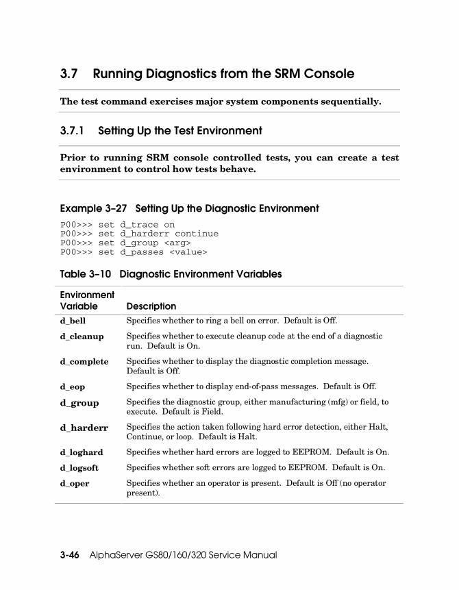
3-46 AlphaServer GS80/160/320 Service Manual
3.7 Running Diagnostics from the SRM Console
The test command exercises major system components sequentially.
3.7.1 Setting Up the Test Environment
Prior to running SRM console controlled tests, you can create a test environment to control how tests behave.
Example 3– 27 Setting Up the Diagnostic Environment P00>>> set d_trace on P00>>> set d_harderr continue P00>>> set d_group <arg> P00>>> set d_passes <value>
Table 3– 10 Diagnostic Environment Variables
Environment Variable
Description
d_bell Specifies whether to ring a bell on error. Default is Off.
d_cleanup Specifies whether to execute cleanup code at the end of a diagnostic run. Default is On.
d_complete Specifies whether to display the diagnostic completion message. Default is Off.
d_eop Specifies whether to display end-of-pass messages. Default is Off.
d_group Specifies the diagnostic group, either manufacturing (mfg) or field, to execute. Default is Field.
d_harderr Specifies the action taken following hard error detection, either Halt, Continue, or loop. Default is Halt.
d_loghard Specifies whether hard errors are logged to EEPROM. Default is On.
d_logsoft Specifies whether soft errors are logged to EEPROM. Default is On.
d_oper Specifies whether an operator is present. Default is Off (no operator present).

Troubleshooting 3-47
Table 3– 10 Diagnostic Environment Variables (Continued)
Environment Variable
Description
d_passes Specifies the number of passes to run a diagnostic. Default is 1. 0 indicates to run the diagnostic indefinitely.
d_quick Specifies whether an abbreviated mode of tests should be run. Default is Off (no abbreviation).
d_report Specifies the level of information provided by diagnostic error reports. The default is Summary; other values are Full or Off.
d_softerr Specifies the action taken following a soft error. Default is Continue; other values are Halt or Loop.
d_startup Specifies whether to display the diagnostic startup message. Default is Off (no startup messages).
d_status Specifies whether diagnostic status reports are enabled. Default is Off (reports not enabled).
d_trace Specifies whether to display test trace messages. Default is Off (no trace messages).
Example 3–27 shows how you can set up the diagnostic environment. Table 3–10 lists all the environment variables that define the environment. All these environment variables are nonvolatile; that is the value of the environment variable is preserved in its default or set state, whichever was its last condition, across a system reset or power cycle.

3-48 AlphaServer GS80/160/320 Service Manual
3.7.2 Background Testing and Display
Several tests can be run in the background freeing the console for other operations. Displaying background test status is possible using the show_status command and the ps command. Stopping background tests is done using the kill_diags command.
Example 3– 28 Running sys_exer in the Background
P00>>> sys_exer � Default zone extended at the expense of memzone. Use INIT before booting Exercising the Memory memtest -bs 1000000 -rb -p 0 & memtest -bs 1000000 -rb -p 0 & memtest -bs 1000000 -rb -p 0 & memtest -bs 1000000 -rb -p 0 & memtest -sa 80000000 -ea FFFDE000 -z -p 0 & memtest -sa 1000000000 -ea 103FFE4000 -z -p 0 & memtest -sa 2000000000 -ea 205FFE2000 -z -p 0 & memtest -sa 3000000000 -ea 30FFFD8000 -z -p 0 & memtest -sa 4000000000 -ea 407FFE0000 -z -p 0 & memtest -sa 5000000000 -ea 507FFE0000 -z -p 0 & memtest -sa 6000000000 -ea 607FFE0000 -z -p 0 & memtest -sa 7000000000 -ea 707FFE0000 -z -p 0 & Exercising the DK* Disks (read only) Exercising the DQ* Disks (read only) dqa0.0.0.15.0 has no media present or is disabled via the RUN/STOP switch dqd0.0.0.15.20 has no media present or is disabled via the RUN/STOP switch dqf0.0.0.15.56 has no media present or is disabled via the RUN/STOP switch file open failed for dqd0.0.0.15.20 file open failed for dqf0.0.0.15.56 file open failed for dqa0.0.0.15.0 Exercising the EW* Network Type "show_status" to display testing progress Type "cat el" to redisplay recent errors Type "init" in order to boot the operating system
� The sys_exer command creates SRM test commands that run in the background. The “&” at the end of each command line created causes the diagnostic to execute in the background enabling the console to accept other commands.

Troubleshooting 3-49
Example 3– 29 Show_status P00>>> show_status ID Program Device Pass Hard/Soft Bytes Written Bytes Read -------- ------------ ------------ ------ --------- ------------- ----------- 00000001 idle system 0 0 0 0 0 0000081c memtest memory 2 0 0 2717908992 2717908992 00000822 memtest memory 2 0 0 2734686208 2734686208 00000828 memtest memory 2 0 0 2701131776 2701131776 00000887 memtest memory 2 0 0 2717908992 2717908992 000008a0 memtest memory 2 0 0 2147344384 2147344384 000008b9 memtest memory 4 0 0 3220881408 3220881408 000008d2 memtest memory 3 0 0 3220979712 3220979712 000008eb memtest memory 1 0 0 0 0 00000905 memtest memory 2 0 0 2147352576 2147352576 0000091e memtest memory 2 0 0 2147352576 2147352576 00000937 memtest memory 2 0 0 2147352576 2147352576 00000940 memtest memory 2 0 0 2147352576 2147352576 00000975 exer_kid dkf0.0.0.1.2 0 0 0 0 4833280 00000976 exer_kid dkg0.0.0.4.2 0 0 0 0 1275392 00000977 exer_kid dkg100.1.0.4 0 0 0 0 1274880 00000978 exer_kid dkg200.2.0.4 0 0 0 0 1274880 0000097c exer_kid dkg300.3.0.4 0 0 0 0 1274880 00000983 exer_kid dkj0.0.0.1.5 0 0 0 0 5041664 000009bf nettest ewa0.0.0.3.0 137 0 0 192896 192896 000009eb nettest ewb0.0.0.6.2 130 0 0 183040 183040 00000a1a nettest ewc0.0.0.6.5 115 0 0 161568 161920 P00>>>
In Example 3–28, some time after sys_exer started, the show_status command was executed. For a full description of the output, see the AlphaServer GS80/160/320 Firmware Reference Manual.
Example 3– 30 Kill_diags P00>>> kill_diags Loop Reply from: 00-00-f8-1b-1c-0b Loop Reply from: 00-00-f8-1b-1c-0b Loop Reply from: 00-00-f8-05-f5-50 Loop Reply from: 00-00-f8-05-f5-50 Loop Reply from: 00-00-f8-05-f5-50 Loop Reply from: 08-00-2b-c3-c1-c7 P00>>> show_status ID Program Device Pass Hard/Soft Bytes Written Bytes Read -------- ------------ ------------ ------ --------- ------------- ----------- 00000001 idle system 0 0 0 0 0 P00>>>
In Example 3–30 the kill_diags command is executed, and the show_status command shows that no diagnostic processes are running now.
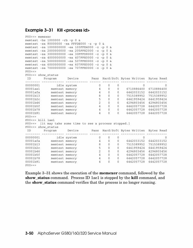
3-50 AlphaServer GS80/160/320 Service Manual
Example 3– 31 Kill <process id> P00>>> memexer memtest -bs 1000000 -rb -p 0 & memtest -sa 80000000 -ea FFFDE000 -z -p 0 & memtest -sa 1000000000 -ea 103FFE4000 -z -p 0 & memtest -sa 2000000000 -ea 205FFE2000 -z -p 0 & memtest -sa 3000000000 -ea 30FFFD8000 -z -p 0 & memtest -sa 4000000000 -ea 407FFE0000 -z -p 0 & memtest -sa 5000000000 -ea 507FFE0000 -z -p 0 & memtest -sa 6000000000 -ea 607FFE0000 -z -p 0 & memtest -sa 7000000000 -ea 707FFE0000 -z -p 0 & P00>>> P00>>> show_status ID Program Device Pass Hard/Soft Bytes Written Bytes Read -------- ------------ ------------ ------ --------- ------------- ----------- 00000001 idle system 0 0 0 0 0 00001ae1 memtest memory 4 0 0 6710886400 6710886400 00001afa memtest memory 4 0 0 6442033152 6442033152 00001b13 memtest memory 8 0 0 7515389952 7515389952 00001b2c memtest memory 5 0 0 6441959424 6441959424 00001b46 memtest memory 2 0 0 4294803456 4294803456 00001b5f memtest memory 4 0 0 6442057728 6442057728 00001b78 memtest memory 4 0 0 6442057728 6442057728 00001b91 memtest memory 4 0 0 6442057728 6442057728 P00>>> P00>>> kill 1ae1 P00>>> [it may take some time to see a process stopped.] P00>>> show_status ID Program Device Pass Hard/Soft Bytes Written Bytes Read -------- ------------ ------------ ------ --------- ------------- ----------- 00000001 idle system 0 0 0 0 0 00001afa memtest memory 4 0 0 6442033152 6442033152 00001b13 memtest memory 8 0 0 7515389952 7515389952 00001b2c memtest memory 5 0 0 6441959424 6441959424 00001b46 memtest memory 2 0 0 4294803456 4294803456 00001b5f memtest memory 4 0 0 6442057728 6442057728 00001b78 memtest memory 4 0 0 6442057728 6442057728 00001b91 memtest memory 4 0 0 6442057728 6442057728 P00>>>
Example 3–31 shows the execution of the memexer command, followed by the show_status command. Process ID 1ae1 is stopped by the kill command, and the show_status command verifies that the process is no longer running.

Troubleshooting 3-51
Example 3– 32 Ps P00>>> ps ID PCB Pri CPU Time Affinity CPU Program State -------- -------- --- -------- -------- --- ---------- ---------------------- 00001bca 00360320 3 0 00000001 0 ps running 00001bc9 00332400 5 0 00000001 0 pkg0_poll waiting on tqe f0ab0 00001b9a 00358f80 2 6691 ffffffff 8 memtest running 00001b93 003a0d80 2 1 00000001 0 sh_bg waiting on 00358F80 00001b91 0039fb60 2 6690 ffffffff 29 memtest running 00001b7a 003995a0 2 1 00000001 0 sh_bg waiting on 0039FB60 00001b78 00398380 2 6691 ffffffff 13 memtest running 00001b61 00394460 2 0 00000001 0 sh_bg waiting on 00398380 00001b5f 00391600 2 6695 ffffffff 24 memtest running 00001b48 0038d500 2 0 00000001 0 sh_bg waiting on 00391600 00001b46 00389a80 2 6696 ffffffff 27 memtest running 00001b2f 00384940 2 0 00000001 0 sh_bg waiting on 00389A80 00001b2c 00380980 2 6698 ffffffff 17 memtest running 00001b15 0037b780 2 1 00000001 0 sh_bg waiting on 00380980 00001b13 0037a560 2 6703 ffffffff 16 memtest running [Several processes deleted] 0000009f 0021db40 0 2047495 01000000 24 idle ready 0000009e 003096e0 3 5728 00200000 21 shell_21 waiting on rxq_ready 0000009c 0021a570 0 2100121 00200000 21 idle running 0000009b 00305740 3 4612 00020000 17 shell_17 waiting on rxq_ready 00000099 00215db0 0 2100543 00020000 17 idle ready 00000098 003017a0 3 7681 00010000 16 shell_16 ready 00000096 00214bc0 0 2016691 00010000 16 idle ready 00000095 002fd800 3 3966 00002000 13 shell_13 waiting on rxq_ready 00000093 002115f0 0 2050930 00002000 13 idle ready 00000092 002f9860 3 6552 00001000 12 shell_12 ready 00000090 00210400 0 1994105 00001000 12 idle ready 0000008f 002f58a0 3 7308 00000200 9 shell_9 waiting on rxq_ready 0000008d 0020ce30 0 2038879 00000200 9 idle running 0000008c 002f18e0 3 6657 00000100 8 shell_8 ready 0000008a 0020bc40 0 2007787 00000100 8 idle ready 00000089 002ed920 3 3433 00000020 5 shell_5 ready 00000087 00208670 0 2047409 00000020 5 idle ready 00000086 002e9980 3 4128 00000010 4 shell_4 waiting on rxq_ready 00000084 00207480 0 2050451 00000010 4 idle running 00000008 002e5a20 5 0 00000001 0 dup_poll waiting on tqe ead1c 00000007 002e44e0 5 0 00000001 0 mscp_poll waiting on tqe e9014 00000006 002cb5c0 6 0 ffffffff 0 tt_control waiting on tt_control 00000004 00044460 7 3666 ffffffff 0 timer waiting on timer 00000003 00043240 6 1412241 ffffffff 21 poll waiting on poll 00000002 00042020 6 79 ffffffff 0 dead_eater waiting on dead_beef 00000001 00202cc0 0 1437102 00000001 0 idle ready P00>>>
As shown in Example 3–32, the ps command displays information about the processes running on the system. The most useful fields here are the process ID, CPU number, program name, and process state.

3-52 AlphaServer GS80/160/320 Service Manual
3.7.3 Testing and Exercising the System
The SRM test command tests the hardware in the system or hard partition. If a system or hard partition is soft partitioned, the test command ignores the soft partition environment variables and tests the hardware in the hard partition.
Example 3– 33 Test P00>>> test Testing the DK* Disks (read only) No DU* Disks available for testing No DR* Disks available for testing Testing the DQ* Disks (read only) Testing the DF* Disks (read only) No MK* Tapes available for testing No MU* Tapes available for testing Testing the VGA (Alphanumeric Mode only) Testing the EW* Network Testing the EI* Network P00>>> Example 3–33 shows an example of the test command. When the test command is used, the entire system (partition) is tested: memory, disks, tapes, serial ports, parallel port, network, and VGA. All tests run serially for a minimum of 10 seconds each. The run time of a test is proportional to memory size and the number of disk drives to test.
An optional external loopback test (-lb) can be performed on the parallel port and on the serial port 1.
Tests can be run either in the foreground or background. The option is controlled by an ampersand; test & would cause tests to run in the background so that other console commands can be executed.
Use the set command to establish parameters, such as whether to halt, loop, or continue on error. The d_passes environment variable, is ignored by the test command.

Troubleshooting 3-53
Example 3– 34 Sys_exer P00>>> sys_exer Default zone extended at the expense of memzone. Use INIT before booting Exercising the Memory memtest -bs 1000000 -rb -p 0 & memtest -bs 1000000 -rb -p 0 & memtest -bs 1000000 -rb -p 0 & memtest -bs 1000000 -rb -p 0 & memtest -sa 80000000 -ea FFFDE000 -z -p 0 & memtest -sa 1000000000 -ea 103FFE4000 -z -p 0 & memtest -sa 2000000000 -ea 205FFE2000 -z -p 0 & memtest -sa 3000000000 -ea 30FFFD8000 -z -p 0 & memtest -sa 4000000000 -ea 407FFE0000 -z -p 0 & memtest -sa 5000000000 -ea 507FFE0000 -z -p 0 & memtest -sa 6000000000 -ea 607FFE0000 -z -p 0 & memtest -sa 7000000000 -ea 707FFE0000 -z -p 0 & Exercising the DK* Disks (read only) Exercising the DQ* Disks (read only) dqa0.0.0.15.0 has no media present or is disabled via the RUN/STOP switch dqd0.0.0.15.20 has no media present or is disabled via the RUN/STOP switch file open failed for dqd0.0.0.15.20 file open failed for dqf0.0.0.15.56 file open failed for dqa0.0.0.15.0 Exercising the EW* Network file open failed for dvd0.0 0.1000.20 file open failed for dva0.0.0.1000.0. file open failed for dvc0.0.0.1000.16 file open failed for dvb0.0.0.1000.14 Type "show_status" to display testing progress Type "cat el" to redisplay recent errors Type "init" in order to boot the operating system
The sys_exer command creates console commands to background test the entire system. All tests run concurrently for a specified time (default is continuous).
Syntax
sys_exer [-lb] [-t<runtime>]
where – lb = loopback and – t = run time in seconds (default is 0 – continuous).
Example 3–34 shows that the sys_exer command creates SRM test commands that run in the background. Where possible all devices and memory are exercised. See

3-54 AlphaServer GS80/160/320 Service Manual
Example 3–29 for the display of the show_status command related to sys_exer.
Example 3– 35 Exer
P00>>> exer dk*.* -p 0 –secs 36000 � P00>>> exer –l 2 dkb0 � P00>>> exer –sb 1 –eb 3 –bc 4 –a ‘w’ –d1 ‘0x5a’ dka100 � P00>>> exer –a ‘?r-w-Rc’ dka400 � � Read all SCSI type disks for the entire length of each disk. Repeat this
until 36000 seconds (10 hours) have elapsed. All disks will be read concurrently. Each block read will occur at a random block number on each disk.
� Read block number 0 and 1 from device dkb0.
� Write hex 5a’s to every byte of blocks 1, 2, and 3 of dka100. The packet size is bc (block count) times bs (block size), or 4 times 512, or 2048 for all writes.
� A nondestructive write test with packet size of 512 bytes. The action string specifies the following sequence of operations:
1. Set the current address to the beginning of a random block.
2. From the beginning of the block, read 512 bytes into buffer1.
3. Set the address back to the beginning of the block.
4. Write the data from buffer1 back to the block on the disk.
5. Set the address back to the beginning of the block again.
6. From the beginning of the block, read 512 bytes into buffer2.
7. Compare buffer1 with buffer2 and report any discrepancies.
8. Repeat the above steps until each block on the disk has been written once and read twice.
The exer command exercises one or more devices by performing specified read, write, and compare operations.

Troubleshooting 3-55
• A read operation reads from a specified device into a buffer.
• A write operation writes from a buffer to a specified device.
• A compare operation compares the contents of the two buffers.
• The exer command uses two buffers, buffer 1 and buffer 2, to carry out the operations. A read or write operation can be performed using either buffer. A compare operation uses both buffers.
You can tailor exer by using options to specify the following: • An address range to test within the test device(s)
• The packet size (number of bytes read or written in one I/O operation)
• The number of passes to run
• How many seconds to run for
• A sequence of individual operations performed on the test device(s). The qualifier used to specify this is called the action string qualifier.
If you simply specify “exer <device>” , the exerciser will do one pass of random reads of the entire device (which could take many minutes).
CAUTION: Running exer on disks can destroy data on the disks.
Syntax
exer [-sb start_block] [-eb end_block] [-p pass_count] [-l blocks] [-bs block_size] [-bc blocks_per_io] [-d1 buf1_string] [-d2 buf2_string] [-a action_string] [-sec seconds] [-m] [-v] [-delay millisecs] device_name

3-56 AlphaServer GS80/160/320 Service Manual
Table 3– 11 Exer Options
-sb start_block Specifies the starting block number (hex). The default is 0.
-eb end_block Specifies the ending block number (hex). The default is 0.
-p pass_count Specifies the number of passes. If 0, then run forever or until Ctrl/C. The default is 1.
-l blocks Specifies the number of blocks (hex) to exercise. The option l has precedence over eb. If only reading, then not using either – l or – eb defaults to read until end-of-file. If writing, and neither – l nor – eb are specified, then exer will write for the size of device. The default for blocks is 1.
-bs block_size Specifies the block size (hex) in bytes. The default is 200.
-bc blocks_per_io Specifies the number of blocks (hex) for each I/O operation. On devices without length (tape), use the specified pack size or default to 2048. The maximum block size allowed with variable-length block reads is 2048. Default is 1.
-d1 buf1_string String argument for eval to generate buffer1 data pattern from. Buffer1 is initialized only once before any I/O occurs. Default = all bytes set to hex 5a’s.
-d2 buf2_string Same as – d1.
-a action_string Specifies an exerciser action string that determines the sequence of reads, writes, and compares to various buffers. The default action string is ?r. Action string characters are:
r Read into buffer1
w Write from buffer1
R Read into buffer2
W Write from buffer2
n Write without lock from buffer1
N Write without lock from buffer2
c Compare buffer1 with buffer2

Troubleshooting 3-57
Table 3– 11 Exer Options (Continued)
- Seek to file offset prior to last read or write
? Seek to a random block offset within the specified range of blocks.
s Sleep for a number of milliseconds specified by the delay qualifier. If no delay qualifier is used, sleep for 1 millisecond. Note: Times reported in verbose mode may not be accurate when this character is used.
z Zero buffer1
Z Zero buffer2
b Add constant to buffer1
B Add constant to buffer2
-sec seconds Specifies termination of the exerciser after the number of seconds have elapsed. By default, exer continues until the specified number of blocks of passes are processed.
-m Specifies metric mode. At the end of the exercise, a total throughput line is displayed.
-v Specifies verbose mode. Data read is also written to the standard output. This is not applicable on writes or compares. The default is verbose mode off.
-delay millisecs Specifies the number of milliseconds to delay when “s” appears as a character in the action string.

3-58 AlphaServer GS80/160/320 Service Manual
Example 3– 36 Memexer P00>>> memexer 3 memtest -bs 1000000 -rb -p 0 & memtest -bs 1000000 -rb -p 0 & memtest -bs 1000000 -rb -p 0 & P00>>> show_status ID Program Device Pass Hard/Soft Bytes Written Bytes Read -------- ------------ ------------ ------ --------- ------------- ----------- 00000001 idle system 0 0 0 0 0 0000011d memtest memory 2 0 0 520093696 20093696 00000123 memtest memory 2 0 0 520093696 520093696 00000162 memtest memory 2 0 0 520093696 520093696 P00>>> kill_diags P00>>> show_status ID Program Device Pass Hard/Soft Bytes Written Bytes Read -------- ------------ ------------ ------ --------- ------------- ----------- 00000001 idle system 0 0 0 0 0 P00>>> The memexer command tests system memory. The program randomly allocates and tests blocks of memory twice the size of the B-cache using all available memory. The pass count is 0 to run the started tests forever (you can use the kill or kill_diags command to terminate). Memexer automatically tests in the background without the user specifying ‘&’.
Syntax
Memexer [<number>]
Where <number> = the number of memory test processes to start.
Example 3–36 shows the memexer command. The pass count is infinite so you must use the kill_diags command to terminate the tests. Use the show status command to view test progress.

Troubleshooting 3-59
Example 3– 37 Fptest P00>>> fptest &p4 & P00>>> ps ID PCB Pri CPU Time Affinity CPU Program State -------- -------- --- -------- -------- --- ---------- ---------------------- 00000395 002be420 3 1 00000001 0 ps running 00000394 002ccf40 1 949 00000010 4 fptest running 00000393 002c8580 2 1 00000001 0 sh_bg waiting on 002CCF40 0000029e 002c5360 3 7705 00000001 0 shell ready 0000003a 002b5660 6 0 ffffffff 0 rx_ewa0 waiting on rx_isr_ewa0 00000036 002aab20 3 6812 00000001 0 shell_0 ready 00000014 0027b320 3 1227 00000010 4 shell_4 waiting on rxq_ready 00000012 001d3150 0 273592 00000010 4 idle ready Use the fptest command to test the floating-point unit of the Alpha processor specified in the command. If no processor is identified, tests are run on the system primary CPU.
The program contains 9 tests:
T1 - Compute Pi in IEEE Mode T2 - Compute Pi in VAX D T3 - Compute Pi in VAX F T4 - Compute Pi in VAX G T5 - Do 11 Floating Pt Math Instructions (+,-,*,/) in IEEE Double T6 - Do 11 Floating Pt Math Instructions (+,-,*,/) in IEEE Single T7 - Do 11 Floating Pt Math Instructions (+,-,*,/) in VAXD Double T8 - Do 11 Floating Pt Math Instructions (+,-,*,/) in VAXF Single T9 - Do 11 Floating Pt Math Instructions (+,-,*,/) in VAXG Double
The show_status command does not display fptest progress. Use the ps command to see the process, if the test is run in the background.
Syntax
fptest [-t <test number>] [-p <pass count>] [&p <cpu number>]
where: -t = a particular test in the suite of floating-point tests -p = the number of passes the test will make (default is 1) &p = the ID number of the CPU to test

3-60 AlphaServer GS80/160/320 Service Manual
Example 3– 38 Fakedisk
P00>>> fakedisk a 10 � P00>>> fakedisk * 15 � P00>>> exer –a ‘?r-w-Rc’ –sec 15 dfa � P00>>> rm dfa � � This command creates a fake disk in memory called dfa the size of ten 512
blocks.
� This command creates a fake disk in memory for each disk controller on each PCI in the system. The size of each RAM disk is fifteen 512 blocks.
� This command causes the following to run for 15 seconds on fake disk dfa: Set the current block address to the beginning of a random block. From the beginning of the block read 512 bytes into buffer1. Set the address back to the beginning of the block. Write the data from buffer1 back to the block on the disk. Set the address back to the beginning of the block. From the beginning of the block read 512 bytes into buffer2. Compare buffer1 with buffer2 and report discrepancies.
� This command removes the fake disk from memory.
The fakedisk command creates RAM disks in memory so that disk controllers on PCIs can be tested without disks attached. The controllers run in loopback mode.
Once fake disks are set up in memory, exer is used to test the controllers.
The rm command is used to remove the “disks” from memory.
Syntax
fakedisk [controller_letter] [number_blocks]
where: controller_letter = a, b, … z, or * (* creates RAM disks = # of controllers) number_blocks = the number of 512 blocks (bytes) for each fake disk in memory

Troubleshooting 3-61
Example 3– 39 Nettest
P00>>> nettest ei* � P00>>> nettest –mode in ew* � P00>>> nettest –mode ex –w 10 e* �
� Internal loopback test on all ei type network devices
� Internal loopback test on all ew type network devices
� External loopback test on all network devices on the system; wait 10 seconds between tests
Nettest is the generic network device exerciser. It can test network devices in internal, external, or live network loopback mode. The test works with ports supporting MOP protocol. Related environment variables can be set from the console to customize nettest before nettest is started.
You can change other network driver characteristics by modifying the port mode. See the -mode option.
Use the show_status display to determine the process ID when terminating an individual diagnostic test. Use the kill or kill_diags command to terminate tests.
Syntax
nettest [-f <file>] [-mode <port_mode>] [-p <pass_count>] [-sv <mop_version>] [-to <loop_time>] [-w <wait_time>] [<port>]
For a complete description of nettest, see the AlphaServer Firmware Reference Manual.

3-62 AlphaServer GS80/160/320 Service Manual
3.7.4 Running SRM Loadable Diagnostics
Each system comes with an Alpha Systems Firmware CD-ROM. On this CD-ROM are update firmware files, LFU, an expanded SRM console, and diagnostics. Some of these diagnostics are run at power-up.
Example 3– 40 Booting the Firmware CD-ROM
Place the firmware CD-ROM in the master PCI box CD-ROM device. �
P00>>> boot dqb0 � (boot dqb0.0.0.15.12) block 0 of dqb0.0.0.15.12 is a valid boot block reading 1082 blocks from dqb0.0.0.15.12 bootstrap code read in base = 3dc000, image_start = 0, image_bytes = 87400 initializing HWRPB at 2000 initializing page table at 3ffec000 initializing machine state setting affinity to the primary CPU jumping to bootstrap code -----------------------------------------------------------------------------
[Appropriate header and text identifying the CD and its contents.] � ----------------------------------------------------------------------------- Hit <RETURN> to scroll text, or <CTRL/C> to skip text. The default bootfile for this platform is [GS320]gs320_v56.exe (LFU)
Hit <RETURN> at the prompt to use the default bootfile � Bootfile: [gs320]gs320_v56_load.exe OpenVMS PALcode V1.80-1, Tru64 UNIX PALcode V1.74-1 system = QBB 0 1 QBB 0 = CPU 0 + Mem 0 + Dir + IOP + PCA 3 + GP (Hard QBB 0) QBB 1 = CPU 0 1 2 3 + Mem 0 1 + Dir + IOP + PCA 2 3 + GP (Hard QBB 1) micro firmware version is X5.6 . . . create powerup entering idle loop initializing GCT/FRU at 22e000 initializing pka pkb pkc dqa dqb eia eib eic AlphaServer Console X5.8-4690, built on May 4 2000 at 06:00:06
P00>>> �

Troubleshooting 3-63
Not all diagnostics are run at power-up. In order to run loadable console controlled diagnostics, an expanded SRM console must be loaded. The loadable diagnostics test devices on the standard I/O module and a Memory Channel should one be on the system.
Example 3–40 shows an example of booting the expanded SRM console.
� Insert the firmware CD-ROM into the CD-ROM device in the master PCI box.
� Boot the CD-ROM.
� After jumping to the bootstrap code, text is displayed describing the contents, changes, and additions to the firmware.
� The name of the LFU file is identified and if you wish to run LFU simply hit <RETURN> but, in this case, to run the loadable diagnostics type in [gs320]gs320_v56_load.exe at the Bootfile: prompt.
� The expanded console now runs.
All loadable diagnostics are run in manufacturing mode and therefore the environment variable d_group must be set to mfg. Example 3–41 through Example 3–46 show how to run the standard I/O diagnostics available when running the expanded SRM console.

3-64 AlphaServer GS80/160/320 Service Manual
Example 3– 41 Acer_bridge_diag P01>>> set d_trace on | P01>>> set d_group mfg | � P01>>> set d_harderr continue | P01>>> acer_bridge_diag -h 12 � � � � � � acer_bridge_ 00000076 Std-I/O H12 1 1 0 0 acer_bridge_ 00000076 Std-I/O H12 1 2 0 0 acer_bridge_ 00000076 Std-I/O H12 1 3 0 0 acer_bridge_ 00000076 Std-I/O H12 1 7 0 0 acer_bridge_ 00000076 Std-I/O H12 1 8 0 0 *** Hard Error - Error #1 - Acer IDE Config Compare Error Diag Name ID Device Pass Test Hard/Soft 1-JAN acer_bridge_ 00000076 Std-I/O H12 1 8 1 0 12:00:01¡ Expected value: 0800002b | Received value: 0000002b | ¢ Failing addr: 50 | *** End of Error *** � The set d_trace command causes the diagnostic output to display on the console.
The set d_group mfg command permits the test to be run. The set d_harderr continue command causes the diagnostic to continue running after a hard error.
� The acer_bridge_diag – h 12 command causes the PCI – ISA bridge diagnostic test suite to run. In this case the standard I/O module tested is on PCI hose 12.
The generic syntax is: acer_bridge_diag -h<dev. ID> -t<test#> –p<pass count>
� The name of the diagnostic is displayed.
� The device ID is given.
� The name of the tested device and its hose number is given.
� The pass count is given.
� The test number within a group of tests is given.
The number of hard/soft errors is displayed.
¡ When an error occurs, the error is identified. In this case, test 8 fails with a hard error during pass 1 of the diagnostic.
¢ The expected data, received data, and failing address are displayed.

Troubleshooting 3-65
Example 3– 42 Acer_io_diag P01>>> set d_trace on | P01>>> set d_group mfg | � P01>>> set d_harderr continue | P01>>> acer_io_diag -h 12 � � acer_io_diag 00000075 Std-I/O H12 1 1 0 0 12:00:01 acer_io_diag 00000075 Std-I/O H12 1 3 0 0 12:00:01 acer_io_diag 00000075 Std-I/O H12 1 4 0 0 12:00:01 acer_io_diag 00000075 Std-I/O H12 1 5 0 0 12:00:01 acer_io_diag 00000075 Std-I/O H12 1 7 0 0 12:00:* acer_io_diag 00000075 Std-I/O H12 1 8 0 0 12:00:* acer_io_diag 00000075 Std-I/O H12 1 9 0 0 12:00:01 Cannot run this test on the Console Standard I/O � acer_io_diag 00000075 Std-I/O H12 1 10 0 0 12:00:01 Cannot run this test on the Console Standard I/O � acer_io_diag 00000075 Std-I/O H12 1 11 0 0 12:00:01 Cannot run this test on the Console Standard I/O � acer_io_diag 00000075 Std-I/O H12 1 12 0 0 12:00:01 Cannot run this test on the Console Standard I/O � acer_io_diag 00000075 Std-I/O H12 1 13 0 0 12:00:01 Cannot run this test on the Console Standard I/O � acer_io_diag 00000075 Std-I/O H12 1 15 0 0 12:00:01 acer_io_diag 00000075 Std-I/O H12 1 16 0 0 12:00:01 acer_io_diag 00000075 Std-I/O H12 1 17 0 0 12:00:01 acer_io_diag 00000075 Std-I/O H12 1 19 0 0 12:00:01 Cannot run this test on the Console Standard I/O � � The set d_trace command causes the diagnostic output to display on the
console. The set d_group mfg command permits the test to be run. The set d_harderr continue command causes the diagnostic to continue running after a hard error.
� The acer_io_diag – h 12 command causes a suite of diagnostic tests to run on the standard I/O module. In this case the standard I/O module being tested is on PCI hose 12.
The generic syntax is: acer_io_diag -h<dev. ID> -t<test#> –p<pass count>
� Tests 1 through 20 are run on the standard I/O module except those that would affect the SRM console operation.
� Tests are not run that would affect SRM console operation.

3-66 AlphaServer GS80/160/320 Service Manual
Example 3– 43 Acer_8042_diag P01>>> set d_trace on | P01>>> set d_group mfg | � P01>>> set d_harderr continue | P01>>> acer_8042_diag -h 46 � � acer_8042_di 00000064 Std-I/O H12 1 1 0 0 12:00:01 acer_8042_di 00000064 Std-I/O H12 1 3 0 0 12:00:01 acer_8042_di 00000064 Std-I/O H12 1 4 0 0 12:00:01 *** Hard Error - Error #4 - KeyBoard BIST Failed � Diag Name ID Device Pass Test Hard/Soft 1-JAN acer_8042_di 00000064 Std-I/O H12 1 4 1 0 12:00:01 *** End of Error *** � acer_8042_di 00000064 Std-I/O H12 1 5 1 0 12:00:01� acer_8042_di 00000064 Std-I/O H12 1 6 1 0 12:00:01 acer_8042_di 00000064 Std-I/O H12 1 7 1 0 12:00:01 � The set d_trace command causes the diagnostic output to display on the
console. The set d_group mfg command permits the test to be run. The set d_harderr continue command causes the diagnostic to continue running even after a hard error.
� The – h 12 command causes the 8042 (keyboard/mouse controller) diagnostic test suite to run. In this case the standard I/O module being tested is on PCI hose 12.
The generic syntax is: acer_8042_diag -h<dev. ID> -t<test#> –p<pass count>
� Tests 1 through 7 run on the keyboard and mouse controller (8042).
� The keyboard test 4 fails with a hard error.
� The diagnostic displays the hard error and continues.
� Note that tests 5, 6, and 7 do not fail though the hard error seen in test 4 shows in the display.

Troubleshooting 3-67
Example 3– 44 Isp1020_diag P01>>> set d_trace on | P01>>> set d_group mfg | � P01>>> set d_harderr continue | P01>>> isp1020_diag pka � � � isp1020_diag 00000081 pka 1 1 0 0 12:00:01 isp1020_diag 00000081 pka 1 2 0 0 12:00:01 isp1020_diag 00000081 pka 1 3 0 0 12:00:01 � The set d_trace command causes the diagnostic output to display on the
console. The set d_group mfg command permits the Acerlab test to be run. The set d_harderr continue command causes the diagnostic to continue running even after a hard error.
� The isp1020_diag pka command causes the console to run the diagnostic test suite on the SCSI controller embedded on PCI bus0.
The generic syntax is: isp1020_diag <device> -p<pass count>
� Tests 1 through 3 run on the SCSI controller. Note that this test targets only Qlogic ISP1020 SCSI controllers. Other SCSI controllers require other diagnostics.
� There are no hard or soft failures in this case.

3-68 AlphaServer GS80/160/320 Service Manual
Example 3– 45 Bq4285_diag P01>>> set d_trace on | P01>>> set d_group mfg | � P01>>> set d_harderr continue | P01>>> bq4285_diag -h 12 � � � bq4285_diag 0000007e bq4285 H12 1 1 0 0 12:00:01 bq4285_diag 0000007e bq4285 H12 1 3 0 0 12:00:01 bq4285_diag 0000007e bq4285 H12 1 4 0 0 12:00:01 bq4285_diag 0000007e bq4285 H12 1 5 0 0 12:00:01
� The set d_trace command causes the diagnostic output to display on the console. The set d_group mfg command permits the test to be run. The set d_harderr continue command causes the diagnostic to continue running even after a hard error.
� The bq4285_diag – h 12 command causes the console to run the diagnostic test suite on the real-time clock. In this case the standard I/O module being tested is on PCI hose 12.
The generic syntax is: bq4285_diag -h <dev. ID> -t<test#> –p<pass count>
� Tests 1 through 5 run on the real-time clock.
� The diagnostic does not have a hard or soft failure.

Troubleshooting 3-69
Example 3– 46 Isa_misc_diag P01>>> set d_trace on | P01>>> set d_group mfg | � P01>>> set d_harderr continue | P01>>> isa_misc_diag -h 12 � � � isa_misc_dia 00000083 Std-I/O H12 1 1 0 0 12:00:01 isa_misc_dia 00000083 Std-I/O H12 1 2 0 0 12:00:01 isa_misc_dia 00000083 Std-I/O H12 1 3 0 0 12:00:01 � The set d_trace command causes the diagnostic output to display on the
console. The set d_group mfg command permits the test to be run. The set d_harderr continue command causes the diagnostic to continue running even after a hard error.
� The isa_misc_diag – h 46 command causes the console to run the miscellaneous diagnostic tests on the ISA bus. In this case the standard I/O module being tested is on PCI hose 12.
The generic syntax is: isa_misc_diag -h <dev. ID> -t<test#> –p<pass count>
� Tests 1 through 3 run. Test 1 = shared RAM pattern test Test 2 = standard I/O EEPROM test Test 3 = standard I/O module CSR test
� The diagnostic does not have a hard or soft failure.

3-70 AlphaServer GS80/160/320 Service Manual
3.7.5 Crashing the System
Use the crash command to obtain a crash dump of the system.
Example 3– 47 Crash P00>>> crash CPU 0 restarting DUMP: 1983738 blocks available for dumping DUMP: 118178 wanted for a partial compressed dump. DUMP: Allowing 2060017 of the 2064113 available on 0x800001 device string for dump = SCSI 1 1 0 0 0 0 0. DUMP.prom: dev SCSI 1 1 0 0 0 0 0, block 2178787 DUMP: Header to 0x800001 at 2064113 (0x1f7ef1) device string for dump = SCSI 1 1 0 0 0 0 0. DUMP.prom: dev SCSI 1 1 0 0 0 0 0, block 2178787 DUMP: Dump to 0x800001: .......: End 0x800001 device string for dump = SCSI 1 1 0 0 0 0 0. DUMP.prom: dev SCSI 1 1 0 0 0 0 0, block 2178787 DUMP: Header to 0x800001 at 2064113 (0x1f7ef1) succeeded halted CPU 0 halt code = 5 HALT instruction executed PC = fffffc0000568704 P00>>> P00>>>

Troubleshooting 3-71
The crash command causes an operating system to halt and write the contents of memory to a file that can later be analyzed. Crash dumps can be helpful in determining why a system has malfunctioned. If the environment variable auto_boot is on, the system will reboot; otherwise, it will remain at the SRM prompt.
The syntax for this command is:
crash [device] The device option specifies the name of the device to which the crash dump is written.

3-72 AlphaServer GS80/160/320 Service Manual
3.8 Troubleshooting with LEDs
Diagnostic LEDs are visible only when cabinet doors are open and faceplates are removed. In some instances LEDs may be the only way to identify a power problem.
Figure 3– 1 System LEDs
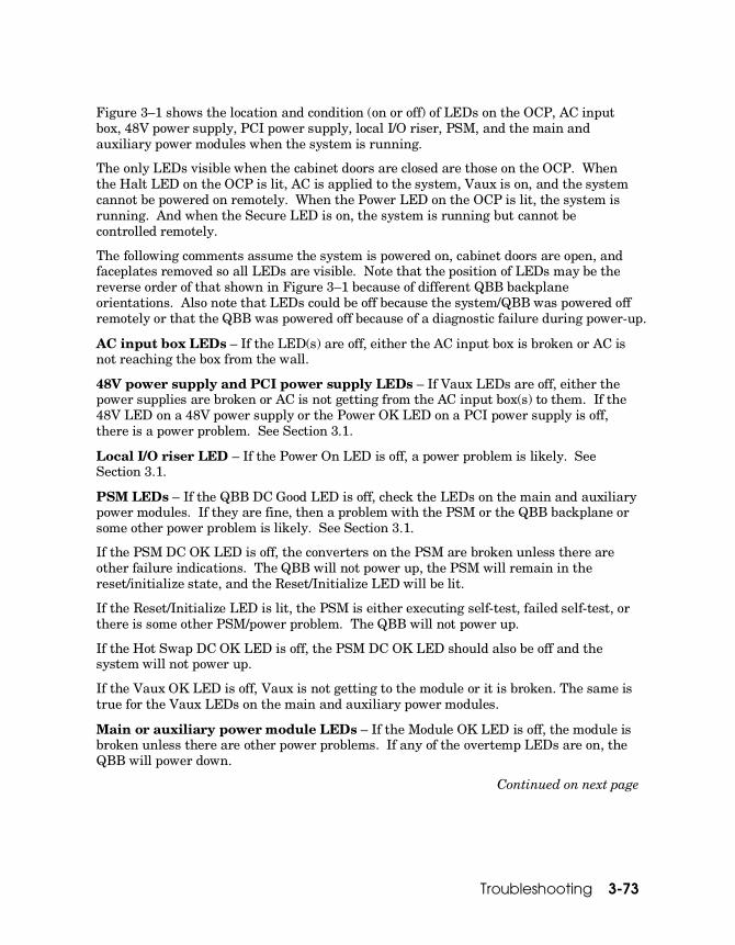
Troubleshooting 3-73
Figure 3–1 shows the location and condition (on or off) of LEDs on the OCP, AC input box, 48V power supply, PCI power supply, local I/O riser, PSM, and the main and auxiliary power modules when the system is running.
The only LEDs visible when the cabinet doors are closed are those on the OCP. When the Halt LED on the OCP is lit, AC is applied to the system, Vaux is on, and the system cannot be powered on remotely. When the Power LED on the OCP is lit, the system is running. And when the Secure LED is on, the system is running but cannot be controlled remotely.
The following comments assume the system is powered on, cabinet doors are open, and faceplates removed so all LEDs are visible. Note that the position of LEDs may be the reverse order of that shown in Figure 3–1 because of different QBB backplane orientations. Also note that LEDs could be off because the system/QBB was powered off remotely or that the QBB was powered off because of a diagnostic failure during power-up.
AC input box LEDs – If the LED(s) are off, either the AC input box is broken or AC is not reaching the box from the wall.
48V power supply and PCI power supply LEDs – If Vaux LEDs are off, either the power supplies are broken or AC is not getting from the AC input box(s) to them. If the 48V LED on a 48V power supply or the Power OK LED on a PCI power supply is off, there is a power problem. See Section 3.1.
Local I/O riser LED – If the Power On LED is off, a power problem is likely. See Section 3.1.
PSM LEDs – If the QBB DC Good LED is off, check the LEDs on the main and auxiliary power modules. If they are fine, then a problem with the PSM or the QBB backplane or some other power problem is likely. See Section 3.1.
If the PSM DC OK LED is off, the converters on the PSM are broken unless there are other failure indications. The QBB will not power up, the PSM will remain in the reset/initialize state, and the Reset/Initialize LED will be lit.
If the Reset/Initialize LED is lit, the PSM is either executing self-test, failed self-test, or there is some other PSM/power problem. The QBB will not power up.
If the Hot Swap DC OK LED is off, the PSM DC OK LED should also be off and the system will not power up.
If the Vaux OK LED is off, Vaux is not getting to the module or it is broken. The same is true for the Vaux LEDs on the main and auxiliary power modules.
Main or auxiliary power module LEDs – If the Module OK LED is off, the module is broken unless there are other power problems. If any of the overtemp LEDs are on, the QBB will power down.
Continued on next page

3-74 AlphaServer GS80/160/320 Service Manual
Figure 3– 1 System LEDs (Continued)
Figure 3–1 continued shows the location and normal condition (on or off) of LEDs on the CPU, HPM, H-switch power supplies, master clock, and CSB node ID module when the system is running.
The following comments assume the system is powered on, all cabinet doors are open, and faceplates removed so all LEDs are visible. Note that LEDs could be off because the system/QBB was powered off remotely or that there is some other power problem. See Section 3.1.

Troubleshooting 3-75
CPU LED – If the Run LED is off when it should be on, the CPU could be broken.
H-switch power manager LEDs – If the DC OK LED is off, the onboard +5V and/or +3V regulator is broken. If the Reset/Initialize LED is on, the module is in the reset state and may not have passed self-test.
H-switch power supply LEDs – If the Vaux LED is off, check that Vaux is OK at other system locations. If it is, Vaux is not present at the power supply for some reason or the power supply is broken. If any of the other LEDs are off with the exception of the Swap OK LED, the power supply is broken.
Master clock LED – If the master clock LED is off, the master clock is not working properly. The entire system is affected, and the system will not power up. The console reports a GR_CLK_OK_TIMEOUT.
Console serial bus ID LEDs – If the SCM master LED is on, the SCM in this PCI is master of the CSB bus. If it is off and there is only one standard I/O module in the system, then there is something wrong with the standard I/O module or the PCI in which it sits.
If the PBM built-in self-test LED is on, either the PBM is performing self-test or it did not pass self-test. Since the PBM micro is on the PCI backplane, the backplane could be broken or the PBM firmware could be corrupt.
If the SCM built-in self-test LED is on, either the SCM is performing self-test or it did not pass self-test. Since the SCM micro is on the standard I/O module, that module could be broken or the SCM firmware could be corrupt.
If the PCI DC power LED is off, there is a problem with power to the PCI.
If the Vaux present LED is off, there is a problem with power to the PCI or the Vaux signal is not reaching the CSB bus ID module. See Section 3.1.
Swap OK LEDs – All Swap OK LEDs are powered by the PSM +5V hot swap converter. When lit, they indicate that the logic voltages are not present at the modules. If the +5V converter is functioning even if the PSM is broken in some other way, the Swap OK LEDs will light.

3-76 AlphaServer GS80/160/320 Service Manual
3.9 Dealing with a Hung System
Troubleshooting a hung system depends upon what was running at the time of the hang. In general, these systems are designed not to hang. If a transaction times out or forward progress is not made for some reason, such events are considered faults and a running system should crash.
Table 3– 12 Hung System Suggestions
1. Try logging in remotely and investigate what the system is doing.
2. Check LEDs in QBBs and power supplies and if there is something abnormal fix it.
3. Check for I/O activity. If the system is in fact hung, there won’t be any. But if the disks are shared with another system, disk activity won’t necessarily mean much.
4. Try to get to the SRM console (OpenVMS - Ctrl/p, Tru64 UNIX - SCM halt in). If you can, issue commands that might help you identify where the problem lies. Try a Ctrl/x to see if you can get a new console shell.
5. Try to get to the SCM using the escape sequence (default - <esc><esc>scm) and issue commands like show csb and show fru to see if you see something odd or see old errors. Check to see if there is an alert pending.
6. If the system is partitioned, the SCM halt in command will halt the partition. Pushing the Halt button will halt the entire system.
7. If you can, use the SRM crash command to force a system crash for analysis later.
8. If all else fails, fault, reset, or power cycle the system.

Troubleshooting 3-77
Troubleshooting a hang is difficult. The suggestions in Table 3–12 are intended to give you a start.
There are some causes you can eliminate. Theoretically, at the hardware level, the system should not hang. Transactions are tracked such that if one is not making forward progress, a timeout is triggered, a machine check is generated, and the system crashes. Such an event is a fault and is considered a serious systemwide event that causes PSMs in the system to initialize (except for error state) and reset all components (ASICs and CPUs) in the system. All QBBs reset. When the machine re-boots, the PALcode attempts to collect the error state, if any, in control and status registers and build a system machine check (660) error frame that Compaq Analyze will automatically decode. See Section 3.12 for information on running Compaq Analyze.
At the operating system level, there are timeouts in software that get triggered that also cause crashes. Applications may hang but they can be handled at the operating system level by stopping the application.
If the microprocessors on the CSB lock up, the system could be running but access to it, through the console, may not function.

3-78 AlphaServer GS80/160/320 Service Manual
3.9.1 Troubleshooting a Diagnostic Hang
SROM and XSROM diagnostics report to the SCM monitor that they are hung.
Example 3– 48 Diagnostic Hang SCM_EF> . . . QBB0 now Testing Step-1 QBB1 now Testing Step-1................. . . . QBB1 now Testing Step-2............... QBB0 Error: *** CPU Connect Error *** ****QBB0-Cpu1TestHang Test:1b Subtest:19 � ****QBB0-Cpu3TestHang Test:1b Subtest:19 � QBB0 Step-3 Tested QBB0 Step-4 Tested QBB0 Step-5 Tested QBB1 Error: *** CPU Connect Error *** ****QBB1-Cpu1TestHang Test:1b Subtest:19 � ****QBB1-Cpu3TestHang Test:1b Subtest:19 � QBB1 Step-3 Tested QBB1 Step-4 Tested QBB1 Step-5 Tested Phase 1 IO_MAP0 from QBB0: 0000c00002322233 IO_MAP1 from QBB1: 00cf000004f444f3 No connection from RIO1 in PCI Drawer f ***SCM: CONFIG ERROR. SOFT ID NOT DETERMINED � QbbConf: 000000dd PQbb : ff SQbb0 : ff Gp : 8 QbbCnt : 02 QbbConf(GP_IOR_CPU_MEM)

Troubleshooting 3-79
Refer to Example 3–48. SROM/XSROM diagnostics are expected to complete in a certain amount of time. If that time is exceeded, a timeout occurs and is reported to the SCM. � CPU1 in QBB0 hangs running test 1b subtest 19. Test 1b is the local IOP
configuration test ID test and is run on a local primary.
� When the test hangs on CPU1, a new local primary is selected, CPU3 on QBB0. It too hangs.
� In QBB1 the same thing is happening. CPU1 hangs running the same test/subtest.
� A new local primary is chosen, CPU3 in QBB1, and it too hangs.
� When the results of phase 0 testing are printed at the beginning of phase 1, the system map indicates the configuration error.

3-80 AlphaServer GS80/160/320 Service Manual
Example 3– 48 Diagnostic Hang (Continued) SCM_EF> QBB0 now Testing Step-6 � . . QBB0 Step-b Tested IO_MAP0 from QBB0: 0000c00002322233 IO_MAP1 from QBB1: 00cf000004f444f3 No connection from RIO1 in PCI Drawer f � Phase 2 ***SCM: CONFIG ERROR. SOFT ID NOT DETERMINED � QbbConf: 000000dd PQbb : ff SQbb0 : ff Gp : 8 QbbCnt : 02 QbbConf(GP_IOR_CPU_MEM) SCM_EF> QBB1 now Testing Step-c QBB0 Step-c Tested Phase 3 ***SCM: CONFIG ERROR. SOFT ID NOT DETERMINED � QbbConf: 000000dd PQbb : ff SQbb0 : ff Gp : 8 QbbCnt : 02 QbbConf(GP_IOR_CPU_MEM) QBB0 Step-d Tested QBB1 Step-d Tested IO_MAP0 from QBB0: 0000c00002322233 IO_MAP1 from QBB1: 00cf000004f444f3 No connection from RIO1 in PCI Drawer f Phase 4 Initializing shared ram Shared RAM Initialized ***SCM: CONFIG ERROR. SOFT ID NOT DETERMINED � QbbConf: 000000dd PQbb : ff SQbb0 : ff Gp : 8 QbbCnt : 02 QbbConf(GP_IOR_CPU_MEM) SCM_EF> . QBB0 now Testing Step-e QBB1 now Testing Step-e... ***SCM: CONFIG ERROR. SOFT ID NOT DETERMINED � QbbConf: 000000dd PQbb : ff SQbb0 : ff Gp : 8 QbbCnt : 02 QbbConf(GP_IOR_CPU_MEM) Power ON Summary: � *** CPU1 on QBB0 FAILURE *** CPU3 on QBB0 FAILURE *** CPU1 on QBB1 FAILURE *** CPU3 on QBB1 FAILURE Power On Complete SCM_EF> Refer to the continuation of Example 3–48.
Troubleshooting 3-81
� Despite the hang in the two QBBs, power-up continues on the CSB.
� The PCI box with the standard I/O module is not connected through the QBB backplane IOP – local I/O riser – near end mini link – hose – far end mini link – PCA remote I/O riser – PCI backplane to the standard I/O module.
� The same condition is seen during the remaining phases of power-up.
� The power on summary shows a failure on each CPU in the system.
The main clue in troubleshooting this event is noting what the machine was doing at the time of the failure. In this case we know the failing test is 1b, sub-test 19. From Appendix C you can determine that Test 1b, Local IOP Configuration, hung during subtest 19, probing PCI Bus 0 on each “good” hose looking for a STD I/O module. This knowledge might lead you to suspect a problem with the backplane, IOA or IOD, or the MPLL associated with either of those ASICs.

3-82 AlphaServer GS80/160/320 Service Manual
3.9.2 Troubleshooting a Diagnostic Fault
SROM and XSROM diagnostics report faults to the SCM monitor.
Example 3– 49 A Sample Diagnostic Fault . . QBB0 now Testing Step-6 | QBB1 Step-6 Tested | . | QBB1 Step-a Tested | QBB2 Step-6 Tested | � . | QBB2 Step-a Tested | QBB3 Step-6 Tested | . | QBB3 Step-a Tested | SCM_E0> .............. PSM30 SysEvent: FAULT_RECOVERY � SysEvent Reg0: 469f SysEvent Reg1: 3fff Fault Entity: 24 ****QBB0-Cpu0TestHang Test:34 Subtest:5 � FruCall:0 FruSeverity:0 SCM: QBB0 callout QBB0 Step-7 Tested . QBB0 Step-a Tested IO_MAP from QBB0: 000000c001311133 IO_MAP from QBB1: 0000000000000003 IO_MAP from QBB2: 0000c10002322233 IO_MAP from QBB3: 0000000000000003 Phase 2 � HS Populated... is it ready? – REMOVE | HS Populated... is it ready? – REMOVE | HS Populated... is it ready? – REMOVE | � HS Populated... is it ready? – REMOVE | SCM_E0> QBB3 now Testing Step-b HPM40 SysEvent Code: 1e SysEvent Reg0: 000f SysEvent Reg1: d581 SCM_E0> QBB0 now Testing Step-b QBB1 now Testing Step-b QBB2 now Testing Step-b.. ******* Waiting 5 seconds

Troubleshooting 3-83
Now waiting 10 seconds after HPM reset � ******* Waiting 5 seconds before sending restart to PSMs � SCM_E0> ... ****QBB3-Cpu0TestHang Test:53 Subtest:1 | ****QBB3-Cpu1TestHang Test:53 Subtest:1 | ****QBB3-Cpu2TestHang Test:53 Subtest:1 | ****QBB3-Cpu3TestHang Test:53 Subtest:1 | Example 3–49 shows reports sent to the SCM over the console serial bus when an unexpected fault occurs during SROM/XSROM testing.
� The system is a four QBB system.
� The system faults and is detected by the PSM.
� Test 34 subtest 5 was running at the time of the fault.
� Despite the fault the SCM attempts to bring up the system.
� Faults are catastrophic.
� The HPM in the hierarchical switch is reset.
� The PSMs in the QBBs are reset.
As power-up continues, other tests hang.
In this case, test 34, Local Soft QBB ID Configuration, hung during subtest 5, writing soft QBB ID to GPA_INIT_ID register. While not a great deal of information to go on, one might suspect the global port on QBB0 since the GPA_INIT_ID register is on that module.

3-84 AlphaServer GS80/160/320 Service Manual
3.10 Dealing with Corrupt Firmware
Each microprocessor on the CSB runs firmware located in flash ROMs on the module or backplane close to the microprocessor. If this firmware is corrupt, a new image can be loaded into the flash ROMs by having the microprocessor running a fail-safe loader image. Only the SCM update command can be used to load the new firmware.
Table 3– 13 Fail-Safe Loader Jumpers
Module or Backplane Force Fail-Safe Loader Mode
Standard I/O module (SCM) J17
Power system manager module (PSM) J9
H-switch power manager module (HPM) J3
PCI backplane (PBM) J60

Troubleshooting 3-85
Initially on power-up or reset each microprocessor on the CSB runs a fail-safe loader image and the microprocessor is said to be in fail-safe loader mode (FSL mode). This FSL image resides in flash ROM in a different location than the normal firmware image run in the microprocessor.
The FSL image has two functions:
• it runs a checksum test on the primary firmware run by the microprocessor.
• it loads a new firmware image into its associated flash ROM when instructed to do so by the SCM update command only.
If the checksum test passes, the FSL code jumps to the normal firmware image and the microprocessor runs that code. If the checksum test fails, the microprocessor remains in FSL mode and the resource, whatever it is, is not configured into the system. Appropriate error messages are sent to the console if a checksum failure occurs and the corrupt image can be replaced. Only the SCM update command can be used to load healthy firmware into a micro’s flash EEPROM when the micro is in FSL mode. See Appendix D for instructions on running the SCM update command.
If the checksum test passes and the normal firmware image still does not run on the microprocessor, FSL mode can be forced by installing a jumper on the failing module or backplane. See Table 3–13.

3-86 AlphaServer GS80/160/320 Service Manual
3.11 Error Detection
Error detection is distributed throughout the system.
Figure 3– 2 Core System Error Detectors
Figure 3–2 is a block diagram showing the data error detectors in the system.
There are three types of errors:
• Correctable errors are detected either by the system or by a CPU. If the error is detected by the system, an error interrupt is generated and delivered to the system primary CPU, the data is corrected at the destination wherever that may be, and PALcode builds a 620 system correctable error frame that is deposited in the error log. If the CPU detects the error, an error interrupt is generated for that CPU and PALcode builds a 630 processor correctable error frame that is deposited in the error log.
• Uncorrectable errors are detected either by the system or by a CPU and are fatal. If the error is detected by the system, an error interrupt is generated and delivered to the system primary CPU, the system crashes,

Troubleshooting 3-87
and PALcode builds a 660 system uncorrectable error frame that is deposited in the error log. If the CPU detects the error, an error interrupt is generated for that CPU, the system crashes, and PALcode builds a 670 processor uncorrectable error frame that is deposited in the error log.
• Faults are errors that compromise the coherence of the system. When a fault is detected, a signal is passed to all QBBs that causes the system including the CPUs to reset and all components (ASICs) in the system to initialize. Error state is latched and PALcode attempts to build a 660 error frame that is deposited in the error log.
There are six error classes:
ECC errors – Most data paths and large data stores are protected by ECC. ECC provides single-bit error detection and correction, and double-bit error detection. For non-coherence-related data stores (memory) single-bit errors are correctable and multi-bit errors are uncorrectable. For coherence-related data stores (directory) single-bit errors are correctable and multi-bit errors are faults.
Parity errors – Some data paths and data stores are protected by parity. Parity errors on data paths and in non-coherence-related data stores are uncorrectable errors. Parity errors on address paths and in coherence-related data stores are faults.
Forward progress errors – If a given transaction in a quad switch is either not issued or not completing, a forward progress error is detected. Such errors are faults.
Overflow errors – If a system component, an ASIC, receives a new reference after flow control should have prevented one, an overflow error is detected. Such errors are faults.
Command inconsistency errors – System components, typically ASICs, check certain internal consistencies and can report errors if consistency rules are not met. Examples of such errors include memory access violations and data command packet reception during ineligible cycles. Such errors are faults.
NXM errors – Memory or I/O references that are out of range cause NXM (non-existent memory) errors. NXM errors can be faults, uncorrectable errors or not an error at all, depending upon the component detecting the error and configuration register settings and the command executing.
For a full description of errors and their consequences, see the AlphaServer GS80/160/320 System Programmer’s Manual.

3-88 AlphaServer GS80/160/320 Service Manual
3.12 Compaq Analyze
Compaq Analyze is the error analysis tool used to analyze errors. The tool runs automatically in the background monitoring the active error log and processing events as they occur. For information on installing, running, and learning about Compaq Analyze, refer to the WEBES V3.0 GS80/160/320 CD-ROM. Compaq Analyze can be run manually using a Web browser or using a command-line interface.
3.12.1 Compaq Analyze Using a Web Browser
Once installed, Compaq Analyze automatically runs on each of the supported operating systems.
Figure 3– 3 Compaq Analyze Using a Web Browser

Troubleshooting 3-89
Figure 3–3 is an example of what you might see when running Compaq Analyze manually using a Web browser. There are two methods available for users to run Compaq Analyze. The method shown here is through a Web browser interface. Either Netscape version 3.x or higher or Internet Explorer version 4.0 or later is required. The second method is through the use of a command-line interface. Both methods are described in the Compaq Analyze User Guide on the WEBES V3.0 GS80/160/320 CD-ROM. For details on using either method to run Compaq Analyze, read the User Guide.
When an error is detected, a problem report is generated that describes the problem and corrective actions necessary to fix it. The problem report is distributed in accordance with the customer’s notification preferences established at the time Compaq Analyze is installed. Example 3–50 shows such a report.
To get information on Compaq Analyze on the Web, go to http://www.compaq.com/support/ and follow the link “Software and Drivers” and “Service Tools.” Note that WEBES V3.0 or later are versions of Compaq Analyze that support GS80/160/320 systems.

3-90 AlphaServer GS80/160/320 Service Manual
3.12.2 Problem Found Report
Compaq Analyze runs in the background and continually analyzes binary entries in the error log. If an error entry meets error criteria, a problem found report is delivered through Compaq Analyze. The problem found report states the problem and identifies the most likely faulty FRU. One can retrieve the problem found report by selecting the Problem Found icon and opening the file.
Example 3– 50 Problem Found (660)
Problem Found: Uncorrectable read error on memory module 1 of QBB0\(Soft QBB0\) at Thu Jan 27 14:55:47 EST 2000
Managed Entity: System Name : WFSI22 System Type : Compaq AlphaServer GS320 6/731 System Serial : WF22 OS Type : OpenVMS/V7.2 Brief Description: � Uncorrectable read error on memory module 1 of QBB0\(Soft QBB0\) Callout ID: Theory Code : 0x86A8020000002305 SQBB.Ent.Err : 0.21.6 Severity: 2 Reporting Node: WFSI22
Full Description: � In the Memory Error Summary Register bit 5 was set. This bit is set when the Memory Module detects an uncorrectable ECC error during the transfer of memory data to the system memory port. If this bit is set, the full error status (including the failing arbBus address and the Data Error bits) is

Troubleshooting 3-91
available to help identify the source of the error. This error bit is implemented as a copy of the Valid bit in the MEM_RD_UCE_TRAP register. NOTE: To determine the array in error a valid configuration tree is required. If this is not available, the entire memory module, including its DIMMs, will be called out. For an uncorrectable memory error a single DIMM in error can not be determined. As a minimum a group of 4 DIMMs will be called out (ie a Memory Array\). No memory write errors have been identified. So the problem source is assumed to be the memory module or its DIMMs. Error detail: The memory has detected a ECC checkbits all-zeros or all-ones.
Refer to Example 3–50.
� The brief description summarizes the problem. In this case an uncorrectable read error on memory module 1 of QBB0\(Soft QBB0\) has been detected. (Though not called out at this level, this error is a 660 machine check.)
� The full description of the problem gives much more detail. Here we learn that a precise diagnosis cannot be made and a single FRU cannot be called out.
Example 3–50 continues on the next few pages.

3-92 AlphaServer GS80/160/320 Service Manual
Example 3– 50 Problem Found (Continued) FRU List: Warning : FRU Configuration Data Not Available {-} Probability : High |
Fru Manufacturer : - | � Fru Model : Memory DIMM 0 | Fru PartNumber : - Fru SerialNumber : - Fru FirmwareRev : - Fru SiteLocation : - Fru CabinetID : - Fru Position : - Fru Chasis : - Fru Assembly : - Fru SubAssembly : - Fru Slot : - Probability : High |
Fru Manufacturer : - | � Fru Model : Memory DIMM 1 | Fru PartNumber : - Fru SerialNumber : - Fru FirmwareRev : - Fru SiteLocation : - Fru CabinetID : - Fru Position : - Fru Chasis : - Fru Assembly : - Fru SubAssembly : - Fru Slot : - . . [Output edited for brevity.] . Probability : High |
Fru Manufacturer : - | � Fru Model : Memory DIMM 7 | Fru PartNumber : - Fru SerialNumber : - Fru FirmwareRev : - Fru SiteLocation : - Fru CabinetID : - Fru Position : -

Troubleshooting 3-93
Fru Chasis : - Fru Assembly : - Fru SubAssembly : - Fru Slot : - Probability : Medium |
Fru Manufacturer : Compaq | � Fru Model : Memory Module 1 | Fru PartNumber : - Fru SerialNumber : - Fru FirmwareRev : - Fru SiteLocation : - Fru CabinetID : - Fru Position : - Fru Chasis : - Fru Assembly : - Fru SubAssembly : - Fru Slot : - Evidence: Time of Event : Sat, 8 Jan 2000 11:30:38
Errorlog Entry Id : 4-346 � WF660 Rule Revision : X1.2/01-10-2000
EEprom SDD written : No �
� As stated in the note in the full description, a single FRU cannot be called out. Each DIMM on memory module 1 is listed with a high probability of failure.
� The memory module (carrier) is given a medium probability of failure.
� The error log entry ID upon which this problem found report is based is 4-346. The importance of this ID is that it enables you to look at the specific error log entry and perhaps gain more information that will help you identify the failing FRU.
� Some failures, error halts, faults, console hardware errors, and fatal environment errors (680 machine checks) get written into the console EEPROM. This error is not one of those.

3-94 AlphaServer GS80/160/320 Service Manual
3.12.3 Description of the Error (660)
If you want to view the error log entry, select the appropriate event. Example 3– 51 shows the Compaq Analyze error report associated with the problem found in Example 3– 50.
Example 3– 51 Compaq Analyze Error Report $0..0/�&7&/5�)&"%&3�$&)�7�����������������������������������������������������������
04�5ZQF�� � � � ��� � � ���0QFO7.4�"91�
)BSEXBSF@"SDI�� � � ��� � � ���"MQIB�
$&)�7FOEPS�*%�� � � � ����� � � ���$PNQBR�$PNQVUFS�$PSQ�
)EXS@4ZT@5ZQF�� � � ���� � � ���(4��������������4FSJFT�
-PHHJOH@$16�� � � �� � � ���$16�-PHHJOH�UIJT�&WFOU�
$16T�*O�"DUJWF�4FU�� � � �� ����
&OUSZ@5ZQF�� � � � ����� � � ���6O$PSSFDUBCMF�4ZTUFN�&WFOU�
%43�.TH�/VN�� � � � ����� � � ���$PNQBR�"MQIB4FSWFS�(4����$IJQ�5ZQF�� � � � ��� � � ����&7��������"�
$&)@%FWJDF�� � � ��
$&)�%FWJDF�*%���� � � Y����������
$&)@%FWJDF@*%@��� � � Y����������
$&)@%FWJDF@*%@��� � � Y����������
6OJRVF�*%�$PVOU�� � � ������������������������]�����������
6OJRVF@*%@1SFGJY�� � � ��������������������������]�
�
5-7�4FDUJPO�PG�$&)�
5-7�%43�4USJOH�� $PNQBR�"MQIB4FSWFS�(4����������
5-7�4ZT�4FSJBM�/VN�� 13050�8'���5-7@5JNF@BT@-PDBM�� 4BU ���+BO���������������������
5-7�04�7FSTJPO�� 7����
5-7@$PNQVUFS@/BNF�� 8'4*���
�
(4��������������������.BDIJOF�$IFDL�'SBNF��������������������������������������������������
GSBNF�TJ[F�� � � � Y�������&��
GSBNF�GMBHT�� � � � Y����������
QSPDFTTPS@PGGTFU�� � � Y����������
TZTUFN�PGGTFU�� � � Y�������"��
��FW�@NDIL@DPEF<����>�� � � Y����������� � � ������4ZTUFN�6ODPSSFDUBCMF�&SSPS�
�GSBNF�SFWJTJPO�� � � Y����������� � � #JU5P5FYU�3FWJTJPO���8'�����������
J@TUBU�� � � � Y��������������������� � *#PY�4UBUVT�3FHJTUFS�
ED�TUBU�� � � � Y��������������������� � %DBDIF�4UBUVT�3FHJTUFS�
D�BEES�� � � � Y��������������������� � $CPY�SFBE�SFHJTUFS�GJFME�
��FSSPS@BEESFTT<����>�� � � Y�������������� � "EESFTT�PG�MBTU�SFQPSUFE�&$$�PS�1BSJUZ�FS�
�
D@TZOESPNF@��� � � Y��������������������� � $#PY�4ZOESPNF���
��VQQFS@RX@TZOESPNF<���>�� � Y���� � � 4ZOESPNF�GPS�6QQFS�2VBEXPSE�
�
D@TZOESPNF@��� � � Y��������������������� � $CPY�4ZOESPNF�����MPXFS�RX�TZOESPNF<���>�� � � Y���� � � 4ZOESPNF�GPS�-PXFS�2VBEXPSE�
�
D@TUBU�� � � � Y��������������������� � $#PY�3FBE�$@45"5�
D�TUT�� � � � Y��������������������� � $#PY�3FBE�3FHJTUFS�$�454�
��CMPDL@TUBUVT<���>�� � � Y��� � � 4IBSFE�
�
NN�TUBU�� � � � Y��������������������� � .FNPSZ�.BOBHFNFOU�4UBUVT�3FHJTUFS�
��PQDPEF<���>�� � � � Y���� � � 0QDPEF�PG�*OTUSVDUJPO�UIBU�$BVTFE�&SSPS�
�

Troubleshooting 3-95
FYD�BEES�� � � � Y''''�''''������������ � &YDFQUJPO�"EESFTT�3FHJTUFS�
��QD<����>�� � � � Y''''�''''�&�������$�� � &YDFQUJPO�"EESFTT�
�
JFS�DN�� � � � Y��������&�'''&������� � *OUFSSVQU�&OBCMF�$VSSFOU�1SPDFTTPS�.PEF��
��DN<���>�� � � � Y��� � � ,FSOFM�
��BTUFO<��>�� � � � Y��� � � "45�*OUFSSVQU�&OBCMF���TJFO<�����>�� � � � Y�''��� � � 4PGUXBSF�*OUFSSVQU�&OBCMFT�
��QDFO<�����>�� � � Y��� � � 1FSGPSNBODF�$PVOUFS�*OUFSSVQU�&OBCMFT�
��DSFO<��>�� � � � Y��� � � $PSSFDUFE�3FBE�&SSPS�*OUFSSVQU�&OBCMFE�
��FJFO<�����>�� � � � Y�'�� � � &YUFSOBM�*OUFSSVQU�&OBCMF�
�
JTVN�� � � � Y��������������������� � *OUFSSVQU�4VNNBSZ�3FHJTUFS�
QBM@CBTF�� � � � Y��������������������� � 1BM�#BTF�3FHJTUFS�
��QBM�CBTF<�����>�� � � Y����������� � � #BTF�1IZTJDBM�"EESFTT�GPS�1"-DPEF�
�
J@DUM�� � � � Y''''�'''$��'��������� � *CPY�$POUSPM�3FHJTUFS�QSPDFTT�DPOUFYU�� � � Y��������������������� � 1SPDFTT�$POUFYU�3FHJTUFS�
VODPSS@DQV@FSSPS@TVN�� � � Y��������������������� � 6ODPSSFDUBCMF�&SSPS�PS�'BVMU�4VNNBSZ�
��2##�<�>�� � � � Y��� � � 2##��VODPSSFDUBCMF�&SSPS�PS�'BVMU�
�
2##�@DTST@UP@CF@MPHHFE�� � � Y��������������������� � 3FHJTUFST�MPHHFE�GPS�2##���
��NFN�<��>�� � � � Y��� � � .FNPSZ�.PEVMF��������������������������
�
�
� Each event in the error log has a common event header that contains the information between callout � and callout �.
� Callout � in Example 3–50 identified the error log entry ID upon which the problem found report was issued as 4-346. The error log in this example is that error log.
� Machine check handlers collect specific information for a given machine check. The information gathered for 660s is presented between callouts � and �. The error is identified as a 660 – System Uncorrectable Error.
� Memory module 1 is identified. Had there been more than one QBB in this system, control and status for each would have been logged.

3-96 AlphaServer GS80/160/320 Service Manual
Example 3– 51 Compaq Analyze Error Report (Continued) START OF SUBPACKETS IN THIS &7&/5 �
4VCQLU@$��@5��@7��
�
.FNPSZ�&SSPS�'SBNF�4VCQBDLFU�����7FSTJPO���
�CBTF@QIZTJDBM@BEESFTT�� � Y''''�''''�''%�������� � #BTF�QIZTJDBM�BEEFTT�
��FOUJUZ<�����>��� � ���� � � &OUJUZ���.FNPSZ�.PEVMF���.&.��
��RCC�JE<�����>�� � � Y�'�� � � 2##JE���2##��
�
�.&.�&33�46.�3&7��� � Y��������������������� � .FNPSZ�&SSPS�4VNNBSZ�3FH��
��3E@FSS@QUS<���>�� � � Y��� � � $PSSFDUBCMF�3FBE�&SSPS�1PJOUFS�
��SE@DPSS@FSS@DOU<���>�� � � Y��� � � $PSSFDUBCMF�3FBE�&SSPS�$PVOU�
��SE�VODPSS�FSS<�>�� � � Y��� � � 6ODPSSFDUBCMF�3FBE�&SSPS���XU@DPSS@FSS@QUS<���>�� � � Y��� � � $PSSFDUBCMF�8SJUF�&SSPS�1PJOUFS�
��XU�DPSS�FSS�DOU<�����>�� � � Y��� � � $PSSFDUBCMF�8SJUF�&SSPS�$PVOU�
��DTS�MPH<��>�� � � � Y��� � � $43�-PH�
��FSS@TVN<��>�� � � Y��� � � .FNPSZ�&SSPS�%FUFDUFE�
�
�.&.@3%@$&@53"1@���� Y��������������������� � .FNPSZ�$PSSFDUBCMF�3FBE�&SSPS�5SBQ���
BSC@CVT<����>��� � Y�������������� � "SC#VT�
XSBQ<���>�� � � � Y��� � � %BUB�8SBQQJOH�0SEFS�
BEES<����>�� � � � Y����������� � � %BUB�#MPDL�"EESFTT�������USBOT<�����>�� � � � Y��� � � 5SBOTBDUJPO���8SJUF�UP�.FNPSZ�
DJE<�����>�� � � � Y��� � � $PNNBOEFS�*%���$16��
RX@MPH<�����>�� � � Y��� � � 2VBEXPSE�JO�&SSPS�����
RX�FSS<�����>��� � Y��� � � /P�&SSPS�
RX@TZOE<�����>�� � � Y���� � � &SSPS�4ZOESPNF�
CML@DPSS@NJT<�����>�� � � Y��� � � /VNCFS�PG�.JTTFE�$PSSFDUBCMF�&SSPST�
WBMJE<��>�� � � � Y��� � � &SSPS�JOGPSNBUJPO�JT�/05�WBMJE�
�
�.&.�3%�$&�53"1���� � � Y��������������������� � .FNPSZ�$PSSFDUBCMF�3FBE�&SSPS�5SBQ���
��BSC�CVT<����>�� � � Y�������������� � "SC#VT�4OBQTIPU�
��XSBQ<���>�� � � � Y��� � � %BUB�8SBQQJOH�0SEFS�
��BEES<����>�� � � � Y����������� � � %BUB�#MPDL�"EESFTT���������USBOT<�����>�� � � Y��� � � 5SBOTBDUJPO���8SJUF�UP�.FNPSZ�
��DJE<�����>�� � � � Y��� � � $PNNBOEFS�*%���$16��
��RX�MPH<�����>�� � � Y��� � � 2VBEXPSE�JO�&SSPS�����
��RX@FSS<�����>�� � � Y��� � � /P�&SSPS�
��RX�TZOE<�����>�� � � Y���� � � &SSPS�4ZOESPNF�
��CML�DPSS�NJT<�����>�� � � Y��� � � /VNCFS�PG�.JTTFE�$PSSFDUBCMF�&SSPST�
��WBMJE<��>�� � � � Y��� � � &SSPS�JOGPSNBUJPO�JT�/05�WBMJE�
�
�.&.�3%�$&�53"1���� � � Y��������������������� � .FNPSZ�$PSSFDUBCMF�3FBE�&SSPS�5SBQ���
��BSC@CVT<����>�� � � Y�������������� � "SC#VT�4OBQTIPU�
��XSBQ<���>�� � � � Y��� � � %BUB�8SBQQJOH�0SEFS�
��BEES<����>�� � � � Y����������� � � %BUB�#MPDL�"EESFTT���������USBOT<�����>�� � � Y��� � � 5SBOTBDUJPO���8SJUF�UP�.FNPSZ�
��DJE<�����>�� � � � Y��� � � $PNNBOEFS�*%���$16��
��RX@MPH<�����>�� � � Y��� � � 2VBEXPSE�JO�&SSPS�����
��RX�FSS<�����>�� � � Y��� � � /P�&SSPS�
��RX�TZOE<�����>�� � � Y���� � � &SSPS�4ZOESPNF�
��CML@DPSS@NJT<�����>�� � � Y��� � � /VNCFS�PG�.JTTFE�$PSSFDUBCMF�&SSPST�
��WBMJE<��>�� � � � Y��� � � &SSPS�JOGPSNBUJPO�JT�/05�WBMJE�
�
�

Troubleshooting 3-97
�.&.@3%@$&@53"1@���� Y��������������������� � .FNPSZ�$PSSFDUBCMF�3FBE�&SSPS�5SBQ���
��BSC�CVT<����>�� � � Y�������������� � "SC#VT�4OBQTIPU�
��XSBQ<���>�� � � � Y��� � � %BUB�8SBQQJOH�0SEFS�
��BEES<����>�� � � � Y����������� � � %BUB�#MPDL�"EESFTT�������
��USBOT<�����>�� � � Y��� � � 5SBOTBDUJPO���8SJUF�UP�.FNPSZ�
��DJE<�����>�� � � � Y��� � � $PNNBOEFS�*%���$16��
��RX�MPH<�����>�� � � Y��� � � 2VBEXPSE�JO�&SSPS�����
��RX@FSS<�����>�� � � Y��� � � /P�&SSPS���RX@TZOE<�����>�� � � Y���� � � &SSPS�4ZOESPNF�
��CML�DPSS�NJT<�����>�� � � Y��� � � /VNCFS�PG�.JTTFE�$PSSFDUBCMF�&SSPST�
��WBMJE<��>�� � � � Y��� � � &SSPS�JOGPSNBUJPO�JT�/05�WBMJE�
�
�
� The memory subpacket for memory module 1 in QBB0 is identified.
� The memory error summary register shows that an uncorrectable memory read error was detected and that the error is a valid error.
� The correctable read error traps show no errors and are not valid. �
Continued on next page �

3-98 AlphaServer GS80/160/320 Service Manual
Example 3– 51 Compaq Analyze Error Report�(Continued)
.&.�3%�6$&�53"1�� � � Y���$�#��������������� � .FNPSZ�6ODPSSFDUBCMF�3FBE�&SSPS�5SBQ�
��BSC@CVT<����>�� � � Y�������������� � "SC#VT�4OBQTIPU���XSBQ<���>�� � � � Y��� � � %BUB�8SBQQJOH�0SEFS�
��BEES<����>�� � � � Y�����%����� � � %BUB�#MPDL�"EESFTT�������
��USBOT<�����>�� � � Y��� � � 5SBOTBDUJPO���8SJUF�UP�.FNPSZ�
��DJE<�����>�� � � � Y��� � � $PNNBOEFS�*%���$16��
��RX@MPH<�����>�� � � Y��� � � 2VBEXPSE�JO�&SSPS����
��RX�FSS<�����>�� � � Y��� � � 6ODPSSFDUBCMF�&SSPS�
��RX�TZOE<�����>�� � � Y�$�� � � &SSPS�4ZOESPNF�
��CML@DPSS@NJT<�����>�� � � Y��� � � /VNCFS�PG�.JTTFE�$PSSFDUBCMF�&SSPST�
��CML�VODPSS�NJT<�����>�� � � Y��� � � /VNCFS�PG�.JTTFE�6ODPSSFDUBCMF�&SSPST�
��WBMJE<��>�� � � � Y��� � � &SSPS�JOGPSNBUJPO�JT�WBMJE�
¡.&.�85�$&�53"1���� � Y��������������������� � .FNPSZ�$PSSFDUBCMF�8SJUF�&SSPS�5SBQ���
��BSC@CVT<����>�� � � Y�������������� � "SC#VT�4OBQTIPU�
��XSBQ<���>�� � � � Y��� � � %BUB�8SBQQJOH�0SEFS�
��BEES<����>�� � � � Y����������� � � %BUB�#MPDL�"EESFTT�������
��USBOT<�����>�� � � Y��� � � 5SBOTBDUJPO���8SJUF�UP�.FNPSZ�
BSC@CVT<����>�� � � Y�������������� � "SC#VT�4OBQTIPU�
��XSBQ<���>�� � � � Y��� � � %BUB�8SBQQJOH�0SEFS�
��BEES<����>�� � � � Y����������� � � %BUB�#MPDL�"EESFTT�������
��USBOT<�����>�� � � Y��� � � 5SBOTBDUJPO���8SJUF�UP�.FNPSZ�
��DJE<�����>�� � � � Y��� � � $PNNBOEFS�*%���$16��
��RX@MPH<�����>�� � � Y��� � � 2VBEXPSE�JO�&SSPS�������RX�FSS<�����>�� � � Y��� � � /P�&SSPS�
��RX@TZOE<�����>�� � � Y���� � � &SSPS�4ZOESPNF�
��CML@DPSS@NJT<�����>�� � � Y��� � � /VNCFS�PG�.JTTFE�$PSSFDUBCMF�&SSPST�
��WBMJE<��>�� � � � Y��� � � &SSPS�JOGPSNBUJPO�JT�/05�WBMJE�
�
¡.&.�85�$&�53"1���� � Y��������������������� � .FNPSZ�$PSSFDUBCMF�8SJUF�&SSPS�5SBQ���
��BSC�CVT<����>�� � � Y�������������� � "SC#VT�4OBQTIPU�
��XSBQ<���>�� � � � Y��� � � %BUB�8SBQQJOH�0SEFS�
��BEES<����>�� � � � Y����������� � � %BUB�#MPDL�"EESFTT�������
��USBOT<�����>�� � � Y��� � � 5SBOTBDUJPO���8SJUF�UP�.FNPSZ�
��DJE<�����>�� � � � Y��� � � $PNNBOEFS�*%���$16��
��RX�MPH<�����>�� � � Y��� � � 2VBEXPSE�JO�&SSPS�������RX@FSS<�����>�� � � Y��� � � /P�&SSPS�
��RX@TZOE<�����>�� � � Y���� � � &SSPS�4ZOESPNF�
��CML�DPSS�NJT<�����>�� � � Y��� � � /VNCFS�PG�.JTTFE�$PSSFDUBCMF�&SSPST�
��WBMJE<��>�� � � � Y��� � � &SSPS�JOGPSNBUJPO�JT�/05�WBMJE�
¡.&.�85�$&�53"1���� � Y��������������������� � .FNPSZ�$PSSFDUBCMF�8SJUF�5SBQ���
��BSC@CVT<����>�� � � Y�������������� � "SC#VT�4OBQTIPU�
��XSBQ<���>�� � � � Y��� � � %BUB�8SBQQJOH�0SEFS�
��BEES<����>�� � � � Y����������� � � %BUB�#MPDL�"EESFTT�������
��USBOT<�����>�� � � Y��� � � 5SBOTBDUJPO���8SJUF�UP�.FNPSZ�
��DJE<�����>�� � � � Y��� � � $PNNEFS�*%���$16��
��RX@MPH<�����>�� � � Y��� � � 2VBEXPSE�JO�&SSPS�����
��RX�FSS<�����>�� � � Y��� � � /P�&SSPS���RX�TZOE<�����>�� � � Y���� � � &SSPS�4ZOESPNF�
��CML@DPSS@NJT<�����>�� � � Y��� � � /VNCFS�PG�.JTTFE�$PSSFDUBCMF�&SSPST�
��WBMJE<��>�� � � � Y��� � � &SSPS�JOGPSNBUJPO�JT�/05�WBMJE�
¡.&.@85@$&@53"1@��� � Y��������������������� � .FNPSZ�$PSSFDUBCMF�8SJUF�&SSPS�5SBQ���
��BSC�CVT<����>�� � � Y�������������� � "SC#VT�4OBQTIPU�
��XSBQ<���>�� � � � Y��� � � %BUB�8SBQQJOH�0SEFS�
��BEES<����>�� � � � Y����������� � � %BUB�#MPDL�"EESFTT�������
��USBOT<�����>�� � � Y��� � � 5SBOTBDUJPO���8SJUF�UP�.FNPSZ�
��DJE<�����>�� � � � Y��� � � $PNNBOEFS�*%���$16��
��RX�MPH<�����>�� � � Y��� � � 2VBEXPSE�JO�&SSPS�����
��RX@FSS<�����>�� � � Y��� � � /P�&SSPS�
��RX@TZOE<�����>�� � � Y���� � � &SSPS�4ZOESPNF���CML�DPSS�NJT<�����>�� � � Y��� � � /VNCFS�PG�.JTTFE�$PSSFDUBCMF�&SSPST�
��WBMJE<��>�� � � � Y��� � � &SSPS�JOGPSNBUJPO�JT�/05�WBMJE�
¢.&.�85�6$&�53"1�� � � Y���$�#��������������� � .FNPSZ�6ODPSSFDUBCMF�8SJUF�&SSPS�5SBQ�
��BSC@CVT<����>�� � � Y�������������� � "SC#VT�4OBQTIPU�
��XSBQ<���>�� � � � Y��� � � "CSCVT�4OBQTIPU�%BUB�8SBQQJOH�0SEFS�
��BEES<����>�� � � � Y�����%����� � � "SCCVT�4OBQTIPU�"EESFTT�EBUBCMPDL������

Troubleshooting 3-99
��USBOT<�����>�� � � Y��� � � 5SBOTBDUJPO���8SJUF�UP�.FNPSZ�
��DJE<�����>�� � � � Y��� � � $PNNBEFS�*%���$16��
��RX@MPH<�����>�� � � Y��� � � 2VBEXPSE�JO�&SSPS�����
��RX@FSS<�����>�� � � Y��� � � 6ODPSSFDUBCMF�&SSPS�
��RX�TZOE<�����>�� � � Y�$�� � � &SSPS�4ZOESPNF���CML@DPSS@NJT<�����>�� � � Y��� � � /VNCFS�PG�.JTTFE�$PSSFDUBCMF�&SSPST�
��CML�VODPSS�NJT<�����>�� � � Y��� � � /VNCFS�PG�.JTTFE�6ODPSSFDUBCMF�&SSPST�
��WBMJE<��>�� � � � Y��� � � &SSPS�JOGPSNBUJPO�JT�/05�WBMJE�
However, the uncorrectable read error trap shows a valid uncorrectable
error.
¡ The correctable write error traps show no errors and are not valid.
¢ And the uncorrectable write error trap, though it shows an uncorrectable error, is not valid.
MEM RD UCE TRAP ( ) is the error event that Compaq Analyze finds in the error log causing it to generate the “problem found” report in Example 3–50.

3-100 AlphaServer GS80/160/320 Service Manual
Example 3– 52 Problem Found (680)
Problem Found: There is a Vital Power Failure in the Firebox at Mon Feb 14 14:39:24 EST 2000
Managed Entity: System Name :wfsi21 System Type :Compaq AlphaServer GS320 6/731 System Serial :PROTO-WF21 OS Type :Digital UNIX T4.0G-6 (Rev. 1474) Brief Description: � There is a Vital Power Failure in the Firebox There is not enough power for the Firebox. Callout ID: Theory Code : x001005000007B105 Severity: 2 Reporting Node: wfsi21
Full Description �
There is a Vital Power Failure in : QBB3 Subrack Number : 2 Failed Power Converter(s) : Ps1 Ps2 Ps3
FRU List: �
Probability : High Manufacturer : - Model : - Part Number : 30-48101-01 Serial Number : -

Troubleshooting 3-101
Firmware Rev : - Site Location : - Cabinet Id : Firebox Power Cabinet Position : Front, Second from Top Chassis : - Assembly : Power Subrack Subassmbly : - Slot : Ps1 Ps2 Ps3
Evidence: �
Time Event was Logged : Thu, 27 Jan 2000 06:59:34 -0500 Time Event Occurred : 27 Jan 2000 11:55:19 Unique ID Count : 0 Unique ID Prefix : 27392 Rule Revision : x1.0 � The brief description summarizes the problem. In this case the problem is
that there is not enough power to keep the two QBBs in the system box running. (Though not called out at this level, this error is a 680 machine check.)
� The full description of the problem gives more detail. Power subrack 2 and its power supplies are identified as faulty.
� The FRUs and their location are identified.
� The supporting evidence can be seen in the error log that occurred at the date and time specified. The event has the unique ID prefix of 27392. You can use Compaq Analyze to view that event.

3-102 AlphaServer GS80/160/320 Service Manual
COMMON EVENT HEADER (CEH) V2.0 OS_Type 1 -- Tru64 UNIX Hardware_Arch 4 -- Alpha CEH_Vendor_ID 3,564 -- Compaq Computer Corp Hdwr_Sys_Type 35 -- GS40/80/160/320 Series Logging_CPU 0 -- CPU Logging this Event CPUs_In_Active_Set 1 Entry_Type 113 -- Uncorrectable System Console Event DSR_Msg_Num 1,969 -- Compaq AlphaServer GS320 Chip_Type 11 -- EV67 21264A CEH_Device 255 CEH_Device_ID_0 x0000 03FF CEH_Device_ID_1 x0000 0007 CEH_Device_ID_2 x0000 0007 Unique_ID_Count 0 Unique_ID_Prefix 27,392 TLV Section of CEH TLV_DSR_String Compaq AlphaServer GS320 6/731 TLV_OS_Version Digital UNIX T4.0G-6 (Rev. 1474) TLV_Sys_Serial_Num PROTO-WF21 TLV_Time_as_Local Thu, 27 Jan 2000 06:59:34 -0500 TLV_Computer_Name wfsi21 Console_Data_log START OF SUBPACKETS IN THIS EVENT System Event Frame Header Subpacket - V1.0 Time_Stamp x0000 3001 1B0B 3713 Time Stamp Seconds[7:0] 19 Seconds Minutes[15:8] 55 Minutes Hours[23:16] 11 Hours Day[31:24] 27 Day Month[39:32] 1 January Year[47:40] 48 Year

Troubleshooting 3-103
PSM System Event Frame Subpacket - Version 1 PSM_Elapsed_Time_Since_Srm_Boot 1,036 Seconds Since Last Console Boot
PSM_Info_Block x0032 00FF 7C84 0001 PSM System Event Information
PSM_System_Event_Code[7:0] x01 Not Enough 48V Regulator Power Available
PSM_Supplementary_Code[15:8] x00 Ps1_Vaux_Ok[16] x0 Power Supply 1 Vaux NOT Ok Ps1_48v_Ok[17] x0 Power Supply 1 48 Volts NOT Ok Ps2_48v_Ok[19] x0 Power Supply 2 48 Volts NOT Ok Ps3_Vaux_Ok[20] x0 Power Supply 3 Vaux NOT Ok Ps3_48v_Ok[21] x0 Power Supply 3 48 Volts NOT Ok Ps1_Temp_Ok[25] x0 Power Supply 1 Temp NOT Ok Cpu0_Dcok[40] x0 CPU 0 DC Power NOT Ok Cpu1_Dcok[41] x0 CPU 1 DC Power NOT Ok Cpu2_Dcok[42] x0 CPU 2 DC Power NOT Ok Cpu3_Dcok[43] x0 CPU 3 DC Power NOT Ok Ior0_Dcok[44] x0 Local IOR 0 DC Power NOT Ok Ior1_Dcok[45] x0 Local IOR 1 DC Power NOT Ok Ior2_Dcok[46] x0 Local IOR 2 DC Power NOT Ok Ior3_Dcok[47] x0 Local IOR 3 DC Power NOT Ok CSB_Address[55:48] x32 QBB 2 PSM System Event Frame Subpacket - Version 1 PSM_Elapsed_Time_Since_Srm_Boot 1,036 Seconds Since Last Console Boot
PSM_Info_Block x0032 00FF 7C84 200D PSM System Event Information
PSM_System_Event_Code[7:0] x0D CPU(x) Module Failure (see Supp Code)
PSM_Supplementary_Code[15:8] x20 CPU 0 Power Failure Ps1_Vaux_Ok[16] x0 Power Supply 1 Vaux NOT Ok Ps1_48v_Ok[17] x0 Power Supply 1 48 Volts NOT Ok Ps2_48v_Ok[19] x0 Power Supply 2 48 Volts NOT Ok Ps3_Vaux_Ok[20] x0 Power Supply 3 Vaux NOT Ok Ps3_48v_Ok[21] x0 Power Supply 3 48 Volts NOT Ok Ps1_Temp_Ok[25] x0 Power Supply 1 Temp NOT Ok Cpu0_Dcok[40] x0 CPU 0 DC Power NOT Ok Cpu1_Dcok[41] x0 CPU 1 DC Power NOT Ok Cpu2_Dcok[42] x0 CPU 2 DC Power NOT Ok Cpu3_Dcok[43] x0 CPU 3 DC Power NOT Ok Ior0_Dcok[44] x0 Local IOR 0 DC Power NOT Ok Ior1_Dcok[45] x0 Local IOR 1 DC Power NOT Ok Ior2_Dcok[46] x0 Local IOR 2 DC Power NOT Ok Ior3_Dcok[47] x0 Local IOR 3 DC Power NOT Ok CSB_Address[55:48] x32 QBB 2

3-104 AlphaServer GS80/160/320 Service Manual
PSM System Event Frame Subpacket - Version 1 PSM_Elaps_Time_Since_Srm_Boot 1,036 Seconds Since Last Console Boot PSM_Info_Block x0033 30FF 7C84 0001 PSM System Event Information PSM_Sys_Event_Code [7:0] x01 Not Enough 48V Regulator Power
Available PSM_Supplement_Code [15:8] x00
Ps1_Vaux_Ok[16] x0 Power Supply 1 Vaux NOT Ok Ps1_48v_Ok[17] x0 Power Supply 1 48 Volts NOT Ok Ps2_48v_Ok[19] x0 Power Supply 2 48 Volts NOT Ok Ps3_Vaux_Ok[20] x0 Power Supply 3 Vaux NOT Ok Ps3_48v_Ok[21] x0 Power Supply 3 48 Volts NOT Ok Ps1_Temp_Ok[25] x0 Power Supply 1 Temp NOT Ok Cpu0_Dcok[40] x0 CPU 0 DC Power NOT Ok Cpu1_Dcok[41] x0 CPU 1 DC Power NOT Ok Cpu2_Dcok[42] x0 CPU 2 DC Power NOT Ok Cpu3_Dcok[43] x0 CPU 3 DC Power NOT Ok Ior2_Dcok[46] x0 Local IOR 2 DC Power NOT Ok Ior3_Dcok[47] x0 Local IOR 3 DC Power NOT Ok CSB_Address[55:48] x33 QBB 3 PSM System Event Frame Subpacket - Version 1 PSM_Elaps_Time_Since_Srm_Boot 1,036 Seconds Since Last Console Boot PSM_Info_Block x0033 30FF 7C84 200D PSM System Event Information PSM_Syst_Event_Code [7:0] x0D CPU(x) Module Failure (see Supp
Code) PSM_Supplementary_Code[15:8] x20 CPU 0 Power Failure Ps1_Vaux_Ok[16] x0 Power Supply 1 Vaux NOT Ok Ps1_48v_Ok[17] x0 Power Supply 1 48 Volts NOT Ok Ps2_48v_Ok[19] x0 Power Supply 2 48 Volts NOT Ok Ps3_Vaux_Ok[20] x0 Power Supply 3 Vaux NOT Ok Ps3_48v_Ok[21] x0 Power Supply 3 48 Volts NOT Ok Ps1_Temp_Ok[25] x0 Power Supply 1 Temp NOT Ok Cpu0_Dcok[40] x0 CPU 0 DC Power NOT Ok Cpu1_Dcok[41] x0 CPU 1 DC Power NOT Ok Cpu2_Dcok[42] x0 CPU 2 DC Power NOT Ok Cpu3_Dcok[43] x0 CPU 3 DC Power NOT Ok Ior2_Dcok[46] x0 Local IOR 2 DC Power NOT Ok Ior3_Dcok[47] x0 Local IOR 3 DC Power NOT Ok CSB_Address[55:48] x33 QBB 3

Troubleshooting 3-105
Example 3– 53 620 Error Report COMMON EVENT HEADER (CEH) V2.0 OS_Type 1 -- Tru64 UNIX Hardware_Arch 4 -- Alpha CEH_Vendor_ID 3,564 -- Compaq Computer Corp Hdwr_Sys_Type 35 -- GS40/80/160/320 Series Logging_CPU 0 -- CPU Logging this Event CPUs_In_Active_Set 8 Entry_Type 620 -- Correctable System Event DSR_Msg_Num 1,969 -- Compaq AlphaServer GS320 Chip_Type 11 -- EV67 21264A CEH_Device 54 CEH_Device_ID_0 x0000 03FF CEH_Device_ID_1 x0000 0007 CEH_Device_ID_2 x0000 0007 Unique_ID_Count 26 Unique_ID_Prefix 29,856 TLV Section of CEH TLV_DSR_String Compaq AlphaServer GS320 6/731 TLV_OS_Version Digital UNIX T4.0G-6 (Rev. 1474.1) TLV_Sys_Serial_Num PROTO-WF21 TLV_Time_as_Local Mon, 7 Feb 2000 10:33:31 -0500 TLV_Computer_Name wfsi21 GS40/80/160/320 - 620 Error Frame frame_size x0000 00A0 frame_flags x8000 0000 processor_offset x0000 0018 system_offset x0000 0058 ev6_mchk_code[31:0] x0000 0204 620 - System Correctable Error frame_revision x0000 0001 BitToText Revision = WF1227199901 i_stat x0000 0000 0000 0000 IBox Status Register dc_stat x0000 0000 0000 0000 Dcache Status Register c_addr x0000 0000 0000 0000 Cbox read register field error_address[42:6] x00 0000 0000 Error Address of last reported ECC or Parity error c_syndrome_1 x0000 0000 0000 0000 CBox Syndrome 1 upper_qw_syndrome[7:0] x00 Syndrome for Upper Quadword c_syndrome_0 x0000 0000 0000 0000 Cbox Syndrome 0 lower_qw_syndrome[7:0] x00 Syndrome for Lower Quadword c_stat x0000 0000 0000 0000 CBox Read C_STAT c_sts x0000 0000 0000 0000 CBox Read Register C_STS block_status[3:0] x0 Shared

3-106 AlphaServer GS80/160/320 Service Manual
mm_stat x0000 0000 0000 0000 Memory Management Status Register opcode[9:4] x00 Opcode of the Instruction that Caused the Error cpu_ce_err_summ x0000 0000 0000 0001 System Correctable Error Summary Register QBB0[0] x1 QBB0 Correctable Errors Reported QBB0_csrs_to_be_logged x0000 0000 0010 0000 Registers logged for QBB0: mem0[20] x1 Memory Module 0 START OF SUBPACKETS IN THIS EVENT System Error Frame Header Subpacket - V1.0 Memory Error Frame Subpacket - Version 2 base_physical_address x0000 08FF FFD0 0000 Base physical addess entity[22:18] 20 Entity = Memory Module 0 (MEM0) qbb_id[41:36] x0F QBBid = QBB0 MEM_ERR_SUM_REV1 x8000 0000 0000 0040 Memory Error Summary Register rd_err_ptr[1:0] x0 Correctable Read Error Pointer rd_corr_err_cnt[4:3] x0 Correctable Read Error Count rd_corr_err[6] x1 Correctable Read Error wt_corr_err_ptr[9:8] x0 Correctable Write Error Pointer wt_corr_err_cnt[12:11] x0 Correctable Write Error Count csr_log[21] x0 CSR Log err_sum[63] x1 Memory Error Detected MEM_RD_CE_TRAP_0 x80DA 4004 0100 0000 Memory Correctable Read Error Trap 0 arb_bus[37:0] x00 0100 0000 ArbBus wrap[1:0] x0 Data Wrapping Order addr[31:2] x0040 0000 Data Block Address <35:6> trans[34:32] x4 Transaction = Read from Memory cid[37:35] x0 Commander ID = CPU0 qw_log[45:43] x0 Quadword in Error = 0 qw_err[47:46] x1 Correctable Error qw_synd[55:48] xDA Error Syndrome blk_corr_mis[58:56] x0 Number of Missed Correctable Errors valid[63] x1 Error information is valid MEM_RD_CE_TRAP_1 x0000 0000 0000 0000 Memory Correctable Read Error Trap 1 arb_bus[37:0] x00 0000 0000 ArbBus Snapshot wrap[1:0] x0 Data Wrapping Order addr[31:2] x0000 0000 Data Block Address <35:6> trans[34:32] x0 Transaction = Write to Memory cid[37:35] x0 Commander ID = CPU0 qw_log[45:43] x0 Quadword in Error = 0 qw_err[47:46] x0 No Error qw_synd[55:48] x00 Error Syndrome blk_corr_mis[58:56] x0 Number of Missed Correctable Errors

Troubleshooting 3-107
valid[63] x0 Error information is NOT valid MEM_RD_CE_TRAP_2 x0000 0000 0000 0000 Memory Correctable Read Error Trap 2 arb_bus[37:0] x00 0000 0000 ArbBus Snapshot wrap[1:0] x0 Data Wrapping Order addr[31:2] x0000 0000 Data Block Address <35:6> trans[34:32] x0 Transaction = Write to Memory cid[37:35] x0 Commander ID = CPU0 qw_log[45:43] x0 Quadword in Error = 0 qw_err[47:46] x0 No Error qw_synd[55:48] x00 Error Syndrome blk_corr_mis[58:56] x0 Number of Missed Correctable Errors valid[63] x0 Error information is NOT valid MEM_RD_CE_TRAP_3 x0000 0000 0000 0000 Memory Correctable Read Error Trap 3 arb_bus[37:0] x00 0000 0000 ArbBus Snapshot wrap[1:0] x0 Data Wrapping Order addr[31:2] x0000 0000 Data Block Address <35:6> trans[34:32] x0 Transaction = Write to Memory cid[37:35] x0 Commander ID = CPU0 qw_log[45:43] x0 Quadword in Error = 0 qw_err[47:46] x0 No Error qw_synd[55:48] x00 Error Syndrome blk_corr_mis[58:56] x0 Number of Missed Correctable Errors valid[63] x0 Error information is NOT valid MEM_RD_UCE_TRAP x0000 0000 0000 0000 Memory Uncorrectable Read Error Trap arb_bus[37:0] x00 0000 0000 ArbBus Snapshot wrap[1:0] x0 Data Wrapping Order addr[31:2] x0000 0000 Data Block Address <35:6> trans[34:32] x0 Transaction = Write to Memory cid[37:35] x0 Commander ID = CPU0 qw_log[45:43] x0 Quadword in Error= 0 qw_err[47:46] x0 No Error qw_synd[55:48] x00 Error Syndrome blk_corr_mis[58:56] x0 Number of Missed Correctable Errors blk_uncorr_mis[61:59] x0 Number of Missed Uncorrectable Errors valid[63] x0 Error information is NOT valid MEM_WT_CE_TRAP_0 x0000 0000 0000 0000 Memory Correctable Write Error Trap 0 arb_bus[37:0] x00 0000 0000 ArbBus Snapshot wrap[1:0] x0 Data Wrapping Order addr[31:2] x0000 0000 Data Block Address <35:6> trans[34:32] x0 Transaction = Write to Memory cid[37:35] x0 Commander ID = CPU0 qw_log[45:43] x0 Quadword in Error = 0 qw_err[47:46] x0 No Error qw_synd[55:48] x00 Error Syndrome blk_corr_mis[58:56] x0 Number of Missed Correctable Errors valid[63] x0 Error information is NOT valid MEM_WT_CE_TRAP_1 x0000 0000 0000 0000 Memory Correctable Write Error Trap 1

3-108 AlphaServer GS80/160/320 Service Manual
arb_bus[37:0] x00 0000 0000 ArbBus Snapshot wrap[1:0] x0 Data Wrapping Order addr[31:2] x0000 0000 Data Block Address <35:6> trans[34:32] x0 Transaction = Write to Memory cid[37:35] x0 Commander ID = CPU0 qw_log[45:43] x0 Quadword in Error = 0 qw_err[47:46] x0 No Error qw_synd[55:48] x00 Error Syndrome blk_corr_mis[58:56] x0 Number of Missed Correctable Errors valid[63] x0 Error information is NOT valid MEM_WT_CE_TRAP_2 x0000 0000 0000 0000 Memory Correctable Write Trap 2 arb_bus[37:0] x00 0000 0000 ArbBus Snapshot wrap[1:0] x0 Data Wrapping Order addr[31:2] x0000 0000 Data Block Address <35:6> trans[34:32] x0 Transaction = Write to Memory cid[37:35] x0 Commder ID = CPU0 qw_log[45:43] x0 Quadword in Error = 0 qw_err[47:46] x0 No Error qw_synd[55:48] x00 Error Syndrome blk_corr_mis[58:56] x0 Number of Missed Correctable Errors valid[63] x0 Error information is NOT valid MEM_WT_CE_TRAP_3 x0000 0000 0000 0000 Memory Correctable Write Error Trap 3 arb_bus[37:0] x00 0000 0000 ArbBus Snapshot wrap[1:0] x0 Data Wrapping Order addr[31:2] x0000 0000 Data Block Address <35:6> trans[34:32] x0 Transaction = Write to Memory cid[37:35] x0 Commander ID = CPU0 qw_log[45:43] x0 Quadword in Error = 0 qw_err[47:46] x0 No Error qw_synd[55:48] x00 Error Syndrome blk_corr_mis[58:56] x0 Number of Missed Correctable Errors valid[63] x0 Error information is NOT valid MEM_WT_UCE_TRAP x0000 0000 0000 0000 Memory Uncorrectable Write Error Trap arb_bus[37:0] x00 0000 0000 ArbBus Snapshot wrap[1:0] x0 Abrbus Snapshot/Data Wrapping Order
addr[31:2] x0000 0000 Arbbus Snapshot/Address of datablock<35:6>
trans[34:32] x0 Transaction = Write to Memory cid[37:35] x0 Commader ID = CPU0 qw_log[45:43] x0 Quadword in Error = 0 qw_err[47:46] x0 No Error qw_synd[55:48] x00 Error Syndrome blk_corr_mis[58:56] x0 Number of Missed Correctable Errors blk_uncorr_mis[61:59] x0 Number of Missed Uncorrectable Errors valid[63] x0 Error information is NOT valid

Troubleshooting 3-109
Example 3– 54 630 Error Report
COMMON EVENT HEADER (CEH) V2.0 OS_Type 1 -- Tru64 UNIX Hardware_Arch 4 -- Alpha CEH_Vendor_ID 3,564 -- Compaq Computer Corp Hdwr_Sys_Type 35 -- GS40/80/160/320 Series Logging_CPU 0 -- CPU Logging this Event CPUs_In_Active_Set 8 Entry_Type 630 -- Correctable Processor Event DSR_Msg_Num 1,969 -- Compaq AlphaServer GS320 Chip_Type 11 -- EV67 21264A CEH_Device 54 CEH_Device_ID_0 x0000 03FF CEH_Device_ID_1 x0000 0007 CEH_Device_ID_2 x0000 0007 Unique_ID_Count 25 Unique_ID_Prefix 29,856 TLV Section of CEH TLV_DSR_String Compaq AlphaServer GS320 6/731 TLV_OS_Version Digital UNIX T4.0G-6 (Rev. 1474.1) TLV_Sys_Serial_Num WF21 TLV_Time_as_Local Mon, 7 Feb 2000 10:33:31 -0500 TLV_Computer_Name wfsi21 EV6_cpu_correctable_frame frame_size x0000 00A0 frame_flags x8000 0000 processor_offset x0000 0018 system_offset x0000 0058 ev6_mchk_code[31:0] x0000 0086 630 - Processor Correctable Error frame_revision x0000 0001 BitToText Revision = WF1227199901 i_stat x0000 0000 0000 0000 IBox Status Register dc_stat x0000 0000 0000 0008 Dcache Status Register dcache_ecc_err_ld[3] x1 ECC Error on Load c_addr x0000 0000 1000 0000 Cbox read register field
error_address[42:6] x00 0040 0000 Error Address of last reported ECC or Parity error
c_syndrome_1 x0000 0000 0000 0000 CBox Syndrome 1 upper_qw_syndrome[7:0] x00 Syndrome for Upper Quadword c_syndrome_0 x0000 0000 0000 00DA Cbox Syndrome 0 lower_qw_syndrome[7:0] xDA Syndrome for Lower Quadword


GS160/320 Component Removal and Replacement 4-1
Chapter 4 GS160/320 Component
Removal and Replacement
This chapter describes the removal and replacement procedures for components in system cabinets. The following topics are covered:
• System Safety
• FRU List
• FRU Power States Defined
• System Box Module Location and Identification
• System Box Module Access
• Memory, Directory, Main Power, or Auxiliary Power Module Removal and Replacement
• CPU Removal and Replacement
• Power System Manager Removal and Replacement
• Clock Splitter Module Removal and Replacement
• Local I/O Riser Removal and Replacement
• Global Port Module Removal and Replacement
• Memory or Directory DIMM Removal and Replacement
• System Box Removal and Replacement
• GS160 Distribution Board Assembly Modules
• Hierarchical Switch Assembly Modules
• System Cabinet Blower Removal and Replacement

4-2 AlphaServer GS80/160/320 Service Manual
4.1 System Safety
These systems use a great deal of power. Use appropriate safety precautions when working on them.
Table 4–1 Hazards and Safety Features
Hazard Risks Safety Features Exposed Areas
AC power Flashing metal Shock Death
AC only in the power cabinet AC loads fully enclosed Securely mated wiring system
None
48 VDC power
Flashing metal Welding of jewelry · heat
Securely mated wiring system 48V isolated from cabinets Covers Current limit
QBB backplane H-switch backplane CPU module Power modules
Low voltage power
Flashing metal Welding of jewelry · heat
Short circuit protection Current limit
QBB backplane H-switch backplane Logic modules Power modules
System blowers
Severe cuts Loss of fingers
Grill
Exposed only when lower system box out
PCI enclosure
Low voltage power hazard Battery on standard I/O
AC loads fully enclosed Interlock
Under power supply connector on the backplane

GS160/320 Component Removal and Replacement 4-3
Table 4–1 lists the various power and mechanical hazards in the system. Use caution when servicing these systems.
WARNING: When the system is off and plugged into an AC outlet, Vaux is still supplied to the system. To remove all power, unplug the AC input box(s) or trip the main circuit breaker on the AC input box(s).
WARNING: If you power off a partition with the SRM power off command and the system has a backed up master SCM, then if the master SCM fails or the PCI containing it is powered off, the redundant SCM will power up the partition. To prevent inadvertent partition power-up, put the PSM switches in the QBBs that make up the partition in the service position.
WARNING: Remove all jewelry when working on the system.
CAUTION: To prevent a remote user from powering on a system or partition while you are working on it be sure to put the OCP switch in the Off or Secure position. And, if necessary, put the PSM switch(s) in the Service position. See the warning above.
CAUTION: Always wear an antistatic wrist strap when working on the system. Wrist straps are located on the front and rear doors of system cabinet 1, on the rear door of the power cabinet, and on the front and rear doors of the GS80.

4-4 AlphaServer GS80/160/320 Service Manual
4.2 FRU List
Table 4– 2 Field-Replaceable Unit Part Numbers
CPU Modules
B4125-xx 4 MB cache (EV67 based)
Memory (Main memory and Directory memory)
B4140-xx Directory module DIMM carrier
B4150-xx Memory module DIMM carrier
54-24941-xx 20-00DSA-xx 256 MB DIMM (memory)
54-24941-xx 20-00ESA-xx 512 MB DIMM (memory)
54-25070-xx 1 GB DIMM (memory)
54-25023-Bx Directory DIMM type 128 Mbit type 2
54-25023-Cx Directory DIMM type 256 Mbit type 3
54-25023-Dx Directory DIMM type 256 Mbit type 4
QBB Modules
B4170-xx Local I/O riser
B4180-xx Global port rear
B4181-xx Global port front
54-25017-01 Main power converter (H7508-AA)
54-25123-01 Auxiliary power converter (H7509-AA)
54-25074-01 Power system manager
54-25117-01 Clock splitter
System Management Console
3X-DS8BA-AA Deskpro PC with software
3X-DS8AA-AA DECserver 90M terminal server box with tray
12-36054-01 Adapter connected to the local terminal port on the standard I/O module when a terminal concentrator is used.

GS160/320 Component Removal and Replacement 4-5
Table 4– 2 Field-Replaceable Unit Part Numbers (Continued)
Console Serial Bus Modules
54-25125-01 CSB node ID module (PCI)
54-25355-01 H-switch CSB interface
54-25371-01 CSB interface in both distribution board housing and GS80 drawer
12-45925-01 Connector, adapter, 2RJ45 (power cab frame)
12-45926-01 Connector, terminator, molded, 8 pos,
PCI Modules (excluding power)
B4190-xx Standard I/O module
54-25127-01 Standard I/O cable interface module
B4171-xx Remote I/O riser (a.k.a. PCI riser)
54-25125-01 CSB node ID module (PCI)
DVD player
3R-A0284-xx CD-ROM
30-55981-06 SCSI 9 GB disk (for factory-installed software)
54-25027-01 PCI backplane
H-switch, Clock Generation Modules, and Distribution Board
BA53A-xx H-switch upgrade
54-25115-01 H-switch power system manager (HPM)
54-30194-02 H-switch power converter, multi-output (H7511-AA)
30-56061-01 H-switch clock module
54-25355-01 H-switch CSB interface
54-25371-01 CSB interface in both distribution board housing and GS80 drawer
30-56060-01 Dual-output clock module (not in H-switch housing but in distribution board housing)
B4186-xx QBB distribution board (a.k.a. scrambler)
70-40112-01 QBB distribution board housing and assembly

4-6 AlphaServer GS80/160/320 Service Manual
Table 4– 2 Field-Replaceable Unit Part Numbers (Continued)
Drawer Modules
B4172-xx Drawer riser
B4173-xx Drawer riser interface
BA185-xx Drawer distribution panel (a.k.a. scrambler)
54-30354-01 Drawer backplane (used to be 54-25047-01)
54-25371-01 Drawer CSB module
Power
70-33328-02
70-33328-03
1000 watt power subrack, IEC power cord (GS80)
1000 watt power subrack, NEMA power cord (GS80)
70-33328-01 1600 watt power subrack (GS160 & GS320)
30-48101-01 1600 watt power converter, 48V output (H7506-AA)
30-48466-01 425 watt power converter, multi-output, PCI (H7507-AA)
30-48100-01 1000 watt power converter, 48V output (H7510-AA)
30-48847-01 GS80 North America AC input box (H7282-AA)
30-48205-04 GS80 European AC input box (H7282-AB)
30-48205-03 GS80 Japanese AC input box (H7282-AC)
30-48848-01 GS160/320 North America/Japan AC input box (H7283-AA)
30-48848-02 GS160/320 European AC input box (H7283-AB)
Miscellaneous
70-40548-01 OCP assembly
BA51A-xx System box (a.k.a. firebox)
BA54A-BA PCI box without standard I/O module

GS160/320 Component Removal and Replacement 4-7
Table 4– 2 Field-Replaceable Unit Part Numbers (Continued)
Fans
12-23609-26 PCI fan
12-45727-01 Fan on drawer
12-47545-01 Blower (used in system cabinets 1 and 2)
Table 4– 3 FRU Cables
Cable Description From To
17-00083-03 Power cord (GS80 in North America)
AC input box PCI or storage device
17-03212-04, 05 Signal cable Terminal server Adapter on local port of STD I/O
17-04308-05 Signal cable SMC PC Terminal server
17-00442-18 Power cord (all GS160/320 + GS80 in Europe/Japan)
AC input box PCI or storage device
17-04009-02 Adapter cable 50 to 68 pin
SCSI signal cable CD-ROM
17-04541-02 Coax clock cable Clock modules. Clock splitters
17-04563-0x –01 expndr cab –02 sys. box –04 drawer
I/O hose cable Local I/O riser Remote I/O riser
17-04709-01 Harness assembly Power subrack Pwr cab bulkhead
17-04710-01 Ribbon cable H-switch clock H-switch
17-04711-01 Power harness Power cab bulkhead
Rear QBBs in sys cab 1
17-04711-02 Power harness Power cab bulkhead
Rear QBBs in sys cab 2
17-04712-01 50 pin sig cable Power subrack Pwr cab bulkhead

4-8 AlphaServer GS80/160/320 Service Manual
Table 4– 3 FRU Cables (Continued)
Cable Description From To
17-04713-01 50 pin sig cable Power cab bulkhead
Front QBBs in sys cab 1
17-04713-02 50 pin sig cable Power cab bulkhead
Front QBBs in sys cab 2
17-04714-01 Power cable Pwr subrack Pwr cab bulkhead
17-04715-01 Power cable Pwr cab bulkhead Blower
17-04715-02 Power cable Pwr cab bulkhead Blower
17-04716-01 17-04716-02
Power (48V/Vaux) –01 long –02 short
QBB H-switch
17-04722-01 Power (48V/Vaux) QBB (8-P sys only)
Dual-output clock & CSB
17-04736-01 Signal cable CSB node ID mod CSB adapter
CSB adapter CSB in H-switch or distrib board housing
17-04797-01 Signal cable Standard I/O SCSI disk
17-04798-01 Power cable PCI backplane SCSI disk, DVD/CD-ROM
17-04800-01 Signal cable PCI backplane CSB ID module
17-04801-01 Signal cable Standard I/O Std I/O interface
17-04810-01 Signal cable PCI backplane OCP
17-04811-01 Power cable Power subrack(s) OCP
17-04844-01 Power cable Power subrck (dr) Drawer blower

GS160/320 Component Removal and Replacement 4-9
Table 4– 3 FRU Cables (Continued)
Cables Description From To
17-04845-01 Power cable Power subrck (dr) Drawer bulkhead
17-04846-01 Power harness Power subrck (dr) Drawer bulkhead
17-04847-01 Ribbon cable Drawer bckplane CSB module
17-04847-02 Ribbon cable Drawer bckplane CSB module
17-04847-03 Ribbon cable Distrib. board CSB module
17-04847-04 Ribbon cable H-switch H-switch CSB mod.
17-04848-01 Signal cable Power subrck (dr) Drawer
17-04848-02 Signal cable Power subrck (dr) Drawer (upgrade)
17-04850-01 Power cable Drawer bulkhead Front of backplane
17-04932-01 Signal cable Standard I/O CD-ROM
17-04936-01 Signal cable CSB adapter CSB adapter
17-04982-01 Power cable H-switch CSB module in H-switch
17-04991-01 Ground strap This cable is used in several locations to electrically ground cabinets, QBB backplanes, the H-switch, and distribution board housing.
17-05011-01 Signal cable Global ports H-switch/ distribution board
17-05023-01 Ground cable (12 meters)
System cabinet x Stand-alone expander cabinet

4-10 AlphaServer GS80/160/320 Service Manual
4.3 FRU Power States Defined
With operating system support, these systems can operate in power states that allow FRUs to be removed and replaced or added while other parts of the system remain running.
Table 4– 4 Power States
Power State Lo
gic
V
olta
ge
48V
Bus
Va
ux
AC
Pow
er
Method of Control
Hot-swap On On On On Operating system (OS)
Warm-swap Off On On On OS, SCM, PSM switch
Cold-swap Off Off On On OS, SCM, OCP (PCI powered)
AC off Off Off Off Off OS, OCP, AC circuit breaker(s),
Table 4–4 defines four power states.
• Hot-swap state - Power is on throughout the system and that which will be swapped out is removed from the operating system resources and is powered down by an SCM or an operating system command.
• Warm-swap state – This state only exists in a partitioned system. Power is on and the operating system(s) is running in all partitions but the one containing the FRU. The operating system in the target partition is shut down, and the partition is powered off.
• Cold-swap state - Vaux and AC power are on. The operating system is shut down, and the system is powered off. The SCM console and OCP control this state (power off / OCP switch in Off position).
• AC off state – The system is down and power is removed by either tripping the main circuit breaker or circuit breakers of a target FRU.
Table 4–5 shows FRUs that can be swapped when they are in the various power states. Other parts of the system may be operating while a particular FRU is in one of these four power states.

GS160/320 Component Removal and Replacement 4-11
Table 4– 5 FRU Power Swap States
FRU H
ot
Wa
rm
Co
ld
AC
Off
Comments
CPU � OS commands
Memory �(sb) �(dr) OS & SCM commands
Directory �(sb) �(dr) OS & SCM commands
Global port �(sb) OS & SCM commands
Local I/O riser � OS & SCM commands
Clock splitter �(sb) �(dr) OS & SCM commands
Main power mod �(sb) �(dr) OS & SCM commands
Auxiliary power mod �(sb) �(dr) OS & SCM commands
Power system mod �(sb) �(dr) OS & SCM commands
System box � Circuit breaker(s) off
Clock module � Console commands
Distribution board �(dr) �(sb) Circuit breaker(s) off
HS backplane � Main circuit breaker off
HS power supply �
HS master clock mod � Main circuit breaker off
HS power manager � Main circuit breaker off
CSB module � Main circuit breaker off
OCP � Main circuit breaker off
Cabinet blower � Main circuit breaker off
48V power supply �
PCI power supply �
PCI option/I/O riser � PCI power off
PCI bckplne/STD I/O � PCI power off
(sb) = system box systems, (dr) = drawer systems

4-12 AlphaServer GS80/160/320 Service Manual
4.3.1 Hot-Swapping a FRU
The hardware supports three FRUs that can be removed while power is applied to the rest of the system: three different power supplies, CPUs, and local I/O risers.
CPU
1. Put the CPU in the hot-swap state by:
• For OpenVMS Planned feature - refer to the OpenVMS documentation
• For Tru64 UNIX Planned feature - refer to the Tru64 UNIX documentation
2. The yellow Swap OK LED lights on the target CPU.
Local I/O riser (not possible at FRS – use the warm-swap state if applicable)
1. Hot-swap of the local I/O riser starts by removing the I/O resources connected to the target from the operating system. (Not possible at FRS)
• For OpenVMS Planned feature - refer to the OpenVMS documentation
• For Tru64 UNIX Planned feature - refer to the Tru64 UNIX documentation
2. The yellow Swap OK LED lights on the target local I/O riser.
Redundant 48V Power Supply
No special procedure required. See Section 5.4.
Redundant H-switch Power Supply
Special procedure required. See Section 4.7.2.
PCI Power Supply
Special procedure required. See Section 6.14.

GS160/320 Component Removal and Replacement 4-13
4.3.2 Warm-Swapping a FRU
Only FRUs in partitioned GS160/320 systems can be placed in a warm-swap state. In partitioned systems a QBB can be isolated and powered off, thus putting it (and its FRUs) in a warm-swap state. To put the FRU in the warm-swap state, shut down the operating system running in the partition containing the target QBB and power off the partition.
Example 4– 1 Warm-Swap State (assumes the system is partitioned)
1. Shut down the operating system in the hard partition that contains the FRU. If the target hard partition contains soft partitions, shut down each instance of the operating system in each soft partition first before proceeding to step 2.
2. Issue the SRM power off command from the console connected to the hard partition that contains the FRU. In the case of a hard partition containing soft partitions, this command must be issued from the lead console i.e. the console that defines and initializes the soft partitions.
3. Put the OCP switch in the Secure position.
4. Remove the FRU.
NOTE: Procedures for warm-swap include a step that puts the OCP switch into the Secure position to prevent remote users from powering on a powered off partition. Placing the service switch on the PSM in the Service position accomplishes the same thing.
NOTE: Only hard partitions can be powered off. To power off a partition containing soft partitions, first shut down each instance of the operating system and then issue the SRM power off command from the lead console. The lead console in a partition is the one controlling the hard partition.

4-14 AlphaServer GS80/160/320 Service Manual
4.3.3 Cold-Swapping a FRU
FRUs that require a cold-swap state are all modules in GS80 systems except CPUs and I/O risers which may be hot swapped, clock modules, and cabinet blowers.
GS80 Modules Except the CPUs and Local I/O Risers
1. Shut down the operating system running in the affected drawer.
2. If the system is partitioned, use the SRM power off command from the console connected to the partition containing the FRU.
3. Put the OCP switch in the Off or Secure position depending upon the particular repair and system configuration.
Cabinet Blower
If the system is a GS160, the entire system must be powered off.
1. Shut down all instances of the operating system.
2. Use the SRM power off command to power off the system or each partition in it. System cabinet 1 is in the cold-swap state and the blower may be removed.
3. See Section 4.8.
If the system is a partitioned GS320, just the partitions in the system cabinet with the blower that is to be replaced need to be in the cold-swap state.
1. If the blower is in system cabinet 1, shut down all instances of the operating system running in QBBs 0 – 3. Skip to step 3.
2. If the blower is in system cabinet 2, shut down all instances of the operating system running in QBBs 4 – 7. Skip to step 4.
3. Power off partitions in system cabinet 1 by using the SRM power off command from the console(s) connected to partitions in system cabinet 1. The blower is in the cold-swap state.
4. Power off partitions in system cabinet 2 by using the SRM power off command from console(s) connected to partitions in system cabinet 2. The blower is in the cold-swap state.
5. See Section 4.8.

GS160/320 Component Removal and Replacement 4-15
4.3.4 Getting a FRU into the AC Off State
FRUs that require AC Off are system backplanes, clock modules, the hierarchical switch backplane and power manager, and a power subrack. The PCI is a special case where the system can be running, but all power is removed from the PCI.
Dual-Output Clock, H-switch Clock, Distribution Board, H-switch, CSB Module, OCP, and HPM
1. Shut down the operating system(s).
2. Trip the master circuit breaker on all AC input boxes. AC is now removed.
System Box
1. If the system is not partitioned, shut down the operating system and remove AC by powering off the system and tripping the main circuit breakers on the AC input boxes. Return to the system box removal procedure (Section 4.5.8).
2. If the system is partitioned, shut down all instances of the operating system in the QBBs in the target system box.
4. To power off the partition(s) in the target system box use the SRM power off command from the console connected to the hard partition that contains the FRU.
5. Trip the color-coded circuit breakers on the AC input box powering the target color-coded system box. AC is now removed from the target system box while the rest of the system remains powered on.
6. See Section 4.5.8.
PCI Box
1. If the operating system supports hot-swap I/O, remove the I/O resources contained in the target PCI from the operating system. Otherwise, shut down the operating system(s) running in the hard partition or system.
2. Power down the hard partition or system.
3. Pull the plugs from the target PCI box’s power supplies.
4. Remove the FRU.

4-16 AlphaServer GS80/160/320 Service Manual
4.4 System Box Module Location and Identification
QBB and slot identify module locations. Since global ports must be physically close to each other, backplanes are rotated and flipped such that slot locations shift relative to the cabinet.
Figure 4– 1 System Box Module Locations (rear) C
PU
0
CP
U1
CP
U2
CP
U3
ME
M0
ME
M1
ME
M2
ME
M3
DIR
Clo
ck s
plitt
er
Aux
pow
er
Mai
n po
wer
PS
M
I/Orisers
Pow
er c
onne
ct
Glo
bal p
QB
B1
Glo
bal p
QB
B0
CP
U0
CP
U1
CP
U2
CP
U3
ME
M0
ME
M1
ME
M2
ME
M3
DIR
Clo
ck s
plitt
er
Aux
pow
er
Mai
n po
wer
PS
M
I/Orisers
Pow
er c
onne
ct
Glo
bal p
QB
B3
Glo
bal p
QB
B2
CP
U0
CP
U1
CP
U2
CP
U3
ME
M0
ME
M1
ME
M2
ME
M3
DIR
Clo
ck s
plitt
er
Au
x p
ower
Mai
n po
wer
PS
MI/O
risers
Pow
er c
onne
ct
Glo
bal p
QB
B4
Glo
bal p
QB
B5
CP
U0
CP
U1
CP
U2
CP
U3
ME
M0
ME
M1
ME
M2
ME
M3
DIR
Clo
ck s
plitt
er
Aux
po
wer
Mai
n po
wer
PS
M
I/Orisers
Pow
er c
onn
ect
Glo
bal p
QB
B6
Glo
bal p
QB
B7
QBB 0 (blue) QBB4 (orange)16-P System 32-P System
QBB6 (brown)
1
1
1
1
PK1537-99
PowerCabinet
3
3
3
3
4
4
Figure 4–1 shows module locations for QBBs at the rear of both GS160 and GS320 systems. Figure 4–2 shows module locations for QBBs at the front of both GS160 and GS320 systems. Note that even-numbered QBBs are located in the back of systems and odd-numbered QBBs are in the front.

GS160/320 Component Removal and Replacement 4-17
Figure 4– 2 System Box Module Location (front)
CP
U0
CP
U1
CP
U2
CP
U3
ME
M0
ME
M1
ME
M2
ME
M3
DIR
Clo
ck s
plitt
er
Aux
pow
er
Mai
n po
wer
PS
M
I/Orisers
CP
U0
CP
U1
CP
U2
CP
U3
ME
M0
ME
M1
ME
M2
ME
M3
DIR
Clo
ck s
plitt
er
Aux
pow
er
Mai
n po
wer
PS
M
I/Orisers
CP
U0
CP
U1
CP
U2
CP
U3
ME
M0
ME
M1
ME
M2
ME
M3
DIR
Clo
ck s
plitt
er
Aux
pow
er
Mai
n po
wer
PS
M
I/Orisers
Sig
nal c
onne
ct
Sig
nal c
onne
ctS
igna
l con
nect
CP
U0
CP
U1
CP
U2
CP
U3
ME
M0
ME
M1
ME
M2
ME
M3
DIR
Clo
ck s
plitt
er
Aux
pow
er
Mai
n po
wer
PS
M
I/Orisers
QBB 1 (blue)32-P System 16-P System
PowerCabinet
QBB5 (orange)
QBB7 (brown)
2
2
2
2
4
4
PK1538-99
Sig
nal c
onne
ct
Power connectors (�) are located on QBBs in the back, and power signal connectors (�) are located in the corresponding position on QBBs in the front.
All global ports (�) exit rear of a system box. In front QBBs global port slots are empty. Also note the difference in placement of global ports between QBB0 and QBB4; in QBB0 the lower global port is from the back QBB0; in QBB4 the lower global port is from the front QBB5.
Note that CPU1 (�), though in the same slot in the backplane, appears in different locations when looking directly at a QBB. The same is true for all other modules.

4-18 AlphaServer GS80/160/320 Service Manual
4.4.1 Power Color Codes
Each system box, power subrack, and AC input box outlets and circuit breakers are color coded to organize cabling and parts placement.
Figure 4– 3 System Box/Power Color Codes
PK0615A
SystemBox 4
(Brown)
SystemBox 3
(Orange)
SystemBox 2
(Green)
SystemBox 1(Blue)
Subrack 1(Blue)
Subrack 2(Green)
Subrack 3(Orange)
Subrack 4(Brown)
BlueGreen
Orange
Brown
AC Input
2AC Input
1

GS160/320 Component Removal and Replacement 4-19
Figure 4–3 shows the front of a GS320 system showing the power system color codes assigned to each system box, power subrack, and AC outlets. The color codes also appear above the circuit breakers of AC input boxes. Cabling and power system parts placement follow this color code scheme.
Color tape is applied in the following locations:
• Near the power connectors at the rear and the power signal connector at the front of system boxes
• Cables from the system boxes to the power cabinet bulkhead
• Both sides of the power cabinet bulkhead
• Cables from the power cabinet bulkhead to the power distribution panel on the power subrack
• Power cabinet frame next to each power subrack
• Above the AC input box outlets
• Above the AC input box circuit breakers protecting the outlets to the power subracks
Table 4–6 shows the colors assigned to parts of the power system and the system resources they power.
Table 4– 6 Power Color Coding
Color
System Box #
QBBs
Power Subrack
AC Input Box Outlets
AC Input Box Circuit Breakers
Blue 1 0 and 1 1 Box 1 top half
CB2, CB3, CB4
Green 2 2 and 3 2 Box 1 bottom half
CB5, CB6, CB7
Orange 3 4 and 5 3 Box 2 top half
CB2, CB3, CB4
Brown 4 6 and 7 4 Box 2 bottom half
CB5, CB6, CB7

4-20 AlphaServer GS80/160/320 Service Manual
4.4.2 Module Color Codes
All modules that plug into a QBB are color-coded.
Figure 4– 4 Slot Color Codes
PK2244
CPU 2(Blue)
CPU 0(Blue)
Memory 3(Gray)
Memory 1(Gray)
PSM(Orange)
ClockSplitter(Green)
AuxiliaryPower(Red)
MainPower
(Yellow)
Directory(White)
CPU 3(Blue)
CPU 1(Blue)
Memory 2(Gray)
Memory 0(Gray)
GlobalPort 1
(Purple)
GlobalPort 0
(Brown)
Table 4– 7 Module Color Codes
Color Code Module
Yellow Main power
Red Auxiliary power
Orange Power system manager (PSM)
Blue CPU
Gray Memory
White Directory
Green Clock splitter
Light blue Local I/O riser (GS80 only)
Brown Global port for rear QBBs
Purple Global port for front QBBs

GS160/320 Component Removal and Replacement 4-21
Each module placed in a QBB is color-coded to correspond to both system box and drawer color-coded slots. Table 4–7 lists the modules and their associated color codes. Figure 4–4 shows slot location color codes for both system boxes and drawers.
For system box systems, QBBs located at the front of system cabinets have global port slots located on the rear of the backplane. Note that the system box orientation depends upon where the box is relative to the hierarchical switch. In Figure 4–1, the orientation of system boxes with QBBs 0 and 2 is rotated 1800 for QBBs 4 and 6. Also note global ports for both back and front QBBs can only be seen at the back of the machine.
For drawer systems, the color codes shown in Figure 4–4 apply to the modules in both drawers though the slot location is slightly different from the slot location in system boxes. Separate global port modules are not necessary for drawer systems since the global port function is designed into the drawer backplane.

4-22 AlphaServer GS80/160/320 Service Manual
4.5 System Box Module Access
All doors on GS160 and GS320 systems have locks, and access to almost all modules requires the removal of a cover plate.
Figure 4– 5 Accessing System Boxes
1
PK1541-99
1

GS160/320 Component Removal and Replacement 4-23
Access to system box modules both front and back requires opening the system cabinet doors and removing the system box faceplate.
The orientation of the system box and its faceplate depends upon the target QBB. Figure 4–5 shows QBB1 in the front of system cabinet 1. Removal of the faceplate is similar for all QBBs.
To remove the faceplate, use a Phillips head screwdriver to loosen, by a ½ turn, the three slide fasteners � that hold the faceplate in place. Slide the fasteners either up or down depending upon how they will release the faceplate from the system box. Once the faceplate has been released, tilt it away from the system box, lift, and remove.
CAUTION: Always wear an antistatic wrist strap when working on the system. Wrist straps are located on the front and rear doors of system cabinet 1, on the rear door of the power cabinet, and on the front and rear doors of the GS80.

4-24 AlphaServer GS80/160/320 Service Manual
4.5.1 Memory, Directory, Main Power, or Auxiliary Power Module Removal and Replacement
Each of these modules is a warm-swap module in GS160/320 systems.
Figure 4– 6 Generic System Box Module Removal
1
For ModuleInstallation,Align ModuleColor toFrame Color,as Shown
INCORRECTCORRECT
Catch Detail
PK2223
1
2
Removal Replacement
2

GS160/320 Component Removal and Replacement 4-25
Module Removal
1. If the system is not partitioned, shut down the operating system and issue the SRM power off command. Put the OCP switch in the Off position. Skip step 2.
2. If the system is partitioned, from the console connected to the partition with the target FRU, shut down the operating system and power it off using the SRM power off command. Put the PSM(s)’ switch in the Service position. Note, only hard partitions can be powered off. If soft partitions are used, they must be shut down and the hard partition must be powered off from the console controlling the partition.
3. Access the particular QBB. See Section 4.5, Figure 4–5.
4. Locate the target module. See Section 4.4. If the FRU is a power module, its yellow Swap OK LED should be lit.
5. Using both hands, one on each module lever, place your index finger on the catch and thumb on the edge of the lever just below/above the arrow. First squeeze to release the lever and then pull both levers away from the module to release it from the QBB backplane. See Figure 4–6.
6. Remove the module.
Module Replacement
CAUTION: Damage may result if the levers are closed when the module is not properly seated. See Figure 4–6.
1. Place the module on the module guides matching the color on the module to the color on the system box and push it by its plastic frame not its levers into the box.
2. Be sure the levers properly seat with the system box.
3. Once the levers activate and are properly seated, press them toward the frame until the catches snap into place.
4. Button up the system.
Be sure to place the OCP switch in its original position.
Verification
Power up the system. Execute the SRM set sys_serial_num command.

4-26 AlphaServer GS80/160/320 Service Manual
4.5.2 CPU Removal and Replacement
The CPU is a hot-swap module.
Figure 4– 7 Removing a CPU
1
For ModuleInstallation,Align ModuleColor toFrame Color,as Shown
INCORRECTCORRECT
Catch Detail
PK2223
1
2
Removal Replacement
2

GS160/320 Component Removal and Replacement 4-27
Module Removal
1. If the operating system supports hot-swap CPU, enter the appropriate OS command to put the target CPU in the hot-swap state. See Section 4.3.1. Skip steps 2 and 3.
2. If the system is not partitioned, shut down the operating system and issue the SRM power off command. Put the OCP switch in the Off position. Skip step 3.
3. If the system is partitioned, from the console connected to the partition with the target FRU, shut down the operating system and power it off using the SRM power off command. Put the PSM(s)’ switch in the Service position. Note, only hard partitions can be powered off. If soft partitions are used, they must be shut down and the hard partition must be powered off from the console controlling the partition.
4. Access the target QBB. See Section 4.5, Figure 4–5. Identify the target CPU – its yellow Hot Swap OK LED should be lit.
5. Using both hands, one on each module lever, place your index finger on the catch and thumb on the edge of the lever just below/above the arrow. First squeeze to release the lever and then pull both levers away from the module to release it from the QBB backplane. See Figure 4–7.
6. Remove the module.
Module Replacement
Reverse the steps outlined in the removal procedure. When placing the module into the system box, refer to Figure 4–7.
CAUTION: Damage may result if the levers are closed when the module is not properly seated. Follow the procedure outlined in Section 4.5.1.
(Note that the PSM will automatically run XSROM test 5d on the new CPU.)
Be sure to return the OCP switch to its original position.
Verification
Power on the CPU and see that it joins the operating system resources. Execute the SRM set sys_serial_num command.

4-28 AlphaServer GS80/160/320 Service Manual
4.5.3 Power System Manager Removal and Replacement
Since the firmware on a spare PSM could be out or date, replacement of the PSM may require a firmware update.
Figure 4– 8 Power Manager Removal
1
For ModuleInstallation,Align ModuleColor toFrame Color,as Shown
INCORRECTCORRECT
Catch Detail
PK2224
1
2
Removal Replacement
2

GS160/320 Component Removal and Replacement 4-29
Module Removal
1. If the system is not partitioned, shut down the operating system and put the OCP switch in the Off position. Skip step 2.
2. If the system is partitioned, from the console connected to the partition with the target FRU, shut down the operating system and power it off using the SRM power off command. Note, only hard partitions can be powered off. If soft partitions are used, they must be shut down and the hard partition must be powered off from the console controlling the partition.
3. Access the particular QBB. See Section 4.5, Figure 4–5.
4. Identify the target PSM. See Section 4.4.
5. Using both hands, one on each module lever, place your index finger on the catch and thumb on the edge of the lever just below/above the arrow. First squeeze to release the lever and then pull both levers away from the module to release it from the QBB backplane. See Figure 4–7.
6. Remove the module.
Module Replacement
CAUTION: Damage may result if the levers are closed when the module is not properly seated. Follow the procedure outlined in Section 4.5.1.
1. Reverse the steps outlined in the removal procedure. When placing the module into the system box, refer to Figure 4–6.
2. If the spare PSM firmware is out of date, choose the appropriate method to update it. See Appendix D.
3. Be sure to return the OCP switch to its original position.
Verification
Power on the QBB. Execute the SRM set sys_serial_num command.

4-30 AlphaServer GS80/160/320 Service Manual
4.5.4 Clock Splitter Module Removal and Replacement
Located next to the global port, the clock splitter provides identical copies of the clock to synchronize transactions.
Figure 4– 9 Clock Splitter Removal
1 2 3
PK2238

GS160/320 Component Removal and Replacement 4-31
Module Removal
1. If the system is not partitioned, shut down the operating system and issue the SRM power off command. Put the OCP switch in the Off position. Skip step 2.
2. If the system is partitioned, from the console connected to the partition with the target FRU, shut down the operating system and power it off using the SRM power off command. Put the PSM(s)’ switch in the Service position. Note, only hard partitions can be powered off. If soft partitions are used, they must be shut down and the hard partition must be powered off from the console controlling the partition.
3. Access the particular QBB. See Section 4.5, Figure 4–5.
4. Identify the target clock splitter. See Section 4.4.
5. Using both hands, one on each module lever, place your index finger on the catch and thumb on the edge of the lever just below/above the arrow. First squeeze to release the lever and then pull both levers away from the module to release it from the QBB backplane. See Figure 4–9.
6. Pull the module part way out of the system box to access and then pull the coax cable from its connector in the center of the module. Pulling the module out too far can stress the clock cable.
7. Remove the module.
Module Replacement
Reverse the steps outlined in the removal procedure. When placing the module into the system box, refer to Section 4.5.1.
CAUTION: Damage may result if the levers are closed when the module is not properly seated.
Be sure to return the OCP switch to its original position.
Verification
Power on the QBB.

4-32 AlphaServer GS80/160/320 Service Manual
4.5.5 Local I/O Riser Removal and Replacement
The local I/O riser modules can be removed without removing the QBB faceplate and opening up the system box.
Figure 4– 10 I/O Riser Removal
PK1238

GS160/320 Component Removal and Replacement 4-33
Module Removal
1. If the operating system supports hot-swap I/O, enter the appropriate OS command to put the target local I/O riser in the hot-swap state. See Section 4.3.1. Skip steps 2 and 3.
2. If the system is not partitioned, shut down the operating system and issue the SRM power off command. Put the OCP switch in the Off position. Skip step 3.
3. If the system is partitioned, from the console connected to the partition with the target FRU, shut down the operating system and power it off using the SRM power off command. Put the PSM(s)’ switch in the Service position. Note, only hard partitions can be powered off. If soft partitions are used, they must be shut down and the hard partition must be powered off from the console controlling the partition.
4. Identify the target I/O riser – its yellow Swap OK LED should be lit.
5. Remove the I/O hose(s) from the riser.
6. Loosen by a couple of turns the screw � that allows the swing catch, and turn it to a vertical position releasing the module’s levers. Using both hands, one on each lever, pull both levers away from the module releasing it from the QBB backplane.
7. Remove the module.
Module Replacement
Reverse the steps outlined in the removal procedure. When placing the module into the system box, make sure the module levers catch properly on the system box.
Be sure to return the OCP switch to its original position.
Verification
Power up the system and check that the I/O map displays the appropriate PCI box and its devices. Execute the SRM set sys_serial_num command.

4-34 AlphaServer GS80/160/320 Service Manual
4.5.6 Global Port Module Removal and Replacement
The global port is the module closest to the distribution board or to the H-switch in systems with more than one system box. The pins on the cables are very fragile.
Figure 4– 11 Global Port Removal
2
PK2242
1
Module Removal
1. If the system is not partitioned, shut down the operating system and issue the SRM power off command. Put the OCP switch in the Off position. Skip step 2.
2. If the system is partitioned, from the console connected to the partition with the target FRU, shut down the operating system and power it off using the SRM power off command. Put the PSM(s)’ switch in the Service position. Note, only hard partitions can be powered off. If soft partitions are used, they must be shut down and the hard partition must be powered off from the console controlling the partition.
3. Access the QBB that contains the target FRU. See Section 4.5, Figure 4–5.

GS160/320 Component Removal and Replacement 4-35
4. Remove the EMI cover off either the H-switch or distribution board housing that is adjacent to the QBB you are working on.
5. Using both hands, one on each module lever, place your index finger on the catch and thumb on the edge of the lever just below/above the arrow. First squeeze to release the lever and then pull both levers away from the module to release it from the QBB backplane. See Figure 4–11.
6. If you are removing a global port connected to a front QBB (odd numbered), pull the module part way out exposing the cable connectors. Do the following to remove both cables:
1. Insert the blade end of a flathead screwdriver between the plastic cable guide and the lip of the connector then twist one end of the cable loose. Repeat this procedure on the other side of the cable and fully disconnect. See Figure 4–11.
2. Pass the cables through the opening between the module and its handle.
3. Pull the module from the system box.
7. If you are removing a global port connected to a rear QBB (even numbered), pull the module out of the system. Its cables are still attached so you’ll not be able to take it from the back of the system. To remove both cables:
1. Insert the blade end of a flathead screwdriver between the plastic cable guide and the lip of the connector then twist one end of the cable loose. Repeat this procedure on the other end of the cable and fully disconnect. See Figure 4–11.
2. The module is now free of the system box.
Module Replacement
Reverse the steps outlined in the removal procedure. When placing the module into the system box, refer to Figure 4–6.
CAUTION: Damage may result if the levers are closed when the module is not properly seated. Follow the procedure outlined in Section 4.5.1.
Verification
Power up the system and check that the SCM displays the global port links to the H-switch/distribution board. Execute the SRM setsys_serial_num command.

4-36 AlphaServer GS80/160/320 Service Manual
4.5.7 Memory or Directory DIMM Removal and Replacement
DIMMs for memory and for the directory are different but the procedure for removing and replacing them is the same. Be sure you are replacing the broken DIMM with the same DIMM variant.
Figure 4– 12 DIMM Removal
DIMMs
DIMM 0DIMM 1DIMM 2DIMM 3DIMM 4DIMM 5DIMM 6DIMM 7
PK1524
DIMM 0 J1DIMM 1 J2DIMM 2 J3DIMM 3 J4DIMM 0 J5DIMM 1 J6DIMM 2 J7DIMM 3 J8
Directory Module Memory Module
Array 0
Array 1
1

GS160/320 Component Removal and Replacement 4-37
Removal
1. Remove the target directory or memory module. Follow the procedure described in Section 4.5.1.
2. Place the module on an anti-static mat on a flat surface with the DIMMs facing up.
3. Identify the DIMM to replace. Figure 4–12 shows the physical layout of both the memory module and the directory module.
4. There are locking levers on the end of each DIMM connector �. Open the levers and gently pull the DIMM from the connector.
Replacement
Reverse the steps outlined in the Removal procedure.
Verification
Power up the system and check that the SCM displays the memory you replaced.

4-38 AlphaServer GS80/160/320 Service Manual
4.5.8 System Box Removal and Replacement
If a QBB backplane requires replacement, the system box is replaced. This procedure requires two people.
Figure 4– 13 System Box Removal
1
2
3
PK1240

GS160/320 Component Removal and Replacement 4-39
Removal (Requires two people)
1. If the system is not partitioned, shut down the operating system and remove AC by powering off the system and tripping the main circuit breakers on the AC input boxes. Skip step 2.
2. If the system is partitioned, shut down instances of the operating system in the target QBBs in the system box. Remove all AC power by tripping the circuit breakers on the AC input box that controls the system box to be removed. See Section 4.4.1 for color-code information.
3. Place an ESD mat, two of which are included with the system box spare, on two horizontal surfaces, one in front of the machine and one in back.
4. Remove all the modules from both the front and rear QBBs. See Sections 4.5.1 through 4.5.6. Place the modules on the ESD mats.
5. Move the cables (global port and clock) out of the system box. Pay close attention to clock cable routing since you will want to put the cables back the same way.
6. Disconnect the power cable from the backplane in the system box. Move the cable out of the box to the rear of the system.
7. Disconnect the ground cable connected to the backplane stiffener and move it out of the way.
8. Disconnect the power cable from the rear of the system box.
9. Disconnect the signal cables from the front of the system box.
10. At the front of the system, loosen the three Phillips head screws holding the upper system box locking bracket. Slide the bracket up and tighten the middle screw to hold it up.
11. Loosen the three Phillips head screws holding the lower system box locking bracket and the system box to the frame and slide it down.
12. Slide the system box from the front of the system cabinet.
Replacement
Reverse the steps outlined in the removal procedure. Do not put the modules into the new system box and then try to put the full box back into the system cabinet. Once the new system box is in place, transfer the modules from the ESD mats to the new system box.
Verification
Power up the system/QBBs and check that the SCM maps in the QBBs in the target system box. Execute the SRM set sys_serial_num command.

4-40 AlphaServer GS80/160/320 Service Manual
4.6 GS160 Distribution Board Assembly Modules
Modules in the distribution board assembly are the distribution board, the console serial bus module, and the dual-output clock module.
4.6.1 Distribution Board Removal and Replacement
Figure 4– 14 Distribution Board Removal
PK2251
5
1
2
3
2
4

GS160/320 Component Removal and Replacement 4-41
Removal
1. Shut down the operating system(s), put the OCP switch in the Off position, and trip the main circuit breaker on the AC input boxes.
2. Open the rear door.
3. Remove the faceplate on QBB0. (See Section 4.5.)
4. Unscrew the two captive screws that hold the EMI cover in place over the distribution board assembly and remove the cover. The distribution board is now exposed.
5. For each blue cable from top to bottom, release the cable from the plastic cable-dressing clip. �
6. Insert the blade end of a flathead screwdriver between the plastic cable guide and the lip of the cable connector at one end of the connector and twist one end of the cable connector loose �.
7. Repeat step 6 on the other end of the cable connector �.
8. Unplug the cable that connects to the CSB module �.
9. Disconnect the ground cable at the distribution board and move it out of the way.
10. Unscrew the remaining nine Phillips head screws � that hold the module to the housing.
11. Remove the distribution board.
Replacement
CAUTION: Be very careful when inserting the blue signal cables back into the connectors on the new distribution board. Both the cable and connector can be damaged easily.
Reverse the steps outlined in the removal procedure.
Verification
Power up and check that the distribution board works. Be sure to put the circuit breaker in the on position before you put the OCP switch in the On position.

4-42 AlphaServer GS80/160/320 Service Manual
4.6.2 Dual-Output Clock Module Removal and Replacement
The dual-output clock module provides the clock signal to both QBBs.
Figure 4– 15 Dual-Output Clock Module Removal
PK2252
4
2
31
1
2

GS160/320 Component Removal and Replacement 4-43
Removal
1. Shut down the operating system(s), put the OCP switch in the Off position, and trip the main circuit breaker on the AC input box.
2. Open the rear door.
3. Remove the faceplate on QBB0. (See Section 4.5.)
4. Unscrew the two captive screws that hold the EMI covers in place over the distribution board assembly and remove the cover. The dual-output clock module is now exposed.
5. Unplug the two coax clock cables. �
6. Unplug the power cable. �
7. Unscrew the four Phillips head screws that hold the module to the distribution board housing. �
8. Remove the module. �
Replacement
Reverse the steps outlined in the removal procedure.
Verification
Power up and boot the system. Be sure to put the circuit breaker in the on position before you put the OCP switch in the On position.

4-44 AlphaServer GS80/160/320 Service Manual
4.6.3 Console Serial Bus Module Removal and Replacement
All AC power must be off when removing this module. In systems with an H-switch, a similar module is located in the H-switch enclosure.
Figure 4– 16 Console Serial Bus Module Removal

GS160/320 Component Removal and Replacement 4-45
Removal
1. Shut down the operating system(s), put the OCP switch in the Off position, and trip the main circuit breaker on all AC input boxes.
2. Open the rear door.
3. Remove the lower QBB faceplate. (See Section 4.5.)
4. Unscrew the two captive screws that hold the EMI cover in place over the distribution board assembly and remove the cover. The console serial bus module is now exposed �.
5. Unplug the three cables from the module: two internal cables, � and �, and one external to the distribution board housing �.
6. Unscrew the two Phillips head screws that hold the CSB module to the H-switch internal frame. �
7. Using a 5mm of 3/16 nut driver, unscrew the posts � on both sides of the external cable connector used to secure the cable to the connector.
8. Remove the CSB module.
Replacement
Reverse the steps outlined in the removal procedure.
Verification
Power up the system. Be sure to put the circuit breaker in the on position before you put the OCP switch in the On position. If the CSB is not working, the system will not power up.

4-46 AlphaServer GS80/160/320 Service Manual
4.7 Hierarchical Switch Assembly Modules
Several parts in the hierarchical switch assembly can be replaced.
4.7.1 H-switch Removal and Replacement
The H-switch FRU is the entire assembly and cables for QBBs in a GS160 system. Replacing the H-switch requires two people.
Figure 4– 17 H-switch Removal
PK1274
1
6
3
5
4
7
A7B7
B6A6
A3
B3
B2
A2
A1
B1
B0
A0
A5B5
B4A4
4 5 6 7
H-Switch(Right Side)
2
8

GS160/320 Component Removal and Replacement 4-47
Removal (This procedure requires two people.)
The hierarchical switch FRU comes cabled for a GS160 and contains clock and power cables for a GS320. This procedure describes replacing a FRU in a GS320. If your system is a GS160, omit step 6. Ground cables for the H-switch stay in the system box.
1. Shut down the operating system(s).
2. Remove all AC power by tripping the main circuit breakers on all AC input boxes.
3. Open the system cabinet front and rear door(s).
4. Remove all global ports from all QBBs. See Section 4.5.6.
5. Disconnect all coax clock cables at the clock splitter end and thread them out of the system boxes. (The spare comes with 8 cables for 8 QBBs.) See Section 4.5.4.
6. (GS320 only) Disconnect the blue cables that go to global ports in QBBs 4, 5, 6, and 7 at the H-switch end. Insert the blade end of a flathead screwdriver between the plastic cable guide and the lip of the connector then twist one end of the cable loose. Repeat this procedure on the other end of the cable and fully disconnect. � Finally thread the cables out of the switch.
7. Disconnect the four power cables powering the H-switch at the system box end. The spare comes with four cables, one for each system box.
8. Disconnect the ground cables at the H-switch end and thread them out of the switch. Retain the hardware for installation. The spare does not come with these cables. �
9. Disconnect the CSB cable at the bottom of the H-switch housing. �
10. Unscrew the blower channel(s) at the bottom of the H-switch housing and push them part way back into the blower cavity. �
11. On the left side of the H-switch housing, unscrew the three captive screws holding the midpanel bracket to the H-switch housing and cabinet. � Remove.
12. Remove the remaining screws holding the H-switch to the system cabinet. If the system is a GS160, you will have to use a long screwdriver threaded through the frame to reach screws on the right side of the H-switch. Make sure that the last two screws removed are on the bracket upon which the H-switch housing pivots at the top, rear, left corner of the housing.
13. With two people lift the H-switch off its bottom pivot and remove it.
Replacement
Reverse the steps outlined in the removal procedure.
Verification
Power up the system and check that the H-switch is functioning.

4-48 AlphaServer GS80/160/320 Service Manual
4.7.2 H-switch Power Supply Removal and Replacement
You can hot swap a redundant power supply in the H-switch assembly.
Figure 4– 18 H-switch Power Supply Removal
1
PK1242
2
3
ON
OFF

GS160/320 Component Removal and Replacement 4-49
Removal
1. Open the system cabinet rear door(s).
2. If you are removing PS1, � in Figure 4–18, remove the faceplate from QBB0 and then remove the lower left EMI cover from the H-switch housing by unscrewing the two captive screws that hold it to the housing. Check that the Swap OK LED is lit. See Section 1.15.3.
3. If you are removing PS2, � in Figure 4–18, remove the faceplate from QBB2 and then remove the upper left EMI cover from the H-switch housing by unscrewing the two captive screws that hold it to the housing. Check that the Swap OK LED is lit. See Section 1.15.3.
4. Put the power enable switch on the power supply in the Off position.
5. Unscrew the four captive screws that hold it to the internal H-switch frame.
6. Grasp the two handles on the supply and pull the supply away from the housing.
Replacement
Make sure the power enable switch on the new power supply is in the Off position before you put it into the H-switch. Then reverse the steps outlined in the removal procedure. Put the power enable switch in the On position after you tighten the four captive screws.
Verification
The system should remain up and running.

4-50 AlphaServer GS80/160/320 Service Manual
4.7.3 H-switch Clock Module Removal and Replacement
All AC power must be off when removing this module. It is located just above the H-switch. Access is gained from the upper left side of the H-switch housing.
Figure 4– 19 H-switch Clock Module Removal
PK2200
1
4 5 6 7
3
2

GS160/320 Component Removal and Replacement 4-51
Removal
1. Shut down the operating system(s), put the OCP switch in the Off position, and trip the main circuit breakers on both AC input boxes.
2. Open the rear door(s).
3. Remove the upper H-switch power supply. See Section 4.7.2. The clock module is now exposed.
4. Unplug all coax cables connected to the module making sure that the QBB ID labels are secure. (You may want to use needle-nosed pliers for this.) �
5. Unplug the ribbon cable that goes to the H-switch module. �
6. Unscrew the four Phillips head screws that hold the module in place and remove it from the H-switch housing. �
Replacement
Reverse the steps outlined in the removal procedure. Be sure that the QBB coax cables get plugged into the correct clock connector – they are color coded and labeled.
Verification
Power up the system. Be sure to put the circuit breaker in the on position before you put the OCP switch in the On position.

4-52 AlphaServer GS80/160/320 Service Manual
4.7.4 H-switch Power Manager Removal and Replacement
All AC power must be off when removing this module. It is located in the lower right side of the H-switch housing.
Figure 4– 20 H-switch Power Manager Module Removal
3
3
3
4
PK1264
2
1
5
6

GS160/320 Component Removal and Replacement 4-53
Removal
1. Shut down the operating system(s), put the OCP switch in the Off position, and trip the main circuit breaker on all AC input boxes.
2. Open the rear door(s).
3. In GS320 systems, skip to step 9.
4. In GS160 systems, remove both the upper and lower QBB faceplates. (See Section 4.5.)
5. Remove the upper and lower H-switch EMI covers. Unscrew the two captive screws that hold them in place and remove them. �
6. On the left side of the H-switch housing, unscrew the three captive screws holding the midpanel bracket to the H-switch housing and cabinet. � Remove the bracket and panel.
7. Using a 12 inch Phillips head screwdriver threaded through the cabinet frame, unscrew the four captive screws holding the H-switch housing on the right to the cabinet’s inner frame. �
8. Swing the H-switch left. Skip step 9. �
9. Remove the faceplate on QBB4. (See Section 4.5.)
10. Remove the bottom EMI cover on the right side of the H-switch. �
11. The back of the HPM is now exposed. Unscrew the four Phillips head screws that hold the HPM in place and remove it. �
Replacement
Reverse the steps outlined in the removal procedure.
If the HPM firmware on the spare is out of date, choose the appropriate method to update it. See Appendix D.
Verification
Power up the system and check that the H-switch powers up correctly. Be sure to put the circuit breaker in the on position before you put the OCP switch in the On position. Execute the SRM set sys_serial_num command.

4-54 AlphaServer GS80/160/320 Service Manual
4.7.5 Console Serial Bus Module Removal and Replacement
All AC power must be off when removing this module. It is located in the lower right side of the H-switch housing.
Figure 4– 21 Console Serial Bus Module Removal
3
3
3
4
PK1265
2
1
5
6
6
7
8

GS160/320 Component Removal and Replacement 4-55
Removal
1. Shut down the operating system(s), put the OCP switch in the Off position, and trip the main circuit breaker on all AC input boxes.
2. Open the rear door(s).
3. In GS320 systems, skip to step 9.
4. In GS160 systems, remove both the upper and lower QBB faceplates. (See Section 4.5.)
5. Unscrew the four captive screws that hold the upper and lower H-switch EMI covers in place and remove both covers �.
6. On the left side of the H-switch housing, unscrew the three captive screws holding the midpanel bracket to the H-switch and cabinet �. Remove.
7. Using a long Phillips head screwdriver threaded through the cabinet frame, unscrew the four captive screws holding the H-switch housing on the right to the cabinet’s inner frame �.
8. Swing the H-switch left �. Skip step 9.
9. Remove the faceplate on QBB 4. (See Section 4.5.)
10. Unscrew the two captive screws holding the lower right EMI cover to the H-switch housing and pull it off �.
11. The console serial bus module is now exposed. Unplug the three cables from the module: two internal cables and one external the H-switch housing �.
12. Remove the two Phillips head screws that hold the CSB module to the H-switch internal frame �.
13. Using a small nutdriver remove the posts on both sides of the external cable connector used to secure the cable to the connector .
14. Remove the CSB module.
Replacement
Reverse the steps outlined in the removal procedure.
Verification
Power up the system. Be sure to put the circuit breaker in the on position before you put the OCP switch in the On position.

4-56 AlphaServer GS80/160/320 Service Manual
4.8 System Cabinet Blower Removal and Replacement
The QBBs in the cabinet from which the blower will be removed must be off.
Figure 4– 22 System Cabinet Blower Removal

GS160/320 Component Removal and Replacement 4-57
Removal
1. If the system is partitioned and is a GS320, operating systems running in the cabinet that does not contain the failing blower can continue to run while the repair is done on the blower in the other cabinet.
2. Open the rear door of the power cabinet and trip the circuit breakers of the AC input box powering the subracks that power the system cabinet containing the failing blower. (Do not trip the main circuit breaker since peripherals may be powered by this particular AC input box.)
3. Open the front and rear doors of the system cabinet(s).
4. At the rear unplug the blower. �
5. Remove the bottom three Phillips head screws holding the blower to the blower plate. �
6. At the front, remove the three Phillips head screws holding the blower in place. �
7. Slide the blower from the front of the cabinet.
Replacement
Reverse the steps outlined in the removal procedure.
Verification
If the system is partitioned, power on the partitions contained in the cabinet. Otherwise, power on the entire system.


Power Cabinet Component Removal and Replacement 5-1
Chapter 5 Power Cabinet Component Removal and Replacement
This chapter describes the removal and replacement procedures of components and options in the GS160/320 power cabinet.
• PCI Modules
• Operator Control Panel Removal and Replacement
• Terminal Server Removal and Replacement
• 48V Power Supply Removal and Replacement
• Power Subrack Removal and Replacement
• AC Input Box Removal and Replacement

5-2 AlphaServer GS80/160/320 Service Manual
5.1 PCI Modules
The PCI boxes are mounted in power or expander cabinets. Except for the power supply, service the PCI box from the rear of the cabinet.
Figure 5–1 Accessing the PCI
11
43
21
PK2249
1
2

Power Cabinet Component Removal and Replacement 5-3
PCI Box Access
1. Remove the I/O resources from the operating system by whatever means necessary. You may have to shut down the system or a partition or use some other means available through the particular operating system or SRM. See individual FRU removal and replacement procedures.
2. Open the front door of the cabinet and unplug the PCI power supplies.
3. Open the rear door of the cabinet.
4. Take whatever steps are necessary to clear cables from the path required to pull the particular PCI box from the cabinet.
5. Release the two black plastic latches on either side of the box rails that hold the box in place by pushing them toward each other.
6. Pull the box out of the cabinet until its slides latch in the fully extended position.
7. To access all devices in the card cage section of the PCI box, unscrew the two captive screws � holding the back cover to the box. Tilt it up and lift it away from the box.
8. If you need access to PCI fans, the DVD/CD-ROM drive, the SCSI FIS disk, or the standard I/O interface module, remove the three Phillips head screws � that hold the front cover to the box. Tilt it up and lift it away from the box. If a storage unit is above the target PCI box, access to the media section is possible from the back of the cabinet. If another PCI box is installed above the target, to remove the front cover, the target PCI box is pushed back into the cabinet, and the box just above the target is pushed back out the rear of the cabinet (steps 4 – 5). Access to the target is now possible from the front of the system.
9. If you are replacing the PCI backplane or if you cannot access devices that must be replaced in the box’s front compartment, remove the box completely by:
• Unplugging the power cords,
• Removing all cables from the box at the bulkhead,
• Following steps 4 and 5 above, and
• Pressing the latches on the box rails and then pulling until the drawer is free of its rails.

5-4 AlphaServer GS80/160/320 Service Manual
5.1.1 Standard I/O Module Removal and Replacement
The standard I/O module is located at the far right of the PCI card cage. AC must be removed from the PCI box when this module is replaced.
Figure 5– 2 Standard I/O Module Removal

Power Cabinet Component Removal and Replacement 5-5
Removal
1. If the operating system in control of the PCI containing the target FRU supports hot-swap I/O and taking the I/O resources away from it will allow it to continue to operate, follow operating system procedures to put the local I/O riser into the hot-swap state. See Section 4.3.1 and skip to step 4.
2. If the system is not partitioned, shut down the operating system and issue the SRM power off command. Put the OCP switch in the Off position. Skip to step 4.
3. If the system is partitioned, from the console connected to the partition to which the PCI box containing the target FRU is attached, shut down the operating system and power it off using the SRM power off command. Put the OCP switch in the Secure position.
4. Follow the procedure described in Section 5.1 to gain access to the PCI card cage section of the box. Be sure to unplug both power supplies at the front of the PCI box before pulling it from the cabinet.
5. Remove cables connected to the standard I/O module at the PCI box bulkhead.
6. Disconnect the two cables that connect to the top edge of the standard I/O module. �
7. Remove the screw holding the module to the frame at the bulkhead of the card cage. �
8. Lift the securing levers at both ends of the module to release it from its connector on the backplane. �
9. Since there may still be one cable connected to the module, carefully lift the module out of the box and hold it to the right of the box.
10. Disconnect the remaining cable � from the side of the module.
Replacement
Reverse the steps outlined in the removal procedure. The system serial number, the SCM monitor, and SRM console firmware reside on this module.
• Use the SRM set sys_serial_num command to set the system serial number.
• If you need to update the firmware, see Appendix D. Put the OCP switch back in its original position.
Verification
Power up the system and check that the new standard I/O module is functioning. Execute the SRM set sys_serial_num command.

5-6 AlphaServer GS80/160/320 Service Manual
5.1.2 Console Serial Bus Node ID Module Removal and Replacement
The CSB node ID module is located in the right rear corner of the PCI box and is attached to the box from the outside. AC must be removed from the PCI box when this module is replaced.
Figure 5– 3 CSB Node ID Module Removal
PK1545
CSB Node ID
1
2
2
3
Removal
1. If the operating system in control of the PCI containing the target FRU supports hot-swap I/O and taking the I/O resources away from it will allow it to continue to operate, follow operating system procedures to put the local I/O riser into the hot-swap state. See Section 4.3.1 and skip to step 4.

Power Cabinet Component Removal and Replacement 5-7
2. If the system is not partitioned, shut down the operating system and issue the SRM power off command. Put the OCP switch in the Off position. Skip to step 4.
3. If the system is partitioned, from the console connected to the partition to which the PCI box containing the target FRU is attached, shut down the operating system and power it off using the SRM power off command. Put the OCP switch in the Secure position. Pull the plugs on the target PCI power supplies.
4. Follow the procedure described in Section 5.1 to gain access to the PCI card cage section of the box. Be sure to unplug both power supplies at the front of the PCI box before pulling it from the cabinet.
5. If there is a standard I/O module in this PCI box, remove it. See Section 5.1.1.
6. Disconnect the CSB cable that connects to the CSB node ID module at the bulkhead. �
7. Although the CSB node ID module is inside the PCI card cage, four screws, two on the right side of the box and two on the rear attach it to the box from the outside. Remove the four screws. �
8. Lift the module from the PCI card cage and disconnect the cable from it to the PCI backplane. (17-04800-01) �
Replacement
Reverse the steps outlined in the removal procedure. Be sure the CSB node ID on the new module is the same as the ID you are replacing.
To increment the node ID number, push the small button below the number using a pencil or pen. To decrement the node ID number, push the small button above the number using a pencil or pen.
Verification
Power up the system and check that the PCI with the changed CSB node ID module is seen by the system.

5-8 AlphaServer GS80/160/320 Service Manual
5.1.3 Remote I/O Riser Removal and Replacement
Two remote I/O riser modules are located in slots marked R0 and R1 in the PCI box.
Figure 5– 4 Remote I/O Riser Removal
PK1544
3
2
1

Power Cabinet Component Removal and Replacement 5-9
Removal
1. If the operating system in control of the PCI containing the target FRU supports hot-swap I/O and taking the I/O resources away from it will allow it to continue to operate, follow operating system procedures to put the local I/O riser into the hot-swap state. See Section 4.3.1 and skip to step 4.
2. If the system is not partitioned, shut down the operating system and issue the SCM power off command. Put the OCP switch in the Off position. Skip to step 4.
3. If the system is partitioned, from the console connected to the partition to which the PCI box containing the target FRU is attached, shut down the operating system and power it off using the SRM power off command. Put the OCP switch in the Secure position. Pull the plugs on the target PCI power supplies.
4. Follow the procedure described in Section 5.1 to gain access to the PCI card cage section of the box. Be sure to unplug both power supplies at the front of the PCI box.
5. Disconnect the hose from the I/O riser you are replacing at the bulkhead. �
6. Remove the screw holding the module to the frame at the bulkhead of the card cage. �
7. Lift the securing levers at both ends of the module to release it from its connector on the backplane. �
8. Remove the module.
Replacement
Reverse the steps outlined in the removal procedure.
Verification
Power up the system and check that the system sees the I/O devices attached through the remote riser you replaced. Execute the SRM set sys_serial_num command.

5-10 AlphaServer GS80/160/320 Service Manual
5.1.4 PCI Option Removal and Replacement
The PCI option to be removed may be in any of the 14 PCI slots.
Figure 5– 5 PCI Option Removal

Power Cabinet Component Removal and Replacement 5-11
Removal
1. If the operating system in control of the PCI containing the target FRU supports hot-swap I/O and taking the I/O resources away from it will allow it to continue to operate, follow operating system procedures to put the local I/O riser into the hot-swap state. See Section 4.3.1 and skip to step 4.
2. If the system is not partitioned, shut down the operating system and issue the SCM power off command. Put the OCP switch in the Off position. Skip to step 4.
3. If the system is partitioned, from the console connected to the partition to which the PCI box containing the target FRU is attached, shut down the operating system and power it off using the SRM power off command. Put the OCP switch in the Secure position. Pull the plugs on the target PCI power supplies.
4. Follow the procedure described in Section 5.1 to gain access to the PCI card cage section of the box. Be sure to unplug both power supplies at the front of the PCI box.
5. Disconnect any cable(s) from the option you are replacing at the bulkhead.
6. Remove the screw holding the module to the frame at the bulkhead.
7. Lift the module from the card cage.
Replacement
Reverse the steps outlined in the removal procedure. Refer to option documentation to determine if option parameters/switches/jumpers need to be set.
Verification
Power up the system and check that the device you replaced is seen and configured in to the system. Refer to option documentation to see if other verification procedures should be followed.

5-12 AlphaServer GS80/160/320 Service Manual
5.1.5 PCI Backplane Removal and Replacement
To remove a PCI backplane, the entire PCI box must be removed from the system.
Figure 5– 6 PCI Backplane Removal
PK1548
1
2
3
Removal
1. If the operating system in control of the PCI containing the target FRU supports hot-swap I/O and taking the I/O resources away from it will allow it to continue to operate, follow operating system procedures to put the local I/O riser into the hot-swap state. See Section 4.3.1 and skip to step 4.

Power Cabinet Component Removal and Replacement 5-13
2. If the system is not partitioned, shut down the operating system and issue the SRM power off command. Put the OCP switch in the Off position. Skip to step 4.
3. If the system is partitioned, from the console connected to the partition to which the PCI box containing the target FRU is attached, shut down the operating system and power it off using the SRM power off command. Put the OCP switch in the Secure position. Pull the plugs on the target PCI power supplies.
4. Remove the PCI power supplies. See Section 5.1.10.
5. Follow the procedure described in Section 5.1 to remove the PCI box from the cabinet.
6. Remove both PCI box covers. See Section 5.1.
7. Remove the standard I/O module if present. See Section 5.1.1.
8. Remove both remote I/O riser modules. See Section 5.1.3.
9. Remove all PCI options. See Section 5.1.4.
10. Remove the CSB node ID module and cable. See Section 5.1.2.
11. Remove the two Phillips head screws that hold the back PCI card guide in place, rotate the bracket so that one end moves forward and the other moves backward and lift the card guide out. �
12. Unplug the power cable from the backplane to the SCSI disk and DVD/CD-ROM.
13. Remove both fans. See Section 5.1.6.
14. Disconnect the interlock switch connector.
15. Unscrew the 16 screws that hold the PCI backplane to the bottom of the box. �
16. Carefully remove the backplane.
Replacement
Reverse the steps outlined in the removal procedure. If necessary, update the PBM firmware. See Appendix D.
Verification
Power up the system and check that the devices on this PCI subsystem are configured into the system.
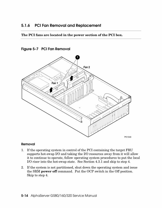
5-14 AlphaServer GS80/160/320 Service Manual
5.1.6 PCI Fan Removal and Replacement
The PCI fans are located in the power section of the PCI box.
Figure 5– 7 PCI Fan Removal
PK1549
1
Fan 1
Fan 2
Removal
1. If the operating system in control of the PCI containing the target FRU supports hot-swap I/O and taking the I/O resources away from it will allow it to continue to operate, follow operating system procedures to put the local I/O riser into the hot-swap state. See Section 4.3.1 and skip to step 4.
2. If the system is not partitioned, shut down the operating system and issue the SRM power off command. Put the OCP switch in the Off position. Skip to step 4.

Power Cabinet Component Removal and Replacement 5-15
3. If the system is partitioned, from the console connected to the partition to which the PCI box containing the target FRU is attached, shut down the operating system and power it off using the SRM power off command. Put the OCP switch in the Secure position.
4. Unplug the power supplies in the target PCI box.
5. Access to a particular fan depends upon whether the PCI box is at the top of a cabinet or underneath another PCI box. If the broken fan is in the top PCI box, you can get to it without taking the box out of the cabinet. If, on the other hand, the broken fan is in a PCI box underneath another box, you may have to take the box out of the cabinet. Follow the appropriate procedure described in Section 5.1 step 7 or step 8.
6. If the broken fan is PCI fan 1 on the left looking at the box from the rear, do the following:
1. Unscrew the captive fastener that holds the fan in place and lift it up but not completely free of the box. �
2. Unplug the fan from the backplane and remove.
7. If the broken fan is PCI fan 2 on the right looking at the box from the rear, do the following:
1. Move the cables from the standard I/O module that pass over the fan out of the way.
2. Disconnect the signal cable from the DVD/CD-ROM that also passes over the fan and fold it into the card cage section of the box.
3. Unscrew the captive fastener that holds the fan in place and lift it up but not completely free of the box. �
4. Unplug the fan from the backplane and remove.
Replacement
Reverse the steps outlined in the removal procedure.
Verification
Power up the system and check that the PCI box with the new fan powers up without error.
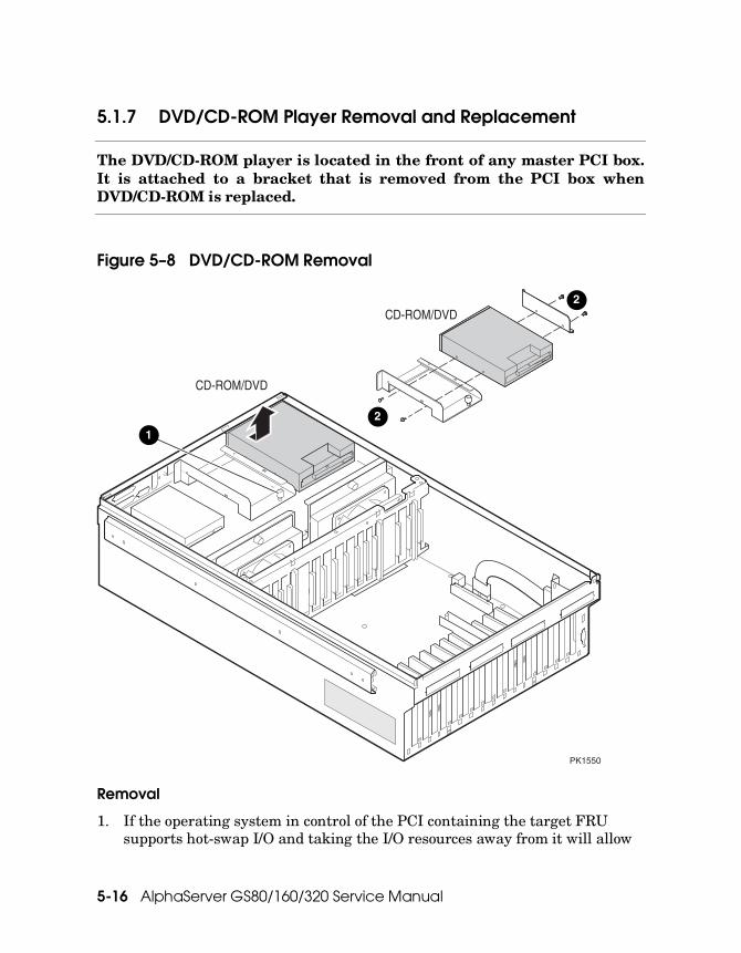
5-16 AlphaServer GS80/160/320 Service Manual
5.1.7 DVD/CD-ROM Player Removal and Replacement
The DVD/CD-ROM player is located in the front of any master PCI box. It is attached to a bracket that is removed from the PCI box when DVD/CD-ROM is replaced.
Figure 5– 8 DVD/CD-ROM Removal
CD-ROM/DVD
CD-ROM/DVD
1
2
2
PK1550
Removal
1. If the operating system in control of the PCI containing the target FRU supports hot-swap I/O and taking the I/O resources away from it will allow

Power Cabinet Component Removal and Replacement 5-17
it to continue to operate, follow operating system procedures to put the local I/O riser into the hot-swap state. See Section 4.3.1 and skip to step 4.
2. If the system is not partitioned, shut down the operating system and issue the SRM power off command. Put the OCP switch in the Off position. Skip to step 4.
3. If the system is partitioned, from the console connected to the partition to which the PCI box containing the target FRU is attached, shut down the operating system and power it off using the SRM power off command. Put the OCP switch in the Secure position.
4. Unplug the power supplies in the target PCI box.
5. In redundant systems that have two master PCI boxes, access to a particular DVD/CD-ROM player depends on whether it is in the PCI box at the top of a cabinet or underneath another PCI box. If the broken device is in the top PCI box, you may be able to get to it without taking the box out of the cabinet. If, on the other hand, the broken device is in a PCI box underneath another PCI box, determine whether you need to remove the box from the cabinet or not. Follow the appropriate procedure described in Section 5.1 step 7 or 8.
6. Unplug the power and signal cables from the DVD/CD-ROM player and fold them out of the way.
7. Unscrew the captive fastener that holds the bracket to which the DVD/CD-ROM player is attached. �
8. Push the front of the DVD/CD-ROM player back toward the rear of the box and lift it up and out.
9. Unscrew the four Phillips head screws holding the DVD/CD-ROM player to the bracket and remove. �
Replacement
Reverse the steps outlined in the removal procedure.
Verification
Power up the system and check that the DVD/CD-ROM drive powers up without errors.

5-18 AlphaServer GS80/160/320 Service Manual
5.1.8 SCSI (FIS) Disk Removal and Replacement
The SCSI disk is located above the standard I/O interface module in a master PCI box.
Figure 5– 9 SCSI Disk Removal

Power Cabinet Component Removal and Replacement 5-19
Removal
1. If the operating system in control of the PCI containing the target FRU supports hot-swap I/O and taking the I/O resources away from it will allow it to continue to operate, follow operating system procedures to put the local I/O riser into the hot-swap state. See Section 4.3.1 and skip to step 4.
2. If the system is not partitioned, shut down the operating system and issue the SRM power off command. Put the OCP switch in the Off position. Skip to step 4.
3. If the system is partitioned, from the console connected to the partition to which the PCI box containing the target FRU is attached, shut down the operating system and power it off using the SRM power off command. Put the OCP switch in the Secure position.
4. Unplug the power supplies in the target PCI box.
5. In systems that have two or more master PCI boxes, access to a particular SCSI disk depends on whether it is in the PCI box at the top of a cabinet or underneath another PCI box. If the broken disk is in the top PCI box, you may be able to get to it without taking the box out of the cabinet. If, on the other hand, the broken device is in a PCI box underneath another box, determine whether you need to remove the box from the cabinet or not. Follow the appropriate procedure described in Section 5.1 step 7 or 8.
6. Unplug the power and signal cables from the SCSI disk and fold them out of the way. �
7. Unscrew the two captive screws that hold the bracket with the SCSI disk in place. �
8. Remove the SCSI disk and bracket by sliding it toward the front of the PCI box and once its tab is free lifting it from the box. �
9. Unscrew the four screws holding the disk to the bracket. �
Replacement
Reverse the steps outlined in the removal procedure.
Verification
Power up the system and check that the SCSI device powers up without error.

5-20 AlphaServer GS80/160/320 Service Manual
5.1.9 Standard I/O Cable Interface Removal and Replacement
The standard I/O cable interface module is located under the SCSI disk in the top right front corner of a master PCI box.
Figure 5– 10 Standard I/O Interface Module Removal

Power Cabinet Component Removal and Replacement 5-21
Removal
1. If the operating system in control of the PCI containing the target FRU supports hot-swap I/O and taking the I/O resources away from it will allow it to continue to operate, follow operating system procedures to put the local I/O riser into the hot-swap state. See Section 4.3.1 and skip to step 4.
2. If the system is not partitioned, shut down the operating system and issue the SRM power off command. Put the OCP switch in the Off position. Skip to step 4.
3. If the system is partitioned, from the console connected to the partition to which the PCI box containing the target FRU is attached, shut down the operating system and power it off using the SRM power off command. Put the OCP switch in the Secure position.
4. Unplug the power supplies in the target PCI box.
5. In systems that have two or more master PCI boxes, access to a particular standard I/O interface module depends on whether it is in the PCI box at the top of a cabinet or underneath another PCI box. If the broken interface module is in the top PCI box, you may be able to get to it without taking the box out of the cabinet. If, on the other hand, the broken device is in a PCI box underneath another box, determine whether you need to remove the box from the cabinet or not. Follow the appropriate procedure described in Section 5.1 step 7 or 8.
6. Remove the SCSI disk above the standard I/O interface module. See Section 5.1.8.
7. Unplug all cables connected to the standard I/O interface module at the front of the PCI box.
8. Unplug the signal cable from the standard I/O interface module. �
9. Unscrew the two Phillips head screws that hold the module in place and remove the module. �
Replacement
Reverse the steps outlined in the removal procedure.
Verification
Power up the system and check that the I/O subsystem powers up without error.
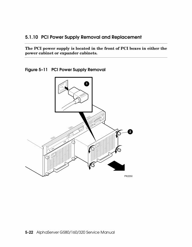
5-22 AlphaServer GS80/160/320 Service Manual
5.1.10 PCI Power Supply Removal and Replacement
The PCI power supply is located in the front of PCI boxes in either the power cabinet or expander cabinets.
Figure 5– 11 PCI Power Supply Removal
PK2250
2
1

Power Cabinet Component Removal and Replacement 5-23
Removal
1. Open the front door of the power cabinet or expander cabinet depending upon where the target power supply is located.
2. Identify the broken power supply by noticing which of the two has its Power OK LED off.
3. Unplug the power supply. �
4. Wait for the Vaux OK LED to go off and the Swap OK LED to come on.
5. Loosen the four captive fasteners holding the faceplate of the power supply to the box. �
6. Grasp the power supply handle and firmly pull it from the box.
Replacement
1. Replace the power supply and tighten the four captive screws. Do not plug in the AC yet.
2. Wait for the Swap OK LED to light and then attach the power cord. �
3. Wait for the Vaux OK LED and Power OK LED to light and the Swap OK LED to go off.
Verification
If the replacement procedure succeeds, verification is accomplished.

5-24 AlphaServer GS80/160/320 Service Manual
5.1.11 Standard I/O Battery Removal and Replacement
The time of year clock battery has a theoretical life of 10 years.
Figure 5– 12 Standard I/O Battery Removal

Power Cabinet Component Removal and Replacement 5-25
WARNING: Danger of explosion if battery is installed incorrectly. Replace only with the same or equivalent type recommended by the manufacturer. Dispose of used batteries according to the manufacturer’s instructions.
Removal
1. Remove the standard I/O module. See Section 5.1.1.
2. Slip the battery from its holder. Notice the battery’s polarity.
Replacement
When you replace the battery, be sure to put it back with the correct polarity. Reverse the steps outlined in the removal for the standard I/O module.
Verification
Power up the system.

5-26 AlphaServer GS80/160/320 Service Manual
5.2 Operator Control Panel Removal and Replacement
The OCP is contained in a plastic shroud at the top of the front door. There are two designs: one that attaches to the door using Tinnerman nuts, the other using screws. The AC must be off during the removal and replacement procedure.
Figure 5– 13 OCP Removal
PK1239
1
3
2

Power Cabinet Component Removal and Replacement 5-27
Removal
1. Shut down the operating system(s)
2. Open the rear door.
3. Trip the main circuit breaker on the AC input box(s).
4. Open the front door.
5. Working at the back of the open door, disconnect the power cable to the back of the OCP. �
6. Unplug the signal cable(s) at the back of the OCP. �
7. If the OCP assembly is connected to the door using screws, go to step 11.
8. If the OCP assembly is held to the door by Tinnerman nuts � on two plastic posts, one to the right and one to the left of the electronics, then proceed with this step. Starting with the post to the left, grasp the top of the door with one hand and with the other place a flathead screwdriver in the post and push until that side of the OCP releases.
9. Repeat step 8 on the post to the right and remove the OCP assembly from the door.
CAUTION: Be careful not to push so hard that the panel falls off the door.
10. If the replacement OCP uses screws to attach the assembly to the door, remove the Tinnerman nuts.
11. Remove the four Phillips head screws holding the OCP assembly to the door. Remove the assembly.
Replacement
Reverse the steps outlined in the removal procedure.
Verification
Observe that the display is working and make sure the reported problem is fixed. When powering up the system, be sure to put the circuit breakers in the On position before you put the OCP switch in the On position.

5-28 AlphaServer GS80/160/320 Service Manual
5.3 Terminal Server Removal and Replacement
The terminal server is located just above the AC input boxes in the power cabinet and is connected to the SMC and the local terminal port on each standard I/O module in the system.
Figure 5– 14 Terminal Server Removal
Power Cabinet Component Removal and Replacement 5-29
Removal
Conceivably the system could be running and doing useful work while the terminal server needs replacing. Essentially what is lost is console control of the system. Assuming this is the case, there is no need to shut down operating systems.
1. Open the front door of the power cabinet.
2. Unplug the power cord connected to the back of the terminal server.
3. Unplug the signal cable connecting the terminal server to the SMC PC.
4. Open the rear door of the power cabinet.
5. Unplug the signal cables connecting the terminal server to the standard I/O module in PCI boxes.
6. Remove the four Phillips head screws holding the terminal server mounting brackets to the power cabinet frame. �
7. Remove the terminal server.
Replacement
Reverse the steps outlined in the removal procedure.
Verification
Verify that each terminal session on the SMC can access the partition to which it is attached.

5-30 AlphaServer GS80/160/320 Service Manual
5.4 48V Power Supply Removal and Replacement
Under certain conditions 48V power supplies may be hot swapped.
Figure 5– 15 Power Supply Removal
PK2233
2
1

Power Cabinet Component Removal and Replacement 5-31
Removal
1. Open the front door of the power cabinet.
2. Locate the power supply that needs to be replaced:
1. Use the color codes to associate a power subrack with the QBB with the power problem. At least one of the power supplies on this subrack should be replaced.
2. If the system box has redundant power, the associated subrack will have three power supplies. The power supply with its 48V LED off is the one to replace. (The failed supply may have both the 48V LED and the Vaux LED off.)
3. If, on the other hand, the system box does not have redundant power, the subrack will have two power supplies and both will have the 48V LED off. If one of the two also has its Vaux LED off, it is the power supply to replace. But if both have their Vaux LEDs lit, do the following:
1. At the Pnn>>> prompt use the reset command to power on the failing QBB. (A power supply can power up a QBB but not run it.)
2. The power supply with its 48V LED off is the supply to replace.
3. Loosen the two captive screws � that hold the target power supply in place.
4. Grasp the power supply handle � and firmly pull it from the subrack.
Replacement
If the power supplies are not properly load/phase balanced, the circuit breakers will trip. To avoid this nuisance, return power supplies to the location from which they came. See Section 1.22.3. Reverse the steps outlined in the removal procedure.
Verification
Power on the system and make sure the LEDs on the new power supply come on.

5-32 AlphaServer GS80/160/320 Service Manual
5.5 Power Subrack Removal and Replacement
AC must be removed from the power subrack for it to be removed.
Figure 5– 16 Power Subrack Removal
1
4
2
2
3
PK1295

Power Cabinet Component Removal and Replacement 5-33
Removal
1. Remove the QBBs in the affected system box from use, by shutting down the instance of the operating system and using the SRM power off command.
2. Open the front and rear doors of the power cabinet.
3. At the back: if the entire system had to be brought down, trip the main circuit breaker on the AC input box powering the subrack; otherwise, trip the three circuit breakers controlling the lines to the subrack. The target subrack and the AC input box circuit breakers controlling it have the same color code.
4. Loosen the two screws holding the retaining bracket for the 48 V cable going to the power cabinet bulkhead and let the bracket drop. �
5. Unplug power cords and signal cables connected to the subrack distribution panel.�
6. Remove the two Phillips head screws holding the subrack to its supporting plate. �
7. Move to the front of the power cabinet and remove the power supplies from the subrack and set aside. See Section 5.4.
8. Remove the plastic fillers at the bottom of the power cabinet to gain access to the back of the AC input boxes. To remove the fillers, pinch the snaps at both ends of the guard and pull it away from the frame.
9. Unplug the power cords from the AC input box that go to the target subrack – again use the color code to determine which cords to unplug.
10. Remove any tie wraps dressing the power cords that would prevent them from being removed with the subrack.
11. Remove the four Phillips head screws holding the subrack to the frame and slide the rack out of the cabinet. � Take care that the power cords attached to the back of the subrack are free to travel with it.
Replacement
Reverse the steps outlined in the removal procedure.
Be sure the power cords are placed back in the same locations from which they were removed.
Verification
Power on the two QBBs.

5-34 AlphaServer GS80/160/320 Service Manual
5.6 AC Input Box Removal and Replacement
The AC input box must be unplugged in order for it to be removed.
Figure 5– 17 AC Input Box Removal
PK2235

Power Cabinet Component Removal and Replacement 5-35
If an AC input box failed, QBBs in one of the system cabinets are not operating.
If your system is a partitioned GS320, some of the system may remain running during this repair.
Removal
1. If the system is partitioned such that you can continue to run partitions in the system cabinet not affected by the target AC input box, continue to let them run. Otherwise, shut down the operating system and turn off the machine.
2. Open the front and rear doors of the power cabinet.
3. Trip the main circuit breaker on the target AC input box.
4. Unplug the main power cord from the utility power service.
5. Unplug the power cords leading to power subracks, PCIs, and storage devices. Note the location of all power cords. To gain access to the back of the AC input box you may have to move to the front of the power cabinet and remove the plastic filler guards at the bottom of the cabinet. To remove the filler, pinch the plastic snaps at both ends of the guard and pull it away from the frame.
6. Loosen the Phillips head screw holding the right side of the cable keeper arm on the frame of the power cabinet just below the AC input boxes. (The main power cable goes under it.) Swing the arm away from the frame.
7. Remove the four Phillips head screws holding the AC input box(s) to the frame and slide the box out of the cabinet.
Replacement
1. Color-code the AC input box you are installing to replicate the one you are replacing. Appendix A describes how power cords are configured.
2. Reverse the steps outlined in the removal procedure.
Verification
Power on the system. Be sure to put the circuit breaker in the On position before you put the OCP switch in the On position.


GS80 Component Removal and Replacement 6-1
Chapter 6 GS80 Component
Removal and Replacement
This chapter describes the removal and replacement procedures for components in the GS80 rack cabinet except for PCI box and storage components. See Chapter 5 for PCI box components. The following topics are covered:
• Accessing a Single or Top Drawer in a GS80 System
• Accessing a Bottom Drawer in a GS80 System
• Memory, Directory, Main Power, or Auxiliary Power Module Removal and Replacement
• CPU Removal and Replacement
• Power System Manager Removal and Replacement
• Clock Splitter Module Removal and Replacement
• I/O Riser Removal and Replacement
• I/O Transition Module Removal and Replacement
• Drawer Backplane Removal and Replacement
• Dual-Output Clock Removal and Replacement
• Distribution Board Removal and Replacement
• Console Serial Bus Removal and Replacement
• Drawer Blower Removal and Replacement
• Operator Control Panel Removal and Replacement
• Power Supply Removal and Replacement
• Power Subrack Removal and Replacement
• AC Input Box Removal and Replacement

6-2 AlphaServer GS80/160/320 Service Manual
6.1 Drawer Modules
The GS80 system uses the same modules as the GS160/320 systems with the exception of the global port module and the I/O riser. The functions of the global port are built into the backplane on the GS80. And the design of the I/O riser is modified so that it fits in the GS80 drawer.
Figure 6–1 Drawer Modules Location
Directory
MEM3CPU2
MEM1CPU0
Main Power
Auxiliary Power
CPU3MEM2
CPU 1MEM0
PSM
Clock Splitter
I/O Riser
I/O Riser
Transition Card
Transition Card
Global PortConnectors
PK1299
CPU 2(Blue)
CPU 0(Blue)
Memory 3(Gray)
Memory 1(Gray)
PSM(Orange)
Clock Splitter(Green)
AuxiliaryPower(Red)
MainPower
(Yellow)
Directory(White)
CPU 3(Blue)
CPU 1(Blue)
Memory 2(Gray)
Memory 0(Gray)
I/O riser(Lt. BLue) I/O riser
(Lt. BLue)

GS80 Component Removal and Replacement 6-3
Figure 6–1 shows the location and color codes of modules that plug into the GS80 backplane. There is no global port module, since the functions are designed into the backplane.
The I/O riser consists of a module that plugs into the backplane and a transition card that plugs into the riser. The transition card is used to bring the I/O signals to the drawer’s bulkhead where the I/O hoses are attached.
Table 6–1 lists modules in the drawer and their associated color codes. The color codes are on both the modules and on the mid-rail card guide in the drawer. There is one exception, the color code for the PSM is on the rear card guide rather than the mid-rail card guide.
Note that when installing modules, the color code on the module faces the color code on the card guides.
Table 6– 1 Module Color Codes (GS80)
Color Code Module
Yellow Main power
Red Auxiliary power
Orange Power system manager
Blue CPU
Gray Memory
White Directory
Green Clock splitter
Light blue Local I/O riser

6-4 AlphaServer GS80/160/320 Service Manual
6.1.1 Accessing a Single or Top Drawer in a GS80 System
To access a single or the top drawer in a two-drawer GS80 configuration is relatively simple, and under most circumstances will require that the system or drawer have its 48V power removed.
Figure 6– 2 Accessing a Top or Single Drawer System
PK1296
1
2

GS80 Component Removal and Replacement 6-5
Under most circumstances, when replacing FRUs in any drawer, the drawer must have its 48V power off. Only two FRUs in the GS80 drawer can be hot swapped: the CPU and a local I/O riser if the operating system supports hot-swap and they are in the top or single drawer. The remaining FRUs are cold-swap or removed when AC is not present. (Cold-swap is defined as a state where Vaux and AC are present but 48V and logic voltages are not. See Section 4.3.)
To access the QBB compartment of a single or top drawer, the front door must be open, the drawer(s) pulled out of the cabinet, and the drawer cover removed.
To pull the drawer(s) from the cabinet, remove the Phillips head screws � holding the drawers to the cabinet frame and pull the drawers forward until the rails are fully extended. There are no latches.
To remove the cover, unscrew the two captive screws that hold the cover to the drawer �, tilt the cover up, and lift it off the drawer.
Note that the safety stabilizer is long enough to prevent the cabinet from tipping over when the drawer is pulled out of the cabinet.

6-6 AlphaServer GS80/160/320 Service Manual
6.1.2 Accessing a Bottom Drawer in a GS80 System
The drawers must be separated to access the bottom drawer in a two-drawer GS80 configuration. When separated, the top drawer and the distribution board channel are pushed back into the cabinet while the bottom drawer remains extended out of the front of the cabinet.
Figure 6– 3 Accessing a Dual Drawer System
PK3200
1
5
6
4
3
2
7

GS80 Component Removal and Replacement 6-7
Before you open the drawers to remove FRUs in a bottom drawer, follow instructions regarding the operating and power state associated with the removal and replacement of the particular FRU.
It is possible, in a nonstandard configuration, that two drawers are configured as two totally independent systems with no distribution board. If this is the case, treat the two drawers as single drawers.
1. Open the front and rear doors.
2. At the rear, unscrew the two captive screws holding the distribution board channel to the bottom drawer. �
3. At the front, remove the eight Phillips head screws holding the drawers to the cabinet frame. �
4. Pull both drawers forward on their rails until they stop. (This lock can be released by pushing buttons below the stops should you need to remove the whole box.)
5. At the left side of both the top and bottom drawer toward the rear, remove the distribution board channel covers. Two Phillips head screws hold each cover in place. �
6. Unplug the two global port cables from the bottom of the distribution board and fold them toward the front of the bottom drawer. � To disconnect the cables, insert the blade of a flathead screwdriver between the plastic cable guide and the lip of the connector at one end. Twist the screwdriver so that one edge of the cable rises from the connector. Repeat this procedure on the other edge of each cable, pull the cable from the connector, and fold it toward the front of the bottom drawer.
7. Unplug the 48V power cable and fold it out of the way. �
8. The coax clock cable is looped inside the distribution board channel in the upper drawer. Release the loop from its clamp and thread the excess cable down from the top drawer to the bottom so that the top drawer can slide back into the cabinet without putting strain on the cable. � Note when recoiling this cable, the loop should not have a diameter smaller than 3.5 inches (9cm).
9. Replace the top distribution board cover that you removed in step 5 and carefully push the top drawer, now free of the bottom, back into the cabinet while attending to the clock cable and the disconnected global port cables so they are not damaged.
10. Unscrew the two captive screws that hold the cover to the bottom drawer, tilt the cover up, and remove it. The QBB compartment of the bottom drawer is now exposed. �
Note that the safety stabilizer foot is long enough to prevent the cabinet from tipping over when the drawers are pulled out.

6-8 AlphaServer GS80/160/320 Service Manual
6.2 Memory, Directory, Main Power, or Auxiliary Power Module Removal and Replacement
Each of these modules is a cold-swap module in GS80 systems. DC power must be removed from the drawer.
Figure 6– 4 Generic Drawer Module Replacement
1
Catch Detail
PK2225
1Removal
Replacement
2
INCORRECTCORRECT
2
For ModuleInstallation, Align
Module Color to FrameColor, as Shown

GS80 Component Removal and Replacement 6-9
Module Removal
1. If the system is not partitioned, shut down the operating system and issue the SRM power off command. Put the OCP switch in the Off position. Skip step 2.
2. If the system is partitioned, from the console connected to the partition with the target FRU, shut down the operating system and power it off using the SRM power off command. Note, only hard partitions can be powered off. If soft partitions are used, both partitions must be shut down and the hard partition powered off.
3. If the FRU is in a single drawer or top drawer in a dual-drawer system, follow the procedure in Section 6.1.1 to gain access to the FRU. Put the PSM switch in the Service position. If the FRU is in the bottom drawer in a dual-drawer system, follow the procedure in Section 6.1.2 to gain access to the FRU.
4. Using both hands, one on each module lever, place your index finger on the catch and thumb on the edge of the lever just below/above the arrow. First squeeze to release the lever and then pull both levers away from the module to release it from the QBB backplane.
5. Remove the module.
Module Replacement
CAUTION: Damage may result if the levers are closed when the module is not properly seated. See Figure 6–4.
1. Place the module on the module guides and push it into the system box.
2. Be sure the levers properly seat with the system box edge by pressing the module firmly into place.
3. Once the levers are properly seated, press them toward the module edge until the catches snap.
4. Be sure to return the OCP switch to its original position.
Verification
Power on the system. Execute the SRM set_sys_serial_num command.

6-10 AlphaServer GS80/160/320 Service Manual
6.3 CPU Removal and Replacement
Only CPUs in a single or top drawer can be hot-swapped.
Figure 6– 5 Removing a CPU
1
Catch Detail
PK2225
1Removal
Replacement
2
INCORRECTCORRECT
2
For ModuleInstallation, Align
Module Color to FrameColor, as Shown

GS80 Component Removal and Replacement 6-11
Module Removal
1. If the operating system supports hot-swap CPU and the CPU in question is in the top drawer, enter the appropriate OS command to put the target CPU in the hot-swap state. See Section 4.3.1. Skip steps 2 and 3.
2. If the system is not partitioned, shut down the operating system and issue the SRM power off command. Put the OCP switch in the Off position. Skip step 3.
3. If the system is partitioned, from the console connected to the partition with the target FRU, shut down the operating system and power it off using the SRM power off command. Note, only hard partitions can be powered off. If soft partitions are used, both partitions must be shut down and the hard partition powered off.
4. Access the drawer by following the procedure in Section 6.1.1 or Section 6.1.2 depending upon whether the CPU is in the top or bottom drawer. Identify the target CPU – its yellow OK to Swap LED should be lit. If applicable, put the PSM switch in the Service position.
5. Using both hands, one on each module lever, place your index finger on the catch and thumb on the edge of the lever just below/above the arrow. First squeeze to release the lever and then pull both levers away from the module to release it from the QBB backplane.
6. Remove the module.
Module Replacement
1. Place the module on the module guides and push it into the system box.
2. Be sure the levers properly seat with the system box edge by pressing the module firmly into place.
3. Once the levers are properly seated, press them toward the module edge until the catches snap.
4. Be sure to return the OCP switch to its original position.
Verification
Power on the CPU and see that it joins the operating system resources. Execute the SRM set sys_serial_num command.

6-12 AlphaServer GS80/160/320 Service Manual
6.4 Power System Manager Removal and Replacement
The PSM is a special removal and replacement case because its firmware may need to be updated.
Figure 6– 6 Power Manager Removal
1
Catch Detail
PK2225
1Removal
Replacement
2
INCORRECTCORRECT
2
For ModuleInstallation, Align
Module Color to FrameColor, as Shown

GS80 Component Removal and Replacement 6-13
Module Removal
1. If the system is not partitioned, shut down the operating system and put the OCP switch in the Off position. Skip step 2.
2. If the system is partitioned, from the console connected to the partition with the target FRU, shut down the operating system and power it off using the SRM power off command. Note, only hard partitions can be powered off. If soft partitions are used, both partitions must be shut down and the hard partition powered off.
3. If the FRU is in a single drawer or top drawer in a dual-drawer system, follow the procedure in Section 6.1.1 to gain access to the FRU. If the FRU is in the bottom drawer in a dual-drawer system, follow the procedure in Section 6.1.2 to gain access to the FRU.
4. Identify the target PSM (color code = orange). Note that the orange color code tag is toward the back of the drawer rather than toward the center unlike all other modules.
5. Using both hands, one on each module lever, place your index finger on the catch and thumb on the edge of the lever just below/above the arrow. First squeeze to release the lever and then pull both levers away from the module to release it from the QBB backplane.
6. Pull the module from the drawer.
Module Replacement
CAUTION: Damage may result if the levers are closed when the module is not properly seated. Follow the procedure outlined in Section 6.2.
1. Reverse the steps outlined in the removal procedure.
2. Choose the appropriate method to update the PSM firmware. See Appendix D. Then update the firmware.
3. Be sure to return the OCP switch to its original position.
Verification
Power on the system. Execute the SRM set sys_serial_num command.

6-14 AlphaServer GS80/160/320 Service Manual
6.5 Clock Splitter Module Removal and Replacement
Located next to the local I/O riser module, the clock splitter provides identical copies of the clock to synchronize transactions.
Figure 6– 7 Clock Splitter Removal
1 2
3
PK2234

GS80 Component Removal and Replacement 6-15
Module Removal
1. If the system is not partitioned, shut down the operating system and issue the SRM power off command. Put the OCP switch in the Off position. Skip step 2.
2. If the system is partitioned, from the console connected to the partition with the target FRU, shut down the operating system and power it off using the SRM power off command. Note, only hard partitions can be powered off. If soft partitions are used, both partitions must be shut down and the hard partition powered off.
3. If the FRU is in a single drawer or top drawer in a dual-drawer system, follow the procedure in Section 6.1.1 to gain access to the FRU. Put the PSM switch in the Service position. If the FRU is in the bottom drawer in a dual-drawer system, follow the procedure in Section 6.1.2 to gain access to the FRU.
4. Identify the target clock splitter (color code = green).
5. Using both hands, one on each module lever, place your index finger on the catch and thumb on the edge of the lever just below/above the arrow. First squeeze to release the lever and then pull both levers away from the module to release it from the QBB backplane.
6. Pull the module part way out of the drawer so that the coax cable connection in the middle of the module is exposed. Pull the cable from its connector. Pulling the module out too far can stress or damage the clock cable.
7. Remove the module.
Module Replacement
CAUTION: Damage may result if the levers are closed when the module is not properly seated. Follow the procedure outlined in Section 6.2.
Reverse the steps outlined in the removal procedure.
Be sure to return the OCP switch to its original position.
Verification
Power on the system. Execute the SRM set sys_serial_num command.

6-16 AlphaServer GS80/160/320 Service Manual
6.6 I/O Riser Removal and Replacement
Only the local I/O riser in a single or top drawer can be hot-swapped and then only when the operating system supports hot-swap I/O.
Figure 6– 8 Local I/O Riser Removal
1
Catch Detail
PK2231
1Removal
Replacement
2
INCORRECTCORRECT
2
For ModuleInstallation, Align
Module Color to FrameColor, as Shown

GS80 Component Removal and Replacement 6-17
Module Removal
1. If the operating system supports hot-swap I/O, enter the OS command that puts the target local I/O module in the hot-swap state. See Section 4.3.1. Skip to step 4.
2. If the system is not partitioned, shut down the operating system and issue the SRM power off command. Put the OCP switch in the Off position. Skip step 3.
3. If the system is partitioned, from the console connected to the partition with the target FRU, shut down the operating system and power it off using the SRM power off command. Note, only hard partitions can be powered off. If soft partitions are used, both partitions must be shut down and the hard partition powered off.
4. Remove the I/O transition module attached to the target local I/O riser. See Section 6.7.
5. If you did not access the drawer containing the target FRU in step 4, access it now. See Section 6.1.1 or 6.1.2. Identify the target local I/O riser. If applicable, put the PSM switch in the Service position.
6. Using both hands, one on each module lever, place your index finger on the catch and thumb on the edge of the lever just below/above the arrow. First squeeze to release the lever and then pull both levers away from the module to release it from the QBB backplane.
7. Remove the module.
Module Replacement
From the spare I/O riser module, remove the plastic protective caps covering the connectors to the I/O transition module. (Place them on the module you are returning.)
Reverse the steps outlined in the removal procedure.
Be sure to leave the OCP switch in its original position.
Verification
Power on the system and verify that the I/O configuration includes resources attached to the replaced local I/O riser. Execute the SRM set_sys_serial_num command.

6-18 AlphaServer GS80/160/320 Service Manual
6.7 I/O Transition Module Removal and Replacement
The local I/O riser transition module in a drawer can be hot-swapped only if the local I/O riser can be hot-swapped.
Figure 6– 9 I/O Riser Transition Module Removal
PK1287
1
2
2

GS80 Component Removal and Replacement 6-19
Removal
1. If the operating system supports hot-swap I/O, enter the OS command that puts the target local I/O module in the hot-swap state. See Section 4.3.1. Skip to step 4.
2. If the system is not partitioned, shut down the operating system and issue the SRM power off command. Put the OCP switch in the Off position. Skip step to step 4.
3. If the system is partitioned, from the console connected to the partition with the target FRU, shut down the operating system and power it off using the SRM power off command. Note, only hard partitions can be powered off. If soft partitions are used, both partitions must be shut down and the hard partition powered off.
4. Open the rear door.
5. Remove the I/O cables from the target transition module. �
6. Loosen the two captive screws holding the transition module to the drawer. �
7. Remove the module.
Replacement
From the spare I/O transition module, remove the two plastic protective caps covering the connectors to the local I/O riser module. (Place them on the module you are returning.)
Reverse the steps outlined in the removal procedure.
Be sure to leave the OCP switch in its original position.
Verification
Power on the system and verify that the I/O configuration includes resources attached to the replaced local I/O riser. Execute the SRM set sys_serial_num command.

6-20 AlphaServer GS80/160/320 Service Manual
6.8 Drawer Backplane Removal and Replacement
The AC must be removed from the drawer when the system backplane is swapped.
Figure 6– 10 Drawer Backplane Removal
PK1248
1
2
3
7
65
4
Removal
1. If the system is not partitioned, shut down the operating system and issue the SRM power off command. Put the OCP switch in the Off position.
2. If the system is partitioned, from the console connected to the partition with the target FRU, shut down the operating system and power it off using SRM power off. Note,

GS80 Component Removal and Replacement 6-21
only hard partitions can be powered off. Pull the 48V power supplies from the subrack powering the drawer with the FRU. (This removes both 48V and Vaux from the drawer.) Skip to step 4.
3. Trip the circuit breaker on the AC input box powering the drawer(s).
4. Access the drawer with the faulty backplane. See Section 6.1.1 or 6.1.2.
5. Remove all modules from the drawer. See Sections 6.2 through 6.6.
6. Disconnect the CSB ribbon cable. �
7. To disconnect the global port cables from the backplane, slip a small flathead screwdriver through the small hole(s) in the left side of the drawer and insert the blade between the plastic cable guide and the lip of the connector. � Twist the screwdriver so that one edge of the cable rises out of the connector. Repeat this procedure on the other edge of each cable, pull the cable from the connector and move it out of the way.
8. Remove the drawer faceplate by removing the six Phillips head screws that hold it in place. �
9. Disconnect the ground strap from the backplane and tuck it under the backplane tray. �
10. At the front of the backplane disconnect the signal cable next to the main power module connector and tuck it down under the backplane tray. �
11. Disconnect the power harness connected to the backplane connector. �
12. Unscrew the Phillips head screw holding the backplane tray to the drawer and slide the tray and backplane forward out of the drawer. �
Replacement
Reverse the removal procedure.
Route cables so that they do not interfere with modules when they are replaced.
Verification
Power up the system. If you tripped the AC circuit breaker, be sure to put the circuit breaker in the on position before you put the OCP keyswitch in the On position.

6-22 AlphaServer GS80/160/320 Service Manual
6.9 Dual-Output Clock Removal and Replacement
The system is off when a dual-output clock module is replaced.
Figure 6– 11 Dual-Output Clock Module Removal
PK1249
1
4
3
5
(Right Side)(Left Side)
2

GS80 Component Removal and Replacement 6-23
Removal
1. Shut down the operating system(s).
2. Put the OCP switch in the Off position.
3. Follow the procedure in Section 6.1.1 to access the top drawer.
4. Remove CPU3 and memory 2 so that you have room to access the clock. If you need more room, remove more modules. See Sections 6.2 and 6.3.
5. Remove the clock module cover plate in the rear left corner of the drawer compartment by removing the two Phillips head screws holding it in place and lifting it out of the drawer. �
6. Remove the clock compartment shield. Note how the shield is installed. �
7. Unplug the coax clock cable(s) from the dual-output clock module. �
8. Unplug the power cable. �
9. Unscrew the four Phillips head screws holding the module to the side of the drawer and remove the module. �
Replacement
Reverse the removal procedure.
Note: When replacing the clock compartment shield, twist the top back edge of the shield to the left of the card guide as you slide the shield into place.
Verification
Power up the system.
Note: There is a spare clock module in the same location in the bottom drawer. You may use it but you’ll have to separate the two drawers and remove the dual-output clock module from the bottom drawer and move it to the top.

6-24 AlphaServer GS80/160/320 Service Manual
6.10 Distribution Board Removal and Replacement
The distribution board is located in the bottom of the distribution board channel.
Figure 6– 12 Distribution Board Removal
1
2
4
PK1291
FOLD
3
When replacing the distribution board, it is not necessary to open the QBB drawer compartment of either the top or bottom drawer.

GS80 Component Removal and Replacement 6-25
Removal
1. If the system is partitioned, it is not necessary to power down anything. (In a GS80 system so partitioned, there is no traffic across the distribution board.) Skip to step 3. Note, only hard partitions can be powered off. If soft partitions are used, they must be shut down and the hard partition be powered off.
2. However, if the system is not partitioned or is partitioned such that there is traffic across the distribution board, shut down the operating systems and issue the SRM power off command. Put the OCP switch in the Off position.
3. Open the front door.
4. Remove the eight Phillips head screws holding the drawers to the cabinet.
5. Pull both drawers forward on their rails until they stop.
6. At the left side of the bottom drawer, remove the distribution board channel cover by removing the two Phillips head screws holding the cover in place. � Remove the cover. The distribution board is now exposed.
7. To disconnect the global port cables from the distribution board insert the blade end of a flathead screwdriver between the plastic cable guide and lip of the cable connector at one end of the connector and twist one edge of the cable loose. Repeat this procedure to loosen the other edge of the cable from the connector on the distribution board and pull it from the connector. � Disconnect the bottom two cables.
8. Disconnect the outer of the two global port cables from the top drawer using the procedure described in step 7. Once the cable is disconnected, free the cable shield and fold the cable and shield up and away from the last cable. � Disconnect the last cable and move all cables away from the distribution board. (The cable shield prevents damage to the cable as the top drawer is slid in and out of the cabinet when the covers are off.)
9. Remove the four Phillips head screws holding the distribution board to the distribution board channel and remove the module. �
Replacement
Reverse the removal procedure.
Verification
Power up the system.

6-26 AlphaServer GS80/160/320 Service Manual
6.11 Console Serial Bus Removal and Replacement
The AC power to the drawer with the target CSB module must be off when replacing the console serial bus module.
Figure 6– 13 Console Serial Bus Removal
1
2
3
4
PK3201
5
6

GS80 Component Removal and Replacement 6-27
Removal
1. If the system is not partitioned, shut down the operating system, issue the SRM power off command, put the OCP switch in the Off position, and trip the main circuit breaker on the AC input box(s) at the rear of the system. Skip to step 4.
2. If the system is partitioned, from the console connected to the partition with the target FRU, shut down the operating system and power it off using SRM power off.
3. Pull the 48V power supplies from the subrack powering the drawer with the FRU. (This removes both 48V and Vaux from the target drawer only.)
4. Remove the I/O transition modules or I/O fillers from the drawer. See Section 6.7.
5. Remove the external CSB cable from the target CSB module. �
6. To access the target drawer, follow the procedure in Section 6.1.1 or Section 6.1.2.
7. Remove the local I/O riser(s). See Section 6.6.
8. To remove the I/O transition module card guide:
• Remove the Phillips head screw holding the horizontal part of the I/O transition card guide to the drawer. �
• At the right side of the drawer, remove the Phillips head screw holding the right side of the card guide to the side of the drawer. Access this screw by through the gap between the open cabinet door and the cabinet frame. �
• Lift the card guide out of the drawer.
9. Push the drawer back into the system, move to the rear, and using a 5mm or 3/16 inch nut driver remove the posts on both sides of the external CSB cable connector. �
10. Reach into the drawer through the hole left by the absence of the I/O transition cards and disconnect the power cable and signal cable from the CSB module itself. �
11. The two plastic standoffs used to hold the module to the drawer have tabs that clip the top and bottom edges of the module to the standoffs. To free the module, push the top tab up and the bottom tab down and release the module from the standoffs. �
12. Once loose remove the module from the drawer.
Replacement
Reverse the steps of the removal procedure.
Verification
Power up the system. If you tripped the AC circuit breaker, be sure to put the circuit breaker in the on position before you put the OCP keyswitch in the On position.

6-28 AlphaServer GS80/160/320 Service Manual
6.12 Drawer Blower Removal and Replacement
The drawer must be powered off to replace the blower.
Figure 6– 14 Drawer Blower Removal
PK1288
1
2

GS80 Component Removal and Replacement 6-29
Removal
1. If the system is not partitioned, shut down the operating system and put the OCP switch in the Off position. Skip step 2.
2. If the system is partitioned and the blower in one of the drawers needs replacing, neither an operating system nor the SRM should be running. Power off the partition off using the SCM power off -par x command. Put the OCP switch in the Secure position. Open the back door of the cabinet. Note, only hard partitions can be powered off. Therefore, if soft partitions are used, all soft partitions must be shut down and the hard partition in which they run must be powered off.
3. Unplug the blower. �
4. Remove the seven Phillips head screws holding the blower to the drawer. �
5. Remove the blower.
Replacement
Reverse the removal procedure.
Be sure to leave the OCP switch in its original position.
Verification
Power up the system.

6-30 AlphaServer GS80/160/320 Service Manual
6.13 Operator Control Panel Removal and Replacement
The OCP is contained in a plastic shroud at the top of the front door. There are two designs: one that attaches to the door using Tinnerman nuts, the other using screws. The AC must be off during the removal and replacement procedure.
Figure 6– 15 OCP Removal
PK1239
1
3
2

GS80 Component Removal and Replacement 6-31
Removal
1. Shut down the operating system(s).
2. Open the rear door.
3. Trip the main circuit breaker on the AC input box(s).
4. Open the front door.
5. Working at the back of the open door, disconnect the power cable to the back of the OCP. �
6. Unplug the signal cable(s) at the back of the OCP. �
7. If the OCP assembly is connected to the door using screws, go to step 11.
8. If the OCP assembly is held to the door by Tinnerman nuts � on two plastic posts, one to the right and one to the left of the electronics, then proceed with this step. Starting with the post to the left, grasp the top of the door with one hand and with the other place a nut driver of suitable size (#8-32) in the post and push until that side of the OCP releases.
9. Repeat step 8 on the post to the right and remove the OCP assembly from the door.
CAUTION: Be careful not to push so hard that the panel falls off the door.
10. If the replacement OCP uses screws to attach the assembly to the door, remove the Tinnerman receptacles and discard.
11. Remove the four Phillips head screws holding the OCP assembly to the door. Remove the assembly.
Replacement
Reverse the steps outlined in the removal procedure.
Power up the system. If you tripped the AC circuit breaker, be sure to put the circuit breaker in the on position before you put the OCP keyswitch in the On position.
Verification
Observe that the display is working and make sure the reported problem is fixed.

6-32 AlphaServer GS80/160/320 Service Manual
6.14 Power Supply Removal and Replacement
Under certain conditions 48V power supplies may be hot swapped.
Figure 6– 16 Power Supply Removal
PK2233
2
1

GS80 Component Removal and Replacement 6-33
Removal
1. Open the front door.
2. Locate the power supply that needs to be replaced:
1. Associate a power subrack with the drawer with the power problem; the upper drawer is powered by the upper subrack, the lower drawer by the lower subrack. At least one of the power supplies on the identified subrack should be replaced.
2. If the drawer has redundant power, the associated subrack will have three power supplies. The power supply with its 48V LED off is the one to replace. (The failed supply may have both the 48V LED and the Vaux LED off.)
3. If, on the other hand, the drawer does not have redundant power, the subrack will have two power supplies and both will have the 48V LED off. If one of the two also has its Vaux LED off, it is the power supply to replace. But if both have their Vaux LEDs lit, do the following:
1. At the Pnn>>> prompt use the reset command to power on the failing QBB. (A power supply can power up a QBB but not run it.)
2. The power supply with its 48V LED off is the supply to replace.
3. Loosen the two captive screws � that hold the target power supply in place.
4. Grasp the power supply handle � and firmly pull it from the subrack.
Replacement
If the power supplies are not properly load/phase balanced, the circuit breakers will trip. To avoid this nuisance, return power supplies to the location from which they came. See Section 1.23.3. Reverse the steps outlined in the removal procedure.
Verification
Power on the system and make sure the LEDs on the new power supply come on.
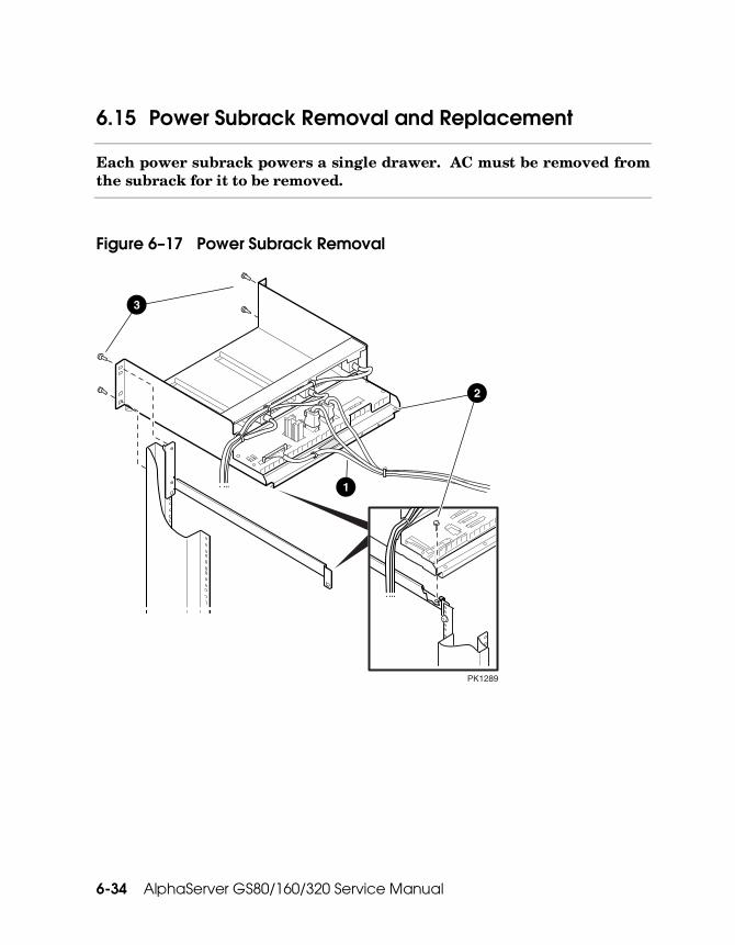
6-34 AlphaServer GS80/160/320 Service Manual
6.15 Power Subrack Removal and Replacement
Each power subrack powers a single drawer. AC must be removed from the subrack for it to be removed.
Figure 6– 17 Power Subrack Removal
PK1289
1
3
2

GS80 Component Removal and Replacement 6-35
If a power subrack needs replacing, it is unlikely that an operating system is running in the drawer powered by it. In some cases it is possible to keep part of the system running, but we recommend that the entire system be brought down.
Removal
1. Shut down the operating system and put the OCP switch in the Off position.
2. Open the front and rear doors of the cabinet.
3. At the back, trip the main circuit breaker on the AC input box(es).
4. Unplug power and signal cables connected to the subrack distribution panel.�
5. Remove the two Phillips head screws holding the subrack to its supporting plate. �
6. Move to the front of the cabinet and remove the power supplies from the subrack and set aside. See Section 6.14.
7. Remove the plastic fillers at the bottom of the power cabinet to gain access to the back of the AC input boxes. To remove the fillers, pinch the snaps at both ends of the guard and lift it away from the frame.
8. Unplug the power cords from the AC input box that go to the target subrack.
9. Remove any tie wraps dressing the power cords that would prevent them from being removed with the subrack. Gather the cords so that when the subrack is pulled out of the front of the cabinet the cords do not catch on anything.
10. Remove the four Phillips head screws holding the subrack to the frame and slide the rack out of the cabinet. Take care that the power cords attached to the back of the subrack are free to travel with it. �
Replacement
Reverse the steps outlined in the removal procedure.
Be sure the power cords are placed back in the same locations from which they were removed.
Verification
Power on the drawer(s). If you tripped the AC circuit breaker, be sure to put the circuit breaker in the on position before you put the OCP keyswitch in the On position.

6-36 AlphaServer GS80/160/320 Service Manual
6.16 AC Input Box Removal and Replacement
There are three variants of AC input boxes. Only one AC input box is required when the inlet voltage is high (200 – 240 V) and two are required when the voltage is low (120 V).
Figure 6– 18 AC Input Box Removal
PK1290

GS80 Component Removal and Replacement 6-37
Removal
1. If the operating system is still running, shut it down.
2. Put the OCP switch into the Off position.
3. Open the front and rear doors of the cabinet.
4. Trip the main circuit breaker on the target AC input box.
5. Unplug the main power cord from the utility power.
6. Unplug the power cords leading to power subracks, PCIs, and storage devices. Note the location of all power cords. To gain access to the back of the AC input box, you may have to move to the front of the cabinet and remove the plastic filler guards at the bottom. To remove the filler, pinch the plastic snaps at both ends of the guard and pull it from away from the frame.
7. Loosen the Phillips head screw holding the right side of the cable keeper arm on the frame just below the AC input boxes. (The main power cable goes under it.) Swing the arm away from the frame.
8. Remove the four Phillips head screws holding the AC input box to the frame and slide the box out of the cabinet.
Replacement
Reverse the steps outlined in the removal procedure.
Refer to Appendix A for power cord locations.
Verification
Power up the system. If you tripped the AC circuit breaker, be sure to put the circuit breaker in the on position before you put the OCP keyswitch in the On position.


Power Distribution Rules A-1
Appendix A Power Distribution Rules
This appendix shows power distribution and cabling for the GS160/320 power cabinet and expander cabinet.
The following topics are covered:
• GS160/320 Power Cabinet Configuration and Cabling
• Expander Cabinet Configuration and Cabling
• GS80 Power Cabling

A-2 AlphaServer GS80/160/320 Service Manual
A.1 GS160/320 Power Cabinet Configuration and Cabling
Cabling the GS160/320 is complex due to the large variety of options and the need to phase balance the AC input boxes to avoid nuisance circuit breaker tripping.
Figure A–1 Power Cabinet Configurations

Power Distribution Rules A-3
Figure A–1 shows the options available for use by each base configuration. Space at the top of the power cabinet is available for two options. An optional PCI box and either an optional BA356 storage device may fill that space; or two optional storage devices may fill the space.
Each base configuration requires two AC input boxes and a master PCI box. The remaining space is used for the power subracks.

A-4 AlphaServer GS80/160/320 Service Manual
Figure A– 2 GS160/320 Power Cabinet Components

Power Distribution Rules A-5
Figure A–2 shows the GS160/320 components that make up the power system. For each component, the figure shows the “J” name for a cable connector. Use Figure A–2 and Figure A–3 to determine where any given cable is connected.

A-6 AlphaServer GS80/160/320 Service Manual
Figure A– 3 GS160/320 Power Cabinet Cabling

Power Distribution Rules A-7
Figure A–3 shows the required and optional cables in the power cabinet. Redundant cables are marked with an asterisk (*).
The AC input for the GS160/320 is three phases. To avoid nuisance tripping of circuit breakers, follow the cabling diagram in Figure A–3.
The physical connector locations are identified in Figure A–2.

A-8 AlphaServer GS80/160/320 Service Manual
A.2 Expander Cabinet Configuration and Cabling
The power cabling in expander cabinets is described in this section.
Figure A– 4 Expander Cabinet Configuration

Power Distribution Rules A-9
Figure A–4 shows possible BA356 storage configurations in expander cabinets available with GS80/160/320 systems.

A-10 AlphaServer GS80/160/320 Service Manual
Figure A– 5 Expander Cabinet Cable Connector Locations

Power Distribution Rules A-11
Figure A–5 shows a diagram of the PCI box and AC input boxes used in expander cabinets. For each, the figure shows the “J” names for a cable connector. Use Figure A–6 and Figure A–7 to determine where any given cable in an expander cabinet is connected.

A-12 AlphaServer GS80/160/320 Service Manual
Figure A– 6 Expander Cabinet H9A20-AA Variant Cabling

Power Distribution Rules A-13
Figure A–6 shows the power cord connections for 120V NEMA cords used in North America. Note that this power cord is also used in the GS80.
Use Figure A–5 and Figure A–6 to determine where any given cable in an expander cabinet is connected.

A-14 AlphaServer GS80/160/320 Service Manual
Figure A– 7 Expander Cabinet H9A20-AB, -AC Variants Cabling

Power Distribution Rules A-15
Figure A–7 shows the power cable connections for expander cabinets used in North America, Japan, and Europe.
Use Figure A–7 and Figure A–5 to determine where any given power cable in such an expander cabinet is connected.

A-16 AlphaServer GS80/160/320 Service Manual
A.3 GS80 Power Cabling
Cabling the GS80 can be confusing due to the sheer number of cords.
Figure A– 8 GS80 Power Cabling -CA Cabinet
BA52A (4P)No. 2
AC inlet No. 2
AC inlet No. 1
OCP Assembly
BA54A PCI No. 1
BA52A (4P)No. 1
H7504Power Subshelf No. 1
H7504Power Subshelf No. 2
Terminator12-45926-01
CSBAdapter
12-45925-01
CSBAdapter
12-45925-01
J-2J-1
J-2J-9
J-1
J-1J-2
J-14J-15
J-3
J-0J-1J-6J-5J-4J-7
J-12J-7
J-10J-9P-3P-2P-1
J-1AJ-1BJ-2AJ-3BJ-3A
J-1AJ-1BJ-2A
J-3AJ-3B
17-04563-02
17-04810-0117-04563-02
17-04563-02
17-04563-02
17-04936-01
17-04936-03
17-04844-01
17-04844-01
17-04848-02
17-04848-02
17-04846-01
J-6J-5J-4J-7
17-04936-0117-04844-0117-04848-0217-04846-01
17-04846-01
17-04736-01
17-04736-01
17-04736-01
17-00083-0317-00083-03
17-00083-0317-00083-03
J-9 17-04936-03
Terminator 12-45926-01(At End of CSB Buss)
J-12J-7
J-10J-9P-3P-2P-1
17-04844-0117-04848-0217-04846-01
17-04811-01
J-2J-1 17-00442-18
17-00442-18
J-4BJ-4A
BA54A PCI - No. 2or BA356 - No. 1or Starlight - No. 1
2nd Starlight(Optional)
(Optional)
J-14J-15
17-04563-0217-04563-02
J-0J-1 17-04563-02
17-04563-0217-05037-02
PK1297

Power Distribution Rules A-17
Figure A–8 shows the power cable connections for the GS80 –CA cabinet used in North America.
Use Figure A–8 and Figure A–5 to determine where any given power cable in such a cabinet is connected.

A-18 AlphaServer GS80/160/320 Service Manual
Figure A– 9 GS80 Power Cabling -CB, -CC Cabinet
PK1298
OCP Assembly
Terminator 12-45926-01(At End of CSB Buss)
BA52A (4P)No. 2
AC inlet No. 1
BA54A PCI No. 1
BA52A (4P)No. 1
H7504Power Subshelf No. 1
H7504Power Subshelf No. 2
J-2J-1
J-2J-9
J-1
J-1J-9
J-2J-14J-15
J-3
J-0J-1J-6J-5J-4J-7
J-12J-7
J-10J-9P-3P-2P-1
J-16J-15J-14
J-12J-11
J-8J7
J-6
J-10J-9
17-04563-02
17-04810-0117-04563-02
17-04563-02
17-04563-02
17-04936-01
17-04936-01
17-04844-01
17-04844-01
17-04848-02
17-04848-02
17-04846-01
J-6J-5J-4J-7
17-04936-0117-04844-0117-04848-0217-04846-01
17-04846-01
17-00442-1817-00442-18
17-00442-1817-00442-1817-04936-18
J-12J-7
J-10J-9P-3P-2P-1
17-04844-0117-04848-0217-04846-01
J-14J-15
17-04563-0217-04563-02
J-0J-1 17-04563-02
17-04563-02
17-04811-01
J-2J-1 17-00442-18
17-00442-18
J-3J-4
BA54A PCI - No. 2or BA356 - No. 1or Starlight - No. 1
2nd Starlight(Optional)
(Optional)
Terminator12-45926-01
CSBAdapter
12-45925-01
CSBAdapter
12-45925-01
17-04736-01
17-04736-01
17-04736-01
17-05037-02

Power Distribution Rules A-19
Figure A–9 shows the power cable connections for the GS80 –CB, –CC cabinet used in Japan, and Europe.
Use Figure A–9 and Figure A–5 to determine where any given power cable in such a cabinet is connected.


Cache Coherency B-1
Appendix B Cache Coherency
Maintaining the coherency of the CPU caches, the memory space, and the I/O space is important in complex, hierarchical systems like the AlphaServer GS80/160/320 systems.
This section describes how cache coherency is maintained.

B-2 AlphaServer GS80/160/320 Service Manual
B.1 Terminology Table B–1 shows the definitions of terms related to cache coherency.
Table B–1 Basic Cache Coherency Terminology
Term Definition
Block A single, contiguous, 64-byte segment of memory, which must start on a 64-byte aligned memory address
Cache block A single entry in a processor’s cache memory, equal to one block of data
Clean Indicates that the data in a cache block has not been modified by the processor associated with the cache
Commander A component (node) in the system that participates in arbitration and initiates transactions
Dirty Indicates that the data in a cache block has been modified by the processor associated with the cache
Responder A node on the arbitration bus which accepts or supplies data and status information in response to a command and address from a commander
Shared Indicates that the data in a cache block of one processor is also contained in the cache of another processor in the system
Transaction A complete operation that results from a command
Victim Indicates that the data in a cache block of a processor is valid but is about to be replaced by another block of data from memory

Cache Coherency B-3
B.2 Cache States The Alpha CPU chip supports five cache states and two sets of commands that affect them. The AlphaServer GS series uses both command sets and four of the five cache states. It is the AlphaServer GS series cache coherency scheme that is described in this section.
The AlphaServer GS series cache states are described in Table B–2.
Table B– 2 AlphaServer GS Series Cache States
Cache State Description Clean The cache location holds a copy of a memory block. Memory,
or another processor, holds the “most up to date” copy of the block. A cache block may be clean even though there may be other copies of the block else where in the system.
Dirty The cache location holds an exclusive, “most up to date” copy of a memory block and the cache location is writeable. The data cached at this location must be written back to memory before this location can be reused.
Dirty - Shared The cache location holds the “most up to date” copy of a memory block, while another cache holds a copy of the same memory block. The block was read from the former’s cache into the latter’s cache after it was modified. The cache location is no longer write-able and must be written back to memory before the cache location can be reused.
Invalid Cache location holds no data.

B-4 AlphaServer GS80/160/320 Service Manual
B.3 Cache Commands • Two sets of commands are used to modify cache state:
• Memory space commands
• System probe commands
B.3.1 Memory Space Commands Table B–3 shows the CPU commands that change the CPU’s cache state when issued to the system. The commands are assigned a “class” which has a common effect on the cache state. It is the command class name that is associated with each cache state change represented by the arrows in Figure B–1. Table B–3 does not contain a complete list of CPU commands; it lists only those relevant to AlphaServer GS series cache coherency. Table B–3 also includes one command, Full Block Write, that is not really a CPU chip command at all, but a command issued exclusively by the AlphaServer GS series I/O processor.

Cache Coherency B-5
Table B– 3 Memory Space Commands
Command Class Description
RdBlk Rd Read a block of memory data into cache.
RdBlkMod RdM Read a block of memory data into cache for the purpose of modification (writing).
Fetch - Read a block of memory data - do not cache it.
RdBlkVic Rd Read a block of memory data into cache that will replace a valid (clean or dirty) block of data.
RdBlkModVic RdM Read a block of memory data into cache for the purpose of modification (writing). This read will replace a valid (clean or dirty) block of data.
Victim - Write the cache data block back to memory.
CleanVictim - Do not write the cache data block back to memory. This book keeping command is used by the system to simplify victim and victim buffer handling.
Evict Evict Displace a valid (clean or dirty) block of data from the cache. This software hook allows software to replace a cache block without reading a spurious memory block.
Clean-to-Dirty CtoD Make a valid non-writeable cache block writeable.
Shared-to-Dirty StoD Make a shared non-writeable cache block writeable.
STCChange-to-Dirty
CtoD/StoD
Make a valid or shared non-writeable cache block writeable for the purpose of a store conditional instruction (STx_C).
Inval-to-Dirty ItoD Put an invalid block of data in cache into a writeable state so that it may be overwritten.
Full-Block-Write
- Overwrite a block in memory. Do not cache any data. Do not victimize any data.

B-6 AlphaServer GS80/160/320 Service Manual
B.3.2 System Probe Commands The second set of commands that affect cache coherency are the “system probe” commands. These are commands that are issued from the system to the CPU requesting data and/or Tag status updates. Probe commands are the result of a CPU command affecting the cache of another CPU. For example, if one CPU reads a dirty block of data that another CPU has in its cache, the system would issue a probe command to the latter CPU, causing it to send a copy of data back to the system and the requesting CPU.
Table B–4 lists the system probe commands that are used in the AlphaServer GS series systems. The list is not a complete list of probe commands available to the Alpha processor.
Table B– 4 System Probe Commands
Probe Command
CPU Action
FRd Forwarded read command. If a processor has a dirty copy of the requested data block in its cache, it locates the block and returns a copy of it to the system.
FRdMod Forwarded read/modify command. If a processor has a dirty copy of the requested data block in its cache, it locates the dirty block, returns a copy of it to the system, and invalidates its own copy.
Inval Invalidate command. If a processor receives an invalidate command targeting a block of data it has in its cache, it invalidates its copy.

Cache Coherency B-7
B.4 Cache State Transition Diagram Figure B–1 shows how both memory space commands and system probe commands cause cache block state to change. Circles in the diagram represent the state of a given cache block. Cache blocks change state as a result of a particular command affecting the block represented by the arrows.
Figure B– 1 Cache State Transition Diagram
Invalid
Clean Dirty
Clean/Shared
Dirty/Shared
CtoD
Rd
Inval
Evict
StoD
FRdFRdM or Inval
Evict
Evict
RdM or ItoD
FRdM or Inval
B.5 Commands and Cache State Interaction Shows how probe commands follow from the interaction of memory space commands and the state of the target cache block in a cache. The table assumes that a processor, CPU0, issues a memory space command to the system. If the target of the command is a cache block located in say CPU1’s cache, as determined by a tag comparison (either directory of DTAG), then the state of the cache block determines which probe command will be issued to CPU1.

B-8 AlphaServer GS80/160/320 Service Manual
Table B– 5 Memory Command and Cache State Interaction
CPU Memory Cmnd Cache Block State Resultant Probe RdBlk Invalid Clean Dirty FRd Dirty-Shared FRd RdBlkMod Invalid Clean Inval Dirty FRdMod Dirty-Shared FRdMod Fetch Invalid Clean Dirty FRd Dirty-Shared FRd RdBlkVic Invalid Clean Dirty FRd Dirty-Shared FRd RdBlkModVic Invalid Clean Inval Dirty FRdMod Dirty-Shared FRdMod FetchBlkVic Invalid Clean Dirty FRd Dirty-Shared FRd Victim Any State Clean Victim Any State Clean-to-Dirty Invalid Clean Inval Dirty Can’t Happen Dirty-Shared Inval Shared-to-Dirty Invalid Clean Inval Dirty Can’t Happen Dirty-Shared Can’t Happen STCChange-to-Dirty Invalid Clean Inval Dirty Can’t Happen Dirty-Shared Inval Inval-to-Dirty Invalid Clean Inval Dirty Inval Dirty-Shared Inval Full-Block-Write Invalid Clean Inval Dirty Inval Dirty-Shared Inval
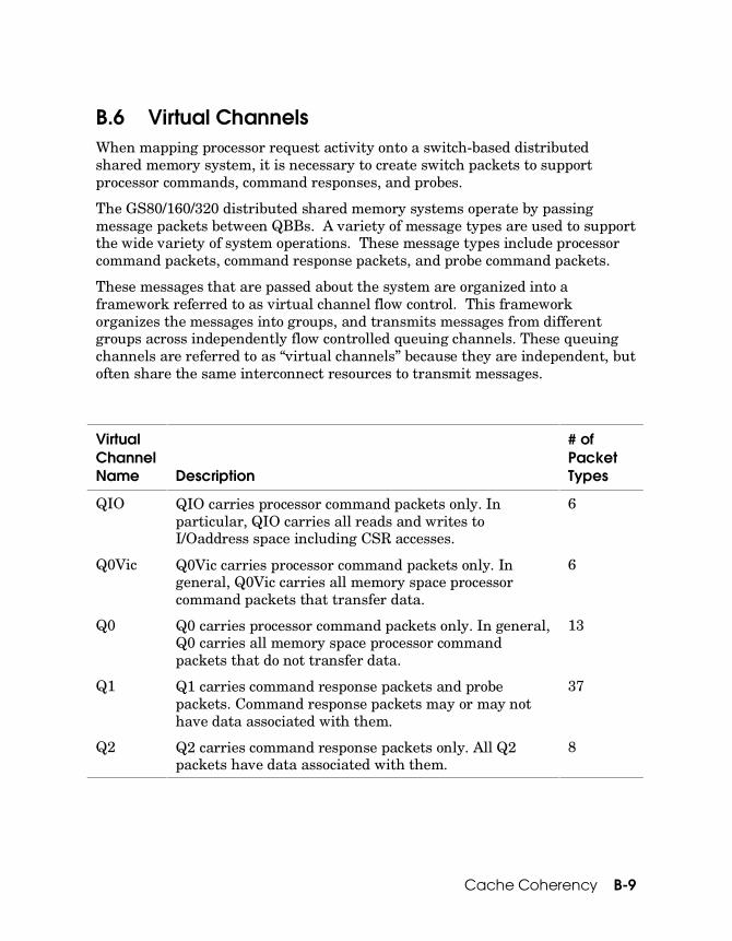
Cache Coherency B-9
B.6 Virtual Channels When mapping processor request activity onto a switch-based distributed shared memory system, it is necessary to create switch packets to support processor commands, command responses, and probes.
The GS80/160/320 distributed shared memory systems operate by passing message packets between QBBs. A variety of message types are used to support the wide variety of system operations. These message types include processor command packets, command response packets, and probe command packets.
These messages that are passed about the system are organized into a framework referred to as virtual channel flow control. This framework organizes the messages into groups, and transmits messages from different groups across independently flow controlled queuing channels. These queuing channels are referred to as “virtual channels” because they are independent, but often share the same interconnect resources to transmit messages.
Virtual Channel Name
Description
# of Packet Types
QIO QIO carries processor command packets only. In particular, QIO carries all reads and writes to I/Oaddress space including CSR accesses.
6
Q0Vic Q0Vic carries processor command packets only. In general, Q0Vic carries all memory space processor command packets that transfer data.
6
Q0 Q0 carries processor command packets only. In general, Q0 carries all memory space processor command packets that do not transfer data.
13
Q1 Q1 carries command response packets and probe packets. Command response packets may or may not have data associated with them.
37
Q2 Q2 carries command response packets only. All Q2 packets have data associated with them.
8

B-10 AlphaServer GS80/160/320 Service Manual
B.7 Virtual Channels and Coherency Flow The virtual channels are useful in explaining how transactions flow through the system while maintaining cache coherency.
B.7.1 Memory Space Transactions
Figure B– 2 Memory Space Transation Flow Diagram
Home MemoryMay hold X
Source ProcessorIssues a reference
to address X
Dirty ProcessorIf X is dirty, thisprocessor has themost up to data
copy of X
Shared ProcessorThis processor has
a copy of X.Home DirectoryHolds coherency
information relevant to X
Q0Q0Vic
Q1
Q1Response
Packet
Q1ProbePacket
(Fwd Rd or Inval)
Q2DirtyData
Q1ProbePacket(Inval)
Figure B–2 illustrates the progression of a memory space transaction through a system. The steps that a transaction may take in this progression are outlined below.
1. All memory space transactions (or “requests”) are issued from some source (or “requesting”) processor, be it a CPU processor or an IOP.
2. All memory space transactions are routed to their home QBB regardless of the location of the latest copy of the block. The home QBB may local to the requesting processor, or it may be another QBB, across the hierarchical switch.
All memory space transactions en route to their home directory travel in virtual channels Q0 and Q0Vic.
Cache Coherency B-11
3. Upon reaching its home QBB, a memory space transaction arbitrates for access to a home directory bank and a home memory bank. When the transaction is granted access to the directory and memory, it accesses both the cache state and the data stored in the block’s memory location.
When the cache state is accessed, it is combined with the transaction’s command type to:
• determine, and atomically update, the next coherency state.
• generate a response packet to the requesting processor.
• generate probe packets to processors with Dirty or Shared copies of the block.
4. The response and probe packets generated by a Q0/Q0Vic transaction at its home directory travel to the requesting processor and processors with Dirty and Shared copies on the Q1 Virtual Channel.
5. If an Fwd Read-type probe packet was generated in step #3 and shipped to a Dirty Processor in step #4, then the Dirty Processor must ship the Dirty data back to the requesting processor. Dirty data is returned to the requesting processor in the Q2 Virtual Channel.

B-12 AlphaServer GS80/160/320 Service Manual
B.7.2 I/O Space Reads
Figure B– 3 I/O Space Read Transaction Flow Diagram
Source ProcessorIssues a referenceto IO address X
IO Processor
IO DeviceSource of PIORd Data
orDestination of PIOWr Data
Arb
QIO PIORd
Q0 PIORd RespQ1 RdIO Comsig
Q2 IO Fill
QIO PIORd

Cache Coherency B-13
Figure B–3 shows the progress of an I/O space read or Programmed IO Read (PIO Rd) transaction through a system. The steps a transaction may take are as follows:
1. All PIO Rd transactions are issued by a source (or “requesting”) processor. The source processor in this case must be a CPU, not an IOP.
2. All PIO Rd transactions are sent to the home QBB of the IOP to which they are targeted in the QIO virtual channel. The home QBB may be local to the requesting processor, or it may be another QBB, across the hierarchical switch.
3. Upon reaching its home QBB, a PIO Rd passes through the QSA quad switch arbiter. All QIO transactions, including PIO Rd transactions, arbitrate not for memory or directory banks, but for the command/address interconnect (the ArbBus) between the home QSA and the home IOP.
4. The home IOP module retrieves read data from the device addressed in the PIO Rd transaction.
5. The home IOP starts a data return sequence by issuing a PIO Rd Response transaction to the home QSA. This transaction travels in the Q0 virtual channel.
6. Upon reaching the home QSA, the PIO Rd Response starts two events:
• It spawns a Q2 IO Fill packet, which returns data to the requesting processor directly (without passing through the home QS Arb).
• It passes itself through the QSA QS arbiter. PIO Rd Response transactions for access to the Q1 virtual channel.
7. Upon winning arbitration at the home QS Arb, the PIO Read Response generates a Rd IO Comsig packet. The Rd IO Comsig travels back to the requesting processor as a Response Packet in the Q1 Virtual Channel.

B-14 AlphaServer GS80/160/320 Service Manual
B.7.3 I/O Space Writes
Figure B– 4 I/O Space Write Transaction Flow Diagram
Source ProcessorIssues a referenceto IO address X
IO Processor
IO DeviceSource of PIORd Data
orDestination of PIOWr Data
Arb
QIO PIOWr
Q1 WrIO Comsig
QIO PIOWr
Figure B–4 shows the progress of an I/O space write or programmed IO write (PIO Wr) transaction through a system. The steps that a transaction may take in this progression are outlined below.
1. All PIO Wr transactions are issued by a source (or “requesting”) IOP. The system does not support peer-to-peer I/O transactions.
2. All PIO Wr transactions are sent to the home QBB of the IOP to which they are targeted in the QIO virtual chanel. The home QBB may be local to the requesting processor, or it may be another QBB, across the hierarchical switch.
3. Upon reaching its home QBB, a PIO Wr passes through the QSA quad switch arbiter (QSA QS Arb). All QIO transactions, including PIO Wr transactions, arbitrate not for memory or directory banks, but for access to the command/address interconnect (the ArbBus) between the home QSA and the home IOP.
4. Upon winning arbitration at the home QS Arb, the PIO Wr generates a Wr IO Comsig packet back to the requesting processor. The Wr IO Comsig travels back to the requesting processor as a Response Packet in the Q1 Virtual Channel.

Cache Coherency B-15
B.8 Virtual Channel Ordering Rules To support cache coherency, virtual channels obey a number of ordering rules. These rules are enforced:
• To support “Sparse Vector” directories (i.e. 1 directory bit/QBB vs. 1 directory/processor)
• To enable system support of Memory Barriers.
• To minimize permutations of in flight transactions.
Q1 Full Ordering
At each QBB, the main arbiter in the QSA, the QS Arb, orders all Q0 transactions to the QBB’s home memory space. This in turn generates a serial stream of Q1 packets directed at both the processor local to the QBB and processors remote to the QBB. These two streams of Q1 packets obey the following rules:
1. All Q1 packets generated by any given QS Arb are generated in a serial order. All processors targeted by some or all of the Q1 packets from a given QS Arb must see these Q1 packets in the order that they were generated.
2. All Q1 packets targeted at processors in QBBs, other than the home QBB, must pass through the QS Arb of the target QBBs. Each QS Arb at each target QBB put Q1 packets from other QBBs with the Q1 packets they generate from Q0 packets in some order. All local processors targeted by some or all of the local Q1 packets and remote Q1 packets must see all of these packets in the order that the local QS Arb put them in.
This rule does not dictate specific ordering of Q1 packets from one QS Arb and Q1 packets from another QS Arb. While the ordering of packets is somewhat arbitrary, it is constrained by 4 rules. The first rule pertains only to ordering between Q1 packets sent from a QS Arb to its local processor and Q1 packets sent from a remote QS Arb. The latter 3 rules pertain to the ordering of Q1 packets as they cross the hierarchical switch.
3. If multiple Q1 packets from a given H-switch input port are targeted at a common H-switch output port, the Q1 packets must appear in the same order at the output port as they appeared at the input port.
4. When Q1 packets from multiple H-switch input ports are multicasting to common output ports, the Q1 packets must appear in the same order at all of the output ports that they target.

B-16 AlphaServer GS80/160/320 Service Manual
5. When ordered lists of Q1 packets from multiple HS input ports target multiple common HS output ports, the Q1 packets must appear at the output ports in a manner consistent with a single, common ordering of all incoming Q1 packets. Each output port may transmit some or all of the packets in the common ordered list.
Q0 Read and Victim Ordering
The system enforces ordering restrictions on reads and victims from the same processor to the same memory block. This restriction applies to the situation where a processor executes the following sequence of events:
1. Read Y, causing Victim X.
2. Read X.
The ordering rule for victim X and read X is:
6. Reads and victims from the same processor to the same memory block must appear at the output of the QS Arb of the memory block’s home QBB in the same order in which they were issued by the processor.
Q0 Change-to-Dirty and Read Ordering
Cache coherency protocol requires that before a change-to-dirty command targeting a given address can be forwarded from the GPA TTT, no reads to same address can be in the round trip path between the particular TTT and the address’ home directory. Since the intent of this rule is to have Change-to-Dirty commands arrive at their home directory without Read commands to the same address in front of them in the round trip path, a TTT ordering function alone is not sufficient for proper system operation. It must be combined with the following system ordering rule:
7. All change-to-dirty and read commands to the same address from the same QBB must appear in the same order at the output of their destination QS Arb as the order in which their source TTT issued them.

Cache Coherency B-17
Victim and Q1 Ordering
To properly implement memory barriers, the cache coherency protocol requires that victim packets “push” Q1 packets from the H-switch arbitration point to the output of the victim’s home QS Arb.
8. The H-switch orders all incoming Q1 packets and victim packets for each of its output ports. All Q1 and victim packets from the H-switch must appear at the output of their targeted QS Arb such that all Q1 packets that preceded a given victim as the packets were issued from the H-switch, still precede the same victim as the packets are issued from the QS Arb.
QIO Full Ordering
9. All PIO reads and PIO writes from a common processor to a common I/Odevice must appear in the same order at the I/Odevice as the order in which they are issued from their processor.
QIO and Q1 Ordering
To properly implement a cached IOP, the cache coherency protocol requires that QIO packets “push” Q1 packets from the H-switch arbitration point to the output of the QIO packet’s home QS Arb.
10. The H-switch merges all incoming Q1 packets and QIO packets into a single order, one for each H-switch output port. All Q1 and QIO packets from the H-switch must appear at the output of their targeted QS Arb such that all Q1 packets that preceded a given QIO packet as the packets were issued from the H-switch, still precede the same QIO packet as the packets are issued from the QS Arb.

B-18 AlphaServer GS80/160/320 Service Manual
B.9 Coherency Data Storage Cache coherency information is stored in the following locations in the system:
• The CPU’s primary tag storage (PTag)
• The IOP tag storage
• The duplicate tag storage on the QBB (DTag)
• The transaction tracking table in the global ports (TTT)
B.9.1 CPU Primary Tag Store (PTag) There is one PTag store in each CPU processor in the system. Each PTag store has one entry per EV6 cache location. Table B–6 describes the information stored in the PTag for each cached block on the CPU module.
Table B– 6 CPU PTag Cache Coherency Storage
PTag Field Field Description
Valid When set, indicates that a memory block is cached at the associated cache location.
Dirty Indicates that the cached block is writeable.
Shared Indicates that another processor has a copy of the cached block.
Tag Identifies the cached memory block; equivalent to the high order address bits of the cached block.
Only the CPU chip accesses the Ptag and only under the following circumstances:
1. When issuing loads and stores, to determine if a copy of a block is in cache and/or if a cached block is write-able.
2. When responding to probe requests from the system. These probe requests may be to provide a copy of its block, invalidate its block, or both invalidate and provide a copy of its block.

Cache Coherency B-19
B.9.2 IOP Tag Store Each IOP in the system implements two fully associative data caches; one “write” cache and one “read” cache. As such, each IOP also implements a fully associative tag store. Table B–7 describes information stored in the IOP tag store.
Table B– 7 IOP Tag Cache Coherency Storage
IOP Tag Field Field Description
Valid When set, indicates that a memory block is cached at the associated cache location.
Dirty Indicates that the cached block is writeable.
Tag Identifies the cached memory block; equivalent to the high order address bits of the cached block.
Both the IOP and the QBB Switch QSA chip access the IOP tag store. The main functions of the IOP tag store are:
• To provide coherency status for requests to local addresses.
• To respond to any coherency updates required as a result of requests to both local and remote addresses.

B-20 AlphaServer GS80/160/320 Service Manual
B.9.3 QBB Duplicate Tag Store (DTag) There is one DTag store in each QBB in the system. Each DTag store has one entry for each potential CPU cache location in a QBB. In other words, the DTag has enough storage to map four CPU module caches.
Table B– 8 DTag Cache Coherency Storage
DTag Field State Description of Field
Status Invalid no valid data is cached at the associated cache location
Clean unmodified data is cached at the associated cache location. This location may hold the only cached copy of the data in the system, or it may share the data with other locations.
Dirty-Not Probed
modified data is cached at the associated cache location. Since the data was modified, no other processor has accessed it. The location contains the only current copy of the data in the system.
Dirty-Probed
modified data is cached at the associated cache location. Since the data was modified, another processor has accessed it.
Tag NA identifies the cached memory block; equivalent to the high order address bits of the cached block
The DTag is accessed exclusively by Only the QBB switch QSA chip has access to the DTag. The main functions of the DTag are:
1. To provide coherency status for requests to local addresses.
2. To filter probe commands that result from requests to local addresses (i.e., if the DTag indicates that a processor does not have a copy of a block to which a probe must be sent, that processor need not be sent the probe).
3. To filter probe commands that result from requests to remote addresses.
The DTag, together with the IOP tag store, form the primary coherency store for the AlphaServer GS80 with one drawer.

Cache Coherency B-21
B.9.4 QBB Directory There is one directory store in each QBB in the system. Each directory holds one entry for each main memory block in its QBB. For example, a 32-Gbyte memory system consisting of 64-byte blocks would require 512-Mbyte directory entries.
Table B– 9 Directory Cache Coherency Storage
Directory Field Field Description
Owner-ID This is a 6 bit encoded field. It identifies which of 32 processors, 8 IOPs or single memory bank holds the most up to date copy of a memory block.
QBB-Present This is an 8-bit vector field. It identifies which QBBs in the system have processors which have up to date, cached copies of a memory block.
NOTE: Although 8 bits are defined in the directory QBB-present mask, only 7 are used. The last bit, whichever corresponds to the home QBB of a given directory, is not necessary because the DTag in the home QBB tracks the coherency status of blocks in local processors.
Only the QSA chip, through the QS Arb, accesses the directory. Its primary function is to provide coherency status in response to requests to local requests.
The QBB directories are the primary coherency store for these systems.
B.9.5 TTT Storage The transaction tracking table is a fully associative, multifunctional control structure. There is one TTT in each global port in a system. This structure performs the following tasks:
1. The TTT acts as a Miss Address File (MAF) for all remote references issued by its associated QBB. This means that the TTT stores 1 entry of information for each remote access issued by a QBB until that transaction is considered complete.
2. The TTT provides coherency information, with regard to transient coherency states, in response to requests to local addresses.

B-22 AlphaServer GS80/160/320 Service Manual
B.9.6 Access to Coherency State Figure B–5 shows how the various coherency stores are connected in a QBB. The PTag is omitted from the diagram because it is connected to, and used exclusively by, the CPU processor. As can be seen in Figure B–5, the QSA implements two interfaces to the cache coherency stores. The information in Table B–10 describes the two interfaces.
Figure B– 5 Cache Coherency Storage Access
Q S A rb
D ire ctory
D T ag
IO P
T T T
M em or y M od ule #3
M em or y M od ule #2
M em or y M od ule #0
M em or y M od ule #1
G lobal P ortIn terfa ce
Q S A
G P A
G P Lin kG P Lin k
A rbB usA rbB us
C oh eren cy In for m a tionC oh er en cy In form a tion

Cache Coherency B-23
Table B– 10 QSA Interface to the Cache Coherency Storage
Interface Description
GPLink - The global port link (GPLink) is the primary, clock-forwarded link between the quad switch address ASIC (QSA) and the global port address ASIC (GPA). This path is used to transmit Q0, Q0Vic, QIO, Q1 and Q2 packets, bound for remote QBBs, to the local GPA. The GPLink can transfer one address packet every two clock cycles.
ArbBus - The arbiter bus (ArbBus) is the synchronous, serialized, uni-directional output from the part of the QSA ASIC known as the quad switch arbiter (QSA QS Arb). The ArbBus is designed as three separate interconnects: one connecting the QSA to the GPA (TTT) and directory module, one connecting the QSA to the DTag and IOP, and one connecting the QSA to the 4 memory modules. The three interconnects function as one logical bus. The ArbBus can transmit an address packet every cycle.

B-24 AlphaServer GS80/160/320 Service Manual
B.10 Coherency Storage and Coherency Flow The following sections describe how various transactions use the system coherency storage elements as they progress through the system.
B.10.1 Local Read Transactions
Figure B– 6 Local Read Coherency Store Flow
Q0: Visit Directrory Dtag, TTT and IOP Tag store via ArbBus.
Q1ProbePacket
(Fwd Rd)
Q2DirtyData
Q1: VisitTTT via ArbBus
Source/Home QBB
Q1: Fwd Rd steered directly to Dirty Processor.
QBB of Dirty Processor
Q2: Fill steered directly to requesting processor.
Q1 Q1Response
Packet

Cache Coherency B-25
Local Read, ReadVic, and Fetch commands use the system coherency storage elements as illustrated in Figure B–6 and described by the following sequence of events.
1. Each Read-type command is first issued to the ArbBus of the home QBB by
means of the QS Arb. It visits:
• The DTag to determine if the addressed block is dirty in the home QBB.
• The directory to determine if the addressed block is dirty in another QBB.
• The IOP tag store to determine if the addressed block is dirty in the home IOP.
• The TTT to determine if the addressed block is in a transient state and to log transient state information.
2. Fwd Rd probe packets resulting from each Read-type command are steered directly to the identified dirty processor without consulting any coherency storage.
3. Upon return to the requesting processor’s QBB, a Q1 response packet visits the TTT via the ArbBus to clear transient state information.
4. Upon return to the requesting processor’s QBB, the Q2 Fill packet is sent directly to the requesting processor.

B-26 AlphaServer GS80/160/320 Service Manual
B.10.2 Local Read Modify Transactions
Figure B– 7 Local Read/Modify Transaction
Q0: Visit Directrory Dtag, TTT and IOP Tag store via ArbBus.
Q1ProbePacket
(Fwd Rd or Inval)
Q2DirtyData
Q1ProbePacket(Inval)
Q2: Visit TTT via ArbBus
Source/Home QBB
Q1: Visit Dtag, TTT and IOP Tag store via ArbBus.
QBB of Shared Processor
Q1: Directory steers Fwd Rd directly to Dirty Processor. Visit TTT, Dtag and IOP Tag Store via ArbBus
QBB of Dirty Processor
Q1 Q1Response
Packet
Q2: Fill steered directly to requesting processor.

Cache Coherency B-27
Local Read Mod and Read Vic Mod commands use the system coherency storage elements as shown in Figure B–7 and described by the following events:
1. Each Read Mod-type command is first issued to the ArbBus of the home QBB by means of the quad switch arbiter. It visits:
• The Dtag to determine both if the addressed block is dirty in the home QBB and if any of the CPUs in the home QBB have copies of the block.
• The directory to determine both if the addressed block is dirty in another QBB and if any other QBBs have copies of the addressed block.
• The IOP tag store to determine if the home IOP has a copy (clean or dirty) of the addressed block.
• The TTT to determine if the addressed block is in a transient state and to log transient state information.
2. The Fwd Rd Mod probe packets resulting from each Read-type command are then issued to the ArbBus of the QBB of a dirty processor. The Fwd Rd Mod is sent directly to the dirty processor without consulting any coherency storage. As the Fwd Rd Mod packet is issued to the ArbBus, it visits:
• The DTag to determine if any of the CPUs in the dirty processor’s QBB have copies of the addressed block.
• The IOP tag store to determine if the IOP in the dirty processor’s QBB has a copy (clean or dirty) of the addressed block.
• The TTT to determine if invalidates should be issued to those processors (CPU and IOP) that have copies of the addressed block.
3. Invalidate probe packets resulting from each Read Mod-type command are then issued to the ArbBus of any QBB with a shared processor. As the invalidate is issued to the ArbBus, it visits:
• The DTag to determine which of the CPUs in the QBB have copies of the addressed block.
• The IOP tag store to determine if the IOP has a copy of the block.
• The TTT to determine if invalidates should be issued to those processors (CPU and IOP) that have copies of the addressed block.
4. Upon return to the requesting processor’s QBB, the Q1 response packet visits the TTT via the ArbBus to clear transient state information.
5. Upon return to the requesting processor’s QBB, the Q2 fill packet is sent directly to the requesting processor.

B-28 AlphaServer GS80/160/320 Service Manual
B.10.3 Local Change-to-Dirty, Inval-to-Dirty and Full Block Transactions
Figure B– 8 Local Change-to-Change Coherency Store Flow
Q1 Q1Response
Packet
Q1ProbePacket(Inval)
Q1: Visit TTT via ArbBus
Source/Home QBB
Q0: Visit Directrory Dtag, TTT and IOP Tag store via ArbBus.
Q1: Visit Dtag, TTT and IOP Tag store via ArbBus.
QBB of Shared Processor

Cache Coherency B-29
Local Change-to-Dirty, Shared-to-Dirty, STCChange-to-Dirty, Inval-to-Dirty and Full Block Write commands use the system coherency storage elements as shown in Figure B–8 and described by the following sequence of events.
1. Each Change-to-Dirty-type command is first issued to the ArbBus of the home QBB by means of the QS Arb. It visits:
• The DTag to determine both if the Change-to-Dirty will succeed or fail, and if any of the CPUs in the home QBB have copies of the addressed block.
• The directory to determine if any other QBBs have copies of the addressed block.
• The IOP tag store to determine if the home IOP has a copy (clean or dirty) of the addressed block.
• The TTT to determine if the addressed block is in a transient state and to log transient state information.
2. Invalidate probe packets resulting from each Change-to-Dirty-type command are then issued to the ArbBus of any QBB with a shared processor. As the Invalidate is issued to the ArbBus, it visits:
• The DTag to determine which of the CPUs in the QBB have copies of the addressed block.
• The IOP tag store to determine if the IOP has a copy of the block.
• The TTT to determine if invalidates should be issued to those processors (CPU and IOP) that have copies of the addressed block.
3. Upon return to the requesting processor’s QBB, the Q1 response packet visits the TTT via the ArbBus, for the purpose of clearing transient state information.

B-30 AlphaServer GS80/160/320 Service Manual
B.10.4 Global (Remote) Read Transactions
Figure B– 9 Global (Remote) Read Transaction Storage Flow
Q 0: Visit TT T v ia GPLink
Q0Q0Vic
Q1
Q1Response
Packet
Q1ProbePacket
(Fwd Rd)
Q2DirtyData
Q 1: Visit TTT, and Dtag or IOP Tag store, via ArbBus.
Q 2: Visit Dtag, and TTT or IOP Tag store v ia ArbBus.
Source QBB
Q 0: Visit Directrory D tag, TTT and IOP Tag store v ia ArbBus.
Home Q BB
Q 1: Directory steers Fw d Rd directly to Dirty Processor.
QBB of Dirty Processor

Cache Coherency B-31
Remote Read, ReadVic and Fetch commands use the system coherency storage elements as illustrated in Figure B–9 and described by the following sequence of events.
1. Each Read-type command first visits the TTT via the GPLink, for the purpose of creating a TTT MAF entry.
2. Each Read-type command is then issued to the ArbBus of the home QBB by means of the QS Arb. It visits:
• The DTag to determine if the addressed block is dirty in the home QBB.
• The directory to determine if the addressed block is dirty in another QBB.
• The IOP tag store to determine if the home IOP has a dirty copy of the addressed block.
• The TTT to determine if the addressed block is in a transient state.
3. Fwd Rd probe packets resulting from each Read-type command are then issued to a Dirty Processor via the ArbBus of the QBB of the Dirty Processor. No coherency storage is consulted for this operation.
4. Q1 response packets resulting from Read-type commands are issued to the ArbBus of the requesting processor’s QBB. They visit:
• The DTag to update the DTag state (only if the requesting processor is an CPU).
• The IOP tag store to update the IOP tag state (only if the requesting processor is the IOP).
• The TTT to clear/update the TTT MAF state.
5. Q2 response packets resulting from Read-type commands are issued to the ArbBus of the requesting processor’s QBB. They visit:
• The DTag to update the DTag state (only if the requesting processor is a CPU).
• The IOP tag store to update the IOP tag state (only if the requesting processor is the IOP).
• The TTT to clear/update the TTT MAF state.

B-32 AlphaServer GS80/160/320 Service Manual
B.10.5 Global (Remote) Read Modify Transactions
Figure B– 10 Read Mod Coherency Store Flow
Q0: Visit TTT via GPLink
Q0Q0Vic
Q1
Q1Response
Packet
Q1ProbePacket
(Fwd Rd or Inval)
Q2DirtyData
Q1ProbePacket(Inval)
Q1: Visit TTT, Dtag and IOP Tag store, via ArbBus.
Q2: Visit Dtag, TTT and IOP Tag store via ArbBus.
Source QBB
Q0: Visit Directrory Dtag, TTT and IOP Tag store via ArbBus.
Home QBBQ1: Visit Dtag, TTT and IOP Tag store via ArbBus.
QBB of Shared Processor
Q1: Directory steers Fwd Rd directly to Dirty Processor. Visit TTT, Dtag and IOP Tag Store via ArbBus
QBB of Dirty Processor
Remote Read Mod and Read Vic Mod commands use the system coherency storage elements as illustrated in Figure B–10 and described by the following sequence of events.
1. Each Read Mod-type command first visits the TTT via the GPLink, for the purpose of creating a TTT MAF entry.
2. Each Read Mod-type command is then issued to the ArbBus of the home QBB by means of the QS Arb. It visits:
• The DTag to determine both if the addressed block is dirty in the home QBB and if any of the CPUs in the home QBB have copies.
• The directory to determine both if the addressed block is dirty in another QBB and if any other QBBs have copies.
• The IOP tag store to determine if the home IOP has a copy (clean or dirty) of the addressed block.
• The TTT to determine if the addressed block is in a transient state.

Cache Coherency B-33
3. The Fwd Rd Mod probe packets resulting from each Read-type command are then issued to the ArbBus of the QBB of the dirty processor. The Fwd Rd Mod is sent directly to the dirty processor and visits:
• The DTag to determine if any of the CPUs in the dirty processor’s QBB have copies of the addressed block.
• The IOP tag store to determine if the IOP in the dirty processor’s QBB has a copy (clean or dirty) of the addressed block.
• The TTT to determine if invalidates should be issued to those processors (CPU and IOP) that have copies of the addressed block.
4. The invalidate probe packets resulting from each Read Mod-type command are then issued to the ArbBus of any QBB with a shared processor. As the invalidate is issued to the ArbBus, it visits:
• The DTag to determine which of the CPUs in the QBB have copies.
• The IOP tag store to determine if the IOP has a copy of the block.
• The TTT to determine if invalidates should be issued to those processors (CPU and IOP) that have copies of the addressed block.
5. The Q1 response packets resulting from Read Mod-type commands are issued to the ArbBus of the requesting processor’s QBB. They visit:
• The DTag to update the DTag state (only if the requesting processor is a CPU), and to determine if any of the CPUs in the requesting processor’s QBB have copies of the addressed block.
• The IOP tag store to update the IOP tag state (only if the requesting processor is the IOP), and/or to determine if the IOP in the requesting processor’s QBB has a copy of the addressed block.
• The TTT to clear/update the TTT MAF state and to determine if invalidates should be issued to those processors (CPU and IOP) that have copies of the addressed block.
6. The Q2 response packets resulting from Read-type commands are issued to the ArbBus of the requesting processor’s QBB. They visit:
• The DTag to update the state if the requesting processor is a CPU.
• The IOP tag store to update the IOP tag state if the requesting processor is the IOP.
• The TTT to clear/update the TTT MAF state.

B-34 AlphaServer GS80/160/320 Service Manual
B.10.6 Global (Remote) Change-to-Dirty Transactions
Figure B– 11 Change-to-Dirty Coherency Store Flow
Q 0: V is it D tag v ia A rB u s V is it TT T v ia G PLin k.
Q 0Q 0V ic
Q 1
Q 1Resp onse
Pack et
Q 1ProbePack et(In val)
Q 1 : V isit TT T, D tag an d IO P T ag s tore, v ia A rb B u s.
Source Q B B
Q 0: V is it D irectro ry D tag , TT T an d IO P Tag sto re v ia A rbB us.
H o m e Q B B
Q 1: V is it D tag , T T T an d IO P Tag sto re v ia A rbB us.
Q B B of Sh ared P rocessor
Remote Change-to-Dirty, Shared-to-Dirty and STCChange-to-Dirty commands use the system coherency storage elements as illustrated in Figure B–11 and described by the following sequence of events.
1. Each Change-to-Dirty-type command is first issued to the ArbBus of the requesting processors QBB. It visits the DTag to determine if it should fail locally or propagate to its home directory.
2. All Change-to-Dirty-type commands that do not fail in the DTag then visit their local TTT via the GPLink, to create a TTT MAF entry.

Cache Coherency B-35
3. Each Change-to-Dirty-type command is then issued to the ArbBus of the home QBB by means of the QS Arb. It visits:
• The DTag to determine if any of the CPUs in the home QBB have copies of the addressed block.
• The directory to determine if the Change-to-Dirty will succeed or fail, and to determine if any other QBBs have copies of the addressed block.
• The IOP tag store to determine if the home IOP has a copy (clean or dirty) of the addressed block.
• The TTT to determine if the addressed block is in a transient state.
4. The invalidate probe packets resulting from each Change-to-Dirty-type command are then issued to the ArbBus of any QBB with a shared processor. As the invalidate is issued to the ArbBus, it visits:
• The DTag to determine which of the CPUs in the QBB have copies of the addressed block.
• The IOP tag store to determine if the IOP has a copy of the block.
• The TTT to determine if invalidates should be issued to those processors (CPU and IOP) that have copies of the addressed block.
5. The Q1 response packets resulting from each Change-to-Dirty-type command is issued to the ArbBus of the requesting processor’s QBB. It visits:
• The DTag to update the DTag state (only if the requesting processor is a CPU), and to determine if any of the CPUs in the requesting processor’s QBB have copies of the addressed block.
• The IOP tag store to update the IOP tag state (only if the requesting processor is the IOP), and/or to determine if the IOP in the requesting processor’s QBB has a copy of the addressed block.
• The TTT to clear/update the TTT MAF state and to determine if invalidates should be issued to those processors (CPU and IOP) that have copies of the addressed block.

B-36 AlphaServer GS80/160/320 Service Manual
B.10.7 Global (Remote) Inval-to-Dirty and Full Block Write Transactions
Figure B– 12 Inval-to-Dirty, Full Block Write Coherency Store Flows
Q 0: V isit TTT v ia G P Link.
Q 0Q 0V ic
Q 1
Q 1Response
P acket
Q 1P robePacket(Inval)
Q 1: V isit TTT , D tag and IOP Tag store , v ia A rbBus.
Source Q BB
Q 0: V isit Directrory D tag, TTT and IOP Tag store v ia A rbB us.
H om e Q BB
Q 1: V isit D tag, TTT and IO P Tag store v ia A rbB us.
Q BB of Shared Processor
Remote Inval-to-Dirty and Full Block Write commands use the system coherency storage elements as illustrated in Figure B–12 and described by the following sequence of events.
1. All Inval-to-Dirty and Full Block Write commands first visit the TTT via the GPLink, for the purpose of creating a TTT MAF entry.

Cache Coherency B-37
2. Each Inval-to-Dirty and Full Block Write command is then issued to the ArbBus of the home QBB by means of the QS Arb. It visits:
• The DTag to determine if any of the CPUs in the home QBB have copies of the addressed block.
• The directory to determine if any other QBBs have copies of the addressed block.
• The IOP tag store to determine if the home IOP has a copy (clean or dirty) of the addressed block.
• The TTT to determine if the addressed block is in a transient state.
3. Invalidate probe packets resulting from each Inval-to-Dirty and Full Block Write command are then issued to the ArbBus of any QBB with a Shared processor. As the Invalidate is issued to the ArbBus, it visits:
• The DTag to determine which of the CPUs in the QBB have copies of the addressed block.
• The IOP tag store to determine if the IOP has a copy of the addressed block.
• The TTT to determine if Invalidates should be issued to those processors (CPU and IOP) that have copies of the addressed block.
4. The Q1 response packets resulting from each Inval-to-Dirty and Full Block Write command is issued to the ArbBus of the requesting processor’s QBB. It visits:
• The DTag to update the DTag state (only if the requesting processor is an EV6), and to determine if any of the CPUs in the requesting processor’s QBB have copies of the addressed block.
• The IOP tag store to update the IOP Tag state (only if the requesting processor is the IOP), and/or to determine if the IOP in the requesting processor’s QBB has a copy of the addressed block.
• The TTT to clear/update the TTT MAF state and to determine if Invalidates should be issued to those processors (EV6 and IOP) that have copies of the addressed block.


Power-Up Diagnostic Error Table C-1
Appendix C Power-Up Diagnostic Error Table
This appendix contains a table that lists SROM and XSROM tests and all possible errors and associated number designations. For each test error, possible FRUs are identified and a brief description of the failure is given. The FRU(s) identified represent a best guess at what is broken and may not actually be the failing piece of hardware. In many cases, test failure information is interpreted at the PSM level and a FRU callout, which may differ from what is listed in the table, is made. The information in the table can guide the user to a FRU or more tests when a given test error number is seen.

C-2 AlphaServer GS80/160/320 Service Manual
Error Number Table Description
Error # column: Contains the error number that is printed as part of the failure report of the srom/xsrom test. “Error: xxxx”
FRU column: Lists the possible FRU(s).
Component(s) column: Lists the possible failing components associated with the FRU(s) called out in the FRU column.
For example, if a callout were FRU1: QBBx.CPUy EV, BCache where
• QBBx (x=0,1,2,3,4,5,6,7) represents the QBB backplane,
• CPUy (y=0,1,2,3) represents the CPU in that QBB,
• EV represents the Alpha Processor as the possible failing component, and
• BCache represents the Backup Cache (on the CPU module) data RAM as the possible component.
Or if a callout were FRU1: QBBx.MEMy.DIMMz, where
• QBBx (x=01,2,3,4,5,6,7) represents the QBB backplane
• MEMy (y=0,1,2,3) represents the Memory module in that QBB
• DIMMz (z=0,1,2,3,4,5,6,7) represents the failing DIMM on that Memory card
NOTE: If either the “FRU” or “Component” column is left blank, the field is the same as the callout for the previous error # directly above it.

Power-Up Diagnostic Error Table C-3
Failure Description column: Any detail which will be useful to the user to decode what the Error # means and why the test failed.
The format for an unexpected interrupt, which might occur during the execution of any XSROM test, is as follows:
Error # = ^xFEED Unexpected Interrupt has occurred
P1 = Trap Vector
P2 = EV6_EXC_ADDR
P3 = EV6_EXC_SUM
P4 = DEADBEEF
Example of an Unexpected Interrupt:
*** Unexpected Exception *** *** Error Format: 3 Severity: Unexpected Interrupt QBB/CPU: 00/00 Type: XSROM selftest Test: 25h Error: feed Rvsn: X4.9-0 FRU1: QBB0 FRU2: FRU3: FRU4: P1: 0000000000000480 P2: 0000020009045811 P3: 00000000000020c0 P4: 00000000deadbeef

C-4 AlphaServer GS80/160/320 Service Manual
Table C–1 Test Number / Error Number
Test # hex
ERROR # <15:0>
FRU(s) Component(s) Failure Description
Alpha CPU chip BIST check test
0001 QBBx.CPUy EV BIST failed for I-Cache and/or D-Cache
1
Parameters error 0001
P1: exp: P2 xor EXP_DATA [where EXP_DATA = I_CTL w/ bit 23 CLEAR] P2: rcvd: EV6 I_CTL Read data P3: addr: IPR Number of I_CTL P4: 0
Alpha CPU chip D-cache test
0001 QBBx.CPUy EV Test Setup
0002 QBBx.CPUy EV Verify all 5’s, write all A’s to EV D-Cache
0003 Verify all A’s, write all 3’s to EV D-Cache
0004 Verify all 3’s, write all C’s to EV D-Cache
0005 Verify all C’s, write all 0’s to EV D-Cache
0006 Verify all 0’s, write all F’s to EV D-Cache
0007 Verify all F’s, write all 0’s to EV D-Cache
2
Parameters all error numbers
P1: Exp: P2 xor EXP_DATA (where EXP_DATA = data written to D-Cache) P2: Rcvd: Actual data received (read from D-Cache) P3: Addr: Failing D-Cache Address P4: 0
Note: If P3 address ends in:
0: expected/received is LOW data<63:0> 8: HI data<127:64>
B-Cache initialization test 3
NONE QBBx.CPUy EV, Bcache BCache Init code. If HANG in this test, B-Cache could not be properly inited.

Power-Up Diagnostic Error Table C-5
Test # hex
ERROR # <15:0>
FRU(s) Component(s) Failure Description
B-cache data line test
0001 QBBx.CPUy EV, Bcache Unexpected error write data pttrn to Bcache.
0002 Unexpected error verifying data pttrn written
0003 B-Cache data RAM failure
0004 B-Cache data RAM failure in a check bit
CB0n Check bit n failure 0<=n<=^xf
4
Parameters error numbers 1,2,3,4 Test runs to completion unless an unexpected error occurs.
P1 mask has the following information: P1 = aabbccdd.nnnnnnnn Where:
Nnnn bits 31:00 number of errors that occurred.
Dd bits 39:32 mask of bad check bits for the LO QW. bit 32=check bit 0, 33=check bit1, etc.
Cc bits 47:40 mask of bad check bits for the HI QW . bit 40=check bit 8, 41=check bit9, etc.
Bb bits 55:48 if FF then a multiple bit error detected in LO QW and code could not determine failing check bits. This should normally only occur if 2 check bits failed in LO at same time. if 0 then ignore this field, it has no information
Aa bits 63:56 if FF then a multiple bit error detected in HI QW and code could not determine failing check bits. This should normally only occur if 2 check bits failed in HI at same time. if 0 then ignore this field, it has no information
P2 mask of any data bits in LO (63:00) that failed during the test. If bit set then that bit failed at least once, if clear then no error. Bit bit 0 = data bit 0, etc... to bit 63 = data bit 63
P3 mask of any data bits in HI (127:64) that failed during the test. If bit set then that bit failed at least once, if clear then no error. Bit bit 0 = data bit 64, etc... to bit 63 = data bit 127.
P4 mask contains the QW address of the first location that failed. More than one may fail.
Note: P2 identifies bits <63:00> that failed. P3 identifies bits <127:64> that failed. P1 bits 39:32 identifies check bits 7:0 that failed. P1 bits 47:40 identifies check bits 15:8 that failed.
parameters for error number CB0n (0<= n <= ^xF):
P1: Cache Line offset written a data pattern
P2: Read from CBOX registers: synd_1<31:24>, synd_0<23:16>, c_stat<8:4>, c_sts<3:0>
P3: Read from CBOX register: c_addr
P4: Data pattern written to cache line

C-6 AlphaServer GS80/160/320 Service Manual
Test # hex
ERROR # <15:0>
FRU(s) Component(s) Failure Description
B-cache march test
0001 QBBx.CPUy EV, Bcache Test setup
0002 QBBx.CPUy EV, Bcache Verify all 5’s, write all A’s to B-Cache
0003 Verify all A’s, write all 3’s to B-Cache
0004 Verify all 3’s, write all C’s to B-Cache
0005 Verify all C’s, write all 0’s to B-Cache
0006 Verify all 0’s, write all F’s to B-Cache
0007 Verify all F’s, write all 0’s to B-Cache
5
Parameters all error numbers
P1: Exp: P2 xor EXP_DATA [where EXP_DATA = QW write data to Bcache]
P2: Rcvd: Actual data received (QW read from Bcache)
P3: Addr: Failing Cache Address
P4: CBOX Read Chain data in <31:0> where:
<31:24> = dc1_syndrome<7:0>
<23:16> = dc0_syndrome<7:0>
<8:4> = c_stat<4:0>
<3:0> = c_sts<3:0>
Note: If P3 address ends in:
0: expected/received is LOW data<63:0>
8: HI data<127:64>

Power-Up Diagnostic Error Table C-7
Test # hex
ERROR # <15:0>
FRU(s) Component(s) Failure Description
B-cache address test
0001 QBBx.CPUy EV, BCache B-Cache init code (write to all 0’s)
0002 Address pattern writes failed (address = data)
0003 Address pattern verification failed
6
Parameters all error numbers
P1: Exp: P2 xor EXP_DATA (where EXP_DATA = data written to B-Cache)
P2: Rcvd: Actual data received (read from B-Cache)
P3: Addr: Failing B-Cache Address
P4: 0
Note: If P3 address ends in:
0: expected/received is LOW data<63:0>
8: HI data<127:64>
Alpha CPU chip D-cache and CPU module B-cache error tests
0001 QBBx.CPUy EV, Bcache single bit error
0002 single bit error, error not logged in DC_STAT
0003 Failed double bit error test
0004 double bit error, error not logged in DC_STAT
0005 D-Cache parity error, DC_STAT not clear before starting
0006 D tag parity error not set
0007 B cache parity error not set
7
Parameters for error numbers 1,3
P1: P2 xor EXP_DATA (where EXP_DATA = DC_STAT ipr read) P3: 0
P2: Rcvd: Actual data received (DC_STAT ipr read) P4: 0
Parameters all error numbers 2,4,5,6
P1: P2 xor EXP_DATA (where EXP_DATA = DC_STAT ipr read) P3: FFFFFFFFFFFFFFFF
P2: Rcvd: Actual data received (DC_STAT ipr read) P4: 0

C-8 AlphaServer GS80/160/320 Service Manual
Test # hex
ERROR # <15:0>
FRU(s) Component(s) Failure Description
B-cache ECC data line test
0001 QBBx.CPUy EV, Bcache DC_STAT error bits not clear before starting test. Bcache ECC data problems
0002 DC_STAT error bits set after reading back ECC patterns. Bcache ECC data problems.
8
Parameters all error numbers: Note: For Error numbers 2, all the following parameters apply. For Error number 1, only P1<31:0>, P3<31:0> and P4 are valid.
P1: DC_STAT read data in <31:0>. Last Bcache address read/written in <63:32> P2: Data pattern written to Bcache address to generate ECC in P3<63:32> P3: CBOX Read Reg in <31:0>. ECC pattern expected to be generated in <63:32>
P3<31:0> breakdown: <31:24> dc1_syndrome<7:0> <23:16> dc0_syndrome<7:0> <15:9> unused <8:4> c_stat<4:0> <3:0> c_sts<3:0>
P4: CBOX Read Reg (c_addr<42:6>) in bits <42:6> P4<63:0> breakdown: <42:0> c_addr <42:6> (reversed c_addr<6:42> = P4<42:6>
B-cache data ECC march test
0001 QBBx.CPUy EV, Bcache DC_STAT error bits not clear before starting
0002 DC_STAT error bits not clear after reading FFFF
0003 DC_STAT error bits not clear after reading 0000
0004 DC_STAT error bits not clear after reading AAAA
0005 DC_STAT error bits not clear after reading 5555
0006 DC_STAT error bits not clear after reading 3333
0007 DC_STAT error bits not clear after reading CCCC
9
Parameters all error numbers: Note: For Error numbers 2->7, all the following parameters apply. For Error number 1, only P1<31:0>, P3<31:0> and P4 are valid.
P1: DC_STAT read data in <31:0>. Last Bcache address read/written in <63:32> P2: Data pattern written to Bcache address to generate ECC in P3<63:32> P3: CBOX Read Reg in <31:0>. ECC pattern expected to be generated in <63:32>
P3<31:0> breakdown: <31:24> dc1_syndrome<7:0> <23:16> dc0_syndrome<7:0> <15:9> unused <8:4> c_stat<4:0> <3:0> c_sts<3:0>
P4: CBOX Read Reg (c_addr<42:6>) in bits <42:6>
P4<63:0> breakdown: <42:0> c_addr <42:6> (reversed c_addr<6:42>

Power-Up Diagnostic Error Table C-9
Test # hex
ERROR # <15:0>
FRU(s) Component(s) Failure Description
B-cache data line and C-box read chain verify test
0001 QBBx.CPUy EV, Bcache Latched Tag address did not match test address
A
Note: This test is not testing TAG RAMs on the CPU module since a certain EV6 hook is not available. TAG DATA RAMs will be fully tested in XSROM test 54. This test will simply test basic Bcache functionality.
Parameters all error numbers
P1: Exp: P2 xsrom EXP_DATA (where EXP_DATA is data written to Bcache)
P2: Rcvd: Actual data received (read)
P3: Addr: Failing Cache Address
P4: 0
B-cache data march and C-box read chain verify test
0001 QBBx.CPUy EV, Bcache Latched Tag address did not match test address 2AAAAAAAA
0002 Latched Tag address did not match test address 555555555
B
Note: This test is not testing TAG RAMs on the CPU module since a certain EV6 hook is not available. TAG DATA RAMs will be fully tested in XSROM test 54. This test will simply test basic Bcache functionality.
Parameters all error numbers
P1: Exp: P2 xsrom EXP_DATA (where EXP_DATA is data written to Bcache)
P2: Rcvd: Actual data received (read)
P3: Addr: Failing Cache Address P4: 0
C
Placeholder D
Placeholder E
Placeholder F
Placeholder

C-10 AlphaServer GS80/160/320 Service Manual
Test # hex
ERROR # <15:0>
FRU(s) Component(s) Failure Description
Local QSD_WHAMI (QSD Who Am I register)
0001 QBBx.CPUy
QBBx
QSD0
FAST QSD_WHAMI read returned CPU # not in 3:0 range
0002 FAST QSD_WHAMI read returned invalid CPU # for CPUx
0003 SLOW QSD_WHAMI read returned invalid CPU # for CPUx
10
Parameters for error numbers 1,2,3
P1: QSD_WHAMI read data returned (read from CPU in P3)
P2: QSD_WHAMI address
P3: CPU# in bits <1:0> passed from SCM (System Primary flag in bit <7>)
P4: Source Soft QBB ID
Local QSD_REV (QSD revision register) test
0001 QBBx.CPUy
QBBx
QSD0
QSD_REV<qsd0_id> invalid for QSD0
0002 QBBx.CPUy
QBBx
QSD1
QSD_REV<qsd1_id> invalid for QSD1
0003 QBBx.CPUy
QBBx
QSD2
QSD_REV<qsd2_id> invalid for QSD2
0004 QBBx.CPUy
QBBx
QSD3
QSD_REV<qsd3_id> invalid for QSD3
11
Parameters for error numbers 1,2,3,4
P1: QSD_REV read data returned
P2: QSD_REV address
P3: CPU# in bits <1:0> passed from SCM (System Primary flag in bit <7>)
P4: Source Soft QBB ID

Power-Up Diagnostic Error Table C-11
Test # hex
ERROR # <15:0>
FRU(s) Component(s) Failure Description
Local QSA_SCRATCH (QSA scratch register) test
0001 QBBx.CPUyQBBx
QSA,QSD0 Read/Write AA pattern failure to qsa_scratch
0002 Read/Write 55 pattern failure to qsa_scratch
0003 Read/Write FF pattern failure to qsa_scratch
0004 Read/Write 00 pattern failure to qsa_scratch
0005 Read/Write Floating 1’s pattern failure to qsa_scratch
0006 Read/Write Floating 0’s pattern failure to qsa_scratch
12
Parameters for error numbers 1,2,3,4,5,6
P1: Expected Data (written to QSA_SCRATCH) P2: Received Data (read from QSA_SCRATCH) P3: Failing Address (of QSA_SCRATCH CSR) P4: Source Soft QBB ID
Local QSD_CPU0..3_SCRATCH (QSDx scratch register) test
0001 QBBx.CPUyQBBx
QSDz (z=0 - 3)
Read/Write AA pattern failure to CPUx_scratch
0002 Read/Write 55 pattern failure to CPUx_scratch
0003 Read/Write FF pattern failure to CPUx_scratch
0004 Read/Write 00 pattern failure to CPUx_scratch
0005 Read/Write Floating 1’s pattern failure to CPUx_scratch
0006 Read/Write Floating 0’s pattern failure to CPUx_scratch
13
Parameters for error numbers 1,2,3,4,5,6
P1: Expected Data (written to QSDs CPUx_SCRATCH) P2: Received Data (read from QSDs CPUx_SCRATCH) P3: Failing Address (of QSDs CPUx_SCRATCH CSR) P4: CPU# in bits <1:0> passed from SCM (System Primary flag in bit <7>)

C-12 AlphaServer GS80/160/320 Service Manual
Test # hex
ERROR # <15:0>
FRU(s) Component(s) Failure Description
Local non-device interrupt test
x = 1 for CE interrupt testing, 2 for UCE interrupt testing, 3 for SE interrupt testing
001x QBBx.CPUyQBBx
QSDz (z=0 - 3)
NO IRQ interrupt posted to CPU
002x Incorrect IRQ int posted to CPU
010x Invalid CPU ID in error summary CSR
020x No QBB_NUM bits set in error summary CSR
040x Incorrect QBB_NUM set in error summary CSR
080x More than one QBB bit set in error summary CSR
011x No IRQ int to CPU. Invalid CPU id in error CSR
021x No IRQ int to CPU. No QBB_NUM in error CSR
041x No IRQ int to CPU. Incorrect QBB_NUM set in error CSR.
081x No IRQ int to CPU. More than one QBB bit set in error CSR
012x Incorrect IRQ int to CPU. Invalid CPU id in error CSR.
022x Incorrect IRQ int to CPU. No QBB_NUM in error CSR.
042x Incorrect IRQ int to CPU. Incorrect QBB_NUM set in error CSR
082x Incorrect IRQ int to CPU. More than one QBB bit set in error CSR.
101x No IRQ int to CPU but QSDs error summary CSR is correct. FRU is likely QSDx->CPUx path
102x Incorrect IRQ int to CPU but QSD’s error summary CSR is correct. FRU is likely QSDx->CPUx path
14
Parameters for ALL error numbers
P1: CPUx_CE/UCE/SE_SUM CSR FAST read P2: CPUx_CE/UCE/SE_SUM CSR address P3: <10:8> = QBB_ID, <2:0> = 001(CE), 010(UCE), 100(SE) testing P4: EV6 ISUM IPR read value

Power-Up Diagnostic Error Table C-13
Test # hex
ERROR # <15:0>
FRU(s) Component(s) Failure Description
Local I/O device interrupt test
0011 QBBx.CPUy QBBx
QSDz (z=0 - 3)
NO IRQ interrupt posted to CPU
0021 Incorrect IRQ int posted to CPU
0101 Invalid CPU ID in error summary CSR
0201 Incorrect IO_DEV_INT_NUM in CPUx_DEV_INT
0111 No IRQ int to CPU. Invalid CPU ID in error CSR
0211 No IRQ int to CPU. Incorrect IO_DEV_INT
0121 Incorrect IRQ to CPU. Invalid CPU ID in error CSR
0221 Incorrect IRQ to CPU. Incorrect IO_DEV_INT
1011 No IRQ int to CPU but IO_DEV_INT is correct. FRU is likely the QSDx->CPUx path
1021 Incorrect IRQ to CPU but IO_DEV_INT is correct. FRU is likely the QSDx->CPUx path!
15
Parameters for ALL error numbers
P1: CPUx_DEV_INT CSR FAST read P2: CPUx_DEV_INT CSR address P3: CPU# in bits <1:0> passed from SCM (System Primary flag in bit <7>) P4: EV6 ISUM IPR read value
Local interval timer interrupt test
0021 QBBx.CPUy QBBx
QSDz (z=0 - 3)
Incorrect IRQ int posted to the CPU
0101 Invalid CPU ID in CPUx_IT_INT
0201 Incorrect IT_COUNT in CPUx_IT_INT
1001 Incorrect IRQ int but CPUx_IT_INT is correct. FRU is likely the QSDx->CPUx path!
16
Parameters for ALL error numbers
P1: CPUx_IT_INT CSR FAST read P2: CPUx_IT_INT CSR address P3: CPU# in bits <1:0> passed from SCM (System Primary flag in bit <7>) P4: EV6 ISUM IPR read value

C-14 AlphaServer GS80/160/320 Service Manual
Test # hex
ERROR # <15:0>
FRU(s) Component(s) Failure Description
Local interprocessor interrupt test
0021 QBBx.CPUy QBBx
QSDz (z=0 - 3)
Incorrect IRQ int posted to the CPU
0101 Invalid CPU ID in CPUx_IP_INT
0201 CPUx_IP_INT<ip_int> not SET
1001 QSD error summary CSR is correct. FRU is likely the QSDx->CPUx path!
17
Parameters for ALL error numbers
P1: CPUx_IP_INT CSR FAST read
P2: CPUx_IP_INT CSR address
P3: CPU# in bits <1:0> passed from SCM (System Primary flag in bit <7>)
P4: EV6 ISUM IPR read value
18 Placeholder
Local IOP address path (IOA_SCRATCH) test
0001 QBBx IOA, QSA, QSD0,1,2,3
Read/Write AA pattern failure to ioa_scratch
0002 Read/Write 55 pattern failure to ioa_scratch
0003 Read/Write FF pattern failure to ioa_scratch
0004 Read/Write 00 pattern failure to ioa_scratch
0005 Read/Write Floating 1’s pattern failure to ioa_scratch
0006 Read/Write Floating 0’s pattern failure to ioa_scratch
19
Parameters
P1: Expected Data (written to IOA_SCRATCH CSR)
P2: Received Data (read from IOA_SCRATCH CSR)
P3: Failing Address (of IOA_SCRATCH CSR)
P4: RSVD
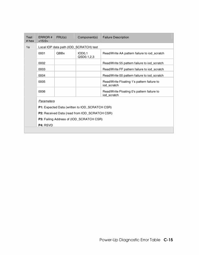
Power-Up Diagnostic Error Table C-15
Test # hex
ERROR # <15:0>
FRU(s) Component(s) Failure Description
Local IOP data path (IOD_SCRATCH) test
0001 QBBx IOD0,1 QSD0.1,2,3
Read/Write AA pattern failure to iod_scratch
0002 Read/Write 55 pattern failure to iod_scratch
0003 Read/Write FF pattern failure to iod_scratch
0004 Read/Write 00 pattern failure to iod_scratch
0005 Read/Write Floating 1’s pattern failure to iod_scratch
0006 Read/Write Floating 0’s pattern failure to iod_scratch
1a
Parameters
P1: Expected Data (written to IOD_SCRATCH CSR)
P2: Received Data (read from IOD_SCRATCH CSR)
P3: Failing Address of (IOD_SCRATCH CSR)
P4: RSVD

C-16 AlphaServer GS80/160/320 Service Manual
Test # hex
ERROR # <15:0>
FRU(s) Component(s) Failure Description
Local Hose 0 Config (1b), Local Hose 1 Config (1c), Local Hose 2 Config (1d), Local Hose 3 Config (1e)
0001 QBBx IOA Data pattern read/write error
0002 QBBx IODz (z=0,1) Data pattern read/write error
0003 QBB#.IORy.CBLz PBPx.RIOy QBB#.IORy.CBLz
MLK
MLK
IOP_HOSE x is present but not initialized
X=0..f; y=0,1; z=0.1
0004 QBB#.IORy. (y=0,1)
MLK, IOA, IOD0,1
Data pattern write/read error on NE_SCRATCH CSR
0014 Hose errors reported in IOA_ERR_SUM
0024 Hose checksum error in IOD_ERR_SUM (slice 0)
0034 Hose checksum error in IOD_ERR_SUM (slice 1)
0044 Error in NE_WHAT_AM_I_CSR
0006 System Box: QBBs.RIOy.CBLz PBPs.ROIy QBBx.IORy
Drawer: QBBx.IORy.CBLz QBBx.IORy.CBLI PBPx.RIOy QBBx.IORy
MLK MLK
MLK MLK
Data pattern write/read error in FE_SCRATCH CSR
y=01, z=0,1
0016 Hose errors reported in IOA_ERR_SUM
0026 Hose checksum error in IOD_ERR_SUM (slice 0)
0036 Hose checksum error in IOD_ERR_SUM (slice 1)
0046 Error in FE_WHAT_AM_I CSR
0008 QBBx.RIOy X=0..f, y=0,1
PCA, MLK Data pattern write/read error in PCA_SCRATCH CSR
0018 Hose errors reported in IOA_ERR_SUM
0028 Hose checksum error in IOD_ERR_SUM (slice 0)
1b
1c
1d
1e
(7 sub-tests)
0038 Hose checksum error in IOD_ERR_SUM (slice 1)

Power-Up Diagnostic Error Table C-17
Test# hex
ERROR # <15:0>
FRU(s) Component Failure Description
Parameters
P1: Expected pattern (written to XXX_SCRATCH CSR or ignore this field when checking IO*_ERR_SUM and IOP CSR)
P2: Received pattern (from XXX_SCRATCH CSR or received data from IO*_ERR_SUM and IOP CSR)
P3: Failing Address (of XXX_SCRATCH CSR or IO*_ERR_SUM or other IOP CSR)
P4: IO Map information passed for SCM needs
1f Placeholder

C-18 AlphaServer GS80/160/320 Service Manual
Test# hex
ERROR # <15:0>
FRU(s) Component(s) Failure Description
Local GPA scratch register test
0001 System box:
QBBx,GP QBBX QBBx.CPUy
Drawer:
QBBx QBBx.CPUy
GPA,GPD0
QSA,QSD0
GP,QSA,QSD0
Read/Write AA pattern failure to gpa_scratch
0002 Read/Write 55 pattern failure to gpa_scratch
0003 Read/Write FF pattern failure to gpa_scratch
0004 Read/Write 00 pattern failure to gpa_scratch
0005 Read/Write Floating 1’s pattern failure to gpa_scratch
0006 Read/Write Floating 0’s pattern failure to gpa_scratch
7777 FRU not determined
GPA CSR (8-bits) Read had bits other than <7:0> set! Possibly bad GP cable or connectors.
20
Parameters for error numbers 1,2,3,4,5,6
P1: Expected Data (written to GPA_SCRATCH)
P2: Received Data (read from GPA_SCRATCH)
P3: Failing Address (of GPA_SCRATCH CSR)
P4: Source Soft QBB ID in bits <2:0>
Parameters for error number 7777
P1: GPA CSR address
P2: GPA CSR data read from GPA CSR address in P1
P3: XSROM GP CSR read routine return address (need listings)
P4: Source Soft QBB ID in bits <2:0>

Power-Up Diagnostic Error Table C-19
Test # hex
ERROR # <15:0>
FRU(s) Component(s) Failure Description
Local GPD scratch register test
0001 System box:
QBBx,GP QBBX QBBx.CPUy
Drawer:
QBBx QBBx.CPUy
GPA,GPDz (z=0 - 3)
QSA,QSDx (x=0 - 3)
GP,QSA,QSDx
Read/Write AA pattern failure to gpd_scratch
0002 Read/Write 55 pattern failure to gpd_scratch
0003 Read/Write FF pattern failure to gpd_scratch
0004 Read/Write 00 pattern failure to gpd_scratch
0005 Read/Write Floating 1’s failure to gpd_scratch
0006 Read/Write Floating 0’s failure to gpd_scratch
7777 FRU not determined
GPA CSR (8-bits) Read had bits other than <7:0> set! Possibly bad GP cable.
21
Parameters for error numbers 1,2,3,4,5,6
P1: Expected Data (written to GPD_SCRATCH)
P2: Received Data (read from GPD_SCRATCH)
P3: Failing Address (of GPD_SCRATCH CSR)
P4: Source Soft QBB ID in bits <2:0>
Parameters for error number 7777
P1: GPA CSR address
P2: Received GPA CSR Data read from GPA CSR address in P1
P3: XSROM GP CSR read routine return address (need listings)
P4: Source Soft QBB ID in bits <2:0>

C-20 AlphaServer GS80/160/320 Service Manual
Test # hex
ERROR # <15:0>
FRU(s) Component(s) Failure Description
Local Gp-link > HS-link loopback test (QBBxis the local QBB in these callouts)
0011 System box: QBBx,GP QBBX.GP.CBLQBBx.CPUy HSW0 Drawer: QBBx QBBx.CBLE SCBL QBBx.CPUy
GPA, GPD0
GPDz (z=0 - 3)
GP,QSDz
Read/Write AA pattern failure to gpa_scratch
0012 Read/Write 55 pattern failure to gpa_scratch
0013 Read/Write FF pattern failure to gpa_scratch
0014 Read/Write 00 pattern failure to gpa_scratch
0015 Read/Write Floating 1’s failure to gpa_scratch
0016 Read/Write Floating 0’s failure to gpa_scratch
0021 Read/Write AA pattern failure to gpd_scratch
0022 Read/Write 55 pattern failure to gpd_scratch
0023 Read/Write FF pattern failure to gpd_scratch
0024 Read/Write 00 pattern failure to gpd_scratch
0025 Read/Write Floating 1’s failure to gpd_scratch
0026 Read/Write Floating 0’s failure to gpd_scratch
F300 System box: QBBx.GP.CBLHSW0 QBBx.GP
Drawer: QBBx.CBL SCBL, QBBx
QBBX is LOCAL QBB
Scratch testing passed but parity errors detected on GP CSRs
22
FC00 System box: HSW0 QBBx.GP.CBL
Drawer: SCBL, QBBx.CBL
QBBX is LOCAL QBB
Scratch testing passed but parity errors detected on HS CSRs

Power-Up Diagnostic Error Table C-21
Test # hex
ERROR # <15:0>
FRU(s) Component(s) Failure Description
FF00 System box: HSW0 QBBx.GP.CBL
Drawer: SCBL, QBBx.CBL
QBBX is LOCAL QBB
Scratch testing passed by parity errors detected on GP and HS CSRs
F3#x System box:QBBx.GP.CBL HSW0 QBBx.GP
Drawer: QBBx.CBL SCBL, QBBx
QBBx is LOCAL QBB
X=1..6 Scratch Test failed. Parity errors detected on GP CSRs.
FC#x System box: HSW0 QBBx.GP.CBL
Drawer: SCBL, QBBx.CBL
QBBx is LOCAL QBB
X=1..6 Scratch Test failed. Parity errors detected on HS CSRs
FF#x System box: HSW0 QBBx.GP.CBL
Drawer: SCBL, QBBx.CBL
QBBx is LOCAL QBB
X=1..6 Scratch Test failed. Parity errors detected on HS and GP CSRs.
#0#x System box: QBBx,GP QBBX.GP.CBLQBBx.CPUy HSW0
Drawer: QBBx QBBx.CBLE SCBL QBBx.CPUy
GPA, GPD0
GPDz (z=0,1,2,3)
GP,QSDz (z=0,1,2,3)
X=1..6 Scratch Test failed. No parity errors detected.
0099 HSW0 / SCBL QSA_QBB_POP_1<hs_ready> bit is NOT set
22 continued
7777 FRU not determined
GPA CSR (8-bits) Read had bits other than <7:0> set! Possibly bad GP cable.

C-22 AlphaServer GS80/160/320 Service Manual
Test# hex
ERROR # <15:0>
FRU(s) Component Failure Description
22 continued
Parameters for error numbers xx1x and xx2x
P1: Expected Data (wrt GPA/GPD_SCRATCH) P2: Received Data (rd GPA/GPD_SCRATCH) P3: Failing Address (of GPA/GPD_SCRATCH CSR) P4: Source Soft QBB ID in bits <2:0>
Parameters for error numbers Fxxx
P1: GPA_HSL_ERR_SUM CSR read data P3: HS_CSR0 CSR read data P2: GPD_HSL_ERR_SUM CSR read data P4: HS_CSR1 CSR read data
Parameters for error number 0099
P1: QSA_QBB_POP_1 CSR read data P2: QSA_QBB_POP_1 CSR address P3: System Map passed to XSROM in PSM CPU Function Command (CSB spec to decode) P4: Source HARD QBB ID
Parameters for error number 7777
P1: GPA CSR address P2: Received GPA CSR Data read from GPA CSR address in P1 P3: XSROM GP CSR return address (need listings) P4: Source Soft QBB ID in bits <2:0>

Power-Up Diagnostic Error Table C-23
Test # hex
ERROR # <15:0>
FRU(s) Component(s) Failure Description
Local GP performance monitor test
0001 QBBx.GP QBBx
PERFMON PERFMON
Default/Reset value is incorrect in REG0->REG10
0002 Default/Reset value is incorrect in Page 0..15 Counter 0..7 and Page 0..15
0003 Write/Read A pattern failure to REG0->REG7
0004 Write/Read 5 pattern failure to REG0->REG7
0005 Write/Read F pattern failure to REG0->REG7
0006 Write/Read 0 pattern failure to REG0->REG7
0007 Write/Read floating 1’s pattern failure to REG0->REG7
0008 Write/Read floating 0’s pattern failure to REG0->REG7
0009 Set back Default/Reset value failure to REG0->REG7
000A Write/Read QBB ID (0->7) failure to PERF_TM1_CONFIG CSR
7777 FRU not determined
GPA CSR (8-bits) Read had bits other than <7:0> set! Possibly bad GP cable.
23
Parameters
P1: Expected Data (written to GP PerfMon CSR)
P2: Received Data (read from GP PerfMon CSR)
P3: Failing Address (of GP PerfMon CSR)
P4: RSVD
Parameters for error number 7777
P1: GPA CSR address
P2: Received GPA CSR Data read from GPA CSR address in P1
P3: XSROM GP CSR read routine return address (need listings)
P4: Source Soft QBB ID in bits <2:0>

C-24 AlphaServer GS80/160/320 Service Manual
Test# hex
ERROR # <15:0>
FRU(s) Component(s) Failure Description
Local IOP error testing m = Interrupt type. (m =1 for CE; m =2 for UCE; m =3 for SE)
0001 QBBq.IORy (y=0,1)
IOA, QSA, QSD 0,1,2,3
IOA_ERR_SUM error
0002 “ IOD 0,1, QSD 0,1,2,3
IOD_ERR_SUM error
00m3 QBBq WFJ, IOA, Path
IOP: IOP_*CE bit Not set
00m4 “ “ IOP: IOP_*CE bit set with other bit set too
00m5 QBBq IOA, QSDx, Path
QSD: Invalid CPU ID in CPUx_*E_SUM CSR
00m6 “ “ QSD: No QBB_NUM bits set in CPUx_*E_SUM CSR
00m7 “ “ QSD: Proper QBB bit NOT set in CPUx_*E_SUM
00m8 “ “ QSD: More than 1 QBB bit set in CPUx_*E_SUM
00m9 For local test
QBBq
For remote test
Drawer: QBBq
System box: QBBq
QBBq.GP
QSDx, path, CPUx
WFJ, GP, path
WFJ, path
Path
00mA “ “ CPU: received incorrect IRQ interrupt
24
Parameters for error # = 0001 and 0002 (IOX = IOA or IOD)
P1: Expected Data (written to IO*_ERR_SUM CSR) P2: Received Data (read from IO*_ERR_SUM CSR) P3: Failing Address (of IO*_ERR_SUM CSR) P4: RSVD
Parameters for error # = 00mn; m =1,2,3; 2< n<^xB
P1: Sender info: interrupt type write into IOP_DIAG_SEND_ERR_INT CSR P2: Sender info: address of IOP_DIAG_SEND_ERR_INT CSR P3: Receiver info: data read from IOP_QBB_ERR_SUM or CPUx_*E_SUM or CPU P4: Receiver info: address of receiver (CSR)

Power-Up Diagnostic Error Table C-25
Test# hex
ERROR# <15:0>
FRU(s) Component(s) Failure Description
Local MEM0 scratch/BIST/error testing Local MEM1 scratch/BIST/error testing Local MEM2 scratch/BIST/error testing Local MEM3 scratch/BIST/error testing
Note: Only ONE test per MEMx (25,26,27,28 = MEM0,MEM1,MEM2,MEM3)
SUBTEST 1 (MEM_SCRATCH CSR Pattern testing)
0001 QBBx.MEMx (x=0,1,2,3 based on which test is running) QBBx.MEMx
MPDx (x=0,1) based on failing slice
QSDx (x=0 - 3) based on failing slice
MPA
Write/Read AA’s pattern to MEM_SCRATCH failed
If both MPDL and MPDH are bac
0002 Write/Read 55’s pattern to MEM_SCRATCH failed
0003 Write/Read FF’s pattern to MEM_SCRATCH failed
0004 Write/Read 00’s pattern to MEM_SCRATCH failed
0005 Float 1’s pattern through MEM_SCRATCH failed
0006 Float 0’s pattern through MEM_SCRATCH failed
SUBTEST 2 (MEM BIST Check testing)
Error# = WXYZ
z<3:0> = F -- BIST check failure occurred on MEMory under test y<4> = 1 -- Single-bit error occurred (bits 7:5 ignored) x<8> = 1 -- Double-bit error occurred (bits 11:9 ignored) w<12> = 1 -- Multiple-bit error occurred (bits 15:13 ignored)
wxyz QBBx.MEMy.DIMM
J1,J2… J8 ALL DIMMS that failed will be listed
QBBx.MEMy QBBx QBBx.MEMy.DIMM
MPD0,MPD1
QSD0,QSD1,QSD2,QSD3
J1,J2… J8
If ALL DIMMs fail, MEMy is bad
abcd QBBx.MEMy MEM BIST not complete!!
25, 26, 27, 28
(3 sub-tests in each test)
dcba QBBx.MEMy MEM INITnot complete!!

C-26 AlphaServer GS80/160/320 Service Manual
Test# hex
ERROR # <15:0>
FRU(s) Component Failure Description
SUBTEST 3 (MEM Error Line test)
QBBx QBBx.CPUy
QBBx
QBBx.MEMy
QBBx
QBBx
QSDy
IOAy, QSDy, path
MPA
WFJ WFJ, IOA, path
25, 26, 27, 28 (3 sub-tests in each test) continued
Error# = LMNX
X = 1 CE testing N = 1 No IRQ<0>(CE) or IRQ<4> (UCE) interrupts posted to the CPU X = 2 UCE testing N = 2 Incorrect IRQ interrupts posted to the CPU
M = 0 QSD Error Summary CSR (CPUx_CE/UCE_SUM) was correct M = 1 Invalid CPU ID in CPUx_CE_SUM or CPUx_UCE_SUM M = 2 No QBB_NUM bits set in CPUx_CE_SUM or CPUx_UCE_SUM M = 4 Incorrect QBB_NUM set in CPUx_CE_SUM or CPUx_UCE_SUM M = 8 More than one QBB_NUM bit set in CPUx_CE_SUM or CPUx_UCE_SUM
L = 1 FRU1 is likely the QSD, QSD->CPU path, or CPU L = 2 FRU1 is likely IOA, QSDy, or IOA->QSDy path (where y=CPU# of Cpu running the test) L = 4 FRU1 is likely the MPA, WFJ, or MPA->WFJ path
FRU2 is likely the WFJ, IOA, or WFJ->IOA path
Possible Test 25, Subtest 3 Error Numbers (decode based on above chart)
101x, 102x 211x, 212x, 221x, 222x, 241x, 242x, 281x, 282x 411x, 412x, 421x, 422x, 441x, 442x, 481x, 482x

Power-Up Diagnostic Error Table C-27
Test# hex
ERROR # <15:0>
FRU(s) Component Failure Description
25, 26, 27, 28
(3 sub-tests in each test) continued
SUBTEST 1: Parameters for error numbers 1,2,3,4,5,6
P1: Exp: Data written to MEM_SCRATCH P3: Addr: Failing Address (MEM_SCRATCH) P2: Rcvd: Data read back from MEM_SCRATCH after write P4: CPU# (running this test) in bits <1:0>
SUBTEST 2: Parameters for error numbers xxxF
P1: Mask of failing DIMMx (0..7) on MEMx (x=0,1,2,3) under test <07:00> = MEM0 DIMM0..7 failures <15:08> = MEM1 DIMM0..7 failures <23:16> = MEM2 DIMM0..7 failures <31:24> = MEM3 DIMM0..7 failures
P2: Mask of DIMMX (0..7) PRESENCE on MEMx (0..3) <07:00> = MEM0 DIMM0..7 presence <15:08> = MEM1 DIMM0..7 presence <23:16> = MEM2 DIMM0..7 presence <31:24> = MEM3 DIMM0..7 presence
P3: Read Data from LAST MEM_SELF_TEST_x CSR read which had a BIST error P4: Address of CSR read in P3
SUBTEST 2: Parameters for error numbers abcd, dcba
P1: Data from last MEM_MOD_CONFIG CSR read P3: MEMx-under-test which failed P2: CSR address of last MEM_MOD_CONFIG CSR read P4: CPU# (running test) in bits <1:0>
SUBTEST 3: Parameters for error numbers LMNX (see chart above)
P1: Data read from CPUx_CE_SUM or CPUx_UCE_SUM P3: Data read from IOP_QBB_ERR_SUM P2: Address of CPUx_CE_SUM or CPUx_UCE_SUM read in P1 P4: EV6 ISUM ipr read data
ALL SUBTESTS: Parameters for error number 0099
P1: Received Data read from QSA_PORT_MAP_0 P2: Expected Data written to QSA_PORT_MAP_0 P3: Address of QSA_PORT_MAP_0 CSR P4: Source Soft QBB ID in bits <2:0>

C-28 AlphaServer GS80/160/320 Service Manual
Test# hex
ERROR# <15:0>
FRU(s) Component(s) Failure Description
Local DTAG scratch and BIST check test
Subtest 1: DTAGx Scratch CSR (DTAG_ERR_ADDR_0) testing
F001 QBBx DTGx (x=0 - 3) for non-MCM backplane
DTG0-3 or DTG4-7 for MCM backplane
Write/Read AA’s to DTAG_ERR_ADDR_0 failed
F002 Write/Read 55s to DTAG_ERR_ADDR_0 fail
F003 Write/Read FFs to DTAG_ERR_ADDR_0 fail
F004 Write/Read 00s to DTAG_ERR_ADDR_0 fail
F005 Float 1s through DTAG_ERR_ADDR_0 failed
F006 Float 0s through DTAG_ERR_ADDR_) failed
Subtest 2: DTAG BIST check testing
Error# = 00xx where xx = 8-bit MASK of which DTAGs (0..7) failed. If any DTAGs failed, then DTAGs TAG RAM block failed BIST. Example: Error# = 64 means DTAG 2,5,6 are all bad.
00xx QBBx DTGx (x=0,1,2,3) for non-MCM backplane
DTG0-3 or DTG4-7 for MCM backplane
Either BIST did NOT complete, or BIST_Err_Summary had bits set
29
(2 sub-tests)
Subtest 1 Parameters for error numbers F00x
P1: Exp: Data written to DTAG_ERR_ADDR_0 P2: Rcvd: Data read back from DTAG_ERR_ADDR_0 after the write P3: Addr: Failing Address (DTAG_ERR_ADDR_0 csr) P4: Total # Dtags in <19:16>, Failing DTAGx in <27:24>, CPU# (running this test) in <1:0>
Subtest 2 Parameters for error numbers 00xx
P1: DTAGx_ERR_SUM CSR read data (8-bits per DTAG CSR read as follows):
<07:00> = DTAG0_ERR_SUM read data <15:08> = DTAG1_ERR_SUM read data : <63:56> = DTAG7_ERR_SUM read data P2: <7:0> shows the mask of DTAGs on which BIST_DONE never set <15:8> = total number of DTAGs on the backplane of QBBx-under-test P3: <7:0> shows the mask of DTAGs on which BIST_ERR_Sum had error bits set P4: Address of LAST DTAGx_ERR_SUM CSR which was read.

Power-Up Diagnostic Error Table C-29
Test# hex
ERROR# <15:0>
FRU(s) Component(s) Failure Description
Local directory scratch and BIST check test
Subtest 1: DIR Scratch CSR (DIR_EDC_SUB_ADDR_B) testing
F001 QBBx.DIR DMA,DMD0,DMD1 Write/Read AA’s pattern to DIR_EDC_SUB_ADDR_B failed
F002 Write/Read 55’s pattern to DIR_EDC_SUB_ADDR_B failed
F003 Write/Read FF’s pattern to DIR_EDC_SUB_ADDR_B failed
F004 Write/Read 00’s pattern to DIR_EDC_SUB_ADDR_B failed
F005 Float 1’s pattern through DIR_EDC_SUB_ADDR_B failed
F006 Float 0’s pattern through DIR_EDC_SUB_ADDR_B failed
Subtest 2: DIR BIST check testing
Error# = 00xx where xx<15:0> = bitmask of failing Arrays 0..15
Note: 2-bits per each Array x (0..15) 00 = NO Error 01 = Single-bit error 10 = Double-bit error 11 = Multiple-bit error
Abcd QBBx.DIR DMA,DMD0,DMD1 DIR BIST never completed or EVERY DIMM failed
00xx QBBx.DIR.DIM J1, J2… ,J8 DIR_SELF_TEST showed failing DIMMs
2a
(2 sub-tests)
Subtest 1 Parameters for error numbers F00x
P1: Exp: Data written to DIR_EDC_SUB_ADDR_b P2: Rcvd: Data read back from DIR_EDC_SUB_ADDR_B after the write P3: Addr: Failing Address (DIR_EDC_SUB_ADDR_B csr) P4: CPU# (running this test) in <1:0>
Subtest 2 Parameters for error number abcd:
P1: DIR_SELF_TEST_CTL CSR read results P2: DIR_SELF_TEST_CTL CSR address P3: Source HARD QBB ID (QBB where the DIRectory resides) P4: CPU# in bits <1:0> passed from SCM (System Primary flag in bit <7>)
Subtest 2 Parameters for error number 00xx:
P1: DIR_SELF_TEST CSR read results P2: DIR_SELF_TEST CSR address P3: <15:0> Bitmask of failing DIR Arrays 0..15 P4: <15:0> Bitmask of DIRectory DIMMs ARRAY 0..15 which are PRESENT

C-30 AlphaServer GS80/160/320 Service Manual
Test# hex
ERROR# <15:0>
FRU(s) Component(s) Failure Description
Local IOP BIST check test
0001 QBBx
QBBx
IOD0
IOD1
Write Cache BIST failure (slice 0)
0002 Write Cache BIST failure (slice 1)
0003 Read Cache BIST failure (slice 0)
0004 Read Cache BIST failure (slice 1)
2b
Parameters for all error numbers
P1: IOD_ERR_SUM CSR read results P2: IOD_ERR_SUM CSR address P3: not used P4: not used
Local QSA error line test
Error# = LMNX
X = 1 CE testing X = 2 UCE testing
N = 1 No IRQ<0>(CE) or IRQ<4> (UCE) interrupts posted to the CPU N = 2 Incorrect IRQ interrupts posted to the CPU
M = 0 QSD Error Summary CSR (CPUx_CE/UCE_SUM) was correct M = 1 Invalid CPU ID in CPUx_CE_SUM or CPUx_UCE_SUM M = 2 No QBB_NUM bits set in CPUx_CE_SUM or CPUx_UCE_SUM M = 4 Incorrect QBB_NUM set in CPUx_CE_SUM or CPUx_UCE_SUM M = 8 More than one QBB_NUM bit set in CPUx_CE_SUM or CPUx_UCE_SUM
L = 1 FRU1 is likely the QSD, QSD->CPU path, or CPU L = 2 FRU1 is likely IOA, QSDy, or IOA->QSDy path (where y=CPU# of Cpu running the test) L = 4 FRU1 is likely the QSA, WFJ, or QSA->WFJ path
FRU2 is likely the WFJ, IOA, or WFJ->IOA path
Possible Test 2c Error Numbers (decode based on above chart)
101x, 102x 211x, 212x, 221x, 222x, 241x, 242x, 281x, 282x 411x, 412x, 421x, 422x, 441x, 442x, 481x, 482x
2c
Parameters for all error numbers:
P1: Data read (FAST read) from CPUx_CE_SUM or CPUx_UCE_SUM P2: Address of CPUx_CE_SUM or CPUx_UCE_SUM which was read in P1 P3: Data read from IOP_QBB_ERR_SUM P4: EV6 ISUM ipr read data

Power-Up Diagnostic Error Table C-31
Test# hex
ERROR# <15:0>
FRU(s) Component Failure Description
Local hose error testing
Error #<3:0> = Error Type Error #<7:4> = MiniLink ID =m ( m =2 =Near End MLK; =1 =Far End MLK; =0 =PCA MLK) Error #<11:8> = Hose ID = h (where: 0<= h <=3 ) Error #<15:12> = QBB ID =q (where: 0<= q <=7 )
qhm1 QBBq.IORx or PBP.RIO or PBP.RIOh
MLK MLK PCA
*_ERR_SUM bit y is NOT set when writing *_DIAG_FORCE_ERR bit y (* = NE/FE/PCA)
qhm2 “ “ IOP_QBB_ERR_SUM<iop_uce> bit NOT set
qhm3 “ “ IOP_QBB_ERR_SUM<iop_uce> bit set, but other
unexpected bits in this CSR are also set
qhm4 “ “ IOA_ERR_SUM<hose_h_MLK_m_UCE> bit NOT
set where m denotes PCA/FE/NE (see above m define)
qhm5 “ “ IOA_ERR_SUM<hose_h_MLK_m_UCE> bit is set
but unexpected bits are also set. where *** denotes PCA/FE/NE (see byte M)
qhm6 QBBq IOA, QSDx, Path
Invalid CPU ID in CPUx_UCE_SUM (QSD)
qhm7 “ “ No QBB bit set in CPUx_UCE_SUM (QSD)
qhm8 “ “ Expected QBB not set in CPUx_UCE_SUM
(QSD)
qhm9 “ “ Expected QBB bit set, but other unexpected bits in
this CSR are also set
qhmA For local test
QBBq
For remote
Drawer: QBBq
System box: QBBq QBBq.GP
QSDx, Path; CPUx
WFJ, GP, Path
WFJ, Path Path
No IRQ interrupts received (CPU)
qhmB “ “ Incorrect IRQ interrupt received (CPU)
2d
9999 N/A N/A
User input an invalid Hose #

C-32 AlphaServer GS80/160/320 Service Manual
Test# hex
ERROR # <15:0>
FRU(s) Component Failure Description
2d continued
Parameters for error # =qhm1 (** = NE or FE or PCA)
P1: Expected Data (written to **_DIAG_FORCE_ERR_SUM CSR)
P2: Received Data (read from **_ERR_SUM CSR)
P3: Failing Address (of **_ERR_SUM CSR)
P4<63:48> may contains 4th error #, P4<47:32> may contains 3rd error #,
P4<31:16> may contains 2nd error #, P4<15:0> contains 1st error #
Parameters for error # = qhmn; (1< n<^xC)
P1: Sender info: The data written into IOP_ERR_INT_TARGET CSR
P2: Receiver info: The data read from IOP_QBB_ERR_SUM or IOA_ERR_SUM or CPUx_UCE_SUM or EV6_ISUM
P3: Receiver info: Address of reading CSR (IOP or IOA or QSD)
P4<63:48> may contains 4th error #, P4<47:32> may contains 3rd error #,
P4 <31:16> may contains 2nd error #, P4<15:0> contains 1st error #
Note: All called out FRUs and P1, P2, P3 are associate with the 1st error #.

Power-Up Diagnostic Error Table C-33
Test# hex
ERROR # <15:0>
FRU(s) Component Failure Description
Local GP error line test
Error# = LMNX
X = 1 CE testing N = 1 No IRQ<0>(CE) or IRQ<4> (UCE) interrupts posted to the CPU X = 2 UCE testing N = 2 Incorrect IRQ interrupts posted to the CPU
M = 0 QSD Error Summary CSR (CPUx_CE/UCE_SUM) was correct M = 1 Invalid CPU ID in CPUx_CE_SUM or CPUx_UCE_SUM M = 2 No QBB_NUM bits set in CPUx_CE_SUM or CPUx_UCE_SUM M = 4 Incorrect QBB_NUM set in CPUx_CE_SUM or CPUx_UCE_SUM M = 8 More than one QBB_NUM bit set in CPUx_CE_SUM or CPUx_UCE_SUM
L = 1 FRU1 is likely the QSD, QSD->CPU path, or CPU L = 2 FRU1 is likely IOA, QSDy, or IOA->QSDy path (where y=CPU# of Cpu running the test) L = 4 FRU1 is likely the GPA, WFJ, or QSA->WFJ path
FRU2 is likely the WFJ, IOA, or WFJ->IOA path
Possible Test 2e Error Numbers (decode based on above chart)
101x, 102x 211x, 212x, 221x, 222x, 241x, 242x, 281x, 282x 411x, 412x, 421x, 422x, 441x, 442x, 481x, 482x
LMNX System box: QBBx.GP QBBx QBBx Drawer: QBBx QBBx QBBx
GPA WFJ WFJ, IOA, path GP WFJ WFJ, IOA, path
LMNX System box: QBBx Drawer: QBBx
OA, QSDy, path
IOA, QSDy, path
LMNX System box: QBBx QBBx.CPUy Drawer: QBBx QBBX.CPUy
QSDy
QSDy
2e
Parameters for all error numbers:
P1: Read CPUx_CE_SUM or CPUx_UCE_SUM P3: Data read from IOP_QBB_ERR_SUM P2: Address of CPUx_CE_SUM or CPUx_UCE_SUM P4: EV6 ISUM ipr read data
2f placeholder

C-34 AlphaServer GS80/160/320 Service Manual
Test # hex
ERROR # <15:0>
FRU(s) Component Failure Description
Local directory error line test
Error# = LMNX
X = 1 CE testing X = 2 UCE testing
N = 1 No IRQ<0>(CE) or IRQ<4> (UCE) interrupts posted to the CPU N = 2 Incorrect IRQ interrupts posted to the CPU
M = 0 QSD Error Summary CSR (CPUx_CE/UCE_SUM) was correct M = 1 Invalid CPU ID in CPUx_CE_SUM or CPUx_UCE_SUM M = 2 No QBB_NUM bits set in CPUx_CE_SUM or CPUx_UCE_SUM M = 4 Incorrect QBB_NUM set in CPUx_CE_SUM or CPUx_UCE_SUM M = 8 More than one QBB_NUM bit set in CPUx_CE_SUM or CPUx_UCE_SUM
L = 1 FRU1 is likely the QSD, QSD->CPU path, or CPU L = 2 FRU1 is likely IOA, QSDy, or IOA->QSDy path (where y=CPU# of Cpu running the test) L = 4 FRU1 is likely the DIR, WFJ, or QSA->WFJ path
FRU2 is likely the WFJ, IOA, or WFJ->IOA path
Possible Test 30 Error Numbers (decode based on above chart)
101x, 102x 211x, 212x, 221x, 222x, 241x, 242x, 281x, 282x 411x, 412x, 421x, 422x, 441x, 442x, 481x, 482x
LMNX QBBx.DIR QBBx QBBx
DMA WFJ WFJ,IOA,path
LMNX QBBx IOA,QSDy,path
LMNX QBBx QBBx.CPUy
QSDy
30
Parameters for all error numbers:
P1: Data read (FAST read) from CPUx_CE_SUM or CPUx_UCE_SUM
P2: Address of CPUx_CE_SUM or CPUx_UCE_SUM which was read in P1
P3: Data read from IOP_QBB_ERR_SUM
P4: EV6 ISUM ipr read data

Power-Up Diagnostic Error Table C-35
Test# hex
ERROR # <15:0>
FRU(s) Component Failure Description
Local QSD error line (FAULT) test
Error# = LMNX
X<0> = 1 always to signify SE testing (no CE or UCE testing here) X = 3 IOP_QBB_ERR_SUM<fault_sum>=0 meaning a FAULT was not reported X = 5 IOP_QBB_ERR_SUM<fault_entity> is incorrect (not as expected) X = 9 IOP_QBB_ERR_SUM<wfj_fault_turned_into_sys_event> bit NOT set!
N = 2 Incorrect IRQ interrupts posted to the CPU
M = 0 QSD Error Summary CSR (CPUx_SE_SUM) was correct M = 1 Invalid CPU ID in CPUx_SE_SUM M = 2 No QBB_NUM bits set in CPUx_SE_SUM M = 4 Incorrect QBB_NUM set in CPUx_SE_SUM M = 8 More than one QBB_NUM bit set in CPUx_SE_SUM
L = 1 FRU1 is likely the QSD, QSD->CPU path, or CPU L = 2 FRU1 is likely IOA, QSDy, or IOA->QSDy path (where y=CPU# of Cpu running the test) L = 4 FRU1 is likely the QSDy (y=0,1,2,3)
FRU2 is likely the WFJ
Possible Test 31 Error Numbers (decode based on above chart)
1021 2121, 2221, 2421, 2821 4123,4125,4129 4223, 4225, 4229
4423,4425,4429 4823, 4825, 4829
LMNX QBBx QBBx
QSDy WFJ
Y=0,1,2,3 based on CPUy running this test
LMNX QBBx IOA,QSDy, path
LMNX QBBX QBBx.CPUy
QSDy
31
Parameters for all error numbers:
P1: Data read (FAST read) from CPUx_SE_SUM
P2: Address of CPUx_SE_SUM which was read in P1
P3: Data read from IOP_QBB_ERR_SUM
P4: EV6 ISUM ipr read data

C-36 AlphaServer GS80/160/320 Service Manual
Test# hex
ERROR # <15:0>
FRU(s) Component Failure Description
Local DTAG error line (FAULT) test
Error# = LMNX
X<0> = 1 always to signify SE testing (no CE or UCE testing here) X = 3 IOP_QBB_ERR_SUM<fault_sum>=0 meaning a FAULT was not reported X = 5 IOP_QBB_ERR_SUM<fault_entity> is incorrect (not as expected) X = 9 IOP_QBB_ERR_SUM<wfj_fault_turned_into_sys_event> bit NOT set!
N = 2 Incorrect IRQ interrupts posted to the CPU
M = 0 QSD Error Summary CSR (CPUx_SE_SUM) was correct M = 1 Invalid CPU ID in CPUx_SE_SUM M = 2 No QBB_NUM bits set in CPUx_SE_SUM M = 4 Incorrect QBB_NUM set in CPUx_SE_SUM M = 8 More than one QBB_NUM bit set in CPUx_SE_SUM
L = 1 FRU1 is likely the QSD, QSD->CPU path, or CPU L = 2 FRU1 is likely IOA, QSDy, or IOA->QSDy path (where y=CPU# of Cpu running the test) L = 4 FRU1 is likely the DTAGx
FRU2 is likely the WFJ
Possible Test 32 Error Numbers (decode based on above chart)
1021 2121, 2221, 2421, 2821 4123,4125,4129 4223, 4225, 4229 4423,4425,4429 4823, 4825, 4829
LMNX QBBx
QBBx
DTGy
DTG0-3
DTG4-7
WFJ
Y=0,1,2,3 for NON-MCM backplane
MCM backplane
MCM backplane
LMNX QBBx IOA, QSDy, path Y=0,1,2,3 based on CPUy running this test
LMNX QBBX
QBBx.CPUy
QSDy Y=0,1,2,3 based on CPUy running this test
32
Parameters for all error numbers:
P1: Data read (FAST read) from CPUx_SE_SUM P2: Address of CPUx_SE_SUM which was read in P1 P3: Data read from IOP_QBB_ERR_SUM P4: EV6 ISUM ipr read data
33 Placeholder

Power-Up Diagnostic Error Table C-37
Test# hex
ERROR # <15:0>
FRU(s) Component Failure Description
Local QBB soft QBB ID configuration test
0001 QBBx Write/Read of QSA_QBB_ID failed (step 2 of Local Soft QBB ID config process)
0002 Write/Read of IOD_CONFIG failed (step 3 of Local Soft QBB ID config process)
0003 Invalid Sub-test number received from PSM. PSM->XSROM interaction problem (bad PSM packet).
0099 QSA_PORT_MAP0..3 Read data does not match data just Written to that CSR during setup for memory CSR accesses (mem_csr_acces_init)
7777 FRU not determined
GPA CSR (8-bits) Read had bits other than <7:0> set! Possibly bad GP cable.
34
(12 sub-tests)
Parameters for error #0001
P1: QSA_QBB_ID read data (read back from QSA_QBB_ID) P3: QSA_QBB_ID address P2: QSA_QBB_ID write data (what we wrote) P4: Source Soft QBB ID in <2:0>
Parameters for error #0002
P1: IOD_CONFIG read data (read back from IOD_CONFIG) P2: IOD_CONFIG write data (what we wrote) P3: IOD_CONFIG address P4: Source Soft QBB ID in <2:0>; Soft QBB ID of QBB under test in <5:3>
Parameters for error #0003
P1: Subtest number P2: CPU ID in bits <1:0> passed by the PSM. Primary CPU if bit<7> = 1 P3: System Map passed by the PSM P4: Source Hard QBB ID
Parameters for error number 0099
P1: Data read from QSA_QBB_MAP_0..3 P2: QSA_QBB_MAP_0..3 CSR address just read P3: Expected Data previously written P4: Source Soft QBB ID in bits <2:0>; Soft QBB ID of QBB under test in <5:3>
Parameters for error number 7777
P1: GPA CSR address P2: Received GPA CSR Data P3: XSROM GP CSR read routine return address P4: Source Soft QBB ID in bits <2:0>; Soft QBB ID of QBB under test in <5:3>

C-38 AlphaServer GS80/160/320 Service Manual
Test # hex
ERROR # <15:0>
FRU(s) Component Failure Description
Remote GPA scratch register test (QBBx is target QBB)
0001 System box: QBBx,GP QBBx.GP.CBLQBBX
HSW0 / QBBx.GP.CBL QBBx.GP QBBx
HSW0
Drawer: QBBx QBBx.CBL
SCBL / QBBx.CBL QBBx SCBL
GPA,GPD0 QSA, QSDx
GPDy
QSA,QSDx
GP,QSA,QSDx
GP,QSA,QSDx
Read/Write AA pattern failure to gpa_scratch
0002 Read/Write 55 pattern failure to gpa_scratch
0003 Read/Write FF pattern failure to gpa_scratch
0004 Read/Write 00 pattern failure to gpa_scratch
0005 Read/Write Floating 1s failure to gpa_scratch
0006 Read/Write Floating 0s failure to gpa_scratch
F300 System box:
QBBx.GP.CBLHSW0 QBBx.GP
Drawer:
QBBx.CBL SCBL, QBBx
QBBx is REMOTE QBB
Scratch testing passed but parity errors detected on GP CSRs
35
FC00 System box:
HSW0 QBBx.GP.CBL
Drawer:
SCBL QBBx.CBL
QBBx is REMOTE QBB
Scratch testing passed but parity errors detected on HS CSRs

Power-Up Diagnostic Error Table C-39
Test# hex
ERROR # <15:0>
FRU(s) Component Failure Description
FF00 System box:
HSW0 QBBx.GP.CBL
Drawer:
SCBL QBBx.CBL
QBBx is REMOTE QBB
Scratch testing passed by parity errors detected on GP and HS CSRs
F3#x System box:
QBBx.GP.CBLHSW0 QBBx.GP
Drawer:
QBBx.CBL SCBL QBBx
QBBx is REMOTE QBB
X=1..6 Scratch Test failed. Parity errors detected on GP CSRs.
FC#x System box:
HSW0 QBBx.GP.CBL
Drawer:
SCBL QBBx.CBL
QBBx is REMOTE QBB
X=1..6 Scratch Test failed. Parity errors detected on HS CSRs
35 continued
FF#x System box:
HSW0 QBBx.GP.CBL
Drawer:
SCBL QBBx.CBL
QBBx is REMOTE QBB
X=1..6 Scratch Test failed. Parity errors detected on HS and GP CSRs.

C-40 AlphaServer GS80/160/320 Service Manual
Test# hex
ERROR # <15:0>
FRU(s) Component Failure Description
#0#x System box:
QBBx,GP QBBx.GP.CBLQBBX HSW0
Or
QBBx.GP.CBLQBBx.GP QBBx, HSW0
Drawer:
QBBx QBBx.CBL SCBL
Or
QBBx.CBL QBBx SCBL
GPA,GPD0 QSA, QSDx
GPDy QSA,QSDx
GP,QSA,QSDx
GP,QSA,QSDx
X=1..6 Scratch Test failed. No parity errors detected.
7777 FRU not determined
GPA CSR (8-bits) Read had bits other than <7:0> set! Possibly bad GP cable
0066 QBBx QSA_QBB_ID<hs_presence> write failed
35 continued
Parameters for error numbers 1,2,3,4,5,6
P1: Expected Data (written to GPA_SCRATCH) P2: Received Data (from GPA_SCRATCH) P3: Failing Address (of GPA_SCRATCH CSR) P4: Source Soft QBB ID in bits <2:0>; Soft QBB ID of QBB under test in <5:3>
Parameters for error number 7777
P1: GPA CSR address P2: GPA CSR data from GPA CSR P3: XSROM GP CSR read routine return address P4: Source Soft QBB ID in bits <2:0>; Soft QBB ID of QBB under test in <5:3>
Parameters for error number 0066
P1: QSA_QBB_ID CSR read data P2: Data written to QSA_QBB_ID (hs_present set) P3: Address of QSA_QBB_ID CSR P4: Source Soft QBB ID in bits <2:0>; Soft QBB ID of QBB under test in <5:3>

Power-Up Diagnostic Error Table C-41
Test# hex
ERROR # <15:0>
FRU(s) Component(s) Failure Description
Remote GPD scratch register test
0001 System box: QBBx,GP QBBX QBBx.CPUy
Drawer: QBBx QBBx.CPUy
GPA,GPDz QSA,QSDx
GP,QSA,QSDx
Read/Write AA pattern failure to gpd_scratch
0002 Read/Write 55 pattern failure to gpd_scratch
0003 Read/Write FF pattern failure to gpd_scratch
0004 Read/Write 00 pattern failure to gpd_scratch
0005 Read/Write Floating 1’s pattern failure to gpd_scratch
0006 Read/Write Floating 0’s pattern failure to gpd_scratch
F300 System box: QBBx.GP.CBLHSW0 QBBx.GP
Drawer: QBBx.CBL SCBL, QBBx
QBBx is REMOTE QBB
Scratch testing passed but parity errors detected on GP CSRs
FC00 System box: HSW0 QBBx.GP.CBL
Drawer: SCBL QBBx.CBL
QBBx is REMOTE QBB
Scratch testing passed but parity errors detected on HS CSRs
36
FF00 System box: HSW0 QBBx.GP.CBL
Drawer: SCBL QBBx.CBL
QBBx is REMOTE QBB
Scratch testing passed by parity errors detected on GP and HS CSRs

C-42 AlphaServer GS80/160/320 Service Manual
Test# hex
ERROR # <15:0>
FRU(s) Component Failure Description
F3#x System box: QBBx.GP.CBLHSW0 QBBx.GP
Drawer: QBBx.CBL SCBL, QBBx
QBBx is REMOTE QBB
X=1..6 Scratch Test failed. Parity errors detected on GP CSRs.
FC#x System box: HSW0 QBBx.GP.CBL
Drawer: SCBL QBBx.CBL
QBBx is REMOTE QBB
X=1..6 Scratch Test failed. Parity errors detected on HS CSRs
FF#x System box: HSW0 QBBx.GP.CBL
Drawer: SCBL QBBx.CBL
QBBx is REMOTE QBB
X=1..6 Scratch Test failed. Parity errors detected on HS and GP CSRs.
#0#x
7777 FRU not determined
GPA CSR (8-bits) Read had bits other than <7:0> set! Possibly bad GP cable.
0066 QBBx QSA_QBB_ID<hs_presence> write failed
36 continued
Parameters for error numbers 1,2,3,4,5,6
P1: Expected Data (written to GPD_SCRATCH) P2: Received Data (read from GPD_SCRATCH) P3: Failing Address (of GPD_SCRATCH CSR) P4: Source Soft QBB ID in bits <2:0>
Parameters for error number 7777
P1: GPA CSR address P2: Receieved GPA CSR Data read from GPA CSR address in P1 P3: XSROM GP CSR read routine return address (need listings) P4: Source Soft QBB ID in bits <2:0>
Parameters for error number 0066
P1: QSA_QBB_ID CSR read data (after the write) P2: Data written to QSA_QBB_ID (should have hs_present set) P3: Address of QSA_QBB_ID CSR written P4: Source Soft QBB ID in bits <2:0>

Power-Up Diagnostic Error Table C-43
Test # hex
ERROR # <15:0>
FRU(s) Component Failure Description
Remote QBB soft QBB ID configuration test
0001 QBBx (tested) Write/Read of QSA_QBB_ID failed (step 2 of config process)
0002 Write/Read of QSA_PORT_MAP failed (step 5 of remote config process)
0003 Write/Read of IOD_CONFIG failed (step 7 of remote config process)
0004 Invalid Sub-test number received from PSM
0005 HSW0/SCBL QSA_QBB_POP_1<hs_ready> bit is NOT set
7777 FRU not determined
GPA CSR (8-bits) Read had bits other than <7:0> set! Possibly bad GP cable.
37
(13 sub-tests)
Parameters for error #0001
P1: QSA_QBB_ID read data (read back after the write of QSA_QBB_ID) P2: QSA_QBB_ID write data (what we expected to read from QSA_QBB_ID) P3: QSA_QBB_ID address P4: Target Soft QBB ID in <2:0>. Source Soft QBB ID in <5:3>
Parameters for error #0002
P1: QSA_PORT_MAP_0 read data (read back after the write of QSA_PORT_MAP_0) P2: QSA_PORT_MAP_0 write data (what we expected to read from QSA_PORT_MAP_0) P3: QSA_PORT_MAP_0 address P4: Target Soft QBB ID in <2:0>. Source Soft QBB ID in <5:3>
Parameters for error #0003
P1: IOD_CONFIG read data (read back after the write of IOD_CONFIG P2: IOD_CONFIG write data (what we expected to read from IOD_CONFIG) P3: IOD_CONFIG address P4: Target Soft QBB ID in <2:0>. Source Soft QBB ID in <5:3>
Parameters for error #0004
P1: Subtest number to be Tested P2: Target QBB (Hard QBB# under-test) P3: System Map passed by the PSM P4: Source Hard QBB ID
Parameters for error number 0005
P1: QSA_QBB_POP_1 CSR read data P2: QSA_QBB_POP_1 CSR address P3: System Map passed to XSROM in PSM CPU Function Command (bytes 13:10 – CSB spec to decode) P4: Source HARD QBB ID
Parameters for error number 7777
P1: GPA CSR address P2: Received GPA CSR Data read P3: XSROM GP CSR read routine return address P4: Target QBB Soft QBB ID in bits <2:0>

C-44 AlphaServer GS80/160/320 Service Manual
Test# hex
ERROR # <15:0>
FRU(s) Component Failure Description
38 See Test 23 (Local GP PerfMon CSR Access). Same error numbers reported for remote.
39 See Test 19 (Local IOA Scratch Access). Same error numbers reported for remote version.
3a See Test 1a (Local IOD Scratch access). Same error numbers reported for remote version.
3b(7 sub-tests)
See Test 1b (Local IO Hose 0 Configuration and Path Verification test). Same error numbers reported for this remote version.
3c(7 sub-tests)
See Test 1b (Local IO Hose 1 Configuration and Path Verification test). Same error numbers reported for this remote version.
3d(7 sub-tests)
See Test 1b (Local IO Hose 2 Configuration and Path Verification test). Same error numbers reported for this remote version.
3e(7 sub-tests)
See Test 1b (Local IO Hose 3 Configuration and Path Verification test). Same error numbers reported for this remote version..
See Test 12 (Local QSA Scratch access). Same error numbers reported for this Remote version. However, The following errors are specific to this Remote QSA test:
F300 System box:
QBBx.GP.CBLHSW0 QBBx.GP
Drawer:
QBBx.CBL SCBL QBBx
QBBx is REMOTE QBB
Scratch testing passed but parity errors detected on GP CSRs
FC00 System box:
HSW0 QBBx.GP.CBL
Drawer:
SCBL QBBx.CBL
QBBx is REMOTE QBB
Scratch testing passed but parity errors detected on HS CSRs
3f
FF00 System box:
HSW0 QBBx.GP.CBL
Drawer:
SCBL QBBx.CBL
QBBx is REMOTE QBB
Scratch testing passed by parity errors detected on GP and HS CSRs

Power-Up Diagnostic Error Table C-45
Test# hex
ERROR # <15:0>
FRU(s) Component Failure Description
F3#x System box:
QBBx.GP.CBLHSW0 QBBx.GP
Drawer:
QBBx.CBL SCBL QBBx
QBBx is REMOTE QBB
X=1..6 Scratch Test failed. Parity errors detected on GP CSRs.
FC#x System box:
HSW0 QBBx.GP.CBL
Drawer:
SCBL QBBx.CBL
QBBx is REMOTE QBB
X=1..6 Scratch Test failed. Parity errors detected on HS CSRs
3f continued
FF#x System box:
HSW0 QBBx.GP.CBL
Drawer:
SCBL QBBx.CBL
QBBx is REMOTE QBB
X=1..6 Scratch Test failed. Parity errors detected on HS and GP CSRs.

C-46 AlphaServer GS80/160/320 Service Manual
Test# hex
ERROR # <15:0>
FRU(s) Component Failure Description
See Test 13 (Local QSD Scratch access). Same error numbers reported for remote version.
F300 System box: QBBx.GP.CBLHSW0 QBBx.GP
Drawer: QBBx.CBL SCBL, QBBx
QBBx is REMOTE QBB
Scratch testing passed but parity errors detected on GP CSRs
FC00 System box: HSW0 QBBx.GP.CBL
Drawer: SCBL QBBx.CBL
QBBx is REMOTE QBB
Scratch testing passed but parity errors detected on HS CSRs
FF00 System box: HSW0 QBBx.GP.CBL
Drawer: SCBL QBBx.CBL
QBBx is REMOTE QBB
Scratch testing passed by parity errors detected on GP and HS CSRs
F3#x System box: QBBx.GP.CBLHSW0 QBBx.GP
Drawer: QBBx.CBL SCBL QBBx
QBBx is REMOTE QBB
X=1..6 Scratch Test failed. Parity errors detected on GP CSRs.
FC#x System box: HSW0 QBBx.GP.CBL
Drawer: SCBL QBBx.CBL
QBBx is REMOTE QBB
X=1..6 Scratch Test failed. Parity errors detected on HS CSRs
40
FF#x System box: HSW0 QBBx.GP.CBL
Drawer: SCBL QBBx.CBL
QBBx is REMOTE QBB
X=1..6 Scratch Test failed. Parity errors detected on HS and GP CSRs.

Power-Up Diagnostic Error Table C-47
Test# hex
ERROR # <15:0>
FRU(s) Component Failure Description
41 See Test 24 (Local IOP Error). Same error numbers reported for this remote version.
See Test 25 (Local MEM0 Scratch/BIST/Error test). Same error numbers reported for this remote version.
See Test 26 (Local MEM1 Scratch/BIST/Error). Same error numbers reported for this remote version.
See Test 27 (Local MEM2 Scratch/BIST/Error). Same error numbers reported for this remote version.
See Test 28 (Local MEM3 Scratch/BIST/Error). Same error numbers reported for this remote version.
QBBx is the Target QBB under test. The following errors are in addition to those documented for the local test 25 – 28.
F300 System box: QBBx.GP.CBLHSW0 QBBx.GP
Drawer: QBBx.CBL SCBL, QBBx
QBBx is REMOTE QBB
Scratch testing passed but parity errors detected on GP CSRs
FC00 System box: HSW0 QBBx.GP.CBL
Drawer: SCBL QBBx.CBL
QBBx is REMOTE QBB
Scratch testing passed but parity errors detected on HS CSRs
FF00 System box: HSW0 QBBx.GP.CBL
Drawer: SCBL QBBx.CBL
QBBx is REMOTE QBB
Scratch testing passed by parity errors detected on GP and HS CSRs
42
43
44
45 (3 sub-tests)
F3#x System box: QBBx.GP.CBLHSW0 QBBx.GP
Drawer: QBBx.CBL SCBL, QBBx
QBBx is REMOTE QBB
X=1..6 Scratch Test failed. Parity errors detected on GP CSRs.

C-48 AlphaServer GS80/160/320 Service Manual
Test# hex
ERROR # <15:0>
FRU(s) Component Failure Description
FC#x System box: HSW0 QBBx.GP.CBL
Drawer: SCBL QBBx.CBL
QBBx is REMOTE QBB
X=1..6 Scratch Test failed. Parity errors detected on HS CSRs
42 – 45 continued
FF#x System box: HSW0 QBBx.GP.CBL
Drawer: SCBL QBBx.CBL
QBBx is REMOTE QBB
X=1..6 Scratch Test failed. Parity errors detected on HS and GP CSRs.
See Test 29 (Local DTAG Scratch/BIST test). Same error numbers reported for remote.
F300 System box: QBBx.GP.CBLHSW0 QBBx.GP
Drawer: QBBx.CBL SCBL, QBBx
QBBx is REMOTE QBB
Scratch testing passed but parity errors detected on GP CSRs
FC00 System box: HSW0 QBBx.GP.CBL
Drawer: SCBL QBBx.CBL
QBBx is REMOTE QBB
Scratch testing passed but parity errors detected on HS CSRs
FF00 System box: HSW0 QBBx.GP.CBL
Drawer: SCBL QBBx.CBL
QBBx is REMOTE QBB
Scratch testing passed by parity errors detected on GP and HS CSRs
46
F3#x System box: QBBx.GP.CBLHSW0 QBBx.GP
Drawer: QBBx.CBL SCBL, QBBx
QBBx is REMOTE QBB
X=1..6 Scratch Test failed. Parity errors detected on GP CSRs.

Power-Up Diagnostic Error Table C-49
Test# hex
ERROR # <15:0>
FRU(s) Component Failure Description
FC#x System box: HSW0 QBBx.GP.CBL
Drawer: SCBL QBBx.CBL
QBBx is REMOTE QBB
X=1..6 Scratch Test failed. Parity errors detected on HS CSRs
46 continued
FF#x System box: HSW0 QBBx.GP.CBL
Drawer: SCBL QBBx.CBL
QBBx is REMOTE QBB
X=1..6 Scratch Test failed. Parity errors detected on HS and GP CSRs.
See Test 2a (Local DIR Scratch/BIST test). Same error numbers reported for this remote.
F300 System box: QBBx.GP.CBLHSW0 QBBx.GP
Drawer: QBBx.CBL SCBL, QBBx
QBBx is REMOTE QBB
Scratch testing passed but parity errors detected on GP CSRs
FC00 System box: HSW0 QBBx.GP.CBL
Drawer: SCBL QBBx.CBL
QBBx is REMOTE QBB
Scratch testing passed but parity errors detected on HS CSRs
FF00 System box: HSW0 QBBx.GP.CBL
Drawer: SCBL QBBx.CBL
QBBx is REMOTE QBB
Scratch testing passed by parity errors detected on GP and HS CSRs
47
F3#x System box: QBBx.GP.CBLHSW0 QBBx.GP
Drawer: QBBx.CBL SCBL, QBBx
QBBx is REMOTE QBB
X=1..6 Scratch Test failed. Parity errors detected on GP CSRs.

C-50 AlphaServer GS80/160/320 Service Manual
Test# hex
ERROR # <15:0>
FRU(s) Component Failure Description
FC#x System box: HSW0 QBBx.GP.CBL
Drawer: SCBL QBBx.CBL
QBBx is REMOTE QBB
X=1..6 Scratch Test failed. Parity errors detected on HS CSRs
47 continued
FF#x System box: HSW0 QBBx.GP.CBL
Drawer: SCBL QBBx.CBL
QBBx is REMOTE QBB
X=1..6 Scratch Test failed. Parity errors detected on HS and GP CSRs.
48 See Test 2b (Local IOP BIST check test). Same error numbers reported for this remote.
49 See Test 2c (Local QSA Error line). Same error numbers reported for this remote version.
4a See Test 2d (Local Hose Error line). Same error numbers reported for this remote version.
4b See Test 2e (Local GP Error line). Same error numbers reported for this remote version except as follows:
Error # 0099 == NO Global Port is present in this QBB UNDER TEST!! (note: This error will be flagged in powerup or user mode even though it’s really only useful in User mode debug)
Parameters for error number 0099
P1: QSA_QBB_POP_1 info (passed to XSROM from PSM… NOT read from the CSR) P2: Target HARD_QBB_UNDER_TEST P3: unused P4: unused
4c Placeholder
4d See Test 30 (Local DIR Error line). Same error numbers reported for this remote version except as follows:
Error # 0099 == NO DIRectory Module is present in this QBB UNDER TEST!! (note: This error will be flagged in powerup or user mode even though it’s really only useful in User mode debug)
Parameters for error number 0099
P1: QSA_QBB_POP_1 info (passed to XSROM from PSM… NOT read from the CSR) P2: Target HARD_QBB_UNDER_TEST P3: unused P4: unused
4e See Test 31 (Local QSD Error line Fault). Same error numbers reported for this Remote version.

Power-Up Diagnostic Error Table C-51
Test# hex
ERROR # <15:0>
FRU(s) Component Failure Description
4f See Test 32 (Local DTAG Error line Fault). Same error numbers reported for this Remote version.
50 Placeholder
51 Placeholder
Memory and directory configuration test
x = Hard QBB_ID where 0<=x<=7 y = Physical MEM Port ID where 0<=y<=3 z = DIR/MEM DIMM ID where 0<=z<=7 n = MEM Array ID where 0<= n<=1
NOTE: ‘CFG’ means MIS-Configuration problem. CFG is NOT a component. x001 QBBx.DIR
CFG DIR module not present on QBB x which is with a GP and MEM in a mult-QBBs system
x0z2 QBBx.DIR J# (#=z+1) CFG QBB x DIR DIMM z type not supported
x003 QBBx.DIR CFG QBB x NUM_DIR_DIMMS < NUM_MEM_ARRAYS
x0z4 QBBx.DIR.DIMz
J# (#=z+1) QBB x DIR DIMM z BIST failed
x0z5 QBBx.DIR CFG Empty DIR or none good DIMM in the DIR
x0z6 N/A Placeholder
x007 QBBx.MEM CFG None of MEM present in a single QBB system
Xyn8 QBBx.MEMy ARRn CFG QBB x MEM y Array n is not fully populated
Xyz9 QBBx.MEMy.DIMz
J# (#=z+1) CFG QBB x MEM y DIMM z has smaller ranks # than other DIMMs. (Other DIMMs may have the same ranks as DIMM k, but only callout the one with lower DIMM ID.)
XyzA QBBx.MEMy.DIMz
J# (#=z+1) QBB x MEM y DIMM z rank failed BIST
XynB QBBx.MEMy ARRn CFG QBB x MEM y Array n use 2 of 3 good ranks
XynC QBBx.MEMy ARRn CFG QBB x MEM y Array n DIMMs are not identical
52
XynD QBBx.MEMy ARRn CFG QBB x MEM y Array n DIMM type is not support

C-52 AlphaServer GS80/160/320 Service Manual
Test# hex
ERROR # <15:0>
FRU(s) Component Failure Description
XynE QBBx.MEMy ARRn QBB x MEM y Array n No rank is enabled
XynF QBBx.MEMy ARRn CFG QBB x MEM y Array N size is reduced to its corresponding DIR DIMM size
7777 FRU not determined
GPA CSR (8-bits) Read had bits other than <7:0> set! Possibly bad GP cable.
52 continued
Parameters
P1: 1st Error # - see Table above to decode. (The FRU callout is associated to FRU1.) P2: 2nd Error # - see Table above to decode. (The FRU callout is associated to FRU2.) P3: 3rd Error # - see Table above to decode. (The FRU callout is associated to FRU3.) P4: 4th Error # - see Table above to decode. (The FRU callout is associated to FRU4.)
Parameters for error number 7777
P1: GPA CSR address P2: Received GPA CSR Data read from GPA CSR address in P1 P3: XSROM GP CSR read routine return address (need listings) P4: Target QBB Soft QBB ID in bits <2:0>
53 Secondary cache victimization test No Errors reported.
B-cache TAG RAM data line test
0001 QBBx.CPUy Bcache TAG RAM read/write failure..address bits <25:16>
0002 QBBx.CPUy Bcache TAG RAM read/write failure..address bits <17:6>
0003 QBBx.CPUy Bcache TAG RAM read/write failure..address bits 34 or up to max memory through bit 21
54
Parameters for error number 0001
P1: Failing address that is also expected data P2: Received data from Bcache read (typically another address value) P3: Failing address that is also expected data P4: Identifies which loop we are in. This information is useful to describe just which bits we are trying to test.
Memory access test 55
NO Error/FRU callouts for this Cpu/MEM test. (supported in Powerup and User mode)

Power-Up Diagnostic Error Table C-53
Test# hex
ERROR # <15:0>
FRU(s) Component Failure Description
Low memory mailbox access test 56
NO Error/FRU callouts for this CPU/MEM test. (supported in Powerup mode ONLY)
Memory thrashing test 57
NO Error/FRU callouts for this CPU/MEM test. (supported in Powerup mode ONLY)
Console flash ROM checksum and unload test
0001 PBP.PCIx FLSH0 No STDIO was found in the earlier Local IO Config Test, so no valid STDIO info was passed down from the PSM. Note: In powerup, should not see this error since SCM will NOT run Test 58 if NO Valid STD I/O was found.
0002 PBP.PCIx FLSH0 Checksum failure on PAL/Console image unloading from offset = 28000. STDIO Flash ROM access failure likely.
0003 PBP.PCIx FLSH0 Checksum failure on the PAL/Console image sitting in memory (after the unload)
58
Parameters for Error #0001
P1: STD IO info in bits <7:0>. If <7>=1, the STDIO info Valid. Else not valid. <5:4> = hose# where STDIO is located. <2:0> = HARD QBB# where the STDIO resides.
P2: CPU Number in bits <1:0> passed by the PSM. Primary CPU if bit<7> = 1
P3: Start of PCI Memory Space Address of Flash EEPROM (where Console resides)
P4: Soft QBB ID of QBB where STDIO is located (based on P1 above)
Parameters for Error #0002 and #0003
P1: Received Checksum (calculated while unloading PAL/Console from Flash)
P2: Expected Checksum (read from last LW in PAL/Console Flash image in Flash ROM)
P3: Address in STDIO Flash where Expected Checksum was read from
P4: Address in Bcache where the last LW of the PAL/Console Flash image was written to
59 ‘Alternate’ Console Unload -- Same Error/FRU callouts as Test 58

C-54 AlphaServer GS80/160/320 Service Manual
Test# hex
ERROR # <15:0>
FRU(s) Component Failure Description
5a-5c are placeholders for future tests if necessary
CPU Hot-swap cache victimization/jump-to-console test 5d
CPU Hot-swap support Test. Secondary Cache victim/jump to console. No errors reported.
5e->5F are placeholders for future tests if necessary.

Firmware Updates D-1
Appendix D Firmware Updates
This appendix covers the following topics:
• System Firmware That May Require Updates
• Preparations for Firmware Updates
• Firmware Updates
• Dealing with a COM1 Port Jam
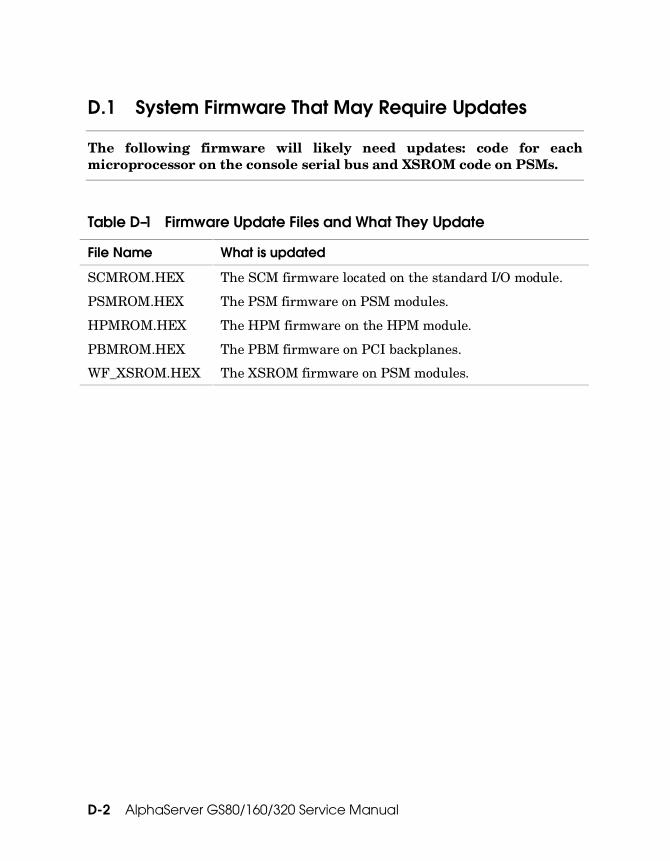
D-2 AlphaServer GS80/160/320 Service Manual
D.1 System Firmware That May Require Updates
The following firmware will likely need updates: code for each microprocessor on the console serial bus and XSROM code on PSMs.
Table D–1 Firmware Update Files and What They Update
File Name What is updated
SCMROM.HEX The SCM firmware located on the standard I/O module.
PSMROM.HEX The PSM firmware on PSM modules.
HPMROM.HEX The HPM firmware on the HPM module.
PBMROM.HEX The PBM firmware on PCI backplanes.
WF_XSROM.HEX The XSROM firmware on PSM modules.

Firmware Updates D-3
Table D–1 lists AlphaServer GS80/160/320 update firmware files. When running an update, each file is written into a flash ROM on the piece of hardware targeted by the update command.
Most recent files are found on the latest AlphaServer firmware CD or can be obtained from the following Web site:
http://ftp.digital.com/pub/digital/Alpha/firmware/
For a full description of LFU, see Appendix B of the Compaq AlphaServer GS80/160/320 Firmware Reference Manual.

D-4 AlphaServer GS80/160/320 Service Manual
D.2 Preparations for Firmware Updates
On any given system some preparations may be needed to perform system firmware updates.
D.2.1 Partitions
LFU cannot update a partitioned system. Operating systems must be shut down and if the system is hardware partitioned, an SCM command must be issued to remove them. LFU must be run from the master SCM.
Example D– 1 Removing Partitions
SCM_E0> show nvram � . . . HP_COUNT 3 | HP_QBB_MASK0 3 | HP_QBB_MASK1 4 | � HP_QBB_MASK2 8 | HP_QBB_MASK3 0 HP_QBB_MASK4 0 HP_QBB_MASK5 0 HP_QBB_MASK6 0 HP_QBB_MASK7 0 . . . SCM_E0> [Shut down the operating system in each partition] � SCM_E0> SCM_E0> set hp_count 0 � SCM_E0> SCM_E0> SCM_E0> SCM_E0> SCM_E0> quit

Firmware Updates D-5
LFU must be run in a nonpartitioned environment for the following reasons:
1. LFU cannot communicate directly over the CSB and relies on the SCM to transfer files to the microprocessors on the CSB.
2. LFU transfers files to SCMs, both master and slaves, through PCI space to shared RAM. If the system remains partitioned, knowledge of PCI space is known only on a per partition basis.
If a system is partitioned, it must be reconfigured to run LFU. Example D–1 shows the necessary preparations.
� The show nvram command is executed. Example D–1 shows that this system has three hard partitions.
� The system has three hard partitions defined by the environment variables hp_count, hp_qbb_mask0, hp_qbb_mask1, and hp_qbb_mask2.
� The operating systems in each partition have to be shut down.
� Use the SCM set hp_count 0 command to remove the hard partitions. Setting the hp_count to zero disables partitions so the QBB masks are ignored. Redefining the partitions, when the update is complete, is a simple matter of setting the hp_count back to the number of hard partitions.

D-6 AlphaServer GS80/160/320 Service Manual
D.2.2 Hardware Connections
Use of the SCM update command requires a physical connection to the master SCM. If the system management console is used, you need not connect a laptop but can execute update procedures from there.
Figure D– 1 Connecting a Laptop to the Local Terminal Port

Firmware Updates D-7
Figure D–1 shows the connection made between a laptop and the local terminal port on the standard I/O module in the master PCI box. On this module resides the CSB master SCM. Use two nine pin to MMJ connectors (H8571-J), one for the COM1 port and the other for the laptop, and connect the two using a DEC connect office cable.
NOTE: If you are using the system management console (SMC) to make firmware updates, you need not connect your laptop since the SMC is already connected to the master PCI box.

D-8 AlphaServer GS80/160/320 Service Manual
D.2.3 Laptop Operating System Preparation
When the SCM update command is used, firmware update files are downloaded from some source into the master SCM module. Certain COM1 port settings are required.
Example D– 2 COM1 Port Settings for Windows NT 4.0
1. From Start go to Settings and select Control Panel.
2. From Control Panel select Ports.
3. From Ports select COM1 and Settings.
4. At Settings for COM1, set: Baud rate: 9600 Data Bits: 8 Parity: None Stop Bits: 1 Flow Control: Xon/Xoff then select Advanced
5. At Advanced Setting for COM1, disable (uncheck) FIFO Enable and leave all other settings at the default.
6. Click OK back through the dialog boxes, shutdown, reboot and verify that these settings stuck.

Firmware Updates D-9
Example D– 3 COM1 Port Settings for Windows 2000
1. From Start go to Settings and select Control Panel.
2. From Control Panel select System.
3. From System select the Hardware tab.
4. From the Hardware tab select Device Manager.
5. Expand Ports and select Communications Port (COM1).
6. At the Communications Port (COM1) Properties, set: Bits per second: 57600 Data Bits: 8 Parity: None Stop Bits: 1 Flow Control: Xon/Xoff then select Advanced.
7. At the Advanced Settings for COM1, deselect Use FIFO buffers.
8. Click OK back through the dialog boxes. There is no need to reboot.
Example D– 4 COM1 Port Settings for Windows 95
1. From Start go to Settings and select Control Panel.
2. From Control Panel select System.
3. From System Properties select the Hardware Manager tab.
4. Expand Ports and select Communications Port (COM1).
5. At the Communications Port (COM1) Properties, select the Port Settings tab and set: Bits per second: 57600 Data Bits: 8 Parity: None Stop Bits: 1 Flow Control: Xon/Xoff then select Advanced.
6. At the Advanced Port Settings, deselect Use FIFO buffers.
7. Click OK back through the dialog boxes. There is no need to reboot.

D-10 AlphaServer GS80/160/320 Service Manual
D.2.4 Terminal Emulator Settings
When the SCM update command is used, firmware update files are downloaded from a host PC COM1 port to the master SCM local port on the standard I/O module. Certain terminal emulator settings are required.
Example D– 5 KEAterm V5.1 Session for PC or Laptop COM1 Port
1. From Start go to Programs and select KEA!VT and then KEA!
2. At the Session Template select Serial – click Next>.
3. At Connection Type select Serial – click Next>.
4. At Connection select the General tab and set Port name: COM1 Speed: 9600 – click Next>.
5. Then select the Options tab and in the Flow Control section set: Data to host: Xon/Xoff Data from host: Xon/Xoff
6. Then select the Rate Limiting tab and deselect (uncheck) both Limit data rate during Paste and ASCII send and Limit data rate during keyboard input and reporting – click Next>.
7. At Terminal Type select VT400-8bit – click Next>.
8. At File Transfer Protocol select ASCII – click Next>.
9. Click Finish to open a KEA terminal session.
10. From the Options menu select History. Select the VT Advanced tab Select (check) Auto wrap lines Click OK.
11. From the File menu select Save Session as Set Name as something like WF_SCM Click Save.

Firmware Updates D-11
Example D– 6 PowerTerm 525 Settings
1. From Start go to Programs and select PowerTerm.
2. At Connect set: Session type COM Terminal type VT420-8 Baud Rate 9600 Stop Bits 1 Port Number 1 Parity 8/none Flow Control Xon/Xoff – click Connect
3. From the Communications menu, select File Transfer Setup and set: Host Data Type 8-Bit (DOS – Ascii) PC Data Type 8-Bit (DOS – Ascii) click OK
Opening Previously Created Sessions
If the COM1 port KEA session was previously created, open it and from the Open Session popup, select the name you selected in step 11 of the KEA setup.
If the a PowerTerm 525 session was previously created, open it selecting the session connecting to the standard I/O module on the GS80/160/320 system.
Changing Baud Rates
Once a connection is established between the laptop/PC and the SCM you may wish to improve performance by increasing the baud rate of both the standard I/O terminal port and the COM1 port on the laptop/PC.
First at the SCM prompt:
SCM_E0> set baud 57600
Then make the appropriate KEAterm or PowerTerm changes to set the connection speed to 57600 also.
Be sure to return the baud rate to 9600 after you’ve completed your session.

D-12 AlphaServer GS80/160/320 Service Manual
D.3 Firmware Updates
Two firmware update modes are available on GS80/160/320 systems: one using LFU and the other using the SCM update command. Note that if a microprocessor’s firmware is corrupt and it is in fail-safe loader mode, the SCM update command must be used to load healthy firmware.
D.3.1 Using LFU
LFU is a standard, fairly automatic, method used to update firmware. Currently (August, 2000), LFU must be run from the master SCM in systems that are not hardware partitioned. LFU updates micros of the same type in parallel and is faster than SCM update. LFU cannot be used when a microprocessor is in FSL mode.
Example D– 7 Running LFU
Place the firmware CD-ROM in the master PCI box CD-ROM device. � P00>>> boot dqb0 (boot dqb0.0.0.15.12) block 0 of dqb0.0.0.15.12 is a valid boot block reading 1082 blocks from dqb0.0.0.15.12 bootstrap code read in base = 3dc000, image_start = 0, image_bytes = 87400 initializing HWRPB at 2000 initializing page table at 3ffec000 initializing machine state setting affinity to the primary CPU jumping to bootstrap code ----------------------------------------------------------------------------- [Appropriate header and text identifying the CD and its contents.] ----------------------------------------------------------------------------- Hit <RETURN> to scroll text, or <CTRL/C> to skip text. The default bootfile for this platform is [GS320]gs320_v56.exe (LFU)
Hit <RETURN> at the prompt to use the default bootfile � Bootfile:

Firmware Updates D-13
***** Loadable Firmware Update Utility ***** -------------------------------------------------------------------- Function Description -------------------------------------------------------------------- Display Displays the system’s configuration table. Exit Done exit LFU (reset). List Lists the device, revision, firmware name, and update
revision. Readme Lists important release information. Update Replaces current firmware with loadable data image. Verify Compares loadable and hardware images. ? or Help Scrolls this function table. --------------------------------------------------------------------
Example D–7 shows an update of all the firmware associated with GS80/160/320 systems.
� Insert the GS80/160/320 firmware CD-ROM into the CD-ROM device in the master PCI box.
� Boot the CD-ROM and follow the instructions to get the LFU banner to display.

D-14 AlphaServer GS80/160/320 Service Manual
Example D– 7 Running LFU (Continued)
UPD> list � Device Current Revision Filename Update Revision SRM V5.7-3525 srm_fw V5.7-3533 micro V5.2(03.06/01:09) micro_fw V5.4(03.24/01:21) UPD> update micro � Confirm update on: micro [Y/(N)]y � WARNING: updates may take several minutes to complete for each device. DO NOT ABORT! micro Updating to V5.4(03.24/01:21) � Updating SCM nodes E0,E1 � Update Cmd processed Transferring hex file...........Flash ON........Flash ON........Flash ON........ Flash ON....$<XFE> Initializing shared ram | Modified SR init-SCM previously ON | Shared RAM Initialized | Master SCM | Testing SCM EEPROM - Passed | Initializing EVs | SCM Selftest Passed | Polling CSB............................ | OCP will be inactive for first 12 seconds after micro reset | . | . | . |

Firmware Updates D-15
� The LFU list command shows the current revision and update revision of
the SCM firmware. Note that LFU does not list each firmware file associated with each micro that is listed in Table D–1. Instead, it lumps them into one file, micro_fw. When using LFU, all microprocessor firmware is updated each time LFU is run.
� The LFU update command is issued.
� Confirmation of the update is required.
� SCM update and micro update begin.
� SCMs are found at nodes E0 and E1. Updating the master and slave SCM commences in parallel and completes.
Once the new SCM code is written into flash, the master SCM polls and maps the entire CSB prior to LFU continuing and updating the other micros in the system.

D-16 AlphaServer GS80/160/320 Service Manual
Example D– 7 Running LFU (Continued)
Updating XSROM node 30,31,32,33 ¡ Update Cmd processed Transferring hex file.................. ~I~ Flashing node 30 (please wait) ~I~ Flashing node 31 (please wait) ~I~ Flashing node 32 (please wait) ~I~ Flashing node 33 (please wait) CSB download of .Hex file complete Updating HPM node 40 ¢ Update Cmd procesed Transferring hex file.................. CSB download of .Hex file complete
Updating PSM node 30,31,32,33 11 Update Cmd processed Transferring hex file........................ CSB download of .Hex file complete Updating PBM nodes 10,11 12 Update Cmd processed Transferring hex file.................. CSB download of .Hex file complete The Master SCM will now finalize the micro flash updates to each CSB Node. After the update is complete, you will be returned to the SCM CLI last flash packet to 30 | last flash packet to 31 | last flash packet to 32 | 13 last flash packet to 33 | last flash packet to 10 | last flash packet to 11 | Please wait. System will complete power off in roughly 10 seconds Local escape sequence verified SCM_E0>

Firmware Updates D-17
¡ Once the SCM completes the map of the CSB, LFU provides the updated XSROM code to the SCM through shared RAM. The SCM sends the code to the PSM in each QBB. After the PSM receives the code, it then blasts it into the XSROM flash ROM.
¢ LFU provides code for the HPM to the SCM. The SCM downloads this code over the CSB to the HPM in the H-switch.
11 LFU then provides code for the PSMs to the SCM. The SCM downloads this code over the CSB to RAM space in each PSM. If there were more than one QBB on the system the download to each is done in parallel. Note that the code is not yet written into the PSM’s flash ROM from which it runs.
12 Next LFU provides new code for the PBMs to the SCM. The SCM downloads this code over the CSB to RAM space controlled by PBMs on each PCI backplane at CSB nodes 10 and 11. Again note that the code is not yet written into the PBM’s flash ROM from which it runs.
13 When the LFU finishes updating all the micros, LFU sends a last packet to the SCM which causes the SCM to issue commands to each PSM and each PBM to transfer the new firmware code each has stored in its RAM to their respective flash ROMs.

D-18 AlphaServer GS80/160/320 Service Manual
D.3.2 Using the SCM Update Command
The SCM update command may be used from the master SCM to update specific firmware in the system. The firmware file must be downloaded to the master SCM local terminal port. If a microprocessor is in FSL mode because its firmware is corrupt, this command must be used.
Example D– 8 Using the Update Command
SCM_E0> power off –par 0 �
SCM_E0> sho csb � CSB Type Firmware Revision FSL Revision Power State 10 PBM T04.6 (11.03/01:09) T4.2 (09.08) ON 11 PBM T04.6 (11.03/01:09) T4.2 (09.08) ON 12 PBM T04.6 (11.03/01:09) T4.2 (09.08) ON 30 PSM T04.5 (11.03/01:07) T4.2 (09.08) OFF SrvSw: SERVICE
30 XSROM T04.6 (11.03/02:19) � c0 CPU0/SROM T4.2-7 OFF c1 CPU1/SROM T4.2-7 OFF c2 CPU2/SROM T4.2-7 OFF c3 CPU3/SROM T4.2-7 OFF c0 IOR0 OFF c1 IOR1 OFF c2 IOR2 OFF c3 IOR3 OFF 31 PSM T04.6 (11.03/01:07) T4.2 (09.08) ON SrvSw: NORMAL 31 XSROM T04.6 (11.03/02:19) c4 CPU0/SROM T4.2-7 On c5 CPU1/SROM T4.2-7 On c6 CPU2/SROM T4.2-7 On c7 CPU3/SROM T4.2-7 On c4 IOR0 On c5 IOR1 On 40 HPM T04.6 (11.03/01:11) T4.2 (09.08) ON e0 SCM MASTER T04.6 (11.03/01:13) T4.2 (09.08) ON e1 SCM SLAVE T04.6 (11.03/01:13) T4.2 (09.08) ON Ineligible e2 SCM SLAVE T04.6 (11.03/01:13) T4.2 (09.08) ON Ineligible e6 SCM SLAVE T04.6 (11.03/01:13) T4.2 (09.08) ON Ineligible
SCM_E0> update –csb 30 � Initiate HEX file transfer from host (press ESC-ESC to abort):

Firmware Updates D-19
Conditions of Note When Using This Update Method
A master and slave SCM may be updated using this method but a master SCM cannot update a slave. To update either a master or slave the device downloading the SCMROM.HEX file must be connected physically to the target standard I/O local port.
When updating the XSROM code, the entire system may be up and running operating systems.
A consequence of updates to any of the microprocessors (with the exception of the XSROM on the PSM) is that they immediately reset once the new firmware downloads. Therefore, you want to minimize the effect of the reset on the rest of the system by isolating the QBB/partition.
When updating a PSM, the partition in which the PSM resides should be powered off.
When updating a PBM, the PCI I/O subsystem in which the PBM resides must be removed from the resources available to an operating system.
When updating an HPM, the system should be powered off.
Example D–8 shows a sample master SCM update of a PSM module in QBB0.
� The target device to be updated must be powered off. In this example the PSM is assumed to be in partition 0. It is also assumed that partition 0 has been appropriately powered off using the SRM power off command prior to the SCM power off – par 0 command.
� The show csb command shows the target off and the PSM switch in the Service position.

D-20 AlphaServer GS80/160/320 Service Manual
Example D– 8 Using the Update Command (Continued)
SCM_E0> update –csb 30 � Initiate HEX file transfer from host (press ESC-ESC to abort): Initiate transfer of the file PSMROM.HEX to the COM1 port �
For KEAterm From the Tools menu goto File Transfer and select Send to Host Change the Files of type: to All Files (*.*) Browse for and select the file PSMROM.HEX. Click on OK.
For PowerTerm 525 From the Communication menu select Send File… At Send File select the Ascii tab Browse for and select the file PSMROM.HEX by clicking on the browse button next to the File Name input box. Click OK. :02000002C0003C Transferring hex file . . . . . . . . ~I~ Flashing node 30 (please wait) CSB download of .HEX file complete
Flash Update complete. � CSB Node 30 connection lost CSB Node 30 connection added SCM_E0>

Firmware Updates D-21
Example D–8 shows a sample master SCM update of a PSM module in QBB0.
� The SCM update command is issued. Note that it is possible to update several PSMs at a time with the command: update –csb 30,31,32…
� Be sure that the terminal emulator is configured properly for the file transfer. See Section D.2.4. The PSMROM.HEX file is transferred to the COM1 port.
� The flash update completes.

D-22 AlphaServer GS80/160/320 Service Manual
D.4 Dealing with a COM1 Port Jam
Occasionally, when the COM1 is under software flow control, as it is when you use a terminal emulator to communicate through it, COM1 can jam. If this occurs, your emulator will have no control of the system or partition to which it is attached. You can clear the jam by clearing the communications link in the emulator and using the SCM clear port command to un-jam COM1.
Example D– 9 Clearing a COM1 Port Jam At your KEAterm emulator From the KEAterm session toolbar, pull down the Connections menu and select CLEAR COMM � P00>>> <esc><esc>scm � SCM_E0> clear port � SCM_E0> quit � P00>>> �

Firmware Updates D-23
In the event that your emulator appears hung, it is possible that the COM1 port is jammed. The procedure presented in Example D–9 will clear the jam. Of course, communications could have failed for some other reason that you will have to investigate if this procedure does not work.
� From the emulator’s perspective, it has received an XOFF. Setting the CLEAR COMM sets XON and the emulator will again transmit the characters you type.
� The escape sequence gets you to the SCM.
� The clear port command clears the COM1 port enabling it to receive characters from the emulator.
� The quit command takes you out of the SCM console monitor and will bring you back to whatever you were running before the jam occurred.
� You are brought back either to the SRM console to the operating system. You may have to hit carriage return before the prompt comes back.


Glossary-1
Glossary
AC off state One of the system power states in which all power is re-moved from the system. See also Hot-swap, Cold-swap,and Warm-swap states.
Clock splittermodule
Module that provides the system with multiple copies ofthe system and I/O reference clocks.
Cold-swap state One of the system power states in which AC power andVaux are present in the system, but power is removedfrom the area being serviced. See also AC off, Hot-swap,and Warm-swap states.
Console serial bus See CSB.
CSB Console serial bus; a bus that runs throughout the sys-tem and connects microprocessors used for monitoringand control of the system. The CSB is managed by thesystem control manager (SCM).
Directory module Module that monitors memory requests made to theQBB on which it resides and is used to maintain cachecoherency. If the data in its memory is not the most cur-rent, the directory forwards the request to the CPU thatowns the most current data.
Distribution board The interface between the global ports in a system withonly two QBBs.
Expander cabinet A cabinet that holds additional storage shelves and PCIboxes.
Galaxy OpenVMS software that is used to manage softpartitions.
Global port Module that provides the interface between QBBsthrough the hierarchical switch or distribution board.

Glossary-2
Hard partition A partition consisting of one or more QBBs and sharingno resources with any other parition. Hard partitionsare defined by using the SCM command language. Seealso Partition.
Hierarchicalswitch
See H-switch.
Hose A logical PCI bus; or the cable between a QBB and a PCIbox.
Hot-swap state A state of the system that allows swapping of certaincomponents while power is present in the system. Seealso Cold-swap, Warm-swap, and AC off states.
HPM H-switch power manager; controls power and monitorspower and temperature inside the H-switch housing. TheHPM reports status to the system control manager. TheSCM can make requests of the H-switch power manager.
H-switch Hierarchical switch; a high-speed switch that connectsall QBBs through their global ports. See also Distribu-tion board.
H-switch powermanager
See HPM.
I/O port Backplane logic that provides an interface to the localI/O riser module.
I/O riser module See Local I/O riser module and Remote I/O riser module.
Instance An operating system running in a partition.
LFU Loadable Firmware Update Utility; firmware used toupdate the SRM console firmware and I/O device firm-ware.
Loadable FirmwareUpdate Utility
See LFU.
Local I/O risermodule
A module on the QBB that provides the interface be-tween the QBB and the remote I/O riser on the PCI.
Local primary CPU The CPU chosen to be the primary CPU in a QBB.
Local testing Testing confined to the QBB on which the CPU doing thetesting resides.

Glossary-3
Memory directorymodule
See Directory module.
OCP Operator control panel; used by the operator to controlthe system. It has a keyswitch, display screen, indica-tors, and buttons. The keyswitch is used to power thesystem up or down or to secure it from remote access.The screen displays messages during booting. Indicatorsshow system state. The buttons reset or halt the system.
Partition A subset of a system’s CPUs, memory, and I/O subsys-tem with a standard I/O module that runs its own copy(instance) of an operating system. See also Hard parti-tion, Soft partition.
PBM PCI backplane manager; monitors and manages the en-vironment and components in the PCI box in which itresides. The SCM can make requests of the PCI back-plane manager.
PCI backplanemanager
See PBM.
PCI boxes Enclosures that provide 14 PCI slots (four PCI buses,two four-slot buses and two three-slot buses).
System primary PCI box
A PCI box that contains a standard I/O module, whosesystem control manager (SCM) controls the entire sys-tem. The system primary PCI box may also be a masterPCI box.
Master PCI box A PCI box that contains a standard I/O module, whoseSRM is the console for the system or partition to which itis connected.
Secondary PCI box
A PCI box that contains a standard I/O module andwhich serves as a backup to the primary PCI box for thesystem or the master PCI box for a partition.
Expansion PCI box
A PCI box that provides 14 PCI slots but contains nostandard I/O module.
Power cabinet Cabinet in the GS160/320 systems that provides powerfor the system cabinets and houses PCI boxes and stor-age shelves.

Glossary-4
Power systemmanager
See PSM.
PSM Power system manager; a module in each QBB thatmonitors CPUs, voltages, temperatures, and fan speedsin the QBB and then reports this information to the sys-tem control manager (SCM). The SCM can makerequests of the power system manager.
QBB Quad building block; the basic building block of the sys-tem. The QBB backplane provides a crossbar switch andconnectors for one to four processor modules, one to fourmemory modules, power converters, a power systemmanager, a memory directory module, a clock splittermodule, a global port, and up to two local I/O risers.
QBB, hard Number that indicates the physical location of a QBB ina system.
QBB, soft Number that indicates a QBB as reported by the firm-ware.
Rack cabinet The GS80 cabinet configured as a complete system thatholds up to two system drawers, each of which has oneQBB.
Remote I/O risermodule
A module on the PCI that provides the interface betweenthe PCI and the QBB through the local I/O riser.
Remote testing Testing run by the system primary CPU on a QBB otherthan the QBB in which it resides.
SCM System control manager; a microprocessor on a standardI/O module that monitors and controls the system statethrough the CSB. The SCM provides a command lan-guage for an operator and allows for remote manage-ment of the system. The SCM controls power-up, systemconfiguration, system monitoring, power-on and power-off, and firmware updates. A second standard I/O mod-ule with another SCM provides a backup control system.
SIO Standard I/O module. Module in a PCI box that has I/Oports, the system control manager (SCM) microprocessor,and SRM console firmware.

Glossary-5
SMC System management console; a PC, software, and termi-nal server used to manage the system.
Soft partition A collection of resources within a hard partition. Re-sources can be allocated among soft partitions. In con-trast to hard partitions, a QBB can provide resources tomore than one soft partition. Soft partitions are definedby using the SRM console. Also referred to as logicalpartitions.
SRM console Firmware on the standard I/O module that provides acommand-line interface for operator control of the sys-tem or of a partition. The SRM console is responsible forbooting the operating system and passing system con-figuration data, discovered during power-up, to it.
Standard I/Omodule
See SIO.
System box The GS160 and GS320 enclosure for two quad buildingblocks (QBBs).
System cabinet The GS160 and GS320 cabinet that holds up to twosystem boxes, each of which has two QBBs.
System controlmanager
See SCM.
System drawer The GS80 enclosure for one quad building block (QBB).
Systemmanagementconsole
See SMC.
System primaryCPU
The CPU chosen out of all CPUs in all QBBs to be theprimary CPU of the system.
Vaux Low voltage power present in the system whenever thepower cord is plugged in and the circuit breakers are on.Vaux powers the console serial bus and all its microproc-essors, allowing the system control manager to power up,monitor, and control the system.

Glossary-6
Warm-swap state One of the power states of the system in which power isremoved from a specified QBB for service while othersegments of the system remain fully powered. See alsoHot-swap, Cold-swap, and AC off states.

Index- 1
Index
A AC input box
GS160/320 (three phase), 1-97 GS80 (single phase), 1-107 removal and replacement (system
box), 5-35 AC-off state
defined, 4-10 getting into, 4-15
Addressing, 1-20 Auxiliary power module, 1-64
removal and replacement (GS160/320), 4-25
removal and replacement (GS80), 6-9
B Backplane removal and replacement
GS80, 6-21 PCI, 5-13 system box, 4-39
Backplanes PCI, 1-83 system box, 1-5 system drawer, 1-11
Battery (standard I/O module) removal and replacement, 5-25
Blower removal and replacement
(GS160/320), 4-57 removal and replacement (GS80), 6-
29 Build command (SCM), 3-23 Build eeprom command (SCM), 3-23
C Cabling
expander cabinet, A-8–A-15 GS80 cabinet, A-16–A-19 power cabinet, A-2–A-7
Cache coherency data storage, B-18–B-23 storage element use and flow, B-37 terminology, B-2
Cache state command interaction, B-7 commands affecting, B-4–B-6 defined, B-3 transition diagram, B-7
CD-ROM removal and replacement, 5-17
Clear environment variable command (SRM), 3-30
Clear error command (SCM), 3-22 Clear port command (SCM), D-23 Clock module
description, 1-51 removal and replacement, 4-51
Clock splitter module description, 1-55 removal and replacement
(GS160/320), 4-31 removal and replacement (GS80), 6-
15 Cold-swap state
defined, 4-10 getting into, 4-14
Color codes module slots, 4-20, 6-3 power, 1-95, 4-19
COM1, 1-87

Index- 2
COM1 port unjam, D-23 COM2, 1-87 Compaq Analyze, 3-88–3-109 Console serial bus
function, 1-22 module removal and replacement
(distribution box housing), 4-45 module removal and replacement
(GS80), 6-27 module removal and replacement (H-
switch housing), 4-55 Console serial bus node ID module, 1-90
removal and replacement, 5-7 Control panel, 1-12, 2-2 CPU chip, 1-45 CPU module, 1-43
removal and replacement (GS160/320), 4-27
removal and replacement (GS80), 6-11
CSB. See Console serial bus Csr command (SRM), 3-42, 3-43
D Diagnostic environment
setting of, 3-46 Diagnostics
booting the SRM for loadable diagnostics, 3-63
running standard I/O diagnostics, 3-62–3-69
running using the SCM console, 3-24–3-29
running using the SRM console, 3-46–3-71
DIMM removal and replacement, 4-37
DIMMs on directory, 1-71 on memory, 1-47
Directory module description, 1-71 function, 1-17 removal and replacement
(GS160/320), 4-25 removal and replacement (GS80), 6-9
Distribution board, 1-74 removal and replacement
(GS160/320), 4-41 removal and replacement (GS80), 6-
25 DTag, 1-15 Dual-output clock module
description, 1-53 removal and replacement (GS160), 4-
43 removal and replacement (GS80), 6-
23 DVD
removal and replacement, 5-17
E EEPROM
build, 3-23 Error detection, 3-86 Exer command (SRM), 3-54–3-57 Expander cabinet
cabling, A-8–A-15
F Fail-safe loader, 3-85 Fakedisk command (SRM), 3-60 Fault pushbutton, 1-13, 2-3 Firmware
corrupt, 3-85 updating using LFU, D-12–D-17 updating using the update command,
D-18–D-21 FIS disk
removal and replacement, 5-19 Fluorescent display, 1-13, 2-3 Fptest command (SRM), 3-59 FRU list, 4-4–4-9
G Global port
function, 1-17 module description, 1-72 removal and replacement, 4-35
GS160/320 backplane, 1-5

Index- 3
module locations, 4-17 power subsystem, 1-94–1-103 system box, 1-7
GS80 backplane, 1-11 cabinet cabling, A-16–A-19 description, 1-9 module locations, 6-3 power subsystem, 1-104–1-111
H Halt LED, 1-13, 2-3 Halt pushbutton, 1-13, 2-3 Hierarchical switch
function, 1-18 module, 1-76 removal and replacement, 4-47
Hot-swap state defined, 4-10 getting into, 4-12
HPM. See H-switch power manager module
H-switch. See Hierarchical switch H-switch power manager module
description, 1-79 function, 1-33 removal and replacement, 4-53
H-switch power module description, 1-66 removal and replacement, 4-49
I I/O riser module (local)
function/description (drawer), 1-60 function/description (system box), 1-
58 removal and replacement (drawer), 6-
17 removal and replacement (system
box), 4-33 I/O riser module (remote)
function/description, 1-89 removal and replacement, 5-9
I/O subsystem, 1-80–1-93 I/O transition module
removal and replacement (GS80), 6-19
I2C buses on CPU, 1-43 on H-switch/HPM, 1-33 on local I/O riser, 1-59 on PCI backplane/PBM, 1-31 on PSM/QBB, 1-29 on remote I/O riser, 1-89
Info command (SRM), 3-44
J Jumpers
on HPM, 1-79 on PCI backplane, 1-83 on standard I/O, 1-87
K Kill command (SRM), 3-50 Kill_diags command (SRM), 3-49
L LEDs
on 48V power supply, 1-99, 1-109 on AC input box (GS160/320), 1-97 on AC input box (GS80), 1-107 on auxiliary power, 1-65 on console serial bus node ID, 1-91 on CPU, 1-43 on HPM, 1-79 on H-switch clock, 1-51 on H-switch power, 1-67 on local I/O riser, 1-59 on main power, 1-63 on OCP, 1-13, 2-3 on PCI box ID, 1-91 on PCI power supply, 1-113 troubleshooting with, 3-72–3-75
LFU running of, D-12–D-17
Local I/O riser removal and replacement (drawer), 6-
17 removal and replacement (system
box), 4-33

Index- 4
Local switch, 1-15
M Main power module, 1-62
removal and replacement (GS160/320), 4-25
removal and replacement (GS80), 6-9 Master clock module, 1-51
removal and replacement, 4-51 Master phase lock loop, 1-57 Memexer command (SRM), 3-58 Memory module, 1-46
removal and replacement (GS160/320), 4-25
removal and replacement (GS80), 6-9 Mini link, 1-59 MMPL description, 1-57 Modem port, 1-87 Module access
GS160/320 system box, 4-23 GS80 bottom drawer, 6-7 GS80 top/single drawer, 6-5
Module locations GS160/320, 4-17 GS80, 6-3
Modules auxiliary power description, 1-64 clock splitter description, 1-55 console serial bus node ID -
description, 1-90 CPU description, 1-43 directory description, 1-71 directory function, 1-17 distribution board description, 1-74 dual-output clock description, 1-53 global port description, 1-72 global port function, 1-17 hierarchical switch description, 1-76 H-switch module description, 1-66 I/O riser (local-drawer) description, 1-
60 I/O riser (local-system box)
description, 1-58 I/O riser (reomte) description, 1-89 main power description, 1-62 master clock description, 1-51
memory description, 1-46 PSM description, 1-49 short-circuit protection description, 1-
69 standard I/O cable interface
description, 1-92 standard I/O module description, 1-87
N Nettest command (SRM), 3-61 Node ID switch, 1-91
O OCP, 1-12, 2-2
removal and replacement (GS160/320), 5-27
removal and replacement (GS80), 6-31
Off switch position, 1-13, 2-3 On switch position, 1-13 Operator control panel, 1-12, 2-2
removal and replacement (GS160/320), 5-27
removal and replacement (GS80), 6-31
P Part numbers, 4-4–4-9 Partitions, 1-34–1-41
hard, 1-35 mixed, 1-39 servicing, 1-41 soft, 1-37
PBM, 1-31 PCI backplane, 1-83
removal and replacement, 5-13 PCI backplane manager, 1-31 PCI box (master), 1-80–1-93 PCI fan
removal and replacement, 5-15 PCI node ID switch, 1-91 PCI option module
removal and replacement, 5-11 PCI power supply
description, 1-112

Index- 5
removal and replacement, 5-23 PCI slots, 1-84 Power
color codes, 4-19 troubleshooting, 3-2
Power cabinet cabling, A-2–A-7
Power distribution, 1-103 Power LED, 1-13, 2-3 Power modules
auxiliary, 1-64 H-switch, 1-66 main, 1-63
Power off command (SRM), 3-31 Power subrack
GS160/320, 1-101 GS80, 1-111 removal and replacement
(GS160/320), 5-33 removal and replacement (GS80), 6-
35 Power supplies
GS160/320 48 VDC described, 1-99 GS80 48 VDC described, 1-109 PCI supply described, 1-113
Power supply removal and replacement, 5-31, 6-33
Power system description GS160/320, 1-95 GS80, 1-105
Power system manager functional description, 1-29 module description, 1-49 module removal and replacement
(GS160/320), 4-29 module removal and replacement
(GS80), 6-13 Power-down states, 4-10 Power-up
error messages, 3-7 Power-up display
OCP keyswitch On, 2-22–2-33 power applied, 2-18
Power-up test flow init. and phase 0, 2-6 phase 1, 2-12
phases 2, 3, and 4, 2-16 Primary switch, 1-14 Ps command (SRM), 3-51 PSM
functional description, 1-29 module description, 1-49 removal and replacement
(GS160/320), 4-29 removal and replacement (GS80), 6-
13
Q QBB
defined, 1-5 orientation, 4-17
QBB IDs hard, 2-13 soft, 2-13
Quad switch, 1-15 Quod building block, 1-5
R Rack system, 1-11 Remote I/O riser module
description, 1-89 removal and replacement, 5-9
Reset pushbutton, 1-13, 2-3
S Safety features, 4-3 SCM. See System control manager SCM command
build eeprom, 3-23 build fru, 3-23 clear error, 3-22 clear port, D-23 list of, 3-11 set environment variables, 3-15 show csb, 3-16 show fru, 3-21 show nvram, 3-14 show status, 3-19 show system, 3-17 update, D-18–D-21

Index- 6
SCP. See Short-circuit protection module
SCSI (FIS) disk removal and replacement, 5-19
Secondary switch, 1-16 Secure LED, 1-13, 2-3 Secure switch position, 1-13 Service switch, 1-49 Set environment variable command
SCM, 3-15 SRM, 3-30
Set sys_serial_num (SRM), 3-41 Short-circuit protection module, 1-69 Show configuration command (SRM), 3-
33 Show csb command (SCM), 3-16 Show environment variable command
(SRM), 3-30 show fru command (SCM), 3-21 Show fru commnad (SRM), 3-38 Show nvram command (SCM), 3-14 Show status command (SCM), 3-19 Show status command (SRM), 3-49 Show system command (SCM), 3-17 SMC. See System management console SRM console command
clear environment variables, 3-30 crash, 3-71 csr, 3-42, 3-43 info, 3-44 power off, 3-31 set environment variable, 3-30 set sys_serial_num, 3-41 show configuration, 3-33 show environment variables, 3-30 show fru, 3-38 show_status, 3-49 test, 3-52 wf power off cpu, 3-32 wf power on cpu, 3-32 wf show cpu, 3-44
SRM console diagnostic acer_8042_diag, 3-66 acer_bridge_diag, 3-64 acer_io_diag, 3-65 bq4285_diag, 3-68
exer, 3-54–3-57 fakedisk, 3-60 fptest, 3-59 isa_misc_diag, 3-69 kill, 3-50 kill_diags, 3-49 memexer, 3-58 nettest, 3-61 ps, 3-51 sisp1020_diag, 3-67 sys_exer, 3-48 test, 3-52
SROM error number detail, C-4–C-10 error reports, 2-34–2-36 running diagnostics, 3-24–3-29
SROM tests, 2-9 Standard I/O cable interface module
description, 1-92 removal and replacement, 5-21
Standard I/O module description, 1-87 removal and replacement, 5-5
Sys_exer command (SRM), 3-48, 3-53 System architecture, 1-14–1-21 System box, 1-7
module locations, 4-17 removal and replacement, 4-39
System building block, 1-5 System cabinets
GS160/320, 1-3 GS80, 1-9
System control manager, 1-22, 1-27 System management architecture, 1-
22–1-33 System management console, 1-25
T Terminal server
function, 1-25 removal and replacement, 5-29
Test command (SRM), 3-52 Troubleshooting
48V power, 3-3 a diagnostic fault, 3-82 a diagnostic hang, 3-79

Index- 7
a hung system, 3-76–3-83 an operating system hang, 3-77 console, 3-5 CSB bus, 3-3 logic voltages, 3-4 OCP, 3-3 power, 3-2 using LEDs, 3-72–3-75 using the SRM console, 3-30–3-45 Vaux, 3-2
U Update
COM1 settings for Windows 2000, D-9
COM1 settings for Windows 95, D-9 COM1 settings for Windows NT, D-8 connecting a laptop to the local
terminal port, D-7 hardware and software preparations,
D-4–D-11 KEAterm settings, D-10 partitions, D-5 PowerTerm settings, D-11
Update command (SCM), D-18–D-21 Update files, D-3
V Vaux, 1-95, 1-109 Virtual channels, B-9
cache coherency flow, B-10–B-14 I/O space reads, B-12 I/O space writes, B-14 memory space transactions, B-10 ordering rules, B-15–B-17
W Warm-swap state
defined, 4-10 getting into, 4-13
Wf power off cpu command (SRM), 3-32 Wf power on cpu command (SRM), 3-32 Wf show cpu command (SRM), 3-44
X XSROM
error number detail, C-11–C-45 error reports, 2-34–2-36 running diagnostics, 3-24–3-29
XSROM tests phase 0, 2-10–2-11 phase 1, 2-13–2-15 phase 2, 3, and 4, 2-17