
Advances in Radar and Components - Qorvo
29
Advances in Radar and Components September 2021 eBook SPONSORED BY It’s who we are It’s what we do
-
Upload
khangminh22 -
Category
Documents
-
view
2 -
download
0
Transcript of Advances in Radar and Components - Qorvo

Advances in Radar and Components
September 2021
eBook
S P O N S O R E D B YIt’s who we are It’s what we do

Table of Contents
2
3 Introduction Pat Hindle Microwave Journal, Editorial Director
15 How Startups Are Shaping the Automotive Radar of Tomorrow Ivan Koshurinov
19 RF GaN: Trends and Directions Eric Higham Strategy Analytics, Newton, Mass.
Revolutionizing Radar Design with Electronically 4 Reconfigurable GaN Power Amplifiers
8 Design of a mmWave MIMO Radar Tero Kiuru and Henrik Forsten VTT Technical Research Centre of Finland Ltd., Espoo, Finland
Survey of RF GaN Fabs: Successful Commercialization 21 and Global Supply Gary Lerude, Microwave Journal Editor
GW, Multi-Way Combiner Using Corrugated Coaxial 24 Waveguide Filters Xuhao Zhao, Yongjun Hu, Qiang Zhang, Chengwei Yuan and Jiande Zhang National University of Defense Technology, China
Qorvo® Advances Radar Architecture with Reconfigurable 28 Dual-Band GaN Power Amplifier MMICs Qorvo
3
Introduction
Advances in Radar and Components
The global Radar industry was $32.56 billion in 2019, and is estimated to reach $44.35 billion by 2028, growing at a CAGR of 4.7% from 2021 to 2028 according to Allied Market Research. Rise in demand for radar systems in automotive and defense industries, surge in territorial battles, and advancements in radar technology drive the growth of the global radar market according to the company. By application, the air traffic control segment held the largest share in 2019, accounting for more than one-fourth of the global radar market, due to rise in number of airports and air travel in developing countries and the need for efficient airspace management system. However, the ground traffic control segment is estimated to register the highest CAGR of 5.8% during the forecast period, owing to growing opportunities for the airports to integrate advanced taxing guidance systems based on the existing international standards and integrated technologies according to the company.
By end user, Allied Market Research says the military and defense segment held the largest share in 2019, contributing to around two-fifths of the global radar market, due to rise in usage of electronic warfare systems and UAVs and advancement in radar technologies and adaptabilities of new missions, platforms, and surroundings.
The underlying component technology for the RF front ends is a key enabler of better performance and reduced cost. GaN transistor technology has been a game changer for higher power and efficiency but presents challenges in the packaging and heat dissipation areas. This eBook reviews some of the technical improvements in radar components and system configurations.
Several of the articles cover improvements due to GaN technology including a survey of GaN foundries covering the various processes in production and in development and electronically re-configurable GaN amplifiers recently introduced by Qorvo. It also covers a giga-watt, multi-way combiner using corrugated coaxial waveguide filters and a mmWave MIMO radar configuration. The eBook also looks at how startups are revolutionizing automotive radar with new 4D sensors for ADAS and autonomy.
We hope that this eBook provides new insights for your future designs in the area of radar. Thanks to RFMW and Qorvo for sponsoring this eBook so it is free to all of our readers.
Pat Hindle, Microwave Journal Editorial Director
4
Revolutionizing Radar Design with Electronically Reconfigurable GaN Power Amplifiers This post first appeared in Microwave Product Digest.
This article demonstrates for the first time a ro-bust commercially available high power ampli-fier based on multi-band transmitter design us-
ing a patented reconfigurable PA technique demon-strated by Charles Campbell.2,3,4 The reconfigurable PA has single-input and single-output reconfigurable matching networks depending on control bit settings for each band of interest. Each bit setting configures all matching networks for band specific optimum per-formance, enabling the PA to deliver the best system level performance possible in a compact package. This results in an overall reduction in size and weight. This new reconfigurable PA design approach overcomes multiple shortcomings of traditional multi-band trans-mit front-end designs. The most obvious benefit is the elimination of a band select switch at the PA output. This reduces the output loss by 0.8-1.0 dB, giving it a clear advantage over traditional design approaches. If designed with optimum load impedances and smart switch placement, the reconfigurable PA can closely approximate the performance levels achieved by inde-pendently tuned band specific amplifiers.
Modern radar systems are being configured as multi-band radars that can use multiple frequency bands in various environment and target conditions to interpret complex scenes. These systems provide an unprec-edented level of performance and capability to de-tect and track hostile targets. For example, Dual Band
Radar (DBR) is the first radar system in the U.S. Navy fleet capable of simulta-neously operating over two frequency bands (S/X-bands), coordinated by a single resource manager.1 S-band signals are resistant to severe weather and atmospheric attenuation. On the other hand, X-band frequencies are often used for highly resolved target imaging. Most cur-rent power amplifiers (PAs) are not suitable for multi-band radar systems because the desired frequency bands are far apart, and individual PAs are optimized at each target frequency band. There have been several approaches to implement broadband or multi-band characteristics by switching between individual PA MMICs. These approaches use either wideband non-uniform distributed PA (NDPA) covering both bands or dual passband power amplifier designs.
The benefits of a reconfigurable PA are more evident when compared to a wideband amplifier. In wideband amplifier design, load impedance is typically designed to be below optimum load target to achieve high output network bandwidth. Wideband amplifiers have reduced output power and power added efficiency (PAE). There-
5
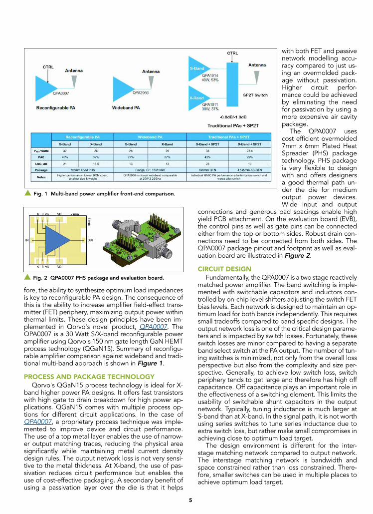
fore, the ability to synthesize optimum load impedances is key to reconfigurable PA design. The consequence of this is the ability to increase amplifier field-effect trans-mitter (FET) periphery, maximizing output power within thermal limits. These design principles have been im-plemented in Qorvo's novel product, QPA0007. The QPA0007 is a 30 Watt S/X-band reconfigurable power amplifier using Qorvo's 150 nm gate length GaN HEMT process technology (QGaN15). Summary of reconfigu-rable amplifier comparison against wideband and tradi-tional multi-band approach is shown in Figure 1.
PROCESS AND PACKAGE TECHNOLOGYQorvo's QGaN15 process technology is ideal for X-
band higher power PA designs. It offers fast transistors with high gate to drain breakdown for high power ap-plications. QGaN15 comes with multiple process op-tions for different circuit applications. In the case of QPA0007, a proprietary process technique was imple-mented to improve device and circuit performance. The use of a top metal layer enables the use of narrow-er output matching traces, reducing the physical area significantly while maintaining metal current density design rules. The output network loss is not very sensi-tive to the metal thickness. At X-band, the use of pas-sivation reduces circuit performance but enables the use of cost-effective packaging. A secondary benefit of using a passivation layer over the die is that it helps
with both FET and passive network modelling accu-racy compared to just us-ing an overmolded pack-age without passivation. Higher circuit perfor-mance could be achieved by eliminating the need for passivation by using a more expensive air cavity package.
The QPA0007 uses cost efficient overmolded 7mm x 6mm Plated Heat Spreader (PHS) package technology. PHS package is very flexible to design with and offers designers a good thermal path un-der the die for medium output power devices. Wide input and output
connections and generous pad spacings enable high yield PCB attachment. On the evaluation board (EVB), the control pins as well as gate pins can be connected either from the top or bottom sides. Robust drain con-nections need to be connected from both sides. The QPA0007 package pinout and footprint as well as eval-uation board are illustrated in Figure 2.
CIRCUIT DESIGNFundamentally, the QPA0007 is a two stage reactively
matched power amplifier. The band switching is imple-mented with switchable capacitors and inductors con-trolled by on-chip level shifters adjusting the switch FET bias levels. Each network is designed to maintain an op-timum load for both bands independently. This requires small tradeoffs compared to band specific designs. The output network loss is one of the critical design parame-ters and is impacted by switch losses. Fortunately, these switch losses are minor compared to having a separate band select switch at the PA output. The number of tun-ing switches is minimized, not only from the overall loss perspective but also from the complexity and size per-spective. Generally, to achieve low switch loss, switch periphery tends to get large and therefore has high off capacitance. Off capacitance plays an important role in the effectiveness of a switching element. This limits the usability of switchable shunt capacitors in the output network. Typically, tuning inductance is much larger at S-band than at X-band. In the signal path, it is not worth using series switches to tune series inductance due to extra switch loss, but rather make small compromises in achieving close to optimum load target.
The design environment is different for the inter-stage matching network compared to output network. The interstage matching network is bandwidth and space constrained rather than loss constrained. There-fore, smaller switches can be used in multiple places to achieve optimum load target.
s Fig. 1 Multi-band power amplifier front-end comparison.
s Fig. 2 QPA0007 PHS package and evaluation board.
6
When comparing output and interstage networks, the input network has the most flexibility due to relaxed loss requirement and having space for more switches and control signals. Both input and interstage networks play a role in amplifier stability performance. Additional loss is added to guarantee stability over wide operating conditions, especially at extremely cold conditions. Tun-ing capacitors and FET terminals have been designed to withstand high voltage standing wave ratio (VSWR) load conditions at maximum input drive to avoid break-down.
Finally, the overall design challenge is to limit S-band small signal gain while not destroying X-band gain. S-band performance is helped by lower frequency FET performance, but limited by the difficulty of extending low-end bandwidth without sacrificing X-band perfor-mance. This is a real challenge even with switchable tun-ing elements.
PERFORMANCEThe QPA0007 is tuned to cover S-band 3.1-3.5 GHz
and X-band 9-11 GHz. Two band switching signals are complementary 0 V and -10 V for S-band and -10 V and 0 V for X-band. The control signals draw or sink 5 mA depending on band selection.
QPA0007 quiescent bias is 700 mA from 26V. Since the input power drives up drain current, output power and PAE are highly independent of quiescent bias cur-rent. Therefore, quiescent bias current can be set based on other performance parameters like small signal gain and switching times.
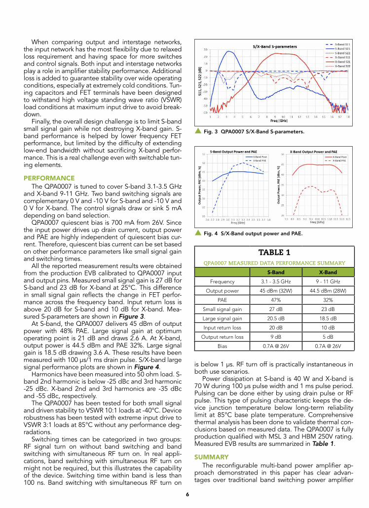
All the reported measurement results were obtained from the production EVB calibrated to QPA0007 input and output pins. Measured small signal gain is 27 dB for S-band and 23 dB for X-band at 25°C. This difference in small signal gain reflects the change in FET perfor-mance across the frequency band. Input return loss is above 20 dB for S-band and 10 dB for X-band. Mea-sured S-parameters are shown in Figure 3.
At S-band, the QPA0007 delivers 45 dBm of output power with 48% PAE. Large signal gain at optimum operating point is 21 dB and draws 2.6 A. At X-band, output power is 44.5 dBm and PAE 32%. Large signal gain is 18.5 dB drawing 3.6 A. These results have been measured with 100 µs/1 ms drain pulse. S/X-band large signal performance plots are shown in Figure 4.
Harmonics have been measured into 50 ohm load. S-band 2nd harmonic is below -25 dBc and 3rd harmonic -25 dBc. X-band 2nd and 3rd harmonics are -35 dBc and -55 dBc, respectively.
The QPA0007 has been tested for both small signal and driven stability to VSWR 10:1 loads at -40°C. Device robustness has been tested with extreme input drive to VSWR 3:1 loads at 85°C without any performance deg-radations.
Switching times can be categorized in two groups: RF signal turn on without band switching and band switching with simultaneous RF turn on. In real appli-cations, band switching with simultaneous RF turn on might not be required, but this illustrates the capability of the device. Switching time within band is less than 100 ns. Band switching with simultaneous RF turn on
is below 1 µs. RF turn off is practically instantaneous in both use scenarios.
Power dissipation at S-band is 40 W and X-band is 70 W during 100 µs pulse width and 1 ms pulse period. Pulsing can be done either by using drain pulse or RF pulse. This type of pulsing characteristic keeps the de-vice junction temperature below long-term reliability limit at 85°C base plate temperature. Comprehensive thermal analysis has been done to validate thermal con-clusions based on measured data. The QPA0007 is fully production qualified with MSL 3 and HBM 250V rating. Measured EVB results are summarized in Table 1.
SUMMARYThe reconfigurable multi-band power amplifier ap-
proach demonstrated in this paper has clear advan-tages over traditional band switching power amplifier
s Fig. 3 QPA0007 S/X-Band S-parameters.
s Fig. 4 S/X-Band output power and PAE.
TABLE 1QPA0007 MEASURED DATA PERFORMANCE SUMMARY
S-Band X-Band
Frequency 3.1 - 3.5 GHz 9 - 11 GHz
Output power 45 dBm (32W) 44.5 dBm (28W)
PAE 47% 32%
Small signal gain 27 dB 23 dB
Large signal gain 20.5 dB 18.5 dB
Input return loss 20 dB 10 dB
Output return loss 9 dB 5 dB
Bias 0.7A @ 26V 0.7A @ 26V

7
front-ends. Qorvo's QPA0007, based on this patented technology, is first in the industry to demonstrate im-proved output power and efficiency performance at both S/X-bands using the same device. In addition, the QPA0007 offers customers a competitive form factor in a cost-effective high-volume package.
ACKNOWLEDGMENTSThe authors would like to thank Terry Hon, Paul Prud-
homme, Gregory Clark, Sujo Vegus, Gary Petree and Reilly Martinez for their individual contributions and ex-cellent support. n
References:1. https://www.raytheon.com/capabilities/products/dbr2. Campbell, C. F., et al. “Electronically reconfigurable matching
network.” U.S. Patent 10,164,587, issued December 25, 2018.3. Campbell, C. F., Kobayashi, K. W. and Lee, C. “A Reconfigurable
S/X-Band 25W GaN Power Amplifier MMIC”, 2019 GOMAC-Tech.
4. http://imapsne.org/virtualCDs/2019/2019%20Presentations/C/C2.pdf
Reconfigurable MMIC Amplifier Supports S- and
X-Band RadarQorvo’s QPA0007 power amplifier enables
next generation radar systems with reconfigu-rable RF output delivering 32 Watts of Psat RF power in S-band (3.1 to 3.5 GHz) and 28 Watts
in X-band (9 to 11 GHz). Large signal gain is 21 dB and 18.5 dB respectively from the 7 x 6 mm SMT device operating from a 26 volt bias.
Test results show better performance than individual S and X-band MMICs combined with
a SPST switch in SWaP-C designs.Learn More
Multi-Chip X-Band FEM Delivers 10 Watts Psat
Qorvo’s QPF5010 is a multi-die front-end module (FEM) designed for 8-12 GHz X-Band applications. The FEM integrates T/R switch,
limiter, low-noise amplifier, and power amplifier. Transmit power is 10W saturated,
receiver noise figure is 2.2 dB. Integrated SMT design dramatically improves overall
reliability and extends Mean Time Between Failures (MTBF) by eliminating many of the
potential failure points inherent with discrete PCB alternatives.
Learn More
8
R adar uses reflected radio waves to determine the range, angle or velocity of objects. These detection systems, which were once the ex-clusive domain of the aerospace and defense
industry, are now gaining popularity in the consumer in-dustry, most notably for automotive radar applications used in adaptive cruise control and autonomous driv-ing assistance systems.1 The analog and RF hardware in modern frequency modulated continuous wave (FMCW) systems is considerably less complex than that of origi-nal pulse-Doppler radar, and commercial adoption is possible, in part, because of high volume semiconduc-tor processes such as SiGe and CMOS technologies, which are enabling cost-effective systems for mass com-mercial applications.
This article presents a 60 GHz FMCW, frequency-di-vision multiplexing (FDM), MIMO radar system for com-mercial radar applications.2 The unique architecture en-ables the total number of transmit (Tx) and receive (Rx) channels to be scaled by the number of ICs in the sys-tem, while still maintaining phase coherence between channels. The approach provides high frame-rate mea-surement, excellent phase stability and a large field of view (FoV). The radar architecture and ICs are designed so the system can be scaled to much larger radars.
The intended use for the radar system in this article is short-range, high-resolution detection of nearby mov-ing objects when the radar itself might be moving, in-tended to capture the flow of people, drones and other autonomous systems. In addition, the system can sup-port simultaneous localization and mapping, object detection (e.g., automobiles) and remote multi-target vital sign measurements for medical applications. FDM was determined to be the best choice to address the
Design of a mmWave MIMO RadarTero Kiuru and Henrik ForstenVTT Technical Research Centre of Finland Ltd., Espoo, Finland
high-resolution requirements, where code division mul-tiplexing was too complicated and the need for accu-rate tracking of fast-moving objects made time division multiplexing impractical. In addition, FDM allows accu-rate phase measurements, which supports medical ap-plications such as remote monitoring of heartbeat and breathing rates from the detection of small movements of the chest.
60 GHZ FMCW MIMO RADARRequirements for the radar system included fast im-
aging greater than 200 Hz, range resolution less than 5 cm, multi-target acquisition, moving target capability and high sensitivity to micromotion—all in a small, light-weight, low-cost footprint. The specifications for the sys-tem are:• 1.5-degree angle resolution with 8 Tx – 8 Rx MIMO• 3 to 5 cm range resolution• 160-degree horizontal FoV• 25-degree elevation FoV
www.mwjournal.com/articles/35244
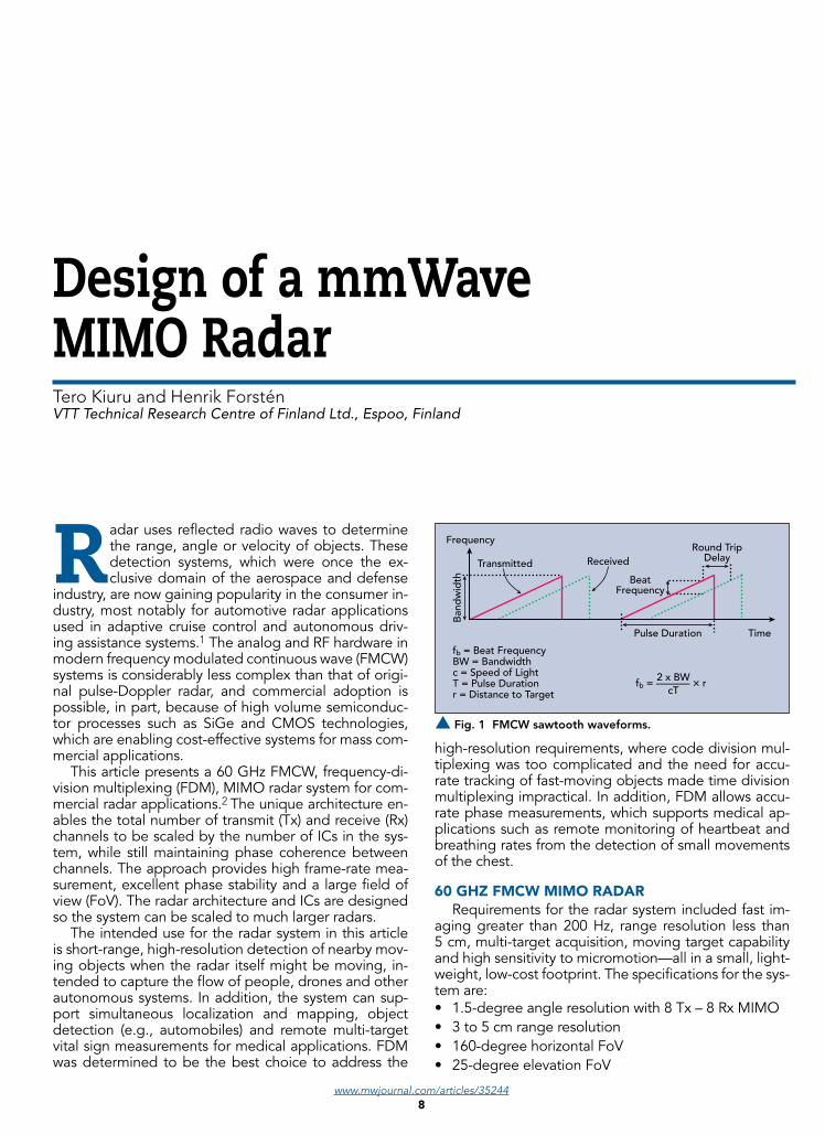
s Fig. 1 FMCW sawtooth waveforms.
Frequency
Ban
dw
idth
Pulse Duration
Transmitted
BeatFrequency
Round TripDelay
Time
Received
fb = Beat FrequencyBW = Bandwidthc = Speed of LightT = Pulse Durationr = Distance to Target
fb = ——— × r2 x BWcT
9
The system offers a maximum de-tection range of 20 to 25 m for sta-tionary human-size objects. Applying background subtraction, this range in-creases to 60 m for moving targets. The system also supports simultaneous de-tection of multiple moving objects with-out physically scanning the antenna. 3D systems with 160 × 160-degree FoV are also available.
While the radar system offers many potential use models, the multi-person vital sign extraction capability is inter-esting for future applications. For data analysis, the speed of the radar tech-nology is key, as it can operate at 200 frames per second (FPS) when not sup-porting visual graphics and 50 to 100 FPS with visualization.
FMCW OPERATIONA traditional pulsed radar detects
the range to a target by emitting a short pulse and observing the time of flight of the returned target echo. This requires the radar to have high instantaneous transmit power and of-ten results in a device with a large, ex-pensive physical structure. FMCW ra-dars achieve similar results using much smaller instantaneous transmit power and size by emitting a continuous microwave signal frequency modu-lated with a low frequency waveform, such as a sawtooth function with pe-riod T, whose duration is much greater than the return time of the echo (see Figure 1).
Unlike pulsed radar, FMCW systems transmit and receive simultaneously, eliminating the blind range that oc-curs when the receiver in a pulsed ra-dar is turned off during transmission. FMCW systems can detect reflected signals from objects very close to the radar, enabling it to measure distances down to a few centimeters. The system achieves excellent range resolution, which is proportional to the reciprocal of the bandwidth, i.e., ∆x = c/(2∆f), and high signal-to-noise ratio with narrow intermediate frequency (IF) bandwidth.
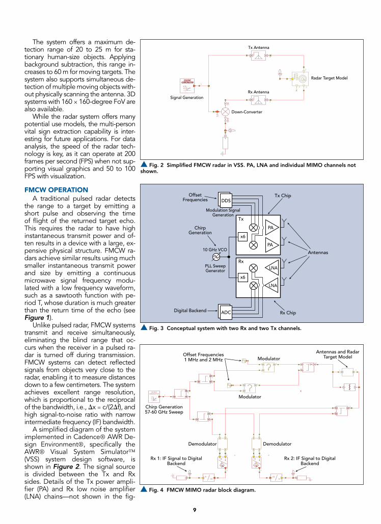
A simplified diagram of the system implemented in Cadence® AWR De-sign Environment®, specifically the AWR® Visual System Simulator™ (VSS) system design software, is shown in Figure 2. The signal source is divided between the Tx and Rx sides. Details of the Tx power ampli-fier (PA) and Rx low noise amplifier (LNA) chains—not shown in the fig-
s Fig. 2 Simplified FMCW radar in VSS. PA, LNA and individual MIMO channels not shown.
INOUT
LO
12
1
CHIRPGENERATOR
fc-f
+f1
TARGET
MODEL
1
23
4
Signal Generation
Down-Converter
Tx Antenna
Rx Antenna
Radar Target Model
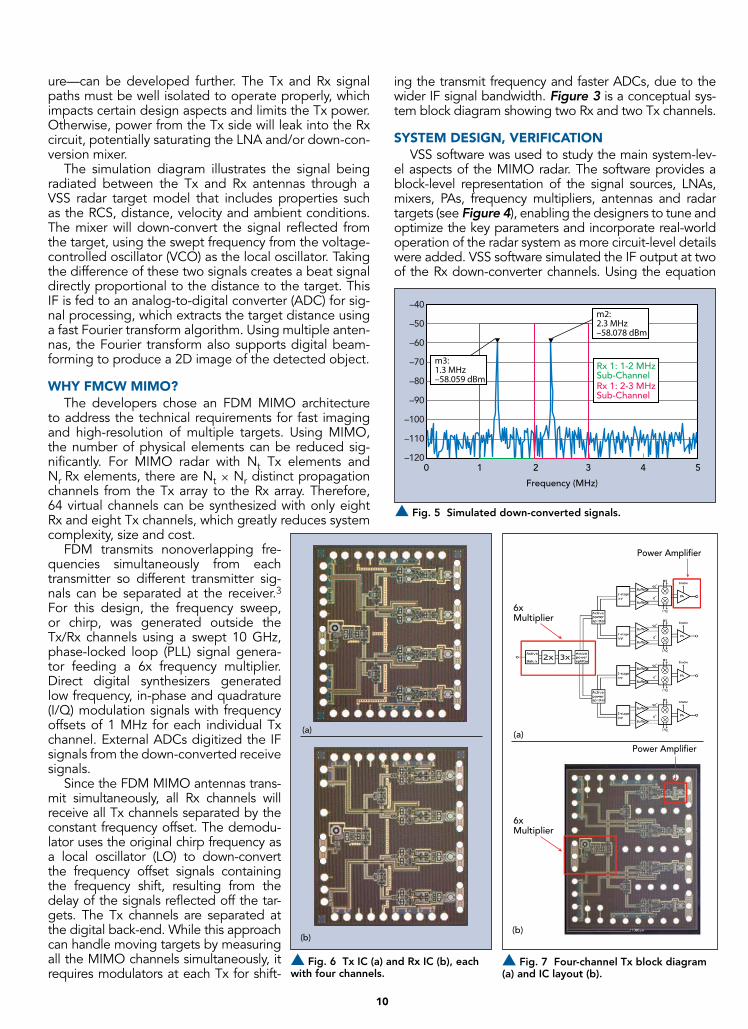
s Fig. 3 Conceptual system with two Rx and two Tx channels.
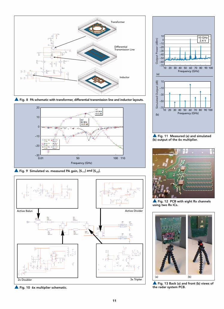
OffsetFrequencies DDS
Tx Chip
Antennas
ChirpGeneration
Digital Backend Rx Chip
PA
Modulation SignalGeneration
PLL SweepGenerator
10 GHz VCO
Tx
PA
x6
RxLNA
LNA
x6
ADC
s Fig. 4 FMCW MIMO radar block diagram.
CHIRPGENERATOR
fc-f
+f1
1 2
3
1 2
3
1
2
3
1 2
3
12
3
1 2
3
CER
1 2
3
CER
1
2
3
1
2
3
1 2
3 4
1 2
1 2
3 4
Offset Frequencies1 MHz and 2 MHz
Chirp Generation57-60 GHz Sweep
Antennas and RadarTarget Model
Demodulator
Modulator
Rx 2: IF Signal to DigitalBackend
Rx 1: IF Signal to DigitalBackend
Modulator
Demodulator
10
ing the transmit frequency and faster ADCs, due to the wider IF signal bandwidth. Figure 3 is a conceptual sys-tem block diagram showing two Rx and two Tx channels.
SYSTEM DESIGN, VERIFICATIONVSS software was used to study the main system-lev-
el aspects of the MIMO radar. The software provides a block-level representation of the signal sources, LNAs, mixers, PAs, frequency multipliers, antennas and radar targets (see Figure 4), enabling the designers to tune and optimize the key parameters and incorporate real-world operation of the radar system as more circuit-level details were added. VSS software simulated the IF output at two of the Rx down-converter channels. Using the equation
ure—can be developed further. The Tx and Rx signal paths must be well isolated to operate properly, which impacts certain design aspects and limits the Tx power. Otherwise, power from the Tx side will leak into the Rx circuit, potentially saturating the LNA and/or down-con-version mixer.
The simulation diagram illustrates the signal being radiated between the Tx and Rx antennas through a VSS radar target model that includes properties such as the RCS, distance, velocity and ambient conditions. The mixer will down-convert the signal reflected from the target, using the swept frequency from the voltage-controlled oscillator (VCO) as the local oscillator. Taking the difference of these two signals creates a beat signal directly proportional to the distance to the target. This IF is fed to an analog-to-digital converter (ADC) for sig-nal processing, which extracts the target distance using a fast Fourier transform algorithm. Using multiple anten-nas, the Fourier transform also supports digital beam-forming to produce a 2D image of the detected object.
WHY FMCW MIMO?The developers chose an FDM MIMO architecture
to address the technical requirements for fast imaging and high-resolution of multiple targets. Using MIMO, the number of physical elements can be reduced sig-nificantly. For MIMO radar with Nt Tx elements and Nr Rx elements, there are Nt × Nr distinct propagation channels from the Tx array to the Rx array. Therefore, 64 virtual channels can be synthesized with only eight Rx and eight Tx channels, which greatly reduces system complexity, size and cost.
FDM transmits nonoverlapping fre-quencies simultaneously from each transmitter so different transmitter sig-nals can be separated at the receiver.3 For this design, the frequency sweep, or chirp, was generated outside the Tx/Rx channels using a swept 10 GHz, phase-locked loop (PLL) signal genera-tor feeding a 6x frequency multiplier. Direct digital synthesizers generated low frequency, in-phase and quadrature (I/Q) modulation signals with frequency offsets of 1 MHz for each individual Tx channel. External ADCs digitized the IF signals from the down-converted receive signals.
Since the FDM MIMO antennas trans-mit simultaneously, all Rx channels will receive all Tx channels separated by the constant frequency offset. The demodu-lator uses the original chirp frequency as a local oscillator (LO) to down-convert the frequency offset signals containing the frequency shift, resulting from the delay of the signals reflected off the tar-gets. The Tx channels are separated at the digital back-end. While this approach can handle moving targets by measuring all the MIMO channels simultaneously, it requires modulators at each Tx for shift-
s Fig. 5 Simulated down-converted signals.
Frequency (MHz)
1 2 3 4 50
–40
–50
–60
–70
–80
–90
–100
–110
–120
m2:2.3 MHz–58.078 dBm
m3:1.3 MHz–58.059 dBm
Rx 1: 1-2 MHzSub-ChannelRx 1: 2-3 MHzSub-Channel
s Fig. 6 Tx IC (a) and Rx IC (b), each with four channels.
(a)
(b)
s Fig. 7 Four-channel Tx block diagram (a) and IC layout (b).
Power Ampli�er
6xMultiplier
(a)
(b)
6xMultiplier
Power Ampli�er
11
s Fig. 11 Measured (a) and simulated (b) output of the 6x multiplier.
Frequency (GHz)
100
–10–20–30–40–50–60–70
Out
put
Pow
er (d
Bm
)
10 20 30 40 50 70 80 90 10060
10 GHz2.4 V
10
–10
–30
–50
–70Sim
ulat
ed O
utp
ut (d
B)
Frequency (GHz)10 20 30 40 50 70 80 90 10060
(a)
(b)
s Fig. 12 PCB with eight Rx channels using two Rx ICs.
s Fig. 13 Back (a) and front (b) views of the radar system PCB.
(a) (b)
s Fig. 9 Simulated vs. measured PA gain, |S11 | and |S22|.
Frequency (GHz)
0.01 100 11050
20
10
0
–10
–20
–30
s Fig. 8 PA schematic with transformer, differential transmission line and inductor layouts.
Transformer
DifferentialTransmission Line
Inductor
s Fig. 10 6x multiplier schematic.
2x Doubler 3x Tripler
Active Balun Active Divider
12
of the chip-level amplifier yields excellent agreement between the measured performance and the simulation (see Figure 9).
Simulations of the active balun, harmonic multiplier chain and active power divider on the output (see Fig-ure 10) were performed assuming a 10 GHz input and 2.4 V bias. The simulation results shown in Figure 11 provide useful insight into the operation of the multi-plier, enabling an understanding of the power levels of the spurious signals being generated. From a radar de-sign perspective, it is beneficial to have this information to suppress these spurious signals, warranting the ad-ditional design steps to fine-tune the circuit.
MIMO RADAR MEASUREMENT RESULTSThe RF section of the receiver (see Figure 12) shows
eight Rx channels supported by two Rx RFICs flip-chip mounted on a PCB. The front and back of the high speed signal processing back-end, mounted on a stand for lab testing, are shown in Figure 13. The phases and ampli-tudes of the receivers are calibrated with a single-point target measurement. Phase and amplitude correction factors are determined so the point target measurement provides an image of a point target at the correct angle.
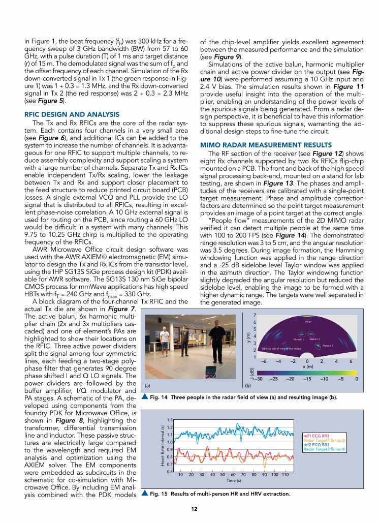
“People flow” measurements of the 2D MIMO radar verified it can detect multiple people at the same time with 100 to 200 FPS (see Figure 14). The demonstrated range resolution was 3 to 5 cm, and the angular resolution was 3.5 degrees. During image formation, the Hamming windowing function was applied in the range direction and a -25 dB sidelobe level Taylor window was applied in the azimuth direction. The Taylor windowing function slightly degraded the angular resolution but reduced the sidelobe level, enabling the image to be formed with a higher dynamic range. The targets were well separated in the generated image.
in Figure 1, the beat frequency (fb) was 300 kHz for a fre-quency sweep of 3 GHz bandwidth (BW) from 57 to 60 GHz, with a pulse duration (T) of 1 ms and target distance (r) of 15 m. The demodulated signal was the sum of fb and the offset frequency of each channel. Simulation of the Rx down-converted signal in Tx 1 (the green response in Fig-ure 1) was 1 + 0.3 = 1.3 MHz, and the Rx down-converted signal in Tx 2 (the red response) was 2 + 0.3 = 2.3 MHz (see Figure 5).
RFIC DESIGN AND ANALYSISThe Tx and Rx RFICs are the core of the radar sys-
tem. Each contains four channels in a very small area (see Figure 6), and additional ICs can be added to the system to increase the number of channels. It is advanta-geous for one RFIC to support multiple channels, to re-duce assembly complexity and support scaling a system with a large number of channels. Separate Tx and Rx ICs enable independent Tx/Rx scaling, lower the leakage between Tx and Rx and support closer placement to the feed structure to reduce printed circuit board (PCB) losses. A single external VCO and PLL provide the LO signal that is distributed to all RFICs, resulting in excel-lent phase-noise correlation. A 10 GHz external signal is used for routing on the PCB, since routing a 60 GHz LO would be difficult in a system with many channels. This 9.75 to 10.25 GHz chirp is multiplied to the operating frequency of the RFICs.
AWR Microwave Office circuit design software was used with the AWR AXIEM® electromagnetic (EM) simu-lator to design the Tx and Rx ICs from the transistor level, using the IHP SG13S SiGe process design kit (PDK) avail-able for AWR software. The SG13S 130 nm SiGe bipolar CMOS process for mmWave applications has high speed HBTs with fT = 240 GHz and fmax = 330 GHz.
A block diagram of the four-channel Tx RFIC and the actual Tx die are shown in Figure 7. The active balun, 6x harmonic multi-plier chain (2x and 3x multipliers cas-caded) and one of element’s PAs are highlighted to show their locations on the RFIC. Three active power dividers split the signal among four symmetric lines, each feeding a two-stage poly-phase filter that generates 90 degree phase shifted I and Q LO signals. The power dividers are followed by the buffer amplifier, I/Q modulator and PA stages. A schematic of the PA, de-veloped using components from the foundry PDK for Microwave Office, is shown in Figure 8, highlighting the transformer, differential transmission line and inductor. These passive struc-tures are electrically large compared to the wavelength and required EM analysis and optimization using the AXIEM solver. The EM components were embedded as subcircuits in the schematic for co-simulation with Mi-crowave Office. By including EM anal-ysis combined with the PDK models
s Fig. 14 Three people in the radar field of view (a) and resulting image (b).
(a) (b)
6
–5–10–15–20–25 0–30
0 2 4
7654321
y (m
)
x (m)
J (d
B)
–6 –2–4
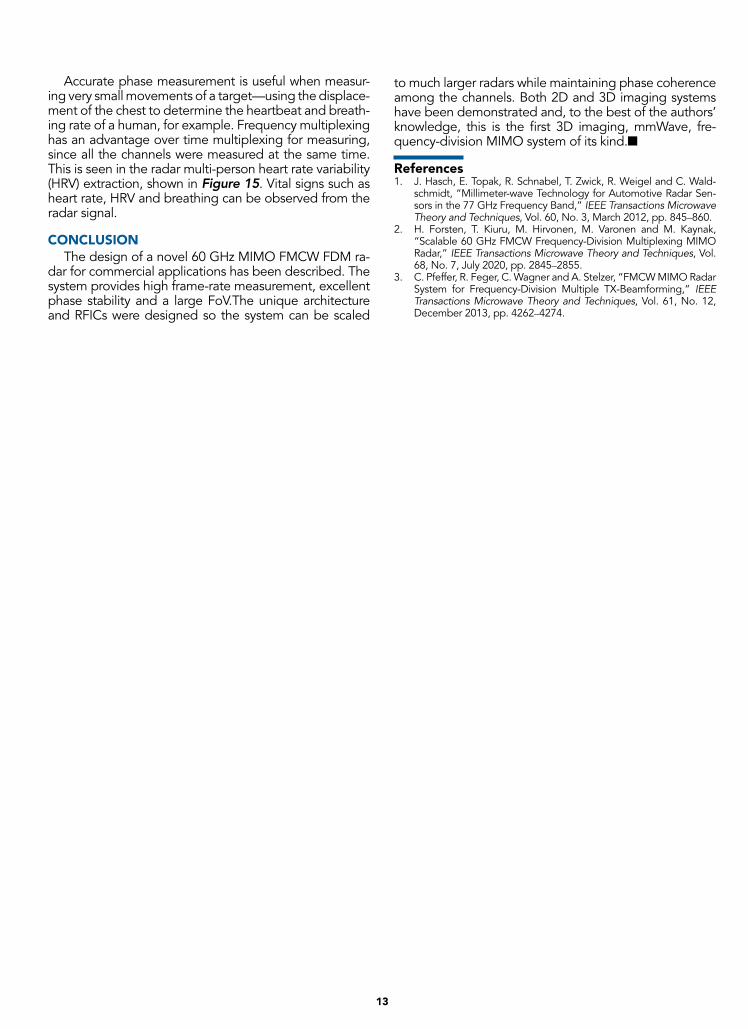
s Fig. 15 Results of multi-person HR and HRV extraction.
Time (s)
1.3
1.2
1.1
1.0
0.9
0.8
0.7
0.6
Hea
rt R
ate
Inte
rval
(s)
10 20 30 40 50 70 80 90 10060 110
ref1 ECG RR1Radar Target1 Smoothref2 ECG RR1Radar Target2 Smooth
13
to much larger radars while maintaining phase coherence among the channels. Both 2D and 3D imaging systems have been demonstrated and, to the best of the authors’ knowledge, this is the first 3D imaging, mmWave, fre-quency-division MIMO system of its kind.n
References1. J. Hasch, E. Topak, R. Schnabel, T. Zwick, R. Weigel and C. Wald-
schmidt, “Millimeter-wave Technology for Automotive Radar Sen-sors in the 77 GHz Frequency Band,” IEEE Transactions Microwave Theory and Techniques, Vol. 60, No. 3, March 2012, pp. 845–860.
2. H. Forsten, T. Kiuru, M. Hirvonen, M. Varonen and M. Kaynak, “Scalable 60 GHz FMCW Frequency-Division Multiplexing MIMO Radar,” IEEE Transactions Microwave Theory and Techniques, Vol. 68, No. 7, July 2020, pp. 2845–2855.
3. C. Pfeffer, R. Feger, C. Wagner and A. Stelzer, “FMCW MIMO Radar System for Frequency-Division Multiple TX-Beamforming,” IEEE Transactions Microwave Theory and Techniques, Vol. 61, No. 12, December 2013, pp. 4262–4274.
Accurate phase measurement is useful when measur-ing very small movements of a target—using the displace-ment of the chest to determine the heartbeat and breath-ing rate of a human, for example. Frequency multiplexing has an advantage over time multiplexing for measuring, since all the channels were measured at the same time. This is seen in the radar multi-person heart rate variability (HRV) extraction, shown in Figure 15. Vital signs such as heart rate, HRV and breathing can be observed from the radar signal.
CONCLUSIONThe design of a novel 60 GHz MIMO FMCW FDM ra-
dar for commercial applications has been described. The system provides high frame-rate measurement, excellent phase stability and a large FoV.The unique architecture and RFICs were designed so the system can be scaled

It’s who we are It’s what we do
Amplifiers• Gain Blocks• Linear Drivers• Low-Noise• Variable Gain• Coaxial Module
Switches• SMT• Coaxial• DIE• High Power• High Isolation
Filters• BAW / SAW• Ceramic• LTCC• Cavity• Waveguide
Transistors• mW to kW• GaN• LDMOS• High Frequency• Packaged & DIE
Attenuators• Fixed• Digital• Coaxial• Chip• Voltage Variable• Temperature Variable
Test &Measurement
• Coax Adapters• Terminations• Open/Shorts• Couplers• Switches• Phase Shifters• Attenuators
Antennas• PCB Mount• Patch• Coaxial• Goose Necks• Body-Worn
Diodes• PIN• Schottky• Varactor• Limiter• Gunn
Cable Assemblies• High-Performance Test• In-Box Solutions• Pigtails• Conformable• Flexible• Semi-Rigid
RFMW is THE Premier RF & Microwave specialty distributorcreated to support your component selection, technical design andfulfillment needs. RFMW offers a complete range of services for
commercial, military, and space requirements.
We provide many Value-Added Services driven by customerrequirements – because we know RF and microwave.
RFMW is the center for all your design solutions.Visit our website to learn more: www.rfmw.com
RFMW • 188 Martinvale Lane • San Jose, CA 95119 U.S.A.Toll Free: +1-877-367-7369 • www.RFMW.com • [email protected]
The Center ForAll Your RF Designs
The Center ForAll Your RF Designs
• Custom Product Development• Electrical Test Capabilities• Device Tape & Reel• Hi-Rel Screening• DIE Services
• Documentation Related Services• Obsolete Parts Replacement
• Solder Tinning• Packaging
• Kitting
Timing Products• Clock Oscillators• MEMS Oscillators• Crystals• Buffers• VCXO• TCXO• OCXO
RFMW.FullPg Ad.07.19.qxp_RFMW.FullPg.Ad.MWJ.comp 9/13/19 12:00 PM Page 1
15
Automobiles are among the most complex prod-ucts that humanity has ever made. Advanced driver assistance systems (ADAS) and, moreover,
self-driving cars are even more sophisticated. Included technologies are: state-of-the-art software, AI mechan-ics, processors and hardware, and sensors that feed all algorithms with information about the environment.
Conventional automotive radars have a long life cy-cle. It is ordinary to see a 5-year-old radar in a newly re-leased car with some self-driving ability. And that radar will not differ much from the one made in 2010, and sometimes, in the 2000's. Basically, most automotive radars utilize 77 GHz range and use a linear frequency-modulated signal with some variations. There are some essential core technology breakthroughs which improve angular resolution: MIMO and electronic beam-steering to name a few.
AREAS OF IMPROVEMENTRadars are good at measuring distance and speed
and they have good distance and speed resolution. Ra-dars operate at night and have the least degradation in harsh weather conditions among other sensors. But they still have a relatively low angular resolution compared to cameras and lidars. Most developers claim they have achieved positive results in improving angular resolu-tion. There are no set criteria, but high-resolution ra-dars are called imaging, which means they provide data close to a camera image.
As an active sensor, radar emits signals and analyzes the reflections. Therefore, the so-called ’mutual interfer-ence’ can arise as a problem. It is when the radars oper-ate within the same frequency range and receive other radars’ emitting signals as their own. This issue may lead
How Startups Are Shaping the Automotive Radar of Tomorrow Ivan Koshurinov
to a low-level data corruption. Even though this may not be considered as a major problem given current radar’s penetration rate, the issue should not be left untreated for the future systems so companies are working on this problem.
Despite the claim that radars are the 2nd cheapest sensor on a vehicle after an ultrasonic one, there is a de-mand for even cheaper radars. Conventional automo-tive radars are estimated to be $50-100 a piece in large quantities, but there is a demand for a $10-30 radar. Fu-ture imaging radars are mentioned are more expensive, starting from $150 in mass production for a single unit and up to $1000 for a 360-degree set. The challenge is to keep the price within these limits or reduce it in future designs.
Future radars should provide more reliable data. This is a complex concept that includes improving false posi-tive and false negative rates and increasing the overall signal to noise ratio. But these things often come along with the key challenges mentioned previously of inter-ference and degradation from materials in front of the radar on the vehicle.
s Fig. 1 From semiengineering.com, courtesy of NXP
16
Most Tier-1 and Tier-2 radar manufacturers such as Veoneer (Autoliv), Bosch, Continental, Delphi, Valeo, etc., are developing new radars to overcome these chal-lenges. Most major players do not like to disclose what they are currently developing. Therefore, we can only discuss their existing sensors. On the contrary, startups usually do not hesitate to tell us much more about their products.
For startups, let's highlight some of the major im-provements we are likely to see in future radars. A ra-dar may be divided into 3 major pieces, antenna feeder path, transceiver, and processing. Each of them may be improved.
ANTENNAS/METAMATERIALS
EchodyneThe most comprehensive approach to building a ra-
dar with better angular resolution is antenna arrays of various types. These complicated antenna arrays used to be very expensive but new methods have been de-veloped to reduce their cost. Echodyne has built its proprietary Metamaterial Electronically Scanning Array (MESA), which looks similar to classic antenna arrays and provides almost the same level of functionality. Recently Echodyne has disclosed some details about automotive 77 GHz radar’s features.
EchoDrive by Echodyne significantly differs from other automotive radars. Being 25 cm wide and 2 kg in weight, Echodrive is bigger than any typical 77 GHz ve-hicle radar. It is also a very powerful unit that consumes 80 W. One may see that even being simplified and opti-mized, MESA antenna remains an expenisve piece. The manufacturer claims it should comply with FCC rules and is being used in other applications. Nevertheless, due to overall complexity, it is unlikely to see an Echo-dyne radar in any production car in the near future.
The target market for EchoDrive is the self-driving
cars. The maximum raw output is as huge as 250k points per second with a data rate of more than 2.5 Gbps. It must be reminded, that radar output is more complex than lidar’s, and contains velocity, signal ratio data as well as range, azimuth and elevation. Such amount of data is what self-driving cars expect.
Lunewave
The company is developing Luneburg lens based an-tennas. The idea of such lenses is known for years and Lunewave makes them closer to the market by using additive technologies and offering antennas for various bands (W-, Ka-, X-). Lens antenna has the widest possi-ble radiation pattern which may be useful for communi-cations or 360-degree collision avoidance systems. The problem of measuring angles to an obstacle is solved by using a relevant amount of transmitting/receiving chan-nels thus making a 3D electronic scanning array. Every channel has its own azimuth and elevation parameters, defined by the construction of the lens.
Metawave
Analog beamforming systems have traditionally been expensive and their complexity grew with operating fre-quency. A Silicon-valley based Metawave claims it has built an analog beamforming antenna for a 77 GHz band that empowers a radar with scanning ability. Metawave’s radar is easily recognized by its metamaterial unit cell antenna. It is said to be built using conventional mate-rials and should be affordable in mass production. Its construction squeezes signal power in narrow cones compared to wide ones in conventional radars.
Inside the radar there are proprietary Marconi 77 GHz phase controllers and mmWave integrated cir-cuits. Along with Metawave’s proprietary calibration sys-tem they enable the transmit and receive beams to be steered in steps of 0.1º in the range of ±22º. Technically, the large amount of active elements technically allows it to reach an even wider steerable range, over ±60 de-gree both in horizontal and vertical planes.
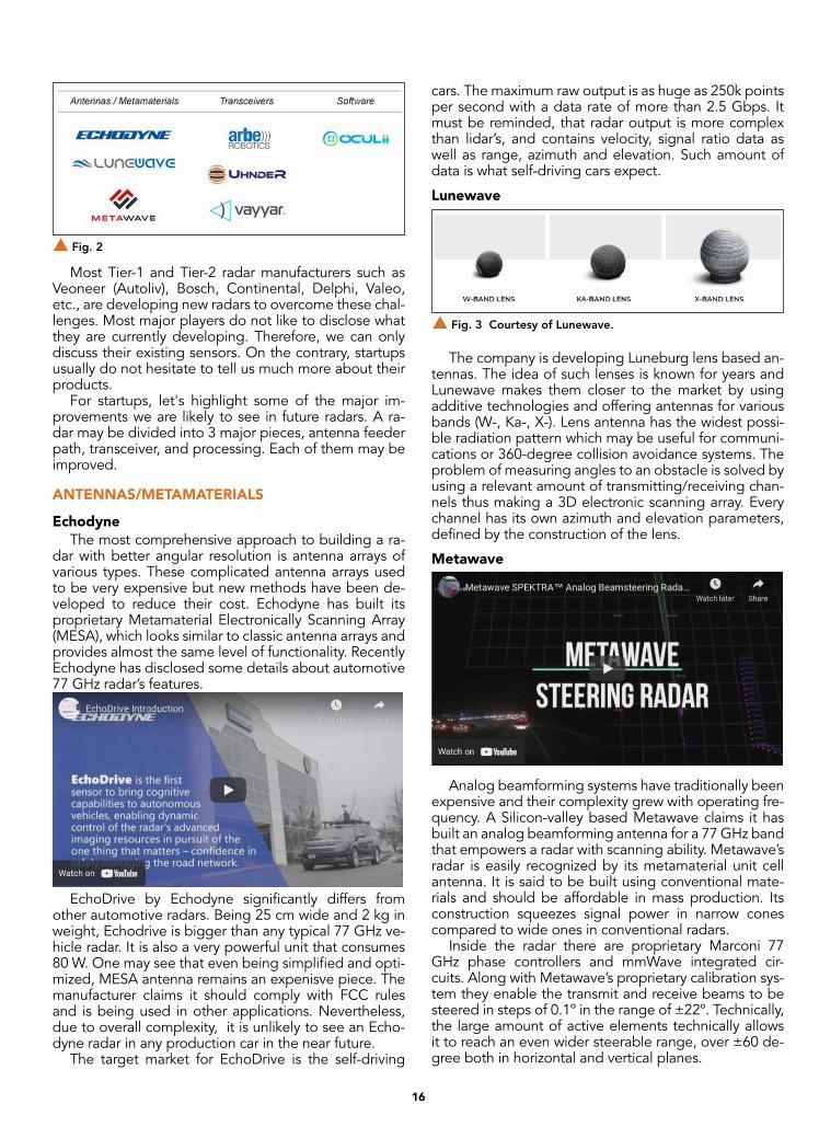
s Fig. 2
s Fig. 3 Courtesy of Lunewave.
17
As shown, it may be roughly compared to a beam constantly moving left to right with 0.1-degree accuracy. Thus giving the ability to distinguish obstacles by angle and measure angular dimensions. Analog scanning can make the radar more tolerant to mutual interference. The radar may be used as a part of a sensor fusion sys-tem, or as a standalone device. For the second case, Metawave is offering a proprietary AI platform that pro-cesses SPEKTRA radar output and performs real-time object classification and labeling.
TRANSCEIVERS
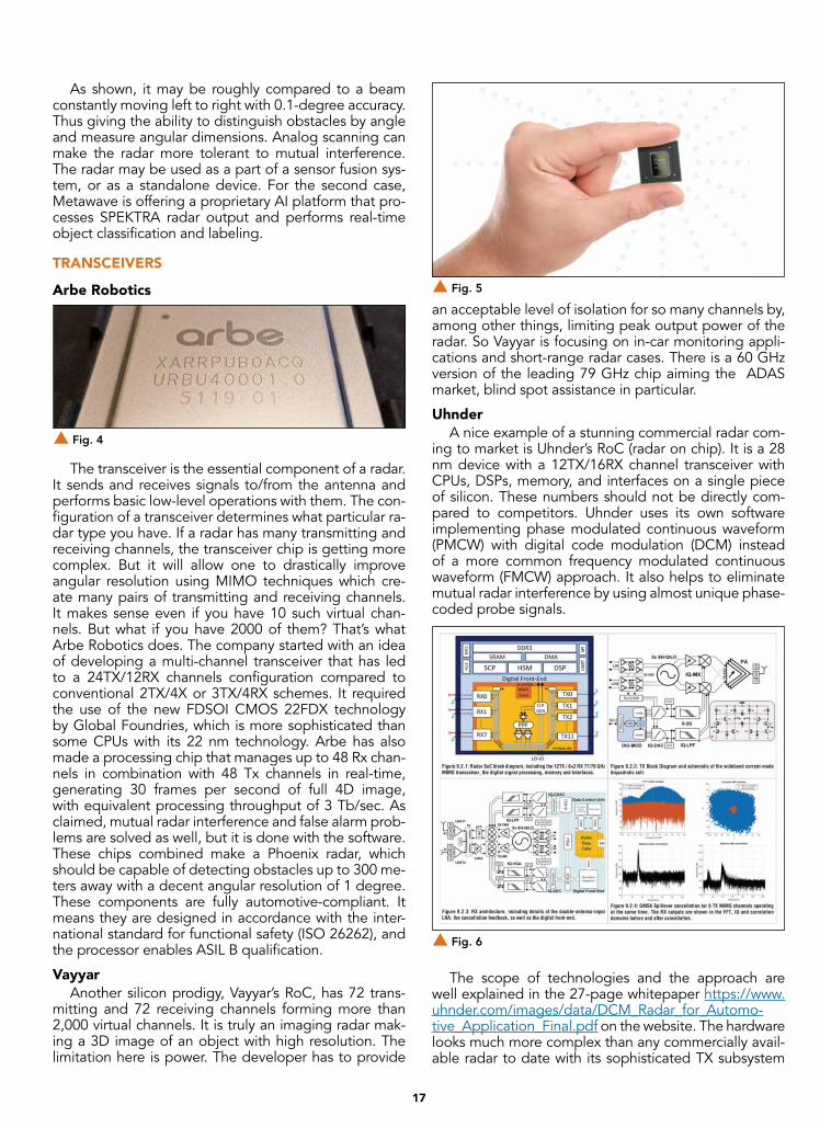
Arbe Robotics
The transceiver is the essential component of a radar. It sends and receives signals to/from the antenna and performs basic low-level operations with them. The con-figuration of a transceiver determines what particular ra-dar type you have. If a radar has many transmitting and receiving channels, the transceiver chip is getting more complex. But it will allow one to drastically improve angular resolution using MIMO techniques which cre-ate many pairs of transmitting and receiving channels. It makes sense even if you have 10 such virtual chan-nels. But what if you have 2000 of them? That’s what Arbe Robotics does. The company started with an idea of developing a multi-channel transceiver that has led to a 24TX/12RX channels configuration compared to conventional 2TX/4X or 3TX/4RX schemes. It required the use of the new FDSOI CMOS 22FDX technology by Global Foundries, which is more sophisticated than some CPUs with its 22 nm technology. Arbe has also made a processing chip that manages up to 48 Rx chan-nels in combination with 48 Tx channels in real-time, generating 30 frames per second of full 4D image, with equivalent processing throughput of 3 Tb/sec. As claimed, mutual radar interference and false alarm prob-lems are solved as well, but it is done with the software. These chips combined make a Phoenix radar, which should be capable of detecting obstacles up to 300 me-ters away with a decent angular resolution of 1 degree. These components are fully automotive-compliant. It means they are designed in accordance with the inter-national standard for functional safety (ISO 26262), and the processor enables ASIL B qualification.
VayyarAnother silicon prodigy, Vayyar’s RoC, has 72 trans-
mitting and 72 receiving channels forming more than 2,000 virtual channels. It is truly an imaging radar mak-ing a 3D image of an object with high resolution. The limitation here is power. The developer has to provide
an acceptable level of isolation for so many channels by, among other things, limiting peak output power of the radar. So Vayyar is focusing on in-car monitoring appli-cations and short-range radar cases. There is a 60 GHz version of the leading 79 GHz chip aiming the ADAS market, blind spot assistance in particular.
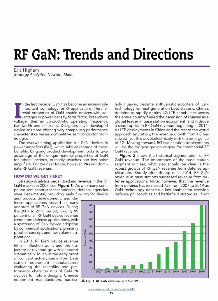
UhnderA nice example of a stunning commercial radar com-
ing to market is Uhnder’s RoC (radar on chip). It is a 28 nm device with a 12TX/16RX channel transceiver with CPUs, DSPs, memory, and interfaces on a single piece of silicon. These numbers should not be directly com-pared to competitors. Uhnder uses its own software implementing phase modulated continuous waveform (PMCW) with digital code modulation (DCM) instead of a more common frequency modulated continuous waveform (FMCW) approach. It also helps to eliminate mutual radar interference by using almost unique phase-coded probe signals.
The scope of technologies and the approach are well explained in the 27-page whitepaper https://www.uhnder.com/images/data/DCM_Radar_for_Automo-tive_Application_Final.pdf on the website. The hardware looks much more complex than any commercially avail-able radar to date with its sophisticated TX subsystem
s Fig. 4
s Fig. 5
s Fig. 6

18
and software-defined hardware pipeline capable of up to 20 Tera-Ops baseband processing. On the other side, the secret sauce is the DCM modulation idea itself that led to such a design, and, hopefully, to a commercially successful product. Uhnder has already partnered with Magna to bring it to the market as Magna Icon Radar.
SOFTWARE PROCESSING
OculiiUnlike other companies, Oculii does not bring com-
plicated hardware design to the market. The company is focused on its proprietary software. Being a partner of TI and Infineon, Oculii is using TI AWR and Infineon RASIC hardware respectively. Texas Instruments’ 60 and 77 GHz AWR family is widely used among startups that
do not want to pay much attention to the hardware, but to put their processing into an already designed SoC. Infineon does not provide a system on chip, but its 77 GHz transceivers as well as Aurix platform are a pretty good start for a radar developer.
Of course, it puts certain limitations on what Oculii can do with a smaller number of TX/RX channels than Arbe or Uhnder. But Oculii’s Virtual Aperture technol-ogy, which might be a new synthetic aperture imple-mentation, does the job. The radar has almost the same feature set as the others. Up to 250 m range, sub-de-gree angular resolution and 120-degree field of view. Oculii’s approach does not require costly hardware de-velopment and may be quickly deployed using existing automotive-grade components. Currently Oculii works with Hella on mass production radar. n
Improved System Performance with Reduced
Size and CostThe Qorvo QPA1011, 7.9 – 11 GHz high power,
GaN MMIC amplifier typically provides 25 W saturated output power with PAE of 37.5%
and large-signal gain of 19.5 dB. This combi-nation of wideband performance provides the flexibility designers are looking for to improve system performance while reducing size and
cost. With good thermal properties, it can sup-port a range of bias voltages and will perform
well under both CW and pulse operations.Learn More
X-Band FEM for High-Level Phased Array Radar
IntegrationDesigned for next-gen 9 to 10.5 GHz AESA
radar applications needing power, efficiency, reliability and survivability, Qorvo’s QPM2637 FEM incorporates a T/R switch, PA, LNA and
power limiter into a 6x6 mm package. Saturat-ed transmit output power is 36 dBm with small signal gain of 32 dB. Receive side noise figure is 2.7dB with small signal gain of 21 dB. GaN
technology withstands up to 4W of receive side input power without permanent damage.
Learn More
19
In the last decade, GaN has become an increasingly important technology for RF applications. The ma-terial properties of GaN enable devices with ad-vantages in power density, form factor, breakdown
voltage, thermal conductivity, operating frequency, bandwidth and efficiency. Designers have developed device solutions offering very compelling performance characteristics versus competitive semiconductor tech-nologies.
The overwhelming application for GaN devices is power amplifiers (PAs), which take advantage of these benefits. Ongoing product development looks to take advantage of the unique material properties of GaN for other functions, primarily switches and low noise amplifiers. For the near future, however, PAs will domi-nate RF GaN revenue.
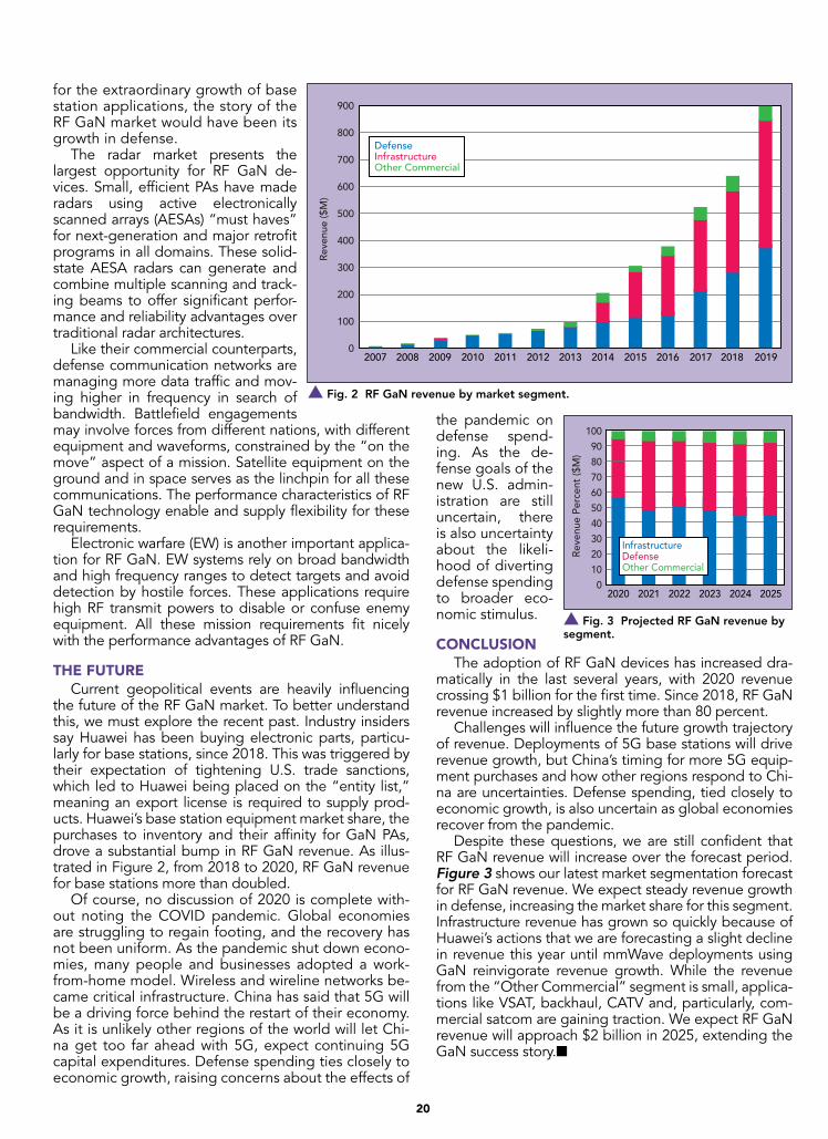
HOW DID WE GET HERE?Strategy Analytics began tracking revenue in the RF
GaN market in 2007 (see Figure 1). As with many com-pound semiconductor technologies, defense agencies were instrumental, providing early funding for device and process development, and de-fense applications served as early adopters of RF GaN devices. During the 2007 to 2013 period, roughly 85 percent of all RF GaN device revenue came from defense applications, with a spattering of GaN device adoption by commercial applications, primarily proof of concept and low volume ap-plications.
In 2013, RF GaN device revenue hit an inflection point and the tra-jectory of revenue growth increased dramatically. Much of the early proof of concept activity came from base station equipment manufacturers evaluating the reliability and per-formance characteristics of GaN PA devices for future designs. Chinese equipment manufacturers, particu-
RF GaN: Trends and DirectionsEric HighamStrategy Analytics, Newton, Mass.
larly Huawei, became enthusiastic adopters of GaN technology for next-generation base stations. China’s decision to rapidly deploy 4G LTE capabilities across the entire country fueled the ascension of Huawei as a global leader in base station equipment, and it drove a sharp uptick in RF GaN revenue beginning in 2014. As LTE deployments in China and the rest of the world approach saturation, the revenue growth from 4G has slowed; yet this dovetailed nicely with the emergence of 5G. Moving forward, 5G base station deployments will be the biggest growth engine for commercial RF GaN revenue.
Figure 2 shows the historical segmentation of RF GaN revenue. The importance of the base station segment is clear; what also should be clear is the robust growth of RF GaN revenue from defense ap-plications. Shortly after the spike in 2014, RF GaN revenue in base stations surpassed revenue from de-fense applications. Note, however, that the revenue from defense has increased 75x from 2007 to 2019 as GaN technology became a key enabler for evolving defense philosophies and battlefield strategies. If not
www.mwjournal.com/articles/36141
s Fig. 1 RF GaN revenue, 2007–2019.
2011 2012 2013 2014 20152010 2017 2018 201920162007 2008 2009
900
800
700
600
500
400
300
200
100
0
Rev
enue
($M
)
20
for the extraordinary growth of base station applications, the story of the RF GaN market would have been its growth in defense.
The radar market presents the largest opportunity for RF GaN de-vices. Small, efficient PAs have made radars using active electronically scanned arrays (AESAs) “must haves” for next-generation and major retrofit programs in all domains. These solid-state AESA radars can generate and combine multiple scanning and track-ing beams to offer significant perfor-mance and reliability advantages over traditional radar architectures.
Like their commercial counterparts, defense communication networks are managing more data traffic and mov-ing higher in frequency in search of bandwidth. Battlefield engagements may involve forces from different nations, with different equipment and waveforms, constrained by the “on the move” aspect of a mission. Satellite equipment on the ground and in space serves as the linchpin for all these communications. The performance characteristics of RF GaN technology enable and supply flexibility for these requirements.
Electronic warfare (EW) is another important applica-tion for RF GaN. EW systems rely on broad bandwidth and high frequency ranges to detect targets and avoid detection by hostile forces. These applications require high RF transmit powers to disable or confuse enemy equipment. All these mission requirements fit nicely with the performance advantages of RF GaN.
THE FUTURECurrent geopolitical events are heavily influencing
the future of the RF GaN market. To better understand this, we must explore the recent past. Industry insiders say Huawei has been buying electronic parts, particu-larly for base stations, since 2018. This was triggered by their expectation of tightening U.S. trade sanctions, which led to Huawei being placed on the “entity list,” meaning an export license is required to supply prod-ucts. Huawei’s base station equipment market share, the purchases to inventory and their affinity for GaN PAs, drove a substantial bump in RF GaN revenue. As illus-trated in Figure 2, from 2018 to 2020, RF GaN revenue for base stations more than doubled.
Of course, no discussion of 2020 is complete with-out noting the COVID pandemic. Global economies are struggling to regain footing, and the recovery has not been uniform. As the pandemic shut down econo-mies, many people and businesses adopted a work-from-home model. Wireless and wireline networks be-came critical infrastructure. China has said that 5G will be a driving force behind the restart of their economy. As it is unlikely other regions of the world will let Chi-na get too far ahead with 5G, expect continuing 5G capital expenditures. Defense spending ties closely to economic growth, raising concerns about the effects of
the pandemic on defense spend-ing. As the de-fense goals of the new U.S. admin-istration are still uncertain, there is also uncertainty about the likeli-hood of diverting defense spending to broader eco-nomic stimulus.
CONCLUSIONThe adoption of RF GaN devices has increased dra-
matically in the last several years, with 2020 revenue crossing $1 billion for the first time. Since 2018, RF GaN revenue increased by slightly more than 80 percent.
Challenges will influence the future growth trajectory of revenue. Deployments of 5G base stations will drive revenue growth, but China’s timing for more 5G equip-ment purchases and how other regions respond to Chi-na are uncertainties. Defense spending, tied closely to economic growth, is also uncertain as global economies recover from the pandemic.
Despite these questions, we are still confident that RF GaN revenue will increase over the forecast period. Figure 3 shows our latest market segmentation forecast for RF GaN revenue. We expect steady revenue growth in defense, increasing the market share for this segment. Infrastructure revenue has grown so quickly because of Huawei’s actions that we are forecasting a slight decline in revenue this year until mmWave deployments using GaN reinvigorate revenue growth. While the revenue from the “Other Commercial” segment is small, applica-tions like VSAT, backhaul, CATV and, particularly, com-mercial satcom are gaining traction. We expect RF GaN revenue will approach $2 billion in 2025, extending the GaN success story.n
s Fig. 2 RF GaN revenue by market segment.
2011 2012 2013 2014 20152010 2017 2018 201920162007 2008 2009
900
800
700
600
500
400
300
200
100
0
Rev
enue
($M
)
DefenseInfrastructureOther Commercial
s Fig. 3 Projected RF GaN revenue by segment.
2024 202520232020 2021 2022
1009080706050403020100
Rev
enue
Per
cent
($M
)
InfrastructureDefenseOther Commercial

21
Survey of RF GaN Fabs: Successful Commercialization and Global SupplyGary Lerude, Microwave Journal Editor
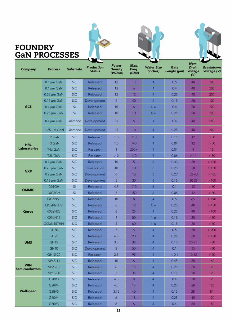
Featured in this month’s Mi-crowave Journal, a survey of the major RF GaN fabs around the globe. The eight
companies responding to our re-quest for information offer an as-tounding 36 process variants fabri-cating devices with 0.5 µm to 40 nm gate lengths on GaN on SiC, GaN on Si and GaN on diamond sub-strates. The process count does not include proprietary recipes the foundries maintain for their custom-ers.
Since RF GaN became a topic at industry conferences in the mid-1990s,1 GaN has been commercial-ized, adopted primarily for military radar, electronic warfare and cellular base stations. One indication of the technology’s success: GaN revenue reached $1 billion in 2020, accord-ing to Strategy Analytics. Read more about the market development for GaN in the accompanying article by Eric Higham of Strategy Analytics.
Eight GaN fabs responded to our survey:• GCS• HRL Laboratories• NXP• OMMIC• Qorvo• UMS• WIN Semiconductors• Wolfspeed.
Six of the eight are based in the United States, two are in Europe and WIN Semiconductors is in Tai-wan. All except for NXP are “open foundries,” willing to engage with
any customer—subject to export controls for the U.S. foundries.
Most GaN on SiC processes run on 100 mm wafers, although three of Qorvo’s five processes and all NXP’s are on 150 mm GaN on SiC wafers. Wolfspeed plans to migrate to 150 mm during the “next couple of years” as volumes increase. Al-though wafer diameter is often used as a marketing promotion, a loaded 100 mm fab is more cost efficient than a lightly loaded 150 mm fab. Interestingly, GCS’ and OMMIC’s GaN on Si processes use 150 mm wafers, which likely reflects the ma-turity and availability of silicon sub-strates.
While volume applications for RF GaN are below 20 GHz (e.g., phased array radar and sub-6 GHz base station power amplifiers), all the fabs surveyed have or are devel-oping shorter gate length processes to extend device performance well into the mmWave frequencies, an-ticipating the capability of GaN to compete with GaAs and silicon for commercial and military applica-tions at these higher frequencies.
In addition to offering com-petitive device performance, open foundries must support designers and their programs with design tools and test and packaging ser-vices. Alternatively, it could be test and packaging services and design tools. The survey identified the fol-lowing capabilities:
GCS provides nonlinear device modeling and RF characterization, Silvaco device simulation, thermal
analysis, failure analysis, 100 percent on-wafer DC test and die inking.
In addition to dedicated wafer fabrication, HRL Laboratories offers multi-project wafers for its mmWave T3 process, enabling prototype runs at reduced cost. HRL is a U.S. De-partment of Defense (DoD) Trusted Foundry and provides designers with process design kits (PDK) for Microwave Office and ADS.
OMMIC offers DC and RF on-wafer screening to deliver known-good die; visual inspection, includ-ing space grade for flight; reliability testing, including wafer and lot ac-ceptance tests; environmental test-ing; and MMIC packaging.
Qorvo provides advanced pack-aging design, assembly and test for DoD programs, defense primes and commercial companies and meets the DoD’s Trusted Cat 1A facility re-quirements.
UMS offers online design rule checking, RF on-wafer testing into mmWave frequencies (e.g., S-pa-rameters, noise, power) and pack-aging options.
www.mwjournal.com/articles/36142
22
FOUNDRY GaN PROCESSES
Company Process Substrate Production Status
Power Density (W/mm)
Max. Freq. (GHz)
Wafer Size (inches)
Gate Length (μm)
Nom. Drain
Voltage (V)
Breakdown Voltage (V)
GCS
0.5 μm GaN SiC Released 12 3.5 4 0.5 48 200
0.4 μm GaN SiC Released 12 6 4 0.4 48 200
0.25 μm GaN SiC Released 12 12 4 0.25 48 200
0.15 μm GaN SiC Development 5 40 4 0.15 28 100
0.4 μm GaN Si Released 10 6 4, 6 0.4 28 200
0.25 μm GaN Si Released 10 10 4, 6 0.25 28 200
0.4 μm GaN Diamond Development 25 6 4 0.4 48 200
0.25 μm GaN Diamond Development 25 10 4 0.25 48 200
HRL Laboratories
T2 GaN SiC Released 1.8 110 4 0.15 12 > 50
T3 GaN SiC Released 1.5 140 4 0.04 12 > 50
T4a GaN SiC Research 1 200+ 4 0.04 4 15
T3L GaN SiC Research > 2 110 4 0.06 > 14 > 50
NXP
0.4 μm GaN SiC Released 10 5 6 0.40 50 > 150
0.25 μm GaN SiC Qualification 10 10 6 0.25 50 > 150
0.2 μm GaN SiC Development 6 15 6 0.20 32-40 > 120
0.15 μm GaN SiC Development 5 30 6 0.15 20-28 > 100
OMMICD01GH Si Released 4.5 110 6 0.1 12 > 60
D006GH Si Released 3 150 6 0.06 12 > 50
Qorvo
QGaN50 SiC Released 10 8 4 0.5 65 > 190
QGaN25HV SiC Released 8 12 4, 6 0.25 48 > 150
QGaN25 SiC Released 8 25 4 0.25 40 > 100
QGaN15 SiC Released 4 50 4, 6 0.15 28 > 60
QGaN15THN SiC Released 4 60 4, 6 0.15 28 > 60
UMS
GH50 SiC Released 5 6 4 0.5 50 > 200
GH25 SiC Released 4.5 20 4 0.25 30 > 120
GH15 SiC Released 3.5 38 4 0.15 20-25 > 80
GH10 SiC Development 3 50 4 0.1 15 > 60
GH10-20 SiC Research 2.5 95 4 < 0.1 10-12 > 40
WIN Semiconductors
NP45-11 SiC Released 10 6 4 0.45 50 160
NP25-02 SiC Released 6 18 4 0.25 28 120
NP15-00 SiC Released 3 35 4 0.15 28 120
Wolfspeed
G28V3 SiC Released 4.5 8 4 0.4 28 120
G28V4 SiC Released 4.5 18 4 0.25 28 120
G28V5 SiC Released 3.75 40 4 0.15 28 84
G40V4 SiC Released 6 18 4 0.25 40 120
G50V3 SiC Released 8 6 4 0.4 50 150
23
WIN Semiconductors can accommodate custom models, testing and offers various assembly interfaces.
Wolfspeed supports ADS and Microwave Office PDKs and provides DC and RF on-wafer probing.
All the fabs maintain reliability assurance programs to qualify new processes and monitor released processes for unexpected changes that could impair the reliability of devices fabricated on their lines.
Qorvo’s GaN HEMT reliability qualification includes multi-temperature DC accelerated life testing (DCALT) and RF operational life testing, with reliability lifetime projections based on a failure criteria of less than a 10 percent change in Imax and using the 90 percent con-fidence lower bound for determining activation energy. Ongoing process monitoring consists of continuous DCALT monitoring using reliability test FETs on every wafer.
NXP’s reliability qualification requirements include extended testing to 3x the expected lifetimes. Al-though most of NXP’s GaN products are supplied to cellular base stations, the company’s manufacturing operations are certified to the stringent automotive IATF16949 quality system standard.
For OMMIC, the final step in qualifying its GaN on Si processes is a space evaluation in collaboration with the European Space Agency.
Similarly, UMS’ GaN processes are internally quali-fied to a minimum target of 20 years at 200°C, followed by space-level evaluation with outside space agencies.
WIN’s GaN qualification follows industry test meth-ods, with the results documented in qualification re-ports, available for review by customers.
The responses to Microwave Journal’s survey reflect a strong global supply chain. These eight fabs are not the only suppliers of RF GaN devices: several “captive” fabs within defense primes serve their own programs, and compound semiconductor fabs are emerging in China (not included in this survey). RF GaN is clearly a strategic semiconductor technology.
Reference1. R. J. Trew, M. W. Shin and V. Gatto, “Wide Bandgap Semicon-
ductor Electronic Devices for High Frequency Applications,” GaAs IC Symposium IEEE Gallium Arsenide Integrated Circuit Symposium, 18th Annual Technical Digest, 1996, pp. 6-9, doi: 10.1109/GAAS.1996.567625.
24
Xuhao Zhao, Yongjun Hu, Qiang Zhang, Chengwei Yuan and Jiande ZhangNational University of Defense Technology, China
A high-power, low loss radial waveguide combiner design was based on two bandpass filters and two radial waveguide structures connected by 12 rectangular waveguides. The transverse electromagnetic (TEM) mode coaxial waveguide filters had greater than 99 percent transmission efficiency across the 300 MHz bandwidth. Long pulse power combining measurements at 9.38 and 9.7 GHz demonstrated gigawatt (GW) power handling capacity and high transmission efficiency.
High-power microwave (HPM) has emerged in re-cent years with new applications and innovative ways to approach existing applications in areas
such as directed-energy weapons, plasma heating, at-mospheric monitoring and space.1-4 Narrowband HPM devices have been widely developed and GW level outputs have been achieved experimentally.5,6 Owing to the limitation of physics and technologies, however, further improvement in the output power capability of a single HPM source has encountered bottlenecks.7,8 To overcome this, an effective approach to obtain higher output power is using waveguide power combining technologies.9-11 Based on polarization orientation of the combined microwaves, these technologies can be divided into cross-polarization synthesis and co-polar-ization synthesis. For cross-polarization synthesis, a T-junction combiner with two kinds of metal plates and a cross-junction combiner have been verified by simu-lation and experiment.9,10 For co-polarization synthe-sis, multiplexers based on waveguide filters have been widely adopted.
An S-Band multiplexer with three rectangular wave-guide filters was described by Li et al.11 Within a 100 MHz passband, the energy efficiency of the diplexer was as high as 95 percent. With 1 GW of incident mi-crowave power, however, the maximum electric field (E-field) of the entire device exceeded 500 kV/cm, caus-ing E-field breakdown. It also suffered from issues such as large size, dispersion and diffraction. In this work, a
GW, Multi-Way Combiner Using Corrugated Coaxial Waveguide Filters
high-power, radial waveguide X-Band combiner was de-signed using two radial waveguide structures and two wideband filters. Its transmission characteristics were in-vestigated through theoretical analysis and simulation. Long pulse measurements were conducted without mi-crowave breakdown. Experimental results agreed with the analysis, which indicates a transmission efficiency greater than 95 percent within the 300 MHz passband, with power handling greater than 1.5 GW.
DESIGN AND SIMULATIONThe combiner consists of six parts (see Figure 1):
9.4 GHz waveguide filter, 90-degree coaxial waveguide
www.mwjournal.com/articles/36135
s Fig. 1 High-power combiner.
Diplexing Structure
9.4 GHzFilter9.7 GHz
Filter
Port 3
Port 2Port 1
90° WaveguideBend
25
bend, 9.7 GHz waveguide filter, branching structure, multi-way transmission structure and combining struc-ture. The 9.7 GHz TEM microwave signal travels through the 9.7 GHz filter and is reflected by the 9.4 GHz filter, forming standing waves. Taking advantage of magnetic coupling in the branching structure with 12 rectangular waveguide ports, the standing waves are extracted and propagate through the 12-path transmission structure. Outputs from the 12 paths are added in the combining structure. The 9.4 GHz signal is input into the combiner via a 90-degree bend and is similarly processed.
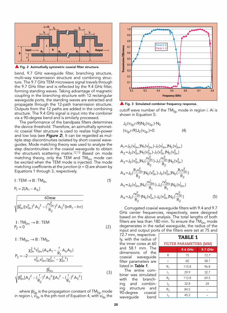
The performance of the bandpass filters determines the device threshold. Therefore, an azimuthally symmet-ric coaxial filter structure is used to realize high-power and low loss (see Figure 2). It can be regarded as mul-tiple step discontinuities isolated by short coaxial wave-guides. Mode matching theory was used to analyze the step discontinuities in the coaxial waveguide to obtain the structure’s scattering matrix.12,13 Based on mode matching theory, only the TEM and TM0m mode can be excited when the TEM mode is injected. The mode matching coefficients at the junction (z = 0) are shown by Equations 1 through 3, respectively.
TEM TM
TM T M
TM TM
0n
0
0m 0n
( )
( )
Ι → ΙΙ
= −
πωε
β ν −ν
−
Ι → ΙΙ=
Ι → ΙΙ
= −χ ν −
ν ν χ − χ
β
β − −
: : (1)
P 2(A A )
60
(( ) A (rR
) A (lnR lnr)
: : E P 0 2
: :
P 2(A A
rR
A A )
( )
[A (rR
) A ][A (rR
) A ]3
1 1 6
0nII
0nII 2
22 0n
II
2
232
1
m2
3
0n2 II
0mI
4 11
6 5
0nII
0mI
0m2 I
0n2 II
0mI
0nII
22
2
232
12
1
252
where βi0p is the propagation constant of TM0p mode
in region i, νi0p is the pth root of Equation 4, with ϰi
0p the
cutoff wave number of the TM0p mode in region i. Ai is shown in Equation 5:
ν ν
ν ν
J ( r/R)N ( )-N
( r/R)J ( )=0 (4)0 0p 0 0p 0
0p 0 0p
ν ν ν νν ν ν ν
νν ν
ν
νν ν
ν
νν ν
ν
νν ν
ν
A =J ( )N ( )-J ( )N ( )A =J ( )N ( )-J ( )N ( )
A =J ( )N (rR
)-J (rR
)N ( )
A =J (RR
)N ( )-J ( )N (RR
)
A =J ( )N (rR
)-J (rR
)N ( )
A =J (rR
)N ( )-J ( )N (rR
) (5)
1 0 0mI
1 0mI
1 0mI
0 0mI
2 0 0nII
1 0nII
1 0nII
0 0nII
3 0 0nII
10nII
21
0nII
20 0n
II
4 01 0n
II
20 0n
II0 0n
II0
1 0nII
2
5 0 0mI
10mI
11
0mI
10 0m
I
6 00nII
20 0n
II0 0n
II0
0nII
2
Corrugated coaxial waveguide filters with 9.4 and 9.7 GHz center frequencies, respectively, were designed based on the above analysis. The total lengths of both filters are less than 180 mm. To ensure the TM0m mode degenerates in the radial waveguide, the radius of the input and output ports of the filters were set at 75 and 72.7 mm, respective-ly, with the radius of the inner cores at 60 and 58.1 mm. The dimensions of the coaxial waveguide filter parameters are listed in Table 1.
The entire com-biner was simulated with the branch-ing and combin-ing structure and 90-degree coaxial waveguide bend
s Fig. 2 Azimuthally symmetric coaxial filter structure.
l2 l2
l1
z = 0
l1
R1Rr
III
R2 R2 R1OutputInput
TABLE 1FILTER PARAMETERS (MM)
9.4 GHz 9.7 GHz
R 75 72.7
r 60 58.1
R1 115.8 96.8
I1 29.9 32.7
R2 112.8 69.5
I2 32.8 24
R3 84.5 –
I3 45.2 –
s Fig. 3 Simulated combiner frequency response.
Frequency (GHz)
1.0
0.9
0.8
0.7
0.6
0.5
0.4
0.3
0.2
0.1
0
Tran
smis
sion
Ef�
cien
cy
9.3 9.4 9.5 9.6 9.7 9.89.2
Ports 2–3Ports 1–3
26
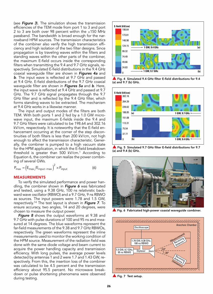
(see Figure 3). The simulation shows the transmission efficiencies of the TEM mode from port 1 to 3 and port 2 to 3 are both over 98 percent within the ±150 MHz passband. The bandwidth is broad enough for the nar-rowband HPM sources. The transmission characteristics of the combiner also verify the high transmission effi-ciency and high isolation of the two filter designs. Since propagation is by traveling waves within the filters and standing waves within the other parts of the combiner, the maximum E-field occurs inside the corresponding filters when transmitting the 9.4 and 9.7 GHz signals, re-spectively. Simulated E-field distributions in the 9.4 GHz coaxial waveguide filter are shown in Figures 4a and b. The input wave is reflected at 9.7 GHz and passed at 9.4 GHz. E-field distributions of the 9.7 GHz coaxial waveguide filter are shown in Figures 5a and b. Here, the input wave is reflected at 9.4 GHz and passed at 9.7 GHz. The 9.7 GHz signal propagates through the 9.7 GHz filter and is reflected by the 9.4 GHz filter, which forms standing waves to be extracted. The mechanism at 9.4 GHz works in a likewise manner.
The input and output modes of the filters are both TEM. With both ports 1 and 2 fed by a 1.0 GW micro-wave input, the maximum E-fields inside the 9.4 and 9.7 GHz filters were calculated to be 198.64 and 302.16 kV/cm, respectively. It is noteworthy that the E-field en-hancement occurring at the corner of the step discon-tinuities of both filters is less than 200 kV/cm, not high enough to affect the transmission characteristic. Gener-ally, the combiner is pumped to a high vacuum state for the HPM application, in which the E-field breakdown threshold is greater than 500 kV/cm.1 According to Equation 6, the combiner can realize the power combin-ing of several GWs.
( )= ×−P E E P (6)max max input max2
input
MEASUREMENTSTo verify the simulated performance and power han-
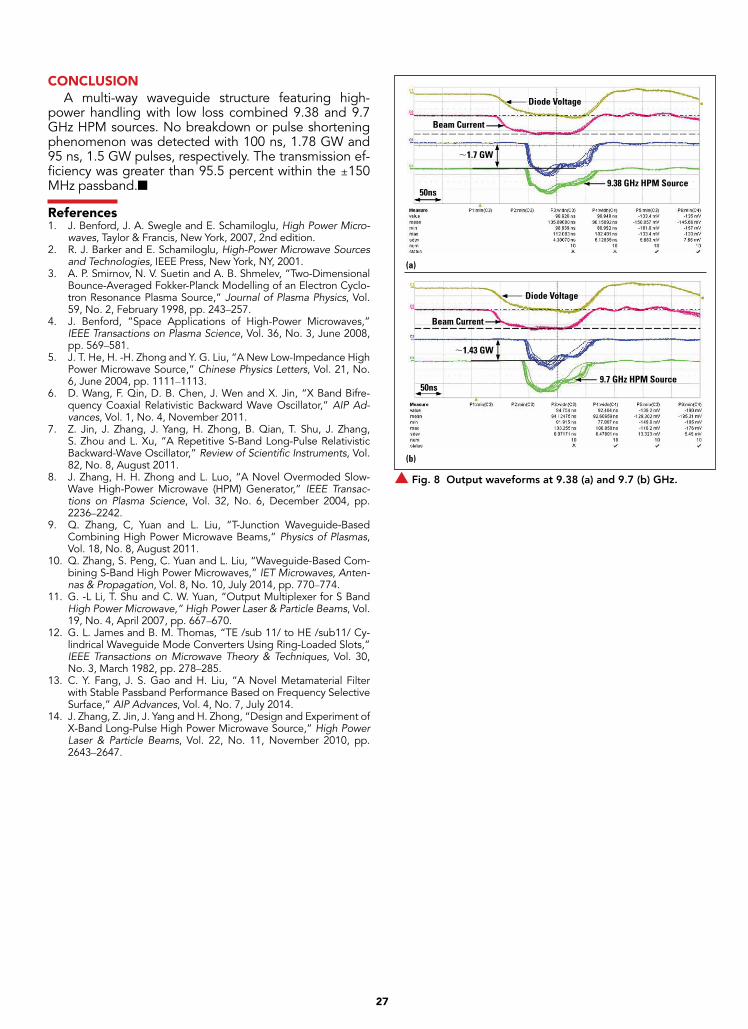
dling, the combiner shown in Figure 6 was fabricated and tested, using a 9.38 GHz, 100 ns relativistic back-ward wave oscillator (RBWO) and a 9.7 GHz, 9 ns RBWO as sources. The input powers were 1.78 and 1.5 GW, respectively.14 The test layout is shown in Figure 7. To ensure accuracy, two angles, 14 and 20 degrees, were chosen to measure the output power.
Figure 8 shows the output waveforms at 9.38 and 9.7 GHz with pulse durations of 100 and 95 ns and mea-sured at 14 degrees. The blue waveforms represent the far-field measurements of the 9.38 and 9.7 GHz RBWOs, respectively. The green waveforms represent the inline measurements used to monitor the working condition of the HPM source. Measurement of the radiation field was done with the same diode voltage and beam current to acquire the power handling capacity and transmission efficiency. With long pulses, the average power levels detected by antennas 1 and 2 were 1.7 and 1.43 GW, re-spectively. From this, the insertion loss of the combiner was calculated to be 4.5 percent and the transmission efficiency about 95.5 percent. No microwave break-down or pulse shortening phenomena were observed during testing.
s Fig. 4 Simulated 9.4 GHz filter E-field distributions for 9.4 (a) and 9.7 (b) GHz.
(a)
(b)
E-�eld (kV/cm)
1 GW, 9.7 GHz
198.64
173.81
148.98
124.15
99.32
74.49
49.66
24.83
0
1 GW, 9.4 GHz
s Fig. 5 Simulated 9.7 GHz filter E-field distributions for 9.7 (a) and 9.4 (b) GHz.
(a)
(b)
E-�eld (kV/cm)
1 GW, 9.7 GHz
302.16
264.39
226.62
188.85
151.08
113.31
75.54
37.77
0 1 GW, 9.4 GHz
s Fig. 6 Fabricated high-power coaxial waveguide combiner.
s Fig. 7 Test setup.
Oscilloscope
1.5 GW, 9.7 GHz,95 ns RBWO
Anechoic Chamber
1.78 GW, 9.38 GHz,100 ns RBWO
Diplexer Horn14°
–20°
(Measurement)
Receiving
Antenna 1
ReceivingAntenna 2
(Validation)
27
CONCLUSIONA multi-way waveguide structure featuring high-
power handling with low loss combined 9.38 and 9.7 GHz HPM sources. No breakdown or pulse shortening phenomenon was detected with 100 ns, 1.78 GW and 95 ns, 1.5 GW pulses, respectively. The transmission ef-ficiency was greater than 95.5 percent within the ±150 MHz passband.n
References1. J. Benford, J. A. Swegle and E. Schamiloglu, High Power Micro-
waves, Taylor & Francis, New York, 2007, 2nd edition.2. R. J. Barker and E. Schamiloglu, High-Power Microwave Sources
and Technologies, IEEE Press, New York, NY, 2001.3. A. P. Smirnov, N. V. Suetin and A. B. Shmelev, “Two-Dimensional
Bounce-Averaged Fokker-Planck Modelling of an Electron Cyclo-tron Resonance Plasma Source,” Journal of Plasma Physics, Vol. 59, No. 2, February 1998, pp. 243–257.
4. J. Benford, “Space Applications of High-Power Microwaves,” IEEE Transactions on Plasma Science, Vol. 36, No. 3, June 2008, pp. 569–581.
5. J. T. He, H. -H. Zhong and Y. G. Liu, “A New Low-Impedance High Power Microwave Source,” Chinese Physics Letters, Vol. 21, No. 6, June 2004, pp. 1111–1113.
6. D. Wang, F. Qin, D. B. Chen, J. Wen and X. Jin, “X Band Bifre-quency Coaxial Relativistic Backward Wave Oscillator,” AIP Ad-vances, Vol. 1, No. 4, November 2011.
7. Z. Jin, J. Zhang, J. Yang, H. Zhong, B. Qian, T. Shu, J. Zhang, S. Zhou and L. Xu, “A Repetitive S-Band Long-Pulse Relativistic Backward-Wave Oscillator,” Review of Scientific Instruments, Vol. 82, No. 8, August 2011.
8. J. Zhang, H. H. Zhong and L. Luo, “A Novel Overmoded Slow-Wave High-Power Microwave (HPM) Generator,” IEEE Transac-tions on Plasma Science, Vol. 32, No. 6, December 2004, pp. 2236–2242.
9. Q. Zhang, C, Yuan and L. Liu, “T-Junction Waveguide-Based Combining High Power Microwave Beams,” Physics of Plasmas, Vol. 18, No. 8, August 2011.
10. Q. Zhang, S. Peng, C. Yuan and L. Liu, “Waveguide-Based Com-bining S-Band High Power Microwaves,” IET Microwaves, Anten-nas & Propagation, Vol. 8, No. 10, July 2014, pp. 770–774.
11. G. -L Li, T. Shu and C. W. Yuan, “Output Multiplexer for S Band High Power Microwave,” High Power Laser & Particle Beams, Vol. 19, No. 4, April 2007, pp. 667–670.
12. G. L. James and B. M. Thomas, “TE /sub 11/ to HE /sub11/ Cy-lindrical Waveguide Mode Converters Using Ring-Loaded Slots,” IEEE Transactions on Microwave Theory & Techniques, Vol. 30, No. 3, March 1982, pp. 278–285.
13. C. Y. Fang, J. S. Gao and H. Liu, “A Novel Metamaterial Filter with Stable Passband Performance Based on Frequency Selective Surface,” AIP Advances, Vol. 4, No. 7, July 2014.
14. J. Zhang, Z. Jin, J. Yang and H. Zhong, “Design and Experiment of X-Band Long-Pulse High Power Microwave Source,” High Power Laser & Particle Beams, Vol. 22, No. 11, November 2010, pp. 2643–2647.
s Fig. 8 Output waveforms at 9.38 (a) and 9.7 (b) GHz.
(a)
(b)
9.7 GHz HPM Source
50ns9.38 GHz HPM Source
Diode Voltage
∼1.7 GW
Beam Current
50ns
Diode Voltage
∼1.43 GW
Beam Current
28
PAs enable dual-use S- and X-Band Radar Systems: QPA0007 and QPA0004
Qorvo® is now shipping the industry’s first com-mercially available family of electronically recon-figurable dual-band (S- and X-Band) GaN pow-
er amplifiers (PAs). These patented PAs support a revo-lutionary shift in radar architecture for defense, weather and commercial avionics.
The QPA0007 and QPA0004 are the first commercial-ly available GaN PAs that can be rapidly reconfigured for operation between S- and X-Bands. This enables a single radar platform to be used across multiple applications, offering precise long-range and short-range capabili-ties. This eliminates the need for independent systems, saving size, weight, power and cost. Now designers can dramatically reduce the BOM and footprint by as much as 50 percent while improving overall performance. The QPA0007 and QPA0004 are available in surface mount technology (SMT) packaging and offer higher saturated power and power-added efficiency when compared to traditional switched dual-band solutions.
Eric Higham, Advanced Semiconductor Applications/Advanced Defense Systems Service director at Strategy Analytics, said, “The defense industry is evolving toward a ‘more with less’ strategy and this places a premium on system performance and flexibility. The capabilities and performance advantages of GaN technology make it attractive in all defense applications, particularly radar. Qorvo’s long heritage and leadership in GaN technol-ogy and defense applications allow them to develop innovative products like these that will support and en-able emerging dual-band radar solutions.”
Roger Hall, general manager of Qorvo’s High Per-formance Systems, said, “Defense and commercial customers count on Qorvo’s world-class GaN solutions, and the QPA0007 and QPA0004 are testament to our engineering team’s passion for innovation. Today’s an-nouncement reveals another industry milestone for Qor-vo, the first commercially available, reconfigurable GaN PAs that support S-band and X-band radar. This new
Qorvo® Advances Radar Architecture with Reconfigurable Dual-Band GaN Power Amplifier MMICs Qorvo
family of products streamlines next-generation radar designs.”
The QPA0007 and QPA0004 are now sampling to qualified customers. These GaN devices are optimized for manufactur-ability and offered in small 7 x 6 mm and 7 x 4 mm QFN, SMT packages.
www.mwjournal.com/articles/36230
QPA0007 Specifications S-Band X-Band
Frequency Range (GHz) 3.1 - 3.5 9 - 11
RF Power (Watts) 32 28
Power Gain (dB) 21 18.5
PAE 47% 32%
Package Size (mm) 7 x 6
QPA0004 Specifications S-Band X-Band
Frequency Range (GHz) 3.1 - 3.5 9 - 11
RF Power (Watts) 9 8
Power Gain (dB) 21 19
PAE 51% 34%
Package Size (mm) 7 x 4

Next-Generation RF Solutions for Mission Critical Systems
© 06-2021 Qorvo US, Inc. | QORVO, ALL AROUND YOU and CONNECT, PROTECT AND POWER are trademarks of Qorvo US, Inc.
Description FrequencyRange (GHz)
RF Power(Watts)
PAE(%)
Pkg. Size(mm)
Part Number
S/X-Dual Band Reconfigurable PA 3.1-3.5, 9-11 32, 28 47, 32 7x6 QPA0007
S/X-Dual Band Reconfigurable PA 3.1-3.5, 9-11 10, 8 51, 34 7x4 QPA0004
X-Band FEM 8-12 10 32 7x5 QPF5010
X-Band FEM 8-12 5 35 7x5 QPF5005
X-Band FEM 8.5-10.5 2 37 7x5 QPF5002
Qorvo® offers customers the most advanced combination of power and performance with its industry-leading GaN power amplifiers and front-end modules (FEMs) that operate between 8 and 12 GHz (X-band). Qorvo’s RF solutions set the standard for reliability, efficiency and design flexibility, and is a trusted and preferred supplier to the DoD and leading defense contractors around the globe. As the industry’s only MRL 10 GaN supplier, customers can depend on Qorvo solutions to support mission critical applications that operate in the harshest environments on land, sea, air and space. At Qorvo we deliver RF and mmWave products to Connect, Protect and PowerTM RF systems All Around You®. To learn more, visit qorvo.com or connect with our distribution partner RFMW at www.rfmw.com/qorvoradar/43
The Industry’s Most Reliable, High-Performance GaN & GaAs Solutions