
Addis Ababa University, College of Health Sciences, School of ...
Upload
khangminh22Category
view
0download
0
i | P a g e
ADDIS ABABA UNIVERSITY
ADDIS ABABA INSTITUTE OF TECHNOLOGY
DEPARTMENT OF ELECTRICAL ENGINEERING FOR RAILWAY
SYSTEM
DEVELOPMENT OF FPGA BASED SYSTEM ON CHIP FOR LEVEL
CROSSING MANAGEMENT SYSTEM IN CASE OF AALRT
BY
SOLOMON HAILEMICHAEL
THESIS SUBMITTED TO ADDIS ABABA INSTITUTE OF
TECHNOLOGY IN PARTIAL FULFILLMENT OF THE
REQUIREMENTS FOR THE DEGREE OF
MASTER OF SCIENCE
IN
ELECTRICAL ENGINEERING FOR RAILWAY SYSTEM
ADVISOR:
DR. YALEMZEWD NEGASH
14 May, 2015

ii | P a g e
ADDIS ABABA UNIVERSITY
ADDIS ABABA INSTITUTE OF TECHNOLOGY
DEVELOPMENT OF FPGA BASED SYSTEM ON CHIP FOR LEVEL CROSSING
MANAGEMENT SYSTEM IN CASE OF AALRT
BY
SOLOMON HAILEMICHAEL
APPROVAL BY BOARD OF EXAMINERS
_________________________________ _________________________________
CHAIRMAN DEPARTMENT OF SIGNATURE
GRADUATE COMMITTEE
_________________________________ ________________________________
ADVISOR SIGNATURE
________________________________ ________________________________
INTERNAL EXAMINER SIGNATURE
________________________________ _______________________________
EXTERNAL EXAMINER SIGNATURE

i | P a g e
“I hereby declare that this report is the results of my own work except for quotes as cited in the
reference.”
Signature: ………………………………………………
Author : SOLOMON HAILEMICHAEL AREFAYNE
Date :------------------------------------------------------

i | P a g e
“I hereby declare that I have read this report and in my opinion this report is sufficient in terms
of the scope and quality for the award of Masters of Electrical and computer Engineering
(Electrical and computer Engineering for Railway Systems) With Honors”
Signature : ………………………………………………
Supervisor‟s name: Dr. Yalemzewd Negash
Date: _______________________________________

ii | P a g e
ACKNOWLEDGEMENT
First of all, I would like to thank God for his blessing, and I also want to express my deepest
gratitude to my supervisor Dr. Yalemzewd Negash for support and guidance throughout this
project running and completion of this report.
My deepest appreciation also goes out to my beloved wife Almaz Leake who gave me many
needed support, encouragement and help throughout my project‟s improvement, and my friends
who struggling with me exploring this scope.

iii | P a g e
Abstract The purpose of this thesis is to develop an automatic railway gate system that uses the FPGA as a
main function of design. The principle objective of this thesis was to design an automatic railway
gate control by FPGA. This thesis deals to develop a prototype of railway gate that function
automatically by using FPGA. Besides that, the interfacing program also had been developed for
the integration part. The main concept of the system is that, depending on arrival or departure of
the train near level crossing, the crossing gate will close or open automatically with displaying
corresponding signals like Red or Green signal. That means, when the train approaching near
level crossing, the crossing gate will close and showing Green signal for train, so, train can move
without any interruption of its speed. After leaving the train from level crossing, the crossing
gate will open, but there may be a chance that when a vehicle is trying to cross the level crossing
then the crossing gate may close as the train is approaching nearby. At this situation, the system
detects the vehicle as an obstacle in order to prevent accidents, so the gate will be opened until
the vehicle moves away from the crossing gate and the train will be stopped as it detects the
Vehicle as obstacle just under crossing gate. By developing automatic gate control, the railway
level crossing accidents of Ethiopia can be minimized. The system is designed using RF
Transceiver, IR Sensor, FPGA, Steeper Motor, Relay and some external devices.
Keywords: Level crossing, FPGA, LabVIEW, Automatic gate control

iv | P a g e
Contents Abstract ........................................................................................................................................................ iii
List of tables ................................................................................................................................................ vii
Lists of Figures ............................................................................................................................................ viii
LIST OF ABBRIVATIONS AND SYMBOLS ........................................................................................................ ix
Chapter one .................................................................................................................................................. 1
Introduction .................................................................................................................................................. 1
1.1 Background of the paper .................................................................................................................... 1
1.2 Statement of the problems ................................................................................................................. 3
1.3 Objective ............................................................................................................................................. 3
1.3.1 General objectives ....................................................................................................................... 3
1.3.2 Specific Objective: ........................................................................................................................ 3
1.4. Scope of Works .................................................................................................................................. 4
1.5 Methodology ....................................................................................................................................... 4
1.6 Thesis Structure .................................................................................................................................. 5
Chapter 2 ....................................................................................................................................................... 6
Level crossing system and design requirements ........................................................................................... 6
2.1 Level Crossings: Definitions, Types and Classifications ....................................................................... 6
2.1.1. Protected Level Crossing ............................................................................................................. 6
2.1.2 Protected Pedestrian Level Crossing ............................................................................................ 7
2.2 Common Level Crossing Design Requirements .................................................................................. 7
2.2.1. Warning time .............................................................................................................................. 8
2.2.2. Level Crossing Approach ............................................................................................................. 9
2.2.3 Train mode ................................................................................................................................. 10
2.2.4 Operational Monitoring ............................................................................................................. 10
2.2.5 Fault Monitoring and Management ........................................................................................... 11
2.2.6 Alarms ........................................................................................................................................ 11
2.2.7 Specific Timings .......................................................................................................................... 12
2.2.8 Gate delay .................................................................................................................................. 14

v | P a g e
2.2.9 Train demand response time ..................................................................................................... 14
2.3 Successive Operation ........................................................................................................................ 15
Chapter 3 ..................................................................................................................................................... 16
Prototyping of embedded system using FPGA ........................................................................................... 16
3.1 Introduction ....................................................................................................................................... 16
3.2 What is an Embedded System? ......................................................................................................... 16
3.3 Design Considerations when Developing an Embedded System ...................................................... 17
3.4 Importance of Rapid Prototyping of Embedded Systems using FPGAs ............................................ 18
3.5 Embedded Systems Design Flow FPGA based ............................................................................ 19
3.5.1 Modeling ............................................................................................................................. 19
3.5.2 Hardware and Software Partitioning ......................................................................................... 20
3.5.3 Scheduling .................................................................................................................................. 20
3.6 Xilinx and Altera Software Tools ................................................................................................. 21
3.6.1 ZYBO (ZYnq BOard) .................................................................................................................... 22
3.7 LabVIEW ............................................................................................................................................ 24
3.7.1 When to Use LabVIEW FPGA ..................................................................................................... 25
3.8 Other Technologies used .................................................................................................................. 26
3.8.1 Infrared Sensor ........................................................................................................................... 26
3.8.2 RF Modules (434MHz): ............................................................................................................... 29
3.8.3 ULN 2003 .................................................................................................................................... 33
3.8.4 Stepper motor ............................................................................................................................ 34
Chapter 4 ..................................................................................................................................................... 37
Methodology ............................................................................................................................................... 37
4.1 Existing system ............................................................................................................................ 37
4.2 Designing of level crossing traffic management system ............................................................. 39
4.2.1 Description of the physical components of a LRT level crossing system ................................... 40
4.3 System flow ....................................................................................................................................... 42
4.4 Finite State Machine (FSM) ............................................................................................................... 43
4.4.1 Traffic lights at a level crossing of a railway and a road. ........................................................... 45
Chapter 5 ..................................................................................................................................................... 48
Results and Discussions .............................................................................................................................. 48
5.1 Vivado Simulation Result .................................................................................................................. 48

vi | P a g e
5.2 LabVIEW simulation results ........................................................................................................ 50
5.3 Discussion on the above result ................................................................................................... 56
5.4 Discussion on safeness of the models ........................................................................................ 57
Chapter 6 ..................................................................................................................................................... 59
Conclusion and Recommendation .............................................................................................................. 59
6.1 Conclusion ........................................................................................................................................ 59
6.2 Future Recommendation .................................................................................................................. 59
Reference .................................................................................................................................................... 60
Appendix A: SDK Programing ...................................................................................................................... 62
A.1 GPIO Program ................................................................................................................................... 62
A.2 LED programing ................................................................................................................................ 63
A.3 Main program .................................................................................................................................. 64

vii | P a g e
List of tables Table 1 Train demand indication ................................................................................................................ 11
Table 2 Crossing operating indication ........................................................................................................ 11
Table 3 ZYBO Device description diagram ............................................................................................... 24
Table 4 Pin description of RF transmitter module ...................................................................................... 30
Table 5 Pin description of RF Receiver module ......................................................................................... 30
Table 6 Pin description of HT12E RF Encoder .......................................................................................... 31
Table 7 Pin description of HT12D RF Decoder ......................................................................................... 32
Table 8 Full step sequence of steeper motor ............................................................................................... 36
Table 9 Half step steeper motor sequence ................................................................................................. 36
Table 10 Description of various terms used to model LX control system .................................................. 40
Table 11 description of possible states of LX system ................................................................................. 56
Table 12 STATES/ SITUATIONS OF RAILWAY TRAFFIC MOVEMENT NEAR THE LEVEL ........ 58

viii | P a g e
Lists of Figures Figure 1 General components of level crossing ............................................................................................ 1
Figure 2. Process flow of the thesis ............................................................................................................... 4
Figure 3. Additional time allowances for angled or wide crossings ............................................................. 9
Figure 4. Railway level crossing and road intersection layout .................................................................... 12
Figure 5. Design Cycles for FPGAs and ASICs .......................................................................................... 19
Figure 6. Hardware Software Partitioning and Co-design .......................................................................... 21
Figure 7. ZYBO Zynq-7000 development board ........................................................................................ 23
Figure 8. With LabVIEW FPGA, you can create custom FPGA VIs for high-speed data acquisition,
control loops, or custom timing and triggering. .......................................................................................... 25
Figure 9. Circuit diagram of IR transmitter ................................................................................................. 27
Figure 10. Circuit diagram of TSOP 1356 .................................................................................................. 28
Figure 11. Block Diagram of an IR receiver ............................................................................................... 28
Figure 12. Pin diagrams of RF receiver and transmitter Module ................................................................ 29
Figure 13. Operation of RF remote control ................................................................................................. 30
Figure 14. Pin diagram of HT12E RF encoder ............................................................................................ 31
Figure 15. ULN 2003 Pin diagram .............................................................................................................. 33
Figure 16. Components of steeper motor .................................................................................................... 34
Figure 17. Driving Steeper Motor using ULN 2003 ................................................................................... 35
Figure 18: Physical components at a level crossing of a railway and a road .............................................. 39
Figure 19. State diagram of automatic gate control .................................................................................... 44
Figure 20. Modeling architecture of LX system ......................................................................................... 45
Figure 21. Model of the railroad-crossing controller .................................................................................. 46
Figure 22. Model of the gate ...................................................................................................................... 47
Figure 23. Schematic diagram of completed design ................................................................................... 48
Figure 24. Package layout of the designed system ..................................................................................... 49
Figure 25. The IP port pin constraints ......................................................................................................... 49
Figure 26. Completed design ...................................................................................................................... 50
Figure 27. Front panel of Level crossing system ........................................................................................ 51
Figure 28. Initial situation ........................................................................................................................... 52
Figure 29. Waiting for interrupt situation ................................................................................................... 52
Figure 30. Checking presences of obstacles inside LX situation ................................................................ 53
Figure 31. Checking for train departure at specified TIMEOUT situation ................................................. 53
Figure 32. Checking Approaching request situation ................................................................................... 54
Figure 33. Checking lowering two barrier parts situation ........................................................................... 54
Figure 34. Checking for faulty situation ..................................................................................................... 55
Figure 35. Informing disaster management force situation ........................................................................ 55

ix | P a g e
List of abbreviations and symbols AALRT Addis Ababa Light Railway Transient
(ASIC) Application Specific Integrated Circuit
DRAM Dynamic RAM
EMIO Extended-MIO
EPROM Erasable-and-programmable ROM
FPGA Field Programmable Gate Array
FSM Finite State Machine
GPIO General Purpose I/O
TSC Traffic Signal Controller
TLR Traffic Light Response
RIU Railway interface unit
QCT Queue Clearance Time
TDRT Train Demand Response Time
IP Intellectual Property
I/O Input and Output
LX Level crossing
LUT Look up table
MIO Multiplexed I/O
NI National Instrument
Tx Transmitter
OTP One-time programmable
RAM Random access memory
ROM Read Only Memory
Rx Receiver
RF Radio Frequency
SDK Software Development Kit
x | P a g e
SOC system-on-chip
SRAM Static RAM
IR Infrared
VI Virtual Instrument
Tx Transmitter
OTP One-time programmable
RAM Random access memory
ROM Read Only Memory
Rx Receiver
RF Radio Frequency
SDK Software Development Kit
SOC system-on-chip
SRAM Static RAM
IR Infrared
VI Virtual Instrument

1 | P a g e

1 | P a g e
Chapter one
Introduction
1.1 Background of the paper
Railway has become the important means of transportation today. Crossing locations of railways
with roads (level crossings) are amongst the most eventful points on the transportation network.
At these points, due to passing the rail & road vehicles with two distinguished mechanism, the
priority is given to the rail vehicle because its braking distance (depending on their weight and
speed) is several hundred times longer than that of road vehicles. In the new implementation of
Railway system like ours, it is expected accidents in the manual level crossing will be high if
there is no automatic control system. Since automatic railway level crossing for our countries is
going to implement for the first time, it needs a lot of investigation, modeling and analysis of all
types of accidents. Level crossing accidents not only dominate in terms of frequency, but
also can be more severe in their consequences than other types of railway accidents,
simply because they can involve injuries and fatalities to railway passengers, as well as,
to road vehicle occupants and other users of Level crossings. Increasing road construction
and road vehicle population in Addis Ababa creates greater chance for Level crossing
accidents to happen.
Figure 1. General components of level crossing

2 | P a g e
For extensive railway network, an efficient management system is required to avoid train
accidents at level crossing. Factors influencing the probability of accident occurrence at LRT
level crossings include:
Rail traffic density (measured in terms of the maximum number of trains passing
the crossing within a 24 hour period);
Road traffic density (measured in terms of the maximum number of motor vehicles of
all types passing the crossing within a 24 hour period);
Presence of physical obstructions restricting the visibility of the track, warning signs or
signals to road users;
Absence of full width barrier protection at level crossings;
Absence of flashing lights and audible warning devices at level crossings;
Poor road surface condition at level crossings (leading to the grounding of low slung road
vehicles); and
Poor alignment and elevation of the road crossing the track (the road may cross
the track at an oblique angle or may approach the crossing on a steeply rising grade).
Weather conditions;
Human errors
In AA-LRT, the crossing gate is going to be operated manually by a gatekeeper after receiving
the information about the train's arrival that is more risky. Nowadays, every system is automated
in order to face new challenges. Automated systems that have less manual operation are flexible,
reliable and accurate. Due to these demands every field prefer automated control systems
especially in the field of electronics where automated systems are giving good result.
In general, this paper utilizes the importance of developing automatic railway level crossing
management system for AALRT based on FPGA tool. Nowadays, Field Programmable Gated
Arrays (FPGA) based technology is very popular in designing embedded systems. Specifically,
in recent years, with the development of FPGA, wireless communication technology, RF
technology have become hot technology in the field of electronic applications. All the
designs included in this prototype were developed following the suitability of labVIEW FPGA.
This automatic railway gate system operated after signal received from the IR and RF sensors.
These signals used to trigger the FPGA for operating the gate motor and alarm indicators by
control unit.
In this system, there are mainly two units: Signal Pole Unit and Train Unit. Signal Pole Unit
includes some major equipment like IR Sensor, Buzzer, LEDs, RF Transmitter, Encoder, DC
Motor, Motor Driver, Relays. Train Unit also includes some major equipment like RF Receiver,
Decoder, DC Motor, Motor Driver, Relays. Some common equipment‟s have used in both
sections like FPGA, Voltage Regulator ICs (78XX), Power Supply and so on.

3 | P a g e
1.2 Statement of the problems
In the existing system, the level crossing is designed to be manned. The railway gate
management has to employ workers to be on duty for control the operation. Due to this, the
worker will manually open and close the gate with under supervision. The lowering of the
crossing barrier will be achieved by manual control of the Crossing operator who can adopt two
modes for control, i.e. the indoor manual control and the on-site manual operation:
Normally, when a train approaches the crossing, the operator should first make sure that
the crossing area is cleared (without people and vehicle), and then press the lowering
button of barrier for lowering control of the barrier;
The crossing barrier can be lowered by on-site manual control in case of power failure
or malfunction.
This prototype will introduce the automatic railway gate operation. This system will make
improvement towards the manually operation before this. Human supervision will be considered
if there are problems occurred while this system was operated.
This is an idea to perform computer integration with mechanical structure to simulate what the
system can do. Control systems with computer applications will make the management or
consumer become more effective.
1.3 Objective
1.3.1 General objectives
The objective of the work is to develop a system on chip to transmit and receive the RF
signals to the safety of public at unmanned level crossing. SOC based on FPGA designed
specifically to govern and easily synchronize with RF transceiver.
1.3.2 Specific Objective:
The specific objectives are:
i. To develop a prototype of railway gate that function automatically by using
FPGA.
ii. To develop an interfacing program for the integration part of FPGA operation.
iii. To design an automatic railway gate control by using FPGA.
iv. Developing the control unit and interfacing unit using VIVADO 2014.1 software
v. Simulating the peripherals using labVIW FPGA simulator

4 | P a g e
1.4. Scope of Works
This thesis covered the operation of automatic railway gate control by using FPGA (ZYNQ 7000
board and LabVIEW). The simulations involved such as IR sensor, light and buzzer, gate motor
and LCD display. All of these operations will be combining to demonstrate the operation of
embedded system.
The operations of FPGA works following the instruction programmed using vivado. The
combining systems were constructed on NI labVIEW and VIVADO software to show whether
the system is right or not.
IR sensor circuit is providing signal to triggered the FPGA. The sensed signal will actuate the
gate motor and LCD display. Alarm and indication light circuit provided as additional part of this
system. Additional elements can be added without affecting the remaining elements.
1.5 Methodology
The general workflows to accomplish the above listed objectives were as shown below:
Figure 2. Process flow of the thesis
Data collection on System Requirements
• Standards
• Operational requirements
• Technical requirements
System Design
• Component of train unit
• Component of signal pole unit
• Control of Rail and road signals
• Control of LC barriers
Result and Discussion
Conclusion and Future work
Simulation
Hardware synthesis, simulation and
integration using VIVADO and labVIEW
Programming of interfacing units using
SDK
5 | P a g e
1.6 Thesis Structure
Chapter 1 introduced the thesis as a whole. The early and basic explanations were mentioned in
this chapter. This chapter consisted of the thesis introduction and objectives, problem statements,
scope of work, and the simplified methodology.
Chapter 2 is the general overview of Level crossing system. This chapter consisted of the
definitions, components, and general requirements used for designed level crossing.
Chapter 3 is reviewing of Technologies and materials used to develop this paper. It explained
how this project came to be. This chapter explains embedded system, prototyping of embedded
system and development tools and additional material used to develop this report.
Chapter 4 is methodology. This chapter explained the part most important of all, the process
flow, what had been researched and what needed to be done was explained in this chapter.
Chapter 5 concentrated on the result and discussion of this thesis. What had been done was
explained in diagrams and written programs. The expected results also mentioned in this chapter.
Chapter 6 was the final chapter in this report. The conclusions and recommendations were placed
in this chapter. In other words, the conclusion was the summary of what had been done
throughout this thesis. After the project was done, recommendations were made and any
expansions or upgrades that might be done in the future were suggested.

6 | P a g e
Chapter 2
Level crossing system and design requirements
2.1 Level Crossings: Definitions, Types and Classifications All road/rail intersections (grade or level crossings) are provided with either passive or active
protection. Passive protection is the application of passive traffic control devices (signage) which
provides an unchanging warning to the road user whether or not a train is approaching the
crossing.
Active protection is the application of warning devices to warn road users of the approach of a
train when the train is a minimum time from entering the road-rail intersection. In some cases, it
also blocks access to the crossing.
This section addresses the terms and definitions relating to those locations where active level
crossing warning or protection devices have been provided for the safety of road users,
pedestrians, and rail traffic.
The terms and definitions used throughout this standard are generally aligned with the wording
used in the current ERC Documentation.
2.1.1. Protected Level Crossing
A Protected Level Crossing is defined to be a road-rail intersection at which a risk assessment
has determined that the hazard is such that provision of active warning and/or protection devices
is required in the interests of the safety of the road traffic, pedestrians and rail traffic.
Active warning devices are provide for the protection of crossing users and there are no passive
traffic control devices such as “GIVE WAY” or “STOP” signs.
Types of Active Level Crossing Protection:
Active level crossing can be classified differently, but the common types of Active Level
Crossing Protection:
1. Level Crossing controlled by Flashing Lights.
2. Level Crossing controlled by Flashing Lights and Half-Boom Gates.
3. Level Crossing controlled by Flashing Lights and Four Quadrant Half-Boom Gates.
In this paper, the term Half-Boom Gate shall be synonymous with the terms Boom Barrier or
Boom Gate. Four quadrant gates shall refer to application of half boom barriers arranged to
control entry to and exit from the road-rail intersection.

7 | P a g e
2.1.2 Protected Pedestrian Level Crossing
A Protected Pedestrian Crossing is defined to be a pedestrian-rail intersection at which a risk
assessment has determined that the hazard is such that provision of active warning and/or
protection devices is required in the interests of the safety of pedestrians.
Types of Pedestrian Level Crossing Protection
These are defined as:
1. Pedestrian level crossing controlled by lights;
2. Pedestrian level crossing controlled by lights and boom barriers or swing gates.
2.2 Common Level Crossing Design Requirements
There are many situations where a traffic signals and a level crossing are in a close proximity.
Each situation has individual characteristics that differ from other instances, but in all cases the
close proximity of the two traffic control facilities leads to the intersection of the traffic and
hence there should be an intersection of the traffic control equipment.
In situation where the distance between the level crossing and the intersection is
small or where the railway line passes through the intersection, it may be
possible to include the railway level crossing within the vehicular conflict area.
In this case, the train movement may be treated as a priority movement with a
dedicated phase.
Where there are intersections on both sides of the level crossing, it is recommended that
both intersections be equipped with traffic signals controlled by a single traffic signal
controller.
Where there is an intersection on one side of the level crossing only, it is desirable to
install a traffic signal lantern on the approach to the level crossing that feeds traffic to the
intersection. The signals can then be sequenced with the intersection signals to prevent
queues forming between the level crossing and the intersection. This is strongly
recommended where any of the following conditions exist:
The level crossing is very close to intersections
it is not possible focus or screen traffic signals at intersection so that they
cannot be seen from vehicles on the other sides of the level crossing:
the level crossing has no warning signals; or
the railway authority is unable to provide a train demand signal sufficiently
early to satisfy the train demand response time required to transition to a
clearance phase.

8 | P a g e
2.2.1. Warning time
Absolute minimum warning time - The absolute minimum warning times applicable to
road level crossings shall be the greater of times mandated by law, by road authorities.
Absolute minimum warning time depends on:
Equipment response
pedestrian time
minimum green on conflicting phase
yellow change interval
red clearance
Design minimum warning times for road and pedestrian crossings shall be:
25 seconds for Type Flashing light installations
25 seconds for Type Flashing light and boom barrier installations
30 seconds for Type Flashing light and boom barrier installations
20 seconds for pedestrian crossings with lights
25 seconds for pedestrian crossings with lights and booms or swing gates
Additional time allowances for angled or wide crossings:
Where the intersection between the road and the railway deviates from 900
the distance travelled
by vehicles to clear the crossing is lengthened. In the case where the distance to clear the
crossing is more than 10m then the minimum warning time shall be increased.
The distance to clear the crossing is measured along the road alignment from a point at the:
Location of the stop line or;
The location of the boom barrier or;
From a line drawn parallel to the closest track and 3.6m from the nearest rail whichever
is furthest from the departure side of the crossing, to a point on the departure side on a
line drawn parallel to the closest track and 2.3m from the nearest rail which point is
furthest from the arrival side (see Fig 2.1).
For every 3m above 10m width, the minimum warning time shall be increased by 1
second.

9 | P a g e
Figure 3. Additional time allowances for angled or wide crossings
Other considerations
Care shall be exercised in relation to determining the minimum warning time of the
fastest trains for various level crossing applications having regard to the avoidance of
excessive warning times because of slow or stopping train patterns.
Use of a constant warning time device is preferred where the technology and application
is suitable.
The minimum warning times specified for type Flashing light installations must be met
for Supplementary Warning Lights; significantly, longer warning times are acceptable if
use can be made of existing train detection systems in the area.
2.2.2. Level Crossing Approach
Level crossing approach is a zone where traffic signal lights are installed adjacent to/near a
railway level crossing, which face traffic that is also controlled by railway warning signals it is
desirable that they only capable of displaying off, yellow and red (this is to ensure that a green
traffic signal and flashing red warning signals cannot be displayed simultaneously to vehicles
arriving at the level crossing). In addition, where traffic signals are on the far side of the a level
crossing, special precautions may need to be taken to ensure that a green aspect is not visible
across the railway level crossing at the same as the flashing red railway signals.
Where traffic signal lights are installed on the approach to the crossing, it is desirable that these
signals are operated in either of the following two ways:
The signal is normally off and is only switched from off to yellow when a train demand is
received, from yellow to red after 5 seconds and red to off when the train demand is
cleared. This type of operations may be used when the likelihood of vehicles becoming
trapped on the railway crossing is extremely low.

10 | P a g e
The signal is normally red and is only switched off when there is no train demand, there
is a demand from a detector at the stop-line near the signal, and the downstream signal is
green. The signal remains off for a minimum of 5 second and is switched to yellow if a
train demand is received or if the phase in which it is running is ready to terminate. The
signal switches from yellow to red after 5 seconds. Under this operation, the downstream
signal must not switch to yellow until all vehicles have cleared the downstream stop-line
(the stop-line detector near the downstream signal has “gapped”) in order to keep the
level crossing clear of queued vehicles. This type of operation is essential when the level
crossing and the intersection are so close that long vehicles cannot be accommodated
between the intersection stop-line and the level crossing. It may also be necessary when
the railway authority is unable to provide sufficient advance warning (train demand
response time) of the arrival of a train.
2.2.3 Train mode
The traffic signal controller will enter train mode, i.e. as if a train demand has been received,
under the following conditions:
A valid, fault free, train demand is indicated
Only one of the train demand signals changes states
A valid, fault free, crossing operating indication is indicated
only one of the crossing operating signal changes states
If the traffic signal controller is in train mode for an extended period and either of the train
demand or crossing operating indication is in an alarm state then the TSC will return to flashing
yellow operation. The “extended period” needs to be determined by the traffic signal engineer.
Leaving train mode will reset the measurement of the period. Reversion from flashing yellow to
normal operation may only occur if train mode is removed or until a technician intervenes on
site.
When the traffic signal controller is ready for the train (clearance phase run for the minimum
period, in a train phase, etc.) a traffic light response (TLR) is given to the Railway Authority to
permit the crossing to operate earlier than the worst-case time. The adaptive engineer should
specify which controller outputs are to be used for TLR indication with respect to any other
outputs being used at the site.
2.2.4 Operational Monitoring
The traffic signal controller must be connected to central controller to provide remote monitoring
of site operation and alarms. This allows the state of intersection to be remotely monitored by
traffic engineering staff, these are:
The state of the train demand indications
The state of the crossing operating indication

11 | P a g e
The state of the traffic light response indication
If the crossing is manually operated
if the controller is in train mode
The use of special facility in place of external detector inputs for the monitoring of the railway
signaling system outputs is not recommended. Detector status is automatically provided to
central control unit for monitoring purpose.
2.2.5 Fault Monitoring and Management
A traffic signal controller interfaced to level crossing signals must be connected to central
control unit to ensure that the site is monitored and alarms noticed.
The train demand and crossing operating indications each comprises two separate signals, one
normally closed and one normally open. Under normal, fault free operation, each of the signals
will change state when an indication is changed. If the controller detects a change in one of the
two signals for each indication then either a fault is detected in the train demand or crossing
operating circuits and the controller shall operate as if a train demand has been received. The
following illustrate the situations.
Table 1 Train demand indication
Train demand Normally closed-open Normally closed -closed
Normally open-open Train demand NO TRAIN DEMAND
Normally open-closed TRAIN DEMAND Train demand
Table 2 Crossing operating indication
Crossing operating Normally closed-open Normally closed-closed
Normally open-open Crossing Operating CROSSING NOT OPERATING
Normally open-closed CROSSING OPERATING Crossing Operating
2.2.6 Alarms
To enable traffic signal engineers and control technicians to diagnose faults the controller should
provide indications to operation monitoring unit under the following circumferences:
Site in flashing yellow due to train demand operating excessively long, and train
demand or crossing operating indication has an alarm state;
Train demand inputs not in agreement;
crossing operating inputs not in agreement;
Traffic light response feedback indication while traffic light response not indicated;
crossing operating indication changes indication changes state from OFF to ON while
train demand not indicated;

12 | P a g e
crossing operating indication present for longer than a defined period after a train
demand is removed;
Crossing operating indication changes from On to OFF while a train demand is
present(while the crossing is not under manual control and the train demand is a repeat
demand);
Crossing operating indication changes from OFF to ON earlier than expected (before
TLR indicated, and the crossing is not under manual control and the controller has no
started up in the clearance phase and it is more than two second before TLR is due to be
indicated);
Crossing operating indication is ON approximately 2 second before TLR is due to being
indicated (and the crossing is not under manual control and the controller has not started
up in the clearance phase).
2.2.7 Specific Timings
The coordination between the railway level crossing and traffic signal controller is achieved
using a traffic signal controller (TSC) incorporating a railway interface unit (RIU). The RIU is
fully described in railway interface unit specification and the procedure for installing the RIU in
the TSC is in the installation and testing specification.
The specific timing provides specific guidance for traffic signal engineer in establishing the
necessary information and time settings required for TSC/personality/RIU to work safely and
efficiently with the level crossing. The following timings need to establish:
Queue Clearance time
Train demand response time
Gate delay
Figure 4. Railway level crossing and road intersection layout

13 | P a g e
The queue clearance (QCT) is required to clear any queue that may have formed across the level
crossing. This means that the QCT must be long enough to clear the queue that may have formed
along part A in figure above. The formulation of the QCT should also take into account the type
of vehicle using the level crossing. E.g. cars, vans, trucks, etc.
The QCT is need to take in to account the worst case scenario, where the slowest moving vehicle
(e.g. bus) may be stopped at point C (Figure 4), i.e. just on the level crossing. The QCT must be
sufficient long to ensure that the slow moving/ slow accelerating vehicle is clear of the level
crossing when the boom gate begin to descend.
Two methods for establishing the QCT are designed below. Both methods should be used to
provide confirmation that the chosen value is appropriate.
In both case the clearance position needs to be determined, i.e. the place at which it is determine
that the queue has been cleared. This maybe when the last vehicle which is obstructing the level
crossing. In order of preference:
a) clears( has passed) the intersection stop line; or
b) reaches the intersection stop line; or
c) clears(has passed) the level crossing;
2.2.7.1 Methods of establishing – Empirical
The queue dynamics can be measured at site to establish the maximum length of time that it
takes sor all vehicles to be clear of the level crossing once the clearance phase has commenced.
This measurement should look at all times of the day and week to ensure the unusual patterns are
identified and timed to find the maximum time to clear the level crossing of queued vehicles.
The establishment of the queue dynamics may need to be reviewed periodically, dependent on
the development and change in use the road and area, and hence change in vehicles using the
intersection- level crossing location.
2.2.7.2 Methods of establishing-Calculation
1. A stationary vehicle takes a particular period to response (initial movement) to a
change in the traffic signal. The period of time is subject to:
a) driver‟s attention;
b) gradient at the vehicles stand point
c) responsiveness of the vehicle, which is dependent on:
i. the drive train of vehicles;
ii. the vehicle‟s weight/ mass[
iii. vehicle‟s engine power; and
iv. vehicle‟s engine innovation
2. A vehicle tracks a particular amount of time to transverse from its start position to the
clearance position which is based on the following:
14 | P a g e
a) The vehicles distance from the start position to the clearance point;
b) the vehicle‟s average acceleration rate, which is dependent on:
i. road alignment between the vehicle‟s start position and the clearance
point;
ii. gradient from the start position to the clearance point;
iii. the road pavement type (more significant when in combination with
positive gradient );
iv. The vehicle‟s direction of travel through the intersection or turning
movement;
v. driver‟s behavior
vi. the actual speed of vehicle compared with the posted speed limit; and
vii. The clearance distance in front of the vehicle
3. The number and type of vehicles from the intersection stop line to and including the
vehicle, which is causing an abstraction on the level crossing.
2.2.8 Gate delay
The time from the level crossing warning lights beginning to flash to the point where the
boom signal commence descending is termed the gate delay. The gate delay allows
vehicles to remove themselves remove from level crossing. This is a parameter is set in
railway signaling system and is expressed as a range because of a variation in the
mechanical tolerance of the boom gates.
Generally, level crossings have a gate delay of 10 to 12 seconds. Where long or slow
moving vehicles operate over the level crossing longer gate delays may be required to
allow a vehicle that is „under‟ the boom gate to be clear by the time the boom gate
descends.
2.2.9 Train demand response time
The formulation of the train demand response time (TDRT) is vital to the correct operation of
the interface. Its calculation is obtained from the combination of the following components:
The time to transition the train demand phase set or clearance phase. The time is
dependent on the currently running phase and movements in the traffic signal
controller and in practice lies somewhere between the best and worst cases;
1. The best case is where the currently running phase has already terminated and the
transition to the next phase can be delivered to the clearance phase immediately,
satisfying and remaining safety times during the transition (shortest delay); and
2. The worst case is where the currently running phase has only just been initiated and
cannot be terminated as one or more of the safety times must be satisfied first
(longest delay). Generally, the longest delay will be incurred when a pedestrian
movement must be terminated and clearance intervals completed before transition to
the next phase can commence.

15 | P a g e
2.3 Successive Operation
Where a level crossing is on busy railway line, (particularly a double track) it is
responsible to expect second train to approach the level crossing where the first train is
still passing through it. There are three general cases where successive operation is to be
considered:
The second train places a train demand while the first train demand is still in
place. The traffic signal controller will not detect the second train but a
continuous train demand. In this case, the successive demand keeps the traffic
signal controller in the train demand phase set and remains here until “both” train
demands have ceased, and will begin transition to the normal set of phase when a
crossing operating ceases.
The second train places a train demands shortly after the level crossing has
ceased operating. In this case, the successive demand is treated as a new separate
demand and a clearance phase is demanded, where appropriate.
The second train places a train demand after the first train demand has been
removed but while the level crossing is still operating. In this case there are two
particular responses by traffic signal controller:
1. The second train demand arrives before the traffic signal controller has
removed the traffic light response. In this case the successive demand keeps
the traffic signal controller in the train demand phase set and remains here
until “both” train demands have ceased and will begin transition to the
normal set of phases when the second crossing operating ceases.
2. The second train demand arrives after the traffic signal controller has
removed the traffic light response. In this case, the railway system may have
started to raise the boom gates. In this instance, the successive demand is
treated as a new separate demand and clearance phase is demanded, where
appropriate.

16 | P a g e
Chapter 3
Prototyping of embedded system using FPGA
3.1 Introduction
The development of an embedded system contains many stages and decisions. The decisions are
based on the application and the standard challenges posed when developing any embedded
system. Before development, it is vital to understand what an embedded system is. The term is
used frequently without giving much thought to the definition. Once a product idea is
established, the stages of development depend on the product. Is the product an embedded
system? If the product is not, different design considerations and stages of development are
followed. The embedded system market contains many time constraints. The product should be
deployed when the demand for the product still exists, if the demand ceases then the product
would not yield any profit for the company. Rapid prototyping is needed in order for the product
to be revealed within the time period allotted. The steps of embedded system design and
development using FPGA are outlined and applied to a test application in later topics.
3.2 What is an Embedded System?
An embedded system is a set of circuitry that is lodged within other devices. A more formal
definition is that an embedded system is a digital system with at least one processor that
implements a hardware function that is a part or all of the digital system. The processor that is
used in an embedded system is an embedded processor.
The typical characteristics of an embedded system are as follows.
1. Designed to perform a single or application specific task, rather than multiple tasks.
Many embedded systems consist of small parts that fit within a larger device. The larger
device could be a general purpose system. An embedded system is usually part of a larger
system.
2. Many embedded systems contain real-time constraints. The design requirements vary by
the applications, but usually power, cost, reliability and performance are emphasized. The
amount of heat produced by the device may be of importance. The weight of the device
should be minimized for most embedded system applications.
3. The embedded system should not cease operation. This is a farfetched goal, but the power
usage and battery life should be utilized appropriately. Reduction in power usage will
greatly increase the battery life and the system would operate for a longer period of time.
4. Embedded systems usually interact with the outside world in the form of LCD displays,
speakers, keyboard, and other visual and auditory signals. The interactions allow the
users to operate the system and to specify certain commands.
5. Although embedded systems are application specific, some degree of programmability is
desired and essential. The re-programmability assists when upgrading the devices, it is

17 | P a g e
much easier to change the software slightly rather than develop the entire hardware from
scratch.
6. The program written for embedded systems, firmware, is stored in a limited amount of
memory. Designers need to consider the limited memory and computer hardware
resources when developing embedded systems.
The main goals when designing an embedded system are to minimize memory and power usage.
The cost of the device will decrease when the parameters are optimized. Tradeoffs when
designing are also encountered.
3.3 Design Considerations when Developing an Embedded System
Embedded systems are within every industry, from aerospace to consumer applications. With the
new advances in embedded systems design, more complex applications may be implemented.
During the development of an embedded system certain process models are followed. These
models usually include the development of a working prototype of the final system. Embedded
systems are single-functioned systems which are tightly constrained by power and cost, and are
reactive and real-time. Embedded problems can be solved using different approaches.
Approaches that are used in practice are as follows:
1. The designer can use a combined hardware/software approach that contains some custom
hardware and an embedded processor core integrated within the custom hardware.
2. The designer can create custom software that runs on an off-the-shelf embedded
processor.
3. The designer uses another type of processor besides a general purpose embedded
processor, such as a digital signal processor, and custom software.
Since embedded systems usually perform a single function, an Application Specific Integrated
Circuit (ASIC) is usually used in the final product development. When designing an embedded
system, many design challenges emerge. These challenges determine the type of chip that will be
used. In order to design a near optimal system, the following need to be considered besides the
functionality and safety of the system.
1. Cost
2. Performance
3. Power
4. Maintainability
5. Size
6. Time-to-Market

18 | P a g e
3.4 Importance of Rapid Prototyping of Embedded Systems using FPGAs
The significance of rapid prototyping of embedded systems can best be explained by briefly
reviewing the trends seen in the embedded system development process. These trends are:
1. The life cycle of embedded products is becoming increasingly smaller. This will lead to
new developments taking place more frequently to replace the outdated products.
2. The complexity of the embedded system is rapidly increasing. With this increase in
functionality and complexity of systems, the embedded system design cycle may be
longer and require more time and man-power. The consumer‟s demand for increasing
functionality translates directly into the increased complexity of the embedded system on
a chip.
There exists a complexity gap between the application requirements and the capabilities of
current silicon technologies. The real world system-on-chip (SOC) complexities lag behind the
capabilities of the silicon hardware even though the demand for high complexity functionality is
increasing tremendously. The tools to exploit the hardware fully has not been developed as of
yet. Rapid prototyping of embedded systems may alleviate the complexity gap problem and
assist with the current trends in the embedded system market. Rapid system prototyping will
allow the designers to explore other design alternatives and to unveil design errors as early as
possible, given the short development period. The embedded system‟s short time-to-market
window greatly benefits from the rapid development of prototypes.
The devices that are used range according to the requirements of the application and the degree
to which the design challenges are satisfied. The device that is influencing embedded systems is
the Field Programmable Gate Array (FPGA). The impact of FPGAs occurs on the prototyping
phase of development as well as the final product development. Embedded systems can be
developed using microcontrollers, microprocessors, ASICs and FPGAs. These methods of
implementation usually require hardware to be designed and built.
A key question is why should FPGAs be used instead of microprocessors, microcontrollers and
ASICs? Microprocessors and microcontrollers are already being applied in many systems.
FPGAs and ASICs can be placed along a spectrum that ranges from configurable to “frozen in
silicon.” The functionality of the FPGA can be customized in the field. The ASIC cannot be
changed after a certain point in the design process is passed. The disadvantage of ASICs is that
the designing and building of the device is very time-consuming and expensive. The final design
created for the ASIC cannot be modified without going through the long process of development
again.
FPGAs are of great interest when it comes to prototyping a system due to the efficient system
development time. The design flow for each device is shown in Figure 5. The development of a
prototype should be efficient in order for the final product to be marketed quickly. Therefore, a
FPGA can be used for the prototype and an ASIC can be used for the final product.

19 | P a g e
Due to the efficient design cycle of FPGAs, it is considered for developing rapid prototypes
during the embedded system design process. With the use of prototypes, it is also important that
simulations be performed to further speed up the design process. Simulations are useful even
before developing a prototype of the device or system. It is preferable that both are used when
developing.
Figure 5. Design Cycles for FPGAs and ASICs
3.5 Embedded Systems Design Flow FPGA based
The embedded system design flow consists of the following steps:
1. modeling;
2. fining;
3. hardware-software partitioning; and
4. scheduling, and mapping
3.5.1 Modeling
Modeling is the process of designing the system and experimenting with algorithms
involved in the embedded application. During the initial stage of the design, product planning
and requirements engineering are performed. Virtual prototypes and “mock-models” are used to
explore the functional and software specification with the client. It is better to adjust the design
specification early in the design process to ensure the customer‟s needs are met.

20 | P a g e
3.5.2 Hardware and Software Partitioning
The application design is further refined into smaller pieces during the refining or what is also
called the partitioning phase. The pieces interact to perform the required function. Hardware
software partitioning is separating the pieces into hardware and software units. The piece of
the application can be implemented in either custom hardware or the software will define its
functionality on a programmable processor. The crucial aspect of this step is the co-design and
the joint optimization of hardware and software.
3.5.3 Scheduling
The next step is the scheduling of functions. Several set of instructions may want to access the
same hardware; therefore the scheduling has to be completely accurate for correct
functionality. The mapping phase is the last part of the design flow. It involves the mapping of
the functional description into software that runs on a processor and/or custom or semi-
custom hardware.
Embedded system design can be broken down into two main parts:
Hardware
Software
The hardware aspect of the design is implemented using hardware packages, hardware
description language programs, and/or gates.
The software aspect deals with the high level C or C++ program that performs the sequence
of steps necessary for the system to operate as specified. The decision of separating the design
into the software and hardware parts is known as hardware/software partitioning. This is a
difficult task when using FPGAs because it is not apparent which modules should be
implemented in hardware and which in software. For other embedded system technologies,
where the hardware is fixed, the hardware/software partitioning step is not necessary.
Figure 6 displays the design flow as it partitions into the hardware and software aspects of the
embedded system design. One of the main partitioning criteria is the speed of the individual
functions composing the entire system. If the logic is in the picosecond and nanosecond range,
the FPGA fabric implements it. If the logic is in the microsecond range, implementation can be
performed in hardware as well as software. For millisecond logic, implementation in software is
easier to accomplish than hardware, because the hardware will be slowed down to
implement this type of function. The majority of the hardware/software partitioning decisions
are made when the function‟s speed allow the flexibility of implementation in either software or
hardware. The decision of which hardware to use is decided even before the steps are refined and
partitioned between hardware and software.

21 | P a g e
System Architect
Partition design in to
Hardware and software
Figure 6. Hardware Software Partitioning and Co-design
The choice of hardware limits the implementation and thus different decisions need to be made
along the design flow. As was mentioned before, a hardware/software partitioning step can be
eliminated depending on the hardware used for the system design. The integration of
hardware and software seems simple, but in some or most cases, it can prove to be quite difficult.
3.6 Xilinx and Altera Software Tools
A brief overview of the Xilinx and Altera software tools are provided. Knowledge of the tools
used in industry for developing FPGA prototypes is essential to develop well-designed
prototypes or even final implementations. Xilinx and Altera are the two main FPGA vendors,
and both contain software that is designed to assist the designer with FPGA design
considerations.
Configuration file
Executable file
Original
Concept
Download to development board
Hardware Design entry
(RTL) Software Design
entry (C, C++)
Compile and/or
assemble
Synthesis
Link etc.
Place and route

22 | P a g e
Xilinx supplies a wide variety of embedded systems design products to improve the development
process and accelerate the time-to-market. “Embedded software tools” often applies tools to
create, edit, compile, link, load, and debug high-level language code, usually C or C++, for
execution on a processor engine. With the ZYNQ 7000 Platform FPGA, engineers can target
design modules for either silicon hardware (FPGA gates) or software applications that run on
the embedded PowerPC or Microblaze. The embedded design products provided by Xilinx
are Software Development Kit (SDK) which contains Platform Studio, and Chip Scope Pro.
The Software Development Kit is an all-encompassing solution for designing embedded
programmable systems. This pre-configured kit includes the Platform Studio Tool Suite,
documentation, and IP. SDK is used for designing Xilinx Platform FPGAs with embedded
IBM PowerPC hard processor cores and/or Xilinx MicroBlaze soft processor cores. Chip Scope
Pro allows analysis of any internal FPGA signal, including embedded processor busses. The
software allows verification of the FPGA on the board at or near operating speed.
ChipScope Pro leverages FPGA re-programmability by identifying problems and adjusting the
design in minutes or hours, not weeks or months as in traditional ASIC design. Built-in software
logic analyzer helps identify and debug problems, including advanced triggering, filter, and
display options.
3.6.1 ZYBO (ZYnq BOard)
The ZYBO (ZYnq BOard) is a feature-rich, ready-to-use, entry-level embedded software and
digital circuit development platform built around the smallest member of the Xilinx Zynq-7000
family, the Z-7010. The Z-7010 is based on the Xilinx All Programmable System-on-Chip (AP
SoC) architecture, which tightly integrates a dual-core ARM Cortex-A9 processor with Xilinx 7-
series Field Programmable Gate Array (FPGA) logic. When coupled with the rich set of
multimedia and connectivity peripherals available on the ZYBO, the Zynq Z-7010 can host a
whole system design. The on-board memories, video and audio I/O, dual-role USB, Ethernet,
and SD slot will have your design up-and-ready with no additional hardware needed.
Additionally, six Pmod connectors are available to put any design on an easy growth path.
The Zynq 7010 AP SoC offers the following features:
650Mhz dual-core Cortex-A9 processor
DDR3 memory controller with 8 DMA channels
High-bandwidth peripheral controllers: 1G Ethernet, USB 2.0, SDIO Low-bandwidth
peripheral controller: SPI, UART, CAN, I2C
Reprogrammable logic equivalent to Artix-7 FPGA
4,400 logic slices, each with four 6-input LUTs and 8 flip-flops
240 KB of fast block RAM
Two clock management tiles, each with a phase-locked loop (PLL) and mixed-
mode clock manager (MMCM)
80 DSP slices

23 | P a g e
Internal clock speeds exceeding 450MHz
On-chip analog-to-digital converter (XADC)
Figure 7. ZYBO Zynq-7000 development board

24 | P a g e
Table 3 ZYBO Device description diagram
3.7 LabVIEW
In the past, LabVIEW was just a graphical programming language that was developed to make it
easier to collect data from laboratory instruments using data acquisition systems. LabVIEW was
always easy to use once you got used to wiring connectors to write your computer programs, and
it definitely makes data acquisition an easier task than without LabVIEW, but LabVIEW is not
just for data acquisition any more.
LabVIEW can be used to perform the following:
acquire data from instruments
process data (e.g., filtering, transforms)
analyze data
control instruments and equipment
For engineers and researchers, LabVIEW makes it possible to bring information from the outside
world into a computer, make decisions based on the acquired data, and send computed results
back into the world to control the way a piece of equipment operates.
LabVIEW produced by National Instruments is visual programming language that allows creating
program with graphics instead of text based code. LabVIEW code/ programs is called Virtual
Instrument or VI and it can have copy of real world instruments e.g. switches and LED on its virtual
workbench
On creation of new VI, two major windows are opened:
Block diagram where graphical code is built

25 | P a g e
Front panel where the virtual instrument (e.g. Waveform, switches) are created and
displayed for user interaction.
LabVIEW codes are built by wiring the nodes of functional graphical blocks together. The node of
functional graphical blocks only executes its function only after it has received data from previous
node.
3.7.1 When to Use LabVIEW FPGA
Like processor-based control systems, FPGAs have been used to implement all types of
industrial control systems, including analog process control, discrete logic, and batch or state-
machine-based control systems. However, FPGA based control systems differ from processor-
based systems in significant ways. If your application has any of the requirements listed below,
you should program your I/O and other low-level tasks using LabVIEW FPGA.
Figure 8. With LabVIEW FPGA, you can create custom FPGA VIs for high-speed data
acquisition, control loops, or custom timing and triggering.
1. Maximum Performance and Reliability
When you compile your control application for an FPGA device, the result is a highly optimized
silicon implementation that provides true parallel processing with the performance and reliability
benefits of dedicated hardware circuitry. Because there is no OS on the FPGA chip, the code is
implemented in a way that ensures maximum performance and reliability.
26 | P a g e
2. High-Speed Waveform Acquisition/Generation (>500 Hz)
The RIO Scan Interface is optimized for control loops running at less than 500 Hz, but many C
Series I/O modules are capable of acquiring and generating at much higher rates. If you need to
take full advantage of these module features and acquire or generate at speeds higher than 500
Hz, you can use LabVIEW FPGA to acquire at a user-defined rate tailored to your application.
3. Custom Triggering/Timing/Synchronization
With the reconfigurable FPGA, you can create simple, advanced, or otherwise custom
implementations of triggers, timing schemes, and I/O or framework synchronization. These can
be as elaborate as triggering a custom CAN message based on the rise of an analog acquisition
exceeding a threshold or as simple as acquiring input values on the rising edge of an external
clock source.
4. Hardware-Based Analysis/Generation and Co-processing
Many sensors output more data than can be reasonably processed on the real-time processor
alone. You can use the FPGA as a valuable coprocessor to analyze or generate complex signals
while freeing the processor for other critical threads. This type of FPGA-based co-processing is
commonly used in applications such as:
Encoding/decoding sensors
Tachometers
Standard and/or custom digital protocols
Signal processing and analysis
Spectral analysis (fast Fourier transforms and windowing)
Filtering, averaging, and so on
Data reduction
Third-party IP integration
Sensor simulation
Linear-variable differential transformers (LVDTs)
Hardware-in-the-loop simulation
5. Highest Performance Control
Not only can you use the FPGA for high-speed acquisition and generation, but you also can
implement many control algorithms on the FPGA. You can use single-point I/O with
multichannel, tunable PID or other control algorithms to implement deterministic control with
loop rates beyond 1 MHz For example, the PID control algorithm that is included with the
LabVIEW FPGA Module executes in just 300 ns (0.000000300 seconds).
3.8 Other Technologies used
3.8.1 Infrared Sensor
The IR train detector is a small circuit that can detect the presence of rolling stock. The detection of the
train is identified by Infra-Red (IR) light been reflected off the bottom of the train and back to the
receiver, in this way any rolling stock can be detected without modifications to the rolling stock or cutting
the track.
The output of the detector can be used in any number of ways from a simple indicator to activating
another circuit that controls signals, level crossing gate, stopping a train at a station for a per-set time, or
points to name but a few.

27 | P a g e
IR Transmitter and Receiver pair can be easily made using 555 timers, IR LED and TSOP1356
IR Receiver. This can be used for remote controls, burglar alarms etc. TSOP1356 is a very
commonly used IR receiver for PCM remote control systems. It has only three pins, Vcc, GND
and Output. It can be powered using a 5V power supply and its active low output can be directly
connected to a microcontroller or microprocessor. It has high immunity against ambient light and
other electrical disturbances. It is able to transfer data up to 2400 bits per second. The PCM
carrier frequency of TSOP1738 is 38KHz, so we want to design a astable multivibrator of
38KHz. This can be done by using 555 Timer.
3.8.1.1 IR Transmitter circuit Diagram
Figure 9. Circuit diagram of IR transmitter
In the above circuit, 555 Timer is wired as an astable Multivibrator. The 100μF capacitor (C1) is
used to reduce ripples in the power supply. First and eighth pins of 555 are used to give power
Vcc and GND respectively. Fourth pin is the reset pin, which is active low input, hence it is
connected to Vcc. 5th
pin is the Control Voltage pin that is not used in this application, and hence
it is grounded via a capacitor to avoid high frequency noises through that pin. Capacitor C2,
Resistors R1, R2 determines the time period of oscillation. Capacitor C2 charges to Vcc via
resistors R1 and R2. It discharges through Resistor R2 and seventh pin of 555. The voltage
across capacitor C2 is connected to the internal comparators via second and sixth pins of 555.
Output is taken from the 3ed
pin of the IC. Charging time constant of the capacitor (output HIGH
period) is determined by the expression and discharging time constant
(output LOW period) is determined by . They are approximately equal.
3.8.1.2 IR Receiver circuit Diagram
This research makes use of an infrared sensor module, which consists of an Infrared
emitting IR receiver TSOP 1356. The output of IR receiver is connected to pin one

28 | P a g e
of the Peripheral I/O port of FPGA. This sensor is used near the gate. Whenever the train
passes, it senses the obstacle and a logic low appear at the FPGA board.
TSOP 13xx series are miniaturized receivers for infrared remote control systems. PIN diode and
preamplifier are assembled on lead frame, the epoxy package is designed as IR filter. The
demodulated output signal can directly be decoded by a FPGA. TSOP 13xx is the standard IR
remote control receiver series, supporting all major transmission codes.
Figure 10. Circuit diagram of TSOP 1356
The output of TSOP 1356 is active low. When there is a proper transmission and reception
between the LED and IR receiver, the output of TSOP 1356 is logic high. The carrier frequency
should be close to 56 kHz. Whenever there is no link between IR transmitter and receiver, the
output pin 3 of TSOP 1356 will be logic low.
Figure 11. Block Diagram of an IR receiver
In the picture above you can see a typical block diagram of an IR receiver. The received signal is
picked up by the IR detection diode on the left side of the diagram. As you can see, only the AC
signal is sent to the Band Pass Filter. The B.P.F is tuned to the modulation of the handset unit. A
common frequency ranges from 30 kHz to 60 kHz in consumer electronics. The next stages are a
detector, integrator and comparator. The purpose of these three blokes is to detect the presence
Amplifier
Demodulator
Limiter
Integrator Comparator
B.B.F

29 | P a g e
of the modulation frequency. If the modulation frequency is present, the output of the comparator
will be pulled low.
Features:
phone detector and preamplifier in one package
Internal filter for PCM frequency
TTL and CMOS compatibility
Output active is low
High immunity against ambient light
Continuous data transmission possible
3.8.2 RF Modules (434MHz):
This module operates at radio frequency. The Radio frequency range is 30 KHz to 300 GHz. In
this system, RF modules use ASK (Amplitude Shift Keying) modulation.
Transmission through RF is better than IR because, the RF signal can travel for longer distances
as compare to infrared. Moreover, IR mostly supports line-of-sight mode, RF signals can travel
even there is an obstruction. RF transmission is more reliable and stronger as compare to IR.
The chosen pair of RF Transmitter and receiver should have same frequency. The transmission
speed of these modules is 1Kbps to 10Kbps. The RF module is often used along with a pair of
encoder/decoder. The encoder is used for encoding parallel data for transmission feed while
reception is decoded by a decoder. HT12E-HT12D, HT640-HT648, etc. are some commonly
used encoder/decoder pair ICs.
Figure 12. Pin diagrams of RF receiver and transmitter Module

30 | P a g e
Table 4 Pin description of RF transmitter module
Pin number Function Name
1 Ground (0V) GND
2 Serial data input pin DATA
3 Supply voltage (5V) VCC
4 Antenna Output pin ANT
Table 5 Pin description of RF Receiver module
Pin number Function Name
1 Ground (0V) GND
2 Serial Data output pin DATA
3 Linear output pin; Not connected NC
4 Supply voltage (5V) VCC
5 Supply voltage (5V) VCC
6 Ground (0V) GND
7 Ground (0V) GND
8 Antenna input pin ANT
Operation of RF remote control
When there is any obstacle in the remote, the transmitter section generates the corresponding RF signal
and this signal is received by the receiver section, hence it switches the corresponding purpose.
A four channel encoder/decoder pair is used in this system. The input signals at the transmitter section are
taken from the four switches and the output signals at the receiver are indicated by the four LED‟s
corresponding to each switch.
Figure 13. Operation of RF remote control

31 | P a g e
Here, the encoder HT12E is used to convert parallel data to serial. This data is transmitted
serially to receiver point through RF. RF receiver receives the data serially and then gives to the
HT12D decoder to convert it to the parallel. Four LEDs indicate the received data.
HT12E Encoder: This encoder IC is integrated series of encoders. This IC is mainly used to
interface RF and IR circuits. This IC converts 12-bit parallel to serial. These 12 bits are divided
into 4 data bits and 8 address bits.
This IC has transmitter enable pin. When trigger signal is received on this pin, the address and
data bits are transmitted together. HT12E starts a 4-word transmission cycle upon receipt of
enable. The transmission cycle is repeated until transmitter enable is kept low.
Figure 14. Pin diagram of HT12E RF encoder
Table 6 Pin description of HT12E RF Encoder
Pin Number Function Name
1
8 BIT ADDRESS PINS FOR INPUT
A0
2 A1
3 A2
4 A3
5 A4
6 A5
7 A6
8 A7
9 Ground (0V) GND
10
4 BIT DATA/ ADDRESS PINS FOR INPUT
D0
11 D1
12 D2
13 D3
14 Serial data input INPUT
15 Oscillator output OSC 2

32 | P a g e
16 Oscillator Input OSC 1
17 Valid transmission, active high VT
18 Supply voltage 5V (2.4-12) VCC
HT12D Decoder: This decoder IC converts serial input data to parallel. This IC indicates valid
transmission by a high at VT (Valid Transmission) pin.
HT12D is capable to decode 12-bit data (8 address bits and 4 data bits). The output data remains
unchanged until the new data is received. It is mainly used in RF and IR circuits. These decoders
are mainly used for remote control applications like burglar alarm, car door alarm, security
system etc.
Table 7 Pin description of HT12D RF Decoder
Pin Number Function Name
1
8 BIT ADDRESS PINS FOR INPUT
A0
2 A1
3 A2
4 A3
5 A4
6 A5
7 A6
8 A7
9 Ground (0V) GND
10
4 BIT DATA/ ADDRESS PINS FOR
OUTPUT
D0
11 D1
12 D2
13 D3
14 Serial data input INPUT
15 Oscillator output OSC 2
16 Oscillator Input OSC 1
17 Valid transmission, active high VT
18 Supply voltage 5V (2.4-12) VCC

33 | P a g e
3.8.3 ULN 2003
ULN is mainly suited for interfacing between low-level circuits and multiple peripheral power
loads. The series ULN20XX high voltage, high current Darlington arrays feature continuous load
current ratings. The driving circuitry in- turn decodes the coding and conveys the necessary data
to the stepper motor, this module aids in the movement of the arm through steppers.
Figure 15. ULN 2003 Pin diagram
The driver makes use of the ULN2003 driver IC, which contains an array of 7 powers Darlington
arrays, each capable of driving 500mA of current. At an approximate duty cycle, depending on
ambient temperature and number of drivers turned on, simultaneously typical power loads
totaling over 230W can be controlled.
The main features of ULN2003 are as follows:
Seven Darlington per package
Output current 500ma per driver (600ma peak)
Output voltage 50v
Integrated suppression diodes for inductive loads
Outputs can be paralleled for high current TTL/CMOS/DTL compatible inputs
Inputs pinned opposite outputs to simplify layout.
Transient protected outputs
The device has base resistors, allowing direct connection to any common logic family. All the
emitters are tied together and brought out to a separate terminal. Output protection diodes are
included; hence, the device can drive inductive loads with minimum extra components. Typical

34 | P a g e
loads include relays, solenoids, stepper motors, magnetic print hammers, multiplexed LED,
incandescent displays and heaters.
3.8.4 Stepper motor
A stepper motor is an electromechanical device that converts electrical pulses into discrete
mechanical movements. The stepper motor is used for position control in applications like disk
drives and robotics. The name stepper is used because this motor rotates through a fixed angular
step in response to each input current pulse received by its controller. In recent years, there has
been widespread demand of stepping motors because of the explosive growth of
computer industry. Their popularity is due to the effect that they can be controlled directly by
computers, microprocessors and programmable controllers. Stepper motors are ideally suited for
situations where precise position and precise speed control are required without the use of
closed-loop feedback. When a definite number of pulses are supplied, the shaft turns through a
definite known angle. This fact makes the steeper motor well suited for open-loop position
control because no feedback need be taken from the output shaft.
Every stepper motor has a permanent magnet rotor also known as shaft surrounded by a stator
poles. The most common stepper motors have four stator windings that are paired with a center
tapped. This type of stepper motor is commonly referred to as a four-phase stepper motor. The
center tap allows a change of current direction in each of two coils when a winding is grounded,
there by resulting in a polarity change of the stator.
Figure 16. Components of steeper motor
The shaft or spindle of a stepper motor rotates in discrete step increments when electrical
command pulses are applied to it in the proper sequence. The stator poles determine the direction
of the rotation. The stator poles are determined by the current sent through the wire coils. As the
polarity of the current is changed, the polarity is also changed causing the reverse motion of the
motor the sequence of the applied pulses is directly related to the direction of motor shafts
rotation. The speed of the motor shafts rotation is directly related to the frequency of the input
pulses and the length of rotation is directly related to the number of input pulses applied. While a
conventional motor shaft moves freely, stepper motor shaft moves in a fixed repeatable
increment, which allows one to move it to a precise position. This repeatable fixed movement is

35 | P a g e
possible because of basic magnetic theory where poles of the same polarity repel and opposite
poles attract.
The stepper motor converts digital signals into fixed mechanical increment of motion. It thereby
provides a natural interface with the digital computer. It is a synchronous motor such that the
rotor rotates a specific incremental number of degrees for each pulse input given to the motor
system. These motors can provide accurate positioning without the need of position feedback
sensors when compared to other motors. The position is known simply by keeping track of the
input step pulses. Usually, position information can be obtained simply by keeping count of the
pulses sent to the motor thereby eliminating the need of expensive position sensors and feedback
control.
The torque they produce, step angle, steps per second and the number of teeth on rotor, rates
stepper motors. The minimum degree of rotation with which the stepper motor turns for a single
pulse if supply to one wire or a pair is called step angle. The minimum step angle is always a
function of the number of teeth on rotor .i.e., the smaller the step angle the more teeth the rotor
possess.
3.8.4.1 Driving a Stepper Motor using uln2003:
Figure 17. Driving Steeper Motor using ULN 2003
Note that the first pin (identified in the Figure 17 above) is connected to D0 of the parallel port
(through the ULN2003, of course). Each successive pin of the stepper motor is connected to
successive data lines on the parallel port. If this order is not correct, the motor will not rotate, but
will wiggle around from side to side. The clamp circuit shown does not connect the clamp
directly to the supply voltage. Instead, it uses a zener diode. This ensures that the decaying
current in the coils are not abruptly cut off, which produces a lot of heat. It is simple, it involves
setting the bits on the port on and off in a specific sequence. The step sequence is given below
for full step and half steps. At any time, only one pin is active in the full step.

36 | P a g e
Table 8 Full step sequence of steeper motor
Step number D0 D1 D2 D3
1 1 0 0 0
2 0 1 0 0
3 0 0 1 0
4 0 0 0 1
Table 9 Half step steeper motor sequence
Steep
No.
D0 D
1
D
2
D3
1 1 0 0 0
2 1 1 0 0
3 0 1 0 0
4 0 1 1 0
5 0 0 1 0
6 0 0 1 1
7 0 0 0 1
8 1 0 0 1
The difference between half step and full step is that for the same step rate, half step gives you
half the speed, twice the resolution, and roughly twice the power consumption. It also gives you
twice the torque. To reverse the direction of the motor, send the sequence in reverse order.

37 | P a g e
Chapter 4
Methodology
4.1 Existing system In the existing system, each of the 12 LXs for LRT line and highway will be provided with one
set of independent LX equipment.
DX-IW control system is mainly composed of the following equipment:
Main control cabinet MCC;
Control and Indication panel CIP (in the control cabinet);
Barrier Control Box
Barrier and Road signal;
Audible alarm device
Main control cabinet consists of main control unit, outdoor equipment interface board and
power Module. The main control unit adopts PLC technology; except the interlocking
system interface, the LX subsystem adopts all-electronic mode for crossing equipment
control, with the dimension of 1200*710*300mm (H*W*D) and wall mounting type.
Control and indication panel CIP is integrated on the faceplate of the control cabinet and LCD
screen is used for indicating the status of the LX equipment.
The LX subsystem will, according to the information of train approaching, automatically
send the indoor and outdoor train approaching alarm notices.
Buzzer alarm will be adopted for indoor train approaching alarm notice;
Audible and visual alarm and indication of signal are adopted for informing the
pedestrians and the vehicle on the road of train approaching and status of LX. The
outdoor audible alarm device is installed at the top of the road signal post and horn
loudspeaker is adopted, with the sound level of 50~80dB and volume adjustment device.
Voice alarm is adopted for audio alarm of the approaching notice.
If there are trains approaching the crossing in both up and down direction, the LX subsystem is
able to send the train approaching alarm notice continuously or send such alarm once again. The
guard can cancel the indoor train approaching alarm notice by pressing the Acknowledge button
on the control and indication panel.
The interlocking system sends the high-level of train approaching and notice LX LRT train leave
the crossing and LX subsystem that will automatically stop the outdoor train approaching alarm
and lift the barrier. If the conditions for lifting are not satisfied, the barrier will remain in the
38 | P a g e
status of lowering and the control circuit will cut off the operation of lifting. Both manual
and automatic lifting of barriers is not allowed.
The Crossing operator will control lowering of the barrier manually. When the train approaches
the crossing, the Crossing operator will, according to the information of train approaching
alarm notice, press the lowering button for manual control of lowering of the barrier after
confirming that pedestrians and vehicles within the area of crossing road surface are cleared.
In the existing system, the level crossing is designed to be manned. The lowering of the
crossing barrier will be achieved by manual control of the Crossing operator who can
adopt two modes for control, i.e. The indoor manual control and the on-site manual
operation:
Normally, when a train approaches the crossing, the operator should first make sure that
the crossing area is cleared (without people and vehicle), and then press the
lowering button of barrier for lowering control of the barrier;
The crossing barrier can be lowered by on-site manual control in case of power failure or
malfunction.

39 | P a g e
4.2 Designing of level crossing traffic management system A LRT level crossing system (LX system) is very complex, safety-critical in nature and
designing such a system is a very widespread research activity. The LX system consists of the
LX Physical Component managed by the LX Control Unit. LX Barriers, LX Road Signal and LX
Rail Signal are the three major physical components of the LX system have been shown figure
18 below.
Figure 18: Physical components at a level crossing of a railway and a road
Fig.18 shows over all block diagrams for LRT automatic gate control system by using FPGA
(ZYNQ). So, two ZYNQ board controllers are used to operate the following function of the
railway gate control system:
To sense the arrival and departure of the train
To open and close the railway gate automatically by using two dc motor
Buzzer and light signal for warning the road users
Display the status of the railway gate system with LCD modules.
This prototype of thesis demonstrated the Automatic Railway Gate Control by Using FPGA.
This thesis utilizes six IR Tx/Rx pairs. Two Pairs are placed at either side of the level crossing
with 2 Km to sense the train arrival and departure. The rest four pairs are placed at crossing gate
of either side. In a crossing gate, one pair is placed vertically downward to sense any vehicle as
obstacle just under the crossing gate and other pair is placed horizontally to sense any vehicle on
the track as obstacle. Other two pairs are placed in the same way on the remaining gate. Three
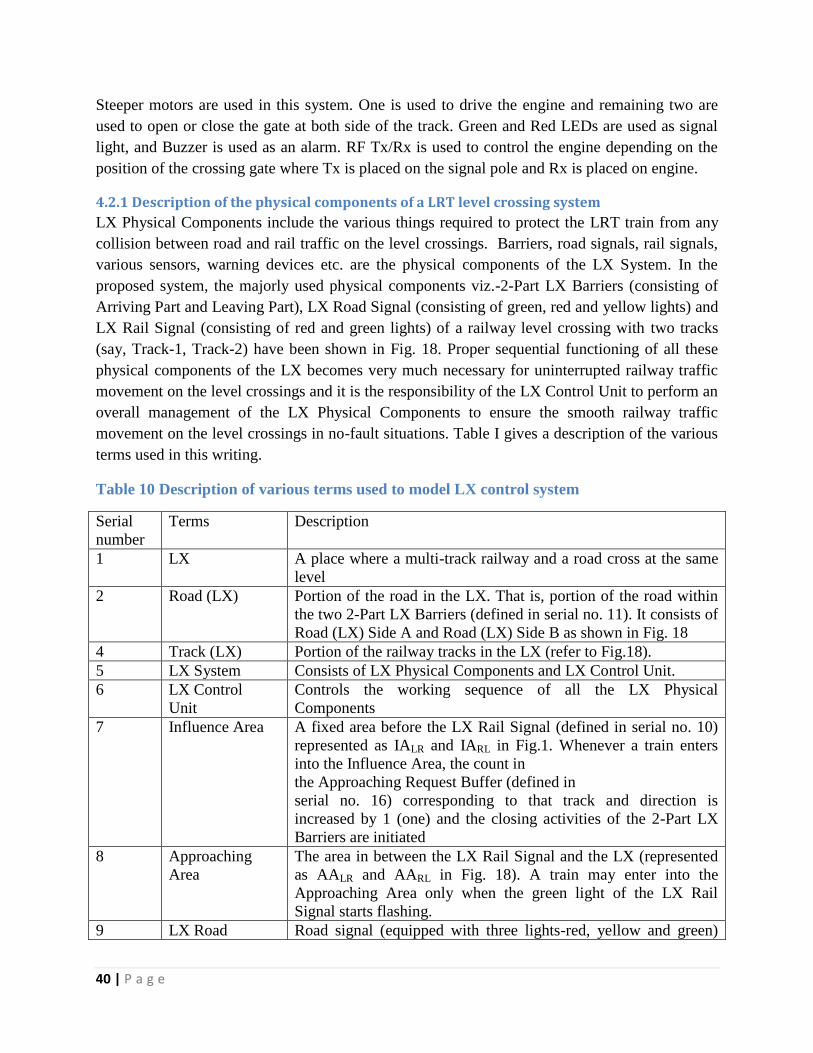
40 | P a g e
Steeper motors are used in this system. One is used to drive the engine and remaining two are
used to open or close the gate at both side of the track. Green and Red LEDs are used as signal
light, and Buzzer is used as an alarm. RF Tx/Rx is used to control the engine depending on the
position of the crossing gate where Tx is placed on the signal pole and Rx is placed on engine.
4.2.1 Description of the physical components of a LRT level crossing system
LX Physical Components include the various things required to protect the LRT train from any
collision between road and rail traffic on the level crossings. Barriers, road signals, rail signals,
various sensors, warning devices etc. are the physical components of the LX System. In the
proposed system, the majorly used physical components viz.-2-Part LX Barriers (consisting of
Arriving Part and Leaving Part), LX Road Signal (consisting of green, red and yellow lights) and
LX Rail Signal (consisting of red and green lights) of a railway level crossing with two tracks
(say, Track-1, Track-2) have been shown in Fig. 18. Proper sequential functioning of all these
physical components of the LX becomes very much necessary for uninterrupted railway traffic
movement on the level crossings and it is the responsibility of the LX Control Unit to perform an
overall management of the LX Physical Components to ensure the smooth railway traffic
movement on the level crossings in no-fault situations. Table I gives a description of the various
terms used in this writing.
Table 10 Description of various terms used to model LX control system
Serial
number
Terms Description
1 LX A place where a multi-track railway and a road cross at the same
level
2 Road (LX) Portion of the road in the LX. That is, portion of the road within
the two 2-Part LX Barriers (defined in serial no. 11). It consists of
Road (LX) Side A and Road (LX) Side B as shown in Fig. 18
4 Track (LX) Portion of the railway tracks in the LX (refer to Fig.18).
5 LX System Consists of LX Physical Components and LX Control Unit.
6 LX Control
Unit
Controls the working sequence of all the LX Physical
Components
7 Influence Area A fixed area before the LX Rail Signal (defined in serial no. 10)
represented as IALR and IARL in Fig.1. Whenever a train enters
into the Influence Area, the count in
the Approaching Request Buffer (defined in
serial no. 16) corresponding to that track and direction is
increased by 1 (one) and the closing activities of the 2-Part LX
Barriers are initiated
8 Approaching
Area
The area in between the LX Rail Signal and the LX (represented
as AALR and AARL in Fig. 18). A train may enter into the
Approaching Area only when the green light of the LX Rail
Signal starts flashing.
9 LX Road Road signal (equipped with three lights-red, yellow and green)

41 | P a g e
Signal placed just before each of the Arriving LX Barrier Parts (defined
in serial no. 12) to control the road traffic movement on the LX.
10 LX Rail Signal A rail signal (equipped with two lights-red and green with usual
meaning) placed on the left hand side of the track in each
direction left-to-right and right-to-left at a
position where Influence Area ends and
Approaching Area begins.
11 2-Part LX
Barrier
Consists of Arriving LX Barrier Part and Leaving LX Barrier
Part. These barrier parts have three functional states- vertically
raised, lowered at 45° and lowered horizontally. These barrier
parts can be raised and lowered independently.
12 Arriving LX
Barrier Part
Half barrier for restricting the road traffic to enter in the LX.
13 Leaving LX
Barrier Part
Half barrier lowered horizontal after all the road traffic (entered
in the LX before the lowering of the arriving part) leave the LX.
14 train passed /
crossed the LX
The train has reached to the next rail signal after passing the LX
successfully within the TIME-OUT (defined in serial no. 17).
15 Train
Approaching
Request
Signal to the LX Control Unit generated when a train just enters
in the Influence Area.
16 Approaching
Request Buffer
An (n X 2)-cell buffer used to keep count of the current Train
Approaching Requests on all the tracks from either sides left-to-
right or right-to-left (n rows in the buffer represent the n tracks
and the two columns represent the two directions). All the cells in
the buffer are initialized with zeros.
17 TIME-OUT Maximum time limit within which a train is expected to cross the
LX after getting green light in the LX Rail Signal in a no-fault
situation.
18 DISASTER Any situation, which leads to an infinite delay in rail or road
traffic movement on the LX.
19 Faulty Situation A faulty situation arises when a train gets stuck indefinitely (at
least for more than the TIME-OUT) just before the LX but after
crossing the LX Rail Signal due to some mechanical fault or
chain pulling.
20 Plunger A device used by the train driver to manually send a fresh request
to the LX Control Unit for lowering the 2-Part LX Barriers
whenever he wants to cross the LX after recovering from a faulty
situation.

42 | P a g e
4.3 System flow A. At the Initial Stage (when there is no train in Influence Area and no train in Approaching
Area)
1. Red flashing in all the LX Rail Signals
2. Green flashing in the LX Road Signals
3. Arriving LX Barrier Parts and Leaving LX Barrier Parts are in raised vertical
position.
B. When a Train Enters into the Influence Area
1. After first t1 sec, the LX Road Signals stop flashing green and start flashing yellow.
After next t2 sec yellow lights stop and red lights start flashing.
2. After t3 sec from the flashing of the red lights in both the Arriving and the Leaving
LX Barrier Parts are lowered at 45°.
3. On checking that there is no road vehicle under the Arriving LX Barrier Parts both
Barriers are lowered to horizontal position within t4 sec. However, if either of
barriers cannot be lowered to the horizontal position within t4 sec, then a DISASTER
(delay in rail traffic movement) is identified and the Disaster Management Force is
informed.
4. After checking that there is no road vehicle on the Road (LX) Side A and Road (LX)
Side B, the Leaving LX Barrier Parts respectively on both sides are lowered to the
horizontal position independently within t5 sec. If either of sides cannot be lowered
within t5 sec, then it is also identified as a DISASTER and it is informed to the
Disaster Management Force.
5. By this time (= t1+t2+t3+t4+t5 sec) the train may at most reach to the LX Rail Signal
and flashing red light in the signal stops the train in front of the LX Rail Signal (if
required). Within t6 s from the horizontal lowering of the Leaving LX Barrier Parts,
the signal stops flashing red and starts flashing green. This flashing green light in
right side authorizes the train to enter in the Approaching Area. Just after the train
enters in the Approaching Area, the LX Rail Signal right side is again turned red to
prevent any other train to enter in the LX on that track before this one goes out.
6. Whenever the train enters into the Approaching Area, the fixed TIME-OUT is set for
the train. In normal situation, the train is expected to cross the LX before the TIME-
OUT is reached. If, before the train passes the LX, another train enters into the
Approaching Area through another track then the TIME-OUT is reset.
C. After the Train Crosses the LX
1. After each train crosses the LX, the Approaching Request Buffer is checked to verify
whether there is any other Train Approaching Request or not. If all the cells in the
buffer contain zeros (i.e., there is no other Train Approaching Request on any of the
n-tracks), the barrier parts on both sides are raised vertical even before the TIME-
OUT is reached and the signals are turned green.

43 | P a g e
2. If at any point of time after the passing of a train it is found that some of the buffer
counts are still non-zero (representing that some other trains have entered in the
Influence Area within this time), the system will wait until all the approaching trains
pass the LX, hence, the Arriving LX Barrier Parts and the Leaving LX Barrier Parts
will remain lowered horizontal until all the trains cross the LX and reach to a
minimum clearance distance (to the next rail signal).
D. After Specific TIME-OUT
In a no-fault situation, the trains usually cross the LX even before the TIME-OUT is reached and
the LX barriers are raised. However, if the LX Barrier Parts remain lowered even after the
TIME-OUT (corresponding to the last Train Approaching Request that was entered in the buffer)
is reached, then a fault or DISASTER is identified.
1) A Faulty Situation arises when a train fails to cross the LX within the TIME-OUT for
some kind of irregularity. It is a case of indefinite waiting for the train to overcome from
this faulty situation. In such a situation we raise all the Arriving LX Barrier Parts and
Leaving LX Barrier Parts to the vertical position and turn the signal green in and red after
checking that there is no Train Approaching Request from any of the sides on any of the
tracks and also the unsuccessful train is not on the Track (LX) (i.e., the train is not
blocking the Road (LX) in any way). After authorizing the road traffic movement on the
Road (LX), the unsuccessful Train Approaching Request is destroyed. When the fault is
fixed, the train driver manually sends a fresh LX crossing request to the LX Control Unit
using the Plunger and all the LX Barrier lowering activities are re-initiated.
2) If after the TIME-OUT such a situation appears that the train is at rest blocking the Road
(LX), then it is identified as a DISASTER and the Disaster Management Force is
informed.
4.4 Finite State Machine (FSM) FSM plays a vital role in the design, has nine states (exclude RESET and END states) of
action to be carried out while functioning. Such as:
Wait for RI (receiver interrupt signal)
Read the data from RF receiver
Forward to data processing unit
Enable PWM signal generator unit for generate the pulse signal close the gate step by
step
Enable red signal and buzzer
Wait for train pass information from IR departure sensor
After receive the signal enable the PWM signal open the gate
Enable green state
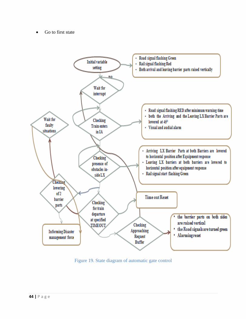
44 | P a g e
Go to first state
Figure 19. State diagram of automatic gate control

45 | P a g e
Figure 20. Modeling architecture of LX system
4.4.1 Traffic lights at a level crossing of a railway and a road.
Where L1, L2, R1 and R2 are IR sensors used to sense the approach and departure of
train and M2 and M2 are used to detect obstacles inside the gate.
I assume that a train may come from either direction on each track, but only one train (per
track) can enter the sensor zone (we call the space between sensor L and R the sensor
zone). Further, we assume that a train never changes its movement direction. I assume
also that trains may be short or very long; i.e., a train in the sensor zone may cover no
sensor, one sensor, two sensors, or all three sensors at the same time.
The control system should cover all imaginable situations, switching the traffic lights
according to the following rules:
Both lights are switched off if the control system is not working.
The yellow lights are flashing if there is no train between sensors L and R or a
train just passed the sensor M and is still between sensors M and L (R) moving
toward R (L), i.e., leaving the sensor zone.
The red lights are on if there is a train between sensor L (R) and M moving
toward M, i.e., approaching the road.
Both red and yellow lights are on if the situation is not definitely defined: after a
system start, when an unexpected sensor signal is received and when the
expected sensor signal has not come after a timeout (train disappeared?). These
situations are considered unsafe and can be resolved only by a manual control:
if the situation is cleared, the operator may reset the system.

46 | P a g e
In addition to the above rules, this model included the following situations to make the system
behavior failsafe.
On startup
When the “train gets lost” (it entered the sensor zone but never left it)
When an unexpected sensor signal occurs, e.g., a sensor M signals the presence of a train
though there has been no train yet detected in the sensor zone
On the state transition diagram, i use the name Sensor1 for denoting either sensor L if the train
comes from the left or sensor R if the train comes from the right. The name Sensor2 means a
sensor signaling that the train leaves the controlled zone. The name Sensor M means of course
the sensor in the middle.
In addition, to make the control system more realistic, this introduced:
A state Start, which allows the state machine to switch on the traffic lights after the
start-up
States Missing and Unexpected to handle the erroneous situations
Figure 21. Model of the railroad-crossing controller
Time invariant t≤30 of state Approaches enforces a transition after 30 seconds have passed since the train
has entered the state. This reflects the necessity of breaking the train if green has not been displayed
within 30 seconds. Time condition t>20 assigned to the transition from on crossing to Faraway reflects

47 | P a g e
the minimum time of passing the crossing by a fast train. Time invariant t≤40 of state on crossing reflects
the maximum time of passing the crossing by a slow train.
A model of the second train is identical except for the names of actions, which are approach2, leave2 and
green2 respectively. A model of the gate is shown in Figure 22. Time invariants t ≤ 20 assigned to states
Closing and Opening enforces a transition after 20 seconds have passed , and reflect time that it takes to
close or to open the gate.
Figure 22. Model of the gate
The simple reachability properties can check if a given state is reachable
Train1.On crossing: This checks if train 1 can pass the crossing (a similar property can be
checked for train 2).
Train1.On crossing && train2.On crossing: This checks if both trains can move through the
crossing simultaneously.
The safety properties can check that unsafe states will never happen:
Train1.On crossing or train2.On crossing imply gate Closed: This ensures that each time a
train is passing the crossing the gate is closed.
Gate Open implies (¬ train1.On crossing && ¬ train1.On crossing): This ensures that each time
the gate is open, a train is not on the crossing.
The aliveness properties can check consequences of an event:
train1.Approaches --> train1.On crossing: This ensures that whenever train 1 approaches the
crossing, it will eventually pass it (a similar property can be checked for train 2).

48 | P a g e
Chapter 5
Results and Discussions
5.1 Vivado Simulation Result This result shows the simulation of the external components interfaced with the main central
device, in this case processing system 7.0 that controls all the timing constraints, IO modules and
external memory mappings. The systems have two processors, one is the internal FPGA
processor and the other is cache processor to store the temporary external data.
Figure 23. Schematic diagram of completed design
Figure 24 shows the Chip planner view of the Functional blocks. It reveals that the numbers of
logic elements used for the functional blocks of SOC are:
Total combinational functions -90/32,216 (< 1%)
Dedicated logic registers - 55/32,216 (< 1%)
Total registers- 55

49 | P a g e
Total pins - 5/475 (1%)
Figure 24. Package layout of the designed system
Figure 25. The IP port pin constraints
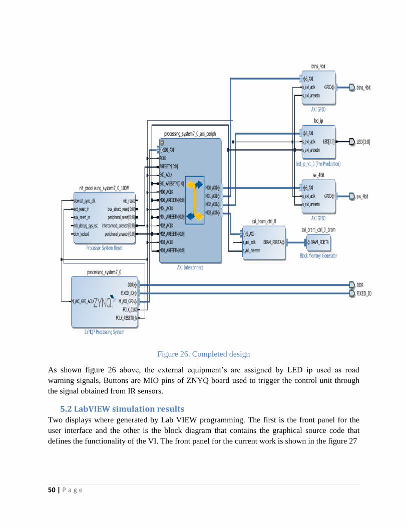
50 | P a g e
Figure 26. Completed design
As shown figure 26 above, the external equipment‟s are assigned by LED ip used as road
warning signals, Buttons are MIO pins of ZNYQ board used to trigger the control unit through
the signal obtained from IR sensors.
5.2 LabVIEW simulation results Two displays where generated by Lab VIEW programming. The first is the front panel for the
user interface and the other is the block diagram that contains the graphical source code that
defines the functionality of the VI. The front panel for the current work is shown in the figure 27

51 | P a g e
Figure 27. Front panel of Level crossing system
As it can be seen in Figure 27, there are eight states (initial setting, waiting for interrupt,
checking presence of obstacles inside LX, checking for train departure at specified Timeout,
checking approaching request buffer, checking lowering two part barriers, checking for faulty
situation and informing disaster management force). When one sensor is activated, their
corresponding warning signals will start to respond. Millisecond timer will start counting until it
reaches its specified timeout (20 second in this case). The eight different cases, where the states
are triggered, are represented in the following different block diagrams.

52 | P a g e
Figure 28. Initial situation
Figure 29. Waiting for interrupt situation

53 | P a g e
Figure 30. Checking presences of obstacles inside LX situation
Figure 31. Checking for train departure at specified TIMEOUT situation

54 | P a g e
Figure 32. Checking Approaching request situation
Figure 33. Checking lowering two barrier parts situation

55 | P a g e
Figure 34. Checking for faulty situation
Figure 35. Informing disaster management force situation
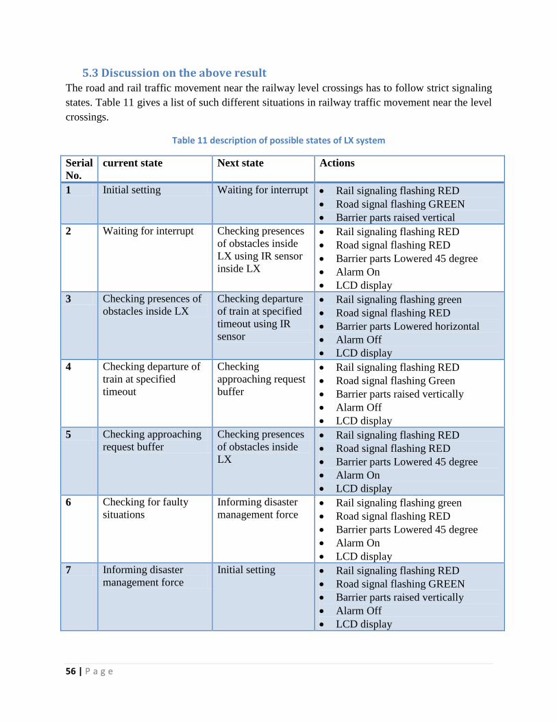
56 | P a g e
5.3 Discussion on the above result The road and rail traffic movement near the railway level crossings has to follow strict signaling
states. Table 11 gives a list of such different situations in railway traffic movement near the level
crossings.
Table 11 description of possible states of LX system
Serial
No.
current state Next state Actions
1 Initial setting Waiting for interrupt Rail signaling flashing RED
Road signal flashing GREEN
Barrier parts raised vertical
2 Waiting for interrupt Checking presences
of obstacles inside
LX using IR sensor
inside LX
Rail signaling flashing RED
Road signal flashing RED
Barrier parts Lowered 45 degree
Alarm On
LCD display
3 Checking presences of
obstacles inside LX
Checking departure
of train at specified
timeout using IR
sensor
Rail signaling flashing green
Road signal flashing RED
Barrier parts Lowered horizontal
Alarm Off
LCD display
4 Checking departure of
train at specified
timeout
Checking
approaching request
buffer
Rail signaling flashing RED
Road signal flashing Green
Barrier parts raised vertically
Alarm Off
LCD display
5 Checking approaching
request buffer
Checking presences
of obstacles inside
LX
Rail signaling flashing RED
Road signal flashing RED
Barrier parts Lowered 45 degree
Alarm On
LCD display
6 Checking for faulty
situations
Informing disaster
management force Rail signaling flashing green
Road signal flashing RED
Barrier parts Lowered 45 degree
Alarm On
LCD display
7 Informing disaster
management force
Initial setting Rail signaling flashing RED
Road signal flashing GREEN
Barrier parts raised vertically
Alarm Off
LCD display

57 | P a g e
5.4 Discussion on safeness of the models
The road and rail traffic movement near the railway level crossings has to follow a strict
signaling. Table 12 gives a list of such acceptable and unacceptable situations in railway traffic
movement near the level crossings.
All the acceptable states/situations (shown in the table) are treated as safe with respect to the
corresponding positions of the road and rail traffic. Safeness means that in such States/situations
the chances of collision between rail and road traffic will never occur. On the other hand, the
unacceptable states represent a chance of collision between the road and rail traffic movement
and naturally becomes the points of concern for us. A railway level crossing system has to ensure
that these unacceptable situations are totally unreachable within the operational sequence of the
system. Therefore, now the aim is to establish that under normal situations this model will never
enter to an unacceptable state within their operations. This in turn prove the safeness conditions
of the models (i.e., in zero-fault situation this system will never lead to any unsafe state/situation
and even if a fault or DISATER takes place, the system will be able to identify that properly such
that the required measures can be taken by the earliest). Whenever an approaching train just
enters in the Influence Area, the restriction on the road traffic movement is initiated. After (t1
+t2) s i.e., at the moment when the LX Road Signals are already turned red and the LX Barrier
Lowering activities are about to start , no car can appear just under the Arriving LX Barrier
Parts. If the Arriving Barrier Parts cannot be lowered in due time then it will directly interrupt
the rail traffic movement. Moreover, all the Arriving and Leaving Barrier Parts have to be
lowered before the train enters within the Approaching Area (AA). Therefore, no car can appear
then on the Road (LX). This remains true until the train passes the LX successfully. If more than
one Approaching Train Requests are found in quick succession then the all the barrier parts
remain closed until the trains pass the LX or TIME-OUT (corresponding to the last Train
Approaching Request) is reached. Therefore, the five states/situations those have been identified
as unacceptable in Table II are of highest interest to us. We will perform safeness analysis on
each of the five states separately.
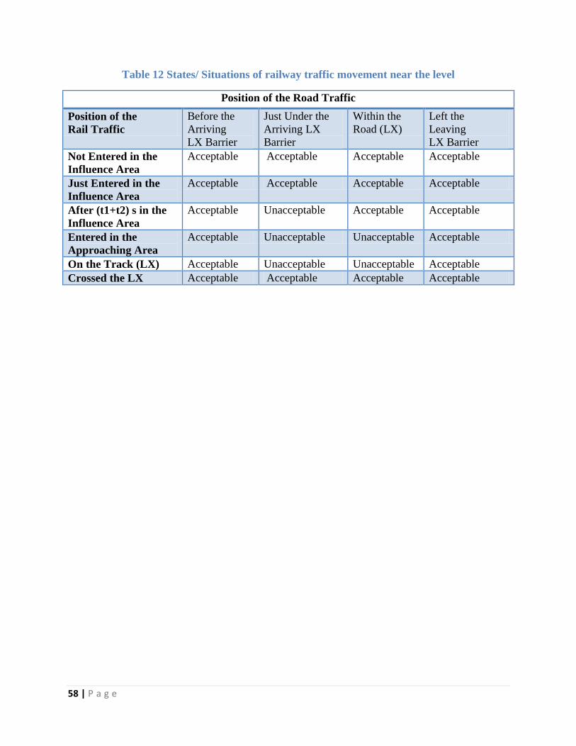
58 | P a g e
Table 12 States/ Situations of railway traffic movement near the level
Position of the Road Traffic
Position of the
Rail Traffic
Before the
Arriving
LX Barrier
Just Under the
Arriving LX
Barrier
Within the
Road (LX)
Left the
Leaving
LX Barrier
Not Entered in the
Influence Area
Acceptable Acceptable Acceptable Acceptable
Just Entered in the
Influence Area
Acceptable Acceptable Acceptable Acceptable
After (t1+t2) s in the
Influence Area
Acceptable Unacceptable Acceptable Acceptable
Entered in the
Approaching Area
Acceptable Unacceptable Unacceptable Acceptable
On the Track (LX) Acceptable Unacceptable Unacceptable Acceptable
Crossed the LX Acceptable Acceptable Acceptable Acceptable

59 | P a g e
Chapter 6
Conclusion and Recommendation
6.1 Conclusion
From the above discussion and information of this system, it is clear that the system is highly
reliable, effective and economical at dense traffic area, suburban area and the route where
frequency of trains is more. As the system is automated, it avoids manual errors and thus
provides ultimate safety to road users. By this mechanism, presence of a gatekeeper is not
necessary and automatic operation of the gate through the motor action is achieved. If there is
any difficulty then train will stop at train approach distances from the level crossing.
I believe that, designed automatic gate control can make a positive contribution in our country.
So doing this I recommend Ethiopian Railway Corporation (ERC) to implement automatic Level
crossing system in the railway sector to minimize the chance of accident and to ensure safety to
the peoples.
6.2 Future Recommendation This paper has satisfactorily fulfilled the basic things such as prevention of accidents inside the
level crossing and the wastage of a man-power. Since this arrangement can be used in remote
areas where the power supply cannot be expected for the motor operation, sensors, buzzer and
signal lights, solar power can be the solution there.
60 | P a g e
References [1] A.Kumar et al. “Intelligent Train Engine for the Fastest New Age Technology”, International
Journal of Innovative Research in Computer and Communication Engineering, vol. 1, Issue 1,
March 2013.
[2] K. Feher, Wireless Digital Communications, Englewood Cliffs, NJ: IEEE Press, 1992.
[3] M.Hamington andC.Leanardo, Radio Frequency applications and Working with Radio
Frequency.
[4] National Instruments Corp.: LabVIEW FPGA. http://www.ni.com/fpga, 24 October 2014
[5] R.K.Verma, Chief Engineer, Indian Railways “Level Crossing Management Information
System
[6] J.A.kalomiros, J.Lygouras, Design and Evolution of a hardware/software FPGA Based
system for fast image processing,
[7] Mengmeng Zhang, Hao Zang, Design and Implementation wireless Transceiver System
on FPGA, International conference on Innovative computing and communication, IEEE
computer society, 2010: 355-357.
[8] M. Sabri, M. H. Husin, W. A. W. Z. Abidin, K. M. Tay, H. M. Basri, Design of FPGA-Based
Traffic Light Controller System , Dept. of Electronic Engineering, Faculty of Engineering,
University Malaysia Sarawak, Sarawak, Malaysia. 978-1-4244-8728-8/11
[9] Henzinger, T., Sifakis, J., “The Discipline of Embedded System Design”
[10] Navabi, Zainalabedin. Embedded Core Design with FPGAs. McGraw-Hill Professional,
2006
[11] K. Feher, Wireless Digital Communications, Englewood Cliffs, NJ: IEEE Press, 1992.
[12] Improving safety on unmanned level crossing by F. ANSARI/ADEN/BRK, B.K.
LA/ADEN/MYS ,J.K. SRIVASTAVA/ARE/RDSO, MANJEET SINGH/AEN/RCF
[13] DAVEY, J., WALLACE, A., STENSON, N. & FREEMAN, J. (2008a), The experiences
and perceptions of heavy vehicle drivers and train drivers of dangers at railway level crossings.
Accident Analysis & Prevention, 40, 1217-1222. [14] J. M Khan and J. R Barry, “Wireless
Infrared Communications”, Proceedings of the IEEE, Vol. 85, pp. 265, February 1997.
[15] HAILE, J. & HESS, T. (2006) The Event Window -Modeling Risk at Level Crossings.
Conference of Railway Engineering, Melbourne.

61 | P a g e
[16] Sun, Wu and Kyriacos C. Mouskos, Network-Wide Traffic Responsive Signal Control in
Urban Environments, Proceedings of the 4th
International Conference on Computational
Intelligence & Neurosciences, Atlantic City, New Jersey, February 27-March 3, 2000.
[17] Vivado Design Suite Reference Guides
(www.xilinx.com/support/documentation/dt_vivado2014-3_referenceguides.htm)
[18] Wall, R. W. and A. Huska, Design Platform for Plug-and-Play IEEE 1451 Traffic Signal,
The 31st Annual IEEE Industrial Electronics Conference, Raleigh, NC, Nov 6-10, 2005.
[19] Wall. R.W., T. Urbanik, D. Bullock, S. Allen, M. Busby, D. DeVoe, A. Huska, T. Rallens,
Distributed Traffic Signal Control: Improving Pedestrian Control as A First Step, Transportation
Research Board 2007 Annual Meeting, Washington D.C.
[20] Theeg, G., Švalov, D., Schone, E., Level Crossings, Railway signaling and interlocking,
Eurailpress 2009

62 | P a g e
Appendix A: SDK Programing
A.1 GPIO Program #include "xparameters.h" #include "xgpio.h" #include "xutil.h" #include "led_ip.h" // Include scutimer header file //==================================================== XScuTimer Timer; /* Cortex A9 SCU Private Timer Instance */ #define ONE_SECOND 325000000 // half of the CPU clock speed int main (void) { XGpio dip, push; int psb_check, dip_check, dip_check_prev, count, Status; // PS Timer related definitions XScuTimer_Config *ConfigPtr; XScuTimer *TimerInstancePtr = &Timer; xil_printf("-- Start of the Program --\r\n"); XGpio_Initialize(&dip, XPAR_SW_4BIT_DEVICE_ID); XGpio_SetDataDirection(&dip, 1, 0xffffffff); XGpio_Initialize(&push, XPAR_BTNS_4BIT_DEVICE_ID); XGpio_SetDataDirection(&push, 1, 0xffffffff); count = 0; // Initialize the timer // Read dip switch values dip_check_prev = XGpio_DiscreteRead(&dip, 1); // Load timer with delay in multiple of ONE_SECOND // Set AutoLoad mode // Start the timer while (1) { // Read push buttons and break the loop if Center button pressed psb_check = XGpio_DiscreteRead(&push, 1); if(psb_check & 0x1) { XScuTimer_Stop(TimerInstancePtr); break; }

63 | P a g e
dip_check = XGpio_DiscreteRead(&dip, 1); if (dip_check != dip_check_prev) { xil_printf("DIP Switch Status %x, %x\r\n", dip_check_prev, dip_check); dip_check_prev = dip_check; // load timer with the new switch settings count = 0; } if(XScuTimer_IsExpired(TimerInstancePtr)) { // clear status bit // output the count to LED and increment the count } } return 0; }
A.2 LED programing ############################ # On-board LED # ############################ set_property PACKAGE_PIN M14 [get_ports LED[0]] set_property IOSTANDARD LVCMOS33 [get_ports LED[0]] set_property PACKAGE_PIN M15 [get_ports LED[1]] set_property IOSTANDARD LVCMOS33 [get_ports LED[1]] set_property PACKAGE_PIN G14 [get_ports LED[2]] set_property IOSTANDARD LVCMOS33 [get_ports LED[2]] set_property PACKAGE_PIN D18 [get_ports LED[3]] set_property IOSTANDARD LVCMOS33 [get_ports LED[3]]
timescale 1ns / 1ps ///////////////////////////////////////////////////////////////// // Module Name: _user_logic ///////////////////////////////////////////////////////////////// module lab3_user_logic( input S_AXI_ACLK, input slv_reg_wren, input [2:0] axi_awaddr, input [31:0] S_AXI_WDATA, input S_AXI_ARESETN, output reg [3:0] LED ); always @( posedge S_AXI_ACLK ) begin if ( S_AXI_ARESETN == 1'b0 ) LED <= 4'b0; else if (slv_reg_wren && (axi_awaddr == 3'h0)) LED <= S_AXI_WDATA[3:0]; end

64 | P a g e
endmodule #include "xparameters.h" #include "xgpio.h" #include "xutil.h" #include "led_ip.h" //==================================================== int main (void) { XGpio dip, push; int i, psb_check, dip_check; xil_printf("-- Start of the Program --\r\n"); XGpio_Initialize(&dip, XPAR_SW_4BIT_DEVICE_ID); // Modify this XGpio_SetDataDirection(&dip, 1, 0xffffffff); XGpio_Initialize(&push, XPAR_BTNS_4BIT_DEVICE_ID); // Modify this XGpio_SetDataDirection(&push, 1, 0xffffffff); while (1) { psb_check = XGpio_DiscreteRead(&push, 1); xil_printf("Push Buttons Status %x\r\n", psb_check); dip_check = XGpio_DiscreteRead(&dip, 1); xil_printf("DIP Switch Status %x\r\n", dip_check); // output dip switches value on LED_ip device LED_IP_mWriteReg(XPAR_LED_IP_S_AXI_BASEADDR, 0, dip_check); for (i=0; i<9999999; i++); } }
A.3 Main program #include "xparameters.h" #include "xgpio.h" #include "xutil.h" #include "led_ip.h" // Include scutimer header file #include "xscutimer.h" //==================================================== XScuTimer Timer; /* Cortex A9 SCU Private Timer Instance */ #define ONE_SECOND 325000000 // half of the CPU clock speed int main (void) { XGpio dip, push; int psb_check, dip_check, dip_check_prev, count, Status;
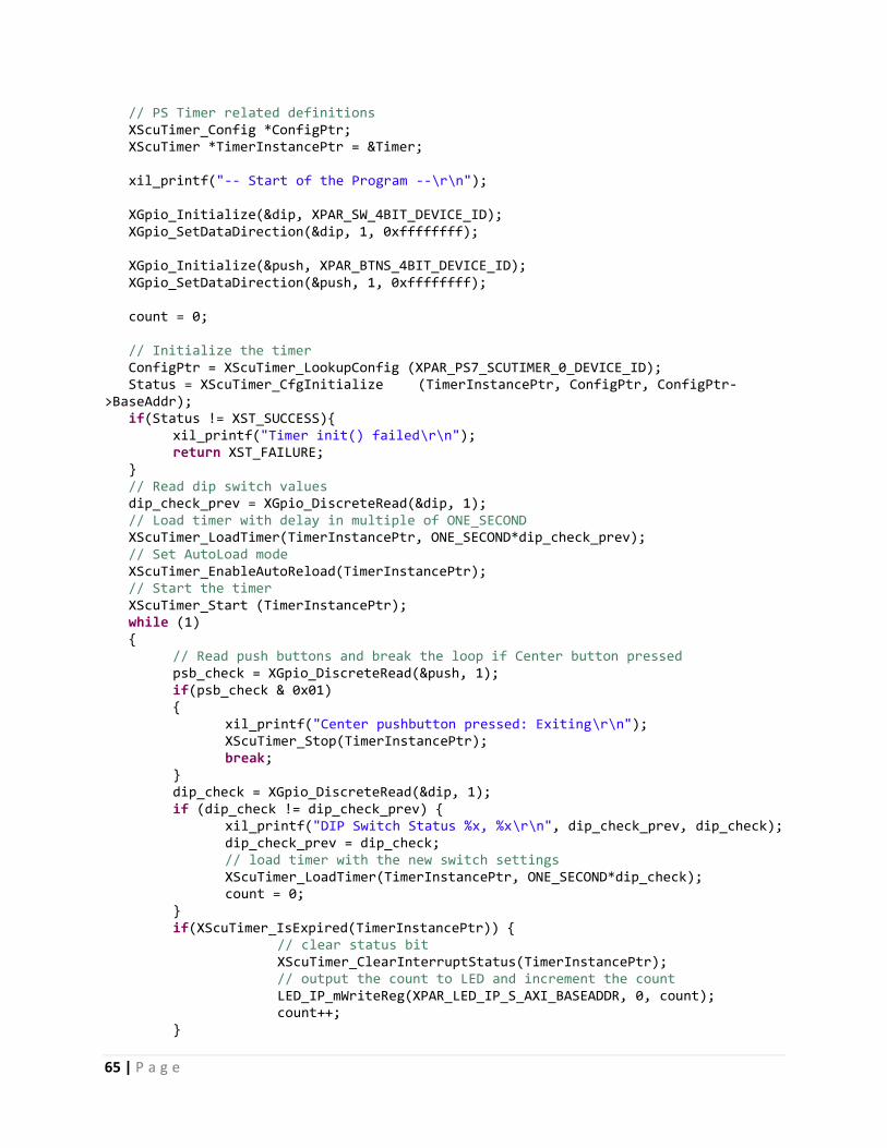
65 | P a g e
// PS Timer related definitions XScuTimer_Config *ConfigPtr; XScuTimer *TimerInstancePtr = &Timer; xil_printf("-- Start of the Program --\r\n"); XGpio_Initialize(&dip, XPAR_SW_4BIT_DEVICE_ID); XGpio_SetDataDirection(&dip, 1, 0xffffffff); XGpio_Initialize(&push, XPAR_BTNS_4BIT_DEVICE_ID); XGpio_SetDataDirection(&push, 1, 0xffffffff); count = 0; // Initialize the timer ConfigPtr = XScuTimer_LookupConfig (XPAR_PS7_SCUTIMER_0_DEVICE_ID); Status = XScuTimer_CfgInitialize (TimerInstancePtr, ConfigPtr, ConfigPtr->BaseAddr); if(Status != XST_SUCCESS){ xil_printf("Timer init() failed\r\n"); return XST_FAILURE; } // Read dip switch values dip_check_prev = XGpio_DiscreteRead(&dip, 1); // Load timer with delay in multiple of ONE_SECOND XScuTimer_LoadTimer(TimerInstancePtr, ONE_SECOND*dip_check_prev); // Set AutoLoad mode XScuTimer_EnableAutoReload(TimerInstancePtr); // Start the timer XScuTimer_Start (TimerInstancePtr); while (1) { // Read push buttons and break the loop if Center button pressed psb_check = XGpio_DiscreteRead(&push, 1); if(psb_check & 0x01) { xil_printf("Center pushbutton pressed: Exiting\r\n"); XScuTimer_Stop(TimerInstancePtr); break; } dip_check = XGpio_DiscreteRead(&dip, 1); if (dip_check != dip_check_prev) { xil_printf("DIP Switch Status %x, %x\r\n", dip_check_prev, dip_check); dip_check_prev = dip_check; // load timer with the new switch settings XScuTimer_LoadTimer(TimerInstancePtr, ONE_SECOND*dip_check); count = 0; } if(XScuTimer_IsExpired(TimerInstancePtr)) { // clear status bit XScuTimer_ClearInterruptStatus(TimerInstancePtr); // output the count to LED and increment the count LED_IP_mWriteReg(XPAR_LED_IP_S_AXI_BASEADDR, 0, count); count++; }

66 | P a g e
} return 0; }
Copyright © 2022 FDOKUMEN