A universal core model for multiple-gate field-effect transistors. Part I: charge model
8
840 IEEE TRANSACTIONS ON ELECTRON DEVICES, VOL. 60, NO. 2, FEBRUARY 2013 A Universal Core Model for Multiple-Gate Field-Effect Transistors. Part I: Charge Model Juan Pablo Duarte, Sung-Jin Choi, Dong-Il Moon, Jae-Hyuk Ahn, Jee-Yeon Kim, Sungho Kim, and Yang-Kyu Choi Abstract—A universal core model for multiple-gate field-effect transistors (Mug-FETs) is proposed. The proposed charge and drain current models are presented in Parts I and II, respectively. It is first demonstrated that an exact potential profile in the entire channel is not necessary for the derivation of accurate charge models in inversion-mode FETs. With application of this new concept, a universal charge model is derived for Mug-FETs by assuming an arbitrary channel potential profile, which simplifies the mathematical formulation. Thereafter, using the Pao–Sah in- tegral, a drain current model is obtained from the charge model of Part I. The proposed model can be expressed as an explicit and continuous form for all operation regimes; therefore, it is well suited for compact modeling to support fast circuit simulations. The model shows good agreement with 2-D and 3-D numerical simulations for several multiple-gate structures, such as single- gate, double-gate, triple-gate, rectangular gate-all-around, and cylindrical gate-all-around FETs. Index Terms—Compact modeling, cylindrical gate-all-around FET (Cy-GAA-FET), double-gate FET (DG-FET), FinFET, multiple-gate FET (Mug-FET), Poisson’s equation, rectangular gate-all-around FET (Re-GAA-FET), semiconductor device mod- eling, single-gate FET (SG-FET), triple-gate FET (TG-FET). I. I NTRODUCTION C ONVENTIONAL planar CMOS transistors on bulk sili- con substrate have been a key component in ultralarge- scale integration (ULSI) technology for the past four decades. As planar CMOS transistors keep following a trend of down- scaling, they are also approaching the fundamental physical limits imposed by the presence of several detrimental effects, such as gate oxide tunneling and short-channel effects (SCEs) [1], [2]. In this context, fully depleted multiple-gate field- effect transistors (Mug-FETs) [3], [4] have been proposed as Manuscript received November 24, 2011; revised October 16, 2012 and December 4, 2012; accepted December 4, 2012. Date of publication December 28, 2012; date of current version January 18, 2013. This work was supported in part by the IT R&D Program of Ministry of Knowledge Econ- omy/Korea Evaluation Institute of Industry Technology under Grant 10035320 (Development of Novel 3D Stacked Devices and Core Materials for the Next Generation Flash Memory), by the Center for Integrated Smart Sensors funded by the Ministry of Education, Science and Technology as Global Frontier Project under Grant CISS-2011-0031848, by Samsung Electronics Company Ltd., and by SK Hynix Semiconductor Inc. The review of this paper was arranged by Editor M. Ieong. J. P. Duarte and S.-J. Choi were with the Department of Electrical Engineer- ing, Korea Advanced Institute of Science and Technology, Daejeon 305-701, Korea. They are now with the University of California, Berkeley, CA 94720 USA. D.-I. Moon, J.-H. Ahn, J.-Y. Kim, S. Kim, and Y.-K. Choi are with the Department of Electrical Engineering, Korea Advanced Institute of Science and Technology, Daejeon 305-701, Korea (e-mail: [email protected]). Color versions of one or more of the figures in this paper are available online at http://ieeexplore.ieee.org. Digital Object Identifier 10.1109/TED.2012.2233478 an alternative to planar devices. One of the main objectives of Mug-FETs is to alleviate the problems brought by the ultimate downscaling of the planar transistors. In fact, the 3-D nature of Mug-FETs improves the robust electrostatic control of the gate over the entire channel; hence, it results in increment of current drivability and reduction of SCEs [3], [4]. Commercial use of 3-D transistors has been recently reported by Intel [5]. They have attempted to utilize 3-D triple-gate architecture for their next generation of ULSI chips [5], which promises fast speeds and power savings. Regardless of the type of circuit being designed (analog, digital, or mixed), circuit designs are always carefully verified by the use of circuit simulators. In the implementation of circuit simulators, compact models are preferred over other numerical approaches because the former can offer, in addition to good computational efficiency, good accuracy [6]. Various compact models have been proposed for several Mug-FET structures, such as double-gate (DG) [7]–[15], triple-gate (TG) [16]–[18], rectangular gate-all-around (Re-GAA) [18]–[20], or cylindrical gate-all-around (Cy-GAA) [21]–[24]. Most of the compact models are based on a “core model,” which is a model obtained using a long-channel assumption, so called gradual-channel ap- proximation (GCA) [25], and neglecting other physical effects such as charge quantization or gate oxide tunneling. In this context, core models are further improved by the inclusion of correction terms that represent advanced physical effects [6]– [24]. Commonly, core models are obtained by solving Poisson’s equation under the GCA condition and assuming Boltzmann’s statistics for the carriers. Although the use of GCA condition and Boltzmann’s statistics alleviates the difficulty in obtaining a solution from Poisson’s equation, a direct analytical solution is only available for the cases of undoped DG- [7] and Cy-GAA- FETs [21], where the 3-D Poisson’s equation can be reduced to a 1-D form. If depletion charges arisen from dopants are included, Poisson’s equation becomes highly nonlinear. Thus, it is difficult to obtain a direct analytical solution [11], [12], [14], [15], [23]. In addition, finding a direct analytical solution becomes more difficult to obtain for other Mug-FET struc- tures [see Fig. 1] because they lack structural symmetry [18]. Compact models for asymmetric structures, such as TG-, Re- GAA-, or Pi-gate-FETs, are rarely found in literature and are mostly accomplished by the extensive use of fitting parameters or numerical techniques [17]–[20]. However, some of these asymmetric structures offer simpler fabrication processes than other symmetric structures [26]. Therefore, it is important and timely to develop physical-based core models for each Mug- FET structure, such as those shown in Fig. 1, for comprehensive understanding and fast circuit testing. 0018-9383/$31.00 © 2012 IEEE
-
Upload
independent -
Category
Documents
-
view
0 -
download
0
Transcript of A universal core model for multiple-gate field-effect transistors. Part I: charge model

840 IEEE TRANSACTIONS ON ELECTRON DEVICES, VOL. 60, NO. 2, FEBRUARY 2013
A Universal Core Model for Multiple-GateField-Effect Transistors. Part I: Charge Model
Juan Pablo Duarte, Sung-Jin Choi, Dong-Il Moon, Jae-Hyuk Ahn, Jee-Yeon Kim, Sungho Kim, and Yang-Kyu Choi
Abstract—A universal core model for multiple-gate field-effecttransistors (Mug-FETs) is proposed. The proposed charge anddrain current models are presented in Parts I and II, respectively.It is first demonstrated that an exact potential profile in the entirechannel is not necessary for the derivation of accurate chargemodels in inversion-mode FETs. With application of this newconcept, a universal charge model is derived for Mug-FETs byassuming an arbitrary channel potential profile, which simplifiesthe mathematical formulation. Thereafter, using the Pao–Sah in-tegral, a drain current model is obtained from the charge modelof Part I. The proposed model can be expressed as an explicitand continuous form for all operation regimes; therefore, it is wellsuited for compact modeling to support fast circuit simulations.The model shows good agreement with 2-D and 3-D numericalsimulations for several multiple-gate structures, such as single-gate, double-gate, triple-gate, rectangular gate-all-around, andcylindrical gate-all-around FETs.
Index Terms—Compact modeling, cylindrical gate-all-aroundFET (Cy-GAA-FET), double-gate FET (DG-FET), FinFET,multiple-gate FET (Mug-FET), Poisson’s equation, rectangulargate-all-around FET (Re-GAA-FET), semiconductor device mod-eling, single-gate FET (SG-FET), triple-gate FET (TG-FET).
I. INTRODUCTION
CONVENTIONAL planar CMOS transistors on bulk sili-con substrate have been a key component in ultralarge-
scale integration (ULSI) technology for the past four decades.As planar CMOS transistors keep following a trend of down-scaling, they are also approaching the fundamental physicallimits imposed by the presence of several detrimental effects,such as gate oxide tunneling and short-channel effects (SCEs)[1], [2]. In this context, fully depleted multiple-gate field-effect transistors (Mug-FETs) [3], [4] have been proposed as
Manuscript received November 24, 2011; revised October 16, 2012and December 4, 2012; accepted December 4, 2012. Date of publicationDecember 28, 2012; date of current version January 18, 2013. This work wassupported in part by the IT R&D Program of Ministry of Knowledge Econ-omy/Korea Evaluation Institute of Industry Technology under Grant 10035320(Development of Novel 3D Stacked Devices and Core Materials for the NextGeneration Flash Memory), by the Center for Integrated Smart Sensors fundedby the Ministry of Education, Science and Technology as Global FrontierProject under Grant CISS-2011-0031848, by Samsung Electronics CompanyLtd., and by SK Hynix Semiconductor Inc. The review of this paper wasarranged by Editor M. Ieong.
J. P. Duarte and S.-J. Choi were with the Department of Electrical Engineer-ing, Korea Advanced Institute of Science and Technology, Daejeon 305-701,Korea. They are now with the University of California, Berkeley, CA 94720USA.
D.-I. Moon, J.-H. Ahn, J.-Y. Kim, S. Kim, and Y.-K. Choi are with theDepartment of Electrical Engineering, Korea Advanced Institute of Science andTechnology, Daejeon 305-701, Korea (e-mail: [email protected]).
Color versions of one or more of the figures in this paper are available onlineat http://ieeexplore.ieee.org.
Digital Object Identifier 10.1109/TED.2012.2233478
an alternative to planar devices. One of the main objectives ofMug-FETs is to alleviate the problems brought by the ultimatedownscaling of the planar transistors. In fact, the 3-D nature ofMug-FETs improves the robust electrostatic control of the gateover the entire channel; hence, it results in increment of currentdrivability and reduction of SCEs [3], [4]. Commercial use of3-D transistors has been recently reported by Intel [5]. Theyhave attempted to utilize 3-D triple-gate architecture for theirnext generation of ULSI chips [5], which promises fast speedsand power savings.
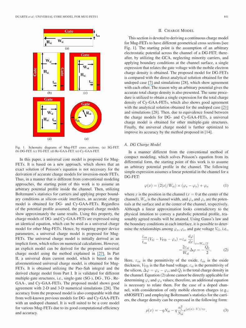
Regardless of the type of circuit being designed (analog,digital, or mixed), circuit designs are always carefully verifiedby the use of circuit simulators. In the implementation of circuitsimulators, compact models are preferred over other numericalapproaches because the former can offer, in addition to goodcomputational efficiency, good accuracy [6]. Various compactmodels have been proposed for several Mug-FET structures,such as double-gate (DG) [7]–[15], triple-gate (TG) [16]–[18],rectangular gate-all-around (Re-GAA) [18]–[20], or cylindricalgate-all-around (Cy-GAA) [21]–[24]. Most of the compactmodels are based on a “core model,” which is a model obtainedusing a long-channel assumption, so called gradual-channel ap-proximation (GCA) [25], and neglecting other physical effectssuch as charge quantization or gate oxide tunneling. In thiscontext, core models are further improved by the inclusion ofcorrection terms that represent advanced physical effects [6]–[24]. Commonly, core models are obtained by solving Poisson’sequation under the GCA condition and assuming Boltzmann’sstatistics for the carriers. Although the use of GCA conditionand Boltzmann’s statistics alleviates the difficulty in obtaining asolution from Poisson’s equation, a direct analytical solution isonly available for the cases of undoped DG- [7] and Cy-GAA-FETs [21], where the 3-D Poisson’s equation can be reducedto a 1-D form. If depletion charges arisen from dopants areincluded, Poisson’s equation becomes highly nonlinear. Thus,it is difficult to obtain a direct analytical solution [11], [12],[14], [15], [23]. In addition, finding a direct analytical solutionbecomes more difficult to obtain for other Mug-FET struc-tures [see Fig. 1] because they lack structural symmetry [18].Compact models for asymmetric structures, such as TG-, Re-GAA-, or Pi-gate-FETs, are rarely found in literature and aremostly accomplished by the extensive use of fitting parametersor numerical techniques [17]–[20]. However, some of theseasymmetric structures offer simpler fabrication processes thanother symmetric structures [26]. Therefore, it is important andtimely to develop physical-based core models for each Mug-FET structure, such as those shown in Fig. 1, for comprehensiveunderstanding and fast circuit testing.
0018-9383/$31.00 © 2012 IEEE
DUARTE et al.: UNIVERSAL CORE MODEL FOR MUG-FETS I 841
Fig. 1. Schematic diagrams of Mug-FET cross sections. (a) SG-FET.(b) DG-FET. (c) TG-FET. (d) Re-GAA-FET. (e) Cy-GAA-FET.
In this paper, a universal core model is proposed for Mug-FETs. It is based on a new approach, which shows that anexact solution of Poisson’s equation is not necessary for thederivation of accurate charge models for inversion-mode FETs.Thus, in a manner that is different from conventional modelingapproaches, the starting point of this work is to assume anarbitrary potential profile inside the channel. Then, utilizingBoltzmann’s statistics for carriers and applying proper bound-ary conditions at silicon–oxide interfaces, an accurate chargemodel is obtained for DG- and Cy-GAA-FETs. Regardlessof the potential profile assumed, the proposed charge modelsshow approximately the same results. Using this property, thecharge models of DG- and Cy-GAA-FETs are expressed usingan identical equation, which can be used as a universal chargemodel for other Mug-FETs. Hence, by mapping proper deviceparameters, a universal charge model is proposed for Mug-FETs. The universal charge model is initially derived as animplicit form, which relies on numerical calculations. However,an explicit model can be derived for the proposed universalcharge model using the method explained in [27]. In PartII, a universal drain current model, which is based on theaforementioned universal charge model, is obtained for Mug-FETs. It is obtained utilizing the Pao–Sah integral and thederived charge model from Part I. It is validated for differentmultiple-gate structures, i.e., single-gate (SG-), DG-, TG-, Re-GAA-, and Cy-GAA-FETs. The proposed model shows goodagreement with 2-D and 3-D numerical simulations [28]. Theaccuracy from the proposed model is also comparable with thatfrom well-known previous models for DG- and Cy-GAA-FETswith an undoped channel. It is well suited to be a core modelfor various Mug-FETs due to its good computational efficiencyand accuracy.
II. CHARGE MODEL
This section is devoted to deriving a continuous charge modelfor Mug-FETs to have different geometrical cross sections [seeFig. 1]. The starting point is the assumption of an arbitraryelectrostatic potential across the channel of a DG-FET; there-after, by utilizing the GCA, neglecting minority carriers, andapplying boundary conditions at the channel surface, a singleexpression that relates the gate voltage with the mobile electroncharge density is obtained. The proposed model for DG-FETsis compared with the direct analytical solution obtained for theundoped case [7] and simulations [28], which show agreementwith each other. The reason why an arbitrary potential gives theaccurate total charge density is also presented. The same proce-dure is utilized to obtain a single expression for the total chargedensity of Cy-GAA-FETs, which also shows good agreementwith the analytical solution obtained for the undoped case [21]and simulations [28]. Then, due to equivalence found betweenthe charge models for DG- and Cy-GAA-FETs, a universalcharge model is obtained for other multiple-gate structures.Finally, the universal charge model is further optimized toimprove its accuracy by the method proposed in [14].
A. DG Charge Model
In a manner different from the conventional method ofcompact modeling, which solves Poisson’s equation from itsdifferential form, the starting point of this work is to assumean arbitrary potential profile in the channel. The followingsimple expression assumes a linear potential in the channel for aDG-FET:
ϕ(x) = (2|x|/Wsi)× (ϕs − ϕo) + ϕo (1)
where x is the position in the channel (x = 0 at the center of thechannel), Wsi is the channel width, and ϕs and ϕo are the poten-tials at the surface and at the center of the channel, respectively.Although a linear approximation looks contradictory to thephysical intuition to convey a parabolic potential profile, rea-sonably agreed results will be attained. Using Gauss’s law andthe boundary conditions at each interface, it is possible to deter-mine the relationships among ϕs, ϕo, and gate voltage VG, i.e.,
εoxtox
(VG − VFB − ϕs) =εsidϕ
dx
∣∣∣∣x=Wsi/2
=2εsiWsi
Δϕ = −Qt
2. (2)
Here, εox is the permittivity of the oxide, tox is the oxidethickness, VFB is the flat-band voltage, εsi is the permittivity ofthe silicon, Δϕ = ϕs − ϕo, and Qt is the total charge density inthe channel. Equation (2) alone cannot be directly applicable fordetermining ϕs and ϕo values; therefore, an additional equationis necessary to relate them. For the case of a doped chan-nel, with consideration of only mobile electron charges (e.g.,nMOSFET) and employing Boltzmann’s statistics for the carri-ers, the charge density can be expressed in the following form:
ρ(x) = −qNsi − qn2i
Nsie(ϕ(x)−V )/vT . (3)

842 IEEE TRANSACTIONS ON ELECTRON DEVICES, VOL. 60, NO. 2, FEBRUARY 2013
Fig. 2. Mobile electrons per unit area in an undoped DG-FET obtained fromthe proposed model (5) and the direct analytical solution [7].
In (3), Nsi is the doping concentration in the channel, ni is theintrinsic carrier concentration, V is the electron quasi-Fermipotential, and vT is the thermal voltage, i.e., kT/q. The left andright terms in (2) are related to the negative half-channel chargedensity per unit area. Integrating the charge density given by(3) over the entire channel [using the channel potential givenby (1)], it is possible to obtain the total charge per unit area inthe channel, i.e.,
Qt =− qNsiWsi − qn2i
Nsi
∫ Wsi/2
−Wsi/2
e(ϕ−V )/vT dx
=− qNsiWsi − qn2iWsi
Nsi
e(ϕo−V )/vT
Δϕ(eΔϕ/vT − 1). (4)
Note that the second term in the right-hand side of (4)corresponds to the total mobile electron charge per unit area(Qe) in the channel. Thus, the total charge density in thechannel is expressed as Qt = Qd +Qe, where Qd is thedepletion charge per unit area given by −qNsiWsi. Expressions(2) and (4) construct a self-consistent equation that can be usedto determine ϕs and ϕo. Following simple subsequent algebraicmanipulations of (2) and (4), it is possible to obtain a closedform expression for the mobile electron charge density in thechannel. Using (4) and replacing Δϕ by −(Wsi/4εsi)×Qt
[from (2)], it is possible to express ϕs as a function of Qe andQd, which is used in (2) to finally obtain
VG − VFB +tox
2εoxQd − V = − tox
2εoxQe
+vT lnQe(Qe +Qd)/(4vT εsi/Wsi)
qn2i
NsiWsi
[1 − exp Wsi
4vT εsi(Qe +Qd)
] . (5)
Equation (5) relates the mobile electron charge per unit areawith the applied gate voltage. Fig. 2 shows the mobile electronper unit area in an undoped DG-FET obtained from (5) andthe direct analytical solution for undoped DG-FETs derived in[7]. Although a linear potential is assumed inside the channel,Fig. 2 ensures that (5) has good agreement with the modelproposed in [7]. Note also that (5) captures the phenomenon ofsubthreshold inversion, which cannot be obtained by standardcharge-sheet models.
Fig. 3. Mobile electrons per unit volume as a function of the position in thechannel and the gate voltage for an undoped DG-FET.
The reason for the good accuracy shown by the proposedmodel can be understood by analyzing the mobile electron perunit volume inside the channel. Fig. 3(a) shows the mobile elec-tron density in the channel for various gate biases obtained from(3), using (1), and the model proposed in [7]. In the subthresh-old region, the mobile electron concentration in the channelis approximately flat; therefore, a linear potential becomes agood approximation. As the gate voltage increases, the mobileelectron concentration does not have a linear profile; however,the peaks of the mobile electron concentration coincide for bothmodels. The total charge density is dominated by those peaksdue to the nature of the carriers’ statistics. As shown by (3), theexponential function from Boltzmann’s statistics determines thecarrier concentration as a function of the channel potential. Asmall change in the channel potential produces a large changein the carrier concentration; therefore, the potential differencebetween the center and the surface of the channel implies thatthe mobile electron concentration at the center of the channelis much smaller than that at the surface. Under this condition,the total mobile electron density is mostly determined by themobile electron concentration at the surface of the channel,which is successfully obtained by (5). Thus, expression (5)approximately represents the total charge density in the channelby capturing the charge through the entire channel in the weakinversion and by capturing the surface charge through thechannel surface in the strong inversion.
Analytical derivation of the solution for Poisson’s equationin a doped channel is a difficult task due to its high-order non-linearity, which comes from the addition of the depletion chargeterm to the total charge density. However, (5) was derived withthe inclusion of the depletion charge; thus, it can be also usedfor doped DG-FETs. In Section II-D, there are descriptions forcomparison between the mobile electron concentration per unitarea obtained from (5) and that obtained from numerical simu-lations [28] using doped DG-FETs. A doped DG-FET wouldnot have a flat mobile electron concentration profile in thesubthreshold region; however, the peak of the mobile electronconcentration in the subthreshold region is also captured by theproposed model even in the heavily doped case [see Fig. 3(b)].
DUARTE et al.: UNIVERSAL CORE MODEL FOR MUG-FETS I 843
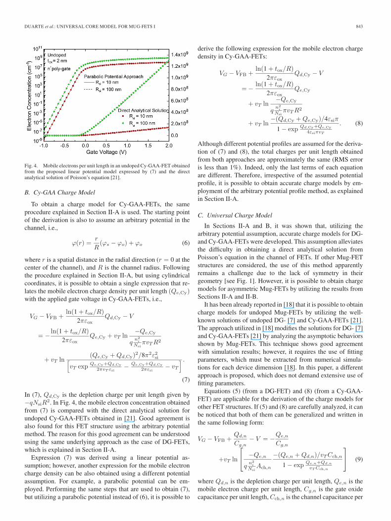
Fig. 4. Mobile electrons per unit length in an undoped Cy-GAA-FET obtainedfrom the proposed linear potential model expressed by (7) and the directanalytical solution of Poisson’s equation [21].
B. Cy-GAA Charge Model
To obtain a charge model for Cy-GAA-FETs, the sameprocedure explained in Section II-A is used. The starting pointof the derivation is also to assume an arbitrary potential in thechannel, i.e.,
ϕ(r) =r
R(ϕs − ϕo) + ϕo (6)
where r is a spatial distance in the radial direction (r = 0 at thecenter of the channel), and R is the channel radius. Followingthe procedure explained in Section II-A, but using cylindricalcoordinates, it is possible to obtain a single expression that re-lates the mobile electron charge density per unit length (Qe,Cy)with the applied gate voltage in Cy-GAA-FETs, i.e.,
VG − VFB +ln(1 + tox/R)
2πεoxQd,Cy − V
= − ln(1 + tox/R)
2πεoxQe,Cy + vT ln
−Qe,Cy
qn2i
NsiπvTR2
+ vT ln(Qe,Cy +Qd,Cy)
2/8π2ε2si[vT exp
Qe,Cy+Qd,Cy
2πvT εsi− Qe,Cy+Qd,Cy
2πεsi− vT
] .
(7)
In (7), Qd,Cy is the depletion charge per unit length given by−qNsiR
2. In Fig. 4, the mobile electron concentration obtainedfrom (7) is compared with the direct analytical solution forundoped Cy-GAA-FETs obtained in [21]. Good agreement isalso found for this FET structure using the arbitrary potentialmethod. The reason for this good agreement can be understoodusing the same underlying approach as the case of DG-FETs,which is explained in Section II-A.
Expression (7) was derived using a linear potential as-sumption; however, another expression for the mobile electroncharge density can be also obtained using a different potentialassumption. For example, a parabolic potential can be em-ployed. Performing the same steps that are used to obtain (7),but utilizing a parabolic potential instead of (6), it is possible to
derive the following expression for the mobile electron chargedensity in Cy-GAA-FETs:
VG − VFB +ln(1 + tox/R)
2πεoxQd,Cy − V
=− ln(1 + tox/R)
2πεoxQe,Cy
+ vT ln−Qe,Cy
qn2i
NsiπvTR2
+ vT ln−(Qd,Cy +Qe,Cy)/4εsiπ
1 − expQd,Cy+Qe,Cy
4εsiπvT
. (8)
Although different potential profiles are assumed for the deriva-tion of (7) and (8), the total charges per unit length obtainedfrom both approaches are approximately the same (RMS erroris less than 1%). Indeed, only the last terms of each equationare different. Therefore, irrespective of the assumed potentialprofile, it is possible to obtain accurate charge models by em-ployment of the arbitrary potential profile method, as explainedin Section II-A.
C. Universal Charge Model
In Sections II-A and B, it was shown that, utilizing thearbitrary potential assumption, accurate charge models for DG-and Cy-GAA-FETs were developed. This assumption alleviatesthe difficulty in obtaining a direct analytical solution fromPoisson’s equation in the channel of FETs. If other Mug-FETstructures are considered, the use of this method apparentlyremains a challenge due to the lack of symmetry in theirgeometry [see Fig. 1]. However, it is possible to obtain chargemodels for asymmetric Mug-FETs by utilizing the results fromSections II-A and II-B.
It has been already reported in [18] that it is possible to obtaincharge models for undoped Mug-FETs by utilizing the well-known solutions of undoped DG- [7] and Cy-GAA-FETs [21].The approach utilized in [18] modifies the solutions for DG- [7]and Cy-GAA-FETs [21] by analyzing the asymptotic behaviorsshown by Mug-FETs. This technique shows good agreementwith simulation results; however, it requires the use of fittingparameters, which must be extracted from numerical simula-tions for each device dimension [18]. In this paper, a differentapproach is proposed, which does not demand extensive use offitting parameters.
Equations (5) (from a DG-FET) and (8) (from a Cy-GAA-FET) are applicable for the derivation of the charge models forother FET structures. If (5) and (8) are carefully analyzed, it canbe noticed that both of them can be generalized and written inthe same following form:
VG − VFB +Qd,n
Cg,n− V = −Qe,n
Cg,n
+vT ln
⎡⎣ −Qe,n
qn2i
NsiAch,n
−(Qe,n +Qd,n)/vTCch,n
1 − expQe,n+Qd,n
vTCch,n
⎤⎦ (9)
where Qd,n is the depletion charge per unit length, Qe,n is themobile electron charge per unit length, Cg,n is the gate oxidecapacitance per unit length, Cch,n is the channel capacitance per
844 IEEE TRANSACTIONS ON ELECTRON DEVICES, VOL. 60, NO. 2, FEBRUARY 2013
unit length, and Ach,n is the area of the channel. The subindex“n” denotes the device architecture being used, e.g., n = DGrefers to a DG-FET. In a DG-FET, Qd,DG, Cg,DG, Cch,DG, andAch,DG are given by
Qd,DG =− qNsiHsiWsi (10)
Cg,DG =2Hsiεoxtox
(11)
Cch,DG =4HsiεsiWsi
(12)
Ach,DG =HsiWsi. (13)
For a Cy-GAA-FET, Qd,Cy, Cg,Cy, Cch,Cy, and Ach,Cy aregiven by
Qd,Cy =− qNsiπR2 (14)
Cg,Cy =2πεox
ln(1 + tox/R)(15)
Cch,Cy =4πεsi (16)Ach,DG =πR2. (17)
Expression (9) continuously captures the behavior of Mug-FETs for all operational regimes: weak inversion, moderateinversion, and strong inversion. Therefore, a charge model fora given FET structure can be obtained by utilizing the values ofQd,n, Cg,n, Cch,n, and Ach,n of that structure.
In the case of an SG-FET, Qd,SG, Cg,SG, Cch,SG, and Ach,SG
are given by
Qd,SG =− qNsiHsiWsi (18)
Cg,SG =Wsiεoxtox
(19)
Cch,SG =WsiεsiHsi
(20)
Ach,SG =HsiWsi. (21)
For a Re-GAA FET, Qd,Re, Cg,Re, Cch,Re, and Ach,Re areapproximately given by
Qd,Re =− qNsiHsiWsi (22)
Cg,Re =5εox/2
ln(1 + 5tox/4Wsi)+
5εox/2ln(1 + 5tox/4Hsi)
(23)
Cch,Re =4WsiεsiHsi
+ 4HsiεsiWsi
(24)
Ach,Re =HsiWsi. (25)
Expression (23) is obtained from [29]; however, another ap-proximation can be also found in [30]. Both formulas showedsimilar values. Expression (24) is simply obtained by overlap-ping two DG-FETs in the Wsi and Hsi directions. For a TG-FET, Qd,TG, Cg,TG, Cch,TG, and Ach,TG are approximatelygiven by
Qd,TG =− qNsiHsiWsi (26)
Cg,TG =3.02 × 3εox/2
ln(1 + 3tox/2Hsi)
− 5εox/4ln(1 + 5tox/4Hsi)
+5εox/4
ln(1 + 5tox/4Wsi)(27)
Cch,TG =WsiεsiHsi
+ 4HsiεsiWsi
(28)
Ach,TG =HsiWsi. (29)
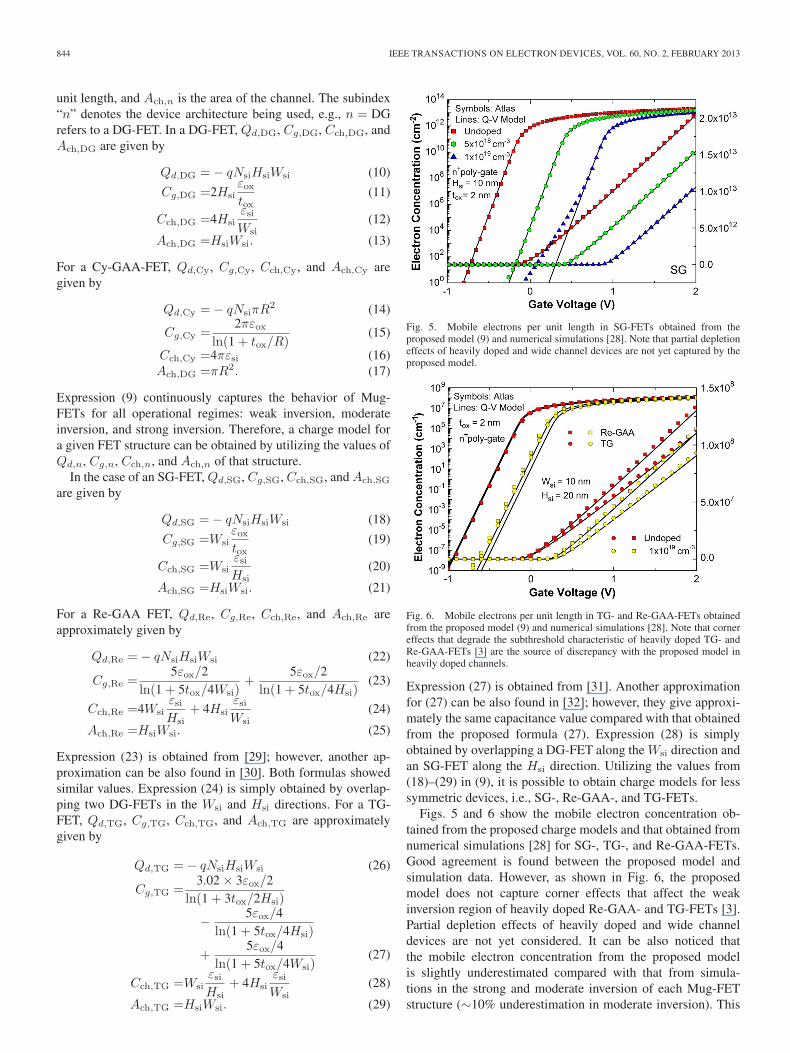
Fig. 5. Mobile electrons per unit length in SG-FETs obtained from theproposed model (9) and numerical simulations [28]. Note that partial depletioneffects of heavily doped and wide channel devices are not yet captured by theproposed model.
Fig. 6. Mobile electrons per unit length in TG- and Re-GAA-FETs obtainedfrom the proposed model (9) and numerical simulations [28]. Note that cornereffects that degrade the subthreshold characteristic of heavily doped TG- andRe-GAA-FETs [3] are the source of discrepancy with the proposed model inheavily doped channels.
Expression (27) is obtained from [31]. Another approximationfor (27) can be also found in [32]; however, they give approxi-mately the same capacitance value compared with that obtainedfrom the proposed formula (27). Expression (28) is simplyobtained by overlapping a DG-FET along the Wsi direction andan SG-FET along the Hsi direction. Utilizing the values from(18)–(29) in (9), it is possible to obtain charge models for lesssymmetric devices, i.e., SG-, Re-GAA-, and TG-FETs.
Figs. 5 and 6 show the mobile electron concentration ob-tained from the proposed charge models and that obtained fromnumerical simulations [28] for SG-, TG-, and Re-GAA-FETs.Good agreement is found between the proposed model andsimulation data. However, as shown in Fig. 6, the proposedmodel does not capture corner effects that affect the weakinversion region of heavily doped Re-GAA- and TG-FETs [3].Partial depletion effects of heavily doped and wide channeldevices are not yet considered. It can be also noticed thatthe mobile electron concentration from the proposed modelis slightly underestimated compared with that from simula-tions in the strong and moderate inversion of each Mug-FETstructure (∼10% underestimation in moderate inversion). This
DUARTE et al.: UNIVERSAL CORE MODEL FOR MUG-FETS I 845
indicates that, to improve the accuracy of the proposed modelin the moderate inversion, (9) needs to be delicately revised(for each case, including SG-, DG-, TG-, Re-GAA-, and Cy-GAA-FETs). This modification is presented in Section II-Dby following the method proposed in [14]. In addition, nu-merical methods have been used to solve (9). This is notpractical for compact modeling applications because the useof numerical methods increases the computation time and maycause divergence problems [27]. However, an explicit modelcan be derived for the proposed universal charge model usingthe method explained in [27]. Corner effects that degrade thesubthreshold characteristic of heavily doped Re-GAA- and TG-FETs [3], causing discrepancy with the proposed model, werenot included in this paper and remained for further work.Finally, note that (5) and (8) have been used to obtain theuniversal charge model; however, (7) can be also used for thesame propose. In the next sections, it is shown that, using (7), amore accurate model can be achieved.
D. Revised Universal Charge Model
Expression (9) shows good accuracy compared with nu-merical simulations [28]. However, the mobile electron con-centration is slightly underestimated mainly in the moderateinversion mode. To improve the accuracy of expression (9), themethod proposed in [14] can be used. In [14], Cch is expressedas αn × Cch, where αn is used as the fitting parameter thatoptimizes the proposed model. This method is based on thefact that Cch will have a different factor, which depends onthe assumed potential profile. For example, Cch is 2πεsi fora Cy-GAA-FET with the assumption of a linear potential [see(7)]. On the other hand, if a parabolic potential is used, Cch,
is 4πεsi [see (8)]. The difference in each Cch mainly arises inthe moderate inversion mode. Note that other operation modesare independent of the assumed potential profile, i.e., weakand strong inversion modes are not strongly affected by theassumed potential profile. Here, an extensive evaluation of theerror arisen from charge models of DG- and Cy-GAA-FETs isperformed to obtain an optimal αn for each case.
It is found that the proposed model showed the lowestaccuracy between the moderate inversion region and an earlystage of the strong inversion. This is because the electron profileis not flat or steep at those bias regimes [see curve at VG = 0 Vin Fig. 3(a)]. This is not the case of heavily doped devices whereelectron concentration is mainly determined at the surface ofthe channel for all operational regimes [see Fig. 3(b)]. It isnoteworthy that the proposed model shows more accuracyat the heavily doped devices than at the undoped devices.Hence, the error evaluation is focused around VTH. In addition,noting the fact that the model is less accurate for lightly dopedFETs, the previously reported models established for undopedDG- [7] and Cy-GAA-FETs [21] are used to obtain an optimalvalue of αn because those models are based on the directanalytical solution of Poisson’s equation. The obtained αn willbe also valid for heavily doped cases.
The electron concentrations obtained from expression (9) andthe reported model for undoped DG-FETs [7] using differentdevice parameters and values for αDG were compared. The
error of the data from the proposed model was obtained fordifferent VG from −0.5 to 0.5 V, Wsi from 1 to 50 nm, tox from1 to 10 nm, αDG from 1 to 2.5, fixed doping (undoped), andfixed-gate work function (n+ poly-gate). The error peaks areconcentrated around VTH, which validated our error evaluationrange. For every device parameter, the worst peak error wasobtained for each value of αDG. Even for αDG of 1 (no usingfitting parameter), the proposed model showed reasonable ac-curacy for the total mobile electron charge density (worst peakerror of ∼18%). At αDG = 1.8, further improvement is madein the accuracy of expression (9). Employment of αDG = 1.8shows a worst peak error of 2.96% for a wide range of deviceparameters and gate bias variations (the RMS error is lower than∼1%). The good accuracy obtained from the proposed model isthen comparable with that from the model obtained in [7].
In the case of Cy-GAA-FETs, the same procedure used forDG-FETs is employed and compared with the model from[21]. Two potential approximations, i.e., parabolic and linearpotential, are used. In these cases, the worst peak error was alsoobtained for each αCy. Different VG from −0.5 to 0.5 V, R from1 to 25 nm, tox from 1 to 10 nm, αCy from 1 to 2, fixed doping(undoped), and gate work function (n+ poly-gate) were usedfor the comparison. αCy of 1 (no use of fitting parameter) showsreasonable accuracy for the total mobile electron charge density(worst peak error of ∼12%); however, αCy of 1.4 furtherimproves the accuracy of expression (9). At αCy = 1.4, thepeak error is 4.5% for the wide range of device parameters andgate bias variations. Therefore, it is concluded that the accuracyobtained from the proposed model is also comparable to thatfrom the model in [21]. In contrast, further improved accuracyis obtained for the linear potential approximation, which isexpressed by (7). In this case, using a value of αCy = 1.6, thepeak error is reduced to 2.89%. Note that the RMS error is lowerthan ∼1% using both approaches.
On the other hand, an optimal value of αn can be alsoextracted using numerical simulations for undoped or dopedFETs [28]. Regardless of the device structure, similar values ofαn ≈ 2 are obtained. Therefore, the modified universal chargemodel from (9) for Mug-FETs is expressed as
VG − VFB +QD,n
Cg,n− V = −Qe,n
Cg,n+ vT ln
−Qe,n
qn2i
NsiAch,n
+vT ln−(Qe,n/αn +Qd,n)/vTCch,n
1 − expQe,n/αn+Qd,n
vTCch,n
(30)
where Qd,n, Cg,n, Cch,n, and Ach,n, depending on a FETstructure, are still given by (10)–(29). Note that αn is appliedonly to the mobile charge term, as expressed in [14]; thus, itdoes not influence the threshold voltage and doping effects.Using the same notation as (30), the model given by (7) canbe also used as a universal charge model given by
VG − VFB +QD,n
Cg,n− V = −Qe,n
Cg,n+ vT ln
−Qe,n
qn2i
NsiAch,n
+vT ln2(Qe,n/αn +Qd,n)
2/(vTCch,n)2
expQe,n/αn+Qd,n
vTCch,n/2− Qe,n/αn+Qd,n
vTCch,n/2− 1
. (31)
846 IEEE TRANSACTIONS ON ELECTRON DEVICES, VOL. 60, NO. 2, FEBRUARY 2013
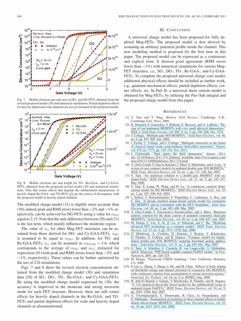
Fig. 7. Mobile electrons per unit area in DG- and SG-FETs obtained from therevised proposed model (30) and numerical simulations. Partial depletion effectsfor heavily doped and wide channels are not yet included in the proposed model.
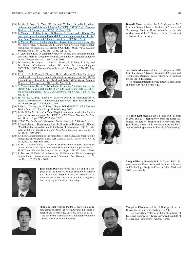
Fig. 8. Mobile electrons per unit length for TG-, Re-GAA-, and Cy-GAA-FETs, obtained from the proposed revised model (30) and numerical simula-tions. Note that corner effects that degrade the subthreshold characteristic ofheavily doped Re-GAA- and TG-FETs [3] are the source of discrepancy withthe proposed model in heavily doped channels.
The modified charge model (31) is slightly more accurate than(30); indeed, peak and RMS errors lower than∼2% and∼1%, re-spectively, can be achieved for DG-FETs using a value for αDG
equal to 2.15. Note that the only difference between (30) and (31)is the last term, which mainly influences the moderate region.
The value of αn for other Mug-FET structures can be as-sumed from those derived for DG- and Cy-GAA-FETs. αSG
is assumed to be equal to αDG. In addition, for TG- andRe-GAA-FETs, αn can be assumed as αTG,Re = 1.6, whichcorresponds to the average of αDG and αCy extracted forexpression (9) (with peak and RMS errors lower than ∼5% and∼1%, respectively). These values can be further optimized bythe use of 2-D simulations.
Figs. 7 and 8 show the revised electron concentration ob-tained from the modified charge model (30) and simulationdata [28] of SG-, DG-, TG-, Re-GAA-, and Cy-GAA-FETs.By using the modified charge model expressed by (30), theaccuracy is improved in the moderate and strong inversionmode for each FET structure. However, there are still cornereffects for heavily doped channels in the Re-GAA- and TG-FETs and partial depletion effects for wide and heavily dopedchannels as aforementioned.
III. CONCLUSION
A universal charge model has been proposed for fully de-pleted Mug-FETs. The proposed model is first derived byassuming an arbitrary potential profile inside the channel. Thisnew modeling method is proposed for the first time in thispaper. The proposed model can be expressed as a continuousand explicit form. It showed good agreement (RMS errorslower than ∼1%) with numerical simulations for various Mug-FET structures, i.e., SG-, DG-, TG-, Re-GAA-, and Cy-GAA-FETs. To complete the proposed universal charge core model,additional physical effects should be included as further work,e.g., quantum mechanical effects, partial depletion effects, cor-ner effects, etc. In Part II, a universal drain current model isobtained for Mug-FETs, by utilizing the Pao–Sah integral andthe proposed charge model from this paper.
REFERENCES
[1] Y. Taur and T. Ning, Modern VLSI Devices. Cambridge, U.K.:Cambridge Univ. Press, 2009.
[2] R. Dennard, F. Gaensslen, V. Rideout, E. Bassous, and A. LeBlanc, “De-sign of ion-implanted MOSFETs with very small physical dimensions,”IEEE J. Solid-State Circuits, vol. SSC-9, no. 5, pp. 256–268, Oct. 1974.
[3] J. Colinge, “Multiple-gate SOI MOSFETs,” Solid State Electron., vol. 48,no. 6, pp. 897–905, Jun. 2004.
[4] I. Ferain, C. Colinge, and J. Colinge, “Multigate transistors as the futureof classical metal–oxide–semiconductor field-effect transistors,” Nature,vol. 479, no. 7373, pp. 310–316, Nov. 2011.
[5] J. Cartwright, “Intel enters the third dimension,” Nature, 2011.doi: 10.1038/news.2011.274. [Online]. Available: http://www.nature.com/news/2011/110506/full/news.2011.274.html
[6] A. Ortiz-Conde, F. Garcia-Sanchez, J. Muci, S. Malobabic, and J. Liou, “Areview of core compact models for undoped double-gate SOI MOSFETs,”IEEE Trans. Electron Devices, vol. 54, no. 1, pp. 131–140, Jan. 2007.
[7] Y. Taur, “An analytical solution to a double-gate MOSFET with un-doped body,” IEEE Electron Device Lett., vol. 21, no. 5, pp. 245–247,May 2000.
[8] Y. Taur, X. Liang, W. Wang, and H. Lu, “A continuous, analytic drain-current model for DG MOSFETs,” IEEE Electron Device Lett., vol. 25,no. 2, pp. 107–109, Feb. 2004.
[9] J. Sallese, F. Krummenacher, F. Prégaldiny, C. Lallement, A. Roy, andC. Enz, “A design oriented charge-based current model for symmetricDG MOSFET and its correlation with the EKV formalism,” Solid StateElectron., vol. 49, no. 3, pp. 485–489, Mar. 2005.
[10] A. Ortiz-Conde, F. Garcıacute;a Sıacute;nchez, and J. Muci, “Rigorousanalytic solution for the drain current of undoped symmetric dual-gateMOSFETs,” Solid State Electron., vol. 49, no. 4, pp. 640–647, Apr. 2005.
[11] M. Dunga, C. Lin, X. Xi, D. Lu, A. Niknejad, and C. Hu, “Modelingadvanced FET technology in a compact model,” IEEE Trans. ElectronDevices, vol. 53, no. 9, pp. 1971–1978, Sep. 2006.
[12] O. Moldovan, A. Cerdeira, D. Jimenez, J. Raskin, V. Kilchytska,D. Flandre, N. Collaert, and B. Iòiguez, “Compact model for highly-doped double-gate SOI MOSFETs targeting baseband analog applica-tions,” Solid State Electron., vol. 51, no. 5, pp. 655–661, May 2007.
[13] G. Smit, A. Scholten, G. Curatola, R. van Langevelde, G. Gildenblat,and D. Klaassen, “PSP-based scalable compact FinFET model,” in Proc.Nanotech, 2007, pp. 520–525.
[14] M. Dunga, “Nanoscale CMOS modeling,” Univ. California, Berkeley,CA, 2008.
[15] F. Liu, L. Zhang, J. Zhang, J. He, and M. Chan, “Effects of body dopingon threshold voltage and channel potential of symmetric DG MOSFETswith continuous solution from accumulation to strong-inversion regions,”Semicond. Sci. Technol., vol. 24, no. 8, p. 085005, Aug. 2009.
[16] H. Abd El Hamid, J. Guitart, V. Kilchytska, D. Flandre, and B. Iniguez,“A 3-D analytical physically based model for the subthreshold swing inundoped trigate FinFETs,” IEEE Trans. Electron Devices, vol. 54, no. 9,pp. 2487–2496, Sep. 2007.
[17] A. Tsormpatzoglou, C. Dimitriadis, R. Clerc, G. Pananakakis, andG. Ghibaudo, “Semianalytical modeling of short-channel effects in lightlydoped silicon trigate MOSFETs,” IEEE Trans. Electron Devices, vol. 55,no. 10, pp. 2623–2631, Oct. 2008.
DUARTE et al.: UNIVERSAL CORE MODEL FOR MUG-FETS I 847
[18] B. Yu, J. Song, Y. Yuan, W. Lu, and Y. Taur, “A unified analyticdrain-current model for multiple-gate MOSFETs,” IEEE Trans. ElectronDevices, vol. 55, no. 8, pp. 2157–2163, Aug. 2008.
[19] E. Moreno, J. Roldán, F. Ruiz, D. Barrera, A. Godoy, and F. Gámiz, “Ananalytical model for square GAA MOSFETs including quantum effects,”Solid State Electron., vol. 54, no. 11, pp. 1463–1469, Nov. 2010.
[20] E. Moreno Perez, J. Roldan Aranda, F. Garcia Ruiz, D. Barrera Rosillo,M. Ibanez Perez, A. Godoy, and F. Gamiz, “An inversion-charge analyt-ical model for square gate-all-around MOSFETs,” IEEE Trans. ElectronDevices, vol. 58, no. 9, pp. 2854–2861, Sep. 2011.
[21] Y. Chen and J. Luo, “A comparative study of double-gate and surrounding-gate MOSFETs in strong inversion and accumulation using an analyticalmodel,” Integration, vol. 1, no. 2, p. 6, 2001.
[22] D. Jiménez, B. Iniguez, J. Sune, L. Marsal, J. Pallares, J. Roig, andD. Flores, “Continuous analytic IV model for surrounding-gateMOSFETs,” IEEE Electron Device Lett., vol. 25, no. 8, pp. 571–573, Aug.2004.
[23] F. Liu, J. He, L. Zhang, J. Zhang, J. Hu, C. Ma, and M. Chan, “A charge-based model for long-channel cylindrical surrounding-gate MOSFETsfrom intrinsic channel to heavily doped body,” IEEE Trans. ElectronDevices, vol. 55, no. 8, pp. 2187–2194, Aug. 2008.
[24] S. Venugopalan, D. Lu, Y. Kawakami, P. Lee, A. Niknejad, and C. Hu,“BSIM-CG: A compact model of cylindrical/surround gate MOSFETfor circuit simulations,” Solid State Electron., vol. 67, no. 1, pp. 79–89,Jan. 2012.
[25] H. Pao and C. Sah, “Effects of diffusion current on characteristics ofmetal–oxide (insulator)–semiconductor transistors,” Solid State Electron.,vol. 9, no. 10, pp. 927–937, Oct. 1966.
[26] J. Park, J. Colinge, and C. Diaz, “Pi-gate SOI MOSFET,” IEEE ElectronDevice Lett., vol. 22, no. 8, pp. 405–406, Aug. 2001.
[27] B. Yu, H. Lu, M. Liu, and Y. Taur, “Explicit continuous models for double-gate and surrounding-gate MOSFETs,” IEEE Trans. Electron Devices,vol. 54, no. 10, pp. 2715–2722, Oct. 2007.
[28] ATLAS User’s Manual, Silvaco Int., Santa Clara, CA, 2008, vol.5, no.0.[29] I. Tienda-Luna, F. Garcıacute;a Ruiz, L. Donetti, A. Godoy, and F. Gámiz,
“Modeling the equivalent oxide thickness of surrounding gate SOI de-vices with high-[kappa] insulators,” Solid State Electron., vol. 52, no. 12,pp. 1854–1860, 2008.
[30] T. Chen, “Determination of the capacitance, inductance, and characteristicimpedance of rectangular lines,” IRE Trans. Microw. Theory Tech., vol. 8,no. 5, pp. 510–519, Sep. 1960.
[31] F. Ruiz, I. Tienda-Luna, A. Godoy, L. Donetti, and F. Gamiz, “Equivalentoxide thickness of trigate SOI MOSFETs with high-kappa insulators,”IEEE Trans. Electron Devices, vol. 56, no. 11, pp. 2711–2719, Nov. 2009.
[32] R. Trevisoli, R. Doria, M. de Souza, and M. Pavanello, “Threshold voltagein junctionless nanowire transistors,” Semicond. Sci. Technol., vol. 26,no. 10, p. 105 009, Oct. 2011.
Juan Pablo Duarte received the B.Sc. and M.S. de-grees from the Korea Advanced Institute of Scienceand Technology, Daejeon, Korea, in 2010 and 2012.He is currently working toward the Ph.D. degree atthe University of California, Berkeley.
Sung-Jin Choi received the Ph.D. degree in electri-cal engineering from the Korea Advanced Institute ofScience and Technology, Daejeon, Korea, in 2012.
He is currently a Postdoctoral Researcher with theUniversity of California, Berkeley.
Dong-Il Moon received the M.S. degree in 2010from the Korea Advanced Institute of Science andTechnology, Daejeon, Korea, where he is currentlyworking toward the Ph.D. degree in the Departmentof Electrical Engineering.
Jae-Hyuk Ahn received the B.S. degree in 2007from the Korea Advanced Institute of Science andTechnology, Daejeon, Korea, where he is workingtoward the Ph.D. degree.
His research interests include electrical biosensorsand nanofabrication technology.
Jee-Yeon Kim received the B.S. and M.S. degreesin 2009 and 2011, respectively, from the Korea Ad-vanced Institute of Science and Technology, Dae-jeon, Korea, where she is working toward the Ph.D.degree in the Department of Electrical Engineering.
Sungho Kim received the B.S., M.S., and Ph.D. de-grees from the Korea Advanced Institute of Scienceand Technology, Daejeon, Korea, in 2006, 2008, and2012, respectively.
Yang-Kyu Choi received the Ph.D. degree from theUniversity of California, Berkeley, in 2001.
He is currently a Professor with the Department ofElectrical Engineering, Korea Advanced Institute ofScience and Technology, Daejeon, Korea.