A Reconfigurable Digital Multiplier and 4:2 Compressor Cells ...
90
University of Windsor University of Windsor Scholarship at UWindsor Scholarship at UWindsor Electronic Theses and Dissertations Theses, Dissertations, and Major Papers 2008 A Reconfigurable Digital Multiplier and 4:2 Compressor Cells A Reconfigurable Digital Multiplier and 4:2 Compressor Cells Design Design Peng Chang University of Windsor Follow this and additional works at: https://scholar.uwindsor.ca/etd Recommended Citation Recommended Citation Chang, Peng, "A Reconfigurable Digital Multiplier and 4:2 Compressor Cells Design" (2008). Electronic Theses and Dissertations. 8127. https://scholar.uwindsor.ca/etd/8127 This online database contains the full-text of PhD dissertations and Masters’ theses of University of Windsor students from 1954 forward. These documents are made available for personal study and research purposes only, in accordance with the Canadian Copyright Act and the Creative Commons license—CC BY-NC-ND (Attribution, Non-Commercial, No Derivative Works). Under this license, works must always be attributed to the copyright holder (original author), cannot be used for any commercial purposes, and may not be altered. Any other use would require the permission of the copyright holder. Students may inquire about withdrawing their dissertation and/or thesis from this database. For additional inquiries, please contact the repository administrator via email ([email protected]) or by telephone at 519-253-3000ext. 3208.
-
Upload
khangminh22 -
Category
Documents
-
view
3 -
download
0
Transcript of A Reconfigurable Digital Multiplier and 4:2 Compressor Cells ...
University of Windsor University of Windsor
Scholarship at UWindsor Scholarship at UWindsor
Electronic Theses and Dissertations Theses, Dissertations, and Major Papers
2008
A Reconfigurable Digital Multiplier and 4:2 Compressor Cells A Reconfigurable Digital Multiplier and 4:2 Compressor Cells
Design Design
Peng Chang University of Windsor
Follow this and additional works at: https://scholar.uwindsor.ca/etd
Recommended Citation Recommended Citation Chang, Peng, "A Reconfigurable Digital Multiplier and 4:2 Compressor Cells Design" (2008). Electronic Theses and Dissertations. 8127. https://scholar.uwindsor.ca/etd/8127
This online database contains the full-text of PhD dissertations and Masters’ theses of University of Windsor students from 1954 forward. These documents are made available for personal study and research purposes only, in accordance with the Canadian Copyright Act and the Creative Commons license—CC BY-NC-ND (Attribution, Non-Commercial, No Derivative Works). Under this license, works must always be attributed to the copyright holder (original author), cannot be used for any commercial purposes, and may not be altered. Any other use would require the permission of the copyright holder. Students may inquire about withdrawing their dissertation and/or thesis from this database. For additional inquiries, please contact the repository administrator via email ([email protected]) or by telephone at 519-253-3000ext. 3208.
A Reconfigurable Digital Multiplier and 4:2
Compressor Cells Design
by
Peng Chang
A Thesis Submitted to the Faculty of Graduate Studies
through Electrical Engineering in Partial Fulfillment of the Requirements for
the Degree of Master of Applied Science at the University of Windsor
Windsor, Ontario, Canada
2008
© Peng Chang

1*1 Library and Archives Canada
Published Heritage Branch
395 Wellington Street OttawaONK1A0N4 Canada
Bibliotheque et Archives Canada
Direction du Patrimoine de I'edition
395, rue Wellington Ottawa ON K1A 0N4 Canada
Your file Votre r6f6rence ISBN: 978-0-494-82099-5 Our file Notre r6f6rence ISBN: 978-0-494-82099-5
NOTICE:
The author has granted a nonexclusive license allowing Library and Archives Canada to reproduce, publish, archive, preserve, conserve, communicate to the public by telecommunication or on the Internet, loan, distribute and sell theses worldwide, for commercial or noncommercial purposes, in microform, paper, electronic and/or any other formats.
AVIS:
L'auteur a accorde une licence non exclusive permettant a la Bibliotheque et Archives Canada de reproduire, publier, archiver, sauvegarder, conserver, transmettre au public par telecommunication ou par I'lnternet, preter, distribuer et vendre des theses partout dans le monde, a des fins commerciales ou autres, sur support microforme, papier, electronique et/ou autres formats.
The author retains copyright ownership and moral rights in this thesis. Neither the thesis nor substantial extracts from it may be printed or otherwise reproduced without the author's permission.
L'auteur conserve la propriete du droit d'auteur et des droits moraux qui protege cette these. Ni la these ni des extraits substantiels de celle-ci ne doivent etre imprimes ou autrement reproduits sans son autorisation.
In compliance with the Canadian Privacy Act some supporting forms may have been removed from this thesis.
While these forms may be included in the document page count, their removal does not represent any loss of content from the thesis.
Conformement a la loi canadienne sur la protection de la vie privee, quelques formulaires secondaires ont ete enleves de cette these.
Bien que ces formulaires aient inclus dans la pagination, il n'y aura aucun contenu manquant.
• • I
Canada

AUTHOR'S DECLARATION OF ORIGINALITY
I hereby certify that I am the sole author of this thesis and that no part of this thesis has
been published or submitted for publication.
I certify that, to the best of my knowledge, my thesis does not infringe upon anyone's
copyright nor violate any proprietary rights and that any ideas, techniques, quotations, or
any other material from the work of other people included in my thesis, published or
otherwise, are fully acknowledged in accordance with the standard referencing practices.
Furthermore, to the extent that I have included copyrighted material that surpasses the
bounds of fair dealing within the meaning of the Canada Copyright Act, I certify that I
have obtained a written permission from the copyright owner(s) to include such
material(s) in my thesis and have included copies of such copyright clearances to my
appendix.
I declare that this is a true copy of my thesis, including any final revisions, as approved
by my thesis committee and the Graduate Studies office, and that this thesis has not been
submitted for a higher degree to any other University or Institution.
in

ABSTRACT
With the continually growing use of portable computing devices and increasingly
complex software applications, there is a constant push for low power high speed
circuitry to support this technology. Because of the high usage and large complex
circuitry required to carry out arithmetic operations used in applications such as digital
signal processing, there has been a great focus on increasing the efficiency of computer
arithmetic circuitry. A key player in the realm of computer arithmetic is the digital
multiplier and because of its size and power consumption, it has moved to the forefront of
today's research.
A digital reconfigurable multiplier architecture will be introduced. Regulated by a 2-bit
control signal, the multiplier is capable of double and single precision multiplication, as
well as fault tolerant and dual throughput single precision execution.
The architecture proposed in this thesis is centered on a recursive multiplication
algorithm, where a large multiplication is carried out using recursions of simpler sub-
multiplier modules. Within each sub-multiplier module, instead of carry save adder
arrays, 4:2 compressor rows are utilized for partial product reduction, which present
greater efficiency, thus result in lower delay and power consumption of the whole
multiplier.
In addition, a study of various digital logic circuit styles are initially presented, and then
three different designs of 4:2 compressor in Domino Logic are presented and simulation
results confirm the property of proposed design in terms of delay, power consumption
and operation frequency.
IV

To my beloved parents.
v

ACKNOWLEDGEMENTS
There are several people who deserve my sincere thanks for their generous contributions
to this thesis.
I would first like to express my sincere gratitude to my supervisor Dr. Majid Ahmadi for
all of his generous support and guidance. His guidance and advice both academically and
personally have had, and will continue to have, a tremendous impact on my life. He has
been an excellent mentor to me. To him I am deeply indebted.
I would also like to thank the faculty at the University of Windsor, including Dr. Roberto
Muscedere for the many conversations and advice offered, and my committee members,
Dr. Arunita Jaekel and Dr. Mitra Mirhassani for their patience and support.
Ms. Andria Turner also deserves much thanks and recognition. Her dedication to the
students is second to none. For all of her assistance and cheerful conversation I am
extremely appreciative.
To Mr. Liton Ghosh, Mr. Ashkan Hosseinzadeh Namin, Mr. Neil Scott, and Mr. Anthony
Karlof, Ms. Mazad Azarmehr I also offer great gratitude. Their sound technical advice
has not only contributed to this thesis but their friendship made the late nights in the lab
all the more bearable.
Finally, to my parents I must extend my most sincere love and gratitude. For every path I
have chosen, they have always shown unending support and enthusiasm.
vi
Table of Contents
AUTHOR'S DECLARATION OF ORIGINALITY Hi
ABSTRACT iv
DEDICATION v
ACKNOWLEDGEMENTS vi
LIST OF FIGURES x
LIST OF TABLES xii
CHAPTER 1 INTRODUCTION 1
1.1 Introduction 1
1.2 Thesis Highlights 2
1.3 Thesis Organization 3
CHAPTER 2 DIGITAL MULTIPLICATION 4
2.1 Basics of Digital Multiplication 4
2.2 Sequential Multiplication 6
2.2.1 Shift-Add Multiplication 6
2.2.2 High Radix Multipliers 7
2.3 Parallel Multipliers 8
2.3.1 Linear parallel Multipliers 9
2.3.2 Column Compression Multipliers 10
2.4 Partial Product Reduction Techniques 12
2.4.1 CSA Reduction Scheme 13
2.4.2 4:2 Compressor Reduction Scheme 16
vii
CHAPTER 3 A RECONFIGURABLE MULTIPLIER ARCHITECTURE . 20
3.1 Recursive Multiplication Algorithms 20
3.1.1 Background Information 21
3.1.2 6:2 Reduction Circuitry 24
3.2 A Reconfigurable Multiplier Architecture 27
3.2.1 Double Precision Mode 30
3.2.2 Single Precision Mode 31
3.2.3 Dural Single Precision Mode 32
3.2.4 Single Precision Fault-tolerant Mode 33
3.3 Modeling and Simulation 34
3.3.1 HDL Model 34
3.3.2 Implementation and Layout 35
3.3.3 Simulation Results 36
CHAPTER 4 CIRCUIT LEVEL DESIGNS OF 4:2 COMPRESSORS 38
4.1 High Order Counters and Compressors 38
4.1.1 Counters 38
4.1.2 Compressors 39
4.2 4:2 Compressors 41
4.2.1 Structure of 4:2 Compressors 41
4.2.2 Logical Level Decompositions of 4:2 Compressors 42
4.3 Circuit Level Designs of 4:2 Compressors 45
4.3.1 Static CMOS 47
4.3.2 Transmission Gate Logic 48
4.3.3 Pass Transistor Logic 49
4.3.4 Dynamic Logic 50
viii

4.4 Domino Logic 51
4.5 Circuit Level Optimizations of Domino Logic Gates 58
4.5.1 Multiple-output Domino Logic 58
4.5.2 Split Domino Logic 62
4.6 Simulation Result 64
4.6.1 Simulation Result for Logical Level Decompositions of 4:2 Compressors 65
4.6.2 Simulation Result for Circuit Level Designs of Full adder and 4:2 Compressor 67
CHAPTER 5 CONCLUSIONS 72
5.1 Summary of Contributions 72
5.1.1 Architectural Contributions 72
5.1.2 Transistor Level Contributions 73
5.2 Conclusions 73
REFERENCES 74
VITAAUCTORIS 77
IX

LIST OF FIGURES
Figure 1 4x4 bit multiplication leading to an 8-bit product 5
Figure 2 A simple dot diagram of 16-bit partial product array 6
Figure 3 Shift-add multiplier implementation 7
Figure 4 Shift-add implementation of a basic radix-4 multiplier 8
Figure 5 One sided CSA tree forming an Array Multiplier 10
Figure 6 Schematic representation of the column compression multiplier process 11
Figure 7 Carry Save Adder (CSA) Array 12
Figure 8 12x12 Wallace Tree 14
Figure 9 12x12 Dadda Tree 15
Figure 10 Definition of a 4:2 Compressor Row 17
Figure 11 Compressor layout for a 16x16-bit multiplication 19
Figure 12 Dot diagram of a single level recursive n-bit multiplication 23
Figure 13 A schematic of a single level recursive multiplier 23
Figure 14 A standard 6:2 reduction microcell composed of 3 stages of full adders 24
Figure 15 6:2 Microcells capable of receiving a variety of input bits 25
Figure 16 A modified version of 6:2 reduction block 27
Figure 17 Outline of Reconfigurable Multiplier 29
Figure 18 Double precision mode 30
Figure 19 Single precision mode 31
Figure 20 Dual single precision mode 32
Figure 21 Single precision - fault tolerant mode 33
Figure 22 Layout view of designed 64-bit reconfigurable multiplier 36
Figure 23 General Counter Representation 39
x

Figure 24 General Compressor Representation 40
Figure 25 Symbol of 4:2 compressor 42
Figure 26 Architecture level representation of 4:2 compressor 43
Figure 27 Primitive decomposition of 4:2 compressor at gate level (Comand) 43
Figure 28 Two alternative decompositions of 4:2 compressor at gate level 45
Figure 29 Static CMOS logic cell depicting the NFET and PFET networks 47
Figure 30 Transmission Gate 48
Figure 31 Pass-transistor implementation of an AND gate 49
Figure 32 Primitive representation of dynamic Logic block 51
Figure 33 Domino Logic 52
Figure 34 Leakage issues in dynamic circuits 54
Figure 35 Static keeper compensate for the charge leakage 55
Figure 36 Charge sharing in dynamic circuits 56
Figure 37 4:2 compressor in Domino Logic (ComD) 57
Figure 38 Multiple-output domino logic 59
Figure 39 Full adder in multiple-output domino logic (FAnewD) 60
Figure 40 Full adder in multiple-output domino logic (FAD) 61
Figure 41 4:2 compressor in multiple-output domino logic (ComnewD) 61
Figure 42 n-input split domino (SD) OR gate 62
Figure 43 Full adder in split domino logic (FAnewSD) 63
Figure 44 4:2 compressor in split domino logic (ComnewSD) 64
XI

LIST OF TABLES
Table 1 Max column height per stage of a 3:2 scheme (carry save adder array) 16
Table 2 Max column height per stage of a 4:2 scheme (4:2 compressor array) 16
Table 3 Modes of Operation of the Reconfigurable Multiplier 29
Table 4 Simulation Results for Reconfigurable Multipliers 37
Table 5 Simulation Results for logical decompositions of 4:2 Compressors 66
Table 6 Comparison of different logical decompositions of 4:2 Compressors 66
Table 7 Simulation Result for full adders 68
Table 8 Comparison of Simulation Result 68
Table 9 Simulation Result for 4:2 compressors 69
Table 10 Comparison of Simulation Result 70
xii

CHAPTER 1
INTRODUCTION
1.1 Introduction
Prior to 1935, a computer was known as a person who performed arithmetic calculations
or "one who computes" Computer was actually a job title during this period of time. The
modern machine definition is based on von Neumann's concepts [1]: "a device that
accepts input, process data, stores data, and produces output" While technology has
come a long way in the many years since von Neumann's work, the basic formula for the
components of a computing system have remained the same.
Von Neumann and his associates state that "a general purpose computing machine should
contain certain main organs relating to arithmetic, memory-storage, control and
connection with the human operator" [1]. The arithmetic organ is known today as the
arithmetic logic unit (ALU); it is required to be capable of adding, subtracting,
multiplying, and dividing. This thesis deals specifically with the multiplication function
of this arithmetic organ.
Multiplication is the key arithmetic operation which is widely used in many
microprocessors and digital signal processing applications. Microprocessors use
multipliers within their arithmetic logic units, and digital signal processing systems
require multipliers to implement DSP algorithms such as convolution and filtering. Since
the multiplier lies directly within the critical path in most systems, the demand for high-
1
speed multiplier is continuously increasing [1]. However, with the fast growing of
portable computing devices, the power consumption of the multiplier has become equally
important. All this has resulted in the pursuit of high speed low power multiplier design
techniques.
1.2 Thesis Highlights This thesis will present a general investigation of digital multiplication, and will highlight
novel reconfigurable multiplier architecture. The proposed design utilizes the
reconfigurable architecture and an optimized 4:2 compressor rows distribution
methodology for partial product reduction presented by Mokrian et al [6]. The principle
advantage of this scheme lies in its multi-mode reconfiguration ability and high efficient
partial product reduction.
The proposed scheme combines many desirable design characteristics, such as low power
dissipation, high throughput capabilities, and fault tolerance. Moreover, a 64-bit
reconfigurable multiplier, with potential applications in Digital Signal Processor (DSP)
devices, has been implemented using the TSMC 0.18 um technology. This design has
been contrasted against a standard high performance architecture of equivalent size, and
has demonstrated promising results, which will be presented in chapter 3.
In addition, other investigations into circuit level implementations of 4:2 compressor will
be addressed. In particular, various designs of 4:2 compressor in Domino Logic are
presented and simulation results confirm the property of proposed designs in terms of
delay, power consumption and operation frequency.
2

1.3 Thesis Organization
The thesis will begin with a general overview of the concept of digital multiplication, and
various multiplication algorithms in chapter 2. Moreover, this chapter will present the
fundamentals of partial product reduction.
Chapter 3 will focus on the introduction of the reconfigurable multiplier architecture,
beginning with the outline of the recursive multiplication algorithm, followed by
implementation and simulation results.
Chapter 4 will initially introduce the 4:2 compressor in terms of basic functionality. This
will be followed by an in-depth analysis of logic styles used in the construction of 4:2
compressors. This analysis will include proposed 4:2 compressor designs in Domino
Logic. This chapter will conclude with the simulation and comparison among these
designed circuitries in terms of delay, power consumption and operation frequency. This
thesis will conclude with a summary of contributions and conclusions in chapter 5.
3

CHAPTER 2
DIGITAL MULTIPLICATION
2.1 Basics of Digital Multiplication
Prior to exploring the various multiplication algorithms, and the applications of each, it is
imperative to present the essence of digital multiplication, and the standard nomenclature.
Just as in the paper and pencil methodology of carrying a multiplication of two values,
digital multiplication entails a sequence of additions carried out on partial products. The
means by which this partial product array is summed to yield the final product is the key
distinguishing factor amongst multiplication schemes.
In general, the partial product array for a n M x J V bit multiplication is formed by the
bitwise logical AND of the multiplicand A and multiplier X, where:
X = [xm> Xm-L Xm-2 ••• x2> xl, X0J
A = [a„, a„.i, an-2 ... a2, au a0]
The summation of the partial products will yield an («+m)-bit product, P, where:
P = [Sn+m, Sn+m-1, Sn+m-2 — Si, S;, SQJ
The partial product array will have (n x m) bits, arranged in m rows of n-bit values. The
array is in essence composed of a sequence of rows that are either shifted versions of the
4
multiplicand, A, or zeros, according to the bits of the multiplier, X. The multiplication of
two 4-bit values is illustrated in Figure 1.
XjOj
x2a3
X3#2
X
•Vjtfj
A%fl:
Xjfli
(h x3
Aflffj
Xl<*2
x^aj
XJOQ
02
X-
X(fi2
Xidi
x:a0
(h Xi
XQCII
x2a0
(to x0
XQIIQ
7 s a s $ s4 s j s2 s1 So
Figure 1 4x4 bit multiplication leading to an 8-bit product
To better visualize the partial product reduction process, the concept of dot diagrams
shall be introduced [1, 2]. A dot diagram is a visual representation of the bits in an
algorithm, where in this particular application the dots represent individual partial
product bits. The nature of the dot diagram is to depict the bits using the relative position
of individual bits, and the manner in which they are manipulated, irrespective of the
actual value of each bit.
Figure 2 shows the partial product array for a 16x16-bit multiplication [1]. The partial
products are shifted to account for the differing arithmetic weight of the bits in the
multiplier, where dots of the same arithmetic weight are aligned vertically. The final
product, represented by the double length row of dots at the bottom, is obtained via the
summation of the dots in each column.
5
t\iri..> IYKI'-UI
Miihir*'-- H»I
i
/ I / i
v-v -
VUvtiitn T iH.-L
1 1 Mi|1"(>lli l i ' i l |
» - — •
/ . ! ! ! ! !
— — _ .
y Produci
• — - - -
] <+
- — - --
<4 — -
J 1 i-
«•
- -
-
, • lu-
^ 1
• I M u
• 1
ml 1 * l m i
• * P 0 1 m' i • > 1
• t*
• 1
Figure 2 A simple dot diagram of 16-bit partial product array
2.2 Sequential Multiplication
2.2.1 Shift-Add Multiplication
In its most basic form, digital multiplication may be carried out through a sequence of
shifts and additions of the multiplicand to the partial product register, governed by the
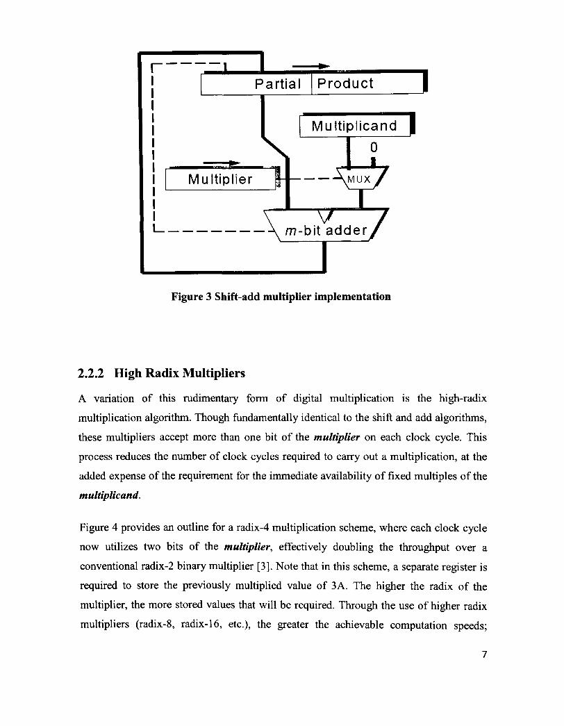
individual bits of the multiplier (Figure 3). This primitive form of multiplication, known
as shift-add or iterative multiplication, although very simple in implementation, is very
slow. The number of iterations, or cycles of addition, that are required grows linearly
with the size of the multiplier, with each cycle having a delay of the required fast adder.
6
Partial Product
\
Multiplier
0 J_
|_ -\MUX/
—7— m-bit adde 7
1 Multiplicand |
Figure 3 Shift-add multiplier implementation
2.2.2 High Radix Multipliers
A variation of this rudimentary form of digital multiplication is the high-radix
multiplication algorithm. Though fundamentally identical to the shift and add algorithms,
these multipliers accept more than one bit of the multiplier on each clock cycle. This
process reduces the number of clock cycles required to carry out a multiplication, at the
added expense of the requirement for the immediate availability of fixed multiples of the
multiplicand.
Figure 4 provides an outline for a radix-4 multiplication scheme, where each clock cycle
now utilizes two bits of the multiplier, effectively doubling the throughput over a
conventional radix-2 binary multiplier [3]. Note that in this scheme, a separate register is
required to store the previously multiplied value of 3 A. The higher the radix of the
multiplier, the more stored values that will be required. Through the use of higher radix
multipliers (radix-8, radix-16, etc.), the greater the achievable computation speeds;
7

however, this comes at the expense of increased overhead in terms of shift circuitry, and
storage registers for all of the required multiples of the multiplicand.
Partial
2x
Multiplier
Product
Multiplicand (A))
I
0 A 2A 3A J I I L _
L - - \ MUX /
£ V
m-bit adde 7 Figure 4 Shift-add implementation of a basic radix-4 multiplier
2.3 Parallel Multipliers
Serial multipliers, and the concept of shift and add algorithms, are a class of primitive
multiplication schemes that take advantage of simple implementation techniques. Such
methods are employed where hardware overhead is an issue, or if there is a lack of a
dedicated hardware multiplier. Modern high performance machines call for more
sophisticated algorithms, in order to limit the computation latency.
Parallel multipliers in general may be classified into two distinct categories: linear
parallel multipliers, and column compression multipliers. As opposed to the serial
multiplier, parallel multipliers generate all of the partial products simultaneously. In

addition, parallel multipliers limit the latency associated with carry propagation to one
final fast adder.
2.3.1 Linear parallel Multipliers
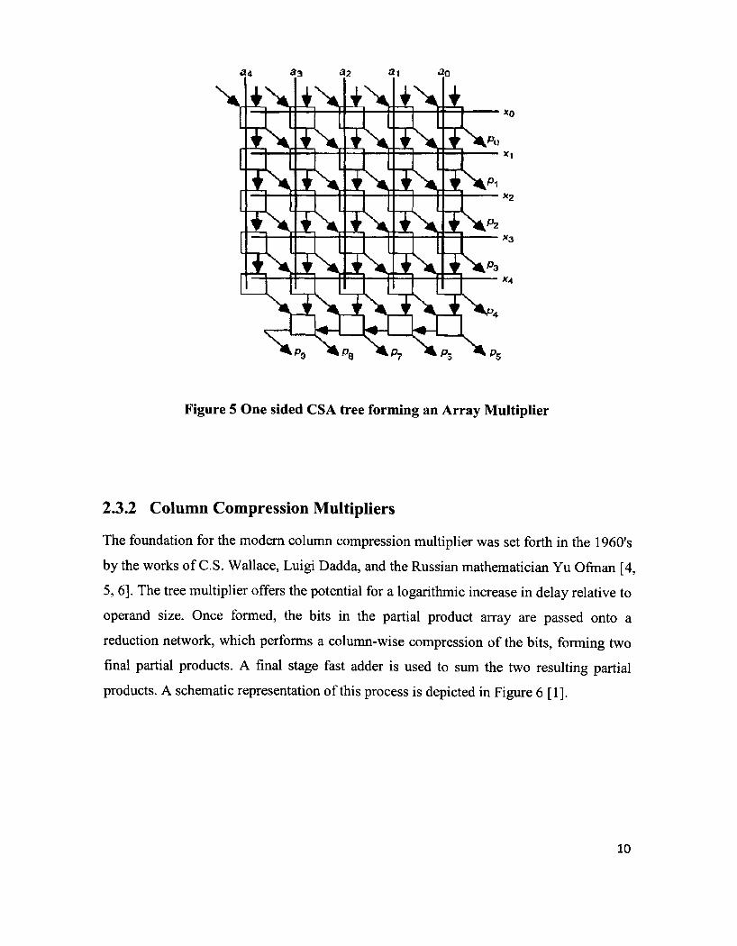
Linear parallel multipliers often referred to as array multipliers; obtain their name from
the linear relationship between their latency and operand size. The array multiplier may
be regarded as a one sided CSA tree, where the reduction process occurs in ordered
stages.
The highly regular layout of the array structure is depicted in 5-bit multiplier in Figure 5.
The systematic arrangement of the cells makes this design ideal for automated layout
techniques, where the bits of the two operands are broadcast across the arrangement of
full adder cells. In this scheme, the outputs of the adders trickle horizontally and
vertically accordingly until the perimeter of the structure where the product bits are
attained. The drawback of this scheme is that the partial products are introduced and
reduced one row at a time, not in parallel as in column compression multipliers. This
leads to higher gate count, and slower performance.
9
*U 33 a? a\ a0
V * ^ Is* +> ESS
I N i + ^
* ^
^
i ^ +Ni
^
+S. +^
+ > s s * ^
Is*
k TV*
S". IV* 1 ^ * 3
* 0
* 2
* 3
X4
XTX3XJXX^< ^ P 9 ^ P Q ^ . ^ 7 ^ * P S ^
Figure 5 One sided CSA tree forming an Array Multiplier
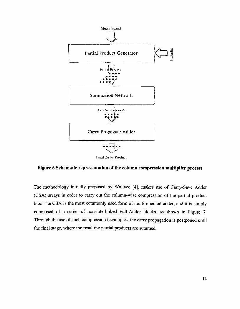
2.3.2 Column Compression Multipliers
The foundation for the modern column compression multiplier was set forth in the 1960's
by the works of C.S. Wallace, Luigi Dadda, and the Russian mathematician Yu Ofinan [4,
5, 6]. The tree multiplier offers the potential for a logarithmic increase in delay relative to
operand size. Once formed, the bits in the partial product array are passed onto a
reduction network, which performs a column-wise compression of the bits, forming two
final partial products. A final stage fast adder is used to sum the two resulting partial
products. A schematic representation of this process is depicted in Figure 6 [1].
10
Multiplicand
r t Cnrtial fniduLl*.
two 2n bit opciuiub • • • i •
Carry Propagate Adder
I in.i! In hit t'roduLt
Figure 6 Schematic representation of the column compression multiplier process
The methodology initially proposed by Wallace [4], makes use of Carry-Save Adder
(CSA) arrays in order to carry out the column-wise compression of the partial product
bits. The CSA is the most commonly used form of multi-operand adder, and it is simply
composed of a series of non-interlinked Full-Adder blocks, as shown in Figure 7
Through the use of such compression techniques, the carry propagation is postponed until
the final stage, where the resulting partial products are summed.
11
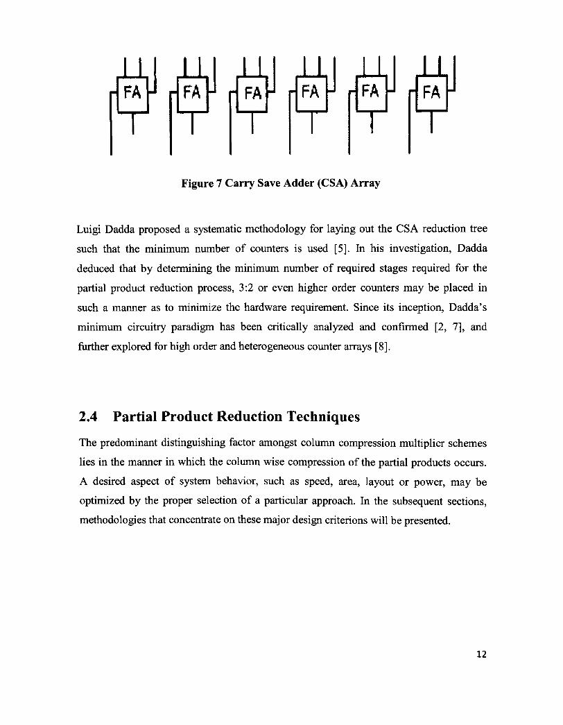
II FA
f
II •FA
1
II • FA
1
1 II •FA J
II r F A •
1
II • FA J
1
Figure 7 Carry Save Adder (CSA) Array
Luigi Dadda proposed a systematic methodology for laying out the CSA reduction tree
such that the minimum number of counters is used [5]. In his investigation, Dadda
deduced that by determining the minimum number of required stages required for the
partial product reduction process, 3:2 or even higher order counters may be placed in
such a manner as to minimize the hardware requirement. Since its inception, Dadda's
minimum circuitry paradigm has been critically analyzed and confirmed [2, 7], and
further explored for high order and heterogeneous counter arrays [8].
2.4 Partial Product Reduction Techniques
The predominant distinguishing factor amongst column compression multiplier schemes
lies in the manner in which the column wise compression of the partial products occurs.
A desired aspect of system behavior, such as speed, area, layout or power, may be
optimized by the proper selection of a particular approach. In the subsequent sections,
methodologies that concentrate on these major design criterions will be presented.
12
2.4.1 CSA Reduction Scheme
Parallel tree multiplier architecture using carry save adder (CSA) arrays has formed the
fundamental framework for the design of high-speed parallel multipliers over the past
four decades. In this section, the dissimilarities between the Wallace and Dadda
techniques will be presented.
In 1964, Wallace [4] introduced a new column compression architecture for fast
multiplication as an alternative to array multiplication. His scheme involves three basic
steps:
1. Generate all partial products at the same time using AND gate array.
2. Reduce all partial products to two numbers using (3, 2) and (2, 2) counters.
3. Sum the two final numbers using some form of fast addition such as a carry-look-
ahead adder (CLA).
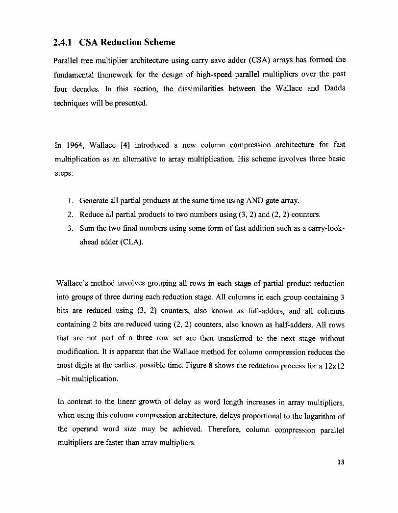
Wallace's method involves grouping all rows in each stage of partial product reduction
into groups of three during each reduction stage. All columns in each group containing 3
bits are reduced using (3, 2) counters, also known as full-adders, and all columns
containing 2 bits are reduced using (2, 2) counters, also known as half-adders. All rows
that are not part of a three row set are then transferred to the next stage without
modification. It is apparent that the Wallace method for column compression reduces the
most digits at the earliest possible time. Figure 8 shows the reduction process for a 12x12
-bit multiplication.
In contrast to the linear growth of delay as word length increases in array multipliers,
when using this column compression architecture, delays proportional to the logarithm of
the operand word size may be achieved. Therefore, column compression parallel
multipliers are faster than array multipliers.
13
r ,.i ̂ ;;j,a).'i IM i ' 1013 U II III I I B " % 1 £ •* * 1 3 t U
yyyyyyyyyyyy yyyyyyyyyyyy'
yyyyyyyyyyyy l*T yyyyyyyyyyyy
.. yyyyyyyyyyyy «** yyyyyyyyyyyyyy • I1 J' A) , .
.. yyyyyyyyyyyyyy I!' ? yyyyyyyyyyyyyy
5?j. yyyyyyyyyyyyyyyy ' • •
H; yyyyyyyyyyyyyyyyyy
Figure 8 12x12 Wallace Tree
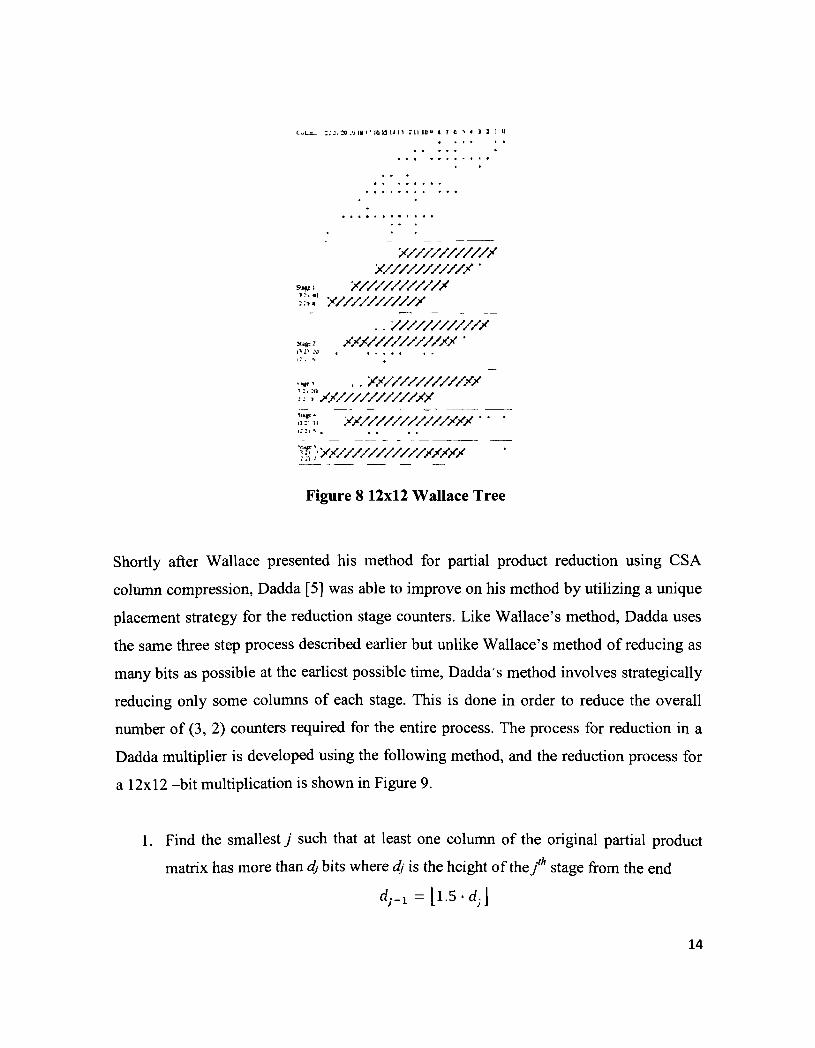
Shortly after Wallace presented his method for partial product reduction using CSA
column compression, Dadda [5] was able to improve on his method by utilizing a unique
placement strategy for the reduction stage counters. Like Wallace's method, Dadda uses
the same three step process described earlier but unlike Wallace's method of reducing as
many bits as possible at the earliest possible time, Dadda's method involves strategically
reducing only some columns of each stage. This is done in order to reduce the overall
number of (3, 2) counters required for the entire process. The process for reduction in a
Dadda multiplier is developed using the following method, and the reduction process for
a 12x12 -bit multiplication is shown in Figure 9.
1. Find the smallest j such that at least one column of the original partial product
matrix has more than a) bits where dj is the height of the/* stage from the end
d ;- i = l l . 5 -d ; ]
14
di = 2
2. In the/* stage from the end, employ (3, 2) and (2, 2) counters to obtain a reduced
matrix with no more than dj bits in any column.
3. Lety =j-l and repeat step 2 until a matrix with only two rows is generated.
a CM : : : i J im H r i e n * i ' ; u toy tt * 'i s * » 3 I n
» 4 •
' . yyyyyy. ::.: yyyy. •
xx V j j l I i ^ *
::: yyyyyyyyyyyy.: •
• • • yyyyyyyyyy. yyyyyyyy. .
'. yyyyyyyyyyyyyyyy.:. . yyyyyyyyyyyyyy.:. •
V tfci •<
1 i 1 1 yyyyyyyyyyyyyyyyyy.: •
•ff;!' yyyyyyyyyyyyyyyyyyyy.
Figure 9 12x12 Dadda Tree
These two schemes were more recently analyzed by Bickerstaff et al. [2] further
confirming that the Dadda tree does in fact utilize fewer adders during the reduction
process, while the Wallace tree tends to insert adders at the earliest opportunity. Although
slightly more irregular, the Dadda scheme presents a more efficient design.
15
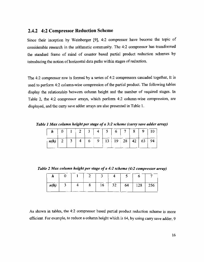
2.4.2 4:2 Compressor Reduction Scheme
Since their inception by Weinberger [9], 4:2 compressor have become the topic of
considerable research in the arithmetic community. The 4:2 compressor has transformed
the standard frame of mind of counter based partial product reduction schemes by
introducing the notion of horizontal data paths within stages of reduction.
The 4:2 compressor row is formed by a series of 4:2 compressors cascaded together, It is
used to perform 4:2 column-wise compression of the partial product. The following tables
display the relationship between column height and the number of required stages. In
Table 2, the 4:2 compressor arrays, which perform 4:2 column-wise compression, are
displayed, and the carry save adder arrays are also presented in Table 1.
Table 1 Max column height per stage of a 3:2 scheme (carry save adder array)
h
n(h)
0
2
1
3
2
4
3
6
4
9
5
13
6
19
7
28
8
42
9
63
10
94
Table 2 Max column height per stage of a 4:2 scheme (4:2 compressor array)
h
n(h)
0
3
1
4
2
8
3
16
4
32
5
64
6
128
7
256
As shown in tables, the 4:2 compressor based partial product reduction scheme is more
efficient. For example, to reduce a column height which is 64, by using carry save adder, 9
16

reduction stages are required, however, by using 4:2 compressor rows, only 5 stages are
needed to finish the partial product reduction.
An arbitrary distribution of 4:2 compressor rows, though effective, may not be entirely
efficient. Until recently, Mokrian et al. [10] proposed a reduction scheme for using 4:2
compressors in partial product reduction. He introduced a layout scheme to minimize the
number of compressor cells required in a complete reduction procedure, which follows the
same idea as Dadda 3:2 counter scheme [5]. This layout scheme defines a compressor row
as depicted in Figure 10. These rows begin with a half-adder or in the rightmost least
significant position followed by a chain of 4:2 compressors and ending with a full-adder in
the leftmost or most significant position.
<r^
>!/ \ l / Nl/ \ y
4:2 Compressor k
^k sk ^ ^
4:2 Compressor k
•V M^
Half Adder
I Figure 10 Definition of a 4:2 Compressor Row
An iterative procedure defined for implementation of this scheme is as follows [11]:
Step (1) Determine the number of compressor rows (NR) required for the given stage
according to the equation:
N„ (n(;,)-2r"*3''^'1)
(1)
where the expression, 2riog2"</') '' , refers to the maximum column height for the next stage.
17

Step (2) Arrows of 4:2 compressors, as outlined in Figure 10, are placed in the partial
product reduction tree. The first row will begin at column JIF and end at column J\L
JXF = 2riog2"(AW (2)
J 1 L=2A:-l-2 r i o g 2" ( ' , M 1 (3)
Every subsequent row will begin at column:
jiF=2^"{h^+2i (4) J
lF=J(,-\)F+2i (5)
and end at column:
JiL=(2k-l-2llosMhU^)-2i (6)
• ^ = ^ - 2 / (7)
where i is the row number within each stage up to NR.
Step (3) Repeat steps (1) and (2) until only two rows remain within the partial product
matrix, at which point a final fast adder will be used. In this thesis, the above scheme will
be used to implement 4:2 compressors in a reconfigurable multiplier architecture.
This process is better explained through the aid of a graphic example. Figure 11 provides
an example of the minimized 4:2 compressor cell distribution for 16><16-bit
multiplication [10]. The symmetric layout of the compressor rows, in addition to the
general configuration of each row (beginning with a half-adder and ending with a full-
adder) is now evident.
18

X H H » a » a :t » 10 ti tr is is u M u i«
X X X X X X X X X X X X X X X X
X X X X X X X X X X X X X X X X X X X X r-r
X X X X X X X X
5? I
X X X X X X X X X X X X X X X X X X X X X X X X X X X] X X X X X X X X X X X X X X X X X X X X X X X X X X X X
x x x x x x x x x x x x x x x x x x x l x x x x x x x x x x x x x x x x x
x x x x x p - X I I I I i l l I
X X x x X X X X
X X X X X X X X
x x x X X X x x x * X X
x x X X X X
X
x T x x i j i < X X X j ] I x x » x p r X X X
X X X X I X
""lx
•7'
X « X
X X X X X X X K X X X X ' X X X x x x x x x x x x x x x x x x x
X X X X
X X X X
r X X X
r X X X
t X X X
7 X X X
T X X X
X * X X
X X X X X X X X
T X X X
X X X X I I ] X x x x x x m \ X X X X x x \x
X X X
Figure 11 Compressor layout for a 16* 16-bit multiplication
CHAPTER 3
A RECONFIGURABLE MULTIPLIER ARCHITECTURE
3.1 Recursive Multiplication Algorithms
The notion of carrying out multiplication by breaking up the operands into smaller
sections has been in existence for several decades. Such schemes offer several advantages
over performing standard multiplication. By breaking a large multiplication into
recursions of smaller multiplications, the regularity of the design is increased, since
smaller multipliers are inherently less complex. In addition, fewer, shorter interconnects
are required to carry out the multiplication, with a limited number of global lines used to
collect the final outputs of each recursion [10].
The name "Recursive Multiplier" may at first appear misleading, since in the
implementation of this algorithm, there are no recursions, or repeated iterations of the
same procedure. The process is simply broken down into smaller sub-processes which are
carried out in parallel. However, for the sake of consistency with the authors [12] the
same nomenclature is adopted.
20
3.1.1 Background Information
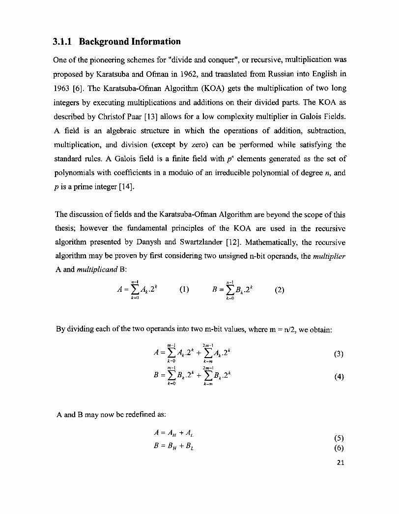
One of the pioneering schemes for "divide and conquer", or recursive, multiplication was
proposed by Karatsuba and Ofman in 1962, and translated from Russian into English in
1963 [6]. The Karatsuba-Ofman Algorithm (KOA) gets the multiplication of two long
integers by executing multiplications and additions on their divided parts. The KOA as
described by Christof Paar [13] allows for a low complexity multiplier in Galois Fields.
A field is an algebraic structure in which the operations of addition, subtraction,
multiplication, and division (except by zero) can be performed while satisfying the
standard rules. A Galois field is a finite field with p" elements generated as the set of
polynomials with coefficients in a modulo of an irreducible polynomial of degree n, and
p is a prime integer [14].
The discussion of fields and the Karatsuba-Ofman Algorithm are beyond the scope of this
thesis; however the fundamental principles of the KOA are used in the recursive
algorithm presented by Danysh and Swartzlander [12]. Mathematically, the recursive
algorithm may be proven by first considering two unsigned n-bit operands, the multiplier
A and multiplicand B:
,4 = |X2* (1) B = J^Bk.2k (2)
By dividing each of the two operands into two m-bit values, where m = n/2, we obtain:
m-\ 2m-\
^ = IX-2* + IX2* (3) /t=0 i=m
m-\ lm-\
B = ZB^2k + TB^k (4) *=0 k=m
A and B may now be redefined as:
A = A„+AL
B = BH+BL (5) (6)
21
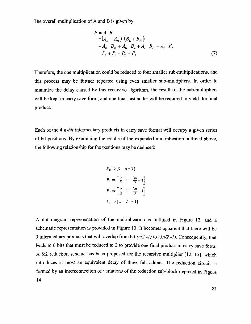
The overall multiplication of A and B is given by:
P = A B = {AL+AH)-(BL+BH)
= AH BH + AH BL + AL BH+AL BL
= P0+P,+P2+Pi (7)
Therefore, the one multiplication could be reduced to four smaller sub-multiplications, and
this process may be further repeated using even smaller sub-multipliers. In order to
minimize the delay caused by this recursive algorithm, the result of the sub-multipliers
will be kept in carry save form, and one final fast adder will be required to yield the final
product.
Each of the 4 n-bit intermediary products in carry save format will occupy a given series
of bit positions. By examining the results of the expanded multiplication outlined above,
the following relationship for the positions may be deduced:
P0=>[0 « - l ]
^ [ H ' y - 1 ]
A dot diagram representation of the multiplication is outlined in Figure 12, and a
schematic representation is provided in Figure 13. It becomes apparent that there will be
3 intermediary products that will overlap from bit (n/2 -I) to (3n/2 -1). Consequently, that
leads to 6 bits that must be reduced to 2 to provide one final product in carry save form.
A 6:2 reduction scheme has been proposed for the recursive multiplier [12, 15], which
introduces at most an equivalent delay of three full adders. The reduction circuit is
formed by an interconnection of variations of the reduction sub-block depicted in Figure
14.
22

N-bit multiplier input operands
4 intermediary n-bit products in carry save form
6:2 Reduction Scheme
T T 2n-1 3n/2-1
T T n/2
Figure 12 Dot diagram of a single level recursive n-bit multiplication
n/2 multiplier
AH*H
AH AL
±n _1_
FINAL FAST ADDER
Figure 13 A schematic of a single level recursive multiplier
23
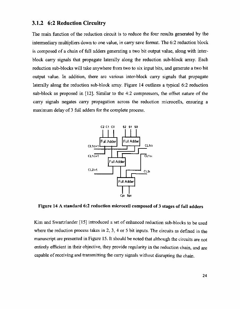
3.1.2 6:2 Reduction Circuitry
The main function of the reduction circuit is to reduce the four results generated by the
intermediary multipliers down to one value, in carry save format. The 6:2 reduction block
is composed of a chain of full adders generating a two bit output value, along with inter
block carry signals that propagate laterally along the reduction sub-block array. Each
reduction sub-blocks will take anywhere from two to six input bits, and generate a two bit
output value. In addition, there are various inter-block carry signals that propagate
laterally along the reduction sub-block array. Figure 14 outlines a typical 6:2 reduction
sub-block as proposed in [12]. Similar to the 4:2 compressors, the offset nature of the
carry signals negates carry propagation across the reduction microcells, ensuring a
maximum delay of 3 full adders for the complete process.
C2 C1 CO S2 SI SO
CL1ci+1
Full Adder
=3 CL1ci+1
CL2i+1
Full Adder
J n Full Adder
Full Adder
CLfci
rz CL1st
CL2i
Cpi Spi
Figure 14 A standard 6:2 reduction microcell composed of 3 stages of full adders
Kim and Swartzlander [15] introduced a set of enhanced reduction sub-blocks to be used
where the reduction process takes in 2, 3, 4 or 5 bit inputs. The circuits as defined in the
manuscript are presented in Figure 15. It should be noted that although the circuits are not
entirely efficient in their objective, they provide regularity in the reduction chain, and are
capable of receiving and transmitting the carry signals without disrupting the chain.
24
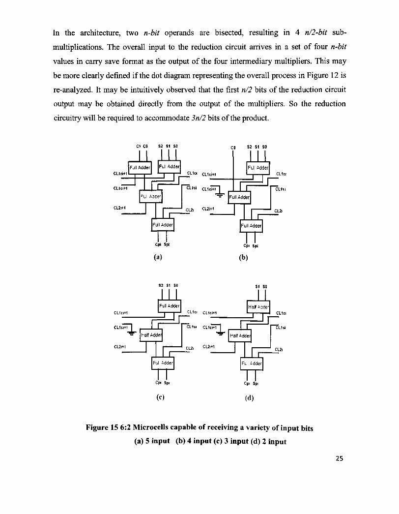
In the architecture, two n-bit operands are bisected, resulting in 4 n/2-bit sub-
multiplications. The overall input to the reduction circuit arrives in a set of four n-bit
values in carry save format as the output of the four intermediary multipliers. This may
be more clearly defined if the dot diagram representing the overall process in Figure 12 is
re-analyzed. It may be intuitively observed that the first n/2 bits of the reduction circuit
output may be obtained directly from the output of the multipliers. So the reduction
circuitry will be required to accommodate 3n/2 bits of the product.
C1 CO S2 S I SO
CLIci+1
FJII Adder
CLtci+1
CL2I+1
Ful Adder
r :ull Adce'
_r Full Adder
Cpi Spi
00
CO S2 S1 SO
CL1ci CL1ci+1
CLtsi CLtc i+ l rL
Ful Adder
3n Full Adder
CL2) CL2i*1
Full Adder
Cpi Spi
(b)
CL1ci
CL1SI
CL2l
CLtci+1
CLIci+1 ^n
S2 S1 SO
Full Adder
Half Adder
CUi+l
Ful Adder
Cpi Spi
(c)
CLIei CL1ci+1
CL1si CLIci+t
S1 SO
^ 1 - ^
HalfAcde
Half Adder
CL2i CL2.+1
FulAdder
Cpi Spi
(d)
CLtci
CL1si
CL2i
Figure 15 6:2 Microcells capable of receiving a variety of input bits
(a) 5 input (b) 4 input (c) 3 input (d) 2 input
25

The reduction pattern leads to the simple expression for the allocation of the reduction
sub-blocks for mnxn bit multiplier as:
• Bits 0 through n/2-1 are obtained directly as a result of the inputs
• Bits n/2 through 3n/2-l are obtained via 6-input reduction blocks
• Bits 3n/2 through 2n-l are obtained using 2-input reduction blocks
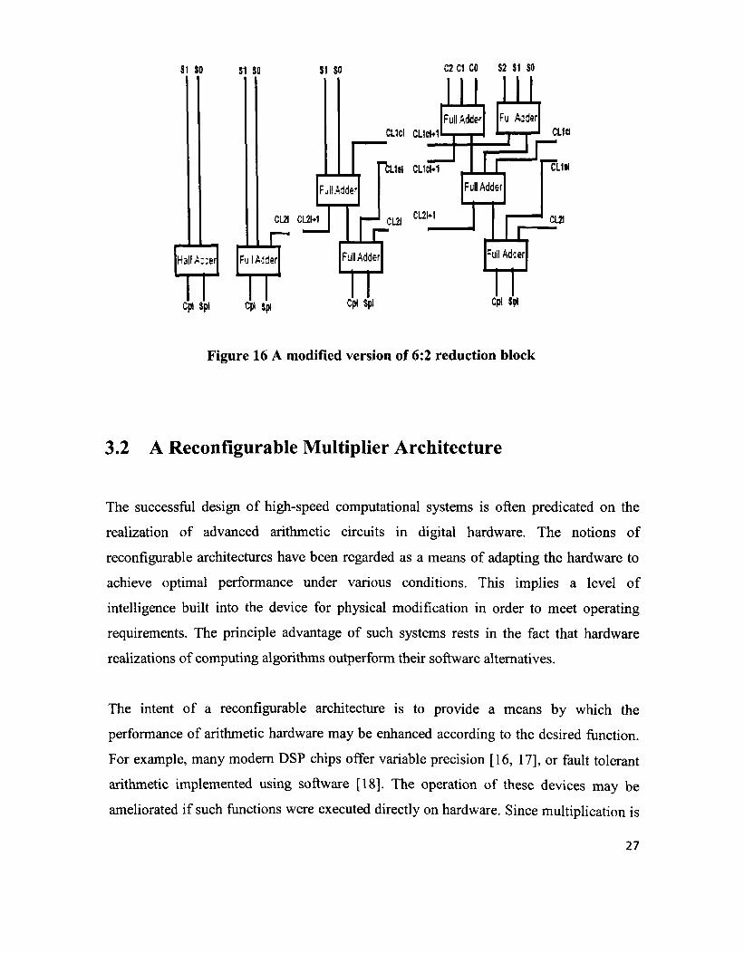
A modified version of the presented reduction scheme is proposed by Mokrian et al. [10],
and shown in Figure 16. The reduction sub-blocks having 6 inputs exist from bit position
(n/2 - 1) to (3n/2 -1). The transition to the 2-input sub-blocks is composed of a two input
reduction cell, a full adder, and a series of half adders for the remaining bits.
The need for the Half-Adder blocks, may not be obvious at first glance, however if the
Carry-out of the Full-adder immediately preceding the cells is taken into consideration,
then there will be three bits in position 3n/2+l. Consequently, the use of the Half Adder
cells will shift a carry bit laterally down the chain, allowing for the final result to have at
most two bits in each position. Furthermore, it should be noted that the final carry out
signal of the last Half Adder is omitted since it would be mathematically impossible to
obtain a bit in the 129th position of a 64-bit multiplication. This 6:2 reduction
configuration will be used for any further modification of the recursive multiplication
algorithm.
26
SI SO $1 SO
HalfA::er|
SI SO C2 CI Cfl S2 SI St
CL1CI CL1d*1 Ful Add?
F J Added
CL2I CL2I u£f Ful Adder!
ftl-ltf CLICM
Cl*l»—y
H CL2I CL2M
Full Adderl
C|« Spi CJK jjji Cpi Spi
Fu Acderl CLIci
I f~
Full Adder
—uil Adoeri
Cpi S(H
CL1SI
CL2I
Figure 16 A modified version of 6:2 reduction block
3.2 A Reconfigurable Multiplier Architecture
The successful design of high-speed computational systems is often predicated on the
realization of advanced arithmetic circuits in digital hardware. The notions of
reconfigurable architectures have been regarded as a means of adapting the hardware to
achieve optimal performance under various conditions. This implies a level of
intelligence built into the device for physical modification in order to meet operating
requirements. The principle advantage of such systems rests in the fact that hardware
realizations of computing algorithms outperform their software alternatives.
The intent of a reconfigurable architecture is to provide a means by which the
performance of arithmetic hardware may be enhanced according to the desired function.
For example, many modern DSP chips offer variable precision [16, 17], or fault tolerant
arithmetic implemented using software [18]. The operation of these devices may be
ameliorated if such functions were executed directly on hardware. Since multiplication is
27
considered to be the dominant computation in most digital signal processing (DSP)
algorithms [19], reconfigurable multiplier architecture may prove to be a desirable
augmentation to existing ALUs in the quest for maximizing performance.
Mokrian et al. [10] developed a reconfigurable multiplication architecture which
envelopes the concepts of fault tolerant computing, low power design, and high
throughput arithmetic into one design. The scheme utilizes a 2-bit control signal to select
one of four modes of operation: double precision multiplication, single precision
multiplication, dual single precision multiplication and single precision fault tolerant
multiplication.
Based on Mokrian's architecture, a reconfigurable multiplier architecture is developed
and shown in Fig 17, in which the 4 sub-multipliers, the reduction circuitry, the voter and
the final fast adder are clearly defined. The recursive multiplier architecture with one
level of recursion is used as the foundation for the reconfigurable architecture. The
advantage offered by the recursive multiplication scheme is the use of smaller multipliers
to implement a larger operation.
In each sub-multiplier, instead of using carry save adder array, 4:2 compressor arrays are
utilized for partial product reduction, which could achieve higher partial product
reduction speed.
In addition to the sub-multipliers, a series of 2:1 multiplexers are used to guide the signal
flow through the device. Since all of the necessary components for each mode of
operation are present in the design, there will be no reconfiguration time required. The
device will be capable of switching between modes of operation in real time without the
necessity to completely reconfigure the internal layout of a programmable device, as is
the case with FPGA devices.
28

*H B H BL
-J •• «_
$#" 4 2 REDUCTION
4 2 REDUCTION
7
4 2 REDUCTION
6 : 2 REDUCTION
I VZ7 \
4 2 REDUCTION
Majority Voter
7 F/AML FAST ADDER (H,GH) FINAL FAST ADDER (LOw)
Figure 17 Outline of Reconfigurable Multiplier
This architecture lends itself to four modes of operation, and thus requires a 2-bit control
signal for selection. The signal and the corresponding modes of operation are
summarized in Table 3.
Table 3 Modes of Operation of the Reconfigurable Multiplier
Control Signal
00
01
10
11
Mode of Operation
Default - Double Precision
Single Precision
Single Precision with Fault Tolerance
Dual Single Precision
29

3.2.1 Double Precision Mode
The default double precision mode is simply a recursive multiplier with one level of
recursion. This mode of operation reaps the benefits of the recursive multiplier
architecture, while bearing no delay penalties, and minimal hardware overhead. The
majority voter circuitry is disengaged through the multiplexor array (Fig 18). The
reconfigurable architecture may be of any size, with the restriction that the single
precision mode must be exactly one half of the double precision mode. To satisfy the
IEEE floating point guidelines, a double precision multiplier having 54-bit operands is
suggested, with each of the base multipliers being 27-bits wide.
AH l
4 : 2 REDUCTION
AL
\
1 BH
/
BL
4 : 2 REDUCTION
^ \
4 : 2 REDUCTION
/
4 : 2 REDUCTION
1
6 : 2 REDUCTION
1
1 Majority Voter
1
FINAL FAST ADDER (HIGH) FINAL FAST ADDER (LOW)
Figure 18 Double precision mode
30
3.2.2 Single Precision Mode
Single precision mode uses gating techniques to shut down three of the base multipliers,
effectively cancelling over 75% of the circuit, in addition to the reduction circuitry and
the majority voter (Fig 19). The final fast adder is also partitioned in the reconfigurable
architecture, such that the upper portion of the adder may be shut down in order to avoid
spurious transitions, which consume unnecessary power. Moreover, the overall latency
now becomes that of the base multiplier, allowing faster operation in single precision
mode than would be possible if the entire circuit was active.
The advantage of this scheme is that the single precision multiplication is carried out
using a full single precision multiplier as opposed to shutting portions of a larger partial
product reduction tree, as is proposed in other variable precision schemes [16]. In this
manner, both single and double precision operations are carried out at maximum
efficiency in terms of area, performance and power.
AH 1
4 : 2 REDUCTION
AL
\
1 BH
/
BL
4 : 2 REDUCTION
—1 \
4 : 2 REDUCTION
/
4 : 2 REDUCTION
l
6 2 REDUCTION
1
1 Majority Voter
1
FINAL FAST ADDER (HIGH) FINAL FAST ADDER (LOW)
Figure 19 Single precision mode
31
3.2.3 Dural Single Precision Mode
In this operation mode, two of the base multipliers may operate in parallel on two
different sets of operands, while the remaining two multipliers are inactive (Figure 20).
This effectively doubles the system throughput, with a latency of a single precision
multiplier. Once again, with the fast adder partitioned into two identical halves, linked via
a multiplexed carry signal, two single precision fast additions may be carried out in
parallel. This configuration comes at little to no delay overhead in most carry-look-ahead
(CLA) and carry skip addition schemes. The gating of signals into the idle multipliers, in
addition to the 6:2 reduction and majority voter circuitries allows for power savings. The
idle circuits are not entirely disconnected from the power supply in order to allow for
rapid and accurate engagement into any other mode of operation.
AH 1
4 2 REDUCTION
\
AL 1
BH
/
BL
4 2 REDUCTION
\
4 2 REDUCTION
/
4 2 REDUCTION
l
6 2 REDUCTION
1
Majority Voter
T FINAL FAST ADDER (HIGH) FINAL FAST ADDER (L0W>
Figure 20 Dual single precision mode
32

3.2.4 Single Precision Fault-tolerant Mode
Although there are numerous methods of implementing fault tolerance in digital systems,
one of the most basic methods is through majority voting between three duplicate values,
which is also referred to as RETWV Since this scheme is composed of four identical
sub-multipliers, three of those may be used in conjunction with an array of 64 XOR gates
and 2:1 MUX cells, to form a simple single precision fault tolerant multiplier (Figure 21).
AH
~T~
4 2 REDUCTION
4 2 REDUCTION
BH BL
4 : 2 REDUCTION
6 2 REDUCTION
4 2 REDUCTION
Majority Voter
FINAL FAST ADDER (HIGH) FINAL FAST ADDER (LOW)
Figure 21 Single precision - fault tolerant mode
With the theoretical framework for the reconfigurable multiplier architecture in place, the
next section will focus on the implementation and simulation details.
33

3.3 Modeling and Simulation For the proper assessment of the performance characteristics of the proposed
reconfigurable architecture, a valid model must be created, and compared against a
benchmark model representing the state-of-the-art. For this reason, a 64-bit
reconfigurable multiplier has been designed using TSMC 0.18um technology.
Additionally, a standard 64-bit Booth-recoded Wallace tree multiplier, similar to that
employed in many of today's high performance processors, such as the Pentium IV [20],
has been developed as a benchmark for comparison purposes.
3.3.1 HDL Model
Verilog describes a digital design as a set of modules, which are the basic building blocks
forming the complete system. This hierarchical design methodology is a fundamental
concept in Verilog digital designs. The reconfigurable multiplier design features four 32-
bit sub-multipliers which are based on 4:2 compressor reduction scheme, a 48-bit 6:2
reduction block and two 64-bit carry-look-ahead adders. The overhead from the
additional features are four arrays of 32 2:1 MUX cells, two arrays of 64 2:1 MUX cells,
and a series of 64 XOR gates and 2:1 MUX cells for the majority voter. All of these
individual modules are enveloped by the top level module which acts as a general
input/output (I/O) interface for the multiplier. The top level module contains the clocked
latching circuitry required for design synthesis, and does not affect the internal
configuration of the multiplier itself.
The multiplier itself is partitioned into the major sections as outlined previously in Fig 17
Built in Synopsys module definitions for carry-look-ahead adders have been used to
model and synthesize portions of the code, ensuring that the most efficient synthesized
netlist is obtained.
34

The Verilog code defines the various modules and their interaction. The code in itself is
over 1500 lines long, and consists of 17 different modules. A complete breakdown of the
hierarchical expansion of the overall reconfigurable architecture, compiled by the
Synopsys Design Vision, confirms the proper framework of the design. The standard cell
components and the gate level configuration of each element may also be referenced
from this file.
3.3.2 Implementation and Layout
The multiplier has been implemented using the TSMC 0.18 um CMOS process using
standard cell libraries provided by the Canadian Microelectronics Corporation.
Semicustom design makes use of standard cell libraries for the fabrication of custom
integrated circuits. The Cadence Design Suite, including Encounter tool, have been used
for the layout placement and routing of the cells, and the layout view of designed
reconfigurable multiplier is shown in Fig 22.
35
Figure 22 Layout view of designed 64-bit reconfigurable multiplier
3.3.3 Simulation Results
As shown in the Table 4, both designed reconfigurable multiplier and benchmark
multiplier are simulated in terms of functionality, power, delay and area. The simulation
result verifies the proper functions of four operation modes, and highlights 25% and 19%
decreases in cell internal power and total dynamic power consumption respectively.
Moreover, the designed multiplier has a slightly shorter delay time, which benefits from
the regularity of recursive structure. Since the designed multiplier has higher number of
cells compared to benchmark multiplier, its total area and cell leakage power consumption
increases 11% and 17% respectively.
36

Table 4 Simulation Results for Reconfigurable Multipliers
*
1 C3
<
a ©
a a s a o U
% O
Tim
ing
(nS)
Number of ports
Number of nets
Number of cells
Number of references
Total Area
Cell Internal Power (mW)
Net Switching Power (m W)
Total Dynamic Power (m W)
Cell Leakage Power (fiW)
Data Arrival Time
R.M
260
20818
20544
63
520498.9
162.7
146.87
309.59
26.37
9.84
B.MM.
259
4363
3506
4
468179.9
214.41
164
378
22.62
9.9
%ofB.M.M
111.17%
75.88%
89.55%
81.9%
116.58%
99.39%

CHAPTER 4
CIRCUIT LEVEL DESIGNS OF 4:2 COMPRESSORS
4.1 High Order Counters and Compressors
4.1.1 Counters
Although the work of Dadda has been directly linked to CSA reduction schemes, his
manuscript [5] had a much broader focus, encompassing the applications of parallel
counters for partial product reduction. The full adder, or carry save adder, is a particular
subset of the class of parallel counters. A parallel (N, M) counter is defined as a
combinational network having M outputs and inputs of equal weight, as shown in Fig 23.
The M outputs are based on the number of logic 'ones' that appear at the N inputs. Any
size counter may be constructed, so long as the M output bits are sufficient to represent
all possible sums of the TV inputs. Examples of typical counters include (3, 2), (7, 3), (15,
4).
High order counters for partial product reduction have been explored and implemented in
numerous proposals [3, 7, 8, 21, 22]. The schemes demonstrating the most promise for
general multiplier architectures having arbitrary operand sizes include low order counter
classes based on full adders and 4:2 compressors.
38
input bits of weight 2'
Figure 23 General Counter Representation
4.1.2 Compressors
Similar to counter structures, digital compressors are used to reduce a given set of inputs
to a vector output. The primary distinction between counter and compressor circuits is
that compressors do not necessarily follow the standard pattern of M outputs drawn from
2M inputs. An [N: M\ compressor in essence is a variation of a counter that employs a
separate path between compressor units in order to generate M final outputs using N>2M
input bits, as shown in Fig 24. Compressor configurations are generally formed using
arrays of horizontally interconnected compressor units. In this manner, a horizontal carry
signal may propagate laterally across the row of compressor units in order to account for
the excess bits formed in the reduction process.
39

* * * * r « N Input bits * of Weight 2"
N:M Compressor
N-2 Carry bits of / . 1 , . .L./.WH >^
J Weight 2'
f Sum bit of Weight f
Figure 24 General Compressor Representation
Higher order classes of compressors may also be used using variations of large counters
with horizontal interconnections; however, these circuits suffer high capacitance, large
circuitry, and problematic matrix positioning as large counters. Song and DeMichelli [22]
have examined the implementation of higher order compressors. Labeled as the 9:2
family of compressors, these structures are formed using 4:2 compressor and (3, 2)
counters. An analysis of counters against compressors has been carried out by Mehta et al.
[23]. In their research, the use of (7, 3) counters against 7:3 compressors, amongst many
others, has been evaluated. Their findings illustrated no major delay advantage in the use
of large compressors over large counters, except for greater interconnect complexity
introduced by the inter-cell wiring of the compressors.
The most widely used style of digital compressor, which displays several promising
characteristics for multiplication applications, is the 4:2 compressor. This special class of
compressors requires a section of discussion on their own.
40
4.2 4:2 Compressors Since its inception by Weinberger in 1981 [9], the concept of the 4:2 compressor has
soared in popularity in many digital multiplication and multi-operand addition schemes.
The application of 4:2 compressors has also been the focus of several studies promoting
its use over Booth recoding schemes [24][25][26]. This section provides an in depth look
at the various logical level decompositions of 4:2 compressors.
4.2.1 Structure of 4:2 Compressors
In general, compressors reduce N-input bits to a single sum bit of equal weight to that of
the inputs but unlike counters, the remaining output bits are all of equal weight: one bit
position greater than that of the inputs. Although the 4:2 compressor is not defined as a
counter, since it is impossible to use 2 output bits to represent 4 binary input bits, the
primitive configuration of 4:2 compressor is based on a 5:3 counter structure, which has 5
inputs and 3 outputs as shown in Figure 25. The four inputs Xo, Xi, X2 and X3, and the
output Sum have the same weight. The output Carry is weighted one binary bit order
higher. The 4:2 compressor receives an input CEM from the preceding module of one binary
bit order lower in significance, and produce an output Cout to the next compressor module
of higher significance. Different structures of 4:2 compressors exist and they all have to
abide by the fundamental equation given as follows [27]:
X0 +XX +X2 +X3 +CIN =Sum+ 2- (Carry+Cout) (].
Besides, to accelerate the carry save summation of the partial products, it is imperative
that the output Cout be independent of the input CIM.
41

'OUT
Xi X2 X3 X4
_& ^ — i k _
4 :2 Compressor
U'
'IN
Carry Sum
Figure 25 Symbol of 4:2 compressor
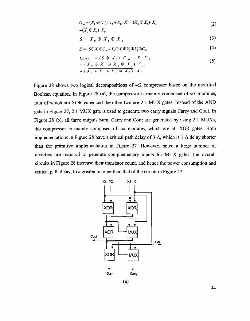
4.2.2 Logical Level Decompositions of 4:2 Compressors
The most primitive implementation of 4:2 compressor is that of two cascaded full adders,
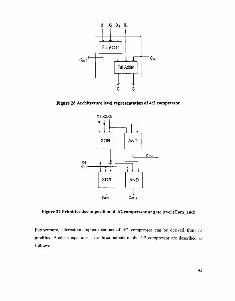
as shown in Figure 26 [28]. By increasing regularity, this configuration lends itself to
gains at the architecture level of the multiplier. At gate level, 4:2 compressors are
anatomized into XOR gates and carry generators, as shown in Figure 27. Therefore,
different designs can be classified based on the critical path delay in terms of the number
of primitive gates. Let AXOR denote the delay of an XOR gate and ACGEN denote the
delay of a carry generator. A compressor is said to have a delay of (m AXOR + n ACGEN)
if its critical path consist of m XOR gates and n carry generators. Since the difference
between the delays of widely used XOR gate and carry generator is trivial in an
optimized design, the delay of the compressor is commonly specified as (m + n) A [27].
Therefore, the straightforward implementation of a 4:2 compressor of Figure 27 has a
long critical path delay of 4A.
42
Xi X2 X3 X4
'OUT
-Nk Nl/ Nl/
Full Adder
Nl/ Nl/ Nl/
Full Adder
Nl/ Nl/
c s
Figure 26 Architecture level representation of 4:2 compressor
>
X4 P i n
,1 >
1
>2X
1
3
XOR
• r
" '
AND
'
XOR
s 1
um
" 1
Cout .
'
AND
d 1 irry
Figure 27 Primitive decomposition of 4:2 compressor at gate level (Com and)
Furthermore, alternative implementations of 4:2 compressor can be derived from its
modified Boolean equations. The three outputs of the 4:2 compressor are described as
follows:
43
cout=(x0®x,)-x2+x0 xx=(x0®x,yx2
+(z0ex1)-x0
S = X. X,® x2
Sum=S®XA ®CM =X0 ®X1 ®X2 ®X3 ®Cm
Carry = (S ® X,) C m + S X 3
= (X0 ® X {® X 2® Jfj) c „
+ (X0 + Xi + X2 ® X 3) X 3
(2)
(3)
(4)
(5)
Figure 28 shows two logical decompositions of 4:2 compressor based on the modified
Boolean equation. In Figure 28 (a), the compressor is mainly composed of six modules,
four of which are XOR gates and the other two are 2:1 MUX gates. Instead of the AND
gate in Figure 27, 2:1 MUX gate is used to generate two carry signals Carry and Cout. In
Figure 28 (b), all three outputs Sum, Carry and Cout are generated by using 2:1 MUXs,
the compressor is mainly composed of six modules, which are all XOR gates. Both
implementations in Figure 28 have a critical path delay of 3 A, which is 1 A delay shorter
than the primitive implementation in Figure 27. However, since a large number of
inverters are required to generate complementary inputs for MUX gates, the overall
circuits in Figure 28 increase their transistor count, and hence the power consumption and
critical path delay, to a greater number than that of the circuit in Figure 27.
X1 X2 X3 X4
XOR
Cout -<—
XOR
XOR MUX
XOR
' I H
Cin
MUX
Sum Carty
(a) 44

X1 X3
X2
Cout
MUX
n
X4.
—(>—o-
MUX
MUX MUX
I I — • •
MUX
" ' •
Cin
MUX
Sum Carry
(b)
Figure 28 Two alternative decompositions of 4:2 compressor at gate level
(a) Commux, (b) Com_pur_mux
4.3 Circuit Level Designs of 4:2 Compressors
Digital design encompasses a wide variety of logic implementations, which arise, for all
intents and purposes, as a result of the transistor configurations composing the individual
logic elements. The synthesis of the particular digital system (or sub-system) will dictate
the nature of the particular logic family chosen. In a survey of logic styles, Zimmermann
and Fichtner [29], outline the various characteristics of the final digital system that are
dictated by the initial selection of the logic style chosen for implementation. The factors
include:
45
• Circuit delay: a function of the number of inversion levels, the number
of transistors in series, transistor sizes (i.e., channel widths), and intra- and
inter-cell wiring capacitances.
• Circuit size: depends on the number of transistors and their sizes and
on the wiring complexity.
• Power dissipation: determined by the switching activity and the node
capacitances (made up of gate, diffusion, and wire capacitances), the latter
of which in turn is a function of the same parameters that also control
circuit size.
• Wiring complexity: the number of connections and their lengths in
addition to the choice of single-rail or dual-rail logic.
• Generality: ease-of-use of logic gates in standard cell design
techniques and logic synthesis.
• Robustness: determined by the resilience to voltage and transistor
scaling as well as varying process and working conditions.
• Compatibility: ability to seamlessly integrate with the surrounding
circuitries.
All of these characteristics may vary considerably from one logic style to another and
thus make the proper choice of logic style crucial for circuit performance. Several logic
styles and logic families will be presented in the following section, along with their
potential vantage points and applications in arithmetic circuitry.
46

4.3.1 Static CMOS
Static CMOS logic, otherwise known as standard CMOS logic, is the logic style of choice
for most implementations, and is most often used in the development of standard cell
libraries for automated digital synthesis. The principle behind a static logic cell is that it
exhibits a well-defined output once the inputs are stabilized and the switching transients
have decayed away. The cell is composed of complementary NFET and PFET networks,
where the input voltages control the conductance of the networks. The switching network
is designed such that only one network is a closed switch for any input combination, thus
determining whether VDD or GND is connected to the output. Figure 29 outlines a typical
static CMOS cell configuration.
- V D D
• •
•
•
•
•
PFET transistor network
NFET transistor network
Figure 29 Static CMOS logic cell depicting the NFET and PFET networks
The advantage of such logic families is in the simplicity of developing a circuit that will
perform a given function, however complex, while providing robust performance
measures. Static logic, for the most part, demonstrates excellent noise immunity, and is
less susceptible to process variation since the sizing of individual transistors does not
vastly alter the circuit's functionality. One disadvantage of this type of logic is the use of 47
a large number of PFET devices, being both slow and large in comparison to NFETs,
which increases power consumption of the circuit. Furthermore, the longest length chain
within each network will determine the worst-case scenario for charge/discharge delay,
forcing more complex systems to carry out potentially sluggish execution.
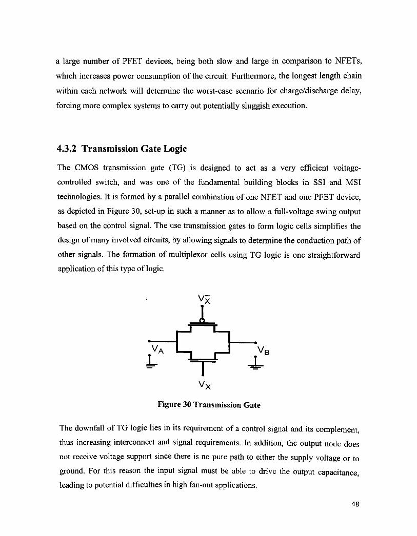
4.3.2 Transmission Gate Logic
The CMOS transmission gate (TG) is designed to act as a very efficient voltage-
controlled switch, and was one of the fundamental building blocks in SSI and MSI
technologies. It is formed by a parallel combination of one NFET and one PFET device,
as depicted in Figure 30, set-up in such a manner as to allow a full-voltage swing output
based on the control signal. The use transmission gates to form logic cells simplifies the
design of many involved circuits, by allowing signals to determine the conduction path of
other signals. The formation of multiplexor cells using TG logic is one straightforward
application of this type of logic.
VN
TO~. Figure 30 Transmission Gate
The downfall of TG logic lies in its requirement of a control signal and its complement,
thus increasing interconnect and signal requirements. In addition, the output node does
not receive voltage support since there is no pure path to either the supply voltage or to
ground. For this reason the input signal must be able to drive the output capacitance
leading to potential difficulties in high fan-out applications.
48

4.3.3 Pass Transistor Logic
As an alternative to complementary CMOS, pass transistor logic attempts to reduce the
number of transistors required to implement logic by allowing the primary inputs to drive
source-drain terminals as well as gate terminals. Specifically, a pass transistor is a
MOSFET with the input signal fed to the source and the output taken from the drain, with
a control signal connected to the gate governing the output.
The promise of this approach is that fewer transistors are required to implement a given
function. For example, the implementation of the AND gate in Figure 31 requires 4
transistors (including the inverter required to invert B), while a complementary CMOS
implementation would require 6 transistors. The reduced number of device has the
additional advantage of lower capacitance.
B
1 A — n .
Figure 31 Pass-transistor implementation of an AND gate
Unfortunately, an NMOS device is effective at passing a 0, but it is poor at pulling a node
to VDD. When the pass transistor pulls a node high, the output only charges up to VDD-
Vr« (threshold voltage). In fact, the situation is worsen by the fact that the device
experience body effect, because a significant source-to-body voltage is present when
pulling high.
49
4.3.4 Dynamic Logic
Standard static CMOS logic maintains a valid output voltage, so long as the inputs are
well defined and continuous. Dynamic CMOS logic on the other hand makes use of
capacitive nodes to store electrical charge, and so is capable of sustaining a valid output
only for a short period of time. The advantages of such logic families are in their ability
to quickly transfer charge, and in turn have a tremendous performance advantage over
static CMOS, and are common in high speed applications. Dynamic circuits differ from
static circuits in that instead of fighting the constant limits due to parasitic RC elements,
capacitances are used as integral components of the circuits.
Though there are several distinct logic families that fall under the dynamic CMOS
classification, there is a common underlying principle behind their operation. In general,
there are two state logic styles where a clock signal controls a pair of complementary
FETS managing the operation of the logic gate (Figure 32). The two stages of operation
are known as the precharge and evaluate stages. During precharge, the output node is
charged via the precharge PFET, this is known as "pre-conditioning" the node, while the
evaluate NFET is cut off. During this phase of the clock, the output and all of the inputs
are invalid. During the evaluate stage, the evaluation NFET conducts, while the
precharge PFET is cut off. The inputs to the logic array are now valid, and if the logic
array produces a value of '0' , there will be a conduction path for the output charge to
ground, else the charge will be maintained at the output and a result of logic T The
charge on the output node may only be held for a limited duration before being corrupted
by charge leakage, and so timing is critical.
50
<K0<
TVDD
Mp (Precliarge)
g- A2
X! HA[A2A3)
'TH out
Mn (Evaluate)
Figure 32 Primitive representation of dynamic Logic block
Compared to static CMOS logic, dynamic logic leads to up to 30% performance gain [30].
Therefore, speed critical paths often deploy dynamic logic to meet speed requirements.
Performance gain over static logic becomes even larger as the number of inputs to the
logic grows. Wide fan-in dynamic logic such as domino are often used in performance
critical paths, e.g. fast look ahead adders and RAM decoders, to achieve high speeds
where static CMOS fails to meet performance objectives. The following sections will be
focused on domino logic and its applications in 4:2 compressors.
4.4 Domino Logic
A dynamic system may be formed through the simple cascading of the individual cells.
This leads to the formation of a variation of the precharge-evaluate logic known as
Domino Logic. The cascading of NFET logic array for the standard precharge-evaluate
logic poses a potential glitch problem, which is overcome in domino logic through the
inversion of the output signal between cascaded cells.
51

A domino logic module consists of an n-type PDN (pull-down network) followed by a
static inverter, as shown in Figure 33. During precharge, the output of the PDN is charged
up to YDD, and the output of the inverter is set to "0" During evaluation, the PDN
conditionally discharges, and the output of the inverter makes a conditional transition
from "0" -"•"!" If one assumes that all the inputs of a domino gate are outputs of other
domino gates, then it is ensured that all inputs are set to "0" at the end of the precharge
phase, and that the only transitions during evaluation are "0" -+"V transitions. The
introduction of the static inverter has the additional advantage that the fan-out of the gate
is driven by a static inverter with a low-impedance output, which increases noise
immunity. Also, the buffer reduces the capacitance of the dynamic output node by
separating internal and load capacitances. Finally, the inverter can be used to drive a
keeper device to combat charge leakage and charge redistribution.
CLK
- H I
In,
ln3
CLK
Figure 33 Domino Logic
VDD
V VSS

Consider now the operation of a chain of domino gates. During precharge, all inputs are
set to "0" During evaluation, the output of the first domino block either stays at "0" or
make a "0" -"•"!" transition, affecting the second gate. This effect might ripple through
the whole chain, one after the other, similar to a line of falling dominoes—hence the
name. Domino logic circuit has the following properties:
1. Since each dynamic gate has a static inverter, only non-inverting logic
can be implemented.
2. Very high speeds can be achieved: only a rising edge delay exists,
while TpHL (high to low transition time) equals zero. The inverter can
be sized to match the fan-out, which is already much smaller than in
the complimentary static CMOS case, as only a single gate capacitance
has to be accounted for per fan-out gate.
Domino logic clearly can result in high-performance solutions compared to static circuits.
However, there are several important considerations that must be taken into account if
one wants dynamic circuits to function properly. These include charge leakage and
charge sharing.
The operation of a dynamic gate relies on the dynamic storage of the output value on a
capacitor. If the pull-down network is off, ideally, the output should remain at the
precharged state of Voo during the evaluation phase. However, this charge gradually
leaks away due to leakage currents, eventually resulting in a malfunctioning of the gate.
Figure 34 shows the sources of leakage for the basic dynamic inverter circuit.
53

DD
A = 0
Out
Figure 34 Leakage issues in dynamic circuits
Source 1 and 2 are the reverse-biased diode and subtheshold leakage of the NMOS pull
down device Ml, respectively. The charge stored on Cz. will slowly leak away through
these leakage channels, causing degradation in the high level. Dynamic circuits therefore
require a minimal clock rate, which is typically on the order of a few KHz. Note that the
PMOS precharge device also contributes some leakage current due to the reverse bias
diode (source 3) and the subthreshold conduction (source 4). To some extent, the leakage
current of the PMOS counteracts the leakage of the pull-down path. As a result, the
output voltage is going to be set by the resistive divider composed of the pull-down and
pull-up paths.
Leakage is caused by the high-impedance state of the output node during the evaluate
mode, when the pull-down path is turned off. The leakage problem may be counteracted
by reducing the output impedance on the output node during evaluation. This often is
done by adding a keeper transistor. The only function of the keeper- a PMOS style pull-
up device- is to compensate for the charge lost due to the pull-down leakage paths. To
avoid ratio problems associated with this style of circuit and the associated static power
54
consumption, the keeper resistance is made high (in other words, the device is kept small).
This allows the (strong) pull-down devices to lower the Out node substantially below the
switching threshold of the next stage. Often, the keeper is implemented in a feedback
configuration to eliminate the static power dissipation altogether, as shown in Figure 35.
DD
CLK —c
J
H
LK—\
M„
Mb
Me
4_
M„ A/; bl
• f
Kh
I Out
Figure 35 Static keeper compensate for the charge leakage
Another important concern in dynamic logic is the impact of charge sharing. Consider the
circuit in Figure 36. During the precharge phase, the output node is precharged to YDD.
Assume that all inputs are set to "0" during precharge, and that the capacitance Ca is
discharged. Assume further that input B remains at "0" during evaluation, while input A
makes a "0" - • " 1 " transition, turning transistor Ma on. The charge stored originally on
capacitor Cz. is redistributed over CL and Ca. This causes a drop in the output voltage,
which cannot be recovered due to the dynamic nature of the circuit.
55
V DD
CLK—<j J M„
••f-i
ff-0—|
CLK—|
Oi(f
h1 ± * M - L
Mfe X "
P^c «. I ' T_ "
Figure 36 Charge sharing in dynamic circuits
The most common and effective approach to deal with the charge redistribution is to also
precharge critical nodes. Since the internal nodes are charged to YDD during precharge,
charge sharing does not occur.
The 4:2 compressor is designed in domino logic circuit and shown in Figure 37. It consists
of two blocks, each block performs the function of full adder, and these two blocks are
cascaded together to realize the function of 4:2 compressor. The first block takes inputs A,
B and C, and generates carry output Cout and intermediary output S, the output S is then
passed to the second block with inputs D and Cin, generating the output Sum and Carry.
Within each block, every M-type PDN is followed by a static inverter and the keeper
device (PMOS) is used, as shown in the Figure 37, to compensate for the charge lost due
to the pull-down leakage paths.
56

VDD
HI
HI
VDD
CLK iT^I f^Sw Sum
HL HL -HL HI HL HL HL HI Cinll—' ~£iSLir "£-|[_ ciu[
1 rvss VDD
CLK J LKeeR§r O
HCHl PJQHI
^ 0 . Carry
S3
"1 vss
Figure 37 4:2 compressor in Domino Logic (Com D)
57
4.5 Circuit Level Optimizations of Domino Logic Gates Several optimizations can be performed on domino logic gates. The most obvious
performance optimization involves the sizing of the transistors in the static inverter. With
the inclusion of the evaluation devices in domino circuits, all gates precharge in parallel,
and the precharge operation takes only two gate delays—charging the output of the
dynamic gate to YDD, and driving the inverter output low. The critical path during
evaluation goes through the pull-down path of the dynamic gate and through the PMOS
pull-up transistor of the static inverter. Therefore, to speed up the circuit during
evaluation, the beta ratio of the static inverter should be made high so that its switching
threshold is close to YDD. This can be accomplished by using a small (minimum-sized)
NMOS and a large PMOS device. The minimum-sized NMOS only affects the precharge
time, which is generally limited due to the parallel precharging of all gates. The only
disadvantage of using a large beta ratio is a reduction in noise margin. Hence, we should
consider reduced noise margin and performance impact simultaneously during the
transistor sizing.
4.5.1 Multiple-output Domino Logic
Numerous variations of domino logic have been proposed. One optimization that reduces
area is multiple-output domino logic. The basic concept is illustrated in Figure 38.
58
C/A-cj
J.,.. P~ H I CIJH
H
- N o — 0 1 --ABir+D)
—1 No— 02 - Bir-O) = B03
f / .ACi
1 . 1 No— 0? = OD
Figure 38 Multiple-output domino logic
It exploits the fact that certain outputs are subsets of other outputs to generate a number
of logical functions in a single gate. In this example, 03=C+D is used in all three outputs,
and thus it is implemented at the bottom of the pull-down network. Since 02 equals B 0 3 ,
it can reuse the logic for 03 . Notice that the internal nodes have to be precharged to YDD
to produce the correct results. Given that the internal nodes precharge to YDD, the number
of devices driving precharge devices is not reduced. However, the number of evaluation
transistors is drastically reduced because they are amortized over multiple outputs.
Additionally, this approach results in a reduction of the fan-out factor, again due to the
reuse of transistors over multiple functions [28].
Considering a full adder which takes three equally weighted bits (A, B, Q and produces a
sum-bit (Sum) as well as a carry-bit (Carry), outputs of the full adder can be described as
follows:
Sum= A®B®C = ABC+ABC+ABC+ABC
Cam' = AB + BC + AC
(1)
(2)
59
By taking the NOT of Carry signal, we obtain:
Carry = AB + BC + AC (3)
Comparing equation (1) with (3), outputs Sum and Carry have some parts in common,
which are ~AB , BC and^C Therefore, we could use part of the circuit, which is used to
generate Sum signal, to generate Carry signal as well, as shown in Figure 39. Compared
with the full adder designed in domino logic (Figure 40), it simplifies the circuit by using
one domino gate, instead of two, to realize the functions of full adder.
Furthermore, since 4:2 compressor is formed by two full adders cascaded together, the 4:2
compressor can be realized by using Multiple-output domino logic as shown in Figure 41.
The designed circuit consists of two blocks, each block performs the function of full
adder, these two blocks are cascaded together to realize the function of a 4:2 compressor.
In each full adder block, the output Carry is the subset of output Sum. vuu
CLK I Kee^
—1 i
HL HL HL HI
HL ML HL HI
LHC
7
VDD
HE ^C HE HC -H £& Carry
Figure 39 Full adder in multiple-output domino logic (FAnewD)
60
VDO
<
O^ { > - ^
"HE
Figure 40 Full adder in multiple-output domino logic (FAD)
VDD
CLK I LK e e p e i A ir1 A ̂ B ,r c r- £ ^
VDD
VDD
CLK I"==F»
Cout
Figure 414:2 compressor in multiple-output domino logic (Com new D)
61
4.5.2 Split Domino Logic
The split domino OR gate shown in Figure 42 achieves higher performance of operation
through Splitting the pull-down network into two sub-networks. A logical 2-input NAND
operation is then utilized to generate the output. The output inverter is no longer required
for the SD circuit. Also, the keeper device is split equally between the two networks.
CLK L r
VDI
CLK
UF-HUHt
CULF 1 H
VD2
Out
" - D
i - i l L ' </.'wlL ,/5~li
Figure 42 n-input split domino (SD) OR gate
Based on the circuit in Figure 39, by splitting the pull-down network into two sub
networks, a full adder is realized in split domino logic, as shown in Figure 43. Moreover,
a 4:2 compressor is also designed in split domino logic and shown in Figure 44. It also
consists of two blocks, each block performs the function of full adder, these two blocks
are cascaded together to realize the function of a 4:2 compressor. The operation of this
split domino circuit is described as follows. During precharge, CLK is LOW, the keeper
devices are OFF and the output is LOW At the onset of evaluation, contention is
eliminated since keeper devices remain OFF. There are two different cases that need to
be considered during the evaluation phase. When all inputs remain LOW and leakage
current is at its maximum, the keeper devices controlled by the 3-input NAND gate are
quickly activated to prevent the dynamic node from drooping and to keep output noise
62
within the required limit. The 3-input NAND gate is skewed in such a way to allow for a
very fast discharge of the keeper control signal in case all inputs remain LOW. The other
case is when the gate evaluates, where at least one path of PDN turns HIGH. In this case,
the dynamic node discharges very quickly due to decreased capacitance and nearly keeps
the keeper devices in the OFF state and contention is therefore minimized. The main
advantage of splitting the pull-down network into two sections is to reduce the dynamic
node capacitance and consequently faster evaluation. Also, the large keeper transistor in
the conventional case is replaced by another transistor which is nearly half the original
keeper size leading to less contention.
Figure 43 Full adder in split domino logic (FAnewSD)
63

VDD
CLK VDD
CLK
™ CLK
Cg> C o u t NAND
^ CLK Carry
NAND
VSS
Figure 44 4:2 compressor in split domino logic (ComnewSD)
4.6 Simulation Result
The simulations are performed by using HSPICE in Cadence design tool. All the circuits
are targeted for TSMC 0.18 urn technologies. Therefore, the circuits are designed and
optimized based on this process model. All the transistors are sized to achieve the fastest
64
possible operation frequency as well as the proper functionality. In the test bench, each
input is driven by buffered signals and each output is loaded with buffers, which offer a
realistic simulation environment reflecting the compressor operation in actual applications.
The delay is measured from the time at which the input signals reaching 50% of its full
value to the time when the output signal reaching 50% of its full potential. The average
delay is the average of delays of all input data. The worst case delay is the largest delay
among all input data. Circuits are thoroughly tested by all the possible input vector
combinations at 1.8 v voltage source.
4.6.1 Simulation Result for Logical Level Decompositions of 4:2
Compressors
Three proposed logical level decompositions of 4:2 compressor are simulated. The
"Comand" in the first row is corresponding to the primitive decomposition of 4:2
compressor in Figure 27. The "Commux" and "Com_pur_mux" refer to the two
alternative decompositions of 4:2 compressor in Figure 28 (a) and (b) separately. The
simulation results and comparison of different implementations are shown in the Table 5
and 6.
65
Table 5 Simulation Results for logical decompositions of 4:2 Compressors
Cell Name
C o m a n d
[Figure 27]
C o m m u x
[Figure 28 (a)]
Com_pur_mux
[Figure 28 (b)]
Power Dissipation
(ns)
2.48E-04
3.12E-04
2.81E-04
Average
Delay (ns)
0.47
0.57
0.51
Worst Case Delay
(ns)
0.59
0.89
0.80
Average PDP
1.17E-13
1.78E-13
1.43E-13
Worst Case PDP
1.46E-13
2.78E-13
2.25E-13
Operation
Frequency
(GHz)
1
0.41
0.63
Table 6 Comparison of different logical decompositions of 4:2 Compressors
Cell Name
Com_and
[Figure 27]
C o m m u x
[Figure 28 (a)]
Com_pur_mux
[Figure 28 (b)]
Power Dissipation
(ns)
100%
126%
113%
Average Delay (ns)
100%
121%
109%
Worst Case Delay (ns)
100%
151%
136%
Average PDP
100%
154%
122%
Worst Case PDP
100%
190%
154%
Operation Frequency
(GHz)
100%
41%
63%
* All values of "Comand" are taken as " 1 "
66
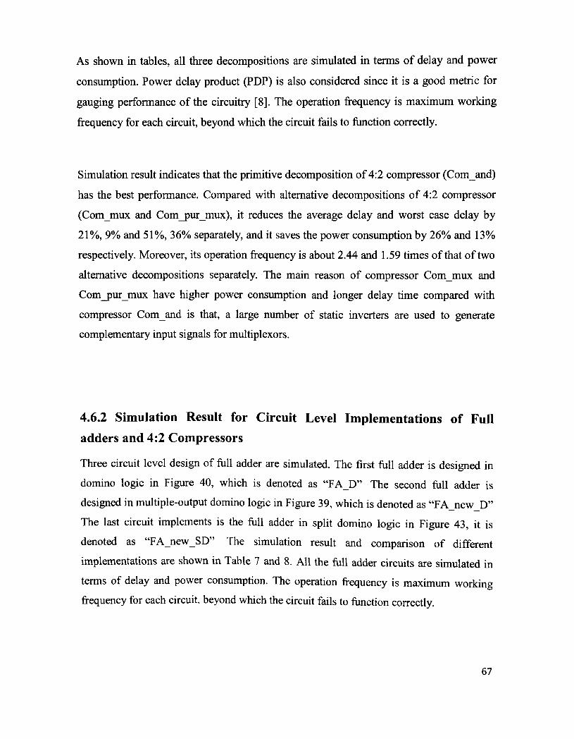
As shown in tables, all three decompositions are simulated in terms of delay and power
consumption. Power delay product (PDP) is also considered since it is a good metric for
gauging performance of the circuitry [8]. The operation frequency is maximum working
frequency for each circuit, beyond which the circuit fails to function correctly.
Simulation result indicates that the primitive decomposition of 4:2 compressor (Comand)
has the best performance. Compared with alternative decompositions of 4:2 compressor
(Commux and Com_pur_mux), it reduces the average delay and worst case delay by
21%, 9% and 51%, 36% separately, and it saves the power consumption by 26% and 13%
respectively. Moreover, its operation frequency is about 2.44 and 1.59 times of that of two
alternative decompositions separately. The main reason of compressor Commux and
Com_pur_mux have higher power consumption and longer delay time compared with
compressor Comand is that, a large number of static inverters are used to generate
complementary input signals for multiplexors.
4.6.2 Simulation Result for Circuit Level Implementations of Full
adders and 4:2 Compressors
Three circuit level design of full adder are simulated. The first full adder is designed in
domino logic in Figure 40, which is denoted as "FAD" The second full adder is
designed in multiple-output domino logic in Figure 39, which is denoted as "FAnewD"
The last circuit implements is the full adder in split domino logic in Figure 43, it is
denoted as "FAnewSD" The simulation result and comparison of different
implementations are shown in Table 7 and 8. All the full adder circuits are simulated in
terms of delay and power consumption. The operation frequency is maximum working
frequency for each circuit, beyond which the circuit fails to function correctly.
67
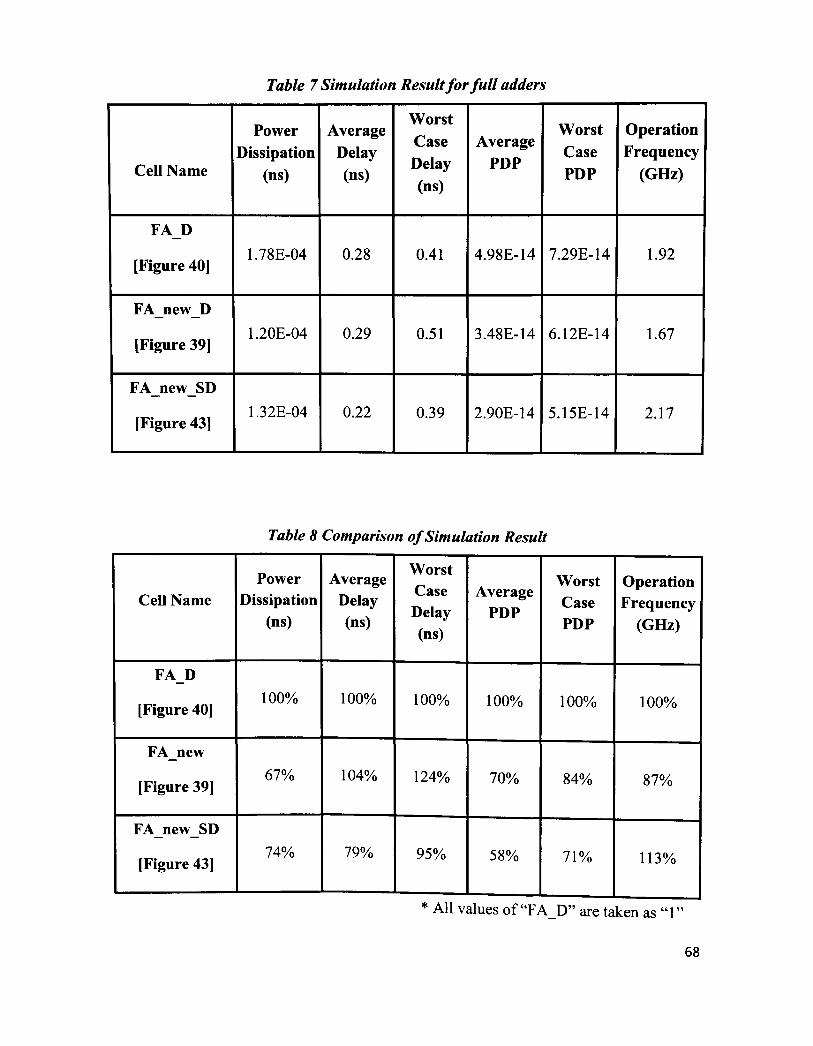
Table 7 Simulation Result for full adders
Cell Name
F A D
[Figure 40]
FAnewJD
[Figure 39]
FA_new_SD
[Figure 43]
Power Dissipation
(ns)
1.78E-04
1.20E-04
1.32E-04
Average Delay (ns)
0.28
0.29
0.22
Worst Case Delay (ns)
0.41
0.51
0.39
Average PDP
4.98E-14
3.48E-14
2.90E-14
Worst Case PDP
7.29E-14
6.12E-14
5.15E-14
Operation Frequency
(GHz)
1.92
1.67
2.17
Table 8 Comparison of Simulation Result
Cell Name
FA_D
[Figure 40]
FA_new
[Figure 39]
FA new_SD
[Figure 43]
Power Dissipation
(ns)
100%
67%
74%
Average Delay (ns)
100%
104%
79%
Worst Case Delay (ns)
100%
124%
95%
Average PDP
100%
70%
58%
Worst Case PDP
100%
84%
71%
Operation Frequency
(GHz)
100%
87%
113%
* All values of "FAD" are taken as " 1 "
68
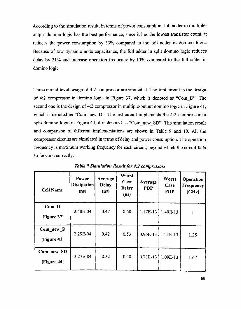
According to the simulation result, in terms of power consumption, full adder in multiple-
output domino logic has the best performance, since it has the lowest transistor count, it
reduces the power consumption by 33% compared to the full adder in domino logic.
Because of low dynamic node capacitance, the full adder in split domino logic reduces
delay by 21% and increase operation frequency by 13% compared to the full adder in
domino logic.
Three circuit level design of 4:2 compressor are simulated. The first circuit is the design
of 4:2 compressor in domino logic in Figure 37, which is denoted as "ComD" The
second one is the design of 4:2 compressor in multiple-output domino logic in Figure 41,
which is denoted as "ComnewD" The last circuit implements the 4:2 compressor in
split domino logic in Figure 44, it is denoted as "ComnewSD" The simulation result
and comparison of different implementations are shown in Table 9 and 10. All the
compressor circuits are simulated in terms of delay and power consumption. The operation
frequency is maximum working frequency for each circuit, beyond which the circuit fails
to function correctly.
Table 9 Simulation Result for 4:2 compressors
Cell Name
Com_D
[Figure 37]
C o m n e w D
[Figure 41]
C o m n e w S D
[Figure 44]
Power Dissipation
(ns)
2.48E-04
2.29E-04
2.27E-04
Average Delay (ns)
0.47
0.42
0.32
Worst Case Delay (ns)
0.60
0.53
0.48
Average PDP
1.17E-13
0.96E-13
0.73E-13
Worst Case PDP
1.49E-13
1.21E-13
1.09E-13
Operation Frequency
(GHz)
1
1.25
1.67
69
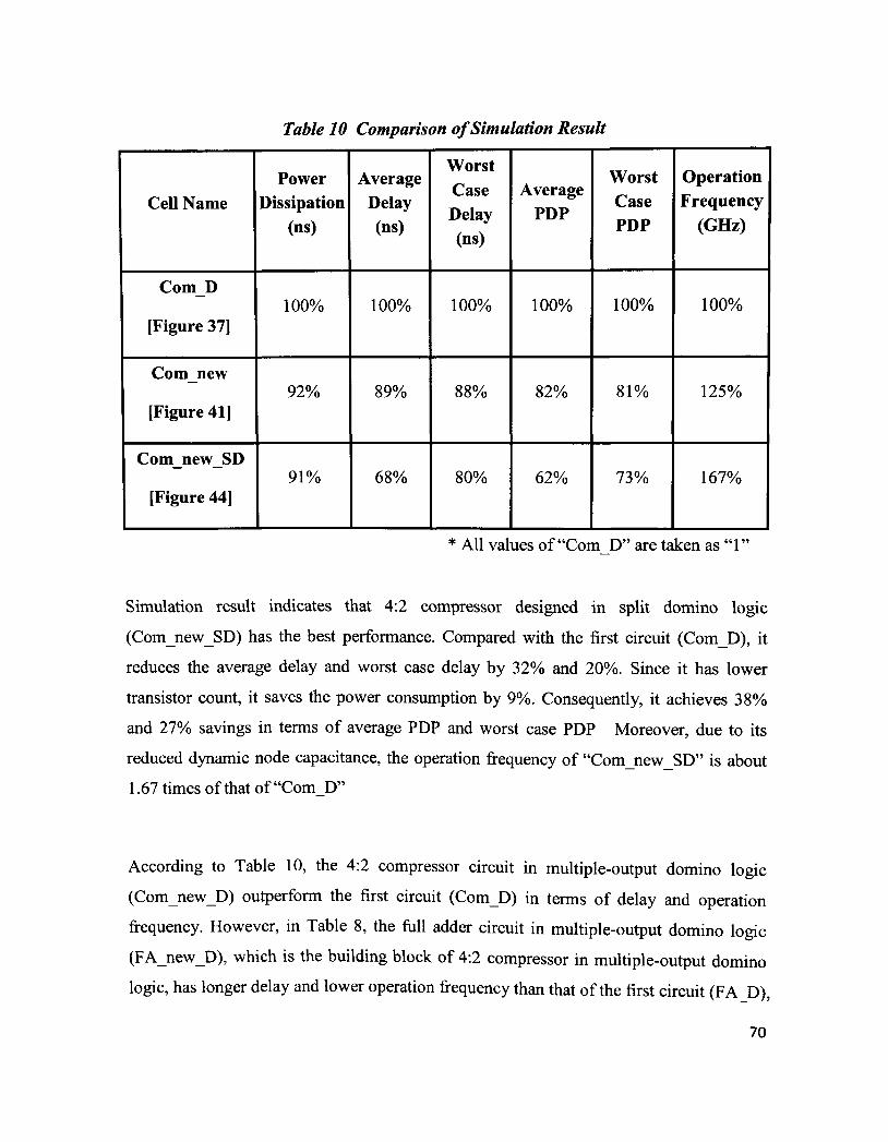
Table 10 Comparison of Simulation Result
Cell Name
C o m D
[Figure 37]
Comnew
[Figure 41]
C o m n e w S D
[Figure 44]
Power Dissipation
(ns)
100%
92%
91%
Average Delay (ns)
100%
89%
68%
Worst Case Delay (ns)
100%
88%
80%
Average PDP
100%
82%
62%
Worst Case PDP
100%
81%
73%
Operation Frequency
(GHz)
100%
125%
167%
* All values of "Com D" are taken as " 1 "
Simulation result indicates that 4:2 compressor designed in split domino logic
(ComnewSD) has the best performance. Compared with the first circuit (ComD), it
reduces the average delay and worst case delay by 32% and 20%. Since it has lower
transistor count, it saves the power consumption by 9%. Consequently, it achieves 38%
and 27% savings in terms of average PDP and worst case PDP Moreover, due to its
reduced dynamic node capacitance, the operation frequency of " C o m n e w S D " is about
1.67 times of that of "ComD"
According to Table 10, the 4:2 compressor circuit in multiple-output domino logic
(ComnewD) outperform the first circuit (ComD) in terms of delay and operation
frequency. However, in Table 8, the full adder circuit in multiple-output domino logic
(FAnewD) , which is the building block of 4:2 compressor in multiple-output domino
logic, has longer delay and lower operation frequency than that of the first circuit (FA D),
70

which is the building block of circuit (ComD). The reason is that: when we design the
full adder in multiple-output domino logic, the total dynamic node capacitance is
increased, thus increase the delay and reduce the operation frequency. However, when we
cascade the full adder in multiple-output domino logic to realize the 4:2 compressor, in
order to make the circuit work properly, we have to increase the fan-out of full adder
block, thus transistor sizing is applied to each pull-down network. This reduces the total
dynamic node capacitance of the circuit, and consequently reduces the delay and increase
the operation frequency of the circuit.
71

CHAPTER 5
CONCLUSIONS
5.1 Summary of Contributions
The purpose of this study has been to explore digital multiplication at both architectural
level and transistor level. This leads to several contributions in the digital multiplication
architecture and high speed low power digital circuit design.
5.1.1 Architectural Contributions
The recursive multiplier architecture has been further explored with the utilization of an
optimized 4:2 compressor reduction scheme which is smaller and more logically efficient
than those proposed in the past. The single level recursive multiplier has then been
enhanced with some gating multiplexors and a majority voter forming a novel
reconfigurable multiplier architecture. This proposal has been implemented and simulated
on the 0.18 urn CMOS process. Its performance and overall characteristics have been
compared against a standard Booth-recoded Wallace multiplier of the same size.
72

5.1.2 Transistor Level Contributions
Based on the primitive logical decomposition of 4:2 compressor, three different
circuitries of 4:2 compressor in Domino logic are proposed, simulation results have
provided validation for these designs.
5.2 Conclusions
By targeting many of the contemporary requirements for digital systems such as power
consumption, critical path delay, regularity, and fault tolerance, a reconfigurable
multiplier architecture that embodies these characteristics has been developed. This
architecture utilizes the recursive multiplication algorithm and an optimized 4:2
compressor layout scheme for partial product reduction.
The developed reconfigurable multiplier architecture has been implemented using the
TSMC 0.18 um CMOS standard cell libraries and its performance has been compared
against a typical multiplier architecture, namely a Booth-recoded Wallace Tree multiplier.
The simulation results have demonstrated that, on average, the reconfigurable multiplier
is efficient in terms of power consumption. The new scheme offers over a 25% savings in
cell internal power and a 19% decrease in dynamic power consumption respectively. In
addition, this scheme has a slightly shorter delay time, which benefits from the regularity
of recursive structure.
To further enhance the performance of proposed reconfigurable multiplier, three circuit
level implementations of 4:2 compressor, which is widely used in highly efficient partial
product reduction, have been proposed and simulated by using HSPICE. The simulation
result confirms that the 4:2 compressor designed in split domino logic has the best
performance among all three designs. Due to its reduced dynamic node capacitance, it
increases its operation frequency by 67% and reduces the average delay by 32%, as
compared to the bench mark 4:2 compressor which is designed in domino logic.
73

REFERENCES
[1] Gary. W Bewick, "Fast Multiplication: Algorithms and Implementation",
Dissertation for the Degree of Doctor in Philosophy, Stanford University, 1994.
[2] Bickerstaff, Schulte and E.E. Swartzlander Jr., "Analysis of column compression
multipliers", IEEE Symposium on Computer Arithmetic, pp. 33 -39, 2001.
[3] Behrooz Parhami, "Computer Arithmetic: Algorithms and Hardware Designs",
Oxford University Press, New York, 2000.
[4] C.S. Wallace, "A suggestion for a fast multiplier", IEEE Transactions on
Electronic Computers, vol. 13, pp 14-17,1964.
[5] Luigi Dadda, "Some schemes for parallel multipliers", Alta Frequenza, vol. 45,
pp. 574-580, 1966.
[6] A. Karatsuba and Y. Ofinan, "Multiplication of Multidigit Numbers on
Automata", Sov. Phys.-Dokl. (English Translation), vol. 7, pp. 595-596, 1963
[7] A. Habibi and P.A. Wintz, "Fast Multipliers", IEEE Transactions on Computers,
vol. C-19,pp. 153-157,1970.
[8] W Stenzel, W. Kubitz, G. Garcia, "A Compact High-Speed Parallel
Multiplication. Scheme", IEEE Transactions on Computers, vol. 26, pp. 948-957,
1977.
[9] A. Weinberger, "4:2 Carry-Save Adder Module", IBM Technical Disclosure
Bulletin, vol. 23, Jan. 1981.
[10] P.Mokrian, "A reconfigurable digital multiplier architecture," Master thesis,
University of Windsor, 2003.
[11] G. Michael Howard , "Investigation into arithmetic sub-cells for digital
multiplication," Master thesis, University of Windsor, 2005.
[12] A.N. Danysh, and E.E. Swartzlander Jr., "A recursive fast multiplier", Asilomar
Conference on Signals, Systems & Computers, vol. 1, pp. 197 -201. 1998.
[13] C. Paar, "A new architecture for a parallel finite field multiplier with low
complexity based on composite fields". IEEE Transactions on Computers, vol. 45, pp. 856-861, 1996.
74
[14] Peter Cameron,"Encyclopaedia of Design Theory", http://www.maths.qmul.ac.uk/
~pjc/design/encyc/topics/, 2002.
[15] J. Kim and E.E. Swartzlander Jr., "Improving the recursive multiplier", Asilomar
Conference on Signals, Systems and Computers, vol. 2, pp. 1320 -1324, 2000.
[16] R. Rogenmoser, L. O'Donnell, S. Nishimoto, "A dual-issue floating-point
coprocessor with SIMD architecture and fast 3D functions", IEEE International
Solid-State Circuits Conference, Volume: lm pp. 414 -415, 2002.
[17] R.K. Kolagotla, J. Fridman, B.C. Aldrich, M.M. Hoffman, W.C. Anderson, M.S.
Allen, D.B. Witt, R.R. Dunton, L.A.Booth Jr., "High performance dual-MAC
DSP architecture", IEEE Signal Processing Magazine , Volume: 19 Issue: 4 , pp.
42-53, July 2002.
[18] J. Eyre and J. Bier, "The evolution of DSP processors", IEEE Signal Processing
Magazine, vol. 17 Issue: 2 , pp. 43-51, March 2000.
[19] Reto Zimmermann, "Computer Arithmetic: Principles, Architectures, and VLSI
Design", Lecture notes for the Integrated Systems Laboratory, Swiss Federal
Institute of Technology (ETH), 1999.
[20] R. Kaivola, N. Narasimhan, "Formal Verification of the Pentium 4 Floating-Point
Multiplier", Design, Automation and Test in Europe Conference and Exhibition,
pp. 20-27, 2002.
[21] A. D. Booth, "A Signed Binary Multiplication Technique", Quarterly Journal of
Mechanics and Applied Mathematics, vol. 4, pp 236-240, June 1951.
[22] P.J. Song, G. De Micheli, "Circuit and architecture trade-offs for high-speed
multiplication" IEEE Journal of Solid-State Circuits, vol 26, pp. 1184-1198, 1991.
[23] M. Mehta, V Parmar, E. Swartzlander, "High-speed multiplier design using
multiinput counter and compressor circuits", IEEE Symposium on Computer
Arithmetic, pp. 43-50, 1991.
[24] R.V.K. Pillai, D. Al-Khalili and A.J. Al-Khalili, "Energy delay analysis of partial
product reduction methods for parallel multiplier implementation", International
Symposium on Low Power Electronics and Design, pp. 201 -204, 1996.
75
[25] D. Villeger and V.G. Oklobdzija, "Analysis of Booth encoding efficiency in
parallel multipliers using compressors for reduction of partial products", Asilomar
Conference on Signals, Systems and Computers, vol. 1, pp. 781 784, 1993
[26] Pascal Bonatto and Vojin Oklobdzija, "Evaluation of Booth's algorithm for
implementation in parallel multipliers", Asilomar Conference on Signals, Systems
and Computers, vol. 1, pp. 608 -610,1996.
[27] Chip-Hong Chang, Jiangmin Gu, and Mingyan Zhang, "Ultra low-voltage low-
power CMOS 4-2 and 5-2 compressors for fast arithmetic circuits," IEEE
Transactions on Circuits and Systems, vol. 51, no. 10, Oct. 2004.
[28] Jan M. Rabaey, "Digital integrated circuits- a design perspective," Prentice-Hall,
New Jersey, 2003.
[29] Zimmermann and Fichtner, "Low-Power Logic Styles: Cmos Versus Pass-
Transistor Logic", IEEE Journal of Solid-State Circuits, vol. 32, pp. 1079-1090,
July 1997.
[30] Massoud Pedram, "Power Optimization and Management in Embedded Systems",
Asia and South Pacific Design Automation Conference, pp. 239 -244, 2001G.
Binnig, C. F Quate, and C. Gerber, "Atomic Force Microscope," Phys. Rev.
Lett., vol. 56, pp. 930-933, Mar. 1986.
76
VITAAUCTORIS
Peng Chang was born in 5 Nov, 1981 in Nan Yang, He Nan, China. He obtained his
B.A.Sc. in Electrical and Computer Engineering from Central South Forestry University
in Hu Nan, China, where he graduated in 2005.
In Fall 2006, Peng began the pursuit of a M.A.Sc. degree in Electrical Engineering under
the supervision of Dr. Majid Ahmadi at the University of Windsor, Windsor, Ontario,
Canada. During this period, he has received a University of Windsor Tuition Scholarship.
His area of specialization has been the high speed low power digital multiplier design.
77