A New Way to Find Low- lmpedance Logic-Circuit Faults
26
-
Upload
khangminh22 -
Category
Documents
-
view
0 -
download
0
Transcript of A New Way to Find Low- lmpedance Logic-Circuit Faults

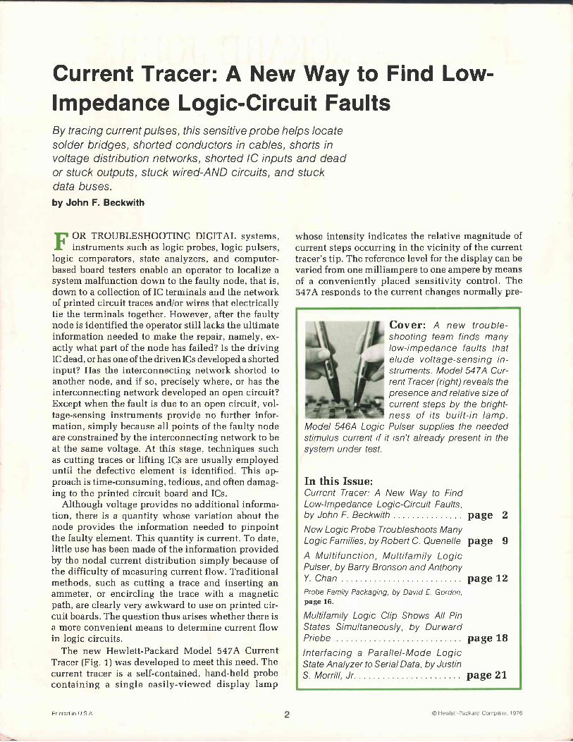
Current Tracer: A New Way to Find Low-lmpedance Logic-Circuit FaultsBy tracing current pulses, fhis sensitive probe helps locatesolder bridges, shorted conductors in cables, shorls involtage distribution networks, shorted lC inputs and deador stuck outputs, stuck wired-AND circuits, and stuckdala buses.by John F. Beckwith
E OR TROUBLESHOOTING DIGITAL systems,I' instruments such as logic probes, logic pulsers,logic comparators, state analyzers, and computer-based board testers enable an operator to localize asystem malfunction down to the faulty node, that is,down to a collection of IC terminals and the networkof printed circuit traces and/or wires that electricallytie the terminals together. However, after the faultynode is identified the operator still lacks the ultimateinformation needed to make the repair, namely, ex-actly what part of the node has failed? Is the drivingIC dead, orhas one of the drivenlCs developed a shortedinput? Has the interconnecting network shorted toanother node, and if so, precisely where, or has theinterconnecting network developed an open circuit?Except when the fault is due to an open circuit, vol-tage-sensing instruments provide no further infor-mation, simply because all points of the faulty nodeare constrained by the interconnecting network to beat the same voltage. At this stage, techniques suchas cutting traces or lifting ICs are usually employeduntil the defective element is identified. This ap-proach is t ime-consuming, tedious, and often damag-ing to the printed circuit board and ICs.
Although voltage provides no additional informa-tion, there is a quantity whose variation about thenode provides the information needed to pinpointthe faulty element. This quantity is current. To date,l itt le use has been made of the information providedby the nodal current distribution simply because ofthe difficulty of measuring current flow. Traditionalmethods, such as cutting a trace and inserting anammeter, or encircling the trace with a magneticpath, are clearly very awkward to use on printed cir-cuit boards. The question thus arises whether there isa more convenient means to determine current flowin logic circuits,
The new Hewlett-Packard Model s+zA CurrentTracer [Fig. r) was developed to meet this need. Thecurrent tracer is a self-contained, hand-held probeconta in ing a s ingle easi ly-v iewed d isplay lamp
P r n t e d r n U S A
whose intensity indicates the relative magnitude ofcurrent steps occurring in the vicinity of the currenttracer's tip. The reference level for the display can bevaried from one milliampere to one ampere by meansof a conveniently placed sensitivity control The547A responds to the current changes normally pre-
Model 5464 Logicstimulus current if itsystern under test.
Cover : A new t roub le -shooting team finds manylow-impedance faults thatelude voltage-sensing in-struments. Model 547A Cur-rent Tracer (right) reveals thepresence and relative size ofcurrent sfeps by the bright-ness o f i t s bu i l t - in lamp.Pulser supp/ies the needed
isn't already present in the
In this Issue:Current Tracer: A New Way to FindLow-l mpedance Logic-Ci rcuit Faults,by John F. Beckwith , , . page 2
New Logic Probe Troubleshoots ManyLogic Families, by Robert C. Quenelle page I
A Multifunction, Multifamily LogicPulser, by Barry Bronson and AnthonyY. Chan . . pagel2Probe Family Packaging, by David E Gordon,page 16.
Multifamily Logic Clip Shorlrs All PinStates Simultaneously, by DurwardP r i e b e . . . p a g e l 8
lnterfacing a Paral lel-Mode LogicState Analyzer to Serial Data, by JustinS . M o r r i l l , J r . . . . . . . . . . p a g e 2 7
O Hewlell-Packard Company, 1 976
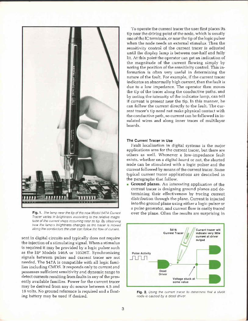
Fig. 1 . The lamp near the tip of the new Model 547 A CurrentTracer varies in brightness according to the relative magni-tude of the current steps occurilng near its tip By observinghow the lamp's brightness changes as the tracer is movedalong the conductors the user can follow the flow of current
sent in digital circuits and typically does not requirethe injection of a stimulating signal. When a stimulusis required it may be provided by a logic pulser suchas the HP Models 546A or 10526T. Synchronizingsignals between pulser and current tracer are notneeded. The 547A is compatible with all logic fami-l ies including CMOS. It responds only to current andpossesses sufficient sensitivity and dynamic range todetect currents resulting from faults in any of the pres-ently available families. Power for the current tracermay be derived from any dc source between 4.b and18 volts. No ground reference is required and a float-ing battery may be used if desired.
To operate the current tracer the user first places itstip near the driving point of the node, which is usuallyone of the IC termina-ls, or near the tip of the logic pulserwhen the node needs an external stimulus. Then thesensitivity control of the current tracer is adjusteduntil the display lamp is between one-half and fullyl it. At this point the operator can get an indication ofthe magnitude of the current f lowing simply bynoting the position of the sensitivity control. This in-formation is often very useful in determining thenature of the fault. For example, if the current tracerindicates an abnormally high current, then the fault isdue to a low impedance. The operator then movesthe tip of the tracer along the conductive paths, andby noting the intensity of the indicator lamp, can telli f current is present near the tip. In this manner, hecan follow the current directly to the fault. The cur-rent tracer's t ip need not make physical contact withthe conductive path, so current can be followed in in-sulated wires and along inner traces of multi layerboards.
The Current Tracer in UseFault localization in digital systems is the major
applications area for the current tracer, but there areothers as well. Whenever a low-impedance faultexists, whether on a digital board or not, the shortednode can be stimulated with a logic pulser and thecurrent followed by means of the current tracer. Sometypical current tracer applications are described inthe paragraphs that follow.r Ground planes. An interesting application of the
current tracer is designing ground planes and de-termining their effectiveness by tracing currentdistribution through the plane. Current is injectedinto the ground plane using either a logic pulser ora pulse generator, and current f low is easily tracedover the plane. Often the results are surprising in
547ACurrent Tracer
Current tracer willindicate very littlecurrent at driveroutput
Fig. 2. Using the current tracer to determine that a stucknode ls caused by a dead driver
that current flows through only a few paths, oralong edges.
r V""- to-ground shorts. Locat ing V""-to-groundshorts is an almost impossible task without theability to trace current flow. To find the short, theuser disconnects the power supply and pulses thepower supply terminal using the logic pulser withthe supply return connected to the GNo lead of thepulser. Even if capacitors are connected betweenV." and ground, the current tracer will usuallyreveal the path carrying the greatest current.
r Stuck node caused by dead driver. Fig. 2 illus-trates a frequent ly occurr ing troubleshoot ingsymptom: a node has been identified on which thevoltage is stuck high or low. Is the driver dead, oris something, such as a shorted input, clamping thenode to a fixed value? This question is readilyanswered by tracing current from the driver toother elements on the node. If the driver is dead,the only current indicated by the tracer will be thatcaused by parasitic coupling from any nearby cur-rents, and this will be much smaller than the nor-mal current capability of the driver. On the otherhand, if the driver is good, normal short circuitcurrent will be present and can be traced to thecircuit element clamping the node.
r Stuck node caused by input short. Fig. 3 illustratesthis situation, which has exactly the same voltagesymptoms as the previous case of a stuck nodecaused by a dead driver. However, the currenttracer will now indicate a large current flowingfrom the driver, and will also make it possible tofollow this current to the cause of the problem,the shorted input. The same procedure will alsofind the fault when the short is on the intercon-necting path of the node-for example, a solderbridge to another node.
Curaenl tracer indicateslarge curlents
Gate withShorted Inpul
Pulse Activity
.rt-Jln
Fig. 3. Ihe current tracer shows that thls sluck node iscaused by an input short,
r Stuck wired-AND node. Another difficult circuitproblem to troubleshoot is the wired-AND node, anode formed by connecting several open-collectoroutput structures. Fig. shows how the currenttracer is used to solve this problem. Each gate'soutput is placed in turn in its off or high-impedancestate by forcing the inputs to an appropriate level(a jumper may be used) while a logic pulser is usedto stimulate the output node. If the gate is good thecurrent tracer will indicate only stray current at thegate output. Conversely, a stuck gate will re-sult in a large current indication. The need toforce the output of the gate to the off state by meansof the jumper at the input can be eliminated if theduty cycle of the high-impedance state when thecircuit is operating is not too low. When this is thecase a logic pulser and current tracer may be usedin the single-pulse mode. If the gate is not stuck theoperator should observe a random presence andabsence of current at the gate output while single-pulsing the node. If the gate is stuck, each pulsefrom the pulser will result in a large current indi-cation from the tracer.
r Stuck three-state data bus. A stuck three-state bus,such as a microprocessor data or address bus, pre-
Current tracerindicates large current
at stuck gate
vTemporary jumper
to ground
Fig,4. The current tracer can often make use of normal cur-rents in a circuit, but sometimes a logic pulser provides aneeded stimulus, as in the difficult problem of a stuck wired-AND node
sents a very diff icult troubleshooting problem,especially to voltage-sensing measurement tools.Because of the many bus terminals, it is very diffi-cult to isolate the one bus element holding it in astuck condition. However. if the current tracerindicates high current at several driver outputs, itis likely that one (and most likely only one) driveris stuck in a low-impedance state. The defectivedriver is located by placing one driver's controlinput l ine to the appropriate level for a high-impedance output state and noting whether highcurrent flow persists at the output. This is repeatedfoi each driver until the bad one is located. Al-ternatively, if the low-impedance duty cycle of adriver is low, the node can be pulsed with the logicpulser, and the defective driver identified by notingwhether every pulse from the pulser results in cur-rent at the driver output. If the current tracer indi-cates high currents at only two drivers the problemis a "bus fight", that is, both drivers trying to drivethe bus at the same time. This is probably causedby improper control signals to the drivers. If thecurrent tracer indicates the absence of abnormallyhigh current activity at all drivers, yet the bus sig-nals are known to be incorrect, then the problem isa driver stuck in the high-impedance state. It canbe found by placing a low impedance on the bus,such as a short to ground, and using the currenttracer to check for the driver that fails to show high-current activity.Efficient use of the current tracer usually requires a
longer familiarization period than does the operationof voltage-sensing instruments. This is primarily be-cause most operators are not used to thinking in termsof current and the information it provides, simply be-cause this information has not been available conven-iently. Also, it requires some skill to avoid the cross-talk problem, that is, if a small current is being tracedin a conductor that is very close to another conductorcarrying a much larger current, the sensor at the tip ofthe current tracer may respond to the current in the
nearby trace. The current sensor has been designed tominimize this effect, but it can never be entirely elim-inated. The operator can, however, by observing thevariation of the current tracer's display as its tip ismoved about the trace, learn to recognize interferenceor crosstalk from a nearbv trace.
lnside the Current TracerFig. 5 is a block diagram of the current tracer. Oper-
ation is as follows. A step change in current occurringat the current tracer's tip is coupled via mutual induc-tance to the current-step sensor, which produces avoltage impulse output proportional to the magni-tude of the current step. The size of the impulse de-creases with increasing separation between the cur-rent path and the tip of the tracer.
The voltage impulse is fed to a variable-gain pre-amplifier. The preamplifier gain is adjusted by thesensitivity control to produce an output of approxi-mately 1 mV when the tracer's tip is placed next to thecurrent path. The output of the preamplifier is furtheramplified and then stretched by two cascaded peakdetectors to produce a pulse of sufficient height andwidth to cause a visible flash of the incandescentlamp that forms the current tracer's display. When thetip of the tracer is moved along the conducting paththe display remains at the same brightness as long asthe same current is still present. However, if the cur-rent has changed to another path, the increased separ-ation between the tip of the tracer and the currentlowers the output of the current-step sensor and de-creases the brightness of the display. Thus the opera-tor is provided with sufficient information to trackthe current path.Current-Step Sensor
Fig, 6 shows the physical construction and anequivalent circuit of the current-step sensor. Its oper-ating principle is essentially that of a current trans-former, A step change in current near the tip of thetracer attempts to induce an emf in the windings onthe coil within the sensor. This coil is nearlv shorted
Fig,5. 547A Current Tracer blockdiagram Cuffent-step sensordetects cutrent steps as sma// as1mA and rejects magnetic fluxthat is not directly beneath thettacer's tiD.
Sensitivity Control
/ M
Ferrite Core
Eddy-Current andElectrostatic Shield
lunknown /
' {oi f \
( ,\
Magnetic Flux Path
Fig. 6. Consfruction and equivalent circuit of the current-step sensor, which acts like a current transformer. For eachcutrent step the sensor produces a voltage impulse at itsoutput
(R is small), so a current is induced in the coi l whose
magnetic flux nearly cancels the flux change causedby the unknown current step. Thus, for a fixed physical orientation, there will be a current step propor-tional to the unknown current step induced in thepickup coil, This induced current flows through theresistor R, producing a voltage that forms the outputsignal of the sensor. The current in the pickup coil,and hence the output voltage, decays with a time con-stant L/R. This time constant is such that the output ofthe current-step sensor is an impulse whose peak valueis proportional to the change in the unknown currentand is independent of the rise time of the currentchange up to about 200 nanoseconds. Although thecurrent-step sensor provides an indication only of cur-rent changes and not the total value of the current, itturns out that for fault finding in digital systems thisinformation is sufficient.
The current-step sensor had to meet a number ofconflicting design criteria. It had to be physicallysrnall so currents in the closely spaced traces foundon printed circuit boards could be distinguished. Ithad to be able to reject magnetic flux originating fromlocations other than the tracer's tip. It had to provide adetectable output for the smallest current steps of in-terest (<1 mA). I t could not respond to vol tagechanges found in digital systems. It had to be me-chanically rugged and manufacturable at a reason-able cost.
These criteria were successfully met by enclosing avery small (1.5-mm-diameter) H-shaped ferrite corewithin a relatively thick, highly conductive shield.The shield serves several purposes: it provides me-chanrcal support and protection for the.pickup core,it shields the core from external changing magneticfields by means of induced eddy currents in theshield that oppose the changing flux, and it is elec-trically grounded and thus protects the coil windingsfrom electric fields caused by the voltages on theboard. Protection from electric fields is adequate toprovide the greater than 110 dB of shielding neededso the tracer's tip can be placed next to voltage stepsof five volts and not respond to them, while at thesame time responding to current steps of 1 mA. For al--mA current step the current-step sensor producesa 100-g,V output spike approximately 150 ns wide.
AmplificationTo make a 100-pr,V 150-ns pulse ltght an incandes-
cent lamp long enough for it to be visible, consider-able amplification is required. For the sake of operat-ing convenience, it was decided to package all thenecessary electronics in the probe body and to powerthe probe from the supplies typically present in a dig-ital environment. This means that the circuitry has tooperate from supply voltages of five volts or less, sonearly all commercially available linear ICs are in-applicable. Also, the shape and small size of the probebody make physical isolation of the amplifier stagesimpractical, and the small volume within the probealso prevents the use of effective high-frequency de-coupling capacitors because of their large size. It waspossible, nevertheless, using two custom ICs, to pack-age on a multilayer board approximately 1.3 cm wideby 10 cm long, 80 dB x 20 MHzof stable linearampli-fication. This was accomplished by very careful loca-tion of components to minimize capacitive coupling,and by orienting the components to cancel destabiliz-ing parasitic inductive coupling. Shielding of thesensitive amplifier from external electric and mag-netic fields is provided by the probe housing, whichis made of aluminum and makes an effective electro-static and eddy-current shield.
For maximum viewing angle, brightness, and con-venience of location, the current tracer's display waschosen to be an incandescent lamp at the tip of theprobe immediately behind the current-step sensor.This location creates a difficult stability problem: apulse at the current-step sensor is amplified and re-turned to the display, which is right next to the sen-sor, and the energy content of the pulse that flashesthe display can be greater than 101a times that cap-tured by the current-step sensor. It was possible, how-ever, thanks to the efficiency of the shielding of the
cunent-step sensor, the orientation of the amplifiercomponents, and careful printed circuit board de-sign to electrically decouple the input from the out-put. In fact, the current pulse that drives the displaylamp actually passes through the board area in whichthe amplif ier is located, but by running the displaylamp's supply and return traces on the inner layers ofa multilayer board, one above the other and separatedby a very thin insulating layer, and covering these withthe outer-layer ground plane, it was possible to confinethe fields from the display pulse to a very small vol-ume. The ground plane also had to be carefully de-signed so the charging currents ofthe parasitic capac-itor formed by the grounded eddy-current shield andthe t race or node under invest igat ion can passthrough the sensitive amplif ier area without induc-tively coupling unwanted signals to the amplif ier.
Fault currents in the various logic families andfrom pulse stimulators can vary from about onemill iampere to one ampere. The tracer normalizesthese to a common reference level so the operatorsees only the value of the current at the tracer's t iprelative to that at the driving point of the node. This60-dB (1000:1J gain variation cannot be achievedwith a potentiometer divider because the parasiticinductances and capacitances associated with a po-tentiometer at the extreme positions of the wiperdegrade the high-frequency response. Also, the gaincontrol has to be in the init ial stages of the amplif ierchain because the requirement of operating fromfive-volt supplies severely restricts the l inear operat-ing range of the amplif iers. For these reasons theentire 60 dB of gain control was placed in the firstamplif ier stage. This was done by taking as the basicconfiguration a single transistor with an unbypassedemitter resistor approximately equal to the collectorresistor (see Fig. 7). Current-controlled variable resis-tors formed from Schottky and silicon diodes areac-coupled to both the collector and emitter resistors.When the sensitivity control on the tracer is placed inthe 1-mA position the variable emitter resistors are intheir low-resistance state and the collector resistancesare in their high-resistance state, thus forming acommon-emitter amplif ier of z0-dB gain. Conversely,when the sensitivity control is in the 14, positionthe collector resistance becomes very small and theemitter resistance large and the configuration formsa 40-dB attenuator. A temperature-compensated,precision-component network was required to pro-vide control currents for the variable resistors to in-sure that the maximum and minimum values of theamplifier gain were repeatable from unit to unit andstable with time.
The noise performance required of the first ampli-f ier stage is quite severe. It must amplify, with a2O-MHz bandwidth, input pulses smaller than 100
Fig. 7. Vailade gain preamplifier provides 60 dB of gainvariation as the sensiliyity control is adjusted. The diodesfunction as current-controlled variable reslstors,
microvolts and yet not introduce any noise peakscomparable in amplitude to the input pulses becausethe downstream circuitry detects each peak andstretches it for a sufficient t ime to l ight the display.Thus the rms noise introduced by the amplif ier mustbe far below the 100-microvolt input pulse. This wasachieved by us ing. a low-noise, h igh- f requencytransistor biased to optimize its noise figure.
Peak DetectorsWhen the sensitivity control is set so the display is
at its reference level, the output of the current-stepsensor emerges from the amplifier chain with an am-plitude of about 500 mV and a width of about 150 nano-seconds. The polarity of this output wil l be either pos-it ive or negative, depending upon the polarity of thecurrent step and the randomly chosen orientation be-tween the current path and the pickup coil in thetracer. The operator is interested only in how themagnitude of this pulse varies as he moves the tip ofthe tracer from place to place, so the signal that drivesthe display lamp must be proportional to the ampli-tude of the output of the amplif ier chain, independentof its polarity, and of sufficient duration to be visible,The required signal processing is accomplished bymeans of two peak detectors. The first, or bipolar peakdetector (Fig. 8J, produces an output pulse of thesame magnitude as the input pulse, but always of thesame polarity, and stretches the peak of the inputpulse from about 20 ns to about 4O 1ts. A second peakdetector stretches the output of the bipolar peak de-tector to about 200 ms, which is long enough to be vis-
loop. This configurationternal supply vgltage tovoltage is low. {4
permits nearly all of the ex-be used when the external
Fig. 8. The output of the bipolar peak detector is a limestretched version of the input, and is positive f or both polaritiesof input
ible. The output of the second peak detector is furtheramplif ied by a dc amplif ier to provide the signal thatl ights the incandescent display lamp.
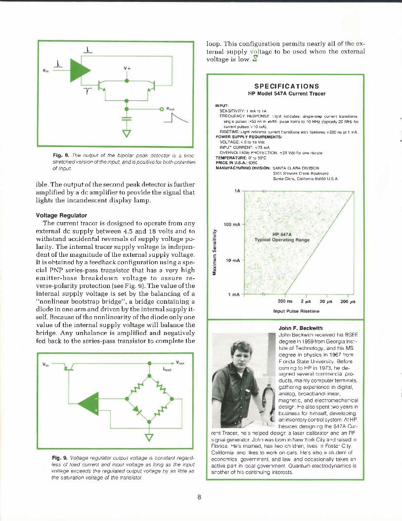
Voltage RegulatorThe current tracer is designed to operate from any
external dc supply between 4.5 and 1.8 volts and towithstand accidental reversals of supply voltage po-larity. The internal tracer supply voltage is indepen-dent of the magnitude of the external supply voltage.It is ohtained by a feedback configuration using a spe-cial PNP series-pass transistor that has a very highemi t t e r -base b reakdown vo l t age to assu re re -verse-polarity protection (see Fig. 9). The value of theinternal supply voltage is set by the balancing of a"nonlinear bootstrap bridge", a bridge containing adiode in one arm and driven by the internal supply it-self. Because of the nonlinearity of the diode only onevalue of the internal supply voltage wil l balance thebridge. Any unbalance is amplif ied and negativelyfed back to the series-pass transistor to complete the
Fig,9. Voltage regulator output voltage /s constanl regard-less of load current and input voltage as long as the inputvoltage exceeds the regulated output voltage by as little asthe saturation voltage of the transistol
S P E C I F I C A T I O N SHP Model 547A Current Tracer
INPUT:SENSITIVITY: 1 mA to 1AFREOUENCY RESPONSE: Light indicates: single-step currenl transitions;
single pulses >50 ns in width; pulse trains to 10 MHz (typrcally 20 MHz torcurrent oulses > 10 mAl
RISETIME: Light ndicates current lransitions with risetimes <200 ns at 1 mAPOWER SUPPLY REOUIFEMENTS:
VOLTAGE;4 5 to 18 VdcINPUT CURFIENT: <75 mAOVEHVOLTAGE PBOTECTION: r25 Vdc for one minute
TEMPEBATURE: 0" to 55'CPRICE lN U.S.A.: S3s0MANUFACTURING DIVISION: SANTA CLARA DIVISION
5301 Stevens Creek BoulevardSanta Clara, California 95050 U S A
q
oo
E
o=
l 0 m A
200 ns 2 ps 20 ys 200 ps
Input Pulse Riset ime
John F. BeckwithJohn Beckwith received his BSEEdegree in 1959 f rom Georgia Inst i-tute of Technology, and his MSdegree in physics in .1967 fromFlorida State University Beforecoming to HP in 1973, he de-signed several commercial pro-ducts, mainly computer terminals,gathering experience in digital,analog, broad band-l inear,magnetic, and electromechanicaldesign He also spent two years inbusiness for himself, developingan inventory control system At HP,besides designing the 5474 Cur-
rent Tracer, he's helped desrgn a laser cal ibrator and an RFsignal generator John was born in New York City and raised inFlorida He's married, has two chi ldren, l ives in Foster City,Cali fornia, and l ikes to work on cars He's also a student ofeconomics, government, and law, and occasional ly takes anactive part in local government Ouantum electrodynamics isanother of his continuing interests
New Logic Probe Troubleshoots ManyLogic FamiliesThe probe's single lamp indicator displays high or lowlogic levels, bad levels, and open circuits on digital circuitnodes. Testable logic families include TTL, DTL, CMOS,HTL, HNIL, and MOS.
by Robert C. Quenelle
n ESIGNING AND TROUBLESHOOTING digitall-J sil6uifs poses some measurement problems notneatly solved by analog test equipment. The digitalcircuit typically has only two narrow voltage ranges,high and low, that represent logic ones and zeros. Avoltmeter or oscil loscope wil l easily give the voltageto more accuracy than is required, but won't translatethose voltages into logic levels, leaving that job to theuser. Although the oscil loscope is sometimes indis-pensable for checking ringing, skews, and so forth, inmany instances a simple indication of logic levelswill suffice.
For several years the logic probe has comple-mented the oscil loscope in helping to solve digitaltroubleshooting problems. HP's Model 10525T, forexample, is small and light enough to be hand-heldand features convenient fingertip display of ones andzeros and 10-nanosecond pulse-catching capabil ity,independent of repetit ion rate. The 10525T translatesvoltages at the measurement tip to logic levels basedon the specifications of TTL logic.
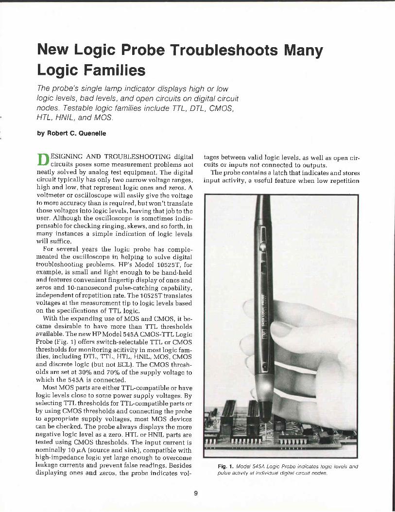
With the expanding use of MOS and CMOS, it be-came desirable to have more than TTL thresholdsavailable. The new HP Model 54sA CMOS-TTL LogicProbe (Fig. 1) offers switch-selectable TTL or CMOSthresholds for monitoring acitivity in most logic fam-il ies, including DTL, TTL, HTL, HNIL, MOS, CMOSand discrete logic (but not ECLI. The CMOS thresh-olds are set at 30% and 7oo/o of the supply voltage towhich the 545A is connected.
Most MOS parts are either TTl-compatible or havelogic levels close to some power supply voltages. Byselecting TTL thresholds for TTL-compatible parts orby using CMOS thresholds and connecting the probeto appropriate supply voltages, most MOS devicescan be checked. The probe always displays the morenegative logic level as a zero. HTL or HNIL parts aretested using CMOS thresholds. The input current isnominally 1O p.A (source and sink), compatible withhigh-impedance logic yet large enough to overcomeleakage currents and prevent false readings. Besidesdisplaying ones and zetos, the probe indicates vol-
tages between valid logic levels, as well as open cir-cuits or inputs not connected to outputs.
The probe contains a latch that indicates and storesinput activity, a useful feature when low repetition
Fig. 1. Model 5454 Logic Probe indicates logic levels andpulse activity at individual digital circuit nodes
supply. In the CMOS mode the probe's thresholdstrack the instantaneous supply voltage as does CMOS
Iogic, thereby compensating for ripple to 1 kHz.
Using the ProbeThe logic probe has two main display modes, static
and dynamic. It indicates in a static circuit whether
the voltage at a particular point is a logic zero, a one,
or an indeterminate level. The lamp in the probe tip is
off for azero,brightfor a one, and dim for a voltagebe-tween logic levels, an open circuit, or a high-impe-
dance point such as a floating input or a three-state
output in the off state. In a dynamic circuit, the tip
lamp will flash at about 10 Hz when the tip is touchedto a point toggling between a one and zero at up to 80MHz in TTL mode and 40 MHz in CMOS. It wil l f lash
on or off for about 50 ms for a single one or zero pulse.
Pulses as short as 10 ns can be detected if the shortground lead is connected to a point near the pulse
source, 20-ns pulses can typically be detected with-
out using the short ground lead. The probe can also be
clipped into a circuit and the latch used to monitor
infrequent activity.
By displaying the dc logic levels in a circuit thelogic probe can be used to verify combinatorial re-Iationships. Or, input levels can be overridden by alogic pulser and the logic probe wil l then test thefunctioning of a circuit without removing any normalconnections. In clocked systems, many logic familiesrespond only to clock transitions and are insensitiveto the clock rate (up to their upper frequency specifi-cationsJ. This allows replacing normal clocking sig-nals with a single cycle or slow clock (once again, alogic pulser may be used) and checking system se-quencing at a convenient rate, Spikes and one-shotoutputs can also be checked even at slow clock rates
rates or single-shot events are involved. A light-emit-ting diode (LED) indicator turns on when a new oneor zero level is detected and stays on until manuallyreset.
To protect the 545A from accidental overloads, thepower supply input is protected to -+25 volts for oneminute and the tip can withstand momentary over-loads to 250 volts. The probe is usable down to threevolts, although the tip lamp gets dimmer below fivevolts. CMOS supplies often have considerable ripple,especially if electrically noisy devices use the same
Fig.2, 545A front-end has two f ast peak detectors and tworelatively slow, low-input-current comparators The circuitcan withstand accidental overloads of +120V continuousand +250V for 75 seconds.
A Smart Probe-Test SystemInstrument test orocedures can have substantial effects on
factory cost, warranty cost, and customer satisfaction High-volume, high{echnology instruments l ike the new logic pro-ducts demand high test throughput and a high test confidencefactor, the latter because warranty cosl on a returned low-costinstrument represents a large po(ion of i ts price,
The solut ion was found in a calculator-control led test systemThe system is a closed-loop, seltcal ibrat ing, ful ly automatictester Most of the hardware is oft the-shelf instrumentation:an HP 9830A Calculator as system controller, an HP 98664Printer for fai lure analysis and stat ist ical data, an HP 53284Counter with bui l t- in DVM for dc voltage measurements and aprogrammable input section for dynamic pulse measurements,an HP 593034 DAC to program the voltage on an HP 6824APower Amplifier, another DACto program dc probe tip voltages,an HP 1900 Pulse Generator System to provide dc and dynamicsignals, an HP 59301A HP-lB-to-Paral lel Converter to programthe instrument interface test boxes and the 1900 Pulse Genera-tor ranges, another 59301A to program an 8-channel 6-bitDAC to set the verniers on the pulse generators, and twoHP 59307A VHF Switches to route the VHF signals going be-tween the generators, the two instrument interface test boxes,and the counter The counter is also used to close the loopback to the calculator under software control for accuratelysett ing the dc and dynamic st imulus circuitry The counter 'sDVM port is used to get test-box control signals into the cal-culator. The 53284 Counter is the only part of the system re-quir ing periodic off- l ine cal ibrat ion Everything else can berecalibrated automatically with correction factors stored in asoftware cal ibrat ion f i le
Inside the two identical instrument interface test boxes aresolenoids that push buttons and sl ide switches, microswitchesthat sense whether a probe, pulser, or current tracer is pluggedin, phototransistors and ampli f iers to measure the brightness ofindicators, VHF relays for pulse l ine termination and load sens-ing, reed relays for direct voltage measurement, and supportelectronics
In operation, al l the operator need do is load the operatrngsystem tape cassette into the calculator, plug a probe oroulser into the left hole of either test box or a current lracerinto the r ight hole, and press the test button. The systemselects the box, identi f ies which instrument is plugged in, runsthe proper test program, l ights the pass or fai l lamp uponcompletion of the test, and i f the instrument fai ls, prints out afai lure analysis and diagnostic message helpful in repair ingthe instrument
-Barry Bronson
because of the 545's pulse stretching display.The 545's dynamic capabil ity allows checking cir-
cuits running at full clock rate. Dead nodes (stuckhigh, low, or bad-level/open) are common failureseasily found with the probe. Spikes on normally quietl ines (such as reset) wil l also show up even if the dutycycle is very low. Often a technique similar to analogsignal tracing can be used to find problems. Workingback from an output to a point where a gate's inputsare moving but the output is not wil l localize manyfaults.
lnside the ProbeThe heart of the 545A Logic Probe is a custom HP
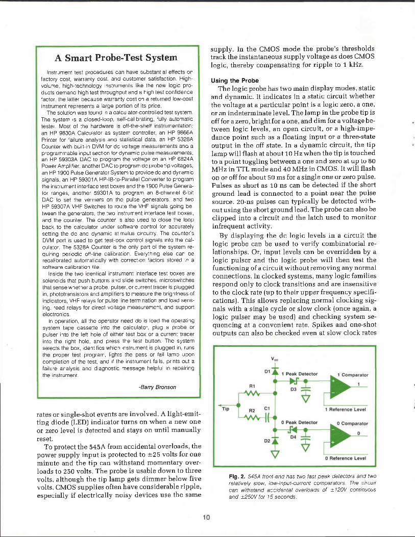
integrated circuit containing input comparators, ref-erence circuits, logic for controll ing the tip lamp andlatch LED, timing circuits, and a lamp driver for oper-at ing the lamp over a 3- to-18-vol t power supplyrange. The input signal is connected to two compara-tors through peak detectors and an external RC net-work (see Fig. 2). The peak detectors use Schottkydiodes (D3 and D4) for fast switching and make itpossible to use relatively slow, low-input-currentcomparators. Protection from input overloads is pro-vided by on-chip clamp diodes (D1 and D2) and theexternal network. R1, the dc path, allows signals upto 250 volts to be momentarily applied while R2 andC1 provide a damped bypass for fast pulses.
The logic section operates asynchronously, trig-gered by data changes at the input. The internal state,indicated by the tip lamp, and the input history sincethe last display change determine the next state. Anew zero or one signal starts a cycle that updates thedisplay, then waits 50 ms to produce a stretching ortoggling effect. The new zero or one signal also setsthe memory indicator, which stays on unti l manuallyreset. If neither a zero nor a one is present and the tim-ing cycle is complete, the logic displays a bad level(dim lamp) unti l a valid logic level arrives.
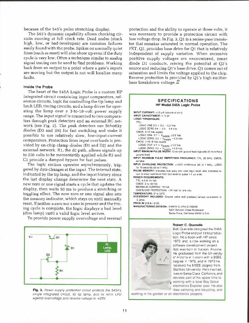
To provide power supply overvoltage and reversal
protection and the abil ity to operate at three volts, itwas necessary to provide a protection circuit withlow voltage drop. In Fig. 3, Q1 is a series-pass transis-tor that remains saturated in normal operation. TheFET, Q2, provides base drive for Q1 that is relativelyindependent of supply variation. When excessiveposi t ive supply vol tages are encountered, zenerdiode D1 conducts, ra is ing the potent ia l a t Q2'ssource and reducing Q1's base drive. Q1. comes out ofsaturation and limits the voltage applied to the chip.Reverse protection is provided by Q1's high emitter-base breakdown voltage. @
S P E C I F I C A T I O N SHP Model 545A Logic Probe
INPUT CURRENT: <15 I.,A (source or sink)INPUT CAPACITANCE: <15 oFLOGIC THRESHOLDS:
TTL:L O G I C O N E 2 0 + 0 4 , 0 2 V o cLOGIC ZERO 0 8 + 02 , -04 Vdc
C|\4OS: 3-10 Vdc supplyLOGIC ONE: 0 7 V"roolu =0.5 VdcLOGIC ZEFIO: 0.3 . V";,^;r,, .0.5 Vdc
Cl\,lOS: >10-18 VOc suppt-y'" 'L O G I C O N E : 0 7 * V s u p o t v t 1 . 0 V d cLOGIC ZERO: 0 .3 ' VsuD; tv = 1 .0 Vdc
INPUT MINIMUM PULSE WIDTH: 10 ns with ground lead (typicaily 20 ns withoutground lead)
INPUT MAXIMUM PULSE REPETITION FHEQUENCY: TTL,80 MHz; CMOS,40 MHz
INPUT OVEHLOAD PROTECTION: a12OV continuous (dc to 1 kHz); a25OVfor 1 5 seconds (dc to 1 kHz)
PULSE MEMOFY: Indicates frrst entry into vatrd togic tevel: also indicates re-turn to init ial valid level lrom bad level for oulse >1 !s wide
POWER REOUIREMENTS:TTL: 4 5 to '15 VdcC M O S : 3 t o 1 8 V d cMAXIMUM CURRENT: 70 mAOVEBLOAD PFOTECTION: t25 Vdc for one min
TEMPEBATURE: 0"to 55'CACCESSORY INCLUDED: cround cable and grabbers (ailows connection to
lC Dins)PRICE lN U.S.A. : S125MANUFACTURING DIVISION: SANTA CLAFIA DIVtStON
5301 Stevens Creek BoulevardSanta Ctara. Californta 95050 U S A
Robert C. QuenelleBob Quenelle designed the 545ALogic Probe and put i t into produc-t ion He's been with HP since1973, and is now working on asoftware development projectBob was born in Tucson, Arizona.He graduated from the University
: of Arizona at Tucson with a BSEEdegree in 1970, and in 1973 he
: received his MSEE degree fromStanford University. He's married.
r , l ives in Santa Clara, Cali fornia, and
Fig.3. Power supply ptotection circuit protects the 54SA'ssingle integrated ctrcuit, its tip lamp, and its latch LEDagainst overvoltage and reverse voltage to +25V
1 1
A Multifunction, Multifamily Logic PulserThis microprogrammed pulse generator in a probe canproduce single pulses, pulse bursfs, or pulse slreams. /fsoutput stage automatically adjusts for the type of logicbeing stimulated.
by Barry Bronson and Anthony Y. Chan
f OGIC PULSERS ARE VALUABLE too l s f o rI-.r troubleshooting digital equipment. Using a pul-
ser to inject pulses into logic nodes without cuttingtraces or removing ICs and monitoring the circuitresponse with a logic probe or clip is an effectivemethod of locating logic, connective, or componentfaul ts . The pulser produces h igh-energy, shor t -duration voltage pulses of a logic state opposite tothat of the node under stimulation.
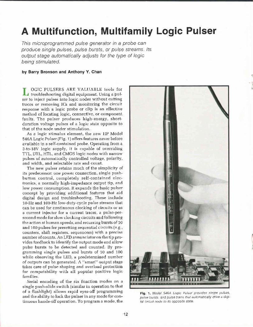
As a logic stimulus element, the new HP Model546A Logic Pulser (Fig. r) offers features never beforeavailable in a self-contained probe. Operating from a3-to-18V logic supply, it is capable of overridingTTL, DTL, HTL, and CMOS logic nodes with narrowpulses of automatically controlled voltage, polarity,and width, and selectable rate and count.
The new pulser retains much of the simplicity ofits predecessor: one power connection, single push-but ton contro l , complete ly sel f -conta ined e lec-tronics, a normally high-impedance output t ip, andlow power consumption. It expands the basic pulserconcept by providing additional features that aiddigital design and troubleshooting. These includeLO-Hz and 100-Hz low-duty-cycle pulse streams thatcan be used for continuous clocking of circuits or asa current injector for a current tracer, a pulse-per-second mode for slow clocking circuits and followingthe action at human speeds, and recurring bursts of 10and 100 pulses for presetting sequential circuits (e.g.,counters, shift registers, sequencers) with a precisenumber of counts. An LED annunciator on the tip pro-vides feedback to identify the output mode and allowpulse bursts to be detected and counted. By pro-gramming single pulses and bursts of 10 and 100while observing the LED, a predetermined numberof outputs can be generated. A "smart" output stagetakes care of pulse shaping and overload protectionfor compatabil ity with all popular positive logicfamilies.
Serial encoding of the six function modes on asingle push-slide switch (similar in operation to thatof a flashlight) allows rapid eyes-off programmingand the ability to lock the pulser in any mode for con-tinuous hands-off operation. To program a mode, the
Fig, 1. Model 5464 Logic Pulser provides single pulses,pulse bursts, and pulse trains that automatically drive a digi-tal circuit node to its opposlte stafe
12
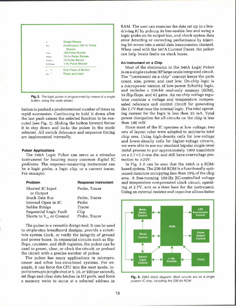
. Single PulsesCont inuous 100-Hz Pulse
Stream100-Pulse Bursts1o-Hz Pulse Stream10-Pulse Bursts1-Hz Pulse Stream
One Press of ButtonPress and Hold
Fig.2. The logic pulser is programmed by means of a singlebutton, using the code shown.
button is pushed a predetermined number of times inrapid succession. Continuing to hold it down afterthe last push causes the selected function to be exe-cuted (see Fig. 2). Sliding the button forward forcesit to stay down and locks the pulser in the modeselected. All switch debounce and sequence timingare implemented internally.
Pulser ApplicationsThe 546,t Logic Pulser can serve as a stimulus
instrument for locating many common digital ICproblems. The response-measuring instrument canbe a logic probe, a logic clip, or a current tracer.For example:
RAM. The user can examine the data set up in a bus-driving IC by pulsing its bus-enable Iine and using alogic probe on its output bus, and check system dataerror detecting or correcting performance by inject-ing bit emors into a serial data transmission channel.When used with the 547A Current Tracer, the pulsercan help locate faults on stuck buses.
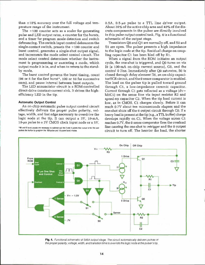
An lnstrument on a ChipMost of the electronics in the 546A Logic Pulser
is on a single custom HP large-scale integrated circuit.The "instrument on a chip" concept keeps the partscount, size, power, and cost low. On-chip logic isa micropower version of low-power Schottky logic,and includes a 256-bit read-only memory [ROM),1a fl ip-flops, and 41 gates. An on-chip voltage regu-lator contains a voltage and temperature compen-sated reference and control circuit for generatingt};.e 2.7Y that runs the internal logic. The total operat-ing current for the logic is less than 25 mA. Totalpower dissipation for all circuits on the chip is lessthan 100 mW.
Since most of the IC operates at low voltage, twosets of layout rules were adopted to minimize totalchip area. Using high-density cells for low-voltageand lower-density cells for higher-voltage circuits,we were able to use our standard bipolar single-levelmetal process to put approximately 1000 transistorson a 2.7 x3.2-mm die, and sti l l have overvoltage pro-
tection to -r25V.
In Fig. 3 it can be seen that the 546A is a ROM-based system. The 256-bit ROM is a functionally opti-mized structure occupying less than loo/o of the chiparea. A free-running 100-Hz RC-controlled voltageand temperature compensated clock circuit, operat-ing at 2.7Y, acts as a time base for the instrument.Using an external resistor and capacitor allows better
The pulser is a versatile design tool. It can be usedto single-step breadboard designs, provide a substi-tute system clock, or verify the integrity of groundand power buses. In sequential circuits such as flip-flops, counters, and shift registers, the pulser can beused to preset, clear, or clock the circuit, or preloadthe circuit with a precise number of pulses.
The pulser has many applications in micropro-cessor and other bus-structured systems. For ex-ample, it can force the CPU into the reset mode, in-ject interrupts (single shot or 1., 10, or 100 per second),set flags and clear data latches in I/O ports, and forcea memory write to occur at a selected address in
Problem
Shorted IC Inputor Output
Stuck Data BusInternal Open in ICSolder BridgeSequential Logic FaultShorts to V"" or Ground
Response Instrument
Probe, Tracer
Probe, TracerProbeTracerClipProbe, Tracer
Flg.3, 546A block diagram. Most circuits are on a singlecustom lC chip, including the 256-bit ROM
13
than -r10% accuracy over the full voltage and tem-perature range of the instrument.
The +100 counter acts as a scaler for generatingpulse and LED output rates, a counter for the bursts,and a timer for program mode detection and switchdebouncing, The switch input control debounces thesingle-contact switch, presets the +tOO counter andburst control, generates a single-shot output signal,and increments the mode select control circuit. Themode select control determines whether the instru-ment is programming or executing a mode, whichoutput mode it is in, and when to return to the stand-by mode.
The burst control governs the burst timing, count(98 or 6 for the first burst*, 100 or 10 for successiveones), and pause interval between burst outputs.
The LED annunciator circuit is a ROM-controlleddirect-drive constant-current sink. It drives the high-efficiency LED in the tip.
Automatic Output ControlAn on-chip automatic pulse output control circuit
effectively delivers the proper pulse polarity, vol-tage, width, and fast edge necessary to overdrive thelogic node at the tip. It can output a 3V, 10-mA,1O-ps pulse to a 3V CMOS clock input node or a 5V,'98 and 6 burst counts are necessary to subtract out the 2 and 4 pulses that output when the userpushes the butlon to program the 100.pulse and 1o-pulse burst modes
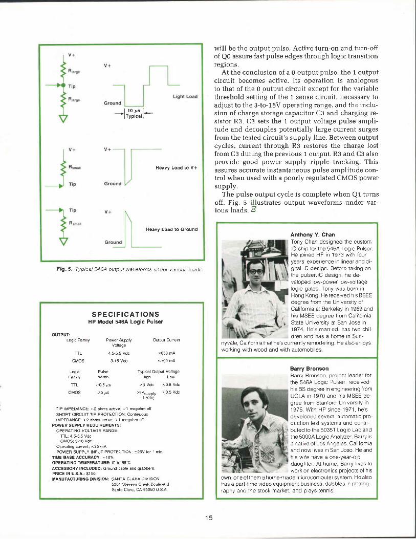
0.5A, 0.5-pcs pulse to a TTL l ine dr iver output.About ZoYoof the active chip area and +o% of the dis-crete components in the pulser are directly involvedin this pulse output control task. Fig. 4 is a functionalschematic of the output stage.
Transistors Q0 and Q1 are normally off, and S0 and51 are open. The pulser presents a high impedanceto the logic node at the tip. Residual charge on coup-ling capacitor C1 has been bled off by R1.
When a signal from the ROM initiates an outputcycle, the one-shot is triggered, and Q0 turns on viaI0 (a 100-mA on-chip current source), G0, and thecontrol 0 line. Immediately after Q0 saturates, S0 isclosed through delay element D0, an on-chip capaci-tor/SCR circuit, and the 0 sense comparator is enabled.The load on the pulser tip is pulled toward groundthrough C1, a low-impedance ceramic capacitor.Current through C1 gets reflected as a voltage (dv:IdUCI) on the sense line via input resistor R2 andspeed-up capacitor C2. When the tip load current islow, as in CMOS, C1 charges slowly. Before it canreach 0.7V about ten microseconds elapses and theone-shot shuts off the 0 output circuit through G0. If aheavy load is present at the tip (e.g., a TTL buffer) chargedevelops rapidly on C1. When the voltage across C1reaches 0.7V, the 0 sense comparator fires the overloadline causing t}te one-shot to retrigger and the 0 outputcircuit to turn off. The heavier the load, the shorter
--r-
Flg. 4. Functional schematic of 546A output stage. The circuit automatically delivers pulses otthe proper polarity, voltage, width , and transition time to override the logic node at the pulser's tip.
1 4
Heavy Load to V+
Heavy Load to Ground
-l#H'l.-
Fig.5. Typical 546A output waveforms under various loads
S P E C I F I C A T I O N SHP Model 546A Logic Pulser
OUTPUT:Logic Family Power Supply Outpul Current
Vottage
TTL 4 5-5 5 Vdc <650 mA
CMOS 3-15 Vdc <100 mA
Logic Pulse Typical Outpul VoltageFaffi ly Wdth High Low
TTL >0 5 ps >3 Vdc <0 I Vdc
CMOS >5 /rs >(Vsuppty <0 5 Vdc1 Vdc)
TIP IMPEDANCE: <2 ohms active; >1 megohm otfSHORT CIBCUIT TIP PROTECTION: ContinuousIMPEDANCE: <2 ohms active; > 1 megohm ofl
POWER SUPPLY REQUIFEMENTS:OPEFATING VOLTAGE RANGE:
TTL:4 5-5 5 VdcCMOS:3-18 Vdc
Operating current; <35 mAPOWER SUPPLY INPUT PROTECTION: t25V for '1 min
TIME BASE ACCURACY: 110%OPERATING TEMPERATURE: CI" Io 55.CACCESSORY INCLUDED: Ground cable and grabbersPRICE lN U.S.A. : $150MANUFACTURING DIVISION: SANTA CLARA DIVISION
5301 Stevens Creek BoulevardSanta Clara, CA 95050 U S A
will be the output pulse. Active turn-on and turn-offof Q0 assure fast pulse edges through logic transitionregions.
At the conclusion of a 0 output pulse, the 1 outputcircuit becomes active. Its operation is analogousto that of the 0 ,output circuit except for the variablethreshold setting of the 1 sense circuit, necessary toadjust to the 3-to-18V operating range, and the inclu-sion of charge storage capacitor C3 and charging re-sistor R3. C3 sets the 1 output voltage pulse ampli-tude and decouples potentially large current surgesfrom the tested circuit's supply line. Between outputcycles, current through R3 restores the charge lostfrom C3 during the previous L output. R3 and C3 alsoprovide good power supply ripple tracking. Thisassures accurate instantaneous pulse amplitude con-trol when used with a poorly regulated CMOS powersupply.
The pulse output cycle is complete when Q1 turnsoff. Fig. 5 il lustrates output waveforms under var-ious lo-"ads. g
Anthony Y. ChanTony Chan designed the customlC chip for the 546A Logic PulserHe joined HP in 1973 with fouryears'experience rn l inear and di-gital lC design, Before taking onthe pulser. lC design, he de-veloped low-power low-voltagelogic gates Tony was born inHong Kong He received his BSEEdegree from the University ofCali fornia at Berkeley in 1969 andhis MSEE degree from Cali forniastate university at Sar Jose in1974 He's married, has two chi l-dren and has a home in Sun-
nyvale, Cali fornia that he's currently remodeling He also enjoysworking with wood and with automobiles
Barry BronsonBarry Bronson, project leader forthe 5464 Logic Pulser, receivedhis BS degree in engineering f romUCLA in 1970 and h is MSEE de-gree from Stanford University in1975 Wi th HP s ince 1971, he 'sdeveloped several automatic pro-duction test systems and contr i-buted to the 5035T Logic Lab andthe 50004 Logic Analyzer Barry isa native of Los Angeles, Cali forniaand now l ives in San Jose He andhis wife have a one-year-olddaughter At home, Barry l ikes towork on electronics projects ol his
own, oneof them ahome-made microcomputersystem Healsohas a part t ime video equipment business, dabbles in photog-raphy and the stock market. and plays tennis
1 5
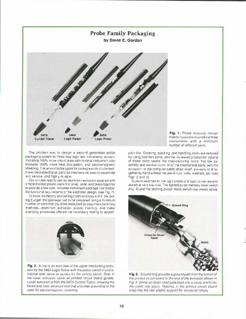
Probe Family Packagingby David E. Gordon
Current Tracer545A
Logic Pulser
The problem was to design a second generation probepackaging system for three new logic test instruments, accom-modating 100% more circuit area with minimal instrument sizeincrease, 20O"/" more heat dissipation, and electromagneticshielding The amount to be spent for tool ing was str ict ly l imitedIt was desirable that al l parts be inexpensive, easy to assembleand service, and highly rel iable,
Our solut ion was to use an aluminum extrusion coupled withsimple molded plast ic parts that snap, sl ide, and press togetherto provide a low cost, versati le instrument package that meetsthe functional requirements of the electronic design (see Fig 1)
To have low factory and sel l ing costs and stay within the tool-ing budget, the package had to be designed using a minimumnumber of parts that could be produced by easy manufacturingmethods-a luminum ex t rus ion , p las t i c mo ld ing , and meta lstamping processes offered the necessary tool ing to accom-
Fig.2. At top is an end view of the upper interlocking extru-sion for the 5464 Logic Pulser with the pulser switch in placelnternal s/ols serye as guldes for the sliding swrich S/ots rnthe lower extrusion serve as printed circuit board guidesLower extrusion is from the 547A Current Tracer, showing thefaced and clear alodined end that provides grounding of thecase for electrcmagnetic shielding
Fig. 1. Probe housing designmakes it posstble to Droduce threeinstruments with a minimumnumber of different patts
pl ish this Ordering, stocking, and handling costs are reducedby using common parts, and the increased production volumeof those parts lowers the manufacturing costs For low as-sembly and service costs, al l of the mechanical parts, with theexception of the crimp-on cable strain rel ief, are easy to f i t lo-gether by hand without the use of nuts, bolts, washers, etc (seeFigs 2 and 3)
Custom switches for the logic probe and logic pulser are pro-duced at very low cost The l ighted pulse memory reset switch(Fig 4) and the latching pulser mode swrtch use plast ic actua-
Fig.S. Ground ring provides a ground path from the bottom ofthe printed crrcuit board to the end of the extrusion shown inFig 2 Crimp-on strain relief pulls back into a cavity and locksthe cable into place Notches in the printed circuit boardsnap into the rear plastic support for structural ridigity
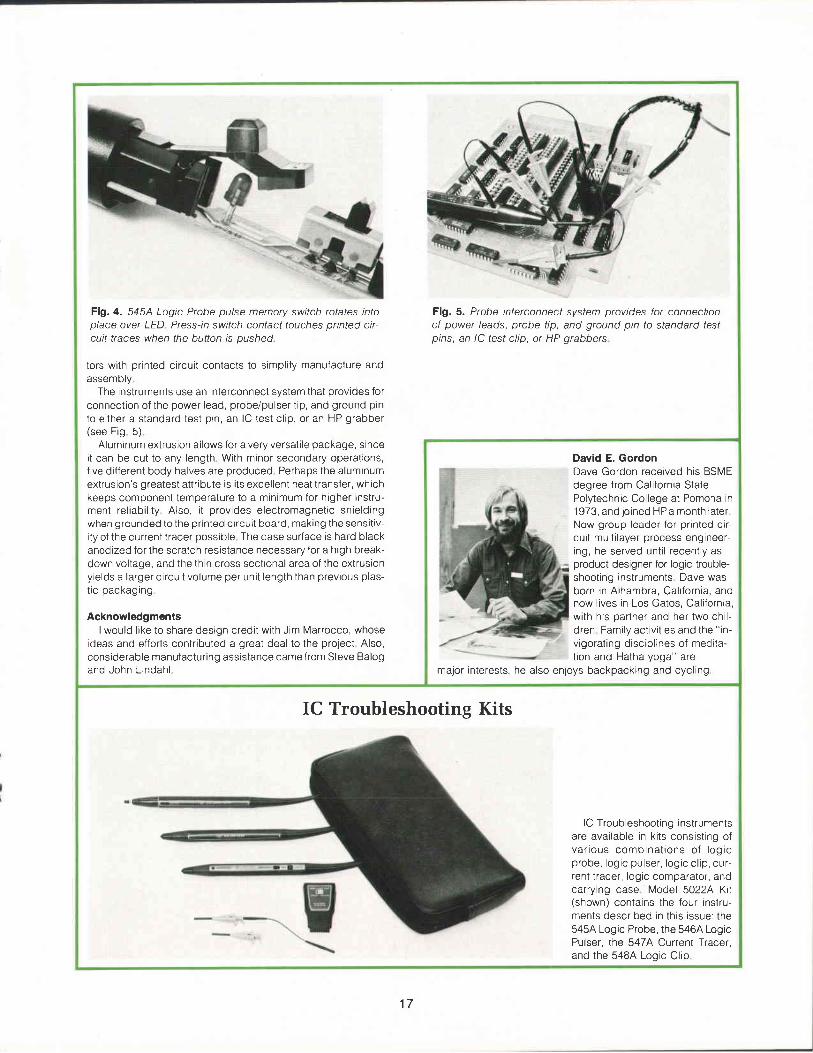
Fig.4- 545A Logic Probe pulse memory switch rotates intoplace over LED Press-in switch contact touches printed cir-cuit traces when the button is pushed
tors with printed circuit contacts to simpli fy manufacture andassemory
The instruments use an interconnect system that provides forconnection of the power lead, probe/pulser t ip, and ground pinto either a standard test pin, an lC test cl ip, or an HP grabber(see Fig 5)
Aluminum extrusion al lows for a very versatr le package, sinceit can be cut to any length With minor secondary operations,f ive dif ferent body halves are produced Perhaps the aluminumextrusion's greatest attr ibute is i ts excel lent heat transfer, whichkeeps component temperature to a minimum for higher rnstru-ment rel iabi l i ty Also, i t provides electromagnetic shieldingwhen grounded to the printed circuit board, making the sensit iv-i ty of the current tracer possible The case surface is hard blackanodized for the scratch resistance necessary for a high break-down voltage, and the thin cross sectional area of the extrusionyields a larger circuit volume per unit length than previous plas-t ic packaging
AcknowledgmentsI would l ike to share design credit with Jim Marrocco, whose
ideas and efforts contributed a great deal to the project Also,considerable manufacturing assistance came from Steve Balogand John Lindahl
Fig.5. Probe interconnect system provides for connectionof power leads, probe tip, and ground pin to standard testpins, an lC test clip, or HP grabbers
David E. GordonDave Gordon received his BSMEdegree from California StatePolytechnic College at Pomola in1973, and joined HP a month laterNow group leader for printed circuit mult i layer process engineer-ing, he served unti l recently asproduct designer for logic trouble-shooting instruments Dave wasborn in Alhambra, Cali fornia, andnow l ives in Los Gatos, Cali fornia,with his oartner and her two chi l-dren Family act ivi t ies and the " in-vigorating drscipl ines of medita-t ion and Hatha yoga" are
major interests; he also enjoys backpacking and cycl ing
IC Troubleshooting Kits
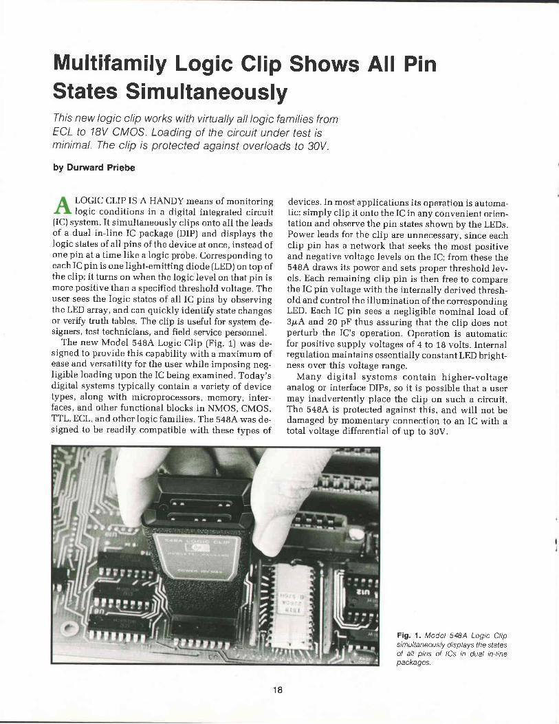
lC Troubleshooting instrumentsare avai lable in kits consist ing ofv a r i o u s c o m b i n a t i o n s o f l o g i cprobe, logic pulser, logic cl ip, cur-rent tracer, logic comparator, andcarrying case Model 50224 Kit(shown) contains the four instru-ments described in this issue: the545A Logic Probe, the 5464 LogicPulser, the 5474 Current Tracer,and the 5484 Logic Clip
1 7
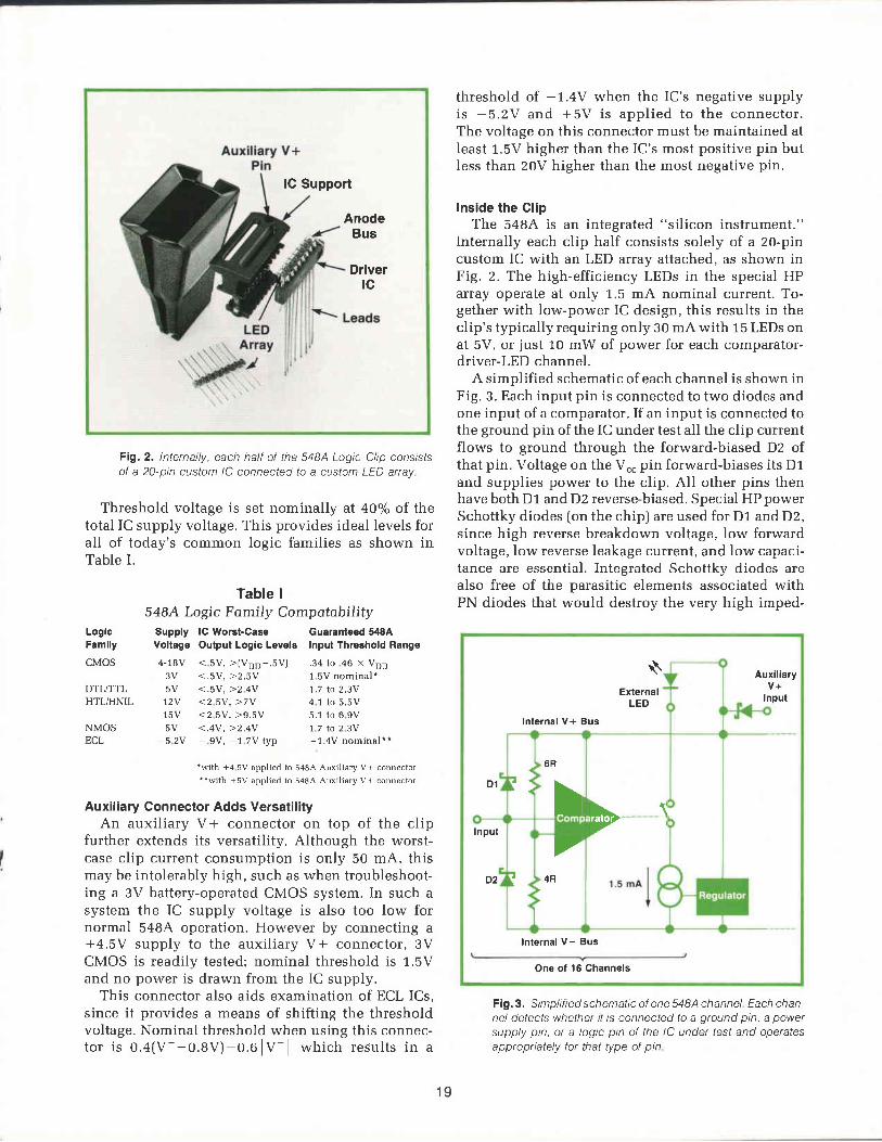
Multifamily Logic Clip Shows All PinStates SimultaneouslyThis new logic clip works with virtually all logic families fromECL to 1BV CMOS. Loading of the circuit under fesf rsminimal. The clip is protected against overloads to 30V.
by Durward Priebe
LOGIC CLIP IS A HANDY means of monitoringlogic conditions in a digital integrated circuit
[IC) system. It simultaneously clips onto all the leadsof a dual in-l ine IC package (DIP) and displays thelogic states of all pins of the device at once, instead ofone pin at a time like a logic probe. Corresponding toeach IC pin is one light-emitting diode (LED) on top ofthe clip; it turns on when the logic level on that pin ismore positive than a specified threshold voltage. Theuser sees the logic states of all IC pins by observingthe LED array, and can quickly identify state changesor verify truth tables. The clip is useful for system de-signers, test technicians, and field service personnel.
The new Model 548A Logic Cl ip (F ig. 1) was de-signed to provide this capabil ity with a maximum ofease and versati l i ty for the user while imposing neg-ligible loading upon the IC being examined. Today'sdigital systems typically contain a variety of devicetypes, along with microprocessors, memory, inter-faces, and other functional blocks in NMOS. CMOS.TTL, ECL, and other logic families. The 548A was de-signed to be readily compatible with these types of
devices. In most applications its operation is automa-tic; simply clip it onto the IC in any convenient orien-tation and observe the pin states shown by the LEDs.Power leads for the clip are unnecessary, since eachclip pin has a network that seeks the most positiveand negative voltage levels on the IC; from these the5484, draws its power and sets proper threshold lev-els. Each remaining clip pin is then free to comparethe IC pin voltage with the internally derived thresh-old and control the i l lumination of the correspondingLED. Each IC pin sees a negligible nominal load of3g,A and 20 pF thus assuring that the clip does notperturb the IC's operation, Operation is automaticfor positive supply voltages of 4 to 18 volts. Internalregulation maintains essentially constant LED bright-ness over this voltage range.
Many d ig i ta l systems conta in h igher-vol tageanalog or interface DIPs, so it is possible that a usermay inadvertently place the clip on such a circuit.The 548,{ is protected against this, and wil l not bedamaged by momentary connection to an IC with atotal voltage differential of up to 30V.
Fig. 1. Model 548/. Logic Clipsimu ltaneou sly d i spl ays lhe slatesof all pins of lCs in dual in-linepackages.
1 8
lC Support
AnodeBus
Drivertc
Fig,2. lnternally, each half of the 54BA Logic C/lp consr,stsof a 20-pin custom lC connected to a custom LED array
Threshold voltage is set nominally at 40% of thetotal IC supply voltage. This provides ideal levels forall of today's common logic families as shown inTable I.
Table I548A Logic Fomily Compatobility
Loglc Supply lC Worst-Case Guaranteed 548AFamlly Voltage Output Logic Levels Input Threshold Range
CMOS 4-18V < 5V, >(VDD-.sV) .34 to 46 x VDD
threshold of -t.qV when the IC's negative supplyi s -5 .2V and +5V i s app l i ed t o t he connec to r .The voltage on this connector must be maintained atleast 1.5V higher than the IC's most positive pin butless than 20V higher than the most negative pin.
Inside the ClipThe 548A is an integrated "sil icon instrument."
Internally each clip half consists solely of a 20-pincustom IC with an LED array attached, as shown inFig. 2. The high-efficiency LEDs in the special HParray operate at only 1.5 mA nominal current. To-gether with low-power IC design, this results in theclip's typically requiring only 30 mA with 15 LEDs onat 5V, or just 10 mW of power for each comparator-driver-LED channel.
A simplif ied schematic of each channel is shown inFig. 3. Each input pin is connected to two diodes andone input of a comparator. If an input is connected tothe ground pin of the IC under test all the clip currentflows to ground through the forward-biased D2 ofthat pin. Voltage on the V"" pin forward-biases its D1and supplies power to the clip. All other pins thenhave both D1 and D2 reverse-biased. Special HP powerSchottky diodes (on the chip) are used for D1 and D2,since high reverse breakdown voltage, low forwardvoltage, low reverse leakage current, and low capaci-tance are essential. Integrated Schottky diodes arealso free of the parasitic elements associated withPN diodes that would destroy the very high imped-
*
ExternalLED
lnternal V+ Bus
Au
D1
Input
D2
t <\ -
6R
I E, 1I\
74R
lnternal V- Bus
uxi l iaryV +
Input
One of 15 Channels
Fig.3, Simplified schematic of one 548A channel Each chan-nel detects whether it ts connected to a ground pin, a powersupply pin, or a logic pin of the lC under test and operatesappropriately for that type of pin
3v < .5v , >2 .5vDTL/TTL 5V <.5V, >2 4VHTL/HNIL 1.2V <2 5V, >7V
1.5V nominal*7 .7 t o 2 .3V4 1 to 5.5V
1 5 V < 2 5 V , > 9 . 5 V 5 . 1 t o 6 9 V
NMOS 5V < .4V, >2 .4V ' t 7 Io 2 3VECL -5 2V - 9V, -1 7V tvD -1 .4V nomina l * *
*with +4 5V applied to 548,4 Auxil iary V+ connector**with +5V applied to 548A Auxil iary V+ connector
Auxil iary Connector Adds Versati l i tyAn auxi l iary V* connector on top of the c l ip
further extends its versati l i ty. Although the worst-case clip current consumption is only 50 mA, thismay be intolerably high, such as when troubleshoot-ing a 3V battery-operated CMOS system. In such asystem the IC supply voltage is also too low fornormal 548,\ operation. However by connecting a+4.5V supply to the auxi l iary V* connector , 3VCMOS is readily tested; nominal threshold is 1.5Vand no power is drawn from the IC supply.
This connector also aids examination of ECL ICs,since it provides a means of shift ing the thresholdvoltage. Nominal threshold when using this connec-t o r i s 0 . 4 ( V + - 0 . 8 V ) - 0 . 6 1 V - l w h i c h r e s u l t s i n a
1 9
ance of each input pin. The comparator input biascurrent plus the leakage currents of Dt and D2 sum toa typical 3p,A input current; 15pA is the guaranteedmaximum. The reference input of the comparator isconnected to a resistor divider across the internalsupply buses, while a regulator maintains constantLED current over the broad operating supply voltagerange.
Using the ClipThe clip can be used on standard DIPs with 8, 14, or
16 pins. To accommodate packages with more pinsit 's usually a simple matter to wire the signal l ines ofinterest to a 16-pin dummy IC package added to thebreadboard or printed circuit card. To make it usefulon printed circuit boards with a high density of ICs orin cramped locations, the clip is physically small; i t is
AcknowledgmentsThe job of designing "si l icon instruments" requires the mara-
thon effort of many people We would l ike to thank the lC layoutstaff for their help in designing the world's most complex j igsawpuzzles and the lC department for their help in bui lding them (in-c lud ing tes t ing and " f ind ing mrss ing p ieces" ! ) These twogroups helped accomplish dif f icult design goals and madethese instruments possible HP's Optoelectronics Division pro-vlded the innovative LED array for the logic cl ip We would alsol ike to thank Roger Smith, group leader, and Gary Gordon, sec-t ion Manager, for their contnbutions and guidance Pete Le-Mmon was instrumental in the development of the automatic testsystem Lou deGive helped develop the manufacturing tech-nology for the 547A current sensing t ip Roy Criswell and MikeYarbrough coordinated development act ivi t ies with the rest ofHP, and Bruce Hanson was our marketino consultanl
-John Beckwith-Barry Bronson-Anthony Chan-Durward Priebe-Robert Quenelle
S P E C I F I C A T I O N SHP Model 548A Logic Clip
INPUT CURRENT: < i15FA per p inINPUT THFESHOLD: >(40 t 06) x supply voltage : logic high (eg at 5V
supply, LED is guaranteed to be otf below 1 7V and on above 2 3V)INPUT PROTECTION: 30 Vdc lor one minuteINPUT VOLTAGE RANGE: 0-18 VdcPOWER SUPPLY REQUIREMENTS:
VOLTAGE:4-18 Vdc across any two p insCURRENT: <50 mA wi th 15 LEDS onAUXIL IARYSUPPLYVOLTAGE:4 5 to20Vdcapp l ied toconnec lo r Supp lymust
be >1 5 Vdc more positive than any pin ol lC under testTEMPERATUBE: CPC to 55"CACCESSOBY INCLUDED: Auxil iary power cable and grabberPRICE lN U.S.A: $105MANUFACTURING DIVISION: SANTA CLAFA DIVISION
5301 Stevens Creek BoulevardSanta Clara. California 95050 U S A
3.8 cm long and extends only 5.1 cm above the ICbeing examined. The LEDs are arranged in two rowsof g with 0.1 in (2.54 mm) spacing between LEDs, and0.3 in (7.62 mm) between rows. The LEDs are inten-tionally unnumbered to eliminate the confusion ofthe three sets of pin numbers that would be necessaryfor B, 14, and 16-pin devices. Reliable electrical con-tact to the IC is assured through the use of gold-platedberyll ium-copper contacts.
For convenience the clip may be oriented on the ICwith the auxil iary V + connector at the pin 1 end. Thisserves as a reminder of the location of the referencepin since the top of the IC is hidden from view by thecl ip .
To verify an IC's truth table the system clock mustbe made slow enough to allow recognition of eachstate. This is readily accomplished by disabling theclock and advancing it with the single pulse, L-Hz, orLO-Hz modes of the 546.4, Logic Pulser. At clock ratesabove 2OHz the clip provides some duty cycle infor-mation and indicates dynamic pin activity by LEDbr ightness changes.0
Durward PriebeDunivard Priebe has been design-ing integrated circuits for 1 1 years.With HP since 1973, he's servedas an lC consultant, most recentlyon the 5454, 5464, and 5474probe designs, and designed the5484 Logic Clip He's authoredseveral art icles on lCs in technicalpubl icat ions. Durward was born inMelrose Park, l l l inois and attendedCali fornia Polytechnic College ato ^ ^ | . , i ^ n L r ^ - ^ ^ - ^ ! ,
. . . San Luis Obispo, graduating in\ 1965 with a BS degree in elec-
tronrc engineering He and hiswifehave two chi ldren. l ive in Sunnv-
vale, Cali fornia, and take great pride in doing most things them-selves Their concern for their ci ty occasional ly results in Dur-ward's representing his neighborhood at ci ty counci l meetings,Among Durward's other interests are taping local concens,astronomy, ornamental welding, sarl ing, and photography
CorrectionsA typo0raphical etror occurred in the equation given as an example ol the printout modes forthe HP-91 Calculator in last month's issue of the Hewlett-Packard Journat, paoe 10 Theequation, for the length (L) of a belt connecting two pulleys, should be:
L : r d z + ( d 2 - d 1 ) ( t a n , l , - 0 )
It should also be noted that the equation is valid only tor d2>d1
Part of one of the references given with the article 0n the Hp Model 47201A oximeter in theOctober issue was inadvertently 0mitted Reterence number 9 should be:H Poppius and AA Vil janen, "Non-lnvasive Measurement of oxygen Saturation duringExercise in Patients with Pulmonary Disease," XXVII Nordiske Lungelege Kongress,oslo,Nomay, 13-15 June 1976
The first equation grven 0n page 5 ol the same article should be: | : In10-Kcd
20
Intertacing a Parallel-Mode Logic StateAnalyzer to Serial DataA new serial-to-parallel converter enables a parallel-modelogic state analyzer to work with serial data so the analyzer'stabular display and versatile triggering can be used fortracing data flow in serial data sysfems.
by Justin S. Morrill, Jr.
q INCE THEIR INTRODUCTION three years ago,U logic state analyzers have become well estab-
lished as indispensable tools for troubleshooting di-gital systems. By capturing a sequence of digitalwords appearing on a data bus or other multinodallocation, and displaying the sequence as a table ofbinary words, logic-state analyzers enable the user totrace data flow and thus track down problems in his
system.These instruments were designed to work with
parallel information (all bits of each word appearingsimultaneously on parallel l ines). Much digital activ-ity, however, occurs serially (bits occurring sequen-tially on a single l ine). For example, many calculatorsoperate serially, and data is transmitted over phonelines in serial form. Furthermore, many parallel-
Fig. 1. Model 102544 Serial-to-Parallel Converter (lower unit) in-terfaces Model 16004 Logic StateAnalyzer (upper unit)to serial datastreams so serial data flow occur-ring at a node or. on a bus can bepresented as a table of binarywords on the logic analyzer's dis-play The usefulness of this in-strument combination for produc-tron tesl ls enhanced by the Model102534 Card Reader (lower right)tha t enab les da ta sequencesmarked on cards to be stored inthe logic state analyzer, bn-by-bttdifferences between the storedsequence and actual data t lowthen appear as brightened 1's onthe right half of the display
21
mode digital systems perform some operations se-rially, such as at I/O interfaces for disc memories andteletypewriter consoles.
A new serial-to-parallel converter now makes itpossible to use the measurement capabil it ies of HP'sModel 1600A and t00zA Logic State Analyzers forthe ser ia l data domain. This accessory, Model7O254A, accepts data in serial form and formats it intoa parallel word for presentation as one line on thelogic state analyzer's tabular display (Fig. f). fust aswith parallel data, the logic state analyzer can be set tocapture and display the data sequence beginningwith a particular word, or data leading up to the word,or data at some point downstream from the word,enabling the user to search out and find the part of theprogram where malfunctions occur.
Applicable too are all the other operating modes ofthe 16004/1607A Logic State Analyzers (halt whenthe captured sequence differs from a previouslystored sequence; indicate bit-by-bit differences be-tween captured and stored sequences, etc.).1 Whenthe 1600A and TOOZA are both used at the same timewith the 1.O254A Serial-to-Parallel Converter, bothserial and parallel data, such as that occurring on bothsides of an I/O interface, can be displayed side by sidein two tables on the 16004 display.
What lt DoesThe heart of the Model 7o2s4{ Serial-to-Parallel
Converter is a bidirectional shift register that isloaded with the serial data. The parallel outputs of theregister are applied to the inputs of the logic stateanalyzer, and when a clock counter indicates that a
--...-
full byte has been loaded into the shift register, a clockpulse is sent to the logic state analyzer. The clockpulse causes the byte to be stored in the analyzer'smemory where it becomes available for display as oneline on the analyzer's CRT.
Designed-in flexibility enables the converter to beused for a wide variety of applications. For example,the shift register is bidirectional so serial data can beloaded in either direction. This gives the user a choiceof having the first bit appear in the most significantposition (LEFT) on the analyzer's display, or in theleast significant position (RIGHT), whichever is easierfor him to interpret.
The length of each byte can be selected to be any-where from 1 to 16 bits by the BrTS/BvTE selectorswitch. Words longer than 16 bits are handled as twoor more sequential bytes.
The data stream bit that is to be loaded into the shiftregister as the first bit can be determined in a numberof ways. Frequently, a sync or framing pulse is avail-able somewhere in the machine being tested. Thispulse can be used to init iate loading of the datastream. If, however, the desired data occurs some timeafter the sync pulse-say following a preamble andaddress-the BITS AFTER syNc selector can be used todelay data loading for a predetermined number of bits(up to 99) after the sync pulse.
If, on the other hand, no separate sync pulse isavailable, the syNc sEARCH mode can be used in con-junction with the pattern recognition capabilities ofthe logic state analyzer. In this mode, the serial sys-tem clock pulses are sent to the logic state analyzercontinuously, causing it to read the contents of the
ToLogicStateAnalyzer
Fig.2. Simplified block diagram of Model 1O254A Seriallo-Parallel Converter Serial-to-parallelconversion occurs in the shift register The other blocks control the timing and direction of shift
register loading and the timing of data transfer to the logic state analyzer
22
1o254A shift register each time a new bit is entered.When the register contents match the digital word setup on the analyzer's TRIGGER wonn switches, the re-sulting trigger is sent to the serial-to-parallel conver-ter, causing it to revert to normal operation. Clockpulses are then sent to the logic state analyzer onlywhen a complete new byte is entered, as determinedby the setting of the BITS/BYTE switch. Initiation ofnormal byte transfer, however, can be delayed pastthe trigger eventby any number of bits up to 99 by useof the BITS AFTER svNc delay selector.
By use of the nnray selector switch in the logic stateana lyzer , the da ta d isp layed can be moveddownstream from the trigger event. The nrlay selec-tor determines the number of bytes (up to 99,999) thatmust occur after the trigger event before display of thedata sequence starts. It is thus possible to go far into aserial word and precisely locate and capture data fordisplay.
Selective StoreThe data transferred to the logic state analyzer can
also be qualified by the BvTES/SvNC selector to com-press the amount of data stored for display. Thisswitch selects the number of bytes transferred follow-ing each sync pulse. For example, if only the two1 6-bit bytes that occur 27 bits after sync are of interest,the nyrnstsylc selector is set to 2, the nrTs/nyrn selec-tor is set to 16, and the BITS AFTER S.aNC is set to 27.Then only those two bytes, out of possibly manyserial words, would be captured for display.
Further qualification of the data stored for examina-tion can be obtained by use of the two qualifier selec-tor switches on the Iogic state analyzer. Two qualifierinputs are provided on the serial-to-parallel conver-ter's input probe and these inputs are latched throughthe converter to the analyzer. Bytes will not be storedin the analyzer unless these inputs match the settingsof the switches (1, 0, or DoN'T cARE), enabling furtherselectivity in the data captured for storage.
Technical DetailsA block diagram ofthe serial-to-parallel converter
is shown in Fig. 2. Inputs are by way of the same typeof six-probe pod used with the Models 1600A and1607A Logic State Analyzers. Besides the data input,there is a sync input, two qualifier inputs, and twoclock inputs (OR'd internally into a single clock in-put). The pod has level-sensing circuits that decidewhether the voltage sensed by each probe is a 1 or a 0.The threshold level, variable over a range of -r10 V, isset by the controls on the logic state analyzer.
An operating feature that was considered ofparamount importance was that the data supplied tothe logic state analyzer should always be justified tothe right. This is because the logic state analyzer
column-blanking control, which allows the user toblank out unused columns when bytes are less than16 bits. starts on the leftmost column and blanks col-umns successively towards the right. This causes noproblem when the first bit in a serial data stream is tobe in the leftmost column. Data is entered at theright-hand input of the shift register and stepped tothe left with each clock pulse until the complete byteis in the register and the byte is transferred to the logicstate analyzer.
When the first bit is to be in the rightmost column,however, the data must be entered at a point in theshift register corresponding to the length of the byte,then stepped to the right. With reference to the diag-ram of Fig. 3, an example will show how this works.Suppose each byte is to have 7 bits. The slrsmvrnswitch then sets up the selector gates such that the
Conirol forRighULett
B i t 7 6 5 4 3 2 1 0
To Logic State Analyzer
Fig. 3. Bl ock d i a gr am of p ar t of the bi d i r ecti on al s hi ft r eg i ster.U1 and U2 are commercial lC 4-bit shift reglsters (U3 is thenext lC in the 16-bit shift tegistet chain) The selector gatesenable serial data to be loaded through any bit position duringright-shift operation (see text)
23

data stream is routed to the parallel input of the shiftregister that is 7 units from the right-hand end, in thiscase input C of UZ. At the same time, U2's paralleloutput QC is routed back through the selector gates toparallel input B, and QB is routed to A.
Each clock pulse loads U2 in parallel, hence the bit
S P E C I F I C A T I O N SHP Model 10254A Serial-to-Parallel Converter
Requires an HP Model 1600A o|1607A Logic-State Analyzer to torm completemeasurement unit; uss data probe supplied with logic state analyzer as inputdevice
DISPLAY FORMATEITS/BYTE: 1 to 16 (displayed as one line on logic-state analyzer)FIRST BIT (LEFT/RIGHT): tomats displayed data with mGt signiticant bit lettor nght
DATA SYNCPATTERN: synchronizes on digital panern within serial dala stream: pattern isselected by logic state analyzer's TRIGGER WORO switchesSYNC SEARCH: pushbutlon or positive-gc,ing pulse (5V max) initiates search forpattern syncEDGE: synchronizes on input probe sync signal with positiv€ or negative edgesel6tableDELAY (BITS AFTER SYNC): selects number of clock pulses (0 to 99) betweensync signal and slarl of dala acquisilionBYTES/SYNC: acquires 1 to 16 bytes between sync pulses tor display.
PROBEREPETITION RATE: <10 MHz in EDGE sync; <7 MHz in PATTERN syncINPUT RC:40 kO shunted by <14 pF at probe tipINPUT THRESHOLO: t10 V dc selected at logic state analyzer.MINIMUM PULSE WIDTH: 40 ns at thresholdSETUPTIME: 50 ns (minimum time data mustbe presenl priortoclocktransition)HOLD TIME:0 ns (minimumtimedata must be presenl tollowing clocktransition)SYNC OQCUFRENCE: 60 ns (minimum time sync edge must precede clocktransition correspdding to firsl data bit)
GENERALPOWER: supplied by 1600A or 16074 logic state analyzer through intercon-necting data cableSIZE:284mm W x 121mm H x 414mm D (11-3 /16 x 4y4 x 5 /16 inches)WEIGHT: 3 2 kg (7 lb )
PRICE lN U.S,A.: '102544, $975 Note: data probe not supplied; uss data probe
lrom 16004 or 1607A L€ic State AnalyzerMANUFACTURING DIVISION: COLORADO SPRINGS DIVISION
1900 Garden of the Gods Boad,Colorado Springs, Colorado 80907 U S A
Hewlett-Packard Company, 1501 Page MillRoad, Palo Alto, California 943O4
in each stage of U2 is loaded into the adjacent stage tothe right. The last stage output, QA, goes to the leftinput L of U1 where it is stepped to the right in thenormal right-shift fashion. Thus, after seven clockpulses, the first bit loaded into C of Uz is in stage A ofU1, the bit 0 position. The byte is thus right justifiedwhen it is transferred to the logic state analyzer.
AcknowledgmentsInitial product definition was by |eff Smith and
many ideas were contributed by section manager BillFarnbach. Product design was by Roger Molnar.O
Reference1. C.T . Smal l and I .S . Mor r i l l , f r . , "The Log ic S ta teAnalyzer, a Viewing Port for the Data Domain," Hewlett-Packard fournal, August 1975.
Justin S. Morrill, Jr.A native of Houston, Texas, JustinMorri l l attended Rice Universitythere, earning a Bachelor of Artsdegree in Science and Engineer-ing and a Master of Electrical En-gineering He then joinedHewlett-Packard (1 972), initiallyworking on an investigative projectinvolving storage CRTs, then onthe 16004/16074 Logic StateAnalyzers. Since then, he hasbeen designing accessories forthe 16004/16074 (card reader,serial-to-parallel converter,probes) When avai lable t ime
coincides with good snow conditions, Justin enjoys cross-country ski ing. Othenvise, he goes cross-country in his four-wheel-drive vehicle He also does some hiking and backpack-ing He and his wife have one son, 3
3257 '7 } ,AAA IZEHCAI{AA4
FFnXd*ff^N*AtLY
CHAN G E OF A D D R ESS :*"Til::#Jf'"*i:-1::i"i:,',Tffifi#i""""JffiiiTi$:[T"^",iJ'"5,:?il"1t3:ff:f:il$,iSiliJ]

HP Archive
This vintage Hewlett-Packard document was preserved and distributed by
www.hparchive.com
Please visit us on the web!
On-line curator: John Miles, KE5FX