A Functional Approach to Testing Bit-Sliced Microprocessors
9
IEEE TRANSACTIONS ON COMPUTERS, VOL. C-30, NO. 8, AUGUST 1981 A Functional Approach to Testing Bit-Sliced Microprocessors THIRUMALAI SRIDHAR, STUDENT MEMBER, IEEE, AND JOHN P. HAYES, SENIOR MEMBER, IEEE Abstract-Bit-sliced microprocessors are representative of an important class of LSI components that can be interconnected in a regular way to construct many useful types of digital systems. This paper develops an analytic test generation methodology for bit-sliced systems. A formal model C for a 1-bit bit-sliced microprocessor is defined which has the main features of many commercially available microprocessors. Using a functional fault model instead of the usual stuck-line fault model, a technique is presented for deriving a complete and near-minimal sequence of tests for C. The basic cell C is extended to form two more general cells Ck and Ck.n. Ck is a k-bit version of C, while Ck,n is Ck with an n X k-bit scratchpad RAM. The internal structure of C4,16 closely resembles that of the AMD 2901 processor slice. Test sequences for these cells are derived in much the same way as for C. It is shown that the test sequence for a single cell (C, Ck, or Ck,n) can easily be extended to a test sequence for an array of N identical cells with no increase in the number of tests required. It is observed that for test generation purposes, bit-sliced microprocessors can be viewed as C-testable iterative logic arrays, which require a constant number of test patterns independent of array size. Some new results on test generation for C-testable systems are presented, as well as a method for modifying iterative logic arrays to make them C- testable. Index Terms-Bit-sliced processors, fault modeling, iterative logic arrays, microprocessors, testability, test generation. I. INTRODUCTION I T IS well known that traditional approaches to test pattern generation are becoming increasingly inadequate when applied to digital systems containing LSI and VLSI compo- nents. Conventional testing methods have two serious limita- tions: 1) they only recognize low-level devices such as gates and flip-flops as primitive elements, and 2) they use low-level fault models such as the line stuck-at-zero/one (s-a-0/1) model, which associates faults with all lines interconnecting the primitive elements. In systems containing tens of thousands of gates and lines, the amount of computation required to construct a comprehensive test set can be enormous. Fur- thermore, a gate-level description of the system components may be unavailable to the test designers. Manufacturers of devices such as microprocessors often only supply designers with register or function-level circuit diagrams. Relatively little work has been done on function-level testing Manuscript received August 6, 1979; revised February 18, 1981. This paper was supported by the U.S. Air Force Office of Scientific Research under Grant AFOSR-77-3352, the Joint Services Electronics Program under Contract F44620-76-C-0061, and a Graduate Fellowship from the IBM Corpora- tion. The authors are with the Department of Electrical Engineering, University of Southern California, Los Angeles, CA 90007. methods [1]- [3] which are applicable to LSI elements like microprocessors. Heuristic test generation is usually employed for these circuits. Such methods yield very large test sets, e.g., 106 test patterns for an 8080 [3], while a microprocessor of the type considered here (the 2901) was found to require about 12 500 test patterns [2]. In this paper we attempt to develop efficient functional test generation procedures for bit-sliced microprocessors and re- lated devices. Bit slicing provides a structural regularity in the system design which is known to facilitate fault diagnosis. The heuristic testing schemes used in practice do not guarantee complete fault detection [2], [3]. Furthermore, as is demon- strated here, they may yield far more tests than are necessary. Our goal is to construct systematic test generation methods which yield test sequences that are complete and of near- minimal length. The first limitation of the conventional test generation methods noted above is avoided by treating relatively complex functional units such as registers and multiplexers as primi- tives. The second is avoided by testing the primitive compo- nents for functional failures; faults affecting their internal lines are not explicitly considered. Finally, the regular intercon- nection structure of bit-sliced systems is exploited so that tests for an array of bit slices can be derived directly from the test set of a single slice. We show that bit-sliced microprocessors can be modeled in a natural way as iterative logic arrays that require a constant number of tests independent of array size; such arrays have been called C-testable [1 0], where C stands for constant. Our analysis also yields some methods for mod- ifying bit slices to increase their testability. II. BIT-SLICED MICROPROCESSORS A device U performing a set of operations on n-bit operands is said to be bit-sliced if a system that performs the same set of operations on Nn-bit operands can be constructed by in- terconnecting N copies of U in a regular way. The basic device U is called a cell or slice, and the interconnection structure usually takes- the form of a cascade, i.e., a one-dimensional iterative logic array (ILA). In a bit-sliced microprocessor, the cell U performs the functions of the arithmetic-logic unit (ALU) and the register file or scratchpad RAM of a computer. A bit-sliced microprocessor is typically controlled by an ex- ternal microprogrammed control unit. As an example, consider the Advanced Micro Devices 2901 4-bit microprocessor cell shown in Fig. 1 [4]. It is capable of performing various standard arithmetic and logical operations 0018-9340/81/0800-0563$00.75 ©D 1981 IEEE 563
Transcript of A Functional Approach to Testing Bit-Sliced Microprocessors

IEEE TRANSACTIONS ON COMPUTERS, VOL. C-30, NO. 8, AUGUST 1981
A Functional Approach to Testing Bit-SlicedMicroprocessors
THIRUMALAI SRIDHAR, STUDENT MEMBER, IEEE, AND JOHN P. HAYES, SENIOR MEMBER, IEEE
Abstract-Bit-sliced microprocessors are representative of animportant class of LSI components that can be interconnected in aregular way to construct many useful types of digital systems. Thispaper develops an analytic test generation methodology for bit-slicedsystems. A formal model C for a 1-bit bit-sliced microprocessor isdefined which has the main features of many commercially availablemicroprocessors. Using a functional fault model instead of the usualstuck-line fault model, a technique is presented for deriving a completeand near-minimal sequence of tests for C. The basic cell C is extendedto form two more general cells Ck and Ck.n. Ck is a k-bit version ofC, while Ck,n is Ck with an n X k-bit scratchpad RAM. The internalstructure of C4,16 closely resembles that of the AMD 2901 processorslice. Test sequences for these cells are derived in much the same wayas for C. It is shown that the test sequence for a single cell (C, Ck, orCk,n) can easily be extended to a test sequence for an array of Nidentical cells with no increase in the number of tests required. It isobserved that for test generation purposes, bit-sliced microprocessorscan be viewed as C-testable iterative logic arrays, which require aconstant number of test patterns independent of array size. Some newresults on test generation for C-testable systems are presented, as wellas a method for modifying iterative logic arrays to make them C-testable.
Index Terms-Bit-sliced processors, fault modeling, iterative logicarrays, microprocessors, testability, test generation.
I. INTRODUCTION
I T IS well known that traditional approaches to test patterngeneration are becoming increasingly inadequate when
applied to digital systems containing LSI and VLSI compo-nents. Conventional testing methods have two serious limita-tions: 1) they only recognize low-level devices such as gates andflip-flops as primitive elements, and 2) they use low-level faultmodels such as the line stuck-at-zero/one (s-a-0/1) model,which associates faults with all lines interconnecting theprimitive elements. In systems containing tens of thousandsof gates and lines, the amount of computation required toconstruct a comprehensive test set can be enormous. Fur-thermore, a gate-level description of the system componentsmay be unavailable to the test designers. Manufacturers ofdevices such as microprocessors often only supply designerswith register or function-level circuit diagrams.
Relatively little work has been done on function-level testing
Manuscript received August 6, 1979; revised February 18, 1981. This paperwas supported by the U.S. Air Force Office of Scientific Research under GrantAFOSR-77-3352, the Joint Services Electronics Program under ContractF44620-76-C-0061, and a Graduate Fellowship from the IBM Corpora-tion.The authors are with the Department of Electrical Engineering, University
of Southern California, Los Angeles, CA 90007.
methods [1]- [3] which are applicable to LSI elements likemicroprocessors. Heuristic test generation is usually employedfor these circuits. Such methods yield very large test sets, e.g.,106 test patterns for an 8080 [3], while a microprocessor of thetype considered here (the 2901) was found to require about12 500 test patterns [2].
In this paper we attempt to develop efficient functional testgeneration procedures for bit-sliced microprocessors and re-lated devices. Bit slicing provides a structural regularity in thesystem design which is known to facilitate fault diagnosis. Theheuristic testing schemes used in practice do not guaranteecomplete fault detection [2], [3]. Furthermore, as is demon-strated here, they may yield far more tests than are necessary.Our goal is to construct systematic test generation methodswhich yield test sequences that are complete and of near-minimal length.The first limitation of the conventional test generation
methods noted above is avoided by treating relatively complexfunctional units such as registers and multiplexers as primi-tives. The second is avoided by testing the primitive compo-nents for functional failures; faults affecting their internal linesare not explicitly considered. Finally, the regular intercon-nection structure of bit-sliced systems is exploited so that testsfor an array of bit slices can be derived directly from the testset of a single slice. We show that bit-sliced microprocessorscan be modeled in a natural way as iterative logic arrays thatrequire a constant number of tests independent of array size;such arrays have been called C-testable [10], where C standsfor constant. Our analysis also yields some methods for mod-ifying bit slices to increase their testability.
II. BIT-SLICED MICROPROCESSORSA device U performing a set of operations on n-bit operands
is said to be bit-sliced if a system that performs the same setof operations on Nn-bit operands can be constructed by in-terconnecting N copies of U in a regular way. The basic deviceU is called a cell or slice, and the interconnection structureusually takes- the form of a cascade, i.e., a one-dimensionaliterative logic array (ILA). In a bit-sliced microprocessor,the cell U performs the functions of the arithmetic-logic unit(ALU) and the register file or scratchpad RAM of a computer.A bit-sliced microprocessor is typically controlled by an ex-ternal microprogrammed control unit.As an example, consider the Advanced Micro Devices 2901
4-bit microprocessor cell shown in Fig. 1 [4]. It is capable ofperforming various standard arithmetic and logical operations
0018-9340/81/0800-0563$00.75 ©D 1981 IEEE
563

IEEE TRANSACTIONS ON COMPUTERS, VOL. C-30, NO. 8, AUGUST 1981
Data output Status Carry lookahead
Fig. 1. Block diagram of the 2901 4-bit microprocessor slice.
on the two 4-bit operands R and S. The arithmetic operationsinclude addition, subtraction, and negation; while the logicaloperations include AND, OR, EXCLUSIVE-OR, and comple-mentation. The two operands R and S can be obtained via thesource multiplexer from several sources: an external input dataline D, a 16 X 4-bit scratchpad RAM, a register T, or a logical0. The final result of an operation performed by the arithme-tic-logic circuits can be transferred to the scratchpad, theregister T, or the output data line Y. Shift operations (bothright and left) can also be performed on the data before writinginto the scratchpad or the register T. The 2901 generates statusor flag signals including sign, overflow, and zero-result sig-nals.A bit-sliced microprocessor based on the 2901 has the ILA
structure depicted in Fig. 2. To allow arithmetic operations tobe extended to operands of arbitrary length, neighboring cellscommunicate via carry (borrow) signals. Each cell generatesa carry output signal CO which can be connected to the carryinput line CI of the cell on its right. This allows ripple carrypropagation through the entire array. Similar left-shift andright-shift connections between adjacent cells allow shift op-erations to take place across the ILA. No communicationbetween cells is needed by the logical operations.
In addition to the ripple carry signal CO, the 2901 has cir-cuits which produce two signals called carry generation (G)and carry propagation (P). G and P are used to implement a
scheme called carry lookahead which can be used in place ofripple carry propagation to speed up arithmetic operations.Carry lookahead requires the use of an additional IC, for ex-
ample, the 2902 [4], which generates from G and P the signalsto be applied to the CI lines. Note, however, that if carrylookahead is implemented, the microprocessor no longer hasthe structure of a simple ILA.
Daoa input
Data output
Fig. 2. An array of 2901 4-bit slices.
Most commercial microprocessors are similar in generalorganization and functional capability to the 2901 [5], [6]. TheIntel 3002 is unique in its use of a 2-bit slice with a separatebus for operand masking, and a separate main memory addressregister. It also has right-shift logic which is implemented inthe ALU itself, and no explicit left-shift logic. The Texas In-struments 74S48 1 is a 4-bit slice having a double-length ac-cumulator and a dual memory address generator. It has onlyone other temporary storage register, hence any extra registersmay have to be maintained externally. Another importantfeature of the 74S48 1 is that it has built-in microprogrammedmultiply and divide algorithms. These algorithms are of theshift-and-add/subtract type, hence they can be extended tooperands of arbitrary length using the basic ILA cell inter-connection structure.
In the foregoing microprocessor designs, the use of bit slicingintroduces structural simplicity and regularity in the connec-tions between IC chips at the printed-circuit board level. Bit-slicing has also been used within IC chips to achieve simplicityand compactness in VLSI designs. For example, it is used ex-tensively in the design of the processor (data path) chip of theCaltech OM-2 microcomputer [ 13].
In the following sections we develop an analytic test gen-eration model of bit-sliced processors.
III. BASIC CELL MODEL
In order to obtain a manageable yet reasonably realisticprocessor cell model we make the following preliminary as-sumptions:
1) the operand size of the cell is one bit;2) the cell contains only two scratchpad registers, an ac-
cumulator A and one additional temporary register T; and3) only ripple-carry propagation is used between the cells
of a bit-sliced array.The above assumptions may be justified as follows. The use
of 1-bit operands makes it feasible and relatively simple to usethe powerful functional fault model described later. Further-more, we will show that tests based on a 1-bit cell can easilybe extended to larger cells. It is also worth noting that 1-bitprocessors may be useful in themselves; the Motorola 14500is an example of a commercially available 1-bit microprocessorwhich, however, is not bit-sliced [7]. The use of only twogeneral-purpose registers is mainly to simplify the test gen-eration process. Again, direct extension of the model to cellshaving a larger set of registers is possible, and is discussed later.Several important commercial microprocessor cells such as
564
.

SRIDHAR AND HAYES: TESTING BIT-SLICED MICROPROCESSORS
the Motorola 10800 and Texas Instruments 74S48 1 have justtwo working registers like our model [6]. Ripple carry prop-agation only is allowed because, as noted earlier, carry look-ahead cannot be implemented without destroying the basicILA structure. The OM-2 data path chip is also designed using1-bit processor cells with ripple-carry interconnections.Commenting on this aspect of the OM-2 design, Mead andConway [ 13, p. 150] state: "Simulation of several lookaheadcarry circuits indicated that they would add a great deal ofcomplexity to the system without much gain in perfor-mance."
In Section V we will discuss the extension of our approachto cells operating on k-bit operands (k = 2, 4, 8, etc.) withcarry lookahead inside each cell and ripple carry between cells.We will also consider increasing the number of scratchpadregisters.The basic 1-bit processor cell model C is shown in Fig. 3.
Apart from the foregoing assumptions, the cell structure andthe functions of its component modules are similar to those ofthe 2901 and, indeed, of many commercially-available bit-sliced microprocessors. Shifting is performed in the shiftermodule ML. Also, to facilitate the microinstruction decodingprocess, we have distributed it among the various functionalblocks; for example, the decoding logic for the lines 13, I4, andI5 that control the ALU function is included in the ALUmodule MF.
For testing purposes, C is treated as a network of smallregister-level modules as depicted in Fig. 3. The modules areregarded as black boxes whose input-output behavior iscompletely defined. For example, components like multiplexersand registers are treated as primitive modules in our analysis.The internal structure of these modules is not considered.Many complex logic elements can be usefully modeled in thisway. This is particularly true when, as in the case of bit-slicedcells, the number of input/output lines in the modules is rel-atively small. Corresponding to this functional view of primi-tive module behavior, we now define a fault model based onfunctional considerations.
Let M be a primitive combinational or synchronous se-quential logic module in a circuit U under test. Let z denotethe function realized byM and let s be the number of internalstates of M; s = 1 ifM is combinational. A malfunction F ofM is called a (functional) fault ofM ifF permanently changesM to a module MF realizing ZF, where z 5 ZF and the numberof states 5F ofMF is not greater than s.
Thus, faults in a combinational module can induce arbitrarychanges in the truth table of the module, but cannot convertit into a sequential circuit. To detect these faults, it is necessaryand sufficient to apply all 2n input vectors to an n-inputmodule. This fault model is relatively powerful. It includes asa proper subset all single and multiple faults of the standardstuck-line fault model. The restriction excluding sequentialbehavior appears to be relatively minor.When M is a sequential circuit, we allow faults to cause any
change in the state table of M that does not increase thenumber of states. This is quite realistic in the case of modulesin which there are k binary memory elements and exactly 2kstates; only sequential modules of this type will be considered.
12 11 10 R S
0 0 0 O A
0 0 1 O T
0 1 0 D A
0 1 1 D T
1 0 0 A A
10 1 A T11 0 D o111 AO
ALU source control
(a)Fcn. 15 14 13 F output
fo 0 0 0 R plus S
fl 00 1 SminusR
f2 0 1 0 RminusS
f3 0 1 1 R OR S
f4 1 0 0 R AND S
f5 101 R AND S
f6 1 1 0 R 0 S
, 111 R @3 S
ALU function control
17 16 Function 19 18 L output0 0 A-L OO F0 1 T-L 0 1 RI1 0 AjT-L 1 0 LI1 1 No op. 1 1 Not used
ALU destination (b) Shift controlcontrol
Fig. 3. (a) 1-bit processor model C. (b) Its microinstruction controlfields.
The restriction on the number of states also allows very com-prehensive fault detection using the checking sequence ap-proach [8]. The clock circuitry is assumed to be fault-free andthe clock lines are not shown explicitly. This assumption iswidely used when analyzing faults in synchronous sequentialcircuits. It is further assumed that only one module in thecircuit U is faulty at any time. This single fault assumptionis included in most fault models. It is justified if the modulefailures are independent, and if U is tested frequently.
It should be emphasized that the foregoing model will onlybe applied to n-input s-state modules where n and s are rela-tively small. The modules of the cell C, for example, are all of
565

IEEE TRANSACTIONS ON COMPUTERS, VOL. C-30, NO. 8, AUGUST 1981
this type. The small size of the modules is necessary to makepractical the essentially exhaustive testing methods requiredby the fault model. Although individual modules are testedexhaustively, networks of these modules are tested in an effi-cient nonexhaustive manner.
IV. TEST GENERATION FOR A SINGLE CELL
In this section we show how to generate tests for the cellmodel C developed in the previous section using our functionalfault model. The general approach to test generation for abit-sliced cell U consisting of k modules MI, M2, * * , Mk iSas follows. Let Ti be a test sequence that detects all faults inMi allowed by the fault model. If Mi is combinational, thenit is necessary and sufficient for Ti to be the set of all 2n inputsto the module, where n is the number of (primary) input linesof Mi. If Mi is a synchronous sequential circuit, then thechecking sequence approach is used in constructing the se-quence Ti [8]. This approach is found to yield minimal ornear-minimal test sequences in the case of the small Moore-type sequential machines considered here. When Mi is acomponent of U, faults in Mi are detected by a test sequenceT7, which when applied to the primary inputs of U: 1) causesTi to be applied to Mi, and 2) causes the responses of Mi to bepropagated to the observable outputs of U. A composite testsequence Tu for the entire cell U is obtained by concatenatingthe various 77 test sequences; thus
Tu= T*T* TrSince only one module can be faulty at a time, the tests forseveral modules can often be merged, thus reducing thenumber of tests for the cell U as a whole.
While it may be very difficult to derive T* from Ti in thecase of arbitrary circuits [14], we are dealing here with aspecial class of circuits, namely bit-sliced circuits, for whichT7 can be constructed fairly easily. As demonstrated by thecommercial bit slices discussed in Section II, bit-sliced ele-ments are composed of relatively simple modules like registers,multiplexers, decoders, etc., having relatively simple inter-modular connections. In most cases the only sequential mod-ules present are registers or small scratchpad RAM's that aredirectly accessible and can readily be initialized to any desiredstate during testing. Thus, as is demonstrated below, it isusually possible to modify T1 by means of easily-derived ini-tialization input sequences to obtain the desired test sequenceT7 for module Mi.The processor cell C is divided into six modules: ML, MR,
Ms, MF, MA, and MT, as shown in Fig. 3(a). The modulesML, MR, Ms, and MF are combinational, while MA and MTcontain synchronous sequential logic. Each of these modules,except MF, has only one output signal which must be identifiedduring testing. The output of every module is observable at theY and/or CO outputs of the cell.
Consider the combinational shifter module ML. Since it hasfive primary inputs, the test set TL has 25 = 32 members. FromTL we can easily construct TL. For example, suppose that bothcontrol lines I8 and I9 ofML are set to 0, so that the output LofML is F. There are eight tests in TL of the form (I8, 19, RI,F, LI) = (0, 0, d, d, d), where d denotes DON'T CARE. To
extend these eight tests to the corresponding members of TL,we need to define suitably all the other primary inputs of C.The input D may be selected so that the desired F input re-quired in the next test for ML is generated. The other primaryinputs of C are kept at a constant value throughout the testingof ML. These constant values are chosen to permit the signalL to be observed at the primary output Y. One way of doing
e this is to write signal L into the register A by setting I6 and I7to 0. The contents of regi-ster A can then be propagated to Yby setting (5, I4, I3, I2, II, IO, CI) to (1, 1, 0,0, 1, 0, d). Fig.4 shows the resulting sequence of eight test patterns appliedto ML by TL. A similar sequence of eight tests can be derivedfor each of the other three combinations of I8 and Ig. Hence,there exists a test sequence TI for ML of length TL = 32. Ina similar way it can be shown that the other combinationalmodules MR, Ms, and MF can be tested completely by acombined test sequence T7 of length 66 [9]. Thus, no morethan 98 test patterns are necessary to test all the combinationalmodules of C.The modules MA and MT are assumed to be Moore-type
sequential machines each with a state table and a state diagramof the type shown in Fig. 5. The state diagram is Eulerian, i.e.,there is a single path passing through every transition of thestate diagram exactly once. An Eulerian path that covers everytransition exactly once corresponds to a checking sequence thatdetects any fault in the sequential module. This is because thenext state can be made observable at the primary output Y ofC by suitable selection of the ALU source control and functioncontrol signals. An optimal checking sequence for MA and MTis easily derived and is given below.
Inputs of I7:I6:
MA and L:MT
001 1 101 1 100001010 1 1 1 0 101 1 0 101 0 1 0000 1 1 1 1 0 1 0 1 0 1 0 1 0
Stateof MA: 0 0 0 0 0 1 1 1 1 1 0 1 1 1 0 0 0Stateof MT: 0 0 0 0 0 1 1 1 1 1 1 1 0 0 0 1 0
The L signal required for the next test input in the above se-quence is obtained by suitably selecting the ALU function andits source controls such that L = F = A (T) or L = F = A (T).This also enables the next state reached to be observed at theY output. The corresponding optimal sequences T% and Tfare easily constructed. The test sequences TA and T*, beingessentially the same, can be merged using the ALU functionsf6 andf7 into a single sequence TAT of length 16 [9].
From the foregoing analysis it can be seen that all themodules in C are completely tested by the test sequences TL,T*, and TA1T. Hence, the test sequence Tc = TIT TAT teststhe processor cell model C, and TC = ITII + T + lTATl= 32 + 66 + 16 = 1 14. Note that 64 tests are required to testMF alone, hence Tc is less than twice the minimum possiblelength.
Next we consider briefly a scheme to improve cell testabilityby introducing a new ALU function. With the existing eightfunctions [see Fig. 3(b)] it is not possible to observe the twointernal signals R and S independently at the cell primaryoutputs. This is because for all eight ALU functions, the pri-
566

SRIDHAR AND HAYES: TESTING BIT-SLICED MICROPROCESSORS
Test No. Is 19 RI F LI D
1 00 0 00 02 00 0 103 00 1 00 14 00 1 10 15 00 O 0 1 16 00 0 1 17 0 0 1 0 1 18 00 1 1 1 1
Fig. 4. Signals applied to ML by eight tests from T*.
Present Input I716L OutputState Next state entry A
000 010 100 110 001 011 101 III
0 0 0 0 0 1 0 1 0 0
1 0 1 0 1 1 1 11
(a)010 000 001 010
0 CS~~~~~0 10~~~~~~~~~~~~~~~~~~~~~~~~~~~~~~11,0t ot
(b)Fig. 5. (a) State table for the register module MA. (b) State diagram for
MA.
mary outputs Y and CO depend on both R and S. Hence, it isnot possible to detect simultaneous changes in these oper-ands.
Suppose we define a new ALU functionfp that performs thefollowing operations: F = R @ CI and CO = S. Using fp,which is called the propagatingfunction, it is possible to ob-serve the two internal signals R and S independently. Thisenables us to redefine the cell structure in terms of only fivemodules, as shown in Fig. 6. Note that the reduction in numberof modules allows more fault coverage than the earlier 6-module cell [see Fig. 3(a)]. To avoid increasing the numberofALU function control lines from the present value of three,the functionfp can be introduced in place of a less frequentlyused function likef5.The test generation process for the 5-module cell is essen-
tially the same as before, except that here the new functionfpis used for propagating the internal signals R and S to theprimary outputs Y and CO, respectively. It can be shown thatthe length of the new test sequence for C does not exceed 136,an increase at most of 22 tests. Thus, the new functionfp allowsmore fault coverage with a nominal increase in the number oftests.
V. EXTENSIONS TO THE BASIC CELL
In this section we consider two kinds of extensions to the1-bit cell C of Fig. 3. First, we extend the word size from oneto k bits so that the cell complexity can more closely approxi-mate that of such commercial bit slices as the Intel 3002 (k =2), the 2901 (k = 4), or the Fairchild 100220 (k = 8). Later,we will also consider increasing the number of scratchpadregisters from one to n. We still restrict our attention to ripplecarry propagation between the cells so that we can retain theILA interconnection structure.
Y
Fig. 6. 5-module version of the basic cell C.
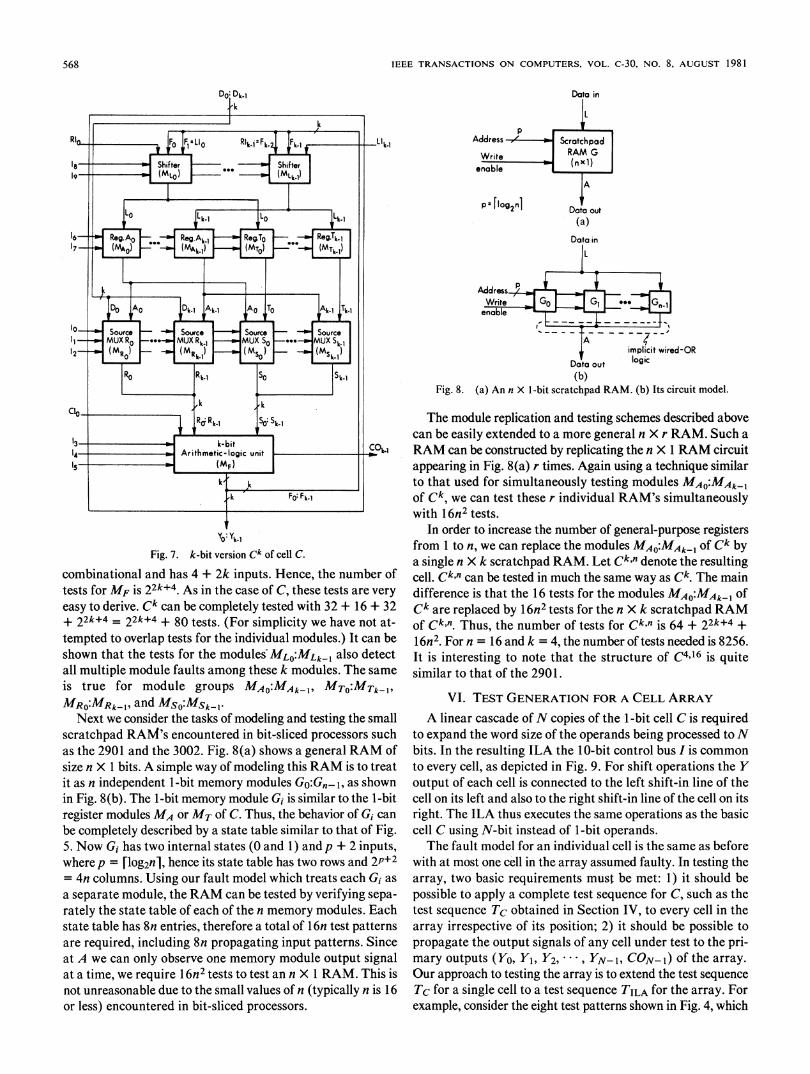
Fig. 7 shows a cell Ck, which is a k-bit version of the original1-bit cell C of Fig. 3(a). In expanding the word size from oneto k, we use a straightforward replication technique. In mostcases a module Mi in C is replaced by k copies of Mi in Ck. Forexample, consider the multiplexer module MR. In Ck MR isreplicated k times to form the k multiplexer modules MRO,MR1, , MRk-l = MRO:MRkIj, as shown in Fig. 7. Themodule MR1, where 0 _ i _ k - 1, operates on the ith bit ofthe k-bit word obtained from the direct input bus Do:Dk_ 1, andthe corresponding ith bit obtained from the registersMAO:MAk-1. The same technique has been used for expandingthe modules ML, MA, MT, and MS of C, as shown in Fig. 7.In the case of the ALU module MF, however, we have retainedit as a single module operating on the k-bit operands Ro:Rk-Iand So:Sk- . The reason for this is to permit the use of any fastcarry propagation scheme such as the carry lookahead withinCk. If such speed-up techniques are not required, then ripplecarry propagation can be used within the k-bit ALU moduleMF, in which case Ck consists of k identical cells of type C incascade. Such an array of cells is discussed in detail in the nextsection.The fault model and test generation approach defined for
C are also used with Ck. Consider, for example, multiplexermodules MRO:MRk-I and MSO:MSk-1. The tests for the mod-ules MR, and Msi are the same as the 32 tests for the modulesMR and MS of C with D, A and T replaced by Di, Ai, and Ti,respectively. A further consequence of the simple expansionscheme used to form Ck is that the tests for the pair of multi-plexers MRi and Msi can be applied at the same time as thetests for every other pair MRj and Msj, where i # j. Thus, themodules MRO:MRk-I and Mso:MSk-I can be completely testedwith only 32 tests. Similarly, the modules MAO:MAk-I andMTO:MTk-I require 16 tests, while the modules MLO;MLk-1require 32 tests. Now the remaining module MF of Ck is
567
IEEE TRANSACTIONS ON COMPUTERS, VOL. C-30, NO. 8, AUGUST 1981
YO: NYkl
Fig. 7. k-bit version Ck of cell C.
combinational and has 4 + 2k inputs. Hence, the number oftests for MF is 22k+4, As in the case of C, these tests are very
easy to derive. Ck can be completely tested with 32 + 16 + 32+ 22k+4 = 22k+4 + 80 tests. (For simplicity we have not at-tempted to overlap tests for the individual modules.) It can beshown that the tests for the modules&MLO:MLk-1 also detectall multiple module faults among these k modules. The same
is true for module groups MAO:MAk-1 MTO:MTk-1,MRO:MRk-1, and MSO:MSkIl-
Next we consider the tasks of modeling and testing the smallscratchpad RAM's encountered in bit-sliced processors suchas the 2901 and the 3002. Fig. 8(a) shows a general RAM ofsize n X 1 bits. A simple way of modeling this RAM is to treatit as n independent 1-bit memory modules Go:G"_ 1, as shownin Fig. 8(b). The 1-bit memory module Gi is similar to the 1-bitregister modules MA or MT of C. Thus, the behavior of Gi can
be completely described by a state table similar to that of Fig.5. Now G1 has two internal states (0 and 1) and p + 2 inputs,where p = [log2nl, hence its state table has two rows and 2P+2= 4n columns. Using our fault model which treats each Gi as
a separate module, the RAM can be tested by verifying sepa-rately the state table of each of the n memory modules. Eachstate table has 8n entries, therefore a total of 1 6n test patternsare required, including 8n propagating input patterns. Sinceat A we can only observe one memory module output signalat a time, we require 16n2 tests to test an n X 1 RAM. This isnot unreasonable due to the small values of n (typically n is 16or less) encountered in bit-sliced processors.
Data in
pAddress Scratchpad
Write RAM Genable (nxl)
A
p0log2n] Data out
(a)Data in
Address = j
enable
implicit wired-ORData out logic
(b)Fig. 8. (a) An n X 1-bit scratchpad RAM. (b) Its circuit model.
The module replication and testing schemes described abovecan be easily extended to a more general n X r RAM. Such aRAM can be constructed by replicating the n X 1 RAM circuitappearing in Fig. 8(a) r times. Again using a technique similarto that used for simultaneously testing modules MAO:MAk-Iof Ck, we can test these r individual RAM's simultaneouslywith 1 6n2 tests.
In order to increase the number of general-purpose registersfrom 1 to n, we can replace the modules MAO:MAk-_ of Ck bya single n X k scratchpad RAM. Let Ck,n denote the resultingcell. Ck,n can be tested in much the same way as Ck. The maindifference is that the 16 tests for the modules MAO:MAk-S ofCk are replaced by 16n2 tests for the n X k scratchpad RAMof Ck,n. Thus, the number of tests for Ck,n is 64 + 22k+4 +16n2. For n = 16 and k = 4, the number of tests needed is 8256.It is interesting to note that the structure of C4,16 is quitesimilar to that of the 2901.
VI. TEST GENERATION FOR A CELL ARRAYA linear cascade ofN copies of the 1-bit cell C is required
to expand the word size of the operands being processed toNbits. In the resulting ILA the 10-bit control bus I is commonto every cell, as depicted in Fig. 9. For shift operations the Youtput of each cell is connected to the left shift-in line of thecell on its left and also to the right shift-in line of the cell on itsright. The ILA thus executes the same operations as the basiccell C using N-bit instead of 1-bit operands.The fault model for an individual cell is the same as before
with at most one cell in the array assumed faulty. In testing thearray, two basic requirements must be met: 1) it should bepossible to apply a complete test sequence for C, such as thetest sequence Tc obtained in Section IV, to every cell in thearray irrespective of its position; 2) it should be possible topropagate the output signals of any cell under test to the pri-mary outputs (Yo, Yi, Y2, * , YN-1, CON-i) of the array.Our approach to testing the array is to extend the test sequenceTc for a single cell to a test sequence TILA for the array. Forexample, consider the eight test patterns shown in Fig. 4, which
568

SRIDHAR AND HAYES: TESTING BIT-SLICED MICROPROCESSORS
Data input
co-Rio -
Data output
Fig. 9. Iterative logic array (ILA) ofN cells of type C.
are applied by TC to the module ML with two of its inputs I8and Ig set to 0. To apply these eight patterns to any cell Ci inan array, the desired RI (LI) input signal must be generatedat the Y output of the cell Ci- 1 (Ci+ 1) to the left (right) of Ci.This can be done by appropriately selecting the D inputs to theneighboring cells Ci- 1 and C,+1. The resulting test patternsare shown in Fig. 10. The other primary inputs (17, I6, I5 14,
I3, 12, II, Io, CIo) of the cells are set to the constant values (0,0, 1, 1,0,0,1,0 , d) as in the single cell case. The test patternsshown in Fig. 10 are repeated for every three consecutive cellsin the array. Thus, with only eight test patterns, the eightmembers of Tc in question can be applied to every cell in thearray. In a similar way the other 24 members of TC that testML can be applied concurrently to every cell. Thus, the moduleML can be tested in every cell by applying only 32 test patternsto the array. The remaining 82 members of TC can be similarlyextended to yield 82 members of TILA. Thus, we have thefollowing result. The array of Fig. 9 is completely testable bya test sequence TILA of length 114, which is the same as thatof Tc for a single cell. The number of tests for the array is aconstant independent of the array size. Arrays with thisproperty are called C-testable [101. Arrays of the k-bit cellsCk, Ck,n can also be shown to be C-testable. This suggests thata bit-sliced microprocessor can be usefully 'modeled as a C-testable ILA. In view of this potentially practical applicationof C-testable ILA's, we examine some of their general prop-erties in the next section.
It should also be noted that if ripple-carry propagation be-tween cells of type C, Ck, or Ck,n is replaced by carry look-ahead, the tests derived for the array with ripple carry are alsovalid for testing the array with carry lookahead. Of course,
additional tests will be needed to check the new circuits usedin implementing the carry lookahead.
VII. C-TESTABLE ILA's
Previous research on C-testable ILA's has been confinedto combinational logic with certain restrictions on cell inter-connections [10], [11]. The array studied by Dias is a one-
dimensional unilateral ILA with direct outputs from every cell[1 1 ]. (Here unilateral means that the signal flow for intercellcommunication is only in one direction, left or right.) Thisstructure is quite similar to that of the arrays discussed in theprevious sections. Indeed, the array of Fig. 9 without the shiftlogic and registers reduces to the array considered by Dias. Toaccount for the k control lines, such as the I lines of Fig. 9 thatare common to every cell, we can view the system as consistingof s ILA's with s = 2k different basic cells, one for each control
TestNo. 18 19 RI1 F, Ll, D, , Di Di+100 0 00 0 0 0
2 0 0 0 1 0 0 1 03 0 0 1 0 0 1 1 04 0 0 1 1 0 0 1 05 0 O O 0 1 1 1 16 O 0 11 0 1 07 0 0 1 0 1 1 1 08 0 0 J 1 1 0 1 0
Note: RI i'F1l = LI1-2Fi =Rli+f LlI.lLlI =RI152' F,1
Fig. 10. Signals applied to cell Ci in an ILA by eight tests for ML.
state. For example, the three lines I3, 14, and I5 that select theALU function in every cell (see Figs. 3 and 9) are taken intoaccount by considering the system to be composed of 23 = 8ILA's, each having a different basic cell realizing one of theeight ALU functions. From now on, unless otherwise stated,ILA, or simply array, will refer to a one-dimensional unilateralarray of identical combinational cells with direct outputs fromevery cell.
In studying combinational ILA's the well-known analogybetween an ILA and a sequential machine viewed at successiveclock periods is useful [ 12]. Accordingly, we represent the basiccell of an ILA by an n X mflow table in which the rows rep-resent the n different horizontal input signals (also known asstates) and the columns represent the direct vertical inputsignals. For example, Figs. 11(b) and 12(b) show flow tablesfor two different cells. The entries of a flow table are pairsconsisting of the next state and the output signal values. Thenext state entry also defines a (state) transition of the cell froman initial state represented by the row in question to a finalstate represented by the next state entry. The behavior of a cellis completely characterized by its flow table.An important property of a cell which is relevant to C-tes-
tability is that of possessing repeatable transitions. A transitionor entry e is repeatable if it is possible to drive the cell from thefinal state after the transition e takes place back to its initialstate. A flow table that only has repeatable transitions is calledan RTflow table. The flow diagram or graph correspondingto an RT flow table has only strongly connected components.The flow table of Fig. 1 1(b) is an RT flow table, whereas thatof Fig. 12(b) is not.The fault model used here is the same as before with every
cell considered as a single module. We also assume that at mostone cell is faulty in the entire array. Accordingly, to test anarray completely it is necessary and sufficient to verify all theentries in the flow table of every cell in the array. The goal hereis to verify each entry for every cell by applying a constantnumber (independent of the array size) of primary test inputsto the array and observing the corresponding primary outputs.To achieve this goal it is necessary to verify an entry e simul-taneously in cells spaced at regular intervals along the array.If not, then the number of array primary inputs necessary toverify the entry e in every cell of the array will depend on thearray size. Hence, we conclude that for C-testability it isnecessary for the cell flow table to be an RT flow table.
Procedures to test an array of arbitrary size with a constantnumber of tests are presented in [9] and [11]. The followingapproach is used in both cases. A particular entry e is verified
569

IEEE TRANSACTIONS ON COMPUTERS, VOL. C-30, NO. 8, AUGUST 1981
a b
c Fuader
(a)
ob0 0 01 10 11
O 0,0 0,1 0,1 1,o0c
1 ,0,1 1,0 1,0 1,1
(b)
Test t
11 00 1 1 0 0
Test t' (shifted version of t)00 1 1 0 0 1 1
0 2 C3
(c)Fig. 11. (a) A full-adder cell. (b) Its flow table. (c) C-tests for entries ei
and e2.
~~~~~0
0 0,0
ncrementer0,1 1,0
y non-repeatoble(a) transition e
(b)
y0 1 Yc
0 0,0 0,1 1,0
1 0,1 1,0 0,1
(c)
Fig. 12. (a) An incrementer cell. (b) Its flow table. (c) The flow tablemodified to make it C-testable.
in cells spaced at regular intervals of constant period k alongthe array. The corresponding test, called a C-test [9] or a looptest [ 1 1], and its k - 1 shifted versions completely verify theentry e in every cell of the array. C-tests and loop tests differin the kinds of sequences they use for verifying the next statesof cells. In the construction of loop tests, characterizing se-
quences [8] are used to distinguish states. In constructing a
C-test, on the other hand, use is made of the simpler sequences(pairwise distinguishing sequences [8]) that distinguish pairsof states. Furthermore, a C-test does not require the (possiblylengthy) synchronizing sequences used by loop tests. Like a
set of loop tests, a complete set of C-tests for an ILA can beshown to verify the ILA's truth table. C-tests and loop testsalways exist when the cell flow table is reduced and of the RTtype.To illustrate the use of C-tests, consider a ripple-carry adder.
Fig. 11 shows the basic cell (a full-adder circuit) and its flowtable, which has a total of eight entries. The two entries labelede1 and e2 can be verified in every cell of the adder array byapplying the C-tests t and its shifted version t', as shown in Fig.11(c). It is evident that t (t') verifies eI (e2) in even numberedcells Co, C2, C4, * *, and e2 (e1) in odd numbered cells C1, C3,
C5, - . The remaining six entries can be verified similarly inevery cell by six more tests. Hence, a ripple-carry adder ofarbitrary size can be tested by eight tests; it is therefore C-testable.
The foregoing testing approach leads to the following result.An ILA with a reduced cell flow table is C-testable if and onlyif the table is also an RT flow table.As an example of a non-C-testable array, consider an in-
crementer circuit having the 1-bit basic cell shown in Fig.12(a). The vertical output 9 of the cell is the input y incre-mented by 1 if the horizontal input x is 1, while 9 = y if x is0. It is evident that the entry labeled e in Fig. 12(b) is nonre-peatable. Hence, an array of such cells is not C-testable.
It is possible, however, to make an array of cells such as thatof Fig. 12(a) C-testable by making a simple modification tothe cell flow table. This is done by adding a new column Ya suchas the one shown in Fig. 12(c). The idea here is to link all thestates of the cell into a single loop by appropriately choosingthe next state entries in Ya. This makes the flow diagramstrongly connected; hence the flow table becomes an RT flowtable. Also, the output entries in Ya can easily be chosen tomake the flow table reduced, if it is not already. Once the flowtable is both reduced and of the RT type, an array of the cor-responding cells will be C-testable. Our method [9] uses adifferent scheme from Dias' [ 1] to select the output entriesin Ya which results in a minimum-length distinguishing se-quence for the modified flow table.The foregoing results on the C-testability for combinational
ILA's can easily be extended to a special class of sequentialarrays. These arrays consist of Moore-type cells with a one-to-one correspondence between the direct (observable) outputsand the internal states, as shown in Fig. 13. Most of the se-quential modules such as registers and shift registers used inbit-sliced processors are of this type. The combinationalmodule L of Fig. 13 realizes the next-state function. It is as-sumed that the memory module M of any cell can be inde-pendently initialized to any desired state via the Y input lines
570

SRIDHAR AND HAYES: TESTING BIT-SLICED MICROPROCESSORS
y
Fig. 13. A special class of sequential cell.
or other external lines. An array P of the 2-module sequentialcells of Fig. 13 can be tested as follows. First, the combinationalsubarray formed from the modules L in P is tested like anyother combinational ILA. For this purpose, the necessary Sinputs to L in each cell of P are obtained by appropriately in-itializing the state ofM of the cells. Next, the memory modulesare tested by verifying their state tables, in which each nextstate entry should equal the corresponding present input s E
S. These entries can readily be verified by applying appropriateinitializing input patterns to P. Thus, we have the followingresult. An array of sequential cells of Fig. 13 is C-testable ifand only if its combinational subarray is C-testable. Accord-ingly, the foregoing characterization of combinational ILA'sand the modification scheme for C-testability are equally validfor this special class of sequential arrays.
VIII. CONCLUDING REMARKSWe have attempted to show that efficient analytic, i.e.,
nonheuristic, test generation using functional fault models isfeasible for fairly realistic processor bit-slices and bit-slicedarrays. We have also shown how the regular array-like struc-ture of bit-sliced systems can be exploited in testing them.Bit-sliced processors with ripple-carry propagation also havethe useful property of C-testability, which greatly simplifiestest generation. Furthermore, tests for a processor of arbitrarylength can easily be generated from the tests of an individualcell.
C-testability of unilateral combinational ILA's is reasonablywell understood. Practical bit-sliced systems are both se-
quential and bilateral. While it may sometimes be feasible toanalyze these systems by decomposing them into sets of uni-lateral combinational arrays, it appears that further under-standing of the behavior of sequential and/or bilateral arrays
is needed.REFERENCES
[1] S. M. Thatte and J. A. Abraham, "A methodology for functional-leveltesting of microprocessors," in Dig. 8th Symp. Fault-Tolerant Comput.,Toulouse, France, 1978, pp. 90-95.
[2] R. McCaskill, "Test approaches for four-bit microprocessor slices," inDig. Semiconductor Test Symp., Cherry Hill, NJ, 1976, pp. 22-26.
[3] A. C. L. Chiang and R. McCaskill, "Two new approaches to simplifytesting of microprocessors," Electronics, vol. 49, no. 2, pp. 100-105, Jan.22, 1976.
[4] Advanced Micro Devices, Am2900 Bipolar Microprocessor Family,Sunnyvale, CA, 1976.
[5] P. M. Adams, "Microprogrammable microprocessor survey," SIG-MICRO Newsletter, vol. 9, no. 1, pp. 23-49, Mar. 1978 (Part 1).
[6] , "Microprogrammable microprocessor survey," SIGMICRONewsletter, vol. 9, no. 2, pp. 7-38, June 1978 (Part 2).
[7] Motorola, Inc., Motorola MCI4SOOB Industrial Control Unit Hand-book, Phoenix, AZ, 1977.
[8] A. D. Friedman and P. R. Menon, Fault Detection in Digital Circuits.Englewood Cliffs, NJ: Prentice-Hall, 1971.
[9] T. Sridhar and J. P. Hayes, "Testing bit-sliced microprocessors," in Dig.9th Symp. Fault-Tolerant Comput., Madison, WI, June 1979, pp.211-218.
[10] A. D. Friedman, "Easily testable iterative systems," IEEE Trans.Comput., vol. C-22, pp. 1061-1064, Dec. 1973.
[11] F. J. 0. Dias, "Truth-table verification of an iterative logic array," IEEETrans. Comput., vol. C-25, pp. 605-613, June 1976.
[12] E. J. McCluskey, "Iterative combinational switching networks-Generaldesign considerations," IRE Trans. Electron. Comput., vol. EC-7, pp.285-291, Dec. 1958.
[13] C. Mead and L. Conway, Introduction to VLSI Systems. Reading,MA: Addison-Wesley, 1980.
[14] R. P. Batni and C. R. Kime, "A module-level testing approach forcombinational networks," IEEE Trans. Comput., vol. C-25, pp.594-604, June 1976.
Thirumalai Sridhar (S'77) received the B.E. de-gree in electronics engineering from BangaloreUniversity, Bangalore, India, in 1973 and theM.E. degree (with distinction) in electrical com-munication engineering from the Indian Instituteof Science, Bangalore in 1975. He' is currentlyworking towards the Ph.D. degree in electrical en-gineering at the University of Southern Califor-na, Los Angeles.From 1975 to 1977 he was with the Switching
Research and Development Division of IndianTelephone Industries, Ltd., Bangalore, where he designed microprocessor-based controllers for electronic switching systems. Since 1977 he has heldpositions as a Teaching and Research Assistant at the University of SouthernCalifornia. From 1979 to 1980 he was also the recipient of a graduate fel-lowship from IBM Corporation. His current interests are in the areas of designfor testability, VLSI systems, fault-tolerant computing, microprocessor-basedsystems, and computer architecture.
Mr. Sridhar is a member of Eta Kappa Nu.
John P. Hayes (S'67-M'70-SM'81) received theB.E. degree from the National University of Ire-land, Dublin in 1965, and the M.S. and Ph.D. de-grees from the University of Illinois, Urbana, in1967 and 1970, respectively, all in electrical engi-neering.From 1965 to 1967 he was with the Digital
Computer Laboratory of the University of Illinoiswhere he participated in the design of the ILLIAC3 computer. From 1960 to 1970 he was engaged inresearch in the area of fault diagnosis of digital
systems at the Coordinated Science Laboratory of the University of Illinois.In 1970 he joined the Operations Research Group at the Shell BeneluxComputing Center of the Royal Dutch/Shell Company in The Hague, wherehe was involved in mathematical programming and software development.Since 1972 he has been with the Departments of Electrical Engineering andComputer Science of the University of Southern California, where he is cur-rently an Associate Professor. His research interests include fault-tolerantcomputing, computer architecture, VLSI design, and microprocessor/mi-crocomputer-based systems. He was Technical Program Chairman of the 1977International Conference on Fault-Tolerant Computing. He is the author ofthe book Computer Architecture and Organization (New York: McGraw-Hill, 1978), and Editor of the Computer Architecture and Systems Depart-ment of Communications of the ACM.
Dr. Hayes is a member of the Association for Computing Machinery andSigma Xi.
571
x-