
A Family of Current References Based on 2T Voltage ... - arXiv
14
1 A Family of Current References Based on 2T Voltage References: Demonstration in 0.18-μm with 0.1-nA PTAT and 1.1-μA CWT 38-ppm/ ◦ C Designs Martin Lefebvre, Student Member, IEEE, David Bol, Senior Member, IEEE Abstract—The robustness of current and voltage references to process, voltage and temperature (PVT) variations is paramount to the operation of integrated circuits in real-world conditions. However, while recent voltage references can meet most of these requirements with a handful of transistors, current references remain rather complex, requiring significant design time and silicon area. In this paper, we present a family of simple current references consisting of a two-transistor (2T) ultra-low-power voltage reference, buffered onto a voltage-to-current converter by a single transistor. Two topologies are fabricated in a 0.18-μm partially-depleted silicon-on-insulator (SOI) technology and mea- sured over 10 dies. First, a 7T nA-range proportional-to-absolute- temperature (PTAT) reference intended for constant-gm biasing of subthreshold operational amplifiers demonstrates a 0.096-nA current with a line sensitivity (LS) of 1.48 %/V, a temperature coefficient (TC) of 0.75 %/ ◦ C, and a variability (σ/μ) of 1.66 %. Then, two 4T+1R μA-range constant-with-temperature (CWT) references with (resp. without) TC calibration exhibit a 1.09- μA (resp. 0.99-μA) current with a 0.21-%/V (resp. 0.20-%/V) LS, a 38-ppm/ ◦ C (resp. 290-ppm/ ◦ C) TC, and a 0.87-% (resp. 0.65-%) (σ/μ). In addition, portability to common scaled CMOS technologies, such as 65-nm bulk and 28-nm fully-depleted SOI, is discussed and validated through post-layout simulations. Index Terms—Current reference, voltage reference, ultra- low-power (ULP), proportional-to-absolute-temperature (PTAT), constant-gm biasing, constant-with-temperature (CWT), temperature-independent. I. I NTRODUCTION C URRENT and voltage references are crucial components of mixed-signal circuits, ranging from ultra-low-power (ULP) sensor nodes for the Internet of Things (IoT) [1] to high-performance circuits for compute-in-memory accelera- tors, such as data converters [2], [3]. Despite the widely different contexts in which these references are used, they share the common objective of ensuring robustness against PVT variations. On the one hand, recent advances in the design of voltage references have led to simple topologies [4]–[6], consisting of only a handful of transistors and consuming a few pW at ambient temperature. While these topologies demon- strate remarkably competitive supply voltage and temperature dependencies with respect to more advanced references, they generally suffer from an increased dependence on process variations and need to be trimmed. Nevertheless, their main advantage lies in the design time reduction arising from the This work was supported by the Fonds National de la Recherche Sci- entifique (FNRS), Belgium as part of the European Horizon 2020 project Convergence. (Corresponding author: Martin Lefebvre.) The authors are with the ICTEAM institute, Universit´ e catholique de Louvain (UCLouvain), 1348 Louvain-la-Neuve, Belgium (e-mail: mar- [email protected]; [email protected]). limited number of degrees of freedom. On the other hand, current references remain more complex than their voltage counterparts, often requiring more components and an intricate sizing [7]. Nonetheless, recent works have shown that a 2T voltage reference can be used to generate a reference current once replicated onto a gate-leakage transistor by a 1T buffer [8], [9]. Such works suggest that simpler yet competitive architectures are within reach. In this paper, we build upon [8], [9] to create a family of simple current references without startup circuit sharing two key principles: (i) the generation of a voltage reference by a 2T ULP structure and (ii) its buffering by a single transistor onto a voltage-to-current (V-to-I) converter. Compared with [8], [9], we substitute the gate-leakage transistor by either a self-cascode MOSFET (SCM) or a resistor, respectively resulting in a nA- and μA-range current. This leads to two novel current reference topologies, fabricated in a 0.18-μm partially-depleted silicon-on-insulator (PDSOI) process. First, a proportional-to-absolute-temperature (PTAT) current refer- ence built by applying a PTAT voltage to an SCM, which is similar to [10], [11] but with a different PTAT voltage gen- eration. The measured 0.096-nA current has a line sensitivity (LS) of 1.48 %/V, a temperature coefficient (TC) of 0.75 %/ ◦ C and a (σ/μ) of 1.66 %, while the current reference consumes down to 0.28 nW at 25 ◦ C. It consists of seven transistors and occupies a silicon area of 8700 μm 2 . Second, a constant- with-temperature (CWT) current reference is obtained by the ratio of a voltage and a resistance with matching TCs. It provides a measured 0.99-μA current with an LS of 0.20 %/V, a TC of 290 ppm/ ◦ C, and a (σ/μ) of 0.65 %. It consumes down to 0.64 μW at 25 ◦ C, and is made of four transistors and a polysilicon resistor, occupying a total silicon area of 3410 μm 2 . Another version with a 4-bit TC calibration reduces temperature dependence down to 38 ppm/ ◦ C, and provides a 1.09-μA current within a 4270-μm 2 silicon area. The remainder of this paper is organized as follows. Section II presents existing MOS-based current generation techniques. Then, Section III highlights the principles shared by both proposed PTAT and CWT topologies, whose sizing is detailed in Section IV. Next, simulation and measurement results are discussed in Section V. We address additional design considerations for an implementation in scaled technologies in Section VI. Finally, Section VII compares our work to the state of the art and Section VIII offers some concluding remarks. This work has been submitted to the IEEE for possible publication, and copyright may be transferred without notice. arXiv:2202.01751v1 [cs.AR] 3 Feb 2022
-
Upload
khangminh22 -
Category
Documents
-
view
0 -
download
0
Transcript of A Family of Current References Based on 2T Voltage ... - arXiv

1
A Family of Current References Based on 2TVoltage References: Demonstration in 0.18-µm with0.1-nA PTAT and 1.1-µA CWT 38-ppm/C Designs
Martin Lefebvre, Student Member, IEEE, David Bol, Senior Member, IEEE
Abstract—The robustness of current and voltage references toprocess, voltage and temperature (PVT) variations is paramountto the operation of integrated circuits in real-world conditions.However, while recent voltage references can meet most of theserequirements with a handful of transistors, current referencesremain rather complex, requiring significant design time andsilicon area. In this paper, we present a family of simple currentreferences consisting of a two-transistor (2T) ultra-low-powervoltage reference, buffered onto a voltage-to-current converterby a single transistor. Two topologies are fabricated in a 0.18-µmpartially-depleted silicon-on-insulator (SOI) technology and mea-sured over 10 dies. First, a 7T nA-range proportional-to-absolute-temperature (PTAT) reference intended for constant-gm biasingof subthreshold operational amplifiers demonstrates a 0.096-nAcurrent with a line sensitivity (LS) of 1.48 %/V, a temperaturecoefficient (TC) of 0.75 %/C, and a variability (σ/µ) of 1.66 %.Then, two 4T+1R µA-range constant-with-temperature (CWT)references with (resp. without) TC calibration exhibit a 1.09-µA (resp. 0.99-µA) current with a 0.21-%/V (resp. 0.20-%/V)LS, a 38-ppm/C (resp. 290-ppm/C) TC, and a 0.87-% (resp.0.65-%) (σ/µ). In addition, portability to common scaled CMOStechnologies, such as 65-nm bulk and 28-nm fully-depleted SOI,is discussed and validated through post-layout simulations.
Index Terms—Current reference, voltage reference, ultra-low-power (ULP), proportional-to-absolute-temperature (PTAT),constant-gm biasing, constant-with-temperature (CWT),temperature-independent.
I. INTRODUCTION
CURRENT and voltage references are crucial componentsof mixed-signal circuits, ranging from ultra-low-power
(ULP) sensor nodes for the Internet of Things (IoT) [1] tohigh-performance circuits for compute-in-memory accelera-tors, such as data converters [2], [3]. Despite the widelydifferent contexts in which these references are used, theyshare the common objective of ensuring robustness againstPVT variations. On the one hand, recent advances in the designof voltage references have led to simple topologies [4]–[6],consisting of only a handful of transistors and consuming a fewpW at ambient temperature. While these topologies demon-strate remarkably competitive supply voltage and temperaturedependencies with respect to more advanced references, theygenerally suffer from an increased dependence on processvariations and need to be trimmed. Nevertheless, their mainadvantage lies in the design time reduction arising from the
This work was supported by the Fonds National de la Recherche Sci-entifique (FNRS), Belgium as part of the European Horizon 2020 projectConvergence. (Corresponding author: Martin Lefebvre.)
The authors are with the ICTEAM institute, Universite catholique deLouvain (UCLouvain), 1348 Louvain-la-Neuve, Belgium (e-mail: [email protected]; [email protected]).
limited number of degrees of freedom. On the other hand,current references remain more complex than their voltagecounterparts, often requiring more components and an intricatesizing [7]. Nonetheless, recent works have shown that a 2Tvoltage reference can be used to generate a reference currentonce replicated onto a gate-leakage transistor by a 1T buffer[8], [9]. Such works suggest that simpler yet competitivearchitectures are within reach.
In this paper, we build upon [8], [9] to create a family ofsimple current references without startup circuit sharing twokey principles: (i) the generation of a voltage reference by a2T ULP structure and (ii) its buffering by a single transistoronto a voltage-to-current (V-to-I) converter. Compared with[8], [9], we substitute the gate-leakage transistor by eithera self-cascode MOSFET (SCM) or a resistor, respectivelyresulting in a nA- and µA-range current. This leads to twonovel current reference topologies, fabricated in a 0.18-µmpartially-depleted silicon-on-insulator (PDSOI) process. First,a proportional-to-absolute-temperature (PTAT) current refer-ence built by applying a PTAT voltage to an SCM, which issimilar to [10], [11] but with a different PTAT voltage gen-eration. The measured 0.096-nA current has a line sensitivity(LS) of 1.48 %/V, a temperature coefficient (TC) of 0.75 %/Cand a (σ/µ) of 1.66 %, while the current reference consumesdown to 0.28 nW at 25C. It consists of seven transistorsand occupies a silicon area of 8700 µm2. Second, a constant-with-temperature (CWT) current reference is obtained by theratio of a voltage and a resistance with matching TCs. Itprovides a measured 0.99-µA current with an LS of 0.20 %/V,a TC of 290 ppm/C, and a (σ/µ) of 0.65 %. It consumesdown to 0.64 µW at 25C, and is made of four transistorsand a polysilicon resistor, occupying a total silicon area of3410 µm2. Another version with a 4-bit TC calibration reducestemperature dependence down to 38 ppm/C, and provides a1.09-µA current within a 4270-µm2 silicon area.
The remainder of this paper is organized as follows. SectionII presents existing MOS-based current generation techniques.Then, Section III highlights the principles shared by bothproposed PTAT and CWT topologies, whose sizing is detailedin Section IV. Next, simulation and measurement resultsare discussed in Section V. We address additional designconsiderations for an implementation in scaled technologies inSection VI. Finally, Section VII compares our work to the stateof the art and Section VIII offers some concluding remarks.
This work has been submitted to the IEEE for possible publication, and copyright may be transferred without notice.
arX
iv:2
202.
0175
1v1
[cs
.AR
] 3
Feb
202
2
2
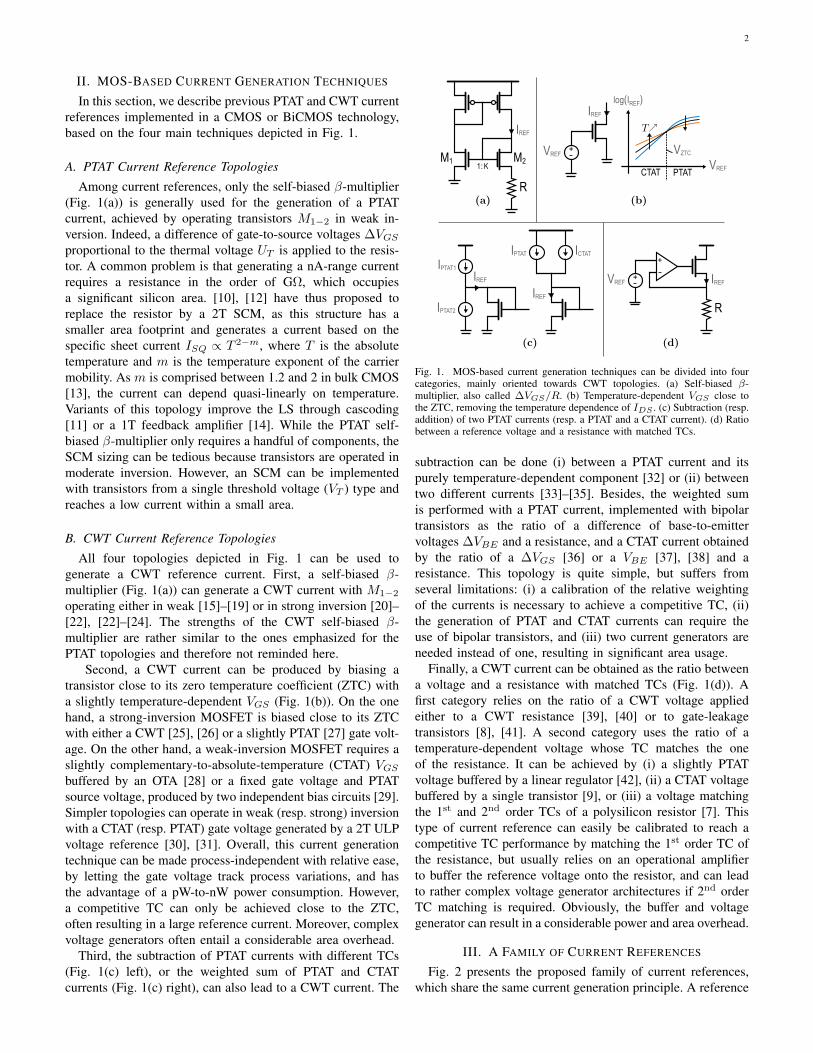
II. MOS-BASED CURRENT GENERATION TECHNIQUES
In this section, we describe previous PTAT and CWT currentreferences implemented in a CMOS or BiCMOS technology,based on the four main techniques depicted in Fig. 1.
A. PTAT Current Reference Topologies
Among current references, only the self-biased β-multiplier(Fig. 1(a)) is generally used for the generation of a PTATcurrent, achieved by operating transistors M1−2 in weak in-version. Indeed, a difference of gate-to-source voltages ∆VGSproportional to the thermal voltage UT is applied to the resis-tor. A common problem is that generating a nA-range currentrequires a resistance in the order of GΩ, which occupiesa significant silicon area. [10], [12] have thus proposed toreplace the resistor by a 2T SCM, as this structure has asmaller area footprint and generates a current based on thespecific sheet current ISQ ∝ T 2−m, where T is the absolutetemperature and m is the temperature exponent of the carriermobility. As m is comprised between 1.2 and 2 in bulk CMOS[13], the current can depend quasi-linearly on temperature.Variants of this topology improve the LS through cascoding[11] or a 1T feedback amplifier [14]. While the PTAT self-biased β-multiplier only requires a handful of components, theSCM sizing can be tedious because transistors are operated inmoderate inversion. However, an SCM can be implementedwith transistors from a single threshold voltage (VT ) type andreaches a low current within a small area.
B. CWT Current Reference Topologies
All four topologies depicted in Fig. 1 can be used togenerate a CWT reference current. First, a self-biased β-multiplier (Fig. 1(a)) can generate a CWT current with M1−2
operating either in weak [15]–[19] or in strong inversion [20]–[22], [22]–[24]. The strengths of the CWT self-biased β-multiplier are rather similar to the ones emphasized for thePTAT topologies and therefore not reminded here.
Second, a CWT current can be produced by biasing atransistor close to its zero temperature coefficient (ZTC) witha slightly temperature-dependent VGS (Fig. 1(b)). On the onehand, a strong-inversion MOSFET is biased close to its ZTCwith either a CWT [25], [26] or a slightly PTAT [27] gate volt-age. On the other hand, a weak-inversion MOSFET requires aslightly complementary-to-absolute-temperature (CTAT) VGSbuffered by an OTA [28] or a fixed gate voltage and PTATsource voltage, produced by two independent bias circuits [29].Simpler topologies can operate in weak (resp. strong) inversionwith a CTAT (resp. PTAT) gate voltage generated by a 2T ULPvoltage reference [30], [31]. Overall, this current generationtechnique can be made process-independent with relative ease,by letting the gate voltage track process variations, and hasthe advantage of a pW-to-nW power consumption. However,a competitive TC can only be achieved close to the ZTC,often resulting in a large reference current. Moreover, complexvoltage generators often entail a considerable area overhead.
Third, the subtraction of PTAT currents with different TCs(Fig. 1(c) left), or the weighted sum of PTAT and CTATcurrents (Fig. 1(c) right), can also lead to a CWT current. The
IREF
1: KM1 M2
R
+
IREF
VREF
VREF
log(IREF)
VZTC
PTATCTAT
R
+
+
ICTATIPTAT
IPTAT1
IPTAT2
VREF IREF
IREF
IREF
Fig. 1. MOS-based current generation techniques can be divided into fourcategories, mainly oriented towards CWT topologies. (a) Self-biased β-multiplier, also called ∆VGS/R. (b) Temperature-dependent VGS close tothe ZTC, removing the temperature dependence of IDS . (c) Subtraction (resp.addition) of two PTAT currents (resp. a PTAT and a CTAT current). (d) Ratiobetween a reference voltage and a resistance with matched TCs.
subtraction can be done (i) between a PTAT current and itspurely temperature-dependent component [32] or (ii) betweentwo different currents [33]–[35]. Besides, the weighted sumis performed with a PTAT current, implemented with bipolartransistors as the ratio of a difference of base-to-emittervoltages ∆VBE and a resistance, and a CTAT current obtainedby the ratio of a ∆VGS [36] or a VBE [37], [38] and aresistance. This topology is quite simple, but suffers fromseveral limitations: (i) a calibration of the relative weightingof the currents is necessary to achieve a competitive TC, (ii)the generation of PTAT and CTAT currents can require theuse of bipolar transistors, and (iii) two current generators areneeded instead of one, resulting in significant area usage.
Finally, a CWT current can be obtained as the ratio betweena voltage and a resistance with matched TCs (Fig. 1(d)). Afirst category relies on the ratio of a CWT voltage appliedeither to a CWT resistance [39], [40] or to gate-leakagetransistors [8], [41]. A second category uses the ratio of atemperature-dependent voltage whose TC matches the oneof the resistance. It can be achieved by (i) a slightly PTATvoltage buffered by a linear regulator [42], (ii) a CTAT voltagebuffered by a single transistor [9], or (iii) a voltage matchingthe 1st and 2nd order TCs of a polysilicon resistor [7]. Thistype of current reference can easily be calibrated to reach acompetitive TC performance by matching the 1st order TC ofthe resistance, but usually relies on an operational amplifierto buffer the reference voltage onto the resistor, and can leadto rather complex voltage generator architectures if 2nd orderTC matching is required. Obviously, the buffer and voltagegenerator can result in a considerable power and area overhead.
III. A FAMILY OF CURRENT REFERENCES
Fig. 2 presents the proposed family of current references,which share the same current generation principle. A reference

3
1: N
M1
M2
VX
IREF
VDD
VREF
VBIAS
M3
M4
VREF
IREF VBIAS
VDD
M1
M2
VX M3
M4 M5
M6
M7VG
M1
M2
VX
VREF
R
M3
VDD
M4VBIAS
IREF
RVTdevice
HVT/IOdevice
V-to-Iconv.
VREF
gen.
Legend
IREF range
IREF TC
CWT PTAT
CWT
CWT
CWT
pA nA µA
∝I SQ
VREF TC
Fig. 2. Overview of the family of current references, generating a reference voltage VREF with a 2T ULP structure and converting it into a current bysingle-transistor buffering onto (a) a gate-leakage transistor [8], [9], (b) an SCM, and (c) a resistor, generating a pA-, nA- and µA-range current, respectively.Finally, (d) summarizes the TC of VREF , as well as the TC and range of IREF across the different architectures.
voltage VREF is generated by a the 2T ULP structure formedby M1−2, and then buffered onto a V-to-I converter bytransistor M3. The range and temperature dependence of thereference current, denoted as IREF , are conditioned by thetype of transistors used in the voltage reference and the chosenV-to-I converter. First, the current reference in Fig. 2(a) relieson a CWT voltage reference biasing a gate-leakage transistor,which acts as a resistance in the order of GΩ. This structurewas proposed in [8], [9] and generates a CWT referencecurrent in the pA range. Second, the current reference inFig. 2(b) relies on a PTAT voltage reference biasing an SCMand generates a nA-range reference current proportional tothe specific sheet current of M6−7 [10], [11]. Third, thecurrent reference in Fig. 2(c) relies on a quasi-CWT voltagereference biasing a resistor and compensating for its temper-ature dependence, and generates a temperature-independentreference current in the µA range. Fig. 2(d) summarizes thecharacteristics of the three references described hereabove. Inthe remainder of this paper, we focus on the nA- and µA-rangecurrent reference topologies, as the pA-range one has alreadybeen proposed in previous art [8], [9].
The topology brought forward in this work offers three mainadvantages. First, it requires a small number of transistors witha potentially dense layout, thus limiting the area footprintand reducing the design time by restraining the number ofdegrees of freedom. Second, the voltage reference draws asupply current in the pA-to-nA range, resulting in a low powerconsumption compared to a β-multiplier or bandgap voltagereference. Third, it does not require any startup circuit as thereference has a unique stable operation point corresponding toa non-zero current, leading to further area savings.
A. 2T ULP Voltage Reference
The 2T ULP voltage reference used in this work wasproposed in [8], [9] in the context of current references andshares the same operation principle as [4], [5], [43]. It relieson the balance of the subthreshold currents in transistorsM1−2 to generate a reference voltage. There are three mainassumptions underlying the reasoning that follows: (i) for thesake of generality, M1−2 have distinct characteristics, (ii) bothtransistors operate in weak inversion, and (iii) the drain-to-source voltage VDS is larger than 4UT , where UT is the
thermal voltage, so the transistors are saturated. Under theseassumptions, the drain-to-source current can be expressed as
IDS = ISQ S exp
(VGS − VT0
nUT
), (1)
where ISQ = µC′
ox (n− 1)U2T is the specific sheet current,
µ is the carrier mobility, C′
ox is the normalized gate oxidecapacitance, S = W/L is the transistor aspect ratio, VT0 isthe threshold voltage at zero body-to-source voltage VBS andn is the subthreshold slope factor. Applying (1) to M1−2 andsolving for the reference voltage yields
VREF = n1UT log
(ISQ2
ISQ1
S2
S1
)+
(n2VT01 − n1VT02
n2
).
(2)For the µA-range reference, M1 is chosen to have a largerthreshold voltage than M2, i.e., VT01 > VT02, and the ratioS2/S1 can be used to tune the reference voltage’s TC, whereasfor the nA-range current reference, the same transistor type isused for M1−2 and (2) simplifies to a purely PTAT voltage
VREF = nUT log
(S2
S1
), (3)
assuming no mismatch between M1−2. The LS of the refer-ence voltage is computed from the small signal schematic inFig. 3, where rvi denotes the output resistance of the V-to-Iconverter. First, assuming that gm3 gd3 and gm4 1
rvi, the
transfer function between vx and vref is given by (4). Then,if gm3 1
rvi, this expression further simplifies to one, which
is in line with the common-drain configuration of M3.
vxvref
'gm3 + gd3 + 1
rvi
gm3' 1 (4)
vrefvdd
=gd2
gm1 + vxvref
(gd1 + gd2)' gd2gm1
(5)
Second, the supply dependence of VREF , i.e., vref/vdd, isgiven by (5) and simplifies to gd2/gm1 for gm gd.
B. nA-Range PTAT Current Reference
To generate a current proportional to the specific sheetcurrent ISQ, the nA-range reference relies on a moderate-inversion SCM formed by M6−7 and biased by a PTATvoltage, as proposed in [10]. The use of moderate inversion

4
requires the advanced compact model (ACM) [44] to describethe transistor I-V relationship. The drain current ID is givenby
ID = ISQ S (if − ir) , (6)
where ISQ = 12µC
′
oxnU2T is the ACM specific sheet current,
S the transistor aspect ratio, and if , ir the forward and reverseinversion levels. The reverse inversion level is non-zero onlywhen the transistor is in triode. Furthermore, the forwardinversion level is linked to the gate and source voltages by
VP − VS = UT
[√1 + if − 2 + log
(√1 + if − 1
)], (7)
where VP = VG−VT0
n is the pinch-off voltage. A similarrelationship is obtained for the reverse inversion level if VSis replaced by VD and if by ir in (7). The ACM equationsapplied to M6−7, respectively in moderate-inversion triode andsaturation, give ir6 = if7 [10]. Then, defining α , if6
if7, if7 is
determined by solving the non-linear equation
VREF = UT
[(√1 + αif7 −
√1 + if7
)+ log
(√1 + αif7 − 1√1 + if7 − 1
)]. (8)
Finally, the aspect ratios of M6−7 must comply with
S6
S7=ISQ7
ISQ6
N + 1
N
1
α− 1. (9)
Moreover, the line sensitivity and mismatch of the referencecurrent are directly related to the characteristics of the voltagereference, through the sensitivity SIREF
. It is computed bymeans of the chain rule as
SIREF=
1
IREF
∂IREF∂VREF
=1
IREF
∂IREF∂if7
∂if7∂VREF
, (10)
where the variation of if7 with respect to VREF is derivedfrom (8) and the sensitivity is thus expressed as
SIREF=
2
if7UT
[α√
1 + αif7 − 1− 1√
1 + if7 − 1
]−1
.
(11)The line sensitivity and mismatch of the reference current canthus be expressed as
1
IREF
∂IREF∂VDD
= SIREF
gd2gm1
, (12)(σ
µ
)IREF
= SIREFσVREF
, (13)
and depend on both the characteristics of the voltage referenceand the sizing of the SCM.
C. µA-Range CWT Current Reference
To generate a temperature-independent reference current,the µA-range current reference relies on a resistor biased bya CWT reference voltage. The reference current is thus givenby IREF = VREF
R . Assuming that the threshold voltage oftransistor Mi, denoted as VT0i, decreases linearly with tem-perature T following VT0i(T ) = VT0i(T0) − αVT0i
(T − T0),
ro2
vdd
1/(gm4+gd4)
vdd
gm1vgs1
gm3vgs3 ro3
ro1
vref
vx
vgs1
vgs3
rvi
Fig. 3. Small signal schematic of the voltage reference, abstracting the V-to-Iconverter as an equivalent resistance rvi.
and that the resistance temperature variation is captured by∂R∂T , the temperature variation of IREF is given by
∂IREF∂T
=1
R
(nk
qlog
(ISQ2S2
ISQ1S1
)+ (αVT01
− αVT02)
)− 1
R2
(UT log
(ISQ2S2
ISQ1S1
)+ (VT01 − VT02)
)∂R
∂T. (14)
Therefore, the ratio S2/S1 leading to zero temperature varia-tion of the reference current at T = T0 is
ISQ1
ISQ2exp
(q
nk
(VT01 − VT02) 1R∂R∂T + (αVT01
− αVT02)
1− T0
R∂R∂T
).
(15)Similarly to the PTAT current reference, the line sensitivityand mismatch are expressed by (12) and (13), where SIREF
is expressed as 1/VREF . Interestingly, these quantities onlydepend on the characteristics of the voltage reference.
IV. CIRCUIT DESIGN AND SIZING METHODOLOGY
In this section, we explain the design choices and detailthe steps of the sizing methodology used to implement theproposed references in the XFAB 0.18-µm PDSOI technology.
A. nA-Range PTAT Current Reference
The sizing of the PTAT current reference illustrated inFig. 2(b) has a twofold objective: minimizing the LS andvariability of IREF , while achieving the reference currenttarget in nominal conditions (TT process, 25C). Four mainparameters can be tuned to achieve this objective:
1) S2/S1, the ratio of M1−2 aspect ratios, which amountsto W2/W1 if these transistors have the same length;
2) m, the multiplier or number of parallel devices used toimplement both M1 and M2;
3) α = if6/if7, the ratio of M6 and M7 inversion levels;4) N , the multiplicative factor in the current mirror formed
by M4 and M5.The first two degrees of freedom are linked to the 2T voltagereference, while the two latter ones are related to the SCM.We will first explain the sizing of the V-to-I converter, i.e.,the SCM, and will then turn to the 2T voltage reference.Besides, low-VT (LVT) devices are selected to implement theproposed reference, as they lead to a lower minimum supplyvoltage than regular-VT (RVT) devices and ensure the proper

5
TABLE IPROPERTIES OF MAXIMUM-LENGTH 25-µM TRANSISTORS IN THE XFAB0.18-µM PDSOI TECHNOLOGY, AT 25C. ISQ IS DETERMINED IN THE
SENSE OF THE ACM MODEL.
Transistor type n ISQ [nA] VT0 [V]
LVT nMOS 1.21 99.63 0.433LVT pMOS 1.14 23.98 -0.383
RVT nMOS 1.29 67.10 0.668RVT pMOS 1.41 29.26 -0.749
Fig. 4. (a) SIREFis dependent on two key design parameters, namely
S2/S1, related to the 2T ULP voltage reference, and α = if6/if7, related tothe SCM. The red star indicates the chosen design point. (b) Inversion levelif7 and sensitivity SIREF
, for different values of α and (c) reference voltageVREF , normalized by the thermal voltage UT , as a function of S2/S1.
operation of the 2T voltage reference at low temperature, aswill be discussed in Section VI-A. Then, we choose to invertthe topology shown in Fig. 2(b), i.e., nMOS and pMOS devicesare swapped, as well as ground and supply connections. Thischange makes it easier to reach a low reference current andavoids using several pwell voltages, requiring deep trench iso-lation (DTI) in PDSOI or triple-well devices in bulk. Finally,the sizing of the SCM and its current mirror is similar to [10],[11], and performed at 25C. It consists of the following steps:
1) Compute VREF using (3);2) Determine the inversion level of M7 by solving (8) for
if7. By definition, the inversion level of M6 is computedas if6 = αif7, and the sensitivity SIREF
is calculatedusing (11);
3) Compute the aspect ratio and width of transistors M6
and M7, forming the SCM. S7 is computed as
S7 =NIREFISQ7if7
(16)
based on (6), while S6 is calculated from (9);4) Compute the aspect ratio and width of M3−5 using (6).
This methodology is implemented in Matlab, and the transistorproperties, summarized in Table I, are computed from DCSpice simulations following [45]. Contrary to [10], [11], wedo not limit ourselves to the methodology detailed hereabove,but we provide guidelines on how to select the main designparameters required by this methodology, namely S2/S1, αand N . Steps 1) and 2) are mostly technology-agnostic, as only
Fig. 5. (a) Aspect ratio of transistors M6−7 as a function of α, for differentvalues of N , and for S2/S1 = 8, assuming the use of LVT pMOS devices forthe SCM. (b) Trade-off between reference voltage mismatch, obtained from104 Monte-Carlo runs, and power consumption in nominal conditions (TT,1.2 V, 25C), as a function of m and for different values of S2/S1. Theunitary device is an LVT pMOS with a 1-µm width and 20-µm length.
TABLE IISIZING OF THE NA-RANGE PTAT CURRENT REFERENCE IN XFAB
0.18-µM PDSOI.
Sizing algorithm output Final implementation
Type W [µm] L [µm] if W [µm] L [µm]
M1 LVT pMOS 4×1 20 - 4×1 20M2 LVT pMOS 32×1 20 - 32×1 20M3 LVT pMOS 0.34 10 0.12 0.35 10M4 LVT nMOS 1.03 2×25 0.05 2×0.5 2×25M5 LVT nMOS 2.06 2×25 0.05 4×0.5 2×25M6 LVT pMOS 0.56 20×25 16.83 0.64 20×25M7 LVT pMOS 0.74 20×25 5.61 0.86 20×25
the subthreshold slope factor n is required at this stage. Indeed,the two other parameters coming into play are S2/S1 and α,which do not depend on the technology choice. Fig. 4(a) de-picts sensitivity SIREF
as a function of these two parameters,and allows to select a couple (S2/S1; α) meeting the targetvalue for SIREF
, here arbitrarily set to 5 %/mV. The chosendesign point (S2/S1 = 8; α = 3) is marked by a red star inFig. 4(a) and yields a sensitivity of 4.72 %/mV. Furthermore,the trends observed in Fig. 4(a) are better understood bylooking at Figs. 4(b) and (c). Increasing S2/S1 pushes M6−7
into moderate inversion, as evidenced by the increase of if7(Fig. 4(b)), due to the higher reference voltage VREF appliedto the SCM (Fig. 4(c)). It should be noted that, for a fixed α,the sensitivity approximately improves as 1/if7, as indicatedby the first term in (11). Then, decreasing α provides a secondtuning knob for improving SIREF
, by pushing M7 even furtherinto moderate inversion (Fig. 4(b)). Next, the results of step3) are technology-dependent, because they rely on (i) thespecific sheet current (Table I) and (ii) the IREF target, hereset to 0.1 nA. Fig. 5(a) represents the aspect ratio of M6−7
as a function of α, for different values of N and for a fixedvoltage reference corresponding to S2/S1 = 8. Similarly toFig. 4(b), decreasing α pushes M6−7 into moderate inversion,thus decreasing their aspect ratio at constant current. Besides,higher values of the multiplicative factor N increase S6−7, asexpected from (9) and (16), facilitating the implementation ofthese transistors at the cost of a higher power consumption.Here, we select N = 2, which gives S6 = 1.12 × 10⁻³ andS7 = 1.49 × 10⁻³. The very low values obtained for theseaspect ratios cannot be achieved with a single device, butwill be implemented as a composite transistor, i.e., the series

6
TABLE IIIRESISTOR PROPERTIES IN THE XFAB 0.18-µM PDSOI TECHNOLOGY.
DENSITY IS MEASURED AT 25C AND TC IS CHARACTERIZED OVER THE-40-TO-125C TEMPERATURE RANGE. ALL THE RESISTORS HAVE A
WIDTH OF 2 µM AND A LENGTH OF 10 µM.
Resistor type Density Average TCR[Ω/] [ppm/C]
N+ diff. 65 1388P+ diff. 80 4037N+ poly. 339 1303N+ poly. (high res.) 6564 3562P+ poly. 295 102P+ poly. (high res.) 1058 802Nwell 1165 3307
Fig. 6. Current reference TC in the -40-to-125C range, as a function oftransistor widths W1 and W2. The red star indicates the chosen design point.TC is computed as explained in Section V.
connection of several devices. Step 4) is straightforward as itis a direct consequence of previous choices.
Finally, let us consider the sizing of the 2T voltage refer-ence. As mentioned earlier, LVT pMOS devices are selectedto ensure a proper operation in all process corners down to-40C, as will be explained in Section VI-A. In addition, alength of 20 µm is chosen to reduce the output conductanceof M2 and improve the LS, as captured by (12). M1−2
are then sized based on Fig. 5(b), illustrating the trade-offbetween the standard deviation of the reference voltage due tolocal mismatch, denoted as σVREF
, and its power in nominalconditions. First, S2/S1 marginally impacts mismatch, asit is dominated by the threshold voltage variations of thesmallest device, here M1, whose sizes do not change withS2/S1. Consequently, increasing S2/S1 only results in a linearincrease of the power consumption, shifting the curve to theright of Fig. 5(b). Second, the multiplier m improves mismatchas 1/
√m, following Pelgrom’s law, while increasing power as
m. A multiplier m = 4 is selected, in addition to the previouslychosen S2/S1 = 8, and gives a power of 6.26 pW and astandard deviation of 0.42 mV.
The transistor sizes output by the sizing algorithm aresummarized in Table II. Two main changes are applied for thefinal implementation: (i) M4−5 are split into parallel devices toenable a common centroid layout, and (ii) M6−7 are widenedbased on simulation results to match the 0.1-nA IREF targetin nominal conditions. It should be noted that α, and thereforeS6/S7, must remain constant during this upscaling, to preservethe reference behavior.
M1
M2
VX
VREF
R
M3
VDD
M4VBIAS
IREF
M1V
1× 2× 4× 8×
M1_CALIB[0] [1] [2] [3] MSW
Calibration circuitry
Legend
RVTdevice
HVT/IOdevice
Fig. 7. A 4-bit TC calibration scheme is implemented by changing the widthof M1 and thus the ratio W2/W1.
TABLE IVSIZING OF THE µA-RANGE CWT CURRENT REFERENCE, WITHOUT AND
WITH TC CALIBRATION, IN XFAB 0.18-µM PDSOI.
w/o TC calib. w/ TC calib.Type W [µm] L [µm] W [µm] L [µm]
M1 RVT pMOS 4×2.25 5 12×0.8 5M1V RVT pMOS / / 1 - 8×0.8 5MSW RVT pMOS / / 0.22 5M2 LVT pMOS 4×1.25 5 4×2 5M3 LVT pMOS 10×10 1 10×10 1M4 LVT nMOS 10×10 1 10×10 1R P+ poly. 0.45 26×13.1 0.45 26×11.9
B. µA-Range CWT Current Reference
The sizing of the CWT current reference shown in Fig. 2(c)focuses on minimizing the TC of IREF while achievingthe current reference target, here set to 1 µA. The sizingmethodology boils down to three steps:
1) Select a resistor with a low temperature coefficient ofresistance (TCR);
2) Size transistors M1−2 to minimize the TC of IREF ;3) Tune R to reach the current reference target in TT.
Note that, similarly to the PTAT current reference, we chooseto invert the topology depicted in Fig. 2(c). First, at step1), selecting a resistor with a low TCR is desirable to avoidthe 2T voltage reference from compensating large and highlynonlinear resistance variations, which would lead to a poor TCof IREF . Table III summarizes the properties of the availableresistors, namely their density and their TCR, computed as
TCR =(Rmax −Rmin)
R(25C) (Tmax − Tmin). (17)
P+ poly resistors, i.e. poly over a p-type-doped substrate,present the lowest TCR values, with 102 and 802 ppm/C forthe regular and high resistance flavors, respectively. A regularP+ poly resistor (rpp1) is selected for its low TCR, despiteits modest density of 295 Ω/. Next, the objective of step2) is to size M1−2 to minimize the TC of IREF . For the 2Tvoltage reference to operate properly, (2) highlights the needfor M1 to have a larger threshold voltage than M2, which iswhy an RVT and LVT pMOS are chosen. The length of bothtransistors being fixed to 5 µm to reach a competitive LS,Fig. 6 demonstrates that the TC of IREF is minimized by aW2/W1 ratio of 0.56, as suggested by (15). Widths of 2.25
7
Fig. 8. Chip microphotograph and layout of the current references in XFAB0.18-µm PDSOI: µA-range CWT current reference (a) without and (b) withcalibration, (c) nA-range PTAT current reference and (d) 25 mm2 0.18-µmPDSOI chip microphotograph.
and 1.25 µm are selected for M1 and M2, on the grounds ofvariability, giving a TC of 18 ppm/C. Finally, step 3 simplyconsists in tuning the value of the resistance to reach the 1-µA target. Transistors M3−4 can be easily sized, with the mainlimitations being that in all PVT corners, M3 must ensure thatM1 remains saturated, and VGS4 must be larger than 4UT forthe current mirror to operate properly.
Nevertheless, the ratio W2/W1 leading to the minimum TCis process-dependent. A calibration mechanism, represented inFig. 7, is consequently implemented by tuning the width ofM1 with a 4-bit control signal. This allows to change W2/W1
from 0.37 to 0.83, leading to a TC for IREF in the 10-to-30-ppm/C range in most process corners, as will be shownin Section V-B. To conclude, the chosen transistor sizes forthe CWT current reference without and with calibration aresummed up in Table IV.
V. SIMULATION AND MEASUREMENT RESULTS
This section presents the simulation and measurement re-sults for the three current references fabricated in XFAB 0.18-µm PDSOI. Their layouts are shown in Fig. 8, together withthe chip microphotograph. Simulations are performed post-layout, to account for non-idealities due to layout effectsand parasitic diodes. Current measurements are carried outwith a Keithley 2636A source meter, connected to the PCBincluding the chip through triaxial cables. The PCB is placedin an Espec SH-261 climatic chamber, in which temperatureis swept from -40 to 85C by steps of 5C while leavinghumidity uncontrolled. Temperature is limited to 85C as somepieces of equipment cannot withstand higher temperatures.
In what follows, the LS and TC are computed using the boxmethod, i.e.,
LS =(IREF,max − IREF,min)
IREF,avg (VDD,max − VDD,min)× 100 %/V,
TC =(IREF,max − IREF,min)
IREF,avg (Tmax − Tmin)× 106 ppm/C,
0.37mV/V
0.40mV/V
0.34mV/V
0.33mV/V
0.49mV/V
VDD,min = 0.55V
2.21%/V
2.06%/V 2.01%/V
2.42%/V2.93%/V
µ= 100.88pA
= 2.78%µ σ
µ= 61.32mVσ = 0 .42mV
Fig. 9. Simulated nA-range PTAT current reference (a) IREF and (b) VREF
as a function of supply voltage, in all process corners and at 25C. Histogramsof (c) IREF and (d) VREF for 104 Monte-Carlo runs in nominal conditions,i.e., in TT, at 1.2 V and 25C.
Fig. 10. Simulated (a) temperature dependence of IREF in all process cornersand at 1.2 V. (b) Power breakdown between the SCM and the 2T voltagereference in TT, as a function of temperature.
where IREF,min, IREF,avg and IREF,max respectively standfor the minimum, average and maximum reference currentamong the considered range. VDD,min (resp. Tmin) andVDD,max (resp. Tmax) refer to the lower and upper bounds ofthe voltage (resp. temperature) range.
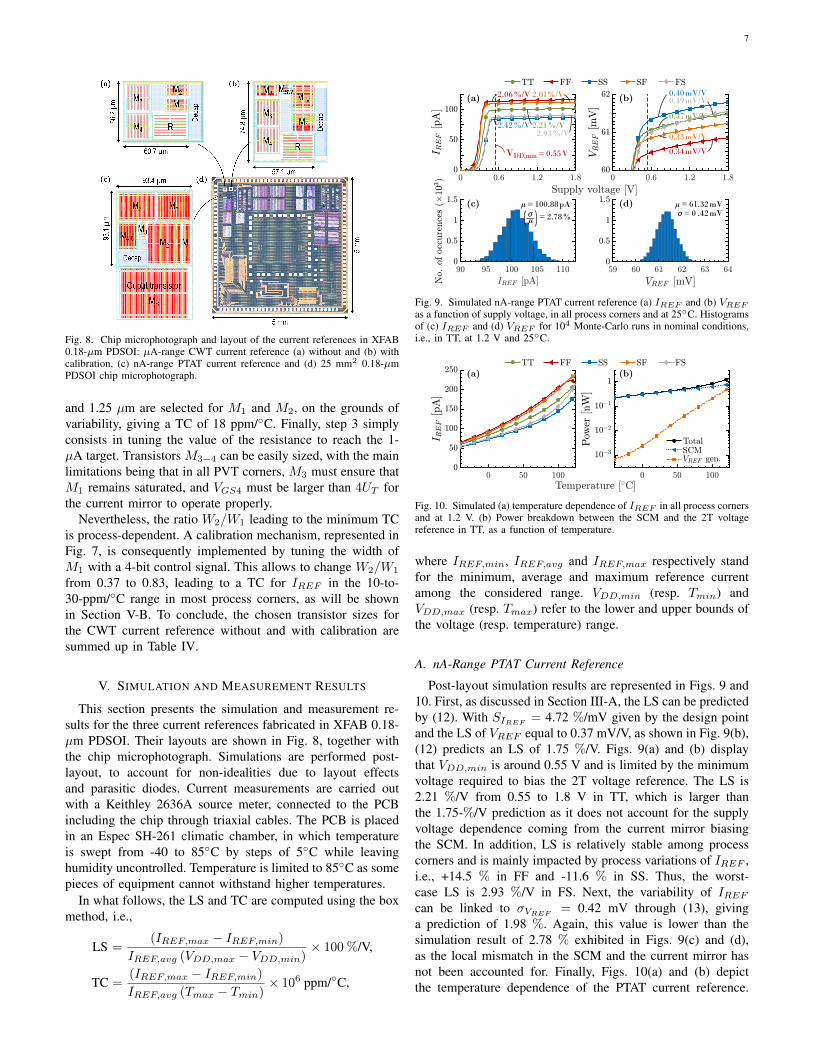
A. nA-Range PTAT Current Reference
Post-layout simulation results are represented in Figs. 9 and10. First, as discussed in Section III-A, the LS can be predictedby (12). With SIREF
= 4.72 %/mV given by the design pointand the LS of VREF equal to 0.37 mV/V, as shown in Fig. 9(b),(12) predicts an LS of 1.75 %/V. Figs. 9(a) and (b) displaythat VDD,min is around 0.55 V and is limited by the minimumvoltage required to bias the 2T voltage reference. The LS is2.21 %/V from 0.55 to 1.8 V in TT, which is larger thanthe 1.75-%/V prediction as it does not account for the supplyvoltage dependence coming from the current mirror biasingthe SCM. In addition, LS is relatively stable among processcorners and is mainly impacted by process variations of IREF ,i.e., +14.5 % in FF and -11.6 % in SS. Thus, the worst-case LS is 2.93 %/V in FS. Next, the variability of IREFcan be linked to σVREF
= 0.42 mV through (13), givinga prediction of 1.98 %. Again, this value is lower than thesimulation result of 2.78 % exhibited in Figs. 9(c) and (d),as the local mismatch in the SCM and the current mirror hasnot been accounted for. Finally, Figs. 10(a) and (b) depictthe temperature dependence of the PTAT current reference.
8
µ= 1.48%/Vσ= 0.30%/V
µ= 96.13pA
VDD,min = 0.55V
= 1.66%µ σ
Fig. 11. Measured average (a) IREF and (c) power consumption vs. VDD at25C, with (b)-(d) details of the 10 dies, for the nA-range current reference.Histograms of (e) IREF and (f) LS across the 10 dies.
µ= 0.75%/°Cσ= 0.01%/°C
VREF gen. power dominates at high temperature
Fig. 12. Measured temperature dependence of (a) IREF and (d) powerconsumption at 0.9 V, for all 10 dies. (b) Power breakdown between theSCM and the 2T voltage reference. (d) Histogram of TC across the 10 dies.
Fig. 10(a) highlights that IREF is approximetaly linear withtemperature up to 100C in TT. Above it, nonlinearitiesinduced by leakage in parasitic nwell/psub diodes appear. Thistranslates to a 0.92-%/C TC for IREF between -40 and125C in TT. Fig. 10(b) demonstrates that power consumptionis linear with temperature below 60C, and is dominated bythe SCM which draws a current proportional to IREF . Then,power increases exponentially with temperature due to the2T voltage reference, whose power consumption scales withdrain-to-source leakage.
Measurement results are presented in Figs. 11 and 12. Inwhat follows, the reference current is measured as the draincurrent of M8 (Fig. 8(c)), divided by a fixed ratio of 36.4,obtained from nominal simulations. Firstly, Fig. 11(a) showsthe average IREF as a function of VDD, and only differsfrom post-layout simulations by a small overshoot at 0.5 V.
VDD,min = 0.65V
0.53%/V
0.65%/V
0.48%/V
0.63%/V
0.51%/V
1.35mV/V
1.25mV/V
1.52mV/V
1.56mV/V1.34mV/V
Fig. 13. Simulated µA-range CWT current reference (a) IREF and (b)VREF , as a function of supply voltage, in all process corners and at 25C.
18ppm/°C
229ppm/°C
134ppm/°C
212ppm/°C68ppm/°C
11ppm/°C (0001)
119ppm/°C (0000)
17ppm/°C (0110)
24ppm/°C (1101)
26ppm/°C (1001)
Fig. 14. Simulated temperature dependence of IREF (a) without and (b)with TC calibration, in all process corners and at 1.2 V.
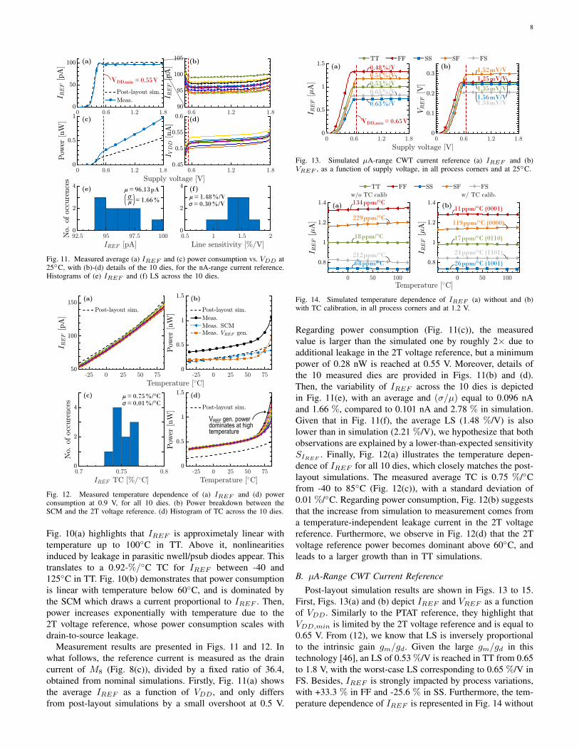
Regarding power consumption (Fig. 11(c)), the measuredvalue is larger than the simulated one by roughly 2× due toadditional leakage in the 2T voltage reference, but a minimumpower of 0.28 nW is reached at 0.55 V. Moreover, details ofthe 10 measured dies are provided in Figs. 11(b) and (d).Then, the variability of IREF across the 10 dies is depictedin Fig. 11(e), with an average and (σ/µ) equal to 0.096 nAand 1.66 %, compared to 0.101 nA and 2.78 % in simulation.Given that in Fig. 11(f), the average LS (1.48 %/V) is alsolower than in simulation (2.21 %/V), we hypothesize that bothobservations are explained by a lower-than-expected sensitivitySIREF
. Finally, Fig. 12(a) illustrates the temperature depen-dence of IREF for all 10 dies, which closely matches the post-layout simulations. The measured average TC is 0.75 %/Cfrom -40 to 85C (Fig. 12(c)), with a standard deviation of0.01 %/C. Regarding power consumption, Fig. 12(b) suggeststhat the increase from simulation to measurement comes froma temperature-independent leakage current in the 2T voltagereference. Furthermore, we observe in Fig. 12(d) that the 2Tvoltage reference power becomes dominant above 60C, andleads to a larger growth than in TT simulations.
B. µA-Range CWT Current ReferencePost-layout simulation results are shown in Figs. 13 to 15.
First, Figs. 13(a) and (b) depict IREF and VREF as a functionof VDD. Similarly to the PTAT reference, they highlight thatVDD,min is limited by the 2T voltage reference and is equal to0.65 V. From (12), we know that LS is inversely proportionalto the intrinsic gain gm/gd. Given the large gm/gd in thistechnology [46], an LS of 0.53 %/V is reached in TT from 0.65to 1.8 V, with the worst-case LS corresponding to 0.65 %/V inFS. Besides, IREF is strongly impacted by process variations,with +33.3 % in FF and -25.6 % in SS. Furthermore, the tem-perature dependence of IREF is represented in Fig. 14 without

9
µ= 1.00µA
= 0.41%µ σ
µ= 252.66mVσ= 1 02mV
Fig. 15. Simulated temperature dependence of (a) IREF and (b) VREF with±1σ, for 104 Monte-Carlo runs in TT and at 1.2 V.
Fig. 16. Measured (a) temperature dependence of IREF at 0.9 V, for all16 calibration codes on a single die, for the µA-range current reference. (b)IREF TC obtained for each calibration code, in TT post-layout simulationsand in measurement.
µ= 0.99µA
µ= 1.09µA
µ= 0.195%/V
µ= 0.207%/V
= 0 .65%µ σ
= 0 .87%µ σ
VDD,min = 0.65V
σ= 0.011%/V
σ= 0.016%/V
Fig. 17. Measured (a) average IREF vs. VDD , and details of the 10 dies(c) without and (e) with TC calibration, at 25C. Histograms of (b) IREF
and LS (d) without and (f) with TC calibration, across the 10 dies.
and with TC calibration. Fig. 14(a) illustrates that withoutTC calibration, an excellent TC of 18 ppm/C is obtainedin TT, but it degrades in skewed corners with 229 ppm/CPTAT in SF and 212 ppm/C CTAT in FS, due to a changeof temperature dependence of VREF . Nevertheless, Fig. 14(b)demonstrates that a simple 4-bit calibration of the W2/W1
width ratio (Fig. 7) can reduce the TC below 30 ppm/C in allprocess corners except for SF, in which the 119 ppm/C PTATTC would require a slightly larger tuning range. Lastly, inFig. 15(a), IREF presents a 2nd order temperature dependencebelow 100C, and leakage leads to a current increase abovethis limit. Moreover, the (σ/µ)’s of IREF and VREF are equal,
µ= 290ppm/°C
µ= 38ppm/°C
σ= 17ppm/°C
σ= 13ppm/°C
Fig. 18. Measured temperature dependence of IREF (a) without TC calibra-tion, (b) with TC calibration and (d) with TC calibration and normalization,at 0.9 V. (c) Histogram of IREF TC across the 10 dies.
as stated by (13), and amount to 0.41 % (Figs. 15(a) and(b)), featuring a perfect match between theory and simulations.Regarding IREF , its average value is 1 µA at 25C, and itsaverage TC reaches 14.9 ppm/C, with a variability of 2.14 %.Measurement results are summarized in Figs. 16 to 18. As the
TC of IREF is mostly impacted by process variations ratherthan local mismatch, we select the optimal code by sweepingthe 16 calibration codes on a single die, as shown in Fig. 16(a).Because we are using a voltage reference with pMOS devicesfor M1−2 and the control switches, increasing the calibrationcode decreases the actual W1, thus reducing the PTAT part ofVREF and boosting the CTAT behavior of IREF . Based onFig. 16(b), we select a code of 0x0001 with a 36.4-ppm/CTC, which is different from the simulated one, here 0x0110with a 19.2-ppm/C TC, likely due to process variations. Next,Fig. 17(a) shows the average IREF behavior with supplyvoltage, with a VDD,min at 0.65 V and a slight increase ofIREF from 0.99 to 1.09 µA due to TC calibration (Fig. 18(b)).In both cases, the average LS is around 0.20 %/V, whichrepresents a 2.7× reduction compared to simulations and couldresult from a larger gm/gd. Variability reaches 0.65 % and0.87 % without and with TC calibration (Fig. 17(b)). Thelarger value compared to 0.41 % in simulation likely comesfrom the yellow and red curves on the bottom of Figs. 17(c)and (e), which appear to be outliers leading to an overesti-mation of (σ/µ). To conclude, the temperature dependenceof IREF is represented in Figs. 18(a) and (b). On one side,without calibration, IREF presents a CTAT behavior leading toa TC of 290 ppm/C in the -40-to-85C range. On the otherside, with calibration, the TC reduces down to 38 ppm/C,corresponding to a 7.6× improvement. In Figs. 18(b) and(d), we observe a 2nd order temperature dependence below70C, as predicted by simulations. A small current surgeabove this limit comes from the power consumption of the2T voltage reference, which is measured together with thereference current, but is not taken into account in the TC.
10
VI. IMPLEMENTATION IN SCALED TECHNOLOGIES
Novel current references are often developed in the 0.18-µm technology node or above. However, their portability tocommon scaled technologies such as 65-nm bulk, 28-nm fully-depleted SOI (FDSOI), or 14-nm FinFET, is hardly discussedand poses a series of challenges. This section details thesechallenges and how they can be overcome for the proposedfamily of current references by focusing on the implementationof the 2T voltage reference.
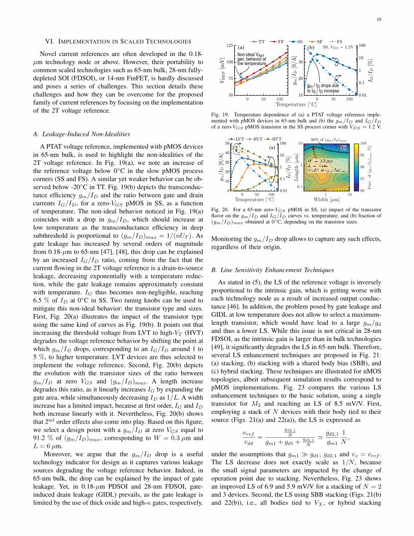
A. Leakage-Induced Non-Idealities
A PTAT voltage reference, implemented with pMOS devicesin 65-nm bulk, is used to highlight the non-idealities of the2T voltage reference. In Fig. 19(a), we note an increase ofthe reference voltage below 0C in the slow pMOS processcorners (SS and FS). A similar yet weaker behavior can be ob-served below -20C in TT. Fig. 19(b) depicts the transconduc-tance efficiency gm/ID and the ratio between gate and draincurrents IG/ID, for a zero-VGS pMOS in SS, as a functionof temperature. The non-ideal behavior noticed in Fig. 19(a)coincides with a drop in gm/ID, which should increase atlow temperature as the transconductance efficiency in deepsubthreshold is proportional to (gm/ID)max = 1/(nUT ). Asgate leakage has increased by several orders of magnitudefrom 0.18-µm to 65-nm [47], [48], this drop can be explainedby an increased IG/ID ratio, coming from the fact that thecurrent flowing in the 2T voltage reference is a drain-to-sourceleakage, decreasing exponentially with a temperature reduc-tion, while the gate leakage remains approximately constantwith temperature. IG thus becomes non-negligible, reaching6.5 % of ID at 0C in SS. Two tuning knobs can be used tomitigate this non-ideal behavior: the transistor type and sizes.First, Fig. 20(a) illustrates the impact of the transistor typeusing the same kind of curves as Fig. 19(b). It points out thatincreasing the threshold voltage from LVT to high-VT (HVT)degrades the voltage reference behavior by shifting the point atwhich gm/ID drops, corresponding to an IG/ID around 1 to5 %, to higher temperature. LVT devices are thus selected toimplement the voltage reference. Second, Fig. 20(b) depictsthe evolution with the transistor sizes of the ratio betweengm/ID at zero VGS and (gm/ID)max. A length increasedegrades this ratio, as it linearly increases IG by expanding thegate area, while simultaneously decreasing ID as 1/L. A widthincrease has a limited impact, because at first order, IG and IDboth increase linearly with it. Nevertheless, Fig. 20(b) showsthat 2nd order effects also come into play. Based on this figure,we select a design point with a gm/ID at zero VGS equal to91.2 % of (gm/ID)max, corresponding to W = 0.3 µm andL = 6 µm.
Moreover, we argue that the gm/ID drop is a usefultechnology indicator for design as it captures various leakagesources degrading the voltage reference behavior. Indeed, in65-nm bulk, the drop can be explained by the impact of gateleakage. Yet, in 0.18-µm PDSOI and 28-nm FDSOI, gate-induced drain leakage (GIDL) prevails, as the gate leakage islimited by the use of thick oxide and high-κ gates, respectively.
gm / ID drops due to IG / ID increase
Non-ideal VREF gen. behavior at low temperature
Fig. 19. Temperature dependence of (a) a PTAT voltage reference imple-mented with pMOS devices in 65-nm bulk and (b) the gm/ID and IG/IDof a zero-VGS pMOS transistor in the SS process corner with VDS = 1.2 V.
Fig. 20. For a 65-nm zero-VGS pMOS in SS, (a) impact of the transistorflavor on the gm/ID and IG/ID curves vs. temperature, and (b) fraction of(gm/ID)max obtained at 0C, depending on the transistor sizes.
Monitoring the gm/ID drop allows to capture any such effects,regardless of their origin.
B. Line Sensitivity Enhancement Techniques
As stated in (5), the LS of the reference voltage is inverselyproportional to the intrinsic gain, which is getting worse witheach technology node as a result of increased output conduc-tance [46]. In addition, the problem posed by gate leakage andGIDL at low temperature does not allow to select a maximum-length transistor, which would have lead to a large gm/gdand thus a lower LS. While this issue is not critical in 28-nmFDSOI, as the intrinsic gain is larger than in bulk technologies[49], it significantly degrades the LS in 65-nm bulk. Therefore,several LS enhancement techniques are proposed in Fig. 21:(a) stacking, (b) stacking with a shared body bias (SBB), and(c) hybrid stacking. These techniques are illustrated for nMOStopologies, albeit subsequent simulation results correspond topMOS implementations. Fig. 23 compares the various LSenhancement techniques to the basic solution, using a singletransistor for M2 and reaching an LS of 8.5 mV/V. First,employing a stack of N devices with their body tied to theirsource (Figs. 21(a) and 22(a)), the LS is expressed as
vrefvdd
=gd2,1N
gm1 + gd1 +gd2,1N
' gd2,1gm1
1
N,
under the assumptions that gm1 gd1, gd2,1 and vx = vref .The LS decrease does not exactly scale as 1/N , becausethe small signal parameters are impacted by the change ofoperation point due to stacking. Nevertheless, Fig. 23 showsan improved LS of 6.9 and 5.9 mV/V for a stacking of N = 2and 3 devices. Second, the LS using SBB stacking (Figs. 21(b)and 22(b)), i.e., all bodies tied to VX , or hybrid stacking
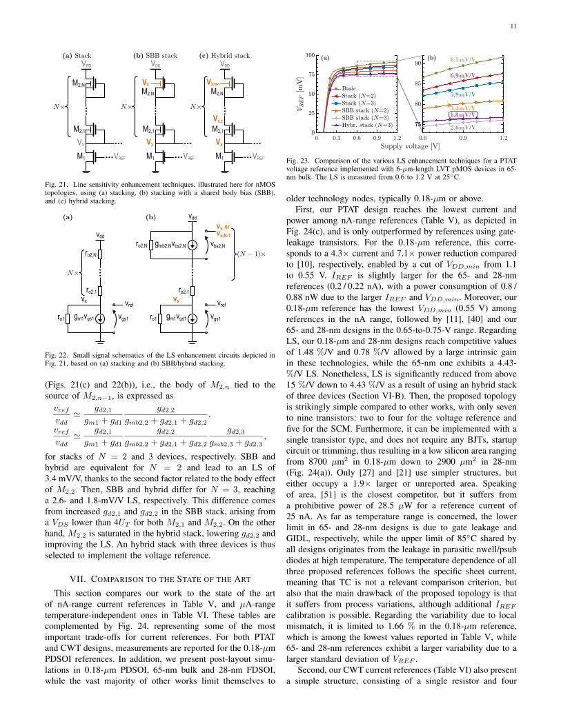
11
M1
M2,1
VX
VDD
VREF
M2,N
M1
M2,1
VX
VDD
VREF
M2,N
VX
M1
M2,1
VX
VDD
VREF
M2,N
VX,N-1
VX,2
Fig. 21. Line sensitivity enhancement techniques, illustrated here for nMOStopologies, using (a) stacking, (b) stacking with a shared body bias (SBB),and (c) hybrid stacking.
vdd
gm1vgs1ro1
vx
vgs1
vref
ro2,1
vbs2,Nro2,N gmb2,Nvbs2,N
ro2,N
vdd
gm1vgs1ro1
vx
vgs1
vref
ro2,1
vx or
vx,N-1
Fig. 22. Small signal schematics of the LS enhancement circuits depicted inFig. 21, based on (a) stacking and (b) SBB/hybrid stacking.
(Figs. 21(c) and 22(b)), i.e., the body of M2,n tied to thesource of M2,n−1, is expressed asvrefvdd' gd2,1gm1 + gd1
gd2,2gmb2,2 + gd2,1 + gd2,2
,
vrefvdd' gd2,1gm1 + gd1
gd2,2gmb2,2 + gd2,1 + gd2,2
gd2,3gmb2,3 + gd2,3
,
for stacks of N = 2 and 3 devices, respectively. SBB andhybrid are equivalent for N = 2 and lead to an LS of3.4 mV/V, thanks to the second factor related to the body effectof M2,2. Then, SBB and hybrid differ for N = 3, reachinga 2.6- and 1.8-mV/V LS, respectively. This difference comesfrom increased gd2,1 and gd2,2 in the SBB stack, arising froma VDS lower than 4UT for both M2,1 and M2,2. On the otherhand, M2,2 is saturated in the hybrid stack, lowering gd2,2 andimproving the LS. An hybrid stack with three devices is thusselected to implement the voltage reference.
VII. COMPARISON TO THE STATE OF THE ART
This section compares our work to the state of the artof nA-range current references in Table V, and µA-rangetemperature-independent ones in Table VI. These tables arecomplemented by Fig. 24, representing some of the mostimportant trade-offs for current references. For both PTATand CWT designs, measurements are reported for the 0.18-µmPDSOI references. In addition, we present post-layout simu-lations in 0.18-µm PDSOI, 65-nm bulk and 28-nm FDSOI,while the vast majority of other works limit themselves to
6.9mV/V
8.5mV/V
5.9mV/V
3.4mV/V1.8mV/V
2.6mV/V
Fig. 23. Comparison of the various LS enhancement techniques for a PTATvoltage reference implemented with 6-µm-length LVT pMOS devices in 65-nm bulk. The LS is measured from 0.6 to 1.2 V at 25C.
older technology nodes, typically 0.18-µm or above.First, our PTAT design reaches the lowest current and
power among nA-range references (Table V), as depicted inFig. 24(c), and is only outperformed by references using gate-leakage transistors. For the 0.18-µm reference, this corre-sponds to a 4.3× current and 7.1× power reduction comparedto [10], respectively, enabled by a cut of VDD,min from 1.1to 0.55 V. IREF is slightly larger for the 65- and 28-nmreferences (0.2 / 0.22 nA), with a power consumption of 0.8 /0.88 nW due to the larger IREF and VDD,min. Moreover, our0.18-µm reference has the lowest VDD,min (0.55 V) amongreferences in the nA range, followed by [11], [40] and our65- and 28-nm designs in the 0.65-to-0.75-V range. RegardingLS, our 0.18-µm and 28-nm designs reach competitive valuesof 1.48 %/V and 0.78 %/V allowed by a large intrinsic gainin these technologies, while the 65-nm one exhibits a 4.43-%/V LS. Nonetheless, LS is significantly reduced from above15 %/V down to 4.43 %/V as a result of using an hybrid stackof three devices (Section VI-B). Then, the proposed topologyis strikingly simple compared to other works, with only sevento nine transistors: two to four for the voltage reference andfive for the SCM. Furthermore, it can be implemented with asingle transistor type, and does not require any BJTs, startupcircuit or trimming, thus resulting in a low silicon area rangingfrom 8700 µm2 in 0.18-µm down to 2900 µm2 in 28-nm(Fig. 24(a)). Only [27] and [21] use simpler structures, buteither occupy a 1.9× larger or unreported area. Speakingof area, [51] is the closest competitor, but it suffers froma prohibitive power of 28.5 µW for a reference current of25 nA. As far as temperature range is concerned, the lowerlimit in 65- and 28-nm designs is due to gate leakage andGIDL, respectively, while the upper limit of 85C shared byall designs originates from the leakage in parasitic nwell/psubdiodes at high temperature. The temperature dependence of allthree proposed references follows the specific sheet current,meaning that TC is not a relevant comparison criterion, butalso that the main drawback of the proposed topology is thatit suffers from process variations, although additional IREFcalibration is possible. Regarding the variability due to localmismatch, it is limited to 1.66 % in the 0.18-µm reference,which is among the lowest values reported in Table V, while65- and 28-nm references exhibit a larger variability due to alarger standard deviation of VREF .
Second, our CWT current references (Table VI) also presenta simple structure, consisting of a single resistor and four

12
TABLE VCOMPARISON TABLE OF CWT (LEFT) AND PTAT (RIGHT, WITH TC HIGHLIGHTED IN GREEN) NA-RANGE CURRENT REFERENCES.
Cordova Dong Far Hirose Huang Huang Ji Kayahan Kim Wang Wang Camacho Camacho Lefebvre[29] [27] [33] [35] [15] [39] [50] [51] [21] [16] [40] [10] [11] This work
Publication ISCAS ESSCIRC ROPEC ESSCIRC ISCAS TCAS-II ISSCC TCAS-I ISCAS VLSI-DAT TCAS-I TCAS-II ISCAS TCAS-IYear 2017 2017 2015 2010 2010 2020 2017 2013 2016 2019 2019 2005 2008 2022
Type of work Sim. Silicon Sim. Silicon Sim. Silicon Silicon Silicon Sim. Silicon Silicon Silicon Silicon Silicon Sim.J Sim.J
Number of samples N/A 32† N/A 15 N/A 10 10 90 N/A 10 16 10 30 10 N/A N/A
Technology 0.18µm 0.18µm 0.18µm 0.35µm 0.18µm 0.18µm 0.18µm 0.35µm 0.13µm 0.18µm 0.18µm 1.5µm 0.18µm 0.18µm 65nm 28nmPDSOI FDSOI
IREF [nA] 10.86 35.02 14 9.95 2.05 11.6 6.64 25 27 6.46 9.77 0.41 0.9 0.096 0.22 0.2Power [nW] 30.5 1.02 150 88.53 5.1 48.64 9.3 28500 N/A 15.8 28 2 2.34 0.282 0.80 0.68
@0.9V @1.5V @1V @1.3V @0.85V @0.8V @N/A @5V @0.85V @0.7V @1.1V @0.65V @0.55V @0.7V @0.74VArea [mm2] 0.01 0.0169 0.0102 0.12 N/A 0.054 0.055 0.0053 N/A 0.062 0.055 0.045 0.01 0.0087 0.0054 0.0029
Supply range [V] 0.9 – 1.8 1.5 – 2.5 1 – 3.3 1.3 – 3 0.85 – 2.2 0.8 – 2 1.3 – 1.8 N/A 1.2 0.85 – 2 0.7 – 1.2 1.1 – 3 0.65 – 2 0.55 – 1.8 0.7 – 1.2 0.74 – 1.8LS [%/V] 0.54 3 0.1 0.046 1.35 1.08 1.16 150 N/A 4.15 0.6 3.5/6∗ 0.2 1.48 4.43 0.78
Temperature range [C] -20 – 120 -40 – 120 0 – 70 -20 – 80 0 – 150 -40 – 120 0 – 110 0 – 80 -30 – 150 -10 – 100 -40 – 125 -20 – 70 -70 – 130 -40 – 85 0 – 85 -20 – 85TC [ppm/C] 108 282 20 1200 91 169 ‡ 680/283/ 128 (sim.) 327 138. 149.8 470/2500∗ 3000 7500 2930 1095
IREF var. (process) [%] 15.8 4.7 N/A N/A 7.5 +17.6/-10.3 N/A 8/1.22∗ 3.7 N/A +11.7/-8.7 N/A N/A +14.5/-14.6 +25.1/-2.0 +5.3/6.3IREF var. (mismatch) [%] 11.6? 1.6 5.8 14.1 N/A 4.3 4.07/1.19∗ 1.4 (sim.) N/A 3.33 1.6 10 2.67 1.66 2.59 4.06
Trimming type 6b for N/A N/A 3b for N/A 6b for N/A N/A N/A N/A 5b for N/A N/A N/A N/A N/AVS gen. IN /IP sub. TC/VREF SCM width
Complexity 25T >4T+2C 31T 52T 10T 23T+4C+2R >18T+1R 11T+1R 7T+1R 12T 23T+2C+2R 10T 16T+1C 7T 9T 8TSpecial components ZVT No No No No Resistor Resistor, Resistor Resistor No Resistor No No No No No
transistor 1BJT∗ Simulation and measurement results. ? Variability is due to the combined effects of process and mismatch variations. It is equal to 15.8 % for the untrimmed current reference and 11.6 %for the trimmed one. † 16 dies for the TT process corner and 4 dies for each of the FF, SS, SF and FS process corners. ‡ Average of the measurement results. Estimated from Fig. 3 of [39]./ Untrimmed and trimmed results. . Minimum of the measurement results. J In this work, simulations refer to post-layout simulations including parasitic diodes.
TABLE VICOMPARISON TABLE OF µA-RANGE TEMPERATURE-INDEPENDENT CURRENT REFERENCES.
Azcona Bendali Crupi Eslampanah Fiori Lee Liu Osipov Serrano Wang Wu Yang Yoo Lefebvre[23] [25] [30] [52] [20] [42] [36] [22] [53] [7] [38] [37] [34] This work
Publication ISCAS TCAS-I ISCAS TCAS-II JSSC ISCAS TCAS-I JSSC TVLSI CICC ASSCC TCAS-IYear 2014 2007 2017 2017 2005 2012 2010 2019 2008 2017 2015 2009 2007 2022
Type of work Sim. Silicon Silicon Silicon Sim. Silicon Sim. Silicon Silicon Silicon Silicon Silicon Silicon Silicon Sim.. Sim..
Number of samples N/A 19 45 5 N/A 10 N/A 10 N/A 12 N/A N/A N/A 10 N/A N/A
Technology 0.18µm 0.18µm 0.18µm 0.18µm 0.35µm 0.18µm 0.18µm 0.35µm 0.5µm 65nm 0.18µm 0.35µm 0.25µm 0.18µm 65nm 28nmBiCMOS PDSOI FDSOI
IREF [µA] 0.5 144.3 0.34 1.5 13.65 7.81 10 1.05 16 – 50 9.42 20 16.5 10.45 0.99 / 1.09 1 1Power [µW] 1.98 83 0.21 1.38 68.25 1.4 80 3.8 N/A 7.18 48 N/A 77 0.64 / 0.71 0.68 0.80
@1.2V @1V @0.45V @0.8V @2.5V @1V @2V @2V @1.4V @2.4V @1.1V @0.65V @0.7V @0.8VArea [mm2] N/A 0.213? 0.00075 0.003 0.0042 0.023 N/A 0.057 0.06/ 0.089 0.005 0.0576 0.002 0.0034 / 0.0043 0.002 0.00044
Supply range [V] 1.2 – 3 1 0.45 – 1.8 0.8 – 2 2.5 1 – 1.2 2 – 3 2 – 3.6 2.3 – 3.3 1.3 – 2.5 2.4 – 3 2 – 3.3 1.1 – 3 0.65 – 1.8 0.7 – 1.2 0.8 – 1.8LS [%/V] 0.69 N/A 3.9 N/A 0.4 N/A 3 2.73 <1 0.018 0.5 N/A 0.17 0.20 / 0.21 4.38 0.57
Temperature range [C] -40 – 120 0 – 100 0 – 80 -40 – 110 -30 – 100 0 – 100 -20 – 120 -45 – 125 0 – 80 -30 – 90 -40 – 80 -20 – 100 0 – 120 -40 – 85 0 – 125 -40 – 125TC [ppm/C] 119 185 578 571 28 24.9 170 143 (min.) <130 86 (min.) 130 280∗ 720 290 / 38J 37.33I 38.42I
247 (avg.) 119 (avg.)
IREF var. (process) [%] 1.3∗ 7† N/A 8.5 N/A 4.5 2.14† N/A N/A 5.13 N/A 0.52∗ N/A +33.3/-25.9 +46.7/-22.6 +9.8/-10.1IREF var. (mismatch) [%] N/A 2.7‡ N/A N/A N/A 3.9 <0.02 0.4 14 N/A N/A 0.65 / 0.87 0.68 0.85
Trimming type 2b for TC N/A 4b for TC N/A N/A N/A N/A N/A Floating charge N/A N/A 10b for TC N/A 4b for TC N/A N/A2b for IREF 4b for IREF for TC, IREF 8b for IREF
Complexity 39T+2R 30T+2C+5R 2T 4T+2R 5T+2R 12T+1C+2R 38T 5T+1R >26T+5C+4R >28T+3R 15T+2R 27T+2R 18T+3R 4/12T+1R 5T+1R 4T+1RSpecial components Resistor Resistor, No Resistor Resistor Resistor 3BJT Resistor Resistor Resistor Resistor, Resistor, Resistor Resistor Resistor Resistor
2BJT 2BJT 5BJT∗ After trimming. ? Estimated from the microphotograph in Fig. 6 of [25]. † Variability is due to the combined effects of process and mismatch variations. ‡ Before trimming. Line sensitivity is notmeasured because the current reference is supplied by a bandgap reference (BGR). / The total area is split between the current reference (0.015 mm2) and the charge pumps (0.045 mm2).. In this work, simulations refer to post-layout simulations including parasitic diodes. J Average of the measurement results over 10 samples. I Median of 104 local mismatch Monte-Carlo runs.
to five transistors, depending on the voltage reference imple-mentation. Therefore, the silicon area is modest compared toother µA-range references (Fig. 24(a)), with 3410 / 4270 µm2
in 0.18-µm, down to a best-in-class 440-µm2 area in 28-nm.[30] has both a small 750-µm2 area and a simple structure,as it relies on a 2T voltage reference to bias a transistor gate(Fig. 1(b)), but it suffers from degraded LS and TC, and has alimited 0-to-80C temperature range. [52], [20] and [22] relyon a handful of components, but [52] has a large 0.003-mm2
area, and [20], [22] require a substantial supply voltage above2 V to operate. [34] occupies a limited 2000-µm2 area, but its720-ppm/C TC is relatively poor, and the 18T+3R structurewill likely lead to prohibitive variability due to local mismatch.Regarding TC, our three references feature a very low 38-ppm/C TC for this current level (Fig. 24(d)), and offer thebest trade-off between TC and silicon area (Fig. 24(b)). Otherworks in Table VI present a low TC, such as [20] with 28
ppm/C, which requires a 2.5-V supply voltage and consumesa considerable 68.3-µW power, and [42] with 25 ppm/C,which necessitates a bandgap reference voltage to have adecent LS and occupies 5.3× more area than our largestdesign. As for other metrics, LS amounts to 0.2 %/V and0.57 %/V in 0.18-µm and 28-nm, but increases up to 4.38 %/Vin 65-nm, despite the use of an SBB stack of two devices. Onone side, the lower temperature limit is -40C, except in 65-nm where it rises to 0C due to gate leakage. On the otherside, the upper limit is 125C, except in 0.18-µm where it islimited to 85C by the measurement equipment. Similarly totheir PTAT counterparts, our CWT references are significantlyaffected by process variations, an issue that can be alleviatedthrough a calibration of IREF . Nevertheless, variability due tolocal mismatch is comprised between 0.65 and 0.87 %, whichis among the best in the state of the art.

13
Gate-leakagetransistors
Gate-leakagetransistors
Gate-leakagetransistors
TC calib.
TC calib.
Fig. 24. Illustration of the trade-offs between (a) area and IREF , (b) areaand TC, (c) power and IREF , and (d) IREF and TC, based on the state ofthe art of nA- and µA-range current references, and few additional references.
VIII. CONCLUSION
In this work, we proposed two novel current referencetopologies sharing two key ideas: (i) the generation of avoltage reference by a 2T ULP structure and (ii) its bufferingonto a V-to-I converter by a single transistor. These referencesare fabricated in a 0.18-µm PDSOI process. First, a nA-range PTAT current is obtained by biasing an SCM with aPTAT voltage. It generates a 0.096-nA current, the lowest todate for current references without gate-leakage transistors,and it does so while consuming only 0.28 nW at 0.55 Vand 25C. Second, a µA-range CWT current is obtained bybiasing a polysilicon resistor with a matched-TC voltage.It generates either a 0.99-µA current with a 290-ppm/CCTAT TC, or a 1.09-µA current with a 38-ppm/C TC,using a 4-bit calibration of the 2T voltage reference widthratio. Both references exhibit a decent LS (1.48 / 0.21 %/V),a low VDD,min (0.55 / 0.65 V), a low variability due tolocal mismatch (1.66 / 0.87 %), while relying on simple 7T/ 4T+1R structures without any startup circuit and occupyinga limited silicon area of 8700 / 4270 µm2. The main drawbackof such architectures is their sensitivity to process variations.Furthermore, we discuss the challenges posed by gate leakage,GIDL, and declining intrinsic gain to the implementation of2T voltages references in scaled 65- and 28-nm technologies.We demonstrate that a proper selection of the transistor typeand sizes, together with the use of LS enhancement techniques,can mitigate these non-idealities.
ACKNOWLEDGMENT
The authors would like to thank Pierre Gerard for themeasurement testbench, Eleonore Masarweh for the micropho-tograph, Denis Flandre and UCLouvain colleagues for fruitfuldiscussions, and ECS group members for their proofreading.
REFERENCES
[1] D. Blaauw et al., “IoT Design Space Challenges: Circuits and Systems,”in Proc. IEEE Symp. VLSI Technol., 2014, pp. 1–2.
[2] J. Zhang, Z. Wang, and N. Verma, “In-memory computation of amachine-learning classifier in a standard 6T SRAM array,” IEEE J.Solid-State Circuits, vol. 52, no. 4, pp. 915–924, 2017.
[3] S. Yin, X. Sun, S. Yu, and J.-s. Seo, “High-Throughput In-MemoryComputing for Binary Deep Neural Networks with MonolithicallyIntegrated RRAM and 90-nm CMOS,” IEEE Trans. Electron Devices,vol. 67, no. 10, pp. 4185–4192, 2020.
[4] M. Seok, G. Kim, D. Blaauw, and D. Sylvester, “A Portable 2-TransistorPicowatt Temperature-Compensated Voltage Reference Operating at0.5V,” IEEE J. Solid-State Circuits, vol. 47, no. 10, pp. 2534–2545,Oct. 2012.
[5] A. Campos De Oliveira, D. Cordova, H. Klimach, and S. Bampi, “A0.12-0.4V, Versatile 3-Transistor CMOS Voltage Reference for Ultra-Low Power Systems,” IEEE Trans. Circuits Syst. I, Reg. Papers, vol. 65,no. 11, pp. 3790–3799, Sept. 2018.
[6] L. Fassio, L. Lin, R. De Rose, M. Lanuzza, F. Crupi, and M. Alioto,“Trimming-Less Voltage Reference for Highly Uncertain HarvestingDown to 0.25 V, 5.4 pW,” IEEE J. Solid-State Circuits, vol. 56, no. 10,pp. 3134–3144, Oct. 2021.
[7] D. Wang, X. L. Tan, and P. K. Chan, “A 65-nm CMOS Constant CurrentSource with Reduced PVT Variation,” IEEE Trans. Very Large ScaleIntegr. (VLSI) Syst., vol. 25, no. 4, pp. 1373–1385, Dec. 2016.
[8] H. Wang and P. P. Mercier, “A 3.4-pW 0.4-V 469.3ppm/C Five-Transistor Current Reference Generator,” IEEE Solid-State Circuits Lett.,vol. 1, no. 5, pp. 122–125, May 2018.
[9] H. Zhuang, J. Guo, C. Tong, X. Peng, and H. Tang, “A 8.2-pW 2.4-pACurrent Reference Operating at 0.5V with No Amplifiers or Resistors,”IEEE Trans. Circuits Syst. II, Exp. Briefs, vol. 67, no. 7, pp. 1204–1208,July 2020.
[10] E. M. Camacho-Galeano, C. Galup-Montoro, and M. C. Schneider, “A 2-nW 1.1-V Self-Biased Current Reference in CMOS Technology,” IEEETrans. Circuits Syst. II, Exp. Briefs, vol. 52, no. 2, pp. 61–65, Feb. 2005.
[11] E. M. Camacho-Galeano, J. Q. Moreira, M. D. Pereira, A. J. Cardoso,C. Galup-Montoro, and M. C. Schneider, “Temperature Performance ofSub-1V Ultra-Low-Power Current Sources,” in Proc. IEEE Int. Symp.Circuits Syst., 2008, pp. 2230–2233.
[12] F. Serra-Graells and J. L. Huertas, “Sub-1-V CMOS Proportional-to-Absolute Temperature References,” IEEE J. Solid-State Circuits, vol. 38,no. 1, pp. 84–88, Jan. 2003.
[13] Y. Tsividis, Operation and Modeling of the MOS Transistor. SecondEdition. New York: McGraw-Hill, 1999.
[14] J. V. De la Cruz and A. L. Aita, “A 1-V PTAT Current Reference Circuitwith 0.05%/V Current Sensitivity to VDD ,” in Proc. IEEE Int. Symp.Circuits Syst., 2016, pp. 502–505.
[15] Z. Huang, Q. Luo, and Y. Inoue, “A CMOS Sub-lV Nanopower Currentand Voltage Reference with Leakage Compensation,” in Proc. IEEE Int.Symp. Circuits Syst., 2010, pp. 4069–4072.
[16] J. Wang and H. Shinohara, “A CMOS 0.85-V 15.8-nW Current andVoltage Reference without Resistors,” in 2019 Int. Symp. VLSI DesignAutom. Test, Hsinchu, Taiwan, Apr. 22-25, 2019, pp. 1–4.
[17] H. J. Oguey and D. Aebischer, “CMOS Current Reference withoutResistance,” IEEE J. Solid-State Circuits, vol. 32, no. 7, pp. 1132–1135,July 1997.
[18] T. Hirose, Y. Asai, Y. Amemiya, T. Matsuoka, and K. Taniguchi,“Ultralow-Power Temperature-Insensitive Current Reference Circuit,” inProc. IEEE Sensors, 2005, pp. 1205–1208.
[19] Y. Osaki, T. Hirose, N. Kuroki, and M. Numa, “A 95-nA, 523ppm/C,0.6-µW CMOS Current Reference Circuit with Subthreshold MOSResistor Ladder,” in 16th Asia and South Pacific Design Autom. Conf.,2011, pp. 113–114.
[20] F. Fiori and P. S. Crovetti, “A New Compact Temperature-CompensatedCMOS Current Reference,” IEEE Trans. Circuits Syst. II, Exp. Briefs,vol. 52, no. 11, pp. 724–728, Nov. 2005.
[21] T. Kim, T. Briant, C. Han, and N. Maghari, “A Nano-Ampere 2nd OrderTemperature-Compensated CMOS Current Reference Using Only SingleResistor for Wide-Temperature Range Applications,” in Proc. IEEE Int.Symp. Circuits Syst., 2016, pp. 510–513.
[22] D. Osipov and S. Paul, “Compact Extended Industrial Range CMOSCurrent References,” IEEE Trans. Circuits Syst. I, Reg. Papers, vol. 66,no. 6, pp. 1998–2006, Jan. 2019.
[23] C. Azcona, B. Calvo, S. Celma, N. Medrano, and M. T. Sanz, “PrecisionCMOS Current Reference with Process and Temperature Compensa-tion,” in Proc. IEEE Int. Symp. Circuits Syst., 2014, pp. 910–913.
[24] S. S. Chouhan and K. Halonen, “A 0.67-µW 177-ppm/C All-MOSCurrent Reference Circuit in a 0.18-µm CMOS Technology,” IEEETrans. Circuits Syst. II, Exp. Briefs, vol. 63, no. 8, pp. 723–727, Feb.2016.

14
[25] A. Bendali and Y. Audet, “A 1-V CMOS Current Reference withTemperature and Process Compensation,” IEEE Trans. Circuits Syst. I,Reg. Papers, vol. 54, no. 7, pp. 1424–1429, July 2007.
[26] K. Ueno, T. Hirose, T. Asai, and Y. Amemiya, “A 46-ppm/C Tem-perature and Process Compensated Current Reference with On-ChipThreshold Voltage Monitoring Circuit,” in 2008 IEEE Asian Solid-StateCircuits Conf., 2008, pp. 161–164.
[27] Q. Dong, I. Lee, K. Yang, D. Blaauw, and D. Sylvester, “A 1.02 nWPMOS-Only, Trim-Free Current Reference with 282ppm/C from -40Cto 120C and 1.6% within-wafer inaccuracy,” in IEEE 43rd Eur. SolidState Circuits Conf., 2017, pp. 19–22.
[28] M. Choi, I. Lee, T.-K. Jang, D. Blaauw, and D. Sylvester, “A 23pW,780ppm/C Resistor-Less Current Reference Using Subthreshold MOS-FETs,” in IEEE 40th Eur. Solid State Circuits Conf., 2014, pp. 119–122.
[29] D. Cordova, A. C. de Oliveira, P. Toledo, H. Klimach, S. Bampi, andE. Fabris, “A Sub-1 V, Nanopower, ZTC Based Zero-VT Temperature-Compensated Current Reference,” in Proc. IEEE Int. Symp. CircuitsSyst., 2017, pp. 1–4.
[30] F. Crupi, R. De Rose, M. Paliy, M. Lanuzza, M. Perna, and G. Iannac-cone, “A Portable Class of 3-Transistor Current References with Low-Power Sub-0.5V Operation,” Int. J. Circuit Theory Appl., vol. 46, no. 4,pp. 779–795, Dec. 2017.
[31] L. Fassio, L. Lin, R. De Rose, M. Lanuzza, F. Crupi, and M. Alioto,“A 0.6-to-1.8 V CMOS Current Reference with Near-100% PowerUtilization,” IEEE Trans. Circuits Syst. II, Exp. Briefs, vol. 68, no. 9,pp. 3038–3042, Sept. 2021.
[32] Y.-S. Park, H.-R. Kim, J.-H. Oh, Y.-K. Choi, and B.-S. Kong, “Compact0.7-V CMOS Voltage/Current Reference with 54/29-ppm/C Tempera-ture Coefficient,” in Proc. Int. SoC Design Conf., 2009, pp. 496–499.
[33] A. Far, “Subthreshold Current Reference Suitable for Energy Harvesting:20ppm/C and 0.1%/V at 140nW,” in 2015 IEEE Int. Autumn Meet.Power Electron. Comput., 2015, pp. 1–4.
[34] C. Yoo and J. Park, “CMOS Current Reference with Supply andTemperature Compensation,” Electron. Lett., vol. 43, no. 25, pp. 1422–1424, Dec. 2007.
[35] T. Hirose, Y. Osaki, N. Kuroki, and M. Numa, “A Nano-Ampere CurrentReference Circuit and its Temperature Dependence Control by UsingTemperature Characteristics of Carrier Mobilities,” in IEEE 36th Eur.Solid State Circuits Conf., 2010, pp. 114–117.
[36] W. Liu, W. Khalil, M. Ismail, and E. Kussener, “A Resistor-FreeTemperature-Compensated CMOS Current Reference,” in Proc. IEEEInt. Symp. Circuits Syst., 2010, pp. 845–848.
[37] B.-D. Yang, Y.-K. Shin, J.-S. Lee, Y.-K. Lee, and K.-C. Ryu, “An Ac-curate Current Reference Using Temperature and Process CompensationCurrent Mirror,” in Proc. IEEE Asian Solid-State Circuits Conf., 2009,pp. 241–244.
[38] C. Wu, W. L. Goh, C. L. Kok, W. Yang, and L. Siek, “A Low TC,Supply Independent and Process Compensated Current Reference,” inProc. IEEE Custom Integr. Circuits Conf., 2015, pp. 1–4.
[39] Q. Huang, C. Zhan, L. Wang, Z. Li, and Q. Pan, “A -40 C to 120 C,169 ppm/C Nano-Ampere CMOS Current Reference,” IEEE Trans.Circuits Syst. II, Exp. Briefs, vol. 67, no. 9, pp. 1494–1498, Sept. 2020.
[40] L. Wang and C. Zhan, “A 0.7-V 28-nW CMOS Subthreshold Voltageand Current Reference in One Simple Circuit,” IEEE Trans. CircuitsSyst. I, Reg. Papers, vol. 66, no. 9, pp. 3457–3466, Aug. 2019.
[41] H. Wang and P. P. Mercier, “A 14.5 pW, 31 ppm/C Resistor-Less 5pA Current Reference Employing a Self-Regulated Push-Pull VoltageReference Generator,” in Proc. IEEE Int. Symp. Circuits Syst., 2016,pp. 1290–1293.
[42] J. Lee and S. Cho, “A 1.4-µW 24.9-ppm/C Current Reference withProcess-Insensitive Temperature Compensation in 0.18-µm CMOS,”IEEE J. Solid-State Circuits, vol. 47, no. 10, pp. 2527–2533, July 2012.
[43] S. Adriaensen, V. Dessard, and D. Flandre, “25 to 300C Ultra-Low-Power Voltage Reference Compatible with Standard SOI CMOSProcess,” Electronics Letters, vol. 38, no. 19, pp. 1103–1104, September2002.
[44] A. I. A. Cunha, M. C. Schneider, and C. Galup-Montoro, “An MOSTransistor Model for Analog Circuit Design,” IEEE J. Solid-StateCircuits, vol. 33, no. 10, pp. 1510–1519, Oct. 1998.
[45] P. G. Jespers and B. Murmann, Systematic Design of Analog CMOSCircuits. Cambridge University Press, 2017.
[46] B. Murmann, P. Nikaeen, D. Connelly, and R. W. Dutton, “Impact ofScaling on Analog Performance and Associated Modeling Needs,” IEEETrans. Electron Devices, vol. 53, no. 9, pp. 2160–2167, Sept. 2006.
[47] L. L. Lewyn, T. Ytterdal, C. Wulff, and K. Martin, “Analog CircuitDesign in Nanoscale CMOS Technologies,” Proc. IEEE, vol. 97, no. 10,pp. 1687–1714, Oct. 2009.
[48] E. Bohannon, C. Washburn, and P. R. Mukund, “Analog IC De-sign in Ultra-Thin Oxide CMOS Technologies with Significant DirectTunneling-Induced Gate Current,” IEEE Trans. Circuits Syst. I, Reg.Papers, vol. 58, no. 4, pp. 645–653, Apr. 2011.
[49] A. Cathelin, “Fully Depleted Silicon on Insulator Devices CMOS: The28-nm Node Is the Perfect Technology for Analog, RF, mmW, andMixed-Signal System-on-Chip Integration,” IEEE Solid-State CircuitsMag., vol. 9, no. 4, pp. 18–26, Nov. 2017.
[50] Y. Ji, C. Jeon, H. Son, B. Kim, H.-J. Park, and J.-Y. Sim, “5.8 A 9.3 nWAll-in-One Bandgap Voltage and Current Reference Circuit,” in Proc.IEEE Int. Solid-State Circuits Conf., 2017, pp. 100–101.
[51] H. Kayahan, O. Ceylan, M. Yazici, S. Zihir, and Y. Gurbuz, “WideRange, Process and Temperature Compensated Voltage Controlled Cur-rent Source,” IEEE Trans. Circuits Syst. I, Reg. Papers, vol. 60, no. 5,pp. 1345–1353, March 2013.
[52] M. S. Eslampanah, S. Kananian, E. Zendehrouh, M. Sharifkhani, A. M.Sodagar, and M. Shabany, “A Low-Power Temperature-CompensatedCMOS Peaking Current Reference in Subthreshold Region,” in Proc.IEEE Int. Symp. Circuits Syst., 2017, pp. 1–4.
[53] G. Serrano and P. Hasler, “A Precision Low-TC Wide-Range CMOSCurrent Reference,” IEEE J. Solid-State Circuits, vol. 43, no. 2, pp.558–565, Feb. 2008.
Martin Lefebvre (S’17) received the M.Sc. de-gree (summa cum laude) in electromechanical en-gineering from the Universite catholique de Lou-vain (UCL), Louvain-la-Neuve, Belgium, in 2017,where he is currently pursuing the Ph.D. degree,under the supervision of Prof. D. Bol. His currentresearch interests include hardware-aware machinelearning algorithms, low-power mixed-signal visionchips for embedded image processing, and ultra-low-power current reference architectures. He servesas a reviewer for various conferences and journals,
including IEEE Trans. VLSI Syst., Int. Symp. on Circuits and Syst. and AsiaPacific Conf. on Circuits and Syst.
David Bol received the Ph.D degree in EngineeringScience from the Universite catholique de Louvain(UCLouvain), Louvain-la-Neuve, Belgium in 2008.In 2005, he was a visiting Ph.D student at theCNM National Centre for Microelectronics, Sevilla,Spain, in advanced logic design. In 2009, he wasa postdoctoral researcher at intoPIX, Louvain-la-Neuve, Belgium, in low-power image processing.In 2010, he was a visiting postdoctoral researcherat the UC Berkeley Laboratory for Manufacturingand Sustainability, Berkeley, CA, in life-cycle as-
sessment of the semiconductor environmental impacts. He is now an AssociateProfessor at UCLouvain. In 2015, he participated to the creation of e-peassemiconductors, Louvain-la-Neuve, Belgium. Prof. Bol leads the ElectronicCircuits and Systems (ECS) group focused on ultra-low-power design of inte-grated circuits for the IoT and biomedical applications including computing,power management, sensing and wireless communications. He is engaged ina social-ecological transition in the field of ICT research. He co-teaches fourM.S. courses on digital, analog and mixed-signal ICs, sensors and systems,with two B.S. courses including the course on Sustainable Development andTransition. Prof. Bol has authored or co-authored more than 120 technicalpapers and conference contributions and holds three delivered patents. He (co-)received four Best Paper/Poster/Design Awards in IEEE conferences (ICCD2008, SOI Conf. 2008, FTFC 2014, ISCAS 2020). He serves as a reviewerfor various journals and conferences such as IEEE J. of Solid-State Circuits,IEEE Trans. on VLSI Syst., IEEE Trans. on Circuits and Syst. I/II. Since2008, he presented several invited papers and keynote tutorials in internationalconferences including a forum presentation at IEEE ISSCC 2018. On theprivate side, he pioneered the parental leave for male professors in his facultyto spend time connecting to nature with his family.