LMx85-1.2, LM385B-1.2 Micropower Voltage References ...
29
Product Folder Sample & Buy Technical Documents Tools & Software Support & Community LM285-1.2, LM385-1.2, LM385B-1.2 SLVS075J – APRIL 1989 – REVISED JANUARY 2015 LMx85-1.2, LM385B-1.2 Micropower Voltage References 1 Features 3 Description These micropower, two-terminal, band-gap voltage 1• Operating Current Range references operate over a 10-μA to 20-mA current – LM285-1.2: 10 μA to 20 mA range and feature exceptionally low dynamic – LM385-1.2: 15 μA to 20 mA impedance and good temperature stability. On-chip trimming provides tight voltage tolerance. The band- – LM385B-1.2: 15 μA to 20 mA gap reference for these devices has low noise and • 1% and 2% Initial Voltage Tolerance long-term stability. • Reference Impedance The design makes these devices exceptionally – LM385-1.2: 1 Ω MAX at 25°C tolerant of capacitive loading and, thus, easier to use – All devices: 1.5 Ω MAX over Full in most reference applications. The wide dynamic Temperature Range operating temperature range accommodates varying current supplies, with excellent regulation. • Very Low Power Consumption • Interchangeable with Industry Standard The extremely low power drain of this series makes them useful for micropower circuitry. These voltage LM285-1.2 and LM385-1.2 references can be used to make portable meters, regulators, or general-purpose analog circuitry, with 2 Applications battery life approaching shelf life. The wide operating • Portable Meter References current range allows them to replace older references with tighter-tolerance parts. • Portable Test Instruments • Battery-Operated Systems Device Information (1) • Current-Loop Instrumentation PART NUMBER PACKAGE (PIN) BODY SIZE (NOM) • Panel Meters SOIC (8) 4.90 mm × 3.91 mm SOP (8) 6.20 mm × 5.30 mm LMx85-1.2 TSSOP (8) 3.00 mm × 4.40 mm TO-226 (3) 4.30 mm × 4.30 mm (1) For all available packages, see the orderable addendum at the end of the datasheet. 4 Simplified Schematic 1 An IMPORTANT NOTICE at the end of this data sheet addresses availability, warranty, changes, use in safety-critical applications, intellectual property matters and other important disclaimers. PRODUCTION DATA.
-
Upload
khangminh22 -
Category
Documents
-
view
1 -
download
0
Transcript of LMx85-1.2, LM385B-1.2 Micropower Voltage References ...

Product
Folder
Sample &Buy
Technical
Documents
Tools &
Software
Support &Community
LM285-1.2, LM385-1.2, LM385B-1.2SLVS075J –APRIL 1989–REVISED JANUARY 2015
LMx85-1.2, LM385B-1.2 Micropower Voltage References1 Features 3 Description
These micropower, two-terminal, band-gap voltage1• Operating Current Range
references operate over a 10-μA to 20-mA current– LM285-1.2: 10 μA to 20 mA range and feature exceptionally low dynamic– LM385-1.2: 15 μA to 20 mA impedance and good temperature stability. On-chip
trimming provides tight voltage tolerance. The band-– LM385B-1.2: 15 μA to 20 mAgap reference for these devices has low noise and• 1% and 2% Initial Voltage Tolerance long-term stability.
• Reference ImpedanceThe design makes these devices exceptionally– LM385-1.2: 1 Ω MAX at 25°C tolerant of capacitive loading and, thus, easier to use
– All devices: 1.5 Ω MAX over Full in most reference applications. The wide dynamicTemperature Range operating temperature range accommodates varying
current supplies, with excellent regulation.• Very Low Power Consumption• Interchangeable with Industry Standard The extremely low power drain of this series makes
them useful for micropower circuitry. These voltageLM285-1.2 and LM385-1.2references can be used to make portable meters,regulators, or general-purpose analog circuitry, with2 Applicationsbattery life approaching shelf life. The wide operating
• Portable Meter References current range allows them to replace older referenceswith tighter-tolerance parts.• Portable Test Instruments
• Battery-Operated SystemsDevice Information(1)
• Current-Loop InstrumentationPART NUMBER PACKAGE (PIN) BODY SIZE (NOM)
• Panel MetersSOIC (8) 4.90 mm × 3.91 mmSOP (8) 6.20 mm × 5.30 mm
LMx85-1.2TSSOP (8) 3.00 mm × 4.40 mmTO-226 (3) 4.30 mm × 4.30 mm
(1) For all available packages, see the orderable addendum atthe end of the datasheet.
4 Simplified Schematic
1
An IMPORTANT NOTICE at the end of this data sheet addresses availability, warranty, changes, use in safety-critical applications,intellectual property matters and other important disclaimers. PRODUCTION DATA.

LM285-1.2, LM385-1.2, LM385B-1.2SLVS075J –APRIL 1989–REVISED JANUARY 2015 www.ti.com
Table of Contents8.3 Feature Description................................................... 71 Features .................................................................. 18.4 Device Functional Modes.......................................... 72 Applications ........................................................... 1
9 Application and Implementation .......................... 83 Description ............................................................. 19.1 Application Information.............................................. 84 Simplified Schematic............................................. 19.2 Typical Application ................................................... 85 Revision History..................................................... 29.3 System Examples ................................................... 106 Pin Configuration and Functions ......................... 3
10 Power Supply Recommendations ..................... 117 Specifications......................................................... 411 Layout................................................................... 117.1 Absolute Maximum Ratings ...................................... 4
11.1 Layout Guidelines ................................................. 117.2 ESD Ratings.............................................................. 411.2 Layout Example .................................................... 117.3 Recommended Operating Conditions....................... 4
12 Device and Documentation Support ................. 127.4 Thermal Information .................................................. 412.1 Related Links ........................................................ 127.5 Electrical Characteristics........................................... 512.2 Trademarks ........................................................... 127.6 Typical Characteristics .............................................. 512.3 Electrostatic Discharge Caution............................ 128 Detailed Description .............................................. 712.4 Glossary ................................................................ 128.1 Overview ................................................................... 7
13 Mechanical, Packaging, and Orderable8.2 Functional Block Diagram ......................................... 7Information ........................................................... 12
5 Revision History
Changes from Revision I (December 2005) to Revision J Page
• Added Applications, Device Information table, Pin Functions table, ESD Ratings table, Thermal Information table,Typical Characteristics, Feature Description section, Device Functional Modes, Application and Implementationsection, Power Supply Recommendations section, Layout section, Device and Documentation Support section, andMechanical, Packaging, and Orderable Information section. ................................................................................................. 1
• Deleted Ordering Information table. ....................................................................................................................................... 1
2 Submit Documentation Feedback Copyright © 1989–2015, Texas Instruments Incorporated
Product Folder Links: LM285-1.2 LM385-1.2 LM385B-1.2

LM285-1.2, LM385-1.2, LM385B-1.2www.ti.com SLVS075J –APRIL 1989–REVISED JANUARY 2015
6 Pin Configuration and Functions
Pin FunctionsPIN
TYPE DESCRIPTIONNAME LP D, PS or PWANODE 1 4 I Shunt Current/Voltage inputCATHODE 2 8 O Common pin, normally connected to groundNC 3 1, 2, 3, 5, 6, 7 — No internal connection
Copyright © 1989–2015, Texas Instruments Incorporated Submit Documentation Feedback 3
Product Folder Links: LM285-1.2 LM385-1.2 LM385B-1.2

LM285-1.2, LM385-1.2, LM385B-1.2SLVS075J –APRIL 1989–REVISED JANUARY 2015 www.ti.com
7 Specifications
7.1 Absolute Maximum Ratingsover operating free-air temperature range (unless otherwise noted) (1)
MIN MAX UNITIR Reverse Current 30 mAIF Forward Current 10 mATJ Operating virtual junction temperature 150 °CTstg Storage temeprature –65 150 °C
(1) Stresses beyond those listed under Absolute Maximum Ratings may cause permanent damage to the device. These are stress ratingsonly, which do not imply functional operation of the device at these or any other conditions beyond those indicated under RecommendedOperating Conditions. Exposure to absolute-maximum-rated conditions for extended periods may affect device reliability.
7.2 ESD RatingsVALUE UNIT
Human body model (HBM), per ANSI/ESDA/JEDEC JS-001, all pins (1) ±2000V(ESD) Electrostatic discharge VCharged device model (CDM), per JEDEC specification JESD22-C101, ±1000all pins (2)
(1) JEDEC document JEP155 states that 500-V HBM allows safe manufacturing with a standard ESD control process.(2) JEDEC document JEP157 states that 250-V CDM allows safe manufacturing with a standard ESD control process.
7.3 Recommended Operating Conditionsover operating free-air temperature range (unless otherwise noted)
MIN MAX UNITIZZ Reference current 0.01 20 mA
LM285-1.2 –40 85TA Operating free-air temperature °C
LM385-1.2, LM385B-1.2 0 70
7.4 Thermal InformationLMx85-1.2
THERMAL METRIC (1) D LP PS PW UNIT8 PINS 3 PINS 8 PINS 8 PINS
RθJA Junction-to-ambient thermal resistance 97 140 95 149 °C/W
(1) For more information about traditional and new thermal metrics, see the IC Package Thermal Metrics application report, SPRA953.
4 Submit Documentation Feedback Copyright © 1989–2015, Texas Instruments Incorporated
Product Folder Links: LM285-1.2 LM385-1.2 LM385B-1.2

LM285-1.2, LM385-1.2, LM385B-1.2www.ti.com SLVS075J –APRIL 1989–REVISED JANUARY 2015
7.5 Electrical Characteristicsover operating free-air temperature range (unless otherwise noted)
LM285-1.2 LM385-1.2 LM385B-1.2PARAMETER TEST CONDITIONS TA
(1) UNITMIN TYP MAX MIN TYP MAX MIN TYP MAX
VZ Reference voltage IZ = I(min) to 20 mA (2) 25°C 1.223 1.235 1.247 1.21 1.235 1.26 1.223 1.235 1.247 V
Average temperature Full ppm/°αVZ coefficient of reference IZ = I(min) to 20 mA (2) ±20 ±20 ±20Range Cvoltage (3)
25°C 1 1 1IZ = I(min) to 1 mA (2)
Full 1.5 1.5 1.5RangeChange in referenceΔVZ mVvoltage with current 25°C 12 20 20IZ = I(min) to 20 mA Full 30 30 30Range
Long-term change in ppm/kΔVZ/Δt IZ = 100 µA 25°C ±20 ±20 ±20reference voltage hr
Minimum reference FullIZ(min) 8 10 8 15 8 15 µAcurrent Range
25°C 0.2 0.6 0.4 1 0.4 1ZZ Reference impedance IZ = 100 µA, f = 25 Hz ΩFull 1.5 1.5 1.5Range
Broadband noise IZ = 100 µA, f = 10 Hz toVn 25°C 60 60 60 µVvoltage 10 kHz
(1) Full range is −40°C to 85°C for the LM285-1.2 and 0°C to 70°C for the LM385-1.2 and LM385B-1.2.(2) I(min) = 10 μA for the LM285-1.2 and 15 μA for the LM385-1.2 and LM385B-1.2(3) The average temperature coefficient of reference voltage is defined as the total change in reference voltage divided by the specified
temperature range.
7.6 Typical Characteristics
Figure 1. Reverse Current vs Reverse Voltage Figure 2. Reference Voltage Change vs Reverse Current
Copyright © 1989–2015, Texas Instruments Incorporated Submit Documentation Feedback 5
Product Folder Links: LM285-1.2 LM385-1.2 LM385B-1.2

LM285-1.2, LM385-1.2, LM385B-1.2SLVS075J –APRIL 1989–REVISED JANUARY 2015 www.ti.com
Typical Characteristics (continued)
Figure 4. Reference Voltage vs Free-Air TemperatureFigure 3. Forward Voltage vs Forward Current
Figure 6. Noise Voltage vs FrequencyFigure 5. Reference Impedance vs Reference Current
Figure 7. Output Noise Voltage vs Cutoff Frequency
6 Submit Documentation Feedback Copyright © 1989–2015, Texas Instruments Incorporated
Product Folder Links: LM285-1.2 LM385-1.2 LM385B-1.2

LM285-1.2, LM385-1.2, LM385B-1.2www.ti.com SLVS075J –APRIL 1989–REVISED JANUARY 2015
8 Detailed Description
8.1 OverviewThe LM285-1.2, LM385-1.2, and LM385-1.2 devices are micropower, two-terminal, band-gap voltage referenceswhich operate over a 10-μA to 20-mA current range. On-chip trimming provides tight voltage tolerance. Theband-gap reference for these devices has low noise and long-term stability.
The design makes these devices exceptionally tolerant of capacitive loading and, thus, easier to use in mostreference applications. The wide dynamic operating temperature range accommodates varying current supplies,with excellent regulation.
The extremely low power drain of this series makes them useful for micropower circuitry. These voltagereferences can be used to make portable meters, regulators, or general-purpose analog circuitry, with battery lifeapproaching shelf life.
8.2 Functional Block Diagram
A. Component values shown are nominal.
8.3 Feature DescriptionA band gap voltage reference controls high gain amplifier and shunt pass element to maintain a nearly constantvoltage between cathode and anode. Regulation occurs after a minimum current is provided to power the voltagedivider and amplifier. Internal frequency compensation provides a stable loop for all capacitor loads. Floatingshunt design is useful for both positive and negative regulation applications.
8.4 Device Functional ModesLM285-1.2, LM385-1.2, and LM385-1.2 devices will operate in one mode, which is as a fixed voltage referencethat cannot be adjusted.
In order for a proper Reverse Voltage to be developed, current must be sourced into the cathode of LM285. Theminimum current needed for proper regulation is denoted in Electrical Characteristics as IZ,min.
Copyright © 1989–2015, Texas Instruments Incorporated Submit Documentation Feedback 7
Product Folder Links: LM285-1.2 LM385-1.2 LM385B-1.2

36 k
1.2 V
5 V
LM385-1.2
LM285-1.2, LM385-1.2, LM385B-1.2SLVS075J –APRIL 1989–REVISED JANUARY 2015 www.ti.com
9 Application and Implementation
NOTEInformation in the following applications sections is not part of the TI componentspecification, and TI does not warrant its accuracy or completeness. TI’s customers areresponsible for determining suitability of components for their purposes. Customers shouldvalidate and test their design implementation to confirm system functionality.
9.1 Application InformationThe The LM285-1.2, LM385-1.2, and LM385-1.2 devices create a voltage reference for to be used for a variety ofapplications including amplifiers, power supplies, and current-sensing circuits. The following application showshow to use these devices to establish a voltage reference.
9.2 Typical Application
Figure 8. Generating Reference Voltage with a Resistive Current Source
9.2.1 Design RequirementsThe key design requirement when using this device as a voltage reference is to supply the LM385 with aminimum Cathode Current (IZ), as indicated in Electrical Characteristics.
9.2.2 Detailed Design ProcedureIn order to generate a constant and stable reference voltage, a current greater than IZ(MIN) must be sourced intothe cathode of this device. This can be accomplished using a current regulating device such as LM334 or asimple resistor. For a resistor, its value should be equal to or greater than (Vsupply - Vreference) ÷ IZ(MIN) .
8 Submit Documentation Feedback Copyright © 1989–2015, Texas Instruments Incorporated
Product Folder Links: LM285-1.2 LM385-1.2 LM385B-1.2

LM285-1.2, LM385-1.2, LM385B-1.2www.ti.com SLVS075J –APRIL 1989–REVISED JANUARY 2015
Typical Application (continued)9.2.3 Application Curves
Figure 9. Transient Response
Copyright © 1989–2015, Texas Instruments Incorporated Submit Documentation Feedback 9
Product Folder Links: LM285-1.2 LM385-1.2 LM385B-1.2

LM285-1.2, LM385-1.2, LM385B-1.2SLVS075J –APRIL 1989–REVISED JANUARY 2015 www.ti.com
9.3 System Examples
9.3.1 Thermocouple Cold-Junction Compensator
Figure 10. Thermocouple Cold-Junction Compensator
9.3.2 Generating Reference Voltage with a Constant Current Source
Figure 11. Generating Reference Voltage with a Constant Current Source Device
10 Submit Documentation Feedback Copyright © 1989–2015, Texas Instruments Incorporated
Product Folder Links: LM285-1.2 LM385-1.2 LM385B-1.2

CATHODE 1
NC 2
NC 3
4
8 7 NC 6
ANODE
5 NC
Rsup
Vsup
CL
GND
NC
NC
GND
LM285-1.2, LM385-1.2, LM385B-1.2www.ti.com SLVS075J –APRIL 1989–REVISED JANUARY 2015
10 Power Supply RecommendationsIn order to not exceed the maximum cathode current, be sure that the supply voltage is current limited.
For applications shunting high currents (30 mA max), pay attention to the cathode and anode trace lengths,adjusting the width of the traces to have the proper current density.
11 Layout
11.1 Layout GuidelinesFigure 12 shows an example of a PCB layout of LMx85x-1.2. Some key Vref niose considerations are:• Connect a low-ESR, 0.1-μF (CL) ceramic bypass capacitor on the cathode pin node.• Decouple other active devices in the system per the device specifications.• Using a solid ground plane helps distribute heat and reduces electromagnetic interference (EMI) noise pickup.• Place the external components as close to the device as possible. This configuration prevents parasitic errors
(such as the Seebeck effect) from occurring.• Do not run sensitive analog traces in parallel with digital traces. Avoid crossing digital and analog traces if
possible and only make perpendicular crossings when absolutely necessary.
11.2 Layout Example
Figure 12. Layout Diagram
Copyright © 1989–2015, Texas Instruments Incorporated Submit Documentation Feedback 11
Product Folder Links: LM285-1.2 LM385-1.2 LM385B-1.2

LM285-1.2, LM385-1.2, LM385B-1.2SLVS075J –APRIL 1989–REVISED JANUARY 2015 www.ti.com
12 Device and Documentation Support
12.1 Related LinksThe table below lists quick access links. Categories include technical documents, support and communityresources, tools and software, and quick access to sample or buy.
Table 1. Related LinksTECHNICAL TOOLS & SUPPORT &PARTS PRODUCT FOLDER SAMPLE & BUY DOCUMENTS SOFTWARE COMMUNITY
LM285-1.2 Click here Click here Click here Click here Click hereLM385-1.2 Click here Click here Click here Click here Click here
LM385B-1.2 Click here Click here Click here Click here Click here
12.2 TrademarksAll trademarks are the property of their respective owners.
12.3 Electrostatic Discharge CautionThese devices have limited built-in ESD protection. The leads should be shorted together or the device placed in conductive foamduring storage or handling to prevent electrostatic damage to the MOS gates.
12.4 GlossarySLYZ022 — TI Glossary.
This glossary lists and explains terms, acronyms, and definitions.
13 Mechanical, Packaging, and Orderable InformationThe following pages include mechanical, packaging, and orderable information. This information is the mostcurrent data available for the designated devices. This data is subject to change without notice and revision ofthis document. For browser-based versions of this data sheet, refer to the left-hand navigation.
12 Submit Documentation Feedback Copyright © 1989–2015, Texas Instruments Incorporated
Product Folder Links: LM285-1.2 LM385-1.2 LM385B-1.2

PACKAGE OPTION ADDENDUM
www.ti.com 13-Aug-2021
Addendum-Page 1
PACKAGING INFORMATION
Orderable Device Status(1)
Package Type PackageDrawing
Pins PackageQty
Eco Plan(2)
Lead finish/Ball material
(6)
MSL Peak Temp(3)
Op Temp (°C) Device Marking(4/5)
Samples
LM285D-1-2 ACTIVE SOIC D 8 75 RoHS & Green NIPDAU Level-1-260C-UNLIM -40 to 85 285-12
LM285DG4-1-2 ACTIVE SOIC D 8 75 RoHS & Green NIPDAU Level-1-260C-UNLIM -40 to 85 285-12
LM285DR-1-2 ACTIVE SOIC D 8 2500 RoHS & Green NIPDAU Level-1-260C-UNLIM -40 to 85 285-12
LM285DRE4-1-2 ACTIVE SOIC D 8 2500 RoHS & Green NIPDAU Level-1-260C-UNLIM -40 to 85 285-12
LM285DRG4-1-2 ACTIVE SOIC D 8 2500 RoHS & Green NIPDAU Level-1-260C-UNLIM -40 to 85 285-12
LM285LP-1-2 ACTIVE TO-92 LP 3 1000 RoHS &Non-Green
SN N / A for Pkg Type -40 to 85 285-12
LM285LPE3-1-2 ACTIVE TO-92 LP 3 1000 RoHS &Non-Green
SN N / A for Pkg Type -40 to 85 285-12
LM285LPRE3-1-2 ACTIVE TO-92 LP 3 2000 RoHS &Non-Green
SN N / A for Pkg Type -40 to 85 285-12
LM385BD-1-2 ACTIVE SOIC D 8 75 RoHS & Green NIPDAU Level-1-260C-UNLIM 0 to 70 385B12
LM385BDG4-1-2 ACTIVE SOIC D 8 75 RoHS & Green NIPDAU Level-1-260C-UNLIM 0 to 70 385B12
LM385BDR-1-2 ACTIVE SOIC D 8 2500 RoHS & Green NIPDAU Level-1-260C-UNLIM 0 to 70 385B12
LM385BDRG4-1-2 ACTIVE SOIC D 8 2500 RoHS & Green NIPDAU Level-1-260C-UNLIM 0 to 70 385B12
LM385BLP-1-2 ACTIVE TO-92 LP 3 1000 RoHS &Non-Green
SN N / A for Pkg Type 0 to 70 385B12
LM385BLPE3-1-2 ACTIVE TO-92 LP 3 1000 RoHS &Non-Green
SN N / A for Pkg Type 0 to 70 385B12
LM385BLPR-1-2 ACTIVE TO-92 LP 3 2000 RoHS &Non-Green
SN N / A for Pkg Type 0 to 70 385B12
LM385BLPRE3-1-2 ACTIVE TO-92 LP 3 2000 RoHS &Non-Green
SN N / A for Pkg Type 0 to 70 385B12
LM385BPW-1-2 ACTIVE TSSOP PW 8 150 RoHS & Green NIPDAU Level-1-260C-UNLIM 0 to 70 385B12
LM385BPWR-1-2 ACTIVE TSSOP PW 8 2000 RoHS & Green NIPDAU Level-1-260C-UNLIM 0 to 70 385B12

PACKAGE OPTION ADDENDUM
www.ti.com 13-Aug-2021
Addendum-Page 2
Orderable Device Status(1)
Package Type PackageDrawing
Pins PackageQty
Eco Plan(2)
Lead finish/Ball material
(6)
MSL Peak Temp(3)
Op Temp (°C) Device Marking(4/5)
Samples
LM385D-1-2 ACTIVE SOIC D 8 75 RoHS & Green NIPDAU Level-1-260C-UNLIM 0 to 70 385-12
LM385DG4-1-2 ACTIVE SOIC D 8 75 RoHS & Green NIPDAU Level-1-260C-UNLIM 0 to 70 385-12
LM385DR-1-2 ACTIVE SOIC D 8 2500 RoHS & Green NIPDAU Level-1-260C-UNLIM 0 to 70 385-12
LM385LP-1-2 ACTIVE TO-92 LP 3 1000 RoHS &Non-Green
SN N / A for Pkg Type 0 to 70 385-12
LM385LPR-1-2 ACTIVE TO-92 LP 3 2000 RoHS &Non-Green
SN N / A for Pkg Type 0 to 70 385-12
LM385LPRE3-1-2 ACTIVE TO-92 LP 3 2000 RoHS &Non-Green
SN N / A for Pkg Type 0 to 70 385-12
LM385PW-1-2 ACTIVE TSSOP PW 8 150 RoHS & Green NIPDAU Level-1-260C-UNLIM 0 to 70 385-12
LM385PWE4-1-2 ACTIVE TSSOP PW 8 150 RoHS & Green NIPDAU Level-1-260C-UNLIM 0 to 70 385-12
LM385PWR-1-2 ACTIVE TSSOP PW 8 2000 RoHS & Green NIPDAU Level-1-260C-UNLIM 0 to 70 385-12
LM385PWRE4-1-2 ACTIVE TSSOP PW 8 2000 RoHS & Green NIPDAU Level-1-260C-UNLIM 0 to 70 385-12
(1) The marketing status values are defined as follows:ACTIVE: Product device recommended for new designs.LIFEBUY: TI has announced that the device will be discontinued, and a lifetime-buy period is in effect.NRND: Not recommended for new designs. Device is in production to support existing customers, but TI does not recommend using this part in a new design.PREVIEW: Device has been announced but is not in production. Samples may or may not be available.OBSOLETE: TI has discontinued the production of the device.
(2) RoHS: TI defines "RoHS" to mean semiconductor products that are compliant with the current EU RoHS requirements for all 10 RoHS substances, including the requirement that RoHS substancedo not exceed 0.1% by weight in homogeneous materials. Where designed to be soldered at high temperatures, "RoHS" products are suitable for use in specified lead-free processes. TI mayreference these types of products as "Pb-Free".RoHS Exempt: TI defines "RoHS Exempt" to mean products that contain lead but are compliant with EU RoHS pursuant to a specific EU RoHS exemption.Green: TI defines "Green" to mean the content of Chlorine (Cl) and Bromine (Br) based flame retardants meet JS709B low halogen requirements of <=1000ppm threshold. Antimony trioxide basedflame retardants must also meet the <=1000ppm threshold requirement.
(3) MSL, Peak Temp. - The Moisture Sensitivity Level rating according to the JEDEC industry standard classifications, and peak solder temperature.
(4) There may be additional marking, which relates to the logo, the lot trace code information, or the environmental category on the device.

PACKAGE OPTION ADDENDUM
www.ti.com 13-Aug-2021
Addendum-Page 3
(5) Multiple Device Markings will be inside parentheses. Only one Device Marking contained in parentheses and separated by a "~" will appear on a device. If a line is indented then it is a continuationof the previous line and the two combined represent the entire Device Marking for that device.
(6) Lead finish/Ball material - Orderable Devices may have multiple material finish options. Finish options are separated by a vertical ruled line. Lead finish/Ball material values may wrap to twolines if the finish value exceeds the maximum column width.
Important Information and Disclaimer:The information provided on this page represents TI's knowledge and belief as of the date that it is provided. TI bases its knowledge and belief on informationprovided by third parties, and makes no representation or warranty as to the accuracy of such information. Efforts are underway to better integrate information from third parties. TI has taken andcontinues to take reasonable steps to provide representative and accurate information but may not have conducted destructive testing or chemical analysis on incoming materials and chemicals.TI and TI suppliers consider certain information to be proprietary, and thus CAS numbers and other limited information may not be available for release.
In no event shall TI's liability arising out of such information exceed the total purchase price of the TI part(s) at issue in this document sold by TI to Customer on an annual basis.

TAPE AND REEL INFORMATION
*All dimensions are nominal
Device PackageType
PackageDrawing
Pins SPQ ReelDiameter
(mm)
ReelWidth
W1 (mm)
A0(mm)
B0(mm)
K0(mm)
P1(mm)
W(mm)
Pin1Quadrant
LM285DR-1-2 SOIC D 8 2500 330.0 12.4 6.4 5.2 2.1 8.0 12.0 Q1
LM385BDR-1-2 SOIC D 8 2500 330.0 12.4 6.4 5.2 2.1 8.0 12.0 Q1
LM385BPWR-1-2 TSSOP PW 8 2000 330.0 12.4 7.0 3.6 1.6 8.0 12.0 Q1
LM385DR-1-2 SOIC D 8 2500 330.0 12.4 6.4 5.2 2.1 8.0 12.0 Q1
LM385PWR-1-2 TSSOP PW 8 2000 330.0 12.4 7.0 3.6 1.6 8.0 12.0 Q1
PACKAGE MATERIALS INFORMATION
www.ti.com 5-Jan-2022
Pack Materials-Page 1

*All dimensions are nominal
Device Package Type Package Drawing Pins SPQ Length (mm) Width (mm) Height (mm)
LM285DR-1-2 SOIC D 8 2500 340.5 336.1 25.0
LM385BDR-1-2 SOIC D 8 2500 340.5 336.1 25.0
LM385BPWR-1-2 TSSOP PW 8 2000 367.0 367.0 35.0
LM385DR-1-2 SOIC D 8 2500 340.5 336.1 25.0
LM385PWR-1-2 TSSOP PW 8 2000 367.0 367.0 35.0
PACKAGE MATERIALS INFORMATION
www.ti.com 5-Jan-2022
Pack Materials-Page 2

TUBE
*All dimensions are nominal
Device Package Name Package Type Pins SPQ L (mm) W (mm) T (µm) B (mm)
LM285D-1-2 D SOIC 8 75 507 8 3940 4.32
LM285DG4-1-2 D SOIC 8 75 507 8 3940 4.32
LM385BD-1-2 D SOIC 8 75 507 8 3940 4.32
LM385BDG4-1-2 D SOIC 8 75 507 8 3940 4.32
LM385BPW-1-2 PW TSSOP 8 150 530 10.2 3600 3.5
LM385D-1-2 D SOIC 8 75 507 8 3940 4.32
LM385DG4-1-2 D SOIC 8 75 507 8 3940 4.32
LM385PW-1-2 PW TSSOP 8 150 530 10.2 3600 3.5
LM385PWE4-1-2 PW TSSOP 8 150 530 10.2 3600 3.5
PACKAGE MATERIALS INFORMATION
www.ti.com 5-Jan-2022
Pack Materials-Page 3

www.ti.com
PACKAGE OUTLINE
C
.228-.244 TYP[5.80-6.19]
.069 MAX[1.75]
6X .050[1.27]
8X .012-.020 [0.31-0.51]
2X.150[3.81]
.005-.010 TYP[0.13-0.25]
0 - 8 .004-.010[0.11-0.25]
.010[0.25]
.016-.050[0.41-1.27]
4X (0 -15 )
A
.189-.197[4.81-5.00]
NOTE 3
B .150-.157[3.81-3.98]
NOTE 4
4X (0 -15 )
(.041)[1.04]
SOIC - 1.75 mm max heightD0008ASMALL OUTLINE INTEGRATED CIRCUIT
4214825/C 02/2019
NOTES: 1. Linear dimensions are in inches [millimeters]. Dimensions in parenthesis are for reference only. Controlling dimensions are in inches. Dimensioning and tolerancing per ASME Y14.5M. 2. This drawing is subject to change without notice. 3. This dimension does not include mold flash, protrusions, or gate burrs. Mold flash, protrusions, or gate burrs shall not exceed .006 [0.15] per side. 4. This dimension does not include interlead flash.5. Reference JEDEC registration MS-012, variation AA.
18
.010 [0.25] C A B
54
PIN 1 ID AREA
SEATING PLANE
.004 [0.1] C
SEE DETAIL A
DETAIL ATYPICAL
SCALE 2.800
www.ti.com
EXAMPLE BOARD LAYOUT
.0028 MAX[0.07]ALL AROUND
.0028 MIN[0.07]ALL AROUND
(.213)[5.4]
6X (.050 )[1.27]
8X (.061 )[1.55]
8X (.024)[0.6]
(R.002 ) TYP[0.05]
SOIC - 1.75 mm max heightD0008ASMALL OUTLINE INTEGRATED CIRCUIT
4214825/C 02/2019
NOTES: (continued) 6. Publication IPC-7351 may have alternate designs. 7. Solder mask tolerances between and around signal pads can vary based on board fabrication site.
METALSOLDER MASKOPENING
NON SOLDER MASKDEFINED
SOLDER MASK DETAILS
EXPOSEDMETAL
OPENINGSOLDER MASK METAL UNDER
SOLDER MASK
SOLDER MASKDEFINED
EXPOSEDMETAL
LAND PATTERN EXAMPLEEXPOSED METAL SHOWN
SCALE:8X
SYMM
1
45
8
SEEDETAILS
SYMM

www.ti.com
EXAMPLE STENCIL DESIGN
8X (.061 )[1.55]
8X (.024)[0.6]
6X (.050 )[1.27]
(.213)[5.4]
(R.002 ) TYP[0.05]
SOIC - 1.75 mm max heightD0008ASMALL OUTLINE INTEGRATED CIRCUIT
4214825/C 02/2019
NOTES: (continued) 8. Laser cutting apertures with trapezoidal walls and rounded corners may offer better paste release. IPC-7525 may have alternate design recommendations. 9. Board assembly site may have different recommendations for stencil design.
SOLDER PASTE EXAMPLEBASED ON .005 INCH [0.125 MM] THICK STENCIL
SCALE:8X
SYMM
SYMM
1
45
8
www.ti.com
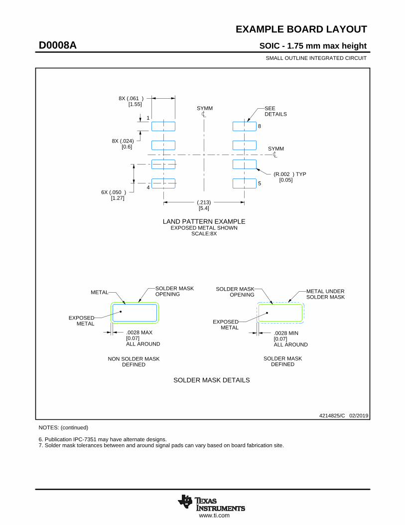
PACKAGE OUTLINE
C
TYP6.66.2
1.2 MAX
6X 0.65
8X 0.300.19
2X1.95
0.150.05
(0.15) TYP
0 - 8
0.25GAGE PLANE
0.750.50
A
NOTE 3
3.12.9
BNOTE 4
4.54.3
4221848/A 02/2015
TSSOP - 1.2 mm max heightPW0008ASMALL OUTLINE PACKAGE
NOTES: 1. All linear dimensions are in millimeters. Any dimensions in parenthesis are for reference only. Dimensioning and tolerancing per ASME Y14.5M. 2. This drawing is subject to change without notice. 3. This dimension does not include mold flash, protrusions, or gate burrs. Mold flash, protrusions, or gate burrs shall not exceed 0.15 mm per side. 4. This dimension does not include interlead flash. Interlead flash shall not exceed 0.25 mm per side.5. Reference JEDEC registration MO-153, variation AA.
18
0.1 C A B
54
PIN 1 IDAREA
SEATING PLANE
0.1 C
SEE DETAIL A
DETAIL ATYPICAL
SCALE 2.800

www.ti.com
EXAMPLE BOARD LAYOUT
(5.8)
0.05 MAXALL AROUND
0.05 MINALL AROUND
8X (1.5)8X (0.45)
6X (0.65)
(R )TYP
0.05
4221848/A 02/2015
TSSOP - 1.2 mm max heightPW0008ASMALL OUTLINE PACKAGE
SYMM
SYMM
LAND PATTERN EXAMPLESCALE:10X
1
45
8
NOTES: (continued) 6. Publication IPC-7351 may have alternate designs. 7. Solder mask tolerances between and around signal pads can vary based on board fabrication site.
METALSOLDER MASKOPENING
NON SOLDER MASKDEFINED
SOLDER MASK DETAILSNOT TO SCALE
SOLDER MASKOPENING
METAL UNDERSOLDER MASK
SOLDER MASKDEFINED

www.ti.com
EXAMPLE STENCIL DESIGN
(5.8)
6X (0.65)
8X (0.45)8X (1.5)
(R ) TYP0.05
4221848/A 02/2015
TSSOP - 1.2 mm max heightPW0008ASMALL OUTLINE PACKAGE
NOTES: (continued) 8. Laser cutting apertures with trapezoidal walls and rounded corners may offer better paste release. IPC-7525 may have alternate design recommendations. 9. Board assembly site may have different recommendations for stencil design.
SYMM
SYMM
1
45
8
SOLDER PASTE EXAMPLEBASED ON 0.125 mm THICK STENCIL
SCALE:10X


www.ti.com
PACKAGE OUTLINE
3X 2.672.03
5.214.44
5.344.32
3X12.7 MIN
2X 1.27 0.13
3X 0.550.38
4.193.17
3.43 MIN
3X 0.430.35
(2.54)NOTE 3
2X2.6 0.2
2X4 MAX
SEATINGPLANE
6X0.076 MAX
(0.51) TYP
(1.5) TYP
TO-92 - 5.34 mm max heightLP0003ATO-92
4215214/B 04/2017
NOTES: 1. All linear dimensions are in millimeters. Any dimensions in parenthesis are for reference only. Dimensioning and tolerancing per ASME Y14.5M.2. This drawing is subject to change without notice.3. Lead dimensions are not controlled within this area.4. Reference JEDEC TO-226, variation AA.5. Shipping method: a. Straight lead option available in bulk pack only. b. Formed lead option available in tape and reel or ammo pack. c. Specific products can be offered in limited combinations of shipping medium and lead options. d. Consult product folder for more information on available options.
EJECTOR PINOPTIONAL
PLANESEATING
STRAIGHT LEAD OPTION
3 2 1
SCALE 1.200
FORMED LEAD OPTIONOTHER DIMENSIONS IDENTICAL
TO STRAIGHT LEAD OPTION
SCALE 1.200

www.ti.com
EXAMPLE BOARD LAYOUT
0.05 MAXALL AROUND
TYP
(1.07)
(1.5) 2X (1.5)
2X (1.07)(1.27)
(2.54)
FULL RTYP
( 1.4)0.05 MAXALL AROUND
TYP
(2.6)
(5.2)
(R0.05) TYP
3X ( 0.9) HOLE
2X ( 1.4)METAL
3X ( 0.85) HOLE
(R0.05) TYP
4215214/B 04/2017
TO-92 - 5.34 mm max heightLP0003ATO-92
LAND PATTERN EXAMPLEFORMED LEAD OPTIONNON-SOLDER MASK DEFINED
SCALE:15X
SOLDER MASKOPENING
METAL
2XSOLDER MASKOPENING
1 2 3
LAND PATTERN EXAMPLESTRAIGHT LEAD OPTIONNON-SOLDER MASK DEFINED
SCALE:15X
METALTYP
SOLDER MASKOPENING
2XSOLDER MASKOPENING
2XMETAL
1 2 3
www.ti.com
TAPE SPECIFICATIONS
19.017.5
13.711.7
11.08.5
0.5 MIN
TYP-4.33.7
9.758.50
TYP2.92.4
6.755.95
13.012.4
(2.5) TYP
16.515.5
3223
4215214/B 04/2017
TO-92 - 5.34 mm max heightLP0003ATO-92
FOR FORMED LEAD OPTION PACKAGE

IMPORTANT NOTICE AND DISCLAIMERTI PROVIDES TECHNICAL AND RELIABILITY DATA (INCLUDING DATA SHEETS), DESIGN RESOURCES (INCLUDING REFERENCE DESIGNS), APPLICATION OR OTHER DESIGN ADVICE, WEB TOOLS, SAFETY INFORMATION, AND OTHER RESOURCES “AS IS” AND WITH ALL FAULTS, AND DISCLAIMS ALL WARRANTIES, EXPRESS AND IMPLIED, INCLUDING WITHOUT LIMITATION ANY IMPLIED WARRANTIES OF MERCHANTABILITY, FITNESS FOR A PARTICULAR PURPOSE OR NON-INFRINGEMENT OF THIRD PARTY INTELLECTUAL PROPERTY RIGHTS.These resources are intended for skilled developers designing with TI products. You are solely responsible for (1) selecting the appropriate TI products for your application, (2) designing, validating and testing your application, and (3) ensuring your application meets applicable standards, and any other safety, security, regulatory or other requirements.These resources are subject to change without notice. TI grants you permission to use these resources only for development of an application that uses the TI products described in the resource. Other reproduction and display of these resources is prohibited. No license is granted to any other TI intellectual property right or to any third party intellectual property right. TI disclaims responsibility for, and you will fully indemnify TI and its representatives against, any claims, damages, costs, losses, and liabilities arising out of your use of these resources.TI’s products are provided subject to TI’s Terms of Sale or other applicable terms available either on ti.com or provided in conjunction with such TI products. TI’s provision of these resources does not expand or otherwise alter TI’s applicable warranties or warranty disclaimers for TI products.TI objects to and rejects any additional or different terms you may have proposed. IMPORTANT NOTICE
Mailing Address: Texas Instruments, Post Office Box 655303, Dallas, Texas 75265Copyright © 2022, Texas Instruments Incorporated