
a differential push-pull voltage mode driver for vertical-cavity ...
77
A DIFFERENTIAL PUSH-PULL VOLTAGE MODE DRIVER FOR VERTICAL-CAVITY SURFACE EMITTING LASER by Ajith Sivadhasan Ramani B.Tech., National Institute of Technology Karanataka, India, 2014 A THESIS SUBMITTED IN PARTIAL FULFILLMENT OF THE REQUIREMENTS FOR THE DEGREE OF MASTER OF APPLIED SCIENCE in THE FACULTY OF GRADUATE AND POSTDOCTORAL STUDIES (Electrical and Computer Engineering) THE UNIVERSITY OF BRITISH COLUMBIA (Vancouver) December 2017 © Ajith Sivadhasan Ramani, 2017
-
Upload
khangminh22 -
Category
Documents
-
view
0 -
download
0
Transcript of a differential push-pull voltage mode driver for vertical-cavity ...

A DIFFERENTIAL PUSH-PULL VOLTAGE MODE DRIVER FOR
VERTICAL-CAVITY SURFACE EMITTING LASER
by
Ajith Sivadhasan Ramani
B.Tech., National Institute of Technology Karanataka, India, 2014
A THESIS SUBMITTED IN PARTIAL FULFILLMENT OF
THE REQUIREMENTS FOR THE DEGREE OF
MASTER OF APPLIED SCIENCE
in
THE FACULTY OF GRADUATE AND POSTDOCTORAL STUDIES
(Electrical and Computer Engineering)
THE UNIVERSITY OF BRITISH COLUMBIA
(Vancouver)
December 2017
© Ajith Sivadhasan Ramani, 2017

ii
Abstract
The unabated demand for data communication has led to a rapid growth in warehouse-sized
datacenters where high-end servers transfer terabytes of data per second between the racks using
optical data links. Vertical cavity surface-emitting laser (VCSEL) based optical links are widely
popular in such datacenters for short-reach (< 300 m) interconnects due to their compact footprint,
low cost, ease of integration with multimode fiber and flexibility in implementing arrays to achieve
high aggregate data rate. Improving power-conversion efficiency (PCE), defined as the ratio of
desired output optical power to the total electrical power of VCSEL driver, is paramount to
improve the overall energy efficiency of the entire optical link. VCSEL diodes are normally driven
single-ended with pseudo-differential current-mode drivers to maintain signal integrity. However,
such conventional drivers consume significant power and are often unable to compensate for
supply switching noise due to package parasitics at high data-rates.
We propose a differential push-pull voltage-mode VCSEL driver to mitigate bondwire parasitics,
reduce power consumption and leverage complementary meral-oxide semiconductor (CMOS)
process scaling to its maximum advantage. A proof-of-concept prototype in a 65nm CMOS
process achieves the highest reported PCE to-date of 18.7% for VCSEL drivers when normalized
to VCSEL slope efficiency. It uses an asymmetric 3-tap rise and fall based pre-emphasis to achieve
a total energy efficiency of 1.52 pJ/b at 16 Gb/s with an average optical power output of 1.34 dBm,
optical modulation amplitude (OMA) of 2.1 dBm and extinction ratio of 5.92 dB.

iii
Lay Summary
Large datacenters need optical-fiber based interconnect links to connect servers that are spaced far
apart by a distance ranging from few meters to several kilometers. At each end of the fiber lies an
optical transmitter that converts the electrical signal from the server to an optical signal, and sends
this optical signal over the fiber. The transmitter must be low cost, and able to convert the electrical
power into optical power efficiently. It should also be able to reliably transmit large amount of
data per second. In this thesis, we present the concept, design, and measurement results of a
transmitter that achieves the best electrical to optical power conversion efficiency reported till date.

iv
Preface
This Thesis is an original intellectual product of the author Ajith. S. Ramani.
All the work presented henceforth was conducted in the System-on-Chip (SoC) Laboratory at the
University of British Columbia, Point Grey campus. Some of the material in Chapters 2, 3, 4 and
5 are based on an IEEE conference paper that is currently under review, and if accepted, will be
published in the conference proceedings.

v
Table of Contents
Abstract .......................................................................................................................................... ii
Lay Summary ............................................................................................................................... iii
Preface ........................................................................................................................................... iv
Table of Contents ...........................................................................................................................v
List of Tables ............................................................................................................................... vii
List of Figures ............................................................................................................................. viii
List of Abbreviations ................................................................................................................. xiii
Acknowledgements .................................................................................................................... xvi
Dedication ................................................................................................................................. xviii
Chapter 1: Introduction ................................................................................................................1
1.1 Optical Link .................................................................................................................... 2
1.2 Research Objective ......................................................................................................... 4
1.3 Thesis Outline ................................................................................................................. 5
Chapter 2: VCSEL Transmitters .................................................................................................6
2.1 Vertical Cavity Surface Emitting Laser .......................................................................... 6
2.2 VCSEL Model ................................................................................................................ 9
2.3 Prior Arts and Limitations ............................................................................................ 12
2.4 Impact of Package Parasitics ........................................................................................ 15
Chapter 3: Proposed VM VCSEL Driver ..................................................................................19
3.1 Asymmetric Equalization Frequency Analysis ............................................................. 22
3.2 Circuit Implementation ................................................................................................. 23
Chapter 4: Layout Considerations, Scanchain and PCB design .............................................27

vi
4.1 Standalone Scanchain Design ....................................................................................... 27
4.2 Layout Considerations .................................................................................................. 31
4.3 PCB Design Considerations .......................................................................................... 34
Chapter 5: Measurements ...........................................................................................................37
5.1 Electrical Measurements ............................................................................................... 37
5.2 VCSEL DC Behavior .................................................................................................... 39
5.3 High Speed Optical Characterization ............................................................................ 42
5.4 Power Consumption and Performance Summary ......................................................... 45
Chapter 6: Conclusion and Future work ...................................................................................49
6.1 Conclusion .................................................................................................................... 49
6.2 Future work ................................................................................................................... 49
Bibliography .................................................................................................................................56

vii
List of Tables
Table 5.1 Performance summary and comparision ....................................................................... 47

viii
List of Figures
Figure 1.1 Block diagram of a generic electro-optical transceiver link. ......................................... 2
Figure 2.1 Cross sectional view of the VCSEL diode. ................................................................... 7
Figure 2.2 VCSEL output light power (Pop) and the forward biased diode voltage (VVCSEL) as a
function of the current (IVCSEL). ...................................................................................................... 8
Figure 2.3 (a) Conventional second-order electrical model of the VCSEL [3] (b) simplified
lumped first-order electrical model of the VCSEL with the package inductance. ......................... 9
Figure 2.4 Second order electrical model for VCSEL optical dynamics [10][18]. Output light
(Pop) is modelled as voltage. Lv and Cv are dependent on the bias current. .................................. 11
Figure 2.5 Schematic of a conventional CM VCSEL driver. (a) common anode driver (b)
common cathode driver (c) common anode driver with modified packaging for on-chip biasing
to reduce supply noise. (d) common cathode driver with modified packaging for on-chip bias .. 14
Figure 2.6 (a) Simplified small signal electrical model of the VCSEL driver packaged to the
VCSEL die. Simulated eye diagrams of the VCSEL junction current Iv at 15 Gb/s (b) without any
package parasitic inductances, (c) with only signal package inductance Lb2 [8], [17], (d) with
both supply and signal package inductances, Lb1 and Lb2, and (e) with ro = 50 Ω to dampen the
ringing due to Lb1 and Lb2. ........................................................................................................... 16
Figure 2.7 Simulated PAM4 eye diagrams of the VCSEL junction current Iv at 25Gb/s (a)
without any package inductance (b) with only signal package inductance Lb2 (c) with both supply
and signal package inductances, Lb1 and Lb2, and (d) with ro = 50 Ω to dampen the ringing due to
Lb1 and Lb2..................................................................................................................................... 17
Figure 2.8 Comparison of prior-art CM drivers to the proposed VM driver ................................ 18
Figure 3.1 Proposed fully-differential push-pull VM VCSEL driver. .......................................... 19

ix
Figure 3.2 Schematic of the low output impedance differential driver in (a) current mode and (b)
voltage mode. ................................................................................................................................ 20
Figure 3.3 Lowering Rt reduces ringing due to Lb1 and Lb2. Power consumption of a differential
VM driver with low Rt is only a fraction of the power consumption of a differential CM driver
with low Rt, for a fixed VCSEL modulation current (Imod) and varying VCSEL junction
resistance. ...................................................................................................................................... 21
Figure 3.4 Equalization analyzed in (a) time domain (b) frequency domain. .............................. 23
Figure 3.5 Block diagram of the fully-differential VM VCSEL driver. ....................................... 24
Figure 3.6 Schematic of the bias generation block for the current DAC and the programmable
bias current DAC. ......................................................................................................................... 25
Figure 3.7 Schematic of CMOS logic gates used for the equalization pulse generation. ............. 26
Figure 3.8 (a) Schematic of the fully-differential push-pull VM output driver with asymmetric
equalization and (b) a driver slice. ................................................................................................ 26
Figure 4.1 Schematic of the modified D flip-flop used as the basic building for the scanchain
design. ........................................................................................................................................... 27
Figure 4.2 Schematic of the custom made 128-bit long scan chain. The Reset and QB signals are
not shown for the flip-flop. ........................................................................................................... 28
Figure 4.3 Schematic of two flip-flops in cascade for timing analysis to compute the setup time
and hold time................................................................................................................................. 29
Figure 4.4 Layout of 128-bit long scan chain with Schmitt trigger and clock tree implementation.
....................................................................................................................................................... 30
Figure 4.5 Die photo of the standalone scan chain and custom-made pads to reduce area and
parasitics. ...................................................................................................................................... 31

x
Figure 4.6 Full-chip layout of the proposed push-pull VM VCSEL driver before metal-fill for
clarity. ........................................................................................................................................... 31
Figure 4.7 Layout of the high frequency drive including differential CMOS based input receiver,
programmable delay generation for equalization, equalization pulse shaping circuit and the
output VM driver. ......................................................................................................................... 32
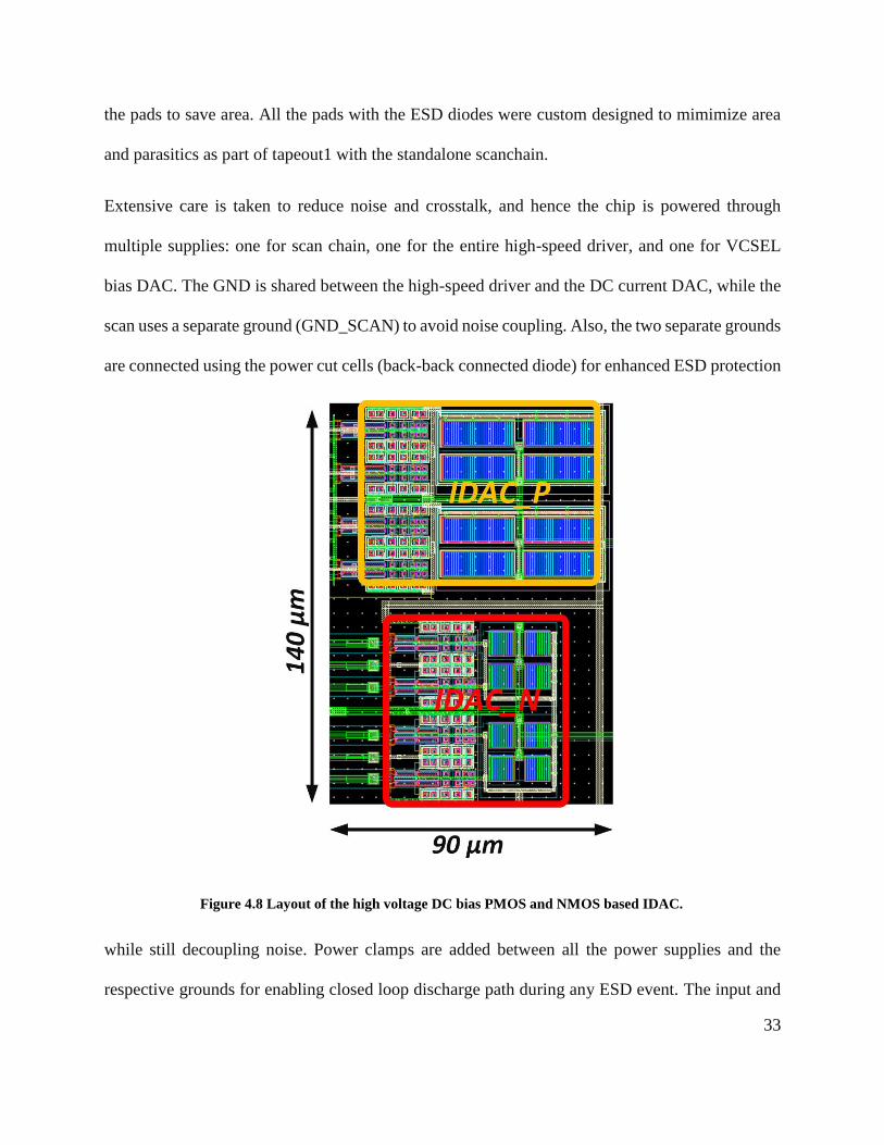
Figure 4.8 Layout of the high voltage DC bias PMOS and NMOS based IDAC......................... 33
Figure 4.9 Fabricated 2-layer rogers PCB used for measuring the prototype chip. ...................... 35
Figure 5.1 Chip Micrograph (a) Die photo of the CMOS VCSEL driver (b) Die photo of the 25
Gbps Finisar VCSEL .................................................................................................................... 37
Figure 5.2 Microscope image of the CMOS die, chip on board packaged to the PCB pads for
electrical testing. ........................................................................................................................... 38
Figure 5.3 Measured electrical eye diagram of the driver for a PRBS7 pattern at (a) 7Gb/s (b)
10Gb/s showing eye degradation due to impedance mismatch. ................................................... 39
Figure 5.4 Microscope image of the CMOS die, chip on board packaged to VCSEL die on a
high-speed PCB board for optical measurements. ........................................................................ 40
Figure 5.5 Setup for (a) optical eye diagram measurement (b) Bit error rate (BER) measurement.
....................................................................................................................................................... 40
Figure 5.6 VCSEL setup for optimal light coupling using lens. This setup was built by Spoorthi
Nayak. ........................................................................................................................................... 41
Figure 5.7 Measured bias DAC current as a function of the control word when the driver is
connected to the VCSEL die. ........................................................................................................ 41
xi
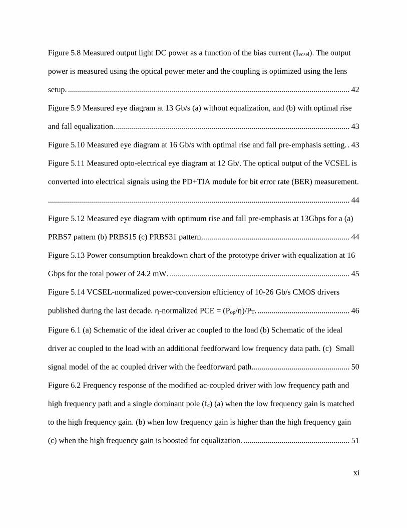
Figure 5.8 Measured output light DC power as a function of the bias current (Ivcsel). The output
power is measured using the optical power meter and the coupling is optimized using the lens
setup. ............................................................................................................................................. 42
Figure 5.9 Measured eye diagram at 13 Gb/s (a) without equalization, and (b) with optimal rise
and fall equalization. ..................................................................................................................... 43
Figure 5.10 Measured eye diagram at 16 Gb/s with optimal rise and fall pre-emphasis setting. . 43
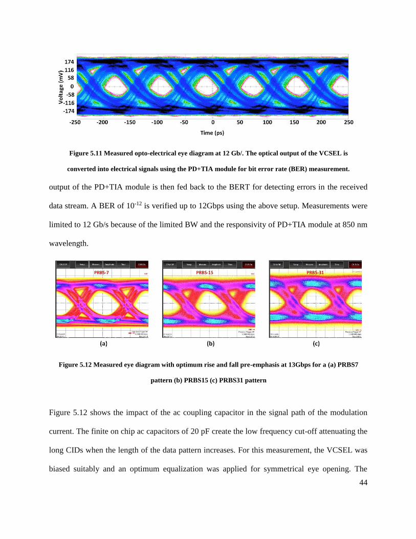
Figure 5.11 Measured opto-electrical eye diagram at 12 Gb/. The optical output of the VCSEL is
converted into electrical signals using the PD+TIA module for bit error rate (BER) measurement.
....................................................................................................................................................... 44
Figure 5.12 Measured eye diagram with optimum rise and fall pre-emphasis at 13Gbps for a (a)
PRBS7 pattern (b) PRBS15 (c) PRBS31 pattern .......................................................................... 44
Figure 5.13 Power consumption breakdown chart of the prototype driver with equalization at 16
Gbps for the total power of 24.2 mW. .......................................................................................... 45
Figure 5.14 VCSEL-normalized power-conversion efficiency of 10-26 Gb/s CMOS drivers
published during the last decade. η-normalized PCE = (Pop/η)/PT. .............................................. 46
Figure 6.1 (a) Schematic of the ideal driver ac coupled to the load (b) Schematic of the ideal
driver ac coupled to the load with an additional feedforward low frequency data path. (c) Small
signal model of the ac coupled driver with the feedforward path................................................. 50
Figure 6.2 Frequency response of the modified ac-coupled driver with low frequency path and
high frequency path and a single dominant pole (fc) (a) when the low frequency gain is matched
to the high frequency gain. (b) when low frequency gain is higher than the high frequency gain
(c) when the high frequency gain is boosted for equalization. ..................................................... 51

xii
Figure 6.3 (a) Schematic of the modified push-pull VM driver with a low frequency driver to
eliminate the low frequency cut-off and reduce the ac capacitor area. ......................................... 52
Figure 6.4 (a) Schematic of the low frequency driver (a) p-path for pushing current (b) n-path for
pulling current. .............................................................................................................................. 54
Figure 6.5 Simulated eye diagram of the modified push-pull driver at 15Gb/s with Cac= 300fF,
RVCSEL = 50Ω and CVCSEL = 300fF (a) with only the low frequency current source in the P-path
and N-path enabled (b) with both the LFD and HFD enabled. ..................................................... 55

xiii
List of Abbreviations
BER Bit error rate
BERT Bit error rate tester
BW Bandwidth
CA Common anode
CC Common cathode
CM Current mode
CMOS Complementary metal oxide semiconductor
COB Chip on-board
DAC Digital to analog converter
dB Decibel
dBm Decibel-milliwatt
DBR Distributed Bragg reflector
E/O Electro-optical
ER Extinction ratio
ESD Electro-static discharge
FIR Finite impulse response
FPGA Field programmable gate array
HFD High frequency driver
IC Integrated circuits
IDAC Current DAC
IO Input output

xiv
IOT Internet of things
ISI Inter symbol interference
LFD Low frequency driver
LVT Low voltage threshold
MRM Microring modulator
MZM Mark Zehnder modulator
NRZ Non-return to zero
O/E Opto-electrical
OMA Optical modulation amplitude
PAM Pulse amplitude modulation
PCB Printed circuit board
PCE Power conversion efficiency
PD Photodiode
PRBS Pseudo random binary sequence
PWM Pulse width modulation
RF Radio frequency
RX Receiver
SSM Supply switching noise
TF Transfer function
TIA Transimpedance amplifier
TX Transmitter
VCSEL Vertical-cavity surface emitting laser

xv
VM Voltage mode
WDM Wavelength division multiplexing

xvi
Acknowledgements
My graduate studies at UBC have been a very enriching experience and a source of enormous
educational growth. I am grateful to many people for their guidance and support throughout this
period.
First and foremost, I would like to thank my supervisor, Prof. Sudip Shekhar for mentoring me.
His support, advice and encouragement have been a defining and essential part of my journey
through graduate school. I feel very honored and privileged to have worked with him. I would also
like to thank Prof. Lukas Chrostowski and Prof. Shahriar Mirabassi for reviewing my thesis and
serving on my graduate defense committee.
I have greatly benefitted from interacting with all my colleagues at UBC SOC Lab. I thank them
for all the insightful discussion. I am especially thankful to Spoorthi Nayak for helping me with
the optical measurements and for being a moral support in my life. I would also like to thank Chen
Yuan for collaborating with me for the scan tapeout and all the course projects. The number of all-
nighters that Chen and I have pulled out is something we both will never forget.
I would like to thank J. Tatum, W. Fan, T. Nguyen and D. Mahgerefteh of Finisar, J. Gao of Intel,
J. Quinn of CMC, and R. Mehrabadi and R. Rosales of UBC for their support.
I acknowledge the Natural Sciences and Engineering Research Council of Canada for financial
support. I also acknowledge the Canadian Microelectronics Corporation for access to CAD tools,
fabrication and test equipment. I also thank Anritsu for providing some of the test equipment.
I would also like to thank all my friends at UBC for injecting my life with energy, fun and
enthusiasm, which is often drained away by the demands of graduate study. Throughout my life I

xvii
have received enormous amount of support from my parents and sister to pursue my desires. I am
forever indebted for all the sacrifices that they have made for me.

xviii
Dedication
To my parents, friends and Sudip.

1
Chapter 1: Introduction
The unabated increase in data communication had led to an exponential growth in the internet
traffic, mainly driven by applications like cloud computing, internet of things (IOT), social
networking, and streaming ultra-high definition video, etc. The increased data traffic has led to the
rapid growth of warehouse-sized datacenters where high-end servers with very high processing
speed transfer terabytes of data per second between the racks. Hence, it is imperative for the input-
output (IO) bandwidth of these data interconnect links to increase in tandem with the increased
network traffic/load and the improved processing speed of the high-performance servers to avoid
the data communication bottleneck.
Copper based electrical interconnect links are widely used in datacenters for short-reach distances
(up to a few meters). The major problem in scaling traditional copper based electrical interconnects
is their frequency-dependent losses, caused by the skin effect, dielectric losses, impedance
mismatch due to discontinuities in the link caused by connectors and vias, and electrical channel
cross-talk [1]. These frequency dependent losses in the interconnect leads to inter-symbol
interference (ISI) in high-speed data patterns, causing adjacent bits to overlap, limiting the
achievable data rates. Although equalization at the transmitter and/or receiver can overcome this
limitation by canceling ISI, it requires additional circuit complexity, power and area. As the link
distance exceeds a few meters and the transmission speed exceeds a few Gb/s [2], losses in the
electrical data links are very high and makes equalization very power hungry. Thus, rather than
being limited by the server processing speed, datacenters will be limited mostly by channel
bandwidth and power consumption. Thus, electrical links are suboptimal choice in datacenters to
transmit high speed data over longer distance.

2
In an optical fiber, unlike electrical interconnects, the attenuation is insignificant and almost
frequency independent when the length of the link is less than a few kilometers [1], [2]. Also, since
the optical signals are completely confined inside an optical fiber, there is no cross-talk between
two fibers when they are bundled together compactly for high density [1], [3]. Furthermore, since
optical signals at multiple wavelength do not interfere with each other, multiple signals at different
wavelength can be transmitted using a single optical fiber using wavelength division multiplexing
(WDM) technique. Hence, optical fiber based interconnect links are optimal solutions in
datacenters to achieve higher aggregate data rate [4].
1.1 Optical Link
A typical electro-optical transceiver link is shown in Figure 1.1. In an optical TX, director
modulation with vertical cavity surface-emitting lasers (VCSELs) or indirect modulation with
Mach-Zehnder (MZM) or ring modulators (MRM) is employed for electrical to optical (E/O)
conversion. The optical data is transmitted through the optical fiber channel. At the receiver, a
photo diode is used for opto-electrical (O/E) conversion.
In an indirect modulator, electro-optical modulator such as MZM or MRM is used as a shutter to
convert high speed electrical data signal into the modulated optical output using an external
Figure 1.1 Block diagram of a generic electro-optical transceiver link.

3
continuous wave (CW) laser [5]. The use of a fixed DC laser source and a separate high-speed
modulator helps in reducing the optical frequency chirp in an indirect modulator, making it a
suitable candidate for WDM applications. However, the losses due to coupling of light output to
and from the modulator, modulator insertion loss and the waveguide insertion loss impose severe
power penalty [6]. Hence, there exists a critical distance below which the use of indirect modulator
is not beneficial and the distance is decided by the link budget and power budget analysis [5][6].
Thus, in general, indirect modulator based links are popular for long reach link > 300m [2][6].
In a direct modulator, a laser source such as a VCSEL is directly modulated by the high-speed
driver to generate the desired modulated light output. Direct modulators have compact foot prints,
reduced coupling losses, reduced cost and lower power consumption than indirect modulators as
it doesn’t need any external modulator for modulation. However, direct modulated laser suffers
from optical frequency chirp due to data modulation making it non-suitable for WDM applications.
Also, the highest achievable data rate is depended on the intrinsic bandwidth of the laser [2].
VCSEL based direct modulator optical links are widely popular in datacenters for short reach
interconnects below 300 m due to their compact footprint, low cost, and ease of integration with
multimode fiber [4][6]. VCSEL emits light perpendicular to the top surface, hence implementing
1D and 2D arrays to achieve high aggregate data rate is easier [2][3]. It is estimate that over 80%
of the optical links in the datacenters manufactured recently are shorter than 100m [7], and most
of these links, if not all, are VCSEL based.
In a VCSEL based link, the VCSEL diode is directly modulated by a transmit driver, converting
electrical power to desired optical power. The total electrical power consumed includes the
contribution from the bias current (Ibias) of the VCSEL, the modulation current pumped into the

4
VCSEL (Imod), and the total current consumed in the driver circuit. The desired optical power at
the VCSEL output is given in terms of the average optical power (Pop) and optical modulation
amplitude (OMA). As the VCSEL diode needs high Ibias and large signal swing (Imod) for its
operation, a significant portion of total link power is dissipated in the VCSEL driver [6]. Thus,
recent research efforts have laid significant emphasis on reducing the power consumed in the
VCSEL driver. These efforts include designing better VCSEL diodes, with better slope efficiency
( = Pop/VCSEL current) and larger –3dB bandwidth (BW), and low power drivers [8]- [10]. While
Ibias and Imod are limited by the VCSEL properties and therefore dependent upon the diode and the
link budget, power consumption in the driver circuit must be reduced to ease the overall power
budget [8]- [12].
1.2 Research Objective
The main objective of this research is to implement a low power, yet fully robust VCSEL
transmitter in a bulk Complementary metal oxide semiconductor (CMOS) process to reduce cost.
Due to the high bias and modulation swing requirements of the VCSEL, VCSEL drivers are usually
designed in a BiCMOS process as they have higher current density, higher unity-gain bandwidth
(fT) and higher breakdown voltage than a CMOS process [13]. CMOS implementation of VCSEL
drivers uses complex cascode structures to avoid device breakdown and ensure reliability, thus
reducing the overall bandwidth [9][14]. In this work a fully differential ac-coupled architecture is
proposed to de-couple the high voltage thick gate device based DC bias path and the high-speed
modulation driver as in [12]. A voltage mode (VM) inverter based high speed driver is used to
reduce the overall power consumption. Furthermore, all the blocks of the driver including the high-
speed data receiver, equalization pulse generator and the output driver is implemented using

5
CMOS logic to reduce the cost and the power consumption of the driver and to ensure easy
scalability to advanced CMOS nodes for better performance.
The proposed low output impedance VM fully-differential driver mitigates the electrical non-
linearity due to supply switching noise (SSN) and ISI caused by the supply and signal package
parasitics. The optical non-linearity due to the VCSEL electron-photon interaction is compensated
using an asymmetric 3-tap rise and fall equalization [10].
The prototype driver is designed and fabricated in 65 nm bulk CMOS process. Post silicon
measurements are performed to verify the effectiveness of the proposed techniques in achieving
the desired performance.
1.3 Thesis Outline
The Thesis is organized as follows. Chapter 2 briefly describes the basics of VCSEL to understand
the proposed work. This chapter also discusses the prior arts and their limitations. It highlights the
non-linearity due to supply and signal package parasitics to the non-return to zero (NRZ) and pulse
amplitude modulation (PAM4) transient response and proposes solutions to fix the non-linearity.
Chapter 3 presents a low output impedance push-pull differential VM driver topology to minimize
such undesired effects due to package parasitics and reduce the driver power consumption. Chapter
4 discusses the design of a custom scan chain to program the chip, and the printed circuit boards
used to measure the prototype driver. It briefly describes the basics of layout used in the driver
design. The measurement setup and the electro-optical measurement results of the proposed
transmitter is presented in Chapter 5. Conclusions and future work for improvements to the
proposed push-pull driver are presented in Chapter 6.

6
Chapter 2: VCSEL Transmitters
2.1 Vertical Cavity Surface Emitting Laser
VCSEL is a forward biased semiconductor laser diode that emits light perpendicular to its top
surface. The advantage of VCSELs over the edge emitting lasers like Fabry-Perot lasers is that
they can be fabricated, tested and packaged more easily and at a lower cost [2]. Figure 2.1 shows
the cross-sectional view of the VCSEL. VCSEL consists of a gain medium located in a very short
vertical cavity with Distributed Bragg Reflecting (DBR) mirrors at the top and bottom [3]. The
Bragg mirrors are formed by many layers of alternating high and low refractive- index material
and it provides the necessary positive feedback action for lasing at a desired wavelength [1]. The
VCSEL optical characteristics and the emitted wavelength is a function of composition of the gain
region and the structure of the DBR [2].
GaAs-based VCSELs operating at 850-nm designed for short reach optical interconnect below
300 m are some of the most widely popular VCSELs [16]. GaAs and InP based VCSELs, lasing
at longer wavelength of 1300-nm and 1550-nm, have also been developed for use in long-distance
links due to lower loss and dispersion at those wavelengths.
A majority of VCSEL arrays are fabricated on a n-doped substrate with a n-doped DBR below and
p-doped DBR above the active region. Also, in some commercially available VCSEL arrays,
VCSEL cathode pads are shared between multiple VCSEL dies enabling only anode driving laser
driver. However, CMOS circuit performance and reliability considerations motivate this polarity
to be reversed and have a p-substrate and a p-doped DBR epitaxy below the active region and a n-

7
type DBR epitaxy above the active region [8][15]. P-substrate shared VCSEL array facilitates
cathode-driving common anode based driver easily implemented using an open drain NMOS
architecture [15]. Although some recent research has achieved improved performance for the p-
substrate VCSEL over n-substrate VCSEL for individual dies [15], difficulties due to material
issues prevents it from being widely adopted as the standard for the array implementation.
Figure 2.2(a) shows the optical power (POP) vs. the bias current (IVCSEL) of the VCSEL diode.
When IVCSEL is less than the threshold current (Ith) of the VCSEL, the output optical power is very
low and mainly due to spontaneous emission. Ith is the minimum current above which the
stimulated emission begins, and lasing action occurs [3]. Ith of the commercially available VCSEL
Figure 2.1 Cross sectional view of the VCSEL diode.

8
diodes are generally below 1 mA. Above Ith, the output light power is linearly proportional to the
input current given by equation (2.1).
Slope efficiency of the VCSEL diode () is the intrinsic efficiency of the VCSEL to convert input
electrical current to output optical power. Typical slope efficiency of the VCSEL published in
literature has a wide range from 0.3 mW/mA to 0.78 mW/mA [8]-[12]. Figure 2.2(b) shows the
VI curve of the VCSEL diode. The voltage drop corresponding to the threshold current of the diode
is called the threshold voltage drop (Vth) [2]. Above Ith, the output voltage (VVCSEL) is linearly
proportional to the input current as shown and is approximated by equation (2.2). VCSEL diodes
have a large series resistance because of the high resistance of DBR mirror stack. Although it
seems that VCSEL output is highly linear to the input current, severe bandwidth limitations and
non-linearities do exist for VCSEL when modulated at high speed and at lower current levels.
Figure 2.2 VCSEL output light power (Pop) and the forward biased diode voltage (VVCSEL) as a function of
the current (IVCSEL).
9
𝑃𝑜𝑝 = 𝜂(𝐼𝑉𝐶𝑆𝐸𝐿 − 𝐼𝑡ℎ) (2.1)
𝑉𝑉𝐶𝑆𝐸𝐿 ≅ 𝑉𝑡ℎ + 𝐼𝑉𝐶𝑆𝐸𝐿𝑅𝑉 (2.2)
2.2 VCSEL Model
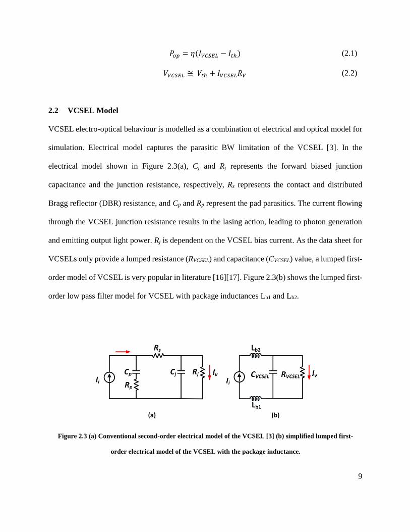
VCSEL electro-optical behaviour is modelled as a combination of electrical and optical model for
simulation. Electrical model captures the parasitic BW limitation of the VCSEL [3]. In the
electrical model shown in Figure 2.3(a), Cj and Rj represents the forward biased junction
capacitance and the junction resistance, respectively, Rs represents the contact and distributed
Bragg reflector (DBR) resistance, and Cp and Rp represent the pad parasitics. The current flowing
through the VCSEL junction resistance results in the lasing action, leading to photon generation
and emitting output light power. Rj is dependent on the VCSEL bias current. As the data sheet for
VCSELs only provide a lumped resistance (RVCSEL) and capacitance (CVCSEL) value, a lumped first-
order model of VCSEL is very popular in literature [16][17]. Figure 2.3(b) shows the lumped first-
order low pass filter model for VCSEL with package inductances Lb1 and Lb2.
Figure 2.3 (a) Conventional second-order electrical model of the VCSEL [3] (b) simplified lumped first-
order electrical model of the VCSEL with the package inductance.

10
VCSEL optical bandwidth is regulated by two coupled differential equations that describe the
interaction of the electron density, N, and the photon density, Np [3]. The rate of the electron
density change is set by the number of carriers injected into the laser cavity volume, V, via the
device current I, and the number of carriers lost via desired stimulated and non-desired
spontaneous and non-radiative recombination:
𝑑𝑁
𝑑𝑡=
𝐼
𝑞𝑉−
𝑁
𝜏𝑠𝑝− 𝐺𝑁𝑁𝑝
(2.3)
where τsp is the non-radiative and spontaneous emission lifetime and G is the stimulated emission
coefficient. Photon density change is governed by the number of photons generated by stimulated
and spontaneous emission and the number of photons lost due to optical absorption and scattering:
𝑑𝑁𝑝
𝑑𝑡= 𝐺𝑁𝑁𝑝 + 𝛽𝑠𝑝
𝑁
𝜏𝑠𝑝−
𝑁𝑝
𝜏𝑝
(2.4)
where βsp is the spontaneous emission coefficient and τp is the photon lifetime. Combining the two
rate equations and performing the Laplace transform yields [3][10][18]
𝐻𝑖(𝑓) =
𝑓𝑟2
𝑓𝑟2 − 𝑓2 + 𝑗 (
𝑓2𝜋) 𝛾
(2.5)
𝑓𝑟 = 𝐷√𝐼𝐷 − 𝐼𝑡ℎ (2.6)
𝛾 = 𝐾𝑓𝑟2 + 𝛾0 (2.7)
where fr is the relaxation oscillation frequency of the VCSEL that is dependent on the bias current,
D (also referred as the D-factor) denotes the rate of increase of resonance frequency with the
current, γ is the damping factor, K is called the K-factor and γ0 is the damping factor offset.
11
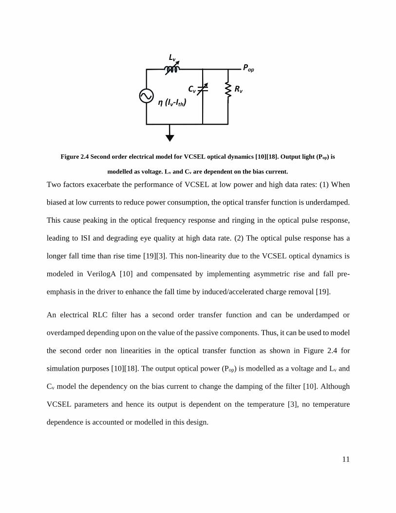
Two factors exacerbate the performance of VCSEL at low power and high data rates: (1) When
biased at low currents to reduce power consumption, the optical transfer function is underdamped.
This cause peaking in the optical frequency response and ringing in the optical pulse response,
leading to ISI and degrading eye quality at high data rate. (2) The optical pulse response has a
longer fall time than rise time [19][3]. This non-linearity due to the VCSEL optical dynamics is
modeled in VerilogA [10] and compensated by implementing asymmetric rise and fall pre-
emphasis in the driver to enhance the fall time by induced/accelerated charge removal [19].
An electrical RLC filter has a second order transfer function and can be underdamped or
overdamped depending upon on the value of the passive components. Thus, it can be used to model
the second order non linearities in the optical transfer function as shown in Figure 2.4 for
simulation purposes [10][18]. The output optical power (Pop) is modelled as a voltage and Lv and
Cv model the dependency on the bias current to change the damping of the filter [10]. Although
VCSEL parameters and hence its output is dependent on the temperature [3], no temperature
dependence is accounted or modelled in this design.
Figure 2.4 Second order electrical model for VCSEL optical dynamics [10][18]. Output light (Pop) is
modelled as voltage. Lv and Cv are dependent on the bias current.

12
It is evident from the rate equation that with the increase in the bias current, the output power
increases and the bandwidth of the VCSEL improves. However, with the increase in the bias
current, VCSEL gets heated up and its internal temperature increases [18]. With the increase in the
temperature, 𝜂 reduces and Ith increases thus, from equation (2.1) the output optical power
saturates at very high current leading to average lifetime reduction and performance degradation
[3] [18].
2.3 Prior Arts and Limitations
VCSEL drivers are usually driven in common-cathode (CC) or common-anode (CA)
configuration. Figure 2.5(a) shows a popular CA implementation of a VCSEL driver. CA drivers
in CMOS are often implemented using an all-NMOS, low voltage-threshold (Vt) devices that drive
the VCSEL cathode. Low-Vt operation and lower parasitics of NMOS (compared to their PMOS
devices) help in attaining higher operating speed. The high voltage needed for forward biasing the
VCSEL diode (VDDH) is applied to its anode externally or on-chip. In a CA current mode (CM)
driver shown in Figure 2.5(a), complementary data signals, D and DB, feed into the CM circuit to
steer the current in its two arms. The right arm feeds the modulation current into the VCSEL. The
left arm mimics the VCSEL impedance, to emulate a pseudo-differential operation. The right arm
must also have an additional current sinking path for Ibias. When VDDH and VDDL are connected
to the same supply pin on-chip [18], the effect of supply bondwire Lb0 to data-dependent supply
switching noise (SSN) and ISI is removed, and a pseudo-differential operation is ensured.
However, the effect of signal bondwires Lb1 and Lb2 are not mitigated, degrading performance at
high data rates. There is also a significant overhead in power consumption, as VDDL, being equal
to VDDH, is high due to VCSEL bias requirements. Even though the VCSEL is essentially driven
single-ended, to prevent SSN and ISI, the current in the left branch is essentially “wasted” for

13
pseudo-differential action. When a separate VDDL is used on-chip to save power (VDDL <
VDDH) [10], Lb0, Lb1 and Lb2 create SSN.
A CM CC implementation shown in Fig. 2.5(b) has similar limitations [8]. In CC driver, the bias
(Ibias) and the modulation current (Imod) necessary to drive the VCSEL is generated from a PMOS
current source which is connected to a high voltage supply that exceed the nominal supply of a
typical CMOS process. These PMOS current sources are usually implemented using either thick
gate PMOS devices or cascode structures to avoid device breakdown. However, this increases the
total parasitics at the driving node, limiting the BW of the driver [14].
In both CC and CA CM implementations of the driver described above, the impedance looking
into the driver from the VCSEL is large. In these high-output impedance drivers, there exists an
inherent tradeoff between power consumption and supply bondwire SSN generation. Furthermore,
the effect of signal bondwires are not mitigated in either designs leading to performance
degradation at higher speed. These effects are further exacerbated in an array implementation,
where supplies are often shared among different VCSEL drivers.
To reduce SSN, the number of ground pads are usually increased to reduce the effective inductance
(Lbg) and a large on-chip decoupling capacitor (Cd) is added at the VDDL pad [8]. Also, since one
of the terminal of the VCSEL diode is connected to an external bias (VDDH or GND) as shown
in Figure 2.5(a) and 2.5(b), the noise at these external pads gets directly coupled to the VCSEL
output degrading high frequency performance. Hence, some recent implementations have also
modified the VCSEL packaging as shown in Figure 2.5(c) and 2.5(d) so that the bias to the VCSEL
is applied on-chip which facilitates the addition of a huge on-chip decoupling capacitor at VDDH

14
pad to reduce SSN [8], [9]. Nevertheless, the current is still “wasted” in the left branch, and the
Figure 2.5 Schematic of a conventional CM VCSEL driver. (a) common anode driver (b) common cathode
driver (c) common anode driver with modified packaging for on-chip biasing to reduce supply noise. (d)
common cathode driver with modified packaging for on-chip bias

15
impact of Lb2 and Lb1 is not accounted for.
2.4 Impact of Package Parasitics
Figure 2.6(a) presents a simplified small signal equivalent model of the VCSEL driver packaged
to the VCSEL die. The driver is assumed to be ideal, with an output resistance of ro = 300 Ω and
capacitance of Cd = 300 fF. Pad parasitics are assumed to be absorbed in the driver, and the VCSEL
die is treated as a single pole circuit with RVCSEL = 50 Ω and CVCSEL= 200 fF. At 15 Gb/s, Figure
2.6(b) shows the simulated eye diagram of the VCSEL junction current (Iv) without any package
bondwire. The impact of different package parasitics are then shown in Figure 2.6(c)-(d).
Packaging inductance, Lb2, in the signal path of the VCSEL causes undesired series peaking [8]
and results in overshoot and ringing in the transient response leading to ISI and signal quality
degradation as shown in Figure 2.6(c). However, both supply and signal package parasitic
inductance of the driver are detrimental to high-speed performance. As shown in Figure 2.6(d),
adding Lb1 can result in significant ringing. A prior-art dampened this ringing by using a low Rt
CM driver, at the expense of degrading the modulation efficiency, as shown in Figure 2.6(e) [17].
Herein, we propose the use of a low Rt VM driver to prevent ringing, and improve efficiency.
With new standards such as IEEE 802.3 adopting PAM4 and other advanced modulation schemes
to increase the data rate to save power [20], constraints for linearity in the TX are becoming more
stringent to accommodate multiple amplitude levels when compared to NRZ. Hence, it is
imperative to mitigate the non-linearity introduced by the package parasitics in the PAM4 transient
response.

16
Figure 2.7 illustrates the impact of different package parasitics on the transient PAM4 electrical
eye-diagram of the VCSEL junction current Iv at 25 Gb/s. Figure 2.7(a) shows the simulated PAM4
response of the ideal driver connected to VCSEL without considering any package parasitics.
Figure 2.7(b) highlights the impact of the signal package parasitic (Lb2) in causing ISI due to the
overshoot and ringing in the transient PAM response. The excessive ringing due to both the signal
and supply package parasitics (Lb2 and Lb1, respectively) leads to eye quality degradation and
closure at higher data rates as in Figure 2.7(c). It is evident from Figure 2.6 and Figure 2.7 that the
non-linearity caused due to the SSN and ISI of the bondwires are more detrimental to the
Figure 2.6 (a) Simplified small signal electrical model of the VCSEL driver packaged to the VCSEL die.
Simulated eye diagrams of the VCSEL junction current Iv at 15 Gb/s (b) without any package parasitic
inductances, (c) with only signal package inductance Lb2 [8], [17], (d) with both supply and signal package
inductances, Lb1 and Lb2, and (e) with ro = 50 Ω to dampen the ringing due to Lb1 and Lb2.

17
performance of the PAM4 transient eye diagram. The non-linearity caused by the signal package
parasitics can be mitigated by using a low Rt driver as shown in Figure 2.7(d).
This work presents a VCSEL driver with a fully differential push-pull modulation to mitigate the
impact of supply package (Lb0 and Lb3) to SSN and minimize current wastage for differential
operation. Voltage-mode (VM) operation of the driver, with its low output impedance (Rt),
mitigates the impact of signal package (Lb1 and Lb2) while consuming a fraction of current when
compared to low Rt CM VCSEL drivers as shown in Figure 2.8 [11]. Low Rt also prevents peaking
in the electrical response due to the signal package, as in [8], [17].
Figure 2.7 Simulated PAM4 eye diagrams of the VCSEL junction current Iv at 25Gb/s (a) without any
package inductance (b) with only signal package inductance Lb2 (c) with both supply and signal
package inductances, Lb1 and Lb2, and (d) with ro = 50 Ω to dampen the ringing due to Lb1 and Lb2.

18
Figure 2.8 Comparison of prior-art CM drivers to the proposed VM driver

19
Chapter 3: Proposed VM VCSEL Driver
Figure 3.1 shows a simplified schematic for the proposed VM differential push-pull driver. As
discussed in Chapter 2, both the CA and CC VCSEL drivers suffer from the SSN generation due
to bondwire which causes undesirable overshoot and ringing in the transient response leading to
ISI. In the proposed driver, DC Ibias needed for forward biasing the VCSEL diode is provided by a
current DAC. Imod is steered (pushed and pulled) by the differential high-speed VM driver through
the AC coupling capacitor. As a constant Imod is drawn from the VDDL supply, the proposed driver
is immune to the supply package parasitic, Lb0. Also, the driver is designed to have a low Rt below
100 Ω to dampen ringing in the transient response caused by the signal package parasitic, Lb1 and
Lb2. Thus, the proposed driver mitigates the effects of both the supply and signal package
parasitics. A fully-differential VCSEL driver was first proposed in [12], but it used off- chip
Figure 3.1 Proposed fully-differential push-pull VM VCSEL driver.

20
transmission lines and bias-Ts mandating the need to drive a terminated VCSEL to avoid
reflections.
The differential low Rt driver can be implemented either in VM or CM as shown in Figure 3.2.
These differential low Rt driver implementations are robust and insensitive to both the supply and
signal package parasitics. Compared to CM driver, VM drivers consume less power and are easily
scalable with the CMOS process [21]. Also, with CMOS scaling, transistor behaves as a better
switch with faster switching speed than a current source [22]. In a low Rt differential CM driver
as shown in Figure 3.2(a), the tail current is split between the load (VCSEL) and the termination
(low Rt), unlike in a VM driver shown in Figure 3.2(b). Thus, for a VCSEL, CM driver draws a
current of Im given by equation (3.1) from the VDDL supply. Figure 3.3 illustrates the ratio of the
power consumption in a VM driver (PVM) to that in a CM driver (PCM) when VDDL implementing
Figure 3.2 Schematic of the low output impedance differential driver in (a) current mode and (b) voltage
mode.

21
the low Rt (= 50 Ω or 100 Ω). For example, if the equivalent junction resistance of the VCSEL
(RVCSEL) is 50 Ω, designing a VM driver with Rt = 100 Ω results in a power savings of up to 60 %
in the driver. Thus, voltage mode logic is a better choice for implementing the low impedance
driver.
𝐼𝑚𝑜𝑑 = 𝐼𝑚 (
𝑅𝑡
2𝑅𝑡 + 𝑅𝑉𝐶𝑆𝐸𝐿)
(3.1)
𝑃𝑉𝑀
𝑃𝐶𝑀=
𝐼𝑚𝑜𝑑 ∗ 𝑉𝐷𝐷𝐿
𝐼𝑚 ∗ 𝑉𝐷𝐷𝐿=
𝑅𝑡
2𝑅𝑡 + 𝑅𝑉𝐶𝑆𝐸𝐿
(3.2)
Differential drive for the VCSEL, however, is only suitable for VCSEL dies where both the anode
and the cathode pads are exposed for driving with electrical signal. In some of the VCSEL arrays,
Figure 3.3 Lowering Rt reduces ringing due to Lb1 and Lb2. Power consumption of a differential VM
driver with low Rt is only a fraction of the power consumption of a differential CM driver with low Rt, for
a fixed VCSEL modulation current (Imod) and varying VCSEL junction resistance.

22
the cathode pad may be shared at the bottom side of the VCSEL array, making it unsuitable for
this architecture.
3.1 Asymmetric Equalization Frequency Analysis
Although the peaking in the electrical transfer function of the VCSEL driver due to the package
parasitics can be mitigated by using a low output impedance differential driver, the nonlinearity in
the optical transfer function of the VCSEL is dependent on the VCSEL parameters in the rate
equation, temperature and the bias current, thus requiring programmable equalization to mitigate
them. To equalize the peaking caused by the VCSEL optical response, a modified FIR based
equalizer with anti-peak response to cancel the VCSEL peaking is used [10][23].
To get an intuitive understanding of the equalizer response, consider a case where the pre-emphasis
response is symmetric for rise and fall edges. Suppose the incoming digital data stream (a) is
delayed by a fraction of a UI represented by td shown in equation (3.3). The delayed data in the Z
domain can be expressed as aZ-α. The data and the delayed data stream can be used to extract the
edge information given by equation (3.4). Figure 3.4(a) shows the waveforms in time domain. The
scaled version of the edge data is subtracted from the original data stream to get the equalizer
response given by equation (3.5). Figure 3.4(b) shows the frequency response of the equalizer
plotted in MATLAB. From the response of the equalizer, it can be shown that the anti-peak of the
equalizer occurs at a frequency given by fp = 1/(2td) [10]. When α is set in accordance to the
resonance peak of the VCSEL optical response and C-1 is scaled according to the amount of
peaking, an optimal flat response can be obtained as shown in Figure 3.4(b).

23
𝑡𝑑 = 𝛼 𝑈𝐼; (3.3)
𝐸𝑑𝑔𝑒 = 𝑎 (1 − 𝑍−𝛼) (3.4)
𝐸𝑞𝑢𝑎𝑙𝑖𝑧𝑒𝑟 = 𝑎 − 𝐶−1 𝑎𝑏𝑠(𝐸𝑑𝑔𝑒) (3.5)
3.2 Circuit Implementation
The top-level block diagram of the fully-differential VCSEL driver is shown in Figure 3.5. The
VCSEL driver consists of an 8-bit thermometer-coded bias-current DAC DC coupled to the
VCSEL and a high-speed driver connected to the VCSEL through an AC coupling capacitor. The
high-speed driver consists of programmable single ended 25–70 Ω impedance (R at the input,
differential buffers, delay generation block, modulation and equalization circuits. All the high-
speed blocks are implemented to generate differential signals to mitigate the SSN. A
programmable on-chip shift register is used to control different functionalities in the driver.
Figure 3.4 Equalization analyzed in (a) time domain (b) frequency domain.

24
The 8-bit thermometric weighed current DAC for biasing the VCSEL is shown in Figure 3.6. The
current DAC provides tunable current from 0 – 6.7 mA. The slices of the DAC are implemented
as a 1:10 current mirror using thick-oxide high voltage (3.3V) transistors to avoid device
breakdown. The PBIAS needed for biasing the PMOS in the current DAC is generated on-chip as
shown in Figure 3.6. The PBIAS can also be fed off-chip (PBIAS_EXT). Since the modulation
current (Imod) swings around the DC operating bias point (Ibias) as shown in Figure 3.5, VCSEL
must be optimally biased to maximize extinction ratio (ER) and OMA with low power
consumption. In this design, the lower level of the swing (Ibias–Imod) is biased at ~ 1.4 mA just
above the VCSEL threshold of 0.8 mA to achieve highest ER and OMA while still avoiding the
laser turn on delay [2].
A fully-differential CMOS inverter-based input buffer is used to receive data from the external
BERT. A simple inverter-based data receiver ensures low power consumption and suitability to
CMOS process scaling. A programmable delay block is included to generate the delay (td) needed
Figure 3.5 Block diagram of the fully-differential VM VCSEL driver.

25
for equalization pulse generation as in [2]. The rising edge pulse (Rise) and its compliment (RiseB),
and the falling edge pulse (Fall) and its compliment (FallB) is extracted using simple CMOS based
logic gates from the incoming data signal to provide asymmetric equalization as shown in Figure.
3.7. The width of the pulse can be varied by changing td and the amount of equalization can be
programmed using control bits.
The schematic of the VM driver capacitively coupled to the VCSEL is shown in Figure 3.8(a).
The VCSEL driver uses 1 main tap, 1 rise tap and 1 fall tap to implement a modified FIR
equalization to compensate for the VCSEL optical non-linearity. The differential push-pull driver
has 2 swing for a given power consumption of the driver and does not generate SSN. The
schematic of the inverter based VM driver slice of the main tap is shown in Figure 3.8(b) [24]. The
peak-peak modulation current for the main tap, rise tap and fall tap are tunable from 0–10 mA, 0–
5 mA, and 0–5 mA, respectively, with 8 bits of thermometric weighed control for each. The rise
Figure 3.6 Schematic of the bias generation block for the current DAC and the programmable bias
current DAC.

26
and fall taps have half the strength of the main tap. AC coupling is implemented using metal-
insulator-metal (MIM) capacitors (Cac = 20 pF) as their capacitance does not change significantly
with the applied voltage unlike MOS capacitors. They also have higher density compared to metal-
oxide-metal (MOM) capacitors. The capacitance value can be reduced and the low frequency cut-
off can be resolved by using techniques discussed in Chapter 6.
Figure 3.8 (a) Schematic of the fully-differential push-pull VM output driver with asymmetric
equalization and (b) a driver slice.
Figure 3.7 Schematic of CMOS logic gates used for the equalization pulse generation.

27
Chapter 4: Layout Considerations, Scanchain and PCB design
4.1 Standalone Scanchain Design
The proposed fully-differential VM VCSEL driver has many programmability features in the
design for input impedance matching, delay generation for equalization, bias current and
modulation current control and rise and fall equalization. Such programmability provision is often
embedded in any modern complex systems like Phase locked loop (PLL), Radio frequency (RF)
transceiver etc. to ensure functionality and robust operation across PVT [25]. Scan chain is an on-
chip programmable shift register that can be used to provide the digital control bits for testing with
reduced pin count, area and power [26].
The proposed driver and many other complex systems designed by other students in UBC SOC
lab highly rely on an on-chip scanchain for test and characterization. A 128-bit long standalone
scan chain is custom designed in a 65nm CMOS process, tapedout out seprarately and successfully
measured prior to the tapeout for the prototype VM VCSEL driver.
Figure 4.1 Schematic of the modified D flip-flop used as the basic building for the scanchain design.

28
Figure 4.1 shows the schematic of the flip-flop available in the 65nm library used as the
fundamental block in the scan chain design. When enable is high, the flipflop samples the data
(Din) at every clock cycle. When enable is low, the flip-flop holds the previous value. The flip-flop
also has a synchronous reset to flush the bits from memory in the serial chain.
Figure 4.2 shows the top-level schematic of the custom made 128-bit scan chain used in the design.
The scan chain consists of a 128-bit long shift register to serially program the digital bits into the
register, and a shadow register connected to each output of the serial shift register chain to
parallelly load the programmed bits and enable/disable the circuit blocks. Although the serial shift
register itself acts as a basic scan chain, its standalone use as a scan chain is not recommended as
it might cause the circuit to go to the undesired state during serial programming. This can cause
undesired glitches in the output or in some cases, even damage the circuit. The parallel shadow
register helps mitigate this problem by loading the serial register only when the serial chain is
completely programmed, and the shift signal is turned low.
Figure 4.2 Schematic of the custom made 128-bit long scan chain. The Reset and QB signals are not
shown for the flip-flop.

29
Although, scan chain is a low-speed circuit and the design seems simple, the setup (tsetup) and hold
(th) time considerations are very important to ensure correct functionality of the serial shift register
chain. Figure 4.3 shows the schematic of two flip-flops connected in cascade, as in scan chain. The
constraints for setup time and hold time are given by equation (4.1) and (4.2) respectively. It is
evident from equation (4.1) that the setup margin can be improved by reducing the clock speed of
the scan clock. However, hold time is dependent not on the operating speed but rather on the
intrinsic delay parameters of the flip-flop and combinational logic [26]. Thus, hold time violation
is more detrimental and the design must ensure sufficient hold time margin even for a long chain
of serial shift registers. Hence, hold time of the flip-flop is made negative (-10 ps) in this design
by adding more delay buffers in the data path than the clock path.
𝑡𝑐𝑙𝑘−𝑞 + 𝑡𝑑 + 𝑡𝑠𝑒𝑡𝑢𝑝 < 𝑇𝑐𝑙𝑘 + 𝑡𝑠𝑘𝑒𝑤 (4.1)
𝑡𝑐𝑙𝑘−𝑞 + 𝑡𝑑 − 𝑡𝑠𝑘𝑒𝑤 > 𝑡ℎ (4.2)
Figure 4.3 Schematic of two flip-flops in cascade for timing analysis to compute the setup time and hold
time.
30
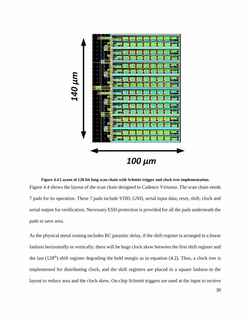
Figure 4.4 shows the layout of the scan chain designed in Cadence Virtuoso. The scan chain needs
7 pads for its operation. These 7 pads include VDD, GND, serial input data, reset, shift, clock and
serial output for verification. Necessary ESD protection is provided for all the pads underneath the
pads to save area.
As the physical metal routing includes RC parasitic delay, if the shift register is arranged in a linear
fashion horizontally or vertically, there will be huge clock skew between the first shift register and
the last (128th) shift register degrading the hold margin as in equation (4.2). Thus, a clock tree is
implemented for distributing clock, and the shift registers are placed in a square fashion in the
layout to reduce area and the clock skew. On-chip Schmitt triggers are used at the input to receive
Figure 4.4 Layout of 128-bit long scan chain with Schmitt trigger and clock tree implementation.

31
all of the low-speed signals for scan, and to offer noise immunity during transitions from substrate
coupling. Figure 4.5 shows the die photo of the standalone scan chip.
4.2 Layout Considerations
Figure 4.6 shows the annotated full chip layout of the proposed fully differential VM VCSEL
driver design in Cadence Virtuoso using a 9-metal layer 65nm CMOS process. The core area of
the chip is 400*250 um2 in a 0.6*1mm2 full chip die area. An on-chip scan chain discussed in the
Figure 4.5 Die photo of the standalone scan chain and custom-made pads to reduce area and parasitics.
Figure 4.6 Full-chip layout of the proposed push-pull VM VCSEL driver before metal-fill for clarity.

32
previous section is integrated with the design to facilitate testing and measurements. Most of the
remaining unoccupied area is filled with decoupling capacitors for improved noise performance.
The decoupling capacitor is custom made by adding metal-oxide-metal (MOM) capacitor on top
of the NMOS RF capacitor from the library for improved capacitance density and better
performance.
There are 31 pads used in total in this design. The pads are connected to the electro-static discharge
(ESD) diodes for protection. The RF pads uses only the higher metal layers (M9 to M8) for reduced
parasitics, DC pads and low frequency pads uses M9-M4 stack, ESD diodes are placed underneath
Figure 4.7 Layout of the high frequency drive including differential CMOS based input receiver,
programmable delay generation for equalization, equalization pulse shaping circuit and the output VM
driver.
33
the pads to save area. All the pads with the ESD diodes were custom designed to mimimize area
and parasitics as part of tapeout1 with the standalone scanchain.
Extensive care is taken to reduce noise and crosstalk, and hence the chip is powered through
multiple supplies: one for scan chain, one for the entire high-speed driver, and one for VCSEL
bias DAC. The GND is shared between the high-speed driver and the DC current DAC, while the
scan uses a separate ground (GND_SCAN) to avoid noise coupling. Also, the two separate grounds
are connected using the power cut cells (back-back connected diode) for enhanced ESD protection
while still decoupling noise. Power clamps are added between all the power supplies and the
respective grounds for enabling closed loop discharge path during any ESD event. The input and
Figure 4.8 Layout of the high voltage DC bias PMOS and NMOS based IDAC.

34
output high speed signals are routed in M8 and M9 to reduce the parasitic resistance and
capacitance. The power and GND rail is routed using strapped metal stack (M9-M3) to reduce the
effective resistance, IR drop and increase the current handling capability of the power rails. The
entire core area layout is made horizontally symmetrical to reduce the mismatch between the data
(D) and its compliment (D_B). RF metal-insulator-metal (MIM) capacitors are used for ac-
coupling because of high linearity and moderate density when compared to MOS capacitor. The
input termination DAC is made using poly resistor because of its high density, and hence reduced
area. The total area of the differential input DAC is 4090 um2. Guard rings are added for every
1515 um2 of the active area to reduce the chances of latch up. All the logic circuits in the high-
speed driver path shown in Figure 4.6 are built using low voltage threshold (LVT) transistors for
enhanced performance. The DC bias path uses thick gate high breakdown voltage transistors for
safety and reliability as shown in Figure 4.7.
4.3 PCB Design Considerations
As discussed in Section 2, wirebond inductance severely degrade the performance of the high-
speed systems. Although packaging experiments are more robust and reliable, typical package
wirebond inductance ranges from 3–5 nH and are hence not preferable. Probing based experiments
are preferred for quick testing of the designs that are sensitive to wirebonds and has less number
of pads. Chip on board (COB) packaging is used to reduce the package parasitics and cost for
testing in this design. In COB, CMOS transmitter die and the VCSEL die are glued to the same
high-speed PCB board and bonded together for electrical connection. Typical wirebond inductance
in COB experiments is less than 1 nH.
35
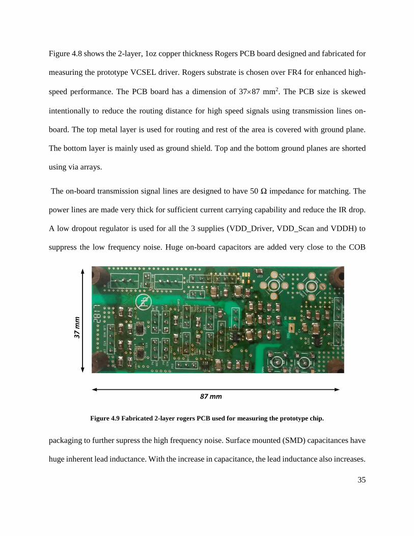
Figure 4.8 shows the 2-layer, 1oz copper thickness Rogers PCB board designed and fabricated for
measuring the prototype VCSEL driver. Rogers substrate is chosen over FR4 for enhanced high-
speed performance. The PCB board has a dimension of 3787 mm2. The PCB size is skewed
intentionally to reduce the routing distance for high speed signals using transmission lines on-
board. The top metal layer is used for routing and rest of the area is covered with ground plane.
The bottom layer is mainly used as ground shield. Top and the bottom ground planes are shorted
using via arrays.
The on-board transmission signal lines are designed to have 50 Ω impedance for matching. The
power lines are made very thick for sufficient current carrying capability and reduce the IR drop.
A low dropout regulator is used for all the 3 supplies (VDD_Driver, VDD_Scan and VDDH) to
suppress the low frequency noise. Huge on-board capacitors are added very close to the COB
packaging to further supress the high frequency noise. Surface mounted (SMD) capacitances have
huge inherent lead inductance. With the increase in capacitance, the lead inductance also increases.
Figure 4.9 Fabricated 2-layer rogers PCB used for measuring the prototype chip.
36
Thus, beyond the self resonance of the capacitor, it behaves like an inductance. Hence a parallel
combination of 4 capacitors of value 0.1 F, 1 F, 10 F, and 100 F are added between each
supply and GND on-board to supress noise over a wide range of frequency.
The DC bias to the chip is tuned using a potentiometer (POT). The output value of the POT is also
filtered using the capacitor combination. All the components that are more than a few mm tall
(header pin, SMA, POT) are kept far away from the COB packaging to avoid blocking of optical
probe head when picking the light using the optical lensed fiber fitted to optical probe as in [8] or
to avoid loss in coupling when using the lensed setup as in [27].
The low frequency output signal from the Altera FPGA board generates signals of high amplitude
(3.3 V). The high swing output of the FPGA board is level shifted to CMOS level (1V) using
resistive division between 2.2 k and 1 k. The output of the resistive division can be buffered
by an on-board Schmitt trigger integreated circuits (ICs) to remove the noise during transitions.
The PCB board is successfully used for the following measurements:
1. Electrically characterization of the high-speed driver.
2. Functionality test of the Scan chain.
3. VCSEL Optical eye diagram measurement.
4. Bit error rate (BER) measurement to verify the functionality of the driver.
5. Power consumption measurement for the driver.
The measurements results are discussed in the next Chapter.

37
Chapter 5: Measurements
5.1 Electrical Measurements
A proof-of-concept prototype was fabricated in a 65nm CMOS process. Figure 5.1(a) shows the
die photo of the CMOS transmitter chip. The core area of the chip is 400250 um2 in a 0.61 mm2
die. Figure 5.1(b) shows the VCSEL die. The VCSEL die has a single anode pad at the center
surrounded by two cathode pads on the emitting top surface as shown in Figure 5.1(b). In this
design, only one of the cathode pad is bonded to the design and the other pad is left open. Chip on
board (COB) packaging is used to reduce the package parasitic and cost for testing in this design.
Although we had 40 CMOS bare dies, as only a handful of VCSELs were available. Only 5 out of
40 CMOS dies were packaged to the VCSELs for optical measurements. 5 more CMOS dies were
bonded to the PCB directly to electrically characterize and ensure full functionality of the driver.
Figure 5.2 shows the die photo of the CMOS transmitter chip wire bonded to the PCB pads using
chip on board (COB) packaging technique for electrical measurements. As the proposed CMOS
Figure 5.1 Chip Micrograph (a) Die photo of the CMOS VCSEL driver (b) Die photo of the 25 Gbps
Finisar VCSEL

38
driver is not designed to drive a load (50 Ω) through a transmission line, it is not matched to 50 Ω.
Hence, to avoid reflections during high speed electrical characterization, an on-board differential
termination of 100 Ω is soldered on the PCB board. However, on-board SMD terminations have
huge parasitics and degrade impedance matching at high frequencies.
The differential electrical data is fed at full rate from an external Anritsu BERT pattern generator.
The electrical output of the driver is measured using an Infineon high speed oscilloscope. The
clock output from the BERT is used to trigger the oscilloscope.
Figure 5.3(a) shows the measured electrical eye diagram of the driver at 7 Gb/s for a PRBS7
pattern. Figure 5.3(b) shows the measured eye diagram at 10 Gb/s for a PRBS7 pattern. We suspect
that the degraded electrical transient performance at 10 Gb/s is mainly caused by reflections due
to impedance mismatch, and is not due to any speed limitation of the driver. Nevertheless, the
electrical measurement is a good indicator to show the functionality of the driver.
Figure 5.2 Microscope image of the CMOS die, chip on board packaged to the PCB pads for electrical
testing.

39
5.2 VCSEL DC Behavior
Figure 5.4 shows the die photo of the CMOS transmitter chip wire bonded to the VCSEL die using
chip on board (COB) packaging technique. Figure 5.5(a) shows the setup used for the optical
measurement of the VCSEL output in this design. An external Anritsu1800A BERT is used to
provide the differential electrical input data pattern for the design. The modulated VCSEL light
output is coupled into a 2m long multimode fiber using the collimating and the focusing lens setup
shown is Figure 5.6 [27]. The coupling efficiency of the VCSEL light output is measured using
Figure 5.3 Measured electrical eye diagram of the driver for a PRBS7 pattern at (a) 7Gb/s (b) 10Gb/s
showing eye degradation due to impedance mismatch.

40
the HP81533B optical power meter. The high speed modulated optical output is measured using
the Anritsu MP2110A BERTwave which has an embedded optical attenuator and an optical scope
functionality.
The measured currents of the bias IDAC as a function of the scan control word when the driver is
bonded to the VCSEL die is shown in Figure 5.7. The measured output light power of the VCSEL
using the HP81533B optical power meter as a function of the VCSEL bias current is shown in
Figure 5.8. The VCSEL output DC light power is linear beyond its threshold current of ~ 0.8 mA.
The measured η of the VCSEL is ~0.125 mW/mA. The datasheet value for η of the VCSEL is 0.3
mW/mA. The 3.8 dB optical coupling loss in the measurement setup is de-embedded in the optical
oscilloscope for eye diagram measurements.
Figure 5.4 Microscope image of the CMOS die, chip on board packaged to VCSEL die on a high-speed
PCB board for optical measurements.
Figure 5.5 Setup for (a) optical eye diagram measurement (b) Bit error rate (BER) measurement.

41
Figure 5.7 Measured bias DAC current as a function of the control word when the driver is connected to
the VCSEL die.
Figure 5.6 VCSEL setup for optimal light coupling using lens. This setup was built by Spoorthi Nayak.

42
5.3 High Speed Optical Characterization
VCSEL optical eye diagram is measured using the setup shown in Figure 5.5(a). Figure 5.9
illustrates the impact of equalization to cancel the asymmetry in the optical eye. Figure 5.9(a)
shows the VCSEL optical eye when modulated by the driver without equalization. Without
equalization, the VCSEL eye is asymmetric with longer fall time and shorter rise time. Figure
5.9(b) is obtained with optimal rise and fall equalization, with the rise and fall tap ratio of 1:2. The
equalization improves the quality of the eye diagram making it more symmetrical. An OMA of
2.64 dBm and an ER of 7.2 dB is measured at 13 Gb/s for a PRBS7 pattern with an energy
efficiency of 1.75 pJ/b.
The measured optical eye diagram of the VCSEL at 16 Gb/s for a PRBS7 input with optimal rise
and fall pre-emphasis is shown in Figure 5.10. The total energy efficiency of the driver with
Figure 5.8 Measured output light DC power as a function of the bias current (Ivcsel). The output power is
measured using the optical power meter and the coupling is optimized using the lens setup.

43
VCSEL is 1.52 pJ/b and the measured OMA and ER of the optical output is 2.1 dBm and 5.92 dB,
respectively.
The bit error in the transmitted optical output of the VCSEL is measured using the setup shown in
Figure 5.5(b) to fully verify the functionality of the transmitter. The optical output of the VCSEL
is converted into electrical signal using the Discovery semiconductor PD+TIA module. Fig 5.11
shows the measure opto-electrical eye diagram at 12 Gb/s from the PD+TIA module. The electrical
Figure 5.9 Measured eye diagram at 13 Gb/s (a) without equalization, and (b) with optimal rise and fall
equalization.
Figure 5.10 Measured eye diagram at 16 Gb/s with optimal rise and fall pre-emphasis setting.
44
output of the PD+TIA module is then fed back to the BERT for detecting errors in the received
data stream. A BER of 10-12 is verified up to 12Gbps using the above setup. Measurements were
limited to 12 Gb/s because of the limited BW and the responsivity of PD+TIA module at 850 nm
wavelength.
Figure 5.12 shows the impact of the ac coupling capacitor in the signal path of the modulation
current. The finite on chip ac capacitors of 20 pF create the low frequency cut-off attenuating the
long CIDs when the length of the data pattern increases. For this measurement, the VCSEL was
biased suitably and an optimum equalization was applied for symmetrical eye opening. The
Figure 5.11 Measured opto-electrical eye diagram at 12 Gb/. The optical output of the VCSEL is
converted into electrical signals using the PD+TIA module for bit error rate (BER) measurement.
Figure 5.12 Measured eye diagram with optimum rise and fall pre-emphasis at 13Gbps for a (a) PRBS7
pattern (b) PRBS15 (c) PRBS31 pattern

45
measured eye diagram at 13Gbps for a PRBS7, PRBS15 and PRBS31 input pattern is shown in
Figure 5.12(a), (b), and (c), respectively. The low frequency cut-off can be resolved by using the
techniques described in Chapter 6.
5.4 Power Consumption and Performance Summary
Figure 5.13 shows the power breakdown of the proposed push-pull VM VCSEL driver at 16 Gb/s.
A major fraction of the total power, around 35% in this design is dissipated by the VCSEL to
generate useful output optical power. The summary of the results achieved are compared with the
prior-art in Table 1. The prototype in 65nm CMOS compares favorably to other drivers in energy
efficiency. A driver in 32nm SOI achieves a superior efficiency of 0.77 pJ/b at 20 Gb/s [10].
However, it leverages a VCSEL with 2.6 higher slope efficiency (). VCSEL varies widely
from 0.2 - 0.75 mW/mA [8], [10], [12], therefore rendering pJ/b as a difficult comparison metric.
Figure 5.13 Power consumption breakdown chart of the prototype driver with equalization at 16 Gbps
for the total power of 24.2 mW.

46
When a VCSEL diode with threshold current (Ith), slope efficiency (), series resistance (RVCSEL)
and diode voltage drop of (Vth) is excited with the current of Iv from an ideal supply, the desired
Pop and the total input electrical power (PT) is given by equation (5.1 and(5.2), respectively. Power
conversion efficiency (PCE) [28] of the VCSEL is defined as the ratio of desired Pop to PT
consumed in the diode and is given by equation (5.3). It is evident fro equation (5.3) that the PCE
of the VCSEL is significantly dependent on the slope efficiency than other parameters [28].
𝑃𝑜𝑝 = (𝐼𝑣 − 𝐼𝑡ℎ) (5.1)
𝑃𝑇 = (𝑉𝑡ℎ + 𝑅𝑉𝐶𝑆𝐸𝐿𝐼𝑣)𝐼𝑣 (5.2)
𝑃𝐶𝐸𝑣𝑐𝑠𝑒𝑙 =
𝑃𝑜𝑝
𝑃𝑇=
𝜂(𝐼𝑣 − 𝐼𝑡ℎ)
(𝑉𝑡ℎ + 𝑅𝑉𝐶𝑆𝐸𝐿𝐼𝑣)𝐼𝑣
(5.3)
PCE can be normalized to the VCSEL to compare different drivers irrespective of the VCSEL
efficiency to get an estimate of the driver efficiency. Improving the overall PCE of the driver is
paramount to improving the overall energy efficiency of the link. Thus, recent research has laid
Figure 5.14 VCSEL-normalized power-conversion efficiency of 10-26 Gb/s CMOS drivers published
during the last decade. η-normalized PCE = (Pop/η)/PT.

47
significant emphasis on improving the overall PCE (wall plug efficiency) of the laser driver. These
efforts include designing a VCSEL with higher and lower Ith, RVCSEL and Vth to improve the
intrinsic PCE of the VCSEL, and improving the -normalized PCE of the driver.
For a VCSEL driver, PT in equation (5.5) includes power due to Ibias (Pbias), power due to Imod (Pmod)
and power consumed by the rest of the circuit (Prem), and Pop is given by equation (5.4). Figure
5.14 plots the -normalized PCE of the 10-26 Gb/s CMOS VCSEL drivers published in the
literature during the last decade, highlighting the performance of the prototype fully-differential
VM driver. Clearly, the prototype drive achieves the highest -normalized PCE of 18.7%.
𝑃𝑜𝑝 = (𝐼𝑏𝑖𝑎𝑠 + 𝐼𝑚𝑜𝑑 − 𝐼𝑡ℎ) (5.4)
Table 5.1 Performance summary and comparision
[10] [8] [12] [11] This work
CMOS Tech. SOI 32 nm 65 nm 0.13
m
65 nm 65 nm
DC/AC Coupled DC AC AC AC AC
VDDL (V) /
VDDH (V)
1.0/
2.5
1.0/
3
1.2/
NA
1.2/
3.3
1.05/
2.75
Wavelength (nm) 980 850 850 850 850
Slope Eff. (mW/mA) 0.78 0.3 0.25 0.54 0.3
Data Rate (Gb/s) 20 15 10 10 16
Total Energy Eff. (pJ/b) 0.77 2 8.5 6.9 1.52
OMA (dBm) 0.9 2.3 –4.43 6.3 2.1
Pop (dBm) 1.55 0.4 –3.16 5.9 1.34
ER (dB) 4 8.9 3.44 5.6 5.92
-normalized PCE (%) 11.89 12.15 8.75 10.07 18.72

48
𝑃𝑇 = (𝑃𝑚𝑜𝑑 + 𝑃𝑏𝑖𝑎𝑠 + 𝑃𝑟𝑒𝑚) (5.5)
𝜂 − 𝑛𝑜𝑟𝑚𝑎𝑙𝑖𝑧𝑒𝑑 𝑃𝐶𝐸 =
𝑃𝑜𝑝 𝜂⁄
𝑃𝑇=
(𝐼𝑣 − 𝐼𝑡ℎ)
(𝑉𝑡ℎ + 𝑅𝑡ℎ𝐼𝑣)𝐼𝑣
(5.6)

49
Chapter 6: Conclusion and Future work
6.1 Conclusion
As data rates for optical interconnects increase, and advance modulations such as PAM4 are
adopted, reducing the effect of bondwire parasitics and power consumption of the drivers will only
become more critical. Scaling of CMOS processes improves the performance of digital circuits
such as inverters, but degrades the performance of current sources. We present an inverter-based
fully-differential VM driver that mitigates the effects of bondwire parasitics, considerably reduces
the power consumption, and has the promise to scale amicably with future CMOS processes.
VCSEL non-linearity is compensated by asymmetric 3-tap rise and fall pre-emphasis. A proof-of-
concept prototype in 65nm CMOS achieves a total energy efficiency of 1.52 pJ/b at 16 Gb/s and a
VCSEL-normalized power conversion efficiency of 18.7 % which is the highest for any 10-26
Gb/s CMOS VCSEL driver, to the best of our knowledge.
6.2 Future work
The proposed low-power architecture is insensitive to both the supply and signal package
parasitics. However, it uses an ac coupling capacitor in the signal path which causes an undesired
low frequency cut-off to the modulating data attenuating the eye height and introducing jitter for
longer PRBS pattern with long continuous identical digits (CIDs). As future work, we propose
modifications to our ac-coupled VM driver architecture to resolve the low frequency cut-off and
reduce the capacitor area, and briefly present some simulation results.

50
Figure 6.1(a) shows the schematic of an ideal driver ac coupled to the load (Rv). The ac coupling
capacitor (Cac) introduces a low frequency cut-off (fc) to the signal path. For a fixed load (Rv), the
capacitor value must be increased to a very large value to reduce the low frequency cut-off. Figure
6.1(b) shows the schematic of the modified driver to remove the low frequency cut off and reduce
the size of the ac-coupling capacitor using an auxiliary low frequency path as in [8][11]. In Figure
6.1(b), the gain transfer function (TF) from Vin to Vout is given by equation (6.1). Since the single
dominant output pole for both the high frequency driver (HFD) and the low frequency driver (LFD)
is same, when the low frequency DC gain is matched to the high frequency gain given by equation
(6.2), an optimal flat response is obtained as in Figure 6.2(a).
Figure 6.1(c) shows the simplified small signal equivalent model with finite output load impedance
(ro) and load capacitance (CL). In Figure 6.1(c), the gain TF is given by equation (6.3). When the
low frequency gain (ALFD) is equal to the high frequency gain (AHFD) given by equation (6.6), an
optimal flat response is obtained as shown in Figure 6.2(a). In general mismatch in the two gains
Figure 6.1 (a) Schematic of the ideal driver ac coupled to the load (b) Schematic of the ideal driver ac
coupled to the load with an additional feedforward low frequency data path. (c) Small signal model of the
ac coupled driver with the feedforward path.

51
can lead to undesired response as in Figure 6.2(b). However, by choosing the HFD gain higher
than the LFD gain, a passive continuous time linear equalization (CTLE) can be improvised to get
rid of the losses due to the parasitic dominant output pole (fc) as shown in Figure 6.2(c).
𝑉0 =
𝐼𝑖𝑅𝑣
1 + 𝑠𝑅𝑣𝐶𝑎𝑐+
𝑉𝑖 ∗ 𝑠𝑅𝑣𝐶𝑎𝑐
1 + 𝑠𝑅𝑣𝐶𝑎𝑐
(6.1)
𝐼𝑖𝑅𝑣 = 𝑉𝑖 => 𝑉𝑜 = 𝑉𝑖 (6.2)
𝑉0 =
𝐼𝑖(𝑅𝑣||𝑟𝑜)
1 + 𝑠(𝑅𝑣||𝑟𝑜)(𝐶𝑎𝑐 + 𝐶𝐿)+
𝑉𝑖 ∗ 𝑠(𝑅𝑣||𝑟𝑜)𝐶𝑎𝑐
1 + 𝑠(𝑅𝑣||𝑟𝑜)(𝐶𝑎𝑐 + 𝐶𝐿)
(6.3)
𝐴𝐻𝐹𝐷 =
𝐶𝑎𝑐
(𝐶𝑎𝑐 + 𝐶𝐿)
(6.4)
𝐴𝐿𝐹𝐷 = 𝐼𝑖(𝑅𝑣||𝑟𝑜) (6.5)
𝐴𝐻𝐹𝐷 = 𝐴𝐿𝐹𝐷 => 𝑉0 = 𝑉𝑖
𝐶𝑎𝑐
(𝐶𝑎𝑐 + 𝐶𝐿)
(6.6)
Figure 6.2 Frequency response of the modified ac-coupled driver with low frequency path and high
frequency path and a single dominant pole (fc) (a) when the low frequency gain is matched to the high
frequency gain. (b) when low frequency gain is higher than the high frequency gain (c) when the high
frequency gain is boosted for equalization.
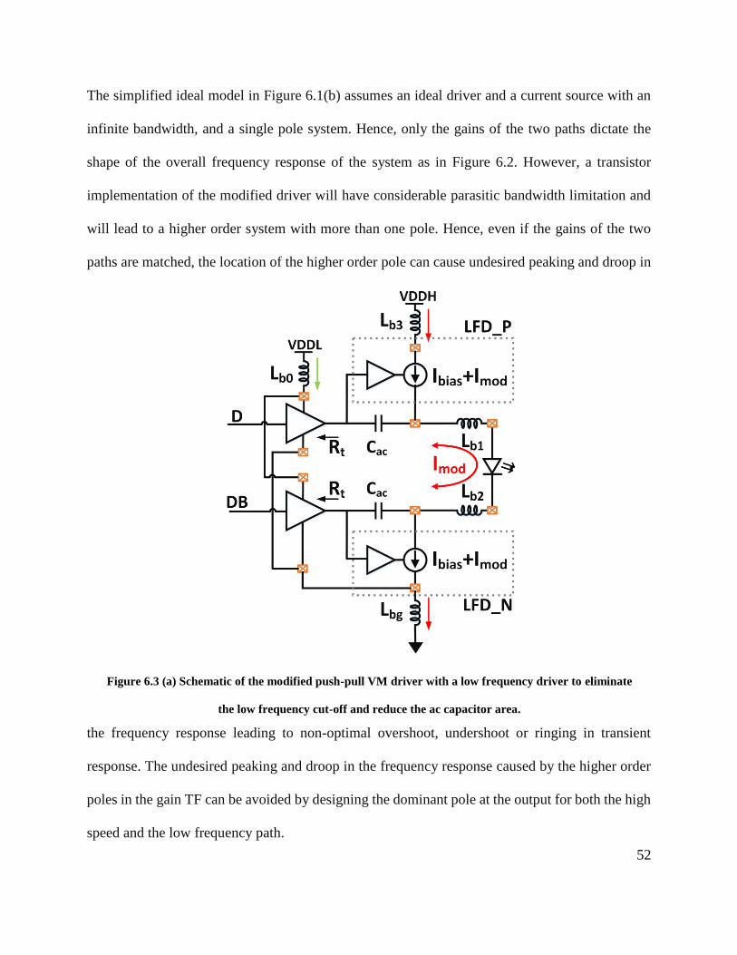
52
The simplified ideal model in Figure 6.1(b) assumes an ideal driver and a current source with an
infinite bandwidth, and a single pole system. Hence, only the gains of the two paths dictate the
shape of the overall frequency response of the system as in Figure 6.2. However, a transistor
implementation of the modified driver will have considerable parasitic bandwidth limitation and
will lead to a higher order system with more than one pole. Hence, even if the gains of the two
paths are matched, the location of the higher order pole can cause undesired peaking and droop in
the frequency response leading to non-optimal overshoot, undershoot or ringing in transient
response. The undesired peaking and droop in the frequency response caused by the higher order
poles in the gain TF can be avoided by designing the dominant pole at the output for both the high
speed and the low frequency path.
Figure 6.3 (a) Schematic of the modified push-pull VM driver with a low frequency driver to eliminate
the low frequency cut-off and reduce the ac capacitor area.

53
The block diagram of the modified fully-differential push-pull VM driver to resolve the low
frequency cut-off due to the ac-coupling capacitor is shown in Figure 6.3. The low frequency
content of the modulation data is pumped into the VCSEL diode using the low frequency CM
drivers, LFD_P and LFD_N. Since the data rate of the LFD is low (~ 2-3 GHz), the SSN due to
the bondwires Lb2 and Lb1 does not impact the high frequency performance of the overall driver
and hence, does not mandate the need for a huge on-chip decoupling capacitor.
Figure 6.4 shows the schematic of the low frequency driver. The basic building block of the LFD
is a 1:10 NMOS and PMOS current mirror as shown on Figure 6.4(a) and Figure 6.4(b),
respectively. As the VCSEL needs high DC bias, the output current sources in the current mirrors
are built using the thick gate high-voltage devices to avoid breakdown. However, the thick gate
devices used to build the LFD has huge parasitics and significantly reduces the bandwidth as it
results in two dominant poles – at the gate and the drain of the output current source MP and MN
respectively. The presence of a dominant pole at the gate of the low frequency path current mirror
MP and MN will cause the LFD to have a lower cut-off frequency than the HFD resulting in an
undesired droop in the overall frequency response. The implementation in [11] used a huge ac
coupling capacitor of 10 pF at the output to make the output pole dominant and to achieve an
optimal flat frequency response. Instead, an ac coupling capacitor Cx (200 fF) can be added to the
gate of the current mirror to push the pole at the gate of the MP and MN to a higher frequency, as
in [8]. Cx enhances the bandwidth by charge redistribution between Cx and the gate capacitance of
MP and MN during falling/rising transitions [8]. The cross over frequency between the LFP and
HFP at the output nodes P and N respectively, is kept below 2 GHz to avoid SSN generation due
to Lb1 and Lb2.

54
The incoming differential data, D and DB is applied to the differential pairs built using low Vt
devices for faster switching of the bias current. The current in the right arm is amplified (10
mirrored) before feeding into the VCSEL. The left arm is a dummy replica of the right arm to
ensure differential operational and avoid SSN. There is also current sinking path of Ib in both the
arms of the differential amplifier for DC biasing the VCSEL above its threshold. Cascode devices
are employed to provide high output impedance for ensuring device safety and accurate current
mirroring.
Figure 6.5 illustrates the impact of the adding the LFD path and reducing the ac coupling capacitor
value from 20 pF to 500 fF on the eye diagram of the VCSEL junction current (Iv) for the proposed
driver. The simulated eye at 15Gb/s for a PRBS31 pattern for the modified driver with only LFD
enabled, and with both the LFD and HFD enabled are shown. A 1 nH inductance is assumed for
Figure 6.4 (a) Schematic of the low frequency driver (a) p-path for pushing current (b) n-path for pulling
current.

55
both the supply and signal package for simulation to capture the SSN and ISI due to bondwire
parasitics.
In summary, our modification and simulations promise that the low frequency cut-off due to the
ac-coupling capacitor in the signal path can be resolved. A natural extension for our proposed
design is to implement drivers to support advanced modulation schemes such as PAM4 or pulse
width modulation (PWM) to further increase the achievable data rate.
Figure 6.5 Simulated eye diagram of the modified push-pull driver at 15Gb/s with Cac= 300fF, RVCSEL =
50Ω and CVCSEL = 300fF (a) with only the low frequency current source in the P-path and N-path enabled
(b) with both the LFD and HFD enabled.

56
Bibliography
[1] B. Razavi, Design of Integrated Circuits for Optical Communications. New York, NY,
USA: McGraw-Hill, 2003.
[2] E. Sackinger, Broadband circuits for optical fiber communication, Hoboken, NJ, USA:
Wiley, 2005.
[3] L. A. Coldren and S. W. Corzine, Diode Lasers and Photonic Integrated Circuits, Wiley-
Interscience, 1995.
[4] J. A. Tatum et al., “VCSEL-based interconnects for current and future data centers,” IEEE
Journal of Lightwave Technology, vol. 33, no. 4, pp. 727–732, Feb. 15, 2015.
[5] I. A. Young et al., “Optical technology for energy efficient I/O in high performance
computing," IEEE Communications Magazine, vol. 48, no. 10, pp. 184-191, Oct. 2010.
[6] A. H. Ahmed et al., “Silicon-photonics microring links for datacenters challenges and
opportunities,” IEEE Journal of Selected Topics in Quantum Electronics, vol. 22, no. 6,
pp. 194-203, Nov.-Dec. 2016.
[7] D. Mahgerefteh et al., “Techno-economic comparison of silicon photonics and multimode
VCSELs,” IEEE Journal of Lightwave Technology, vol. 34, no. 2, pp. 233–242, Jan. 15,
2016.
[8] V. Kozlov et al, “Capacitively-coupled CMOS VCSEL driver circuits,” IEEE Journal of
Solid-State Circuits, vol. 51, no. 9, pp. 2077-2090, Sep. 2016.
[9] J. Proesel et al., “25 Gb/s 3.6 pJ/b and 15 Gb/s 1.37 pJ/b VCSEL-based optical links in
90 nm CMOS,” IEEE Int. Solid-State Circuits Conf. Dig. Tech. Papers, pp. 418–420,
2012.

57
[10] M. Raj et al., “A modelling and nonlinear equalization technique for a 20 Gb/s 0.77 pJ/b
VCSEL transmitter in 32 nm SOI CMOS,” IEEE Journal of Solid-State Circuits, vol. 51,
no. 8, pp. 1734–1743, Aug. 2016.
[11] H. Morita et al., “A 12 × 5 two-dimensional optical I/O array for 600Gb/s chip-to-chip
interconnect in 65nm CMOS,” IEEE Int. Solid- State Circuits Conf. Dig. Tech. Papers,
pp. 140–141, Feb. 2014.
[12] S. Rabii et al., “An integrated VCSEL driver for 10Gb Ethernet in 0.13μm CMOS,” IEEE
Int. Solid-State Circuits Conf. Dig. Tech. Papers, pp. 930–939, Feb. 2006.
[13] P. Chevalier et al., "Advanced SiGe BiCMOS and CMOS platforms for Optical and
Millimeter-Wave Integrated Circuits," IEEE Compound Semiconductor Integrated
Circuit Symposium, San Antonio, TX, pp. 12-15, 2006.
[14] M. Shibata et al., “A 26-Gb/s 1.80-pJ/bit CMOS-Driven Transmitter for 850-nm
Common-Cathode VCSELs," Optical Fiber Communication Conference, Anaheim, CA,
pp. 1-3, Mar. 2015.
[15] K. Lear et. al, “Common anode vertical-cavity surface-emitting lasers on p-doped
substrates," Conference on Lasers and Electro-Optics, pp. 292-293, 1997.
[16] J. G. Jim Tatum et. al, “High Speed Characteristics of VCSELs," Proc. SPIE, vol. 3004,
pp. 151-159, May 1997.
[17] C. Xie et al., “Optimizing 10Gbps VCSEL for real-world laser driver in parallel optical
transceiver,” Proc. SPIE, vol. 7615, p. 761508-10, Feb. 2010.
[18] S. Palermo et al., “A 90 nm CMOS 16 Gb/s transceiver for optical interconnect,” IEEE
Journal of Solid-State Circuits, vol. 43, no. 5, pp. 1235–1246, May 2008.

58
[19] D. Kucharski et al., “A 20 Gb/s VCSEL driver with pre-emphasis and regulated output
impedance in 0.13 μm CMOS,” in IEEE Int. Solid-State Circuits Conf. (ISSCC) Dig. Tech.
Papers, vol. 1. pp. 222–594, Feb. 2005.
[20] S. Shekhar et. al , “Silicon electronics-photonics integrated circuits for
datacenters”, IEEE Compound Semiconductor IC Symposium, Austin, TX, pp. 1-4, Nov.
2016 (invited).
[21] G. Balamurugan et al., “A scalable 5–15 Gbps, 14–75 mW low power I/O transceiver in
65 nm CMOS”, IEEE Journal of Solid-State Circuits, vol. 43, no. 4, pp. 1010-1019, April
2008.
[22] J. Li et al., “Scaling Trends for Picojoule-per-Bit WDM Photonic Interconnects in CMOS
SOI and FinFET Processes”, IEEE Journal of Lightwave Technology, vol. 34, no. 11, pp.
2730-2742, June, 2016.
[23] A. Sharif-Bakhtiar et al., “A 40-Gbps 0.5-pJ/bit VCSEL Driver in 28nm CMOS with
Complex Zero Equalizer”, Custom Integrated Circuits Conference, Austin, Texas, May
2017.
[24] A. H. K. Park et al., “Comparison of DAC-less PAM4 modulation in segmented ring
resonator an dual cascaded ring resonator”, IEEE Optical Interconnects Conf., pp. 7-8,
June 2017.
[25] N. H. E Weste and D. M. Harris, CMOS VLSI Design: A Circuits and System Perspective,
4th ed., Addison-Wesley, 2010.
[26] J. M. Rabaey, A. Chandrakasan, and B. Nikolic, Digital Integrated Circuits, A Design
Perspective, 2nd ed., Prentice-Hall, 2003.

59
[27] S. G. Nayak, A fully-integrated complementary metal-oxide semiconductor receiver with
avalanche photodetector, MASc Thesis, University of British Columbia, Aug, 2017
[28] R. Michalzik, VCSELs: Fundamentals, Technology and Applications of Vertical-Cavity
Surface-Emitting Lasers, New York, USA: Springer, 2013.
[29] K. Ohhata et al."Design of a 4 * 10 Gb/s VCSEL Driver Using Asymmetric Emphasis
Technique in 90-nm CMOS for Optical Interconnection," in IEEE Transactions on
Microwave Theory and Techniques, vol. 58, no. 5, pp. 1107-1115, May 2010.
[30] J. Y. Jiang et al., "100Gb/s ethernet chipsets in 65nm CMOS technology," 2013 IEEE
International Solid-State Circuits Conference Digest of Technical Papers, San Francisco,
CA, pp. 120-121, 2013.
[31] C. L. Schow et al., "Low-Power 16 x 10 Gb/s Bi-Directional Single Chip CMOS Optical
Transceivers Operating at ≪ 5 mW/Gb/s/link," in IEEE Journal of Solid-State Circuits,
vol. 44, no. 1, pp. 301-313, Jan. 2009.
[32] J. E. Proesel et al., "Ultra-low-power 10 to 28.5 Gb/s CMOS-driven VCSEL-based optical
links [Invited]," in IEEE/OSA Journal of Optical Communications and Networking, vol.
4, no. 11, pp. B114-B123, Nov. 2012.