A 1.5 kW Radio-Frequency Tunable Matching Network Based ...
16
A 1.5 kW Radio-Frequency Tunable Matching Network Based on Phase-Switched Impedance Modulation The MIT Faculty has made this article openly available. Please share how this access benefits you. Your story matters. As Published 10.1109/OJPEL.2020.2987782 Publisher Institute of Electrical and Electronics Engineers (IEEE) Version Final published version Citable link https://hdl.handle.net/1721.1/135389 Terms of Use Creative Commons Attribution 4.0 International license Detailed Terms https://creativecommons.org/licenses/by/4.0/
-
Upload
khangminh22 -
Category
Documents
-
view
6 -
download
0
Transcript of A 1.5 kW Radio-Frequency Tunable Matching Network Based ...

A 1.5 kW Radio-Frequency Tunable Matching NetworkBased on Phase-Switched Impedance Modulation
The MIT Faculty has made this article openly available. Please share how this access benefits you. Your story matters.
As Published 10.1109/OJPEL.2020.2987782
Publisher Institute of Electrical and Electronics Engineers (IEEE)
Version Final published version
Citable link https://hdl.handle.net/1721.1/135389
Terms of Use Creative Commons Attribution 4.0 International license
Detailed Terms https://creativecommons.org/licenses/by/4.0/

Received 24 February 2020; revised 31 March 2020; accepted 10 April 2020. Date of publication 16 April 2020;date of current version 11 May 2020. The review of this article was arranged by Associate Editor Min Chen.
Digital Object Identifier 10.1109/OJPEL.2020.2987782
A 1.5 kW Radio-Frequency Tunable MatchingNetwork Based on Phase-Switched
Impedance ModulationANAS AL BASTAMI 1 (Student Member, IEEE), ALEXANDER JURKOV2 (Student Member, IEEE),
DAVID OTTEN1, DUY T. NGUYEN2 (Member, IEEE), AARON RADOMSKI2 (Member, IEEE),AND DAVID J. PERREAULT 1 (Fellow, IEEE)
1 Department of Electrical Engineering and Computer Science, Massachusetts Institute of Technology, Cambridge, MA 02139 USA2 MKS Instruments, Inc., Rochester, NY 14623 USA
CORRESPONDING AUTHOR: ANAS AL BASTAMI (e-mail: [email protected])
This work was financially supported by MKS Instruments, Inc.
ABSTRACT Dynamically-tunable impedance matching is a key feature in numerous radio-frequency (RF)applications at high frequencies (10 s of MHz) and power levels (100s–1000 s of Watts and above). Thiswork develops techniques that enable the design of high power tunable matching networks (TMN) that canbe tuned orders of magnitude faster than with conventional tunable impedance matching techniques, whilerealizing the high power levels required for many industrial applications. This is achieved by leveraging anemerging technique – known as phase-switched impedance modulation (PSIM), which involves switchingpassive elements at the rf operating frequency – that has previously been demonstrated at rf frequencies at upto a few hundred Watts. In this paper, we develop design approaches that enable it to be practically used atup to many kilowatts of power at frequencies in the 10 s of MHz. A detailed analysis of the factors affectingthe losses as well as the tradeoffs of a basic PSIM-based element is provided. Furthermore, it is shown howincorporating additional stages to the PSIM-based element, including impedance scaling and / or the additionof series or shunt passive elements, influences the losses and enables the efficient processing of high powerlevels given the limitations of available switches. A PSIM-based TMN that matches load impedances to 50 �
and delivers up to 1.5 kW of power at frequencies centered around 13.56 MHz is implemented and testedover a load impedance range suitable for various industrial plasma processes.
INDEX TERMS Impedance matching, impedance transformation, impedance modulation, plasma genera-tion, phase-switched impedance, PSIM, tunable matching network, antenna tuning unit, capacitively-coupledplasma.
I. INTRODUCTIONA wide range of existing and emerging applications requirethe delivery of radio-frequency (rf) power into widely-varyingloads at power levels up to several kilowatts and beyond.Examples include magnetic resonance imaging [1], [2], wire-less communications [3], wireless power transfer [4]–[8],and plasma generation [9], [10]. The wide variation in loadimpedance in many of these applications makes it challengingto achieve efficient rf power generation while maintaining ac-ceptable loading of the rf amplifier or inverter, and providingaccurate control of power delivered to the load.
RF amplifiers and inverters are typically designed to op-erate efficiently into a fixed load impedance, and the perfor-mance of many high-frequency (HF, 3–30 MHz) and veryhigh frequency (VHF, 30-300 MHz) switched-mode poweramplifiers/inverters degrades quickly with variations in loadimpedance, e.g., [11]–[13]. This variation in load impedanceis commonly addressed by utilizing a tunable matching net-work (TMN) between the load and the generator [5], [6], [10],[14]–[17]. The TMN matches the varying load impedanceto a fixed input impedance (e.g., 50 �) suitable for drivingby the amplifier. Conventional TMN designs have adjustable
This work is licensed under a Creative Commons Attribution 4.0 License. For more information, see https://creativecommons.org/licenses/by/4.0/
124 VOLUME 1, 2020
passive components that are dynamically tuned, such as byusing servo motors to mechanically adjust a set of variablecapacitors or inductors, or by using reconfigurable capacitorand/or inductor banks, or by using high-power varactors [18],[19]. While such tuning methods can be effective, they oftenresult in systems that are bulky, costly, limited in resolution,and have slow response to changes in load impedance. Thisslow response, for example, can be of concern to semicon-ductor manufacturing industries, which utilize modern rapidmulti-step plasma processes to meet increasing demands formanufacturing very thin films and finer features. Such pro-cesses result in rapid load impedance steps taking place atintervals as short as 10 s of microseconds, posing challengesto conventional TMN designs.
Other approaches addressing load impedance variationswithout using a TMN have been proposed in the literature;however, they each have their own limitations. In [10], forexample, an approach utilizing a resistance compression net-work is proposed to achieve narrow-range loading of thepower amplifier. While this can be effective in many appli-cations, it requires a specially-configured set of loads whichmight not be desirable nor practical in some applications.While other approaches of achieving resistance compressionwithout requiring such a special set of loads have been pro-posed (e.g, [20]), it is not possible to achieve control of in-put impedance with arbitrary precision. In [7], [21], anotherapproach is proposed where the inverters are configured todirectly drive the varying load impedance; this, however, canresult in substantial over-rating of the constituent inverters,which may not be desirable.
The concept of using a passive element switched at an acoperating frequency to realize an effective variable impedancehas been known for some time (e.g., [22], [23]). Recently,it was shown in [9] that this technique can be successfullyrealized at high frequencies (10 s of MHz) and used to createhigh-bandwidth tunable matching networks. In particular, [9]demonstrated that a capacitor switched under ZVS conditions(using, for e.g., a GaN transistor in parallel with the capacitor)could be employed for efficient, high-bandwidth impedancematching at up to 10 s of MHz and 100 s of Watts.
This paper further develops this technique, termed phase-switched impedance modulation (PSIM), to enable the designof TMNs that can efficiently process high (multi-kilowatt)power levels at high frequencies (10 s of MHz) with extremelyfast modulation bandwidth, such that it can address the needsof high-power applications such as industrial plasma process-ing. In Section II, we provide a detailed analysis and charac-terization of losses in a basic PSIM element, and demonstratehow impedance scaling as well as incorporating series andshunt passive elements affect these losses and can be usedto improve the power processing capability of a PSIM TMNgiven limited transistor ratings. Section III discusses the de-sign of a prototype 1.5 kW TMN based on the models andinsights developed in the paper. Section IV presents experi-mental results and evaluates the performance of the proposedTMN. Finally, Section V concludes the paper.
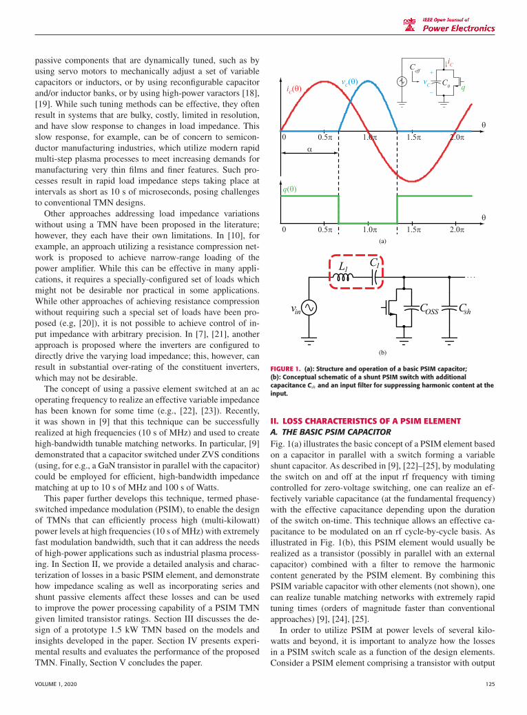
FIGURE 1. (a): Structure and operation of a basic PSIM capacitor;(b): Conceptual schematic of a shunt PSIM switch with additionalcapacitance Csh and an input filter for suppressing harmonic content at theinput.
II. LOSS CHARACTERISTICS OF A PSIM ELEMENTA. THE BASIC PSIM CAPACITORFig. 1(a) illustrates the basic concept of a PSIM element basedon a capacitor in parallel with a switch forming a variableshunt capacitor. As described in [9], [22]–[25], by modulatingthe switch on and off at the input rf frequency with timingcontrolled for zero-voltage switching, one can realize an ef-fectively variable capacitance (at the fundamental frequency)with the effective capacitance depending upon the durationof the switch on-time. This technique allows an effective ca-pacitance to be modulated on an rf cycle-by-cycle basis. Asillustrated in Fig. 1(b), this PSIM element would usually berealized as a transistor (possibly in parallel with an externalcapacitor) combined with a filter to remove the harmoniccontent generated by the PSIM element. By combining thisPSIM variable capacitor with other elements (not shown), onecan realize tunable matching networks with extremely rapidtuning times (orders of magnitude faster than conventionalapproaches) [9], [24], [25].
In order to utilize PSIM at power levels of several kilo-watts and beyond, it is important to analyze how the lossesin a PSIM switch scale as a function of the design elements.Consider a PSIM element comprising a transistor with output
VOLUME 1, 2020 125

AL BASTAMI ET AL.: 1.5 kW RADIO-FREQUENCY TUNABLE MATCHING NETWORK BASED ON PHASE-SWITCHED IMPEDANCE MODULATION
capacitance COSS along with an additional parallel capacitanceCsh as shown in Fig. 1(b), such that the total capacitance isC0 = COSS + Csh. It was shown in [9], [24], [25] that at thefundamental frequency, assuming linear capacitance C0, theratio of the effective shunt capacitance Ceff synthesized bymodulating switch on-time through angle α (see Fig. 1(a)) tocapacitance C0 can be expressed as follows:
Ceff
C0= π
π − α + sin α cos α. (1)
The net current iC flowing through the parallel combinationof C0 and the switch is ideally purely sinusoidal, as shownin Fig. 1(a). We can express the magnitude of the current interms of Ceff and the fundamental component of vC. The LCtank in Fig. 1(b) is ideally series-resonant at the fundamentalfrequency to remove any harmonic components, resulting inthe fundamental component of vC being equal to vin. There-fore, we have:
|iC| = ωCeff|vin| , (2)
where ω is the angular fundamental frequency. To computethe conduction loss in the PSIM switch, we calculate the rmscurrent through the PSIM switch (neglecting loss in the switchoutput capacitance for simplicity). Note that when the switchis on, the current that flows through it is equal to the currentiC. When the PSIM switch is off, no current flows throughit. Thus, the switch rms current isw,rms can be expressed asfollows:
isw,rms =√
1
2π
∫ α
−α
|iC|2 sin2(ωt ) d (ωt )
= |iC|√2
√α − sin α cos α
π
= |iC|√2
√1 − C0
Ceff, (3)
where the last step is obtained by plugging in equation (1).The conduction loss in the PSIM switch Pcond can now
be computed as i2sw,rmsRDS,ON, where RDS,ON is the dynamicon-state resistance of the switch [26]–[28]. Plugging in equa-tions (2) and (3) and simplifying yields the following exactequation:
Pcond = RDS,ONω2C20
(Ceff
C0
)(Ceff
C0− 1
) |vin|22
. (4)
Recall that C0 = COSS + Csh is the total shunt capacitancewhen the switch is off. By expressing Csh as some multipleof COSS, i.e. Csh ≡ γCOSS with multiplier γ , we can re-writeequation (4) as follows:
Pcond
|vin|2/2= ωRDS,ONCOSS · (1 + γ ) · ωC0
·(
Ceff
C0
) (Ceff
C0− 1
). (5)
In a typical TMN application, a known input resistance Rin
(such as 50 �) is often desired, which implies that the inputpower is |vin|2/(2Rin). Thus, one can think of equation (5)as being proportional to the fraction of input power that islost in the TMN due to the PSIM conduction loss, whichis directly connected to the achievable TMN efficiency. Fur-thermore, expressed this way, equation (5) explicitly showsthe dependence of this fractional power loss on factors ofparameters related to device properties (RDS,ON and COSS),external capacitance (γ ), and TMN topology (C0 and Ceff).Another useful way to arrange this information is to explicitlyexpress conduction loss as a function of switch peak voltagein addition to the other parameters. It is shown in Appendix Athat the conduction loss can be approximated as follows:
Pcond = 0.35 ωRDS,ONCOSSV 2sw,pk︸ ︷︷ ︸
DevicePerformance
· (1 + γ )︸ ︷︷ ︸External
CapacitanceFactor
·
MinimumSusceptance︷︸︸︷
ωC0
·√(
Ceff
C0
) (Ceff
C0− 1
)︸ ︷︷ ︸
PSIMModulation
Ratio
, (6)
where Vsw,pk is the peak transistor off-state voltage. Equation(6) allows one to readily see the effects device selection andcircuit choices have on loss and design of a PSIM-basedTMN. For example, it can be seen in (6) that for a given devicevoltage rating, RDS,ONCOSS becomes an important figure ofmerit for implementing PSIM, as it is in some switched-moderf power amplifier applications [29].
Equations (5) and (6) reveal the direct connection of themaximum required value of Ceff/C0 to both PSIM loss met-rics. Since this ratio, termed capacitance modulation ratio,is a function of the TMN circuit design and topology, theequations can be used to quickly evaluate the performanceof different candidate topologies and compare them for suit-ability in a given PSIM-based TMN application. For instance,an important feature revealed by the equations is that thedependence of loss on Ceff/C0 is superlinear, and thus it isgenerally desirable to select TMN topologies that achieve therequired impedance match with the lowest shunt PSIM capac-itance modulation possible. Another implication of equations(5) and (6) is that it is ideally advantageous to realize - to theextent possible - the shunt capacitance C0 entirely using thePSIM switch’s output capacitance COSS without resorting toany additional external capacitance Csh. This corresponds toγ in the equations being as close to zero as possible, therebyreducing losses.
However, because the output capacitance COSS of availablepower switches, including GaN and SiC devices, is generallynonlinear and highly dependent on the switch drain voltage,this results in a dependence of the required capacitance mod-ulation on the operating power level even for a fixed load
126 VOLUME 1, 2020

impedance (as will be demonstrated experimentally in sectionIV). Since COSS typically decreases with higher drain voltages,the PSIM switch modulation angle needs to be increased athigher power levels in order to maintain a given requiredeffective shunt capacitance. The effects of such nonlinearitiesare reduced with the use of discrete parallel capacitance. Like-wise, these equations do not address the fact that device capac-itance may be more lossy in practice than high-quality-factordiscrete capacitors, or that exclusively using device capaci-tance may be difficult as regards cost and packaging. For thesereasons it is often desirable to implement some portion of thecapacitance as discrete capacitance. The choice of Csh is thusa tradeoff between minimizing switch conduction losses whilemaintaining acceptable COSS loss, COSS nonlinearity, and size/ cost of switches.
Note that while Fig. 1 explicitly shows only a single PSIMswitch, the loss equations apply even when several PSIMswitches are utilized in parallel as a single switch. In the lattercase, Pcond represents the total conduction loss in all switches,and γ represents the ratio of external shunt capacitance Csh tothe total output capacitance of all the PSIM switches NCOSS,where N is the number of switches (i.e., γ ≡ Csh/(NCOSS)).In addition to conduction loss, another form of PSIM switchloss that needs to be considered in the design process is theloss due to the charging / discharging of the transistors’ out-put capacitance COSS (which is often not well represented asohmic conduction loss). This loss mechanism is addressed indetail in [30]–[34].
B. IMPEDANCE SCALING FOR PSIM CAPACITORSIn many applications, given the limitations of device volt-age ratings of available switches, the operating power levelrequirements may prohibit the direct use of the circuit inFig. 1(b) at the desired input impedance level. To illustratethis, suppose the circuit in Fig. 1(b) is part of a TMN thatmaintains a 50 � input impedance. At just 1 kW of inputpower, the input voltage magnitude, which is equal to themagnitude of the fundamental component of the PSIM switchvoltage in Fig. 1(b), is about 316 V. This corresponds to PSIMswitch peak voltages exceeding 630 V, which approaches orexceeds the voltage rating of many available GaN devices.Thus, it is crucial to address topological considerations indesigning PSIM-based TMNs and their intersection with thedevice considerations.
Fig. 2 introduces an impedance scaling stage that scalesdown the voltages in the circuit of Fig. 1(b) by a factor of k.The currents in turn scale up by a factor of k, resulting in thePSIM switch operating at impedance levels that are a factorof k2 lower. Therefore, the following relations hold for theparameters in the transformed circuit relative to the originalvalues:
|v′in| = |vin|/k, (7)
C′0 = k2C0, (8)(
Ceff/C0)′ = Ceff/C0, (9)
FIGURE 2. Circuit resulting after scaling voltages / currents by a factor of k.
where the primed variables denote the transformed quantitieswhen referred to the original untransformed circuit. This al-lows us to plug these primed quantities directly into equations(5) or (6) to obtain the PSIM conduction loss in the trans-formed circuit. Note that the capacitance modulation ratioCeff/C0 is unaffected by the scaling since it is only a functionof the TMN topology and the range over which the loadimpedance varies.
It can be seen that the expression for the PSIM conductionloss is unaffected by the addition of the scaling stage in Fig. 2;this can be advantageous in a number of ways. First, it canbe used to lower the voltages on the PSIM switch(es), whichcan be useful in high power applications with high inputvoltage levels. Second, the scaling stage allows increasingC0 (and allowed COSS) by a factor of k2 without sacrificingPSIM conduction loss. This in turn can be achieved by par-alleling more PSIM devices, resulting in a reduction of perswitch PSIM conduction loss by a factor of k2. Furthermore,in many impedance matching applications (for e.g., in manyplasma systems) where the full load impedance range needsto be stepped up by some amount to provide a desired inputimpedance, a fixed scaling up network can be part of theoverall matching system, and can very efficiently provide atleast part of the load impedance transformation. Essentially,the addition of a scaling stage provides the ability to optimizea design to best take advantage of the voltage capabilities ofa given class of semiconductor devices, independent of thevoltages required for a given power and impedance level.
In general, the selection of the scaling factor is a trade-off between achieving acceptable PSIM peak voltages, and
VOLUME 1, 2020 127

AL BASTAMI ET AL.: 1.5 kW RADIO-FREQUENCY TUNABLE MATCHING NETWORK BASED ON PHASE-SWITCHED IMPEDANCE MODULATION
FIGURE 3. Circuit showing the addition of series capacitance Cser.
implementing the PSIM switches with a reasonable numberof paralleled devices, while maintaining acceptable cost andcomplexity of the scaling stage. In addition to impedancescaling, more degrees of freedom may sometimes be neededto achieve an acceptable tradeoff, as discussed in the nextsection.
C. PSIM WITH ADDITIONAL SERIES CAPACITANCEIn a TMN application, the minimum and maximum requiredshunt capacitance (and thus the capacitance modulation ra-tio as well) is directly related to the TMN architecture, therange of load impedance to be matched, as well as the desiredimpedance to match to. In the implementation in Fig. 1(b), theminimum capacitance seen at the input is C0, realized entirelyby the switch output capacitance COSS as well as any externalCsh. The maximum capacitance Ceff is achieved by modulatingthe PSIM switch as described earlier.
Another approach for realizing the required minimum andmaximum shunt capacitance is to combine a PSIM capacitorwith another fixed capacitance Cser in series, as shown inFig. 3. This has the advantage of providing voltage divisionto the switch drain node, and can thus be used as anotherdesign handle along with scaling. In addition, Cser somewhatdecouples the switch drain node from the rest of the circuitelements, which can improve the harmonic content of thevoltage waveform.
To evaluate the effect of adding series capacitance on thePSIM conduction loss, we follow a procedure similar to thatin section A. As before, we start by computing the currententering the PSIM switch node:
|iC| = ωCnet|vin| , (10)
where Cnet ≡ Ceff||Cser is the net capacitance realized by thecombination of the PSIM capacitor and Cser. Equation (3)still holds, and thus we have the following expression forconduction loss:
Pcond = RDS,ONω2C2net
(1 − C0
Ceff
) |vin|22
. (11)
To obtain better insight from the PSIM loss equation, wedefine Cmin, the minimum net shunt capacitance as Cmin =C0||Cser. Using the definitions of Cmin and Cnet, it can beshown (by eliminating Cser) that the following holds:
Cmin
Ceff= Cmin
C0+ Cmin
Cnet− 1. (12)
Now, equation (11) can be re-written as follows:
Pcond = RDS,ONω2C2net
(C0
Cmin
) (Cmin
C0− Cmin
Ceff
) |vin|22
. (13)
Finally, plugging in relation (12) into (13), recalling the defi-nitions of C0 and γ , and re-arranging terms yields this expres-sion for PSIM conduction loss:
Pcond
|vin|2/2= ωRDS,ONCOSS · (1 + γ ) · ωCmin
·(
Cnet
Cmin
) (Cnet
Cmin− 1
). (14)
This equation is analogous to equation (5), with C0 replacedby Cmin, and Ceff replaced by Cnet. This means that for a givenminimum and maximum net shunt capacitance, the PSIMconduction loss is unaffected if that shunt capacitance is re-alized as a combination of PSIM and a fixed series capacitor.It is important to note, however, that achieving a given netcapacitance with the addition of Cser necessitates higher PSIMcapacitance modulation ratios and thus higher PSIM switchmodulation angles compared to the case when no series capac-itance is added. This is because a larger variation in the PSIMcapacitor is needed to realize a given required range of netoverall capacitance. Therefore, there is an inherent tradeoffbetween the achievable reduction in switch peak voltage dueto capacitive division, and the switch conduction angle.
A major result of the topological modifications presented inthis section as well as the prior section shows that the switchpeak voltage, modulation ratio, and loss can be traded off byutilizing such topological variants in appropriate ways. Thisenables the development of TMN designs capable of process-ing high power levels given the limitations of available activedevices. Combined with recent advances in wide bandgappower semiconductor devices (e.g., GaN and SiC devices),this opens up the use of PSIM in numerous applications athigh powers and high frequencies.
128 VOLUME 1, 2020
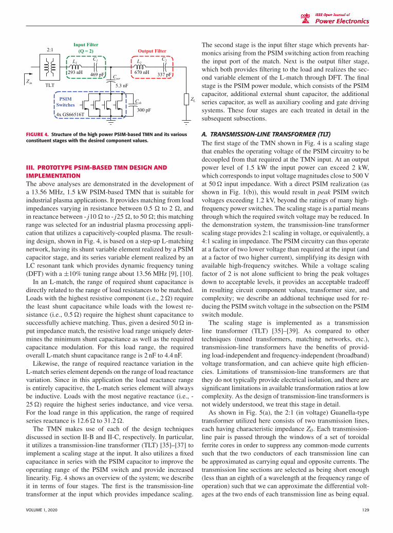
FIGURE 4. Structure of the high power PSIM-based TMN and its variousconstituent stages with the desired component values.
III. PROTOTYPE PSIM-BASED TMN DESIGN ANDIMPLEMENTATIONThe above analyses are demonstrated in the development ofa 13.56 MHz, 1.5 kW PSIM-based TMN that is suitable forindustrial plasma applications. It provides matching from loadimpedances varying in resistance between 0.5 � to 2 �, andin reactance between - j10 � to - j25 �, to 50 �; this matchingrange was selected for an industrial plasma processing appli-cation that utilizes a capacitively-coupled plasma. The result-ing design, shown in Fig. 4, is based on a step-up L-matchingnetwork, having its shunt variable element realized by a PSIMcapacitor stage, and its series variable element realized by anLC resonant tank which provides dynamic frequency tuning(DFT) with a ±10% tuning range about 13.56 MHz [9], [10].
In an L-match, the range of required shunt capacitance isdirectly related to the range of load resistances to be matched.Loads with the highest resistive component (i.e., 2 �) requirethe least shunt capacitance while loads with the lowest re-sistance (i.e., 0.5 �) require the highest shunt capacitance tosuccessfully achieve matching. Thus, given a desired 50 � in-put impedance match, the resistive load range uniquely deter-mines the minimum shunt capacitance as well as the requiredcapacitance modulation. For this load range, the requiredoverall L-match shunt capacitance range is 2 nF to 4.4 nF.
Likewise, the range of required reactance variation in theL-match series element depends on the range of load reactancevariation. Since in this application the load reactance rangeis entirely capacitive, the L-match series element will alwaysbe inductive. Loads with the most negative reactance (i.e., -25 �) require the highest series inductance, and vice versa.For the load range in this application, the range of requiredseries reactance is 12.6 � to 31.2 �.
The TMN makes use of each of the design techniquesdiscussed in section II-B and II-C, respectively. In particular,it utilizes a transmission-line transformer (TLT) [35]–[37] toimplement a scaling stage at the input. It also utilizes a fixedcapacitance in series with the PSIM capacitor to improve theoperating range of the PSIM switch and provide increasedlinearity. Fig. 4 shows an overview of the system; we describeit in terms of four stages. The first is the transmission-linetransformer at the input which provides impedance scaling.
The second stage is the input filter stage which prevents har-monics arising from the PSIM switching action from reachingthe input port of the match. Next is the output filter stage,which both provides filtering to the load and realizes the sec-ond variable element of the L-match through DFT. The finalstage is the PSIM power module, which consists of the PSIMcapacitor, additional external shunt capacitor, the additionalseries capacitor, as well as auxiliary cooling and gate drivingsystems. These four stages are each treated in detail in thesubsequent subsections.
A. TRANSMISSION-LINE TRANSFORMER (TLT)The first stage of the TMN shown in Fig. 4 is a scaling stagethat enables the operating voltage of the PSIM circuitry to bedecoupled from that required at the TMN input. At an outputpower level of 1.5 kW the input power can exceed 2 kW,which corresponds to input voltage magnitudes close to 500 Vat 50 � input impedance. With a direct PSIM realization (asshown in Fig. 1(b)), this would result in peak PSIM switchvoltages exceeding 1.2 kV, beyond the ratings of many high-frequency power switches. The scaling stage is a partial meansthrough which the required switch voltage may be reduced. Inthe demonstration system, the transmission-line transformerscaling stage provides 2:1 scaling in voltage, or equivalently, a4:1 scaling in impedance. The PSIM circuitry can thus operateat a factor of two lower voltage than required at the input (andat a factor of two higher current), simplifying its design withavailable high-frequency switches. While a voltage scalingfactor of 2 is not alone sufficient to bring the peak voltagesdown to acceptable levels, it provides an acceptable tradeoffin resulting circuit component values, transformer size, andcomplexity; we describe an addtional technique used for re-ducing the PSIM switch voltage in the subsection on the PSIMswitch module.
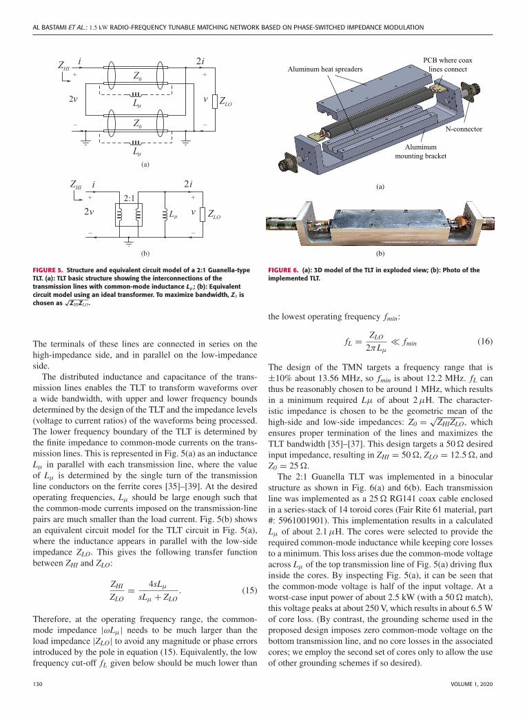
The scaling stage is implemented as a transmissionline transformer (TLT) [35]–[39]. As compared to othertechniques (tuned transformers, matching networks, etc.),transmission-line transformers have the benefits of provid-ing load-independent and frequency-independent (broadband)voltage transformation, and can achieve quite high efficien-cies. Limitations of transmission-line transformers are thatthey do not typically provide electrical isolation, and there aresignificant limitations in available transformation ratios at lowcomplexity. As the design of transmission-line transformers isnot widely understood, we treat this stage in detail.
As shown in Fig. 5(a), the 2:1 (in voltage) Guanella-typetransformer utilized here consists of two transmission lines,each having characteristic impedance Z0. Each transmission-line pair is passed through the windows of a set of toroidalferrite cores in order to suppress any common-mode currentssuch that the two conductors of each transmission line canbe approximated as carrying equal and opposite currents. Thetransmission line sections are selected as being short enough(less than an eighth of a wavelength at the frequency range ofoperation) such that we can approximate the differential volt-ages at the two ends of each transmission line as being equal.
VOLUME 1, 2020 129
AL BASTAMI ET AL.: 1.5 kW RADIO-FREQUENCY TUNABLE MATCHING NETWORK BASED ON PHASE-SWITCHED IMPEDANCE MODULATION
FIGURE 5. Structure and equivalent circuit model of a 2:1 Guanella-typeTLT. (a): TLT basic structure showing the interconnections of thetransmission lines with common-mode inductance Lμ; (b): Equivalentcircuit model using an ideal transformer. To maximize bandwidth, Z0 ischosen as
√ZHIZLO.
The terminals of these lines are connected in series on thehigh-impedance side, and in parallel on the low-impedanceside.
The distributed inductance and capacitance of the trans-mission lines enables the TLT to transform waveforms overa wide bandwidth, with upper and lower frequency boundsdetermined by the design of the TLT and the impedance levels(voltage to current ratios) of the waveforms being processed.The lower frequency boundary of the TLT is determined bythe finite impedance to common-mode currents on the trans-mission lines. This is represented in Fig. 5(a) as an inductanceLμ in parallel with each transmission line, where the valueof Lμ is determined by the single turn of the transmissionline conductors on the ferrite cores [35]–[39]. At the desiredoperating frequencies, Lμ should be large enough such thatthe common-mode currents imposed on the transmission-linepairs are much smaller than the load current. Fig. 5(b) showsan equivalent circuit model for the TLT circuit in Fig. 5(a),where the inductance appears in parallel with the low-sideimpedance ZLO. This gives the following transfer functionbetween ZHI and ZLO:
ZHI
ZLO= 4sLμ
sLμ + ZLO. (15)
Therefore, at the operating frequency range, the common-mode impedance |ωLμ| needs to be much larger than theload impedance |ZLO| to avoid any magnitude or phase errorsintroduced by the pole in equation (15). Equivalently, the lowfrequency cut-off fL given below should be much lower than
FIGURE 6. (a): 3D model of the TLT in exploded view; (b): Photo of theimplemented TLT.
the lowest operating frequency fmin:
fL = ZLO
2πLμ
� fmin (16)
The design of the TMN targets a frequency range that is±10% about 13.56 MHz, so fmin is about 12.2 MHz. fL canthus be reasonably chosen to be around 1 MHz, which resultsin a minimum required Lμ of about 2 μH. The character-istic impedance is chosen to be the geometric mean of thehigh-side and low-side impedances: Z0 = √
ZHIZLO, whichensures proper termination of the lines and maximizes theTLT bandwidth [35]–[37]. This design targets a 50 � desiredinput impedance, resulting in ZHI = 50 �, ZLO = 12.5 �, andZ0 = 25 �.
The 2:1 Guanella TLT was implemented in a binocularstructure as shown in Fig. 6(a) and 6(b). Each transmissionline was implemented as a 25 � RG141 coax cable enclosedin a series-stack of 14 toroid cores (Fair Rite 61 material, part#: 5961001901). This implementation results in a calculatedLμ of about 2.1 μH. The cores were selected to provide therequired common-mode inductance while keeping core lossesto a minimum. This loss arises due the common-mode voltageacross Lμ of the top transmission line of Fig. 5(a) driving fluxinside the cores. By inspecting Fig. 5(a), it can be seen thatthe common-mode voltage is half of the input voltage. At aworst-case input power of about 2.5 kW (with a 50 � match),this voltage peaks at about 250 V, which results in about 6.5 Wof core loss. (By contrast, the grounding scheme used in theproposed design imposes zero common-mode voltage on thebottom transmission line, and no core losses in the associatedcores; we employ the second set of cores only to allow the useof other grounding schemes if so desired).
130 VOLUME 1, 2020
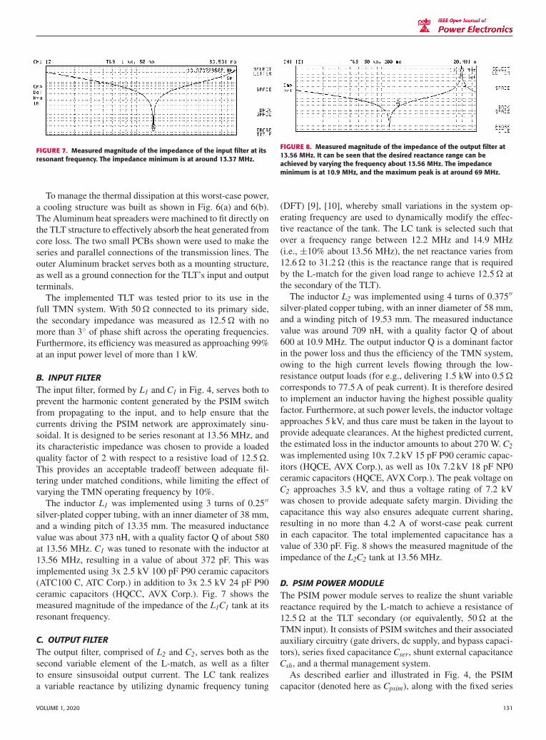
FIGURE 7. Measured magnitude of the impedance of the input filter at itsresonant frequency. The impedance minimum is at around 13.37 MHz.
To manage the thermal dissipation at this worst-case power,a cooling structure was built as shown in Fig. 6(a) and 6(b).The Aluminum heat spreaders were machined to fit directly onthe TLT structure to effectively absorb the heat generated fromcore loss. The two small PCBs shown were used to make theseries and parallel connections of the transmission lines. Theouter Aluminum bracket serves both as a mounting structure,as well as a ground connection for the TLT’s input and outputterminals.
The implemented TLT was tested prior to its use in thefull TMN system. With 50 � connected to its primary side,the secondary impedance was measured as 12.5 � with nomore than 3◦ of phase shift across the operating frequencies.Furthermore, its efficiency was measured as approaching 99%at an input power level of more than 1 kW.
B. INPUT FILTERThe input filter, formed by L1 and C1 in Fig. 4, serves both toprevent the harmonic content generated by the PSIM switchfrom propagating to the input, and to help ensure that thecurrents driving the PSIM network are approximately sinu-soidal. It is designed to be series resonant at 13.56 MHz, andits characteristic impedance was chosen to provide a loadedquality factor of 2 with respect to a resistive load of 12.5 �.This provides an acceptable tradeoff between adequate fil-tering under matched conditions, while limiting the effect ofvarying the TMN operating frequency by 10%.
The inductor L1 was implemented using 3 turns of 0.25′′silver-plated copper tubing, with an inner diameter of 38 mm,and a winding pitch of 13.35 mm. The measured inductancevalue was about 373 nH, with a quality factor Q of about 580at 13.56 MHz. C1 was tuned to resonate with the inductor at13.56 MHz, resulting in a value of about 372 pF. This wasimplemented using 3x 2.5 kV 100 pF P90 ceramic capacitors(ATC100 C, ATC Corp.) in addition to 3x 2.5 kV 24 pF P90ceramic capacitors (HQCC, AVX Corp.). Fig. 7 shows themeasured magnitude of the impedance of the L1C1 tank at itsresonant frequency.
C. OUTPUT FILTERThe output filter, comprised of L2 and C2, serves both as thesecond variable element of the L-match, as well as a filterto ensure sinsusoidal output current. The LC tank realizesa variable reactance by utilizing dynamic frequency tuning
FIGURE 8. Measured magnitude of the impedance of the output filter at13.56 MHz. It can be seen that the desired reactance range can beachieved by varying the frequency about 13.56 MHz. The impedanceminimum is at 10.9 MHz, and the maximum peak is at around 69 MHz.
(DFT) [9], [10], whereby small variations in the system op-erating frequency are used to dynamically modify the effec-tive reactance of the tank. The LC tank is selected such thatover a frequency range between 12.2 MHz and 14.9 MHz(i.e., ±10% about 13.56 MHz), the net reactance varies from12.6 � to 31.2 � (this is the reactance range that is requiredby the L-match for the given load range to achieve 12.5 � atthe secondary of the TLT).
The inductor L2 was implemented using 4 turns of 0.375′′silver-plated copper tubing, with an inner diameter of 58 mm,and a winding pitch of 19.53 mm. The measured inductancevalue was around 709 nH, with a quality factor Q of about600 at 10.9 MHz. The output inductor Q is a dominant factorin the power loss and thus the efficiency of the TMN system,owing to the high current levels flowing through the low-resistance output loads (for e.g., delivering 1.5 kW into 0.5 �
corresponds to 77.5 A of peak current). It is therefore desiredto implement an inductor having the highest possible qualityfactor. Furthermore, at such power levels, the inductor voltageapproaches 5 kV, and thus care must be taken in the layout toprovide adequate clearances. At the highest predicted current,the estimated loss in the inductor amounts to about 270 W. C2
was implemented using 10x 7.2 kV 15 pF P90 ceramic capac-itors (HQCE, AVX Corp.), as well as 10x 7.2 kV 18 pF NP0ceramic capacitors (HQCE, AVX Corp.). The peak voltage onC2 approaches 3.5 kV, and thus a voltage rating of 7.2 kVwas chosen to provide adequate safety margin. Dividing thecapacitance this way also ensures adequate current sharing,resulting in no more than 4.2 A of worst-case peak currentin each capacitor. The total implemented capacitance has avalue of 330 pF. Fig. 8 shows the measured magnitude of theimpedance of the L2C2 tank at 13.56 MHz.
D. PSIM POWER MODULEThe PSIM power module serves to realize the shunt variablereactance required by the L-match to achieve a resistance of12.5 � at the TLT secondary (or equivalently, 50 � at theTMN input). It consists of PSIM switches and their associatedauxiliary circuitry (gate drivers, dc supply, and bypass capaci-tors), series fixed capacitance Cser, shunt external capacitanceCsh, and a thermal management system.
As described earlier and illustrated in Fig. 4, the PSIMcapacitor (denoted here as Cpsim), along with the fixed series
VOLUME 1, 2020 131

AL BASTAMI ET AL.: 1.5 kW RADIO-FREQUENCY TUNABLE MATCHING NETWORK BASED ON PHASE-SWITCHED IMPEDANCE MODULATION
capacitance Cser, realize the shunt capacitance required by theL-match. To fully specify the values of these two quantities,two constraints must be satisfied. First, the series combina-tion of the two capacitors must realize a range of 2 nF to4.4 nF, imposed by the load range of the L-match. Second,the capacitors must provide sufficient voltage division to thePSIM drain node to maintain acceptable peak voltages wellwithin the operating limits of the selected power devices,while simultaneously keeping an acceptable range of PSIMcapacitance modulation. Note that the worst-case PSIM drainvoltage occurs at the highest operating power level and whenthe shunt capacitance is at its minimum, corresponding toloads having the highest resistance (i.e., 2 �).
The switch was selected to have a low RDS,ONCOSS productto minimize the conduction losses, as implied by equations(5) and (6). In addition, it was selected to substantially realizemost of the required shunt capacitance (at least 2 nF) suchthat minimal external shunt capacitance is required, whilemaintaining a practical number of devices, thereby ensuringcompact layout and adequate synchronization between all de-vices. It is also desired to select a switch having low junction-to-case thermal resistance to facilitate cooling. The top-cooledGaN Systems 650 V rated GS66516 T switch was selectedto realize the PSIM capacitor, owing to its low RDS,ONCOSS,its favorable junction-to-case thermal resistance of 0.3 ◦C/W,and its ability to realize the required capacitance with a fewdevices, as will be seen shortly. For this device, an operatingpeak voltage limit of about 400 V provides adequate safetymargin.
At a worst-case input power of about 2.5 kW into 50 �, thepeak voltage of the fundamental component of the L-matchshunt capacitor is 250 V. Relating this peak of the fundamentalvoltage to the actual peak of the switch drain is possible ifCOSS were constant with respect to voltage (see Appendix A);however, it is difficult to obtain a similar result analytically fora voltage-dependent COSS. From the equations in AppendixA, it can be inferred that the ratio of the peak voltage to thepeak of the fundamental varies roughly between 2 and 3 overtypical range of conduction angles. The upper part of thisrange is practically limited to about 130◦, corresponding toa capacitance modulation factor of about 8; note that higherPSIM conduction angles result in significantly higher har-monic distortion levels, which are undesirable. Furthermore,very short switch off-times are hard to realize in practice atthese frequencies given the gate rise and fall times of availabledevices. Therefore, an approximate voltage ratio of 2.5 can beused to approximate the switch peak voltage to a first order.Using this factor, it can be seen that if we desire to keep thepeak switch voltage below 400 V, the series capacitor Cser
must divide down the voltage applied to the PSIM module bya factor of about 1.56; this sets one of the two constraints.
The second constraint is satisfied by ensuring that the seriescombination of Cpsim and Cser adequately realizes the range ofrequired L-match shunt capacitance. With a minimum oper-ating power of about 200 W, the aforementioned constraintswere satisfied when Cser was about 5.3 nF, and when four
GS66516 T switches were used in conjunction with a smallexternal fixed shunt capacitance Csh of 300 pF, as shown inFig. 4. This resulted in a predicted capacitance modulationfactor just below 8. The worst-case total PSIM conductionand COSS charging / discharging losses were estimated viaextensive simulations of the TMN across the full load rangeto be about 130 W, or about 32 W per switch.
The GaN switches and Csh, implemented using 8x 1.5 kV39 pF NP0 ceramic capacitors (VJ1111, Vishay), were sol-dered on a 2′′×2′′ PCB shown in Fig. 9(a). In practice, thevalue of Cser can be experimentally adjusted to cancel anyparasitic series inductance in the PSIM branch at the operatingfrequency, and to address inaccuracies in the device simula-tion models. One way of achieving this is to gradually increasethe operating power level with the load having the highest re-sistance (which demands highest voltage levels), and monitorthe switch peak voltage. Parasitic inductance or device modelinaccuracies may result in higher than predicted switch peakvoltages; in such cases, the value of Cser can be lowered toreduce the switch peak voltage as needed. In this system, itwas adjusted to 3 nF, which was implemented using 20x 1 kV150 pF C0G ceramic capacitors (VJ1111, Vishay) solderedon two separate 1.05′′×0.85′′ two-layer PCBs as shown inFig. 9(b). This mounting arrangement ensured equal currentsharing between the capacitors to avoid overheating.
Fig. 9(c) shows the bottom of the PCB with the PSIMswitches. The precisely symmetric layout of the switches inFig. 9(c) and their associated gate driving circuitry in Fig. 9(a)ensures substantially equal current sharing among all switchesas well as synchronized gate drive waveforms. To effectivelyabsorb the heat from these switches, a custom-built 0.1′′ thicksilver-plated copper heat spreader, shown in Fig. 9(d), wasmechanically attached and soldered to the bottom of the PCBas shown in the photos. For high design margin it was desiredto keep the junction temperature of the switches at about85 ◦C, which is achievable if the heat spreader surface ismaintained at about 60 ◦C. At 130 W of switch losses and anambient temperature of about 30 ◦C, this requires a coolingsystem that can achieve an effective thermal resistance of0.2 ◦C/W from the surface of the spreader to ambient. Thiswas accomplished by the forced-air cooling system shownin Fig. 9(e), which consists of a silver-plated Dynatron A25copper heatsink, with a 24 V San Ace B97 fan blower (part #:9BMB24P2G01) that provides air flow at up to 47.3 cubic feetper minute (CFM); this cooling scheme achieves the requiredthermal resistance. Fig. 10 shows a photo of the developedTMN. It can be seen from the photos that in this configuration,the switches need to have a low-resistance path through whichcurrent flows to the system ground, namely, the chassis. Thisis accomplished via the two silver-plated copper L-bracketsshown in Figs. 9(e) and 10, which establish the ground con-nection to the chassis. The overall TMN box dimensions wereabout 14′′×14′′×5,′′ providing a shield to contain emissionsfrom coreless magnetics, with an Aluminum lid covering theenclosure from the top. This shielding arrangement is typi-cal of commercially-manufactured TMNs. Table 1 shows a
132 VOLUME 1, 2020
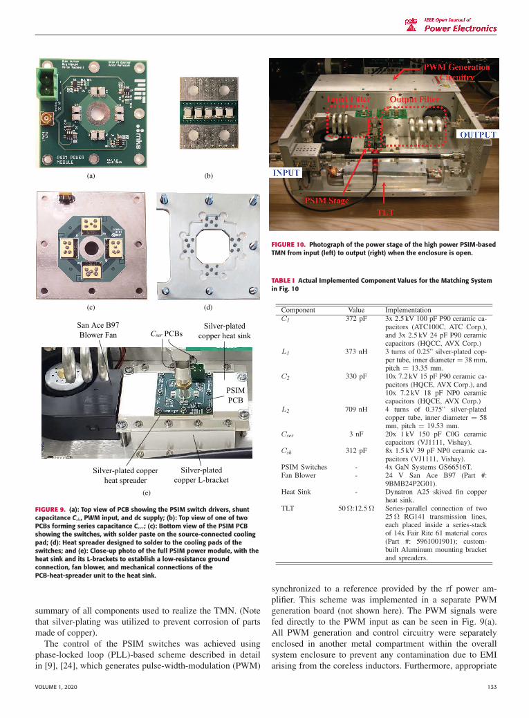
FIGURE 9. (a): Top view of PCB showing the PSIM switch drivers, shuntcapacitance Csh, PWM input, and dc supply; (b): Top view of one of twoPCBs forming series capacitance Cser; (c): Bottom view of the PSIM PCBshowing the switches, with solder paste on the source-connected coolingpad; (d): Heat spreader designed to solder to the cooling pads of theswitches; and (e): Close-up photo of the full PSIM power module, with theheat sink and its L-brackets to establish a low-resistance groundconnection, fan blower, and mechanical connections of thePCB-heat-spreader unit to the heat sink.
summary of all components used to realize the TMN. (Notethat silver-plating was utilized to prevent corrosion of partsmade of copper).
The control of the PSIM switches was achieved usingphase-locked loop (PLL)-based scheme described in detailin [9], [24], which generates pulse-width-modulation (PWM)
FIGURE 10. Photograph of the power stage of the high power PSIM-basedTMN from input (left) to output (right) when the enclosure is open.
TABLE I Actual Implemented Component Values for the Matching Systemin Fig. 10
synchronized to a reference provided by the rf power am-plifier. This scheme was implemented in a separate PWMgeneration board (not shown here). The PWM signals werefed directly to the PWM input as can be seen in Fig. 9(a).All PWM generation and control circuitry were separatelyenclosed in another metal compartment within the overallsystem enclosure to prevent any contamination due to EMIarising from the coreless inductors. Furthermore, appropriate
VOLUME 1, 2020 133

AL BASTAMI ET AL.: 1.5 kW RADIO-FREQUENCY TUNABLE MATCHING NETWORK BASED ON PHASE-SWITCHED IMPEDANCE MODULATION
FIGURE 11. Measurement setup used to test the TMN. The setup consists of a 3 kW rf generator, the implemented TMN, a load synthesizer that generatesthe desired load range, and two I-V probes for impedance measurement.
FIGURE 12. Scope waveforms showing FET drain-source voltage (cyan), TMN input voltage (dark blue), and voltage across the two paralleled 50 � coaxresistors (purple). The waveforms shown are for various synthesized loads running at (a): low output power levels (100 W or 150 W), and (b): high outputpower levels (1000 W or 1500 W), while achieving a 50 � input impedance. In the rightmost plot of (a), no switch conduction is needed to achieve thedesired 50 � match.
isolation and filtering was utilized in the PWM generation andcontrol circuitry to protect against conducted EMI from thepower stage.
IV. EXPERIMENTAL RESULTSFig. 11 shows the experimental setup used to evaluate theperformance of the implemented TMN. The setup consists ofan rf generator, the implemented TMN, a load synthesizer,as well as I-V probes at the TMN input and output, capableof measuring impedance and power, among other parame-ters. The rf generator (EDGE 3013, MKS Instruments Inc.)is a liquid-cooled rf power amplifier, with the capability ofadjusting the frequency about 13.56 MHz. The load rangeof interest was synthesized using two parallel 500 W, 50 �
coax resistors (Termaline 8201, Bird Electronic Corp.) con-nected via a tunable matching network (MWH-100, MKSInstruments Inc.), as shown in Fig. 11. The rf generator
provides the reference to the PWM generation circuitry usedto command the switching of the PSIM switches. The I-V probes (Model #: 000-1106-117, MKS Instruments Inc.)provide in-line sensing of instantaneous voltage and currentand their ratio, providing instantaneous measurements of rfimpedance and power flow.
For each load tested, the input power was gradually in-creased to achieve output power levels from 100 W up to amaximum target output power of 1.5 kW. Once a desiredload impedance was set and synthesized, the duty cycle ofthe PWM pulses and operating frequency were adjusted asneeded to obtain a 50 � input match with no reflected power.In some cases, the PWM pulses were also phase-shifted toprevent reverse conduction of the switches.
Figs. 12(a) and 12(b) show the measured waveforms ofthe TMN matching various loads (0.5- j15 �, 1.0- j15 �,1.5- j15 �, and 2.0- j15 �) to 50 � at output power levels
134 VOLUME 1, 2020

ranging from 100 W up to 1.5 kW. The measured waveformsin each scope screen shot show the input voltage (dark blue),the output voltage across the two paralleled 50 � resistors(purple), and the switch drain-source voltage (cyan). Since thereactive portion of these loads was the same, the operatingfrequency was about the same, at around 13.89 MHz. It canbe seen from Fig. 12 that the TMN successfully achieves a50 � input impedance for several loads across a wide oper-ating power range, while simultaneously maintaining accept-able peak PSIM switch voltages and sinusoidal output voltagewaveforms.
The scope waveforms reveal two features that confirm ourpredictions about the system. First, at a given operating powerlevel, as the load resistance decreases (going from right to leftin both Figs. 12(a) and 12(b)), higher PSIM conduction anglescan be observed. This matches our prediction that a highernet shunt capacitance is required to achieve a 50 � match forloads with lower resistance. Second, it can be seen that for agiven load (e.g., the rightmost scope shots in Figs. 12(a) and12(b)), maintaining a 50 � input impedance at higher powerlevels requires higher PSIM switch conduction angles. Thisconfirms our prediction that at higher power levels, the higherswitch drain voltages result in a reduction in its output ca-pacitance COSS , which in turn necessitates higher conductionangles to achieve the net shunt capacitance required by theL-match. These trends are further illustrated in Figs. 13(a)and 13(b), which show the switch duty cycles required toachieve a 50 � input impedance for the full range of loadstested at 200 W and 1.5 kW, respectively. It can be seen thatthe implemented TMN design had very good utilization of thedynamic range of the switch with respect to duty cycle; theduty cycles used to achieve a 50 � match ranged from 25%up to 70%, which was well within the capability of the PWMgeneration and gate driving circuitry.
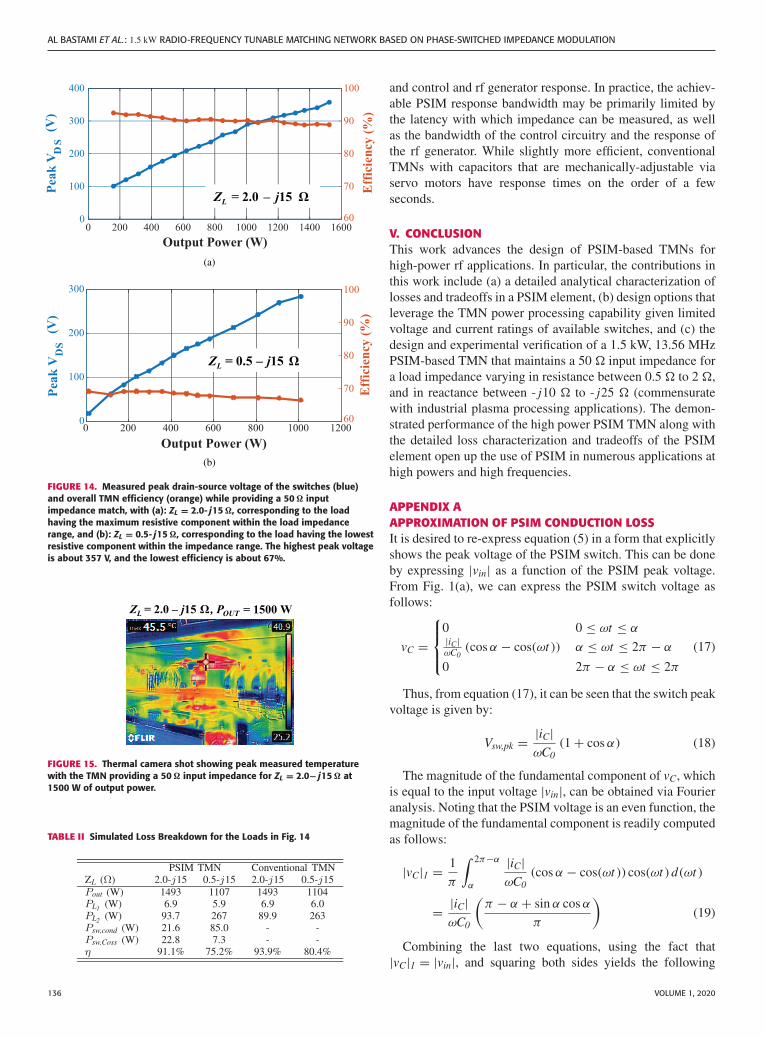
Figs. 14(a) and 14(b) show the measured peak drain-sourcevoltage of the switches as well as the overall TMN efficiencywhile providing a 50 � input impedance match for two loadswith the highest and lowest resistance, respectively, across thefull operating power range. It can be seen from Fig. 14(a)that the peak switch voltage successfully remains below theimposed limit of 400 V, with a peak voltage of 357 V at1.5 kW of output power. For loads having the highest resis-tance component, exemplified by the load shown in Fig. 14(a),a TMN efficiency of about 90% was achieved, even at higherpower levels where PSIM modulation was not negligible (seerightmost scope shot in Fig. 12(b)). The TMN efficiency forloads having the lowest resistance was just below 70%, asshown in Fig. 14(b). The majority of power loss in this TMNwas due to the limited quality factor of the output inductor andis therefore not related to the performance or characteristicsof the PSIM module. Inductors in conventional impedancematching systems have comparable losses at similar operatingconditions; this problem can be alleviated by using an inductorhaving a higher quality factor. (These high inductor losses,especially at high output current levels, were the reason thatthe highest operating output power was limited to 1 kW for
FIGURE 13. Measured switch duty cycle plotted against the resistivecomponent of the load range for different load reactance values. Theresults shown are with the TMN providing a 50 � input impedance matchat output power levels of (a): 200 W, and (b): 1500 W. For a given powerlevel, loads having the lowest resistance component require higher switchduty cycles. Furthermore, for a given load, higher duty cycles are requiredat higher output power levels, owing to the nonlinearity of the transistors’output capacitance COSS .
loads having the lowest resistance). Fig. 15 shows a thermalcamera shot of the TMN system delivering 1.5 kW to a loadZL =2.0- j15 � in steady-state. It can be seen that the oper-ating temperatures of the various system components are ac-ceptable, with a peak of 45.5 ◦C at the output filter capacitors.This suggests that the designed thermal management systemadequately cools the PSIM switches.
To gain further insight into the distribution of losses inthe PSIM TMN, Table 2 shows the loss values obtainedfrom simulating the two loads in Fig. 14 for both the PSIMTMN as well as for a conventional TMN (with no PSIMelements) having the same inductor quality factors, assumingideal (lossless) tunable capacitors. The results further confirmthat a dominant portion of total loss is due to losses in theoutput inductor L2. In addition, it can be seen that undersimilar operating conditions, similar inductor loss values areobserved in a conventional TMN design. Despite the addi-tional switch losses in the PSIM TMN, the benefit of havingthe ability to match impedance orders of magnitude fasterthan conventional TMNs makes PSIM an attractive techniquefor many applications. Extensive simulations show that thedemonstrated PSIM TMN circuit settles within no more than5 μs, ignoring the time needed for impedance measurement
VOLUME 1, 2020 135
AL BASTAMI ET AL.: 1.5 kW RADIO-FREQUENCY TUNABLE MATCHING NETWORK BASED ON PHASE-SWITCHED IMPEDANCE MODULATION
FIGURE 14. Measured peak drain-source voltage of the switches (blue)and overall TMN efficiency (orange) while providing a 50 � inputimpedance match, with (a): ZL = 2.0- j15 �, corresponding to the loadhaving the maximum resistive component within the load impedancerange, and (b): ZL = 0.5- j15 �, corresponding to the load having the lowestresistive component within the impedance range. The highest peak voltageis about 357 V, and the lowest efficiency is about 67%.
FIGURE 15. Thermal camera shot showing peak measured temperaturewith the TMN providing a 50 � input impedance for ZL = 2.0− j15 � at1500 W of output power.
TABLE II Simulated Loss Breakdown for the Loads in Fig. 14
and control and rf generator response. In practice, the achiev-able PSIM response bandwidth may be primarily limited bythe latency with which impedance can be measured, as wellas the bandwidth of the control circuitry and the response ofthe rf generator. While slightly more efficient, conventionalTMNs with capacitors that are mechanically-adjustable viaservo motors have response times on the order of a fewseconds.
V. CONCLUSIONThis work advances the design of PSIM-based TMNs forhigh-power rf applications. In particular, the contributions inthis work include (a) a detailed analytical characterization oflosses and tradeoffs in a PSIM element, (b) design options thatleverage the TMN power processing capability given limitedvoltage and current ratings of available switches, and (c) thedesign and experimental verification of a 1.5 kW, 13.56 MHzPSIM-based TMN that maintains a 50 � input impedance fora load impedance varying in resistance between 0.5 � to 2 �,and in reactance between - j10 � to - j25 � (commensuratewith industrial plasma processing applications). The demon-strated performance of the high power PSIM TMN along withthe detailed loss characterization and tradeoffs of the PSIMelement open up the use of PSIM in numerous applications athigh powers and high frequencies.
APPENDIX AAPPROXIMATION OF PSIM CONDUCTION LOSSIt is desired to re-express equation (5) in a form that explicitlyshows the peak voltage of the PSIM switch. This can be doneby expressing |vin| as a function of the PSIM peak voltage.From Fig. 1(a), we can express the PSIM switch voltage asfollows:
vC =
⎧⎪⎨⎪⎩
0 0 ≤ ωt ≤ α|iC|ωC0
(cos α − cos(ωt )) α ≤ ωt ≤ 2π − α
0 2π − α ≤ ωt ≤ 2π
(17)
Thus, from equation (17), it can be seen that the switch peakvoltage is given by:
Vsw,pk = |iC|ωC0
(1 + cos α) (18)
The magnitude of the fundamental component of vC, whichis equal to the input voltage |vin|, can be obtained via Fourieranalysis. Noting that the PSIM voltage is an even function, themagnitude of the fundamental component is readily computedas follows:
|vC|1 = 1
π
∫ 2π−α
α
|iC|ωC0
(cos α − cos(ωt )) cos(ωt ) d (ωt )
= |iC|ωC0
(π − α + sin α cos α
π
)(19)
Combining the last two equations, using the fact that|vC|1 = |vin|, and squaring both sides yields the following
136 VOLUME 1, 2020
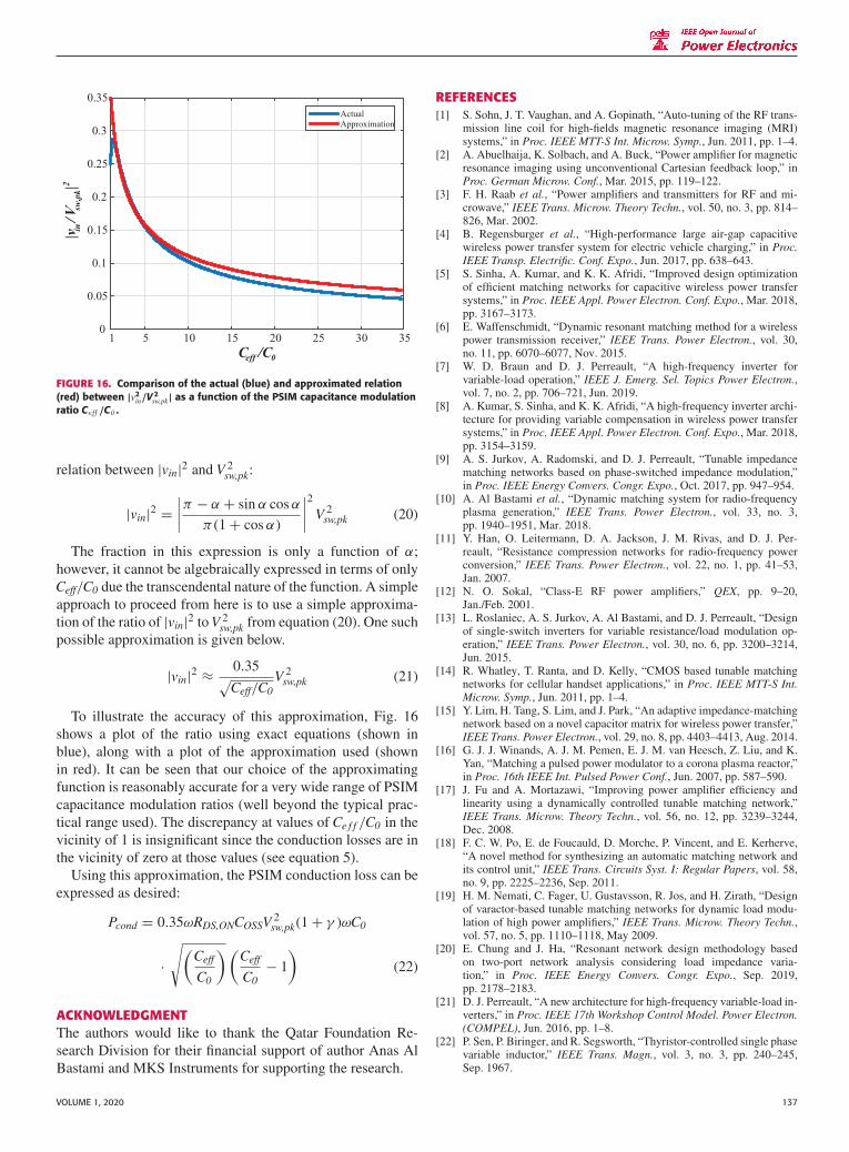
FIGURE 16. Comparison of the actual (blue) and approximated relation(red) between |v2
in/V2
sw,pk| as a function of the PSIM capacitance modulationratio Ceff /C0 .
relation between |vin|2 and V 2sw,pk:
|vin|2 =∣∣∣∣π − α + sin α cos α
π (1 + cos α)
∣∣∣∣2
V 2sw,pk (20)
The fraction in this expression is only a function of α;however, it cannot be algebraically expressed in terms of onlyCeff/C0 due the transcendental nature of the function. A simpleapproach to proceed from here is to use a simple approxima-tion of the ratio of |vin|2 to V 2
sw,pk from equation (20). One suchpossible approximation is given below.
|vin|2 ≈ 0.35√Ceff/C0
V 2sw,pk (21)
To illustrate the accuracy of this approximation, Fig. 16shows a plot of the ratio using exact equations (shown inblue), along with a plot of the approximation used (shownin red). It can be seen that our choice of the approximatingfunction is reasonably accurate for a very wide range of PSIMcapacitance modulation ratios (well beyond the typical prac-tical range used). The discrepancy at values of Ce f f /C0 in thevicinity of 1 is insignificant since the conduction losses are inthe vicinity of zero at those values (see equation 5).
Using this approximation, the PSIM conduction loss can beexpressed as desired:
Pcond = 0.35ωRDS,ONCOSSV 2sw,pk(1 + γ )ωC0
·√(
Ceff
C0
)(Ceff
C0− 1
)(22)
ACKNOWLEDGMENTThe authors would like to thank the Qatar Foundation Re-search Division for their financial support of author Anas AlBastami and MKS Instruments for supporting the research.
REFERENCES[1] S. Sohn, J. T. Vaughan, and A. Gopinath, “Auto-tuning of the RF trans-
mission line coil for high-fields magnetic resonance imaging (MRI)systems,” in Proc. IEEE MTT-S Int. Microw. Symp., Jun. 2011, pp. 1–4.
[2] A. Abuelhaija, K. Solbach, and A. Buck, “Power amplifier for magneticresonance imaging using unconventional Cartesian feedback loop,” inProc. German Microw. Conf., Mar. 2015, pp. 119–122.
[3] F. H. Raab et al., “Power amplifiers and transmitters for RF and mi-crowave,” IEEE Trans. Microw. Theory Techn., vol. 50, no. 3, pp. 814–826, Mar. 2002.
[4] B. Regensburger et al., “High-performance large air-gap capacitivewireless power transfer system for electric vehicle charging,” in Proc.IEEE Transp. Electrific. Conf. Expo., Jun. 2017, pp. 638–643.
[5] S. Sinha, A. Kumar, and K. K. Afridi, “Improved design optimizationof efficient matching networks for capacitive wireless power transfersystems,” in Proc. IEEE Appl. Power Electron. Conf. Expo., Mar. 2018,pp. 3167–3173.
[6] E. Waffenschmidt, “Dynamic resonant matching method for a wirelesspower transmission receiver,” IEEE Trans. Power Electron., vol. 30,no. 11, pp. 6070–6077, Nov. 2015.
[7] W. D. Braun and D. J. Perreault, “A high-frequency inverter forvariable-load operation,” IEEE J. Emerg. Sel. Topics Power Electron.,vol. 7, no. 2, pp. 706–721, Jun. 2019.
[8] A. Kumar, S. Sinha, and K. K. Afridi, “A high-frequency inverter archi-tecture for providing variable compensation in wireless power transfersystems,” in Proc. IEEE Appl. Power Electron. Conf. Expo., Mar. 2018,pp. 3154–3159.
[9] A. S. Jurkov, A. Radomski, and D. J. Perreault, “Tunable impedancematching networks based on phase-switched impedance modulation,”in Proc. IEEE Energy Convers. Congr. Expo., Oct. 2017, pp. 947–954.
[10] A. Al Bastami et al., “Dynamic matching system for radio-frequencyplasma generation,” IEEE Trans. Power Electron., vol. 33, no. 3,pp. 1940–1951, Mar. 2018.
[11] Y. Han, O. Leitermann, D. A. Jackson, J. M. Rivas, and D. J. Per-reault, “Resistance compression networks for radio-frequency powerconversion,” IEEE Trans. Power Electron., vol. 22, no. 1, pp. 41–53,Jan. 2007.
[12] N. O. Sokal, “Class-E RF power amplifiers,” QEX, pp. 9–20,Jan./Feb. 2001.
[13] L. Roslaniec, A. S. Jurkov, A. Al Bastami, and D. J. Perreault, “Designof single-switch inverters for variable resistance/load modulation op-eration,” IEEE Trans. Power Electron., vol. 30, no. 6, pp. 3200–3214,Jun. 2015.
[14] R. Whatley, T. Ranta, and D. Kelly, “CMOS based tunable matchingnetworks for cellular handset applications,” in Proc. IEEE MTT-S Int.Microw. Symp., Jun. 2011, pp. 1–4.
[15] Y. Lim, H. Tang, S. Lim, and J. Park, “An adaptive impedance-matchingnetwork based on a novel capacitor matrix for wireless power transfer,”IEEE Trans. Power Electron., vol. 29, no. 8, pp. 4403–4413, Aug. 2014.
[16] G. J. J. Winands, A. J. M. Pemen, E. J. M. van Heesch, Z. Liu, and K.Yan, “Matching a pulsed power modulator to a corona plasma reactor,”in Proc. 16th IEEE Int. Pulsed Power Conf., Jun. 2007, pp. 587–590.
[17] J. Fu and A. Mortazawi, “Improving power amplifier efficiency andlinearity using a dynamically controlled tunable matching network,”IEEE Trans. Microw. Theory Techn., vol. 56, no. 12, pp. 3239–3244,Dec. 2008.
[18] F. C. W. Po, E. de Foucauld, D. Morche, P. Vincent, and E. Kerherve,“A novel method for synthesizing an automatic matching network andits control unit,” IEEE Trans. Circuits Syst. I: Regular Papers, vol. 58,no. 9, pp. 2225–2236, Sep. 2011.
[19] H. M. Nemati, C. Fager, U. Gustavsson, R. Jos, and H. Zirath, “Designof varactor-based tunable matching networks for dynamic load modu-lation of high power amplifiers,” IEEE Trans. Microw. Theory Techn.,vol. 57, no. 5, pp. 1110–1118, May 2009.
[20] E. Chung and J. Ha, “Resonant network design methodology basedon two-port network analysis considering load impedance varia-tion,” in Proc. IEEE Energy Convers. Congr. Expo., Sep. 2019,pp. 2178–2183.
[21] D. J. Perreault, “A new architecture for high-frequency variable-load in-verters,” in Proc. IEEE 17th Workshop Control Model. Power Electron.(COMPEL), Jun. 2016, pp. 1–8.
[22] P. Sen, P. Biringer, and R. Segsworth, “Thyristor-controlled single phasevariable inductor,” IEEE Trans. Magn., vol. 3, no. 3, pp. 240–245,Sep. 1967.
VOLUME 1, 2020 137
AL BASTAMI ET AL.: 1.5 kW RADIO-FREQUENCY TUNABLE MATCHING NETWORK BASED ON PHASE-SWITCHED IMPEDANCE MODULATION
[23] W.-J. Gu and K. Harada, “A new method to regulate resonant convert-ers,” IEEE Trans. Power Electron., vol. 3, no. 4, pp. 430–439, Oct. 1988.
[24] A. S. Jurkov, “Techniques for efficient radio frequency power conver-sion,” Ph.D. dissertation, Electr.Eng. Comput. Sci., , Massachusetts Inst.Technol., Cambridge, MA, USA, 2019.
[25] D. Perreault and A. Jurkov, “Tunable matching network with phase-switched elements,” U.S. Patent 9,755,576, Sep. 2017.
[26] D. Jin and J. A. del Alamo, “Methodology for the study of dynamicon-resistance in high-voltage GaN field-effect transistors,” IEEE Trans.Electron Devices, vol. 60, no. 10, pp. 3190–3196, Oct. 2013.
[27] B. J. Galapon, A. J. Hanson, and D. J. Perreault, “Measuring dynamicon resistance in GaN transistors at MHz frequencies,” in Proc. IEEE19th Workshop Control Model. Power Electron., Jun. 2018, pp. 1–8.
[28] G. Zulauf, M. Guacci, and J. W. Kolar, “Dynamic on-resistance inGaN-on-Si HEMTs: Origins, dependencies, and future characterizationframeworks,” IEEE Trans. Power Electron., vol. 35, no. 6, pp. 5581–5588, Jun. 2020.
[29] J. M. Rivas, R. S. Wahby, J. S. Shafran, and D. J. Perreault, “Newarchitectures for radio-frequency dc-dc power conversion,” IEEE Trans.Power Electron., vol. 21, no. 2, pp. 380–393, Mar. 2006.
[30] G. Zulauf, S. Park, W. Liang, K. N. Surakitbovorn, and J. Rivas-Davila,“COSS losses in 600 V GaN power semiconductors in soft-switched,high- and very-high-frequency power converters,” IEEE Trans. PowerElectron., vol. 33, no. 12, pp. 10 748–10 763, Dec. 2018.
[31] M. Guacci et al., “On the origin of the Coss -losses in soft-switchingGaN-on-Si power HEMTs,” IEEE J. Emerg. Sel. Topics Power Elec-tron., vol. 7, no. 2, pp. 679–694, Jun. 2019.
[32] J. Zhuang, G. Zulauf, J. Roig, J. D. Plummer, and J. Rivas-Davila, “Aninvestigation into the causes of COSS losses in GaN-on-Si HEMTs,”in Proc. 20th Workshop Control Model. Power Electron. (COMPEL),Jun. 2019, pp. 1–7.
[33] G. Zulauf, Z. Tong, J. D. Plummer, and J. M. Rivas-Davila, “Activepower device selection in high- and very-high-frequency power con-verters,” IEEE Trans. Power Electron., vol. 34, no. 7, pp. 6818–6833,Jul. 2019.
[34] Z. Tong, G. Zulauf, J. Xu, J. D. Plummer, and J. Rivas-Davila, “Outputcapacitance loss characterization of silicon carbide schottky diodes,”IEEE J. Emerg. Sel. Topics Power Electron., vol. 7, no. 2, pp. 865–878,Jun. 2019.
[35] E. Rotholz, “Transmission-line transformers,” IEEE Trans. Microw.Theory Techn., vol. 29, no. 4, pp. 327–331, Apr. 1981.
[36] A. Eroglu, “High-power transmission line transformer design forplasma generators,” IEEE Trans. Plasma Sci., vol. 42, no. 4, pp. 969–975, Apr. 2014.
[37] W. A. Davis and K. Agarwal, Radio Frequency Circuit Design. Hobo-ken, NJ, USA: Wiley, 2001.
[38] G. Guanella, “New method of impedance matching in radio-frequencycircuits,” Brown Boveri Rev., vol. 31, no. 9, pp. 327–329, Sep. 1944.
[39] C. Trask, “A tutorial on transmission line transformers,” Aug 2005,pp. 1–7. [Online]. Available: http://home.earthlink.net/%7Echristrask/TraskTLTTutorial.pdf
138 VOLUME 1, 2020


![KW[from 1994]wac_c.pdf](https://static.fdokumen.com/doc/165x107/6314afe3c72bc2f2dd0476e0/kwfrom-1994waccpdf.jpg)