900000_102_08.pdf - Navy Radio
52
ELECTRONIC CIRCUITS NAVSHIPS SECTION 8 MULTIVIBRATOR CIRCUITS PART A. ELECTRON-TUBE CIRCUITS ASTABLE (FREE-RUNNING) MULTIVIERATORS. - !he tern astohie mviwvtbmmt ~efexs tc Gr,e class of multivibmtor or relaxation-osciilatar clrcuits that can function in e~ther of two temporarily stable conditions and i s copableof rapidly switchng irom one temporarily stable mndition to the other. The astable multivibrotor is frequently reierred to as a freerunning multivibmtor. It IS basically on oscillator consisting of two stages coupled sc that the Input siqnol to each stage is tcken from the ;,:P;: ;i :he ckzr. F.nc the circdi? hlnmes tiepn:nninn hecousr of the regenerative feedback, and the frequency of operation is determined ?ti-cn!? by its mqlingcirc~i: constants rather thon by an externul synchronizing . , c l t u ~ . 'Ihe irequency oi operollon ior on osrabie muiiivibrotai can k as iow os one cycle per minute or us high as 1CC kilocycles per second, depending on the circuit desicgi. The output of the astable multivibrator is usuallv neor!y rectangular m. form. A symmetrical output results when the RC time constants of the muplino circuits are . . made equal. Rectanqular pulses of almost any desired width (time curotion) can be obtained by piooortionina the .. . R-C time mnstants of the coupling circuits withrespect to one another; the resultinq pulse output is unsymmetrical since the RC time constantsof the &ling circuits ore no rqu;;:. The aperaung frequency sf h e ostabie muilinbiator can k chonqed by switching wiues of 8 or C, or both R wd C, in the coupiinq ciicuits to alter the tlae imstanu. For emmp!e, a mdtivibrator desiqed to operate at 800 pps con be changed to o lower frequency, such cs 4W p?s, by simply s+v,tct~nq additiono! copocitors into the circuit in pardie! with *e eesting coupiing copocltors ro lower the repetition frequency. ?he frequency stobiliv of the multivibrotor is same- what better Vim mot oi the typicai biocklng osciiioior. However, a disadvantage of tLe mdtivibmtor is hot its out- put impedmce is essendally equal to the piateioac tesls- tmce anavlis resls1ar:st must be rria~vti~ in ;id?: to obtmn q n d frequency stobiiity. Also, the negative qoing waveiom 1s generated at a much lower impdance %L , , I .*. ., t . ...- q e : : : 3e23~se i chiiGc3 hod wi:: d s c zffec: the ire.,-ency stability thp output is &G;~,eLT.c> 2 : : , : e ::!!:.::c:, ;?, ::+e? :: :5"1?+- the loai from the mi-vibrator plate circ~it. In same .:Lb;cr.css C ~ . ~ & ~ ~ : L ~ ! : ; :?? ~::i>~!k:!?! i" ? dlfieientlatea waveiom!, anc tnls nave;o,m, in :w,, .; uop:ied t i :!;c co$..ode fc!!~--e~: 12 this circ~lit m~figurn- ri~ :he :ao? wi!! have !he !as! d!ect upon the T-!!?- vibrator irequency s t a ~ ~ i l r y . TRIODE PLATE-Ti)-tiKlD COUPLED ~jT6Bii Yiiiii- VIBRATOR. WO, OOO. 102 MULTIVIBRATORS duces o square-wove output far use as trigger or timing pulses. CHARACTERIS1 ICS. Freerunning oscillator; does not require trigger pulse 12 produce o ~ ~ i l j a i i ~ ~ ~ . Operating frequency i s determined piimari!y by the RC !!me cnnstonts in the ieedbock ioiate-to-3rd) coupling circdis md b,y cpp!ied wltcgr. Frequenq stability of 3 percent con be obtained. Input trigger pulses may be qplied to the circuit for synchronization to produce a stable output; it may be qnchronlzed at the trigger-pulse frequency or i n t e ~ a l submultiples thereof. Symnetricd squme- or rectangular-wove output is u:udu~cd wil=i hi P.C :i;;.: :c:.;:cn:z ci !5$ zi? cirri,,'- are equal. Unsymmetrical output i s produced when the L-C tlme constmt oi one grid clrcuit is purposely nlde severd times greater thon that oi the other; for h i s , . ;?-3;.;an tbr iwu tubes jre j!! for 3eri.?s "! . . tire. Output impedance is essentially equol to platehad ~mpedance. CIRCUIT ANALYSIS. Genecol. Re free-running platetailrid cosip!e2 mu1t:vibrotor i s a bosic ostohie muitivibrator. ';he circuit is fundamentally a twwstage R-C coupled amplifier with the output of the second staye coupled to the input of the first stage! Thus the output signal i s fed back in h e proper phase to reinforce the input signal; as o result, s;stained oscillo2ons cccc:. Circuit Op.r.ztion. The accompanying circuit schematic ?iics:ia~es two triode dect;;r. : ; he ; i: c hcilc !r$e running mdt~vlhrator ilrcuit. Electron tubes V! and V: are identicd-type triode tubes; although the occompany- ing schenatic illustrates two separate tnodes, o twin- . . ... "A , . ,,.,,e ;s ~requcndy use: in this ,circuit. Cqaciz: C!
-
Upload
khangminh22 -
Category
Documents
-
view
1 -
download
0
Transcript of 900000_102_08.pdf - Navy Radio

ELECTRONIC CIRCUITS NAVSHIPS
SECTION 8
MULTIVIBRATOR CIRCUITS
PART A. ELECTRON-TUBE CIRCUITS
ASTABLE (FREE-RUNNING) MULTIVIERATORS. - !he tern astohie mviwvtbmmt ~efexs tc Gr,e class of
multivibmtor or relaxation-osciilatar clrcuits that can function in e~ther of two temporarily stable conditions and i s copableof rapidly switchng irom one temporarily stable mndition to the other. The astable multivibrotor i s frequently reierred to as a freerunning multivibmtor. It IS basically on oscillator consisting of two stages coupled sc that the Input siqnol to each stage i s tcken from the ;,:P;: ;i :he ckzr. F . n c the circdi? h l n m e s tiepn:nninn hecousr of the regenerative feedback, and the frequency of operation is determined ?ti-cn!? by i ts m q l i n g c i r c ~ i : constants rather thon by an externul synchronizing . , c l tu~ .
'Ihe irequency oi operollon ior on osrabie muiiivibrotai can k as iow os one cycle per minute or u s high as 1CC kilocycles per second, depending on the circuit desicgi.
The output of the astable multivibrator i s usuallv neor!y rectangular m. form. A symmetrical output results when the RC time constants of the muplino circuits are . . made equal. Rectanqular pulses of almost any desired width (time curotion) can be obtained by piooortionina the . . . R-C time mnstants of the coupling circuits withrespect to one another; the resultinq pulse output i s unsymmetrical since the RC time constantsof the &ling circuits ore no
rqu;;:.
The aperaung frequency sf h e ostabie muilinbiator can k chonqed by switching wiues of 8 or C, or both R w d C, in the coupiinq ciicuits to alter the t lae imstanu. For emmp!e, a mdtivibrator des iqed to operate at 800 pps con be changed to o lower frequency, such cs 4W p?s, by simply s+v,tct~nq additiono! copocitors into the circuit in pardie! with *e eesting coupiing copocltors ro lower the repetition frequency.
?he frequency stobiliv of the multivibrotor i s same- what better Vim mot oi the typicai biocklng osciiioior. However, a disadvantage of tLe mdtivibmtor i s ho t its out- put impedmce is essendally equal to the piateioac tesls- tmce anavlis resls1ar:st must be r r i a ~ v t i ~ in ;id?: to obtmn q n d frequency stobiiity. Also, the negative qoing waveiom 1s generated at a much lower impdance % L , , I .*. . , t . ...- q e : : : 3 e 2 3 ~ s e i chiiGc3 hod wi:: d s c zffec: the ire.,-ency stability thp output i s
&G;~,eLT.c> 2 : ::::,::e ::!!:.::c:, ;?, ::+e? :: :5"1?+-
the loai from the mi-vibrator plate c i rc~i t . In same .:Lb;cr.css C ~ . ~ & ~ ~ : L ~ !:; :?? ~::i>~!k:!?! i" ?
dlfieientlatea waveiom!, anc tnls nave;o,m, i n :w,, .; uop:ied t i :!;c co$..ode fc!!~--e~: 12 this circ~lit m~figurn- r i ~ :he :ao? wi!! have !he !as! d!ect upon the T-!!?- vibrator irequency s t a ~ ~ i l r y .
TRIODE PLATE-Ti)-tiKlD COUPLED ~ j T 6 B i i Yi i i i i - VIBRATOR.
WO, OOO. 102 MULTIVIBRATORS
duces o square-wove output far use as trigger or timing pulses.
CHARACTERIS1 ICS. Freerunning oscillator; does not require trigger pulse
12 produce o ~ ~ i l j a i i ~ ~ ~ . Operating frequency i s determined piimari!y by the RC
!!me cnnstonts in the ieedbock ioiate-to-3rd) coupling circdis md b,y cpp!ied wltcgr.
Frequenq stability of 3 percent con be obtained. Input trigger pulses may be qpl ied to the circuit for synchronization to produce a stable output; it may be qnchronlzed at the trigger-pulse frequency or i n t e ~ a l submultiples thereof.
Symnetricd squme- or rectangular-wove output is u:udu~cd w i l = i hi P.C :i;;.: :c:.;:cn:z c i !5$ zi? cirri,,'-
are equal. Unsymmetrical output i s produced when the L-C tlme constmt oi one grid clrcuit i s purposely nlde severd times greater thon that oi the other; for h i s
, . ;?-3;.;an tbr iwu tubes jre j!! for 3eri.?s "! . . tire.
Output impedance i s essentially equol to pla tehad ~mpedance.
CIRCUIT ANALYSIS. Genecol. R e free-running platetailrid cosip!e2
mu1t:vibrotor i s a bosic ostohie muitivibrator. ';he circuit is fundamentally a twwstage R-C coupled amplifier with the output of the second staye coupled to the input of the first stage! Thus the output signal i s fed back in h e proper phase to reinforce the input signal; a s o result, s;stained oscillo2ons cccc:.
Circuit Op.r.ztion. The accompanying circuit schematic ?iics:ia~es two triode dect;;r. :;he; i: c hcilc !r$e running mdt~vlhrator ilrcuit. Electron tubes V! and V: are identicd-type triode tubes; although the occompany- ing schenatic illustrates two separate tnodes, o twin-
. . ... "A , . ,,.,,e ;s ~requcndy use: in this ,circuit. Cqaciz: C!

ELECTRONIC CIRCUITS NAVWIPS
provides the coupling from the plate of V2 to the grid of Vl; capacitor C2 provides the coupl~ng from the plate of V1 to the grid of V2. Resistors R1 md R2 ore the grid re- sistors for V1 and V2, respectively; resistors R3 and R4 are the plate-load resistors for V1 ond V2, respectively.
Capacitor C1 and resistor R1 form on R C circuit to determine the discharge time mnstant in the grid circuit of V1: capacitor C2 and resistor P2 determine the dis- charqe time mnstant in the arid circuit of V2.. Output pulses can be taken fmm theplate of either or blh' electran tubes. Capacitors C3 and C4 are the output muplinq ~. ccpocitors for V1 ond V2, respectively.
When wltage is first applied to the circuit, the grids of bath tubes are at zero bias and plote current starts to flow through piatefood resistors R3 and R4. Also, capoci- tors C1 and C2 begin to charge when the applied wltage rppears ot the plote of each tube. If the constants of both stages of the circuit ore dike, the currents thmugh both tubes may at first be nearly equol. In practice, the symmetrical freerunning multivibmtor component d u e s are held to close tolemnces in order to obtain gaod freq uency stability; the value of mupling capacitors C1 and C2 are at least 2 percent tolerance, grid resistors R1 and R2 ore 1 percent tolerance, and plate-load resistors R3 and R4 are usually 5 percent tolerance. However, in spite of the close tolermces of the components, there will always be some slight difference in the two currents. This small dif- ference in tube currents will couse o further unbalance, resulting in a regenerative oction which rapidly switches the circuit to a condition wherein one tube i s conducting max- imum current and the other is cut off.
For example, if initially the current through tube V l should be slightly greater than that through V2, the wlt- oge drop ocmss plotelood resistor R3 will be greater than the drop across resistor R4. 7ks results in a lower plate voltage for V1. This decrease in plote wltoge i s mupled through mupling ccpacitor C2 fo the grid of V2 as a n e g o t i v q i n g instantonmus qrid wltaqe which reduces the plate current of V2. When the current thmuah V2 i s decreased, the current through plotelood resistor R4 i s also decreased; therefore, the wltoqe drop across resisfor R4 decreases, resulting in a rise in the plate wltoge of V2. This increase in plate voltoqe i s mupled thmuch mupling mpocitor C1 to the gridof Vl a s a positive going instantaneous grid voltage which increases the plate current of VI. The drop ocmss plateload resistor R3 increases, the plate voltage of V1 decreases, and os before, the decrease in the plote wltoge of V1 i s mupled to the grid of V2 as a negative-going wltage. The regenerative switching oction just described continues iq idly until V2 i s cut off and V1 i s at maximum mnduction.
In order to cut off plote current in V2, the grid of V2 must be driven negotive beyond the cutoff wltaqe. ?he negative gnd voltage results from o chorge on coupling ccp- acitoi C2. Since h s charge leoks off through gnd resistor R2, the grid wltage ot V2 does not remain in o negotive mndition but starts to ietum to zem as C2 discharges through R2 and the cathodetwlote mnduction resistonce of '$1.. When Ci dischorges sufficiendy and the grid voltage cutoff point i s reached, plote current once again starts to flow through VZ, initiating another switching action
similar to the first oction described. However, this time os V2 conducts, coupling capocltor C1 discharges through qrid resistor R1 to cut off the plate current in V1, and the switching oction ends with V1 cutaff and V2 at maximum mnduction. Here again, the negative chorge existing on mupling q a c i t o r C1 must discharge through qrid resistor R1 and tube V2 before the q id wltage cut off point is reached and V1 con conduct to initiate another switching action. The switching action repeats mntinuousiy with first one tube and then the other tube conducting.
For the following discussim of circuit operation, refer to the accompmying illustrotion which shows o simplified schematic and waveforms for a symmetrical free-running multivibrator.
At time to (start of time interval a) on the waveform il- lustrotion, the grid of V1 ( e , ~ ) has been driven negative to
I CI CHARGE I ' 12
1 CZ CHARGE ! GRlO VOLTAGE. C.O.fi--- i i ~ ~ ' ---- --I:: =:
V 2 I 1eq21 - C2 I
I DISCWRG! I + -----
PLATE V 2 VOLTAGE, m- E b b HARGE CHARGE
I I P 2 1
Theoretical Wavaforns for 0 Symmetrical Free-Running Mvltivibrator
ORIGINAL


ELECTRONIC CIRCUITS N A V W I P S
(C3 or C4). in cases where it i s desired to minimize the effect of o varying load impedance on the multivibrotor fre- quency stability, a cathode follower i s used for isolation.
FAILURE ANALYSIS. No O U I ~ U ? . Assuming that the multivibrator i s o free-
runniig type and no synchronizing signal i s applied, the applied plate and filament voltages should be mmsured to determine whether thev are within soecliied values. If eithn coupling capocitor C1 and ~2 should become leaky or shorted, o positive potential will be present on the qrid of the associoted tubeand, as a result,~the tube will conduct heavily: the other tube will olso conduct heavily, since it will be ot zero bias. A similar condition could e a s t if either coupling capocitor C1 or C2 should open; in h i s case the feedbock necessary to sustain oscillations cannot ocmr ar.d b t h tubes will conduct hmvily because the grlds ore at zero bias. If the circuit i s in o nonoscilloting con- dition, the voltage at each plate should be measured to de- termine whether plote-load resistor R3 or R4 i s open. If either i s open, there will be no plate voltage present on the associated plate; olso, the other tube will conduct heav- ily because of zero bias, m d its plote voltage will be low. If either output coupling capacitor (C3 or C4) should be- come leaky or shorted, the input resistor of the following stage c m tom o voltage divider which olso includes the associated plateiood resistor (R3 or R4). If the input re- sistor of the following stage is returned to ground or to o negative potential, voltage4ivider action may reduce the voltoge available at the plate of the multivibrator to the point where oscillations will cease; also, the addition01 mnent through the plate-load resistor (R3 or R4) may cause the resistor to bum out.
Incorrect Frequency or Pulse Width. The critical com- ponents governing the frequency and pulse width of the multivibrator ore thosein the couelinq circuits. Any chanae in components governing the discharge time coistont will directly affect frequency md pulse width; a chmge in capacitor Cl or C2 or resistor RI or R2 will have the qeates t effect. A chanqe in the value of elote-load rrsis- &r R3 or R4 will affect ihe mplitude of &e output, and it will also have an effect upon the frequencu, but not nearlv . . . os much a s the components mentioned above.
A drift in frequency of the free-running multivibrator will generally occur if the applied plate voltage should change approximately 10 percmt from the specified value:
~ ~
olso, some frequency drift may occur if the fi lwent volt- age should drop below the specified value.
In a practicd circuit, where the multivibrotor is free- running and i s not synchronized from an external source, mems may be provided to adjust the applied plote voltage or to adjust the volue of resistonce in each grid circuit. This provision enables the circuit to k odjusted to the correct frequency and oulse width, and compensates for differences in individual tube chorocteristics ,#hen cl tube substitution hos been made.
If either output coupliny capocitor (i3 or 4 ) should become leoky or shorted, the voltage-divider octlan '.*:nich con occur m q reduce the amplitude of the output woveiorm and cause the multivibrotor to operate at 3 higher freq~ency, since the grid capacitor (C1 or 22) dischnrye time is ieom-
W0.000.102 MULTIVIBRATORS
dent uoan tne nount 3! chlnge in capacitor uolt>je. T ie ooer3tion of t i e follo.vln,, s q e TW also diected by the chmqe in grid-bizs valtaje :esultiw from the volt3.ji- divider octiar.
PENTODE ELECTRON-COUPLED ASTABLE MULTIVI- BRATOR.
IPPLIC4TION. The pentode eiectron-couplec nst3ule nultivibrator
produces il squ3re.vave output for use 1s ~ I L J A C I 3t :i:ncnq aulses.
CHARACTERISTICS. Freerunning oscillator; does not rqoi te trixJer pulse
to produce oscillations. 3perating frequency is deterxned pr::rar~ly by the 3-2
time constants in t'le feejtock jscreen-to-jrii) coupllnj circuits on3 by the ap?lied screen voltage.
Frequency stability of 3 oersen: con be obtoined. Input b i q ~ e r ;lu!ses msy be applied to tne circu~t !or syo- chronizztian to produce 3 stable octput; the circuit nay be synchronized at the trlqaer-3uls.r f:e,;uency or intepal submultiples thereof.
Symmetric31 squzre- or rectanqulor-.vmz sutput is produced when the 3-C l ine constmts of tne @id circuits ore equal. linsyxmetrical outout is ?reduced hen the .3-_^ tiae constont of one grid circuit 1s purnosely mode several times ?renter than thzt of the other: far this con- dition the two tubes are cut off for unequal periods of time.
Output i s obtoinec from either piote cirwit (or both). Jhanqes in load hove minimum effect Jpon multivibmtor frequency becouse Iood i s isoloted from pentode xreen (multiviurotor plote) circuit by electrsn-strezm coupling 2nd supgressor-yid octisn of tube.
CIRCUIT ANALYSIS. Gsnorol. The pentode electronsoupled multivibrotor
is tasicolly a free-running (triode) piate-to-~qid-c3upled nultivibrstor usin,, the scrsen ur1,ds 3f s h z r ~ cutoff, oen- tode-type tutes os pistes for the rultivitrztor switchiw~ iunction. 'The circuit i s fundamentdly s t ao - s tn~e :i-Z amplifier with the output (screen pid) olthe secon3 stzge coupled to the input 3f the first sloqe. The screen griS of each tube functionsln the oscillator c~rcuit a s though it #ere the plote of o viode. Thus, the out?ut signol from the screen q i j is fed taca i n t i e proper phase to remforce the input signal; 35 3 result. sustained osclilotions occur. The output, t~ken fro3 t ie rhte-load resistor, is coupled to the multivibrotcr oscillatoq circuit throuvh the electron strwm of the pentode tube.
Circuir Operation. The accompanying circuit schematic illustrates two pentode electron tube: in 3 basic tree-running multivlbrator circuit. iec t ron tubes Vl and '42 ore identicol sharp cutoff, pentode-type tubes. Zapacltor 31 provides the coupling from the screen q id 31 V2 to the jrid of VI; ca~acitor J? monies the cauplin [ran the screen ?rid of V1 to the yril of J ? . ieslstors 3 1 2nd !12 are the grid reslstois for VI and V2, respectiiiely; resistors 1 3 on3 34 ore the screen resistors for V1 and V2. Resistors R 5 and R6 ore the plotrload resistors for V1 and V2, iespectively.
ORIGINAL

ELECTRONIC U R U l l T S NAVWIPS
Resistor R7 i s a series voltagedropping resistor which is common to Loth screen -grid circuits.
Capacitor CI ond resistor 8 1 form M R-i circuit to determine the dischorye time constant in the yrid circuit of V1; copmitor C2 and resistor R2 determine the dischorye time constmi in the grid circuit of V2.
Output pulses con be taken from the plate of either or both electron tubes. Capmitors Y3 and C4 are the output coupliny capacitors for V 1 and V2, respectively.
bk ', Pentode Elertrom-Coupled Astable Multiribrotor
Tne ssitchinq c t i o a of the electron-coupled multi- vibrator is similar to that of the triode pioteto-yr13-coupled multivihotor circluit, prevlwsly descrlkd in tnis section.
A'hen voltage is first applied tn the circuit, the grids of both tubes ore at zero bias and Loth plate md screen cur- rsnts start :a flow; the plate currents pass through plnte- log4 resistors 35 and 36, ond the screen currents wss through resistors R3 md R4 and through the common v o i t q e ?;a-,pinj resistor. 17. Also, c3pxi:ors C1 an? C? iiegio ir>,;)13r, *: .L- -- > : - A . . - I . - .- --- -.- -* * n c,.,"o" - w >r.. t,JC spg,,cu "L,.,",,c . ,,""~".o . "~ .hb " -.-.,. ~l each t ~ t e . currents &rough Loth t dk ; rzy ir cw:! at lirst; ho.vever, in spite of the close toler~nces of the components i n the control-qrid and screen-qid cirzdits, therc will olwws be some slight difference inthe lotol ccrrents 3! the b k s . The liffereqce in screen-,$id c!ir- rents *ill cause a furthe: unbclarce, resu!tinq in a r e yenerorive acrion wnich ropidiy sriitchej the iiiiuit ti. ii cedition .wherein nce tuSe 1s conihcting mlximum screen and plote currents ond the other i s cut off.
C-- ...-..I ; I ili*i"ll,. t i - tn,*, " " A crrDDn , ". .. .l....r.rl .".". r.r.- current throuyh t u k V1 should te slightly reoter than tho1 through V2, the valtoge droo ocross screen resistor 33 -111 hp ,qia-tPi thon the drop ncross screw. resistor R4. -, t ~ ~ L b ie-lts i i ~ u l c ~ e r sceea .vz!tcqe !;: I!!, '!?,is 5 -
crease in screen voltoge is llppllea mrouyn coupiinq capa- citor ::: 1" the ip3 ol V i a s a negstive ;om3 insr3nr3neous "rid voltoye which reduces the plate M: 5ci2en -iir:ents
9Q),000.102 MULTIVIBRATORS
oi V2. #hen the screen current of V2 is decreased, the current through screen resistor 84 (and resistor R7) i s also decreased; therefore, the voltage drop across resistor 3 4 decreases, resultiny in o rise in the screen voltage a! V2. This increase in screen voltaye i s fed thrauyh mupling capacitor C l to the yrid of V 1 a s a positive-goiny inston- taneous grid voltage which increases the screen current 91 V1. The voltoye drop across screen resistor R3 increases a s the screen current increases, the screen voltage of V1 decreases, and, a s tefore, the decrease in the screen vol- toye of Vl i s applied to the yrid of V2 os o negativeyoin? voltoge. Note that os L+e screen current of V l increases t i - E C ~ D E S C S I ~ ~ I ! c! V? i w r ~ n s e s . S i n c ~ fne screen currents of Vi and V 1 tlow through aropping resistor Z i , rie voltdye (with respect to jrouni) at the junctia;. of resisto:~ A?, 34, and R7 remains essentially constant tnrourjhout !he entire ~ e r i o ? o! osci!!?!i3c.
Ihe rerlenerative switchiny action just described for the screen-qid to control-grid coupling of the pentode multivibrator circuit continues rapidly until V2 is cut off and V 1 i s at maximum conduction. In order to cut off plote 2nd screen current in V!, the grid of V2 %us1 be driven negative teyond the cutoff voltage. The negative q i d voitaye results from a charje on coupliny capackor 2. Since this charge leaks off through grid resistor 82, the grid voltage ot V2 does not remain in a negative condition but storts to return to zero os Z2 discharges t h r w a resistor R2 and the conduction resistance (cathode to screen yrid) o! VI. 'When copcitor 132 a~schoryes suificientiy and he grid voltoge cutoff paint i s reached, the plote and screen currents once aqain start t; flow th;our;h V2, initiating another switching oction similar to the first action described. However, this time a s V 2 conducts, coupliny capacitor Z i discharyes through q i d resistor 3 1 to cut off the plote and xreen currents i!~ Vi, on? the saitchinj zcti3r. enis :ii:h Vi cut off and V L at maximum mnductlon. Here sgaln, t'ne chorge existing on mupling capacitor L'l must discharye fhiouyh grid resistor 31 and tube V2 before the wid voitaqe cutoff point i s reached and Vl can conduct to initiate another s,.uitching oction.
In n shop cutoff ~entode tute, a s lonq a s the plate voltage i s qeater than the opplied saeen voltaye, the plzte current i t the tub* depends lor.jely upon fhp screen ic,l:ii:je rzthe: thm amn the i'312e 3! Lbe sp1ie.i d!?!e .;jlt,~je. The screen jri? :s z n j e pos:t:vz s?tk respect t3 the x t h d e m i therefore a t t~ac t s electrons 1ro:n the cathode; however, nost a! the electrons 3ttrzctez by me screen pass on throucjh the screen yrid and reach ine piote. !t i s this flow of electrons to the plate thot couples the xltivibrator onion to t ie plate circuit, from which the out- put rvoveiorm is aulaineu. The term electron soupled ic- fers to thls method of coilpiing within h e t u k .
The ioct that ~ l o t e current i s laryely indep2nient of c w ;!ic? plcte vc!!-ge moksc it pnssii.!e tr n r " i i l r ~ the desired output waveform in the plate circult sinc; :he positive potential existing on the s r e e n # i l l ccntrcl me numkr of - c!ec::ans miv in j ;t the p!>;c. ?xrt?er.T2re, me piote ind . - - - - - ----.- --- -^-.."11^-1 i.. .in -^,;-" ^I ,hpcnntrni =,ze,, LU, ,C , ,L> U L C + " , > L t u , * L " ", .,.b -. -- .... - - qrld; tnerelore, wnen me row IS cr mxi i i l u i n C ~ ~ ~ ~ ~ . ~ L L I U I I . , ond pliite current L l i r . ~ , ~ tnrouqn me :ig~e:owi ~ e s i s i ~ i , tile voltaye drop ocxlros the plate-Isad : e ~ i ~ t 3 T is z ! x 13xi-urn
ORIGINAL

ELECTRONIC CIRCUITS NAVSHIPS
3n! t:.e ~ !71? .i(lil3-,e :i th;. t ~ k L S TL~LTLI? , . :,ner !ie t u z i is cut off , :ne pl::e ~01132~ . i s 31 x n x i ~ ~ c l . Th'ls, 1 i r c~ :o lh~rc 31 the 013le cf rho tube 1; Jeter-.lned by t i e z^~.!;,ltn, 7f tic. el2ctr01 stre:n to tk,e p l a c c l r l J l t , ; l n i 1k.t;. I n tdm, I S !overnri >{ ttne s .v l t%ln~ ic t ion o t tns au1liv!or?tor -~scil!?tnry clicvlt :central m i screen irl3s). - 1 7 e 3JWres i3 r jrld 3c t s t3 shield the ;cr?en from the ;llztt
3rd prevents chon'jes in ioadlni from ~ f i e c t i n r 1b.e oscil- 1 ~ t o r y elrcmt; therefor?, the I rqcency 3i th? ? i d t l v ~ L r ~ t o r !s re3srinauiy io!">en,ient n l cn3n:les in outuut la731nq.
Lire the t rmie ~ i 3 t r t 3 - , r 1 3 - ~ 0 ~ o l e ! ngl t ivi i i r~tor , :r;:rloei 3 rev lu~s ly i n th is ieCtl3'1, the pr3porl~onln,, ?f
t-~e ,I-7 tile const3nts 31 the coupliny circults ( . i l . ~ l 2nd :i?JZj deternine rihether the w t a t .vuvclor 7 .vdl be syn- 3etr icol or unsy:nmetricol.
.? riie outout iv3vefarm I; t k e n from either or bath 017te
::rcuits on? coupled to tli lo32 tnmu,,h Jn outnut-ccuollnq capacitor (C3 or C4).
FAILURE ANALYSIS. No O ~ t p ~ 1 . Assuming that the multivibrator i s a free-
runninj type and no synchronizln'j sl,!n=l i s m ? l ~ e d , the al,?te, screen, nni fil3nent voit7jes sha.il3 be ~!?osure! to .'cterllne .vhetner they .Ire .ulthln spncille.4 v d u e i . I f i l lher ;!:alin! c3p lc~ t31 ..:I or .:2 should k c o n i le34y or .:horte?, .I pssltive potentla1 +,ill tie >resent oo the ,rli 31 the o s s o i l ~ t c l tuae, =nd, u s a result, the tube r ill conduct continuously; the other tube iuill 3150 con?u31. s ince i t
nil1 be 31 zero oias. Assl-?il;r c?niltion c o u l l exist if e l thei caupllng c ~ o o c i t o r :I or :? shoul? npen; in this z?sr, the feedtock n e c e s s q to s u s l x n 3 s ~ i l I a t i o n s cannot occur, unJ bath tubes will conduct continuousiy tecouse the grids ore o t zero bias. If this circuit i s in o nanascillat- lnq candillon, the voltoqe 01 each screen gild should be meassred to determ~ne whether screen resis:or R3 or 134 i s open. If either 1s open, there will k no screen voltage pre- sent an the o s s o c i o t d screen grid, ond the t u b e will t e cut oil; also, the other tube will conduct continuously because of zero bias, and i t s plate and screen voltoges will te low. F'urrherngre, ii res ls t l r 117 snoulS open, there aiill be no vol t z j e i t ellher screen j r d , 3nJ bath t u k s ,rill be cut clf.
Note that, if a plate load resistor (R5 or R6) should open, the i rui t ivl~ralor osci lhtory circuit (control 2nd Screen i l l s ) m3y L x c t ~ o n nornolly, but no ' 1 ~ 1 3 ~ 1 ~ ~ ~ v e i o r m 'Will be o i r t a i n e l frorr the tube ossoci3ted :vitn the o w n plate-1033 resistor.
Incorrect Frequency or Pulse Width. The critical com- oonents jovern lq the frequency an:: x l s e '.wiith of tne ;aultivibrotor are those in the c ~ u p l l n ~ a r c u i t s . Any chsnge In conoonents qovernlnq the (3-J dlschzrje tlzrc canstont will directly affect frequency and pulse width; o change in cooacitar 5 1 or C2 or resistor . i l or 32 oil1 hzvs the jre3test e f f e c t . :. c h m q e in the value o f screen r e i s t a r (13 or Hi 3 r
droooinq resistor ,37 will also hive sn effect uoon the frequmcy 2nd pulse width, but not necrly 3s xuch 0s the coupi~n:, conoonents mentioned =Love.
In 3 9rac t i cd CllNif, #here the nultivlbrltar is f r e e running ond 1s not synchronizej f r o ? ln external source,
CHANGE 1
0967-000-0120 MULTIVIBRATORS ,means rnJy t e ?:ovl?ed I 3 i3lust the 3 0 ~ l i d screen va1ts'~e or I: 3312~1 :>e volue of r e s i s t lnce in eier! cantral-jril circuit. rh i s aiovision enu t l e s the c i r c ~ ~ i t to t e 7 i i u s t e i I3 tne correct frequency 2nd wise ~ i d t n 2nd :onnensltes 131 d~ l l e rences lo in-iividu,l tube c i o r ~ c t a r ~ s t l c ; m e n a tube ~ d b ~ l l t ' l l l o n has t een mqie.
Reduced Output. A reduction in output amplitude is lenerr;Ily cause? by a d e f e c t ~ v e tube; houever, 11 c:n 3lso be coused by a decrease in the applied plate voltage or on Increase in the resistonce of the associated p la t r lood resbstsr !:',5 or 175). A slrnllor c-iniitlnn can :\so re;~lr fra.? 3 zh3210 i n the . i ~ l u e of t i e 39711e! screen v~lt:js; however, i n tnls cssc 1:- :nu i l lv ib r~r~r f r e l u e n q vlll "13-
usbly be af lecteJ Leiore 2 natice35le cnmqr. ~n su t lu t :ccuis !f ellher output cou?lin; c2pocitar (C! or G4) shoul i
beco:lle lelky or shorted, the lnout resistor 01 the l>llo.ving s tage con i31r 3 v31toqe 3 1 v ~ i e r ,which 1153 I I I C I U I ~ S In? ossociote? a l o t e l o a ~ reslstar (H5 or P,j]. li tne i n p ~ t resistor of the f d l ~ v ~ n ~ ~ s t a f j e is retgrned to jrouod or to 3 nejotive p31entiol. volt^ j?-,Jivider ilctnn m y re'iuce tne vrrlt.l'le ov~il3sl-s 31 tb,e a la te 31 the n ~ l t l v i l i r ~ t o r m! re- duce the omolttu3e ol the nut?ut duvrinrn; d s ~ , the -J- ditlonal current through the nllte-load resls tar (05 ar :?5) m q m u s e the resis tor to burn out. F '~r thernorc, the oper- ation oi the ialIo?vlng s t r q e nay d s o oe 3ffectcd by the c h 3 n e in jrld-bias va l t s j e resul1ln.j from the voltale- divider uctlcn.
TRIODE CATHODE-COUPLED ASTABLE MULTIVI. BRATOR.
APPLICATION. The triode cathode-coupled astable rnultivibiotor pro
duces a square- or rectangular-wave output lor use os trlqger or tlmlnq ouises.
CHARACTERISTICS. Free-runnmg oscillator: does not require trlgqer pulse
ta produce osc i l l a t~ons . Operotinq f r e q u e n q 1s determined primarily the
R-C t i n e constont in the grid circuit and by the applied voltage.
frequency s tob i l~ ty i s rother poor when unsychronlz- ed; however, s toh~ l i ty i s goad when synchron~zed by on external timing pulse.
Circuit nay be synchronized a t the timing-pulse frequency or integrcl submultiples thereof.
Either o syrnrnetricol square- or rectangular-wove outplit or an unsymef r i ca l output may k oroduced by chonqlnq clrcuit constants or voltoges.
Output impedance is essent ia l ly equal to plate-load impedance.
CIRCUIT ANALYSIS. G.nsr.1. The triode cothcde-coupled astable multivi-
brotor i s funct~anal ly similar to the Sasic Triode P la te - to Grid-Coupled Astable Multivibrctor discussed ot the beqin- ning of Section 8 of this Handbook. A-C coupling i s provided

ELECTRONIC CIRCUITS NAVSHI PS
from the plate of Vl to the grid of V2, os in the b s i c ploretogrid-coupled c l r c u ~ t , but in this instance the coup i~ng from V2 to V2 i s direct, k i n g affected in the cathode clrculr through o common cothode rrslslur; tile 3-C :oupl;nq ( ~ n the insic circuit) from the plote of V2 to , , , , 2 " ""- -' .i'? , ",,,',,~". - "",.",2U,, ", cathode-coupied clrcult uses separate cotnode h a s resls- tors, w i t t i L'i couolrd to Vl throuqh a capilcitor rather thon d~rec t ly . Output signols can k tokenfrom the plate of elti.er or both electron tubes, a s in the boslc p i o t t t e q i d - coupled circuit conilgumtlon.
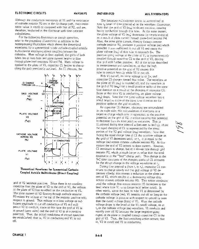
Circuit Operotion. Tie xconpony lng a r c u i t sihernotlz ~ i i u s t r a r r s two t r ~ o d r riectron r u b s i n a b c s ~ m t h a i e ~ ZL-;;:~ ~ 3:!..b!i. (!rer-r-lcin;! ?"!??.??!C!.'! I?IC'?!! e.rpiny. Ing direct coilpl~na i n the cathode clrcult. Electron tubes V1 u:vd V2 c:c 1 I r~ t i cu l - ty3e triode t u k s ; olthouqh tile ~ c i 8 e ~ l ~ u t 1 s ~ : i ~ s i : i i t t s s e w r a t e triodes, ; i-is-triode i s irequer,!iy used ln ti:>> circulr. 2opaci:or C l pravldes the coupiing irorn the piote o f V i to the mid of L'2. E e s ~ s t a r s 91 and R? ore the grid resistors of V1 cnd V2, respective- ly: resistors 43 and 1 4 ore the p!cte-laud resistors of V1 and V2, respectively. Resistor R5 1s the common cothode- coupilnq and bias reslstor couplinq V2 to Vl.
c 2 OUTPUT
Triode Cothod.-Coupled Artoblc Multivibrator (Direct Coupling)
Capacitors C2 und C3 a re the o u t p ~ t n;;ilng c0paijto:5 !or V l and '42, iespect~vely.
-----.+-. .., .:.......... I! an5 :e::rta: US !s:z cn6 3-C circui!
r>i#ii3:i*ir,,~,.! tk,e tic* cs?,5:c7,: ir. tk,c ::i? cirr2i: c! 1!2. .. lne imtlcl chorge poth lor cawcl lo r -1 is Tion 11s ieil s ! d ~ thri,,;h V: i r l ~ : ~ - l i ~ ~ :cs:~:c: 3ni :ke zlcre su;piy
W67-000-0120 MULTIVIBRATORS
voltage to ground, then through cathode resistor R5 and the low iopproximotely 1K) cathode-tugrid canduct im resistonce o! V2 to the righ: s ide of C l , os illustrated by $ - . - > . A 8s ~ULLU- ,L , , = ):..- - pzt,. .L A.m ;- --.. ru,. A a! the !ol!awi~g simplified
schematic diagram. W e n t e canduction through V2 de- c:zzccc, cr.2 ?he T?? c! '42 cc !mqr dn?w+rr,rrpnt, the cilursr potil fur C l i s completed through giid resist- R?, cs :!!~st:oted by the dotted-line p t h e in the some diagram. For a l l practical purposes, C l charge completely durinq the t n e that V2 condxcts; the avaunt of chorge via R2 is negligjbie. Port B of the dioqiam shows the dlschorge path !or c o p c l t o r C i to he through grid resistor R2, common cathode iesista R5, ond the iow ccthode-to-
A CHARGE WTHS I
I' - I - B
DiSCHARtE PaTH
Charge and iJirchorgc Pofhr tor Capoc,to, C i
; : , , : ! . 7-; ..-- ---- .--. -' . ,.,., c .d.. , -. h e charge patn ana tne cutail voltage lwei o: '$1 dr- . . .- . . . ~r<~,,>m,c :\,c L c G ~ ~ ~ , G ! : iac f h ~ t '!I I!! ?JIO!!; the C O C ~
s a t G! !!,e dlsch,::~ :,nth zn;! h e z t o f ! ,vsltoqe lew! of V2 determine the length of tlme Ulat V i is curoii.
If tine tlme constants for t h e charge and discharge of C l ore equal. a symmetrlcoi square-wove output is produced by the z!rcilt: by mek!ng the chcrqe cnd discharge R-C !:ne c o l s ! ~ ! S @!!!Gel!, the clicult produces on osym- 72t:iCGi, G; E Z T ~ ? ~ T C ~ I C C ~ , :ezt~~~;ic;~~::z~:e 9C:pu:.
CHANGE I

ELECTRONIC CIRCUITS NAVSHl PS 0967-000-01 20 MULTIVIBRATORS
When tube V1 is conductmq, copacitor C1 discharges throuqh grld resistor R2, common cathode resistor R5, ond the plate resistance of V1. The grid voltage of V2 apprwches cutoff as mpocitoi Cl dlschorqes; thls is ~Iiustroted by the Vi qr~d voltaqe (eq,) waveform durinq time ~nterval c (between I, and 13. At I, the qrld valtoqe oi V2 just reaches the cutofi level, perm~ttinq his rubera conduct. When the plate current of V2 increases, the voltoge across commm caihode reslstor 8 5 (wovefcric ek) also Increases (goes positive); this increases the bios on V1 and thereby reduces the conduction of Vl. The de- creasing plote current of V1 poduces a ~si t ive-qoina s14nal across its platelmd reslstor, 3, which. in turn, 1s
coupled through capacitor C1 to the wid of V2, causina .L - ,,,,a G ~ A G 16 %CG,X t,idt,lv x,s. t .~~. ~ r , ~ J d , t ~ ~ ~ , t~ i(,- . . . creasing the plate current of V2, the pos~tive grid voltoqe agam muses grid current !law orid chorqes capacitor Cl. Thus, the second swltcninq action occurs and the cycie 1s now complete as the initial cmditions once aqain ore rmched; that is. V2 is conduct~ny and VI is cutoff.
In the preceding discussion the multivibrotor was con- s~dered to be a symrnetr?cal type; that is, the perjods lor conduction and cl;toff of the tubes ore eqwl. An osym- metrical, or unbalanced, output can be obtoired by hoving V2 cutoff for a Ionwr per!od than Vl. 4dlustir.a the value of me mihcde resistance wlil permlt thls to ho~pen, smce it is the bios voltoqe developed across the common cathode
'u\ resistor that determines when Vl begins conduction. In this mse, the combined ume mtervols of 0 nnd b wlli be less w~ (non time iiitervai c. \ Another conliprotion of o t n d e co thd~ ioup ied oarohle m~~lt~vibrotor is the circuit shown i n the occammny- !ng schematic diaqiran. Th~s c!:ccjt 1s identiccl to thp h s i c m m m o n - c a t h d e ~ e ~ i ~ t o ~ - c o u ~ l e d circuit just dls- cussed, except that the feedback from V2 to Vl now 1s by copxilive coupling through "4 between the two cathodes. Aithouqh the son^ switchinu uction occurs between the two t u i 5 nnd the cutoff time of V2 is still determined by the d!schoiqinc of capacitor C l throuah qrid resistor R2, the . . cutoff time bi v l in &is instance is determined by the ctnrqino of comcitor C4 throuqh its cothcde resistor, R5.
to cowcitive coupling between cathodes, seoarate cothode resistors OIC. used.)
The char? ond discharge pahs for copacltors Ci nnc i4 ore depicted !n the following ~iiusuotion. Vote that zapcltor ii i2arts A and 6 of the ~iiustrotian) tne pihs ore the same as in the directiaupled circuit lust discussed, except that the mlhcde resstor through whlch capacltor Cl now charqes inltiollv is R6. The rharqe wth for capacltor '2 (part L' of thc ~!irsVat:o~,; :s iror ::s riqht side throuqh the low calhde-to-piate conduction resistance
OUTPUT
0
T.:.J- r..L-J. C l . l A...LI. ...-- -",..""C'-""l,." ".,"",C
Multivibrator (Capacitive Coupling)
to ground. !hen through V1 cathode resistor 35 to its left side. Part D of the illustrotion shows the discharqe pork for cowcitor C4 to be from its left side throuqh the low cothodeto-pl-te conductio~! r:.s?stc~ce of Vl, p!cte-!xd resistor R3, and the plate-supply voltage to ground, then through V2 cothcde resistor R6 to its riqht side.
of V2, plote-lood resistor R4, 2nd the plate-supply voltage


ELECTRONIC CIRCUITS NAVSHIPS
voltoqe on the qrid of V2 (becamlnq l e s s neqotive a s capacitor C i discharges through resistor 32) and the vol taqe on i t s cothode (becolnmq l e s s oositive a s caxlcitor ~ 4 d i s c h o r g e s through reslstor R6) i ec reoses sufficjently, 7 , " r r, uqoin conducts. Tne switching oction repeats continuous-
ly with first or.e t u k and t i en the other tube cona~c t ing . n ......... 1 . L . I ........ . , .,,L "",p", "2 ,,,=,.,",L,",",",", i> cu;ern [,t,t,a e,r,,t:r
or born piate clrcults imough output coupilnrj copocitar CZ or C3. In ciises n h ~ r e i t is desired to rr .mii l~re h e effect of voryinq load impedance an the frequency stobllity of the multivibrotoi, o cathode follower i s use; for stability.
The t r ~ o d e cothcde-caupleJ ostoble rr.ultivibrator, like the plate-togrid-coupled type, may bbe ssynh:onlzed . w I : ~
; staoie extern?! scurce !a !o:c: k e pr:::? ci 5 - ="I:; v~brctar action to be exoctly the some as that of the - synchrmizirg some. :nc i:~q;;enq a! the syiichronirin-, sign31 x u s i k slightly i q h e r titun Lie nuturui operotinq irequency oi the muit~v~orotor so ihct me syr.chromzinq puisr occurs just prlor to the time that normoi switchlnq action would occur.
FAILURE ANALYSIS. No OU~PU,. Assuming that the multivibrotor is c free-
running tyoe and no synchronizinp s ignals are applied, the plate and ilioment vaitaqes should be measured to d e
& termine whether they ore within the specif ied values. if coupling capacitor C1 should became l w k y or shorted, o positive potentioi will be present on f i e qrid 3! VZ and, ""."",,,. , . . . : - 2 . . I ..1 . I , " < " l..lY.., ,"^ " L * * l > L .il::;IL: . : m Y I I Y , li *ili :ei:iciii
cutoff beccuse oi the niqh positive pctenuai ( t ios) on i t s cothode os n i e s ~ l t a! :ne h r c v ionductlor; oi '72. ii tile circuit does not oscl!icte, mensure me vo!tclr]r ot eort, plate to deternine whether ploteioc? reslstar 33 ;r 34 15
open. If either resistor :s open, tiiere wiil -e r c voitoqe on the osstx-iated plote: olso, the other tube wlil condtict hmvlly ord, 05 c ~esg!! "f the hec."; CCE~.-:::~~I, 1:s plate voltage wall be low.
In the common-cotf.oderrs:stor-mspled ci;c;it i;n~ iiquratlon, >! co thme reslslor tii were to open there would 'keno ou:pbt keiiluse nejther tuke :vcuid cor.d.~ct, and tt.e plate voltoge of h t h tubes would be ot a+. In the c o p s l t ~ v r c a u p ~ ~ - c u t n o a e circuit conl!qbrolian, i t i c t n w r resistor R5 or R6 were to open only the associated tube IVI or V2, respect~vely) would not conduct. if couplinq . . . . . ...... -"?".-..", , , , -,,., "",.-. . ,, ." r .... L,L ..YU." "Z .," ICedjUcil ,lCli,l
112 !O I!!, cn? tks 2: 2d:p~t !xz I:,? ~ , u h ~ ~ ~ i L r " ; o , . R.6ur.d Outp.,. .: , c l r r : ; "~ ;ii tikt ;";$", ~,i ,~;. i . , i ,
i s pene;aliy =-used by il j e i c t iv r t u k ; however, ir a n . . . ;I;; & <"""i,: ..j i YCI~L>I _:I i:,c UrPi lCL plLit ;i;i(i4e u an !ncreuse i n tne reslstcnce ai me ossocloied p l o t e !=d :C"."*.. 9, . 9' 3' "..,,"., . d u, .,*. , I =,,,,r% <,"i&#"t c""!,,,'.:,, < , , , , " , z ' , ! , ~ > : , -- * .&,.,!A L I~ W: C3, ......"... , J , ~ , , ~ c :e;:, ,ST sm.,-rt&, :hc ;r,+: ( ~ > I S -
tor oi me toiiow~nq stoge cm. !orm c wl tooe ritvlder which uiso includes h e c s s o c ~ a t e d plnteiaod reslsto:, R3 or H4. i f the ~ n p u t resistor of the foliow?ng stoge 1s :et:j:ne? :a qcound or to ri ne.jct:ve PO!F.C:II!, ,~s!:c~c-cI:I~c: 3i:i3ii
m o y reouce t h ~ ~ o l t o y e OYCII:C!~ n! :he :!cte c! :hi ,xij!:i- . . . , , . .................. ." *,,-- .?- --..,,. -. .... :i .-... -... .---*. .... ....,.... "i -. ""ti."; .rii"ciij,lrr. ,,:*,, ,he ";,:;.,""": -,,., "-. *k-- -L ... - , .... 8 . . ............. *. .... .. .....-.. R3 or H4, r o y c n ~ i e the ie i is tnr !n s2r- c;:. Cz:t~c;7.z7.:,
0967-WO-0120 MULTIVIBRATORS
the operatlon of the fol!ow1n2 s tcqe may nlso be affected by the c h o r e in grid-bas voltage resilltlng from the ,,cltarre divider oc t~on .
Incorrect Frequency or Pulse Width. The critlcal coaponents ;la?iern:n? fi.e irequency snd pl;isc u d n oi t!:e rnul t~v~brstar o r r Ciosc in t i e :c~p!lr; circuits. Any cncnge in me compone?ts qovern?nq the grld cr camode R-C tlme constants %,ill directly offect the f r e q e n w on3 pulse .wldtn: o chonqe in the P-C c o m b ~ n o t ~ a r s o t w-Ci or R5-C4 will hove the greatest effect . A chonge in the value of plotelood resistor R3 or P4 rill1 offect the o.v.pli- tcde of the output; ; twi l l =!so t,ave an efiect on the I r e qurncy, but nut nearly so muc" os tne camparents rnent!onel awve.
:i loc ul~irsyrrly v u l ~ u j i , +LD, b i l u u i ~ ~ilulqr OPPIUX-
~motely 10 p?rcen.t i m n !hi. sper!flr? .!cl:n, n ?:!I! 1- f:r . . q ~ e n s y ;i-r.rruily Jccur; t-:::c :rrqdmq m:: r?; :Iso x c u r ii tne itinnen! voi!~lge shOuid era@ below :"e saer?i:-.? VUI"~.
In a proctlcol clrcuit, whe:e tne multlv~bratar I S f r e c rlinniny an; nat synchronized iron an external source, 0
variable rrs ls tar 1% 5e liio,;?ed ts adlust the oppiicc . ~ ~
plote vcltsge 0: tc c i l ~ s : ti.? vc!;lc df i e s i s i m c e in cock: >rid circu!!. The provlsinn enables the multi:.ii.:ator to . . . . ne a c j ! ~ s t e c t c t?e carrect i:cquc:cj. 2;: 2-l:e ,;;:::h, ;iC oermlts odlustmer.t to compensate ior differences i n In-
d lv~dua l tube c h a r a c t e r ~ s t ~ c s when a t l ~ b e substitution is mace.
Ii either output :oup!ing capacitor (C2 or C3) should , , aeca;.i ie3x.i : I s h ~ i t i s , ine v o i i ~ ~ e d l v l d t r uctiun which
con occur 33y r e d ~ c e the amplltuZe of the output waveform and ciisi rie ml.irl,,~?rnIor to o?rrole ot il7h.er !r-q'iencY, :!r,x t1.c ::I: x?,=:!t=: !C'!!. :;sck,zr~e t:r.e ::; depe~,,derit .pan It,? m o u n t af chungt ir, cupacilur vo;taqe.
BISTABLE iSTARi -S iOP) MULTIVIBRATORS.
- ; n e term bir toble multivibrotor refers to one c iass of
rnuitivibiator or ieloxotion oscillotor circuits that can func- tion in either of two s table s tutes ond i s c c p b l e oi switrh- in7 m p ~ d l y from one stuble s t a t e t o theother upon the up- pi~cat ion oi a t rqqer pulse. i n the strict sense of the word, the bistoble rnuitivibrotor i sna t nr. oscillotor: r a t h ~ r , it 1s
I circuit k v l r . 7 two conditionsnf stohle (histnhle! eqlili- in ium ultrj r q , > i r ! n i iwc trlpilr t r ~ q - p r ~ in campierr ,q s ! q i e
7 -, y e . ; :,e ~. i r ;u t ion oi ine bistobi? m~ii:i.u~brnrar is i e - i rncent u p ; , tr:e ti:llln;cur:t:o! ~ C I ~ U P . L?VOIYEI !n !?.e t:onsier of conduction from one tube to the other, initiated L! "11 ;:.~U: :ii(ijei p,isc i; ? i u i t r oolarity anu sutl!cier,t ornplitude. Becousc t k r e i s c sudden ievrrsal (or "flap-
,. , , , :'!:I; : !TCm ?.le SIX!t. S:3!E. ti: !1C 3!RCi, :% 2:5tZ>!C
. . :;:;l:;v;i;;:s; ;s irequently ie;eiieo 10 23 a flip-;lop c i rcu~ i .
7he bistable mri!t~vibiotor pro.'.aces rin output pu!se,
more commonly coiled a "oute", truvir.g fost r ise and fal l times and cxtcerne flatqess o i top. l o gemrate !his Qpi
;I ~ i i i . f ~ i ; ; ~ i i i ~ i r c ~ i t ~ & U ~ I C S otrc tiilicler pulse !or ... ,U,~-ZX (s tar t ) anti ~7r,atk8ec t r ~ ~ j ~ ~ e r p ~ k ~ for rurx~<zfi ( s I o : , ~ ,
~ i l i ~ s qrnprnzlnr! o ' ' s i ~ y ' ' i ~ l n r r l n n (or P n r r ! ~ ? I I ! t r ! ~ y ! . , , L ~ . ...... ...... ............ ..: ,,.. ... u: uu.:,;d:., :LSI" -,.I .,LC
cppijcs GI !q t i z e i z e r < ~ l s [I,% f:eq2e:cy), tk,? ,,c,tr>
CHANGE I

ELECTRONIC CIRCUITS NAVSHIPS
generated ore wide. On theother hand, when the triqger pulses ore of constant f r equenq and ore applied a t short tune intervals (high frequency), the -Jutes genemted are norrow. In ol l cases , however, two input trigger pulses a re required t o complete one cyc le of operotion, resulting in on mtput gate frequency one-half that of the input trigger fie- quency.
Although the t w n a and turn-off input tiigger pulses (which can be applied from different sources o s well) can b e of either positive n negotive polarity, o negotive trigger i s preferred. A reason for this requirement i s that if o tube i s biased for beyond cutoff, o highumplitude positive pulse i s required t o drive the tube from cut off into conduction. On theother hand, o lowumplitude negative pulse will immediately cut off conduction of a tube. In addition, the circuit used to generate a lowumpiitude pulse requires l e s s p e r .
?he rectangularqate output of the bistoble multivibrotor con be either positive or negouve in palority. Each gote i s inmed by the combination of positive and negotive s t e p functions produced by turning the multivibrotor an ond off. The negotiveqoing s t e p i s inherently faster (0.7 mi- crosecond) tho" the posi t iveqoing s t ep (2.5 minoseconds). When conrecling other circuits t o the bistoble multivibrotor output, pecaut ions should te token s o a s to peven t the shunting capacitance from cousing undersirable e f fec t s on the r i se and fal l timesof the s t e p function.
TRIODE ECCLES-JORDAN (FLIP-FLOP) MULTIVI- BRATOR.
APPLICATION. The triode Eccles-Jordan (flip-flop) multivibrotor pro-
duces a square- or rectangular-wave output for use a s gating or timing s ignals , 4 for on-off switching op?rotians in binary counter circuits.
CHARACTERISTICS. Circuit a s s u r e s oneof wa s t ab le states: one tube
namally conducting with theother tube normally cut off , and vice versa.
Requires two input triggers t o complete one cycle of operation; the circuit assumes a s table s t a t e upon comple- tion of eoch ha l l cyc le of operotion.
For a constant-frequency input, the output frequency is oneha l f that of the input triqger irequency.
Input triggers con be either positive or negotive; posi- tive trigger offects namolly cut-off t u k , and negative trigger affects normally conducting tube.
Symmetrical triggering occurs when the same trigger pulse is applied simultaneously; unsymnetricol triggering occurs when triggers o re applied s e p r a t e l y .
Symmtricol or unsymmetrical output gate depends on timing sequerre of input trigger pulses; input triggers from different sowces (twn-on and twn-off triggers) pro- duce unsymrnetricol gote output.
Plote-toqrid feedback coupling is direct (through resis- tors), with byposs capaci tors used to speed up switching from ane s table s t a t e t o theother.
Circuit con be made t o assume the some s t ab le s t a t e whenever voltages are applied by incorporating a definite jrnbalance within the circuit or by using a monuolly con- trolled "reset" s i p a l .
Tubes con be grid-biased by connecting to neqative supply, or cathodebiased by connecting cathodes throuqh voltage divider to positive supply.
CIRCUIT ANALYSIS. General. The triode Eccles-Jordan (flip-flop1 multi-
vibrotor is capable of producing a s q u a r e or rectonqulor- wove output pulse (gote) ~n response to two input triqqers. T h i s type of multiv~brotor has two s table (bistoble) s toles - one tube i s normoily conducting while the other tube i s narmolly held cut off - ond will function for only oneha l f cyc le upon the opplicotion of on input trioaer. Feedbock * - from the plate of one tube to the grid of t h e other is direct through a coupling resistor bypassed with o capacitor, whose function i s to reduce or eliminate the e f f e c t s of tube inter- electrode capacitance. Because two input triqqers (turn- . . on and turn-off) ore required to complete one cycle of opera- tion, the output-gate frequency of the blstoble multivibrotor i s oneha l f the Input trigger f i equenq . The output qote length isdetermined by the time interval of the turn-on and turn-off input trigger. Output s ignals con be taken from the plate of either or bath electron tubes. J
c i r c u i t Operotion. The occomponying circuit schematic ! \
i l lust ra tes two triode electron tubes in the basic Eccles- 'U - 1
C 6 OUTPUT
r I&--%
-
Triode EcclcrJordon (Flip-Flop) Multivibrator
CHANGE i

ELECTRONIC CIRCUITS NAVSHIPS 0967-000-0120 MULTIVIBRATORS
Jordan multivibrator circuit. Electron tubes V l and V2 are identical-type triode tubes; althouqh the accomponylnq schematic illustrates w o separate triodes, o twin-triode i s frequently used in this circuit. Rrs i s to i s R l urld R2 urc the qrid resistors for V l m d V2, respectively. Resistor H3 p:c.:idec L?e d::ec: c p i i - ; !:zz th: F!;:: of 'I! :a thc ;;i! ui L'2, uild r r s i s iw R4 p u v i d r s tile direci coupling from rhe plate of 'I2 to the <:id o! 'I!. Feedback resis tsrs P.3 m d R4 ore bypassed with copacitors C3 and C4, respectively. T h e s e copacitors permit foster switching action from one tube to the other by reducing the e i f ec t s oi tube inter- electrode capacitance. 3es i s to r s R5 ond R6 are the plate- !wd resistors for Vl onc \'2, respectively. Capci tor i . - . -. : i ,mo : . L rn? the ~np~it-tri,,,:er ingpi i r? ropnciynrs !or ' ~ ' 1 and V2, respectively; they provide symmetrlcol tilr;qerln<. Capacitors C6 and (n me the odtput-?ate codpllnq LC-
paci:nrs for '!I mi! V2, respectively. Opsrotlnq bias for
under mnsiderotlon i s for a radar opplication wherein i t i s d e s ~ r a b i e ta have the gate length controlled by the display circuit. Thus, iiie rodar w e e p circuit provides the thm- u f i trigger Lo relurrl tile i~ ,ui l ivihuioi to i t s initiul s t u b k Stole.
.,,L.. -, ...... L .... . - - ? > - A .. .LA ........ .L-.- :- , , i ,cii rvi,vLjr .a i i ia , u p p r i i u iu u i i i i i L " l i , i i r i i r ir
o silgnt conauct~on tnrougn ooh tubes. Becouse o i ine in- i~e rzn t !mbalmce of the ciiilrit, h;wev.t.i, ane t h e will conduct slightly more rhon the other. For example, if in- ltioliy the current through V l should be slightly qrrotei than tnat rhrougn V2, tine ,ioltoge drop across plotrlooO ieslsto: R5 ,w111 be jreoter than 1t.e 2rop a c r s s s p io t r ioad resistor 36. Tnls results in o lower plate voltoge for V l , li,,,.i . . . 15 ,ppi!ed ti!r"miqt !es!i!rr i! !u ths ~ r i , ? Q! Vi, !hnj cilus;na the voltoqe at th ;s 3rid ;a become mare neqotive cna :educe the current th.ruuc!~ '12. 'idher. the plate current liircuuh -42 i s redwed, h e i k r i e i ~ i ii,rauijh pluteloi-id re j is ts i
grid circuit voltage divders . The cathode c i r c u ~ t voltaije divider c o n s ~ s t i of conmon cathode resistcr R7, byposse? with copocitor C5, md resistor R8: the voltoge dlvlder far the grid c ~ r c u ~ t of V l cons i s t s of resistors R l , R4, ond R6, and the voltoge d1v13ei for t9e a n d circilit a f V2 consis ts of res is tors R2, P.3, a d 85.
Considei now the operution of me triode Eccles-Jordan (flip-flop) mult~vlbrotor by referring to the precedinq cir- cuit illustration and the occomponying illustration of the
k.n. ;A,,..I:--A : ~ L LA,,.^+;-^^ . . . . . . . . . . . . . . . . . . . . . . . . . . . . . . . . . . . . . . . . . . . . . . . . . . . .M"- :- -.A-. .- ' I
iuiiy analyze tne :lmmg scqiience, oss;rne h o t tile c i r i u t C - 1
oge of V2. Tte positive-gomg plate voltoqe oi V2 i s opplled th:ou:h reslstor P4 to h e qrid of V!, mckinq thisqrid more positlie. T ~ P reqmprotlve action just described continues
ropidly until V2 i s cut off and '11 1s at moximum conduction. - L . , i ,,US, the c l r iul t i5 in 3ne o! i t s two s table s toles of equliibrlum, os represented by tlme lnterval o on ine wave- form lliustration. Note thct the output ot the plote of V1 i s a t i t s most negotlve excursJon (V1 is conducting) while ine output ot the plate of V2 i s positive (V2 i s cut off). ........ .... .... ........... ^ .L.-. 1 n r. .!-. .:-:.. .: 2. . . . . - ... -. - . . . . . . . . . -. . . . . . . - . ...... .- ............... "1??C L " ? ? i L W , L :11111,1,, L l l L Y l L
to drive me nonconducting turc out of curoii, the circuit ier ,oins in this s table conditiar: lint11 Jn input triqqer p d s e
IN,,,l lo 'I '2 'b 36
(TURN-ON1 0
-
is applied. P.ss9me n 3 , ~ C?C! a nejc!li.e III??C: pu!?t. of sufficient
amplitude is appil& s i n i u l t n n w u ~ l ~ to both qrids throuqh inurlr cuuoc!turs C l urla C2. Tnis tilqorr D d s r , which i s .LO *,,."-*" ,--,,. ,.;""".<.?,., ,ho ,"A". ,,-;-" ";." ,,.,- ,,,- ,",,, ",, ...* ". ....>., -. .. ........ is cpplird a! 1, os illus!rate? on the waveform diagram. because V2 is olready a t off. Yie input triqqei h a s l i t t le
l N W T TRIGGER 0
(TURN-OFF1 . .
r i f ec r on thls tube; however, the same negotlve triqqer pi.ise <rives ti,e qrid oi i ' l below cutofi, cousinq this
PLATE MLTAGE norrnaily q n d u c t ~ n q tube to +crease conduct~on. As soon v1
:i rrwuces corriiiziion, i t s piate voltaije u s e s toward L.p11
:nu o l a t r s u o p l ~ ~ valtcae, +Ebb. The p o s i u v r q o m c sional I I I I ot tne d a t e of Vl 1s now c o ~ p l e d thiouah resistor H3 ond
o; I : / I , , - " 1" i , " ' 2 , d " ' 2 a . ;;.us, ! I / I I ! I i : ,; ;:,>Lunt i, 36,ti i i l , l_l "CtlGli s i i ~ i s : Ir: :.O.* ~ ~ f i d ~ i t 5 .... t i : , . . i j ,.,dd,,", GS ,fi>,.'<.tc,, by L;,r <"\,"=,"$>,, 4; ,$... p,"<e, a>z " , +A +* i-I )-- 1s cutoii. The ~r~ultiviorutor irlnolnb l n U i l s cundltlori,
aiuE I i " - , ny i I i I ,,I..-:. .a ,La LcLd:2d 4;-Li= h:uLt ah , ; ~ p . - k : w., ;a>;:e I,.. , . , . .
I I (FROM SWEEP CIRCUIT) I I m T - r I .
I . .
V Z I :SIYO: b, until arotk,er trlaqei i s apclle,2. I.PzI ..,
i M i-: li . I....,. I , ( ? 1 1 I, ," :I.>,?,! ;.!,I ,!lll:,:1111. !-. i l l ! _ i l l i l i ; L i l r IITI:U?',I , . .. ... i i I I I
~ . ' . f , ....,, l , , e i>>Jr ;*r;> ;;I!> :> <ppil;< I I
".. ...-<-.
I I I I I I int 1,) ond the q a t ~ is terminated. The neqotlveoolna o i l , 8 8 ... . ,
I i , , ,,.cat trigger m t s cif condilitlor. s: Vi m3 causes a I i 8 : > : 8 I , , swirchlnq octlcn !ha: retoms the rnult~vibroto: !o i t s o n a n a l 0 ; C I d / . ! I ! , , ;t;hlt s:;tr. :c :.r.?ci :'i :s :an?~ctln; a-3 Vi is c-! o!!.
CHANGE 1 8-A-1 3

ELECTRONIC CIRCUITS NAVSH IPS
Close examnailon of the woveform iilustratlan reveals thot the lenqth of the output qotes i s deter~nlned by the tune interval between the !urn-on and turn-off trlqqers. If the f r equenw of the turn-off triqqer i s mode lower, the time intervol between tqe triggers w ~ l l increase; hence, the l a t e lenqth will i i k e w ~ s e increase. Conversely, the gate length will drecrease if the turn-off tnqqer frequency i s increased. Thus, the bistable mult~vibrator p rovdes o pos111ve or neqative qote output in response to o timinq (turn-On) ir.put triager pulse, with the gate bemq terminated by a turn-off triqqer pulse. If a s inqle constanl-frequency trlgqer i s used for Sath the turn-on and turn-off functions, the c ~ r c u i t will produce o symmetrical squore-wove output hoving a frequency o n r h o l i that of the input-triqqer I r e quency.
In the symmetrical-input bistable multivibrator beinq considered, positive input triqqer pulses of sufficient amplitude con also be used to Initlate the switchinq actlon between tubes V1 and V2. When the positive triqqer pulse i s applied simultanmusly to the grids of the tubes, there will be no eifect on the operation of the conducting tube. However, the plate current of the cut-off tube will be in- creased, cousinq i t s plote voltoqe to foll. The foll in plate voltage, when coupled to the grid of the conducting tube, drives this tube into cutoff.
Althouqh i t i s true that either neqative or positlve in- put triqger pulses can couse the switchinq action to occur. triggering with negative pulses i s preferred. For exornple, if the cut-off tube 1s biased with a hiqh neqotive potential, o high-amplitude positive pulse i s required to dri,,e the tube into conduct~on, and only the most positive portion of the pulse has any effect. On the other hond, a low-amplitude negative pulse applied to the conductlnq tube immediately drives this tube into cutoff, causing an instontaneous switchinq oction.
FAILURE ANALYSIS. No Output. The input trigger should be checked with
on osc i l losmpe to determine whether i t i s b e ~ n q applied to the circuit and whether i t i s of the proper polarity m d amplitude. Lack of an Input trlqqer a t the qrid of V1 or V2 can be due to on open couplinq capacitor, C l or C2, or to failure of the externol input-trlqqer source.
Failure of the plote voltoge supply, +Ebb, will disrupt the operauon of the c~rcu i t , a s will an open cathode cir- cuit. With tubes (or a single twin-triode tube) installed in the circuit, the filament and piote voltoqes should be measured, as well as the bias voltaqe developed across the cathode resistance, to determ~ne whether the opplied volt- ages a re within tolerance and whether plotelaod resistor R5 or R6 and ca thodrb los resistor R7 or RB 1s o p e n If coupling resistor R3 or R4 i s open there will be no fecd- bock siqnal to cause the multivibrator sw~tch inq actlon. If bypass capacitor C 3 or C4 i s open feedbock will still occur, but the interelectrode capacitance of the tube moy couse undesirable effects on the wovefront of the feedback signal. An open output coupling capacitor, C6 or Cl, will prevent the output-qote s i p a l from reachinq the followinq stoqe.
Reduced Output. A reduction in output is 2enrroii,+ caused by a defective tube; however, 11 c a ~ also be causec by a decrease in the cpplied plate voltoqe or an increase in the reslstonce af the ossocioted plate-lood ieslstar, R5 or P6. A leaky or shorted output coupl~nq capacitor, C6 or C7, viill lorn o voltoge h v ~ d e r vilth the lnput resistor of the following stoge. If the input reslstor of t i j s follow- ~ n g s tage i s returned to grwnd or tc o ne-jativr supply, the voltage at the plote of both V1 and V2 w ~ l l be reduced, ord the operotion of the following s t aqe will be upset by the chonge in voltoqe applled to i t s grid. Also, the odditlonu1 current through p la te load reslstor R5 or H6 may cause the reslstor to burn out.
Incorrect Frequency or Got. Width. ' h e tnode Eccles- Jordan ( f l ~ p i l o p ) multlvibrator has no components wvernina the frequency or width of i t s output-gate slqnal: these are both governed by the input trlqqeis applied to the circuit. Therefore, any change in the output-gate frequency or wldth i s a result of improper operation of the turn-on and/or turn- off trigger generotlng circuits.
PENTODE ECCLES-JORDAN (FLIP-FLOP) MULTIVI- BRATOR.
APPLICATION. The pentade Eccles-Jordan (flipflop) nultivibrotor
produces o square- or rectanqulor-wave autput for use os gatlng or timing signois, or for on-off switching operotlans i n binary counter circuits.
CHARACTERISTICS. Clicuit ossumes one of two stoble stotes: one tube
normally canductlng wlth the other tube normally cut o f f , and vice versa.
Requires two input triggers to complete ooe cycle of operotion: the clicult assumes a s table stote upon comple tion of each half-cycle of operation.
For a constant-frequency input, the output i r equenq is oneholf thot o i the input trigger frequency.
Input trlqqers can be either p o s ~ t i v e or negative: posi- tive trigger affects normally cut-off tube, and neqotive trlgger a f fec t s normally conductlnq tube.
Symmetrical trigqerinq occurs when the some triqqer pulse is opplied simultaneously; unsymmetrlcol trlqqerinr; occurs when t r~ggers ore applled seporateiy.
Symmetrical or unsymmetrlcol output qote depends on tlmlng sequence o f lnput trigger pulses; lnput trlgqers from different sources (turn-on m d turn-off triggers) produce un- symmetrlcol gate output.
Plote-twsuppressor grld feedback c o u p l ~ n ~ i s direct (through resistors), wlth bypass copacjtors dsed to speed up switching from one s table s t a t e to the other.
Circuit can be made to assume the same stoble s t a t e whenever voltoges ore applied by lncorporoting a def imte imbalance within the clrcult or by usmg a manually control- led "reset" s q n a i .
Tubes con be grid-biased by connecting to neqative supply, or cathodebiased by connectlnq cothodes throuqh voltoge dlvlder to positive supply.


ELECTRONIC CIRCUITS NAVSHIPS
When voltoqe 1s f i rs t opplied to the a rcu i t , there i s o sliqht conduction through both tubes. However, because of the inherent imbalance of the circuit, one tube will con- duct sliqhtly more than the other. For example, if initially the current through V1 should be sliqhtly qrwter than that throuqh V2, the voltoge drop ac ross plote-load resistor R6 will be qreoter than the drop across ploteiood resistor R7. This results in o lower plote voltage far V1, which i s ap- plied through resistor R4 to the suppressor qrid of V2. The negouvegoinq signol on the V2 suppressor qiid reduces the plate current of thls tube, thus reducing the current through plateload resistor R7 m d cousinq o voltoqe r ise ot the plateof V2. Th i s posi t iveqoinq voltoqe i s coupled through resistor R5 to the suppressor grid of V1, further increasing theplote current of V1. Suppressor qrid current flows a t o slight positive suppressor grid voltoqe, but de- c reases a t o high positive suppressor qrid voltaqe, such o s when the positivegoing signol i s applied from the plote o f V2. The plate current of V1 Increases further, and o r e generative oction occurs instantaneously to drive V1 into heovy conduction m d V2 into cutoff. Thus, the multl- vibrator i s in one of i t s s table s t a t e s , as depicted durlnq time interval o in the waveform illustrotion referenced p r e viously. Since there i s no lnternal R-C time constont timing circuit to drive the nonconducting tube out of cutoff, the circuit remainsin this s t ab le s to te until o timinq pulse i s npp l~ed to the control grids to couse the switchinq action.
Assume now that o negotive trigger pulse of su f f~c ien t amplitude i s applied simultaneously to both control srids. T h e trlgger pulse, applied a t t,, has l i t t le effect on the operation of V2 s ince this tube i s already cut off. However, the some negative triqger drives the grid o f V1 below cut- off, causing this tube to reduce conduction. As soon as V1 reduces conduction, i t s plate voltage r i ses toward the plate supply voltoge, +Ebb. The posi t ivegoing slqnol at the plate of Vl 1s now coupled through resistor R4 m d applied to the suppressor of V2 driving V2 into conduction. Thus, a t instant 1, a switching oction occurs, with the re- sult thot V2 now becomes the conducting tube and V1 i s cut off. Thus, the circuit i s in the second of i t s two stoble s totes , a s depicted durinq time interval b. The multivibrator remains in the condition wherein V2 1s conductinq and V l i s cut off until the next negative triqgei pulse is applied to cause mother switching action.
When the desired qate duration i s attained, the neqatlve turn-off trigger 1s applied (at 2) and the qate i s terminated. The negativegoing turn-aff trigger cu t s off conductian o f V2 and causes a sw~tch ing action that returns the multi- vibrator to i t s origlnal s table s t a t e wherein V1 i s conduct- Ing and V2 i s cut off. The circuit remoins in this condition (time interval c ) until mother negative triqqer from the timlnq circuits, the turn+" trigger, i s opplied a t 1,.
As in the triode Eccles-Jordm multivibrotor, the lenqth o f the output qates of the pentode confiquration i s deter- mined by the time lntervol between the tu rnan and turn- off triqqers. The qote lenqth will increase if the turn-off . ~
trigger frequenry i s decreased; conversely, the qate ienqth w ~ l l decreose if the turn-off trigger frequency is increased.
CHANGE 1
If a single constant-frequency trlqger i s used for both the turn-on and turn-off functions, the c i r c u ~ t will produce o symmetrical squarewave output hoving a frequency o n r h o l f thot of the input-trigger frequency.
Although positive trlqqer pulses could be used to "drive" the pentode Eccles-Jordm bistoble multivibrotor, neqative trigger pulses a re preferred; a small-amplitude negative pulse when applied to the mnductina tube will immediatelv drive thls tube into cutoff to cause an instantaneous switch- ing action. The output of the multivibrotor i s token from either or both plote circults through on output couplinq capacitor (C4 or C5). A cathode follower should be used couple the positive gate output to a circuit tho1 requires qrid current, s ince the multivibrotor may occoslonally fail.
FAILURE ANALYSIS. No O Y ~ P Y ~ . The mput triqaer should be checked with . .
on oscilloscope to d e t k n i n e whether i t i s beinq opplied to the circult and whether i t i s of the proper polarity and . . . omplitude. Lack of an input trigger a t the grid of V1 or V2 con be due to failure of the external input-triqqer source or to the coupling from the trigger source to the multivibrotor.
Failure o f the supply-voltaqe source, +Ebb, w ~ l l disrupt the operation of he circuit, a s :vill an open cathode cir- cult. W~th tubes installed in the clrcuit, the filament, plote, screen grid, ond suppressor grld voltoges should be meos- ured, a s well as the bias voltagedeveloped cc ross the cathode resistance, to determine whether the opplied volt- ages ore within tolerance and whether any of the respective electrode resis tors ore open (resis tors R2 through R9). If soupllng resistor A4 or R5 isopen, there will be no feed- back signal to offect the multivibrotor switchinq oction; in oddi t~on, the d-c operating potenual fmm the ossocioted suppressor grid will be removed. If bypass copacitar C l or C2 1s open, feedback will s t i l l occur, but the i n t e r e l e r trode copocitance of the tube may couse undesirable effects an the wavefrant of the feedbock s l p a l . An open output coupling capacitor, C6 or C7, w111 prevent the output-?ate s ignal from reoching the following stage.
Reduced Output. A reduction in output i s generally caused by a defective tube; however, ~t can a l so be caused by a decreose in the applied voltoqe or an incieose in the resis tance of the assodo ted p i a t r l o o d resistor, R6 or R7. A leoky or shorted output coupling copacitar, C4 or C5, n!ll :ar.a a voltage hv ide r with the input resistor of the following stage. If the input resistor o f this followinq s t age 1s returned to ground or to o negative supply, the volt- a g e a t the plate, screen grid, m d suppressor qrid of bath V l ond V2 will be reduced, and the operation of the followinq s toge will be upset by the change in voltage opplied to i t s grid. Also, the odditlono1 current through the resis tors o s s o c ~ o t e d with the electrodes mentioned previously moy couse the resistors to bum out.
Incorrect Frequency ond Gote Width. The pentade Eccles-Jordan (f l ipf lop) multivibrotor has no components governing the frequency or width o f i t s output-qate siqnois: these ore both governed by theinput triggers applied to the circuit. Therefore, m y change in the output-gate fre-
8-A-16

ELECTRONIC CIRCUITS NAVSHIPS
quency or width i s o result of improper operation of the turn- on and-or turn-aff trigger generating circuits.
MONOSTABLE (ONE-SHOT) MULTIVIBRATORS. The term monostoble mvltiribrotor refers to one c l a s s
o f multivibrator or relaxation oscillator circuits that function in a s table condition until the application of a triqqer pulse. At this time the circuit switches r ap idy m d qoes throuqh one complete cycle of operation, after which i t reverts to i t s original stoble condition, in which i t remains until the application of onather trigger pulse. The monostable (or en-shot) multivibrator i s essentially 3 two-stage reststonce-mpari tnnrpm~~plpr i~mpl~f i~r, n n 4 n ~ t n n n s r 1 I I n t n r
I" tne StrlCt sense ot me worn, wlVl one tube normally cut off and the other tube noimolly condilcting. The o n e s h o t mu~t~vibrator operates in much the some mmner os the f rp~runn inq , or astable. type diccgrsed earlier in Section 8 of this Hmdbmk, except that this circuit requires on in- put trigger to initiate the multivibrator action and produce the output signal.
The monostoble multivibrator produces a s q u a r e or ;ectanguIor-wove output pulse, mare commonly called o ,, gate", having f a s t r ise and fall times m d extreme flotness on top; ttie pulse is produced only in response to an input trigger. The autput frequency i s determined by the frequency of the input trigger, m d the durotion of the ga te lenqth i s determined by the circuit design. The o n e s h o t multivibrator con be used at pulserepetition rates from zero to maximum - w h ~ c h i s determined by the gate length and the R-C time 4 cons tmt of the circuit. A nominoi range of ga te time duro- ::cc :c frox 30 to 2500 n i c i o s e s c d s , wtict, will accomxo- dote trigger pulses in the r m g e of 200 to 20W pps.
In opplicatlons requiring d f i e ren t gate lengths, the gotedetermining components con be switched in value to proddce thr desired gate length1 Also, the monostable muitlvibrator may supply both positive m d negative gates to os m a y os four brmches. A precaution is that the pos i t lvega te output should not be applied to o circuit requir- ~ n g grld current os the multlvibrator may occasionally loll; the use of a cathode !o!iower or buffer circuit will eliminate this disoduontoqe. Because the monostable multivibiotor i s not well suited for controlling the gate length with o ?~r?df ! trigger pulse, a b ~ s t a b l e ~ t l t i v i b r a t o r sh3u!? be ;zed when th,is tyze of :mt;a! i s desired.
Aitbouj5 tL,e sutput f;am the nonostable md1:iv;br;ltar i s sanet imes differentiated to prc.?ide o puise e ~ t h e r 2: the :ending edge or the trailing edge of the gate waveform, in most cases only the lwding edge of the waveform must k extremeiy fast: the trailing ecge IS ~ s u a i i y not used lor c:ltical 1:mln; cppl!cations. A neqotiveqolnq Ieshnq sdqr la used when~vei p s s i b i r sloce such o quie cun be obtained rather easily irom m y tube eiectrade except the cothode. In addition, a negative gate a t the plate of o E,2!!i"!hmtnr !fit.? w!!! ,l!w.l:,s be o !o.:e: lmpedmce thm a posltive gale bt the some plate.
A tost posltiveqolng leodlnq edqe con be obtained on the clc!e c! ? r e t c t e s! tile l.d~t?v:b:oto: OR!:. :! 2i:eit
OW74W-0120 MULTIVIBRATORS
couplmg i s provided to the control gnd of the opposite tube. Even in this case, coutlon should be ~ s e d to ensure that the value of the associated speed-up capacitor is just enouqh to match the input capac i tmce of the opposite tube; if die value of thls copacitor is t w large, the voltaqe r ise on the plote will be delayed. An output gate wlth u f a s t pos i t ive going lwding edge may beohtamed from the plate of o cothodecoupled monostable multivibrator, s ince this cir- cilit hos o f ree plate not involved directly in the c ~ i c u i t multivibrator action. A fast positivegoing leodinq edqe a t a decreused amplitude can be obtained ot the cothode of the multivlbrotor tube that i s normoily cut off.
TRIOOE PLATE-TO-GRIO-COUPLED MONOSTABLE MULTIVIBRATOR
4PPLICbTlON. The tnode plateteqr~d-coupled monostoble muitivibr*
tor produces o squarewave or rectanqulor-wave output for use as gotmg or ummg signals.
CHARACTERISTICS. Circuit ossumes a s table s tote in which one tube normally
c m d u c t s and the other tube i s normally cut off. Requires on input tnqqer to couse circuit operation;
c i r c u t returns to stable s t a t e upon completion of one cycle of operation.
Input trlqqer can be either neqotlve or positive; neqative trlgqer oifects tube that is normoily conductma, and pasltlve trigger a f f e c t s tube h o t i s normally cut off.
P:cducei s v d a i e a z d e or :ectn,-~!3i-.,v-:.e % g u t ;c:es of b t i ; ps : : ive and negative polarity in response to an in- put trlgger.
Output qate ienqth isdetermlned by R-C time COnStMt ii. grid ciicdlt and by th r applied voltoye; sbtput f r e q u e n , ~ i s determined by input tngger frequency.
CIRCUIT ANALYSIS. General. The trlode plateto-qrid-coupled monastcble
-ult:~iiSro!or :i a two-stage resistimcecapac:tm~e~~?:plsd om~l l f l e r capable of producing a squarewave or rectanaular- wove autput p d s e (gate) in response to an input trlqqer. The aoncstoble n~lai . ibrato! hcs ocly m e s t cb le stcte, i.n ... L<-L "-- ,..L.- ".....",,.. -."A,,"." .L.. -.L-. L" :- """, " , , C '"UC "".'I ,,,, f "mi "Y,il L Y E 10
r.crx;lly cut off, wd will func::on for only one complete cycle upon the appiication of the Input tiiyqer. To achieve the s table mnditlon, the grid of the normally conductinq tube 1s usuolly returned to E!+, while the qrid of the tube :bat i s normally c , ~ t off 1s returned to pound or to a neqatlve voltoge wurce. Feedback from h e plote of one tube to qrld of li~r oppusite tube is through R C couplinq. a e rouse the mmostabie multiv~brator operates for only one cycie in response to an input-trigger pulse, the output i r e q2eflcy f kiS circ.i! is dehe2A4! per: the t:i frequency; the output qate lenqth i s determined by the R-C time constont of the p l a t e t e q i i d feedback network and the oza!?ed :.a!tsge. O L I ~ U ~ s i ~ a ! ~ ;m be t&cn from tL.c p!o:r -' -:.Lee -.."A ... LA. u, =AL,m=L "t W " , =.=-,.u,, LU"C3.

ELECTRONIC CIRCUITS NAVSHIPS
Circuit Operotion. T h e occornpanyin~ clrcult schemotic i l lustrates two trlode electron tubes in a plate-to-qrid- coupled monostable multiv;biator confiqurotion. Electron tubes V l and V2 a re identlcoi-type trlode tubes; olthouqh the accompanying schematic illustrates two seporote tii- odes, a twin-triode is frequently used in this clrcult. Ca-
OUTPUT "I 0
C4 OUTPUT
-I* I t J
0
Triode Plate-to-Grid-Coupler Monostable Multivibrator
pacitor C 1 provides mupllng from the plate of V2 to the grid of VI, and capacitor C2 provides coupling from the plote o f V1 to the grid o f V2. Resistor R1 returns the qrid of V1 to the negative voltage (bias) supply, -Ecc, ond resistor R 2 returns the grid o f V2 to the positive voltoge supply, +Ebb. Resis tors R 3 ond R4 m e the pioteload resis tors for VI a d V2, respectively. Capacitors C3 and C4 cre the output coupiing copocitors for V1 and V2, respectively. T h e tube thot i s normally cut off is V1, ond the tube thot i s normally conducting is V2.
The followinq simplified schemotic dioqrom illus- trates the charge and discharge paths far feedback ca- pacitor C2. The cutoff time of V2 is determined by the discharge of capocitor C2 through resistor H2 toward the positive voltage supply, +Ebb. Although the conduction
V I ""Q CHARGE FUTH -
+'bb -
- 8 8.
DISCHARGE PATH
Charge and Dirchorgc Paths tor Capacitor C2
resis tance of V1 i s included in the dischorqe path of C2, ~t i s small as compared with the resistance of R2, ond can therefore be neglected. T h e cutoff time of V1 1s determined by the period of the input trigqer pulse. If the R2-C2 time constant is mode exactly oneha l f the pe r~od of the triqqer pulse, the multiv~brotor produces o symmetrical s q u a r e wave output; i f the R2-C2 time constant i s made lonqer or shorter than oneholf the trigger pulse period, on osymmetri- col rectanguior-wave output i s produced.
Consider now the operotion of the triode plote-twqrid- coupled monostable multivibiotor by refernng to the p r e ceding circuit illustrotions ond the occomponyinq illustro- tlon of the ideolized theoreticol waveforms. When voltoqe i s first applied, V2 goes into conduction and V1 cuts off. T h l s action results from the fact that the qrid of V2 i s returned through resistor R2 to a positive voltoqe, while the grid of V l i s returned through resistor HI to o neqative voltage. Thus, ot time b (start of time intervol a) on the waveform illustrotion, the grid voltage of V2 (eq,) i s sliqht- ly positive, causing conduction through V2, and a decrease in i t s piote voltage (ep,). The negotivegoing voltage a t the plote of V2 i s coupled through capacitor C l to the grid of Vl , thus oiding in cutting off this tube (:vovefon e q , ) Aiso, a t to, coupling capacitor C2 c h a r ~ e s through the lcii co thode to-grid internal resistance of V2 (oppmxlmotely iK) and the V1 plate-load resistor, R3. The voltage nt the plote of V1 i s represmted by the ep, woveform. At I., then, the p l o t e to-grid-coupled monosrable muitivibrator assumes i t s
CHANGE 1

nl"np-,n" --, .. I .7..=i,-1. -..,A,3,>- ,".2-"..
i " " , " " " ..-.:<.a0 is>i.p-a
.A:,:>)- f , ~ , h " , ! , , r , ~
cGTrJ3na, ia,o,, !O,!fi,< ajon:,,>,din9~, 4 ,' ] : ,2"2~4 ,,I&" 'h,, I ? . . t , .- :a ':ol::odr: ?.::q3no? ] ~ , d ] r . , ~ .;ze,g :r< .11,2;:,c :J~<:]:;AS
~ o ~ o ~ q i n l i j i > m aqi wajja 01 ~ o u i j s ymqpaq ou aq !I'M amti: r s u - &a .. 23 :G 1 3 ; ~ i : m d x S i l~ jd ra i ji .ilaoc si ~n ;i 1.
inisisal sola-a!!o 10 10 ~g io:s!ia! m..i!ora ? ~ " ~ ! C L S I . . 3:LT:z;C: 2.y.:. .7:r z;!::;z,. ;?:;:<? 4,;: :<,;:<,;.;
auruizmp ui 'abollgfi. s u q p:)L a?! s:, . ! V V ? u :pa~!:s.,a> ac, D,IIOUS SdUDjTOh alD!"p>," ~ l , ' . , t i ~ " ~ i l l ! . : T " ~ J T . - ',!! T>r n i . p ! r
-ur (aqnl apc!n-ui.h$l ajbu? o lo) saqnl q 1 1 ~ '11~2~!2 a2oY:c; [:ado uo i i : ~ sc ' l ~ n a ~ r j i r i I; -101:~i?ado a i : .::;
-sip !!im ' ls?+ 'A!ddna ;lbr~!on ahniscC 293 40 a;?!!:: . - ' ~ J I W S ~ s V u ~ ~ l - ~ ~ ' ~ d u t ~u~~~~~~ 10,
> ~ ~
sy YY-. 6,) ," VJ." -3, IU lOYYL l , ,,IUY! L, ," , i Y ] dp, ,4! ,ddc p m nirlojod ladaid aqi ja s! I! laqiaqm ~ u o l i n ~ i l . ~ alji
01 pa!lddo b u r 7 sr 1r la"laqm au~wlalap 01 admso11rsrc un q i l ~ pay53q3 aq pjnoljs iabEiil inoui a q i '4ndwd ON
'SISAlVNV 38 f l l lVJ
.uansnpuoa olu! $10 ins hljour~au s! ioql aqnl aql b u ~ n r i ~ Aq lo 'j:oln> OIUI aqr! bur~>npsos 1 ~ o ~ ~ o u a p h ' l ~ ~ x : ( ?
palor1rur s! uo!ln~;idn ininlq~nrl!nlll lo a p h ? n ' I I K ~ A . ~ bun :I!
.asl?d ;acc!;i aniicta; ; sc ih ; z ;.I;: 2; ai i;, ;o;.;c;;; qbnaiqi paldna3 uairl s! :a66!11 pallahu, aql :?A lo i i o ~ r ! a!,!
u i ! ~ IalpIod U! pai3auum sr a>n:d ? ~ q u PIT , , ~ a : ~ x u v
-laLbril,, a jo prit aqi oi pariddo SI latfrl: a ~ i i i s w . o 'r;?i:
-usr[ddu r!r>dllJ-lus!d~uld duos u l . i ! r o x i q l idbiill 0'1" I I ~ M [ A 10 pubaql oi lo ~ , 4 . lo alold a q 01 h j i a ~ r ; : aillddc
ar!nd laai~rl l ??!!rsod y .acocl.c a:>as 2.1 sa,.??? 7. 12 . pjib aql 01 z3 l o l r ~ o d o s qbnalql paidno, a,rn lb. 10 a101d aq;
01 A~ual!p p a ~ ~ d d o aslnd 1abE~ll an!lobau y .paxsbtrli aq uos 11nsl1s 1ololqm!11nru aqi q s ~ q h ilq poqlalli LTUO a q ~ I O U
si ' asos syql UT auop so^ so 'aonl buri3n~uos i j l a w l o ~ "yi F..' "' ' ".,; >. ' " . " A .'F"." ", . . .
i r r r-,,."u cl,.i" Arrr,.i a ..., rrvli o . . .hlbdnz atojjon an!lri$ ajqi
pua ' h u a n b a ~ j 13t'hui I W ~ U I aqi .Aq pailrwlalap sr b u a n b a ~ j indlno i o i o ~ q i ~ r ~ l n c : alqoisauow aqi 'snqi .uorisnpuo>
olul uan!lp s! 7,j uaqM aurilllalap 'bolion p a r ~ d d r 14': puc ~3-ZG 10 i m i i m ~ ~ allin 3-2 arii >uc 'ua!iJniua> oiui lianllp
E l I,, LiaqM F;i..T;,ajap a s ~ n d i i t . i l j ] a:;] 10 i i t i j r , - i l i i r jo ~ ' i 3 1 'osjv 'aslnd i a t b l n indrii q u a ioj U U ~ J U J C ~ U j~
' ! ? A > zl'irrillln? w n llhnnjllr c=nF in!n~nr~r! :n?, , l i rnn,anmlr: . , , < . 8 t ,. . aql iuq4 j ; n i , ~ i ~ sl;?nlincm a,,! I C aol!nur:!av; isol:)
.'I la pal!dao s t as!rc : db t~ l : dn!l~Lau ~ a q i s u ~ j:1m ( 3 ;o.\:aiu! ;-:I! acr::pm?
-il;nu. aql "I io 'a-uaq .iZba) lll~ojio.~#, ~ C C I ~ M 9116 aq: uo ayjds ahil!sad aqj so liaiioinp awii a m s aqi in aylds an:lobaa !!nus r: sou ('da) zh io wlalano* aEoijon s i i [d auL .slsnpuos tipbo 21% uaijnl 23 ~olr:3jo: bulldr05 ;C
O U T O I D ~ ~ aq! jo ITnsal o SD uoiiE;rp awn awrs aql jo a>:?- a n ~ i i s o d ~ T D ~ S D soq (lba) 711 )O p!lb aq! IC W I O J ~ A D Y aij1 i ~ m '](a papunal sr ('da) ,,A, j0 alofd aqi 10 wlo)ano*r a t c -110" a ' a . l , j jjo s1n3 UTOED ~ S I ~ M [,I 10 pub aql 01 1 2
.",!d,'ti~>d ",L:#O,u: ?*!<,,<A> s , d,r:!i <,i a:; !OL,S C>","b inlllli,l i# i ! ,. n18n r- . c l ~ q ? ' ~ " ? . - , 12!56" ? > g ~ l - 1 L. 1 ,!gpmsu! $ 2 ~ " >u 7. ..
- , l o in., . q " j i i ! :'I":, '-'bun. nu ,Jar, .,* 15 :,rnlicn ?,,h at<! 8 L.,.
2;aq" i3'i'"i' " ;""d aqj !;dd.. atolic.. ;.:!!.-,j
aqi 10 [DTIuaion aql ~ I D N . O I as!, 01 (iba) zn 10 abcilon prlc a:!; sasnc3 s iqi .Alddns ai.ailo~\ anillsod aql 10 iowaiod
?U] L,Jg,*,ai . - J"!C!S?I "t"TIILl EatlC"3SrL 71- 1.!!3~dc2 ,;q . ......., -."-.. ,.-,-J... ~.. , .... ".. ,-.- ",.".> "-..-. ..*. . , -
'j:oinS '. 7 " 1,,p " ! ~ P p l I C ~ r r :pi:!* II,p!C:C ".,2"11 , A:p,-.ClJs>
o u l s: :oiolqinri!nw a41 puo s ~ n s j o van30 burri?;r*c o
'. >a 'ST", .,1c1n> OIU, ,"bl,:,, , A d,,,J,, c,, ,A 1 , : 1,:. A,,,
c! 7 > io~lnor:, Ubnsis; ~ .d~ i i l l 02 s: I:::!::.. hxnbdn:inbau . . . , < " A uur ' , ~ S U ~ J , . ~ , , !!, It, ~ ; I , , I ~ " A A,,>!,; 4,,L ~,,",!:>,,!, - Y I ; ~ u u ! [ A L ~ i m l p p u o jjolrl: d n q u i7i.dj aiollon pl l i aqi
oujs ro i srlql '1'2 13 VIID a41 01 1 3 J O I I ~ S D > q~nolq i palano2 sr 1oubis oura'.sn!irsod '41 puo 'abol~on h~ddns acl p ~ n ~ o l
sssr: ('&j i t , joatoijon a l q d aqi 'zn, ;ino~;l uoilsnuuos pasoalsap aql jo i!nsa> a sy 'jjoins oitii 72 anrlp a1 sr
( ' I io pallodo 'ura) asjnd ~ a b b r l ~ srql jo isajja aqL ' ~ , q jo p!ib aql 01 h ~ l s a ~ : ? pariddo s i a w l aql jjo in, 01 a?nlr[dwn i~~a:2!:]ns jo a s p :at.C.!11 a~:-.C.au o 7mm'l ,- ....... ..-" a:? ssv
.:?!:?li. S! 2r115 13f+!l! C
[ Q Y ~ Yojii?uaa s!q "I ablowal i ! n ~ ! s aql !j!u i ru Aljawlou sr 2 m slx;c= h1;o-:ou ~ , j qzrqm 3r 'alms alqois
I , s r , l " I!! 'a!o]s .:qnis 91. ca!,,n"sp Jo]pJn,ln,n,l, z.,qp~S~u~TJ 7 . .., - .,
n
ELECTRONIC CIRCUITS NAVSHIPS
by a decrease in the applied plote voltaqe or an increose in the resistance oi the associated plote-load reslstor, R3 or R4. A l e d y or shorted output coupling capacitor, C3 or C4, will form a voltage divider with the input resistor of the following stoge. In this input resistor i s returned to ground or to a negotlve voltage supply, the voltaqe at the plote oi bath V1 md V2 will be reduced, and the operotion of the following stoge will beupset by the chonqe in volt- age owlied to its grid. Also, the additional current thrauqh platelood reslstor R3 or R4 may couse the reslstoi to burn out.
Incorrect Frequency or Cote Width. The ploteto-qnd- coupled monostoble muluvibiotor has no components rpvem- ing the frequency of its output-gate signal; this irequency is governed by the input trigger applied to the circuit. Therefore, any change in the output-gate frequency i s o result of lrnproper operotion of the trigger qenerotinq cir- cults. A change i n the output-gate width, however, will result if there i s o change in thevalue of either reslstor R2, capacitor C2, or the applied voltaqe. A chanqe in the resistance or capocitonce of the R2-C2 timinq control circuit will hove the greatest effect on the qote wldth; chmges in the opplied voltope will oifect the qate width to a lesser degree.
TRIODE COMMON-CATHOOE-RESISTOR-COUPLED MONOSTABLE MULTIVIBRATOR.
APPLICATION. The triode mmmonsathoderesistor-coupled monostable
multivibrator produces o squarewove or rectonqulor-wave output for use a s goting or timlng signals.
CHARACTERISTICS. Circuit assumes o stable state, in wh~ch one tube normal-
ly conducts and the other tube i s noimolly cut ail. Requires an input triqger to cause circuit operotion;
circuit returns to stoble state upon completion of one cycle of operation.
lnput tiiuqer con be either neqatlve or positive: neqative trigger affects tube that i s normally mnductinq, and positive triqqer affpcts tube that i s normally cut off. ~.
Produces squarewave or rectonqular-wove output qates of both positive and neqative polarity in reswnse to an input trigger.
Output qote length isdetermined by R-C time constant in grid circuit and by the applied voltoqe: output frequency i s determined input trlgger frequency.
CIRCUIT ANALYSIS. ten.ral. The triode mmmon-cathoderesistor-coupled
monostable multivibrator is functionally sirnilor to the Triode Ploteto-Grid-Coupled Monostable M~itivibrator discussed previously in Section 8 of this Handbwk. The circuit has only one stable state, in which one tube normally conducts while the other tube is normolly cut off, and will function ior only one complete cycle upon the opplication
0967-000-0120 MULTIVIBRATORS
of an input triqqer pulse. To achieve the stoble condi- tion, the qrid of the normally conductinq tube i s usually returned to its cathode or to & while the qrid of the tube that is normally cut off i s returned to mund or to a neqative voltaqe (bias) supply. R-C couplinq i s provided from the plate of Vl to the qrid of V2, but the couplinu from V2 to V1 i s effected across o common cathode reslstai. Be- cause the monostoble rnultivibrator operates for only one cycle in response to an input triqqer pulse, the output fie
quency of this circuit is dependent upon the input triqqer time constmt of the qid circuit and by the opplied volt- age. Output signals can be token from the plote of either or bath electrcn tubes.
Circuit Oprmtion. The acmmpanyinq circuit schematic illustrates two triode electron tubes in a common-cathode- resistor-coupled mcnostoble multivibrator caniiquration. Electron tubes V1 and V2 ore identicol-type triode tubes; olthough the accompmying schematic illustrates two s e p
O U T P U T C3
Triode Common.Cothode-Resistor-Coupled Monortoblc Multivibrawr
orate triodes, a twin-triode i s frequently used in this circuit. Capocitor C1 is the input muplinq copocitor for opplication of a positive trigger to the grid of Vl. Copocitoi C2 pro- vides coupling irom the plote of V1 to the qiid of V2. R e sistor R1 returns the qrid oi V1 to ground, and resistor R2 returns the grid of V2 to the common cathode connection. Resistors R3 and R4 me the plate-load resistors for V1 and V2, respectively. Resistor R5 i s the common cathode bias ond mupiing resistor for coupling from V2 ta V1. Co- pacitors C3 and C4 are the output coupling copacitois for

ELECTRONIC CIRCUITS
4 + i"
B niSCHARGE PATH
0967-W0.01N) MULTIVIBRATORS
ground, producing o bios voltage oi suificient amplitude to hold V1 cut oil (s ince i t s grid i s ieturned to ground throuqh resistor R l ) , and still permit V2 to conduct. Thus, or tune g (s!art of time interval an the woveform illustration, the grid voltage of V2 (a,) i s slightly positive, cousin? mn.ilir!ion rhrouqh V2: as o result, thepiote voftaqe (ep,)
! I , I I
+ 8 , , I , ,
INPUT TRIGGER ((in1
0 , 8 , I /
1 1 1 1 ) 1 ' , , , ,
PLATE VOLTAGE v2
ICP21
G R I D VOLTAGE VZ
( e g 2 1
\' -, ~ n ~ r g c grid 3iri6.-igi P i & $ k; C;p;rlts: C? VOLTAGE ACROSS RS +
, e l 1
8 I
/ o ! b / i d ! ! f ! V l on3 V2, respect!voly. The tube that i s normally cut o f f is V l , and :he tube that is normally canductinq i s V2.
T h e iollowlng simplified schematic dioqrom illustrates the charqe and discharge paths lor capacitor C2. The cut- ;!! time o! '12 :s detrrmjned by the discharq? of capacitor
C2 through resistor R2. Although the conduction resis- t m c e of \'I i s included in the dischwge pcth of C2, i t i s i r equenq ; the output gate length is ceternilned by the R-i: s n a i l a s compared with tne resis tance 01 R2, and can &,ere- f a re be neglected. The cutoff time of V l i s deterrnlned by the perlod of the input trigjer puisr. if me R;-c2 time constant is made exactly onehalf the period of the triqqer pulse, h e mult~vibrator produces o symmetr!cal s q u a r e
~ .. . . wave butput; A; It,;. YL-CL i:xe i0nstm.s.; :c none Icr!qe: 0:
shorter tt:or, one-i.~!: t;e trijqer p;!ss pc:ia.', s? n:cs:.zr.e!ri- cul ~ e ~ t ~ n , ~ ~ ~ ~ : - . ~ o v e ~ t + i ;a >r&ze:.
Consider no* the operonun o i ihe triode common-caL?odr , .
:es>b<dlPbd.>,e: :,,"r,",tdL;= :,."k;.":h":~; b: :c:e:r:r,< :: the precealng circult ~I lustrat ions ona m e occompanvlno !i!,d~:rs!mr, 01 L I , ~ j,ieahz& t b , e ~ r e t : c ~ i ; v w v ~ c f o ; ~ ~ . 'Wk,e~ .;;ltugu ;i ipjii?,j, ;'; jsi; :n:a ;oni>c:?3r. 3-3 V1 =-ti o f f . Th i s oction resuits irom tne toct that the qrla oi vi is
returned throuqh ieslstcr R i to n e cainode, initiully placing L".s gr!d ot the same potentlo1 as the cathode, m d :h;s allo:i~r.; V? :a conduct b.e,>viiy. The plate current flow c! '!2 :1:.-;!: cammar. ccLh.ace r e s ~ s t n r 35 moKes the volt- uur ui i c ~ i i-? ;; the ;;;;;:o: ;a::::,:? :::L? :=E;.YL.: iL'
Theoretical 'Vaveforns lor Triode Conmon-Cathode- Rcsirtor-Coonled Monostoble Multirib:atar
o i '41 d e a e z s e s iaci-sc c i plate current flun thrau-;, ?.. r ' i u t r F
food resistor R4. Also, a s a result af V2 plate current, there i s o positive voltoge iekj developed a c r c s s csmmon iath;?e resist:; ES, :vL;ch p:c.vides !he blos !n ru! of! V1. The pasl t lvrqoing voltoqe at kin pl i t e of V1 (ep,) i s coupled rhraugn cupucitor i'2 to h e y i d of '42, dn;;n; LL.e ;;is !-::her ;3ii!!.i~.. P ! s n , l ! b, m r l p i i n , ~ rnpocitor C2 charges through the low cathodrtc-grid internal reslstar.ce , ..* ,
GI V L i u p p l ~ ~ ~ ~ ~ . ~ t ~ ; ~ :K; ird the p!ote!;~? r~s i s to : , P?, . i / i i . . , -, . .. :>,: h, :,:e: :Y r.~~~~~r:-~~c>:i~oderesistor-c~,~rJed !~!onosabie muluvibrat~r ossiincs 1:s st351e s ta te , in nklicij ,,? I r , i , r i . ~ ! l ~ i m d y c t s a;? V! 1s co:nallv a! off; the .a:- cu l l rer?mns in tnls condltlon untii u trlqqei pulse 1s ~ p ~ i i n i .
;.,s." ,,,= :.:* ::>:: 2 2c. , : : :7 !:i:;er >>!SF 2f ? ~ f ! i ~ i ? ~ . l ;r.plivx?r 1:. ,;-l;.sr tile !"be t j conidct is ;pp!ied to Lh,c ?ii: ot V I throuyn couplln; capacitor i i . ikr eiiect oi .L. ,,,,> ~ .,,, c: +!;c (;in, .~ppl ie? s! !,! i s !n l r i v r V! ,?to
conducoon, mi cnusiil; m llrcreose in current th rou~t : V1 ~ i e c r e c s e iz : b ~ e ~ l ~ : ~ ~ ~ ~ l l ~ g ~ ~ ~ ~ ~ ~ ~ )!I. -!bis?eqc!i~!e
golnq volraqe 1s applled lnsrantunrously through c u j o a t o r C2 tc :'.e grid of 1'2, h iv iny Lhe grid voltoqe oi ..-, , :.i :eq,; brlsw ~iit.:.!!. '.L?!IF! ii* V? ~ l . 7 , ~ ;,iiiCir? iEaSC:_
CHANGE 1 8-A-21

ELECTRONIC CIRCUITS NAVSHIPS
the voltoge drop (ek) ocross cathode resistor R5 decreases to the level where i t decreases the bios on Vl , permittlno t h ~ s tube to conduct more heavlly. Thus, ot I,, a switching oction occurs and the multivibrator 1s in a "temporory" s table state, in ,which V1 conducts and V2 i s m t off .
During this temporary s table s ta te i t ime ir;tervol b), ca- pacitor C2 begiils to dlschorqe, causinq the arid valtoqe af V2 (eq,) to becorre l e s s nejotive. The d~scharqe psth of C2 is downward rhrougb qrid resistor H2 and inen upword through the low cathodeto-plate conduction res i s twce of VI. At this time V1 d o n e i s conducting; 11s plate current 1s lin.ited by i t s o w cathode blos, wb,ict, i s not sufficient to cut o f f V1. As the voltage (eq,) on tne q r ~ d of V2 be- comes l e s s negotive, because of the discharqinq of ca- pacitor C2, i t soon reaches the point, a t t,, where is is no longer of sufficient amplitude to hold V2 in cutoff. Con- sequently, V2 once ogoin conducts, and the flow of V2 plate current through common cothode resistor R5 lncreoses the voltoge drop (ek) across this resistor, aqmn increosinq the bios of V! and reducioq the flow of plate current lb,rouqh Vi. As the conduction through V1 decreases , the plate volt- age (ep,) of V1 r lses toward the potential of the positive voltage, supply, +Ebb. The positive-going s i q a l at the plote of VI i s coupled throu2h capacitor C2 to the q i d of V2, driving thisgtid positive (wovefonn eq,, a t t,). Thus, capocjtor C2 s tops dischorginq ond aqain beqins charqinq. The voltage woveform ot the plote of V l (ep,) i s rounded oil, and the wl toge woveform at the gdd of V2 (es,) has o small positive spike of the same time duration, o s 3 result of the cha rg~ng of coupling capacitor C 2 when V2 oqoin conducts. The plate wl toge waveform of V2 (ep,) has o small negative s p ~ k e , and the voltoge waveform across common cothode reslstor R5 (ek) has a small positive spike of the some time duration os the positive spike on the V2 q i d voltage waveform (eq,). Hence, at t,, the multivibrator reverts to i t s originol s table condition in which V2 conducts and V1 i s ~t off: the circuit remains in this condition (lime interval c ) until mother positive triqqer pulse i s opplied at I,.
Close exminat ion of the woveforms reveols tho! the monostable multivibrator goes through one complete cycle of operation for each input trigger pulse. Also, the tune o f application of the triqaer pulse determines when Vl is . . drtven Into conduction, and the R-C time constant of R2-C2 and the npplied voltooe determine when V2 i s driven into
~ ~
conduction. Thus, the monostoble multivibrotor output f r e quency i s determined by the input trigger frequency, and the output gate width i s determined by the dschorqinq of capacitor C2 through resistor R2 toward the potential of the positive voltoge supply.
A positlve triqqer pulse oppiied to the arid of the tube that i s norrnolly cutoff, a s was done in this case , i s not the only method by which the multivibrotor circuit can be trig- gered. A negative trigger pulse applied directly to the cathode o f V1 or applled to the qrid of V2 and coupled to the cathode of V1 through the co~thodefollower action of R5 se rves the some purpose. In some procucal-circuit applica- tions, o poslttvetrigger i s applied to the qrid of a "tnqaer-
CHANGE 1
~nverter" s tcge i;hose plcte 1s conrected in parallel with the plote o! V1: t i e invertec t rqqer is then couple? thro'mh copacitor C2 to the ;rid ci V2 as a neqctlve tria2er pclse. In any event, c q c l e of rnuitlvibrator operation i s initiated by ?r l - i~nq the noirnall,y conauctinq tube into cutoli, or by d r ~ v i r ? the tube t'lat 1s normally cut off lnto conduction.
FAILURE ANALYSIS. N o Output. The input t rqqer shoul? be checked with,
an oscilloscope t o determine whether i t i s beina applied to the clrcult ond wt,ether i t is of h e proper polarity ond omplltude. Lclck of on input trlgqer a t the qrid of V l can be due to on open coupling capacitor, C1, or to failure of the erternol input-trigqer source.
Fai lure of h e pcsjtlve voltage supply, +Ebb, will dis- rupt the operation of the circuit, a s w ~ l l an apen cothode clrcult. With tubes (or o single twin-tr~ode tube) installed i n the circuit, the filament and plate valtaqes should be measured, o s well a s the blas voltage developej ocross the cathode resistance, to determine whether the opplied voltages ore within tolerance and whether platelood resistor R3 or R4 or cathode bias resistor R5 i s apen. If cauplinq capac:tor C2 opens, there will be no feedback siqnol to effect the cultivibrator sw~tchinq action. An open output coupling capocltoi, C3 or C4, will prevent the output-qate siqnal from reachin3 the followinq s t w e . . .
Reduced Output. A reduction in output is qenerally caused by o defective tube: however, i t can also be caused by a decrease in the applied voltage or on increase in the ies ls tance of the ossocioted platelood resistor, R3 or R4. A leaky or shorted output coupling capacitor, C3 or C4, will form a voltage divider wlth the input resistor of the following stage. If the input resistor of thls following stage is returned to ground or to a negative voltaqe supply. the voltoge ot the plote 01 bath V1 and V2 will be reduced. and the opeiotlon of this following stoqe will be upset by the chanqe ir. voltoge applied to i t s qrld. Also, the addi- tional current through plotelood resistor R3 or R4 may cause the resistor to burn out.
Incorrect Fr.gusncr or G ~ t e Width. The mmmon-cathode resistor-coupled monostoble multivibrotor has no components governing the frequency of i t s output-gate siqnal: this frequency i s governed by the input triqjer applied to the cir- cult. Therefore, m y change in the output-gate frequency i s a result of improper operation of the triqqer-qeneratlnq circuits. A c h m j e in the output-gate width, however, will result if there i s a c h m g e m the value of either resistor R2, copacitor C2, or the applied voltoge. A chanqe in the r e s i s t ance or capacitance of the R2-C2 timing control a r - cuit will have the greatest effect on the gate width; chanqes In the applied voltage will affect the gate width to a l e s se r degree.

ELECTRONIC CIRCUITS NAVSHIPS 0967.000-0120 MULTIVIBRATORS
PHANTASTRON MULTIVIBRATOR. rT+"" APPLICATION.
7ke pnjn!or:ran nulrvi~ru!or is D jeni:c:c r: :sc- : 3 ~ ~ . u l c r ~ n a v e o.t+t ho;.:n; e r r r e l e lineonty jnd occ;rocy !C! ,sr 1; '11II1 I , , , U, i l , , , , i r i s . ~ , ~ ! : .
CHARACTERISTICS. dperauon 1s slniiior to h a t of 3 i;.or.ostab!e nul!~.
CIRCUIT AI.:ALYUS. Gcne,.l. T;iv ;a;rtcsuor. iiieyi: ;; :;cs;ae:c.: !c se z
relunatlcn o;:lllator ;i:.llsr to 3 c c.ult~vlbrotar :n ipero:lar.; !he screen-coupled and cothodecaupled phontostron c l r c u ~ t s are unalanous :c t i e plcti-ti-ql?-caupled ar? co!hode-
y ' .LL..:c~ ' ~ J - :.._ , * . ..L.I- i i . - - .....I.I...., ' + , , - , i r . b n 7 - reCpFTflVPI,;. . . - _ ~ ~ 5 dl{.
\ :erep.ce 1" Lqe :>er01,3:, C ! :r,p ::rc>;ts 1s :k: :x ::.2::-:: -
!- ,, ;ole ~L!:LVI~TO:O: derives >!s :17:1no IIOIII U T ehpinentlai i , w3vetorr developed 31 0:: Z-C n r t n s r h , nnerecs I r e ;n;-~
*--+.-n ."" - - , . ,.-e- --. . 1 . h.1,- ' l i l l e r - tqe sweep oenernt?: :; p:c- 3 ~ e u ;ireor t , i : , ~ i ; ~~ic:c;:. ' 3 e pb.irtai!rc~, : s ~:s:in!ly !"me: oi. ',i :L.e :pplicutio~. c i 2 ~ i t m ; cr trl2;er culse . cnd ! s !,Jrl?c r!! ni!motlcniiy bv a;; ~ n l e r : i ~ i i ~ .,?ner;is; m;eiar-, . ~ O L + o posluve and o negotlve rectanplar-w-ve ;;ti,! *I:+ .ie!l~:e!:~ed l a d i n g edaes c o y be obtoined fr-n tnr pnonrostrcr, de,~rcc;r; d;, ;c ~ i + : ;>i.;s~:ii::.
i-rll tnaI^.. . i ..--, , - ..Q,, -,.~..ys~i ct ijittei c i r i ~ i t operct!o~n. 2nd trlr crraratlon 61 the s;reer.-caLp:ec, cotngde-ccupied, urmi . ...-. . - ~ , - , ..vdvr!: Ilrrlidii i.~~..:;~::-:. ;i;c~I:;, rc!?: +? Fr!!??
2; oi this rmndbook. Circuit Operation, ine accozpunylng s:r.c::.u!li 11-
, ".Lu" - ?....-*.. . . " . , . . , , i i,.:~,~:;;r;c'::;'::~ 2Juy.::s:.: ::, = , . . : : :k2?rCZr: !d /?F17n?CF!70r E i l l t l Y l P r l l l O l Cl?nIi;UiUiiSn. . ' ~ L . L > --*---..- , I ! .,-..* ,, ?,..", ,,,.,. i ,? 5 k , z 7 z ~ .- - y , , L.....,....- .. ~ ~ r - ~ - - ~
cu!:!i pcr.ta.'c, such zi ti.e b A S z r i t s ele;trlcol!y 4u!v- . . . . . - - - .,..- '75,>! .,.b r,l.l y-, ...L... -,.,..... . : r ~ .
. . . . c3c1: 9e use0 0s *eii, p c " ' l G e 2 In<: t:.t :;s=cs::~, 2 . ~ ~ :
- ,,,-" ..,bu..u.." .. - - - -,. -.- ..-.nnrl,ci -... 1? lii.!tr,2!?,j 7r. j !esCr!k~J ,; se?:::?, 22 z : ~ ~ 2 ? !!3rA'k"k.
h_h INPUT
- C 4 - -
CATHODE 7 OUTPUT
_L - L - - Pentagrid Phantastmn ~ u l t i v i b r a k r
I 3 e Iunctlans c l the electrodes o! the pentagrid tube b s e c 1; hjs c ~ r z u ~ t ore 05 : s l l ~ ~ ~ ; s : &d 1, w i : ~ t l 1s the control grid, connois Lie tot01 t u b e (cathode) current. Grids ? cnd 4, conn.cte6 internaliy, act os the screen grid. ? h e cathode, the control yrid (qrid I), ond the screen g l d (grids 2 and 4) correspond to the narmolly conducting tube 01 the cahde-coup led xonastoble multlvrnrator. (For ana lys l s of Tr>o.le Cannon-Caihode-Resistor-Caupled blonostable ,, l!~;it;:?~x ;;e:n!ls.?; refer !c !?e appilconie discussion
j;ver: earlier 1s Sectlor! B o i his Hondbok.) Gnd 3, which , .
:; =;ci::;.i ,cLi,tiL.: 7 ; : . ;;:t-c!: !5c d::n:~r between screen and piute carrent; o ncqit1i.e voltage on this wid reduces plate cunent ond increases screen current; a w s i - uve vcltoqe has the opposlte effect. Also, ?rid 3 has the e ; ; ~ ! 3: CIZ?;::::: !j:e xiiw,:;. ;,,r;in:; :lnic 5cZe of Lh.e electrcns returned tgwcrd the cothade by i t s ocrion pcss through tile screen qrld and reduce the spuce iharye near L?C ccthode, therety rnitsln" the lncreose of screen current :u 3e l e i s thcr the ;or;es~and:og d e n e a s e in plate current. ;i,d x ,, ,u,,.,ei:ed ---- ;r.tc:rcl!y to the cathode, IS s ~ p p r e s s o r T:?. 3- x 6 n d e t h ~ :>ddltionul contra! i n ~ d (g~d 3), and L+S plate correspond to the normally cutoff tube 01 the c-:::a2e<c~;:e? zcz2s!2b!e 2s!!j"ibr3tor. -
: y e z:rc:l: : 2 2 i i i t i ;! :hc pentcqid-tuhe nhantns- xu- :ui;islbruto: serve t'le idlmvlng !-zctlons: nesis tors .. , n- , :. ,, r... - .. ..,,,,.- ..,:.".e dliz~dei tram h~ pos:tl.ie v o i t o , ~ e sucsly (+Ebb) to ground, setting the bias levei c t grlo 3 i-! !h~rpbv :nltlcliv holdinq plote current cut off. Resistor - - . ' , .- .- :!:, ;.:;:,, 1 x 3 re::::31. n e cotlnoe-olos i ~ s l s t o r , 74 ; j ;c :;eives ,is the cst5ode-!m? resistor. i3eslstars % znb ri t a m a voitoqe j l v i d r r fro- the ~ ~ s i t i i c 131tsqe 4u;;!i (+&b; t: :~cL^?. s'i.ttln7 me npcrcrlng voitoqr ievei ;! !he screen ~ I I . Oenlstor P5returns the control q l d to . . . - - . . - ) . - e n -..--I,, ..t+,.. thr .hinc level fiat " , Z b">,u"r "u.,"vL "" vv., , --..-.3 . . lnltiolly permits the screen q l d to conduct h m v ~ l y . Opero- ti31 7 : the clrcsi! occurs a l tn? rate ie ternlned by the dls-
il! jit?,?,kik ;imr^:tm L--2 L?T?,rn TeSIsT", Ri; I n sonle
CHANGE I

ELECTRONICS CIRCUITS NAVSHIPS
circuits this gnd-return reslstar, w h ~ h usuolly hcs c vulue exceeding 1 megohm, i s mode varlabie to set the .xnnl-ux d e l w or pulse width of the output gote. Capocltor C2 olso provides feedback Iron plate to g i d to ollow topld response to any changes in the piate voltage. Capacitor C l couples the input trlgger to grld 3; this trlgqer initiiltes [or turzs on) the phontostron octlon. Capacitors C3 and C4 ore the out- put coupling capacitors for the screen grid and cathode, respectively; o posltive gate is obtained from the screen rgid, and o negative gate from the cathode. If desired, o Imwr sowtooth woveform can be obtained from the plote of the phontastron c i r c u ~ t .
Tne following s lmpl~fled schemat~c diograz shows the charge ond d ~ s c h a r g e paths for capacitor C2. The charge path (part A of the illustmtionl i s from ground through cathode resistor R4, the low cothade-to-grid conduction re- sistonce of V 1 , to the right s ~ d e of the c o p a l t a r , and then
+Ebb
t t
I - I' - A B
CHARGE PAM DISCHARGE PATH
IEXPONENT~ALI (LINEAR)
Charge asd Dirrhorgc Paths b r Coporitor C 2
from the ie f t s ide o f the capacitor through plate-load r e sistor R3 and the p s i b v e voltage supply tock to mound. This path couses capacitor C2 to chorge a t an exponentla1 rote during the time that plate currmt is cut o f f and the tube is drawing hmvy screen cwrent and only slight control grid current. The discharge path (port I? of the illusiratlon) for capacitor C2 is from i t s rlght s ide through grid-bias re- sistor R5ond the pasltlve voltage supply (+Ebb) to ground, and then from ground through cathode resistor R 4 and the low cathodeto-plate cond~c t ion resistance of V1 to the ieft s ide of the capacitor. Tnis path causes capacitor C 2 to discharge a t a iinear ra te during the time that screen cur- rent is low (nmr cutoff) and the tube is drawing heavy plate currmt. ?he linear discharge of capacitor C2 results from the M~ller e f fec t of tube V1, producing o much longer discharge circuit than could be obto~ned from R5C2 alone.
' h a t is, althou& the discharge rote of capacitor C2 i s deteroined by the t1rr.e constant of R5C2, the discharge copacltancc 15 not the value of C2 alone, but is effectively the value a t C2 tlmes the quantity unity plus the gain of V 1 ( I + A), which i s the Miller effect.
The operation of the phantostron nultivihrator can be more msi ly understood by iefernng to the preceding circuit illustrations and the a c c o r p n y i n q :vovefoim illustration during the foilow~ng discussion. When voltoge i s f r rs t up- plied, the plote sectJon of the tube is in cutoff and there i s heavy screen mid current. The conduct~on of screen cur-
t~ ' I ' 2 3 14
3RlD 3 VOLTAGE
1.~31
PLATE VOLTAGE
I e p I
curwr ,
CONTROL GRlD VOLTAGE + 1 eg11
0
I I L l N E 4 R l CATHODE VOLTAGE ACROSS R 4
l*k1
I SCRItl CURNIT '
SCREEN GRlD VOLTAGE + I 1802.4 > I I
o l D ! i d ,
Thmreticol Waveforms f o r Pentogrid Phantartron Multivibtoror
rent 1s o result of the aperoting voltoge on this electrode, o s determined by voltage divider resis tors R6 and R7. The voltage is sufficiently p s l t i v e to atfract electrons emitted by the cothode os o result of the positive bias on the con- trol mid (pos~ t lve voltaae return to Bt through resistor R5); thls permits the flaw of cathode current at t h ~ s time. In od- d~ t ion to permitting heavy screen current, the positive con- trol qrld draws current and chorges c o p c l t o r C2 through the path described previously. The tot01 screen and con- to1 grid current through cathode-bias resistor R4 produces a voltage drop ocross this resistor. Comparison of the ek
ond eq, .roveforms reveals that the positive potmtiol at the tup of resistor R 4 i s no,+v greater than the positive potwtial at qrld 3, vihlch i s obtained from the action o f voltage divid- er resistors R1 old R2. A bias voltoge i s therefore e s t a b lished between grld 3 ond the cathode: this bias i s suf- ficlent to cut o f f plate current, while having no effect on screen or control grid current. Because there IS no plate current, the patent101 is moxinum posltlve (at &), as
CHANGE 1
ELECTRONICS CIRCUITS NAVSHIPS W67-0000120 MULTIVIBRATORS
depicted by the ep voltoge woveform durinq : r e interval 0. Notjce, a lso, during t l n e interval 0 , thot tne screen volt- age (eq,.,) is or : niniaum as a result of heavy screen c ~ r - rent, the cathode voltage (ek) 1s p s i f ~ v e , ond the control mid voltoqe (q,) IS ;ositive because the psi l lve-golnq ripa! n! the ,pime 15 ied tack through sowci to r CZ. Ih?s, h e n , 1% the stable s tole of the phontostion rluitivibrotoi; the c ~ r c u i t remoms m th~s condition (heavy screen current and plate current cut o f f ) until a p s l u v e ~ l g g e r pulse is ~ p p h e d to grld 3 at 1,.
i l k n the GosLtlve trigger rein! 1s applied mrodrjh c o p - cxtoi Cl 13 grid 3, '! overcomes the bms on thrs q , d ond --- w , * - .I-+- r...- -.,r=nt . - ~ ~ ~ tn flnw. Thls current. I!! turn, couses an lrnmediute drop i n the plote voltage d e v e i o k u~lv,;.
pin~e-Imd reslstur P3. T . e negcnve-go:-g s!g.nl n_! the alate 1s coupied !hraugh ccuplcltor C2 to !he contrni wid, r;Lc;c :t 2rii.e~ the g i d s ~ ~ f f ~ r ~ p n t l y n q o t l v e to r m s c e h e tot01 cothode current. Since lhe total cathode cunen l is reduced, the scree] current 1s a lso reduced; thus a pos~uve- jclng vo!taqe is pmduced or the screen grid. ?hmtiyh cathodeiollower action, ihe negative-going slynal ot the control grid i s coupled ro the cathode, .where i t reduces the bias between the cathode ond mid 3. With o d e c r m s e in this bias voitaqe there is on increase :n plate current, resuitlng In a iurther drop i n plote valtaqe. The action just described
~ ~
1s c u r u l a t ~ v e and instontoneous, so that when the posiuve trigqer is applled to grid 3 a t I,, thwe 1s an immediate increase in plote cunent and o sharp loll in plate voltage, 5 decrease in screen cunrnl and u sharp increase i:: aarr:: '.
.Jn. voltage, o decrease in totoi cathode current and sharp de-
i -.ec;e in cz:b,ode voltgqe, nrd the rontrol grid is driven -,
r(, nerptlve. All of lke valtcge r e l a t i o n s h l ~ s ore depicted ot : on the woveiorrl ~ i lus r rcuan .
R e fac t thot the p h t e current increases while the mtn- jde currei.1 dec:mses 15 possible becouse h e screen cur- rent is now decreoslng. ;ilereiore, h e i i ze in ;l::e c l r r c ! results from the fact that ?he p!cIe ?raws curreRt which had previausiy qane to the screen q l d . R a t ; s , tie 5131 k t w e e n the cothode ond gnd 3 i s d e c i m s ~ n g , which 1s a reqenrmtlve action: col;slnq the plote current to Increase. S ~ n ~ l t a n e o ~ s l y , h e b135 between the cothode ond cunrr3i grid is incrnsmr], whlch is u degenerative actlor., c n u s ~ n q :be :o:,c1 t v k ,mrrent lond skreen mid cuirent) to decrease. >c ;:em qrld C ' L ~ T C * ~ i s only reduced-not cut off corm ;!e:e!;; ;! !! cut o!i cornpirtriy. rile yiutc curitin; hiu!;
.:ITS be ru ! 3!i and clirulr wouia nct iulic1li.r;. I l c i ce , :>c;c
;:,&: ;e,- pci.9: *ere rne regenwotive arid irvrilrra;..c e i fe r t s ore equol ond the current s t a b ~ i l z e s iur ur; lnstunt. +! ; I S tile loston! fut t , , n'rren tne ;nn:p ~ J L ? i!. >;a:= .-::~
cqe ceases) ot whir?, c c p c l t o r 22 aeqlns 1:s ilnear 315- cftcrqe x;iGc.
4s camcltur CS disinarqes d;r:o; !me i:.;eri;i b, :: izses e lecuons iron its righr s ide , i n effect making tnls c!?e -1 in? rnmcl to r fond the contra1 jr12 0 s well) ncre ps : t ive !c reduce the bits 3e:iueen the control grld and the .-ornode. Tie rrductl-n ir. control qr;i Cms jerr.1:~ e tec.i!er iigw n i piate current chrciqh the ::be, :r5!c.n TO?'.- :!* rc:ses !" ~ " o i r n q ~ nro? ni:lubn ~u:l,v;e-i;z; ic;:;:;:
fi4 (ek waveform) and lowers die plate voltage (ep wave- lorn), os iliustioted dunnq ume intervals b. Tne ra te of cmnqe in tuce current 1s governed by the discharge m t e of comcltor Ci throuqn resistor Rj. Thiis, ;a diechargmg. the control wid s ide of capacitor C2 qraduolly becomes more posirlve, causlslq air iiiiicszc :?, plctn cn.rel! thnt produces a constant decrease in piote voiroqe. "he w s i i i v e vc!toqc Increment on the control wid is olways s!lghtly greater than t?e neqauveqolnq plote s > ~ o l i t produces; therefore, the he wid potenuai modualiy r l ses and the plote potent101 mnduolly drabs, as depicted by the respective gnd (eq.)
ond plote (ep) wavefor;ls dwinq t ine interval b. An impita . i t charocteiistic o! this clrcu~: is the ex-
:re;;.? !;ncc::!y -! !'.? rc te at c n o r ~ e I- <he p iuw vu:iuue G-:
aid voltuoe durlnq time lnterval b. ?he p s i u v e q o i n q yiid increase:. t h e condcctlor, the:cby decreasing the lnternoi resistance o: the tube. A d z r m s ~ n s reslstonce i n
series w l ~ l o cowcltor results in c iinear voltage disu!~urgr oi he capoa to r , in i t rod a f h e exjunmU.' disch~r.;e oh tained when il hxed value of resistance is i n ser ies with a capacitor. Tne phartastron plate voltoge durlnq ume Inter- voi b is, therefore, o lineor dawnward-siopinq voltoqe, and the q r ~ d voltoae is o linear upword-sloping voltoge.
Tne action desc r~Led during time interval b continues untli the plate voltoge becomes so low (only o f e w volts) that the tube can no lonqer omplify the changes i n plote voitoqe. At this instont, t, copacitor C2 stops discharging and die controi qrrd 1s rapidly driven positive, cousing the
cur i e i t 1; ;nc:c;ss- c t c ,very ! IS! rot?. Tne rapid r i s e oi current through cotnode-oios ies:s:ur 14 p o d ~ e s G 5lgh msl t ive p t e n t l o l on the cathode, ivh~ch, In reiatlon to the ws l t lve wtent ia l or q i d 3, is o Sios su i i i c~en t to :ut oi! plcte current. Since the totoi tubs current is lncreasinq o t thls instant, the oddltlonal cuirent must flow in the screen w ~ d clrcult. The actlor, now occurinq is regenerntlve: a s tL.e plc!e ~vnltnae aoes positive k c a u s e of p ~ a t w i i r i e a i cutoff, the control qrid qaes positive and causes a n m- crease in tube current, which produces o hilrher voltage drop across reslsror R4 tu u :c imse t:e blzs a:. ;:id 3 cnd further cur of! plate csrrent. 'his, the phantusnan r d t i - vlhator hos returned 12 :ts orlqlnai stobie s tole of plate current iuroi i arid OX^,.^^^. ;i;ecz ;::d cxe?! , oc rllus- tiated durinq tune lntervol c, uztil the next trigger pulse a t t, aqain causes o cycle of phaotas~rur~ actlofi. B e f ~ i e
, . .-- ' ..., ,< ~*-,<.< ;-- !h,> "-.. - > ? , D - . - y r - .,,, p " . . , ... . L A . -\".. .. .+ .... . '.:;:c:.e:, ccpgc?tar :C2 must charge tiroush :k,e re1a:lvely
. - :-,." >:<~:,$-.!;:! 7~': !!-? ?"ms!m4~ ,c,r?,,it c i E3C2. Z C ~ i a i i j e of h e relctlvely slow recharq~r,g oi ii, a ionq pe-
3 . - - - - -'.;- ----'r.:,." "! (.hy rhnlrls!r31 gate Se- >.<" .,,.-, -"" " , .~ :ore !ne uppltcat,on bi at. : ,ex: ubg;er j l 2 . ' l e !3r;
- - -- ... ~ .,,.. ". - 4 "7 u* ,i - "w..P~ lr t" p C l j L l t e V01t34e :ep)
*;;e!::: ?u:?nc !? re intervnl c .
A s ment~oned preuiuualy, nhti, t:e jhsn!z;tr~n is tr!l;- qered (turned on) there IS a ;udder, d:op in the screen r - r - rent. ?his oraduces on tne screen grid i; iiusiir<t-j;;nG vo!taqe wlth o s t eep leadinq edqe (eq,,. wavetormi. As lne turn current q r o d u a l l ~ incrmse~, ;rod::;nj tLc ! inex drn: ;; ,!.!: cGv, ;h i ;;;;;>, :..-c-: :zcrl.sei ?r. t i . + .;::;;
CHANGE 1 8-A-25


ELECTRONICS CIRCUITS NAVSHIPS 0967-W&0120
mode 1s usually the best method of checklng for the cause of the jitter, whlch con then be traced to 11s source.
Incorrect Frsqumncy. The phantojlron ~nultivlbrotor has . ~ ~ ~
signal; thls frequency is governed a/ the lnput trlqger ap- ,-!led ti. !h* c?:cu:!. c ~ l = ! ~ : e , cz:. C"CIGC ::: :I-: O;:P..: guir ilqurriuy 1s a resuii oi inproper operarion oi h e t r q qer generatmq c.:cuits.
CHANGE I


ELECTRONIC CIRCUITS NAYSHIPS
PART B. SEMICONDUCTOR CIRCUITS
ASTAeLE MULTIVIBRATORS.
?he rerrn osmbie mviti~ibrotor :eie:s :c : c k s i n i xi.!;:- vihrntor or reloxorion-oscillct3: c::cr:!s ?. -.;!, :-r:zii3n i n ci:',?: -! :?!3 tempnr2r?iy srohie cu.,iltro-,z x-l :; cI;rr:!e
-r.iUle C31r^_::L31 of ropidly switching from one ter:;uro;k, :' to tne other. Tne osWbie mult:viii::cr I: i:e:;--.!ly retarre1
to as s frss-runninp mult ivibr~to. . it is o a s l c ~ l i y on sscl l - ! ~ t 3 r consisting of two ilocjes ioii3!e? ;c :;:! !-t. !riplit s(qnol :o sta:r 1s take; irom :re %!:.I! l t L-i. 7:- ,?: .
3ne 5!3,q? ::'i,,,;f; .*5.:2 !?? :!ill :: _..: .?!I :'Ill. I " C l i l ! . . 2 ........... .- ........ :r,.iF .. -,. ...... . . . . . . . . . . . ....... ,-,.- ... .....-.. ........ . . . that i s , the stoqe wnic:! nno w e n ;on3s:tlr!:: <iL> ,:L, -1,-
!he storle inat Lji heen .;i sf: c;n?dz:r. 7",: t".? c!c?~~il necomes irewunfilr,q ce;cu"e 1: :::: r;;i;l.:::: .: ::=2li,.,
.... 2 t;li f "' ..-..., :-" .. ',:'"; :.-.-. r , . . ... ....... .............. .~ . " . - .. ; * c rc,?:linfj-c!rcult c*-i lnnt i rlriler :::::I.. L,; ::I r...ir;.-~ ..- synchronizlnq pulse.
!dost transistor nti::ivi;;o:o: c;:cu!r5 ?re :...;n:?;oiits of rnu!tlvlbrotar c lrcsi ts usiaq e i ~ c t i u n i;cs. 73: >-:.rjle, the col lector-~oipic: :ransis::;r ::: !:..:::r . t i ? 1 : :-. :I : ;-..: to tt,e olote-te:;r?i coupled elz.:trc,i-:~jc :r.:!?.,::ir3t?r- !-F
e-!::el-couole- :runsisrai rr!u:ar.hi;:i: i: 7zZ13:3:r 'C. !?-
catbodec3uple! e!ectron-tube niultivltrutor. n o t k e r !am o f tronsistor astable rnultivibrotor circuit wmcr is usei prtrnorily to convert iow-voltnqe 3c to :~i~h-io::ogi z; i3: rectificotlon, is j i s c u s s e :C the 3::-72 dC-.;::t!'/Ei~ zh ,:.r:;i; i r Yec!:~~ ?, i l r f R, Doner I~ i i r ; .es.
P . e ~ I P ~ D S C / ! l ~ . i l : L O 1 ~ C I "? 35:-m!e .>sltw,Siii;: . - ~~~ ~. : z,.518r,t, e < k7 :)~: iez:;: 2! !-m -,.-,!,? , - r , : ,*-*p.::. $*L.<,3ri!y "*< k e ~ . > z . . > I < C :::x ~
, . .:: : : .~ : - ~- , ; ~ : ~ ~ i t s , the s ~ p ~ l y v o i t ~ g e , 7n l I T ~ ~ ! : ~ t > i i c , ~ ; . ~ . ; ~ :! :1
rronslstors tnerse!.,es. TYp1c;I iij?ti:ii,- ::3j;ec:ri :?! .... . . -, " . -. .,;,,.. - , -. . :,-: - - . . ,.,,; ::;.",;,:::;:z :=>..= k??,, <<,,:I ??,r!m< -,n.
second to 3s hlg: a; i8X k ~ i o c y c i r a /I=: liiilii. The frequency 3; i:,c ~,"ji,i;::;::: :A: :2 '~-11:~lil. .,;'
chclqinz !he voiue CI the :me cois~art ts i r b i . i z r u ; l c i circilits I! c inr~e :r?3rje in ! re luer iv i s z-?sl:2C. .! 3
sx31! char,<e :z !<=.;#Jen"y ;s, ,2esirc2, I:.- :re:,?',c-, 2;: ) :.c . .
rnnrini lhj irv ;hanji?~ j :he >xe-!r-:z:t!,? .:' . ... '; ,.,:
multivlnrntcrs ,ise sepliote ;xihe; s;;:..-.; :;r I..; ~ , . , ,;:. ; :!z~:;: 3!T.C"p'": "rn.ID"FI i n tho;? case: ;:;e:iJ :re:..:.- ,-,. itii,l;;!; ;.: ::*~:e:::~l:. i..~?"n"'. ::.'! !..e !i.?:,eTC" ::, !:>
... , ? , - - ......... 2 ' 7 . 1,. ...... : ,.,. -....... i n-:>, ..""-.. .
The a
- - I ! 1 : A : .................. . . cw"9!ln< c~:cc::s T ! , , , ~ , ~ e q I C 1 . , t ,s 2:: :./,:;;
llly,, ' .:..... ....-.- - .. . . . - . . ,d& u , z % ..., c .. < ..: . . . . . . ,
~ ~ ... . . ?" l ~ ~ s y ~ m e t ~ i c c ! ULiiSe ,3,J!E~: ':.z'PL:.;>::. ..=:..=., :I,, - -.- .- -: * L n -n,,nI,r,., YLF? ,.(, s ..;* >,:2<,oeL,,, :,,sac L O ~ ~ L U ~ L ~ -~ .. ---.. ~ . . , ::q?! !C?TIP cnnnrle :n o 3 a l l t j ro l t i j e ; ;zj :Is, LP
, .. . , 5,eC esjaiy,, i,33C'i$:, :v,r:e 1:;. y--.;r.:! !!-,,,7tl,-,;; ................ :- - ; =
p~""orr,ofi,,,~ oi T:!.:e ,:L,!,>:~;,,:$ z! :,.2 :-*;:.:. , 7::~: . ,
-*.-,- -" ,,>-v- mp, , , , .,; , , , ; > A L . ::,: 2.;:";. ::,:; ::.~ ~
"" .... ~, .. ...... .,-. !!c:e ,.,fi.e-. rr-... f. .>:>.P;I?E. !i C.<L.t.> L ;;:;-.::1:.
LC, i;,.? < , Y , L A"LL..d. .>. . . . . . . . . . . . 3: :he III.L:?S?~I,..
900,000.lOZ MULTIVIBRATORS
TL,e nns: ~ : % K O C 3513u:e ?,~itl.!i~lotoi C ~ T C L I I :S l?,e cni i l ron-ezi~rei confl?uration: i ie iefore, the ou:put wave- [six :s :;<en i107 tne i r l iector CLIC'J~!. :: the caveforrr is sy~:ne:r;zzI, :-2 osrput : i n be tzkefi :;;,a the :CI!~C!~: c!reult ?i ?!:ne: rrans:>,ul, ; i rile n~l . i ! i i - is z?,~y-m.etiica~, 11e ~I? I~UI 1s [oxen i:sn; r!le ccllecin; c i rw; t ,whlcn provides r p r irsi,r,; nur,iui,i,, Cincc ,7,3:: 2 ~ ! , 2 t l l -~~l!?"i"~t"r ,z>rc,~:ts :dnc!!cs s1m,ig:iy, only 2 i"",~ freL?-7d7>:i;: .xi!:l- . . .7;r:r3K,r !S JJ>#-,A;>e~: ,r, t'-,2 pc:z<:~!:k,s !C !c!!?.%,.
BASiC FREE-RUNNING ASTABLE MULTIVIBRATORS.
* ? F i i C A T I D N . - . .7.> ;-. -- .- . . . . . . . . . i . . : _ . v . ,, .......... - .,->.. . . . . . . . . . .
. . .......... ............ . - . x .,:.: ,: ..:...2z-. :L,;~
tur ~ s e 3s ; t:;:;le: sr i;::n; pdie in i!ectronic cquipments: . . . . . . '. in. nm3i.pp~,on to sw,jc,,. . , , ........................ " .". ,I ...
............. ..,.' ." .i ,",: ^. ... ,,,,! ,2 .->.,.,. A" . . . . ,r",,:s u::icn . . . . . . . . . . ,., . . . . . . -. . - .......... . . . . . . . . . . . . . . ~ ~ - ~, , .~
~ ~ . > : .. :.":-. A 7 : ,:-. ",,- a:, i ,;,L,:,A, a,, ....... . . . . . . ::its!, : ~ 3 ; v,qr:e!y 3: 51r??li?~ ( I ~ ! : I I C Z ~ ~ O ~ : S !n r d a : an? -"-",.,"., . .,..>.. . .. >.,st':.
CHARACTERISTICS. F ............ . . 'CC,,'.,'~ .,,,, <dc;!!c12:; ~ E s n,>r !e,#,,c? 2 tricze: !:"kc
:c 7~ " ....... . :,\,""LC " -L... "1 ..... ". L P S I J : I ~ ~ i r e ~ e r c y I F deterxintd priml;~!y 3)1 !ie t,me
constr;qts !r t-,e feedi*lcn :collector-ta-base) caupllny clr- . ,
, . ! 1 .. It-.. y , ,c "PV.,?" " 0 +e. 1.;; , ; : , , : ' ;.c.2re-.??.- cr I"rtl-.".:!g.-i"3.,~ 312tpJt ii
>,,>;>xe~: *7 , : : , ::,c ; ..,, = ::r.s1::,;s L: .:.: LL+;.2; ,c.:,zL;:? i.i < _ ,_ ' ........ j l ; y r 7 e r r : c n ! 9utpui rs produce? .xncn :se t i z e
- . - ."- " ~ ~ , - > . . . , . . . . . . . a , , 4 , . ... r , , c r r --.- .r--t-r i r , . , 1 . 7 . 2: !:e ;:be:; fa1 !?,is CUF.UI!!UII tn? . . . . . . . . . . . q;,: . ...,,, ; 2;; ;.: ::i :: ?JS?L:!~X; (-,I t.-e::~ol p e r ~ d s of . -- L,.,,=.
; , , . " , , ; , ' , - =.: - - .--- - ". ," ... ..... ~~.>.". 4. c, u"., -.-. ", rcc-nmin-rl:!l!te: ; ? i i . ~ ? l ~0n i lqu :~ t lon .
1 i;;' : :?5?..: 2.: !: ',- y ! ? " "he: :m,?s;s!r,l 15 ?r con- ,,t>L!lV.q ,:art> ;:,JLk, - - L y - : : .Y .>s~G:?~ ic >?775~i-5!el',! '???-'
~. - ~ . . - -= ,,:,*-, ; J r , L :st:: :: :: cJ:c:! . .L...... ........... :.> .... ~ , L , .... " . ~ A ) .>.-.s ..
ORIGINAL , , h , , , i

ELECTRONIC CIRCUITS NAVSHIPS
Circui t Operotion. Tb.e 3ccompilnyinq clrcl;lt scwmatic lllustiates two tmnsistors in o h s i c ireeiunnln!, multi- vibrator circuit.
Basic FrecRrnning Astabla Multiribrotor Using PNP Tronrirtorr
Tronslstors 01 on3 02 ore identical PNP ironsistors used in a commoniminer circull coniiquntlon; eitier junc- tion or point contact transistors may be used in this circuit. Resistors 31 ond H4 ore the collector load resistors Lor 3 1 and 32, respectively; R2 ond 23 ore the base-biosinq resistors for Q1 and 02, respectively. Cop3citor C1 prc- vides the coupling from the collector of C1 to ths base of 92; capacitor C2 provides the coupling from the collector of 02 to the base of Ql. Capacitor C1 and resistm R3 form on R-C circuit to determine the dischorrje time constont far the bose of 02: copocitoi C2 cnd reslstar R2 determine the discharge time constont far t ie base 01 31. Ccpcitors C3 and C4 are the output coupllnq czpacltors for Z1 ond 02, respectively. An ailtput woveform can be taken fro? the coilector element of either transistor, or output woveforms con k token from the collector elements of 'bth transistors.
The mmmon~mirter coniiquronm illustrated sses a single-battery poner source, Vcc. Forwmd Dins for the base of tronsistor Ql is obtained through the low-resistance emitter-base junction, which is in sprles 'with resistor R2 across the voltale source, Vcc; since tb.e base of '21 is placed at a negative potential with respect to its emitter, the required forward iios for the PNP tronsistcr is thereby established. In o like manner, iorward b n s !or !he base of Wansistor 32 i s obtained throuqh the emitter-base )unction and resistor R3. 'K~inen voltage is first applied to the m~ltl- vibrator, the curient which f lors in each collector lwd resistor. R1 and R4, i s determined by the effective resist- ance offered by tronslstors 01 and 0 2 for o give.. value of base-bias voltoye.
The multivibrator circuit shown in the scnematlc a p pears to be a balanced (or symmetrical) circuit, since each R-C-coxpled stoge ;s identizal !a the rrtiler: t~owever, in splte of the use of cl3seta!eronce components, there %ill olwoys k mlnor differences in circuit resistoncec ond in
junction resistances within the transistors themselves. 0. balmced circuit i s nssumed here and not necessorlly a rnultivibrotnr desqned tor unsymmetrical output.) A s a result of this ~nherent unbalance, tile lnltiol collector cur- rent (resalting from the forword-bias conditions set up by the emitter-hse junction resistances and bias resistors 32 o~td R3) far each transistor is different, aqd the immediate effect produced by regenerative action between the mupled stayes i s that one tronsistor conducts while the other is cut off. For the purpose of t h s explonot~on, assume that initially more collector current flows through tronsistor 0 1 than through tronsistor 02; thus, as the collector current of 0 1 increases, the voltoqe at the collector of 0 1 decreases with respect to its emitter, or pound. In other words, the collector of Q l becomes less negative ond this, in effect, acts a s a positive-yoiny pulse, wilich is coupled through cawcitor C1 to the base of transistor 02. The positive- qoiny pulse at the base of 02 makes the base positive with respect to its emitter (qound) and, a s a result, 02 o p prooches cutoff. The collector current of C2 decrases because of the reversebios action, ond tne voltage at the collector of 02 increases, and apprwches the supply volt- age, -Vcc. in other words, the collector of 02 becomes more negative and this, in effect, acts as o negative-goinq pulse, which i s coupled through capacitor C2 to the base of transistor 01. The negativeyoing pulse at the base of 3 1 places the base neyotive with respect to its emitter (around), and the collector current 01 0 1 is further increased because of the forward-bios oction. This reyenerotive pro- cess continues until Q l is driven into soturotion (os a result
91 COLLECTOR I
DISCHARGE
Q l RASE TO G R O U N D
I I I I I
02 COLLECTOR o I TO G R O U N D
I CI ; DISCHARGE
02 BASE TO GROUND
T i ; T 2
I 9 , C O N D U C T I N G ~ I i i CuioFF 0 2 CUTOFF j ip2 CONDUCTING
Throreticol Wovcfornr for a Symnetricml Free-Running Multivibrator (Using PNP Transistors)
ORIGINAL

ELECTRONIC CIRCUITS NAVSHIPS
of increased fomard-bias), and 02 i s cut off (as a result of the reversebias conditions).
For the following discussion of circuit operation, refer to the circuit schematic shown previously, and also to the waveforms shown in the accompanying illustration.
Assume mat transistor Qi i s mnduciing urd has j us1 reached saturation. When 0 1 i s at saturation, i ts coliector current no ionuer increases but rather becomes o constant value (see ~ l * m l l e a o r waveform for period Ti); therefore, there i s no further chanue in collector voitaue to be coupled through capacitor C1 to the base of tronsistor 02. The voltage at the base of Ql is only o few tenths of o volt neuative, and, as a result, copacitor C2 quickly charges (see Qi hose wilvrforili fcr per id TI> :nrol;gi: :he low re- sistance of R4 to a potentiol which i s approximately equal to - 'Jcc. Since the collector voltoye i t Qi (31 is mn- ductin" heavily) 1s at nearly yound potentioi capacitor C1 (previously charged) starts discharging (see 02 base wove form for period TI) ot o rate which i s eqlni to the time constant R3C1, through transistor 01, the voltage source. and resistor R3.
As capacitor C1 dischoryes, the voltage at the base of 0 2 becomes less and less positive (negativegoing) until a point i s reached where reverse bias i s no longer applied and Q2 i s able to conduct (as shown in the Q2 base waveform
iJ\ at the end of period TI). \ When the base of 0 2 returns to a forward-bias condition,
92 begins to conduct and its collector current begins to iiow through load reslstor R4. As riie coiir~io? uoitoge at Q2 drops (see 02 collector wavelorm for period n), o ckcginy (positive-going pulse) voltoge i s coupled throuqh capacitor C2 to the hose of tmnsistor Qi. Tne voltoge at the ' h se of Q1 i s only a few tenths of a volt negative, and, a s a result of the charge on capacitor C2, reverse bias is spplied to the base of Ql. Transistor Q1 is driven to cutoff, and the collector voltage of 9 1 rises (see 3 1 ~~~~~tor waveform for period T2). This rise, coupled throuyh C1, will drive the base of Q2 further lnto the forward-bias con- dition. The voltaye at the base of 02 i s only a few tenths of o volt negative, and the collector voltoge at 0 1 i s approxi- mately -Vcc; a s o result, capacitor C1 quickly recharges (see Q2 base waveform for period T2) through the iow r e sistonce of R1 to a potential which i s approximately equal to -Vcc. Since the collector voltage at 0 2 (02 i s con- ~ ~ c t i n g heav~iy) 1s ot neoriy ground potentiul (see 32 cai- iector waveform for per id T2j, capacitor C2 (pievimsiy chmgd) starts dlschorging at a rote W h s n is q u a i ti; h e time constant R2C2, through transistor 02, the voltaqe solirce, and resistor Ri.
As capacitor C2 discharges (see 0 1 base waveform ior per id TL), the voltoge 31 the h s e of 'ji becomes lesa drd
less ps i t ive (neqative-yolnq) until o paint is reached ihere reverse bias i s no longer applied, and Ql is able to conduct.
W h ~ n the hase of 0 1 begins to conduct, collector cur- rent beains to increase throuah lwd resistor R1. As the voltoye drops at the collector of 0 1 a changing (positive 301na pulse; voltoue is coualed through cawcito: C! tc . . . :he *re c! tnnrtstnr 0 2 m initiotr uriuli~ri q c i t oi cwia- <ion.
For N C ~ i~a: f%~i: i if ;pe:r;:ia~, .n.hexe.ie: o ch3n;r over of the multivibrotor takes place one oi two act~ons
occurs: in one case capacitor C1 recharges throuyh iwd resistor R1 and the base-emitter iunction of 0 2 to the value of the supply voltage, Vcc, while capacitor C2 discharges though the series circuit cansisting of transistor 02, the voltage source, and resistor R2; in the other case, capaci- to: C? recharges thmugh iwd resistor R4 and the base- emiiier jui~ctiiri of 01 to :hs ualue of the supply voltoge. Vcc, while capacitor C1 discharges through the series circuit consistinu of transistor 01, the voltoae source. and . . resistor R3.
The discharoe times of caoacitors C1 and C2 are rela- tively long a s compared with their charge times; thus, the capacitor which i s charging reaches its final potential long 5efore &e u,im ~upci :" r ~ S G = ccjxp:e:e>; &zci :cq~i . Thiz action can be c l ~ l r l y seen if the Ql and 02 base waveforms in the illustration are compared for periods T I and T2.
The waveforms shown in the preceding illustration are for a symmeuicni rnultivibrutur, und the cutp~: taken !;om :he collector of either transistor i s o square wove. The woveforms shown in the acmpanying illustration are for an unsymmetrical multivibrator, and the output waveforms have unequal time durations. The general circuit operation i s identical with that oi the symmetrical multivibrator; however, the on and off times, or chaiqe and discharge Limes, are different since different R C values are used.
'0 ' 1
! 1 I
91 COLLECTOR TO GROUND r
, , , , Ol C O N O U C T i N G L j _ i j i v i i i i i 02 CUTOFF i p2 CONDUCTING
Theoretical Waveforms hot aa Unrymnetrical Free-Running Muhivibrator (using PiF Tranrirrorrj
FAILURE AN.4LYSIS. Ho Ourpvr Ail ip;-;i;;;;;:: :: ::o::cl:%::&, c: 2,:-r-
3 . - - . > -- 2:.:-. -- ,,-:, -- , , W I > ~ > t,,ntillIl,,,. "a h ~ . . "., 3 de:eQ:~e ::xs:~!~r, CC?. cause lock of output. The tronsistor element voitoqes con be checked against their ptope; u~!ues :o determine the
ORIGINAL

ELECTRONIC CIRCUITS NAVSHIPS
defective component. With the circuit in the nonascillating condition, a check of the voltages ot the collector ai each transistor will reveal whether lmd resistor R1 or R4 is open. If either resistor i s open, there will Le no collector voltaye cn the associated transistor; also, the other tron- sistor will conduct heavily becouse of the reduced bios (the circuit i s inoperative), and its collector voltoye will be low. [In this case the collector resistor can burn out.) If couplinq copocitor C1 or C2 is leaky or shorted, the collector resistor of one tronsistor will be shunted across the base resistor of the other transistor, and the fixed bias cn the base of the tronsistor to which the defective copaci- tor i s connected, will be increased. If the increase in tios is sufficient, the tronsistor will be rendered inoperative. (Under certain conditions, on unsymmetrical output can occur.) Also, if coupling capacitor C1 or C2 i s open, or if resistor R3 or R4 is open, the circuit will be rendered in- operative, since the R C circuit resistance will be mfinite. If output copxitar C3 or C4 is open, the circuit will operate at a slightly different frequency because of Lmd chanyes, but no output will be observed.
Inconect Frequency and Pulse Width. The niticol com- ponents qoverning the frequency and puke width of the multivibrator ore those in the coupliny circuts. Any chmqe in the components governing the R-C discharge time constont will directly affect the frequency and pulse width. A chanqe in value of coupling capacitor C l or C2 or in the base resistance R2 or R3 will hove the greatest effect. Rlthouqh il chonqe in the value of collector resis- tor Rl or R4 will affect the frequency and pulse width, it will hove o greater effect on the output amplitude of the woveform.
A 10 percent variation in the collector voltoge may cause some frequency drift. However, in procticol circuits where the multivibrator is unsynchronized and free-running, adjustments are usually provided to adjust the collector voltage or the base resistance (usually the latter). In this manner the circuit can be set to the correct Oequency and pulse width, and can be compensated for the difference in transistor characteristics when a replacement i s mode.
If output coupling capacitor C3 or C4 is leaky or short- ed, the voltoge divider action which con occur though the h s e resistance of the next stoge may reduce the amplitude of the output waveform and cause the multivibrotor to operate at a higher frequency. This is true becouse the dischorge time in the base circuit is dependent m the amount of chonge in the voltoye applied to the capacitor. Another effect can be a change in the operation of the follow- ing stoge caused ty the bias voltage resulting from this voltoge divider action.
If this following stage employs a PNP tronsistor, the forward bios on the tronsistor will be increased, with a resultant increase in collector wrent . The excessive collector current may cause burnout oi the collector resistor or the tronsistor, depending on the ratings of those parts. If the stoge employs an NPN transistor the bias w ~ l l be reversed and cutoff moy occur.
0967-WO-0120 MULTIVIBRATORS
BISTABLE MULTIVIBRATORS. The term bistable multivibrotor reiers to one class ai
multiv~brotor or relaxation osc~llotor clrcuits thot can function in either of two stable nates, and i s copoble of switching rapidly from one stoble state to the other upon the ao~lication of a trioaer ouise. In the svlct sense of . . .. . the word, the bistoble multivibrator i s not an oscillator; rother, it i s o circuit having two conditions of stable (bi- stable) equilibrium and requiring two Input triqqers to complete o sinqle cycle. That 15, the bistoble multivibrotor
~ ~
i s imtlally ot rest in e~ther one of two stable states: when triggered by on Input pulse, the circuit switches to the second stable state, where it remains until triqqered by an- other puise. Thus, the operation of the semiconductor bi- stable muluvibrator i s dependent upon the timingcontrol action involved in the transfer oi conduction from one tran- sistor to the other, ~nitioted by an Input trigger pulse of proper polarity and sufficient omplltude. Because there i s a sudden reversal (or "flopping") tram onestabie state to the other, the bistoble multivibrotor is Lrequently referred to 0s a flip-flop Circuit.
Most semiconductor muitivibrator circmts are counter- parts of multivlbrator circuits usinq electron tubes. For example, the basic tronsistor bistoble multivlbrotor is analopus to the triode electron tube Eccies-Jordan bistable muitivibrator. In both cases, the bistoble multivibrotor produces on output puise, more commonly cclled o "gate", having fast rise cnd fall times and extreme flatness on top. To generate this type of waveform, the circuit requires one trigger pulse for tum-on (start) and another trigger pulse for tum-off (stop), thus generating a "step" function for each input triqaer. When the triqaer pulses are of con- . . . . stont frequency and are applied at long time lntervds (law frequency), the gates generated ore wide. On the other hand, when the trigger pulses are of constant irequency and ore applied at short time intervals [hiqh frequency), the gates generated ore narrow. In 011 cases, however, two input trigger pulses ore required to complete one njcie of operation, resuiting in an output gate frequenq one-half thot of the input trigqer irequency.
The rectonqulor-gate output of the bistable multivibrotor can be either posltive or negative in polarity. Each qote is formed by the mmb~nation of positive and neqative step functions produced by turning the multivibratoi on and off, thot is, driv~ng the trons~stor from cutoff to saturation, and vice versa.
When a tronsistor i s operot~ng in the soturotion reqlon, a phenomenon known a s minority carrier =torag. occurs. Because the callector-base voltage i s l~mlted in i ts ex- cursion by the resistance in the collector orcult, the collector cannot accept 011 of the minority carriers iniected by the emitter, and, as a result, an excess of minority curriers is built up in the base region. In o PNP transistor that is in a state of saturation, an excess of holes i s built up in the base; before the tronsistor can be turned off, this excess must be removed. Thus, the turn-oil operation i s o function oi the amount of minority carrier storoqe. Minority carrier storage i s one limiting ioctor in the switchinq speed
CHANGE 1

ELECTRONIC CIRCUITS HAVSHIPS
of the multivlbrotor; other foctors that l m l t the switchlnq speed are the operating level of the uonslstors, collector copocltmce, and external clrcult elements.
Mlnority corner storoqe ccn he prevented by 11xitinq the exc-rsioo of h e ca!!ec!a: voltage a! a sv;tch;nq stcqe to an area outside tr,e s a t ~ r a t l o n reglon of the tronslstor. in th is cose; f h ~ rn/!~rtov CI IT~P" I!+ no! i1mit.d h:, fir cn!iec .*. ";.",,:, .--- L... .... L-. L. . .LA :- .- L Y ' i i l L Y ' l I C a . _ I L I Y l L l , YYL l U L l i r l UY L l l C ,,,"*1,,,",11 L Y l l C i l ,
limitation of the transistor. This i s the basis of operotlor. o f the "nonsaturatlno multivibrator": this circuit i s dis- cussed in detail later in this section, as ore several other semiconductor bistable multlvlbrator clrcuits and bistoble
BASIC FLIP-FLOP MULTIVIBRATOR
APPLICA~ION. n L"7.-',..rl ,. :...i 2 . .- -. .. ' " C ,.,y"Vy "'"" '" 'U 'YL" p W Y L C D Y 3ij"YIC-ii
rectanjuior-wove output for use os gotinq or timinq s i g n d s in radar se t s . It i s a l so used in switchingsircuit opplico- tions, and for computer lqi: operotlons which i n c h d e counting, shif t iegis ters , clock pulses, and memory cir- cuitry. l h i s circuit i s often used for reloycantrol functions, an6 for o variety of sinilo; applications in rador and com- municGtions systems.
CHARACTERISTICS. Clrcuit a s s u r e s one of two stoble states: one trans-
istor norrmliy conducts while the other transistor i s cut off, onit vice versa.
Requires two input triggers to complete one cycle of o;ermm: the c l r cx t osssmes i. s t ~ b l ~ 5!3:e :POP cc~p!e- tion of eoch h o l f i y c l e of operotion.
F a o cmstmt-frequency input, the output frequency i s one-half that of the inp l t trigger frequency.
Input triggers cns k e i t k r pmit ive or negotive (posi- .:.. .A. e trijger moy be opplied t o base of conducting Uonsistor,
and negative trigger rcoy be applied t o base of cut-off tronsistor in common-emitter circuit configuration).
Symmetricol triggering cccurs when the some trigger pulse i s applied simultaneousiy; unsymmetricol trlqqering occurs when triggers ore applied separately.
Symmetrical or unsymmetrical output gote d e p n d s on timing sequence of input trigger pulses; input triggers f r m
different sources (turn-an and turn-off triggers) produce unsymmetrical output gote.
Collector-to-base feedback cocp i in j 1s Cirect (through r e s i s t a s ) , with byposs cap3c i tus used to s ~ e e d up s w i t h - inq from one s table s t a t e to the other.
Clrcult can be m d e to assume the same inltlal s table s t a t e whenever voltoges ore owl ied by incorpaoting o oe!?ntte imbalance %?thin th.r ciicu!!, or by using a mansal!y cmtiol led "reset" signal.
l t p i t is token from collector of either transistor m common-emitter circuit cmfigwation.
a t p u t impdonce i s low when transistor is in cmduct- ing (on) s ta te ; output impdonce 1s approximately equal to co!!ector l m d resistonce when tronsistor 1s ic cutoff (o f f ) S!?!! .
CIRCUIT ANALYSIS.
(gate) in respoose to two input triqqers. This type of multi- vibratn has two stable (bistoble) s t s t e s - one tronsistor i s normally conducting whlie the other w a s i s t a i s normally held cut off - eoch one functims fa only one-half cycle when triggered. F e e d h c k from the collector of one transis- tor to the bose of t k other i s direct t h o u & o coupling re- sistor bypassed by a capacitor. Tt .ec~poci ty shunts the high-frequency components of the pulse from collectar to base around the coupling r e s i s t a s o that the rapid change taking place ot one collector i s coupled, with minimum attenuation, to the base of theether tronsistor. Because two input triqgers iturn-on and turnilfij are required to mm- plete one cycle of operation, the o u t ~ u t aote freruencv of . - . . the f l i p f l o p mi>ltivibrator 8s one-half the inpit trigger fre- quency. The output qote ler.ath i s determined by the time inter";: be tweer the ;ma &d turn-off trigger;. Gutput signals a re token from the collector of e i t k r or both transis- tors in the mmmmsmit ter circuit configuration.
clrcult Opr0tlon. ?he occompmymg circuit schematic illustrates two transistors in cbos ic flip-flop multivibrator circuit. Transistors V! and 0 2 ore identical PNP transjs- tors used in a commonemltter circuit c m f i q ~ o t i o n ; either junction or pointcontoct nansistors may be used in mis circuit. Resistors R l m d R2 are t k base-biasing r e s i s t a s tor U i ana UZ, respectively. Resistor R3 provides the di- rect coupling from the m l l e c t u of 9 1 to the base of 02, and resistor R4 provides t k direct coupling f ran the milector

ELECTRONIC CIRCUITS NAVSHIPS 0967-000-0 120 MULTIVIBRATORS
C 5 PI
r OUTPUT
Basic F I I ~ F I o ~ Multlvlbrator Using PNP Trnnrlstors
of 92 to the tase of Ql. Feedback resistors R3 md R4 are bypassed with mpocitors C3 md C4, respectively; these capacitas permit faster switchinq actim from one tronsis- tor to the other. Resistors R5 and R6 ore the collector- lmd and output resistcrs for Ql and 9 2 , respectively. Ca- pacitors C1 and C2 ore the input trigger couplinq capacitors for Ql md 02, respectively; they provide unsymmetrical triggering. Capcitors C5 and C6 are theoutput-qate coupl- ing capcitors for Q1 ond 02, respectively. An output wave- formcon be taken from the collector elexmt of either trans- istor, or output woveform can be taken from t k mllector elemnts of both trmsistors simultaneously.
Fixed bias for the PNP t rmsis tas of this flip-flop multi- vibrator is obtaired from two sewrste di. voltaqe sources via voltoqe-divider networks. Resistors Rl. R4, and R6 form one voltoqe divider between the pasitive d s (~VBB) and neqtive d s (-Vcc) supply voltaqes. Tne resistor values are selected so thot the voltaqe at the top of R1 i s negative with respect to the grounded P-type emitter of Ql : thus, the emitter of 01 i s forward biased with respect to the N-type base. Another voltaqe divider, consistinq of re- sistors R2, R3, and R5 between the positive and neqative supply voltaqes, fcrword biases the emitter of 02 in the same manner. That is, the voltaae at the too of R2 (at the N-type base of Q2) is neqative with respect ot the P-type emitter of 92. Because of the wltaqed~vider oction, the volmge a t the collecto of each transistor ismore nmctive than the wltoqe at its base; thus, the collector-base iunc- Uon of each PNP transistor is reverse biosed.
m e n voltaqe i s first amlied to the circuit, the current which flows m each collector load resistor (R5 and R6) is
deternine4 by the effective resistonce offered by transistors Q1 md 92 for a qiven value of base-bias voltaae. Althouqh the multivibrotor shown in the schematic apwars to be a balanced clrcuit, and in spite of the use of close-tolerance comwents , there is always minor differences in internal resistorre within the trmsistas. As 3 result of this in- herent imbalance, the initial collector current (resultinq from the fomord-bias conditions set ua by the emitter-bose Junction resistances and bias resistors R1 and R2) foreach trmsistor i s different, and the immediate effect produced by regenerative action betwem the coupled staqes is thot m e transistor conducts while theother is cut off.
For the purpose of this explanation. assume initially thot more mllector current flows throuqh trmsistor 0 1 than through trmsistor Q2; thus, a s the collectcn current of Qi ilrreases, the neqative wltoqe at the collector of Ql de- creases with respect to its emitter, or qromd. Thus, the collector of Q l becomes less neqotive and this, m effect. acts a s a positiveqoinq pulse, which is directly coupled through resistor R3 to the base of transistor 02. The positiveqoina pulse at the base of 02 makes the bose wsi- tive with respect to the emitter (qround) and, as o result, QZ is reverse-biased md approaches cutoff. 'h collector cunent of Q2 deneasesbecouse of the reverse-bias attion between its base and witter, and the voltaqe at the collec- tor of 92 increases, iisinq towords the value of the supply voltaqe. In other wads, as the collector of 0 2 k c o m s more neaotive a neqative-aoinq pulse is developed ocrcss R6, which i s directly coupled rhrouqh resistor A4 to the h s e of transistor Ql . The neqative-qoina pulse at the h s e
CHANGE 2

ELECTRONIC CIRCUITS NAVSHIPS
of Q l makes the t a s e negotive with respect t o i t s emitter (ground), and increase the forward bins on the base, caus- ing the coilector cunent of Q l to hr ther increose. %is regenerative process cmt inues until Q1 i s driven into sat- .:- I . . .. ). -I A, < A (-... ,..i.hinr, n n ~ n7 U Y L I Y I ,"a Y -. ." " .--,, .- is cut off ios a resulx of rhe incrrusrd i rvns r -b ias ) . Thus, with the initial opplicotim of d-c p w m , m e uonsistor i s turned on rrhile theother is cut off, and each transistor is hen held in !his p r t i ~ l o i stateof operation by the feedback from the other transistor until the off-uigger arrives.
For the io1ioiMng discussion 01 b a s x fLp-flop multi- vibrator c i r m i t operation, refer to the preceding c~rcu i t s c e m o o c and :k n c c o m p y i n y i i iuaouLu> u; illc i icui- >zed theoreuccl waveforms. Assune thot transistor Q i has been initially turned on and i s conducting heovily in a sot-
10 1, *= , *. TURN-OW I TIMING IRIGGER W A K F M W S
GATE 1 ?DURATION I I /
COLLECTOR WAVEFORMS
LIGHT
0 ,
Theoretics1 Wave{orms for Bosir Flip-Flop Muitivibrotor (Using PNP Tcantirtorrl
u r o t ~ d stote, vin~ietranslstor "2 rermiw cut oft. Thus tile
c:rcuit i s resting in one of i t s WO st i l t le s1:tes of eqdili- b:i-- os d i s c , s s e d c b r e lnitin! rlirniu, yprind 1s represented by time interval a on tb,e woveform illustrotim, whl:e the steady s tote conducun< conht ion ai 0 1 1s repre- zented bv 11-e ??tmvni b. Tnereiors. i i e o u t p r ~t h e roi- !:c!;r c! :'! ir 31 ift ,zest ~csI!:,.~ ~.YCSEIM, wh?!n the
outpl t ot the co l l ec ta of 9 2 i s a t i t s most negative excur- sion ( 0 2 i i ~ t o f f ) . Since there i s no internal firre constunt c i r c ~ i t povided to permit thenonconducting transistor to be rutomoticaliy raised above ~ t o f i (the fixed bios net- work ensures thot i t i sheld below cutoff), the circuit re- ma;nr ;n !hi: stable c m d t ~ o n lrnhi "sitive off-trlqger i s opplied Ql.
At time I,, the ws i t ive turnuff trigger i s applied to terminal B, and the base of Q1 i s instantoneously driven oelow cutoff. Collector current flow though 001 reduces, ond keay collector cmrent flow through 0 2 develops a positlve-jmn: output voltage across R5, which IS zlsc ao- - 1 pascY ' .L-. - i L " U Y v m , D, - - A . P A - . ln .- hinc -..- the ...~ . q! 01 Thls additional reverse-bias quickly causes 0 1 collector current to c w s e , on6 he collector voitage rises quick!'? towards tne supplyvolue, prducin; o regotive-:oing autput .L.-. ,;., ,,,., -7- ,,. ,-c *: :he 52-e !in:.. th?s negnti.ieq"inq roliectcr voltoge i s fedbock through R3 and C3 to the b s e of 0 2 a s a foword biss . This continuous feedbock o c t i m oi reverse bios cn Q l m d forward bias m 02 c o n t ~ n w s until the ml- lector voitoge on 0 2 bottoms, or saturntior, i s reached. ' h e circuit now rests in 11s secon i s table s tote , (Luring tlme interval E ) with Q l n m ~ o n d l i c t l n g while Q2 conducts heav- liv. The sw~rchina action is s w d e d up by c a p c i t u s C3 o h C4 which allow the inston~aneous d & g e s t a te im- medioteiv applied to the o s s a i a t e d t a s e element to produce t h s t eep le.a-ding and trailing edges of the woveium. The clrcuit rermins in this condium (time interval c ) until cnober !urnu?, tnqqer oi posltlve rolarlty i s applied to terminal A.
At time t,, the pisi:ivc :-m-cr. t r i :~ : 1s cpplied to C2 ond the buse oi 32 ni i~ch 1s faward biose? and heovily car- ducunq. n ie lnstontaneaus p s i t i v e bia , produed by the input signal cancels the existing forworr bias m d reverse- biubrs Z2, stopplnq ;3l!ectir carre?.! !low. As !he ro!lector current of 0 2 ceases , the coilccior voltoge 01 Gi rises to- wards that of the supply a n d p c d i r e s a negaliveqoinq o u t p t signal. Meanwhile, this negative output voltage i s a lso fed back to the b s e of Ql through ieedbock re- sistor R4 whlch i s bypassed by C4. The instantaneous ne- gative s w i n j throuqh C3 quickly ?rives thc base of 01 m o forward-blosec direction, ond causes 01 to conduct. As Q! conducts, nn output voltage of w s i t i v q o i n q polarity i s de,:elspr? 1crc55 n5. -,nl is ied bock through R3, by- ;%sd by L'j, !o t n e t a s e oi Qi drlvin? 11 s t i i i further td- 'wrss n t o i i . D,us Gi isneid cut oii, while Qi owct ujuil; ;Lrd.lc!s neovliy n w r scl'irotlon. lnis is tne stariiny saniii. !,on and the other stable operatin? po1r.t (time interval d on the wovetarml.
Close examination of the wovefmii l i l~s t ro t ion reveal5 :!.-I L?e length oi tne =:put gn!es 1s deter:ninr,i by tile time interval cetneen me r m a and :;rr.ofi triggers.. i i thefrequency of the turnaff u i g e r i s mode lower, the tinle intervoi between the triggers w ~ l l increase; hence, he g a t e length will decrease if the t ~ r n d f f trigger f r ewency i s in- creased. Thus, the bistable mil:ivibrator pov ides s psi- tlvr or regotive a ~ t p l i t qi:e iii iespznse t s z um;nq ~ ? p t !t,.rrn-) r r > n P r puise; w l l h Lilr gait. bemu i i r i i i i i ~ i ~ i i j . z
CHANGE I 84.7

ELECTRONIC CIRCUITS NAVSHIPS
tuinaff tngger pulse. If a single constant-frequency trig- ger is used lor both the t u m a and twnaff functions, the circuit produces o synrn.trlsal square wove output, with a frequency onehalf that of the higqer frequency. A sinqle wise c m be used for triggering because elther the leadins or the trailing edge of the trigger can be used. When con- ducting, and the leading edge is applied, a positive trigger operates to reverse bias the conducting transistor while the feedback muses the nmcmductinq transistor to be turned on. Conversely, if the trailing edge of the higqer pulse is applied to the nonconducting tonsistor, it produces a forword-biased conditim and starts the transistor conducting, while feedback f r m the transistor produces o reverse hios to stop the first transistn from operoting. This oction is true a s long as the trigger is a sharp pulse of short duratim. If of long duration, on unsymmetrical wtput will be pr* duced.
In the symmetricol-lnput bistable multivtbrator under d~scussion, neqotive triqqer pukes of sufficient mplitude con also be used to init& the switching action beiween transistors Q1 cnd 92. When the negative pulse i s applied simultaneously to the bose of the transistors, there will be no effect m the operatim of the conducting tube. However, the collector current on the cutaif transistor will be increosed, causing the collector voltage to decrease. The decrease in collector voltoge when coupled to the grid of the nonconducung transistor drives this transistor into full conduction. In turn, feedbock through this newly turned on transistor bmses off the originally conducting frcnslstor.
Although it i s true that either negative or positive inpit trimer pulses can couse the swtchinq oction to occur, triggering with positive pulses i s preferred. For example, if t k cut-off transistor is biased with o highly positive patentiol, a high-emplitude negative pulse is required to drive it into conduction, and only the most negotive portion of the pulse has my effect. On the other hand, a low ompli- tude positive pulse applied to the conducting transistor Immediately drives this transistor into cutoff, musing o relotlvely lnstontaneous switching oction.
FAILURE ANALYSIS. No Output. The Input trigger should be checked with
an oscilloscope to determine whether it is k i cg applied to the circuit, and whether i t is of the paper amplitude and polarity. Lack of an input trigger at the hase of Ql or 9 2 can be due to an open couplinu cawcitor. C1 or C2. or to failure of the externol input-triger source. If the input signal dces not oppeor m the h s e side of the mwcitor use on in-circuit capcitance checker to check Cl or C2 for proFer capcitance or an open circuit.
Failure of the base bias ar collectn hias supply will disrupt operation of the circuit as would an oFen feedback circuit. Use o voltmeter to check the base bias, collector, and sup ly voltages. Normal voltoge indications an these elemnts also indicates that neither R1 nor R2 i s open and, Lkewise, R3 and R4 also. If either C3 or C4 is shmted, the circuit will still operate os a directsoupled unit and operation will be somewhot slowed up, but an output will
still be obtained. Ii normal slgnols oppeor on the collec- t n s but not at the output, coupling capacitor C5 or C6 i s probably opn. Use on insircuit capacitance checker to verify the copacitmce value and to check for an o p n or shorted condition.
Reduced Output. A reduction of outpit is usually caused by low collector volta?e, improper bias, or a de- fective transistor. A chmae in the tes>stonce of the associ- ated collector-lmd res ls tar2~5 or R6 will also affect the output ompl~tude. Check the resistance with on ohmmeter. A leaky o; shorted output coupling copcitor, C5 or C6, will iarm a voltoge d ~ n d e i with the input resistor of the following stage. If the input resistor of the following stage i s returned to grwnd or to o bias supply, the coilectn voltage m either 0 1 or 9 2 will be changed and operation of the followins stoqe will be upset by the change in volt- age on its grid. In addition, this may possibly couse oddi- tional collector current flow through collectn resistor 85 or R6 and muy couse the resistor to bum cut.
Inser.act Frequency or Gate Width. The bosic flipflop mult~vibrator has no parts governing the irequency or width of the output gate signal; these are both governed by the input trlggers applied to the circuit. Therefore, any change in theoutputqote frequency or width is o direct result of Improper operation of the turnan and/or turn-off trigger generating circuits.
DIRECT COUPLED (OR BINARY) MULTIVIBRATOR.
APPLICATION. The directsoupled (or binary) multivibrator produces a
square or rectanqlor output waveform prlnorily for use in complier circuit md switching operotims such as computer loglo, counting and shift register operaums, clock p i k e generation ond memory circuit.
Because of its sirnpliclty 1s also serves 0 variety of slmilor applications in rodai and electronic equipments.
CHARACTERISTICS. Usually employs self bias. Provides two outputs (one is the inverse of the other). Requires a turn-ff or reset trigger to chonge state. Requires o m~nimum number of p i t s . Operotes at low levels (1015 millivolt input cmtrols
200-300 millivolt output).
CIRCUIT ANALYSIS. General. The d s coupled or binmy (count-by-two cir-
cuil) multivibrotor oifers d e s i q simplicity and a minimum of parts which leads to its frequent use In logic circuitry. It is basically, a bistoble multivlbrotor with two states of stable operotion. In the on-state, one transistor continu- ously conducts while !he other remoms cut off. in the off- state, the previously conducting transistor i s cut off and the previously noncmducting transistor i s switched on. The change of state is accomplished only by o separate trigger. There is no R C timing network to permit automotic
CHANGE I
ELECTRONIC CIRCUITS NAVSHIPS
chorae or dlschorge to control the sw~tch inq rate. Design i s usuaUy such that the conductinq tronslstor operates in a sntunted condition. Tnus thebose voltaqe 1s higher thon the emitter and the collector valtoges, and a l l element voitaoes are ian. In volue with only a koction o! n vclt di!!e:ence h e t v ~ e m them. Cmcequen!iy, th? cmducting transistor has a iow value of dissipation, and the output 1s a l so iow. A s o resuit, the d-c multlilbrotor usually re- quires a stoqe of external amplif~cot ion if other t r a n s s t a s ore to be driven by it. When operoted os o saturated !lip- !loo i t requires a 5.iqher turndi! power tnan that of the non- soturatina type (discussed Inter ;n this section of the Hand- i - L i Q:-^^ . r.cirtnrr "," .,eo-i thp -,rc,,,, ,$ "+..,. .~ ~ ,
somewhat sensltlve t z t emwnture znonges ozove b~ cegiees Centiqrude.
Circuit Opro,ion. Tne accor.pnyinq schematic iiiu- 51:;tes ; k s i c 4% !!i? !!c.?.
+ I N P U T
%=sic PNP DirectSouplcd (Binary) Flip Flop
Note tnot onlv two resistors (R1 snd R2) are used, which serve both cs collector resistors and as feedtack r e s i s t a s , ond across which the output 1s developed. For s impllc~ty, the control trlqqer c i r cu i ty 1s not s n o w .
Initially o forword bias i s sppiied t o both t r a n s i s t a s bv connecting the base of 0 1 and 0 2 to H2, and R I , respec- iivriy (the negullvr svvoiy ril;iigt triiuugti L'r re;ist;i 1 e s f * . i i - . _ _ .L ..-- ":-.".> , e~" , ."s ">. ..A* "",,.,.~, -,,. 17, the ci.>e:.c< ~f z z,<;e: +:*c L":, ..":.".>;b:a ;<;d :- :::A::. However, the f i rs t one to establish a iiow oi coilector cur- ~ e , l t p,o:w:c: 2 &s.i.vr.,->r2; cb;;e<t", a<".:2$ *\I.,C~. ~- z+-
plied to Dias me opposlte trcnslstar m:ow cUr0:i. beccuse . . . "i ine ~nnsrcfii iliy:.: i;:!e;ez;t i 3 tiji i i s i ~ t a c i i . k::vee:, j j l i l 3 1 t-GnS;s;Cij, i,CC ::an;:stc: ;::!i :i::..yi ccrdxc: r.3re heavily tho" m e other. i s s u n e tor me sore oi alscusslon t m t G I is conductinq onc Si is iriven to cutoff. Since this c i rmi t o p r o t e s a t coiiector saturcltlon, o heavy cur- r e r t ilcws ircn the supply thraugh resjstor H1, nnd ironsis- tcr 'Q! t s groi~va. The iisw n! ic o r snown an tne scnenot l r -. j;z;cC; ; pL;i>.; :CItO;E ^-"- - , , ,,.. ,.,~..,< ,,,-. -.ur" -.--- ,,.. ....- ru-....-
gomg voltage 1s fed back directly to the base oi QS os a re- verse blos whlch immediately s tops conductlan through 9 2 . T i e heavy flaw of i c drops the collector voltage of Q1 ta almost zero ( i t 1s sotuioted). Meonwhlle, since 02 stops conducting i t s collector voltoge n s e s io nearly the full neg- ative supply volue. Slnce the base of Lll 1s connected to me collector end of R2, thls negotive-going feedbock voltoqe rs applied to the base of 01 as o large forward h a s . The base voltage cn Q1 isnow hlgher than that of the collector, and s ince the emitter i s grounded and e!iectlveIy ot zero p ten t io l , the hose voltoqe is a l so higher than the emltter. Thus the base vol ta je i s the dan lna t~nq voltage w h c n holds 0 1 conductina until a turn-oif trlqqer arrives. The clrculi 1s now operuunq L t t w c c r ~ 1r . i~i~d1; t1 x; 1: G; siobwn on the nccm.pmyi"q waveform IIIUS~TOIIM.
INPUT I INPUT 2
". + :'n v.rrnf! :riiclr zrrivns, on6 7 nplntlvp . .. .= . input pulse is o ~ p i l e i via lnpui 2. Cal>i.quciii;y, tire KC+:-
tlve l n p t cn the base drives 92 iz a fsrward &recliun !:% srnali sofuratIan wi tage fed iror. he coiiecto: oi G1 is easi ly overcome by the negctive inpi t puiscl, 0r.d L2 con- Zucts. immeilateii, ;are21 i:ch tb~oi : jk~ 32 cJLuiz J ;;:;- v , ,- 1 ~, : : e d r t , 5 : ci I . ~ I C E -
2 i u i A ? " ^ " < ,,,,,r,.,,,," ,,-, ,,., , iu,, iuru"l. , , , "" .,,. ..I. i.- .----- :r R1 Lie collector wl toqe of ? I rises towards the ! d l r . e ~ s -
. , =;;:;. :-'2e, mj fee& 5cc:y ?.. >.,= r.i..!,,? nr,>blt,;.,
CHANGE 1

ELECTRONIC CIRCUITS NAVSHIPS
voltoge to t k base of 02. Thus, 0 2 is qdickly switched into conduction while Ql i s turned-off. At time \ the sec- ond stable stote is occmplished, ond now t k circuit owoits mother brrn-off triqger at time t,. This is merely a repeat of the sequence of operatim at time 1,. Namely, a negotive trigger i s applied to inplt 1 h i c h drives the bse of 0 1 in a forward directim, couses collectn current flow though R1 and feeds back a positiveqoing voltage to the base of 02 causing it to stop mrductinq. Instmtoneously, the collector mltoge of 0 2 rises towards the negotive supply value, md drives the base of Q l into heovy conduction. ' he circuit isnow resting in the initial stote, with 0 1 cm- ducdng havily and 0 2 cut off.
' h e circuit schematic of o practical binary multivibrator is shown in the accompmying illustration, with control circuitry. Except for the operation of transistcrs 0 3 md 04, circuit opration i s identical and corresponding ports are labelled identically so that the discussion above ap- plies.
OUTPUT
. INPUT 1 INPUT 2
w w Typical PNP Binmy Mullivibmtor
Transistor 0 3 and 0 4 merely act as switches, when a nega- tive triqler is applied to their base they cmduct, and whe, no trigger is present they are held nonconducting. The control tronsistn connected to the conducting multivibrator transistor is held at cutoff by the low saturotion voltage of the collectcr to which it is connected, while the other is held cutoff by the high reverse bios at the nmsoductinq collector. Since their emitters are cmnected directly to ground, when triggered, they develop a shut-aff pulse which stops the conducting tronsistor fran operating and causes the switching. F a example, assume 01 heavily mnductmg, with i ts base held neqotive bv the feedback from R2. 0 4 is resting reverse biased awolting the control trigger. When theneqative mntrol triqqer (input 2) arrives, t h e b s e of -. 0 4 is driven negative md this forword bias couses the transistor to cmduct through RZ. Fiow of collector current
CHANGE 1
in 94 develops a positive swinging pulse across 82 and drives the brse of 0 1 positive to cutoff. Thus 0 1 is stopped from conducting. Transistor 0 3 oprotes similarly, assuming 02 conducting md Q l cut off, the negatlve input to 0 3 (input I ) causes collectcr conduction and produces o positive pulse across Rl, thereby driving 02 base posi- tive tocutoff, md switching 01 into conduction by tte feedback developed as the collector of 0 2 rises towords the negative supply at cutoff.
FAILURE MALYSIS. Pmrtiol or No Output. A no-auptup canditlon mn only
be coused by a lack of bias voltoge because of a blown fuse or defect in the supply, or because both trmsistos 0 1 and 02 or load resistors R1 and R2 are defective. If either Q l or 02 is operable ond either P I or R2 i s not open, a single unswitched output will be obtained, since the cir- cuit has two states of operation. First check the supply voltage with o high resistance voltmeter to ascertain that a blown fuse or defective power supply isnot ot fault. Then check the collector voltage to ground. Tronslstors Ql md 9 3 hill show either o high negative voltoge or proc- ticoily zero voltage depnmng on whether or not 0 1 is con- ducting, while Q2 and 94 will paduce exactly the opposite indication under normal operotion. If both 0 1 ond 92 in- dicate e i tk r o low voltage or o high voltage, 0r.e or both of the transistors is ot fault. Use an in circui: tronslstor checker to l a o t e the defective one. In the absence of a transistor checker use on ohmmeter, and check the forward and reverse resistance of the emittei and collector lunc- tions with the bias removed. The forword resistance should be cmsiderably lower than the reverse resistance. Replace any defective transistors with known q o d ones. Since control tronslstors Q3 and 0 4 shunt the multivibrator tran- sistors, lf defective, the output w ~ l l also be shunted to qround. If inoperative, there will still be a single output ond t k stage will not change stote. If they ore simultane- ously shorted, there will be no output snd both 0 1 and 02 collector voltage will be a h 5 1 zero. If only one is shorted there still will remam o single output which cunnot be switched by application of on input tngger.
R-dussd Ou$put. A reduced output is usuaily caused by low collector voltoge, improper bios, or o defective transis- tor. Any change in the resistanceof collector lmd resistors R1 or R2 will also affect the output amplitude. Use a h~gh resistonce voltmeter to check the supply and collector voltages, md measure the resistonce of RI and R2 with on ohmmeter. If the voltages are normal and bath R1 and R2 ore of proper value the transistor must be atfault. Check the beto of both trmsistors with on in-cirmit checker to determine which has o loss of gain, or use an osc~l loscop to locate the low output woveform and associated transistor.
Inswrect Frequency or Gats Width. The direct-coipied multlvibrator hos no pans governing the intern01 frequenq or width of the output gate signal; these are solely con- trolled by the inplt triggers applied to the circuit. T~ere- fore, any change in output gate frequency or w~dth can only be a direct result of improper operation of the twn-on or turn-off trigger generatingclrcuits, not the multlvibiotor.

ELECTRONIC CIRCUITS NAVSHIPS 0967-000-0120 MULTIVIBRATORS
0
OUTPUT
VCS
&-- 01 VOLTAGE COLLECTOR
11 12 13 1.
02 COLLECTOR VOLTAGE
I 01 COLLECTOR VOLTAGE
Q Z ~ O L L E C T O R VOLTAGE
Typical Input and Output Waveforms
Although R3 connects the collector of 01 to the base of C2, and any voltoge appearing on the collector of 0 1 will also eventually oppem on 02 base, a sped up of this anion is obta~ned by bypassing R3 with capacitor 21. nus, the high frequency components of the collector signal are not slowed up by the resistance of R3 so thot switching action is foster than without C1.
Consider now the effect of the conmon coupling re- sistor (R4) in the emitter circuit. Initially the heavy current through C2 produced o neqotive drop onoss R4, os marked an the schematic. This negative emitter bias ,which i s degenerative, becouse no bvposs cooocitor is . . employed, olso tends to prevent 92 current flow. However, the bose bios of 02 is much larger and the degenerative emitter voltoge produced ocross R4 has little effect on C2 collector current flow. However. 0 1 i s already at cutoff, and this addition01 negative emitter bios ensures that it remcins so until sufficient bose input is opplied (on the next half-njcle) to overcome this reverse bios.
'Xith the collector current f l w ~ of 42 reducing, the d e generative voltage developed across 34 also reduces, which i s the same a s appiymg on increasing positive voltoge between emitter and gro~nd. Thus, while the hose of C l is driver: in a forwmd-blosed direction bv the inaut signal, o regenerotlve feedback 1s developed in the emitter
circuit by the reduction of 02 current flow. Conseauentiv. . . tronsistor (jl is quickly driven into heavy conduction nem soturatlon. The resulting instontoneous positive swing developed across R2 is instondy opplied through 2 1 to the base of 32, ond quickly drives 02 to cutoff. The circuit now rests in its second stable state (interval t, to 1,) until another trigger arrives to drive 92 into conduction and cut Off ij I.
'?;hen the input signcl ogoin swings in o positive direct~on (time interval I,), the ps i t ive voltoge appearing octoss E l causes c reverse bios to be applied C l bose and reduce collector current flovi through 82; ti:is produces a negative swinging voltage ocross R2, which is appl~ed to the bose of 02 through capacitor i l . T'le negative swing forwmd-binses 02 on? starts it conducting, and develops a
positive-going voltoge swing across R6 to provide an in- phase output voltage. Sirnuitonmusly, the increased ne- gative emitter (reversel bias developed ocross feedbock resistor R4 further stops canduction in 91. This regenero- tive feedback action quickly drlves C2 to collector satura- tion and 01 to cutoff, whereupon the rising negative collector voltoge of 01 appi~ed tobase of 02 through C1 ond RS holds 02 strongly conducting despite the degenerotlve emitter voltage developed ocross R4 (time interval t, to 1,). This is the initial order of conduction and the tron- sistor owaits the next trigger (at time I,) to turn off C2 cnd turn on 01. Because of the extreme regenerative octlon of the emitter-mupled circuit, once started. the switchina action is quickly accomplished, and the shape of the input trigger has no effect in detem~ninc the output waveform. Cutoff and turn-on is sharp and the sides 01 the waveforni me steep. The width of the output wcveform like the other bistable multivibrotors i s controlled by the difference in time between the off and on pulses. 'YYhen symmetrical and equal a true square wove is produced.
FAILURE ANALYSIS. Constant or No Output. Lock of supply voltage, an
open common emitter resistor, or defective transistors are ohout the only three Items which can cause a no out- put mnditlon, since at least one steody output can always be obtained if any voltage i s preserjt. Check the supply h
voltage with a high resistance voltmeter to make certain that u blown fuse or defect~ve supply are not at fault. Since R4 connects both mansistors to gmund and they me
4 reverse collector biased, no conduction will occur if R4 1s open, and a steody negatlve output will be obtoined. A zero emitter to ground wltoge reading will indicote thot R4 should be replaced. If o steody positive, or nem zero but constant voltage is obtained. 01 is probably defective and should be replaced with a known good transistor. On the other hand if 02 is shorted the some indication would occur. Likewise, if 02 is open a steady negative output voltage would be obtoined through R6. It i s evident thot it i s rothei difficult because of the feedback and direct conneztions in t h ~ s t p e of circuit to obtain o specific ~ndication which mncluslvely points to only one cause of trouble. Therefore, a simple voltage check plus o resistance onalysis of the few pans involved should quickly locote the defective component. If the voltage and resistance me correct but an unswitchable steady output is still obtoined, check thot on input trigger is being ieceivd on both sides of coupling capacitor Ccc, uslng an oscilloscope.
R.dus.d Output. A reduced output can occur becouse of low supply voltages, improper bias voltage, or defective transistors. Check the supply and bias voltoge with a high resistance voltmeter. Use an inclrcuit transistor checker, or check for o low forword-resistance and o high reverse- resistance with an ohmmeter.
Incorr.st Pulse Width or Frequency. Like the other bistable multiv~brotors, an effect on frequency or pulse width is mnuolled by the time difference between the on-
CHANGE I 8-0-12

ELECTRONIC CIRCUITS NAVSHIPS
and oif-triggers. Thus any faulty operation of this type is due s l e l y to defects in the trigger generating circuits ond not the multivibrotor.
APPLICATION. The saturating multivibrotor i s used to supply o re?
tangular gale, or trigger, in radar and control oppiicotions. md in the logic switching circuits oi computers and simlla: devices.
CHARACTERISTICS. Usually ilses [:xed bios. Fnvides t,,vo outputs simultaneously, one the inverse
oi the other. Requires o turn*" or tum-oft trigger to ctcwgt store.
Hos two (bistable1 stable states (one unns~stor mn- ducts while the other remains cut off and vice versa).
Output pwer i s considerably lower than <hat of the nonsaturoting type.
Operating speed i s slower than the nonsaturoting muR1- vibrator.
CIRCUIT ANALYSIS. ten..ol. In the saturating multivibrotor, the emitter
and mllecfor voltages me lower than the bose voltage and tk,ere is cniy o few renci;s oi r; uuii diffrirncr betweeo them. Consequently, it takes more driving wwer in this saturating circuit, as mmpaied with the nonsaturatinq circuit, to drive the stoge out of soturotion (a larger h~ggei is required). The output voltage i s also less. Thus, v:nlle a certaln mount oi stability noy be imported by sntrirnted opmtlon the gnin and speed sufier. The a a i n ;s lizited by the low sa:;ation mltages. x:! the speed " the m u n t of tine required to obtain hole dispersion (the extremely neavy soturotian current injects extrc holes in the base, whlch require a ilnlte recovery time to remove therj. As o result, the soturoted cirmlt is used where ~ t s simplicity mak.es it mare ecoromicolly ieasible than the non-soturotlng Iype.
c;..~it Operotion. Tne schematic of o l ~ i c a l soturoted mt:ltivibrotor 15 shown in the occompanylnq lllushation.
0967-000-0120 MULTIVIBRATORS
WTPUT
4-
OUTPUT
4 0
I TRIGGER - - . 0
Sahroted PNP Multivibmtor
Fixed blos is owlied by o voltage divider orranqement, consistinq of R1, R3. md R6 for transistor 02, md 82, R4, and H5 for ?I, mnnected between the negative supply ~ 7 6 , q r ~ f i ~ ~ . Fsdhcc'K rcz;~tcrs R3 cc2 .?4 c e b,7asse4 by cowcitors i i ond i i , respectively, to speed up response. An output is token from each collector, and the Input trlgqer 1s a~vlied ocross emltter resistor 57, ,which is common to both transistors. This circult arrangement 1s that of the conventional bistable multi- vibrator arrinqed for comnlon emitter tiigaeilnq.
In the quiescent mn.'i::oc, with no trigger qpiied, bLh tmr-lstors conduct immed!otely when the supply voltage 1s
opplied, since they ore b t h forward biased through wltoge hviders to the neqotive supply. Although the circuit 1s
symmetrical, that is, the collector, feedback, nnd bose resistors are all of equal values to minimize any unbalance, there still exlsts a slight d~iierence in base resistonce between transistors of the some types. Thus, one uan- sistor olwavs tends to mnduct more heavily than does 11s counter~r t , and throuah :e&bock iiom the caiiecioi to the owasite bas= drives the issociated honsistor tc . . cuioii, and itdeli ;U fuii c;n.?.tcl;on. Ass;r.r l i t t!,c sokc oi discussion the norn~ally-on transistor 1s P I , while 92 .. .. ;s the nocn;oiiyuii t r u n i ~ s w i . ;lo11 ame i. ;b t, (iis shUtiir on the acmmpanyina waveform ~liustrotion) the initlal cnnnucrlon is establisiled ns prrvluu1). rxp:ilined, ji. -. .... , . .... , , .. ,. .r i . , . ; . : ; * , , . : c n ,' ,,,,, ", L ,> ,."..".".", :: .- _"..:_l._.., ..?:.. -. .. .
off. Slnce the turn-off input trigger of this time i s stwping '32 there is no effect nnd the circuit rests in its initiolly- on stme until time 1,.
CHANGE 1

ELECTRONIC CIRCUITS NAVSHIPS
Typical Waveforms
During the interval from t, to t, o continuous positive (reverse) bios exists ot the base of 02 due to base current flow from ground through R6, producing a voltoge drop of the polmity shown on the schematic (this current is actually produced by reverse mlkector current Leo). Thus, with reverse base bios and a reverse mllector bios, 02 remains cut off untd the next turnan trigger arrlves. Since no collector current flows through R2 the mllector of 92 rises towards the value of the negative supply voltage and drives 0 1 base in o forword-biosed direction. causing heavy conduction through 01. The heavy collector current drops the voltoge ocross R l to almost zero, and o positiveping output i s produced ot A, while o negative output from 0 2 i s produced a t terninal 8. Once saturated, the collector voltage of 0 1 i s less than the base vcltage fed bock from 92. With high current but low voltuge, the power dissipation of the xonsistor i s well within ratings (one advantage of saturated operotion is the low collector dissipation mvolved). They heavy emitter current flow through the common, emitter-coupling resistor h7 places a large degenerative voltage on the emitter of 02 which effectively reversebioses 02. Thus Q2 is held in i ts off- state, regardless of whether ornot the off period i s long
enough for C1 to discharge. The only effect on cpeiotion that C1 has is thot of speeding up the switching operation by shunting the hlgh frequency rrcnsients mound H3 to help speed up tun-on, or turn-off, sviitching oction.
When the negative trigger i s applied ot 1, the emitter of 0 1 i s driven nwative, which i s the same as drivinq the base pasitive to reverse bios the uonsistor. Since tronsistor 92 i s olreody reversebiosed, this trigger has no effect on 02, only on 91. Consequently, the collector and emitter current of 9 1 is reduced. This reduction of collector current produces a negotiveswinqinq voltage across collector resistor Rl, and throuqh C1 to the base of
couses collector current flow thiough mllector resistor R2. The voltoge drop ocross R2 produced by the increasing collector current reduces the collector voltage, effectively producing o positiveswinging voltage at the collector. which i s fed back through capacitor C2 to the base af 01. The positive-swinging voltage drives the base of 0 l instantaneously in a reversebiased direction and causes o further d r q in collector current. The regenerotive feed- back action continues smoothly and quickly until 0 2 i s driven into collector soturation (collector voltage bottoms), while Ql i s cut off. While this regenerotive feedbock and switching oction occurs, a degenerotive voltage i s developed across common resistor Fi7 in the emitter cir- cuits of both transistors. Although this degenerative
.I emitter voltoge normolly is of such polarity a s to oppose the increase of current, it i s not of as great an amplitude
U
os the feedback voltoge developed octoss R5 which is ?*J driving 0 1 to cutoff, or the feedback voltoge developed across RI which is driving 0 2 into conduction. It does,
r 6 however, aid in obtaining collector current cut off on Q l since the uonsistor i s already being driven in that direction. and eventually reochlng soturation. Because the heavy coilector soturation current of Ql produces extra holes in the base of 01, tronsistor Ql does not stop conduction immediately when its base voltage i s drivenpositive ond base current flow i s stopped. But insteod, the collector current continues to flow for a finite interval, even though there i s no forward bias on 01, until the holes are removed from the base of 0 1 md cut-off vrevoils. With no collector current flow, the collector bf 0 1 rises in a neyotive direction towards the fell supply voltage, and o negative output is produced ot terminal A. Mem- while, as 92 conducts heov~ly saturated, the collector current i s almost zero, and o positive output voltoge 15
paducrd o t teimlnol B by tile voltuoe drop ocross col:ectoi resistor R2 of 02. Conditions ore now exactly opposite the original stote and 92 rests in the on-stote (interval 12 to 13), while QI rests in the cutoff stote owaiting o negative turn-on trigger ot time 13.
',When the turnen trlggei orrives ot time 13, the emltter of Ql and 42 is drlven neqative. Since Q! IS already in o "on-conducting state the trigger cannot further stop conduction so it has no effect on the owrotion of 01. Howevn, the trigger does drive 02 m o reversebiosed
CHANGE 1

ELECTRONIC CIRCUITS NAVSHIPS
direction (o negotlve emitter trigger has the some effect os a positive base trigger), and causes o reduction of collector current flow through R 2 Immediately a negotive swinging vo!tcge is develaped acioss P2 and applied through C l to the base of 61, which drives GI in o for- wnrd direction towmris soturntion. The incrensing "*,I-"." .-,,..-. 'I -,., .,. .-,, "!. 0 1 """4" ..,.A,,.."" " "V.rrb.ui Lu.ui, ..".. .lu"uilli UIJ".II " positiveswinging c o l l ~ t a r voltage which is applied throuuh C l to the base of 02, further drivinu 02 m o reverie biased direction andfurther reducing collector current flow. Thls reuenerot>ve switchinq action 1s smmth, continuous and relatively fast so that except for o slight deloy coused by hole storwe, os explcined pc"2~"a:r L r bL,e Gvvcs;te cGcd,bhr, ci ccEi,><t,~-# .r. c;, the switching is considered to be olmost instantaneous. #hen Q l reaches saturotim and 0 2 1s completely cutoff, minimize hole stnrage time and produce speedy operatlon, eve:? us high C J ~ 20 mrWcycles. Tllus, the tendency is to use saturated circuitry generally for its simplicity ond economy. Non-suturuted circuits me usually only used when output pawer requirements coll for more pwer than con be produced with soturoted circuits.
FAILURE ANALYSIS. t n e r m l . Nhen making voltoge checks use o vacuum-tube
voltmeter to ovoid the low values of shunting resistance employed on the low voltage ronges. Be careful also to observe proper polarity when checking continuity with on
,.A \ ohmmeter; since n forword bias through on? of the tran- : , : slstor junct;ons ~,il! cniise c false l ~ ~ ~ r e s i s t m c e recdlng.
Po.+iol or Stend* Output. Foilure of one half of the clrcult to operate will produce a partla1 output i n the form of a steady single polarity output. Failure of the suoolv voltoae, or emitter resistor 97, are about the orlv .. . * . two possibilities of obtaining no output ot 011. Because of the feedback connections ~t becomes ratt,er difficult to jsaiote the trouble by syzptom along. It is qulckei to make a voltam check and determine if the suo~ lv voltaqe .. ~
is present, and that no !use sr power supply is at fault. Then use an ohmmeter to the staue ouain rests in the . . or~ginol conducting state awaiting o tum-on trigger for Ci .- ., .-L-..- ,..,.., e ~peratior: !i~terval ?3 t3 14). !?cc?h,5ile, 3
pasitive output i s developed onoss R 2 and oppl~ed output rerminnl 2, whlle c nrgotive u~tput is devrlopedocross - . .Yl csd aw1:ed to teir.:r.d 4.
Proctically all the mn-clompe6 m~lt~v~orators are of t " ~ c?turotpd !ype, since rlnmylng tile wme!orn! 1" "lei- ate wlthin the normal operating reglor. of the tronslstor ..hw use! o i an ampl!fier is necessary. A c In"? ,:i !),F ;.;se drlue :s ~ l i c , c e i to dna mllectcr cbrrect ~ n t i l the trnmstor collector voltage bottoms, saturation will nlwoys occur. Therefore to produce the 'unchanging steady current represent4 hy ti& flat tor, of tteadtput pdse t h e must be no further chonqe of collector current. in rise simple m;iriv~b:moi inis i s ockievei by colircroi current saturotian, and in tb,e .?ore complicated types of muitivibiotors by clamping diodes. At the tine transistors . , ^ r.. ^. .. . ..A ""A ^*-li^* *^ tL." .,. " ,.: r,.r,,.t ..%.L ...=. -=&" .... " ".." "." v..." ." .... u .>?. ". "..b".~,
hole storage time effects caused a serious limitotion i n the speed of operation at which procticd multivibrators could be mode to operate. At the present state of the art, however, specinl switching transistors haw heen l ievelo~~ri which check for continuity and proper resistance values to locote the defective part.
!! either co!lenar resistor U! or Y2 is open, no collector vaitage will appear an t4e osmc~ated transis- tor, Ql or 02, respecttvely, and the b ~ o s voltoge dlv- idei will be open. Therefore, the other uonsistor w~l l be eifectively cutoff biosed by the floot~nq base, and the nornol reverse collector bios. 'hith no condadion, a single negative output will be produced while the other . ._. . , ! t , L. --.- > ....-. !.- -.-- --,!--.-. ~ I.. ,IYLvY' '.... - ." . . i i "rLi. LU..LL.". I.1.1.i. 1..
the event emltter reslstor R7 whlch is common to both transjstors opens, there will be no from of current throuqi, either transistor, but o nqotlve output will appear at btk, output tcrmlnnis since the t r o n i i ~ t o i ~ i l l : , iil effect, operate as if both were biosed to cutoff. Thus, bath collector voltages will rise to the full value of the supply. Therefore, if either transistor foils, or bath fail, o nqa- tune output will be produced.
Normal voltage indlcotlons an the bose ar.d collector elements of the transistors usually indicates tho1 onv ossociated series resistors hove continuity and prorper value. However, it is just as easy to check the resistance of wch resistor with an ohmmeter because of the few ports involved. Since it is impartont to cLleck tho1 the proper polarity and amplitude of input trigger exists and ttnt it is present, use on oscilloscope to observe the waveforms. When the woveforms are inproper or mlssinq 11 locates the generci orea of the trouble, w5,ici. rus t then be further localized by voltoge and reslstarlce checks.
R-duced Output. A reduced outvut 1s usuolly coused by low collector voltoge, improper b~os, or c defective t;m,sistoi. 4 cha~ge ;n the assoclctec colieao; 1033 resistor, RI or R2, will olso ofiea the output omplitude. Use an oscilloscope to observe the waveforms and deter- mine rherc thc redxed omlit-de exist:. Thee check fo: proper bios and collector voltoge in that portion of the circait, and make certoin thzt the ml1eiti.r iesistmce ir. ~0:msl. !! n3:m:l voltcget sc ;TCCP~! 1z-I !!c c~!lxtn: resistance i s within tolerance, ond a low output omplitude >t~lJ exists, it must be be,uuse of reduced wunsistu? - . , . . . . . . , , , ", -e&i"pe .";- ..,,, ... -< i-,-,- ..... - --,..- ---A :... >- a .. ones.
Incorr.~t Frequency 0. GOC W i d h Smre :k? m , i t j - vlorctor ncs no pmts wmcn govern me freque.?cy or ,wlatr c! the 0ijtc;it ~ i ~ n . ~ ! tL,p:p -re b o t h ,n;u,=;ned ;; tL,e i;; : ,.: ...gqer:' dppliaS< !3 t!l~ L ~ I C J ~ : . !je?.Le, 2r.y <!,::.;e i!. :..L..
bcr!lceteri mist be t ie nliect res;lt 61 ?TCICrCT ~6e:ctic- ot L5e tum-on or turn-oti trloqer oenerctlna clrcultr.
APPLICATION. -. ,-. rn.".". ," . , ~ . O C ." ..,,,,,,.,, , ,:,r ,,L,,..>~~.u,u~..," .., ".....".".*. .- """- ." ..-""-, -
I'C!I"q,2!": ,:me "i .J!qqpl !n r,J,lll i r i > ,~l.ll:/-i, ,. , ! , , j . , - . , ,

ELECTRONIC CIRCUITS NAVSHI PS
and m the I q l c switching circuifs of computers and sifiilhr
devlces. Porticulariy where a large powei output is re- quired.
CHARACTERISTICS. Usuollv uses fixed bias. Provides two s~multoneous outputs, uile is the Inverse
of the other. Requxres a turn-an or o turnuff tr~gger to change state. Has two stoble opratlng states (blstoble). Output frequency is one-half that of the trigger frequency. Output power is greater thon that of the saturotlng type. Opmting speed is foster thon the saturating multi-
vibrator. Uses clomplng diodes to prevent soturotion effects.
CIRCUIT ANALYSIS. ~enera l . The nonsaturatlng multivibrotor uses clamping
dlodes to stop collector soturotion, and steering diodes to make certain the proper trlqger is received, thus ovolding false triggering. In the circuit dxscussed below breakdown dlodes ore also used to prevent forward biosing of the col- lector which would couse soturation. Consequently, the transistors operote in the normal operating region (over the l~nea r portion of their uansfer curve). Basically the circuit i s that of o conventional emitterzoupled bistable multi- vibrator, with the steennq, clomp~ng, and breakdown dlodes added.
circuit Operation. The schematic of a typical nansaturot- ing multivibrotor i s shown in the accompanying illustration.
+ v s s 0
TRIGGER-(N
N P N N o n r ~ t u r o t i n ~ dul t iv ibrato~
Resutors R1 ond RZ are the collector resistors of Q1 and 02, respectively. The collector to base feedback net- works are CZ and R5, and C4 and R6, ,with the common coupl~ngem~tter reslstor 38, bypassed by C5 to prevent degeneration. Resistors R7 and R9 ore the base return r t- sistors. The clamping d~odes are CR1 and CR2 whlch shunt R3 and R4. Diodes CR3 and CR4 are the respective
steering diodes of Cjl and 02. Breakdown dlodes CR5 and UR6 ore soturatlan limiters which prevent the collector volt- age of Ql and Q2 from being forword blosed when conducting. Input triggering pulses are injected ot input termlnal I (con- nected for ~a ro l l e l trlggerlng), while term~nols A and Bare the output terminals from which the square wave output i s taken. Transistor 0 2 is considered to be the normally-an transistor, while Ql is normollyuff. When the negotlve in- put trigger i s applied to the base of 92 , these conditions are reversed ond 9 2 i s turned off, whlle Ql 1s turned on. When the next negative trigger i s applied to the base of Q l , the circuit reverts back to the initial s tate a1 operotion, with Ql off, and Q2 on.
In the absence of an input signal, both transistors initially conduct. Although the muitivibrator circuit is sym. metrical (corresponding resistors hove the same value), there is alwoys o slight difference in collector resistivity between transistors of the same t y p , so that one transistor will conduct more heavily than the other. In turn, the heav- ierzonducting transistor produces a feedback voltoge which cuts off the l~ghtzonducting transistor. Assume for the sake of discussion that Ql i s initially in the offsondltlcn while Q2 i s in the onsondition.
In the quiescent condition, then, Q1 i s effectively a t '"3
cutoff, or ot i ts lowest l im~t of conductlon held by a nega- C i tive, reverse-blas feedback voltage from the callector of 0 2 via R C network R5, C2 (NPN transistors require a nega- tive bias voltage far cutoff). With no collector current flow- Ing through R1, the collector of Q1 i s a t o high positive voltage near the supply value (reverse-biosed collector), and both steering diode CR3 and clamping diode CR1 are held in o reverse-biased condition. At the some time, the negative feedhock voltage produced by collectoi current flow through R2, and applies through C2 and R5 holdsbreak- down diode CR5 in a iorward-biased condition but cuts off the base of Q1. In a s~milor manner, the emitter blas devel- oped across RB and C5 holds the emitter-base junction of Ql in a reverse-biased condition preventing conductlon. Meanwhile, a positive feedback voltoqe from the collector of Q1 is applied via C4 and R6 to the base of 0 2 through breakdown diode CR6. Because of the high reverse voltage (collector of 0 1 is near supply level), breakdown diode CR6 conducts in a reverse direction and mointams a constant forword bias on 02, which causes heavy current flow but not collectm soturation. The heavy collector current flow through collector resistor R2 develops a negative-going voltaqe which 1s applied to terminol B a s on o u t ~ u t , slmul- . . . . taneously with the positive output from terminal A. As Q2 collector current increases, the voltoqe drop across RZ in- creases also, ond the collector voltage of 9 2 reduces kcom- Ing less pasltive. Slnce steering diode CR4 is connected
8-8-16

ELECTRONIC CIRCUITS NAVSHIPS
to the collector of Q2 through R4, when the collector volt- age drops lowei than the positive ieedback voitoge devel- oped across R1 (which i s applied through R6 to the anode 01 d i d e CR4) diode k ----- '... .- >
LUIIKA ~ u ~ ~ ~ r u - b i a s e d arid conducts, and os the collector voltage drops further CR2 eveiltuolly c o c d ~ c ! ~ . TL.s ~o!!Pc!o: cf Q? :L EC-! C ~ E - C C ! ~ ~ :?:z.-gC the two diodes to the cathode o i breakdown diode CR6 and the ]unction of R6. As long as the bieakdohn diode malntalni o constoot potential b e t w e n the base ond collector of Q2, the collector valtoae connot f a l l lower than the bcse volt- age. Therefore, the collector cannot be forward b:osed on= soturotlon mnnot occur. Aithocgh the ci l lectar cunent aay st i l l Increase 11 oddltlonai bas t current dilve :s suml lea , tn? ,-7iie,-,,?: ;n!,=Gt,al ?eT,zlnS ??,nc.7?: .3, :?,= :>'..-,? -:"I-
mum value. The a s r a t i n g range of C2 (cnd later 31) ther , i s from the rninimm valljc of collector voltage to a tnos; the fu l l supply .,- .u!.u,e ,-.. c! cutof!. The S ~ C ~ C is i.mi in i:s i ~ : -
tioi conducting 0; un-state j 2 c<,r,ou,tlr,j no ;I .ii, and rests ifi t h s c ~ n d i t ~ o f i until a t u r n 4 t r~qqer Ls received.
0 r Y INPUT r - T
At time 1, ir, the acco~ponyinq woveiorn; i i l i s v o t ~ a n , o -; ...- '.; .- Ir-:."' .- -.; *..-. :..,.,3 'n" ~
..-j;..;i u .53-. .- -,+;;;.. .. _. ..,, "
i t IS olrr-aj. ioza~ict ing the ~ . q q c . i has no errecr arlu ine s t q e rests i? !he ?n::?zl!;r-ir cczd:r?;r. ::n:eri.-: :, :; 1,:. .A: tune !,. $2 gex: ne.qc:ive t-iqqtr :s x:!:ed . . I::slzi. ?: lo he cornme a! & m e 2ni und s~n~uiioneousiy to 3 4 \r;o C3. Slnce Q l 1s nonconducting and the base is uiready negotlve, no e l f e c l is fel t an Q 1. rloweue:, wher. tne nega- tlve pulse .passes throjgh CR4 nnd C3F ind :lppecrs I n .he
0: CL I: ?ns!?r:q xl(inl!y it.i.irs+.!"?lres ,:cc.,:!. -" . . -" " ." , . ,. .//? L,".."."ll. ".." ."^"." - 1 - " ... -"..i_,~i
rent flovi through R2. As the caliector cwrent decreases, tne drop across R2 IS reduced and the collector voltage k- comes mare positive. This posltlveqalng voltoge 1s opplled os feedback through C2 und R5, cuuslng brrukdowll diode , 235 to c o n d m in u reverse dlrect!on, and driving h e bcse " 6 n, .. .. i""..".A.b i 2 ,-.I> ..... u. ... " ."..."." u~"4L" "*,LL%.">>. L " A . C L L " 2 L " L , C , , L C,"".
fiows through 8 1 and praduces o neqotive-qorna volrnqe ~. ,which 1s applied ttrough feedback nethorn C4 and R6 to the bose of 02 through brea~down d d e CR6. Thus 02 is driven further m o reverse-olosed dlrectlan, and o l o r g ~ r tuinun voltuqe is fed back agom to the basti of 0 1 by the mcreos- Ing collector cur:er.: flw through Rl . 'The regenerative
ierdback continues 5-.oothly and ropldly until 31 1s fully --",,." .**. ,.,,,,, " . ,,, P '.I? 1s .:,rv,<,tt, 1q.2 ::rc,,j! no,* rests !", i t s second s table s t c t e (~n te rva l t, to 1,) until triggered off 3:mn 01 t m e t,. When 3! conducts, dlodes CR3 ond CR1 z:c activated sl;;.:!;:!y to dlodes CR2 ond Cfi4 in the dls- z x i i a n cf Ci apeio:ion, so thut G35, Cii3, and ZR1 can- . .- - - -A ..-. ...,u= LU LUL>UULL, w h i l e s iegotlue output p ~ l s r is P ~ O d ~ ~ e d a t te im~nal A. With 3 2 held a t cutoff by feedback from Q l , o pasltive square-wove output pulse i s obtoined a t terminal B os the collector voitoqe oi Q2 r ises toward the full suppiy value. In thls instance, the emltter bias developed across 58 Dy conduction cf 0 1 keeps 3 2 e x t t e r reverse-biased, ,ahlie brrok3own dlode CF(5 n;nlntuins o c o ~ s t o n t d~fference m potential between the base and collector of Ql. Thus, while addition01 current may be drawn through Q l lf the base curient drive increases, the collector vcltaoe rerna;ns s t w d v "* ,,; n,n,n,,n^I"..aA " ,..-.., " l ,'-A>., .---, .. ". .- "." .,.-,. :,",L.,,."~. .~ "uw.,,",,"A L",,c,,,. .a
rrqulred, i t is supplied through the shun1 d l d e circuit !ram the c u t u f f s lde of the c l r c u l t ~ v ~ c R2, ond R5. Since any a d d ~ t ~ o n a l mse current suppilea ot thls time would cause only a s n a l i increose a! collector cunent this shunting actlan nil1 not oppreciobiy reduce the output voitoge devel- oped across R2. But, what is more rrnwrtont, ~s that ad- c?t?onnl c ~ l l e c t a r csrrez! !h.ro??;h R! CST,~C! OCC.II nnd d ~ o p the caiiector of Q! to zero and cause sotuiatlon. .At time
t., the next negative vigger i s upplled through CI , and C R j , and CH5, t o tne mse of 1 , reducing the ilaw oi collector current oeccdse of the reverse bias i t applles. Subsequent- jy, the previously iilscbssed cycle of feedback through C4 n d no occurs, nr lv lnq tne base sf y2 1r::o ccncucrion, ano produces odditlonol i e e d h c k through i2 ond R5 to drive the bose of 3! In the a i l d l r e c t ~ a n . Thus tlme t, carre- -""- .- .- .*- ., -. . -e"'.L". L" L..' .... 1.I. Ci "i .( ..,..-,. i .YU pLL".YY"., iYi.
z:2c:c2 ir,cffcc:i.;c, z i x c ;2 .;;cz z!:c:?., zzs;;7.c2 tG i e . ~~ , ~~
" 3 , .
iihen a p s i t i - e rigger w i s e is oppile6 rh r~ugh i i or -" , , "2, J! : k ' . c r a c - E ~ G * ~ " aic=slT>,, A.u ,Acs A:.,: cd:8r.,4t :=.IL:l 2
:rlgqer>ng ;Icmr in the c~:culi. Aiter tne ;uise ceoses , :ne c,c,s;t~.Je %c+,<>rrj? r,rm :I:+ c ~ , p x ; t c , r ,.> <q,>:r%;y i,s::,crpj ..."..-L~..1;.->1 - r -.~:<.-." db , . , .~...,,. .L2r . c. .I.? .-!?2. .-.:,y Jz:..21,A. c.lc..: +u,Lu,-.- ., me trolling edge ai a negatlve trlgqer is olso ellmnoted in this f a s h o n p o v ~ d m g a f c s t recovery tlme. Diodes llH7 ond reslstoi R13, shown ia dotted l!nes i n the rchematlc, are trlgge: shopin; d e v ~ c e s tc d l c w speedy trl:ger!nq, h e y nre cot necessur??y 0 p r t of Lne !ru!!?w!?ra!er. Fei?s!ci UlL'?s . . . . ,,-- ." -*" ,.,.. .--. ... ~
""L" ." U.".. "y ".., p".~."c u*q9'. -" ~.,", ."'.,L L,,,,qc,,.,q

ELECTRONIC CIRCUITS NAVSHIPS 0967-WO-0120 MULTIVIBRATORS
cannot occur. Diode CR7 acts a s o gate for negative trig- gers ond shunts them around R10 to ovoid ony attenuation, while forcing any positlve excursions to trove1 through R10. Feedback capacitors C2 and C4 functlon only to pass the high frequency component of the sw~tching transients from collector to hase w~thout ottenuatian. Thus the switching ocuon i s speeded up, and the output waveform has steep leading and tmiling edges rather than sloping sides pro- duced by slow switching action.
Although clamplng and steerlng d~odes provide improv- ed operotlon. 11 is possible to de s~gn nonsoturotlng multl- vibrators using the standard saturated nultlvibrotor circuit
with different volues of component parts. In this case, parts values ore chosen s o thot saturation does not occur. It is also of Interest to note thot, while the sotuiated circuits use heavy currents a t very low voltoges the dlsslpatian 1s
less thon that involved in the nonsaturating clrcult, whlch uses neoriaturation currents a t hiqher voitoqes with o consequent increase in overage collector dissipation. Therefore, the nansaturotinq circuit usually reauires tran- slstors wlth higher ratlngs.
FAILURE ANALYSIS. Genorol. When making voltoge checks, use o vacuum-
tube voltmeter to ovo.d the low values of shuntmy resist-
ance employed on the low voltoge ranges. Be careful also to observe the proper piorl ty when checking contlnulty wlth on ohmmeter, slnce o faword blos through any 01 the tron- slstor junction will cause a false low-resistance reodlng.
Portool or No Output. It IS necessary that the oraver . . polarity and amplitude trigger be applied before the circult w ~ l l switch from one stote to another. However, it will rest in one stable stote ond produce a single output if unable to respond to a wigger, or i f disabled. Use on oscilloscope to determine thot the proper trigger i s applied, and then check the element voltages to determine if the circuit is otherwise normal. Check the supply valtoge f ~ i s t to make certain the foult is not in o blown fuse ar defective power supply. W~th the normol voltages present and o proper trlgger ot the input, i f switching will not occur check steering d~odes CR3 and CR4 to s e e if they pass the pulse. If not, replace the defective d~ode with a known good one. Should emmltter reslstor R8 which 1s common to both Q1 and Q2 open, neither will function but a dual positlve output will be obtomed from terminals A ond B smce they will rlse to the full value of the supply voltoge. Follure of breakdown dlodes CR5 and CR6 will allow saturation to occur, but will not prevent obtaining an output. When the collector voltoge is found to be lower thon the h s e voltoge the ossocloted breakdown diode is inoperative ond should be replaced with one knawn to be good.
L o r Output. Law collector voltoge, Improper bias, failure of the breckdown dicdes, or the tronslstars them- selves con cause o law output. If emitter bypass capacitor
C5 i s open, degeneration will cause a reduction of output. Use on incircuit copacitonce checker for this test. A change in the associated collector lood reslstois, R1 or R2, will also effect the output amplitude. Use on oscillosccpe
to observe the output waveiorm and determine where the reduced ampl~tude exlsts. Then check for the p iop r bias and collector voltage in thot portion of the circuit. If normol voltage is present ond the collector resistor i s within tolerance, but low output onplitude s t d l exists i t must be caused by reduced collector current. Replace the doubtful transistors wlth known goad ones.
Incorrect Frequency or t o t e Width. Slnce the irulu- vibrator has no parts which govern the frequency or wldth of the output signal, these are bath governed by the input tnggers opplled to the circuit. Hence, ony change in these parameters must be the direct result of improper cpeiation of the turnan or turnan or turn-aff trigger generotmy clr- cuits.
RELAY CONTROL MULTIVIBRATOR
APPLICATION. Illhe reloy control multivlbratar is used in computers and
electronic switching clrcults to control a reloy or similar electramechonlcal devlce where the rotlo of the oniiff cur- rents is 10 or more.
CHARACTERISTICS. Usuolly uses fixed bus . Requ~res a turn-an ond o turn-aff trigger to chonge stote. Hos two stoble stotes (bistable). Operates at o frequency of one half the trlgger pulse
frequency. Is o soturoting type of multivibrator. Uses steering diodes for stobihty.
\ P?,
Inductive kickback iron the relay coil is prevented by a ?(, dlode clipper.
Operating speed is ilmited by the reloy cperoting speed.
CIRCUIT ANALYSIS. tenerol. LT the reloy control multlv>brato:, one tran-
sistor is used to aperote the reloy, w ~ t h a pull-in to drop-aut current ratlo of opproximotely 15 to 1. A rectangular output 1s simultaneously obtoined from the other transistor; o positive output is obtolned with the reloy closed, and a negative output w~th the reloy open. Steering dlodes are prov~ded to prevent false wigyering and a protective diode IS ploced ocross the relay aperatlng cod to prevent induc- tive opratlng transients from affecting the transistor to which the reloy is connected.
Circuit Operotion. The schematic of o typlcal reloy control muit~vlbratar is shown in the following illustration.

ELECTRONIC CIRCUITS NAVSHIPS
b SET
INPUT IRELAY OFF1
b m RESET INPUT
IRELAY ON1
NI'N Relay Control Multivibrotor
As con be seen iiom the scnemotic, relay K! is operated by tronslstor 1 , while Q2 provides o rectangular output veil- age. The neqative input trigger is opplled thrauoh ottenuor- ing resistors R9 or R10 ond capacitors C3 or C4 to turn off the conducting bansistor. Rer!s!nr 34 IS !he C ~ ~ C ! C I I re- s ~ s t o r for 02, while the relav coil of K i functions similarly far 91. he feedback network for Q1 consls ts of C2 and R3, while 32 1s held ig anr'uc!!on by a w!!oce .'?v!.?er z"ncze- men! 31 4 1 m d 4 2 tcqe'her ,:!:th bias resistor 47. !?ic.de CR2 prevents the ccllec:cr vr!:nge ss:?; 2! C1 1;::r: :c!ny c o d K: from wpp!.,ing the !eedback fa operate 32, ?,esj:- tors R6 and R7 zre the bse bias :es;s:a:s. Xote that !;xi.! bios i s supplied fram a seporate base blas source; ond that !wa d~f fe ren t c i i l l e c ! ~ ~ supplies nre !us%, w!!n inn! of I?! (Vcc,) king the lowest.
Norrr.oliy, timsis;iii 3 2 is &e ivn&~ii i i ;q tiiiii3.ji~i
whiie Qi i s cut off. inltiaiiy, bath imnslstors wlli conduct. but with bias voltage d i v ~ d e r R1, R2, ond R7 connected kt~!eef i Lhe h!qh pns!!!"? vn!!n_:n of Vrc, 1"d "n?nt!ue hn? blos supply Vbb, ~1 pcsitive (forward) bias exist; an 3 2 base. Thereiare, 0 2 conducts neovliy and develops o negc- t:ve-cc!no v c i t c ~ e across coiiectnr reslstcr 3.1. .ih!cc !s f;? k:k :~::-Qc r: ,,i u: :, !is ccze C! 3:. ?::vL?:. :I
into cutoff. As the voltage ncross K1 c o d r lses to the sup- ply value of Vcc,, diode CR2 is reverse biosed ond prevenis any feedback i ron the co i l enor of Q1 to the base of 92. The negotlve feedback voltage on 0 1 base holds NPN tiansistar Q l in a nonconducting condition with only a smilli reversesol lector current flaw throuqh K1 relzr. c o ~ i . At this t ine , any voltage drop ocross K1 ploces o positive blos on protective diode CP.1 to keep 1: reverse-bused snd nanconducnng. As long os the cothcde of dlode C32 re- moms ot the positlve level of Vcc,, and os long os the volt- cge drop ocross 3 1 keeps the onode icrwer thon !he cathode voltoge, CR2 o i so remains in o nonconduct~ng c o n d ~ t ~ o n .
ihlh~n n nP?o*ivr trlqqer 1s opnllrd to the reset m u t termlnal through H I U cnd ~ 4 , tne w s e oi ji 1s mor;enrar~iy 2.. . .er - . , ,,egctis-e by the car.duc:ion a1 s :eer in~ diode CFI4. and causes S 2 to s top conducting. Thus, os the forward b!oi nn 3 2 1s reduced hy the inpnt trii;qpy th r rcilector current voltage drop across R4 reduces (becomes positive-
going). The ieedback of the posltivesw!nging collector voltage through i 2 and R j to the bose of Q1 produces o iorwaid bics which couses Ql collectar current to Increase. The flow of 01 collector current through !he :cloy c o d of Yl 1s of a wluil ly which keeps CR1 iweise-biased. CR2 a l so remains reverse biosed, until the collector potential of Q l drops below the anode potentiol applled through R1 and R2. A s Q2 collector current decieoses and Q l collector current lncreoses the base of Ql i s further driven towards soturo- rlon by rhe feedback fram R4. Eventuaily, ieiay Ki pulis i n , and transistor Ql 1s m saturotlon, while transistor Q2 is cvt Q!!. .A! this ti-- 3 ?osit!ve vc!!.qe is deve!ope? 01 the outpdt terminal of 0 2 os the collector vckuge of G 2 r ises to tne supply voiue a1 Vcc,. At soturotlon the coliector volt- age of Ql i s l e s s thon the base voltage (only o few tenths c! ; :c!t! and CR2 1s f3~mrd-biased. Electrcn curren! I!-w from ground through iji ond CR2 ro Fii, and voltage suppiy \ice, produces a negative reverse bias voltage whlch i s fed back through R2 to 0 2 bose to hold 0 2 in a nonconductinq s ta te . Thls 1s the second stoble s ta te , with Ql on ond 3 2 off.
When a negative tnqger :s applied through R9 and C3 from the set-input of 0 1 , steering diode CR3 ~ e n w r o r ~ l y conducts ond produces a momentary reverse bias un the 'Ms. of Q!, cc??s!y ?! cn!lec!nr c r r e " !!o reduce. '!he :d:cln? cn!!ec!a: curren! o!!cws I re vci!a:e 3" the ::::thXr o! [:iZ to rise i n n ps : t ive a:rectlon towards S i l o - , ,.y :.nltsge ice, snc ecenruo!ly ic\zerse-o!oses !re oiaae. The p o s ~ t l v e voltage fed bck to the base of 02 through R i IP" Ri now cnuses .)i ro oqmn conduct. i h ~ s j~ "ulcniy reaches thelnitiol srable conducting s t a t e with Ql cut off by ,$ ,.* . ..egall;e , f e e d k c k t*.rcd@, U:: 2nd V3. When :'he :?I- lectur cuden1 fluwirrg through i r icy c o ~ i of Kl is iediiihi to zero, the inductive !ield a b u t the coil collapses and causes i?R! to momentnriiy conduct when a neoative irosient a p e a s on the cathode. The negative inducuve kick is thereby effei- tively clipped aii, pratectlng 31 from t!e lnductlvr surge voitoge.
<*-,.-" "inrl-. I ' V I ""A I ' M " ",,il nnt n , i n w c rnSlt,".? u.--....x -.---- ...~ - . ~...~ - ? -~~ t, ,,jger p,..be tL U+Ft i . ",. L,,C ..u"e ". c.L:.c, u. 4', ".d>
CHANGE I
ELECTRONIC CIRCUITS NAVSHI PS 0967-000-0120 MULTIVIBRATORS
false triggering is prevented. Res~stara A9 and RIO ore not always reqmred, In fact, they are really not o part of the multlvibrator. They are used to provide a hlgh imwdonce input instead of the opprovimote 300 ohm ~mpedance offered by the coupl~ng capci tors alone. These resistors also prolong the discharge time of the trigger, ensurlng tnot tne swltchlno action occurs before the trioaer is ienoved. t'dith . . the steerlng dlode cathodes connected back to their osso- clated co l l~c tor through R5 and Re, the conductlnq tran- slstor mointoins the dlode in an olmost forriord biosed con- dltion (in saturation the collector is almost the some volue 0s the base voltage -with)" tenths of a volt). Thus the lorge trlgger pulse instantly turns the diode on ond triggers the conducting transistor off. If a negative trlgger pulse was accidentally opplled to the nonconducting tronsmar, the lorge collector to bose reverse blos would prevent the diode from belng forward biased, and the tnggel would be ineffective.
Since the output voltage i s in-phase ,wth the closmg of the reloy it may be used to signal the ps l t ion of tne relay or to trigger an associated circult. The pnme purpose of thls multivibrator circuit, however, is to control the reloy. Since the reloy 1s a mechanical device, it operotes a t slow- er speeds than the electronic circult; thus the reloy operot- ing speed determines the mox1mu.m switching speed.
FAILURE ANALYSIS. t.neral. When makina voltoae checks, use a vacuum-
tube voltmeter to ovoid the low values of shuntlng resist- ance employed an the low voltoqe ronaes. Be careful to . . observe proper polarity when checklng cmtinulty w ~ t h on ohmmeter, since a forword blas through any of the translstor . . junctions will couse a false low-resistonce reodlng.
No Output or Partial O U I ~ U ~ . Total loss of output could only result from lack of supply voltage, since on output will be produced even if bath tronsistars are moperatlve. Al- though the reloy will not operate lf Q1 1s defective or hos a defective c~rcul t part, a p s i u v e voltage equal to the Vcc, supply will sb l l be obtoined from Q2, if inopeiotive, or o negatlve output 11 operable. Use on oscilloscope to determine that the proper input trigger exlsts and passes through the correct steering diode (an open diode con pre- vent triggering). Then measure the supply valtaqe and . . ~
check the collector voitoge on both transistors. hlrh the correct collector bias supply voltoge and base bios voltoqe present, the collector of the conducting translstor should measure very low (a few tenths of a volt), while the cut off translstor will hove a hlgh collector voltoge almost the same a s that of the supply voltage. If both collector volt- ages ore low, either reloy cod K1 or collector reslstor R4 1s a w n , or the uansistor (5) are shorted. Check the Ie-
slstance of R4 ond K1 cod, if the resistances oie sotis- factory, replace the tronslstor (s ) .
Where on output is obtolned but no switching occurs, In add~tlon to defective steering diodes, elther R9, R10, C3 or C4 con be o p n . Hence the necessity to use the os- cllloscope to determine if the Input trlgger oppeors a t the trans~stor base termmol. The c~rcul t will o p i a t e wlthout
feedback comcltors C1 ond C2 but will be somewhot slowed down, and will most probably cause sloping lwdlng and tro~lmg edges on the output waveforrn a t high sw~tchmq speeds.
~ r r o t i c operotion. Since the circuit IS controlled by on external trigger it 1s important to observe the trigger with on oscilioscope to be certoin that the trigger itself i s not er- ratic. If the nlqger appears normol in shape and amplitude, check operotIan of the steering dlodes and the resistonce of R5 and R8. If the resistance of R5 or R8 increases with age, or they become own. the b~as ing of the steering diodes and the discharge time of R9, C3 or R10, C4 will be changed. Such condition might also be caused by defective transistors.
Check the resistors with on ohmmeter, and the diodes orid vonsistors wlth an incircuit checker, if possible. Otherwise. substitute known good dlodes or transistors to determine which are defecuve.
Incorrect Frsqumcy or t o t s Width. Slnce the multi- vibrotor has no ports which govern the frequency or width of the output signal, these ore both governed by the input triggers applied to the circuit. Hence, any change in these parameters must be the direct result i.f improper operation of the turndn 01 tum+ff trigger generating circuits.
LOW output . LOW collector voltage, improper bios, or defective transistors con cause a low output voltage. A change in collector resistor R4 will olso affect the output amplitude. Use on oscilioscope to check the output wave- iorm and determine where the reduced onpiitude exists. Then check for the proper bias ond collector voltages in that portion of the clrcult. If normol voltages ore present and the collector resistor 1s within tolerance, but law out- put amplitude st i l l exists, i t can only be because of reduced collector current. Replace the doubtful translstor with one known to be good.
MONOSTABLE MULTIVIBRATORS.
The manastable multlv>brotor. a s conuasted with the blstibie type of multivibmtor, hds only one fixed or stable stote. The other stote is an operation01 state determined by on RC tlme-constant network. Initially, the monostable cir- cuit i s triggered into action. Once triggered, the change of state occurs ond the formerly conducting transistor is cut off, while the other transistor conducts. This action con- tinues until the RC network i s discharged sufficiently to trigger the nonconducting tube on agaln and restore tile mi- tlol stote of o~ertition whlch ex~ r t ed before the trigger wos onolied. The monostable clrcuit can usually be easily rec- . . ognized by the base biasing connection of the normally- conductina translstor. It usuollv cons~s t s of o vultooe divid- er connected to the negotive supply (far PNP transistor:;) which holds the transistor forward blused until cut off by the action of the trigger pulse, whereas the other type of multi- v~brctors have sv r cn~e tnc~ l feedback netnorks. Pecause of the slngle stable stnte of aperotlan, this clrcult is also
CHANGE l 8-6-20

ELECTRONIC CIRCUITS NAVYIIPS
known In other publicotlons a s a onsshor, sinplssring, or single-shot multivibrotor. It is someumes also called o flip-flip circuit, because once the trigger inltiotes the mi- tial flipping action the circuit ltseli wlil flip bock a t the end oi the RC discharge time. Because of the time-zonstont switching actlon me ctrcuit needs uniy v~lr Ii~ggei per c;:- put waveform, and operates a t the same frequency as the m- put trigger, instead of holi tne trlgger frequency a s in other mult~vibrotors.
Tne basic monostabie rnult~v~brotor is discussed in foi- lowlng paragraphs. Somewhat more stable circults con be produced by uslng steering diodes and clamping diodes to ensure positive triggeilng. However, these circuits oli operutr ~ ~ ~ ~ ~ ~ l o r l y to the hs;; ;ce-shot zuitnibrat .~ srcept that the diodes prevent false triggering by positlve noise pukes.
BASIC ONE-SHOT MULTIVIBRATOR.
APPLICATION. The basic one-shct mult~vibrotor is used to prov~de o
Jeioy function ior cornpat~ble l o g ~ c circuits, or 1s used a s a gate m computers, electronic control or commiinication equipment.
r\ CHARACTERISTICS.
Usuolly uses ilxed blos. PA Hequires an on-ci;qqer, i u i W L I ~ iuto?iitical!y :.u:n it- . , . .
self off. '?I Operotes a t the same repetitmi frequency a s that of the
trigger. Has one stable state (monostable). Is o saturating type of rnuit~v~brator.
CIRCUIT ANALYSIS. t.ne.,d. The boslc one-shot muluvibiotar is o triggered
circuit, which requires o Uiquer pulse to lnitlate actlon. .. . Once the trigger pulse lniuates the action, the circult uses 115 own oawei to comolete the owrotion. Either the stoble state at cutoff or soturotian 15 used. Normally, one transls- tor 1s aoeroted saturated while tne omer is ut cuiofi. 'Whm the c i rcu~t is triggered by an external pulse, the operating
oolnt is moved from the lnitlal stable reqion to the omer stobie (operoungj irqi;~. :deanwh:le, L;c :me cs.?s!an! vi the circuit elements halds the operntlng p i n t m !he new StODLe (0p3a:ingi reqlOn f ~ r J s>>>I: *l<d Z ! ::?.e. '?b.C operotlng pant then moves back to the oai~ginal stable region.
c,rcu,t Opsratcon. Tile Jihrm~t.- ,! 2 :;a::! h z ~ z monostable (one-shot) mult~v~brotor is snown m me uc- :?apnylng iilusuutlun.
CHANGE 1
0967-000-0120 MULTIVIBRATORS
-I css +J A + INFVT Vbb
Basic PNP One-Shot Multivibrator
Fixed forward bias 1s applied to the b s e of 02 by resistor R i , whiie the voituge divider cons>sung ui R4, R3, cnd 25 farm o fixed bias divider between the base bias supply and !he zollector supply nnd ground. Thus Ql is biased slightly positive, and is cut off by thls reverse-blas. Resistor H4 also is the collector resistor for 92, and Rl serves o sirni- lor function for Q1. Res~star R 3 serves as the collector-to- bzsc feedhock resistor ior Q l , while C! 1s the feedbock ca- pacltor for Qi. %th einrtters are qiiijnded and o C:OSSC~~-
nected, grounded-enitte: circu~t i s used. The input is ap- plied rhrouqh coupling capacitor Ccc, while the output is token directly from the collector of 92. If desired, the out- put load could also be capacitiveiy coupled.
Ir: the quiescent condlbn , tronslstor 02 conducts heov- 11y whlle transstar 9 1 is cut off. This action occus In?-
tinily because of the large negotlve forword blos pioced on the h s e of 02 by iesistor R2: which is connected b c k to tne negn!!ve suppiy. 7""s on applicul~ori 0; p x e ; Qi quick!y saturates, and oevelaps o gosit~ve-swir.ging i~ t i . ; : sc rsss 84, wnlcn 1s led mck lo me k s r ui ii C'.r;ugk zs-
s ~ s t o r R3, holding the translstar ot cut off. During the on- oerioj 0: 02, teeamck capacitor i i is c?iuryrd p u ~ : : ~ i i ; j , through Rl and the low base-emltter saturotlon resistance ot J2. 'The :-r: saturorlon resistonce of Gi ixlasrmittei lunctlon acts os u s*i:ch, connectin; E l or:: C 1 in series with the negative supply source and ground.
When the nqot ive tnuqer is applied to Q l base through coupling capacitor Ccc (tlme t, i n the following waveform ~llustrauon), transistor Q: i s instantly driven into conduc- [ton by this foruord biis. The f lc ,~ , of O! calhcto: curren! thmugh Rl ipduces the r i i e r i ~ v ~ cui:eitoz .ziWqc on4 p:c-
r.L;.;-s.";:,jin; :.c::~;: 3CICCI. E:. ."'^!?i / c rr_
p:& ;$i i~qh i;!eedhck = p a t a r C! ss I p s i t t v e rwerse

ELECTRONIC CIRCUITS NAVSHIPS
blos to cut off 02. As the collector cwrent oi 92 reduces. the voltoge across collector resistor R4 rises toward thot of the negouve collector supply, and on increasing farward- bias is fed bock to the bose of Q1 through feedback reslstor R3. Thus Q2 is cut off and Q1 is turned an. Operation 1s now reversed and the output from Q2 is a negative voltage. Since C1 is positively charged, when dlsconn~ted from ground by 02 being driven Into cut off, the capacitor holds the bose of 02 hiqhly msitive [reverse-bioiedi while it dis- . . ~ . charges. The discharge path i; through the low callector-to- emltter soturouon resistance of Ql, and ground on one slde, and through R2 to the negative supply an the other side. The discharge is shown by the typical RC discharge curve on the balling edge of the Vb, waveform (time t, to \) in the woveform ~llusttotion. 92 remoms nonconducilng untll the base voltoge drops to zero and the base of Q2 goes slightly negative ot ume t,. Q2 immedlotely starts to conduct, and the flow of collectar current throuqh R4 produces a positlve- swinging voltage, which i s applied through feedback resis- tor R3 to drive 0 1 in o reverse-biased ditect~on ond stop con- duction through 01. This regenemtive feedback ocuon oc- curs quickly, and the output of 9 2 is now o positive square wave voltage. The quiescent state of operation continues until the next trigger (time I,), whereupon the switching action described above is again reputed.
I I
0967-000-0120 MULTIYIBRATORS
FAILURE ANALYSIS. Gcns.01. When making voltoge checks, use o vacuum-
tube voltmeter to ovoid the low values of shunting resist- ance employed on the low voltage ranges. Be careful to ob- serve proper polatity when checking continuity with on ohm- meter, since a forward bios through any of the transistor junctions will cause a false low-resistance reading.
No Output. Lock of supply voltaqe, an own collector
~. ~~ -
ohmmeter will determine if Q2 needs replacement. When re- placing transistors use known good ones.
Continuous Output. If bias resistor A2 increoses with age or opns , the bose of 9 2 will tend to flmt m o zero- biased condition. The mllector of Q2 will rise to the s u p ply value, and o continuous output with no switchina action will occur. The same indication will also occur ~f & is open, since Q1 will be biosed beyond cut off ond the vioaer will not be large enough to initiaie action. At the very best, an attempt to switch may he noticed, with the cucuit revert- ing bock to the cut off condition when the trigger ceases. Such action is best observed with an oscilloscope. Should R5 open, o negative (forward-bins) will be placed on 01, and both Ql and Q2 will conduct with o continuous positive out- put from Q2. On the other hand if Q1 is slopped from con- ducting by a short across R5,Q2 will continue to operote alone, also producing a continuous positlve output. Becouse of the few resistors in the circuit o quick check with on ohm- meter will determine if they are sotisfocto~. Should C1 be
10 1, 12
Monostable Multivibrotor Waveforms
CHANGE I
- - - open circuited, no feedhadt con be applied i r o i the col- lector of 0 1 to the base of 02 and switchinu will not occur. again 0 2 will rest in a conducting position with o posibve output near zero. If Cl becomes short circuited, Ri and R2 will be paralleled and a higher iorward bias will be applled 32 base, holding it in conduction and preventing opration. Use an ins~rcui t capacitance checker to check the mpac- ity of C1. If the resistors ore sat~sfaccory, together w~th Ci , then Qi must be defective if a continuous output still occurs.
Low O u ~ u t . Low collector voltaqe, Improper bios, or defective transistors con cause a low output voltoge. A change in collector resistor R4 will also affect the output amplitude. Use an oscilloscope to check the output wove- form and determine where the reducedamplitude exists. Then check for the proper bias and collector voltages in thot portion of the circuit. If normol voltoges ore present and the collector resistor is within tolerance, but a low output ampl~tude sull exists, it con only be bemuse of reduced collector current. Replace the doubtful transistor with one known to be good.
Incorrect Frequcnq. Since the nultivibrator has no parts which govern the frequency of operation, it is governed by the applied input trigger. Hence any change in frequency must be the result of improper operation of the turn-cn trig- ger generating circuits.

ELECTRONIC CIRCUITS NAVSHIPS 0967-000-0120
In-rr.st Pulse width. While the frequency is governed by the input trigger, the length of time the cucuit op ra t e s before il~pplng back to the initial stable condition is de- terEmd '.. .L -: 1. ..- ,, ,,e ,,.,,.. ~. , .ecorsan: gwerned by 'h c h i g e and discharge of C1 through R2, ond also R1. Thus if the vs!ce c! C! ci.c?.-es or ho ! a! R! or R2 c h c n ~ e s , cr if the suiuruiior~ lrsiriunur oi Uunaisiul pi ct8~n~t .b uppieciutiy, a d~fferent pulse width may be expcted. Observotian of the output pulse on an oscil loscop will show any change m width. Measure the value of C1 with on in-circuit c o p c - itonce checker, and check the resistance of R1 and R2. If these parts appear sotisfoctory replace 92 wlth a known goad transistor. Any delays m switching are the result of 5:nonry carrier inlecoan mra ["e b s e ar salurouon, when requires a finite discharge time unul the circuit can k trig- gered. Should o noticeable delay in switching occur after the circuit has heen op raung properly, first check al l par& .voi~es, if sotisiaitory, repioce the transistir js) .wiGii good anes ba!!y C: wil! Se a t fau!:).