78K/0 Series 8-bit Single-chip Microcontroller Basic (III) AN
417
To our customers, Old Company Name in Catalogs and Other Documents On April 1 st , 2010, NEC Electronics Corporation merged with Renesas Technology Corporation, and Renesas Electronics Corporation took over all the business of both companies. Therefore, although the old company name remains in this document, it is a valid Renesas Electronics document. We appreciate your understanding. Renesas Electronics website: http://www.renesas.com April 1 st , 2010 Renesas Electronics Corporation Issued by: Renesas Electronics Corporation (http://www.renesas.com) Send any inquiries to http://www.renesas.com/inquiry.
-
Upload
khangminh22 -
Category
Documents
-
view
3 -
download
0
Transcript of 78K/0 Series 8-bit Single-chip Microcontroller Basic (III) AN

To our customers,
Old Company Name in Catalogs and Other Documents
On April 1st, 2010, NEC Electronics Corporation merged with Renesas Technology
Corporation, and Renesas Electronics Corporation took over all the business of both companies. Therefore, although the old company name remains in this document, it is a valid Renesas Electronics document. We appreciate your understanding.
Renesas Electronics website: http://www.renesas.com
April 1st, 2010 Renesas Electronics Corporation
Issued by: Renesas Electronics Corporation (http://www.renesas.com)
Send any inquiries to http://www.renesas.com/inquiry.

Notice 1. All information included in this document is current as of the date this document is issued. Such information, however, is
subject to change without any prior notice. Before purchasing or using any Renesas Electronics products listed herein, please confirm the latest product information with a Renesas Electronics sales office. Also, please pay regular and careful attention to additional and different information to be disclosed by Renesas Electronics such as that disclosed through our website.
2. Renesas Electronics does not assume any liability for infringement of patents, copyrights, or other intellectual property rights of third parties by or arising from the use of Renesas Electronics products or technical information described in this document. No license, express, implied or otherwise, is granted hereby under any patents, copyrights or other intellectual property rights of Renesas Electronics or others.
3. You should not alter, modify, copy, or otherwise misappropriate any Renesas Electronics product, whether in whole or in part. 4. Descriptions of circuits, software and other related information in this document are provided only to illustrate the operation of
semiconductor products and application examples. You are fully responsible for the incorporation of these circuits, software, and information in the design of your equipment. Renesas Electronics assumes no responsibility for any losses incurred by you or third parties arising from the use of these circuits, software, or information.
5. When exporting the products or technology described in this document, you should comply with the applicable export control laws and regulations and follow the procedures required by such laws and regulations. You should not use Renesas Electronics products or the technology described in this document for any purpose relating to military applications or use by the military, including but not limited to the development of weapons of mass destruction. Renesas Electronics products and technology may not be used for or incorporated into any products or systems whose manufacture, use, or sale is prohibited under any applicable domestic or foreign laws or regulations.
6. Renesas Electronics has used reasonable care in preparing the information included in this document, but Renesas Electronics does not warrant that such information is error free. Renesas Electronics assumes no liability whatsoever for any damages incurred by you resulting from errors in or omissions from the information included herein.
7. Renesas Electronics products are classified according to the following three quality grades: “Standard”, “High Quality”, and “Specific”. The recommended applications for each Renesas Electronics product depends on the product’s quality grade, as indicated below. You must check the quality grade of each Renesas Electronics product before using it in a particular application. You may not use any Renesas Electronics product for any application categorized as “Specific” without the prior written consent of Renesas Electronics. Further, you may not use any Renesas Electronics product for any application for which it is not intended without the prior written consent of Renesas Electronics. Renesas Electronics shall not be in any way liable for any damages or losses incurred by you or third parties arising from the use of any Renesas Electronics product for an application categorized as “Specific” or for which the product is not intended where you have failed to obtain the prior written consent of Renesas Electronics. The quality grade of each Renesas Electronics product is “Standard” unless otherwise expressly specified in a Renesas Electronics data sheets or data books, etc.
“Standard”: Computers; office equipment; communications equipment; test and measurement equipment; audio and visual equipment; home electronic appliances; machine tools; personal electronic equipment; and industrial robots.
“High Quality”: Transportation equipment (automobiles, trains, ships, etc.); traffic control systems; anti-disaster systems; anti-crime systems; safety equipment; and medical equipment not specifically designed for life support.
“Specific”: Aircraft; aerospace equipment; submersible repeaters; nuclear reactor control systems; medical equipment or systems for life support (e.g. artificial life support devices or systems), surgical implantations, or healthcare intervention (e.g. excision, etc.), and any other applications or purposes that pose a direct threat to human life.
8. You should use the Renesas Electronics products described in this document within the range specified by Renesas Electronics, especially with respect to the maximum rating, operating supply voltage range, movement power voltage range, heat radiation characteristics, installation and other product characteristics. Renesas Electronics shall have no liability for malfunctions or damages arising out of the use of Renesas Electronics products beyond such specified ranges.
9. Although Renesas Electronics endeavors to improve the quality and reliability of its products, semiconductor products have specific characteristics such as the occurrence of failure at a certain rate and malfunctions under certain use conditions. Further, Renesas Electronics products are not subject to radiation resistance design. Please be sure to implement safety measures to guard them against the possibility of physical injury, and injury or damage caused by fire in the event of the failure of a Renesas Electronics product, such as safety design for hardware and software including but not limited to redundancy, fire control and malfunction prevention, appropriate treatment for aging degradation or any other appropriate measures. Because the evaluation of microcomputer software alone is very difficult, please evaluate the safety of the final products or system manufactured by you.
10. Please contact a Renesas Electronics sales office for details as to environmental matters such as the environmental compatibility of each Renesas Electronics product. Please use Renesas Electronics products in compliance with all applicable laws and regulations that regulate the inclusion or use of controlled substances, including without limitation, the EU RoHS Directive. Renesas Electronics assumes no liability for damages or losses occurring as a result of your noncompliance with applicable laws and regulations.
11. This document may not be reproduced or duplicated, in any form, in whole or in part, without prior written consent of Renesas Electronics.
12. Please contact a Renesas Electronics sales office if you have any questions regarding the information contained in this document or Renesas Electronics products, or if you have any other inquiries.
(Note 1) “Renesas Electronics” as used in this document means Renesas Electronics Corporation and also includes its majority-owned subsidiaries.
(Note 2) “Renesas Electronics product(s)” means any product developed or manufactured by or for Renesas Electronics.

Application Note
Printed in Japan©
78K/0 Series
8-bit Single-chip Microcontroller
Basic (III)
µPD78054 subseries µPD78054Y subseriesµPD78064 subseries µPD78064Y subseriesµPD78078 subseries µPD78078Y subseriesµPD78083 subseries µPD78098 subseriesµPD780018 subseries µPD780018Y subseriesµPD780058 subseries µPD780058Y subseriesµPD780308 subseries µPD780308Y subseriesµPD78058F subseries µPD78058FY subseriesµPD78064B subseries µPD78070A, 78070AYµPD78075B subseries µPD78075BY subseriesµPD78098B subseries
Document No. U10182EJ2V0AN00 (2nd edition)Date Published October 1997 N
1995

[MEMO]

Purchase of NEC I2C components conveys a license under the Philips I2C Patent Rights to use these
components in an I2C system, provided that the system conforms to the I2C Standard Specification as defined
by Philips.
FIP, EEPROM, and IEBus are trademarks of NEC Corporation.
NOTES FOR CMOS DEVICES
1 PRECAUTION AGAINST ESD FOR SEMICONDUCTORS
Note:
Strong electric field, when exposed to a MOS device, can cause destruction of the gate oxide and
ultimately degrade the device operation. Steps must be taken to stop generation of static electricity
as much as possible, and quickly dissipate it once, when it has occurred. Environmental control
must be adequate. When it is dry, humidifier should be used. It is recommended to avoid using
insulators that easily build static electricity. Semiconductor devices must be stored and transported
in an anti-static container, static shielding bag or conductive material. All test and measurement
tools including work bench and floor should be grounded. The operator should be grounded using
wrist strap. Semiconductor devices must not be touched with bare hands. Similar precautions need
to be taken for PW boards with semiconductor devices on it.
2 HANDLING OF UNUSED INPUT PINS FOR CMOS
Note:
No connection for CMOS device inputs can be cause of malfunction. If no connection is provided
to the input pins, it is possible that an internal input level may be generated due to noise, etc., hence
causing malfunction. CMOS devices behave differently than Bipolar or NMOS devices. Input levels
of CMOS devices must be fixed high or low by using a pull-up or pull-down circuitry. Each unused
pin should be connected to VDD or GND with a resistor, if it is considered to have a possibility of
being an output pin. All handling related to the unused pins must be judged device by device and
related specifications governing the devices.
3 STATUS BEFORE INITIALIZATION OF MOS DEVICES
Note:
Power-on does not necessarily define initial status of MOS device. Production process of MOS
does not define the initial operation status of the device. Immediately after the power source is
turned ON, the devices with reset function have not yet been initialized. Hence, power-on does
not guarantee out-pin levels, I/O settings or contents of registers. Device is not initialized until the
reset signal is received. Reset operation must be executed immediately after power-on for devices
having reset function.

The export of these products from Japan is regulated by the Japanese government. The export of some or all of theseproducts may be prohibited without governmental license. To export or re-export some or all of these products from acountry other than Japan may also be prohibited without a license from that country. Please call an NEC salesrepresentative.
The information in this document is subject to change without notice.No part of this document may be copied or reproduced in any form or by any means without the prior writtenconsent of NEC Corporation. NEC Corporation assumes no responsibility for any errors which may appear inthis document.NEC Corporation does not assume any liability for infringement of patents, copyrights or other intellectual propertyrights of third parties by or arising from use of a device described herein or any other liability arising from useof such device. No license, either express, implied or otherwise, is granted under any patents, copyrights or otherintellectual property rights of NEC Corporation or others.While NEC Corporation has been making continuous effort to enhance the reliability of its semiconductor devices,the possibility of defects cannot be eliminated entirely. To minimize risks of damage or injury to persons orproperty arising from a defect in an NEC semiconductor device, customers must incorporate sufficient safetymeasures in its design, such as redundancy, fire-containment, and anti-failure features.NEC devices are classified into the following three quality grades:"Standard", "Special", and "Specific". The Specific quality grade applies only to devices developed based on acustomer designated “quality assurance program“ for a specific application. The recommended applications ofa device depend on its quality grade, as indicated below. Customers must check the quality grade of each devicebefore using it in a particular application.
Standard: Computers, office equipment, communications equipment, test and measurement equipment,audio and visual equipment, home electronic appliances, machine tools, personal electronicequipment and industrial robots
Special: Transportation equipment (automobiles, trains, ships, etc.), traffic control systems, anti-disastersystems, anti-crime systems, safety equipment and medical equipment (not specifically designedfor life support)
Specific: Aircrafts, aerospace equipment, submersible repeaters, nuclear reactor control systems, lifesupport systems or medical equipment for life support, etc.
The quality grade of NEC devices is "Standard" unless otherwise specified in NEC's Data Sheets or Data Books.If customers intend to use NEC devices for applications other than those specified for Standard quality grade,they should contact an NEC sales representative in advance.Anti-radioactive design is not implemented in this product.
M7 96.5
The application circuits and their parameters are for reference only and are not intended for use in actual design-ins.

NEC Electronics Inc. (U.S.)Santa Clara, CaliforniaTel: 800-366-9782Fax: 800-729-9288
NEC Electronics (Germany) GmbHDuesseldorf, GermanyTel: 0211-65 03 02Fax: 0211-65 03 490
NEC Electronics (UK) Ltd.Milton Keynes, UKTel: 01908-691-133Fax: 01908-670-290
NEC Electronics Italiana s.r.1.Milano, ItalyTel: 02-66 75 41Fax: 02-66 75 42 99
NEC Electronics Hong Kong Ltd.Hong KongTel: 2886-9318Fax: 2886-9022/9044
NEC Electronics Hong Kong Ltd.Seoul BranchSeoul, KoreaTel: 02-528-0303Fax: 02-528-4411
NEC Electronics Singapore Pte. Ltd.United Square, Singapore 1130Tel: 253-8311Fax: 250-3583
NEC Electronics Taiwan Ltd.Taipei, TaiwanTel: 02-719-2377Fax: 02-719-5951
NEC do Brasil S.A.Sao Paulo-SP, BrasilTel: 011-889-1680Fax: 011-889-1689
NEC Electronics (Germany) GmbHBenelux OfficeEindhoven, The NetherlandsTel: 040-2445845Fax: 040-2444580
NEC Electronics (France) S.A.Velizy-Villacoublay, FranceTel: 01-30-67 58 00Fax: 01-30-67 58 99
NEC Electronics (France) S.A.Spain OfficeMadrid, SpainTel: 01-504-2787Fax: 01-504-2860
NEC Electronics (Germany) GmbHScandinavia OfficeTaeby, SwedenTel: 08-63 80 820Fax: 08-63 80 388
Regional Information
Some information contained in this document may vary from country to country. Before using any NECproduct in your application, please contact the NEC office in your country to obtain a list of authorizedrepresentatives and distributors. They will verify:
• Device availability
• Ordering information
• Product release schedule
• Availability of related technical literature
• Development environment specifications (for example, specifications for third-party tools andcomponents, host computers, power plugs, AC supply voltages, and so forth)
• Network requirements
In addition, trademarks, registered trademarks, export restrictions, and other legal issues may also varyfrom country to country.
J96. 8

Major Revisions in This Edition
Page Description
Throughout Addition of following products as target products:
µPD780018, 780018Y, 780058, 780058Y, 780308, 780308Y, 78058F, 78058FY, 78064B, 78075B, 78075BY,
78098B subseries, µPD78070A, 78070AY
µPD78052(A), 78053(A), 78054(A)
µPD78062(A), 78063(A), 78064(A)
µPD78081(A), 78082(A), 78P083(A), 78081(A2)
µPD78058F(A), 78058FY(A)
µPD78064B(A)
Deletion of following products as target products:
µPD78P054Y, 78P064Y, 78074, 78075, 78075, 78074Y, 78075Y
p.100 Addition of Note 2 and Caution 2 to Figure 4-5 Format of Watchdog Timer Mode Register
p.113 Addition of Caution to Figure 5-8 Format of External Interrupt Mode Register 0
p.196 Addition of Table 8-2 Items Supported by Each Subseries
p.197 Addition of Table 8-3 Registers of Serial Interface
p.204, p206 Addition of note on using wake-up function and note on changing operation mode to Figures 8-7 and 8-8
Format of Serial Operating Mode Register 0
p.218, p.224 Addition of Caution to Figures 8-16 and 8-17 Format of Automatic Data Transfer/Reception Interval
Specification Register
p.239 Addition of Figures 8-23 and 8-24 Format of Serial Interface Pin Select Register
p.240 µPD6252 as maintenance product in 8.1 Interface with EEPROM TM (µPD6252)
p.250 Addition of (5) Limitations when using I 2C bus mode to 8.1.2 Communication in I 2C bus mode
p.286 Addition of (f) Limitations when using UART mode to 8.5 Interface in Asynchronous Serial Interface
(UART) Mode
p.347 Addition of Figure 11-3 Format of Port Mode Register 12
p.216, p.217 Description of following register formats and tables for each subseries:
p.229-p.232 Figures 8-14 and 8-15 Format of Automatic Data Transmission/Reception Control Register
p.352, p.353 Tables 8-4, 8-5, and 8-6 Setting of Operation Modes of Serial Interface Channel 2
Figures 12-1 and 12-2 Format of LCD Display Mode Register
p.387 Addition of APPENDIX B REVISION HISTORY
The mark shows major revised points.

INTRODUCTION
Readers This Application Note is intended for use by engineers who understand the functions
of the 78K/0 series and wish to design application programs with the following
subseries products:
• Subseries
µPD78054 subseries : µPD78052, 78053, 78054, 78P054, 78055, 78056,
78058, 78P058, 78052(A), 78053(A), 78054(A)
µPD78054Y subseries : µPD78052Y, 78053Y, 78054Y, 78055Y, 78056Y,
78058Y, 78P058Y
µPD78064 subseries : µPD78062, 78063, 78064, 78P064, 78062(A), 78063(A),
78064(A)
µPD78064Y subseries : µPD78062Y, 78063Y, 78064Y
µPD78078 subseries : µPD78076, 78078, 78P078
µPD78078Y subseries : µPD78076Y, 78078Y, 78P078Y
µPD78083 subseries : µPD78081, 78082, 78P083, 78081(A), 78082(A),
78P83(A), 78081(A2)
µPD78098 subseries : µPD78094, 78095, 78096, 78098ANote 1 , 78P098ANote 1
µPD780018 subseries : µPD780016Note 2 , 780018Note 2 , 78P0018Note 2
µPD780018Y subseries : µPD780016YNote 2 , 780018YNote 2 , 78P0018YNote 2
µPD780058 subseries : µPD780053Note 1 , 780054Note 1 , 780055Note 1 ,
780056Note 1, 780058Note 1, 78F0058Note 1
µPD780058Y subseries : µPD780053YNote 2 , 780054YNote 2 ,
780055YNote 2 , 780056YNote 2 , 780058YNote 2 ,
78F0058YNote 2
µPD780308 subseries : µPD780306Note 1 , 780308Note 1 , 78P0308Note 1
µPD780308Y subseries : µPD780306YNote 1 , 780308YNote 1 , 78P0308YNote 1
µPD78058F subseries : µPD78056F, 78058F, 78P058F, 78058F(A)
µPD78058FY subseries : µPD78056FY, 78058FY, 78P058FY, 78P058FY(A)
µPD78064B subseries : µPD78064B, 78P064B, 78064B(A)
µPD78070A, 78070AY
µPD78075B subseries : µPD78074B, 78075B
µPD78075BY subseries: µPD78074BYNote 1 , 78075BYNote 1
µPD78098B subseries : µPD78095BNote 2 , 78096BNote 2 , 78098BNote 2 ,
78P098BNote 2
Notes 1. Under development
2. Planned
Remarks 1. The µPD78052(A), 78053(A), and 78054(A) have higher reliability
than the µPD78052, 78053, and 78054.
2. The µPD78062(A), 78063(A), and 78064(A) have higher reliability
than the µPD78062, 78063, and 78064.
3. The µPD78081(A), 78082(A), 78P083(A), and 78081(A2) have higher
reliability than the µPD78081, 78082, and 78P083.
4. The µPD78058F(A) and 78058FY(A) have higher reliability than the
µPD78058F and 78058FY.
5. The µPD78064B(A) has higher reliability than the µPD78064B.

Purpose This Application Note is to deepen your understanding of the basic functions of the
78K/0 series by using program examples.
Note that the programs and hardware configuration shown in this document are only
examples and not subject to mass production.
Organization This Application Note consists of the following contents:
• General
• Software
• Hardware
In addition to this Application Note, the following Application Notes are also available:
Document Number
Japanese English
78K/0 Series IEA-715 IEA-1288 µPD78002, 78002Y
Application Note µPD78014, 78014Y
Basic (I) µPD78018F, 78018FY
78K/0 Series U10121J U10121E µPD78044
Application Note µPD78044H
Basic (II) µPD780208
µPD780228
78K/0 Series U10182J This µPD78054, 78054Y
Application Note document µPD78064, 78064Y
Basic (III) µPD78078, 78078Y
µPD78083
µPD78098
µPD780018, 780018Y
µPD780058, 780058Y
µPD780308, 780308Y
µPD78058F, 78058FY
µPD78064B
µPD78070A, 78070AY
µPD78075B, 78075BY
µPD78098B
78K/0 Series IEA-718 IEA-1289 All subseries in 78K/0
Application Note series
Floating-Point except µPD78002 and
Operation Program 78002Y subseries
µPD78014 Series IEA-744 IEA-1301 µPD78014
Application Note only µPD78014 and
Electronic Pocketbook 78P014
Caution The application examples and program lists shown in this Application Note assume that the main
system clock operates at 4.19 MHz, not at 5.0 MHz.
Document Name Targeted Subseries Contents
Explains basic functions of
products in 78K/0 series by
using program examples
Explains floating-point operation
programs of products in 78K/0
series
Explains how to organize
electronic pocketbook by using
µPD78014 subseries

How to Read This Manual Although this Application Note explains the functions of the 78K/0 series products,
the functions of some products in each subseries differ from those of the others.
(1/2)
Subseries µPD78054 µPD78064 µPD78078 µPD78083 µPD78098 µPD780018 µPD780058Chapter µPD78054Y µPD78064Y µPD78078Y µPD780018Y µPD780058YCHAPTER 1 GENERAL
CHAPTER 2 FUNDAMENTALSOF SOFTWARECHAPTER 3 APPLICATIONSOF SYSTEM CLOCK SELECTIONCHAPTER 4 APPLICATIONS OFWATCHDOG TIMERCHAPTER 5 APPLICATIONS OF16-BIT TIMER/EVENT COUNTERCHAPTER 6 APPLICATIONS OF8-BIT TIMER/EVENT COUNTERCHAPTER 7 APPLICATIONS OFWATCH TIMERCHAPTER 8 APPLICATIONS OFSERIAL INTERFACECHAPTER 9 APPLICATIONS OFA/D CONVERTERCHAPTER 10 APPLICATIONSOF D/A CONVERTERCHAPTER 11 APPLICATION OFREAL-TIME OUTPUT PORTCHAPTER 12 APPLICATIONSOF LCD CONTROLLER/DRIVERCHAPTER 13 APPLICATIONSOF KEY INPUT
(2/2)
Subseries µPD780308 µPD78058F µPD78064B µPD78070A µPD78075B µPD78098BChapter µPD780308Y µPD78058FY µPD78070AY µPD78075BYCHAPTER 1 GENERALCHAPTER 2 FUNDAMENTALSOF SOFTWARECHAPTER 3 APPLICATIONSOF SYSTEM CLOCK SELECTIONCHAPTER 4 APPLICATIONS OFWATCHDOG TIMERCHAPTER 5 APPLICATIONS OF16-BIT TIMER/EVENT COUNTERCHAPTER 6 APPLICATIONS OF8-BIT TIMER/EVENT COUNTERCHAPTER 7 APPLICATIONS OFWATCH TIMERCHAPTER 8 APPLICATIONS OFSERIAL INTERFACECHAPTER 9 APPLICATIONS OFA/D CONVERTERCHAPTER 10 APPLICATIONSOF D/A CONVERTERCHAPTER 11 APPLICATION OFREAL-TIME OUTPUT PORTCHAPTER 12 APPLICATIONSOF LCD CONTROLLER/DRIVERCHAPTER 13 APPLICATIONSOF KEY INPUT
–
–
–
–
–
–
–
–
–
– ––––
–
–
–
–
– – – –
–
–

The (A)-model and standard models differ only in quality grade.
The µPD78081(A2) differs from standard models and (A)-models in terms of supply
voltage and operating temperature range. For details, refer to the individual Data
Sheet.
In this document, read (A)-models and (A2)-model as follows:
µPD78052 → µPD78052(A) µPD78053 → µPD78053(A)
µPD78054 → µPD78054(A) µPD78062 → µPD78062(A)
µPD78063 → µPD78063(A) µPD78064 → µPD78064(A)
µPD78081 → µPD78081(A) µPD78082 → µPD78082(A)
µPD78P083 → µPD78P083(A) µPD78081 → µPD78081(A2)
µPD78058F → µPD78058F(A) µPD78058FY → µPD78058FY(A)
µPD78064B → µPD78064B(A)
Legend Data significance : Left: higher digit, right: lower digit
Low active : ××× (top bar over pin or signal name)
Note : Description of Note in the text
Caution : Important information
Remark : Supplement
Numeric representation : Binary ... ×××× or ××××B
Decimal ... ××××Hexadecimal ... ××××H
Quality Grade • Standard
µPD78052, 78053, 78054, 78055, 78056, 78058, 78P058
µPD78052Y, 78053Y, 78054Y, 78055Y, 78056Y, 78058Y, 78P058Y
µPD78062, 78063, 78064, 78P064
µPD78062Y, 78063Y, 78064Y
µPD78076, 78078, 78P078
µPD78076Y, 78078Y, 78P078Y
µPD78081, 78082, 78P083
µPD78094, 78095, 78096, 78098A, 78P098A
µPD780016, 780018, 78P0018
µPD780016Y, 780018Y, 78P0018Y
µPD780053, 780054, 780055, 780056, 780058, 78F0058
µPD780053Y, 780054Y, 780055Y, 780056Y, 780058Y, 78F0058Y
µPD780306, 780308, 78P0308
µPD780306Y, 780308Y, 78P0308Y
µPD78056F, 78058F, 78P058F
µPD78056FY, 78058FY, 78P058FY
µPD78064B, 78P064B
µPD78070A, 78070AY
µPD78074B, 78075B
µPD78074BY, 78075BY
µPD78095B, 78096B, 78098B, 78P098B

• Special
µPD78052(A), 78053(A), 78054(A)
µPD78062(A), 78063(A), 78064(A)
µPD78082(A), 78083(A), 78P083(A), 78081(A2)
µPD78058F(A), 78058FY(A)
µPD78064B(A)
Please refer to "Quality Grades on NEC Semiconductor Devices" (Document No. C11531E) published byNEC Corporation to know the specification of quality grade on the devices and its recommended applications.
Application Field • Consumer appliances
Related documents
Some of the related documents listed below are preliminary versions but not so specified here.
• Common related documents
Document Number
Japanese English
78K/0 Series Application Note - Basic (III) U10182J This document
78K/0 Series Application Note - Floating-Point Operation Program IEA-718 IEA-1289
78K/0 Series User’s Manual - Instruction U12326J U12326E
78K/0 Series Instruction Set U10904J –
78K/0 Series Instruction Table U10903J –
Document Name

• Documents dedicated to product
(1) µPD78054 subseries
Document Number
Japanese English
µPD78052, 78053, 78054, 78055, 78056, 78058 Data Sheet U12327J IC-3403
µPD78P054 Data Sheet U12346J U12346E
µPD78P058 Data Sheet IC-8884 U10417E
µPD78054, µPD78054Y Subseries User’s Manual U11747J U11747E
µPD78054 Subseries Special Function Register Table U10102J –
µPD78052(A), 78053(A), 78054(A) Data Sheet U12171J U12171E
(2) µPD78054Y subseries
Document Number
Japanese English
µPD78052Y, 78053Y, 78054Y, 78056Y, 78058Y Data Sheet U10906J U10906E
µPD78P058Y Data Sheet U10907J U10907E
µPD78054, 78054Y Subseries User’s Manual U11747J U11747E
µPD78054Y Subseries Special Function Register Table U10087J –
(3) µPD78064 subseries
Document Number
Japanese English
µPD78062, 78063, 78064 Data Sheet U12238J U12338E
µPD78P064 Data Sheet U12589J U12589E
µPD78062(A), 78063(A), 78064(A) Data Sheet U10335J U10335E
µPD78064, 78064Y Subseries User’s Manual U10105J U10105E
µPD78064 Subseries Special Function Register Table IEM-5568 –
(4) µPD78064Y subseries
Document Number
Japanese English
µPD78062Y, 78063Y, 78064Y Data Sheet U10330J U10330E
µPD78064, 78064Y Subseries User’s Manual U10105J U10105E
µPD78064Y Subseries Special Function Register Table IEM-5583 –
Document Name
Document Name
Document Name
Document Name

Document Name
Document Name
Document Name
Document Name
(5) µPD78078 subseries
Document Number
Japanese English
µPD78076, 78078 Data Sheet U10167J U10167E
µPD78P078 Data Sheet U10168J U10168E
µPD78078 Subseries User’s Manual U10641J U10641E
µPD78078 Subseries Special Function Register Table IEM-5607 –
(6) µPD78078Y subseries
Document Number
Japanese English
µPD78076Y, 78078Y Data Sheet U10605J U10605E
µPD78P078Y Data Sheet U10606J U10606E
µPD78078, 78078Y Subseries User’s Manual U10641J U10641E
µPD78078Y Subseries Special Function Register Table U10257J –
(7) µPD78083 subseries
Document Number
Japanese English
µPD78081, 78082 Data Sheet U11415J U11415E
µPD78P083 Data Sheet U11006J U11006E
uPD78081(A), 78082(A) Data Sheet U12436J To be released soon
uPD78P083(A) Data Sheet U12175J U12175E
µPD78083 Subseries User’s Manual U12176J U12176E
µPD78083 Subseries Special Function Register Table IEM-5599 –
(8) µPD78098 subseries
Document Number
Japanese English
µPD78094, 78095, 78096, 78098A Data Sheet U10146J U10146E
µPD78P098A Data Sheet U10203J U10203E
µPD78098 Subseries User’s Manual IEU-854 IEU-1381
µPD78098 Subseries Special Function Register List IEM-5591 –

(9) µPD780018 subseries
Document Number
Japanese English
µPD780016, 780018 Preliminary Product Information Plan to prepare Plan to prepare
µPD78P0018 Preliminary Product Information Plan to prepare Plan to prepare
µPD780018, 780018Y Subseries User’s Manual Plan to prepare Plan to prepare
(10) µPD780018Y subseries
Document Number
Japanese English
µPD780016Y, 780018Y Preliminary Product Information U11810J U11810E
µPD78P0018Y Preliminary Product Information Plan to prepare Plan to prepare
µPD780018, 780018Y Subseries User’s Manual Plan to prepare Plan to prepare
(11) µPD780058 subseries
Document Number
Japanese English
µPD780053, 780054, 780055, 780056, 780058 U12182J U12182E
Preliminary Product Information
µPD78F0058 Preliminary Product Information U12092J U12092E
µPD780058, 780058Y Subseries User’s Manual U12013J U12013E
(12) µPD780058, 780058Y subseries
Document Number
Japanese English
µPD780053Y, 780054Y, 780055Y, 780056Y, 780058Y Plan to prepare Plan to prepare
Preliminary Product Information
µPD78F0058Y Preliminary Product Information U12324J U12324E
µPD780058, 780058Y Subseries User’s Manual U12013J U12013E
(13) µPD780308 subseries
Document Number
Japanese English
µPD780306, 780308 Data Sheet U11105J U11105E
µPD78P0308 Preliminary Product Information U11776J U11776E
µPD780308, 780308Y Subseries User’s Manual U11377J U11377E
Document Name
Document Name
Document Name
Document Name
Document Name

(14) µPD780308Y subseries
Document Number
Japanese English
µPD780306Y, 780308Y Data Sheet U12251J U12251E
µPD78P0308Y Preliminary Product Information U11832J U11832E
µPD780308, 780308Y Subseries User’s Manual U11377J U11377E
(15) µPD78058F subseries
Document Number
Japanese English
µPD78056F, 78058F Data Sheet U11795J U11795E
µPD78P058F Data Sheet U11796J U11796E
µPD78058F(A) Data Sheet To be released soon Plan to prepare
µPD78058F, 78058FY Subseries User’s Manual U12068J U12068E
(16) µPD78058FY subseries
Document Number
Japanese English
µPD78056FY, 78058FY Data Sheet U12142J U12142E
µPD78P058FY Data Sheet U12076J U12076E
µPD78058F, 78058FY Subseries User’s Manual U12068J To be released soon
(17) µPD78064B subseries
Document Number
Japanese English
µPD78064B Data Sheet U11590J U11590E
µPD78064B(A) Data Sheet U11597J U11597E
µPD78P064B Data Sheet U11598J U11598E
µPD780308, 780308Y User’s Manual U10785J U10785E
Document Name
Document Name
Document Name
Document Name

(18) µPD78070A, 78070AY subseries
Document Number
Japanese English
µPD78070A Data Sheet U10326J U10326E
µPD78070AY Data Sheet U10542J U10542E
µPD78070A, 78070AY User’s Manual IEU-907 U10200E
µPD78070A U10133J –
µPD78070AY U10134J –
(19) µPD78075B subseries
Document Number
Japanese English
µPD78074B, 78075B Data Sheet U12017J U12017E
µPD78075B, 78075BY Subseries User’s Manual U12560J To be released soon
(20) µPD78075BY subseries
Document Number
Japanese English
µPD78074BY, 78075BY Data Sheet Plan to prepare Plan to prepare
µPD78075B, 78075BY Subseries User’s Manual U12560J To be released soon
(21) µPD78098B subseries
Document Number
Japanese English
µPD78095B, 78096B, 78098B Data Sheet Plan to prepare Plan to prepare
µPD78P098B Data Sheet Plan to prepare Plan to prepare
µPD78098B Subseries User’s Manual To be released soon Plan to prepare
The contents of the above related documents are subject to change without notice. Be sure to use the
latest edition when you design your system.
Document Name
Document Name
Document Name
Document Name

– i –
CONTENTS
CHAPTER 1 GENERAL ................................................................................................................... 11.1 Product Development of 78K/0 Serie s ....................................................................... 11.2 Features of 78K/0 Serie s .............................................................................................. 3
CHAPTER 2 FUNDAMENTALS OF SOFTWAR E .......................................................................... 572.1 Data Transfe r .................................................................................................................. 572.2 Data Compariso n ........................................................................................................... 582.3 Decimal Additio n ........................................................................................................... 592.4 Decimal Subtractio n ...................................................................................................... 662.5 Binary-to-Decimal Conversio n ..................................................................................... 682.6 Bit Manipulation Instructio n ......................................................................................... 702.7 Binary Multiplication (16 bits × 16 bits ) ..................................................................... 712.8 Binary Division (32 bits ÷ 16 bits ) ............................................................................... 75
CHAPTER 3 APPLICATION OF SYSTEM CLOCK SELECTIO N ................................................. 793.1 Changing PCC Immediately after RESE T ................................................................... 893.2 Selecting Power ON/OF F .............................................................................................. 91
CHAPTER 4 APPLICATIONS OF WATCHDOG TIME R ............................................................... 954.1 Setting Watchdog Timer Mod e .................................................................................... 1014.2 Setting Interval Timer Mod e ......................................................................................... 103
CHAPTER 5 APPLICATIONS OF 16-BIT TIMER/EVENT COUNTE R ......................................... 1055.1 Setting of Interval Time r ............................................................................................... 1165.2 PWM Outpu t .................................................................................................................... 1185.3 Remote Controller Signal Receptio n .......................................................................... 121
5.3.1 Remote controller signal reception by counter clearing ................................................ 123
5.3.2 Remote controller signal reception by PWM output and free running mode................ 137
5.4 One-Shot Pulse Outpu t ................................................................................................. 1525.5 PPG Outpu t ..................................................................................................................... 156
CHAPTER 6 APPLICATIONS OF 8-BIT TIMER/EVENT COUNTE R ........................................... 1636.1 Setting of Interval Time r ............................................................................................... 171
6.1.1 Setting of 8-bit timers ...................................................................................................... 172
6.1.2 Setting of 16-bit timer ...................................................................................................... 173
6.2 Musical Scale Generatio n ............................................................................................. 174
CHAPTER 7 APPLICATIONS OF WATCH TIME R........................................................................ 1817.1 Watch and LED Display Progra m ................................................................................ 187
CHAPTER 8 APPLICATIONS OF SERIAL INTERFAC E .............................................................. 1958.1 Interface with EEPROM TM (µPD6252) ......................................................................... 240
8.1.1 Communication in 2-wire serial I/O mode ...................................................................... 242
8.1.2 Communication in I2C bus mode .................................................................................... 250

– ii –
8.2 Interface with OSD LSI ( µPD6451A) ............................................................................ 2608.3 Interface in SBI Mode .................................................................................................... 265
8.3.1 Application as master CPU ............................................................................................. 267
8.3.2 Application as slave CPU ................................................................................................ 276
8.4 Interface in 3-Wire Serial I/O Mode ............................................................................. 2798.4.1 Application as master CPU ............................................................................................. 280
8.4.2 Application as slave CPU ................................................................................................ 283
8.5 Interface in Asynchronous Serial Interface (UART) Mode ...................................... 286
CHAPTER 9 APPLICATIONS OF A/D CONVERTER ................................................................... 2999.1 Level Meter ..................................................................................................................... 3079.2 Thermometer .................................................................................................................. 3169.3 Analog Key Input ........................................................................................................... 3269.4 4-Channel Input A/D Conversion ................................................................................. 332
CHAPTER 10 APPLICATIONS OF D/A CONVERTER ................................................................. 33710.1 SIN Wave Output ............................................................................................................ 338
CHAPTER 11 APPLICATION OF REAL-TIME OUTPUT PORT ................................................... 34511.1 Stepping Motor ............................................................................................................... 348
CHAPTER 12 APPLICATIONS OF LCD CONTROLLER/DRIVER ............................................... 35112.1 Static Display ................................................................................................................. 36012.2 4-Time Division Display ................................................................................................ 366
CHAPTER 13 APPLICATIONS OF KEY INPUT ............................................................................ 373
APPENDIX A DESCRIPTION OF SPD CHART ............................................................................. 379
APPENDIX B REVISION HISTORY ............................................................................................... 387

– iii –
LIST OF FIGURES (1/6)
Fig. No. Title Page
1-1. Block Diagram of µPD78054 Subseries ....................................................................................... 4
1-2. Block Diagram of µPD78054Y Subseries .................................................................................... 7
1-3. Block Diagram of µPD78064 Subseries ....................................................................................... 10
1-4. Block Diagram of µPD78064Y Subseries .................................................................................... 12
1-5. Block Diagram of µPD78078 Subseries ....................................................................................... 14
1-6. Block Diagram of µPD78078Y Subseries .................................................................................... 16
1-7. Block Diagram of µPD78083 Subseries ....................................................................................... 18
1-8. Block Diagram of µPD78098 Subseries ....................................................................................... 20
1-9. Block Diagram of µPD780018 Subseries ..................................................................................... 23
1-10. Block Diagram of µPD780018Y Subseries .................................................................................. 26
1-11. Block Diagram of µPD780058 Subseries ..................................................................................... 29
1-12. Block Diagram of µPD780058Y Subseries .................................................................................. 32
1-13. Block Diagram of µPD780308 Subseries ..................................................................................... 35
1-14. Block Diagram of µPD780308Y Subseries .................................................................................. 37
1-15. Block Diagram of µPD78058F Subseries .................................................................................... 39
1-16. Block Diagram of µPD78058FY Subseries .................................................................................. 42
1-17. Block Diagram of µPD78064B Subseries .................................................................................... 45
1-18. Block Diagram of µPD78070A ..................................................................................................... 47
1-19. Block Diagram of µPD78070AY ................................................................................................... 49
1-20. Block Diagram of µPD78075B Subseries .................................................................................... 51
1-21. Block Diagram of µPD78075BY Subseries .................................................................................. 53
1-22. Block Diagram of µPD78098B Subseries .................................................................................... 55
2-1. Data Exchange ............................................................................................................................ 57
2-2. Data Comparison ......................................................................................................................... 58
2-3. Decimal Addition .......................................................................................................................... 59
2-4. Decimal Subtraction ..................................................................................................................... 66
2-5. Binary-to-Decimal Conversion ..................................................................................................... 68
2-6. Bit Operation ................................................................................................................................ 70
2-7. Binary Multiplication ..................................................................................................................... 71
2-8. Binary Division ............................................................................................................................. 75
3-1. Format of Processor Clock Control Register
(µPD78054, 78054Y, 78064, 78064Y, 78078, 78078Y, 780058, 780058Y, 780308, 780308Y,
78058F, 78058FY, 78064B, 78075B, 78075BY subseries, µPD78070A,78070AY) .................... 81
3-2. Format of Processor Clock Control Register (µPD78083 subseries) ........................................... 82
3-3. Format of Processor Clock Control Register (µPD78098, 78098B subseries) ............................ 83
3-4. Format of Processor Clock Control Register (µPD780018, 780018Y subseries) ........................ 84
3-5. Format of Oscillation Mode Select Register
(µPD78054, 78054Y, 78064, 78064Y, 78078, 78078Y, 78083, 780058, 780058Y, 780308,
780308Y, 78058F, 78058FY, 78064B, 78075B, 78075BY subseries, µPD78070A,
78070AY) ..................................................................................................................................... 85
3-6. Format of Oscillation Mode Select Register (µPD78098, 78098B subseries) ............................. 85

– iv –
LIST OF FIGURES (2/6)
Fig. No. Title Page
3-7. Format of Oscillation Mode Select Register
(µPD780018, 780018Y subseries) ............................................................................................... 86
3-8. Format of Clock Select Register 1 (µPD78098, 78098B subseries) ............................................ 86
3-9. Format of Clock Select Register 2 (µPD78098, 78098B subseries) ............................................ 86
3-10. Example of Selecting CPU Clock after RESET (with µPD78054 subseries) ............................... 89
3-11. Example of System Clock Changing Circuit ................................................................................ 90
3-12. Example of Changing System Clock on Power Failure (µPD78054 subseries) ........................... 90
4-1. Format of Timer Clock Select Register 2
(µPD78054 78054Y, 78064, 78064Y, 78078, 78078Y, 780058, 780058Y, 780308, 780308Y,
78058F, 78058FY, 78064B, 78075B, 78075BY subseries, µPD78070A, 78070AY) ................... 96
4-2. Format of Timer Clock Select Register 2 (µPD78083 subseries) ................................................ 97
4-3. Format of Timer Clock Select Register 2 (µPD78098, 78098B subseries) .................................. 98
4-4. Format of Timer Clock Select Register 2 (µPD780018, 780018Y subseries) .............................. 99
4-5. Format of Watchdog Timer Mode Register .................................................................................. 100
4-6. Count Timing of Watchdog Timer ................................................................................................ 103
5-1. Format of Timer Clock Select Register 0
(µPD78054, 78054Y, 78064, 78064Y, 78078, 78078Y, 780058, 780058Y, 780308, 780308Y, 78058F,
78058FY, 78064B, 78075B, 78075BY subseries, µPD78070A, 78070AY) ................................. 106
5-2. Format of Timer Clock Select Register 0 (µPD78098, 78098B subseries) .................................. 108
5-3. Format of Timer Clock Select Register 0 (µPD780018, 780018Y subseries) .............................. 109
5-4. Format of 16-Bit Timer Mode Control Register ............................................................................ 110
5-5. Format of Capture/Compare Control Register ............................................................................. 111
5-6. Format of 16-Bit Timer Output Control Register .......................................................................... 112
5-7. Format of Port Mode Register 3 ................................................................................................... 113
5-8. Format of External Interrupt Mode Register 0 .............................................................................. 113
5-9. Format of Sampling Clock Select Register
(µPD78054, 78054Y, 78064, 78064Y, 78078, 78078Y, 780058, 780058Y, 780308, 780308Y,
78058F, 78058FY, 78064B, 78075B, 78075BY subseries, µPD78070A, 78070AY) ................... 114
5-10. Format of Sampling Clock Select Register (µPD78098, 78098B subseries) ............................... 115
5-11. Format of Sampling Clock Select Register (µPD780018, 780018Y subseries) ........................... 115
5-12. Example of Remote Controller Signal Receiver Circuit ............................................................... 121
5-13. Remote Controller Signal Transmitter IC Output Signal .............................................................. 122
5-14. Output Signal of Receiver Preamplifier ........................................................................................ 122
5-15. Sampling of Remote Controller Signal ......................................................................................... 123
5-16. Timing of One-Shot Pulse Output Operation by Software Trigger ............................................... 153
5-17. PPG Output Waveform Changing Timing .................................................................................... 156
6-1. Format of Timer Clock Select Register 1
(µPD78054, 78054Y, 78064, 78064Y, 78078, 78078Y, 780058, 780058Y, 780308, 780308Y,
78058F, 78058FY, 78064B, 78075B, 78075BY subseries, µPD78070A, 78070AY) ................... 164
6-2. Format of Timer Clock Select Register 1 (µPD78098, 78098B subseries) .................................. 166

– v –
LIST OF FIGURES (3/6)
Fig. No. Title Page
6-3. Format of Timer Clock Select Register 1 (µPD780018, 780018Y subseries) .............................. 167
6-4. Format of 8-Bit Timer Mode Control Register .............................................................................. 168
6-5. Format of 8-Bit Timer Output Control Register ............................................................................ 169
6-6. Format of Port Mode Register 3 ................................................................................................... 170
6-7. Count timing of 8-Bit Timers ........................................................................................................ 171
6-8. Musical Scale Generation Circuit ................................................................................................. 174
6-9. Timer Output and Interval ............................................................................................................ 174
7-1. Format of Timer Clock Select Register 2
(µPD78054, 78054Y, 78064, 78064Y, 78078, 78078Y, 780058, 780058Y, 780308, 780308Y,
78058F, 78058FY, 78064B, 78075B, 78075BY subseries, µPD78070A, 78070AY) ................... 182
7-2. Format of Timer Clock Select Register 2 (µPD78098, 78098B subseries) .................................. 183
7-3. Format of Timer Clock Select Register 2 (µPD780018, 780018Y subseries) .............................. 184
7-4. Format of Watch Timer Mode Control Register
(µPD78054, 78054Y, 78064, 78064Y, 78078, 78078Y, 780018, 780018Y, 780058, 780058Y,
780308, 780308Y, 78058F, 78058FY, 78064B, 78075B, 78075BY subseries, µPD78070A,
78070AY) ..................................................................................................................................... 185
7-5. Format of Watch Timer Mode Control Register (µPD78098, 78098B subseries) ........................ 186
7-6. Concept of Watch Data ................................................................................................................ 187
7-7. LED Display Timing...................................................................................................................... 188
7-8. Circuit Example of Watch Timer .................................................................................................. 188
8-1. Format of Timer Clock Select Register 3
(µPD78054, 78078, 780058, 78058F, 78075B subseries, µPD78070A) ..................................... 198
8-2. Format of Timer Clock Select Register 3
(µPD78054Y, 78078Y, 780058Y, 78058FY, 78075BY subseries, µPD78070AY) ....................... 199
8-3. Format of Timer Clock Select Register 3 (µPD78064, 780308, 78064B subseries) .................... 200
8-4. Format of Timer Clock Select Register 3 (µPD78064Y, 780308Y subseries) ............................. 201
8-5. Format of Timer Clock Select Register 3 (µPD78098, 78098B subseries) .................................. 202
8-6. Format of Timer Clock Select Register 3 (µPD780018, 780018Y subseries) .............................. 203
8-7. Format of Serial Operating Mode Register 0
(µPD78054, 78064, 78078, 78098, 780058, 780308, 78058F, 78064B, 78075B,
78098B subseries, µPD78070A) .................................................................................................. 204
8-8. Format of Serial Operating Mode Register 0
(µPD78054Y, 78064Y, 78078Y, 780058Y, 780308, 78058FY, 78075BY subseries,
µPD78070AY) .............................................................................................................................. 206
8-9. Format of Serial Bus Interface Control Register
(µPD78054, 78064, 78078, 78098, 780058, 780308, 78058F, 78064B, 78075B, 78098B
subseries, µPD78070A) ............................................................................................................... 208
8-10. Format of Serial Bus Interface Control Register
(µPD78054Y, 78064Y, 78078Y, 780058Y, 780308Y, 78058FY, 78075BY subseries,
µPD78070AY) .............................................................................................................................. 210
– vi –
LIST OF FIGURES (4/6)
Fig. No. Title Page
8-11. Format of Interrupt Timing Specification Register
(µPD78054, 78064, 78078, 78098, 780058, 780308, 78058F, 78064B, 78075B,
78098B subseries, µPD78070A) .................................................................................................. 212
8-12. Format of Interrupt Timing Specification Register
(µPD78054Y, 78064Y, 78078Y, 780058Y, 78008Y, 78058FY, 78075BY subseries,
µPD78070AY) .............................................................................................................................. 213
8-13. Format of Serial Operating Mode Register 1
(µPD78054, 78054Y, 78078, 78078Y, 78098, 780018, 780018Y, 780058, 780058Y, 78058F,
78058FY, 78075B, 78075BY, 78098B subseries, µPD78070A, 78070AY) ................................. 215
8-14. Format of Automatic Data Transfer/Reception Control Register
(µPD78054, 78054Y, 78078, 78078Y, 78098, 780018, 780018Y, 78058F, 78058FY, 78075B,
78075BY, 78098B subseries, µPD78070A, 78070AY) ................................................................ 216
8-15. Format of Automatic Data Transfer/Reception Control Register
(µPD780058, 780058Y subseries) ............................................................................................... 217
8-16. Format of Automatic Data Transfer/Reception Interval Specification Register
(µPD78054, 78054Y, 78078, 78078Y, 780018, 780018Y, 780058, 780058Y, 78058F,
78058FY, 78075B, 78075BY subseries, µPD78070A, 78070AY) ............................................... 218
8-17. Format of Automatic Data Transfer/Reception Interval Specification Register
(µPD78098, 78098B subseries) ................................................................................................... 224
8-18. Format of Serial Operating Mode Register 2
(µPD78054, 78054Y, 78064, 78064Y, 78078, 78078Y, 78083, 78098, 780058, 780058Y,
780308, 780308Y, 78058F, 78058FY, 78064B, 78075B, 78075BY, 78098B subseries,
µPD78070A, 78070AY) ................................................................................................................ 227
8-19. Format of Asynchronous Serial Interface Mode Register
(µPD78054, 78054Y, 78064, 78064Y, 78078, 78078Y, 78083, 78098, 780058, 780058Y,
780308, 780308Y, 78058F, 78058FY, 78064B, 78075B, 78075BY, 78098B subseries,
µPD78070A, 78070AY) ................................................................................................................ 228
8-20. Format of Asynchronous Serial Interface Status Register
(µPD78054, 78054Y, 78064, 78064Y, 78078, 78078Y, 78083, 78098, 780058, 780058Y,
780308, 780308Y, 78058F, 78058FY, 78064B, 78075B, 78075BY, 78098B subseries,
µPD78070A, 78070AY) ................................................................................................................ 234
8-21. Format of Baud Rate Generator Control Register
(µPD78054, 78054Y, 78064, 78064Y, 78078, 78078Y, 78083, 780058, 780058Y, 780308,
780308Y, 78058F, 78058FY, 78064B, 78075B, 78075BY subseries, µPD78070A,
78070AY) ..................................................................................................................................... 235
8-22. Format of Baud Rate Generator Control Register (µPD78098, 78098B subseries) .................... 237
8-23. Format of Serial Interface Pin Select Register (µPD780058 and 780058Y Subseries) ............... 239
8-24. Format of Serial Interface Pin Select Register
(µPD780308 and 780308Y Subseries) ........................................................................................ 239
8-25. Pin Configuration of µPD6252 ..................................................................................................... 240
8-26. Example of Connection of µPD6252 ............................................................................................ 242
8-27. Communication Format of µPD6252 ............................................................................................ 243
8-28. Example of Connection between µPD6252 and I2C Bus Mode ................................................... 250

– vii –
LIST OF FIGURES (5/6)
Fig. No. Title Page
8-29. µPD6252 Operation Timing ........................................................................................................ 251
8-30. Example of Connecting µPD6451A ............................................................................................. 260
8-31. Communication Format of µPD6451A ......................................................................................... 260
8-32. Example of Connection in SBI Mode ........................................................................................... 265
8-33. Communication Format in SBI Mode ........................................................................................... 266
8-34. ACK Signal in Case of Time out .................................................................................................. 267
8-35. Testing Bus Line .......................................................................................................................... 267
8-36. Example of Connection in 3-Wire Serial I/O Mode ...................................................................... 279
8-37. Communication Format in 3-Wire Serial I/O Mode ...................................................................... 279
8-38. Output of Busy Signal .................................................................................................................. 283
8-39. Communication Block Diagram .................................................................................................... 288
8-40. Communication Format ................................................................................................................ 289
8-41. Reception Format ........................................................................................................................ 289
8-42. Timing of Reception Completion Interrupt (when ISRM = 1) ....................................................... 295
8-43. Receive Buffer Register Reading Disabled Period ...................................................................... 296
9-1. Format of A/D Converter Mode Register
(µPD78054, 78054Y, 78064, 78064Y, 78078, 78078Y, 78083, 780058, 780058Y, 780308,
780308Y, 78058F, 78058FY, 78064B, 78075B, 78075BY subseries, µPD78070A,
78070AY) ..................................................................................................................................... 300
9-2. Format of A/D Converter Mode Register (µPD78098, 78098B subseries) .................................. 301
9-3. Format of A/D Converter Mode Register (µPD780018, 780018Y subseries) .............................. 302
9-4. Format of A/D Converter Input Select Register ........................................................................... 303
9-5. Format of External Interrupt Mode Register 1 ..............................................................................
(µPD78054, 78054Y, 78078, 78078Y, 78098, 780018, 780018Y, 78058F, 78058FY, 78075B,
78075BY, 78098B subseries, µPD78070A, 78070AY) ................................................................ 304
9-6. Format of External Interrupt Mode Register 1
(µPD78064, 78064Y, 780058, 780058Y, 780308, 780308Y, 78064B subseries) ........................ 305
9-7. Format of External Interrupt Mode Register 1 (µPD78083 subseries) ......................................... 306
9-8. Format of A/D Current Cut Select Register (µPD78098, 78098B subseries) .............................. 306
9-9. Example of Level Meter Circuit .................................................................................................... 307
9-10. A/D Conversion Result and Display ............................................................................................. 307
9-11. Concept of Peak Hold .................................................................................................................. 308
9-12. Circuit Example of Thermometer ................................................................................................. 316
9-13. Temperature vs. Output Characteristic ........................................................................................ 317
9-14. Example of Analog Key Input Circuit ........................................................................................... 327
9-15. Timing Chart in 4-Channel Scan Mode ........................................................................................ 332
10-1. Format of D/A Converter Mode Register ..................................................................................... 337
10-2. Analog Output and Output Data Storage Timing ......................................................................... 338
10-3. D/A Output Waveform .................................................................................................................. 338
10-4. SIN Wave Conversion Circuit ...................................................................................................... 340

– viii –
LIST OF FIGURES (6/6)
Fig. No. Title Page
11-1. Format of Real-Time Output Port Mode Register ........................................................................ 346
11-2. Format of Real-Time Output Port Control Register ...................................................................... 346
11-3. Format of Port Mode Register 12 ................................................................................................. 347
11-4. Phase Excitation Output Pattern and Output Timing ................................................................... 348
12-1. Format of LCD Display Mode Register (µPD78064, 78064Y, 78064B subseries) ....................... 352
12-2. Format of LCD Display Mode Register (µPD780308, 780308Y subseries) ................................. 353
12-3. Format of LCD Display Control Register ...................................................................................... 354
12-4. Relations between Contents of LCD Display Data Memory and Segment/Common Output ....... 356
12-5. Common Signal Waveform .......................................................................................................... 358
12-6. Phase Difference in Voltage between Command Signal and Segment Signal ............................ 359
12-7. Display Pattern and Electrode Wiring of Static LCD .................................................................... 360
12-8. Connection of Static LCD ............................................................................................................. 361
12-9. Example of Connecting LCD Driving Power in Static Display Mode
(with external divider resistor, VDD = 5 V, and VLCD = 5 V) ........................................................... 361
12-10. Example of Static LCD Driving Waveform ................................................................................... 362
12-11. Display Pattern of 4-Time Division LCD and Electrode Wiring .................................................... 366
12-12. Connections of 4-Time Division LCD Panel ................................................................................. 367
12-13. Example of Connecting LCD Drive Power in 4-Time Division Mode
(with external divider resistor, VDD = 5 V, VLCD = 5 V) .................................................................. 367
12-14. Example of 4-Time Division LCD Driving Waveform.................................................................... 368
13-1. Key Matrix Circuit ......................................................................................................................... 373

– ix –
LIST OF TABLES (1/2)
Table. No. Title Page
1-1. Functional Outline of µPD78054 Subseries ................................................................................. 5
1-2. Functional Outline of µPD78054Y Subseries ............................................................................... 8
1-3. Functional Outline of µPD78064 Subseries ................................................................................. 11
1-4. Functional Outline of µPD78064Y Subseries ............................................................................... 13
1-5. Functional Outline of µPD78078 Subseries ................................................................................. 15
1-6. Functional Outline of µPD78078Y Subseries ............................................................................... 17
1-7. Functional Outline of µPD78083 Subseries ................................................................................. 19
1-8. Functional Outline of µPD78098 Subseries ................................................................................. 21
1-9. Functional Outline of µPD780018 Subseries ............................................................................... 24
1-10. Functional Outline of µPD780018Y Subseries ............................................................................. 27
1-11. Functional Outline of µPD780058 Subseries ............................................................................... 30
1-12. Functional Outline of µPD780058Y Subseries ............................................................................. 33
1-13. Functional Outline of µPD780308 Subseries ............................................................................... 36
1-14. Functional Outline of µPD780308Y Subseries ............................................................................. 38
1-15. Functional Outline of µPD78058F Subseries ............................................................................... 40
1-16. Functional Outline of µPD78058FY Subseries ............................................................................ 43
1-17. Functional Outline of µPD78064B Subseries ............................................................................... 46
1-18. Functional Outline of µPD78070A ................................................................................................ 48
1-19. Functional Outline of µPD78070AY ............................................................................................. 50
1-20. Functional Outline of µPD78075B8 Subseries ............................................................................. 52
1-21. Functional Outline of µPD78075BY Subseries ............................................................................ 54
1-22. Functional Outline of µPD78098B Subseries ............................................................................... 56
3-1. Maximum Time Required for Changing CPU Clock ..................................................................... 80
3-2. Relation between CPU Clock and Minimum Instruction Execution Time
(other than µPD78098 and 78098B subseries) ............................................................................ 87
3-3. CPU Clock (fCPU) List (µPD78098 and 78098B Subseries) .......................................................... 88
5-1. Valid Time of Input Signal ............................................................................................................ 123
5-2. Valid Time of Input Signal ............................................................................................................ 137
6-1. Musical Scale and Frequency ...................................................................................................... 17
8-1. Serial Interface Channel of Each Subseries ................................................................................ 195
8-2. Items Supported by Each Subseries ............................................................................................ 196
8-3. Registers of Serial Interface ......................................................................................................... 197
8-4. Setting of Operation Modes of Serial Interface Channel 2
(µPD78054, 78054Y, 78064, 78064Y, 78078, 78078Y, 78083, 78098, 78058F, 78058FY,
78064B, 78075B, 78075BY, 78098B subseries, µPD78070A, 78070AY) ................................... 229
8-5. Setting of Operation Modes of Serial Interface Channel 2 (µPD780058 and
780058Y Subseries) .................................................................................................................... 230
8-6. Setting of Operation Modes of Serial Interface Channel 2 (µPD780308 and
780308Y Subseries) .................................................................................................................... 232

– x –
LIST OF TABLES (2/2)
Table. No. Title Page
8-7. Pin Function of µPD6252 ............................................................................................................. 241
8-8. µPD6252 Commands ................................................................................................................... 242
8-9. Signals in SBI Mode ..................................................................................................................... 266
8-10. Relations between Main System Clock and Baud Rate (at fX = 4.19 MHz) ................................. 287
9-1. A/D Conversion Value and Temperature ..................................................................................... 318
9-2. Input Voltage and Key Code ........................................................................................................ 326
9-3. Resistances of R1 through R5 ..................................................................................................... 327
10-1. Voltage of SIN Wave Output and Preset Value ........................................................................... 339
11-1. Operation Mode and Output Trigger of Real-Time Output Port ................................................... 346
12-1. Maximum Number of Pixels for Display ....................................................................................... 355
12-2. COM Signal .................................................................................................................................. 357
12-3. Select and Unselect Voltages (COM0) ........................................................................................ 360
12-4. Select and Unselect Voltages (COM0, 1, 2, 3) ............................................................................ 366
A-1. Comparison between SPD Symbols and Flowchart Symbol ....................................................... 379

CHAPTER 1 GENERAL
1.1 Product Development of 78K/0 Series
The following shows the products organized according to usage. The names in the parallelograms are subseries
names.
Note Under planning
64-pin
64-pin
64-pin
64-pin
80-pin
80-pin EMI-noise reduced version of the PD78054
UART and D/A converter were enhanced to the PD78014 and I/O was enhancedPD78054 PD78054Y
PD78058F PD78058FY
PD780034
PD780024
PD780964
PD780924
PD780034Y
PD780024Y
µµµµ
µ
µµµµ
µ
64-pin
A/D converter of the PD780024 was enhanced
Serial I/O of the PD78018F was added and EMI-noise was reduced.
On-chip inverter control circuit and UART. EMI-noise was reduced.
µµ
µµ
A/D converter of the PD780924 was enhancedµ
PD78044F
PD78044H
80-pin
80-pin
PD78064
PD78064B
PD780308
100-pin
100-pin
100-pin PD780308Y
PD78064Y
PD7809880-pin
PD78P091464-pin
78K/0Series
An N-ch open drain I/O was added to the PD78044F, Display output total: 34
Basic subseries for driving FIP, Display output total: 34
LCD drive
The SIO of the PD78064 was enhanced, and ROM, RAM capacity increased
EMI-noise reduced version of the PD78064
Basic subseries for driving LCDs, On-chip UART
IEBusTM supported
An IEBus controller was added to the PD78054
LV
On-chip PWM output, LV digital code decoder, and Hsync counter
µ
µ
µ
µµµ
µ
µ
µ
µµ
µ
µµ
µ
µ
PD78083
PD78002 PD78002Y
PD780001
PD78014 PD78014Y
PD78018F PD78018FY Low-voltage (1.8 V) operation version of the PD78014, with larger selection of ROM and RAM capacities
An A/D converter and 16-bit timer were added to the PD78002An A/D converter was added to the PD78002
Basic subseries for control
On-chip UART, capable of operating at low voltage (1.8 V)
µµµµµ
µ
µ
µ
42/44-pin
64-pin
64-pin
64-pin
64-pin
PD78014Hµ EMI-noise reduced version of the PD78018Fµ
µPD780058 PD780058YNoteµ µ80-pin Serial I/O of the PD78054 was enhanced and EMI-noise was reduced.
100-pin
100-pin
Products in mass production
Products under development
Y subseries products are compatible with I2C bus.
A timer was added to the PD78054 and external interface was enhanced
ROM-less version of the PD78078PD78070A PD78070AY
µ
PD78078 PD78078Y
PD780018AY
µµ
µµµ100-pin Serial I/O of the PD78078Y was enhanced and the function is limited.
µ
µ
100-pin
Control
PD78075B PD78075BYµ µ EMI-noise reduced version of the PD78078µ
Inverter control
PD780228100-pin The I/O and FIP C/D of the PD78044H were enhanced, Display output total: 48µ µµPD780208100-pin
FIPTM drive
The I/O and FIP C/D of the PD78044F were enhanced, Display output total: 53µ µPD780208µ
PD78098B EMI-noise reduced version of the PD78098µ80-pin
µ
Meter control
On-chip automobile meter driving controller/driverPD780973µ80-pin
1

2
CHAPTER 1 GENERAL
The following lists the main functional differences between subseries products.
Function ROM Timer 8-bit 10-bit 8-bitSerial Interface I/O
VDD MIN. External
Subseries Name Capacity 8-bit 16-bit Watch WDT A/D A/D D/A Value Expansion
Control µPD78075B 32K-40K 4ch 1ch 1ch 1ch 8ch – 2ch 3ch (UART: 1ch) 88 1.8 V
µPD78078 48K-60K
µPD78070A – 61 2.7 V
µPD780058 24K-60K 2ch 2ch 3ch (time division UART: 1ch) 68 1.8 V
µPD78058F 48K-60K 3ch (UART: 1ch) 69 2.7 V
µPD78054 16K-60K 2.0 V
µPD780034 8K-32K – 8ch – 3ch (UART: 1ch, 51 1.8 V
µPD780024 8ch – time division 3-wire: 1ch)
µPD78014H 2ch 53 1.8 V
µPD78018F 8K-60K
µPD78014 8K-32K 2.7 V
µPD780001 8K – – 1ch 39 –
µPD78002 8K-16K 1ch – 53
µPD78083 – 8ch 1ch (UART: 1ch) 33 1.8 V –
Inverter µPD780964 8K-32K 3ch Note – 1ch – 8ch – 2ch (UART: 2ch) 47 2.7 V
control µPD780924 8ch –
FIP µPD780208 32K-60K 2ch 1ch 1ch 1ch 8ch – – 2ch 74 2.7 V –
drive µPD780228 48K-60K 3ch – – 1ch 72 4.5 V
µPD78044H 32K-48K 2ch 1ch 1ch 68 2.7 V
µPD78044F 16K-40K 2ch
LCD µPD780308 48K-60K 2ch 1ch 1ch 1ch 8ch – – 3ch (time division UART: 1ch) 57 2.0 V –
drive µPD78064B 32K 2ch (UART: 1ch)
µPD78064 16K-32K
IEBus µPD78098 40K-60K 2ch 1ch 1ch 1ch 8ch – 2ch 3ch (UART: 1ch) 69 2.7 V
supported µPD78098B 32K-60K
Meter µPD780973 24K-32K 3ch 1ch 1ch 1ch 5ch – – 2ch (UART: 1ch) 56 4.5 V –control
LV µPD78P0914 32K 6ch – – 1ch 8ch – – 2ch 54 4.5 V
Note 10-bit timer: 1 channel

3
CHAPTER 1 GENERAL
1.2 Features of 78K/0 Series
The 78K/0 series is a collection of 8-bit single-chip microcontrollers ideal for commercial systems.
The µPD78054 and 78054Y subseries are provided with peripheral hardware functions such as an A/D converter,
D/A converter, timer, serial interface, real-time output port, and interrupt function.
The µPD78064 and 78064Y subseries are provided with peripheral hardware functions such as an LCD controller/
driver, A/D converter, timer, serial interface, and interrupt function.
The µPD78078 and 78078Y subseries are based on the µPD78054 and 78054Y subseries with a timer added and
the external interface function reinforced.
The µPD78083 subseries is provided with peripheral hardware functions such as an A/D converter, timer, serial
interface, and interrupt function.
The µPD78098 subseries is based on the µPD78054 subseries with an IEBus controller added.
The µPD780018 and 780018Y subseries are versions of the µPD78078 and 78078Y subseries (serial interface
with time division transfer function) with an improved serial interface and a limited number of functions.
The µPD780058 and 780058Y subseries are low-EMI noise versions of the µPD78054 and 78054Y subseries
(serial interface with time division transfer function), with an improved serial interface.
The µPD780308 and 780308Y subseries are versions of the µPD78064 and 78064Y subseries with increased ROM
and RAM with an improved serial interface.
The µPD78058F, 78058FY, 78064B, 78075B, 78075BY, and 78098B subseries are low-EMI noise versions of the
µPD78054, 78054Y, 78064, 78078, 78078Y, and 78098 subseries.
The µPD78070A and 78070AY subseries are the ROM-less versions of the µPD78078 and 78078Y subseries.
The µPD78054Y, 78064Y, 78078Y, 780058Y, 780308Y, 78058FY, 78075BY subseries and µPD78070AY are
provided with I2C bus control function instead of the SBI function of the µPD78054, 78064, 78078, 780058, 780308,
78058F, 78075B subseries and µPD78070A.
In addition, one-time PROM, EPROM, or flash-memory models that can operate at the same operating voltage
as the mask ROM models and that are ideal for early and small-scale production of the application system are also
available.
The block diagram and function outline of each series is shown on the following pages.

4
CHAPTER 1 GENERAL
Figure 1-1. Block Diagram of µPD78054 Subseries
Remarks 1. The internal ROM and RAM capacities differ depending on the model.
2. ( ): µPD78P054, 78P058
16-bit TIMER/EVENT COUNTER
TO0/P30
IC(VPP)
VDD
TI00/INTP0/P00
VSS
TI01/INTP1/P01
8-bit TIMER/EVENTCOUNTER 1
TO1/P31TI1/P33
8-bit TIMER/EVENTCOUNTER 2
TO2/P32TI2/P34
WATCHDOG TIMER
WATCH TIMER
SERIALINTERFACE 0
SI0/SB0/P25SO0/SB1/P26
SCK0/P27
SERIALINTERFACE 1
SI1/P20SO1/P21
SCK1/P22
SERIALINTERFACE 2
SI2/RXD/P70SO2/TXD/P71
INTERRUPTCONTROL
INTP0/P00-INTP6/P06
CLOCK OUTPUTCONTROLPCL/P35
A/D CONVERTER
D/A CONVERTERAVSS
BUZZER OUTPUT
AVDD
AVSS
AVREF0
STB/P23BUSY/P24
BUZ/P36
AVREF1
ANO0/P130,ANO1/P131
ANI0/P10-ANI7/P17
SCK2/ASCK/P72
PORT0P00P01-P06P07
PORT1 P10-P17
PORT2 P20-P27
PORT3 P30-P37
PORT4 P40-P47
PORT5 P50-P57
PORT6 P60-P67
PORT7 P70-P72
PORT12 P120-P127
PORT13 P130, P131
REAL-TIMEOUTPUT PORT
RTP0/P120-RTP7/P127
EXTERNALACCESS
SYSTEMCONTROL
AD0/P40-AD7/P47A8/P50-A15/P57
WR/P65WAIT/P66
RD/P64
ASTB/P67
X2XT1/P07
X1
XT2
RESET
RAM
78K/0CPU CORE ROM

5
CHAPTER 1 GENERAL
Table 1-1. Functional Outline of µPD78054 Subseries (1/2)
Item
Part Number
Mask ROM PROM Mask ROM PROM
16K bytes 24K bytes 32K bytes 32K bytesNote 2 40K bytes 48K bytes 60K bytes 60K bytesNote 3
512 bytes 1024 bytes 1024 bytesNote 3 1024 bytes 1024 bytesNote 3
32 bytes
None 1024 bytes 1024 bytesNote 4
64K bytes
8 bits × 8 × 4 banks
0.4 µs/0.8 µs/1.6 µs/3.2 µs/6.4 µs/12.8 µs (at 5.0 MHz)
122 µs (at 32.768 kHz)
• 16-bit operation
• Multiplication/division (8 bits × 8 bits, 16 bits ÷ 8 bits)
• Bit manipulation (set, reset, test, Boolean operation)
• BCD adjustment, etc.
• Total : 69
• CMOS input : 2
• CMOS I/O : 63
• N-ch open-drain I/O : 4
8-bit resolution × 8 channels
8-bit resolution × 2 channels
• 3-wire serial I/O/SBI/2-wire serial I/O mode selectable : 1 channel
• 3-wire serial I/O mode (with function to automatically transfer/receive up to 32 bytes) : 1 channel
• 3-wire serial I/O/UART mode selectable : 1 channel
• 16-bit timer/event counter : 1 channel
• 8-bit timer/event counter : 2 channels
• Watch timer : 1 channel
• Watchdog timer : 1 channel
3 (14-bit PWM output: 1)
19.5 kHz, 39.1 kHz, 78.1 kHz, 156 kHz, 313 kHz, 625 kHz, 1.25 MHz, 2.5 MHz, 5.0 MHz (with
main system clock of 5.0 MHz), 32.768 kHz (with subsystem clock of 32.768 kHz)
Notes 1. The µPD78P054 is a PROM model of the µPD78052, 78053, and 78054.
2. The µPD78P058 is a PROM model of the µPD78055, 78056, and 78058.
3. The capacities of the internal PROM and internal high-speed RAM can be changed by using a memory
size select register (IMS).
4. The internal expansion RAM capacity can be changed by using an internal expansion RAM size select
register (IXS).
ROM
High-speed RAM
Buffer RAM
Expansion RAM
Memory space
General-purpose register
Minimum With main
instruction system clock
execution With subsystem
time clock
Instruction set
I/O port
A/D converter
D/A converter
Serial interface
Timer
Timer output
Clock output
µPD78052 µPD78053 µPD78054 µPD78P054 µPD78055 µPD78056 µPD78058 µPD78P058Note 1 Note 2
Internal
memory

6
CHAPTER 1 GENERAL
Table 1-1. Functional Outline of µPD78054 Subseries (2/2)
Item
Part Number
1.2 kHz, 2.4 kHz, 4.9 kHz, 9.8 kHz (with main system clock of 5.0 MHz)
Internal: 13, external: 7
Internal: 1
1
Internal: 1, external: 1
VDD = 2.0 to 6.0 V
• 80-pin plastic QFP (14 × 14 mm, resin thickness 2.7 mm)
• 80-pin plastic QFP (14 × 14 mm, resin thickness 1.4 mm)Note 3
• 80-pin plastic TQFP (fine pitch) (12 × 12 mm) (µPD78052, 78053, 78054, 78P054, 78058 only)
• 80-pin ceramic WQFN (14 × 14 mm) (µPD78P054, 78P058 only)
Notes 1. The µPD78P054 is a PROM model of the µPD78052, 78053, and 78054.
2. The µPD78P058 is a PROM model of the µPD78055, 78056, and 78058.
3. Under planning
µPD78052 µPD78053 µPD78054 µPD78P054 µPD78055 µPD78056 µPD78058 µPD78P058Note 1 Note 2
Buzzer output
Vectored Maskable
interrupt Non-maskable
source Software
Test input
Supply voltage
Package

7
CHAPTER 1 GENERAL
Figure 1-2. Block Diagram of µPD78054Y Subseries
Remarks 1. The capacities of the internal ROM and RAM differ depending on the model.
2. ( ): µPD78P058Y
16-bit TIMER/EVENT COUNTER
TO0/P30
IC(VPP)
VDD
TI00/INTP0/P00
VSS
TI01/INTP1/P01
8-bit TIMER/EVENTCOUNTER 1
TO1/P31TI1/P33
8-bit TIMER/EVENTCOUNTER 2
TO2/P32TI2/P34
WATCHDOG TIMER
WATCH TIMER
SERIALINTERFACE 0
SI0/SB0/SDA0/P25SO0/SB1/SDA1/P26
SCK0/SCL/P27
SERIALINTERFACE 1
SI1/P20SO1/P21
SCK1/P22
SERIALINTERFACE 2
SI2/RXD/P70SO2/TXD/P71
INTERRUPTCONTROL
INTP0/P00-INTP6/P06
CLOCK OUTPUTCONTROLPCL/P35
A/D CONVERTER
D/A CONVERTERAVSS
BUZZER OUTPUT
AVDD
AVSS
AVREF0
STB/P23BUSY/P24
BUZ/P36
AVREF1
ANO0/P130,ANO1/P131
ANI0/P10-ANI7/P17
SCK2/ASCK/P72
PORT0P00P01-P06P07
PORT1 P10-P17
PORT2 P20-P27
PORT3 P30-P37
PORT4 P40-P47
PORT5 P50-P57
PORT6 P60-P67
PORT7 P70-P72
PORT12 P120-P127
PORT13 P130, P131
REAL-TIMEOUTPUT PORT
RTP0/P120-RTP7/P127
EXTERNALACCESS
SYSTEMCONTROL
AD0/P40-AD7/P47A8/P50-A15/P57
WR/P65WAIT/P66
RD/P64
ASTB/P67
X2XT1/P07
X1
XT2
RESET
RAM
78K/0CPU CORE ROM

8
CHAPTER 1 GENERAL
Table 1-2. Functional Outline of µPD78054Y Subseries (1/2)
Item
Part Number
Mask ROM PROM
16K bytes 24K bytes 32K bytes 40K bytes 48K bytes 60K bytes 60K bytesNote 1
512 bytes 1024 bytes 1024 bytesNote 1
32 bytes
None 1024 bytes 1024 bytesNote 2
64K bytes
8 bits × 8 × 4 banks
0.4 µs/0.8 µs/1.6 µs/3.2 µs/6.4 µs/12.8 µs (at 5.0 MHz)
122 µs (at 32.768 kHz)
• 16-bit operation
• Multiplication/division (8 bits × 8 bits, 16 bits ÷ 8 bits)
• Bit manipulation (set, reset, test, Boolean operation)
• BCD adjustment, etc.
• Total : 69
• CMOS input : 2
• CMOS I/O : 63
• N-ch open-drain I/O : 4
8-bit resolution × 8 channels
8-bit resolution × 2 channels
• 3-wire serial I/O/2-wire serial I/O/I2C bus mode selectable : 1 channel
• 3-wire serial I/O mode (with function to automatically transfer/receive up to 32 bytes) : 1 channel
• 3-wire serial I/O/UART mode selectable : 1 channel
• 16-bit timer/event counter : 1 channel
• 8-bit timer/event counter : 2 channels
• Watch timer : 1 channel
• Watchdog timer : 1 channel
3 (14-bit PWM output: 1)
19.5 kHz, 39.1 kHz, 78.1 kHz, 156 kHz, 313 kHz, 625 kHz, 1.25 MHz, 2.5 MHz, 5.0 MHz (with
main system clock of 5.0 MHz), 32.768 kHz (with subsystem clock of 32.768 kHz)
Notes 1. The capacities of the internal PROM and internal high-speed RAM can be changed by using a memory
size select register (IMS).
2. The internal expansion RAM capacity can be changed by using an internal expansion RAM size select
register (IXS).
ROM
High-speed RAM
Buffer RAM
Expansion RAM
Memory space
General-purpose register
Minimum With main
instruction system clock
execution With subsystem
time clock
Instruction set
I/O port
A/D converter
D/A converter
Serial interface
Timer
Timer output
Clock output
µPD78052Y µPD78053Y µPD78054Y µPD78055Y µPD78056Y µPD78058Y µPD78P058Y
Internal
memory

9
CHAPTER 1 GENERAL
Table 1-2. Functional Outline of µPD78054Y Subseries (2/2)
Item
Part Number
1.2 kHz, 2.4 kHz, 4.9 kHz, 9.8 kHz (with main system clock of 5.0 MHz)
Internal: 13, external: 7
Internal: 1
1
Internal: 1, external: 1
VDD = 2.0 to 6.0 V
• 80-pin plastic QFP (14 × 14 mm, resin thickness 2.7 mm)
• 80-pin plastic QFP (14 × 14 mm, resin thickness 1.4 mm)Note
• 80-pin ceramic WQFN (14 × 14 mm)(µPD78P058Y only)
Note Under planning
Buzzer output
Vectored Maskable
interrupt Non-maskable
source Software
Test input
Supply voltage
Package
µPD78052Y µPD78053Y µPD78054Y µPD78055Y µPD78056Y µPD78058Y µPD78P058Y

10
CHAPTER 1 GENERAL
Figure 1-3. Block Diagram of µPD78064 Subseries
Remarks 1. The internal ROM and RAM capacities differ depending on the model.
2. ( ): µPD78P064
16-bit TIMER/EVENT COUNTER
TO0/P30
IC(VPP)
VDD
TI00/INTP0/P00
VSS
TI01/INTP1/P01
8-bit TIMER/EVENTCOUNTER 1
TO1/P31TI1/P33
8-bit TIMER/EVENTCOUNTER 2
TO2/P32TI2/P34
WATCHDOG TIMER
WATCH TIMER
SERIALINTERFACE 0
SI0/SB0/P25SO0/SB1/P26
SCK0/P27
SERIALINTERFACE 2
SI2/RXD/P70SO2/TXD/P71
INTERRUPTCONTROL
INTP0/P00-INTP5/P05
CLOCK OUTPUTCONTROLPCL/P35
A/D CONVERTER
BUZZER OUTPUT
AVDD
AVSS
AVREF
BUZ/P36
ANI0/P10-ANI7/P17
SCK2/ASCK/P72
PORT0P00P01-P05P07
PORT1 P10-P17
PORT2 P25-P27
PORT3 P30-P37
PORT7 P70-P72
PORT8 P80-P87
PORT9 P90-P97
PORT10 P100-P103
P110-P117
SYSTEMCONTROL
S0-S23
BIASfLCD
X2XT1/P07
X1
XT2
RESET
RAM
78K/0CPU CORE ROM
PORT11
S24/P97-S31/P90
S32/P87-S39/P80
COM0-COM3
VLC0-VLC2
LCDCONTROLLER/
DRIVER

11
CHAPTER 1 GENERAL
Table 1-3. Functional Outline of µPD78064 Subseries
Item
Part Number
Mask ROM PROM
16K bytes 24K bytes 32K bytes 32K bytesNote 1
512 bytes 1024 bytes 1024 bytesNote 1
40 × 4 bits
64K bytes
8 bits × 8 × 4 banks
0.4 µs/0.8 µs/1.6 µs/3.2 µs/6.4 µs/12.8 µs (at 5.0 MHz)
122 µs (at 32.768 kHz)
• 16-bit operation
• Multiplication/division (8 bits × 8 bits, 16 bits ÷ 8 bits)
• Bit manipulation (set, reset, test, Boolean operation)
• BCD adjustment, etc.
• Total : 57
• CMOS input : 2
• CMOS I/O : 55
8-bit resolution × 8 channels
• Segment signal output : 40 max.
• Common signal output : 4 max.
• Bias : 1/2 or 1/3 bias selectable
• 3-wire serial I/O/SBI/2-wire serial I/O mode selectable : 1 channel
• 3-wire serial I/O/UART mode selectable : 1 channel
• 16-bit timer/event counter : 1 channel
• 8-bit timer/event counter : 2 channels
• Watch timer : 1 channel
• Watchdog timer : 1 channel
3 (14-bit PWM output: 1)
19.5 kHz, 39.1 kHz, 78.1 kHz, 156 kHz, 313 kHz, 625 kHz, 1.25 MHz, 2.5 MHz, 5.0 MHz (with
main system clock of 5.0 MHz), 32.768 kHz (with subsystem clock of 32.768 kHz)
1.2 kHz, 2.4 kHz, 4.9 kHz, 9.8 kHz (with main system clock of 5.0 MHz)
Internal: 12, external: 6
Internal: 1
1
Internal: 1, external: 1
VDD = 2.0 to 6.0 V
• 100-pin plastic QFP (fine pitch) (14 × 14 mm, resin thickness 1.45 mm)
• 100-pin plastic LQFP (fine pitch) (14 × 14 mm, resin thickness 1.4 mm)
• 100-pin plastic QFP (14 × 20 mm)
• 100-pin ceramic WQFN (14 × 20 mm)Note 2 (µPD78P064 only)
Notes 1. The capacities of the internal PROM and internal high-speed RAM can be changed by using a memory
size select register (IMS).
2. Under development
ROM
High-speed RAM
LCD display RAM
Memory space
General-purpose register
Minimum With main
instruction system clock
execution With subsystem
time clock
Instruction set
I/O port
(including pins multiplexed
with segment signal output)
A/D converter
LCD controller/driver
Serial interface
Timer
Timer output
Clock output
Buzzer output
Vectored Maskable
interrupt Non-maskable
source Software
Test input
Supply voltage
Package
Internal
memory
µPD78062 µPD78063 µPD78064 µPD78P064
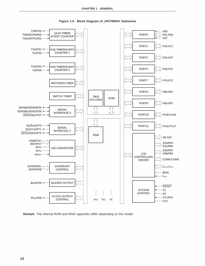
12
CHAPTER 1 GENERAL
Figure 1-4. Block Diagram of µPD78064Y Subseries
Remark The internal ROM and RAM capacities differ depending on the model.
16-bit TIMER/EVENT COUNTER
TO0/P30
ICVDD
TI00/INTP0/P00
VSS
TI01/INTP1/P01
8-bit TIMER/EVENTCOUNTER 1
TO1/P31TI1/P33
8-bit TIMER/EVENTCOUNTER 2
TO2/P32TI2/P34
WATCHDOG TIMER
WATCH TIMER
SERIALINTERFACE 0
SI0/SB0/SDA0/P25SO0/SB1/SDA1/P26
SCK0/SDL/P27
SERIALINTERFACE 2
SI2/RXD/P70SO2/TXD/P71
INTERRUPTCONTROL
INTP0/P00-INTP5/P05
CLOCK OUTPUTCONTROLPCL/P35
A/D CONVERTER
BUZZER OUTPUT
AVDD
AVSS
AVREF
BUZ/P36
ANI0/P10-ANI7/P17
SCK2/ASCK/P72
PORT0P00P01-P05P07
PORT1 P10-P17
PORT2 P25-P27
PORT3 P30-P37
PORT7 P70-P72
PORT8 P80-P87
PORT9 P90-P97
PORT10 P100-P103
P110-P117
SYSTEMCONTROL
S0-S23
BIASfLCD
X2XT1/P07
X1
XT2
RESET
RAM
78K/0CPU CORE ROM
PORT11
S24/P97-S31/P90
S32/P87-S39/P80
COM0-COM3
VLC0-VLC2
LCDCONTROLLER/
DRIVER

13
CHAPTER 1 GENERAL
Table 1-4. Functional Outline of µPD78064Y Subseries
Item
Part Number
Mask ROM
16K bytes 24K bytes 32K bytes
512 bytes 1024 bytes
40 × 4 bits
64K bytes
8 bits × 8 × 4 banks
0.4 µs/0.8 µs/1.6 µs/3.2 µs/6.4 µs/12.8 µs (at 5.0 MHz)
122 µs (at 32.768 kHz)
• 16-bit operation
• Multiplication/division (8 bits × 8 bits, 16 bits ÷ 8 bits)
• Bit manipulation (set, reset, test, Boolean operation)
• BCD adjustment, etc.
• Total : 57
• CMOS input : 2
• CMOS I/O : 55
8-bit resolution × 8 channels
• Segment signal output : 40 max.
• Common signal output : 4 max.
• Bias : 1/2 or 1/3 bias selectable
• 3-wire serial I/O/2-wire serial I/O/I2C bus mode selectable : 1 channel
• 3-wire serial I/O/UART mode selectable : 1 channel
• 16-bit timer/event counter : 1 channel
• 8-bit timer/event counter : 2 channels
• Watch timer : 1 channel
• Watchdog timer : 1 channel
3 (14-bit PWM output: 1)
19.5 kHz, 39.1 kHz, 78.1 kHz, 156 kHz, 313 kHz, 625 kHz, 1.25 MHz, 2.5 MHz, 5.0 MHz (with
main system clock of 5.0 MHz), 32.768 kHz (with subsystem clock of 32.768 kHz)
1.2 kHz, 2.4 kHz, 4.9 kHz, 9.8 kHz (with main system clock of 5.0 MHz)
Internal: 12, external: 6
Internal: 1
1
Internal: 1, external: 1
VDD = 2.0 to 6.0 V
• 100-pin plastic QFP (fine pitch) (14 × 14 mm, resin thickness 1.45 mm)
• 100-pin plastic LQFP (fine pitch) (14 × 14 mm, resin thickness 1.4 mm)
• 100-pin plastic QFP (14 × 20 mm)
ROM
High-speed RAM
LCD display RAM
Memory space
General-purpose register
Minimum With main
instruction system clock
execution With subsystem
time clock
Instruction set
I/O port
(including pins multiplexed
with segment signal output)
A/D converter
LCD controller/driver
Serial interface
Timer
Timer output
Clock output
Buzzer output
Vectored Maskable
interrupt Non-maskable
source Software
Test input
Supply voltage
Package
µPD78062Y µPD78063Y µPD78064Y
Internal
memory

14
CHAPTER 1 GENERAL
Figure 1-5. Block Diagram of µPD78078 Subseries
Remarks 1. The internal ROM capacitiy differs depending on the model.
2. ( ): µPD78P078
16-bit TIMER/EVENT COUNTER
TO0/P30
IC(VPP)
VDD
TI00/INTP0/P00
VSS
TI01/INTP1/P01
8-bit TIMER/EVENTCOUNTER 1
TO1/P31TI1/P33
8-bit TIMER/EVENTCOUNTER 2
TO2/P32TI2/P34
WATCHDOG TIMER
WATCH TIMER
SERIALINTERFACE 0
SI0/SB0/P25SO0/SB1/P26
SCK0/P27
SERIALINTERFACE 1
SI1/P20SO1/P21
SCK1/P22
SERIALINTERFACE 2
SI2/RXD/P70SO2/TXD/P71
INTERRUPTCONTROL
INTP0/P00-INTP6/P06
CLOCK OUTPUTCONTROLPCL/P35
A/D CONVERTER
D/A CONVERTERAVSS
BUZZER OUTPUT
AVDD
AVSS
AVREF0
STB/P23BUSY/P24
BUZ/P36
AVREF1
ANO0/P130,ANO1/P131
ANI0/P10-ANI7/P17
SCK2/ASCK/P72
PORT0P00P01-P06P07
PORT1 P10-P17
PORT2 P20-P27
PORT3 P30-P37
PORT4 P40-P47
PORT5 P50-P57
PORT6 P60-P67
PORT7 P70-P72
PORT8 P80-P87
PORT9 P90-P96
REAL-TIMEOUTPUT PORT
RTP0/P120-RTP7/P127
EXTERNALACCESS
SYSTEMCONTROL
AD0/P40-AD7/P47
A8/P50-A15/P57
WR/P65WAIT/P66
RD/P64
ASTB/P67
X2XT1/P07
X1
XT2
RESET
RAM
78K/0CPU CORE ROM
8-bit TIMER/EVENTCOUNTER 5TI5/TO5/P100
8-bit TIMER/EVENTCOUNTER 6TI6/TO6/P101
PORT10 P100-P103
PORT12 P120-P127
PORT13 P130, P131
A0/P80-A7/P87

15
CHAPTER 1 GENERAL
Table 1-5. Functional Outline of µPD78078 Subseries
Item
Part Number
Mask ROM PROM
48K bytes 60K bytes 60K bytesNote 1
1024 bytes
32 bytes
1024 bytes
64K bytes
8 bits × 8 × 4 banks
0.4 µs/0.8 µs/1.6 µs/3.2 µs/6.4 µs/12.8 µs (at 5.0 MHz)
122 µs (at 32.768 kHz)
• 16-bit operation
• Multiplication/division (8 bits × 8 bits, 16 bits ÷ 8 bits)
• Bit manipulation (set, reset, test, Boolean operation)
• BCD adjustment, etc.
• Total : 88
• CMOS input : 2
• CMOS I/O : 78
• N-ch open-drain I/O : 8
8-bit resolution × 8 channels
8-bit resolution × 2 channels
• 3-wire serial I/O/SBI/2-wire serial I/O mode selectable : 1 channel
• 3-wire serial I/O mode (with function to automatically transfer/receive up to 32 bytes) : 1 channel
• 3-wire serial I/O/UART mode selectable : 1 channel
• 16-bit timer/event counter : 1 channel
• 8-bit timer/event counter : 4 channels
• Watch timer : 1 channel
• Watchdog timer : 1 channel
5 (14-bit PWM output: 1, 8-bit PWM output: 2)
19.5 kHz, 39.1 kHz, 78.1 kHz, 156 kHz, 313 kHz, 625 kHz, 1.25 MHz, 2.5 MHz, 5.0 MHz (with
main system clock of 5.0 MHz), 32.768 kHz (with subsystem clock of 32.768 kHz)
Internal: 15, external: 7
Internal: 1
1
Internal: 1, external: 1
VDD = 1.8 to 5.5 V
• 100-pin plastic QFP (fine pitch) (14 × 14 mm, resin thickness 1.45 mm)
• 100-pin plastic LQFP (fine pitch) (14 × 14 mm, resin thickness 1.4 mm)Note 2
• 100-pin plastic QFP (14 × 20 mm, resin thickness 2.7 mm)
• 100-pin ceramic WQFN (14 × 20 mm) (µPD78P078 only)
Notes 1. The internal ROM capacity can be changed by using a memory size select register (IMS).
2. Under planning
ROM
High-speed RAM
Buffer RAM
Expansion RAM
Memory space
General-purpose register
Minimum With main
instruction system clock
execution With subsystem
timon clock
Instruction set
I/O port
A/D converter
D/A converter
Serial interface
Timer
Timer output
Clock output
Vectored Maskable
interrupt Non-maskable
source Software
Test input
Supply voltage
Package
Internal
memory
µPD78076 µPD78078 µPD78P078

16
CHAPTER 1 GENERAL
Figure 1-6. Block Diagram of µPD78078Y Subseries
Remarks 1. The internal ROM capacity differs depending on the model.
2. ( ): µPD78P078Y
16-bit TIMER/EVENT COUNTER
TO0/P30
IC(VPP)
VDD
TI00/INTP0/P00
VSS
TI01/INTP1/P01
8-bit TIMER/EVENTCOUNTER 1
TO1/P31TI1/P33
8-bit TIMER/EVENTCOUNTER 2
TO2/P32TI2/P34
WATCHDOG TIMER
WATCH TIMER
SERIALINTERFACE 0
SI0/SB0/SDA0/P25SO0/SB1/SDA1/P26
SCK0/SCL/P27
SERIALINTERFACE 1
SI1/P20SO1/P21
SCK1/P22
SERIALINTERFACE 2
SI2/RXD/P70SO2/TXD/P71
INTERRUPTCONTROL
INTP0/P00-INTP6/P06
CLOCK OUTPUTCONTROLPCL/P35
A/D CONVERTER
D/A CONVERTERAVSS
BUZZER OUTPUT
AVDD
AVSS
AVREF0
STB/P23BUSY/P24
BUZ/P36
AVREF1
ANO0/P130,ANO1/P131
ANI0/P10-ANI7/P17
SCK2/ASCK/P72
PORT0P00P01-P06P07
PORT1 P10-P17
PORT2 P20-P27
PORT3 P30-P37
PORT4 P40-P47
PORT5 P50-P57
PORT6 P60-P67
PORT7 P70-P72
PORT8 P80-P87
PORT9 P90-P96
REAL-TIMEOUTPUT PORT
RTP0/P120-RTP7/P127
EXTERNALACCESS
SYSTEMCONTROL
AD0/P40-AD7/P47
A8/P50-A15/P57
WR/P65WAIT/P66
RD/P64
ASTB/P67
X2XT1/P07
X1
XT2
RESET
RAM
78K/0CPU CORE ROM
8-bit TIMER/EVENTCOUNTER 5TI5/TO5/P100
8-bit TIMER/EVENTCOUNTER 6TI6/TO6/P101
PORT10 P100-P103
PORT12 P120-P127
PORT13 P130, P131
A0/P80-A7/P87

17
CHAPTER 1 GENERAL
Table 1-6. Functional Outline of µPD78078Y Subseries
Item
Part Number
Mask ROM PROM
48K bytes 60K bytes 60K bytesNote 1
1024 bytes
32 bytes
1024 bytes
64K bytes
8 bits × 8 × 4 banks
0.4 µs/0.8 µs/1.6 µs/3.2 µs/6.4 µs/12.8 µs (at 5.0 MHz)
122 µs (at 32.768 kHz)
• 16-bit operation
• Multiplication/division (8 bits × 8 bits, 16 bits ÷ 8 bits)
• Bit manipulation (set, reset, test, Boolean operation)
• BCD adjustment, etc.
• Total : 88
• CMOS input : 2
• CMOS I/O : 78
• N-ch open-drain I/O : 8
8-bit resolution × 8 channels
8-bit resolution × 2 channels
• 3-wire serial I/O/2-wire serial I/O/I2C bus mode selectable : 1 channel
• 3-wire serial I/O mode (with function to automatically transfer/receive up to 32 bytes) : 1 channel
• 3-wire serial I/O/UART mode selectable : 1 channel
• 16-bit timer/event counter : 1 channel
• 8-bit timer/event counter : 4 channels
• Watch timer : 1 channel
• Watchdog timer : 1 channel
5 (14-bit PWM output: 1, 8-bit PWM output: 2)
19.5 kHz, 39.1 kHz, 78.1 kHz, 156 kHz, 313 kHz, 625 kHz, 1.25 MHz, 2.5 MHz, 5.0 MHz (with
main system clock of 5.0 MHz), 32.768 kHz (with subsystem clock of 32.768 kHz)
1.2 kHz, 2.4 kHz, 4.9 kHz, 9.8 kHz (with main system clock of 5.0 MHz)
Internal: 15, external: 7
Internal: 1
1
Internal: 1, external: 1
VDD = 1.8 to 5.5 V
• 100-pin plastic QFP (14 × 20 mm, resin thickness 2.7 mm)
• 100-pin plastic LQFP (fine pitch) (14 × 14 mm, resin thickness 1.4 mm)Note 2
• 100-pin ceramic WQFN (14 × 20 mm) (µPD78P078Y only)
Notes 1. The internal ROM capacity can be changed by using a memory size select register (IMS).
2. Under development
ROM
High-speed RAM
Buffer RAM
Expansion RAM
Memory space
General-purpose register
Minimum With main
instruction system clock
execution With subsystem
time clock
Instruction set
I/O port
A/D converter
D/A converter
Serial interface
Timer
Timer output
Clock output
Buzzer output
Vectored Maskable
interrupt Non-maskable
source Software
Test input
Supply voltage
Package
Internal
memory
µPD78076Y µPD78078Y µPD78P078Y

18
CHAPTER 1 GENERAL
Figure 1-7. Block Diagram of µPD78083 Subseries
Remarks 1. The internal ROM and RAM capacities differ depending on the model.
2. ( ): µPD78P083
8-bit TIMER/EVENT COUNTER 5
IC(VPP)
VDD
TI5/TO5/P100
VSS
WATCHDOG TIMER
SERIALINTERFACE 2
SI2/RxD/P70SO2/TxD/P71
SCK2/ASCK/P72
INTERRUPTCONTROL
INTP1/P01-INTP3/P03
CLOCK OUTPUTCONTROLPCL/P35
A/D CONVERTER
BUZZER OUTPUT
AVDD
AVSS
AVREF1
BUZ/P36
ANI0/P10-ANI7/P17
PORT0P00
P01-P03
PORT1 P10-P17
SYSTEMCONTROL
X2X1RESET
RAM
78K/0CPU CORE ROM
5-bit TIMER/EVENT COUNTER 6TI6/TO6/P101
PORT3 P30-P37
PORT5 P50-P57
PORT7 P70-P72
PORT10 P100, P101

19
CHAPTER 1 GENERAL
Table 1-7. Functional Outline of µPD78083 Subseries
Item
Part Number
Mask ROM PROM
8K bytes 16K bytes 24K bytesNote 1
256 bytes 384 bytes 512 bytesNote 1
64K bytes
8 bits × 8 × 4 banks
0.4 µs/0.8 µs/1.6 µs/3.2 µs/6.4 µs/12.8 µs
(with main system clock of 5.0 MHz)
• 16-bit operation
• Multiplication/division (8 bits × 8 bits, 16 bits ÷ 8 bits)
• Bit manipulation (set, reset, test, Boolean operation)
• BCD adjustment, etc.
• Total : 33
• CMOS input : 1
• CMOS I/O : 32
8-bit resolution × 8 channels
3-wire serial I/O/UART mode selectable: 1 channel
• 8-bit timer/event counter : 2 channels
• Watchdog timer : 1 channel
2 (8-bit PWM output)
19.5 kHz, 39.1 kHz, 78.1 kHz, 156 kHz, 313 kHz, 625 kHz, 1.25 MHz, 2.5 MHz, 5.0 MHz
(with main system clock of 5.0 MHz)
1.2 kHz, 2.4 kHz, 4.9 kHz, 9.8 kHz (with main system clock of 5.0 MHz)
Internal: 8, external: 3
Internal: 1
1
VDD = 1.8 to 5.5 VNote 2
• 42-pin plastic shrink DIP (600 mil)
• 42-pin ceramic shrink DIP (with window) (600 mil) (µPD78P083 only)
• 44-pin plastic QFP (10 × 10 mm)
Notes 1. The capacities of the internal PROM and internal-high-speed RAM can be changed by using a memory
size select register. (IMS)
2. The supply voltage (VDD) of the µPD78081(A2) is 4.5 to 5.5 V.
Internal
memory
µPD78081 µPD78082 µPD78P083
ROM
High-speed RAM
Memory space
General-purpose register
Minimum instruction
execution time
Instruction set
I/O port
A/D converter
Serial interface
Timer
Timer output
Clock output
Buzzer output
Vectored Maskable
interrupt Non-maskable
source Software
Supply voltage
Package

20
CHAPTER 1 GENERAL
Figure 1-8. Block Diagram of µPD78098 Subseries
Remarks 1. The internal ROM and RAM capacities differ depending on the model.
2. ( ): µPD78P098A
TX/P124/RTP4RX/P125/RTP5
16-bit TIMER/EVENT COUNTER
TO0/P30
IC(VPP)
VDD
TI00/INTP0/P00
VSS
TI01/INTP1/P01
8-bit TIMER/EVENTCOUNTER 1
TO1/P31TI1/P33
8-bit TIMER/EVENTCOUNTER 2
TO2/P32TI2/P34
WATCHDOG TIMER
WATCH TIMER
SERIALINTERFACE 0
SI0/SB0/P25SO0/SB1/P26
SCK0/P27
SERIALINTERFACE 1
SI1/P20SO1/P21
SCK1/P22
SERIALINTERFACE 2
SI2/RXD/P70SO2/TXD/P71
INTERRUPTCONTROL
INTP0/P00-INTP6/P06
CLOCK OUTPUTCONTROLPCL/P35
A/D CONVERTER
D/A CONVERTERAVSS
BUZZER OUTPUT
AVDD
AVSS
AVREF1
STB/P23BUSY/P24
BUZ/P36
AVREF0
ANO0/P130,ANO1/P131
ANI0/P10-ANI7/P17
SCK2/ASCK/P72
PORT0P00P01-P06P07
PORT1 P10-P17
PORT2 P20-P27
PORT3 P30-P37
PORT4 P40-P47
PORT5 P50-P57
PORT6 P60-P67
PORT7 P70-P72
PORT12 P120-P127
PORT13 P130, P131
REAL-TIMEOUTPUT PORT
RTP0/P120-RTP7/P127
EXTERNALACCESS
SYSTEMCONTROL
AD0/P40-AD7/P47A8/P50-A15/P57
WR/P65WAIT/P66
RD/P64
ASTB/P67
X2XT1/P07
X1
XT2
RESET
RAM
78K/0CPU CORE ROM
IEBusCONTROLLER

21
CHAPTER 1 GENERAL
ROM
High-speed RAM
Buffer RAM
Expansion RAM
Memory space
General-purpose register
Minimum With main
instruction system clock
execution With subsystem
time clock
Instruction set
I/O port
IEBus controller
A/D converter
D/A converter
Serial interface
Timer
Timer output
Clock output
Table 1-8. Functional Outline of µPD78098 Subseries (1/2)
Item
Part Number
Mask ROM PROM
32K bytes 40K bytes 48K bytes 60K bytes 60K bytesNote 3
1024 bytes
32 bytes
None 2048 bytes 2048 bytesNote 4
64K bytes
8 bits × 8 × 4 banks
0.5 µs/1.0 µs/2.0 µs/4.0 µs/8.0 µs/16.0 (at 6.0 MHz)
122 µs (at 32.768 kHz)
• 16-bit operation
• Multiplication/division (8 bits × 8 bits, 16 bits ÷ 8 bits)
• Bit manipulation (set, reset, test, Boolean operation)
• BCD adjustment, etc.
• Total : 69
• CMOS input : 2
• CMOS I/O : 63
• N-ch open-drain I/O: 4
Effective transfer rate: 3.9 kbps/17 kbps/26 kbps
8-bit resolution × 8 channels
8-bit resolution × 2 channels
• 3-wire serial I/O/SBI/2-wire serial I/O mode selectable : 1 channel
• 3-wire serial I/O mode (with function to automatically transfer/receive up to 32 bytes) : 1 channel
• 3-wire serial I/O/UART mode selectable : 1 channel
• 16-bit timer/event counter : 1 channel
• 8-bit timer/event counter : 2 channels
• Watch timer : 1 channel
• Watchdog timer : 1 channel
3 (14-bit PWM output: 1)
15.6 kHz, 31.3 kHz, 62.5 kHz, 125 kHz, 250 kHz, 500 kHz, 1.0 MHz, 2.0 MHz, 4.0 MHz (with
main system clock of 6.0 MHz), 32.768 kHz (with subsystem clock of 32.768 kHz)
Notes 1. Under development
2. The µPD78P098A is the PROM model of the µPD78094, 78095, 78096, and 78098A.
3. The internal PROM capacity can be changed by using a memory size select register (IMS).
4. The internal expansion RAM can be changed by using an internal expansion RAM size select register
(IXS).
Internal
memory
µPD78094 µPD78095 µPD78096 µPD78098ANote 1 µPD78P098ANote 1, 2

22
CHAPTER 1 GENERAL
Table 1-8. Functional Outline of µPD78098 Subseries (2/2)
Item
Part Number
977 Hz, 1.95 kHz, 3.9 kHz, 7.8 kHz (with main system clock of 6.0 MHz)
Internal: 14, external: 7
Internal: 1
1
Internal: 1, external: 1
VDD = 2.7 to 6.0 V
• 80-pin plastic QFP (14 × 14 mm)
• 80-pin ceramic WQFN (14 × 14 mm)Note 1 (µPD78P098A only)
Notes 1. Under development
2. The µPD78P098A is a PROM model of the µPD78094, 78095, 78096, and 78098A.
µPD78094 µPD78095 µPD78096 µPD78098ANote 1 µPD78P098ANote 1, 2
Buzzer output
Vectored Maskable
interrupt Non-maskable
source Software
Test input
Supply voltage
Package

23
CHAPTER 1 GENERAL
Figure 1-9. Block Diagram of µPD780018 Subseries
Remarks 1. The internal ROM capacity differs depending on the model.
2. ( ): µPD78P0018
16-bit TIMER/EVENT COUNTER
TO0/P30
IC(VPP)
VDD0,VDD1
TI00/INTP0/P00
VSS0,VSS1
TI01/INTP1/P01
8-bit TIMER/EVENTCOUNTER 1
TO1/P31TI1/P33
8-bit TIMER/EVENTCOUNTER 2
TO2/P32TI2/P34
WATCHDOG TIMER
WATCH TIMER
SERIALINTERFACE 1
SI1/P20SO1/P21
SCK1/P22
INTERRUPTCONTROL
INTP0/P00-INTP6/P06
CLOCK OUTPUTCONTROLPCL/P35
A/D CONVERTER
BUZZER OUTPUT
AVSS
AVREF
STB/P23BUSY/P24
BUZ/P36
ANI0/P10-ANI7/P17
PORT0P00P01-P06
PORT1 P10-P17
PORT2 P20-P27
PORT3 P30-P37
PORT4 P40-P47
PORT5 P50-P57
PORT6 P60-P67
PORT8 P80-P87
PORT9 P90-P96
EXTERNALACCESS
SYSTEMCONTROL
AD0/P40-AD7/P47
A8/P50-A15/P57
WR/P65WAIT/P66
RD/P64
ASTB/P67
X2XT1
X1
XT2
RESET
RAM
78K/0CPU CORE ROM
8-bit TIMER/EVENTCOUNTER 5TI5/TO5/P100
8-bit TIMER/EVENTCOUNTER 6TI6/TO6/P101
PORT10 P100-P103
PORT11 P110-P117
PORT15 P150-P156
A0/P80-A7/P87
SERIALINTERFACE 4
SI4A/P90
SO4A/P91
SCK4A/P92
SI4B/P93
SO4B/P94
SCK4B/P95
SI4C/P110
SO4C/P111
SCK4C/P112

24
CHAPTER 1 GENERAL
Table 1-9. Functional Outline of µPD780018 Subseries (1/2)
Item
Part Number
Mask ROM PROM
48K bytes 60K bytes 60K bytesNote
1024 bytes
32 bytes
1024 bytes
64K bytes
8 bits × 8 × 4 banks
0.4 µs/0.8 µs/1.6 µs/3.2 µs/6.4 µs (at 5.0 MHz)
122 µs (at 32.768 kHz)
• 16-bit operation
• Multiplication/division (8 bits × 8 bits, 16 bits ÷ 8 bits)
• Bit manipulation (set, reset, test, Boolean operation)
• BCD adjustment, etc.
• Total : 88
• CMOS input : 9
• CMOS I/O : 79
8-bit resolution × 8 channels
• 3-wire serial I/O mode (with automatical transfer/reception function) : 1 channel
• 3-wire serial I/O mode selectable (with time-division transfer function) : 1 channel
• 16-bit timer/event counter : 1 channel
• 8-bit timer/event counter : 4 channels
• Watch timer : 1 channel
• Watchdog timer : 1 channel
5 (14-bit PWM output: 1, 8-bit PWM output: 2)
39.1 kHz, 78.1 kHz, 156 kHz, 313 kHz, 625 kHz, 1.25 MHz, 2.5 MHz, 5.0 MHz (with main
system clock of 5.0 MHz), 32.768 kHz (with subsystem clock of 32.768 kHz)
Note The internal ROM capacity can be changed by using a memory size select register. (IMS)
Caution The µPD780018 subseries is under planning.
ROM
High-speed RAM
Buffer RAM
Expansion RAM
Memory space
General-purpose register
Minimum With main
instruction system clock
execution With subsystem
time clock
Instruction set
I/O port
A/D converter
Serial interface
Timer
Timer output
Clock output
Internal
memory
µPD780016 µPD780018 µPD78P0018

25
CHAPTER 1 GENERAL
Table 1-9. Functional Outline of µPD780018 Subseries (2/2)
Item
Part Number
2.4 kHz, 4.9 kHz, 9.8 kHz (with main system clock of 5.0 MHz)
Internal: 12, external: 7
Internal: 1
1
Internal: 1, external: 1
VDD = 2.7 to 5.5 V
TA = –40 to +85 °C
• 100-pin plastic QFP (14 × 20 mm)
• 100-pin ceramic WQFN (14 × 20 mm) (µPD78P0018 only)
Caution The µPD780018 subseries is under planning.
Buzzer output
Vectored Maskable
interrupt Non-maskable
source Software
Test input
Supply voltage
Operating temperature
Package
µPD780016 µPD780018 µPD78P0018
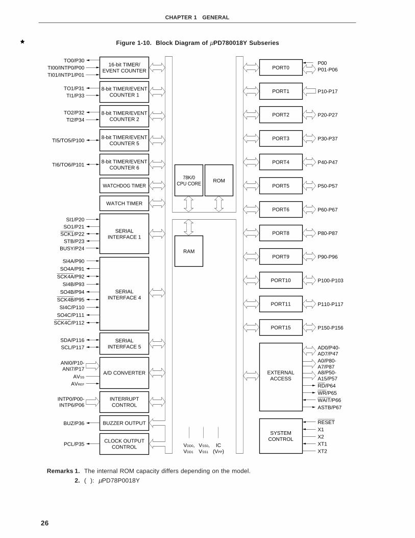
26
CHAPTER 1 GENERAL
Figure 1-10. Block Diagram of µPD780018Y Subseries
Remarks 1. The internal ROM capacity differs depending on the model.
2. ( ): µPD78P0018Y
16-bit TIMER/EVENT COUNTER
TO0/P30
IC(VPP)
VDD0,VDD1
TI00/INTP0/P00
VSS0,VSS1
TI01/INTP1/P01
8-bit TIMER/EVENTCOUNTER 1
TO1/P31TI1/P33
8-bit TIMER/EVENTCOUNTER 2
TO2/P32TI2/P34
WATCHDOG TIMER
WATCH TIMER
SERIALINTERFACE 1
SI1/P20SO1/P21
SCK1/P22
INTERRUPTCONTROL
INTP0/P00-INTP6/P06
CLOCK OUTPUTCONTROLPCL/P35
A/D CONVERTER
BUZZER OUTPUT
AVSS
AVREF
STB/P23BUSY/P24
BUZ/P36
ANI0/P10-ANI7/P17
PORT0P00P01-P06
PORT1 P10-P17
PORT2 P20-P27
PORT3 P30-P37
PORT4 P40-P47
PORT5 P50-P57
PORT6 P60-P67
PORT8 P80-P87
PORT9 P90-P96
EXTERNALACCESS
SYSTEMCONTROL
AD0/P40-AD7/P47
A8/P50-A15/P57
WR/P65WAIT/P66
RD/P64
ASTB/P67
X2XT1
X1
XT2
RESET
RAM
78K/0CPU CORE ROM
8-bit TIMER/EVENTCOUNTER 5TI5/TO5/P100
8-bit TIMER/EVENTCOUNTER 6TI6/TO6/P101
PORT10 P100-P103
PORT11 P110-P117
PORT15 P150-P156
A0/P80-A7/P87
SERIALINTERFACE 4
SI4A/P90
SO4A/P91
SCK4A/P92
SI4B/P93
SO4B/P94
SCK4B/P95
SI4C/P110
SO4C/P111
SCK4C/P112
SERIALINTERFACE 5
SDA/P116SCL/P117

27
CHAPTER 1 GENERAL
Table 1-10. Functional Outline of µPD780018Y Subseries (1/2)
Item
Part Number
Mask ROM PROM
48K bytes 60K bytes 60K bytesNote
1024 bytes
32 bytes
1024 bytes
64K bytes
8 bits × 8 × 4 banks
0.4 µs/0.8 µs/1.6 µs/3.2 µs/6.4 µs (at 5.0 MHz)
122 µs (at 32.768 kHz)
• 16-bit operation
• Multiplication/division (8 bits × 8 bits, 16 bits ÷ 8 bits)
• Bit manipulation (set, reset, test, Boolean operation)
• BCD adjustment, etc.
• Total : 88
• CMOS input : 9
• CMOS I/O : 79
8-bit resolution × 8 channels
• 3-wire serial I/O mode (with automatical transfer/reception function) : 1 channel
• 3-wire serial I/O mode selectable (with time-division transfer function) : 1 channel
• I2C bus mode (multi-master compatible) : 1 channel
• 16-bit timer/event counter : 1 channel
• 8-bit timer/event counter : 4 channels
• Watch timer : 1 channel
• Watchdog timer : 1 channel
5 (14-bit PWM output: 1, 8-bit PWM output: 2)
39.1 kHz, 78.1 kHz, 156 kHz, 313 kHz, 625 kHz, 1.25 MHz, 2.5 MHz, 5.0 MHz (with main
system clock of 5.0 MHz), 32.768 kHz (with subsystem clock of 32.768 kHz)
Note The internal PROM capacity can be changed by using a memory size select register. (IMS)
Caution The µPD780018Y subseries is under development.
ROM
High-speed RAM
Buffer RAM
Expansion RAM
Memory space
General-purpose register
Minimum With main
instruction system clock
execution With subsystem
time clock
Instruction set
I/O port
A/D converter
Serial interface
Timer
Timer output
Clock output
Internal
memory
µPD780016Y µPD780018Y µPD78P018Y
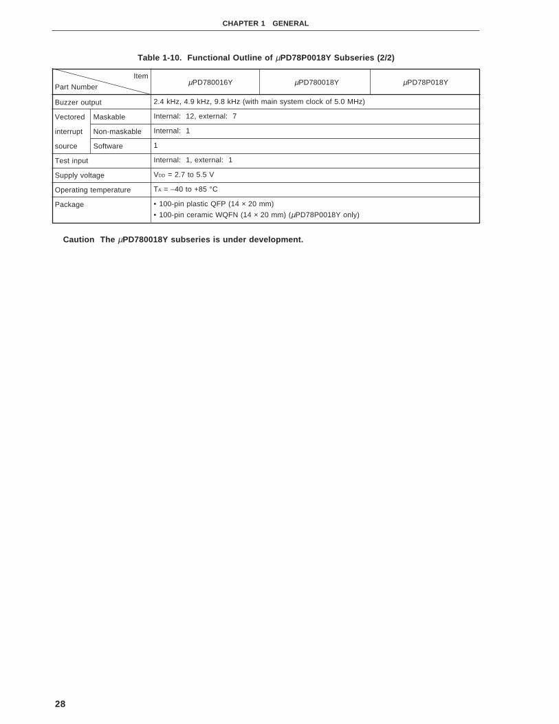
28
CHAPTER 1 GENERAL
Buzzer output
Vectored Maskable
interrupt Non-maskable
source Software
Test input
Supply voltage
Operating temperature
Package
Table 1-10. Functional Outline of µPD78P0018Y Subseries (2/2)
Item
Part Number
2.4 kHz, 4.9 kHz, 9.8 kHz (with main system clock of 5.0 MHz)
Internal: 12, external: 7
Internal: 1
1
Internal: 1, external: 1
VDD = 2.7 to 5.5 V
TA = –40 to +85 °C
• 100-pin plastic QFP (14 × 20 mm)
• 100-pin ceramic WQFN (14 × 20 mm) (µPD78P0018Y only)
Caution The µPD780018Y subseries is under development.
µPD780016Y µPD780018Y µPD78P018Y

29
CHAPTER 1 GENERAL
Figure 1-11. Block Diagram of µPD780058 Subseries
Remarks 1. The capacities of the internal ROM and RAM differ depending on the model.
2. ( ): µPD78F0058
16-bit TIMER/EVENT COUNTER
TO0/P30
IC(VPP)
VDD0,VDD1
TI00/INTP0/P00
VSS0,VSS1
TI01/INTP1/P01
8-bit TIMER/EVENTCOUNTER 1
TO1/P31TI1/P33
8-bit TIMER/EVENTCOUNTER 2
TO2/P32TI2/P34
WATCHDOG TIMER
WATCH TIMER
SERIALINTERFACE 0
SI0/SB0/P25SO0/SB1/P26
SCK0/P27
SERIALINTERFACE 1
SI1/P20SO1/P21
SCK1/P22
SERIALINTERFACE 2
INTERRUPTCONTROL
INTP0/P00-INTP5/P05
CLOCK OUTPUTCONTROLPCL/P35
A/D CONVERTER
D/A CONVERTERAVSS
BUZZER OUTPUT
AVSS
AVREF0
STB/TxD1/P23BUSY/RxD1/P24
BUZ/P36
AVREF1
ANO0/P130,ANO1/P131
ANI0/P10-ANI7/P17
PORT0P00P01-P05P07
PORT1 P10-P17
PORT2 P20-P27
PORT3 P30-P37
PORT4 P40-P47
PORT5 P50-P57
PORT6 P60-P67
PORT7 P70-P72
PORT12 P120-P127
PORT13 P130, P131
REAL-TIMEOUTPUT PORT
RTP0/P120-RTP7/P127
EXTERNALACCESS
SYSTEMCONTROL
AD0/P40-AD7/P47A8/P50-A15/P57
WR/P65WAIT/P66
RD/P64
ASTB/P67
X2XT1/P07
X1
XT2
RESET
RAM
78K/0CPU CORE
ROMFLASH
MEMORY
BUSY/RxD1/P24STB/TxD1/P23SI2/RxD0/P70
SO2/TxD0/P71SCK2/ASCK/P72

30
CHAPTER 1 GENERAL
Table 1-11. Functional Outline of µPD780058 Subseries (1/2)
Item
Part Number
Mask ROM Flash memory
24K bytes 32K bytes 40K bytes 48K bytes 60K bytes 60K bytesNote 1
1024 bytes
32 bytes
None 1024 bytes 1024 bytesNote 2
64K bytes
8 bits × 8 × 4 banks
0.4 µs/0.8 µs/1.6 µs/3.2 µs/6.4 µs/12.8 µs (at 5.0 MHz)
122 µs (at 32.768 kHz)
• 16-bit operation
• Multiplication/division (8 bits × 8 bits, 16 bits ÷ 8 bits)
• Bit manipulation (set, reset, test, Boolean operation)
• BCD adjustment, etc.
• Total : 68
• CMOS input : 2
• CMOS I/O : 62
• N-ch open-drain I/O : 4
8-bit resolution × 8 channels
8-bit resolution × 2 channels
• 3-wire serial I/O/SBI/2-wire serial I/O mode selectable : 1 channel
• 3-wire serial I/O mode (with function to automatically transfer/receive up to 32 bytes) : 1 channel
• 3-wire serial I/O/UART mode selectable (with time-division transfer function) : 1 channel
• 16-bit timer/event counter : 1 channel
• 8-bit timer/event counter : 2 channels
• Watch timer : 1 channel
• Watchdog timer : 1 channel
3 (14-bit PWM output: 1)
19.5 kHz, 39.1 kHz, 78.1 kHz, 156 kHz, 313 kHz, 625 kHz, 1.25 MHz, 2.5 MHz, 5.0 MHz (with
main system clock of 5.0 MHz), 32.768 kHz (with subsystem clock of 32.768 kHz)
Notes 1. The capacities of the flash memory can be changed by using a memory size select register (IMS).
2. The internal expansion RAM capacity can be changed by using an internal expansion RAM size select
register (IXS).
Caution The µPD780058 subseries is under development.
ROM
High-speed RAM
Buffer RAM
Expansion RAM
Memory space
General-purpose register
Minimum With main
instruction system clock
execution With subsystem
time clock
Instruction set
I/O port
A/D converter
D/A converter
Serial interface
Timer
Timer output
Clock output
Internal
memory
µPD780053 µPD780054 µPD780055 µPD780056 µPD780058 µPD78F0058

31
CHAPTER 1 GENERAL
Table 1-11. Functional Outline of µPD780058 Subseries (2/2)
Item
Part Number
1.2 kHz, 2.4 kHz, 4.9 kHz, 9.8 kHz (with main system clock of 5.0 MHz)
Internal: 13, external: 7
Internal: 1
1
Internal: 1, external: 1
VDD = 1.8 to 5.5 V
TA = –40 to +85 °C
• 80-pin plastic QFP (14 × 14 mm, resin thickness 2.7 mm)
• 80-pin plastic QFP (14 × 14 mm, resin thickness 1.4 mm)Note
• 80-pin plastic TQFP (fine pitch) (12 × 12 mm)
Note Under planning
Caution The µPD780058 subseries is under development.
Buzzer output
Vectored Maskable
interrupt Non-maskable
source Software
Test input
Supply voltage
Operating temperature
Package
µPD780053 µPD780054 µPD780055 µPD780056 µPD780058 µPD78F0058

32
CHAPTER 1 GENERAL
Figure 1-12. Block Diagram of µPD780058Y Subseries
Remarks 1. The capacities of the internal ROM and RAM differ depending on the model.
2. ( ): µPD78F0058Y
16-bit TIMER/EVENT COUNTER
TO0/P30
IC(VPP)
VDD0,VDD1
TI00/INTP0/P00
VSS0,VSS1
TI01/INTP1/P01
8-bit TIMER/EVENTCOUNTER 1
TO1/P31TI1/P33
8-bit TIMER/EVENTCOUNTER 2
TO2/P32TI2/P34
WATCHDOG TIMER
WATCH TIMER
SERIALINTERFACE 0
SI0/SB0/SDA0/P25SO0/SB1/SDA1/P26
SCK0/SCL/P27
SERIALINTERFACE 1
SI1/P20SO1/P21
SCK1/P22
SERIALINTERFACE 2
INTERRUPTCONTROL
INTP0/P00-INTP5/P05
CLOCK OUTPUTCONTROLPCL/P35
A/D CONVERTER
D/A CONVERTERAVSS
BUZZER OUTPUT
AVSS
AVREF0
STB/TxD1/P23BUSY/RxD1/P24
BUZ/P36
AVREF1
ANO0/P130,ANO1/P131
ANI0/P10-ANI7/P17
PORT0P00P01-P05P07
PORT1 P10-P17
PORT2 P20-P27
PORT3 P30-P37
PORT4 P40-P47
PORT5 P50-P57
PORT6 P60-P67
PORT7 P70-P72
PORT12 P120-P127
PORT13 P130, P131
REAL-TIMEOUTPUT PORT
RTP0/P120-RTP7/P127
EXTERNALACCESS
SYSTEMCONTROL
AD0/P40-AD7/P47A8/P50-A15/P57
WR/P65WAIT/P66
RD/P64
ASTB/P67
X2XT1/P07
X1
XT2
RESET
RAM
78K/0CPU CORE
ROMFLASH
MEMORY
BUSY/RxD1/P24STB/TxD1/P23SI2/RxD0/P70
SO2/TxD0/P71SCK2/ASCK/P72

33
CHAPTER 1 GENERAL
Table 1-12. Functional Outline of µPD780058Y Subseries (1/2)
Item
Part Number
Mask ROM Flash memory
24K bytes 32K bytes 40K bytes 48K bytes 60K bytes 60K bytesNote 1
1024 bytes
32 bytes
None 1024 bytes 1024 bytesNote 2
64K bytes
8 bits × 8 × 4 banks
0.4 µs/0.8 µs/1.6 µs/3.2 µs/6.4 µs/12.8 µs (at 5.0 MHz)
122 µs (at 32.768 kHz)
• 16-bit operation
• Multiplication/division (8 bits × 8 bits, 16 bits ÷ 8 bits)
• Bit manipulation (set, reset, test, Boolean operation)
• BCD adjustment, etc.
• Total : 68
• CMOS input : 2
• CMOS I/O : 62
• N-ch open-drain I/O : 4
8-bit resolution × 8 channels
8-bit resolution × 2 channels
• 3-wire serial I/O/2-wire serial I/O/I2C bus mode selectable : 1 channel
• 3-wire serial I/O mode (with function to automatically transfer/receive up to 32 bytes) : 1 channel
• 3-wire serial I/O/UART mode selectable (with time-division transfer function) : 1 channel
• 16-bit timer/event counter : 1 channel
• 8-bit timer/event counter : 2 channels
• Watch timer : 1 channel
• Watchdog timer : 1 channel
3 (14-bit PWM output: 1)
19.5 kHz, 39.1 kHz, 78.1 kHz, 156 kHz, 313 kHz, 625 kHz, 1.25 MHz, 2.5 MHz, 5.0 MHz (with
main system clock of 5.0 MHz), 32.768 kHz (with subsystem clock of 32.768 kHz)
Notes 1. The capacities of the flash memory can be changed by using a memory size select register (IMS).
2. The internal expansion RAM capacity can be changed by using an internal expansion RAM size select
register (IXS).
Caution The µPD780058Y subseries is under planning.
ROM
High-speed RAM
Buffer RAM
Expansion RAM
Memory space
General-purpose register
Minimum With main
instruction system clock
execution With subsystem
time clock
Instruction set
I/O port
A/D converter
D/A converter
Serial interface
Timer
Timer output
Clock output
Internal
memory
µPD780053Y µPD780054Y µPD780055Y µPD780056Y µPD780058Y µPD78F0058Y

34
CHAPTER 1 GENERAL
Table 1-12. Functional Outline of µPD780058Y Subseries (2/2)
Item
Part Number
1.2 kHz, 2.4 kHz, 4.9 kHz, 9.8 kHz (with main system clock of 5.0 MHz)
Internal: 13, external: 7
Internal: 1
1
Internal: 1, external: 1
VDD = 1.8 to 5.5 V
TA = –40 to +85 °C
• 80-pin plastic QFP (14 × 14 mm, resin thickness 2.7 mm)
• 80-pin plastic QFP (14 × 14 mm, resin thickness 1.4 mm)
• 80-pin plastic TQFP (fine pitch) (12 × 12 mm)
Caution The µPD780058Y subseries is under planning.
Buzzer output
Vectored Maskable
interrupt Non-maskable
Software
Test input
Supply voltage
Operating temperature
Package
µPD780053Y µPD780054Y µPD780055Y µPD780056Y µPD780058Y µPD78F0058Y

35
CHAPTER 1 GENERAL
Figure 1-13. Block Diagram of µPD780308 Subseries
Remarks 1. The internal ROM capacity differs depending on the model.
2. ( ): µPD78P0308
16-bit TIMER/EVENT COUNTER
TO0/P30
IC(VPP)
VDD0,VDD1,
TI00/INTP0/P00
VSS0,VSS1,
TI01/INTP1/P01
8-bit TIMER/EVENTCOUNTER 1
TO1/P31TI1/P33
8-bit TIMER/EVENTCOUNTER 2
TO2/P32TI2/P34
WATCHDOG TIMER
WATCH TIMER
SERIALINTERFACE 0
SI0/SB0/P25SO0/SB1/P26
SCK0/P27
SERIALINTERFACE 2
SI2/RXD/P70SO2/TXD/P71
INTERRUPTCONTROL
INTP0/P00-INTP5/P05
CLOCK OUTPUTCONTROLPCL/P35
A/D CONVERTER
BUZZER OUTPUT
AVDD
AVSS
AVREF
BUZ/P36
ANI0/P10-ANI7/P17
SCK2/ASCK/P72
PORT0P00P01-P05P07
PORT1 P10-P17
PORT2 P25-P27
PORT3 P30-P37
PORT7 P70-P72
PORT8 P80-P87
PORT9 P90-P97
PORT10 P100-P103
P110-P117
SYSTEMCONTROL
S0-S23
BIASfLCD
X2XT1/P07
X1
XT2
RESET
RAM
78K/0CPU CORE ROM
PORT11
S24/P97-S31/P90
S32/P87-S39/P80
COM0-COM3
VLC0-VLC2
LCDCONTROLLER/
DRIVER
RXD/P114TXD/P113
SERIALINTERFACE 3
SI3/P110SO3/P111
SCK3/P112

36
CHAPTER 1 GENERAL
Table 1-13. Functional Outline of µPD780308 Subseries
Item
Part Number
Mask ROM PROM
48K bytes 60K bytes 60K bytesNote
1024 bytes
1024 bytes
40 × 4 bits
64K bytes
8 bits × 8 × 4 banks
0.4 µs/0.8 µs/1.6 µs/3.2 µs/6.4 µs/12.8 µs (at 5.0 MHz)
122 µs (at 32.768 kHz)
• 16-bit operation
• Multiplication/division (8 bits × 8 bits, 16 bits ÷ 8 bits)
• Bit manipulation (set, reset, test, Boolean operation)
• BCD adjustment, etc.
• Total : 57
• CMOS input : 2
• CMOS I/O : 55
8-bit resolution × 8 channels
• Segment signal output : 40 max.
• Common signal output : 4 max.
• Bias : 1/2 or 1/3 bias selectable
• 3-wire serial I/O/SBI/2-wire serial I/O mode selectable : 1 channel
• 3-wire serial I/O/UART mode selectable : 1 channel
• 3-wire serial I/O mode : 1 channel
• 16-bit timer/event counter : 1 channel
• 8-bit timer/event counter : 2 channels
• Watch timer : 1 channel
• Watchdog timer : 1 channel
3 (14-bit PWM output: 1)
19.5 kHz, 39.1 kHz, 78.1 kHz, 156 kHz, 313 kHz, 625 kHz, 1.25 MHz, 2.5 MHz, 5.0 MHz (with
main system clock of 5.0 MHz), 32.768 kHz (with subsystem clock of 32.768 kHz)
1.2 kHz, 2.4 kHz, 4.9 kHz, 9.8 kHz (with main system clock of 5.0 MHz)
Internal: 13, external: 6
Internal: 1
1
Internal: 1, external: 1
VDD = 2.0 to 5.5 V
• 100-pin plastic QFP (fine pitch) (14 × 14 mm)
• 100-pin plastic QFP (14 × 20 mm)
• 100-pin ceramic WQFN (14 × 20 mm) (µPD78P0308 only)
Note The capacity of the internal PROM can be changed by using a memory size select register (IMS).
Caution The µPD780308 subseries is under development.
ROM
High-speed RAM
Expansion RAM
LCD display RAM
Memory space
General-purpose register
Minimum With main
instruction system clock
execution With subsystem
time clock
Instruction set
I/O port
(including pins multiplexed
with segment signal output)
A/D converter
LCD controller/driver
Serial interface
Timer
Timer output
Clock output
Buzzer output
Vectored Maskable
interrupt Non-maskable
Software
Test input
Supply voltage
Package
Internal
memory
µPD780306 µPD780308 µPD78P0308

37
CHAPTER 1 GENERAL
Figure 1-14. Block Diagram of µPD780308Y Subseries
Remarks 1. The internal ROM capacity differs depending on the model.
2. ( ): µPD78P0308Y
16-bit TIMER/EVENT COUNTER
TO0/P30
ICVDD0,VDD1,
TI00/INTP0/P00
VSS0,VSS1,
TI01/INTP1/P01
8-bit TIMER/EVENTCOUNTER 1
TO1/P31TI1/P33
8-bit TIMER/EVENTCOUNTER 2
TO2/P32TI2/P34
WATCHDOG TIMER
WATCH TIMER
SERIALINTERFACE 0RxD/P114
TxD/P113SCK0/SDL/P27
SERIALINTERFACE 3
SI3/P110SO3/P111
INTERRUPTCONTROL
INTP0/P00-INTP5/P05
CLOCK OUTPUTCONTROLPCL/P35
A/D CONVERTER
BUZZER OUTPUT
AVDD
AVSS
AVREF
BUZ/P36
ANI0/P10-ANI7/P17
SCK3/P112
PORT0P00P01-P05P07
PORT1 P10-P17
PORT2 P25-P27
PORT3 P30-P37
PORT7 P70-P72
PORT8 P80-P87
PORT9 P90-P97
PORT10 P100-P103
P110-P117
SYSTEMCONTROL
S0-S23
BIASfLCD
X2XT1/P07
X1
XT2
RESET
RAM
78K/0CPU CORE ROM
PORT11
S24/P97-S31/P90
S32/P87-S39/P80
COM0-COM3
VLC0-VLC2
LCDCONTROLLER/
DRIVER
SERIALINTERFACE 2
SI2/RXD/P70SO2/TXD/P71
SCK2/ASCK/P72
SI0/SB0/SDA0/P25SO0/SB1/SDA1/P26

38
CHAPTER 1 GENERAL
Table 1-14. Functional Outline of µPD780308Y Subseries
Item
Part Number
Mask ROM PROM
48K bytes 60K bytes 60K bytesNote
1024 bytes
1024 bytes
40 × 4 bits
64K bytes
8 bits × 8 × 4 banks
0.4 µs/0.8 µs/1.6 µs/3.2 µs/6.4 µs/12.8 µs (at 5.0 MHz)
122 µs (at 32.768 kHz)
• 16-bit operation
• Multiplication/division (8 bits × 8 bits, 16 bits ÷ 8 bits)
• Bit manipulation (set, reset, test, Boolean operation)
• BCD adjustment, etc.
• Total : 57
• CMOS input : 2
• CMOS I/O : 55
8-bit resolution × 8 channels
• Segment signal output : 40 max.
• Common signal output : 4 max.
• Bias : 1/2 or 1/3 bias selectable
• 3-wire serial I/O/2-wire serial I/O/I2C bus mode selectable : 1 channel
• 3-wire serial I/O/UART mode selectable : 1 channel
• 3-wire serial I/O mode : 1 channel
• 16-bit timer/event counter : 1 channel
• 8-bit timer/event counter : 2 channels
• Watch timer : 1 channel
• Watchdog timer : 1 channel
3 (14-bit PWM output: 1)
19.5 kHz, 39.1 kHz, 78.1 kHz, 156 kHz, 313 kHz, 625 kHz, 1.25 MHz, 2.5 MHz, 5.0 MHz (with
main system clock of 5.0 MHz), 32.768 kHz (with subsystem clock of 32.768 kHz)
1.2 kHz, 2.4 kHz, 4.9 kHz, 9.8 kHz (with main system clock of 5.0 MHz)
Internal: 13, external: 6
Internal: 1
1
Internal: 1, external: 1
VDD = 2.0 to 5.5 V
• 100-pin plastic QFP (14 × 20 mm)
• 100-pin ceramic WQFN (14 × 20 mm) (µPD78P0308Y only)
Note The capacity of the internal PROM can be changed by using a memory size select register (IMS).
Caution The µPD780308Y subseries is under development.
ROM
High-speed RAM
Expansion RAM
LCD display RAM
Memory space
General-purpose register
Minimum With main
Instruction system clock
execution With subsystem
cycle clock
Instruction set
I/O port
(including pins multiplexed
with segment signal output)
A/D converter
LCD controller/driver
Serial interface
Timer
Timer output
Clock output
Buzzer output
Vectored Maskable
interrupt Non-maskable
source Software
Test input
Supply voltage
Package
µPD780306Y µPD780308Y µPD78P0308Y
Internal
memory

39
CHAPTER 1 GENERAL
Figure 1-15. Block Diagram of µPD78058F Subseries
Remarks 1. The internal ROM and RAM capacities differ depending on the model.
2. ( ): µPD78P058F
16-bit TIMER/EVENT COUNTER
TO0/P30
IC(VPP)
VDD
TI00/INTP0/P00
VSS
TI01/INTP1/P01
8-bit TIMER/EVENTCOUNTER 1
TO1/P31TI1/P33
8-bit TIMER/EVENTCOUNTER 2
TO2/P32TI2/P34
WATCHDOG TIMER
WATCH TIMER
SERIALINTERFACE 0
SI0/SB0/P25SO0/SB1/P26
SCK0/P27
SERIALINTERFACE 1
SI1/P20SO1/P21
SCK1/P22
SERIALINTERFACE 2
SI2/RXD/P70SO2/TXD/P71
INTERRUPTCONTROL
INTP0/P00-INTP6/P06
CLOCK OUTPUTCONTROLPCL/P35
A/D CONVERTER
D/A CONVERTER
BUZZER OUTPUT
AVREF0
STB/P23BUSY/P24
BUZ/P36
AVREF1
ANO0/P130,ANO1/P131
ANI0/P10-ANI7/P17
SCK2/ASCK/P72
PORT0P00P01-P06P07
PORT1 P10-P17
PORT2 P20-P27
PORT3 P30-P37
PORT4 P40-P47
PORT5 P50-P57
PORT6 P60-P67
PORT7 P70-P72
PORT12 P120-P127
PORT13 P130, P131
REAL-TIMEOUTPUT PORT
RTP0/P120-RTP7/P127
EXTERNALACCESS
SYSTEMCONTROL
AD0/P40-AD7/P47A8/P50-A15/P57
WR/P65WAIT/P66
RD/P64
ASTB/P67
X2XT1/P07
X1
XT2
RESET
RAM
78K/0CPU CORE ROM
AVDD AVSS

40
CHAPTER 1 GENERAL
Table 1-15. Functional Outline of µPD78058F Subseries (1/2)
Item
Part Number
Mask ROM PROM
48K bytes 60K bytes 60K bytesNote 1
1024 bytes
32 bytes
None 1024 bytes 1024 bytesNote 2
64K bytes
8 bits × 8 × 4 banks
0.4 µs/0.8 µs/1.6 µs/3.2 µs/6.4 µs/12.8 µs (at 5.0 MHz)
122 µs (at 32.768 kHz)
• 16-bit operation
• Multiplication/division (8 bits × 8 bits, 16 bits ÷ 8 bits)
• Bit manipulation (set, reset, test, Boolean operation)
• BCD adjustment, etc.
• Total : 69
• CMOS input : 2
• CMOS I/O : 63
• N-ch open-drain I/O : 4
8-bit resolution × 8 channels
8-bit resolution × 2 channels
• 3-wire serial I/O/SBI/2-wire serial I/O mode selectable : 1 channel
• 3-wire serial I/O mode (with function to automatically transfer/receive up to 32 bytes) : 1 channel
• 3-wire serial I/O/UART mode selectable : 1 channel
• 16-bit timer/event counter : 1 channel
• 8-bit timer/event counter : 2 channels
• Watch timer : 1 channel
• Watchdog timer : 1 channel
3 (14-bit PWM output: 1)
19.5 kHz, 39.1 kHz, 78.1 kHz, 156 kHz, 313 kHz, 625 kHz, 1.25 MHz, 2.5 MHz, 5.0 MHz (with
main system clock of 5.0 MHz), 32.768 kHz (with subsystem clock of 32.768 kHz)
Notes 1. The capacity of the internal PROM can be changed by using a memory size select register (IMS).
2. The internal expansion RAM capacity can be changed by using an internal expansion RAM size select
register (IXS).
ROM
High-speed RAM
Buffer RAM
Expansion RAM
Memory space
General-purpose register
Minimum With main
instruction system clock
execution With subsystem
time clock
Instruction set
I/O port
A/D converter
D/A converter
Serial interface
Timer
Timer output
Clock output
µPD78056F µPD78058F µPD78P058F
Internal
memory

41
CHAPTER 1 GENERAL
Table 1-15. Functional Outline of µPD78058F Subseries (2/2)
Item
Part Number
1.2 kHz, 2.4 kHz, 4.9 kHz, 9.8 kHz (with main system clock of 5.0 MHz)
Internal: 13, external: 7
Internal: 1
Internal: 1
Internal: 1, external: 1
VDD = 2.7 to 6.0 V
• 80-pin plastic QFP (14 × 14 mm, resin thickness 2.7 mm)
• 80-pin plastic QFP (14 × 14 mm, resin thickness 1.4 mm)Note
• 80-pin plastic TQFP (fine pitch) (12 × 12 mm) (µPD78058F only)
Note Under planning
Buzzer output
Vectored Maskable
interrupt Non-maskable
source Software
Test input
Supply voltage
Package
µPD78056F µPD78058F µPD78P058F

42
CHAPTER 1 GENERAL
Figure 1-16. Block Diagram of µPD78058FY Subseries
Remarks 1. The capacities of the internal ROM and RAM differ depending on the model.
2. ( ): µPD78P058FY
16-bit TIMER/EVENT COUNTER
TO0/P30TI00/INTP0/P00TI01/INTP1/P01
8-bit TIMER/EVENTCOUNTER 1
TO1/P31TI1/P33
8-bit TIMER/EVENTCOUNTER 2
TO2/P32TI2/P34
WATCHDOG TIMER
WATCH TIMER
SERIALINTERFACE 0
SI0/SB0/SDA0/P25SO0/SB1/SDA1/P26
SCK0/SCL/P27
SERIALINTERFACE 1
SI1/P20SO1/P21
SCK1/P22
SERIALINTERFACE 2
SI2/RXD/P70SO2/TXD/P71
INTERRUPTCONTROL
INTP0/P00-INTP6/P06
CLOCK OUTPUTCONTROLPCL/P35
A/D CONVERTER
D/A CONVERTER
BUZZER OUTPUT
AVREF0
STB/P23BUSY/P24
BUZ/P36
AVREF1
ANO0/P130,ANO1/P131
ANI0/P10-ANI7/P17
SCK2/ASCK/P72
PORT0P00P01-P06P07
PORT1 P10-P17
PORT2 P20-P27
PORT3 P30-P37
PORT4 P40-P47
PORT5 P50-P57
PORT6 P60-P67
PORT7 P70-P72
PORT12 P120-P127
PORT13 P130, P131
REAL-TIMEOUTPUT PORT
RTP0/P120-RTP7/P127
EXTERNALACCESS
SYSTEMCONTROL
AD0/P40-AD7/P47A8/P50-A15/P57
WR/P65WAIT/P66
RD/P64
ASTB/P67
X2XT1/P07
X1
XT2
RESET
RAM
78K/0CPU CORE ROM
IC(VPP)
VDD VSS AVDD AVSS
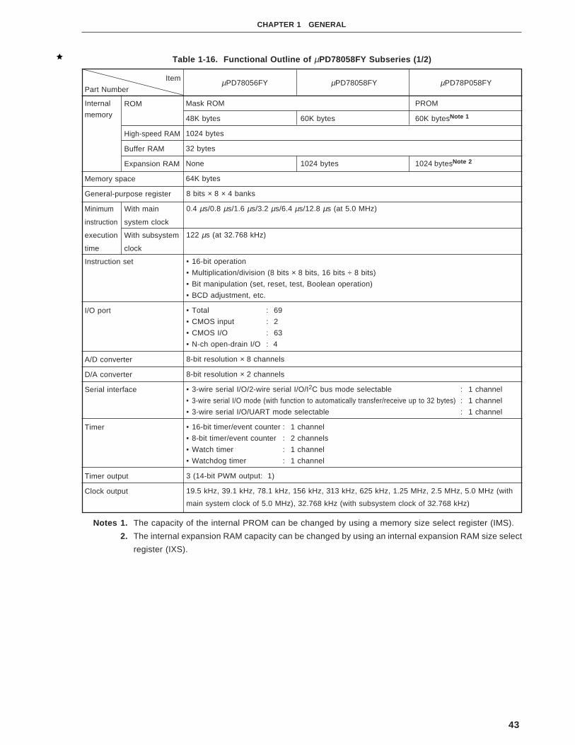
43
CHAPTER 1 GENERAL
Table 1-16. Functional Outline of µPD78058FY Subseries (1/2)
Item
Part Number
Mask ROM PROM
48K bytes 60K bytes 60K bytesNote 1
1024 bytes
32 bytes
None 1024 bytes 1024 bytesNote 2
64K bytes
8 bits × 8 × 4 banks
0.4 µs/0.8 µs/1.6 µs/3.2 µs/6.4 µs/12.8 µs (at 5.0 MHz)
122 µs (at 32.768 kHz)
• 16-bit operation
• Multiplication/division (8 bits × 8 bits, 16 bits ÷ 8 bits)
• Bit manipulation (set, reset, test, Boolean operation)
• BCD adjustment, etc.
• Total : 69
• CMOS input : 2
• CMOS I/O : 63
• N-ch open-drain I/O : 4
8-bit resolution × 8 channels
8-bit resolution × 2 channels
• 3-wire serial I/O/2-wire serial I/O/I2C bus mode selectable : 1 channel
• 3-wire serial I/O mode (with function to automatically transfer/receive up to 32 bytes) : 1 channel
• 3-wire serial I/O/UART mode selectable : 1 channel
• 16-bit timer/event counter : 1 channel
• 8-bit timer/event counter : 2 channels
• Watch timer : 1 channel
• Watchdog timer : 1 channel
3 (14-bit PWM output: 1)
19.5 kHz, 39.1 kHz, 78.1 kHz, 156 kHz, 313 kHz, 625 kHz, 1.25 MHz, 2.5 MHz, 5.0 MHz (with
main system clock of 5.0 MHz), 32.768 kHz (with subsystem clock of 32.768 kHz)
Notes 1. The capacity of the internal PROM can be changed by using a memory size select register (IMS).
2. The internal expansion RAM capacity can be changed by using an internal expansion RAM size select
register (IXS).
ROM
High-speed RAM
Buffer RAM
Expansion RAM
Memory space
General-purpose register
Minimum With main
instruction system clock
execution With subsystem
time clock
Instruction set
I/O port
A/D converter
D/A converter
Serial interface
Timer
Timer output
Clock output
µPD78056FY µPD78058FY µPD78P058FY
Internal
memory

44
CHAPTER 1 GENERAL
Table 1-16. Functional Outline of µPD78058FY Subseries (2/2)
Item
Part Number
1.2 kHz, 2.4 kHz, 4.9 kHz, 9.8 kHz (with main system clock of 5.0 MHz)
Internal: 13, external: 7
Internal: 1
1
Internal: 1, external: 1
VDD = 2.7 to 6.0 V
• 80-pin plastic QFP (14 × 14 mm, resin thickness 2.7 mm)
• 80-pin plastic QFP (14 × 14 mm, resin thickness 1.4 mm)Note
• 80-pin plastic TQFP (fine pitch)(12 × 12 mm) (µPD78058FY only)
Note Under planning
Buzzer output
Vectored Maskable
interrupt Non-maskable
source Software
Test input
Supply voltage
Package
µPD78056FY µPD78058FY µPD78P058FY

45
CHAPTER 1 GENERAL
Figure 1-17. Block Diagram of µPD78064B Subseries
Remark ( ): µPD78P064B
16-bit TIMER/EVENT COUNTER
TO0/P30TI00/INTP0/P00TI01/INTP1/P01
8-bit TIMER/EVENTCOUNTER 1
TO1/P31TI1/P33
8-bit TIMER/EVENTCOUNTER 2
TO2/P32TI2/P34
WATCHDOG TIMER
WATCH TIMER
SERIALINTERFACE 0
SI0/SB0/P25SO0/SB1/P26
SCK0/P27
SERIALINTERFACE 2
SI2/RXD/P70SO2/TXD/P71
INTERRUPTCONTROL
INTP0/P00-INTP5/P05
CLOCK OUTPUTCONTROLPCL/P35
A/D CONVERTER
BUZZER OUTPUT
AVREF
BUZ/P36
ANI0/P10-ANI7/P17
SCK2/ASCK/P72
PORT0P00P01-P05P07
PORT1 P10-P17
PORT2 P25-P27
PORT3 P30-P37
PORT7 P70-P72
PORT8 P80-P87
PORT9 P90-P97
PORT10 P100-P103
P110-P117
SYSTEMCONTROL
S0-S23
BIASfLCD
X2XT1/P07
X1
XT2
RESET
RAM
78K/0CPU CORE ROM
PORT11
S24/P97-S31/P90
S32/P87-S39/P80
COM0-COM3
VLC0-VLC2
LCDCONTROLLER/
DRIVER
IC(VPP)
VDD VSS AVDD AVSS

46
CHAPTER 1 GENERAL
Table 1-17. Functional Outline of µPD78064B Subseries
Item
Part Number
Mask ROM PROM
32K bytes
1024 bytes
40 × 4 bits
64K bytes
8 bits × 8 × 4 banks
0.4 µs/0.8 µs/1.6 µs/3.2 µs/6.4 µs/12.8 µs (at 5.0 MHz)
122 µs (at 32.768 kHz)
• 16-bit operation
• Multiplication/division (8 bits × 8 bits, 16 bits ÷ 8 bits)
• Bit manipulation (set, reset, test, Boolean operation)
• BCD adjustment, etc.
• Total : 57
• CMOS input : 2
• CMOS I/O : 55
8-bit resolution × 8 channels
• Segment signal output : 40 max.
• Common signal output : 4 max.
• Bias : 1/2 or 1/3 bias selectable
• 3-wire serial I/O/SBI/2-wire serial I/O mode selectable : 1 channel
• 3-wire serial I/O/UART mode selectable : 1 channel
• 16-bit timer/event counter : 1 channel
• 8-bit timer/event counter : 2 channels
• Watch timer : 1 channel
• Watchdog timer : 1 channel
3 (14-bit PWM output: 1)
19.5 kHz, 39.1 kHz, 78.1 kHz, 156 kHz, 313 kHz, 625 kHz, 1.25 MHz, 2.5 MHz, 5.0 MHz (with
main system clock of 5.0 MHz), 32.768 kHz (with subsystem clock of 32.768 kHz)
1.2 kHz, 2.4 kHz, 4.9 kHz, 9.8 kHz (with main system clock of 5.0 MHz)
Internal: 12, external: 6
Internal: 1
1
Internal: 1, external: 1
VDD = 2.0 to 6.0 V
• 100-pin plastic QFP (fine pitch) (14 × 14 mm)
• 100-pin plastic QFP (14 × 20 mm)
ROM
High-speed RAM
LCD display RAM
Memory space
General-purpose register
Minimum With main
instruction system clock
execution With subsystem
time clock
Instruction set
I/O port
(including pins multiplexed
with segment signal output)
A/D converter
LCD controller/driver
Serial interface
Timer
Timer output
Clock output
Buzzer output
Vectored Maskable
interrupt Non-maskable
source Software
Test input
Supply voltage
Package
Internal
memory
µPD78064B µPD78P064B
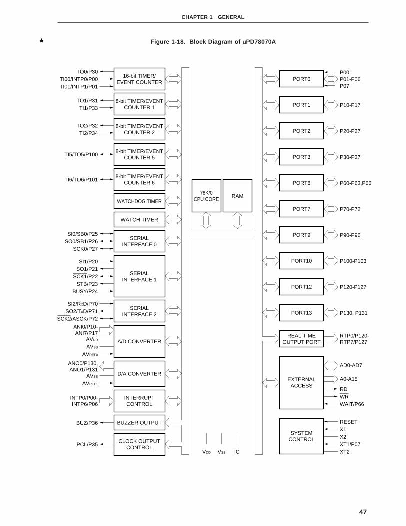
47
CHAPTER 1 GENERAL
Figure 1-18. Block Diagram of µPD78070A
16-bit TIMER/EVENT COUNTER
TO0/P30
ICVDD
TI00/INTP0/P00
VSS
TI01/INTP1/P01
8-bit TIMER/EVENTCOUNTER 1
TO1/P31TI1/P33
8-bit TIMER/EVENTCOUNTER 2
TO2/P32TI2/P34
WATCHDOG TIMER
WATCH TIMER
SERIALINTERFACE 0
SI0/SB0/P25SO0/SB1/P26
SCK0/P27
SERIALINTERFACE 1
SI1/P20SO1/P21
SCK1/P22
SERIALINTERFACE 2
SI2/RXD/P70SO2/TXD/P71
INTERRUPTCONTROL
INTP0/P00-INTP6/P06
CLOCK OUTPUTCONTROLPCL/P35
A/D CONVERTER
D/A CONVERTERAVSS
BUZZER OUTPUT
AVDD
AVSS
AVREF0
STB/P23BUSY/P24
BUZ/P36
AVREF1
ANO0/P130,ANO1/P131
ANI0/P10-ANI7/P17
SCK2/ASCK/P72
PORT0P00P01-P06P07
PORT1 P10-P17
PORT2 P20-P27
PORT3 P30-P37
PORT6 P60-P63,P66
PORT7 P70-P72
PORT9 P90-P96
REAL-TIMEOUTPUT PORT
RTP0/P120-RTP7/P127
EXTERNALACCESS
SYSTEMCONTROL
AD0-AD7
WRWAIT/P66
RD
X2XT1/P07
X1
XT2
RESET
78K/0CPU CORE RAM
8-bit TIMER/EVENTCOUNTER 5TI5/TO5/P100
8-bit TIMER/EVENTCOUNTER 6TI6/TO6/P101
PORT10 P100-P103
PORT12 P120-P127
PORT13 P130, P131
A0-A15

48
CHAPTER 1 GENERAL
Table 1-18. Functional Outline of µPD78070A
None
1024 bytes
32 bytes
64K bytes
8 bits × 8 × 4 banks
0.4 µs/0.8 µs/1.6 µs/3.2 µs/6.4 µs/12.8 µs (at 5.0 MHz)
122 µs (at 32.768 kHz)
• 16-bit operation
• Multiplication/division (8 bits × 8 bits, 16 bits ÷ 8 bits)
• Bit manipulation (set, reset, test, Boolean operation)
• BCD adjustment, etc.
• Total : 61
• CMOS input : 2
• CMOS I/O : 51
• N-ch open-drain I/O : 8
8-bit resolution × 8 channels
8-bit resolution × 2 channels
• 3-wire serial I/O/SBI/2-wire serial I/O mode selectable : 1 channel
• 3-wire serial I/O mode (with function to automatically transfer/receive up to 32 bytes) : 1 channel
• 3-wire serail I/O/UART mode selectable : 1 channel
• 16-bit timer/event counter : 1 channel
• 8-bit timer/event counter : 4 channels
• Watch timer : 1 channel
• Watchdog timer : 1 channel
5 (14-bit PWM output: 1, 8-bit PWM output: 2)
19.5 kHz, 39.1 kHz, 78.1 kHz, 156 kHz, 313 kHz, 625 kHz, 1.25 MHz, 2.5 MHz, 5.0 MHz (with
main system clock of 5.0 MHz), 32.768 kHz (with subsystem clock of 32.768 kHz)
Internal: 15, external: 7
Internal: 1
1
Internal: 1
VDD = 2.7 to 5.5 V
• 100-pin plastic QFP (fine pitch) (14 × 14 mm)
• 100-pin plastic QFP (14 × 20 mm)
ROM
High-speed RAM
Buffer RAM
Memory space
General-purpose register
Minimum With main
instruction system clock
execution With subsystem
time clock
Instruction set
I/O port
A/D converter
D/A converter
Serial interface
Timer
Timer output
Clock output
Vectored Maskable
interrupt Non-maskable
source Software
Test input
Supply voltage
Package
Internal
memory
FunctionsPart Number
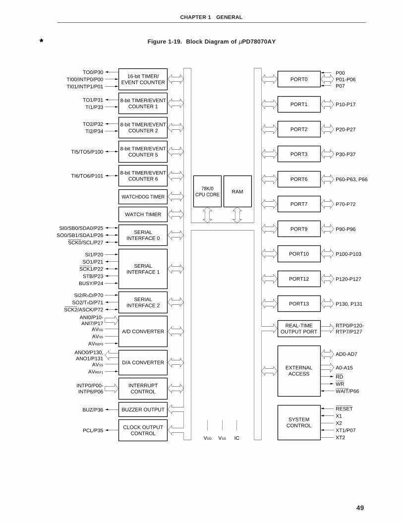
49
CHAPTER 1 GENERAL
Figure 1-19. Block Diagram of µPD78070AY
16-bit TIMER/EVENT COUNTER
TO0/P30
ICVDD
TI00/INTP0/P00
VSS
TI01/INTP1/P01
8-bit TIMER/EVENTCOUNTER 1
TO1/P31TI1/P33
8-bit TIMER/EVENTCOUNTER 2
TO2/P32TI2/P34
WATCHDOG TIMER
WATCH TIMER
SERIALINTERFACE 0
SI0/SB0/SDA0/P25SO0/SB1/SDA1/P26
SCK0/SCL/P27
SERIALINTERFACE 1
SI1/P20SO1/P21
SCK1/P22
SERIALINTERFACE 2
SI2/RXD/P70SO2/TXD/P71
INTERRUPTCONTROL
INTP0/P00-INTP6/P06
CLOCK OUTPUTCONTROLPCL/P35
A/D CONVERTER
D/A CONVERTERAVSS
BUZZER OUTPUT
AVDD
AVSS
AVREF0
STB/P23BUSY/P24
BUZ/P36
AVREF1
ANO0/P130,ANO1/P131
ANI0/P10-ANI7/P17
SCK2/ASCK/P72
PORT0P00P01-P06P07
PORT1 P10-P17
PORT2 P20-P27
PORT3 P30-P37
PORT6 P60-P63, P66
PORT7 P70-P72
PORT9 P90-P96
REAL-TIMEOUTPUT PORT
RTP0/P120-RTP7/P127
EXTERNALACCESS
SYSTEMCONTROL
AD0-AD7
WRWAIT/P66
RD
X2XT1/P07
X1
XT2
RESET
78K/0CPU CORE RAM
8-bit TIMER/EVENTCOUNTER 5TI5/TO5/P100
8-bit TIMER/EVENTCOUNTER 6TI6/TO6/P101
PORT10 P100-P103
PORT12 P120-P127
PORT13 P130, P131
A0-A15

50
CHAPTER 1 GENERAL
Table 1-19. Functional Outline of µPD78070AY
None
1024 bytes
32 bytes
64K bytes
8 bits × 8 × 4 banks
0.4 µs/0.8 µs/1.6 µs/3.2 µs/6.4 µs/12.8 µs (at 5.0 MHz)
122 µs (at 32.768 kHz)
• 16-bit operation
• Multiplication/division (8 bits × 8 bits, 16 bits ÷ 8 bits)
• Bit manipulation (set, reset, test, Boolean operation)
• BCD adjustment, etc.
• Total : 61
• CMOS input : 2
• CMOS I/O : 51
• N-ch open-drain I/O : 8
8-bit resolution × 8 channels
8-bit resolution × 2 channels
• 3-wire serial I/O/2-wire serial I/O/I2C bus mode selectable : 1 channel
• 3-wire serial I/O mode (with function to automatically transfer/receive up to 32 bytes) : 1 channel
• 3-wire serial I/O/UART mode selectable : 1 channel
• 16-bit timer/event counter : 1 channel
• 8-bit timer/event counter : 4 channels
• Watch timer : 1 channel
• Watchdog timer : 1 channel
5 (14-bit PWM output: 1, 8-bit PWM output: 2)
19.5 kHz, 39.1 kHz, 78.1 kHz, 156 kHz, 313 kHz, 625 kHz, 1.25 MHz, 2.5 MHz, 5.0 MHz (with
main system clock of 5.0 MHz), 32.768 kHz (with subsystem clock of 32.768 kHz)
1.2 kHz, 2.4 kHz, 4.9 kHz, 9.8 kHz (with main system clock of 5.0 MHz)
Internal: 15, external: 7
Internal: 1
1
Internal: 1
VDD = 2.7 to 5.5 V
• 100-pin plastic QFP (14 × 20 mm)
• 100-pin plastic QFP (fine pitch) (14 × 14 mm)
ROM
High-speed RAM
Buffer RAM
Memory space
General-purpose register
Minimum With main
instruction system clock
execution With subsystem
time clock
Instruction set
I/O port
A/D converter
D/A converter
Serial interface
Timer
Timer output
Clock output
Buzzer output
Vectored Maskable
interrupt Non-maskable
source Software
Test input
Supply voltage
Package
Internal
memory
FunctionsPart Number

51
CHAPTER 1 GENERAL
Figure 1-20. Block Diagram of µPD78075B Subseries
Remark The internal ROM capacity differs depending on the model.
16-bit TIMER/EVENT COUNTER
TO0/P30
ICVDD0,VDD1
TI00/INTP0/P00
VSS0,VSS1
TI01/INTP1/P01
8-bit TIMER/EVENTCOUNTER 1
TO1/P31TI1/P33
8-bit TIMER/EVENTCOUNTER 2
TO2/P32TI2/P34
WATCHDOG TIMER
WATCH TIMER
SERIALINTERFACE 0
SI0/SB0/P25SO0/SB1/P26
SCK0/P27
SERIALINTERFACE 1
SI1/P20SO1/P21
SCK1/P22
SERIALINTERFACE 2
SI2/RXD/P70SO2/TXD/P71
INTERRUPTCONTROL
INTP0/P00-INTP6/P06
CLOCK OUTPUTCONTROLPCL/P35
A/D CONVERTER
D/A CONVERTERAVSS
BUZZER OUTPUT
AVSS
AVREF0
STB/P23BUSY/P24
BUZ/P36
AVREF1
ANO0/P130,ANO1/P131
ANI0/P10-ANI7/P17
SCK2/ASCK/P72
PORT0P00P01-P06P07
PORT1 P10-P17
PORT2 P20-P27
PORT3 P30-P37
PORT4 P40-P47
PORT5 P50-P57
PORT6 P60-P67
PORT7 P70-P72
PORT8 P80-P87
PORT9 P90-P96
REAL-TIMEOUTPUT PORT
RTP0/P120-RTP7/P127
EXTERNALACCESS
SYSTEMCONTROL
AD0/P40-AD7/P47
A8/P50-A15/P57
WR/P65WAIT/P66
RD/P64
ASTB/P67
X2XT1/P07
X1
XT2
RESET
RAM
78K/0CPU CORE ROM
8-bit TIMER/EVENTCOUNTER 5TI5/TO5/P100
8-bit TIMER/EVENTCOUNTER 6TI6/TO6/P101
PORT10 P100-P103
PORT12 P120-P127
PORT13 P130, P131
A0/P80-A7/P87

52
CHAPTER 1 GENERAL
Table 1-20. Functional Outline of µPD78075B8 Subseries
Item
Part Number
Mask ROM
32K bytes 40K bytes
1024 bytes
32 bytes
64K bytes
8 bits × 8 × 4 banks
0.4 µs/0.8 µs/1.6 µs/3.2 µs/6.4 µs/12.8 µs (at 5.0 MHz)
122 µs (at 32.768 kHz)
• 16-bit operation
• Multiplication/division (8 bits × 8 bits, 16 bits ÷ 8 bits)
• Bit manipulation (set, reset, test, Boolean operation)
• BCD adjustment, etc.
• Total : 88
• CMOS input : 2
• CMOS I/O : 78
• N-ch open-drain I/O : 8
8-bit resolution × 8 channels
8-bit resolution × 2 channels
• 3-wire serial I/O/SBI/2-wire serial I/O mode selectable : 1 channel
• 3-wire serial I/O mode (with function to automatically transfer/receive up to 32 bytes) : 1 channel
• 3-wire serial I/O/UART mode selectable : 1 channel
• 16-bit timer/event counter : 1 channel
• 8-bit timer/event counter : 4 channels
• Watch timer : 1 channel
• Watchdog timer : 1 channel
5 (14-bit PWM output: 1, 8-bit PWM output: 2)
19.5 kHz, 39.1 kHz, 78.1 kHz, 156 kHz, 313 kHz, 625 kHz, 1.25 MHz, 2.5 MHz, 5.0 MHz (with
main system clock of 5.0 MHz), 32.768 kHz (with subsystem clock of 32.768 kHz)
Internal: 15, external: 7
Internal: 1
1
Internal: 1, external: 1
VDD = 1.8 to 5.5 V
• 100-pin plastic QFP (fine pitch) (14 × 14 mm, resin thickness 1.45 mm)
• 100-pin plastic QFP (14 × 20 mm, resin thickness 2.7 mm)
ROM
High-speed RAM
Buffer RAM
Expansion RAM
Memory space
General-purpose register
Minimum With main
instruction system clock
execution With subsystem
time clock
Instruction set
I/O port
A/D converter
D/A converter
Serial interface
Timer
Timer output
Clock output
Vectored Maskable
interrupt Non-maskable
source Software
Test input
Supply voltage
Package
Internal
memory
µPD78074B µPD78075B

53
CHAPTER 1 GENERAL
Figure 1-21. Block Diagram of µPD78075BY Subseries
Remark The internal ROM capacity differs depending on the model.
16-bit TIMER/EVENT COUNTER
TO0/P30
IC(VPP)
VDD0,VDD1
TI00/INTP0/P00
VSS0,VSS1
TI01/INTP1/P01
8-bit TIMER/EVENTCOUNTER 1
TO1/P31TI1/P33
8-bit TIMER/EVENTCOUNTER 2
TO2/P32TI2/P34
WATCHDOG TIMER
WATCH TIMER
SERIALINTERFACE 0
SI0/SB0/SDA0/P25SO0/SB1/SDA1/P26
SCK0/SCL/P27
SERIALINTERFACE 1
SI1/P20SO1/P21
SCK1/P22
SERIALINTERFACE 2
SI2/RXD/P70SO2/TXD/P71
INTERRUPTCONTROL
INTP0/P00-INTP6/P06
CLOCK OUTPUTCONTROLPCL/P35
A/D CONVERTER
D/A CONVERTERAVSS
BUZZER OUTPUT
AVSS
AVREF0
STB/P23BUSY/P24
BUZ/P36
AVREF1
ANO0/P130,ANO1/P131
ANI0/P10-ANI7/P17
SCK2/ASCK/P72
PORT0P00P01-P06P07
PORT1 P10-P17
PORT2 P20-P27
PORT3 P30-P37
PORT4 P40-P47
PORT5 P50-P57
PORT6 P60-P67
PORT7 P70-P72
PORT8 P80-P87
PORT9 P90-P96
REAL-TIMEOUTPUT PORT
RTP0/P120-RTP7/P127
EXTERNALACCESS
SYSTEMCONTROL
AD0/P40-AD7/P47
A8/P50-A15/P57
WR/P65WAIT/P66
RD/P64
ASTB/P67
X2XT1/P07
X1
XT2
RESET
RAM
78K/0CPU CORE ROM
8-bit TIMER/EVENTCOUNTER 5TI5/TO5/P100
8-bit TIMER/EVENTCOUNTER 6TI6/TO6/P101
PORT10 P100-P103
PORT12 P120-P127
PORT13 P130, P131
A0/P80-A7/P87

54
CHAPTER 1 GENERAL
Table 1-21. Functional Outline of µPD78075BY Subseries
Item
Part Number
Mask ROM
32K bytes 40K bytes
1024 bytes
32 bytes
64K bytes
8 bits × 8 × 4 banks
0.4 µs/0.8 µs/1.6 µs/3.2 µs/6.4 µs/12.8 µs (at 5.0 MHz)
122 µs (at 32.768 kHz)
• 16-bit operation
• Multiplication/division (8 bits × 8 bits, 16 bits ÷ 8 bits)
• Bit manipulation (set, reset, test, Boolean operation)
• BCD adjustment, etc.
• Total : 88
• CMOS input : 2
• CMOS I/O : 78
• N-ch open-drain I/O : 8
8-bit resolution × 8 channels
8-bit resolution × 2 channels
• 3-wire serial I/O/2-wire serial I/O/I2C bus mode selectable : 1 channel
• 3-wire serial I/O mode (with function to automatically transfer/receive up to 32 bytes) : 1 channel
• 3-wire serial I/O/UART mode selectable : 1 channel
• 16-bit timer/event counter : 1 channel
• 8-bit timer/event counter : 4 channels
• Watch timer : 1 channel
• Watchdog timer : 1 channel
5 (14-bit PWM output: 1, 8-bit PWM output: 2)
19.5 kHz, 39.1 kHz, 78.1 kHz, 156 kHz, 313 kHz, 625 kHz, 1.25 MHz, 2.5 MHz, 5.0 MHz (with
main system clock of 5.0 MHz), 32.768 kHz (with subsystem clock of 32.768 kHz)
1.2 kHz, 2.4 kHz, 4.9 kHz, 9.8 kHz (with main system clock of 5.0 MHz)
Internal: 15, external: 7
Internal: 1
1
Internal: 1, external: 1
VDD = 1.8 to 5.5 V
• 100-pin plastic QFP (14 × 20 mm, resin thickness 2.7 mm)
Caution The µPD78075BY subseries is under development.
ROM
High-speed RAM
Buffer RAM
Memory space
General-purpose register
Minimum With main
instruction system clock
execution With subsystem
time clock
Instruction set
I/O port
A/D converter
D/A converter
Serial interface
Timer
Timer output
Clock output
Buzzer output
Vectored Maskable
interrupt Non-maskable
source Software
Test input
Supply voltage
Package
Internal
memory
µPD78074BY µPD78075BY
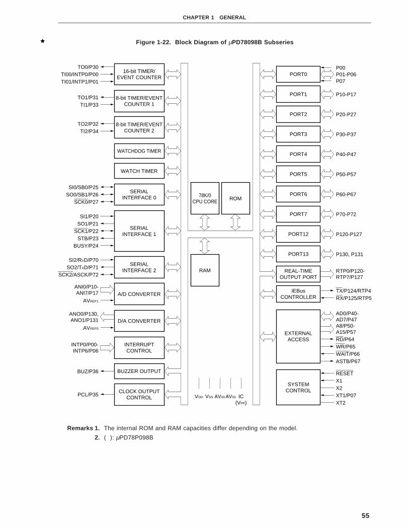
55
CHAPTER 1 GENERAL
Figure 1-22. Block Diagram of µPD78098B Subseries
Remarks 1. The internal ROM and RAM capacities differ depending on the model.
2. ( ): µPD78P098B
TX/P124/RTP4RX/P125/RTP5
16-bit TIMER/EVENT COUNTER
TO0/P30TI00/INTP0/P00TI01/INTP1/P01
8-bit TIMER/EVENTCOUNTER 1
TO1/P31TI1/P33
8-bit TIMER/EVENTCOUNTER 2
TO2/P32TI2/P34
WATCHDOG TIMER
WATCH TIMER
SERIALINTERFACE 0
SI0/SB0/P25SO0/SB1/P26
SCK0/P27
SERIALINTERFACE 1
SI1/P20SO1/P21
SCK1/P22
SERIALINTERFACE 2
SI2/RXD/P70SO2/TXD/P71
INTERRUPTCONTROL
INTP0/P00-INTP6/P06
CLOCK OUTPUTCONTROLPCL/P35
A/D CONVERTER
D/A CONVERTER
BUZZER OUTPUT
AVREF1
STB/P23BUSY/P24
BUZ/P36
AVREF0
ANO0/P130,ANO1/P131
ANI0/P10-ANI7/P17
SCK2/ASCK/P72
PORT0P00P01-P06P07
PORT1 P10-P17
PORT2 P20-P27
PORT3 P30-P37
PORT4 P40-P47
PORT5 P50-P57
PORT6 P60-P67
PORT7 P70-P72
PORT12 P120-P127
PORT13 P130, P131
REAL-TIMEOUTPUT PORT
RTP0/P120-RTP7/P127
EXTERNALACCESS
SYSTEMCONTROL
AD0/P40-AD7/P47A8/P50-A15/P57
WR/P65WAIT/P66
RD/P64
ASTB/P67
X2XT1/P07
X1
XT2
RESET
RAM
78K/0CPU CORE ROM
IEBusCONTROLLER
IC(VPP)
VDD VSS AVDD AVSS

56
CHAPTER 1 GENERAL
Table 1-22. Functional Outline of µPD78098B Subseries
Item
Part Number
Mask ROM PROM
40K bytes 48K bytes 60K bytes 60K bytesNote 1
1024 bytes
32 bytes
None 2048 bytes 2048 bytesNote 2
64K bytes
8 bits × 8 × 4 banks
0.5 µs/1.0 µs/2.0 µs/4.0 µs/8.0 µs/16.0 (at 6.0 MHz)
122 µs (at 32.768 kHz)
• 16-bit operation
• Multiplication/division (8 bits × 8 bits, 16 bits ÷ 8 bits)
• Bit manipulation (set, reset, test, Boolean operation)
• BCD adjustment, etc.
• Total : 69
• CMOS input : 2
• CMOS I/O : 63
• N-ch open-drain I/O: 4
Effective transfer rate: 3.9 kbps/17 kbps/26 kbps
8-bit resolution × 8 channels
8-bit resolution × 2 channels
• 3-wire serial I/O/SBI/2-wire serial I/O mode selectable : 1 channel
• 3-wire serial I/O mode (with function to automatically transfer/receive up to 32 bytes) : 1 channel
• 3-wire serial I/O/UART mode selectable : 1 channel
• 16-bit timer/event counter : 1 channel
• 8-bit timer/event counter : 2 channels
• Watch timer : 1 channel
• Watchdog timer : 1 channel
3 (14-bit PWM output: 1)
15.6 kHz, 31.3 kHz, 62.5 kHz, 125 kHz, 250 kHz, 500 kHz, 1.0 MHz, 2.0 MHz, 4.0 MHz (with
main system clock of 6.0 MHz), 32.768 kHz (with subsystem clock of 32.768 kHz)
977 Hz, 1.95 kHz, 3.9 kHz, 7.8 kHz (with main system clock of 6.0 MHz)
Internal: 14, external: 7
Internal: 1
1
Internal: 1, external: 1
VDD = 2.7 to 6.0 V
• 80-pin plastic QFP (14 × 14 mm)
• 80-pin ceramic WQFN (14 × 14 mm) (µPD78P098B only)
Notes 1. The internal PROM capacity can be changed by using a memory size select register (IMS).
2. The internal expansion RAM can be changed by using an internal expansion RAM size select register
(IXS).
Caution The µPD78098B subseries is under planning.
ROM
High-speed RAM
Buffer RAM
Expansion RAM
Memory space
General-purpose register
Minimum With main
instruction system clock
execution With subsystem
time clock
Instruction set
I/O port
IEBus controller
A/D converter
D/A converter
Serial interface
Timer
Timer output
Clock output
Buzzer output
Vectored Maskable
interrupt Non-maskable
source Software
Test input
Supply voltage
Package
Internal
memory
µPD78095B µPD78096B µPD78098B µPD78P098B
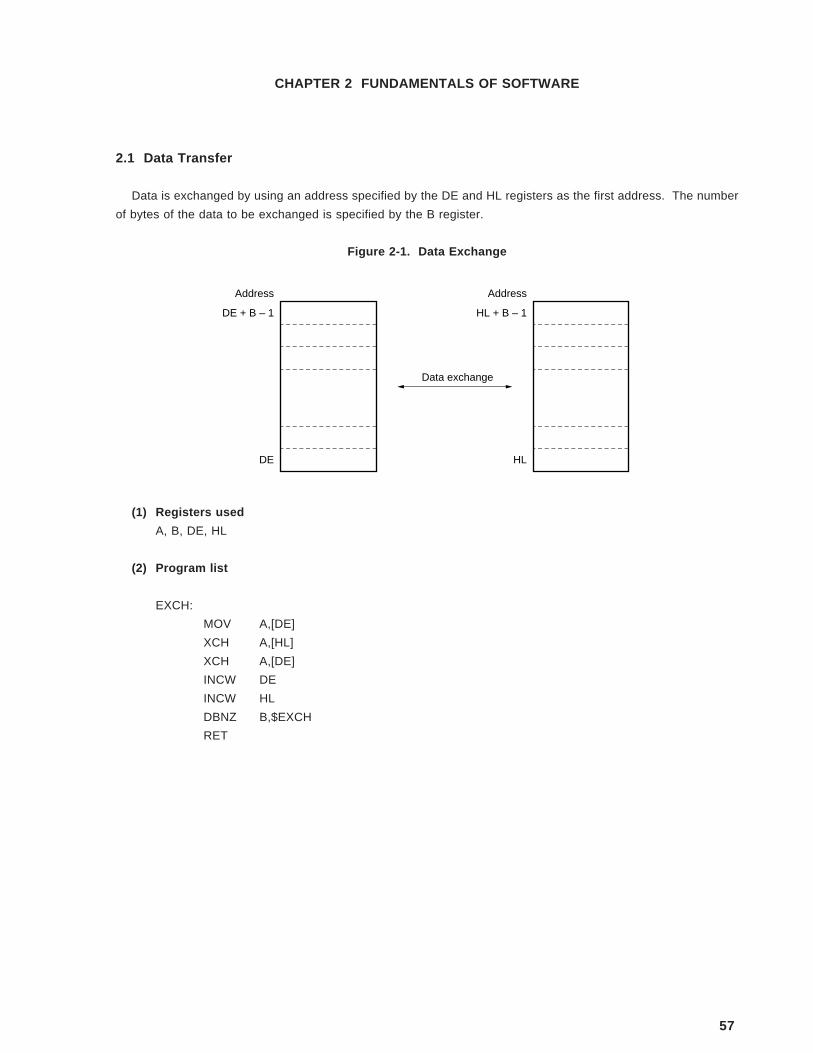
CHAPTER 2 FUNDAMENTALS OF SOFTWARE
2.1 Data Transfer
Data is exchanged by using an address specified by the DE and HL registers as the first address. The number
of bytes of the data to be exchanged is specified by the B register.
Figure 2-1. Data Exchange
(1) Registers used
A, B, DE, HL
(2) Program list
EXCH:
MOV A,[DE]
XCH A,[HL]
XCH A,[DE]
INCW DE
INCW HL
DBNZ B,$EXCH
RET
Data exchange
Address
DE + B – 1
DE
Address
HL + B – 1
HL
57

58
CHAPTER 2 FUNDAMENTALS OF SOFTWARE
2.2 Data Comparison
Data is compared by using an address specified by the DE and HL registers as the first address. The number
of bytes of the data to be compared is specified by the B register. If the result of comparison is equal, CY is cleared
to 0; if not, CY is set to 1.
Figure 2-2. Data Comparison
(1) Registers used
A, B, DE, HL
(2) Program list
COMP:
MOV A,[DE]
CMP A,[HL]
BNZ $ERROR
INCW DE
INCW HL
DBNZ B,$COMP
CLR1 CY
BR RTN
ERROR:
SET1 CY
RTN:
RET
Data comparison
Address
DE + B – 1
DE
Address
HL + B – 1
HL

59
CHAPTER 2 FUNDAMENTALS OF SOFTWARE
2.3 Decimal Addition
The lowest address for decimal addition is specified by the DE and HL registers, and the number of digits specified
by BYTNUM is added. The result of the addition is stored to an area specified by the HL register. If an overflow or
underflow occurs as a result of the addition, execution branches to error processing. Define the branch address as
‘ERROR’ in the main routine. Also declare it as PUBLIC.
Figure 2-3. Decimal Addition
(1) Flowchart
Address
DE + BYTNUM – 1
DE
Address
HL + BYTNUM – 1
HL
Address
HL + BYTNUM – 1
HL
+ =
Decimal subtraction processing
BCDADD
C ← number of bytes fordecimal addition
B ← C – 1Number of bytes for decimal
addition without sign
Signs ofaugend and addend
same?
Decimal addition processing
RET
BCDAD2
No
Yes

60
CHAPTER 2 FUNDAMENTALS OF SOFTWARE
DADDS
CY ← 0Sign flag SFLAG ← 0
DADDS1
A ← [DE] + [HL] + CY Adds augend and addend with CY
Adjusts result to decimaland stores in memory
DE ← DE + 1, HL ← HL + 1 Increments addend
and augend addresses
B ← B – 1
B = 0
A ← [DE] + [HL] + CY Adds addend and augend with CY
Yes
CY = 1
Sign flag SFLAG ← 1 CY = 0
Yes
DADDS3
Result adjusted to decimal?
CY = 1
No
Yes
No
A7 = 1
No
Yes
Sign flag SFLAG = 1
Yes
No
A7 ← 1
Stores A to memory
RET
DADDS6
No
ERROR

61
CHAPTER 2 FUNDAMENTALS OF SOFTWARE
DSUBS
Makes subtrahend positive Sign flag SFLAG ← 0
Makes subtrahend positive Sign flag SFLAG ← 1
A ← [DE] – [HL] – CY Subtracts subtrahend from
minuend with CY DE ← DE + 1, HL ← HL + 1
Increments subtrahendand minuend addresses
B ← C, CY ← 0
Minuend < 0
Adjusts result to decimaland stores in memory
Yes
C = 0
Inverts sign flag that takes10's complement
Yes
DSUBS1
Result = 0
No
Yes
No
Sign flag = 1
Yes
No
RET
DSUBS2
C ← C – 1
CY = 1
Yes
Appends negative sign to result
DSUBS5
No
No

62
CHAPTER 2 FUNDAMENTALS OF SOFTWARE
(2) Registers used
AX, BC, DE, HL
(3) Program list
;******************************************************************; *; Input parameter *; HL register: addend first address *; DE register: augend first address *; Output parameter *; HL register: Operation result first address *; *;******************************************************************
PUBLIC BCDADD,BCDAD1,BCDAD2PUBLIC DADDSPUBLIC DSUBSEXTRN ERROREXTBIT SFLAG
;BYTNUM EQU 4;
CSEGBCDADD:
MOV C,#BYTNUMBCDAD1:
MOV A,CMOV B,ADEC B
BCDAD2:MOV A,[HL+BYTNUM–1]XCHW AX,DEXCHW AX,HLXCHW AX,DEXOR A,[HL+BYTNUM–1]XCHW AX,HLXCHW AX,DEXCHW AX,HL
BT A.7,$BCDAD3CALL !DADDSRET
BCDAD3:CALL !DSUBSRET
; Error processing branch address; Sign flag
; Sets number of digits for operation
; Sets number of digits for operation to C register
; Loads MSB (sign data) of augend
; Loads MSB (sign data) of augend
; Signs coincide? ELSE subtraction processing; THEN addition processing

63
CHAPTER 2 FUNDAMENTALS OF SOFTWARE
;=============================================================; ***** 10 Decimal addition *****;=============================================================
DADDS:CLR1 CYCLR1 SFLAG
DADDS1:MOV A,[DE]ADDC A,[HL]ADJBAMOV [HL],AINCW HLINCW DEDBNZ B,$DADDS1
MOV A,[DE]ADDC A,[HL]
DADDS2:BNC $DADDS3SET1 SFLAGCLR1 CY
DADDS3:ADJBABNC $DADDS4BR ERROR
DADDS4:BF A.7,$DADDS5BR ERROR
DADDS5:BF SFLAG,$DADDS6SET1 A.7
DADDS6:MOV [HL],ARET
; Starts addition from lowest digit
; End of addition (number of digits for operation – 1)
; Negative addition; THEN sets negative status
; Sets sign
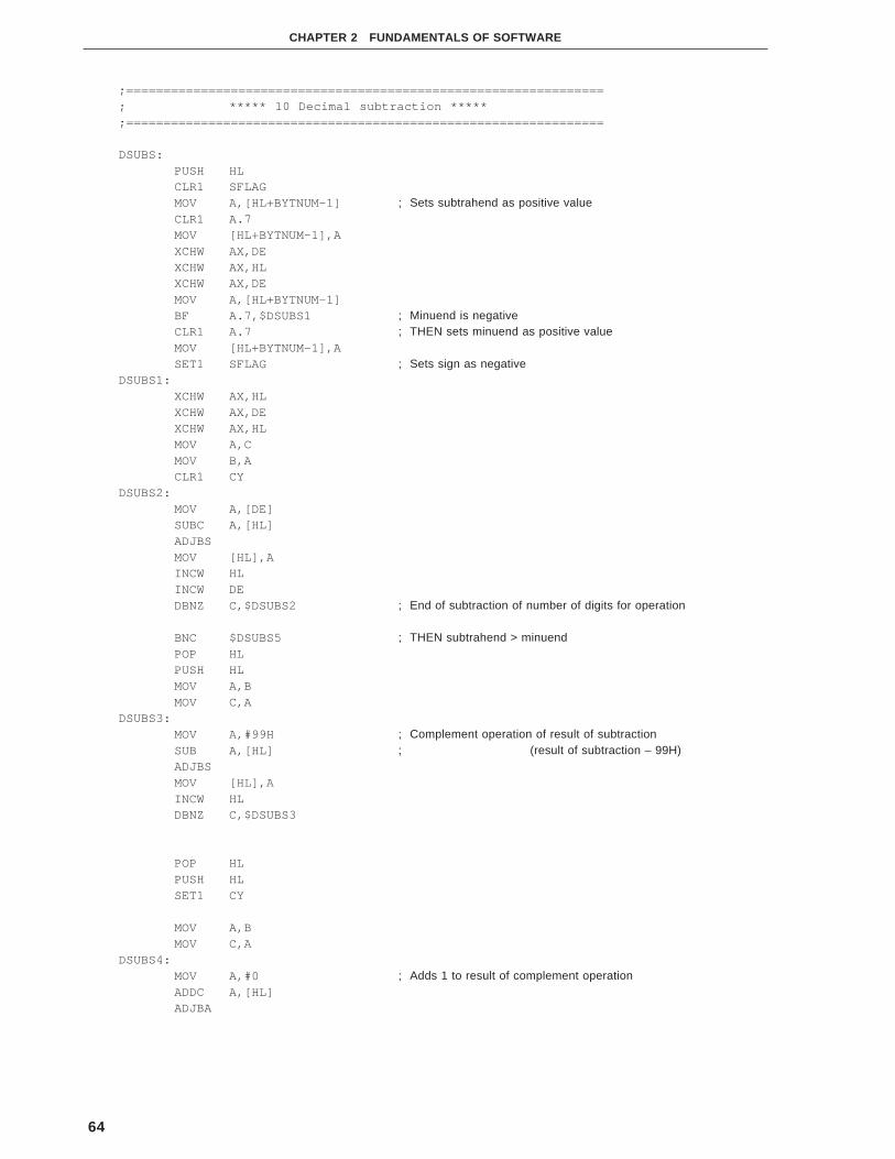
64
CHAPTER 2 FUNDAMENTALS OF SOFTWARE
;================================================================; ***** 10 Decimal subtraction *****;================================================================
DSUBS:PUSH HLCLR1 SFLAGMOV A,[HL+BYTNUM–1]CLR1 A.7MOV [HL+BYTNUM–1],AXCHW AX,DEXCHW AX,HLXCHW AX,DEMOV A,[HL+BYTNUM–1]BF A.7,$DSUBS1CLR1 A.7MOV [HL+BYTNUM–1],ASET1 SFLAG
DSUBS1:XCHW AX,HLXCHW AX,DEXCHW AX,HLMOV A,CMOV B,ACLR1 CY
DSUBS2:MOV A,[DE]SUBC A,[HL]ADJBSMOV [HL],AINCW HLINCW DEDBNZ C,$DSUBS2
BNC $DSUBS5POP HLPUSH HLMOV A,BMOV C,A
DSUBS3:MOV A,#99HSUB A,[HL]ADJBSMOV [HL],AINCW HLDBNZ C,$DSUBS3
POP HLPUSH HLSET1 CY
MOV A,BMOV C,A
DSUBS4:MOV A,#0ADDC A,[HL]ADJBA
; Sets subtrahend as positive value
; Minuend is negative; THEN sets minuend as positive value
; Sets sign as negative
; End of subtraction of number of digits for operation
; THEN subtrahend > minuend
; Complement operation of result of subtraction; (result of subtraction – 99H)
; Adds 1 to result of complement operation

65
CHAPTER 2 FUNDAMENTALS OF SOFTWARE
MOV [HL],AINCW HLDBNZ C,$DSUBS4MOV1 CY,SFLAGNOT1 CYMOV1 SFLAG,CY
;======================================================; ***** 0 check of operation result *****;======================================================
DSUBS5:MOV A,BMOV C,APOP HLPUSH HLMOV A,#0
DSUBS6:CMP A,[HL]INCW HLBNZ $DSUBS7DBNZ C,$DSUBS6POP HLRET
DSUBS7:BF SFLAG,$DSUBS8POP HLPUSH HLMOV A,[HL+BYTNUM–1]SET1 A.7MOV [HL+BYTNUM–1],A
DSUBS8:POP HLRET
; 0 check from lowest digit
; 0 check of all digits completed; THEN result of subtraction = 0
; Result of subtraction is negative; THEN sets sign

66
CHAPTER 2 FUNDAMENTALS OF SOFTWARE
2.4 Decimal Subtraction
The lowest address for decimal subtraction is specified by the DE and HL registers, and the number of digits
specified by BYTNUM is subtracted. The result of the subtraction is stored to an area specified by the HL register.
If an overflow or underflow occurs as a result of the subtraction, execution branches to error processing. Define the
branch address as ‘ERROR’ in the main routine. Also declare it as PUBLIC.
This program replaces minuend and subtrahend with augend and addend, and calls a program of decimal addition.
Figure 2-4. Decimal Subtraction
(1) Flowchart
(2) Registers used
AX, BC, DE, HL
Address
DE + BYTNUM – 1
DE
Address
HL + BYTNUM – 1
HL
Address
HL + BYTNUM – 1
HL
– =
BCDSUB
C ← number of bytes fordecimal subtraction
Decimal addition withsubtrahend and minuend as
addend and augend
RET
Inverts sign bit of subtrahend

67
CHAPTER 2 FUNDAMENTALS OF SOFTWARE
(3) Program list
;******************************************************************; *; Input parameter *; HL register: subtrahend first address *; DE register: minuend first address *; Output parameter *; HL register: Operation result first address *; *;******************************************************************
PUBLIC BYTNUMPUBLIC BCDSUBEXTRN BCDADD,BCDAD2
;BYTNUM EQU 4;
CSEGBCDSUB:
MOV C,#BYTNUMBCDSU1:
MOV A,CMOV B,ADEC B
MOV A,[HL+BYTNUM–1]MOV1 CY,A.7NOT1 CYMOV1 A.7,CYMOV [HL+BYTNUM–1],ACALL !BCDAD2RET
; Sets number of digits for operation
; Sets number of digits for operation to C register
; Sets MSB (sign data) of subtrahend for addition; Inverts sign data
; Calls decimal addition processing

68
CHAPTER 2 FUNDAMENTALS OF SOFTWARE
2.5 Binary-to-Decimal Conversion
Binary data of 16 bits in data memory is converted into 5-digit decimal data and stored in data memory. Binary
data of 16 bits is divided by decimal 10 by the number of times equal to the number of digits (4 times), and conversion
is carried out with the result of the operation and the value of the remainder at that time.
Figure 2-5. Binary-to-Decimal Conversion
Example To convert FFH into decimal number
(1) Registers used
AX, BC, HL
0 × ×0 0 × 0 × 0 ×
Low High
Decimal 5 digits (5 bytes)
× × ××
Low
Binary 16 bits (2 bytes)
High
0 5 50 0 2 0 0 0 0
Low High
Decimal 5 digits (5 bytes)
F F 00
Low
Binary 16 bits (2 bytes)
High
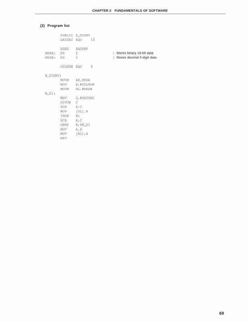
69
CHAPTER 2 FUNDAMENTALS OF SOFTWARE
(2) Program list
PUBLIC B_DCONVDATDEC EQU 10
DSEG SADDRPREGA: DS 2REGB: DS 5
COLNUM EQU 4
B_DCONV:MOVW AX,REGAMOV B,#COLNUMMOVW HL,#REGB
B_D1:MOV C,#DATDECDIVUW CXCH A,CMOV [HL],AINCW HLXCH A,CDBNZ B,$B_D1MOV A,XMOV [HL],ARET
; Stores binary 16-bit data; Stores decimal 5-digit data

70
CHAPTER 2 FUNDAMENTALS OF SOFTWARE
2.6 Bit Manipulation Instruction
A 1 bit of a flag in the data memory is ANDed with the bit 4 of port 6, and the result is ANDed with the bit 5 of
port 6 and is output to the bit 6 of port 6.
Figure 2-6. Bit Operation
(1) Program list
PUBLIC BIT_OP,FLG
BSEG
FLG DBIT
BIT_OP:
MOV1 CY,FLG
AND1 CY,P6.4
OR1 CY,P6.5
MOV1 P6.6,CY
RET
FLG
PORT6.4
PORT6.5
PORT6.6

71
CHAPTER 2 FUNDAMENTALS OF SOFTWARE
2.7 Binary Multiplication (16 bits × 16 bits)
Data in a multiplicand area (HIKAKE; 16 bits) and multiplier area (KAKE; 16 bits) are multiplied, and the result
is stored in an operation result storage area (KOTAE).
Figure 2-7. Binary Multiplication
<Processing contents>
Multiplication is performed by adding the multiplicand by the number of bits of the multiplier that are “1”.
Operation result storage area (4 bytes)
KOTAE + 3 KOTAE
Multiplier area (2 bytes)
KAKE + 1 KAKE
Multiplicand area (2 bytes)
HIKAKE + 1 HIKAKE
×
=
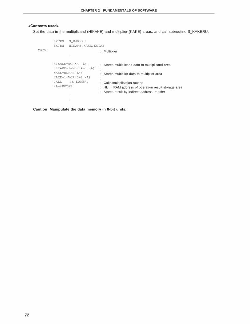
72
CHAPTER 2 FUNDAMENTALS OF SOFTWARE
<Contents used>
Set the data in the multiplicand (HIKAKE) and multiplier (KAKE) areas, and call subroutine S_KAKERU.
EXTRN S_KAKERUEXTRN HIKAKE,KAKE,KOTAE
MAIN:··
HIKAKE=WORKA (A)HIKAKE+1=WORKA+1 (A)KAKE=WORKB (A)KAKE+1=WORKB+1 (A)CALL !S_KAKERUHL=#KOTAE
···
Caution Manipulate the data memory in 8-bit units.
; Multiplier
; Stores multiplicand data to multiplicand area;; Stores multiplier data to multiplier area;; Calls multiplication routine; HL ← RAM address of operation result storage area; Stores result by indirect address transfer

73
CHAPTER 2 FUNDAMENTALS OF SOFTWARE
(1) Input/output condition
• Input parameter
HIKAKE : Store the multiplicand data in this area.
KAKE : Store the multiplier data in this area.
• Output parameter
KOTAE : Store the result of the operation in this area.
(2) SPD chart
[Multiplication subroutine]
(3) Registers used
A, B
S_KAKERU Initializes operation result storage area
WORK1 ← multiplier (low)
for (B = #0 ; B < #16 ; B + +)
if (B = #8)
THEN
WORK1 ← multiplier (high)
Shifts WORK1 1 bit to left
if_bit (CY = #1)
THEN
Adds multiplicand to operation result storage area
if (B ≠ #15)
THEN
Shifts operation result storage area 1 bit to left
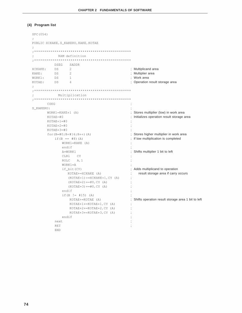
74
CHAPTER 2 FUNDAMENTALS OF SOFTWARE
; Multiplicand area; Multiplier area; Work area; Operation result storage area
;;; Stores multiplier (low) in work area; Initializes operation result storage area;;;; Stores higher multiplier in work area; if low multiplication is completed;;; Shifts multiplier 1 bit to left;;;; Adds multiplicand to operation; result storage area if carry occurs;;;;;; Shifts operation result storage area 1 bit to left;;;;;;
(4) Program list
$PC(054);PUBLIC HIKAKE,S_KAKERU,KAKE,KOTAE;;************************************************; RAM definition;************************************************
DSEG SADDRHIKAKE: DS 2KAKE: DS 2WORK1: DS 1KOTAE: DS 4;;************************************************; Multiplication;************************************************
CSEGS_KAKERU:
WORK1=KAKE+1 (A)KOTAE=#0KOTAE+1=#0KOTAE+2=#0KOTAE+3=#0for(B=#0;B<#16;B++)(A)
if(B == #8)(A)WORK1=KAKE (A)endifA=WORK1CLR1 CYROLC A,1WORK1=Aif_bit(CY)
KOTAE+=HIKAKE (A)(KOTAE+1)+=HIKAKE+1,CY (A)(KOTAE+2)+=#0,CY (A)(KOTAE+3)+=#0,CY (A)
endifif(B != #15) (A)
KOTAE+=KOTAE (A)KOTAE+1+=KOTAE+1,CY (A)KOTAE+2+=KOTAE+2,CY (A)KOTAE+3+=KOTAE+3,CY (A)
endifnextRETEND

75
CHAPTER 2 FUNDAMENTALS OF SOFTWARE
2.8 Binary Division (32 bits ÷ 16 bits)
Data in a dividend area (HIWARU; 32 bits) is divided by data in a divisor area (WARUM; 16 bits), and the result
is stored in an operation result storage area (KOTAE). If a remainder is generated, it is stored in a calculation result
reminder area (AMARI).
If division is executed with the divisor being 0, an error occurs.
Figure 2-8. Binary Division
<Processing contents>
The dividend is shifted to the left to the work area starting from the highest digit. If the contents of the work
area are greater than the divisor, the divisor is subtracted from the work area, and the least significant bit of
the dividend is set to 1. In this way, division is carried out by executing the program by the number of bits of
the dividend.
If the divisor is 0, an error flag (F_ERR) is set.
Dividend storage area (4 bytes)
HIWARU + 3 HIWARU
Calculation result remainder area (2 bytes)
AMARI + 1 AMARI
=
Operation result storage area (4 bytes)
KOTAE + 3 KOTAE
Divisor area (2 bytes)
WARUM + 1 WARUM
÷

76
CHAPTER 2 FUNDAMENTALS OF SOFTWARE
<Usage>
Set data in the dividend area (HIWARU) and divisor area (WARUM), and call subroutine S_WARU.
EXTRN S_WARUEXTRN HIWARU,WARUM,KOTAEEXBIT F_ERR
MAIN:··
HIWARU=WORKA (A)HIWARU+1=WORKA+1 (A)WARUM=WORKB (A)WARUM+1=WORKB+1 (A)CALL !S_WARUHL=#KOTAE
··
if_bit(F_ERR)Calculation error processing
endif···
Caution Manipulate the data memory in 8-bit units.
;;; Stores dividend data to dividend area;; Stores divisor data to divisor area;; Calls division calculation routine; HL ← stores RAM address of operation result storage area;;;;;

77
CHAPTER 2 FUNDAMENTALS OF SOFTWARE
(1) Input/output conditions
• Input parameter
HIWARU: Store the dividend data in this area.
WARUM : Store the divisor data in this area.
• Output parameter
KOTAE : Store the result of the calculation in this area.
(2) SPD chart
[Division subroutine]
(3) Registers used
A, B
S_WARU Clears operation error flag
Initializes operation result storage area and calculation result remainder area
if (divisor = #0)
THEN
Sets operation error flag
if_bit (operation error flag = #0)
THEN
for (B = #0 ; B < #32 ; B + +)
Shifts dividend and calculation result remainder I bit to left at same time
if (calculation result remainder divisor)
THEN
Calculation result remainder ← calculation result remainder - divisor
Dividend ← dividend OR #1
Operation result storage area ← dividend area

78
CHAPTER 2 FUNDAMENTALS OF SOFTWARE
; Dividend area; Divisor area; Calculation result remainder storage area
; Operation error flag
;;; Clears operation error flag; Clears calculation result storage area to 0;; Clears operation result storage area to 0;;;; Divisor = 0?;; Sets operation error flag if divisor is 0;;; Operation error?; Starts 32-bit division; Shifts dividend and remainder 1 bit to left;;;;;;; Remainder ≥ divisor?; Remainder = remainder – divisor;; Stores 1 to first bit of dividend area;;;;;;;;; Stores operation result;;;;;
(4) Program list
$PC(054);PUBLIC S_WARU,HIWARU,WARUM,F_ERREXTRN KOTAE;;************************************************; RAM definition;************************************************
DSEG SADDRHIWARU: DS 4WARUM: DS 2AMARI: DS 2
BSEGF_ERR DBIT;************************************************; Division;************************************************
CSEGS_WARU:
CLR1 F_ERRAMARI=#0AMARI+1=#0KOTAE=#0KOTAE+1=#0KOTAE+2=#0KOTAE+3=#0if(WARUM == #0)
if(WARUM+1 == #0)SET1 F_ERR
endifendifif_bit(!F_ERR)
for(B=#0;B < #32;B++) (A)HIWARU+=HIWARU (A)HIWARU+1+=HIWARU+1,CY (A)HIWARU+2+=HIWARU+2,CY (A)HIWARU+3+=HIWARU+3,CY (A)AMARI+=AMARI,CY (A)AMARI+1+=AMARI+1,CY (A)
if(AMARI+1 > WARUM+1) (A)AMARI–=WARUM (A)AMARI+1–=WARUM+1,CY (A)HIWARU |= #1
elseif_bit(Z)if(AMARI >= WARUM) (A)
AMARI–=WARUM(A)AMARI+1–=WARUM+1,CY (A)HIWARU |= #1
endifendif
nextKOTAE=HIWARU (A)KOTAE+1=HIWARU+1 (A)KOTAE+2=HIWARU+2 (A)KOTAE+3=HIWARU+3 (A)
endifRETEND
CHAPTER 3 APPLICATION OF SYSTEM CLOCK SELECTION
The 78K/0 series allows you to select a CPU clock and controls the operation of the oscillator by rewriting the
contents of the processor clock control register (PCC), oscillation mode select register (OSMS), and clock select
registers 1 and 2 (IECL1 and IECL2).
When the CPU clock is changed, the time shown in Table 3-1 is required since the contents of the PCC have been
rewritten until the CPU clock is actually changed. It is therefore not apparent for a while after the contents of the
PCC have been rewritten, whether the processor operates on the new or old clock. To stop the main system clock
or execute the STOP instruction, therefore, the wait time shown in Table 3-1 is necessary.
Caution IECL1 and IECL2 are provided to the µPD78098, 78098B subseries only.
79

80
CHAPTER 3 APPLICATION OF SYSTEM CLOCK SELECTION
Table 3-1. Maximum Time Required for Changing CPU Clock
Set Value before Change Set Value after Change
MCS CSS PCC2 PCC1 PCC0 CSS PCC2 PCC1 PCC0 CSS PCC2 PCC1 PCC0 CSS PCC2 PCC1 PCC0 CSS PCC2 PCC1 PCC0 CSS PCC2 PCC1 PCC0 CSS PCC2 PCC1 PCC0
0 0 0 0 0 0 0 1 0 0 1 0 0 0 1 1 0 1 0 0 1 × × ×
× 0 0 0 0 8 instructions 4 instructions 2 instructions 1 instruction 1 instruction
× 0 0 0 1 16 instructions 4 instructions 2 instructions 1 instruction 1 instruction
× 0 0 1 0 16 instructions 8 instructions 2 instructions 1 instruction 1 instruction
× 0 0 1 1 16 instructions 8 instructions 4 instructions 1 instruction 1 instruction
× 0 1 0 0 16 instructions 8 instructions 4 instructions 2 instructions 1 instruction
1 1 × × × fX/2fXT instructions fX/4fXT instructions fX/8fXT instructions fX/16fXT instructions fX/32fXT instructions
(77 instructions) (39 instructions) (20 instructions) (10 instructions) (5 instructions)
0 1 × × × fX/4XT instructions fX/8fXT instructions fX/16fXT instructions fX/32fXT instructions fX/64fXT instructions
(39 instructions) (20 instructions) (10 instructions) (5 instructions) (3 instructions)
Caution Do not select dividing the CPU clock (PCC0-PCC2) and changing from the main system clock to
subsystem clock (by setting CSS to 0 → 1) at the same time.
However, dividing the CPU clock (PCC0-PCC2) can be selected at the same time as changing from
the subsystem clock to the main system clock.
Remarks 1. One instruction is the minimum instruction execution time of the CPU clock before change.
2. ( ): fX = 5.0 MHz, fXT = 32.768 kHz

81
CHAPTER 3 APPLICATION OF SYSTEM CLOCK SELECTION
Figure 3-1. Format of Processor Clock Control Register
(µPD78054, 78054Y, 78064, 78064Y, 78078, 78078Y, 780058, 780058Y, 780308,
780308Y, 78058F, 78058FY, 78064B, 78075B, 78075BY subseries, µPD78070A,
78070AY)
R/W CSS PCC2 PCC1 PCC0 Selects CPU clock (fCPU)
MCS = 1 MCS = 0
0 0 0 0 fXX fX fX/2
0 0 1 fXX/2 fX/2 fX/22
0 1 0 fXX/22 fX/22 fX/23
0 1 1 fXX/23 fX/23 fX/24
1 0 0 fXX/24 fX/24 fX/25
1 0 0 0 fXT/2
0 0 1
0 1 0
0 1 1
1 0 0
Others Setting prohibited
R CLS Status of CPU clock
0 Main system clock
1 Subsystem clock
R/W FRC Selects feedback resistor of subsystem clock
0 Uses internal feedback resistor
1 Does not use internal feedback resistor
R/W MCC Controls oscillation of main system clockNote 2
0 Enables oscillation
1 Stops oscillation
Notes 1. Bit 5 is a read-only bit.
2. Use MCC to stop the oscillation of the main system clock when the CPU operates on the subsystem
clock. Do not use the STOP instruction.
Caution Be sure to clear bit 3 to 0.
Remarks 1. fXX : main system clock frequency (fX or fX/2)
2. fX : main system clock oscillation frequency
3. fXT : subsystem clock oscillation frequency
4. MCS: bit 0 of oscillation mode select register (OSMS)
7 6 5 4 3 2Symbol 1 0
FFFBHPCC0PCC PCC10 PCC2CSSCLSFRCMCC
Address At reset R/W
04H R/WNote1

82
CHAPTER 3 APPLICATION OF SYSTEM CLOCK SELECTION
Figure 3-2. Format of Processor Clock Control Register ( µPD78083 subseries)
PCC2 PCC1 PCC0 Selects CPU clock (fCPU)
MCS = 1 MCS = 0
0 0 0 fXX fX fX/2
0 0 1 fXX/2 fX/2 fX/22
0 1 0 fXX/22 fX/22 fX/23
0 1 1 fXX/23 fX/23 fX/24
1 0 0 fXX/24 fX/24 fX/25
Others Setting prohibited
Caution Be sure to clear bits 3 through 7 to 0.
Remarks 1. fXX : main system clock frequency (fX or fX/2)
2. fX : main system clock oscillation frequency
3. MCS: bit 0 of oscillation mode select register (OSMS)
7 6 5 4 3 2Symbol 1 0
FFFBHPCC0PCC PCC10 PCC20000
Address At reset R/W
04H R/W

83
CHAPTER 3 APPLICATION OF SYSTEM CLOCK SELECTION
Figure 3-3. Format of Processor Clock Control Register ( µPD78098, 78098B subseries)
R/W CSS PCC2 PCC1 PCC0 Selects CPU clock (fCPU)
0 0 0 0 fXX
0 0 1 fXX/2
0 1 0 fXX/22
0 1 1 fXX/23
1 0 0 fXX/24
1 0 0 0 fXT/2
0 0 1
0 1 0
0 1 1
1 0 0
Others Setting prohibited
R CLS Status of CPU clock
0 Main system clock
1 Subsystem clock
R/W FRC Selects feedback resistor of subsystem clock
0 Uses internal feedback resistor
1 Does not use internal feedback resistor
R/W MCC Controls oscillation of main system clockNote 2
0 Enables oscillation
1 Stops oscillation
Notes 1. Bit 5 is a read-only bit.
2. Use MCC to stop the oscillation of the main system clock when the CPU operates on the subsystem
clock. Do not use the STOP instruction.
Caution Be sure to clear bit 3 to 0.
Remarks 1. fXX: main system clock frequency
2. fXT : subsystem clock oscillation frequency
7 6 5 4 3 2Symbol 1 0
FFFBHPCC0PCC PCC10 PCC2CSSCLSFRCMCC
Address At reset R/W
04H R/WNote 1

84
CHAPTER 3 APPLICATION OF SYSTEM CLOCK SELECTION
Figure 3-4. Format of Processor Clock Control Register ( µPD780018, 780018Y subseries)
R/W CSS PCC2 PCC1 PCC0 Selects CPU clock (fCPU)
0 0 0 0 fXX fX
0 0 1 fXX/2 fX/2
0 1 0 fXX/22 fX/22
0 1 1 fXX/23 fX/23
1 0 0 fXX/24 fX/24
1 0 0 0 fXT/2
0 0 1
0 1 0
0 1 1
1 0 0
Others Setting prohibited
R CLS Status of CPU clock
0 Main system clock
1 Subsystem clock
R/W FRC Selects feedback resistor of subsystem clock
0 Uses internal feedback resistor
1 Does not use internal feedback resistor
R/W MCC Controls oscillation of main system clockNote 2
0 Enables oscillation
1 Stops oscillation
Notes 1. Bit 5 is a read-only bit.
2. Use MCC to stop the oscillation of the main system clock when the CPU operates on the subsystem
clock. Do not use the STOP instruction.
Caution Be sure to clear bit 3 to 0.
Remarks 1. fXX: main system clock frequency (fX)
2. fX : main system clock oscillation frequency
3. fXT : subsystem clock oscillation frequency
7 6 5 4 3 2Symbol 1 0
FFFBHPCC0PCC PCC10 PCC2CSSCLSFRCMCC
Address At reset R/W
04H R/WNote 1

85
CHAPTER 3 APPLICATION OF SYSTEM CLOCK SELECTION
Figure 3-5. Format of Oscillation Mode Select Register
(µPD78054, 78054Y, 78064, 78064Y, 78078, 78078Y, 78083, 780058, 780058Y,
780308, 780308Y, 78058F, 78058FY, 78064B, 78075B, 78075BY subseries,
µPD78070A, 78070AY)
Cautions 1. When an instruction that writes a value to the OSMS is executed (including when the
instruction is executed to write the same value), the main system clock cycle is extended up
to 2/f X only during the execution of the write instruction.
Consequently, a temporary error of the count clock cycle of the peripheral hardware units that
operate on the main system clock, such as timers, occurs.
When the oscillation mode is changed, the clock supplied to the peripheral hardware, as well
as the clock supplied to the CPU, is changed.
It is therefore recommended that you execute the instruction to write the OSMS only once after
the reset signal has been deasserted, and before the peripheral hardware operates.
2. Set 1 to MCS after V DD has risen to 2.7 V or more.
Figure 3-6. Format of Oscillation Mode Select Register ( µPD78098, 78098B subseries)
Caution When an instruction that writes a value to the OSMS is executed (including when the instruction
is executed to write the same value), the main system clock cycle is extended up to 2/f X only during
the execution of the write instruction.
Consequently, `rary error of the count clock cycle of the peripheral hardware units that operate
on the main system clock, such as timers, occurs.
When the oscillation mode is changed, the clock supplied to the peripheral hardware, as well as
the clock supplied to the CPU, is changed.
It is therefore recommended that you execute the instruction to write the OSMS only once after
the reset signal has been deasserted, and before the peripheral hardware operates.
7 6 5 4 3 2Symbol 1 0
MCS Controls divider circuit of main system clock
FFF2HMCSOSMS 00 00000
Address At reset R/W
00H W
0 Uses divider circuit
1 Does not use divider circuit
7 6 5 4 3 2Symbol 1 0
Controls divider circuit of main system clock (dividercircuit 1)
FFF2HMCSOSMS 00 00000
Address At reset R/W
00H W
0 Uses 1/2 divider circuit in divider circuit 1
1 Does not use 1/2 divider circuit in divider circuit 1
MCS
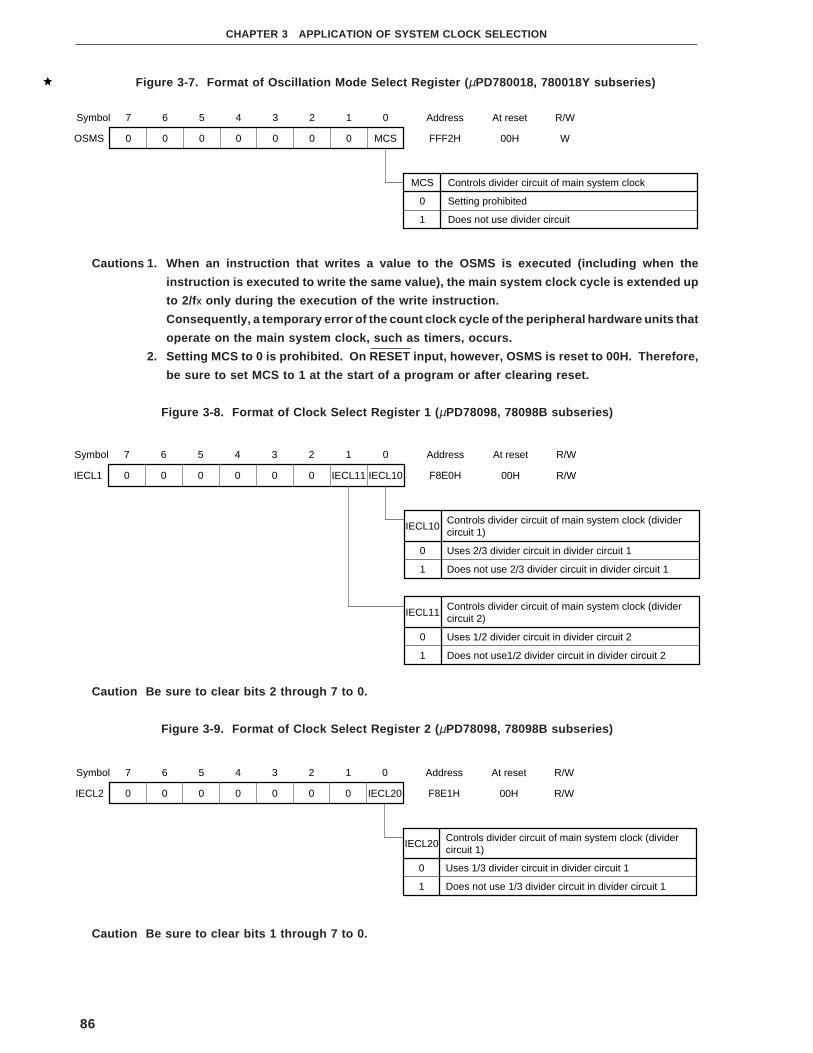
86
CHAPTER 3 APPLICATION OF SYSTEM CLOCK SELECTION
Cautions 1. When an instruction that writes a value to the OSMS is executed (including when the
instruction is executed to write the same value), the main system clock cycle is extended up
to 2/f X only during the execution of the write instruction.
Consequently, a temporary error of the count clock cycle of the peripheral hardware units that
operate on the main system clock, such as timers, occurs.
2. Setting MCS to 0 is prohibited. On RESET input, however, OSMS is reset to 00H. Therefore,
be sure to set MCS to 1 at the start of a program or after clearing reset.
Figure 3-8. Format of Clock Select Register 1 ( µPD78098, 78098B subseries)
Caution Be sure to clear bits 2 through 7 to 0.
Figure 3-9. Format of Clock Select Register 2 ( µPD78098, 78098B subseries)
Caution Be sure to clear bits 1 through 7 to 0.
Figure 3-7. Format of Oscillation Mode Select Register ( µPD780018, 780018Y subseries)
7 6 5 4 3 2Symbol 1 0
MCS Controls divider circuit of main system clock
FFF2HMCSOSMS 00 00000
Address At reset R/W
00H W
0 Setting prohibited
1 Does not use divider circuit
7 6 5 4 3 2Symbol 1 0
Controls divider circuit of main system clock (dividercircuit 1)
F8E0HIECL10IECL1 IECL110 00000
Address At reset R/W
00H R/W
IECL10
0 Uses 2/3 divider circuit in divider circuit 1
1 Does not use 2/3 divider circuit in divider circuit 1
Controls divider circuit of main system clock (dividercircuit 2)
IECL11
0 Uses 1/2 divider circuit in divider circuit 2
1 Does not use1/2 divider circuit in divider circuit 2
7 6 5 4 3 2Symbol 1 0
Controls divider circuit of main system clock (dividercircuit 1)
F8E1HIECL20IECL2 00 00000
Address At reset R/W
00H R/W
IECL20
0 Uses 1/3 divider circuit in divider circuit 1
1 Does not use 1/3 divider circuit in divider circuit 1

87
CHAPTER 3 APPLICATION OF SYSTEM CLOCK SELECTION
The fastest instruction is executed in two CPU clocks. Therefore, the relation between the CPU clock (fCPU) and
minimum instruction execution time is as shown in Tables 3-2 and 3-3.
Table 3-2. Relation between CPU Clock and Minimum Instruction Execution Time
(other than µPD78098 and 78098B subseries)
CPU Clock (fCPU) Minimum Instruction Execution Time: 2/fCPU
Notes 1. Except µPD780018 and 780018Y subseries
2. Except µPD78083 subseries
Remark fX = 5.0 MHz, fXT = 32.768 kHz
fX : Main system clock oscillation frequency
fXT : Subsystem clock oscillation frequency
fX 0.4 µs
fX/2 0.8 µs
fX/22 1.6 µs
fX/23 3.2 µs
fX/24 6.4 µs
fX/25Note 1 12.8 µs
fXTNote 2 122 µs

88
CH
AP
TE
R 3 A
PP
LICA
TIO
N O
F S
YS
TE
M C
LOC
K S
ELE
CT
ION
1 0 0 0 fXT/2(122 µs)
0 0 1
0 1 0
0 1 1
1 0 0
Others Setting prohibited
Remarks 1. fX : Main system clock oscillation frequency
2. fXX : Main system clock frequency
3. fXT : Subsystem clock oscillation frequency
4. ( ) : Minimum instruction execution time with fX = 6.0 MHz or fXT = 32.768 kHz: 2/fCPU
Table 3-3. CPU Clock (f CPU) List ( µPD78098 and 78098B Subseries)
Selects CPU clock (fCPU)
CSS PCC2 PCC1 PCC0 MCS 0 0 0 0 1 1 1 1
IECL20 0 0 1 1 0 0 1 1
IECL10 0 1 0 1 0 1 0 1
0 0 0 0 fXX fX/2 (2fX/3)/2 (fX/3)/2 (2fX/9)/2 fX 2fX/3 fX/3 2fX/9
(0.67 µs) (1.00 µs) (2.00 µs) (3.00 µs) (Setting prohibited) (0.50 µs) (1.00 µs) (1.50 µs)
0 0 1 fXX/2 fX/22 (2fX/3)/22 (fX/3)/22 (2fX/9)/22 fX/2 (2fX/3)/2 (fX/3)/2 (2fX/9)/2
(1.33 µs) (2.00 µs) (4.00 µs) (6.00 µs) (0.67 µs) (1.00 µs) (2.00 µs) (3.00 µs)
0 1 0 fXX/22 fX/23 (2fX/3)/23 (fX/3)/23 (2fX/9)/23 fX/22 (2fX/3)/22 (fX/3)/22 (2fX/9)/22
(2.67 µs) (4.00 µs) (8.00 µs) (12.0 µs) (1.33 µs) (2.00 µs) (4.00 µs) (6.00 µs)
fX/24 (2fX/3)/24 (fX/3)/24 (2fX/9)/24 fX/23 (2fX/3)/23 (fX/3)/23 (2fX/9)/23
(5.33 µs) (8.00 µs) (16.0 µs) (24.0 µs) (2.67 µs) (4.00 µs) (8.00 µs) (12.0 µs)
1 0 0 fXX/24 fX/25 (2fX/3)/25 (fX/3)/25 (2fX/9)/25 fX/24 (2fX/3)/24 (fX/3)/24 (2fX/9)/24
(10.7 µs) (16.0 µs) (32.0 µs) (48.0 µs) (5.33 µs) (8.00 µs) (16.0 µs) (24.0 µs)
0 1 1 fXX/23

89
CHAPTER 3 APPLICATION OF SYSTEM CLOCK SELECTION
3.1 Changing PCC Immediately after RESET
When the RESET signal is asserted, the slowest mode (processor clock control register: PCC = 04H, oscillation
mode select register: OSMS = 00H) of the main system clock is selected for the CPU clock. To set the highest speed
of the CPU clock, therefore, the contents of the PCC must be rewritten (PCC = 00H, OSMS = 01H). To use the fasted
mode, however, the voltage on the VDD pin has to have risen to a sufficient level and be stable.
In the following example, the CPU waits until the VDD pin voltage has risen to the sufficient level by using the watch
timer (the interval time is set to 3.91 ms). After that, the CPU operates on the fastest clock.
Figure 3-10. Example of Selecting CPU Clock after RESET (with µPD78054 subseries)
ON
OFF4.5 V
2.0 V
H
L
Commercialpower source
VDD pin voltage
RESET signal
CPU clock wait time Wait status 0.48 sµ15.28 sµ31.3 ms(217/fX: at 4.19 MHz)
RESET signal is deasserted 10 s after VDD pin voltage has risen to 2.0 V or more. CPU clock oscillation starts.
VDD pin voltage has risento 4.5 V or more before contents of PCC are changed.
µ
3.9 ms

90
CHAPTER 3 APPLICATION OF SYSTEM CLOCK SELECTION
(1) SPD chart
(2) Program list
;**************************************;* Sets wait time;**************************************
TCL2=#00010000BTMC2=#00110110Bwhile_bit(!TMIF3)endwCLR1 WTIFOSMS=#00000001BPCC=#00000000B
; Sets watch timer to 3.91 ms; 3.91 ms?
; Does not use divider circuit; Sets CPU clock in fastest mode
Sets watch timer to 3.91 ms
WHILE: No watch timer interrupt request ( ! TMIF3)
Clears TMIF3
Sets PCC in fastest mode

91
CHAPTER 3 APPLICATION OF SYSTEM CLOCK SELECTION
VSSVDD
+ 5.6V+
INTP1/TI01/P01
PD78054µ
3.2 Selecting Power ON/OFF
The 78K/0 series can operate in an ultra low current consumption mode by using the processor clock control register
(PCC) and selecting the subsystem clock. By providing a backup power supply such as a Ni-Cd battery or super
capacitor to the system, therefore, the system can continue operating even if a power failure occurs.
In this example, a power failure is detected by using INTP1 (both the rising and falling edges are selected as the
edge to be detected), and the contents of the PCC are changed depending on the port level at that time. Figure 3-
11 shows a circuit example, and Figure 3-12 shows the system clock changing timing.
Figure 3-11. Example of System Clock Changing Circuit

92
CHAPTER 3 APPLICATION OF SYSTEM CLOCK SELECTION
ON
OFF
6.0 (V)
4.5 (V)
Commercialpower source
H
L
P01/INTP1 pin
Interrupt request occurs
2.0 (V)
VDD pin voltage
System clock
Mainsystem
clock
MainsystemclockSubsystem clock
Interrupt request occurs
Waits until VDD rises to 4.5 V or more
Figure 3-12. Example of Changing System Clock on Power Failure ( µPD78054 subseries)
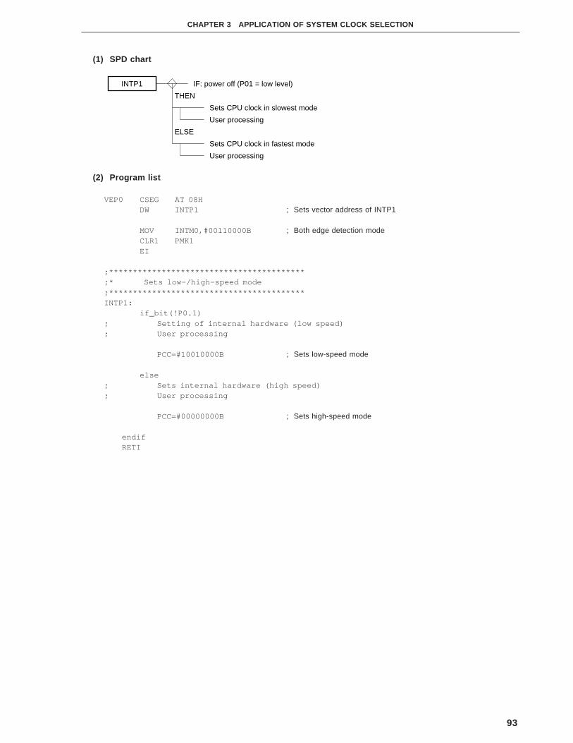
93
CHAPTER 3 APPLICATION OF SYSTEM CLOCK SELECTION
; Sets vector address of INTP1
; Both edge detection mode
; Sets low-speed mode
; Sets high-speed mode
INTP1 IF: power off (P01 = low level)
THEN
Sets CPU clock in slowest mode
User processing
ELSE
Sets CPU clock in fastest mode
User processing
(1) SPD chart
(2) Program list
VEP0 CSEG AT 08HDW INTP1
MOV INTM0,#00110000BCLR1 PMK1EI
;*****************************************;* Sets low-/high-speed mode;*****************************************INTP1:
if_bit(!P0.1); Setting of internal hardware (low speed); User processing
PCC=#10010000B
else; Sets internal hardware (high speed); User processing
PCC=#00000000B
endifRETI

[MEMO]
94

CHAPTER 4 APPLICATIONS OF WATCHDOG TIMER
The watchdog timer of the 78K/0 series has two modes: watchdog timer mode in which a hang-up of the
microcontroller is detected, and interval timer mode.
The watchdog timer is set by using timer clock select register 2 (TCL2) and watchdog timer mode register (WDTM).
95

96
CHAPTER 4 APPLICATIONS OF WATCHDOG TIMER
Figure 4-1. Format of Timer Clock Select Register 2
(µPD78054 78054Y, 78064, 78064Y, 78078, 78078Y, 780058, 780058Y, 780308,
780308Y, 78058F, 78058FY, 78064B, 78075B, 78075BY subseries, µPD78070A,
78070AY)
TCL22 TCL21 TCL20 Selects count clock of watchdog timer
MCS = 1 MCS = 0
0 0 0 fXX/23 fX/23 (625 kHz) fX/24 (313 kHz)
0 0 1 fXX/24 fX/24 (313 kHz) fX/25 (156 kHz)
0 1 0 fXX/25 fX/25 (156 kHz) fX/26 (78.1 kHz)
0 1 1 fXX/26 fX/26 (78.1 kHz) fX/27 (39.1 kHz)
1 0 0 fXX/27 fX/27 (39.1 kHz) fX/28 (19.5 kHz)
1 0 1 fXX/28 fX/28 (19.5 kHz) fX/29 (9.8 kHz)
1 1 0 fXX/29 fX/29 (9.8 kHz) fX/210 (4.9 kHz)
1 1 1 fXX/211 fX/211 (2.4 kHz) fX/212 (1.2 kHz)
TCL24 Selects count clock of watch timer
MCS = 1 MCS = 0
0 fXX/27 fX/27 (39.1 kHz) fX/28 (19.5 kHz)
1 fXT (32.768 kHz)
TCL27 TCL26 TCL25 Selects frequency of buzzer output
MCS = 1 MCS = 0
0 × × Disables buzzer output
1 0 0 fXX/29 fX/29 (9.8 kHz) fX/210 (4.9 kHz)
1 0 1 fXX/210 fX/210 (4.9 kHz) fX/211 (2.4 kHz)
1 1 0 fXX/211 fX/211 (2.4 kHz) fX/212 (1.2 kHz)
1 1 1 Setting prohibited
Caution To change the data of TCL2 except when writing the same data, once stop the timer operation.
Remarks 1. fXX : main system clock frequency (fX or fX/2)
2. fX : main system clock oscillation frequency
3. fXT : subsystem clock oscillation frequency
4. × : don’t care
5. MCS: bit 0 of oscillation mode select register (OSMS)
6. ( ) : fX = 5.0 MHz or fXT = 32.768 kHz
7 6 5 4 3 2Symbol 1 0
FF42HTCL20TCL2 TCL210 TCL22TCL24TCL25TCL26TCL27
Address At reset R/W
00H R/W

97
CHAPTER 4 APPLICATIONS OF WATCHDOG TIMER
Figure 4-2. Format of Timer Clock Select Register 2 ( µPD78083 subseries)
TCL22 TCL21 TCL20 Selects count clock of watchdog timer
MCS = 1 MCS = 0
0 0 0 fXX/23 fX/23 (625 kHz) fX/24 (313 kHz)
0 0 1 fXX/24 fX/24 (313 kHz) fX/25 (156 kHz)
0 1 0 fXX/25 fX/25 (156 kHz) fX/26 (78.1 kHz)
0 1 1 fXX/26 fX/26 (78.1 kHz) fX/27 (39.1 kHz)
1 0 0 fXX/27 fX/27 (39.1 kHz) fX/28 (19.5 kHz)
1 0 1 fXX/28 fX/28 (19.5 kHz) fX/29 (9.8 kHz)
1 1 0 fXX/29 fX/29 (9.8 kHz) fX/210 (4.9 kHz)
1 1 1 fXX/211 fX/211 (2.4 kHz) fX/212 (1.2 kHz)
TCL27 TCL26 TCL25 Selects frequency of buzzer output
MCS = 1 MCS = 0
0 × × Disables buzzer output
1 0 0 fXX/29 fX/29 (9.8 kHz) fX/210 (4.9 kHz)
1 0 1 fXX/210 fX/210 (4.9 kHz) fX/211 (2.4 kHz)
1 1 0 fXX/211 fX/211 (2.4 kHz) fX/212 (1.2 kHz)
1 1 1 Setting prohibited
Cautions 1. To change the data of TCL2 except when writing the same data, once stop the timer operation.
2. Be sure to clear bits 3 and 4 to 0.
Remarks 1. fXX : main system clock frequency (fX or fX/2)
2. fX : main system clock oscillation frequency
3. × : don’t care
4. MCS: bit 0 of oscillation mode select register (OSMS)
5. ( ) : fX = 5.0 MHz
7 6 5 4 3 2Symbol 1 0
FF42HTCL20TCL2 TCL210 TCL220TCL25TCL26TCL27
Address At reset R/W
00H R/W

98
CHAPTER 4 APPLICATIONS OF WATCHDOG TIMER
Figure 4-3. Format of Timer Clock Select Register 2 ( µPD78098, 78098B subseries)
TCL22 TCL21 TCL20 Selects count clock of watchdog timer
0 0 0 fXX/23 (500 kHz)
0 0 1 fXX/24 (250 kHz)
0 1 0 fXX/25 (125 kHz)
0 1 1 fXX/26 (62.5 kHz)
1 0 0 fXX/27 (31.3 kHz)
1 0 1 fXX/28 (15.6 kHz)
1 1 0 fXX/29 (7.8 kHz)
1 1 1 fXX/211 (2.0 kHz)
TCL24 Selects count clock of watch timer
0 fXX/27 (31.3 kHz)
1 fXT (32.768 kHz)
TCL27 TCL26 TCL25 Selects frequency of buzzer output
0 × × Disables buzzer output
1 0 0 fXX/29 (7.8 kHz)
1 0 1 fXX/210 (3.9 kHz)
1 1 0 fXX/211 (1.95 kHz)
1 1 1 Setting prohibited
Caution To change the data of TCL2 except when writing the same data, once stop the timer operation.
Remarks 1. fXX : main system clock frequency
2. fXT : subsystem clock oscillation frequency
3. × : don’t care
4. ( ) : fXX = 4.0 MHz or fXT = 32.768 kHz
7 6 5 4 3 2Symbol 1 0
FF42HTCL20TCL2 TCL210 TCL22TCL24TCL25TCL26TCL27
Address At reset R/W
00H R/W

99
CHAPTER 4 APPLICATIONS OF WATCHDOG TIMER
Figure 4-4. Format of Timer Clock Select Register 2 ( µPD780018, 780018Y subseries)
TCL22 TCL21 TCL20 Selects count clock of watchdog timer
0 0 0 fXX/23 fX/23 (625 kHz)
0 0 1 fXX/24 fX/24 (313 kHz)
0 1 0 fXX/25 fX/25 (156 kHz)
0 1 1 fXX/26 fX/26 (78.1 kHz)
1 0 0 fXX/27 fX/27 (39.1 kHz)
1 0 1 fXX/28 fX/28 (19.5 kHz)
1 1 0 fXX/29 fX/29 (9.8 kHz)
1 1 1 fXX/211 fX/211 (2.4 kHz)
TCL24 Selects count clock of watch timer
0 fXX/27 fX/27 (39.1 kHz)
1 fXT (32.768 kHz)
TCL27 TCL26 TCL25 Selects frequency of buzzer output
0 × × Disables buzzer output
1 0 0 fXX/29 fX/29 (9.8 kHz)
1 0 1 fXX/210 fX/210 (4.9 kHz)
1 1 0 fXX/211 fX/211 (2.4 kHz)
1 1 1 Setting prohibited
Caution To change the data of TCL2 except when writing the same data, once stop the timer operation.
Remarks 1. fXX : main system clock frequency (fX)
2. fX : main system clock oscillation frequency
3. fXT : subsystem clock oscillation frequency
4. × : don’t care
5. ( ): fX = 5.0 MHz or fXT = 32.768 kHz
7 6 5 4 3 2Symbol 1 0
FF42HTCL20TCL2 TCL210 TCL22TCL24TCL25TCL26TCL27
Address At reset R/W
00H R/W

100
CHAPTER 4 APPLICATIONS OF WATCHDOG TIMER
Figure 4-5. Format of Watchdog Timer Mode Register
Notes 1. Once WDTM3 and WDTM4 have been set to 1, they cannot be cleared to 0 by software.
2. When RUN is set to 1, the WDTM starts interval timer operation.
3. Once RUN has been set to 1, it cannot be cleared to 0 by software. Therefore, when counting has been
started, it cannot be stopped by any means other than the RESET signal.
Caution 1. When RUN is set to 1 and the watchdog timer is cleared, the actual overflow time is up to 0.5%
shorter than the time set by the timer clock select register 2.
2. When using the watchdog timer modes 1 and 2, confirm that the interrupt request flag (TMIF4)
is 0 and then set WDTM4 to 1. If WDTM4 is set to 1 while TMIF4 is 1, the non-maskable interrupt
occurs regardless of the contents of WDTM3.
7 6 5 4 3 2Symbol 1 0
WDTM4 Selects operation mode of watchdog timeNote 1
FFF9H0WDTM 0WDTM3 0WDTM400RUN
Address At reset R/W
00H R/W
WDTM3
0 Interval timer modeNote 2 (maskable interruptrequest occurs when overflow occurs)
×
1 Watchdog timer mode (non-maskableinterrupt request occurs when overflow occurs)
0
1 Watchdog timer mode 2 (reset operationstarts when overflow occurs)
1
RUN Selects watchdog timer operationNote 3
0 Stops counting
1 Clears counter and starts counting

101
CHAPTER 4 APPLICATIONS OF WATCHDOG TIMER
4.1 Setting Watchdog Timer Mode
Reset processing or non-maskable interrupt processing is performed after the watchdog timer has detected a hang-
up. You can select which processing is to be performed by the watchdog timer mode register (WDTM). When the
watchdog timer mode is used, the timer must be cleared at intervals shorter than the set hang-up detection time. If
the timer is not cleared, an overflow occurs, and reset or interrupt processing is executed.
The hang-up detection time of the watchdog timer is set by the timer clock select register 2 (TCL2).
In the following example, the hang-up detection time is set to 7.81 ms and the reset processing is performed when
an overflow occurs.
(1) SPD chart
Sets hang-up detection time of watchdog timer to 7.81 ms
Sets watchdog timer in reset start mode
User processing 1
Clears watchdog timer
User processing 2
Clears watchdog timer
User processing 3
Clears watchdog timer

102
CHAPTER 4 APPLICATIONS OF WATCHDOG TIMER
(2) Program list
;*************************************;* Sets watchdog timer;*************************************
OSMS=#00000001BTCL2=#00000100BWDTM=#10011000B
;User processing 1
SET1 RUN;
User processing 2
SET1 RUN;
User processing 3
SET1 RUN
- -
- -
- -
- -
- -
- -
- -
; Does not use divider circuit; Sets watchdog timer to 7.81 ms; Sets reset start mode
; Clears timer
; Clears timer
; Clears timer

103
CHAPTER 4 APPLICATIONS OF WATCHDOG TIMER
4.2 Setting Interval Timer Mode
When the interval timer mode is used, the interval time is set by the timer clock select register 2 (TCL2) (interval
time = 0.488 ms to 125 ms, at fX = 4.19 MHz). In this mode, an interrupt request flag (TMIF4) is set when an overflow
occurs in the timer.
In the following example, three types of times, 0.977 ms, 7.82 ms, and 125 ms, are set.
Figure 4-6. Count Timing of Watchdog Timer
(1) Program list
<1> To set 0.977 ms
TCL2=#00000001B ; Sets 0.977 ms
WDTM=#10001000B ; Selects interval timer mode
<2> To set 7.82 ms
TCL2=#00000100B ; Sets 7.82 ms
WDTM=#10001000B ; Selects interval timer mode
<3> To set 125 ms
TCL2=#00000111B ; Sets 125 ms
WDTM=#10001000B ; Selects interval timer mode
Remark The above interval time is the value when OSMS = 01H.
Timer count
INTWDT
FC FD FE FF 00 01 02 03 FD FE FF 00

[MEMO]
104

CHAPTER 5 APPLICATIONS OF 16-BIT TIMER/EVENT COUNTER
The 16-bit timer/event counter of the 78K/0 series has the following six functions:
• Interval timer
• PWM output
• Pulse width measurement
• External event counter
• Square wave output
• One-shot pulse output
The 16-bit timer/event counter is set by the following registers:
• Timer clock select register 0 (TCL0)
• 16-bit timer mode control register (TMC0)
• Capture/compare control register 0 (CRC0)
• 16-bit timer output control register (TOC0)
• Port mode register 3 (PM3)
• External interrupt mode register (INTM0)
• Sampling clock select register (SCS)
105

106
CHAPTER 5 APPLICATIONS OF 16-BIT TIMER/EVENT COUNTER
Figure 5-1. Format of Timer Clock Select Register 0
(µPD78054, 78054Y, 78064, 78064Y, 78078, 78078Y, 780058, 780058Y, 780308,
780308Y, 78058F, 78058FY, 78064B, 78075B, 78075BY subseries, µPD78070A,
78070AY)
TCL03 TCL02 TCL01 TCL00 Selects clock of PCL output
MCS = 1 MCS = 0
0 0 0 0 fXT (32.768 kHz)
0 1 0 1 fXX fX (5.0 MHz) fX/2 (2.5 MHz)
0 1 1 0 fXX/2 fX/2 (2.5 MHz) fX/22 (1.25 MHz)
0 1 1 1 fXX/22 fX/22 (1.25 MHz) fX/23 (625 kHz)
1 0 0 0 fXX/23 fX/23 (625 kHz) fX/24 (313 kHz)
1 0 0 1 fXX/24 fX/24 (313 kHz) fX/25 (156 kHz)
1 0 1 0 fXX/25 fX/25 (156 kHz) fX/26 (78.1 kHz)
1 0 1 1 fXX/26 fX/26 (78.1 kHz) fX/27 (39.1 kHz)
1 1 0 0 fXX/27 fX/27 (39.1 kHz) fX/28 (19.5 kHz)
Others Setting prohibited
TCL06 TCL05 TCL04 Selects count clock of 16-bit timer register
MCS = 1 MCS = 0
0 0 0 TI00 (valid edge can be specified)
0 0 1 2fXX Setting prohibited fX (5.0 MHz)
0 1 0 fXX fX (5.0 MHz) fX/2 (2.5 MHz)
0 1 1 fXX/2 fX/2 (2.5 MHz) fX/22 (1.25 MHz)
1 0 0 fXX/22 fX/22 (1.25 MHz) fX/23 (625 kHz)
1 1 1 Watch timer output (INTTM3)
Others Setting prohibited
CLOE Controls PCL output
0 Disables output
1 Enables output
Cautions 1. The valid edge of the TI00/INTP0 pin is specified by the external interrupt mode register 0
(INTM0). The frequency of the sampling clock is selected by the sampling clock select register
(SCS).
2. To enable PCL output, set TCL00 through TCL03, and then set CLOE to 1 by using a 1-bit
memory manipulation instruction.
3. Read the count value from TM0, not from the capture/compare register 01(CR01), when TI00
is specified as the count clock of TM0.
4. Before writing new data to TCL0, stop the timer operation once.
7 6 5 4 3 2Symbol 1 0
FF40HTCL00TCL0 TCL01TCL03 TCL02TCL04TCL05TCL06CLOE
Address At reset R/W
00H R/W

107
CHAPTER 5 APPLICATIONS OF 16-BIT TIMER/EVENT COUNTER
Remarks 1. fXX : main system clock frequency (fX or fX/2)
2. fX : main system clock oscillation frequency
3. fXT : subsystem clock oscillation frequency
4. TI00 : input pin of 16-bit timer/event counter
5. TM0 : 16-bit timer register
6. MCS: bit 0 of oscillation mode select register (OSMS)
7. ( ) : at fX = 5.0 MHz or fXT = 32.768 kHz

108
CHAPTER 5 APPLICATIONS OF 16-BIT TIMER/EVENT COUNTER
Figure 5-2. Format of Timer Clock Select Register 0 ( µPD78098, 78098B subseries)
TCL03 TCL02 TCL01 TCL00 Selects clock of PCL output
0 0 0 0 fXT (32.768 kHz)
0 1 0 1 fXX (4.0 MHz)
0 1 1 0 fXX/2 (2.0 MHz)
0 1 1 1 fXX/22 (1.0 MHz)
1 0 0 0 fXX/23 (500 kHz)
1 0 0 1 fXX/24 (250 kHz)
1 0 1 0 fXX/25 (125 kHz)
1 0 1 1 fXX/26 (62.5 kHz)
1 1 0 0 fXX/27 (31.3 kHz)
Others Setting prohibited
TCL06 TCL05 TCL04 Selects count clock of 16-bit timer register
0 0 0 TI00 (valid edge can be specified)
0 0 1 2fXXNote
0 1 0 fXX (4.0 MHz)
0 1 1 fXX/2 (2.0 MHz)
1 0 0 fXX/22 (1.0 MHz)
1 1 1 Watch timer output (INTTM3)
Others Setting prohibited
CLOE Controls PCL output
0 Disables output
1 Enables output
Note At fXX > 2.5 MHz, setting prohibited.
Cautions 1. The valid edge of the TI00/INTP0 pin is specified by the external interrupt mode register 0
(INTM0). The frequency of the sampling clock is selected by the sampling clock select register
(SCS).
2. To enable PCL output, set TCL00 through TCL03, and then set CLOE to 1 by using a 1-bit
memory manipulation instruction.
3. Read the count value from TM0, not from the capture/compare register 01(CR01), when TI00
is specified as the count clock of TM0.
4. Before writing new data to TCL0, stop the timer operation once.
Remarks 1. fXX : main system clock frequency
2. fXT : subsystem clock oscillation frequency
3. TI00 : input pin of 16-bit timer/event counter
4. TM0 : 16-bit timer register
5. ( ) : at fXX = 4.0 MHz or fXT = 32.768 kHz
7 6 5 4 3 2Symbol 1 0
FF40HTCL00TCL0 TCL01TCL03 TCL02TCL04TCL05TCL06CLOE
Address At reset R/W
00H R/W

109
CHAPTER 5 APPLICATIONS OF 16-BIT TIMER/EVENT COUNTER
Figure 5-3. Format of Timer Clock Select Register 0 ( µPD780018, 780018Y subseries)
TCL03 TCL02 TCL01 TCL00 Selects clock of PCL output
0 0 0 0 fXT (32.768 kHz)
0 1 0 1 fXX fX (5.0 MHz)
0 1 1 0 fXX/2 fX/2 (2.5 MHz)
0 1 1 1 fXX/22 fX/22 (1.25 MHz)
1 0 0 0 fXX/23 fX/23 (625 kHz)
1 0 0 1 fXX/24 fX/24 (313 kHz)
1 0 1 0 fXX/25 fX/25 (156 kHz)
1 0 1 1 fXX/26 fX/26 (78.1 kHz)
1 1 0 0 fXX/27 fX/27 (39.1 kHz)
Others Setting prohibited
TCL06 TCL05 TCL04 Selects count clock of 16-bit timer register
0 0 0 TI00 (valid edge can be specified)
0 1 0 fXX fX (5.0 MHz)
0 1 1 fXX/2 fX/2 (2.5 MHz)
1 0 0 fXX/22 fX/22 (1.25 MHz)
1 1 1 Watch timer output (INTTM3)
Others Setting prohibited
CLOE Controls PCL output
0 Disables output
1 Enables output
Cautions 1. The valid edge of the TI00/INTP0 pin is specified by the external interrupt mode register 0
(INTM0). The frequency of the sampling clock is selected by the sampling clock select register
(SCS).
2. To enable PCL output, set TCL00 through TCL03, and then set CLOE to 1 by using a 1-bit
memory manipulation instruction.
3. Read the count value from TM0, not from the capture/compare register 01(CR01), when TI00
is specified as the count clock of TM0.
4. Before writing new data to TCL0, stop the timer operation once.
Remarks 1. fXX : main system clock frequency (fX)
2. fX : main system clock oscillation frequency
3. fXT : subsystem clock oscillation frequency
4. TI00 : input pin of 16-bit timer/event counter
5. TM0 : 16-bit timer register
6. ( ) : at fX = 5.0 MHz or fXT = 32.768 kHz
7 6 5 4 3 2Symbol 1 0
FF40HTCL00TCL0 TCL01TCL03 TCL02TCL04TCL05TCL06CLOE
Address At reset R/W
00H R/W

110
CHAPTER 5 APPLICATIONS OF 16-BIT TIMER/EVENT COUNTER
Figure 5-4. Format of 16-Bit Timer Mode Control Register
OVF0 Detects overflow of 16-bit timer register
0 Overflow does not occur
1 Overflow occurs
TMC03 TMC02 TMC01 Selects operation mode Selects output timing of TO0 Occurrence of
and clear mode interrupt request
0 0 0
0 0 1
0 1 0
0 1 1
1 0 0
1 0 1
1 1 0
1 1 1
Cautions 1. Before setting the clear mode or changing the output timing of TO0, stop the timer operation
(by clearing TMC01 through TMC03 to 0, 0, 0).
2. The valid edge of the TI00/INTP0 pin is selected by the external interrupt mode register 0
(INTM0). The frequency of the sampling clock is selected by the sampling clock select register
(SCS).
3. When using the PWM mode, set data to CR00 after setting the PWM mode.
4. When a mode in which the timer is cleared and started on coincidence between TM0 and CR00,
the OVF0 flag is set to 1 when the set value of CR00 is FFFFH and the value of TM0 changes
from FFFFH to 0000H.
5. The 16-bit timer register starts operating as soon as a value other than 0, 0, 0 (operation stop
mode) is set to TMC01 through TMC03. To stop the operation, clear TMC01 through TMC03
to 0, 0, 0.
Stops operation (clears TM0
to 0)
PWM mode (free running)
Free running mode
Clears and starts at valid edge
of TI00
Clears and start at coinci-
dence between TM0 and
CR00
Not affected
PWM pulse output
Coincidence between TM0
and CR00 or between TM0
and CR01
Coincidence between TM0
and CR00, or between TM0
and CR01, or valid edge of
TI00
Coincidence between TM0
and CR00 or between TM0
and CR01
Coincidence between TM0
and CR00, or between TM0
and CR01, or valid edge of
TI00
Coincidence between TM0
and CR00 or between TM0
and CR01
Coincidence between TM0
and CR00, or between TM0
and CR01, or valid edge of
TI00
Does not occur
Occurs if TM0 and CR00
coincide and if TM0 and
CR01 coincide
7 6 5 4 3 2Symbol 1 0
FF48HOVF0TMC0 TMC01TMC03 TMC020000
Address At reset R/W
00H R/W

111
CHAPTER 5 APPLICATIONS OF 16-BIT TIMER/EVENT COUNTER
Remarks 1. TO0 : output pin of 16-bit timer/event counter
2. TI00 : input pin of 16-bit timer/event counter
3. TM0 : 16-bit timer register
4. CR00 : compare register 00
5. CR01 : compare register 01
Figure 5-5. Format of Capture/Compare Control Register
Cautions 1. Be sure to stop the timer operation before setting CRC0.
2. When a mode in which the timer is cleared and started on coincidence between TM0 and CR00
is selected by the 16-bit timer mode control register, do not specify CR00 as the capture
register.
7 6 5 4 3 2Symbol 1 0
CRC00 Selects operation mode of CR00
FF4CHCRC00CRC0 CRC010 CRC020000
Address At reset R/W
04H R/W
0 Operates as compare register
1 Operates as capture register
CRC01 Selects capture trigger of CR00
0 Captures at valid edge of TI01
1 Captures at valid edge of TI00
CRC02 Selects operation mode of CR01
0 Operates as compare register
1 Operates as capture register

112
CHAPTER 5 APPLICATIONS OF 16-BIT TIMER/EVENT COUNTER
Figure 5-6. Format of 16-Bit Timer Output Control Register
Cautions 1. Be sure to stop the timer operation before setting TOC0 (except OSPT).
2. LVS0 and LVR0 are always 0 when they are read immediately after data has been set.
3. OSPT is automatically cleared after data has been set. It is therefore always 0 when read.
7 6 5 4 3 2Symbol 1 0
TOE0 Controls output of 16-bit timer/event counter
FF4EHTOE0TOC0 TOC01LVS0 LVR0TOC04OSPEOSPT0
Address At reset R/W
00H R/W
0 Disables output (port mode)
1 Enables output
TOC01 PWM mode Other than PWM mode
Selects active level Controls timer output F/Fon coincidence betweenCR00 and TM0
0 Active high Disables reverse operation
1 Active low Enables reverse operation
LVS0 Sets status of timer output F/F of 16-bit timer/event counter
0 Not affected
0 Resets timer output F/F (to 0)
LVR0
0
1
0 Sets timer output F/F (to 1)
0 Setting prohibited
0
1
TOC04 Controls timer output F/F on coincidence betweenCR01 and TM0
0 Disables reverse operation
0 Enables reverse operation
OSPE Controls one-shot pulse output operation
0 Successive pulse output
1 One-shot pulse output
OSPT Controls output trigger of one-shot pulse by software
0 No one-shot pulse trigger
1 One-shot pulse trigger

113
CHAPTER 5 APPLICATIONS OF 16-BIT TIMER/EVENT COUNTER
Figure 5-7. Format of Port Mode Register 3
Figure 5-8. Format of External Interrupt Mode Register 0
Caution Before setting the valid edge of the INTP0/TI00/P00 pin, clear bits 1 through 3 (TMC01 through
TMC03) of the 16-bit timer mode control register (TMC0) to 0, 0, 0, and stop the timer.
7 6 5 4 3 2Symbol 1 0
ES11 Selects valid edge of INTP0
FFECH0INTM0 0ES11 ES10ES20ES21ES30ES31
Address At reset R/W
00H R/W
0 Falling edge
0 Rising edge
ES10
0
1
1 Setting prohibited
1 Both rising and falling edges
0
1
ES21 Selects valid edge of INTP1
0 Falling edge
0 Rising edge
ES20
0
1
1 Setting prohibited
1 Both rising and falling edges
0
1
ES31 Selects valid edge of INTP2
0 Falling edge
0 Rising edge
ES30
0
1
1 Setting prohibited
1 Both rising and falling edges
0
1
7 6 5 4 3 2Symbol 1 0
PM3n Selects input/output mode of P3n pin (n = 0-7)
FF23HPM30PM3 PM31PM33 PM32PM34PM35PM36PM37
Address At reset R/W
FFH R/W
0 Output mode (output buffer ON)
1 Input mode (output buffer OFF)

114
CHAPTER 5 APPLICATIONS OF 16-BIT TIMER/EVENT COUNTER
Figure 5-9. Format of Sampling Clock Select Register
(µPD78054, 78054Y, 78064, 78064Y, 78078, 78078Y, 780058, 780058Y, 780308,
780308Y, 78058F, 78058FY, 78064B, 78075B, 78075BY subseries, µPD78070A,
78070AY)
Caution f XX/2N is the clock supplied to the CPU, and f XX/25, fXX/26, and f XX/27 are the clocks supplied to the
peripheral hardware. f XX/2N is stopped in the HALT mode.
Remarks 1. N : Value (N = 0 to 4) set to the bits 0 through 2 (PCC0 through PCC2) of the processor clock
control register (PCC)
2. fXX : main system clock frequency (fX or fX/2)
3. fX : main system clock oscillation frequency
4. MCS: bit 0 of oscillation mode select register (OSMS)
5. ( ) : at fX = 5.0 MHz
7 6 5 4 3 2Symbol 1 0
SCS1 Selects sampling clock of INTP0
FF47HSCS0SCS SCS10 00000
Address At reset R/W
00H R/W
SCS0
MCS = 1
0 fXX/2N0
MCS = 0
0 fXX/271 fX/27 (39.1 kHz) fX/28 (19.5 kHz)
1 fXX/250 fX/25 (156.3 kHz) fX/26 (78.1 kHz)
1 fXX/261 fX/26 (78.1 kHz) fX/27 (39.1 kHz)

115
CHAPTER 5 APPLICATIONS OF 16-BIT TIMER/EVENT COUNTER
Figure 5-10. Format of Sampling Clock Select Register ( µPD78098, 78098B subseries)
Caution f XX/2N is the clock supplied to the CPU, and f XX/25, fXX/26, and f XX/27 are the clocks supplied to the
peripheral hardware. f XX/2N is stopped in the HALT mode.
Remarks 1. N : Value (N = 0 to 4) set to the bits 0 through 2 (PCC0 through PCC2) of the processor clock control
register (PCC)
2. fXX : main system clock frequency
3. ( ) : at fXX = 4.0 MHz
Figure 5-11. Format of Sampling Clock Select Register ( µPD780018, 780018Y subseries)
Caution f XX/2N is the clock supplied to the CPU, and f XX/25, fXX/26, and f XX/27 are the clocks supplied to the
peripheral hardware. f XX/2N is stopped in the HALT mode.
Remarks 1. N : Value (N = 0 to 4) set to the bits 0 through 2 (PCC0 through PCC2) of the processor clock control
register (PCC)
2. fXX : main system clock frequency (fX)
3. fX : main system clock oscillation frequency
4. ( ) : at fX = 5.0 MHz
7 6 5 4 3 2Symbol 1 0
SCS1 Selects sampling clock of INTP0
FF47HSCS0SCS SCS10 00000
Address At reset R/W
00H R/W
SCS0
0 fXX/2N0
0 fXX/27 (31.3 kHz)1
1 fXX/25 (125.0 kHz)0
1 fXX/26 (62.5 kHz)1
7 6 5 4 3 2Symbol 1 0
SCS1 Selects sampling clock of INTP0
FF47HSCS0SCS SCS10 00000
Address At reset R/W
00H R/W
SCS0
0 fXX/2N0
0 fXX/27 1
1 fXX/25 0
1 fXX/26 1
fX/27 (39.1 kHz)
fX/25 (156.3 kHz)
fX/26 (78.1 kHz)

116
CHAPTER 5 APPLICATIONS OF 16-BIT TIMER/EVENT COUNTER
5.1 Setting of Interval Timer
To set the 16-bit timer/event counter as an interval timer, first set the timer clock select register 0 (TCL0) and the
16-bit timer mode control register (TMC0). The clear mode of the 16-bit timer is set by TMC0 and the interval time
is set by TCL0.
After that, set the value of the compare register (CR00) from the setup time and count clock. Determine the setup
time by using the following expression:
Setup time = (Compare register value + 1) × Count clock cycle
This section shows two examples of setup times of the interval timer: 10 ms and 50 ms.
(a) Interval of 10 ms
<1> Setting of TMC0
Selects a mode in which the timer is cleared and started on coincidence between TM0 and CR00.
<2> Setting of TCL0
Select the fXX mode in which an interval time of 10 ms or more can be set and the resolution is the
highest (OSMS = 01H).
<3> Setting of CR00
10 ms = (N + 1) ×
N = 10 ms × 4.19 MHz – 1 = 4.1899
(1) Program list
OSMS = #00000001B; Does not use divider circuit
CRC0 = #00000000B ; Selects CR00 as compare register
CR00 = #41899
TCL0 = #00100000B ; Selects count clock fXX
TMC0 = #00001100B ; Clears and starts 16-bit timer/event counter when TM0 and CR00 coincide
14.19 MHz
••

117
CHAPTER 5 APPLICATIONS OF 16-BIT TIMER/EVENT COUNTER
(b) Interval of 50 ms
<1> Setting of TMC0
Selects a mode in which the timer is cleared and started on coincidence between TM0 and CR00.
<2> Setting of TCL0
Select the fXX/22 mode in which an interval time of 50 ms or more can be set and the resolution is
the highest (OSMS = 01H).
<3> Setting of CR00
50 ms = (N + 1) ×
N = 50 ms × 4.19 MHz/22 – 1 = 52374
(1) Program list
OSMS = #00000001B; Does not use divider circuit
CRC0 = #00000000B ; Selects CR00 as compare register
CR00 = #52374
TCL0 = #01000000B ; Selects count clock fXX/22
TMC0 = #00001100B ; Clears and starts 16-bit timer/event counter when TM0 and CR00 coincide
14.19 MHz/22
••

118
CHAPTER 5 APPLICATIONS OF 16-BIT TIMER/EVENT COUNTER
5.2 PWM Output
When using the 16-bit timer/event counter in the PWM output mode, set the PWM mode by the 16-bit timer mode
control register (TMC0) and enables the output of the 16-bit timer/event counter by the 16-bit timer output control
register (TOC0).
The pulse width (active level) of PWM is determined by the value set to the capture/compare register 00 (CR00).
Because the PWM of the 78K/0 series has a resolution of 14 bits, however, bits 2 through 15 of CR00 are valid (clear
bits 0 and 1 of CR00 to ‘0, 0’).
In the example below, the basic cycle of the PWM mode is set to 61.0 µs ( × 28) and the low level is selected
as the active level. The high-order 4 bits of the pulse width are rewritten depending on the value of the parameter
(00H to FFH). Therefore, in the following application example, PWM output can be performed in 16 steps (CR00 =
0FFCH to FFFCH).
(1) Description of package
<Public declaration symbol>
PWM : PWM output subroutine name
PWMOUT: input parameter of PWM active level
<Registers used>
AX
<RAM used>
Name Usage Attribute Bytes
PWMOUT Sets PWM active level SADDR 1
<Nesting>
1 level 2 bytes
<Hardware units used>
• 16-bit timer/event counter
• P30/TO0
1fXX

119
CHAPTER 5 APPLICATIONS OF 16-BIT TIMER/EVENT COUNTER
<Initial setting>
• OSMS = #00000001B ; Oscillation mode select register: does not use divider circuit
• Setting of 16-bit timer/event counter
CRC0 = #00000000B ; Selects CR00 as compare register
TMC0 = #00000010B ; PWM output mode
TCL0 = #00100000B ; PWM basic cycle: 61.0 µs
TOC0 = #00000011B ; Low-active output
• PM30 = 0 ; P30 output mode
• P30 = 0 ; P30 output latch
<Starting>
After setting data to PWMOUT in RAM, call subroutine PWM.
(2) Example of use
EXTRN PWM, PWMOUT
OSMS = #00000001B ; Does not use divider circuit
CRC0 = #00000000B ; Selects CR00 as compare register
TOC0 = #00000011B ; Sets low-active PWM output
TCL0 = #00100000B ; Selects count clock fXX
TMC0 = #00000010B ; Sets PWM mode
PWMOUT = A ; Sets input parameter of active level
CALL !PWM
(3) SPD chart
...
...
PWM Loads data of PWMOUT
Decodes data of high-order 4 bits of CR00
Sets XFFCH to CR00 (X: 0 to FH)

120
CHAPTER 5 APPLICATIONS OF 16-BIT TIMER/EVENT COUNTER
(4) Program list
PUBLIC PWM,PWMOUTPWM_DAT DSEG SADDRPWMOUT: DS 1;************************************;* PWM output (16 steps);************************************P0_SEG CSEGPWM:
A=PWMOUTA<<=1A<<=1A<<=1A<<=1A|=#0FHX=#0FCHCR00=AXRET
; PWM output data area (0-15)
; Loads high-order data of PWMOUT
; Sets low-order 12 bits to 0FFCH

121
CHAPTER 5 APPLICATIONS OF 16-BIT TIMER/EVENT COUNTER
5.3 Remote Controller Signal Reception
This section introduces two examples of programs that receives signals from a remote controller by using the 16-
bit timer/event counter.
• The counter is cleared each time the valid edge of the remote controller signal has been detected, and measures
a pulse width from the timer count value (capture register CR01) when the next valid edge has been detected.
• The timer operates in the free running mode to measure a pulse width from the difference of the counter between
valid edges. PWM output is also performed at the same time.
The remote controller signal is received by a PIN receiver diode and is input to the P00/TI00/INTP0 pin via receive
amplifier µPC1490. Figure 5-12 shows an example of a remote controller signal receiver circuit, and Figure 5-13 shows
the format of the remote controller signal.
Figure 5-12. Example of Remote Controller Signal Receiver Circuit
PH310
160 kΩ
f0 VCC
100 kΩ
IN+ OUT
+ 100 Fµ
INTP0/TI00/P00
VDD
GND
4.7 Ω
IN–
+ 1 Fµ
CD
+ 10 Fµ
GND C1
1000 pF
PC1490µ
PD78054µ
+5 V
Shield case

122
CHAPTER 5 APPLICATIONS OF 16-BIT TIMER/EVENT COUNTER
Figure 5-13. Remote Controller Signal Transmitter IC Output Signal
Because the receiver preamplifier µPC1490 used in the circuit example on the previous page is low-active, the
level input to the µPD78054 subseries is the inverted data of the remote controller transmit data.
Figure 5-14. Output Signal of Receiver Preamplifier
Time at oscillation frequency of 455 kHz
Firsttime
Second time and onward (signal transmitted only while key is held down)
67.5 ms
108 ms 108 ms
9 ms
13.5 ms
27 ms 27 ms
67.5 ms
9 ms 4.5 ms
13.5 ms 2.25 ms
9 ms 2.25 ms
11.25 ms0.56 ms
1.125 ms0 1 1 0 0 1
0.56 ms
Leader Code
4.5 ms
Custom Code8 bits
Custom Code8 bits
Data Code8 bits
Data Code8 bits
PC1490 output
4.5 ms
Leader code
µ
9 ms
H
L

123
CHAPTER 5 APPLICATIONS OF 16-BIT TIMER/EVENT COUNTER
5.3.1 Remote controller signal reception by counter clearing
Table 5-1 shows the valid pulse width for receiving a remote controller signal in the program example shown in
this section, and <1> through <6> describes how to process each signal. The repeat signal of the remote controller
signal is valid only within 250 ms after a valid signal has been input. If a signal input within 3 ms after the normal
data has been loaded, the data is invalid.
Table 5-1. Valid Time of Input Signal
Signal Name Output Time Valid Time
Leader code (low) 9 ms 6.8 ms-11.8 ms
Leader code Normal 4.5 ms 3 ms-5 ms
(high) Repeat 2.25 ms 1.8 ms-3 ms
Custom/data 0 1.125 ms 0.5 ms-1.8 ms
code 1 2.25 ms 1.8 ms-2.5 ms
<1> Leader code (low)
The interval time of the 16-bit timer/event counter is set to 1.5 ms, and the port level is sampled by means
of interrupt processing. When five low levels have been detected in succession, these low levels are
identified as a leader code, and the interval time is changed to 7.81 ms. After that, the pulse width of
the low level of the leader code is measured by using rising-edge interrupt request INTP0.
Figure 5-15. Sampling of Remote Controller Signal
Interval time
Noise NoiseValid if low five
times in succession
7.81 ms1.5 ms

124
CHAPTER 5 APPLICATIONS OF 16-BIT TIMER/EVENT COUNTER
<2> Leader code (high)
The pulse width while the leader code is high is measured by using the falling-edge interrupt request
INTP0 and the count value of the timer.
<3> Custom/data code
The pulse width of each 1 bit (1 cycle) is measured by using the falling-edge interrupt request INTP0.
After the data of the 32nd bit has been loaded, the system tests if the inverted data and custom code
coincide. It also checks that there is no data in the 33rd bit.
<4> Repeat code detection
When the high level of the leader code is less than 3 ms, the pulse width from output of the leader code
to the rising edge of the INTP0 is measured.
<5> Valid period of repeat code
After the valid data has been input, sampling is performed by the interrupt processing (1.5 ms interval)
of the 16-bit timer/event counter to measure the valid time of the repeat code of 250 ms.
<6> Time out during pulse width measurement
If the interrupt request of the 16-bit timer/event counter (7.81 ms) occurs during pulse width measure-
ment, it is judged to be time out, and the data is invalid.
(1) Description of package
<Public declaration symbol>
RMDATA : Stores remote controller receive data
RPT : Repeat valid period identification flag
IPDTFG : Valid data identification flag
RMDTOK : Input signal validity identification flag
RMDTSET : Input signal identification flag
<Registers used>
Bank 0: AX, BC, HL

125
CHAPTER 5 APPLICATIONS OF 16-BIT TIMER/EVENT COUNTER
<RAM used>
Name Usage Attribute Bytes
RPTCT Repeat code valid time counter SADDR 1
RMENDCT No-input time counter after data input
SELMOD Mode selection
LD_CT Leader signal detection counter
RMDATA Valid data storage area
WORKP Input signal storage area SADDRP 4
<Flags used>
Name Usage
IPDTFG Presence/absence of valid data
RMDTOK Validity of input signal
RMDTSET Presence/absence of input signal
RPT Judgment whether repeat valid period elapsed
<Nesting>
5 levels 12 bytes
<Hardware used>
• 16-bit timer/event counter
• P00/TI00/INTP0
<Initial setting>
• OSMS = #00000001B ; Oscillation mode select register: does not use divider circuit
• Setting of 16-bit timer/event counter
CRC0 = #00000100B ; Selects operation mode of CR00, CR01
TMC0 = #00001100B ; Clears timer on coincidence between TM0 and CR00
TCL0 = #00100000B ; Count clock fXX
CR00 = #6290 ; Compare register 00
• SCS = #00000011B ; INTP0 sampling clock fXX/26
• PPR0 = 0 ; INTP0 high-priority interrupt
• TMMK0 = 0 ; Enables 16-bit timer/event counter interrupt
• Defines custom code to be CSTM and declares PUBLIC
• RAM clear
<Starting>
Started by INTP0 and INTTM00 interrupt requests

126
CHAPTER 5 APPLICATIONS OF 16-BIT TIMER/EVENT COUNTER
(2) Example of use
PUBLIC CSTMEXTRN RMDATA,RPTCTEXTBIT RPT,RMDTSET,IPDTFG
CSTM EQU 9DH
OSMS=#00000001BCRC0=#00000100BCR00=#6290TCL0=#00100000BTMC0=#00001100BSCS=#00000011B
CLR1 PPR0CLR1 RPTCLR1 IPDTFGCLR1 RMDTSET
CLR1 TMMK0EI
DT_TEST:if_bit(RMDTSET)
CLR1 RMDTSETif_bit(RPT)
;; Repeat processing;
else;; Processing when there is input;
endifelse
if_bit(!RPT);; Processing when there is no input;
endifendif
; Remote controller custom code
; Does not use divider circuit; Selects operation mode of CR00, CR01
; Sets 1.5 ms
; fXX/26 as INTP0 sampling clock
; INTP0 with high priority; Clears flag
; Enables timer interrupt

127
CHAPTER 5 APPLICATIONS OF 16-BIT TIMER/EVENT COUNTER
(3) SPD chart
INTTM00 Selects register bank 1
Enables master interrupt
IF: input signal exists (IPDTFG)
IF: valid data exists (RMDTOK)
THEN
THEN
IF: no input within repeat valid time (250 ms)
THEN
Invalidates repeat code
ELSE Clears RPT, IPDTFG, and RMDTOK
Counts repeat valid time
Counts leader low time S_LOWCT
ELSE
IF: No input after end of data input (within 4.5 ms)
THEN
Valid data exists
Sets RMDTOK and RMDTSET
Sets leader low detection mode S_M0SET
Initializes leader low detection counter
ELSE
Counts leader low time S_LOWCT
S_LOWCT IF: Leader low detection mode
THEN
IF: P00 = LOW
IF: P00 = LOW five times in succession
THEN
THEN
Selects leader low measuring mode
Sets 16-bit timer to 7.81 ms
Sets INTP0 rising-edge detection mode
Enables INTP0
Initializes leader low detection counter
Initializes leader detection counter
ELSE
ELSE
Sets leader low detection mode S_M0SET
Initializes leader detection counter

128
CHAPTER 5 APPLICATIONS OF 16-BIT TIMER/EVENT COUNTER
INTP0 Selects register bank 0
Waits for 100 s WAITµCASE: SELMOD
OF: 1
Leader low measuring mode LEAD_L
OF: 2
Leader high measuring mode LEAD_H
OF: 3
Custom code/data loading mode CDCODE
OF: 4
Repeat code detection mode REPCD
OF: 5
Abnormal data detection mode ENDCHK
LEAD_L IF: P00 = HIGH
LEAD_H IF: P00 = LOW
Waits for 100 s WAIT
THEN
µIF: P00 = HIGH
THEN
Reads timer CR_READ
IF: 6.8 ms ≤ Ieader low ≤ 11.8 ms
THEN
Selects leader high detection mode
Sets INTP0 falling-edge detection mode
ELSE
Sets leader low detection mode S_M0SET
THEN
Waits for 100 s WAITµIF: P00 = LOW
THEN
Reads timer CR_READ
IF: 2 ms ≤ leader high ≤ 5 ms
THEN
IF: Ieader high ≥ 3 ms
THEN
Selects custom code/data load mode
Initializes data storage area
ELSE
Selects repeat detection mode
Sets INTP0 rising-edge detection mode
ELSE
Sets leader low detection mode S_M0SET

129
CHAPTER 5 APPLICATIONS OF 16-BIT TIMER/EVENT COUNTER
CDCODE IF: P00 = LOW
THEN
Waits for 100 s WAITµIF: P00 = LOW
THEN
Reads timer CR_READ
IF: 0.5 ms < input data ≤ 2.5 ms
THEN
IF: input data ≥ 1.8 ms
THEN
Sets CY
ELSE
Clears CY
Stores CY to data storage area
IF: end of 32 bits of data input
THEN
IF: custom code coincides
THEN
IF: custom/data code coincides with inverted data
THEN
Stores data code
Sets status in which input data exists
Sets IPDTFG and clears RMDTSET, RPT, and RMDTOK
Sets leader low detection mode S_M0SET
ELSE
Sets leader low detection mode S_M0SET
ELSE
Sets leader low detection mode S_M0SET
ELSE
Sets leader low detection mode S_M0SET
REPCD IF: P00 = HIGH
THEN
Waits for 100 s WAITµIF: P00 = HIGH
THEN
IF: valid data exists
THEN
Reads timer CR_READ
IF: repeat code ≤ 1 ms
THEN
Sets repeat code valid status
Sets RPT
Sets data input end status
Sets abnormal data detection mode S_M5SET
ELSE
Sets leader low detection mode S_M0SET
ELSE
Sets abnormal data detection mode S M5SET

130
CHAPTER 5 APPLICATIONS OF 16-BIT TIMER/EVENT COUNTER
ENDCHK IF: P00 = LOW
THEN
Waits for 100 s WAITµIF: P00 = LOW
THEN
Sets input signal invalid status
Sets leader low detection mode S_M0SET
Clears IPDTFG and RPT
CR_READ Reads capture register
Stops 16-bit timer operation
Starts timer
S_M0SET Selects leader low detection mode
Disables INTP0 interrupt
Sets 16-bit timer to 1.5 ms
S_M5SET Selects abnormal data detection mode
Sets counter for repeat valid time
Sets 16-bit timer to 1.5 ms

131
CHAPTER 5 APPLICATIONS OF 16-BIT TIMER/EVENT COUNTER
; Repeat code valid time counter; No-input time counter after data input; Selects mode; Leader signal detection counter; Valid data storage area
; Input signal storage area
; Valid data exists; Input signal is valid; Input signal exists; Repeat code valid period
; Sets vector address of INTP0
; Sets vector address of 16-bit timer
; Enables interrupt (INTP0); Input signal exists?; Valid data exists?
; Repeat invalid time; Repeat code invalid status
; Sets that valid data exists
; Sets leader (low) detection mode
(4) Program list
PUBLIC RPT,IPDTFG,RMDTOK,RMDTSETPUBLIC RMENDCT,RPTCT,SELMOD,LD_CT,RMDATAEXTRN CSTM
RM_DAT DSEG SADDRRPTCT: DS 1RMENDCT: DS 1SELMOD: DS 1LD_CT: DS 1RMDATA: DS 1
RM_DATP DSEG SADDRPWORKP: DS 4
BSEGIPDTFG DBITRMDTOK DBITRMDTSET DBITRPT DBIT
VEP0 CSEG AT 06HDW INTP0
VETM0 CSEG AT 20HDW INTTM00
;******************************************************; Remote controller signal timer processing;******************************************************TM0_SEG CSEGINTTM00:
SEL RB1EIif_bit(IPDTFG)
if_bit(RMDTOK)RPTCT––
if(RPTCT==#0)CLR1 RPTCLR1 IPDTFGCLR1 RMDTOK
endifCALL !S_LOWCT
elseRMENDCT––if(RMENDCT==#0)
SET1 RMDTOKSET1 RMDTSETCALL !S_M0SET
endifLD_CT=#5
endifelse
CALL !s_LOWCTendifRETI

132
CHAPTER 5 APPLICATIONS OF 16-BIT TIMER/EVENT COUNTER
S_LOWCT:if(SELMOD==#0)
if_bit(!P0.0)LD_CT––if(LD_CT==#0)
SELMOD=#1TMC0=#00000000BCR00=#32767TMC0=#00001100BINTM0=#00000100BCLR1 PIF0CLR1 PMK0LD_CT=#5
endifelse
LD_CT=#5endif
elseCALL !S_MOSETLD_CT=#5
endifRET
$EJECT;***********************************************************;* Remote controller signal edge detection processing;***********************************************************P0_SEG CSEGINTP0:
SEL RB0CALL !WAITswitch(SELMOD)case 1:
CALL !LEAD_Lbreak
case 2:CALL !LEAD_Hbreak
case 3:CALL !CDCODEbreak
case 4:CALL !REPCDbreak
case 5:CALL !ENDCHK
endsRET1
; Leader (low) detection mode?
; Leader (low) measuring mode
; Timer: 7.81 ms
; Enables INTP0 interrupt
; Sets leader (low) detection mode
; Waits for 100 µs
; Leader low detection processing
; Leader high detection processing
; Custom/data code loading processing
; Repeat code detection processing
; Abnormal data detection processing
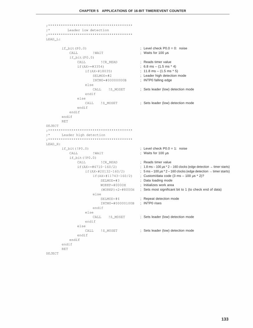
133
CHAPTER 5 APPLICATIONS OF 16-BIT TIMER/EVENT COUNTER
; Level check P0.0 = 0: noise; Waits for 100 µs
; Reads timer value; 6.8 ms – (1.5 ms * 4); 11.8 ms – (1.5 ms * 5); Leader high detection mode; INTP0 falling edge
; Sets leader (low) detection mode
; Sets leader (low) detection mode
; Level check P0.0 = 1: noise; Waits for 100 µs
; Reads timer value; 1.8 ms – 100 µs * 2 – 160 clocks (edge detection → timer starts); 5 ms – 100 µs * 2 – 160 clocks (edge detection → timer starts); Custom/data code (3 ms – 100 µs * 2)?; Data loading mode; Initializes work area; Sets most significant bit to 1 (to check end of data)
; Repeat detection mode; INTP0 rises
; Sets leader (low) detection mode
; Sets leader (low) detection mode
;****************************************;* Leader low detection;****************************************LEAD_L:
if_bit(P0.0)CALL !WAITif_bit(P0.0)
CALL !CR_READif(AX>=#3354)
if(AX<#18035)SELMOD=#2INTM0=#00000000B
elseCALL !S_MOSET
endifelse
CALL !S_MOSETendif
endifendifRET
$EJECT;****************************************;* Leader high detection;****************************************LEAD_H:
if_bit(!P0.0)CALL !WAITif_bit(!P0.0)
CALL !CR_READif(AX>=#6710–160/2)
if(AX<#20132–160/2)if(AX>#11743–160/2)
SELMOD=#3WORKP=#0000H(WORKP)+2=#8000H
elseSELMOD=#4INTM0=#00000100B
endifelse
CALL !S_M0SETendif
elseCALL !S_M0SET
endifendif
endifRET
$EJECT

134
CHAPTER 5 APPLICATIONS OF 16-BIT TIMER/EVENT COUNTER
; Level check P0.0 = 1: noise; Waits for 100 µs
; Reads timer value; 0.5 ms – 100 µs * 2 – 190 clocks (edge detection → timer starts); 2.5 ms – 100 µs * 2 –190 clocks (edge detection → timer starts); 1.8 ms – 100 µs * 2 – 190 clocks (edge detection → timer starts)
; Sets work area address; Sets number of digits of work area
; Stores 1-bit data; Shifts 1 bit
; End of shifting all bits; End of 32-bit input?
; Custom code check
; Custom code inverted data check
; Data code inverted data check
; Stores input data
; Sets status in which input data exists
; Sets leader (low) detection mode
; Sets leader (low) detection mode
;******************************;* Custom/data code loading;******************************CDCODE:
if_bit(!P0.0)CALL !WAITif_bit(!P0.0)
CALL !CR_READif(AX>=#1257–190/2)
if(AX<#9646–190/2)if(AX>=#6710–190/2)
SET1 CYelse
CLR1 CYendifHL=#WORKP+3C=#4
WKSHFT:A=[HL]RORC A,1[HL]=AHL––DBNZ C,$WKSHFTif_bit(CY)
if(WORKP+0==#CSTM) (A)
A^WORKP+1if(A==#0FFH)
A=WORKP+2A^=WORKP+3if(A==#0FFH)
RMDATA=WORKP+2 (A)
SET1 IPDTFGCLR1 RMDTSETCLR1 RPTCLR1 RMDTOKCALL !S_M5SET
else
CALL !S_M0SETendif
else
CALL !S_M0SETendif
elseCALL !S_M0SET

135
CHAPTER 5 APPLICATIONS OF 16-BIT TIMER/EVENT COUNTER
; Sets leader (low) detection mode
; Sets leader (low) detection mode
; Level check P0.0 = 0: noise; Waits for 100 µs
; Valid data exists?; Reads timer value; 1 ms – 100 µs * 2 – 190 clocks (edge detection → timer starts)
; Input signal check after end of data
; Sets leader (low) detection mode
; Sets leader (low) detection mode
endifendif
elseCALL !S_M0SET
endifelse
CALL !S_M0SETendif
endifendifRET
$EJECT;************************************;* Repeat code detection;************************************REPCD:
if_bit(P0.0)CALL !WAITif_bit(P0.0)
if_bit(RMDTOK)CALL !CR_READif(AX<=#3354–190/2)
SET1 RPTCLR1 RMDTOKCLR1 RMDTSETCALL !S_M5SET
elseCALL !S_M0SET
endifelse
CALL !S_M0SETendif
endifendifRET
$EJECT

136
CHAPTER 5 APPLICATIONS OF 16-BIT TIMER/EVENT COUNTER
;****************************************;* Abnormal data detection;****************************************ENDCHK:
if_bit(!P0.0)CALL !WAITif_bit(!P0.0)
CLR1 IPDTFGCLR1 RPTCALL !S_M0SET
endifendifRET
;****************************************;* Waits for 100 µs;****************************************WAIT:
B=#(838–14–12–8)/12WAITCT:
DBNZ B,$WAITCTRET
;*****************************************;* Sets leader (low) detection mode;*****************************************S_M0SET:
TMC0=#00000000BCR00=#6290TCL0=#00100000BTMC0=#00001100BSELMOD=#0SET1 PMK0RET
;*****************************************;* Sets abnormal data detection mode;*****************************************S_M5SET:
RPTCT=#173SELMOD=#5RMENDCT=#3TMC0=#00000000BCR00=#6290TMC0=#00001100BRET
;****************************************;* Reads timer count value;****************************************CR_READ:
AX=CR01TMC0=#00000000BTMC0=#00001100BRET
; Level check P0.0 = 1: noise; Waits for 100 µs
; Abnormal data input; Input signal invalid; Sets leader (low) detection mode
; CALL(14), RET(12), MOV(8); Sets 100 µs; 1 instruction 12 clocks
; Sets timer to 1.5 ms
; Leader (low) detection mode
; 250 ms measuring counter; Data input end mode; No-input checking counter; Stops operation; Sets 1.5 ms
; Stops operation; Starts timer

137
CHAPTER 5 APPLICATIONS OF 16-BIT TIMER/EVENT COUNTER
5.3.2 Remote controller signal reception by PWM output and free running mode
Table 5-2 shows the valid pulse width when a remote controller signal is received by this program. <1> through
<6> below describes how each signal is processed.
Table 5-2. Valid Time of Input Signal
Signal Name Output Time Valid Time
Leader code (low) 9 ms 3 ms-10 ms
Leader code Normal 4.5 ms 3 ms-5 ms
(high) Repeat 2.25 ms 1.8 ms-3 ms
Custom/data 0 1.125 ms 0.5 ms-1.8 ms
code 1 2.25 ms 1.8 ms-2.5 ms
<1> Leader code (low)
The value of the capture/compare register 01 (CR01) is stored to memory by an interrupt request that
occurs when the falling edge of INTP0 is detected.
The pulse width is measured from the difference between the values of CR01 and the capture/compare
register 00 (CR00) when the rising edge is generated.
<2> Leader code (high)
The pulse width between the high levels of the leader code is measured by the falling-edge interrupt
request INTP0 and the count value of the timer.
<3> Custom/data code
The pulse width of each 1 bit (1 cycle) is measured by the falling-edge interrupt request INTP0. After
the data of the 32nd bit has been loaded, the system tests if the inverted data and custom code coincide.
It also checks that there is no data of the 33rd bit.
<4> Repeat code detection
When the high level of the leader code is less than 3 ms, the pulse width from output of the leader code
to the rising edge of the INTP0 is measured.
<5> Valid period of repeat code
After the valid data has been input, the overflow flag (OVF0) of the 16-bit timer/event counter is tested
by the main program, and the repeat code valid time of 250 ms is measured.

138
CHAPTER 5 APPLICATIONS OF 16-BIT TIMER/EVENT COUNTER
<6> Time out during pulse width measurement
The OVF0 of the 16-bit timer/event counter is tested during pulse width measurement. If it is detected
two times, time out is assumed and the data is assumed to be invalid.
Because the 16-bit timer/event counter operates in the PWM mode in this example, the remote controller
signal is received and, at the same time, PWM output can be performed by linking the program of 5.2
PWM Output.
(1) Description of package
<Public declaration symbol>
TIM_PRO : name of subroutine processing timer overflow
RMDATA : stores remote controller receive data
RPT : repeat valid period identification flag
IPDTFG : valid data identification flag
RMDTOK : valid input signal identification flag
RMDTSET : input signal identification flag
OVSENS : INTP0 processing timer overflow detection flag
<Registers used>
Bank 0: AX, BC, HL
<RAM used>
Name Usage Attribute Bytes
RPTCT Repeat code invalid time counter SADDR 1
RMENDCT No-input time counter after data input
SELMOD Mode selection
LD_CT Leader signal detection counter
RMDATA Valid data storage area
TO_CNT Timer overflow detection counter
CR01_NP Newest timer count value storage area SADDRP 2
CR01_OP Previous timer count value storage area
WORKP Input signal storage area 4

139
CHAPTER 5 APPLICATIONS OF 16-BIT TIMER/EVENT COUNTER
<Flag used>
Name Usage
IPDTFG Presence/absence of valid data
RMDTOK Presence/absence of valid input signal
RMDTSET Presence/absence of input signal
RPT Judgment whether repeat valid period elapsed
TO_FLG Occurrence of timer overflow
OVSENS Detection of timer overflow by INTP0 processing
<Nesting>
5 levels 11 bytes
<Hardware used>
• 16-bit timer/event counter
• P00/TI00/INTP0
• P30/TO0
<Initial setting>
• OSMS = #00000001B ; Oscillation mode select register: does not use divider circuit
• Setting of 16-bit timer/event counter
CRC0 = #00000100B ; Selects operation mode of CR00, CR01
TMC0 = #00000010B ; PWM output mode
TCL0 = #00100000B ; PWM basic cycle: 61.0 µs
TOC0 = #00000011B ; Low-active output
• PM30 = 0 ; P30 output mode
• SCS = #00000011B ; INTP0 sampling clock fXX/26
• PPR0 = 0 ; INTP0 high-priority interrupt
• PMK0 = 0 ; Enables INTP0 interrupt
• Defines custom code to CSTM and declares PUBLIC
• RAM clear
<Starting>
• Test the OVF0 of the 16-bit timer/event counter. When OVF0 is set, call subroutine TIM_PRO.
• Start by an interrupt request when the valid edge of the remote controller signal is detected.

140
CHAPTER 5 APPLICATIONS OF 16-BIT TIMER/EVENT COUNTER
; Custom code
; Does not use divider circuit; Selects operation mode of CR00, CR01; PWM output, low active setting; Selects count clock fXX
; PWM mode, overflow occurs; INTP0 falling edge; INTP0 sampling clock fXX/26
; INTP0 with high priority; Clears flag
; Enables INTP0 interrupt
; Detects timer overflow by INTP0 processing
; Timer overflow occurs
(2) Example of use
PUBLIC CSTMEXTRN RMDATA,RPTCT,PWM,PWMOUT,TIM_PROEXTBIT RPT,RMDTSET,IPDTFG,TO_FLG,OVSENS
CSTM EQU 9DH
OSMS=#00000001BCRC0=#00000100BTOC0=#00000011BTCL0=#00100000BTMC0=#00000010BINTM0=#00000000BSCS=#00000011B
CLR1 PPR0CLR1 RPTCLR1 IPDTFGCLR1 RMDTSET
CLR1 PMK0EI
DT_TEST:if_bit(OVSENS)
CLR1 OVSENSCALL !TIM_PRO
elseif_bit(OVF0)CLR1 OVF0SET1 TO_FLGCALL !TIM_PRO
endifif_bit(RMDTSET)
CLR1 RMDTSETif_bit(RPT)
;; Repeat processing;
else;; Processing when input exists;
endifelse
if_bit(!RPT);; Processing when input does not exist;
endifendifMOV PWMOUT,ACALL !PWM
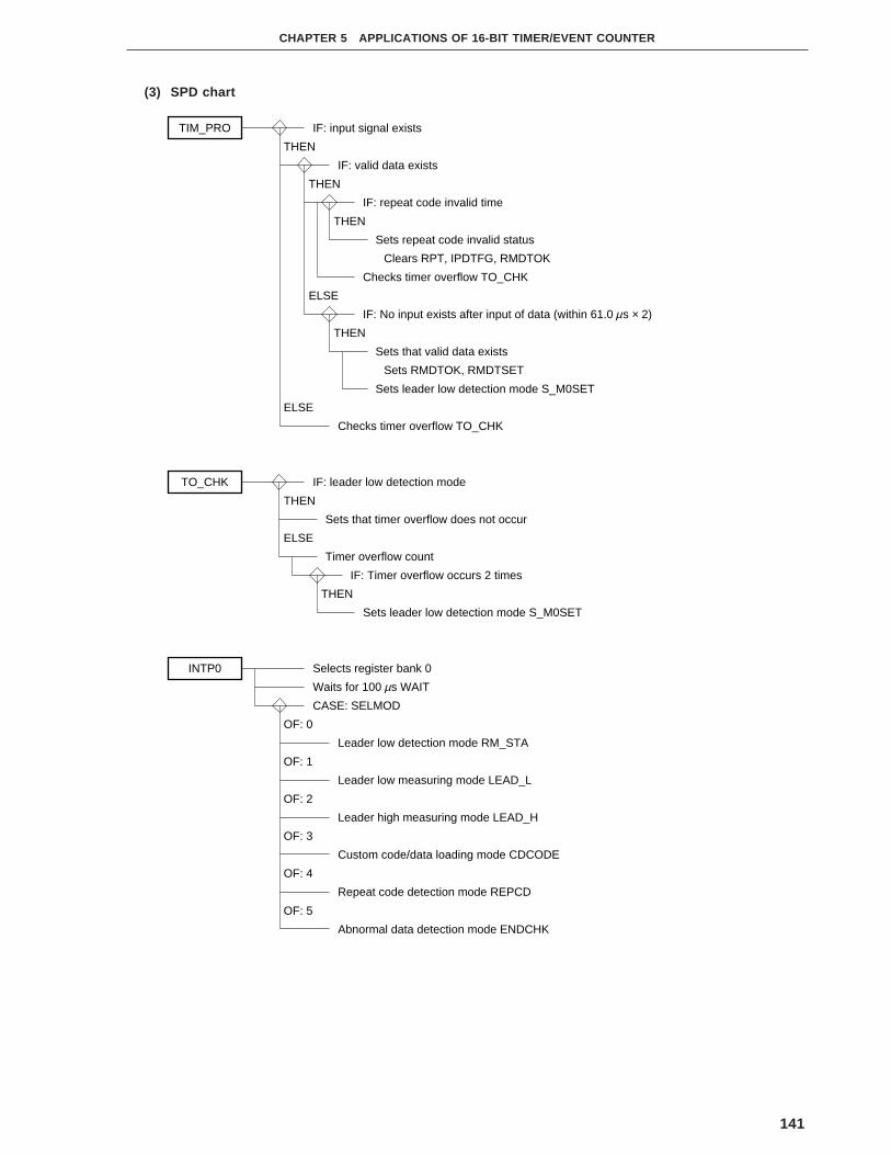
141
CHAPTER 5 APPLICATIONS OF 16-BIT TIMER/EVENT COUNTER
(3) SPD chart
TIM_PRO IF: input signal exists
TO_CHK IF: leader low detection mode
THEN
ELSE
IF: valid data exists
THEN
IF: repeat code invalid time
THEN
Sets repeat code invalid status
Clears RPT, IPDTFG, RMDTOK
Checks timer overflow TO_CHK
IF: No input exists after input of data (within 61.0 s × 2)µTHEN
Sets that valid data exists
Sets RMDTOK, RMDTSET
Sets leader low detection mode S_M0SET
ELSE
Checks timer overflow TO_CHK
THEN
Sets that timer overflow does not occur
ELSE
Timer overflow count
IF: Timer overflow occurs 2 times
THEN
Sets leader low detection mode S_M0SET
INTP0 Selects register bank 0
Waits for 100 s WAITµCASE: SELMOD
OF: 0
Leader low detection mode RM_STA
OF: 1
Leader low measuring mode LEAD_L
OF: 2
Leader high measuring mode LEAD_H
OF: 3
Custom code/data loading mode CDCODE
OF: 4
Repeat code detection mode REPCD
OF: 5
Abnormal data detection mode ENDCHK

142
CHAPTER 5 APPLICATIONS OF 16-BIT TIMER/EVENT COUNTER
RM_STA IF: P00 = LOW
THEN
Waits for 100 s WAITµIF: P00 = LOW
THEN
Stores data of capture register to memory
Selects leader low measuring mode 1
Sets INTP0 rising-edge detection mode
LEAD_L IF: P00 = HIGH
LEAD_H IF: P00 = LOW
Waits for 100 s WAIT
THEN
µIF: P00 = HIGH
THEN
Reads timer PW_CT
IF: 3 ms ≤ Ieader low ≤ 10 ms
THEN
Selects leader high detection mode
Sets INTP0 falling-edge detection mode
ELSE
Sets leader low detection mode S_M0SET
THEN
Waits for 100 s WAITµIF: P00 = LOW
THEN
Reads timer PW_CT
IF: 2 ms ≤ leader high ≤ 5 ms
THEN
IF: Ieader high ≥ 3 ms
THEN
Selects custom code/data loading mode
Initializes data storage area
ELSE
Selects repeat detection mode
Sets INTP0 rising-edge detection mode
ELSE
Sets leader low detection mode S_M0SET

143
CHAPTER 5 APPLICATIONS OF 16-BIT TIMER/EVENT COUNTER
CDCODE IF: P00 = LOW
THEN
Waits for 100 s WAITµIF: P00 = LOW
THEN
Reads timer CR_READ
IF: 0.5 ms < input data ≤ 2.5 ms
THEN
IF: input data ≥ 1.8 ms
THEN
Sets CY
ELSE
Clears CY
Stores CY to data storage area
IF: end of 32 bits of data input
THEN
IF: custom code coincidence
THEN
IF: Coincidence between custom/data code and inverted data
THEN
Stores data code
Sets input data existing status
Sets IPDTFG, and clears RMDTSET, RPT, and RMDTOK
Sets abrormal data detection mode S_M5SET
ELSE
Sets leader low detection mode S_M0SET
ELSE
Sets leader low detection mode S_M0SET
ELSE
Sets leader low detection mode S_M0SET
REPCD IF: P00 = HIGH
THEN
Waits for 100 s WAITµIF: P00 = HIGH
THEN
IF: valid data exists
THEN
Reads timer PW_CT
IF: repeat code ≤ 1 ms
THEN
Sets repeat code valid status
Sets RPT
Sets data input end status
Sets abnormal data detection mode S_M5SET
ELSE
Sets leader low detection mode S_M0SET
ELSE
Sets abnormal data detection mode S_M5SET

144
CHAPTER 5 APPLICATIONS OF 16-BIT TIMER/EVENT COUNTER
ENDCHK IF: P00 = LOW
THEN
Waits for 100 s WAITµIF: P00 = LOW
THEN
Sets input signal invalid status
Sets leader low detection mode S_M0SET
Clears IPDTFG, RPT
PW_CT IF: OVF occurs after edge detection processing
THEN
IF: OVF occurs < interrupt acknowledgment processing time (65 clocks)
THEN
Sets that timer overflow occurs
Loads capture register value
Subtracts capture register value from previous value
IF: borrow occurs as result of subtraction (CY = 1)
THEN
IF: timer overflow occurs (TO_FLG = 1)
THEN
Clears CY flag
ELSE
IF: timer overflow occurs (TO_FLG = 1)
THEN
Sets CY flag
Stores capture register value to memory
S_M0SET Selects leader low detection mode
Clears TO_FLG
Sets INTP0 falling-edge detection mode
S_M5SET Selects abnormal data detection mode
Sets repeat valid time counter

145
CHAPTER 5 APPLICATIONS OF 16-BIT TIMER/EVENT COUNTER
; Repeat code valid time counter; No-input time counter after data input; Mode selection; Leader signal detection counter; Valid data storage area; Timer overflow counter
; Newest timer counter value storage area; Previous timer counter value storage area; Input signal storage area
; Valid data exists; Input signal valid; Input signal exists; Repeat code valid period; Timer overflow occurs; Detects timer overflow by INTP0 processing
; Sets vector address of INTP0
; Input signal exists?; Valid data exists?
; Repeat invalid time; Repeat code valid status
; Valid data exists
; Sets leader (low) detection mode
; Checks timer overflow
(4) Program list
PUBLIC TIM_PRO,RPT,IPDTFG,RMDTOK,RMDTSETPUBLIC RMENDCT,RPTCT,SELMOD,LD_CT,RMDATAPUBLIC TO_FLG,OVSENSEXTRN CSTM
RM_DAT DSEG SADDRRPTCT: DS 1RMENDCT:DS 1SELMOD: DS 1LD_CT: DS 1RMDATA: DS 1TO_CNT: DS 1
RM_DATP DSEG SADDRPCR01_NP:DS 2CR01_OP:DS 2WORKP: DS 4
BSEGIPDTFG DBITRMDTOK DBITRMDTSET DBITRPT DBITTO_FLG DBITOVSENS DBIT
VEP0 CSEG AT 06HDW INTP0
$EJECT;******************************************************; Remote controller signal timer processing;******************************************************TM0_SEG CSEGTIM_PRO:
if_bit(IPDTFG)if_bit(RMDTOK)RPTCT––
if(RPTCT==#0)CLR1 RPTCLR1 IPDTFGCLR1 RMDTOK
endifelse
RMENDCT––if(RMENDCT==#0)
SET1 RMDTOKSET1 RMDTSETCALL !S_M0SET
endifendif
elseCALL !TO_CHK
endifRET

146
CHAPTER 5 APPLICATIONS OF 16-BIT TIMER/EVENT COUNTER
; Sets start edge detection mode
; Waits for 100 µs
; Start edge detection processing
; Leader low detection processing
; Leader high detection processing
; Custom/data code loading processing
; Repeat code detection processing
; Abnormal data detection processing
; Starts timer count; Level check P0.0 = 1: noise; Waits for 100 µs
; Stores capture register; Leader low detection mode; INTP0 rising edge
TO_CHK:if(SELMOD==#0)
CLR1 TO_FLGelse
TO_CNT++if(TO_CNT==#2)
CALL !S_M0SETendif
endifRET
$EJECT;***********************************************************;* Remote controller signal edge detection processing;***********************************************************P0_SEG CSEGINTP0:
SEL RB0
CALL !WAIT
switch(SELMOD)
case 0:CALL !RM_STAbreak
case 1:CALL !LEAD_Lbreak
case 2:CALL !LEAD_Hbreak
case 3:CALL !CDCODEbreak
case 4:CALL !REPCDbreak
case 5:CALL !ENDCHK
endsRET1
;***********************************************************;* Start edge detection;***********************************************************RM_STA:
CLR1 TO_FLGif_bit(!P0.0)
CALL !WAITif_bit(!P0.0)
CR01_OP=CR01 (AX)SELMOD=#1INTM0=#00000100BTO_CNT=#0
endifendifRET

147
CHAPTER 5 APPLICATIONS OF 16-BIT TIMER/EVENT COUNTER
;****************************************;* Leader low detection;****************************************LEAD_L:
if_bit(P0.0)CALL !WAITif_bit(P0.0)
CALL !PW_CTif_bit(!CY)
TO_CNT=#0if(AX>=#12582)
if(AX<#41942)SELMOD=#2INTM0=#00000000B
elseCALL !S_M0SET
endifelse
CALL !S_M0SETendif
elseCALL !S_M0SET
endifendif
endifRET
$EJECT;****************************************;* Leader high detection;****************************************LEAD_H:
if_bit(!P0.0)CALL !WAITif_bit(!P0.0)
CALL !PW_CTif_bit(!CY)
TO_CNT=#0if(AX>=#7549)
if(AX<#20971)if(AX>#12582)
SELMOD=#3WORKP=#0000H(WORKP)+2=#8000H
elseSELMOD=#4INTM0=#00000100B
endifelse
CALL !S_M0SETendif
elseCALL !S_M0SET
endifelse
CALL !S_M0SETendif
endifendifRET
$EJECT
; Level check P0.0 = 1: noise; Waits for 100 µs
; Reads timer value
; 3 ms; 10 ms; Leader high detection mode; INTP0 falling edge
; Sets start edge detection mode
; Sets start edge detection mode
; Sets start edge detection mode
; Level check P0.0 = 0: noise; Waits for 100 µs
; Reads timer value
; 1.8 ms; 5 ms; Custom/data code (3 ms)?; Data loading mode; Initializes work area; Sets most significant bit to 1 (to confirm end of data)
; Repeat detection mode; INTP0 rises
; Sets start edge detection mode
; Sets start edge detection mode
; Sets start edge detection mode

148
CHAPTER 5 APPLICATIONS OF 16-BIT TIMER/EVENT COUNTER
;******************************;* Custom/data code loading;******************************CDCODE:
if_bit(!P0.0)CALL !WAITif_bit(!P0.0)
CALL !PW_CTif_bit(!CY)
TO_CNT=#0if(AX>=#2096)
if(AX<#10485)if(AX>=#7549)
SET1 CYelse
CLR1 CYendif
HL=#WORKP+3C=#4
WKSHFT:A=[HL]RORC A,1[HL]=AHL––DBNZ C,$WKSHFT
if_bit(CY)
if(WORKP+0==#CSTM) (A)A^=WORKP+1if(A==#0FFH)
A=WORKP+2
A^=WORKP+3if(A==#0FFH)
RMDATA=WORKP+2 (A)
SET1 IPDTFGCLR1 RMDTSETCLR1 RPTCLR1 RMDTOKCALL !S_M5SET
else
CALL !S_M0SETendif
else
CALL !S_M0SETendif
elseCALL !S_M0SET
endifendif
elseCALL !S_M0SET
endifelse
; Level check P0.0 = 1: noise; Waits for 100 µs
; Reads timer value
; 0.5 ms; 2.5 ms; 1.8 ms
; Sets work area address; Sets number of work area digits
; Stores 1-bit data; Shifts 1 bit
; End of shifting all digits
; End of input of 32 bits?; Checks custom code
; Checks custom code inverted data
; Checks data code inverted data
; Stores input data
; Sets input data existing status
; Sets start edge detection mode
; Sets start edge detection mode
; Sets start edge detection mode

149
CHAPTER 5 APPLICATIONS OF 16-BIT TIMER/EVENT COUNTER
CALL !S_M0SETendif
elseCALL !S_M0SET
endifendif
endifRET
$EJECT
;************************************;* Repeat code detection;************************************REPCD:
if_bit(P0.0)CALL !WAITif_bit(P0.0)
if_bit(RMDTOK)CALL !PW_CTif_bit(!CY)
TO_CNT=#0if(AX<=#4193)
SET1 RPTCLR1 RMDTOKCLR1 RMDTSETCALL !S_M5SET
elseCALL !S_M0SET
endifelse
CALL !S_M0SETendif
elseCALL !S_M0SET
endifendif
endifRET
$EJECT
; Sets start edge detection mode
; Sets start edge detection mode
; Level check P0.0 = 1: noise; Waits for 100 µs
; Valid data?; Reads timer value
; 1 ms
; Checks input signal after end of data
; Sets start edge detection mode
; Sets start edge detection mode
; Sets start edge detection mode

150
CHAPTER 5 APPLICATIONS OF 16-BIT TIMER/EVENT COUNTER
; Level check P0.0 = 1: noise; Waits for 100 µs
; Abnormal data input; Input signal invalid; Sets start edge detection mode
; OVF0 after edge detection?; Interrupt acknowledgment processing time = 65 clocks (MAX)
; Loads capture register value
; AX = CR01_NP – CR01_OP
; Saves operation result; CR01_NP > CR01_OP; Timer overflow occurs (flag test); Normal data
; Timer overflow; Error occurs
; Restores operation result
;*********************************************;* Abnormal data detection;*********************************************ENDCHK:
if_bit(!P0.0)CALL !WAITif_bit(!P0.0)
CLR1 IPDTFGCLR1 RPTCALL !S_M0SET
endifendifRET
;*********************************************;* Calculation of capture register value;*********************************************PW_CT:
if_bit(OVF0)if(CR01<#10000–33) (AX)
CLR1 OVF0SET1 OVSENSSET1 TO_FLG
endifendif
CR01_NP=CR01 (AX)
A=CR01_NP+0A–=CR01_OPX=AA=CR01_NP+1SUBC A,CR01_OP+1
BC=AXif_bit(CY)
if_bit(TO_FLG)CLR1 CY
endifelse
if_bit(TO_FLG)SET1 CY
endifendif
CR01_OP=CR01_NP (AX)AX=BCCLR1 TO_FLGRET

151
CHAPTER 5 APPLICATIONS OF 16-BIT TIMER/EVENT COUNTER
;**********************************************;* Waits for 100 µs;**********************************************WAIT:
B=#(838–14–12–8)/12WAITCT:
DBNZ B,$WAITCTRET
;**********************************************;* Sets start edge detection mode;**********************************************S_M0SET:
TO_CNT=#0SELMOD=#0INTM0=#00000000BRET
;**********************************************;* Setting of abnormal data detection mode;**********************************************S_M5SET:
RPTCT=#16SELMOD=#5RMENDCT=#2RET
; CALL (14), RET (12), MOV (8); Sets 100 µs; 1 instruction 12 clocks
; Start edge detection mode; INTP0 falling edge
; 250 ms measuring counter; Data input end mode; No-input checking counter

152
CHAPTER 5 APPLICATIONS OF 16-BIT TIMER/EVENT COUNTER
5.4 One-Shot Pulse Output
The 16-bit timer/event counter has a function which outputs a one-shot pulse in synchronization with a software
trigger and external trigger (INTP0/TI00/P00 pin input).
When using the one-shot pulse output function, the 16-bit timer mode control register (TMC0), capture/compare
control register 0 (CRC0), and 16-bit timer output control register (TOC0) must be set.
In this section, an example for setting the one-shot pulse by using the software trigger is introduced.
The OSPT flag (bit 6 of the TOC0 register) is set at arbitrary timing (such as key input).
After the software trigger has occurred, TM0 is cleared and started. When the value of TM0 coincides with the
value set in advance to CR01, the TO0/P30 pin output is inverted (and becomes active). When the value of TM0
later coincides with the value set in advance to CR00, the TO0/P30 pin output is inverted again (and becomes inactive).
The TM0 counter is cleared and counting up is started again after the value of TM0 has coincided with the value of
CR00. The output of the TO0/P30 pin, however, is not inverted even if coincidence occurs next time. TM0 is cleared
and started and the output of the TO0/P30 pin is inverted only when the software trigger is set. The active level of
the TO0/P30 pin is determined by selecting the initial value of the TO0/P30 pin output of the TOC0 register.
Note that, when using the one-shot pulse output function with the software trigger, the OSPT flag must not be set
to 1 while the one-shot pulse is output. To output the one-shot pulse again, do so after INTTM00, which is an interrupt
request that occurs when TM0 coincides with CR00, has occurred.
In the example presented in this section, the software trigger is designed by using key input, and “H” active output
is produced 10 ms after for 1 ms.

153
CHAPTER 5 APPLICATIONS OF 16-BIT TIMER/EVENT COUNTER
Figure 5-16. Timing of One-Shot Pulse Output Operation by Software Trigger
Remark F_TRG: flag indicating that output of the one-shot pulse is in progress. For details, refer to (2) Example
of use.
Count clock
TM0 count value
TO0/P30 pin output
CR01 set value
CR00 set value
OSPT
INTTM01
INTTM00
F_TRG
0000 N N+1 M–2 M–1 M 0000
N
M
10 ms 1 ms

154
CHAPTER 5 APPLICATIONS OF 16-BIT TIMER/EVENT COUNTER
(1) Description of package
<Public declaration symbol>
SOP_INIT: One-shot pulse output initial setting subroutine
<Register used>
None
<RAM used>
None
<Nesting level>
1 level 2 bytes
<Hardware used>
• 16-bit timer/event counter
<Initial setting>
• OSMS = #00000001B ; Oscillation mode select register: does not use divider circuit
• CLR1 P3.0 ; Clears output latch of bit 0 of port 3 to 0
• CLR1 PM3.0 ; Sets bit 0 of port mode register 3 in output mode
• CALL !SOP_INIT ; Sets by subroutine SOP_INIT
<Starting>
Set bit 6 (OSPT) of the 16-bit timer output control register (TOC0).

155
CHAPTER 5 APPLICATIONS OF 16-BIT TIMER/EVENT COUNTER
; Does not use divider circuit; Sets 0 to output latch if multiplexed pin is used; Sets output mode if multiplexed pin is used; One-shot pulse output initial setting routine
; Previous output ends?; Clears and starts 16-bit counter; Sets one-shot pulse trigger flag;;; End of one-shot pulse output?; Clears one-shot trigger flag; Clears TMIF00 request flag;
(2) Example of use
Because bit 6 (OSPT) of the 16-bit timer output control register (TOC0) is not set again while the pulse is output
in the example of this package, the F_TRG flag is set as soon as the OSPT flag has been set as shown in
Figure 5-16. Even if the next output request is issued while the F_TRG flag is set (i.e., while the pulse is output),
the OSPT flag is not set. After the one-shot pulse has been output (INTTM00 occurs), clear the F_TRG flag.
EXTRN SOP_INT
M1PR0 CSEGRES_STA:
OSMS=#00000001BCLR1 P3.0CLR1 PM3.0CALL !SOP_INIT
··
if(key request issued)if_bit(!F_TRG)
SET1 OSPTSET1 F_TRG
endifendifif_bit(TMIF00)
CLR1 F_TRGCLR1 TMIF00
endif··
(3) SPD chart
SOP_INIT Stops timer operation
Selects count clock of 16-bit timer register
Uses CR00 and CR01 as compare registers
Sets compare register 00 (CR00) (Time required from start of trigger to second inversion of TO0 output)
Sets compare register 01 (CR01) (Time required from start of trigger to first inversion of TO0 output)
Selects one-shot pulse output mode
Starts on coincidence between TM0 and CR00(enables timer operation)

156
CHAPTER 5 APPLICATIONS OF 16-BIT TIMER/EVENT COUNTER
(4) Program list
PUBLIC SOP_INIT
OPINIT CSEGSOP_INIT:
TMC0=#00000000BTCL0=#01000000BCRC0=#00000000BCR00=#11550–1CR01=#10500–1TOC0=#00110111BTMC0=#00001100BRETEND
5.5 PPG Output
When using the 16-bit timer/event counter in the PPG (Programmable Pulse Generator) mode, the 16-bit timer
mode control register (TMC0), capture/compare control register 0 (CRC0), and 16-bit timer output control register
(TOC0) must be set.
As the PPG output pulse, a square wave with a cycle specified by the count value set in advance to the 16-bit
capture/compare register 00 (CR00) and a pulse width specified by the count value set in advance to the 16-bit capture/
compare register 01 (CR01) is output from the TO0/P30 pin.
In the application example shown in this section, the output waveform is changed by using the PPG output. Data
indicating the one cycle and pulse width of the output waveform is stored in ROM. This data is stored in the compare
register.
The cycle and pulse width of the PPG output in this program can be changed in units of 1 ms to 10 ms. Therefore,
the cycle can be set in a range of 2 to 10 ms, and the pulse width can be set in a range of 1 to 9 ms. If the cycle
is equal to or less than the pulse width when the output waveform is changed, the data is not changed.
The output waveform is changed after the end of one output cycle. Figure 5-17 shows the PPG output waveform
changing timing.
Figure 5-17. PPG Output Waveform Changing Timing
; Stops timer operation; Count clock of 16-bit timer register: 1.05 MHz; Uses CR00 and CR01 as compare registers; Sets compare register to 11 ms; Sets compare register to 10 ms; Selects one-shot pulse mode; Starts on coincidence between TM0 and CR00 (enables timer operation);
Request forchange
Data changed Request for changeData changed
Pulsewidth
1 cycle

157
CHAPTER 5 APPLICATIONS OF 16-BIT TIMER/EVENT COUNTER
(1) Description of package
<Public declaration symbol>
• Subroutine name
SPG_INIT : PPG output initial setting subroutine
• Data definition reference name of SPG_INIT routine
PDAT : First address of data value for pulse width stored to compare register
SDAT : First address of data value for cycle stored to compare register
• Input parameter of SPG_INIT routine
PARUSU : Pulse width time storage area
SAIKURU : 1 cycle time storage area
• Input/output parameters of SPG_INIT routine and INTTM00 interrupt
PARUSUP : Pulse width time change data storage area
SAIKURUP : 1-cycle time change data storage area
<Registers used>
SPG_INIT : Bank 0 AX, HL
INTTM00 : Bank 2 AX
<RAM used>
Name Usage Attribute Bytes
PARUSU Sets pulse width time SADDR 1
SAIKURU Sets 1-cycle time SADDR 1
PARUSUP Sets compare data value corresponding to pulse SADDRP 2
width time
SAIKURUP Sets compare data value corresponding to 1 cycle SADDRP 2
time
<Flag used>
None

158
CHAPTER 5 APPLICATIONS OF 16-BIT TIMER/EVENT COUNTER
<Nesting level>
1 level 3 bytes
<Hardware used>
• 16-bit timer/event counter
<Initial setting>
• OSMS = #00000001B ; Oscillation mode select register: does not use divider circuit
• CLR1 P3.0 ; Clears output latch of bit 0 of port 3 to 0
• CLR1 PM3.0 ; Sets bit 0 of port mode register 3 in output mode
• CALL !PPG_INIT ; Sets by subroutine PPG_INIT
<Starting>
After the 16-bit timer/event counter has been reset and started, set pulse width time in the specified range
to PARUSU in RAM and cycle time in the specified range to SAIKURU, and call subroutine PPG_INIT.
When changing the PPG output waveform, clear the INTTM00 interrupt request flag to enable the interrupt
after setting a compare data value corresponding to the pulse width in the specified range to PARUSUP,
and a compare data value corresponding to the cycle time in the specified range to SAIKURUP.

159
CHAPTER 5 APPLICATIONS OF 16-BIT TIMER/EVENT COUNTER
; Minimum cycle time; Minimum pulse width time
; Does not use divider circuit; Sets initial cycle value; Sets initial pulse width value; Clears output latch to 0 if multiplexed pin is used; Sets output mode if multiplexed pin is used;;
; If SAIKURUP > PARUSU; Data 1 → address XXX0; Data 2 → address XXX2; Data 3 → address XXX4; ·
; Table reference of low-order 8 bits of value stored to; compare register; X register ← low-order 8 bits;; Table reference of high-order 8 bits of value stored to compare register; A register ← high-order 8 bits;;; Cycle time storage processing;;;;;;;;;;;; Clears request flag; Enables compare register 00 interrupt; No data change;
(2) Example of use
EXTRN SPG_INITEXTRN SAIKURUP.PARUSUPEXTRN SAIKURU,PARUSUEXTRN PDAT,SDAT;SMIN EQU 02HPMIN EQU 01H
··
OSMS=#00000001BSAIKURU=#SMINPARUSU=#PMINCLR1 P3.0CLR1 PM3.0CALL !SPG_INITEI
··
if(request for changing square wave)if(SAIKURU > PARUSU) (A)
A=PARUSUA––A <<= 1X=AA=#0AX+=#PDATHL=AXX=[HL] (A)HL++A=[HL]PARUSUP=AX
;A=SAIKURUA––A––A <<= 1X=AA=#0AX+=#SDATHL=AXX=[HL] (A)HL++A=[HL]SAIKURUP=AXCLR1 TMIF00CLR1 TMMK00
endifendif
··

160
CHAPTER 5 APPLICATIONS OF 16-BIT TIMER/EVENT COUNTER
(3) SPD chart
PPG_INIT Stops timer operation
Selects count clock of 16-bit timer register
Uses CR00 and CR01 as compare registers
Table reference of compare data corresponding to PARUSU area contents and stores it in PARUSU area
Table reference of compare data corresponding to SAIKURU area contents and stores it in SAIKURUP area
Stores contents of SAIKURUP area to compare register 00 (CR00)
Stores contents of PARUSUP area to compare register 01 (CR01)
Sets successive pulse output and sets initial value "H" of TO0 pin output
Starts on coincidence between TM0 and CR00 (enables timer operation)
INTTM00 Selects register bank 2
Stores contents of SAIKURUP area to compare register 00 (CR00)
Stores contents of PARUSUP area to compare register 01 (CR01)
Disables INTTM00 interrupt

161
CHAPTER 5 APPLICATIONS OF 16-BIT TIMER/EVENT COUNTER
(4) Program list
PUBLIC SPG_INIT,PDAT,SDATPUBLIC SAIKURU,PARUSUEXTRN SAIKURUP,PARUSUP;;************************************************; RAM definition;************************************************PPGRAM DSEG SADDRSAIKURU: DS 1PARUSU: DS 1;;************************************************; PPG output initial setting;************************************************PPGINIT CSEGSPG_INIT:
TMC0=#00000000BTCL0=#00100000BCRC0=#00000000BA=PARUSUA––A <<= 1X=AA=#0AX+=#PDATHL=AXX=[HL] (A)HL++A=[HL]PARUSUP=AX
;A=SAIKURUA––A––A <<= 1X=AA=#0AX+=#SDATHL=AXX=[HL] (A)HL++A=[HL]SAIKURUP=AXCR00=SAIKURUP (AX)CR01=PARUSUP (AX)TOC0=#00011011BTMC0=#00001100BRET
;; 1 cycle time storage area; Pulse width storage area
; Stops timer operation; Count clock of 16-bit timer register: 4.19 MHz; Uses CR00 and CR01 as compare register; Data 1 → address XXX0; Data 2 → address XXX2; Data 3 → address XXX4; ·
; Table reference of low-order 8 bits of value stored to; compare register; X register ← low-order 8 bits;; Table reference of high-order 8 bits of value stored to compare register; A register ← high-order 8 bits;;; Cycle time storage processing;;;;;;;;;;;; Sets compare register to 2 ms; Sets compare register to 1 ms; Sets successive pulse output and initial value ‘H’; Starts on coincidence between TM0 and CR00 (enables timer opera-
tion);

162
CHAPTER 5 APPLICATIONS OF 16-BIT TIMER/EVENT COUNTER
PDAT:DW 4201DW 8403DW 12605DW 16807DW 21009DW 25211DW 29413DW 33615DW 37817
SDAT:DW 8403DW 12605DW 16807DW 21009DW 25211DW 29413DW 33615DW 37817DW 42019END
PUBLIC PARUSUP,SAIKURUP;VETM00 CSEG AT 20H
DW INTTM00;P2RAM DSEG SADDRPPARUSUP: DS 2SAIKURUP: DS 2;****************************************************************; PPG output (cycle pulse width time changing interrupt);****************************************************************TM00 CSEGINTTM00:
SEL RB2CR01=PARUSUP (AX)CR00=SAIKURUP (AX)SET1 TMMK00RETIEND
;; Address XXX0; Address XXX2; Address XXX4;;;;;;;; Address XXX0; Address XXX2; Address XXX4;;;;;;
; Pulse width time changing data storage area; 1 cycle time changing data storage area
;;; Selects bank 2; CR00, CR01 ← stores pulse width and cycle time changing data;; Disables compare register 00 interrupt;

CHAPTER 6 APPLICATIONS OF 8-BIT TIMER/EVENT COUNTER
The 8-bit timer/event counter of the 78K/0 series has three functions: interval timer, external event counter, and
square wave output. Two channels of 8-bit timers/event counters are provided and these timers/event counters can
be used as a 16-bit timer/event counter when connected in cascade.
The 8-bit timers/event counters are set by the following registers:
• Timer clock select register 1 (TCL1)
• 8-bit timer mode control register (TMC1)
• 8-bit timer output control register (TOC1)
• Port mode register 3 (PM3)
• Port 3 (P3)
163

164
CHAPTER 6 APPLICATIONS OF 8-BIT TIMER/EVENT COUNTER
Figure 6-1. Format of Timer Clock Select Register 1
(µPD78054, 78054Y, 78064, 78064Y, 78078, 78078Y, 780058, 780058Y, 780308,
780308Y, 78058F, 78058FY, 78064B, 78075B, 78075BY subseries, µPD78070A,
78070AY)
TCL13 TCL12 TCL11 TCL10 Selects count clock of 8-bit timer register 1
MCS = 1 MCS = 0
0 0 0 0 Falling edge of TI1
0 0 0 1 Rising edge of TI1
0 1 1 0 fXX/2 fX/2 (2.5 MHz) fX/22 (1.25 MHz)
0 1 1 1 fXX/22 fX/22 (1.25 MHz) fX/23 (625 kHz)
1 0 0 0 fXX/23 fX/23 (625 kHz) fX/24 (313 kHz)
1 0 0 1 fXX/24 fX/24 (313 kHz) fX/25 (156 kHz)
1 0 1 0 fXX/25 fX/25 (156 kHz) fX/26 (78.1 kHz)
1 0 1 1 fXX/26 fX/26 (78.1 kHz) fX/27 (39.1 kHz)
1 1 0 0 fXX/27 fX/27 (39.1 kHz) fX/28 (19.5 kHz)
1 1 0 1 fXX/28 fX/28 (19.5 kHz) fX/29 (9.8 kHz)
1 1 1 0 fXX/29 fX/29 (9.8 kHz) fX/210 (4.9 kHz)
1 1 1 1 fXX/211 fX/211 (2.4 kHz) fX/212 (1.2 kHz)
Others Setting prohibited
TCL17 TCL16 TCL15 TCL14 Selects count clock of 8-bit timer register 2
MCS = 1 MCS = 0
0 0 0 0 Falling edge of TI2
0 0 0 1 Rising edge of TI2
0 1 1 0 fXX/2 fX/2 (2.5 MHz) fX/22 (1.25 MHz)
0 1 1 1 fXX/22 fX/22 (1.25 MHz) fX/23 (625 kHz)
1 0 0 0 fXX/23 fX/23 (625 kHz) fX/24 (313 kHz)
1 0 0 1 fXX/24 fX/24 (313 kHz) fX/25 (156 kHz)
1 0 1 0 fXX/25 fX/25 (156 kHz) fX/26 (78.1 kHz)
1 0 1 1 fXX/26 fX/26 (78.1 kHz) fX/27 (39.1 kHz)
1 1 0 0 fXX/27 fX/27 (39.1 kHz) fX/28 (19.5 kHz)
1 1 0 1 fXX/28 fX/28 (19.5 kHz) fX/29 (9.8 kHz)
1 1 1 0 fXX/29 fX/29 (9.8 kHz) fX/210 (4.9 kHz)
1 1 1 1 fXX/211 fX/211 (2.4 kHz) fX/212 (1.2 kHz)
Others Setting prohibited
Caution Before writing new data to TCL1, stop the timer operation once.
7 6 5 4 3 2Symbol 1 0
FF41HTCL10TCL1 TCL11TCL13 TCL12TCL14TCL15TCL16TCL17
Address At reset R/W
00H R/W

165
CHAPTER 6 APPLICATIONS OF 8-BIT TIMER/EVENT COUNTER
Remarks 1. fXX : main system clock frequency (fX or fX/2)
2. fX : main system clock oscillation frequency
3. TI1 : input pin of 8-bit timer register 1
4. TI2 : input pin of 8-bit timer register 2
5. MCS: bit 0 of oscillation mode select register (OSMS)
6. ( ) : at fX = 5.0 MHz

166
CHAPTER 6 APPLICATIONS OF 8-BIT TIMER/EVENT COUNTER
Figure 6-2. Format of Timer Clock Select Register 1 ( µPD78098, 78098B subseries)
TCL13 TCL12 TCL11 TCL10 Selects count clock of 8-bit timer register 1
0 0 0 0 Falling edge of TI1
0 0 0 1 Rising edge of TI1
0 1 1 0 fXX/2 (2.0 MHz)
0 1 1 1 fXX/22 (1.0 MHz)
1 0 0 0 fXX/23 (500 kHz)
1 0 0 1 fXX/24 (250 kHz)
1 0 1 0 fXX/25 (125 kHz)
1 0 1 1 fXX/26 (62.5 kHz)
1 1 0 0 fXX/27 (31.3 kHz)
1 1 0 1 fXX/28 (15.6 kHz)
1 1 1 0 fXX/29 (7.8 kHz)
1 1 1 1 fXX/211 (2.0 kHz)
Others Setting prohibited
TCL17 TCL16 TCL15 TCL14 Selects count clock of 8-bit timer register 2
0 0 0 0 Falling edge of TI2
0 0 0 1 Rising edge of TI2
0 1 1 0 fXX/2 (2.0 MHz)
0 1 1 1 fXX/22 (1.0 MHz)
1 0 0 0 fXX/23 (500 kHz)
1 0 0 1 fXX/24 (250 kHz)
1 0 1 0 fXX/25 (125 kHz)
1 0 1 1 fXX/26 (62.5 kHz)
1 1 0 0 fXX/27 (31.3 kHz)
1 1 0 1 fXX/28 (15.6 kHz)
1 1 1 0 fXX/29 (7.8 kHz)
1 1 1 1 fXX/211 (2.0 kHz)
Others Setting prohibited
Caution Before writing new data to TCL1, stop the timer operation once.
Remarks 1. fXX : main system clock frequency
2. TI1: input pin of 8-bit timer register 1
3. TI2: input pin of 8-bit timer register 2
4. ( ) : at fXX = 4.0 MHz
7 6 5 4 3 2Symbol 1 0
FF41HTCL10TCL1 TCL11TCL13 TCL12TCL14TCL15TCL16TCL17
Address At reset R/W
00H R/W

167
CHAPTER 6 APPLICATIONS OF 8-BIT TIMER/EVENT COUNTER
Figure 6-3. Format of Timer Clock Select Register 1 ( µPD780018, 780018Y subseries)
TCL13 TCL12 TCL11 TCL10 Selects count clock of 8-bit timer register 1
0 0 0 0 Falling edge of TI1
0 0 0 1 Rising edge of TI1
0 1 1 0 fXX/2 fX/2 (2.5 MHz)
0 1 1 1 fXX/22 fX/22 (1.25 MHz)
1 0 0 0 fXX/23 fX/23 (625 kHz)
1 0 0 1 fXX/24 fX/24 (313 kHz)
1 0 1 0 fXX/25 fX/25 (156 kHz)
1 0 1 1 fXX/26 fX/26 (78.1 kHz)
1 1 0 0 fXX/27 fX/27 (39.1 kHz)
1 1 0 1 fXX/28 fX/28 (19.5 kHz)
1 1 1 0 fXX/29 fX/29 (9.8 kHz)
1 1 1 1 fXX/211 fX/211 (2.4 kHz)
Others Setting prohibited
TCL17 TCL16 TCL15 TCL14 Selects count clock of 8-bit timer register 2
0 0 0 0 Falling edge of TI2
0 0 0 1 Rising edge of TI2
0 1 1 0 fXX/2 fX/2 (2.5 MHz)
0 1 1 1 fXX/22 fX/22 (1.25 MHz)
1 0 0 0 fXX/23 fX/23 (625 kHz)
1 0 0 1 fXX/24 fX/24 (313 kHz)
1 0 1 0 fXX/25 fX/25 (156 kHz)
1 0 1 1 fXX/26 fX/26 (78.1 kHz)
1 1 0 0 fXX/27 fX/27 (39.1 kHz)
1 1 0 1 fXX/28 fX/28 (19.5 kHz)
1 1 1 0 fXX/29 fX/29 (9.8 kHz)
1 1 1 1 fXX/211 fX/211 (2.4 kHz)
Others Setting prohibited
Caution Before writing new data to TCL1, stop the timer operation once.
Remarks 1. fXX : main system clock frequency (fX)
2. fX : main system clock oscillation frequency
3. TI1 : input pin of 8-bit timer register 1
4. TI2 : input pin of 8-bit timer register 2
5. ( ) : at fX = 5.0 MHz
7 6 5 4 3 2Symbol 1 0
FF41HTCL10TCL1 TCL11TCL13 TCL12TCL14TCL15TCL16TCL17
Address At reset R/W
00H R/W

168
CHAPTER 6 APPLICATIONS OF 8-BIT TIMER/EVENT COUNTER
Figure 6-4. Format of 8-Bit Timer Mode Control Register
Cautions 1. Before changing the operation mode, stop the timer operation.
2. When using the two 8-bit timer registers as a one 16-bit timer register, enable or stop the
operation by using TCE1.
7 6 5 4 3 2Symbol 1 0
TCE1 Controls operation of 8-bit timer register 1
FF49HTCE1TMC1 TCE20 TMC120000
Address At reset R/W
00H R/W
0 Stops operation (clears TM1 to 0)
1 Enables operation
TCE2 Controls operation of 8-bit timer register 2
0 Stops operation (clears TM2 to 0)
1 Enables operation
TMC12 Selects operation mode
0 8-bit timer register × 2 channel mode (TM1, TM2)
1 16-bit timer register × 1 channel mode (TMS)

169
CHAPTER 6 APPLICATIONS OF 8-BIT TIMER/EVENT COUNTER
Figure 6-5. Format of 8-Bit Timer Output Control Register
Cautions 1. Before setting TOC1, be sure to stop the timer operation.
2. LVS1, LVS2, LVR1, and LVR2 are always 0 when they are read.
7 6 5 4 3 2Symbol 1 0
TOE1 Controls output of 8-bit timer/event counter 1
FF4FHTOE1TOC1 TOC11LVS1 LVR1TOE2TOC15LVR2LVS2
Address At reset R/W
00H R/W
0 Disables output (port mode)
1 Enables output
TOC11 Controls timer output F/F of 8-bit timer/event counter 1
0 Disables reverse operation
1 Enables reverse operation
LVS1 Sets status of timer output F/F of 8-bit timer/event counter 1
0 Not affected
0 Resets timer output F/F (to 0)
LVR1
0
1
1 Sets timer output F/F (to 1)
Setting prohibited
0
1
TOE2 Controls output of 8-bit timer/event counter 2
0 Disables output (port mode)
1 Enables output
TOC15 Controls timer output F/F of 8-bit timer/event counter 2
0 Disables reverse operation
1 Enables reverse operation
LVS2 Sets status of timer output F/F of 8-bit timer/event counter 2
0 Not affected
0 Resets timer output F/F (to 0)
LVR2
0
1
1 Sets timer output F/F (to 1)
1 Setting prohibited
0
1
1

170
CHAPTER 6 APPLICATIONS OF 8-BIT TIMER/EVENT COUNTER
Figure 6-6. Format of Port Mode Register 3
7 6 5 4 3 2Symbol 1 0
PM3n Selects input/output mode of P3n pin (n = 0-7)
FF23HPM30PM3 PM31PM33 PM32PM34PM35PM36PM37
Address At reset R/W
FFH R/W
0 Output mode (output buffer ON)
1 Input mode (output buffer OFF)

171
CHAPTER 6 APPLICATIONS OF 8-BIT TIMER/EVENT COUNTER
6.1 Setting of Interval Timer
When using an 8-bit timer/event counter as an interval timer, set an operation mode by the 8-bit timer mode control
register (TMC1) and interval time by the timer clock select register 1 (TCL1).
After that, set the values of the compare registers (CR10 and CR20) from the setup time and count clock. The
setup time is determined by using the following expression:
Setup time = (Compare register value + 1) × Count clock cycle
The setup time can be calculated in the same manner regardless of whether each 8-bit timer/event counter is used
or two 8-bit timers/event counters are used as a 16-bit timer/event counter. The count clock when two 8-bit timers/
event counters are used as a 16-bit timer/event counter, however, is selected by the bits 0 through 3 (TCL10 through
TCL13) of TCL1.
Examples of the modes of the 8-bit timers and 16-bit timer are described next.
Figure 6-7. Count timing of 8-Bit Timers
Count clock
TM1, TM2
INTTM1, INTTM2
TO1
N–2 N–1 N 00 01 02 N–2 N–1 N

172
CHAPTER 6 APPLICATIONS OF 8-BIT TIMER/EVENT COUNTER
6.1.1 Setting of 8-bit timers
In this example, 8-bit timer 2 is used to set two types of interval times: 500 µs and 100 ms.
(a) To set interval of 500 µs
<1> Setting of TMC1
Select the 8-bit timer register × 2 channel mode and enables the operation of the 8-bit timer 2.
<2> Setting of TCL1
Select fXX/24 that allows setting of 500 µs or more and has the highest resolution (OSMS = 01H).
<3> Setting of CR20
500 µs = (N + 1) ×
N = 500 µs × 4.19 MHz/24 – 1 = 130
(1) Program list
OSMS = #00000001B ; Does not use divider circuit
TCL1 = #10011001B ; Selects fXX/24 as count clock
CR20 = #130
TMC1 = #00000010B
(b) To set interval of 100 ms
<1> Setting of TMC1
Select the 8-bit timer register × 2 channel mode and enables the operation of the 8-bit
timer 2.
<2> Setting of TCL1
Select fXX/211 that allows setting of 100 ms or more and has the highest resolution (OSMS = 01H).
<3> Setting of CR20
100 ms = (N + 1) ×
N = 100 ms × 4.19 MHz/211 – 1 = 204
(1) Program list
OSMS = #00000001B ; Does not use divider circuit
TCL1 = #11111111B ; Selects fXX/211 as count clock
CR20 = #204
TMC1 = #00000010B
14.19 MHz/24
••
14.19 MHz/211
••

173
CHAPTER 6 APPLICATIONS OF 8-BIT TIMER/EVENT COUNTER
6.1.2 Setting of 16-bit timer
In this example, 8-bit timers 1 and 2 are connected in cascade as a 16-bit timer to set two types of interval times:
500 ms and 10 s.
(a) To set interval of 500 ms
<1> Setting of TMC1
Select the 16-bit timer register × 1 channel mode and enables the operation of the 8-bit timers 1
and 2.
<2> Setting of TCL1
Select fXX/25 that allows setting of 500 ms or more and has the highest resolution (OSMS = 01H).
<3> Setting of CR10 and CR20
500 ms =
N = 500 ms × 4.19 MHz/25 – 1 = 65468 = FF6CH
CR10 = 6CH, CR20 = FFH
(1) Program list
OSMS = #00000001B ; Does not use divider circuit
TCL1 = #00001010B
CR10 = #06CH ; Sets 65468 to CR10 and CR20
CR20 = #0FFH ; CR10 = 6CH, CR20 = FFH
TMC1 = #00000111B
(b) To set interval of 10 s
<1> Setting of TMC1
Select the 16-bit timer register × 1 channel mode and enable the operation of the 8-bit timers 1 and
2.
<2> Setting of TCL1
Select fXX/211 that allows setting of 10 s or more and has the highest resolution (OSMS = 01H).
<3> Setting of CR10 and CR20
10 s =
N = 10 s × 4.19 MHz/211 – 1 = 20458 = 4FEAH
CR10 = EAH, CR20 = 4FH
(1) Program list
OSMS = #00000001B ; Does not use divider circuit
TCL1 = #00001111B
CR10 = #0EAH ; Sets 20458 to CR10 and CR20
CR20 = #4FH ; CR10 = EAH, CR20 = 4FH
TMC1 = #00000111B
N + 14.19 MHz/25
••
N + 14.19 MHz/211
••

174
CHAPTER 6 APPLICATIONS OF 8-BIT TIMER/EVENT COUNTER
6.2 Musical Scale Generation
This section shows an example of a program that uses the square wave output (P31/TO1) of an 8-bit timer/event
counter and generates a musical scale by supplying pulses to an external buzzer.
Figure 6-8. Musical Scale Generation Circuit
The output frequency of the P31/TO1 pin is set by the count clock and a compare register. In this example, the
central frequency of the musical scale is set to a range of 523 to 1046 Hz. Therefore, fXX/25 is selected as the count
clock (oscillation mode select register: OSMS = 01H). Table 6-1 shows the musical scale, the set value of the compare
register, and frequency of the output pulse. Because one cycle of the timer output is created when the value of the
timer coincides with the value of the compare register two times, the interval time is set as half a cycle time.
Figure 6-9. Timer Output and Interval
PD78054µ
VDD
P31/TO1
IntervalCR10 coincidence
interval
Timer output cycle

175
CHAPTER 6 APPLICATIONS OF 8-BIT TIMER/EVENT COUNTER
As for the time length of a sound, the output time is determined by setting an interval time with 8-bit timer/event
counter 2 and by counting the number of times the interrupt generated by the timer/event counter. In this example,
8-bit timer/event counter 2 is set to 20 ms.
Table 6-1. Musical Scale and Frequency
Musical Scale Musical Scale Frequency Hz Compare Register Value Output Frequency Hz
Do 523.25 124 524.3
Re 587.33 111 585.1
Mi 659.25 98 662.0
Fa 698.46 93 697.2
So 783.98 83 780.2
La 880.00 73 885.6
Tee 987.77 65 993.0
Do 1046.5 62 1040
The format of the data table for this program is shown below.
TABLE:
DB musical scale data 1, sound length data 1
DB musical scale data 2, sound length data 2
DB musical scale data n, sound length data n
DB 0, 0
The musical scale data is set to 0 for rest, and the sound length data is set to 0 for the end of data.
Example Number of counts of 8-bit timer/event counter to output sound for 1 second
Number of counts = 1 s/20 ms = 50 (50 is set as number of counts)
This program sequentially outputs do, re, mi, and so on, for 1 second each.
......

176
CHAPTER 6 APPLICATIONS OF 8-BIT TIMER/EVENT COUNTER
(1) Description of package
<Public declaration symbol>
MLDY: Subroutine name of musical scale generation program
<Registers used>
Bank 0: A, B, HL
<RAM used>
Name Usage Attribute Bytes
POINT Stores pointer value of table data SADDR 1
LNG Counts sound length data
<Nesting>
1 level 3 bytes
<Hardware used>
• 8-bit timer/event counters 1 and 2
• P31/TO1
<Initial setting>
• Sets by subroutine MLDY
• Enables interrupt
<Starting>
• Call subroutine MLDY
(2) Example of use
EXTRN MLDY
CALL !MLDY
EI
...

177
CHAPTER 6 APPLICATIONS OF 8-BIT TIMER/EVENT COUNTER
(3) SPD chart
MLDY Sets P31/TO1 in output mode
Clears pointer (POINT) of reference table to 0
Sets initial data 1 as sound length data (LNG)
Sets 8-bit timer/event counter 1 in output mode
Sets 8-bit timer/event counter 2 to 20 ms
Enables 8-bit timer 2 interrupt
INTTM2 Selects register bank 0
Decrements sound length data (LNG)
IF: end of output time
References sound data indicated by pointer
IF: sound data ≠ mute data
Sets sound data to compare register of timer 1
Disables TO1 output of timer 1
References sound length data
IF: sound length data ≠ musical scale generation end data
Sets sound length data
Disables timer 2 interrupt
Stops timer 2 operation
THEN
ELSE
ELSE
THEN
THEN

178
CHAPTER 6 APPLICATIONS OF 8-BIT TIMER/EVENT COUNTER
(4) Program list
PUBLIC MLDY
VETM2 CSEG AT 26HDW INTTM2
ML_DAT DSEG SADDRPOINT: DS 1LNG: DS 1
;*************************************************;* Musical scale generation initialize;*************************************************ML_SEG CSEGMLDY:
CLR PM3.1POINT=#0LGN=#1OSMS=#00000001BTOC1=#00000011BTCL1=#11101010BCR20=#163TMC1=#00000010BCLR1 TMMK2RET
$EJECT
; Sets vector address of 8-bit timer/event counter
; Pointer for table data; Sound length data
; Sets P3.1 in output mode; Initial setting of pointer
; Does not use divider circuit; Sets TO1 output mode
; Sets timer 2 to 20 ms; Enables timer 2 operation; Enables timer 2 interrupt
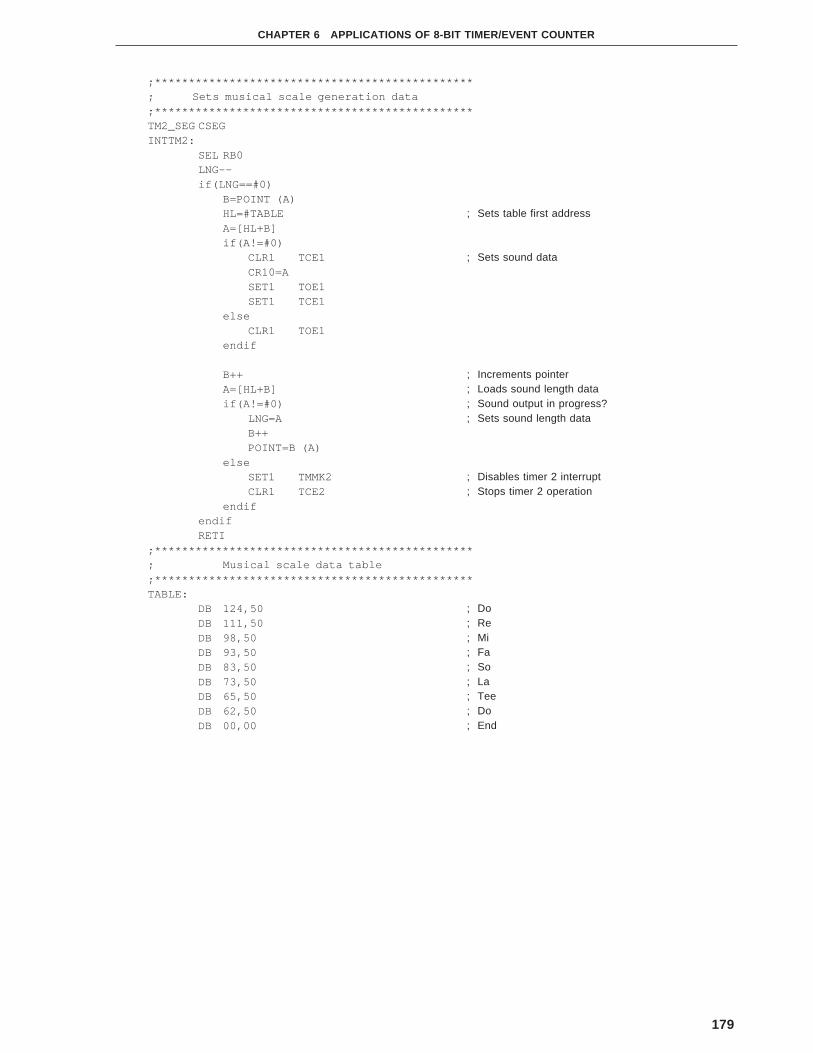
179
CHAPTER 6 APPLICATIONS OF 8-BIT TIMER/EVENT COUNTER
;***********************************************; Sets musical scale generation data;***********************************************TM2_SEG CSEGINTTM2:
SEL RB0LNG––if(LNG==#0)
B=POINT (A)HL=#TABLEA=[HL+B]if(A!=#0)
CLR1 TCE1CR10=ASET1 TOE1SET1 TCE1
elseCLR1 TOE1
endif
B++A=[HL+B]if(A!=#0)
LNG=AB++POINT=B (A)
elseSET1 TMMK2CLR1 TCE2
endifendifRETI
;***********************************************; Musical scale data table;***********************************************TABLE:
DB 124,50DB 111,50DB 98,50DB 93,50DB 83,50DB 73,50DB 65,50DB 62,50DB 00,00
; Sets table first address
; Sets sound data
; Increments pointer; Loads sound length data; Sound output in progress?; Sets sound length data
; Disables timer 2 interrupt; Stops timer 2 operation
; Do; Re; Mi; Fa; So; La; Tee; Do; End

[MEMO]
180

CHAPTER 7 APPLICATIONS OF WATCH TIMER
The watch timer of the 78K/0 series has a watch timer function that causes the timer to overflow every 0.5 second
by using the main system clock or subsystem clock as the clock source, and an interval timer function that allows
you to set six types of reference times. These two functions can be simultaneously used.
The watch timer is set by using timer clock select register 2 (TCL2) and watch timer mode control register (TMC2).
181

182
CHAPTER 7 APPLICATIONS OF WATCH TIMER
Figure 7-1. Format of Timer Clock Select Register 2
(µPD78054, 78054Y, 78064, 78064Y, 78078, 78078Y, 780058, 780058Y, 780308,
780308Y, 78058F, 78058FY, 78064B, 78075B, 78075BY subseries,
µPD78070A, 78070AY)
TCL22 TCL21 TCL20 Selects count clock of watchdog timer
MCS = 1 MCS = 0
0 0 0 fXX/23 fX/23 (625 kHz) fX/24 (313 kHz)
0 0 1 fXX/24 fX/24 (313 kHz) fX/25 (156 kHz)
0 1 0 fXX/25 fX/25 (156 kHz) fX/26 (78.1 kHz)
0 1 1 fXX/26 fX/26 (78.1 kHz) fX/27 (39.1 kHz)
1 0 0 fXX/27 fX/27 (39.1 kHz) fX/28 (19.5 kHz)
1 0 1 fXX/28 fX/28 (19.5 kHz) fX/29 (9.8 kHz)
1 1 0 fXX/29 fX/29 (9.8 kHz) fX/210 (4.9 kHz)
1 1 1 fXX/211 fX/211 (2.4 kHz) fX/212 (1.2 kHz)
TCL24 Selects count clock of watch timer
MCS = 1 MCS = 0
0 fXX/27 fX/27 (39.1 kHz) fX/28 (19.5 kHz)
1 fXT (32.768 kHz)
TCL27 TCL26 TCL25 Selects frequency of buzzer output
MCS = 1 MCS = 0
0 × × Disables buzzer output
1 0 0 fXX/29 fX/29 (9.8 kHz) fX/210 (4.9 kHz)
1 0 1 fXX/210 fX/210 (4.9 kHz) fX/211 (2.4 kHz)
1 1 0 fXX/211 fX/211 (2.4 kHz) fX/212 (1.2 kHz)
1 1 1 Setting prohibited
Caution Before writing new data to TCL2, stop the timer operation once.
Remarks 1. fXX : main system clock frequency (fX or fX/2)
2. fX : main system clock oscillation frequency
3. fXT : subsystem clock oscillation frequency
4. × : don’t care
5. MCS: bit 0 of oscillation mode select register (OSMS)
6. ( ) : at fX = 5.0 MHz or fXT = 32.768 kHz
7 6 5 4 3 2Symbol 1 0
FF42HTCL20TCL2 TCL210 TCL22TCL24TCL25TCL26TCL27
Address At reset R/W
00H R/W

183
CHAPTER 7 APPLICATIONS OF WATCH TIMER
Figure 7-2. Format of Timer Clock Select Register 2 ( µPD78098, 78098B subseries)
TCL22 TCL21 TCL20 Selects count clock of watchdog timer
0 0 0 fXX/23 (500 kHz)
0 0 1 fXX/24 (250 kHz)
0 1 0 fXX/25 (125 kHz)
0 1 1 fXX/26 (62.5 kHz)
1 0 0 fXX/27 (31.3 kHz)
1 0 1 fXX/28 (15.6 kHz)
1 1 0 fXX/29 (7.8 kHz)
1 1 1 fXX/211 (2.0 kHz)
TCL24 Selects count clock of watch timer
0 fXX/27 (31.3 kHz)
1 fXT (32.768 kHz)
TCL27 TCL26 TCL25 Selects frequency of buzzer output
0 × × Disables buzzer output
1 0 0 fXX/29 (7.8 kHz)
1 0 1 fXX/210 (3.9 kHz)
1 1 0 fXX/211 (1.95 kHz)
1 1 1 Setting prohibited
Caution Before writing new data to TCL2, stop the timer operation once.
Remarks 1. fXX: main system clock frequency
2. fXT: subsystem clock oscillation frequency
3. × : don’t care
4. ( ): at fXX = 4.0 MHz or fXT = 32.768 kHz
7 6 5 4 3 2Symbol 1 0
FF42HTCL20TCL2 TCL210 TCL22TCL24TCL25TCL26TCL27
Address At reset R/W
00H R/W

184
CHAPTER 7 APPLICATIONS OF WATCH TIMER
Figure 7-3. Format of Timer Clock Select Register 2 ( µPD780018, 780018Y subseries)
TCL22 TCL21 TCL20 Selects count clock of watchdog timer
0 0 0 fXX/23 fX/23 (625 kHz)
0 0 1 fXX/24 fX/24 (313 kHz)
0 1 0 fXX/25 fX/25 (156 kHz)
0 1 1 fXX/26 fX/26 (78.1 kHz)
1 0 0 fXX/27 fX/27 (39.1 kHz)
1 0 1 fXX/28 fX/28 (19.5 kHz)
1 1 0 fXX/29 fX/29 (9.8 kHz)
1 1 1 fXX/211 fX/211 (2.4 kHz)
TCL24 Selects count clock of watch timer
0 fXX/27 fX/27 (39.1 kHz)
1 fXT
TCL27 TCL26 TCL25 Selects frequency of buzzer output
0 × × Disables buzzer output
1 0 0 fXX/29 fX/29 (9.8 kHz)
1 0 1 fXX/210 fX/210 (4.9 kHz)
1 1 0 fXX/211 fX/211 (2.4 kHz)
1 1 1 Setting prohibited
Caution Before writing new data to TCL2, stop the timer operation once.
Remarks 1. fXX: main system clock frequency (fX)
2. fX : main system clock oscillation frequency
3. fXT: subsystem clock oscillation frequency
4. × : don’t care
5. ( ): at fX = 5.0 MHz or fXT = 32.768 kHz
7 6 5 4 3 2Symbol 1 0
FF42HTCL20TCL2 TCL210 TCL22TCL24TCL25TCL26TCL27
Address At reset R/W
00H R/W

185
CHAPTER 7 APPLICATIONS OF WATCH TIMER
Figure 7-4. Format of Watch Timer Mode Control Register
(µPD78054, 78054Y, 78064, 78064Y, 78078, 78078Y, 780018, 780018Y, 780058,
780058Y, 780308, 780308Y, 78058F, 78058FY, 78064B, 78075B, 78075BY
subseries, µPD78070A, 78070AY)
TMC20 Selects watch operation mode
0 Normal operation mode (sets flag at fW/214)
1 Fast-forward mode (sets flag at fW/25)
TMC21 Controls operation of prescaler
0 Clears after operation stopped
1 Enables operation
TMC22 Controls operation of 5-bit counter
0 Clears after operation stopped
1 Enables operation
TMC23 Selects set time of watch timer
At fXX = 5.0 MHz At fXX = 4.19 MHz At fXT = 32.768 kHz
0 214/fW (0.4 sec) 214/fW (0.5 sec) 214/fW (0.5 sec)
1 213/fW (0.2 sec) 213/fW (0.25 sec) 213/fW (0.25 sec)
TMC26 TMC25 TMC24 Selects interval time of prescaler
At fXX = 5.0 MHz At fXX = 4.19 MHz At fXT = 32.768 kHz
0 0 0 24/fW (410 µs) 24/fW (488 µs) 24/fW (488 µs)
0 0 1 25/fW (819 µs) 25/fW (977 µs) 25/fW (977 µs)
0 1 0 26/fW (1.64 ms) 26/fW (1.95 ms) 26/fW (1.95 ms)
0 1 1 27/fW (3.28 ms) 27/fW (3.91 ms) 27/fW (3.91 ms)
1 0 0 28/fW (6.55 ms) 28/fW (7.81 ms) 28/fW (7.81 ms)
1 0 1 29/fW (13.1 ms) 29/fW (15.6 ms) 29/fW (15.6 ms)
Others Setting prohibited
Caution Do not often clear the prescaler when the watch timer is used.
Remarks 1. fW : watch timer clock frequency (fXX/27 or fXT)
2. fXX: main system clock frequency (fX or fX/2)
3. fX : main system clock oscillation frequency
4. fXT: subsystem clock oscillation frequency
7 6 5 4 3 2Symbol 1 0
FF4AHTMC20TMC2 TMC21TMC23 TMC22TMC24TMC25TMC260
Address At reset R/W
00H R/W

186
CHAPTER 7 APPLICATIONS OF WATCH TIMER
Figure 7-5. Format of Watch Timer Mode Control Register ( µPD78098, 78098B subseries)
7 6 5 4 3 2Symbol 1 0
TMC23 Selects set time of watch flag
FF4AHTMC20TMC2 TMC21TMC23 TMC22TMC24TMC25TMC260
Address At reset R/W
00H R/W
TMC20
0 214/fW (0.5s)0
1 213/fW (0.25s)
0 25/fW (977 s)1
1 24/fW (488 s)
µ
µ
TMC21 Controls operation of prescaler
0 Clears after operation stopped
1 Enables operation
TMC22 Controls operation of 5-bit counter
0 Clears after operation stopped
1 Enables operation
TMC26 Selects interval time of prescaler
0
0
TMC25
0
0
0 26/fW (1.95 ms)
0 27/fW (3.91 ms)
1
1
TMC24
0
1
0
1
1 28/fW (7.81 ms)
1 29/fW (15.6 ms)
0
0
Others Setting prohibited
0
1
24/fW (488 s)µ
25/fW (977 s)µ
Caution Do not often clear the prescaler when the watch timer is used.
Remarks 1. fW : watch timer clock frequency (fX/28 or fXT)
2. ( ): at fW = 32.768 kHz

187
CHAPTER 7 APPLICATIONS OF WATCH TIMER
7.1 Watch and LED Display Program
As an example of using the watch timer, this section introduces a program that counts time by using an 0.5 second
overflow and dynamically displays LED at intervals of 1.95 ms.
To count time, an overflow flag is tested each time a subroutine is called. When the flag is set, time is counted
up in seconds. Because an overflow occurs every 0.5 second, it takes 1 minute to count 120 times. The overflow
flag is tested at intervals of 1.95 ms so that the flag is tested without fail. The watch of this program is 24-hour watch.
The high-order and low-order digits of minute and hour data are stored in separate areas of memory.
Figure 7-6. Concept of Watch Data
Second data Minute data Hour data
0-120Low-orderdigit 0-9
High-orderdigit 0-5
Low-orderdigit 0-9
High-orderdigit 0-2

188
CHAPTER 7 APPLICATIONS OF WATCH TIMER
As LED dynamic display, four digits are displayed with the display digit changed at intervals of 1.95 ms. In this
example, the high-order 4 bits of P3 are used as a digit signal, and P5 that can directly drive an LED is selected as
a segment signal.
The digit of an LED specified by a display digit area (DIGCT) in an LED display area is displayed. To change the
digit signal, the segment signal is turned off so that the adjacent digits are not displayed.
Figure 7-7. LED Display Timing
Figure 7-8. Circuit Example of Watch Timer
P34
P35
P36
P37
Port 5
DIGIT 0 1 2 3 0 1 2 3 0 1 2 3
Segment signal OFF
PD78054µ
P37
P36
P35
P34
P50
P57
7-segment LED × 4

189
CHAPTER 7 APPLICATIONS OF WATCH TIMER
(1) Description of package
<Public declaration symbol>
SECD : second data storage area
MINDP : minute data storage area
HOURDP : hour data storage area
LEDDP : LED display area
<Register used>
Bank 0: AX, B, HL
<RAM used>
Name Usage Attribute Bytes
MINDP Stores minute data SADDRP 2
HOURDP Stores hour data
SECD Stores second data 1
DIGCT Stores LED display digit data
LEDDP LED display data 4
<Hardware used>
• Watch timer
• P34-37
• P5
<Initial setting>
• TMC2 = #00100110B ; 0.5-second watch operation at 1.95 ms interval
• TMMK3 = 0 ; enables watch timer interrupt
<Starting>
Started by the interval timer interrupt request of the watch timer.
(2) Example of use
EXTRN MINDP, HOURDP, SECD, LEDDP
TMC2 = #00100110B ; 0.5-second watch operation at 1.95 ms interval
CLR1 TMMK3 ; Enables watch timer interrupt
EI

190
CHAPTER 7 APPLICATIONS OF WATCH TIMER
(3) SPD chart
INTTM3 Selects register bank 0
Watch count TIME
LED display LEDDSP
LEDDSP Turns OFF segment signal
IF: digit counter (DIGCT) = 0
Initial setting of digit signal
Shifts digit signal I bit higher
THEN
ELSE
Outputs segment signal of digit indicated by digit counter
Increments digit counter
TIME IF: Sets watch timer interrupt request flag
Increments second counter
IF: second counter = 120
Sets second counter to 0
Increments minute (low) counter
IF: minute (low) counter = 10
THEN
THEN
THEN
Clears minute (low) counter to 0
Increments minute (high) counter
IF: minute (high) counter = 6
THEN
Clears minute (high) counter to 0
Increments hour (low) counter
IF: hour data ≠ 0204H
IF: hour (low) counter = 10
Clears hour (low) counter to 0
Increments hour (high) counter
Clears hour counter to 0
THEN
THEN
ELSE

191
CHAPTER 7 APPLICATIONS OF WATCH TIMER
(4) Program list
PUBLIC HOURDP,MINDP,SECD,LEDDP
WT_DATP DSEG SADDRPMINDP: DS 2HOURDP: DS 2SECD: DS 1DIGCT: DS 1LEDDP: DS 4
VETM3 CSEG AT 1EHDW INTTM3
;***************************************;* Interval interrupt processing;***************************************TM3_SEG CSEGINTTM3:
SEL RB0CALL !TIMECALL !LEDDPSPRETI
; Minute data storage area; Hour data storage area; Second data storage area; LED display digit area; LED display area
; Sets vector address of watch timer

192
CHAPTER 7 APPLICATIONS OF WATCH TIMER
;************************************; LED display;************************************LEDDPSP:
P5=#0FFHDIGCT&=#00000011Bif(DIGCT==#0)
A=P3A&=#00001111BA|=#00010000BP3=A
elseA=P3A&=#11110000BX=AA=P3A+=XP3=A
endif
B=DIGCT (A)HL=#LEDDPB=[HL+B] (A)HL=#SEGDTP5=[HL+B] (A)
DIGCT++RET
SEGDT:DB 11000000BDB 11111001BDB 10100100BDB 10110000BDB 10011001BDB 10010010BDB 10000010BDB 11111000BDB 10000000BDB 10010000BDB 10001000BDB 10000011BDB 11000110BDB 10100001BDB 10000110BDB 10001110B
$EJECT
; Turns OFF segment output; Adjusts digit counter (0-3)
; Initial setting of digit signal (high-order 4 bits)
; Shifts high-order 4 bits
; Sets address of display data; Display area first address; Sets display data; Conversion to segment data; Outputs segment signal
; 0; 1; 2; 3; 4; 5; 6; 7; 8; 9; A; B; C; D; E; F

193
CHAPTER 7 APPLICATIONS OF WATCH TIMER
;********************************;* Watch count up;********************************TIME:
if_bit(WTIF)CLR1 WTIFSECD++if(SECD==#120)
SECD=#0(MINDP+0)++if((MINDP+0)==#10)
(MINDP+0)=#0(MINDP+1)++if(MINDP+1==#6)
(MINDP+1)=#0(HOURDP+0)++if(HOURDP!=#0204H) (AX)
if((HOURDP+0)==#10)(HOURDP+0)=#0(HOURDP+1)++
endifelse
HOURDP=#0000Hendif
endifendif
endifendifRET
; 0.5 second test
; 120 = 60 seconds/0.5
; Increments minute (low); Carry occurs
; Increments minute (high); Carry occurs
; Hour data 24?; Carry occurs

[MEMO]
194

CHAPTER 8 APPLICATIONS OF SERIAL INTERFACE
The 78K/0 series is provided with the serial interface shown in Table 8-1.
Table 8-1. Serial Interface Channel of Each Subseries
Channel 0 Channel 1 Channel 2 Channel 3 Channel 4 Channel 5
3-wire 2-wire SBI I2C bus 3-wire 3-wire 3-wire UART 3-wire 3-wire I2C bus
with with (multi-
automatic time- master
trans- division sup-
mission/ function porting)
reception
function
µPD78054 × × × ×
µPD78054Y × × × ×
µPD78064 × × × × × ×
µPD78064Y × × × × × ×
µPD78078 × × × ×
µPD78078Y × × × ×
µPD78083 × × × × × × × × ×
µPD78098 × × × ×
µPD780018 × × × × × × × ×
µPD780018Y × × × × × × ×
µPD780058 × × × ×
µPD780058Y × × × ×
µPD780308 × × × × ×
µPD780308Y × × × × ×
µPD78058F × × × ×
µPD78058FY × × × ×
µPD78064B × × × × × ×
µPD78070A × × × ×
µPD78070AY × × × ×
µPD78075B × × × ×
µPD78075BY × × × ×
µPD78098B × × × ×
Note With time-division transfer function
Remark : Function provided, ×: Function not provided
Subseries
Configuration
of Serial
Interface
Note
Note
Note
Note
195
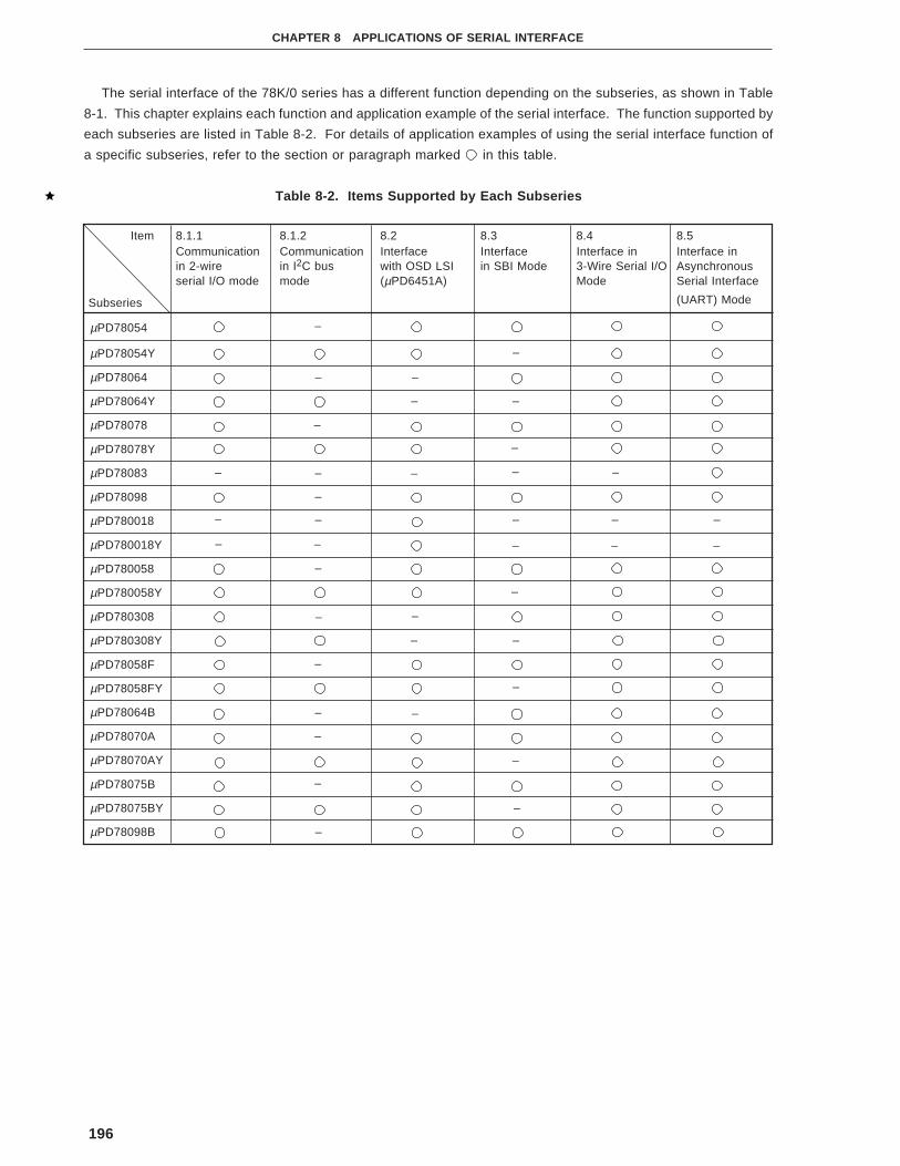
196
CHAPTER 8 APPLICATIONS OF SERIAL INTERFACE
The serial interface of the 78K/0 series has a different function depending on the subseries, as shown in Table
8-1. This chapter explains each function and application example of the serial interface. The function supported by
each subseries are listed in Table 8-2. For details of application examples of using the serial interface function of
a specific subseries, refer to the section or paragraph marked in this table.
Table 8-2. Items Supported by Each Subseries
Item 8.1.1 8.1.2 8.2 8.3 8.4 8.5Communication Communication Interface Interface Interface in Interface inin 2-wire in I2C bus with OSD LSI in SBI Mode 3-Wire Serial I/O Asynchronousserial I/O mode mode (µPD6451A) Mode Serial Interface
(UART) Mode
µPD78054
µPD78054Y
µPD78064
µPD78064Y
µPD78078
µPD78078Y
µPD78083
µPD78098
µPD780018
µPD780018Y
µPD780058
µPD780058Y
µPD780308
µPD780308Y
µPD78058F
µPD78058FY
µPD78064B
µPD78070A
µPD78070AY
µPD78075B
µPD78075BY
µPD78098B
Subseries
–
–
–
–
–
–
–
–
– –
–
–
–
–
–
–
–
–
–
–
–
–
–
–
–
– – –
– – –
–
–
– –
–
––
–

197
CHAPTER 8 APPLICATIONS OF SERIAL INTERFACE
The functions and operations of the serial interface are specified by using the following registers:
Table 8-3. Registers of Serial Interface
Serial Interface Register Used
Channel 0 • Timer clock select register (TCL3)
• Serial operation mode register 0 (CSIM0)
• Serial bus interface control register (SBIC)
• Interrupt timing specification register (SINT)
Channel 1 • Timer clock select register (TCL3)
• Serial operation mode register 1 (CSIM1)
• Automatic data transmission/reception control register (ADTC)
• Automatic data transmission/reception interval specification register (ADTI)
Channel 2 • Serial operation mode register 2 (CSIM2)
• Asynchronous serial interface mode register (ASIM)
• Asynchronous serial interface status register (ASIS)
• Baud rate generator control register (BRGC)
• Serial interface pin select register (SIPS)Note
Note This register is provided only on the µPD780058, 780058Y, 780308, and 780308Y subseries.
Remark This chapter describes the register formats and application examples of serial interface channels 0, 1,
and 2. For details of the register formats of channels 3, 4, and 5, refer to the User’s Manual of each
subseries.

198
CHAPTER 8 APPLICATIONS OF SERIAL INTERFACE
Figure 8-1. Format of Timer Clock Select Register 3
(µPD78054, 78078, 780058, 78058F, 78075B subseries, µPD78070A)
TCL33 TCL32 TCL31 TCL30 Selects serial clock of serial interface channel 0
MCS = 1 MCS = 0
0 1 1 0 fXX/2 Setting prohibited fX/22 (1.25 MHz)
0 1 1 1 fXX/22 fX/22 (1.25 MHz) fX/23 (625 kHz)
1 0 0 0 fXX/23 fX/23 (625 kHz) fX/24 (313 kHz)
1 0 0 1 fXX/24 fX/24 (313 kHz) fX/25 (156 kHz)
1 0 1 0 fXX/25 fX/25 (156 kHz) fX/26 (78.1 kHz)
1 0 1 1 fXX/26 fX/26 (78.1 kHz) fX/27 (39.1 kHz)
1 1 0 0 fXX/27 fX/27 (39.1 kHz) fX/28 (19.5 kHz)
1 1 0 1 fXX/28 fX/28 (19.5 kHz) fX/29 (9.8 kHz)
Others Setting prohibited
TCL37 TCL36 TCL35 TCL34 Selects serial clock of serial interface channel 1
MCS = 1 MCS = 0
0 1 1 0 fXX/2 Setting prohibited fX/22 (1.25 MHz)
0 1 1 1 fXX/22 fX/22 (1.25 MHz) fX/23 (625 kHz)
1 0 0 0 fXX/23 fX/23 (625 kHz) fX/24 (313 kHz)
1 0 0 1 fXX/24 fX/24 (313 kHz) fX/25 (156 kHz)
1 0 1 0 fXX/25 fX/25 (156 kHz) fX/26 (78.1 kHz)
1 0 1 1 fXX/26 fX/26 (78.1 kHz) fX/27 (39.1 kHz)
1 1 0 0 fXX/27 fX/27 (39.1 kHz) fX/28 (19.5 kHz)
1 1 0 1 fXX/28 fX/28 (19.5 kHz) fX/29 (9.8 kHz)
Others Setting prohibited
Caution Before writing new data to TCL3, stop serial transfer once.
Remarks 1. fXX : main system clock frequency (fX or fX/2)
2. fX : main system clock oscillation frequency
3. MCS : bit 0 of oscillation mode select register (OSMS)
4. ( ) : at fX = 5.0 MHz
7 6 5 4 3 2Symbol 1 0
FF43HTCL30TCL3 TCL31TCL33 TCL32TCL34TCL35TCL36TCL37
Address At reset R/W
88H R/W

199
CHAPTER 8 APPLICATIONS OF SERIAL INTERFACE
Figure 8-2. Format of Timer Clock Select Register 3
(µPD78054Y, 78078Y, 780058Y, 78058FY, 78075BY subseries, µPD78070AY)
TCL33 TCL32 TCL31 TCL30 Selects serial clock of serial interface channel 0
MCS = 1 MCS = 0 MCS = 1 MCS = 0
0 1 1 0 fXX/25 Setting prohibited fX/26 (78.1 kHz) fXX/2 Setting prohibited fX/22 (1.25 MHz)
0 1 1 1 fXX/26 fX/26 (78.1 kHz) fX/27 (39.1 kHz) fXX/22 fX/22 (1.25 MHz) fX/23 (625 kHz)
1 0 0 0 fXX/27 fX/27 (39.1 kHz) fX/28 (19.5 kHz) fXX/23 fX/23 (625 kHz) fX/24 (313 kHz)
1 0 0 1 fXX/28 fX/28 (19.5 kHz) fX/29 (9.77 kHz) fXX/24 fX/24 (313 kHz) fX/25 (156 kHz)
1 0 1 0 fXX/29 fX/29 (9.77 kHz) fX/210 (4.88 kHz) fXX/25 fX/25 (156 kHz) fX/26 (78.1 kHz)
1 0 1 1 fXX/210 fX/210 (4.88 kHz) fX/211 (2.44 kHz) fXX/26 fX/26 (78.1 kHz) fX/27 (39.1 kHz)
1 1 0 0 fXX/211 fX/211 (2.44 kHz) fX/212 (1.22 kHz) fXX/27 fX/27 (39.1 kHz) fX/28 (19.5 kHz)
1 1 0 1 fXX/212 fX/212 (1.22 kHz) fX/213 (0.61 kHz) fXX/28 fX/28 (19.5 kHz) fX/29 (9.8 kHz)
Others Setting prohibited
TCL37 TCL36 TCL35 TCL34 Selects serial clock of serial interface channel 1
MCS = 1 MCS = 0
0 1 1 0 fXX/2 Setting prohibited fX/22 (1.25 MHz)
0 1 1 1 fXX/22 fX/22 (1.25 MHz) fX/23 (625 kHz)
1 0 0 0 fXX/23 fX/23 (625 kHz) fX/24 (313 kHz)
1 0 0 1 fXX/24 fX/24 (313 kHz) fX/25 (156 kHz)
1 0 1 0 fXX/25 fX/25 (156 kHz) fX/26 (78.1 kHz)
1 0 1 1 fXX/26 fX/26 (78.1 kHz) fX/27 (39.1 kHz)
1 1 0 0 fXX/27 fX/27 (39.1 kHz) fX/28 (19.5 kHz)
1 1 0 1 fXX/28 fX/28 (19.5 kHz) fX/29 (9.8 kHz)
Others Setting prohibited
Caution Before writing new data to TCL3, stop serial transfer once.
Remarks 1. fXX : main system clock frequency (fX or fX/2)
2. fX : main system clock oscillation frequency
3. MCS : bit 0 of oscillation mode select register (OSMS)
4. ( ) : at fX = 5.0 MHz
Serial clock in 3-wire serial I/O or 2-wire
serial I/O modeSerial clock in I2C bus mode
7 6 5 4 3 2Symbol 1 0
FF43HTCL30TCL3 TCL31TCL33 TCL32TCL34TCL35TCL36TCL37
Address At reset R/W
88H R/W

200
CHAPTER 8 APPLICATIONS OF SERIAL INTERFACE
Figure 8-3. Format of Timer Clock Select Register 3 ( µPD78064, 780308, 78064B subseries)
TCL33 TCL32 TCL31 TCL30 Selects serial clock of serial interface channel 0
MCS = 1 MCS = 0
0 1 1 0 fXX/2 Setting prohibited fX/22 (1.25 MHz)
0 1 1 1 fXX/22 fX/22 (1.25 MHz) fX/23 (625 kHz)
1 0 0 0 fXX/23 fX/23 (625 kHz) fX/24 (313 kHz)
1 0 0 1 fXX/24 fX/24 (313 kHz) fX/25 (156 kHz)
1 0 1 0 fXX/25 fX/25 (156 kHz) fX/26 (78.1 kHz)
1 0 1 1 fXX/26 fX/26 (78.1 kHz) fX/27 (39.1 kHz)
1 1 0 0 fXX/27 fX/27 (39.1 kHz) fX/28 (19.5 kHz)
1 1 0 1 fXX/28 fX/28 (19.5 kHz) fX/29 (9.8 kHz)
Others Setting prohibited
Cautions 1. Clear bits 4 through 6 to 0 and set bit 7 to 1.
2. Before writing new data to TCL3, stop serial transfer once.
Remarks 1. fXX : main system clock frequency (fX or fX/2)
2. fX : main system clock oscillation frequency
3. MCS : bit 0 of oscillation mode select register (OSMS)
4. ( ) : at fX = 5.0 MHz
7 6 5 4 3 2Symbol 1 0
FF43HTCL30TCL3 TCL31TCL33 TCL320001
Address At reset R/W
88H R/W

201
CHAPTER 8 APPLICATIONS OF SERIAL INTERFACE
Figure 8-4. Format of Timer Clock Select Register 3 ( µPD78064Y, 780308Y subseries)
TCL33 TCL32 TCL31 TCL30 Selects serial clock of serial interface channel 0
MCS = 1 MCS = 0 MCS = 1 MCS = 0
0 1 1 0 fXX/25 Setting prohibited fX/26 (78.1 kHz) fXX/2 Setting prohibited fX/22 (1.25 MHz)
0 1 1 1 fXX/26 fX/26 (78.1 kHz) fX/27 (39.1 kHz) fXX/22 fX/22 (1.25 MHz) fX/23 (625 kHz)
1 0 0 0 fXX/27 fX/27 (39.1 kHz) fX/28 (19.5 kHz) fXX/23 fX/23 (625 kHz) fX/24 (313 kHz)
1 0 0 1 fXX/28 fX/28 (19.5 kHz) fX/29 (9.77 kHz) fXX/24 fX/24 (313 kHz) fX/25 (156 kHz)
1 0 1 0 fXX/29 fX/29 (9.77 kHz) fX/210 (4.88 kHz) fXX/25 fX/25 (156 kHz) fX/26 (78.1 kHz)
1 0 1 1 fXX/210 fX/210 (4.88 kHz) fX/211 (2.44 kHz) fXX/26 fX/26 (78.1 kHz) fX/27 (39.1 kHz)
1 1 0 0 fXX/211 fX/211 (2.44 kHz) fX/212 (1.22 kHz) fXX/27 fX/27 (39.1 kHz) fX/28 (19.5 kHz)
1 1 0 1 fXX/212 fX/212 (1.22 kHz) fX/213 (0.61 kHz) fXX/28 fX/28 (19.5 kHz) fX/29 (9.8 kHz)
Others Setting prohibited
Cautions 1. Clear bits 4 through 6 to 0 and set bit 7 to 1.
2. Before writing new data to TCL3, stop serial transfer once.
Remarks 1. fXX : main system clock frequency (fX or fX/2)
2. fX : main system clock oscillation frequency
3. MCS : bit 0 of oscillation mode select register (OSMS)
4. ( ) : at fX = 5.0 MHz
Serial clock in 3-wire serial I/O or
2-wire serial I/O modeSerial clock in I2C bus mode
7 6 5 4 3 2Symbol 1 0
FF43HTCL30TCL3 TCL31TCL33 TCL320001
Address At reset R/W
88H R/W

202
CHAPTER 8 APPLICATIONS OF SERIAL INTERFACE
Figure 8-5. Format of Timer Clock Select Register 3 ( µPD78098, 78098B subseries)
TCL33 TCL32 TCL31 TCL30 Selects serial clock of serial interface channel 0
0 1 1 0 fXX/2Note
0 1 1 1 fXX/22 (1.0 MHz)
1 0 0 0 fXX/23 (500 kHz)
1 0 0 1 fXX/24 (250 kHz)
1 0 1 0 fXX/25 (125 kHz)
1 0 1 1 fXX/26 (62.5 kHz)
1 1 0 0 fXX/27 (31.3 kHz)
1 1 0 1 fXX/28 (15.6 kHz)
Others Setting prohibited
TCL37 TCL36 TCL35 TCL34 Selects serial clock of serial interface channel 1
0 1 1 0 fXX/2Note
0 1 1 1 fXX/22 (1.0 MHz)
1 0 0 0 fXX/23 (500 kHz)
1 0 0 1 fXX/24 (250 kHz)
1 0 1 0 fXX/25 (125 kHz)
1 0 1 1 fXX/26 (62.5 kHz)
1 1 0 0 fXX/27 (31.3 kHz)
1 1 0 1 fXX/28 (15.6 kHz)
Others Setting prohibited
Note Can be set only when the main system clock frequency is 5.0 MHz or less.
Caution Before writing new data to TCL3, stop serial transfer once.
Remarks 1. fXX : main system clock frequency
2. ( ) : at fXX = 4.0 MHz
7 6 5 4 3 2Symbol 1 0
FF43HTCL30TCL3 TCL31TCL33 TCL32TCL34TCL35TCL36TCL37
Address At reset R/W
88H R/W

203
CHAPTER 8 APPLICATIONS OF SERIAL INTERFACE
Figure 8-6. Format of Timer Clock Select Register 3 ( µPD780018, 780018Y subseries)
TCL37 TCL36 TCL35 TCL34 Selects serial clock of serial interface channel 1
0 1 1 1 fXX/22 fX/22 (1.25 MHz)
1 0 0 0 fXX/23 fX/23 (625 kHz)
1 0 0 1 fXX/24 fX/24 (313 kHz)
1 0 1 0 fXX/25 fX/25 (156 kHz)
1 0 1 1 fXX/26 fX/26 (78.1 kHz)
1 1 0 0 fXX/27 fX/27 (39.1 kHz)
1 1 0 1 fXX/28 fX/28 (19.5 kHz)
Others Setting prohibited
Caution Before writing new data to TCL3, stop serial transfer once.
Remarks 1. fXX : main system clock frequency (fX)
2. fX : main system clock oscillation frequency
3. ( ) : at fX = 5.0 MHz
7 6 5 4 3 2Symbol 1 0
FF43H0TCL3 01 0TCL34TCL35TCL36TCL37
Address At reset R/W
88H R/W

204
CHAPTER 8 APPLICATIONS OF SERIAL INTERFACE
Figure 8-7. Format of Serial Operating Mode Register 0
(µPD78054, 78064, 78078, 78098, 780058, 780308, 78058F, 78064B, 78075B, 78098B
subseries, µPD78070A)(1/2)
R/W CSIM CSIM Selects clock of serial interface channel 001 00
0 × Clock externally input to SCK0 pin
1 0 Output of 8-bit timer register 2 (TM2)
1 1 Clock specified by bits 0 through 3 of timer clock select register 3 (TCL3)
R/W CSIM CSIM CSIM PM25 P25 PM26 P26 PM27 P27 Operation mode First bit Function of Function of Function of
04 03 02 SI0/SB0/P25 pin SO0/SB1/P26 pin SCK0/P27 pin
0 × 0 Note 2 Note 2 0 0 0 1 3-wire serial MSB SI0Note 2 SO0 SCK0
1 I/O mode LSB (input) (CMOS output) (CMOS I/O)
1 0 0 Note 3 Note 3 0 0 0 1 SBI mode MSB P25 SB1 SCK0
(CMOS I/O) (N-ch open drain (CMOS I/O)
I / O )
1 0 0 Note 3 Note 3 0 1 SB0 P26
(N-ch open drain (CMOS I/O)
I/O)
1 1 0 Note 3 Note 3 0 0 0 1 2-wire serial MSB P25 SB1 SCK0
I/O mode (CMOS I/O) (N-ch open drain (N-ch open drain
I/O) I/O)
1 0 0 Note 3 Note 3 0 1 SB0 P26
(N-ch open drain (CMOS I/O)
I/O)
R/W WUP Controls wake-up functionNote 4
0 Generates interrupt request signal in all modes each time serial transfer is executed
1 Generates interrupt request signal when address received after bus has been released (when CMDD = RELD =
1) coincides with data of slave address register in SBI mode
Notes 1. Bit 6 (COI) is a read-only bit.
2. When only the transmission function is used, this pin can be used as P25 (CMOS I/O).
3. These pins can be used as port pins.
4. When using the wake-up function (WUP = 1), clear bit 5 (SIC) of the interrupt timing specification register
(SINT) to 0.
Caution Do not change the operation mode (3-wire serial I/O/2-wire serial I/O/SBI) while the operation of
the serial interface channel 0 is enabled. To change the operation mode, stop the serial operation.
Remark × : don’t care
PM×× : Port mode register
P×× : Output latch of port
×1
× ×
× ×
××
××
7
CSIE0
6
COI
5
WUP
4
CSIM04
3
CSIM03
2
CSIM02
1
CSIM01
0
CSIM00CSIM0
Symbol
FF60H
Address At reset R/W
00H R/WNote 1

205
CHAPTER 8 APPLICATIONS OF SERIAL INTERFACE
Figure 8-7. Format of Serial Operating Mode Register 0
(µPD78054, 78064, 78078, 78098, 780058, 780308, 78058F, 78064B, 78075B, 78098B
subseries, µPD78070A)(2/2)
R COI Slave address comparison result flagNote
0 Data of slave address register does not coincide with data of serial I/O shift register
1 Data of slave address register coincides with data of serial I/O shift register
R/W CSIE0 Controls operation of serial interface channel 0
0 Stops operation
1 Enables operation
Note COI is 0 when CSIE0 = 0.
Caution Do not change the operation mode (3-wire serial I/O/2-wire serial I/O/SBI) while the operation of
the serial interface channel 0 is enabled. To change the operation mode, stop the serial operation.

206
CHAPTER 8 APPLICATIONS OF SERIAL INTERFACE
Figure 8-8. Format of Serial Operating Mode Register 0
(µPD78054Y, 78064Y, 78078Y, 780058Y, 780308Y, 78058FY, 78075BY
subseries, µPD78070AY) (1/2)
R/W CSIM CSIM Selects clock of serial interface channel 001 00
0 × Clock externally input to SCK0/SCL pin
1 0 Output of 8-bit timer register 2 (TM2)Note 2
1 1 Clock specified by bits 0 through 3 of timer clock select register 3 (TCL3)
R/W CSIM CSIM CSIM PM25 P25 PM26 P26 PM27 P27 Operation mode First bit Function of Function of Function of
04 03 02 SI0/SB0/SDA0/P25 pin SO0/SB1/SDA1/P26 pinSCK0/SCL/P27 pin
0 × 0 Note 3 Note 3 0 0 0 1 3-wire serial MSB SI0Note 3 SO0 SCK0
1 I/O mode LSB (input) (CMOS output) (CMOS I/O)
1 1 0 Note 4 Note 4 0 0 0 1 2-wire serial MSB P25 SB1 SCK0/SCL
× × I/O mode or (CMOS I/O) (N-ch open drain (N-ch open drain
I2C bus mode I/O) I/O)
1 0 0 Note 4 Note 4 0 1 SB0/SDA0 P26
× × (N-ch open drain (CMOS I/O)
I/O)
R/W WUP Controls wake-up functionNote 5
0 Generates interrupt request signal in all modes each time serial transfer is executed
1 Generates interrupt request signal when address received after start condition has been detected (when CMDD
= 1) coincides with data of slave address register in I2C mode
Notes 1. Bit 6 (COI) is a read-only bit.
2. In the I2C bus mode, the clock frequency is 1/16 of the clock frequency output by TO2
3. When only the transmission function is used, this pin can be used as P25 (CMOS I/O).
4. These pins can be used as port pins.
5. When using the wake-up function (WUP = 1), clear bit 5 (SIC) of the interrupt timing specification register
(SINT) to 0. While WUP = 1, do not execute an instruction that writes data to the I/O shift register 0
(SIO0).
Caution Do not change the operation mode (3-wire serial I/O/2-wire serial I/O/I 2C bus) while the operation
of the serial interface channel 0 is enabled. To change the operation mode, stop the serial
operation.
Remark × : don’t care
PM×× : Port mode register
P×× : Output latch of port
×1
7
CSIE0
6
COI
5
WUP
4
CSIM04
3
CSIM03
2
CSIM02
1
CSIM01
0
CSIM00CSIM0
Symbol
FF60H
Address At reset R/W
00H R/WNote 1

207
CHAPTER 8 APPLICATIONS OF SERIAL INTERFACE
Figure 8-8. Format of Serial Operating Mode Register 0
(µPD78054Y, 78064Y, 78078Y, 780058Y, 780308Y, 78058FY, 78075BY
subseries, µPD78070AY) (2/2)
R COI Slave address comparison result flagNote
0 Data of slave address register does not coincide with data of serial I/O shift register
1 Data of slave address register coincides with data of serial I/O shift register
R/W CSIE0 Controls operation of serial interface channel 0
0 Stops operation
1 Enables operation
Note COI is 0 when CSIE0 = 0.
Caution Do not change the operation mode (3-wire serial I/O/2-wire serial I/O/I 2C bus) while the operation
of the serial interface channel 0 is enabled. To change the operation mode, stop the serial
operation.

208
CHAPTER 8 APPLICATIONS OF SERIAL INTERFACE
Figure 8-9. Format of Serial Bus Interface Control Register
(µPD78054, 78064, 78078, 78098, 780058, 780308, 78058F, 78064B, 78075B,
78098B subseries, µPD78070A) (1/2)
R/W RELT Used to output bus release signal.
When RELT = 1, SO latch is set to 1. After SO latch has been set, this bit is automatically cleared to
0. It is also cleared to 0 when CSIE = 0.
R/W CMDT Used to output command signal.
When CMDT = 1, SO latch is cleared to 0. After SO latch has been cleared, this bit is automatically
cleared to 0. It is also cleared to 0 when CSIE0 = 0.
R RELD Bus release detection
Clear condition (RELD = 0) Set condition (RELD = 1)
• On execution of transfer start instruction • When bus release signal (REL) is detected
• If values of SIO0 and SVA do not coincide when
address is received
• When CSIE0 = 0
• At RESET input
R CMDD Command detection
Clear condition (CMDD = 0) Set condition (CMDD = 1)
• On execution of transfer start instruction • When command signal (CMD) is detected
• When bus release signal (REL) is detected
• When CSIE0 = 0
• At RESET input
R/W ACKT Outputs acknowledge signal in synchronization with falling edge of SCK0 clock immediately after
instruction that sets this bit to 1 has been executed. After acknowledge signal has been output, this
bit is automatically cleared to 0. ACKE is cleared to 0.
This bit is also cleared to 0 when transfer of serial interface is started and when CSIE0 = 0.
Note Bits 2, 3, and 6 (RELD, CMDD, and ACKD) are read-only bits.
Remarks 1. Bits 0, 1, and 4 (RELD, CMDT, and ACKT) are cleared to 0 when they are read after data has been
set.
2. CSIE0: Bit 7 of the serial operating mode register 0 (CSIM0)
7 6 5 4 3 2Symbol 1 0
FF61HRELTSBIC CMDTCMDD RELDACKTACKEACKDBSYE
Address At reset R/W
00H R/WNote

209
CHAPTER 8 APPLICATIONS OF SERIAL INTERFACE
Figure 8-9. Format of Serial Bus Interface Control Register
(µPD78054, 78064, 78078, 78098, 780058, 780308, 78058F, 78064B, 78075B,
78098B subseries, µPD78070A) (2/2)
R/W ACKE Controls acknowledge signal output
0 Disables automatic output of acknowledge signal (output by ACKT is enabled)
1 Before completion Acknowledge signal is output in synchronization with falling edge of 9th clock
of transfer of SCK0 (automatically output when ACKE = 1)
After completion Acknowledge signal is output in synchronization with falling edge of SCK0
of transfer clock immediately after instruction that sets this bit to 1 has been executed
(automatically output when ACKE = 1). However, this bit is not automatically
cleared to 0 after acknowledge signal has been output.
R ACKD Acknowledge detection
Clear condition (ACKD = 0) Set condition (ACKD = 1)
• Falling edge of SCK0 clock immediately after • When acknowledge signal (ACK) is detected at
busy mode has been released after execution rising edge of SCK0 clock after completion of
of transfer start instruction transfer
• When CSIE0 = 0
• At RESET input
R/W Controls output of synchronization busy signal
0 Disables output of busy signal in synchronization with falling edge of SCK0 clock immediately after
instruction that clears this bit to 0 has been executed
1 Outputs busy signal at falling edge of SCK0 clock following acknowledge signal
Note The busy mode can be released by starting serial interface transfer and receiving of an address signal.
However, the BSYE flag is not cleared to 0.
Remark CSIE0: Bit 7 of the serial operating mode register 0 (CSIM0)
BSYENote

210
CHAPTER 8 APPLICATIONS OF SERIAL INTERFACE
Figure 8-10. Format of Serial Bus Interface Control Register
(µPD78054Y, 78064Y, 78078Y, 780058Y, 780308Y, 78058FY, 78075BY
subseries, µPD78070AY) (1/2)
R/W RELT Used to output stop condition.
When RELT = 1, SO latch is set to 1. After SO latch has been set, this bit is automatically cleared to
0. It is also cleared to 0 when CSIE0 = 0.
R/W CMDT Used to output start condition.
When CMDT = 1, SO latch is cleared to 0. After SO latch has been cleared, this bit is automatically
cleared to 0. It is also cleared to 0 when CSIE0 = 0.
R RELD Stop condition detection
Clear condition (RELD = 0) Set condition (RELD = 1)
• On execution of transfer start instruction • Stop condition is detected
• If values of SIO0 and SVA do not coincide when
address is received
• When CSIE0 = 0
• At RESET input
R CMDD Start condition detection
Clear condition (CMDD = 0) Set condition (CMDD = 1)
• On execution of transfer start instruction • When start condition is detected
• When stop condition is detected
• When CSIE0 = 0
• At RESET input
R/W ACKT Makes SDA0 (SDA1) low immediately after instruction that sets this bit to 1 (ACKT = 1) until next
SCL falls. Used to generate ACK signal by software when 8-clock wait is selected.
Cleared to 0 when transfer by serial interface is started and CSIE0 = 0
Note Bits 2, 3, and 6 (RELD, CMDD, and ACKD) are read-only bits.
Remark CSIE0: Bit 7 of the serial operating mode register 0 (CSIM0)
7 6 5 4 3 2Symbol 1 0
FF61HRELTSBIC CMDTCMDD RELDACKTACKEACKDBSYE
Address At reset R/W
00H R/WNote

211
CHAPTER 8 APPLICATIONS OF SERIAL INTERFACE
Figure 8-10. Format of Serial Bus Interface Control Register
(µPD78054Y, 78064Y, 78078Y, 780058Y, 780308Y, 78058FY, 78075BY
subseries, µPD78070AY) (2/2)
R/W ACKE Controls automatic output of acknowledge signalNote 1
0 Disables automatic output of acknowledge signal (output by ACKT is enabled).
Used for transmission or reception with 8-clock wait selectedNote 2 .
1 Enables automatic output of acknowledge signal.
Acknowledge signal is output in synchronization with falling edge of 9th clock of SCL (automatically
output when ACKE = 1). After output, this bit is not automatically cleared to 0.
Used for reception when 9-clock wait is selected.
R ACKD Acknowledge detection
Clear condition (ACKD = 0) Set condition (ACKD = 1)
• On execution of transfer start instruction • When acknowledge signal is detected at rising
• When CSIE0 = 0 edge of SCL clock after completion of transfer
• At RESET input
R/W Controls transmission N-ch open drain output in I2C bus modeNote 4
0 Enables output (transmission)
1 Disables output (reception)
Notes 1. Set this bit before starting transfer.
2. Output the acknowledge signal on reception by using ACKT when 8-clock wait is selected.
3. The wait status can be released by starting transfer of serial interface or receiving an address signal.
However, BSYE is not cleared to 0.
4. Be sure to set BSYE to 1 when using the wake-up function.
Remark CSIE0: Bit 7 of the serial operating mode register 0 (CSIM0)
BSYENote 3

212
CHAPTER 8 APPLICATIONS OF SERIAL INTERFACE
Figure 8-11. Format of Interrupt Timing Specification Register
(µPD78054, 78064, 78078, 78098, 780058, 780308, 78058F, 78064B, 78075B,
78098B subseries, µPD78070A)
Notes 1. Bit 6 (CLD) is a read-only bit.
2. Clear SIC to 0 when using the wake-up function in the SBI mode.
3. CLD is 0 when CSIE0 = 0.
Caution Be sure to clear bits 0 through 3 to 0.
Remark SVA : slave address register
CSIIF0 : interrupt request flag corresponding to INTCSI0
CSIE0 : bit 7 of the serial operating mode register 0 (CSIM0)
7 6 5 4 3 2Symbol 1 0
SVAM Bits of SVA used as slave address
FF63H0SINT 00 0SVAMSICCLD0
Address At reset R/W
00H R/WNote 1
0 Bits 0 through 7
1 Bits 1 through 7
SIC Selects INTCSI0 interrupt sourceNote 2
0 Sets CSIIF0 at end of transfer of serial interfacechannel 0
1 Sets CSIIF0 at end of transfer of serial interfacechannel 0 or on detection of bus release
R/W
R/W
CLD Level of SCK0 pinNote 3
0 Low level
1 High level
R

213
CHAPTER 8 APPLICATIONS OF SERIAL INTERFACE
Figure 8-12. Format of Interrupt Timing Specification Register
(µPD78054Y, 78064Y, 78078Y, 780058Y, 780308Y, 78058FY, 78075BY
subseries, µPD78070AY) (1/2)
R/W WAT1 WAT0 Controls wait and interrupt processing request
0 0 Generates interrupt request at rising edge of 8th clock of SCK0 (clock output goes into
high-impedance state)
0 1 Setting prohibited
1 0 Used in I2C bus mode (8-clock wait).
Generates interrupt processing request at rising edge of 8th clock of SCL (master makes
SCL output low and waits after outputting 8 clocks. Slave makes SCL pin low and requests
for wait after inputting 8 clocks).
1 1 Used in I2C bus mode (9-clock wait).
Generates interrupt processing request at rising edge of 9th clock of SCL (master makes
SCL output low and waits after outputting 9 clocks. Slave makes SCL pin low and requests
for wait after inputting 9 clocks).
R/W WREL Controls wait release
0 Wait release status
1 Releases wait status.
After wait status has been released, this bit is automatically cleared to 0 (used to release wait status
set by WAT1 and WAT0)
R/W CLC Controls clock levelNote 2
0 Used in I2C bus mode.
Makes output level of SCL pin low when serial transfer is not executed
1 Used in I2C bus mode.
Makes output level of SCL pin high impedance when serial transfer is not executed (clock line goes
high).
Used by master to generate start/stop condition.
Notes 1. Bit 6 (CLD) is a read-only bit.
2. Clear CLC to 0 when the I2C bus mode is not used.
7 6 5 4 3 2Symbol 1 0
FF63HWAT0SINT WAT1CLC WRELSVAMSICCLD0
Address At reset R/W
00H R/WNote 1

214
CHAPTER 8 APPLICATIONS OF SERIAL INTERFACE
Figure 8-12. Format of Interrupt Timing Specification Register
(µPD78054Y, 78064Y, 78078Y, 780058Y, 780308Y, 78058FY, 78075BY
subseries, µPD78070AY) (2/2)
R/W SVAM Bits of SVA used as slave address
0 Bits 0 through 7
1 Bits 1 through 7
R/W SIC Selects INTCSI0 interrupt sourceNote 1
0 Sets CSIIF0 to 1 at end of transfer of serial interface channel 0
1 Sets CSIIF0 to 1 at end of transfer of serial interface channel 0 or on detection of stop condition
R/W CLD Level of SCK0/SCL/P27 pinNote 2
0 Low level
1 High level
Notes 1. Sets SIC to 1 when using the wake-up function in the I2C mode.
2. CLD is 0 when CSIE0 = 0.
Remark SVA : slave address register
CSIIF0 : interrupt request flag corresponding to INTCSI0
CSIE0 : bit 7 of the serial operating mode register 0 (CSIM0)

215
CHAPTER 8 APPLICATIONS OF SERIAL INTERFACE
Figure 8-13. Format of Serial Operating Mode Register 1
(µPD78054, 78054Y, 78078, 78078Y, 78098, 780018, 780018Y, 780058, 780058Y,
78058F, 78058FY, 78075B, 78075BY, 78098B subseries, µPD78070A, 78070AY)
CSIM CSIM Selects clock of serial interface channel 111 10
0 × Clock externally input to SCK1 pinNote 1
1 0 Output of 8-bit timer register 2 (TM2)
1 1 Clock specified by bits 4 through 7 of timer clock select register 3 (TCL3)
ATE Selects operation mode of serial interface channel 1
0 3-wire serial I/O mode
1 3-wire serial I/O mode with automatic transfer/reception function
DIR First bit Function of SI1 pin Function of SO1 pin
0 MSB SI1/P20 SO1
1 LSB (input) (CMOS output)
CSIE CSIM PM20 P20 PM21 P21 PM22 P22 Operation of Function of Function of Function of
1 11 shift register 1 SI1/P20 pin SO1/P21 pin SCK1/P22
0 × Note 2 Note 2 Note 2 Note 2 Note 2 Note 2 Stops Clear P20 P21 P22
operation (CMOS I/O) (CMOS I/O) (CMOS I/O)
1 0 Note 3 Note 3 0 0 1 × Enables Count operation SI1Note 3 SO1 SCK1
1 × operation (input) (CMOS output) (input)
1 0 1 SCK1
(CMOS output)
Notes 1. Clear bit 2 (STRB) and bit 1 (BUSY1) of the automatic data transfer/reception control register (ADTC)
to 0, 0 when the external clock input is selected by clearing CSIM11 to 0.
2. These pins can be used as port pins.
3. When only transmit is executed, this pin can be used as P20 (CMOS I/O). (Set bit 7 (RE) of the automatic
data transfer/reception control register (ADTC) to 0.)
Remark × : don’t care
PM×× : Port mode register
P×× : Output latch of port
Controls operationof counter ofserial clock
× ×× × × ×
7
CSIE1
6
DIR
5
ATE
4
0
3
0
2
0
1
CSIM11
0
CSIM10
CSIM1
Symbol
FF68H
Address At reset R/W
00H R/W

216
CHAPTER 8 APPLICATIONS OF SERIAL INTERFACE
Figure 8-14. Format of Automatic Data Transfer/Reception Control Register
(µPD78054, 78054Y, 78078, 78078Y, 78098, 780018, 780018Y, 78058F, 78058FY,
78075B, 78075BY, 78098B subseries, µPD78070A, 78070AY)
Notes 1. Bits 3 and 4 (TRF and ERR) are read-only bits.
2. Identify the end of automatic transfer/reception by using TRF instead of CSIIF1. (interrupt request flag)
Caution When external clock input is selected by clearing bit 1 (CSIM11) of the serial operating mode
register 1 (CSIM1) to 0, clear STRB and BUSY1 of ADTC to 0, 0.
Remark ×: don’t care
7 6 5 4 3 2Symbol 1 0
FF69HBUSY0ADTC BUSY1TRF STRBERRERCEARLDRE
Address At reset R/W
00H R/WNote 1
BUSY1 Controls busy input
0 Does not use busy input
1 Enables busy input (active high)
BUSY0
×
0
1 Enables busy input (low active)1
R/W
STRB Controls strobe output
0 Disables strobe output
1 Enables strobe output
R/W
TRF Status of automatic transfer/reception functionNote 2
0 Detects end of automatic transfer/reception (0 whenautomatic transfer/reception is stopped or when ARLD= 0)
1 Automatic transfer/reception in progress (1 when SIO1is written)
R
ERR Detects error of automatic transfer/reception function
0 No error on automatic reception (0 when 1 is written toSIO1)
1 Error on automatic transfer/reception
R
ERCE Controls error check of automatic transfer/receptionfunction
0 Disables error check on automatic transfer/reception
1 Enables error check on automatic transfer/reception(only when BUSY1 = 1)
R/W
ARLD Selects operation mode of automatic transfer/reception function
0 Single mode
1 Repetitive mode
R/W
RE Controls reception of automatic transfer/receptionfunction
0 Disables reception
1 Enables reception
R/W

217
CHAPTER 8 APPLICATIONS OF SERIAL INTERFACE
Figure 8-15. Format of Automatic Data Transfer/Reception Control Register
(µPD780058, 780058Y subseries)
Notes 1. Bits 3 and 4 (TRF and ERR) are read-only bits.
2. Identify the end of automatic transfer/reception by using TRF instead of CSIIF1. (interrupt request flag)
Cautions 1. When external clock input is selected by clearing bit 1 (CSIM11) of the serial operating mode
register 1 (CSIM1) to 0, clear STRB and BUSY1 of ADTC to 0, 0.
2. When using the P23/STB/TxD1 and P24/BUSY/RxD1 pins in the asynchronous serial interface
(UART) mode of serial interface channel 2, the busy control option and busy & strobe control
option are invalid.
Remark ×: don’t care
7 6 5 4 3 2Symbol 1 0
FF69HBUSY0ADTC BUSY1TRF STRBERRERCEARLDRE
Address At reset R/W
00H R/WNote 1
BUSY1 Controls busy input
0 Does not use busy input
1 Enables busy input (active high)
BUSY0
×
0
1 Enables busy input (low active)1
R/W
STRB Controls strobe output
0 Disables strobe output
1 Enables strobe output
R/W
TRF Status of automatic transfer/reception functionNote 2
0 Detects end of automatic transfer/reception (0 whenautomatic transfer/reception is stopped or when ARLD= 0)
1 Automatic transfer/reception in progress (1 when SIO1is written)
R
ERR Detects error of automatic transfer/reception function
0 No error on automatic reception (0 when 1 is written toSIO1)
1 Error on automatic transfer/reception
R
ERCE Controls error check of automatic transfer/receptionfunction
0 Disables error check on automatic transfer/reception
1 Enables error check on automatic transfer/reception(only when BUSY1 = 1)
R/W
ARLD Selects operation mode of automatic transfer/reception function
0 Single mode
1 Repetitive mode
R/W
RE Controls reception of automatic transfer/receptionfunction
0 Disables reception
1 Enables reception
R/W

218
CHAPTER 8 APPLICATIONS OF SERIAL INTERFACE
Figure 8-16. Format of Automatic Data Transfer/Reception Interval Specification Register
(µPD78054, 78054Y, 78078, 78078Y, 780018, 780018Y, 780058, 780058Y, 78058F,
78058FY, 78075B, 78075BY subseries, µPD78070A, 78070AY) (1/4)
ADTI7 Controls interval time of data transfer
0 Does not control interval time by ADTINote 1
1 Controls interval time by ADTI (ADTI0 through ADTI4)
ADTI4 ADTI3 ADTI2 ADTI1 ADTI0 Specifies interval time of data transfer (fXX = 5.0 MHz)
Minimum valueNote 2 Maximum valueNote 2
0 0 0 0 0 18.4 µs + 0.5/fSCK 20.0 µs + 1.5/fSCK
0 0 0 0 1 31.2 µs + 0.5/fSCK 32.8 µs + 1.5/fSCK
0 0 0 1 0 44.0 µs + 0.5/fSCK 45.6 µs + 1.5/fSCK
0 0 0 1 1 56.8 µs + 0.5/fSCK 58.4 µs + 1.5/fSCK
0 0 1 0 0 69.6 µs + 0.5/fSCK 71.2 µs + 1.5/fSCK
0 0 1 0 1 82.4 µs + 0.5/fSCK 84.0 µs + 1.5/fSCK
0 0 1 1 0 95.2 µs + 0.5/fSCK 96.8 µs + 1.5/fSCK
0 0 1 1 1 108.0 µs + 0.5/fSCK 109.6 µs + 1.5/fSCK
0 1 0 0 0 120.8 µs + 0.5/fSCK 122.4 µs + 1.5/fSCK
0 1 0 0 1 133.6 µs + 0.5/fSCK 135.2 µs + 1.5/fSCK
0 1 0 1 0 146.4 µs + 0.5/fSCK 148.0 µs + 1.5/fSCK
0 1 0 1 1 159.2 µs + 0.5/fSCK 160.8 µs + 1.5/fSCK
0 1 1 0 0 172.0 µs + 0.5/fSCK 173.6 µs + 1.5/fSCK
0 1 1 0 1 184.8 µs + 0.5/fSCK 186.4 µs + 1.5/fSCK
0 1 1 1 0 197.6 µs + 0.5/fSCK 199.2 µs + 1.5/fSCK
0 1 1 1 1 210.4 µs + 0.5/fSCK 212.0 µs + 1.5/fSCK
Notes 1. The interval time is dependent on only the CPU processing.
2. The interval time of data transfer includes an error. The minimum and maximum values of the interval
time for data transfer can be calculated by the following expressions (where n is the value set to ADTI0
through ADTI4). However, if the minimum value calculated by the expression below is less than 2/fSCK,
the minimum interval time is 2/fSCK.
Minimum value = (n+1) × + +
Maximum value = (n+1) × + +
26
fXX
28
fXX
0.5
fSCK
26
fXX
36
fXX
1.5
fSCK
7 6 5 4 3 2Symbol 1 0
FF6BHADTI0ADTI ADTI1ADTI3 ADTI2ADTI400ADTI7
Address At reset R/W
00H R/W

219
CHAPTER 8 APPLICATIONS OF SERIAL INTERFACE
Cautions 1. Do not write ADTI during automatic transmission/reception operation.
2. Be sure to clear bits 5 and 6 to 0.
3. When controlling interval time of data transfer by automatic transfer/reception using ADTI,
the busy control option is invalid.
Remarks 1. fXX : main system clock frequency (fX or fX/2)
2. fX : main system clock oscillation frequency
3. fSCK: serial clock frequency

220
CHAPTER 8 APPLICATIONS OF SERIAL INTERFACE
Figure 8-16. Format of Automatic Data Transfer/Reception Interval Specification Register
(µPD78054, 78054Y, 78078, 78078Y, 780018, 780018Y, 780058, 780058Y, 78058F,
78058FY, 78075B, 78075BY subseries, µPD78070A, 78070AY) (2/4)
ADTI4 ADTI3 ADTI2 ADTI1 ADTI0 Specifies interval time of data transfer (fXX = 5.0 MHz)
Minimum valueNote Maximum valueNote
1 0 0 0 0 223.2 µs + 0.5/fSCK 224.8 µs + 1.5/fSCK
1 0 0 0 1 236.0 µs + 0.5/fSCK 237.6 µs + 1.5/fSCK
1 0 0 1 0 248.8 µs + 0.5/fSCK 250.4 µs + 1.5/fSCK
1 0 0 1 1 261.6 µs + 0.5/fSCK 263.2 µs + 1.5/fSCK
1 0 1 0 0 274.4 µs + 0.5/fSCK 276.0 µs + 1.5/fSCK
1 0 1 0 1 287.2 µs + 0.5/fSCK 288.8 µs + 1.5/fSCK
1 0 1 1 0 300.0 µs + 0.5/fSCK 301.6 µs + 1.5/fSCK
1 0 1 1 1 312.8 µs + 0.5/fSCK 314.4 µs + 1.5/fSCK
1 1 0 0 0 325.6 µs + 0.5/fSCK 327.2 µs + 1.5/fSCK
1 1 0 0 1 338.4 µs + 0.5/fSCK 340.0 µs + 1.5/fSCK
1 1 0 1 0 351.2 µs + 0.5/fSCK 352.8 µs + 1.5/fSCK
1 1 0 1 1 364.0 µs + 0.5/fSCK 365.6 µs + 1.5/fSCK
1 1 1 0 0 376.8 µs + 0.5/fSCK 378.4 µs + 1.5/fSCK
1 1 1 0 1 389.6 µs + 0.5/fSCK 391.2 µs + 1.5/fSCK
1 1 1 1 0 402.4 µs + 0.5/fSCK 404.0 µs + 1.5/fSCK
1 1 1 1 1 415.2 µs + 0.5/fSCK 416.8 µs + 1.5/fSCK
Note The interval time of data transfer includes an error margin. The minimum and maximum values of the interval
time for data transfer can be calculated by the following expressions (where n is the value set to ADTI0
through ADTI4). However, if the minimum value calculated by the expression below is less than 2/fSCK,
the minimum interval time is 2/fSCK.
Minimum value = (n+1) × + +
Maximum value = (n+1) × + +
Cautions 1. Do not write ADTI during automatic transfer/reception operation.
2. Be sure to clear bits 5 and 6 to 0.
3. When controlling interval time of data transfer by automatic transfer/reception using ADTI,
the busy control option is invalid.
Remarks 1. fXX : main system clock frequency (fX or fX/2)
2. fX : main system clock oscillation frequency
3. fSCK: serial clock frequency
26
fXX
28
fXX
0.5
fSCK
26
fXX
36
fXX
1.5
fSCK
7 6 5 4 3 2Symbol 1 0
FF6BHADTI0ADTI ADTI1ADTI3 ADTI2ADTI400ADTI7
Address At reset R/W
00H R/W

221
CHAPTER 8 APPLICATIONS OF SERIAL INTERFACE
Figure 8-16. Format of Automatic Data Transfer/Reception Interval Specification Register
(µPD78054, 78054Y, 78078, 78078Y, 780018, 780018Y, 780058, 780058Y, 78058F,
78058FY, 78075B, 78075BY subseries, µPD78070A, 78070AY) (3/4)
ADTI7 Controls interval time of data transfer
0 Does not control interval time by ADTINote 1
1 Controls interval time by ADTI (ADTI0 through ADTI4)
ADTI4 ADTI3 ADTI2 ADTI1 ADTI0 Specifies interval time of data transfer (fXX = 2.5 MHz)
Minimum valueNote 2 Maximum valueNote 2
0 0 0 0 0 36.8 µs + 0.5/fSCK 40.0 µs + 1.5/fSCK
0 0 0 0 1 62.4 µs + 0.5/fSCK 65.6 µs + 1.5/fSCK
0 0 0 1 0 88.0 µs + 0.5/fSCK 91.2 µs + 1.5/fSCK
0 0 0 1 1 113.6 µs + 0.5/fSCK 116.8 µs + 1.5/fSCK
0 0 1 0 0 139.2 µs + 0.5/fSCK 142.4 µs + 1.5/fSCK
0 0 1 0 1 164.8 µs + 0.5/fSCK 168.0 µs + 1.5/fSCK
0 0 1 1 0 190.4 µs + 0.5/fSCK 193.6 µs + 1.5/fSCK
0 0 1 1 1 216.0 µs + 0.5/fSCK 219.2 µs + 1.5/fSCK
0 1 0 0 0 241.6 µs + 0.5/fSCK 244.8 µs + 1.5/fSCK
0 1 0 0 1 267.2 µs + 0.5/fSCK 270.4 µs + 1.5/fSCK
0 1 0 1 0 292.8 µs + 0.5/fSCK 296.0 µs + 1.5/fSCK
0 1 0 1 1 318.4 µs + 0.5/fSCK 321.6 µs + 1.5/fSCK
0 1 1 0 0 344.0 µs + 0.5/fSCK 347.2 µs + 1.5/fSCK
0 1 1 0 1 369.6 µs + 0.5/fSCK 372.8 µs + 1.5/fSCK
0 1 1 1 0 395.2 µs + 0.5/fSCK 398.4 µs + 1.5/fSCK
0 1 1 1 1 420.8 µs + 0.5/fSCK 424.0 µs + 1.5/fSCK
Notes 1. The interval time is dependent on only the CPU processing.
2. The interval time of data transfer includes an error margin. The minimum and maximum values of the
interval time for data transfer can be calculated by the following expressions (where n is the value set
to ADTI0 through ADTI4). However, if the minimum value calculated by the expression below is less
than 2/fSCK, the minimum interval time is 2/fSCK.
Minimum value = (n+1) × + +
Maximum value = (n+1) × + +
26
fXX
28
fXX
0.5
fSCK
26
fXX
36
fXX
1.5
fSCK
7 6 5 4 3 2Symbol 1 0
FF6BHADTI0ADTI ADTI1ADTI3 ADTI2ADTI400ADTI7
Address At reset R/W
00H R/W

222
CHAPTER 8 APPLICATIONS OF SERIAL INTERFACE
Cautions 1. Do not write ADTI during automatic transfer/reception operation.
2. Be sure to clear bits 5 and 6 to 0.
3. When controlling interval time of data transfer by automatic transfer/reception using ADTI,
the busy control option is invalid.
Remarks 1. fXX : main system clock frequency (fX or fX/2)
2. fX : main system clock oscillation frequency
3. fSCK: serial clock frequency
223
CHAPTER 8 APPLICATIONS OF SERIAL INTERFACE
Figure 8-16. Format of Automatic Data Transfer/Reception Interval Specification Register
(µPD78054, 78054Y, 78078, 78078Y, 780018, 780018Y, 780058, 780058Y, 78058F,
78058FY, 78075B, 78075BY subseries, µPD78070A, 78070AY) (4/4)
ADTI4 ADTI3 ADTI2 ADTI1 ADTI0 Specifies interval time of data transfer (fXX = 2.5 MHz)
Minimum valueNote Maximum valueNote
1 0 0 0 0 446.4 µs + 0.5/fSCK 449.6 µs + 1.5/fSCK
1 0 0 0 1 472.0 µs + 0.5/fSCK 475.2 µs + 1.5/fSCK
1 0 0 1 0 497.6 µs + 0.5/fSCK 500.8 µs + 1.5/fSCK
1 0 0 1 1 523.2 µs + 0.5/fSCK 526.4 µs + 1.5/fSCK
1 0 1 0 0 548.8 µs + 0.5/fSCK 552.0 µs + 1.5/fSCK
1 0 1 0 1 574.4 µs + 0.5/fSCK 577.6 µs + 1.5/fSCK
1 0 1 1 0 600.0 µs + 0.5/fSCK 603.2 µs + 1.5/fSCK
1 0 1 1 1 625.6 µs + 0.5/fSCK 628.8 µs + 1.5/fSCK
1 1 0 0 0 651.2 µs + 0.5/fSCK 654.4 µs + 1.5/fSCK
1 1 0 0 1 676.8 µs + 0.5/fSCK 680.0 µs + 1.5/fSCK
1 1 0 1 0 702.4 µs + 0.5/fSCK 705.6 µs + 1.5/fSCK
1 1 0 1 1 728.0 µs + 0.5/fSCK 731.2 µs + 1.5/fSCK
1 1 1 0 0 753.6 µs + 0.5/fSCK 756.8 µs + 1.5/fSCK
1 1 1 0 1 779.2 µs + 0.5/fSCK 782.4 µs + 1.5/fSCK
1 1 1 1 0 804.8 µs + 0.5/fSCK 808.0 µs + 1.5/fSCK
1 1 1 1 1 830.4 µs + 0.5/fSCK 833.6 µs + 1.5/fSCK
Note The interval time of data transfer includes an error margin. The minimum and maximum values of the interval
time for data transfer can be calculated by the following expressions (where n is the value set to ADTI0
through ADTI4). However, if the minimum value calculated by the expression below is less than 2/fSCK,
the minimum interval time is 2/fSCK.
Minimum value = (n+1) × + +
Maximum value = (n+1) × + +
Cautions 1. Do not write ADTI during automatic transfer/reception operation.
2. Be sure to clear bits 5 and 6 to 0.
3. When controlling interval time of data transfer by automatic transfer/reception using ADTI,
the busy control option is invalid.
Remarks 1. fXX : main system clock frequency (fX or fX/2)
2. fX : main system clock oscillation frequency
3. fSCK: serial clock frequency
26
fXX
28
fXX
0.5
fSCK
26
fXX
36
fXX
1.5
fSCK
7 6 5 4 3 2Symbol 1 0
FF6BHADTI0ADTI ADTI1ADTI3 ADTI2ADTI400ADTI7
Address At reset R/W
00H R/W

224
CHAPTER 8 APPLICATIONS OF SERIAL INTERFACE
Figure 8-17. Format of Automatic Data Transfer/Reception Interval Specification Register
(µPD78098, 78098B subseries) (1/2)
ADTI7 Controls interval time of data transfer
0 Does not control interval time by ADTINote 1
1 Controls interval time by ADTI (ADTI0 through ADTI4)
ADTI4 ADTI3 ADTI2 ADTI1 ADTI0 Specifies interval time of data transfer (fXX = 4.0 MHz)
Minimum valueNote 2 Maximum valueNote 2
0 0 0 0 0 23.0 µs + 0.5/fSCK 25.0 µs + 1.5/fSCK
0 0 0 0 1 39.0 µs + 0.5/fSCK 41.0 µs + 1.5/fSCK
0 0 0 1 0 55.0 µs + 0.5/fSCK 57.0 µs + 1.5/fSCK
0 0 0 1 1 71.0 µs + 0.5/fSCK 73.0 µs + 1.5/fSCK
0 0 1 0 0 87.0 µs + 0.5/fSCK 89.0 µs + 1.5/fSCK
0 0 1 0 1 103.0 µs + 0.5/fSCK 105.0 µs + 1.5/fSCK
0 0 1 1 0 119.0 µs + 0.5/fSCK 121.6 µs + 1.5/fSCK
0 0 1 1 1 135.0 µs + 0.5/fSCK 137.0 µs + 1.5/fSCK
0 1 0 0 0 151.0 µs + 0.5/fSCK 153.0 µs + 1.5/fSCK
0 1 0 0 1 167.0 µs + 0.5/fSCK 169.0 µs + 1.5/fSCK
0 1 0 1 0 183.0 µs + 0.5/fSCK 185.0 µs + 1.5/fSCK
0 1 0 1 1 199.0 µs + 0.5/fSCK 201.0 µs + 1.5/fSCK
0 1 1 0 0 215.0 µs + 0.5/fSCK 217.0 µs + 1.5/fSCK
0 1 1 0 1 231.0 µs + 0.5/fSCK 233.0 µs + 1.5/fSCK
0 1 1 1 0 247.0 µs + 0.5/fSCK 249.0 µs + 1.5/fSCK
0 1 1 1 1 263.0 µs + 0.5/fSCK 265.0 µs + 1.5/fSCK
Notes 1. The interval time is dependent on only the CPU processing.
2. The interval time of data transfer includes an error margin. The minimum and maximum values of the
interval time for data transfer can be calculated by the following expressions (where n is the value set
to ADTI0 through ADTI4). However, if the minimum value calculated by the expression below is less
than 2/fSCK, the minimum interval time is 2/fSCK.
Minimum value = (n+1) × + +
Maximum value = (n+1) × + +
26
fXX
28
fXX
0.5
fSCK
26
fXX
36
fXX
1.5
fSCK
7 6 5 4 3 2Symbol 1 0
FF6BHADTI0ADTI ADTI1ADTI3 ADTI2ADTI400ADTI7
Address At reset R/W
00H R/W
225
CHAPTER 8 APPLICATIONS OF SERIAL INTERFACE
Cautions 1. Do not write ADTI during automatic transfer/reception operation.
2. Be sure to clear bits 5 and 6 to 0.
3. When controlling interval time of data transfer by automatic transfer/reception using ADTI,
the busy control option is invalid.
Remarks 1. fXX : main system clock frequency
2. fSCK: serial clock frequency

226
CHAPTER 8 APPLICATIONS OF SERIAL INTERFACE
Figure 8-17. Format of Automatic Data Transfer/Reception Interval Specification Register
(µPD78098, 78098B subseries) (2/2)
ADTI4 ADTI3 ADTI2 ADTI1 ADTI0 Specifies interval time of data transfer (fXX = 4.0 MHz)
Minimum valueNote Maximum valueNote
1 0 0 0 0 279.0 µs + 0.5/fSCK 281.0 µs + 1.5/fSCK
1 0 0 0 1 295.0 µs + 0.5/fSCK 297.0 µs + 1.5/fSCK
1 0 0 1 0 311.0 µs + 0.5/fSCK 313.0 µs + 1.5/fSCK
1 0 0 1 1 327.0 µs + 0.5/fSCK 329.0 µs + 1.5/fSCK
1 0 1 0 0 343.0 µs + 0.5/fSCK 345.0 µs + 1.5/fSCK
1 0 1 0 1 359.0 µs + 0.5/fSCK 361.0 µs + 1.5/fSCK
1 0 1 1 0 375.0 µs + 0.5/fSCK 377.0 µs + 1.5/fSCK
1 0 1 1 1 391.0 µs + 0.5/fSCK 393.0 µs + 1.5/fSCK
1 1 0 0 0 407.0 µs + 0.5/fSCK 409.0 µs + 1.5/fSCK
1 1 0 0 1 423.0 µs + 0.5/fSCK 425.0 µs + 1.5/fSCK
1 1 0 1 0 439.0 µs + 0.5/fSCK 441.0 µs + 1.5/fSCK
1 1 0 1 1 455.0 µs + 0.5/fSCK 457.0 µs + 1.5/fSCK
1 1 1 0 0 471.0 µs + 0.5/fSCK 473.0 µs + 1.5/fSCK
1 1 1 0 1 487.0 µs + 0.5/fSCK 489.0 µs + 1.5/fSCK
1 1 1 1 0 503.0 µs + 0.5/fSCK 505.0 µs + 1.5/fSCK
1 1 1 1 1 519.0 µs + 0.5/fSCK 521.0 µs + 1.5/fSCK
Note The interval time of data transfer includes an error margin. The minimum and maximum values of the interval
time for data transfer can be calculated by the following expressions (where n is the value set to ADTI0
through ADTI4). However, if the minimum value calculated by the expression below is less than 2/fSCK,
the minimum interval time is 2/fSCK.
Minimum value = (n+1) × + +
Maximum value = (n+1) × + +
Cautions 1. Do not write ADTI during automatic transfer/reception operation.
2. Be sure to clear bits 5 and 6 to 0.
3. When controlling interval time of data transfer by automatic transfer/reception using ADTI,
the busy control option is invalid.
Remarks 1. fXX : main system clock frequency
2. fSCK: serial clock frequency
26
fXX
28
fXX
0.5
fSCK
26
fXX
36
fXX
1.5
fSCK
7 6 5 4 3 2Symbol 1 0
FF6BHADTI0ADTI ADTI1ADTI3 ADTI2ADTI400ADTI7
Address At reset R/W
00H R/W

227
CHAPTER 8 APPLICATIONS OF SERIAL INTERFACE
Figure 8-18. Format of Serial Operating Mode Register 2
(µPD78054, 78054Y, 78064, 78064Y, 78078, 78078Y, 78083, 78098, 780058, 780058Y,
780308, 780308Y, 78058F, 78058FY, 78064B, 78075B, 78075BY, 78098B subseries,
µPD78070A, 78070AY)
Cautions 1. Be sure to clear bits 0 and 3 through 6 to 0.
2. Set CSIM2 to 00H in the UART mode.
7 6 5 4 3 2Symbol 1 0
FF72H0CSIM2 CSCK0 CSIM22000CSIE2
Address At reset R/W
00H R/W
CSCK Selects clock in 3-wire serial I/O mode
0 Clock externally input to SCK2 pin
1 Output of dedicated baud rate generator
CSIM22 Specifies first bit
0 MSB
1 LSB
CSIE2 Controls operation in 3-wire serial I/O mode
0 Stops operation
1 Enables operation

228
CHAPTER 8 APPLICATIONS OF SERIAL INTERFACE
Figure 8-19. Format of Asynchronous Serial Interface Mode Register
(µPD78054, 78054Y, 78064, 78064Y, 78078, 78078Y, 78083, 78098, 780058, 780058Y,
780308, 780308Y, 78058F, 78058FY, 78064B, 78075B, 78075BY, 78098B subseries,
µPD78070A, 78070AY)
Note When the baud rate generator output is selected by setting SCK to 1, the ASCK pin can be used as an
I/O port pin.
Cautions 1. Set ASIM to 00H when the 3-wire serial I/O mode is selected.
2. Before changing the operation mode, stop the serial transfer/reception operation.
7 6 5 4 3 2Symbol 1 0
FF70HSCKASIM ISRMCL SLPS0PS1RXETXE
Address At reset R/W
00H R/W
SCK Selects clock of asynchronous serial interface mode
0 Clock externally input to ASCK pin
1 Output of dedicated baud rate generatorNote
ISRM Controls receive end interrupt on occurrence of error
0 Generates receive end interrupt request when error occurs
1 Does not generate receive end interrupt request when error occurs
SL Specifies stop bit length of transmit data
0 1 bit
1 2 bits
CL Specifies character length
0 7 bits
1 8 bits
PS1 Specifies parity bitPS0
0 No parity0
Always append 0 parity during transmission.Does not check parity during reception (doesnot generate parity error)
0 1
1 Odd parity0
1 Even parity1
RXE Controls reception operation
0 Stops reception operation
1 Enables reception operation
TXE Controls transmission operation
0 Stops transmission operation
1 Enables transmission operation

229
CHAPTER 8 APPLICATIONS OF SERIAL INTERFACE
Table 8-4. Setting of Operation Modes of Serial Interface Channel 2
(µPD78054, 78054Y, 78064, 78064Y, 78078, 78078Y, 78083, 78098, 78058F, 78058FY,
78064B, 78075B, 78075BY, 78098B subseries, µPD78070A, 78070AY)
(1) Operation stop mode
ASIM CSIM2 PM70 P70 PM71 P71 PM72 P72 First Shift Function of Function of Function of
TXE RXE SCK CSIE2CSIM22 CSCK bit clock P70/SI2/RxD P71/SO2/TxD P72/SCK2/ASCK
pin pin pin
0 0 × 0 × × ×Note 1 ×Note 1 ×Note 1 ×Note 1 ×Note 1 ×Note 1 – – P70 P71 P72
Others Setting prohibited
(2) 3-wire serial I/O mode
ASIM CSIM2 PM70 P70 PM71 P71 PM72 P72 First Shift Function of Function of Function of
TXE RXE SCK CSIE2CSIM22 CSCK bit clock P70/SI2/RxD P71/SO2/TxD P72/SCK2/ASCK
pin pin pin
0 0 0 1 0 0 1Note 2 ×Note 2 0 1 1 × MSB External SI2Note 2 SO2 SCK2 input
clock (CMOS output)
1 0 1 Internal SCK2 output
clock
1 1 0 1 × LSB External SI2Note 2 SO2 SCK2 input
clock (CMOS output)
1 0 1 Internal SCK2 output
clock
Others Setting prohibited
(3) Asynchronous serial interface mode
ASIM CSIM2 PM70 P70 PM71 P71 PM72 P72 First Shift Function of Function of Function of
TXE RXE SCK CSIE2CSIM22 CSCK bit clock P70/SI2/RxD P71/SO2/TxD P72/SCK2/ASCK
pin pin pin
1 0 0 0 0 0 ×Note 1 ×Note 1 0 1 1 × LSB External P70 TxD ASCK input
clock (CMOS output)
1 ×Note 1 ×Note 1 Internal P72
clock
0 1 0 0 0 0 1 × ×Note 1 ×Note 1 1 × External RxD P71 ASCK input
clock
1 ×Note 1 ×Note 1 Internal P72
clock
1 1 0 0 0 0 1 × 0 1 1 × External TxD ASCK input
clock (CMOS output)
1 ×Note 1 ×Note 1 Internal P72
clock
Others Setting prohibited
Notes 1. These pins can be used as port pins.
2. This pin can be used as P70 (CMOS I/O) when only transmission is executed.
Remark × : don’t care
PM×× : port mode register
P×× : output latch of port

230
CH
AP
TE
R 8 A
PP
LICA
TIO
NS
OF
SE
RIA
L INT
ER
FA
CE
SIPS21 SIPS20
× ×
ASIM CSIM2 SIPS
TXE RXE SCK
0 0 0
Others
First Shift
bit clock
MSB
LSB
Setting prohibited
Function of Function of Function of Function of Function of
P70/SI2/RxD0 pin P71/SO2/TxD0 pin P23/STB/TxD1 pin P24/BUSY/RxD1 pin P72/SCK2/ASCK pin
SI2Note 2 SO2 P23/STB P24/BUSY SCK2 input
(CMOS output) SCK2 output
SI2Note 2 SO2 SCK2 input
(CMOS output) SCK2 output
PM70 P70 PM71 P71 PM23 P23 PM24 P24 PM72 P72
1Note 2 ×Note 2 0 1 ×Note 1 ×Note 1 ×Note 1 ×Note 1 1 ×
0 1
1 ×
0 1
CSIE2 CSIM22 CSCK
1 0 0
1
1 1 0
1
ASIM CSIM2 SIPS
TXE RXE SCK
0 0 ×
Others
Table 8-5. Setting of Operation Modes of Serial Interface Channel 2 ( µPD780058 and 780058Y Subseries) (1/2)
(1) Operation stop mode
(2) 3-wire serial I/O mode
Notes 1. These pins can be used as port pins.
2. This pin can be used as P70 (CMOS I/O) when only transmission is executed.
Remark × : don’t care
PM×× : port mode register
P×× : output latch of port
CSIE2 CSIM22 CSCK
0 × ×
SIPS21 SIPS20
× ×
PM70 P70 PM71 P71 PM23 P23 PM24 P24 PM72 P72
×Note 1 ×Note 1 ×Note 1 ×Note 1 ×Note 1 ×Note 1 ×Note 1 ×Note 1 ×Note 1 ×Note 1
First Shift
bit clock
– –
Setting prohibited
Function of Function of Function of Function of Function of
P70/SI2/RxD0 pin P71/SO2/TxD0 pin P23/STB/TxD1 pin P24/BUSY/RxD1 pin P72/SCK2/ASCK pin
P70 P71 P23/STB P24/BUSY P72
Externalclock
Internalclock
ExternalclockInternalclock

231
CH
AP
TE
R 8 A
PP
LICA
TIO
NS
OF
SE
RIA
L INT
ER
FA
CE
ASIM CSIM2 SIPS
TXE RXE SCK
1 0 0
1
0 1 0
1
1 1 0
1
1 0 0
1
0 1 0
1
1 1 0
1
Others
CSIE2 CSIM22 CSCK
0 0 0
0 0 0
0 0 0
0 0 0
0 0 0
0 0 0
Table 8-5. Setting of Operation Modes of Serial Interface Channel 2 ( µPD780058 and 780058Y Subseries) (2/2)
(3) Asynchronous serial interface mode
First Shift
bit clock
LSB
Setting prohibited
Function of Function of Function of Function of Function of
P70/SI2/RxD0 pin P71/SO2/TxD0 pin P23/STB/TxD1 pin P24/BUSY/RxD1 pin P72/SCK2/ASCK pin
P70 TxD0 P23/STB P24/BUSY ASCK input
(CMOS output) P72
RxD0 P71 ASCK input
P72
TxD0 ASCK input
(CMOS output) P72
P70 Output high TxD1 P24/BUSY ASCK input
P72
P70 P71 P23/STB RxD1 ASCK input
(input) P72
P70 Output high TxD1 RxD1 ASCK input
(input) P72
SIPS21 SIPS20
0 0
0 0
0 0
1 0
0 1
1 1
Externalclock
Internalclock
ExternalclockInternalclock
ExternalclockInternalclock
ExternalclockInternalclock
Externalclock
Internalclock
ExternalclockInternalclock
PM70 P70 PM71 P71 PM23 P23 PM24 P24 PM72 P72
×Note ×Note 0 1 ×Note ×Note ×Note ×Note 1 ×
×Note ×Note
1 × ×Note ×Note ×Note ×Note ×Note ×Note 1 ×
×Note ×Note
1 × 0 1 ×Note ×Note ×Note ×Note 1 ×
×Note ×Note
×Note ×Note 0 1 0 1 ×Note ×Note 1 ×
×Note ×Note
1 × ×Note ×Note ×Note ×Note 1 × 1 ×
×Note ×Note
1 × 0 1 0 1 1 × 1 ×
×Note ×Note
Note These pins can be used as port pins.
Remark × : don’t care
PM×× : port mode register
P×× : output latch of port

232
CH
AP
TE
R 8 A
PP
LICA
TIO
NS
OF
SE
RIA
L INT
ER
FA
CE
Table 8-6. Setting of Operation Modes of Serial Interface Channel 2 ( µPD780308 and 780308Y Subseries) (1/2)
ASIM CSIM2 SIPS
TXE RXE SCK
0 0 0
Others
First Shift
bit clock
MSB
LSB
Setting prohibited
Function of Function of Function of Function of Function of
P70/SI2/RxD0 pin P71/SO2/TxD0 pin P113/TxD pin P114/RxD pin P72/SCK2/ASCK pin
SI2Note 2 SO2 P113 P114 SCK2 input
(CMOS output) SCK2 output
SI2Note 2 SO2 SCK2 input
(CMOS output) SCK2 output
CSIE2 CSIM22 CSCK
1 0 0
1
1 1 0
1
ASIM CSIM2 SIPS
TXE RXE SCK
0 0 ×
Others
(1) Operation stop mode
(2) 3-wire serial I/O mode
Notes 1. These pins can be used as port pins.
2. This pin can be used as P70 (CMOS I/O) when only transmission is executed.
Remark × : don’t care
PM×× : port mode register
P×× : output latch of port
CSIE2 CSIM22 CSCK
0 × ×
SIPS21 SIPS20
× ×
PM70 P70 PM71 P71 PM113 P113 PM114 P114 PM72 P72
×Note 1 ×Note 1 ×Note 1 ×Note 1 ×Note 1 ×Note 1 ×Note 1 ×Note 1 ×Note 1 ×Note 1
First Shift
bit clock
– –
Setting prohibited
Function of Function of Function of Function of Function of
P70/SI2/RxD0 pin P71/SO2/TxD0 pin P113/TxD pin P114/RxD pin P72/SCK2/ASCK pin
P70 P71 P113 P114 P72
SIPS21 SIPS20
× × Externalclock
Internalclock
ExternalclockInternalclock
PM70 P70 PM71 P71 PM113 P113 PM114 P114 PM72 P72
1Note 2 ×Note 2 0 1 ×Note 1 ×Note 1 ×Note 1 ×Note 1 1 ×
0 1
1 ×
0 1

233
CH
AP
TE
R 8 A
PP
LICA
TIO
NS
OF
SE
RIA
L INT
ER
FA
CE
Function of Function of Function of Function of Function of
P70/SI2/RxD0 pin P71/SO2/TxD0 pin P113/TxD pin P114/RxD pin P72/SCK2/ASCK pin
P70 TxD P113 P114 ASCK input
(CMOS output) P72
RxD P71 ASCK input
P72
TxD ASCK input
(CMOS output) P72
P70 Output high TxD P114 ASCK input
P72
P70 P71 P113 RxD ASCK input
(input) P72
P70 Output high TxD RxD ASCK input
(input) P72
Table 8-6. Setting of Operation Modes of Serial Interface Channel 2 ( µPD780308 and 780308Y Subseries) (2/2)
ASIM CSIM2 SIPS
TXE RXE SCK
1 0 0
1
0 1 0
1
1 1 0
1
1 0 0
1
0 1 0
1
1 1 0
1
Others
CSIE2 CSIM22 CSCK
0 0 0
0 0 0
0 0 0
0 0 0
0 0 0
0 0 0
(3) Asynchronous serial interface mode
First Shift
bit clock
LSB
Setting prohibited
SIPS21 SIPS20
0 0
0 0
0 0
1 0
0 1
1 1
Externalclock
Internalclock
ExternalclockInternalclock
ExternalclockInternalclock
ExternalclockInternalclock
Externalclock
Internalclock
ExternalclockInternalclock
PM70 P70 PM71 P71 PM113 P113 PM114 P114 PM72 P72
×Note ×Note 0 1 ×Note ×Note ×Note ×Note 1 ×
×Note ×Note
1 × ×Note ×Note ×Note ×Note ×Note ×Note 1 ×
×Note ×Note
1 × 0 1 ×Note ×Note ×Note ×Note 1 ×
×Note ×Note
×Note ×Note 0 1 0 1 ×Note ×Note 1 ×
×Note ×Note
1 × ×Note ×Note ×Note ×Note 1 × 1 ×
×Note ×Note
1 × 0 1 0 1 1 × 1 ×
×Note ×Note
Note These pins can be used as port pins.
Remark × : don’t care
PM×× : port mode register
P×× : output latch of port
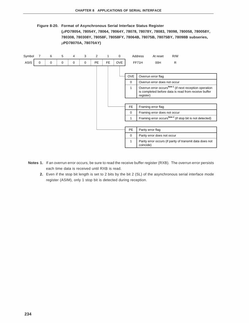
234
CHAPTER 8 APPLICATIONS OF SERIAL INTERFACE
Figure 8-20. Format of Asynchronous Serial Interface Status Register
(µPD78054, 78054Y, 78064, 78064Y, 78078, 78078Y, 78083, 78098, 780058, 780058Y,
780308, 780308Y, 78058F, 78058FY, 78064B, 78075B, 78075BY, 78098B subseries,
µPD78070A, 78070AY)
Notes 1. If an overrun error occurs, be sure to read the receive buffer register (RXB). The overrun error persists
each time data is received until RXB is read.
2. Even if the stop bit length is set to 2 bits by the bit 2 (SL) of the asynchronous serial interface mode
register (ASIM), only 1 stop bit is detected during reception.
7 6 5 4 3 2Symbol 1 0
FF71HOVEASIS FE0 PE0000
Address At reset R/W
00H R
OVE Overrun error flag
0 Overrun error does not occur
1 Overrun error occursNote 1 (if next reception operationis completed before data is read from receive bufferregister)
FE Framing error flag
0 Framing error does not occur
1 Framing error occursNote 2 (if stop bit is not detected)
PE Parity error flag
0 Parity error does not occur
1 Parity error occurs (if parity of transmit data does not coincide)

235
CHAPTER 8 APPLICATIONS OF SERIAL INTERFACE
Figure 8-21. Format of Baud Rate Generator Control Register
(µPD78054, 78054Y, 78064, 78064Y, 78078, 78078Y, 78083, 780058, 780058Y, 780308,
780308Y, 78058F, 78058FY, 78064B, 78075B, 78075BY subseries, µPD78070A,
78070AY) (1/2)
MDL3 MDL2 MDL1 MDL0 Selects input clock of baud rate generator k
0 0 0 0 fSCK/16 0
0 0 0 1 fSCK/17 1
0 0 1 0 fSCK/18 2
0 0 1 1 fSCK/19 3
0 1 0 0 fSCK/20 4
0 1 0 1 fSCK/21 5
0 1 1 0 fSCK/22 6
0 1 1 1 fSCK/23 7
1 0 0 0 fSCK/24 8
1 0 0 1 fSCK/25 9
1 0 1 0 fSCK/26 10
1 0 1 1 fSCK/27 11
1 1 0 0 fSCK/28 12
1 1 0 1 fSCK/29 13
1 1 1 0 fSCK/30 14
1 1 1 1 fSCKNote –
Note Can be used only in the 3-wire serial I/O mode.
Remarks 1. fSCK: source clock of 5-bit counter
2. k : value set by MDL0 through MDL3 (0 ≤ k ≤ 14)
7 6 5 4 3 2Symbol 1 0
FF73HMDL0BRGC MDL1MDL3 MDL2TPS0TPS1TPS2TPS3
Address At reset R/W
00H R/W

236
CHAPTER 8 APPLICATIONS OF SERIAL INTERFACE
Figure 8-21. Format of Baud Rate Generator Control Register
(µPD78054, 78054Y, 78064, 78064Y, 78078, 78078Y, 78083, 780058, 780058Y, 780308,
780308Y, 78058F, 78058FY, 78064B, 78075B, 78075BY subseries, µPD78070A,
78070AY) (2/2)
TPS3 TPS2 TPS1 TPS0 Selects source clock of 5-bit counter n
MCS = 1 MCS = 0
0 0 0 0 fXX/210 fX/210 (4.9 kHz) fX/211 (2.4 kHz) 11
0 1 0 1 fXX fX (5.0 MHz) fX/2 (2.5 MHz) 1
0 1 1 0 fXX/2 fX/2 (2.5 MHz) fX/22 (1.25 MHz) 2
0 1 1 1 fXX/22 fX/22 (1.25 MHz) fX/23 (625 kHz) 3
1 0 0 0 fXX/23 fX/23 (625 kHz) fX/24 (313 kHz) 4
1 0 0 1 fXX/24 fX/24 (313 kHz) fX/25 (156 kHz) 5
1 0 1 0 fXX/25 fX/25 (156 kHz) fX/26 (78.1 kHz) 6
1 0 1 1 fXX/26 fX/26 (78.1 kHz) fX/27 (39.1 kHz) 7
1 1 0 0 fXX/27 fX/27 (39.1 kHz) fX/28 (19.5 kHz) 8
1 1 0 1 fXX/28 fX/28 (19.5 kHz) fX/29 (9.8 kHz) 9
1 1 1 0 fXX/29 fX/29 (9.8 kHz) fX/210 (4.9 kHz) 10
Others Setting prohibited
Caution If data is written to BRGC during communication, the output of the baud rate generator is
disturbed and communication cannot be executed normally.
Therefore, do not write data to BRGC during communication.
Remarks 1. fXX : main system clock frequency (fX or fX/2)
2. fX : main system clock oscillation frequency
3. MCS : bit 0 of oscillation mode select register (OSMS)
4. n : value set by TPS0 through TPS3 (1 ≤ n ≤ 11)
5. ( ) : at fX = 5.0 MHz

237
CHAPTER 8 APPLICATIONS OF SERIAL INTERFACE
Figure 8-22. Format of Baud Rate Generator Control Register ( µPD78098, 78098B subseries) (1/2)
MDL3 MDL2 MDL1 MDL0 Selects input clock of baud rate generator k
0 0 0 0 fSCK/16 0
0 0 0 1 fSCK/17 1
0 0 1 0 fSCK/18 2
0 0 1 1 fSCK/19 3
0 1 0 0 fSCK/20 4
0 1 0 1 fSCK/21 5
0 1 1 0 fSCK/22 6
0 1 1 1 fSCK/23 7
1 0 0 0 fSCK/24 8
1 0 0 1 fSCK/25 9
1 0 1 0 fSCK/26 10
1 0 1 1 fSCK/27 11
1 1 0 0 fSCK/28 12
1 1 0 1 fSCK/29 13
1 1 1 0 fSCK/30 14
1 1 1 1 fSCKNote –
Note Can be used only in the 3-wire serial I/O mode.
Remarks 1. fSCK : source clock of 5-bit counter
2. k : value set by MDL0 through MDL3 (0 ≤ k ≤ 14)
7 6 5 4 3 2Symbol 1 0
FF73HMDL0BRGC MDL1MDL3 MDL2TPS0TPS1TPS2TPS3
Address At reset R/W
00H R/W

238
CHAPTER 8 APPLICATIONS OF SERIAL INTERFACE
Figure 8-22. Format of Baud Rate Generator Control Register ( µPD78098, 78098B subseries) (2/2)
TPS3 TPS2 TPS1 TPS0 Selects source clock of 5-bit counter n
0 0 0 0 fXX/210 (3.91 kHz) 11
0 1 0 1 fXX (4.0 MHz) 1
0 1 1 0 fXX/2 (2.0 MHz) 2
0 1 1 1 fXX/22 (1.0 MHz) 3
1 0 0 0 fXX/23 (500 kHz) 4
1 0 0 1 fXX/24 (250 kHz) 5
1 0 1 0 fXX/25 (125 kHz) 6
1 0 1 1 fXX/26 (62.5 kHz) 7
1 1 0 0 fXX/27 (31.3 kHz) 8
1 1 0 1 fXX/28 (15.6 kHz) 9
1 1 1 0 fXX/29 (7.81 kHz) 10
Others Setting prohibited
Caution If data is written to BRGC during communication, the output of the baud rate generator is
disturbed and communication cannot be executed normally.
Therefore, do not write data to BRGC during communication.
Remarks 1. fXX : main system clock frequency
2. n : value set by TPS0 through TPS3 (1 ≤ n ≤ 11)
3. ( ) : at fXX = 4.0 MHz

239
CHAPTER 8 APPLICATIONS OF SERIAL INTERFACE
Figure 8-23. Format of Serial Interface Pin Select Register
(µPD780058 and 780058Y Subseries)
SIPS21 SIPS20 Selects I/O pin of asynchronous serial interface
0 0 Input pin : RxD0/SI2/P70
Output pin : TxD0/SO2/P71
0 1 Input pin : RxD1/BUSY/P24
Output pin : TxD0/SO2/P71
1 0 Input pin : RxD0/SI2/P70
Output pin : TxD1/STB/P23
1 1 Input pin : RxD1/BUSY/P24
Output pin : TxD1/STB/P23
Cautions 1. Change the mode of an I/O Pin after stopping the serial transfer/reception operation.
2. When using the busy control option or busy & strobe control option in the 3-wire serial I/O
mode with automatic transfer/reception function of the serial interface channel 1, the RxD1/
BUSY/P24 and TxD1/STB/P23 pins cannot be used as data I/O pins.
Figure 8-24. Format of Serial Interface Pin Select Register
(µPD780308 and 780308Y Subseries)
SIPS21 SIPS20 Selects I/O pin of asynchronous serial interface
0 0 Input pin : RxD/SI2/P70
Output pin : TxD/SO2/P71
0 1 Input pin : RxD/P114
Output pin : TxD/SO2/P71
1 0 Input pin : RxD0/SI2/P70
Output pin : TxD/P113
1 1 Input pin : RxD/P114
Output pin : TxD/P113
Cautions 1. Change the mode of an I/O Pin after stopping the serial transfer/reception operation.
2. Port 11 has a falling edge detection function. Do not input a falling edge to the pin used as
a multiplexed pin of this port.
7
0
6
0
5
SIPS21
4
SIPS20
3
0
2
0
1
0
0
0
Symbol
SIPS
Address
FF75H
At reset
00H
R/W
R/W
7
0
6
0
5
SIPS21
4
SIPS20
3
0
2
0
1
0
0
0
Symbol
SIPS
Address
FF75H
At reset
00H
R/W
R/W

240
CHAPTER 8 APPLICATIONS OF SERIAL INTERFACE
8.1 Interface with EEPROM TM (µPD6252)
The µPD6252Note is a 2048-bit EEPROM which can be electrically written or erased. To write or read data to or
from the µPD6252, the 3-wire serial interface is used.
Note µPD6252 is for maintenance use.
Figure 8-25. Pin Configuration of µPD6252
1CE
2IC
3IC
4GND
VDD8
CS7
SCL6
SDA5

241
CHAPTER 8 APPLICATIONS OF SERIAL INTERFACE
Table 8-7. Pin Function of µPD6252
Pin Number Pin Name I/O Function
1 CE CMOS input Keep this pin high during data transfer.
Caution Do not change the level of this pin from high to low during data
transfer.
To change the level of this pin from high to low, make sure that the CS pin (pin 7)is low. By making both the CE and CS pins low, you can set the standby status in
which the power consumption is reduced.
2 IC – Fix the IC pins to the high or low level via resistor.
3
4 GND – Ground
5 SDA CMOS input/ Data input/output pin.
N-ch open-drain Because this pin is an N-ch open-drain I/O pin, externally pull it up with a resistor.
output
6 SCL CMOS input Inputs a clock for data transfer.
7 CS CMOS input Chip select pin. When this pin is high, the µPD6252 is enabled to operate.
When it is low, memory cells cannot be read or written.
When the level of this pin is changed from high to low with the SCL pin high, the
operation of the serial bus interface is started. To end the operation of the serial bus
interface, change the level of this pin from high to low.
8 VDD – Positive power: +5 V ±10%
SDA

242
CHAPTER 8 APPLICATIONS OF SERIAL INTERFACE
8.1.1 Communication in 2-wire serial I/O mode
The 3-wire mode of the µPD6252Note is implemented by serial clock (SCL), data (SDA), and chip select (CS) lines.
Excluding the handshaking line, therefore, only two lines, clock and data lines, are necessary for interfacing. To
interface the µPD6252 with a 78K/0 series microcontroller, the 2-wire serial I/O mode is used. In the example shown
in this section, the µPD78054 subseries is used.
Note µPD6252 is for maintenance use.
Figure 8-26. Example of Connection of µPD6252
Table 8-8 and Figure 8-27 shows the commands to write and read data to/from the µPD6252 and communication
format.
Table 8-8. µPD6252 Commands
Command Name Command Operation
RANDOM WRITE 00000000B [00H] Transfers write data after setting an 8-bit word address (WA). Up to 3 bytes of write
MSB data can be set successively.
C7-C0 Correspondence between word address and data
WA Data of first byte
WA+1 Data of second byte
WA+2 Data of third byte
The write operation is executed in the internal write cycle after the CS pin has gone
low.
CURRENT READ 10000000B [80H] Transfers the contents of memory specified by the word address (WA) (current
MSB address) specified when the command is set, to the read data buffer. Each time 8
C7-C0 bits of data have been read from the SDA pin, the word address (WA) is incremented,
and the corresponding memory contents are transferred to the data buffer.
RANDOM READ 11000000B [C0H] Executes data read starting from a set word address (WA) after the word address has
MSB been set.
C7-C0 The difference from CURRENT READ is that this command sets a word address (WA)
after it has been executed.
After the word address has been set, this command performs the same operation as
CURRENT READ.
PD78054
SCK0 SCL
µ PD6252µ
SB1 SDA
P32 CS
CE
VDD VDD

243
CHAPTER 8 APPLICATIONS OF SERIAL INTERFACE
Figure 8-27. Communication Format of µPD6252
(1) RANDOM WRITE
(2) CURRENT READ
(3) RANDOM READ
CS
SDA
SCL
C7 C6 C5 C4 C3 C2 C1 C0 WA7 WA6 WA5 WA4 WA3 WA2 WA1 WA0 D7 D6 D5 D4 D3 D2 D1 D0 2nd byteWB flag output
Write is executed by making CS in low with SCL pin high.WA is last written address + 1 and is retained(current address) (issuance of STP).
WA input
Command input Write data input (WA) (WA + 1) (WA + 2)
Internal WA SDA mode
Starts by making CS pin highwhen SCL pin is high(issuance of STA).
WA retains input value until STP is detected, and is incremented each time 1 byte is written in the internal write cycle after STP has been detected.
Data of 1st byte is written tomemory addressed by WA.
WB flag is retained while eightclocks are input to SCL pin.
IN OUT INWA + 1 to WA + 3
0 0 0 0 0 0 0 0
CURRENT ADDRESS WA
CS
SDA
SCL
C7 C6 C5 C4 C3 C2 C1 C0 D7 D6 D5 D4 D3 D2 D1 D0 D7 D6 D0 D7 D6 D2 D0WB flag output
Current address
Command input Read data (WA) (WA + 1)
Internal WA SDA mode IN OUT OUT
WA + n + 1
1 0 0 0 0 0 0 0
CURRENT ADDRESS = WA WA+n
(WA + 2) (WA + n)
Operation ends by making CS pin high withSCL pin high. WA is last read address + 1 andretained (current address) (issuance of STP)
WA+2WA+1
D1
1st byte3rd byte
Operation ends if CS pin is made low withSCL pin high (issuance of STP). WA is last read address + 1 and retained.
CS
SDA
SCL
C7 C6 C5 C4 C3 C2 C1 C0 WA7 WA6 WA5 WA4 WA3 WA2 WA1 WA0 D7 D6 D5 D4 D3 D2 D1 D0WB flag output
WA input (WA)
Internal WA SDA mode IN OUT IN
WA + n + 1
1 1 0 0 0 0 0 0
CURRENT ADDRESS WA
D7 D1 D0
(WA+1) ··· (WA+n)
WB flag is retained while 8 clocks are input to SCL pin.
Starts by making CS pin highwith SCL pin high (issuance of STA).
Contents of WA are read asdata of first byte.
Contents of WA+1, ··· WA+n aresequentially read each time 1 bytehas been read.
WA+1 WA+n
OUT

244
CHAPTER 8 APPLICATIONS OF SERIAL INTERFACE
Steps <1> through <5> below are the operating procedure of the µPD6252. In this example, the number of data
to be written or read per interface operation is fixed to 1 byte. If the µPD6252 is in the write busy (WB) status when
interfaced, the busy flag is set.
<1> Make the CS pin (P32) high to start interfacing.
<2> Transmit the write or read command.
<3> Receive the data of WRITE BUSY. If interfacing the µPD6252 is enabled, 00H is received. If a code other
than 00H is received, it is judged that the µPD6252 is in the WRITE BUSY status. In this case, communication
is stopped.
<4> Transfer the data corresponding to the command.
<5> Make the CS pin (P32) low to end the communication.
(1) Description of package
<Public declaration symbol>
T3_6252 : µPD6252 transfer subroutine name
RWRITE : RANDOM WRITE command value
RREAD : RANDOM READ command value
CREAD : CURRENT READ command value
WADAT : Word address storage area
TRNDAT : Transmit data storage area
RCVDAT : Receive data storage area
CMDDAT : Command data storage area
BUSYFG : Busy status test flag
CS6252 : CS pin (P32) of µPD6252
<Register used>
A
<RAM used>
Name Usage Attribute Bytes
WAADR Stores word address (before start of transfer) SADDR 1
TRNDAT Stores transmit data (before start of transfer)
RCVDAT Stores receive data (after end of transfer)
CMDDAT Stores command data (before start of transfer)

245
CHAPTER 8 APPLICATIONS OF SERIAL INTERFACE
<Flag used>
Name Usage
BUSYFG Sets WRITE BUSY status
<Nesting>
1 level 3 bytes
<Hardware used>
• Serial interface channel 0
• P32
<Initial setting>
• OSMS = #00000001B ; Oscillation mode select register: does not use divider circuit
• Setting of serial interface channel 0
CSIM0 = #10011011B ; Selects 2-wire serial I/O mode and SB1 pin
• TCL3 = #××××1001B ; Serial clock fXX/24
• RELT = 1 ; Makes SB1 latch high
<Starting>
Set the necessary data corresponding to the commands and call T3_6252. After execution returns from the
subroutine, the busy flag (BUSYFG) is tested. If the busy flag is set, transfer is not executed. It is therefore
necessary to execute transfer again. In the receive mode, the receive data is stored RCVDAT after execution
has returned from the subroutine.

246
CHAPTER 8 APPLICATIONS OF SERIAL INTERFACE
(2) Example of use
EXTRN RWRITE,RREAD,CREADEXTRN WADAT,TRNDAT,RCVDAT,CMDDAT,T3_6252EXTBIT BUSYFG,CS6252
OSMS=#00000001BCSIM0=#10011011BTCL3=#10011001BCLR1 SB0CLR1 CS6252CLR1 PM3.2
CMDDAT=A
WADAT=A
TRNDAT=A
repeatCLR1 BUSYFGCALL !T3_6252
until_bit(!BUSYFG)
A=RCVDAT
.
.
.
.
.
.
.
.
.
.
.
.
.
.
.
.
; Does not use divider circuit; Sets 2-wire serial I/O mode and SB1 pin; Sets SCK0 = 262 kHz
; Makes CS of µPD6252 low
Sets each data to memory
UNTIL: Not WRITE BUSY
Clears busy flag
Calls T3_6252
Loads receive data

247
CHAPTER 8 APPLICATIONS OF SERIAL INTERFACE
(3) SPD chart
T3_6252 Clears busy flag
Issues start bit
Transfers command
WHILE: waits for end of transfer (CSIIF0 = 0)
Receives busy signal
WHILE: waits for end of transfer (CSIIF0 = 0)
IF: not WB status (SIO0 = 00H)
THEN
ELSE
CASE: CMDDAT
OF: RWRITE
Transfers word address
WHILE: waits for end of transfer
Transfers data
WHILE: waits for end of transfer
BREAK
OF: RREAD
Transfers word address
WHILE: waits for end of transfer
OF: CREAD
Receives data
WHILE: waits for end of transfer
Stores receive data to memory
Sets busy status
Sets BUSYFG
Issues stop bit

248
CHAPTER 8 APPLICATIONS OF SERIAL INTERFACE
(4) Program list
PUBLIC RWRITE,RREAD,CREADPUBLIC WADAT,TRNDAT,RCVDAT,CMDDAT,T3_6252PUBLIC BUSYFG,CS6252
CSI_DAT DSEG SADDRWADAT: DS 1TRNDAT: DS 1RCVDAT: DS 1CMDDAT: DS 1
CSI_FLG BSEGBUSYFG DBIT
RWRITE EQU 00HRREAD EQU 0C0HCREAD EQU 080HCS6252 EQU 0FF03H.2
CSI_SEG CSEG;*************************************;* µPD6252 (3-wire) communication;*************************************T3_6252:
CLR1 BUSYFGSET1 CS6252SI00=CMDDAT (A)while_bit(!CSIIF0)endwCLR1 CSIIF0SIO0=#0FFHwhile_bit(!CSIIF0)endwCLR1 CSIIF0if(SIO0==#00H)
switch (CMDDAT)case RWRITE:
SIO0=WADAT (A)while_bit(!CSIIF0)endwCLR1 CSIIF0SIO0=TRNDAT (A)while_bit(!CSIIF0)endwCLR1 CSIIF0
break
case RREAD:SIO0=WADAT (A)while_bit(!CSIIF0)endwCLR1 CSIIF0
case CREAD:SIO0=#0FFHwhile_bit(!CSIIF0)endwCLR1 CSIIF0RCVDAT=SIO0 (A)
ends
; Word address storage area; Transmit data storage area; Receive data storage area; Command data storage area
; Sets busy status
; RANDOM WRITE mode; RANDOM READ mode; CURRENT READ mode; 0FF03H=PORT3
; Issues start bit; Transfers command; Waits for end of transfer
; Starts reception of busy signal; Waits for end of transfer
; Busy check
; Transfers word address; Waits for end of transfer
; Starts data transfer; Waits for end of transfer
; Transfers word address; Waits for end of transfer
; Starts data reception; Waits for end of transfer
; Stores receive data

249
CHAPTER 8 APPLICATIONS OF SERIAL INTERFACE
; Sets busy statuselse
SET1 BUSYFGendifCLR1 CS6252RET

250
CHAPTER 8 APPLICATIONS OF SERIAL INTERFACE
8.1.2 Communication in I 2C bus mode
In the 2-wire mode of the µPD6252Note , two lines, serial clock (SCL) and data (SDA) lines are used for
communication. This mode conforms to the communication format of I2C. Therefore, the I2C mode is selected when
communicating with the µPD6252 by using the µPD78054Y, 78064Y, 78078Y, 780058Y, 780308Y, 78058FY,
78075BY subseries, or µPD78070AY.
In the example shown in this section, the µPD78054Y subseries is used.
Note µPD6252 is for maintenance use.
Figure 8-28. Example of Connection between µPD6252 and I2C Bus Mode
Figure 8-29 shows the communication format in which data is written to or read from the µPD6252.
PD78054Y
SDA0 (SDA1)SCL
SDASCL
SDASCL
µ PD6252µ
A1 = 0A2 = 0
A1 = 1 A2 = 0
SDASCL
A1 = 0 A2 = 1
SDASCL
A1 = 1 A2 = 1
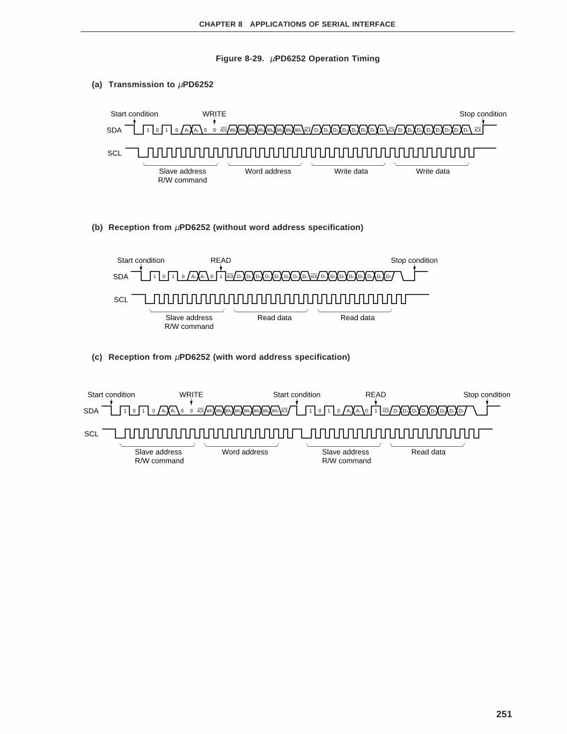
251
CHAPTER 8 APPLICATIONS OF SERIAL INTERFACE
Figure 8-29. µPD6252 Operation Timing
(a) Transmission to µPD6252
(b) Reception from µPD6252 (without word address specification)
(c) Reception from µPD6252 (with word address specification)
WA7 WA6 WA5 WA4 WA3 WA2 WA1 WA0 D7 D6 D5 D4 D3 D2 D1
Start condition
D0 D7 D6 D5 D4 D3 D2 D1 D01 0 1 0 A2 A1 0 0 ACK ACK ACK ACKSDA
SCL
WRITE Stop condition
Write data Write dataSlave addressR/W command
Word address
D7 D6 D5 D4 D3 D2 D1 D0 D7 D6 D5 D4 D3 D2 D1
Start condition
D01 0 1 0 A2 A1 0 1 ACK ACKSDA
SCL
READ Stop condition
Read dataSlave addressR/W command
Read data
WA7 WA6 WA5 WA4 WA3 WA2 WA1 WA0
Start condition
1 0 1 0 A2 A1 0 0 ACK ACKSDA
SCL
WRITE
Slave address R/W command
Read dataSlave address R/W command
Word address
A2 A11 0 1 0 1 ACK
Start condition READ
0 D7 D6 D5 D4 D3 D2 D1 D0
Stop condition

252
CHAPTER 8 APPLICATIONS OF SERIAL INTERFACE
Steps <1> through <5> below are the communication procedure of the µPD6252. In this example, the number
of data to be written or read is fixed to 1 byte. If the master receives data in the I2C bus format, and if it has received
the last data, the ACK signal is not output. Because the master does not output the ACK signal in this example, ACKE
is always 0.
<1> Set a start condition to start communication.
Fall the data with the serial clock high.
<2> Transmit the slave address value (bits 1 through 7) of the µPD6252 and write (bit 0 = 0)/read (bit 0 = 1) select
bit.
1 0 1 0 A2 A1 0 R / W
Slave address R/W selection
7-bit (bits 7 through 1) 1 bit (bit 0) Remark A2 and A1 are set by external pins.
<3> Transfer the data.
• In transmission mode
(i) Transmit the word address of the µPD6252.
(ii) Transmit the write data.
• In reception mode
Receive the read data.
<4> Set an end condition to end the communication.
Rise the data with the serial clock high.
<5> Because a word address is specified only in the write mode, to read data by specifying an address, the address
must be specified by once setting the write mode.
If the µPD6252 does not return the ACK signal during data transfer, communication is stopped.
The start and end conditions are set by CLC when the serial clock is manipulated, and by RELT and CMDT when
data is manipulated.

253
CHAPTER 8 APPLICATIONS OF SERIAL INTERFACE
(1) Description of package
<Public declaration symbol>
T2_6252 : µPD6252 transfer subroutine name
WAADR : Word address storage area
TRNDAT : Transmit data storage area
RCVDAT : Receive data storage area
SLVADR : Slave address storage area
BUSYFG : Busy status test flag
WRCHG : Write → read mode change flag
ERRFG : Error status test flag
<Register used>
A
<RAM used>
Name Usage Attribute Bytes
WAADR Stores word address (before start of transfer) SADDR 1
TRNDAT Stores transmit data (before start of transfer)
RCVDAT Stores receive data (after end of transfer)
SLVADR Stores slave address
<Flag used>
Name Usage
BUSYFG Sets WRITE BUSY status
WRCHG Changes write mode to read mode
ERRFG Sets error status
<Nesting>
1 level 2 bytes
<Hardware used>
Serial interface 0

254
CHAPTER 8 APPLICATIONS OF SERIAL INTERFACE
<Initial setting>
• OSMS = #00000001B ; Oscillation mode select register: does not use divider circuit
• Setting of serial interface channel 0
CSIM0 = #10011011B ; Selects 2-wire serial I/O mode and SB0 pin
• TCL3 = #××××1000B ; Selects serial clock fXX/23 and 16
• SINT = #00001011B ; Generates interrupts at rising edge of 9th serial clock and sets clock line to high
level
<Starting>
• Set the necessary data corresponding to the commands and call T2_6252. In the reception mode, the
receive data is stored to RCVDAT after execution has returned from the subroutine.
• If the serial clock is low (busy status) when communication is started or if ACK cannot be received during
data transfer, the BUSYFG and ERRFG are set. Test and clear these flags with the main processing.
(2) Example of use
EXTRN WAADR,TRNDAT,RCVDAT,SLVADR,T2_6252EXTBIT BUSYFG,WRCHG,ERRFG
SET1 SB0OSMS=#00000001BCSIM0=#10011011BSINT=#00001011BTCL3=#10001000BSET1 RELTSET1 SCK0CLR1 SB0
WAADR=A
TRNDAT=A
SLVADR=ACALL !T2_6252if_bit(BUSYFG)
CLR1 BUSYFG
endif
if|bit(ERRFG)CLR1 ERRFG
ENDIF
; Does not use divider circuit; Serial interface 2-wire, SB0; Sets I2C mode; SCK = 32.7 kHz
....
....
....
....
....
Sets data
Calls T2_6252
(IF: sets BUSYFG)
Clears BUSYFG
To busy processing
(IF: sets ERRFG)
Clears ERRFG
To error processing

255
CHAPTER 8 APPLICATIONS OF SERIAL INTERFACE
(3) SPD chart
IF: SCK0 = LOWT2_6252
Sets busy status
THEN
Sets BUSYFGELSE
Issues start bitSTABIT
Transmits slave address
WHILE: waits for end of transfer (CSIIF0 = 0)
IF: ACK signal not detected
Sets error status
THEN
ELSE Sets ERRFG
IF: transmit mode
THEN
Transmits word address of PD6252µWHILE: waits for end of transfer
IF: ACK signal not detected
THEN
Sets error status
ELSE Sets ERRFG
IF: changes to read mode
THEN
WHILE: SCK0 = HIGH
Outputs high level in order of data and clock
Changes slave address to read mode
GOTO STABIT
ELSE
Transmits data
WHILE: waits for end of transfer
IF: ACK signal not detected
THEN
Sets error status
Sets ERRFG
Receives data
ELSE
WHILE: waits for end of transfer
Stores receive data to memory
Outputs low level in order of clock and data
Issues stop bit

256
CHAPTER 8 APPLICATIONS OF SERIAL INTERFACE
(4) Program list
PUBLIC WAADR,TRNDAT,RCVDAT,SLVADR,T2_6252PUBLIC BUSYFG,WRCHG,ERRFG
CSI_DAT DSEG SADDRWAADR: DS 1TRNDAT: DS 1RCVDAT: DS 1SLVADR: DS 1
CSI_FLG BSEGBUSYFG DBITWRCHG DBITERRFG DBIT
SCK0 EQU P2.7
CSI_SEG CSEG;*************************************;* µPD6252 (2-wire) communication;*************************************T2_6252:
if_bit(!CLD)SET1 BUSYFG
elseSTABIT:
SET1 CMDTNOPNOPNOPNOPNOPCLR1 CLCSIO0=SLVADR (A)while_bit(!CSIIF0)endwCLR1 CSIIF0if_bit(!ACKD)
SET1 ERRFGelseif_bit(!SLVADR.0)
SI00=WAADR (A)while_bit(!CSIIF0)endwCLR1 CSIIF0if_bit(!ACKD)
SET1 ERRFGelseif_bit(WRCHG)
while_bit(CLD)endwSET1 RELTSET1 CLCwhile_bit(!CLD)endwNOPNOPNOPNOPNOPNOPNOPNOPSET1 SLVADR.0goto STABIT
else
; Word address storage area; Transmit data storage area; Receive data storage area; Salve address storage area
; Sets busy status; Changes mode; Sets error status
; Busy status
; Issues start bit; Waits for start bit valid width
; Changes clock to low level; Starts transmitting slave address; Waits for end of transfer
; ACK signal not detected
; Transmission mode; Starts transmitting word address; Waits for end of transfer
; ACK signal not detected
; Checks high level of clock
; Waits for high level valid width of clock
; Changes to read mode address

257
CHAPTER 8 APPLICATIONS OF SERIAL INTERFACE
SIO0=TRNDAT (A)while_bit(!CSIIF0)endwCLR1 CSIIF0if_bit(!ACKD)
SET1 ERRFGendif
endifelse
SIO0=#0FFHwhile_bit(!CSIIF0)endwCLR1 CSIIF0RCVDAT=SIO0 (A)
endif
while_bit(CLD)endwSET1 CMDTSET1 CLCwhile_bit(!CLD)endwNOPNOPNOPNOPNOPNOPNOPNOPSET1 RELT
endifRET
; Starts transmitting data; Waits for end of transfer
; ACK signal detected
; Starts data reception; Waits for end of transfer
; Stores receive data
; Checks high level of clock
; Waits for high level valid width of clock
; Issues stop bit

258
CHAPTER 8 APPLICATIONS OF SERIAL INTERFACE
(5) Limitation when using I 2C bus mode
The following limitation applies when the µPD78054Y, 78064Y, 78078Y, 780058Y, 780308Y, 78058FY,
78075BY subseries, and µPD78070AY are used. This section explains an example using the µPD78054Y.
• Limitation when the device is used as a slave device in the I 2C bus mode
Description: If the wake-up function is executed (by setting the WUP flag (bit 5 of serial operation mode
register 0 (CSIM0) to 1) in the serial transfer statusNote , the data between other slave device
and the master devices is checked as an address. If that data coincides with the slave address
of the µPD78054Y, therefore, the µPD78054Y takes part in communication, destroying the
communication data.
Note The serial transfer status is the status from when the serial I/O shift register 0 (SIO0)
has been written until the interrupt request flag (CSIIF0) is set to 1 by completion of
serial transfer.
Preventive measures: The above problem can be prevented by modifying the program.
Before executing the wake-up function, execute the following program that clears
the serial transfer status. When executing the wake-up function, do not execute
an instruction that writes data to SIO0. Even if such an instruction is executed,
data can be received when the wake-up function is executed.
This program is to clear the serial transfer status. To clear the serial transfer status,
serial interface channel 0 must be stopped (by clearing the CSIE0 flag (bit 7 of the
serial operation mode register (CSIM0) to 0). If the serial interface channel 0 is
stopped in the I2C bus mode, however, the SCL pin outputs a high level and the
SDA0 (SDA1) pin outputs a low level, affecting communication on the I2C bus.
Therefore, this program allows the SCL and SDA0 (SDA1) pin to go into a high-
impedance state to prevent the I2C bus from being affected.
Note that, in this example, the serial data input/output pin is SDA0 (/P25). If SDA1
(/P26) is used as the serial data input/output pin, take P2.5 and PM2.5 in the
program as P2.6 and PM2.6.

259
CHAPTER 8 APPLICATIONS OF SERIAL INTERFACE
• Example of program that clears serial transfer status
SET1 P2.5 ; <1>
SET1 PM2.5 ; <2>
SET1 PM2.7 ; <3>
CLR1 CSIE0 ; <4>
SET1 CSIE0 ; <5>
SET1 RELT ; <6>
CLR1 PM2.7 ; <7>
CLR1 P2.5 ; <8>
CLR1 PM2.5 ; <9>
<1> When the I2C bus mode is restored by instruction <5>, the SDA0 pin does not output a low level. The
output of the SDA0 pin goes into a high-impedance state.
<2> The P25(/SDA0) pin is set in the input mode to prevent the SDA0 line from being affected when the
port mode is set by instruction <4>. The P25 pin is set in the input mode when instruction <2> is
executed.
<3> The P27 (/SCL) pin is set in the input mode to prevent the SCL line from being affected when the port
mode is set by instruction <4>. The P27 pin is set in the input mode when instruction <3> is executed.
<4> The I2C bus mode is changed to the port mode.
<5> The port mode is changed to the I2C bus mode.
<6> Instruction <8> prevents the SDA0 pin from outputting a low level.
<7> The P27 pin is set in the output mode because it must be in the output mode in the I2C bus mode.
<8> The output latch of the P25 pin is cleared to 0 because it must be cleared to 0 in the I2C bus mode.
<9> The P25 pin is set in the output mode because it must be in the output mode in the I2C bus mode.
Remark RELT: Bit 0 of serial bus interface control register (SBIC)

260
CHAPTER 8 APPLICATIONS OF SERIAL INTERFACE
8.2 Interface with OSD LSI ( µPD6451A)
The OSD (On Screen Display) LSI µPD6451A displays the program information of a VCR and TV channels on
a display when used in combination with a microcontroller. The µPD6451A is interface with four lines: DATA, CLK,
STB, and BUSY. In the example shown in this section, the µPD78054 subseries is used to interface the µPD6451A.
Figure 8-30. Example of Connecting µPD6451A
Figure 8-31. Communication Format of µPD6451A
The strobe signal (STB) is output and busy signal (BUSY) is tested automatically by the serial interface channel
1 of the 78K/0 series to establish handshaking with and to interface the µPD6451A. To match the communication
format of the µPD6451A, the µPD78054 subseries is set in a mode in which output of the strobe signal and input of
the busy signal (high active) are enabled. By setting the transmit data (32 bytes MAX) in a buffer area (FAC0H through
FADFH) and the number of transmit data to the automatic data transmit/receive address pointer (ADTP), you can
automatically transmit plural data successively.
PD78054
SCK1 CLK
µ PD6451Aµ
RGBSO1 DATA
STB STB
BUSY BUSY
Display
RGB
SCK1
SO1
STB
BUSY
DO7 DO6 DO5 DO4 DO3 DO2 DO1 DO0

261
CHAPTER 8 APPLICATIONS OF SERIAL INTERFACE
(1) Description of package
<Public declaration symbol>
TR6451 : µPD6451A transfer subroutine name
DTVAL : Number of transmit data setting area
<Register used>
A
<RAM used>
Name Usage Attribute Bytes
DTVAL Stores number of transmit data SADDR 1
<Nesting>
1 level 2 bytes
<Hardware used>
• Serial interface channel 1
<Initial setting>
• Setting of serial interface channel 1
CSIM1 = #10100011B ; Enables automatic transmission/reception with MSB first
ADTC = #00000110B ; Enables busy input (high active) and strobe output in single mode
• ADTI = #00000000B ; Interval time of data transfer
• OSMS = #00000001B ; Oscillation mode select register; does not use divider circuit
• TCL3 = #1001××××B ; Serial clock fXX/24
• Makes P22 output latch high
• PM2 = #×××1000×B ; Sets P21, P22, and P23 in output mode and P24 in input mode
<Starting>
Set the data to be transmitted to the buffer RAM (starting from the highest address), and the number of data
to be transmitted to DTVAL, and call TR6451. You can check the end of data transfer by testing the bit 3
(TRF) of the automatic data transfer/reception control register (ADTC).

262
CHAPTER 8 APPLICATIONS OF SERIAL INTERFACE
(2) Example of use
EXTRN TR6451,DTVAL
SCK1 EQU P2.2
OSMS=#00000001BP2=#00000100BPM2=#11110001BCSIM1=#10100011BTCL3=#10011001BADTC=#00000110BADTI=#00000000B
DE=#TABLE1HL=#0FAC0HB=32
while(B>#0)B––[HL+B]=[DE] (A)DE++
endw
DATVAL=#32CALL !TR6451while_bit(TRF)endw
.
.
.
.
.
.
.
.
; Does not use divider circuit
; Sets automatic transfer/reception function; SCK1 = 262 kHz; Enable strobe and busy signals; Interval time of data transfer
; Sets table reference address of transmit data; Sets first address of buffer RAM; Sets number of data to be transmitted
; Transfers transmit data to buffer RAM
; Sets number of data to be transmitted
; Waits for end of transfer
Sets data to buffer RAM
Sets number of data to be transmitted to DTVAL
Calls TR6451
WHILE: waits for end of transfer

263
CHAPTER 8 APPLICATIONS OF SERIAL INTERFACE
TABLE1:DB 11111111BDB 01000000BDB 11000000BDB 10000000BDB 11111100BDB 11101001B
DB 10001100B
DB 11011011BDB 10010101BDB 10100000B
DB 07HDB 08HDB 1BHDB 6DHDB 00HDB 10HDB 11HDB 20HDB 20HDB 1CHDB 19HDB 13HDB 11HDB 24HDB 19HDB 00HDB 1EHDB 10HDB 1EHDB 00HDB 24HDB 15H
Remark For the command and data of the output table data, refer to µPD6451A Data Sheet (Document No. IC-
2337).
; Power-ON reset, command 1; Vertical address 0; Horizontal address 0; Character size; Command 0; Turns LC transmission ON, blinking OFF, display ON
; Turns blinking ON. Character: red
; Color specification, background filled in cyan; Number of display lines: 5; Number of display digits: 0
; 7; 8; K; /; 0
; A; P; P; L; I; C; A; T; I; O; N
; N; O; T; E

264
CHAPTER 8 APPLICATIONS OF SERIAL INTERFACE
(3) SPD chart
(4) Program list
PUBLIC TR6451,DTVAL
CSI_DAT DSEG SADDRDTVAL: DS 1
CSI_SEG CSEG;*************************************;* µPD6451A communication;*************************************TR6451:
A=DTVALA––ADTP=ASIO1=#0FFHRET
; Number of data setting area
; Sets number of data
; Starts transfer
TR6451 Sets (number of data to be transmitted – 1) to ADTP
Sets status before transfer
Starts transfer
265
CHAPTER 8 APPLICATIONS OF SERIAL INTERFACE
8.3 Interface in SBI Mode
The 78K/0 series has an SBI mode conforming to NEC serial bus format. In this mode, one master CPU can
communicate with two or more slave CPUs by using two lines: clock and data. In the example shown in this section,
the µPD78054 subseries is used.
Figure 8-32 shows an example of connection to use the SBI mode, and Figure 8-33 shows the communication
format.
Figure 8-32. Example of Connection in SBI Mode
PD78054 master
SCK0
SB0
SCK0
SB0
Slave CPU
SCK
SB
VDD
Slave CPU
SCK
SB
µ PD78054 slaveµ

266
CHAPTER 8 APPLICATIONS OF SERIAL INTERFACE
Figure 8-33. Communication Format in SBI Mode
(a) Address transmission
(b) Command transmission
(c) Data transmission/reception
Table 8-9. Signals in SBI Mode
Signal Name Output by: Meaning
Address Master Selects slave device
Command Master Command to slave device
Data Master/slave Data to be processed by slave or master
Clock Master Serial data transmission/reception synchronization signal
ACK Receiver sideNote Reception acknowledge signal
BUSY Slave Busy status
Note This signal is output by the receiver side during normal operation. However, it is output
by the master CPU in case of an error such as time out.
SCK0
SB0 A7 A6 A5 A4 A3 A2 A1 A0
SetsRELD
SetsCMDD
SCK0
SB0 C7 C6 C5 C4 C3 C2 C1 C0
SetsCMDD
SCK0
SB0 D7 D6 D5 D4 D3 D2 D1 D0 ACK
SetsACKD

267
CHAPTER 8 APPLICATIONS OF SERIAL INTERFACE
8.3.1 Application as master CPU
When the µPD78054 subseries is used as a master CPU, it performs processing (a) through (d) below with respect
to slave CPUs.
(a) Address transmission
(b) Command transmission
(c) Data transmission
(d) Data reception
While the above processing is performed, errors <1> and <2> below are checked.
<1> Time out processing
If the master CPU transmits data and a slave does not return the ACK signal within a specific time (in this
example, before the watch interrupt request occurs five times), the master judges that an error has occurred.
The master CPU then outputs an ACK signal and terminates the processing.
Figure 8-34. ACK Signal in Case of Time out
<2> Testing bus line
The master CPU tests whether data has been correctly output to the bus line by setting the transmit data
to the serial I/O shift register 0 (SIO0) and the slave address register (SVA). Because the data on the bus
line is received by SIO0, it confirms that the data has been output normally by testing bit 6 (COI) of the serial
operating mode register 0 (CSIM0) (that is set when SIO0 coincides with SVA) at the end of transfer.
Figure 8-35. Testing Bus Line
In Figure 8-35, the values of SIO0 and SVA do not coincide (SIO0 = 07H and SVA = 0FH). Consequently, COI
= 0, and an error has occurred on the bus line.
SB0 ACK
End of transfer
INTTM3 (ACKD test)
(time out)
Master output
SIO0 = 0FH 0 0 0 0 1 1 1 1
SB0 = 07H 0 0 0 0 0 1 1 11

268
CHAPTER 8 APPLICATIONS OF SERIAL INTERFACE
(1) Description of package
<Public declaration symbol>
M_TRANS : Master SBI transfer subroutine name
TR_MODE : Storage area of transfer mode select value
TRNDAT : Transmit data storage area
RCVDAT : Receive data storage area
TRADR : Address transmit mode select value
TRCMD : Command transmit mode select value
TRDAT : Data transmit mode select value
RCDAT : Data reception mode select value
ERRORF : Error status test flag
<Register used>
Subroutine A
<RAM used>
Name Usage Attribute Bytes
TR_MODE Stores transfer mode select value SADDR 1
ACKCT Time out counter
TRNDAT Stores transmit data
RCVDAT Stores receive data
<Flag used>
Name Usage
RCVFLG Sets reception mode
BUSYFG Sets busy status
ERRORF Sets error status
ACKWFG Sets ACK signal wait status
<Nesting>
2 levels 5 bytes

269
CHAPTER 8 APPLICATIONS OF SERIAL INTERFACE
<Hardware used>
• Serial interface channel 0
• Watch timer
<Initial setting>
• OSMS=#00000001B ; Oscillation mode select register: does not use divider circuit
• Sets serial interface channel 0
CSIM0=#10010011B ; Selects SBI mode and SB1 pin
• TCL3=#××××1001B ; Serial clock: fXX/24
• RELT=1 ; Makes SO0 latch high
• P27=1 ; Makes P27 output latch high
• TMC2=#00100110B ; Watch timer interval: 1.95 ms
• Enables watch timer interrupt
<Starting>
Set the transfer mode and necessary data, and call M_TRANS. When execution has returned from the
subroutine, occurrence of a transfer error can be checked by testing the error flag (ERRORF). In the reception
mode, the receive data is stored to RCVDAT after execution has returned from the subroutine.

270
CHAPTER 8 APPLICATIONS OF SERIAL INTERFACE
(2) Example of use
EXTRN M_TRANS,TR_MODE,TRADR,TRCMD,TRDAT,RCDATEXTRN TRNDAT,RCVDATEXTBIT ERRORF
SCK0 EQU P2.7SB1 EQU P2.5
OSMS=#00000001BSET1 SB1CSIM0=#10010111BTCL3=#10011001BTMC2=#00100110BCLR1 BSYESET1 RELTSET1 SCK0CLR1 SB1CLR1 CSIMK0CLR1 TMMK3EI
TR_MODE=#TRADRTRNDAT=#5AHCALL !M_TRANSif_bit(ERRORF) Error processingendif
.
.
.
.
.
.
.
.
; Does not use divider circuit
; Operates in SBI mode; SCK0 = 262 kHz; Sets interval of watch timer to 1.95 ms; Disables output of busy signal; Sets output latch
; Enables serial interface channel 0 interrupt; Enables watch timer interrupt; Enables master interrupt
Sets transfer mode
Sets transmit data
Calls M_TRANS
IF: error occurs
Error processing

271
CHAPTER 8 APPLICATIONS OF SERIAL INTERFACE
(3) SPD chart
M_TRANS CASE: TR_MODE
Outputs command signal
OF: TRADR
WHILE: SB0 = LOW
WHILE: SCK0 = LOW
Outputs bus release signal
OF: TRCMD
Outputs command signal
WHILE: SB0 = LOW
WHILE: SCK0 = LOW
OF: TRDAT
Sets transmission mode
Clears RCVFLG
BREAK
OF: RCDAT
Sets reception mode
Sets RCVFLG
Sets output off data (FFH) of bus line
BREAK
Sets transmission status
Sets BUSYFG
Sets transmit data to SIO0 and SVA
WHILE: transfer in progress (sets BUSYFG)
Stores data of SIO0 to RCVDAT
IF: transmission mode
IF: error occurs in bus line
Sets error status
Sets ERRORF
THEN
THEN

272
CHAPTER 8 APPLICATIONS OF SERIAL INTERFACE
INTCSI0 Selects register bank 0
IF: transmission mode
IF: ACK signal not received
THEN
THEN
Sets ACK wait status
Sets ACKWFG
ELSE
Clears busy status
Clears error status
Clears BUSYFG
Clears ERRORF
Outputs ACK signal
ELSE
Clears BUSYFG and ERRORF
INTTM3 Selects register bank 0
IF: ACK wait status
THEN
IF: ACK received
THEN
IF: time out
Clears ACK wait status
Clears ACKWFG
Clears busy status
Clears BUSYFG
ELSE
Time out error processing
Clears ACK wait status
Clears ACKWFG
Clears busy status
Clears BUSYFG
THEN

273
CHAPTER 8 APPLICATIONS OF SERIAL INTERFACE
(4) Program list
PUBLIC M_TRANS,TR_MODE,TRADR,TRCMD,TRDAT,RCDATPUBLIC TRNDAT,RCVDAT,ERRORF
VECSI0 CSEG AT 14HDW INTCSI0
VETM3 CSEG AT 1EHDW INTTM3
SBI_DAT DSEG SADDRTRNDAT: DS 1RCVDAT: DS 1TR_MODE:DS 1ACKCT: DS 1
SBI_FLG BSEGRCVFLG DBITBUSYFG DBITERRORF DBITACKWFG DBIT
SB0 EQU P2.5SCK0 EQU P2.7
TRADR EQU 1TRCMD EQU 2TRDAT EQU 3RCDAT EQU 4
; Sets vector address of serial interface channel 0
; Sets vector address of watch timer
; Transmit data; Receive data; Sets transfer mode; ACK time out count
; Sets reception mode; Transfer status; Error display; ACK wait status
; Selects address transmission mode; Selects command transmission mode; Selects data transmission mode; Selects data reception mode

274
CHAPTER 8 APPLICATIONS OF SERIAL INTERFACE
;*******************************************;* SBI data transfer processing;*******************************************SBI_SEG CSEGM_TRANS:
switch(TR_MODE)case TRADR:
SET1 PM2.5while_bit(!SB0)CLR1 PM2.5endwwhile_bit(!SCK0)endwSET1 CMDTNOPSET1 RELTA=#TRCMD
case TRCMD:SET1 PM2.5while_bit(!SB0)CLR1 PM2.5endwwhile_bit(!SCK0)endwSET1 CMDTA=#TRDAT
case TRDAT:CLR1 RCVFLGA=TRNDATbreak
case RCDAT:SET1 RCVFLGMOV A,#0FFHbreak
ends
SET1 BUSYFGSVA=ASIO0=A
while_bit(BUSYFG)endwRCVDAT=SIO0 (A)if_bit(!RCVFLG)
if_bit(!COI)SET1 ERRORF
endifendifRET
; SB0 = high?
; SCK = high?
; Outputs command signal; Wait; Outputs bus release signal
; SB0 = high?
; SCK = high?
; Outputs command signal
; Sets transmission mode; Sets transmit data
; Sets reception mode; Turns off receive buffer
; Sets transfer status; Tests bus line; Starts transfer
; Transfer in progress
; Stores receive data; Transmission mode; Bus line output abnormal; Sets error status

275
CHAPTER 8 APPLICATIONS OF SERIAL INTERFACE
; Transmission mode; Acknowledge signal not received; Sets acknowledge signal wait status
; Clears busy status; Clears error status
; Outputs acknowledge signal; Clears busy status; Clears error status
; Acknowledge signal wait status?; Acknowledge signal received?; Clears acknowledge signal wait status; Clears busy status
; Time out?; Time out error processing
; Clears acknowledge signal wait status; Clears busy status
;***************************************;* INTCSI0 interrupt processing;***************************************CSI_SEG CSEGINTCSI0:
SEL RB0if_bit(!RCVFLG)
if_bit(!ACKD)ACKCT=#5SET1 ACKWFG
elseCLR1 BUSYFGCLR1 ERRORF
endifelse
SET1 ACKTCLR1 BUSYFGCLR1 ERRORF
endifRET
;***************************************;* Time out processing;***************************************TM3_SEG CSEGINTTM3:
SEL RB0if_bit(ACKWFG)
if_bit(ACKD)CLR1 ACKWFGCLR1 BUSYFG
elseACKCT--if(ACKCT==#0)
SET1 ACKTSET1 ERRORFCLR1 ACKWFGCLR1 BUSYFG
endifendif
endif

276
CHAPTER 8 APPLICATIONS OF SERIAL INTERFACE
8.3.2 Application as slave CPU
A slave CPU receives addresses, commands, and data from the master CPU and transmits data to the master
CPU.
In the example shown in this section, addresses are received by using the wake-up function. This function is to
generate an interrupt only when the address value transmitted by the master to the slave coincides with the value
set to the slave address register (SVA) of the slave in the SBI mode. Therefore, only the slave CPU selected by the
master CPU generates INTCSI0, and the slave CPUs not selected operates without generating an inadvertent
interrupt request.
The slave CPU clears the wake-up function when it has been selected by the master (the interrupt request signal
is generated at the end of transmission), and interfaces with the master CPU. Addresses, commands, and data being
transmitted are identified by using bits 2 and 3 (RELD and CMDD) of the serial bus interface control register (SB IC).
Because the slave CPU is not automatically placed in the unselect status, a program that returns the slave CPU
to the unselect status must be prepared by processing commands between the master and CPU.
(1) Description of package
<Public declaration symbol>
RCVDAT: Receive data storage area
<Register used>
Bank 0: A
<RAM used>
Name Usage Attribute Bytes
RCVDAT Stores receive data SADDR 1
<Flag used>
Name Usage
RCVFLG Sets reception mode
<Nesting>
1 level 3 bytes
<Hardware used>
• Serial interface channel 0
<Initial setting>
• Setting of serial interface channel 0
CSIM0=#10010011B; Sets SBI mode, SBI pin, and wake-up mode, and inputs
serial clock from external source
• BYSE=1 Outputs synchronous busy signal
• RELT=1 Makes SO0 latch high
• SVA=#SLVADR; Slave address
• Enables serial interface channel 0 interrupt

277
CHAPTER 8 APPLICATIONS OF SERIAL INTERFACE
<Starting>
The interrupt processing is started by generation of INTCSI0. The interrupt processing performs the following
processing:
• Identifies address/command/data
• Outputs ACK signal
• Stores receive data to RCVDAT
(2) Example of use
EXTRN RCVDATEXTBIT RCVFLG
SLVADR EQU 5AHSB1 EQU P2.5
SET1 SB1CSIM0=#10110100BSET1 RELTSET1 BSYESVA=#SLVADRSIO0=#0FFHCLR1 SB1CLR1 CSIMK0EI
(3) SPD chart
.
.
.
.
; Inputs external clock, sets SB1 pin, and selects wake-up mode; Sets output latch to high level; Sets busy automatic output; Sets slave address; Serial transfer start command
; Enables serial interface channel 0 interrupt; Enables master interrupt
INTCSI0 Selects register bank 0
THEN
IF: address received
Clears wake-up mode
Outputs ACK signal
Address coincidence processing
ELSE
IF: command received
THEN
Command reception processing
Outputs ACK signal
ELSE
IF: reception mode
THEN
Data reception processing
Outputs ACK signal
ELSE
Data transmission processing
Stores SIO0 data to memory

278
CHAPTER 8 APPLICATIONS OF SERIAL INTERFACE
(4) Program list
VECSI0 CSEG AT 14HDW INTCSI0
SCI_DAT DSEG SADDRRCVDAT: DS 1
CSI_FLG BSEGRCVFLG DBIT
CSI_SEG CSEG;***************************************;* INTCSI0 interrupt processing;***************************************INTCSI0:
SEL RB0if_bit(RELD)
CLR1 WUPSET1 ACKT
; User processing (address reception)
;***************************************
elseif_bit(CMDD); User processing (command reception)
SET1 ACKTelse
if_bit(RCVFLG); User processing (data reception processing)
SET1 ACKTelse
; User processing (data transmission processing)endif
;***************************************endifRCVDAT=SIO0 (A)
RETI
; Sets vector address of serialinterface channel 0
; Receive data storage area
; Sets reception mode
; To address reception; Clears wake-up mode; Outputs acknowledge signal
; To command reception
; Outputs acknowledge signal
; Outputs acknowledge signal

279
CHAPTER 8 APPLICATIONS OF SERIAL INTERFACE
8.4 Interface in 3-Wire Serial I/O Mode
In this section, examples of communication between the master and a slave by using the 3-wire serial I/O mode
(serial clock, data input, data output) of the serial channel 0 of the 78K/0 series are shown. In these examples, one
extra busy signal is used as a handshake signal for simultaneous transmission/reception between the master and
slave. This busy signal is active-low and is output by the slave. The data is 8 bits long and transmitted with the MSB
first. In the examples in this section, the µPD78054 subseries is used.
Figure 8-36. Example of Connection in 3-Wire Serial I/O Mode
Figure 8-37. Communication Format in 3-Wire Serial I/O Mode
Master
SCK0 SCK0
Slave
SI0 SO0
SO0 SI0
BUSY BUSY
BUSY
SCK0
SO0
SI0
DO7 DO6 DO5 DO4 DO3 DO2 DO1 DO0
DI7 DI6 DI5 DI4 DI3 DI2 DI1 DI0

280
CHAPTER 8 APPLICATIONS OF SERIAL INTERFACE
8.4.1 Application as master CPU
The serial clock is set to fXX/24, and communication is executed in synchronization with this serial clock between
the master and slave CPUs.
The master CPU starts transmission after it has set the transmit data. If the slave CPU is busy (when the busy
signal is low), however, the master does not transmit data and sets the busy flag (BUSYFG).
(1) Description of package
<Public declaration symbol>
TRANS : Name of 3-wire transfer subroutine of master
TDATA : Transmit data storage area
RDATA : Receive data storage area
BUSY : Busy signal input port
TREND : Transfer end test flag
BUSYFG : Busy status test flag
<Register used>
Interrupt : Bank 0, A
Subroutine : A
<RAM used>
Name Usage Attribute Bytes
TDATA Stores transmit data SADDR 1
RDATA Stores receive data
<Flag used>
Name Usage
TREND Sets transfer end status
BUSYFG Sets busy status
<Nesting>
2 levels 5 bytes
<Hardware used>
• Serial interface channel 0
• P33
<Initial setting>
• OSMS=#00000001B ; Oscillation mode select register: does not used divider
circuit
• Setting of serial interface channel 0
CSIM0=#10000011B ; 3-wire serial I/O mode, MSB first
• TCL3=#××××1001B ; Serial clock fXX/24
• P27=1 ; Makes P27 output latch high
• P33 input mode
• Enables serial interface channel 0 interrupt
281
CHAPTER 8 APPLICATIONS OF SERIAL INTERFACE
<Starting>
Set the transmit data to TDATA and call TRANS. After execution has returned from the subroutine, test the
busy flag (BUSYFG). If the busy flag is set, transfer has not been executed and therefore, you must execute
it again. If the busy flag is cleared, transfer has ended and the receive data has been stored to RDATA.
(2) Example of use
EXTRN TDATA,RDATA,TRANSEXTBIT TREND,BUSYFG,BUSY
SCK0 EQU P2.7
OSMS=#00000001BCSIM0=#10000011BTCL3=#10011001BSET1 SCK0SET1 PM3.3CLR1 CSIMK0EI
TDATA=Arepeat
CLR1 BUSYFGCALL !TRANS
until_bit(!BUSYFG)while_bit(!TREND)endwA=RDATA
.
.
.
.
.
.
.
.
; Does not use divider circuit; Sets 3-wire serial I/O mode with MSB first; Sets SCK0 = 262 kHz
; Sets P3.3 input mode; Enables serial interface channel 0
; Sets transmit data
; Busy test
; Ends transfer
; Loads receive data
Sets transmit data
UNTIL: BUSYFG cleared
Clears BUSYFG
Calls TRANS
WHILE: TREND cleared
Loads receive data

282
CHAPTER 8 APPLICATIONS OF SERIAL INTERFACE
(3) SPD chart
(4) Program list
PUBLIC TRANS,RDATA,TDATA,BUSY,TREND,BUSYFGVECSI0 CSEG AT 14H
DW INTCSI0
BUSY EQU 0FF03H.3
CSI_DAT DSEG SADDRRDATA: DS 1TDATA: DS 1
CSI_FLG BSEGTREND DBITBUSYFG DBIT
CSI_SEG CSEG
;**************************************;:* INTCSI0 interrupt processing;**************************************INTCSI0:
SEL RB0RDATA=SIO0 (A)SET1 TRENDRETI
;**************************************;* 3-wire (master);**************************************TRANS:
if_bit(BUSY)SIO0=TDATA (A)
elseSET1 BUSYFG
endifRET
; Sets vector address of serial interface channel 0
; 0FF03H = PORT3
; Receive data storage area; Transmit data storage area
; Sets transfer end status; Sets busy status
; Stores receive data; Sets transfer end status
; Enables transfer; Sets transmit data
; Sets busy status
TRANS IF: transfer enabled
Sets transmit data to SIO0
THEN
ELSE
Sets busy status
Sets BUSYFG
INTCSI0 Selects register bank 0
Stores data of SIO0 to memory
Sets transfer end status
Sets TREND

283
CHAPTER 8 APPLICATIONS OF SERIAL INTERFACE
8.4.2 Application as slave CPU
In this example, a slave CPU simultaneously transmits and receives 8-bit data in synchronization with the serial
clock from the master CPU. The busy signal output by the slave CPU is low (busy status) while the transmit data
is prepared. This busy signal is cleared (high level) when the transmit data is set (CALL !TRANS), and is output (low
level) when interrupt INTCSI0 occurs at the end of transfer.
Therefore, the busy status remains after the end of transfer until the data is set.
Figure 8-38. Output of Busy Signal
(1) Description of package
<Public declaration symbol>
TRANS : Name of 3-wire transfer subroutine of slave
TDATA : Transmit data storage area
RDATA : Receive data storage area
BUSY : Busy signal output port
TREND : Transfer end test flag
<Register used>
Interrupt : Bank 0, A
Subroutine : A
<RAM used>
Name Usage Attribute Bytes
TDATA Stores transmit data SADDR 1
RDATA Stores receive data
<Flag used>
Name Usage
TREND Sets transfer end status
<Nesting>
2 level 5 bytes
<Hardware used>
• Serial interface channel 0
• P33
BUSY
Waits fortransmission
Transmissionin progress Transmit data being prepared
Sets transmit data INTCSI0 Sets transmit data

284
CHAPTER 8 APPLICATIONS OF SERIAL INTERFACE
<Initial setting>
• Setting of serial interface channel 0
CSIM0=#10000000B ; Sets 3-wire serial I/O mode with MSB first, and inputs external
clock
• P33=0 ; P33 output mode
• Setting of busy status
• Enables serial interface channel 0
<Starting>
Set the transmit data to TDATA and call TRANS. Because the busy signal is cleared by the processing of
TRANS, the slave waits for communication with the master. After the communication has ended, INTCSI0
occurs and interrupt processing is started. You can check the end of transfer by testing TREND. After TREND
has been set, the receive data has been stored to RDTA.
(2) Example of use
EXTRN TDATA,RDATA,TRANSEXTBIT TREND,BUSY
CSIM0=#10000000BCLR1 BUSYCLR1 PM3.3CLR1 CSIMK0EI
TDATA=ACALL !TRANSwhile_bit(!TREND)endwA=RDATA
; Sets 3-wire I/O mode with MSB first; Busy status; P3.3 output mode; Enables serial interface channel 0
; Sets transmit data
; Ends transfer
; Loads receive data
.
.
.
.
.
.
.
.
Sets transmit data
Calls TRANS
WHILE: TREND cleared
Loads receive data

285
CHAPTER 8 APPLICATIONS OF SERIAL INTERFACE
(3) SPD chart
(4) Program list
PUBLIC RDATA,TDATA,BUSY,TREND,BUSYFGPUBLIC TRANS
VECSI0 CSEG AT 14HDW INTCSI0
CSI_DAT DSEG SADDRRDATA: DS 1TRADA: DS 1
CSI_FLG BSEGTREND DBITBUSYFG DBIT
BUSY EQU 0FF03H.3
CSI_SEG CSE;**************************************;* INTCSI0 interrupt processing;**************************************INTCSI0:
SEL RB0CLR1 BUSYRDATA=SI00 (A)SET1 TRENDRETI
;**************************************;* 3-wire (slave);**************************************TRANS:
SIO0=TDATA (A)SET1 BUSYRET
; Sets vector address of serial interface channel 0
; Stores receive data; Stores transmit data
; Sets transfer end status; Sets busy status
; 0FF03H = PORT3
; Sets busy status; Stores receive data; Sets transfer end status
; Sets transmit data; Clears busy status
TRANS Sets transmit data to SIO0
Clears busy signal
INTCSI0 Selects register bank 0
Outputs busy signal
Stores SIO0 data to memory
Sets transfer end status
286
CHAPTER 8 APPLICATIONS OF SERIAL INTERFACE
8.5 Interface in Asynchronous Serial Interface (UART) Mode
Serial interface channel 2 has two modes: asynchronous serial interface (hereafter referred to as “UART”) and
3-wire serial I/O modes.
Serial interface channel 2 is set by the following registgers:
• Serial operating mode register 2 (CSIM2)
• Asynchronous serial interface mode register (ASIM)
• Asynchronous serial interface status register (ASIS)
• Baud rate generator control register (BRGC)
• Oscillation mode select register (OSMS)
UART using serial interface channel 2 is briefly described below.
The UART mode of serial interface channel 2 is to transmit or receive 1-byte data following a start bit and can
perform full-duplex operation.
The operations of UART communication are described below.
(a) Communication format
One data frame of transmit/receive data consists of a start bit, character bits, parity bit, and stop bit. The
character bit length, parity, and stop bit length in one data frame are specified by using the asynchronous serial
interface mode register (ASIM).
(b) Setting of baud rate
A UART dedicated baud rate generator is provided that can set a wide range of baud rates. A baud rate can
also be defined by dividing the clock input to the ASCK pin.
The transmit/receive clock for the band rate is generated by dividing the main system clock. The baud rate
generated from the main system clock can be calculated by the following expression. Table 8-10 shows the
relations between the main system clock and baud rate (at fx = 4.19 MHz).
fXX[Baud rate] = [Hz]
2n × (k + 16)
Remarks 1. fXX: main system clock frequency (fX or fX/2)
2. fX : main system clock oscillation frequency
3. n : value set by TPS0-TPS3
(bits 4-7 of the baud rate generator control register (BRGC) (1 ≤ n ≤ 11)
4. k : value set by MDL0-MDL3 (bits 0-3 of BRGC) (0 ≤ k ≤ 14)

287
CHAPTER 8 APPLICATIONS OF SERIAL INTERFACE
Table 8-10. Relations between Main System Clock and Baud Rate (at f X = 4.19 MHz)
MCS = 1 MCS = 0
Set value of BRGC Error (%) Set value of BRGC Error (%)
75 0BH 1.14 EBH 1.14
110 03H –2.01 E3H –2.01
150 EBH 1.14 DBH 1.1.4
300 DBH 1.14 CBH 1.14
600 CBH 1.14 BBH 1.14
1200 BBH 1.14 ABH 1.14
2400 ABH 1.14 9BH 1.14
4800 9BH 1.14 8BH 1.14
9600 8BH 1.14 7BH 1.14
19200 7BH 1.14 6BH 1.14
31250 71H –1.31 61H –1.31
38400 6BH 1.14 5BH 1.14
76800 5BH 1.14 – –
Remark MCS: bit 0 of the oscillation mode select register (OSMS)
(c) Transmission
Transmission is started when transmit data has been written to the transmit shift register (TXS). The start
bit and parity bit are automatically appended.
(d) Reception
Reception is enabled when bit 6 (RXE) of the asynchronous serial interface mode register (ASIM) is set to
1, and the data input to the RxD pin is sampled. When reception of one frame of data has been completed,
the receive data in the shift register is transferred to the receive buffer register (RXB) and a receive end interrupt
request (INTSR) occurs.
(e) Receive error
During reception, three types of errors may occur: parity error, framing error, and overrun error. If the error
flag of the asynchronous serial interface status register (ASIS) is set as a result of data reception, a receive
error interrupt (INTSER) occurs. By reading the contents of ASIS in the receive error interrupt processing
(INTSER), which error has occurred can be identified. The contents of ASIS are reset (0) by either reading
the receive buffer register (RXB) or receiving the next data. (if the next data includes an error, that error flag
is set).
Cautions 1. The contents of the asynchronous serial interface status register (ASIS) are reset to 0
when the receive buffer register (RXB) is read or the next data is received. To determine
the nature of the error, be sure to read ASIS before reading RXB.
2. Be sure to read the receive buffer register (RXB) when a reception error has occurred.
Otherwise, an overrun error will occur when the next data is received, and the reception
error status will persist.
Baud rate (bps)
288
CHAPTER 8 APPLICATIONS OF SERIAL INTERFACE
During communication, transmission and reception with a terminal is performed and RTS and CTS are
controlled for handshaking. The communication protocol is shown below.
• Baud rate: 9600 bps
• No parity bit
• Stop bit: 2 bits
• LSB first
• CTS input pin: P31
• RTS output pin: P32
When transmission is started, the end of the previous transmission (in which case the transmission end
interrupt request flag (STIF) is set to 1) is checked, and transmission is executed if the CTS input status is
ready (“L”).
During reception, the busy signal (“H”) is output to the RTS output pin when a reception end interrupt request
(INTSR) occurs. “L” is output to the RTS output pin when reception is enabled.
A receive error interrupt request (INTSER) occurs if a receive error (parity error, framing error, or overrun error)
occurs, and the error flag is set. Figure 8-39 shows a communication block diagram, and Figures 8-40 and
8-41 show the transmission/reception format.
Figure 8-39. Communication Block Diagram
PD78054µ
TXD
RTS output
CTS input
RXD
Terminal
TXD
RTS output
CTS input
RXD

289
CHAPTER 8 APPLICATIONS OF SERIAL INTERFACE
Figure 8-40. Communication Format
Figure 8-41. Reception Format
CTS input pinP31
Data outputTXD
D1
Communicationstart timing
D0 D2 D3 D4 D5 D6 D7
Reception at reception side OK
Transmission endinterrupt request
INTST
Startbit
Paritybit
Stopbit
RTS output pinP32
Data inputRXD
D1D0 D2 D3 D4 D5 D6 D7
Receive endinterrupt request
INTSR
Startbit
Paritybit
Stopbit
Receive errorinterrupt request
INTSER

290
CHAPTER 8 APPLICATIONS OF SERIAL INTERFACE
(1) Description of package
<Public declaration symbol>
• Subroutine name
S_SOSHIN : Transmit routine
• Input parameter of S_SOSHIN routine
SOSHIN : Transmit data storage area
• Output parameter of S_SOSHIN routine
F_BUSY : Transmit busy flag
• Output parameter of INTSR interrupt
JUSHIN : Receive data storage area
F_TUSHIN : Reception end flag
• Output parameter of INTSER interrupt
F_ERR : Receive error flag
<Register used>
S_SOSHIN : Bank 0, A
INTSR : Bank 3, A
INTSER : Bank 3, A
<RAM used>
Name Usage Attribute Bytes
SOSHIN Transmit data storage area SADDR 1
JUSHIN Receive data storage area SADDR 1
<Flag used>
Name Usage
F_TUSHIN Set at end of reception
F_BUSY Set if transmission cannot be started by CTS input
pin; cleared if transmission can be started
F_ERR Set if receive error occurs
<Nesting level>
2 levels 5 bytes

291
CHAPTER 8 APPLICATIONS OF SERIAL INTERFACE
<Hardware used>
• Serial interface channel 2 (UART mode)
<Initial setting>
• OSMS=#00000001B ; Oscillation mode select register: does not use divider circuit
• CLR1 P3.2 ; P31 = CTS input, P32 = RTS output
PM3=#××××10×B
• BRGC=#10001011B ; Sets baud rate to 9600 bps (error: 1.14%)
• CSIM2=#00000000B ; Sets 0 to serial operation mode register 2 when UART is used
• ASIM=#11001101B ; Sets asynchronous serial interface mode register
• CLR1 SRIF ; Clears reception end receive error interrupt request flags
CLR1 SERIF
• SET1 STIF ; Sets transmission end interrupt request flag (to end transmission)
• CLR1 SRMK ; Enables reception end and receive error interrupts
CLR1 SERMK
Caution Before starting transmission, check the transmission end interrupt request flag (STIF) so
that transmission is not executed during transmission. Therefore, set the transmission
end interrupt request flag (STIF) after reset and start.
Remark To use the transmission end interrupt (to generate the interrupt request), use an additional flag.
Set the additional flag as the initial setting. Clear the flag at the start of transmission, and set
it in the interrupt processing.
<Starting>
Store the transmit data to the SOSHIN area at the start of transmission and call the S_SOSHIN routine.

292
CHAPTER 8 APPLICATIONS OF SERIAL INTERFACE
(2) Example of use
EXTRN S_SOSHINEXTRN SOSHIN,JUSHINEXTBIT F_TUSHIN,F_ERR,F_BUSY;RTS_0 EQU P3.2;
OSMS=#00000001BCLR1 RTS_0PM3=#11111011BBRGC=#10001011BCSIM2=#00000000BASIM=#11001101B
CLR1 SERIFCLR1 SRIFSET1 STIF
;CLR1 SERMKCLR1 SRMKEI
if_bit(transmission request)SOSHIN=ACALL !S_SOSHIN
endifif_bit(F_BUSY)
Communication busy processing
endif
if_bit(F_TUSHIN)CLR1 F_TUSHINA=JUSHIN
Reception processing
CLR1 RTS_0endif
if_bit(F_ERR)CLR1 F_ERR
Receive error processing
endif
.
.
.
.
.
.
; RTS output port
; Does not use divider circuit;; P31 = CTS input, P32 = RTS output; 9600 bps (error: 1.41%); Initial setting when UART is used; Enables receive error interrupt. Stop bit: 2 bits; Transmit data: 8 bits. No parity. Enables reception and transmission.; Clears receive error interrupt request flag; Clears reception end interrupt request flag; Sets transmit end interrupt request flag; →Ends transmission; Enables receive error interrupt; Enables reception end interrupt;
; Sets transmission request flag?; Stores transmit data; Calls transmit routine
; End of transmission?
;
;
; Sets reception end flag?; Clears reception end flag; Reads receive data
;
; RTS output pin ← “L” (ready status);
; Receive error occurs?;
;
;
.
.
.
.
.
.
.
.
.
.

293
CHAPTER 8 APPLICATIONS OF SERIAL INTERFACE
(3) SPD chart
S_SOSHIN (if: previous transmission ends ?)
INTSER Selects register bank 3
(if: transmission enabled ?)
Clears transmit busy flag
Clears transmit end interrupt request flag
TXS ← transmit data
Sets transmit busy flag
Sets transmit busy flag
THEN
ELSE
THEN
ELSE
INTSR Selects register bank 3
RTS output pin ← "H" (sets busy status)
JUSHIN ← RXB (loads receive data)
Sets reception end flag
A ← RXB (loads receive error data)
Sets receive error flag

294
CHAPTER 8 APPLICATIONS OF SERIAL INTERFACE
(4) Program list
PUBLIC S_SOSHINPUBLIC SOSHIN,JUSHINPUBLIC F_TUSHIN,F_ERR,F_BUSY;VESR CSEG AT 1AH
DW INTSRVESER CSEG AT 18H
DW INTSER;RTS_0 EQU P3.2CTS_I EQU P3.1;UARTRAM DSEG SADDRSOSHIN: DS 1JUSHIN: DS 1;UARTFLG BSEGF_TUSHIN DBITF_BUSY DBITF_ERR DBIT;;************************************; Transmission routine;************************************UARTPR0 CSEGS_SOSHIN:
if_bit(STIF)if_bit(!CTS_I)
CLR1 STIFTXS=SOSHIN (A)CLR1 F_BUSY
elseSET1 F_BUSY
endifelse
SET1 F_BUSYendifRET
;************************************; Reception end routine;************************************INTSR:
SEL RB3SET1 RTS_0JUSHIN=RXB (A)SET1 F_TUSHINRETI
;************************************; Reception error routine;************************************INTSER:
SEL RB3A=RXBSET1 F_ERRRETIEND
; RTS output port; CTS input port
; Transmit data storage area; Receive data storage area
; Reception end flag; Communication busy flag; Reception error flag
; Previous transmission end?; Enables transmission?; Clears transmit end interrupt request flag; Stores transmit data; Clears transmit busy flag;; Disables transmission → sets transmission busy flag;;;;
;; RTS ← H; Loads receive data; Sets reception end flag;
; Selects bank 3; Reads error data; Sets receive error flag;

295
CHAPTER 8 APPLICATIONS OF SERIAL INTERFACE
(f) Limitation when using UART mode
In the UART mode, the reception completion interrupt (INTSR) occurs a certain time after the reception
error interrupt (INTSER) has occurred and cleared. As a result, the following phenomenon may take place.
• Description
If bit 1 (ISRM) of the asynchronous serial interface mode register (ASIM) is set to 1, the reception
completion interrupt (INTSR) does not occur when a reception error occurs. If the receive buffer register
(RXB) is read at certain timing (a in Figure 8-42) during reception error interrupt (INTSER) processing,
the internal error flag is cleared to 0. Therefore, it is judged that a reception error has not occurred,
and INTSR, which should not occur, occurs. Figure 8-42 illustrates this operation.
Figure 8-42. Timing of Reception Completion Interrupt (when ISRM = 1)
Remark ISRM : Bit 1 of asynchronous serial interface mode register (ASIM)
fSCK : Source clock of 5-bit counter of baud rate generator
RXB : Receive buffer register
To prevent this phenomenon, take the following measures:
• Preventive measures
• In case of framing error or overrun error
Disable the receive buffer register (RXB) from being read for a certain period (T2 in Figure 8-43)
after the receive error interrupt (INTSER) has occurred.
• In case of parity error
Disable the receive buffer register (RXB) from being read for a certain period (T1 + T2 in Figure
8-43) after the reception error interrupt (INTSER) has occurred.
INTSER (when framingoverrun error occurs)
Error flag(internal flag)
INTSR
Interrupt routineof CPU
Cleared when RXBis read
Reads RXB It is judged that receive error has notoccurred, and INTSR occurs.
fSCK
a

296
CHAPTER 8 APPLICATIONS OF SERIAL INTERFACE
Figure 8-43. Receive Buffer Register Reading Disabled Period
T1: Time of one data of baud rate selected by baud rate generator control register (BRGC) (1/baud rate)
T2: Time of two source clocks (fSCK) of 5-bit counter selected by BRGC
• Example of preventive measures
An example of preventive measures is shown below.
[Condition]
fX = 5.0 MHz
Processor clock control register (PCC) = 00H
Oscillation mode select register (OSMS) = 01H
Baud rate generator control register (BRGC) = 80H (2400 bps is selected as baud rate)
tCY = 0.4 µs (tCY = 0.2 µs)
T1 = = 833.4 µs
T2 = 12.8 × 2 = 25.6 µs
= 4295 (clocks)
1
2400
T1 + T2
tCY
RxD (input)
INTSR
INTSER (when framing oroverrun error occurs)
INTSER (when parityerror occurs)
D0 D1 D2 D6 D7 ParitySTOP
START
T1 T2

297
CHAPTER 8 APPLICATIONS OF SERIAL INTERFACE
[Example]
EI
INTSER occurs
7 CPU clocks (min.)(time from interruptrequest to processing)
Instructions of 4288CPU clocks (MIN.) are
necessary
MOV A, RXB
RETI
UART receive errorinterrupt (INTSER) processingMain processing

[MEMO]
298

CHAPTER 9 APPLICATIONS OF A/D CONVERTER
The A/D converter of the 78K/0 series is a successive approximation type with an 8-bit resolution and eight
channels. Although only a select mode is supported as the operation mode, conversion can be started by an external
trigger. If the external trigger is not used, the analog data of a selected channel is repeatedly converted into a digital
signal.
The A/D converter is set by the A/D converter mode register (ADM), A/D converter input select register (ADIS),
external interrupt mode register 1 (INTM1), and A/D current cut select register (IEAD).
Caution IEAD is provided only to the µPD78098 and 78098B subseries.
299

300
CHAPTER 9 APPLICATIONS OF A/D CONVERTER
Figure 9-1. Format of A/D Converter Mode Register
(µPD78054, 78054Y, 78064, 78064Y, 78078, 78078Y, 78083, 780058, 780058Y,
780308, 780308Y, 78058F, 78058FY, 78064B, 78075B, 78075BY subseries,
µPD78070A, 78070AY)
ADM3 ADM2 ADM1 Selects analog input channel
0 0 0 ANI0
0 0 1 ANI1
0 1 0 ANI2
0 1 1 ANI3
1 0 0 ANI4
1 0 1 ANI5
1 1 0 ANI6
1 1 1 ANI7
FR1 FR0 HSC Selects A/D conversion timeNote 1
At fX = 5.0 MHz At fX = 4.19 MHz
MCS = 1 MCS = 0 MCS = 1 MCS = 0
0 0 1 80/fX (setting prohibited)Note 2 160/fX (32.0 µs) 80/fX (19.1 µs) 160/fX (38.1 µs)
0 1 1 40/fX (setting prohibited)Note 2 80/fX (setting prohibited)Note 2 40/fX (setting prohibited)Note 2 80/fX (19.1 µs)
1 0 0 50/fX (setting prohibited)Note 2 100/fX (20.0 µs) 50/fX (setting prohibited)Note 2 100/fX (23.8 µs)
1 0 1 100/fX (20.0 µs) 200/fx (40.0 µs) 100/fX (23.8 µs) 200/fX (47.7 µs)
Others Setting prohibited
TRG Selects external trigger
0 No external trigger (software start)
1 Conversion started by external trigger (hardware start)
CS Controls A/D conversion operation
0 Stops operation
1 Starts operation
Notes 1. Set the A/D conversion time to 19.1 µs or longer.
2. These settings are prohibited because the A/D conversion time is less than 19.1 µs.
Cautions 1. To reduce the power consumption of the A/D converter when the standby function is used,
stop the A/D conversion operation by clearing bit 7 (CS) to 0, and then execute the HALT or
STOP instruction.
2. To resume the A/D conversion operation which has been once stopped, clear the interrupt
request flag (ADIF) to 0 and then start the A/D conversion operation.
Remarks 1. fX : main system clock oscillation frequency
2. MCS : bit 0 of the oscillation mode select register (OSMS)
7 6 5 4 3 2Symbol 1 0
FF80HHSCADM ADM1ADM3 ADM2FR0FR1TRGCS
Address At reset R/W
01H R/W
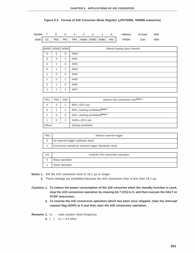
301
CHAPTER 9 APPLICATIONS OF A/D CONVERTER
Figure 9-2. Format of A/D Converter Mode Register ( µPD78098, 78098B subseries)
ADM3 ADM2 ADM1 Selects analog input channel
0 0 0 ANI0
0 0 1 ANI1
0 1 0 ANI2
0 1 1 ANI3
1 0 0 ANI4
1 0 1 ANI5
1 1 0 ANI6
1 1 1 ANI7
FR1 FR0 HSC Selects A/D conversion timeNote 1
0 0 1 80/fXX (20.0 µs)
0 1 1 40/fXX (setting prohibited)Note 2
1 0 0 50/fXX (setting prohibited)Note 2
1 0 1 100/fXX (25.0 µs)
Others Setting prohibited
TRG Selects external trigger
0 No external trigger (software start)
1 Conversion started by external trigger (hardware start)
CS Controls A/D conversion operation
0 Stops operation
1 Starts operation
Notes 1. Set the A/D conversion time to 19.1 µs or longer.
2. These settings are prohibited because the A/D conversion time is less than 19.1 µs.
Cautions 1. To reduce the power consumption of the A/D converter when the standby function is used,
stop the A/D conversion operation by clearing bit 7 (CS) to 0, and then execute the HALT or
STOP instruction.
2. To resume the A/D conversion operation which has been once stopped, clear the interrupt
request flag (ADIF) to 0 and then start the A/D conversion operation.
Remarks 1. fXX : main system clock frequency
2. ( ) : fXX = 4.0 MHz
7 6 5 4 3 2Symbol 1 0
FF80HHSCADM ADM1ADM3 ADM2FR0FR1TRGCS
Address At reset R/W
01H R/W
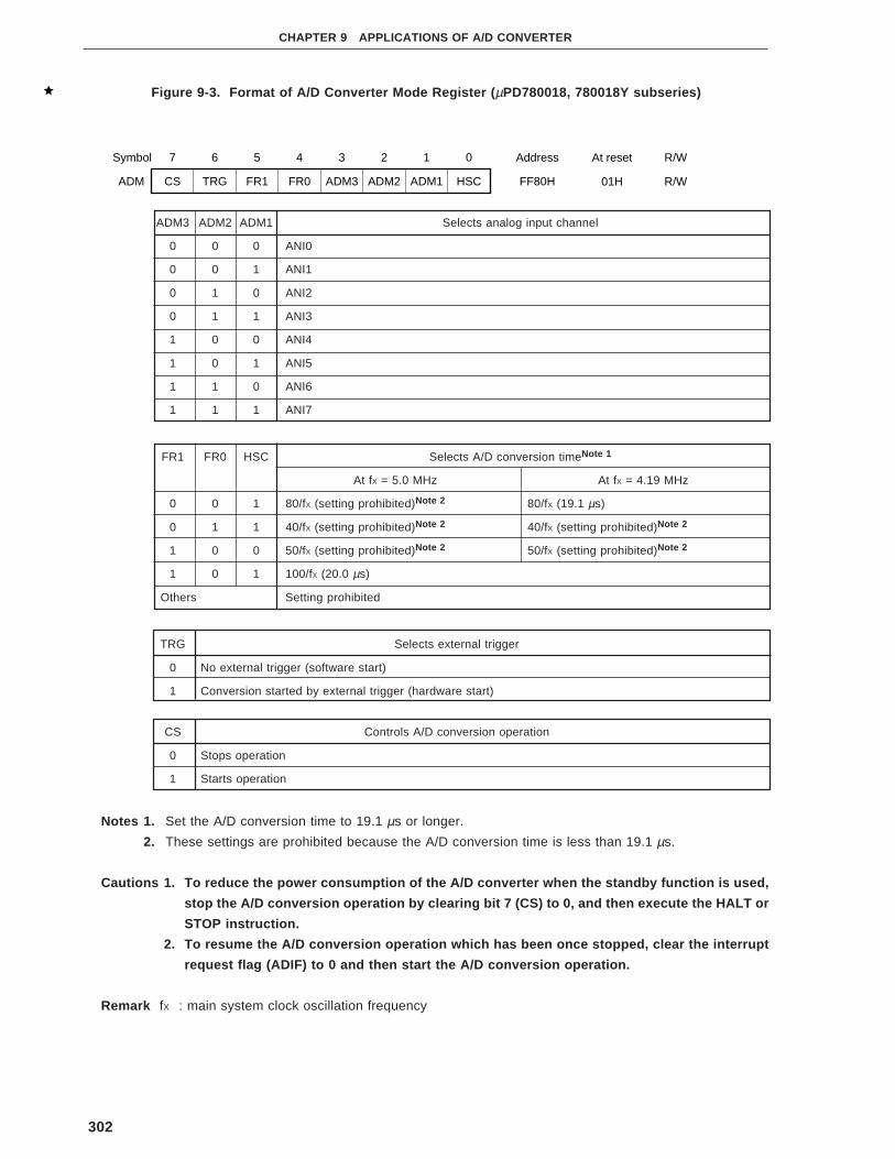
302
CHAPTER 9 APPLICATIONS OF A/D CONVERTER
Figure 9-3. Format of A/D Converter Mode Register ( µPD780018, 780018Y subseries)
ADM3 ADM2 ADM1 Selects analog input channel
0 0 0 ANI0
0 0 1 ANI1
0 1 0 ANI2
0 1 1 ANI3
1 0 0 ANI4
1 0 1 ANI5
1 1 0 ANI6
1 1 1 ANI7
FR1 FR0 HSC Selects A/D conversion timeNote 1
At fX = 5.0 MHz At fX = 4.19 MHz
0 0 1 80/fX (setting prohibited)Note 2 80/fX (19.1 µs)
0 1 1 40/fX (setting prohibited)Note 2 40/fX (setting prohibited)Note 2
1 0 0 50/fX (setting prohibited)Note 2 50/fX (setting prohibited)Note 2
1 0 1 100/fX (20.0 µs)
Others Setting prohibited
TRG Selects external trigger
0 No external trigger (software start)
1 Conversion started by external trigger (hardware start)
CS Controls A/D conversion operation
0 Stops operation
1 Starts operation
Notes 1. Set the A/D conversion time to 19.1 µs or longer.
2. These settings are prohibited because the A/D conversion time is less than 19.1 µs.
Cautions 1. To reduce the power consumption of the A/D converter when the standby function is used,
stop the A/D conversion operation by clearing bit 7 (CS) to 0, and then execute the HALT or
STOP instruction.
2. To resume the A/D conversion operation which has been once stopped, clear the interrupt
request flag (ADIF) to 0 and then start the A/D conversion operation.
Remark fX : main system clock oscillation frequency
7 6 5 4 3 2Symbol 1 0
FF80HHSCADM ADM1ADM3 ADM2FR0FR1TRGCS
Address At reset R/W
01H R/W

303
CHAPTER 9 APPLICATIONS OF A/D CONVERTER
Figure 9-4. Format of A/D Converter Input Select Register
Cautions 1. Set analog input channels in the following steps:
<1> Set the number of analog input channels by using ADIS.
<2> Select one channel whose data is to be converted, from the channels selected by ADIS,
by using the A/D converter mode register (ADM).
2. The internal pull-up resistor is not used to the channel selected by ADIS as an analog input
channel, regardless of the value of the bit 1 (PUO1) of the pull-up resistor option register L
(PUOL).
7 6 5 4 3 2Symbol 1 0
ADIS3 Selects number of analoginput channels
FF84HADIS0ADIS ADIS1ADIS3 ADIS20000
Address At reset R/W
00H R/W
ADIS2 ADIS1 ADIS0
0 No analog input channel(P10-P17)
0 0 0
0 1 channel (ANl0, P11-P17)0 0 1
0 2 channels (ANl0, ANl1,P12-P17)
0 1 0
0 3 channels (ANl0-ANl2,P13-P17)
0 1 1
0 4 channels (ANl0-ANl3,P14-P17)
1 0 0
0 5 channels (ANl0-ANI4,P15-P17)
1 0 1
0 6 channels (ANl0-ANI5,P16-P17)
1 1 0
0 7 channels (ANI0-ANl6, P17)1 1 1
1 8 channels (ANI0-ANI7)0 0 0
Others Setting prohibited

304
CHAPTER 9 APPLICATIONS OF A/D CONVERTER
Figure 9-5. Format of External Interrupt Mode Register 1
(µPD78054, 78054Y, 78078, 78078Y, 78098, 780018, 780018Y, 78058F,
78058FY, 78075B, 78075BY, 78098B subseries, µPD78070A, 78070AY)
7 6 5 4 3 2Symbol 1 0
ES41 Selects valid edge of INTP3
FFEDHES40INTM1 ES41ES51 ES50ES60ES61ES70ES71
Address At reset R/W
00H R/W
ES40
0 Falling edge0
0 Rising edge1
1 Setting prohibited0
1 Both rising and falling edges1
ES51 Selects valid edge of INTP4ES50
0 Falling edge0
0 Rising edge1
1 Setting prohibited0
1 Both rising and falling edges1
ES61 Selects valid edge of INTP5ES60
0 Falling edge0
0 Rising edge1
1 Setting prohibited0
1 Both rising and falling edges1
ES71 Selects valid edge of INTP6ES70
0 Falling edge0
0 Rising edge1
1 Setting prohibited0
1 Both rising and falling edges1

305
CHAPTER 9 APPLICATIONS OF A/D CONVERTER
Figure 9-6. Format of External Interrupt Mode Register 1
(µPD78064, 78064Y, 780058, 780058Y, 780308, 780308Y, 78064B subseries)
7 6 5 4 3 2Symbol 1 0
ES41 Selects valid edge of INTP3
FFEDHES40INTM1 ES41ES51 ES50ES60ES6100
Address At reset R/W
00H R/W
ES40
0 Falling edge0
0 Rising edge1
1 Setting prohibited0
1 Both rising and falling edges1
ES51 Selects valid edge of INTP4ES50
0 Falling edge0
0 Rising edge1
1 Setting prohibited0
1 Both rising and falling edges1
ES61 Selects valid edge of INTP5ES60
0 Falling edge0
0 Rising edge1
1 Setting prohibited0
1 Both rising and falling edges1

306
CHAPTER 9 APPLICATIONS OF A/D CONVERTER
Figure 9-7. Format of External Interrupt Mode Register 1 ( µPD78083 subseries)
Caution Be sure to clear bits 2 through 7 to 0.
Figure 9-8. Format of A/D Current Cut Select Register ( µPD78098, 78098B subseries)
7 6 5 4 3 2Symbol 1 0
ES41 Selects valid edge of INTP3
FFEDHES40INTM1 ES410 00000
Address At reset R/W
00H R/W
ES40
0 Falling edge0
0 Rising edge1
1 Setting prohibited0
1 Both rising and falling edges1
7 6 5 4 3 2Symbol 1 0
F8E2HIEAD0IEAD 00 00000
Address At reset R/W
00H R/W
IEAD0 Controls connection between AVDD and AVREF0
0 Disconnects AVDD from AVREF0
1 Connects AVDD and AVREF0

307
CHAPTER 9 APPLICATIONS OF A/D CONVERTER
9.1 Level Meter
In this application example, the analog voltage input to the A/D converter is displayed on an LED matrix consisting
of 4 × 4, i.e., 16 LEDs.
Because a level meter has been included in this example, the LED display is given in decibel units. Figure 9-9
shows the circuit of the level meter, and Figure 9-10 shows the relations between the result of the A/D conversion
and the number of display digits.
Figure 9-9. Example of Level Meter Circuit
Figure 9-10. A/D Conversion Result and Display
P60
P61
P62
P63
P64
P65
P66
P67
ANIn
=
PD78054µ
16151413121110987654321
0 0AH–22
12H–17
20H–12
2EH–9
39H–7
40H–6
48H–5
51H–4
5BH–3
66H–2
72H–1
80H0
90H1
A2H2
B5H3
FFH6 [dB]
Display value
Dis
play
leve
l
LED(Units)

308
CHAPTER 9 APPLICATIONS OF A/D CONVERTER
The level meter in this example operates with specifications <1> through <3> below.
<1> Measurement method
A/D conversion is performed every 20 ms, and the average value of four previous data is calculated and
displayed on the LEDs.
<2> Display method
The LED display is updated every 20 ms. The LED matrix consists of 4 × 4 = 16 LEDs and performs dynamic
display. For the dynamic display, 8-bit timer/event counter 1 (interval time: 2 ms) is used.
<3> Peak hold
Holding the maximum display level for a specific period (1 second) is called peak hold. Even if the display
level drops during a specific period, only the LED at the maximum display level is held. Therefore, the hold
period of the hold level is 20 ms to 1 s.
Figure 9-11. Concept of Peak Hold
(1) Description of package
<Public declaration symbol>
LEVEL : Name of LED display subroutine
DSPLEV : Display level storage area
HLDLEV : Hold level storage area
CT20MS : Counter measuring 20 ms
CT1S : Counter measuring 1 s
<Register used>
AX, HL, BC (subroutine processing)
Bank 0: A, HL, B (interrupt processing)
Specific period (1 second)
Hold level 6 6 6 6 7 8 9 9 9 9 9 9 4 4 4 5 6 6
Display level 6 5 4 5 7 8 9 8 7 6 5 5 4 3 3 5 6 2

309
CHAPTER 9 APPLICATIONS OF A/D CONVERTER
<RAM used>
Name Usage Attribute Bytes
ADDAT Stores A/D conversion value SADDR 4
DSPLEV Stores display level 1
HLDLEV Stores hold level
CT20MS Counter measuring 20 ms
CT1S Counter measuring 1 s
DIGCNT Display digit counter
DSPDAT Stores display data 4
WORKCT Work counter for loop processing 1
<Flag used>
Name Usage
T20MSF Set every 20 ms
T1SF Set every 1 s
<Nesting>
2 levels 5 bytes
<Hardware used>
• A/D converter
• 8-bit timer/event counter 1
• P6
<Initial setting>
• OSMS = #00000001B ; Oscillation mode select register: does not use divider circuit
• ADM = #1000×××1B ; Selects channel of A/D converter and starts operation
• TCL1 = #10111011B ; Interval time of 2 ms of 8-bit timer/event counter 1
TMC1 = #00000001B
CR10 = 130
• P6 output mode
• Makes P6 output latch low
• Enables INTTM1 interrupt

310
CHAPTER 9 APPLICATIONS OF A/D CONVERTER
<Starting>
This program performs two types of processing: A/D conversion (subroutine) and LED display (interrupt).
• A/D conversion processing
Call LEVEL at least once every 20 ms from the main processing. The LEVEL processing performs A/D
conversion processing only when 20 has elapsed.
• LED display
The 4 × 4 LED matrix performs dynamic display by using the interrupt processing of 8-bit timer/event
counter 1 (interval: 2 ms). The interrupt processing of 8-bit timer/event counter 1 sets the T20MSF (loading
of A/D conversion value) and T1SF (end of hold period) used for the A/D conversion processing at an
interval of 2 ms.
(2) Example of use
EXTRN LEVEL,CT20MS,CT1S
MOV CT20MS,#10MOV CT1S,#50MOV TMC2,#00100110BCLR1 TMMK3
P6=#00HPM6=#00000000BOSMS=#00000001BADM=#10000001BTCL1=#10111011B
CR10=#130TMC1=#00000001BCLR1 TMMK1EI
; Turns OFF LED display
; Does not use divider circuit; ANI0 pin starts operation; Sets 8-bit timer/event counter 1 to 2 ms
; Enables 8-bit timer/event counter 1 interrupt

311
CHAPTER 9 APPLICATIONS OF A/D CONVERTER
(3) SPD chart
LEVEL IF: 20 ms elapses (T20MSF = 1)
THEN
ELSE
INTTM1 Selects register bank 0
Clears T20MSF
Stores A/D conversion value to memory
Averages four previous A/D conversion values
(FOR: WORKCT = #0; WORKCT < #16; WORKCT + +)
IF: conversion result > display level comparison data
Updates comparison data
BREAK
Stores display data to memory
IF: less then 1 second (T1SF = 0)
THEN
IF: hold level < display level
THEN
Sets display level to hold level
THEN
ELSE
Clears T1SF
Sets display level to hold level
Converts display level and hold level to segment signal
Stores digit signal and segment signal to memory in combination
Outputs OFF signal to digit and segment
Outputs memory contents indicated by digit counter
Increments digit counter
Decrements 20 ms counter
IF: 20 ms elapses (CT20MS = 0)
Sets 20 ms counter to 10
Sets 20 ms elapse status
Sets T20MSF
Decrements 1-s counter
IF: 1 second elapses (CT1S = 0)
Sets 1-s counter to 50
Sets 1-s elapse status
Sets T1SF
THEN
THEN

312
CHAPTER 9 APPLICATIONS OF A/D CONVERTER
(4) Program list
PUBLIC LEVEL,HLDLEV,DSPLEV,CT20MS,CT1S
AD_DAT DSEG SADDRADDAT: DS 4DSPLEV: DS 1HLDLEV: DS 1CT20MS: DS 1CT1S: DS 1DIGCNT: DS 1DSPDAT: DS 4WORKCT: DS 1
AD_FLG BSEGT20MSF DBITT1SF DBIT
VETM1 CSEG AT 24HDW INTTM1
AD_SEG CSEG;********************************** Sets level meter data;*********************************LEVEL:
IF_BIT(T20MSF)CLR1 T20MSFA=ADCRA<->ADDATA<->ADDAT+1A<->ADDAT+2A<->ADDAT+3
AX=#0HHL=#ADDATfor(WORKCT=#0;WORKCT<#4;WORKCT++)
A+=[HL]HL++if_bit(CY)
X++endif
next
A<->XC=#4AX/=Cif(C>=#2) (A)
X++endif
HL=#LEVTBLB=#0for(WORKCT=#0;WORKCT<#16;WORKCT++)
if(X>=[HL+B]) (A)B++
elsebreak
endifnext
; A/D conversion result storage area; Display level value; Hold level value; 20 ms counter; 1 s counter; Display digit counter; Display data
; Measures 20 ms; Measures 1 s
; Sets vector address of 8-bit timer/event counter 1
; Checks 20 ms
; Inputs A/D conversion value; Stores A/D conversion value
; Averages four A/D conversion values
; Data storage address
; Carry; Higher digit
; Averages four values; AX/C = AX (quotient) ... C (remainder); Remainder processing (2 or higher is carried); Carry processing
; Conversion result storage register
; Compares data

313
CHAPTER 9 APPLICATIONS OF A/D CONVERTER
DSPLEV=B (A)
if_bit(!T1SF)X=HLDLEV (A)if(X<DSPLEV) (A)
HLDLEV=DSPLEV (A)endif
elseCLR1 T1SFHLDLEV=DSPLEV (A)
endif
HL=#DSPTBLA=DSPLEVA+=AB=AA=HLDLEVA+=AC=AX=[HL+B] (A)B++A=[HL+B]HL=#HLDTBLA<->XA|=[HL+C]A<->XC++A|=[HL+C]BC=AX
HL=#DSPDATA=CA&=#0FHA|=#00010000B[HL]=AHL++A=CA>>=1A>>=1A>>=1A>>=1A&=#0FHA|=#00100000B[HL]=AHL++A=BA&=#0FHA|=#01000000B[HL]=AHL++A=BA>>=1A>>=1A>>=1A>>=1A&=#0FHA|=#10000000B[HL]=A
endif
; Determines display data
; 1 s (hold level updated); Compares hold and display levels
; Creates display level
; Creates hold level
; Sets segment signal of first digit
; Sets digit signal
; Sets segment signal of second digit
; Sets digit signal
; Sets segment signal of third digit
; Sets digit signal
; Sets segment signal of fourth digit
; Sets digit signal

314
CHAPTER 9 APPLICATIONS OF A/D CONVERTER
RETLEVTBL:
DB 0AHDB 12HDB 20HDB 2EHDB 39HDB 40HDB 48HDB 51HDB 5BHDB 66HDB 72HDB 80HDB 90HDB 0A2HDB 0B5HDB 0FFH
DSPTBL:DW 0000000000000000BDW 0000000000000001BDW 0000000000000011BDW 0000000000000111BDW 0000000000001111BDW 0000000000011111BDW 0000000000111111BDW 0000000001111111BDW 0000000011111111BDW 0000000111111111BDW 0000001111111111BDW 0000011111111111BDW 0000111111111111BDW 0001111111111111BDW 0011111111111111BDW 0111111111111111BDW 1111111111111111B
HLDTBL:DW 0000000000000000BDW 0000000000000001BDW 0000000000000010BDW 0000000000000100BDW 0000000000001000BDW 0000000000010000BDW 0000000000100000BDW 0000000001000000BDW 0000000010000000BDW 0000000100000000BDW 0000001000000000BDW 0000010000000000BDW 0000100000000000BDW 0001000000000000BDW 0010000000000000BDW 0100000000000000BDW 1000000000000000B
$EJECT

315
CHAPTER 9 APPLICATIONS OF A/D CONVERTER
;********************************** Level meter data;*********************************TM1_SEG CSEGINTTM1:
SEL RB0P6=#00000000BHL=#DSPDATB=DIGCNT (A)P6=[HL+B] (A)DIGCNT++DIGCNT&=#00000011BCT20MS--if(CT20MS==#0)
CT20MS=#10SET1 T20MSFCT1S--if(CT1S==#0)
CT1S=#50SET1 T1SF
endifendifRETI
; Turns OFF digit and segment signals
; 20 ms?
; Sets initial counter value
; 1s?
; Sets initial counter value

316
CHAPTER 9 APPLICATIONS OF A/D CONVERTER
9.2 Thermometer
In this application example, a temperature in a range of –20°C to +50°C is measured by using a thermistor (6 kΩ/
0°C) as a temperature sensor. Changes in the resistance of the thermistor with respect to temperature are given
by the following expression:
R = R0exp B (1/T – 1/T0)
where,
R : resistance at given temperature T [°K]
T : given temperature [°K]
R0 : resistance at reference temperature T0 [°K]
T0 : reference temperature [°K]
B : constant obtained by reference temperature T0 [°K] and T0 [°K]
Constant B changes with the temperature. This constant can be calculated by changing the above expression
as follows:
1 RB = In
(1/T–1/T0) R0
Figure 9-12 shows a circuit example. This circuit is designed to input 0 V at –20°C, and 5 V at + 50°C.
Figure 9-12. Circuit Example of Thermometer
PD78054µ
ANIn+
–
Th

317
CHAPTER 9 APPLICATIONS OF A/D CONVERTER
Because the characteristic of the thermistor is non linear in this example, the input analog voltage is not converted
to a temperature in a range of –20 °C to +50 °C through calculation but by comparison with table data. This conversion
result is stored to RAM (DSPDAT) as 2-digit BCD. Figure 9-13 shows the characteristics of the thermistor, and Table
9-1 shows the relations between temperature and A/D conversion value.
To measure the temperature, four conversion values are averaged and converted to a temperature. The result
of the conversion is stored in a display area. Therefore, the data is updated once every four times. For example,
if measurement processing is executed every 250 ms, the display updating cycle is 1 second.
Figure 9-13. Temperature vs. Output Characteristic
100
90
80
70
60
50
40
30
20
10
0–20 –10 0 10 20 30 40 50
Temperature
(°C)
Per
cent
age
of o
utpu
t cha
ract
eris
tic
(%)

318
CHAPTER 9 APPLICATIONS OF A/D CONVERTER
Table 9-1. A/D Conversion Value and Temperature
Conversion Temperature Conversion Temperature Conversion Temperature Conversion Temperature
Value [°C] Value [°C] Value [°C] Value [°C]
00 –20.0 38 –2.5 82 15.5 CB 33.5
01 –19.5 3C –1.5 86 16.5 CE 34.5
04 –18.5 40 –0.5 8B 17.5 D2 35.5
07 –17.5 44 0.5 8F 18.5 D6 36.5
0A –16.5 48 1.5 93 19.5 D9 37.5
0C –15.5 4C 2.5 97 20.5 DC 38.5
0F –14.5 50 3.5 9B 21.5 E0 39.5
12 –13.5 54 4.5 9F 22.5 E3 40.5
16 –12.5 58 5.5 A3 23.5 E7 41.5
19 –11.5 5C 6.5 A8 24.5 EA 42.5
1C –10.5 60 7.5 AC 25.5 ED 43.5
1F –9.5 64 8.5 B0 26.5 F0 44.5
23 –8.5 69 9.5 B4 27.5 F3 45.5
26 –7.5 6D 10.5 B7 28.5 F6 46.5
2A –6.5 71 11.5 BB 29.5 F9 47.5
2D –5.5 75 12.5 BF 30.5 FC 48.5
31 –4.5 7A 13.5 C3 31.5 FE 49.5
35 –3.5 7E 14.5 C7 32.5 FF 50.0
(1) Description of package
<Public declaration symbol>
THMETER : Thermometer subroutine call name
DSPDAT : Display data storage area
CNTPRO : Test counter counting number of inputs
MINUSF : Minus temperature display flag
T250MSF : 250-ms setting flag
<Register used>
AX, BC, HL

319
CHAPTER 9 APPLICATIONS OF A/D CONVERTER
<RAM used>
Name Usage Attribute Bytes
ADDAT Stores A/D conversion value SADDR 4
DSPDAT Stores display data 2
CNTPRO Test counter for number of inputs 1
WORKCT Work counter for loop processing
<Flag used>
Name Usage
T250MSF Executes measurement processing when set
MINUSF Set when temperature is below zero
<Nesting>
1 level 2 bytes
<Hardware used>
A/D converter
<Initial setting>
ADM = #1000×××1B; Selects A/D converter channel and starts operation
<Starting>
Set the T250MSF flag in each measurement cycle by using timer processing. After that, call THMETER at
least once in measurement cycle.

320
CHAPTER 9 APPLICATIONS OF A/D CONVERTER
(2) Example of use
EXTRN THMETER,DSPDAT,CNTPROEXTBIT MINUSF,T250MSF
AD_DAT DSEG SADDRCT250MS:DS 1LEDD: DS 4DIGCT: DS 1
VETM3 CSEG AT 1EHDW INTTM3
MOV TMC2,#00100110BCLR1 TMMK3
CT250MS=#128CNTPR0=#4ADM=#10000011B
;**********************************************; Watch timer interrupt processing; Interval time: 1.95 ms;**********************************************INTTM3:
DBNZ CT250MS,$RTNTM3MOV CT250MS,#128SET1 T250MSF
RTNTM3:
RETI
.
.
.
.
.
.
.
.
.
.
.
.
.
.
.
.
; 250 ms counter; LED display area; LED display digit counter
; Sets vector address of watch timer
; Sets watch timer to 1.95 ms
; Selects ANI1 pin and starts operation
; 1.95 ms interrupt processing
; 250 ms elapses

321
CHAPTER 9 APPLICATIONS OF A/D CONVERTER
(3) SPD chart
THMETER IF: 250 ms elapses (T250MS = 1)
THEN
ELSE
Clears T250MS
Stores A/D conversion value to memory
IF: four values stored in memory
THEN
Averages four A/D conversion values
(FOR: WORKCT = #0; WORKCT < #70; WORKCT + +)
IF: conversion result > comparison data for temperature conversion
THEN
Updates comparison data
BREAK
IF: minus temperature data
THEN
Sets minus status
Sets MINUSF
Converts temperature data to decimal number and stores in memory

322
CHAPTER 9 APPLICATIONS OF A/D CONVERTER
(4) Program list
PUBLIC THMETER,DSPDAT,CNTPR0,T250MSF,MINUSF
AD_DAT DSEG SADDRADDAT: DS 4DSPDAT: DS 2CNTPR0: DS 1WORKCT: DS 1
AD_FLG BSEGT250MSF DBITMINUSF DBIT
TH_SEG CSEG;********************************** Sets temperature data;*********************************THMETER:
if_bit(T250MSF)CLR1 T250MSFA=ADCRA<->ADDATA<->ADDAT+1A<->ADDAT+2A<->ADDAT+3
CNTPR0--if(CNTPR0==#0)
CNTPR0=#4AX=#0HHL=#ADDATfor(WORKCT=#0;WORKCT<#4;WORKCT++)
A+=[HL]HL++if_bit(CY)
X++endif
next
A<->XC=#4AX/=Cif(C>=#2) (A)
X++endif
A=XB=#0HL=#THRTBLif(A==#0FFH)
B=#70else
for(WORKCT=#0;WORKCT<#70;WORKCT++)if(X>=[HL+B]) (A)
B++else
breakendif
next
; A/D conversion result storage area; Display data; Tests number of inputs
; Sets 250 ms; Sets minus data
; 250 ms
; Data storage address
; Carry occurs; Carry
; AX/C = AX (quotient) ... C (remainder); Remainder processing (2 digits or more carried); Carry processing
; Converts to temperature data
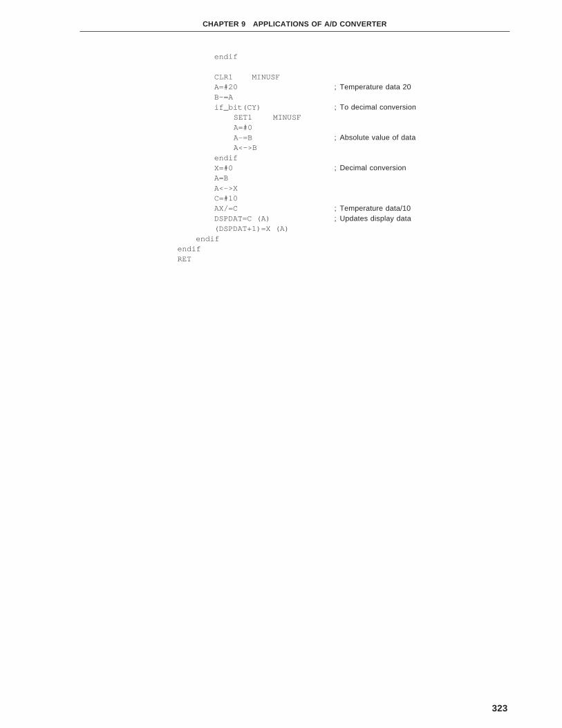
323
CHAPTER 9 APPLICATIONS OF A/D CONVERTER
endif
CLR1 MINUSFA=#20B–=Aif_bit(CY)
SET1 MINUSFA=#0A–=BA<->B
endifX=#0A=BA<->XC=#10AX/=CDSPDAT=C (A)(DSPDAT+1)=X (A)
endifendifRET
; Temperature data 20
; To decimal conversion
; Absolute value of data
; Decimal conversion
; Temperature data/10; Updates display data

324
CHAPTER 9 APPLICATIONS OF A/D CONVERTER
THRTBL;;
DB 1 ; –19.5DB 4 ; –18.5DB 7 ; –17.5DB 0AH ; –16.5DB 0CH ; –15.5DB 0FH ; –14.5DB 12H ; –13.5DB 16H ; –12.5DB 19H ; –11.5DB 1CH ; –10.5DB 1FH ; –9.5DB 23H ; –8.5DB 26H ; –7.5DB 2AH ; –6.5DB 2DH ; –5.5DB 31H ; –4.5DB 35H ; –3.5DB 38H ; –2.5DB 3CH ; –1.5DB 40H ; –0.5DB 44H ; +0.5DB 48H ; 1.5DB 4CH ; 2.5DB 50H ; 3.5DB 54H ; 4.5DB 58H ; 5.5DB 5CH ; 6.5DB 60H ; 7.5DB 64H ; 8.5DB 69H ; 9.5DB 6DH ; 10.5DB 71H ; 11.5DB 75H ; 12.5DB 7AH ; 13.5DB 7EH ; 14.5DB 82H ; 15.5DB 86H ; 16.5DB 8BH ; 17.5DB 8FH ; 18.5DB 93H ; 19.5DB 97H ; 20.5DB 9BH ; 21.5DB 9FH ; 22.5DB 0A3H ; 23.5DB 0A8H ; 24.5DB 0ACH ; 25.5DB 0B0H ; 26.5DB 0B4H ; 27.5DB 0B7H ; 28.5DB 0BBH ; 29.5DB 0BFH ; 30.5DB 0C3H ; 31.5DB 0C7H ; 32.5DB 0CBH ; 33.5DB 0CEH ; 34.5DB 0D2H ; 35.5DB 0D6H ; 36.5

325
CHAPTER 9 APPLICATIONS OF A/D CONVERTER
DB 0D9H ; 37.5DB 0DCH ; 38.5DB 0E0H ; 39.5DB 0E3H ; 40.5DB 0E7H ; 41.5DB 0EAH ; 42.5DB 0EDH ; 43.5DB 0F0H ; 44.5DB 0F3H ; 45.5DB 0F6H ; 46.5DB 0F9H ; 47.5DB 0FCH ; 48.5DB 0FFH ; 49.5

326
CHAPTER 9 APPLICATIONS OF A/D CONVERTER
9.3 Analog Key Input
In this example, sixteen keys are input by using the A/D converter. To input keys, a circuit must be designed so
that a voltage peculiar to a key is input to the A/D converter when the key is pressed.
Because sixteen keys are input in this example, VDD is divided by 16 and the voltage of each key is converted into
a key code. Table 9-2 shows the relations between the input voltages and key codes (00H through 0FH). When
no key input is made, the key code is 10H.
Table 9-2. Input Voltage and Key Code
Input Voltage V A/D Conversion Value Key Code
GND 00-07H 00H
1/16VDD 08-17H 01H
2/16VDD 18-27H 02H
3/16VDD 28-37H 03H
4/16VDD 38-47H 04H
5/16VDD 48-57H 05H
6/16VDD 58-67H 06H
7/16VDD 68-77H 07H
8/16VDD 78-87H 08H
9/16VDD 88-97H 09H
10/16VDD 98-A7H 0AH
11/16VDD A8-B7H 0BH
12/16VDD B8-C7H 0CH
13/16VDD C8-D7H 0DH
14/16VDD D8-E7H 0EH
15/16VDD E8-F7H 0FH
VDD F8-FFH 10H
Figure 9-14 shows an example of the circuit that satisfies the above relations between the input voltages and key
codes. Note, however, that this circuit gives a priority to the key with the lower number if two or more keys are pressed
at the same time.

327
CHAPTER 9 APPLICATIONS OF A/D CONVERTER
Figure 9-14. Example of Analog Key Input Circuit
Resistances R0 through R15 used in the circuit in Figure 9-14 can be calculated by the following expression:
n × R0 RK =
16–n
Table 9-3 shows the resistances of R1 through R15 where R0 is 1 kΩ in the above expression (the calculation
result of a resistance may slightly different from the resistance of commercial resistors indicated by a color code).
Table 9-3. Resistances of R1 through R5
Resistor No. Resistance Value Ω Resistor No. Resistance Value Ω Resistor No. Resistance Value Ω
R1 68 R6 150 R11 560
R2 75 R7 180 R12 750
R3 82 R8 220 R13 1.3 k
R4 100 R9 270 R14 2.7 k
R5 120 R10 390 R15 8.2 k
This program converts an input analog voltage into the corresponding key code shown in Table 9-2, absorbs
chattering, and then stores the input voltage to RAM. To absorb chattering, a key code is assumed to be valid when
it coincides with a given value five times in succession. For example, if an analog voltage is sampled every 5 ms,
chattering of 20 to 25 ms is absorbed. If a key input is changed, a key change flag (KEYCHG) is set.
n
ΣK=1
ANIn
VDD
PD78054µ
K0
K1
K2
K14
K15
R0
R1
R2
R14
R15

328
CHAPTER 9 APPLICATIONS OF A/D CONVERTER
(1) Description of package
<Public declaration symbol>
AKEYIN : Analog key input subroutine name
KEYDAT : Key code storage area
PASTDT : Key code storage area for chattering absorption
CHATCT : Chattering absorption counter
KEYCHG : Key change test flag
CHTENDF : Flag to test end of chattering absorption
KEYOFF : Key code when there is no key input
<Register used>
A
<RAM used>
Name Usage Attribute Bytes
PASTDAT Stores key code for chattering absorption SADDR 1
KEYDAT Stores key code
CHATCNT Chattering counter
<Flag used>
Name Usage
KEYCHG Set when key is changed
CHTENDF Sets when chattering absorption ends
<Nesting>
1 level 2 bytes
<Hardware used>
A/D converter
<Initial setting>
ADM = #1000×××1B; Selects A/D converter channel and starts operation
<Starting>
• Call AKEYIN at fixed interval.
• Input a key code after testing the key change flag. Note that this flag is not cleared by the subroutine and
must be cleared after the flag has been tested.

329
CHAPTER 9 APPLICATIONS OF A/D CONVERTER
(2) Example of use
EXTRN AKEYIN,KEYDAT,PASTDT,CHATCTEXTRN KEYOFF
EXTBIT KEYCHG,CHTENDF
VETM3 CSEG AT 1EHDW INTTM3
MAINDAT DSEG SADDRCT5MS: DS 1
TMC2=#00100110BCLR1 TMMK3CT5MS=#3
KEYDAT=#KEYOFFPASTDT=#KEYOFFCHATCT=#CHAVALCLR1 CHTENDFCLR1 KEYCHGADM=#10000101BEI
if_bit(KEYCHG)CLR1 KEYCHG; Key input processing
endif
;**********************************************; Watch timer interrupt processing; Interval: 1.95 ms;**********************************************INTTM3:
DBNZ CT5MS,$RTNTM3MOV CT5MS,#3CALL !AKEYIN
RTNTM3:
RETI
.
.
.
.
.
.
.
.
.
.
.
.
.
.
.
.
; Sets vector address of watch timer
; Sets OFF data as key data
; Sets number of times of chattering to five
; Selects ANI2 pin and starts operation
; Key changed?
; 1.95 ms interrupt processing
; 1.95 ms × 3 elapses

330
CHAPTER 9 APPLICATIONS OF A/D CONVERTER
(3) SPD chart
AKEYIN Inputs and adjusts A/D conversion value (adds 8)
THEN
ELSE
IF: overflow occurs
Sets no key input status
Decodes key
IF: key input not changed
IF: chattering being absorbed
THEN
THEN
IF: chattering absorption ends
THEN
Sets chattering absorption status
Sets CHTENDF
IF: valid key changed
THEN
Updates key code
Sets key change status
ELSE
Updates comparison key code
Sets KEYCHG
Sets chattering absorption start status
Clears CHTENDF

331
CHAPTER 9 APPLICATIONS OF A/D CONVERTER
(4) Program list
PUBLIC AKEYIN,KEYDAT,PASTDTPUBLIC CHATCT,KEYOFFPUBLIC KEYCHG,CHTENDF
AK_DAT DSEG SADDRKEYDAT: DS 1PASTDT: DS 1CHATCT: DS 1
AK_FLG BSEGKEYCHG DBITCHTENDF DBIT
KEYOFF EQU 10HCHAVAL EQU 5
AK_SEG CSEG;******************************* Analog key input;******************************AKEYIN:
A=ADCRA+=#8if_bit(CY)
A=#KEYOFFelse
A>>=1A>>=1A>>=1A>>=1A&=0FH
endifif(A==PASTDT)
if_bit(!CHTENDF)CHATCT--if(CHATCT==#0)
SET1 CHTENDFA=PASTDTif(A!=KEYDAT)
KEYDAT=ASET1 KEYCHG
endifendif
endifendif
PASTDT=ACHATCT=#CHAVAL-1CLR1 CHTENDF
endifRET
; Key data storage area; Chattering key data; Chattering counter
; Key changed; Chattering absorption end status
; OFF key data; Number of times of chattering absorption
; Inputs A/D conversion value; Corrects data
; Sets no key input status
; Decodes key
; No key change; Chattering being absorbed; End of chattering absorption
; Sets chattering absorption status
; Valid key changed; Updates key data; Sets key change status
; Updates previous key data; Starts chattering absorption

332
CHAPTER 9 APPLICATIONS OF A/D CONVERTER
9.4 4-Channel Input A/D Conversion
This section describes the method to scan four channels for A/D conversion. The A/D conversion operation is
started by the software.
The analog voltages input to the selected four channels are converted into digital signals. The result of the
A/D conversion of each channel is stored in RAM.
An interrupt request is generated by using 8-bit timer/event counter 1. The result of the conversion is loaded and
channel is converted in the processing of this interrupt request. Because 8-bit timer/event counter 1 is set to 10 ms,
it is not necessary to measure the wait time of the A/D conversion.
Caution To change the interrupt time, make the following setting:
• Set timer longer than A/D conversion end time + Interrupt entry
return time + Interrupt processing time.
• Test flags that indicate the end of the conversion.
Figure 9-15. Timing Chart in 4-Channel Scan Mode
INTTM2
ADCR ANI0 ANI1 ANI2 ANI3 ANI0 ANI1 ANI2 ANI3 ANI0
ADIn 1 2 3 0 1 2 3 0 10
10 ms

333
CHAPTER 9 APPLICATIONS OF A/D CONVERTER
(1) Description of package
<Public declaration symbol>
• Output parameter
M_CH0 : Stores conversion result of channel 0
M_CH1 : Stores conversion result of channel 1
M_CH2 : Stores conversion result of channel 2
M_CH3 : Stores conversion result of channel 3
<Register used>
A
<RAM used>
Name Usage Attribute Bytes
M_CH0 Channel 0 conversion result storage area SADDR 1
M_CH1 Channel 1 conversion result storage area SADDR 1
M_CH2 Channel 2 conversion result storage area SADDR 1
M_CH3 Channel 3 conversion result storage area SADDR 1
M_MODE Mode storage area SADDR 1
<Nesting>
1 level 3 bytes
<Hardware used>
• A/D converter
• 8-bit timer/event counter 1
• Port 1 (P10-P13)
<Initial setting>
• OSMS = #00000001B ; Oscillation mode select register: does not use divider circuit
• ADM = #1000××××B ; Selects A/D converter channel and starts operation
• ADIS = #00000100B ; Selects number of A/D converter channels
• TCL1 = #00001110B ; Interval time of 8-bit timer/event counter 1: 10 ms
TMC1 = #00000001B
CR10 = #81
• Enables TMMK1 interrupt

334
CHAPTER 9 APPLICATIONS OF A/D CONVERTER
(2) Example of use
EXTRN M_CH0,M_CH1,M_CH2,M_CH3,M_MODE;******************************************; Initialize;******************************************M4 CSEG ;RES_STA:
SEL RB0 ;DI ;
OSMS=#00000001BADM=#10000001BADIS=#00000100BCR10=#81TCL1=#00001110BTMC1=#00000001BCLR1 TMIF1CLR1 TMMK1EIM_MODE=#0
while(forever)
A=M_CH0
A=M_CH1
A=M_CH2
A=M_CH3
(3) SPD chart
[A/D conversion processing]
.
.
.
.
; Does not use divider circuit; Starts A/D operation and selects external trigger channel 0; Selects analog input channel 4; Sets modulo register 81; Count clock: 8.2 kHz; Enables 8-bit timer/register 1 operation; Clears timer 1 interrupt request flag; Enables timer 1 interrupt;; Sets initial value (0 channel) to mode area
;
; A ← data of channel 0
; A ← data of channel 1
; A ← data of channel 2
; A ← data of channel 3
.
.
.
.
.
.
.
.
.
.
.
.
KASAN Loads conversion result of channel for previous A/D conversion
Changes channel
ADM ← selects changed channel

335
CHAPTER 9 APPLICATIONS OF A/D CONVERTER
(4) Program list
;********************************************; A/D conversion;********************************************;$PC(054) ;;PUBLIC M_CH0,M_CH1,M_CH2,M_CH3,M_MODE ;;VEINTM1 CSEG AT 24H
DW KASAN;********************************************; RAM definition;********************************************
DSEG SADDRM_CH0: DS 1M_CH1: DS 1M_CH2: DS 1M_CH3: DS 1M_MODE: DS 1;
CSEGKASAN:
SEL RB2switch(M_MODE)case 0:
M_CH0=ADCR (A)M_MODE++ADM=#10000011Bbreak
case 1:M_CH1=ADCR (A)M_MODE++ADM=#10000101Bbreak
case 2:M_CH2=ADCR (A)M_MODE++ADM=#10000111Bbreak
case 3:M_CH3=ADCR (A)M_MODE=#0ADM=#10000001Bbreak
endsRETIEND
; Area for channel 0 addition; Area for channel 1 addition; Area for channel 2 addition; Area for channel 3 addition; Mode storage area
;
; Selects bank 2; Channel currently selected?; Channel 0:; Transfers conversion result to RAM;; Select channel 1:;; Channel 1:; Transfers conversion result to RAM;; Selects channel 2;; Channel 2:; Transfers conversion result to RAM;; Selects channel 3;; Channel 3:; Transfers conversion result to RAM;; Selects channel 0;;;

[MEMO]
336

CHAPTER 10 APPLICATIONS OF D/A CONVERTER
The D/A converter of the 78K/0 series consists of two voltage output type D/A converter channels with an 8-bit
resolution. This D/A can be used in two modes: normal mode and real-time output mode. In the normal mode, the
output trigger is writing data to the D/A conversion value setting registers 0 and 1 (DACS0 and 1). In the real-time
output mode, the output is triggered by the interrupt requests (INTTM1 and 2) of 8-bit timer/event counters 1 and 2.
In this mode, set data to DACS0 and DACS1 after an output trigger has been generated until the next output trigger
is generated.
The D/A converter is set by the D/A converter mode register.
Figure 10-1. Format of D/A Converter Mode Register
Cautions 1. To use the D/A converter, set the multiplexed port pins in the input mode and disconnect the
pull-up resistor.
2. Be sure to clear bits 2, 3, 6, and 7 to 0.
3. The output goes into a high-impedance state when D/A conversion operation is stopped.
4. The output trigger in the real-time output mode is INTTM1 for channel 0 and INTTM2 for
channel 1.
7 6 5 4 3 2Symbol 1 0
FF98HDACE0DAM DACE10 0DAM4DAM500
Address At reset R/W
00H R/W
DACE0 Controls D/A converter channel 0
0 Stops D/A conversion operation
1 Enables D/A conversion operation
DACE1 Controls D/A converter channel 1
0 Stops D/A conversion operation
1 Enables D/A conversion operation
DAM4 Operation mode of D/A converter channel 0
0 Normal mode
1 Real-time output mode
DAM5 Operation mode of D/A converter channel 1
0 Normal mode
1 Real-time output mode
337
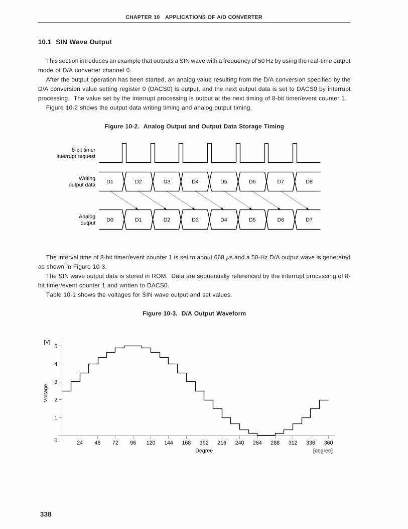
338
CHAPTER 10 APPLICATIONS OF A/D CONVERTER
10.1 SIN Wave Output
This section introduces an example that outputs a SIN wave with a frequency of 50 Hz by using the real-time output
mode of D/A converter channel 0.
After the output operation has been started, an analog value resulting from the D/A conversion specified by the
D/A conversion value setting register 0 (DACS0) is output, and the next output data is set to DACS0 by interrupt
processing. The value set by the interrupt processing is output at the next timing of 8-bit timer/event counter 1.
Figure 10-2 shows the output data writing timing and analog output timing.
Figure 10-2. Analog Output and Output Data Storage Timing
The interval time of 8-bit timer/event counter 1 is set to about 668 µs and a 50-Hz D/A output wave is generated
as shown in Figure 10-3.
The SIN wave output data is stored in ROM. Data are sequentially referenced by the interrupt processing of 8-
bit timer/event counter 1 and written to DACS0.
Table 10-1 shows the voltages for SIN wave output and set values.
Figure 10-3. D/A Output Waveform
8-bit timerinterrupt request
Writingoutput data D2D1 D3 D4 D5 D6 D7 D8
Analogoutput D1D0 D2 D3 D4 D5 D6 D7
1
24
Vol
tage
48 72 96 120 144 168 192 216 240 264 288 312 336 360
2
3
4
5[V]
Degree [degree]
0

339
CHAPTER 10 APPLICATIONS OF A/D CONVERTER
Table 10-1. Voltage of SIN Wave Output and Preset Value
Degree Voltage (V) Set Value Degree Voltage (V) Set Value
0 2.5000 80H 180 2.5000 80H
12 3.0200 9BH 192 1.9802 65H
24 3.5168 B4H 204 1.4832 4CH
36 3.9695 CBH 216 1.0305 35H
48 4.3579 DFH 228 0.6421 21H
60 4.6651 EFH 240 0.3349 11H
72 4.8776 FAH 252 0.1224 06H
84 4.9863 FFH 264 0.0137 01H
96 4.9863 FFH 276 0.0137 01H
108 4.8776 FAH 288 0.1224 06H
120 4.6651 EFH 300 0.3349 11H
132 4.3579 DFH 312 0.6421 21H
144 3.9695 CBH 324 1.0305 35H
156 3.5168 B4H 336 1.4832 4CH
168 3.0200 9BH 348 1.9802 65H
Remark The analog voltage output to the ANO0 pin is determined by the following expression:
AVREF1 × DACS0ANO0 pin output voltage =
256
Caution The voltage values shown in Table 10-1 is rounded off at the fifth position after the decimal point.
However, the preset value is calculated with the data before rounding off. The resultant data is
rounded off at the first position after the decimal point.

340
CHAPTER 10 APPLICATIONS OF A/D CONVERTER
The output analog value is processed by the SIN wave conversion circuit shown in Figure 10-4 to create a SIN
wave without step.
Figure 10-4. SIN Wave Conversion Circuit
(1) Description of package
<Public declaration symbol>
• Data definition reference name
SDATA : First address of SIN wave output data to be stored to DACS0 register
ENDDAT : Last pointer of SIN wave data
• Input/output parameter
C_DATA : ROM data counter
<Register used>
Bank 3; AX, HL, B
<RAM used>
Name Usage Attribute Bytes
C_DATA Counter indicating pointer that extracts SIN wave SADDR 1
output data
<Flag used>
None
<Nesting level>
1 level 3 bytes
1 F
0.012 F
Amplifier
SlN wave
Integrating circuit Lowpass filter
µ 270 kΩ
µ10 kWANO0

341
CHAPTER 10 APPLICATIONS OF A/D CONVERTER
<Hardware used>
• D/A converter
• 8-bit timer/event counter 1
<Initial setting>
• OSMS = #00000001B ; Oscillation mode select register: does not use divider circuit
• PM13 = #×××××××1B ; Sets port 13 in input mode
• TCL1 = #××××1001B ; Interval of 8-bit timer/event counter: 668 µs
TMC1 = #000000×0B
CR10 = #174
• DACS0 = #80H ; Sets D/A converter
DAM = #00000001B
• SET1 DAM.4 ; Sets D/A converter in real-time output mode
• SET1 TCE1 ; Enables operation of 8-bit timer/event counter 1 and enables interrupt
CLR1 TMIF1
CLR1 TMMK1
Caution To prevent output of a value on resetting and starting, once set the normal mode and write
the initial value to the D/A conversion value setting register 0 (DACS0), and then output
the initial value. After that, set the real-time output mode, and enable the operation of
8-bit timer/event counter 1 and interrupt.
If D/A conversion is started in the real-time output mode after reset and start with the initial
value set to the DACS0 register, 0 V (data D0 in Figure 10-2. Analog Output and Output
Data Storage Timing) is output.
<Starting>
When starting output, enable the operation of the D/A converter (by setting bit 4 (DAM4) of the D/A converter
mode register(DAM)), the operation of 8-bit timer/event counter 1 (by setting bit 0 (TCE) of the 8-bit timer
mode control register (TMC1)), and interrupts (by clearing TMIF1 and TMMK1).
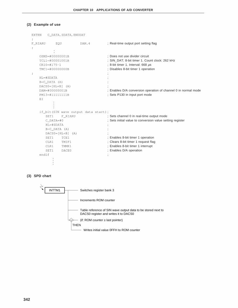
342
CHAPTER 10 APPLICATIONS OF A/D CONVERTER
(2) Example of use
EXTRN C_DATA,SDATA,ENDDAT;F_RIARU EQU DAM.4;
OSMS=#00000001BTCL1=#00001001BCR10=#175-1TMC1=#00000000B
;HL=#SDATAB=C_DATA (A)DACS0=[HL+B] (A)DAM=#00000001BPM13=#11111111BEI
if_bit(SIN wave output data start)SET1 F_RIARUC_DATA=#0HL=#SDATAB=C_DATA (A)DACS0=[HL+B] (A)SET1 TCE1CLR1 TMIF1CLR1 TMMK1SET1 DACE0
endif
(3) SPD chart
.
.
.
.
.
.
.
.
.
.
; Real-time output port setting flag
; Does not use divider circuit; SIN_DAT; 8-bit timer 1. Count clock: 262 kHz; 8-bit timer 1. Interval: 668 µs; Disables 8-bit timer 1 operation;;;;; Enables D/A conversion operation of channel 0 in normal mode; Sets P130 in input port mode
;; Sets channel 0 in real-time output mode; Sets initial value to conversion value setting register;;;; Enables 8-bit timer 1 operation; Clears 8-bit timer 1 request flag; Enables 8-bit timer 1 interrupt; Enables D/A operation;
INTTM1 Switches register bank 3
THEN
Increments ROM counter
Table reference of SIN wave output data to be stored next to DACS0 register and writes it to DACS0
(if: ROM counter ≥ last pointer)
Writes initial value 0FFH to ROM counter

343
CHAPTER 10 APPLICATIONS OF A/D CONVERTER
(4) Program list
PUBLIC C_DATA,SDATA,ENDDAT;VETIM1 CSEG AT 24H
DW INTTM1
ENDDAT EQU 1DH;SINRAM DSEG SADDRC_DATA: DS 1;********************************************************; SIN wave data change interrupt processing;********************************************************SINDAT CSEGINTTM1:
SEL RB3C_DATA++B=C_DATA (A)HL=#SDATADACS0=[HL+B] (A)if(C_DATA >= #ENDDAT)
C_DATA=#0FFHendifRETI
SDATA:DB 09BHDB 0B4HDB 0CBHDB 0DFHDB 0EFHDB 0FAHDB 0FFHDB 0FFHDB 0FAHDB 0EFHDB 0DFHDB 0CBHDB 0B4HDB 09BHDB 080HDB 065HDB 04CHDB 035HDB 021HDB 011HDB 006HDB 001HDB 001HDB 006HDB 011HDB 021HDB 035HDB 04CHDB 065HDB 080HEND
; SIN wave data 1 cycle end value
; ROM data counter
; Sets bank 3; Increments ROM data counter; Refers to SIN wave output data;; Stores data; End of 1 cycle of SIN wave?; Initializes ROM data counter;;;; SIN wave data;;;;;;;;;;;;;;;;;;;;;;;;;;;;;

[MEMO]
344

CHAPTER 11 APPLICATION OF REAL-TIME OUTPUT PORT
This chapter describes the real-time output function of the 78K/0 series.
The real-time output function is used to output data set in advance in the real-time output buffer registers (RTBL
and RTBH) to an external device by transferring the data to an output latch by hardware as soon as a timer interrupt
request or external interrupt request occurs.
By using the real-time output port function, a jitter free signal can be output. Therefore, this function is ideal for
controlling a stepping motor. The real-time output port can be set in the port mode or real-time output mode in 1-
bit units.
The real-time output data is written to the real-time output buffer registers (RTBL and RTBH). RTBL and RTBH
are mapped to independent addresses in the SFR area.
When an operation mode of 4 bits × 2 channels is selected, RTBL and RTBH can independently set data.
When an operation mode of 8 bits × 1 channel is specified, data can be set to RTBL or RTBH by writing 8-bit data
to either of RTBL or RTBH.
The real-time output port is set by using the real-time output port mode register (RTPM), real-time output control
register (RTPC), and port mode register 12 (PM12).
345

346
CHAPTER 11 APPLICATION OF REAL-TIME OUTPUT PORT
Figure 11-1. Format of Real-Time Output Port Mode Register
Cautions 1. When the real-time output port mode is used, the port that performs real-time output must
be set in the output mode (by clearing the corresponding bits of the port mode register 12
(PM12) to 0).
2. Data cannot be set to the output latch of the port set in the real-time output port mode. To
set an initial value, therefore, set data to the output latch before setting the real-time output
port mode.
Figure 11-2. Format of Real-Time Output Port Control Register
The relationship between operation mode and output trigger of the real-time output port is shown in Table 11-1.
Table 11-1. Operation Mode and Output Trigger of Real-Time Output Port
BYTE EXTR Output Mode RTBH → Port Output RTBL → Port Output
0 0 4 bits × 2 channels INTTM2 INTTM1
1 INTTM1 INTP2
1 0 8 bits × 1 channel INTTM1
1 INTP2
7 6 5 4 3 2Symbol 1 0
FF34HRTPM0RTPM RTPM1RTPM3 RTPM2RTPM4RTPM5RTPM6RTPM7
Address At reset R/W
00H R/W
RTPMn Selects real-time output port (n = 0-7)
0 Port mode
1 Real-time output port mode
7 6 5 4 3 2Symbol 1 0
FF36HEXTRRTPC BYTE0 00000
Address At reset R/W
00H R/W
EXTR Controls real-time output by INTP2
0 Does not use INTP2 as real-time output trigger
1 Uses INTP2 as real-time output trigger
BYTE Operation mode of real-time output port
0 4 bits × 2 channels
1 8 bits × 1 channel

347
CHAPTER 11 APPLICATIONS OF REAL-TIME OUTPUT PORT
Figure 11-3. Format of Port Mode Register 12
7 6 5 4 3 2Symbol 1 0
PM12n Selects input/output mode of P12n pin (n = 0-7)
FF2CHPM120PM12 PM121PM123 PM122PM124PM125PM126PM127
Address At reset R/W
FFH R/W
0 Output mode (output buffer ON)
1 Input mode (output buffer OFF)

348
CHAPTER 11 APPLICATION OF REAL-TIME OUTPUT PORT
11.1 Stepping Motor
A 4-phase stepping motor is connected to the real-time output port (P120 through P123) and is controlled with
1-phase excitation pattern. A motor that rotates 1.8 degree per step is used for 1-phase excitation and is driven 200
revolutions per minute.
The time required for 1 step is calculated by the following expression:
60 seconds1 step = = 1.5 ms
200 revolutions × Step
The compare register (CR01) of 8-bit timer/event counter 1 is set to 1.5 ms and the real-time output buffer register
(RTBL) is set.
By using the real-time output port control register (RTPC), set the 4 bit × 2 channel real-time output mode, and
the coincidence interrupt (INTTM1) of the 8-bit timer/event counter 1 as the output trigger (refer to Table 11-1).
Figure 11-4 shows the phase excitation output pattern and output timing.
Figure 11-4. Phase Excitation Output Pattern and Output Timing
360 degrees
1.8 degree
1-phase excitation pattern
Port P123 P122 P121 P120
0 0 0 1
0 0 1 0
0 1 0 0
1 0 0 0
INTTM1
P120
P121
P122
P123
1.5 ms

349
CHAPTER 11 APPLICATIONS OF REAL-TIME OUTPUT PORT
(1) Description of package
<Public declaration symbol>
None
<Register used>
Bank 3, A
<RAM used>
None
<Flag used>
None
<Nesting level>
1 level 3 bytes
<Hardware used>
• Real-time output port
• 8-bit timer/event counter 1
<Initial setting>
• OSMS = #00000001B ; Oscillation mode select register: does not use divider circuit
• P12 = #××××0000B ; Sets P120-P123 in output port mode
PM12 = #××××0000B
• TCL1 = #××××1010B ; Timer clock select register 1 (count clock: 131 kHz)
• CR10 = #195 ; Compare register (set to 1.5 ms)
• TMC1 = #000000×1B ; 8-bit timer mode control register 1 (enables operation of 8-bit timer/event counter
1)
• RTPM = ××××1111B ; Real-time output port mode register (lower 4 bits are used as real-time output
port)
• RTPC = #00000000B ; Real-time output port control register (selects 4 bit × 2 channel mode and
INTTM1 as output trigger)
• RTBL = #00000001B ; Initial setting of real-time output buffer register
• CLR1 TMIF1 ; Clears 8-bit timer/event counter 1 interrupt request flag
• CLR1 TMMK1 ; Enables 8-bit timer/event counter 1
<Starting>
Clear the interrupt request flag of 8-bit timer/event counter 1 and enable the interrupt when the operation
is started.

350
CHAPTER 11 APPLICATION OF REAL-TIME OUTPUT PORT
(2) Example of use
OSMS=#00000001BTCL1=#00001010BCR10=#196-1P12=#00000000BPM12=#11110000BRTPM=#00001111BRTPC=#00000000BRTBL=#00000001BTMC1=#00000001BCLR1 TMIF1CLR1 TMMK1EI
(3) SPD chart
(4) Program list
VETIM1 CSEG AT 24HDW INTTM1
;**************************************************; Stepping motor data output processing;**************************************************MOTER CSEGINTTM1:
SEL RB3A=RTBLif(A < #8)
A <<= 1else
A=#01HendifRTBL=ARETIEND
; Does not use divider circuit; MORTER_DAT: 8-bit timer 1. Count clock: 131 kHz; Sets compare register to 1.5 ms;; Sets P120-P123 in output port mode; Sets low-order 4 bits in output port mode; Uses INTTM1 as output trigger;; Enables 8-bit timer 1 operation; Clears 8-bit timer 1 interrupt request flag; Enables 8-bit timer 1 interrupt;
.
.
.
.
.
.
; Bank 3;; Prepares next output data;;;;; RTPL ← output data;
.
.
.
INTTM1 Suitches register bank 3
A ← RTBL (loads data currently output)
(if: A < #00001000B)
THEN
ELSE
Shifts A register 1 bit to left
A ← #00000001B (returns to initial value)
RTBL ← A

CHAPTER 12 APPLICATIONS OF LCD CONTROLLER/DRIVER
The LCD controller/driver of the µPD78064, 78064Y, 780308, 780308Y, and 78064B subseries is set by using the
LCD display mode register (LCDM) and LCD display control register (LCDC).
351

352
CHAPTER 12 APPLICATIONS OF LCD CONTROLLER/DRIVER
Figure 12-1. Format of LCD Display Mode Register
(µPD78064, 78064Y, 78064B subseries)
LCDM2 LCDM1 LCDM0 Time division Bias
0 0 0 4 1/3
0 0 1 3 1/3
0 1 0 2 1/2
0 1 1 3 1/2
1 0 0 Static
Others Setting prohibited
LCDM6 LCDM5 LCDM4 Selects LCD clockNote
At fXX = 5.0 MHz At fXX = 4.19 MHz At fXT = 32.768 kHz
0 0 0 fW/29 (76 Hz) fW/29 (64 Hz) fW/29 (64 Hz)
0 0 1 fW/28 (153 Hz) fW/28 (128 Hz) fW/28 (128 Hz)
0 1 0 fW/27 (305 Hz) fW/27 (256 Hz) fW/27 (256 Hz)
0 1 1 fW/26 (610 Hz) fW/26 (512 Hz) fW/26 (512 Hz)
Others Setting prohibited
LCDON Enables/disables LCD display
0 Display off (all segment outputs are unselect signal outputs)
1 Display on
Note The LCD clock is supplied by the watch timer. To perform LCD display, set the bit 1 (TMC21) of watch
timer mode control register (TMC2) to 1.
If TMC21 is reset to 0 during LCD display, supply of the LCD clock is stopped and the display is disturbed.
Remarks 1. fW : watch timer clock frequency (fXX/27 or fXT)
2. fXX : main system clock frequency (fX or fX/2)
3. fX : main system clock oscillation frequency
4. fXT : subsystem clock oscillation frequency
7 6 5 4 3 2Symbol 1 0
FFB0HLCDM0LCDM LCDM10 LCDM2LCDM4LCDM5LCDM6LCDON
Address At reset R/W
00H R/W

353
CHAPTER 12 APPLICATIONS OF LCD CONTROLLER/DRIVER
Figure 12-2. Format of LCD Display Mode Register
(µPD780308, 780308Y subseries)
LCDM2 LCDM1 LCDM0 Time division Bias
0 0 0 4 1/3
0 0 1 3 1/3
0 1 0 2 1/2
0 1 1 3 1/2
1 0 0 Static
Others Setting prohibited
Supply voltage of LCD controller/driver
Static display mode 1/3 bias mode 1/2 bias mode
0 Normal operation 2.0 to 5.5 V 2.5 to 5.5 V 2.7 to 5.5 V
1 Low-voltage operation 2.0 to 3.4 V
LCDM6 LCDM5 LCDM4 Selects LCD clockNote
At fXX = 5.0 MHz At fXX = 4.19 MHz At fXT = 32.768 kHz
0 0 0 fW/29 (76 Hz) fW/29 (64 Hz) fW/29 (64 Hz)
0 0 1 fW/28 (153 Hz) fW/28 (128 Hz) fW/28 (128 Hz)
0 1 0 fW/27 (305 Hz) fW/27 (256 Hz) fW/27 (256 Hz)
0 1 1 fW/26 (610 Hz) fW/26 (512 Hz) fW/26 (512 Hz)
Others Setting prohibited
LDON Enables/disables LCD display
0 Display off (all segment outputs are unselect signal outputs)
1 Display on
Notes 1. To lower the power consumption, clear LCDM3 to 0 when LCD display is not used. To manipulate
LCDM3, be sure to turn off the LCD display.
If TMC21 is cleared to 0 during LCD display, the supply of the LCD clock is stopped and the display
is disturbed.
2. The LCD clock is supplied by the watch timer. To perform LCD display, set the bit 1 (TMC21) of watch
timer mode control register (TMC2) to 1.
If TMC21 is reset to 0 during LCD display, supply of the LCD clock is stopped and the display is disturbed.
Remarks 1. fW : watch timer clock frequency (fXX/27 or fXT)
2. fXX : main system clock frequency (fX or fX/2)
3. fX : main system clock oscillation frequency
4. fXT : subsystem clock oscillation frequency
7 6 5 4 3 2Symbol 1 0
FFB0HLCDM0LCDM LCDM1LCDM3 LCDM2LCDM4LCDM5LCDM6LCDON
Address At reset R/W
00H R/W
LCDM3Note 1 Operation mode of
LCD controller/driver

354
CHAPTER 12 APPLICATIONS OF LCD CONTROLLER/DRIVER
Figure 12-3. Format of LCD Display Control Register
Cautions 1. Pins that output segments cannot be used as output port pins even if 0 is set to the
corresponding port mode register.
2. When pins that output segments are read as port pins, 0 is returned.
3. Pins set by LCDC to output segments are not used with the internal pull-up resistor,
regardless of the values of the bits 0 and 1 (PUO8 and PUO9) of the pull-up resistor option
register H (PUOH).
7 6 5 4 3 2Symbol 1 0
FFB2HLIPSLCDC LEPS0 0LCDC4LCDC5LCDC6LCDC7
Address At reset R/W
00H R/W
LEPS Selects LCD drive power supply
0 Does not supply power for LCD driving
0 Supplies LCD driving power from VDD
LIPS
0
1
1 Supplies driving power from BIAS pin (BIASand VLC0 pins are internally short-circuited)
1 Setting prohibited
0
1
LCDC7 Function of P80/S39-P97/S24 pins
Port pin
LCDC6
0 P80-P970
LCDC5 LCDC4
Segment pin
0 0 None
0 P80-P950 0 1 S24, S25
0 P80-P930 1 0 S24-S27
0 P80-P910 1 1 S24-S29
0 P80-P871 0 0 S24-S31
0 P80-P851 0 1 S24-S33
0 P80-P831 1 0 S24-S35
0 P80, P811 1 1 S24-S37
1 None0 0 0 S24-S39
Others Setting prohibited

355
CHAPTER 12 APPLICATIONS OF LCD CONTROLLER/DRIVER
The LCD controller/driver of the µPD78064, 78064Y, 780308, and 780308Y subseries is described next.
(a) Function of LCD controller/driver
The LCD controller/driver has the following functions:
<1> Automatically outputs segment and common signals by automatically reading the display data memory.
<2> Five types of display modes are available:
• Static mode
• 1/2 duty mode (1/2 bias)
• 1/3 duty mode (1/2 bias)
• 1/3 duty mode (1/3 bias)
• 1/4 duty mode (1/3 bias)
<3> Four types of frame frequencies can be selected in each display mode.
<4> Up to 40 segment signal outputs (S0 through S39) and four common signal outputs (COM0 through
COM3) are available. Sixteen segment outputs can be set in the input/output port mode in 2-bit units
(P80/S39 through P87/S32, and P90/S31 through P97/S24).
<5> Divider resistors for generating the LCD drive voltage can be provided to the mask ROM model by mask
option.
<6> Can operate on the subsystem clock.
Table 12-1 shows the maximum number of pixels that can be displayed in each display mode.
Table 12-1. Maximum Number of Pixels for Display
Bias Time Division Common Signal Used Maximum Number of Pixels
– Static COM0 (COM0-COM3) 40 (40 segments × 1 common)Note 1
1/2 2 COM0, COM1 80 (40 segments × 2 common)Note 2
3 COM0-COM2 120 (40 segments × 3 common)Note 3
1/3 3 COM0-COM2
4 COM0-COM3 160 (40 segments × 4 common)Note 4
Notes 1. Can display 5 digits with eight segments for each digit on an 8-segment LCD panel.
2. Can display 10 digits with four segments for each digit on an 8-segment LCD panel.
3. Can display 13 digits with three segments for each digit on an 8-segment LCD panel.
4. Can display 20 digits with two segments for each digit on an 8-segment LCD panel.

356
CHAPTER 12 APPLICATIONS OF LCD CONTROLLER/DRIVER
(b) Setting of LCD controller/driver
Set the LCD controller/driver as follows. When using the LCD controller/driver, set the watch timer in the
operating status in advance.
<1> Enables the watch operation by using the timer clock select register 2 (TCL2) and watch timer mode
control register (TMC2).
<2> Set the initial value to the display data memory (FA58H through FA7FH).
<3> Specify the pins used for segment output by using the LCD display control register (LCDC).
<4> Set the display mode and LCD clock by using the LCD display mode register.
After that, set data to the display data memory according to the contents to be displayed.
(c) LCD display data memory
The LCD display data memory is mapped to addresses FA58H through FA7FH. The data stored to the LCD
display data memory can be displayed on the LCD panel by using the LCD controller/driver.
Figure 12-4 shows the relations between the contents of LCD display data memory and the segment/common
outputs.
The area not used for display can be used as an ordinary RAM area.
Figure 12-4. Relations between Contents of LCD Display Data Memory and Segment/Common Output
Caution The high-order 4 bits of the LCD display data memory are not used as memory bits. Be sure to
clear these bits to 0.
FA7FH
FA7EH
FA7DH
FA7CH
FA5AH
FA59H
FA58H
COM3 COM2 COM1 COM0
bit 7 bit 6 bit 5 bit 4 bit 3 bit 2 bit 1 bit 0
S0
S1
S2
S3
S37/P82
S38/P81
S39/P80
Address

357
CHAPTER 12 APPLICATIONS OF LCD CONTROLLER/DRIVER
(d) Common and segment signals
Each pixel on an LCD panel lights when the potential difference between the corresponding common and
segment signals reaches to a specific level (LCD drive voltage VLCD).
Because an LCD panel degrades if DC voltages are applied as common and segment signals, it is driven by
AC voltages.
<1> Common signal
The common signal is selected as shown in Table 12-2 according to the set number of time divisions
and repeatedly operates in the cycles shown in the table. In the static mode, the same signal is output
to COM0 through COM3.
In the 2-time division mode, open the COM2 and COM3 pins. Open the COM3 pin in the 3-time division
mode.
Table 12-2. COM Signal
COM0 COM1 COM2 COM3
Static
2 time divisions Open Open
3 time divisions Open
4 time divisions
<2> Segment signal
Segment signals correspond to a 40-byte LCD display data memory (FA58H through FA7FH). Bits 0,
1, 2, and 3 of the display data memory are read in synchronization of COM0, COM1, COM2, and COM3,
respectively. If the content of each bit is 1, the corresponding segment signal is converted to a select
voltage and is output to the segment pin (S0 to S39). If the content of a bit is 0, the segment signal is
converted to an unselect voltage. (Note that S24 through S39 are multiplexed with input/output port pins.)
Therefore, confirm what combination of the front panel electrode (corresponding to a segment signal)
and rear panel electrode (corresponding to a common signal) of the LCD panel generates a display
pattern, and write the bit data corresponding to the pattern to be displayed on a one-to-one basis to the
LCD display memory.
In the static mode, bits 1, 2, and 3 of the LCD display data memory are not used for LCD display. In
the 2- and 3-time division modes, bits 2 and 3, and bit 3 are not used for LCD display, respectively. These
bits therefore can be used for any other purposes.
Bits 4 through 7 are fixed to 0.
COM Signal
Number of Time
Divisions

358
CHAPTER 12 APPLICATIONS OF LCD CONTROLLER/DRIVER
<3> Output waveforms of common and segment signals
Only when the voltage levels of specific common and segment signals reach the select levels, ±VLCD (LCD
drive voltage) level is reached and the corresponding pixel on the LCD panel lights. The pixel remains
dark with any other combination of the common and segment signals.
Figure 12-5 shows the waveform of the common signal, and Figure 12-6 shows the phase difference in
voltage between the common and segment signals.
Figure 12-5. Common Signal Waveform
(a) Static display mode
(b) 1/2 bias
(c) 1/3 bias
Remarks 1. T : one cycle of LCDCL
2. TF : frame frequency
3. VLCD : LCD drive voltage
COMn(static)
VLC0
VSS
VLCD
TF = T
COMn(2-time division)
VLC0
VLC2 VLCD
VSS
TF = 2T
COMn(3-time division)
VLC0
VLC2 VLCD
VSS
TF = 3T
COMn(3-time division)
VLC0
VLC1
VLCD
TF = 3T
VLC2
VSS
VLC0
VLC1
VLCD
TF = 4T
VLC2
VSS
COMn(4-time division)

359
CHAPTER 12 APPLICATIONS OF LCD CONTROLLER/DRIVER
Figure 12-6. Phase Difference in Voltage between Command Signal and Segment Signal
(a) Static display mode
(b) 1/2 bias
(c) 1/3 bias
Remarks 1. T : one cycle of LCDCL
2. VLCD : LCD drive voltage
(e) Supplying LCD drive voltage
The mask ROM model can be provided by mask option with a divider resistor that is used to create the LCD
drive voltage (the PROM model is not provided with a divider resistor). By providing the divider resistor, an
LCD drive voltage corresponding to each bias can be created without an external divider resistor.
In addition, an LCD drive voltage can be supplied to the BIAS pin to support various LCD drive voltages.
VLC0
VSS
VLC0
VSS
Common signal
Segment signal
Select Unselect
VLCD
VLCD
T T
VLC0
VLC2Common signal
Segment signal
Select Unselect
VLCD
VLCD
T T
VSS
VLC0
VLC2
VSS
VLC0
VLC1
Common signal
Segment signal
Select Unselect
VLCD
VLCD
T T
VLC2
VSSVLC0
VLC1
VLC2
VSS

360
CHAPTER 12 APPLICATIONS OF LCD CONTROLLER/DRIVER
12.1 Static Display
This section explains an example using the µPD78064 subseries. A 4-digit static LCD is driven by using the 32
segment signals (S0 through S31) and a common signal (COM0). Figure 12-7 shows the display pattern and electrode
wiring of the static LCD. Figure 12-8 shows the connections among the segment signals and common signal. Figure
12-9 shows an example of connecting an LCD driving power supply in the static display mode (with an external divider
resistor, VDD = 5 V, and VLCD = 5 V). The display example in Figure 12-8 is “1234”, and the contents of the display
data memory (addresses FA60H through FA7FH) correspond to this.
In this section, how to display the second digit, “3”, is described. According to the display pattern in Figure 12-
8, the select and unselect voltages must be output to the S8 through S15 pins in the timing of the common signal
COM0, as shown in Table 12-3.
Table 12-3. Select and Unselect Voltages (COM0)
SegmentS8 S9 S10 S11 S12 S13 S14 S15
Common
COM0 Unselect Select Select Select Unselect Select Unselect Select
From Table 12-3, it is clear that 10101110 must be set to bit 0 of the display data memory (addresses FA70H through
FA77H) corresponding to S8 through S15.
Figure 12-10 shows the LCD driving waveforms of S11, S12, and COM0.
Because the same waveform as COM0 is output to COM1, 2, and 3, the driving capability can be increased by
connecting COM0, 1, 2, and 3.
Figure 12-7. Display Pattern and Electrode Wiring of Static LCD
Remark n = 0-3
S8n + 2
S8n + 1
COM0S8n + 5
S8n
S8n + 7
S8n + 3
S8n + 4
S8n + 6

361
CHAPTER 12 APPLICATIONS OF LCD CONTROLLER/DRIVER
Figure 12-8. Connection of Static LCD
Figure 12-9. Example of Connecting LCD Driving Power in Static Display Mode
(with external divider resistor, V DD = 5 V, and V LCD = 5 V)
LCD PANEL
0
×
×
×
1
×
×
×
1
×
×
×
0
×
×
×
1
×
×
×
1
×
×
×
0
×
×
×
0
×
×
×
0
×
×
×
1
×
×
×
1
×
×
×
1
×
×
×
0
×
×
×
1
×
×
×
0
×
×
×
1
×
×
×
0
×
×
×
0
×
×
×
1
×
×
×
1
×
×
×
0
×
×
×
0
×
×
×
1
×
×
×
1
×
×
×
0
×
×
×
1
×
×
×
1
×
×
×
0
×
×
×
0
×
×
×
0
×
×
×
0
×
×
×
0
×
×
×S
0
S1
S2
S3
S4
S5
S6
S7
S8
S9
S10
S11
S12
S13
S14
S15
S16
S17
S18
S19
S20
S21
S22
S23
S24
S25
S26
S27
S28
S29
S30
S31
FA
7FH
EDCBA9876543210
FA
6FH
EDCBA9876543210
BIT0
BIT1
BIT2
BIT3
CO
M3
CO
M2
CO
M1
CO
M0
TIMING STROBE
DATA MEMORY ADDRESS
LIPS
LEPS(= 0)
VLC0
VLC1
VLC2
VSS
VLCD
VDD
BIAS pin
VLCD = VDD

362
CHAPTER 12 APPLICATIONS OF LCD CONTROLLER/DRIVER
Figure 12-10. Example of Static LCD Driving Waveform
Remark TF: frame frequency
To display the LCD, segment signals are output based on the waveform of the common signal.
The static LCD is lit by a segment signal (S11) output at a frame frequency half a cycle shifted from that of the
common signal (COM0) as shown in Figure 12-10. This means that a potential difference is generated between the
common signal and segment signal, and this potential difference is responsible for lighting the LCD. As can be seen
from COM0 and S11 in Figure 12-10, a potential difference ±VLCD (LCD drive voltage) is generated between these
signals.
To extinguish the LCD, the segment signal (S12) is output in a waveform synchronous to that of the common signal
(COM0). In this way, the potential difference between COM0 and S12 is eliminated and the LCD remains dark.
VLC0
VSS
COM0
TF
Common signal
VLC0
VSS
S11 Segment signal
VLC0
VSS
S12 Segment signal
+ VLCD
0COM0–S11
– VLCD
LCD lights
+ VLCD
0COM0–S12
– VLCD
LCD extinguishes

363
CHAPTER 12 APPLICATIONS OF LCD CONTROLLER/DRIVER
(1) Description of package
<Public declaration symbol>
• Subroutine name
S_LCD : Static display data storage routine
• Input parameter
B_LCD : LCD display content storage buffer area
• Data definition reference name
S0 : LCD display data memory reference address (FA7FH)
<Register used>
Bank 0 : AX, DE, HL
<RAM used>
Name Usage Attribute Bytes
B_LCD LCD display data storage buffer area SADDR 1
i Display digit loop counter SADDR 1
j Segment setting loop counter SADDR 1
WORKP Display data storage area address saving area SADDRP 2
<Flag used>
None
<Nesting level>
1 level 2 bytes
<Hardware used>
• LCD controller/driver
<Initial setting>
• OSMS = #00000001B ; Oscillation mode select register
• TCL2 = #×××00×××B ; Count clock of watch timer = selects system clock
• TMC2 = #0×××××1×B ; Supplies LCD clock (enables prescaler operation)
• LCDC = #01000010B ; LCD display control register (supplies LCD drive power from BIAS pin with
segment pins S24 through S31 used)
• LCDM = #10100100B ; LCD display mode register (sets static display, selects LCD clock, and turns on
display)
Caution Set the initial value to the LCD display data memory (FA58H through FA7FH) before
turning on the LCD display.
<Starting>
Set the display contents in the B_LCD area and call the S_LCD routine.

364
CHAPTER 12 APPLICATIONS OF LCD CONTROLLER/DRIVER
(2) Example of use
EXTRN SLCD,B_LCD,S0
HL=#S0BC=#0FA80H-0FA58Hwhile(BC!=#0) (AX)
A=#0[HL]=AHL--BC--
endw;
B_LCD=#0B_LCD+1=#0B_LCD+2=#0B_LCD+3=#0
;TCL2=#00000000BTMC2=#00000010BLCDC=#01000010BLCDM=#10100100B
;
B_LCD+3=A
B_LCD+2=A
B_LCD+1=A
B_LCD=ACALL !S_LCD
(3) SPD chart
.
.
.
.
.
.
.
.
.
.
; Clears LCDRAM; (from FA58H to FA7FH);;;;;;
;;;;
; Count clock of watch timer = selects main system clock; Enables operation of prescaler; Supplies LCD drive power from BIAS pin with segments S24 through 31 used; Turns ON static display with 256-Hz clock selected
;
;
;
;;
.
.
.
S_LCD Stores address S0 (RAM address of first digit of LCD) to HL register
Stores B_LCD address (buffer area of first digit of LCD) – 1 to WORKP area
(for: i = #0; i < #4; i + +)
Increments WORKP area (display area address of next digit)
Saves display data to A register by table reference
(for: j = #0; j < #8; j + +)
Shifts A register 1 bit to right and transfers bit 0 to CY
Transfers CY to bit 0 of [HL]
Decrements HL register (next segment address of LCD)

365
CHAPTER 12 APPLICATIONS OF LCD CONTROLLER/DRIVER
(4) Program list
PUBLIC S_LCD,B_LCD,S0;S0 EQU 0FA7FH;LCDRAM1 DSEG SADDRB_LCD: DS 4i: DS 1j: DS 1LCDRAM2 DSEG SADDRPWORKP: DS 2;******************************************************; LCD display (static display) processing;******************************************************LSDS CSEGS_LCD:
HL=#S0WORKP=#B_LCD-1for(i=#0;i<#4;i++)
DE=WORKP (AX)DE++WORKP=DE (AX)X=[DE] (A)A=#0AX+=#LCDDATDE=AXA=[DE]for(j=#0;j<#8;j++)
RORC A,1[HL].0=CYHL--
nextnextRET
LCDDAT:DB 11011110BDB 00000110BDB 11101100BDB 10101110BDB 00110110BDB 10111010BDB 11111010BDB 00011110BDB 11111110BDB 10111110BDB 01111110BDB 11110010BDB 11011000BDB 11100110BDB 11111000BDB 01111000BDB 00000000BEND
; 1st digit of LCD
; Display BUF area; Work counter; Work counter
; Work area
; HL ← address S0; Work area ← address of B_LCD - 1;;; References display data of contents of next digit;;;;;;;; Stores display data to bit 0 from address S0;;;;;
; 0; 1; 2; 3; 4; 5; 6; 7; 8; 9; A; B; C; D; E; F; Extinguishes

366
CHAPTER 12 APPLICATIONS OF LCD CONTROLLER/DRIVER
12.2 4-Time Division Display
This section explains an example using the µPD78064 subseries. Four LCD digits are driven by means of 1/3
bias and 4-time division by using the 16 segment signals (S0 through S15) and four common signals (COM0 through
COM3). Figure 12-12 shows the connection of a 4-time division 4-digit LCD panel with 10 display patterns shown
in Figure 12-11 and the segment (S0 through S15) and common (COM0 through COM4) signals of the µPD78064
subseries. Figure 12-13 shows an example of connecting an LCD drive power supply in the 4-time division display
mode (with external divider resistor, VDD = 5 V, and VLCD = 5 V). The display example in Figure 12-12 is “12345678”,
and the contents of the display data memory (addresses FA70H through FA7FH) correspond to this.
In this case, “6” at the third digit has been taken as an example. According to the display pattern in Figure 12-
12, the select and unselect voltages shown in Table 12-4 must be output to the S4 and S5 pins in the timing of the
common signals COM0 through COM3.
Table 12-4. Select and Unselect Voltages (COM0, 1, 2, 3)
Segment S4 S5
Common
COM0 Select (a) Select (e)
COM1 Unselect (b) Select (f)
COM2 Select (c) Select (g)
COM3 Unselect (d) Select (h)
Remark (a) through (h) in the table corresponds to the segments a through h in Figure 12-12.
Table 12-4 indicates that 0101 should be stored to the display data memory address (FA7BH) corresponding to
S4.
Figure 12-14 shows the LCD drive waveforms between S4 and COM0 and COM1 signals.
Figure 12-11. Display Pattern of 4-Time Division LCD and Electrode Wiring
Remark n = 0-7
S2n
S2n + 1
COM1COM0
COM2
COM3

367
CHAPTER 12 APPLICATIONS OF LCD CONTROLLER/DRIVER
Figure 12-12. Connections of 4-Time Division LCD Panel
Figure 12-13. Example of Connecting LCD Drive Power in 4-Time Division Mode
(with external divider resistor, V DD = 5 V, VLCD = 5 V)
BIT0
BIT1
BIT2
BIT3
CO
M3
CO
M2
CO
M1
CO
M0
TIMING STROBE
LCD PANEL
DATA MEMORY ADDRESS
a
bfe
h dg
c
1
1
1
0
1
1
1
1
1
1
1
0
1
0
0
0
1
0
1
0
1
1
1
1
1
0
1
0
1
1
0
1
0
1
1
0
1
1
0
0
1
1
1
0
0
1
0
1
1
1
0
0
0
1
1
1
0
1
1
0
0
0
0
0
FA
7FH
EDCBA9876543210
S0
S1
S2
S3
S4
S5
S6
S7
S8
S9
S10
S11
S12
S13
S14
S15
LIPS
LEPS(= 0)
VLC0
VLC1
VLC2
VSS
VLCD
VDD
BIAS pin
R
R
R
VLCD = VDD

368
CHAPTER 12 APPLICATIONS OF LCD CONTROLLER/DRIVER
Figure 12-14. Example of 4-Time Division LCD Driving Waveform
Remarks 1 . TF: frame frequency
2. The valid waveform of each common signal is enclosed in dotted line.
VLC0
VSS
COM0
TF
VLC0
VSS
COM1VLC1
VLC2
VLC1
VLC2
VLC0
VSS
COM2VLC1
VLC2
VLC0
VSS
COM3VLC1
VLC2
VLC0
VSS
S4VLC1
VLC2
+ VLC0
COM0–S4
+ 1/3VLCD
– 1/3VLCD
– VLCD
+ VLC0
0COM1–S4
+ 1/3VLCD
– 1/3VLCD
+ VLCD
Select Unselect Select Unselect
0

369
CHAPTER 12 APPLICATIONS OF LCD CONTROLLER/DRIVER
For 4-time division LCD display, the valid timing (enclosed in dotted line in Figure 12-14) of each common signal
is output in a cycle 1/4 of the frame frequency (TF) as shown in Figure 12-14. In this timing,each segment signal is
output to light or extinguish the LCD.
For example, segment signal S4 outputs a waveform that lights the LCD in the timing of COM0 and COM2, in respect
to each common signal (COM0 through COM3) in Figure 12-14.
When the relations between each common signal and S4 is examined, it can be seen that a potential difference
of ±VLCD (LCD drive voltage) is generated at the COM0 select timing between COM0 and S4, as can be seen from
the waveform of COM0-S4. In the case of COM2 and S4, a voltage difference of ±VLCD (LCD drive voltage) is also
generated between COM2 and S4 at the COM2 select timing. Therefore, the segment indicated by COM0, COM2
and S4 lights.
Because a voltage difference between COM1 and S4 is always ±1/3 VLCD (COM1-S4 in Figure 12-14) at the select
timing of COM1 (COM1 in Figure 12-14), the LCD remains dark.

370
CHAPTER 12 APPLICATIONS OF LCD CONTROLLER/DRIVER
(1) Description of package
<Public declaration symbol>
• Subroutine name
S_4LCD : 4-time division display data storage routine
• Input parameter
B_LCD : LCD display content storage buffer area
• Data definition reference name
S0 : LCD display data memory reference address (FA7FH)
<Register used>
Bank 0; AX, DE, HL
<RAM used>
Name Usage Attribute Bytes
B_LCD LCD display data storage buffer area SADDR 1
i Display digit loop counter SADDR 1
WORKP Display data storage area address saving area SADDRP 2
<Flag used>
None
<Nesting level>
1 level 2 bytes
<Hardware used>
• LCD controller/driver
<Initial setting>
• OSMS = #00000001B ; Oscillation mode select register
• TCL2 = #×××00×××B ; Count clock of watch timer = selects system clock
• TMC2 = #0×××××1×B ; Supplies LCD clock (enables operation of prescaler)
• LCDC = #00000001B ; LCD display control register (LCD driving power is supplied from VDD with
segment signal pins S24 through S31 not used)
• LCDM = #10100000B ; LCD display mode register (sets 4-time division display, selects LCD clock, turns
ON display)
Caution Set the initial value to the LCD display data memory (FA58H through FA7FH) before
turning ON the LCD.
<Starting>
Set the display contents to the B_LCD area and call the S_4LCD routine.

371
CHAPTER 12 APPLICATIONS OF LCD CONTROLLER/DRIVER
(2) Example of use
EXTRN S_4LCD,B_LCD,S0
HL=#S0BC=#0FA80H-0FA58Hwhile(BC!=#0) (AX)
A=#0[HL]=AHL--BC--
endw;
B_LCD=#0B_LCD+1=#0B_LCD+2=#0B_LCD+3=#0
;TCL2=#00000000BTMC2=#00000010BLCDC=#00000001BLCDM=#10100000B
;
B_LCD+3=A
B_LCD+2=A
B_LCD+1=A
B_LCD=ACALL !S_4LCD
(3) SPD chart
.
.
.
.
.
.
.
.
.
.
; Clears LCDRAM; (from FA58H to FA7FH);;;;;;
;;;;
; Count clock of watch timer = selects main system clock; Enables prescaler operation; Supplies driving power from VDD with segments S24 through S31 not used; Turns on 4-time division display with 256-Hz clock selected, turns ON display
;
;
;
;;
.
.
.
S_4LCD Stores address S0 (RAM address of first digit of LCD) to HL register
Stores address B_LCD (buffer area of first digit of LCD) – 1 to WORKP area
(for: i = #0; i < #8; i + +)
Increments WORKP area (display area address of next digit)
Stores display data to A register by table reference
Rotates address [HL] 1 digit to left
Shifts A register 4 bits to right
(transfers low-order 4 bits of A register to low-order 4 bits of address [HL])
Decrements HL register
(LCD RAM area corresponding to odd segments of one digit of LCD)
Rotates address [HL] 1 digit to left
Decrements HL register
(LCD RAM area corresponds to even segment of 1 digit of LCD)

372
CHAPTER 12 APPLICATIONS OF LCD CONTROLLER/DRIVER
(4) Program list
PUBLIC S_4LCD,B_LCD,S0
S0 EQU 0FA7FH
LCD4RAM1 DSEG SADDRB_LCD: DS 8i: DS 1LCD4RAM2 DSEG SADDRPWO4RKP: DS 2;***************************************************************; LCD display (4-time division display) processing;***************************************************************LSD4 CSEGS_4LCD:
HL=#S0WORKP=#B_LCD-1for(i=#0;i<#8;i++)
DE=WORKP (AX)DE++WORKP=DE (AX)X=[DE] (A)A=#0AX+=#LCDDATDE=AXA=[DE]ROL4 [HL]A >>= 1A >>= 1A >>= 1A >>= 1HL--ROL4 [HL]HL--
nextRET
LCDDAT:DB 11010111BDB 00000110BDB 11100011BDB 10100111BDB 00110110BDB 10110101BDB 11110101BDB 00010111BDB 11110111BDB 10110111BDB 01110111BDB 11110100BDB 11010001BDB 11100110BDB 11110001BDB 01110001BDB 00000000BEND
; 1st digit of LCD
; Display BUF area; Work counter
; Work area
; HL ← address S0;;;; References display data of contents of next digit;;;;;;; [HL] ← low-order 4 bits of A register; Shifts high-order 4 bits of A register to lower 4 bits;;;; HL– –; [HL] ← low-order 4 bits of A register; HL– –;;
; 0; 1; 2; 3; 4; 5; 6; 7; 8; 9; A; B; C; D; E; F; Extinguishes

CHAPTER 13 APPLICATIONS OF KEY INPUT
This chapter introduces an example of a program that inputs signals from a key matrix of 4 × 8 keys. The key
scan be pressed successively, and two or more keys can be pressed simultaneously. In the circuit shown in this
section, the high-order 4 bits of port 3 (P34 through P37) are used as key scan signals, and port 4Note is used as
key return signals. As the pull-up resistor of port 4 for key return, the internal pull-up resistor set by software is used
(refer to Figure 13-1 ).
Port 4 of the 78K/0 series has a function to detect the falling edges of the eight port pins in parallel. If port 4 is
used for key return signals, therefore, the standby mode can be released through detection of a falling edge, i.e.,
by key input.
In this example, the µPD78054 subseries is used.
Note With the µPD78064, 78064Y, 780308, 780308Y, and 78064B subseries, port 11 is used instead of port 4.
Figure 13-1. Key Matrix Circuit
The input keys are stored to RAM on a one key-to-1 bit basis. The RAM bit corresponding to a pressed key is
set and the bit corresponding to a released key is cleared. By testing the RAM data on a 1-bit-by-1-bit basis starting
from the first bit, the key status can be checked. To absorb chattering, the key is assumed to be valid when four
successive key codes coincide with a given code. For example, if a key code is sampled every 5 ms, chattering of
15 ms to 20 ms can be absorbed. If the key input is changed, a key change flag (KEYCHG) is set.
P34P35P36P37
P47 =
PD78054µ
P46P45P44P43P42P41P40
Pull-upresistors
connected
373

374
CHAPTER 13 APPLICATIONS OF KEY INPUT
(1) Description of package
<Public declaration symbol>
KEYIN : Key input subroutine name
KEYDATA : Key data storage area
CHATCT : Chattering counter
KEYCHG : Key change test flag
<Register used>
AX, DE, HL
<RAM used>
Name Usage Attribute Bytes
KEYDATA Stores valid key data SADDR 4
WORK Stores key data during chattering
CHATCT Chattering counter 1
WORKCT Loop processing work counter
<Flag used>
Name Usage
CHGFG Set if key input changes
KEYCHG Set if valid key changes
CHTEND Confirms end of chattering
<Nesting>
1 level 2 bytes
<Hardware used>
• P4
• P3 (P34-P37)
<Initial setting>
• PUO4 = 1 ; Connects pull-up resistor to P4
• PM3 = #0000××××B ; Sets high-order 4 bits of P3 in output mode
<Starting>
• Call KEYIN at specific intervals.
• Before inputting the key data, test the key change flag. The key change flag is not cleared by the subroutine.
Clear the flag after it has been tested.

375
CHAPTER 13 APPLICATIONS OF KEY INPUT
(2) Example of use
EXTRN KEYDATA,CHATCT,KEYINEXTBIT KEYCHG
VETM3 CSEG AT 1EHDW INTTM3
MAINDAT DSEG SADDRCT5MS: DS 1
TMC2=#00100110BCLR1 TMMK3CT5MS=#3
PM3=#00000000BSET1 PUO.4CHATCT=#3
if_bit(KEYCHG)CLR1 KEYCHG; Key input processing
endif
;**********************************************; Watch timer interrupt processing; Interval time: 1.95 ms;**********************************************INTTM3:
DBNZ CT5MS,$RTNTM3MOV CT5MS,#3CALL !ANKEYIN
RTNTM3:
RETI
.
.
.
.
.
.
.
.
.
.
.
.
.
.
.
.
.
.
.
.
; Sets vector address of watch timer
; Sets P3 in output mode; Pulls P4 up; Initial setting of chattering counter
; Key changed?
; 1.95 ms interrupt
; 1.95 ms × 3 elapses
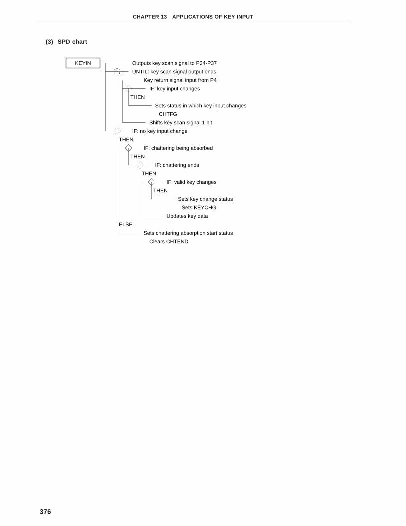
376
CHAPTER 13 APPLICATIONS OF KEY INPUT
(3) SPD chart
KEYIN Outputs key scan signal to P34-P37
THEN
ELSE
UNTIL: key scan signal output ends
Key return signal input from P4
IF: key input changes
Sets status in which key input changes
CHTFG
Shifts key scan signal 1 bit
IF: no key input change
THEN
IF: chattering being absorbed
THEN
IF: chattering ends
THEN
IF: valid key changes
THEN
Sets key change status
Sets KEYCHG
Updates key data
Sets chattering absorption start status
Clears CHTEND

377
CHAPTER 13 APPLICATIONS OF KEY INPUT
(4) Program list
PUBLIC KEYDATA,KEYCHG,KEYIN,CHATCT
KEY_DAT DSEG SADDRKEYDATA:DS 4WORK: DS 4CHATCT: DS 1WORKCT: DS 1
KEY_FLG BSEGCHGFG DBITKEYCHG DBITCHTEND DBIT
KEY_SEG CSEG;******************************** Matrix key input;*******************************KEYIN:
CLR1 CHGFGP3&=#00001111BP3|=#00010000BHL=#WORKrepeat
A=P4A^=#11111111Bif(A!=[HL])
SET1 CHGFG[HL]=A
endifHL++A=P3A&=#11110000BX=AA=P3A+=XP3=A
until_bit(CY)
if_bit(!CHGFG)if_bit(!CHTEND)
CHATCT--if(CHATCT==#0)
SET1 CHTENDDE=#WORKHL=#KEYDATAfor(WORKCT=#0;WORKCT<#4;WORKCT++)
if([DE]!=[HL]) (A)SET1 KEYCHG
endifA<->[HL]HL++DE++
nextendif
endifelse
CHATCT=#3CLR1 CHTEND
endifRET
; Key data storage area; Chattering key data; Chattering counter
; Key change status; Key changed; Chattering absorption end status
; Sets address of key work area
; Data inverted; Key changed?
; Shifts key scan 1 bit
; Key changed; Chattering absorbed; Chattering ends
; Key changed
; Transfers WORK to KEYDATA

[MEMO]
378

APPENDIX A DESCRIPTION OF SPD CHART
SPD stands for Structured Programming Diagrams.
Structuring means structuring the logical processing of a program, and designing and formulating the logic by using
the basic structure of the logic elements.
All programs can be created by only combining the basic structure of logic elements, (sequentially, selectively,
or repeatedly). (This is called a structured theorem). Through structuring, the flow of a program is clarified, and the
reliability is improved. Although various methods are available for expressing the structuring of a program, NEC
employs a diagram technique called SPD.
The following table describes the SPD symbols used for the SPD technique and compares them with flowchart
symbols.
Table A-1. Comparison between SPD Symbols and Flowchart Symbol (1/2)
Processing Name SPD Symbol Flowchart Symbol
Sequential processing
Conditional branch
(IF)
Conditional branch
(SWITCH)
Processing 1
Processing 2
Processing 1
Processing 2
[THEN]
(IF: condition)
Processing 1
Processing 2
[ELSE] Processing 1
Condition
THEN
Processing 2
ELSE
[CASE: 1]
(SWITCH: condition)
Processing 1
Processing 2
[CASE: 2]
Processing n
[CASE: n]
... Processing 2
Condition
Processing nProcessing 1
379

380
APPENDIX A DESCRIPTION OF SPD CHART
Table A-1. Comparison between SPD Symbols and Flowchart Symbol (2/2)
Processing Name SPD Symbol Flowchart Symbol
Conditional loop
(WHILE)
Conditional loop
(UNTIL)
Conditional loop
(FOR)
Infinite loop
Connector
(WHILE: condition)
Processing
Processing
Condition
THEN
ELSE
(UNTIL: condition)
Processing
THEN
ELSE
Processing
Condition
(FOR: initial value; condition;increment/decrement specification)
Processing
Initial value
Condition
Processing
THEN
Increment/decrement
ELSE
(WHILE: forever)
Processing Processing
[THEN]
(IF: condition)
GOTO A
A
Processing
ConditionELSE
THEN
A
Processing
A
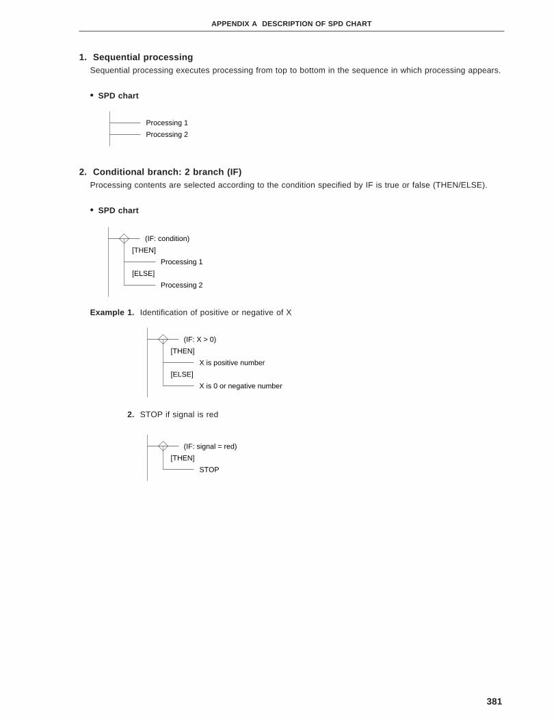
381
APPENDIX A DESCRIPTION OF SPD CHART
1. Sequential processingSequential processing executes processing from top to bottom in the sequence in which processing appears.
• SPD chart
2. Conditional branch: 2 branch (IF)Processing contents are selected according to the condition specified by IF is true or false (THEN/ELSE).
• SPD chart
Example 1. Identification of positive or negative of X
2. STOP if signal is red
Processing 1
Processing 2
(IF: condition)
Processing 1
Processing 2
[THEN]
[ELSE]
(IF: X > 0)
X is positive number
X is 0 or negative number
[THEN]
[ELSE]
(IF: signal = red)
STOP
[THEN]

382
APPENDIX A DESCRIPTION OF SPD CHART
3. Conditional branch: multiple branch (SWITCH)The condition specified by SWITCH is compared with the status indicated by CASE to select the processing. The
processing of the SWITCH statement may be executed only when the given values coincide, or continued downward
starting from when the given values coincide (if the processing is not continued downward, ‘break’ is described). If
there is no coincide status, ‘default’ processing is executed (description of ‘default’ is arbitrary).
(1) Execution only on coincidence
• SPD chart
Example Displays name of month by input characters
(SWITCH: condition)
[CASE: status 1]
Processing 1
break
[CASE: status 2]
Processing 2
break
[CASE: status n]
Processing n
[default]
Processing 0
When status 1: processing 1
When status 2: processing 2
When status n: processing n
If status does not coincide: processing 0
.....
.....
(execution)
......
(SWITCH: input character)
[CASE: '1']
Displays Jan
break
[CASE: '2']
Displays Feb
break
[default]
Displays ERROR
......

383
APPENDIX A DESCRIPTION OF SPD CHART
(2) If processing continues from coincidence status
• SPD chart
Example Transmission/reception of serial interface
4. Conditional Loop (WHILE)The condition indicated by WHILE is judged. If the condition is satisfied, processing is repeatedly executed (if
the condition is not satisfied from the start, the processing is not executed).
• SPD chart
Example Buffers key until RETURN key is input
(SWITCH: condition)
[CASE: Status 1]
Processing 1
[CASE: Status 2]
Processing 2
[CASE: Status n]
Processing n
[default]
Processing 0
......
When status 1: processing 1 → processing 2 → ... → processing n
When status 2: processing 2 → ... → processing n
When status n: processing n
If status does not coincide: processing 0
(execution)
.....
.....
(SWITCH: transfer mode)
[CASE: 1]
Address transmission
[CASE: 2]
[CASE: 3]
Data transmission
break
Data reception
When status 1: address transmission → data transmission
When status 2: data transmission
When status 3: data reception
(execution)
(WHILE: condition)
Processing
(WHILE: not RETURN key)
Inputs 1 character key
Stores input key to buffer

384
APPENDIX A DESCRIPTION OF SPD CHART
5. Conditional Loop (UNTIL)The condition indicated by UNTIL is judged after processing has been executed, and the processing is repeatedly
executed until a given condition is satisfied (even if the condition is not satisfied from the start, the processing is
executed once).
• SPD chart
Example Multiplies value of B register by 10 and stores result to A register
6. Conditional Loop (FOR)While the condition of the parameter indicated by FOR is satisfied, processing is repeatedly executed.
• SPD chart
Example Clears 256 bytes to 0 starting from address HL
(UNTIL: condition)
Processing
Initializes A register
Sets value to B register
Stores 10 to counter
(UNTIL: counter = 0)
A = A + B
Decrements counter
(FOR: initial value; condition; increment/decrement specification)
Processing
Sets first address to HL register
(FOR: WORKCT = #0; WORKCT < #256; WORKCT + +)
Clears address HL to 0
Increments HL register

385
APPENDIX A DESCRIPTION OF SPD CHART
7. Infinite LoopIf ‘forever’ is set as the condition of WHILE, processing is infinitely executed.
• SPD chart
Example To execute main processing repeatedly
8. Connector (GOTO)Unconditionally branches to a specified address.
• SPD chart
(1) To branch to same module
(WHILE: forever)
Processing
(WHILE: forever)
Decodes key
Stores key code to display areaMain processing
ERR
(IF: condition)
[THEN]
GOTO ERR
Processing
...

386
APPENDIX A DESCRIPTION OF SPD CHART
(2) To branch to different module
Example To select a parameter at the start address of a subroutine and set wait state
9. Connector (continuation)Used when the SPD of one module requires two or more pages to indicate the flow of processing.
• SPD chart
(IF: condition)
[THEN]
SUB_ER Processing
GOTO ERR
(SUB_ER) ; Module name
ERR
Processing
...
WAIT10 Sets 10 to A register
GOTO WAIT
WAIT20 Sets 20 to A register
GOTO WAIT
WAIT30 Sets 30 to A register
WAIT
(UNTIL: A = 0)
Decrements A
1
Processing 1
Processing 2
1
Processing 3
Processing 4

APPENDIX B REVISION HISTORY
The revision history of this document is as follows. “Chapter” indicates the chapter number in the preceding edition.
(1/2)
Edition Major Revision from Preceding Edition Chapter
Throughout2nd edition
CHAPTER 4 APPLICATION OF
WATCHDOG TIMER
CHAPTER 5 APPLICATION OF
16-BIT TIMER/EVENT COUNTER
CHAPTER 8 APPLICATION OF
SERIAL INTERFACE
Addition of following products as target products:
µPD780018, 780018Y, 780058, 780058Y, 780308, 780308Y,
78058F, 78058FY, 78064B, 78075B, 78075BY, 78098B
subseries, µPD78070A, 78070AY
µPD78052(A), 78053(A), 78054(A)
µPD78062(A), 78063(A), 78064(A)
µPD78081(A), 78082(A), 78P083(A), 78081(A2)
µPD78058F(A), 78058FY(A)
µPD78064B(A)
Deletion of following products as target products:
µPD78P054Y, 78P064Y, 78074, 78075, 78074Y, 78075Y
Addition of Note 2 and Caution 2 to Figure 4-5 Format of
Watchdog Timer Mode Register
Addition of Caution to Figure 5-8 Format of External Interrupt
Mode Register 0
Addition of Table 8-2 Items Supported by Each Subseries
Addition of Table 8-3 Registers of Serial Interface
Addition of note on using wake-up function and note on
changing operation mode to Figures 8-7 and 8-8 Format of
Serial Operating Mode Register 0
Addition of Caution to Figures 8-16 and 8-17 Format of
Automatic Data Transmission/Reception Interval Specification
Register
Addition of Figures 8-23 and 8-24 Format of Serial Interface Pin
Select Register
µPD6252 as maintenance product in 8.1 Interface with
EEPROMTM (µPD6252)
Addition of (5) Limitations when using I2C bus mode to 8.1.2
Communication in I2C bus mode
Addition of (f) Limitations when using UART mode to 8.5
Interface in Asynchronous Serial Interface (UART) Mode
387

388
APPENDIX B REVISION HISTORY
CHAPTER 8 APPLICATION OF
SERIAL INTERFACE
2nd edition
CHAPTER 11 APPLICATION OF
REAL-TIME OUTPUT PORT
CHAPTER 12 APPLICATION OF
LCD CONTROLLER/DRIVER
Description of following register formats and tables for each
subseries:
Figures 8-14 and 8-15 Format of Automatic Data Transfer/
Reception Control Register
Tables 8-4, 8-5, and 8-6 Setting of Operating Modes of Serial
Interface Channel 2
Figures 12-1 and 12-2 Format of LCD Display Mode Register
Addition of Figure 11-3 Format of Port Mode Register 12
Description of following register formats for each subseries:
Figures 12-1 and 12-2 Format of LCD Display Mode Register
Edition Major Revision from Preceding Edition Chapter
(2/2)
Although NEC has taken all possible stepsto ensure that the documentation suppliedto our customers is complete, bug freeand up-to-date, we readily accept thaterrors may occur. Despite all the care andprecautions we've taken, you mayencounter problems in the documentation.Please complete this form wheneveryou'd like to report errors or suggestimprovements to us.
Hong Kong, Philippines, OceaniaNEC Electronics Hong Kong Ltd.Fax: +852-2886-9022/9044
KoreaNEC Electronics Hong Kong Ltd.Seoul BranchFax: 02-528-4411
TaiwanNEC Electronics Taiwan Ltd.Fax: 02-719-5951
Address
North AmericaNEC Electronics Inc.Corporate Communications Dept.Fax: 1-800-729-9288
1-408-588-6130
EuropeNEC Electronics (Europe) GmbHTechnical Documentation Dept.Fax: +49-211-6503-274
South AmericaNEC do Brasil S.A.Fax: +55-11-889-1689
Asian Nations except PhilippinesNEC Electronics Singapore Pte. Ltd.Fax: +65-250-3583
JapanNEC CorporationSemiconductor Solution Engineering DivisionTechnical Information Support Dept.Fax: 044-548-7900
I would like to report the following error/make the following suggestion:
Document title:
Document number: Page number:
Thank you for your kind support.
If possible, please fax the referenced page or drawing.
Excellent Good Acceptable PoorDocument Rating
Clarity
Technical Accuracy
Organization
CS 96.8
Name
Company
From:
Tel. FAX
Facsimile Message