(75) inventors. Epbelli's). 3.23. A : to Sanabem, 52.
128
USOO7045833B2 (12) United States Patent (10) Patent No.: US 7,045,833 B2 Campbell et al. (45) Date of Patent: May 16, 2006 (54) AVALANCHE PHOTODIODES WITH AN 4,839,706 A 6/1989 Brennan ...................... 257/21 IMPACTIONIZATION-ENGINEERED 4,982.255. A 1/1991 Tomita MULTIPLICATION REGION 5,187,553 A * 2/1993 Makita ....................... 257/187 5,204,539 A * 4/1993 Tsuji et al. ................... 257/21 ck (75) inventors. Epbelli's). 3.23. A : to Sanabem, 52. ing Yuan, Piscataway, NJ (US) 5,369,292 A 11/1994 Yoo et al. ck (73) Assignee: Board of Regents, The University of : A : RE: im EIS Texas System, Austin, TX (US) 5,539.221 A 7/1996 Tsuji et al. 5,543,629 A 8/1996 Nakamura et al. ............ 257/21 (*) Notice: Subject to any disclaimer, the term of this 5,744,849 A * 4/1998 Sugawa ...................... 257/438 patent is extended or adjusted under 35 5,847.418. A 12/1998 Nakamura et al. U.S.C. 154(b) by 457 days. 6,326,650 B1 12/2001 Allam ........................ 257, 186 (21) Appl. No.: 09/969,133 OTHER PUBLICATIONS International Search Report, PCT/US01/30775, mailed Jul (22) Filed: Oct. 1, 2001 18, 2002. O O R.J. McIntyre, “A New Look at Impact Ionization-Part I: A (65) Prior Publication Data Theory of Gain, Noise, Breakdown Probability, and Fre US 2003 FOO47752 A1 Mar. 13, 2003 quency Response.” IEEE Trans. On Electron Dev., vol. 46, No. 8, pp. 1623-1631, 1999. Related U.S. Application Data (60) Provisional application No. 60/236,952, filed on Sep. (Continued) 29, 2000. Primary Examiner Nathan J. Flynn (51) Int. Cl. Assistant Examiner Fazli Erdem HOIL 2L/00 (2006.01) (74) Attorney, Agent, or Firm Meyertons, Hood, Kivlin, (52) U.S. Cl. ...................... 257/186: 257/187; 257/188: Kowert & Goetzel, P.C.; Eric B. Meyertons 257/185; 257/430; 257/431; 257/432; 257/429; 438/48; 438/50: 438/63; 438/65 (58) Field of Classification Search ................ 257/186, (57) ABSTRACT 257/187, 185, 184,438,53–55, 191, 18, 257/22, 21; 438/48, 50, 63,65; 25, 2. An avalanche photodiode including a multiplication layer is See application file for complete search history. provided. The multiplication layer may include a well region and a barrier region. The well region may include a material (56) References Cited having a higher carrier ionization probability than a material U.S. PATENT DOCUMENTS 4,731,641 A 3, 1988 Matsushima et al. used to form the barrier region. 81 Claims, 82 Drawing Sheets
-
Upload
khangminh22 -
Category
Documents
-
view
3 -
download
0
Transcript of (75) inventors. Epbelli's). 3.23. A : to Sanabem, 52.

USOO7045833B2
(12) United States Patent (10) Patent No.: US 7,045,833 B2 Campbell et al. (45) Date of Patent: May 16, 2006
(54) AVALANCHE PHOTODIODES WITH AN 4,839,706 A 6/1989 Brennan ...................... 257/21 IMPACTIONIZATION-ENGINEERED 4,982.255. A 1/1991 Tomita MULTIPLICATION REGION 5,187,553 A * 2/1993 Makita ....................... 257/187
5,204,539 A * 4/1993 Tsuji et al. ................... 257/21 ck
(75) inventors. Epbelli's). 3.23. A : to Sanabem, 52. ing Yuan, Piscataway, NJ (US) 5,369,292 A 11/1994 Yoo et al.
ck
(73) Assignee: Board of Regents, The University of : A : RE: im EIS Texas System, Austin, TX (US) 5,539.221 A 7/1996 Tsuji et al.
5,543,629 A 8/1996 Nakamura et al. ............ 257/21 (*) Notice: Subject to any disclaimer, the term of this 5,744,849 A * 4/1998 Sugawa ...................... 257/438
patent is extended or adjusted under 35 5,847.418. A 12/1998 Nakamura et al. U.S.C. 154(b) by 457 days. 6,326,650 B1 12/2001 Allam ........................ 257, 186
(21) Appl. No.: 09/969,133 OTHER PUBLICATIONS International Search Report, PCT/US01/30775, mailed Jul
(22) Filed: Oct. 1, 2001 18, 2002. O O R.J. McIntyre, “A New Look at Impact Ionization-Part I: A
(65) Prior Publication Data Theory of Gain, Noise, Breakdown Probability, and Fre US 2003 FOO47752 A1 Mar. 13, 2003 quency Response.” IEEE Trans. On Electron Dev., vol. 46,
No. 8, pp. 1623-1631, 1999. Related U.S. Application Data
(60) Provisional application No. 60/236,952, filed on Sep. (Continued) 29, 2000.
Primary Examiner Nathan J. Flynn (51) Int. Cl. Assistant Examiner Fazli Erdem
HOIL 2L/00 (2006.01) (74) Attorney, Agent, or Firm Meyertons, Hood, Kivlin, (52) U.S. Cl. ...................... 257/186: 257/187; 257/188: Kowert & Goetzel, P.C.; Eric B. Meyertons
257/185; 257/430; 257/431; 257/432; 257/429; 438/48; 438/50: 438/63; 438/65
(58) Field of Classification Search ................ 257/186, (57) ABSTRACT 257/187, 185, 184,438,53–55, 191, 18,
257/22, 21; 438/48, 50, 63,65; 25, 2. An avalanche photodiode including a multiplication layer is See application file for complete search history. provided. The multiplication layer may include a well region
and a barrier region. The well region may include a material (56) References Cited having a higher carrier ionization probability than a material
U.S. PATENT DOCUMENTS
4,731,641 A 3, 1988 Matsushima et al.
used to form the barrier region.
81 Claims, 82 Drawing Sheets

US 7,045,833 B2 Page 2
OTHER PUBLICATIONS
Yuan et al., “A New Look at Impact Ionization-Part II: Gain and Noise in Short Avalanche Photodiodes.” IEEE Trans. On Electron Dev., vol. 46, No. 8, pp. 1632-1639, 1999. Yuan et al., “Impact Ionization Characteristics of III-V Semiconductors for a Wide Range of Multiplication Region Thicknesses.” IEEE Journal of Ouantum Electronics, vol. 36, No. 2, pp. 198-204, 2000. Wang et al., “Avalanche photodiodes with an Impact-Ion ization-Engineered multiplication region, 2000 IEEE Annual Meeting Conference Proceedings, 13" Annual Meeting, Rio Grande, Puerto Rico, 13-1 pp. 9-10 vol. 1, XP002204728, 2000. Campbell et al., “High-Speed, Low-Noise Avalanche Photodiodes. Optical Fiber Communication Conference. Technical Digest Postconference Edition. Trends in Optics and PH, pp. 114-116 vol. 4, XP002204729, 2000. Arndt et al., “Comparison measurements for selection of suitable photodetectors for use in Nd:YAG LDA systems.” Exp. In Fluids, vol. 20, pp. 460-465, 1996. Hayden et al., “Overview of laser communication technol ogy at NASA Goddard space flight center, in Proc. SPIE. vol. 1866, pp. 45-55, 1993. J.B. Johnson, “Thermal Agitation of Electricity in Conduc tors”, Phys. Rev., vol. 32, pp. 97-109, 1928. H. Nyquist, “Thermal Agitation of Electric Charge in Con ductors”, Phys. Rev., vol. 32, pp. 110-113, 1928. Bowers et al., “High-speed Photodetectors.” Handbook of Optics, vol. 1, McGraw-Hill, New York, 1995. Wey et al., “108 GHz. GainAS/InP p-I-n Photodiodes with Integrated Bias Tees and Matched Resistors.” IEEE Photon. Tech. Lett., vol. 5, No. 11, pp. 1310-1312, 1993. Chou et al., “Nanoscale tera-hertz metal-semiconductor metal photodetectors.” IEEE J. Ouantum Electron. Vol. 28, No. 10, pp. 2358-2368, 1992. Emeis et al., “High-Speed GainAs Schottky Photodetector.” Electron. Lett., vol. 21, No. 5, pp. 181-180, 1985. S. Forrest, “Sensitivity of Avalanche Photodetector Receiv ers for High-Bit-Rate Long-Wavelength Optical Communi cation Systems.” Semiconductors and Semimetals, vol. 22, Lightwave Communications Technology, Orlando, FL, Aca demic, pp. 329-387, 1985. R.J. McIntyre, “Multiplication noise in uniform avalanche diodes.” IEEE Trans. On Electron Dev. Vol. 13, No. 1, pp. 164-168, 1966. Chin et al., “ Multilayer Reflectors by Molecular Beam Epitaxy for Resonance Enhanced Absorption in Thin High Speed Detectors. J. Vac. Sci. and Tech., vol. 8, No. 2, pp. 339-342, 1990. Kishino et al., “Resonant Cavity Enhanced (RCE) Photodetectors.” IEEE.J. Quantum Electron., vol. 27, No. 8, pp. 2025-2034, 1991. Corzine et al., “Design of Fabry-Perot surface-emitting lasers with a periodic gain structure.” IEEE J. Quantum Electron., vol. 25, No. 6, pp. 1513-1524, 1989. Dentai et al., “High-quantum efficiency, long-wavelength, InP/InGaAs microcavity photodiode.” Electron. Lett., vol. 27, No. 23, pp. 2125-2127, 1991. Barron et al., “Resonant-Cavity enhanced p-i-n photodetec tor with 17 GHz bandwidth-efficiency product.” Electron. Lett., vol. 30, pp. 1796-1797, 1994. Forrest et al., “Evidence for tunneling in reverse-biased III-V photodetector diodes. Appl. Phys. Lett., vol. 36, pp. 580-582, 1980.
Forrest et al., “Inos GaozAS photodiodes with dark current limited by generation-recombination and tunneling. Appl. Phys. Lett., vol. 37, pp. 322-324, 1980. Nishida et al., “InGaAsP Heterostructure Avalanche Photodiodes with High Avalanche Gain. Appl. Phys. Lett. vol. 35, No. 3, pp. 251-252, 1979. Tarof et al., “Planar InP/InGaAs Avalanche Photodetectors with Partial Charge Sheet in Device Periphery.' Appl. Phys. Lett., vol. 57, No. 7, pp. 670-672, 1990. Tarof et al., “High-Frequency Performance of Separate Absorption Grading, Charge, and Multiplication InP/ InGaAs Avalanche Photodiodes.” IEEE Photon. Tech. Lett., vol. 5, No. 6, pp. 672-674, 1993. N.R. Howard, “Avalanche Multiplication in Silicon Junctions'.J. Electron. Contr., vol. 13, pp. 537-544, 1962. Lee et al., “Ionization Rates of Holes and Electrons in Silicon, Phys. Rev., vol. 134, pp. A761-773, 1964. R.J. McIntyre, “The distribution of gains in uniformly multiplying avalanche photodiodes: Theory.” IEEE Trans. on Electron Dev., vol. ED-19, pp. 703-713, 1972. R.B. Emmons, “Avalanche-Photodiode Frequency Response,” J. Appl. Phys., vol. 38, No. 9, pp. 3705-3714, 1967. Emmons et al., “The Frequency Response of Avalanching Photodiodes, IEEE Trans. On Electron Dev., vol. 13, No. 3, pp. 297-305, 1966. W.T. Read, Jr., “A Proposed High-Frequency, Negative Resistance Diode'. Bell System Tech. J., vol. 37, pp. 401 446, 1958. Stillman et al., “Avalanche Photodiodes,' Semiconductors and Semimetals, vol. 12, Infrared Detectors, New York, Academic, pp. 291-393, 1977. Bulman et al., “Experimental determination of impact ion ization coefficients in (100) GaAs, IEEE Electron Dev. Lett., vol. 4, No. 6, pp. 181-185, 1983. Bulman et al., “The Determination of Impact Ionization Coefficients in (100) Gallium Arsenide Using Avalanche Noise and Photocurrent Multiplication Measurements.” IEEE Trans. Electron Dev., vol. 32, No. 11, pp. 2454-2466, 1985. Bulman et al., “Determination of impact ionization coeffi cients in InP by analysis of photomultiplication and noise measurements.” International Electron Devices Meeting 1981, pp. 288-291, 1981. Robbins et al., “Impact ionization in AlGaAs for x=0.1- 0.4.” Appl. Phys. Lett., vol. 52, No. 4, pp. 2996-2998, 1988. Watanabe et al., “Impact ionization rates in (100) Alosino. 52AS. IEEE Electron Dev. Lett., vol. 11, No. 10, pp. 437-438, 1990. Armiento et al., “Impact ionization in (100)-, (110)-, (111)- oriented InPavalanche photodiodes. Appl. Phys. Lett., vol. 43, No. 2, pp. 198-200, 1983. Cook et al., “ Electron and hole impact ionization coeffi cients in InP determined by photomultiplication measure ments.” Appl. Phys. Lett., vol. 40, No. 7, pp. 589-591, 1982. Osaka et al., “Impact ionization coefficients of electrons and holes in (100)-oriented Gai-In, ASP.” IEEE.J. Quantum Electron., vol. 21, No. 9, pp. 1326-1338, 1985. Taguchi et al., “Temperature dependence of impact ioniza tion coefficients in InP, J. Appl. Phys. Vol. 59, No. 2, pp. 476-481, 1986. Wu et al., “Design of Silicon Hetero-Interface Photodetec tors.” IEEE J. Lightwave Technol., vol. 15, No. 8, pp. 1608-1615, 1997.

US 7,045,833 B2 Page 3
Jhee et al., “ The effect of nonuniform gain on the multi plication noise of InP/InGaAsP/InGaAs avalanche photodiodes.” IEEE J. Ouantum Electron. Vol. 21, No. 12, pp. 1858-1861, Dec. 1985. Campbell et al., “Multiplication noise of wide-bandwidth InP/InGaAsP/InGaAs avalanche photodiodes.' J. Lightwave Technol., vol. 7, No. 3, pp. 473–477, 1989. Hu et al., “Noise characteristics of thin multiplication region GaAs avalanche photodiodes. Appl. Phys. Lett., vol. 69, No. 24, pp. 3734-3736, 1996. Anselm et al., “Performance of Thin Separate Absorption, Charge, and Multiplication Avalanche Photodiodes.” IEEE J. Ouantum Electron... vol. 34, No. 3, pp. 482-490, 1998. Li et al., “Avalanche multiplication noise characteristics in thin GaAs p" -i-n"diodes.” IEEE Trans. Electron Dev., vol. 45, No. 10, pp. 2102-2107, 1998. Campbell et al., “High-Speed InP/InGaAsP/InGaAs Ava lanche Photodiodes Grown by Chemical Beam Epitaxy.' IEEE J. Ouantum Electron. Vol. 24, No. 3, pp. 496-500, 1988. Campbell et al., “Frequency Response of InP/InGaAsP/ InGaAs Avalanche Photodiodes.” IEEE J. Lightwave Technol., vol. 7, No. 5, pp. 778-784, 1989. Ekholm et al., “High Bandwidth Planar InP/InGaAs Ava lanche Photodiodes, IEEE Trans. On Electron Dev, Vol. 35, No. 12, pp. 2434, 1988. Kagawa et al., “A Wide-Bandwidth Low-Noise InGaAsP InA1As Superlattice Avalanche Photodiode with a Flip-Chip Structure for Wavelengths of 1.3 and 1.55 um.” IEEE J. Ouantum Electron., vol. 29, No. 5, pp. 1387-1392, 1988. Watanabe et al., “Gain-Bandwidth Product Analysis of InAlGaAs-InAlAs Superlattice Avalanche Photodiodes.” IEEE Photon. Tech. Lett., vol. 8, No. 2, pp. 269-271, 1996. Watanabe et al., “High-Speed and Low-Dark-Current Flip Chip InalAS/InAlGaAs Quaternary Well Superlattice APD's with 120 GHz. Gain-Bandwidth product.” IEEE Photon. Tech. Lett., vol. 5, No. 6, pp. 675-677, 1993. Watanabe et al., “Design and Performance of InAlGaAs/ InAlAs Superlattice Avalanche Photodiodes.” IEEE J. Lightwave Technol., vol. 15, No. 6, pp. 1012-1019, 1997. Nie et al., “High-Speed Resonant-Cavity Separate Absorp tion and Multiplication Avalanche Photodiodes with 130 GHz. Gain-Bandwidth Product, Appl. Phys. Lett., vol. 70. No. 2, pp. 161-163, 1997. Anselm et al., “A Resonant-Cavity, Separate-Absorption and-Multiplication, Avalanche Photodiode with Low Excess Noise Factor.” IEEE Electron Dev. Lett., vol. 17, No. 3, pp. 91-93, 1996. Li et al., "Low Excess Noise Characteristics in Thin Ava lanche Region GaAs Diodes.” Electron. Lett., vol. 34, No. 1, pp. 125, 1997. van Vliet et al., “Theory of carrier multiplication and noise in avalanche devices—Part II: Two-carrier processes.” IEEE Trans. Electron Dev., vol. ED-26, pp. 752-764, 1979. J. S. Marsland, “On the effect of ionization dead spaces on avalanche multiplication and noise for uniform electric field,” J. Appl. Phys., vol. 67, pp. 1929-1933, 1990. Marsland et al., “Lucky drift estimation of excess noise factor for conventional avalanche photodiodes including the dead space effect.” IEEE Trans. Electron Dev., vol.39, pp. 1129-1134, 1992. Okuto et al., “Ionization coefficients in semiconductors: A nonlocal property,’” Phys. Rev. B. vol. 10, pp. 4284-4296, 1974.
Shichijo et al., “Band-structure-dependent transport and impact ionization in GaAs.” Phys. Rev. B. vol. 23, pp. 41.97-4207, 1981. K. F. Brennan, “Calculated electron and hole spatial ioniza tion profiles in bulk GaAs and superlattice avalanche photodiodes.” IEEE Quantum Electron. Vol. 24, pp. 2001 2006, 1988. Sano et al., “Impact-ionization theory consistent with a realistic band structure of silicon.” Phys. Rev. B. vol. 45, pp. 4171-4180, 1992. Bude et al., “Thresholds of impact ionization in semicon ductors,” J. Appl. Phys., vol. 72, pp. 3554-3561, 1992. Chandramouliet al., “Monte Carlo analysis of bandstructure influence on impact ionization in semiconductors.” Solid State Electron., vol. 36, pp. 285-290, 1993. Kamakura et al., “Impact ionization model for full band Monte Carlo simulation.” J. Appl. Phys., vol. 75, pp. 3500 3506, 1994. Dunn et al., “Monte Carlo simulation of impact ionization and current multiplication in short GaAspin diodes.” Semicond Sci. Technol., vol. 12, pp. 111-120, 1997. Ong et al., “A simple model to determine multiplication and noise in avalanche photodiodes.' J. Appl. Phys. Vol. 83, pp. 3426-3428, 1998. Spinelli et al., “Dead space approximation for impact ion ization in silicon. Appl. Phys. Lett., vol. 68, pp. 3707-3709, 1996. Spinelli et al., “Mean gain of avalanche photodiodes in a dead space model.” IEEE Trans. Electron Dev., vol. 43, pp. 23-30, 1996. Aspines et al., “Optical properties of AlGaAs.J. of Appl. Phys., vol. 60, No. 2, pp. 754-767, Jul. 1986. Garriga et al., “Optical properties of AlAs.” Solid State Comm., vol. 61, No. 3, pp. 157-160, 1987. Aspines et al., “Dielectric functions and optical parameters of Si, Ge. GaP. GaAs, GaSb, InP, InAs, and InSb from 1.5 to 6.0 eV.” Phys. Rev. B. vol. 27, No. 2, pp. 985-1009, Jan. 1983. R. Williams, “Ohmic Contacts.” Gallium Arsenide Process ing Techniques, Ch. 11, pp. 225-257, Artech, House, 1990. G.A. Samara, "Temperature and pressure dependences of the dielectric constants of semiconductors.” Phys. Rev. B. vol. 27, No. 6, pp. 3494-3505, 1983. Fern et al., “Refractive index of AlAs. J. Appl. Phys., vol. 42, No. 9, pp. 3499-3500, 1971. K. Seeger, “Temperature dependence of the dielectric con stants of semi-insulating III-V compounds. Appl. Phys. Lett., vol. 54, No. 13, pp. 1268-1269, 1989. Gonzalez et al., “Universality of the 1/3 Shot-Noise Sup pression Factor in Nondegenerate Diffusive Conductors.” Phys. Rev. Lett., vol. 80, No. 13, pp. 2901-2904, 1998. Reklaitis et al., “Monte Carlo Study of Shot Noise Suppres sion.” J. Appl. Phys., vol. 82, No. 6, pp. 3161-3163, 1997. Starikov et al., “ Transfer Impedance Calculations of Elec tronic Noise in Two-Terminal Semiconductor Structures.J. Appl. Phys., vol. 83, No. 4, pp. 2052-2066, 1998. Kagawa et al., “InGaAsP-InAlAs Superlattice Avalanche Photodiode.” IEEE Journal of Ouantum Electronic, vol. 28, No. 6, p. 1420, Jun. 1, 1992. Hanatani et al., “Flip-Chip InAlAS/InGaAs Superlattice Avalanche Photodiodes with Back-Illuminated Structures,” Microwave and Optical Technology Letters, vol. 7, No. 3, pp. 103-107, Feb. 20, 1994. Yuan et al., “High-Speed and Low-Noise Avalanche Photodiode Operating at 1.06 um.” IEEE Journal of Selected

US 7,045,833 B2 Page 4
Topics in Ouantum Electronics, vol. 6, No. 3, pp. 422-425, May/Jun. 2000. Yuan et al., “High-Speed Quantum-Dot Resonant-Cavity SACM Avalanche Photodiodes Operating at 1.06 um.” IEEE/LEOS Summer Topical Meeting, San Diego, Califor nia, Jul. 1999. Yuan et al., High-Speed Quantum-Dot Resonant-Cavity SACM Avalanche Photodiodes Operating at 1.06 um, 57" Device Research Conference, Santa Barbara, California, Jun., 1999. Nie et al., “High Speed and High Gain-Bandwidth-Product Resonant-Cavity InGaAs/InAlAs Avalanche Photodiodes for Optical Fiber Communications.” OFC 99, San Diego, California, Feb., 1999. Hayat et al., “Effect of dead space on gain and noise of double-carrier-multiplication avalanche photodiodes.” IEEE Trans. Electron Dev., vol.39, pp. 546-552, 1992. Hayat et al., “Effect of dead space on gain and noise in Si and GaAs avalanche photodiodes.” IEEE.J. Quantum Elec tron, vol. 28, pp. 1360-1365, 1992. Lenox et al., “Resonant-Cavity InGaAs/InAlAs Avalanche Photodiodes with Gain-Bandwidth-Product of 290 GHZ, IEEE Photonics Technology Letters, vol. 11, No. 9, pp. 1162-1164, Sep. 1999. S.D. Personik, “Receiver Design for Digital Fiber-Optic Communication Systems, Part I and II. Bell Syst. Tech.J., vol. 52, pp. 843-886, 1973.
Kasper et al., “Multigigabit-per-Second Avalanche Photodiode Lightwave Receivers,” J. Lightwave Tech., vol. 5, No. 10, pp. 1351-1364, 1987. Campbell et al., “Quantum dot resonant cavity photodiode with operation near 1.3 mm wavelength. Electron. Lett. vol. 33, pp. 1337-1339, 1997. Nie et al., “Quantum-Dot Resonant-Cavity Separate Absorp tion, Charge, and Multiplication Avalanche Photodiode Operating at 1.06 um.” IEEE Photonics Tech. Lett., vol. 10, No. 7, pp. 1009-1011, 1998. Campbell et al., “Resonant-Cavity Separate Absorption and Multiplication Avalanche Photodiodes with High Speed and High Gain-Bandwidth Product.” Ph.D. dissertation, Univer sity of Texas at Austin, 1998. Baklenov et al., “Multi-stacked quantum dot resonant-cavity photodetector operating at 1.06 um.” Electronics Letters, vol. 34, No. 7, pp. 694-695, Apr. 1998. Hildebrand et al., “GaAl,Sb avalanche photodiodes: reso nant impact ionization with very high ratio of ionization coefficients.” IEEE.J. Quantum Electron. Vol. 17, No. 2, pp. 284-288, 1981. Hildebrand et al., “Resonant enhancement of impact in GaAl Sb.” Appl. Phys. Lett., vol. 37, No. 9, pp. 801-803, 1980.
* cited by examiner

U.S. Patent May 16, 2006 Sheet 1 of 82 US 7,045,833 B2
4 22
10 () 8 12 2O 16
Fig. 1

U.S. Patent May 16, 2006 Sheet 2 of 82 US 7,045,833 B2
36.
Fig. 2

U.S. Patent May 16, 2006 Sheet 3 of 82 US 7,045,833 B2
1.0
0.6
O.4
No cavity R=0.3 R=0
------. . . . . . . . . . . Absorption (old)
Fig. 3

U.S. Patent May 16, 2006 Sheet 4 of 82 US 7,045,833 B2
0.0.1. 68O O .4
0.001 0.01 0.1
Normalized Absorption coefficient, Old
Fig. 4

U.S. Patent May 16, 2006 Sheet 5 of 82 US 7,045,833 B2
122 5O5 10
0.3 0.4 0.5 0.6 0.7 0.8 0.9 1
Top Reflectivity
Fig. 5


U.S. Patent May 16, 2006 Sheet 7 of 82 US 7,045,833 B2
44
46
N-ty -Ses
Electric field
pe
NSN
Fig. 7
U.S. Patent May 16, 2006 Sheet 8 of 82 US 7,045,833 B2

U.S. Patent May 16, 2006 Sheet 9 of 82 US 7,045,833 B2
e injection h injection
k=20 k=0.05
1000 k=1 O k=0.1 K-5 k=0.2
k=2 k=0.5
100 k=1 k=1
S k=0.5 k=2 L k=0.2 k=5
k:0.1 kir-10 O k=0.05 k=20
k=0.0 k=infinity A6 1 O 100
Multiplication (M)
Fig. 9

U.S. Patent May 16, 2006 Sheet 10 of 82 US 7,045,833 B2
100
10
10-2
0.01 0.1 O
Normalized Frequency (cot)
Fig. 10

U.S. Patent May 16, 2006 Sheet 11 of 82 US 7,045,833 B2
k=2x10 k=10 k-0
1 O O
10
1 O 2
1 10 100 1000
Multiplication (M)

U.S. Patent May 16, 2006 Sheet 12 of 82 US 7,045,833 B2
EM n" region n region
Fig. 12

U.S. Patent May 16, 2006 Sheet 13 of 82 US 7,045,833 B2
nAAs C. o inAIAs B
-v-- inp o. -v- inp B - - lnP o. -0- inp B -- Sio. -0- Si B
1.0 2.0 3.0 4.0 5.0 6.0
1/E (10 cm/V)
Fig. 13

U.S. Patent May 16, 2006 Sheet 14 of 82 US 7,045,833 B2
105
la
t E 10 s
N/
c
s n -- AlGaAs O.
O3 -v- AlGaAs B 10 -- AlGaAS O.
-- AlGaAs B -- AlGaAs O. -0- AlGaAs B al-A- AlGaAs O
10° E -- AlGaAs B
1.0 1.5 2.O 2.5 3.0 3.5 4.0 4.5 5.0
1/E (10 cm/V)
Fig. 14

US 7,045,833 B2 Sheet 15 of 82 May 16, 2006 U.S. Patent
Depth (um)
Incident Photon · · · · · · · · · * ·
º nº GaAs subs
.*~~ ~~2 × × × ×
Electric Field (10” V/cm) trate : : ~~~~
Fig. 15


U.S. Patent
&
:::::: :: 8-XX & :
V 3: s:: E. E.
May 16, 2006 Sheet 17 of 82
X-838. &E: 3:08:3:
US 7,045,833 B2
Fig. 17

U.S. Patent May 16, 2006 Sheet 18 of 82 US 7,045,833 B2
* 3: ... . : ". . . . . w
. . . . ; . . . . . . .'; ... . . . . . . - . . . . . . . . . . .
& wax. ...&xx: X x-xx-xs as:
: E: :::::::::::
:::::::: xxxx is:
Fig. 18


U.S. Patent May 16, 2006 Sheet 20 of 82 US 7,045,833 B2

U.S. Patent May 16, 2006 Sheet 21 of 82 US 7,045,833 B2
Fig. 21

U.S. Patent May 16, 2006 Sheet 22 of 82 US 7,045,833 B2
O By Method v By Method II - Fit With k=0.48
Gain
Fig. 22

U.S. Patent May 16, 2006 Sheet 23 of 82 US 7,045,833 B2
1OOuF
AC Signal
Fig. 23

U.S. Patent May 16, 2006 Sheet 24 of 82 US 7,045,833 B2
83 mm 1.74mm. 629mm 714-nm 1441 nm
O 10 2O 30 40 50
Voltage (V)
Fig. 24

U.S. Patent May 16, 2006 Sheet 25 of 82 US 7,045,833 B2
83nm 174nm 629nm 74nn 1441 nm, 100
Voltage (V)
Fig. 25

U.S. Patent May 16, 2006 Sheet 26 of 82 US 7,045,833 B2
25
20
5
10
4 6 8 10 12 14 16 18 20 22
Area (10 um)

U.S. Patent May 16, 2006 Sheet 27 of 82 US 7,045,833 B2
83, 174,629,714, 1441 nm
S. L
S. O (vs.
()
O Z
8 WS 83 nm. 3 W.174 nm. i W629 nm.
We/14 nm WS-1441 nm.
5 10 15 20 25 30 Gain
Fig. 27

U.S. Patent May 16, 2006 Sheet 28 of 82 US 7,045,833 B2
56 4.
3
2 O 200 400 600 800 1000 1200 1400 1600 1800
Multiplication Region Thickness (nm)
Fig. 28

U.S. Patent May 16, 2006 Sheet 29 Of 82 US 7,045,833 B2
93rm 194n 362nn 739nnn 1408m 10-5
11 OO 76 10-8
10-9
10-10
f 0-11 W s
O 10 2O 30 40 50 60
Voltage (V)
Fig. 29

U.S. Patent May 16, 2006 Sheet 30 of 82 US 7,045,833 B2
739nm 1408m 93nm 194nn 362nn w OO
w
10
W
60
Voltage (V)
Fig. 30

U.S. Patent May 16, 2006 Sheet 31 of 82 US 7,045,833 B2
93, 194, 362,739, 1408 nm
12 W93 nm W194 nm W362 mm
10 W739 mm
8
5 L
6
4
2
5 10 15 20 Gain
Fig. 31

U.S. Patent May 16, 2006 Sheet 32 of 82 US 7,045,833 B2
100
10
Reverse Bias (V)
Fig. 32

U.S. Patent May 16, 2006 Sheet 33 of 82 US 7,045,833 B2
Fig. 33

U.S. Patent May 16, 2006 Sheet 34 of 82 US 7,045,833 B2
1
2.0 2.2 2.4 2.6 2.8 3.0 3.2 3.4 3.6 3.8 4.0
11E (10 cm/V)
Fig. 34

U.S. Patent May 16, 2006 Sheet 35 of 82 US 7,045,833 B2
60%-27mm
107
10 E2
10
90%-140nm O -1 O
10" . . . . . . . . . . . . . . . 60%-158mm
10-12 .. O 2 4. 6 8 10 12 14 16
Reverse Bias (V)
Fig. 35

U.S. Patent May 16, 2006 Sheet 36 of 82 US 7,045,833 B2
60%-217nm 60%-158mm 80%-100nm 90%-140nm 90%-140nm, Corrected
Gain
Fig. 36

U.S. Patent May 16, 2006 Sheet 37 of 82 US 7,045,833 B2
190nm 566nm 799nm 1596nm 100
10
O 10 20 30 40 50 60 70 80
Voltage (V)
Fig. 37

U.S. Patent May 16, 2006 Sheet 38 of 82 US 7,045,833 B2
We 190 in W363 in Watss6 yr. WS9 in We 596 r
Gain
Fig. 38

U.S. Patent May 16, 2006 Sheet 39 Of 82 US 7,045,833 B2
281m 37 nm. 582n On 243nn 100
10
Woltage (V)
Fig. 39

U.S. Patent May 16, 2006 Sheet 40 of 82 US 7,045,833 B2
281,317,582, 1110, 1243 nm
W=281 nm W37 nm W582 nm W1110 nm W=1243 nm
Gain
Fig. 40


U.S. Patent May 16, 2006 Sheet 42 of 82 US 7,045,833 B2
83mm homo
O 2 4. 6. 8 10 2
Reverse Bias (V)
Fig. 42

U.S. Patent May 16, 2006 Sheet 43 of 82 US 7,045,833 B2
5On X2 35mm x2 70nm X 83nm homo 42nm X2
Fig. 43

U.S. Patent May 16, 2006 Sheet 44 of 82 US 7,045,833 B2
1OO OO
GaAS
-o- W WS 29C O W VS 50C
10 --v-- V vs 75C O c - - W WS OOC
-o- VVS 25C
s c
O 5 O 15 20 25 3O 35 40 O 5 O 15 20 25 30 35 A.O A5
1 OO
s (5 O
O 5 O 15 20 25 3O 35 A.O 45 O 5 O 15 20 25 3O 35
Voltage (V) Voltage (V)
Fig. 44

U.S. Patent May 16, 2006 Sheet 45 of 82 US 7,045,833 B2
0.60
0.55
0.50
O45
N4 0.40
0.35
O.30 -8- GaAs
-v- AlG aAS O.25 -- AlGaAs
0.20 20 40 60 80 100 120 140
Temperature (C)
Fig. 45

U.S. Patent May 16, 2006 Sheet 46 of 82 US 7,045,833 B2
1
O
2.5 3.0 3.5 4.0 A.5 5.0 5.5 6.0
1/E (10 cm/W)
Fig. 46

U.S. Patent May 16, 2006 Sheet 47 of 82 US 7,045,833 B2
0.
0.01 2.2 24 2.6 2.8 3.0 3.2 3.4 3.6 3.8 4.0 4.2 4.4
1/E (10 cm/W)
Fig. 47

U.S. Patent May 16, 2006 Sheet 48 of 82 US 7,045,833 B2
11
O.
O
loo Z 1.8 2.0 2.2 2.4 2, 6 2.8 3.0 3.2 3.4
-3
at 1/E O
Fig. 48

U.S. Patent May 16, 2006 Sheet 49 of 82 US 7,045,833 B2
-- GaAs
-- AlGaAs * - O - Calculated, GaAs . . v. Calculated, AlGaAs
0.0 02 0.4 0.6 0.8 1.0 12 1.4 1.6 Thickness (um)
Fig. 49

U.S. Patent May 16, 2006 Sheet 50 of 82 US 7,045,833 B2
0.8
-- noseAlois As O.7 . -- nP
Y . . . . . Calculated, in AlAs 0.6 + - Calculated, inP
0.5 5.
0.4
O.3
O.2
O. 0.0 0.2 0.4 0.6 0.8 1.O 1.2 4. 1.6
Thickness (um)
Fig. 50

U.S. Patent May 16, 2006 Sheet 51 of 82 US 7,045,833 B2
83rm 74nn 629 74 144 in 100
Voltage (V)
Fig. 51

U.S. Patent May 16, 2006 Sheet 52 of 82 US 7,045,833 B2
83, 174,629,714, 1441 nm
12
s 10
O s
is 8 L C 2 O 6 % . . . . . . We 83 nm.
4. WC. Y. . . W174 nm A.S. T. Wiss29 inn
. . . . W714 nm 2 A. W1441 nm
5 10 15 20 25 30 Gain
Fig. 52

U.S. Patent May 16, 2006 Sheet 53 of 82 US 7,045,833 B2
OO 93rm 194m 362mm 739mm 1408m
eam
as 10
as t 1 &Ea gxzza2a2z42%
SV ... O
60
Voltage (V)
Fig. 53

U.S. Patent May 16, 2006 Sheet 54 of 82 US 7,045,833 B2
93, 194,362,739, 408 in
12 to W93 w We 194 in E. W.s362 t sf39 A Wis 408
au 8
e 6
4.
2
5 O 5 20 Gain
Fig. 54

U.S. Patent May 16, 2006 Sheet 55 of 82 US 7,045,833 B2
190nm 363 nm 566nm 799nnn 1596nm 100
% ex:22%2 - EA 1 & %ixSz.22%22f O 10 20 30 AO 50 60 70 80
Woltage (V)
Fig. 55

U.S. Patent May 16, 2006 Sheet 56 of 82 US 7,045,833 B2
190, 363, 566,799, 1596 mm
W566 n. W99 hm
20 Gain
Fig. 56

U.S. Patent May 16, 2006 Sheet 57 of 82 US 7,045,833 B2
281 37 582nrn 1110m 1243m 100
10
assassi:SE f s n Eisaipawasia:
W.281 in W317 m W582 mm W110 m W243
Gain
Fig. 57

U.S. Patent May 16, 2006 Sheet 58 Of 82 US 7,045,833 B2
Saturated hot is a n e s a s p r s = e o a D a n e s a s a
Conventiora Model &
- cold O.O O. O.2 0.3 0.4
x (m)
Fig. 58

U.S. Patent May 16, 2006 Sheet 59 of 82 US 7,045,833 B2
-- Fitted O. V Fitted 3 - C knoW
- B known
t E 9.
s ()
o s
2. ta
1.0 15 2.0 2.5 3.0 3.5 4.0
1/E (1 ocm/V)
Fig. 59

U.S. Patent May 16, 2006 Sheet 60 of 82 US 7,045,833 B2
tra . . . . . . .
Fig. 60

U.S. Patent May 16, 2006 Sheet 61 of 82 US 7,045,833 B2
14
12 DC 5 E4x1OW/cm
W-0.4 W-0.3 W-O.2 W-0.1 W-O.O
X (am)
Fig. 61

U.S. Patent May 16, 2006 Sheet 62 of 82 US 7,045,833 B2
830 nm 1 O64 nm 1300 nm 550 nm
1 2
1 O
1GaAs 0. 8 Quantum Efficiency
O. 6 OO% 2. > y
O. 4.
0. 2
O.O 400 600 800 1 OOO 1200 1400 1600 1800
Wavelength (nm)
Fig. 62

U.S. Patent May 16, 2006 Sheet 63 of 82 US 7,045,833 B2
Fig. 63

U.S. Patent May 16, 2006 Sheet 64 of 82 US 7,045,833 B2
O72nm. 25nn
8OO 900 1 OOC OO 12OO 3OO
Wavelength, nm
Fig. 64

U.S. Patent May 16, 2006 Sheet 65 of 82 US 7,045,833 B2
"N 82
8 1 / 96
4
Fig. 65

U.S. Patent May 16, 2006 Sheet 66 of 82 US 7,045,833 B2
Fig. 66

U.S. Patent May 16, 2006 Sheet 67 of 82 US 7,045,833 B2
1 102
::
OO Fig. 67

U.S. Patent May 16, 2006 Sheet 68 of 82 US 7,045,833 B2
Fig. 68

U.S. Patent May 16, 2006 Sheet 69 of 82 US 7,045,833 B2
s
15 10
Voltage (V)
Fig. 69

U.S. Patent May 16, 2006 Sheet 70 of 82 US 7,045,833 B2
1
2 O
1 O
-4- 1045 1047 1049 1051 1053 1055 1057 1059 1061 1063. 1065
Wavelength (nm)
Fig. 70

U.S. Patent May 16, 2006 Sheet 71 of 82 US 7,045,833 B2
2 3 4 5 6 7 8 9 10 11 12 13 14 Gain
Fig. 71

U.S. Patent May 16, 2006 Sheet 72 Of 82 US 7,045,833 B2
100
1 10 100
Gain
Fig. 72

U.S. Patent May 16, 2006 Sheet 73 of 82 US 7,045,833 B2
Abs 8. W. x & &
eadout and Signal Processing ci rcuit
Fig. 73

U.S. Patent May 16, 2006 Sheet 74 of 82 US 7,045,833 B2
2 4 6 8 10 12 14 16 18 20 Gain
Fig. 74

U.S. Patent May 16, 2006 Sheet 75 of 82 US 7,045,833 B2
5

U.S. Patent May 16, 2006 Sheet 76 of 82 US 7,045,833 B2
1. O24 Alo2Gao 8AS
1.6 um 2 W-93 & w W-94 nati -
: ill W-382 n.fr e. . Im / O W.739 nm -
A 0.2 pm a W-408
5 10 5 20 25 3O
Multiplication (a)
no.52Alo.48AS -------------
W9 . . . W.283 W-363 • , . . . War317 in Wesses rim . . . . . W-582nn W-799 - W-10 in W1595 an . . . . . . W-1243 mm
Gain
Fig. 76

U.S. Patent May 16, 2006 Sheet 77 of 82 US 7,045,833 B2
Aloggao. AS (200nm thick)
Fig. 77

U.S. Patent May 16, 2006 Sheet 78 of 82 US 7,045,833 B2
Electric Field
Fig. 78

U.S. Patent May 16, 2006 Sheet 79 of 82
- ------ ------- Resonant-Cavity |-
SAM-APD 290GHz
- s
--4----suu-a-----wic-------- 2
uw-rrills---. ) ---------- - ------------------------ --------
Planar SACGMAPD122GHz or it --------------- u--mn-numur unim-- -sn--------
- un-lu. -------8-- - -------- --- -
O 1 OO 1OOO
Multiplication
US 7,045,833 B2
Fig. 79

U.S. Patent May 16, 2006 Sheet 80 of 82 US 7,045,833 B2
3

US 7,045,833 B2 Sheet 81 of 82 May 16, 2006 U.S. Patent
(uu) u?ôUÐIÐAeM
i
- - - - - - - - - - - - - - - - - - - - - - - - - - - - - - - - - - - - -
(%) AoueIOy unluenoeue)x

U.S. Patent May 16, 2006 Sheet 82 of 82 US 7,045,833 B2
Voltage (V)
Fig. 82
O
7 vo 64x10 cm/sec, R-48 40Carm K-22, C-90 f 2OCram k-018, G-75 EF
DC Gain
Fig. 83

US 7,045,833 B2 1.
AVALANCHE PHOTODODES WITH AN IMPACTIONIZATION-ENGINEERED
MULTIPLICATION REGION
PRIORITY CLAIM
This application claims priority to U.S. Provisional Appli cation No. 60/236,952 entitled “Avalanche Photodiodes With An Impact-Ionization-Engineered Multiplication Region, filed Sep. 29, 2000. The above-referenced provi sional application is hereby incorporated by reference as if fully set forth herein.
BACKGROUND OF THE INVENTION
1. Field of the Invention This invention generally relates to avalanche photodiodes
with an impact-ionization-engineered multiplication region. Certain embodiments relate to avalanche photodiodes hav ing higher impact ionization in a first portion of the multi plication region and lower impact ionization in a second portion of the multiplication layer.
2. Description of the Related Art Light has been used for communication since signal fires
were first used to send messages thousands years ago. In the 1960s and 1970s, the invention of the laser and the development of the low-loss optical fiber have ushered in a new era of optical communication. In the past 20 years, fiber optic communication systems have become the dominant backbone of the information-carrying infrastructure across the world due, at least in part, to their high capacity, high speed, relatively low cost, and security. The booming com munication market, especially Internet-related systems, has imposed a serious challenge to the capacity of current systems.
Optical communication systems may include a transmit ter, a receiver, and a transmission medium to convey energy from the transmitter to the receiver. A laser may be located at the transmitter end of the system and may be modulated with an input electric signal. The output beam may be coupled to an optical fiber through which the optical signal may propagate to the receiver. The receiver may be a photodetector, which may convert the optical signal to an electric signal. The photodetector may be an essential com ponent of the receiver in a fiber optic communication system. In the future, development of relatively high-speed, low-noise, sensitive and low-cost optoelectronic devices may be key to meet future capacity requirements. An appropriate photodetector for high-bit-rate, long-haul
fiber optic communications may be an avalanche photodiode (APD). For example, an APD may have an internal gain that provides higher sensitivity than PIN photodiodes. It is important to achieve high sensitivity to maximize the sepa ration between optical repeaters and, thus, reduce the overall system cost. APDs may achieve about 5 dB to about 10 dB better sensitivity than PINs, provided that the multiplication noise is low and the gain-bandwidth product of the APD is sufficiently high. The multiplication region of an APD may play a role in determining the gain, the multiplication noise, and the gain-bandwidth product.
SUMMARY OF THE INVENTION
A reduction in the avalanche noise with decreasing mul tiplication region thickness was investigated on GaAS AlGaAs, InAlAs and InP APDs. This investigation may provide a new approach to increase the sensitivity of pho
10
15
25
30
35
40
45
50
55
60
65
2 todiodes. The increased sensitivity may be explained in terms of a newly developed analytical history-dependent avalanche theory proposed by R. J. McIntyre. By incorpo rating relatively low-noise multiplication regions into reso nant-cavity, separate-absorption-charge-multiplication-re gion (SACM) APDs, a series of relatively high-speed devices were demonstrated with relatively low avalanche noise, relatively low dark current, relatively high quantum efficiency, and relatively high gain on both GaAs and InP substrates. The wavelengths include about 800 nm to about 900 nm, about 1.06 um, about 1.3 um, and about 1.55 Lum. Among these devices, the highest near-unity-gain bandwidth observed may be about 35 GHZ, while the highest gain bandwidth product may be about 290 GHz. These APDs may have the best performance reported to date. These APDs may be the only APDs that may operate at about 20 GB/s and with minimal optimization at about 40 GB/s. Due to its high performance, the SACM avalanche pho
todiode may be an appropriate device for long-haul, high bit-rate fiber optic communications. The length of an optical link may be determined by the minimum optical signal that may be detected at the transmitted bit-rate. In comparison to photoconductors, metal-semiconductor-metal photodetec tors, and PIN photodiodes, the internal gain of avalanche photodiodes may greatly increase the signal-to-noise ratio and simplify the preamplifier design of Such photodiodes. On the other hand, the introduction of the resonant cavity may circumvent the trade-off between quantum efficiency and bandwidth for normal-incidence, single-pass PINs and APDS. The conventional avalanche theory has been widely
accepted and has proven to be an extremely useful model for a wide variety of avalanche devices. Based on reported ionization coefficients of most semiconductors and conven tional theory, the philosophy of APD design has previously favored long multiplication regions in order to keep the electric field low.
High-speed SACM APDs may also be important. Self assembled quantum-dots grown on GaAs substrates may provide a narrower bandgap than quantum wells. In order to fill the low-performance region near about 1 mm of com mercially available avalanche photodiodes, quantum-dot stacks may be incorporated into a SACM structure as the absorption region. Enhanced by a resonant cavity tuned at about 1.06 um, the device may produce a quantum efficiency as high as about 58%. By employing an Alo GasAS low-noise multiplication region, a low noise level (k=0.24) and a gain-bandwidth product of about 220 GHz may be obtained with a unity-gain bandwidth of about 35 GHz. The quantum-dot (“OD) absorption layers and the resonant cavity may allow this device to achieve a quantum efficiency of about 58% at about 1.06 um. An embodiment of the invention relates to an avalanche
photodiode that includes a multiplication layer. The multi plication layer may include a well region and a barrier region. The well region may include a material having a carrier ionization probability that may be higher than a carrier ionization probability of a material used to form the barrier region. The carrier ionization probability of the material of the well region and the carrier ionization prob ability of the material of the barrier region may be selected to modulate the multiplication layer Such that impact ion ization may occur Substantially in the well region proximate boundaries of the well region. In addition, the carrier ion ization probability of the material of the well region and the carrier ionization probability of the material of the barrier region may be selected to modulate the multiplication layer

US 7,045,833 B2 3
Such that the boundary region may be configured as an acceleration field for carriers.
In an embodiment, the multiplication layer may also include heterojunctions configured to increase impact ion ization in a first portion of the multiplication layer and to 5 reduce impact ionization in a second portion of the multi plication layer. The multiplication layer may also include multiple semiconductor materials configured to increase impact ionization in a first area of the multiplication layer and to reduce impact ionization in a second area of the 10 multiplication layer.
In an embodiment, the multiplication layer may have a thickness of less than about 0.5 um. In this manner, a probability of ionization in the barrier region may be reduced. In addition, the well region may have a thickness 15 of less than about 100 nm. The barrier region may have a thickness less than about 100 nm. The multiplication layer may also include a second well region. The first well region may be spaces from the second well region by the barrier region. The second well region may also include a material 20 having a higher carrier ionization probability than the mate rial used to form the barrier region.
In an embodiment, the well region may include a binary compound of Group IIIB and Group VB elements. For example, the well region may include gallium and arsenic or 25 indium and phosphorus. Alternatively, the well region may include a ternary compound of Group IIIB and Group VB elements. In an example, the well region may include indium, gallium, and arsenic. The barrier region may include a binary compound of Group IIIB and Group VB elements. 30 Alternatively, the barrier region may include a ternary compound of Group IIIB and Group VB elements. For example, the barrier region may include aluminum, gallium, and arsenic. In addition, the barrier region may include aluminum, indium, and arsenic. 35
In an embodiment, the photodiode may also include a Substrate layer. The Substrate layer may include gallium and arsenic or indium and phosphorus. The photodiode may also include p and n regions. The p and n regions may include aluminum, gallium, and arsenic. 40
In an embodiment, an average electric field for a gain in the multiplication layer may be less than an average electric field for the gain in an additional multiplication layer. The additional multiplication layer may include the material of the well region. 45
Another embodiment relates to an avalanche photodiode that may include a multiplication layer including aluminum, gallium, and arsenic. For example, the multiplication layer may include AlGaAs, where X may be at least about 0.7. The multiplication layer may have a thickness of less than 50 about 200 nm. The photodiode may also include a player. The player may include AlGaAs. AlGaAs of the p layer may have an X of at least about 0.6. A thickness of the p layer may be less than about 0.2 Lum. In addition, a thickness of the multiplication layer may be substantially 55 less than a thickness of the player. A noise of the photodiode may be less than about twice a shot noise of the photodiode. The photodiode may include a AlGaAs/GaAs SACM avalanche photodiode.
In an embodiment, the photodiode may also include an 60 absorption region. The absorption region may include GaAs. Alternatively, the absorption region may include InGa AAS. Such a photodiode may be configured to detect light having a wavelength in a range of about 0.85 um to about 1 lm. 65 In an embodiment, the photodiode may include a long
wavelength absorber wafer bonded to the multiplication
4 layer. The long-wavelength absorber may include InAsP. GainAsSb, and/or In Gao 7As quantum wells compen sated by Ino sGao P barrier layers.
Another embodiment relates to an avalanche photodiode including a multiplication region that may include indium, aluminum, and arsenic. For example, the multiplication layer may include In AlasAs. A thickness of the multi plication region may be less than about 0.3 um. A gain bandwidth product of the photodiode may be about 300 GHz at a wavelength of about 1.55 um. The photodiode may include a resonant-cavity avalanche photodiode, and the multiplication layer may be separated from absorption and charge regions of the photodiode. Ak factor, a figure of merit for multiplication noise, of the photodiode may be less than about 0.5. A bandwidth of the photodiode may be greater than about 20 GHz at gains of less than about 10. A unity-gain external quantum efficiency of the photodiode may be about 65% at a wavlength of about 1.5 Lum. A bias voltage of the photodiode may be about 20 V to about 50 V. The avalanche photodiode may be include a resonant-cavity Structure.
In an embodiment, the avalanche photodiode may include an absorber. The avalanche photodiode may be configured to detect light having a wavelength of about 1.55 um. The absorber may include Ino sGao.47AS. A peak quantum efficiency of the photodiode may be greater than about 60%. A dark current of the photodiode may be less than about 10 nA biased at about 90% breakdown. A gain of the photo diode may be greater than about 50. In addition, a thickness of the multiplication layer may be less than about 0.4 um. In this manner, a gain-bandwidth product of the photodiode may be about 130 GHz.
Another embodiment relates to a resonant-cavity photo diode that may include a Fabry-Perot cavity and top dielec tric mirrors coupled to the cavity. The top dielectric mirrors may be configured for monolithic wavelength selection. The top dielectric mirrors may also be configured as broadband reflectors. The top dielectric mirrors may have an absorption minimum at a peak wavelength of a spectral response of the photodiode. In this manner, the top dielectric mirrors may form a spectral notch filter. A quantum efficiency of the a peak wavelength of a spectral response of the photodiode may be greater than about 90%.
BRIEF DESCRIPTION OF THE DRAWINGS
Other objects and advantages of the invention will become apparent upon reading the following detailed description and upon reference to the accompanying draw ings in which:
FIG. 1 depicts an equivalent circuit of a PIN photodiode: FIG. 2 depicts a partial cross-sectional view of an embodi
ment of a resonant-cavity photodetector using an InAlAs— InGaAs Schottky device:
FIG. 3 depicts quantum efficiency as a function of Cld for several values of top mirror reflectivity;
FIG. 4 depicts a plot of my as a function of Cld for various R values;
FIG. 5 depicts spectral linewidth of resonant-cavity pho todiodes as a function of top mirror reflectivity;
FIG. 6 depicts a partial cross-sectional view of an embodi ment of a generic structure and electric field profile of a SAMAPD; FIG.7 depicts a partial cross-sectional view of an embodi
ment of a generic structure and electric field profile of a SACM APD;

US 7,045,833 B2 5
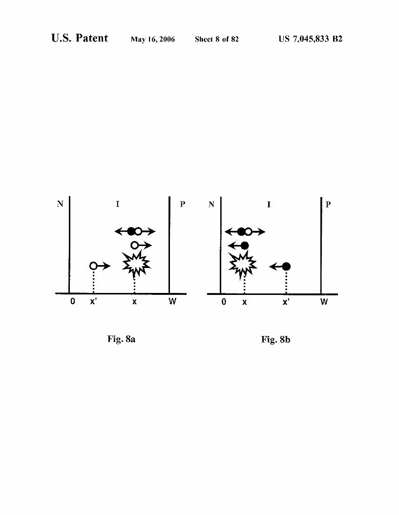
FIG. 8a depicts a schematic of spatial notation for holes in conventional local-field multiplication theory;
FIG. 8b depicts a schematic of spatial notation for elec trons in conventional local-field multiplication theory;
6 FIG. 36 depicts a plot of measured excess noise factors of
AlGaAs APDs with high Al atomic percentages and thin multiplication layer thicknesses;
FIG. 37 depicts a plot of gains for Ino Alo as AS homo FIG.9 depicts a plot of excess noise factors as a function 5 junction APDs with various multiplication layer thicknesses;
of gain for different ks; FIG. 10 depicts frequency response of an avalanche
photodiode with B/C-0.1 under pure electron injection; FIG. 11 depicts bandwidth as a function of avalanche gain
at different k values in a PIN structure; FIG. 12 depicts a schematic of an abrupt PN junction used
for determining electron and hole ionization coefficients from photo-multiplication measurements;
FIG. 13 depicts ionization coefficients of Si, InP, and InAlAs as a function of electric field;
FIG. 14 depicts ionization coefficients of GaAs and AlGaAS as a function of electric field;
FIG. 15 depicts a homojunction PIN structure used in gain and noise measurements;
FIG. 16 depicts a partial cross-sectional view of a PIN structure used in gain and noise measurements;
FIG. 17 depicts a top view of a PIN device after process 1ng
FIG. 18 depicts a partial cross-sectional view of a PIN structure after formation of a p-contact;
FIG. 19 depicts a partial cross-sectional view of a PIN structure after formation of a mesa:
FIG. 20 depicts a partial cross-sectional view of a PIN structure after formation of a n-contact;
FIG. 21 depicts a schematic diagram of a gain and noise measurement apparatus;
FIG. 22 depicts a plot of excess noise factor for GaAs APDs with about a 0.8 um thick multiplication region;
FIG. 23 depicts a schematic diagram of a circuit of the bias-tee used in noise measurement;
FIG. 24 depicts photocurrent and dark current of about 100 um diameter GaAs homojunction APDs with multipli cation layer thicknesses of about 100 nm to about 1400 nm:
FIG. 25 depicts a plot of measured gains for GaAs APDs; FIG. 26 depicts a plot of junction capacitance and area of
GaAs homojunction APDs with multiplication layer thick nesses of about 100 nm to about 1400 nm,
FIG. 27 depicts a comparison plot of measured excess noise factors and calculated values using the conventional theory for GaAs;
FIG. 28 depicts a plot of average electric field near breakdown of devices with various multiplication layer thicknesses;
FIG. 29 depicts a plot of photocurrent and dark current of Alo Gao AS APDs with various multiplication layer thick nesses;
FIG. 30 depicts a plot of gain for Al Gao AS homo junction APDs;
FIG. 31 depicts a plot of measured excess noise factors and calculated values using conventional theory for Alo Gao AS APDs;
FIG. 32 depicts a plot of measured gains of the Al GaAs APDs with various Al ratios (x):
FIG.33 depicts a plot of measured excess noise factors of AlGaAs APDs;
FIG. 34 depicts a plot of ionization coefficients of Al GaAs extracted from gain curves and F(M) curves with the conventional theory;
FIG. 35 depicts a plot of photocurrent and dark current AlGaAS APDS with high Al atomic percentages and thin multiplication layer thicknesses;
10
15
25
30
35
40
45
50
55
60
65
FIG. 38 depicts a plot of measured excess noise factors and calculated values using conventional theory for In 52 AlasAs homojunction APDs;
FIG. 39 depicts a plot of gains for the InP NIP homo junction APDs with various multiplication layer thicknesses;
FIG. 40 depicts a plot of measured excess noise factors and calculated values using conventional theory for the InP homojunction APDs;
FIG. 41 depicts a schematic diagram of Impact-Ioniza tion-Engineered (IIE) multiplication region;
FIG. 42 depicts a plot of photocurrent and dark current of IIE APDs:
FIG. 43 depicts a plot of measured excess noise factors of IIE APDs and a 83 nm thick GaAs homojunction device:
FIG. 44 depicts plots of temperature dependence of gains of AlGaAs APDs with a 0.8 um thick multiplication region and various Al ratios:
FIG. 45 depicts a plot of temperature dependence of k values fitted with measured excess noise factors of 0.8 um thick homojunction AlGaAS APDs;
FIG. 46 depicts a plot of ionization coefficients of GaAs at different temperatures:
FIG. 47 depicts a plot of ionization coefficients of Al GasAS at different temperatures:
FIG. 48 depicts a plot of ionization coefficients of AlGao 6As at different temperatures;
FIG. 49 depicts a plot of fitted and calculated k values versus multiplication region thicknesses on GaAs based APDs:
FIG. 50 depicts a plot of fitted and calculated k values versus multiplication region thicknesses on InP based APDs:
FIG. 51 depicts a plot of measured and fitted gain curves for GaAs homojunction APDs;
FIG. 52 depicts a plot of measured excess noise factors of GaAs APDs and their fits with a history-dependent model;
FIG. 53 depicts a plot of measured and fitted gain curves for Al GasAs homojunction APDs;
FIG. 54 depicts a plot of measured excess noise factors of Al GasAs APDs and their fits with the history-dependent model; FIG.55 depicts a plot of measured and fitted gain curves
for In AlasAs homojunction APDs: FIG. 56 depicts a plot of measured excess noise factors of
In Alo as AS APDS and their fits with the history-depen dent model;
FIG. 57 depicts a plot of measured and fitted gain and noise curves for InPhomojunction APDs;
FIG. 58 depicts a plot of spatial variation of ionization probability density (Ox) of a hole traveling along x without ionization;
FIG. 59 depicts a comparison plot of measured O(E) and f(E) reported in literature with O(E) and f(E) of saturated hot carriers in the history-dependent theory;
FIG. 60 depicts a plot of electric field profiles of devices reported in literature and corresponding effective electric fields E of electrons and E, of holes in the history dependent theory;
FIG. 61 depicts a plot of a model of the history-dependent C.(wix) compared to Monte Carlo simulations on Si;
FIG. 62 depicts a plot of spectral response of commer cially available InGaAs/InP and Si APDs;

US 7,045,833 B2 7
FIG. 63 depicts an AFM top view of a 6 mono-layer self-aligned Ino Alo AS layer,
FIG. 64 depicts a plot of photo-luminescence spectrum of the self-aligned Ino Alois AS QD layer,
FIG. 65 depicts a partial cross-sectional view and electric field profile near breakdown of a resonant-cavity SACM APD with In Al AS QD absorption layers;
FIG. 66 depicts a partial cross-sectional view of a pro cessed resonant-cavity SACM APD with In Al AS QD absorption layers;
FIG. 67 depicts a top view of a processed resonant-cavity SACM APD;
FIG. 68 depicts a schematic diagram of an experimental setup for frequency-response measurements of resonant cavity SACM APDs;
FIG. 69 depicts a plot of measured photocurrent and dark current of the resonant-cavity SACM APDs;
FIG. 70 depicts a plot of quantum-efficiency spectra measured for QD SACM APDs with 3 pair MgF/ZnSe top mirrors;
FIG. 71 depicts a plot of excess noise factor of resonant cavity QD SACM APDs as a function of avalanche gain;
FIG. 72 depicts a plot of measured bandwidth versus gain for SACM APDs:
FIG. 73 depicts a partial cross-sectional view of a device structure and proposed integration method for arrays of In, Alo as AS/InossGao 47As resonant-cavity APDs:
FIG. 74 depicts a plot of excess noise factor versus gain for an Al Gao. As APD and a Si APD;
FIG. 75 depicts a partial cross-sectional view of a SACM APD with a AlGaAs, with X greater than about 0.8. multiplication region;
FIG. 76a depicts a plot of measured excess noise factors for GaAs homojunction APDs for various multiplication widths:
FIG. 76b depicts a plot of measured excess noise factors for Alo Gao AS homojunction APDs for various multipli cation widths:
FIG. 76c depicts a plot of measured excess noise factors for Inos Alo as AS homojunction APDs for various multipli cation widths:
FIG. 76d depicts a plot of measured excess noise factors for InP homojunction APDs for various multiplication widths:
FIG. 77 depicts a plot of excess noise versus gain for an Alo Gao AS homojunction APD;
FIG. 78 depicts a schematic of an electric field of a resonant-cavity SACM and a partial cross-sectional view of a resonant-cavity SACM;
FIG. 79 depicts a plot of measured bandwidth versus DC gain for an SACM APD;
FIG. 80 depicts a partial cross-sectional view of a reso nant-cavity Ino sGao 47AS/Inos Alo as AS APD;
FIG. 81 depicts a plot of external quantum efficiency versus wavelength;
FIG. 82 depicts a plot of photoresponse, dark current, and gain of InAlAS/InGaAs resonant-cavity SACM APD; and
FIG. 83 depicts a plot of bandwidth versus DC gain for InAlAS/InGaAs resonant-cavity SACM APD.
While the invention is susceptible to various modifica tions and alternative forms, specific embodiments thereof are shown by way of example in the drawings and will herein be described in detail. It should be understood, however, that the drawings and detailed description thereto are not intended to limit the invention to the particular form disclosed, but on the contrary, the intention is to cover all
10
15
25
30
35
40
45
50
55
60
65
8 modifications, equivalents and alternatives falling within the spirit and scope of the present invention as defined by the appended claims.
DETAILED DESCRIPTION OF THE PREFERRED EMBODIMENTS
Operating wavelength may be one of the most significant specifications for a photodetector. For example, operating wavelength may determine an absorption material of a photodetector, and thus a material system for the whole device. In this manner, a semiconductor photodetector may be specified for an operating wavelength range. A long wavelength cut-off of a spectral response may be determined by the absorption edge, or bandgap, of the absorption material of a photodetector. A short-wavelength cut-off may be observed because of recombination near the surface. Since optical fibers demonstrate minimum dispersion and attenuation at about 1.3 Lum and about 1.55um, respectively, these wavelengths have become standards for long-haul high-bit-rate fiber optic telecommunication applications. For short-haul communications. Such as local area networks (“LAN”), operating wavelengths may vary from about 800 nm to about 1 um since the relatively inexpensive and well-developed AlGaAs and Si technologies are avail able. In addition, there may also be a wide range of appli cations for Nd:YAG lasers, for example, in industrial manu facturing, medicine, remote sensing, space communications, and the military requiring high-performance photodetectors that operate at about 1.06 um. The demand for such photo detectors may also lead to advances in high-performance photodetectors working at about 1 um. The responsivity, R, normally expressed in terms of A/W.
may be defined as the current generated by unit incident light power. This characteristic may be equivalently described by the external quantum efficiency m, which is 100% when every incident photon excites an electron-hole pair that may be eventually collected by the electrodes. Based on the above description, the relation between R and my may be written as
ife hy (1) illert F
where I is the photo-generated current, P is the incident power, hV is the photon energy, and e is the electron charge. In order to make receivers with a high signal-to-noise ratio and maximize the separation between optical repeaters, photodetectors with a relatively high responsivity or external quantum efficiency may be required. Quantum efficiency may be the most useful characteristic to utilize. To reduce the number of repeaters and amplifiers in a
long-haul giga-bits fiber optic communication system, the photodetectors may need to be relatively sensitive. The ultimate detection capability of a receiver may be limited by noise and dark current. The ability to detect the presence or absence of a signal, or the sensitivity, may depend upon the ability to discriminate between a signal and noise. Noise may be described in terms of <i>, the quadratic mean of the current. The noise appearing in an infrared system may arise from a variety of sources, which may be classified into three categories: photodetector noise, amplifier noise, and radia tion fluctuation from the background.
For photodetectors operating at high frequency, thermal noise and shot noise may be the two main noise sources, and

US 7,045,833 B2 9
they may be characterized by uniform spectral densities. Thermal noise may appear when current flows through any resistive material, and its noise may be presented as
(i. ) 4KT i = - D, terra R (2)
where B is the observation bandwidth, T is the absolute temperature, k is the Boltzmann's constant, and R is the load resistor. Shot noise may be associated with the discrete nature of the charge carriers, and it may be expressed as
(i)=2eIB, (3)
where e is the electron charge. Since these two noise sources are statistically independent, the Summation of their qua dratic mean values gives the total fluctuation, <i>.
4kT 4 (i) = (in)+(i) = --B+2el B. (4)
From this equation, it may be seen that high resistance may be desirable in order to reduce the thermal noise and enhance the sensitivity of photodetectors. A high resistance, however, may result in a high RC constant in the circuit, which may reduce the bandwidth of a device and system. In high-speed applications, the effects of such a reduction in the bandwidth of a device and system may be reduced, and even eliminated, by circuit-level and/or device-level solutions. The signal-to-noise ratio S/N may be generally defined as the power ratio of signal to noise.
To support a high transmission bit-rate in long-haul fiber optic telecommunication systems, the bandwidth of every component may need to be relatively high. Therefore, band width may be another important parameter for high-perfor mance photodetectors. Generally speaking, a bandwidth of a photodetector may be determined by the following factors: carrier transit time, RC time constant, diffusion current, carrier trapping at heterojunctions, and packaging. When significant absorption occurs out of the high-field
region, the carrier-diffusion current may reduce the transient response of a photodiode. Those carriers within about one diffusion length of the depletion region may have an oppor tunity to diffuse into the active region. Since the diffusion process may last as long as the carrier lifetime, this current may contribute a slow tail to the impulse response. For relatively high-speed devices, this problem may be reduced, and even eliminated, with a double-heterojunction design that limits the absorbing region in the high-field intrinsic region.
To avoid a long tail in an impulse response due to carrier diffusion, the absorption layer of high-speed photodetectors may be placed in a depletion region. In response to absorbed light, photo-generated electron-hole pairs may quickly drift across this high-field region and may be collected by the electrodes. A reduced, and even minimum, transit time may be achieved with an electric field that may be high enough so that carriers may travel at their saturation Velocities. During this transport process, the applied bias may be Substantially constant. According to Gauss's law, the electric field in the depleted region may be disturbed by the move ment of the carriers, which may result in a significant displacement current relative to the carrier current. Such a disturbance may start from about a time when the generation
10
15
25
30
35
40
45
50
55
60
65
10 of carriers begins and may be reduced as the generated carriers are collected at the boundaries of the depletion region. In this case, the transit time may be determined primarily by the length of the depletion region and the saturation velocities of the carriers. When heterostructures are used in photodetector designs,
carrier trapping at discontinuities of the conduction band or the valence band may also affect device bandwidth. When carrier trapping is significant, an impulse response may not end until the trapped carriers have recombined or have escaped by thermionic emission, which may be a very slow process. Hole trapping may be significant in long-wave length photodetectors due to a large Valence band disconti nuity at InP/InGaAs heterojunctions. Since an applied bias may reduce the barrier height, a sufficient electric field across the heterojunction may increase the emission rate. To reduce interface trapping, the barrier may be reduced by Superlattice or compositional grading. RC time constant and packaging may also influence
photodetector performance. FIG. 1 shows an equivalent circuit of a PIN photodiode. Generally, the circuit following current source 10 may include resistors 12, 14, and 16, capacitors 18 and 20, and inductor 22, and may serve as a low band-pass filter. As shown in FIG. 1, capacitor 18, C. is the junction capacitance that may originate from the depletion region, and capacitor 20, C, may be the parasitic capacitance. Inductor 22, L. may be the total series induc tance, which may arise from the leads. Resistor 12, R, which may normally be large under reverse bias, may be the diode shunt resistance or junction resistance caused by carriers within the depletion region. Resistor 14, R, may be the series resistance of the diode, and resistor 16, R, may be the load resistance. If the device short-circuit current, cur rent source 10 as shown in FIG. 1, has a frequency response J(c)), then the spectrum of the output current J(CD) may be expressed with the transfer function H(c) of the equivalent circuit as:
H(c) may be found from simple circuit analysis. For the circuit shown in FIG. 1, H(c) may be given by
RD a + ico(b - co?) - do?
with (6) H(co) =
a = Rs + R + RD b = Rs RLC, + LS + (Rs -- RL)RoC -- Rt Rp C;
C = Rs. LSC, RbC. d = (Rs RLC + Ls)RbC + Rs. LSC + RpCLs.
Another problem introduced by packaging is that a pho todiode may be a high impedance load and may have a reflection coefficient close to unity. An impedance mismatch between the device, the load, and the transmission line may result in resonance in the circuit and may determine the photodetectors frequency response. The photoconductor is the simplest photodetector that
may exhibit an internal gain mechanism. Since carrier density in an active region may be modulated by an optical signal, detection of the photoconductor may be based on a Subsequent conductivity change of the material. A thickness of the active region may be large enough to absorb a significant fraction of the incident light and Small enough to avoid a low resistance and to reduce, and even minimize,

US 7,045,833 B2 11
thermal noise. Another trade-off of the photoconductor may be between gain and bandwidth. Since the photo-generated current may persist until all carriers are collected at the electrodes or recombine in the active region, the bandwidth B of the photoconductor may be proportional to the recip rocal of the slower carriers’ lifetime t.
B. cx 1. (7)
Assuming that holes travel with a lower Saturation velocity, an appropriate carrier lifetime, t, in Equation 7 may be the carrier lifetime of holes, T. Continued existence of holes in the channel may attract electrons to the channel thereby maintaining charge neutrality in the channel. The attraction of electrons to the channel may result in a photocurrent gain, G, which may be expressed as
t (8)
where t is the electron transit time. Then, the gain-band width product may be constant and may be determined by t. To improve the gain-bandwidth product, the photoconductor may include a relatively short active region, which, in turn, may result in lower quantum efficiency and lower resistance. A lateral dimension of an active region, and thereby perfor mance, of the photoconductor may be determined by reso lution capability of a lithography process and/or system used to form the active region. As such, in fiber optic communi cation systems, where relatively high bandwidth and rela tively high sensitivity are essential, photoconductors may be seldom used. The simplest photodetector with a junction may be the
Metal-Semiconductor-Metal (“MSM) photodiode. An MSM photodiode may include two Schottky contacts formed on an undoped semiconductor layer. Since an MSM photodiode may be inherently substantially planar, an MSM photodiode may be relatively easy to integrate with a metal-semiconductor FET (“MESFET) preamplifier.
Under normal operation conditions for an MSM photo diode, a region between the two contacts may be almost completely depleted, and photo-generated carriers may be swept to the two contacts by this electric field. Since transit of the carriers may be a drift process, a bandwidth of the photodiode may be determined by a transit time of the carriers and a charge-up time of the diode. The charge-up time may be determined by junction and parasitic RC constants. An equivalent circuit of an MSM photodiode may be similar to an equivalent circuit of a PIN photodiode, as shown in FIG. 1. Since a junction capacitance of a MSM diode may be much smaller than that of a PIN diode, a MSM diode may have a higher bandwidth than a PIN diode for a comparable device area. The transit time of a MSM diode may be determined by the distance between the contacts. With interdigitated finger contacts and a spacing of approxi mately 1 um, MSM photodiodes may have a bandwidth of about 20 GHz to about 50 GHz. Using submicron lithogra phy techniques, a bandwidth of about 510 GHz may be achieved. The avalanche multiplication effect may be observed under relatively strong electric field, which may correspond to an increase in tunnel current, especially in narrow-bandgap materials.
10
15
25
30
35
40
45
50
55
60
65
12 For low electric fields, the dark current of MSM devices
may be due primarily to thermionic emission over the barrier. In GaAs devices, the barrier may be reasonably high such that the dark currents of MSM diodes and PIN diodes may be comparable. In the long-wavelength region, InGaAS MSM diodes may exhibit relatively high dark currents due to a relatively low Schottky barrier height at the metal/ InGaAs interface. An InAlAs layer may be included at the interface to increase the barrier height, and a graded bandgap layer may be included at the InGaAs/InAlAs interface to reduce hole trapping. In addition, since the contacts may be formed on the device surface, almost half of the incident photons may be blocked. The number of incident photons that may be blocked may be reduced if the contacts are substantially transparent contacts. MSM photodiodes may not typically be used in long-haul fiber optic communication although they may demonstrate relatively high bandwidths and compatibility for integration with preamplifiers. A structure that may be most widely used in fiber optic
communication is a PIN photodiode, which may demon strate relatively high speed, relatively low dark current, relatively low noise, and a reasonable quantum efficiency. The PIN photodiode may be a junction diode in which a lightly doped region (n- or p- depending on the junction formation technique) may be formed between p' and n' regions. Due to relatively low density of free carriers in the “intrinsic' region, the region may be fully depleted at approximately Zero or a very low reverse bias. Conse quently, the electric field may be substantially confined to this region. The PIN diode may have a relatively stable depletion region thickness with respect to the variation of the applied voltage.
For high-speed operation, to avoid slow carrier diffusion, an absorption layer may be placed in the depleted intrinsic region where photo-generated carriers may drift with Satu ration velocities. Similar to MSM photodiodes, a bandwidth of a PIN photodiode may be determined by carrier transit time and RC constants. The transit time may be reduced, and even minimized, with relatively thin depletion regions. A relatively small junction capacitance may be normally achieved by reducing the device area to a value consistent with the desired bandwidth. For optimal design, it may be customary to keep a balance between the transit time and the RC time constant:
(9)
i = -
where T is the signal modulation period. For a PIN diode with an absorption layer in the depletion
region, the external quantum efficiency m, may be expressed as
m=n.(1-R)(1-e), (10)
where m is the internal quantum efficiency, d is the width of the absorption region, C. is the absorption coefficient, and R is the reflectivity of the top surface. According to Equation 10, reducing reflectivity on the top surface and increasing width of the absorption region may increase quantum effi ciency. Increasing width of the absorption region, however, may reduce bandwidth by increasing transit time. Conse quently, speed and quantum efficiency of PIN photodiodes may be inversely related. Such an inverse relationship may

US 7,045,833 B2 13
be addressed by decoupling the widths of the absorption and depletion layers and by including a resonant cavity. The main noise sources of PIN photodiodes may be shot
noise and thermal noise, which are described in Equation 2 and 3. Considering an incident optical signal, P., according to Equation 1, the photocurrent I, is expressed as
(11) eneat Pinc h F p hy
where hv is the photon energy. Since the photocurrent I. the response to the background radiation I, and the dark current I, increase shot noise, the current I in Equation 3 is the summation of the three. Thermal noise may be caused by resistors in the diode circuit, as shown in FIG. 1. For this circuit, the resistance R in Equation 2 may be
R=(i. 1 i) (12) R, "R," R.)
where R is the shunt resistance, R is the load resistance, and R, which is parallel to R, is the input resistance of the following preamplifier. Since the two noise sources, shot noise and thermal noise, may be statistically independent, the total noise may be the Summation of the two as shown in Equation 4. The signal power may be calculated with i.R. and the noise power is <i>R. Therefore, the signal to-noise power ratio may be expressed as
(13) ( enert Pinc hy
li, 4kT - B
A conventional measure of sensitivity is the noise equivalent power (“NEP), which may be presented as the minimum detectable power (P), at unity signal-to-noise ratio. For a given signal-to-noise ratio S/N and bandwidth B, (P and NEP may be defined as
inc)min
h (Syl2 4kTY' (14) (Pinc)min = () (2ell + IB - D) + Bll-,
and
4kTY' NEP = (2el, + B + D) + Blf2. eilert R
To increase the sensitivity of a PIN photodiode, external quantum efficiency m, and total resistance R may be increased, and unwanted currents, I and I may be decreased.
Another widely used structure in fiber optic communica tion is the avalanche photodiode (APD). An avalanche
10
15
25
30
35
40
45
50
55
60
65
14 photodiode may be a reverse-biased pnjunction that may be operated close to the breakdown voltage. Photo-generated carriers injected into the depletion region may drift at their saturation Velocities. If the carriers gain Sufficient energy from the electric field, ionizing collisions with the lattice may occur. Secondary electron-hole pairs may be generated in this process. The primary and secondary carriers may create additional carriers until they exit the high field region. This process may be generally referred to as impact ioniza tion. A typical field intensity for Such a process may be in the range from about 10 V/cm to about 10° V/cm. The typical field intensity may vary, however, depending on, for example, the material and the structure of the multiplication region. A central issue for photodetectors in fiber optic commu
nication may be detection of weak optical signals. Often, a length of an optical link may be determined by a minimum optical signal that may be detected at the transmission bit-rate. As opposed to PIN photodetectors, the internal gain introduced by the avalanche process may increase the sig nal-to-noise ratio and thus the sensitivity of receivers that employ APDS. This gain may also relax the requirements on the following amplifiers. At relatively low bias, APDs may be essentially PINs, and
main sources of noise for the APDs may be shot noise and thermal noise. As the gain of an APD increases, the main Source of noise may be the multiplication process. For example, the statistical nature of the multiplication process may result in random fluctuation in the total number of secondary carriers generated by each primary carrier injected into the gain region. This random fluctuation may cause excess noise in the total signal current, and it may be generally referred to as multiplication noise. The shot noise term may be modified to include the multiplication noise as follows
where F is the excess noise factor, which may be commonly used as the noise figure of merit of an APD. Similar to Equation 4, the total noise <i> of an APD may be written aS
16 (i) = (ii) + (i) = 2e(Iph + lp + lp)BM F+ --B. (16)
The power signal-to-noise ratio S/N becomes
(17) (the f (S)- N power
et Pine \ (line)
An upper bound of the signal-to-noise ratio may be reached if F=1, and the thermal noise 4 kt/RM and unwanted currents (I and I) may be neglected compared to the contribution of the photocurrent I. This limit may be

US 7,045,833 B2 15
generally referred to as the quantum noise limit of detection, and it is defined as
(18) ( eneat Pinc hy ph
2elph B (). - - N power 2eB
Similar to the definition in Equation 14, we can define the NEP for APDS as
(19)
As demonstrated in these equations, increasing gain M may reduce the contribution of thermal noise and may increase the final signal-to-noise ratio. A noise penalty may occur, however, with increasing F. Consequently, there may be an optimum value of the gain which may increase, and may even maximize, the signal-to-noise ratio. In addition, the internal gain from the photodetector may reduce again requirement of a subsequent preamplifier and may produce higher bandwidth and lower noise from a simpler amplifier. Therefore, APDs may achieve about 5 dB to about 10 dB better sensitivity than PINs. For high-bit-rate, long-haul fiber optic systems, an avalanche photodiode may be the photodetector of choice. The demand for gigabit fiber-optic communication and
the rising popularity of fiber optics in RF/microwave sys tems have led to many advances in high-speed photodetector technology. Specific application requirements have spurred developments of novel device structures to improve the speed and responsivity of high-speed photodetectors. Tra ditional high-speed photodiodes, both PINs and APDs, may be designed around a trade-off between bandwidth and quantum efficiency. For example, to increase bandwidth, the transit time of photo-generated carriers across the high-field depletion region may be reduced thereby placing an upper limit on the absorption layer thickness. The external quan tum efficiency me, of conventional photodetectors may be determined by the optical absorption coefficient O, the thickness d of the active layer, and the surface reflectivity R. To increase quantum efficiency, a thickness of the active
layer may be increased, and an anti-reflective coating may used. Assuming C. is approximately 10 cm', to achieveme, greater than about 95%, a relatively thick (e.g., greater than about 3 Lum) active layer may be required. Increasing a thickness of the absorption region may increase transit time and may reduce the device speed. Therefore, it may be desirable to increase quantum efficiency without reducing the bandwidth. Such an increase in my may be achieved by utilizing a resonant cavity structure, in which an optical signal may be recirculated across a relatively thin absorbing layer to effectively increase the optical path length.
Resonant-cavity photodetectors were first demonstrated using an InAlAS-InGaAs Schottky device. A cross-sectional view of an embodiment of a resonant-cavity photodetector is shown in FIG. 2. As shown in FIG. 2, a basic resonant-cavity enhanced (“RCE") device may include relatively thin, nar row-bandgap absorption layer 24 sandwiched between two mirrors 26 and 28 and transparent spacer layers 30 and 32. Optical signal 34 may enter the device through mirror 26 and may be recirculated across relatively thin, narrow bandgap absorption layer 24 and transparent spacer layers 30 and 32
10
15
25
30
35
40
45
50
55
60
65
16 between mirrors 26 and 28. The device may also include contacts 36 and 38. Contacts 36 and 38 may be formed laterally proximate mirrors 26 and 28, respectively. The resonant wavelength may be determined by an optical length of a GaAs substrate or InGaAs/InAlAs on InP. Since top mirror 26 may be deposited at the very end of the process, a relatively large and tunable reflectivity may be achieved with a few pairs of dielectric layers. In the following context, R and R may be used to describe the power reflectivities of top and bottom mirrors, 26 and 28, respectively. The external quantum efficiency for resonant-cavity pho
todetectors may be expressed as
(1 + R. e )(1-R)(1-e') (20) 1 - 2 v R, R2 eod cos(2f3L + f1 + f2) + R. Re-2od
11ert F
where C. is the optical absorption coefficient and up and up are the phase shifts at the mirrors. Since the propagation constant f(?3-2nd L/Wo, where wo is the vacuum wavelength and n is refractive index) is dependent upon wavelength, m, may change periodically with the inverse of the wavelength. The peak quantum efficiency m may be reached when the cosine term is 1:
(1 + Re)(1-R)(1 - e.) (1 - VR, R., e-ad)
ilpeak
FIG. 3 shows the external quantum efficiency of a reso nant-cavity device as a function of absorption, Od, for several values of top mirror reflectivity. The top mirror reflectivities may correspond to different numbers of pairs of dielectric quarter-wave layers with more pairs producing higher reflectivities. The bottom mirrors may include quar ter-wave stacks of GaAs/AlAs. The bottom mirror reflec tivity R is 99%, except for the “no cavity” case, in which R is set to 0, and R is set to 30%. The range of old shown may correspond to relatively thin absorption layers (about tens of nanometers to about hundreds of nanometers) with absorption coefficients typical for Ino sGao As at near infrared wavelengths (e.g., C. of about 0.5 um to about 2 um'). The four different values for top mirror reflectivity shown in FIG.3 may correspond to a typical semiconductor air interface plus 1, 2, and 3 pairs of dielectric quarter-wave layers. In all cases shown, a resonant cavity may dramati cally improve the peak quantum efficiency. Except for very narrow absorption layers, selection of an appropriate top mirror may increase peak external quantum efficiencies to greater than about 80%. In comparison, the external quan tum efficiency may less than about 15% without a cavity. The optimum top mirror reflectivity for high my occurs at
R=Re2. (22)
FIG. 4 shows maximum quantum efficiency, m of a resonant-cavity device as a function of normalized absorp tion coefficient, Old, for various bottom mirror reflectivities, R with top mirror reflectivity, R, determined by Equation 22. The curve for a conventional photodetector (having a R of about 0), as shown by the dashed line in FIG. 4, may exceed about 90% external quantum efficiency only if a thickness of the absorption layer is greater than about 2 um. Such a photodetector may have a lower bandwidth due to a longer carrier transit time. The longer carrier transit time

US 7,045,833 B2 17
may also increase the carriers’ recombination probability thereby reducing quantum efficiency. In contrast, resonant cavity photodetectors having an R of about 0.99 may have a quantum efficiency greater than about 90% with a rela tively thin absorption layer. From FIGS. 3 and 4, it may be seen that resonant-cavity photodetectors with relatively thin absorption regions may have higher bandwidths than con ventional photodetectors without sacrificing the quantum efficiency.
In the above calculations, spatial distribution of the opti cal field inside the cavity was neglected. Interference between upward and downward propagating waves may create a standing wave inside the cavity. Since the optical field inside the cavity may not be uniform, the actual absorbed power may be a function of a position of the absorption layer. When the absorption layer spans several periods of a standing wave in the cavity, the standing wave effect may be averaged out. But for a relatively thin absorp tion layer, quantum efficiency of a resonant-cavity device may be affected by a position of the absorption layer. An effective absorption coefficient, C. may be introduced to simplify the calculation, which may defined as
1 23 i? data Etc. A)? (23) 2 ra/2 2 "d: Etz, A)
dei
where v Wo?n, E(z,w) is the electrical field profile at a given Wavelength w and the denominator is the average of the standing wave. For a relatively thin absorption region in a cavity with relatively highly-reflective mirrors, C. may vary from almost twice the bulk absorption coefficient at an anti-node of an optical standing wave to only a fraction of the optical standing wave at a node. Due to this configuration, resonant-cavity photodiodes
may demonstrate intrinsic wavelength selectivity. Intrinsic wavelength selectivity may be useful in Some wavelength division multiplexing (“WDM) applications. For WDM applications, important characteristics may include, but are not limited to, the free spectral range (“FSR), the finesse of the cavity F, and full width at half maximum (“FWHM) of the spectral response. FSR specifies the wavelength separa tion between two adjacent resonant bands. Under linear phase approximations, the FSR may be approximated by the expression
FSR A2 (24) 2neff Leif
where n, is the effective refractive index and L is the effective optical cavity length. The finesse F and FWHM (AW) of the resonance peak may be defined as
FSR (25) F =
A 12
A 1 - WR Red FWHM = A2 = 0, y - 2 ineff Leif VRR, e-ad/2
FIG. 5 shows peak external quantum efficiency and spec tral linewidth of a resonant-cavity photodiode as a function
5
10
15
25
30
35
40
45
50
55
60
65
18 of the top mirror reflectivity. The three different sets of curves correspond to three different absorption layer thick nesses using the effective absorption at about 1.3 um of an InsGaAs layer located at approximately an anti-node of a cavity's optical standing wave. The Solid line corresponds to an absorption layer thickness of about 50 nm. The medium dashed line corresponds to an absorption layer thickness of about 25 nm. The small dashed line corresponds to an absorption layer thickness of about 12 nm. The bottom mirror reflectivity is approximately 0.99, and the effective length of the cavity is about 1.5 lum. As shown in FIG. 5, spectral linewidth decreases with increasing reflectivities and decreasing absorption coefficients.
Although relatively high reflectivity mirrors may result in a high-finesse cavity and narrow linewidth, such mirrors may also lead to relatively narrow angle detection. The quantum efficiencies of resonant-cavity photodetectors given above are for normal incidence. Peak quantum effi ciency may decrease with incident angle, 0,. The resonance wavelength may also shift from the normally incident case. The angle dependency of m may be expressed as a function of the cavity finesse F, the wavelength w, the effective cavity length L. and effective refractive index n as follows
An (26) n
Quantum efficiency may be more sensitive to the angle of incidence for a high-finesse cavity at shorter wavelengths than for longer wavelengths. Although this phenomenon may be very useful for special applications such as high response-angle detection, this phenomenon effectively decreases the numerical aperture of resonant-cavity photo detectors and imposes limitations for fiber optic communi cations. However, the quantum efficiency may not change appreciably within an incident angle of about 5° even for a high-finesse cavity. In practice, fiber couplers and integrated microlenses may be used to increase the numerical aperture of resonant cavity photodetectors.
In a resonant cavity, photons may be reflected by mirrors and may cross the absorption region several times. Photo generated carriers, however, may drift across this region only once. By decoupling optical and electrical path lengths, a resonant-cavity structure may achieve relatively high external quantum efficiency with a thin absorption layer. In this manner, a relatively high quantum efficiency may be achieved without a reduction in carrier transit time.
An appreciable gain from an APD may be achieved with a relatively high electric field in the multiplication region. At relatively high electric field intensities, tunneling current I may be the dominant component of the dark current, and turne its expression for direct bandgap semiconductors is
1 3 0m. Ei ei E.
(27) unnel a YA exp
where mo is the free electron mass, e is the electron charge, h is the reduced Planck's constant, E, is the maximum junction electric field, and E is the bandgap of the semi conductor. The parameter () is a dimensionless quantity on the order of unity, and depends on the effective electron mass

US 7,045,833 B2 19
and the detailed shape of the tunneling barrier. The prefactor A is a constant, and Y depends on the initial and final states of the tunneling carrier. A modified APD structure may be generally referred to as
a separate-absorption-multiplication ("SAM) APD. FIG. 6 illustrates a partial cross-sectional view of an embodiment of a generic structure and electric field profile of a SAM APD. As shown in FIG. 6, a SAM APD may include absorption region 40 separated from multiplication region 42. In prac tice, a field may be applied across narrow-bandgap absorp tion layer 40 to avoid a slow carrier-diffusion process. A relatively high electric field applied on a narrow-bandgap material may result in a relatively high tunneling current. To avoid excessive dark current, especially from narrow-band gap absorption materials such as Ino sGao 47AS, it may be necessary to separate the multiplication and absorption regions and to alter the profile of the electric field. In such a structure, a relatively high electric field may be applied only to the wide-bandgap material in multiplication region 42, as shown in FIG. 6. Such a structure with such an applied electric field may lead to a substantially lower tunneling current. In 1979, the first InCaAsP SAM avalanche photo diode was demonstrated to have again of about 3000 and a dark current density of approximately 1 (LA/cm at relatively low Voltage. A partial cross-sectional view of an embodiment of a
generic structure and electric profile of a separate-absorp tion-charge-multiplication-region (“SACM) APD is shown in FIG. 7. To achieve higher performance from relatively thin multiplication regions and to alleviate a tunneling current that may originate from a relatively high field, wide-bandgap intrinsic multiplication region 48 and charge region 46 may be used to replace the lightly doped gain region in SAMAPDs. The SACM may also include absorp tion region 44. As a result of the several heterointerfaces in this structure, carrier trapping may broaden an impulse response and reduce a bandwidth of the APD. Graded layers may be formed at these interfaces to change the bandstruc ture gradually. Such a device may be generally referred to as a separate-absorption-graded-charge-multiplication-region (“SAGCM) APD. Due to the similarity of the two struc tures and the wide application of graded layers in high performance devices, the term SACM may often be used for both SACM and SAGCM structures. With an InPSAGCM planar structure, a gain-bandwidth product of about 122 GHz was achieved.
Combining the resonant cavity and the SACM structure, high-performance APDs with relatively high quantum effi ciency, relatively high speed, relatively low dark current, relatively high gain-bandwidth products, and relatively low multiplication noise may be achieved. The widespread development of optical fiber and other
optical communication and data processing systems in the visible and near-infrared spectral regions has excited wide interest in Solid-state avalanche photodiodes. Continuous effort has been made to understand the mechanism of this ionization process since the first successful avalanche theory was published. This theory is generally referred to as the local-field theory. A main assumption of the local-field theory is that impact ionization is a continuous, local pro cess, and that ionization probability only depends on the local electric field irrespective of a carrier's ionization history. This theory has been widely accepted and has proved to be an extremely useful model for a wide variety of avalanche devices.
In the conventional theory, two parameters, ionization coefficients C. and B, may be introduced to describe the
5
10
15
25
30
35
40
45
50
55
60
65
20 ionization probability density of electrons and holes in a material. In other words, in an element distance dx, the probability for an electron to cause an impact ionization event is C.dx, and the corresponding probability for a hole is Bdx. The assumption of locality may be the most important approximation in this theory, and this assumption may greatly simplify calculations. Under this assumption, the ionization coefficients are functions of the position in a specific structure under a given bias. Since excessive defects may cause a premature breakdown, it may be reasonable to assume that the carrier recombination in the depletion region may be negligible when a device exhibits good gain char acteristics. The gain calculation in the local-field avalanche theory
may start from the consideration of an electron-hole pair injected at x within the depletion region. M(x) may be used to represent the gain or average total number of pairs that may be generated in the multiplication region as a result of the original pair injected at X. Since this pair may eventually reach the boundaries of the multiplication region, its con tribution to the gain may be 1. On its way to the boundary, the electron may have a probability of C.(x).dx to generate another electron-hole pair at X within a distance element dx. FIGS. 8a and 8b illustrate schematic diagrams of spatial notation for holes and electrons, respectively, in conven tional local-field multiplication theory. In FIGS. 8a and 8b, holes are indicated by open circles, and electrons are indi cated by filled circles. As shown in these Figures, carriers may be created at X and ionization may occur at X.
This new pair may initiate another reaction chain with a gain of M(x), and its contribution to the total gain is M(x)C.(x).dx. After integrating all the ionization probabilities of the initial electron and hole,
x' w (28) M(x)=1 + dyM(x)a(x) + dxM(x)/3(x). O
Differentiating,
d M(x) , '))M(x' (29) - = (a(x)-f(x))M(x).
The solution is
(30)
Substituting Equation 30 into Equation 28 and setting x=w, may determine the value of M(w). This gives
In 1966, R. J. McIntyre proposed the first successful multiplication noise theory based on the locality assumption.

US 7,045,833 B2 21
This theory has been widely accepted and has been proven to be a useful model for a wide variety of avalanche devices. The consideration of avalanche noise may start from the pairs generated in a distance element dx. Since carriers may be always generated in pairs, only electrons or holes may be counted. The change of the hole current I, in dx is
dI (CI+I, +g).dx, (32)
where I, is the electron current and g is the thermal or optical generation rate in dx. In a bandwidth element df, the shot noise of this current increment may be given by
(Idi - (di)) = 2edIdf. (33)
Normally, the multiplication noise may be described in terms of the noise spectral density with units of A/Hz. Since this element of noise current may experience the same multiplication as any other current generated in dx, its contribution to the total noise spectral density (p may be
(IM(x)d I. - (M(x)d I)) (34)
Integration yields
(35) O dy
where I(0) and I,(w) are the hole and electron currents, respectively, that may arise from injection at the boundaries. Solving provides a complete expression for the total noise spectral density
O
2e2?avaMico-Mo. O
where I is the total current. With M(x) obtained in the above gain calculation, the total current may be expressed as
In the case where B-kC.(k is a constantzl), p may be simplified:
2el 2 2
(kM (w) - M - (0).
10
15
25
30
35
40
45
50
55
60
65
22 Assuming k<1, we get M(w)>M(O). Then, the noise of a given injection current I under a specific gain MI/I may be minimized under pure electron injection, in which g(x) =0. Under this condition,
(39)
The excess noise factor F(M) may be used to represent the noise figure of merit of an avalanche device.
F(M) = kM + (1 -(2- it) (40)
For pure hole injection, the noise and the excess noise factor may be obtained by substituting 1/k for k.
Excess noise factor, F(M), may be plotted as a function of gain for different k's for pure electron and hole injections if B-kC, as shown in FIG. 9. As shown in FIG.9, the avalanche noise at a given gain M may be less if most carriers that enter the multiplication region are those with higher ionization coefficients (for example, electrons in Si and GaAs, holes in InP). The strong dependence of the noise on the k value may also be demonstrated in FIG. 9. Under the injection of carriers with higher ionization coefficient, the avalanche noise may increase as the k value approaches unity.
Equations to calculate the bandwidth of avalanche pho todiodes have also been developed within the framework of the local-field avalanche theory. The calculation of the transient current response of a PIN structure may start from the fluid equation
(41)
where N(x,t) is the particle density, G(x,t) is the generation rate per Volume, and J(x,t) is the flux density. Applying this equation to the 1-D model shown in FIGS. 8a and 8b and considering electrons and holes separately, the time-depen dent equations for electron density n(x,t), hole density p(n,t), electron current density (x,t), and hole current density j(x,t) may be expressed as
where e is the electron charge, and Y(x,t) is the local net e-h pair current generation rate density. Under normal operation, the i region may be fully depleted and electrons and holes may be driven by the electric field at the saturation velocities V, and v, respectively. The carrier diffusion in the i region may thus be negligible. With this saturation-velocity assumption, the Fourier transform of Equation 42 and Sub sequent integral over the area of the photodiode may be

US 7,045,833 B2
where g(x, ()) is the corresponding transform result of Y(X,t). The general solution with injection currents i(w, (D) and i(0, ()) from the boundaries may be expressed as
in (X, (0) = (44)
where
and
are the transit-times of electrons and holes from X" to X. With the assumptions of locality and no optical generation in the multiplication region, the current density generation rate Y(x,t) in this region is
and the integral of its Fourier transform over the device Surface gives
g(x,0)-Cl(x)i,(x,0)+f(x)i(x,0). (46)
Therefore, the two equations in Equation 44 are linked to each other by g(x,c)), and the electric field profile may be incorporated through C(X) and f(X) in these equations. The general analytical Solution of Equation 44 with Equation 46 is quite complex, and details of the solution are known in the art. With this solution, the total current i in the junction, which includes both the carrier current and the displacement current, is
(47)
10
15
25
30
35
40
45
50
55
60
65
24 and
8 E(x, co) d. Seeo t
is integrated across the junction interface. The current of interest is the external short-circuit current, which may be expressed as
i(co) = (48) i? distics, (o) + i (x, (o), WJ0
where the third term in Equation 47 is dropped because the dc bias applied across the device does not change with the input signal.
With the assumption used in Equation 45 that impact ionization may be the only carrier generation mechanism in the multiplication region, the alternating current at unity gain, io(0. (D), may be
Based upon this definition, the ac gain of the device M(co) is
(50)
and the dc gain M(t)=0) under pure electron or hole injec tion, which may be calculated with Equation 31 (M(x=0) or M(x-w)), may also be expressed as
i(co) lim tu-0 io (co)
(51) M(a) = 0) = lin M(a)
With these concepts, the frequency response figure of merit F(co) of an APD may be defined as
M (co) i(co) M(a) = 0) TIM (a) = 0)io (co)
(52)
Since the analytic Solution of Equation 44 may be quite complicated, a more revealing Summary may be shown in FIGS. 10 and 11, which are plots of the numerical results of the solution. For simplicity, saturation velocities of electrons and holes are assumed to be substantially equal. FIG. 10 illustrates the frequency response of an APD with B/C-0.1 under pure electron injection at different dc gain M Versus the normalized frequency (ot, where t is the carrier transit time. As shown in FIG. 10, bandwidth may decrease as the gain increases. FIG. 11 illustrates the bandwidth as a func tion of avalanche gain at different k values in a PIN structure. The dotted line in FIG. 11 is the MC/B curve. FIG. 11 illustrates the influence of the k=B/C. value to the 3 dB bandwidth of an APD. The M-O/B curve superimposed on these curves illustrates that multiplication may have little effect on bandwidth when M-O/B. For M>C/B, the curves may be nearly straight lines thereby indicating a constant

US 7,045,833 B2 25
gain-bandwidth product, which may also strongly depend on the B/C. value. As further illustrated in FIG. 11, a higher gain-bandwidth product may be expected in a device with a lower B/C. value under pure electron injection. A simple physical picture may be obtained in extreme
cases. For example, in the best case, where k is greater than or equal to about 0, a duration of the response may be the Sum of the transit times of an electron and a hole through the depletion region. While in the worst case, where k is greater than or equal to about 1, secondary carriers may continu ously recycle through the multiplication region, which may result in relatively long response times at high gains. Such a long avalanche buildup time, which gives rise to the constant gain-bandwidth product, may determine the fre quency response at high gains. Therefore, the gain-band width product may be greater in APDs that include materials having Smaller ionization coefficient ratios (assuming CDB). As described herein, ionization coefficients of electrons
and holes of the multiplication-region material, especially the ratio of the ionization coefficients, may largely determine the gain, noise and bandwidth of substantially the entire APD structure. To characterize ionization properties of materials, a series of measurement methods may be deter mined based on the conventional avalanche theory. In most cases, the avalanche gains under different injection condi tions, for example, pure electron and pure hole injections, may be utilized. Several measurement methods are known in the art. However, only two structures, PIN junctions and abrupt PN junctions, may be commonly used in Such mea SurementS.
The simplest configuration for measurement and analysis may be a PIN structure such as the PIN photodiode shown in FIG. 1. Near the breakdown voltage, the i region may be fully depleted, and the electric field may be substantially uniform across this region. Since C(X) and B(x) may be constant throughout the high-field region in this case, Equa tion 31 may be greatly simplified. The electron-injection gain M(w.V) and hole-injection gain M(O.V) as functions of the reverse bias may be given by
M(, W) = C (53) (*) explo all 6 - C
where C.C.(E)=O.(V/w) and B-B(E)=f3(V/w). After measure ment of the two gains, O(E) and B(E) may be solved as
1 M(w, V 54 a(E)-f(E) = Int .. Y.) (54) 1 M (w, V) - 1 M(w, V)
a(E) = it. V) - M (w, wn M(0, w) M(w, V) - 1 M(w, V)
f3(E) = it. V) - M (w, wn. w V
E = -. *
Due to limitations of growth techniques, early ionization coefficient measurements were generally performed on an abrupt PN structure. FIG. 12 illustrates a schematic of an abrupt PN junction that may be used for determining elec tron and hole ionization coefficients from photo-multiplica
10
15
25
30
35
40
45
50
55
60
65
26 tion measurements. In the structure shown in FIG. 12, the depletion region thickness w may be shorter than that of the in region L. In addition, the electric field, E(X), and its maximum, E may also be determined by the applied bias V. Using Poisson’s equation, we may obtain the following equations
()" (55) wo = - eN
V = Mr. 8 n;
E(x) = Ey(1 ),
where V, is the built-in bias between the p" and n' regions, wo is a constant used to simplify the presentation, and N. N, and N are the doping levels in the n, n' and p" regions, respectively. As before, e is the electron charge, while 6 and 6 are the static dielectric constants of vacuum and the semiconductor, respectively. Similar to the calcula tion for PIN junctions, the electron-injection gain M(w,V) and hole-injection gain M(0. V) may be represented by C. and B. Solving these two equations, we may calculate the ionization coefficients with measured gain curves
Ef) = E 1 dM (0, V) (56) f3(E1) = MM(0, V)M(, V) dy E) = E 1 d M(w, V) 1 dM (0, V)
o(E1) = Eur, v, v' -- to v, v f3(Ed).
The above two methods may be based on measurements of gain under pure electron injection and hole injection. The two curves may be relatively close to each other, and the calculation in Equations 54 and 56 may depend on the difference between the two gain curves. Therefore, the accuracy of the final result may be subject to the influence of many factors in the experiment. To avoid deviations caused by variations in crystal growth, the two gain curves may be measured on the same device. An appropriate device for Such measurement may include heterojunctions, which may result in a higher-than-Zero punch-through Voltage. As such, it may be difficult to determine the unity-gain refer ence. In this context, gain and noise measurements may be made under pure electron or hole injection to determine the ionization coefficients of electrons and holes in the region where the local-field avalanche theory may be effective. In the following derivation, pure electron injection, which may be used in the measurements of most III-V semiconductors, will be considered. The equations for pure hole injection may be deduced similarly.
In a PIN structure as shown in FIG. 1, an electric field may be constant in the intrinsic region. According to Equation 53, the gain under pure electron injection may be written as

US 7,045,833 B2 27
M(w, V) = a - 3 1 (57) aexp-(a - B)w - B 1
1 - Il - exp-wat1 - k)
In the noise measurement, the physical parameter obtained is the noise power spectral density S. According to Equa tions 36 and 40, it may be given by
S = 2el M’ F(M)R(0) (58)
F(M) = k M + (1 -(2- it)
where M is the gain M(wV). From the noise measurement, k near breakdown may be determined according to Equation 58. Since the electric field range in which an APD has a considerable gain may be relatively narrow, k may be considered constant in the range, where the avalanche noise is measured as a function of gain. Then, combined with Equation 57, the ionization coefficients C.(E) and f(E) may be calculated by
(M(w, V) - 1)(1 - k) M(w, V)
(1 - k)w
-In 1 (59)
C. :
f3 = ka
W = E.
Since the 1960s, significant work has been devoted to understanding the avalanche process, and the ionization characteristics of most semiconductors have been measured
Material
Si
GaAs
10
15
25
30
35
Alo.1 GaogAS
Alo2Gaos.As
Alo Gao 7AS
AloGao.6AS
Ino.52Alo.48AS
InP
InP
28 with at least one of the methods mentioned above. Following is a brief review of the reported ionization coefficients of Si, GaAs, AlGaAs, Inos Alois AS, and InP.
In the framework of the local-field avalanche theory, the ionization coefficients may be assumed to be functions of only a local electric field. A widely used parameterization is given by
a(E) = A.expl-(i. y (60)
f3(E) = At exp -(i. )".
where E is the local electric field, and A. A. E. E. m. and m, are constants. The reported parameters of the ion ization coefficients of Si, GaAs, AlGaAs, Inos Alois AS, and InP are listed in Table 1. The parameters for ionization characteristics are of semiconductors in (100) orientation. According to these values, the ionization coefficients are plotted in FIGS. 13 and 14 as functions of 1/E. FIG. 13 illustrates ionization coefficients of Si, InP, and InAlAs as a function of electric field. FIG. 14 illustrates ionization coefficients of GaAs and AlGaAs as a function of electric field. These plots illustrate that for every material listed here a larger difference between C. and B may be obtained at relatively low electric field intensities. In addition, silicon demonstrates an extremely low k value. For semiconductors with CZB, lowerk's may be expected in a low electric field. Based on this observation and the local-field theory, the multiplication region may need to keep a relatively low near-breakdown electric field for low avalanche noise and high gain-bandwidth product. Consequently, for a long time, APD designs may have favored long multiplication regions to keep the electric field low.
TABLE 1.
Carrier A. E. E. Range Type (10cm ) (10 V/cm) M k = B/C (10 V/cm)
e 10.4 10.8 O O.OO86- 2.0–5.O
l 7.7 19.7 O O.12
e 2.99 6.85 .6 0.40- 2.2–6.3
l 2.22 6.57 75 0.77
e 1.81 6.31 2.0 (0.54- 2.5–4.2
l 3.05 7.22 .9 O.98
e 10.9 13.7 .3 0.64- 3.0–6.3
l 6.45 11.1 5 O.89
e 2.21 7.64 2.0 0.61- 2.9-5.6
l 2.79 8.47 .9 O.90
e 174 33.9 O O.54- 2.9 4.3
l 30.6 20.7 .2 O.64
e 86 35 O O.29- 4.0–6.5
l 230 45 O O.SO
e 55.5 31.0 .0 1.42- 3.7-6.O
l 32.1 25.6 O 2.49
e 112 31.1 O 1.87- 2.4-3.8
l 47.9 25.5 O 4.41
e 29.3 26.4 .0 1.43- 36-56
l 16.2 21.1 O 2.41
e 2.32 8.46 2.O 1.25- 5.3 7.7
l 2.48 7.89 2.0 1.49