4.3 Discussion
100
4. Tunneling Current in p+ - n+ Junctions 64 the exponential factor in equation 4.2, where factors other than Et do not contribute significantly to the temperature dependence. Since the temperature dependence of Et is dominated by the bandgap temperature dependence, the same is expected for the temperature dependence of the tunneling current, resulting in a concave shape of tunneling current vs. temperature on a linear scale, as seen in Fig. 4.6a. When plotted on a logarithmic scale, the tunneling current is expected to have the following form: logIt cx: Et cx: Ea (4.4) If instead of temperature, the corresponding bandgap is used as x-axis and the tun- neling current is plotted on a logarithmic scale, a linear dependence vs. bandgap is expected resulting from the linear dependence on Et (equation 4.4). This is shown in Fig. 4.6b. We have assumed that the Si l-x Ge x bandgap has the same .temperature dependence as that of Si (given in ref. [86]), i.e. that the Si/Si l-x Ge x bandgap off- set (105meV for x=O.15) is temperature independent. The same method to identify excess tunneling current was used in ref. [81]. 4.3 Discussion For the same n-type doping, the tunneling currents in our devices are approximately three orders of magnitude lower than those of the ion implanted devices previously reported [78]. If the implanted junctions were somewhat compensated due to the non- abrupt implantation profiles, the actual junction doping would be less than indicated, making the RTCVD results even better in comparison. Since the tunneling current is mediated by midgap states at the junction, the vast reduction in tunneling currents of the devices fabricated by RTCVD implies a commensurate reduction of density of defects at the interface. This may be due to. the absence of residual implant-related damage in the RTCVD junctions, and these results indicate high quality of epitaxial .
-
Upload
khangminh22 -
Category
Documents
-
view
2 -
download
0
Transcript of 4.3 Discussion

4. Tunneling Current in p+ - n+ Junctions 64
the exponential factor in equation 4.2, where factors other than Et do not contribute
significantly to the temperature dependence. Since the temperature dependence of
Et is dominated by the bandgap temperature dependence, the same is expected for
the temperature dependence of the tunneling current, resulting in a concave shape
of tunneling current vs. temperature on a linear scale, as seen in Fig. 4.6a. When
plotted on a logarithmic scale, the tunneling current is expected to have the following
form:
log It cx: Et cx: Ea (4.4)
If instead of temperature, the corresponding bandgap is used as x-axis and the tun-
neling current is plotted on a logarithmic scale, a linear dependence vs. bandgap is
expected resulting from the linear dependence on Et (equation 4.4). This is shown in
Fig. 4.6b. We have assumed that the Si l-x Ge x bandgap has the same .temperature
dependence as that of Si (given in ref. [86]), i.e. that the Si/Si l-x Ge x bandgap off-
set (105meV for x=O.15) is temperature independent. The same method to identify
excess tunneling current was used in ref. [81].
4.3 Discussion
For the same n-type doping, the tunneling currents in our devices are approximately
three orders of magnitude lower than those of the ion implanted devices previously
reported [78]. If the implanted junctions were somewhat compensated due to the non-
abrupt implantation profiles, the actual junction doping would be less than indicated,
making the RTCVD results even better in comparison. Since the tunneling current is
mediated by midgap states at the junction, the vast reduction in tunneling currents
of the devices fabricated by RTCVD implies a commensurate reduction of density of
defects at the interface. This may be due to. the absence of residual implant-related
damage in the RTCVD junctions, and these results indicate high quality of epitaxial
.

!
4. Tunneling Current in p+ - n+ Junctions 65
20
-~ 15I0~'-"
+.I 10cQ)L-L-
~ 5
0100 200 300 400
a) temperature (K)
... .- ...
<{ 1 0-6 """...'-" "'...
'...+.I ......c ~...Q) "'...L- 'l...L- ...:] "'.(J ...
...~1 0-7 ...~
... ... ... ..."'... ...
3x 1 0-81 1.02 1.04
b) bandgap (eV)
Figure 4.6: a) Typical current vs. temperature dependence of a heavily doped SiGejSidevice (ND =1 x 1019 cm-3, Va = 0.32V, A = 3.25 X 10⁻⁴ cm2). b) Current vs.Si 0.85 Ge 0.15 bandgap of the same device. The data confirms the expected shape of
excess tunneling current.

4. Tunneling Current in p+ - n+ Junctions 66
interfaces. We have no independent measurement of the midgap state densities at
the junction to confirm this hypothesis, however. Base-emitter junctions are often
formed by diffusion from doped polysilicon instead of ion implantation in present-day
technology. Significant tunneling currents have also been observed in base-emitter
junctions formed by a poly-Si emitter process [80, 81], but no systematic data on
tunneling current densities as the function of doping at the junction, like that of [78],
has been reported.
The implications of these results for HBT performance are shown in Fig. 4.7.
It is shown how the tunneling current is predicted to limit the current gain in a
SijSi 0.85 Ge 0.15 jSi HBT with a base doping 5 x 1019 cm-3 and a basewidth of 500A,
as the emitter doping is increased. Without the presence of tunneling, the gain
would follow the ideal curve shown in the figure. At higher emitter doping levels, the
ideal curve bends due to the bandgap narrowing in the heavily doped silicon emitter.
The minority carrier parameters of del Alamo [84] are used to model n-Si emitter.
With tunneling, the gain curves are predicted to drop rapidly after a certain doping is
reached since tunneling causes a significant increase in the base current. The effects of
the tunneling levels in epitaxially grown junctions are contrasted to those in implanted
junctions, previously reported. The reduction in parasitic tunneling current at the
same doping level that we observed predicts a shift towards higher emitter doping
and an increase in the peak gain. The low tunneling current enables high gain to
be maintained to higher base doping levels, enabling reduced base resistances and
increased Early voltages.
To avoid excess tunneling currents, often proposed device structures have a re-
duced emitter doping at the base-emitter junction or a lighter doped emitter spacer
layer [87]. However, the lighter doped (1 x 1018 cm-3 or less) emitter layer could lead
to a degradation of high speed performance due to an increase in the emitter storage
time, normally negligible in heavily doped emitters [47].
~"'"",,,,"' I

4. Tunneling Current in p+ - n+ Junctions 67
103Si/Sio.8sGeo.1s/Si HBTNB=5x 1 019cm-3 ,
10 2 VBE=0.48V "",,""'id~alc: ". (no tunneling).- ....'0 .
~ .' ...'-I' ...' ,..." ,
101 \with tunneling\ .th. . I It ' WIIon Imp. resu s, tunneling
\ this work1 '1017 1018 1019 1020
emitter doping (cm-3)
Figure 4.7: Calculated effects of the tunneling current on the gain of SijSi 1-x Ge x jSiHBT's as the emitter doping is increased. Both curves based on the ion implantationresults and this data are given for comparison, as well as the ideal curve (no tunneling).
-

4. Tunneling Current in p+ - n+ Junctions 68
4.4 Conclusions
A reduction of three orders of magnitude in forward bias tunneling current densities
of RTCVD fabricated SijSi and SijSiGe junctions compared to ion implanted results
is observed. These results demonstrate the high quality of the epitaxial interface, i.e.
lower interface states densities compared to ion-implanted junctions. Low tunneling
currents allow higher limits to transistor base and emitter dopings which imply higher
gains, reduced base resistances and higher Early voltages of scaled devices. The results
imply an upper limit of doping at the base-emitter interface of 1 X 1019 cm-3 before
a substantial degradation of base current in SijSi 1-x Gex HBT's.

4. Tunneling Current in p+ - n+ Junctions 69
a)
sample n-doping n-dopingnumber from C- V from spreading junction
(1018cm-3) resistance (1018cm-3)
436 2.7 3.5 SijSi437 6.2 7.7 SijSi438 8.5 9.5 SijSi466 0.13 - SijSi467 10 12 SijSiGe468 1.5 - SijSiGe469 1.5 - SijSi
b)
sample n-layer growth p-layer growthnumber
temperature PH4 flow time temperature B2Hs flow time(OC) (sccm) (min) (OC) (sccm) (min)
(70ppm in H2) (10ppm in H2)436 1000 500 6
+ 850 10 100437 1000 500 60 700 500 50438 1000 500 6438 + 900 500 95466 1000 - 10469 1000 20 6467 900 500 10 625 200 +48sccm GeH4 7.5468 1000 20 6 700 500 50
Table 4.1: Summary of p+-n+diodes: a) doping, b) growth parameters

Chapter 5
Lateral Hole and Vertical Electron Currents in
Si1-xGex Bases
5.1 Introduction
Although high performance SijSi I-x Ge x jSi bipolar devices have been demonstrated,
experimental data for even DC modeling of these devices is still lacking. In silicon,
it is well known that the heavy doping in the emitter of bipolar transistors causes
bandgap narrowing that affects minority carrier transport, namely, the narrower gap
in the emitter causes an exponential decrease in collector current (an opposite effect
to HBT action). For that reason, heavy doping effects in silicon, particularly in n-type
material, have been extensively studied [84, 85, 88, 89].
In SijSi I-x Ge x jSi HBT's, the Si I-x Ge x base is generally heavily doped. The
effects of heavy base doping on vertical electron and lateral hole currents have not been
substantially experimentally measured, although heavy base doping is often employed
in the design of narrow-base devices. Vertical minority carrier transport, crucial for
accurate modeling of collector current, is affected by heavy-doping-induced bandgap
narrowing while lateral hole current, which is important for base sheet resistance,
is affected by hole drift mobility. One needs to study both the effects of Ge and
the doping to understand and accurately predict the performance of SijSil-xGexjSi
HBT's.
70
-

5. Lateral Hole and Vertical Electron Currents in Si1-xGex Bases 71
In this chapter we present a set of comprehensive measurements of lateral hole
current and vertical electron current across the strained Si l-x Gex base of an npn
HBT in a wide range of base dopings and Ge concentrations. Based on room temper-
ature measurements, we have extracted the effective bandgap for electron transport.
We have also developed an empirical model for the collector current enhancement
with respect to all-Si devices vs. base sheet resistance.
5.2 Device fabrication
For this study, we fabricated Si/Si1-xGex/Si HBT's with flat Ge and B profiles in the
base grown by Rapid Thermal Chemical Vapor Deposition (RTCVD). Si l-x Ge x layers
were grown at 625°C, while Si emitters were grown at 800°C for 7.5 minutes. Base
dopings ranged from 1018cm-3 to 102ocm-3 and Ge concentrations ranged from 0%
to 27%. Base widths varied from 300A to 2000A. The devices with more Ge in the
base had narrower bases to avoid strain relaxation. The Ge concentrations were mea-
sured by x-ray diffraction. The Ge fraction was measured by the shift of the 400
peak (Cu Ka radiation line) using: x = 0.178 x ~(2e). The estimated error in x is
:1:1 %. Undoped SiGe base-emitter and base-collector layers, 50A to 200A thick were
introduced to avoid parasitic barriers due to boron out diffusion during the emitter
growth (see chapter 2). SIMS measurements confirmed flat profiles, base dopings and
widths, and that the B-doping was contained within the SiGe layer (Fig. 5.1). The
device structure is shown in Fig. 5.2. Van der Pauw patterns for base resistance
measurements were made on each sample in addition to transistors.
A simple double mesa wet-etch process without any thermal cycles over 400°C
was used to prevent any possibility of parasitic barriers due to the thermal diffusion.
No emitter implants were used since these can cause anomalous base dopant diffusion
in Si l-x Ge x HBT's. for even moderate temperatures [90] and thus cause parasitic

5. Lateral Hole and Vertical Electron Currents in Si1-xGex Bases 72
1021
,-.7 1 020
E~ 1019
C0~ 1018aL-
-+-'
~ 1 017UC
<3 1016 SiC00 1 015 total B areal density:OJ 1.45x1 015/cm2
10140.2 0.4 0.6
Depth (~m)Figure 5.1: A typical SIMS profile of a device used in this study. Si and Ge are inarbitrary units. B was contained within the SiGe layer even for the heaviest dopeddevices.
- ---

5. Lateral Hole and Vertical Electron Currents in Sil-xGex Bases 73
metal E
n-Si
Van der Pauw Transistor
Figure 5.2: A typical device structure used in this study. Van der Pauw patternswere fabricated next to transistor devices.
barriers. A selective wet etch [91] was used to remove the emitter for contacting
the base layer. The highest temperature step in the whole process was during the
emitter growth. We have done experiments prior to this study to confirm that the
Si I-x Ge x layers were fully strained and no barrier formation occured during the
emitter growth (also confirmed by SIMS).
The emitter area of transistors ranged from 20 x 20j.£m2 to 100 x 100j.£m2. No
significant perimeter effects in the collector current measurements were observed.
5.3 Majority carrier properties
Lateral hole mobility in p-type heavily doped Si I-x Ge x is of great importance for
accurate modeling of base sheet resistance. The mobility important for base sheet
resistance in equation 2.6 is the low field drift mobility. However, the most often
measured mobility is the one measured by Hall measurements, i.e. Hall mobility.
Drift and Hall mobilities reflect the band structure and scattering mechanism in
different ways. They are the same in case of parabolic or spherical energy bands and
energy independent carrier scattering times. This is not the case, however, in heavily
doped, strained Si I-x Ge x' The ratio of Hall and drift mobility is usually defined as

5. Lateral Hole and Vertical Electron Currents in Si1-xGex Bases 74
the Hall scattering factor (rH = JLp,Hall/ JLp,drift).
The strain affects the band structure in Si 1-x Ge x alloys. The degeneracy of
conduction and valence bands is lifted, moving four conduction band minima in the
growth plane down with respect to the other two, and splitting heavy and light hole
bands with the heavy hole band lying higher. Because of strain-induced changes in
the energy bands of Si 1-x Ge x alloys, a reduction in hole effective mass compared to
bulk Si is expected [92]. This would tend to cause a higher drift mobility [93, 94].
The effect is expected to be more pronounced in the direction perpendicular to the
growth plane. On the other hand, the presence of alloy scattering would tend to reduce
the hole mobility. Some experimental evidence exists to support an enhancement in
hole drift mobility with increasing Ge concentration at a single doping level [95].
In this work we measured hole Hall mobilities, sheet resistivities, dr~ft mobilities
and Hall scattering factors over a wide range of dopings (1018 - 1020cm-3) and Ge
concentrations (0-27%).
Fig. 5.3.a shows the measured Hall mobility (JLp,Hall) of holes at room temperature
as a function of base doping. Different symbols represent different Ge concentrations
(x). A decrease in the Hall mobility with increasing doping is obvious, as expected
due to the increase in ionized impurity scattering. However, for similar doping levels,
Hall mobilities decrease with the increasing Ge concentration. This is clearly shown
in Fig. 5.3.b where the Hall mobility is plotted vs. Ge concentration for devices with
similar doping levels.
The measurement of drift mobility (JLp,drift) and Hall scattering factor requires an
independent measurement of carrier concentration in the base, in addition to Hall (
measurements. The integrated hole concentration was obtained from SIMS profiles,
assuming full dopant activation. The SIMS results were calibrated by implanted stan-
dards into similar Si 1-x Ge x layers. The results were also corrected for the expected
effects of base-emitter and base-collector space-charge regions. The full activation of

5. Lateral Hole and Vertical Electron Currents in Si1-xGex Bases 75
a)
00 100 00%. 19%> .8-11%~23%~ 80 c14% .27%
Eu
"'-"~ 60 0 0
~.- m-g 40 . .E ~ .= 20 .0 .:r:
01018 1019 21
Base doping (cm-3)
b)
8000 .5- 7x 1 018cm-3~ 0 1-2x1 020cm-3N 60 ,E ", "U "
"'-" ,, ., .£' 40 """ ";'"- 0 ' ,.- ~, "..0 u', '0 "" 0E 20 0 """- ,- 00:r:
00 10 20 30
Ge concentration (%)
Figure 5.3: a) Hole lateral Hall mobility as a function of base doping for various Geconcentrations, b) Hole lateral Hall mobility as a function of Ge concentration fordifferent doping levels.
5. Lateral Hole and Vertical Electron Currents in Si1-xGex Bases 76
2
. 2-5x 1 018cm-3
1.5 o1-2x10²ocm-3L0 --
-+oJ ----U --- 00 1 ---'+- --
a --- . ---- --0 ----::I: 0
0.5 -
00 5 10 15 20
Ge concentration (%)
Figure 5.4: Hall scattering factor for holes as a function of Ge concentration
B atoms is a reasonable assumption, since the emitters were grown at 800°C for 7.5
minutes after the in-situ doped Si I-x Ge x base layers. The accuracy of the extracted
values for Hall scattering factor and drift mobility is expected to be :1:20%. By com-
paring the measured integrated hole concentration in the base by Hall measurements
to those measured by SIMS, we extracted the Hall scattering factor. Fig. 5.4 shows
the Hall scattering factor as a function of x. It is obvious that the Hall scattering
factor decreases with increasing Ge content and for x ~ 0.1 is actually less than unity:
No clear doping dependence of Hall scattering factor was observed. Note that if the
hole concentrations were lower than the chemical boron concentrations obtained by
SIMS (due to incomplete dopant activation), the resulting Hall scattering factor would
be even lower. A similar trend of decreasing Hall scattering factor with increasing
Ge concentration was also observed by McGregor et al. [95]. This behaviour is not
yet well understood. 'The difference between Hall and drift mobility depends on the

5. Lateral Hole and Vertical Electron Currents in Si1-xGex Bases 77
detailed structure of the valence bands and hole scattering mechanisms which, to the
knowledge of the authors, has not been addressed in Si l-x Ge x strained alloys.
Fig. 5.5.a shows drift mobility as a function of base doping for different Ge con-
centrations. No clear dependence of drift mobility on Ge concentration was observed,
as illustrated in Fig. 5.5.b. Although at dopings of 5 - 7 X 1018cm-3 a slight increase
with increasing Ge content was noticed, consistent with the results of ref. [95], at high
doping levels (1 - 2 x 10²°cm-3) no dependence on Ge concentration was observed.
For subsequent modeling purposes, a best fit to experimental data is given by:
350,tLPdrifl = 20 + 1 + ( NA )O.S (5.1)lO17cm-3
This is plotted as a dashed line in Fig. 5.5. Measurement of hole drift mobility in
a wide range of doping and Ge concentrations enables the prediction 9f base sheet
resistance for an arbitrary structure.
5.4 Effective bandgap measurements and model
The effect of bandgap narrowing in heavily doped Si, relevant for electrical device
performance, is often modeled as an increase in intrinsic effective minority carrier
concentration [96, 97]. For a p-type material this would be:
~EG eft"2 - 2 ~ (5 2)ni,eff - nio e .
where ni,eff is the effective intrinsic carrier concentration, nio is the true intrinsic carrier
concentration and LlEG,eff is the effective (apparent) bandgap narrowing. We have
extended this approach to HBT's, where LlEG,eff includes bandgap narrowing due to
Ge in the base as well as heavy doping.
It is well known that the collector saturation current density of an HBT with flat
Ge and doping profiles without parasitic conduction band barriers or spikes due to
~ '

5. Lateral Hole and Vertical Electron Currents in Si1-xGex Bases 78
a)
120~rn~ 1 00 "
N \.~ 80 [] "
,'-" . "~
~ '0~ 60 ":= ,..c "0 40 0 "... "-
E 0 ~ 20 .
L(:)
01018 1019 1020 1021
Base doping (cm-3)
b)
100~rn~ 80NE .~ 60 .~.-
:c 400 0 0E 0
o+J 20~ . 5- 7x 1 Q18cm-3
0 o1-2x1Q20cm-3
00 10 20 30
Ge concentration (%)
Figure 5.5: a) Drift mobility as a function of base doping for various Ge concentra-tions. The line is the fit to data, b) Drift mobility as a function of Ge concentrationsfor two doping levels.

5. Lateral Hole and Vertical Electron Currents in Si1-xGex Bases 79
conduction band offsets in the base can be modeled as:
D N N -EG IfJ qncy ::-t!.::- ( )= e kBT 5 3co GB .
where Dn is the minority carrier diffusion coefficient, Nc and Ny are conduction and
valence band densities of states, GB is the Gummel number in the Si1_xGex base,
and EG,eff is the effective bandgap for minority carrier concentration in the base. The
effective bandgap is determined by the Ge concentration in Si1-xGex, but narrowing
due to heavy doping, observed in Si [85] and SiGe [98], should also be taken into
account. The equation 5.3 can be rewritten as follows:
J - ~~~ (NcNY)SiGe 2 ~ (5 4)co - G . (N N ) nio,Si e B .B,SlGe c y Si
where f).EG,eff is the effective bandgap reduction with respect to intrinsic Si. The
ratio (NcNy )SiGe/(NcNy )Si represents the reduction in densities of states due to strain-
induced splitting of the bands in Si 1-x Ge x , and all heavy doping effects are included
in f).EG,eff'
Based on equation 5.4 there are two ways in which f).EG,eff may be found. The
first possibility is to compare Jco of the' HBT to that of a similar all-Si device as
a function of temperature [14, 99, 100, 18]. If one assumes a similar temperature
dependence of mobility, densities of states and bandgap in the Si 1-x Ge x as in Si,
one can extract a f).EG,eff from the temperature dependence of the ratio of Jco in the
two devices. This method has an advantage that no knowledge of electron diffusion
coefficient Dn or base doping level is required. However, if one uses a lightly doped Si
sample as a reference, one makes an implicit error because of the known difference in
the temperature dependence of Dn in p-type Si at different doping levels [101]. For
example, from room temperature down to 200K, the ratio of Dn in p-type Si doped
"",,5 X 1018 cm-3 to that doped 6 X 1019 cm-3 changes from 1.1 to 0.3 [85, 101]. This
could introduce an error of """ 65 me V in f).EG,eff if it were extracted from a fit of the
--- -

5. Lateral Hole and Vertical Electron Currents in Si1-xGex Bases 80
ratio of Jco's over this same temperature range. This might be overcome if one had all
Si transistors with the same base dopings as all HBT's, but this would not give an ab-
solute number for the bandgap reduction due to heavy doping. Furthermore, because
of alloy scattering, one might expect a different temperature dependence of Dn in Si
and SiGe of similar dopings. Finally, while the tJoEG,eff extracted by this method will
by definition accurately model the temperature dependence of the collector current,
it may not be a good predictor of the absolute value of room temperature collector
current, which is more important than its temperature scaling for most modeling
applications.
Therefore in this study we have chosen to make measurements of GB and to make
reasonable assumptions for Dn and the densities of states ratio, so that an absolute
value of tJoEG,eff (compared to undoped Si as represented by n~o) can be.extracted.
Fig. 5.6 shows a typical Gummel plot of a transistor used in this study. The
collector current is ideal over several orders of magnitude, and the negligible effect of
the reverse collector bias indicates no parasitic barriers due to boron out diffusion, even
for very heavy dopings in the base (102°cm-3), as confirmed by SIMS. Measurements
on different area devices showed negligible perimeter effects.
Since both conduction and valence bands split in strained Si I-x Ge x the effective
densities of states will be lower than in Si. To take the reduction of densities of
states into account, we used the model of Prinz et al.[48]. This model assumes a rigid
splitting of both the conduction and valence band degeneracies due to uniaxial strain.
One can then calculate the densities of states reduction factor (NcNv )SiGe/(NcNv )Si
as a function of Ge concentration and temperature. For the Ge concentrations of
interest (7-27%) the reduction factor is in the range of 0.6-0.3 at room temperature.
A more rigorous calculation using the band structure of [102] would give even lower
value of Nv in strained Sil-xGex ("'-'0.3 for x=0.2) [94].
To model the minority carrier mobility in the base, we used the Si model of

5. Lateral Hole and Vertical Electron Currents in Si1-xGex Bases 81
0.0010.0001
, 1 0-5«
'-' 1 0-6~ 1 0-7
-Y 1 0-8
10-910-101 0-11
-0.2 -0.4 -0.6
V be (V)Figure 5.6: Typical Gummel plot of an HBT used in this study. Ge concentration inthis device was 23% with the base doping of 3 x 1018 cm-3
---

5. Lateral Hole and Vertical Electron Currents in Sit-xGex Bases 82
Swirhun et al.[85] for electron mobilities as a function of B-doping. This is a rea-
sonable approximation since calculations by Kay and Tang [103] of minority electron
mobility in strained Si i-x Ge x alloys predict at most an enhancement of 20% over
Si values in the doping range of interest. Note also that we observed no clear ev-
idence of significant enhancement of lateral hole drift mobilities with increased Ge
concentrations, especially at high doping levels. The base Gummel number GB was
measured directly by SIMS on the same wafer on which the devices were made. The
Gummel number was also obtained by the lateral base transport measurements. The
agreement with that found by SIMS was obtained within the uncertainty of 30% due
to the uncertainty in the Hall scattering factor. On devices where no SIMS data was
available, the Gummel number obtained by Hall measurements was used, corrected
by the Hall scattering factor of Fig. 5.4. Finally, for n?o,Si the acce~ted value of
1 x 1020 cm-3 at 295K was used. The estimated total uncertainty on the prefactor in
equation (3) (combined uncertainty of Dn, GB, and the densities of states ratio) was
a factor of 2. This corresponds to an uncertainty of 17 meV in the extracted ~EG,eff.
The summary of the samples and the most relevant measured parameters is given in
Table 5.1.
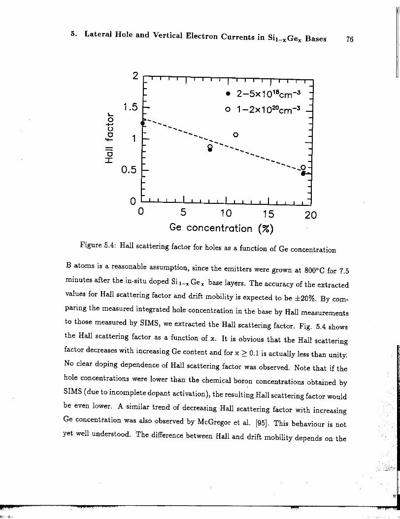
Using this method, Fig. 5.7 shows the extrac~ed effective bandgap narrowing
at room temperature as a function of Ge concentration for different doping levels.
For the devices with similar dopings, the linear dependence on Ge concentration is
obvious. Fitting the data at the same doping level gives a bandgap offset with respect
to Si of"", 7meV /l%Ge. Assuming'that this linear dependence on Ge concentration
is independent of doping, we have separated the two effects contributing to bandgap
reduction with respect to undoped Si: bandgap reduction due to Ge (~EG,Ge) and
bandgap narrowing due to heavy doping effects (~EG,dop).
~EG,eff = ~EG,Ge + ~EG,dop (5.5)
;,
'iri("l'i~~t1

5. Lateral Hole and Vertical Electron Currents in Si1-xGex Bases 83
Assuming a ~EG,dop of the form:
NA~EG,dop = A + B x log(iQ18 ~) (5.6)
and a-linear dependence of ~EG,Ge on x as ax, a three-parameter best fit to our data
was found to be:
NA~EG.eff = 28.6 + 27.4 x log(l~ -="3) + 688 x x (me V) (5.7)
where NA is the base doping and x the Ge concentration. The first two terms represent
bandgap narrowing due to doping and the last term is the Ge contribution. ~EG.eff is
not the measure of the actual bandgap reduction, but the effective (apparent) bandgap
reduction, relevant for minority carrier concentration and thus electron transport
across the Si 1-x Ge x base. The apparent bandgap is larger than the true bandgap
due to valence band filling in the degenerately doped semiconductor and hence, the
effects of Fermi-Dirac statistics [104]. The effective bandgap reduction is a useful
parameter to model the collector current of Si/Si 1-x Ge x /Si HBT's and predict the
enhancement over Si-base devices.
Experimental values for ~EG.dop for Si 1-x Gex are obtained by subtracting the
germanium contribution (688x meV) from the measured ~EG.eff. These values are
plotted in Fig. 5.8 vs. base doping. This is the first time that such data has been
collected for such a wide range of dopings and Ge concentrations in Si/Si 1-x Ge x /Si
HBT's. Also plotted are previously reported results by Swirhun et al. [85] and model
by Klaassen et al.[89] for apparent bandgap narrowing in p-type Si. The apparent
bandgap narrowing clearly increases with increased doping, as expected. No clear Ge
dependence is observed after the linear dependence has been subtracted. The bandgap
narrowing of 27me V / decade agrees well with the 25-33me V narrowing at various Ge
concentrations with the doping increase from 5 X 1011 cm-3 to 5 x 1018cm-3, obtained
from temperature dependent measurements by Poortmans et al.[98].
5. Lateral Hole and Vertical Electron Currents in Si1-xGex Bases 84
400.1- 7 X 1 018cm-3 .........1 6 1019 -3 ...300 . - X cm '" ...'"
$' "1-2.5 x10²°cm-3 '" '"
... ...Q) ... . ... ... ...
E ..., ...'"... ...... ...'-" 200 '" ...8;~ ... ...
G. "","'.'" ~ W 8:' ...""
<] 100 ", ...,... slope: 7meV /1 %Ge...
...'"......
00 0.1 0.2 0.3 0.4
Atomic Fraction Ge
Figure 5.7: Effective bandgap reduction with respect to intrinsic Si vs. Ge concen-tration
--

5. Lateral Hole and Vertical Electron Currents in Sit-xGex Bases 85
150,
'"
.18-27% ",'"
... 9-14% Si-models """"""
$" 100 80% ~""" .,.,.,.,.,.,'
Q) '" .,.,.,E ",'" .,.,.,'-' .,.,., "'.
'" .,.,.,Q. '" ...0 '" \"0 '"c5 50 ",'" /-- . .
W ~ ,,? fit to this data<3 .
Swirhun et 01.-- Klaassen et 01.
0
1017 1018 1019 1020 1021
Base Doping (cm-3)
Figure 5.8: Apparent bandgap narrowing vs. base doping after linear dependence ofthe bandgap reduction on Ge content has been subtracted

5. Lateral Hole and Vertical Electron Currents in Si1-xGex Bases 86
200 . Kamins, EDL'89, 31 %A Kin9' TED'89, 15-31 %.Pruljmboom, EDL'91 t 20%. Gruhlet EDL t92t 21 %~ . Pruijmboomt ME'92t 13%
E othis work 8-27%'-'
Q. 100 .cy """"""
0 'V
ci ""0 0w 0 0~ 0.."" .
o 'O 'i'"" .""""0 "" .
1 017 1018 1019 1020 1021
Base Doping (cm-3)
Figure 5.9: Apparent bandgap narrowing vs. base doping after linear dependence ofthe bandgap reduction on Ge content has been subtracted compared with data fromliterature
Plotted in Fig. 5.9 are data points for ilEG,dop for other SiGe HBT's reported in
the literature [19, 14, 18, 24, 90], along with our data of Fig. 5.8 and the model for
ilEG,dop. ilEG,eff, as defined in this work, was not directly given in these papers, but
adequate information on base doping, base-width, collector current, etc. was given so
that ilEG,eff could be calculated. ilEG,dop was then found after subtracting the linear
dependence on Ge, as described earlier. In general the data of the other work also lie
near our best fit for ilEG,eff' It is interesting to note that nearly all of the data points
which fall substantially below the best fit line are from devices which were fabricated
using an implanted emitter process, which is known to give rise to excess base dopant
diffusion (and possible parasitic barrier formation resulting in smaller ilEG,eff) [90].
Note that our results for ilEG,dop are consistently lower than those found in Si (as
~~

5. Lateral Hole and Vertical Electron Currents in Si1-xGex Bases 87
represented by the work of Swirhun [85] and Klaassen [89]), although calculations by
Jain et al.[105] predict LlEG,doP to be slightly higher in SiGe than in Si, and strain-
dependent. A possible explanation for smaller apparent bandgap narrowing compared
to Si lies in the fact that at the same doping level, due to the band splitting and
thus, reduced densities of states, the Fermi level in degenerately doped Si I-x Ge x lies
higher in the valence bands, and thus contributes more to the apparent bandgap
reduction. To relate the apparent bandgap narrowing to the true bandgap reduction
(LlEG,true) one needs to know the position of the Fermi level in the degenerately doped
material and take into account the effect of degenerate statistics (Fermi-Dirac instead
of Boltzmann), as illustrated in Fig. 5.10. The hole concentration (doping) is related
to the Fermi level (EF) by [86]:
2 Ev-EFp = NA = Nv~ F1/t.(-k ~) (5.8)
where Fl/t.(EF/kBT) is the Fermi-Dirac integral. Fig. 5.11 shows the calculated
position of the Fermi level with respect to the valence band edge as a function of base
doping for Si and Si 0.8 GeO.2 using equation 5.8 and the model of Prinz et al. [48]
for the effective valence band density of states in Si I-x Ge x . Note that the position
of the Fermi level starts to diverge from the straight line in the case of Si 0.8 Ge 0.2 at
a lower doping level, and diverges much faster with increasing doping, thus having a
bigger effect on LlEG,eff than in Si at the same doping level. Possin et al. [104] have
the first modeled the apparent bandgap narrowing as the sum of the true bandgap
narrowing (LlEG,true) and the negative term representing the Fermi-Dirac (~EG,FD)
correction given as:
LlEG,eff = LlEG,true + LlEG,FD (5.9)
LlEG,FD is always negative and it is given by:
[ ~ Ev - EF ] N ALlEG FD = In e kBT F1/t.( ) = -(Ev - EF) + kBTln-N (5.10) , kBT v
~c"",c.

5. Lateral Hole and Vertical Electron Currents in Si1-xGex Bases 88
,
--A A Ec. .. .. .. ,. ., .
EG,eff ! ! EG, true. ., .=EG.true+Ey-EF-kB T1n(NJNy) ! ~
E: VV
EF --
Figure 5.10: Qualitative band diagram illustrating the difference between the trueand the effective bandgap

5. Lateral Hole and Vertical Electron Currents in Si1-xGex Bases 89
150
100, > 50
Q)
E'-' 0
~W
1>-50W
nondegenerate-100
-1501017 1018 1019 1020
base doping (cm-3)
Figure 5.11: Position of the Fermi level with respect to the valence band edge for Siand Si l-x Ge x
\
-

5. Lateral Hole and Vertical Electron Currents in Si1-xGex Bases 90
150
, > 100Q)
E
~~ 50
00 5 X 1 019 1 020
base doping (cm-3)
Figure 5.12: Calculated Fermi-Dirac correction to the bandgap narrowing as a func-tion of base doping for various Ge concentrations at room temperature
Fig. 5.12 shows calculated values for L).EG,FD at room temperature as a function of
doping for x = 0, 10 and 20% using equation 5.10. We have applied the L).EG,FD to
our Si I-x Ge x data of Fig. 5.7 and subtracted the linear Ge dependence (L).EG,Ge , tme V /1 %) to extract the true Si I-x Ge x bandgap reduction. The results are plotted
in Fig. 5.13. Also shown in the figure are the theoretical calculation for the true
bandgap narrowing in p-Si by Jain and Roulston [105] (solid line) and room tem-
perature Si-data of Wagner [106] measured by photoluminescence. The L).EG,dop,true
agrees fairly well with the Si data at lower dopings, but at heavy doping levels the
Si I-x Ge x data lies higher. There is no clear Ge dependence on L).EG,dop,true, however.
If the carrier concentration effective mass of ref. [92] were used, which would result in
even bigger L).EG,FD, the data points would shift to even higher values of L).EG,dop,true

5. Lateral Hole and Vertical Electron Currents in Si1-xGex Bases 91
300
250 . 9-14X (this work), . 17-27X (this work)~ 200 . Si (Wagner. 300K)
E---2150 .Q.0
ci 1 00W<3
50
01018 1019 1020
base doping (cm-3)
Figure 5.13: The heavy-doping contribution to the true bandgap reduction in strainedSi l-x Ge x calculated from the measured ~EG,eff as: ~EG,dop,true = ~EGldop-~EG,FD'
Also shown for comparison are the Si data points of Wagner and the theoreticalcalculation for p-Si of Jain and Roulston (solid line).

5. Lateral Hole and Vertical Electron Currents in Si1-xGex Bases 92
at high doping levels and higher Ge concentrations. On the other hand, the observed
Fermi energy in p-Si is less than predicted by the conventional density of states equa-
tion (5.8) [107]. If similar behaviour were the case in Si I-x Ge x , this would result
in overestimated ~EG,dop;true' Although some uncertainty in the absolute value of
~EG,dop.true remains, the Fermi level in strained Si I-x Ge x clearly lies higher than
in Si for the same doping level resulting in stronger effects of degenerate statistics.
Thus, the weaker doping dependence and lower values compared to Si data of the
apparent ~EG,dop are attributed to the larger effect of ~EG.FD in Si I-x Ge x than in
Si.
5.5 Collector current vs. base resistance model
The two important parameters for the DC design of Si I-x Ge x HBT's is the base
sheet resistance and the collector current enhancement with respect to Si. The base
sheet resistance is important for high-speed application of Si I-x Ge x HBT's and is
often more easier measured (and more relevant) than the actual doping in the base
or the integrated hole concentration. The effective bandgap reduction determines the
collector current enhancement factor over the similarly doped all-Si device. By using
R. = (qp,pGB)-l one can rewrite equation 5.4 to model the collector current as a
function of these two parameters:
(N N ) t;.EQ .ffJ 2 C v SiGe 2 D R TT (5 11)co = q (NcNv)Si nio,Si n J1,p B,sheet e B .
where p,p and Dn are the lateral drift hole mobility and vertical electron diffusion
coefficient in p+ -base, respectively. Equation 5.11 shows a clear trade-off between
collector current (gain) and base sheet resistance. This is summarized in Fig. 5.14.
The relative collector current with respect to Si is plotted as a function of base sheet
resistance for various Ge concentrations. A relative collector current factor of one is
defined for Si at a base sheet resistance of 1k.\1jsq. The lines are the model calculations

5. Lateral Hole and Vertical Electron Currents in Si1-xGex Bases 93
104+ICQ)
~1 0000
5 100+I()Q)
-0 100Q)
.~ 1+I0Q)
~ 0.110 100 1000 104 105
Base Sheet Resistance (ohm/sq.).
Figure 5.14: Relative collector current vs. base sheet resistance. The lines correspondto the model, the points are the data
assuming base widths of 50oA, hole drift mobilities given by equation 5.1, bandgap
reduction by equation 5.7, strain-induced correction for densities of states given by
[48] and electron mobility by [85]. The points are measured data in our HBT's scaled
to 50oA base-widths. Note especially the effect of the bandgap narrowing due to
heavy base doping which has a more significant effect than the lateral and vertical
mobility reduction at heavy dopings. The bandgap narrowing causes curves not to
be linear, and limits the reduction in collector current at low base resistances.
5.6 Summary
This chapter provides a comprehensive study of majority carrier properties in heav-
ily B-doped strained Si1-xGex layers as well as collector currents of HBT's in the
.","

5. Lateral Hole and Vertical Electron Currents in Si1-xGex Bases 94
sample Ge GB -SIMS GB -Hall NA doped RB,sheet Jco b.EG,eft'number (%) (1014cm-2) (1014cm-2) (1019cm-3) WB (A) (knjsq.) (nAjcm2) (meV)
933 0 4.2 3.8 4.3 980 0.475934 11 14.7 13.4 22.5 660 0.16 0.020 165935 18.5 0.17 0.27 0.52 400 6.29 2.203 171936 17.5 4.78 6.2 22.0 400 0.36 0.1712 197937 23 0.03 0.31 160 36.25 84.31 197938 23 1.4 5.9 160 7.5 4.878 231939 23 2.6 12.0 80 0.88940 27 0.44 1.0 175 27.89 32.06 245946 27 4.8 13.0 90 0.98947 9 0.47 0.52 0.26 1830 2.26 0.0871 106948 9 15.0 8.3 1800 0.16949 9 14.2 16.0 11.5. 1190 0.12 0.0086 140633 0 0.27 0.45 600 3.8 .0.0869 77636 14 0.43 0.61 650 3.2 0.7505 161641 24 0.21 0.23 400 5.8642 14 0.062 0.1 600 18.0 4.109 140643 21 0.69 0.6 600 2.0 1.537 186
Table 5.1: Summary of HBT samples and relevant parameters (GB -SIMS is the rawdata uncorrected for depletion region effects, GB -Hall is calculated assuming rH = 1)
wide range of dopings and Ge concentrations for the first time [108]. The hole Hall
mobility decreases with increasing Ge concentration at a fixed doping level, because
the Hall scattering factor decreases as Ge is added. The lateral hole drift mobility
remains approximately constant as Ge is added, with perhaps a slight increase at low
doping levels. The apparent bandgap narrowing in p-type strained Si l-x Ge x was
measured for the first time over a wide range of doping and Ge levels. The depen-
dence of the narrowing on Ge was independent of doping, and the heavy doping
contribution to the effective bandgap narrowing is found to be independent of Ge
concentration but slightly lower than that obtained for Si at the same doping level,

5. Lateral Hole and Vertical Electron Currents in Si1-xGex Bases 95
attributed to the Fermi-Dirac statistics effect. Finally, a trade-off between the col-
lector current enhancement and base sheet resistance is presented for DC modeling
of Si I-x Ge x HBT's. The bandgap narrowing at heavy doping levels (low base sheet
resistances) has a larger impact than that of reduced mobility at high doping levels.
~ -

Chapter 6
Minority Carrier Properties in Si1-xGex
6.1 Introduction
Bipolar transistors rely on minority carrier transport across the device. This is why
accurate modeling of minority carrier transport deserves a lot of attention. Important
parameters to characterize it are minority carrier mobility (Jln in p-type material),
minority carrier lifetime (Tn), and minority carrier diffusion length (1n), which are
related by:
1n = JD:-;: (6.1)
where Dn is the diffusion coefficient (Dn = I.£n x kBT /q). The collector current density
of a bipolar transistor in forward active mode is given by:
qD n.2 ~Jc = N 1 . nh(l /1 ) e kBT (6.2)A n sm wB n
In case of narrow bases (WB < < 1n) equation 6.2 simplifies to 5.3 for DC collec-
tor current. In the previous chapter, we have measured nj2 (i.e. Eo) in doped
Si 1-x Ge x assuming that Dn is the same as in silicon "(given by [84]). Although this
assumption might be reasonable considering no significant Ge-dependence on major-
ity hole mobility in heavily doped HBT bases, the accurate values of minority carrier
mobility still need to be determined in strained Si 1-x Ge x alloys.
96
-

6. Minority Carrier Properties in Si1-xGex 97
It has been experimentally observed that the minority carrier mobility in heavily
doped silicon is larger than majority carrier mobility [85, 84]. The difference between
majority and minority mobilities are not surprising, since apart from heavy doping
effects.on the bandgap structure, the dominant impurities for electron scattering be-
come acceptors instead of donors, i.e. majority carriers are holes instead of electrons.
Both electron-hole and electron~electron scattering need to be taken into account.
The temperature dependence of minority carrier mobility IS also very different from
the majority [101]. In case of strained Si1_xGex alloys, the minority carrier mobility
is also expected to be affected by strain and alloy scattering.
One could independently determine the minority carrier diffusion coefficient in
strained Si 1-x Ge x by measuring both the lifetime and minority carrier diffusion
length. In this chapter, we report the design of the lateral device ~tructure for
diffusion length and lifetime measurements and diffusion length results for strained
Si1_xGex layers in the p-type doping range of 2 x 1017 cm-3 to 4 x 1018 cm-3.
6.2 Methods to measure minority carrier diffusion length
and mobility
In silicon, many types of device structures have been used over the years by various
authors to extract minority carrier properties. A critical review of measurements
previously reported is included in the work of del Alamo [96] and Swirhun [97].
Since collector current in a bipolar transistor is a clean monitor of minority carriers
through the base and it is ideal with respect to base-emitter voltage, del Alamo [96]
and Swirhun [97] have reported a comprehensive set of diffusion length measurements
on lateral bipolar transistors for nand p-type Si, respectively (the method first used
by Wieder [109]). In case of wide-base bipolar transistor (WB » Ln) from equation
--

6. Minority Carrier Properties in Sit-xGex 98
6.2 collector current becomes:
2qDnni2 =:!!J3.. ~Ic = A e Ln e kBT (6.3)NALn
In case of lateral devices A is the collecting area which includes two-dimensional
effects. The lateral devices were obtained by implantation of emitter and collector
into the base material. From the collector current measurements on devices with
various basewidths, the diffusion length was determined by fitting Ic vs. WB.
Minority carrier mobility cannot be extracted just from DC measurements. To
measure minority carrier mobility a time-dependent technique needs to be used. For
example, if one independently measured lifetime, the mobility could be extracted
by combining the lifetime with the diffusion length measurements. The lifetime at
heavy doping levels is expected to be a fundamental property of the material due to
recombination dominated by Auger processes. No data on minority carrier lifetime is
available for Si I-x Ge x at present.
Lifetime can be measured by decay of photoluminescence radiation of electron-
hole pairs after excitation by a short laser pulse [110, 111, 85]. Since band-edge
photoluminescence has been observed in Si I-x Ge x alloys [65] one could essentially
measure lifetime. However, photoluminescence from Si I-x Ge x quantum wells has
only been observed at low temperatures which restricts lifetime measurements to
below room temperature. Minority carrier lifetime could also be measured as a decay
of photo excited carriers, as proposed by Stevenson and Keyes [112]. The excess carrier
generated by light pulses cause a momentary increase in the conductivity. The decay
of that conductivity is a measure of lifetime. Another method to measure lifetime
is from AC diffusion length measurements, as demonstrated by Dziewior and Silber
[113], since the diffusion length measured at frequency w is related to the DC (10)
value by:10L(w) =
/ 1 I ;..- (6.4)v .L + JWT

6. Minority Carrier Properties in Si1-xGex 99
Misiakos et al. [114] have proposed a method for simultaneous measurement
od diffusion coefficient, lifetime and diffusion length based on lateral collection of
photogenerated carriers by a semi-infinite junction by DC measurements and transient
response in the frequency domain.
To our knowledge, the only reported measurement of the electron diffusion coef-
ficient in Si I-x Ge x by King et. al. [14] was based on DC measurements on vertical
HBT collector current. He was forced to make the assumption of no differences
in densities of states between Si and strained Si I-x Ge x and that minority carrier
diffusion coefficients in Si and Si I-x Ge x have the same temperature dependence.
Furthermore, high values of oxygen contamination (1 X 1020 cm-3) were present in
these Si I-x Ge x layers.
We have designed a lateral device structure for the diffusion length measurements.
Although one cannot provide a bulk strained Si I-x Ge x material, one can optimize
layer structure such that the lateral minority carrier current transport is dominated
by the transport through a thin Si I-x Ge x layer. This is possible due to conduction
band offset between p+ -Si and p+ -Si I-x Ge x' However, special care needs to be taken
to prevent parallel Si transport, as well as loss of carriers due to surface recombination.
The same structure could be used for lifetime measurements by monitoring the decay
of photoconductivity [112] or, at low temperatures, by measuring photoluminescence
decay. The following sections discuss the proposed device structure and the design
details, as well as initial diffusion length measurements.
6.3 Structure optimization for measurements of minority
carrier parameters in strained SiGe alloys
Due to strain relaxation constrains (see chapter 2) Si I-x Ge x material can only be
fabricated in thin layers, on the order of 100-10001. That makes it impossible to

6. Minority Carrier Properties in Si1-xGex 100
loE ~.,20-400 n m
60 nm
-3-5 .;Urn
101 cm3..jI
." ~--~ ~~."..,.~._""~. .,-o l
< 100>p-Si substrate
Figure 6.1: Device structure optimized using MEDICI (2D simulator) for diffusionlength measurements
design vertical "long-base" devices, so "long-base" device structures are limited to
lateral transport. An issue that needs to be solved in lateral devices is the confinment
of minority carriers within the thin Si I-x Ge x layer. However, in case of p-Si/p-
Sil-xGex/p-Si heterostructures, since the bandgap of strained Si I-x Ge x is smaller
than silicon bandgap, it is reasonable to assume that most of electrons are going to
be confined within the Si I-x Gex layer. Such heterostructures were optimized using
2D device simulation program (MEDICI) by simulating lateral bipolar transistors for
diffusion length measurements. The structure is shown in Fig. 6.1. The emitter
and collector would be fabricated by ion implantation and annealing. The distance
between the emitter and collector implant determines the basewidth WB. Fig. 6.2

6. Minority Carrier Properties in Si1-xGex 101
1.5
~ 1>Q)
~ 0.5~Q)CQ)
0
-0.50 500 1000
distance (1)
Figure 6.2: Simulated band diagram of p+ -Si/p+ -Si 0.8 Ge 0.2 /p+ -Si
shows the simulated band diagram of a p+ -Si/p+ -Si 0.8 Ge 0.2 /p+ -Si heterostructure.
For""' 20% germanium in the Si 1-x Ge x layer the conduction band difference is ""'
140meV between the Si and Si 1-x Gex.
In lateral bipolar transistors, the collector current is inversely proportional to
exp(wB/Ln) (equation 6.3), so the slope of the measured collector current, on a log-
arithmic scale, vs. WB gives the diffusion length. To first order the ratio of lateral
currents in Si 1-x Ge x and Si is given by:
Ic(SiGe) ~ ~~ NA(Si) NcNv(SiGe) e~ (6.5)Ic(Si) A(Si) NA(SiGe) NcNv(Si)
The thicker the Si 1-x Ge x layer, more current will flow through Si 1-x Ge x' The thick-
ness of the Si 1-x Ge x layer is limited by the critical thickness. The implants need
to be shallow to minimize the collecting area in silicon. The higher the doping in
I
iow" I

6. Minority Carrier Properties in Si1-xGex 102
surrounding Si layers the better is the current ratio (i.e. less current in Si), until
the doping level is reached to start causing significant bandgap narrowing or leakage
currents in p+ -n+ junctions. The losses of minority carriers to the substrate or to
the surface also need to be taken into account. The doping and the thickness of the
bottom Si layer were optimized for negligible substrate effects. For p-type Si doped
1 X 1019 cm-3 the required thickness was found to be at least 3JLm. The models of
Swirhun [97] for minority carrier parameters were used in the simulation.
Fig. 6.3 shows collector currents vs. base-emitter voltage for the above struc-
ture (NA(SiGe) = 1 x 1019 cm-3, NA(Si) = 5 x 1019 cm-3), as well as bulk Si (NA =1 X 1019 cm-3, no Si I-x Ge x channel), and bulk Si I-x Ge x (possible in simulation,
NA = 1 X 1019 cm-3) devices when no surface recombination is present and WB ~ 4Ln.
The collector current in Si 0.8 Ge 0.2 channel device (realistic structure) is. almost iden-
tical to the bulk Si 0.8 Ge 0.2 device. However, the collector current in the all-Si device
is much lower ('" exp( -L1EG/kBT)). The simulations confirmed the exponential de-
pendence of the collector current on basewidth and that the extracted diffusion lengths
were the same in case of bulk Si 0.8 Ge 0.2 and Si 0.8 Ge 0.2 -channel devices. To further
confirm that the lateral electron transport is mainly through the Si 0.8 Ge 0.2 layer,
simulations with different mobilities in Si and Si 0.8 Ge 0.2 were performed. This is
shown in Fig. 6.4. The increase in electron mobility in the Si 0.8 Ge 0.2 layer increases
the collector current, while the change in electron mobility in Si does not affect the
current.
After the preliminary structure was designed, surface recombination was intro-
duced in the simulations. Significant surface recombination could cause the measured
diffusion length to appear lower than the true one due to a lower effective lifetime. If
the effective lifetime were measured independently, one could still extract the correct
minority carrier diffusion coefficient in the Si I-x Ge x layer, but not the true lifetime.
To first order, if the cap Si layer is thin ( < < Ln) and the surface recombination veloc-

6. Minority Carrier Properties in Si1-xGex 103
E 1 0-6~10-7 /" c,' /« 1 0-8 \b0 /'-' ~/
1 0-9 .<)~ /""""' ~/~1 0-10 /~1 0-11 //"'010 -12 0'
.<'~~1 0-13 ~o:Q) Ci
t10-14 c,0a')o~1 0-15 c;,a' ",.II--=10-16 --810-17
0 -0.2 -0.4 -0.6 -0.8
VBE (V)
Figure 6.3: Simulated collector current density for a Si 0.8 Ge 0.2 channel device(WSiGe = 600A, NA(SiGe) = 1 x 1019 cm-3, NA(Si) = 5 x 1019 cm-3, WSi,cap =200A, WSi,buffer = 5p.m, wB = 15p.m), and bulk Si and bulk Si 0.8 Ge 0.2 devices,(NA = 1 X 1019 cm-3, wvertical = 20p.m, wB = 15p.m in both cases)
., Ic,~ "-!

6. Minority Carrier Properties in Si1-xGex 104
E 1 0-6 "~ 1 0-7 ",,"~ 1 0-8 \b0~:'"
~"~ 1 0-9 .C)~,,"
~1 0-10 ~,,"(/) "~1 0-11 ",,"-01 0-12~1 0-13Q)t10-14"810-15=1 0-1681 0-17
0 -0.2 -0.4 -0.6 -0.8
V8E (V)
Figure 6.4: Simulated collector current density for a Si 0.8 Ge 0.2 channel device(WSi,cap = 200A, WSiGe = 600A, WSi,buffer = 5JLm) when electron mobilities in Siand Si 0.8 Ge 0.2 layers are varied
~
6. Minority Carrier Properties in Si1-xGex 105
ity slow compared to Dn.Si/WSi.cap so that the electron quasi Fermi level at the surface
is the same as that in the Si I-x Ge x , one can write:
(~ ) . -~-~ + ~ S ~ (66)SlGe - - eff e B .dt Tn,eff Tn,SiGe WSiGe
where nSiGe is the electron concentration in Si I-x Ge x , Tn,eff is the measured lifetime,
Tn SiGe is the true lifetime in Si I-x Ge x , Seff is the surface recombination velocity,
(accounting for any band banding effects at the Si surface) and WSiGe is the thickness
of the Si 0.8 Ge 0.2 layer. The effective lifetime can be modeled as:
( ) -1 1 Sff ~Tn.eff = + -=-e kBT (6.7)
Tn,SiGe WSiGe
This is illustrated in Fig. 6.S where the effective lifetime is plotted as a function of the
true lifetime for different Self. The Tn range in the figure approximatel~ corresponds
to the 1 x 1018 cm-3 to S X 1019 cm-3 p-type doping range in Si [97]. For surface
recombination to have negligible effects, the following needs to hold:
~ WS.GSeffe kBT« 1 e (6.8)Tn,SiGe
Assuming the same minority carrier lifetimes in Si I-x Ge x as in Si ('""" IOns), Seff
should be below'""" 104cm/s. The simulation gives an upper limit to Seff of 6000cm/s.
By increasing the thickness of the top Si layer the surface effects are reduced, but thin-
ner top layers are desired for high lateral current ratio (equation 6.5). The thickness
for Seff '""" 105cm/s needs to be above soooA.
6.4 Device fabrication
A set of structures was grown to measure minority carrier parameters. A thick (3-
SJLm) p+(l X 1019 cm-3-S X 1019 cm-3) Si buffer layer was grown to prevent the dif-
fusion of carriers to p- Si substrate in all samples. Si 0.8 Ge 0.2 layers 600A thick
and 300A thick were grown with the doping levels varying from 3 X 1017 cm-3 to

6. Minority Carrier Properties in Si1-xGex 106
200cnc:
~Q,) 150E
.-+-'Q,)
~ 100Q,)>.-
+-'
~ 50l.+-I.+-Q,)
50 100 150 200true SiGe lifetime (ns)
Figure 6.5: Effective lifetime as a function of true lifetime for various surface recom-bination velocities
~'C~"

6. Minority Carrier Properties in Si1-xGex 107
sam pIe B2Hsflow Si 0.8 Ge 0.2 thickness Si cap Si I-x Ge x dopingnumber (sccm) (1) thickness (1) (1018cm-3)
(10ppm in H2) by SIMS by SIMS by SIMS
1567 11 480 4360 3.21568 11 240 4480 3.81569 0.8 400 4320 . 0.26
1570 2.5 440 4120 0.71571. 6.2 504 4000 1.71572 5 400 240 1.21573 7 400 230 2.51574 7 180 240 2.7
Table 6.1: Summary of structural parameters of samples designed for measurementsof minority carrier properties
4 x 1018 cm-3. Both structures with thick ("" 4000A) and thin ("" 200A) p+Si-cap
layers were grown (1.5 X 1019 cm-3-2 X 1019 cm-3). The layer thicknesses and doping
levels were measured by SIMS. The actual doping in the Si I-x Ge x layers measured
by SIMS was lower (by a factor of 2-3) than expected from B2Hs flows in all sam-
ples. The actual Si I-x Ge x layer thicknesses were also lower than predicted from the
expected growth rate (by ""1.5). The summary of samples and relevant structure
parameters is given in Table 6.1.
To measure the electron diffusion length, we have fabricated devices similar to
that of Fig. 6.1 except that the minority carriers were generated by light illumination
instead of a forward biased p-n junction. This method was proposed by Misiakos et
at. [114]. It is shown in Fig. 6.6.
To minimize the surface recombination, a high quality thermal oxide is desired at
Si/SiO2 interface. However, processing of Si/Si I-x Ge x heterojunctions is restricted
to temperatures below 800°C. We have used a thin layer ("" 501) of thermal oxide

6. Minority Carrier Properties in Si1-xGex 108
light
11111.11C I" ~ ~I
20 -450 nmp-Si 0 ~eO?
17 '19 '--1 20-50 nm10 -10 cm-
S. -3-5 )Jmp- 1
1019 -3- cm
< 100>p-Si substrate
Figure 6.6: Device structure used for diffusion length measurements. The collectorcontact area was 150 x 150p.m2, the basewidths ranged from 1p.m to 30p.m.

6. Minority Carrier Properties in Si1-xGex 109
grown at 700°C (10 min. dry O2 + 40 min wet H2O + 5 min. dry O2 + 10 min N2),
as an interface layer, and then deposited 5000A thick plasma oxide at low temper-
ature (350°C). A surface recombination velocity of below 1000cm/s is predicted for
2 X 1019 cm-3 p-type substrate for a dry O2 oxidation followed by an argon anneal
for a high quality Si/Si02 interface [115]. Assuming another factor of 10 higher Seff
due to possible lower quality of our thermal oxides would still give negligible effects.
The oxide was used as an ion implantation mask. Four various implant conditions
(both P and As) were used to form the collector. The summary of implant conditions
is given in Table 6.2. On some of the samples with thick Si caps, the Si cap layers
very partially etched prior to implantation to reduce the Si current path. Device with
different implants were processed simultaneously, for comparison. All the implants
were annealed at 700°C for 20 minutes.
The entire p-n junction area was covered by the metal contact which laterally
extended over the passivating oxide to provide a mask for the uniform light beam,
as shown in Fig. 6.6. On one side of the contact the shaded area extended up to a
distance WB (varied 1 - 30p.m) while it was much larger on the other sides (150p.m).
This provides the photo current that is a function of basewidth WB (see the following
section).
Ti/ Al metalization was used as the collector contact. Devices with 1000A and
2000A thick metal were fabricated.
6.5 Diffusion length measurements
Misiakos et al. [116] have derived an analytical expression for lateral photocurrent
assuming a thick bulk material. In case of p-Si/p-Si1-xGex/p-Si structure, the exact
expression becomes complicated, but since most of carriers generated are going to be

6. Minority Carrier Properties in Si1-xGex 110
run implant expected depthconditions (SUPREM)
I P1572-1574, not etched 1 x 1015 cm-2,20KeV 900A
1569-1571 etched 4000AII P
1 X 1015 cm-2,20KeV ~".:
1569-1571, etched 1000A + 1 x 1015 cm-2,60KeV 3500A+ 1 x 1015 cm-2,100KeV+ 1 x 1015 cm-2,150KeV
III P1 X 1015 cm-2 20KeV,
1569-1571, etched 2000A + 1 x 1015 cm-2,60KeV 2500A+ 1 x 1015 cm-2,100KeVIV As .
2 X 1015 cm-2 10KeV,1569-1571, etched 1000A + 1 x 1015 cm-2,60KeV 1400A
1572- 74, not etched + 1 x 1015 cm-2,110KeV
Table 6.2: Summary of processing runs and implant conditions
confined to Si 1-x Ge x layer, one can approximate photo current as:
Jph ~ roo qGe-x/Lndx = qGLne-WB/Ln (6.9)JWB
where G is the generation rate of carriers per unit area. The exponential dependence
on basewidth is the same as in case of a bipolar transistor (I c:x: e-WB/Ln), as expected.
A typical measured photogenerated current vs. basewidth is plotted in Fig. 6.7.
That the measurement was not affected by the absorption length of the incident light
was confirmed by measurements with visible light (microscope lamp on the probe
station) and 1.2JLm laser. In the case of a visible light source, carriers were mostly
generated in Si layers and diffused into the Si 1-x Ge x well, while with 1.2JLm light
source most of the carriers were probably generated within the Si 1-x Ge x layer. No

6. Minority Carrier Properties in Si1-xGex 111
'< NA(SiGe)=1. 7x1 Q18cm-3Q. 10
'-"'
+'c:Q)L-
§ /+'.,g 1 Ln=3.78J1,mQ.
0.4
2 4 6 8 10 12 14 16
basewidth (J1,m)
Figure 6.7: Photocurrent vs. basewidth for NA =1.7 X 1018 cm-3 in Sio.8Geo.2 layer

6. Minority Carrier Properties in Si1-xGex 112
difference in the results was observed, within the experimental error. The collector
currents were measured at zero bias using HP-4140B pA-meter. The collector cur-
rents in devices with thin metal (1000A) mask did not approach zero at very large
basewidths ('"'" 10Ln), but rather a constant background current, probably because
the thin metal was still transparent for some of the light. This was not the case when
the metal thickness was increased to 2000A. In the case of thin metal devices, the
background current was subtracted from the total current to evaluate the diffusion
lengths. The same diffusion lengths (within 10%) were found as on the devices with
thick metal on the same wafers.
Various implant conditions did not affect the diffusion length results. However,
whenever the implant depth reached the Si I-x Ge x layer, an increased leakage cur-
rent in base-collector diode characteristics was observed at room te~perature ('"'"
100nA/1 V). This was probably due to implantation damage in Si I-x Ge x. Enhanced
implantation damage in Si I-x Ge x relative to that in Si for similar implantation con-
ditions has been reported {117]. lithe n+ region did not reach the Sil-xGex layer,
leakage in p-n junctions was negligible « 1nA/1V). However, if the p-n junction is
within the top Si layer and the collecting junction does not reach the Si I-x Ge x layer,
the thin p+-Si layer between the Sil-xGex channel and the n+collector presents an
additional barrier for electron transport resulting in lower collector current levels.
However, if the barrier thickness is small (a few hundred A) compared to the lat-
eral basewidth (which was always the case in our devices), the collector currents at
different basewidths should still scale as exp( -wB/Ln), so that the same extracted
Ln is found. Neither the Si-cap thickness nor the processing variations affected the
Ln measurements within the experimental error, so parallel transport in Si cap layer
probably did not affect the results.
The room temperature results are summarized in Fig. 6.8. Also shown in the
figure are the results for Si reported by Swirhun [97] and Leu and Neugroschel [118].
~-

6. Minority Carrier Properties in Si1-xGex 113
A SwirhunE A C Neugroshel
~ . visible.thick m.I A . visible.thin m....c: 1 0 c. visible. As~ .&. vlslble.thl~ c.c: 0 1.2#£m.thln c.Q) * 1.2#£m.thlck m.- A A
.Q ! 0 I A ~c -tJ A
(/):J c~ Is. Dc-0 .- A,
1
2x 10¹⁷ 1018 1019
p-doping (cm-3)
Figure 6.8: Room temperature diffusion length vs.doping in Si 0.8 Ge 0.2 , published Sidata is also shown
For heavily doped Si (above ,...,2 x 1019 cm-3), the decrease in measured diffusion
lengths is attributed to Auger recombination. At lower doping levels, the lifetimes
measured in Si from processed samples (reflected in the plotted Si diffusion lengths
of Fig. 6.8), were well below the Auger limit, most likely caused by Shockley-Read-
Hall (SRH) or trap-assisted Auger processes [97, 118]. Both SRH and trap-assisted
Auger recombination are mediated by recombination centers in the bandgap so the
measured minority carrier parameters reflect both material and processing quality.
Since our samples are all doped well below 1 X 1019 cm-3 we also expect SRH or
trap-assisted Auger processes to dominate. It is clear from Fig. 6.8 that the values
obtained for our samples have lower diffusion lengths than similarly doped silicon at
room temperature.
t

6. Minority Carrier Properties in Sit-xGex 114
~E ... b. Si 100K. Swirhun~ ... D Si 77K. Neugroshel~ . SiGe 8SK (impl.l)
"-"" . ... SiGe 8SK (impl.lf)..c. . SiGe 8SK. thin cap~ 10 b.
C~ .. aC0 . b..- b.(J) . D D:J
I+- b.l+-.--0
1
2x 10¹⁷ 1 018 1019
p-doping (cm-3)
Figure 6.9: Low temperature diffusion length vs.doping in Si 0.8 Ge 0.2, also shownpublished Si data
We have also performed low temperature measurements. Fig. 6.9 shows the
Si 0.8 Ge 0.2 diffusion length measured at 85K. Also shown for comparison, is the Si
data of Swirhun [97] measured at lOOK and data of Leu and Neugroschel [118] mea-
sured at 77K. There is no sufficient Si data at low temperature published to clearly
establish diffusion length vs. doping curve, and the temperature dependence of mi-
nority carrier mobility is strongly doping dependent [97], but it is clear from Fig. 6.9
that data points for Si I-x Ge x lie near the published Si data.
We think that the reason for the diffusion lengths compared to Si at room vs.
low temperature is not a bulk Si I-x Ge x property, but that the room temperature
data is affected by surface recombination due to the limited quality of our passiva-
6. Minority Carrier Properties in Si1-xGex 115
tion oxide. If the effective surface recombination velocity is much larger than we
expected, the effective lifetime would be much lower resulting in lower measured dif-
fusion lengths. At low temperature however, due to the better confinment of carriers
within Si I-x Ge x (exponential factor in equation 6.7), the surface recombination be-
comes less significant and measured diffusion lengths represent true properties of the
material. This was confirmed by temperature dependent PL measurements. It has
recently been shown [119] that the photoluminescence (PL) from Si I-x Gex quantum
wells decreases with increasing temperature above lOOK due to a low effective lifetime
caused by surface recombination at the top Si surface.
To extract minority carrier mobility one still needs to measure the lifetime. If
measured at room temperature on the same samples, the true mobility values could
be extracted since the same effective lifetime would be measured as t~at affecting
the diffusion length measurements, provided that the surface is passivated in the
same manner. One way to measure electron lifetime would be to modulate the light
source at a frequency w, where w "'" liT ("'" 10MHz) and use equation 6.4 to calculate
lifetimes from DC and AC diffusion lengths [113] or monitor the transient response
in the frequency domain [114]. A more straightforward way would be to measure
the change in photoconductivity of the sample in time when illuminated with a short
light pulse [112]. Finally, all the samples used in this study exhibited strong PL
signal at 77K and 10K. By monitoring the PL decay low temperature lifetime could
be measured. The lifetime measurement and extraction of a lateral minority carrier
diffusion coefficient vs. doping will be subject of future work.
Note that for HBT modeling the vertical (not lateral as given in this chapter)
Dn is needed. The strain moves the four conduction band valleys in the growth
plane down with respect to the other two in the growth direction. As a result, the
electrons traveling in the growth direction will experience the transverse effective
mass m* = mt (0.19 in Si) while those in the growth plane will see m* given by:
~

6. Minority Carrier Properties in Si1-xGex 116
-1-. = l + -1-. Assumin g that the strain does not affect the band curvatures , onem ml mj
could easily relate vertical and lateral electron mobilities as the ratio of lateral and
vertical effective masses.
6.6 Summary
This chapter provides details of SijSi I-x Ge x jSi heterostructure design for the best
performance of lateral devices to extract minority carrier parameters in strained
Si I-x Ge x. The first measurements of the electron diffusion length as a function of
p-doping (2 x 1017 cm-3 - 4 x 1018 cm-3) in Si 0.8 Ge 0.2 are presented. Room temper-
ature results are affected by surface recombination and the diffusion length appears
lower than that reported in Si. Effects of the surface recombination are supressed
at low temperature due to better confinment of carriers within the Si l~x Ge x layer.
Low temperature diffusion length values (85K) appear similar or slightly higher than
reported Si data. This may be due to high quality material (higher lifetimes) or
increased minority carrier mobility. Minority carrier lifetime still remains to be mea-
sured to extract the electron mobilities.

Chapter 7
.
Electron Resonant Tunneling in SijSi1-xGex
Heterostructures
7.1 Introduction
The main focus of this thesis has been npn SijSi I-x Ge x jSi HBT's, the device in
SijSi I-x Ge x material system which is the most likely to be exploited in industry in
the near future. However, opportunities for novel heterojunction device structures
in Si-based material system exist beyond HBT's. One interesting vertical-transport
devices is a resonant tunneling structure. In chapter 3 we have used p-type reso-
nant tunneling diodes as a tool to characterize SijSi I-x Ge x interfaces. From the
application perspective, resonant tunneling devices are very interesting because of
their potential high speed performance [120, 121, 122]. The integration of resonant
tunneling diodes into transistor structures opens a field of multifunctional devices
which can lead to a reduction in circuit complexity and size. This field has advanced
much further in 111- V's than in the Si-based material system. Since the first resonant
tunneling bipolar transistor operating at room temperature was demonstrated [123],
such applications as a multiple state memory [124, 125], a parity generator [126], and
a frequency multiplier [127] have been demonstrated in 111- V's.
117

7. Electron Resonant Tunneling in SijSi1-xGex Heterostructures 118
7.2 Device fabrication
In SijSi 1-x Ge x material system, the resonant tunneling of holes has been exten-
sively.studied [72, 73, 74], but the electron resonant tunneling has not received much
attention, except for the single report of Ismail et al. [75]. This is mainly due to the
energy band configuration, namely the relatively large valence band offset of a strained
Si1_xGex layer grown on Si substrate, as explained in chapter 2. To achieve the elec-
tron resonant tunneling, a certain offset in the conduction band is needed. This can
be accomplished by exploiting a strained Sijrelaxed Si1_xGex heterojunction grown
on a relaxed Si1_yGey buffer on top of a <100> Si substrate. Such a structure re-
quires a capability of growing high quality, n-type doped, relaxed Si1_xGex layers. In
these structures, Si layers are subjected to tensile strain. The strain causes splitting
of the conduction bands, such that the four valleys in the growth plane move up in
energy, while the two valleys in the growth direction move down. The two valleys form
the conduction band edge in Si which is actually lower than that of the surrounding
SiGe. The conduction band offset is expected to be '"'" 200meV for Sio.65Geo.35jSi
heterojunction, while the splitting of conduction bands is predicted to be '"'" 230me V,
calculated according to the model of Van de Walle and Martin [35]. The two-fold
degenerate lowest band in the strained Si has a heavy mass in the growth direction
(mz ~ 0.98). Due to the large conduction band splitting it is expected that only the
heavy electrons will be involved in the tunneling process. The schematic conduction
band diagram of the structure at zero bias is shown in Fig. 7.1.
The structures were grown by RTCVD on a <100> n-type silicon substrate. A
0.5j.£m-thick continuously graded Si1_xGex layer was grown at 625°C, up to x = 0.35.
On top of the graded layer a 1j.£m-thick, n-type doped Sio.65Geo.35 buffer was grown,
doped ~ 7x1018cm-3 using phosphine as the dopant source. The growth was followed
by an in situ anneal at 800°C for an hour, which provided a fully relaxed "substrate"
;~!j

7" Electron Resonant Tunneling in SijSi1-xGex Heterostructures 119
0.4 " , \ I / "" Si', SiGe' Si 'SiG~/ Si "'-
" , \ 1 /S" G "" Ws ' Wb \ Wwl Wb / Ws "'- S"GIe" , \ 1 / Ie" ' \1 / '" / ~ " ,\ 1/ > N =7x1018cm-31 IN =7x1018cm-3
(1) 0 2 D I I D'-"' . I I
I I~ I I0')~(1)C(1)
0 0 50 100 150
distance (nm)
Figure 7.1: Schematic conduction band diagram at zero bias. Also shown are thedifferent layers: silicon spacers, Ws = 17SAj Sio.65Geo.35 barriers, Wb = 40 - 70Aj andSi well, Ww = 20 - soA.

7. Electron Resonant Tunneling in SijSi1-xGex Heterostructures 120
for the double barrier structure. Undoped 175A wide Si spacers were grown to prevent
dopant diffusion into the barriers and the well. Sio.65Geo.35 barriers were grown at
625°C, with the thicknesses nominally varying from 40 to 70A on different samples.
The silicon quantum well was grown at 700°C, and its width varied from 20 to 50A.
On top of the double barrier structure another n-type Sio.65Geo.35 (~ 0.1JLm) layer
was grown, with the top 300A very heavily doped (~ 1020cm-3) to provide ohmic
contacts. The devices were fabricated by a simple mesa process. The metal (Tij AI)
was used as a mesa mask and the contacts were annealed for 20 minutes in forming
gas at 350°C. The mesa sidewalls were not passivated. The resulting device structure
is shown in Fig. 7.2. The device area varied from 60 x 60 to 130 x 130JLm2.
7.3 Results
Symmetric resonant tunneling of electrons for various well and barrier widths was
observed for the first time [128]. In earlier work, only a single broad peak for one
positive bias was observed [75]. The peak-to-valley ratios of 2 were observed for the
sharpest resonance at 4.2K for the devices with the well widths of 25A and barrier
widths of 60A, as seen from Fig. 7.3. In the I-V curves resonant features start to ap-
pear at about 225K (at 240K in dIj dV curves). At 150K (labeled (b) in Fig. 7.3) the
two distinct peaks are obvious. When the temperature is further decreased the higher
bias peak (labeled HEo) becomes sharper due to the suppression of the background
current (thermionic current component and scattering effects), but the lower one (la-
beled X) becomes weaker, completely disappearing at low temperatures (d). At 4.2K
the peak-to-valley ratio is at its largest value for the higher bias resonance. Devices
with different well and barrier widths all exhibit similar temperature behaviour, ex-
cept that the number and strengths of resonances varies. All of the resonances except
the lowest are strongest at 4K and decrease with an increase in temperature. The
",C' '-0' I
I

7. Electron Resonant Tunneling in Si/Si1-x Gex Heterostructures 121
metal ""
n+ 30nm
SiO.65 GeO.35
n 60nm
Si 17.5nm
SiO.65 GeO.35barriers un~oped4-7nmSi well Si 17.5nm
2-5nm
SiO.65 GeO.35
18 -3n=7xl0 cm
: n- graded buffer :
Figure 7.2: RTD device structure

7. Electron Resonant Tunneling in SijSi1-x Gex Heterostructures 122
2
1
~« tE 0 HEo
-1
-2
-0.6 -0.3 0 0.3 .0.6
voltage (V)
Figure 7.3: I-V curves of a device with 25A well and 60A barriers (area=70 x 70,um2)at various temperatures: (a) 220K, (b) 150K, (c) 80K, (d) 4.2K.
lowest energy resonance is not visible below T ~ 50K, (even in dIjdV), but rapidly
increases in strength up to 120-140K, above which it slowly disappears into the in-
creasing background current. The peak current density of the higher bias peak of
the device shown in Fig. 7.3 at 80K is 20Ajcm2, and increases to 800Ajcm2 as the
barrier width is reduced to 40A (the well width remains constant). The devices with
wider wells exhibit more resonant peaks, as expected, due to lower states in the well,
but the resonances are weaker compared to the narrower well devices (25A). Fig.
7.4 shows I-V and dIjdV curves for a device with a 50A well and 70A barriers, at
80K. There are four distinct resonances observed in the dIjdV curve. The resonant
features are symmetric for positive and negative biases (with respect to the top layer
in the structure). In general, the position of resonances for opposite bias polarities

7. Electron Resonant Tunneling in SijSi1-xGex Heterostructures 123
3 0.01
~«
« EE 0 0.0 '-'
'-' >- -0"
-0Idl/dV
-3 . -0.01.I
-1 0 1
voltage (V)Figure 7.4: Typical I-V and dlj dV - V curves of a 50A wellj70A barriers device
(area=100 x 1001J.m2) with four distinct resonances at 80K
are within 15% for all devices. The symmetric position of the resonances for positive
and negative biases implies symmetric spacer thicknesses (within 25A), which implies
negligible phosphorous segregation at the lower n+SiGejSi interface.
We have used a simple first order model to relate resonant features to the calcu-
lated states in the quantum well, assuming an electron effective mass of 0.98mo, no
charge buildup in the well, no voltage drop in the emitter and full depletion of the col-
lector spacer. For example, for device with a 50A well and 70A barriers, the calculated
bias positions corresponding to the ground state, first, second, and third excited state
in the well (HEo - HE3) are 42, 165, 369, and 627m V, respectively. The observed bias
positions (positive and negative) of the four distinct resonances in the dlj dV curve
at 80K were: 112-120, 162-180, 365-400, and 700-900mV. The three higher bias reso-
I

7. Electron Resonant Tunneling in SijSi1-xGex Heterostructures 124
nances are easily associated with the tunneling to the first three excited levels of the
quantum well (HE1, RE2 and HE3), but the lowest bias resonance does not fit into
the model. Since the ground state energy in the well (REo) is calculated to be only
lIme V, tunneling to this state might indeed not be observed, because of too high a
Fermi level in the emitter, explaining the absence of the expected 42m V peak, but not
the origin of the 112-120m V peak. Similar calculations on the samples with different
barrier and well widths gave similar results. A summary of samples is given in Table
7.1. In devices with narrower wells and hence higher HEo states, the HEo state was
observed, but a lower lying anomalous peak was still also seen (as in the devices of
figures 7.3 and 7.4). Therefore both, the calculation of resonance positions and the
temperature behaviour suggest a different origin of the lowest energy resonance. To
our knowledge, this is the first time that such an anomalous temperatur~ dependence
of a resonant peak has been reported. A first possible explanation for this behaviour
involves the quantization of levels in the accumulation layer expected to form in the
emitter (assuming 2-D to 2-D tunneling). At low temperature, only the ground state
in the emitter would be occupied, but at high temperatures tunneling could also occur
from thermal electrons in the first excited state, yielding a low bias replica from the
emitter ground state resonance. However, the shape of 1- V curves (figures 7.3 and 7.4)
strongly suggests 3-D to 2-D tunneling process (not 2-D to 2-D) [129, 130]. Tunneling
through a defect-state, since there is a relatively high concentration of defects present
in structures grown on relaxed Sil-xGex buffer layers (""1 x 107 cm-2), would not
explain the temperature behaviour of the anomalous resonance. Finally, we propose
a phonon-absorption-assisted resonant tunneling model to explain the temperature
behaviour of the lowest-bias resonance [131].

7. Electron Resonant Tunneling in SijSi1-xGex Heterostructures 125
""A""" - """""-~
hc.>ph i 0,EF !
---"---
Ec
Figure 7.5: Schematic diagram of phonon-absorption-assisted tunneling indicatingphonon absorption prior to tunneling (path al-a2) and after tunneling (path b1- b2).
7.4 Phonon-absorption-assisted model
There has been evidence of phonon- emission-assisted tunneling in III-V material sys-
tem [132]. In this process an electron can tunnel into the well by emitting an LO-
phonon near the zone center. Therefore, at higher bias a small replica of the elastic
resonance appears in the I-V curve. The voltage difference between the position of
the elastic resonance and the phonon-replica is related to the La-phonon energy.
We propose a model for the low bias feature involving electron tunneling via
phonon absorption) as illustrated in Fig. 7.5. An electron of energy E in the emitter
absorbs a phonon to acquire energy nwph to tunnel into the well state (E + nwph).
As explained earlier, the conduction band in strained silicon is twofold degenerate,
~ CV~- I

7. Electron Resonant Tunneling in SijSi1-xGex Heterostructures 126
emitter well
AE AE
V V V V-0.85 0.85 kz(1f/a) -0.85 0.85 kz(1f/a)
: .{\!\, ": no-phonon : I. '., .. .. .
I phonon-assisted :' J
Figure 7.6: Schematic diagram illustrating direct and phonon-assisted electron tun-neling processes in SiGejSi material system. Phonon-assisted process: ~kz ~ q ~2 X O.857rja + G ~ O.37rja
with the heavy electron effective mass along the growth direction (z-axis). The two
conduction band minima in silicon lie at ~-point (kz ~ :!:O.857r fa). This enables
phonon-assisted scattering from one valley to another, as illustrated in Fig. 7.6.
The transverse momentum is conserved while the absorbed phonon contributes to kz,
with the phonon momentum q equal to 2kz - G ~ O.37r j a (where G is the reciprocal
lattice vector). Since the optical phonons have relatively high energies (~ 62me V at
q = 0 for Si [86] we expect acoustic phonons to be involved in this process rather than
optical. For a transverse acoustic (TA) phonon in silicon, the energy corresponding to
q= O.37rja is ~ 13meV [86]. This would give a peak in the I-V curve corresponding

7. Electron Resonant Tunneling in SijSi1-x Gex Heterostructures 127
to an energy of 13me V below the true quantum well state. Given the thicknesses
of different layers in the structure, the same first order model used earlier to relate
energy and voltages for a device with soA well and 70A barriers predicts a shift in
bias position of SOm V. For the soA well device described earlier, the expected position
of the low bias replica of the HE! state is then 16S - SO = 11Sm V, in surprisingly
good agreement with the measured biases of 112-120m V for the anomalous peak.
This feature is not observed for higher resonant levels, possibly due to the significant
increase in the background current at higher biases.
A careful study of the temperature dependence supports the phonon-absorption
hypothesis. The total size of the resonance should be proportional to the number of
phonons available (nph) to be absorbed:
1I cx nph cx !i l k T (7.1)e "'ph b - 1
where llWph is the phonon energy. This qualitatively explains the disappearance of the
peak at low temperatures. A quantitative analysis was performed by separating the
background current by fitting the I-V data at different temperatures to a third-order
piecewice-polynomial curve, excluding the data points at the resonance. The edge
bias points of the excluded interval at the resonance were manually selected so that
the background current fit exhibited no resonances or features. The actual data and
fitted background I-V curves for a soA well device at three different temperatures are
shown in Fig. 7.7. Fig. 7.8 shows the resulting lowest- bias-resonance strength vs.
inverse temperature for different devices. Curves (a) and (b) are data for a device with
2sA well, for positive and negative biases, and curve (c) is data for a soA well device.
The error in the data points due to the background fitting procedure is expected to
be less than 10%. The data points were then fitted to equation 7.1 with the phonon
energy and a vertical scaling constant as adjustable parameters, yielding the dashed
lines in Fig. 7.8. The resulting phonon energies of 14meV, 16meV and 12meV for
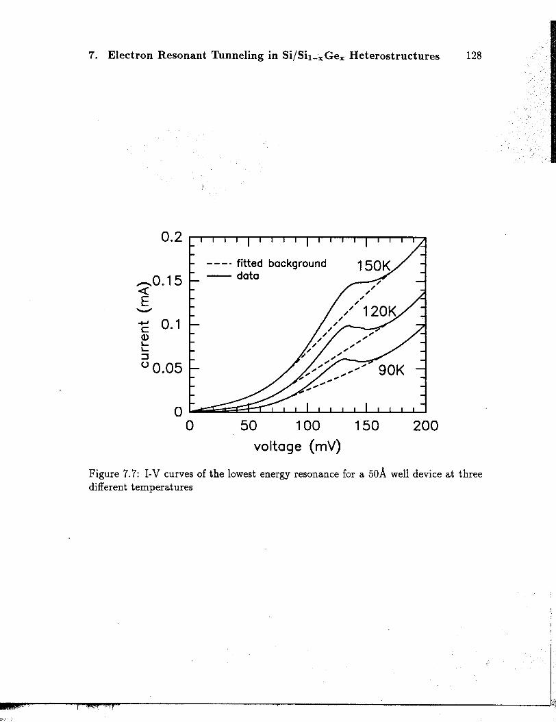
7. Electron Resonant Tunneling in SijSi1-xGex Heterostructures 128
j
0.2
fitted background0.15 - data
«E
~
""C 0.1Q)L-L-:]:u 0.05
00 50 100 150 200
voltage (mV)
Figure 7.7: I-V curves of the lowest energy resonance for a 50A well device at threedifferent temperatures
I;fi

7. Electron Resonant Tunneling in Si/Si1-x Gex Heterostructures 129
10-5-.>X«
'"-'
-+-'c:Q)L-L-
:JU
"'CQ)
-+-'CL- 10-8~Q)
-+-'
.S6x10-7
8 9 10 11 12 13
1aaa/T (1/K)Figure 7.8: Integrated tunneling current for the lowest energy resonance vs. 1000/Tfor: (a) 2sA well device, positive bias, (b) 2sA well device, negative bias, (c) soAwell device, positive bias. The dashed lines are fits to phonon population curves (a)nUl = 14meV, (b) 1iw = 16meV, (c) nUl = 12meV
,
--"",1,;

7. Electron Resonant Tunneling in SijSi1-xGex Heterostructures 130
(a),(b) and (c), respectively, are very close to predicted 13meV for the TA-phonon in.silicon with q = 0.37r fa, and strongly support the phonon-absorption-assisted model
as the origin of the lowest bias resonance.
Any two-step process, such as phonon absorption and tunneling, requires that the
system pass through an intermediate state. In the case of the phonon-absorption-
assisted tunneling process the electron may become "hot" by absorbing the phonon
(step ai in Fig. 7.5) prior to tunneling (step a2)' so that the intermediate state could
be a true existing state in the conduction band of the emitter with a finite lifetime.
This is in contrast to tunneling before the phonon absorption (steps bi and b2 in Fig.
7.5) or to any path for phonon-emission-assisted tunneling where the intermediate
state would be only a "virtual" state. Furthermore, after absorbing a phonon (ai), an
electron will see a substantially lower tunneling barrier height than folloVling the bi -
b2 path or any path for phonon emission. Therefore, it is reasonable that transitions
through phonon absorption, when allowed by the energy and momentum conservation
rules, are more favorable than phonon-emission related transitions. This could explain
why no high-energy replicas corresponding to phonon-emission were observed in our
samples and why the relative strength of such a resonance is comparable to the true
elastic resonance through the level with which it is associated.
A unique feature of the strained SijSii-xGex system is that low energy (and hence
plentiful) acoustic phonons may be involved due to the momentum transfer between
the degenerate conduction band minima. In a material system with one band mini-
mum, only high energy zone center optical phonons would be allowed, making such
phenomenon much less likely to occur due to a lower number of phonons. That is a
possible reason why phonon-absorption-assisted features have not been observed for
holes in SijSiGe or in III-V material systems.

7. Electron Resonant Tunneling in SijSi1-x Gex Heterostructures 131
7.5 Summary
The first symmetric electron resonant tunneling diode, a novel vertical transport de-
vice in SijSi 1-x Ge x material system, has been demonstrated. This confirms high
quality of RTCVD epitaxial layers and possibly opens a new area of multifunctional
devices to be researched. An anomalous temperature dependence of a low bias res-
onance has been observed. Both the comparison of observed resonances with the
calculated states in the well and the temperature behaviour are consistent with a
model of phonon-absorption-assisted tunneling.

7. Electron Resonant Tunneling in SijSi1-x Gex Heterostructures 132
sample well barrier spacer calculated observed temperature assignmentnumber width width width bias bias dependence of observed
(A) (A) (A) (mV) (mV) resonance
1072 50 70 175 42 (HEo) 112-120 anomalous Xcenter 165 (HEl) 162-180 o.k. HEl
369 (HE2) 365-400 o.k. HE2627 (HE3) 700-900 o.k. HE3
1072 40 65 175 65 (HEo) 160-170 anomalous. Xcenter 252 (HEl) 220-250 o.k. HEl
552 (HE2) 600-800 o.k. HE2
1072 15-25 40-60 125-175 180-250 anomalous Xedge 300-450 o.k. HEo
1149 30 50 175 50-55 anomalous Xcenter 118 (HEo) 95-120 o.k. HEo
456 (HEl) 426-515 o.k. HEl
1149 10-25 30-50 100-175 150-300 anomalous Xedge 200-500 o.k. HEo
Table 7.1: Summary of RTD samples
, I

Chapter 8
Conclusions and Suggestions for Further Research
8.1 Conclusions
The research leading to this thesis mainly focussed on SijSi 1-x Ge x jSi HBT's: issues
related to process integration and experimental determination of parameters critical
for accurate DC device modeling and design.
The interest in SijSi 1-x Gex jSi HBT's lies in the potential to fabricate high speed
devices and circuits, since the HBT structure allows increased base dopings to reduce
base sheet resistance and graded germanium profiles to reduce base transit times. Low
intrinsic device delay (high fT), low parasitic base resistances, low parasitic capaci-
tances, and optimized load are prerequisites for high speed circuit performance. When
integrated into Si technology, processing needs to be adjusted to reduced thermal cy-
cles (to below 800°C) to prevent strain relaxation and minimize dopant diffusion in
the base.
All the samples in this work were grown by RTCVD. The quality of epitaxial
material and interfaces was studied in a wide pressure range, by means of x-ray re-
flectivity, photoluminescence and electrical performance of p-type resonant tunneling
diodes. An interface roughness of below sA was established for high quality epitaxial
layers grown at low pressure.
A heavily doped base and a heavily doped emitter in a bipolar transistor lead to
133
~ '"'."""c~~c :~\r "'~"

8. Conclusions and Suggestions for Further Research 134
a p+ -n+ junction. Tunneling currents in p+ -n+ base-emitter junction could cause
a severe increase in the base current. The doping on the lighter doped side of the
junction should not exceed 5 X 1018 cm-3 in order not to cause significant tunneling.
Both tunneling, and boron diffusion can be controlled by carefully designed undoped
spacer layers within the Si I-x Ge x base.
From the room temperature collector current measurements, bandgap narrowing
in heavily doped Si I-x Ge x layers was extracted in a wide range of p-type dopings
and germanium concentrations for the first time. An empirical model for the effective
bandgap narrowing relevant for the minority carrier transport in the base was pre-
sented. The heavy doping contribution to the effective bandgap narrowing is lower
than that in Si, due to the strain-induced splitting of the bands which pushes the
Fermi level further into the valence band for a given hole concentrati?n. Further-
more, the design trade-off between the base sheet resistance and gain was clearly
presented.
The minority carrier diffusion length was extracted for the first time in p-type
Si I-x Ge x as a function of doping from the photocurrent measurements on optimized
lateral devices at room temperature and 85K.
Finally, a novel vertical transport device in the Si-based material system, a sym-
metric electron resonant tunneling diode was demonstrated for the first time. The
anomalous temperature behaviour of the lowest bias resonance was explained by
phonon-absorption-assisted model.
8.2 Suggestions for future work
This thesis gives the first empirical model of bandgap narrowing (due to Ge and heavy
doping) in strained Si I-x Ge x layers obtained from collector current measurements.
It would be interesting to observe bandgap narrowing as a function of germanium

8. Conclusions and Suggestions for Further Research 135
concentration and p-type doping in Si I-x Ge x by optical measurements, such as pho-
toluminescence, and compare it to the electrical results. In this way the relationship
between the "true" bandgap narrowing and the effective one could be accurately
determined and compared to Si.
The minority carrier lifetime in p-Si I-x Ge x still remains to be measured. Com-
bined with the diffusion lenght measurements presented in this work, this could lead
to the first measurement of minority carrier mobility in strained Si I-x Ge x , a pa-
rameter critical for accurate collector current modeling.
The focus of this work has been p-type material since the base in npn HBT is a
heavily p-type doped Si I-x Ge x layer. However, for various device applications, such
as pnp HBT for example, n-type material also deserves to be studied.
The integration of HBT's with resonant tunneling structures into m~ltifunctional
devices still needs to be demonstrated in Si/Si I-x Ge x material system. This might
be easier to accomplish for a pnp HBT where the double barrier for hole transport
could be integrated within the vertical structure of the device (in base-emitter space
charge region or in the base, for example). Integration of electron resonant tunneling
structures requires further improvement in the relaxed buffer layers, in terms of defect
densities and high quality material with high minority carrier lifetimes.
Research on other materials, such as silicon-carbide or silicon-germanium-carbon
alloys extends the field of heterojunctionson silicon and among other, possible bipolar
device applications.
Finally, Si/Si I-x Ge x /Si HBT's have been pushing the limits of high speed device
performance and integration into silicon bipolar technology. How far this trend will
continue still remains to be seen.

A ppendix A
Growth and Processing Details
This appendix provides growth details and run-sheets for typical samples of each
chapter in this thesis. It also gives processing details for p and n-type resonant
tunneling diodes.
A.I Graded base HBT samples
Samples in this section are related to chapter 2. Graded base HBT test samples (#758
and #759) were grown on n-type (30-60 ncm) <100> Si substrates. The standard
"clean + buffer" initial sequence was grown prior to base and emitter HBT layers.
The 6 min. high temperature buffer layer was not intentionally doped. All layers
were grown at 6 torr with constant H2 flow of 3slpm and DCS flow of 26sccm. The
growth sequence for sample #759 is given in Tab. A.1.
AT&T samples (#996-1002, #1011-1018) were grown on patterned wafers with-
out the high temperature buffer layer (only 30 sec clean at 1000°C), and a thin
( "" 180A) Si layer was grown at 700°C prior to base layer growth. These samples only
had 500-700A (105 sec at 800°C) emitter layer doped"" 1 X 1018 cm-3 (PH3 flow of
2.5 sccm).
136

A. Growth and Processing Details 137
Table A.1: HBT sample #759, base and emitter growth
time temperature GeH4 B2H6 PH3 comment(sec) (OC) (sccm) (sccm) (sccm)
base layer:
134 625 81 0 18%, 150A spacer134 625 87 33550 625 77 300 5 x 1019 cm-3, 300A57 625 68 26564 625 59 23275 625 50 091 625 41 0 150A spacer115 625 32 0 12%10 625 0 0 purge
emitter layer:
60 800 0 0 2.5 1 x 1018 cm-3, 400A390 800 0 0 25 1 x 1019 cm-3, 2600A
A.2 Samples for interface roughness study
The growth sequence of sample #1334 is given as an example of a sequence where the
Si 1-x Ge x layer is grown at pressure above 6 torr (Tab. A.2). The Si 1-x Ge x layer
growth followed the standard high-temperature sequence. DCS flow was constant at
26sccm and not interrupted between layers.
The details of the growth of sample #1432 are also given (Tab. A.3). This is the
20-period superlattice sample used for XRD characterization of the low-pressure and

A. Growth and Processing Details 138
Table A.2: XRR and PL sample #1334, Si I-x Ge x and Si cap layer growth
time temperature pressure H2 GeH4 comment(sec) (OC) (torr) (slpm) (sccm)
60 1000 6 340 700 6 3110 625 6-+60 3-+4-+3 stabilize pressure75 625 60 3 100 Si 0.7 GeO.3 , 250A60 625 60 3 0300 700 60 3 0 Si cap
low-temperature interfaces.
A.3 P-type resonant tunneling diodes
P-type resonant tunneling structures (#1297, #1336, 6 torr; #1337, 60 torr; and
#1374,220 torr) were grown on p-type (, 30ncm) <100> Si substrates. The clean-
ing step consisted of a 2 min. bake at 1000°C and 250 torr. A 5 min. (, 1.um
thick) buffer layer was doped p-type (B2Hs (10 ppm in H2) flow of 50 sccm). The
symmetric, undoped double-barrier structure consisted of a strained Si I-x Ge x well
sandwiched between Si barriers and Si I-x Ge x spacer layers which were separating
the double-barrier structure from the doped emitterf-collector Si regions. All the Si
layers were grown at 700°C and Si I-x Ge x layers at 625°C. Si doped layers were
doped 2 - 5 X 1019 cm-3. The top layer was a p+contact Si layer. The growth se-
quence of sample #1297 is given as an example (Tab. A.4).

A. Growth and Processing Details 139
Table A.3: Growth details for superlattice sample #1432
temperature Si carrier flow GeH4 flow growth rate(OC) (sccm) (sccm) (A/min.)
Si layer 625 silane (0.4% in H2): 250 - 18.8
Si 0.8 Ge 0.2 550 DCS: 26 100 4.6
A.4 Flat-base HBT samples
Flat-base HBT samples with uniform Band Ge concentrations were used in chapter 5
to study the minority and majority carrier properties in strained Si I-x Ge x . Chapter
5 provides the list of samples (Tab.5.1). Collectors in these samples were doped
via out diffusion from the n-type doped high-temperature buffer layer. The growth
sequence, including the n-buffer, of sample #934 is shown as a typical example (Tab.
A.5).
A.5 Lateral SiGe channel devices
The structures designed to study minority carrier parameters in strained Si I-x Ge x are
discussed in chapter 6, and a list of samples is provided (Tab.6.1). The layers were
grown on p-type (8-60ncm) <100> Si substrates. The high temperature buffer in
these structures was thick ("" 3,um), and p+doped (500 sccm B2Hs flow). The growth
sequence of sample #1570 of the layers following the p+buffer is shown as a typical
example (Tab. A.6).

A. Growth and Processing Details 140
Table A.4: Sample #1297, p-type RTD
time temperature GeH4 B2H6 comment(sec) (OC) (sccm) (sccm)
60 1000 50600 700 50 p-Si45 625 temp. stabilize60 625 200 Sio.75 GeO.25 spacer, 160A10 625 purge100 700 barrier, 50A45 625 temp. stabilize15 625 200 Si 0.75 Ge 0.25 well, 40A10 625 purge100 700 barrier, 50A45 625 temp. stabilize60 625 200 Si 0.75 Ge 0.25 spacer, 160A10 625 purge
600 700 50 p-Si600 700 450 p+-Si
A.6 N-type resonant tunneling diodes
Double-barrier structures for electron resonant tunneling were grown on relaxed,
graded Si I-x Ge x buffer layers (see chapter 7), as developed by C. W. Liu. The growth
sequence (following the high-temperature buffer) for sample #1072 is given here (Tab.
A.7).

A. Growth and Processing Details 141
Table A.5: Sample #934, flat-base HBT
time temperature GeH4 B2H6 PH3 comment(sec) (OC) (sccm) (sccm) (sccm)
60 1000 clean600 1000 2.5 n-buffer600 cold
240 1000 - collector60 70040 625 temp. stab.300 625 50 BC Si 0.86 Ge 0.14 spacer600 625 50 400 1 x 1020 cm -~ base300 625 50 BE Si 0.86 Ge 0.14 spacer10 625 purge
450 800 2.5 emitter
A.7 Processing of resonant tunneling diodes
All of the resonant tunneling diodes of chapter 7 (n-type) and most of the RTD
devices of chapter 3 (p-type) were processed by a simple mesa process involving only,
one photolitographic step. P-type devices were also processed by a three-step wet-etch
process There was some differencies in the observed I-V curves between the devices
from the same wafer processed in different ways (peak-to-valley ratio, peak position),
although this might not be process related but due to layer nonuniformity across the
wafer. Both of the processes are described. Short anneals (conditions given below)
improved peak-to-valley ratios on some devices and moved the peak position towards
a slightly lower bias (probably due to lower contact resistance). All the devices with

A. Growth and Processing Details 142
Table A.6: Sample #1570, lateral transport device
time temperature GeH4 B2Hs comment(sec) (°0) (sccm) (sccm)
420 800 210 ",1 x 1019 cm-3 Si30 700 35180 625 -t2.5 set flow360 625 100 2.5 p-Si 0.8 Ge 0.2 channel45' 625 -t210 set flow312 800 210 ",1 x 1019 cm-3 Si cap7 800 -
only Al metalization (no Ti) did not survive the 10min anneal at 400°0 (probably
due to Al spiking).
Singe-step process
. initial ROA clean
. metal evaporation (e-beam evaporator: 500A Ti + 2000A Al or just 2500A Al in
some cases)
. photolitography (define mesas)
. metal etch (AI etch + HF : H2O(1 : 100) for Ti)
. plasma etch using metal mask (SFs only 15sccm, 150mtorr, 100W, 0.4min '" 5000-
6000A)
. photoresist strip
. clean HF : H2O(1 : 50), 30 sec
. Al evaporation on. the back or in the corner for the bottom electrode

A. Growth and Processing Details 143
. anneal (on some samples, 400°0, 10-15 min, N2)
Wet-etch process
. initial clean
. photolitography (define mesas)
. wet mesa etch (5000-6000A)
. photoresist strip
. photolitography (for bottom conatact lift-off)
. clean HF: H2O(1 : 10), 30 sec
. metal evaporation (e- beam evaporator: 3000A AI)
. lift-off
. RTA (450°0, 5 min, N2)
. photolitography (for top conatact lift-off)
. clean HF : H2O(1 : 10), 30 sec
. metal evaporation (e- beam evaporator: 3000A AI)
. lift-off
. RTA (380°0, 3 min, N2)

A. Growth and Processing Details 144
Table A.7: Sample #1072, n.,type RTD
time temperature GeH4 PH3 comment(sec) (OC) (sccm) (sccm)
60 100040 70040 625
3000 625 0-35 14 1-10%, loooA2400 625 35-100 14 10-20%, 2500A.780 625 100-450 14 20-35%, 2600A1500 625 450 14 Si 0.65 Ge 0.35, 7500A3600 800 anneal45 625 set temp.10 625 450
350 700 Si spacer, 175A45 625 set temp.14 625 450 Si 0.65 Ge 0.35 barrier, 70A10 625 purge100 700 Si well, 50A45 625 set temp.14 625 450 Si 0.65 Ge 0.35 barrier, 70A10 625 purge
350 700 Si spacer, 175A45 625 set temp.120 625 450 14 n-Si 0.65 Ge 0.35, 600A60 625 450 150 n + -Si .0.65 Ge 0.35 contact layer
- "~ ~~J

Appendix B
Publications and Presentations Resulting from
this Thesis
1. Z. Matutinovit Krstelj, E. Chason, and J. C. Sturm, "Growth pressure effects
on Si1-xGex CVD", submitted for publication to J. of Electronic Materials.
2. J. C. Sturm, X. Xiao, Q. Mi, C. W. Liu, A. St Amour, Z. Matutinovit Krstelj,
L. C. Lenchyshyn, and M. L. W. Thewalt, "Photoluminescence and Electro-
luminescence processes in Si1-xGex heterostructures grown by chemical vapor
deposition, Mater. Sci. and Eng., B21, 1993, pp. 307-311.
3. Z. Matutinovit Krstelj, V. Venkataraman, E. J. Prinz, and J. C. Sturm, " A
comprehensive study of lateral and vertical current transport in Si/Si1-xGex/Si
HBT's", Tech. Dig. Int. Elec. Dev. Mtg. 1993, pp. 87-90.
4. Z. Matutinovit Krstelj, E. Chason, J. C. Sturm, "Growth pressure effects on
Si1-xGex CVD", Tech. Prog. Elec. Mat. Conf., 39, 1993.
5. Z. Matutinovit Krstelj, C. W. Liu, X. Xiao, and J. C. Sturm, "Evidence of
phonon-absorption-assisted electron resonant tunneling in Si/SiGe diodes", J.
Vac. Sci. Technol. B, 11, pp. 1145-1148, 1993.
145

B. Publications and Presentations Resulting from this Thesis 146
6. Z. Matutinovic Krstelj, C. W. Liu, X. Xiao, and J. C. Sturm, "Symmetric
SijSiGe electron resonant tunneling diodes with an anomalous temperature be-
haviour", Appl. Phys. Lett., 62, pp. 603-605, 1993.
7. Z. Matutinovic Krstelj, C. W. Liu, X. Xiao, and J. C. Sturm, "Electron SijSiGe
resonant tunneling diodes grown by RTCVD", Proc. Topical Symposium on
Silicon Based Heterostructures, Amer. Vac. Soc., 1992.
8. Z. Matutinovic-Krstelj, E. J. Prinz, P. V. Schwartz, and J. C. Sturm, "Reduc-
tion of the p+-n+ junction tunneling current for base current improvement in
SijSiGejSi heterojunction bipolar transistors," Proc. Mat. Res. Soc. Symp.,
220, pp. 445-450, 1991.
9. Z. Matutinovic-Krstelj, E. J. Prinz, P. V. Schwartz, and J. C. Sturm, "Re-
duction of p+ -n+ junction tunneling current for base current improvement in
SijSiGejSi HBT's", IEEE Electron Device Lett., EDL-12, pp. 163-165, 1991.
10. J. C. Sturm, E. J. Prinz, P. V. Schwartz, P. M. Garone, and Z. Matutinovic-
Krstelj, "Growth and transistor applications of Si1-xGex structures by rapid
thermal chemical vapor deposition," Proc. First Topical Symposium on Silicon
Based Heterostructures, Amer. Vac. Soc., pp. 5-10, 1990.
i
References r-
[1] E. Crabbe, B. Mayerson, J. Stork, and D. Harame, "Verical profile optimiza-
tion of very-high frequency epitaxial Si- and SiGe-base bipolar transistors,"
International Electron Devices Meeting Tech. Dig., pp. 83-86, 1993.
[2] E. Kasper, A. Gruhle, and H. Kibbel, "The influence of MBE-layer design on the
high frequency performance of SijSiGe HBTs," International Electron Devices
Meeting Tech. Dig., pp. 79-82, 1993.
[3] D. Harame, J. M. C. Stork, B. S. Meyerson, K.-J. Hsu, J. Cotte, K. A. Jenkins,
J. D. Cressler, P. Restle, E. F. Crabbe, S. S. T. E. Tice, B. W. Scharf, and
J. A. Jasaitis, "Optimization of SiGe HBT technology for high speed analog
and mixed signal applications," International Electron Devices Meeting Tech.
Dig., pp. 71-74, 1993.
[4] H. Kroemer, "Heterostructure bipolar transistors and integrated circuits," Proc.
IEEE, vol. 70, pp. 13-25, 1982.
[5] S. S. Iyer, G. L. Patton, S. L. Delage, S. Tiwari, and J. M. C. Stork, "Silicon-
germanium base heterojunction bipolar transistors by molecular beam epitaxy,"
International Electron Devices Meeting Tech. Dig., pp. 874-876, 1987.
[6] G. L. Patton, S. S. Iyer, S. L. Delage, S. Tiwari, and J. M. C. Stork, "Silicon-
germanium-base heterojunction bipolar transistors by molecular beam epitaxy,"
IEEE Electron Device Lett., vol. 9, pp. 165-167, 1988.
147

References 148
[7] T. Tatsumi, H. Hirayama, and N. Aizaki, "Si/Geo.3Sio.7/Si heterojunction bipo-
lar transistor made with Si molecular beam epitaxy," Appl. Phys. Lett., vol. 52,
pp. 895-897,1988.
[8] H. Temkin, J. C. Bean, A. Antreasyan, and R. Leibenguth, "GexSi1-x strained-
layer heterostructure bipolar transistors," Appl. Phys. Lett., vol. 52, pp. 1089-
1091,1988.
[9] D.-X. Xu, G.-D. Shen, M. Willander, W.-X. Ni, and G. V. Hansson, "n-Si/p-
Sil_xGex/n-Si double-heterojunction bipolar transistors," Appl. Phys. Lett.,
vol. 52, pp. 2239-2241, 1988.
[10] D.-X. Xu, G.-D. Shen, M. Willander, W.-X. Ni, and G. V. Hansson, "n-Si/p-
Si1_xGex/n-Si double-heterojunction bipolar transistors," IEEE Electron Device
Lett., vol. 9, pp. 453-456, 1988.
[11] P. Narozny, M. Hamacher, H. Damkes, H. Kibbel, and E. Kasper, "Si/SiGe
heterojunction bipolar transistor with graded gap SiGe base made by molecular
beam epitaxy," International Electron Devices Meeting Tech. Dig., pp. 562-565,
1988.
[12] J. F. Gibbons, C. A. King, J. L. Hoyt, D. B. Noble, C. M. Gronet, M. P. Scott,
S. J. Rosner, G. Reid, S. Laderman, K. Nauka, J. Turner, and T. I. Kamins,
"Si/Si1-xGex heterojunction bipolar transistors fabricated by limited reaction
processing," International Electron Devices Meeting Tech. Dig., pp. 566-569,
1988.
[13] C. A. King, J. L. Hoyt, C. M. Gronet, J. F. Gibbons, M. P. Scott, and J. Turner,
"Si/Si1-xGex heterojunction bipolar transistors produced by limited reaction
processing," IEEE Electron Device Lett., vol. 10, pp. 52-54, 1989.

References 149
[14] C. A. King, J. L. Hoyt, and J. F. Gibbons, "Bandgap and transport properties
of Si1-xGex by analysis of nearly ideal Si/Si1-xGex/Si heterojunction bipolar
transistors," IEEE Trans. Electron Devices, vol. 36, pp. 2093-2104, 1989.
[15] J. F. Gibbons, C. M. Gronet, and K. E. Williams, "Limited reaction processing:
Silicon epitaxy," Appl. Phys. Lett., vol. 47, pp. 721-723,1985.
[16] G. L. Patton, D. L. Harame, J. M. C. Stork, B. S. Meyerson, G. J. Scilla, and
E. Ganin, "Graded-SiGe-base, poly-emitter heterojunction bipolar transistors,"
IEEE Electron Device Lett., vol. 10, pp. 534-536, 1989.
[17] E. J. Prinz and J. C. Sturm, "Base transport in near-ideal graded-base
Si/Si1-xGex/Si heterojunction bipolar transistors from 150 K to 370 K," In-
ternational Electron Devices Meeting Tech. Dig., pp. 975-978, 1990.
[18] A. Pruijmboom, J. W. Slot boom, D. J. Gravesteijn, C. W. Fredriksz, A. A. van
Gorkum, R. A. van de Heuvel, J. M. L. van Rooij-Mulder, G. Streutker, and
G. F. A. van de Walle, "Heterojunction bipolar transistors with SiGe base grown
by molecular beam epitaxy," IEEE Electron Device Lett., vol. 12, pp. 357-359,
1991.
[19] T. I. Kamins, K. Nauka, J. B. Kruger, J. L. Hoyt, C. A. King, D. B. No-
ble, C. M. Gronet, and J. F. Gibbons, "Small-geometry, high-performance,
Si-Si1-xGex heterojunction bipolar transistors," IEEE Electron Device Lett.,
vol. 10, pp. 503-505, 1989.
[20] G. L. Patton, J. H. Comfort, B. S. Meyerson, E. F. Crabbe, G. J. Scilla,
E. de Fresart, J. M. C. Stork, J. Y.-C. Sun, D. L. Harame, and J. N. Burghartz,
"75-GHz iT SiGe-base heterojunction bipolar transistors," IEEE Electron De-
vice Lett., vol. 11, pp. 171-173, 1990.
~C"""'~C""',"'~ i

References 150
[21] J. H. Comfort, G. L. Patton, J. D. Cressler, W. Lee, E. F. Crabbe, B. S. Mey-
erson, J. Y.-C. Sun, J. M. C. Stork, P.-F. Lu, J. N. Burghartz, J. Warnock,
G. Scilla, K.- Y. Toh, M. D' Agostino, C. Stanis, and K. Jenkins, "Profile lever-
age in self-aligned epitaxial Si or SiGe base bipolar technology," International
Electron Devices Meeting Tech. Dig., pp. 21-24, 1990.
[22] J. N. Burghartz, J. H. Comfort, G. L. Patton, J. D. Cressler, B. S. Meyerson,
J. M. C. Stork, J. Y.-C. Sun, G. Scilla, J. Warnock, B. J. Ginsberg, K. Jenkins,
K.- Y. Toh, D. L. Harame, and S. R. Mader, "Sub-30 ps ECL circuits using
high- iT Si and SiGe epitaxial base SEEW transistors," International Electron
Devices Meeting Tech. Dig., pp. 297-300, 1990.
[23] D. L. Harame, E. F. Crabbe, J. D. Cressler, J. H. Comfort, J. Y.-C. Sun,
S. R. Stiffler, E. Kobeda, J. N. Burghartz, M. M. Gilbert, J. C. Malinowsli,
A. J. Dally, S. Ratanaphanyarat, M. J. Saccamango, W. Rausch, J. Cotte,
C. Chu, and J. M. C. Stork, "A high performance epitaxial SiGe-base ECL BiC-
MaS technology," International Electron Devices Meeting Tech. Dig., pp. 19-
22,1992.
[24] A. Gruhle, "MBE-grown SijSiGe HBT's with high ,8, fT, and fmax," IEEE
Electron Device Lett., vol. 13, pp. 206-208, 1992.
[25] A. Schuppen, A. Gruhle, U. Erben, H. Kibbel, and U. Konig, "90 GHz-fmax
SiGe heterojunction bipolar transistors," Device Research Coni Tech. Dig.,
1994.
[26] J. H. van der Merwe, "Crystal interfaces. Part I. Semi-infinite crystals," J. Appl.
Phys., vol. 34, pp. 117-122, 1963.
[27] J. W. Matthews and A. E. Blakeslee, "Defects in epitaxial multilayersj I. Misfit
dislocations," J. Crystal Growth, vol. 27, pp. 118-125, 1974.
""-' I"~' I
,

References 151
[28] J. W. Matthews and A. E. Blakeslee, "Defects in epitaxial multilayersj II. Dislo-
cation pile-ups, threading dislocations, slip lines and cracks," J. Crystal Growth,
vol. 29, pp. 273-280, 1975.
[29] J. W. Matthews and A. E. Blakeslee, "Defects in epitaxial multilayersj
III. Preparation of almost perfect multilayers," J. Crystal Growth, vol. 32,
pp. 265-273,1976.
[30] R. People and J. C. Bean, "Calculation of critical layer thickness versus lattice
mismatch for GexSi1-x/Si strained-layer heterostructures," Appl. Phys. Lett.,
vol. 47, pp. 322-324, 1985.
[31] R. Braunstein, A. R. Moore, and F. Herman, "Intrinsic optical absorption in
germanium-silicon alloys," Phys. Rev., vol. 109, pp. 695-710, 1958.
[32] R. People, "Indirect bandgap of coherently strained Si1-xGex bulk alloys on
<001> silicon substrates," Phys. Rev. B, vol. 32, pp. 1405-1408, 1985.
[33] R. People and J. C. Bean, "Band alignments of coherently strained GexSi1-x/Si
heterostructures on <001> GeySi1_y substrates," Appl. Phys. Lett., vol. 48,
pp. 538-540, 1986.
[34] D. V. Lang, R. People, J. C. Bean, and A. M. Sergent, "Measurement of
the bandgap of GexSi1-x/Si strained-layer heterostructures," Appl. Phys. Lett.,
vol. 47, pp. 1333-1335, 1985.
[35] C. G. van de Walle and R. M. Martin, "Theoretical calculations of heterojunc-
tion discontinuities in the Si/Ge system," Phys. Rev. B, vol. 34, pp. 5621-5634,
1986.
.,' i" , I

References 152
[36] X. Xiao and J. C. Sturm, "Direct evidence by photoluminescence of type-I band
alignment for strained Si1-xGex (x ~ 0.35) on (100) silicon," Elec. Mater. Conf.
Tech. Dig., pp. 22-23, 1992.
[37] D. L. Harame, J. M. C. Stork, B. S. Meyerson, E. F. Crabbe, G. J. Scilla,
E. de Fresart, A. E. Megdanis, C. L. Stanis, G. L. Patton, A. A. Bright,J. B. Johnson, and S. S. Furkay, " 30GHz polysilicon-emitter and singe-crystal-
emitter graded SiGe-base PNP transistors," International Electron Devices
Meeting Tech. Dig., pp. 33-36, 1990.
[38] H. F. Cooke, "Microwave transistors: Theory and design," Proc. IEEE, vol. 59,
pp. 1163-1181,1971.
[39] H. Kroemer, "Two integral relationships pertaining to the electron transport
through a bipolar transistor with a nonuniform energy gap in the base region,"
Solid-State Electron., vol. 28, pp. 1101-1103, 1985.
[40] T. Y. Chiu, G. M. Chin, M. Y. Lau, R. C. Hanson, M. D. Morris, K. F.
Lee, T. Y. M. Liu, A. M. Voschenkov, R. G. Schwartz, V. D. Archer, S. N.
Finegan, and M. D. Feuer, "The design and characterization of Nonoverlapping
Super Self-aligned BiCMOS technology," IEEE Trans. Electron Devices, vol. 38,
pp. 141-150, 1991.
[41] D. D. Tang and P. M. Solomon, "Bipolar transistor design for optimized power-
delay logic circuits," IEEE J. Solid-State Circuits, vol. 14, pp. 679-684, 1979.
[42] J. M. C. Stork, "Bipolar transistor scaling for minimum switching delay and
energy dissipation," International Electron Devices Meeting Tech. Dig., pp. 550-
553,1988.

References 153
[43] K. G. Moerschei, T. Y. Chiu, P. W. A, K. S. Lee, R. G. Schwartz, R. A. Mantz,
T. Y. M. Liu, K. F. Lee, V. D. Archer, G. R. Hower, G. T. Mazea, R. E. Carsia,
J. A. Pavlo, M. P. Ling, J. L. Delein, F. M. Ereeg, J. J. Egan, C. J. Fassi, J. T.
Glich, and M. A. Prosnic, "ATT's bipolar process is BEST," Semiconductor
International, pp. 72-74, Nov. 1990.
[44] T. Y. Chiu, J. M. Sung, and T. M. Liu private communication, 1991/92.
[45] T. M. Liu, G. M. Chin, D. Y. Jeon, M. D. Morris, V. D. Archer, H. H. Kom,
M. Cerullo, K. F. Lee, J. M. Sung, K. Lau, T. Y. Chiu, A. M. Voschenkov, and
R. G. Schwartz, "A half-micron Super Self-aligned BiCMOS Technology for
high speed applications," International Electron Devices Meeting Tech. Dig.,
pp. 23-26,1992.
[46] E. J. Prinz and J. C. Sturm, "Current gain - Early voltage products in hetero-
junction bipolar transistors with nonuniform base bandgaps," IEEE Electron
Device Lett., vol. 12, pp. 661-663, 1991.
[47] A. Gruhle, "The influence of emitter-base junction design on collector saturation
current, ideality factor, Early voltage, and device switching speed of Si/SiGe
HBT's," IEEE Trans. Electron Devices, vol. 41, pp. 198-203, 1994.
[48] E. J. Prinz, P. M. Garone, P. V. Schwartz, X. Xiao, and J. C. Sturm,
"The effect of base emitter spacers and strain-dependent densities of states
in Si/Si1-xGex/Si heterojunction bipolar transistors," International Electron
Devices Meeting Tech. Dig., pp. 639-642, 1989.
[49] E. J. Prinz, P. M. Garone, P. V. Schwartz, X. Xiao, and J. C. Sturm, "The
effects of base dopant out diffusion and undoped Si1-xGex junction spacer layers
in Si/Si1-xGex/Si heterojunction bipolar transistors," IEEE Electron Device
Lett., vol. 12, pp. 42-44, 1991.

References 154
[50] J. W. Slotboom, G. Streutker, A. Pruijmboom, and D. J. Gravesteijn, "Parasitic
energy barriers in SiGe HBT's," IEEE Electron Device Lett., vol. 12, pp. 486-
488,1991.
[51] D. D. Tang and P.-F. Lu, "A reduced-field design concept for high-performance
bipolar transistors," IEEE Electron Device Lett., vol. 10, pp. 67-69, 1989.
[52] D. C. D' Avanzo, M. Vanzi, and R. W. Dutton, "One-dimensional semiconductor
device analysis (SEDAN)," Stanford Univ. Tech. Rep. G-201-5, vol. Stanford,
CA, Oct. 1979.
[53] P. Kuo, J. L. Hoyt, J. F. Bibbons, J. E. Turner, R. D. Jacowitz, and T. I.
Kamins, "Comparison of boron diffusion in Si and strained Si I-x Ge x epitaxial
layers," Appl. Phys. Lett., vol. 62, pp. 612-614, 1993.
[54] N. Moriya, L. C. Feldman, H. S. Luftman, C. A. King, J. Bevk, and B. Freer,
"Boron diffusion strained Si I-x Ge x epitaxial layers," Phys. Rev. Lett., vol. 62,
pp. 883-886, 1993.
[55] S. M. Hu, "Diffusion and segregation in inhomogeneous media and the
Si I-x Ge x heterostructure," Phys. Rev. Lett., vol. 63, pp. 2492-2495, 1989.
[56] S. M. Hu, D. C. Ahlgren, P. A. Ronsheim, and J. O. Chu, "Experimental study
of diffusion and segregation in a Si I-x Ge x heterostructure," Phys. Rev. Lett.,
vol. 67, pp. 1450-1453, 1991.
[57] B. S. Meyerson, "Low-temperature silicon epitaxy by ultrahigh vacuum chemi-
cal vapor deposition," Appl. Phys. Lett., vol. 48, pp. 797-799, 1986.
[58] B. S. Meyerson, K. J. Uram, and F. K. LeGoues, "Cooperative phenomena in sil-
icon/ germanium low temperature epitaxy," Appl. Phys. Lett., vol. 53, pp. 2555-
2557,1988.

References 155i
"
[59] C. M. Gronet, C. A. King, W. Opyd, J. F. Gibbons, S. D. Wilson, and R. Hull,
"Growth of SijSil-xGex strained-layer superlatticesusing limited reaction pro-
cessing," J. Appl. Phys., vol. 61, pp. 2407-2409, 1987.
[60] J. C. Sturm, P. V. Schwartz, E. J. Prinz, and H. Manoharan, "Growth of
Si I-x Ge x by rapid thermal chemical vapor deposition and application to het-
erojunction bipolar transistors," J. Vac. Sci. Technol. B, vol. 9, pp. 2011-2016,
1991.
[61] W. B. de Boer and D. J. Meyer, "Low temperature chemical vapor deposition of
epitaxial Si and SiGe layers at atmospheric pressure," Appl. Phys. Lett., vol. 58,
pp. 1286-1288,1991.
[62] P. D. Agnello, T. O. Sedgwick, M. S. Goorsky, J. Ott, T. S. Kuan, G. Scilla,
and V. P. Kesan, "Growth of silicon-germanium alloys by atmospheric-pressure
chemical vapor deposition at low temperatures," Mat. Res. Soc. Symp. Proc.,
vol. 220, pp. 607-612, 1991.
[63] J. C. Sturm, P. V. Schwartz, and P. M. Garone, "Silicon temperature measure-
ment by infrared transmission for rapid thermal processing applications," Appl.
Phys. Lett., vol. 56, pp. 961-963, 1990.
[64] D. Graf, M. Grundner, and R. Schulz, "Oxidation of HF-treated Si wafer sur-
faces in air," J. Appl. Phys., vol. 68, pp. 5155-5161, 1990.
[65] J. C. Sturm, H. Manoharan, L. C. Lenchyshyn, M. L. W. Thewalt, N. L. Rowell,
J. P. Noel, and D. C. Houghton, "Well resolved band-edge photoluminescence
of excitons confined in strained Si I-x Ge x quantum wells," Phys. Rev. Lett.,
vol. 66, pp. 1362-1365, 1991.

References 156
[66] E. Chason and D. T. Warwick, "X-ray reflectivity measurements of surface
roughness using energy dispersive detection," Mat. Res. Sump. Proc., vol. 208,
pp. 351-356,1991.
[67] E. Chason, T. M. Mayer, A. Payne, and D. Wu, "in situ energy dispersive x-
ray reflectivity measurement of H ion bombardment on SiO2jSi and Si," Appl.
Phys. Lett., vol. 60, pp. 2353-2355, 1992.
[68] E. Chason and T. M. Mayer, "Low energy bombardment induced roughening
and smoothing of SiO2 surfaces," Appl. Phys. Lett., vol. 62, pp. 363-365, 1993.
[69] D. Dutarte, P. Warren, F. Provenier, F. Chollet, and A. Perio, "Fabrication of
relaxed Si 1-x Ge x layers on si substrates by RTCVD," J. VaG. Sci. Technol. B,
to be published, 1994.
[70] A. J. Pidduck, D. J. Robbins, A. G. Cullis, W. Y. Leong, and A. M. Pitt,
"Evolution of surface morphology and strain during SiGe epitaxy," Thin Solid
Films, vol. 222, pp. 78-84, 1992.
[71] D. Dutarte, P. Warren, I. Berbezier, and P. Perret, "Low temperature Si
and Si 1-x Ge x epitaxy by rapid thermal chemical vapour deposition using hy-
drides," Thin Solid Films, vol. 222, pp. 52-56, 1992.
[72] H. C. Liu, D. Landheer, M. Buchanan, and D. C. Houghton, "Resonant tun-
neling in SijSi 1-x Ge x jSi double-barrier structures," Appl. Phys. Lett., vol. 52,
pp. 1809-1811, 1988.I .
[73] S. S. Rhee, J. S. Park, R. P. G. Karunasiri, Q. Ye, and K. L. Wang, "Resonant
tunneling through a SijGeSijSi heterostructure on a GeSi buffer layer," Appl.
Phys. Lett., vol. 53, pp. 204-206, 1988.

References 157
[74] U. Gennser, V. P. Kesan, S. S. Iyer, T. J. Bucelot, and E. S. Yang, "Resonant
tunneling of holes through silicon barriers," J. Vac. Sci. Technol. B, vol. 8,
pp. 210-213,1990.
[75] K. Ismail, B. S. Meyerson, and P. J. Wang, "Electron resonant tunneling in
SijSiGe double barrier diodes," Appl. Phys. Lett., vol. 59, pp. 973-975, 1991.
[76] Z . Matutinovit Krstelj, C. W. Liu, X. Xiao, and J. C. Sturm, "Symmetric
SijSi 1-x Ge x jSi electron resonant tuneling diodes with an anomalous temper-
ature behaviour," Appl. Phys. Lett., vol. 62, pp. 603-605, 1993.
[77] H. C. Manoharan, "Structural and electronic properties of RTCVD-grown
strained layer silicon-germanium heterostructures," Senior Independent Work,
Princeton Univ. Princeton, NJ., 1991.
[78] J. A. D. Alamo and R. M. Swanson, "Forward-bias tunneling: A limitation to
bipolar device scaling," IEEE Electron Device Lett., vol. 7, pp. 629-631, 1986.
[79] J. M. C. Stork and R. D. Isaac, "Tunneling in base-emitter junctions," IEEE
Trans. Electron Devices, vol. 30, pp. 1527-1534, 1983.
[80] E. Hackbarth and D. D.-L. Tang, "Inherent and stress-induces leakage in heavily
doped silicon junctions," IEEE Trans. Electron Devices, vol. 35, pp. 2108-2118,
1988.
[81] E. Hackbarth and T .-C. Chen, "Indetification and implication of a perimeter
tunneling current component in advance self-aligned bipolar transistors," IEEE
Trans. Electron Devices, vol. 35, pp. 89-95, 1988.
[82] A. G. Chynoweth, W. L. Feldmann, a~d R. A. Logan, "Excess tunnel current
in silicon Esak.i junction," Phys. Rev., vol. 121, pp. 684-694, 1961.

References 158
[83] Z. Matutinovic-Krstelj, E. J. Prinz, P. V. Schwartz, and J. C. Sturm, "Re-
duction of the p+ -n+ junction tunneling current for base current improvement
in Si/SiGe/Si heterojunction bipolar transistors," IEEE Electron Device Lett.,
vol. 12, pp. 163-165, 1991.
[84] J. del Alamo, S. Swirhun, and R. M. Swanson, "Simultaneous measurement
of hole lifetime, hole mobility and bandgap narrowing in heavily doped n-type
silicon," International Electron Devices Meeting Tech. Dig., 1985.
[85] S. Swirhun, Y.-H. Kwark, and R. M. Swanson, "Measurement of electron life-
time, electron mobility and bandgap narrowing in heavily doped p-type Silicon,"
International Electron Devices Meeting Tech. Dig., 1986.
[86] S. M. Sze, Physics of semiconductor devices. John Wiley & Sons, New York,
NY, 1981.
[87] J. H. Comfort, E. F. Crabbe, J. D. Cressler, W. Lee, J. Y.-C. Sun, J. Malinowski,
M. D' Agostino, J. N. Burghartz, J. M. C. Stork, and B. S. Meyerson, "Single
crystal emitter cap for epitaxial Si- and SiGe-base transistors," International
Electron Devices Meeting Tech. Dig., pp. 857-860, 1991.
[88] M. Ghannam and R. Mertens, "Accurate determination of bandgap narrowing
in heavily-doped epitaxial p-type silicon," Microelectronic Engineering, vol. 19,
1992.
[89] D. Klaassen, J. Slotboom, and H. de Graaff, "Unified apparent bandgap nar-
rowing in n- and p-type Silicon," Solid-State Electronics, vol. 35, 1992.
[90] A. Pruijmboom, C. E. Timmering, J. M. L. van Rooij-Mulder, D. J. Gravesteijn,
W. B. de Boer, W. J. Kersten, J. W. Slotboom, C. J. Vriezema, and R. de Kruif,
"cO--,
"'"

References 159
"Heterojunction bipolar transistors with SiGe base," Microelectronic Engineer-
ing, vol. 19, pp. 427-434, 1992.
[91] P. Narozny, H. Damkes, H. Kibbel, and E. Kasper, "SijSiGe heterojunction
bipolar transistors made by molecular beam epitaxy," IEEE Trans. Electron
Devices, vol. 36, pp. 2363-2366, 1989.
[92] T. Manku and A. Nathan, "Effective mass for strained p-type Si1-xGex,"
J. Appl. Phys., vol. 69, pp. 8414-8416, 1991.
[93] T. Manku and A. Nathan, "Lattice mobilty of holes in strained and unstrained
Si1-xGex alloys," IEEE Electron Device Lett., vol. 12, pp. 704-706, 1991.
[94] T. Manku, J. M. McGregor, A. Nathan, D. J. Roulston, J.-P. Noel, and D. C.
Houghton, "Drift hole mobilty in strained and unstrained doped Si1-xGex al-
loys," IEEE Trans. Electron Devices, vol. 40, pp. 1990-1995, 1993.
[95] J. M. McGregor, T. Manku, J.-P. Noel, D. J. Roulston, A. Nathan, and D. C.
Houghton, "Measured in-plane hole drift and hall mobilty in heavily-doped
strained p-type Si1-xGex," J. Electron. Materials, vol. 22, pp. 319-421, 1993.
[96] J. del Alamo, "Minority carrier trasnsport in heavily doped n-type silicon,"
Ph.D. dissertation, Stanford Univ. Stanford, Ca., 1985.
[97] S. E. Swirhun, "Characterization of majority and minority carrier transport in
heavily doped silicon," Ph.D. dissertation, Stanford Univ. Stanford, Ca., 1987.
[98] J. Poortmans, S. C. Jain, M. Caymax, A. V. Ammel, J. Nijs, R. P. Mertens,
and R. V. Overstraeten, "Evidence of the influence of heavy doping induced
bandgap narrowing on the collector current of strained SiGe-base HBT's," Mi-
croelectronic Engineering, vol. 19, 1992.

References 160
[99] J. C. Sturm, E. J. Prinz, P. M. Garone, and P. V. Schwartz, "Band-gap shifts
in silicon-germanium heterojunction bipolar transistors," Appl. Phys. Lett.,
vol. 54, pp. 2707-2709, 1989.
[100] J. C. Sturm and E. J. Prinz, "Graded base SijSi1-xGexjSi heterojunction bipo-
lar transistors grown by rapid thermal chemical vapor deposition with near-ideal
electrical characteristics," IEEE Electron Device Lett., vol. 12, pp. 303-305,
1991.
[101] S. Swirhun, D. Kane, and R.M.Swanson, "Temperature dependence of minor-
ity electron mobility and bandgap narrowing in p+ Si," International Electron
Devices Meeting Tech. Dig., 1988.
[102] T. Manku and A. Nathan, "Energy band structure for strained p-type
Si1-xGex," Phys. Rev. B, vol. 43, pp. 12634-12637, 1991.
[103] L. E. Kay and T.- W. Wang, "Monte carlo calculation of strained and unstrained
electron mobilities in Si1-xGex using an improved ionized-impurity model,"
J. Appl. Phys., vol. 70, pp. 1483-1488, 1991.
[104] G. E. Possin, M. S. Adler, and B. J. Baliga, "Measurements of the p-n product
in heavily doped epitaxial emitters," IEEE Trans. Electron Devices, vol. 31,
pp. 3-17,1984.
[105] S. Jain and D. Roulston, "A simple expression for bandgap narrowing in heavily
doped Si, Ge, GaAs and GeSi strained layers," Solid-State Electronics, vol. 34,
1991.
[106] J. Wagner, "Bandgap narrowing in heavily doped silicon at 20 and 300K studied
by photoluminescence," Phys. Rev. B, vol. 32, 1985.

References 161
[107] W. P. Dumke, "Bandgap narrowing from luminescence in p-type Si," J. Appl.
Phys., vol. 54, 1983.
[108] Z. Matutinovic Krstelj, V. Venkataraman, E. J. Prinz, and J. C. Sturm,
"A comprehensive study of lateral and vertical current transport in
SijSi 1-x Ge x jSi HBT's," International Electron Devices Meeting Tech. Dig.,
pp. 87-90,1993.
[109] A. Wieder, "Emitter effects in shallow bipolar device: measurements and con-
sequences," IEEE Trans. Electron Devices, vol. 54, 1983.
[110] J. D. Beck and R. Conradt, "Auger-recombination in Si," Solid-St.Comm., 1973.
[111] J. Dziewior and W. Schmid, "Auger coefficients for highly doped and highly
excited silicon," Appl. Phys. Lett., vol. 31, 1977.
[112] D. T. Stevenson and R. J. Keyes, "Measurements of carrier lifetime in germa-
nium and silicon," J. Appl. Phys., vol. 26, pp. 190-195, 1955.
[113] J. Dziewior and D. Silber, "Minority carrier diffusion coefficients in highly doped
silicon," Appl. Phys. Lett., vol. 35, 1979.
[114] K. Misiakos, C. H. Wang, and A. Neugroshel, "Method for simultaneus mea-
surement of diffusivity, lifetime, and diffusion length, with application to heavily
doped silicon," IEEE Electron Device Lett., vol. 10, 1989.
[115] W. D. Eades, "Characterization of silicon-silicon dioxide interface traps using
deep level transient spectroscopy," Ph.D. dissertation, Stanford Univ. Stanford,
Ca., 1985.
[116] K. Misiakos, C. H. Wang, A. Neugroshel, and F. A. Lindholm, "Simultaneus ex-
traction of minority carrier transport parameters in crystalline semiconductors
by lateral photocurrent," J. Appl. Phys., vol. 67, 1990.

References 162
[117] T. E. Haynes and o. W. Holland, "Production of lattice damage during ion
implantation of SiGe alloys," Elec. Mater. Conf Tech. Dig., p. 50, 1992.
[118] I. Y. Leu and A. Neugroshel, "Minority carrier transport parameters in heavily
doped p-type silicon at 296 and 77K," IEEE Trans. Electron Devices, vol. 40,
1993.
[119] J. C. Sturm, A. S. Amour, Q. Mi, L. C. Lenchyshyn, and M. L. W. Thewalt,
"High temperature (77-300K) photo- and electroluminescence in Si/Si 1-x Ge x
heterostructures," Jpn. J. Appl. Phys., vol. 33, to be published 1994.
[120] T. Sollner, W. D. Goodhue, P. E. Parker, and D. D. Peck, "Resonant tunneling
through quantum wells at frequencies up to 2~5 THz," Appl. Phys. Lett., vol. 43,
pp. 588-590, 1983.
[121] S. Luryi, "Frequency limit of'double-barrier resonant-tunneling oscillators,"
Appl. Phys. Lett., vol. 47, pp. 490-492, 1985.
[122] N. C, Kluksdahl, A. Kriman, D. K. Ferry, and C. Ringhofer, "Transient switch-
ing behavior of the resonant-tunneling diode," IEEE Electron Device Lett.,
vol, 9, pp, 457-459, 1988.
[123] F. Capasso, S. Sen, A. C. Gossard, A. Hutchinson, and J. English, "Quantum-
well resonant tuneling bipolar transistor operating at room temperature," IEEE
Electron Device Lett., vol. 7, pp. 573-576, 1986.
[124] S. Sen, F. Capasso, A. Y. Cho, and D. L. Sivco, "R.esonant tuneling device with
multiple negative differential resistance: digital and signal processing applica-
tions with reduced circuit complexity," IEEE Trans. Electron Devices, vol. 34,
pp. 2185-2192,1987.

References 163
[125] T. Tanoue, H. Mizuta, and S. Takahashi, "A triple-well resonant tuneling diode
for multiple valued logic applications," IEEE Electron Device Lett., vol. 9,
pp. 365-368,1988.
[126] S. Sen, F. Capasso, A. Y. Cho, and D. L. Sivco, "Parity generator circuit using
a multi-state resonant tuneling bipolar transistor," Electronics Lett., vol. 24,
pp. 1506-1510, 1988.
[127] S. Sen, F. Capasso, A. Y. Cho, and D. L. Sivco, "Multiple state resonant tunel-
ing bipolar transistor operating at room temperature and its application as a
frequency multiplier," IEEE Electron Device Lett., vol. 9, pp. 533-536, 1988.
[128] Z. Matutinovic-Krstelj, C. W. Liu, X. Xiao, and J. C. Sturm, "Symmetric
SijSi I-x Ge x jSi electron resonant tunneling diodes with an anomalous tem-
perature behavior," Appl. Phys. Lett., vol. 62, pp. 603-605, 1993.
[129] S.- Y. Lin private communication, 1992.
[130] A. Zaslavsky, "Double barrier resonant tunneling in three and two dimensions,"
Ph.D. dissertation, Princeton Univ. Princeton, NJ., 1991.
[131] Z. Matutinovic-Krstelj, C. W. Liu, X. Xiao, and J. C. Sturm, "Ev-
idence of phonon-absorption-assisted ssige electron resonant tunneling in
SijSil-xGexjSi diodes," J. Vac. Sci. Technol. B, vol. 11, pp.1145-1148, 1993.
[132] V. J. Goldman, D. C. Tsui, and J. E. Cunningham, "Evidence of LO-phonon-
emission-assisted tuneling in double-barrier heterostructures," Phys. Rev. B,
vol. 36, pp. 7635-7637, 1987.
I