3D System Integration Technologies
12
3D System Integration Technologies Peter Ramm, Armin Klumpp, Reinhard Merkel, Josef Weber, Robert Wieland, Andreas Ostmann 1 , Jürgen Wolf 1 Fraunhofer Institute for Reliability and Microintegration, Munich Division Hansastrasse 27d, 80686 Munich, Germany [email protected] 1 Technical University of Berlin Gustav-Meyer-Allee 25, 13355 Berlin, Germany ABSTRACT In the last years strong efforts were made to miniaturize microelectronic systems. Chip scale packages, flip chips and multichip modules are now commonly used in a great variety of products (e. g. mobile phones, hand-held computers and chip cards). Future microelectronic applications require significantly more complex devices with increased functionality and performance. Due to added device content, chip area will also increase. Performance, multi- functionality and reliability of microelectronic systems will be limited mainly by the wiring between the subsystems (so called "wiring crisis"), causing a critical performance bottleneck for future IC generations. 3D System Integration provides a base to overcome these drawbacks. Furthermore, systems with minimum volume and weight as well as reduced power consumption can be realized for portable applications. 3D integrated systems show reduced chip areas and enable optimized partitioning, both which decrease the fabrication cost of the system. An additional benefit is the enabling of minimal interconnection lengths and the elimination of speed-limiting inter-chip interconnects. 3D concepts which take advantage of wafer level processing to avoid increasing package sizes and expensive single component assembling processes have the potential to integrate passive devices resistors, inductors and capacitors into the manufacturing system and provide full advantage for system performance. The ITRS roadmap predicts an increasing demand for systems-on-a-chip (SoC) [1]. Conventional fabrication is based on embedded technologies which are cost intensive. A new low cost fabrication approach for vertical system integration is introduced. The wafer-level 3D SoC technology, optimized to the capability for chip-to-wafer stacking has the potential to replace embedded technologies based on monolithic integration. INTRODUCTION Several companies and research institutes all over the world are currently working on the development of 3D system integration technologies. Industrial users are for example working in the areas of high-density memories, high performance processors, real time image processing and aerospace applications. Besides approaches based on fabrication of multiple device layers using recrystallization or epitaxial growth of Si [2], the large spectrum of technological concepts can be classified in three categories: a) Stacking of packages, b) Stacking of chips and c) Vertical system integration by wafer stacking or chip-to-wafer stacking, respectively. Mat. Res. Soc. Symp. Proc. Vol. 766 © 2003 Materials Research Society E5.6.1
-
Upload
independent -
Category
Documents
-
view
3 -
download
0
Transcript of 3D System Integration Technologies

3D System Integration Technologies
Peter Ramm, Armin Klumpp, Reinhard Merkel, Josef Weber, Robert Wieland, Andreas Ostmann 1, Jürgen Wolf 1
Fraunhofer Institute for Reliability and Microintegration, Munich Division Hansastrasse 27d, 80686 Munich, Germany
[email protected] 1Technical University of Berlin
Gustav-Meyer-Allee 25, 13355 Berlin, Germany
ABSTRACT
In the last years strong efforts were made to miniaturize microelectronic systems. Chip scale packages, flip chips and multichip modules are now commonly used in a great variety of products (e. g. mobile phones, hand-held computers and chip cards). Future microelectronic applications require significantly more complex devices with increased functionality and performance. Due to added device content, chip area will also increase. Performance, multi-functionality and reliability of microelectronic systems will be limited mainly by the wiring between the subsystems (so called "wiring crisis"), causing a critical performance bottleneck for future IC generations. 3D System Integration provides a base to overcome these drawbacks. Furthermore, systems with minimum volume and weight as well as reduced power consumption can be realized for portable applications. 3D integrated systems show reduced chip areas and enable optimized partitioning, both which decrease the fabrication cost of the system. An additional benefit is the enabling of minimal interconnection lengths and the elimination of speed-limiting inter-chip interconnects. 3D concepts which take advantage of wafer level processing to avoid increasing package sizes and expensive single component assembling processes have the potential to integrate passive devices resistors, inductors and capacitors into the manufacturing system and provide full advantage for system performance.
The ITRS roadmap predicts an increasing demand for systems-on-a-chip (SoC) [1]. Conventional fabrication is based on embedded technologies which are cost intensive. A new low cost fabrication approach for vertical system integration is introduced. The wafer-level 3D SoC technology, optimized to the capability for chip-to-wafer stacking has the potential to replace embedded technologies based on monolithic integration.
INTRODUCTION
Several companies and research institutes all over the world are currently working on the development of 3D system integration technologies. Industrial users are for example working in the areas of high-density memories, high performance processors, real time image processing and aerospace applications. Besides approaches based on fabrication of multiple device layers using recrystallization or epitaxial growth of Si [2], the large spectrum of technological concepts can be classified in three categories:
a) Stacking of packages, b) Stacking of chips and c) Vertical system integration by wafer stacking or chip-to-wafer stacking, respectively.
Mat. Res. Soc. Symp. Proc. Vol. 766 © 2003 Materials Research Society E5.6.1

TECHNOLOGICAL CONCEPTS FOR 3D SYSTEM INTEGRATION a) Stacking of Packages: A number of concepts that exceed conventional multichip module (MCM) technology are
based on stacking of packaged devices and their interconnection via side-wall contacts. Since the early 90s, corresponding techniques have been applied, among others, by the companies Irvine Sensors in co-operation with IBM [3], Dense Pack (now DEPAC Technologies) and CUBIC Memory. In the framework of ESPRIT project 6490 the so-called vertical multichip-module concept MCM-V was developed by the National Microelectronic Research Center Cork (NMRC), Alcatel Espace and Thomson CSF (now Thales) [4]. Besides the standard application of memory stacks, the MCM-V was used to realize image processing systems (gray scale camera, A/D converter and processors).
A well established way of realizing stacked packages, mainly for MEMS applications, is
using TB-BGA (Top Bottom – Ball Grid Array) modules. FR4 casings are made up of basically three parts: a top, a bottom and a frame. The upper side of the top and the backside of the bottom are equipped with defined interfaces for data transmission. A bus system has been integrated into the frame to transfer data from module to module. Top, bottom and frame are soldered or mounted together by a conductive adhesive. The modules are soldered into a stack (Figure 1). The standardized interfaces according to VDMA standards sheet 66305 ensure that even microsystems from different manufacturers are compatible with each other.
Figure 1: Stacked Packages as modular components.
Fraunhofer IZM in cooperation with TU Berlin has introduced the so-called chip-in-polymer
technology (CIP) [5]. CIP offers the way to 3D system integration by embedding very thin components into build-up layers of printed circuit boards (PCB´s). Thin chips of about 50 µm are die bonded to a FR4 panel. They are embedded in a liquid epoxy dielectric by spin coating or by vacuum lamination of a dielectric layer. Vias to the bond pads of the chip and to the board are opened by photolithography or, in case of the laminate, by a laser. Finally the chips are electrically connected by fully-additive electroless Cu deposition of conductor lines (Figure 2). Integrated resistors are obtained by electroless deposition of a thin, highly-resistive NiP layer.
E5.6.2
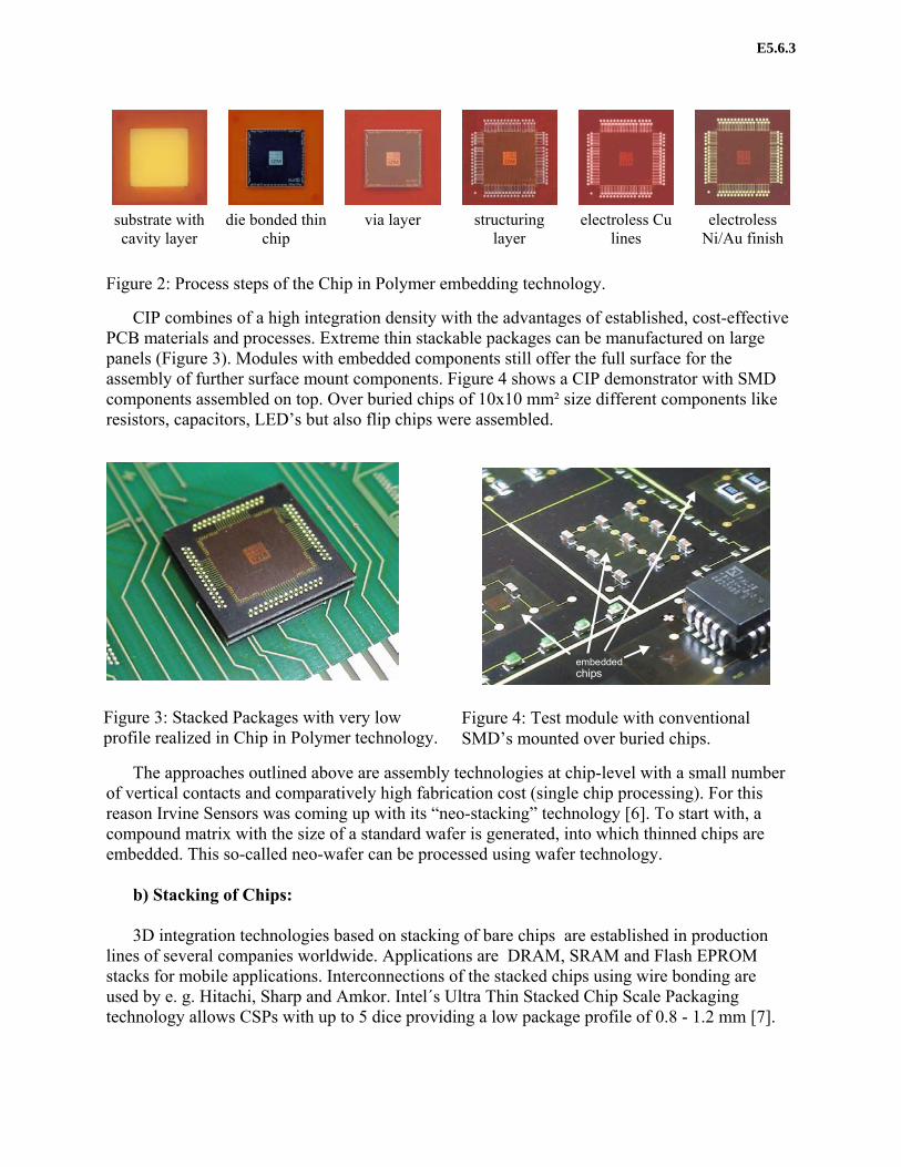
substrate with cavity layer
die bonded thin
chip
via layer
structuring
layer
electroless Cu
lines
electroless
Ni/Au finish Figure 2: Process steps of the Chip in Polymer embedding technology.
CIP combines of a high integration density with the advantages of established, cost-effective PCB materials and processes. Extreme thin stackable packages can be manufactured on large panels (Figure 3). Modules with embedded components still offer the full surface for the assembly of further surface mount components. Figure 4 shows a CIP demonstrator with SMD components assembled on top. Over buried chips of 10x10 mm² size different components like resistors, capacitors, LED’s but also flip chips were assembled.
embedded chips
The approaches outlined above are assembly technologies at chip-level with a small number
of vertical contacts and comparatively high fabrication cost (single chip processing). For this reason Irvine Sensors was coming up with its “neo-stacking” technology [6]. To start with, a compound matrix with the size of a standard wafer is generated, into which thinned chips are embedded. This so-called neo-wafer can be processed using wafer technology.
Figure 3: Stacked Packages with very low profile realized in Chip in Polymer technology.
Figure 4: Test module with conventional SMD’s mounted over buried chips.
b) Stacking of Chips: 3D integration technologies based on stacking of bare chips are established in production
lines of several companies worldwide. Applications are DRAM, SRAM and Flash EPROM stacks for mobile applications. Interconnections of the stacked chips using wire bonding are used by e. g. Hitachi, Sharp and Amkor. Intel´s Ultra Thin Stacked Chip Scale Packaging technology allows CSPs with up to 5 dice providing a low package profile of 0.8 - 1.2 mm [7].
E5.6.3

Other chip stacking approaches are using flip chip technique on silicon or flex interposer or combined techniques with flip chip and wire bond interconnects. Figure 5 shows a BGA (FR 4 substrate) with a flip chip mounted microcontroller on a silicon chip with redistributed IO-pads. The interconnects from the interposer to the substrate are wire bonds.
Si-Chip
Si-Chip
Substrat
Glob Top
Figure 5: Example of chip on chip integration technique on a BGA substrate using flip chip technique and wire bonds.
A so called face-down wafer level circuit integration technique is based on an extension of a standard redistribution technology for wafer-level-CSPs. In the approach of Fraunhofer IZM a base chip at wafer level will be used as an active substrate for smaller and thinner ICs. These thinned active components are assembled in flip chip fashion on the base IC using solder bumps. Large solder balls (> 300 µm) on the base chip can be utilized for the interconnect to the next package level. This technology uses thin film techniques to reroute the peripheral I/Os to an array of under bump metallization (UBM) pads. A low electrical resistivity of the rewiring metallization is achieved by electroplating copper. A low-k photo-definable layer (BCB) is used as the dielectric layer.
For performing an efficient 3D system integration it is necessary to consider the passive components of a system as well. In addition to size and cost saving the integration of passives leads to advantages in reliability and electrical behaviour. Wafer level processing enables the integration of resistors, inductors and capacitors into the redistribution process as well. Figure 6 shows the principle scheme of the integration concept.
single layer coildouble layer coil
parallel platecapacitor
thin filmresistor
single layer coildouble layer coil
parallel platecapacitor
thin filmresistor
Figure 6 : Principle of chip on chip integration technology (flip chip technique) with integrated passives in the redistribution layer on base circuit.
A different approach, the thin chip integration concept (TCI), can be used to avoid the flip
chip assembly process for the module. Key element of this technology are extremely thin completely processed wafers and chips. In contrast to existing packaging techniques the TCI concept uses 20 µm thin chips mounted on a base chip by adhesive or soldering. This technique offers excellent electrical properties of the wiring system and the interconnection of the active
E5.6.4

and passive devices. The signal transmission time for high speed memory modules will be reduced compared to single chip packages.
The process for TCI modules starts up with one type of bottom wafer carrying large base chips. The completely processed device wafers for the top IC have to be mounted on a carrier substrate by a reversible adhesive bond and undergo a backside thinning process until the thinned wafers show a remaining thickness of approximately 20 µm. The thinned chips are mounted on the active base wafer (bottom wafer) and covered by a photosensitive dielectric layer (BCB). BCB as dielectric layer offers excellent electrical properties, high temperature stability, very low water up-take with a medium curing temperature. A thin film redistribution process (Cu) is used to interconnect the top and carrier circuits. The wiring system is covered by a solder-mask (Photo-BCB). The similar process sequence can be used to integrate a second active device on top of the base wafer (see Figure 7). Finally the deposition of an under bump metallization and a solder bump deposition completes the manufacturing of the TCI module.
single layer coildouble layer coil
parallel platecapacitor
thin filmresistor
Figure 7: Principle of wafer-level chip on chip integration technique with two integrated active circuits on top of a base chip using thin film interconnects.
A similar approach of wafer-level 3D packaging, called Ultra Thin Chip Stacking UTCS, is developed by IMEC, Alcatel Espace, LAAS and the University of Barcelona [8]. It uses stacking of chips to a substrate wafer, embedding and interconnecting the thinned circuits with a modified multilayer thin film wiring.
A low cost process for wafer-level stacking of dice was reported by Infineon Technologies and Fraunhofer IZM [9]. The face-to-face stacking technology “SOLID” is limited to chip stacks with two vertically integrated device layers. Both, the mechanical bond and the electrical connections between the chips are realized by solid-liquid-interdiffusion of thin electroplated and structured Cu/Sn layers. Figure 8 shows a schematic cross section of the chip stack.
bottom chip
bond pad(e.g. wire bond)
top chip(face down)
redistribution inter chip via
Figure 8: Schematic of the Face-to-Face SOLID technology.
E5.6.5

c) Vertical System Integration: The principle of vertical system integration is characterized by very high density vertical
inter-chip wiring of stacked devices. Thinned device substrates (wafers or dice, respectively) are stacked by aligned bonding and electrically interconnected by free positioned inter-chip vias. A corresponding wafer stacking approach is developed by the Tohoku University in cooperation with CREST: by wafer bonding of a thinned top wafer to a bottom wafer, using doped poly-silicon filled inter-chip vias and Au/In micro bumps as vertical interconnects, they demonstrated the realization and basic operation of a 3D microprocessor consisting of three circuit layers [10]. However, the described high-density 3D integration technology is based on the generation of buried interconnects which requires essential interventions to the basic IC process technology, thus considerably increasing the fabrication costs. The Japanese Association of Super-Advanced Electronics Technologies (ASET) is currently working on wafer-level stacking concepts without interfering the basic IC process. One of their project targets is a “super-high density” 3D LSI chip integration technology for interconnecting more than five device layers by electroplated via holes through 50 - 70 µm thin device substrates (20 µm pitch) [11]. The results they are presenting are very promising [12]. Due to the comparatively large lateral size of the etched inter-chip vias (typically 10 - 20 µm), they are metallized by electroplating of copper. The challenge is to fill these very deep inter-chip vias without voids. For this reason high conformal – e. g. time-modulated – Cu plating techniques have to be applied with corresponding long deposition times (> 1 hour), which would result in rather high fabrication cost.
Fraunhofer IZM in cooperation with Infineon Technologies developed a wafer-to-wafer stacking technology based on low temperature bonding with polyimide as intermediate layer and a 3D metallization process which provides a very high density vertical wiring between the thinned device wafers by the use of W- or Cu-filled inter-chip vias. The so called InterChip-Via (ICV) technology is described in detail elsewhere [13]. Figure 9 shows the corresponding schematic of a vertically integrated device stack.
Top-Si (~ 10 µm)
FOX
ILD
Bottom-Si (~ 630 µm)
Polyimide
TEOS CMP
Plasmaoxide
Spacer 2
MOCVD-T
Plasmaoxide
Plasmanitride
TEOS CMP
Spacer 1
Passivation
Top-MetalStack-Metal
W-CVD
iN
FOX
ILD
Bottom Metal
E5.6.6
Figure 10: FIB of a vertically integrated test chip structure, showing 2.5 x 2.5 µm2 inter-chip vias (contact chain with 10 000 ICVs).
Figure 9: InterChip Via technology –Schematic of a vertically integrated device stack.

The ICV concept in principle is suitable for both, wafer-stacking and chip-to-wafer-stacking for vertical system integration. The wafer-stacking approach is well suited for 3D integration of devices with nearly identical chip areas. Prior to wafer stacking inter-chip vias (ICVs) with typically 1 - 3 µm diameter are prepared on the top wafer. The high aspect ratio ICVs are etched through all dielectric layers and typically 12 µm deep into the silicon. The wafer is then temporarily bonded onto a handling substrate by using a glue polymer and thinned with high uniformity until the ICVs are opened from the rear (remaining silicon thickness approximately 10 µm). After optical alignment of the stabilized top wafer versus a polyimide coated bottom wafer, the durable polyimide bond is established at approximately 400 °C and the handling substrate is removed. Now the inter-chip vias are opened to the bottom wafer’s metallization, laterally isolated with highly conformal O3 /TEOS and finally refilled with TiN/W CVD. Subsequently, a tungsten etch back process is applied for W-plug formation. The lateral electrical connection of the metallized inter-chip via with the metal level of the top wafer is done by opening contact windows on the top wafer followed by a standard Al metallization and passivation. Finally, the bond pads are opened and the 3D integrated device stacks can be tested, diced and packaged by use of standard procedures.
Figure 10 shows a FIB cross section of a vertically integrated test structure (contact chain with 10 000 ICVs, 2.5 x 2.5 µm2). Typical resistances of W-filled ICVs with e.g. 16 µm depth and 2.5 µm diameter (see Figure 11) are in the range of 1 Ohm. Figure 12 shows the corresponding relative resistance distribution for a wafer stack.
ICV Resistance, 147 samples
0%
5%
10%
15%
20%
25%
30%
35%
0 0,2 0,4 0,6 0,8 1 1,2 1,4 1,6 1,8 2 R [Ohm]
Rel
ativ
e D
istr
ibut
ion
10 µm W
Pl
Al
Al
Si
Figure 12: Relative distribution of 16 µm deep W-filled inter-chip vias (2.5 x 2.5 µm2).
Figure 11: ICV technology – FIB of a W-filled inter-chip via (2.5 x 2.5 µm2).
Wafer stacks fabricated according to the ICV technology show a very high vertical interconnect density of some 100 000 cm-2 with low contact resistance inter-chip vias. Reliability tests proved that the yield and functionality of nonvolatile memories basically are not affected by the corresponding thinning and bonding processes. Because the ICV technology is marked by the use of CMOS-compatible materials and process steps exclusively, it allows for fabrication of 3D SoC´s in standard semiconductor production lines.
E5.6.7

CHIP-TO-WAFER TECHNOLOGY FOR VERTICAL SYSTEM INTEGRATION Manufacturing technologies that largely rely on wafer fabrication processes show a
comparatively favorable cost structure. On the other hand wafer yield and chip area issues may speak against wafer stacking concepts. In consequence, so called chip-to-wafer technologies mainly based on wafer-level processes utilizing known good dice only, will be of advantage. In Figure 13 wafer-to-wafer and chip-to-wafer concepts for vertical system integration are shown in principle.
Figure 13: Vertical System Integration; wafer-to-wafer versus chip-to-wafer stacking concept for fabrication of vertical integrated systems.
Vertical system integration in general is based on thinning, adjusted bonding and vertical metallization of completely processed device substrates by inter-chip vias placed at arbitrary locations. For wafer stacking approaches, the step raster on the device wafers must be chosen identically. This is easily fulfilled for 3D integration of devices of the same kind (e.g. memories) but in the general case of different device areas, the handicap of processing with identical step raster would result in active silicon loss and in consequence increase the fabrication cost per die. In most cases this restriction is even more serious than the yield loss by stacking a non functional die to a good die. For chip-to-wafer stacking approaches the starting materials are completely processed wafers, too. After wafer-level testing, thinning and separation, known good dice of the top wafer are aligned bonded to the known good dice of a bottom wafer. This process step represents the only one on chip-level within the total vertical system integration sequence. The subsequent processing for vertical metallization is on wafer-scale again.
E5.6.8

In the case of the above described ICV technology based on polyimide bonding the process flow for chip-to-wafer is more complex and therefore cost-intensive mainly because of the need for lithography steps on a bottom wafer with mounted dice. E. g. non standard resist techniques have to be applied in order to process on a resulting large topography caused by stacked dice with minimum thickness of 20 µm. In consequence we are working on the development of a new vertical system integration technology with no need for additional process steps on stack level. The so-called ICV-SLID concept is based on the bonding of top chips to a bottom wafer by very thin Cu/Sn pads (thickness approximately 8 µm) which provide both, the electrical and the mechanical interconnect. The new approach combines the advantages of the well-established ICV process and the solid-liquid-interdiffusion technique which is already successfully applied for face-to-face die stacking [9]. The ICV-SLID concept is a non-flip concept. The top surface of the chip to be added is the top surface after stacking it to the substrate. The inter-chip vias are fully processed – etched and metallized as well – prior to the thinning sequence, with the advantage that the later stacking of the separated known good dice to the bottom device wafer is the final step of the 3D integration process flow. As a fully modular concept, it allows the formation of multiple device stacks. Figure 14 shows the schematic cross section of a vertically integrated circuit fabricated in accordance with the ICV-SLID concept, also indicating the stacking of a next level chip.
Level 2 chip,Si 10-50 µm
Level 3 chip
Figure 14: ICV-SLID technology: Schematic for the formation of multiple device stacks.
The introduced ICV-SLID process starts, if needed, with planarisation of the bottom substrate and the wafer of the subsequent stack layer. This is only necessary when IC technologies are used, which result in a final topography that exceeds about 1 µm. State-of-the-art technologies already use planarisation processes within the device fabrication sequences and end up with a comparatively low topography. The first essential step is the formation of inter-chip vias. The via etch, lateral isolation and metal filling is performed on wafers with standard thickness, thus resulting in basically defect-free inter-chip vias. The ICVs are connected to the contact wiring of the devices by a standard metallization (aluminum or copper, depending on the
E5.6.9

technology). The process sequence for the formation of the metallized inter-chip vias is described briefly: The ICVs with typically 1 - 3 µm diameter are prepared on a fully processed and tested device wafer by etching through all passivation and ILD layers, followed by a typically 12 µm deep silicon trench etch. For lateral via isolation, a highly conformal CVD of O3/TEOS-oxide is applied and the inter-chip vias are metallized by using MOCVD of tungsten (20 nm MOCVD-TiN as barrier layer) and etch back for metal plug formation (Figure 15). The lateral electrical connection of the W-filled inter-chip vias with the uppermost metal level of the device is performed by standard Al metallization. The devices are now ready for wafer-level test and selection. The last process sequence performed on the top wafer with standard thickness is through-mask electroplating of Cu. The top wafer is then temporarily bonded to a handling wafer and thinned with very high uniformity using precision grinding, wet chemical spin etching and a final CMP step until the W-filled vias are exposed from the rear (Figure 16).
Figure 15: Top device with W-filled inter-chip vias (12 µm depth, 2 x 2 µm²).
Figure 16: Bottom side of 10 µm thin top device stabilized by the handling substrate, showing tungsten plugs, opened from the rear.
After deposition of dielectric layers for electrical isolation and opening to the W-filled inter-chip vias, through-mask electroplating of a typically 8 µm thin copper/tin bilayer is applied. The surface is completely covered with the soldering metal; electrical contacts are formed by isolation trenches in the Cu/Sn layer and the remaining areas that are not used for electrical means serve as dummy areas for mechanical stabilization of the future stack. The bottom wafer is through-mask electroplated with Cu as the counterpart metal of the soldering metal system. Figure 17 shows the surface of the bottom wafer including alignment structures.
igure 17: Top side of the bottom wafer with through-mask electroplated copper. F
E5.6.10
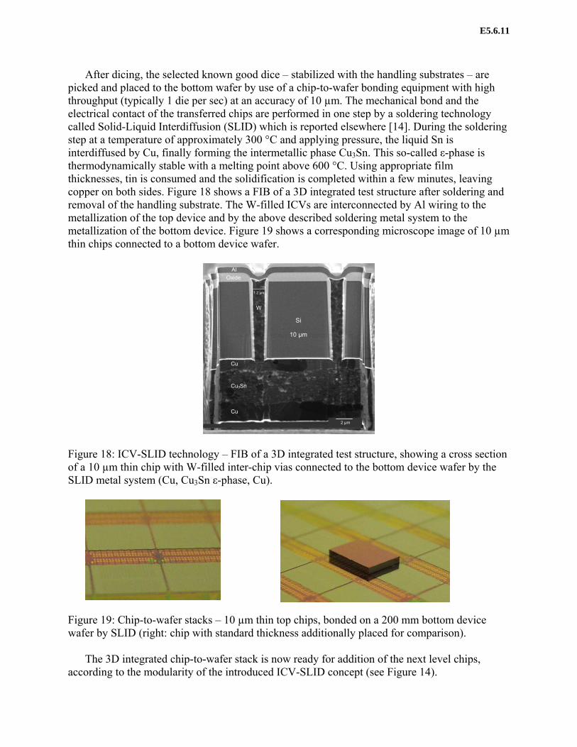
After dicing, the selected known good dice – stabilized with the handling substrates – are pick
y ng
ase is
leaving d
f 10 µm
ed and placed to the bottom wafer by use of a chip-to-wafer bonding equipment with highthroughput (typically 1 die per sec) at an accuracy of 10 µm. The mechanical bond and the electrical contact of the transferred chips are performed in one step by a soldering technologcalled Solid-Liquid Interdiffusion (SLID) which is reported elsewhere [14]. During the solderistep at a temperature of approximately 300 °C and applying pressure, the liquid Sn is interdiffused by Cu, finally forming the intermetallic phase Cu3Sn. This so-called ε-phthermodynamically stable with a melting point above 600 °C. Using appropriate film thicknesses, tin is consumed and the solidification is completed within a few minutes, copper on both sides. Figure 18 shows a FIB of a 3D integrated test structure after soldering anremoval of the handling substrate. The W-filled ICVs are interconnected by Al wiring to the metallization of the top device and by the above described soldering metal system to the metallization of the bottom device. Figure 19 shows a corresponding microscope image othin chips connected to a bottom device wafer.
Si
10 µm
Al
W
Cu
Cu3Sn
Cu
Oxide
2 µm
1.2 µm
igure 18: ICV-SLID technology – FIB of a 3D integrated test structure, showing a cross section Fof a 10 µm thin chip with W-filled inter-chip vias connected to the bottom device wafer by the SLID metal system (Cu, Cu3Sn ε-phase, Cu).
igure 19: Chip-to-wafer stacks – 10 µm thin top chips, bonded on a 200 mm bottom device
he 3D integrated chip-to-wafer stack is now ready for addition of the next level chips, according to the modularity of the introduced ICV-SLID concept (see Figure 14).
Fwafer by SLID (right: chip with standard thickness additionally placed for comparison).
T
E5.6.11

CO
Several outstanding technology concepts for 3D integration are currently in development, a few of them are already in production. Successful market entry will be determined by the performance improvement achieved and the profitability in relation to the total system cost. Manufacturing technologies largely relying on wafer fabrication processes show a comparatively favorable cost structure. Wafer yield and chip area issues may speak against wafer stacking concepts. In consequence, chip-to-wafer technologies mainly based on wafer-level processes utilizing known good dice only, will be of advantage. A corresponding new approach for vertical system integration, optimized to the capability for chip-to-wafer stacking, is introduced and discussed. The so-called ICV-SLID technology is based on adjusted bonding and vertical metallization of completely processed device substrates without interfering the basic IC process. The proposed wafer-level 3D integration concept has the potential for low cost fabrication of high-performance 3D-SoCs and is well suited as a replacement for embedded technologies. ACKNOWLEDGEMENTS This report is partly based on a project which is supported by the German Bundesministerium für Bildung und Forschung under support-no. 01M 2999 A. REFERENCES 1. International Technology Roadmap for Semiconductors (ITRS), http://public.itrs.net
NCLUSIONS
2. Y. Akasaka, Proc. IEEE 74, 1703 (1986). 3. C. L. Bertin, et al., IEEE Trans. on Components, Hybrids and Manufacturing Technology 16(8), 1006 (1993). 4. J. Barret, et al., Proc. IEEE Electronic Components and Technology Conference, 656 (1995). 5. A. Ostmann, A. Neumann, S. Welser, E. Jung, L. Böttcher, and H. Reichl, Proc. Polytronic Conference, 160 (2002). 6. K. D. Gann, HDI Magazine, December issue (1999). 7. www.intel.org 8. S. Pinel, A. Marty, J. Tasselli, J. Bailbe, E. Beyne, R. Van Hoof, S. Marco, J. Morante, O. Vendier, M. Huan, IEEE Trans. on Components and Packaging Technologies. 25(2), 244 (2002). 9. H. Hübner, O. Ehrmann, M. Eigner, W. Gruber, A. Klumpp, R. Merkel, P. Ramm, M. Roth, J. Weber, R. Wieland, Proc. Advanced Metallization Conference 2002 (AMC 2002), edited by B.M. Melnick, T.S. Cale, S. Zaima, T. Ohba (Mater. Res. Soc. Proc. V-18, Warrendale). 10. H. Kurino, T. Nakamura, K.W. Lee, Y. Igarashi, T. Mizokusa, Y. Yamada, T. Morooka, and M. Koyanagi, Proc. Advanced Metallization Conference 2001 (AMC 2001), edited by A.J. Mckerrow, Y. Shacham-Diamond, S. Zaima, T.Ohba (Mater. Res. Soc. Proc. V-17, Warrendale). 11. www.aset.or.jp 12. H. Yonemura, M. Tomisaka, M. Hoshino, K. Takahashi, H. Kadota, Proc. Advanced Metallization Conference 2002 (AMC 2002), edited by B.M. Melnick, T.S. Cale, S. Zaima, T. Ohba (Mater. Res. Soc. Proc. V-18, Warrendale). 13. P. Ramm, D. Bonfert, H. Gieser, J. Haufe, F. Iberl, A. Klumpp, A. Kux, R. Wieland, Proc. International Interconnect Technology Conference 2001 (IITC 2001), 160. 14. L. Bernstein, H. Bartolomew, Trans. Met. Soc. AIME 236, 404 (1966).
E5.6.12