3D Simulation of Base Carrier Transport Effects in Back Side Point Contact Silicon Solar Cells
31
Chapter 6 THREE-DIMENSIONAL SIMULATION OF BASE CARRIER TRANSPORT EFFECTS IN BACK SIDE POINT CONTACT SILICON SOLAR CELLS K. Kotsovos and K. Misiakos Institute of Microelectronics, NCSR Demokritos, Attiki, Greece ABSTRACT This work presents a theoretical investigation of rear junction point contact silicon solar cells through three-dimensional numerical simulation based on the solution of minority and majority carrier transport equations in the base of the cell. The device series resistance is evaluated through the simulated current-voltage (IV) curves under AM1.5 illumination conditions and its dependence on back contact geometry is examined. Results are presented which show the influence of the majority carrier transport in the base to the solar cell performance. A comparison is also performed with two other similar types of point contact solar cells, one with the emitter located on the front surface and the other on both surfaces, as well as with a conventional solar cell structure. I. INTRODUCTION Rear point contact (locally diffused) silicon solar cells with backside p/n junctions are structures which have already shown their promising potential in solar energy production, reaching very high conversion efficiency (27.5%) under concentrated illumination [1]. Although these devices were ideal for concentrator applications due to low series resistance and surface recombination losses, they have some additional interesting advantages, compared to typical solar cells designed for one-sun operating conditions. Specifically, since the metallization grid lies entirely on the back surface, there is no shading loss on the illuminated surface of the solar cell, while the interconnection of individual cells into modules Institute of Microelectronics, NCSR Demokritos, P. O Box 60228 153 10 Aghia Paraskevi, Attiki, Greece Tel: (+30)2106503113, Fax: (+30)2106511723, E-mail: [email protected]
-
Upload
independent -
Category
Documents
-
view
1 -
download
0
Transcript of 3D Simulation of Base Carrier Transport Effects in Back Side Point Contact Silicon Solar Cells
Chapter 6
THREE-DIMENSIONAL SIMULATION OF BASE
CARRIER TRANSPORT EFFECTS IN BACK SIDE POINT
CONTACT SILICON SOLAR CELLS
K. Kotsovos and K. Misiakos Institute of Microelectronics, NCSR Demokritos, Attiki, Greece
ABSTRACT
This work presents a theoretical investigation of rear junction point contact silicon solar
cells through three-dimensional numerical simulation based on the solution of minority
and majority carrier transport equations in the base of the cell. The device series
resistance is evaluated through the simulated current-voltage (IV) curves under AM1.5
illumination conditions and its dependence on back contact geometry is examined.
Results are presented which show the influence of the majority carrier transport in the
base to the solar cell performance. A comparison is also performed with two other similar
types of point contact solar cells, one with the emitter located on the front surface and the
other on both surfaces, as well as with a conventional solar cell structure.
I. INTRODUCTION
Rear point contact (locally diffused) silicon solar cells with backside p/n junctions are
structures which have already shown their promising potential in solar energy production,
reaching very high conversion efficiency (27.5%) under concentrated illumination [1].
Although these devices were ideal for concentrator applications due to low series resistance
and surface recombination losses, they have some additional interesting advantages,
compared to typical solar cells designed for one-sun operating conditions. Specifically, since
the metallization grid lies entirely on the back surface, there is no shading loss on the
illuminated surface of the solar cell, while the interconnection of individual cells into modules
Institute of Microelectronics, NCSR Demokritos, P. O Box 60228 153 10 Aghia Paraskevi, Attiki, Greece Tel:
(+30)2106503113, Fax: (+30)2106511723, E-mail: [email protected]
K. Kotsovos and K. Misiakos 2
is more easily implemented. However, this optimized solar cell design was considered to be
too complex for use at low concentrations, so a simplified structure was proposed by Sinton
et al. [2], suitable for cost-effective production. Therefore, SunPower Corporation has
developed a process for that purpose, providing solar cells fabricated on high quality FZ
substrates with efficiencies greater than 20% under normal sunlight [3]. The choice of high
quality material is necessary for this type of solar cells, since the photogenerated carriers need
to reach the back surface in order to be collected.
Results of theoretical simulations regarding the back contact structure have already been
published in the literature. A 3D model based on the solution of semiconductor transport
equations using a variational approach has been developed by Swanson [4-5], which was
applied in order to optimize the back point contact solar cell design under concentrated
illumination. An optimization of the interdigitated back contact cell was performed by Chin et
al. [6], while the simulated efficiency limit of this cell was calculated by Ohtsuka et al. [7] by
3D simulations. Epitaxial layer transfer has also been proposed as an alternative way to
produce back contact solar cells [8], where this method is used to create thin silicon films on
foreign substrates and a two-dimensional model was applied for this case.
The purpose of this work is a theoretical investigation of back junction point contact solar
cells by means of numerical three-dimensional simulation based on the solution of minority
and majority carrier transport equations in the base of the cell. The method is based on the
transformation in x and y dimensions of the basic partial differential equations through 2D
Fast Fourier Transform (FFT). In Fourier space these equations become algebraic in Kx and
Ky (the transformed x, y variables), thus reducing to ordinary differential equations with
respect to z, that can be solved in analytical form. The basic assumption for such a problem
reformulation is planar geometry and low injection. The solution of the transport equations
under illumination conditions provides the device IV characteristics and solar cell’s series
resistance is extracted. This model was previously used [9] to simulate a structure similar to
the PERL [10-11] solar cell, a device that is consisted of an emitter covering the front
illuminated surface and point contacts in the back surface. The same method was later applied
for the simulation of the double junction solar cell [12], a device with an additional emitter in
the back surface. Since the back junction point contact solar cell and the previous two types
of solar cells, are high efficiency structures, a direct comparison among them is performed.
The influence of back contact size and spacing in solar cell performance is discussed in detail.
The following section presents a description of the mathematical model of our method as
applied on the point contact structures under consideration. The third section includes our
simulation results and discussion.
II. MATHEMATICAL MODEL- SIMULATION ALGORITHM
II.1. Assumptions –Device Geometry
The base of the solar cells is considered to be under low injection conditions and assumed
as homogeneous with thickness w, while the junctions are infinitesimally shallow.
Photogeneration in the emitter regions is considered negligible, while their ohmic losses are
neglected. We set as x, y the directions parallel to the junction while z is the perpendicular
Three-Dimensional Simulation of Base Carrier Transport Effects… 3
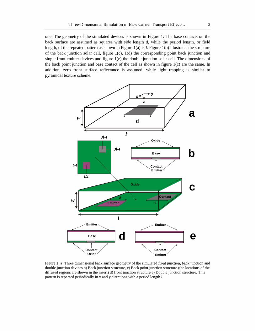
one. The geometry of the simulated devices is shown in Figure 1. The base contacts on the
back surface are assumed as squares with side length d, while the period length, or field
length, of the repeated pattern as shown in Figure 1(a) is l. Figure 1(b) illustrates the structure
of the back junction solar cell, figure 1(c), 1(d) the corresponding point back junction and
single front emitter devices and figure 1(e) the double junction solar cell. The dimensions of
the back point junction and base contact of the cell as shown in figure 1(c) are the same. In
addition, zero front surface reflectance is assumed, while light trapping is similar to
pyramidal texture scheme.
x y
z
d
d
d
l
l/4
l/4
3l/4
3l/4
l
w
w
a
b
c
d e
Emitter
Emitter
Emitter Emitter
Oxide Emitter
Base
Base
Contact
Contact
Contact Contact
Oxide
Oxide
Figure 1. a) Three dimensional back surface geometry of the simulated front junction, back junction and
double junction devices b) Back junction structure, c) Back point junction structure (the locations of the
diffused regions are shown in the insert) d) front junction structure e) Double junction structure. This
pattern is repeated periodically in x and y directions with a period length l
K. Kotsovos and K. Misiakos 4
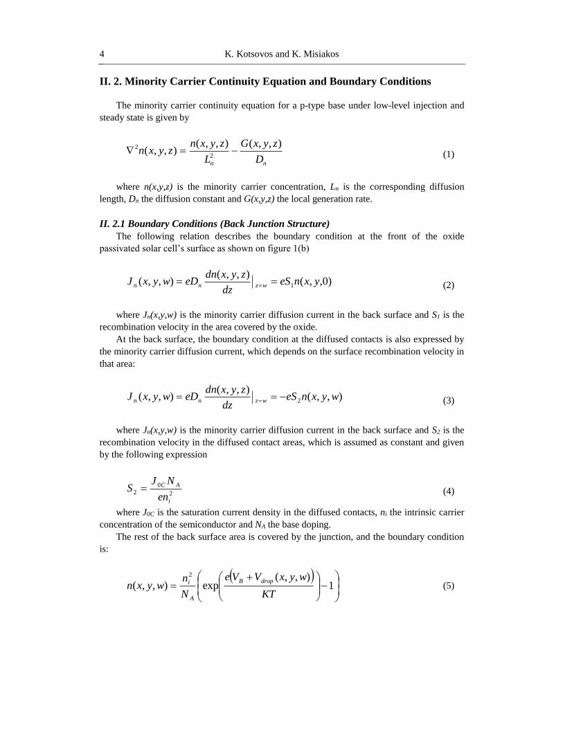
II. 2. Minority Carrier Continuity Equation and Boundary Conditions
The minority carrier continuity equation for a p-type base under low-level injection and
steady state is given by
nn D
zyxG
L
zyxnzyxn
),,(),,(),,(
2
2
(1)
where n(x,y,z) is the minority carrier concentration, Ln is the corresponding diffusion
length, Dn the diffusion constant and G(x,y,z) the local generation rate.
II. 2.1 Boundary Conditions (Back Junction Structure)
The following relation describes the boundary condition at the front of the oxide
passivated solar cell’s surface as shown on figure 1(b)
)0,,(),,(
),,( 1 yxneSdz
zyxdneDwyxJ wznn
(2)
where Jn(x,y,w) is the minority carrier diffusion current in the back surface and S1 is the
recombination velocity in the area covered by the oxide.
At the back surface, the boundary condition at the diffused contacts is also expressed by
the minority carrier diffusion current, which depends on the surface recombination velocity in
that area:
),,(),,(
),,( 2 wyxneSdz
zyxdneDwyxJ wznn
(3)
where Jn(x,y,w) is the minority carrier diffusion current in the back surface and S2 is the
recombination velocity in the diffused contact areas, which is assumed as constant and given
by the following expression
2
0
2
i
AC
en
NJS
(4)
where J0C is the saturation current density in the diffused contacts, ni the intrinsic carrier
concentration of the semiconductor and NA the base doping.
The rest of the back surface area is covered by the junction, and the boundary condition
is:
1
),,(exp),,(
2
KT
wyxVVe
N
nwyxn
dropB
A
i
(5)
Three-Dimensional Simulation of Base Carrier Transport Effects… 5
where VB is the junction bias voltage and Vdrop is the voltage drop caused by the majority
carrier flow through the base series resistance. This voltage drop is initially set to zero.
II. 2.2 Boundary Conditions (Back Point Junction Structure)
The front surface of this structure, shown on figure 1(c) is covered by oxide, so relation
(2) gives the expression of the boundary condition in that region. Expressions (3) and (5)
define the boundary conditions in the back diffused contacts and the junction area
respectively.
The rest of the back surface is oxide passivated, so the boundary condition is defined by
the minority carrier diffusion current
),,(),,(
),,( 3 wyxneSdz
zyxdneDwyxJ wznn
(6)
where S3 is the recombination velocity in the area covered by the back oxide.
II. 2. 3. Boundary Conditions (Front Junction Structure)
The emitter of the front junction solar cell, which is illustrated in figure 1(d) covers the
whole illuminated surface, so the boundary condition inside the junction is
1
)0,,(exp)0,,(
2
KT
yxVVe
N
nyxn
dropB
A
i
(7)
At the back surface, the minority carrier diffusion current is determined by the surface
recombination velocity, where in the diffused base contact regions is defined by relation (4),
while in the oxide passivated surface has a constant value (S1). Therefore, the general form of
the boundary condition at the back surface may be written as
),,(),(),,(
),,( wyxnyxeSdz
zyxdneDwyxJ wznn
(8)
II. 2. 4. Boundary Conditions (Double Junction Structure)
The double junction structure (fig. 1(e)) is consisted of an emitter covering the whole
front surface (as in the front junction device), so the boundary condition in that area is given
by (7). In a similar way, the conditions in the back surface are expressed by relations (3) and
(5) of section II.2.1. The front and back emitters of this device are biased with same voltage
VB.
II.3. Majority Carrier Voltage Drop Equation
The solution of continuity equation (1) may be used to obtain the voltage drop caused by
the majority carrier flow. We begin from the current density relation for the majority carriers
K. Kotsovos and K. Misiakos 6
peDpEeJ ppp (9)
Charge neutrality in the semiconductor is assumed, so it follows that δp(x,y,z)=δn(x,y,z).
Since the cell is operated under low injection, pNA, where NA is the base doping. Using these
assumptions and with the aid of (1), we differentiate (9)
nnAp
np
nn
p
Ap
n
nn
pApp
pApppApp
D
G
L
n
N
DDE
zGn
D
DENG
n
D
G
L
neDENeJ
neDENeJpeDENeJ
2
2
22
)(
The comparison of this equation with (1), gives a more compact expression
nDDN
V pn
Ap
22 )(1
(10)
where Dn, Dp are the diffusion constants for electron and holes respectively and μp is the
hole mobility. The solution of this equation provides the voltage drop due to majority carrier
flow and is subjected to the boundary conditions given in the next subsection.
II. 3.1. Boundary Conditions (Back Junction Structure)
Since there is no total current flow in the oxide covering the whole front surface of the
back junction solar cell, the majority carrier current value is exactly the opposite of the
minority carrier equivalent:
)0,,()0,,( 1 yxneSyxJ p (11)
At the back surface, the diffused back contact areas are considered as the ground
terminal, so the majority carrier voltage drop is zero:
0)w,y,x(Vdrop (12)
At the rest of the back surface area, covered by the rear junction, the majority carrier
current is given by
1
)),,((exp),,( 0
KT
wyxVVeJwyxJ
dropB
p
(13)
Three-Dimensional Simulation of Base Carrier Transport Effects… 7
where J0 is the emitter saturation current density. Expressions (11) and (13) can be
converted as boundary conditions for the electric field E if we make use of (9) with the
following way:
Ap
n
n
p
p
n
n
p
App
pAppppp
Ne
JD
DJ
EJD
DENeJ
neDENeJpeDpEeJ
(14)
The minority carrier current density Jn, which is required in expression (14) is obtained
from the solution of the continuity equation described in section II. 2.
II. 3.2. Boundary Conditions (Back Point Junction Structure)
The front surface of this structure is covered by oxide as in the case of the back junction
structure, so expression (11) defines the boundary condition in that region. Relations (12),
(13) also describe the boundary conditions inside the back diffused contact and junction areas
respectively, while the rest of the back surface is covered by oxide, so the following condition
holds
),,(),,( 3 wyxneSwyxJ p (15)
As reported on the previous subsection, the majority carrier expressions may be
converted to electric field boundary conditions by making use of (14).
II. 3.3. Boundary Conditions (Front Junction Structure)
The boundary condition for the majority current at the front surface and inside the
junction is written as:
1
))0,,((exp)0,,( 0
KT
yxVVeJyxJ
dropB
p
(16)
where J0 is the saturation current density in the emitter. The expression of the boundary
condition in the oxide-covered part of the back surface is also given by
),,(),,( 1 wyxneSwyxJ p (17)
The diffused back contact areas are considered as the ground terminal, where the majority
carrier voltage drop is given by (12).
K. Kotsovos and K. Misiakos 8
II. 3.3. Boundary Conditions (Double Junction Structure)
Since the front emitter of this structure covers the whole surface, relation (16) of the
previous subsection defines the boundary condition in that area. In a similar way, back
surface boundary conditions are expressed by relations (12) and (13) of section II.3.1.
II. 4. Algorithm Description
In this section we will provide a description of the algorithm, which is used to obtain a
numerical solution of the problem formulated in the previous subsections. The derived
expressions from the solutions of the minority carrier diffusion equation and the majority
carrier voltage drop equation are given in appendices B and C respectively.
II. 4. 1. Diffusion Equation Solution Algorithm
(1) The algorithm starts with an initial guess for the minority carrier concentrations in
front and back surface areas not covered by the emitters, while in the junction
regions the corresponding boundary conditions (depending on the investigated
structure) that define the minority carrier concentrations are applied. Majority
carrier voltage drop is initially set to zero.
(2) A two-dimensional Fast Fourier Transform (FFT) with respect to x, y is performed
to both surface concentrations and the minority carrier current density in Fourier
space is calculated by differentiating the general solution of the diffusion equation
with respect to z (appendix B).
(3) An inverse FFT is then applied to each of the transformed current densities to obtain
the real current densities at the areas not covered by the junctions, while at the
regions covered by oxide or the back contacts the current densities are acquired
from the boundary conditions.
(4) Subsequent Fast Fourier Transforms are used in order to calculate the new carrier
concentrations as functions of the transformed current densities )0,,(~
yxn kkJ ,
),,(~
wkkJ yxn (Appendix B).
(5) Inverse Fast Fourier Transforms are performed to the previously obtained carrier
concentrations to calculate the new estimated ones in real space.
(6) The solution is set as a mixture of the previously calculated and the newly obtained
minority carrier distributions with a defined percentage. If this solution fulfills the
convergence condition, the results are stored in order to proceed with the voltage
drop equation, else calculations are repeated from step 2.
II. 4. 2. Voltage Drop Equation Solution Algorithm
The results of the solution of the minority carrier diffusion equation are required in order
to obtain the majority carrier voltage drop. Therefore, the corresponding procedure for the
case of equation (10), which follows the one referred to the previous section, is described
through the following steps:
Three-Dimensional Simulation of Base Carrier Transport Effects… 9
(1) An initial guess for the majority carrier voltage drop (Vdrop) on both surfaces is used.
This is considered as zero. This estimate also fulfills the boundary condition at the
back-diffused contacts.
(2) Two-dimensional Fast Fourier Transforms with respect to x, y are performed to the
voltage distributions and the electric field distributions in Fourier space
)0,,(~
yx kkE , ),,(~
wkkE yx are calculated by differentiating the general solution of
equation (10) with respect to z (appendix C).
(3) An inverse FFT is then applied to each of the transformed electric field distributions
to obtain the corresponding values in real space, while at the regions covered by
oxide or the junctions the current densities are acquired from the boundary
conditions.
(4) In this step, Fast Fourier Transforms are used in order to obtain the electric field
distributions in Fourier space and the new transformed voltage
distributions )0,,(~
yx kkV , ),,(~
wkkV yx as functions of
)0,,(~
yx kkE , ),,(~
wkkE yx are calculated (appendix C).
(5) Inverse Fast Fourier Transforms are performed to the previously obtained voltage
distributions to calculate the new estimated equivalents in real space.
(6) The solution is set as a mixture of the previously calculated and the newly obtained
one in a similar way as that referred to in the previous subsection. If this solution
fulfills the convergence condition, the results are stored in order to be inserted in the
boundary conditions of the minority carrier diffusion equation, else calculations are
repeated from step 2.
II. 4. 3. Solution of the Final Coupled Problem
The separate solutions of the differential equations (1) and (10) are not necessarily self-
consistent for all working conditions, since the boundary conditions that define the minority
carrier diffusion equation depend on the calculated majority carrier voltage distribution in a
non-linear way. Therefore self-consistency should be achieved by following a proper iterative
procedure described as following:
(1) Calculation of the solution of equation (1) by following the steps described in
section II. 4.1. The calculations are performed under the assumption of zero voltage
drop.
(2) Numerical solution of equation (10) using the minority carrier currents and density
distributions as obtained previously.
(3) New solution of the minority carrier diffusion equation taking into account the
voltage distributions calculated from the previous step.
(4) The procedure continues between steps 2 and 3 until self-consistency is achieved.
K. Kotsovos and K. Misiakos 10
III. SIMULATION RESULTS
The substrate of the simulated solar cells is considered as monocrystalline silicon, with
base doping density NA=1016cm-3. We assume that the oxide-covered surfaces have ideal
passivation properties, so there are no recombination losses at these areas. Therefore, the
recombination velocity at these surfaces is zero while in the diffused contact regions is
calculated from the relation (4), where we assume that the recombination current in these
regions is J0c=10-12 A/cm2. The emitter saturation current value of all devices is the same (10-
13 A/cm2), while for all acquired results of the following sections III.1-III.4, a base diffusion
length Ln of 800μm is assumed. The mobilities for minority and majority carriers are taken
from Klaasen [13]. The simulated illumination is considered as the global AM1.5 sun
spectrum [14] normalized to 100mW/cm2, where light trapping similar to the pyramidal
textured scheme is assumed (Appendix A). The back surface contact has reflective
characteristics with reflectivity R=95%.
The simulation program, which is based on the algorithm of section II. 4 is used to
calculate the IV characteristic of the cell and from that curve the maximum power, the short
circuit current, the open circuit voltage and the series resistance of the cell are obtained. The
series resistance of the cell is calculated for each point of the curve using the following
relation
I
II
I
e
KTVV
R sc
sc
oc
s
ln
(18)
The value of Rs which is obtained by (18) is caused by the current crowding effect at the
back point contacts, since inside these regions current density values are large [9]. Such an
effect induces a voltage drop which rises fast near the base contact edges. This effect is more
intense in the back point junction structure, where near the back point emitter as shown in
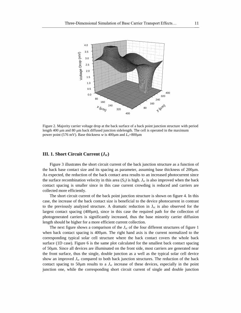
figure 2 an additional voltage drop is induced. The maximum voltage drop value is reached
inside the emitter area, where it remains constant. In this structure d/l equals 0.2, while the
period of the repeated pattern and the base thickness is 400μm.
Three-Dimensional Simulation of Base Carrier Transport Effects… 11
80
160
240
320
400
0.0
0.5
1.0
1.5
2.0
2.5
3.0
3.5
4.0
80
160
240
320
400
Vo
lta
ge
Dro
p (
mV
)
y (m
)x (m)
Figure 2. Majority carrier voltage drop at the back surface of a back point junction structure with period
length 400 μm and 80 μm back diffused junction sidelength. The cell is operated in the maximum
power point (576 mV). Base thickness w is 400μm and Ln=800μm
III. 1. Short Circuit Current (Jsc)
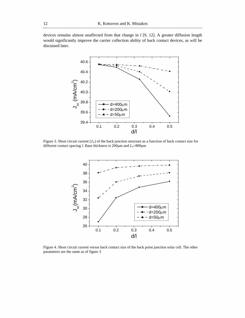
Figure 3 illustrates the short circuit current of the back junction structure as a function of
the back base contact size and its spacing as parameter, assuming base thickness of 200μm.
As expected, the reduction of the back contact area results to an increased photocurrent since
the surface recombination velocity in this area (S2) is high. Jsc is also improved when the back
contact spacing is smaller since in this case current crowding is reduced and carriers are
collected more efficiently.
The short circuit current of the back point junction structure is shown on figure 4. In this
case, the increase of the back contact size is beneficial to the device photocurrent in contrast
to the previously analyzed structure. A dramatic reduction in Jsc is also observed for the
largest contact spacing (400μm), since in this case the required path for the collection of
photogenerated carriers is significantly increased, thus the base minority carrier diffusion
length should be higher for a more efficient current collection.
The next figure shows a comparison of the Jsc of the four different structures of figure 1
when back contact spacing is 400μm. The right hand axis is the current normalized to the
corresponding typical solar cell structure where the back contact covers the whole back
surface (1D case). Figure 6 is the same plot calculated for the smallest back contact spacing
of 50μm. Since all devices are illuminated on the front side, most carriers are generated near
the front surface, thus the single, double junction as a well as the typical solar cell device
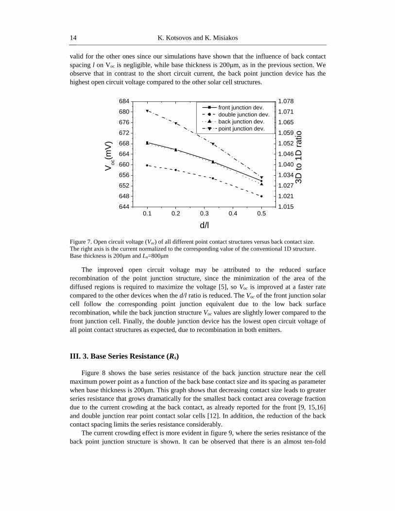
show an improved Jsc compared to both back junction structures. The reduction of the back
contact spacing to 50μm results to a Jsc increase of these devices, especially in the point
junction one, while the corresponding short circuit current of single and double junction
K. Kotsovos and K. Misiakos 12
devices remains almost unaffected from that change in l [9, 12]. A greater diffusion length
would significantly improve the carrier collection ability of back contact devices, as will be
discussed later.
0.1 0.2 0.3 0.4 0.539.4
39.6
39.8
40.0
40.2
40.4
40.6
Jsc (
mA
/cm
2)
d/l
d=400m
d=200m
d=50m
Figure 3. Short circuit current (Jsc) of the back junction structure as a function of back contact size for
different contact spacing l. Base thickness is 200μm and Ln=800μm
0.1 0.2 0.3 0.4 0.526
28
30
32
34
36
38
40
Jsc(m
A/c
m2)
d/l
d=400m
d=200m
d=50m
Figure 4. Short circuit current versus back contact size of the back point junction solar cell. The other
parameters are the same as of figure 3
Three-Dimensional Simulation of Base Carrier Transport Effects… 13
0.1 0.2 0.3 0.4 0.526
28
30
32
34
36
38
40
42
0.64
0.69
0.74
0.79
0.83
0.88
0.93
0.98
1.03
3D
to 1
D r
atio
Jsc(m
A/c
m2)
d/l
front junction device
double junction device
back junction device
point junction device
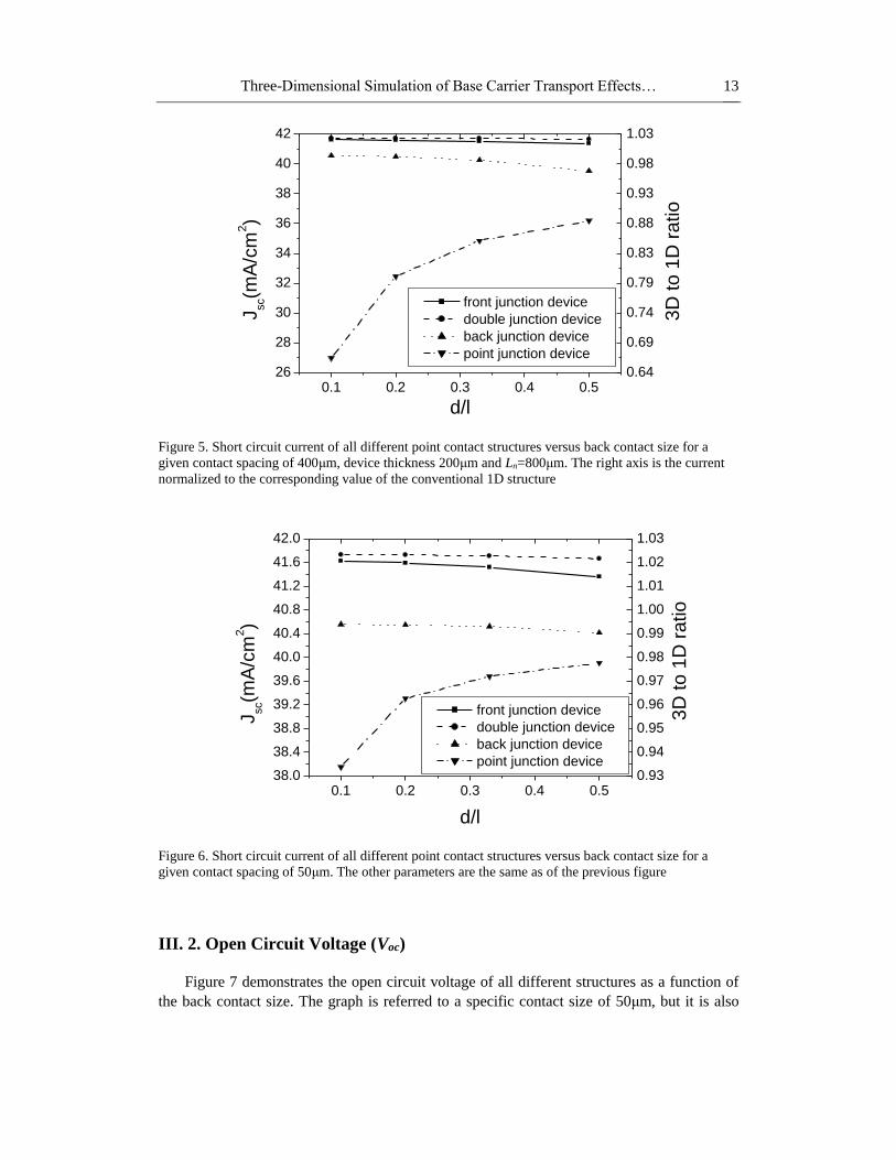
Figure 5. Short circuit current of all different point contact structures versus back contact size for a
given contact spacing of 400μm, device thickness 200μm and Ln=800μm. The right axis is the current
normalized to the corresponding value of the conventional 1D structure
0.1 0.2 0.3 0.4 0.538.0
38.4
38.8
39.2
39.6
40.0
40.4
40.8
41.2
41.6
42.0
0.93
0.94
0.95
0.96
0.97
0.98
0.99
1.00
1.01
1.02
1.03
3
D t
o 1
D r
atio
Jsc(m
A/c
m2)
d/l
front junction device
double junction device
back junction device
point junction device
Figure 6. Short circuit current of all different point contact structures versus back contact size for a
given contact spacing of 50μm. The other parameters are the same as of the previous figure
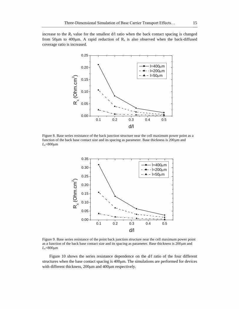
III. 2. Open Circuit Voltage (Voc)
Figure 7 demonstrates the open circuit voltage of all different structures as a function of
the back contact size. The graph is referred to a specific contact size of 50μm, but it is also
K. Kotsovos and K. Misiakos 14
valid for the other ones since our simulations have shown that the influence of back contact
spacing l on Voc is negligible, while base thickness is 200μm, as in the previous section. We
observe that in contrast to the short circuit current, the back point junction device has the
highest open circuit voltage compared to the other solar cell structures.
0.1 0.2 0.3 0.4 0.5644
648
652
656
660
664
668
672
676
680
684
1.015
1.021
1.027
1.034
1.040
1.046
1.052
1.059
1.065
1.071
1.078
3D
to
1D
ra
tio
Vo
c(m
V)
d/l
front junction dev.
double junction dev.
back junction dev.
point junction dev.
Figure 7. Open circuit voltage (Voc) of all different point contact structures versus back contact size.
The right axis is the current normalized to the corresponding value of the conventional 1D structure.
Base thickness is 200μm and Ln=800μm
The improved open circuit voltage may be attributed to the reduced surface
recombination of the point junction structure, since the minimization of the area of the
diffused regions is required to maximize the voltage [5], so Voc is improved at a faster rate
compared to the other devices when the d/l ratio is reduced. The Voc of the front junction solar
cell follow the corresponding point junction equivalent due to the low back surface
recombination, while the back junction structure Voc values are slightly lower compared to the
front junction cell. Finally, the double junction device has the lowest open circuit voltage of
all point contact structures as expected, due to recombination in both emitters.
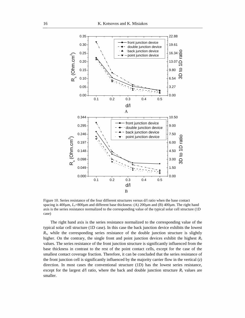
III. 3. Base Series Resistance (Rs)
Figure 8 shows the base series resistance of the back junction structure near the cell
maximum power point as a function of the back base contact size and its spacing as parameter
when base thickness is 200μm. This graph shows that decreasing contact size leads to greater
series resistance that grows dramatically for the smallest back contact area coverage fraction
due to the current crowding at the back contact, as already reported for the front [9, 15,16]
and double junction rear point contact solar cells [12]. In addition, the reduction of the back
contact spacing limits the series resistance considerably.
The current crowding effect is more evident in figure 9, where the series resistance of the
back point junction structure is shown. It can be observed that there is an almost ten-fold
Three-Dimensional Simulation of Base Carrier Transport Effects… 15
increase to the Rs value for the smallest d/l ratio when the back contact spacing is changed
from 50μm to 400μm. A rapid reduction of Rs is also observed when the back-diffused
coverage ratio is increased.
0.1 0.2 0.3 0.4 0.50.00
0.05
0.10
0.15
0.20
0.25
Rs (
Oh
m.c
m2)
d/l
l=400m
l=200m
l=50m
Figure 8. Base series resistance of the back junction structure near the cell maximum power point as a
function of the back base contact size and its spacing as parameter. Base thickness is 200μm and
Ln=800μm
0.1 0.2 0.3 0.4 0.50.00
0.05
0.10
0.15
0.20
0.25
0.30
0.35
Rs (
Oh
m.c
m2)
d/l
l=400m
l=200m
l=50m
Figure 9. Base series resistance of the point back junction structure near the cell maximum power point
as a function of the back base contact size and its spacing as parameter. Base thickness is 200μm and
Ln=800μm
Figure 10 shows the series resistance dependence on the d/l ratio of the four different
structures when the base contact spacing is 400μm. The simulations are performed for devices
with different thickness, 200μm and 400μm respectively.
K. Kotsovos and K. Misiakos 16
0.1 0.2 0.3 0.4 0.50.00
0.05
0.10
0.15
0.20
0.25
0.30
0.35
0.00
3.27
6.54
9.80
13.07
16.34
19.61
22.88
3D
to
1D
ra
tio
Rs (
Oh
m.c
m2)
d/l
front junction device
double junction device
back junction device
point junction device
A
0.1 0.2 0.3 0.4 0.50.000
0.049
0.098
0.148
0.197
0.246
0.295
0.344
0.00
1.50
3.00
4.50
6.00
7.50
9.00
10.50
3D
to
1D
ra
tio
Rs (
Oh
m.c
m2)
d/l
front junction device
double junction device
back junction device
point junction device
B
Figure 10. Series resistance of the four different structures versus d/l ratio when the base contact
spacing is 400μm, Ln=800μm and different base thickness: (A) 200μm and (B) 400μm. The right hand
axis is the series resistance normalized to the corresponding value of the typical solar cell structure (1D
case)
The right hand axis is the series resistance normalized to the corresponding value of the
typical solar cell structure (1D case). In this case the back junction device exhibits the lowest
Rs, while the corresponding series resistance of the double junction structure is slightly
higher. On the contrary, the single front and point junction devices exhibit the highest Rs
values. The series resistance of the front junction structure is significantly influenced from the
base thickness in contrast to the rest of the point contact cells, except for the case of the
smallest contact coverage fraction. Therefore, it can be concluded that the series resistance of
the front junction cell is significantly influenced by the majority carrier flow in the vertical (z)
direction. In most cases the conventional structure (1D) has the lowest series resistance,
except for the largest d/l ratio, where the back and double junction structure Rs values are
smaller.
Three-Dimensional Simulation of Base Carrier Transport Effects… 17
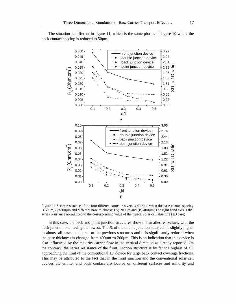
The situation is different in figure 11, which is the same plot as of figure 10 where the
back contact spacing is reduced to 50μm.
0.1 0.2 0.3 0.4 0.50.000
0.005
0.010
0.015
0.020
0.025
0.030
0.035
0.040
0.045
0.050
0.00
0.33
0.65
0.98
1.31
1.63
1.96
2.29
2.61
2.94
3.27
3D
to 1
D r
atio
Rs (
Ohm
.cm
2)
d/l
front junction device
double junction device
back junction device
point junction device
A
0.1 0.2 0.3 0.4 0.50.00
0.01
0.02
0.03
0.04
0.05
0.06
0.07
0.08
0.09
0.10
0.00
0.30
0.61
0.91
1.22
1.52
1.83
2.13
2.44
2.74
3.05
front junction device
double junction device
back junction device
point junction device
3D
to 1
D r
atio
Rs (
Ohm
.cm
2)
d/l B
Figure 11.Series resistance of the four different structures versus d/l ratio when the base contact spacing
is 50μm, Ln=800μm and different base thickness: (A) 200μm and (B) 400μm. The right hand axis is the
series resistance normalized to the corresponding value of the typical solar cell structure (1D case)
In this case, the back and point junction structures show the smallest Rs values, with the
back junction one having the lowest. The Rs of the double junction solar cell is slightly higher
in almost all cases compared to the previous structures and it is significantly reduced when
the base thickness is changed from 400μm το 200μm. This is an indication that this device is
also influenced by the majority carrier flow in the vertical direction as already reported. On
the contrary, the series resistance of the front junction structure is by far the highest of all,
approaching the limit of the conventional 1D device for large back contact coverage fractions.
This may be attributed to the fact that in the front junction and the conventional solar cell
devices the emitter and back contact are located on different surfaces and minority and
K. Kotsovos and K. Misiakos 18
majority carriers move to opposite directions, thus minority carrier flow opposes majority
carrier movement, while in the back and point junction devices, the diffused regions lie in the
same surface, so both minority and majority carriers flow towards the back surface. Therefore
in this case, the reduced series resistance values of the back and point junction structures, is a
clear advantage for concentrator applications, where ohmic losses need to be minimized, due
to the high current generated by the solar cell. The double junction structure is also a good
potential candidate for such applications since its series resistance is also low. It must be
additionally noted, that all structures except from the single front junction one, may reach
much lower Rs values compared to the conventional 1D device.
III. 3. Maximum Efficiency (η)
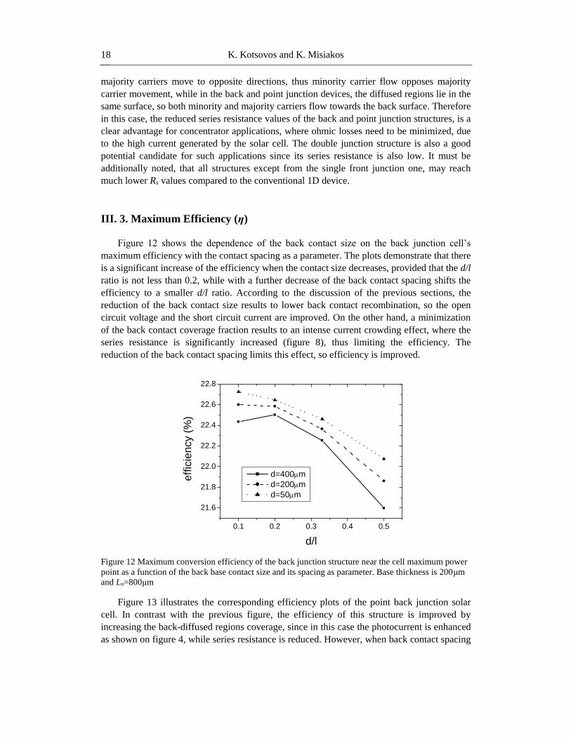
Figure 12 shows the dependence of the back contact size on the back junction cell’s
maximum efficiency with the contact spacing as a parameter. The plots demonstrate that there
is a significant increase of the efficiency when the contact size decreases, provided that the d/l
ratio is not less than 0.2, while with a further decrease of the back contact spacing shifts the
efficiency to a smaller d/l ratio. According to the discussion of the previous sections, the
reduction of the back contact size results to lower back contact recombination, so the open
circuit voltage and the short circuit current are improved. On the other hand, a minimization
of the back contact coverage fraction results to an intense current crowding effect, where the
series resistance is significantly increased (figure 8), thus limiting the efficiency. The
reduction of the back contact spacing limits this effect, so efficiency is improved.
0.1 0.2 0.3 0.4 0.5
21.6
21.8
22.0
22.2
22.4
22.6
22.8
effic
ien
cy (
%)
d/l
d=400m
d=200m
d=50m
Figure 12 Maximum conversion efficiency of the back junction structure near the cell maximum power
point as a function of the back base contact size and its spacing as parameter. Base thickness is 200μm
and Ln=800μm
Figure 13 illustrates the corresponding efficiency plots of the point back junction solar
cell. In contrast with the previous figure, the efficiency of this structure is improved by
increasing the back-diffused regions coverage, since in this case the photocurrent is enhanced
as shown on figure 4, while series resistance is reduced. However, when back contact spacing
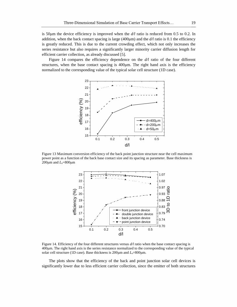
Three-Dimensional Simulation of Base Carrier Transport Effects… 19
is 50μm the device efficiency is improved when the d/l ratio is reduced from 0.5 to 0.2. In
addition, when the back contact spacing is large (400μm) and the d/l ratio is 0.1 the efficiency
is greatly reduced. This is due to the current crowding effect, which not only increases the
series resistance but also requires a significantly larger minority carrier diffusion length for
efficient carrier collection, as already discussed [5].
Figure 14 compares the efficiency dependence on the d/l ratio of the four different
structures, when the base contact spacing is 400μm. The right hand axis is the efficiency
normalized to the corresponding value of the typical solar cell structure (1D case).
0.1 0.2 0.3 0.4 0.515
16
17
18
19
20
21
22
23
eff
icie
ncy (
%)
d/l
d=400m
d=200m
d=50m
Figure 13 Maximum conversion efficiency of the back point junction structure near the cell maximum
power point as a function of the back base contact size and its spacing as parameter. Base thickness is
200μm and Ln=800μm
0.1 0.2 0.3 0.4 0.515
16
17
18
19
20
21
22
23
0.70
0.74
0.79
0.83
0.88
0.93
0.97
1.02
1.07
3D
to
1D
ratio
effic
ien
cy (
%)
d/l
front junction device
double junction device
back junction device
point junction device
Figure 14. Efficiency of the four different structures versus d/l ratio when the base contact spacing is
400μm. The right hand axis is the series resistance normalized to the corresponding value of the typical
solar cell structure (1D case). Base thickness is 200μm and Ln=800μm.
The plots show that the efficiency of the back and point junction solar cell devices is
significantly lower due to less efficient carrier collection, since the emitter of both structures
K. Kotsovos and K. Misiakos 20
is located on the back surface. As already discussed, the efficiency of the point junction solar
cell is severely limited by current crowding. The highest performing structures are the single
front and double junction solar cells, which have almost the same efficiency.
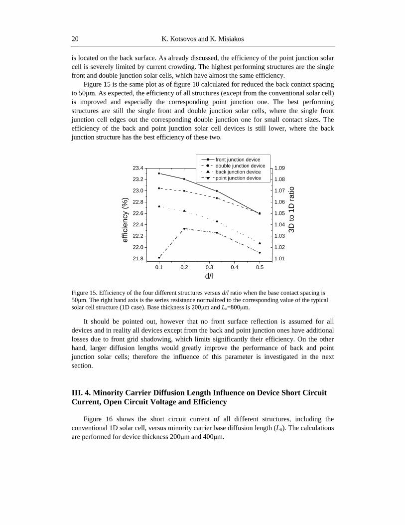
Figure 15 is the same plot as of figure 10 calculated for reduced the back contact spacing
to 50μm. As expected, the efficiency of all structures (except from the conventional solar cell)
is improved and especially the corresponding point junction one. The best performing
structures are still the single front and double junction solar cells, where the single front
junction cell edges out the corresponding double junction one for small contact sizes. The
efficiency of the back and point junction solar cell devices is still lower, where the back
junction structure has the best efficiency of these two.
0.1 0.2 0.3 0.4 0.5
21.8
22.0
22.2
22.4
22.6
22.8
23.0
23.2
23.4
1.01
1.02
1.03
1.04
1.05
1.06
1.07
1.08
1.09
3
D t
o 1
D r
atio
eff
icie
ncy (
%)
d/l
front junction device
double junction device
back junction device
point junction device
Figure 15. Efficiency of the four different structures versus d/l ratio when the base contact spacing is
50μm. The right hand axis is the series resistance normalized to the corresponding value of the typical
solar cell structure (1D case). Base thickness is 200μm and Ln=800μm.
It should be pointed out, however that no front surface reflection is assumed for all
devices and in reality all devices except from the back and point junction ones have additional
losses due to front grid shadowing, which limits significantly their efficiency. On the other
hand, larger diffusion lengths would greatly improve the performance of back and point
junction solar cells; therefore the influence of this parameter is investigated in the next
section.
III. 4. Minority Carrier Diffusion Length Influence on Device Short Circuit
Current, Open Circuit Voltage and Efficiency
Figure 16 shows the short circuit current of all different structures, including the
conventional 1D solar cell, versus minority carrier base diffusion length (Ln). The calculations
are performed for device thickness 200μm and 400μm.
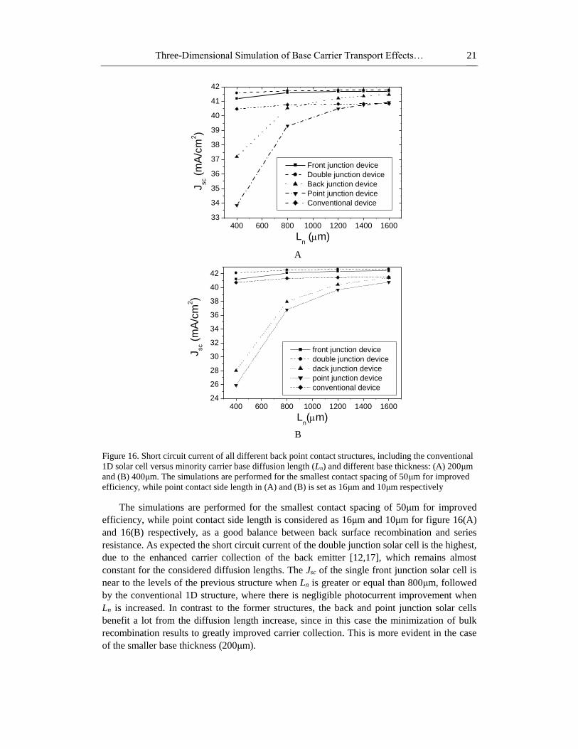
Three-Dimensional Simulation of Base Carrier Transport Effects… 21
400 600 800 1000 1200 1400 160033
34
35
36
37
38
39
40
41
42
Jsc (
mA
/cm
2)
Ln (m)
Front junction device
Double junction device
Back junction device
Point junction device
Conventional device
A
400 600 800 1000 1200 1400 160024
26
28
30
32
34
36
38
40
42
Jsc (
mA
/cm
2)
Ln(m)
front junction device
double junction device
dack junction device
point junction device
conventional device
B
Figure 16. Short circuit current of all different back point contact structures, including the conventional
1D solar cell versus minority carrier base diffusion length (Ln) and different base thickness: (A) 200μm
and (B) 400μm. The simulations are performed for the smallest contact spacing of 50μm for improved
efficiency, while point contact side length in (A) and (B) is set as 16μm and 10μm respectively
The simulations are performed for the smallest contact spacing of 50μm for improved
efficiency, while point contact side length is considered as 16μm and 10μm for figure 16(A)
and 16(B) respectively, as a good balance between back surface recombination and series
resistance. As expected the short circuit current of the double junction solar cell is the highest,
due to the enhanced carrier collection of the back emitter [12,17], which remains almost
constant for the considered diffusion lengths. The Jsc of the single front junction solar cell is
near to the levels of the previous structure when Ln is greater or equal than 800μm, followed
by the conventional 1D structure, where there is negligible photocurrent improvement when
Ln is increased. In contrast to the former structures, the back and point junction solar cells
benefit a lot from the diffusion length increase, since in this case the minimization of bulk
recombination results to greatly improved carrier collection. This is more evident in the case
of the smaller base thickness (200μm).
K. Kotsovos and K. Misiakos 22
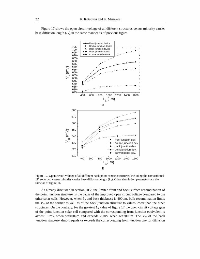
Figure 17 shows the open circuit voltage of all different structures versus minority carrier
base diffusion length (Ln) in the same manner as of previous figure.
400 600 800 1000 1200 1400 1600625630635640645650655660665670675680685690695700705
Voc(m
V)
Ln (m)
Front junction device
Double junction device
Back junction device
Point junction device
Conventional device
A
400 600 800 1000 1200 1400 1600610
620
630
640
650
660
670
680
front junction dev.
double junction dev.
back junction dev.
point junction dev.
conventional dev.
Vo
c (
mV
)
Ln(m)
B
Figure 17. Open circuit voltage of all different back point contact structures, including the conventional
1D solar cell versus minority carrier base diffusion length (Ln). Other simulation parameters are the
same as of figure 16
As already discussed in section III.2, the limited front and back surface recombination of
the point junction structure, is the cause of the improved open circuit voltage compared to the
other solar cells. However, when Ln and base thickness is 400μm, bulk recombination limits
the Voc of the former as well as of the back junction structure to values lower than the other
structures. On the contrary, for the greatest Ln value of figure 17 the open circuit voltage gain
of the point junction solar cell compared with the corresponding front junction equivalent is
almost 10mV when w=400μm and exceeds 20mV when w=200μm. The Voc of the back
junction structure almost equals or exceeds the corresponding front junction one for diffusion
Three-Dimensional Simulation of Base Carrier Transport Effects… 23
lengths greater than 800μm and w=200μm, while the voltage of the double junction structure
is significantly lower compared to the three previously referred solar cells due to front and
back emitter recombination. The conventional structure shows the most limited open circuit
voltage, which is more than 35mV lower than the corresponding back point junction one
when Ln is 1600μm and w=400μm, while this difference is increased to 60mV when
w=200μm.
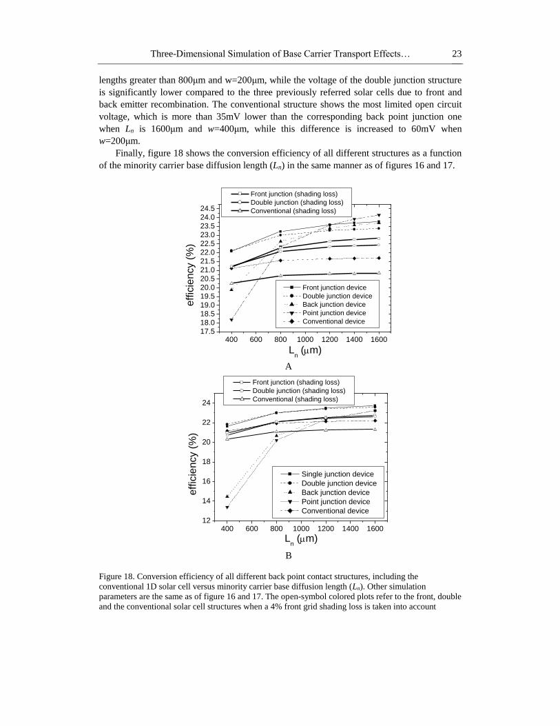
Finally, figure 18 shows the conversion efficiency of all different structures as a function
of the minority carrier base diffusion length (Ln) in the same manner as of figures 16 and 17.
400 600 800 1000 1200 1400 160017.5
18.0
18.5
19.0
19.5
20.0
20.5
21.0
21.5
22.0
22.5
23.0
23.5
24.0
24.5
Front junction (shading loss)
Double junction (shading loss)
Conventional (shading loss)
e
ffic
ien
cy (
%)
Ln (m)
Front junction device
Double junction device
Back junction device
Point junction device
Conventional device
A
400 600 800 1000 1200 1400 160012
14
16
18
20
22
24
Front junction (shading loss)
Double junction (shading loss)
Conventional (shading loss)
Single junction device
Double junction device
Back junction device
Point junction device
Conventional device
eff
icie
ncy (
%)
Ln (m)
B
Figure 18. Conversion efficiency of all different back point contact structures, including the
conventional 1D solar cell versus minority carrier base diffusion length (Ln). Other simulation
parameters are the same as of figure 16 and 17. The open-symbol colored plots refer to the front, double
and the conventional solar cell structures when a 4% front grid shading loss is taken into account
K. Kotsovos and K. Misiakos 24
As expected the point and back junction structures benefit the most from the diffusion
length increase due to more efficient carrier collection, where for diffusion lengths greater
than 800μm their efficiencies are almost equal, while the efficiency of the point junction solar
cell exceeds the corresponding back junction one by a small margin when Ln=1600μm and
w=400μm. In addition when w=400μm, these structures show superior performance compared
to the conventional solar cell, when Ln=1200μm or larger, while for the largest diffusion
length value of the graph, their efficiencies approach the levels of the single front and double
junction ones. This small efficiency premium (approximately 0.5% absolute for the case of
the single front junction cell and 0.34% for the double junction equivalent) is eliminated if
front surface grid shadowing is taken into account, as shown on the graphs where a 4%
shading loss is assumed. In this case, the back and point junction solar cells exhibit the
highest efficiencies when Ln is greater than 1200μm (Ln/w>3). If the device thickness is
reduced to 200μm and base diffusion length is greater than 1200μm (Ln/w>6), the point
junction cell shows the highest efficiency of all structures, neglecting shadowing losses.
When grid shadowing is set to 4%, the back and point junction structures reach higher
efficiencies compared to the single and double junction solar cells for diffusion lengths
greater than 800μm (Ln/w>4). Therefore, the choice of thin, high quality silicon wafers is
absolutely necessary for the fabrication of the back and point junction solar cells. Topsil
produces such FZ wafers with minority carrier lifetimes greater than 1ms for use in the PV
industry [18], while wafers grown under the MCZ method (magnetically confined
Czochralski) that are already used for the fabrication of high efficiency PERL structures [19]
are good candidates as a starting material and they cost less than electronic quality FZ wafers.
IV. CONCLUSION
In this work back junction, point contact (locally diffused) solar cells have been
investigated through 3D simulations and compared with corresponding single front junction,
double junction as well as conventional (1D) solar cell devices. It was shown that the
simulated base series resistance of the back junction structure reached significantly lower
values compared to the single front and double junction devices, especially for small back
contact spacing. The back point junction solar cell reached the highest open circuit voltage
due to reduced surface recombination, although current-crowding effects would severely
affect its efficiency by reducing the solar cell’s photocurrent and increasing the base series
resistance if the diffused areas are too small or too remotely spaced. A proper choice of back
diffused contact spacing and size, would result to low Rs, close to the values of the back
junction structure. Therefore, these cells are preferable for concentrator applications, since
their efficiency would be significantly less affected from resistive losses compared to the
single front junction back point contact solar cell and the conventional device. However, high
quality starting material and relatively thin substrates (Ln/w>4) are required so that these
devices reach efficiencies significantly higher than the conventional 1D device and close to or
higher than the single front or double junction structure. On the other hand, the double
junction solar cell could also be proposed as a very good choice for all applications, since it
performs marginally lower compared to the corresponding front junction one on high quality
Three-Dimensional Simulation of Base Carrier Transport Effects… 25
substrates, and it has the best efficiency on low quality ones. In addition its simulated base
series resistance reached values near to those of the back junction solar cells.
REFERENCES
[1] R. A.Sinton, Y. Kwark, J. Y. Gan, R. M. Swanson, IEEE Electron Device Lett., Vol. 7
(10), p.1855, 1986.
[2] R. A. Sinton and R. M. Swanson, IEEE Trans. on Electron Devices, Vol. 37 (10), p.348,
1990.
[3] W. Mullikan, D. Rose, M. J. Cudzinovic, D. M. De Ceuster, K. R. McIntosh, David D.
Smith, and R. M. Swanson, Proceedings of the 19 EPVSEC, Paris, France, p. 387, 2004.
[4] R. M. Swanson, EPRI Rep., AP-2859, 1983.
[5] R. M. Swanson, Solar Cells, Vol. 17, p. 85, 1986.
[6] D. J. Chin and Navon D. H., Solid State Electron., Vol. 24, p.109, 1981.
[7] H. Ohtsuka, Y. Ohkura, T. Uematsu and T. Warabisako, Prog. Photovoltaics: Res. Appl.,
Vol. 2, p. 275, 1994.
[8] Nichiporuk O., Kaminski A., Lemiti M., Fave A. and Skryshevski V, Sol. Energy Mat.
and Sol. Cells, 86, p. 517, 2005.
[9] K. Kotsovos and K. Misiakos, J. Appl. Phys., Vol. 89, p. 2491, 2001.
[10] J. Zhao, A. Wang, P. Altermatt and M. A. Green, Appl. Phys. Lett., Vol. 66 , p. 3646,
1995.
[11] Zhao J., Wang A., και Green M. A., Progr. In Photovoltaics: Res. Appl., Vol. 7, p. 471,
1999.
[12] K. Kotsovos and K. Misiakos, Sol. En. Mat. and Sol. Cells, Vol. 77, p. 209, 2003.
[13] D.B.M. Klaassen, Solid-State Electronics, Vol. 35, p. 953, 1992.
[14] R. Hulstrom R. Bird and C. Riordan, Solar Cells, Vol. 15, p. 365, 1985.
[15] Zhao J., Wang A., and Green M. A., Sol. Energy Mat. and Sol. Cells,Vol. 32, p. 89, 1994.
[16] Catchpole K. R. and Blakers A. W., Sol. Energy Mat. and Sol. Cells, 73, p. 189, 2002.
[17] E. Van Kerschaver, C. Zechner, and J. Dicker, IEEE Trans. El. Devices, Vol. 47 (4) , p.
711, 2000.
[18] Vedde J., Jensen L., Larsen T. and Klausen T., Proceedings of the 19 EPVSEC, Paris,
France, p. 1075, 2004.
[19] Zhao J., Wang A. and Green M. A., Progr. In Photovoltaics: Res. Appl., Vol. 8, p. 549,
2000.
APPENDIX A. LIGHT GENERATION PROFILE MODEL
The surface of the simulated devices is textured as shown in figure A.1. The back surface
is assumed reflective with a constant reflection coefficient Rb. This light-trapping scheme
improves the absorbing properties of the investigated material, since incoming rays enter the
cell with an angle of incidence, which is different than normal, so the material absorption
coefficient αi is increased according to the following relation.
K. Kotsovos and K. Misiakos 26
θ
Figure A.1. Assumed light trapping scheme used for the model calculations
sin
i
ieff
(A.1)
where αieff is the effective material absorption coefficient under a given wavelength,
while θ is the angle shown in figure A.1. Assuming that photon flux decays exponentially
with increasing depth and that light is coupled out after performing a double pass across the
cell, then the photon generation rate which is independent from x and y directions for all
wavelengths of the considered AM1.5 spectrum, is written as
)()()(1
1
1
1
)(zGegeRegzG
N
i
i
N
i
i
zw
iieff
w
b
z
iieffieffieffieff
(A.2)
where gi is the number of generated electron-hole pairs for the given wavelength i. By
substituting in (A.2), the generation rate in front and back surface are obtained
1
1
1
1
2)0()1()0(
N
i
i
N
i
i
w
biieff GeRgG ieff
(A.3)
1
1
1
1
)()()(N
i
i
N
i
i
w
b
w
iieff wGeRegwG ieffieff
(A.4)
The differentiation of (A.2) provides the following expression
1
1
1
1
)(2 )()()( N
i
i
N
i
i
zww
b
z
iieff zGeeRegdz
zdGieffieffieff
(A.5)
while the corresponding values for both surfaces are
Three-Dimensional Simulation of Base Carrier Transport Effects… 27
1
1
1
1
22
0
)0()1()( N
i
i
N
i
i
w
biieff
z
GeRgdz
zdGieff
(A.6)
1
1
1
1
2 )()()( N
i
i
N
i
i
w
b
w
iieff
wz
wGeRegdz
zdGieffieff
(A.7)
The expressions (A.2)-(A.7) will be used in the following sections for the solution of the
transport equations.
APPENDIX B. SOLUTION OF THE MINORITY CARRIER CONTINUITY
EQUATION
Performing a two-dimensional Fourier Transform on equation (1) the following
expression is obtained:
n
yx
n
yx
yx
D
zGzkkn
Lkk
dz
zkknd )(~
),,(~)1
(),,(~
2
22
2
2
(B.1)
where )(~
),,,(~ zGzkkn yx are the Fourier transforms with respect to x, y of
)(),,,( zGzyxn respectively. This is an ordinary differential equation with independent
variable z, which has the following general solution:
n
zR
yx
zR
yxyxD
zGkekkBekkAzkkn
)(~
),(),(),,(~1
11
(B.2)
where 222
11
nyx L
kkR and k1 is determined by differentiating (B.2) with respect
to z twice and equating the result with the right part of (B.1). By performing the necessary
operations and with the use of (A.2) we get
1
122
1 )(
)(~
),(),(),,(~ 11
N
i ieffn
izR
yx
zR
yxyxRD
zGekkBekkAzkkn
(B.3)
The solution defined by (B.3) incorporates the constants A and B, which should be
determined through the boundary conditions. These constants may be expressed as functions
of ),,(~),0,,(~ wkknkkn yxyx in the following way:
K. Kotsovos and K. Misiakos 28
wRwR
N
i ieffn
wR
iiyx
wR
yx
yxee
RD
eGwGwkknekkn
kkA11
1
1
1
122
1 )(
)0(~
)(~
),,(~)0,,(~
),(
(B.4)
wRwR
N
i ieffn
i
wR
iwR
yxyx
yxee
aRD
wGeGekknwkkn
kkB11
1
1
1
122
1 )(
)(~
)0(~
)0,,(~),,(~
),(
(B.5)
where )(~
),0(~
wGG are the carrier generation rates in the front and back surface
respectively and are given by (A.3) and (A.4).
The minority carrier diffusion current can be obtained by differentiating (B.3) with
respect to z
1
122
1
1)(
)(~
),(),(
),,(~),,(~
11
N
i ieffn
izR
yx
zR
yx
yx
n
yxn
RD
zGekkAekkBR
dz
zkknd
eD
zkkJ
(B.6)
After substituting (B.4) and (B.5) in (A.6) we get the final expressions for the current in
both surfaces:
1
122
1
1
122
1
1
)(
)0(~
)(
)(~
2)0(~
))(0,,(~),,(~2)0,,(
~
11
11
11
N
i ieffn
i
wRwR
N
i ieffn
i
wRwR
iwRwR
yxyx
n
yxn
RD
G
ee
RD
wGeeGeekknwkkn
ReD
kkJ
(B.7)
1
122
1
1
122
1
1
)(
)(~
)(
)(~
)0(~
2)0,,(~2))(,,(~
),,(~
11
11
11
N
i ieffn
i
wRwR
N
i ieffn
i
wRwR
i
yx
wRwR
yx
n
yxn
RD
wG
ee
RD
wGeeGkkneewkkn
ReD
wkkJ
(B.8)
where )(~
),0(~
wGG ii are defined in (A.6) and (A.7). The expressions (B.7) and (B.8)
may be used to calculate the minority carrier diffusion currents in Fourier space as a function
of the corresponding surface concentrations. The opposite procedure could be performed by
solving the system of (B.7) and (B.8) to obtain the transformed surface minority carrier
concentrations as a function of the corresponding diffusion currents
Three-Dimensional Simulation of Base Carrier Transport Effects… 29
1
122
111
1
122
1
1
1
1
122
1
)(
)0(~
)sinh(
1)(
)(~
),,(~
)coth()(
)0(~
)0,,(~
)0,,(~
N
i ieffn
i
N
i ieffn
i
yxn
N
i ieffn
i
yxn
yx
RD
G
wRR
RD
wGwkkJ
wRR
RD
GkkJ
kkn
(B.9)
1
122
1
1
1
1
122
1
11
1
122
1
)(
)(~
)coth()(
)(~
),,(~
)sinh(
1)(
)0(~
)0,,(~
),,(~
N
i ieffn
i
N
i ieffn
i
yxn
N
i ieffn
i
yxn
yx
RD
wGwR
R
RD
wGwkkJ
wRR
RD
GkkJ
wkkn
(B.10)
The expressions (B.7)-(B.10) are used to solve the diffusion equation by application of
the algorithm described in section II.4.1.
APPENDIX C. SOLUTION OF THE MAJORITY CARRIER VOLTAGE
DROP EQUATION
A similar analysis is used for the solution of equation (9), so by performing a two-
dimensional Fourier Transform in (9) and using (B.3) we get
1
122
1
22
2
2
2
1)(
1)(~
),(),(
),,(~),,(
~
11 N
i ieffnn
i
n
zR
yx
zR
yx
Ap
pn
yx
yx
RLD
zG
L
ekkBekkA
N
DD
zkkVRdz
zkkVd
(C.11)
where 22
yx kkR .This ordinary differential equation has the following general
solution when R0
1
122
1
2
3
2
21
11
1)(
1)(~
),(),(
),(),(),,(~
11 N
i ieffnn
i
n
zR
yx
zR
yx
Ap
pn
Rz
yx
Rz
yxyx
RLD
zGc
L
ekkBcekkAc
N
DD
ekkBekkAzkkV
(C.12)
where c1, c2, c3 are constants, which can be calculated by differentiating (C.12) with
respect to z twice and equating the result with the right part of (C.11). Therefore, by
completing these operations the general solution may written in the following form
K. Kotsovos and K. Misiakos 30
),,(~),(),(),,(~
11 zkknN
DDekkBekkAzkkV yx
Ap
npRz
yx
Rz
yxyx
(C.13)
The constants A1 and B1 may be expressed as a function of the transformed surface
voltage distributions in a similar manner as that of previous section
RwRw
yx
Rw
yxyx
Rw
yx
yxee
wkknekknkwkkVekkVkkA
)),,(~)0,,(~(),,(~
)0,,(~
),(1
1
(C.14)
RwRw
Rw
yxyx
Rw
yxyx
yxee
ekknwkknkekkVwkkVkkB
))0,,(~),,(~()0,,(~
),,(~
),(1
1
(C.15)
where
Ap
pn
N
DDk
1 . The electric field can be calculated through differentiation of
(C.13) with respect to z, as following
n
yxnRz
yx
Rz
yx
yxRz
yx
Rz
yx
yx
yx
eD
zkkJkekkBekkAR
dz
zkkndkekkBekkAR
dz
zkkVdzkkE
),,(~
,,
),,(~
,,),,(
~
),,(~
111
111
(C.16)
The substitution of (C.14) and (C.15) in (C.16) leads to the following expressions for the
electric field on both surfaces as a function of the corresponding voltage distributions
n
yxn
yxyx
yxyxyx
eD
kkJk
Rw
wkknkwkkVRwkknkkkVRkkE
)0,,(~
sinh
),,(~),,(~
coth)0,,(~)0,,(~
)0,,(~
1
1
1
(C.17)
n
yxn
yxyx
yxyx
yx
eD
wkkJk
RwwkknkwkkVRw
kknkkkVRwkkE
),,(~
)coth(),,(~),,(~
)sinh(
)0,,(~)0,,(~
),,(~
1
1
1
(C.18)
Three-Dimensional Simulation of Base Carrier Transport Effects… 31
Conversely, the surface voltage distributions may be related to the corresponding electric
fields by using (C.17) and (C.18)
)0,,(~
)sinh(
1
),,(~
),,(~
)coth(
)0,,(~
)0,,(~
)0,,(~
1
1
1
yx
n
yxn
yx
n
yxn
yx
yx
kknkRwR
eD
wkkJkwkkE
RwR
eD
kkJkkkE
kkV
(C.19)
),,(~)coth(
),,(~
),,(~
)sinh(
1
)0,,(~
)0,,(~
),,(~
1
1
1
wkknkRwR
eD
wkkJkwkkE
RwR
eD
kkJkkkE
wkkV
yx
n
yxn
yx
n
yxn
yx
yx
(C.20)
Expressions (C.17)-(C.20) are valid when R0 and may be used to solve equation (9) by
application of the algorithm described in section II.4.2. If R=0 the general solution of (9) is
reduced to the following simple form
),0,0(~)0,0()0,0(),0,0(~
111 znkBzAzV (C.21)
so the previously described procedure may be used to find the required relations for the
electric field on both surfaces depending on the voltage distributions and conversely.